Product Specification 1 / 34 LM240WU7 Liquid Crystal Display Ver. 1.0 Apr. 3 . 2009 SPECIFICATION FOR APPROVAL ( ) Preliminary Specification ( ● ) Final Specification 24.0” WUXGA TFT LCD Title MODEL BUYER LM240WU7 *MODEL SLA1 SUFFIX LG Display Co., Ltd. SUPPLIER *When you obtain standard approval, please use the above model name without suffix NDS Please return 1 copy for your confirmation with your signature and comments. / / / SIGNATURE DATE APPROVED BY H.S KIM / G.Manager MNT Products Engineering Dept. LG Display Co., Ltd. APPROVED BY SIGNATURE DATE REVIEWED BY PREPARED BY J.Y LEE / Manager [C] S.J Lee / Engineer G.T KIM / Manager [P] K.H MOON / Manager [M] Company Confidential PDF created with pdfFactory Pro trial version www.pdffactory.com

Welcome message from author
This document is posted to help you gain knowledge. Please leave a comment to let me know what you think about it! Share it to your friends and learn new things together.
Transcript

Product Specification
1 / 34
LM240WU7Liquid Crystal Display
Ver. 1.0 Apr. 3 . 2009
SPECIFICATIONFOR
APPROVAL
( ) Preliminary Specification( ● ) Final Specification
24.0” WUXGA TFT LCDTitle
MODEL
BUYER
LM240WU7*MODEL
SLA1SUFFIX
LG Display Co., Ltd.SUPPLIER
*When you obtain standard approval,
please use the above model name without suffix
NDS
Please return 1 copy for your confirmation with
your signature and comments.
/
/
/
SIGNATURE DATEAPPROVED BY
H.S KIM / G.Manager
MNT Products Engineering Dept.LG Display Co., Ltd.
APPROVED BYSIGNATURE
DATE
REVIEWED BY
PREPARED BY
J.Y LEE / Manager [C]
S.J Lee / Engineer
G.T KIM / Manager [P]
K.H MOON / Manager [M]
Compa
ny C
onfid
entia
l
PDF created with pdfFactory Pro trial version www.pdffactory.com
Product Specification
2 / 34
LM240WU7Liquid Crystal Display
Ver. 1.0 Apr. 3 . 2009
Contents
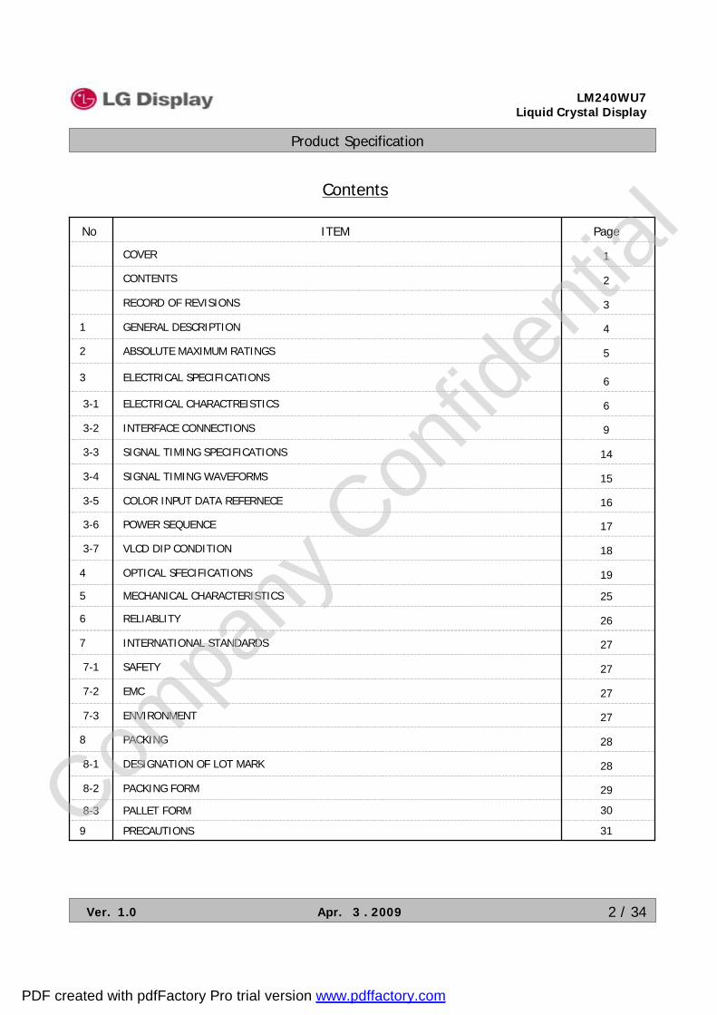
18VLCD DIP CONDITION3-7
27EMC7-2
31PRECAUTIONS9
17POWER SEQUENCE3-6
30PALLET FORM8-3
16
9INTERFACE CONNECTIONS3-2
COLOR INPUT DATA REFERNECE3-5
28DESIGNATION OF LOT MARK8-1
29PACKING FORM8-2
28PACKING8
27ENVIRONMENT7-3
1COVER
2CONTENTS
3RECORD OF REVISIONS
4GENERAL DESCRIPTION1
5ABSOLUTE MAXIMUM RATINGS2
6ELECTRICAL SPECIFICATIONS3
6ELECTRICAL CHARACTREISTICS3-1
14SIGNAL TIMING SPECIFICATIONS3-3
15SIGNAL TIMING WAVEFORMS3-4
19OPTICAL SFECIFICATIONS4
25MECHANICAL CHARACTERISTICS5
26RELIABLITY6
27INTERNATIONAL STANDARDS7
27SAFETY7-1
PageITEMNo
Compa
ny C
onfid
entia
l
PDF created with pdfFactory Pro trial version www.pdffactory.com

Product Specification
3 / 34
LM240WU7Liquid Crystal Display
Ver. 1.0 Apr. 3 . 2009
RECORD OF REVISIONS
Update the Optical specifications19
Updated the Mechanical Drawing27Apr. 3. 20091.0
Updated the Mechanical Drawing26
Update the Optical specifications19Mar. 17. 20090.2
Updated the Mechanical Drawing26, 27
Update the Electircal characteristics6
Update the General Features4Feb. 5. 20090.1
First Draft(Preliminary)-Nov. 7. 20080.0
DescriptionPageRevision DateRevision No
Compa
ny C
onfid
entia
l
PDF created with pdfFactory Pro trial version www.pdffactory.com

Product Specification
4 / 34
LM240WU7Liquid Crystal Display
Ver. 1.0 Apr. 3 . 2009
1. General Description
General Features
View Angle Free (R/L 178(Typ.), U/D 178(Typ.))Viewing Angle(CR>10)
0.270 mm x 0.270 mmPixel Pitch
8-bit, 16,777,216 colorsColor Depth
1920 horiz. By 1200 vert. Pixels RGB stripes arrangementPixel Format
400 cd/m2 ( Center 1 points)Luminance, White
Total 69.72 Watt (Typ.) ( 6.72 Watt@VLCD, 63 Watt @Vlamp)Power Consumption
2830 g (typ.) Weight
Transmissive mode, normally blackDisplay Operating Mode
Hard coating(3H), Anti-glare treatment of the front polarizerSurface Treatment
546.4(H) x 352.0(V) x 35.7(D) mm(Typ.) * without inverterOutline Dimension
24.1 inches(61.13cm) diagonalActive Screen Size
LM240WU7 is a Color Active Matrix Liquid Crystal Display with an integral Cold Cathode FluorescentLamp(CCFL) backlight system. The matrix employs a-Si Thin Film Transistor as the active element.It is a transmissive type display operating in the normally black mode. It has a 24inch diagonally measured active display area with WUXGA resolution (1200 vertical by 1920 horizontal pixel array)Each pixel is divided into Red, Green and Blue sub-pixels or dots which are arranged in vertical stripes.Gray scale or the brightness of the sub-pixel color is determined with a 8-bit gray scale signal for each dot,thus, presenting a palette of more than 16,7M(True) colors. It has been designed to apply the 8Bit 2 port LVDS interface.I t i s i ntended to support displays where high brightness, super wide viewing angle,high color saturation, and high color are important.
CN1(30pin)
LVDS
2port
+12.0V
Power Circuit Block
Source Driver Circuit
TFT - LCD Panel(1920 × RGB × 1200 pixels)
S1 S1920
RGB
TimingController
+12.0V
Back light Assembly(U-Shape 6CCFL)
2 x 6Sockets (High)VLamp
Compa
ny C
onfid
entia
l
PDF created with pdfFactory Pro trial version www.pdffactory.com
Product Specification
5 / 34
LM240WU7Liquid Crystal Display
Ver. 1.0 Apr. 3 . 2009
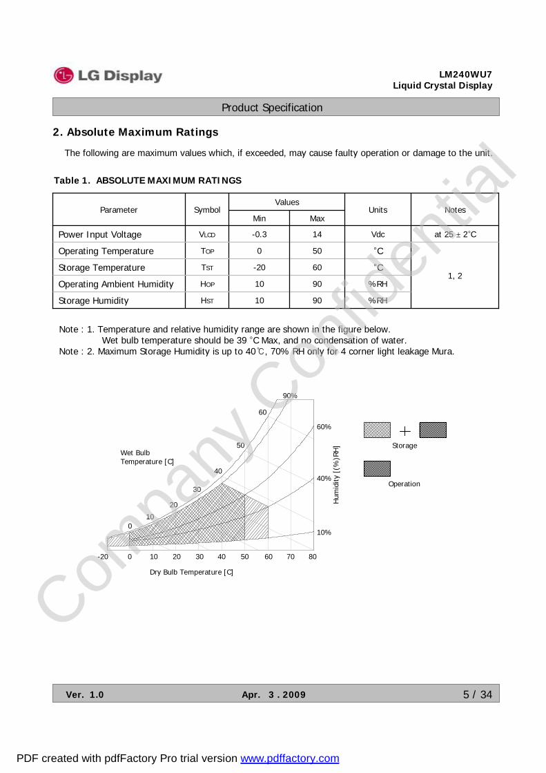
2. Absolute Maximum Ratings
The following are maximum values which, if exceeded, may cause faulty operation or damage to the unit.
Note : 1. Temperature and relative humidity range are shown in the figure below. Wet bulb temperature should be 39 °C Max, and no condensation of water.
Note : 2. Maximum Storage Humidity is up to 40℃, 70% RH only for 4 corner light leakage Mura.
Table 1. ABSOLUTE MAXIMUM RATINGS
Units
%RH9010HOPOperating Ambient Humidity
%RH9010HSTStorage Humidity
°C60-20TSTStorage Temperature1, 2
°C500TOPOperating Temperature
at 25 ± 2°CVdc14-0.3VLCDPower Input Voltage
MaxMinParameter Notes
ValuesSymbol
90%
10 20 30 40 50 60 70 800-20
010
20
30
40
50
Dry Bulb Temperature [C]
Wet BulbTemperature [C]
Storage
Operation
Hum
idity
[(%
)RH
]
10%
40%
60%
60
Compa
ny C
onfid
entia
l
PDF created with pdfFactory Pro trial version www.pdffactory.com
Product Specification
6 / 34
LM240WU7Liquid Crystal Display
Ver. 1.0 Apr. 3 . 2009
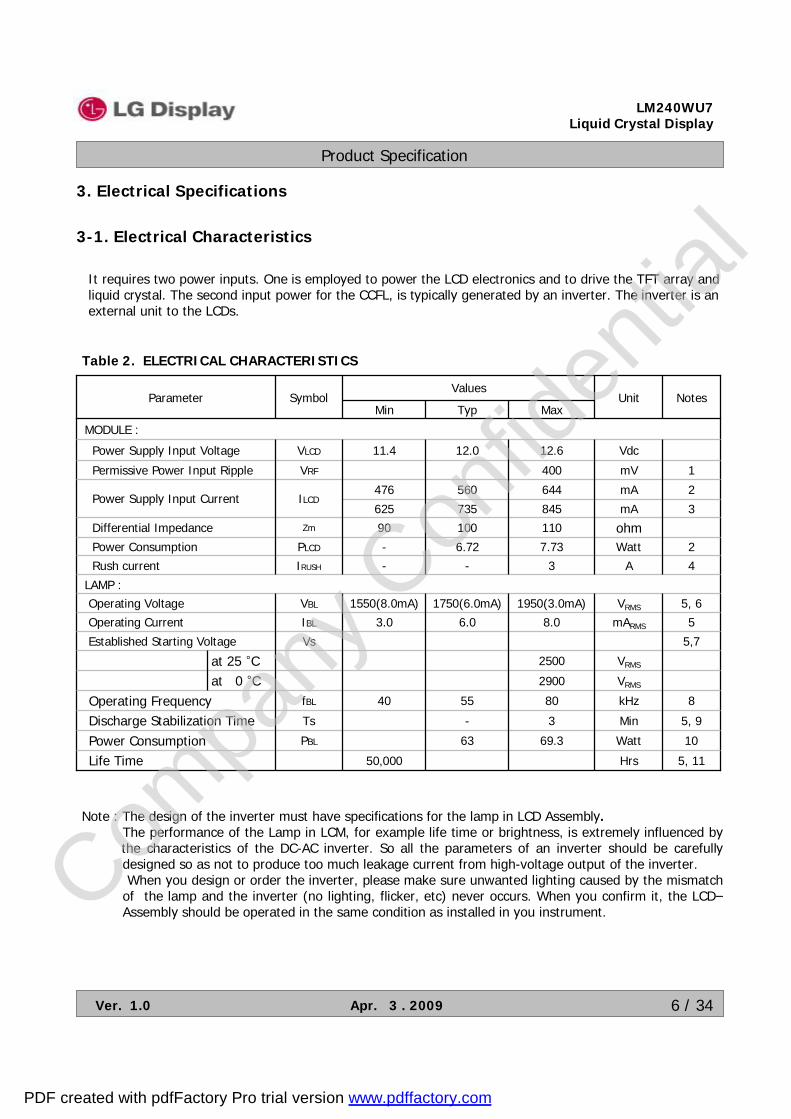
3. Electrical Specifications
3-1. Electrical Characteristics
Table 2. ELECTRICAL CHARACTERISTICS
It requires two power inputs. One is employed to power the LCD electronics and to drive the TFT array and liquid crystal. The second input power for the CCFL, is typically generated by an inverter. The inverter is an external unit to the LCDs.
5, 11Hrs50,000Life Time
LAMP :5, 6VRMS1950(3.0mA)1750(6.0mA) 1550(8.0mA)VBLOperating Voltage
5mARMS8.06.03.0IBLOperating Current
5,7VsEstablished Starting Voltage
VRMS2500at 25 °CVRMS2900at 0 °C
8kHz805540fBLOperating Frequency5, 9Min3-TsDischarge Stabilization Time10Watt69.363PBLPower Consumption
4A3--IRUSHRush current
MODULE :
2Watt7.736.72-PLCDPower Consumptionohm11010090ZmDifferential Impedance
Vdc12.612.011.4VLCDPower Supply Input Voltage
1mV400VRFPermissive Power Input Ripple
2mA644560476
3mA845735625ILCDPower Supply Input Current
Parameter SymbolMaxTypMin
NotesUnitValues
Note : The design of the inverter must have specifications for the lamp in LCD Assembly.The performance of the Lamp in LCM, for example life time or brightness, is extremely influenced bythe characteristics of the DC-AC inverter. So all the parameters of an inverter should be carefullydesigned so as not to produce too much leakage current from high-voltage output of the inverter.When you design or order the inverter, please make sure unwanted lighting caused by the mismatch
of the lamp and the inverter (no lighting, flicker, etc) never occurs. When you confirm it, the LCD–Assembly should be operated in the same condition as installed in you instrument.Com
pany
Con
fiden
tial
PDF created with pdfFactory Pro trial version www.pdffactory.com
Product Specification
7 / 34
LM240WU7Liquid Crystal Display
Ver. 1.0 Apr. 3 . 2009
Note : Do not Insert conducting Meterial to lamp connecting socket. If the conducting Meterial is inserted to the lamp connecting sockets, TFT-LCD Module has a low luminance and the inverter has abnormalaction. Because leakage current is occurred between lamp connecting socket and conducting material.
1. Permissive power ripple should be measured under VLCD=12.0V, 25 ± 2°C,fV=60Hz condition and At thattime, we recommend the bandwidth configuration of oscilloscope is to be under 20Mhz.
2. The specified current and power consumption are under the VLCD=12.0V, 25 ± 2°C,fV=60Hz condition whereas mosaic pattern(8 x 6) is displayed and fV is the frame frequency.
3. The current is specified at the maximum current pattern.4. The duration of rush current is about 2ms and rising time of power Input is 1ms(min.).5. Specified values are for a single lamp.6. Operating voltage is measured at 25 ± 2°C. The variance of the voltage is ± 10%.7. The voltage above VS should be applied to the lamps for more than 1 second for start-up.
(Inverter open voltage must be more than lamp starting voltage.)Otherwise, the lamps may not be turned on. The used lamp current is the lamp typical current.
8. The output of the inverter must have symmetrical(negative and positive) voltage waveform andsymmetrical current waveform (Unsymmetrical ratio is less than 10%). Please do not use the inverter which has unsymmetrical voltage and unsymmetrical current and spike wave. Lamp frequency may produce interface with horizontal synchronous frequency and as a result this maycause beat on the display. Therefore lamp frequency shall be as away possible from the horizontalsynchronous frequency and from its harmonics in order to prevent interference.
9. Let ’s define the brightness of the lamp after being lighted for 5 minutes as 100%.TS is the time required for the brightness of the center of the lamp to be not less than 95%.The used lamp current is the lamp typical current.
10. The lamp power consumption shown above does not include loss of external inverter.The used lamp current is the lamp typical current. (PBL = VBL x IBL x NLamp )
11. The life is determined as the time at which brightness of the lamp is 50% compared to that of initial value at the typical lamp current on condition of continuous operating at 25 ± 2°C.
12. Requirements for a system inverter design, which is intended to have a better display performance, a better power efficiency and a more reliable lamp, are following. It shall help increase the lamp lifetime and reduce leakage current.
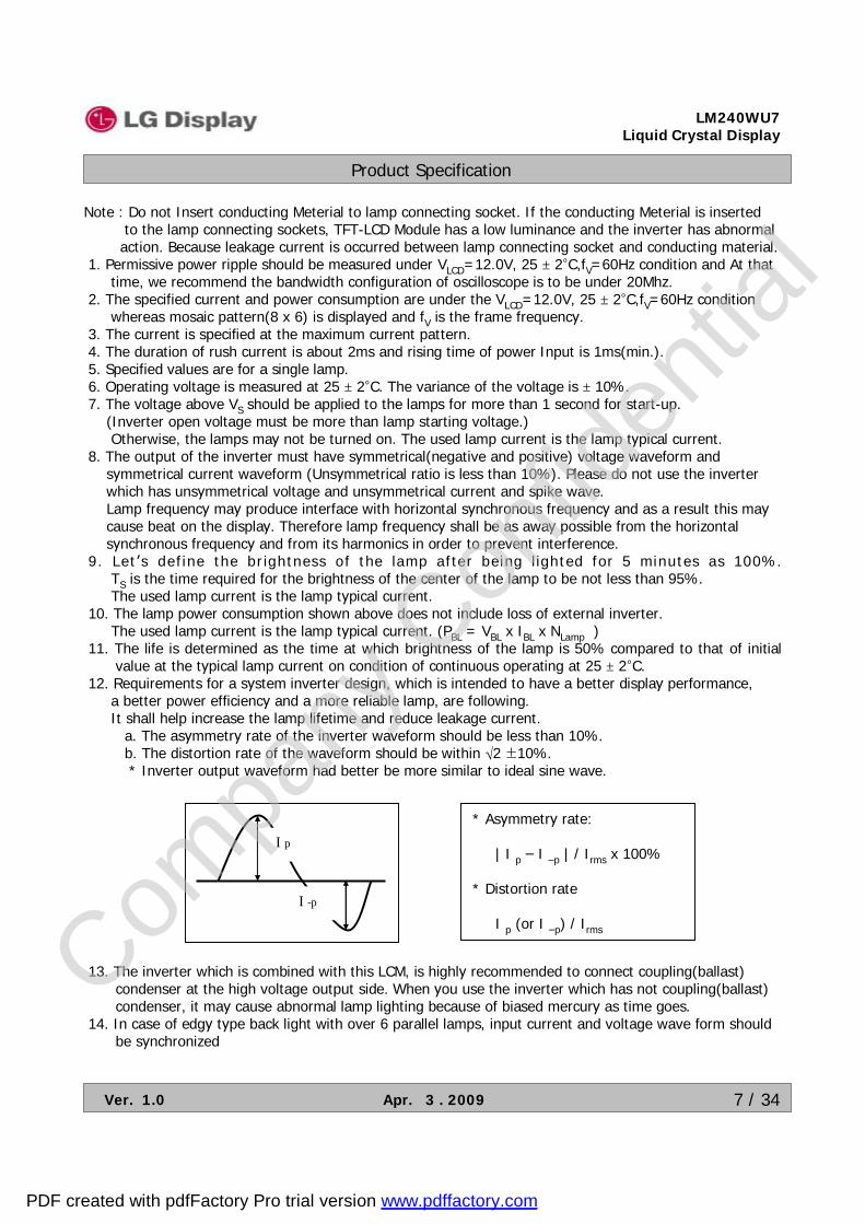
a. The asymmetry rate of the inverter waveform should be less than 10%. b. The distortion rate of the waveform should be within √2 ±10%. * Inverter output waveform had better be more similar to ideal sine wave.
I p
I -p
* Asymmetry rate:
| I p – I –p | / Irms x 100%
* Distortion rate
I p (or I –p) / Irms
13. The inverter which is combined with this LCM, is highly recommended to connect coupling(ballast) condenser at the high voltage output side. When you use the inverter which has not coupling(ballast) condenser, it may cause abnormal lamp lighting because of biased mercury as time goes.
14. In case of edgy type back light with over 6 parallel lamps, input current and voltage wave form should be synchronized
Compa
ny C
onfid
entia
l
PDF created with pdfFactory Pro trial version www.pdffactory.com

Product Specification
8 / 34
LM240WU7Liquid Crystal Display
Ver. 1.0 Apr. 3 . 2009
Mosaic Pattern(8 x 6)
Typical current pattern
(White : 255Gray, Black : 0Gray)Maximum current pattern
White Pattern
< Power consumption (VLCD=12.0V, 25 ± 2°C,fV=60Hz) >
Black Pattern
< Permissive Power Input Ripple (VLCD=12.0V, 25 ± 2°C,fV=60Hz) >
White Pattern
[ Figure 1 ] Mosaic pattern & Black Pattern for power consumption measurement
Compa
ny C
onfid
entia
l
PDF created with pdfFactory Pro trial version www.pdffactory.com

Product Specification
9 / 34
LM240WU7Liquid Crystal Display
Ver. 1.0 Apr. 3 . 2009
3-2. Interface Connections
Table 3 MODULE CONNECTOR(CN1) PIN CONFIGURATION
- LCD Connector(CN1) : IS100-L30B-C23 (UJU), KDF71G-30S-1H (Hirose ) or Equivalent- Mating Connector : FI-X30C2L (Manufactured by JAE) or Equivalent
3-2-1. LCD Module
Note: 1. All GND(ground) pins should be connected together and to Vss which should also be connected to the LCD’s metal frame.
2. All VLCD (power input) pins should be connected together.3. Input Level of LVDS signal is based on the EIA 664 Standard.
VLCD
VLCD
ODC ON
PWM
OPEN
OPEN
GND
SR3P
SR3M
SCLKINP
SCLKINM
SR2P
SR2M
GND
SR1P
Symbol
30
29
28
27
26
25
24
23
22
21
20
19
18
17
16
No
Power Supply +12.0V
Power Supply +12.0V
ODC ON/OFF ControlH : ODC ON , L : ODC OFF Default : ODC ON ( No connection)
PWM_OUT for Wavy Noise
NC
NC
Ground
Plus signal of even channel 3 (LVDS)
Minus signal of even channel 3 (LVDS)
Plus signal of even clock channel (LVDS)
Minus signal of even clock channel (LVDS)
Plus signal of even channel 2 (LVDS)
Minus signal of even channel 2 (LVDS)
Ground
Plus signal of even channel 1 (LVDS)
Description
Minus signal of even channel 1 (LVDS)
Ground
Plus signal of even channel 0 (LVDS)
Minus signal of even channel 0 (LVDS)
Plus signal of odd channel 3 (LVDS)
Minus signal of odd channel 3 (LVDS)
Plus signal of odd clock channel (LVDS)
Minus signal of odd clock channel (LVDS)
Ground
Plus signal of odd channel 2 (LVDS)
Minus signal of odd channel 2 (LVDS)
Plus signal of odd channel 1 (LVDS)
Minus signal of odd channel 1 (LVDS)
Plus signal of odd channel 0 (LVDS)
Minus signal of odd channel 0 (LVDS)
Description
SR1M15
GND14
SR0P13
SR0M12
FR3P11
FR3M10
FCLKINP9
FCLKINM8
GND7
FR2P6
FR2M5
FR1P4
FR1M3
FR0P2
FR0M1
SymbolNo
301
User Connector Diagram
IS100-L30B-C23(UJU)
#1 #30
Rear view of LCM
Compa
ny C
onfid
entia
l
PDF created with pdfFactory Pro trial version www.pdffactory.com

Product Specification
10 / 34
LM240WU7Liquid Crystal Display
Ver. 1.0 Apr. 3 . 2009
Table 4. REQUIRED SIGNAL ASSIGNMENT FOR Flat Link (TI:SN75LVDS83) Transmitter
Notes : Refer to LVDS Transmitter Data Sheet for detail descriptions.
Pin # Require SignalPin Name Pin # Require SignalPin Name
1 Power Supply for TTL InputVCC 29 Ground pin for TTLGND
2 TTL Input (R7)D5 30 TTL Input (DE)D26
3 TTL Input (R5)D6 31 TTL Level clock InputTX CLKIN
4 TTL Input (G0)D7 32 Power Down InputPWR DWN
5 Ground pin for TTLGND 33 Ground pin for PLLPLL GND
6 TTL Input (G1)D8 34 Power Supply for PLLPLL VCC
7 TTL Input (G2)D9 35 Ground pin for PLLPLL GND
8 TTL Input (G6)D10 36 Ground pin for LVDSLVDS GND
9 Power Supply for TTL InputVCC 37 Positive LVDS differential data output 3TxOUT3+
10 TTL Input (G7)D11 38 Negative LVDS differential data output 3TxOUT3-
11 TTL Input (G3)D12 39 Positive LVDS differential clock outputTX CLKOUT+
12 TTL Input (G4)D13 40 Negative LVDS differential clock outputTX CLKOUT-
13 Ground pin for TTLGND 41 Positive LVDS differential data output 2TX OUT2+
14 TTL Input (G5)D14 42 Negative LVDS differential data output 2TX OUT2-
15 TTL Input (B0)D15 43 Ground pin for LVDSLVDS GND
16 TTL Input (B6)D16 44 Power Supply for LVDSLVDS VCC
17 Power Supply for TTL InputVCC 45 Positive LVDS differential data output 1TX OUT1+
46 Negative LVDS differential data output 1TX OUT1-18 TTL Input (B7)D17
47 Positive LVDS differential data output 0TX OUT0+
48 Negative LVDS differential data output 0TX OUT0-
19 TTL Input (B1)D18
20 TTL Input (B2)D19
49 Ground pin for LVDSLVDS GND21 Ground pin for TTL InputGND
22 TTL Input (B3)D20
23 TTL Input (B4)D21
50 TTL Input (R6)D27
51 TTL Input (R0)D0
24 TTL Input (B5)D22
25 TTL Input (RSVD)D23
52 TTL Input (R1)D1
53 Ground pin for TTLGND
26 Power Supply for TTL InputVCC 54 TTL Input (R2)D2
55 TTL Input (R3)D327 TTL Input (HSYNC)D24
56 TTL Input (R4)D428 TTL Input (VSYNC)D25Compa
ny C
onfid
entia
l
PDF created with pdfFactory Pro trial version www.pdffactory.com
Product Specification
11 / 34
LM240WU7Liquid Crystal Display
Ver. 1.0 Apr. 3 . 2009
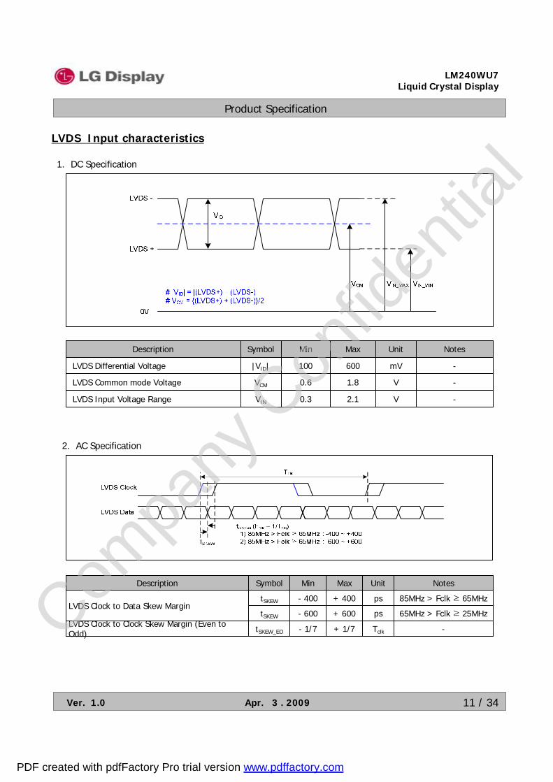
LVDS Input characteristics
NotesUnitMaxMinSymbolDescription
85MHz > Fclk ≥ 65MHzps+ 400- 400tSKEWLVDS Clock to Data Skew Margin
-
65MHz > Fclk ≥ 25MHz
- 1/7
- 600
Tclk+ 1/7tSKEW_EOLVDS Clock to Clock Skew Margin (Even to Odd)
ps+ 600tSKEW
-V2.10.3VINLVDS Input Voltage Range
-V1.80.6VCMLVDS Common mode Voltage
-mV600100|VID|LVDS Differential Voltage
NotesUnitMaxMinSymbolDescription
1. DC Specification
2. AC Specification
Compa
ny C
onfid
entia
l
PDF created with pdfFactory Pro trial version www.pdffactory.com

Product Specification
12 / 34
LM240WU7Liquid Crystal Display
Ver. 1.0 Apr. 3 . 2009
< Clock skew margin between channel >
< LVDS Data Format >
3. Data Format1) LVDS 2 Port
Compa
ny C
onfid
entia
l
PDF created with pdfFactory Pro trial version www.pdffactory.com
Product Specification
13 / 34
LM240WU7Liquid Crystal Display
Ver. 1.0 Apr. 3 . 2009
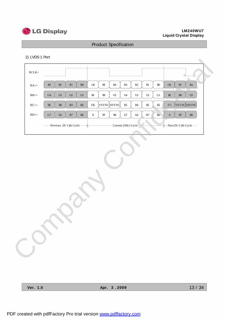
2) LVDS 1 Port
G0 R5 R4 R3 R2 R1 R0
B1 B0 G5 G4 G3 G2 G1
DE VSYNC HSYNC B5 B4 B3 B2
X B7 B6 G7 G6 R7 R6
R1 R0
G2 G1
B3 B2
R7 R6
G0
B1
DE
X
Current (Nth ) Cycle
R5 R4
B0 G5
VSYNC HSYNC
B7 B6
R3 R2
G4 G3
B5 B4
G7 G6
Previous (N-1)th Cycle Next (N+1)th Cycle
RCLK+
RA+/-
RB+/-
RC+/-
RD+/-
Compa
ny C
onfid
entia
l
PDF created with pdfFactory Pro trial version www.pdffactory.com

Product Specification
14 / 34
LM240WU7Liquid Crystal Display
Ver. 1.0 Apr. 3 . 2009
3-3. Signal Timing SpecificationsThis is signal timing required at the input of the TMDS transmitter. All of the interface signal timing should besatisfied with the following specifications for it’s proper operation.
Table 5. TIMING TABLE (VESA COORDINATED VIDEO TIMING)
tHP
tWV+ tVBP+ tVFP373533-Vertical Blank
432tVFPVertical Front Porch
272625tVBPVertical Back Porch
120012001200tVVVertical Valid
tCLK
tHP
SYMBOL
444036tHBPHorizontal Back Porch
282420tHFPHorizontal Front Porch
tWH+ tHBP+ tHFP848076-Horizontal Blank
Hz6159.9558.85fVFrequency
666tWVWidth-Active
161616tWHWidth-ActivetCLK
104410401036tHPPeriodHsync
tHP123712351233tVPPeriod
Vsync
960960960tHVHorizontal Valid
Data
Enable
MHz787776fCLKFrequency
Pixel frequency
: Typ. 154MHz
ns13.1612.9812.82tCLKPeriodDCLK
NoteUnitMaxTypMinITEM
Note: Hsync period and Hsync width-active should be even number times of tCLK. If the value is odd number times of tCLK, display control signal can be asynchronous. In order to operate this LCM a Hsync, Vsyn, and DE(data enable) signals should be used.
1. The performance of the electro-optical characteristics may be influenced by variance of the verticalrefresh rates.
2. Vsync and Hsync should be keep the above specification.3. Hsync Period, Hsync Width, and Horizontal Back Porch should be any times of of character
number(8).4. The polarity of Hsync, Vsync is not restricted.
Compa
ny C
onfid
entia
l
PDF created with pdfFactory Pro trial version www.pdffactory.com

Product Specification
15 / 34
LM240WU7Liquid Crystal Display
Ver. 1.0 Apr. 3 . 2009
3-4. Signal Timing Waveforms
Dclk
Hsync, Vsync, DE, DATA
tCLK 0.5VDD
VALID
INVALIDINVALID
DE(Data Enable)
0.7VDD
0.3VDD
DATA
Data are latched at the falling edge of DCLK
Hsync
DE(Data Enable)
DE(Data Enable)
tWH
tHP
tHFPtHBP
tVP
tWV
tVBPtVFP
tHV
tVV
Vsync
Compa
ny C
onfid
entia
l
PDF created with pdfFactory Pro trial version www.pdffactory.com

Product Specification
16 / 34
LM240WU7Liquid Crystal Display
Ver. 1.0 Apr. 3 . 2009
3-5. Color Input Data Reference
Table 6. COLOR DATA REFERENCE
The Brightness of each primary color(red,green,blue) is based on the 8-bit gray scale data input for the color;the higher the binary input, the brighter the color. The table below provides a reference for color versus data input.
0 0 0 0 0 0 0 00 0 0 0 0 0 0 00 0 0 0 0 0 0 0GREEN (000) Dark
GREEN
0 0 0 0 0 0 0 00 0 0 0 0 0 0 10 0 0 0 0 0 0 0GREEN (001)
............
0 0 0 0 0 0 0 01 1 1 1 1 1 1 00 0 0 0 0 0 0 0GREEN (254)
0 0 0 0 0 0 0 01 1 1 1 1 1 1 10 0 0 0 0 0 0 0GREEN (255)
0 0 0 0 0 0 0 00 0 0 0 0 0 0 00 0 0 0 0 0 0 0RED (000) Dark
RED
0 0 0 0 0 0 0 00 0 0 0 0 0 0 00 0 0 0 0 0 0 1RED (001)
............
0 0 0 0 0 0 0 00 0 0 0 0 0 0 01 1 1 1 1 1 1 0RED (254)
0 0 0 0 0 0 0 00 0 0 0 0 0 0 01 1 1 1 1 1 1 1RED (255)
0 0 0 0 0 0 0 10 0 0 0 0 0 0 00 0 0 0 0 0 0 0BLUE (001)
............
1 1 1 1 1 1 1 00 0 0 0 0 0 0 00 0 0 0 0 0 0 0BLUE (254)
1 1 1 1 1 1 1 10 0 0 0 0 0 0 00 0 0 0 0 0 0 0BLUE (255)
BLUE (000) Dark
White
Yellow
Magenta
Cyan
Blue (255)
Green (255)
Red (255)
Black 0 0 0 0 0 0 0 00 0 0 0 0 0 0 00 0 0 0 0 0 0 0
BasicColor
0 0 0 0 0 0 0 00 0 0 0 0 0 0 01 1 1 1 1 1 1 1
0 0 0 0 0 0 0 01 1 1 1 1 1 1 10 0 0 0 0 0 0 0
1 1 1 1 1 1 1 10 0 0 0 0 0 0 00 0 0 0 0 0 0 0
1 1 1 1 1 1 1 11 1 1 1 1 1 1 10 0 0 0 0 0 0 0
1 1 1 1 1 1 1 10 0 0 0 0 0 0 01 1 1 1 1 1 1 1
0 0 0 0 0 0 0 01 1 1 1 1 1 1 11 1 1 1 1 1 1 1
1 1 1 1 1 1 1 11 1 1 1 1 1 1 11 1 1 1 1 1 1 1
BLUEMSB LSB
GREENMSB LSB
REDMSB LSB
B7 B6 B5 B4 B3 B2 B1 B0G7 G6 G5 G4 G3 G2 G1 G0R7 R6 R5 R4 R3 R2 R1 R0
0 0 0 0 0 0 0 00 0 0 0 0 0 0 00 0 0 0 0 0 0 0
BLUE
Color
Input Color Data
Compa
ny C
onfid
entia
l
PDF created with pdfFactory Pro trial version www.pdffactory.com

Product Specification
17 / 34
LM240WU7Liquid Crystal Display
Ver. 1.0 Apr. 3 . 2009
3-6. Power Sequence
Notes : 1. Please avoid floating state of interface signal at invalid period.2. When the interface signal is invalid, be sure to pull down the power supply for LCD VLCDto 0V.3. Lamp power must be turn on after power supply for LCD and interface signal are valid.
Interface Signal, Vi(Digital RGB signal, SCDT ,Vsync, Hsync, DE, Clock to PanelLinkTransmitter)
Power Supply for Backlight Inverter
Power Supply, VLCD
90%VLCD
90%
10% 10%
T10V
LAMP ONLAMP OFF
ms-500T7
ms50-0.01T2
ms
ms--500T3
--200T4
ms50-0.01T5
ms10-0.5T1
MaxTypMinUnits
ValuesParameter
Table 7. POWER SEQUENCE
T3
0V
T6
LAMP OFF
T4
T2 T5 T7
Valid Data
Compa
ny C
onfid
entia
l
PDF created with pdfFactory Pro trial version www.pdffactory.com
Product Specification
18 / 34
LM240WU7Liquid Crystal Display
Ver. 1.0 Apr. 3 . 2009
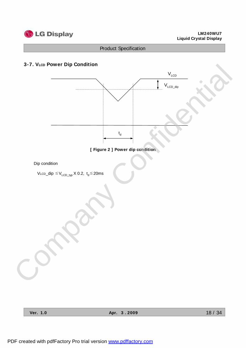
3-7. VLCD Power Dip Condition
Dip condition
VLCD_dip≤VLCD_typ X 0.2, td≤20ms
VLCD
td
[ Figure 2 ] Power dip condition
VLCD_dip
Compa
ny C
onfid
entia
l
PDF created with pdfFactory Pro trial version www.pdffactory.com

Product Specification
19 / 34
LM240WU7Liquid Crystal Display
Ver. 1.0 Apr. 3 . 2009
Optical characteristics are determined after the unit has been ‘ON’ for approximately 30 minutesin a dark environment at 25±2°C. The values specified are at an approximate distance 50cm from the LCDsurface at a viewing angle of Φ and θ equal to 0 ° and aperture 1 degree.FIG 3 presents additional information concerning the measurement equipment and method.
[ FIG 3 ] Optical Characteristic Measurement Equipment and Method
Table 8. OPTICAL CHARACTERISTICS (Ta=25 °C, VLCD=12.0V, fV=60Hz Dclk=154MHz, VBR=3.3V)
4. Optical Specifications
50cm
Optical Stage(x,y) LCD Module Pritchard 880 or equivalent
11000700CRContrast Ratio
5ms12--TGTG_MAX
5ms-5-TGTG_AVRGray to Gray
-178-θCST_VVertical6Degree
-178-θCST_HHorizontalColor Shift
-178θGMA_VVerticalEffective 8Degree
-178θGMA_HHorizontal
92.2Gray Scale
VerticalHorizontal
-178170θV7Degree
-178170θHGeneral
Viewing Angle (CR>10)
WHITE
BLUE
GREEN
RED
0.613Gy
0.304Gx
0.070By
0.146Bx
0.329Wy0.313Wx
Decay TimeRise Time
4ms127.5-TrD
0.335Ry
Typ+0.03
0.644
Typ-0.03
Rx
Color Coordinates [CIE1931]
4ms127.5-TrR
Response Time
3%75δ WHITELuminance Variation2cd/m2400320LWHSurface Luminance, white
NotesUnitsMaxTypMin
ValuesSymbolParameter
Compa
ny C
onfid
entia
l
PDF created with pdfFactory Pro trial version www.pdffactory.com
Product Specification
20 / 34
LM240WU7Liquid Crystal Display
Ver. 1.0 Apr. 3 . 2009
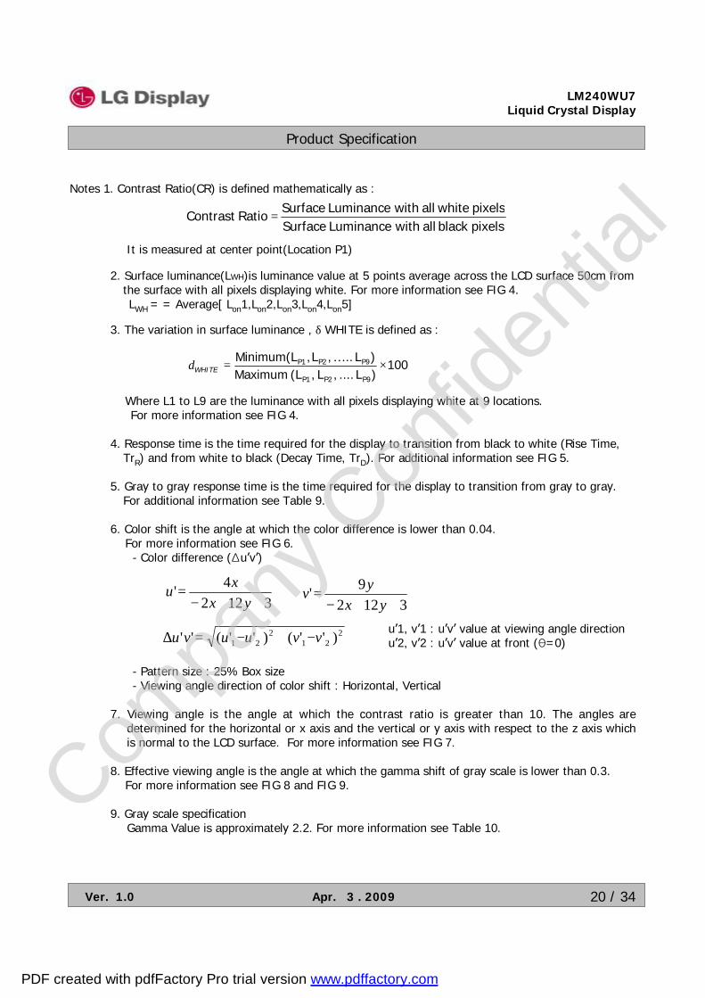
Notes 1. Contrast Ratio(CR) is defined mathematically as :
It is measured at center point(Location P1)
2. Surface luminance(LWH)is luminance value at 5 points average across the LCD surface 50cm from the surface with all pixels displaying white. For more information see FIG 4. LWH = = Average[ Lon1,Lon2,Lon3,Lon4,Lon5]
3. The variation in surface luminance , δ WHITE is defined as :
Where L1 to L9 are the luminance with all pixels displaying white at 9 locations. For more information see FIG 4.
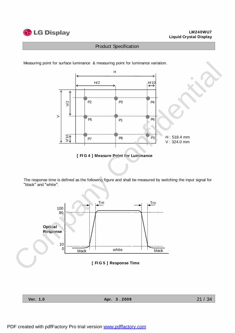
4. Response time is the time required for the display to transition from black to white (Rise Time, TrR) and from white to black (Decay Time, TrD). For additional information see FIG 5.
5. Gray to gray response time is the time required for the display to transition from gray to gray. For additional information see Table 9.
6. Color shift is the angle at which the color difference is lower than 0.04.For more information see FIG 6.- Color difference (Δu’v’)
u’1, v’1 : u’v’ value at viewing angle directionu’2, v’2 : u’v’ value at front (θ=0)
- Pattern size : 25% Box size- Viewing angle direction of color shift : Horizontal, Vertical
7. Viewing angle is the angle at which the contrast ratio is greater than 10. The angles aredetermined for the horizontal or x axis and the vertical or y axis with respect to the z axis whichis normal to the LCD surface. For more information see FIG 7.
8. Effective viewing angle is the angle at which the gamma shift of gray scale is lower than 0.3.For more information see FIG 8 and FIG 9.
9. Gray scale specificationGamma Value is approximately 2.2. For more information see Table 10.
31224'
++−=
yxxu
31229'
++−=
yxyv
221
221 )''()''('' vvuuvu −+−=∆
pixels black all with Luminance Surfacepixels white all with Luminance Surface
RatioContrast =
100)L .... ,L ,(L Maximum)L .. ,L,Minimum(L
P9P2P1
P9P2P1 ×…
=WHITEδ
Compa
ny C
onfid
entia
l
PDF created with pdfFactory Pro trial version www.pdffactory.com
Product Specification
21 / 34
LM240WU7Liquid Crystal Display
Ver. 1.0 Apr. 3 . 2009
[ FIG 5 ] Response Time
The response time is defined as the following figure and shall be measured by switching the input signal for “black” and “white”.
Measuring point for surface luminance & measuring point for luminance variation.
whiteblack
TrR TrD10090
100
Optical Response
black
[ FIG 4 ] Measure Point for Luminance
H : 518.4 mmV : 324.0 mm
H
H/2
V
V/2
●
P1
P4P2
P9P7
●
●
● ●
●P3
●P8
P6●P5
●
H/10
V/10
Compa
ny C
onfid
entia
l
PDF created with pdfFactory Pro trial version www.pdffactory.com

Product Specification
22 / 34
LM240WU7Liquid Crystal Display
Ver. 1.0 Apr. 3 . 2009
25% Box size
2263110155206240B
2263110155206240G
2263110155206240R
BlackNeutral 3.5Neutral 5Neutral 6.5Neutral 8White
172151363765145B
126622122714832G
352072411977226R
CyanMagentaYellowRedGreenBlue
2958868717424B
162193396769104G
2301607621156219R
Orange yellowYellow greenPurpleModerate redPurplish blueOrange
1781854616112345B
19911810211214256G
114129778520698R
Bluish greenBlue flowerFoliageBlue skyLight skinDark skin
Average RGB values in Bruce RGB for Macbeth Chart[ FIG 6 ] Color Shift Test Pattern
Color shift is defined as the following test pattern and color.
Rising Time
G0
G63
G127
G191
G255
Falling Time
G0G63G127G191G255Gray to Gray
The gray to gray response time is defined as the following figure and shall be measured by switching the input signal for “Gray To Gray”.
- Gray step : 5 step- TGTG_AVR is the total average time at rising time and falling time for “Gray To Gray”.- TGTG_MAX is the max time at rising time or falling time for “Gray To Gray”.
Table 9. Gray to gray response time table
Compa
ny C
onfid
entia
l
PDF created with pdfFactory Pro trial version www.pdffactory.com

Product Specification
23 / 34
LM240WU7Liquid Crystal Display
Ver. 1.0 Apr. 3 . 2009
[ FIG 7 ] Viewing angle
Dimension of viewing angle range.
Normal Y E
φ
θ
φ = 0°, Right
φ = 180°, Left
φ = 270°, Down
φ = 90°, Up
br LaVL += )log()log()log( aVrLL b +=−
Here the Parameter α and γ relate the signal level V to the luminance L.The GAMMA we calculate from the log-log representation (FIG. 9)
[ FIG 8 ] Sample Luminance vs. gray scale (using a 256 bit gray scale)
[ FIG 9 ] Sample Log-log plot of luminance vs. gray scale
Compa
ny C
onfid
entia
l
PDF created with pdfFactory Pro trial version www.pdffactory.com

Product Specification
24 / 34
LM240WU7Liquid Crystal Display
Ver. 1.0 Apr. 3 . 2009
Table 10. Gray Scale Specification
0.130
100
75.4
53.0
35.2
21.2
11.7
4.7
1.2
255
223
191
159
127
95
63
31
Relative Luminance [%] (Typ.)Gray Level
Compa
ny C
onfid
entia
l
PDF created with pdfFactory Pro trial version www.pdffactory.com

Product Specification
25 / 34
LM240WU7Liquid Crystal Display
Ver. 1.0 Apr. 3 . 2009
5. Mechanical Characteristics
The contents provide general mechanical characteristics. In addition the figures in the next page are detailed mechanical drawing of the LCD.
324.0mmVertical
Hard coating(3H)Anti-glare treatment of the front polarizerSurface Treatment
2830 g(Typ) / 2970 g(Max)Weight
328.0mmVertical
352.0mmVertical
35.7mmDepth
518.4mmHorizontalActive Display Area
522.4mmHorizontalBezel Area
546.4mmHorizontal
Outline Dimension
Notes : Please refer to a mechanic drawing in terms of tolerance at the next page.
Compa
ny C
onfid
entia
l
PDF created with pdfFactory Pro trial version www.pdffactory.com
Product Specification
26 / 34
LM240WU7Liquid Crystal Display
Ver. 1.0 Apr. 3 . 2009
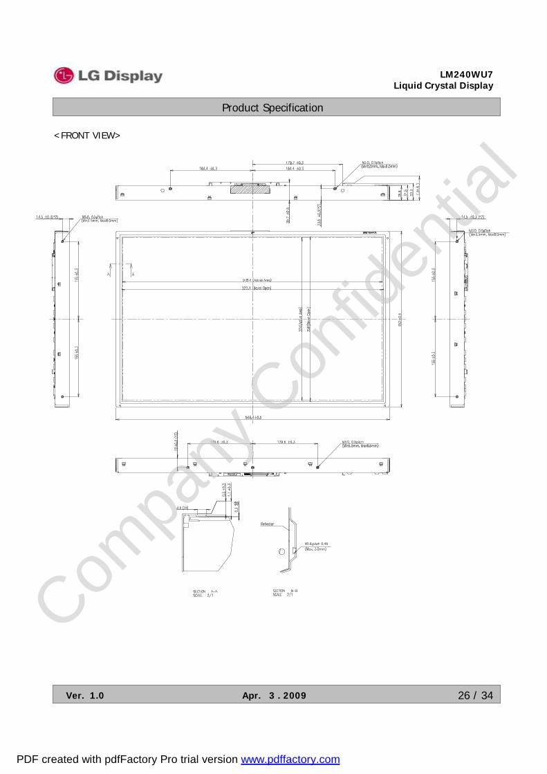
<FRONT VIEW>
Compa
ny C
onfid
entia
l
PDF created with pdfFactory Pro trial version www.pdffactory.com
Product Specification
27 / 34
LM240WU7Liquid Crystal Display
Ver. 1.0 Apr. 3 . 2009
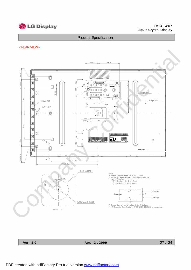
<REAR VIEW>
Compa
ny C
onfid
entia
l
PDF created with pdfFactory Pro trial version www.pdffactory.com
Product Specification
28 / 34
LM240WU7Liquid Crystal Display
Ver. 1.0 Apr. 3 . 2009
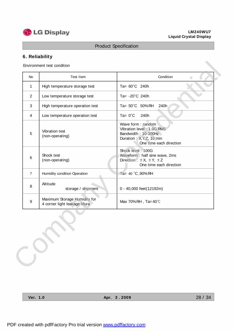
6. Reliability
Environment test condition
0 - 40,000 feet(12192m)Altitude
storage / shipment8
Ta= 40 °C ,90%RHHumidity condition Operation7
Max 70%RH , Ta=40℃Maximum Storage Humidity for4 corner light leakage Mura.9
Shock level : 100GWaveform : half sine wave, 2msDirection :±X, ±Y, ±Z
One time each direction
Shock test(non-operating)6
Wave form : randomVibration level : 1.0G RMSBandwidth : 10-300HzDuration : X,Y,Z, 10 min
One time each direction
Vibration test(non-operating)5
Ta= 0°C 240hLow temperature operation test4
Ta= 50°C 50%RH 240hHigh temperature operation test3
Ta= -20°C 240hLow temperature storage test2
Ta= 60°C 240hHigh temperature storage test1
ConditionTest ItemNo
Compa
ny C
onfid
entia
l
PDF created with pdfFactory Pro trial version www.pdffactory.com
Product Specification
29 / 34
LM240WU7Liquid Crystal Display
Ver. 1.0 Apr. 3 . 2009
7. International Standards
7-1. Safety
7-2. EMC
a) ANSI C63.4 “Methods of Measurement of Radio-Noise Emissions from Low-Voltage Electrical and Electrical Equipment in the Range of 9kHZ to 40GHz. “American National Standards Institute(ANSI),1992
b) C.I.S.P.R “Limits and Methods of Measurement of Radio Interface Characteristics of InformationTechnology Equipment.“ International Special Committee on Radio Interference.
c) EN 55022 “Limits and Methods of Measurement of Radio Interface Characteristics of InformationTechnology Equipment.“ European Committee for Electrotechnical Standardization.(CENELEC), 1998( Including A1: 2000 )
a) UL 60950-1:2003, First Edition, Underwriters Laboratories, Inc.,Standard for Safety of Information Technology Equipment.
b) CAN/CSA C22.2, No. 60950-1-03 1st Ed. April 1, 2003, Canadian Standards Association,Standard for Safety of Information Technology Equipment.
c) EN 60950-1:2001, First Edition, European Committee for Electrotechnical Standardization(CENELEC)European Standard for Safety of Information Technology Equipment.
7-3. Environment
a) RoHS. Directive 2002/95/EC of the European Parliament and of the Council on the reduction of theuse of certain hazardous substances in electrical and electronic equipment. January 2003
Compa
ny C
onfid
entia
l
PDF created with pdfFactory Pro trial version www.pdffactory.com
Product Specification
30 / 34
LM240WU7Liquid Crystal Display
Ver. 1.0 Apr. 3 . 2009
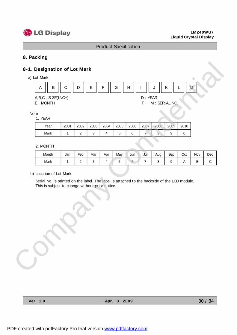
8. Packing
8-1. Designation of Lot Mark
a) Lot Mark
A B C D E F G H I J K L M
A,B,C : SIZE(INCH) D : YEAR E : MONTH F ~ M : SERIAL NO.
Note1. YEAR
2. MONTH
Mark
Year
0
2010
6
2006
7
2007
8
2008
9
2009
4
2004
5
2005
321
200320022001
B
Nov
Mark
Month
A
Oct
6
Jun
7
Jul
8
Aug
9
Sep
4
Apr
5
May
C321
DecMarFebJan
b) Location of Lot Mark
Serial No. is printed on the label. The label is attached to the backside of the LCD module.This is subject to change without prior notice.
Compa
ny C
onfid
entia
l
PDF created with pdfFactory Pro trial version www.pdffactory.com

Product Specification
31 / 34
LM240WU7Liquid Crystal Display
Ver. 1.0 Apr. 3 . 2009
a) Package quantity in one box : 5EA
b) Box Size : 436 X 346 X 628
8-2. Packing Form
Compa
ny C
onfid
entia
l
PDF created with pdfFactory Pro trial version www.pdffactory.com

Product Specification
32 / 34
LM240WU7Liquid Crystal Display
Ver. 1.0 Apr. 3 . 2009
8-3. Pallet Form
OPPTAPE5
YUPO PAPERLABEL4
CLIP 18MMBAND, CLIP7
PPBAND6
SWR4ANGLE, PACKING3
Paper_1030X870X130PALLET2
PACKING ASS’Y1
MATERIALDESCRIPTIONNO.
Compa
ny C
onfid
entia
l
PDF created with pdfFactory Pro trial version www.pdffactory.com

Product Specification
33 / 34
LM240WU7Liquid Crystal Display
Ver. 1.0 Apr. 3 . 2009
9. PRECAUTIONS
Please pay attention to the followings when you use this TFT LCD module.
9-1. MOUNTING PRECAUTIONS
(1) You must mount a module using holes arranged in four corners or four sides.(2) You should consider the mounting structure so that uneven force (ex. Twisted stress) is not applied to the
module. And the case on which a module is mounted should have sufficient strength so that external force is not transmitted directly to the module.
(3) Please attach the surface transparent protective plate to the surface in order to protect the polarizer.Transparent protective plate should have sufficient strength in order to the resist external force.
(4) You should adopt radiation structure to satisfy the temperature specification.(5) Acetic acid type and chlorine type materials for the cover case are not desirable because the former
generates corrosive gas of attacking the polarizer at high temperature and the latter causes circuit break by electro-chemical reaction.
(6) Do not touch, push or rub the exposed polarizers with glass, tweezers or anything harder than HBpencil lead. And please do not rub with dust clothes with chemical treatment.Do not touch the surface of polarizer for bare hand or greasy cloth.(Some cosmetics are detrimentalto the polarizer.)
(7) When the surface becomes dusty, please wipe gently with absorbent cotton or other soft materials like chamois soaks with petroleum benzene. Normal-hexane is recommended for cleaning the adhesives used to attach front / rear polarizers. Do not use acetone, toluene and alcohol because they cause chemical damage to the polarizer.
(8) Wipe off saliva or water drops as soon as possible. Their long time contact with polarizer causes deformations and color fading.
(9) Do not open the case because inside circuits do not have sufficient strength.
9-2. OPERATING PRECAUTIONS
(1) The spike noise causes the mis-operation of circuits. It should be lower than following voltage : V=±200mV(Over and under shoot voltage)
(2) Response time depends on the temperature.(In lower temperature, it becomes longer.)(3) Brightness depends on the temperature. (In lower temperature, it becomes lower.)
And in lower temperature, response time(required time that brightness is stable after turned on) becomeslonger.
(4) Be careful for condensation at sudden temperature change. Condensation makes damage to polarizer or electrical contacted parts. And after fading condensation, smear or spot will occur.
(5) When fixed patterns are displayed for a long time, remnant image is likely to occur.(6) Module has high frequency circuits. Sufficient suppression to the electromagnetic interference shall be
done by system manufacturers. Grounding and shielding methods may be important to minimized theinterference.
(7) Please do not give any mechanical and/or acoustical impact to LCM. Otherwise, LCM can’t be operated its full characteristics perfectly.
(8) A screw which is fastened up the steels should be a machine screw. (if not, it causes metallic foreign material and deal LCM a fatal blow)
(9) Please do not set LCD on its edge.
Compa
ny C
onfid
entia
l
PDF created with pdfFactory Pro trial version www.pdffactory.com

Product Specification
34 / 34
LM240WU7Liquid Crystal Display
Ver. 1.0 Apr. 3 . 2009
Since a module is composed of electronic circuits, it is not strong to electrostatic discharge. Make certain that treatment persons are connected to ground through wrist band etc. And don’t touch interface pin directly.
9-3. ELECTROSTATIC DISCHARGE CONTROL
Strong light exposure causes degradation of polarizer and color filter.
9-4. PRECAUTIONS FOR STRONG LIGHT EXPOSURE
When storing modules as spares for a long time, the following precautions are necessary.
(1) Store them in a dark place. Do not expose the module to sunlight or fluorescent light. Keep the temperature between 5°C and 35°C at normal humidity.
(2) The polarizer surface should not come in contact with any other object.It is recommended that they be stored in the container in which they were shipped.
9-5. STORAGE
9-6. HANDLING PRECAUTIONS FOR PROTECTION FILM
(1) The protection film is attached to the bezel with a small masking tape.When the protection film is peeled off, static electricity is generated between the film and polarizer.This should be peeled off slowly and carefully by people who are electrically grounded and with well ion-blown equipment or in such a condition, etc.
(2) When the module with protection film attached is stored for a long time, sometimes there remains a very small amount of glue still on the bezel after the protection film is peeled off.
(3) You can remove the glue easily. When the glue remains on the bezel surface or its vestige is recognized, please wipe them off with absorbent cotton waste or other soft material like chamois soaked with normal-hexane.
Compa
ny C
onfid
entia
l
PDF created with pdfFactory Pro trial version www.pdffactory.com
Related Documents