UNIVERSITY OF CALIFORNIA, LOS ANGELES Sparse Matrix-Vector Multiplication FPGA Implementation Teng Wang (SID: 704-272-121) 02/27/2015

Welcome message from author
This document is posted to help you gain knowledge. Please leave a comment to let me know what you think about it! Share it to your friends and learn new things together.
Transcript

UNIVERSITY OF CALIFORNIA, LOS ANGELES
Sparse Matrix-Vector Multiplication FPGA
Implementation
Teng Wang
(SID: 704-272-121)
02/27/2015

Sparse Matrix-Vector Multiplication FPGA Implementation Teng Wang
2
Table of Contents 1 Introduction ............................................................................................................................................. 3
2 Sparse Matrix-Vector Multiplication .................................................................................................... 3 2.1 SpMxV Problem Overview ................................................................................................................. 3 2.2 Sparse Matrix Representation ............................................................................................................ 4 2.3 SpMxV Algorithm for CSR Format .................................................................................................... 5
3 Parameterized Accumulator Design ...................................................................................................... 5 3.1 Accumulator Challenges .................................................................................................................... 5 3.2 Tree-Traversal Method: An Intuitive Idea ......................................................................................... 6 3.3 Partially Compacted Binary Tree (PCBT) Accumulator ................................................................... 6 3.4 The Implementation of Accumulator .................................................................................................. 8
4 SpMxV Architecture ............................................................................................................................... 9 4.1 The Top-Level SpMxV Architecture ................................................................................................... 9 4.2 System Controller and Memory Controller ...................................................................................... 10
4.2.1 Option 1: The Serial Option ...................................................................................................... 11 4.2.2 Option 2: The Parallel Option ................................................................................................... 12 4.2.3 Trade-Offs Between Two Options ............................................................................................ 14
5 Performance Evaluation ....................................................................................................................... 15 5.1 SpMxV FPGA Implementation ......................................................................................................... 15 5.2 Benchmarks: Test Matrices .............................................................................................................. 16 5.3 Performance Evaluation .................................................................................................................. 17 5.4 Resource Usage ................................................................................................................................ 18 5.5 Limitations and Improvements ......................................................................................................... 19
References ..................................................................................................................................................... 20
Sparse Matrix-Vector Multiplication FPGA Implementation Teng Wang
3
1 Introduction Sparse Matrix-Vector Multiplication (SpMxV) is directly related to a wide variety of
computational disciplines, including circuit and economic modeling, industrial engineering, image reconstruction, algorithms for least squares and eigenvalue problems [1-4]. Floating-point SpMxV, generally denoted as y = Ax, is the key computational kernel that dominates the performance of many scientific and engineering applications. However, the performance of SpMxV is highly limited by the irregularity of memory accesses as well as high ratio of memory I/O operations [5], and is usually much lower than that of dense matrix multiplication.
SpMxV can be implemented on FPGAs and GPUs. GPUs, which have also gained
both general-purpose programmability and native support for floating-point arithmetic, are regarded as an efficient platform for SpMxV. But FPGAs exceed the performance to the GPUs when their memory bandwidth is scaled to match that of GPUs. In addition, the ability to design customized accumulator architecture for FPGAs, allows researchers and engineers to make a more efficient use of the memory bandwidth [5].
In this report, we will propose an SpMxV architecture running on the research platform,
Reconfigurable Open Architecture Computing Hardware (ROACH). The report can be organized as follows. In Section 2, we will describe the basic background of SpMxV; in Section 3, we will discuss the design of the parameterized accumulator integrated into the SpMxV kernel in detail; in Section 4, we mainly focus on the SpMxV system and the architecture design, and two different memory organizations are implemented; in Section 5, we will evaluate the performance of our design.
2 Sparse Matrix-Vector Multiplication In this section, we will describe the basic background of SpMxV that is needed for
computational kernel design, including SpMxV problem overview, sparse matrix representation, and the general sparse matrix algorithm based on the compressed sparse row (CSR) format.
2.1 SpMxV Problem Overview Consider the matrix-vector product y = Ax. A is an n × n sparse matrix with m
nonzero elements. We use Aij (i = 0, …, n – 1; j = 0, …, n – 1) to denote the elements of A. x and y are vectors of length n, and their elements are denoted by xj, yi (j = 0, …, n – 1; i = 0, …, n - 1), respectively.
Initially, A, x and y are all in the external memory. Therefore, m+n memory accesses
are needed to bring A and x to the computational kernel. For a nonzero matrix element Aij, the following operation is performed:
yi = yi + Aij × xj, if Aij ≠ 0

Sparse Matrix-Vector Multiplication FPGA Implementation Teng Wang
4
It can be easily seen that the operation involves floating-point multiplication and accumulations. Since each nonzero element in A needs two floating-point operations, 2m floating-point operations are to be performed. When the computation is completed, n results are to be written to the external memory. Therefore the total number I/O operation is m+2n [1].
2.2 Sparse Matrix Representation A variety of ways exist to represent sparse matrices. Figure 1 illustrates a sample sparse matrix and three different formats to represent it [2].
Figure 1. The Sparse Matrix Representations [2] The coordinate (COO) format, shown in Fig. 1(b), uses three arrays, data, row and col, to explicitly represent the value of nonzero elements and their corresponding row and column indices. The compressed sparse column (CSC) format, shown in Fig. 1(c), stores the row indices and an array of column pointers. The compressed sparse row (CSR) format, shown in Fig. 1(d), is the most frequently used storage format for sparse matrices. In our design, CSR format, shown in Fig. 2, is used. The CSR format stores a matrix in three arrays, val, col and ptr. Array val and col contain the value and corresponding column number for each non-zero value in the matrix with a row-major order, while the

Sparse Matrix-Vector Multiplication FPGA Implementation Teng Wang
5
ptr array stores the indices within val and col where each row begins, terminated with a value that contains the total length of val and col [5].
Figure 2. Compressed Sparse Row (CSR) Format [5]
Note that, by subtracting consecutive entries in the ptr array, we can tell how many entries are there for each row since ptr array represents the row boundaries, and a new array len is generated. In Fig. 2, the len array is:
len = [2 3 1 3 3 4]
2.3 SpMxV Algorithm for CSR Format The SpMxV algorithm based on CSR format can be best illustrated by the following
pseudo code [5]: for (i = 0; i < N; i ++) for (j = row_ptr[i]; j < row_ptr[i + 1]; j++) y[i] += a[j] * x[col_ind[j]];
3 Parameterized Accumulator Design The accumulation is the key part in the SpMxV and its design will greatly influence the flexibility and efficiency of the system. In this section, we will implement and improve the parameterized accumulator based on the prior work of Ling Zhuo, et al [1][3]. Even though floating-point operators can have different latencies, our accumulator can easily be reconfigured and adapt to different requirements.
3.1 Accumulator Challenges The accumulator is used to reduce multiple variable-length sets of sequentially
delivered floating-point values without stalling the pipeline or imposing unreasonable buffer requirements. The general idea is best depicted in Figure 3, and the accumulation problem can be defined by the following formula:
A[i + 1] = A[i] + X Floating-point operators are usually deeply pipelined and without special micro-
architectural or data scheduling techniques, the Read-After-Write (RAW) hazard that exists between A[i + 1] and A[i] requires that each new value of X delivered to the accumulator wait for the latency of the adder [6]. However, since floating-point adders usually have latencies larger than one and new input is required to be supplied into the

Sparse Matrix-Vector Multiplication FPGA Implementation Teng Wang
6
accumulator each clock cycle, it would prevent the adder from providing the current sum before the next input value arrives.
Figure 3. General Idea of Accumulation In addition, if the sequences of input values belong to different accumulation sets
where no explicit separation exists between different sets, the operation will be stalled or lead to incorrect results.
3.2 Tree-Traversal Method: An Intuitive Idea In the tree-traversal method [1][3], the accumulation of a set of input values is
represented by a binary adder tree. Therefore, accumulating the input values is equivalent to performing a breadth first traversal of a tree, and n-1adders/nodes are needed to form a ⌈lg(n)⌉-stage binary adder tree.
However, this method is not feasible in the view of FPGA implementation. For large n,
the floating-point adders themselves will occupy a huge amount of area. Moreover, since the inputs will arrive sequentially, this architecture leads to an inefficient use of the adders. Suppose an adder at level 0 of the tree, it must first wait for two inputs to arrive. Before it can operate on any more inputs, it must wait for the next n-2 inputs to arrive and enter the other adders at level 0; all adders in the same level must operate “concurrently”. Such inefficiency exists at all levels.
3.3 Partially Compacted Binary Tree (PCBT) Accumulator Since the input values arrive at accumulator sequentially, we can observe that the
adders at the same tree level are actually used in different clock cycles. Instead of multiple adders at a given tree level, there is only one adder at each level, which is shown in Figure 4. Meanwhile, unlike the original design proposed by Ling Zhuo et al. [1][3], each level only have one buffer feeding its corresponding adder. Thus the design, shown in Figure 5, has ⌈lg(n)⌉ adders and a buffer size of ⌈lg(n)⌉; half of the buffers are saved compared to the original design.
This design is called Partially Compacted Binary Tree (PCBT) Accumulator [1][3].
The idea and the implementation are fairly simple and straightforward, and each level has the same topology, which enables the design reusability and extendibility. It also partially overcomes the problem of large area occupation proposed in Section 3.2. However, the utilization of the adders in the design is still very low. Since normally the adder at each level must wait for two operands delivered from the last level to start computation, the adder at level i only reads new inputs once every 2i+1 cycles. Additionally, before the

Sparse Matrix-Vector Multiplication FPGA Implementation Teng Wang
7
accumulator is integrated into the computation kernel, designer should determine the minimum number of levels that is needed for correct results. This requires designers to have some knowledge of the sparse matrix to be calculated before making the trade-off.
Figure 4. One Level of Partially Compacted Binary Tree (PCBT) Accumulator
Figure 5. Partially Compacted Binary Tree (PCBT) Accumulator In each clock cycle, adders at each level will check if it has enough operands to begin execution. Normally, the adder proceeds if the buffer contains one operand and the other comes directly from the input. A special case that should be taken care of is, when n, the total number of inputs within one set, is not a power of 2, adders at certain levels need to proceed with a single operand stored in the buffers. This scenario only happens when the data stored in the buffer is the last input at that level, or when the accumulation of one input set has been completed by its previous levels, thus no other input is waiting to pair up with it. The operation described earlier is also called singleton add. For each singleton add, an input is added with 0.
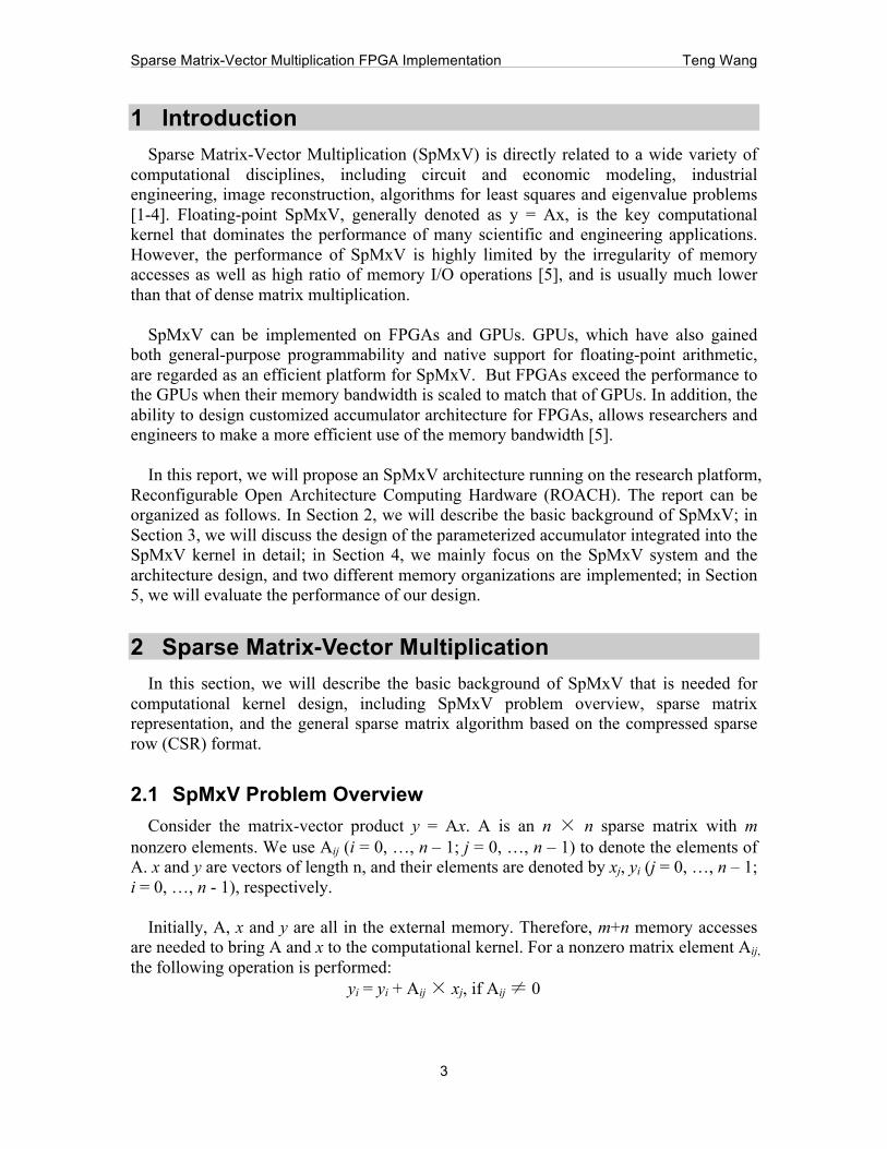
To correctly determine when a singleton add is to be performed, we attach a label to each number that enters the buffers. The label will indicate how many of the inputs within the same set remain to be accumulated. Figure 6 illustrates how the five inputs within the same set are labeled at each level [1][3]. The small boxes represent the inputs, and the corresponding labels are shown below them. The inputs labeled as 0 do not really
Sparse Matrix-Vector Multiplication FPGA Implementation Teng Wang
8
exist; the only purpose is to form a virtual binary tree on which PCBT design is based. If we use tu to denote the label for input u, then u cannot be the last input of the set at level l when tu > 2l, and u must be the last input of the set at level l when tu ≤ 2l. The singleton add should be performed accordingly. One must also pay attention to how the labels are updated in order to ensure correct results. When two inputs are to be added, the label of the result is the larger one of the two inputs’ labels; when singleton add is to be performed, the label of the result is the source operand’s label itself.
Figure 6. Labels for PCBT Inputs (n = 5) [1][3]
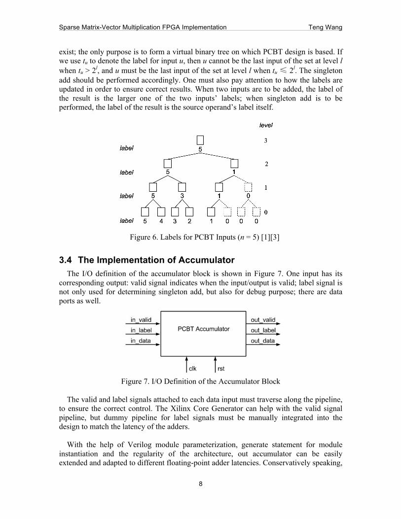
3.4 The Implementation of Accumulator The I/O definition of the accumulator block is shown in Figure 7. One input has its corresponding output: valid signal indicates when the input/output is valid; label signal is not only used for determining singleton add, but also for debug purpose; there are data ports as well.
Figure 7. I/O Definition of the Accumulator Block The valid and label signals attached to each data input must traverse along the pipeline, to ensure the correct control. The Xilinx Core Generator can help with the valid signal pipeline, but dummy pipeline for label signals must be manually integrated into the design to match the latency of the adders.
With the help of Verilog module parameterization, generate statement for module instantiation and the regularity of the architecture, out accumulator can be easily extended and adapted to different floating-point adder latencies. Conservatively speaking,

Sparse Matrix-Vector Multiplication FPGA Implementation Teng Wang
9
we must have ⌈lg(n)⌉ levels inside the accumulator, where n is the number of sparse matrix columns. However, we observe that, in the test matrices, the number of nonzero elements per row is rarely larger than 1024. Thus usually 10 levels are enough to ensure the correct results.
The latency of our accumulator can be expressed as follows:
Latency = α⌈lg(n)⌉
Where α is the adder depth. The range of α is between 3 and 11, and is limited by Xilinx Core Generator. Table 1 below lists the relation between adder depth and accumulator latency when n is 1024.
Adder Depth 3 4 5 6 7 8 9 10 11
Accumulator Latency 30 40 50 60 70 80 90 100 110
Table 1. The Relation Between Adder Depth and Accumulator Latency (n = 1024) In ROACH platform, the floating-point operator is constructed using DSP48Es on the board, and the DSP resources are plentiful. Thus the area occupation by floating-adders is not an issue. For resource usage, refer to Section 5.
4 SpMxV Architecture 4.1 The Top-Level SpMxV Architecture The top-level SpMxV architecture schematic is shown in Figure 8. The SpMxV kernel is implemented on ROACH FPGA platform, and serves as the co-processor attached to a PowerPC embedded processor running MATLAB environments. We communicate with our SpMxV kernel through MATLAB commands. In our design, QDRs and BRAMs are served as memories. The memory controller is responsible for controlling memory enable signals as well as the address pointers, allowing elements of A and x to be continuously streamed into SpMxV kernel for computation. The memory controller is also the interface between memories and SpMxV controller. SpMxV controller is a system controller that coordinates the activities between MATLAB environments on PowerPC and SpMxV kernel on FPGA. It also incorporates a system finite state machine (FSM), which is in charge of global scheduling. ALU is the computation unit implementing the multiplication and accumulation of SpMxV algorithms. In our design, ALU shown in Figure 9 is directly mapped, and it consists of one multiplier and one accumulator. The implementation of the accumulator has been discussed in detail in Section 3. As long as hardware resources on board can be guaranteed, especially the memory resources, we can easily apply parallelism into our

Sparse Matrix-Vector Multiplication FPGA Implementation Teng Wang
10
system by using multiple ALUs and adding FIFOs. The implementation of parallelism is not considered and included in our design.
Figure 8. Top-Level SpMxV Architecture Schematic
Figure 9. ALU
4.2 System Controller and Memory Controller The behavior of BRAMs is similar to SRAMs with a latency of one. But the QDRs
enable bursting read/write operations, i.e., when issuing reads and writes, data is presented on the respective data ports for two consecutive clock cycles, and the address presented when a read/write is issued addresses a full burst worth of memory. Therefore,
(Optional)

Sparse Matrix-Vector Multiplication FPGA Implementation Teng Wang
11
one address in QDRs essentially stands for two 36-bit data word (32-bit data plus 4-bit ECC bit).
We notice that vec and val should be streamed into ALU at the same time, and col is
used for indexing to get vec. Thus two options are available from the view of memory organization. No matter what option is used, no data hazard will occur and no additional stalls are needed for data scheduling, thus eliminating the need for data buffering before data is fed into ALU.
4.2.1 Option 1: The Serial Option In Option 1, the serial option shown in Figure 10, we store val and its corresponding
col in one QDR address. The vec and ptr are stored in BRAMs. The latency of QDR access is 10 clock cycles, and 1 clock cycle for BRAM access. When we access the QDR, the val and col will come out serially. While we use col to index vec BRAM, the val needs to be buffered accordingly. A pair of vec and val will be fed into ALU at most every two cycles.
Figure 10. Memory Access Mechanism for Option 1, The Serial Option In order to achieve the memory access mechanism for Option 1 described earlier, we
take advantage of finite state machine (FSM) shown in Figure 11 to control the process of memory access and deal with some corner cases. S0 is the reset state; SX is used to satisfy the timing requirement of ptr BRAM; S1 is to read ptr[addra_ptr]; S2 is to read ptr[addra_ptr + 1] and update addra_ptr pointer; S3 is to calculate current_row_label, which is equal to ptr[addra_ptr + 1] – ptr[addra_ptr], the FSM goes to S4 if current_row_label ≠ 0, or goes to S6 if current_row_label = 0; S4 is to read col[addra_qdr] and update current_row_label; S5 is to read val[addra_qdr] and update addra_qdr, the FSM goes to S4 if current_row_label ≠ 0, and it goes to S1 if

Sparse Matrix-Vector Multiplication FPGA Implementation Teng Wang
12
current_row_label = 0; S6 proceed when a row of the sparse matrix is all zero, the memory controller will take some special actions and then goes back to S1.
Figure 11. Finite State Machine of Controller for Option 1
Note that between the controller generates the current_row_label and ALU consumes the label, there is a latency of 11 incurred by memory latency. Therefore, a dummy pipeline is needed to act as the shift register, and ensure that the label can match the data. The valid signal consumed by ALU can be directly generated from data valid output port of QDRs, and the valid signal generator must ensure that the signal can match the data.
Figure 12. Memory Access Mechanism for Option 2, The Parallel Option
4.2.2 Option 2: The Parallel Option In Option 2, the parallel option shown in Figure 12, we store val in one QDR memory
and col in another. The vec and ptr are also stored in BRAMs. We can use the same

Sparse Matrix-Vector Multiplication FPGA Implementation Teng Wang
13
address to access val and the corresponding col from QDRs, and then use col as the address to index vec BRAM while we buffer val at the same time. A pair of vec and val is fed into ALU every clock cycle.
One corner case introduced by QDR burst operations must be considered. Since col
and val are stored consecutively in two QDRs, it is possible that the col of the last value of the previous sparse matrix row is stored in the first 36-bit of a QDR address, and the next row’s first value’s col is stored in the second 36-bit of the same QDR address. This issue is called parity problem, and the system FSM must correctly recognize this corner case and respond accordingly. Thus we introduce parity FSM, and the truth table is shown in Table 2. It can be observed that next_parity = parity_of_current_row XOR current_parity. Before we proceed a row, we look up the parity bit; we need to dump the first data come out of QDRs if current parity = 1, and no dumping is performed if current parity = 0. The parity of the current row is essentially the LSB of current_row_label when it has first been calculated.
Current Parity Parity of the Current Row Next Parity
Even/0 Even/0 Even/0
Even/0 Odd/1 Odd/1 Odd/1 Odd/1 Even/0
Odd/1 Even/0 Odd/1
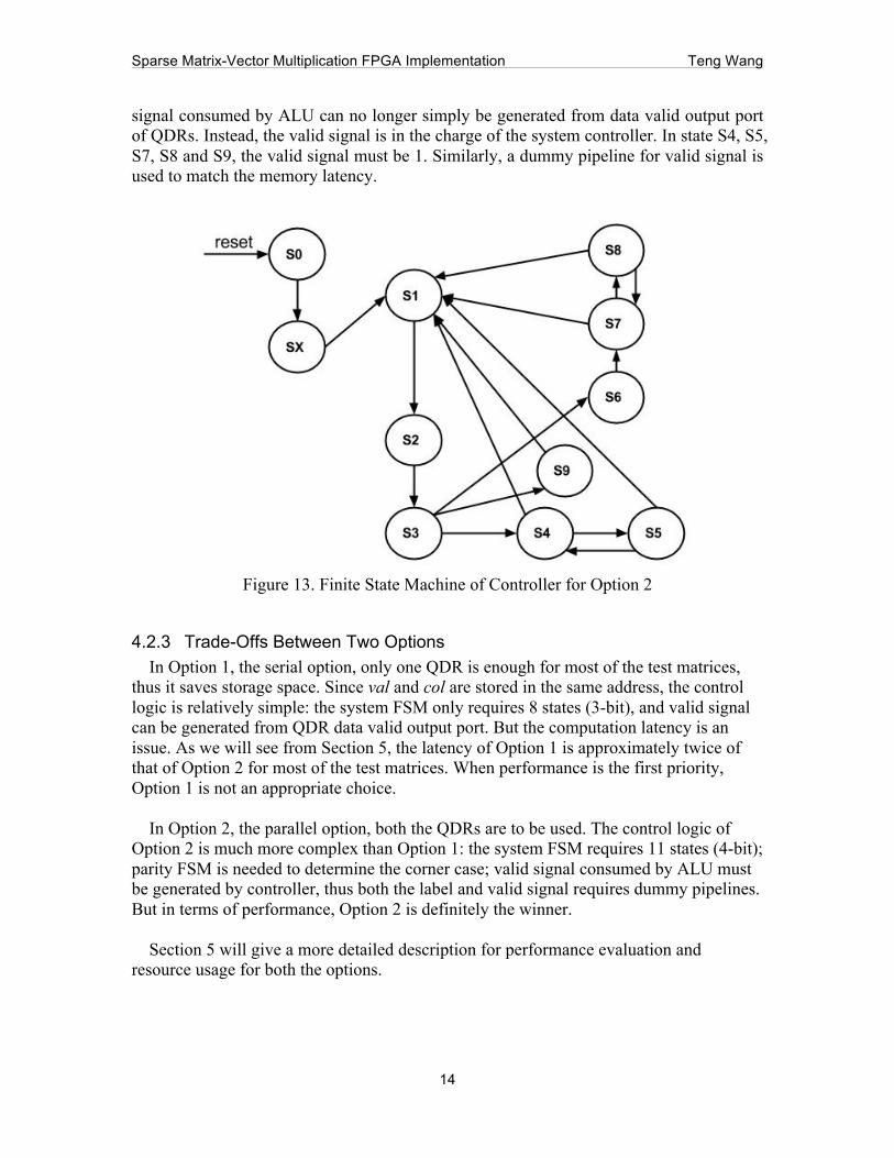
Table 2. The Truth Table for Parity FSM With the help of parity FSM, our system FSM shown in Figure 13 will work accordingly. S0 is the reset state; SX is to satisfy the timing requirements of ptr BRAM; S1 is to read ptr[addra_ptr]; S2 is to read ptr[addra_ptr + 1] and update addra_ptr pointer; S3 is to calculate current_row_label, which is equal to ptr[addra_ptr + 1] – ptr[addra_ptr], the FSM goes to S4 if parity = 0 and current_row_label ≠ 0, or goes to S6 if parity = 1 and current_row_label ≠ 0, or goes to S9 if current_row_label = 0; S4 is to read the first data stored in addra_qdr, and update current_row_label, the FSM goes back to S1 if current row ends (current_row_label = 1), or goes to S5; S5 is to read the second data stored in addra_qdr, and update both current_row_label and addra_qdr, the FSM goes back to S1 if current row ends (current_row_label = 1), or goes to S4; S6 will ignore the first data stored in addra_qdr, and the FSM goes to S7; S7 will read the second data stored in addra_qdr, and update both the current_row_label and the addra_qdr, the FSM goes to S1 if current row ends (current_row_label = 1), or goes to S8; S8 will read the first data stored in addra_qdr + 1, and update current_row_label, the FSM goes back to S1 if current row ends (current_row_label = 1), or goes to S7; S9 proceed when one row of the sparse matrix is all zero, the memory controller will take special actions and goes back to S1. As in Option 1, a dummy pipeline is needed to act as the shift register, and ensure that the label can match the data between the controller and ALU. Unlike Option 1, the valid
Sparse Matrix-Vector Multiplication FPGA Implementation Teng Wang
14
signal consumed by ALU can no longer simply be generated from data valid output port of QDRs. Instead, the valid signal is in the charge of the system controller. In state S4, S5, S7, S8 and S9, the valid signal must be 1. Similarly, a dummy pipeline for valid signal is used to match the memory latency.
Figure 13. Finite State Machine of Controller for Option 2
4.2.3 Trade-Offs Between Two Options In Option 1, the serial option, only one QDR is enough for most of the test matrices,
thus it saves storage space. Since val and col are stored in the same address, the control logic is relatively simple: the system FSM only requires 8 states (3-bit), and valid signal can be generated from QDR data valid output port. But the computation latency is an issue. As we will see from Section 5, the latency of Option 1 is approximately twice of that of Option 2 for most of the test matrices. When performance is the first priority, Option 1 is not an appropriate choice.
In Option 2, the parallel option, both the QDRs are to be used. The control logic of
Option 2 is much more complex than Option 1: the system FSM requires 11 states (4-bit); parity FSM is needed to determine the corner case; valid signal consumed by ALU must be generated by controller, thus both the label and valid signal requires dummy pipelines. But in terms of performance, Option 2 is definitely the winner.
Section 5 will give a more detailed description for performance evaluation and
resource usage for both the options.

Sparse Matrix-Vector Multiplication FPGA Implementation Teng Wang
15
5 Performance Evaluation 5.1 SpMxV FPGA Implementation
The SpMxV kernel is implemented and evaluated on ROACH FPGA platform. ROACH has a Virtex-5 SX95T FPGA, a PowerPC embedded processor running Linux, two 36Mb QDRII+ SRAMs and 2GB of DDR2 SDRAM [2].
Figure 14. Top-Level View of Simulink Model for Option 1
Figure 15. Top Level View of Simulink Model for Option 2

Sparse Matrix-Vector Multiplication FPGA Implementation Teng Wang
16
A MATLAB interface running on the embedded processor can help to communicate with SpMxV kernel mapped on board through software registers, BRAMs on FPGA and QDRs on board.
The top-level view of Simulink model for both Option 1 and Option 2 is shown in
Figure 14 and Figure 15, respectively. Both the systems are running at 100MHz frequency using one clock domain.
5.2 Benchmarks: Test Matrices Table 3 details the size and overall sparsity structure of the test matrices for performance evaluation. These matrices are publically available online from University of Florida Sparse Matrix Collection [7]. These matrices allow for robust and repeatable experiments: they are informally representative of matrices that arise in practice and cover a wide spectrum of domains, instead of artificially generated ones whose results could be misleading. Hence the test matrices we use are a good suit of benchmarks to measure the performance and efficiency of our design.
Matrix
Rows
Columns
Nonzeros
Nonzeros/Row Sparsity
Dense(A1) 2,000 2,000 4,000,000 2000.00 100.00000% Protein(A2) 36,417 36,417 4,344,765 119.31 0.32761%
FEM/Spheres(A3) 83,334 83,334 6,010,480 72.13 0.08655% FEM/Cantilever(A4) 62,451 62,451 4,007,383 64.17 0.10275%
Wind Tunnel(A5) 217,918 217,918 11,524,432 52.88 0.02427% FEM/Harbor(A6) 46,835 46,835 2,374,001 50.69 0.10823%
QCD(A7) 49,152 49,152 1,916,928 39.00 0.07935% FEM/Ship(A8) 140,874 140,874 3,568,176 25.33 0.01798% Economics(A9) 206,500 206,500 1,273,389 6.17 0.00299%
Epidemiology(A10) 525,825 525,825 2,100,225 3.99 0.00076% FEM/Accelerator(A11) 121,192 121,192 2,624,331 21.65 0.01787%
Circuit(A12) 170,998 170,998 958,936 5.61 0.00328% Webbase(A13) 1,000,005 1,000,005 3,105,536 3.11 0.00031%
LP(A14) 4,284 1,092,610 11,279,748 2632.99 0.24098% Table 3. Test Matrices for Performance Evaluation

Sparse Matrix-Vector Multiplication FPGA Implementation Teng Wang
17
5.3 Performance Evaluation Theoretically, the performance of both the options can be estimated based on the
accumulator design and system FSM described in Section 3 and 4. However, the ALU latency can be ignored compared to memory access latency. Therefore, for Option 1, the serial option, the total computation latency can be estimated as follows:
LatencyOp1 ≈ 3 × Rows + 2 × Nonzeros For option 2, the parallel option, the total computation latency can be estimated as
follows: LatencyOp2 ≈ 3 × Rows + 1 × Nonzeros
Table 4. Performance Evaluation for SpMxV Kernel It can be estimated that the latency of Option 2 is roughly half of that of Option 1. The
measured computation latency shown in Table 4 and Figure 16 confirms our estimation. We can also see from Table 4 that, as sparcity goes lower, the overhead of dealing with rows that have small number of non-zero elements goes higher. The overhead is introduced since the system FSM always needs to traverse states S1, S2 and S3 to calculate current_row_label, as described in Section 4. These overheads can only be
Matrix
Computation Latency (Cycles)
Run Time (s)
Throughput (MFLOP/s)
Option 1 Option 2 Option 1 Option 2 Option 1 Option 2 Dense(A1) 8,006,000 4,006,000 0.08006 0.04006 99.92506 199.70045 Protein(A2) 8,886,768 4,476,286 0.08887 0.04476 97.78054 194.12366
FEM/Spheres(A3) 12,295,504 6,266,742 0.12296 0.06267 97.76712 191.82151 FEM/Cantilever(A4) 8,218,523 4,198,931 0.08219 0.04199 97.52076 190.87636
Wind Tunnel(A5) 23,750,023 12,190,364 0.23750 0.12190 97.04775 189.07445 FEM/Harbor(A6) 4,898,284 2,517,021 0.04898 0.02517 96.93195 188.63581
QCD(A7) 3,989,275 2,066,448 0.03989 0.02066 96.10409 185.52876 FEM/Ship(A8) 7,574,092 3,994,789 0.07574 0.03995 94.22056 178.64153 Economics(A9) 3,166,382 1,987,934 0.03166 0.01988 80.43180 128.11180
Epidemiology(A10) 5,789,481 3,681,378 0.05789 0.03681 72.55314 114.09995 FEM/Accelerator(A
11) 5,623,462 2,990,895 0.05623 0.02991 93.33506 175.48801 Circuit(A12) 2,430,971 1,557,964 0.02431 0.01558 78.89325 123.10118
Webbase(A13) 9,211,202 6,599,503 0.09211 0.06600 67.42955 94.11424 LP(A14) 23,023,794 11,294,842 0.23024 0.11295 97.98340 199.73273

Sparse Matrix-Vector Multiplication FPGA Implementation Teng Wang
18
hidden when the total number of non-zero elements is substantially greater than three times the number of rows.
The computational throughput results for each test matrix are shown in Figure 16. The throughput can be calculated by the formula below:
Throughput = 200 × Nonzeros / Latency (MFLOP/s)
Figure 16. The Computational Throughput for FPGA SpMxV Kernel
5.4 Resource Usage The resource usage for SpMxV kernel implemented on FPGA board for both options is
summarized in Table 5. The usage of registers, LUTs and DSP48Es is much lower than that of BRAMs since we need a large amount of BRAMs to store the whole vector (vec/x). The usage of BRAMs and DSP48Es is the same for both the options; but Option 2 consumes more registers and LUTs than Option 1 does. The results confirm our analysis in Section 4.2.3
Resource Used
Available Percentage
Option 1 Option 2 Option 1 Option 2
Registers 4,244 5,092 58,880 7% 8%
LUTs 5,929 6,957 58,880 10% 11%
BRAMs 132 132 244 54% 54%
DSP48Es 23 23 640 3% 3%
Table 5. The Resource Usage for SpMxV Kernel FPGA Implementation

Sparse Matrix-Vector Multiplication FPGA Implementation Teng Wang
19
5.5 Limitations and Improvements To achieve higher computation and resource efficiency, parallelism techniques can be
applied simply by using multiple ALUs to calculate dot product for different rows, or using matrix blocking for the same row. However, memory resources on board will become a bottleneck since the bandwidth of the memories and the amount memory resources are limited. Thus non-blocking storage techniques may be required.
Moreover, since the system controller needs to feed several ALUs simultaneously and
memory controller has to deal with several memory accesses during the same clock cycle, the application of a more advanced data scheduling mechanism is inevitable. Therefore the control logic behind the scene will be much more complicated than that in our design.
Sparse Matrix-Vector Multiplication FPGA Implementation Teng Wang
20
References [1] Ling Zhuo and Viktor K. Prasanna. "Sparse matrix-vector multiplication on
FPGAs." Proceedings of the 2005 ACM/SIGDA 13th international symposium on Field-programmable gate arrays. ACM, 2005.
[2] Richard Dorrance, Fengbo Ren, and Dejan Marković. "A scalable sparse matrix-vector multiplication kernel for energy-efficient sparse-blas on FPGAs."Proceedings of the 2014 ACM/SIGDA international symposium on Field-programmable gate arrays. ACM, 2014.
[3] Yan Zhang, et al. "FPGA vs. GPU for sparse matrix vector multiply." Field-Programmable Technology, 2009. FPT 2009. International Conference on. IEEE, 2009.
[4] Ling Zhuo, Gerald R. Morris, and Viktor K. Prasanna. "High-performance reduction circuits using deeply pipelined operators on FPGAs." Parallel and Distributed Systems, IEEE Transactions on 18.10 (2007): 1377-1392.
[5] Georgios Goumas, et al. "Understanding the performance of sparse matrix-vector multiplication." Parallel, Distributed and Network-Based Processing, 2008. PDP 2008. 16th Euromicro Conference on. IEEE, 2008.
[6] Krishna K. Nagar, Yan Zhang, and Jason D. Bakos. "An integrated reduction technique for a double precision accumulator." Proceedings of the Third International Workshop on High-Performance Reconfigurable Computing Technology and Applications. ACM, 2009.
[7] Timothy A. Davis and Yifan Hu. "The University of Florida sparse matrix collection." ACM Transactions on Mathematical Software (TOMS) 38.1 (2011): 1.
Related Documents