IEEE JOURNAL OF SOLID-STATE CIRCUITS, VOL. 30, NO. 11, NOVEMBER 1995 1215 SPARC64: A 64-b 64-Active-Instruction Out-of-Order-Execution MCM Processor Ted Williams, Member, IEEE, Niteen Patkar, Member, IEEE, and Gene Shen, Member, IEEE Abstruct- We report the first implementation of the new SPARC V9 64-b instruction set architecture. The HaL processor called SPARC64 is a ceramic Multi-Chip Module (MCM) that contains one CPU chip, one Memory Management Unit (MMU) chip, and four 64 KB Cache chips. Together, they implement a unique three-level address translation scheme that efficiently supports using virtual addresses spread anywhere in the full 64- b address range. The processor assigns a serial number to each issued instruction to track up to 64 in-progress instructions and can speculatively issue through up to 16 branches. It issues up to 4 instructions per cycle and utilizes superscalar instruction issue, register renaming, and dataflow (potentially out-of-order) execution to fully exploit instruction-level parallelism. The pro- cessor maintains a precise-state execution model, and commits in-order, up to 9 instructions in a cycle. In a HaL RI system, a production SPARC64 running at 143 MHz has a performance of 230 SPECint92 and 300 SPECfp92 and dissipates 50 W from a 3.3 v supply. I. INTRODUCTION HE SPARC V9 architecture is a new instruction set T definition that is an upwards-compatible 64-b extension to the 32-b SPARC V7 and V8 architectures. Through the initiative and efforts of HaL and other member companies within the SPARC International committee [l] during 1991 and 1992, many specific details were built into this uniform V9 definition rather than left as unspecified or optional extensions. The SPARC V9 standard includes new cache-prefetch and conditional-register-moveinstructions to facilitate superscalar machines. Software can help hardware achieve better branch prediction with a new family of branch instructions with defined static prediction bits. Most importantly, instead of just a single trap level, the V9 architecture includes a new consistent definition of a stack of trap levels anchored with a restricted and cautious execution mode known as RED STATE (RED = Reset, Error, Debug). The SPARC64 processor has been initially designed for a uniprocessor system [2], but various choices were made with the intent of using future versions in multiprocessor systems. The most important feature of this type was the choice to implement memory accesses using a three-level translation scheme that truly allows efficient use of the huge range of 64-b addresses. Using two levels of translation instead of just a single level allows virtual addresses to be distributed sparsely anywhere in the entire 64-b range without exploding the size of the mapping tables. Manuscript received May 2, 1995; revised August 12, 1995. The authors were with HaL Computer Systems, Campbell, CA 95008 USA. IEEE Log Number 9415131. This paper discusses primarily only the core Multi-Chip Module (MCM) processor module called SPARC64, but the underlying assumption is that the processor is a part of a complete system. The current uniprocessor system of HaL Computer Systems is called R1, and there is a multiprocessor system called R2 in development. The two most unique properties that these systems demonstrate are the three-level memory translation hierarchy and the ability to keep up to 64 instructions in some portion of the processor active simultaneously. Throughout the designs, there has also been an emphasis on robust design techniques, and all of the chips use built-in-self-test of arrays and full-scan for individual registers to enhance both fabrication testability coverage and field diagnostics. Section I1 of this paper discusses the environment of the new two-translation memory hierarchy. Section I11 discusses the internals of the CPU chip and describes the decoupled pipeline, mechanisms to keep track of 64 in-progress instructions, and checkpointing. Section IV goes into more detail about the fetch, issue, and branch logic, and Section V goes into more detail about the reservation stations and function units in the CPU chip. Section VI describes the three-level memory translation scheme in more detail and the characteristics of the nonblocking Caches. Section VI1 tells of the features added, especially in the Memory Management Unit (MMU) chip, for enhanced Reliability, Availability and Serviceability (RAS). The CAD tools, circuit styles, and fabrication technology used in the design are described in Section VIII. Lastly, Section IX concludes with some statistics of the SPARC64 design. 11. EFFICIENTLY DISTRIBUTING VIRTUAL MEMORY THROUGHOUT A FULL64-b ADDRESS SPACE A conventional page-table look-up for a two-level address space, as traditionally used in 32-b computers, is not practical for a 64-b machine because of the size of the page table or the depth of the page-table tree. An inverted page-table mechanism, where the required page-table size is proportional only to the size of the physical memory, could be a possible solution but is still not efficient for large physical memory sizes because of the size of the associative searches required. To solve this problem, two levels of translation that allow a three-level memory hierarchy, as shown in Fig. 1, allow the processor to first make a translation on a virtual address to find an intermediate address, called the “logical” address in SPARC64, and then use the logical address to look up the actual physical real memory address. A range of logical addresses (when referenced by some virtual address) is called a 0018-9200/95$04.00 0 1995 IEEE

Welcome message from author
This document is posted to help you gain knowledge. Please leave a comment to let me know what you think about it! Share it to your friends and learn new things together.
Transcript

IEEE JOURNAL OF SOLID-STATE CIRCUITS, VOL. 30, NO. 11, NOVEMBER 1995 1215
SPARC64: A 64-b 64-Active-Instruction Out-of-Order-Execution MCM Processor Ted Williams, Member, IEEE, Niteen Patkar, Member, IEEE, and Gene Shen, Member, IEEE
Abstruct- We report the first implementation of the new SPARC V9 64-b instruction set architecture. The HaL processor called SPARC64 is a ceramic Multi-Chip Module (MCM) that contains one CPU chip, one Memory Management Unit (MMU) chip, and four 64 KB Cache chips. Together, they implement a unique three-level address translation scheme that efficiently supports using virtual addresses spread anywhere in the full 64- b address range. The processor assigns a serial number to each issued instruction to track up to 64 in-progress instructions and can speculatively issue through up to 16 branches. It issues up to 4 instructions per cycle and utilizes superscalar instruction issue, register renaming, and dataflow (potentially out-of-order) execution to fully exploit instruction-level parallelism. The pro- cessor maintains a precise-state execution model, and commits in-order, up to 9 instructions in a cycle. In a HaL RI system, a production SPARC64 running at 143 MHz has a performance of 230 SPECint92 and 300 SPECfp92 and dissipates 50 W from a 3.3 v supply.
I. INTRODUCTION
HE SPARC V9 architecture is a new instruction set T definition that is an upwards-compatible 64-b extension to the 32-b SPARC V7 and V8 architectures. Through the initiative and efforts of HaL and other member companies within the SPARC International committee [ l ] during 1991 and 1992, many specific details were built into this uniform V9 definition rather than left as unspecified or optional extensions. The SPARC V9 standard includes new cache-prefetch and conditional-register-move instructions to facilitate superscalar machines. Software can help hardware achieve better branch prediction with a new family of branch instructions with defined static prediction bits. Most importantly, instead of just a single trap level, the V9 architecture includes a new consistent definition of a stack of trap levels anchored with a restricted and cautious execution mode known as RED STATE (RED = Reset, Error, Debug).
The SPARC64 processor has been initially designed for a uniprocessor system [2], but various choices were made with the intent of using future versions in multiprocessor systems. The most important feature of this type was the choice to implement memory accesses using a three-level translation scheme that truly allows efficient use of the huge range of 64-b addresses. Using two levels of translation instead of just a single level allows virtual addresses to be distributed sparsely anywhere in the entire 64-b range without exploding the size of the mapping tables.
Manuscript received May 2, 1995; revised August 12, 1995. The authors were with HaL Computer Systems, Campbell, CA 95008 USA. IEEE Log Number 9415131.
This paper discusses primarily only the core Multi-Chip Module (MCM) processor module called SPARC64, but the underlying assumption is that the processor is a part of a complete system. The current uniprocessor system of HaL Computer Systems is called R1, and there is a multiprocessor system called R2 in development. The two most unique properties that these systems demonstrate are the three-level memory translation hierarchy and the ability to keep up to 64 instructions in some portion of the processor active simultaneously. Throughout the designs, there has also been an emphasis on robust design techniques, and all of the chips use built-in-self-test of arrays and full-scan for individual registers to enhance both fabrication testability coverage and field diagnostics.
Section I1 of this paper discusses the environment of the new two-translation memory hierarchy. Section I11 discusses the internals of the CPU chip and describes the decoupled pipeline, mechanisms to keep track of 64 in-progress instructions, and checkpointing. Section IV goes into more detail about the fetch, issue, and branch logic, and Section V goes into more detail about the reservation stations and function units in the CPU chip. Section VI describes the three-level memory translation scheme in more detail and the characteristics of the nonblocking Caches. Section VI1 tells of the features added, especially in the Memory Management Unit (MMU) chip, for enhanced Reliability, Availability and Serviceability (RAS). The CAD tools, circuit styles, and fabrication technology used in the design are described in Section VIII. Lastly, Section IX concludes with some statistics of the SPARC64 design.
11. EFFICIENTLY DISTRIBUTING VIRTUAL MEMORY THROUGHOUT A FULL 64-b ADDRESS SPACE
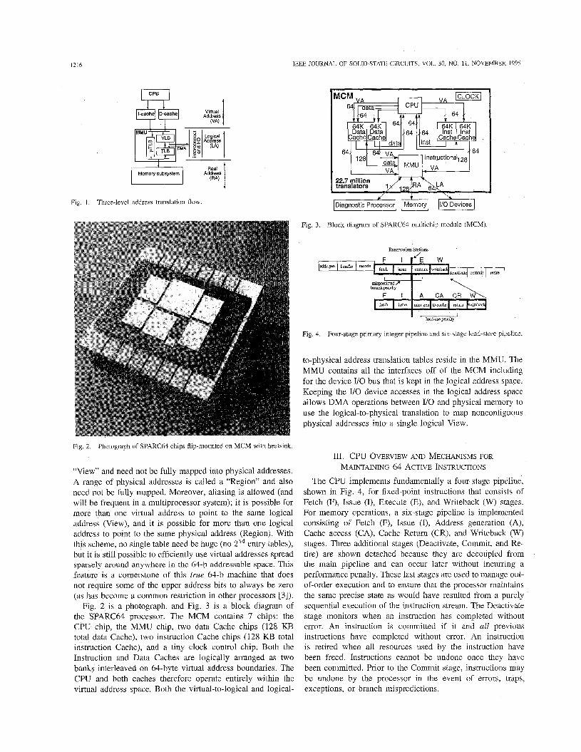
A conventional page-table look-up for a two-level address space, as traditionally used in 32-b computers, is not practical for a 64-b machine because of the size of the page table or the depth of the page-table tree. An inverted page-table mechanism, where the required page-table size is proportional only to the size of the physical memory, could be a possible solution but is still not efficient for large physical memory sizes because of the size of the associative searches required. To solve this problem, two levels of translation that allow a three-level memory hierarchy, as shown in Fig. 1, allow the processor to first make a translation on a virtual address to find an intermediate address, called the “logical” address in SPARC64, and then use the logical address to look up the actual physical real memory address. A range of logical addresses (when referenced by some virtual address) is called a
0018-9200/95$04.00 0 1995 IEEE
1216 IEEE JOURNAL OF SOLID-STATE CIRCUITS, VOL. 30, NO. 11, NOVEMBER 1995
w t ir;lh I-each D-cache
-1 Memory subsystem *:q Fig. 1. Three-level address translation flow.
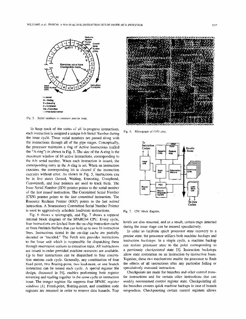
Fig. 2. Photograph of SPARC64 chips flip-mounted on MCM with heatsink.
"View" and need not be fully mapped into physical addresses. A range of physical addresses is called a "Region" and also need not be fully mapped. Moreover, aliasing is allowed (and will be frequent in a multiprocessor system); it is possible for more than one virtual address to point to the same logical address (View), and it is possible for more than one logical address to point to the same physical address (Region). With this scheme, no single table need be huge (no 254 entry tables), but it is still possible to efficiently use virtual addresses spread sparsely around anywhere in the 64-b addressable space. This feature is a cornerstone of this true 64-b machine that does not require some of the upper address bits to always be zero (as has become a common restriction in other processors [3]).
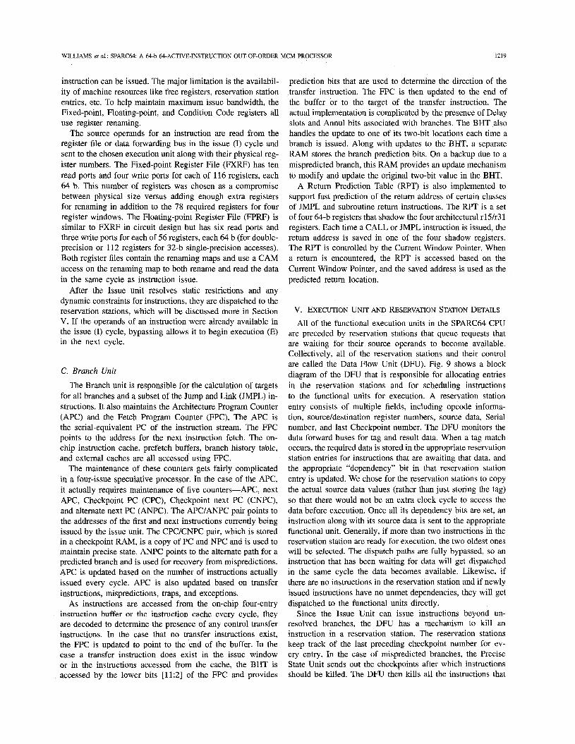
Fig. 2 is a photograph, and Fig. 3 is a block diagram of the SPARC64 processor. The MCM contains 7 chips: the CPU chip, the MMU chip, two data Cache chips (128 KB total data Cache), two instruction Cache chips (128 KB total instruction Cache), and a tiny clock control chip. Both the Instruction and Data Caches are logically arranged as two banks interleaved on 64-byte virtual address boundaries. The CPU and both caches therefore operate entirely within the virtual address space. Both the virtual-to-logical and logical-
22.7 million transistors I ,28 R
Fig. 3. Block diagram of SPARC64 multichip module (MCM)
Reservation Stations
'w Fig. 4 Four-stage pnmary integer plpeline and six-stage load-store pipeline
to-physical address translation tables reside in the MMU. The MMU contains all the interfaces off of the MCM including for the device U 0 bus that is kept in the logical address space. Keeping the I/O device accesses in the logical address space allows DMA operations between I/O and physical memory to use the logical-to-physical translation to map noncontiguous physical addresses into a single logical View.
m. CPU OVERVIEW AND MECHANISMS FOR MAINTAINING 64 ACTIVE INSTRUCTIONS
The CPU implements fundamentally a four-stage pipeline, shown in Fig. 4, for fixed-point instructions that consists of Fetch (F), Issue (I), Execute (E), and Writeback (W) stages. For memory operations, a six-stage pipeline is implemented consisting of Fetch (F), Issue (I), Address generation (A), Cache access (CA), Cache Return (CR), and Writeback (W) stages. Three additional stages (Deactivate, Commit, and Re- tire) are shown detached because they are decoupled from the main pipeline and can occur later without incurring a performance penalty. These last stages are used to manage out- of-order execution and to ensure that the processor maintains the same precise state as would have resulted from a purely sequential execution of the instruction stream. The Deactivate stage monitors when an instruction has completed without error. An instruction is committed if it and all previous instructions have completed without error. An instruction is retired when all resources used by the instruction have been freed. Instructions cannot be undone once they have been committed. Prior to the Commit stage, instructions may be undone by the processor in the event of errors, traps, exceptions, or branch mispredictions.
WILLIAMS et al.: SPARC64: A 64-b 64-ACTIVE-INSTRUCTION OUT-OF-ORDER MCM PROCESSOR 1217
I = ISSUW W = WaHlng x = ExeOUtlng C =Completed CM = Commlned .. = Free Serial number
Fig. 5. Serial numbers to maintain precise state.
TO keep track of the status of all in-progress instructions, each instruction is assigned a unique 6-b Serial Number during the issue cycle. These serial numbers are passed along with the instructions through all of the pipe stages. Conceptually, the processor maintains a ring of Active Instructions (called the “A-ring”) as shown in Fig. 5. The size of the A-ring is the maximum window of 64 active instructions, corresponding to the 6-b serial number. When each instruction is issued, the corresponding entry in the A-ring is set. When an instruction executes, the corresponding bit is cleared if the instruction executes without error. As shown in Fig. 5, instructions can be in five states (Issued, Waiting, Executing, Completed, Committed), and four pointers are used to track them. The Issue Serial Number (ISN) pointer points to the serial number of the lust issued instruction. The Committed Serial Number (CSN) pointer points to the lust committed instruction. The Resource Reclaim Pointer (RRP) points to the last retired instruction. A Nonmemory Committed Serial Number Pointer is used to aggressively schedule loadstore instructions.
Fig. 6 shows a micrograph, and Fig. 7 shows a topmost internal block diagram of the SPARC64 CPU. Every cycle, four instructions are fetched from the on-chip instruction cache or from Prefetch Buffers that can hold up to two 16 instruction lines. Instructions stored in the on-chip cache are partially decoded or “recoded.” The Fetch unit provides instructions to the Issue unit which is responsible for dispatching them through reservation stations to execution units. All instructions are issued in-order provided machine resources are available. Up to four instructions can be dispatched to four reserva- tion stations each cycle. Generally, any combination of four fixed-point, two floating-point, two load-store, or one branch instruction can be issued each cycle. A special register file design, discussed in [4], enables performing both register renaming and reading together in the same cycle as instruction issue. The integer register file supports four SPARC register windows [ 11. Fixed-point, floating-point, and condition code registers are renamed in order to remove data hazards. Trap
Fig. 6. Micrograph of CPU chip.
To Data Caches
Fig. 7. CPU block diagram.
levels are also renamed, and as a result, certain traps detected during the issue stage can be entered speculatively.
In order to facilitate quick processor state recovery to a precise state, the processor utilizes both machine backups and instruction backsteps. In a single cycle, a machine backup can restore processor state to the point corresponding to a previously checkpointed state [ 5 ] . Instruction backsteps allow state restoration on an instruction-by-instruction basis. Together, these two mechanisms enable the processor to flush the effects of all instructions after any particular failing or speculatively executed instruction.
Checkpoints are made for branches and other control trans- fer instructions and for certain other instructions that can modify nonrenamed control register state. Checkpointing all the branches ensures quick machine backups in case of branch mispredicts. Checkpointing certain control registers allows

1218 IEEE JOURNAL OF SOLID-STATE CIRCUITS, VOL. 30, NO. 11, NOVEMBER 1995
them to be modified speculatively. Pointers to the last check- point accompany each instruction throughout the processor and can be used to easily identify which instructions need to be killed for a specific machine backup. Checkpoints need only include the actual data from the few registers that are not renamed. For all of the renamed registers, each checkpoint need only keep the renaming map. The checkpoints of the maps are stored physically within the register files themselves, and the register files can restore the in-use map to a checkpointed one in a single cycle. The processor and register files can store up to sixteen checkpoints, and therefore, the SPARC64 can issue through the predicted paths of up to 16 branches speculatively.
Backup to a checkpoint provides a fast, but coarse, means to restore processor state. Individual instruction backsteps are used to provide a finer, but slower, means to get back to the state of a specific instruction in the case of exceptions occurring between checkpoints. Processor state restoration during backsteps involves updating register resources and decrementing the program counter by the backstep amount. The processor is able to backstep up to four instructions per cycle.
An issued instruction is placed in one of four types of reservation stations: Fixed-point, Floating-point, Address Gen- eration, Load/Store. Fixed-point instructions can also be sent to the Address generation reservation station. An instruction can execute once its operands are available, and as a result, instructions may execute out of order. Selection for execution is based mainly on an oldest-first algorithm. A total of seven instructions can be selected for execution each cycle: the Fixed-point, Address Generation, and Loadstore reservation stations are each able to initiate two instructions for execution, while the Floating-point reservation station is able to initiate one instruction.
As instructions complete execution, results are broadcast back to reservation stations and status information is provided to the Precise State Unit (PSU). The PSU tracks error and completion status and commits and retires instructions in order. The PSU also sequences instruction exceptions and external interrupts. Summarizing, up to ten instructions can execute, nine instructions can complete, eight instructions can commit, and four instructions can retire, in any one cycle. Up until commitment and retirement, register values are kept unique in case the processor will need to backup or restore a checkpoint. Retirement includes the reclaiming and freeing of all resources, such as renamed registers and the serial number, that an instruction used.
Iv. FETCH, ISSUE, AND BRANCH UNIT LOGIC DETAILS
Fig. 8 shows more detail about the portions of the SPARC64 called the Fetch, Branch, and Issue Units. The Fetch Unit interfaces between the off-chip instruction caches and the Branch and Issue units. It prefetches up to two 64-byte lines (16 instructions per line) ahead of the current program counter, recodes, and stores instructions in a 4 U3 (1024 locations, each 38 b) direct-mapped instruction cache. The separate Branch History Table (BHT) maps to all 1024 locations of the
Address to Data from Instruction
I I I BHT $4 Instructions
I
I
dispatched to resewation stations
Fig. 8. Fetch, branch, and issue units.
instruction cache using a dynamic branch prediction algorithm based on 2-b saturating counters.
A. Fetch Unit
There are no specific alignment constraints, so a fetch always returns four instructions on an on-chip cache hit, unless the access is to the end of the cache line (two cache lines cannot be accessed concurrently). Writes to the cache do not block read accesses. In the case of a miss, the Fetch Unit activates the prefetch logic based upon the missed address. The prefetch interface implements a split transaction protocol with the two interleaved Cache chips on the MCM each supplying two instruction words (64 b) along with separate status information. Cache fill requests are uniquely identified by partial address.
The Caches on the MCM return the identifiers one cycle before the data, and these are used to set up the writes to the prefetch on-chip cache lines. The instructions pass through a recode block that recodes control transfer, unimplemented, and illegal instructions. It also calculates partial target addresses for branches and calls, prepending one control bit and storing the calculated target in the original instruction. This technique results in only one extra bit for each instruction and reduces the branch target calculation to a simple increment or decrement of the upper bits of the Program Counter.
After recode, instructions are latched and written into the cache the next cycle. The fetch unit also forwards newly read instructions to the Issue Unit on the same cycle as they are written into the on-chip cache. Parity error detection is implemented on the on-chip instruction cache interface, and any resulting errors are just passed along with individual instructions. The actual parity error is incurred only if an attempt is made to issue the erroneous data.
B. Issue Unit The Issue Unit can issue up to four instructions every cycle.
There are very few issue restrictions. Any combination of four fixed-point, two floating-point, two loadlstore, or one branch
WLLIAMS et al.: SPARC64 A 64-b 64-ACTIVE-INSTRUCTION OUT-OF-ORDER MCM PROCESSOR 1219
instruction can be issued. The major limitation is the availabil- ity of machine resources like free registers, reservation station entries, etc. To help maintain maximum issue bandwidth, the Fixed-point, Floating-point, and Condition Code registers all use register renaming.
The source operands for an instruction are read from the register file or data forwarding bus in the issue (I) cycle and sent to the chosen execution unit along with their physical reg- ister numbers. The Fixed-point Register File (FXRF) has ten read ports and four write ports for each of 116 registers, each 64 b. This number of registers was chosen as a compromise between physical size versus adding enough extra registers for renaming in addition to the 78 required registers for four register windows. The Floating-point Register File (FPRF) is similar to FXRF in circuit design but has six read ports and three write ports for each of 56 registers, each 64 b (for double- precision or 112 registers for 32-b single-precision accesses). Both register files contain the renaming maps and use a CAM access on the renaming map to both rename and read the data in the same cycle as instruction issue.
After the Issue unit resolves static restrictions and any dynamic constraints for instructions, they are dispatched to the reservation stations, which will be discussed more in Section V. If the operands of an instruction were already available in the issue (I) cycle, bypassing allows it to begin execution (E) in the next cycle.
C. Branch Unit The Branch unit is responsible for the calculation of targets
for all branches and a subset of the Jump and Link (JMPL) in- structions. It also maintains the Architecture Program Counter (APC) and the Fetch Program Counter (FPC). The APC is the serial-equivalent PC of the instruction stream. The FPC points to the address for the next instruction fetch. The on- chip instruction cache, prefetch buffers, branch history table, and external caches are all accessed using FPC.
The maintenance of these counters gets fairly complicated in a four-issue speculative processor. In the case of the APC, it actually requires maintenance of five counters-APC, next APC, Checkpoint PC (CPC), Checkpoint next PC (CNPC), and alternate next PC (ANPC). The APC/ANPC pair points to the addresses of the first and next instructions currently being issued by the issue unit. The CPC/CNPC pair, which is stored in a checkpoint RAM, is a copy of PC and NPC and is used to maintain precise state. ANPC points to the alternate path for a predicted branch and is used for recovery from mispredictions. APC is updated based on the number of instructions actually issued every cycle. APC is also updated based on transfer instructions, mispredictions, traps, and exceptions.
As instructions are accessed from the on-chip four-entry instruction buffer or the instruction cache every cycle, they are decoded to determine the presence of any control transfer instructions. In the case that no transfer instructions exist, the FPC is updated to point to the end of the buffer. In the case a transfer instruction does exist in the issue window or in the instructions accessed from the cache, the BHT is accessed by the lower bits [11:2] of the FPC and provides
prediction bits that are used to determine the direction of the transfer instruction. The FPC is then updated to the end of the buffer or to the target of the transfer instruction. The actual implementation is complicated by the presence of Delay slots and Annul bits associated with branches. The BHT also handles the update to one of its two-bit locations each time a branch is issued. Along with updates to the BHT, a separate RAM stores the branch prediction bits. On a backup due to a mispredicted branch, this RAM provides an update mechanism to modify and update the original two-bit value in the BHT.
A Return Prediction Table (RPT) is also implemented to support fast prediction of the return address of certain classes of JMPL and subroutine return instructions. The RPT is a set of four 64-b registers that shadow the four architectural r15/r31 registers. Each time a CALL or JMPL instruction is issued, the return address is saved in one of the four shadow registers. The RPT is controlled by the Current Window Pointer. When a return is encountered, the RPT is accessed based on the Current Window Pointer, and the saved address is used as the predicted return location.
v. EXECUTION UNIT AND RESERVATION STATION DETAILS All of the functional execution units in the SPARC64 CPU
are preceded by reservation stations that queue requests that are waiting for their source operands to become available. Collectively, all of the reservation stations and their control are called the Data Flow Unit (DFU). Fig. 9 shows a block diagram of the DFU that is responsible for allocating entries in the reservation stations and for scheduling instructions to the functional units for execution. A reservation station entry consists of multiple fields, including opcode informa- tion, source/destination register numbers, source data, Serial number, and last Checkpoint number. The DFU monitors the data forward buses for tag and result data. When a tag match occurs, the required data is stored in the appropriate reservation station entries for instructions that are awaiting that data, and the appropriate “dependency” bit in that reservation station entry is updated. We chose for the reservation stations to copy the actual source data values (rather than just storing the tag) so that there would not be an extra clock cycle to access the data before execution. Once all its dependency bits are set, an instruction along with its source data is sent to the appropriate functional unit. Generally, if more than two instructions in the reservation station are ready for execution, the two oldest ones will be selected. The dispatch paths are fully bypassed, so an instruction that has been waiting for data will get dispatched in the same cycle the data becomes available. Likewise, if there are no instructions in the reservation station and if newly issued instructions have no unmet dependencies, they will get dispatched to the functional units directly.
Since the Issue Unit can issue instructions beyond un- resolved branches, the DFU has a mechanism to kill an instruction in a reservation station. The reservation stations keep track of the last preceding checkpoint number for ev- ery entry. In the case of mispredicted branches, the Precise State Unit sends out the checkpoints after which instructions should be killed. The DFU then kills all the instructions that
1220 JEEE JOURNAL OF SOLID-STATE CIRCUITS, VOL. 30, NO. 11, NOVEMBER 1995
- I
Result and Status Buses
Lookahead Add operation. FX1 and FX2 are the most general units and can also perform move, multiply step, and bitwise logical, shift, and rotate operations.
There is one Integer Multiply and Divide (IMULDIV) unit composed of a separate 64-b Multiplier and a 64-b Divider. The IMULDIV unit shares operand and result buses with the FX1 unit and uses the 64-b carry lookahead adder in FX1 for one cycle at the start and end of a multiply or divide instruction. The IMULDIV unit is not pipelined internally and can only execute one integer multiply or divide instruction at a time. The Multiplier contains a multiplier tree that is capable of computing a 64 x 16 b multiplication in carry- save form in each clock cycle. After an extra cycle for the 6 4 4 adder to generate the final result, the IMULDIV can finish the 32-b signed and unsigned multiplications in three cycles and the 64-b signed and unsigned multiplications in five cycles. The integer Divider implements a radix 4 SRT algorithm. The divider can complete 64-b divides in 2-39 cycles, depending on the magnitude of the operands, with an average latency of 17 cycles.
All targets for JMPL instructions are calculated in FX2. The result bus of FX2 is also shared with return data from the processor privileged and state registers. FX3 and FX4 are used primarily for address calculations for Load or Store instructions but can also be used for general fixed-point calculations. To conserve area, these last two units do not support shift operations.
Fig. 9. Block diagram of the data flow unit and functional units.
were issued mistakenly assuming correct prediction at those checkpoints.
Each of the reservation stations, as shown in Fig. 9, has eight entries, except for the LS reservation station that has twelve en- tries. The FX Reservation Station (DFMFXU) schedules fixed- point instructions for two general-purpose integer execution units. The lnteger MultiplyDivide instructions also go through the DFMFXU. The basic algorithm to select instructions out of the DFMFXU is “oldest-ready.” The AGENFX Reservation Station (DFMAGEN) schedules fixed-point and loadstore instruction address generation to two more restricted integer execution units. DFMAGEN is similar to DFMFXU except that address generation of younger loads is stalled if there is an active older store in the reservation station.
The FP reservation station (DFMFPU) schedules one in- struction per cycle to one of the two floating-point units. The two FP units are a Floating-point Multiply-Add (FMA) unit and a Floating-point Divider (FDIV). The LS Reservation station (DFMLSU) schedules Memory operations including Loads, Stores, and Atomic instructions to the external Data Caches. This will be explained in more detail in subsection D.
A. Fixed-point Functional Units The four integer fixed-point functional units are called
FX1-4 and can each perform a single cycle 64-b fast Carry
B. Floating-Point Multiply-Add Unit The Floating-point Multiply-Add unit (FMA) is IEEE
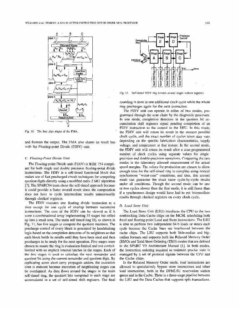
754 compliant and executes all single and double precision floating-point move, compare, add, and multiply instructions. The “fused” multiply-add operation (A*B + C) means that only one rounding error is incurred in the combined operation. The use of a fused operation was pioneered in [6] and has since been adopted by several companies. Having a single unit avoids having to design several different functional units because all floating arithmetic (except division) can be implemented as a special case of this single fused multiply- add. For example, subtraction is implemented as a fused multiply-add with the B operand forced to 1 and with the C operand negated. The FMA implementation is a four- stage fully pipelined unit and can accept a new floating-point instruction every cycle.
As shown in Fig. 10, the first pipe stage in the FMA formats the input operands, calculates an alignment shift count for the add operand, completes the first half of the add operand alignment to the multiplier product, and goes through the first half of a full 53 x 53 carry-save adder tree using regular 9 x 3 layout blocks. The second pipe stage contains the second part of the 53 x 53 tree that reduces the multiplier result down to two partial products in carry-save form, adds the C operand to the partial product, and completes the first half of the leading zero calculation. The third stage finishes the leading zero calculation, sums up the two partial products, and normalizes the result. The fourth pipe stage determines exceptions and special cases, rounds the result to the destination precision,
WILLIAMS et al.: SPARC64: A 64-b 64-ACTIVE-INSTRUCTION OUT-OF-ORDER MCM PROCESSOR 1221
A 0 C n n
pipe 1 I \ I
/ I
A,*B, + C,
E esu t out ut
L
Fig. 10. The four pipe stages of the FTVIA.
and formats the output. The FMA also shares its result bus with the Floating-point Divide (FDIV) unit.
C. Flouting-Point Divide Unit
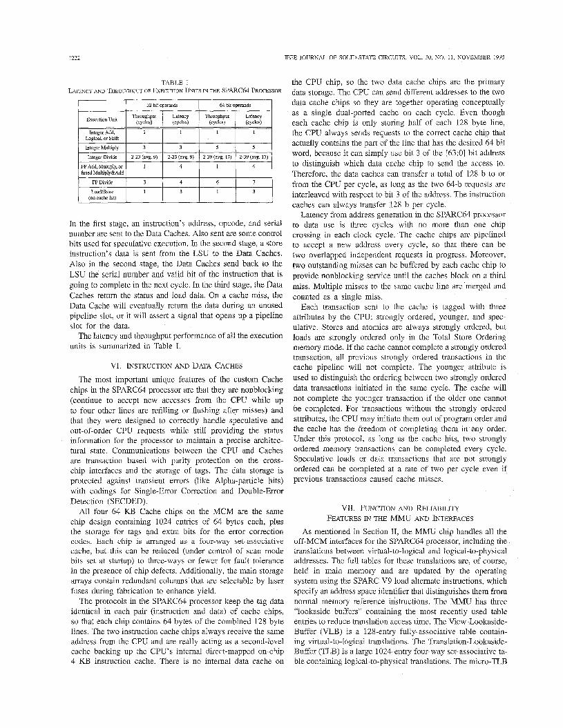
The Floating-point Divide unit (FDIV) is IEEE 754 compli- ant for both single and double precision floating-point divide instructions. The FDIV is a self-timed functional block that makes use of fast precharged circuit techniques for computing quotient digits directly using a modified radix-2 SRT algorithm [7]. The SPARC64 team chose the self-timed approach because it could provide a faster overall result since the computation does not have to cycle intermediate results unnecessarily through clocked registers.
The FDIV executes one floating divide instruction at a time except for one cycle of overlap between successive instructions. The core of the FDIV can be viewed as if it were a combinational array implementing 55 stages but rolled up into a small area. The main self-timed ring [8], as shown in Fig. 11, has five stages to compute the quotient mantissa. The precharge control of every block is generated by handshaking logic based on the completion detectors of its neighbors so that each block holds its results until they have been used and then precharges to be ready for the next operation. Five stages were chosen to assure the ring is evaluation-limited and not control- limited with no explicit internal latches in the stages. Each of the five stages is used to calculate the next remainder and quotient bit using the current remainder and quotient digit. By replicating some short carry propagate adders, the execution time is reduced because execution of neighboring stages can be overlapped. As data flows around the stages in the main self-timed ring, the quotient bits computed in each stage are accumulated in a set of self-timed shift registers. The final
Stage Stage R e m r m-1 Control , Bus
Stage 4- Stage 4- Stage
Fig. 11. Self-timed FDIV ring iterates around stages without registers.
rounding is done in one additional clock cycle while the whole ring precharges again for the next instruction.
The FDIV unit can operate in either of two modes, pro- grammed through the scan chain by the diagnostic processor. In one mode, completion detectors in the quotient bit ac- cumulation shift registers signal pending completion of an FDIV instruction to the control in the DFU. In this mode, the FDIV unit will return its result in the soonest possible clock cycle, and the exact number of cycles taken may vary depending on the specific fabrication characteristics, supply voltage, and temperature at that instant. In the second mode, the FDIV unit will return its result after a scan-programmed number of clock cycles using separate values for single- precision and double-precision operations. Comparing the two modes in the laboratory allowed measurement of the actual speed margins. The values for production are chosen to allow enough time for the self-timed ring to complete using normal synchronous “worst-case” conditions, and thus, this second mode can guarantee the exact same cycle-by-cycle results under all conditions. Though the second mode can be one or two cycles slower than the first mode, it is still faster than if a synchronous design would have had to put intermediate results through clocked registers on every clock cycle.
D. Load Store Unit
The Load Store Unit (LSU) interfaces the CPU to the two nonblocking Data Cache chips on the MCM, scheduling both fixed and floating-point Load and Store instructions. The LSU is able to perform two independent 64-b loads or stores each cycle because the Cache lines are interleaved between the cache chips. The LSU supports both little-endian and big- endian formats and supports both the Relaxed Memory Order (RMO) and Total Store Ordering (TSO) modes that are defined in the SPARC V9 Architecture Manual [l]. In both modes, the instruction ordering required to maintain precise state is managed by a set of protocol signals between the CPU and the Cache chips.
In the Relaxed Memory Order mode, load instructions are allowed to speculatively bypass store instructions and other load instructions, both in the DFMLSU reservation station queue and in the Cache. There is a three-stage pipeline between the LSU and the Data Caches that supports split transactions.
1222 IEEE JOURNAL OF SOLID-STATE CIRCUITS, VOL. 30, NO. 11, NOVEMBER 1995
Execution Unit
Integer Add, Logical, or Shift
Inteeer Multiolv
TABLE I LATENCY AND THROUGHPUT OF EXECUTION UNITS IN THE SPARC64 PROCEsSOR
Throughput Latency Throughput Latency (cycles) (cycles) (cycles) (cycles)
1 1 1 1
3 3 5 5
1 - 1 32bitoperands I Mbitopemds I
FP Add, Multiply, or fused MultiplyBAdd
FP Divide
Load/Store (on cache hit)
1 4 1 4
3 4 6 7
1 3 1 3
- _ . I I I
Integer Divide I 2-23 (avg. 9) I 2-23 (avg, 9) I 2-39 (avg. 17) 1 2-39 (aVg. 17)
In the first stage, an instruction’s address, opcode, and serial number are sent to the Data Caches. Also sent are some control bits used for speculative execution. In the second stage, a store instruction’s data is sent from the LSU to the Data Caches. Also in the second stage, the Data Caches send back to the LSU the serial number and valid bit of the instruction that is going to complete in the next cycle. In the third stage, the Data Caches return the status and load data. On a cache miss, the Data Cache will eventually return the data during an unused pipeline slot, or it will assert a signal that opens up a pipeline slot for the data.
The latency and throughput performance of all the execution units is summarized in Table I.
VI. INSTRUCTION AND DATA CACHES
The most important unique features of the custom Cache chips in the SPARC64 processor are that they are nonblocking (continue to accept new accesses from the CPU while up to four other lines are refilling or flushing after misses) and that they were designed to correctly handle speculative and out-of-order CPU requests while still providing the status information for the processor to maintain a precise architec- tural state. Communications between the CPU and Caches are transaction based with parity protection on the cross- chip interfaces and the storage of tags. The data storage is protected against transient errors (like Alpha-particle hits) with codings for Single-Error Correction and Double-Error Detection (SECDED).
All four 64 KB Cache chips on the MCM are the same chip design containing 1024 entries of 64 bytes each, plus the storage for tags and extra bits for the error correction codes. Each chip is arranged as a four-way set-associative cache, but this can be reduced (under control of scan mode bits set at startup) to three-ways or fewer for fault tolerance in the presence of chip defects. Additionally, the main storage arrays contain redundant columns that are selectable by laser fuses during fabrication to enhance yield.
The protocols in the SPARC64 processor keep the tag data identical in each pair (instruction and data) of cache chips, so that each chip contains 64 bytes of the combined 128 byte lines. The two instruction cache chips always receive the same address from the CPU and are really acting as a second-level cache backing up the CPU’s internal direct-mapped on-chip 4 KB instruction cache. There is no internal data cache on
the CPU chip, so the two data cache chips are the primary data storage. The CPU can send different addresses to the two data cache chips so they are together operating conceptually as a single dual-ported cache on each cycle. Even though each cache chip is only storing half of each 128 byte line, the CPU always sends requests to the correct cache chip that actually contains the part of the line that has the desired 64 bit word, because it can simply use bit 3 of the [63:0] bit address to distinguish which data cache chip to send the access to. Therefore, the data caches can transfer a total of 128 b to or from the CPU per cycle, as long as the two 64-b requests are interleaved with respect to bit 3 of the address. The instruction caches can always transfer 128 b per cycle.
Latency from address generation in the SPARC64 processor to data use is three cycles with no more than one chip crossing in each clock cycle. The cache chips are pipelined to accept a new address every cycle, so that there can be two overlapped independent requests in progress. Moreover, two outstanding misses can be buffered by each cache chip to provide nonbloclung service until the caches block on a third miss. Multiple misses to the same cache line are merged and counted as a single miss.
Each transaction sent to the cache is tagged with three attributes by the CPU: strongly ordered, younger, and spec- ulative. Stores and atomics are always strongly ordered, but loads are strongly ordered only in the Total Store Ordering memory mode. If the cache cannot complete a strongly ordered transaction, all previous strongly ordered transactions in the cache pipeline will not complete. The younger attribute is used to distinguish the ordering between two strongly ordered data transactions initiated in the same cycle. The cache will not complete the younger transaction if the older one cannot be completed. For transactions without the strongly ordered attributes, the CPU may initiate them out of program order and the cache has the freedom of completing them in any order. Under this protocol, as long as the cache hits, two strongly ordered memory transactions can be completed every cycle. Speculative loads or data transactions that are not strongly ordered can be completed at a rate of two per cycle even if previous transactions caused cache misses.
VII. FUNCTION AND RELIABILITY mATLJRES IN THE MMU AND INTERFACES
As mentioned in Section 11, the MMU chip handles all the off-MCM interfaces for the SPARC64 processor, including the translations between virtual-to-logical and logical-to-physical addresses. The full tables for these translations are, of course, held in main memory and are updated by the operating system using the SPARC V9 load alternate instructions, which specify an address space identifier that distinguishes them from normal memory reference instructions. The MMU has three “lookaside buffers” containing the most recently used table entries to reduce translation access time. The View-Lookaside- Buffer (VLB) is a 128-entry fully-associative table contain- ing virtual-to-logical translations. The Translation-Lookaside- Buffer (TLB) is a large 1024-entry four-way set-associative ta- ble containing logical-to-physical translations. The micro-TLB
WILLIAMS et al.: SPARC64 A 64-b 64-ACTIVE-INSTRUCTION OUT-OF-ORDER MCM PROCESSOR 1223
(pTLB) is a three-port 8-entry fully-associative table con- taining complete virtual-to-physical translations of cacheable memory requests only. The three ports on the pTLB allow the one instruction and two data memory addresses that can be generated by the CPU each cycle to all operate in parallel. For each translation request that hits in the pTLB, the physical address is available in a single cycle, and no further translations are necessary. If the pTLB misses, then VLB and TLB translations, initiated in parallel, are checked for hits. They are much larger and more likely to hit; but if they also miss, then a hardware table walk is initiated to bring in the required translation table entries from main memory. The MMU chip contains a complete state machine to handle this sequence of memory accesses without requiring any assistance from the CPU chip.
Before real addresses are sent out into the main memory subsystem, they are also checked for a match in one more table called the Data Cache Real Address Table (DCRAT). This is a 1024-entry four-way set-associative table storing the real address tags of all the cache lines held in the two data cache chips. If an access requested by the CPU matches an entry in the DCRAT, it is a virtual-miss-real-hit because the requested data is already in the cache under a different virtual address. In this case, the cache entry is re-tugged instead of a requiring a main memory access. The DCRAT also snoops on all main memory bus transactions, so that in a multiprocessor configuration the data caches are kept coherent with main memory when any shared references are detected.
The MMU interface to the main memory subsystem can transfer 128 b per cycle. The memory system returns the critical word first when servicing cache misses. The total latency for a cache miss (but translation-hit) is about 21 processor cycles.
All translation tables are protected by parity. If a translation or cache parity error is detected, the MMU can maintain correct system state by simply invalidating the hit, thus causing a miss that brings in fresh data from main memory. The new translation uses a different translation table entry, so that even if one of the translation tables contains a hard-error in a specific location, graceful degradation will still allow the processor to continue execution correctly [9]. The DCRAT is protected by a SECDED code like the cache data itself. While hardware does detect the single or double bit errors, the correction of single-bit errors in the DCRAT or caches is performed by a system software trap, since this event is too rare to justify building the correction algorithm in silicon.
The MMU generates the (72, 64) SECDED code on all writes to main memory. On all read operations, the error code bits are hashed with the parity-encoded address bits to be able to detect any transient address errors between the MMU and the main memory subsystem [lo]. Ordinary main-memory data errors are corrected in the MMU, but double bit or address errors are treated as high-priority uncorrectable errors.
The MMU maintains both low-priority and high-priority error queues for the SPARC64 processor to be able to log and recover from errors. Low-priority errors, of which there are a total of 15 types, are errors that have already been corrected, such as a single-bit memory error in the caches
or main memory that was corrected by the SECDED coding. High-priority errors, of which there are a total of 24 types, are those uncorrectable errors such as double-bit, chip-crossing parity, or address parity errors that require immediate attention and will cause the CPU to go into the RED mode of execution to avoid generating any further errors. In this mode, the SPARC64 processor, with the assistance of the separate off- MCM diagnostic processor, can then recover as much system state as possible. For many failures, software can disable a failed hardware unit (such as a way of the caches or one of the translation maps), recover data, and provide an orderly shutdown or restart of the system.
VIII. CAD TOOLS AND TECHNOLOGY FOR SIMULATION AND PHYSICAL DESIGN
The SPARC64 processor was designed from scratch by a newly assembled team of engineers working in Campbell, CA. Unlike most microprocessor projects, HaL did not have a previous design database from which to “evolve” the new design.
The performance impact of processor microarchitecture choices was studied through the use of detailed processor models. Simulations of the processor model allowed many parameters to be adjusted and measured, such as the number of checkpoints, rename registers, reservation station entries, etc. Additionally, arbitrary observability into the execution en- gine diagnosed performance-limiting structures. Our processor model was called Timer and utilized trace driven simulation. The Timer strives to model events within the CPU, caches, MMU, and memory system on a cycle-by-cycle basis but was not kept 100% cycle accurate with respect to the real hardware in order to ease coding, reconfiguration, and to improve its execution rate. Experiments matching the Timer model against real silicon indicate a typical error of only a few percent. Prior to a Timer run, traces of applications are generated using an instruction set simulator that captures both user and kernel code. Every instruction, including effective addresses or branch targets if relevant, is captured into a trace file. In order to reduce the size of the traces from long running programs, the trace was typically sampled down to a manageable size. This trace file can then be simulated through the Timer to measure the effects of numerous microarchitectural tradeoffs.
Logic entry was mainly textual and used the internal Aida hardware description language called ADL. Simulation of this language was available both in software and using specialized hardware accelerators designed specifically to execute this language. Both the software and hardware simulations of ADL used cycle-bused Levelized Compiled Code (LCC) where the order of gate evaluation is predetermined at compile time. Each gate in the design therefore gets reevaluated once, and only once, per clock cycle. When most gates do switch every cycle, as is more likely in superscalar designs like SPARC64, the LCC method results in faster simulation of gate networks than the simulators for Verilog that must trace event dependencies during run time.
For simplicity, the designs and logic simulation used pri- marily edge-triggered registers rather than individual latches.
1224 II
kill3 resource0
resource1 kill2 kill1
I kill0
Fig. 12. Resource stall circuit.
All circuit blocks that contained their own storage were encapsulated in models to fit into the overall scannable register and combinational-logic only environment. Although there were some blocks that were specified in a Register Transfer Level (RTL) subset of ADL and then synthesized using Synopsys, the majority of the logic in the processor was specified directly at the gate level in ADL. Optimizations to move logic across register boundaries and to improve path timing between registers were all done by hand.
The CPU, Cache, and MMU chips were simulated both separately and together in a complete gate-level model of the SPARC64. Separately built models of each chip allowed the individual chip teams to make faster independent progress, but the combined model was, of course, required to verify the correctness of all the interactions. Because of the large teams of engineers whose work was interrelated, explicit version control was an important requirement, and HaL built an internal hierarchical source-code versioning system so that each model and team could choose explicit versions of the other pieces. In this way, environments were kept stable, and the scheduling of changes deliberately and explicitly communicated to balance maximizing parallel progress and keeping every piece up-to-date.
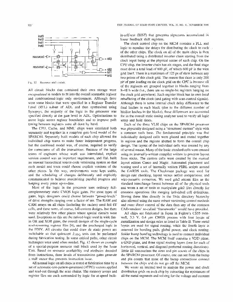
Most of the logic in the processor uses ordinary full- complementary static CMOS logic gates. For most types of gates, logic designers could choose between “power-levels’’ of drive strengths ranging over a factor of ten. The RAM and CAM arrays on all chips (including the caches) used full 6T cells, and these were, of course, full-custom designs, but there were relatively few other places where special circuits were used. Exceptions to this are the ratioed-logic used in wide fan- in OR and XOR gates, the overall designs of the single-cycle read-renaming register files [4], and the precharged logic in the FDIV. All circuits that could draw dc static power are switchable so that quiescent IDDQ tests can be performed during fabrication testing. In some critical paths, other circuit techniques were used when needed. Fig. 12 shows an example of a special-purpose resource stall block used by the Issue Unit. Based on resource availability and attributes decoded from instructions, three levels of transmission gates generate a stall vector that prevents instruction issue.
All normal logic on all chips is tested at fabrication time by a set of automatic-test-pattern-generated (ATPG) vectors applied and read-out through the scan chains. The memory arrays and register files are each surrounded by logic for at-speed built-
3EE JOURNAL OF SOLID-STATE CIRCUITS, VOL. 30, NO. 11, NOVEMBER 1995
in-self-test (BIST) that generates signatures accumulated in linear feedback shift registers.
The clock control chip on the MCM contains a PLL and logic to equalize the delays for distributing the clock to each of the other chips. The clock on all of the main chips is then distributed using a distributed inverter chain starting from the clock input bump at the physical center of each chip. On the CPU chip, the inverter chain has six stages, and the final stage must drive a total load of 800 pF, of which 600 pF is the wire grid itself. There is a maximum of 125 ps of skew between any two points of this clock grid. The reason that there is only 200 pF of gate loading on the clock grid on the CPU is because all of the registers are grouped together in blocks ranging from 8 4 8 b wide (i.e., there are no single-bit registers hanging on the clock grid anywhere). Each register block has its own local rebuffering of the clock (and gating with scan-control signals). Although there is some internal clock delay difference to the final latches in each block (due to the different number of bitslice latches in the blocks), these differences are accounted for in the overall static timing analyzer used to verify all logic setup and hold times.
Each of the three VLSI chips on the SPARC64 processor was physically designed using a “structured-custom’’ style with a common tools base. The fundamental principle was that individually designed cells were placed and routed together in regions and the regions abutted to form the overall chip design. The layout of the individual cells was created by any of several means. Many of the basic standard cells were created using an internally-written compiler written to generate layout from sticks. The custom cells were created by the manual layout editors Caeco and Magic. Automated placement and routing used a set of internally written PERL scripts around the GARDS tools. The Checkmate package was used for design-rule checking, layout versus netlist comparisons, and wire-parasitic extraction. We used gds2 stream files as the standard interchange format between all of the physical tools and wrote a set of tools to manipulate gds2 files directly for common operations like merging individual cell definitions. Storing these files directly in the Unix directory hierarchy also allowed using the same robust versioning control methods and more direct control of the data than any of the common CAI)-vendors’ so-called “frameworks” would have provided.
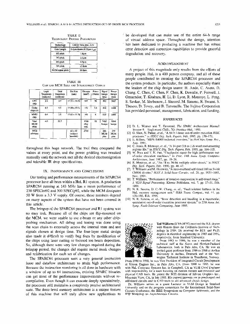
All chips are fabricated in Japan in Fujitsu’s CS55 twin- well, 3.3 V, 0.4 pm CMOS process with four layers of metallization and design rules as listed in Table 11. Three metal layers are used for signal routing, while the fourth layer is reserved for bonding pads, global power, and clock routing. Solder bump bonding technology is used to connect individual chips on the MCM. The MCM itself contains a VDD plane, a GND plane, and three signal routing layers (one for each of horizontal, vertical, and diagonal preferred routing directions). Table I11 summarizes the sizes and pin counts of the chips in the SPARC64 processor. Of course, one can see from the bump and pin counts that most of the bump connections connect between the chips and do not go off the MCM.
We wrote an internal tool to analyze the power and clock distribution grids on each chip by extracting the resistances of all the metal segments and solving for the voltage and currents
WILLIAMS et al.: SPARC64: A 64-b 64-ACTIVE-INSTRUCTION OUT-OF-ORDER MCM PROCESSOR 1225
MCS substrate
TABLE I1 TECHNOLOGY PROCESS PARAMETERS
61x45 2145 286 219 (without MCM MCM heatsink) pins pins
Technology I CMOS ’kin-well, 3.3V
Gate-Length I 0 . 4 ~ drawn (0.35~ Lee)
I M1 pitch I 1.8pm I
TABLE 111 CHIP AND MCM SIZES AND INTERCONNECT COUNTS
throughout this huge network. The tool then compared the values at every point, and the power gridding was tweaked manually until the network met all the desired electromigration and tolerable IR drop specifications.
Ix. PERFORMANCE AND CONCLUSIONS
Our testing and performance measurements of the SPARC64 processor have all been within a HaL R1 system. A production SPARC64 running at 143 MHz has a mean performance of 230 SPECint92 and 300 SPECfp92, while the MCM dissipates 50 W from a 3.3 V supply. Of course, these numbers depend on many aspects of the system that have not been covered in this article.
The bringup of the SPARC64 processor and R1 system was no easy task. Because all of the chips are flip-mounted on the MCM, we were unable to use e-beam or any other chip- probing mechanism. All debug and testing was done using the scan chain to externally access the internal state and test signals chosen at design time. The four-layer metal design also made it difficult to verify bug fixes by modification of the chips using laser cutting or focused ion-beam deposition. So, although there were very few changes required during the bringup period, the changes did require metal mask changes and refabrication for each set of changes.
The SPARC64 processor uses a very general instruction issue and dataflow architecture to attain high performance. Because the instruction reordering is all done in hardware with a window of up to 64 instructions, existing SPARC binaries can get most of the performance improvements without re- compilation. Even though it can execute deeply speculatively, the processor still maintains a completely precise architectural state. The three-level memory architecture is a unique feature of this machine that will truly allow new applications to
be developed that can make use of the entire 64-b range of virtual address space. Throughout the design, attention has been dedicated to producing a machine that has robust error detection and correction capabilities to provide graceful degradation and recovery.
ACKNOWLEDGMENT A project of this magnitude only results from the efforts of
many people. HaL is a 400 person company, and all of these people contributed to creating the SPARC64 processor and the system products. In particular, the authors especially thank the leaders of the chip design teams: H. Ando, C. Asato, D. Chang, C. Chen, C. Chen, F. Chen, K. Dawallu, P. Forssell, J. Gmuender, T. Kitahara, H. Li, D. Lyon, R. Montoye, L. Peng, S. Savkar, M. Shebanow, J. Sherred, M. Simone, R. Swami, S. Thusoo, D. Tovey, and B. Turumella. The Fujitsu Corporation has provided personnel, management, fabrication, and funding.
REFERENCES
D. L. Weaver and T. Germond, The SPARC Architecture Manual: Version 9. G. Shen, N. Patkar, et al., “A 64 b 4-issue out-of-order execution RISC processor,” in ZSSCC Dig. Tech. Papers, Feb. 1995, pp. 170-171. E. Killian, “MIPS R4000 technical overview,” in HotChips Symp. Rec., Aug. 1991. C. Asato, R. Montoye, et. al., “A 14-port 3.8 ns 116-word read-renaming register file,” in ZSSCC Dig. Tech. Papers, Feb. 1995, pp. 104-105. W. Hwu and T. N. Patt, ‘Checkpoint repair for high performance out- of-order execution machines,” in Proc. 14th Annu. Symp. Computer Architecture, June 1987, pp. 18-26. R. Montoye, et. al., “An 18 ns 56-bit multiply-adder circuit,” in ISSCC Dig. Tech. Papers, Feb. 1990, pp. 46-47. T. Williams and M. Horowitz, “A zero-overhead self-timed 160 ns 54-bit CMOS divider,” ZEEE J. Solid-State Circuits, vol. 26, pp. 1651-1661, Nov. 1991. T. Williams, “Performance of iterative computation in self-timed rings,” J. VLSZ Signal Processing, Kluwer Publishers, vol. 7, pp. 17-31, Feb. 1994. N. R. Saxena, D. C.-W. Chang, et. al., “Fault-tolerant features in the HaL memory management unit,” ZEEE Trans. Comput., vol. 44, pp. 170-180;Feb. 1995. N. R. Saxena, et. al., “Error detection and handling in a superscalar, speculative out-of-order execution processor system,” in 25th Annu. Int. Symp. Fault-Tolerunt Computing, June 1995.
Englewood Cliffs, NJ: Prentice-Hall, 1993.
Ted Williams (S’89-M’92) received the B.S. degree with Honors from the California Institute of Tech- nology in 1984. He received the M.S. and Ph.D. degrees in electrical engineering in 1985 and 1991, respectively, from Stanford University.
From 1983 to 1986, he was a member of the technical staff at the Xerox and Hewlett-Packard Laboratories, both in Palo Alto, CA. He was an invited guest professor from 1986 to 1988 at Aarhus University in Aarhus, Denmark and at the Nor- wegian Technical Institute in Trondheim, Norway.
From 1988 to 1990, he was Vice-president of Integrated Circuit Development at Silicon Engines Inc., in Palo Alto, CA. From 1990 to 1995, he was with HaL Computer Systems Inc. in Campbell, CA as VLSI Chief Engineer with responsibility for a team focusing on custom circuits and electrical and physical CAD tools. He joined the MTI division of Silicon Graphics Inc., Mountain View, CA, in late 1995. His current interests are in precharged and self-timed circuits and in CAD tools to aid advanced circuit design.
Dr. Williams serves as a guest Lecturer in VLSI Design at Stanford University and on the program committees for the Intemational Solid-state Circuits Conference, the IEEE Symposium on Computer Arithmetic, and the IFIP Workshop on Asynchronous Circuits.
1226
Niteen Patkar (S’84-M’84) received the B.S.E.E. degree from University of Bombay, India in 1981 and the M.S.E.E. degree from Texas Tech University in 1984.
From 1984 to 1989, he was a Senior Design Engineer with Advanced Micro Devices, San Anto- nio TX, working on Array Processors and Floating Point Processors. From 1989 to 1991, he was with Performance Semiconductor as a Senior Engineer in the MIPS Microprocessor Design Group. He has been with HaL Computer Systems since 1991 and
is Manager for Processor Development. He managed the design of the first HaL CPU chip and also the bringup of the HaL R1 system. Currently, he is working on HaL’s future microprocessor designs.
IEEE JOURNAL OF SOLID-STATE CIRCUITS, VOL. 30, NO. 11, NOVEMBER 1995
Gene Shen (M’88) received a B.S E E degree from MIT in 1987 and Masters of Engineering from Come11 University in 1988
From 1988 to 1991, he worked on the MC88110 processor at Motorola in Austin TX He was at HaL Computer Systems from 1991 to 1995 and was a technical leader for the Issue unit of SPARC64 processor He also served as the design manager of HaL’s second generation CPU He is now with Exponential Technology, San Jose, CA. His interests are in high performance processor architecture and
integrated circuit design. Mr. Shen is a member of the IEEE Computer Society
Related Documents