ARTICLE Copyright © 2013 by American Scientific Publishers All rights reserved. Printed in the United States of America Journal of Nanoengineering and Nanomanufacturing Vol. 3, pp. 1–7, 2013 (www.aspbs.com/jnan) Solvothermal Synthesis of One Dimensional Copper Doped Cadmium Sulphide Nanorods and Their Photocatalytic Performance Sudhir S. Arbuj, Sagar R. Bhalerao, Sunit B. Rane, Uttam P. Mulik ∗ , and Dinesh P. Amalnerkar Centre for Materials for Electronics Technology, Off Pashan Road, Panchwati, Pune 411008, India ABSTRACT In this study, one dimensional Cu doped CdS with higher aspect ratio was synthesized by solvothermal tech- nique. The Cu doping concentration was varied from 0.1 to 5 mol% (Cu x Cd 1−x S where x = 0.001, 0.005, 0.01 and 0.05). The prepared compositions were characterized using various spectroscopic techniques such as, UV-visible and photoluminescence, X-ray diffraction, Field emission scanning electron and Transmission elec- tron microscopy. X-ray diffractogram shows formation of crystalline CdS with hexagonal wurtzite structure. The DRS exhibits absorption edge between 520 to 530 nm revealing the band gap of 2.38 to 2.34 eV. Photolumines- cence spectrum yielded two distinct peaks at ∼ 515 and 602 nm. The broad emission band around ∼ 515 nm corresponds to the band edge excitation. FE-SEM micrographs demonstrate the formation of nanorods with 30–50 nm diameter and 0.5 to 10 m length. The aspect ratio of Cu x Cd 1−x S nanorods increased with increase in copper doping up to 1 mol%. TEM confirms the formation of crystalline nano rods of Cu doped CdS materi- als. The photocatalytic activity of the prepared Cu doped CdS was investigated for methylene blue degradation. Among the prepared compositions, Cu 0.01 Cd 0.99 S exhibits higher rate of degradation, rate constant observed is 1.42 × 10 −2 min −1 . KEYWORDS: Solvothermal Synthesis, 1D Nano Structures, Photocatalysis, Dye Degradation. 1. INTRODUCTION The semiconducting metal chalcogenide nanorods and nanowires have been investigated in great details due to their unusual optical and electrical properties and poten- tial applications in nanodevices. 1–3 Among the II–VI semi- conductors, CdS is one of the most studied chalcogenide having direct band gap of 2.4 eV. 4 5 Particularly, the one dimensional nanostructures exhibit interesting physico- chemical properties and have potential applications in light emitting diodes, solar cells, photocatalysis, optoelectronic devices etc. 6–9 These properties of metal chalcogenides can be further improved using transition metal doping. It is evident from the literature, use of transition elements as a dopant increases the luminescent properties of chalco- genide materials. 10–13 Recently large number of methods have been tried to synthesize 1D metal sulphides such as thermal evaporation, physical vapor deposition, elec- trochemical deposition and solvothermal technique. 14–17 ∗ Author to whom correspondence should be addressed. Email: [email protected] Received: xx Xxxx Xxxx Accepted: xx Xxxx Xxxx Among these methods solvothermal route is simple, con- venient, less energy consuming and does not require any harsh reaction conditions. 18 Many researchers reported the solvothermal synthesis of 1D CdS, using ethylenediamine (EDA) as a solvent. 19–21 The EDA is well known struc- ture directing agent but still it is important to understand the formation mechanism of 1D nanostructure with con- trolled aspect ratio. Lee et al. reported the synthesis of one dimensional CdS nanowires and studied the formation mechanism. 22 Synthesis of CdS nano wires using mixed solvents of EDA and dodecanethiol were reported by Xu et al. 23 However these synthesized nanowires and rods were still unsatisfactory in there aspect ratios. Up till now for the improvement of aspect ratios, many efforts were directed towards optimizing the reaction conditions like use of different solvent ratios, reaction temperatures and time. In this study, we have demonstrated the synthesis of one dimensional copper doped CdS nanostructures by solvothermal technique and studied their physico-chemical properties particularly for the influence of Cu doping towards the aspect ratio of Cu x Cd 1−x S nanorods/wires. The amount of Cu doping affecting the aspect ratio of nanorods and their photocatalytic activity was evaluated for methy- lene blue degradation. J. Nanoeng. Nanomanuf. 2013, Vol. 3, No. 2 2157-9326/2013/3/001/007 doi:10.1166/jnan.2013.1123 1

Welcome message from author
This document is posted to help you gain knowledge. Please leave a comment to let me know what you think about it! Share it to your friends and learn new things together.
Transcript
ARTIC
LECopyright © 2013 by American Scientific Publishers
All rights reserved.
Printed in the United States of America
Journal of Nanoengineering and NanomanufacturingVol. 3, pp. 1–7, 2013
(www.aspbs.com/jnan)
Solvothermal Synthesis of One DimensionalCopper Doped Cadmium Sulphide Nanorodsand Their Photocatalytic PerformanceSudhir S. Arbuj, Sagar R. Bhalerao, Sunit B. Rane,Uttam P. Mulik∗, and Dinesh P. Amalnerkar
Centre for Materials for Electronics Technology, Off Pashan Road, Panchwati, Pune 411008, India
ABSTRACT
In this study, one dimensional Cu doped CdS with higher aspect ratio was synthesized by solvothermal tech-nique. The Cu doping concentration was varied from 0.1 to 5 mol% (CuxCd1−xS where x= 0.001, 0.005, 0.01and 0.05). The prepared compositions were characterized using various spectroscopic techniques such as,UV-visible and photoluminescence, X-ray diffraction, Field emission scanning electron and Transmission elec-tron microscopy. X-ray diffractogram shows formation of crystalline CdS with hexagonal wurtzite structure. TheDRS exhibits absorption edge between 520 to 530 nm revealing the band gap of 2.38 to 2.34 eV. Photolumines-cence spectrum yielded two distinct peaks at ∼515 and 602 nm. The broad emission band around ∼515 nmcorresponds to the band edge excitation. FE-SEM micrographs demonstrate the formation of nanorods with30–50 nm diameter and 0.5 to 10 �m length. The aspect ratio of CuxCd1−xS nanorods increased with increasein copper doping up to 1 mol%. TEM confirms the formation of crystalline nano rods of Cu doped CdS materi-als. The photocatalytic activity of the prepared Cu doped CdS was investigated for methylene blue degradation.Among the prepared compositions, Cu0.01Cd0.99S exhibits higher rate of degradation, rate constant observed is1.42×10−2 min−1.
KEYWORDS: Solvothermal Synthesis, 1D Nano Structures, Photocatalysis, Dye Degradation.
1. INTRODUCTION
The semiconducting metal chalcogenide nanorods andnanowires have been investigated in great details due totheir unusual optical and electrical properties and poten-tial applications in nanodevices.1–3 Among the II–VI semi-conductors, CdS is one of the most studied chalcogenidehaving direct band gap of 2.4 eV.4�5 Particularly, the onedimensional nanostructures exhibit interesting physico-chemical properties and have potential applications in lightemitting diodes, solar cells, photocatalysis, optoelectronicdevices etc.6–9 These properties of metal chalcogenides canbe further improved using transition metal doping. It isevident from the literature, use of transition elements asa dopant increases the luminescent properties of chalco-genide materials.10–13 Recently large number of methodshave been tried to synthesize 1D metal sulphides suchas thermal evaporation, physical vapor deposition, elec-trochemical deposition and solvothermal technique.14–17
∗Author to whom correspondence should be addressed.Email: [email protected]: xx Xxxx XxxxAccepted: xx Xxxx Xxxx
Among these methods solvothermal route is simple, con-venient, less energy consuming and does not require anyharsh reaction conditions.18 Many researchers reported thesolvothermal synthesis of 1D CdS, using ethylenediamine(EDA) as a solvent.19–21 The EDA is well known struc-ture directing agent but still it is important to understandthe formation mechanism of 1D nanostructure with con-trolled aspect ratio. Lee et al. reported the synthesis ofone dimensional CdS nanowires and studied the formationmechanism.22 Synthesis of CdS nano wires using mixedsolvents of EDA and dodecanethiol were reported by Xuet al.23 However these synthesized nanowires and rodswere still unsatisfactory in there aspect ratios. Up till nowfor the improvement of aspect ratios, many efforts weredirected towards optimizing the reaction conditions likeuse of different solvent ratios, reaction temperatures andtime. In this study, we have demonstrated the synthesisof one dimensional copper doped CdS nanostructures bysolvothermal technique and studied their physico-chemicalproperties particularly for the influence of Cu dopingtowards the aspect ratio of CuxCd1−xS nanorods/wires. Theamount of Cu doping affecting the aspect ratio of nanorodsand their photocatalytic activity was evaluated for methy-lene blue degradation.
J. Nanoeng. Nanomanuf. 2013, Vol. 3, No. 2 2157-9326/2013/3/001/007 doi:10.1166/jnan.2013.1123 1
Sudhir Arbuj
Typewritten text
J. Nanoeng. Nanomanuf. Vol. 3, pp. 107-113, 2013
Solvothermal Synthesis of One Dimensional Copper Doped Cadmium Sulphide Nanorods and Their Photocatalytic Performance Arbuj et al.
ARTIC
LE2. EXPERIMENTAL DETAILS
2.1. Chemicals
In the present study, the analytical grade cadmiumnitrate (Cd(NO3�2 4H2O), copper chloride (CuCl2 2H2O),thiourea, and ethylenediamine (EDA) were used withoutany further purification.
2.2. Synthesis of One Dimensional Cu Doped CdS
The CuxCd1−xS (where x= 0, 0.001, 0.005, 0.01 and 0.05)nanorods were synthesized using solvothermal technique.For this purpose 10−x mmol Cd(NO3�2 4H2O, ‘x’ mmolof CuCl2 2H2O and 20 mmol of thiourea were dissolvedseparately in 25, 10 and 25 mL of ethylenediamine respec-tively and mixed together with constant stirring. The resul-tant mixture was stirred for 10 min, transferred into teflonlined stainless steel autoclave and was further heated at200 �C for 8 hrs. The resultant mass was centrifuged,washed with distilled water and ethanol several times.It was subsequently, dried at 80 �C for 4 hrs in an oven andused for the further physico-chemical analysis and photo-catalytic study.
2.3. Characterization
The crystal structure phases were identified using pow-der XRD (Bruker AXS model D-8, 10 to 70� range,scan rate = 1� min−1� equipped with a monochroma-tor and Ni-filtered Cu K� radiation. Diffuse reflectanceUV-Visible absorbance spectra were recorded using Shi-madzu UV-Vis-NIR spectrophotometer (Model UV-3600)over a wavelength range 300 to 800 nm. The absorbancewas measured against the BaSO4 as a reference. Thephotoluminescence analysis was performed on Shimadzuspectrofluorophotometer (RF-5301PC). The morphologicalcharacterization of the samples was accomplished usingHITACHI S-4800. Microstructure analysis was carried outusing transmission electron microscopy performed usingTechnai 20 G2 (FEI, Netherlands) microscope operating at200 kV.
2.4. Photocatalytic Activity Study
For the evaluation of photocatalytic activity, 50 mg of pow-dered CuxCd1−xS was suspended in a 100 ml of aqueousMB solution (10 ppm MB, pH = 7) in a 250 ml conicalflask and stirred for 1 h in dark at room temperature. Thenthe mixture was continuously stirred under 400 W mer-cury vapour lamp irradiation in closed box. The mercuryvapor lamp was kept vertically in the quartz tube, providedwith the water circulation arrangement in order to minimizethe heating effect due to IR radiation. At regular intervalsof time, aliquots of aqueous solution were taken from theflask, centrifuged and the UV-visible absorption spectrum
of the clear solution was recorded using a double beamspectrophotometer. The decrease in the absorbance value at664 nm wavelength, corresponding to the typical peak forthe absorption spectra of MB, was utilized to determine theextent of degradation of MB and the photocatalytic activityof the sample with respect to irradiation time.
3. RESULTS AND DISCUSSION
3.1. X-Ray Diffraction Analysis
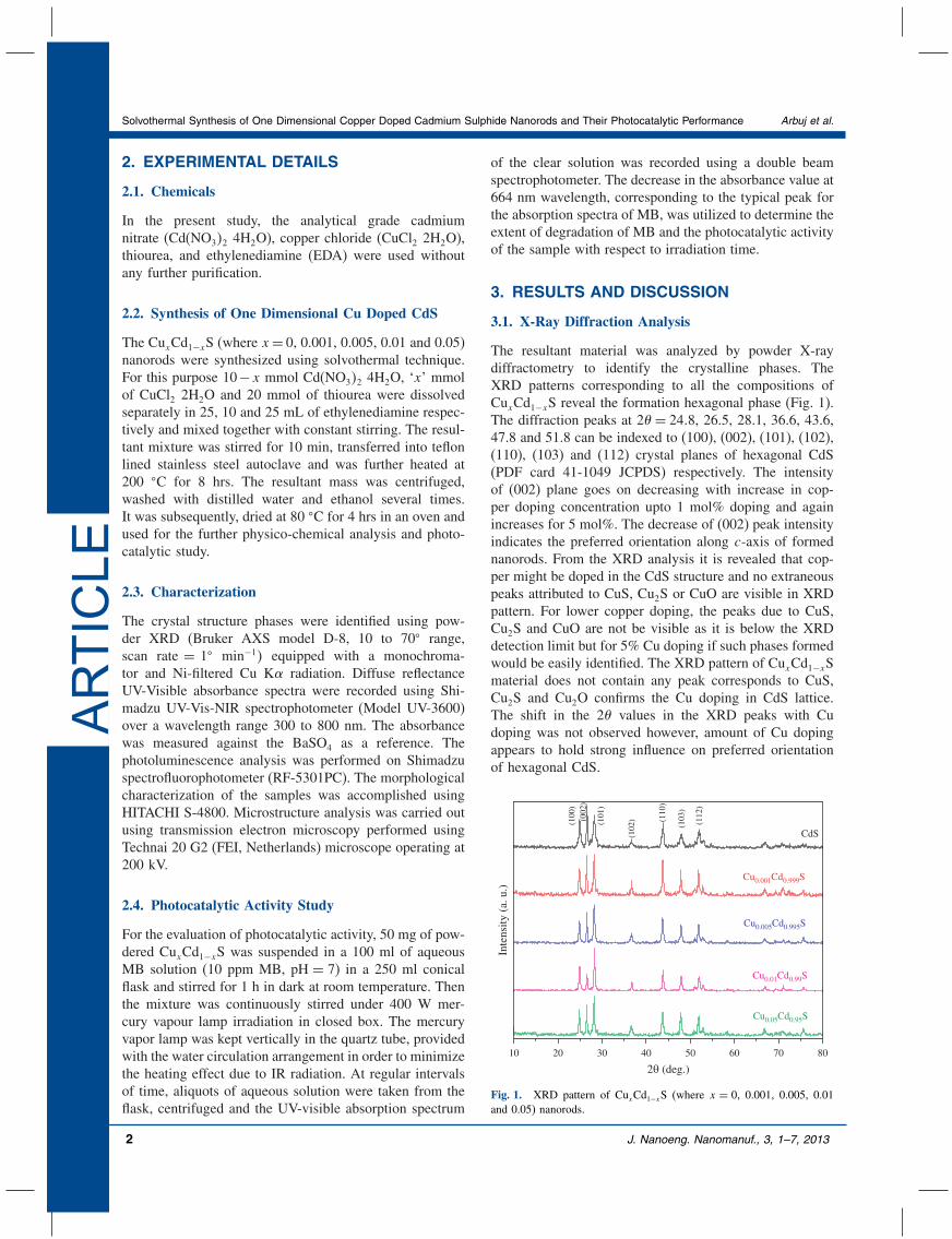
The resultant material was analyzed by powder X-raydiffractometry to identify the crystalline phases. TheXRD patterns corresponding to all the compositions ofCuxCd1−xS reveal the formation hexagonal phase (Fig. 1).The diffraction peaks at 2� = 24�8, 26.5, 28.1, 36.6, 43.6,47.8 and 51.8 can be indexed to (100), (002), (101), (102),(110), (103) and (112) crystal planes of hexagonal CdS(PDF card 41-1049 JCPDS) respectively. The intensityof (002) plane goes on decreasing with increase in cop-per doping concentration upto 1 mol% doping and againincreases for 5 mol%. The decrease of (002) peak intensityindicates the preferred orientation along c-axis of formednanorods. From the XRD analysis it is revealed that cop-per might be doped in the CdS structure and no extraneouspeaks attributed to CuS, Cu2S or CuO are visible in XRDpattern. For lower copper doping, the peaks due to CuS,Cu2S and CuO are not be visible as it is below the XRDdetection limit but for 5% Cu doping if such phases formedwould be easily identified. The XRD pattern of CuxCd1−xSmaterial does not contain any peak corresponds to CuS,Cu2S and Cu2O confirms the Cu doping in CdS lattice.The shift in the 2� values in the XRD peaks with Cudoping was not observed however, amount of Cu dopingappears to hold strong influence on preferred orientationof hexagonal CdS.
(112
)
(103
)
(110
)
(102
)(101
)
(002
)(1
00)
CdS
Cu0.001Cd0.999S
Cu0.005Cd0.995S
Cu0.01Cd0.99S
10 20 30 40 50 60 70 80
Cu0.05Cd0.95S
2θ (deg.)
Inte
nsity
(a.
u.)
Fig. 1. XRD pattern of CuxCd1−xS (where x = 0, 0.001, 0.005, 0.01and 0.05) nanorods.
2 J. Nanoeng. Nanomanuf., 3, 1–7, 2013
Arbuj et al. Solvothermal Synthesis of One Dimensional Copper Doped Cadmium Sulphide Nanorods and Their Photocatalytic Performance
ARTIC
LE
400 500 600 700 800
Abs
orba
nce
(a.u
.)
Wavelength (nm)
485 nmCdS
Cu0.001Cd0.999S
Cu0.005Cd0.995S
Cu0.01Cd0.99S
Cu0.05Cd0.95S
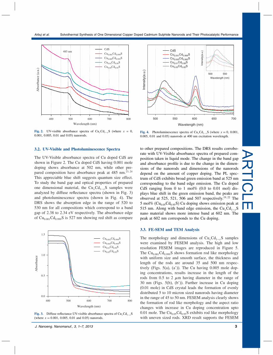
Fig. 2. UV-visible absorbance spectra of CuxCd1−xS (where x = 0,0.001, 0.005, 0.01 and 0.05) nanorods.
3.2. UV-Visible and Photoluminescence Spectra
The UV-Visible absorbance spectra of Cu doped CdS areshown in Figure 2. The Cu doped CdS having 0.001 moledoping shows absorbance at 502 nm, while other pre-pared composition have absorbance peak at 485 nm.23�24
This appreciable blue shift suggests quantum size effect.To study the band gap and optical properties of preparedone dimensional material, the CuxCd1−xS samples wereanalyzed by diffuse reflectance spectra (shown in Fig. 3)and photoluminescence spectra (shown in Fig. 4). TheDRS shows the absorption edge in the range of 520 to530 nm for all compositions which correspond to a bandgap of 2.38 to 2.34 eV respectively. The absorbance edgeof Cu0�001Cd0�999S is 527 nm showing red shift as compare
400 500 600 700 800
0.0
0.5
1.0
1.5
Abs
orba
nce
Wavelength (nm)
Cu0.001Cd0.999S
Cu0.005Cd0.995S
Cu0.01Cd0.99S
Cu0.05Cd0.95S
Fig. 3. Diffuse reflectance UV-visible absorbance spectra of CuxCd1−xS(where x = 0�001, 0.005, 0.01 and 0.05) nanorods.
500
500
Wavelength (nm)
Inte
nsity
(a.u
.)
Inte
nsity
(a.u
.)
Wavelength (nm)
CdSCu0.001Cd0.999SCu0.005Cd0.995SCu0.01Cd0.99SCu0.05Cd0.95S
550
700650600550
Fig. 4. Photoluminescence spectra of CuxCd1−xS (where x = 0, 0.001,0.005, 0.01 and 0.05) nanorods at 400 nm excitation wavelength.
to other prepared compositions. The DRS results corrobo-rate with UV-Visible absorbance spectra of prepared com-position taken in liquid mode. The change in the band gapand absorbance profile is due to the change in the dimen-sions of the nanorods and dimensions of the nanorodsdepend on the amount of copper doping. The PL spec-trum of CdS exhibits broad green emission band at 525 nmcorresponding to the band edge emission. The Cu dopedCdS ranging from 0 to 1 mol% (0.0 to 0.01 mol) dis-plays blue shift in the green emission band, the peaks areobserved at 525, 521, 506 and 507 respectively.19�22 The5 mol% (Cu0�05Cd0�95S) Cu doping shows emission peak at515 nm. Along with band edge emission, the CuxCd1−xSnano material shows more intense band at 602 nm. Thepeak at 602 nm corresponds to the Cu doping.
3.3. FE-SEM and TEM Analysis
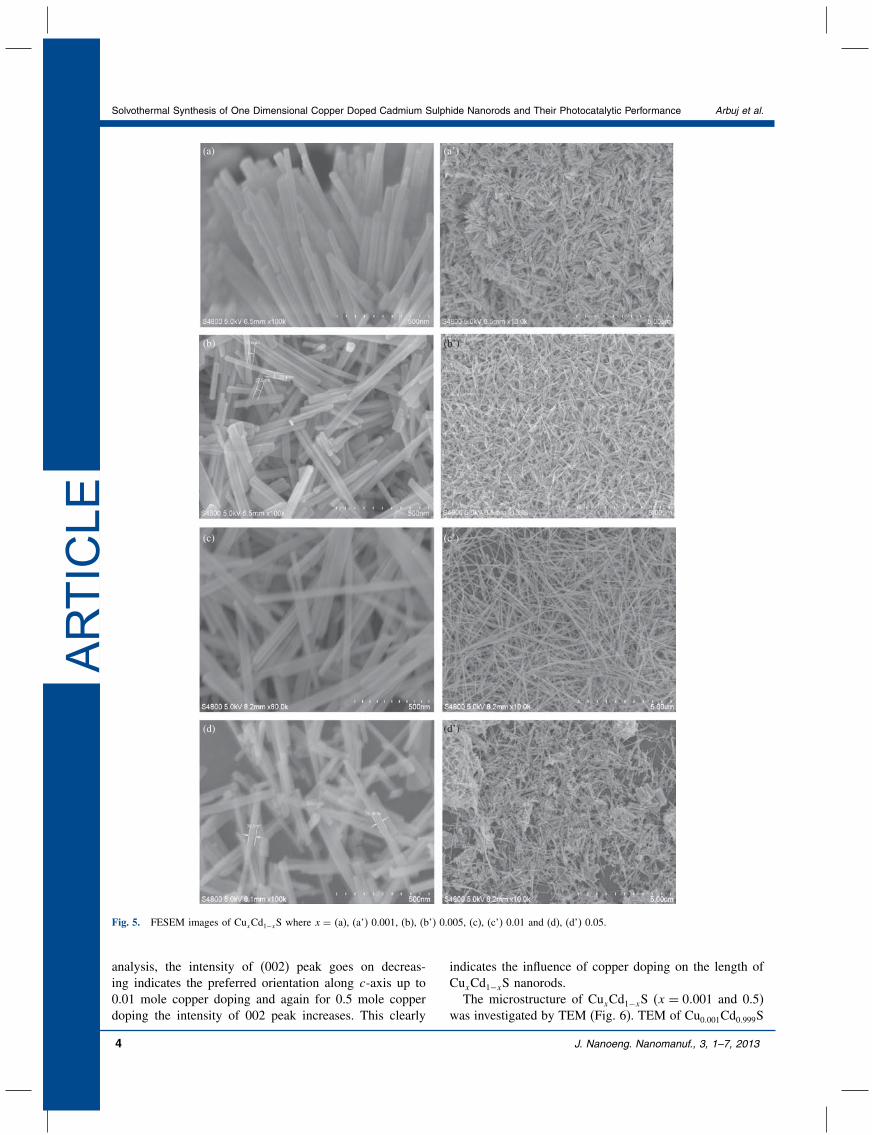
The morphology and dimensions of CuxCd1−xS sampleswere examined by FESEM analysis. The high and lowresolution FESEM images are reproduced in Figure 5.The Cu0�001Cd0�999S shows formation rod like morphologywith uniform size and smooth surface, the thickness andlength of the rods are around 35 and 500 nm respec-tively (Figs. 5(a), (a’)). The Cu having 0.005 mole dop-ing concentrations, results increase in the length of therods from 0.5 to 2 �m having diameter in the range of30 nm (Figs. 5(b), (b’)). Further increase in Cu doping(0.01 mole) in CdS crystal leads the formation of evenlydistributed 5 to 10 micron sized nanorods having diameterin the range of 45 to 50 nm. FESEM analysis clearly showsthe formation of rod like morphology and the aspect ratiochanges with increase in Cu doping concentration upto0.01 mole. The Cu0�05Cd0�95S exhibits rod like morphologywith uneven sized rods. XRD result supports the FESEM
J. Nanoeng. Nanomanuf., 3, 1–7, 2013 3
Solvothermal Synthesis of One Dimensional Copper Doped Cadmium Sulphide Nanorods and Their Photocatalytic Performance Arbuj et al.
ARTIC
LE(a)
(b)
(c)
(d) (d’)
(a’)
(b’)
(c’)
Fig. 5. FESEM images of CuxCd1−xS where x = (a), (a’) 0.001, (b), (b’) 0.005, (c), (c’) 0.01 and (d), (d’) 0.05.
analysis, the intensity of (002) peak goes on decreas-ing indicates the preferred orientation along c-axis up to0.01 mole copper doping and again for 0.5 mole copperdoping the intensity of 002 peak increases. This clearly
indicates the influence of copper doping on the length ofCuxCd1−xS nanorods.
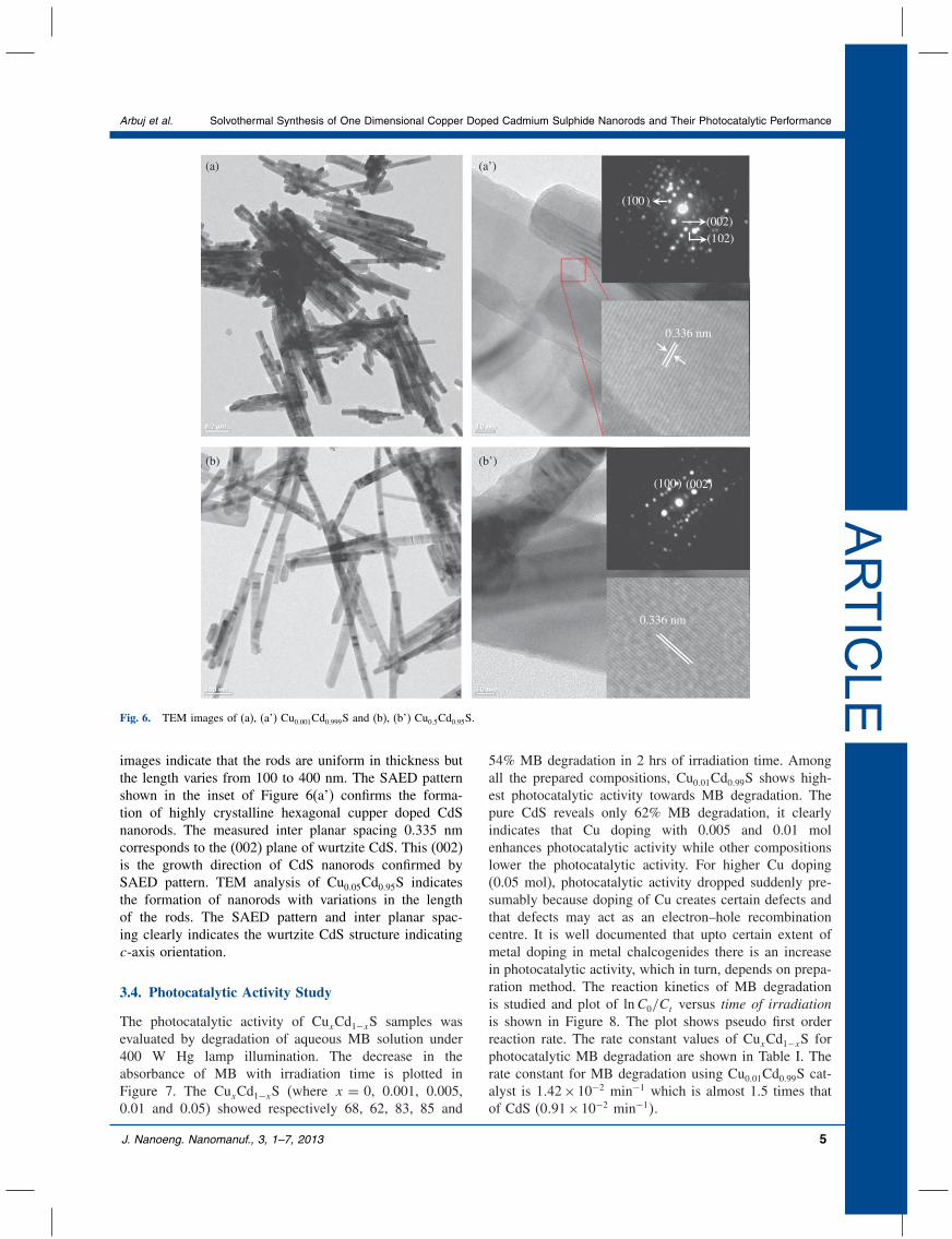
The microstructure of CuxCd1−xS (x = 0�001 and 0.5)was investigated by TEM (Fig. 6). TEM of Cu0�001Cd0�999S
4 J. Nanoeng. Nanomanuf., 3, 1–7, 2013
Arbuj et al. Solvothermal Synthesis of One Dimensional Copper Doped Cadmium Sulphide Nanorods and Their Photocatalytic Performance
ARTIC
LE(a)
(b)
(a’)
(b’)
(002)(102)
(100)
(002)(100)
0.336 nm
0.336 nm
Fig. 6. TEM images of (a), (a’) Cu0�001Cd0�999S and (b), (b’) Cu0�5Cd0�95S.
images indicate that the rods are uniform in thickness butthe length varies from 100 to 400 nm. The SAED patternshown in the inset of Figure 6(a’) confirms the forma-tion of highly crystalline hexagonal cupper doped CdSnanorods. The measured inter planar spacing 0.335 nmcorresponds to the (002) plane of wurtzite CdS. This (002)is the growth direction of CdS nanorods confirmed bySAED pattern. TEM analysis of Cu0�05Cd0�95S indicatesthe formation of nanorods with variations in the lengthof the rods. The SAED pattern and inter planar spac-ing clearly indicates the wurtzite CdS structure indicatingc-axis orientation.
3.4. Photocatalytic Activity Study
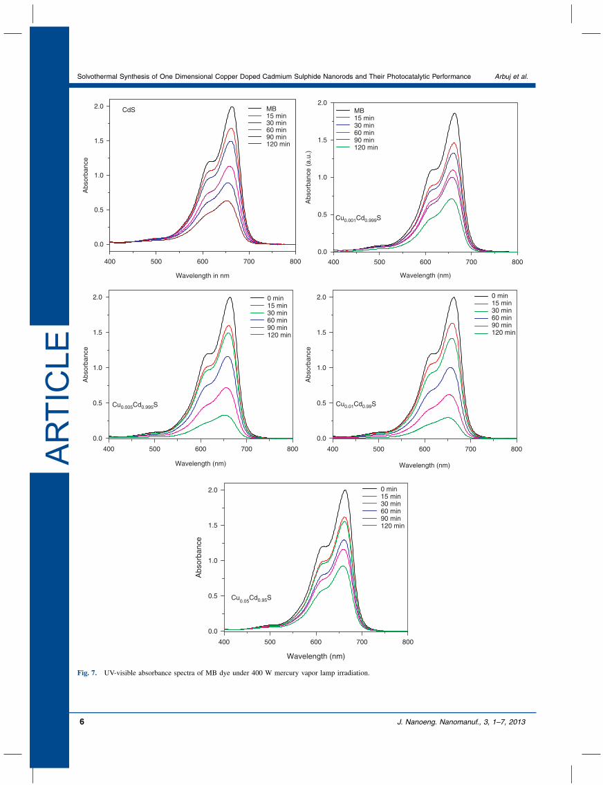
The photocatalytic activity of CuxCd1−xS samples wasevaluated by degradation of aqueous MB solution under400 W Hg lamp illumination. The decrease in theabsorbance of MB with irradiation time is plotted inFigure 7. The CuxCd1−xS (where x = 0, 0.001, 0.005,0.01 and 0.05) showed respectively 68, 62, 83, 85 and
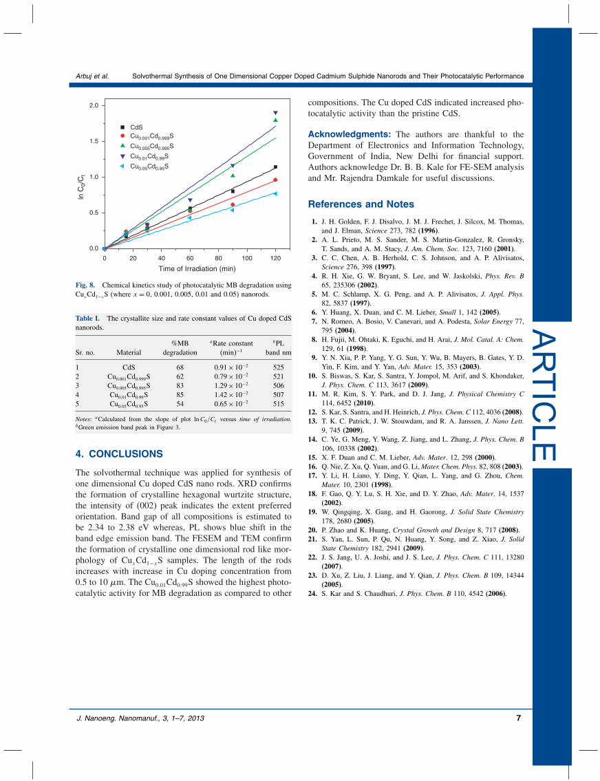
54% MB degradation in 2 hrs of irradiation time. Amongall the prepared compositions, Cu0�01Cd0�99S shows high-est photocatalytic activity towards MB degradation. Thepure CdS reveals only 62% MB degradation, it clearlyindicates that Cu doping with 0.005 and 0.01 molenhances photocatalytic activity while other compositionslower the photocatalytic activity. For higher Cu doping(0.05 mol), photocatalytic activity dropped suddenly pre-sumably because doping of Cu creates certain defects andthat defects may act as an electron–hole recombinationcentre. It is well documented that upto certain extent ofmetal doping in metal chalcogenides there is an increasein photocatalytic activity, which in turn, depends on prepa-ration method. The reaction kinetics of MB degradationis studied and plot of lnC0/Ct versus time of irradiationis shown in Figure 8. The plot shows pseudo first orderreaction rate. The rate constant values of CuxCd1−xS forphotocatalytic MB degradation are shown in Table I. Therate constant for MB degradation using Cu0�01Cd0�99S cat-alyst is 1�42×10−2 min−1 which is almost 1.5 times thatof CdS (0�91×10−2 min−1�.
J. Nanoeng. Nanomanuf., 3, 1–7, 2013 5
Solvothermal Synthesis of One Dimensional Copper Doped Cadmium Sulphide Nanorods and Their Photocatalytic Performance Arbuj et al.
ARTIC
LE
400 500 600 700 800
0.0
0.5
1.0
1.5
2.0MB15 min30 min60 min90 min120 min
Abs
orba
nce
(a.u
.)
Wavelength (nm)
Cu0.001Cd0.999S
400 500 600 700 800
0.0
0.5
1.0
1.5
2.0 0 min15 min30 min60 min90 min120 min
Abs
orba
nce
Wavelength (nm)
Cu0.005Cd0.995S
400 500 600 700 800
0.0
0.5
1.0
1.5
2.0 0 min15 min30 min60 min90 min120 min
Abs
orba
nce
Wavelength (nm)
Cu0.01Cd0.99S
400 500 600 700 800
0.0
0.5
1.0
1.5
2.0 0 min15 min30 min60 min90 min120 min
Abs
orba
nce
Wavelength (nm)
Cu0.05
Cd0.95S
400 500 600 700 800
0.0
0.5
1.0
1.5
2.0 MB 15 min 30 min 60 min 90 min 120 min
Abs
orba
nce
Wavelength in nm
CdS
Fig. 7. UV-visible absorbance spectra of MB dye under 400 W mercury vapor lamp irradiation.
6 J. Nanoeng. Nanomanuf., 3, 1–7, 2013
Arbuj et al. Solvothermal Synthesis of One Dimensional Copper Doped Cadmium Sulphide Nanorods and Their Photocatalytic Performance
ARTIC
LE
0 20 40 60 80 100 120
0.0
0.5
1.0
1.5
2.0
ln C
0/C
t
Time of Irradiation (min)
CdSCu0.001Cd0.999S
Cu0.005Cd0.995S
Cu0.01Cd0.99S
Cu0.05Cd0.95S
Fig. 8. Chemical kinetics study of photocatalytic MB degradation usingCuxCd1−xS (where x = 0, 0.001, 0.005, 0.01 and 0.05) nanorods.
Table I. The crystallite size and rate constant values of Cu doped CdSnanorods.
%MB aRate constant bPLSr. no. Material degradation (min)−1 band nm
1 CdS 68 0.91×10⁻² 5252 Cu0�001Cd0�999S 62 0.79×10⁻² 5213 Cu0�005Cd0�995S 83 1.29×10⁻² 5064 Cu0�01Cd0�99S 85 1.42×10⁻² 5075 Cu0�05Cd0�95S 54 0.65×10⁻² 515
Notes: aCalculated from the slope of plot lnC0/Ct versus time of irradiation.bGreen emission band peak in Figure 3.
4. CONCLUSIONS
The solvothermal technique was applied for synthesis ofone dimensional Cu doped CdS nano rods. XRD confirmsthe formation of crystalline hexagonal wurtzite structure,the intensity of (002) peak indicates the extent preferredorientation. Band gap of all compositions is estimated tobe 2.34 to 2.38 eV whereas, PL shows blue shift in theband edge emission band. The FESEM and TEM confirmthe formation of crystalline one dimensional rod like mor-phology of CuxCd1−xS samples. The length of the rodsincreases with increase in Cu doping concentration from0.5 to 10 �m. The Cu0�01Cd0�99S showed the highest photo-catalytic activity for MB degradation as compared to other
compositions. The Cu doped CdS indicated increased pho-tocatalytic activity than the pristine CdS.
Acknowledgments: The authors are thankful to theDepartment of Electronics and Information Technology,Government of India, New Delhi for financial support.Authors acknowledge Dr. B. B. Kale for FE-SEM analysisand Mr. Rajendra Damkale for useful discussions.
References and Notes
1. J. H. Golden, F. J. Disalvo, J. M. J. Frechet, J. Silcox, M. Thomas,and J. Elman, Science 273, 782 (1996).
2. A. L. Prieto, M. S. Sander, M. S. Martin-Gonzalez, R. Gronsky,T. Sands, and A. M. Stacy, J. Am. Chem. Soc. 123, 7160 (2001).
3. C. C. Chen, A. B. Herhold, C. S. Johnson, and A. P. Alivisatos,Science 276, 398 (1997).
4. R. H. Xie, G. W. Bryant, S. Lee, and W. Jaskolski, Phys. Rev. B65, 235306 (2002).
5. M. C. Schlamp, X. G. Peng, and A. P. Alivisatos, J. Appl. Phys.82, 5837 (1997).
6. Y. Huang, X. Duan, and C. M. Lieber, Small 1, 142 (2005).7. N. Romeo, A. Bosio, V. Canevari, and A. Podesta, Solar Energy 77,
795 (2004).8. H. Fujii, M. Ohtaki, K. Eguchi, and H. Arai, J. Mol. Catal. A: Chem.
129, 61 (1998).9. Y. N. Xia, P. P. Yang, Y. G. Sun, Y. Wu, B. Mayers, B. Gates, Y. D.
Yin, F. Kim, and Y. Yan, Adv. Mater. 15, 353 (2003).10. S. Biswas, S. Kar, S. Santra, Y. Jompol, M. Arif, and S. Khondaker,
J. Phys. Chem. C 113, 3617 (2009).11. M. R. Kim, S. Y. Park, and D. J. Jang, J. Physical Chemistry C
114, 6452 (2010).12. S. Kar, S. Santra, and H. Heinrich, J. Phys. Chem. C 112, 4036 (2008).13. T. K. C. Patrick, J. W. Stouwdam, and R. A. Janssen, J. Nano Lett.
9, 745 (2009).14. C. Ye, G. Meng, Y. Wang, Z. Jiang, and L. Zhang, J. Phys. Chem. B
106, 10338 (2002).15. X. F. Duan and C. M. Lieber, Adv. Mater. 12, 298 (2000).16. Q. Nie, Z. Xu, Q. Yuan, and G. Li,Mater. Chem. Phys. 82, 808 (2003).17. Y. Li, H. Liano, Y. Ding, Y. Qian, L. Yang, and G. Zhou, Chem.
Mater. 10, 2301 (1998).18. F. Gao, Q. Y. Lu, S. H. Xie, and D. Y. Zhao, Adv. Mater. 14, 1537
(2002).19. W. Qingqing, X. Gang, and H. Gaorong, J. Solid State Chemistry
178, 2680 (2005).20. P. Zhao and K. Huang, Crystal Growth and Design 8, 717 (2008).21. S. Yan, L. Sun, P. Qu, N. Huang, Y. Song, and Z. Xiao, J. Solid
State Chemistry 182, 2941 (2009).22. J. S. Jang, U. A. Joshi, and J. S. Lee, J. Phys. Chem. C 111, 13280
(2007).23. D. Xu, Z. Liu, J. Liang, and Y. Qian, J. Phys. Chem. B 109, 14344
(2005).24. S. Kar and S. Chaudhuri, J. Phys. Chem. B 110, 4542 (2006).
J. Nanoeng. Nanomanuf., 3, 1–7, 2013 7
Related Documents