Solution-processed flexible ZnO transparent thin-film transistors with a polymer gate dielectric fabricated by microwave heating This article has been downloaded from IOPscience. Please scroll down to see the full text article. 2009 Nanotechnology 20 465201 (http://iopscience.iop.org/0957-4484/20/46/465201) Download details: IP Address: 141.223.169.20 The article was downloaded on 21/12/2009 at 03:49 Please note that terms and conditions apply. The Table of Contents and more related content is available HOME | SEARCH | PACS & MSC | JOURNALS | ABOUT | CONTACT US

Welcome message from author
This document is posted to help you gain knowledge. Please leave a comment to let me know what you think about it! Share it to your friends and learn new things together.
Transcript

Solution-processed flexible ZnO transparent thin-film transistors with a polymer gate dielectric
fabricated by microwave heating
This article has been downloaded from IOPscience. Please scroll down to see the full text article.
2009 Nanotechnology 20 465201
(http://iopscience.iop.org/0957-4484/20/46/465201)
Download details:
IP Address: 141.223.169.20
The article was downloaded on 21/12/2009 at 03:49
Please note that terms and conditions apply.
The Table of Contents and more related content is available
HOME | SEARCH | PACS & MSC | JOURNALS | ABOUT | CONTACT US
IOP PUBLISHING NANOTECHNOLOGY
Nanotechnology 20 (2009) 465201 (5pp) doi:10.1088/0957-4484/20/46/465201
Solution-processed flexible ZnOtransparent thin-film transistors with apolymer gate dielectric fabricated bymicrowave heatingChanwoo Yang1, Kipyo Hong1, Jaeyoung Jang1, Dae Sung Chung1,Tae Kyu An1, Woon-Seop Choi2 and Chan Eon Park1
1 Polymer Research Institute, Department of Chemical Engineering, Pohang University ofScience and Technology, Pohang 790-784, Korea2 School of Display Engineering, Hoseo University, Asan-city, Chungnam 336-795, Korea
E-mail: [email protected] and [email protected]
Received 7 August 2009, in final form 18 September 2009Published 22 October 2009Online at stacks.iop.org/Nano/20/465201
AbstractWe report the development of solution-processed zinc oxide (ZnO) transparent thin-filmtransistors (TFTs) with a poly(2-hydroxyethyl methacrylate) (PHEMA) gate dielectric on aplastic substrate. The ZnO nanorod film active layer, prepared by microwave heating, showed ahighly uniform and densely packed array of large crystal size (58 nm) in the [002] direction ofZnO nanorods on the plasma-treated PHEMA. The flexible ZnO TFTs with the plasma-treatedPHEMA gate dielectric exhibited an electron mobility of 1.1 cm2 V−1 s−1, which was higher bya factor of ∼8.5 than that of ZnO TFTs based on the bare PHEMA gate dielectric.
(Some figures in this article are in colour only in the electronic version)
1. Introduction
Thin-film transistors (TFTs) based on organic semiconduc-tors [1] or metal oxide semiconductors [3–9] have been widelystudied with the goal of providing feasible alternatives to con-ventional silicon technologies for applications that require lowcost, flexible, large area and transparent electronics. Althoughorganic semiconductors are characterized by low processingtemperatures, mechanical flexibility, large coverage areas andlow cost processing [1], the long term stability of TFTs basedon organic semiconductors is limited due to their instability inthe presence of atmospheric water and oxygen [2]. TFTs thatuse metal oxide semiconductors, such as zinc oxide (ZnO), in-dium zinc oxide, zinc tin oxide and indium gallium zinc oxide,have the advantages of high charge mobility, excellent environ-mental stability and high transparency in comparison to TFTsbased on organic semiconductors [3–9].
ZnO-based TFTs are generally fabricated by vacuumdeposition methods, such as rf magnetron sputtering, chemicalvapor deposition, pulsed-laser deposition and atomic layerdeposition, which promise good performance and high
reliability compared to solution processing techniques [3–5].However, vacuum deposition methods are not compatible withlow cost TFT manufacturing because vacuum processes arenot inexpensive. For solution-processed ZnO TFT devicesfabricated by sol–gel [6–8] or spray pyrolysis methods [9],an electron mobility (μ) of more than 1 cm2 V−1 s−1 canbe obtained only with either high processing temperatures(>300 ◦C) or long processing times. Nomura et al [5]have reported fabrication of transparent ZnO-based TFTson plastic substrates using room temperature processable rfmagnetron sputtering. However, solution-processed ZnO TFTson plastic substrates have not yet been studied because ofthe requirement for high temperature solution processing toachieve a high μ. Here, we report that microwave heatingmay be used to grow ZnO nanorods, which can be usedas the semiconductor material in the fabrication of solution-processed high μ ZnO transparent TFTs on a plastic substrate.Large area ZnO nanorods can be synthesized by microwaveheating, at low temperatures (100 ◦C) but with a rapid growthrate (100 nm min−1) [10]. Additionally, we controlled thepolymer gate dielectric surface energies by oxygen (O2)
0957-4484/09/465201+05$30.00 © 2009 IOP Publishing Ltd Printed in the UK1
Nanotechnology 20 (2009) 465201 C Yang et al
Table 1. Gate dielectric characteristics of the bare PHEMA and the plasma-treated PHEMA dielectrics, and electrical characteristics of theflexible ZnO TFTs using the above gate dielectrics.
Gate dielectric characteristics Electrical characteristics
Sample Rq (nm) γ (mJ m−2) Ci (nF cm−2) μ (cm2 V−1 s−1) Ion/Ioff VT (V) S (V/decade)
Bare PHEMA 0.87 48 9.4 0.13 102 −18.2 14.9Plasma-treated PHEMA 0.82 56 9.7 1.1 103 18.1 5.11
plasma treatment and investigated the relation between surfaceenergies and the growth and crystallinity of ZnO nanorods andTFT characteristics.
2. Experimental details
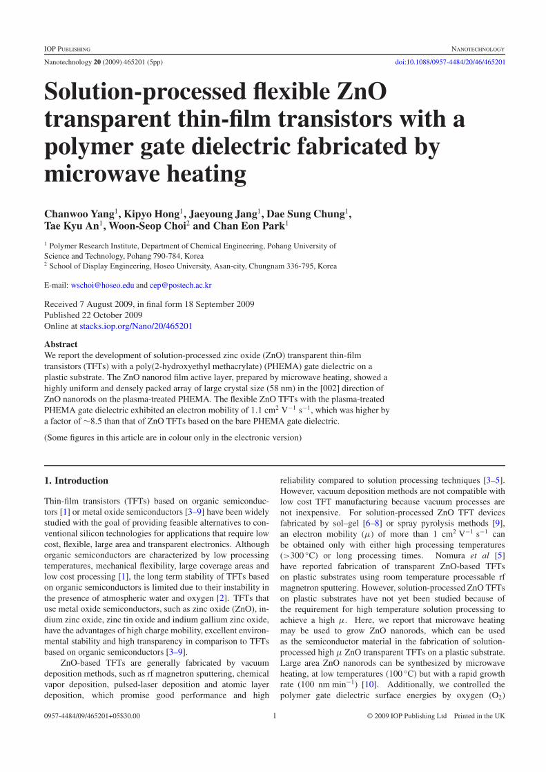
A diagram of the device structure and a photograph of theflexible ZnO TFTs described here are shown in figures 1(a)and (b), respectively. A commercially available polyarylatefilm (Ferrania Technologies, AryLite™ A200HC) with athickness of 200 μm was used as a substrate. A 100 nm thickindium tin oxide (ITO) gate was deposited onto the polyarylatesubstrate by rf magnetron sputtering. To fabricate a flexible andtransparent gate dielectric, a solution of poly(2-hydroxyethylmethacrylate) (PHEMA, Aldrich, Mw = 300 000) andmethylated poly(melamine-co-formaldehyde) (Aldrich, Mn =511) in N,N-dimethyl formamide was deposited by spincoating and crosslinked by heating at 200 ◦C for 1 h. Thecrosslinked bare PHEMA film was 740 nm thick with an rmsroughness (Rq ) of approximately 0.8–0.9 nm. To control thesurface energy (γ ) of the gate dielectric without changing thesurface roughness, the PHEMA layer was O2-plasma-treatedwith an rf power of 40 W for 10 s. The changes in surfaceenergy after O2 plasma treatment were calculated by measuringthe contact angles of water and diiodomethane. The calculatedsurface energy increased from 48 to 56 mJ m−2 whereas thesurface roughness did not change significantly with O2 plasmatreatment, as indicated in table 1. When the O2 plasmatreatment time was increased, the surface of the polymer wasetched to a greater extent and roughened [13]. We selectedthe plasma condition (40 W for 10 s) since the topographyof the PHEMA after 10 s of the O2 plasma was rough witha sharply edged and pointed surface, which is critical tothe morphology of the active layer and the performance ofTFT devices [13, 14]. A 10 mM solution of zinc acetatedehydrate (99.999%, Aldrich) in 1-propanol was spin-cast ontothe bare or plasma-treated PHEMA dielectrics at 2000 rpmfor 30 s. The samples were then baked at 130 ◦C for 1 min.This coating–baking procedure was repeated five times toensure a uniform coverage of zinc acetate crystallites. Thesamples were pre-annealed at 200 ◦C in an air atmosphere for1 h to yield ZnO seeds. The 200 nm thick ZnO nanorodfilms were grown by dipping the samples in a mixture ofequimolar 25 mM zinc nitrate hexahydrate (98%, Aldrich)and hexamethylenetetramine (99%+, Aldrich) solution indeionized water, followed by heating in a microwave oven(2.45 GHz) at a power of 700 W for 3 min under ambientair. The samples were then rinsed with deionized waterand dried in a vacuum oven at 60 ◦C for 1 h to remove theresidual solvent. Finally, the source/drain electrodes were
Figure 1. (a) A schematic cross section and (b) photograph of aflexible ZnO TFT with PHEMA as a polymer gate dielectric on apolyarylate substrate.
defined on the ZnO nanorod film by thermally evaporatingaluminum (Al) through a shadow mask. The channel length(L) and width (W ) were 150 and 1500 μm, respectively. Theelectrical characteristics of the ZnO TFTs were measured inthe dark at room temperature using Keithley 2400 and 236source/measurement units. The capacitance was measuredwith an HP 4284A Precision LCR meter. The capacitanceper unit area (Ci ) of the bare and the plasma-treated PHEMAdielectrics were found to be 9.4 and 9.7 nF cm−2 at 150 Hz,respectively. Synchrotron x-ray diffraction (XRD) analysiswas performed to investigate the crystal structure of the ZnOnanorod films at the 10C1 beamline at the Pohang AcceleratorLaboratory.
3. Results and discussion
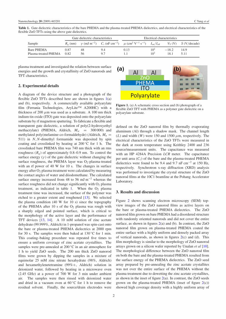
Figure 2 shows scanning electron microscopy (SEM) top-view images of the ZnO nanorod films as active layers onthe bare or plasma-treated PHEMA dielectrics. The ZnOnanorod film grown on bare PHEMA had a disordered structurewith randomly oriented nanorods and did not cover the entiresurface, as shown in figures 2(a) and (b). In contrast, the ZnOnanorod film grown on plasma-treated PHEMA coated theentire surface with a highly uniform and densely packed arrayof vertical nanorods, as shown in figures 2(c) and (d). Thisfilm morphology is similar to the morphology of ZnO nanorodarrays grown on a silicon wafer reported by Unalan et al [10].The morphological difference between the ZnO nanorod filmon both the bare and the plasma-treated PHEMA resulted fromthe surface energy of the PHEMA dielectrics. The ZnO seedarray prepared by pre-annealing the zinc acetate crystalliteswas not over the entire surface of the PHEMA without theplasma treatment due to dewetting the zinc acetate crystallites,as shown in the inset of figure 2(a). In contrast, the ZnO seedsgrown on the plasma-treated PHEMA (inset of figure 2(c))showed high coverage density with a highly uniform array of
2
Nanotechnology 20 (2009) 465201 C Yang et al
Figure 2. SEM images of ZnO nanorod films grown on (a), (b) bare PHEMA and (c), (d) plasma-treated PHEMA. The length of the scalebars in (a), (c) and (b), (d) is 2 μm and 200 nm, respectively. Insets show top view of ZnO seed arrays grown on (a) bare PHEMA and(c) plasma-treated PHEMA. Scale mark 1 μm.
seeds because the surfaces of the plasma-treated PHEMA havea relatively high γ (56 mJ m−2) and have better wettabilitywith respect to hydrophilic zinc acetate crystallite than thesurfaces of the bare PHEMA (48 mJ m−2). The initial ZnOseed layer plays a crucial role for highly oriented ZnO nanorodgrowth [11]. Accordingly, the disorganized formation of seedsgrown on the surfaces of the bare PHEMA induced the growthof disordered structures with randomly oriented nanorods. Thepromotion of seed density on the plasma-treated PHEMA ledto enhanced orientation, density and coverage of the nanorodfilms on the surfaces.
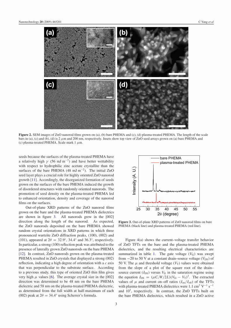
Out-of-plane XRD patterns of the ZnO nanorod filmsgrown on the bare and the plasma-treated PHEMA dielectricsare shown in figure 3. All nanorods grew in the [002]direction along the length of the nanorod. As expected,the ZnO nanorods deposited on the bare PHEMA showedrandom crystal orientations in XRD patterns in which threepronounced wurtzite ZnO diffraction peaks, (100), (002) and(101), appeared at 2θ = 32.9◦, 34.4◦ and 36.3◦, respectively.In particular, a strong (100) reflection peak was attributed to thepresence of laterally grown ZnO nanorods on the bare PHEMA[12]. In contrast, ZnO nanorods grown on the plasma-treatedPHEMA resulted in ZnO crystals that displayed a strong (002)reflection, indicating a high degree of orientation with a c axisthat was perpendicular to the substrate surface. Accordingto a previous study, this type of oriented ZnO thin film givesvery high μ values [6]. The average crystal size in the [002]direction was determined to be 48 nm on the bare PHEMAdielectric and 58 nm on the plasma-treated PHEMA dielectric,as determined from the full width at half-maximum of each(002) peak at 2θ = 34.4◦ using Scherrer’s formula.
Figure 3. Out-of-plane XRD patterns of ZnO nanorod films on barePHEMA (black line) and plasma-treated PHEMA (red line).
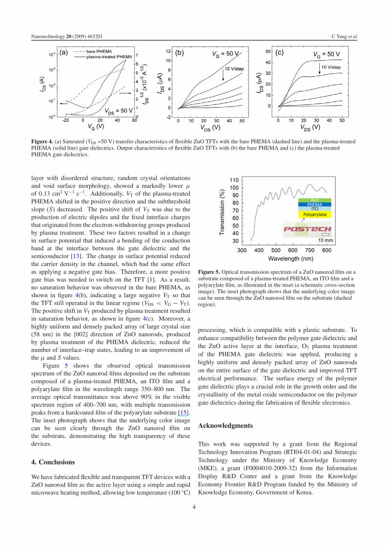
Figure 4(a) shows the current–voltage transfer behaviorof ZnO TFTs on the bare and the plasma-treated PHEMAdielectrics, and the resulting electrical characteristics aresummarized in table 1. The gate voltage (VG) was sweptfrom −20 to 50 V at a constant drain–source voltage (VDS) of50 V. The μ and threshold voltage (VT) values were obtainedfrom the slope of a plot of the square root of the drain–source current (IDS) versus VG in the saturation regime usingthe equation IDS = (μCi W/2L)(VG − VT)2. The extractedvalues of μ and current on–off ratios (Ion/Ioff) of the TFTswith plasma-treated PHEMA dielectrics were 1.1 cm2 V−1 s−1
and 103, respectively. In contrast, the ZnO TFTs built onthe bare PHEMA dielectrics, which resulted in a ZnO active
3
Nanotechnology 20 (2009) 465201 C Yang et al
Figure 4. (a) Saturated (VDS =50 V) transfer characteristics of flexible ZnO TFTs with the bare PHEMA (dashed line) and the plasma-treatedPHEMA (solid line) gate dielectrics. Output characteristics of flexible ZnO TFTs with (b) the bare PHEMA and (c) the plasma-treatedPHEMA gate dielectrics.
layer with disordered structure, random crystal orientationsand void surface morphology, showed a markedly lower μ
of 0.13 cm2 V−1 s−1. Additionally, VT of the plasma-treatedPHEMA shifted in the positive direction and the subthresholdslope (S) decreased. The positive shift of VT was due to theproduction of electric dipoles and the fixed interface chargesthat originated from the electron-withdrawing groups producedby plasma treatment. These two factors resulted in a changein surface potential that induced a bending of the conductionband at the interface between the gate dielectric and thesemiconductor [13]. The change in surface potential reducedthe carrier density in the channel, which had the same effectas applying a negative gate bias. Therefore, a more positivegate bias was needed to switch on the TFT [1]. As a result,no saturation behavior was observed in the bare PHEMA, asshown in figure 4(b), indicating a large negative VT so thatthe TFT still operated in the linear regime (VDS < VG − VT).The positive shift in VT produced by plasma treatment resultedin saturation behavior, as shown in figure 4(c). Moreover, ahighly uniform and densely packed array of large crystal size(58 nm) in the [002] direction of ZnO nanorods, producedby plasma treatment of the PHEMA dielectric, reduced thenumber of interface–trap states, leading to an improvement ofthe μ and S values.
Figure 5 shows the observed optical transmissionspectrum of the ZnO nanorod films deposited on the substratecomposed of a plasma-treated PHEMA, an ITO film and apolyarylate film in the wavelength range 350–800 nm. Theaverage optical transmittance was above 90% in the visiblespectrum region of 400–700 nm, with multiple transmissionpeaks from a hardcoated film of the polyarylate substrate [15].The inset photograph shows that the underlying color imagecan be seen clearly through the ZnO nanorod film onthe substrate, demonstrating the high transparency of thesedevices.
4. Conclusions
We have fabricated flexible and transparent TFT devices with aZnO nanorod film as the active layer using a simple and rapidmicrowave heating method, allowing low temperature (100 ◦C)
Figure 5. Optical transmission spectrum of a ZnO nanorod film on asubstrate composed of a plasma-treated PHEMA, an ITO film and apolyarylate film, as illustrated in the inset (a schematic cross-sectionimage). The inset photograph shows that the underlying color imagecan be seen through the ZnO nanorod film on the substrate (dashedregion).
processing, which is compatible with a plastic substrate. Toenhance compatibility between the polymer gate dielectric andthe ZnO active layer at the interface, O2 plasma treatmentof the PHEMA gate dielectric was applied, producing ahighly uniform and densely packed array of ZnO nanorodson the entire surface of the gate dielectric and improved TFTelectrical performance. The surface energy of the polymergate dielectric plays a crucial role in the growth order and thecrystallinity of the metal oxide semiconductor on the polymergate dielectrics during the fabrication of flexible electronics.
Acknowledgments
This work was supported by a grant from the RegionalTechnology Innovation Program (RTI04-01-04) and StrategicTechnology under the Ministry of Knowledge Economy(MKE), a grant (F0004010-2009-32) from the InformationDisplay R&D Center and a grant from the KnowledgeEconomy Frontier R&D Program funded by the Ministry ofKnowledge Economy, Government of Korea.
4

Nanotechnology 20 (2009) 465201 C Yang et al
References
[1] Braga D and Horowitz G 2009 Adv. Mater. 21 1473[2] Jeon H, Shin K, Yang C, Park C E and Park K S-H 2008 Appl.
Phys. Lett. 93 163304[3] Carcia P F, McLean R S, Reilly M H and Nunes G 2003 Appl.
Phys. Lett. 82 1117[4] Carcia P F, McLean R S and Reilly M H 2006 Appl. Phys. Lett.
88 123509[5] Nomura K, Ohta H, Takagi A, Kamiya T, Hirano M and
Hosono H 2004 Nature 432 488[6] Ong B S, Li C, Li Y, Wu Y and Loutfy R 2007 J. Am. Chem.
Soc. 129 2750[7] Pal B N, Trottman P, Sun J and Katz H E 2008 Adv. Funct.
Mater. 18 1832
[8] Park W J, Shin H S, Ahn B D, Kim G H, Lee S M, Kim K Hand Kim H J 2008 Appl. Phys. Lett. 93 083508
[9] Bashir A, Wobkenberg P H, Smith J, Ball J M,Adamopoulos G, Bradley D D C and Anthopoulos T D 2009Adv. Mater. 21 1
[10] Unalan H E, Hiralal P, Rupesinghe N, Dalal S, Milne W I andAmaratunga G A J 2008 Nanotechnology 19 255608
[11] Gao L and Chen Z 2006 J. Cryst. Growth 293 522[12] Hong J-I, Bae J, Wang Z L and Snyder R L 2009
Nanotechnology 20 085609[13] Shin K, Yang S Y, Yang C, Jeon H and Park C E 2007
Org. Electron. 8 336[14] Khan T, Vasileska D and Thornton T J 2005 J. Vac. Sci.
Technol. B 23 1782[15] Asenjo B, Guillen C, Herrero J and Gutierrez M T 2009 Thin
Solid Films 517 2320
5
Related Documents


![13. Osdi Ashari Optical and Structural Properties of ZnO Thin Films Fabricated by Sol-Gel Method Ok[1]](https://static.cupdf.com/doc/110x72/56d6bd5c1a28ab30168dae69/13-osdi-ashari-optical-and-structural-properties-of-zno-thin-films-fabricated.jpg)