Solution Manual for Digital Systems Design Using VHDL 3rd Edition by Roth and John Link full download: https://www.testbankfire.com/download/solution-manual-for-digital- systems-design-using-vhdl-3rd-edition-by-roth-and-john/ Chapter 2 Solutions 2.1 (a) VHDL - VHSIC Hardware Description Language VHSIC - Very High Speed Integrated Circuit (b) VHDL has statements that execute concurrently since it must model real hardware in which the components are all in operation at the same time. (c) A hardware description language allows a digital system to be designed and debugged at a higher level of abstraction than schematic capture with gates, flip-flops, and standard MSI building blocks. The details of the gates and flip-flops do not need to be handled during early phases of design. Designs are more portable when low-level library-specific details are not included in the model. HDLs allow the creation of such portable high-level behavioral models. 2.2 (a) Legal: A_123, and1; Illegal: 123A (Starts with number), _A123 (starts with underscore), A123_ (ends with underscore), c1 c2 (adjacent underscores), and (reserved word). (b) They all equivalent. VHDL is not case sensitive. 2.3 (a) (b) 2.4 entity Comb is port(A, B, C, D : in bit; Z : out bit); end Comb; architecture Comb2_1 of Comb is signal E, F, G, H, I : bit; begin H <= (A and B and C) after 5 ns; E <= H or D after 5 ns; G <= (B nor C) after 5 ns; F <= G nand A after 5 ns; I <= not F after 2 ns; Z <= E xor I after 5 ns; end Comb2_1; 2.5 (a) entity one_bit_sub is port(x, y, bin: in bit; 17 © 2018 Cengage Learning®. All Rights Reserved. May not be scanned, copied or duplicated, or posted to a publicly accessible website, in whole or in part.

Welcome message from author
This document is posted to help you gain knowledge. Please leave a comment to let me know what you think about it! Share it to your friends and learn new things together.
Transcript
Solution Manual for Digital Systems Design Using
VHDL 3rd Edition by Roth and John
Link full download: https://www.testbankfire.com/download/solution-manual-for-digital-
systems-design-using-vhdl-3rd-edition-by-roth-and-john/
Chapter 2 Solutions
2.1 (a) VHDL - VHSIC Hardware Description Language VHSIC - Very High Speed Integrated Circuit
(b) VHDL has statements that execute concurrently since it must model real hardware in which the
components are all in operation at the same time.
(c) A hardware description language allows a digital system to be designed and debugged at a
higher level of abstraction than schematic capture with gates, flip-flops, and standard MSI
building blocks. The details of the gates and flip-flops do not need to be handled during early
phases of design. Designs are more portable when low-level library-specific details are not
included in the model. HDLs allow the creation of such portable high-level behavioral models.
2.2 (a) Legal: A_123, and1; Illegal: 123A (Starts with number), _A123 (starts with underscore), A123_ (ends with underscore), c1 c2 (adjacent underscores), and (reserved word).
(b) They all equivalent. VHDL is not case sensitive.
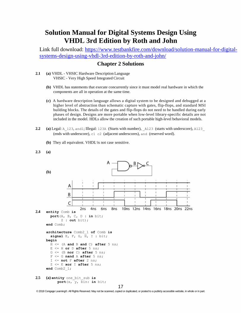
2.3 (a)
(b)
2.4 entity Comb is
port(A, B, C, D : in bit;
Z : out bit); end Comb;
architecture Comb2_1 of Comb is
signal E, F, G, H, I : bit; begin
H <= (A and B and C) after 5 ns;
E <= H or D after 5 ns; G <= (B nor C) after 5 ns;
F <= G nand A after 5 ns; I <= not F after 2 ns; Z <= E xor I after 5 ns;
end Comb2_1;
2.5 (a) entity one_bit_sub is port(x, y, bin: in bit;
17 © 2018 Cengage Learning®. All Rights Reserved. May not be scanned, copied or duplicated, or posted to a publicly accessible website, in whole or in part.
diff, bout: out bit);
end one_bit_sub;
architecture equ of one_bit_sub is
begin diff <= x xor y xor bin; -- difference. See problem 1.2 answer
bout <= (not x and bin) or (not x and y) or (bin and y); -- borrow out. See problem 1.2 answer
18 © 2018 Cengage Learning®. All Rights Reserved. May not be scanned, copied or duplicated, or posted to a publicly accessible website, in whole or in part.

end equ;
(b) entity four_bit_sub is port(a, b: in bit_vector(3 downto 0);
bin: in bit; d: out bit_vector(3 downto 0);
bout: out bit); end four_bit_sub;
architecture test of four_bit_sub is
signal bo: bit_vector(3 downto 0) := "0000"; -- borrow bits
component one_bit_sub port(x, y, bin: in bit;
diff, bout: out bit); end component;
begin FS0: one_bit_sub port map(a(0),b(0),bin,d(0),bo(1));
FS1: one_bit_sub port map(a(1),b(1),bo(1),d(1),bo(2));
FS2: one_bit_sub port map(a(2),b(2),bo(2),d(2),bo(3));
FS3: one_bit_sub port map(a(3),b(3),bo(3),d(3),bout); end test;
2.6 (a) entity circuit is
port(A, B, C, D: in bit; G: out bit);
end circuit;
architecture internal of circuit is signal E, F: bit;
begin E <= A and B; F <= E or C;
G <= D and F; end internal;
(b) entity circuit is
port(A, B, C, D: in bit; G: out bit);
end circuit;
architecture internal of circuit is signal E, F: bit;
begin process(A, B, C, D, E, F)
begin E <= A and B;
F <= E or C; G <= D and F;
end process; end internal;
2.7 A changes to 1 at 25 ns, B changes to 1 at 20 + ∆ ns, C does not change
2.8 (a) A falling-edge triggered D flip-flop with asynchronous active high clear and set
(b) Q = '0', because Clr = 1 has priority.
2.9 entity SR_Latch is
port(S, R: in bit; Q, Qn: inout bit);
end SR_Latch;
19
© 2018 Cengage Learning®. All Rights Reserved. May not be scanned, copied or duplicated, or posted to a publicly accessible website, in whole or in part.
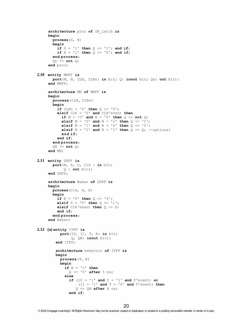
architecture proc of SR_Latch is
begin process(S, R) begin if S = '1' then Q <= '1'; end if;
if R = '1' then Q <= '0'; end if; end process;
Qn <= not Q; end proc;
2.10 entity MNFF is
port(M, N, CLK, CLRn: in bit; Q: inout bit; Qn: out bit);
end MNFF;
architecture MN of MNFF is
begin process(CLK, CLRn)
begin if CLRn = '0' then Q <= '0'; elsif CLK = '0' and CLK'event then
if M = '0' and N = '0' then Q <= not Q;
elsif M = '0' and N = '1' then Q <= '1';
elsif M = '1' and N = '0' then Q <= '0'; elsif M = '1' and N = '1' then Q <= Q; --optional end if;
end if; end process;
QN <= not Q; end MN;
2.11 entity DDFF is
port(R, S, D, Clk : in bit;
Q : out bit); end DDFF;
architecture Behav of DDFF is
begin process(Clk, R, S)
begin if R = '0' then Q <= '0';
elsif S = '0' then Q <= '1';
elsif Clk'event then Q <= D;
end if; end process;
end Behav;
2.12 (a) entity ITFF is port(I0, I1, T, R: in bit;
Q, QN: inout bit); end ITFF;
architecture behavior of ITFF is
begin process(T, R)
begin if R = '1' then
Q <= '0' after 5 ns;
else if (I0 = '1' and T = '1' and T'event) or
(I1 = '1' and T = '0' and T'event) then
Q <= QN after 8 ns; end if;
20
© 2018 Cengage Learning®. All Rights Reserved. May not be scanned, copied or duplicated, or posted to a publicly accessible website, in whole or in part.
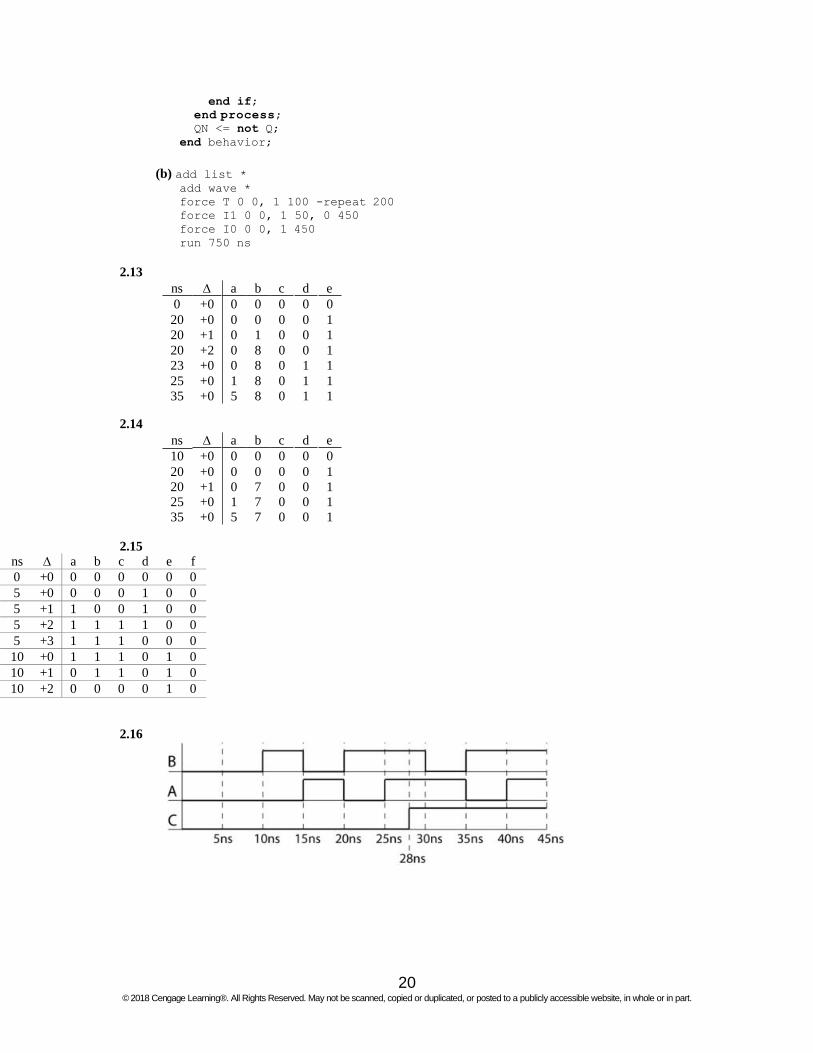
end if; end process;
QN <= not Q; end behavior;
(b) add list *
add wave * force T 0 0, 1 100 -repeat 200
force I1 0 0, 1 50, 0 450 force I0 0 0, 1 450
run 750 ns
2.13 ns ∆ a b c d e 0 +0 0 0 0 0 0 20 +0 0 0 0 0 1 20 +1 0 1 0 0 1 20 +2 0 8 0 0 1 23 +0 0 8 0 1 1 25 +0 1 8 0 1 1 35 +0 5 8 0 1 1
2.14
ns ∆ a b c d e 10 +0 0 0 0 0 0 20 +0 0 0 0 0 1 20 +1 0 7 0 0 1 25 +0 1 7 0 0 1 35 +0 5 7 0 0 1
2.15
ns ∆ a b c d e f 0 +0 0 0 0 0 0 0 5 +0 0 0 0 1 0 0 5 +1 1 0 0 1 0 0 5 +2 1 1 1 1 0 0 5 +3 1 1 1 0 0 0 10 +0 1 1 1 0 1 0 10 +1 0 1 1 0 1 0 10 +2 0 0 0 0 1 0
2.16
20 © 2018 Cengage Learning®. All Rights Reserved. May not be scanned, copied or duplicated, or posted to a publicly accessible website, in whole or in part.
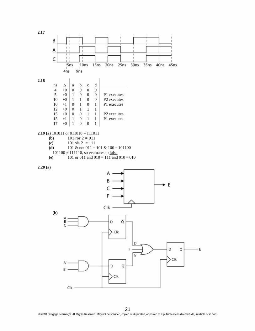
2.17
2.18
2.19 (a) 101011 or 011010 = 111011 (b) 101 ror 2 = 011 (c) 101 sla 2 = 111 (d) 101 & not 011 = 101 & 100 = 101100
101100 ≠ 111110, so evaluates to false (e) 101 or 011 and 010 = 111 and 010 = 010
2.20 (a)
(b)
21
© 2018 Cengage Learning®. All Rights Reserved. May not be scanned, copied or duplicated, or posted to a publicly accessible website, in whole or in part.
ns ∆
a b c d
4 +0 5 +0
10 +0 10 +1 12 +0 15 +0 15 +1 17 +0
0 0 0 0 1 0 0 0 1 1 0 0 0 1 0 1 0 1 1 1 0 0 1 1 1 0 1 1 1 0 0 1
P1 executes
P2 executes
P1 executes
P2 executes
P1 executes
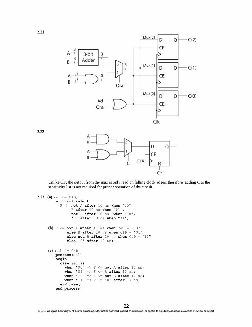
2.21
2.22
Unlike Clr, the output from the mux is only read on falling clock edges; therefore, adding C to the
sensitivity list is not required for proper operation of the circuit.
2.23 (a) sel <= C&D; with sel select
F <= not A after 10 ns when "00",
B after 10 ns when "01", not B after 10 ns when "10",
'0' after 10 ns when "11";
(b) F <= not A after 10 ns when C&D = "00" else B after 10 ns when C&D = "01" else not B after 10 ns when C&D = "10"
else '0' after 10 ns;
(c) sel <= C&D; process(sel)
begin case sel is when "00" => F <= not A after 10 ns;
when "01" => F <= B after 10 ns; when "10" => F <= not B after 10 ns; when "11" => F <= '0' after 10 ns;
end case;
end process;
22 © 2018 Cengage Learning®. All Rights Reserved. May not be scanned, copied or duplicated, or posted to a publicly accessible website, in whole or in part.

2.24 (a) process(C, B1, B2, B3) begin
case C is when 1 => A <= B1;
when 2 => A <= B2;
when 3 => A <= B3;
when others => A <= 0; end case;
end process;
or
process(C, B1, B2, B3)
begin if C = 1 then A <= B1;
elsif C = 2 then A <= B2;
elsif C = 3 then A <= B3;
else A <= 0; end if; end process;
(b)
2.25 (a) entity Latch is port(S, R: in bit;
P, Q: inout bit); end Latch;
architecture conditional of Latch is
begin Q <= '1' when S = '1' -- Assume SR = 0 else '0' when R = '1'
else Q; P <= not Q;
end conditional;
(b) architecture characteristic of Latch is begin
Q <= S or (not R and Q);
P <= not Q; end characteristic;
(c) architecture gate of Latch is
begin P <= S nor Q;
Q <= R nor P; end gate;
2.26 S = "0101", Co = '1'
23
© 2018 Cengage Learning®. All Rights Reserved. May not be scanned, copied or duplicated, or posted to a publicly accessible website, in whole or in part.

2.27 library IEEE; use IEEE.numeric_bit.all;
entity Adder is
port(A: in bit_vector(3 downto 0); B: in integer range 0 to 15; Sum: out bit_vector(4 downto 0));
end Adder;
architecture overloaded of Adder is signal sum5: unsigned(4 downto 0);
begin sum5 <= '0' & UNSIGNED(A) + TO_UNSIGNED(B, 4); -- conv fns in Appndx B
Sum <= BIT_VECTOR(sum5); end overloaded;
2.28 (a) entity decoder_3to8_behavioral is
port(A0, A1, A2, E1_bar, E2_bar, E3: in bit; Y0_bar, Y1_bar, Y2_bar, Y3_bar, Y4_bar, Y5_bar, Y6_bar, Y7_bar: out bit := '1');
end decoder_3to8_behavioral;
architecture behavior of decoder_3to8_behavioral is
signal input_values:bit_vector(3 downto 0); signal enable:bit; begin
enable<=E3 and (not E2_bar) and (not E1_bar);
input_values<=(enable)&(A2)&(A1)&(A0);
process (input_values) begin case input_values is
when "1000" =>
Y0_bar <='0';
Y1_bar <='1';
Y2_bar <='1';
Y3_bar <='1';
Y4_bar <='1';
Y5_bar <='1';
Y6_bar <='1';
Y7_bar <='1'; when "1001" =>
Y0_bar <='1';
Y1_bar <='0';
Y2_bar <='1';
Y3_bar <='1';
Y4_bar <='1';
Y5_bar <='1';
Y6_bar <='1';
Y7_bar <='1'; when "1010" =>
Y0_bar <='1';
Y1_bar <='1';
Y2_bar <='0';
Y3_bar <='1';
Y4_bar <='1';
Y5_bar <='1';
Y6_bar <='1';
Y7_bar <='1';
24 © 2018 Cengage Learning®. All Rights Reserved. May not be scanned, copied or duplicated, or posted to a publicly accessible website, in whole or in part.

when "1011" =>
Y0_bar <='1';
Y1_bar <='1';
Y2_bar <='1';
Y3_bar <='0';
Y4_bar <='1';
Y5_bar <='1';
Y6_bar <='1';
Y7_bar <='1'; when "1100" =>
Y0_bar <='1';
Y1_bar <='1';
Y2_bar <='1';
Y3_bar <='1';
Y4_bar <='0';
Y5_bar <='1';
Y6_bar <='1';
Y7_bar <='1'; when "1101" =>
Y0_bar <='1';
Y1_bar <='1';
Y2_bar <='1';
Y3_bar <='1';
Y4_bar <='1';
Y5_bar <='0';
Y6_bar <='1';
Y7_bar <='1'; when "1110" =>
Y0_bar <='1';
Y1_bar <='1';
Y2_bar <='1';
Y3_bar <='1';
Y4_bar <='1';
Y5_bar <='1';
Y6_bar <='0';
Y7_bar <='1'; when "1111" =>
Y0_bar <='1';
Y1_bar <='1';
Y2_bar <='1';
Y3_bar <='1';
Y4_bar <='1';
Y5_bar <='1';
Y6_bar <='1';
Y7_bar <='0'; when others =>
Y0_bar <='1'; Y1_bar <='1';
Y2_bar <='1';
Y3_bar <='1';
Y4_bar <='1';
Y5_bar <='1';
Y6_bar <='1';
Y7_bar <='1'; end case;
end process;
25
© 2018 Cengage Learning®. All Rights Reserved. May not be scanned, copied or duplicated, or posted to a publicly accessible website, in whole or in part.

end behavior;
(b) entity decoder_3to8_dataflow is port(A0, A1, A2, E1_bar, E2_bar, E3: in bit;
Y0_bar, Y1_bar, Y2_bar, Y3_bar, Y4_bar, Y5_bar, Y6_bar, Y7_bar: out bit := '1'); end decoder_3to8_dataflow;
architecture dataflow of decoder_3to8_dataflow is
signal enable:bit;
begin enable<=(E3) and (not E2_bar) and (not E1_bar);
Y0_bar<=not((enable)and(not A2)and(not A1)and(not A0));
Y1_bar<=not((enable)and(not A2)and(not A1)and(A0));
Y2_bar<=not((enable)and(not A2)and(A1)and(not A0));
Y3_bar<=not((enable)and(not A2)and(A1)and(A0));
Y4_bar<=not((enable)and(A2)and(not A1)and(not A0));
Y5_bar<=not((enable)and(A2)and(not A1)and(A0));
Y6_bar<=not((enable)and(A2)and(A1)and(not A0));
Y7_bar<=not((enable)and(A2)and(A1)and(A0));
end dataflow;
(c) entity decoder_3to8_structural is port(A0, A1, A2, E1_bar, E2_bar, E3: in bit;
Y0_bar, Y1_bar, Y2_bar, Y3_bar, Y4_bar, Y5_bar, Y6_bar, Y7_bar: out bit := '1'); end decoder_3to8_structural;
architecture structure of decoder_3to8_structural is
component inverter port(A: in bit; Z: out bit);
end component;
component and3 port(A, B, C: in bit; Z: out bit);
end component;
component and4 port(A, B, C, D: in bit; Z: out bit);
end component;
signal A2prime, A1prime, A0prime, invertA2prime, invertA1prime, invertA0prime, E1, E2, Y0, Y1, Y2, Y3, Y4, Y5, Y6, Y7, enable: bit;
begin I0:inverter port map(A2, A2prime);
I1:inverter port map(A1, A1prime);
I2:inverter port map(A0, A0prime);
I3:inverter port map(E1_bar, E1);
I4:inverter port map(E2_bar, E2); I5:inverter port map(A2prime, invertA2prime);
I6:inverter port map(A1prime, invertA1prime);
I7:inverter port map(A0prime, invertA0prime);
I8:inverter port map(Y0,Y0_bar); I9:inverter port map(Y1,Y1_bar);
I10:inverter port map(Y2,Y2_bar);
I11:inverter port map(Y3,Y3_bar);
26
© 2018 Cengage Learning®. All Rights Reserved. May not be scanned, copied or duplicated, or posted to a publicly accessible website, in whole or in part.
I12:inverter port map(Y4,Y4_bar);
I13:inverter port map(Y5,Y5_bar);
I14:inverter port map(Y6,Y6_bar);
I15:inverter port map(Y7,Y7_bar); AG0:and4 port map(enable,A2prime,A1prime,A0prime,Y0);
AG1:and4 port map(enable,A2prime,A1prime,invertA0prime,Y1);
AG2:and4 port map(enable,A2prime,invertA1prime,A0prime,Y2); AG3:and4 port map(enable,A2prime,invertA1prime,invertA0prime,Y3);
AG4:and4 port map(enable,invertA2prime,A1prime,A0prime,Y4);
AG5:and4 port map(enable,invertA2prime,A1prime,invertA0prime,Y5);
AG6:and4 port map(enable,invertA2prime,invertA1prime,A0prime,Y6); AG7:and4 port map(enable,invertA2prime,invertA1prime,invertA0prime,Y7);
AG8:and3 port map(E1,E2,E3, enable);
end structure;
entity inverter is port(A: in bit; Z: out bit);
end inverter; architecture inv of inverter is begin Z <= not A;
end inv;
entity and3 is port(A, B, C: in bit; Z: out bit); end and3; architecture concur of and3 is
begin Z <= (A and B and C);
end concur;
entity and4 is port(A, B, C, D: in bit; Z: out bit);
end and4; architecture con of and4 is
begin Z <= (A and B and C and D);
end con;
2.29
entity decoder_4to16_structural is port(A0, A1, A2, A3, E1_bar, E2_bar, E3: in bit;
Y0_bar,Y1_bar,Y2_bar,Y3_bar,Y4_bar,Y5_bar,Y6_bar,Y7_bar,Y8_bar,Y9_bar,Y10_bar,Y11_bar,
Y12_bar,Y13_bar,Y14_bar,Y15_bar: out bit := '1'); end decoder_4to16_structural;
architecture decoder of decoder_4to16_structural is
component decoder_3to8_structural port(A0, A1, A2, E1_bar, E2_bar, E3: in bit; Y0_bar, Y1_bar, Y2_bar, Y3_bar, Y4_bar, Y5_bar,
Y6_bar, Y7_bar: out bit); end component;
signal A2prime, A1prime, A0prime, invertA2prime, invertA1prime, invertA0prime, E1, E2, Y0, Y1, Y2,
Y3, Y4, Y5, Y6, Y7, enable: bit;
27
© 2018 Cengage Learning®. All Rights Reserved. May not be scanned, copied or duplicated, or posted to a publicly accessible website, in whole or in part.

begin D1:decoder_3to8_structural port map(A0, A1, A2, A3, E2_bar, E3, Y0_bar, Y1_bar, Y2_bar, Y3_bar,
Y4_bar, Y5_bar, Y6_bar, Y7_bar); D2:decoder_3to8_structural port map(A0, A1, A2, E1_bar, E2_bar, A3, Y8_bar, Y9_bar, Y10_bar,
Y11_bar, Y12_bar, Y13_bar, Y14_bar, Y15_bar); end decoder;
2.30 (a) entity alu is
port(M,Cn:in bit; A,B: in bit_vector(3 downto 0);
F: out bit_vector(3 downto 0); S:
in bit_vector(3 downto 0)); end alu;
architecture unit of alu is
begin
process(A,B,S,M,Cn) begin case S is
when "0000"=>F<=not A; when "0001"=>F<=not(A and B);
when "0010"=>F<=(not A) and B;
when "0011"=>F<="0001"; when "0100"=>F<=not (A or B);
when "0101"=>F<=not B; when "0110"=>F<=not(A XOR B);
when "0111"=>F<=A or (not B);
when "1000"=>F<=(not A) and B;
when "1001"=>F<=A XOR B;
when "1010"=>F<=B; when "1011"=>F<=A or B;
when "1100"=>F<="0000"; when "1101"=>F<=A and (not B); when "1110"=>F<=A and B;
when "1111"=>F<=A; end case;
end process;
end unit;
(b) library IEEE;
use IEEE.numeric_bit.all;
entity alu is port(M,Cn:in bit;
A,B: in unsigned (3 downto 0); F:out unsigned (3 downto 0);
S: in bit_vector(3 downto 0)); end alu;
architecture arithunit of alu is
begin
process(A,B,S,M,Cn) begin
28
© 2018 Cengage Learning®. All Rights Reserved. May not be scanned, copied or duplicated, or posted to a publicly accessible website, in whole or in part.
if(Cn='0') then case S is
when "0000"=>F<=A-1; when "0001"=>F<=(A and B) - 1;
when "0010"=>F<=(A and (not B)) -1;
when "0011"=>F<="1111"; when "0100"=>F<= A+(A or (not B)); when "0101"=>F<= (A and B) + (A or (not B)); when "0110"=>F<= A - B - 1;
when "0111"=>F<= A or (not B);
when "1000"=>F<= A + (A or B);
when "1001"=>F<=A + B; when "1010"=>F<= (A and (not B))+(A or B); when "1011"=>F<=A or B; when "1100"=>F<=A + (A sll 1); when "1101"=>F<= (A and B) + A; when "1110"=>F<= (A and (not B)) + A; when "1111"=>F<=A;
end case; else
case S is when "0000"=>F<=A; when "0001"=>F<=(A and B); when "0010"=>F<=(A and (not B));
when "0011"=>F<="0000"; when "0100"=>F<= A+(A or (not B))+1; when "0101"=>F<= (A and B) + (A or (not B)) + 1;
when "0110"=>F<= A - B; when "0111"=>F<= A or (not B) + 1;
when "1000"=>F<= A + (A or B) + 1;
when "1001"=>F<=A + B + 1; when "1010"=>F<= (A and (not B))+(A or B) + 1;
when "1011"=>F<=(A or B) +1; when "1100"=>F<=A + A + 1; when "1101"=>F<= (A and B) + A + 1; when "1110"=>F<= (A and (not B)) + A + 1; when "1111"=>F<=A + 1;
end case; end if;
end process;
end arithunit;
2.31 (a) library IEEE; use IEEE.numeric_bit.all;
entity counter is
port(d: in unsigned(3 downto 0); clk, clr, ent, enp, up, load: in bit; q: inout unsigned(3 downto 0); co: out bit);
end counter;
architecture test of counter is begin
process(clk, clr)
begin
29 © 2018 Cengage Learning®. All Rights Reserved. May not be scanned, copied or duplicated, or posted to a publicly accessible website, in whole or in part.
if clr = '0' then Q <= "0000";
elsif clk = '1' and clk'event then if load = '0' then q <= d; -- load elsif (ent = '1' and enp = '1' and (not up) = '1') then
if q = "0000" then q <= "1001"; -- wrap around
else q <= q – 1; end if; --decrement elsif (ent = '1' and enp = '1' and up = '1') then
if q = "1001" then q <= "0000"; -- wrap around
else q <= q + 1; end if; --increment end if;
end if; end process; co <= '1' when (ent = '1') and ((up = '1' and (Q = "1001")) or
(up = '0' and (Q ="0000"))) else '0'; end test;
(b) The block diagram is similar to Figure 2-47 with an "Up" input added to each counter. The
VHDL description similar to Figure 2-48.
2.32 Students should look on the web for 74192 data sheet. CLR is active high. LOADB is active low.
Counting up happens when UP has a rising edge and DOWN=1. Counting down happens when
DOWN has a rising edge and UP=1. CARRY indicates terminal count in the up direction, i.e. 9.
BORROW indicates terminal count in the down direction, i.e. 0.
Operating Mode CLR LOADB UP DOWN D Q Borrow Carry Clear
Load Count Up
Count Down
1 X X 0 XXXX 1 X X 1 XXXX 0 0 X X XXXX 0 1 ↑ 1 XXXX 0 1 1 ↑ XXXX
0000 0 1 0000 1 1
Q = D 1* 1* Q = Q + 1 1 1** Q = Q – 1 1** 1
* when loading, if the input is 0 and down = 0, borrow will be 0. If the input is 9 and up = 0, carry
will be 0 ** Borrow = 0 when the counter is in state 0 and down = 0. Carry = 0 when the counter is in state 9
and up = 0.
entity count74192 is port(DOWN, UP, CLR, LOADB: in bit;
BORROW, CARRY: out bit; D: in integer range 0 to 15; Q: inout integer range 0 to 15);
end count74192;
architecture behav of count74192 is begin
process(DOWN, UP, CLR, LOADB) begin if CLR = '1' then Q <= 0; elsif LOADB = '0' then Q <= D; elsif UP'event and UP = '1' and DOWN = '1' then
if Q = 9 then Q <= 0; else Q <= Q + 1; end if; elsif DOWN'event and DOWN = '1' and UP = '1' then
if Q = 0 then Q <= 9;
else Q <= Q - 1; end if; end if;
end process; -- borrow rises on rising edge of DOWN in state 0
BORROW <= '0' when DOWN = '0' and Q = 0 else '1';
30
© 2018 Cengage Learning®. All Rights Reserved. May not be scanned, copied or duplicated, or posted to a publicly accessible website, in whole or in part.
-- carry rises on rising edge of UP in state 9
CARRY <= '0' when UP = '0' and Q = 9 else '1'; end behav;
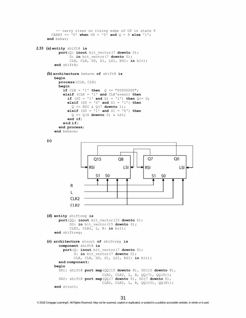
2.33 (a) entity shift8 is
port(Q: inout bit_vector(7 downto 0); D: in bit_vector(7 downto 0); CLR, CLK, S0, S1, LSI, RSI: in bit);
end shift8;
(b) architecture behave of shift8 is begin
process(CLK, CLR)
begin if CLR = '1' then Q <= "00000000";
elsif (CLK = '1' and CLK'event) then if (S0 = '1' and S1 = '1') then Q<= D; elsif (S0 = '0' and S1 = '1') then
Q <= RSI & Q(7 downto 1); elsif (S0 = '1' and S1 = '0') then
Q <= Q(6 downto 0) & LSI; end if;
end if;
end process; end behave;
(c)
(d) entity shiftreg is port(QQ: inout bit_vector(15 downto 0);
DD: in bit_vector(15 downto 0);
CLK2, CLR2, L, R: in bit); end shiftreg;
(e) architecture struct of shiftreg is
component shift8 is port(Q: inout bit_vector(7 downto 0);
D: in bit_vector(7 downto 0); CLR, CLK, S0, S1, LSI, RSI: in bit);
end component;
begin SR1: shift8 port map(QQ(15 downto 8), DD(15 downto 8),
CLR2, CLK2, L, R, QQ(7), QQ(0)); SR2: shift8 port map(QQ(7 downto 0), DD(7 downto 0),
CLR2, CLK2, L, R, QQ(15), QQ(8)); end struct;
31
© 2018 Cengage Learning®. All Rights Reserved. May not be scanned, copied or duplicated, or posted to a publicly accessible website, in whole or in part.

2.34 library IEEE; use IEEE.numeric_bit.all;
entity countQ1 is
port(clk, Ld8, Enable: in bit; S5: out bit; Q: out unsigned(3 downto 0));
end countQ1;
architecture counter of countQ1 is signal Qint: unsigned(3 downto 0);
begin
process(clk)
begin if clk'event and clk = '1' then
if Ld8 = '1' then Qint <= "1000"; elsif Enable = '1' then
if Qint = "0011" then Qint <= "1000"; else Qint <= Qint – 1; end if;
end if; end if;
end process; S5 <= '1' when Qint <= "0101" else '0'; Q <= Qint;
end counter;
2.35 (a) library IEEE; use IEEE.numeric_bit.all;
entity up_down is
port(CLK, CLR, LD, UP: in bit; D: in unsigned(3 downto 0); Q: inout unsigned(3 downto 0));
end up_down;
architecture counter of up_down is
begin process begin wait until CLK = '0' and CLK'event;
if CLR = '1' then Q <= "0000"; elsif LD = '1' then Q <= D;
elsif UP = '1' then Q <= Q + 1;
else Q <= Q – 1; end if;
end process; end counter;
(b)
32 © 2018 Cengage Learning®. All Rights Reserved. May not be scanned, copied or duplicated, or posted to a publicly accessible website, in whole or in part.
(c) library IEEE; use IEEE.numeric_bit.all;
entity modulo6 is
port(Q: inout unsigned(3 downto 0); ClK, Reset, CNT: in bit);
end entity;
architecture six of modulo6 is component up_down is port(CLK, CLR, LD, UP: in bit;
D: in unsigned(3 downto 0); Q: inout unsigned(3 downto 0));
end component; signal load, clock: bit;
begin load <= Reset or (not Q(0) and Q(1) and Q(2) and not Q(3)); clock <= CLK and CNT; --assume CNT changes when CLK is 0 U0: up_down port map(CLOCK, '0', load, '1', "0001", Q);
end six;
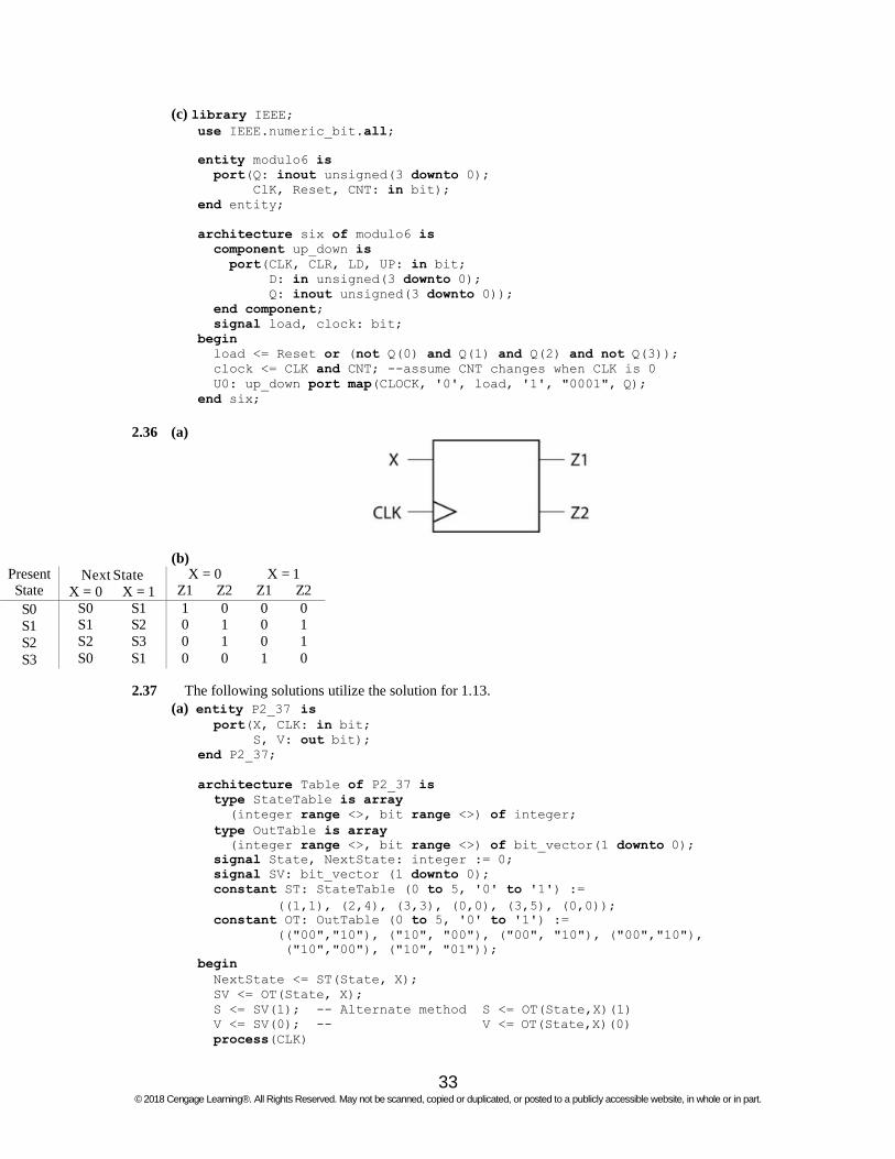
2.36 (a)
(b) Present State
Next State
X = 0 X = 1 X = 0 X = 1
Z1 Z2 Z1 Z2 S0
S1
S2
S3
S0 S1 S1 S2 S2 S3 S0 S1
1 0 0 0 0 1 0 1 0 1 0 1 0 0 1 0
2.37 The following solutions utilize the solution for 1.13.
(a) entity P2_37 is port(X, CLK: in bit;
S, V: out bit); end P2_37;
architecture Table of P2_37 is
type StateTable is array (integer range <>, bit range <>) of integer;
type OutTable is array (integer range <>, bit range <>) of bit_vector(1 downto 0);
signal State, NextState: integer := 0; signal SV: bit_vector (1 downto 0); constant ST: StateTable (0 to 5, '0' to '1') :=
((1,1), (2,4), (3,3), (0,0), (3,5), (0,0)); constant OT: OutTable (0 to 5, '0' to '1') :=
(("00","10"), ("10", "00"), ("00", "10"), ("00","10"), ("10","00"), ("10", "01"));
begin NextState <= ST(State, X);
SV <= OT(State, X); S <= SV(1); -- Alternate method S <= OT(State,X)(1) V <= SV(0); -- V <= OT(State,X)(0) process(CLK)
33
© 2018 Cengage Learning®. All Rights Reserved. May not be scanned, copied or duplicated, or posted to a publicly accessible website, in whole or in part.
begin if CLK'event and CLK = '0' then
State <= NextState;
end if; end process;
end Table;
(b) entity P2_37 is port(X, CLK: in bit;
S, V: out bit); end P2_37;
architecture Equations of P2_37 is
signal Q1, Q2, Q3: bit; begin
process(CLK)
begin if CLK = '0' and CLK'event then
Q1 <= not Q1 and Q3; Q2 <= (not Q2 and not Q3) or (X and not Q1 and Q2);
Q3 <= (not Q1 and Q3) or (Q2 and not Q3); end if;
end process; S <= (X and not Q2) or (not X and Q2);
V <= (X and Q1 and Q2); end Equations;
(c) entity P2_37 is
port(X, CLK: in bit; S, V: out bit);
end P2_37;
architecture Structural of P2_37 is component DFF port(D, CLK: in bit; Q: out bit; QN: out bit := '1');
end component; component And2 port(A1, A2: in bit; Z: out bit);
end component; component Or2 port(A1, A2: in bit; Z: out bit);
end component;
component And3 port(A1, A2, A3: in bit; Z: out bit);
end component; component Inverter port(A: in bit; Z: out bit);
end component; signal Q1, Q2, Q3: bit := '0'; signal XN, Q1N, Q2N, Q3N: bit := '1';
signal D1, D2, D3: bit := '0'; signal A1, A2, A3, A4, A5, A6: bit := '0';
begin I1: Inverter port map (X, XN);
G1: And2 port map (Q1N, Q3, D1);
G2: And2 port map (Q2N, Q3N, A1); G3: And3 port map (X, Q1N, Q2, A2);
G4: Or2 port map (A1, A2, D2); G5: And2 port map (Q1N, Q3, A3);
G6: And2 port map (Q2, Q3N, A4);
G7: Or2 port map (A3, A4, D3);
G8: And2 port map (X, Q2N, A5);
34 © 2018 Cengage Learning®. All Rights Reserved. May not be scanned, copied or duplicated, or posted to a publicly accessible website, in whole or in part.
G9: And2 port map (XN, Q2, A6);
G10: Or2 port map (A5, A6, S);
G11: And3 port map (X, Q1, Q2, V); DFF1: DFF port map (D1, CLK, Q1, Q1N);
DFF2: DFF port map (D2, CLK, Q2, Q2N);
DFF3: DFF port map (D3, CLK, Q3, Q3N); end Structural;
See Section 2.15 for the definition of the DFF component. The And3, And2, Or2, and Inverter
components are all similar to the Nand3 component given on pages 109-110 (section 2.15).
2.38 The following solutions utilize the solution for 1.14. (a) entity P2_38a is
port(X, CLK: in bit; D, B: out bit);
end P2_38a;
architecture Table of P2_38a is signal State, NextState: integer range 0 to 5;
begin process(State, X)
begin case State is
when 0 => if X = '0' then D <= '0'; B <= '0'; NextState <= 1; else D <= '1'; B <= '0'; NextState <= 1; end if;
when 1 => if X= '0' then D <= '1'; B <= '0'; NextState <= 2; else D <= '0'; B <= '0'; NextState <= 3; end if;
when 2 => if X = '0' then D <= '1'; B <= '0'; NextState <= 4; else D <= '0'; B <= '0'; NextState <= 5; end if;
when 3 => if X = '0' then D <= '0'; B <= '0'; NextState <= 5; else D <= '1'; B <= '0'; NextState <= 5; end if;
when 4 => if X = '0' then D <= '1'; B <= '1'; NextState <= 0; else D <= '0'; B <= '0'; NextState <= 0; end if;
when 5 => if X = '0' then D <= '0'; B <= '0'; NextState <= 0; else D <= '1'; B <= '0'; NextState <= 0; end if;
end case;
end process;
process(CLK)
begin if (CLK = '0' and CLK'event) then State <= NextState; end if;
end process;
end Table;
(b) entity P2_38b is port(X, CLK: in bit;
D, B: out bit); end P2_38b;
architecture Equations of P2_38b is signal Q1, Q2, Q3: bit; begin
process(CLK)
begin if (CLK='0' and CLK'event) then
Q1 <= (not Q1 and not Q3) or (not X and Q1 and not Q2);
Q2 <= (not Q2 and Q3); Q3 <= not Q2 and (Q3 or Q1);
end if; end process; D <= (not X and Q1) or (X and not Q1 and Q3);
B <= not X and Q1 and Q2;
35
© 2018 Cengage Learning®. All Rights Reserved. May not be scanned, copied or duplicated, or posted to a publicly accessible website, in whole or in part.
end Equations;
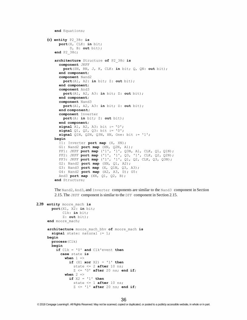
(c) entity P2_38c is port(X, CLK: in bit;
D, B: out bit); end P2_38c;
architecture Structure of P2_38c is
component JKFF port(SN, RN, J, K, CLK: in bit; Q, QN: out bit);
end component; component Nand2 port(A1, A2: in bit; Z: out bit);
end component; component And3 port(A1, A2, A3: in bit; Z: out bit);
end component; component Nand3 port(A1, A2, A3: in bit; Z: out bit);
end component;
component Inverter port(A: in bit; Z: out bit);
end component; signal A1, A2, A3: bit := '0';
signal Q1, Q2, Q3: bit := '0'; signal Q1N, Q2N, Q3N, XN, One: bit := '1';
begin I1: Inverter port map (X, XN); G1: Nand2 port map (XN, Q2N, A1); FF1: JKFF port map ('1', '1', Q3N, A1, CLK, Q1, Q1N);
FF2: JKFF port map ('1', '1', Q3, '1', CLK, Q2, Q2N);
FF3: JKFF port map ('1', '1', Q1, Q2, CLK, Q3, Q3N);
G2: Nand2 port map (XN, Q1, A2); G3: Nand3 port map (X, Q1N, Q3, A3); G4: Nand2 port map (A2, A3, D); G5:
And3 port map (XN, Q1, Q2, B); end Structure;
The Nand2, And3, and Inverter components are similar to the Nand3 component in Section
2.15. The JKFF component is similar to the DFF component in Section 2.15.
2.39 entity moore_mach is port(X1, X2: in bit;
Clk: in bit;
Z: out bit); end moore_mach;
architecture moore_mach_bhv of moore_mach is
signal state: natural := 1; begin
process(Clk)
begin if Clk = '0' and Clk'event then
case state is when 1 =>
if (X1 xor X2) = '1' then state <= 2 after 10 ns; Z <= '0' after 20 ns; end if;
when 2 => if X2 = '1' then
state <= 1 after 10 ns; Z <= '1' after 20 ns; end if;
36
© 2018 Cengage Learning®. All Rights Reserved. May not be scanned, copied or duplicated, or posted to a publicly accessible website, in whole or in part.

when others => null;
end case; end if;
end process; end moore_mach_bhv;
2.40 entity P_40 is
port(x1, x2, clk: in bit; z1, z2: out bit);
end P_40;
architecture behavioral of P_40 is signal state, next_state: integer range 1 to 3;
begin process(state, x1, x2) begin case state is when 1 => if ((x1 & x2) = "00") then next_state <= 3 after 10 ns;
elsif ((x1&x2) = "01") then next_state <= 2 after 10 ns;
else next_state <= 1 after 10 ns; end if; when 2 => if ((x1 & x2) = "00") then next_state <= 2 after 10 ns;
elsif ((x1&x2) = "01") then next_state <= 1 after 10 ns;
else next_state <= 3 after 10 ns; end if; when 3 => if ((x1 & x2) = "00") then next_state <= 1 after 10 ns;
elsif ((x1&x2) = "01") then next_state <= 2 after 10 ns;
else next_state <= 3 after 10 ns; end if; end case;
end process;
process(clk)
begin if (clk = '0' and clk'event) then state <= next_state after 5 ns; end if;
end process; z1 <= '1' after 10 ns when state = 2 else '0' after 10 ns; z2 <= '1' after 10 ns when state = 3 else '0' after 10 ns;
end behavioral;
2.41 (a) nextstate is not always assigned a new value in the conditional statements, else clauses are not specified. so a latch will be created to hold nextstate to its old value.
(b) The latch output would have the most recent value of nextstate.
(c) process(state, X)
begin case state is when 0 => if X = '1' then nextstate <= 1;
else nextstate <= 0; end if; when 1 => if X = '0' then nextstate <= 2;
else nextstate <= 1; end if; when 2 => if X = '1' then nextstate <= 0;
else nextstate <= 2; end if; end case;
end process;
37
© 2018 Cengage Learning®. All Rights Reserved. May not be scanned, copied or duplicated, or posted to a publicly accessible website, in whole or in part.
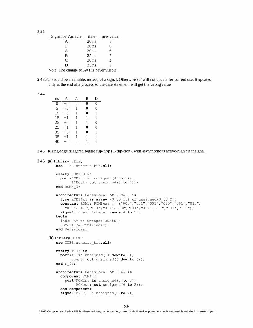
2.42 Signal or Variable time new value
A 20 ns 1 F 20 ns 6 A 20 ns 6 B 25 ns 7 C 30 ns 2 D 35 ns 5
Note: The change to A=1 is never visible.
2.43 Sel should be a variable, instead of a signal. Otherwise sel will not update for current use. It updates only at the end of a process so the case statement will get the wrong value.
2.44
ns ∆ A B D 0 +0 0 0 0 5 +0 1 0 0 15 +0 1 0 1 15 +1 1 1 1 25 +0 1 1 0 25 +1 1 0 0 35 +0 1 0 1 35 +1 1 1 1 40 +0 0 1 1
2.45 Rising-edge triggered toggle flip-flop (T-flip-flop), with asynchronous active-high clear signal
2.46 (a) library IEEE;
use IEEE.numeric_bit.all;
entity ROM4_3 is port(ROMin: in unsigned(0 to 3);
ROMout: out unsigned(0 to 2)); end ROM4_3;
architecture Behavioral of ROM4_3 is
type ROM16x3 is array (0 to 15) of unsigned(0 to 2); constant ROM1: ROM16x3 := ("000","001","001","010","001","010", "010","011","001","010","010","011","010","011","011","100");
signal index: integer range 0 to 15; begin
index <= to_integer(ROMin);
ROMout <= ROM1(index); end Behavioral;
(b) library IEEE;
use IEEE.numeric_bit.all;
entity P_46 is port(A: in unsigned(11 downto 0);
count: out unsigned(3 downto 0)); end P_46;
architecture Behavioral of P_46 is
component ROM4_3 port(ROMin: in unsigned(0 to 3);
ROMout: out unsigned(0 to 2)); end component; signal B, C, D: unsigned(0 to 2);
38 © 2018 Cengage Learning®. All Rights Reserved. May not be scanned, copied or duplicated, or posted to a publicly accessible website, in whole or in part.

begin RO1: ROM4_3 port map (A(11 downto 8), B);
RO2: ROM4_3 port map (A(7 downto 4), C);
R03: ROM4_3 port map (A(3 downto 0), D);
count <= '0' & B + C + D; end Behavioral;
(c)
A Count D C B 111111111111
010110101101
100001011100
1100
0111
0101
100 100 100 011 010 010 010 010 001
2.47
a b c y7 y6 y5 y4 y3 y2 y1 y0 0 0 0 0 0 0 0 0 0 0 1 0 0 1 0 0 0 0 0 0 1 0 0 1 0 0 0 0 0 0 1 0 0 0 1 1 0 0 0 0 1 0 0 0 1 0 0 0 0 0 1 0 0 0 0 1 0 1 0 0 1 0 0 0 0 0 1 1 0 0 1 0 0 0 0 0 0 1 1 1 1 0 0 0 0 0 0 0
library IEEE; use IEEE.numeric_bit.all; entity decoder is
port(A, B, C: in bit; X: out unsigned(7 downto 0));
end decoder; architecture LUT of decoder is
type ROM is array (0 to 7) of unsigned(7 downto 0); signal Table: ROM := ("00000001", "00000010", "00000100", "00001000",
"00010000", "00100000", "01000000", "10000000"); signal index: unsigned(2 downto 0);
begin index <= A & B & C; X <= Table(to_integer(index));
end LUT;
2.48 (a) process(A) variable Max: integer;
begin Max := A(1); for i in 2 to 20 loop if A(i) > Max then
Max := A(i);
end if; end loop;
end process;
(b) process(A) variable Max, i: integer;
begin Max := A(1); i := 2; while i <= 20 loop if A(i) > Max then
39 © 2018 Cengage Learning®. All Rights Reserved. May not be scanned, copied or duplicated, or posted to a publicly accessible website, in whole or in part.
Max := A(i);
end if; i := i + 1;
end loop; end process;
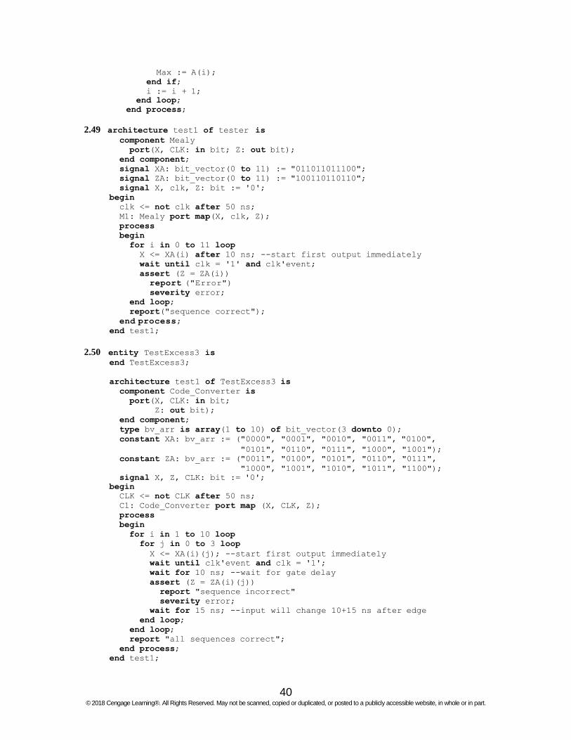
2.49 architecture test1 of tester is
component Mealy port(X, CLK: in bit; Z: out bit);
end component; signal XA: bit_vector(0 to 11) := "011011011100";
signal ZA: bit_vector(0 to 11) := "100110110110";
signal X, clk, Z: bit := '0'; begin
clk <= not clk after 50 ns; M1: Mealy port map(X, clk, Z);
process begin for i in 0 to 11 loop
X <= XA(i) after 10 ns; --start first output immediately
wait until clk = '1' and clk'event; assert (Z = ZA(i))
report ("Error")
severity error; end loop; report("sequence correct");
end process;
end test1;
2.50 entity TestExcess3 is end TestExcess3;
architecture test1 of TestExcess3 is
component Code_Converter is port(X, CLK: in bit;
Z: out bit); end component; type bv_arr is array(1 to 10) of bit_vector(3 downto 0);
constant XA: bv_arr := ("0000", "0001", "0010", "0011", "0100", "0101", "0110", "0111", "1000", "1001");
constant ZA: bv_arr := ("0011", "0100", "0101", "0110", "0111", "1000", "1001", "1010", "1011", "1100");
signal X, Z, CLK: bit := '0';
begin CLK <= not CLK after 50 ns; C1: Code_Converter port map (X, CLK, Z); process begin for i in 1 to 10 loop
for j in 0 to 3 loop X <= XA(i)(j); --start first output immediately
wait until clk'event and clk = '1'; wait for 10 ns; --wait for gate delay
assert (Z = ZA(i)(j)) report "sequence incorrect"
severity error; wait for 15 ns; --input will change 10+15 ns after edge
end loop; end loop; report "all sequences correct";
end process; end test1;
40 © 2018 Cengage Learning®. All Rights Reserved. May not be scanned, copied or duplicated, or posted to a publicly accessible website, in whole or in part.

2.51 library IEEE; use IEEE.numeric_bit.all;
entity testbench is
port(time1: out time);
end testbench;
architecture test1 of testbench is
signal clk, Ld8, Enable, S5: bit;
signal Q: unsigned(3 downto 0);
component countQ1 is port(ckl, Ld8, Enable: in bit; S5: out bit;
Q: out unsigned(3 downto 0)); end component;
begin time1 <= now when S5 = '1' else 0 ns;
clk <= not clk after 50 ns; Ld8 <= '1', '0' after 100 ns; Enable <= '0', '1' after 100 ns, '0' after 600 ns,
'1' after 800 ns, '0' after 1800 ns; cnt1: countQ1 port map (clk, Ld8, Enable, S5, Q);
end test1;
2.52 entity testSMQ1 is port(correct: inout Boolean);
end testSMQ1; architecture testSM of test SMQ1 is
component SMQ1 port(X, CLK: in bit; Z: out bit);
end component; constant answer: bit_vector(1 to 5) := "11010";
signal X, Z, CLK: bit; begin
clk <= not clk after 50 ns; X <= '1', '0' after 100 ns, '1' after 300 ns;
SMQ1_1: SMQ1 port map (X, CLK, Z); process begin wait for 40 ns; --read output 10ns before rising edge of clock
for i in 1 to 15 loop correct <= answer(i) = Z;
wait for 100 ns; if correct = FALSE then exit; end if;
end loop; wait;
end process;
end testSM;
2.56
library IEEE; use IEEE.numeric_bit.all;
entity bcd is port(Load, Clr, Enable, Clk, Up: in bit;
D: in unsigned(3 downto 0); Cout: out bit; Q: out unsigned(3 downto 0));
end bcd;
architecture counter of bcd is
signal Qout: unsigned(3 downto 0);
41
© 2018 Cengage Learning®. All Rights Reserved. May not be scanned, copied or duplicated, or posted to a publicly accessible website, in whole or in part.

begin Q <= Qout;
process(Clk,Clr)
begin if Clr = '0' then Qout<="0000"; elsif Clk'event and Clk = '1' then
if Load = '1' and Enable = '1' then case D is
when "1010"=> Qout<="0000" after 2 ns;
when "1011"=> Qout<="0001" after 2 ns;
when "1100"=> Qout<="0010" after 2 ns;
when "1101"=> Qout<="0011" after 2 ns;
when "1110"=> Qout<="0100" after 2 ns;
when "1111"=> Qout<="0101" after 2 ns;
when others => Qout <= D after 2 ns; end case;
elsif Load = '0' and Enable = '1' and Up = '1' then if Qout = "1001" then Cout <= '1'; Qout<="0000" after 2 ns; else Qout <= Qout + 1 after 2 ns; Cout <= '0';
end if; elsif Load = '0' and Up = '0' and Enable = '1' then
if Qout = "0000" then Cout <= '1'; Qout<="1001" after 2 ns;
else Qout <= Qout - 1 after 2 ns; Cout <= '0'; end if;
end if; end if;
end process; end counter;
2.57
library IEEE; use IEEE.numeric_bit.all;
entity complex is
port(clk50Mhz: in bit; clk: inout bit);
end complex;
architecture internal of complex is constant Fifty_Mil: integer := 50000000; signal counter_Big: integer range 1 to Fifty_Mil;
begin
process(clk50Mhz) begin if clk50Mhz = '1' and clk50Mhz'event then
if counter_Big = Fifty_Mil then counter_Big <= 1; clk<=not clk; else counter_Big<=counter_Big+1;
end if; end if; end process;
end internal;
42
© 2018 Cengage Learning®. All Rights Reserved. May not be scanned, copied or duplicated, or posted to a publicly accessible website, in whole or in part.
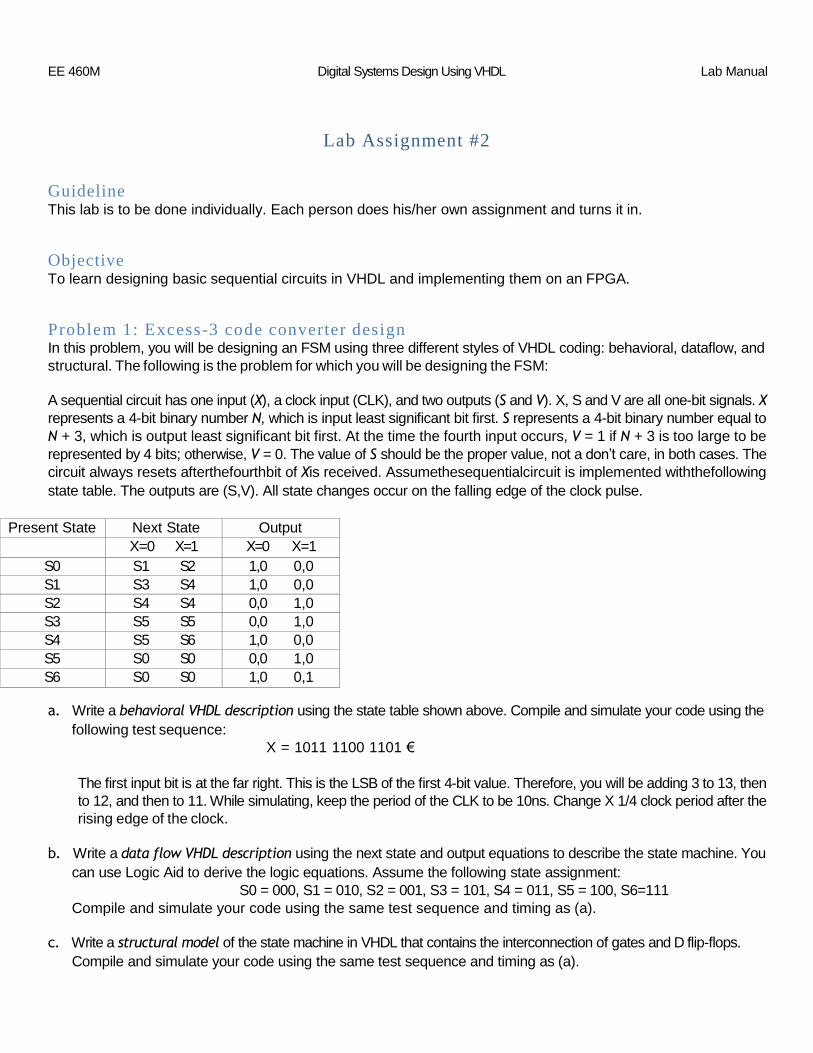
EE 460M Digital Systems Design Using VHDL Lab Manual
Lab Assignment #2
Guideline This lab is to be done individually. Each person does his/her own assignment and turns it in.
Objective To learn designing basic sequential circuits in VHDL and implementing them on an FPGA.
Problem 1: Excess-3 code converter design In this problem, you will be designing an FSM using three different styles of VHDL coding: behavioral, dataflow, and
structural. The following is the problem for which you will be designing the FSM:
A sequential circuit has one input (X), a clock input (CLK), and two outputs (S and V). X, S and V are all one-bit signals. X
represents a 4-bit binary number N, which is input least significant bit first. S represents a 4-bit binary number equal to
N + 3, which is output least significant bit first. At the time the fourth input occurs, V = 1 if N + 3 is too large to be
represented by 4 bits; otherwise, V = 0. The value of S should be the proper value, not a don’t care, in both cases. The
circuit always resets afterthefourthbit of Xis received. Assumethesequentialcircuit is implemented withthefollowing
state table. The outputs are (S,V). All state changes occur on the falling edge of the clock pulse. Present State Next State Output
X=0 X=1 X=0 X=1 S0 S1 S2 1,0 0,0 S1 S3 S4 1,0 0,0 S2 S4 S4 0,0 1,0 S3 S5 S5 0,0 1,0 S4 S5 S6 1,0 0,0 S5 S0 S0 0,0 1,0 S6 S0 S0 1,0 0,1
a. Write a behavioral VHDL description using the state table shown above. Compile and simulate your code using the
following test sequence: X = 1011 1100 1101 €
The first input bit is at the far right. This is the LSB of the first 4-bit value. Therefore, you will be adding 3 to 13, then
to 12, and then to 11. While simulating, keep the period of the CLK to be 10ns. Change X 1/4 clock period after the
rising edge of the clock.
b. Write a data flow VHDL description using the next state and output equations to describe the state machine. You can use Logic Aid to derive the logic equations. Assume the following state assignment:
S0 = 000, S1 = 010, S2 = 001, S3 = 101, S4 = 011, S5 = 100, S6=111 Compile and simulate your code using the same test sequence and timing as (a).
c. Write a structural model of the state machine in VHDL that contains the interconnection of gates and D flip-flops.
Compile and simulate your code using the same test sequence and timing as (a).

EE 460M Digital Systems Design Using VHDL Lab Manual
Problem 2: BCD Counter Design Implement a 1 digit BCD (binary coded decimal) counter. It should be a synchronous (4-bit) up/down decade counter
with output Q that works as follows: All state changes occur on the rising edge of the CLK input, except the
asynchronous clear (CLR). When CLR = 0, the counter is reset regardless of the values of the other inputs. You can keep
the time period of the CLK signal to 10ns for simulating your design.
D
CO BCD Counter
ENABLE
LOAD
UP
CLR
Q
If theLOAD= ENABLE= 1,the datainputDis loadedinto thecounter.
If LOAD = 0 and ENABLE = UP = 1, the counter is incremented. If LOAD = 0, ENABLE = 1, and UP = 0, the counter is decremented. If ENABLE = 1 and UP = 1, the carry output (CO) = 1 when the counter’s value is 9.
If ENABLE = 1 and UP = 0, the carry output (CO) = 1 when the counter’s value is 0.
a. Write a VHDL description of the counter. You may implement your design in any style you wish. It will be easier to
use a behavioral description which can be either written in the algorithmic way (eg. Count <= Count + 1 – Figure 2.46
in the text) or a state machine way (eg. State <= Next_State – Figure 2.54/2.56 in the text). You may also use
dataflow or structural descriptions, although that will be more work. Use the following simulation for your
waveforms:
1. Load counter with 6 2. Increment counter four times. You should get 9 and then 0. 3. Decrement counter once. You should get9. 4. Clear the counter.
b. Write a VHDL description of a decimal counter that uses two of the above counters to form a two-decade decimal
up/down counter that counts up from 00 to 99 or down from 99 to 00. In other words, instantiate (port map) two
single digit counters in a top module (the two-digit counter). You may need some extra logic in the top module too
other than these instantiations. The top module will have these inputs and outputs: CLR, CLK, ENABLE, LOAD, UP,
D1, D2, Q1, D2, CO. Use the following simulation for your waveforms:
1. Load counter with97 2. Increment counter five times. 3. Do nothing for 2 clock periods 3. Decrement counter four times. 4. Clear the counter.

EE 460M Digital Systems Design Using VHDL Lab Manual
Problem 3: Synthesizing and implementing the BCD counter on the FPGA Usethecodeforthesingledigit BCDcounterthatyouwrote inProblem2a. Beforeyousynthesize itandimplement iton
the board, you will have to modify your code a little bit. This is because the CLK signal available on the board is a high
frequency signal (50 MHz). If you use this high frequency for your circuit, you will not be able to give proper inputs or
see proper outputs to your design.
So, you need to add a clock divider to your VHDL description. Create two more entities in your design. Call one as top
and another as divider. Make connections as shown in the following figure. Look at the codes given in the end of this
document, understand them and see how they can be used as clock dividers.
Ensure that there are no latches in your design. Xilinx ISE will report these in the Synthesis report. You need to eliminate
such warnings. You may want to read the synthesis guidelines “Tips for writing synthesizable code” available on
Blackboard.
To look for latches in your synthesized design, open the synthesis report generated by ISE by clicking “View Synthesis
Report” under the “Synthesize-XST” option. In the synthesis report, look for “Macro Statistics” and see if any latches are
being shown. Alternatively, you can look for “cell usage” in the report and there should not be any cells under “Flip
Flops/Latches” having names starting with “L”.
Also, after adding the counter/clock divider block to your design, simulate the top entity in Modelsim before directly
synthesizing using ISE to ensure that the counter/divider works. And while simulating, reduce the large values (like
5000000) in the counter to small values (say 50), so that simulation takes less time and the waveforms are legible. Don't
forget to switch to the correct (large) value before synthesizing.
TOP
CLK input
(connect it
to 50MHz
clock – B8)
Other inputs
Divider
Slow clock
BCD
Counter
Outputs
Synthesize the top module (which includes the divider and the 1-digit bcd counter) and use the following pin
assignments. Download the design onto the board and make sure it works as expected. LOAD BTN0 D SW[3:0] ENABLE SW4 UP SW5 CLK B8 COUNT LED[3:0] CO LED4
EE 460M Digital Systems Design Using VHDL Lab Manual
CLR
Useful Information
SW6
1. Don’t limit your testing tothe input sequencesmentioned with the problem statement. During thecheckouts,
theTAswillapplyseveralinputcombinationstotestyourdesign.So,makesuretodoathoroughtestingofyour
design using sufficient number of inputs.
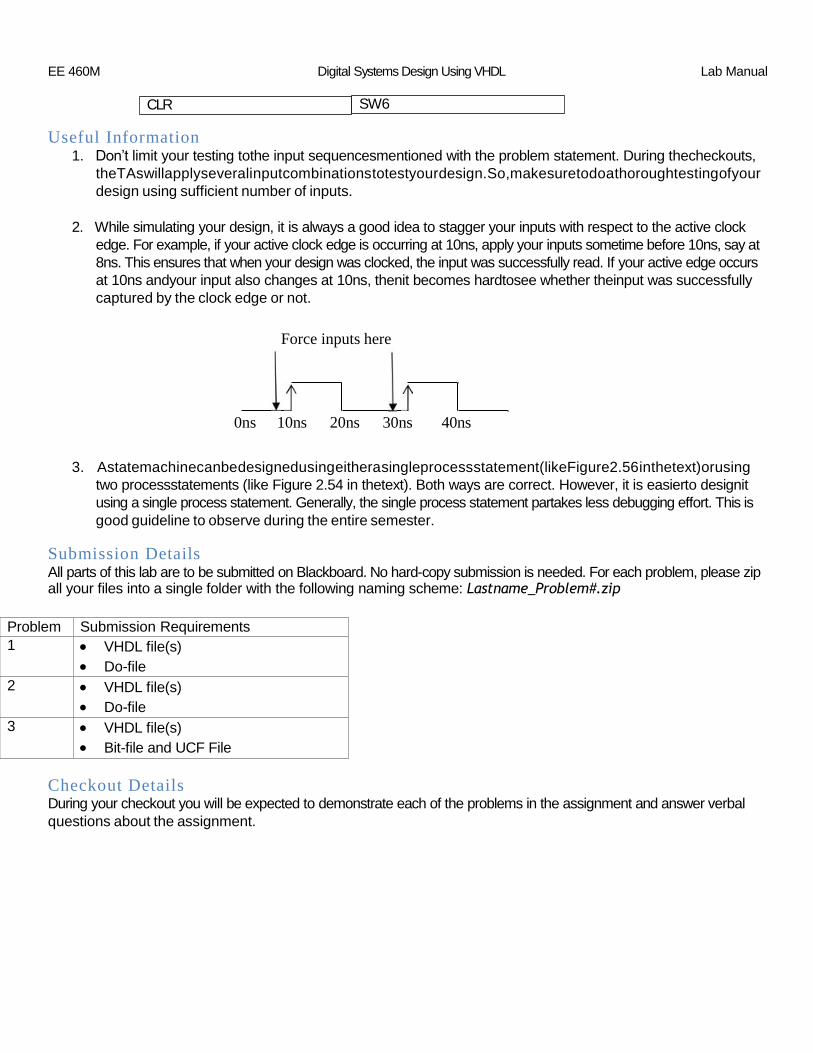
2. While simulating your design, it is always a good idea to stagger your inputs with respect to the active clock
edge. For example, if your active clock edge is occurring at 10ns, apply your inputs sometime before 10ns, say at
8ns. This ensures that when your design was clocked, the input was successfully read. If your active edge occurs
at 10ns andyour input also changes at 10ns, thenit becomes hardtosee whether theinput was successfully
captured by the clock edge or not.
Force inputs here
0ns 10ns 20ns 30ns 40ns
3. Astatemachinecanbedesignedusingeitherasingleprocessstatement(likeFigure2.56inthetext)orusing
two processstatements (like Figure 2.54 in thetext). Both ways are correct. However, it is easierto designit
using a single process statement. Generally, the single process statement partakes less debugging effort. This is
good guideline to observe during the entire semester.
Submission Details All parts of this lab are to be submitted on Blackboard. No hard-copy submission is needed. For each problem, please zip all your files into a single folder with the following naming scheme: Lastname_Problem#.zip
Problem Submission Requirements 1 VHDL file(s)
Do-file 2 VHDL file(s)
Do-file 3 VHDL file(s)
Bit-file and UCF File
Checkout Details During your checkout you will be expected to demonstrate each of the problems in the assignment and answer verbal
questions about the assignment.

EE 460M Digital Systems Design Using VHDL Lab Manual
Example 1
library IEEE; use IEEE.numeric_bit.ALL;
entity simpleCounter is
Port ( clk50Mhz : in bit; led : out bit);
end simpleCounter;
architecture Behavioral ofsimpleCounter is
signal counter: unsigned (26 downto 0);
signalcnt_temp: bit_vector(26 downto 0);
begin
process (clk50Mhz) begin if clk50MHZ = '1' and clk50Mhz'event then counter <= counter + 1; --increment counter every 20 ns (1/ 50 Mhz) cycle.
end if; end process;
cnt_temp <= bit_vector(counter);
led<=cnt_temp(26);
-- (2^26 / 50E6) = 1.34 seconds
end Behavioral;
Example 2
library IEEE;
use IEEE.numeric_bit.ALL;
entity complex is Port ( clk50Mhz : in bit;
led : inoutbit );
end complex;
architecture Behavioral of complex is signal counter: integer range 1 to 50000000;
begin
process (clk50Mhz) begin
if clk50MHZ = '1' and clk50Mhz'event then if counter = 50000000 then counter <= 1; led <= not led; else counter <= counter + 1;
end if; end if;

EE 460M Digital Systems Design Using VHDL Lab Manual
end process;
end Behavioral;
Related Documents