LMK04000, LMK04001, LMK04002, LMK04010 LMK04011, LMK04031, LMK04033 www.ti.com SNOSAZ8J – SEPTEMBER 2008 – REVISED SEPTEMBER 2011 LMK04000 Family Low-Noise Clock Jitter Cleaner with Cascaded PLLs Check for Samples: LMK04000, LMK04001, LMK04002, LMK04010, LMK04011, LMK04031, LMK04033 1FEATURES 23• Cascaded PLLatinum™ PLL Architecture • Support Clock Rates up to 1080 MHz – PLL1 • Default Clock Output (CLKout2) at power up – Phase Detector Rate of up to 40 MHz • Five Dedicated Channel Divider and Delay Blocks – Integrated Low-Noise Crystal Oscillator Circuit • Pin Compatible Family of Clocking Devices – Dual Redundant Input Reference Clock • Industrial Temperature Range: -40 to 85 °C with LOS • 3.15 V to 3.45 V Operation – PLL2 • Package: 48 Pin WQFN (7.0 x 7.0 x 0.8 mm) – Normalized [1 Hz] PLL Noise Floor of - 224 dBc/Hz APPLICATIONS – Phase Detector Rate up to 100 MHz • Data Converter Clocking – Input Frequency-Doubler • Wireless Infrastructure – Integrated Low-Noise VCO • Networking, SONET/SDH, DSLAM • Ultra-Low RMS Jitter Performance • Medical – 150 fs RMS Jitter (12 kHz – 20 MHz) • Military / Aerospace – 200 fs RMS Jitter (100 Hz – 20 MHz) • Test and Measurement • LVPECL/2VPECL, LVDS, and LVCMOS outputs • Video DESCRIPTION The LMK04000 family of precision clock conditioners provides low-noise jitter cleaning, clock multiplication and distribution without the need for high-performance voltage controlled crystal oscillators (VCXO) module. Using a cascaded PLLatinum™ architecture combined with an external crystal and varactor diode, the LMK04000 family provides sub-200 femtosecond (fs) root mean square (RMS) jitter performance. The cascaded architecture consists of two high-performance phase-locked loops (PLL), a low-noise crystal oscillator circuit, and a high-performance voltage controlled oscillator (VCO). The first PLL (PLL1) provides a low- noise jitter cleaner function while the second PLL (PLL2) performs the clock generation. PLL1 can be configured to either work with an external VCXO module or use the integrated crystal oscillator with an external crystal and a varactor diode. When used with a very narrow loop bandwidth, PLL1 uses the superior close-in phase noise (offsets below 50 kHz) of the VCXO module or the crystal to clean the input clock. The output of PLL1 is used as the clean input reference to PLL2 where it locks the integrated VCO. The loop bandwidth of PLL2 can be optimized to clean the far-out phase noise (offsets above 50 kHz) where the integrated VCO outperforms the VCXO module or crystal used in PLL1. The LMK04000 family features dual redundant inputs, five differential outputs, and an optional default-clock upon power up. The input block is equipped with loss of signal detection and automatic or manual selection of the reference clock. Each clock output consists of a programmable divider, a phase synchronization circuit, a programmable delay, and an LVDS, LVPECL, or LVCMOS output buffer. The default startup clock is available on CLKout2 and it can be used to provide an initial clock for the field-programmable gate array (FPGA) or microcontroller that programs the jitter cleaner during the system power up sequence. 1 Please be aware that an important notice concerning availability, standard warranty, and use in critical applications of Texas Instruments semiconductor products and disclaimers thereto appears at the end of this data sheet. 2PLLatinum is a trademark of Texas Instruments. 3All other trademarks are the property of their respective owners. PRODUCTION DATA information is current as of publication date. Copyright © 2008–2011, Texas Instruments Incorporated Products conform to specifications per the terms of the Texas Instruments standard warranty. Production processing does not necessarily include testing of all parameters.

Welcome message from author
This document is posted to help you gain knowledge. Please leave a comment to let me know what you think about it! Share it to your friends and learn new things together.
Transcript
LMK04000, LMK04001, LMK04002, LMK04010LMK04011, LMK04031, LMK04033
www.ti.com SNOSAZ8J –SEPTEMBER 2008–REVISED SEPTEMBER 2011
LMK04000 Family Low-Noise Clock Jitter Cleaner with Cascaded PLLsCheck for Samples: LMK04000, LMK04001, LMK04002, LMK04010, LMK04011, LMK04031, LMK04033
1FEATURES23• Cascaded PLLatinum™ PLL Architecture • Support Clock Rates up to 1080 MHz
– PLL1 • Default Clock Output (CLKout2) at power up– Phase Detector Rate of up to 40 MHz • Five Dedicated Channel Divider and Delay
Blocks– Integrated Low-Noise Crystal OscillatorCircuit • Pin Compatible Family of Clocking Devices
– Dual Redundant Input Reference Clock • Industrial Temperature Range: -40 to 85 °Cwith LOS • 3.15 V to 3.45 V Operation
– PLL2 • Package: 48 Pin WQFN (7.0 x 7.0 x 0.8 mm)– Normalized [1 Hz] PLL Noise Floor of -
224 dBc/Hz APPLICATIONS– Phase Detector Rate up to 100 MHz • Data Converter Clocking– Input Frequency-Doubler • Wireless Infrastructure– Integrated Low-Noise VCO • Networking, SONET/SDH, DSLAM
• Ultra-Low RMS Jitter Performance • Medical– 150 fs RMS Jitter (12 kHz – 20 MHz) • Military / Aerospace– 200 fs RMS Jitter (100 Hz – 20 MHz) • Test and Measurement
• LVPECL/2VPECL, LVDS, and LVCMOS outputs • Video
DESCRIPTIONThe LMK04000 family of precision clock conditioners provides low-noise jitter cleaning, clock multiplication anddistribution without the need for high-performance voltage controlled crystal oscillators (VCXO) module. Using acascaded PLLatinum™ architecture combined with an external crystal and varactor diode, the LMK04000 familyprovides sub-200 femtosecond (fs) root mean square (RMS) jitter performance.
The cascaded architecture consists of two high-performance phase-locked loops (PLL), a low-noise crystaloscillator circuit, and a high-performance voltage controlled oscillator (VCO). The first PLL (PLL1) provides a low-noise jitter cleaner function while the second PLL (PLL2) performs the clock generation. PLL1 can be configuredto either work with an external VCXO module or use the integrated crystal oscillator with an external crystal anda varactor diode. When used with a very narrow loop bandwidth, PLL1 uses the superior close-in phase noise(offsets below 50 kHz) of the VCXO module or the crystal to clean the input clock. The output of PLL1 is used asthe clean input reference to PLL2 where it locks the integrated VCO. The loop bandwidth of PLL2 can beoptimized to clean the far-out phase noise (offsets above 50 kHz) where the integrated VCO outperforms theVCXO module or crystal used in PLL1.
The LMK04000 family features dual redundant inputs, five differential outputs, and an optional default-clock uponpower up. The input block is equipped with loss of signal detection and automatic or manual selection of thereference clock. Each clock output consists of a programmable divider, a phase synchronization circuit, aprogrammable delay, and an LVDS, LVPECL, or LVCMOS output buffer. The default startup clock is available onCLKout2 and it can be used to provide an initial clock for the field-programmable gate array (FPGA) ormicrocontroller that programs the jitter cleaner during the system power up sequence.
1
Please be aware that an important notice concerning availability, standard warranty, and use in critical applications ofTexas Instruments semiconductor products and disclaimers thereto appears at the end of this data sheet.
2PLLatinum is a trademark of Texas Instruments.3All other trademarks are the property of their respective owners.
PRODUCTION DATA information is current as of publication date. Copyright © 2008–2011, Texas Instruments IncorporatedProducts conform to specifications per the terms of the TexasInstruments standard warranty. Production processing does notnecessarily include testing of all parameters.

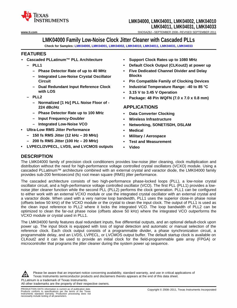
LMK040xx
Precision Clock Conditioner
Recovered ³GLUW\´�FORFN�RU�
clean clock
0XOWLSOH�³FOHDQ´�FORFNV�DW�
different frequencies
Fout
CLKout4
CLKout2A
CLKout1
CLKout0
DAC
Serializer/Deserializer
LMX2531PLL+VCO
ADC> 1 Gsps
FPGA
CLKin0
Crystal or VCXO
Backup Reference Clock
CLKin1
LMK04000, LMK04001, LMK04002, LMK04010LMK04011, LMK04031, LMK04033SNOSAZ8J –SEPTEMBER 2008–REVISED SEPTEMBER 2011 www.ti.com
Table 1. Device Configuration Information
2VPECL / LVPECLNSID PROCESS LVDS OUTPUTS LVCMOS OUTPUTS VCOOUTPUTS
LMK04000BISQ BiCMOS 3 4 1185 to 1296 MHz
LMK04001BISQ BiCMOS 3 4 1430 to 1570 MHz
LMK04002BISQ BiCMOS 3 4 1600 to 1750 MHz
LMK04010BISQ BiCMOS 5 1185 to 1296 MHz
LMK04011BISQ BiCMOS 5 1430 to 1570 MHz
LMK04031BISQ BiCMOS 2 2 2 1430 to 1570 MHz
LMK04033BISQ BiCMOS 2 2 2 1840 to 2160 MHz
NSID CLKout0 CLKout1 CLKout2 CLKout3 CLKout4
LMK04000BISQ 2VPECL / LVPECL LVCMOS x 2 LVCMOS x 2 2VPECL / LVPECL 2VPECL / LVPECL
LMK04001BISQ 2VPECL / LVPECL LVCMOS x 2 LVCMOS x 2 2VPECL / LVPECL 2VPECL / LVPECL
LMK04002BISQ 2VPECL / LVPECL LVCMOS x 2 LVCMOS x 2 2VPECL / LVPECL 2VPECL / LVPECL
LMK04010BISQ 2VPECL / LVPECL 2VPECL / LVPECL 2VPECL / LVPECL 2VPECL / LVPECL 2VPECL / LVPECL
LMK04011BISQ 2VPECL / LVPECL 2VPECL / LVPECL 2VPECL / LVPECL 2VPECL / LVPECL 2VPECL / LVPECL
LMK04031BISQ LVDS 2VPECL / LVPECL LVCMOS x 2 2VPECL / LVPECL LVDS
LMK04033BISQ LVDS 2VPECL / LVPECL LVCMOS x 2 2VPECL / LVPECL LVDS
2 Submit Documentation Feedback Copyright © 2008–2011, Texas Instruments Incorporated
Product Folder Links: LMK04000 LMK04001 LMK04002 LMK04010 LMK04011 LMK04031 LMK04033

OSCin
OSCin*
R1 Divider Phase Detector
PLL1N1 Divider
VCODivider
CLKout4
CLKout4*
CLKout3B
CLKout3A
CLKout2B
CLKout2A
CLKout1
CLKout1*
CP
out1
Internal VCO
Partially Integrated Loop Filter
DelayMux
DelayMux
DividerDelay
Mux
DividerDelay
Mux
Distribution Path
CLK
DATA
LE
ControlRegisters
PWirePort
Device Control
LDGOE
SYNC*
Fout
Clock Buffers
Mux
Divider
Divider
CLKin0
CLKin0*
CLKin1CLKin1*
R2 DividerPhase
DetectorPLL2N2 Divider
CP
out2
2X
CLKout0
CLKout0*
DelayMuxDivider
LOS
LOS
LOS0
LOS1
Mux
LMK04000, LMK04001, LMK04002, LMK04010LMK04011, LMK04031, LMK04033
www.ti.com SNOSAZ8J –SEPTEMBER 2008–REVISED SEPTEMBER 2011
Functional Block Diagram
Copyright © 2008–2011, Texas Instruments Incorporated Submit Documentation Feedback 3
Product Folder Links: LMK04000 LMK04001 LMK04002 LMK04010 LMK04011 LMK04031 LMK04033

4748 46 45 44 43 42 41 40 39 38 37
11
12
10
9
8
7
6
5
4
3
2
1
1413 15 16 17 18 19 20 21 22 23 24
26
25
27
28
29
30
31
32
33
34
35
36GND
Fout
Vcc1
Vcc2
Vcc
3
DLD
_BY
P
Vcc
5
Vcc
6
CLKin1*
Vcc8
Vcc9
Vcc10
Vcc
11
Vcc
12
Vcc
13
Vcc
14
CLKuWire
DATAuWire
LEuWire
NC
LDObyp1
LDObyp2
GOE
LD
CLK
out0
CLK
out0
*
GN
D
Vcc
4
CLK
in0
CLK
in0*
CP
out1
Vcc
7
CLKin1
SYNC*
OSCin
OSCin*
CPout2
CLKin0_LOS
CLKin1_LOS
Bias
CLK
out1
CLK
out1
*
CLK
out2
CLK
out2
*
CLK
out3
CLK
out3
*
CLK
out4
CLK
out4
*
DAP
LMK04000, LMK04001, LMK04002, LMK04010LMK04011, LMK04031, LMK04033SNOSAZ8J –SEPTEMBER 2008–REVISED SEPTEMBER 2011 www.ti.com
Connection Diagram
Figure 1. 48-Pin WQFN PackageTop View
PIN DESCRIPTIONSPin Number Name(s) I/O Type Description
1 GND GND Ground (For Fout Buffer)
2 Fout O ANLG VCO Frequency Output Port
3 VCC1 PWR Power Supply for VCO Output Buffer
4 CLKuWire I CMOS Microwire Clock Input
5 DATAuWire I CMOS Microwire Data Input
6 LEuWire I CMOS Microwire Latch Enable Input
7 NC No Connection
8 VCC2 PWR Power Supply for VCO
9 LDObyp1 ANLG LDO Bypass, bypassed to ground with a 10 µF capacitor
10 LDObyp2 ANLG LDO Bypass, bypassed to ground with a 0.1 µFcapacitor
11 GOE I CMOS Global Output Enable
12 LD O CMOS Lock Detect and PLL multiplexer Output
13 VCC3 PWR Power Supply for CLKout0
14 CLKout0 O LVDS/LVPECL Clock Channel 0 Output
15 CLKout0* O LVDS/LVPECL Clock Channel 0* Output
16 DLD_BYP ANLG DLD Bypass, bypassed to ground with a 0.47 µFcapacitor
17 GND GND Ground (Digital)
18 VCC4 PWR Power Supply for Digital
4 Submit Documentation Feedback Copyright © 2008–2011, Texas Instruments Incorporated
Product Folder Links: LMK04000 LMK04001 LMK04002 LMK04010 LMK04011 LMK04031 LMK04033

LMK04000, LMK04001, LMK04002, LMK04010LMK04011, LMK04031, LMK04033
www.ti.com SNOSAZ8J –SEPTEMBER 2008–REVISED SEPTEMBER 2011
PIN DESCRIPTIONS (continued)
Pin Number Name(s) I/O Type Description
19 VCC5 PWR Power Supply for CLKin buffers and PLL1 R-divider
20 CLKin0 I ANLG Reference Clock Input Port for PLL1 - AC or DCCoupled (1)
21 CLKin0* I ANLG Reference Clock Input Port for PLL1 (complimentary) -AC or DC Coupled (1)
22 VCC6 PWR Power Supply for PLL1 Phase Detector and ChargePump
23 CPout1 O ANLG Charge Pump1 Output
24 VCC7 PWR Power Supply for PLL1 N-Divider
25 CLKin1 I ANLG Reference Clock Input Port for PLL1 - AC or DCCoupled (1)
26 CLKin1* I ANLG Reference Clock Input Port for PLL1 (complimentary) -AC or DC Coupled (1)
27 SYNC* I CMOS Global Clock Output Synchronization
28 OSCin I ANLG Reference oscillator Input for PLL2 - AC Coupled
29 OSCin* I ANLG Reference oscillator Input for PLL2 - AC Coupled
30 VCC8 PWR Power Supply for OSCin Buffer and PLL2 R-Divider
31 VCC9 PWR Power Supply for PLL2 Phase Detector and ChargePump
32 CPout2 O ANLG Charge Pump2 Output
33 VCC10 PWR Power Supply for VCO Divider and PLL2 N-Divider
34 CLKin0_LOS O LVCMOS Status of CLKin0 reference clock input
35 CLKin1_LOS O LVCMOS Status of CLKin1 reference clock input
36 Bias I ANLG Bias Bypass. AC coupled with 1 µF capacitor to Vcc1
37 VCC11 PWR Power Supply for CLKout1
38 CLKout1 O LVPECL/LVCMOS Clock Channel 1 Output
39 CLKout1* O LVPECL/LVCMOS Clock Channel 1* Output
40 VCC12 PWR Power Supply for CLKout2
41 CLKout2 O LVPECL/LVCMOS Clock Channel 2 Output
42 CLKout2* O LVPECL/LVCMOS Clock Channel 2* Output
43 VCC13 PWR Power Supply for CLKout3
44 CLKout3 O LVPECL Clock Channel 3 Output
45 CLKout3* O LVPECL Clock Channel 3* Output
46 VCC14 PWR Power Supply for CLKout4
47 CLKout4 O LVDS/LVPECL Clock Channel 4 Output
48 CLKout4* O LVDS/LVPECL Clock Channel 4* Output
DAP DAP DIE ATTACH PAD, connect to GND
(1) The reference clock inputs may be either AC or DC coupled.
These devices have limited built-in ESD protection. The leads should be shorted together or the device placed in conductive foamduring storage or handling to prevent electrostatic damage to the MOS gates.
Copyright © 2008–2011, Texas Instruments Incorporated Submit Documentation Feedback 5
Product Folder Links: LMK04000 LMK04001 LMK04002 LMK04010 LMK04011 LMK04031 LMK04033

LMK04000, LMK04001, LMK04002, LMK04010LMK04011, LMK04031, LMK04033SNOSAZ8J –SEPTEMBER 2008–REVISED SEPTEMBER 2011 www.ti.com
Absolute Maximum Ratings (1) (2) (3) (4)
Parameter Symbol Ratings Units
Supply Voltage (5) VCC -0.3 to 3.6 V
Input Voltage VIN -0.3 to (VCC + 0.3) V
Storage Temperature Range TSTG -65 to 150 °C
Lead Temperature (solder 4 sec) TL +260 °C
Differential Input Current (CLKinX/X*, IIN ± 5 mAOSCin/OSCin*)
(1) "Absolute Maximum Ratings" indicate limits beyond which damage to the device may occur. Operating Ratings indicate conditions forwhich the device is intended to be functional, but do not guarantee specific performance limits. For guaranteed specifications and testconditions, see the Electrical Characteristics. The guaranteed specifications apply only to the test conditions listed.
(2) If Military/Aerospace specified devices are required, please contact the TI Sales Office/Distributors for availability and specifications.(3) This device is a high performance RF integrated circuit with an ESD rating up to 8 KV Human Body Model, up to 300 V Machine Model
and up to 1,250 V Charged Device Model and is ESD sensitive. Handling and assembly of this device should only be done at ESD-freeworkstations.
(4) Stresses in excess of the absolute maximum ratings can cause permanent or latent damage to the device. These are absolute stressratings only. Functional operation of the device is only implied at these or any other conditions in excess of those given in the operationsections of the data sheet. Exposure to absolute maximum ratings for extended periods can adversely affect device reliability.
(5) Never to exceed 3.6 V.
Package Thermal ResistancePackage θJA θJ-PAD (Thermal Pad)
48-Lead WQFN (1) 27.4° C/W 5.8° C/W
(1) Specification assumes 16 thermal vias connect the die attach pad to the embedded copper plane on the 4-layer JEDEC board. Thesevias play a key role in improving the thermal performance of the WQFN. It is recommended that the maximum number of vias be used inthe board layout.
Recommended Operating ConditionsParameter Symbol Condition Min Typical Max Unit
Ambient TA VCC = 3.3 V -40 25 85 °CTemperature
Supply Voltage VCC 3.15 3.3 3.45 V
Electrical Characteristics(3.15 V ≤ VCC ≤ 3.45 V, -40 °C ≤ TA ≤ 85 °C. Typical values represent most likely parametric norms at VCC = 3.3 V, TA = 25°C, at the Recommended Operating Conditions at the time of product characterization and are not guaranteed.)
Symbol Parameter Conditions Min Typ Max Units
Current Consumption
ICC_PD Power Down Supply Current 1 mA
LMK04000, LMK04001,LMK04002 380 435(2)
Supply Current with all clocksICC_CLKS enabled, all delay bypassed, LMK04010, LMK04011 mA378 435Fout disabled. (1) (2)
LMK04031, LMK04033 335 385(2)
CLKin0/0* and CLKin1/1* Input Clock Specifications
Manual Select mode 0.001 400Clock Input FrequencyfCLKin MHz(3)Auto-Switching mode 1 400
(1) Load conditions for output clocks: LVPECL: 50 Ω to VCC-2 V. 2VPECL: 50 Ω to VCC-2.36 V. LVDS: 100 Ω differential. LVCMOS: 10 pF.(2) Additional test conditions for ICC limits: All clock delays disabled, CLKoutX_DIV = 510, PLL1 and PLL2 locked. (See Table 33 for more
information)(3) CLKin0 and CLKin1 maximum of 400 MHz is guaranteed by characterization, production tested at 200 MHz.
6 Submit Documentation Feedback Copyright © 2008–2011, Texas Instruments Incorporated
Product Folder Links: LMK04000 LMK04001 LMK04002 LMK04010 LMK04011 LMK04031 LMK04033

LMK04000, LMK04001, LMK04002, LMK04010LMK04011, LMK04031, LMK04033
www.ti.com SNOSAZ8J –SEPTEMBER 2008–REVISED SEPTEMBER 2011
Electrical Characteristics (continued)(3.15 V ≤ VCC ≤ 3.45 V, -40 °C ≤ TA ≤ 85 °C. Typical values represent most likely parametric norms at VCC = 3.3 V, TA = 25°C, at the Recommended Operating Conditions at the time of product characterization and are not guaranteed.)
Symbol Parameter Conditions Min Typ Max Units
Slew Rate on CLKinSLEWCLKin 20% to 80% 0.15 0.5 V/ns(4)
AC coupled to CLKinX;Input Voltage Swing, CLKinX* AC coupled to Ground 0.25 2.0 Vppsingle-ended input (CLKinX_TYPE=0)VCLKin (Bipolar input buffermode) CLKinX and CLKinX* are bothInput Voltage Swing, driven, AC coupled. 0.5 3.1 Vppdifferential input (CLKinX_TYPE=0)
DC offset voltage betweenVCLKin-offset (Bipolar input Each pin AC coupledCLKinX/CLKinX* 44 mVbuffer mode) (CLKinX_TYPE=0)|CLKinX-CLKinX*|
AC coupled to CLKinX;Input Voltage Swing, single- CLKinX* AC coupled to Ground 0.25 2.0 Vppended input (CLKinX_TYPE=1)VCLKin (MOS input buffermode) CLKinX and CLKinX* are bothInput Voltage Swing, driven, AC coupled. 0.5 3.1 Vppdifferential input (CLKinX_TYPE=1)
DC coupled to CLKinX;VCLKin-VIH (MOS input buffer Maximum input voltage CLKinX* AC coupled to Ground 2.0 VCC Vmode) (CLKinX_TYPE=1)
DC coupled to CLKinX;VCLKin-VIL (MOS input buffer CLKinX* AC coupled to Ground 0.0 0.4 Vmode) (CLKinX_TYPE=1)
DC offset voltage betweenVCLKin-offset (MOS input Each pin AC coupledCLKinX/CLKinX* 294 mVbuffer mode) (CLKinX_TYPE=1)|CLKinX-CLKinX*|
PLL1 Specifications
PLL1 Phase DetectorfPD 40 MHzFrequency
VCPout1 = VCC/2, 25PLL1_CP_GAIN = 100b
VCPout1 = VCC/2, 50PLL1_CP_GAIN = 101b
VCPout1 = VCC/2, 100PLL1_CP_GAIN = 110b
VCPout1 = VCC/2,PLL1 Charge Pump Source 400ICPout1 SOURCE µAPLL1_CP_GAIN = 111bCurrent (5)
PLL1_CP_GAIN = 000b NA
PLL1_CP_GAIN = 001b NA
VCPout1=VCC/2, PLL1_CP_GAIN 20= 010b
VCPout1=VCC/2, PLL1_CP_GAIN 80= 011b
(4) In order to meet the jitter performance listed in the subsequent sections of this data sheet, the minimum recommended slew rate for allinput clocks is 0.5 V/ns. This is especially true for single-ended clocks. Phase noise performance will begin to degrade as the clock inputslew rate is reduced. However, the device will function at slew rates down to the minimum listed. When compared to single-endedclocks, differential clocks (LVDS, LVPECL) will be less susceptible to degradation in phase noise performance at lower slew rates due totheir common mode noise rejection. However, it is also recommended to use the highest possible slew rate for differential clocks toachieve optimal phase noise performance at the device outputs.
(5) This parameter is programmable
Copyright © 2008–2011, Texas Instruments Incorporated Submit Documentation Feedback 7
Product Folder Links: LMK04000 LMK04001 LMK04002 LMK04010 LMK04011 LMK04031 LMK04033

LMK04000, LMK04001, LMK04002, LMK04010LMK04011, LMK04031, LMK04033SNOSAZ8J –SEPTEMBER 2008–REVISED SEPTEMBER 2011 www.ti.com
Electrical Characteristics (continued)(3.15 V ≤ VCC ≤ 3.45 V, -40 °C ≤ TA ≤ 85 °C. Typical values represent most likely parametric norms at VCC = 3.3 V, TA = 25°C, at the Recommended Operating Conditions at the time of product characterization and are not guaranteed.)
Symbol Parameter Conditions Min Typ Max Units
VCPout1=VCC/2, PLL1_CP_GAIN -25= 100b
VCPout1=VCC/2, PLL1_CP_GAIN -50= 101b
VCPout1=VCC/2, PLL1_CP_GAIN -100= 110b
VCPout1=VCC/2, PLL1_CP_GAINPLL1 Charge Pump Sink -400ICPout1 SINK µA= 111bCurrent (5)
PLL1_CP_GAIN = 000b NA
PLL1_CP_GAIN = 001b NA
VCPout1=VCC/2, PLL1_CP_GAIN -20= 010b
VCPout1=VCC/2, PLL1_CP_GAIN -80= 011b
Charge Pump Sink / SourceICPout1 %MIS VCPout1 = VCC/2, T = 25 °C 3 10 %Mismatch
Magnitude of Charge Pump 0.5 V < VCPout1 < VCC - 0.5 VICPout1VTUNE Current vs. Charge Pump 4 %TA = 25 °CVoltage Variation
Charge Pump Current vs.ICPout1 %TEMP 4 %Temperature Variation
Charge Pump TRI-STATEPLL1 ICPout1 TRI 0.5 V < VCPout < VCC - 0.5 V 5 nALeakage Current
PLL2 Reference Input (OSCin) Specifications
EN_PLL2_REF 2X = 0 250PLL2 Reference Input (7)fOSCin MHz(6)
EN_PLL2_REF 2X = 1 50
PLL2 Reference ClockSLEWOSCin 20% to 80% 0.15 0.5 V/nsminimum slew rate on OSCin
AC coupled; Single-endedInput Voltage for OSCin orVOSCin (Single-ended) (Unused pin AC coupled to 0.2 2.0 VppOSCin* GND)
VOSCin (Differential) Differential voltage swing AC coupled 0.4 3.1 Vpp
Crystal Oscillator Mode Specifications
fXTAL Crystal Frequency Range 6 20 MHz
Crystal Effective SeriesESR 6 MHz < FXTAL < 20 MHz 100 OhmsResistance
Vectron VXB1 crystal, 12.288PXTAL Crystal Power Dissipation (8) 200 µWMHz, RESR < 40 ΩInput Capacitance ofCIN -40 to +85 °C 6 pFLMK040xx OSCin port
PLL2 Phase Detector and Charge Pump Specifications
fPD Phase Detector Frequency 100 MHz
(6) FOSCin maximum frequency guaranteed by characterization. Production tested at 200 MHz.(7) The EN_PLL2_REF2X bit (Register 13) enables/disables a frequency doubler mode for the PLL2 OSCin path.(8) See Application Section discussion of Crystal Power Dissipation.
8 Submit Documentation Feedback Copyright © 2008–2011, Texas Instruments Incorporated
Product Folder Links: LMK04000 LMK04001 LMK04002 LMK04010 LMK04011 LMK04031 LMK04033

LMK04000, LMK04001, LMK04002, LMK04010LMK04011, LMK04031, LMK04033
www.ti.com SNOSAZ8J –SEPTEMBER 2008–REVISED SEPTEMBER 2011
Electrical Characteristics (continued)(3.15 V ≤ VCC ≤ 3.45 V, -40 °C ≤ TA ≤ 85 °C. Typical values represent most likely parametric norms at VCC = 3.3 V, TA = 25°C, at the Recommended Operating Conditions at the time of product characterization and are not guaranteed.)
Symbol Parameter Conditions Min Typ Max Units
VCPout2=VCC/2, PLL2_CP_GAIN 100= 00b
VCPout2=VCC/2, PLL2_CP_GAIN 400= 01bPLL2 Charge Pump SourceICPoutSOURCE µACurrent (9)VCPout2=VCC/2, PLL2_CP_GAIN 1600= 10b
VCPout2=VCC/2, PLL2_CP_GAIN 3200= 11b
VCPout2=VCC/2, PLL2_CP_GAIN -100= 00b
VCPout2=VCC/2, PLL2_CP_GAIN -400= 01bPLL2 Charge Pump SinkICPoutSINK µACurrent (9)VCPout2=VCC/2, PLL2_CP_GAIN -1600= 10b
VCPout2=VCC/2, PLL2_CP_GAIN -3200= 11b
Charge Pump Sink/SourceICPout2%MIS VCPout2=VCC/2, TA = 25 °C 3 10 %Mismatch
Magnitude of Charge Pump 0.5 V < VCPout2 < VCC - 0.5 VICPout2VTUNE Current vs. Charge Pump 4 %TA = 25 °CVoltage Variation
Charge Pump Current vs.ICPout2%TEMP 4 %Temperature Variation
ICPout2TRI Charge Pump Leakage 0.5 V < VCPout2 < VCC - 0.5 V 10 nA
PLL 1/f Noise at 10 kHz offset PLL2_CP_GAIN = 400 µA -117PN10kHz (10). Normalized to dBc/Hz
PLL2_CP_GAIN = 3200 µA -1221 GHz Output Frequency
PLL2_CP_GAIN = 400 µA -219Normalized Phase NoisePN1Hz dBc/HzContribution (11)PLL2_CP_GAIN = 3200 µA -224
Internal VCO Specifications
LMK040x0 1185 1296
LMK040x1 1430 1570fVCO VCO Tuning Range MHz
LMK040x2 1600 1750
LMK040x3 1840 2160
LMK040x0, TA = 25 °C, single- 3ended
LMK040x1, TA = 25 °C, single- 3ended
VCO Output power to a LMK040x2, TA = 25 °C, single-PVCO 2 dBm50 Ω load driven by Fout ended
LMK040x3, TA = 25 °C, single- 0ended 1840 MHz
LMK040x3, TA = 25 °C, single- -5ended 2160 MHz
(9) This parameter is programmable(10) A specification in modeling PLL in-band phase noise is the 1/f flicker noise, LPLL_flicker(f), which is dominant close to the carrier. Flicker
noise has a 10 dB/decade slope. PN10kHz is normalized to a 10 kHz offset and a 1 GHz carrier frequency. PN10kHz = LPLL_flicker(10kHz) - 20log(Fout / 1 GHz), where LPLL_flicker(f) is the single side band phase noise of only the flicker noise's contribution to total noise,L(f). To measure LPLL_flicker(f) it is important to be on the 10 dB/decade slope close to the carrier. A high compare frequency and a cleancrystal are important to isolating this noise source from the total phase noise, L(f). LPLL_flicker(f) can be masked by the referenceoscillator performance if a low power or noisy source is used. The total PLL inband phase noise performance is the sum of LPLL_flicker(f)and LPLL_flat(f).
(11) A specification modeling PLL in-band phase noise. The normalized phase noise contribution of the PLL, LPLL_flat(f), is defined as:PN1HZ=LPLL_flat(f)-20log(N)-10log(fCOMP). LPLL_flat(f) is the single side band phase noise measured at an offset frequency, f, in a 1 Hzbandwidth and fCOMP is the phase detector frequency of the synthesizer. LPLL_flat(f) contributes to the total noise, L(f).
Copyright © 2008–2011, Texas Instruments Incorporated Submit Documentation Feedback 9
Product Folder Links: LMK04000 LMK04001 LMK04002 LMK04010 LMK04011 LMK04031 LMK04033
LMK04000, LMK04001, LMK04002, LMK04010LMK04011, LMK04031, LMK04033SNOSAZ8J –SEPTEMBER 2008–REVISED SEPTEMBER 2011 www.ti.com
Electrical Characteristics (continued)(3.15 V ≤ VCC ≤ 3.45 V, -40 °C ≤ TA ≤ 85 °C. Typical values represent most likely parametric norms at VCC = 3.3 V, TA = 25°C, at the Recommended Operating Conditions at the time of product characterization and are not guaranteed.)
Symbol Parameter Conditions Min Typ Max Units
Fine Tuning Sensitivity LMK040x0 7 to 9(The range displayed in the LMK040x1 8 to 11typical column indicates the
LMK040x2 9 to 14lower sensitivity is typical atKVCO the lower end of the tuning MHz/V
range, and the higher tuningsensitivity is typical at the LMK040x3 14 to 26higher end of the tuningrange).
After programming R15 forAllowable Temperature Drift lock, no changes to output|ΔTCL| for Continuous Lock 125 °Cconfiguration are permitted to(12)guarantee continuous lock
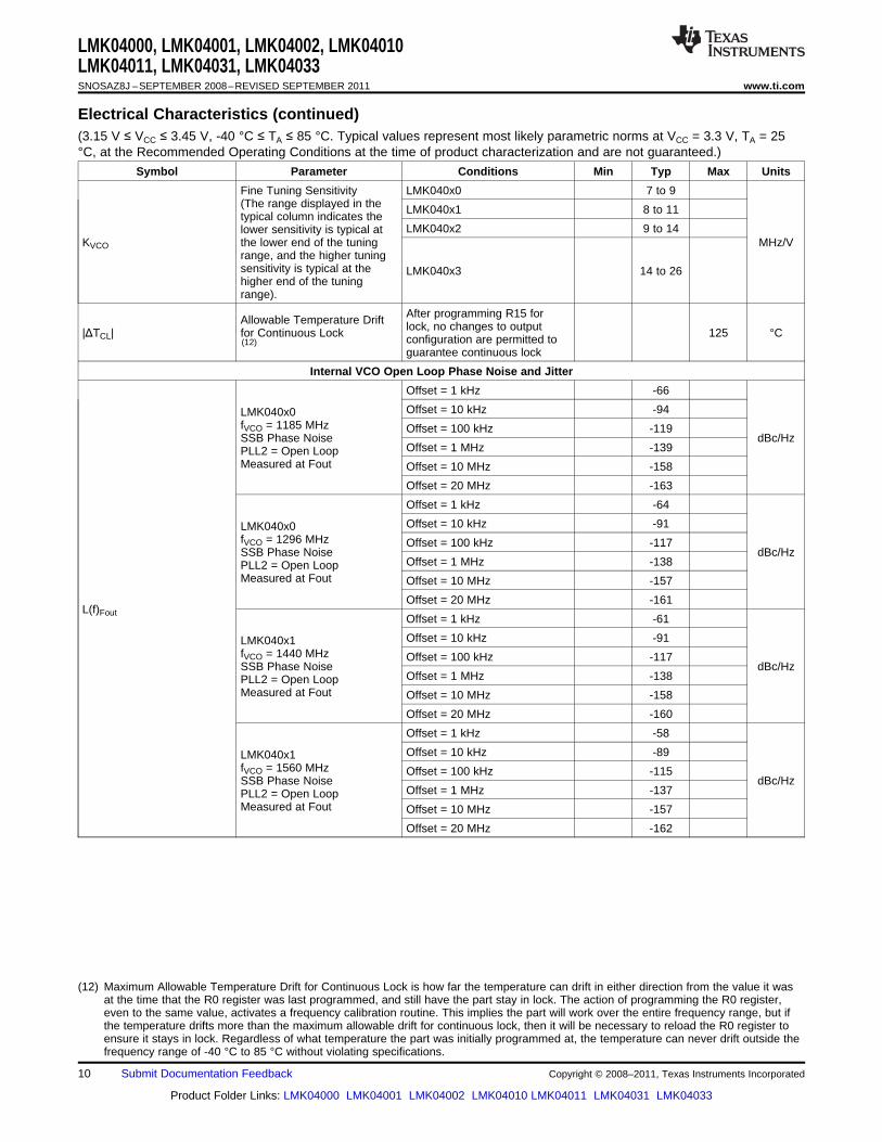
Internal VCO Open Loop Phase Noise and Jitter
Offset = 1 kHz -66
Offset = 10 kHz -94LMK040x0fVCO = 1185 MHz Offset = 100 kHz -119SSB Phase Noise dBc/Hz
Offset = 1 MHz -139PLL2 = Open LoopMeasured at Fout Offset = 10 MHz -158
Offset = 20 MHz -163
Offset = 1 kHz -64
Offset = 10 kHz -91LMK040x0fVCO = 1296 MHz Offset = 100 kHz -117SSB Phase Noise dBc/Hz
Offset = 1 MHz -138PLL2 = Open LoopMeasured at Fout Offset = 10 MHz -157
Offset = 20 MHz -161L(f)Fout
Offset = 1 kHz -61
Offset = 10 kHz -91LMK040x1fVCO = 1440 MHz Offset = 100 kHz -117SSB Phase Noise dBc/Hz
Offset = 1 MHz -138PLL2 = Open LoopMeasured at Fout Offset = 10 MHz -158
Offset = 20 MHz -160
Offset = 1 kHz -58
Offset = 10 kHz -89LMK040x1fVCO = 1560 MHz Offset = 100 kHz -115SSB Phase Noise dBc/Hz
Offset = 1 MHz -137PLL2 = Open LoopMeasured at Fout Offset = 10 MHz -157
Offset = 20 MHz -162
(12) Maximum Allowable Temperature Drift for Continuous Lock is how far the temperature can drift in either direction from the value it wasat the time that the R0 register was last programmed, and still have the part stay in lock. The action of programming the R0 register,even to the same value, activates a frequency calibration routine. This implies the part will work over the entire frequency range, but ifthe temperature drifts more than the maximum allowable drift for continuous lock, then it will be necessary to reload the R0 register toensure it stays in lock. Regardless of what temperature the part was initially programmed at, the temperature can never drift outside thefrequency range of -40 °C to 85 °C without violating specifications.
10 Submit Documentation Feedback Copyright © 2008–2011, Texas Instruments Incorporated
Product Folder Links: LMK04000 LMK04001 LMK04002 LMK04010 LMK04011 LMK04031 LMK04033

LMK04000, LMK04001, LMK04002, LMK04010LMK04011, LMK04031, LMK04033
www.ti.com SNOSAZ8J –SEPTEMBER 2008–REVISED SEPTEMBER 2011
Electrical Characteristics (continued)(3.15 V ≤ VCC ≤ 3.45 V, -40 °C ≤ TA ≤ 85 °C. Typical values represent most likely parametric norms at VCC = 3.3 V, TA = 25°C, at the Recommended Operating Conditions at the time of product characterization and are not guaranteed.)
Symbol Parameter Conditions Min Typ Max Units
Offset = 1 kHz -63
Offset = 10 kHz -91LMK040x2fVCO = 1600 MHz Offset = 100 kHz -115SSB Phase Noise dBc/Hz
Offset = 1 MHz -137PLL2 = Open LoopMeasured at Fout Offset = 10 MHz -156
Offset = 20 MHz -161
Offset = 1 kHz -61
Offset = 10 kHz -90LMK040x2fVCO = 1750 MHz Offset = 100 kHz -114SSB Phase Noise dBc/Hz
Offset = 1 MHz -136PLL2 = Open LoopMeasured at Fout Offset = 10 MHz -155
Offset = 20 MHz -160L(f)Fout
Offset = 1 kHz -58
Offset = 10 kHz -88LMK040x3fVCO = 1840 MHz Offset = 100 kHz -113SSB Phase Noise dBc/Hz
Offset = 1 MHz -135PLL2 = Open LoopMeasured at Fout Offset = 10 MHz -155
Offset = 20 MHz -158
Offset = 1 kHz -54
Offset = 10 kHz -84LMK040x3fVCO = 2160 MHz Offset = 100 kHz -110SSB Phase Noise dBc/Hz
Offset = 1 MHz -132PLL2 = Open LoopMeasured at Fout Offset = 10 MHz -154
Offset = 20 MHz -157
Copyright © 2008–2011, Texas Instruments Incorporated Submit Documentation Feedback 11
Product Folder Links: LMK04000 LMK04001 LMK04002 LMK04010 LMK04011 LMK04031 LMK04033

LMK04000, LMK04001, LMK04002, LMK04010LMK04011, LMK04031, LMK04033SNOSAZ8J –SEPTEMBER 2008–REVISED SEPTEMBER 2011 www.ti.com
Electrical Characteristics (continued)(3.15 V ≤ VCC ≤ 3.45 V, -40 °C ≤ TA ≤ 85 °C. Typical values represent most likely parametric norms at VCC = 3.3 V, TA = 25°C, at the Recommended Operating Conditions at the time of product characterization and are not guaranteed.)
Symbol Parameter Conditions Min Typ Max Units
Internal VCO Closed Loop Phase Noise and Jitter Specifications using an Instrumentation Quality VCXO
Offset = 1 kHz -111
Offset = 10kHz -119LMK040x0 (13)
Offset = 100 kHz -121fVCO = 1200 MHzSSB Phase Noise Offset = 1 MHz -133 dBc/HzPLL2 = Closed Loop Offset = 10 MHz -157Measured at Fout
Offset = 20 MHz -162
Offset = 40 MHz -165
Offset = 1 kHz -110
Offset = 10 kHz -117LMK040x1 (14)
Offset = 100 kHz -120fVCO = 1500 MHzSSB Phase Noise Offset = 1 MHz -132 dBc/HzPLL2 = Closed Loop Offset = 10 MHz -156Measured at Fout
Offset = 20 MHz -160
Offset = 40 MHz -163L(f)Fout
Offset = 1 kHz -111
Offset = 10 kHz -118LMK040x2 (15)
Offset = 100 kHz -120fVCO = 1600 MHzSSB Phase Noise Offset = 1 MHz -132 dBc/HzPLL2 = Closed Loop Offset = 10 MHz -156Measured at Fout
Offset = 20 MHz -162
Offset = 40 MHz -165
Offset = 1 kHz -107
Offset = 10 kHz -114LMK040x3 (16)
Offset = 100 kHz -117fVCO = 2000 MHzSSB Phase Noise Offset = 1 MHz -126 dBc/HzPLL2 = Closed Loop Offset = 10 MHz -152Measured at Fout
Offset = 20 MHz -156
Offset = 40 MHz -160
(13) For LMK040x0, fVCO = 1200 MHz. PLL1 is powered down. A 100 MHz Wenzel XO (model: 501-04623G) drives the OSCin input ofPLL2. PLL2 parameters: VCO_DIV = 3, N2 = 5, R2 = 1, FDET = 100 MHz, ICP2 = 1.6 mA, C1 = 22 pF, C2 = 5.6 nF, R2 = 1.8 kΩ, LBW =268 kHz, PM = 75°. Wenzel XO phase noise: 100 Hz: -132 dBc/Hz; 1 kHz: -147 dBc/Hz; 10 kHz: -159 dBc/Hz; 100 kHz: -167 dBc/Hz.
(14) For LMK040x1, fVCO = 1500 MHz. PLL1 is powered down. A 100 MHz Wenzel XO (model: 501-04623G) drives the OSCin input ofPLL2. PLL2 parameters: VCO_DIV = 3, N2 = 5, R2 = 1, FDET = 100 MHz, ICP2 = 1.6 mA, C1 = 22 pF, C2 = 5.6 nF, R2 = 1.8 kΩ, LBW =268 kHz, PM = 75°. Wenzel XO phase noise: 100 Hz: -132 dBc/Hz; 1 kHz: -147 dBc/Hz; 10 kHz: -159 dBc/Hz; 100 kHz: -167 dBc/Hz.
(15) For LMK040x2, fVCO = 1600 MHz. PLL1 is powered down. A 100 MHz Wenzel XO (model: 501-04623G) drives the OSCin input ofPLL2. PLL2 parameters: VCO_DIV = 2, N2 = 8, R2 = 1, FDET = 100 MHz, ICP2 = 1.6 mA, C1 = 22 pF, C2 = 5.6 nF, R2 = 1.8 kΩ, LBW =252 kHz, PM = 76°. Wenzel XO phase noise: 100 Hz: -132 dBc/Hz; 1 kHz: -147 dBc/Hz; 10 kHz: -159 dBc/Hz; 100 kHz: -167 dBc/Hz.
(16) For LMK040x3, fVCO = 2000 MHz. PLL1 is powered down. A 100 MHz Wenzel XO (model: 501-04623G) drives the OSCin input ofPLL2. PLL2 parameters: VCO_DIV = 2, N2 = 10, R2 = 1, FDET = 100 MHz, ICP2 = 1.6 mA, C1 = 22 pF, C2 = 5.6 nF, R2 = 1.8 kΩ, LBW= 434 kHz, PM = 69°. Wenzel XO phase noise: 100 Hz: -132 dBc/Hz; 1 kHz: -147 dBc/Hz; 10 kHz: -159 dBc/Hz; 100 kHz: -167 dBc/Hz.
12 Submit Documentation Feedback Copyright © 2008–2011, Texas Instruments Incorporated
Product Folder Links: LMK04000 LMK04001 LMK04002 LMK04010 LMK04011 LMK04031 LMK04033

LMK04000, LMK04001, LMK04002, LMK04010LMK04011, LMK04031, LMK04033
www.ti.com SNOSAZ8J –SEPTEMBER 2008–REVISED SEPTEMBER 2011
Electrical Characteristics (continued)(3.15 V ≤ VCC ≤ 3.45 V, -40 °C ≤ TA ≤ 85 °C. Typical values represent most likely parametric norms at VCC = 3.3 V, TA = 25°C, at the Recommended Operating Conditions at the time of product characterization and are not guaranteed.)
Symbol Parameter Conditions Min Typ Max Units
LMK040x0 (13) BW = 12 kHz to 20 MHz 105fVCO = 1200 MHz
BW = 100 Hz to 20 MHz 110Integrated RMS Jitter
LMK040x1 (14) BW = 12 kHz to 20 MHz 100fVCO = 1500 MHz
BW = 100 Hz to 20 MHz 105Integrated RMS JitterJFout fs
LMK040x2 (15) BW = 12 kHz to 20 MHz 95fVCO = 1600 MHz
BW = 100 Hz to 20 MHz 100Integrated RMS Jitter
LMK040x3 (16) BW = 12 kHz to 20 MHz 105fVCO = 2000 MHz
BW = 100 Hz to 20 MHz 110Integrated RMS Jitter
CLKout's Internal VCO Closed Loop Phase Noise and Jitter Specifications using an Instrumentation Quality VCXO
Offset = 1 kHz -125LMK040x0 (17)
fCLKout = 250 MHz Offset = 10 kHz -130SSB Phase Noise Offset = 100 kHz -132Measured at Clock Outputs
Offset = 1 MHz -148Value is average for all outputtypes Offset = 10 MHz -157
Offset = 1 kHz -126LMK040x1 (18)
fCLKout = 250 MHz Offset = 10 kHz -133SSB Phase Noise Offset = 100 kHz -136Measured at Clock Outputs
Offset = 1 MHz -147Value is average for all outputtypes Offset = 10 MHz -156
L(f)CLKout dBc/HzOffset = 1 kHz -127LMK040x2 (19)
fCLKout = 250 MHz Offset = 10 kHz -133SSB Phase Noise Offset = 100 kHz -134Measured at Clock Outputs
Offset = 1 MHz -145Value is average for all outputtypes Offset = 10 MHz -157
Offset = 1 kHz -125LMK040x3 (20)
fCLKout = 250 MHz Offset = 10 kHz -132SSB Phase Noise Offset = 100 kHz -135Measured at Clock Outputs
Offset = 1 MHz -145Value Is average for all outputtypes Offset = 10 MHz -156
(17) For LMK040x0, fVCO = 1250 MHz. PLL1 is powered down. A 100 MHz Wenzel XO (model: 501-04623G) drives the OSCin input ofPLL2. PLL2 parameters: VCO_DIV = 5, N2 = 5, R2 = 2, FDET = 50 MHz, ICP2 = 3.2 mA, C1 = 22 pF, C2 = 5.6 nF, R2 = 1.8 kΩ, LBW =251 kHz, PM = 76°. Wenzel XO phase noise: 100 Hz: -132 dBc/Hz; 1 kHz: -147 dBc/Hz; 10 kHz: -159 dBc/Hz; 100 kHz: -167 dBc/Hz.CLKoutX_DIV = Bypass. CLKout_DLY = OFF.
(18) For LMK040x1, fVCO = 1500 MHz. PLL1 is powered down. A 100 MHz Wenzel XO (model: 501-04623G) drives the OSCin input ofPLL2. PLL2 parameters: VCO_DIV = 3, N2 = 5, R2 = 1, FDET = 100 MHz, ICP2 = 1.6 mA, C1 = 22 pF, C2 = 5.6 nF, R2 = 1.8 kΩ, LBW =268 kHz, PM = 75°. Wenzel XO phase noise: 100 Hz: -132 dBc/Hz; 1 kHz: -147 dBc/Hz; 10 kHz: -159 dBc/Hz; 100 kHz: -167 dBc/Hz.CLKoutX_DIV = 2. CLKout_DLY = OFF.
(19) For LMK040x2, fVCO = 1750 MHz. PLL1 is powered down. A 100 MHz Wenzel XO (model: 501-04623G) drives the OSCin input ofPLL2. PLL2 parameters: VCO_DIV = 7, N2 = 5, R2 = 2, FDET = 50 MHz, ICP2 = 1.6 mA, C1 = 22 pF, C2 = 5.6 nF, R2 = 1.8 kΩ, LBW =354 kHz, PM = 73°. Wenzel XO phase noise: 100 Hz: -132 dBc/Hz; 1 kHz: -147 dBc/Hz; 10 kHz: -159 dBc/Hz; 100 kHz: -167 dBc/Hz.CLKoutX_DIV = Bypass. CLKout_DLY = OFF.
(20) For LMK040x3, fVCO = 2000 MHz. PLL1 is powered down. A 100 MHz Wenzel XO (model: 501-04623G) drives the OSCin input ofPLL2. PLL2 parameters: VCO_DIV = 2, N2 = 10, R2 = 1, FDET = 100 MHz, ICP2 = 1.6 mA, C1 = 22 pF, C2 = 5.6 nF, R2 = 1.8 kΩ, LBW= 434 kHz, PM = 69°. Wenzel XO phase noise: 100 Hz: -132 dBc/Hz; 1 kHz: -147 dBc/Hz; 10 kHz: -159 dBc/Hz; 100 kHz: -167 dBc/Hz.CLKoutX_DIV = 4. CLKout_DLY = OFF.
Copyright © 2008–2011, Texas Instruments Incorporated Submit Documentation Feedback 13
Product Folder Links: LMK04000 LMK04001 LMK04002 LMK04010 LMK04011 LMK04031 LMK04033

LMK04000, LMK04001, LMK04002, LMK04010LMK04011, LMK04031, LMK04033SNOSAZ8J –SEPTEMBER 2008–REVISED SEPTEMBER 2011 www.ti.com
Electrical Characteristics (continued)(3.15 V ≤ VCC ≤ 3.45 V, -40 °C ≤ TA ≤ 85 °C. Typical values represent most likely parametric norms at VCC = 3.3 V, TA = 25°C, at the Recommended Operating Conditions at the time of product characterization and are not guaranteed.)
Symbol Parameter Conditions Min Typ Max Units
LMK040x0 (21) BW = 12 kHz to 20 MHz 130fCLKout = 250 MHz
BW = 100 Hz to 20 MHz 135Integrated RMS Jitter
LMK040x1 (22) BW = 12 kHz to 20 MHz 115fCLKout = 250 MHz
BW = 100 Hz to 20 MHz 120Integrated RMS JitterJCLKout fsLVPECL/2VPECL/LVDS LMK040x2 (23) BW = 12 kHz to 20 MHz 130fCLKout = 250 MHz
BW = 100 Hz to 20 MHz 135Integrated RMS Jitter
LMK040x3 (24) BW = 12 kHz to 20 MHz 125fCLKout = 250 MHz
BW = 100 Hz to 20 MHz 130Integrated RMS Jitter
LMK040x0 (21) BW = 12 kHz to 20 MHz 140fCLKout = 250 MHz
BW = 100 Hz to 20 MHz 145Integrated RMS Jitter
LMK040x1 (22) BW = 12 kHz to 20 MHz 110fCLKout = 250 MHz
BW = 100 Hz to 20 MHz 115Integrated RMS JitterJCLKout fsLVCMOS LMK040x2 (23) BW = 12 kHz to 20 MHz 130fCLKout = 250 MHz
BW = 100 Hz to 20 MHz 135Integrated RMS Jitter
LMK040x3 (24) BW = 12 kHz to 20 MHz 120fCLKout = 250 MHz
BW = 100 Hz to 20 MHz 125Integrated RMS Jitter
CLKout's Internal VCO Closed Loop Jitter Specifications using a Commercial Quality VCXO
(21) For LMK040x0, fVCO = 1250 MHz. PLL1 is powered down. A 100 MHz Wenzel XO (model: 501-04623G) drives the OSCin input ofPLL2. PLL2 parameters: VCO_DIV = 5, N2 = 5, R2 = 2, FDET = 50 MHz, ICP2 = 3.2 mA, C1 = 22 pF, C2 = 5.6 nF, R2 = 1.8 kΩ, LBW =251 kHz, PM = 76°. Wenzel XO phase noise: 100 Hz: -132 dBc/Hz; 1 kHz: -147 dBc/Hz; 10 kHz: -159 dBc/Hz; 100 kHz: -167 dBc/Hz.CLKoutX_DIV = Bypass. CLKout_DLY = OFF.
(22) For LMK040x1, fVCO = 1500 MHz. PLL1 is powered down. A 100 MHz Wenzel XO (model: 501-04623G) drives the OSCin input ofPLL2. PLL2 parameters: VCO_DIV = 3, N2 = 5, R2 = 1, FDET = 100 MHz, ICP2 = 1.6 mA, C1 = 22 pF, C2 = 5.6 nF, R2 = 1.8 kΩ, LBW =268 kHz, PM = 75°. Wenzel XO phase noise: 100 Hz: -132 dBc/Hz; 1 kHz: -147 dBc/Hz; 10 kHz: -159 dBc/Hz; 100 kHz: -167 dBc/Hz.CLKoutX_DIV = 2. CLKout_DLY = OFF.
(23) For LMK040x2, fVCO = 1750 MHz. PLL1 is powered down. A 100 MHz Wenzel XO (model: 501-04623G) drives the OSCin input ofPLL2. PLL2 parameters: VCO_DIV = 7, N2 = 5, R2 = 2, FDET = 50 MHz, ICP2 = 1.6 mA, C1 = 22 pF, C2 = 5.6 nF, R2 = 1.8 kΩ, LBW =354 kHz, PM = 73°. Wenzel XO phase noise: 100 Hz: -132 dBc/Hz; 1 kHz: -147 dBc/Hz; 10 kHz: -159 dBc/Hz; 100 kHz: -167 dBc/Hz.CLKoutX_DIV = Bypass. CLKout_DLY = OFF.
(24) For LMK040x3, fVCO = 2000 MHz. PLL1 is powered down. A 100 MHz Wenzel XO (model: 501-04623G) drives the OSCin input ofPLL2. PLL2 parameters: VCO_DIV = 2, N2 = 10, R2 = 1, FDET = 100 MHz, ICP2 = 1.6 mA, C1 = 22 pF, C2 = 5.6 nF, R2 = 1.8 kΩ, LBW= 434 kHz, PM = 69°. Wenzel XO phase noise: 100 Hz: -132 dBc/Hz; 1 kHz: -147 dBc/Hz; 10 kHz: -159 dBc/Hz; 100 kHz: -167 dBc/Hz.CLKoutX_DIV = 4. CLKout_DLY = OFF.
14 Submit Documentation Feedback Copyright © 2008–2011, Texas Instruments Incorporated
Product Folder Links: LMK04000 LMK04001 LMK04002 LMK04010 LMK04011 LMK04031 LMK04033

LMK04000, LMK04001, LMK04002, LMK04010LMK04011, LMK04031, LMK04033
www.ti.com SNOSAZ8J –SEPTEMBER 2008–REVISED SEPTEMBER 2011
Electrical Characteristics (continued)(3.15 V ≤ VCC ≤ 3.45 V, -40 °C ≤ TA ≤ 85 °C. Typical values represent most likely parametric norms at VCC = 3.3 V, TA = 25°C, at the Recommended Operating Conditions at the time of product characterization and are not guaranteed.)
Symbol Parameter Conditions Min Typ Max Units
LMK040x0 (25) (26) BW = 12 kHz to 20 MHz 140 200fCLKout = 250 MHz
BW = 100 Hz to 20 MHz 185Integrated RMS Jitter
LMK040x1 (27) (26) BW = 12 kHz to 20 MHz 130 200fCLKout = 250 MHz
BW = 100 Hz to 20 MHz 190Integrated RMS JitterJCLKout fsLVPECL/2VPECL LMK040x2 (28) (26) BW = 12 kHz to 20 MHz 150 200fCLKout = 250 MHz
BW = 100 Hz to 20 MHz 190Integrated RMS Jitter
LMK040x3 (29) (26) BW = 12 kHz to 20 MHz 145 200fCLKout = 250 MHz
BW = 100 Hz to 20 MHz 200Integrated RMS Jitter
LMK040x1 (30) BW = 12 kHz to 20 MHz 130fCLKout = 250 MHz
BW = 100 Hz to 20 MHz 190Integrated RMS JitterJCLKout fsLVDS LMK040x3 (31) BW = 12 kHz to 20 MHz 145fCLKout = 250 MHz
BW = 100 Hz to 20 MHz 200Integrated RMS Jitter
(25) For LMK040x0, FVCO = 1250 MHz. PLL1 parameters: FDET = 1 MHz, ICP1 = 100 µA, loop bandwidth = 20 Hz. A 100 MHz VCXO drivesthe OSCin input of PLL2. PLL2 parameters: VCO_DIV = 5, N2 = 5, R2 = 2, FDET = 50 MHz, ICP2 = 3.2 mA, C1 = 0 pF, C2 = 12 nF, R2= 1.8 kΩ, LBW = 254 kHz, PM = 81°. CLKDIST parameters: CLKoutX_DIV = Bypass, CLKout_DLY = OFF. VCXO phase noise: 100 Hz:-100 dBc/Hz; 1 kHz: -128 dBc/Hz; 10 kHz: -144 dBc/Hz; 100 kHz: -147 dBc/Hz.
(26) Max jitter specification applies to CH3 (LVPECL) output and guaranteed by test in production.(27) For LMK040x1, FVCO = 1500 MHz. PLL1 parameters: FDET = 1 MHz, ICP1 = 100 µA, loop bandwidth = 20 Hz. A 100 MHz VCXO drives
the OSCin input of PLL2. PLL2 parameters: VCO_DIV = 3, N2 = 5, R2 = 1, FDET = 100 MHz, ICP2 = 1.6 mA, C1 = 0 pF, C2 = 12 nF, R2= 1.8 kΩ, LBW = 271 kHz, PM = 80°. CLKDIST parameters: CLKoutX_DIV = 2, CLKout_DLY = OFF. VCXO phase noise: 100 Hz: -100dBc/Hz; 1 kHz: -128 dBc/Hz; 10 kHz: -144 dBc/Hz; 100 kHz: -147 dBc/Hz.
(28) For LMK040x2, FVCO = 1750 MHz. PLL1 parameters: FDET = 1 MHz, ICP1 = 100 µA, loop bandwidth = 20 Hz. A 100 MHz VCXO drivesthe OSCin input of PLL2. PLL2 parameters: VCO_DIV = 7, N2 = 5, R2 = 2, FDET = 50 MHz, ICP2 = 3.2 mA, C1 = 0 pF, C2 = 12 nF, R2= 1.8 kΩ, LBW = 360 kHz, PM = 79°. CLKDIST parameters: CLKoutX_DIV = Bypass, CLKout_DLY = OFF. VCXO phase noise: 100 Hz:-100 dBc/Hz; 1 kHz: -128 dBc/Hz; 10 kHz: -144 dBc/Hz; 100 kHz: -147 dBc/Hz.
(29) For LMK040x3, FVCO = 2000 MHz. PLL1 parameters: FDET = 1 MHz, ICP1 = 100 µA, loop bandwidth = 20 Hz. A 100 MHz VCXO drivesthe OSCin input of PLL2. PLL2 parameters: VCO_DIV = 2, N2 = 10, R2 = 1, FDET = 100 MHz, ICP2 = 1.6 mA, C1 = 0 pF, C2 = 12 nF,R2 = 1.8 kΩ, LBW = 445 kHz, PM = 76°. CLKDIST parameters: CLKoutX_DIV = 4, CLKout_DLY = OFF. VCXO phase noise: 100 Hz: -100 dBc/Hz; 1 kHz: -128 dBc/Hz; 10 kHz: -144 dBc/Hz; 100 kHz: -147 dBc/Hz.
(30) For LMK040x1, FVCO = 1500 MHz. PLL1 parameters: FDET = 1 MHz, ICP1 = 100 µA, loop bandwidth = 20 Hz. A 100 MHz VCXO drivesthe OSCin input of PLL2. PLL2 parameters: VCO_DIV = 3, N2 = 5, R2 = 1, FDET = 100 MHz, ICP2 = 1.6 mA, C1 = 0 pF, C2 = 12 nF, R2= 1.8 kΩ, LBW = 271 kHz, PM = 80°. CLKDIST parameters: CLKoutX_DIV = 2, CLKout_DLY = OFF. VCXO phase noise: 100 Hz: -100dBc/Hz; 1 kHz: -128 dBc/Hz; 10 kHz: -144 dBc/Hz; 100 kHz: -147 dBc/Hz.
(31) For LMK040x3, FVCO = 2000 MHz. PLL1 parameters: FDET = 1 MHz, ICP1 = 100 µA, loop bandwidth = 20 Hz. A 100 MHz VCXO drivesthe OSCin input of PLL2. PLL2 parameters: VCO_DIV = 2, N2 = 10, R2 = 1, FDET = 100 MHz, ICP2 = 1.6 mA, C1 = 0 pF, C2 = 12 nF,R2 = 1.8 kΩ, LBW = 445 kHz, PM = 76°. CLKDIST parameters: CLKoutX_DIV = 4, CLKout_DLY = OFF. VCXO phase noise: 100 Hz: -100 dBc/Hz; 1 kHz: -128 dBc/Hz; 10 kHz: -144 dBc/Hz; 100 kHz: -147 dBc/Hz.
Copyright © 2008–2011, Texas Instruments Incorporated Submit Documentation Feedback 15
Product Folder Links: LMK04000 LMK04001 LMK04002 LMK04010 LMK04011 LMK04031 LMK04033

LMK04000, LMK04001, LMK04002, LMK04010LMK04011, LMK04031, LMK04033SNOSAZ8J –SEPTEMBER 2008–REVISED SEPTEMBER 2011 www.ti.com
Electrical Characteristics (continued)(3.15 V ≤ VCC ≤ 3.45 V, -40 °C ≤ TA ≤ 85 °C. Typical values represent most likely parametric norms at VCC = 3.3 V, TA = 25°C, at the Recommended Operating Conditions at the time of product characterization and are not guaranteed.)
Symbol Parameter Conditions Min Typ Max Units
LMK040x0 (32) BW = 12 kHz to 20 MHz 150fCLKout = 250 MHz
BW = 100 Hz to 20 MHz 190Integrated RMS Jitter
LMK040x1 (30) BW = 12 kHz to 20 MHz 125fCLKout = 250 MHz
BW = 100 Hz to 20 MHz 185Integrated RMS JitterJCLKout fsLVCMOS LMK040x2 (33) BW = 12 kHz to 20 MHz 150fCLKout = 250 MHz
BW = 100 Hz to 20 MHz 190Integrated RMS Jitter
LMK040x3 (31) BW = 12 kHz to 20 MHz 145fCLKout = 250 MHz
BW = 100 Hz to 20 MHz 195Integrated RMS Jitter
CLKout's Internal VCO Closed Loop Jitter Specifications using the Integrated Low Noise Crystal Oscillator Circuit
LMK040x0 (34) BW = 12 kHz to 20 MHz 190fCLKout = 245.76 MHz
BW = 100 Hz to 20 MHz 230Integrated RMS Jitter
LMK040x1 (35) BW = 12 kHz to 20 MHz 200fCLKout = 245.76 MHz
BW = 100 Hz to 20 MHz 230Integrated RMS JitterJCLKout fsLVPECL/2VPECL/LVDS LMK040x2 (36) BW = 12 kHz to 20 MHz 195fCLKout = 245.76 MHz
BW = 100 Hz to 20 MHz 230Integrated RMS Jitter
LMK040x3 (37) BW = 12 kHz to 20 MHz 245fCLKout = 245.76 MHz
BW = 100 Hz to 20 MHz 260Integrated RMS Jitter
(32) For LMK040x0, FVCO = 1250 MHz. PLL1 parameters: FDET = 1 MHz, ICP1 = 100 µA, loop bandwidth = 20 Hz. A 100 MHz VCXO drivesthe OSCin input of PLL2. PLL2 parameters: VCO_DIV = 5, N2 = 5, R2 = 2, FDET = 50 MHz, ICP2 = 3.2 mA, C1 = 0 pF, C2 = 12 nF, R2= 1.8 kΩ, LBW = 254 kHz, PM = 81°. CLKDIST parameters: CLKoutX_DIV = Bypass, CLKout_DLY = OFF. VCXO phase noise: 100 Hz:-100 dBc/Hz; 1 kHz: -128 dBc/Hz; 10 kHz: -144 dBc/Hz; 100 kHz: -147 dBc/Hz.
(33) For LMK040x2, FVCO = 1750 MHz. PLL1 parameters: FDET = 1 MHz, ICP1 = 100 µA, loop bandwidth = 20 Hz. A 100 MHz VCXO drivesthe OSCin input of PLL2. PLL2 parameters: VCO_DIV = 7, N2 = 5, R2 = 2, FDET = 50 MHz, ICP2 = 3.2 mA, C1 = 0 pF, C2 = 12 nF, R2= 1.8 kΩ, LBW = 360 kHz, PM = 79°. CLKDIST parameters: CLKoutX_DIV = Bypass, CLKout_DLY = OFF. VCXO phase noise: 100 Hz:-100 dBc/Hz; 1 kHz: -128 dBc/Hz; 10 kHz: -144 dBc/Hz; 100 kHz: -147 dBc/Hz.
(34) For LMK040x0, FVCO = 1228.8 MHz. PLL1 parameters: FDET = 1.024 MHz, ICP1 = 100 µA, loop bandwidth = 20 Hz. A 12.288 MHzVectron crystal (model: VXB1-1127-12M288000) and tuning circuitry is used with on-chip XO circuitry. PLL2 parameters: VCO_DIV = 5,N2 = 10, EN_PLL2_REF2X = 1, FDET = 24.576 MHz, ICP2 = 3.2 mA, C1 = 0 pF, C2 = 12 nF, R2 = 1.8 kΩ, R3 = 600 Ω, R4 = 10 kΩ, C3= 150 pF, C4 = 60 pF, LBW = 109 kHz, PM = 43°, CLKoutX_DIV = 2, CLKout_DLY = OFF.
(35) For LMK040x1, FVCO = 1474.56 MHz. PLL1 parameters: FDET = 1.024 MHz, ICP1 = 100 µA, loop bandwidth = 20 Hz. A 12.288 MHzEcliptek crystal (model: ECX-6465) and tuning circuitry is used with on-chip XO circuitry. PLL2 parameters: VCO_DIV = 3, N2 = 20,EN_PLL2_REF2X = 1, FDET = 24.576 MHz, ICP2 = 3.2 mA, C1 = 0 pF, C2 = 12 nF, R2 = 1.8 kΩ, R3 = 600 Ω, R4 = 10 kΩ, C3 = 150pF, C4 = 60 pF, LBW = 103 kHz, PM = 44°, CLKoutX_DIV = 2, CLKout_DLY = OFF.
(36) For LMK040x2, FVCO = 1720.32 MHz. PLL1 parameters: FDET = 1.024 MHz, ICP1 = 100 µA, loop bandwidth = 20 Hz. A 12.288 MHzVectron crystal (model: VXB1-1127-12M288000) and tuning circuitry is used with on-chip XO circuitry. PLL2 parameters: VCO_DIV = 7,N2 = 10, EN_PLL2_REF2X = 1, FDET = 24.576 MHz, ICP2 = 3.2 mA, C1 = 0 pF, C2 = 12 nF, R2 = 1.8 kΩ, R3 = 600 Ω, R4 = 10 kΩ, C3= 150 pF, C4 = 60 pF, LBW = 120 kHz, PM = 40°, CLKoutX_DIV = 2, CLKout_DLY = OFF.
(37) For LMK040x3, FVCO = 1966.08 MHz. PLL1 parameters: FDET = 1.024 MHz, ICP1 = 100 µA, loop bandwidth = 20 Hz. A 12.288 MHzEcliptek crystal (model: ECX-6465) and tuning circuitry is used with on-chip XO circuitry. PLL2 parameters: VCO_DIV = 4, N2 = 20,EN_PLL2_REF2X = 1, FDET = 24.576 MHz, ICP2 = 3.2 mA, C1 = 0 pF, C2 = 12 nF, R2 = 1.8 kΩ, R3 = 600 Ω, R4 = 10 kΩ, C3 = 150pF, C4 = 60 pF, LBW = 91 kHz, PM = 47°, CLKoutX_DIV = 2, CLKout_DLY = OFF.
16 Submit Documentation Feedback Copyright © 2008–2011, Texas Instruments Incorporated
Product Folder Links: LMK04000 LMK04001 LMK04002 LMK04010 LMK04011 LMK04031 LMK04033

LMK04000, LMK04001, LMK04002, LMK04010LMK04011, LMK04031, LMK04033
www.ti.com SNOSAZ8J –SEPTEMBER 2008–REVISED SEPTEMBER 2011
Electrical Characteristics (continued)(3.15 V ≤ VCC ≤ 3.45 V, -40 °C ≤ TA ≤ 85 °C. Typical values represent most likely parametric norms at VCC = 3.3 V, TA = 25°C, at the Recommended Operating Conditions at the time of product characterization and are not guaranteed.)
Symbol Parameter Conditions Min Typ Max Units
LMK040x0 (34) BW = 12 kHz to 20 MHz 195fCLKout = 245.76 MHz
BW = 100 Hz to 20 MHz 230Integrated RMS Jitter
LMK040x1 (35) BW = 12 kHz to 20 MHz 195fCLKout = 245.76 MHz
BW = 100 Hz to 20 MHz 220Integrated RMS JitterJCLKout fsLVCMOS LMK040x2 (36) BW = 12 kHz to 20 MHz 195fCLKout = 245.76 MHz
BW = 100 Hz to 20 MHz 230Integrated RMS Jitter
LMK040x3 (37) BW = 12 kHz to 20 MHz 240fCLKout = 245.76 MHz
BW = 100 Hz to 20 MHz 260Integrated RMS Jitter
Digital Inputs (CLKuWire, DATAuWire, LEuWire)
VIH High-Level Input Voltage 1.6 VCC V
VIL Low-Level Input Voltage 0.4 V
IIH High-Level Input Current VIH = VCC -5 25 µA
IIL Low-Level Input Current VIL = 0 -5.0 5.0 µA
Digital Inputs (GOE, SYNC*)
VIH High-Level Input Voltage 1.6 VCC V
VIL Low-Level Input Voltage 0.4 V
IIH High-Level Input Current VIH = VCC -5.0 5.0 µA
IIL Low-Level Input Current VIL = 0 -40.0 5.0 µA
Digital Outputs (CLKinX_LOS, LD)
VOH High-Level Output Voltage IOH = -500 µA VCC - 0.4 V
VOL Low-Level Output Voltage IOL = 500 µA 0.4 V
Default Power On Reset Clock Output Frequency
CLKout2, LM040x0 50
CLKout2, LM040x1 62Default output clock frequencyfCLKout-startup MHzat device power on CLKout2, LM040x2 68
CLKout2, LM040x3 81
LVDS Clock Outputs (CLKoutX)
Maximum FrequencyfCLKout RL = 100 Ω 1080 MHz(38)
CLKoutX to CLKoutY LVDS-LVDS, T = 25 °C,TSKEW 30 ps(39) FCLK = 800 MHz, RL= 100 ΩVOD Differential Output Voltage 250 350 450 mV
Change in Magnitude of VOD R = 100 Ω differentialΔVOD for complementary output -50 50 mVtermination, AC coupled to
states receiver input,FCLK = 800 MHz,VOS Output Offset Voltage 1.125 1.25 1.375 VT = 25 °C
Change in VOS forΔVOS 35 |mV|complementary output states
ISA Output short circuit current - Single-ended output shorted to -24 24 mAISB single ended GND, T = 25 °C
Output short circuit current - Complimentary outputs tiedISAB -12 12 mAdifferential together
LVPECL Clock Outputs (CLKoutX) (40)
(38) For Clock output frequencies > 1 GHz, the maximum allowable clock delay is limited to ½ of a period, or, 0.5/FCLKoutX.(39) Equal loading and identical channel configuration on each channel is required for specification to be valid. Specification not valid for
delay mode.(40) LVPECL/2VPECL is programmable for all NSIDs.
Copyright © 2008–2011, Texas Instruments Incorporated Submit Documentation Feedback 17
Product Folder Links: LMK04000 LMK04001 LMK04002 LMK04010 LMK04011 LMK04031 LMK04033

LMK04000, LMK04001, LMK04002, LMK04010LMK04011, LMK04031, LMK04033SNOSAZ8J –SEPTEMBER 2008–REVISED SEPTEMBER 2011 www.ti.com
Electrical Characteristics (continued)(3.15 V ≤ VCC ≤ 3.45 V, -40 °C ≤ TA ≤ 85 °C. Typical values represent most likely parametric norms at VCC = 3.3 V, TA = 25°C, at the Recommended Operating Conditions at the time of product characterization and are not guaranteed.)
Symbol Parameter Conditions Min Typ Max Units
Maximum FrequencyfCLKout 1080 MHz(41)
LVPECL-to-LVPECL,CLKoutX to CLKoutY T = 25 °C, FCLK = 800 MHz,TSKEW 40 ps(42) each output terminated with
120 Ω to GND.
VCC -VOH Output High Voltage V0.93FCLK = 100 MHz, T = 25 °CTermination = 50 Ω to VCC -VOL Output Low Voltage VVCC - 2 V 1.82
VOD Output Voltage 660 890 965 mV
2VPECL Clock Outputs (CLKoutX)
Maximum FrequencyfCLKout 1080 MHz(41)
2VPECL-2VPECL, T=25 °C,CLKoutX to CLKoutYTSKEW FCLK = 800 MHz, each output 40 ps(42)terminated with 120 Ω to GND.
VCC -VOH Output High Voltage V0.95FCLK = 100 MHz, T = 25 °CTermination = 50 Ω to VCC -VOL Output Low Voltage VVCC - 2 V 1.98
VOD Output Voltage 800 1030 1200 mV
LVCMOS Clock Outputs (CLKoutX)
fCLKout Maximum Frequency 5 pF Load 250 MHz
VOH Output High Voltage 1 mA Load VCC - 0.1 V
VOL Output Low Voltage 1 mA Load 0.1 V
IOH Output High Current (Source) VCC = 3.3 V, VO = 1.65 V 28 mA
IOL Output Low Current (Sink) VCC = 3.3 V, VO = 1.65 V 28 mA
Skew between any two RL = 50 Ω, CL = 10 pF,TSKEW LVCMOS outputs, same T = 25 °C, FCLK = 100 MHz. 100 ps
channel or different channel (43)
VCC/2 to VCC/2, FCLK = 100DUTYCLK Output Duty Cycle 45 50 55 %MHz, T = 25 °C (44)
20% to 80%, RL = 50 Ω,TR Output Rise Time 400 psCL = 5 pF
80% to 20%, RL = 50 Ω,TF Output Fall Time 400 psCL = 5 pF
Mixed Clock Skew
Same device, T = 25 °C,LVPECL to LVDS skew -230 ps250 MHz
Same device, T = 25 °C,TSKEW ChanX - ChanY LVDS to LVCMOS skew 770 ps250 MHz
Same device, T = 25 °C,LVCMOS to LVPECL skew -540 ps250 MHz
Microwire Interface Timing
TCS Data to Clock Set Up Time See Microwire Input Timing 25 ns
TCH Data to Clock Hold Time See Microwire Input Timing 8 ns
(41) For Clock output frequencies > 1 GHz, the maximum allowable clock delay is limited to ½ of a period, or, 0.5/FCLKoutX.(42) Equal loading and identical channel configuration on each channel is required for specification to be valid. Specification not valid for
delay mode.(43) Equal loading and identical channel configuration on each channel is required for specification to be valid. Specification not valid for
delay mode.(44) Guaranteed by characterization.
18 Submit Documentation Feedback Copyright © 2008–2011, Texas Instruments Incorporated
Product Folder Links: LMK04000 LMK04001 LMK04002 LMK04010 LMK04011 LMK04031 LMK04033

tCEStCS
D27 D26 D25 D24
tCHtCWH
tCWL
D23 D0 A3 A2 A1 A0
MSB LSB
DATAuWire
CLKuWire
LEuWire
tES
tEWH
LMK04000, LMK04001, LMK04002, LMK04010LMK04011, LMK04031, LMK04033
www.ti.com SNOSAZ8J –SEPTEMBER 2008–REVISED SEPTEMBER 2011
Electrical Characteristics (continued)(3.15 V ≤ VCC ≤ 3.45 V, -40 °C ≤ TA ≤ 85 °C. Typical values represent most likely parametric norms at VCC = 3.3 V, TA = 25°C, at the Recommended Operating Conditions at the time of product characterization and are not guaranteed.)
Symbol Parameter Conditions Min Typ Max Units
TCWH Clock Pulse Width High See Microwire Input Timing 25 ns
TCWL Clock Pulse Width Low See Microwire Input Timing 25 ns
Clock to Latch EnableTES See Microwire Input Timing 25 nsSet Up Time
TCES Clock to Enable Setup Time See Microwire Input Timing 25 ns
TEW Load Enable Pulse Width See Microwire Input Timing 25 ns
Serial Data Timing Diagram
Register programming information on the DATAuWire pin is clocked into a shift register on each rising edge ofthe CLKuWire signal. On the rising edge of the LEuWire signal, the register is sent from the shift register to theregister addressed. A slew rate of at least 30 V/µs is recommended for these signals. After programming iscomplete the CLKuWire, DATAuWire, and LEuWire signals should be returned to a low state. If the CLKuWire orDATAuWire lines are toggled while the VCO is in lock, as is sometimes the case when these lines are sharedwith other parts, the phase noise may be degraded during this programming.
Charge Pump Current Specification Definitions
I1 = Charge Pump Sink Current at VCPout = VCC - ΔV
I2 = Charge Pump Sink Current at VCPout = VCC/2
Copyright © 2008–2011, Texas Instruments Incorporated Submit Documentation Feedback 19
Product Folder Links: LMK04000 LMK04001 LMK04002 LMK04010 LMK04011 LMK04031 LMK04033

LMK04000, LMK04001, LMK04002, LMK04010LMK04011, LMK04031, LMK04033SNOSAZ8J –SEPTEMBER 2008–REVISED SEPTEMBER 2011 www.ti.com
I3 = Charge Pump Sink Current at VCPout = ΔV
I4 = Charge Pump Source Current at VCPout = VCC - ΔV
I5 = Charge Pump Source Current at VCPout = VCC/2
I6 = Charge Pump Source Current at VCPout = ΔV
ΔV = Voltage offset from the positive and negative supply rails. Defined to be 0.5 V for this device.
Charge Pump Output Current Magnitude Variation vs. Charge Pump Output Voltage
Charge Pump Sink Current vs. Charge Pump Output Source Current Mismatch
Charge Pump Output Current Magnitude Variation vs. Temperature
20 Submit Documentation Feedback Copyright © 2008–2011, Texas Instruments Incorporated
Product Folder Links: LMK04000 LMK04001 LMK04002 LMK04010 LMK04011 LMK04031 LMK04033

FREQUENCY (MHz)
NO
ISE
FLO
OR
(dB
c/H
z)
-130-135-140-145-150-155-160-165-170
10 100 1000
Delay = 0 ps
Delay = 450 ps
Delay = 1800 ps
Delay = 900 ps
Delay = 2100 ps
FREQUENCY (MHz)
NO
ISE
FLO
OR
(dB
c/H
z)
-130-135-140-145-150-155-160-165-170
10 100 1000
LVCMOS
LVDS (differential)
LVPECL (differential)
FREQUENCY (MHz)
SIN
GLE
-EN
DE
D P
-P V
OLT
AG
E (V
) 5
4
3
2
1
0
0 100 200 300 400 500
No Load
47 pF Load
22 pF Load10 pF Load
100 pF Load
FREQUENCY (MHz)
ICC
(mA
)
40353025201510
50
0 50 100 150 200 250 300 350 400
FREQUENCY (MHz)
DIF
FE
RE
NT
IAL
P-P
VO
LTA
GE
(V
)
1.0
0.9
0.8
0.7
0.6
0.5
0.4
0.3
0.2
0.1
0.00 300 600 900 1.2k 1.5k 1.8k
FREQUENCY (MHz)
DIF
FE
RE
NT
IAL
P-P
VO
LTA
GE
(V
)
2.5
2.0
1.5
1.0
0.5
0.00 400 800 1.2k 1.6k 2k
NORMAL Mode
LV2PECL Mode
LMK04000, LMK04001, LMK04002, LMK04010LMK04011, LMK04031, LMK04033
www.ti.com SNOSAZ8J –SEPTEMBER 2008–REVISED SEPTEMBER 2011
Typical Performance Characteristics
Clock Output AC Characteristics
LVDS VOD LVPECL VODvs. vs.
Frequency Frequency
Figure 2. Figure 3.
LVCMOS Vppvs. Typical Dynamic ICC, LVCMOS Driver, VCC = 3.3 V,
Frequency Temp = 25 °C, CL= 5 pF
Figure 4. Figure 5.
Clock Channel Delay Noise Floor Clock Output Noise Floorvs. vs.
Frequency Frequency
Figure 6. Figure 7.
To estimate this noise, only the output frequency is required. Divide value and input frequency are not relevant.
Copyright © 2008–2011, Texas Instruments Incorporated Submit Documentation Feedback 21
Product Folder Links: LMK04000 LMK04001 LMK04002 LMK04010 LMK04011 LMK04031 LMK04033

100 1000 10000 100000
OFFSET (Hz)
-170
-160
-150
-140
-130
-120
-110
-100
-90
-80
dBc
1000000 10000000 100000000
100 1000 10000 100000
OFFSET (Hz)
-170
-160
-150
-140
-130
-120
-110
-100
-90
-80dB
c
1000000 10000000 100000000
LMK04000, LMK04001, LMK04002, LMK04010LMK04011, LMK04031, LMK04033SNOSAZ8J –SEPTEMBER 2008–REVISED SEPTEMBER 2011 www.ti.com
Typical Performance Characteristics (continued)The noise of the delay block is independent of output type and only applies if the delay is enabled. The noise floor,due to the distribution section accounting for the delay noise, can be calculated as: Total Output Noise = 10 xlog(10Output Buffer Noise/10 + 10Delay Noise Floor/10).
Typical LVDS Phase Noise, FCLK = 250 MHz, RMS Jitter = 192 fs (100 Hz to 20 MHz)
Figure 8.
Typical LVPECL Phase Noise, FCLK = 250 MHz, RMS Jitter = 196 fs (100 Hz to 20 MHz)
Figure 9.
Reference clock = 10 MHz, PLL1_R = 10, PLL1_N = 100, PLL1_CP_GAIN = 100 µA, PLL1 Loop BW = 20 Hz, VCXO= 100 MHz Crystek CVPD-920-100, PLL2_R = 2, PLL2_N = 10, PLL2_CP_GAIN = 1600 µA, PLL2 Loop BW = 137kHz, fVCO = 1500 MHz, VCO_DIV = 3, CLKoutX_DIV = 2, CLK_DLY = OFF.
22 Submit Documentation Feedback Copyright © 2008–2011, Texas Instruments Incorporated
Product Folder Links: LMK04000 LMK04001 LMK04002 LMK04010 LMK04011 LMK04031 LMK04033

100 1000 10000 100000
OFFSET (Hz)
-170
-160
-150
-140
-130
-120
-110
-100
-90
-80
dBc
1000000 10000000 100000000
LMK04000, LMK04001, LMK04002, LMK04010LMK04011, LMK04031, LMK04033
www.ti.com SNOSAZ8J –SEPTEMBER 2008–REVISED SEPTEMBER 2011
Typical Performance Characteristics (continued)Typical LVCMOS Phase Noise, FCLK = 250 MHz, RMS Jitter = 188 fs (100 Hz to 20 MHz)
Figure 10.
Copyright © 2008–2011, Texas Instruments Incorporated Submit Documentation Feedback 23
Product Folder Links: LMK04000 LMK04001 LMK04002 LMK04010 LMK04011 LMK04031 LMK04033

LMK04000, LMK04001, LMK04002, LMK04010LMK04011, LMK04031, LMK04033SNOSAZ8J –SEPTEMBER 2008–REVISED SEPTEMBER 2011 www.ti.com
FEATURES
System Architecture
The cascaded PLL architecture of the LMK040xx was chosen to provide the lowest jitter performance over thewidest range of output frequencies and phase noise offset frequencies. The first stage PLL (PLL1) is used inconjunction with an external reference clock and an external VCXO to provide a frequency accurate, low phasenoise reference clock for the second stage frequency multiplication PLL (PLL2). PLL1 typically uses a narrowloop bandwidth (10 Hz to 200 Hz) to retain the frequency accuracy of the reference clock input signal while at thesame time suppressing the higher offset frequency phase noise that the reference clock may have accumulatedalong its path or from other circuits. The “cleaned” reference clock frequency accuracy is combined with the lowphase noise of an external VCXO to provide the reference input to PLL2. The low phase noise referenceprovided to PLL2 allows it to use wider loop bandwidths (50 kHz to 200 kHz). The chosen loop bandwidth forPLL2 should take best advantage of the superior high offset frequency phase noise profile of the internal VCOand the good low offset frequency phase noise of the reference VCXO for PLL2. Ultra low jitter is achieved byallowing the external VCXO’s phase noise to dominate the final output phase noise at low offset frequencies andthe internal VCO’s phase noise to dominate the final output phase noise at high offset frequencies. This results inbest overall phase noise and jitter performance.
Redundant Reference Inputs (CLKin0/CLKin0*, CLKin1/CLKin1*)
The LMK040xx has two LVDS/LVPECL/LVCMOS compatible reference clock inputs for PLL1, CLKin0 andCLKin1. The selection of the preferred input may be fixed to either CLKin0 or CLKin1, or may be configured toemploy one of two automatic switching modes when redundant clock signals are present. The PLL1 referenceclock input buffers may also be individually configured as either a CMOS buffered input or a bipolar bufferedinput.
PLL1 CLKinX (X=0,1) LOSS OF SIGNAL (LOS)
When either of the two auto-switching modes is selected for the reference clock input mode, the signal status ofthe selected reference clock input is indicated by the state of the CLKinX_LOS (loss-of-signal) output. Theseoutputs may be configured as either CMOS (active HIGH on loss-of-signal), NMOS open-drain or PMOS open-drain. If PLL1 was originally locked and then both reference clocks go away, then the frequency accuracy of theLMK04000 device will be set by the absolute tuning range of the VCXO used on PLL1. The absolute tuningrange of the VCXO can be determined by multiplying its' tuning constant by the charge pump voltage.
Integrated Loop Filter Poles
The LMK040xx features programmable 3rd and 4th order loop filter poles for PLL2. When enabled, internalresistors and capacitor values may be selected from a fixed range of values to achieve either 3rd or 4th orderloop filter response. These programmable components compliment external components mounted near the chip.
Clock Distribution
The LMK040xx features a clock distribution block with a minimum of five outputs that are a mixture of LVPECL,2VPECL, LVDS, and LVCMOS. The exact combination is determined by the part number. The 2VPECL is aNational Semiconductor proprietary configuration that produces a 2 Vpp differential swing for compatibility withmany data converters. More than five outputs may be available for device versions that offer dual LVCMOSoutputs.
CLKout Divide (CLKoutX_DIV, X = 0 to 4)
Each individual clock distribution channel includes a channel divider. The range of divide values is 2 to 510, insteps of 2. “Bypass” mode operates as a divide-by-1.
CLKout Delay (CLKoutX_DLY, X = 0 to 4)
Each individual clock distribution channel includes a delay adjustment. Clock output delay registers(CLKoutX_DLY) support a nominal 150 ps step size and range from 0 to 2250 ps of total delay.
24 Submit Documentation Feedback Copyright © 2008–2011, Texas Instruments Incorporated
Product Folder Links: LMK04000 LMK04001 LMK04002 LMK04010 LMK04011 LMK04031 LMK04033
DistributionPath
SYNC*
CLKout0
CLKout1
CLKout2
LMK04000, LMK04001, LMK04002, LMK04010LMK04011, LMK04031, LMK04033
www.ti.com SNOSAZ8J –SEPTEMBER 2008–REVISED SEPTEMBER 2011
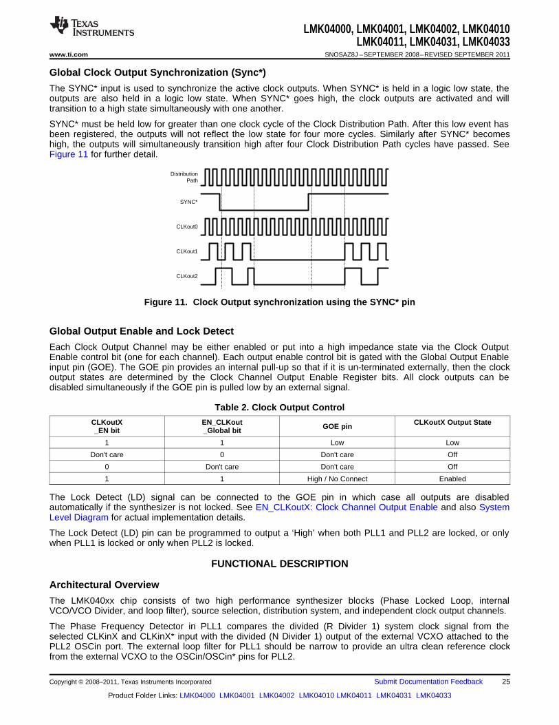
Global Clock Output Synchronization (Sync*)
The SYNC* input is used to synchronize the active clock outputs. When SYNC* is held in a logic low state, theoutputs are also held in a logic low state. When SYNC* goes high, the clock outputs are activated and willtransition to a high state simultaneously with one another.
SYNC* must be held low for greater than one clock cycle of the Clock Distribution Path. After this low event hasbeen registered, the outputs will not reflect the low state for four more cycles. Similarly after SYNC* becomeshigh, the outputs will simultaneously transition high after four Clock Distribution Path cycles have passed. SeeFigure 11 for further detail.
Figure 11. Clock Output synchronization using the SYNC* pin
Global Output Enable and Lock Detect
Each Clock Output Channel may be either enabled or put into a high impedance state via the Clock OutputEnable control bit (one for each channel). Each output enable control bit is gated with the Global Output Enableinput pin (GOE). The GOE pin provides an internal pull-up so that if it is un-terminated externally, then the clockoutput states are determined by the Clock Channel Output Enable Register bits. All clock outputs can bedisabled simultaneously if the GOE pin is pulled low by an external signal.
Table 2. Clock Output Control
CLKoutX EN_CLKout CLKoutX Output StateGOE pin_EN bit _Global bit
1 1 Low Low
Don't care 0 Don't care Off
0 Don't care Don't care Off
1 1 High / No Connect Enabled
The Lock Detect (LD) signal can be connected to the GOE pin in which case all outputs are disabledautomatically if the synthesizer is not locked. See EN_CLKoutX: Clock Channel Output Enable and also SystemLevel Diagram for actual implementation details.
The Lock Detect (LD) pin can be programmed to output a ‘High’ when both PLL1 and PLL2 are locked, or onlywhen PLL1 is locked or only when PLL2 is locked.
FUNCTIONAL DESCRIPTION
Architectural Overview
The LMK040xx chip consists of two high performance synthesizer blocks (Phase Locked Loop, internalVCO/VCO Divider, and loop filter), source selection, distribution system, and independent clock output channels.
The Phase Frequency Detector in PLL1 compares the divided (R Divider 1) system clock signal from theselected CLKinX and CLKinX* input with the divided (N Divider 1) output of the external VCXO attached to thePLL2 OSCin port. The external loop filter for PLL1 should be narrow to provide an ultra clean reference clockfrom the external VCXO to the OSCin/OSCin* pins for PLL2.
Copyright © 2008–2011, Texas Instruments Incorporated Submit Documentation Feedback 25
Product Folder Links: LMK04000 LMK04001 LMK04002 LMK04010 LMK04011 LMK04031 LMK04033

LMK04000, LMK04001, LMK04002, LMK04010LMK04011, LMK04031, LMK04033SNOSAZ8J –SEPTEMBER 2008–REVISED SEPTEMBER 2011 www.ti.com
The Phase Frequency Detector in PLL2 then compares the divided (R Divider 2) reference signal from the PLL2OSCin port with the divided (N Divider 2 and VCO Divider) output of the internal VCO. The bandwidth of theexternal loop filter for PLL2 should be designed to be wide enough to take advantage of the low in-band phasenoise of PLL2 and the low high offset phase noise of the internal VCO. The VCO output is passed through acommon VCO divider block and placed on a distribution path for the clock distribution section. It is also routed tothe PLL2_N counter. Each clock output channel allows the user to select a path with a programmable dividerblock, a phase synchronization circuit, a programmable delay, and LVDS/LVPECL/2VPECL/LVCMOS compatibleoutput buffers.
Phase Detector 1 (PD1)
Phase Detector 1 in PLL1 (PD1) can operate up to 40 MHz. Since a narrow loop bandwidth should be used forPLL1, the need to operate at high phase detector rate to lower the in-band phase noise becomes unnecessary.
Phase Detector 2 (PD2)
Phase Detector 2 in PLL2 (PD2) supports a maximum comparison rate of 100 MHz, though the actual maximumfrequency at the input port (PLL2 OSCin/OSCin*) is 250 MHz. Operating at highest possible phase detector ratewill ensure low in-band phase noise for PLL2 which in turn produces lower total jitter, as the in-band phase noisefrom the reference input and PLL are proportional to N2.
PLL2 Frequency Doubler
The PLL2 reference input at the OSCin port may be optionally routed through a frequency doubler function ratherthan through the PLL2_R counter. The maximum phase comparison frequency of the PLL2 phase detector is 100MHz, so the input to the frequency doubler is limited to a maximum of 50 MHz. The frequency doubler featureallows the phase comparison frequency to be increased when a relative low frequency oscillator is driving theOSCin port. By doubling the PLL2 phase comparison frequency, the in-band PLL2 noise is reduced by about 3dB.
Inputs / Outputs
PLL1 Reference Inputs (CLKin0 / CLKin0*, CLKin1 / CLKin1*)
The reference clock inputs for PLL1 may be selected from either CLKin0 and CLKin1. The user has the capabilityto manually select one of the two inputs or to configure an automatic switching mode operation. A detaileddescription of this function is described in the uWire programming section of this data sheet.
PLL2 OSCin / OSCin* Port
The feedback from the external oscillator being locked with PLL1 is injected to the PLL2 OSCin/OSCin* pins.This input may be driven with either a single- ended or differential signal. If operated in single ended mode, theunused input should be tied to GND with a 0.1 µF capacitor. Either AC or DC coupling is acceptable. Internal tothe chip, this signal is routed to the PLL1_N Counter and to the reference input for PLL2. The internal circuitry ofthe OSCin port also supports the optional implementation of a crystal based oscillator circuit. A crystal, varactordiode and a small number of other external components may be used to implement the oscillator. The internaloscillator circuit is enabled by setting the EN_PLL2_XTAL bit.
CPout1 / CPout2
The CPout1 pin provides the charge pump current output to drive the loop filter for PLL1. This loop filter shouldbe configured so that the total loop bandwidth for PLL1 is less than 200 Hz. When combined with an externaloscillator that has low phase noise at offsets close to the carrier, PLL1 generates a reference for PLL2 that isfrequency locked to the PLL1 reference clock but has the phase noise performance of the oscillator. The CPout2pin provides the charge pump current output to drive the loop filter for PLL2. This loop filter should be configuredso that the total loop bandwidth for PLL2 is in the range of 50 kHz to 200 kHz. See the section on uWire devicecontrol for a description of the charge pump current gain control.
26 Submit Documentation Feedback Copyright © 2008–2011, Texas Instruments Incorporated
Product Folder Links: LMK04000 LMK04001 LMK04002 LMK04010 LMK04011 LMK04031 LMK04033

tCEStCS
D27 D26 D25 D24
tCHtCWH
tCWL
D23 D0 A3 A2 A1 A0
MSB LSB
DATAuWire
CLKuWire
LEuWire
tES
tEWH
LMK04000, LMK04001, LMK04002, LMK04010LMK04011, LMK04031, LMK04033
www.ti.com SNOSAZ8J –SEPTEMBER 2008–REVISED SEPTEMBER 2011
Fout
The buffered output of the internal VCO is available at the Fout pin. This is a single-ended output (sinusoid).Each time the PLL2_N counter value is updated via the uWire interface, an internal algorithm is triggered thatoptimizes the VCO performance.
Digital Lock Detect 1 Bypass
The VCO coarse tuning algorithm requires a stable OSCin clock (reference clock to PLL2) to frequency calibratethe internal VCO correctly. In order to ensure a stable OSCin clock, the first PLL must achieve lock status. Adigital lock detect is used in PLL1 to monitor its lock status. After lock is achieved by PLL1, the coarse tuningcircuitry is enabled and frequency calibration for the internal VCO begins.
The (DLD_BYP) pin is provided to allow an external bypass cap to be connected to the digital lock detect 1. Thiscapacitor will eliminate potential glitches at initial startup of PLL1 due to unknown phase relationships betweenthe Ncntr1 and Rcntr1.
Bias
Proper bypassing of this pin by a 1 µF capacitor connected to VCC is important for low noise performance.
General Programming Information
LMK040xx devices are programmed using several 32-bit registers. Each register consists of a 4-bit address fieldand 28-bit data field. The address field is formed by bits 0 through 3 (LSBs) and the data field is formed by bits 4through 31 (MSBs). The contents of each register are clocked in MSB first (bit 31), and the LSB (bit 0) last.During programming, the LE signal should be held LOW. The serial data is clocked in on the rising edge of theCLK signal. After the LSB (bit 0) is clocked in the LE signal should be toggled LOW-to-HIGH-to-LOW to latch thecontents into the register selected in the address field. Registers R0-R4, R7, and R8-R15 must be programmedin order to achieve proper device operation. Figure 12 illustrates the serial data timing sequence.
Figure 12. uWire Timing Diagram
To achieve proper frequency calibration, the OSCin port must be driven with a valid signal before programmingRegister 15. Changes to PLL2_R Counter or the OSCin port signal require Register 15 to be reloaded in order toactivate the frequency calibration process.
Recommended Programming Sequence
The recommended programming sequence involves programming R7 with the reset bit set to 1 (Reg. 7, bit 4) toensure the device is in a default state. If R7 is programmed again, the reset bit should be set to 0. Registers areprogrammed in order with R15 being the last register programmed. An example programming sequence isshown below:• Program R7 with the RESET bit = 1 (b4 = 1). This ensures that the device is configured with default settings.
When RESET = 1, all other R7 bits are ignored.– - If R7 is programmed again during the initial configuration of the device, the RESET bit should be cleared
(b4 = 0)• Program R0 through R4 as necessary to configure the clock outputs as desired. These registers configure
clock channel functions such as the channel multiplexer output selection, divide value, delay value, andenable/disable bit.
Copyright © 2008–2011, Texas Instruments Incorporated Submit Documentation Feedback 27
Product Folder Links: LMK04000 LMK04001 LMK04002 LMK04010 LMK04011 LMK04031 LMK04033

LMK04000, LMK04001, LMK04002, LMK04010LMK04011, LMK04031, LMK04033SNOSAZ8J –SEPTEMBER 2008–REVISED SEPTEMBER 2011 www.ti.com
• Program R5 and R6 with the default values shown in the register map on the following pages.• Program R7 with RESET = 0.• Program R8 through R10 with the default values shown in the register map on the following pages.• Program R11 to configure the reference clock inputs (CLKin0 and CLKin1).
– - type, LOS timeout, LOS type, and mode (manual or auto-switching)• Program R12 to configure PLL1.
– - Charge pump gain, polarity, R counter and N counter• Program R13 through R15 to configure PLL2 parameters, crystal mode options, and certain globally asserted
functions.
The following table provides the register map for device programming:
28 Submit Documentation Feedback Copyright © 2008–2011, Texas Instruments Incorporated
Product Folder Links: LMK04000 LMK04001 LMK04002 LMK04010 LMK04011 LMK04031 LMK04033

LMK04000, LMK04001, LMK04002, LMK04010LMK04011, LMK04031, LMK04033
www.ti.com SNOSAZ8J –SEPTEMBER 2008–REVISED SEPTEMBER 2011
Table 3. Register Map 31-16
Register 31 30 29 28 27 26 25 24 23 22 21 20 19 18 17 16
Data [31:16]
CLKout0 EN_CLKR0 0 0 0 0 0 0 0 1 _PECL_ 0 0 0 0 CLKout0_MUX out0LVL
CLKout1 CLKout1B_STATE CLKout1A_STATE EN_CLKR1 0 0 0 0 0 0 0 1 _PECL_ CLKout1_MUX [1:0][1:0] [1:0] out1LVL
CLKout2 CLKout2B_STATE CLKout2A_STATE EN_CLKR2 0 0 0 0 0 0 0 1 _PECL_ CLKout2_MUX [1:0][1:0] [1:0] out2LVL
CLKout3 CLKout3B_STATE CLKout3A_STATE EN_CLKR3 0 0 0 0 0 0 0 1 _PECL_ CLKout3_MUX [1:0][1:0] [1:0] out3LVL
CLKout4 EN_CLKR4 0 0 0 0 0 0 0 1 _PECL_ 0 0 0 0 CLKout4_MUX [1:0] out4LVL
R5 0 0 0 0 0 0 0 0 0 0 0 0 0 0 0 0
R6 0 0 0 0 1 0 0 0 0 0 0 0 0 0 0 0
R7 0 0 0 0 0 0 0 0 0 0 0 0 0 0 0 0
R8 0 0 0 0 0 0 0 0 0 0 0 0 0 0 0 0
R9 0 0 0 0 0 0 0 0 1 0 1 0 0 0 1 0
RC_DLDR10 0 0 0 0 0 0 1 0 1 0 1 0 0 0 01_Start
R11 0 0 0 0 0 0 0 0 0 1 1 0 0 1 0 1
PLL1_CR12 PLL1_CP_GAIN [2:0] PLL1_R Counter [11:0]P_POL
EN_CLK POWER EN_PLLEN_PLL out_Glob DOWN,R13 0 0 0 0 1 0 1 0 0 0 EN_Fout 0 2_REF22_XTAL al, default = Xdefault=1 0
R14 0 0 0 OSCin_FREQ [7:0] PLL_MUX [4:0]
PLL2_CP_GAINR15 0 0 0 1 VCO_DIV [3:0] PLL2_N Counter [17:0][1:0]
Copyright © 2008–2011, Texas Instruments Incorporated Submit Documentation Feedback 29
Product Folder Links: LMK04000 LMK04001 LMK04002 LMK04010 LMK04011 LMK04031 LMK04033

LMK04000, LMK04001, LMK04002, LMK04010LMK04011, LMK04031, LMK04033SNOSAZ8J –SEPTEMBER 2008–REVISED SEPTEMBER 2011 www.ti.com
Register Map 15-0Register 15 14 13 12 11 10 9 8 7 6 5 4 3 2 1 0
Data [15:4] A3 A2 A1 A0
R0 CLKout0_DIV [7:0] CLKout0_DLY [3:0] 0 0 0 0
R1 CLKout1_DIV [7:0] CLKout1_DLY [3:0] 0 0 0 1
R2 CLKout2_DIV [7:0] CLKout2_DLY [3:0] 0 0 1 0
R3 CLKout3_DIV [7:0] CLKout3_DLY [3:0] 0 0 1 1
R4 CLKout4_DIV [7:0] CLKout4_DLY [3:0] 0 1 0 0
R5 0 0 0 0 0 0 0 0 0 0 0 0 0 1 0 1
R6 0 0 0 0 0 0 0 0 0 1 1 1 0 1 1 0
R7 0 0 0 0 0 0 0 0 0 0 0 RESET 0 1 1 1
R8 0 0 0 0 0 0 0 0 0 0 0 0 1 0 0 0
R9 0 0 1 0 1 0 1 0 0 0 0 0 1 0 0 1
R10 0 0 0 0 0 0 0 0 0 0 0 0 1 0 1 0
CLKin1_ CLKin0_R11 0 0 0 0 BUFTYP BUFTYP LOS_TIMEOUT [1:0] LOS_TYPE [1:0] CLKin_SEL [1:0] 1 0 1 1
E E
R12 PLL1_N Counter [11:0] 1 1 0 0
PLL2 CP PLL1 CPR13 TRI- TRI- PLL2_R4_LF [2:0] PLL2_R3_LF [2:0] PLL2_C3_C4_LF [3:0] 1 1 0 1
STATE STATE
R14 PLL2_R Counter [11:0] 1 1 1 0
R15 PLL2_N Counter [17:0] 1 1 1 1
30 Submit Documentation Feedback Copyright © 2008–2011, Texas Instruments Incorporated
Product Folder Links: LMK04000 LMK04001 LMK04002 LMK04010 LMK04011 LMK04031 LMK04033

LMK04000, LMK04001, LMK04002, LMK04010LMK04011, LMK04031, LMK04033
www.ti.com SNOSAZ8J –SEPTEMBER 2008–REVISED SEPTEMBER 2011
Default Device Register Settings After Power On/Reset
Table 4 illustrates the default register settings programmed in silicon for the LMK040xx after power on orasserting the reset bit.
Table 4. Default Device Register Settings after Power On/Reset
Field Name Default Default State Field Description Register Bit LocationValue (MSB:LSB)
(decimal)
CLKoutX_PECL_LVL 0 2VPECL disabled This bit sets LVPECL clock level. Valid when R0 to R4 23the clock channel is configured asLVPECL/2VPECL; otherwise, not relevant.
CLKoutXB_STATE 0 Inverted This field sets the state of output B of an R1 to R3 22:21LVCMOS Clock channel.
CLKoutXA_STATE 1 Non-Inverted This field sets the state of output A of an R1 to R3 20:19LVCMOS Clock channel.
EN_CLKoutX 0 OFF Clock Channel enable bit. Note: The state of R0 to R4 16CLKout2 is ON by default.
Reserved Registers (1) (1) R5,R6,R8 NAR9,R10
RC_DLD1_Start 1 Enabled Forces the VCO tuning algorithm state R10 29machine to wait until PLL1 is locked.
CLKin1_BUFTYPE 1 MOS mode CLKin1 Input Buffer Type R11 11
CLKin0_BUFTYPE 1 MOS mode CLKin0 Input Buffer Type R11 10
LOS_TIMEOUT 1 3 MHz (min.) Selects Lower Reference Clock input R11 9:8frequency for LOS Detection.
LOS_TYPE 3 CMOS Selects LOS output type (2) R11 7:6
CLKin_SEL 0 CLKin0 Selects Reference Clock source R11 5:4
PLL1 CP Polarity 1 Positive polarity Selects the charge pump output polarity, i.e., R12 31the tuning slope of the external VCXO
PLL1_CP_GAIN 6 100 µA Sets the PLL1 Charge Pump Gain R12 30:28
PLL1_R Counter 1 Divide = 1 Sets divide value for PLL1_R Counter R12 27:16
PLL1_N Counter 1 Divide = 1 Sets divide value for PLL1_N Counter R12 15:4
EN_PLL2_REF2X 0 Disabled Enables or disables the OSCin frequency R13 16doubler path for the PLL2 reference input
EN_PLL2_XTAL 0 OFF Enables or Disables internal circuits that R13 21support an external crystal driving the OSCinpins
EN_Fout 0 OFF Enables or disables the VCO output buffer R13 20
CLK Global Enable 1 Enabled Global enable or disable for output clocks R13 18
POWER DOWN 0 Disabled (device is Device power down control R13 17active)
PLL2 CP TRI-STATE 0 TRI-STATE Enables or disables TRI-STATE for PLL2 R13 15disabled Charge Pump
PLL1 CP TRI-STATE 0 TRI-STATE Enables or disables TRI-STATE for PLL1 R13 14disabled Charge Pump
OSCin_FREQ 200 200 MHz Source frequency driving OSCin port R14 28:21
PLL_MUX 31 Reserved Selects output routed to LD pin R14 20:16
PLL2_R Counter 1 Divide = 1 Sets Divide value for PLL2_R Counter R14 15:4
PLL2_CP_GAIN 2 1600 µA Sets PLL2 Charge Pump Gain R15 27:26
VCO_DIV 2 Divide = 2 Sets divide value for VCO output divider R15 25:22
PLL2_N Counter 1 Divide = 1 Sets PLL2_N Counter value R15 21:4
(1) These registers are reserved. The Power On/Reset values for these registers are shown in the register map and should not be changedduring programming.
(2) If the CLKin_SEL value is set to either [0,0] or [0,1], the LOS_TYPE field should be set to [0,0].
Copyright © 2008–2011, Texas Instruments Incorporated Submit Documentation Feedback 31
Product Folder Links: LMK04000 LMK04001 LMK04002 LMK04010 LMK04011 LMK04031 LMK04033

LMK04000, LMK04001, LMK04002, LMK04010LMK04011, LMK04031, LMK04033SNOSAZ8J –SEPTEMBER 2008–REVISED SEPTEMBER 2011 www.ti.com
Register R0 To R4
Registers R0 through R4 control the five clock outputs. Register R0 controls CLKout0, Register R1 controlsCLKout1, and so on. Aside from this, the functions of the bits in these registers are identical. The X inCLKoutX_MUX, CLKoutX_DIV, CLKoutX_DLY, and CLKoutX_EN denote the actual clock output which may befrom 0 to 4.
CLKoutX_DIV: Clock Channel Divide Registers
Each of the five clock output channels (0 though 4) has a dedicated 8-bit divider followed by a fixed divide by 2that is used to generate even integer related versions of the distribution path clock frequency (VCO Divideroutput). If the VCO Divider value is even then the Channel Divider may be bypassed (See CLK Output Mux),giving an effective divisor of 1 while preserving a 50% duty cycle output waveform.
Table 5. CLKoutX_DIV: Clock Channel Divide Values
CLKoutX_DIV [ 7:0 ] Total Divide Value
b7 b6 b5 b4 b3 b2 b1 b0
0 0 0 0 0 0 0 0 invalid
0 0 0 0 0 0 0 1 2
0 0 0 0 0 0 1 0 4
0 0 0 0 0 0 1 1 6
0 0 0 0 0 1 0 0 8
0 0 0 0 0 1 0 1 10
- - - - -- - - - -
1 1 1 1 1 1 1 1 510
EN_CLKoutX: Clock Channel Output Enable
Each Clock Output Channel may be either enabled or disabled via the Clock Output Enable control bits. Eachoutput enable control bit is gated with the Global Output Enable input pin (GOE) and Global Output Enable bit(EN_CLKout_Global). The GOE pin provides an internal pull-up so that if it is unterminated externally, the clockoutput states are determined by the Clock Output Enable Register bits. All clock outputs can be set to the lowstate simultaneously if the GOE pin is pulled low by an external signal. If EN_CLKout_Global is programmed to 0all outputs are turned off. If both GOE and EN_CLKout_Global are low the clock outputs are turned off.
Table 6. EN_CLKoutX: Clock Channel Output Enable Control Bits
BIT NAME BIT = 1 BIT = 0 DEFAULT
EN_CLKout0 ON OFF OFF
EN_CLKout1 ON OFF OFF
EN_CLKout2 ON OFF ON
EN_CLKout3 ON OFF OFF
EN_CLKout4 ON OFF OFF
EN_CLKout_Global According to individual channel All EN_CLKout X = OFF -settings
Note the default state of CLKout2 is ON after power on or RESET assertion. The nominal frequency is 62 MHz(LMK040x1) or 81 MHz (LMK040x3). This is based on a channel divide value of 12 and default VCO_DIV valueof 2. If an active CLKout2 at power on is inappropriate for the user’s application, the following method can beemployed to shut off CLKout2 during system initialization:
When the device is powered on, holding the GOE pin LOW will disable all clock outputs. The device can beprogrammed while the GOE is held LOW. The state of CLKout2 can be altered during device programmingaccording to the user’s specific application needs. After device configuration is complete, the GOE pin shouldbe set HIGH to enable the active clock channels.
32 Submit Documentation Feedback Copyright © 2008–2011, Texas Instruments Incorporated
Product Folder Links: LMK04000 LMK04001 LMK04002 LMK04010 LMK04011 LMK04031 LMK04033

LMK04000, LMK04001, LMK04002, LMK04010LMK04011, LMK04031, LMK04033
www.ti.com SNOSAZ8J –SEPTEMBER 2008–REVISED SEPTEMBER 2011
CLKoutX_DLY: Clock Channel Phase Delay Adjustment
Each output channel has an output delay register that can be used to introduce a lag relative to the distributionpath frequency (VCO Divider output). These registers support a 150 ps stepsize and range from 0 to 2.25 ns oftotal delay. When the channel phase delay registers are enabled, a nominal fixed delay of 300 ps of delay isincurred in addition to the programmed delay. The Channel Phase Delay Adjustment Registers are 4 bits wideand are programmed as follows:
Table 7. CLKoutX_DLY: Clock Channel Delay Control Bit Values
CLKoutX_DLY [ 3:0 ] DELAY (ps)
b3 b2 b1 b0
0 0 0 0 0
0 0 0 1 150
0 0 1 0 300
0 0 1 1 450
0 1 0 0 600
0 1 0 1 750
0 1 1 0 900
0 1 1 1 1050
1 0 0 0 1200
1 0 0 1 1350
1 0 1 0 1500
1 0 1 1 1650
1 1 0 0 1800
1 1 0 1 1950
1 1 1 0 2100
1 1 1 1 2250
CLKoutX/CLKoutX* LVCMOS Mode Control
For clock outputs that are configured as LVCMOS, the LVCMOS CLKoutX/CLKoutX* outputs can beindependently configured by uWire CLKoutXA_STATE and CLKoutXB_STATE bits. The following choices areavailable for LVCMOS outputs:
Table 8. CLKoutXA_STATE, CLKoutXB_STATE Control Bits for LVCMOS Modes
CLKoutXA_STATE CLKoutXB_STATE LVCMOS Modes
b1 b0 b1 b0
0 0 0 0 Inverted
0 1 0 1 Normal
1 0 1 0 Low
1 1 1 1 TRI-STATE
CLKoutX/CLKoutX* LVPECL Mode Control
Clock outputs designated as LVPECL can be configured in one of two possible output levels. The default modeis the common LVPECL swing of 800 mVp-p single-ended (1.6 Vp-p differential). A second mode, 2VPECL, canbe enabled in which the swing is increased to 1000 mVp-p single-ended (2 Vp-p differential).
Table 9. LVPECL Output Format Control
CLKoutX_PECL_LVL Output Format
0 LVPECL (800 mVpp)
1 2VPECL (1000 mVpp)
Copyright © 2008–2011, Texas Instruments Incorporated Submit Documentation Feedback 33
Product Folder Links: LMK04000 LMK04001 LMK04002 LMK04010 LMK04011 LMK04031 LMK04033

N
R
X À�FOSCin
(VCO_DIV À CLK_DIV)FCLK error = À
N
R
FOSCin
(VCO_DIV À CLK_DIV)FCLK = À
LMK04000, LMK04001, LMK04002, LMK04010LMK04011, LMK04031, LMK04033SNOSAZ8J –SEPTEMBER 2008–REVISED SEPTEMBER 2011 www.ti.com
CLKoutX_MUX: Clock Output Mux
The output of each CLKoutX channel pair is controlled by its' channel multiplexer (mux). The mux can selectbetween several signals: bypassed, divided only, divided and delayed, or delayed only.
Table 10. CLKoutX_MUX: Clock Channel Multiplexer Control Bits
CLKout_MUX [1:0] Clock Mode
b1 b0
0 0 Bypassed
0 1 Divided
1 0 Delayed
1 1 Divided and Delayed
Registers 5, 6
These registers are reserved. These register values should not be modified from the values shown in the registermap.
Register 7
Reset bit
This bit is only in register R7. The use of this bit is optional and it should be set to '0' if not used. Setting this bitto a '1' forces all registers to their power on reset condition and therefore automatically clears this bit.
Registers 8, 9
These registers are reserved. These register values should not be modified from the values shown in the registermap.
Register 10
RC_DLD1_Start: PLL1 Digital Lock Detect Run Control bit
This bit is used to control the state machine for the PLL2 VCO tuning algorithm. The following table describes thefunction of this bit.
Table 11. RC_DLD1_Start bit States
RC_DLD1_Start Description
1 The PLL2 VCO tuning algorithm trigger is delayed until PLL1 Digital Lock Detect is valid.
0 The PLL2 VCO tuning algorithm runs immediately after any PLL2_N counter update, despite the state of PLL1Digital Lock Detect.
If the user is unsure of the state of the reference clock input at startup of the LMK040xx device, settingRC_DLD1_Start = 0 will allow PLL2 to tune and lock the internal VCO to the oscillator attached to the OSCinport. This ensures that the active clock outputs will start up at frequencies close to their desired values. The errorin clock output frequency will depend on the open loop accuracy of the oscillator driving the OSCin port. Thefrequency of an active clock output is normally given by:
If the open loop frequency accuracy of the external oscillator (either a VCXO or crystal based oscillator) is "X"ppm, then the error in the output clock frequency (FCLK error) will be:
34 Submit Documentation Feedback Copyright © 2008–2011, Texas Instruments Incorporated
Product Folder Links: LMK04000 LMK04001 LMK04002 LMK04010 LMK04011 LMK04031 LMK04033

LMK04000, LMK04001, LMK04002, LMK04010LMK04011, LMK04031, LMK04033
www.ti.com SNOSAZ8J –SEPTEMBER 2008–REVISED SEPTEMBER 2011
Setting this bit to 0 does not prevent PLL1 from locking the external oscillator to the reference clock input afterthe latter input becomes valid.
Register 11
CLKinX_BUFTYPE: PLL1 CLKinX/CLKinX* Buffer Mode Control
The user may choose between one of two input buffer modes for the PLL1 reference clock inputs: either bipolarjunction differential or MOS. Both CLKinX and CLKinX* input pins must be AC coupled when driven differentially.In single ended mode, the CLKinX* pin must be coupled to ground through a capacitor. The active CLKinX buffermode is selected by the CLKinX_TYPE bits programmed via the uWire interface.
Table 12. PLL1 CLKinX_BUFTYPE Mode Control Bits
b1 b0 CLKin1_TYPE CLKin0_TYPE
0 0 BJT Differential BJT Differential
0 1 BJT Differential MOS
1 0 MOS BJT Differential
1 1 MOS MOS
CLKin_SEL: PLL1 Reference Clock Selection and Revertive Mode Control Bits
This register allows the user to set the reference clock input that is used to lock PLL1, or to select an auto-switching mode. The automatic switching modes are revertive or non-revertive. In either revertive or non-revertive mode, CLKin0 is the initial default reference source for the auto-switching mode. When revertive modeis active, the switching control logic will always select CLKin0 as the reference if it is active, otherwise it selectsCLKin1. When non-revertive mode is active, the switching logic will only switch the reference input if the currentlyselected input fails.
Table 13 illustrates the control modes. Modes [1,0] and [1,1] are the auto-switching modes. The behavior of bothmodes is tied to the state of the LOS signals for the respective reference clock inputs.
If the reference clock inputs are active prior to configuration of the device, then the normal programmingsequence described under General Programming Information can be used without modification. If it cannot beguaranteed that the reference clocks are active prior to device programming, then the device programmingsequence should be modified in order to ensure that CLKin0 is selected as the default. Under this scenario, thedevice should be programmed as described in General Programming Information, with CLKin_SEL bitsprogrammed to [0,0] in register R11. The other R11 fields for clock type and LOS timeout should be programmedwith the appropriate values for the given application. After the reference clock inputs have started, register R11should be programmed a second time with the CLKin_SEL field modified to the set the desired mode. The clocktype field and LOS field values should remain the same.
Table 13. CLKin_SEL: Reference Clock Selection Bits
CLKin_SEL [1:0] Function
b1 b0
0 0 Force CLKin0 / CLKin0* as PLL1 reference
0 1 Force CLKin1 / CLKin1* as PLL1 reference
1 0 Non-revertive. Auto-switching. CLKin0 is the default reference clock. If CLKin0 fails, CLKin1is automatically selected if active. If CLKin0 restarts, CLKin1 remains as the selectedreference clock unless it fails, then CLKin0 is re-selected.
1 1 Revertive. Auto-switching. CLKin0 is the preferred reference clock and is selected whenactive.
CLKinX_LOS
The CLKin0_LOS and CLKin1_LOS pins indicate the state of the respective PLL1 CLKinX reference input whenthe CLKin_SEL bits are set set to either [1,0] or [1,1]. The detection logic that determines the state of thereference inputs is sensitive to the frequency of the reference inputs and must be configured to operate with theappropriate frequency range of the reference inputs, as described in the next section.
Copyright © 2008–2011, Texas Instruments Incorporated Submit Documentation Feedback 35
Product Folder Links: LMK04000 LMK04001 LMK04002 LMK04010 LMK04011 LMK04031 LMK04033

LMK04000, LMK04001, LMK04002, LMK04010LMK04011, LMK04031, LMK04033SNOSAZ8J –SEPTEMBER 2008–REVISED SEPTEMBER 2011 www.ti.com
PLL1 Reference Clock LOS Timeout Control
This register is used to tune the LOS timeout based upon the frequency of the reference clock input(s). Theregister value controls the timeout setting for both CLKin0 and CLKin1. The value programmed in theLOS_TIMEOUT register represents the minimum input frequency for which loss of signal can be detected. Forexample, if the reference input frequency is 12.288 MHz, then either register values (0,0) or (0,1) will result invalid loss of signal detection. If the reference input frequency is 1 MHz, then only the register value (0,0) willresult in valid detection of signal loss.
Table 14. Reference Clock LOS Timeout Control Bits
b1 b0 Corresponding Minimum Input Frequency
0 0 1 MHz
0 1 3.0 MHz
1 0 13 MHz
1 1 32 MHz
LOS Output Type Control
The output format of the LOS pins may be selected as active CMOS, open drain NMOS and open drain PMOS,as shown in the following table.
Table 15. Loss of Signal (LOS) Output Pin Format Type
LOS_TYPE [1:0] Functional Description
b1 b0
0 0 Reserved
0 1 NMOS open drain
1 0 PMOS open drain
1 1 Active CMOS
The LOS output signal is valid only when CLKin_SEL bits are set to either [1,0] or [1,1]. If the CLKin_SEL field isprogrammed to either of the fixed inputs, [0,0] or [0,1], the LOS_TYPE bits should be set to [0,0].
Register 12
PLL1_N: PLL1_N Counter
The size of the PLL1_N counter is 12 bits. This counter will support a maximum divide ratio of 4095 andminimum divide ratio of 1. The 12 bit resolution is sufficient to support minimum phase detector frequencyresolution of approximately 50 kHz when the VCXO frequency is 200 MHz.
For a 200 MHz external VCXO, the minimum phase detector rate will be PDmin = 200 MHz/4095 = 48.84 kHz
Table 16. PLL1_N Counter Values
N [17:0] VALUE
b11 b10 ... b6 b5 b4 b3 b2 b1 b0
0 0 0 0 0 0 0 0 0 Not Valid
0 0 0 0 0 0 0 0 1 1
0 0 0 0 0 0 0 1 0 2
. . . . . . . ...
1 1 1 4095
36 Submit Documentation Feedback Copyright © 2008–2011, Texas Instruments Incorporated
Product Folder Links: LMK04000 LMK04001 LMK04002 LMK04010 LMK04011 LMK04031 LMK04033

LMK04000, LMK04001, LMK04002, LMK04010LMK04011, LMK04031, LMK04033
www.ti.com SNOSAZ8J –SEPTEMBER 2008–REVISED SEPTEMBER 2011
PLL1_R: PLL1_R Counter
The size of the PLL1_R counter is 12 bits. This counter will support a maximum divide ratio of 4095 andminimum divide ratio of 1.
Table 17. PLL1_R Counter Values
R [11:0] VALUE
b11 b10 b9 b8 b7 b6 b5 b4 b3 b2 b1 b0
0 0 0 0 0 0 0 0 0 0 0 0 Not Valid
0 0 0 0 0 0 0 0 0 0 0 1 1
. . . . . . . . . . . . ...
1 1 1 1 1 1 1 1 1 1 1 1 4095
PLL1 Charge Pump Current Gain (PLL1_CP_GAIN) and Polarity Control (PLL1_CP_POL)
The Loop Band Width (LBW) on PLL1 should be narrow to suppress the noise from the system or input clocks atCLKinX/CLKinX* port. This configuration allows the noise of the external VCXO to dominate at low offsetfrequencies. Given that the noise of the external VCXO is far superior than the noise of PLL1, this settingproduces a very clean reference clock to PLL2 at the OSCin port.
In order to achieve a LBW as low as 10 Hz at the supported VCXO frequency (1 MHz to 200 MHz), a range ofcharge pump currents in PLL1 is provided. The table below shows the available current gains. A small chargepump current is required to obtain a narrow LBW at high phase detector rate (small N value).
Table 18. PLL1 Charge Pump Current Selections (PLL1_CP_GAIN)
PLL1_CP_GAIN [2:0] PLL1 Charge Pump Current Magnitude (µA)
b2 b1 b0
0 0 0 RESERVED
0 0 1 RESERVED
0 1 0 20
0 1 1 80
1 0 0 25
1 0 1 50
1 1 0 100
1 1 1 400
The PLL1_CP_POL bit sets the PLL1 charge pump for operation with a positive or negative slope VCO/VCXO. Apositive slope VCO/VCXO increases frequency with increased tuning voltage. A negative slope VCO/VCXOincreases frequency with decreased tuning voltage.
Table 19. PLL1 Charge Pump Polarity Control Bits (PLL1_CP_POL)
PLL1_CP_POL DESCRIPTION
0 Negative Slope VCO/VCXO
1 Positive Slope VCO/VCXO
Register 13
EN_PLL2_XTAL: Crystal Oscillator Option Enable
If an external crystal is being used to implement a discrete VCXO, the internal feedback amplifier must beenabled in order to complete the oscillator circuit.
Copyright © 2008–2011, Texas Instruments Incorporated Submit Documentation Feedback 37
Product Folder Links: LMK04000 LMK04001 LMK04002 LMK04010 LMK04011 LMK04031 LMK04033
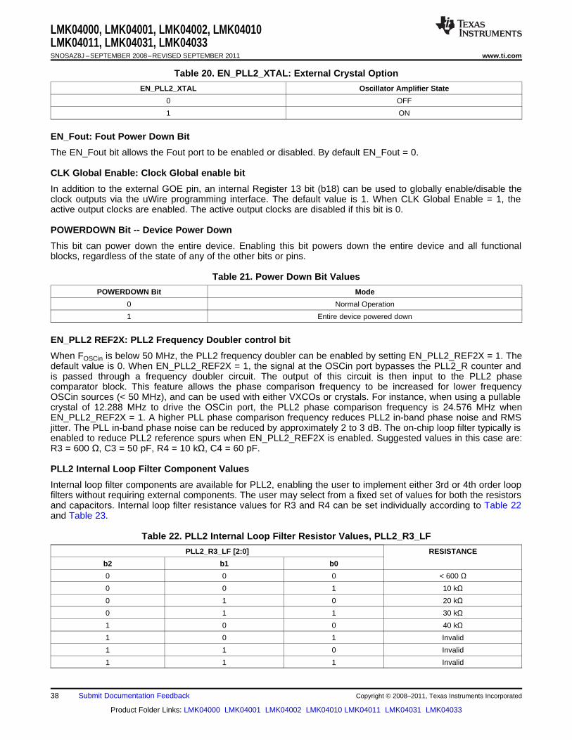
LMK04000, LMK04001, LMK04002, LMK04010LMK04011, LMK04031, LMK04033SNOSAZ8J –SEPTEMBER 2008–REVISED SEPTEMBER 2011 www.ti.com
Table 20. EN_PLL2_XTAL: External Crystal Option
EN_PLL2_XTAL Oscillator Amplifier State
0 OFF
1 ON
EN_Fout: Fout Power Down Bit
The EN_Fout bit allows the Fout port to be enabled or disabled. By default EN_Fout = 0.
CLK Global Enable: Clock Global enable bit
In addition to the external GOE pin, an internal Register 13 bit (b18) can be used to globally enable/disable theclock outputs via the uWire programming interface. The default value is 1. When CLK Global Enable = 1, theactive output clocks are enabled. The active output clocks are disabled if this bit is 0.
POWERDOWN Bit -- Device Power Down
This bit can power down the entire device. Enabling this bit powers down the entire device and all functionalblocks, regardless of the state of any of the other bits or pins.
Table 21. Power Down Bit Values
POWERDOWN Bit Mode
0 Normal Operation
1 Entire device powered down
EN_PLL2 REF2X: PLL2 Frequency Doubler control bit
When FOSCin is below 50 MHz, the PLL2 frequency doubler can be enabled by setting EN_PLL2_REF2X = 1. Thedefault value is 0. When EN_PLL2_REF2X = 1, the signal at the OSCin port bypasses the PLL2_R counter andis passed through a frequency doubler circuit. The output of this circuit is then input to the PLL2 phasecomparator block. This feature allows the phase comparison frequency to be increased for lower frequencyOSCin sources (< 50 MHz), and can be used with either VXCOs or crystals. For instance, when using a pullablecrystal of 12.288 MHz to drive the OSCin port, the PLL2 phase comparison frequency is 24.576 MHz whenEN_PLL2_REF2X = 1. A higher PLL phase comparison frequency reduces PLL2 in-band phase noise and RMSjitter. The PLL in-band phase noise can be reduced by approximately 2 to 3 dB. The on-chip loop filter typically isenabled to reduce PLL2 reference spurs when EN_PLL2_REF2X is enabled. Suggested values in this case are:R3 = 600 Ω, C3 = 50 pF, R4 = 10 kΩ, C4 = 60 pF.
PLL2 Internal Loop Filter Component Values
Internal loop filter components are available for PLL2, enabling the user to implement either 3rd or 4th order loopfilters without requiring external components. The user may select from a fixed set of values for both the resistorsand capacitors. Internal loop filter resistance values for R3 and R4 can be set individually according to Table 22and Table 23.
Table 22. PLL2 Internal Loop Filter Resistor Values, PLL2_R3_LF
PLL2_R3_LF [2:0] RESISTANCE
b2 b1 b0
0 0 0 < 600 Ω0 0 1 10 kΩ0 1 0 20 kΩ0 1 1 30 kΩ1 0 0 40 kΩ1 0 1 Invalid
1 1 0 Invalid
1 1 1 Invalid
38 Submit Documentation Feedback Copyright © 2008–2011, Texas Instruments Incorporated
Product Folder Links: LMK04000 LMK04001 LMK04002 LMK04010 LMK04011 LMK04031 LMK04033

LMK04000, LMK04001, LMK04002, LMK04010LMK04011, LMK04031, LMK04033
www.ti.com SNOSAZ8J –SEPTEMBER 2008–REVISED SEPTEMBER 2011
Table 23. PLL2 Internal Loop Filter Resistor Values, PLL2_R4_LF
PLL2_R4_LF [2:0] RESISTANCE
b2 b1 b0
0 0 0 < 200 Ω0 0 1 10 kΩ0 1 0 20 kΩ0 1 1 30 kΩ1 0 0 40 kΩ1 0 1 Invalid
1 1 0 Invalid
1 1 1 Invalid
Internal loop filter capacitors for C3 and C4 can be set individually according to the following table.
Table 24. PLL2 Internal Loop Filter Capacitor Values
PLL2_C3_C4_LF [3:0] Loop Filter Capacitance(pF)
b3 b2 b1 b0
0 0 0 0 C3 = 0, C4 = 10
0 0 0 1 C3 = 0, C4 = 60
0 0 1 0 C3 = 50, C4 = 10
0 0 1 1 C3 = 0, C4 = 110
0 1 0 0 C3 = 50, C4 = 110
0 1 0 1 C3 = 100, C4 = 110
0 1 1 0 C3 = 0, C4 = 160
0 1 1 1 C3 = 50, C4 = 160
1 0 0 0 C3 = 100, C4 = 10
1 0 0 1 C3 = 100, C4 = 60
1 0 1 0 C3 = 150, C4 = 110
1 0 1 1 C3 = 150, C4 = 60
1 1 0 0 Reserved
1 1 0 1 Reserved
1 1 1 0 Reserved
1 1 1 1 Reserved
PLL1 CP TRI-STATE and PLL2 CP TRI-STATE
The charge pump output of either CPout1 or CPout2 may be placed in a TRI-STATE mode by setting theappropriate PLLx CP TRI-STATE bit.
Table 25. PLL1 Charge Pump TRI-STATE bit values
PLL1 CP TRI-STATE Description
1 PLL1 CPout1 is at TRI-STATE
0 PLL1 CPout1 is active
Table 26. PLL2 Charge Pump TRI-STATE bit values
PLL2 CP TRI-STATE Description
1 PLL2 CPout2 is at TRI-STATE
0 PLL2 CPout2 is active
Copyright © 2008–2011, Texas Instruments Incorporated Submit Documentation Feedback 39
Product Folder Links: LMK04000 LMK04001 LMK04002 LMK04010 LMK04011 LMK04031 LMK04033

LMK04000, LMK04001, LMK04002, LMK04010LMK04011, LMK04031, LMK04033SNOSAZ8J –SEPTEMBER 2008–REVISED SEPTEMBER 2011 www.ti.com
Register 14
OSCin_FREQ: PLL2 Oscillator Input Frequency Register
The frequency of the PLL2 reference input to the PLL2 Phase Detector (OSCin/OSCin* port) must beprogrammed in order to support proper operation of the internal VCO tuning algorithm. This is an 8-bit registerthat sets the frequency to the nearest 1-MHz increment.
Table 27. OSCin_FREQ Register Values
OSCin_FREQ [7:0] VALUE
b7 b6 b5 b4 b3 b2 b1 b0
0 0 0 0 0 0 0 0 Not Valid
0 0 0 0 0 0 0 1 1 MHz
0 0 0 0 0 0 1 0 2 MHz
. . . . . . . ...
1 1 1 1 1 0 1 0 250 MHz
1 1 0 0 1 0 0 1 Not Valid
. . . . . . . . .
1 1 1 1 1 1 1 1 Not Valid
PLL2_R: PLL2_R Counter
The PLL2 R Counter is 12 bits wide. It divides the PLL2 OSCin/OSCin* clock and is connected to the PLL2Phase Detector.
Table 28. PLL2_R: PLL2_R Counter Values
R [11:0] VALUE
b11 b10 b9 b8 b7 b6 b5 b4 b3 b2 b1 b0
0 0 0 0 0 0 0 0 0 0 0 0 Not Valid
0 0 0 0 0 0 0 0 0 0 0 1 1
. . . . . . . . . . ...
1 1 1 1 1 1 1 1 1 1 1 1 4095
PLL_MUX: LD Pin Selectable Output
The signal appearing on the LD pin is programmable via the uWire interface and provides access to severalinternal signals which may be valuable for either status monitoring during normal operation or for debuggingduring the hardware development phase. This pin may be forced to either a HIGH or LOW state, and may alsobe configured as specified in Table 29.
40 Submit Documentation Feedback Copyright © 2008–2011, Texas Instruments Incorporated
Product Folder Links: LMK04000 LMK04001 LMK04002 LMK04010 LMK04011 LMK04031 LMK04033

LMK04000, LMK04001, LMK04002, LMK04010LMK04011, LMK04031, LMK04033
www.ti.com SNOSAZ8J –SEPTEMBER 2008–REVISED SEPTEMBER 2011
Table 29. PLL_MUX: LD Pin Selectable Outputs
PLL_MUX [4:0] LD Output
b4 b3 b2 b1 b0
0 0 0 0 0 HiZ
0 0 0 0 1 Logic High
0 0 0 1 0 Logic Low
0 0 0 1 1 PLL2 Digital Lock Detect Active High
0 0 1 0 0 PLL2 Digital Lock Detect Active Low
0 0 1 0 1 PLL2 Analog Lock Detect Push Pull
0 0 1 1 0 PLL2 Analog Lock Detect Open Drain NMOS
0 0 1 1 1 PLL2 Analog Lock Detect Open Drain PMOS
0 1 0 0 0 Reserved
0 1 0 0 1 PLL2_N Divider Output / 2
0 1 0 1 0 Reserved
0 1 0 1 1 PLL2_R Divider Output / 2
0 1 1 0 0 Reserved
0 1 1 0 1 Reserved
0 1 1 1 0 PLL1 Digital Lock Detect Active HIGH
0 1 1 1 1 PLL1 Digital Lock Detect Active LOW
1 0 0 0 0 Reserved
1 0 0 0 1 Reserved
1 0 0 1 0 Reserved
1 0 0 1 1 Reserved
1 0 1 0 0 PLL1_N Divider Output / 2
1 0 1 0 1 Reserved
1 0 1 1 0 PLL1_R Divider Output / 2
1 0 1 1 1 PLL1 and PLL2 Digital Lock Detect
1 1 0 0 0 Inverted PLL1 and PLL2 Digital Lock Detect
1 1 0 0 1 Reserved
1 1 0 1 0 Reserved
1 1 0 1 1 Reserved
1 1 1 0 0 Reserved
1 1 1 0 1 Reserved
1 1 1 1 0 Reserved
1 1 1 1 1 Reserved
Copyright © 2008–2011, Texas Instruments Incorporated Submit Documentation Feedback 41
Product Folder Links: LMK04000 LMK04001 LMK04002 LMK04010 LMK04011 LMK04031 LMK04033
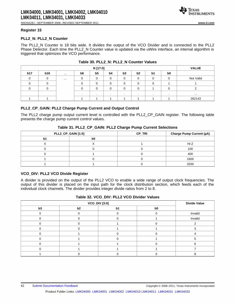
LMK04000, LMK04001, LMK04002, LMK04010LMK04011, LMK04031, LMK04033SNOSAZ8J –SEPTEMBER 2008–REVISED SEPTEMBER 2011 www.ti.com
Register 15
PLL2_N: PLL2_N Counter
The PLL2_N Counter is 18 bits wide. It divides the output of the VCO Divider and is connected to the PLL2Phase Detector. Each time the PLL2_N Counter value is updated via the uWire interface, an internal algorithm istriggered that optimizes the VCO performance.
Table 30. PLL2_N: PLL2_N Counter Values
N [17:0] VALUE
b17 b16 ... b6 b5 b4 b3 b2 b1 b0
0 0 ... 0 0 0 0 0 0 0 Not Valid
0 0 0 0 0 0 0 0 1 1
0 0 0 0 0 0 0 1 0 2
. . . . . . . ...
1 1 1 1 1 1 1 1 1 262143
PLL2_CP_GAIN: PLL2 Charge Pump Current and Output Control
The PLL2 charge pump output current level is controlled with the PLL2_CP_GAIN register. The following tablepresents the charge pump current control values.
Table 31. PLL2_CP_GAIN: PLL2 Charge Pump Current Selections
PLL2_CP_GAIN [1:0] CP_TRI Charge Pump Current (µA)
b1 b0
X X 1 Hi-Z
0 0 0 100
0 1 0 400
1 0 0 1600
1 1 0 3200
VCO_DIV: PLL2 VCO Divide Register
A divider is provided on the output of the PLL2 VCO to enable a wide range of output clock frequencies. Theoutput of this divider is placed on the input path for the clock distribution section, which feeds each of theindividual clock channels. The divider provides integer divide ratios from 2 to 8.
Table 32. VCO_DIV: PLL2 VCO Divider Values
VCO_DIV [3:0] Divide Value
b3 b2 b1 b0
0 0 0 0 Invalid
0 0 0 1 Invalid
0 0 1 0 2
0 0 1 1 3
0 1 0 0 4
0 1 0 1 5
0 1 1 0 6
0 1 1 1 7
1 0 0 0 8
42 Submit Documentation Feedback Copyright © 2008–2011, Texas Instruments Incorporated
Product Folder Links: LMK04000 LMK04001 LMK04002 LMK04010 LMK04011 LMK04031 LMK04033

CP
out1
LEuWire
CLKuWire
DATAuWire
GOE
LD
(optional)
To Host
CLK
out0
CLK
out0
*
CLK
out1
*C
LKou
t1
CLK
out2
BC
LKou
t2A
CLK
out3
*C
LKou
t3
CLK
out4
*C
LKou
t4
To System
SYNC*
CLK
in0
CLK
in0*
Bias
Vcc
LDObyp1
LDObyp2
10 PF 0.1 PF
1 PF
0.1 PF
LMK040xx
100Ö
VCXO
OSCin
OSCin*
100 Ö
0.1 uF
CLKin1*
CLKin1
0.1 PF
0.1 PF
To System
To Host
CPout2
100 pF100 pFTo
System
Fout
Reference Clock #1(Primary)
Reference Clock #2(Secondary)
PLL1 Loop Filter
PLL2 Loop Filter
Rterm0.1 PF
120Ö
120Ö
To System
To System
51Ö
0.1 PF
0.1 PF
0.1 PF
0.1 PF
120Ö
120Ö
To System
0.47 PF
DLD
_BY
P
33 p
F
33 p
F
33 p
F
0.1 PF
LMK04000, LMK04001, LMK04002, LMK04010LMK04011, LMK04031, LMK04033
www.ti.com SNOSAZ8J –SEPTEMBER 2008–REVISED SEPTEMBER 2011
APPLICATION INFORMATION
System Level Diagram
The following diagram illustrates the typical interconnection of the LMK040xx in a clocking application.
Figure 13. Typical Application
Figure 13 shows an LMK04000 family device with external circuitry. The primary reference clock input is atCLKin0/0*. A secondary reference clock is driving CLKin1/1*. Both clocks are depicted as AC coupled differentialdrivers. The VCXO attached to the OSCin/OSCin* port is configured as an AC coupled single-ended driver. Anyof the input ports (CLKin0/0*, CLKin1/1*, or OSCin/OSCin*) may be configured as either differential or single-ended. These options are discussed later in the data sheet.
The diagram shows an optional connection between the LD pin and GOE. With this arrangement, the LD pin canbe programmed to output a lock detect signal that is active HIGH (see Table 29 for optional LD pin outputs). Iflock is lost, the LD pin will transition to a LOW, pulling GOE low and causing all clock outputs to be disabled.This scheme should be used only if disabling the clock outputs is desirable when lock is lost.
Copyright © 2008–2011, Texas Instruments Incorporated Submit Documentation Feedback 43
Product Folder Links: LMK04000 LMK04001 LMK04002 LMK04010 LMK04011 LMK04031 LMK04033

LMK04000, LMK04001, LMK04002, LMK04010LMK04011, LMK04031, LMK04033SNOSAZ8J –SEPTEMBER 2008–REVISED SEPTEMBER 2011 www.ti.com
The loop filter for PLL2 consists of three external components that implement two lower order poles, plus optionalinternal integrated components if 3rd or 4th order poles are needed. The loop filter components for PLL1 must beexternal components.
The VCO output buffer signal that appears at the Fout pin when enabled (EN_Fout = 1) should be AC coupledusing a 100 pF capacitor. This output is a single-ended signal by default. If a differential signal is required, a 50Ω balun may be connected to this pin to convert it to differential.
The clock outputs are all AC coupled with 0.1 µF capacitors. CLKout1 and CLKout3 are depicted as LVPECL,with 120 Ω emitter resistors as source termination. However, the output format of the clock channels will vary bydevice part number, so the designer should use the appropriate source termination for each channel. Latersections of this data sheet illustrate alternative methods for AC coupling, DC coupling and terminating the clockoutputs.
LDO Bypass And Bias Pin
The LDObyp1 and LDObyp2 pins should be connected to GND through external capacitors, as shown in thediagram. Furthermore, the Bias pin should be connected to VCC through a 1 µF capacitor in series.
Loop Filter
Each PLL of the LMK04000 family requires a dedicated loop filter. The loop filter for PLL1 must be connected tothe CPout1 pin. Figure 14 shows a simple 2-pole loop filter. The output of the filter drives an external VCXOmodule or discrete implementation of a VCXO using a crystal resonator. Higher order loop filters may beimplemented using additional external R and C components. It is recommended the loop filter for PLL1 result in atotal closed loop bandwidth in the range of 10 Hz to 200 Hz. The design of the loop filter is application specificand highly dependent on parameters such as the phase noise of the reference clock, VCXO phase noise, andphase detector frequency for PLL1. National’s Clock Conditioner Owner’s Manual covers this topic in detail andNational’s Clock Design Tool can be used to simulate loop filter designs for both PLLs. These resources may befound: http://www.national.com/timing/.
As shown in the diagram, the charge pump for PLL2 is directly connected to the optional internal loop filtercomponents, which are normally used only if either a third or fourth pole is needed. The first and second polesare implemented with external components. The loop must be designed to be stable over the entire application-specific tuning range of the VCO. The designer should note the range of KVCO listed in the table of ElectricalCharacteristics and how this value can change over the expected range of VCO tuning frequencies. Becauseloop bandwidth is directly proportional to KVCO, the designer should model and simulate the loop at the expectedextremes of the desired tuning range, using the appropriate values for KVCO.
When designing with the integrated loop filter of the LMK04000 family, considerations for minimum resistorthermal noise often lead one to the decision to design for the minimum value for integrated resistors, R3 and R4.Both the integrated loop filter resistors and capacitors (C3 and C4) also restrict the maximum loop bandwidth.However, these integrated components do have the advantage that they are closer to the VCO and can thereforefilter out some noise and spurs better than external components. For this reason, a common strategy is tominimize the internal loop filter resistors and then design for the largest internal capacitor values that permit awide enough loop bandwidth. In situations where spurs requirements are very stringent and there is margin onphase noise, it might make sense to design for a loop filter with integrated resistor values larger than theirminimum value.
44 Submit Documentation Feedback Copyright © 2008–2011, Texas Instruments Incorporated
Product Folder Links: LMK04000 LMK04001 LMK04002 LMK04010 LMK04011 LMK04031 LMK04033

C2
PLL2 Phase
Detector
R2C1
C3 C4
R3 R4
LMK040xx
PLL2 Internal Loop Filter
PLL2 External Loop Filter
C2
PLL1Phase
Detector
R2
CPout1
C1
LMK040xx
PLL1 External Loop Filter
CP
out2
External VCXO
Internal VCO
LMK04000, LMK04001, LMK04002, LMK04010LMK04011, LMK04031, LMK04033
www.ti.com SNOSAZ8J –SEPTEMBER 2008–REVISED SEPTEMBER 2011
Figure 14. Loop Filter
Table 33. Typical Current Consumption for Selected Functional Blocks
PowerTypical ICC Power Dissipated in
(Temp = 25 °C, Dissipated in LVPECL/2VPECLBlock Condition VCC = 3.3 V) device Emitter(mA) (mW) Resistors
(mW)
Single input clock (CLKIN_SEL = 0 or 1); LOS disabled;Entire device, PLL1 and PLL2 locked; All CLKouts are off; No LVPECL 115 380 -core current emitter resistors connected
REFMUX Enable auto-switch mode (CLKIN_SEL = 2 or 3) 4.3 14 -
LOS Enable LOS (LOS_TYPE = 1, or 2, or 3) 3.6 12 -
Low Channel The low channel internal buffer is enabled when CLKout0 is 10 33 -Internal Buffer enabled
High Channel The high channel internal buffer is enabled when one of 10 33 -Internal Buffer CLKout1 through CLKout4 is enabled
Divider bypassed (CLKout_MUX = 0, 2) 0 0 -Divide circuitry Divider enabled, divide = 2 (CLKout_MUX = 1, 3) 5.3 17 -per output
Divider enabled, divide > 2 (CLKout_MUX = 1, 3) 8.5 28 -
Delay bypassed (CLKout_MUX = 0, 1) 0 0 -Delay circuitry per Delay enabled, delay < 8 (CLKout_MUX = 2, 3) 5.8 19 -output
Delay enabled, delay > 7 (CLKout_MUX = 2, 3) 9.9 33 -
Fout Buffer EN_Fout = 1 14.5 48 -
LVDS Buffer LVDS buffer, enabled 19.3 64 -
Copyright © 2008–2011, Texas Instruments Incorporated Submit Documentation Feedback 45
Product Folder Links: LMK04000 LMK04001 LMK04002 LMK04010 LMK04011 LMK04031 LMK04033

LMK04000, LMK04001, LMK04002, LMK04010LMK04011, LMK04031, LMK04033SNOSAZ8J –SEPTEMBER 2008–REVISED SEPTEMBER 2011 www.ti.com
Table 33. Typical Current Consumption for Selected Functional Blocks (continued)
PowerTypical ICC Power Dissipated in
(Temp = 25 °C, Dissipated in LVPECL/2VPECLBlock Condition VCC = 3.3 V) device Emitter(mA) (mW) Resistors
(mW)
LVPECL/2VPECL buffer (enabled and with 120 Ω emitter 40 82 50resistors)LVPECL/2VPECL LVPECL/2VPECL buffer (disabled and with 120 Ω emitterBuffer 21.7 47 25resistors)
LVPECL/2VPECL (disabled and with no emitter resistors) 0 0 -
LVCMOS buffer static ICC, CL = 5 pF 4.5 15 -LVCMOS Buffer
LVCMOS buffer dynamic ICC, CL = 5 pF, CLKout = 100(1)16 53 -MHz
Entire device LMK0400x (2) (3) 379.5 1102 150(Single input clock LMK0401x (2) (3) 377.5 996 250(CLKIN_SEL = 0
LMK0403x (2) (3)or 1); LOSdisabled; PLL1and PLL2 locked;Fout disabled; All 337.1 1012 100CLKouts are on;No delay); Divide> 2 on eachoutput.
(1) Dynamic power dissipation of LVCMOS buffer varies with output frequency and can be found in the LVCMOS dynamic ICC vs frequencyplot, as shown in Typical Performance Characteristics. Total power dissipation of the LVCMOS buffer is the sum of static and dynamicpower dissipation. CLKoutXa and CLKoutXb are each considered an LVCMOS buffer.
(2) Assuming ThetaJ = 27.4 °C/W, the total power dissipated on chip must be less than 40/27.4 = 1450 mW to guarantee a junctiontemperature is less than 125 °C.
(3) Worst case power dissipation can be estimated by multiplying typical power dissipation with a factor of 1.2.
Current Consumption / Power Dissipation Calculations
Due to the myriad of possible configurations the following table serves to provide enough information to allow theuser to calculate estimated current consumption of the device. Unless otherwise noted VCC = 3.3 V, TA = 25 °C.
From Table 33 the current consumption can be calculated in any configuration. For example, the current for theentire device with 1 LVDS (CLKout0) & 1 LVPECL (CLKout1) output in bypassed mode can be calculated byadding up the following blocks: core current, clock buffer, one LVDS output buffer current, and one LVPECLoutput buffer current. There will also be one LVPECL output drawing emitter current, but some of the power fromthe current draw is dissipated in the external 120 Ω resistors which doesn't add to the power dissipation budgetfor the device. If delays or divides are switched in, then the additional current for these stages needs to be addedas well.
For power dissipated by the device, the total current entering the device is multiplied by the voltage at the deviceminus the power dissipated in any emitter resistors connected to any of the LVPECL outputs. If no emitterresistors are connected to the LVPECL outputs, this power will be 0 watts. For example, in the case of 1 LVDS(CLKout0) & 1 LVPECL (CLKout1) operating at 3.3 V, we calculate 3.3 V × (115 + 10 + 10 + 19.3 + 40) mA = 3.3V × 194.3 mA = 641.2 mW. Because the LVPECL output (CLKout1) has the emitter resistors hooked up and thepower dissipated by these resistors is 50 mW, the total device power dissipation is 641.2 mW - 50 mW = 591.2mW.
When the LVPECL output is active, ~1.7 V is the average voltage on each output as calculated from the LVPECLVOH & VOL typical specification. Therefore the power dissipated in each emitter resistor is approximately (1.7 V)2 /120 Ω = 25 mW. When the LVPECL output is disabled, the emitter resistor voltage is ~1.07 V. Therefore thepower dissipated in each emitter resistor is approximately (1.07 V)2 / 120 Ω = 9.5 mW.
46 Submit Documentation Feedback Copyright © 2008–2011, Texas Instruments Incorporated
Product Folder Links: LMK04000 LMK04001 LMK04002 LMK04010 LMK04011 LMK04031 LMK04033

0.33 mm, typ
1.2 mm, typ
5.0 mm, min
LMK04000, LMK04001, LMK04002, LMK04010LMK04011, LMK04031, LMK04033
www.ti.com SNOSAZ8J –SEPTEMBER 2008–REVISED SEPTEMBER 2011
Power Supply Conditioning
The recommended technique for power supply management is to connect the power pins for the clock outputs(pins 13, 37, 40, 43, and 46) to a dedicated power plane and connect all other power pins on the device (pins 3,8, 18, 19, 22, 24, 30, 31, and 33) to a second power plane. Note: the LMK04000 family has internal voltageregulators for the PLL and VCO blocks to provide noise immunity.
Thermal Management
Power consumption of the LMK04000 family of devices can be high enough to require attention to thermalmanagement. For reliability and performance reasons the die temperature should be limited to a maximum of125 °C. That is, as an estimate, TA (ambient temperature) plus device power consumption times θJA should notexceed 125 °C.
The package of the device has an exposed pad that provides the primary heat removal path as well as excellentelectrical grounding to a printed circuit board. To maximize the removal of heat from the package a thermal landpattern including multiple vias to a ground plane must be incorporated on the PCB within the footprint of thepackage. The exposed pad must be soldered down to ensure adequate heat conduction out of the package. Arecommended land and via pattern is shown in Figure 15. More information on soldering WQFN packages canbe obtained: http://www.national.com/analog/packaging/.
Figure 15. Recommended Land and Via Pattern
To minimize junction temperature it is recommended that a simple heat sink be built into the PCB (if the groundplane layer is not exposed). This is done by including a copper area of about 2 square inches on the oppositeside of the PCB from the device. This copper area may be plated or solder coated to prevent corrosion butshould not have conformal coating (if possible), which could provide thermal insulation. The vias shown inFigure 15 should connect these top and bottom copper layers and to the ground layer. These vias act as “heatpipes” to carry the thermal energy away from the device side of the board to where it can be more effectivelydissipated.
Copyright © 2008–2011, Texas Instruments Incorporated Submit Documentation Feedback 47
Product Folder Links: LMK04000 LMK04001 LMK04002 LMK04010 LMK04011 LMK04031 LMK04033

2CL = 6 + 6 + 4 = 14 pF
2
CSTRAYCL = CTUNE + CIN +
CP
out1
LMK040xx
OSCin
OSCin*
Copt
PLL1 Loop Filter
XTAL
CC1 = 2.2 nF
CC2 = 2.2 nF
R1 = 4.7k
R3 = 10k
Copt
1 nF
R2 = 4.7k
SMV1249-074LF
LMK04000, LMK04001, LMK04002, LMK04010LMK04011, LMK04031, LMK04033SNOSAZ8J –SEPTEMBER 2008–REVISED SEPTEMBER 2011 www.ti.com
Figure 16. Reference Design Circuit for Crystal Oscillator Option
Optional Crystal Oscillator Implementation (OSCin/OSCin*)
The LMK04000 family features supporting circuitry for a discretely implemented oscillator driving the OSCin portpins. Figure 16 illustrates a reference design circuit for a crystal oscillator:
This circuit topology represents a parallel resonant mode oscillator design. When selecting a crystal for parallelresonance, the total load capacitance, CL, must be specified. The load capacitance is the sum of the tuningcapacitance (CTUNE), the capacitance seen looking into the OSCin port (CIN), and stray capacitance due to PCBparasitics (CSTRAY), and is given by:
CTUNE is provided by the varactor diode shown in Figure 16, Skyworks model SMV1249-074. A dual diodepackage with common cathode and provides the variable capacitance for tuning. The single diode capacitanceranges from approximately 31 pF at 0.3 V to 3.4 pF at 3 V. The capacitance range of the dual package (anode toanode) is approximately 15.5 pF at 3 V to 1.7 pF at 0.3 V. The desired value of VTUNE applied to the diode shouldbe VCC/2, or 1.65 V for VCC = 3.3 V. The typical performance curve from the data sheet for the SMV1249-074indicates that the capacitance at this voltage is approximately 6 pF (12 pF/2).
The nominal input capacitance (CIN) of the LMK04000 family OSCin pins is 6 pF. The stray capacitance (CSTRAY)of the PCB should be minimized by arranging the oscillator circuit layout to achieve trace lengths as short aspossible and as narrow as possible trace width (50 Ω characteristic impedance is not required). As an example,assume that CSTRAY is 4 pF. The total load capacitance is nominally:
Consequently the load capacitance specification for the crystal in this case should be nominally 14 pF.
48 Submit Documentation Feedback Copyright © 2008–2011, Texas Instruments Incorporated
Product Folder Links: LMK04000 LMK04001 LMK04002 LMK04010 LMK04011 LMK04031 LMK04033

1(C0 + CL1)
- 1(C0 + CL2)
=21À
FFCL1
FCL1 - FCL2=
2À
C1=F
'F C0
C1¸¹
ᬩ
§ CL2
C1+
1-C0
C1¸¹
ᬩ
§ CL1
C1+
1
2(C0 + CL1)+ 1 C0
C1¸¹
ᬩ
§ CL
C1+
1+ 1
2
C1FL = FS À = FS À
LMK04000, LMK04001, LMK04002, LMK04010LMK04011, LMK04031, LMK04033
www.ti.com SNOSAZ8J –SEPTEMBER 2008–REVISED SEPTEMBER 2011
The 2.2 nF capacitors shown in the circuit are coupling capacitors that block the DC tuning voltage applied by the4.7 k and 10 k resistors. The value of these coupling capacitors should be large, relative to the value of CTUNE(CC1 = CC2 >> CTUNE), so that CTUNE becomes the dominant capacitance.
For a specific value of CL, the corresponding resonant frequency (FL) of the parallel resonant mode circuit is:
FS = Series resonant frequency
C1 = Motional capacitance of the crystal
CL = Load capacitance
C0 = Shunt capacitance of the crystal, specified on the crystal datasheet
The normalized tuning range of the circuit is closely approximated by:
CL1, CL2 = The endpoints of the circuit’s load capacitance range, assuming a variable capacitance element is onecomponent of the load. FCL1, FCL2 = parallel resonant frequencies at the extremes of the circuit’s loadcapacitance range.
A common range for the pullability ratio, C0/C1, is 250 to 280. The ratio of the load capacitance to the shuntcapacitance is ~(n * 1000), n < 10. Hence, picking a crystal with a smaller pullability ratio supports a wider tuningrange because this allows the scale factors related to the load capacitance to dominate.
Examples of the phase noise and jitter performance of the LMK04031 with a crystal oscillator are shown inTable 34. This table illustrates the clock output phase noise when a 12.288 MHz crystal is paired with PLL1.
Table 34. Example RMS Jitter and Clock Output Phase Noise for LMK04031 with a12.288 MHz Crystal Driving OSCin (T = 25 °C, VCC = 3.3 V) (1)
RMS Jitter (ps)
Integration Bandwidth Clock Output Type PLL2 PDF = 12.288 MHz PLL2 PDF = 24.576 MHz(EN_PLL2_REF2X = 0) (EN_PLL2_REF2X = 1)
FCLK = 122.88 MHz FCLK = 153.6 MHz FCLK = 122.88 MHz
100 Hz – 20 MHz LVPECL 0.279 0.263 0.300
LVCMOS 0.244 0.248 0.218
LVDS 0.272 0.269 0.245
10 kHz – 20 MHz LVPECL 0.251 0.234 0.284
LVCMOS 0.211 0.215 0.193
LVDS 0.236 0.235 0.217
Phase Noise (dBc/Hz)
Offset Clock Output Type PLL2 FPD = 12.288 MHz PLL2 FPD = 24.576 MHz(EN_PLL2_REF2X = 0) (EN_PLL2_REF2X = 1)
FCLK = 122.88 MHz FCLK = 153.6 MHz FCLK = 122.88 MHz
100 Hz LVPECL -107 -106 -106
LVCMOS -105 -103 -104
LVDS -105 -104 -106
(1) Performance data and crystal specifications contained in this section are based on Ecliptek model ECX-6465, 12.288 MHz.
Copyright © 2008–2011, Texas Instruments Incorporated Submit Documentation Feedback 49
Product Folder Links: LMK04000 LMK04001 LMK04002 LMK04010 LMK04011 LMK04031 LMK04033

VTUNE (VDC)
ppm
180140100
6020
-20-60
-100-140-180
0.0 0.3 0.6 0.9 1.2 1.5 1.8 2.1 2.4 2.7 3.0 3.3
LMK04000, LMK04001, LMK04002, LMK04010LMK04011, LMK04031, LMK04033SNOSAZ8J –SEPTEMBER 2008–REVISED SEPTEMBER 2011 www.ti.com
Table 34. Example RMS Jitter and Clock Output Phase Noise for LMK04031 with a12.288 MHz Crystal Driving OSCin (T = 25 °C, VCC = 3.3 V) (1) (continued)
1 kHz LVPECL -126 -124 -130
LVCMOS -125 -124 -127
LVDS -126 -123 -126
10 kHz LVPECL -125 -124 -131
LVCMOS -127 -125 -128
LVDS -126 -124 -131
100 kHz LVPECL -134 -133 -134
LVCMOS -135 -133 -134
LVDS -134 -132 -134
1 MHz LVPECL -155 -154 -154
LVCMOS -157 -155 -155
LVDS -155 -153 -154
10 MHz LVPECL -158 -158 -158
LVCMOS -160 -159 -159
LVDS -158 -158 -157
Example crystal specifications are presented in Table 35.
Table 35. Example Crystal Specifications
Parameter Value
Nominal Frequency (MHz) 12.288
Frequency Stability, T = 25 °C ± 10 ppm
Operating temperature range -40 °C to +85 °C
Frequency Stability, -40 °C to +85 °C ± 15 ppm
Load Capacitance 14 pF
Shunt Capacitance (C0) 5 pF Maximum
Motional Capacitance (C1) 20 fF ± 30%
Equivalent Series Resistance 25 Ω Maximum
Drive level 2 mWatts Maximum
C0/C1 ratio 225 typical, 250 Maximum
See Figure 17 for a representative tuning curve.
Figure 17. Example Tuning Curve, 12.288 MHz Crystal
50 Submit Documentation Feedback Copyright © 2008–2011, Texas Instruments Incorporated
Product Folder Links: LMK04000 LMK04001 LMK04002 LMK04010 LMK04011 LMK04031 LMK04033

= 0.00164,MHz
V(2.03 - 0.814) À 106
12.288 À 81.4 - (-81.4)( )
'V À 106
FNOM À ('ppm2 - 'ppm1)KVCO =
= 0.00164MHz
V2.03 - 0.8140.001 - (-0.001)
KVCO ='F'V
,MHz
V= ¸
¹
ᬩ
§ 'F2 - 'F1
VTUNE2 - VTUNE1
LMK04000, LMK04001, LMK04002, LMK04010LMK04011, LMK04031, LMK04033
www.ti.com SNOSAZ8J –SEPTEMBER 2008–REVISED SEPTEMBER 2011
The tuning curve achieved in the user's application may differ from the curve shown above due to differences inPCB layout and component selection.
This data is measured on the bench with the crystal integrated with the LMK04000 family. Using a voltmeter tomonitor the VTUNE node for the crystal, the PLL1 reference clock input frequency is swept in frequency and theresulting tuning voltage generated by PLL1 is measured at each frequency. At each value of the reference clockfrequency, the lock state of PLL1 should be monitored to ensure that the tuning voltage applied to the crystal isvalid.
The curve shows over the tuning voltage range of 0.17 VDC to 3.0 VDC, the frequency range is ± 163 ppm; orequivalently, a crystal frequency range of ± 2000 Hz. The measured tuning voltage at the nominal crystalfrequency (12.288 MHz) is 1.4 V. Using the diode data sheet tuning characteristics, this voltage results in atuning capacitance of approximately 6.5 pF.
The tuning curve data can be used to calculate the gain of the oscillator (KVCO). The data used in the calculationsis taken from the most linear portion of the curve, a region centered on the crossover point at the nominalfrequency (12.288 MHz). For a well designed circuit, this is the most likely operating range. In this case, thetuning range used for the calculations is ± 1000 Hz (± 0.001 MHz), or ± 81.4 ppm. The simplest method is tocalculate the ratio:
ΔF2 and ΔF1 are in units of MHz. Using data from the curve this becomes:
A second method uses the tuning data in units of ppm:
FNOM is the nominal frequency of the crystal and is in units of MHz. Using the data, this becomes:
In order to ensure startup of the oscillator circuit, the equivalent series resistance (ESR) of the selected crystalshould conform to the specifications listed in the table of Electrical Characteristics. It is also important to select acrystal with adequate power dissipation capability, or drive level. If the drive level supplied by the oscillatorexceeds the maximum specified by the crystal manufacturer, the crystal will undergo excessive aging andpossibly become damaged. Drive level is directly proportional to resonant frequency, capacitive load seen by thecrystal, voltage and equivalent series resistance (ESR). For more complete coverage of crystal oscillator design,see Application Note AN-1939 at http://www.national.com/analog/timing/clocking orhttp://www.national.com/appnotes.
Termination and use of Clock Output (Drivers)
When terminating clock drivers keep in mind these guidelines for optimum phase noise and jitter performance:• Transmission line theory should be followed for good impedance matching to prevent reflections.• Clock drivers should be presented with the proper loads. For example:
– LVDS drivers are current drivers and require a closed current loop.– LVPECL drivers are open emitters and require a DC path to ground.
• Receivers should be presented with a signal biased to their specified DC bias level (common mode voltage)for proper operation. Some receivers have self-biasing inputs that automatically bias to the proper voltagelevel. In this case, the signal should normally be AC coupled.
Copyright © 2008–2011, Texas Instruments Incorporated Submit Documentation Feedback 51
Product Folder Links: LMK04000 LMK04001 LMK04002 LMK04010 LMK04011 LMK04031 LMK04033

CLKoutX
CLKoutX*
LVPECL Receiver
120:
100:�Trace(Differential)
120:
Vcc
Vcc
LVPECL Driver
82:
82:
CLKoutX
CLKoutX*
LVPECL Receiver
50:
100:�Trace(Differential)
50:
Vcc - 2 V
Vcc - 2 V
LVPECL Driver
CLKoutX
CLKoutX*
LVDS Receiver10
0:100:�Trace(Differential)
LVDSDriver
LMK04000, LMK04001, LMK04002, LMK04010LMK04011, LMK04031, LMK04033SNOSAZ8J –SEPTEMBER 2008–REVISED SEPTEMBER 2011 www.ti.com
It is possible to drive a non-LVPECL or non-LVDS receiver with an LVDS or LVPECL driver as long as the aboveguidelines are followed. Check the datasheet of the receiver or input being driven to determine the besttermination and coupling method to be sure that the receiver is biased at its optimum DC voltage (common modevoltage). For example, when driving the OSCin/OSCin* input of the LMK04000 family, OSCin/OSCin* should beAC coupled because OSCin/OSCin* biases the signal to the proper DC level (See Figure 13) This is only slightlydifferent from the AC coupled cases described in Driving CLKin Pins with a Single-Ended Source because theDC blocking capacitors are placed between the termination and the OSCin/OSCin* pins, but the concept remainsthe same. The receiver (OSCin/OSCin*) sets the input to the optimum DC bias voltage (common mode voltage),not the driver.
Termination for DC Coupled Differential Operation
For DC coupled operation of an LVDS driver, terminate with 100 Ω as close as possible to the LVDS receiver asshown in Figure 18.
Figure 18. Differential LVDS Operation, DC Coupling, No Biasing of the Receiver
For DC coupled operation of an LVPECL driver, terminate with 50 Ω to VCC - 2 V as shown in Figure 19.Alternatively terminate with a Thevenin equivalent circuit (120 Ω resistor connected to VCC and an 82 Ω resistorconnected to ground with the driver connected to the junction of the 120 Ω and 82 Ω resistors) as shown inFigure 20 for VCC = 3.3 V.
Figure 19. Differential LVPECL Operation, DC Coupling
Figure 20. Differential LVPECL Operation, DC Coupling, Thevenin Equivalent
52 Submit Documentation Feedback Copyright © 2008–2011, Texas Instruments Incorporated
Product Folder Links: LMK04000 LMK04001 LMK04002 LMK04010 LMK04011 LMK04031 LMK04033

CLKoutX
CLKoutX*
120:
120:
0.1 PF
0.1 PF
LVPECL Receiver
100:�Trace(Differential)
LVPECLDriver
82:
120:
Vcc
82:
120:
Vcc
0.1 PF
0.1 PF
LVDSReceiver
100:�Trace(Differential)
LVDSDriver 10
0:
CLKoutX
CLKoutX*
0.1 PF
0.1 PF
LVDS Receiver
50:
100:�Trace(Differential)
LVDSDriver
50:
Vbias
LMK04000, LMK04001, LMK04002, LMK04010LMK04011, LMK04031, LMK04033
www.ti.com SNOSAZ8J –SEPTEMBER 2008–REVISED SEPTEMBER 2011
Termination for AC Coupled Differential Operation
AC coupling allows for shifting the DC bias level (common mode voltage) when driving different receiverstandards. Since AC coupling prevents the driver from providing a DC bias voltage at the receiver it is importantto ensure the receiver is biased to its ideal DC level.
When driving non-biased LVDS receivers with an LVDS driver, the signal may be AC coupled by adding DCblocking capacitors, however the proper DC bias point needs to be established at the receiver. One way to dothis is with the termination circuitry in Figure 21.
Figure 21. Differential LVDS Operation, AC Coupling, External Biasing at the Receiver
Some LVDS receivers may have internal biasing on the inputs. In this case, the circuit shown in Figure 21 ismodified by replacing the 50 Ω terminations to Vbias with a single 100 Ω resistor across the input pins of thereceiver, as shown in Figure 22. When using AC coupling with LVDS outputs, there may be a startup delayobserved in the clock output due to capacitor charging. The previous figures employ a 0.1 µF capacitor. Thisvalue may need to be adjusted to meet the startup requirements for a particular application.
Figure 22. LVDS Termination for a Self-Biased Receiver
LVPECL drivers require a DC path to ground. When AC coupling an LVPECL signal use 120 Ω emitter resistorsclose to the LVPECL driver to provide a DC path to ground as shown in Figure 23. For proper receiver operation,the signal should be biased to the DC bias level (common mode voltage) specified by the receiver. The typicalDC bias voltage for LVPECL receivers is 2 V. A Thevenin equivalent circuit (82 Ω resistor connected to VCC anda 120 Ω resistor connected to ground with the driver connected to the junction of the 82 Ω and 120 Ω resistors) isa valid termination as shown in Figure 23 for VCC = 3.3 V. Note this Thevenin circuit is different from the DCcoupled example in Figure 20.
Figure 23. Differential LVPECL Operation, AC Coupling, Thevenin Equivalent, External Biasing at theReceiver
Copyright © 2008–2011, Texas Instruments Incorporated Submit Documentation Feedback 53
Product Folder Links: LMK04000 LMK04001 LMK04002 LMK04010 LMK04011 LMK04031 LMK04033

CLKoutX
CLKoutX*
120:
120:
0.1 PF
0.1 PF
50:�Trace
50:
Load50:
LVPECLDriver
CLKoutX
CLKoutX*
:
50:�Trace
120:
Load
Vcc
82:
120:
VccLVPECL
Driver
82
CLKoutX
CLKoutX* 50:
50:�Trace
50:
Load
Vcc - 2V
Vcc - 2VLVPECL
Driver
LMK04000, LMK04001, LMK04002, LMK04010LMK04011, LMK04031, LMK04033SNOSAZ8J –SEPTEMBER 2008–REVISED SEPTEMBER 2011 www.ti.com
Termination for Single-Ended Operation
A balun can be used with either LVDS or LVPECL drivers to convert the balanced, differential signal into anunbalanced, single-ended signal.
It is possible to use an LVPECL driver as one or two separate 800 mVpp signals. When using only one LVPECLdriver of a CLKoutX/CLKoutX* pair, be sure to properly terminated the unused driver. When DC coupling one ofthe LMK04000 family clock LVPECL drivers, the termination should be 50 Ω to VCC - 2 V as shown in Figure 24.The Thevenin equivalent circuit is also a valid termination as shown in Figure 25 for Vcc = 3.3 V.
Figure 24. Single-Ended LVPECL Operation, DC Coupling
Figure 25. Single-Ended LVPECL Operation, DC Coupling, Thevenin Equivalent
When AC coupling an LVPECL driver use a 120 Ω emitter resistor to provide a DC path to ground and ensure a50 Ω termination with the proper DC bias level for the receiver. The typical DC bias voltage for LVPECLreceivers is 2 V (See Driving CLKin Pins with a Single-Ended Source). If the companion driver is not used itshould be terminated with either a proper AC or DC termination. This latter example of AC coupling a single-ended LVPECL signal can be used to measure single-ended LVPECL performance using a spectrum analyzer orphase noise analyzer. When using most RF test equipment no DC bias point (0 VDC) is required for safe andproper operation. The internal 50 Ω termination of the test equipment correctly terminates the LVPECL driverbeing measured as shown in Figure 26.
Figure 26. Single-Ended LVPECL Operation, AC Coupling
54 Submit Documentation Feedback Copyright © 2008–2011, Texas Instruments Incorporated
Product Folder Links: LMK04000 LMK04001 LMK04002 LMK04010 LMK04011 LMK04031 LMK04033

0.1 PF
0.1 PFLMK040XX
Input100:100:�Trace
(Differential)
Differential Sinewave Clock
Source
CLKinX
CLKinX*
LMK04000, LMK04001, LMK04002, LMK04010LMK04011, LMK04031, LMK04033
www.ti.com SNOSAZ8J –SEPTEMBER 2008–REVISED SEPTEMBER 2011
DRIVING CLKin AND OSCin INPUTS
Driving CLKin Pins with a Differential Source
Both CLKin ports can be driven by differential signals. It is recommended that the input mode be set to bipolar(CLKinX_TYPE = 0) when using differential reference clocks. The LMK04000 family internally biases the inputpins so the differential interface should be AC coupled. The recommended circuits for driving the CLKin pins witheither LVDS or LVPECL are shown in Figure 27 and Figure 28.
Figure 27. CLKinX/X* Termination for an LVDS Reference Clock Source
Figure 28. CLKinX/X* Termination for an LVPECL Reference Clock Source
Finally, a reference clock source that produces a differential sinewave output can drive the CLKin pins using thefollowing circuit. Note: the signal level must conform to the requirements for the CLKin pins listed in the ElectricalCharacteristics table.
Figure 29. CLKinX/X* Termination for a Differential Sinewave Reference Clock Source
Driving CLKin Pins with a Single-Ended Source
The CLKin pins of the LMK04000 family can be driven using a single-ended reference clock source, for example,either a sinewave source or an LVCMOS/LVTTL source. Either AC coupling or DC coupling may be used. In thecase of the sinewave source that is expecting a 50 Ω load, it is recommended that AC coupling be used asshown in the circuit below with a 50 Ω termination..
NOTEThe signal level must conform to the requirements for the CLKin pins listed in theElectrical Characteristics table. CLKinX_TYPE in Register 11 is recommended to be set tobipolar mode (CLKinX_TYPE = 0).
Copyright © 2008–2011, Texas Instruments Incorporated Submit Documentation Feedback 55
Product Folder Links: LMK04000 LMK04001 LMK04002 LMK04010 LMK04011 LMK04031 LMK04033

0.1 PF
0.1 PF
50:�Trace
50:
LMK040XXClock Source
CLKinX
CLKinX*
LMK04000, LMK04001, LMK04002, LMK04010LMK04011, LMK04031, LMK04033SNOSAZ8J –SEPTEMBER 2008–REVISED SEPTEMBER 2011 www.ti.com
Figure 30. CLKinX/X* Single-ended Termination
If the CLKin pins are being driven with a single-ended LVCMOS/LVTTL source, either DC coupling or ACcoupling may be used. If DC coupling is used, the CLKinX_TYPE should be set to MOS buffer mode(CLKinX_TYPE = 1) and the voltage swing of the source must meet the specifications for DC coupled, MOS-mode clock inputs given in the table of Electrical Characteristics. If AC coupling is used, the CLKinX_TYPEshould be set to the bipolar buffer mode (CLKinX_TYPE = 0). The voltage swing at the input pins must meet thespecifications for AC coupled, bipolar mode clock inputs given in the table of Electrical Characteristics. In thiscase, some attenuation of the clock input level may be required. A simple resistive divider circuit before the ACcoupling capacitor is sufficient.
Figure 31. DC Coupled LVCMOS/LVTTL Reference Clock
Additional Outputs with an LMK04000 Family Device
The number of outputs on a LMK04000 family device can be expanded in many ways. The first method is to usethe differential outputs as two single-ended outputs. For CMOS outputs, both the positive and negative outputscan be programmed to be in phase, or 180 degrees out of phase. LVDS/LVPECL positive and negative outputsare always 180 degrees out of phase. LVDS single-ended is not recommended.
In addition to this technique, the number of outputs can be expanded with a LMK01000 family device. To do this,one of the clock outputs of a LMK04000 can drive the LMK01000 device.
For more information on phase synchronization with multiple devices, please refer to application note AN-1864:http://www.national.com/an/AN/AN-1864.pdf.
Output Clock Phase Noise Performance VS. VCXO Phase Noise
The jitter cleaning capability of the LMK04000 family is highly dependent on the phase noise performance of theVCXO (or crystal) that is integrated with PLL1. The VCXO is the reference for PLL2 which provides the clock forthe output distribution path. Consequently, the designer must choose a VCXO (or crystal) that supports therequired performance at the clock outputs.
An example of the difference in performance that can be obtained from various VCXOs is illustrated in thefollowing plots. Figure 32 compares the phase noise of two different VCXOs: VCXO “A” and VCXO “B”. BothVCXOs have a center frequency of 100 MHz. The figure of merit, RMS jitter, is measured over the bandwidth100 Hz to 200 kHz. This is the most relevant integration bandwidth for the VCXO because it will have the mostimpact inside the loop bandwidth of PLL2.
56 Submit Documentation Feedback Copyright © 2008–2011, Texas Instruments Incorporated
Product Folder Links: LMK04000 LMK04001 LMK04002 LMK04010 LMK04011 LMK04031 LMK04033

100 1000 10000 100000
OFFSET (Hz)
-170
-160
-150
-140
-130
-120
-110
-100
-90
-80
dBc
1000000 10000000 100000000
s�yK�^�_, RMS jitter = 224 fs
s�yK�^�_, RMS jitter = 167 fs
100 1000 10000 100000
OFFSET (Hz)
-170
-160
-150
-140
-130
-120
-110
-100
-90
-180
dBc
1000000 10000000 100000000
s�yK�^�_
s�yK�^�_
LMK04000, LMK04001, LMK04002, LMK04010LMK04011, LMK04031, LMK04033
www.ti.com SNOSAZ8J –SEPTEMBER 2008–REVISED SEPTEMBER 2011
Figure 32. VCXO Phase Noise Comparison, 100 MHz
This plot shows that VCXO “B” exhibits superior phase noise when compared to VCXO “A”. Both VCXOs offerexcellent jitter performance from 100 Hz to 200 kHz. VCXO “A” exhibits RMS jitter of 151 femtoseconds (fs),while VCXO “B” has RMS jitter of 90 fs.
Figure 33 Figure 34 Figure 35 present a side-by-side comparison of clock output phase noise at 250 MHz,organized by output format and associated VCXO. The total RMS jitter listed on the plots is integrated from 100Hz to 20 MHz. Examining these plots, the clock output phase noise associated with VCXO “B” is superior in allcases. The average improvement in RMS jitter due to VCXO “B” is approximately 47 fs. The plots show theprimary difference in clock output phase noise is in the band from 100 Hz to approximately 4 kHz. Across thisrange, the VCXO phase noise dominates that of the PLL, given the loop bandwidth of this design, which is 152kHz. Above 4 kHz, the PLL noise dominates (inside the loop bandwidth), so it is basically the same for eitherVCXO. Comparing the jitter of two VCXOs in the 100 Hz to 4 kHz band, it can be shown that VCXO “A” exhibitsjitter of 142 fs, and VCXO “B” exhibits jitter of 90 fs. The difference, 52 fs, accounts for the majority of theaverage difference in RMS jitter at the clock outputs when comparing VCXOs.
The PLL configurations listed below were the same for both VCXOs/LMK040xx pair:• PLL1 loop filter components: C1 = 100 nF, C2 = 680 nF, R2 = 39 kΩ• PLL1 fPD = 1 MHz, CP gain = 100 µA, loop BW = 20 Hz• PLL2 loop filter components: C1 = 0, C2 = 12 nF, R2 = 1.8 kΩ• PLL2 fPD = 25 MHz, CP gain = 3200 µA, loop BW = 152 kHz
Figure 33. LVDS Clock Output Phase Noise Comparison, 250 MHz
Copyright © 2008–2011, Texas Instruments Incorporated Submit Documentation Feedback 57
Product Folder Links: LMK04000 LMK04001 LMK04002 LMK04010 LMK04011 LMK04031 LMK04033

100 1000 10000 100000
OFFSET (Hz)
-170
-160
-150
-140
-130
-120
-110
-100
-90
-80
dBc
1000000 10000000 100000000
s�yK�^�_, RMS jitter = 209 fs
s�yK�^�_, RMS jitter = 166 fs
100 1000 10000 100000
OFFSET (Hz)
-170
-160
-150
-140
-130
-120
-110
-100
-90
-80
dBc
1000000 10000000 100000000
s�yK�^�_, RMS jitter = 211 fs
s�yK�^�_, RMS jitter = 171 fs
LMK04000, LMK04001, LMK04002, LMK04010LMK04011, LMK04031, LMK04033SNOSAZ8J –SEPTEMBER 2008–REVISED SEPTEMBER 2011 www.ti.com
Figure 34. LVPECL Clock Output Phase Noise Comparison, 250 MHz
Figure 35. LVCMOS Clock Output Phase Noise Comparison, 250 MHz
58 Submit Documentation Feedback Copyright © 2008–2011, Texas Instruments Incorporated
Product Folder Links: LMK04000 LMK04001 LMK04002 LMK04010 LMK04011 LMK04031 LMK04033

PACKAGE OPTION ADDENDUM
www.ti.com 10-Dec-2020
Addendum-Page 1
PACKAGING INFORMATION
Orderable Device Status(1)
Package Type PackageDrawing
Pins PackageQty
Eco Plan(2)
Lead finish/Ball material
(6)
MSL Peak Temp(3)
Op Temp (°C) Device Marking(4/5)
Samples
LMK04000BISQ/NOPB ACTIVE WQFN RHS 48 1000 RoHS & Green SN Level-3-260C-168 HR -40 to 85 K04000BI
LMK04000BISQE/NOPB ACTIVE WQFN RHS 48 250 RoHS & Green SN Level-3-260C-168 HR -40 to 85 K04000BI
LMK04000BISQX/NOPB ACTIVE WQFN RHS 48 2500 RoHS & Green SN Level-3-260C-168 HR -40 to 85 K04000BI
LMK04001BISQ/NOPB ACTIVE WQFN RHS 48 1000 RoHS & Green SN Level-3-260C-168 HR -40 to 85 K04001BI
LMK04001BISQE/NOPB ACTIVE WQFN RHS 48 250 RoHS & Green SN Level-3-260C-168 HR -40 to 85 K04001BI
LMK04001BISQX/NOPB ACTIVE WQFN RHS 48 2500 RoHS & Green SN Level-3-260C-168 HR -40 to 85 K04001BI
LMK04002BISQ/NOPB ACTIVE WQFN RHS 48 1000 RoHS & Green SN Level-3-260C-168 HR -40 to 85 K04002BI
LMK04002BISQE/NOPB ACTIVE WQFN RHS 48 250 RoHS & Green SN Level-3-260C-168 HR -40 to 85 K04002BI
LMK04002BISQX/NOPB ACTIVE WQFN RHS 48 2500 RoHS & Green SN Level-3-260C-168 HR -40 to 85 K04002BI
LMK04010BISQ/NOPB ACTIVE WQFN RHS 48 1000 RoHS & Green SN Level-3-260C-168 HR -40 to 85 K04010BI
LMK04010BISQE/NOPB ACTIVE WQFN RHS 48 250 RoHS & Green SN Level-3-260C-168 HR -40 to 85 K04010BI
LMK04010BISQX/NOPB ACTIVE WQFN RHS 48 2500 RoHS & Green SN Level-3-260C-168 HR -40 to 85 K04010BI
LMK04011BISQ/NOPB ACTIVE WQFN RHS 48 1000 RoHS & Green SN Level-3-260C-168 HR -40 to 85 K04011BI
LMK04011BISQE/NOPB ACTIVE WQFN RHS 48 250 RoHS & Green SN Level-3-260C-168 HR -40 to 85 K04011BI
LMK04011BISQX/NOPB ACTIVE WQFN RHS 48 2500 RoHS & Green SN Level-3-260C-168 HR -40 to 85 K04011BI
LMK04031BISQ/NOPB ACTIVE WQFN RHS 48 1000 RoHS & Green SN Level-3-260C-168 HR -40 to 85 K04031BI
LMK04031BISQE/NOPB ACTIVE WQFN RHS 48 250 RoHS & Green SN Level-3-260C-168 HR -40 to 85 K04031BI
LMK04031BISQX/NOPB ACTIVE WQFN RHS 48 2500 RoHS & Green SN Level-3-260C-168 HR -40 to 85 K04031BI
LMK04033BISQ/NOPB ACTIVE WQFN RHS 48 1000 RoHS & Green SN Level-3-260C-168 HR -40 to 85 K04033BI
LMK04033BISQE/NOPB ACTIVE WQFN RHS 48 250 RoHS & Green SN Level-3-260C-168 HR -40 to 85 K04033BI

PACKAGE OPTION ADDENDUM
www.ti.com 10-Dec-2020
Addendum-Page 2
Orderable Device Status(1)
Package Type PackageDrawing
Pins PackageQty
Eco Plan(2)
Lead finish/Ball material
(6)
MSL Peak Temp(3)
Op Temp (°C) Device Marking(4/5)
Samples
LMK04033BISQX/NOPB ACTIVE WQFN RHS 48 2500 RoHS & Green SN Level-3-260C-168 HR -40 to 85 K04033BI
(1) The marketing status values are defined as follows:ACTIVE: Product device recommended for new designs.LIFEBUY: TI has announced that the device will be discontinued, and a lifetime-buy period is in effect.NRND: Not recommended for new designs. Device is in production to support existing customers, but TI does not recommend using this part in a new design.PREVIEW: Device has been announced but is not in production. Samples may or may not be available.OBSOLETE: TI has discontinued the production of the device.
(2) RoHS: TI defines "RoHS" to mean semiconductor products that are compliant with the current EU RoHS requirements for all 10 RoHS substances, including the requirement that RoHS substancedo not exceed 0.1% by weight in homogeneous materials. Where designed to be soldered at high temperatures, "RoHS" products are suitable for use in specified lead-free processes. TI mayreference these types of products as "Pb-Free".RoHS Exempt: TI defines "RoHS Exempt" to mean products that contain lead but are compliant with EU RoHS pursuant to a specific EU RoHS exemption.Green: TI defines "Green" to mean the content of Chlorine (Cl) and Bromine (Br) based flame retardants meet JS709B low halogen requirements of <=1000ppm threshold. Antimony trioxide basedflame retardants must also meet the <=1000ppm threshold requirement.
(3) MSL, Peak Temp. - The Moisture Sensitivity Level rating according to the JEDEC industry standard classifications, and peak solder temperature.
(4) There may be additional marking, which relates to the logo, the lot trace code information, or the environmental category on the device.
(5) Multiple Device Markings will be inside parentheses. Only one Device Marking contained in parentheses and separated by a "~" will appear on a device. If a line is indented then it is a continuationof the previous line and the two combined represent the entire Device Marking for that device.
(6) Lead finish/Ball material - Orderable Devices may have multiple material finish options. Finish options are separated by a vertical ruled line. Lead finish/Ball material values may wrap to twolines if the finish value exceeds the maximum column width.
Important Information and Disclaimer:The information provided on this page represents TI's knowledge and belief as of the date that it is provided. TI bases its knowledge and belief on informationprovided by third parties, and makes no representation or warranty as to the accuracy of such information. Efforts are underway to better integrate information from third parties. TI has taken andcontinues to take reasonable steps to provide representative and accurate information but may not have conducted destructive testing or chemical analysis on incoming materials and chemicals.TI and TI suppliers consider certain information to be proprietary, and thus CAS numbers and other limited information may not be available for release.
In no event shall TI's liability arising out of such information exceed the total purchase price of the TI part(s) at issue in this document sold by TI to Customer on an annual basis.

TAPE AND REEL INFORMATION
*All dimensions are nominal
Device PackageType
PackageDrawing
Pins SPQ ReelDiameter
(mm)
ReelWidth
W1 (mm)
A0(mm)
B0(mm)
K0(mm)
P1(mm)
W(mm)
Pin1Quadrant
LMK04000BISQ/NOPB WQFN RHS 48 1000 330.0 16.4 7.3 7.3 1.3 12.0 16.0 Q1
LMK04000BISQE/NOPB WQFN RHS 48 250 178.0 16.4 7.3 7.3 1.3 12.0 16.0 Q1
LMK04000BISQX/NOPB WQFN RHS 48 2500 330.0 16.4 7.3 7.3 1.3 12.0 16.0 Q1
LMK04001BISQ/NOPB WQFN RHS 48 1000 330.0 16.4 7.3 7.3 1.3 12.0 16.0 Q1
LMK04001BISQE/NOPB WQFN RHS 48 250 178.0 16.4 7.3 7.3 1.3 12.0 16.0 Q1
LMK04001BISQX/NOPB WQFN RHS 48 2500 330.0 16.4 7.3 7.3 1.3 12.0 16.0 Q1
LMK04002BISQ/NOPB WQFN RHS 48 1000 330.0 16.4 7.3 7.3 1.3 12.0 16.0 Q1
LMK04002BISQE/NOPB WQFN RHS 48 250 178.0 16.4 7.3 7.3 1.3 12.0 16.0 Q1
LMK04002BISQX/NOPB WQFN RHS 48 2500 330.0 16.4 7.3 7.3 1.3 12.0 16.0 Q1
LMK04010BISQ/NOPB WQFN RHS 48 1000 330.0 16.4 7.3 7.3 1.3 12.0 16.0 Q1
LMK04010BISQE/NOPB WQFN RHS 48 250 178.0 16.4 7.3 7.3 1.3 12.0 16.0 Q1
LMK04010BISQX/NOPB WQFN RHS 48 2500 330.0 16.4 7.3 7.3 1.3 12.0 16.0 Q1
LMK04011BISQ/NOPB WQFN RHS 48 1000 330.0 16.4 7.3 7.3 1.3 12.0 16.0 Q1
LMK04011BISQE/NOPB WQFN RHS 48 250 178.0 16.4 7.3 7.3 1.3 12.0 16.0 Q1
LMK04011BISQX/NOPB WQFN RHS 48 2500 330.0 16.4 7.3 7.3 1.3 12.0 16.0 Q1
LMK04031BISQ/NOPB WQFN RHS 48 1000 330.0 16.4 7.3 7.3 1.3 12.0 16.0 Q1
LMK04031BISQE/NOPB WQFN RHS 48 250 178.0 16.4 7.3 7.3 1.3 12.0 16.0 Q1
LMK04031BISQX/NOPB WQFN RHS 48 2500 330.0 16.4 7.3 7.3 1.3 12.0 16.0 Q1
PACKAGE MATERIALS INFORMATION
www.ti.com 5-Nov-2021
Pack Materials-Page 1

Device PackageType
PackageDrawing
Pins SPQ ReelDiameter
(mm)
ReelWidth
W1 (mm)
A0(mm)
B0(mm)
K0(mm)
P1(mm)
W(mm)
Pin1Quadrant
LMK04033BISQ/NOPB WQFN RHS 48 1000 330.0 16.4 7.3 7.3 1.3 12.0 16.0 Q1
LMK04033BISQE/NOPB WQFN RHS 48 250 178.0 16.4 7.3 7.3 1.3 12.0 16.0 Q1
LMK04033BISQX/NOPB WQFN RHS 48 2500 330.0 16.4 7.3 7.3 1.3 12.0 16.0 Q1
*All dimensions are nominal
Device Package Type Package Drawing Pins SPQ Length (mm) Width (mm) Height (mm)
LMK04000BISQ/NOPB WQFN RHS 48 1000 853.0 449.0 35.0
LMK04000BISQE/NOPB WQFN RHS 48 250 208.0 191.0 35.0
LMK04000BISQX/NOPB WQFN RHS 48 2500 853.0 449.0 35.0
LMK04001BISQ/NOPB WQFN RHS 48 1000 853.0 449.0 35.0
LMK04001BISQE/NOPB WQFN RHS 48 250 208.0 191.0 35.0
LMK04001BISQX/NOPB WQFN RHS 48 2500 853.0 449.0 35.0
LMK04002BISQ/NOPB WQFN RHS 48 1000 853.0 449.0 35.0
LMK04002BISQE/NOPB WQFN RHS 48 250 208.0 191.0 35.0
LMK04002BISQX/NOPB WQFN RHS 48 2500 853.0 449.0 35.0
LMK04010BISQ/NOPB WQFN RHS 48 1000 853.0 449.0 35.0
LMK04010BISQE/NOPB WQFN RHS 48 250 208.0 191.0 35.0
LMK04010BISQX/NOPB WQFN RHS 48 2500 853.0 449.0 35.0
LMK04011BISQ/NOPB WQFN RHS 48 1000 853.0 449.0 35.0
LMK04011BISQE/NOPB WQFN RHS 48 250 208.0 191.0 35.0
PACKAGE MATERIALS INFORMATION
www.ti.com 5-Nov-2021
Pack Materials-Page 2
Device Package Type Package Drawing Pins SPQ Length (mm) Width (mm) Height (mm)
LMK04011BISQX/NOPB WQFN RHS 48 2500 853.0 449.0 35.0
LMK04031BISQ/NOPB WQFN RHS 48 1000 853.0 449.0 35.0
LMK04031BISQE/NOPB WQFN RHS 48 250 208.0 191.0 35.0
LMK04031BISQX/NOPB WQFN RHS 48 2500 853.0 449.0 35.0
LMK04033BISQ/NOPB WQFN RHS 48 1000 853.0 449.0 35.0
LMK04033BISQE/NOPB WQFN RHS 48 250 208.0 191.0 35.0
LMK04033BISQX/NOPB WQFN RHS 48 2500 853.0 449.0 35.0
PACKAGE MATERIALS INFORMATION
www.ti.com 5-Nov-2021
Pack Materials-Page 3

www.ti.com
PACKAGE OUTLINE
C
SEE TERMINALDETAIL
48X 0.300.18
5.1 0.1
48X 0.50.3
0.80.7
(A) TYP
0.050.00
44X 0.5
2X5.5
2X 5.5
A 7.156.85
B
7.156.85
0.300.18
0.50.3
(0.2)
WQFN - 0.8 mm max heightRHS0048APLASTIC QUAD FLATPACK - NO LEAD
4214990/B 04/2018
DIM AOPT 1 OPT 2(0.1) (0.2)
PIN 1 INDEX AREA
0.08 C
SEATING PLANE
1
1225
36
13 24
48 37
(OPTIONAL)PIN 1 ID 0.1 C A B
0.05
EXPOSEDTHERMAL PAD
49 SYMM
SYMM
NOTES: 1. All linear dimensions are in millimeters. Any dimensions in parenthesis are for reference only. Dimensioning and tolerancing per ASME Y14.5M. 2. This drawing is subject to change without notice. 3. The package thermal pad must be soldered to the printed circuit board for thermal and mechanical performance.
SCALE 1.800
DETAILOPTIONAL TERMINAL
TYPICAL

www.ti.com
EXAMPLE BOARD LAYOUT
0.07 MINALL AROUND
0.07 MAXALL AROUND
48X (0.25)
48X (0.6)
( 0.2) TYPVIA
44X (0.5)
(6.8)
(6.8)
(1.25) TYP
( 5.1)
(R0.05)TYP
(1.25)TYP
(1.05) TYP
(1.05)TYP
WQFN - 0.8 mm max heightRHS0048APLASTIC QUAD FLATPACK - NO LEAD
4214990/B 04/2018
SYMM
1
12
13 24
25
36
3748
SYMM
LAND PATTERN EXAMPLEEXPOSED METAL SHOWN
SCALE:12X
NOTES: (continued) 4. This package is designed to be soldered to a thermal pad on the board. For more information, see Texas Instruments literature number SLUA271 (www.ti.com/lit/slua271).5. Vias are optional depending on application, refer to device data sheet. If any vias are implemented, refer to their locations shown on this view. It is recommended that vias under paste be filled, plugged or tented.
49
SOLDER MASKOPENING
METAL UNDERSOLDER MASK
SOLDER MASKDEFINED
EXPOSEDMETAL
METAL EDGE
SOLDER MASKOPENING
SOLDER MASK DETAILS
NON SOLDER MASKDEFINED
(PREFERRED)
EXPOSEDMETAL

www.ti.com
EXAMPLE STENCIL DESIGN
48X (0.6)
48X (0.25)
44X (0.5)
(6.8)
(6.8)
16X( 1.05)
(0.625) TYP
(R0.05) TYP
(1.25)TYP
(1.25)TYP
(0.625) TYP
WQFN - 0.8 mm max heightRHS0048APLASTIC QUAD FLATPACK - NO LEAD
4214990/B 04/2018
NOTES: (continued) 6. Laser cutting apertures with trapezoidal walls and rounded corners may offer better paste release. IPC-7525 may have alternate design recommendations.
49
SYMM
METALTYP
SOLDER PASTE EXAMPLEBASED ON 0.125 mm THICK STENCIL
EXPOSED PAD 49
68% PRINTED SOLDER COVERAGE BY AREA UNDER PACKAGESCALE:15X
SYMM
1
12
13 24
25
36
3748

IMPORTANT NOTICE AND DISCLAIMERTI PROVIDES TECHNICAL AND RELIABILITY DATA (INCLUDING DATA SHEETS), DESIGN RESOURCES (INCLUDING REFERENCE DESIGNS), APPLICATION OR OTHER DESIGN ADVICE, WEB TOOLS, SAFETY INFORMATION, AND OTHER RESOURCES “AS IS” AND WITH ALL FAULTS, AND DISCLAIMS ALL WARRANTIES, EXPRESS AND IMPLIED, INCLUDING WITHOUT LIMITATION ANY IMPLIED WARRANTIES OF MERCHANTABILITY, FITNESS FOR A PARTICULAR PURPOSE OR NON-INFRINGEMENT OF THIRD PARTY INTELLECTUAL PROPERTY RIGHTS.These resources are intended for skilled developers designing with TI products. You are solely responsible for (1) selecting the appropriate TI products for your application, (2) designing, validating and testing your application, and (3) ensuring your application meets applicable standards, and any other safety, security, regulatory or other requirements.These resources are subject to change without notice. TI grants you permission to use these resources only for development of an application that uses the TI products described in the resource. Other reproduction and display of these resources is prohibited. No license is granted to any other TI intellectual property right or to any third party intellectual property right. TI disclaims responsibility for, and you will fully indemnify TI and its representatives against, any claims, damages, costs, losses, and liabilities arising out of your use of these resources.TI’s products are provided subject to TI’s Terms of Sale or other applicable terms available either on ti.com or provided in conjunction with such TI products. TI’s provision of these resources does not expand or otherwise alter TI’s applicable warranties or warranty disclaimers for TI products.TI objects to and rejects any additional or different terms you may have proposed. IMPORTANT NOTICE
Mailing Address: Texas Instruments, Post Office Box 655303, Dallas, Texas 75265Copyright © 2021, Texas Instruments Incorporated
Related Documents


