A B D DE R RE D R 5V 1k 1k A B D DE R RE POLCOR D R A B D DE R POLCOR D R RE A B D DE R POLCOR D R RE Master SN65HVD82 Slave SN65HVD888 Slave SN65HVD888 Slave SN65HVD888 Cross-wire fault 0 Copyright © 2018, Texas Instruments Incorporated Product Folder Order Now Technical Documents Tools & Software Support & Community An IMPORTANT NOTICE at the end of this data sheet addresses availability, warranty, changes, use in safety-critical applications, intellectual property matters and other important disclaimers. PRODUCTION DATA. SN65HVD888 SLLSEH3C – JULY 2013 – REVISED JANUARY 2018 SN65HVD888 Bus-Polarity Correcting RS-485 Transceiver With IEC-ESD Protection 1 1 Features 1• Exceeds Requirements of EIA-485 Standard • Bus-Polarity Correction Within 76 ms (t FS ) • Data Rate: 300 bps to 250 kbps • Works With Two Configurations: – Failsafe Resistors Only – Failsafe and Differential Termination Resistors • Up to 256 Nodes on a Bus (1/8 Unit Load) • SOIC-8 Package for Backward Compatibility • Bus-Pin Protection: – ±16 kV HBM protection – ±12 kV IEC61000-4-2 Contact Discharge – +4 kV IEC61000-4-4 Fast Transient Burst 2 Applications • E-Metering Networks • Industrial Automation • HVAC Systems • DMX512-Networks • Process Control • Battery-Powered Applications • Motion Control • Telecom Equipment 3 Description The SN65HVD888 is a low-power RS-485 transceiver with automatic bus-polarity correction and transient protection. Upon hot plug-in, the device detects and corrects the bus polarity within the first 76 ms of bus idling. On-chip transient protection protects the device against IEC61000 ESD and EFT transients. This device has robust drivers and receivers for demanding industrial applications. The bus pins are robust to electrostatic discharge (ESD) events, with high levels of protection to Human-Body Model (HBM), Air-Gap Discharge, and Contact Discharge specifications. The device combines a differential driver and a differential receiver, which operate together from a single 5-V power supply. The driver differential outputs and the receiver differential inputs are connected internally to form a bus port suitable for half-duplex (two-wire bus) communication. The device features a wide common-mode voltage range making the device suitable for multi-point applications over long cable runs. The SN65HVD888 is available in an SOIC-8 package, and is characterized from –40°C to 125°C. Device Information (1) PART NUMBER PACKAGE BODY SIZE (NOM) SN65HVD888 SOIC (8) 4.90 mm × 3.91 mm (1) For all available packages, see the orderable addendum at the end of the datasheet. Typical Network Application With Polarity Correction (POLCOR)

Welcome message from author
This document is posted to help you gain knowledge. Please leave a comment to let me know what you think about it! Share it to your friends and learn new things together.
Transcript

A
B
D
DE
R
RE
D
R
5V
1k
1k
A
B
D
DE
R
RE
PO
LCO
R
D
R
A B
DDER
POLCOR
DR
RE
A B
DDER
POLCOR
DR
RE
MasterSN65HVD82
SlaveSN65HVD888
SlaveSN65HVD888
SlaveSN65HVD888
Cross-wirefault 0
Copyright © 2018, Texas Instruments Incorporated
Product
Folder
Order
Now
Technical
Documents
Tools &
Software
Support &Community
An IMPORTANT NOTICE at the end of this data sheet addresses availability, warranty, changes, use in safety-critical applications,intellectual property matters and other important disclaimers. PRODUCTION DATA.
SN65HVD888SLLSEH3C –JULY 2013–REVISED JANUARY 2018
SN65HVD888 Bus-Polarity Correcting RS-485 Transceiver With IEC-ESD Protection
1
1 Features1• Exceeds Requirements of EIA-485 Standard• Bus-Polarity Correction Within 76 ms (tFS)• Data Rate: 300 bps to 250 kbps• Works With Two Configurations:
– Failsafe Resistors Only– Failsafe and Differential Termination Resistors
• Up to 256 Nodes on a Bus (1/8 Unit Load)• SOIC-8 Package for Backward Compatibility• Bus-Pin Protection:
– ±16 kV HBM protection– ±12 kV IEC61000-4-2 Contact Discharge– +4 kV IEC61000-4-4 Fast Transient Burst
2 Applications• E-Metering Networks• Industrial Automation• HVAC Systems• DMX512-Networks• Process Control• Battery-Powered Applications• Motion Control• Telecom Equipment
3 DescriptionThe SN65HVD888 is a low-power RS-485 transceiverwith automatic bus-polarity correction and transientprotection. Upon hot plug-in, the device detects andcorrects the bus polarity within the first 76 ms of busidling. On-chip transient protection protects the deviceagainst IEC61000 ESD and EFT transients. Thisdevice has robust drivers and receivers fordemanding industrial applications. The bus pins arerobust to electrostatic discharge (ESD) events, withhigh levels of protection to Human-Body Model(HBM), Air-Gap Discharge, and Contact Dischargespecifications.
The device combines a differential driver and adifferential receiver, which operate together from asingle 5-V power supply. The driver differentialoutputs and the receiver differential inputs areconnected internally to form a bus port suitable forhalf-duplex (two-wire bus) communication. Thedevice features a wide common-mode voltage rangemaking the device suitable for multi-point applicationsover long cable runs. The SN65HVD888 is availablein an SOIC-8 package, and is characterized from–40°C to 125°C.
Device Information(1)
PART NUMBER PACKAGE BODY SIZE (NOM)SN65HVD888 SOIC (8) 4.90 mm × 3.91 mm
(1) For all available packages, see the orderable addendum atthe end of the datasheet.
Typical Network Application With Polarity Correction (POLCOR)

2
SN65HVD888SLLSEH3C –JULY 2013–REVISED JANUARY 2018 www.ti.com
Product Folder Links: SN65HVD888
Submit Documentation Feedback Copyright © 2013–2018, Texas Instruments Incorporated
Table of Contents1 Features .................................................................. 12 Applications ........................................................... 13 Description ............................................................. 14 Revision History..................................................... 25 Pin Configuration and Functions ......................... 36 Specifications......................................................... 3
6.1 Absolute Maximum Ratings ...................................... 36.2 ESD Ratings: JEDEC Specifications ........................ 36.3 ESD Ratings: IEC Specifications .............................. 46.4 Recommended Operating Conditions....................... 46.5 Thermal Information .................................................. 46.6 Electrical Characteristics........................................... 56.7 Power Dissipation Characteristics ........................... 66.8 Switching Characteristics .......................................... 66.9 Typical Characteristics .............................................. 7
7 Parameter Measurement information .................. 87.1 Driver......................................................................... 87.2 Receiver .................................................................... 9
8 Detailed Description ............................................ 10
8.1 Overview ................................................................ 108.2 Functional Block Diagram ....................................... 108.3 Feature Description................................................. 108.4 Device Functional Modes........................................ 12
9 Application and Implementation ........................ 149.1 Application Information............................................ 149.2 Typical Application ................................................. 20
10 Power Supply Recommendations ..................... 2111 Layout................................................................... 22
11.1 Layout Guidelines ................................................. 2211.2 Layout Example ................................................... 22
12 Device and Documentation Support ................. 2312.1 Device Support...................................................... 2312.2 Receiving Notification of Documentation Updates 2312.3 Community Resources.......................................... 2312.4 Trademarks ........................................................... 2312.5 Electrostatic Discharge Caution............................ 2312.6 Glossary ................................................................ 23
13 Mechanical, Packaging, and OrderableInformation ........................................................... 23
4 Revision HistoryNOTE: Page numbers for previous revisions may differ from page numbers in the current version.
Changes from Revision B (June 2017) to Revision C Page
• Changed 3.3 VISO To: 5 VISO in Figure 24 ........................................................................................................................... 20
Changes from Revision A (September 2015) to Revision B Page
• Changed text From: "characterized from –40°C to 85°C" To: "characterized from –40°C to 125°C" in the Description ....... 1• Changed the TA MAX value From: 85°C To: 125°C in the Recommended Operating Conditions table ............................... 4• Changed ICC to show values for the temperature ranges of –40°C to 85°C and –40°C to 125°C in the Electrical
Characteristics table ............................................................................................................................................................... 5
Changes from Original (July 2013) to Revision A Page
• Added Pin Configuration and Functions section, ESD Ratings table, Feature Description section, Device FunctionalModes, Application and Implementation section, Power Supply Recommendations section, Layout section, Deviceand Documentation Support section, and Mechanical, Packaging, and Orderable Information section .............................. 1
• Changed JEDEC Standard 22, Test Method A114 (HBM) from ±4 to ±8 kV......................................................................... 3• Changed JEDEC Standard 22, Test Method A115 (Machine Model) from ±100 to ±200 V. ................................................. 3• Changed the "D and RE Inputs" circuit and the "DE Input" circuit of Figure 15................................................................... 13
D
R
DERE
VccBAGND
1234
8765
3
SN65HVD888www.ti.com SLLSEH3C –JULY 2013–REVISED JANUARY 2018
Product Folder Links: SN65HVD888
Submit Documentation FeedbackCopyright © 2013–2018, Texas Instruments Incorporated
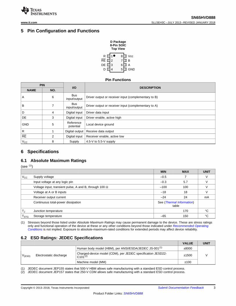
5 Pin Configuration and Functions
D Package8-Pin SOICTop View
Pin FunctionsPIN
I/O DESCRIPTIONNAME NO.
A 6 Businput/output Driver output or receiver input (complementary to B)
B 7 Businput/output Driver output or receiver input (complementary to A)
D 4 Digital input Driver data inputDE 3 Digital input Driver enable, active high
GND 5 Referencepotential Local device ground
R 1 Digital output Receive data outputRE 2 Digital input Receiver enable, active lowVCC 8 Supply 4.5-V to 5.5-V supply
(1) Stresses beyond those listed under Absolute Maximum Ratings may cause permanent damage to the device. These are stress ratingsonly and functional operation of the device at these or any other conditions beyond those indicated under Recommended OperatingConditions is not implied. Exposure to absolute-maximum-rated conditions for extended periods may affect device reliability.
6 Specifications
6.1 Absolute Maximum Ratings(see (1))
MIN MAX UNITVCC Supply voltage –0.5 7 V
Input voltage at any logic pin –0.3 5.7 VVoltage input, transient pulse, A and B, through 100 Ω –100 100 VVoltage at A or B inputs –18 18 VReceiver output current –24 24 mAContinuous total-power dissipation See (Thermal Information)
tableTJ Junction temperature 170 °CTSTG Storage temperature –65 150 °C
(1) JEDEC document JEP155 states that 500-V HBM allows safe manufacturing with a standard ESD control process.(2) JEDEC document JEP157 states that 250-V CDM allows safe manufacturing with a standard ESD control process.
6.2 ESD Ratings: JEDEC SpecificationsVALUE UNIT
V(ESD) Electrostatic discharge
Human body model (HBM), per ANSI/ESDA/JEDEC JS-001 (1) ±8000
VCharged-device model (CDM), per JEDEC specification JESD22-C101 (2) ±1500
Machine model (MM) ±100
4
SN65HVD888SLLSEH3C –JULY 2013–REVISED JANUARY 2018 www.ti.com
Product Folder Links: SN65HVD888
Submit Documentation Feedback Copyright © 2013–2018, Texas Instruments Incorporated
6.3 ESD Ratings: IEC SpecificationsVALUE UNIT
V(ESD) Electrostatic dischargeIEC 61000-4-2 ESD (Contact Discharge), bus terminals and GND ±12000
VIEC 61000-4-4 EFT (Fast transient or burst) bus terminals and GND ±4000IEC 60749-26 ESD (HBM), bus terminals and GND ±16000
(1) The algebraic convention in which the least positive (most negative) limit is designated as minimum is used in this data sheet.(2) Operation is specified for internal (junction) temperatures up to 150°C. Self-heating due to internal power dissipation should be
considered for each application. Maximum junction temperature is internally limited by the thermal shut-down (TSD) circuit whichdisables the driver outputs when the junction temperature reaches 170°C.
6.4 Recommended Operating ConditionsMIN NOM MAX UNIT
VCC Supply voltage 4.5 5 5.5 VVID Differential input voltage –12 12 VVI Input voltage at any bus terminal (separate or common mode) (1) –7 12 VVIH High-level input voltage (driver, driver-enable, and receiver-enable inputs) 2 VCC VVIL Low-level input voltage (driver, driver-enable, and receiver-enable inputs) 0 0.8 V
IO Output currentDriver –60 60
mAReceiver –8 8
CL Differential load capacitance 50 pFRL Differential load resistance 60 Ω
1/tUI Signaling rate 0.3 250 kbpsTJ Junction temperature –40 150 °CTA
(2) Operating free-air temperature (see Thermal Information for additional information) –40 125 °C
(1) For more information about traditional and new thermal metrics, see the Semiconductor and IC Package Thermal Metrics applicationreport, SPRA953.
6.5 Thermal Information
THERMAL METRIC (1)SN65HVD888
UNITD (SOIC)8 PINS
RθJA Junction-to-ambient thermal resistance 116.1 °C/WRθJC(top) Junction-to-case (top) thermal resistance 60.8 °C/WRθJB Junction-to-board thermal resistance 57.1 °C/WψJT Junction-to-top characterization parameter 13.9 °C/WψJB Junction-to-board characterization parameter 56.5 °C/W

5
SN65HVD888www.ti.com SLLSEH3C –JULY 2013–REVISED JANUARY 2018
Product Folder Links: SN65HVD888
Submit Documentation FeedbackCopyright © 2013–2018, Texas Instruments Incorporated
(1) Under any specific conditions, VIT+ is specified to be at least VHYS higher than VIT–.
6.6 Electrical Characteristicsover operating free-air temperature range (unless otherwise noted)
PARAMETER TEST CONDITIONS MIN TYP MAX UNIT
│VOD│Driver differential-output voltagemagnitude
RL = 60 Ω, 375 Ω on each outputfrom –7 to +12 V See Figure 4 1.5 2.5
VRL = 54 Ω (RS-485)See Figure 5
1.5 2.5
RL = 100 Ω (RS-422) 2 3
Δ│VOD│Change in magnitude of driverdifferential-output voltage RL = 54 Ω, CL = 50 pF See Figure 5 –0.2 0 0.2 V
VOC(SS)Steady-state common-modeoutput voltage Center of two 27-Ω load resistors See Figure 5 1 VCC / 2 3 V
ΔVOCChange in differential drivercommon-mode output voltage Center of two 27-Ω load resistors See Figure 5 –0.2 0 0.2 mV
VOC(PP)Peak-to-peak driver common-mode output voltage Center of two 27-Ω load resistors See Figure 5 850 mV
COD Differential output capacitance 8 pF
VIT+Positive-going receiverdifferential-input voltage threshold 35 100 mV
VIT–Negative-going receiverdifferential-input voltage threshold
–100 –35 mV
VHYS(1) Receiver differential-input voltage
threshold hysteresis (VIT+ – VIT– ) 40 60 mV
VOH Receiver high-level output voltage IOH = –8 mA 2.4 VCC – 0.3 V
VOL Receiver low-level output voltage IOL = 8 mA 0.2 0.4 V
IIDriver input, driver enable, andreceiver enable input current –2 2 µA
IOZReceiver high-impedance outputcurrent VO = 0 V or VCC, RE at VCC –10 10 µA
│IOS│ Driver short-circuit output current │IOS│ with VA or VB from –7 to +12 V 150 mA
II Bus input current (driver disabled)VCC = 4.5 to 5.5 V or VI = 12 V 75 125
µAVCC = 0 V, DE at 0 V VI = –7 V –100 –40
ICCSupply current (quiescent)–40°C to 85°C
Driver and receiver enabledDE = VCC,RE = GND,No load
750 900
µA
Driver enabled, receiver disabledDE = VCC,RE = VCC,No load
650
Driver disabled, receiver enabledDE = GND,RE = GND,No load
750
Driver and receiver disabled
DE = GND,D = GNDRE = VCC,No load
0.4 5
ICCSupply current (quiescent)–40°C to 125°C
Driver and receiver enabledDE = VCC,RE = GND,No load
750 990
µADriver enabled, receiver disabledDE = VCC,RE = VCC,No load
715
Driver disabled, receiver enabledDE = GND,RE = GND,No load
825
Supply current (dynamic) See Figure 3

6
SN65HVD888SLLSEH3C –JULY 2013–REVISED JANUARY 2018 www.ti.com
Product Folder Links: SN65HVD888
Submit Documentation Feedback Copyright © 2013–2018, Texas Instruments Incorporated
6.7 Power Dissipation CharacteristicsPARAMETER TEST CONDITIONS VALUE UNIT
PD
Power Dissipationdriver and receiver enabled,VCC = 5.5 V, TJ = 150°C50% duty cycle square-wavesignal at 250 kbps signalingrate:
Unterminated RL = 300 Ω,CL = 50 pF (driver) 164
mWRS-422 load RL = 100 Ω,CL = 50 pF (driver) 247
RS-485 load RL = 54 Ω,CL = 50 pF (driver) 316
6.8 Switching Characteristics3.3 ms > bit time > 4 μs (unless otherwise noted)
PARAMETER TEST CONDITIONS MIN TYP MAX UNIT
DRIVER
tr, tf Driver differential-output rise and fall times RL = 54 Ω, CL = 50 pF See Figure 6 400 700 1200 ns
tPHL, tPLH Driver propagation delay RL = 54 Ω, CL = 50 pF See Figure 6 90 700 1000 ns
tSK(P) Driver pulse skew, |tPHL – tPLH| RL = 54 Ω, CL = 50 pF See Figure 6 25 200 ns
tPHZ, tPLZ Driver disable time See Figure 7 andFigure 8 50 500 ns
tPHZ, tPLZ Driver enable timeReceiver enabled See Figure 7 and
Figure 8 500 1000 ns
Receiver disabled See Figure 7 andFigure 8 3 9 µs
RECEIVER
tr, tf Receiver output rise and fall times CL = 15 pF See Figure 9 18 30 ns
tPHL, tPLH Receiver propagation delay time CL = 15 pF See Figure 9 85 195 ns
tSK(P) Receiver pulse skew, |tPHL – tPLH| CL = 15 pF See Figure 9 1 15 ns
tPHZ, tPLZ Receiver disable time 50 500
tPZL(1),tPZH(1)tPZL(2),tPZH(2)
Receiver enable time
Driver enabled See Figure 10 20 130 ns
Driver disabled See Figure 11 2 8 µs
tFS Bus failsafe time Driver disabled See Figure 12 44 58 76 ms

0
5
10
15
20
25
0 50 100 150 200 250
Sup
ply
Cur
rent
(m
A)
Signal Rate (kbps) C003
VCC = 5 V D = DE = /RE = 5 V
±10
±8
±6
±4
±2
0
2
4
6
8
10
0 10 20 30 40 50 60 70 80 90 100
Driv
er O
utpu
t V
olta
ge (
V)
Driver Output Current (mA) C001
VCC = 5 V D = DE = 5 V
VOH
VOL
0
1
2
3
4
5
6
7
8
9
10
0 10 20 30 40 50 60 70 80 90 100
Driv
er D
iffer
entia
l Out
put
Vol
tage
(V
)
Driver Output Current (mA) C002
VCC = 5 V D = DE = 5 V
7
SN65HVD888www.ti.com SLLSEH3C –JULY 2013–REVISED JANUARY 2018
Product Folder Links: SN65HVD888
Submit Documentation FeedbackCopyright © 2013–2018, Texas Instruments Incorporated
6.9 Typical Characteristics
Figure 1. Driver Output Voltage vs Driver Output Current Figure 2. Driver Differential Output Voltage vs Driver OutputCurrent
Figure 3. Supply Current vs Signaling Rate

VO
VI
tPZL tPLZ
50%
50%
5V
§�5V
0V
VOL10%Input
Generator
A
B
VOD
RL= 110 �
VI50�
DE CL= 50 pF
S1
5V
VO
VI
tPZH
tPHZ
50%
50%
5V
§�0V
0V
VOH90%InputGenerator
A
B
VOD
RL= 110 �
VI50�
DE CL= 50 pF
S1
VOD
VI
tPLH tPHL
tr tf
90%
50%
10%50%
5V
§�2V
§�-2V
0V
InputGenerator
A
B
Vcc
VODD 54 �
VI50�
DE
CL= 50 pF
A
B
VOC
VOC(PP)ûVOC(SS)
VA
VB0V or 5 VA
B
VODD
RL/2
RL/2
CLVOC
0V or 5 VA
B
DE
Vcc
-7V < Vtest < 12 VVODD
375 �
60 �
375 �
8
SN65HVD888SLLSEH3C –JULY 2013–REVISED JANUARY 2018 www.ti.com
Product Folder Links: SN65HVD888
Submit Documentation Feedback Copyright © 2013–2018, Texas Instruments Incorporated
7 Parameter Measurement information
7.1 Driver
Figure 4. Measurement of Driver Differential-Output Voltage With Common-Mode Load
Figure 5. Measurement of Driver Differential and Common-Mode Output With RS-485 Load
Figure 6. Measurement of Driver Differential-Output Rise and Fall Times and Propagation Delays
Figure 7. Measurement of Driver Enable and Disable Times With Active-High Output and Pull-Down Load
Figure 8. Measurement of Driver Enable and Disable Times With Active-Low Output and Pull-up Load

VI
0V
tPHL
50%
InputGenerator
VO
VI50�
RE
A
B
R1.5V
0V
10 k�50%
tFS
VO
VCC
(DE = Low)
VO
VI
50%
5V
§�0V
0V
VOH
50%VOL
VCC
tPZL(2)
VO
tPZH(2)
A at 1.5VB at 0VS1 to GND
A at 0VB at 1.5VS1 to VCC
50%
InputGenerator
VO
VI50�
A
B
R
CL= 15 pFRE
0V or 1.5 V
Vcc
1 k�S1
1.5 V or 0 V
VO
VI
tPHZ
50%
50%
5V
§�0V
0V
VOH90%
50%10% VOL
VCC
tPLZtPZL(1)
VO
tPZH(1) D at 5VS1 to GND
D at 0VS1 to VCC
InputGenerator
VO
VI50�
A
B
R
CL= 15 pFRE
0V or 5 V
DE
Vcc
D
Vcc
1 k�S1
VOD
VI
tPLH tPHL
tr tf
90%
50%
10%50%
5V
VOH
VOL
0V
InputGenerator
VO
VI50�
RE
A
B
R1.5V
0V
CL= 15 pF
9
SN65HVD888www.ti.com SLLSEH3C –JULY 2013–REVISED JANUARY 2018
Product Folder Links: SN65HVD888
Submit Documentation FeedbackCopyright © 2013–2018, Texas Instruments Incorporated
7.2 Receiver
Figure 9. Measurement of Receiver Output Rise and Fall Times and Propagation Delays
Figure 10. Measurement of Receiver Enable and Disable Times With Driver Enabled
Figure 11. Measurement of Receiver Enable Times With Driver Disabled
Figure 12. Measurement of Receiver Polarity-Correction Time With Driver Disabled

Vcc
GND
B
A
D
DE
R
REP
OLC
OR
Copyright © 2018, Texas Instruments Incorporated
10
SN65HVD888SLLSEH3C –JULY 2013–REVISED JANUARY 2018 www.ti.com
Product Folder Links: SN65HVD888
Submit Documentation Feedback Copyright © 2013–2018, Texas Instruments Incorporated
8 Detailed Description
8.1 OverviewThe SN65HVD888 device is a half-duplex RS-485 transceiver suitable for data transmission at rates up to 250kbps over controlled-impedance transmission media (such as twisted-pair cabling). The device features a highlevel of internal transient protection, making it able to withstand up ESD strikes up to 12 kV (per IEC 61000-4-2)and EFT transients up to 4 kV (per IEC 61000-4-4) without incurring damage. Up to 256 units of SN65HVD82may share a common RS-485 bus due to the device’s low bus input currents. The device features automaticpolarity correction, which detects bus mis-wirings at start-up and then swaps the A and B halves of the bus ifneeded.
8.2 Functional Block Diagram
8.3 Feature Description
8.3.1 Low-Power Standby ModeWhen the driver and the receiver are both disabled (DE = Low and RE = High) the device enters standby mode.If the enable inputs are in the disabled state for only a brief time (for example: less than 100 ns), the device doesnot enter standby mode, preventing the SN65HVD888 from entering standby mode during driver or receiverenabling. Only when the enable inputs are held in the disabled state for a duration of 300 ns or more does thedevice enter low-power standby mode. In this mode most internal circuitry is powered down, and the steady-statesupply current is typically less than 400 nA. When either the driver or the receiver is re-enabled, the internalcircuitry becomes active. During VCC power-up, when the device is set for both driver and receiver disabledmode, the device may consume more than 5-µA of ICC disabled current because of capacitance charging effects.This condition occurs only during VCC power up.
8.3.2 Bus Polarity CorrectionThe SN65HVD888 automatically corrects a wrong bus-signal polarity caused by a cross-wire fault. In order todetect the bus polarity, all three of the following conditions must be met:• A failsafe-biasing network (commonly at the master node) must define the signal polarity of the bus• A slave node must enable the receiver and disable the driver (RE = DE = Low)• The bus must idle for the failsafe time, tFS-max
After the failsafe time has passed, the polarity correction is complete and is applied to both the receive andtransmit channels. The status of the bus polarity is latched within the transceiver and is maintained forsubsequent data transmissions.
NOTEData string durations of consecutive 0s or 1s exceeding tFS-min can accidently trigger awrong polarity correction and must be avoided.
Figure 13 shows a simple point-to-point data link between a master node and a slave node. Because the masternode with the failsafe biasing network determines the signal polarity on the bus, an RS-485 transceiver withoutpolarity correction, such as SN65HVD82, suffices. All other bus nodes, typically performing as slaves, require theSN65HVD888 transceiver with polarity correction.

-Vod +Vod
Dm
VAm
VBm
DIRm
high Z
-Vid+Vid
tFS
Rs
VAs
VBs
Uncorrected R output:R is in phase with
wrong VID polarity
Corrected R output:R is reversed to
wrong VID polarity
DIRs
Low due to pull-downor actively driven
VSs
Low due to pull-down and then actively driven
Mastersignals
Slavesignals
VFS
VFS
0V
0V
A
B
D
DE
R
PO
LCO
RRE
Vcc
GND
A
B
D
DE
R
RE
VS-Master
RFS
RFS
RT (opt.)
VSM
GND
Vcc
VS-Slave
RxD
TxD
DIR
MCU
DGND
Vdd
VS-Slave
RxD
TxD
DIR
MCU
DGND
Vdd
VS-Master Slavenode
Masternode
RT (opt.)
11
SN65HVD888www.ti.com SLLSEH3C –JULY 2013–REVISED JANUARY 2018
Product Folder Links: SN65HVD888
Submit Documentation FeedbackCopyright © 2013–2018, Texas Instruments Incorporated
Feature Description (continued)
Figure 13. Point-To-Point Data Link With Cross-Wire Fault
Prior to initiating data transmission the master transceiver must idle for a time span that exceeds the maximumfailsafe time, tFS-max, of a slave transceiver. This idle time is accomplished by driving the direction control line,DIR, low. After a time, t > tFS-max, the master begins transmitting data.
Because of the indicated cross-wire fault between master and slave, the slave node receives bus signals withreversed polarity. Assuming the slave node has just been connected to the bus, the direction-control pin ispulled-down during power-up and then is actively driven low by the slave MCU. The polarity correction begins assoon as the slave supply is established and ends after approximately 44 to 76 ms.
Figure 14. Polarity Correction Timing Prior to a Data Transmission

12
SN65HVD888SLLSEH3C –JULY 2013–REVISED JANUARY 2018 www.ti.com
Product Folder Links: SN65HVD888
Submit Documentation Feedback Copyright © 2013–2018, Texas Instruments Incorporated
Feature Description (continued)
(1) The polarity-correcting mode is entered when VID < VIT– and t > tFS and DE = low. This state is latched when RE turns from Low to High.
Initially the slave receiver assumes that the correct bus polarity is applied to the inputs and performs no polarityreversal. Because of the reversed polarity of the bus-failsafe voltage, the output of the slave receiver, RS, turnslow. After tFS has passed and the receiver has detected the wrong bus polarity, the internal POLCOR logicreverses the input signal and RS turns high.
At this point all incoming bus data with reversed polarity are polarity corrected within the transceiver. Becausepolarity correction is also applied to the transmit path, the data sent by the slave MCU are reversed by thePOLCOR logic and then fed into the driver.
The reversed data from the slave MCU are reversed again by the cross-wire fault in the bus, and the correct buspolarity is reestablished at the master end.
This process repeats each time the device powers up and detects an incorrect bus polarity.
8.4 Device Functional Modes
Table 1. Driver Pin FunctionsINPUT ENABLE OUTPUTS
DESCRIPTIOND DE A B
NORMAL MODE
H H H L Actively drives bus High
L H L H Actively drives bus Low
X L Z Z Driver disabled
X OPEN Z Z Driver disabled by default
OPEN H H L Actively drives bus High
POLARITY-CORRECTING MODE (1)
H H L H Actively drives bus Low
L H H L Actively drives bus High
X L Z Z Driver disabled
X OPEN Z Z Driver disabled by default
OPEN H L H Actively drives bus Low
(1) The polarity-correcting mode is entered when VID < VIT– and t > tFS and DE = low. This state is latched when RE turns from Low to High.
Table 2. Receiver Pin FunctionsDIFFERENTIAL INPUT ENABLE OUTPUT
DESCRIPTIONVID = VA – VB RE R
NORMAL MODE
VIT+ < VID L H Receive valid bus High
VIT– < VID < VIT+ L ? Indeterminate bus state
VID < VIT– L L Receive valid bus Low
X H Z Receiver disabled
X OPEN Z Receiver disabled
Open, short, idle Bus L ? Indeterminate bus state
POLARITY-CORRECTING MODE (1)
VIT+ < VID L L Receive valid bus Low
VIT– < VID < VIT+ L ? Indeterminate bus state
VID < VIT– L H Receive polarity corrected bus High
X H Z Receiver disabled
X OPEN Z Receiver disabled
Open, short, idle Bus L ? Indeterminate bus state

Vcc
9V
D and RE Inputs
1k
100k
D,RE
Vcc
9V
DE Input
1k
100k
DE
Vcc
9V
R Output
1kR
Vcc
16V
16V
A
B
Driver Outputs
R2
R1
16V
16V
A
Receiver Inputs Vcc
B
R3
R
R2
R3
R1
13
SN65HVD888www.ti.com SLLSEH3C –JULY 2013–REVISED JANUARY 2018
Product Folder Links: SN65HVD888
Submit Documentation FeedbackCopyright © 2013–2018, Texas Instruments Incorporated
Figure 15. Equivalent Input and Output Schematic Diagrams

Vcc
GND
B
A
D
DE
R
RE
PO
LCO
R
a) Independent driver and receiver enable signals
b) Combined enable signals for use as directional control pin
c) Receiver always on
R
D
Vcc
GND
B
A
D
DE
R
REP
OLC
OR
R
D
Vcc
GND
B
A
D
DE
R
RE
PO
LCO
R
R
D
Copyright © 2018, Texas Instruments Incorporated
14
SN65HVD888SLLSEH3C –JULY 2013–REVISED JANUARY 2018 www.ti.com
Product Folder Links: SN65HVD888
Submit Documentation Feedback Copyright © 2013–2018, Texas Instruments Incorporated
9 Application and Implementation
NOTEInformation in the following applications sections is not part of the TI componentspecification, and TI does not warrant its accuracy or completeness. TI’s customers areresponsible for determining suitability of components for their purposes. Customers shouldvalidate and test their design implementation to confirm system functionality.
9.1 Application Information
9.1.1 Device ConfigurationThe SN65HVD888 is a half-duplex RS-485 transceiver operating from a single 5-V ±10% supply. The driver andreceiver enable pins allow for the configuration of different operating modes.
Figure 16. Transceiver Configurations
Using independent enable lines provides the most flexible control as the lines allow for the driver and thereceiver to be turned on and turned off individually. While this configuration requires two control lines, it allows forselective listening to the bus traffic, whether the driver is transmitting data or not. Only this configuration allowsthe SN65HVD888 to enter low-power standby mode because it allows both the driver and receiver to be disabledsimultaneously.
Combining the enable signals simplifies the interface to the controller by forming a single direction-control signal.Thus, when the direction-control line is high, the transceiver is configured as a driver, while for a low the deviceoperates as a receiver.
Tying the receiver enable to ground and controlling only the driver-enable input also uses only one control line. Inthis configuration a node not only receives the data on the bus sent by other nodes but also receives the datasent on the bus, enabling the node to verify the correct data has been transmitted.
9.1.2 Bus DesignAn RS-485 bus consists of multiple transceivers connected in parallel to a bus cable. To eliminate linereflections, each cable end is terminated with a termination resistor, RT, whose value matches the characteristicimpedance, Z0, of the cable. This method, known as parallel termination, allows for relatively high data rates overlong cable length.
Common cables used are unshielded twisted pair (UTP), such as low-cost CAT-5 cable with Z0 = 100 Ω, andRS-485 cable with Z0 = 120 Ω. Typical cable sizes are AWG 22 and AWG 24.
The maximum bus length is typically given as 4000 ft or 1200 m, and represents the length of an AWG 24 cablewhose cable resistance approaches the value of the termination resistance, thus reducing the bus signal by halfor 6 dB. Actual maximum usable cable length depends on the signaling rate, cable characteristics, andenvironmental conditions.

10000
1000
100
10
CA
BL
EL
EN
GT
H-
ft
100 1k 10k 100k 1M 10M 100M
DATA RATE - bps
Conservative
Characteristics
5,10,20 % Jitter
15
SN65HVD888www.ti.com SLLSEH3C –JULY 2013–REVISED JANUARY 2018
Product Folder Links: SN65HVD888
Submit Documentation FeedbackCopyright © 2013–2018, Texas Instruments Incorporated
Application Information (continued)Table 3. VID with a Failsafe Network and Bus Termination
VCCRL DIFFERENTIAL
TERMINATIONRFS PULLUP RFS PULLDOWN VID
5 V 54 Ω
560 Ω 560 Ω 230 mV1 KΩ 1 KΩ 131 mV
4.7 KΩ 4.7 KΩ 29 mV10 KΩ 10 KΩ 13 mV
An external failsafe-resistor network must be used to ensure failsafe operation during an idle bus state. When thebus is not actively driven, the differential receiver inputs could float allowing the receiver output to assume arandom output. A proper failsafe network forces the receiver inputs to exceed the VIT threshold, thus forcing theSN65HVD888 receiver output into the failsafe (high) state. Table 3 shows the differential input voltage (VID) forvarious failsafe networks with a 54-Ω differential bus termination.
9.1.3 Cable Length Versus Data RateThere is an inverse relationship between data rate and cable length, which means the higher the data rate, theshorter the cable length; and conversely, the lower the data rate the longer the cable length. While most RS-485systems use data rates between 10 kbps and 100 kbps, applications such as e-metering often operate at rates ofup to 250 kbps even at distances of 4000 ft and longer. Longer distances are possible by allowing for smallsignal jitter of up to 5 or 10%.
Figure 17. Cable Length vs Data Rate Characteristic
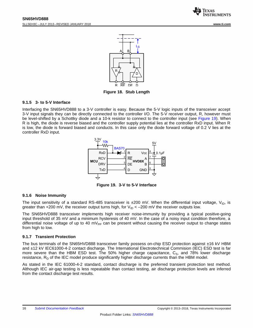
9.1.4 Stub LengthWhen connecting a node to the bus, the distance between the transceiver inputs and the cable trunk, known asthe stub, should be as short as possible. The reason for the short distance is because a stub presents a non-terminated piece of bus line which can introduce reflections if the distance is too long. As a general guideline, theelectrical length or round-trip delay of a stub should be less than one-tenth of the rise time of the driver, thusleading to a maximum physical stub length of as shown in Equation 1.
LStub ≤ 0.1 × tr × v × c
where• tr is the 10/90 rise time of the driver• c is the speed of light (3 × 10⁸ m/s or 9.8 × 108 ft/s)• v is the signal velocity of the cable (v = 78%) or trace (v = 45%) as a factor of c (1)
Based on Equation 1, with a minimum rise time of 400 ns, Equation 2 shows the maximum cable-stub length ofthe SN65HVD888.
LStub ≤ 0.1 × 400 × 10-9 × 3 108 × 0.78 = 9.4 m (or 30.6 ft) (2)
RxD
TxD
DRVMCU
R
RE
DE
D
A
B
Vcc
GND
1
2
3
4
7
6
5
3.3V10k
HVD8X
8
5V
0.1µF
BAS70
RCV
R
A B
R RE DE D
D
LS
16
SN65HVD888SLLSEH3C –JULY 2013–REVISED JANUARY 2018 www.ti.com
Product Folder Links: SN65HVD888
Submit Documentation Feedback Copyright © 2013–2018, Texas Instruments Incorporated
Figure 18. Stub Length
9.1.5 3- to 5-V InterfaceInterfacing the SN65HVD888 to a 3-V controller is easy. Because the 5-V logic inputs of the transceiver accept3-V input signals they can be directly connected to the controller I/O. The 5-V receiver output, R, however mustbe level-shifted by a Schottky diode and a 10-k resistor to connect to the controller input (see Figure 19). WhenR is high, the diode is reverse biased and the controller supply potential lies at the controller RxD input. When Ris low, the diode is forward biased and conducts. In this case only the diode forward voltage of 0.2 V lies at thecontroller RxD input.
Figure 19. 3-V to 5-V Interface
9.1.6 Noise ImmunityThe input sensitivity of a standard RS-485 transceiver is ±200 mV. When the differential input voltage, VID, isgreater than +200 mV, the receiver output turns high, for VID < –200 mV the receiver outputs low.
The SN65HVD888 transceiver implements high receiver noise-immunity by providing a typical positive-goinginput threshold of 35 mV and a minimum hysteresis of 40 mV. In the case of a noisy input condition therefore, adifferential noise voltage of up to 40 mVPP can be present without causing the receiver output to change statesfrom high to low.
9.1.7 Transient ProtectionThe bus terminals of the SN65HVD888 transceiver family possess on-chip ESD protection against ±16 kV HBMand ±12 kV IEC61000-4-2 contact discharge. The International Electrotechnical Commision (IEC) ESD test is farmore severe than the HBM ESD test. The 50% higher charge capacitance, CS, and 78% lower dischargeresistance, RD of the IEC model produce significantly higher discharge currents than the HBM model.
As stated in the IEC 61000-4-2 standard, contact discharge is the preferred transient protection test method.Although IEC air-gap testing is less repeatable than contact testing, air discharge protection levels are inferredfrom the contact discharge test results.

RC RD
CSHigh-Voltage
PulseGenerator
DeviceUnderTest C
urre
nt -
A
4035302520151050
Time - ns
0 50 100 150 200 250 300
10kV IEC
10kV HBM
330
(1.5k)
150pF
(100pF)
50M
(1M)
Copyright © 2016, Texas Instruments Incorporated
17
SN65HVD888www.ti.com SLLSEH3C –JULY 2013–REVISED JANUARY 2018
Product Folder Links: SN65HVD888
Submit Documentation FeedbackCopyright © 2013–2018, Texas Instruments Incorporated
Figure 20. HBM and IEC-ESD Models and Currents in Comparison (HBM Values in Parenthesis)
The on-chip implementation of IEC ESD protection significantly increases the robustness of equipment. Commondischarge events occur because of human contact with connectors and cables. Designers may choose toimplement protection against longer duration transients, typically referred to as surge transients. Figure 12suggests two circuit designs providing protection against short and long duration surge transients, in addition toESD and Electrical Fast Transients (EFT) transients. Table 4 lists the bill of materials for the external protectiondevices.
EFTs are generally caused by relay-contact bounce or the interruption of inductive loads. Surge transients oftenresult from lightning strikes (direct strike or an indirect strike which induce voltages and currents), or theswitching of power systems, including load changes and short circuits switching. These transients are oftenencountered in industrial environments, such as factory automation and power-grid systems.
Figure 21 compares the pulse-power of the EFT and surge transients with the power caused by an IEC ESDtransient. In the diagram on the left of Figure 21, the tiny blue blip in the bottom left corner represents the powerof a 10-kV ESD transient, which already dwarfs against the significantly higher EFT power spike, and certainlydwarfs against the 500-V surge transient. This type of transient power is well representative of factoryenvironments in industrial and process automation. The diagram on the fright of Figure 21 compares theenormous power of a 6-kV surge transient, most likely occurring in e-metering applications of power generatingand power grid systems, with the aforementioned 500-V surge transient.
NOTEThe unit of the pulse-power changes from kW to MW, thus making the power of the 500-Vsurge transient almost dropping off the scale.

100
0.1
0.01
10
1
10-3
10-4
10-5
10-6
Pu
lse E
nerg
y -
Jo
ule
0.5 1 2 4 6 8 10
Peak Pulse Voltage - kV
1000
ESD
EFT
Surge
15
EFT Pulse Train
Pu
lse
Po
we
r -
kW
22
20
18
16
14
12
10
8
6
4
2
0
Time - sμ
0 5 10 15 20 25 30 35 40
0.5kV Surge
10kV ESD
4kV EFT
Pu
lse
Po
we
r -
MW
2.2
2.0
1.8
1.6
1.4
1.2
1.0
0.8
0.6
0.4
0.2
0
Time - sμ
0 5 10 15 20 25 30 35 40
0.5kV Surge
6kV Surge
3.0
2.8
2.6
2.4
18
SN65HVD888SLLSEH3C –JULY 2013–REVISED JANUARY 2018 www.ti.com
Product Folder Links: SN65HVD888
Submit Documentation Feedback Copyright © 2013–2018, Texas Instruments Incorporated
Figure 21. Power Comparison of ESD, EFT, and Surge Transients
In the case of surge transients, hgih-energy content is signified by long pulse duration and slow decaying pulsepower
The electrical energy of a transient that is dumped into the internal protection cells of the transceiver is convertedinto thermal energy. This thermal energy heats the protection cells and literally destroys them, thus destroyingthe transceiver. Figure 22 shows the large differences in transient energies for single ESD, EFT, and surgetransients as well as for an EFT pulse train, commonly applied during compliance testing.
Figure 22. Comparison of Transient Energies

R
RE
DE
D
B
A
Vcc
GND
1
2
3
4
7
6
5
Vcc
10k
10k
XCVR
TVS
R1
R2
TBU1
TBU2
MOV1
MOV2
8
Vcc
0.1�FRxD
TxD
DIR
MCU
R
RE
DE
D
B
A
Vcc
GND
1
2
3
4
7
6
5
Vcc
10k
10k
XCVR
TVS
R1
R2
8
Vcc
0.1�FRxD
TxD
DIR
MCU
Copyright © 2016, Texas Instruments Incorporated
19
SN65HVD888www.ti.com SLLSEH3C –JULY 2013–REVISED JANUARY 2018
Product Folder Links: SN65HVD888
Submit Documentation FeedbackCopyright © 2013–2018, Texas Instruments Incorporated
Table 4. Bill of MaterialsDEVICE FUNCTION ORDER NUMBER MANUFACTURER
XCVR 5-V, 250-kbps RS-485 Transceiver SN65HVD888 TIR1, R2 10-Ω, Pulse-Proof Thick-Film Resistor CRCW0603010RJNEAHP VishayTVS Bidirectional 400-W Transient Suppressor CDSOT23-SM712 BournsTBU1, TBU2 Bidirectional. TBU-CA-065-200-WH Bourns
MOV1, MOV2 200mA Transient Blocking Unit 200-V, Metal-Oxide Varistor MOV-10D201K Bourns
Figure 23. Transient Protections Against ESD, EFT, and Surge Transients
The left circuit shown in Figure 23 provides surge protection of ≥ 500-V transients, while the right protectioncircuits can withstand surge transients of 5 kV.

Vcc1 Vcc2
GND1 GND2
OUTA
16
14
13
2,8 9,15
INA
OUTD
1
3
4
5
6ISO7241
0.1μF 0.1μF
EN1 EN27 10
INB12
11
OUTB
OUTC
IND
INC
4.7k 4.7k
10μF 0.1μF
MBR0520L
MBR0520L
1:1.330.1μF
3
1
D2
SN6501
D1
Vcc
4,5
2
GND
3.3V
IN
EN GND
OUT4 1
23TLV70733
10μF
5VISO
10μF
ISO-BARRIER
8
7
6
5
UCA0RXD
P3.0
P3.1
UCA0TXD
16
11
12
15
4
XOUT
XIN
5
6
2
MSP430
F2132
1
2
3
4
0.1μF
TVS
R1
0.1μF
DVss
DVcc
R2
Vcc
GND2
B
A
R
RE
DE
D
HVD888
RHV
PSU
L1
N
PE
PE
PEisland
Protective Earth Ground,
Equipment Safety Ground
Floating RS-485 Common
RHV
R1,R2, TVS: see A. below
Short thick Earth wire or Chassis
CHV
CHV
= 1MΩ, 2kV high-voltage resistor, TT electronics, HVC 2010 1M0 G T3
= 4.7nF, 2kV high-voltage capacitor, NOVACAP, 1812 B 472 K 202 N T
Copyright © 2017, Texas Instruments Incorporated
20
SN65HVD888SLLSEH3C –JULY 2013–REVISED JANUARY 2018 www.ti.com
Product Folder Links: SN65HVD888
Submit Documentation Feedback Copyright © 2013–2018, Texas Instruments Incorporated
9.2 Typical ApplicationMany RS-485 networks use isolated bus nodes to prevent the creation of unintended ground loops and theirdisruptive impact on signal integrity. An isolated bus node typically includes a micro controller that connects tothe bus transceiver through a multi-channel, digital isolator (Figure 24).
A. See Table 4.
Figure 24. Isolated Bus Node With Transient Protection
9.2.1 Design RequirementsExample Application: Isolated Bus Node with Transient Protection• RS-485-compliant bus interface (needs differential signal amplitude of at least 1.5 V under fully-loaded
conditions – essentially, maximum number of nodes connected and with dual 120-Ω termination).• Galvanic isolation of both signal and power supply lines.• Able to withstand ESD transients up to 12 kV (per IEC 61000-4-2) and EFTs up to 4 kV (per IEC 61000-4-4).• • Full control of data flow on bus in order to prevent contention (for half-duplex communication).
9.2.2 Detailed Design ProcedurePower isolation is accomplished using the push-pull transformer driver SN6501 and a low-cost LDO, TLV70733.
Signal isolation uses the quadruple digital isolator ISO7241. Notice that both enable inputs, EN1 and EN2, arepulled-up via 4.7-kΩ resistors to limit input currents during transient events.
While the transient protection is similar to the one in Figure 23 (left circuit), an additional high-voltage capacitordiverts transient energy from the floating RS-485 common further towards Protective Earth (PE) ground. Thisdiversion is necessary as noise transients on the bus are usually referred to Earth potential.
RVH refers to a high-voltage resistor, and in some applications even a varistor. This resistance is applied toprevent charging of the floating ground to dangerous potentials during normal operation.
21
SN65HVD888www.ti.com SLLSEH3C –JULY 2013–REVISED JANUARY 2018
Product Folder Links: SN65HVD888
Submit Documentation FeedbackCopyright © 2013–2018, Texas Instruments Incorporated
Typical Application (continued)Occasionally varistors are used instead of resistors in order to rapidly discharge CHV, if expected that fasttransients might charge CHV to high-potentials.
Note that the PE island represents a copper island on the PCB for the provision of a short, thick Earth wireconnecting this island to PE ground at the entrance of the power supply unit (PSU).
In equipment designs using a chassis, the PE connection is usually provided through the chassis itself. Typicallythe PE conductor is tied to the chassis at one end while the high-voltage components, CHV and RHV, areconnecting to the chassis at the other end.
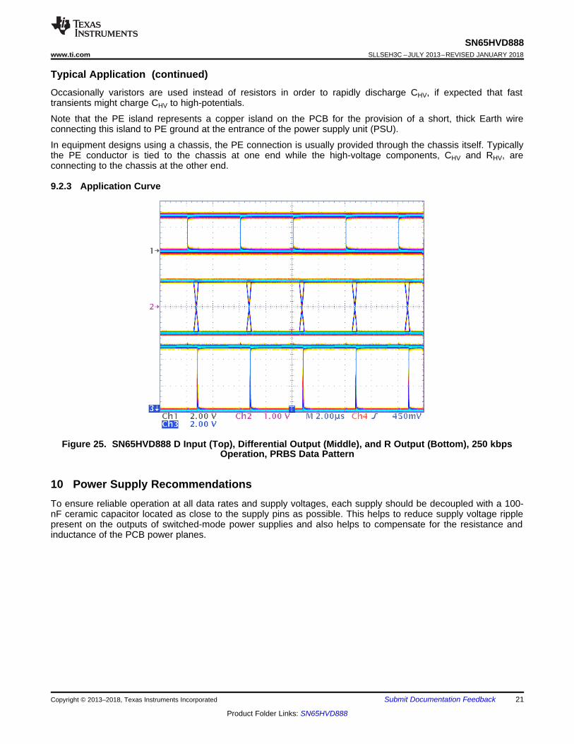
9.2.3 Application Curve
Figure 25. SN65HVD888 D Input (Top), Differential Output (Middle), and R Output (Bottom), 250 kbpsOperation, PRBS Data Pattern
10 Power Supply RecommendationsTo ensure reliable operation at all data rates and supply voltages, each supply should be decoupled with a 100-nF ceramic capacitor located as close to the supply pins as possible. This helps to reduce supply voltage ripplepresent on the outputs of switched-mode power supplies and also helps to compensate for the resistance andinductance of the PCB power planes.
MCUR
R
Via to ground
SN65HVD888
JMP
R
R
R
C
5
6
6
1
4R
5
Via to VCC
TVS
75
22
SN65HVD888SLLSEH3C –JULY 2013–REVISED JANUARY 2018 www.ti.com
Product Folder Links: SN65HVD888
Submit Documentation Feedback Copyright © 2013–2018, Texas Instruments Incorporated
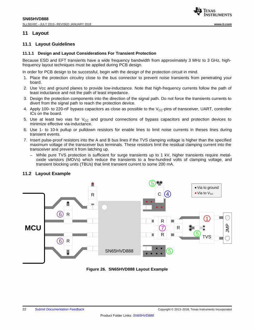
11 Layout
11.1 Layout Guidelines
11.1.1 Design and Layout Considerations For Transient ProtectionBecause ESD and EFT transients have a wide frequency bandwidth from approximately 3 MHz to 3 GHz, high-frequency layout techniques must be applied during PCB design.
In order for PCB design to be successful, begin with the design of the protection circuit in mind.1. Place the protection circuitry close to the bus connector to prevent noise transients from penetrating your
board.2. Use Vcc and ground planes to provide low-inductance. Note that high-frequency currents follow the path of
least inductance and not the path of least impedance.3. Design the protection components into the direction of the signal path. Do not force the transients currents to
divert from the signal path to reach the protection device.4. Apply 100- to 220-nF bypass capacitors as close as possible to the VCC-pins of transceiver, UART, controller
ICs on the board.5. Use at least two vias for VCC and ground connections of bypass capacitors and protection devices to
minimize effective via-inductance.6. Use 1- to 10-k pullup or pulldown resistors for enable lines to limit noise currents in theses lines during
transient events.7. Insert pulse-proof resistors into the A and B bus lines if the TVS clamping voltage is higher than the specified
maximum voltage of the transceiver bus terminals. These resistors limit the residual clamping current into thetransceiver and prevent it from latching up.– While pure TVS protection is sufficient for surge transients up to 1 kV, higher transients require metal-
oxide varistors (MOVs) which reduce the transients to a few-hundred volts of clamping voltage, andtransient blocking units (TBUs) that limit transient current to some 200 mA.
11.2 Layout Example
Figure 26. SN65HVD888 Layout Example

23
SN65HVD888www.ti.com SLLSEH3C –JULY 2013–REVISED JANUARY 2018
Product Folder Links: SN65HVD888
Submit Documentation FeedbackCopyright © 2013–2018, Texas Instruments Incorporated
12 Device and Documentation Support
12.1 Device Support
12.1.1 Third-Party Products DisclaimerTI'S PUBLICATION OF INFORMATION REGARDING THIRD-PARTY PRODUCTS OR SERVICES DOES NOTCONSTITUTE AN ENDORSEMENT REGARDING THE SUITABILITY OF SUCH PRODUCTS OR SERVICESOR A WARRANTY, REPRESENTATION OR ENDORSEMENT OF SUCH PRODUCTS OR SERVICES, EITHERALONE OR IN COMBINATION WITH ANY TI PRODUCT OR SERVICE.
12.2 Receiving Notification of Documentation UpdatesTo receive notification of documentation updates, navigate to the device product folder on ti.com. In the upperright corner, click on Alert me to register and receive a weekly digest of any product information that haschanged. For change details, review the revision history included in any revised document.
12.3 Community ResourcesThe following links connect to TI community resources. Linked contents are provided "AS IS" by the respectivecontributors. They do not constitute TI specifications and do not necessarily reflect TI's views; see TI's Terms ofUse.
TI E2E™ Online Community TI's Engineer-to-Engineer (E2E) Community. Created to foster collaborationamong engineers. At e2e.ti.com, you can ask questions, share knowledge, explore ideas and helpsolve problems with fellow engineers.
Design Support TI's Design Support Quickly find helpful E2E forums along with design support tools andcontact information for technical support.
12.4 TrademarksE2E is a trademark of Texas Instruments.All other trademarks are the property of their respective owners.
12.5 Electrostatic Discharge CautionThese devices have limited built-in ESD protection. The leads should be shorted together or the device placed in conductive foamduring storage or handling to prevent electrostatic damage to the MOS gates.
12.6 GlossarySLYZ022 — TI Glossary.
This glossary lists and explains terms, acronyms, and definitions.
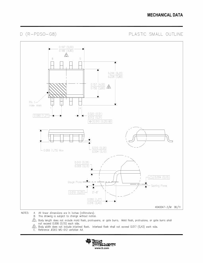
13 Mechanical, Packaging, and Orderable InformationThe following pages include mechanical, packaging, and orderable information. This information is the mostcurrent data available for the designated devices. This data is subject to change without notice and revision ofthis document. For browser-based versions of this data sheet, refer to the left-hand navigation.
PACKAGE OPTION ADDENDUM
www.ti.com 18-Dec-2017
Addendum-Page 1
PACKAGING INFORMATION
Orderable Device Status(1)
Package Type PackageDrawing
Pins PackageQty
Eco Plan(2)
Lead/Ball Finish(6)
MSL Peak Temp(3)
Op Temp (°C) Device Marking(4/5)
Samples
SN65HVD888D ACTIVE SOIC D 8 75 Green (RoHS& no Sb/Br)
CU NIPDAU Level-1-260C-UNLIM -40 to 85 HVD888
SN65HVD888DR ACTIVE SOIC D 8 2500 Green (RoHS& no Sb/Br)
CU NIPDAU Level-1-260C-UNLIM -40 to 85 HVD888
(1) The marketing status values are defined as follows:ACTIVE: Product device recommended for new designs.LIFEBUY: TI has announced that the device will be discontinued, and a lifetime-buy period is in effect.NRND: Not recommended for new designs. Device is in production to support existing customers, but TI does not recommend using this part in a new design.PREVIEW: Device has been announced but is not in production. Samples may or may not be available.OBSOLETE: TI has discontinued the production of the device.
(2) RoHS: TI defines "RoHS" to mean semiconductor products that are compliant with the current EU RoHS requirements for all 10 RoHS substances, including the requirement that RoHS substancedo not exceed 0.1% by weight in homogeneous materials. Where designed to be soldered at high temperatures, "RoHS" products are suitable for use in specified lead-free processes. TI mayreference these types of products as "Pb-Free".RoHS Exempt: TI defines "RoHS Exempt" to mean products that contain lead but are compliant with EU RoHS pursuant to a specific EU RoHS exemption.Green: TI defines "Green" to mean the content of Chlorine (Cl) and Bromine (Br) based flame retardants meet JS709B low halogen requirements of <=1000ppm threshold. Antimony trioxide basedflame retardants must also meet the <=1000ppm threshold requirement.
(3) MSL, Peak Temp. - The Moisture Sensitivity Level rating according to the JEDEC industry standard classifications, and peak solder temperature.
(4) There may be additional marking, which relates to the logo, the lot trace code information, or the environmental category on the device.
(5) Multiple Device Markings will be inside parentheses. Only one Device Marking contained in parentheses and separated by a "~" will appear on a device. If a line is indented then it is a continuationof the previous line and the two combined represent the entire Device Marking for that device.
(6) Lead/Ball Finish - Orderable Devices may have multiple material finish options. Finish options are separated by a vertical ruled line. Lead/Ball Finish values may wrap to two lines if the finishvalue exceeds the maximum column width.
Important Information and Disclaimer:The information provided on this page represents TI's knowledge and belief as of the date that it is provided. TI bases its knowledge and belief on informationprovided by third parties, and makes no representation or warranty as to the accuracy of such information. Efforts are underway to better integrate information from third parties. TI has taken andcontinues to take reasonable steps to provide representative and accurate information but may not have conducted destructive testing or chemical analysis on incoming materials and chemicals.TI and TI suppliers consider certain information to be proprietary, and thus CAS numbers and other limited information may not be available for release.
In no event shall TI's liability arising out of such information exceed the total purchase price of the TI part(s) at issue in this document sold by TI to Customer on an annual basis.

PACKAGE OPTION ADDENDUM
www.ti.com 18-Dec-2017
Addendum-Page 2

TAPE AND REEL INFORMATION
*All dimensions are nominal
Device PackageType
PackageDrawing
Pins SPQ ReelDiameter
(mm)
ReelWidth
W1 (mm)
A0(mm)
B0(mm)
K0(mm)
P1(mm)
W(mm)
Pin1Quadrant
SN65HVD888DR SOIC D 8 2500 330.0 12.5 6.4 5.2 2.1 8.0 12.0 Q1
PACKAGE MATERIALS INFORMATION
www.ti.com 18-Dec-2017
Pack Materials-Page 1
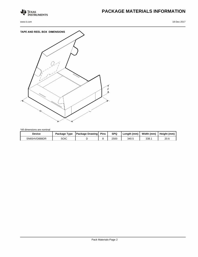
*All dimensions are nominal
Device Package Type Package Drawing Pins SPQ Length (mm) Width (mm) Height (mm)
SN65HVD888DR SOIC D 8 2500 340.5 338.1 20.6
PACKAGE MATERIALS INFORMATION
www.ti.com 18-Dec-2017
Pack Materials-Page 2


IMPORTANT NOTICE
Texas Instruments Incorporated (TI) reserves the right to make corrections, enhancements, improvements and other changes to itssemiconductor products and services per JESD46, latest issue, and to discontinue any product or service per JESD48, latest issue. Buyersshould obtain the latest relevant information before placing orders and should verify that such information is current and complete.TI’s published terms of sale for semiconductor products (http://www.ti.com/sc/docs/stdterms.htm) apply to the sale of packaged integratedcircuit products that TI has qualified and released to market. Additional terms may apply to the use or sale of other types of TI products andservices.Reproduction of significant portions of TI information in TI data sheets is permissible only if reproduction is without alteration and isaccompanied by all associated warranties, conditions, limitations, and notices. TI is not responsible or liable for such reproduceddocumentation. Information of third parties may be subject to additional restrictions. Resale of TI products or services with statementsdifferent from or beyond the parameters stated by TI for that product or service voids all express and any implied warranties for theassociated TI product or service and is an unfair and deceptive business practice. TI is not responsible or liable for any such statements.Buyers and others who are developing systems that incorporate TI products (collectively, “Designers”) understand and agree that Designersremain responsible for using their independent analysis, evaluation and judgment in designing their applications and that Designers havefull and exclusive responsibility to assure the safety of Designers' applications and compliance of their applications (and of all TI productsused in or for Designers’ applications) with all applicable regulations, laws and other applicable requirements. Designer represents that, withrespect to their applications, Designer has all the necessary expertise to create and implement safeguards that (1) anticipate dangerousconsequences of failures, (2) monitor failures and their consequences, and (3) lessen the likelihood of failures that might cause harm andtake appropriate actions. Designer agrees that prior to using or distributing any applications that include TI products, Designer willthoroughly test such applications and the functionality of such TI products as used in such applications.TI’s provision of technical, application or other design advice, quality characterization, reliability data or other services or information,including, but not limited to, reference designs and materials relating to evaluation modules, (collectively, “TI Resources”) are intended toassist designers who are developing applications that incorporate TI products; by downloading, accessing or using TI Resources in anyway, Designer (individually or, if Designer is acting on behalf of a company, Designer’s company) agrees to use any particular TI Resourcesolely for this purpose and subject to the terms of this Notice.TI’s provision of TI Resources does not expand or otherwise alter TI’s applicable published warranties or warranty disclaimers for TIproducts, and no additional obligations or liabilities arise from TI providing such TI Resources. TI reserves the right to make corrections,enhancements, improvements and other changes to its TI Resources. TI has not conducted any testing other than that specificallydescribed in the published documentation for a particular TI Resource.Designer is authorized to use, copy and modify any individual TI Resource only in connection with the development of applications thatinclude the TI product(s) identified in such TI Resource. NO OTHER LICENSE, EXPRESS OR IMPLIED, BY ESTOPPEL OR OTHERWISETO ANY OTHER TI INTELLECTUAL PROPERTY RIGHT, AND NO LICENSE TO ANY TECHNOLOGY OR INTELLECTUAL PROPERTYRIGHT OF TI OR ANY THIRD PARTY IS GRANTED HEREIN, including but not limited to any patent right, copyright, mask work right, orother intellectual property right relating to any combination, machine, or process in which TI products or services are used. Informationregarding or referencing third-party products or services does not constitute a license to use such products or services, or a warranty orendorsement thereof. Use of TI Resources may require a license from a third party under the patents or other intellectual property of thethird party, or a license from TI under the patents or other intellectual property of TI.TI RESOURCES ARE PROVIDED “AS IS” AND WITH ALL FAULTS. TI DISCLAIMS ALL OTHER WARRANTIES ORREPRESENTATIONS, EXPRESS OR IMPLIED, REGARDING RESOURCES OR USE THEREOF, INCLUDING BUT NOT LIMITED TOACCURACY OR COMPLETENESS, TITLE, ANY EPIDEMIC FAILURE WARRANTY AND ANY IMPLIED WARRANTIES OFMERCHANTABILITY, FITNESS FOR A PARTICULAR PURPOSE, AND NON-INFRINGEMENT OF ANY THIRD PARTY INTELLECTUALPROPERTY RIGHTS. TI SHALL NOT BE LIABLE FOR AND SHALL NOT DEFEND OR INDEMNIFY DESIGNER AGAINST ANY CLAIM,INCLUDING BUT NOT LIMITED TO ANY INFRINGEMENT CLAIM THAT RELATES TO OR IS BASED ON ANY COMBINATION OFPRODUCTS EVEN IF DESCRIBED IN TI RESOURCES OR OTHERWISE. IN NO EVENT SHALL TI BE LIABLE FOR ANY ACTUAL,DIRECT, SPECIAL, COLLATERAL, INDIRECT, PUNITIVE, INCIDENTAL, CONSEQUENTIAL OR EXEMPLARY DAMAGES INCONNECTION WITH OR ARISING OUT OF TI RESOURCES OR USE THEREOF, AND REGARDLESS OF WHETHER TI HAS BEENADVISED OF THE POSSIBILITY OF SUCH DAMAGES.Unless TI has explicitly designated an individual product as meeting the requirements of a particular industry standard (e.g., ISO/TS 16949and ISO 26262), TI is not responsible for any failure to meet such industry standard requirements.Where TI specifically promotes products as facilitating functional safety or as compliant with industry functional safety standards, suchproducts are intended to help enable customers to design and create their own applications that meet applicable functional safety standardsand requirements. Using products in an application does not by itself establish any safety features in the application. Designers mustensure compliance with safety-related requirements and standards applicable to their applications. Designer may not use any TI products inlife-critical medical equipment unless authorized officers of the parties have executed a special contract specifically governing such use.Life-critical medical equipment is medical equipment where failure of such equipment would cause serious bodily injury or death (e.g., lifesupport, pacemakers, defibrillators, heart pumps, neurostimulators, and implantables). Such equipment includes, without limitation, allmedical devices identified by the U.S. Food and Drug Administration as Class III devices and equivalent classifications outside the U.S.TI may expressly designate certain products as completing a particular qualification (e.g., Q100, Military Grade, or Enhanced Product).Designers agree that it has the necessary expertise to select the product with the appropriate qualification designation for their applicationsand that proper product selection is at Designers’ own risk. Designers are solely responsible for compliance with all legal and regulatoryrequirements in connection with such selection.Designer will fully indemnify TI and its representatives against any damages, costs, losses, and/or liabilities arising out of Designer’s non-compliance with the terms and provisions of this Notice.
Mailing Address: Texas Instruments, Post Office Box 655303, Dallas, Texas 75265Copyright © 2018, Texas Instruments Incorporated
Related Documents


