February 2013 1 © 2013 Microsemi Corporation SmartFusion2 System-on-Chip FPGAs Introduction Microsemi’s SmartFusion ® 2 System-on-Chip (SoC) FPGAs integrate fourth generation flash-based FPGA fabric, an ARM ® Cortex™-M3 processor, and high performance communications interfaces on a single chip. The SmartFusion2 FPGA is the industry’s lowest power, the most secure, and has the highest reliability of any programmable logic solution. SmartFusion2 offers up to 3.6X the gate density and up to 2X the performance of previous flash-based FPGA families and includes multiple memory blocks and multiply accumulate blocks for DSP processing. The 166 MHz ARM Cortex-M3 processor is enhanced with ETM and 8 Kbyte instruction cache, and additional peripherals including CAN, Gigabit Ethernet, and high speed USB. High speed serial interfaces enable PCIe, XAUI/XGXS plus native SERDES communication while DDR2/DDR3 memory controllers provide high speed memory interfaces. SmartFusion2 Device Status SmartFusion2 Product Brief and Pin Descriptions The product brief and pin descriptions are published separately: SmartFusion2 Product Brief SmartFusion2 Pin Descriptions Table 1 • SmartFusion2 Device Status Family Devices Status M2S005TM2S005 Advance M2S010T/M2S010 Advance M2S025T/M2S025 Advance M2S050T/M2S050 Advance M2S075T/M2S075 Advance M2S080T/M2S080 Advance M2S120T/M2S120 Advance Revision 3

Welcome message from author
This document is posted to help you gain knowledge. Please leave a comment to let me know what you think about it! Share it to your friends and learn new things together.
Transcript
February 2013 1© 2013 Microsemi Corporation
SmartFusion2 System-on-Chip FPGAs
IntroductionMicrosemi’s SmartFusion®2 System-on-Chip (SoC) FPGAs integrate fourth generation flash-basedFPGA fabric, an ARM® Cortex™-M3 processor, and high performance communications interfaces on asingle chip. The SmartFusion2 FPGA is the industry’s lowest power, the most secure, and has thehighest reliability of any programmable logic solution. SmartFusion2 offers up to 3.6X the gate densityand up to 2X the performance of previous flash-based FPGA families and includes multiple memoryblocks and multiply accumulate blocks for DSP processing. The 166 MHz ARM Cortex-M3 processor isenhanced with ETM and 8 Kbyte instruction cache, and additional peripherals including CAN, GigabitEthernet, and high speed USB. High speed serial interfaces enable PCIe, XAUI/XGXS plus nativeSERDES communication while DDR2/DDR3 memory controllers provide high speed memory interfaces.
SmartFusion2 Device Status
SmartFusion2 Product Brief and Pin DescriptionsThe product brief and pin descriptions are published separately:
SmartFusion2 Product Brief SmartFusion2 Pin Descriptions
Table 1 • SmartFusion2 Device Status
Family Devices StatusM2S005TM2S005 AdvanceM2S010T/M2S010 AdvanceM2S025T/M2S025 AdvanceM2S050T/M2S050 AdvanceM2S075T/M2S075 AdvanceM2S080T/M2S080 AdvanceM2S120T/M2S120 Advance
Revision 3
SmartFusion2 System-on-Chip FPGAs Datasheet
2 Revision 3
Introduction . . . . . . . . . . . . . . . . . . . . . . . . . . . . . . . . . . . . . . . . . . . . . . . . . . . . . . . . . . . . . . . . . 1SmartFusion2 Device Status . . . . . . . . . . . . . . . . . . . . . . . . . . . . . . . . . . . . . . . . . . . . . . . . . . 1SmartFusion2 Product Brief and Pin Descriptions . . . . . . . . . . . . . . . . . . . . . . . . . . . . . . . . . . . 1General Specifications . . . . . . . . . . . . . . . . . . . . . . . . . . . . . . . . . . . . . . . . . . . . . . . . . . . . . . . . 7
Operating Conditions . . . . . . . . . . . . . . . . . . . . . . . . . . . . . . . . . . . . . . . . . . . . . . . . . . . . . . . . . . . . . . . 7Power Supply Sequencing and Power-On Reset (Commercial and Industrial) . . . . . . . . . . . . . . . . . . 9Thermal Characteristics . . . . . . . . . . . . . . . . . . . . . . . . . . . . . . . . . . . . . . . . . . . . . . . . . . . . . . . . . . . 10
Calculating Power Dissipation . . . . . . . . . . . . . . . . . . . . . . . . . . . . . . . . . . . . . . . . . . . . . . . . . 12Quiescent Supply Current . . . . . . . . . . . . . . . . . . . . . . . . . . . . . . . . . . . . . . . . . . . . . . . . . . . . . . . . . . 12I/O Power . . . . . . . . . . . . . . . . . . . . . . . . . . . . . . . . . . . . . . . . . . . . . . . . . . . . . . . . . . . . . . . . . . . . . 12Power Consumption of Various Internal Resources . . . . . . . . . . . . . . . . . . . . . . . . . . . . . . . . . . . . 14Power Methodology . . . . . . . . . . . . . . . . . . . . . . . . . . . . . . . . . . . . . . . . . . . . . . . . . . . . . . . . . . . . . . . 16
Average Fabric Temperature and Voltage Derating Factors . . . . . . . . . . . . . . . . . . . . . . . . . . 21Timing Model . . . . . . . . . . . . . . . . . . . . . . . . . . . . . . . . . . . . . . . . . . . . . . . . . . . . . . . . . . . . . . 22User I/O Characteristics . . . . . . . . . . . . . . . . . . . . . . . . . . . . . . . . . . . . . . . . . . . . . . . . . . . . . . 24
Input Buffer and AC Loading . . . . . . . . . . . . . . . . . . . . . . . . . . . . . . . . . . . . . . . . . . . . . . . . . . . . . . . . 24Output Buffer and AC Loading . . . . . . . . . . . . . . . . . . . . . . . . . . . . . . . . . . . . . . . . . . . . . . . . . . . . . . 25Tristate Buffer and AC Loading . . . . . . . . . . . . . . . . . . . . . . . . . . . . . . . . . . . . . . . . . . . . . . . . . . . . . . 26Detailed I/O Characteristics . . . . . . . . . . . . . . . . . . . . . . . . . . . . . . . . . . . . . . . . . . . . . . . . . . . . . . . . . 27Single-Ended I/O Standards . . . . . . . . . . . . . . . . . . . . . . . . . . . . . . . . . . . . . . . . . . . . . . . . . . . . . . . . 29Memory Interface and Voltage Referenced I/O Standards . . . . . . . . . . . . . . . . . . . . . . . . . . . . . . . . . 46Differential I/O Standards . . . . . . . . . . . . . . . . . . . . . . . . . . . . . . . . . . . . . . . . . . . . . . . . . . . . . . . . . . 63I/O Register Specifications . . . . . . . . . . . . . . . . . . . . . . . . . . . . . . . . . . . . . . . . . . . . . . . . . . . . . . . . . 74DDR Module Specification . . . . . . . . . . . . . . . . . . . . . . . . . . . . . . . . . . . . . . . . . . . . . . . . . . . . . . . . . 76
Logic Module Specifications . . . . . . . . . . . . . . . . . . . . . . . . . . . . . . . . . . . . . . . . . . . . . . . . . . . 824-input LUT (LUT-4) . . . . . . . . . . . . . . . . . . . . . . . . . . . . . . . . . . . . . . . . . . . . . . . . . . . . . . . . . . . . . . 82Sequential Module . . . . . . . . . . . . . . . . . . . . . . . . . . . . . . . . . . . . . . . . . . . . . . . . . . . . . . . . . . . . . . . . 83
Global Resource Characteristics . . . . . . . . . . . . . . . . . . . . . . . . . . . . . . . . . . . . . . . . . . . . . . . 85FPGA Fabric SRAM . . . . . . . . . . . . . . . . . . . . . . . . . . . . . . . . . . . . . . . . . . . . . . . . . . . . . . . . . 86
FPGA Fabric Large SRAM (LSRAM) . . . . . . . . . . . . . . . . . . . . . . . . . . . . . . . . . . . . . . . . . . . . . . . . . 86FPGA Fabric Micro SRAM (uSRAM) . . . . . . . . . . . . . . . . . . . . . . . . . . . . . . . . . . . . . . . . . . . . . . . . . . 92
On-Chip Oscillators . . . . . . . . . . . . . . . . . . . . . . . . . . . . . . . . . . . . . . . . . . . . . . . . . . . . . . . . . 106Clock Conditioning Circuits (CCC) . . . . . . . . . . . . . . . . . . . . . . . . . . . . . . . . . . . . . . . . . . . . . 108Serial Peripheral Interface (SPI) Characteristics . . . . . . . . . . . . . . . . . . . . . . . . . . . . . . . . . . 109Inter-Integrated Circuit (I2C) Characteristics . . . . . . . . . . . . . . . . . . . . . . . . . . . . . . . . . . . . . . 111List of Changes . . . . . . . . . . . . . . . . . . . . . . . . . . . . . . . . . . . . . . . . . . . . . . . . . . . . . . . . . . . . 113Datasheet Categories . . . . . . . . . . . . . . . . . . . . . . . . . . . . . . . . . . . . . . . . . . . . . . . . . . . . . . . 114Export Administration Regulations (EAR) . . . . . . . . . . . . . . . . . . . . . . . . . . . . . . . . . . . . . . . . 114Safety Critical, Life Support, and High-Reliability Applications Policy . . . . . . . . . . . . . . . . . . 114
Table of Contents
SmartFusion2 System-on-Chip FPGAs Datasheet
Revision 3 3
Timing Model . . . . . . . . . . . . . . . . . . . . . . . . . . . . . . . . . . . . . . . . . . . . . . . . . . . . . . . . . . . . . . . . . . . . . . 22Tristate Buffer for Enable Path Test Point . . . . . . . . . . . . . . . . . . . . . . . . . . . . . . . . . . . . . . . . . . . . . . . . 26Input DDR Module . . . . . . . . . . . . . . . . . . . . . . . . . . . . . . . . . . . . . . . . . . . . . . . . . . . . . . . . . . . . . . . . . . 76Input DDR Timing Diagram . . . . . . . . . . . . . . . . . . . . . . . . . . . . . . . . . . . . . . . . . . . . . . . . . . . . . . . . . . . 77Output DDR Module . . . . . . . . . . . . . . . . . . . . . . . . . . . . . . . . . . . . . . . . . . . . . . . . . . . . . . . . . . . . . . . . . 79Output DDR Timing Diagram . . . . . . . . . . . . . . . . . . . . . . . . . . . . . . . . . . . . . . . . . . . . . . . . . . . . . . . . . . 80LUT-4 . . . . . . . . . . . . . . . . . . . . . . . . . . . . . . . . . . . . . . . . . . . . . . . . . . . . . . . . . . . . . . . . . . . . . . . . . . . . 82Sequential Module . . . . . . . . . . . . . . . . . . . . . . . . . . . . . . . . . . . . . . . . . . . . . . . . . . . . . . . . . . . . . . . . . . 83Timing Diagram . . . . . . . . . . . . . . . . . . . . . . . . . . . . . . . . . . . . . . . . . . . . . . . . . . . . . . . . . . . . . . . . . . . . 83SPI Timing for a Single Frame Transfer in Motorola Mode (SPH = 1) . . . . . . . . . . . . . . . . . . . . . . . . . . 110I2C Timing Parameter Definition . . . . . . . . . . . . . . . . . . . . . . . . . . . . . . . . . . . . . . . . . . . . . . . . . . . . . . 112
List of Figures
Revision 3 4
SmartFusion2 System-on-Chip FPGAs Datasheet
SmartFusion2 Device StatusSmartFusion2 Device Status . . . . . . . . . . . . . . . . . . . . . . . . . . . . . . . . . . . . . . . . . . . . . . . . . . . . . . . . . . . 1
SmartFusion2 Product Brief and Pin Descriptions
General SpecificationsAbsolute Maximum Ratings . . . . . . . . . . . . . . . . . . . . . . . . . . . . . . . . . . . . . . . . . . . . . . . . . . . . . . . . . . . . 7Recommended Operating Conditions . . . . . . . . . . . . . . . . . . . . . . . . . . . . . . . . . . . . . . . . . . . . . . . . . . . . 8FPGA and Embedded Flash Programming, Storage and Operating Limits . . . . . . . . . . . . . . . . . . . . . . . . 9Package Thermal Resistance . . . . . . . . . . . . . . . . . . . . . . . . . . . . . . . . . . . . . . . . . . . . . . . . . . . . . . . . . . 10
Calculating Power DissipationQuiescent Supply Current Characteristics . . . . . . . . . . . . . . . . . . . . . . . . . . . . . . . . . . . . . . . . . . . . . . . . 12Summary of I/O Input Buffer Power (per pin) . . . . . . . . . . . . . . . . . . . . . . . . . . . . . . . . . . . . . . . . . . . . . . 12Summary of I/O Output Buffer Power (per pin) . . . . . . . . . . . . . . . . . . . . . . . . . . . . . . . . . . . . . . . . . . . . 13Different Components Contributing to Dynamic Power Consumption . . . . . . . . . . . . . . . . . . . . . . . . . . . 14Different Components Contributing to the Static Power Consumption in SmartFusion2 Devices . . . . . . 15Toggle Rate Guidelines Recommended for Power Calculation . . . . . . . . . . . . . . . . . . . . . . . . . . . . . . . . 20Enable Rate Guidelines Recommended for Power Calculation . . . . . . . . . . . . . . . . . . . . . . . . . . . . . . . . 20
Average Fabric Temperature and Voltage Derating FactorsAverage Temperature and Voltage Derating Factors for Fabric Timing Delays . . . . . . . . . . . . . . . . . . . . 21
Timing ModelTiming Model Parameters . . . . . . . . . . . . . . . . . . . . . . . . . . . . . . . . . . . . . . . . . . . . . . . . . . . . . . . . . . . . 23
User I/O CharacteristicsInput Capacitance . . . . . . . . . . . . . . . . . . . . . . . . . . . . . . . . . . . . . . . . . . . . . . . . . . . . . . . . . . . . . . . . . . . 27I/O Weak Pull-Up/Pull-Down Resistances for DDRIO I/O Bank . . . . . . . . . . . . . . . . . . . . . . . . . . . . . . . . 27I/O Weak Pull-Up/Pull-Down Resistances for MSIO I/O Bank . . . . . . . . . . . . . . . . . . . . . . . . . . . . . . . . . 27Schmitt Trigger Input Hysteresis . . . . . . . . . . . . . . . . . . . . . . . . . . . . . . . . . . . . . . . . . . . . . . . . . . . . . . . 28I/O Weak Pull-Up/Pull-Down Resistances for MSIOD I/O Bank . . . . . . . . . . . . . . . . . . . . . . . . . . . . . . . . 28LVTTL/LVCMOS 3.3 V DC Voltage Specification . . . . . . . . . . . . . . . . . . . . . . . . . . . . . . . . . . . . . . . . . . 29LVTTL/LVCMOS 3.3 V Minimum and Maximum AC Input and Output Levels . . . . . . . . . . . . . . . . . . . . . 29LVTTL/LVCMOS 3.3 V Transmitter Drive Strength Specifications . . . . . . . . . . . . . . . . . . . . . . . . . . . . . . 30LVCMOS 3.3 V Receiver Characteristics . . . . . . . . . . . . . . . . . . . . . . . . . . . . . . . . . . . . . . . . . . . . . . . . . 30LVCMOS 3.3 V Transmitter Characteristics . . . . . . . . . . . . . . . . . . . . . . . . . . . . . . . . . . . . . . . . . . . . . . . 30LVCMOS 2.5 V DC Voltage Specification . . . . . . . . . . . . . . . . . . . . . . . . . . . . . . . . . . . . . . . . . . . . . . . . 31LVCMOS 2.5 V Minimum and Maximum AC Input and Output Levels . . . . . . . . . . . . . . . . . . . . . . . . . . . 31LVCMOS 2.5 V Transmitter Drive Strength Specifications . . . . . . . . . . . . . . . . . . . . . . . . . . . . . . . . . . . . 32LVCMOS 2.5 V Receiver Characteristics . . . . . . . . . . . . . . . . . . . . . . . . . . . . . . . . . . . . . . . . . . . . . . . . . 32LVCMOS 2.5 V Transmitter Characteristics . . . . . . . . . . . . . . . . . . . . . . . . . . . . . . . . . . . . . . . . . . . . . . . 32LVCMOS 1.8 V DC Voltage Specification . . . . . . . . . . . . . . . . . . . . . . . . . . . . . . . . . . . . . . . . . . . . . . . . 34LVCMOS 1.8 V Minimum and Maximum AC Input and Output Levels . . . . . . . . . . . . . . . . . . . . . . . . . . . 34LVCMOS 1.8 V Transmitter Drive Strength Specifications . . . . . . . . . . . . . . . . . . . . . . . . . . . . . . . . . . . . 35LVCMOS 1.8 V Receiver Characteristics . . . . . . . . . . . . . . . . . . . . . . . . . . . . . . . . . . . . . . . . . . . . . . . . . 35LVCMOS 1.8 V Transmitter Characteristics . . . . . . . . . . . . . . . . . . . . . . . . . . . . . . . . . . . . . . . . . . . . . . . 36LVCMOS 1.5 V DC Voltage Specification . . . . . . . . . . . . . . . . . . . . . . . . . . . . . . . . . . . . . . . . . . . . . . . . 38
List of Tables
SmartFusion2 System-on-Chip FPGAs Datasheet
Revision 3 5
LVCMOS 1.5 V Minimum and Maximum AC Input and Output Levels . . . . . . . . . . . . . . . . . . . . . . . . . . . 38LVCMOS 1.5 V Transmitter Drive Strength Specifications . . . . . . . . . . . . . . . . . . . . . . . . . . . . . . . . . . . . 39LVCMOS 1.5 V Receiver Characteristics . . . . . . . . . . . . . . . . . . . . . . . . . . . . . . . . . . . . . . . . . . . . . . . . . 39LVCMOS 1.5 V Transmitter Characteristics . . . . . . . . . . . . . . . . . . . . . . . . . . . . . . . . . . . . . . . . . . . . . . . 39LVCMOS 1.2 V DC Voltage Specification . . . . . . . . . . . . . . . . . . . . . . . . . . . . . . . . . . . . . . . . . . . . . . . . 41LVCMOS 1.2 V Minimum and Maximum AC Input and Output Levels . . . . . . . . . . . . . . . . . . . . . . . . . . . 41LVCMOS 1.2 V Transmitter Drive Strength Specifications . . . . . . . . . . . . . . . . . . . . . . . . . . . . . . . . . . . . 41LVCMOS 1.2 V Receiver Characteristics . . . . . . . . . . . . . . . . . . . . . . . . . . . . . . . . . . . . . . . . . . . . . . . . . 42LVCMOS 1.2 V Transmitter Characteristics . . . . . . . . . . . . . . . . . . . . . . . . . . . . . . . . . . . . . . . . . . . . . . . 43PCI/PCI-X DC Voltage Specification – Applicable to MSIO Bank ONLY . . . . . . . . . . . . . . . . . . . . . . . . . 44PCI/PCI-X Minimum and Maximum AC Input and Output Levels – Applicable to MSIO Bank ONLY . . . 44AC Switching Characteristics for Receiver (Input Buffers) . . . . . . . . . . . . . . . . . . . . . . . . . . . . . . . . . . . . 45AC Switching Characteristics for Transmitter (Output and Tristate Buffers . . . . . . . . . . . . . . . . . . . . . . . 45HSTL DC Voltage Specification . . . . . . . . . . . . . . . . . . . . . . . . . . . . . . . . . . . . . . . . . . . . . . . . . . . . . . . . 46HSTL Minimum and Maximum AC Input and Output Levels . . . . . . . . . . . . . . . . . . . . . . . . . . . . . . . . . . 47HSTL Receiver Characteristics . . . . . . . . . . . . . . . . . . . . . . . . . . . . . . . . . . . . . . . . . . . . . . . . . . . . . . . . 48HSTL Transmitter Characteristics . . . . . . . . . . . . . . . . . . . . . . . . . . . . . . . . . . . . . . . . . . . . . . . . . . . . . . 49DDR1/SSTL2 DC Voltage Specification . . . . . . . . . . . . . . . . . . . . . . . . . . . . . . . . . . . . . . . . . . . . . . . . . . 50DDR1/SSTL2 Minimum and Maximum AC Input and Output Levels . . . . . . . . . . . . . . . . . . . . . . . . . . . . 51DDR1/SSTL2 Receiver Characteristics . . . . . . . . . . . . . . . . . . . . . . . . . . . . . . . . . . . . . . . . . . . . . . . . . . 52DDR1/SSTL2 Transmitter Characteristics . . . . . . . . . . . . . . . . . . . . . . . . . . . . . . . . . . . . . . . . . . . . . . . . 52SSTL18 DC Voltage Specification . . . . . . . . . . . . . . . . . . . . . . . . . . . . . . . . . . . . . . . . . . . . . . . . . . . . . . 53SSTL18 Minimum and Maximum AC Input and Output Levels . . . . . . . . . . . . . . . . . . . . . . . . . . . . . . . . 55DDR2/SSTL18 Receiver Characteristics . . . . . . . . . . . . . . . . . . . . . . . . . . . . . . . . . . . . . . . . . . . . . . . . . 56DDR2/SSTL18 Transmitter Characteristics . . . . . . . . . . . . . . . . . . . . . . . . . . . . . . . . . . . . . . . . . . . . . . . 57SSTL15 DC Voltage Specification (for DDRIO I/O Bank Only) . . . . . . . . . . . . . . . . . . . . . . . . . . . . . . . . 58SSTL15 Minimum and Maximum AC Input and Output Levels (for DDRIO I/O Bank Only) . . . . . . . . . . . 59SSTL15 Receiver Characteristics . . . . . . . . . . . . . . . . . . . . . . . . . . . . . . . . . . . . . . . . . . . . . . . . . . . . . . . 60DDR3/SSTL15 Transmitter Characteristics . . . . . . . . . . . . . . . . . . . . . . . . . . . . . . . . . . . . . . . . . . . . . . . 60LPDDR DC Voltage Specification . . . . . . . . . . . . . . . . . . . . . . . . . . . . . . . . . . . . . . . . . . . . . . . . . . . . . . . 61LPDDR Minimum and Maximum AC Input and Output Levels . . . . . . . . . . . . . . . . . . . . . . . . . . . . . . . . . 61LPDDR Receiver Characteristics . . . . . . . . . . . . . . . . . . . . . . . . . . . . . . . . . . . . . . . . . . . . . . . . . . . . . . . 62LPDDR Transmitter Characteristics . . . . . . . . . . . . . . . . . . . . . . . . . . . . . . . . . . . . . . . . . . . . . . . . . . . . . 62LVDS DC Voltage Specification . . . . . . . . . . . . . . . . . . . . . . . . . . . . . . . . . . . . . . . . . . . . . . . . . . . . . . . . 63LVDS Minimum and Maximum AC Input and Output Levels . . . . . . . . . . . . . . . . . . . . . . . . . . . . . . . . . . 63LVDS Receiver Characteristics . . . . . . . . . . . . . . . . . . . . . . . . . . . . . . . . . . . . . . . . . . . . . . . . . . . . . . . . 64LVDS Transmitter Characteristics . . . . . . . . . . . . . . . . . . . . . . . . . . . . . . . . . . . . . . . . . . . . . . . . . . . . . . 64B-LVDS DC Voltage Specification . . . . . . . . . . . . . . . . . . . . . . . . . . . . . . . . . . . . . . . . . . . . . . . . . . . . . . 65B-LVDS Minimum and Maximum AC Input and Output Levels . . . . . . . . . . . . . . . . . . . . . . . . . . . . . . . . 65AC Switching Characteristics for Receiver (Input Buffers) . . . . . . . . . . . . . . . . . . . . . . . . . . . . . . . . . . . . 66AC Switching Characteristics for Transmitter (Output and Tristate Buffers . . . . . . . . . . . . . . . . . . . . . . . 66M-LVDS DC Voltage Specification . . . . . . . . . . . . . . . . . . . . . . . . . . . . . . . . . . . . . . . . . . . . . . . . . . . . . . 67M-LVDS Minimum and Maximum AC Input and Output Levels . . . . . . . . . . . . . . . . . . . . . . . . . . . . . . . . 67AC Switching Characteristics for Receiver (Input Buffers) . . . . . . . . . . . . . . . . . . . . . . . . . . . . . . . . . . . . 68AC Switching Characteristics for Transmitter (Output and Tristate Buffers) . . . . . . . . . . . . . . . . . . . . . . 68Mini-LVDS DC Voltage Specification . . . . . . . . . . . . . . . . . . . . . . . . . . . . . . . . . . . . . . . . . . . . . . . . . . . . 69Mini-LVDS Minimum and Maximum AC Input and Output Levels . . . . . . . . . . . . . . . . . . . . . . . . . . . . . . 69AC Switching Characteristics for Receiver (Input Buffers) . . . . . . . . . . . . . . . . . . . . . . . . . . . . . . . . . . . . 70AC Switching Characteristics for Transmitter (Output and Tristate Buffers) . . . . . . . . . . . . . . . . . . . . . . 70RSDS DC Voltage Specification . . . . . . . . . . . . . . . . . . . . . . . . . . . . . . . . . . . . . . . . . . . . . . . . . . . . . . . . 71
List of Tables
6 Revision 3
RSDS Minimum and Maximum AC Input and Output Levels . . . . . . . . . . . . . . . . . . . . . . . . . . . . . . . . . . 71AC Switching Characteristics for Receiver (Input Buffers) . . . . . . . . . . . . . . . . . . . . . . . . . . . . . . . . . . . . 72AC Switching Characteristics for Transmitter (Output and Tristate Buffers) . . . . . . . . . . . . . . . . . . . . . . 72LVPECL DC Voltage Specification – Applicable to MSIO I/O Banks Only . . . . . . . . . . . . . . . . . . . . . . . . 73LVPECL Minimum and Maximum AC Input and Output Levels – Applicable to MSIO I/O Banks Only . . 73LVPECL Receiver Characteristics . . . . . . . . . . . . . . . . . . . . . . . . . . . . . . . . . . . . . . . . . . . . . . . . . . . . . . 73Input Data Enable Register Propagation Delays . . . . . . . . . . . . . . . . . . . . . . . . . . . . . . . . . . . . . . . . . . . 74Output Data/Enable Register Propagation Delays . . . . . . . . . . . . . . . . . . . . . . . . . . . . . . . . . . . . . . . . . . 75Input DDR Propagation Delays . . . . . . . . . . . . . . . . . . . . . . . . . . . . . . . . . . . . . . . . . . . . . . . . . . . . . . . . 78Output DDR Propagation Delays . . . . . . . . . . . . . . . . . . . . . . . . . . . . . . . . . . . . . . . . . . . . . . . . . . . . . . . 81
Logic Module SpecificationsCombinatorial Cell Propagation Delays . . . . . . . . . . . . . . . . . . . . . . . . . . . . . . . . . . . . . . . . . . . . . . . . . . 82Register Delays . . . . . . . . . . . . . . . . . . . . . . . . . . . . . . . . . . . . . . . . . . . . . . . . . . . . . . . . . . . . . . . . . . . . 84
Global Resource CharacteristicsM2S050T Global Resource . . . . . . . . . . . . . . . . . . . . . . . . . . . . . . . . . . . . . . . . . . . . . . . . . . . . . . . . . . . 85
FPGA Fabric SRAMRAM1K18 – Dual-Port Mode for Depth × Width Configuration 1k × 18 . . . . . . . . . . . . . . . . . . . . . . . . . . 86RAM1K18 – Dual-Port Mode for Depth × Width Configuration 2k × 9 . . . . . . . . . . . . . . . . . . . . . . . . . . . 87RAM1K18 – Dual-Port Mode for Depth × Width Configuration 4k × 4 . . . . . . . . . . . . . . . . . . . . . . . . . . . 88RAM1K18 – Dual-Port Mode for Depth × Width Configuration 8k × 2 . . . . . . . . . . . . . . . . . . . . . . . . . . . 89RAM1K18 – Dual-Port Mode for Depth × Width Configuration 16k × 1 . . . . . . . . . . . . . . . . . . . . . . . . . . 90RAM1K18 – Two-Port Mode for Depth × Width C0nfiguration 512 × 36 . . . . . . . . . . . . . . . . . . . . . . . . . 91uSRAM (RAM1024x1) in 1024x1 Mode . . . . . . . . . . . . . . . . . . . . . . . . . . . . . . . . . . . . . . . . . . . . . . . . . . 92uSRAM (RAM512x2) in 512x2 Mode . . . . . . . . . . . . . . . . . . . . . . . . . . . . . . . . . . . . . . . . . . . . . . . . . . . . 94uSRAM (RAM256x4) in 256x4 Mode . . . . . . . . . . . . . . . . . . . . . . . . . . . . . . . . . . . . . . . . . . . . . . . . . . . . 96uSRAM (RAM128x8) in 128x8 Mode . . . . . . . . . . . . . . . . . . . . . . . . . . . . . . . . . . . . . . . . . . . . . . . . . . . . 98uSRAM (RAM128x9) in 128x9 Mode . . . . . . . . . . . . . . . . . . . . . . . . . . . . . . . . . . . . . . . . . . . . . . . . . . . 100uSRAM (RAM64x16) in 64x16 Mode . . . . . . . . . . . . . . . . . . . . . . . . . . . . . . . . . . . . . . . . . . . . . . . . . . . 102uSRAM (RAM64x18) in 64x18 Mode . . . . . . . . . . . . . . . . . . . . . . . . . . . . . . . . . . . . . . . . . . . . . . . . . . . 104
On-Chip OscillatorsElectrical Characteristics of the Crystal Oscillator . . . . . . . . . . . . . . . . . . . . . . . . . . . . . . . . . . . . . . . . . 106Electrical Characteristics of the 25/50 MHz RC Oscillator . . . . . . . . . . . . . . . . . . . . . . . . . . . . . . . . . . . 106Electrical Characteristics of the 1 MHz RC Oscillator . . . . . . . . . . . . . . . . . . . . . . . . . . . . . . . . . . . . . . . 107
Clock Conditioning Circuits (CCC)SmartFusion2 CCC/PLL Specification . . . . . . . . . . . . . . . . . . . . . . . . . . . . . . . . . . . . . . . . . . . . . . . . . . 108
Serial Peripheral Interface (SPI) CharacteristicsSPI Characteristics . . . . . . . . . . . . . . . . . . . . . . . . . . . . . . . . . . . . . . . . . . . . . . . . . . . . . . . . . . . . . . . . . 109
Inter-Integrated Circuit (I2C) CharacteristicsI2C Characteristics . . . . . . . . . . . . . . . . . . . . . . . . . . . . . . . . . . . . . . . . . . . . . . . . . . . . . . . . . . . . . . . . . 111
List of Changes
Revision 3 7
ADVANCE INFORMATION (Subject to Change)
SmartFusion2 DC and Switching Characteristics
General Specifications
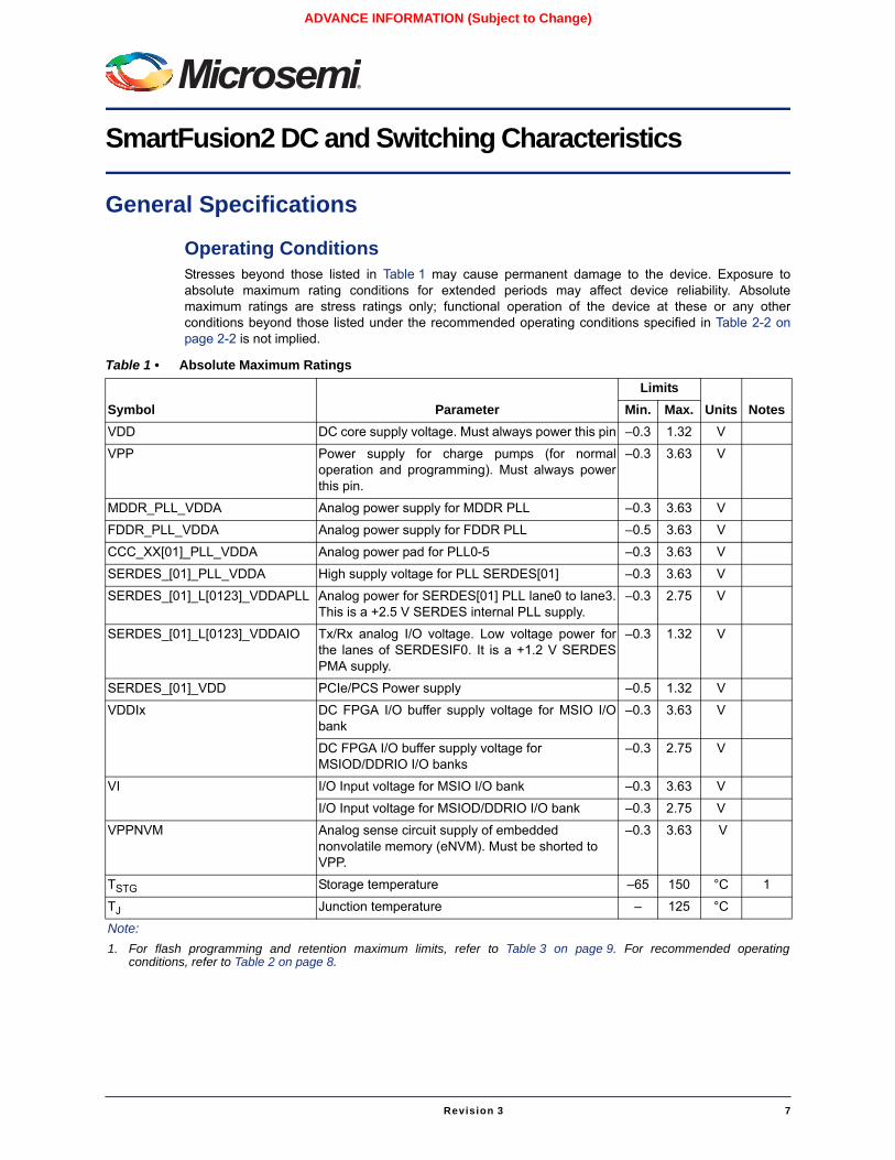
Operating ConditionsStresses beyond those listed in Table 1 may cause permanent damage to the device. Exposure toabsolute maximum rating conditions for extended periods may affect device reliability. Absolutemaximum ratings are stress ratings only; functional operation of the device at these or any otherconditions beyond those listed under the recommended operating conditions specified in Table 2-2 onpage 2-2 is not implied.
Table 1 • Absolute Maximum Ratings
Symbol ParameterLimits
Units NotesMin. Max.VDD DC core supply voltage. Must always power this pin –0.3 1.32 V
VPP Power supply for charge pumps (for normaloperation and programming). Must always powerthis pin.
–0.3 3.63 V
MDDR_PLL_VDDA Analog power supply for MDDR PLL –0.3 3.63 V
FDDR_PLL_VDDA Analog power supply for FDDR PLL –0.5 3.63 V
CCC_XX[01]_PLL_VDDA Analog power pad for PLL0-5 –0.3 3.63 V
SERDES_[01]_PLL_VDDA High supply voltage for PLL SERDES[01] –0.3 3.63 V
SERDES_[01]_L[0123]_VDDAPLL Analog power for SERDES[01] PLL lane0 to lane3.This is a +2.5 V SERDES internal PLL supply.
–0.3 2.75 V
SERDES_[01]_L[0123]_VDDAIO Tx/Rx analog I/O voltage. Low voltage power forthe lanes of SERDESIF0. It is a +1.2 V SERDESPMA supply.
–0.3 1.32 V
SERDES_[01]_VDD PCIe/PCS Power supply –0.5 1.32 V
VDDIx DC FPGA I/O buffer supply voltage for MSIO I/Obank
–0.3 3.63 V
DC FPGA I/O buffer supply voltage for MSIOD/DDRIO I/O banks
–0.3 2.75 V
VI I/O Input voltage for MSIO I/O bank –0.3 3.63 V
I/O Input voltage for MSIOD/DDRIO I/O bank –0.3 2.75 V
VPPNVM Analog sense circuit supply of embedded nonvolatile memory (eNVM). Must be shorted to VPP.
–0.3 3.63 V
TSTG Storage temperature –65 150 °C 1
TJ Junction temperature – 125 °C
Note:1. For flash programming and retention maximum limits, refer to Table 3 on page 9. For recommended operating
conditions, refer to Table 2 on page 8.
SmartFusion2 DC and Switching Characteristics
8 Revision 3
ADVANCE INFORMATION (Subject to Change)
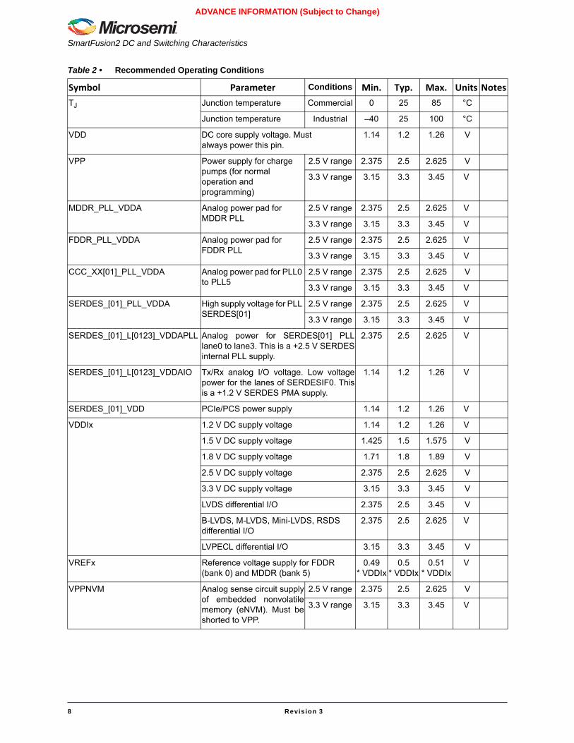
Table 2 • Recommended Operating Conditions
Symbol Parameter Conditions Min. Typ. Max. Units NotesTJ Junction temperature Commercial 0 25 85 °C
Junction temperature Industrial –40 25 100 °C
VDD DC core supply voltage. Mustalways power this pin.
1.14 1.2 1.26 V
VPP Power supply for charge pumps (for normal operation and programming)
2.5 V range 2.375 2.5 2.625 V
3.3 V range 3.15 3.3 3.45 V
MDDR_PLL_VDDA Analog power pad for MDDR PLL
2.5 V range 2.375 2.5 2.625 V
3.3 V range 3.15 3.3 3.45 V
FDDR_PLL_VDDA Analog power pad for FDDR PLL
2.5 V range 2.375 2.5 2.625 V
3.3 V range 3.15 3.3 3.45 V
CCC_XX[01]_PLL_VDDA Analog power pad for PLL0 to PLL5
2.5 V range 2.375 2.5 2.625 V
3.3 V range 3.15 3.3 3.45 V
SERDES_[01]_PLL_VDDA High supply voltage for PLL SERDES[01]
2.5 V range 2.375 2.5 2.625 V
3.3 V range 3.15 3.3 3.45 V
SERDES_[01]_L[0123]_VDDAPLL Analog power for SERDES[01] PLLlane0 to lane3. This is a +2.5 V SERDESinternal PLL supply.
2.375 2.5 2.625 V
SERDES_[01]_L[0123]_VDDAIO Tx/Rx analog I/O voltage. Low voltagepower for the lanes of SERDESIF0. Thisis a +1.2 V SERDES PMA supply.
1.14 1.2 1.26 V
SERDES_[01]_VDD PCIe/PCS power supply 1.14 1.2 1.26 V
VDDIx 1.2 V DC supply voltage 1.14 1.2 1.26 V
1.5 V DC supply voltage 1.425 1.5 1.575 V
1.8 V DC supply voltage 1.71 1.8 1.89 V
2.5 V DC supply voltage 2.375 2.5 2.625 V
3.3 V DC supply voltage 3.15 3.3 3.45 V
LVDS differential I/O 2.375 2.5 3.45 V
B-LVDS, M-LVDS, Mini-LVDS, RSDS differential I/O
2.375 2.5 2.625 V
LVPECL differential I/O 3.15 3.3 3.45 V
VREFx Reference voltage supply for FDDR (bank 0) and MDDR (bank 5)
0.49* VDDIx
0.5* VDDIx
0.51* VDDIx
V
VPPNVM Analog sense circuit supplyof embedded nonvolatilememory (eNVM). Must beshorted to VPP.
2.5 V range 2.375 2.5 2.625 V
3.3 V range 3.15 3.3 3.45 V
SmartFusion2 System-on-Chip FPGAs Datasheet
Revision 3 9
ADVANCE INFORMATION (Subject to Change)
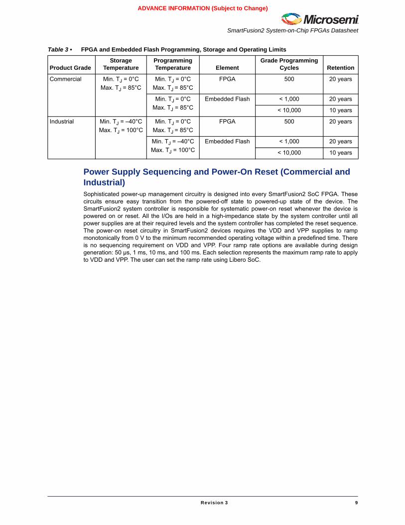
Power Supply Sequencing and Power-On Reset (Commercial and Industrial)Sophisticated power-up management circuitry is designed into every SmartFusion2 SoC FPGA. Thesecircuits ensure easy transition from the powered-off state to powered-up state of the device. TheSmartFusion2 system controller is responsible for systematic power-on reset whenever the device ispowered on or reset. All the I/Os are held in a high-impedance state by the system controller until allpower supplies are at their required levels and the system controller has completed the reset sequence.The power-on reset circuitry in SmartFusion2 devices requires the VDD and VPP supplies to rampmonotonically from 0 V to the minimum recommended operating voltage within a predefined time. Thereis no sequencing requirement on VDD and VPP. Four ramp rate options are available during designgeneration: 50 µs, 1 ms, 10 ms, and 100 ms. Each selection represents the maximum ramp rate to applyto VDD and VPP. The user can set the ramp rate using Libero SoC.
Table 3 • FPGA and Embedded Flash Programming, Storage and Operating Limits
Product GradeStorage
TemperatureProgramming Temperature Element
Grade Programming Cycles Retention
Commercial Min. TJ = 0°CMax. TJ = 85°C
Min. TJ = 0°CMax. TJ = 85°C
FPGA 500 20 years
Min. TJ = 0°CMax. TJ = 85°C
Embedded Flash < 1,000 20 years
< 10,000 10 years
Industrial Min. TJ = –40°CMax. TJ = 100°C
Min. TJ = 0°CMax. TJ = 85°C
FPGA 500 20 years
Min. TJ = –40°CMax. TJ = 100°C
Embedded Flash < 1,000 20 years
< 10,000 10 years
SmartFusion2 DC and Switching Characteristics
10 Revision 3
ADVANCE INFORMATION (Subject to Change)
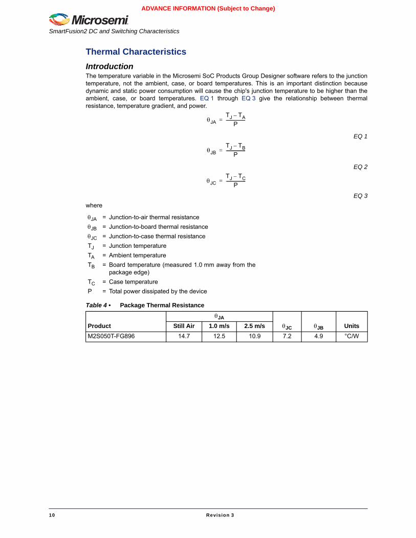
Thermal CharacteristicsIntroductionThe temperature variable in the Microsemi SoC Products Group Designer software refers to the junctiontemperature, not the ambient, case, or board temperatures. This is an important distinction becausedynamic and static power consumption will cause the chip's junction temperature to be higher than theambient, case, or board temperatures. EQ 1 through EQ 3 give the relationship between thermalresistance, temperature gradient, and power.
EQ 1
EQ 2
EQ 3where
θJA = Junction-to-air thermal resistanceθJB = Junction-to-board thermal resistanceθJC = Junction-to-case thermal resistanceTJ = Junction temperatureTA = Ambient temperatureTB = Board temperature (measured 1.0 mm away from the
package edge)TC = Case temperatureP = Total power dissipated by the device
Table 4 • Package Thermal Resistance
ProductθJA
θJC θJB UnitsStill Air 1.0 m/s 2.5 m/sM2S050T-FG896 14.7 12.5 10.9 7.2 4.9 °C/W
θJATJ TA–
P-------------------=
θJBTJ TB–
P-------------------=
θJCTJ TC–
P-------------------=
SmartFusion2 System-on-Chip FPGAs Datasheet
Revision 3 11
ADVANCE INFORMATION (Subject to Change)
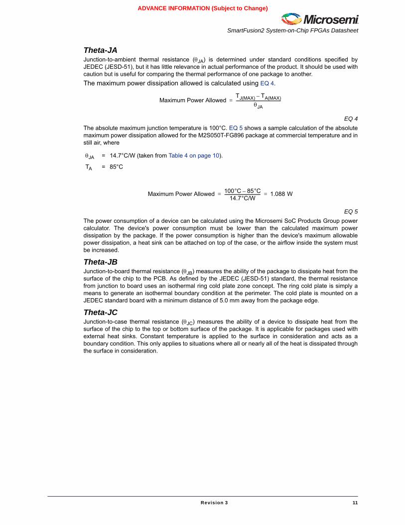
Theta-JAJunction-to-ambient thermal resistance (θJA) is determined under standard conditions specified byJEDEC (JESD-51), but it has little relevance in actual performance of the product. It should be used withcaution but is useful for comparing the thermal performance of one package to another.The maximum power dissipation allowed is calculated using EQ 4.
EQ 4The absolute maximum junction temperature is 100°C. EQ 5 shows a sample calculation of the absolutemaximum power dissipation allowed for the M2S050T-FG896 package at commercial temperature and instill air, where
EQ 5The power consumption of a device can be calculated using the Microsemi SoC Products Group powercalculator. The device's power consumption must be lower than the calculated maximum powerdissipation by the package. If the power consumption is higher than the device's maximum allowablepower dissipation, a heat sink can be attached on top of the case, or the airflow inside the system mustbe increased.
Theta-JBJunction-to-board thermal resistance (θJB) measures the ability of the package to dissipate heat from thesurface of the chip to the PCB. As defined by the JEDEC (JESD-51) standard, the thermal resistancefrom junction to board uses an isothermal ring cold plate zone concept. The ring cold plate is simply ameans to generate an isothermal boundary condition at the perimeter. The cold plate is mounted on aJEDEC standard board with a minimum distance of 5.0 mm away from the package edge.
Theta-JCJunction-to-case thermal resistance (θJC) measures the ability of a device to dissipate heat from thesurface of the chip to the top or bottom surface of the package. It is applicable for packages used withexternal heat sinks. Constant temperature is applied to the surface in consideration and acts as aboundary condition. This only applies to situations where all or nearly all of the heat is dissipated throughthe surface in consideration.
θJA = 14.7°C/W (taken from Table 4 on page 10).
TA = 85°C
Maximum Power AllowedTJ(MAX) TA(MAX)–
θJA---------------------------------------------=
Maximum Power Allowed 100°C 85°C–14.7°C/W
------------------------------------ 1.088 W= =
SmartFusion2 DC and Switching Characteristics
12 Revision 3
ADVANCE INFORMATION (Subject to Change)
Calculating Power Dissipation
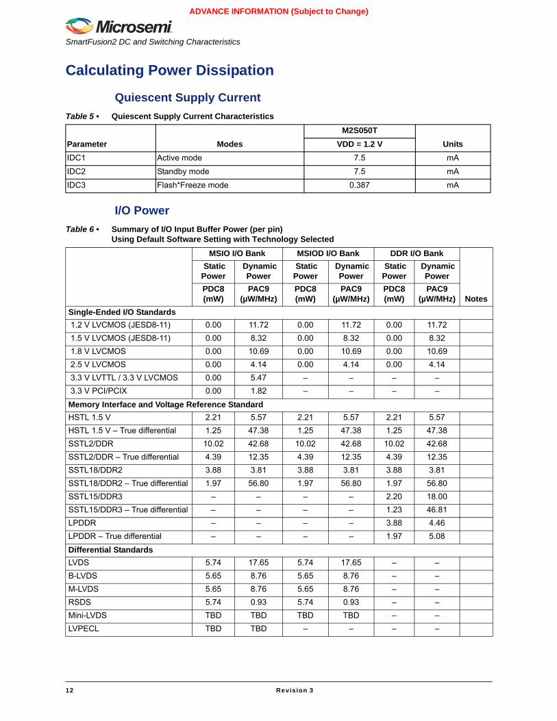
Quiescent Supply Current
I/O Power
Table 5 • Quiescent Supply Current Characteristics
Parameter ModesM2S050T
UnitsVDD = 1.2 VIDC1 Active mode 7.5 mA
IDC2 Standby mode 7.5 mA
IDC3 Flash*Freeze mode 0.387 mA
Table 6 • Summary of I/O Input Buffer Power (per pin) Using Default Software Setting with Technology Selected
MSIO I/O Bank MSIOD I/O Bank DDR I/O Bank
Notes
Static Power
Dynamic Power
Static Power
Dynamic Power
Static Power
Dynamic Power
PDC8 (mW)
PAC9 (µW/MHz)
PDC8 (mW)
PAC9 (µW/MHz)
PDC8 (mW)
PAC9 (µW/MHz)
Single-Ended I/O Standards 1.2 V LVCMOS (JESD8-11) 0.00 11.72 0.00 11.72 0.00 11.72 1.5 V LVCMOS (JESD8-11) 0.00 8.32 0.00 8.32 0.00 8.32 1.8 V LVCMOS 0.00 10.69 0.00 10.69 0.00 10.69 2.5 V LVCMOS 0.00 4.14 0.00 4.14 0.00 4.14 3.3 V LVTTL / 3.3 V LVCMOS 0.00 5.47 – – – – 3.3 V PCI/PCIX 0.00 1.82 – – – –
Memory Interface and Voltage Reference StandardHSTL 1.5 V 2.21 5.57 2.21 5.57 2.21 5.57HSTL 1.5 V – True differential 1.25 47.38 1.25 47.38 1.25 47.38SSTL2/DDR 10.02 42.68 10.02 42.68 10.02 42.68SSTL2/DDR – True differential 4.39 12.35 4.39 12.35 4.39 12.35SSTL18/DDR2 3.88 3.81 3.88 3.81 3.88 3.81SSTL18/DDR2 – True differential 1.97 56.80 1.97 56.80 1.97 56.80SSTL15/DDR3 – – – – 2.20 18.00SSTL15/DDR3 – True differential – – – – 1.23 46.81LPDDR – – – – 3.88 4.46LPDDR – True differential – – – – 1.97 5.08
Differential StandardsLVDS 5.74 17.65 5.74 17.65 – –B-LVDS 5.65 8.76 5.65 8.76 – –M-LVDS 5.65 8.76 5.65 8.76 – –RSDS 5.74 0.93 5.74 0.93 – –Mini-LVDS TBD TBD TBD TBD – –LVPECL TBD TBD – – – –
SmartFusion2 System-on-Chip FPGAs Datasheet
Revision 3 13
ADVANCE INFORMATION (Subject to Change)
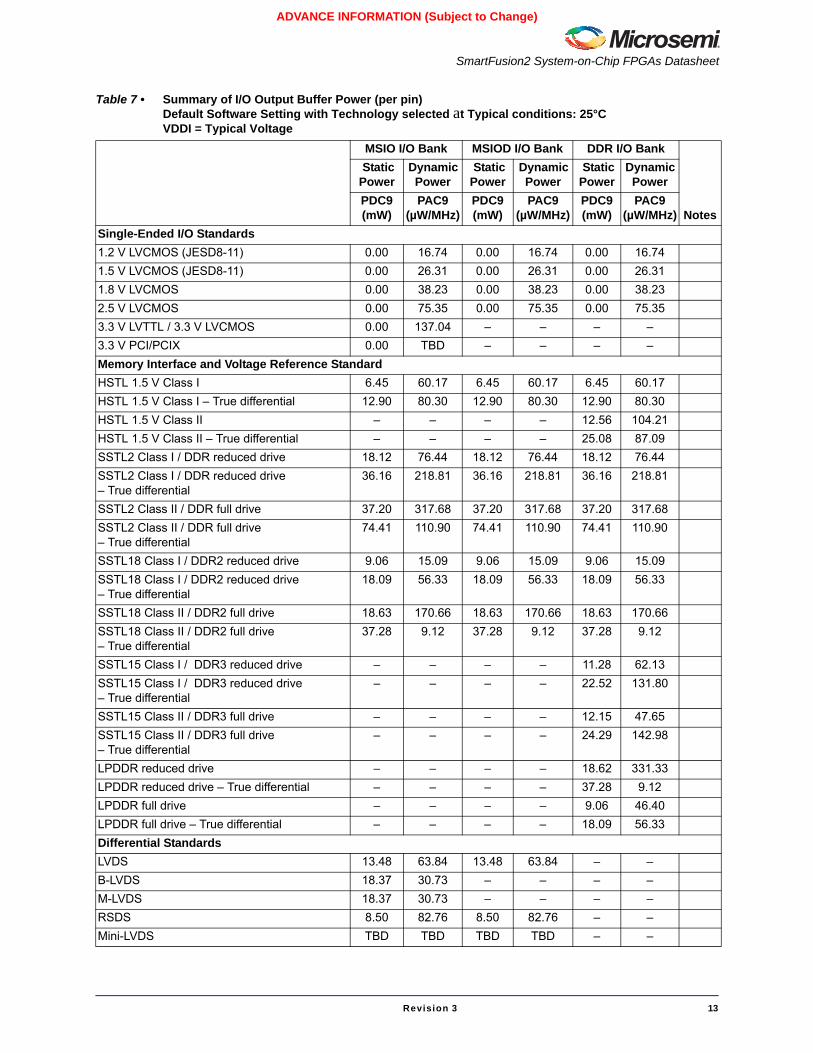
Table 7 • Summary of I/O Output Buffer Power (per pin)Default Software Setting with Technology selected at Typical conditions: 25°CVDDI = Typical Voltage
MSIO I/O Bank MSIOD I/O Bank DDR I/O Bank
Notes
Static Power
Dynamic Power
Static Power
Dynamic Power
Static Power
Dynamic Power
PDC9 (mW)
PAC9 (µW/MHz)
PDC9 (mW)
PAC9 (µW/MHz)
PDC9 (mW)
PAC9 (µW/MHz)
Single-Ended I/O Standards1.2 V LVCMOS (JESD8-11) 0.00 16.74 0.00 16.74 0.00 16.741.5 V LVCMOS (JESD8-11) 0.00 26.31 0.00 26.31 0.00 26.311.8 V LVCMOS 0.00 38.23 0.00 38.23 0.00 38.232.5 V LVCMOS 0.00 75.35 0.00 75.35 0.00 75.353.3 V LVTTL / 3.3 V LVCMOS 0.00 137.04 – – – –3.3 V PCI/PCIX 0.00 TBD – – – –Memory Interface and Voltage Reference StandardHSTL 1.5 V Class I 6.45 60.17 6.45 60.17 6.45 60.17HSTL 1.5 V Class I – True differential 12.90 80.30 12.90 80.30 12.90 80.30HSTL 1.5 V Class II – – – – 12.56 104.21HSTL 1.5 V Class II – True differential – – – – 25.08 87.09SSTL2 Class I / DDR reduced drive 18.12 76.44 18.12 76.44 18.12 76.44SSTL2 Class I / DDR reduced drive– True differential
36.16 218.81 36.16 218.81 36.16 218.81
SSTL2 Class II / DDR full drive 37.20 317.68 37.20 317.68 37.20 317.68SSTL2 Class II / DDR full drive – True differential
74.41 110.90 74.41 110.90 74.41 110.90
SSTL18 Class I / DDR2 reduced drive 9.06 15.09 9.06 15.09 9.06 15.09SSTL18 Class I / DDR2 reduced drive – True differential
18.09 56.33 18.09 56.33 18.09 56.33
SSTL18 Class II / DDR2 full drive 18.63 170.66 18.63 170.66 18.63 170.66SSTL18 Class II / DDR2 full drive– True differential
37.28 9.12 37.28 9.12 37.28 9.12
SSTL15 Class I / DDR3 reduced drive – – – – 11.28 62.13SSTL15 Class I / DDR3 reduced drive – True differential
– – – – 22.52 131.80
SSTL15 Class II / DDR3 full drive – – – – 12.15 47.65SSTL15 Class II / DDR3 full drive– True differential
– – – – 24.29 142.98
LPDDR reduced drive – – – – 18.62 331.33LPDDR reduced drive – True differential – – – – 37.28 9.12LPDDR full drive – – – – 9.06 46.40LPDDR full drive – True differential – – – – 18.09 56.33Differential StandardsLVDS 13.48 63.84 13.48 63.84 – –B-LVDS 18.37 30.73 – – – –M-LVDS 18.37 30.73 – – – –RSDS 8.50 82.76 8.50 82.76 – –Mini-LVDS TBD TBD TBD TBD – –
SmartFusion2 DC and Switching Characteristics
14 Revision 3
ADVANCE INFORMATION (Subject to Change)
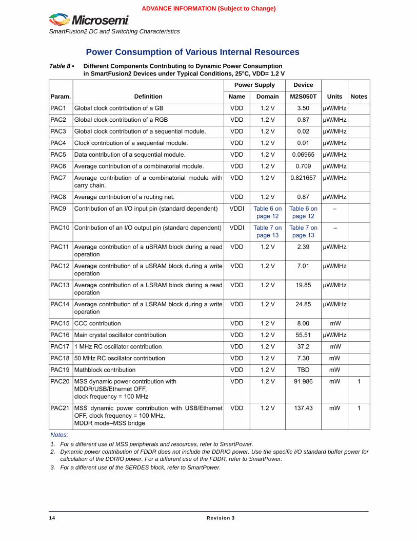
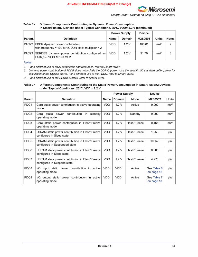
Power Consumption of Various Internal ResourcesTable 8 • Different Components Contributing to Dynamic Power Consumption
in SmartFusion2 Devices under Typical Conditions, 25°C, VDD= 1.2 V
Param. Definition
Power Supply Device
Units NotesName Domain M2S050T
PAC1 Global clock contribution of a GB VDD 1.2 V 3.50 µW/MHz
PAC2 Global clock contribution of a RGB VDD 1.2 V 0.87 µW/MHz
PAC3 Global clock contribution of a sequential module. VDD 1.2 V 0.02 µW/MHz
PAC4 Clock contribution of a sequential module. VDD 1.2 V 0.01 µW/MHz
PAC5 Data contribution of a sequential module. VDD 1.2 V 0.06965 µW/MHz
PAC6 Average contribution of a combinatorial module. VDD 1.2 V 0.709 µW/MHz
PAC7 Average contribution of a combinatorial module withcarry chain.
VDD 1.2 V 0.821657 µW/MHz
PAC8 Average contribution of a routing net. VDD 1.2 V 0.87 µW/MHz
PAC9 Contribution of an I/O input pin (standard dependent) VDDI Table 6 on page 12
Table 6 on page 12
–
PAC10 Contribution of an I/O output pin (standard dependent) VDDI Table 7 on page 13
Table 7 on page 13
–
PAC11 Average contribution of a uSRAM block during a readoperation
VDD 1.2 V 2.39 µW/MHz
PAC12 Average contribution of a uSRAM block during a writeoperation
VDD 1.2 V 7.01 µW/MHz
PAC13 Average contribution of a LSRAM block during a readoperation
VDD 1.2 V 19.85 µW/MHz
PAC14 Average contribution of a LSRAM block during a writeoperation
VDD 1.2 V 24.85 µW/MHz
PAC15 CCC contribution VDD 1.2 V 8.00 mW
PAC16 Main crystal oscillator contribution VDD 1.2 V 55.51 µW/MHz
PAC17 1 MHz RC oscillator contribution VDD 1.2 V 37.2 mW
PAC18 50 MHz RC oscillator contribution VDD 1.2 V 7.30 mW
PAC19 Mathblock contribution VDD 1.2 V TBD mW
PAC20 MSS dynamic power contribution with MDDR/USB/Ethernet OFF, clock frequency = 100 MHz
VDD 1.2 V 91.986 mW 1
PAC21 MSS dynamic power contribution with USB/EthernetOFF, clock frequency = 100 MHz, MDDR mode–MSS bridge
VDD 1.2 V 137.43 mW 1
Notes:1. For a different use of MSS peripherals and resources, refer to SmartPower.2. Dynamic power contribution of FDDR does not include the DDRIO power. Use the specific I/O standard buffer power for
calculation of the DDRIO power. For a different use of the FDDR, refer to SmartPower.3. For a different use of the SERDES block, refer to SmartPower.
SmartFusion2 System-on-Chip FPGAs Datasheet
Revision 3 15
ADVANCE INFORMATION (Subject to Change)
PAC22 FDDR dynamic power contribution with frequency = 100 MHz, DDR clock multiplier = 2
VDD 1.2 V 108.81 mW 2
PAC23 SERDES dynamic power contribution configured asPCIe_GEN1 x1 at 125 MHz
VDD 1.2 V 91.70 mW 3
Table 9 • Different Components Contributing to the Static Power Consumption in SmartFusion2 Devicesunder Typical Conditions, 25°C, VDD = 1.2 V
Param. Definition
Power Supply Device
UnitsName Domain Mode M2S050T
PDC1 Core static power contribution in active operatingmode
VDD 1.2 V Active 9.000 mW
PDC2 Core static power contribution in standbyoperating mode
VDD 1.2 V Standby 9.000 mW
PDC3 Core static power contribution in Flash*Freezeoperating mode
VDD 1.2 V Flash*Freeze 0.465 mW
PDC4 LSRAM static power contribution in Flash*Freezeconfigured in Sleep state
VDD 1.2 V Flash*Freeze 1.250 µW
PDC5 LSRAM static power contribution in Flash*Freezeconfigured in Suspended state
VDD 1.2 V Flash*Freeze 10.140 µW
PDC6 USRAM static power contribution in Flash*Freezeconfigured in Sleep state
VDD 1.2 V Flash*Freeze 0.500 µW
PDC7 USRAM static power contribution in Flash*Freezeconfigured in Suspend state
VDD 1.2 V Flash*Freeze 4.970 µW
PDC8 I/O Input static power contribution in activeoperating mode
VDDI VDDI Active See Table 6 on page 12
µW
PDC9 I/O output static power contribution in activeoperating mode
VDDI VDDI Active See Table 7 on page 13
µW
Table 8 • Different Components Contributing to Dynamic Power Consumptionin SmartFusion2 Devices under Typical Conditions, 25°C, VDD= 1.2 V (continued)
Param. Definition
Power Supply Device
Units NotesName Domain M2S050T
Notes:1. For a different use of MSS peripherals and resources, refer to SmartPower.2. Dynamic power contribution of FDDR does not include the DDRIO power. Use the specific I/O standard buffer power for
calculation of the DDRIO power. For a different use of the FDDR, refer to SmartPower.3. For a different use of the SERDES block, refer to SmartPower.
SmartFusion2 DC and Switching Characteristics
16 Revision 3
ADVANCE INFORMATION (Subject to Change)
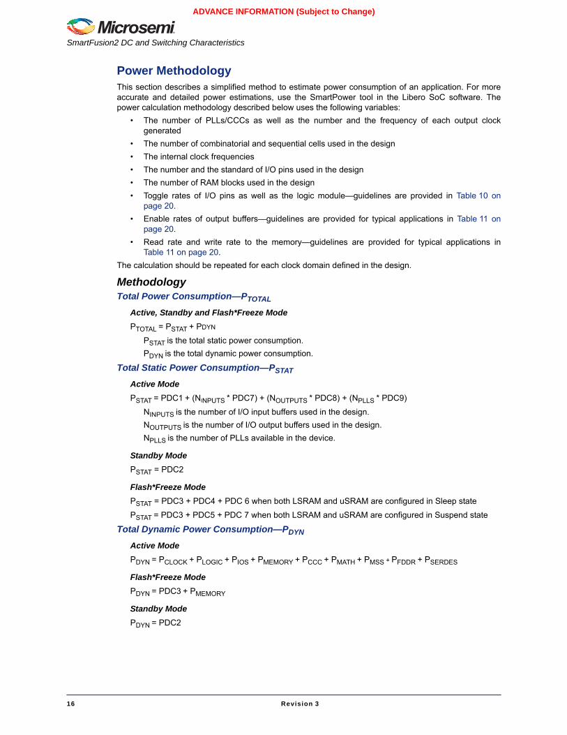
Power MethodologyThis section describes a simplified method to estimate power consumption of an application. For moreaccurate and detailed power estimations, use the SmartPower tool in the Libero SoC software. Thepower calculation methodology described below uses the following variables:
• The number of PLLs/CCCs as well as the number and the frequency of each output clockgenerated
• The number of combinatorial and sequential cells used in the design• The internal clock frequencies• The number and the standard of I/O pins used in the design• The number of RAM blocks used in the design• Toggle rates of I/O pins as well as the logic module—guidelines are provided in Table 10 on
page 20.• Enable rates of output buffers—guidelines are provided for typical applications in Table 11 on
page 20.• Read rate and write rate to the memory—guidelines are provided for typical applications in
Table 11 on page 20.The calculation should be repeated for each clock domain defined in the design.
MethodologyTotal Power Consumption—PTOTAL
Active, Standby and Flash*Freeze ModePTOTAL = PSTAT + PDYN
PSTAT is the total static power consumption.PDYN is the total dynamic power consumption.
Total Static Power Consumption—PSTAT
Active ModePSTAT = PDC1 + (NINPUTS * PDC7) + (NOUTPUTS * PDC8) + (NPLLS * PDC9)
NINPUTS is the number of I/O input buffers used in the design.NOUTPUTS is the number of I/O output buffers used in the design.NPLLS is the number of PLLs available in the device.
Standby ModePSTAT = PDC2
Flash*Freeze ModePSTAT = PDC3 + PDC4 + PDC 6 when both LSRAM and uSRAM are configured in Sleep state
PSTAT = PDC3 + PDC5 + PDC 7 when both LSRAM and uSRAM are configured in Suspend state
Total Dynamic Power Consumption—PDYN
Active ModePDYN = PCLOCK + PLOGIC + PIOS + PMEMORY + PCCC + PMATH + PMSS + PFDDR + PSERDES
Flash*Freeze ModePDYN = PDC3 + PMEMORY
Standby ModePDYN = PDC2
SmartFusion2 System-on-Chip FPGAs Datasheet
Revision 3 17
ADVANCE INFORMATION (Subject to Change)
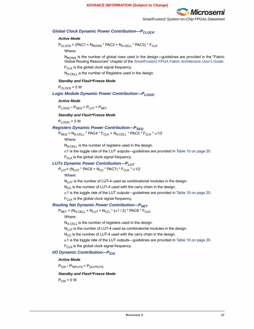
Global Clock Dynamic Power Contribution—PCLOCK
Active ModePCLOCK = (PAC1 + NROWS * PAC2 + NS-CELL * PAC3) * FCLK
Where:NROWS is the number of global rows used in the design—guidelines are provided in the "FabricGlobal Routing Resources" chapter of the SmartFusion2 FPGA Fabric Architecture User's Guide.FCLK is the global clock signal frequency.NS-CELL is the number of Registers used in the design.
Standby and Flash*Freeze ModePCLOCK = 0 W
Logic Module Dynamic Power Contribution—PLOGIC
Active ModePLOGIC = PSEQ + PLUT + PNET
Standby and Flash*Freeze ModePLOGIC = 0 W
Registers Dynamic Power Contribution—PSEQPSEQ = NS-CELL * PAC4 * FCLK + NS-CELL * PAC5 * FCLK * α1/2
Where:NS-CELL is the number of registers used in the design.α1 is the toggle rate of the LUT outputs—guidelines are provided in Table 10 on page 20.FCLK is the global clock signal frequency.
LUTs Dynamic Power Contribution—PLUTPLUT= (NLUT * PAC6 + NCC * PAC7) * FCLK * α1/2
Where:NLUT is the number of LUT-4 used as combinatorial modules in the design.NCC is the number of LUT-4 used with the carry chain in the design.α1 is the toggle rate of the LUT outputs—guidelines are provided in Table 10 on page 20.FCLK is the global clock signal frequency.
Routing Net Dynamic Power Contribution—PNETPNET = (NS-CELL + NLUT + NCC) * (α1 / 2) * PAC8 * FCLK
Where:NS-CELL is the number of registers used in the design.NLUT is the number of LUT-4 used as combinatorial modules in the design.NCC is the number of LUT-4 used with the carry chain in the design.α1 is the toggle rate of the LUT outputs—guidelines are provided in Table 10 on page 20.FCLK is the global clock signal frequency.
I/O Dynamic Contribution—PIOS
Active ModePIOS = PINPUTS + POUTPUTS
Standby and Flash*Freeze ModePIOS = 0 W
SmartFusion2 DC and Switching Characteristics
18 Revision 3
ADVANCE INFORMATION (Subject to Change)
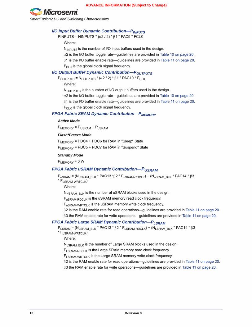
I/O Input Buffer Dynamic Contribution—PINPUTSPINPUTS = NINPUTS * (α2 / 2) * β1 * PAC9 * FCLK
Where:NINPUTS is the number of I/O input buffers used in the design.α2 is the I/O buffer toggle rate—guidelines are provided in Table 10 on page 20.β1 is the I/O buffer enable rate—guidelines are provided in Table 11 on page 20.FCLK is the global clock signal frequency.
I/O Output Buffer Dynamic Contribution—POUTPUTSPOUTPUTS = NOUTPUTS * (α2 / 2) * β1 * PAC10 * FCLK
Where:NOUTPUTS is the number of I/O output buffers used in the design.α2 is the I/O buffer toggle rate—guidelines are provided in Table 10 on page 20.β1 is the I/O buffer enable rate—guidelines are provided in Table 11 on page 20.FCLK is the global clock signal frequency.
FPGA Fabric SRAM Dynamic Contribution—PMEMORY
Active ModePMEMORY = PUSRAM + PLSRAM
Flash*Freeze ModePMEMORY = PDC4 + PDC6 for RAM in "Sleep" State
PMEMORY = PDC5 + PDC7 for RAM in "Suspend" State
Standby ModePMEMORY = 0 W
FPGA Fabric uSRAM Dynamic Contribution—PUSRAMPuSRAM = (NuSRAM_BLK * PAC13 *β2 * FuSRAM-RDCLK) + (NuSRAM_BLK * PAC14 * β3* FuSRAM-WRTCLK)
Where:NuSRAM_BLK is the number of uSRAM blocks used in the design.FuSRAM-RDCLK is the uSRAM memory read clock frequency.FuSRAM-WRTCLK is the uSRAM memory write clock frequency.β2 is the RAM enable rate for read operations—guidelines are provided in Table 11 on page 20.β3 the RAM enable rate for write operations—guidelines are provided in Table 11 on page 20.
FPGA Fabric Large SRAM Dynamic Contribution—PLSRAMPLSRAM = (NLSRAM_BLK * PAC13 * β2 * FLSRAM-RDCLK) + (NLSRAM_BLK * PAC14 * β3 * FLSRAM-WRTCLK)
Where:NLSRAM_BLK is the number of Large SRAM blocks used in the design.FLSRAM-RDCLK is the Large SRAM memory read clock frequency.FLSRAM-WRTCLK is the Large SRAM memory write clock frequency.β2 is the RAM enable rate for read operations—guidelines are provided in Table 11 on page 20.β3 the RAM enable rate for write operations—guidelines are provided in Table 11 on page 20.
SmartFusion2 System-on-Chip FPGAs Datasheet
Revision 3 19
ADVANCE INFORMATION (Subject to Change)
PLL/CCC Dynamic Contribution—PPLL
Active ModePPLL = PAC15
Flash*Freeze/Standby ModePPLL = 0 W
External Main Crystal Oscillator Dynamic Contribution—PXTL-OSC
Active ModePXTL-OSC = PAC16 * FCLK
Where:FCLK is the output frequency of the oscillator.
Flash*Freeze/Standby ModePXTL-OSC = 0 W
On-Chip 25/50MHz RC Oscillator Dynamic Contribution—P50RC-OSC
Active Mode/Standby ModeP50RC-OSC = 0 W
Flash*FreezeWhen used by MSS:
P50RC-OSC = PAC18
When not used by MSS:
P50RC-OSC = 0 W
Mathblock Dynamic Power Contribution—PMATH
Active ModePMATH = PAC19 * NMATH_BLK * FMATHCLK
NMATH_BLK is the number of mathblocks used in the design.FMATHCLK is the mathblock clock frequency.
Flash*Freeze/Standby ModePMATH = 0 W
Microcontroller Subsystem Dynamic Power Contribution—PMSS
Active ModeWith MDDR OFF:
PMSS = PAC20
With MDDR ON:
PMSS = PAC21
Flash*Freeze/Standby ModePMSS = 0 W
SmartFusion2 DC and Switching Characteristics
20 Revision 3
ADVANCE INFORMATION (Subject to Change)
FDDR Dynamic Power Contribution—PFDDR
Active ModePFDDR = PAC22
FDDR Dynamic power contributions do not include the power contributions of the DDR I/O. This shouldbe accounted for in the I/O power calculations.
Flash*Freeze/Standby ModePFDDR = 0 W
SERDES Contribution—PSERDES
Active ModePSERDES = PAC23
Flash*Freeze/Standby ModePSERDES = 0 W
GuidelinesToggle Rate DefinitionA toggle rate defines the frequency of a net or logic element relative to a clock. It is a percentage. If thetoggle rate of a net is 100%, this means that the net switches at half the clock frequency. Below are someexamples:
• The average toggle rate of a shift register is 100%, as all flip-flop outputs toggle at half of the clockfrequency.
• The average toggle rate of an 8-bit counter is 25%:– Bit 0 (LSB) = 100%– Bit 1 = 50%– Bit 2 = 25%– …– Bit 7 (MSB) = 0.78125%– Average toggle rate = (100% + 50% + 25% + 12.5% + . . . 0.78125%) / 8.
Enable Rate DefinitionOutput enable rate is the average percentage of time during which tristate outputs are enabled. Whennon-tristate output buffers are used, the enable rate should be 100%.
Table 10 • Toggle Rate Guidelines Recommended for Power Calculation
Component Definition Guideline
α1 Toggle rate of logic module outputs 10%
α2 I/O buffer toggle rate 10%
Table 11 • Enable Rate Guidelines Recommended for Power Calculation
Component Definition Guideline
β1 I/O output buffer enable rate Toggle rate of the logic driving the output buffer
β2 FPGA fabric SRAM enable rate for read operations 12.50%
β3 FPGA fabric SRAM enable rate for write operations 12.50%
β4 eNVM enable rate for read operations < 5%
SmartFusion2 System-on-Chip FPGAs Datasheet
Revision 3 21
ADVANCE INFORMATION (Subject to Change)
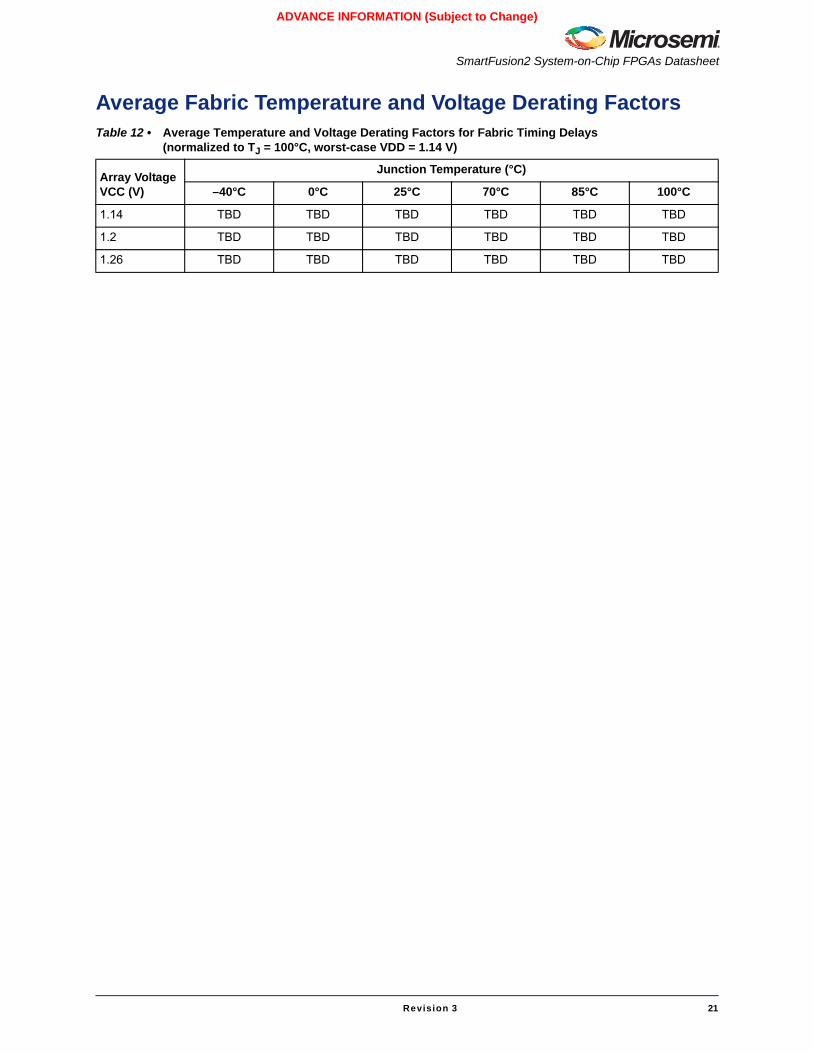
Average Fabric Temperature and Voltage Derating FactorsTable 12 • Average Temperature and Voltage Derating Factors for Fabric Timing Delays
(normalized to TJ = 100°C, worst-case VDD = 1.14 V)
Array Voltage VCC (V)
Junction Temperature (°C)
–40°C 0°C 25°C 70°C 85°C 100°C
1.14 TBD TBD TBD TBD TBD TBD
1.2 TBD TBD TBD TBD TBD TBD
1.26 TBD TBD TBD TBD TBD TBD
SmartFusion2 DC and Switching Characteristics
22 Revision 3
ADVANCE INFORMATION (Subject to Change)
Timing Model
Figure 1 • Timing Model
D Q
Y
Y
D QD Q D QY
Combinational Cell
Combinational Cell
Combinational Cell
I/O Module(Registered)
I/O Module(Non-Registered)
Register Cell Register Cell
I/O Module(Non-Registered)
LVDS
DDR3
LVDS
Buffer
Buffer
Buffer
SSTL2Class I
Y
Combinational Cell
Y
Combinational Cell
Y
Combinational Cell
I/O Module(Non-Registered)
I/O Module(Non-Registered)
I/O Module(Registered)
LVCMOS 2.5 VOutput Drive Strength = 4X MSIO I/O Bank
I/O Module(Non-Registered)
LVCMOS 1.5 VOutput Drive Strength = 12XDDRIO I/O Bank
LVCMOS 2.5 VOutput Drive Strength = 7X MSIO I/O Bank
InputClock
InputClock
InputClock
LVCMOS 2.5 V
LVCMOS 2.5 V
LVCMOS 2.5 V
AB
E
H
J
M P
K
I
FG
C
D
L M
C C
N OL Buffer
SmartFusion2 System-on-Chip FPGAs Datasheet
Revision 3 23
ADVANCE INFORMATION (Subject to Change)
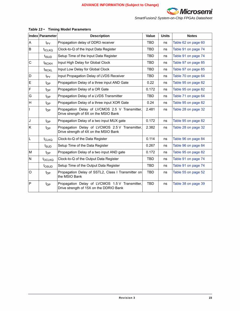
Table 13 • Timing Model Parameters
Index Parameter Description Value Units Notes
A tPY Propagation delay of DDR3 receiver TBD ns Table 62 on page 60
B tICLKQ Clock-to-Q of the Input Data Register TBD ns Table 91 on page 74
tISUD Setup Time of the Input Data Register TBD ns Table 91 on page 74
C tRCKH Input High Delay for Global Clock TBD ns Table 97 on page 85
tRCKL Input Low Delay for Global Clock TBD ns Table 97 on page 85
D tPY Input Propagation Delay of LVDS Receiver TBD ns Table 70 on page 64
E tDP Propagation Delay of a three input AND Gate 0.22 ns Table 95 on page 82
F tDP Propagation Delay of a OR Gate 0.172 ns Table 95 on page 82
G tDP Propagation Delay of a LVDS Transmitter TBD ns Table 71 on page 64
H tDP Propagation Delay of a three input XOR Gate 0.24 ns Table 95 on page 82
I tDP Propagation Delay of LVCMOS 2.5 V Transmitter,Drive strength of 8X on the MSIO Bank
2.481 ns Table 28 on page 32
J tDP Propagation Delay of a two input MUX gate 0.172 ns Table 95 on page 82
K tDP Propagation Delay of LVCMOS 2.5 V Transmitter,Drive strength of 4X on the MSIO Bank
2.382 ns Table 28 on page 32
L tCLKQ Clock-to-Q of the Data Register 0.114 ns Table 96 on page 84
tSUD Setup Time of the Data Register 0.267 ns Table 96 on page 84
M tDP Propagation Delay of a two input AND gate 0.172 ns Table 95 on page 82
N tOCLKQ Clock-to-Q of the Output Data Register TBD ns Table 91 on page 74
tOSUD Setup Time of the Output Data Register TBD ns Table 91 on page 74
O tDP Propagation Delay of SSTL2, Class I Transmitter onthe MSIO Bank
TBD ns Table 55 on page 52
P tDP Propagation Delay of LVCMOS 1.5 V Transmitter,Drive strength of 15X on the DDRIO Bank
TBD ns Table 38 on page 39
SmartFusion2 DC and Switching Characteristics
24 Revision 3
ADVANCE INFORMATION (Subject to Change)
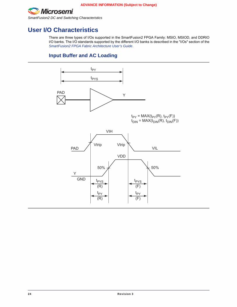
User I/O CharacteristicsThere are three types of I/Os supported in the SmartFusion2 FPGA Family: MSIO, MSIOD, and DDRIOI/O banks. The I/O standards supported by the different I/O banks is described in the "I/Os" section of theSmartFusion2 FPGA Fabric Architecture User’s Guide.
Input Buffer and AC Loading
tPYS(R)
PAD
Y
Vtrip
GND tPYS(F)
tPY(R)
tPY(F)
Vtrip
50%50%
VIH
VDD
VIL
PADY
tPY
tPYS
tPY = MAX(tPY(R), tPY(F))tDIN = MAX(tDIN(R), tDIN(F))
SmartFusion2 System-on-Chip FPGAs Datasheet
Revision 3 25
ADVANCE INFORMATION (Subject to Change)
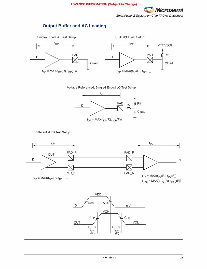
Output Buffer and AC Loading
tDP(R)
VOL
tDP(F)
VtripVtrip
VOH
D50% 50%
VDD
0 V
OUT
PAD
tDP
Cload
D
tDP
tDP = MAX(tDP(R), tDP(F))
PAD
Cload
Rtt
VTT/VDDI
D
tDP = MAX(tDP(R), tDP(F))
Single-Ended I/O Test Setup HSTL/PCI Test Setup
tDP
PAD
Cload
RttD
tDP = MAX(tDP(R), tDP(F))
Voltage-Referenced, Singled-Ended I/O Test Setup
Differential I/O Test Setup
Rs
tDP tPY
PAD_P PAD_P
IND
tDP = MAX(tDP(R), tDP(F))tPY = MAX(tPY(R), tPY(F))tPYS = MAX(tPYS(R), tPYS(F))
PAD_N PAD_N
OUT
SmartFusion2 DC and Switching Characteristics
26 Revision 3
ADVANCE INFORMATION (Subject to Change)
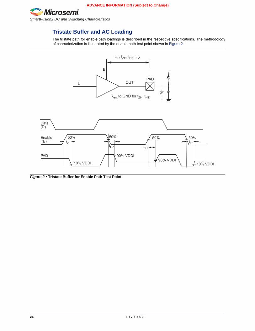
Tristate Buffer and AC LoadingThe tristate path for enable path loadings is described in the respective specifications. The methodologyof characterization is illustrated by the enable path test point shown in Figure 2.
Figure 2 • Tristate Buffer for Enable Path Test Point
tHZ tZH
tLZ
90% VDDI 90% VDDI
10% VDDI
50%
PAD
Data(D)
Enable (E)
50%
10% VDDI
tZL
50%
PAD
E
D OUT
tZL, tZH, tHZ, tLZ
Rent to GND for tZH, tHZ
50%
SmartFusion2 System-on-Chip FPGAs Datasheet
Revision 3 27
ADVANCE INFORMATION (Subject to Change)
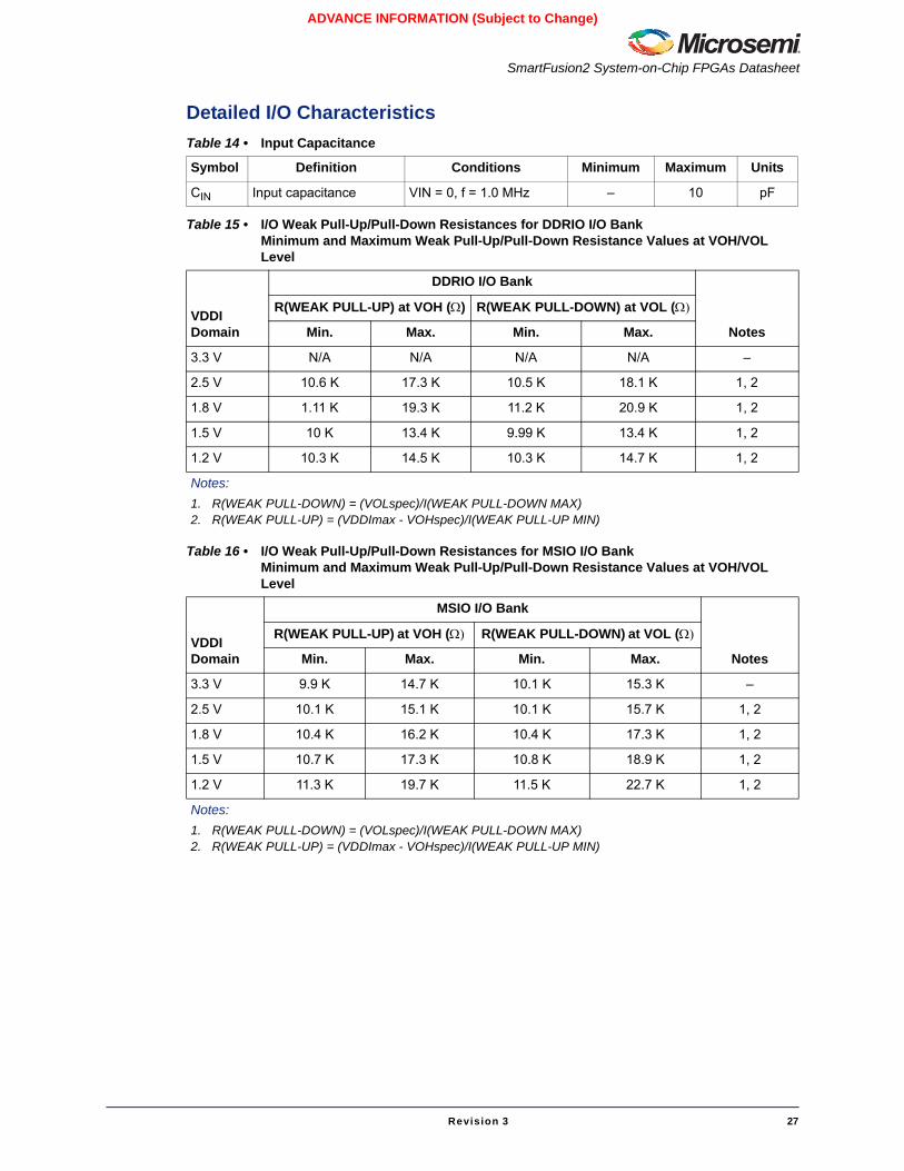
Detailed I/O CharacteristicsTable 14 • Input Capacitance
Symbol Definition Conditions Minimum Maximum Units
CIN Input capacitance VIN = 0, f = 1.0 MHz – 10 pF
Table 15 • I/O Weak Pull-Up/Pull-Down Resistances for DDRIO I/O BankMinimum and Maximum Weak Pull-Up/Pull-Down Resistance Values at VOH/VOL Level
VDDI Domain
DDRIO I/O Bank
Notes
R(WEAK PULL-UP) at VOH (Ω) R(WEAK PULL-DOWN) at VOL (Ω)
Min. Max. Min. Max.
3.3 V N/A N/A N/A N/A –
2.5 V 10.6 K 17.3 K 10.5 K 18.1 K 1, 2
1.8 V 1.11 K 19.3 K 11.2 K 20.9 K 1, 2
1.5 V 10 K 13.4 K 9.99 K 13.4 K 1, 2
1.2 V 10.3 K 14.5 K 10.3 K 14.7 K 1, 2
Notes:1. R(WEAK PULL-DOWN) = (VOLspec)/I(WEAK PULL-DOWN MAX)2. R(WEAK PULL-UP) = (VDDImax - VOHspec)/I(WEAK PULL-UP MIN)
Table 16 • I/O Weak Pull-Up/Pull-Down Resistances for MSIO I/O BankMinimum and Maximum Weak Pull-Up/Pull-Down Resistance Values at VOH/VOL Level
VDDI Domain
MSIO I/O Bank
Notes
R(WEAK PULL-UP) at VOH (Ω) R(WEAK PULL-DOWN) at VOL (Ω)
Min. Max. Min. Max.
3.3 V 9.9 K 14.7 K 10.1 K 15.3 K –
2.5 V 10.1 K 15.1 K 10.1 K 15.7 K 1, 2
1.8 V 10.4 K 16.2 K 10.4 K 17.3 K 1, 2
1.5 V 10.7 K 17.3 K 10.8 K 18.9 K 1, 2
1.2 V 11.3 K 19.7 K 11.5 K 22.7 K 1, 2
Notes:1. R(WEAK PULL-DOWN) = (VOLspec)/I(WEAK PULL-DOWN MAX)2. R(WEAK PULL-UP) = (VDDImax - VOHspec)/I(WEAK PULL-UP MIN)
SmartFusion2 DC and Switching Characteristics
28 Revision 3
ADVANCE INFORMATION (Subject to Change)
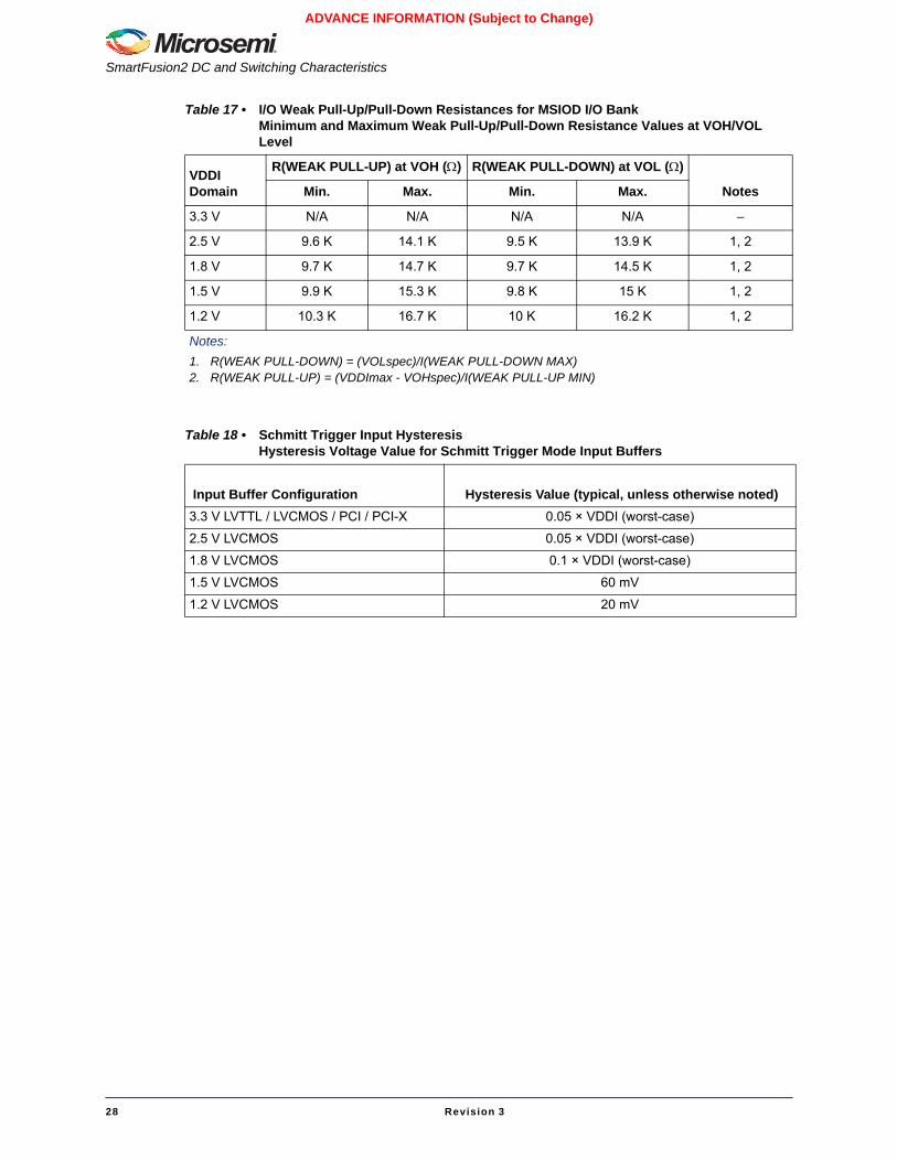
Table 17 • I/O Weak Pull-Up/Pull-Down Resistances for MSIOD I/O BankMinimum and Maximum Weak Pull-Up/Pull-Down Resistance Values at VOH/VOL Level
VDDI Domain
R(WEAK PULL-UP) at VOH (Ω) R(WEAK PULL-DOWN) at VOL (Ω)
NotesMin. Max. Min. Max.
3.3 V N/A N/A N/A N/A –
2.5 V 9.6 K 14.1 K 9.5 K 13.9 K 1, 2
1.8 V 9.7 K 14.7 K 9.7 K 14.5 K 1, 2
1.5 V 9.9 K 15.3 K 9.8 K 15 K 1, 2
1.2 V 10.3 K 16.7 K 10 K 16.2 K 1, 2
Notes:1. R(WEAK PULL-DOWN) = (VOLspec)/I(WEAK PULL-DOWN MAX)2. R(WEAK PULL-UP) = (VDDImax - VOHspec)/I(WEAK PULL-UP MIN)
Table 18 • Schmitt Trigger Input HysteresisHysteresis Voltage Value for Schmitt Trigger Mode Input Buffers
Input Buffer Configuration Hysteresis Value (typical, unless otherwise noted)3.3 V LVTTL / LVCMOS / PCI / PCI-X 0.05 × VDDI (worst-case)
2.5 V LVCMOS 0.05 × VDDI (worst-case)
1.8 V LVCMOS 0.1 × VDDI (worst-case)
1.5 V LVCMOS 60 mV
1.2 V LVCMOS 20 mV
SmartFusion2 System-on-Chip FPGAs Datasheet
Revision 3 29
ADVANCE INFORMATION (Subject to Change)
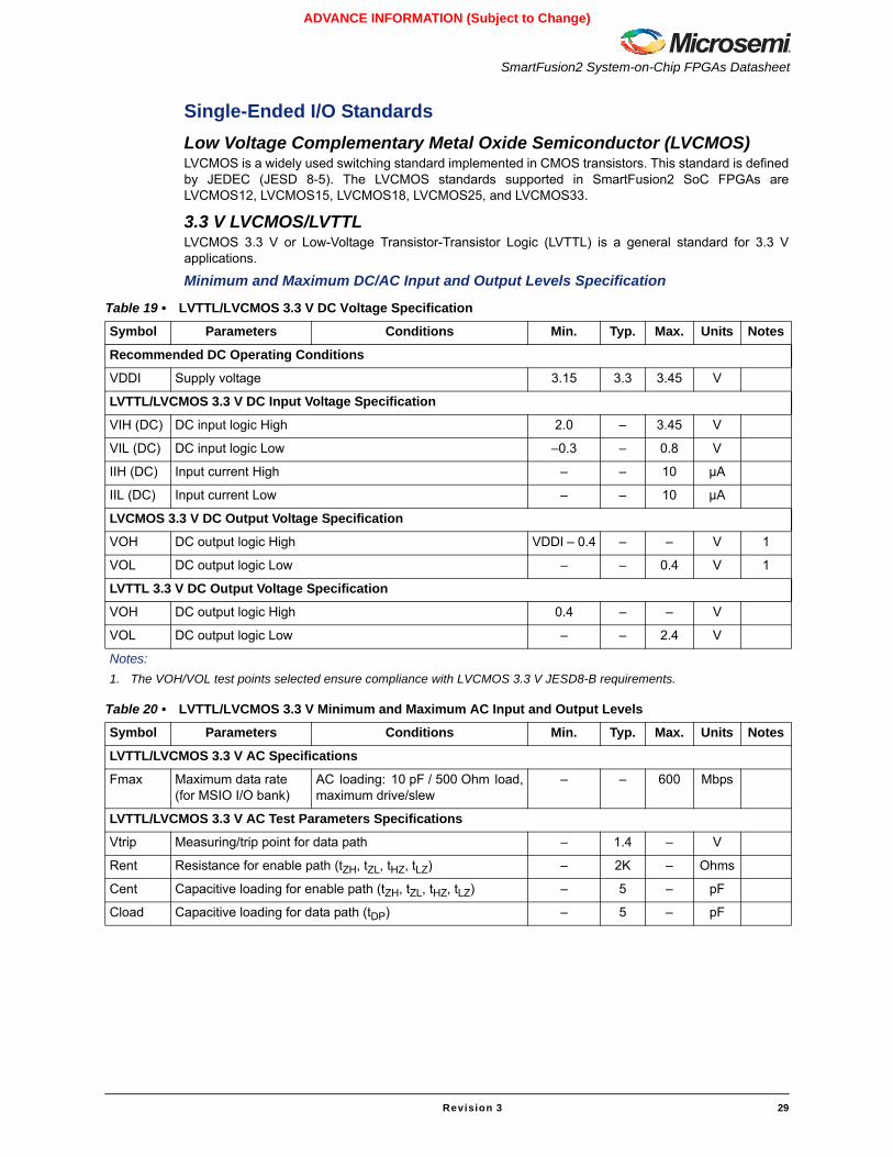
Single-Ended I/O StandardsLow Voltage Complementary Metal Oxide Semiconductor (LVCMOS)LVCMOS is a widely used switching standard implemented in CMOS transistors. This standard is definedby JEDEC (JESD 8-5). The LVCMOS standards supported in SmartFusion2 SoC FPGAs areLVCMOS12, LVCMOS15, LVCMOS18, LVCMOS25, and LVCMOS33.
3.3 V LVCMOS/LVTTLLVCMOS 3.3 V or Low-Voltage Transistor-Transistor Logic (LVTTL) is a general standard for 3.3 Vapplications.
Minimum and Maximum DC/AC Input and Output Levels Specification
Table 19 • LVTTL/LVCMOS 3.3 V DC Voltage Specification
Symbol Parameters Conditions Min. Typ. Max. Units Notes
Recommended DC Operating Conditions
VDDI Supply voltage 3.15 3.3 3.45 V
LVTTL/LVCMOS 3.3 V DC Input Voltage Specification
VIH (DC) DC input logic High 2.0 – 3.45 V
VIL (DC) DC input logic Low –0.3 – 0.8 V
IIH (DC) Input current High – – 10 µA
IIL (DC) Input current Low – – 10 µA
LVCMOS 3.3 V DC Output Voltage Specification
VOH DC output logic High VDDI – 0.4 – – V 1
VOL DC output logic Low – – 0.4 V 1
LVTTL 3.3 V DC Output Voltage Specification
VOH DC output logic High 0.4 – – V
VOL DC output logic Low – – 2.4 V
Notes:1. The VOH/VOL test points selected ensure compliance with LVCMOS 3.3 V JESD8-B requirements.
Table 20 • LVTTL/LVCMOS 3.3 V Minimum and Maximum AC Input and Output Levels
Symbol Parameters Conditions Min. Typ. Max. Units Notes
LVTTL/LVCMOS 3.3 V AC Specifications
Fmax Maximum data rate(for MSIO I/O bank)
AC loading: 10 pF / 500 Ohm load,maximum drive/slew
– – 600 Mbps
LVTTL/LVCMOS 3.3 V AC Test Parameters Specifications
Vtrip Measuring/trip point for data path – 1.4 – V
Rent Resistance for enable path (tZH, tZL, tHZ, tLZ) – 2K – Ohms
Cent Capacitive loading for enable path (tZH, tZL, tHZ, tLZ) – 5 – pF
Cload Capacitive loading for data path (tDP) – 5 – pF
SmartFusion2 DC and Switching Characteristics
30 Revision 3
ADVANCE INFORMATION (Subject to Change)
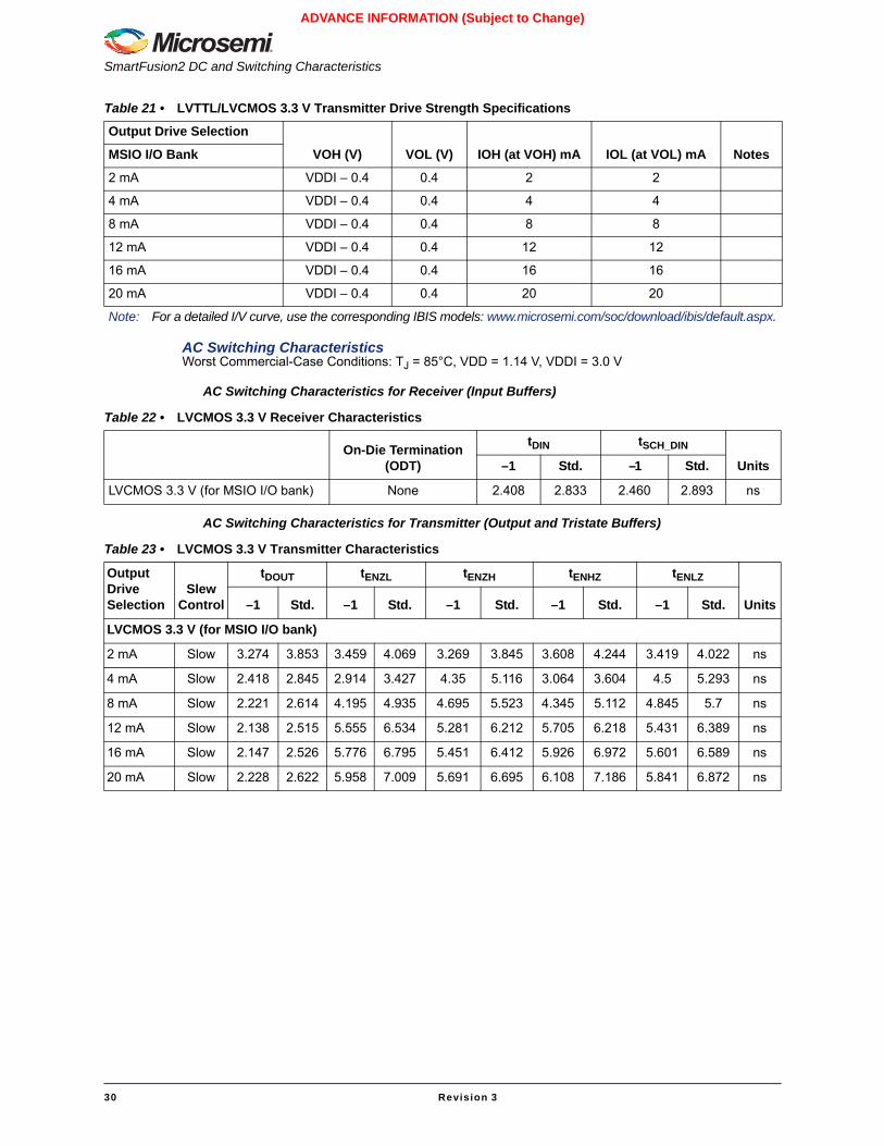
AC Switching CharacteristicsWorst Commercial-Case Conditions: TJ = 85°C, VDD = 1.14 V, VDDI = 3.0 V
AC Switching Characteristics for Receiver (Input Buffers)
AC Switching Characteristics for Transmitter (Output and Tristate Buffers)
Table 21 • LVTTL/LVCMOS 3.3 V Transmitter Drive Strength Specifications
Output Drive Selection
VOH (V) VOL (V) IOH (at VOH) mA IOL (at VOL) mA NotesMSIO I/O Bank
2 mA VDDI – 0.4 0.4 2 2
4 mA VDDI – 0.4 0.4 4 4
8 mA VDDI – 0.4 0.4 8 8
12 mA VDDI – 0.4 0.4 12 12
16 mA VDDI – 0.4 0.4 16 16
20 mA VDDI – 0.4 0.4 20 20
Note: For a detailed I/V curve, use the corresponding IBIS models: www.microsemi.com/soc/download/ibis/default.aspx.
Table 22 • LVCMOS 3.3 V Receiver Characteristics
On-Die Termination (ODT)
tDIN tSCH_DIN
Units–1 Std. –1 Std.
LVCMOS 3.3 V (for MSIO I/O bank) None 2.408 2.833 2.460 2.893 ns
Table 23 • LVCMOS 3.3 V Transmitter Characteristics
Output Drive Selection
Slew Control
tDOUT tENZL tENZH tENHZ tENLZ
Units–1 Std. –1 Std. –1 Std. –1 Std. –1 Std.
LVCMOS 3.3 V (for MSIO I/O bank)
2 mA Slow 3.274 3.853 3.459 4.069 3.269 3.845 3.608 4.244 3.419 4.022 ns
4 mA Slow 2.418 2.845 2.914 3.427 4.35 5.116 3.064 3.604 4.5 5.293 ns
8 mA Slow 2.221 2.614 4.195 4.935 4.695 5.523 4.345 5.112 4.845 5.7 ns
12 mA Slow 2.138 2.515 5.555 6.534 5.281 6.212 5.705 6.218 5.431 6.389 ns
16 mA Slow 2.147 2.526 5.776 6.795 5.451 6.412 5.926 6.972 5.601 6.589 ns
20 mA Slow 2.228 2.622 5.958 7.009 5.691 6.695 6.108 7.186 5.841 6.872 ns
SmartFusion2 System-on-Chip FPGAs Datasheet
Revision 3 31
ADVANCE INFORMATION (Subject to Change)
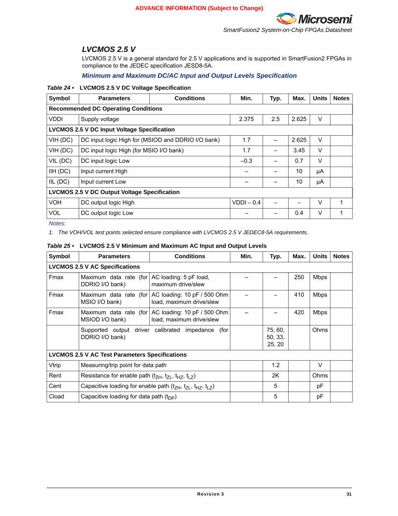
LVCMOS 2.5 VLVCMOS 2.5 V is a general standard for 2.5 V applications and is supported in SmartFusion2 FPGAs incompliance to the JEDEC specification JESD8-5A.
Minimum and Maximum DC/AC Input and Output Levels Specification
Table 24 • LVCMOS 2.5 V DC Voltage Specification
Symbol Parameters Conditions Min. Typ. Max. Units Notes
Recommended DC Operating Conditions
VDDI Supply voltage 2.375 2.5 2.625 V
LVCMOS 2.5 V DC Input Voltage Specification
VIH (DC) DC input logic High for (MSIOD and DDRIO I/O bank) 1.7 – 2.625 V
VIH (DC) DC input logic High (for MSIO I/O bank) 1.7 – 3.45 V
VIL (DC) DC input logic Low –0.3 – 0.7 V
IIH (DC) Input current High – – 10 µA
IIL (DC) Input current Low – – 10 µA
LVCMOS 2.5 V DC Output Voltage Specification
VOH DC output logic High VDDI – 0.4 – – V 1
VOL DC output logic Low – – 0.4 V 1
Notes:1. The VOH/VOL test points selected ensure compliance with LVCMOS 2.5 V JEDEC8-5A requirements.
Table 25 • LVCMOS 2.5 V Minimum and Maximum AC Input and Output Levels
Symbol Parameters Conditions Min. Typ. Max. Units Notes
LVCMOS 2.5 V AC Specifications
Fmax Maximum data rate (forDDRIO I/O bank)
AC loading: 5 pF load,maximum drive/slew
– – 250 Mbps
Fmax Maximum data rate (forMSIO I/O bank)
AC loading: 10 pF / 500 Ohmload, maximum drive/slew
– – 410 Mbps
Fmax Maximum data rate (forMSIOD I/O bank)
AC loading: 10 pF / 500 Ohmload, maximum drive/slew
– – 420 Mbps
Supported output driver calibrated impedance (forDDRIO I/O bank)
75, 60, 50, 33, 25, 20
Ohms
LVCMOS 2.5 V AC Test Parameters Specifications
Vtrip Measuring/trip point for data path 1.2 V
Rent Resistance for enable path (tZH, tZL, tHZ, tLZ) 2K Ohms
Cent Capacitive loading for enable path (tZH, tZL, tHZ, tLZ) 5 pF
Cload Capacitive loading for data path (tDP) 5 pF
SmartFusion2 DC and Switching Characteristics
32 Revision 3
ADVANCE INFORMATION (Subject to Change)
AC Switching CharacteristicsWorst Commercial-Case Conditions: TJ = 85°C, VDD = 1.14 V, VDDI = 2.375 V
AC Switching Characteristics for Receiver (Input Buffers)
AC Switching Characteristics for Transmitter (Output and Tristate Buffers)
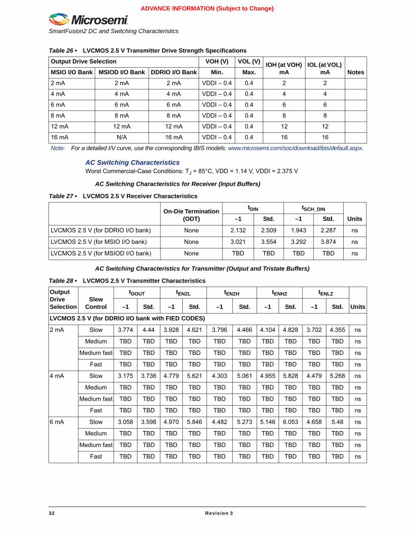
Table 26 • LVCMOS 2.5 V Transmitter Drive Strength Specifications
Output Drive Selection VOH (V) VOL (V) IOH (at VOH) mA
IOL (at VOL) mA NotesMSIO I/O Bank MSIOD I/O Bank DDRIO I/O Bank Min. Max.
2 mA 2 mA 2 mA VDDI – 0.4 0.4 2 2
4 mA 4 mA 4 mA VDDI – 0.4 0.4 4 4
6 mA 6 mA 6 mA VDDI – 0.4 0.4 6 6
8 mA 8 mA 8 mA VDDI – 0.4 0.4 8 8
12 mA 12 mA 12 mA VDDI – 0.4 0.4 12 12
16 mA N/A 16 mA VDDI – 0.4 0.4 16 16
Note: For a detailed I/V curve, use the corresponding IBIS models: www.microsemi.com/soc/download/ibis/default.aspx.
Table 27 • LVCMOS 2.5 V Receiver Characteristics
On-Die Termination (ODT)
tDIN tSCH_DIN
Units–1 Std. –1 Std.
LVCMOS 2.5 V (for DDRIO I/O bank) None 2.132 2.509 1.943 2.287 ns
LVCMOS 2.5 V (for MSIO I/O bank) None 3.021 3.554 3.292 3.874 ns
LVCMOS 2.5 V (for MSIOD I/O bank) None TBD TBD TBD TBD ns
Table 28 • LVCMOS 2.5 V Transmitter Characteristics
Output Drive Selection
Slew Control
tDOUT tENZL tENZH tENHZ tENLZ
Units–1 Std. –1 Std. –1 Std. –1 Std. –1 Std.
LVCMOS 2.5 V (for DDRIO I/O bank with FIED CODES)
2 mA Slow 3.774 4.44 3.928 4.621 3.796 4.466 4.104 4.828 3.702 4.355 ns
Medium TBD TBD TBD TBD TBD TBD TBD TBD TBD TBD ns
Medium fast TBD TBD TBD TBD TBD TBD TBD TBD TBD TBD ns
Fast TBD TBD TBD TBD TBD TBD TBD TBD TBD TBD ns
4 mA Slow 3.175 3.736 4.779 5.621 4.303 5.061 4.955 5.828 4.479 5.268 ns
Medium TBD TBD TBD TBD TBD TBD TBD TBD TBD TBD ns
Medium fast TBD TBD TBD TBD TBD TBD TBD TBD TBD TBD ns
Fast TBD TBD TBD TBD TBD TBD TBD TBD TBD TBD ns
6 mA Slow 3.058 3.598 4.970 5.846 4.482 5.273 5.146 6.053 4.658 5.48 ns
Medium TBD TBD TBD TBD TBD TBD TBD TBD TBD TBD ns
Medium fast TBD TBD TBD TBD TBD TBD TBD TBD TBD TBD ns
Fast TBD TBD TBD TBD TBD TBD TBD TBD TBD TBD ns
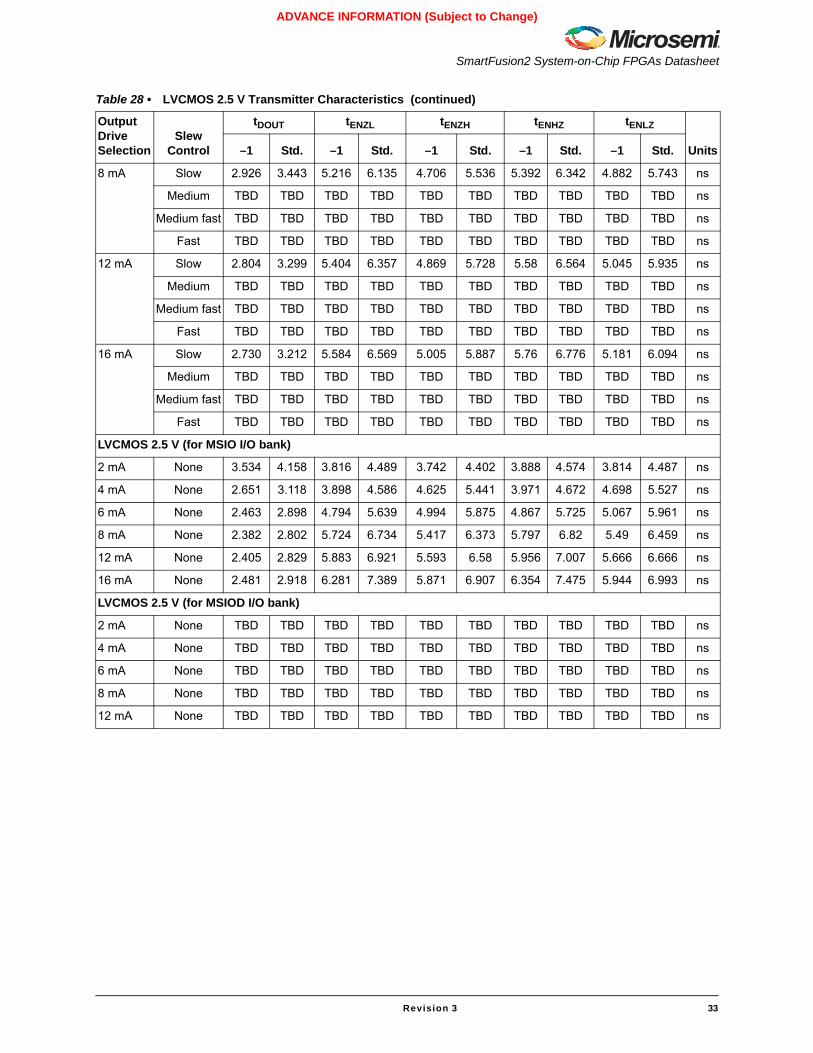
SmartFusion2 System-on-Chip FPGAs Datasheet
Revision 3 33
ADVANCE INFORMATION (Subject to Change)
8 mA Slow 2.926 3.443 5.216 6.135 4.706 5.536 5.392 6.342 4.882 5.743 ns
Medium TBD TBD TBD TBD TBD TBD TBD TBD TBD TBD ns
Medium fast TBD TBD TBD TBD TBD TBD TBD TBD TBD TBD ns
Fast TBD TBD TBD TBD TBD TBD TBD TBD TBD TBD ns
12 mA Slow 2.804 3.299 5.404 6.357 4.869 5.728 5.58 6.564 5.045 5.935 ns
Medium TBD TBD TBD TBD TBD TBD TBD TBD TBD TBD ns
Medium fast TBD TBD TBD TBD TBD TBD TBD TBD TBD TBD ns
Fast TBD TBD TBD TBD TBD TBD TBD TBD TBD TBD ns
16 mA Slow 2.730 3.212 5.584 6.569 5.005 5.887 5.76 6.776 5.181 6.094 ns
Medium TBD TBD TBD TBD TBD TBD TBD TBD TBD TBD ns
Medium fast TBD TBD TBD TBD TBD TBD TBD TBD TBD TBD ns
Fast TBD TBD TBD TBD TBD TBD TBD TBD TBD TBD ns
LVCMOS 2.5 V (for MSIO I/O bank)
2 mA None 3.534 4.158 3.816 4.489 3.742 4.402 3.888 4.574 3.814 4.487 ns
4 mA None 2.651 3.118 3.898 4.586 4.625 5.441 3.971 4.672 4.698 5.527 ns
6 mA None 2.463 2.898 4.794 5.639 4.994 5.875 4.867 5.725 5.067 5.961 ns
8 mA None 2.382 2.802 5.724 6.734 5.417 6.373 5.797 6.82 5.49 6.459 ns
12 mA None 2.405 2.829 5.883 6.921 5.593 6.58 5.956 7.007 5.666 6.666 ns
16 mA None 2.481 2.918 6.281 7.389 5.871 6.907 6.354 7.475 5.944 6.993 ns
LVCMOS 2.5 V (for MSIOD I/O bank)
2 mA None TBD TBD TBD TBD TBD TBD TBD TBD TBD TBD ns
4 mA None TBD TBD TBD TBD TBD TBD TBD TBD TBD TBD ns
6 mA None TBD TBD TBD TBD TBD TBD TBD TBD TBD TBD ns
8 mA None TBD TBD TBD TBD TBD TBD TBD TBD TBD TBD ns
12 mA None TBD TBD TBD TBD TBD TBD TBD TBD TBD TBD ns
Table 28 • LVCMOS 2.5 V Transmitter Characteristics (continued)
Output Drive Selection
Slew Control
tDOUT tENZL tENZH tENHZ tENLZ
Units–1 Std. –1 Std. –1 Std. –1 Std. –1 Std.
SmartFusion2 DC and Switching Characteristics
34 Revision 3
ADVANCE INFORMATION (Subject to Change)
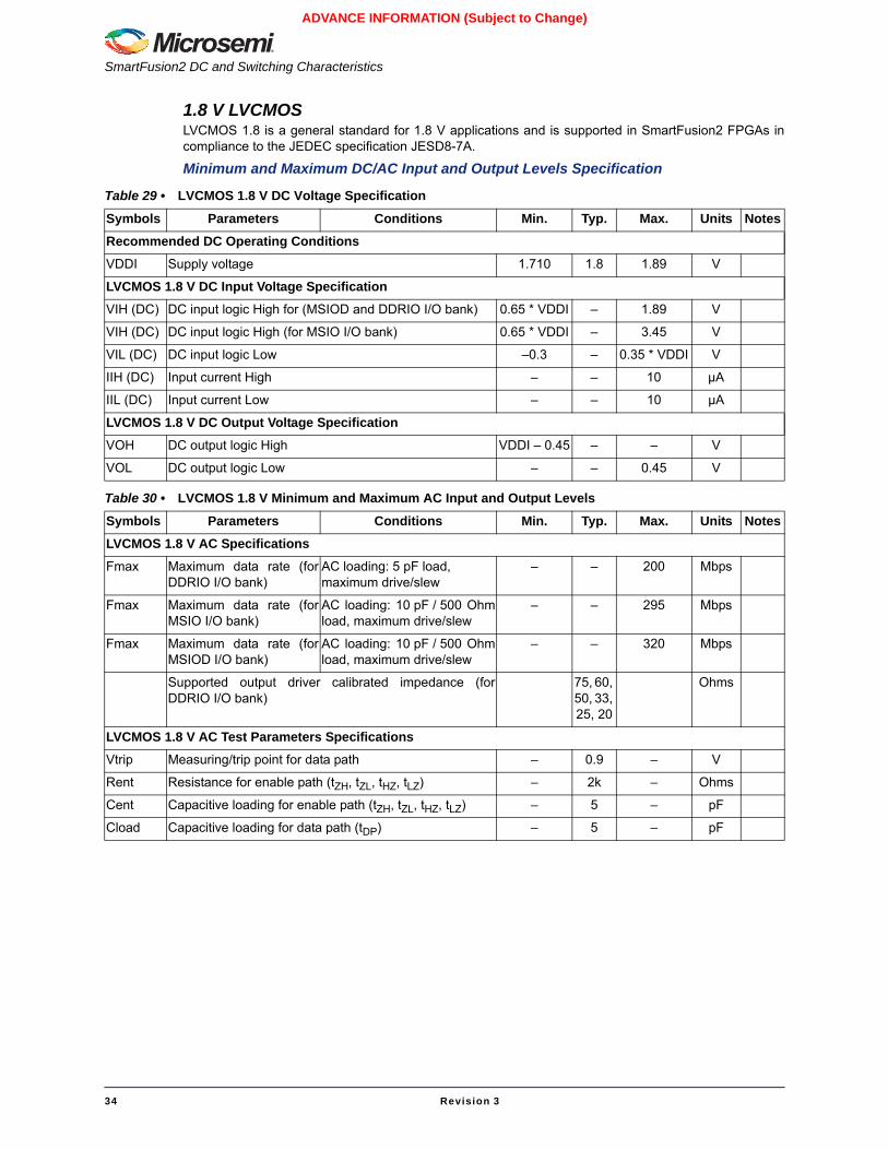
1.8 V LVCMOSLVCMOS 1.8 is a general standard for 1.8 V applications and is supported in SmartFusion2 FPGAs incompliance to the JEDEC specification JESD8-7A.
Minimum and Maximum DC/AC Input and Output Levels Specification
Table 29 • LVCMOS 1.8 V DC Voltage Specification
Symbols Parameters Conditions Min. Typ. Max. Units NotesRecommended DC Operating ConditionsVDDI Supply voltage 1.710 1.8 1.89 V
LVCMOS 1.8 V DC Input Voltage SpecificationVIH (DC) DC input logic High for (MSIOD and DDRIO I/O bank) 0.65 * VDDI – 1.89 V
VIH (DC) DC input logic High (for MSIO I/O bank) 0.65 * VDDI – 3.45 V
VIL (DC) DC input logic Low –0.3 – 0.35 * VDDI V
IIH (DC) Input current High – – 10 µA
IIL (DC) Input current Low – – 10 µA
LVCMOS 1.8 V DC Output Voltage SpecificationVOH DC output logic High VDDI – 0.45 – – V
VOL DC output logic Low – – 0.45 V
Table 30 • LVCMOS 1.8 V Minimum and Maximum AC Input and Output Levels
Symbols Parameters Conditions Min. Typ. Max. Units NotesLVCMOS 1.8 V AC SpecificationsFmax Maximum data rate (for
DDRIO I/O bank)AC loading: 5 pF load,maximum drive/slew
– – 200 Mbps
Fmax Maximum data rate (forMSIO I/O bank)
AC loading: 10 pF / 500 Ohmload, maximum drive/slew
– – 295 Mbps
Fmax Maximum data rate (forMSIOD I/O bank)
AC loading: 10 pF / 500 Ohmload, maximum drive/slew
– – 320 Mbps
Supported output driver calibrated impedance (forDDRIO I/O bank)
75, 60, 50, 33, 25, 20
Ohms
LVCMOS 1.8 V AC Test Parameters SpecificationsVtrip Measuring/trip point for data path – 0.9 – V
Rent Resistance for enable path (tZH, tZL, tHZ, tLZ) – 2k – Ohms
Cent Capacitive loading for enable path (tZH, tZL, tHZ, tLZ) – 5 – pF
Cload Capacitive loading for data path (tDP) – 5 – pF
SmartFusion2 System-on-Chip FPGAs Datasheet
Revision 3 35
ADVANCE INFORMATION (Subject to Change)
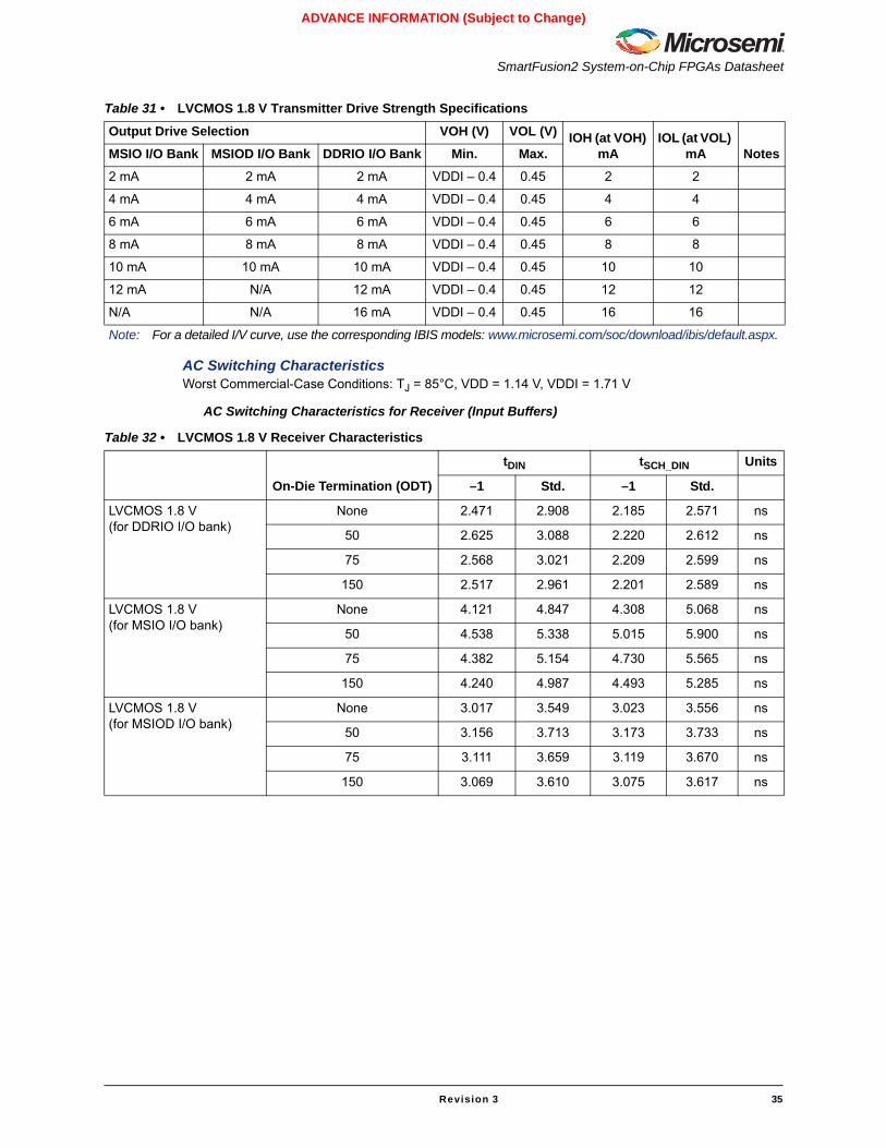
AC Switching CharacteristicsWorst Commercial-Case Conditions: TJ = 85°C, VDD = 1.14 V, VDDI = 1.71 V
AC Switching Characteristics for Receiver (Input Buffers)
Table 31 • LVCMOS 1.8 V Transmitter Drive Strength Specifications
Output Drive Selection VOH (V) VOL (V) IOH (at VOH) mA
IOL (at VOL) mA NotesMSIO I/O Bank MSIOD I/O Bank DDRIO I/O Bank Min. Max.
2 mA 2 mA 2 mA VDDI – 0.4 0.45 2 2
4 mA 4 mA 4 mA VDDI – 0.4 0.45 4 4
6 mA 6 mA 6 mA VDDI – 0.4 0.45 6 6
8 mA 8 mA 8 mA VDDI – 0.4 0.45 8 8
10 mA 10 mA 10 mA VDDI – 0.4 0.45 10 10
12 mA N/A 12 mA VDDI – 0.4 0.45 12 12
N/A N/A 16 mA VDDI – 0.4 0.45 16 16
Note: For a detailed I/V curve, use the corresponding IBIS models: www.microsemi.com/soc/download/ibis/default.aspx.
Table 32 • LVCMOS 1.8 V Receiver Characteristics
On-Die Termination (ODT)
tDIN tSCH_DIN Units
–1 Std. –1 Std.
LVCMOS 1.8 V(for DDRIO I/O bank)
None 2.471 2.908 2.185 2.571 ns
50 2.625 3.088 2.220 2.612 ns
75 2.568 3.021 2.209 2.599 ns
150 2.517 2.961 2.201 2.589 ns
LVCMOS 1.8 V(for MSIO I/O bank)
None 4.121 4.847 4.308 5.068 ns
50 4.538 5.338 5.015 5.900 ns
75 4.382 5.154 4.730 5.565 ns
150 4.240 4.987 4.493 5.285 ns
LVCMOS 1.8 V(for MSIOD I/O bank)
None 3.017 3.549 3.023 3.556 ns
50 3.156 3.713 3.173 3.733 ns
75 3.111 3.659 3.119 3.670 ns
150 3.069 3.610 3.075 3.617 ns
SmartFusion2 DC and Switching Characteristics
36 Revision 3
ADVANCE INFORMATION (Subject to Change)
AC Switching Characteristics for Transmitter (Output and Tristate Buffers)
Table 33 • LVCMOS 1.8 V Transmitter Characteristics
Output Drive Selection
Slew Control
tDOUT tENZL tENZH tENHZ tENLZ
Units–1 Std. –1 Std. –1 Std. –1 Std. –1 Std.
LVCMOS 1.8 V (for DDRIO I/O bank)
2 mA Slow 4.270 5.024 4.806 5.655 4.298 5.056 5.095 5.994 4.526 5.324 ns
Medium 3.877 4.562 4.530 5.330 3.919 4.612 4.819 5.669 4.208 4.951 ns
Medium fast 3.684 4.335 4.386 5.160 3.790 4.459 4.675 5.499 4.079 4.798 ns
Fast 3.665 4.312 4.376 5.149 3.781 4.448 4.665 5.488 4.070 4.787 ns
4 mA Slow 3.949 4.647 5.298 6.233 4.688 5.515 5.587 6.572 4.977 5.854 ns
Medium 3.558 4.187 5.019 5.905 4.357 5.127 5.308 6.244 4.646 5.466 ns
Medium fast 3.367 3.961 4.877 5.738 4.224 4.970 5.166 6.077 4.513 5.309 ns
Fast 3.347 3.938 4.868 5.727 4.214 4.959 5.157 6.066 4.503 5.298 ns
6 mA Slow 3.735 4.394 5.510 6.483 4.867 5.726 5.799 6.822 5.156 6.065 ns
Medium 3.370 3.965 5.250 6.177 4.565 5.371 5.539 6.516 4.854 5.710 ns
Medium fast 3.194 3.759 5.116 6.020 4.444 5.228 5.405 6.359 4.733 5.567 ns
Fast 3.175 3.736 5.110 6.012 4.437 5.221 5.399 6.351 4.726 5.56o ns
8 mA Slow 3.640 4.283 5.702 6.708 5.029 5.917 5.991 7.047 5.318 6.256 ns
Medium 3.278 3.857 5.438 6.399 4.717 5.550 5.727 6.738 5.006 5.889 ns
Medium fast 3.101 3.649 5.309 6.247 4.593 5.404 5.598 6.586 4.882 5.743 ns
Fast 3.082 3.627 5.303 6.240 4.587 5.397 5.592 6.579 4.876 5.736 ns
10 mA Slow 3.515 4.135 5.931 6.979 5.215 6.136 6.220 7.318 5.504 6.475 ns
Medium 3.165 3.723 5.678 6.681 4.901 5.767 5.967 7.020 5.190 6.106 ns
Medium fast 2.991 3.519 5.563 6.545 4.781 5.625 5.852 6.884 5.070 5.964 ns
Fast 2.973 3.497 5.559 6.540 4.773 5.616 5.848 6.879 5.062 5.955 ns
12 mA Slow 3.446 4.054 5.976 7.032 5.244 6.169 6.265 7.371 5.533 6.508 ns
Medium 3.113 3.662 5.737 6.750 4.957 5.832 6.026 7.089 5.246 6.171 ns
Medium fast 2.949 3.470 5.630 6.624 4.846 5.702 5.919 6.963 5.135 6.041 ns
Fast 2.931 3.449 5.629 6.623 4.840 5.695 5.918 6.962 5.129 6.034 ns
16 mA Slow 3.388 3.986 6.110 7.189 5.349 6.293 6.399 7.528 5.638 6.632 ns
Medium 3.065 3.606 5.885 6.924 5.058 5.951 6.174 7.263 5.347 6.290 ns
Medium fast 2.903 3.416 5.797 6.821 4.950 5.824 6.086 7.160 5.239 6.163 ns
Fast 2.885 3.395 5.797 6.820 4.944 5.817 6.086 7.159 5.233 6.156 ns
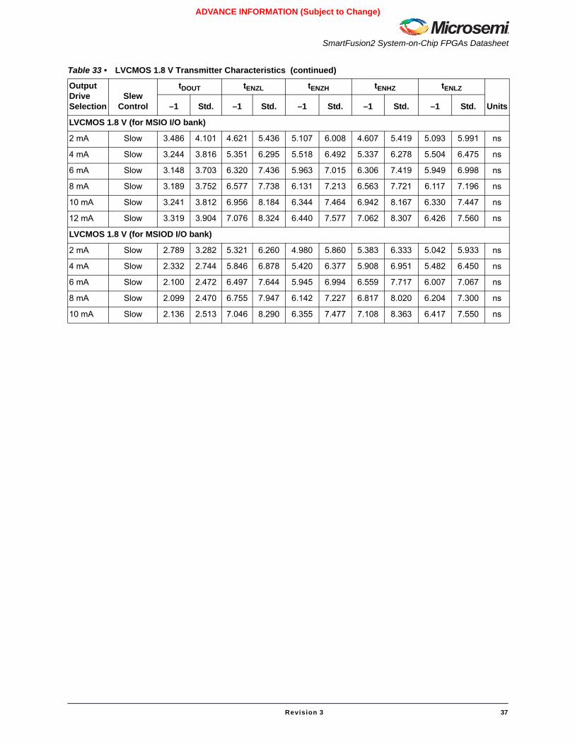
SmartFusion2 System-on-Chip FPGAs Datasheet
Revision 3 37
ADVANCE INFORMATION (Subject to Change)
LVCMOS 1.8 V (for MSIO I/O bank)
2 mA Slow 3.486 4.101 4.621 5.436 5.107 6.008 4.607 5.419 5.093 5.991 ns
4 mA Slow 3.244 3.816 5.351 6.295 5.518 6.492 5.337 6.278 5.504 6.475 ns
6 mA Slow 3.148 3.703 6.320 7.436 5.963 7.015 6.306 7.419 5.949 6.998 ns
8 mA Slow 3.189 3.752 6.577 7.738 6.131 7.213 6.563 7.721 6.117 7.196 ns
10 mA Slow 3.241 3.812 6.956 8.184 6.344 7.464 6.942 8.167 6.330 7.447 ns
12 mA Slow 3.319 3.904 7.076 8.324 6.440 7.577 7.062 8.307 6.426 7.560 ns
LVCMOS 1.8 V (for MSIOD I/O bank)
2 mA Slow 2.789 3.282 5.321 6.260 4.980 5.860 5.383 6.333 5.042 5.933 ns
4 mA Slow 2.332 2.744 5.846 6.878 5.420 6.377 5.908 6.951 5.482 6.450 ns
6 mA Slow 2.100 2.472 6.497 7.644 5.945 6.994 6.559 7.717 6.007 7.067 ns
8 mA Slow 2.099 2.470 6.755 7.947 6.142 7.227 6.817 8.020 6.204 7.300 ns
10 mA Slow 2.136 2.513 7.046 8.290 6.355 7.477 7.108 8.363 6.417 7.550 ns
Table 33 • LVCMOS 1.8 V Transmitter Characteristics (continued)
Output Drive Selection
Slew Control
tDOUT tENZL tENZH tENHZ tENLZ
Units–1 Std. –1 Std. –1 Std. –1 Std. –1 Std.
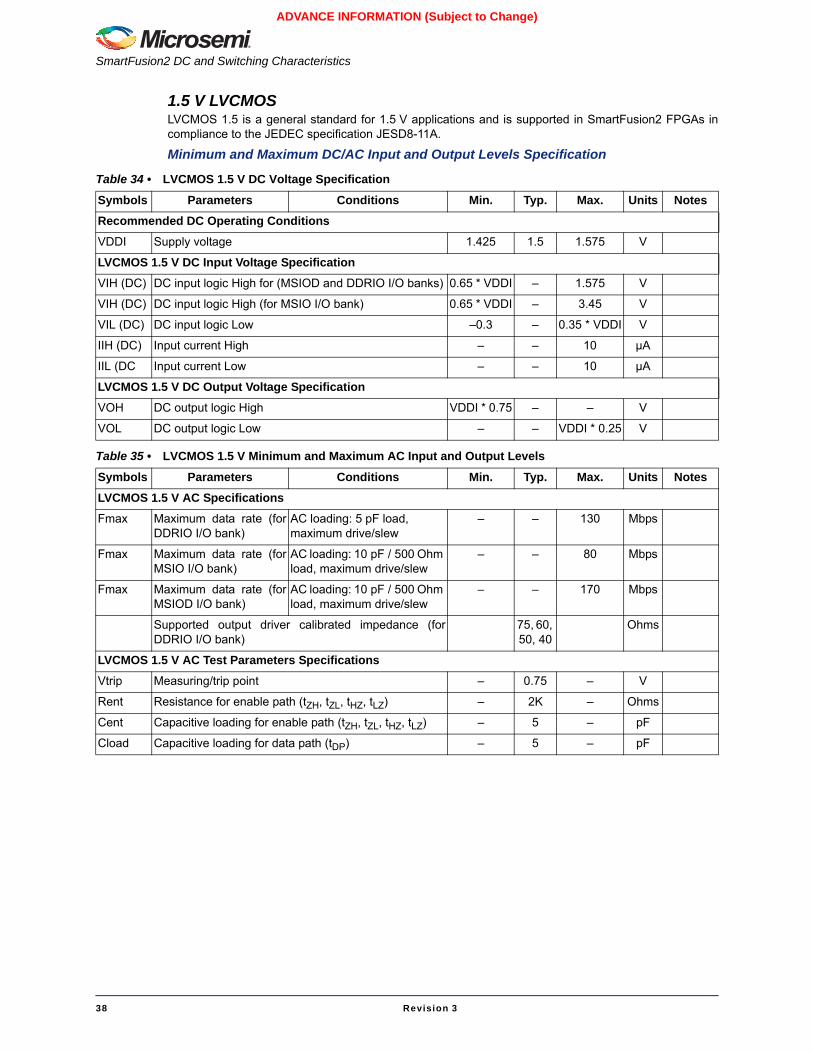
SmartFusion2 DC and Switching Characteristics
38 Revision 3
ADVANCE INFORMATION (Subject to Change)
1.5 V LVCMOSLVCMOS 1.5 is a general standard for 1.5 V applications and is supported in SmartFusion2 FPGAs incompliance to the JEDEC specification JESD8-11A.
Minimum and Maximum DC/AC Input and Output Levels Specification
Table 34 • LVCMOS 1.5 V DC Voltage Specification
Symbols Parameters Conditions Min. Typ. Max. Units NotesRecommended DC Operating ConditionsVDDI Supply voltage 1.425 1.5 1.575 V
LVCMOS 1.5 V DC Input Voltage SpecificationVIH (DC) DC input logic High for (MSIOD and DDRIO I/O banks) 0.65 * VDDI – 1.575 V
VIH (DC) DC input logic High (for MSIO I/O bank) 0.65 * VDDI – 3.45 V
VIL (DC) DC input logic Low –0.3 – 0.35 * VDDI V
IIH (DC) Input current High – – 10 µA
IIL (DC Input current Low – – 10 µA
LVCMOS 1.5 V DC Output Voltage SpecificationVOH DC output logic High VDDI * 0.75 – – V
VOL DC output logic Low – – VDDI * 0.25 V
Table 35 • LVCMOS 1.5 V Minimum and Maximum AC Input and Output Levels
Symbols Parameters Conditions Min. Typ. Max. Units NotesLVCMOS 1.5 V AC SpecificationsFmax Maximum data rate (for
DDRIO I/O bank)AC loading: 5 pF load,maximum drive/slew
– – 130 Mbps
Fmax Maximum data rate (forMSIO I/O bank)
AC loading: 10 pF / 500 Ohm load, maximum drive/slew
– – 80 Mbps
Fmax Maximum data rate (forMSIOD I/O bank)
AC loading: 10 pF / 500 Ohm load, maximum drive/slew
– – 170 Mbps
Supported output driver calibrated impedance (forDDRIO I/O bank)
75, 60, 50, 40
Ohms
LVCMOS 1.5 V AC Test Parameters SpecificationsVtrip Measuring/trip point – 0.75 – V
Rent Resistance for enable path (tZH, tZL, tHZ, tLZ) – 2K – Ohms
Cent Capacitive loading for enable path (tZH, tZL, tHZ, tLZ) – 5 – pF
Cload Capacitive loading for data path (tDP) – 5 – pF
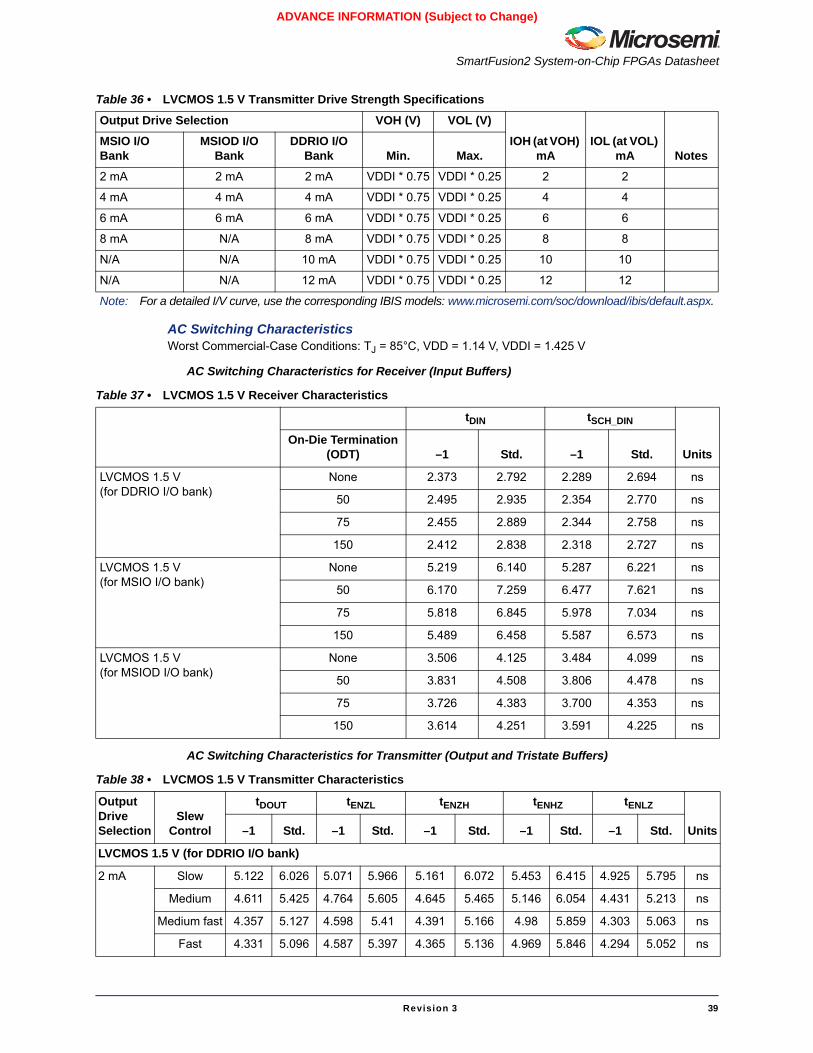
SmartFusion2 System-on-Chip FPGAs Datasheet
Revision 3 39
ADVANCE INFORMATION (Subject to Change)
AC Switching CharacteristicsWorst Commercial-Case Conditions: TJ = 85°C, VDD = 1.14 V, VDDI = 1.425 V
AC Switching Characteristics for Receiver (Input Buffers)
AC Switching Characteristics for Transmitter (Output and Tristate Buffers)
Table 36 • LVCMOS 1.5 V Transmitter Drive Strength Specifications
Output Drive Selection VOH (V) VOL (V)IOH (at VOH)
mAIOL (at VOL)
mA NotesMSIO I/O Bank
MSIOD I/O Bank
DDRIO I/O Bank Min. Max.
2 mA 2 mA 2 mA VDDI * 0.75 VDDI * 0.25 2 2
4 mA 4 mA 4 mA VDDI * 0.75 VDDI * 0.25 4 4
6 mA 6 mA 6 mA VDDI * 0.75 VDDI * 0.25 6 6
8 mA N/A 8 mA VDDI * 0.75 VDDI * 0.25 8 8
N/A N/A 10 mA VDDI * 0.75 VDDI * 0.25 10 10
N/A N/A 12 mA VDDI * 0.75 VDDI * 0.25 12 12
Note: For a detailed I/V curve, use the corresponding IBIS models: www.microsemi.com/soc/download/ibis/default.aspx.
Table 37 • LVCMOS 1.5 V Receiver Characteristics
tDIN tSCH_DIN
UnitsOn-Die Termination
(ODT) –1 Std. –1 Std.
LVCMOS 1.5 V (for DDRIO I/O bank)
None 2.373 2.792 2.289 2.694 ns
50 2.495 2.935 2.354 2.770 ns
75 2.455 2.889 2.344 2.758 ns
150 2.412 2.838 2.318 2.727 ns
LVCMOS 1.5 V (for MSIO I/O bank)
None 5.219 6.140 5.287 6.221 ns
50 6.170 7.259 6.477 7.621 ns
75 5.818 6.845 5.978 7.034 ns
150 5.489 6.458 5.587 6.573 ns
LVCMOS 1.5 V (for MSIOD I/O bank)
None 3.506 4.125 3.484 4.099 ns
50 3.831 4.508 3.806 4.478 ns
75 3.726 4.383 3.700 4.353 ns
150 3.614 4.251 3.591 4.225 ns
Table 38 • LVCMOS 1.5 V Transmitter Characteristics
Output Drive Selection
Slew Control
tDOUT tENZL tENZH tENHZ tENLZ
Units–1 Std. –1 Std. –1 Std. –1 Std. –1 Std.
LVCMOS 1.5 V (for DDRIO I/O bank)
2 mA Slow 5.122 6.026 5.071 5.966 5.161 6.072 5.453 6.415 4.925 5.795 ns
Medium 4.611 5.425 4.764 5.605 4.645 5.465 5.146 6.054 4.431 5.213 ns
Medium fast 4.357 5.127 4.598 5.41 4.391 5.166 4.98 5.859 4.303 5.063 ns
Fast 4.331 5.096 4.587 5.397 4.365 5.136 4.969 5.846 4.294 5.052 ns
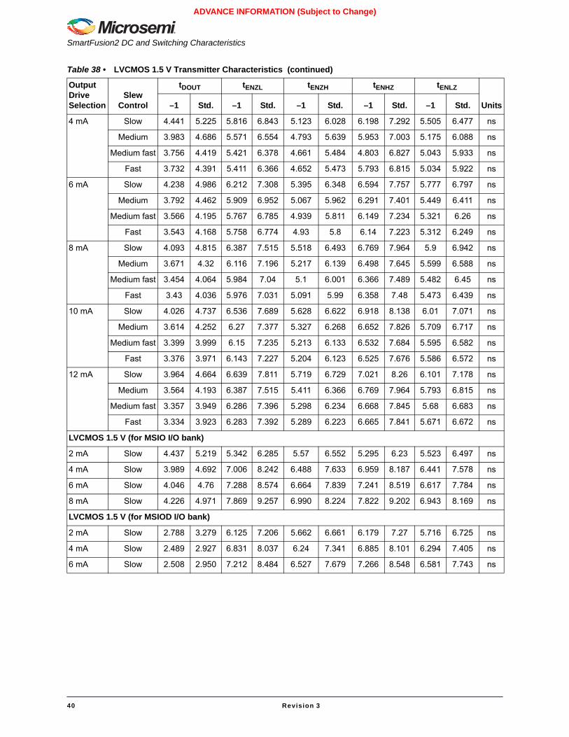
SmartFusion2 DC and Switching Characteristics
40 Revision 3
ADVANCE INFORMATION (Subject to Change)
4 mA Slow 4.441 5.225 5.816 6.843 5.123 6.028 6.198 7.292 5.505 6.477 ns
Medium 3.983 4.686 5.571 6.554 4.793 5.639 5.953 7.003 5.175 6.088 ns
Medium fast 3.756 4.419 5.421 6.378 4.661 5.484 4.803 6.827 5.043 5.933 ns
Fast 3.732 4.391 5.411 6.366 4.652 5.473 5.793 6.815 5.034 5.922 ns
6 mA Slow 4.238 4.986 6.212 7.308 5.395 6.348 6.594 7.757 5.777 6.797 ns
Medium 3.792 4.462 5.909 6.952 5.067 5.962 6.291 7.401 5.449 6.411 ns
Medium fast 3.566 4.195 5.767 6.785 4.939 5.811 6.149 7.234 5.321 6.26 ns
Fast 3.543 4.168 5.758 6.774 4.93 5.8 6.14 7.223 5.312 6.249 ns
8 mA Slow 4.093 4.815 6.387 7.515 5.518 6.493 6.769 7.964 5.9 6.942 ns
Medium 3.671 4.32 6.116 7.196 5.217 6.139 6.498 7.645 5.599 6.588 ns
Medium fast 3.454 4.064 5.984 7.04 5.1 6.001 6.366 7.489 5.482 6.45 ns
Fast 3.43 4.036 5.976 7.031 5.091 5.99 6.358 7.48 5.473 6.439 ns
10 mA Slow 4.026 4.737 6.536 7.689 5.628 6.622 6.918 8.138 6.01 7.071 ns
Medium 3.614 4.252 6.27 7.377 5.327 6.268 6.652 7.826 5.709 6.717 ns
Medium fast 3.399 3.999 6.15 7.235 5.213 6.133 6.532 7.684 5.595 6.582 ns
Fast 3.376 3.971 6.143 7.227 5.204 6.123 6.525 7.676 5.586 6.572 ns
12 mA Slow 3.964 4.664 6.639 7.811 5.719 6.729 7.021 8.26 6.101 7.178 ns
Medium 3.564 4.193 6.387 7.515 5.411 6.366 6.769 7.964 5.793 6.815 ns
Medium fast 3.357 3.949 6.286 7.396 5.298 6.234 6.668 7.845 5.68 6.683 ns
Fast 3.334 3.923 6.283 7.392 5.289 6.223 6.665 7.841 5.671 6.672 ns
LVCMOS 1.5 V (for MSIO I/O bank)
2 mA Slow 4.437 5.219 5.342 6.285 5.57 6.552 5.295 6.23 5.523 6.497 ns
4 mA Slow 3.989 4.692 7.006 8.242 6.488 7.633 6.959 8.187 6.441 7.578 ns
6 mA Slow 4.046 4.76 7.288 8.574 6.664 7.839 7.241 8.519 6.617 7.784 ns
8 mA Slow 4.226 4.971 7.869 9.257 6.990 8.224 7.822 9.202 6.943 8.169 ns
LVCMOS 1.5 V (for MSIOD I/O bank)
2 mA Slow 2.788 3.279 6.125 7.206 5.662 6.661 6.179 7.27 5.716 6.725 ns
4 mA Slow 2.489 2.927 6.831 8.037 6.24 7.341 6.885 8.101 6.294 7.405 ns
6 mA Slow 2.508 2.950 7.212 8.484 6.527 7.679 7.266 8.548 6.581 7.743 ns
Table 38 • LVCMOS 1.5 V Transmitter Characteristics (continued)
Output Drive Selection
Slew Control
tDOUT tENZL tENZH tENHZ tENLZ
Units–1 Std. –1 Std. –1 Std. –1 Std. –1 Std.
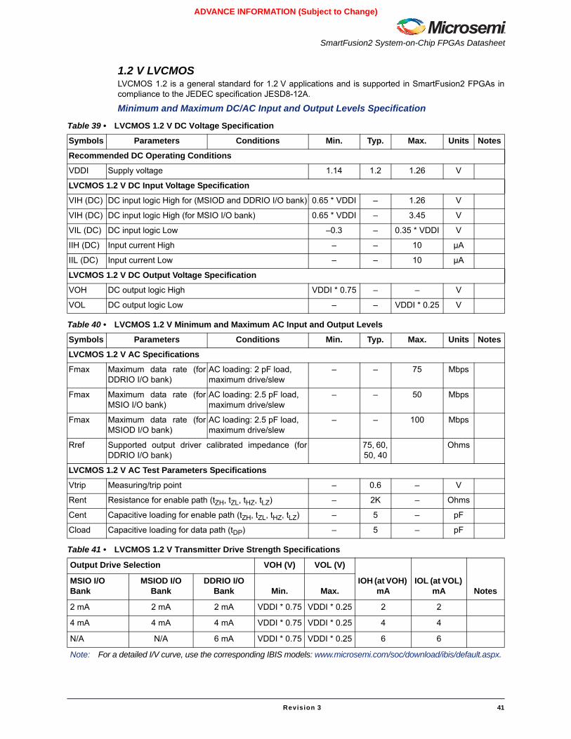
SmartFusion2 System-on-Chip FPGAs Datasheet
Revision 3 41
ADVANCE INFORMATION (Subject to Change)
1.2 V LVCMOSLVCMOS 1.2 is a general standard for 1.2 V applications and is supported in SmartFusion2 FPGAs incompliance to the JEDEC specification JESD8-12A.
Minimum and Maximum DC/AC Input and Output Levels Specification
Table 39 • LVCMOS 1.2 V DC Voltage Specification
Symbols Parameters Conditions Min. Typ. Max. Units Notes
Recommended DC Operating Conditions
VDDI Supply voltage 1.14 1.2 1.26 V
LVCMOS 1.2 V DC Input Voltage Specification
VIH (DC) DC input logic High for (MSIOD and DDRIO I/O bank) 0.65 * VDDI – 1.26 V
VIH (DC) DC input logic High (for MSIO I/O bank) 0.65 * VDDI – 3.45 V
VIL (DC) DC input logic Low –0.3 – 0.35 * VDDI V
IIH (DC) Input current High – – 10 µA
IIL (DC) Input current Low – – 10 µA
LVCMOS 1.2 V DC Output Voltage Specification
VOH DC output logic High VDDI * 0.75 – – V
VOL DC output logic Low – – VDDI * 0.25 V
Table 40 • LVCMOS 1.2 V Minimum and Maximum AC Input and Output Levels
Symbols Parameters Conditions Min. Typ. Max. Units Notes
LVCMOS 1.2 V AC Specifications
Fmax Maximum data rate (forDDRIO I/O bank)
AC loading: 2 pF load,maximum drive/slew
– – 75 Mbps
Fmax Maximum data rate (forMSIO I/O bank)
AC loading: 2.5 pF load, maximum drive/slew
– – 50 Mbps
Fmax Maximum data rate (forMSIOD I/O bank)
AC loading: 2.5 pF load, maximum drive/slew
– – 100 Mbps
Rref Supported output driver calibrated impedance (forDDRIO I/O bank)
75, 60, 50, 40
Ohms
LVCMOS 1.2 V AC Test Parameters Specifications
Vtrip Measuring/trip point – 0.6 – V
Rent Resistance for enable path (tZH, tZL, tHZ, tLZ) – 2K – Ohms
Cent Capacitive loading for enable path (tZH, tZL, tHZ, tLZ) – 5 – pF
Cload Capacitive loading for data path (tDP) – 5 – pF
Table 41 • LVCMOS 1.2 V Transmitter Drive Strength Specifications
Output Drive Selection VOH (V) VOL (V)
IOH (at VOH) mA
IOL (at VOL) mA Notes
MSIO I/O Bank
MSIOD I/O Bank
DDRIO I/O Bank Min. Max.
2 mA 2 mA 2 mA VDDI * 0.75 VDDI * 0.25 2 2
4 mA 4 mA 4 mA VDDI * 0.75 VDDI * 0.25 4 4
N/A N/A 6 mA VDDI * 0.75 VDDI * 0.25 6 6
Note: For a detailed I/V curve, use the corresponding IBIS models: www.microsemi.com/soc/download/ibis/default.aspx.
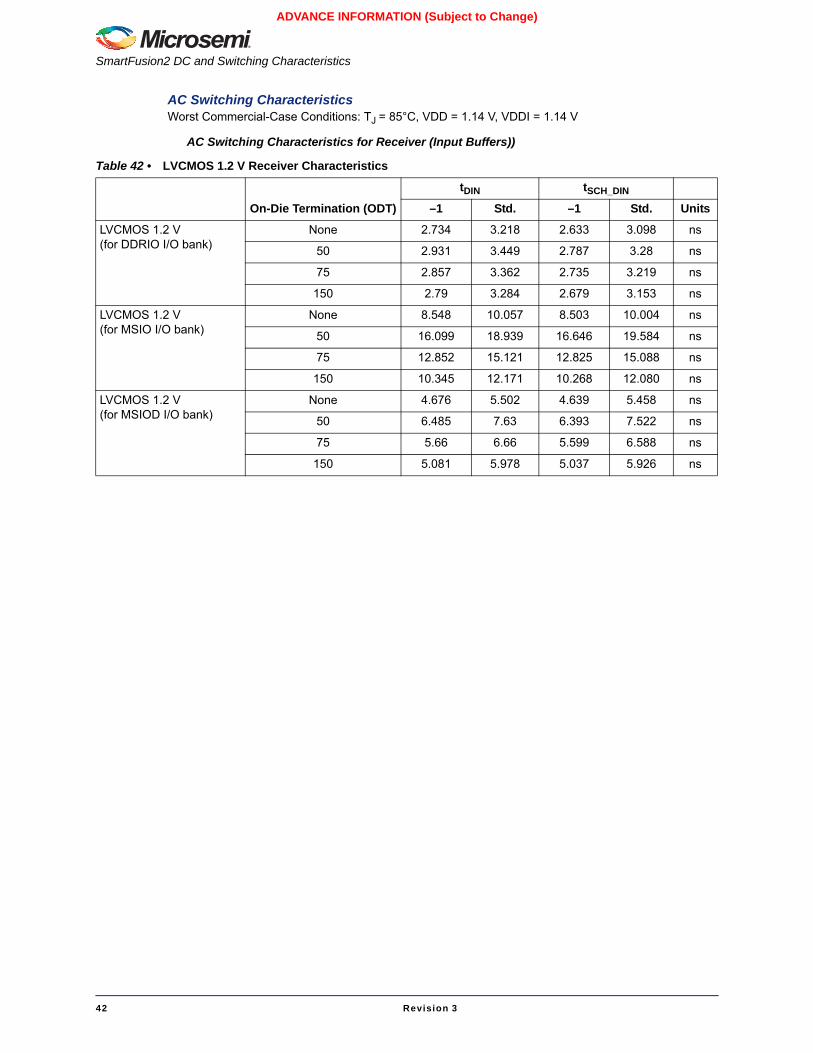
SmartFusion2 DC and Switching Characteristics
42 Revision 3
ADVANCE INFORMATION (Subject to Change)
AC Switching CharacteristicsWorst Commercial-Case Conditions: TJ = 85°C, VDD = 1.14 V, VDDI = 1.14 V
AC Switching Characteristics for Receiver (Input Buffers))
Table 42 • LVCMOS 1.2 V Receiver Characteristics
On-Die Termination (ODT)
tDIN tSCH_DIN
–1 Std. –1 Std. Units
LVCMOS 1.2 V(for DDRIO I/O bank)
None 2.734 3.218 2.633 3.098 ns
50 2.931 3.449 2.787 3.28 ns
75 2.857 3.362 2.735 3.219 ns
150 2.79 3.284 2.679 3.153 ns
LVCMOS 1.2 V(for MSIO I/O bank)
None 8.548 10.057 8.503 10.004 ns
50 16.099 18.939 16.646 19.584 ns
75 12.852 15.121 12.825 15.088 ns
150 10.345 12.171 10.268 12.080 ns
LVCMOS 1.2 V(for MSIOD I/O bank)
None 4.676 5.502 4.639 5.458 ns
50 6.485 7.63 6.393 7.522 ns
75 5.66 6.66 5.599 6.588 ns
150 5.081 5.978 5.037 5.926 ns
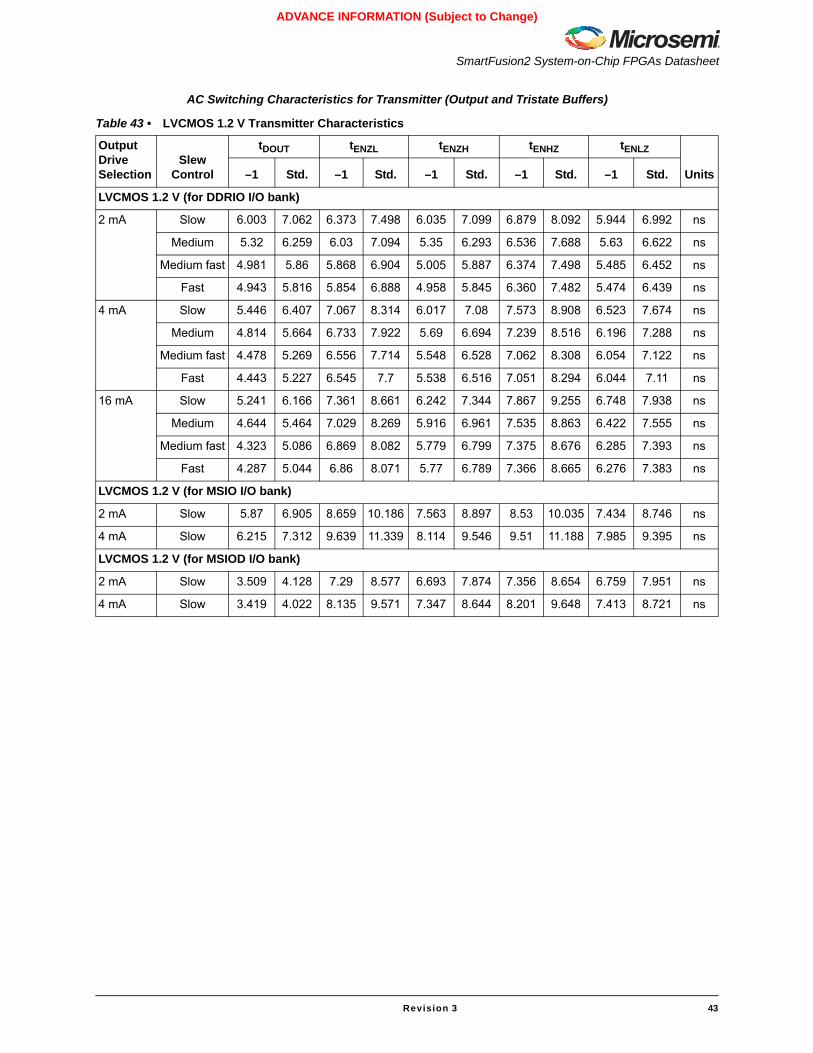
SmartFusion2 System-on-Chip FPGAs Datasheet
Revision 3 43
ADVANCE INFORMATION (Subject to Change)
AC Switching Characteristics for Transmitter (Output and Tristate Buffers)
Table 43 • LVCMOS 1.2 V Transmitter Characteristics
Output Drive Selection
Slew Control
tDOUT tENZL tENZH tENHZ tENLZ
Units–1 Std. –1 Std. –1 Std. –1 Std. –1 Std.
LVCMOS 1.2 V (for DDRIO I/O bank)
2 mA Slow 6.003 7.062 6.373 7.498 6.035 7.099 6.879 8.092 5.944 6.992 ns
Medium 5.32 6.259 6.03 7.094 5.35 6.293 6.536 7.688 5.63 6.622 ns
Medium fast 4.981 5.86 5.868 6.904 5.005 5.887 6.374 7.498 5.485 6.452 ns
Fast 4.943 5.816 5.854 6.888 4.958 5.845 6.360 7.482 5.474 6.439 ns
4 mA Slow 5.446 6.407 7.067 8.314 6.017 7.08 7.573 8.908 6.523 7.674 ns
Medium 4.814 5.664 6.733 7.922 5.69 6.694 7.239 8.516 6.196 7.288 ns
Medium fast 4.478 5.269 6.556 7.714 5.548 6.528 7.062 8.308 6.054 7.122 ns
Fast 4.443 5.227 6.545 7.7 5.538 6.516 7.051 8.294 6.044 7.11 ns
16 mA Slow 5.241 6.166 7.361 8.661 6.242 7.344 7.867 9.255 6.748 7.938 ns
Medium 4.644 5.464 7.029 8.269 5.916 6.961 7.535 8.863 6.422 7.555 ns
Medium fast 4.323 5.086 6.869 8.082 5.779 6.799 7.375 8.676 6.285 7.393 ns
Fast 4.287 5.044 6.86 8.071 5.77 6.789 7.366 8.665 6.276 7.383 ns
LVCMOS 1.2 V (for MSIO I/O bank)
2 mA Slow 5.87 6.905 8.659 10.186 7.563 8.897 8.53 10.035 7.434 8.746 ns
4 mA Slow 6.215 7.312 9.639 11.339 8.114 9.546 9.51 11.188 7.985 9.395 ns
LVCMOS 1.2 V (for MSIOD I/O bank)
2 mA Slow 3.509 4.128 7.29 8.577 6.693 7.874 7.356 8.654 6.759 7.951 ns
4 mA Slow 3.419 4.022 8.135 9.571 7.347 8.644 8.201 9.648 7.413 8.721 ns
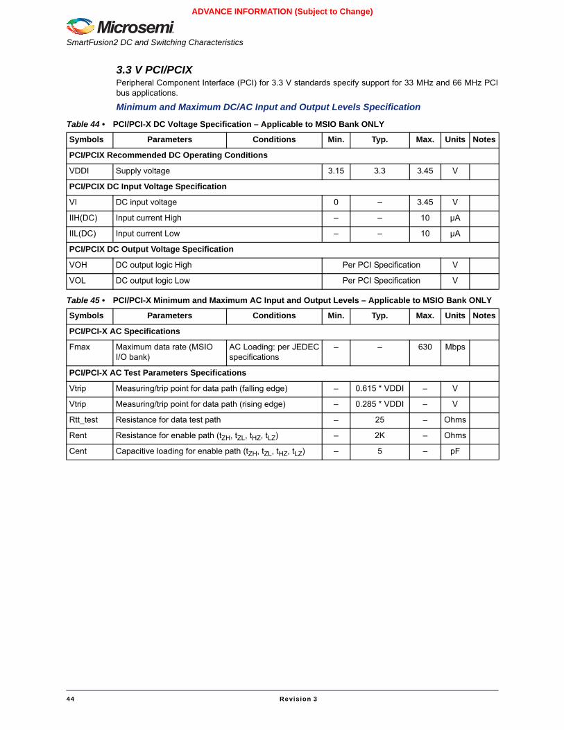
SmartFusion2 DC and Switching Characteristics
44 Revision 3
ADVANCE INFORMATION (Subject to Change)
3.3 V PCI/PCIXPeripheral Component Interface (PCI) for 3.3 V standards specify support for 33 MHz and 66 MHz PCIbus applications.
Minimum and Maximum DC/AC Input and Output Levels Specification
Table 44 • PCI/PCI-X DC Voltage Specification – Applicable to MSIO Bank ONLY
Symbols Parameters Conditions Min. Typ. Max. Units Notes
PCI/PCIX Recommended DC Operating Conditions
VDDI Supply voltage 3.15 3.3 3.45 V
PCI/PCIX DC Input Voltage Specification
VI DC input voltage 0 – 3.45 V
IIH(DC) Input current High – – 10 µA
IIL(DC) Input current Low – – 10 µA
PCI/PCIX DC Output Voltage Specification
VOH DC output logic High Per PCI Specification V
VOL DC output logic Low Per PCI Specification V
Table 45 • PCI/PCI-X Minimum and Maximum AC Input and Output Levels – Applicable to MSIO Bank ONLY
Symbols Parameters Conditions Min. Typ. Max. Units Notes
PCI/PCI-X AC Specifications
Fmax Maximum data rate (MSIO I/O bank)
AC Loading: per JEDECspecifications
– – 630 Mbps
PCI/PCI-X AC Test Parameters Specifications
Vtrip Measuring/trip point for data path (falling edge) – 0.615 * VDDI – V
Vtrip Measuring/trip point for data path (rising edge) – 0.285 * VDDI – V
Rtt_test Resistance for data test path – 25 – Ohms
Rent Resistance for enable path (tZH, tZL, tHZ, tLZ) – 2K – Ohms
Cent Capacitive loading for enable path (tZH, tZL, tHZ, tLZ) – 5 – pF
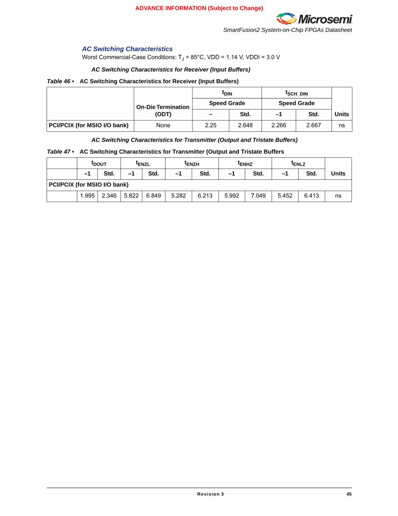
SmartFusion2 System-on-Chip FPGAs Datasheet
Revision 3 45
ADVANCE INFORMATION (Subject to Change)
AC Switching Characteristics Worst Commercial-Case Conditions: TJ = 85°C, VDD = 1.14 V, VDDI = 3.0 V
AC Switching Characteristics for Receiver (Input Buffers)
AC Switching Characteristics for Transmitter (Output and Tristate Buffers)
Table 46 • AC Switching Characteristics for Receiver (Input Buffers)
On-Die Termination (ODT)
tDIN tSCH_DIN
Units
Speed Grade Speed Grade
– Std. –1 Std.
PCI/PCIX (for MSIO I/O bank) None 2.25 2.648 2.266 2.667 ns
Table 47 • AC Switching Characteristics for Transmitter (Output and Tristate Buffers
tDOUT tENZL tENZH tENHZ tENLZ
Units–1 Std. –1 Std. –1 Std. –1 Std. –1 Std.
PCI/PCIX (for MSIO I/O bank)
1.995 2.346 5.822 6.849 5.282 6.213 5.992 7.049 5.452 6.413 ns
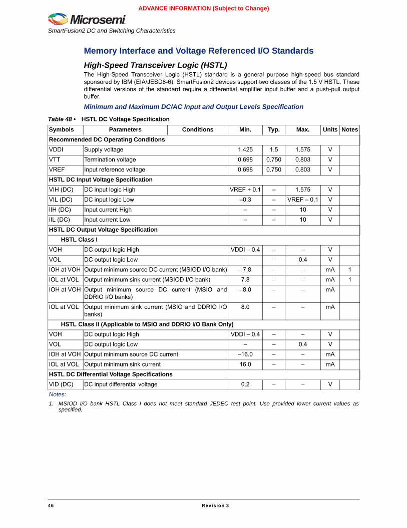
SmartFusion2 DC and Switching Characteristics
46 Revision 3
ADVANCE INFORMATION (Subject to Change)
Memory Interface and Voltage Referenced I/O StandardsHigh-Speed Transceiver Logic (HSTL)The High-Speed Transceiver Logic (HSTL) standard is a general purpose high-speed bus standardsponsored by IBM (EIA/JESD8-6). SmartFusion2 devices support two classes of the 1.5 V HSTL. Thesedifferential versions of the standard require a differential amplifier input buffer and a push-pull outputbuffer.
Minimum and Maximum DC/AC Input and Output Levels Specification
Table 48 • HSTL DC Voltage Specification Symbols Parameters Conditions Min. Typ. Max. Units NotesRecommended DC Operating ConditionsVDDI Supply voltage 1.425 1.5 1.575 V
VTT Termination voltage 0.698 0.750 0.803 V
VREF Input reference voltage 0.698 0.750 0.803 V
HSTL DC Input Voltage SpecificationVIH (DC) DC input logic High VREF + 0.1 – 1.575 V
VIL (DC) DC input logic Low –0.3 – VREF – 0.1 V
IIH (DC) Input current High – – 10 V
IIL (DC) Input current Low – – 10 V
HSTL DC Output Voltage SpecificationHSTL Class I
VOH DC output logic High VDDI – 0.4 – – V
VOL DC output logic Low – – 0.4 V
IOH at VOH Output minimum source DC current (MSIOD I/O bank) –7.8 – – mA 1
IOL at VOL Output minimum sink current (MSIOD I/O bank) 7.8 – – mA 1
IOH at VOH Output minimum source DC current (MSIO andDDRIO I/O banks)
–8.0 – – mA
IOL at VOL Output minimum sink current (MSIO and DDRIO I/Obanks)
8.0 – – mA
HSTL Class II (Applicable to MSIO and DDRIO I/O Bank Only)VOH DC output logic High VDDI – 0.4 – – V
VOL DC output logic Low – – 0.4 V
IOH at VOH Output minimum source DC current –16.0 – – mA
IOL at VOL Output minimum sink current 16.0 – – mA
HSTL DC Differential Voltage SpecificationsVID (DC) DC input differential voltage 0.2 – – V
Notes:1. MSIOD I/O bank HSTL Class I does not meet standard JEDEC test point. Use provided lower current values as
specified.
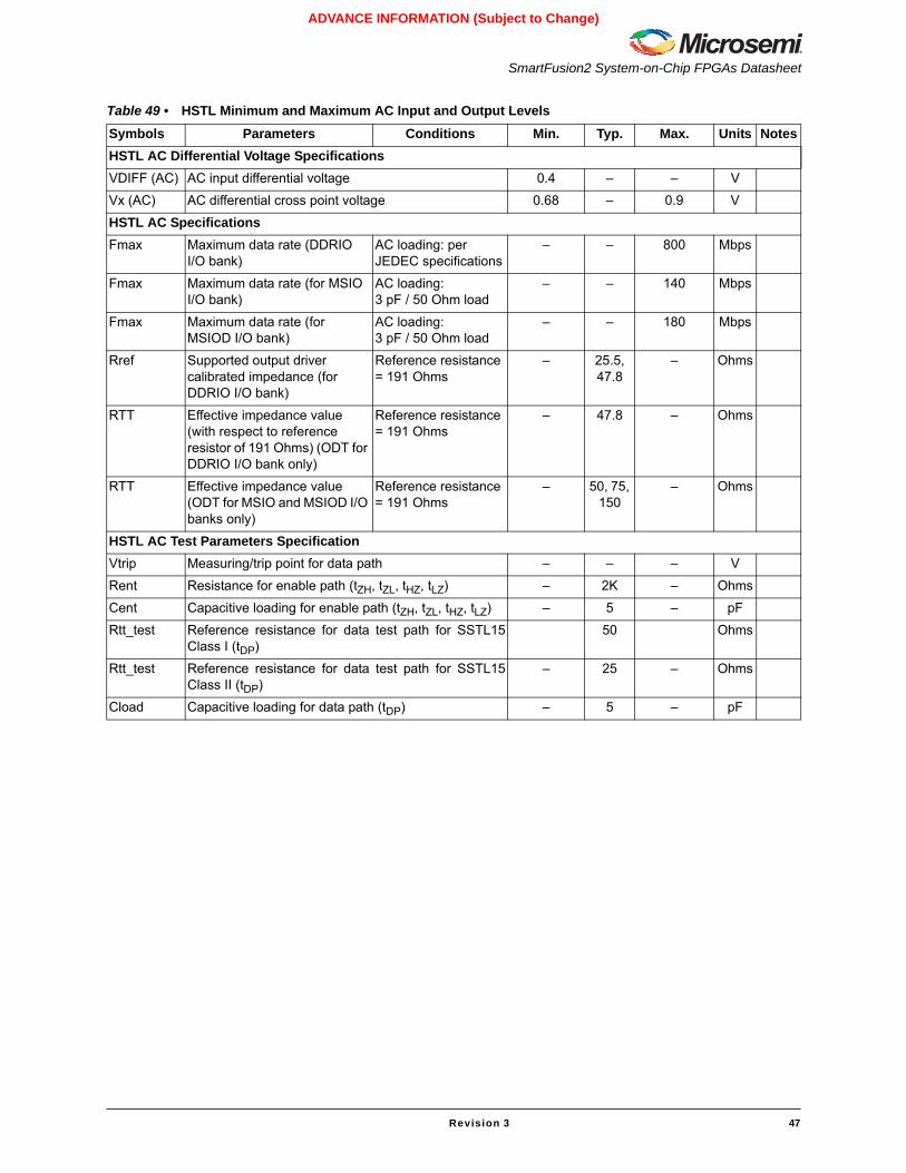
SmartFusion2 System-on-Chip FPGAs Datasheet
Revision 3 47
ADVANCE INFORMATION (Subject to Change)
Table 49 • HSTL Minimum and Maximum AC Input and Output LevelsSymbols Parameters Conditions Min. Typ. Max. Units NotesHSTL AC Differential Voltage SpecificationsVDIFF (AC) AC input differential voltage 0.4 – – V
Vx (AC) AC differential cross point voltage 0.68 – 0.9 V
HSTL AC SpecificationsFmax Maximum data rate (DDRIO
I/O bank)AC loading: per JEDEC specifications
– – 800 Mbps
Fmax Maximum data rate (for MSIO I/O bank)
AC loading: 3 pF / 50 Ohm load
– – 140 Mbps
Fmax Maximum data rate (for MSIOD I/O bank)
AC loading: 3 pF / 50 Ohm load
– – 180 Mbps
Rref Supported output driver calibrated impedance (for DDRIO I/O bank)
Reference resistance = 191 Ohms
– 25.5, 47.8
– Ohms
RTT Effective impedance value (with respect to reference resistor of 191 Ohms) (ODT for DDRIO I/O bank only)
Reference resistance = 191 Ohms
– 47.8 – Ohms
RTT Effective impedance value (ODT for MSIO and MSIOD I/O banks only)
Reference resistance = 191 Ohms
– 50, 75, 150
– Ohms
HSTL AC Test Parameters SpecificationVtrip Measuring/trip point for data path – – – V
Rent Resistance for enable path (tZH, tZL, tHZ, tLZ) – 2K – Ohms
Cent Capacitive loading for enable path (tZH, tZL, tHZ, tLZ) – 5 – pF
Rtt_test Reference resistance for data test path for SSTL15Class I (tDP)
50 Ohms
Rtt_test Reference resistance for data test path for SSTL15Class II (tDP)
– 25 – Ohms
Cload Capacitive loading for data path (tDP) – 5 – pF
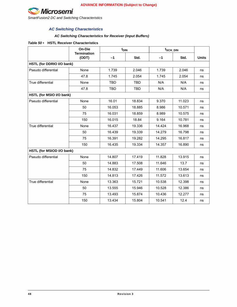
SmartFusion2 DC and Switching Characteristics
48 Revision 3
ADVANCE INFORMATION (Subject to Change)
AC Switching CharacteristicsAC Switching Characteristics for Receiver (Input Buffers)
Table 50 • HSTL Receiver Characteristics
On-Die Termination
(ODT)
tDIN tSCH_DIN
Units–1 Std. –1 Std.
HSTL (for DDRIO I/O bank)
Pseudo differential None 1.739 2.046 1.739 2.046 ns
47.8 1.745 2.054 1.745 2.054 ns
True differential None TBD TBD N/A N/A ns
47.8 TBD TBD N/A N/A ns
HSTL (for MSIO I/O bank)
Pseudo differential None 16.01 18.834 9.370 11.023 ns
50 16.053 18.885 8.986 10.571 ns
75 16.031 18.859 8.989 10.575 ns
150 16.015 18.84 9.164 10.781 ns
True differential None 16.437 19.336 14.424 16.968 ns
50 16.439 19.339 14.279 16.798 ns
75 16.391 19.282 14.295 16.817 ns
150 16.435 19.334 14.357 16.890 ns
HSTL (for MSIOD I/O bank)
Pseudo differential None 14.807 17.419 11.828 13.915 ns
50 14.883 17.508 11.646 13.7 ns
75 14.832 17.449 11.606 13.654 ns
150 14.813 17.426 11.572 13.613 ns
True differential None 13.363 15.721 10.538 12.398 ns
50 13.555 15.946 10.528 12.386 ns
75 13.493 15.874 10.436 12.277 ns
150 13.434 15.804 10.541 12.4 ns
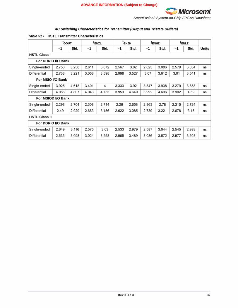
SmartFusion2 System-on-Chip FPGAs Datasheet
Revision 3 49
ADVANCE INFORMATION (Subject to Change)
AC Switching Characteristics for Transmitter (Output and Tristate Buffers)
Table 51 • HSTL Transmitter Characteristics
tDOUT tENZL tENZH tENHZ tENLZ
Units–1 Std. –1 Std. –1 Std. –1 Std. –1 Std.
HSTL Class I
For DDRIO I/O Bank
Single-ended 2.753 3.238 2.611 3.072 2.567 3.02 2.623 3.086 2.579 3.034 ns
Differential 2.738 3.221 3.058 3.598 2.998 3.527 3.07 3.612 3.01 3.541 ns
For MSIO I/O Bank
Single-ended 3.925 4.618 3.401 4 3.333 3.92 3.347 3.938 3.279 3.858 ns
Differential 4.086 4.807 4.043 4.755 3.953 4.649 3.992 4.696 3.902 4.59 ns
For MSIOD I/O Bank
Single-ended 2.298 2.704 2.308 2.714 2.26 2.658 2.363 2.78 2.315 2.724 ns
Differential 2.49 2.929 2.683 3.156 2.622 3.085 2.739 3.221 2.678 3.15 ns
HSTL Class II
For DDRIO I/O Bank
Single-ended 2.649 3.116 2.575 3.03 2.533 2.979 2.587 3.044 2.545 2.993 ns
Differential 2.633 3.098 3.024 3.558 2.965 3.489 3.036 3.572 2.977 3.503 ns
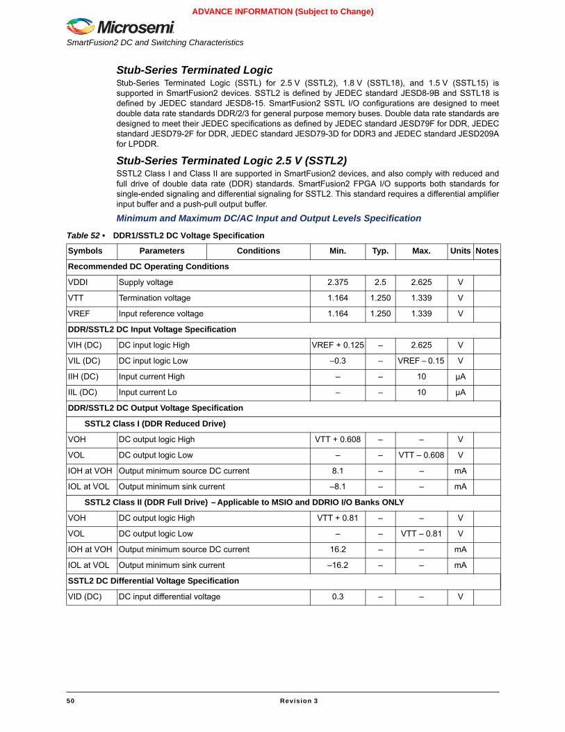
SmartFusion2 DC and Switching Characteristics
50 Revision 3
ADVANCE INFORMATION (Subject to Change)
Stub-Series Terminated Logic Stub-Series Terminated Logic (SSTL) for 2.5 V (SSTL2), 1.8 V (SSTL18), and 1.5 V (SSTL15) issupported in SmartFusion2 devices. SSTL2 is defined by JEDEC standard JESD8-9B and SSTL18 isdefined by JEDEC standard JESD8-15. SmartFusion2 SSTL I/O configurations are designed to meetdouble data rate standards DDR/2/3 for general purpose memory buses. Double data rate standards aredesigned to meet their JEDEC specifications as defined by JEDEC standard JESD79F for DDR, JEDECstandard JESD79-2F for DDR, JEDEC standard JESD79-3D for DDR3 and JEDEC standard JESD209Afor LPDDR.
Stub-Series Terminated Logic 2.5 V (SSTL2)SSTL2 Class I and Class II are supported in SmartFusion2 devices, and also comply with reduced andfull drive of double data rate (DDR) standards. SmartFusion2 FPGA I/O supports both standards forsingle-ended signaling and differential signaling for SSTL2. This standard requires a differential amplifierinput buffer and a push-pull output buffer.
Minimum and Maximum DC/AC Input and Output Levels Specification
Table 52 • DDR1/SSTL2 DC Voltage Specification
Symbols Parameters Conditions Min. Typ. Max. Units Notes
Recommended DC Operating Conditions
VDDI Supply voltage 2.375 2.5 2.625 V
VTT Termination voltage 1.164 1.250 1.339 V
VREF Input reference voltage 1.164 1.250 1.339 V
DDR/SSTL2 DC Input Voltage Specification
VIH (DC) DC input logic High VREF + 0.125 – 2.625 V
VIL (DC) DC input logic Low –0.3 – VREF – 0.15 V
IIH (DC) Input current High – – 10 µA
IIL (DC) Input current Lo – – 10 µA
DDR/SSTL2 DC Output Voltage Specification
SSTL2 Class I (DDR Reduced Drive)
VOH DC output logic High VTT + 0.608 – – V
VOL DC output logic Low – – VTT – 0.608 V
IOH at VOH Output minimum source DC current 8.1 – – mA
IOL at VOL Output minimum sink current –8.1 – – mA
SSTL2 Class II (DDR Full Drive) – Applicable to MSIO and DDRIO I/O Banks ONLY
VOH DC output logic High VTT + 0.81 – – V
VOL DC output logic Low – – VTT – 0.81 V
IOH at VOH Output minimum source DC current 16.2 – – mA
IOL at VOL Output minimum sink current –16.2 – – mA
SSTL2 DC Differential Voltage Specification
VID (DC) DC input differential voltage 0.3 – – V
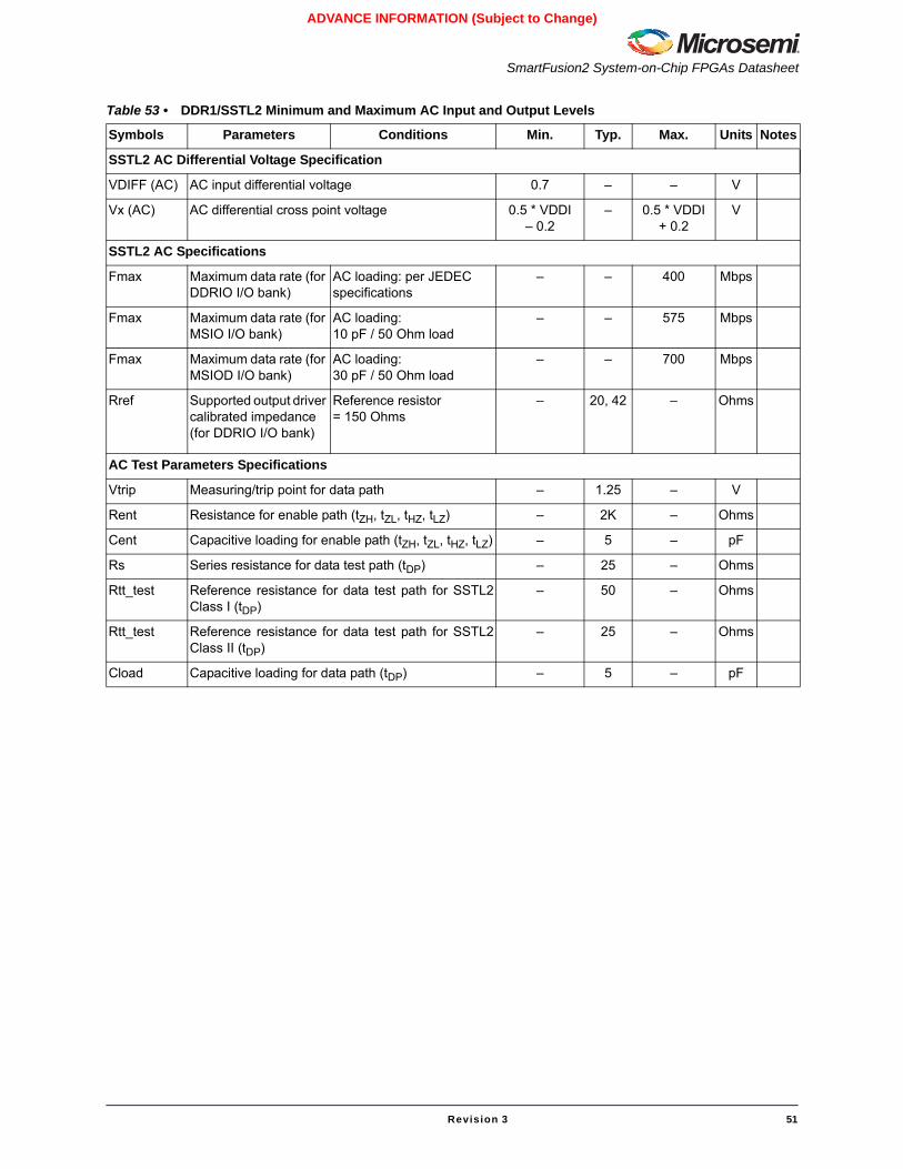
SmartFusion2 System-on-Chip FPGAs Datasheet
Revision 3 51
ADVANCE INFORMATION (Subject to Change)
Table 53 • DDR1/SSTL2 Minimum and Maximum AC Input and Output Levels
Symbols Parameters Conditions Min. Typ. Max. Units Notes
SSTL2 AC Differential Voltage Specification
VDIFF (AC) AC input differential voltage 0.7 – – V
Vx (AC) AC differential cross point voltage 0.5 * VDDI – 0.2
– 0.5 * VDDI + 0.2
V
SSTL2 AC Specifications
Fmax Maximum data rate (for DDRIO I/O bank)
AC loading: per JEDEC specifications
– – 400 Mbps
Fmax Maximum data rate (for MSIO I/O bank)
AC loading: 10 pF / 50 Ohm load
– – 575 Mbps
Fmax Maximum data rate (for MSIOD I/O bank)
AC loading: 30 pF / 50 Ohm load
– – 700 Mbps
Rref Supported output driver calibrated impedance (for DDRIO I/O bank)
Reference resistor= 150 Ohms
– 20, 42 – Ohms
AC Test Parameters Specifications
Vtrip Measuring/trip point for data path – 1.25 – V
Rent Resistance for enable path (tZH, tZL, tHZ, tLZ) – 2K – Ohms
Cent Capacitive loading for enable path (tZH, tZL, tHZ, tLZ) – 5 – pF
Rs Series resistance for data test path (tDP) – 25 – Ohms
Rtt_test Reference resistance for data test path for SSTL2Class I (tDP)
– 50 – Ohms
Rtt_test Reference resistance for data test path for SSTL2Class II (tDP)
– 25 – Ohms
Cload Capacitive loading for data path (tDP) – 5 – pF
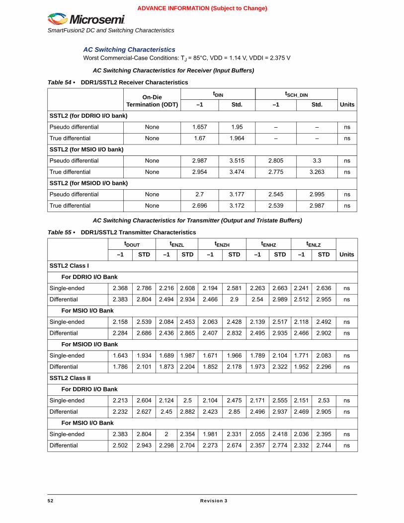
SmartFusion2 DC and Switching Characteristics
52 Revision 3
ADVANCE INFORMATION (Subject to Change)
AC Switching CharacteristicsWorst Commercial-Case Conditions: TJ = 85°C, VDD = 1.14 V, VDDI = 2.375 V
AC Switching Characteristics for Receiver (Input Buffers)
AC Switching Characteristics for Transmitter (Output and Tristate Buffers)
Table 54 • DDR1/SSTL2 Receiver Characteristics
On-Die Termination (ODT)
tDIN tSCH_DIN
Units–1 Std. –1 Std.
SSTL2 (for DDRIO I/O bank)
Pseudo differential None 1.657 1.95 – – ns
True differential None 1.67 1.964 – – ns
SSTL2 (for MSIO I/O bank)
Pseudo differential None 2.987 3.515 2.805 3.3 ns
True differential None 2.954 3.474 2.775 3.263 ns
SSTL2 (for MSIOD I/O bank)
Pseudo differential None 2.7 3.177 2.545 2.995 ns
True differential None 2.696 3.172 2.539 2.987 ns
Table 55 • DDR1/SSTL2 Transmitter Characteristics
tDOUT tENZL tENZH tENHZ tENLZ
Units–1 STD –1 STD –1 STD –1 STD –1 STD
SSTL2 Class I
For DDRIO I/O Bank
Single-ended 2.368 2.786 2.216 2.608 2.194 2.581 2.263 2.663 2.241 2.636 ns
Differential 2.383 2.804 2.494 2.934 2.466 2.9 2.54 2.989 2.512 2.955 ns
For MSIO I/O Bank
Single-ended 2.158 2.539 2.084 2.453 2.063 2.428 2.139 2.517 2.118 2.492 ns
Differential 2.284 2.686 2.436 2.865 2.407 2.832 2.495 2.935 2.466 2.902 ns
For MSIOD I/O Bank
Single-ended 1.643 1.934 1.689 1.987 1.671 1.966 1.789 2.104 1.771 2.083 ns
Differential 1.786 2.101 1.873 2.204 1.852 2.178 1.973 2.322 1.952 2.296 ns
SSTL2 Class II
For DDRIO I/O Bank
Single-ended 2.213 2.604 2.124 2.5 2.104 2.475 2.171 2.555 2.151 2.53 ns
Differential 2.232 2.627 2.45 2.882 2.423 2.85 2.496 2.937 2.469 2.905 ns
For MSIO I/O Bank
Single-ended 2.383 2.804 2 2.354 1.981 2.331 2.055 2.418 2.036 2.395 ns
Differential 2.502 2.943 2.298 2.704 2.273 2.674 2.357 2.774 2.332 2.744 ns
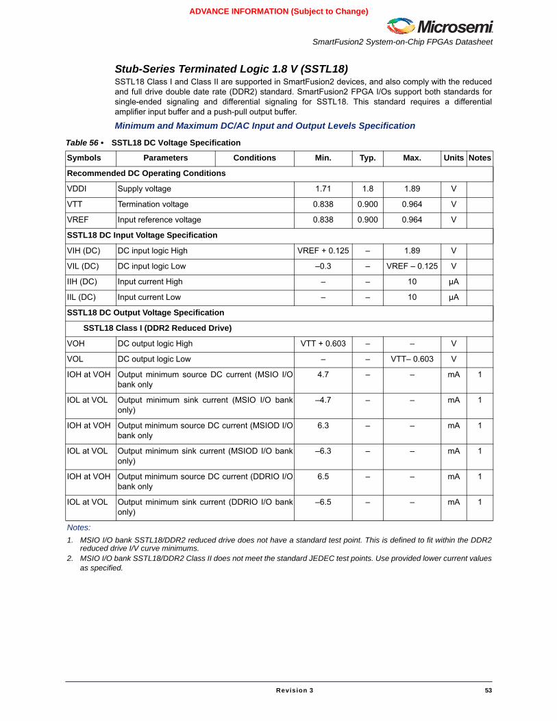
SmartFusion2 System-on-Chip FPGAs Datasheet
Revision 3 53
ADVANCE INFORMATION (Subject to Change)
Stub-Series Terminated Logic 1.8 V (SSTL18)SSTL18 Class I and Class II are supported in SmartFusion2 devices, and also comply with the reducedand full drive double date rate (DDR2) standard. SmartFusion2 FPGA I/Os support both standards forsingle-ended signaling and differential signaling for SSTL18. This standard requires a differentialamplifier input buffer and a push-pull output buffer.
Minimum and Maximum DC/AC Input and Output Levels Specification
Table 56 • SSTL18 DC Voltage Specification
Symbols Parameters Conditions Min. Typ. Max. Units Notes
Recommended DC Operating Conditions
VDDI Supply voltage 1.71 1.8 1.89 V
VTT Termination voltage 0.838 0.900 0.964 V
VREF Input reference voltage 0.838 0.900 0.964 V
SSTL18 DC Input Voltage Specification
VIH (DC) DC input logic High VREF + 0.125 – 1.89 V
VIL (DC) DC input logic Low –0.3 – VREF – 0.125 V
IIH (DC) Input current High – – 10 µA
IIL (DC) Input current Low – – 10 µA
SSTL18 DC Output Voltage Specification
SSTL18 Class I (DDR2 Reduced Drive)
VOH DC output logic High VTT + 0.603 – – V
VOL DC output logic Low – – VTT– 0.603 V
IOH at VOH Output minimum source DC current (MSIO I/Obank only
4.7 – – mA 1
IOL at VOL Output minimum sink current (MSIO I/O bankonly)
–4.7 – – mA 1
IOH at VOH Output minimum source DC current (MSIOD I/Obank only
6.3 – – mA 1
IOL at VOL Output minimum sink current (MSIOD I/O bankonly)
–6.3 – – mA 1
IOH at VOH Output minimum source DC current (DDRIO I/Obank only
6.5 – – mA 1
IOL at VOL Output minimum sink current (DDRIO I/O bankonly)
–6.5 – – mA 1
Notes:1. MSIO I/O bank SSTL18/DDR2 reduced drive does not have a standard test point. This is defined to fit within the DDR2
reduced drive I/V curve minimums.2. MSIO I/O bank SSTL18/DDR2 Class II does not meet the standard JEDEC test points. Use provided lower current values
as specified.
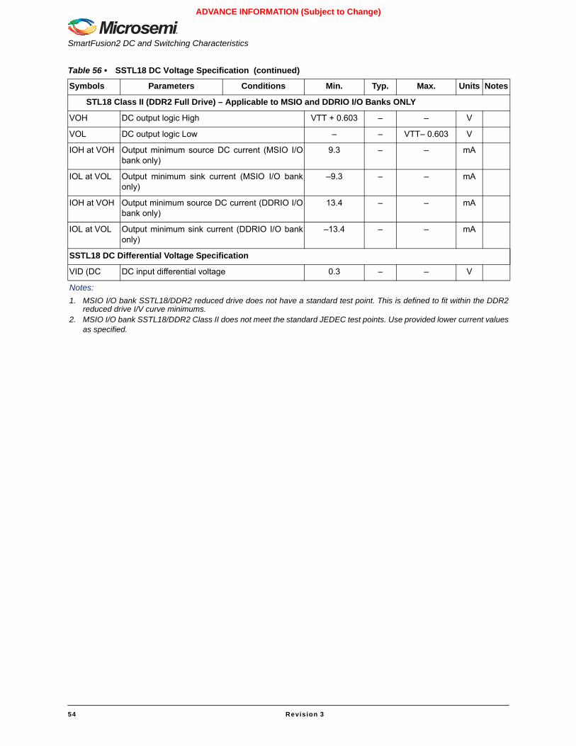
SmartFusion2 DC and Switching Characteristics
54 Revision 3
ADVANCE INFORMATION (Subject to Change)
STL18 Class II (DDR2 Full Drive) – Applicable to MSIO and DDRIO I/O Banks ONLY
VOH DC output logic High VTT + 0.603 – – V
VOL DC output logic Low – – VTT– 0.603 V
IOH at VOH Output minimum source DC current (MSIO I/Obank only)
9.3 – – mA
IOL at VOL Output minimum sink current (MSIO I/O bankonly)
–9.3 – – mA
IOH at VOH Output minimum source DC current (DDRIO I/Obank only)
13.4 – – mA
IOL at VOL Output minimum sink current (DDRIO I/O bankonly)
–13.4 – – mA
SSTL18 DC Differential Voltage Specification
VID (DC DC input differential voltage 0.3 – – V
Table 56 • SSTL18 DC Voltage Specification (continued)
Symbols Parameters Conditions Min. Typ. Max. Units Notes
Notes:1. MSIO I/O bank SSTL18/DDR2 reduced drive does not have a standard test point. This is defined to fit within the DDR2
reduced drive I/V curve minimums.2. MSIO I/O bank SSTL18/DDR2 Class II does not meet the standard JEDEC test points. Use provided lower current values
as specified.
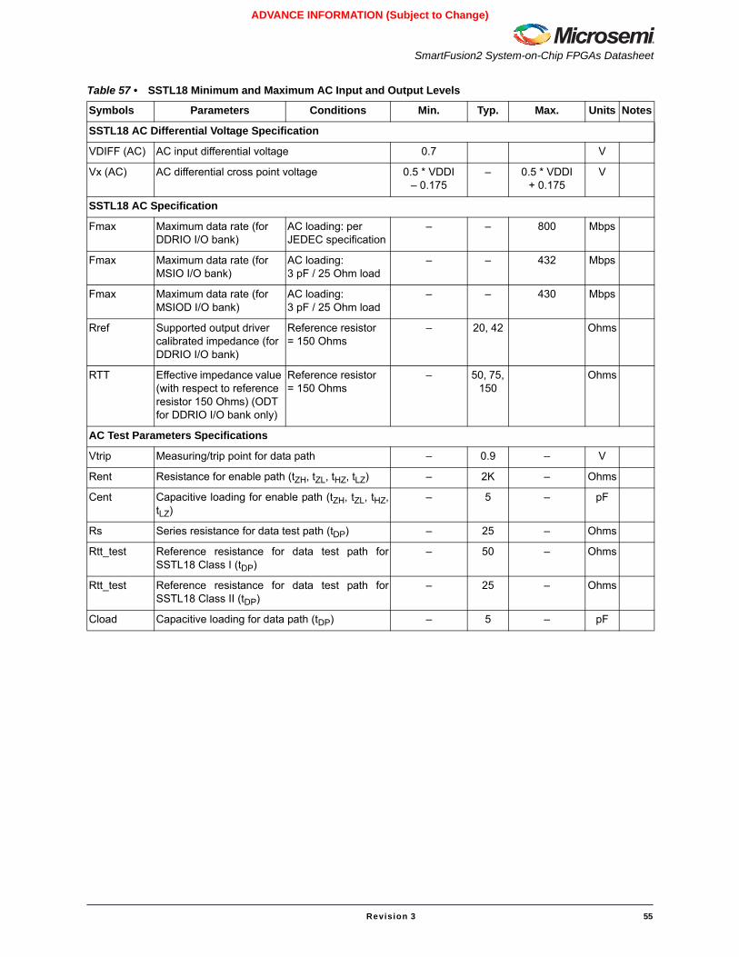
SmartFusion2 System-on-Chip FPGAs Datasheet
Revision 3 55
ADVANCE INFORMATION (Subject to Change)
Table 57 • SSTL18 Minimum and Maximum AC Input and Output Levels
Symbols Parameters Conditions Min. Typ. Max. Units Notes
SSTL18 AC Differential Voltage Specification
VDIFF (AC) AC input differential voltage 0.7 V
Vx (AC) AC differential cross point voltage 0.5 * VDDI – 0.175
– 0.5 * VDDI + 0.175
V
SSTL18 AC Specification
Fmax Maximum data rate (for DDRIO I/O bank)
AC loading: per JEDEC specification
– – 800 Mbps
Fmax Maximum data rate (for MSIO I/O bank)
AC loading: 3 pF / 25 Ohm load
– – 432 Mbps
Fmax Maximum data rate (for MSIOD I/O bank)
AC loading: 3 pF / 25 Ohm load
– – 430 Mbps
Rref Supported output driver calibrated impedance (for DDRIO I/O bank)
Reference resistor= 150 Ohms
– 20, 42 Ohms
RTT Effective impedance value (with respect to reference resistor 150 Ohms) (ODT for DDRIO I/O bank only)
Reference resistor= 150 Ohms
– 50, 75, 150
Ohms
AC Test Parameters Specifications
Vtrip Measuring/trip point for data path – 0.9 – V
Rent Resistance for enable path (tZH, tZL, tHZ, tLZ) – 2K – Ohms
Cent Capacitive loading for enable path (tZH, tZL, tHZ,tLZ)
– 5 – pF
Rs Series resistance for data test path (tDP) – 25 – Ohms
Rtt_test Reference resistance for data test path forSSTL18 Class I (tDP)
– 50 – Ohms
Rtt_test Reference resistance for data test path forSSTL18 Class II (tDP)
– 25 – Ohms
Cload Capacitive loading for data path (tDP) – 5 – pF
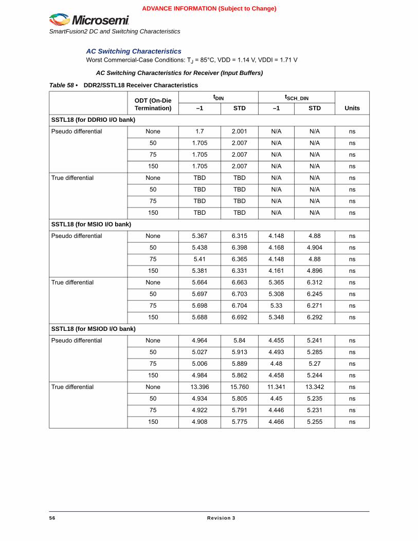
SmartFusion2 DC and Switching Characteristics
56 Revision 3
ADVANCE INFORMATION (Subject to Change)
AC Switching CharacteristicsWorst Commercial-Case Conditions: TJ = 85°C, VDD = 1.14 V, VDDI = 1.71 V
AC Switching Characteristics for Receiver (Input Buffers)
Table 58 • DDR2/SSTL18 Receiver Characteristics
ODT (On-Die Termination)
tDIN tSCH_DIN
Units–1 STD –1 STD
SSTL18 (for DDRIO I/O bank)
Pseudo differential None 1.7 2.001 N/A N/A ns
50 1.705 2.007 N/A N/A ns
75 1.705 2.007 N/A N/A ns
150 1.705 2.007 N/A N/A ns
True differential None TBD TBD N/A N/A ns
50 TBD TBD N/A N/A ns
75 TBD TBD N/A N/A ns
150 TBD TBD N/A N/A ns
SSTL18 (for MSIO I/O bank)
Pseudo differential None 5.367 6.315 4.148 4.88 ns
50 5.438 6.398 4.168 4.904 ns
75 5.41 6.365 4.148 4.88 ns
150 5.381 6.331 4.161 4.896 ns
True differential None 5.664 6.663 5.365 6.312 ns
50 5.697 6.703 5.308 6.245 ns
75 5.698 6.704 5.33 6.271 ns
150 5.688 6.692 5.348 6.292 ns
SSTL18 (for MSIOD I/O bank)
Pseudo differential None 4.964 5.84 4.455 5.241 ns
50 5.027 5.913 4.493 5.285 ns
75 5.006 5.889 4.48 5.27 ns
150 4.984 5.862 4.458 5.244 ns
True differential None 13.396 15.760 11.341 13.342 ns
50 4.934 5.805 4.45 5.235 ns
75 4.922 5.791 4.446 5.231 ns
150 4.908 5.775 4.466 5.255 ns
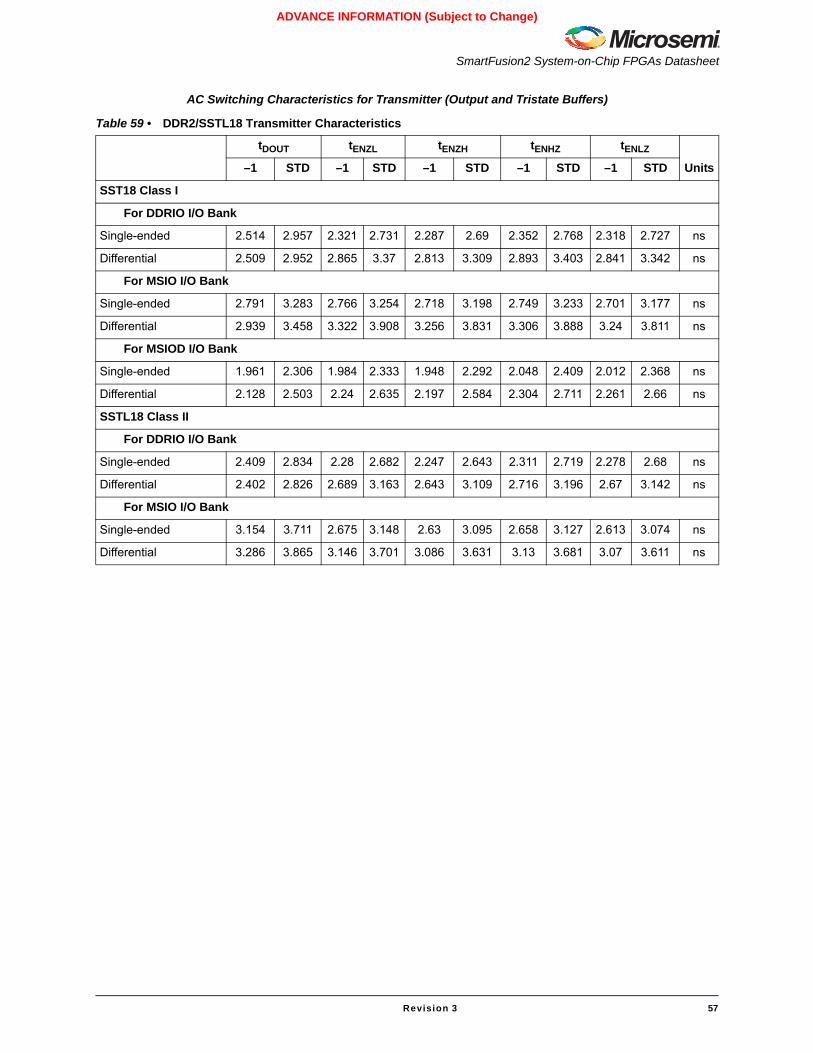
SmartFusion2 System-on-Chip FPGAs Datasheet
Revision 3 57
ADVANCE INFORMATION (Subject to Change)
AC Switching Characteristics for Transmitter (Output and Tristate Buffers)
Table 59 • DDR2/SSTL18 Transmitter Characteristics
tDOUT tENZL tENZH tENHZ tENLZ
Units–1 STD –1 STD –1 STD –1 STD –1 STD
SST18 Class I
For DDRIO I/O Bank
Single-ended 2.514 2.957 2.321 2.731 2.287 2.69 2.352 2.768 2.318 2.727 ns
Differential 2.509 2.952 2.865 3.37 2.813 3.309 2.893 3.403 2.841 3.342 ns
For MSIO I/O Bank
Single-ended 2.791 3.283 2.766 3.254 2.718 3.198 2.749 3.233 2.701 3.177 ns
Differential 2.939 3.458 3.322 3.908 3.256 3.831 3.306 3.888 3.24 3.811 ns
For MSIOD I/O Bank
Single-ended 1.961 2.306 1.984 2.333 1.948 2.292 2.048 2.409 2.012 2.368 ns
Differential 2.128 2.503 2.24 2.635 2.197 2.584 2.304 2.711 2.261 2.66 ns
SSTL18 Class II
For DDRIO I/O Bank
Single-ended 2.409 2.834 2.28 2.682 2.247 2.643 2.311 2.719 2.278 2.68 ns
Differential 2.402 2.826 2.689 3.163 2.643 3.109 2.716 3.196 2.67 3.142 ns
For MSIO I/O Bank
Single-ended 3.154 3.711 2.675 3.148 2.63 3.095 2.658 3.127 2.613 3.074 ns
Differential 3.286 3.865 3.146 3.701 3.086 3.631 3.13 3.681 3.07 3.611 ns
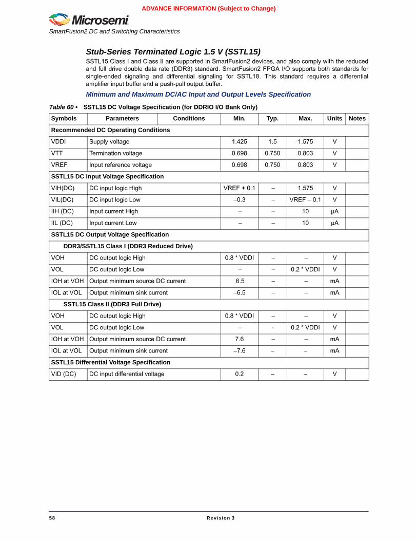
SmartFusion2 DC and Switching Characteristics
58 Revision 3
ADVANCE INFORMATION (Subject to Change)
Stub-Series Terminated Logic 1.5 V (SSTL15)SSTL15 Class I and Class II are supported in SmartFusion2 devices, and also comply with the reducedand full drive double data rate (DDR3) standard. SmartFusion2 FPGA I/O supports both standards forsingle-ended signaling and differential signaling for SSTL18. This standard requires a differentialamplifier input buffer and a push-pull output buffer.
Minimum and Maximum DC/AC Input and Output Levels Specification
Table 60 • SSTL15 DC Voltage Specification (for DDRIO I/O Bank Only)
Symbols Parameters Conditions Min. Typ. Max. Units Notes
Recommended DC Operating Conditions
VDDI Supply voltage 1.425 1.5 1.575 V
VTT Termination voltage 0.698 0.750 0.803 V
VREF Input reference voltage 0.698 0.750 0.803 V
SSTL15 DC Input Voltage Specification
VIH(DC) DC input logic High VREF + 0.1 – 1.575 V
VIL(DC) DC input logic Low –0.3 – VREF – 0.1 V
IIH (DC) Input current High – – 10 µA
IIL (DC) Input current Low – – 10 µA
SSTL15 DC Output Voltage Specification
DDR3/SSTL15 Class I (DDR3 Reduced Drive)
VOH DC output logic High 0.8 * VDDI – – V
VOL DC output logic Low – – 0.2 * VDDI V
IOH at VOH Output minimum source DC current 6.5 – – mA
IOL at VOL Output minimum sink current –6.5 – – mA
SSTL15 Class II (DDR3 Full Drive)
VOH DC output logic High 0.8 * VDDI – – V
VOL DC output logic Low – - 0.2 * VDDI V
IOH at VOH Output minimum source DC current 7.6 – – mA
IOL at VOL Output minimum sink current –7.6 – – mA
SSTL15 Differential Voltage Specification
VID (DC) DC input differential voltage 0.2 – – V
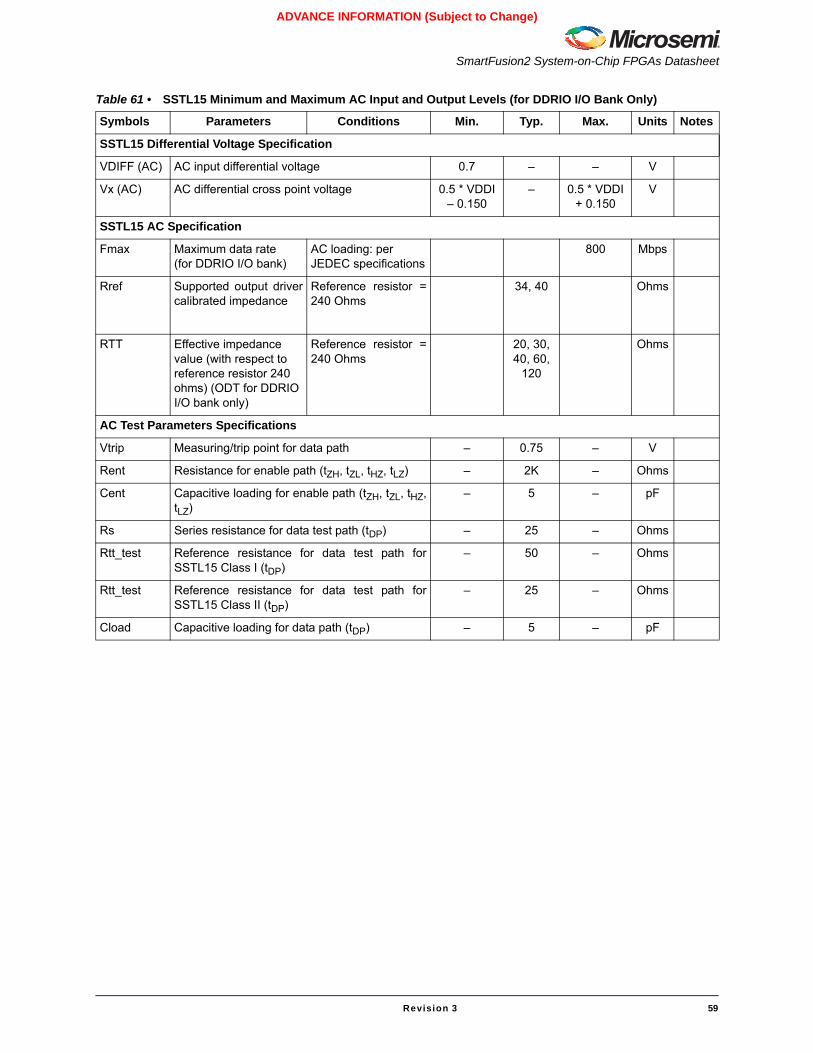
SmartFusion2 System-on-Chip FPGAs Datasheet
Revision 3 59
ADVANCE INFORMATION (Subject to Change)
Table 61 • SSTL15 Minimum and Maximum AC Input and Output Levels (for DDRIO I/O Bank Only)
Symbols Parameters Conditions Min. Typ. Max. Units Notes
SSTL15 Differential Voltage Specification
VDIFF (AC) AC input differential voltage 0.7 – – V
Vx (AC) AC differential cross point voltage 0.5 * VDDI – 0.150
– 0.5 * VDDI + 0.150
V
SSTL15 AC Specification
Fmax Maximum data rate (for DDRIO I/O bank)
AC loading: per JEDEC specifications
800 Mbps
Rref Supported output drivercalibrated impedance
Reference resistor =240 Ohms
34, 40 Ohms
RTT Effective impedance value (with respect to reference resistor 240 ohms) (ODT for DDRIO I/O bank only)
Reference resistor =240 Ohms
20, 30, 40, 60,
120
Ohms
AC Test Parameters Specifications
Vtrip Measuring/trip point for data path – 0.75 – V
Rent Resistance for enable path (tZH, tZL, tHZ, tLZ) – 2K – Ohms
Cent Capacitive loading for enable path (tZH, tZL, tHZ,tLZ)
– 5 – pF
Rs Series resistance for data test path (tDP) – 25 – Ohms
Rtt_test Reference resistance for data test path forSSTL15 Class I (tDP)
– 50 – Ohms
Rtt_test Reference resistance for data test path forSSTL15 Class II (tDP)
– 25 – Ohms
Cload Capacitive loading for data path (tDP) – 5 – pF
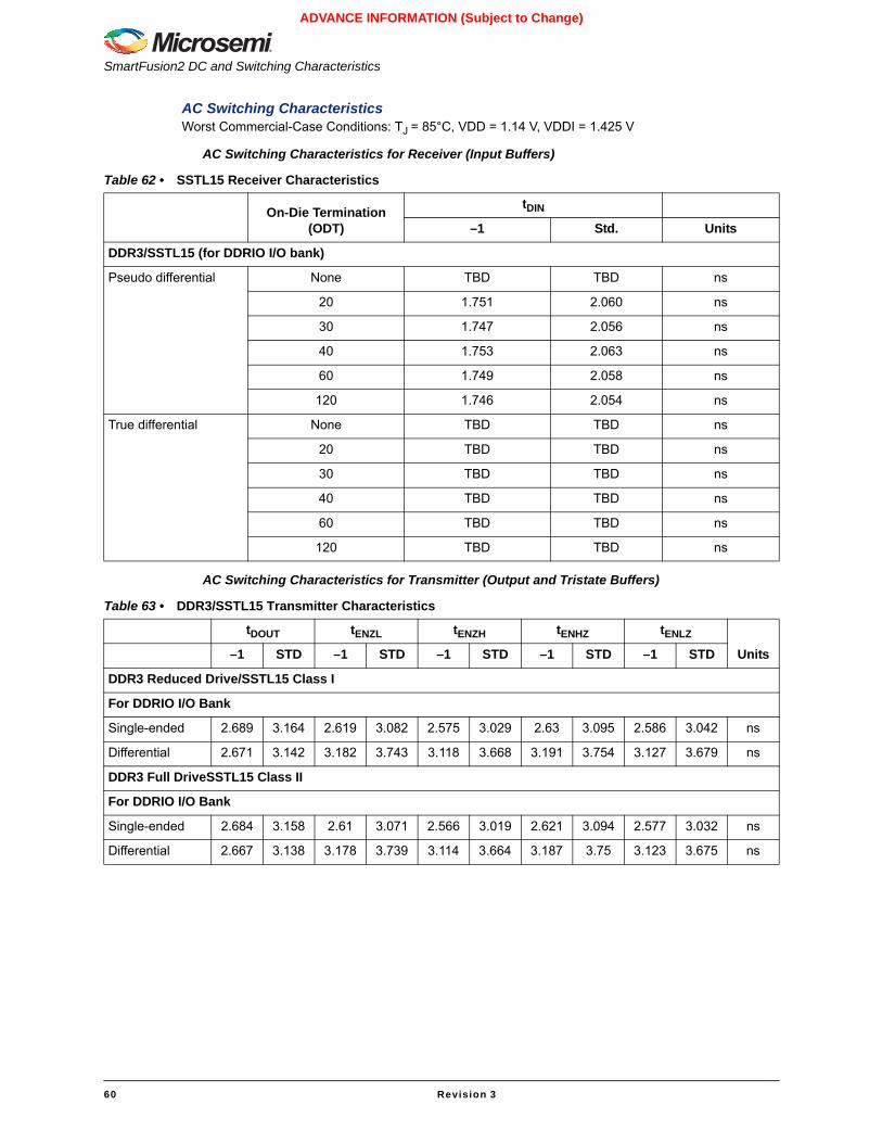
SmartFusion2 DC and Switching Characteristics
60 Revision 3
ADVANCE INFORMATION (Subject to Change)
AC Switching CharacteristicsWorst Commercial-Case Conditions: TJ = 85°C, VDD = 1.14 V, VDDI = 1.425 V
AC Switching Characteristics for Receiver (Input Buffers)
AC Switching Characteristics for Transmitter (Output and Tristate Buffers)
Table 62 • SSTL15 Receiver Characteristics
On-Die Termination (ODT)
tDIN
–1 Std. Units
DDR3/SSTL15 (for DDRIO I/O bank)
Pseudo differential None TBD TBD ns
20 1.751 2.060 ns
30 1.747 2.056 ns
40 1.753 2.063 ns
60 1.749 2.058 ns
120 1.746 2.054 ns
True differential None TBD TBD ns
20 TBD TBD ns
30 TBD TBD ns
40 TBD TBD ns
60 TBD TBD ns
120 TBD TBD ns
Table 63 • DDR3/SSTL15 Transmitter Characteristics
tDOUT tENZL tENZH tENHZ tENLZ
Units–1 STD –1 STD –1 STD –1 STD –1 STD
DDR3 Reduced Drive/SSTL15 Class I
For DDRIO I/O Bank
Single-ended 2.689 3.164 2.619 3.082 2.575 3.029 2.63 3.095 2.586 3.042 ns
Differential 2.671 3.142 3.182 3.743 3.118 3.668 3.191 3.754 3.127 3.679 ns
DDR3 Full DriveSSTL15 Class II
For DDRIO I/O Bank
Single-ended 2.684 3.158 2.61 3.071 2.566 3.019 2.621 3.094 2.577 3.032 ns
Differential 2.667 3.138 3.178 3.739 3.114 3.664 3.187 3.75 3.123 3.675 ns
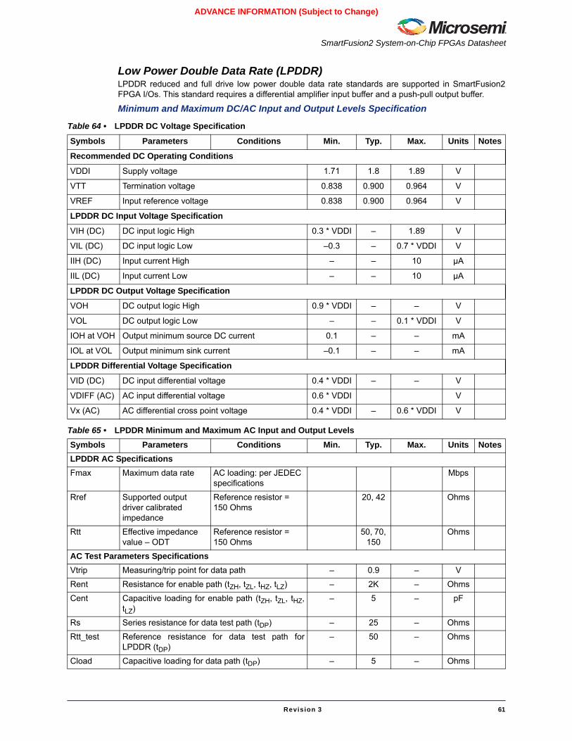
SmartFusion2 System-on-Chip FPGAs Datasheet
Revision 3 61
ADVANCE INFORMATION (Subject to Change)
Low Power Double Data Rate (LPDDR)LPDDR reduced and full drive low power double data rate standards are supported in SmartFusion2FPGA I/Os. This standard requires a differential amplifier input buffer and a push-pull output buffer.
Minimum and Maximum DC/AC Input and Output Levels Specification
Table 64 • LPDDR DC Voltage Specification
Symbols Parameters Conditions Min. Typ. Max. Units Notes
Recommended DC Operating Conditions
VDDI Supply voltage 1.71 1.8 1.89 V
VTT Termination voltage 0.838 0.900 0.964 V
VREF Input reference voltage 0.838 0.900 0.964 V
LPDDR DC Input Voltage Specification
VIH (DC) DC input logic High 0.3 * VDDI – 1.89 V
VIL (DC) DC input logic Low –0.3 – 0.7 * VDDI V
IIH (DC) Input current High – – 10 µA
IIL (DC) Input current Low – – 10 µA
LPDDR DC Output Voltage Specification
VOH DC output logic High 0.9 * VDDI – – V
VOL DC output logic Low – – 0.1 * VDDI V
IOH at VOH Output minimum source DC current 0.1 – – mA
IOL at VOL Output minimum sink current –0.1 – – mA
LPDDR Differential Voltage Specification
VID (DC) DC input differential voltage 0.4 * VDDI – – V
VDIFF (AC) AC input differential voltage 0.6 * VDDI V
Vx (AC) AC differential cross point voltage 0.4 * VDDI – 0.6 * VDDI V
Table 65 • LPDDR Minimum and Maximum AC Input and Output LevelsSymbols Parameters Conditions Min. Typ. Max. Units NotesLPDDR AC SpecificationsFmax Maximum data rate AC loading: per JEDEC
specificationsMbps
Rref Supported output driver calibrated impedance
Reference resistor = 150 Ohms
20, 42 Ohms
Rtt Effective impedance value – ODT
Reference resistor = 150 Ohms
50, 70, 150
Ohms
AC Test Parameters SpecificationsVtrip Measuring/trip point for data path – 0.9 – V
Rent Resistance for enable path (tZH, tZL, tHZ, tLZ) – 2K – Ohms
Cent Capacitive loading for enable path (tZH, tZL, tHZ,tLZ)
– 5 – pF
Rs Series resistance for data test path (tDP) – 25 – Ohms
Rtt_test Reference resistance for data test path forLPDDR (tDP)
– 50 – Ohms
Cload Capacitive loading for data path (tDP) – 5 – Ohms
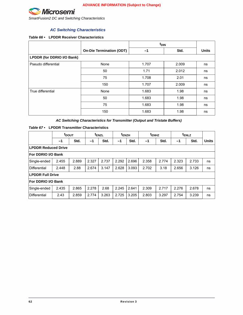
SmartFusion2 DC and Switching Characteristics
62 Revision 3
ADVANCE INFORMATION (Subject to Change)
AC Switching Characteristics
AC Switching Characteristics for Transmitter (Output and Tristate Buffers)
Table 66 • LPDDR Receiver Characteristics
On-Die Termination (ODT)
tDIN
Units–1 Std.
LPDDR (for DDRIO I/O Bank)
Pseudo differential None 1.707 2.009 ns
50 1.71 2.012 ns
75 1.708 2.01 ns
150 1.707 2.009 ns
True differential None 1.683 1.98 ns
50 1.683 1.98 ns
75 1.683 1.98 ns
150 1.683 1.98 ns
Table 67 • LPDDR Transmitter Characteristics
tDOUT tENZL tENZH tENHZ tENLZ
Units–1 Std. –1 Std. –1 Std. –1 Std. –1 Std.
LPDDR Reduced Drive
For DDRIO I/O Bank
Single-ended 2.455 2.889 2.327 2.737 2.292 2.696 2.358 2.774 2.323 2.733 ns
Differential 2.448 2.88 2.674 3.147 2.628 3.093 2.702 3.18 2.656 3.126 ns
LPDDR Full Drive
For DDRIO I/O Bank
Single-ended 2.435 2.865 2.278 2.68 2.245 2.641 2.309 2.717 2.276 2.678 ns
Differential 2.43 2.859 2.774 3.263 2.725 3.205 2.803 3.297 2.754 3.239 ns
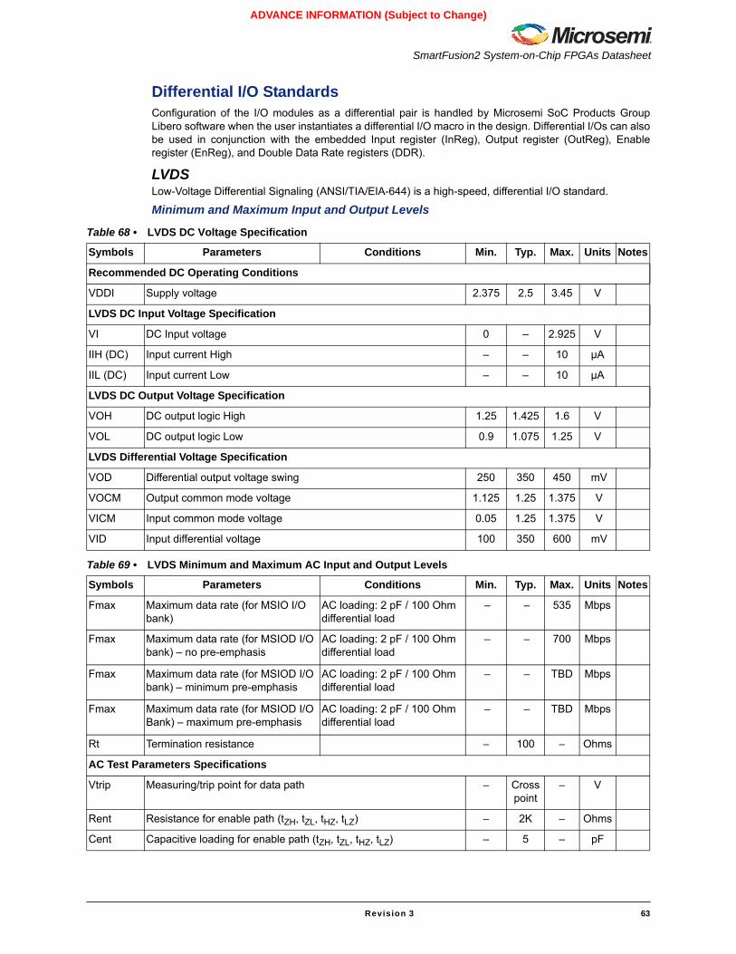
SmartFusion2 System-on-Chip FPGAs Datasheet
Revision 3 63
ADVANCE INFORMATION (Subject to Change)
Differential I/O StandardsConfiguration of the I/O modules as a differential pair is handled by Microsemi SoC Products GroupLibero software when the user instantiates a differential I/O macro in the design. Differential I/Os can alsobe used in conjunction with the embedded Input register (InReg), Output register (OutReg), Enableregister (EnReg), and Double Data Rate registers (DDR).
LVDSLow-Voltage Differential Signaling (ANSI/TIA/EIA-644) is a high-speed, differential I/O standard.
Minimum and Maximum Input and Output Levels
Table 68 • LVDS DC Voltage Specification
Symbols Parameters Conditions Min. Typ. Max. Units Notes
Recommended DC Operating Conditions
VDDI Supply voltage 2.375 2.5 3.45 V
LVDS DC Input Voltage Specification
VI DC Input voltage 0 – 2.925 V
IIH (DC) Input current High – – 10 µA
IIL (DC) Input current Low – – 10 µA
LVDS DC Output Voltage Specification
VOH DC output logic High 1.25 1.425 1.6 V
VOL DC output logic Low 0.9 1.075 1.25 V
LVDS Differential Voltage Specification
VOD Differential output voltage swing 250 350 450 mV
VOCM Output common mode voltage 1.125 1.25 1.375 V
VICM Input common mode voltage 0.05 1.25 1.375 V
VID Input differential voltage 100 350 600 mV
Table 69 • LVDS Minimum and Maximum AC Input and Output Levels
Symbols Parameters Conditions Min. Typ. Max. Units Notes
Fmax Maximum data rate (for MSIO I/O bank)
AC loading: 2 pF / 100 Ohm differential load
– – 535 Mbps
Fmax Maximum data rate (for MSIOD I/O bank) – no pre-emphasis
AC loading: 2 pF / 100 Ohm differential load
– – 700 Mbps
Fmax Maximum data rate (for MSIOD I/O bank) – minimum pre-emphasis
AC loading: 2 pF / 100 Ohm differential load
– – TBD Mbps
Fmax Maximum data rate (for MSIOD I/O Bank) – maximum pre-emphasis
AC loading: 2 pF / 100 Ohm differential load
– – TBD Mbps
Rt Termination resistance – 100 – Ohms
AC Test Parameters Specifications
Vtrip Measuring/trip point for data path – Cross point
– V
Rent Resistance for enable path (tZH, tZL, tHZ, tLZ) – 2K – Ohms
Cent Capacitive loading for enable path (tZH, tZL, tHZ, tLZ) – 5 – pF
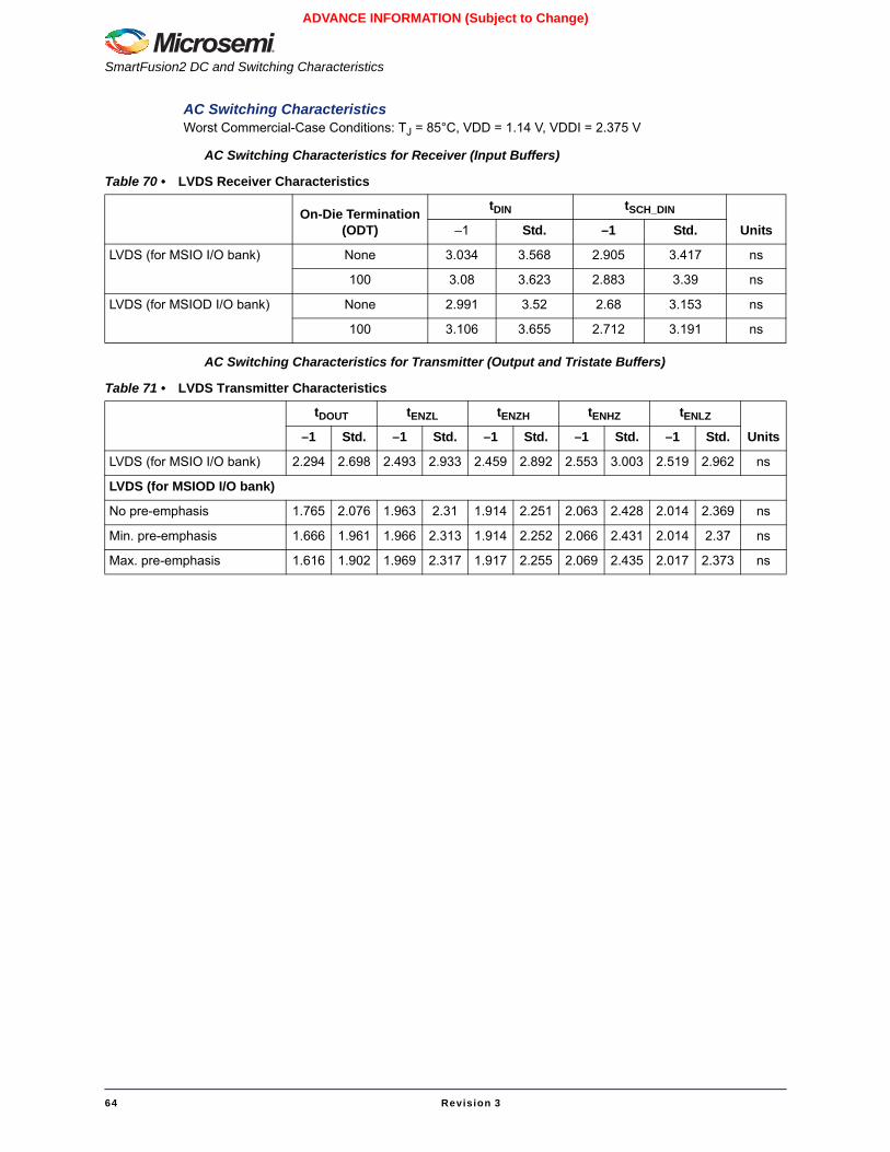
SmartFusion2 DC and Switching Characteristics
64 Revision 3
ADVANCE INFORMATION (Subject to Change)
AC Switching CharacteristicsWorst Commercial-Case Conditions: TJ = 85°C, VDD = 1.14 V, VDDI = 2.375 V
AC Switching Characteristics for Receiver (Input Buffers)
AC Switching Characteristics for Transmitter (Output and Tristate Buffers)
Table 70 • LVDS Receiver Characteristics
On-Die Termination (ODT)
tDIN tSCH_DIN
Units–1 Std. –1 Std.
LVDS (for MSIO I/O bank) None 3.034 3.568 2.905 3.417 ns
100 3.08 3.623 2.883 3.39 ns
LVDS (for MSIOD I/O bank) None 2.991 3.52 2.68 3.153 ns
100 3.106 3.655 2.712 3.191 ns
Table 71 • LVDS Transmitter Characteristics
tDOUT tENZL tENZH tENHZ tENLZ
Units–1 Std. –1 Std. –1 Std. –1 Std. –1 Std.
LVDS (for MSIO I/O bank) 2.294 2.698 2.493 2.933 2.459 2.892 2.553 3.003 2.519 2.962 ns
LVDS (for MSIOD I/O bank)
No pre-emphasis 1.765 2.076 1.963 2.31 1.914 2.251 2.063 2.428 2.014 2.369 ns
Min. pre-emphasis 1.666 1.961 1.966 2.313 1.914 2.252 2.066 2.431 2.014 2.37 ns
Max. pre-emphasis 1.616 1.902 1.969 2.317 1.917 2.255 2.069 2.435 2.017 2.373 ns
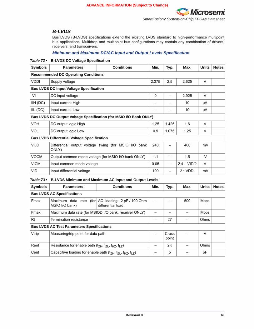
SmartFusion2 System-on-Chip FPGAs Datasheet
Revision 3 65
ADVANCE INFORMATION (Subject to Change)
B-LVDSBus LVDS (B-LVDS) specifications extend the existing LVDS standard to high-performance multipointbus applications. Multidrop and multipoint bus configurations may contain any combination of drivers,receivers, and transceivers.
Minimum and Maximum DC/AC Input and Output Levels Specification
Table 72 • B-LVDS DC Voltage Specification
Symbols Parameters Conditions Min. Typ. Max. Units Notes
Recommended DC Operating Conditions
VDDI Supply voltage 2.375 2.5 2.625 V
Bus LVDS DC Input Voltage Specification
VI DC input voltage 0 – 2.925 V
IIH (DC) Input current High – – 10 µA
IIL (DC) Input current Low – – 10 µA
Bus LVDS DC Output Voltage Specification (for MSIO I/O Bank ONLY)
VOH DC output logic High 1.25 1.425 1.6 V
VOL DC output logic Low 0.9 1.075 1.25 V
Bus LVDS Differential Voltage Specification
VOD Differential output voltage swing (for MSIO I/O bankONLY)
240 – 460 mV
VOCM Output common mode voltage (for MSIO I/O bank ONLY) 1.1 – 1.5 V
VICM Input common mode voltage 0.05 – 2.4 – VID/2 V
VID Input differential voltage 100 – 2 * VDDI mV
Table 73 • B-LVDS Minimum and Maximum AC Input and Output Levels
Symbols Parameters Conditions Min. Typ. Max. Units Notes
Bus LVDS AC Specifications
Fmax Maximum data rate (forMSIO I/O bank)
AC loading: 2 pF / 100 Ohmdifferential load
– – 500 Mbps
Fmax Maximum data rate (for MSIOD I/O bank, receiver ONLY) – – – Mbps
Rt Termination resistance – 27 – Ohms
Bus LVDS AC Test Parameters Specifications
Vtrip Measuring/trip point for data path – Cross point
– V
Rent Resistance for enable path (tZH, tZL, tHZ, tLZ) – 2K – Ohms
Cent Capacitive loading for enable path (tZH, tZL, tHZ, tLZ) – 5 – pF
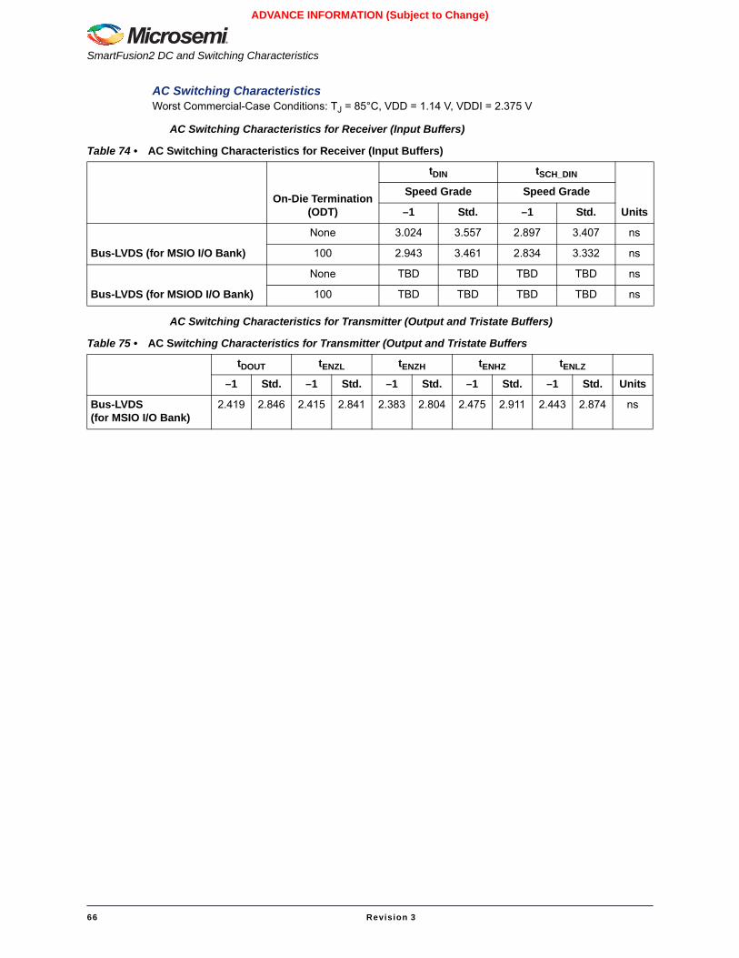
SmartFusion2 DC and Switching Characteristics
66 Revision 3
ADVANCE INFORMATION (Subject to Change)
AC Switching Characteristics Worst Commercial-Case Conditions: TJ = 85°C, VDD = 1.14 V, VDDI = 2.375 V
AC Switching Characteristics for Receiver (Input Buffers)
AC Switching Characteristics for Transmitter (Output and Tristate Buffers)
Table 74 • AC Switching Characteristics for Receiver (Input Buffers)
On-Die Termination (ODT)
tDIN tSCH_DIN
Units
Speed Grade Speed Grade
–1 Std. –1 Std.
Bus-LVDS (for MSIO I/O Bank)
None 3.024 3.557 2.897 3.407 ns
100 2.943 3.461 2.834 3.332 ns
Bus-LVDS (for MSIOD I/O Bank)
None TBD TBD TBD TBD ns
100 TBD TBD TBD TBD ns
Table 75 • AC Switching Characteristics for Transmitter (Output and Tristate Buffers
tDOUT tENZL tENZH tENHZ tENLZ
–1 Std. –1 Std. –1 Std. –1 Std. –1 Std. Units
Bus-LVDS(for MSIO I/O Bank)
2.419 2.846 2.415 2.841 2.383 2.804 2.475 2.911 2.443 2.874 ns
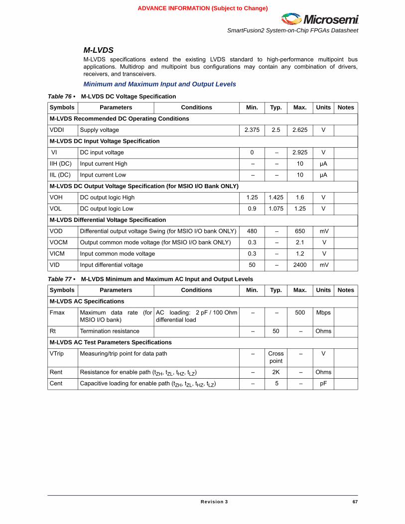
SmartFusion2 System-on-Chip FPGAs Datasheet
Revision 3 67
ADVANCE INFORMATION (Subject to Change)
M-LVDSM-LVDS specifications extend the existing LVDS standard to high-performance multipoint busapplications. Multidrop and multipoint bus configurations may contain any combination of drivers,receivers, and transceivers.
Minimum and Maximum Input and Output Levels
Table 76 • M-LVDS DC Voltage Specification
Symbols Parameters Conditions Min. Typ. Max. Units Notes
M-LVDS Recommended DC Operating Conditions
VDDI Supply voltage 2.375 2.5 2.625 V
M-LVDS DC Input Voltage Specification
VI DC input voltage 0 – 2.925 V
IIH (DC) Input current High – – 10 µA
IIL (DC) Input current Low – – 10 µA
M-LVDS DC Output Voltage Specification (for MSIO I/O Bank ONLY)
VOH DC output logic High 1.25 1.425 1.6 V
VOL DC output logic Low 0.9 1.075 1.25 V
M-LVDS Differential Voltage Specification
VOD Differential output voltage Swing (for MSIO I/O bank ONLY) 480 – 650 mV
VOCM Output common mode voltage (for MSIO I/O bank ONLY) 0.3 – 2.1 V
VICM Input common mode voltage 0.3 – 1.2 V
VID Input differential voltage 50 – 2400 mV
Table 77 • M-LVDS Minimum and Maximum AC Input and Output Levels
Symbols Parameters Conditions Min. Typ. Max. Units Notes
M-LVDS AC Specifications
Fmax Maximum data rate (forMSIO I/O bank)
AC loading: 2 pF / 100 Ohmdifferential load
– – 500 Mbps
Rt Termination resistance – 50 – Ohms
M-LVDS AC Test Parameters Specifications
VTrip Measuring/trip point for data path – Cross point
– V
Rent Resistance for enable path (tZH, tZL, tHZ, tLZ) – 2K – Ohms
Cent Capacitive loading for enable path (tZH, tZL, tHZ, tLZ) – 5 – pF
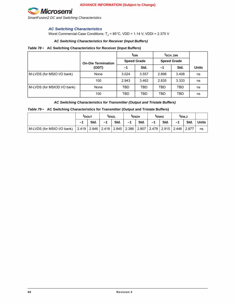
SmartFusion2 DC and Switching Characteristics
68 Revision 3
ADVANCE INFORMATION (Subject to Change)
AC Switching Characteristics Worst Commercial-Case Conditions: TJ = 85°C, VDD = 1.14 V, VDDI = 2.375 V
AC Switching Characteristics for Receiver (Input Buffers)
AC Switching Characteristics for Transmitter (Output and Tristate Buffers)
Table 78 • AC Switching Characteristics for Receiver (Input Buffers)
On-Die Termination (ODT)
tDIN tSCH_DIN
Units
Speed Grade Speed Grade
–1 Std. –1 Std.
M-LVDS (for MSIO I/O bank) None 3.024 3.557 2.898 3.408 ns
100 2.943 3.462 2.835 3.333 ns
M-LVDS (for MSIOD I/O bank) None TBD TBD TBD TBD ns
100 TBD TBD TBD TBD ns
Table 79 • AC Switching Characteristics for Transmitter (Output and Tristate Buffers)
tDOUT tENZL tENZH tENHZ tENLZ
–1 Std. –1 Std. –1 Std. –1 Std. –1 Std. Units
M-LVDS (for MSIO I/O bank) 2.419 2.846 2.418 2.845 2.386 2.807 2.478 2.915 2.446 2.877 ns
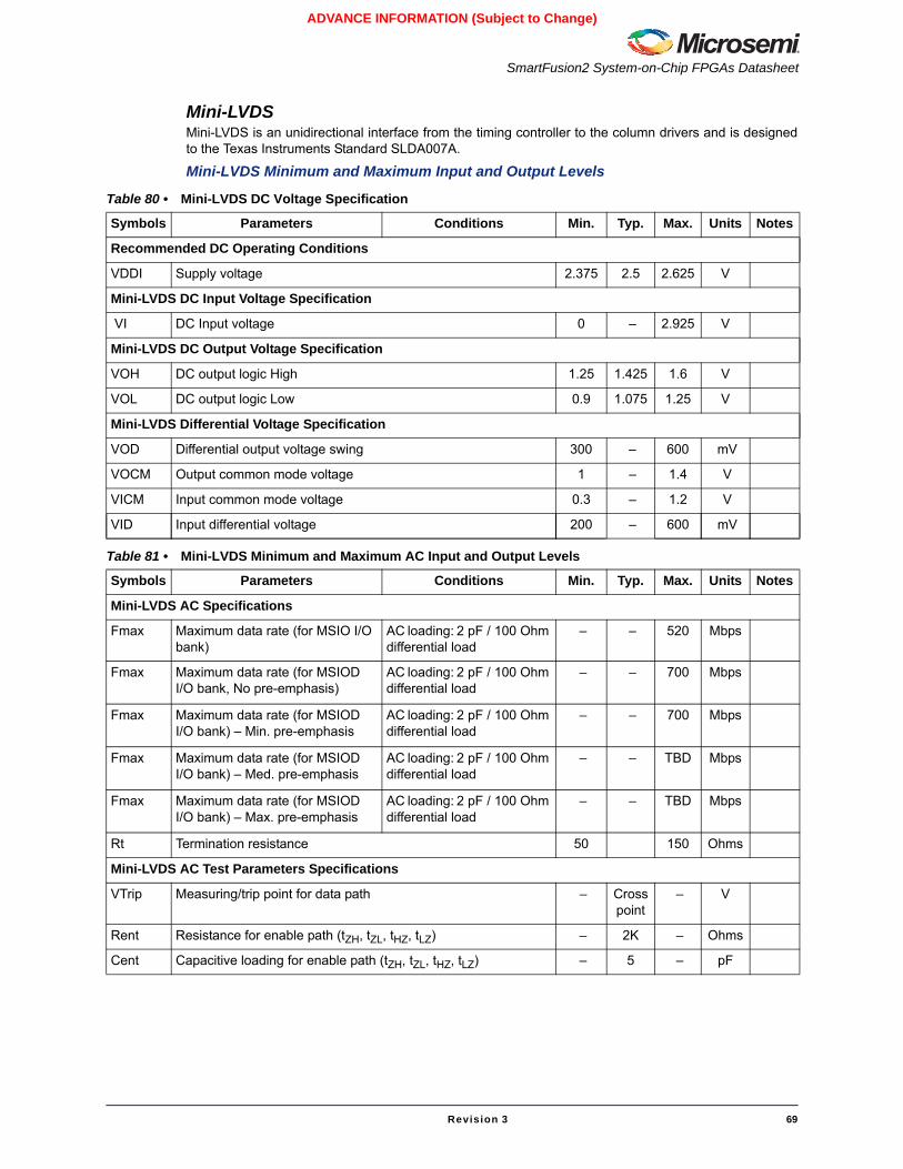
SmartFusion2 System-on-Chip FPGAs Datasheet
Revision 3 69
ADVANCE INFORMATION (Subject to Change)
Mini-LVDSMini-LVDS is an unidirectional interface from the timing controller to the column drivers and is designedto the Texas Instruments Standard SLDA007A.
Mini-LVDS Minimum and Maximum Input and Output Levels
Table 80 • Mini-LVDS DC Voltage Specification
Symbols Parameters Conditions Min. Typ. Max. Units Notes
Recommended DC Operating Conditions
VDDI Supply voltage 2.375 2.5 2.625 V
Mini-LVDS DC Input Voltage Specification
VI DC Input voltage 0 – 2.925 V
Mini-LVDS DC Output Voltage Specification
VOH DC output logic High 1.25 1.425 1.6 V
VOL DC output logic Low 0.9 1.075 1.25 V
Mini-LVDS Differential Voltage Specification
VOD Differential output voltage swing 300 – 600 mV
VOCM Output common mode voltage 1 – 1.4 V
VICM Input common mode voltage 0.3 – 1.2 V
VID Input differential voltage 200 – 600 mV
Table 81 • Mini-LVDS Minimum and Maximum AC Input and Output Levels
Symbols Parameters Conditions Min. Typ. Max. Units Notes
Mini-LVDS AC Specifications
Fmax Maximum data rate (for MSIO I/O bank)
AC loading: 2 pF / 100 Ohm differential load
– – 520 Mbps
Fmax Maximum data rate (for MSIOD I/O bank, No pre-emphasis)
AC loading: 2 pF / 100 Ohm differential load
– – 700 Mbps
Fmax Maximum data rate (for MSIOD I/O bank) – Min. pre-emphasis
AC loading: 2 pF / 100 Ohm differential load
– – 700 Mbps
Fmax Maximum data rate (for MSIOD I/O bank) – Med. pre-emphasis
AC loading: 2 pF / 100 Ohm differential load
– – TBD Mbps
Fmax Maximum data rate (for MSIOD I/O bank) – Max. pre-emphasis
AC loading: 2 pF / 100 Ohm differential load
– – TBD Mbps
Rt Termination resistance 50 150 Ohms
Mini-LVDS AC Test Parameters Specifications
VTrip Measuring/trip point for data path – Cross point
– V
Rent Resistance for enable path (tZH, tZL, tHZ, tLZ) – 2K – Ohms
Cent Capacitive loading for enable path (tZH, tZL, tHZ, tLZ) – 5 – pF
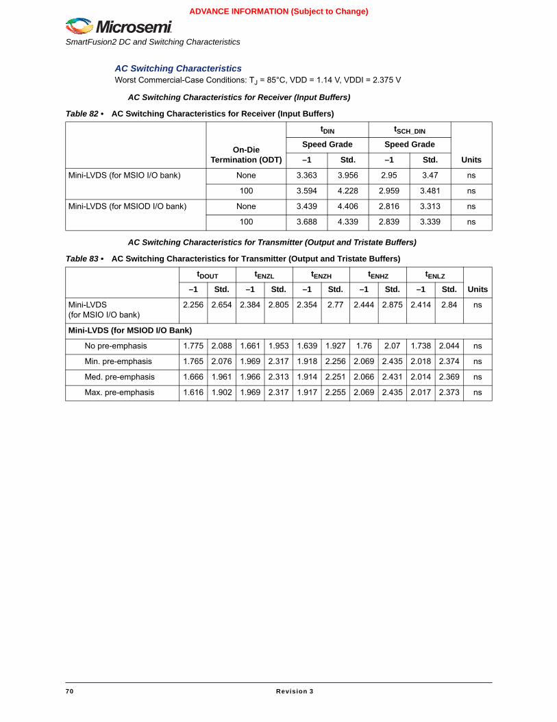
SmartFusion2 DC and Switching Characteristics
70 Revision 3
ADVANCE INFORMATION (Subject to Change)
AC Switching Characteristics Worst Commercial-Case Conditions: TJ = 85°C, VDD = 1.14 V, VDDI = 2.375 V
AC Switching Characteristics for Receiver (Input Buffers)
AC Switching Characteristics for Transmitter (Output and Tristate Buffers)
Table 82 • AC Switching Characteristics for Receiver (Input Buffers)
On-Die Termination (ODT)
tDIN tSCH_DIN
Units
Speed Grade Speed Grade
–1 Std. –1 Std.
Mini-LVDS (for MSIO I/O bank) None 3.363 3.956 2.95 3.47 ns
100 3.594 4.228 2.959 3.481 ns
Mini-LVDS (for MSIOD I/O bank) None 3.439 4.406 2.816 3.313 ns
100 3.688 4.339 2.839 3.339 ns
Table 83 • AC Switching Characteristics for Transmitter (Output and Tristate Buffers)
tDOUT tENZL tENZH tENHZ tENLZ
Units–1 Std. –1 Std. –1 Std. –1 Std. –1 Std.
Mini-LVDS (for MSIO I/O bank)
2.256 2.654 2.384 2.805 2.354 2.77 2.444 2.875 2.414 2.84 ns
Mini-LVDS (for MSIOD I/O Bank)
No pre-emphasis 1.775 2.088 1.661 1.953 1.639 1.927 1.76 2.07 1.738 2.044 ns
Min. pre-emphasis 1.765 2.076 1.969 2.317 1.918 2.256 2.069 2.435 2.018 2.374 ns
Med. pre-emphasis 1.666 1.961 1.966 2.313 1.914 2.251 2.066 2.431 2.014 2.369 ns
Max. pre-emphasis 1.616 1.902 1.969 2.317 1.917 2.255 2.069 2.435 2.017 2.373 ns
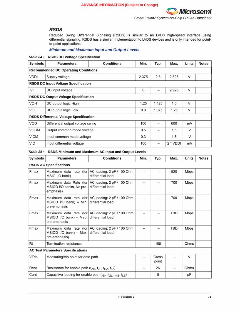
SmartFusion2 System-on-Chip FPGAs Datasheet
Revision 3 71
ADVANCE INFORMATION (Subject to Change)
RSDSReduced Swing Differential Signaling (RSDS) is similar to an LVDS high-speed interface usingdifferential signaling. RSDS has a similar implementation to LVDS devices and is only intended for point-to-point applications.
Minimum and Maximum Input and Output Levels
Table 84 • RSDS DC Voltage Specification
Symbols Parameters Conditions Min. Typ. Max. Units Notes
Recommended DC Operating Conditions
VDDI Supply voltage 2.375 2.5 2.625 V
RSDS DC Input Voltage Specification
VI DC input voltage 0 – 2.925 V
RSDS DC Output Voltage Specification
VOH DC output logic High 1.25 1.425 1.6 V
VOL DC output logic Low 0.9 1.075 1.25 V
RSDS Differential Voltage Specification
VOD Differential output voltage swing 100 – 600 mV
VOCM Output common mode voltage 0.5 – 1.5 V
VICM Input common mode voltage 0.3 – 1.5 V
VID Input differential voltage 100 – 2 * VDDI mV
Table 85 • RSDS Minimum and Maximum AC Input and Output Levels
Symbols Parameters Conditions Min. Typ. Max. Units Notes
RSDS AC Specifications
Fmax Maximum data rate (forMSIO I/O bank)
AC loading: 2 pF / 100 Ohm differential load
– – 520 Mbps
Fmax Maximum data Rate (forMSIOD I/O banks, No pre-emphasis)
AC loading: 2 pF / 100 Ohm differential load
– – 700 Mbps
Fmax Maximum data rate (forMSIOD I/O bank) – Min.pre-emphasis
AC loading: 2 pF / 100 Ohm differential load
– – 700 Mbps
Fmax Maximum data rate (forMSIOD I/O bank) – Med.pre-emphasis
AC loading: 2 pF / 100 Ohm differential load
– – TBD Mbps
Fmax Maximum data rate (forMSIOD I/O bank) – Max.pre-emphasis)
AC loading: 2 pF / 100 Ohm differential load
– – TBD Mbps
Rt Termination resistance 100 Ohms
AC Test Parameters Specifications
VTrip Measuring/trip point for data path – Cross point
– V
Rent Resistance for enable path (tZH, tZL, tHZ, tLZ) – 2K – Ohms
Cent Capacitive loading for enable path (tZH, tZL, tHZ, tLZ) – 5 – pF
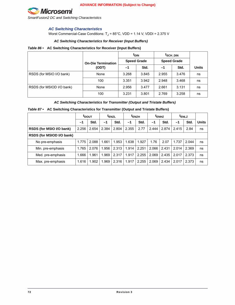
SmartFusion2 DC and Switching Characteristics
72 Revision 3
ADVANCE INFORMATION (Subject to Change)
AC Switching Characteristics Worst Commercial-Case Conditions: TJ = 85°C, VDD = 1.14 V, VDDI = 2.375 V
AC Switching Characteristics for Receiver (Input Buffers)
AC Switching Characteristics for Transmitter (Output and Tristate Buffers)
Table 86 • AC Switching Characteristics for Receiver (Input Buffers)
On-Die Termination (ODT)
tDIN tSCH_DIN
Units
Speed Grade Speed Grade
–1 Std. –1 Std.
RSDS (for MSIO I/O bank) None 3.268 3.845 2.955 3.476 ns
100 3.351 3.942 2.948 3.468 ns
RSDS (for MSIOD I/O bank) None 2.956 3.477 2.661 3.131 ns
100 3.231 3.801 2.769 3.258 ns
Table 87 • AC Switching Characteristics for Transmitter (Output and Tristate Buffers)
tDOUT tENZL tENZH tENHZ tENLZ
Units–1 Std. –1 Std. –1 Std. –1 Std. –1 Std.
RSDS (for MSIO I/O bank) 2.256 2.654 2.384 2.804 2.355 2.77 2.444 2.874 2.415 2.84 ns
RSDS (for MSIOD I/O bank)
No pre-emphasis 1.775 2.088 1.661 1.953 1.638 1.927 1.76 2.07 1.737 2.044 ns
Min. pre-emphasis 1.765 2.076 1.956 2.313 1.914 2.251 2.066 2.431 2.014 2.369 ns
Med. pre-emphasis 1.666 1.961 1.969 2.317 1.917 2.255 2.069 2.435 2.017 2.373 ns
Max. pre-emphasis 1.616 1.902 1.969 2.316 1.917 2.255 2.069 2.434 2.017 2.373 ns
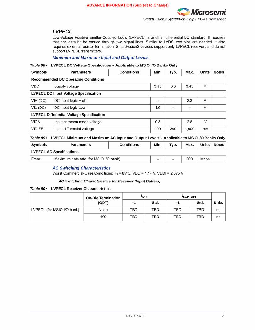
SmartFusion2 System-on-Chip FPGAs Datasheet
Revision 3 73
ADVANCE INFORMATION (Subject to Change)
LVPECLLow-Voltage Positive Emitter-Coupled Logic (LVPECL) is another differential I/O standard. It requiresthat one data bit be carried through two signal lines. Similar to LVDS, two pins are needed. It alsorequires external resistor termination. SmartFusion2 devices support only LVPECL receivers and do notsupport LVPECL transmitters.
Minimum and Maximum Input and Output Levels
AC Switching CharacteristicsWorst Commercial-Case Conditions: TJ = 85°C, VDD = 1.14 V, VDDI = 2.375 V
AC Switching Characteristics for Receiver (Input Buffers)
Table 88 • LVPECL DC Voltage Specification – Applicable to MSIO I/O Banks Only
Symbols Parameters Conditions Min. Typ. Max. Units Notes
Recommended DC Operating Conditions
VDDI Supply voltage 3.15 3.3 3.45 V
LVPECL DC Input Voltage Specification
VIH (DC) DC input logic High – – 2.3 V
VIL (DC) DC input logic Low 1.6 – – V
LVPECL Differential Voltage Specification
VICM Input common mode voltage 0.3 2.8 V
VIDIFF Input differential voltage 100 300 1,000 mV
Table 89 • LVPECL Minimum and Maximum AC Input and Output Levels – Applicable to MSIO I/O Banks Only
Symbols Parameters Conditions Min. Typ. Max. Units Notes
LVPECL AC Specifications
Fmax Maximum data rate (for MSIO I/O bank) – – 900 Mbps
Table 90 • LVPECL Receiver Characteristics
On-Die Termination (ODT)
tDIN tSCH_DIN
Units–1 Std. –1 Std.
LVPECL (for MSIO I/O bank) None TBD TBD TBD TBD ns
100 TBD TBD TBD TBD ns
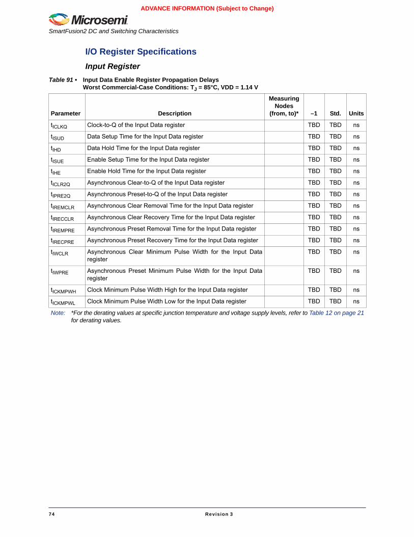
SmartFusion2 DC and Switching Characteristics
74 Revision 3
ADVANCE INFORMATION (Subject to Change)
I/O Register SpecificationsInput Register
Table 91 • Input Data Enable Register Propagation DelaysWorst Commercial-Case Conditions: TJ = 85°C, VDD = 1.14 V
Parameter Description
Measuring Nodes
(from, to)* –1 Std. Units
tICLKQ Clock-to-Q of the Input Data register TBD TBD ns
tISUD Data Setup Time for the Input Data register TBD TBD ns
tIHD Data Hold Time for the Input Data register TBD TBD ns
tISUE Enable Setup Time for the Input Data register TBD TBD ns
tIHE Enable Hold Time for the Input Data register TBD TBD ns
tICLR2Q Asynchronous Clear-to-Q of the Input Data register TBD TBD ns
tIPRE2Q Asynchronous Preset-to-Q of the Input Data register TBD TBD ns
tIREMCLR Asynchronous Clear Removal Time for the Input Data register TBD TBD ns
tIRECCLR Asynchronous Clear Recovery Time for the Input Data register TBD TBD ns
tIREMPRE Asynchronous Preset Removal Time for the Input Data register TBD TBD ns
tIRECPRE Asynchronous Preset Recovery Time for the Input Data register TBD TBD ns
tIWCLR Asynchronous Clear Minimum Pulse Width for the Input Dataregister
TBD TBD ns
tIWPRE Asynchronous Preset Minimum Pulse Width for the Input Dataregister
TBD TBD ns
tICKMPWH Clock Minimum Pulse Width High for the Input Data register TBD TBD ns
tICKMPWL Clock Minimum Pulse Width Low for the Input Data register TBD TBD ns
Note: *For the derating values at specific junction temperature and voltage supply levels, refer to Table 12 on page 21for derating values.
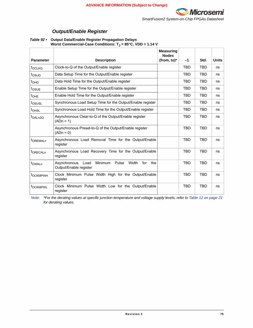
SmartFusion2 System-on-Chip FPGAs Datasheet
Revision 3 75
ADVANCE INFORMATION (Subject to Change)
Output/Enable RegisterTable 92 • Output Data/Enable Register Propagation Delays
Worst Commercial-Case Conditions: TJ = 85°C, VDD = 1.14 V
Parameter Description
Measuring Nodes
(from, to)* –1 Std. Units
tOCLKQ Clock-to-Q of the Output/Enable register TBD TBD ns
tOSUD Data Setup Time for the Output/Enable register TBD TBD ns
tOHD Data Hold Time for the Output/Enable register TBD TBD ns
tOSUE Enable Setup Time for the Output/Enable register TBD TBD ns
tOHE Enable Hold Time for the Output/Enable register TBD TBD ns
tOSUSL Synchronous Load Setup Time for the Output/Enable register TBD TBD ns
tOHSL Synchronous Load Hold Time for the Output/Enable register TBD TBD ns
tOALn2Q Asynchronous Clear-to-Q of the Output/Enable register(ADn = 1)
TBD TBD ns
Asynchronous Preset-to-Q of the Output/Enable register(ADn = 0)
TBD TBD ns
tOREMALn Asynchronous Load Removal Time for the Output/Enableregister
TBD TBD ns
tORECALn Asynchronous Load Recovery Time for the Output/Enableregister
TBD TBD ns
tOWALn Asynchronous Load Minimum Pulse Width for theOutput/Enable register
TBD TBD ns
tOCKMPWH Clock Minimum Pulse Width High for the Output/Enableregister
TBD TBD ns
tOCKMPWL Clock Minimum Pulse Width Low for the Output/Enableregister
TBD TBD ns
Note: *For the derating values at specific junction temperature and voltage supply levels, refer to Table 12 on page 21for derating values.
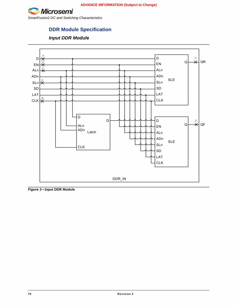
SmartFusion2 DC and Switching Characteristics
76 Revision 3
ADVANCE INFORMATION (Subject to Change)
DDR Module SpecificationInput DDR Module
Figure 3 • Input DDR Module
SLE
D
EN
ALn
ADn
SLn
SD
LAT
CLK
Q
SLE
D
EN
ALn
ADn
SLn
SD
LAT
CLK
Q
QR
QF
DDR_IN
Latch
D
ALnADn
CLK
Q
D
ENALn
ADn
SLn
SD
LAT
CLK
A
B
C
D
E
F
G
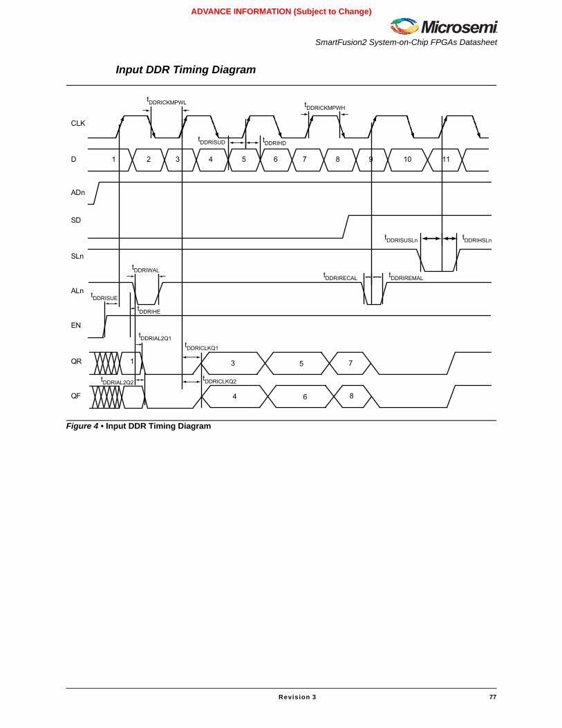
SmartFusion2 System-on-Chip FPGAs Datasheet
Revision 3 77
ADVANCE INFORMATION (Subject to Change)
Input DDR Timing Diagram
Figure 4 • Input DDR Timing Diagram
tDDRIAL2Q2
tDDRIREMAL
1 2 3 4 5 6 7 8 9
CLK
D
ALn
QF
QR
4 6 8
tDDRIHDtDDRISUD
tDDRICLKQ2
tDDRIAL2Q1tDDRICLKQ1
3 5 7
10 11
ADn
SD
tDDRIRECAL
SLn
tDDRIHSLntDDRISUSLn
EN
1
tDDRISUE
tDDRIHE
tDDRIWAL
tDDRICKMPWL tDDRICKMPWH
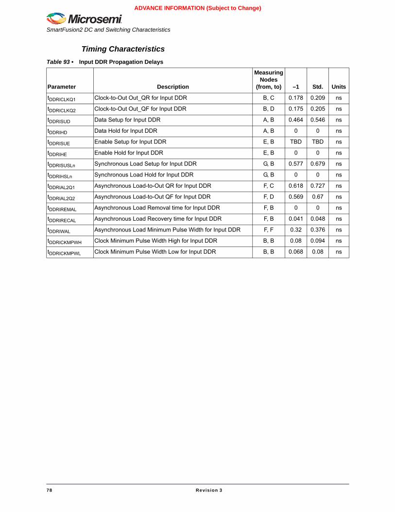
SmartFusion2 DC and Switching Characteristics
78 Revision 3
ADVANCE INFORMATION (Subject to Change)
Timing CharacteristicsTable 93 • Input DDR Propagation Delays
Parameter Description
Measuring Nodes
(from, to) –1 Std. Units
tDDRICLKQ1 Clock-to-Out Out_QR for Input DDR B, C 0.178 0.209 ns
tDDRICLKQ2 Clock-to-Out Out_QF for Input DDR B, D 0.175 0.205 ns
tDDRISUD Data Setup for Input DDR A, B 0.464 0.546 ns
tDDRIHD Data Hold for Input DDR A, B 0 0 ns
tDDRISUE Enable Setup for Input DDR E, B TBD TBD ns
tDDRIHE Enable Hold for Input DDR E, B 0 0 ns
tDDRISUSLn Synchronous Load Setup for Input DDR G, B 0.577 0.679 ns
tDDRIHSLn Synchronous Load Hold for Input DDR G, B 0 0 ns
tDDRIAL2Q1 Asynchronous Load-to-Out QR for Input DDR F, C 0.618 0.727 ns
tDDRIAL2Q2 Asynchronous Load-to-Out QF for Input DDR F, D 0.569 0.67 ns
tDDRIREMAL Asynchronous Load Removal time for Input DDR F, B 0 0 ns
tDDRIRECAL Asynchronous Load Recovery time for Input DDR F, B 0.041 0.048 ns
tDDRIWAL Asynchronous Load Minimum Pulse Width for Input DDR F, F 0.32 0.376 ns
tDDRICKMPWH Clock Minimum Pulse Width High for Input DDR B, B 0.08 0.094 ns
tDDRICKMPWL Clock Minimum Pulse Width Low for Input DDR B, B 0.068 0.08 ns
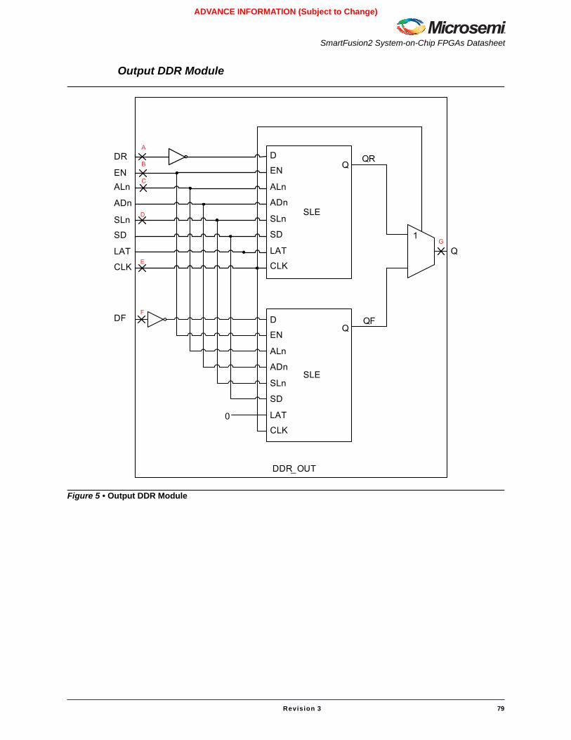
SmartFusion2 System-on-Chip FPGAs Datasheet
Revision 3 79
ADVANCE INFORMATION (Subject to Change)
Output DDR Module
Figure 5 • Output DDR Module
SLE
D
EN
ALn
ADn
SLn
SD
LAT
CLK
Q
SLE
D
EN
ALn
ADn
SLn
SD
LAT
CLK
Q
QR
QF
DDR_OUT
ENALn
ADn
SLn
SD
LAT
CLK
1
Q
DR
DF
0
G
A
B
C
D
E
F
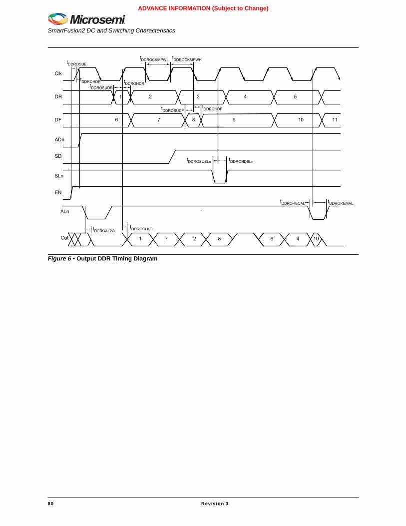
SmartFusion2 DC and Switching Characteristics
80 Revision 3
ADVANCE INFORMATION (Subject to Change)
Figure 6 • Output DDR Timing Diagram
`
6 7
21
8
3
9 10
4 5
2 8 9
tDDROREMAL
tDDROHDRtDDROSUDR
tDDROHDFtDDROSUDF
tDDROCLKQ
tDDRORECAL
Clk
DF
DR
ALn
Out
tDDROAL2Q
71 4
11
ADn
SD
SLn
EN
10
tDDROSUE
tDDROHDE
tDDROSUSLn tDDROHDSLn
tDDROCKMPWL tDDROCKMPWH
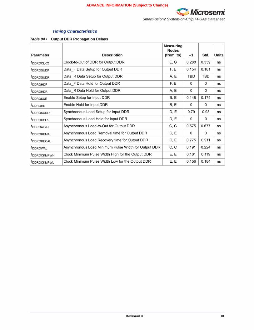
SmartFusion2 System-on-Chip FPGAs Datasheet
Revision 3 81
ADVANCE INFORMATION (Subject to Change)
Timing Characteristics
Table 94 • Output DDR Propagation Delays
Parameter Description
Measuring Nodes
(from, to) –1 Std. Units
tDDROCLKQ Clock-to-Out of DDR for Output DDR E, G 0.288 0.339 ns
tDDROSUDF Data_F Data Setup for Output DDR F, E 0.154 0.181 ns
tDDROSUDR Data_R Data Setup for Output DDR A, E TBD TBD ns
tDDROHDF Data_F Data Hold for Output DDR F, E 0 0 ns
tDDROHDR Data_R Data Hold for Output DDR A, E 0 0 ns
tDDROSUE Enable Setup for Input DDR B, E 0.148 0.174 ns
tDDROHE Enable Hold for Input DDR B, E 0 0 ns
tDDROSUSLn Synchronous Load Setup for Input DDR D, E 0.79 0.93 ns
tDDROHSLn Synchronous Load Hold for Input DDR D, E 0 0 ns
tDDROAL2Q Asynchronous Load-to-Out for Output DDR C, G 0.575 0.677 ns
tDDROREMAL Asynchronous Load Removal time for Output DDR C, E 0 0 ns
tDDRORECAL Asynchronous Load Recovery time for Output DDR C, E 0.775 0.911 ns
tDDROWAL Asynchronous Load Minimum Pulse Width for Output DDR C, C 0.191 0.224 ns
tDDROCKMPWH Clock Minimum Pulse Width High for the Output DDR E, E 0.101 0.119 ns
tDDROCKMPWL Clock Minimum Pulse Width Low for the Output DDR E, E 0.156 0.184 ns
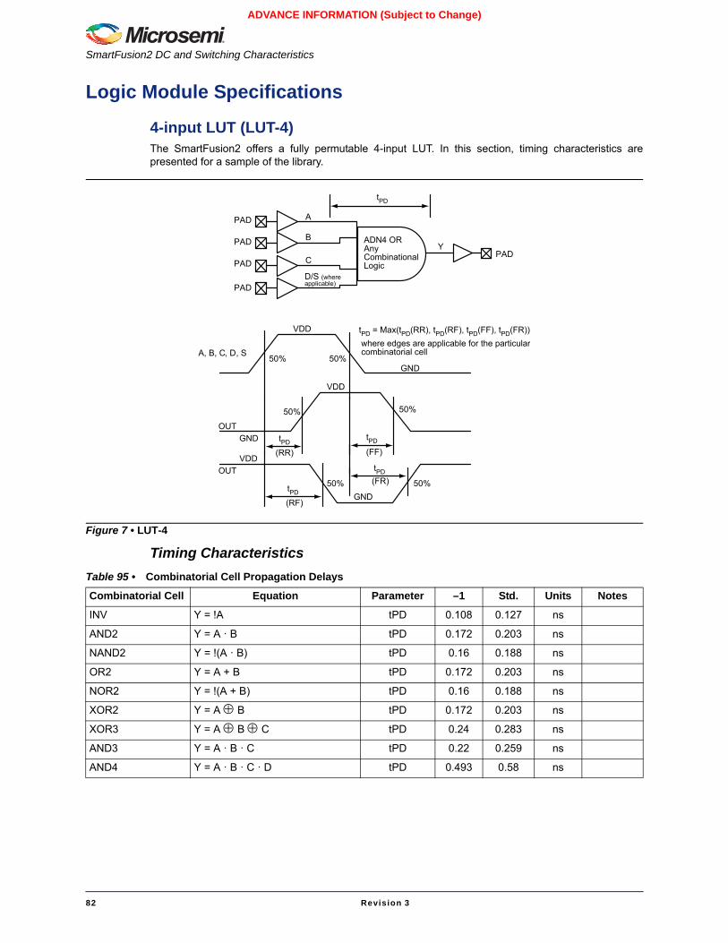
SmartFusion2 DC and Switching Characteristics
82 Revision 3
ADVANCE INFORMATION (Subject to Change)
Logic Module Specifications
4-input LUT (LUT-4)The SmartFusion2 offers a fully permutable 4-input LUT. In this section, timing characteristics arepresented for a sample of the library.
Timing CharacteristicsFigure 7 • LUT-4
tPD
PAD A
BY
PADPAD
PADD/S (whereapplicable)
ADN4 ORAny CombinationalLogic
PAD
C
tPDtPD
tPD
tPD
(RR)
A, B, C, D, S
OUT
50%
GND(FF)
50%
50%50%
VDD
VDD
GND
(RF)
50%
tPD = Max(tPD(RR), tPD(RF), tPD(FF), tPD(FR))where edges are applicable for the particularcombinatorial cell
(FR) 50%
VDDOUT
GND
Table 95 • Combinatorial Cell Propagation Delays
Combinatorial Cell Equation Parameter –1 Std. Units Notes
INV Y = !A tPD 0.108 0.127 ns
AND2 Y = A · B tPD 0.172 0.203 ns
NAND2 Y = !(A · B) tPD 0.16 0.188 ns
OR2 Y = A + B tPD 0.172 0.203 ns
NOR2 Y = !(A + B) tPD 0.16 0.188 ns
XOR2 Y = A ⊕ B tPD 0.172 0.203 ns
XOR3 Y = A ⊕ B ⊕ C tPD 0.24 0.283 ns
AND3 Y = A · B · C tPD 0.22 0.259 ns
AND4 Y = A · B · C · D tPD 0.493 0.58 ns
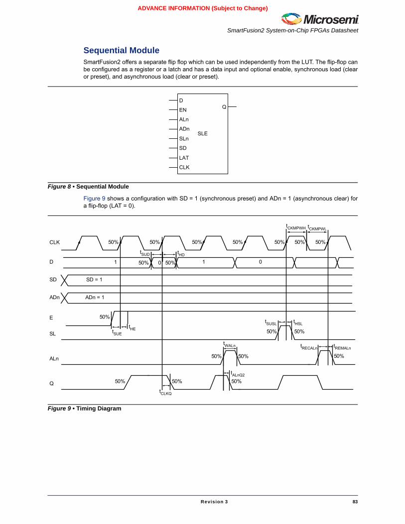
SmartFusion2 System-on-Chip FPGAs Datasheet
Revision 3 83
ADVANCE INFORMATION (Subject to Change)
Sequential ModuleSmartFusion2 offers a separate flip flop which can be used independently from the LUT. The flip-flop canbe configured as a register or a latch and has a data input and optional enable, synchronous load (clearor preset), and asynchronous load (clear or preset).
Figure 9 shows a configuration with SD = 1 (synchronous preset) and ADn = 1 (asynchronous clear) fora flip-flop (LAT = 0).
Figure 8 • Sequential Module
SLE
D
EN
ALn
ADn
SLn
SD
LAT
CLK
Q
Figure 9 • Timing Diagram
SL
ALn
Q
CLK
D
E
tSUE
50%
50%
tSUD tHD
50% 50%
tCLKQ
1 0
tHE
tSUSL tHSL
50%
tRECALn tREMALntWALn
tALnQ2
tCKMPWH tCKMPWL
50% 50%
50% 50%
50% 50% 50% 50% 50% 50%
50%
50%
SD
ADn ADn = 1
SD = 1
1
50%
0
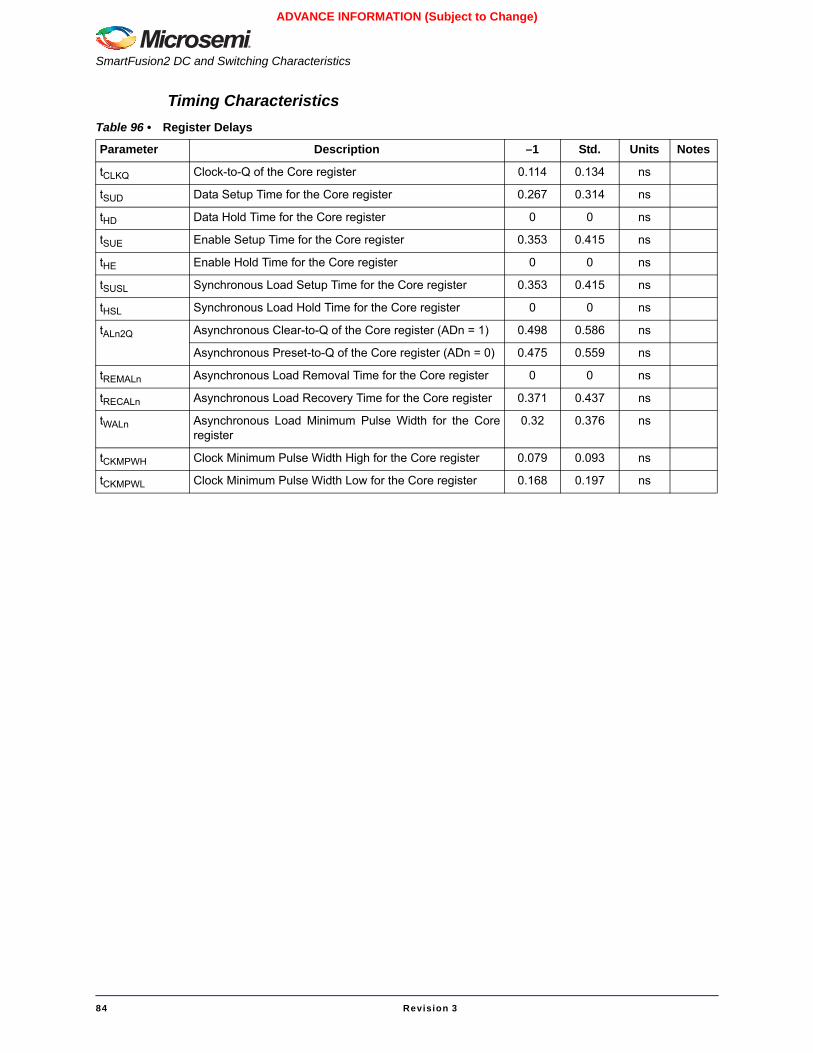
SmartFusion2 DC and Switching Characteristics
84 Revision 3
ADVANCE INFORMATION (Subject to Change)
Timing CharacteristicsTable 96 • Register Delays
Parameter Description –1 Std. Units Notes
tCLKQ Clock-to-Q of the Core register 0.114 0.134 ns
tSUD Data Setup Time for the Core register 0.267 0.314 ns
tHD Data Hold Time for the Core register 0 0 ns
tSUE Enable Setup Time for the Core register 0.353 0.415 ns
tHE Enable Hold Time for the Core register 0 0 ns
tSUSL Synchronous Load Setup Time for the Core register 0.353 0.415 ns
tHSL Synchronous Load Hold Time for the Core register 0 0 ns
tALn2Q Asynchronous Clear-to-Q of the Core register (ADn = 1) 0.498 0.586 ns
Asynchronous Preset-to-Q of the Core register (ADn = 0) 0.475 0.559 ns
tREMALn Asynchronous Load Removal Time for the Core register 0 0 ns
tRECALn Asynchronous Load Recovery Time for the Core register 0.371 0.437 ns
tWALn Asynchronous Load Minimum Pulse Width for the Coreregister
0.32 0.376 ns
tCKMPWH Clock Minimum Pulse Width High for the Core register 0.079 0.093 ns
tCKMPWL Clock Minimum Pulse Width Low for the Core register 0.168 0.197 ns
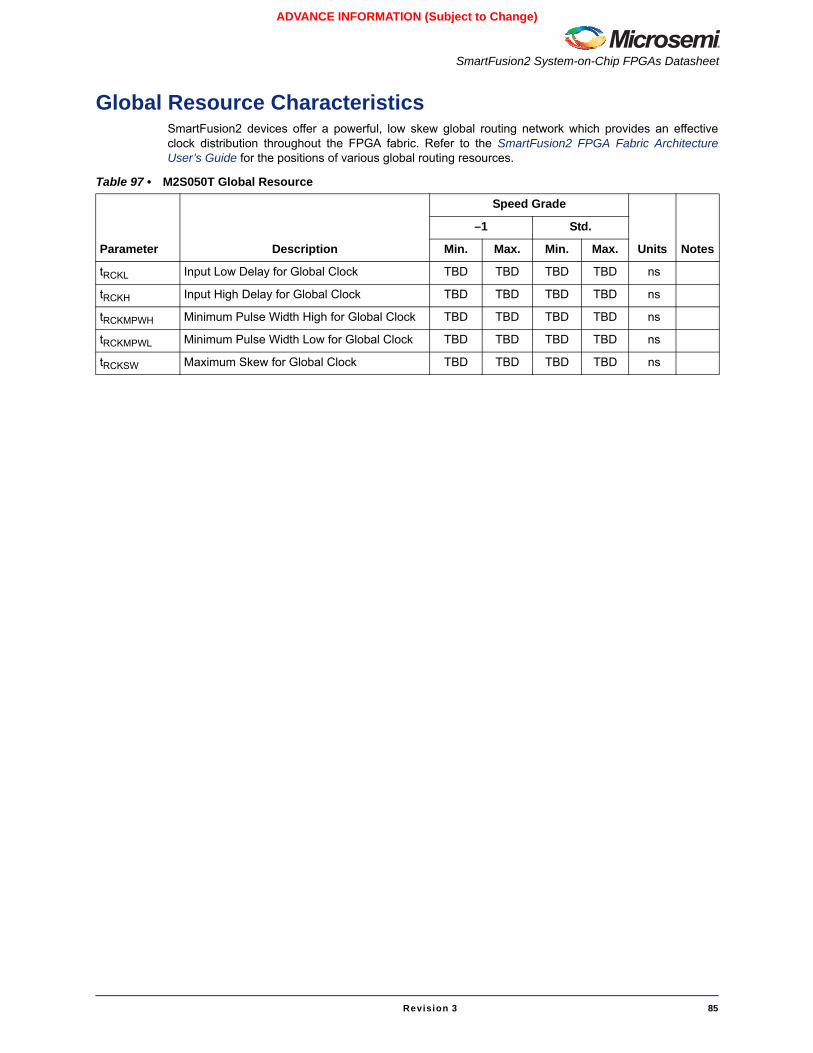
SmartFusion2 System-on-Chip FPGAs Datasheet
Revision 3 85
ADVANCE INFORMATION (Subject to Change)
Global Resource CharacteristicsSmartFusion2 devices offer a powerful, low skew global routing network which provides an effectiveclock distribution throughout the FPGA fabric. Refer to the SmartFusion2 FPGA Fabric ArchitectureUser’s Guide for the positions of various global routing resources.
Table 97 • M2S050T Global Resource
Parameter Description
Speed Grade
Units Notes
–1 Std.
Min. Max. Min. Max.
tRCKL Input Low Delay for Global Clock TBD TBD TBD TBD ns
tRCKH Input High Delay for Global Clock TBD TBD TBD TBD ns
tRCKMPWH Minimum Pulse Width High for Global Clock TBD TBD TBD TBD ns
tRCKMPWL Minimum Pulse Width Low for Global Clock TBD TBD TBD TBD ns
tRCKSW Maximum Skew for Global Clock TBD TBD TBD TBD ns
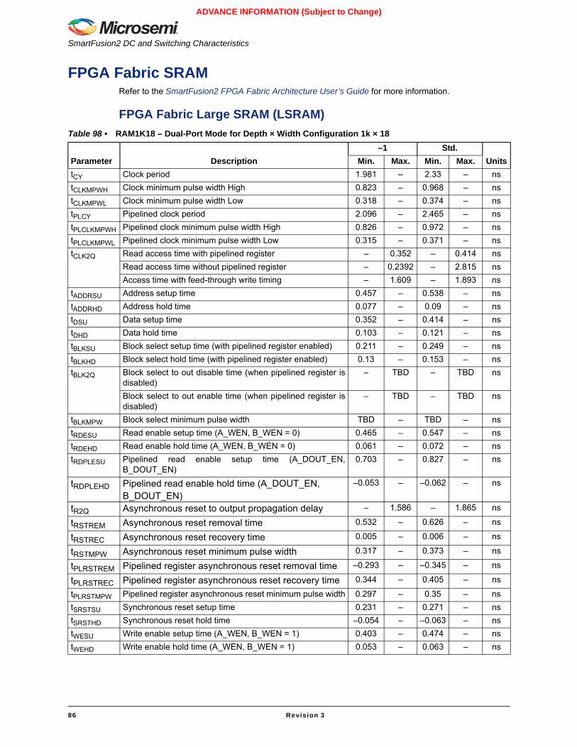
SmartFusion2 DC and Switching Characteristics
86 Revision 3
ADVANCE INFORMATION (Subject to Change)
FPGA Fabric SRAMRefer to the SmartFusion2 FPGA Fabric Architecture User’s Guide for more information.
FPGA Fabric Large SRAM (LSRAM)Table 98 • RAM1K18 – Dual-Port Mode for Depth × Width Configuration 1k × 18
Parameter Description–1 Std.
UnitsMin. Max. Min. Max.tCY Clock period 1.981 – 2.33 – nstCLKMPWH Clock minimum pulse width High 0.823 – 0.968 – nstCLKMPWL Clock minimum pulse width Low 0.318 – 0.374 – nstPLCY Pipelined clock period 2.096 – 2.465 – nstPLCLKMPWH Pipelined clock minimum pulse width High 0.826 – 0.972 – nstPLCLKMPWL Pipelined clock minimum pulse width Low 0.315 – 0.371 – nstCLK2Q Read access time with pipelined register – 0.352 – 0.414 ns
Read access time without pipelined register – 0.2392 – 2.815 nsAccess time with feed-through write timing – 1.609 – 1.893 ns
tADDRSU Address setup time 0.457 – 0.538 – nstADDRHD Address hold time 0.077 – 0.09 – nstDSU Data setup time 0.352 – 0.414 – nstDHD Data hold time 0.103 – 0.121 – nstBLKSU Block select setup time (with pipelined register enabled) 0.211 – 0.249 – nstBLKHD Block select hold time (with pipelined register enabled) 0.13 – 0.153 – nstBLK2Q Block select to out disable time (when pipelined register is
disabled)– TBD – TBD ns
Block select to out enable time (when pipelined register isdisabled)
– TBD – TBD ns
tBLKMPW Block select minimum pulse width TBD – TBD – nstRDESU Read enable setup time (A_WEN, B_WEN = 0) 0.465 – 0.547 – nstRDEHD Read enable hold time (A_WEN, B_WEN = 0) 0.061 – 0.072 – nstRDPLESU Pipelined read enable setup time (A_DOUT_EN,
B_DOUT_EN)0.703 – 0.827 – ns
tRDPLEHD Pipelined read enable hold time (A_DOUT_EN, B_DOUT_EN)
–0.053 – –0.062 – ns
tR2Q Asynchronous reset to output propagation delay – 1.586 – 1.865 ns
tRSTREM Asynchronous reset removal time 0.532 – 0.626 – ns
tRSTREC Asynchronous reset recovery time 0.005 – 0.006 – ns
tRSTMPW Asynchronous reset minimum pulse width 0.317 – 0.373 – ns
tPLRSTREM Pipelined register asynchronous reset removal time –0.293 – –0.345 – ns
tPLRSTREC Pipelined register asynchronous reset recovery time 0.344 – 0.405 – ns
tPLRSTMPW Pipelined register asynchronous reset minimum pulse width 0.297 – 0.35 – nstSRSTSU Synchronous reset setup time 0.231 – 0.271 – nstSRSTHD Synchronous reset hold time –0.054 – –0.063 – nstWESU Write enable setup time (A_WEN, B_WEN = 1) 0.403 – 0.474 – nstWEHD Write enable hold time (A_WEN, B_WEN = 1) 0.053 – 0.063 – ns
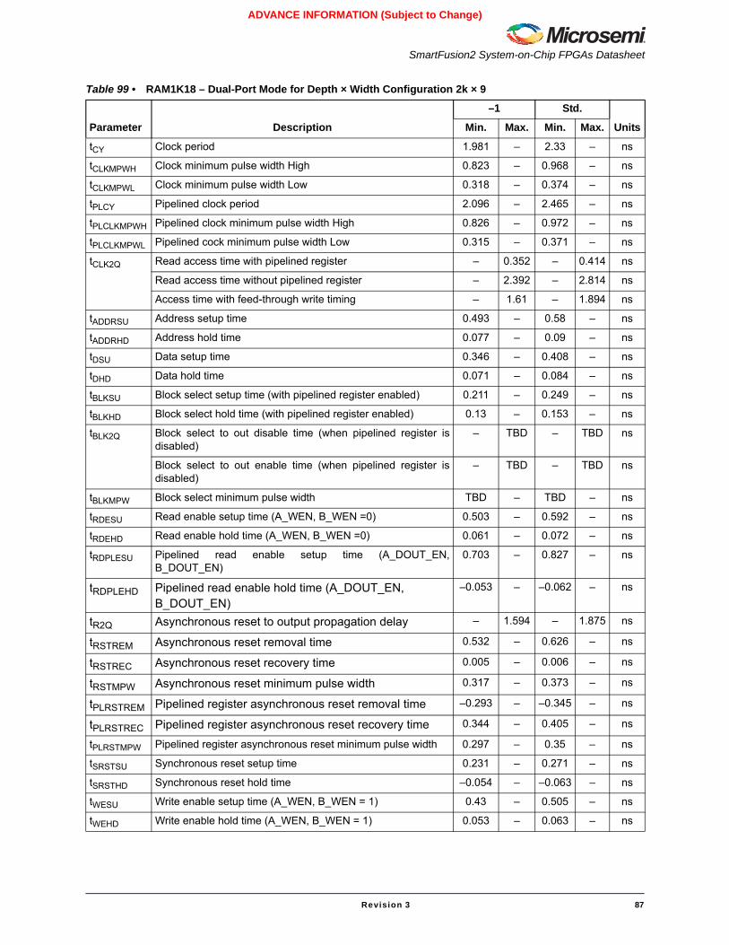
SmartFusion2 System-on-Chip FPGAs Datasheet
Revision 3 87
ADVANCE INFORMATION (Subject to Change)
Table 99 • RAM1K18 – Dual-Port Mode for Depth × Width Configuration 2k × 9
Parameter Description
–1 Std.
UnitsMin. Max. Min. Max.
tCY Clock period 1.981 – 2.33 – ns
tCLKMPWH Clock minimum pulse width High 0.823 – 0.968 – ns
tCLKMPWL Clock minimum pulse width Low 0.318 – 0.374 – ns
tPLCY Pipelined clock period 2.096 – 2.465 – ns
tPLCLKMPWH Pipelined clock minimum pulse width High 0.826 – 0.972 – ns
tPLCLKMPWL Pipelined cock minimum pulse width Low 0.315 – 0.371 – ns
tCLK2Q Read access time with pipelined register – 0.352 – 0.414 ns
Read access time without pipelined register – 2.392 – 2.814 ns
Access time with feed-through write timing – 1.61 – 1.894 ns
tADDRSU Address setup time 0.493 – 0.58 – ns
tADDRHD Address hold time 0.077 – 0.09 – ns
tDSU Data setup time 0.346 – 0.408 – ns
tDHD Data hold time 0.071 – 0.084 – ns
tBLKSU Block select setup time (with pipelined register enabled) 0.211 – 0.249 – ns
tBLKHD Block select hold time (with pipelined register enabled) 0.13 – 0.153 – ns
tBLK2Q Block select to out disable time (when pipelined register isdisabled)
– TBD – TBD ns
Block select to out enable time (when pipelined register isdisabled)
– TBD – TBD ns
tBLKMPW Block select minimum pulse width TBD – TBD – ns
tRDESU Read enable setup time (A_WEN, B_WEN =0) 0.503 – 0.592 – ns
tRDEHD Read enable hold time (A_WEN, B_WEN =0) 0.061 – 0.072 – ns
tRDPLESU Pipelined read enable setup time (A_DOUT_EN,B_DOUT_EN)
0.703 – 0.827 – ns
tRDPLEHD Pipelined read enable hold time (A_DOUT_EN, B_DOUT_EN)
–0.053 – –0.062 – ns
tR2Q Asynchronous reset to output propagation delay – 1.594 – 1.875 ns
tRSTREM Asynchronous reset removal time 0.532 – 0.626 – ns
tRSTREC Asynchronous reset recovery time 0.005 – 0.006 – ns
tRSTMPW Asynchronous reset minimum pulse width 0.317 – 0.373 – ns
tPLRSTREM Pipelined register asynchronous reset removal time –0.293 – –0.345 – ns
tPLRSTREC Pipelined register asynchronous reset recovery time 0.344 – 0.405 – ns
tPLRSTMPW Pipelined register asynchronous reset minimum pulse width 0.297 – 0.35 – ns
tSRSTSU Synchronous reset setup time 0.231 – 0.271 – ns
tSRSTHD Synchronous reset hold time –0.054 – –0.063 – ns
tWESU Write enable setup time (A_WEN, B_WEN = 1) 0.43 – 0.505 – ns
tWEHD Write enable hold time (A_WEN, B_WEN = 1) 0.053 – 0.063 – ns
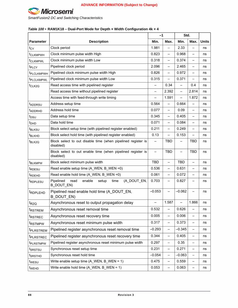
SmartFusion2 DC and Switching Characteristics
88 Revision 3
ADVANCE INFORMATION (Subject to Change)
Table 100 • RAM1K18 – Dual-Port Mode for Depth × Width Configuration 4k × 4
Parameter Description
–1 Std.
UnitsMin. Max. Min. Max.
tCY Clock period 1.981 – 2.33 – ns
tCLKMPWH Clock minimum pulse width High 0.823 – 0.968 – ns
tCLKMPWL Clock minimum pulse width Low 0.318 – 0.374 – ns
tPLCY Pipelined clock period 2.096 – 2.465 – ns
tPLCLKMPWH Pipelined clock minimum pulse width High 0.826 – 0.972 – ns
tPLCLKMPWL Pipelined clock minimum pulse width Low 0.315 – 0.371 – ns
tCLK2Q Read access time with pipelined register – 0.34 – 0.4 ns
Read access time without pipelined register – 2.392 – 2.814 ns
Access time with feed-through write timing – 1.591 – 1.872 ns
tADDRSU Address setup time 0.564 – 0.664 – ns
tADDRHD Address hold time 0.077 – 0.09 – ns
tDSU Data setup time 0.345 – 0.405 – ns
tDHD Data hold time 0.071 – 0.084 – ns
tBLKSU Block select setup time (with pipelined register enabled) 0.211 – 0.249 – ns
tBLKHD Block select hold time (with pipelined register enabled) 0.13 – 0.153 – ns
tBLK2Q Block select to out disable time (when pipelined register isdisabled)
– TBD – TBD ns
Block select to out enable time (when pipelined register isdisabled)
– TBD – TBD ns
tBLKMPW Block select minimum pulse width TBD – TBD – ns
tRDESU Read enable setup time (A_WEN, B_WEN =0) 0.536 – 0.631 – ns
tRDEHD Read enable hold time (A_WEN, B_WEN =0) 0.061 – 0.072 – ns
tRDPLESU Pipelined read enable setup time (A_DOUT_EN,B_DOUT_EN)
0.703 – 0.827 – ns
tRDPLEHD Pipelined read enable hold time (A_DOUT_EN, B_DOUT_EN)
–0.053 – –0.062 – ns
tR2Q Asynchronous reset to output propagation delay – 1.587 – 1.866 ns
tRSTREM Asynchronous reset removal time 0.532 – 0.626 – ns
tRSTREC Asynchronous reset recovery time 0.005 – 0.006 – ns
tRSTMPW Asynchronous reset minimum pulse width 0.317 – 0.373 – ns
tPLRSTREM Pipelined register asynchronous reset removal time –0.293 – –0.345 – ns
tPLRSTREC Pipelined register asynchronous reset recovery time 0.344 – 0.405 – ns
tPLRSTMPW Pipelined register asynchronous reset minimum pulse width 0.297 – 0.35 – ns
tSRSTSU Synchronous reset setup time 0.231 – 0.271 – ns
tSRSTHD Synchronous reset hold time –0.054 – –0.063 – ns
tWESU Write enable setup time (A_WEN, B_WEN = 1) 0.475 – 0.559 – ns
tWEHD Write enable hold time (A_WEN, B_WEN = 1) 0.053 – 0.063 – ns
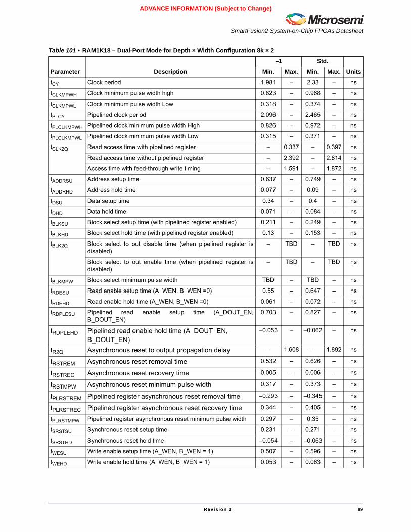
SmartFusion2 System-on-Chip FPGAs Datasheet
Revision 3 89
ADVANCE INFORMATION (Subject to Change)
Table 101 • RAM1K18 – Dual-Port Mode for Depth × Width Configuration 8k × 2
Parameter Description
–1 Std.
UnitsMin. Max. Min. Max.
tCY Clock period 1.981 – 2.33 – ns
tCLKMPWH Clock minimum pulse width high 0.823 – 0.968 – ns
tCLKMPWL Clock minimum pulse width Low 0.318 – 0.374 – ns
tPLCY Pipelined clock period 2.096 – 2.465 – ns
tPLCLKMPWH Pipelined clock minimum pulse width High 0.826 – 0.972 – ns
tPLCLKMPWL Pipelined clock minimum pulse width Low 0.315 – 0.371 – ns
tCLK2Q Read access time with pipelined register – 0.337 – 0.397 ns
Read access time without pipelined register – 2.392 – 2.814 ns
Access time with feed-through write timing – 1.591 – 1.872 ns
tADDRSU Address setup time 0.637 – 0.749 – ns
tADDRHD Address hold time 0.077 – 0.09 – ns
tDSU Data setup time 0.34 – 0.4 – ns
tDHD Data hold time 0.071 – 0.084 – ns
tBLKSU Block select setup time (with pipelined register enabled) 0.211 – 0.249 – ns
tBLKHD Block select hold time (with pipelined register enabled) 0.13 – 0.153 – ns
tBLK2Q Block select to out disable time (when pipelined register isdisabled)
– TBD – TBD ns
Block select to out enable time (when pipelined register isdisabled)
– TBD – TBD ns
tBLKMPW Block select minimum pulse width TBD – TBD – ns
tRDESU Read enable setup time (A_WEN, B_WEN =0) 0.55 – 0.647 – ns
tRDEHD Read enable hold time (A_WEN, B_WEN =0) 0.061 – 0.072 – ns
tRDPLESU Pipelined read enable setup time (A_DOUT_EN,B_DOUT_EN)
0.703 – 0.827 – ns
tRDPLEHD Pipelined read enable hold time (A_DOUT_EN, B_DOUT_EN)
–0.053 – –0.062 – ns
tR2Q Asynchronous reset to output propagation delay – 1.608 – 1.892 ns
tRSTREM Asynchronous reset removal time 0.532 – 0.626 – ns
tRSTREC Asynchronous reset recovery time 0.005 – 0.006 – ns
tRSTMPW Asynchronous reset minimum pulse width 0.317 – 0.373 – ns
tPLRSTREM Pipelined register asynchronous reset removal time –0.293 – –0.345 – ns
tPLRSTREC Pipelined register asynchronous reset recovery time 0.344 – 0.405 – ns
tPLRSTMPW Pipelined register asynchronous reset minimum pulse width 0.297 – 0.35 – ns
tSRSTSU Synchronous reset setup time 0.231 – 0.271 – ns
tSRSTHD Synchronous reset hold time –0.054 – –0.063 – ns
tWESU Write enable setup time (A_WEN, B_WEN = 1) 0.507 – 0.596 – ns
tWEHD Write enable hold time (A_WEN, B_WEN = 1) 0.053 – 0.063 – ns
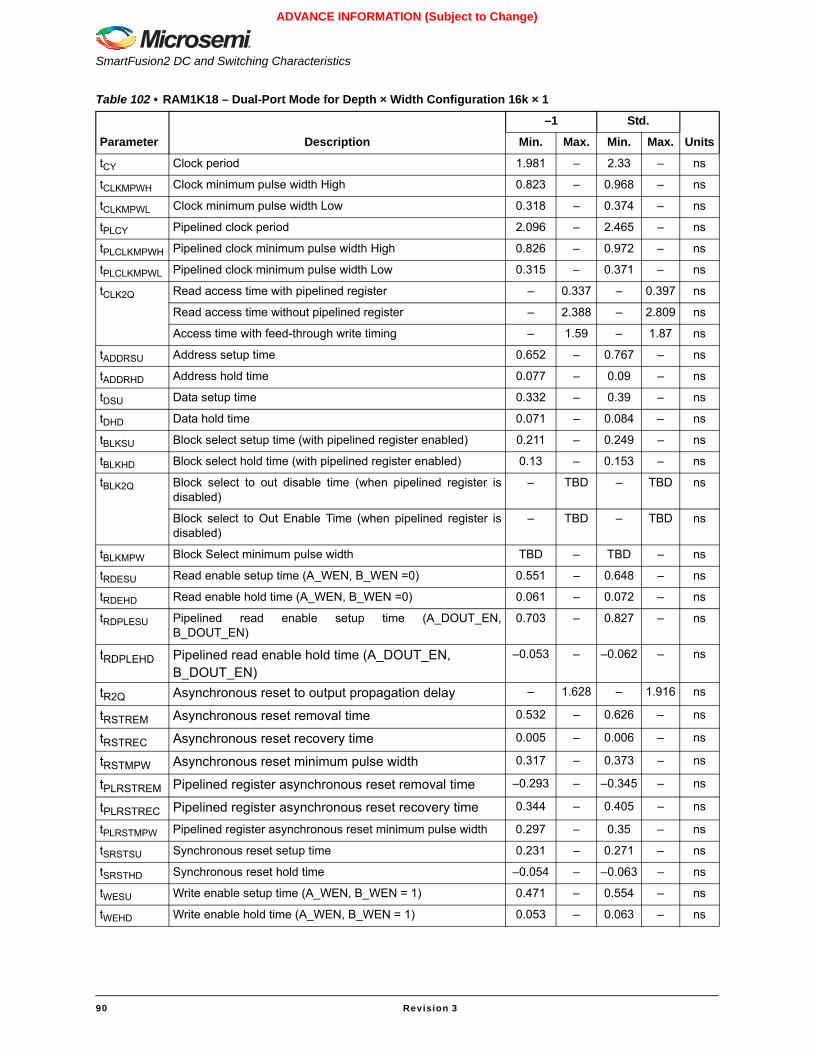
SmartFusion2 DC and Switching Characteristics
90 Revision 3
ADVANCE INFORMATION (Subject to Change)
Table 102 • RAM1K18 – Dual-Port Mode for Depth × Width Configuration 16k × 1
Parameter Description
–1 Std.
UnitsMin. Max. Min. Max.
tCY Clock period 1.981 – 2.33 – ns
tCLKMPWH Clock minimum pulse width High 0.823 – 0.968 – ns
tCLKMPWL Clock minimum pulse width Low 0.318 – 0.374 – ns
tPLCY Pipelined clock period 2.096 – 2.465 – ns
tPLCLKMPWH Pipelined clock minimum pulse width High 0.826 – 0.972 – ns
tPLCLKMPWL Pipelined clock minimum pulse width Low 0.315 – 0.371 – ns
tCLK2Q Read access time with pipelined register – 0.337 – 0.397 ns
Read access time without pipelined register – 2.388 – 2.809 ns
Access time with feed-through write timing – 1.59 – 1.87 ns
tADDRSU Address setup time 0.652 – 0.767 – ns
tADDRHD Address hold time 0.077 – 0.09 – ns
tDSU Data setup time 0.332 – 0.39 – ns
tDHD Data hold time 0.071 – 0.084 – ns
tBLKSU Block select setup time (with pipelined register enabled) 0.211 – 0.249 – ns
tBLKHD Block select hold time (with pipelined register enabled) 0.13 – 0.153 – ns
tBLK2Q Block select to out disable time (when pipelined register isdisabled)
– TBD – TBD ns
Block select to Out Enable Time (when pipelined register isdisabled)
– TBD – TBD ns
tBLKMPW Block Select minimum pulse width TBD – TBD – ns
tRDESU Read enable setup time (A_WEN, B_WEN =0) 0.551 – 0.648 – ns
tRDEHD Read enable hold time (A_WEN, B_WEN =0) 0.061 – 0.072 – ns
tRDPLESU Pipelined read enable setup time (A_DOUT_EN,B_DOUT_EN)
0.703 – 0.827 – ns
tRDPLEHD Pipelined read enable hold time (A_DOUT_EN, B_DOUT_EN)
–0.053 – –0.062 – ns
tR2Q Asynchronous reset to output propagation delay – 1.628 – 1.916 ns
tRSTREM Asynchronous reset removal time 0.532 – 0.626 – ns
tRSTREC Asynchronous reset recovery time 0.005 – 0.006 – ns
tRSTMPW Asynchronous reset minimum pulse width 0.317 – 0.373 – ns
tPLRSTREM Pipelined register asynchronous reset removal time –0.293 – –0.345 – ns
tPLRSTREC Pipelined register asynchronous reset recovery time 0.344 – 0.405 – ns
tPLRSTMPW Pipelined register asynchronous reset minimum pulse width 0.297 – 0.35 – ns
tSRSTSU Synchronous reset setup time 0.231 – 0.271 – ns
tSRSTHD Synchronous reset hold time –0.054 – –0.063 – ns
tWESU Write enable setup time (A_WEN, B_WEN = 1) 0.471 – 0.554 – ns
tWEHD Write enable hold time (A_WEN, B_WEN = 1) 0.053 – 0.063 – ns
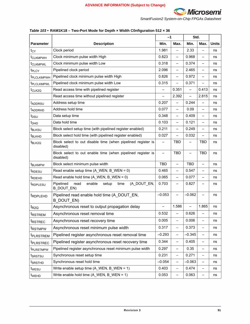
SmartFusion2 System-on-Chip FPGAs Datasheet
Revision 3 91
ADVANCE INFORMATION (Subject to Change)
Table 103 • RAM1K18 – Two-Port Mode for Depth × Width C0nfiguration 512 × 36
Parameter Description
–1 Std.
UnitsMin. Max. Min. Max.
tCY Clock period 1.981 – 2.33 – ns
tCLKMPWH Clock minimum pulse width High 0.823 – 0.968 – ns
tCLKMPWL Clock minimum pulse width Low 0.318 – 0.374 – ns
tPLCY Pipelined clock period 2.096 – 2.465 – ns
tPLCLKMPWH Pipelined clock minimum pulse width High 0.826 – 0.972 – ns
tPLCLKMPWL Pipelined clock minimum pulse width Low 0.315 – 0.371 – ns
tCLK2Q Read access time with pipelined register – 0.351 – 0.413 ns
Read access time without pipelined register – 2.392 – 2.815 ns
tADDRSU Address setup time 0.207 – 0.244 – ns
tADDRHD Address hold time 0.077 – 0.09 – ns
tDSU Data setup time 0.348 – 0.409 – ns
tDHD Data hold time 0.103 – 0.121 – ns
tBLKSU Block select setup time (with pipelined register enabled) 0.211 – 0.249 – ns
tBLKHD Block select hold time (with pipelined register enabled) 0.027 – 0.032 – ns
tBLK2Q Block select to out disable time (when pipelined register isdisabled)
– TBD – TBD ns
Block select to out enable time (when pipelined register isdisabled)
– TBD – TBD ns
tBLKMPW Block select minimum pulse width TBD – TBD – ns
tRDESU Read enable setup time (A_WEN, B_WEN = 0) 0.465 – 0.547 – ns
tRDEHD Read enable hold time (A_WEN, B_WEN = 0) 0.065 – 0.077 – ns
tRDPLESU Pipelined read enable setup time (A_DOUT_EN,B_DOUT_EN)
0.703 – 0.827 – ns
tRDPLEHD Pipelined read enable hold time (A_DOUT_EN, B_DOUT_EN)
–0.053 – –0.062 – ns
tR2Q Asynchronous reset to output propagation delay – 1.586 – 1.865 ns
tRSTREM Asynchronous reset removal time 0.532 – 0.626 – ns
tRSTREC Asynchronous reset recovery time 0.005 – 0.006 – ns
tRSTMPW Asynchronous reset minimum pulse width 0.317 – 0.373 – ns
tPLRSTREM Pipelined register asynchronous reset removal time –0.293 – –0.345 – ns
tPLRSTREC Pipelined register asynchronous reset recovery time 0.344 – 0.405 – ns
tPLRSTMPW Pipelined register asynchronous reset minimum pulse width 0.297 – 0.35 – ns
tSRSTSU Synchronous reset setup time 0.231 – 0.271 – ns
tSRSTHD Synchronous reset hold time –0.054 – –0.063 – ns
tWESU Write enable setup time (A_WEN, B_WEN = 1) 0.403 – 0.474 – ns
tWEHD Write enable hold time (A_WEN, B_WEN = 1) 0.053 – 0.063 – ns
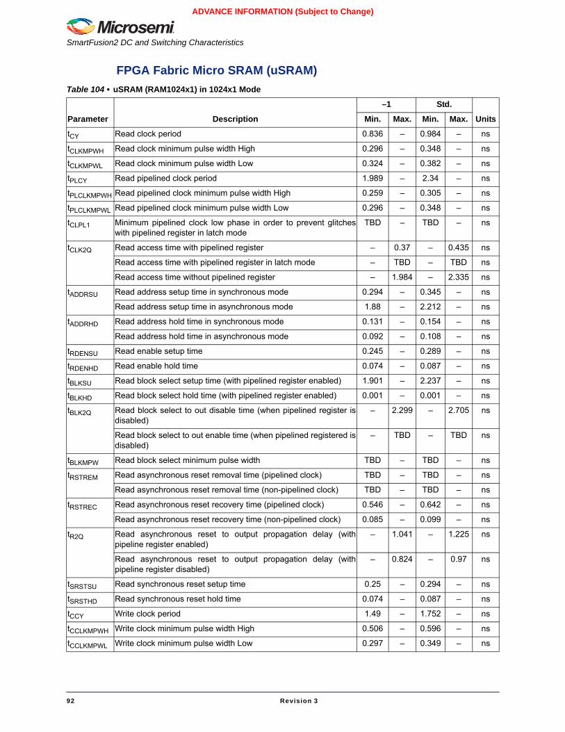
SmartFusion2 DC and Switching Characteristics
92 Revision 3
ADVANCE INFORMATION (Subject to Change)
FPGA Fabric Micro SRAM (uSRAM)Table 104 • uSRAM (RAM1024x1) in 1024x1 Mode
Parameter Description
–1 Std.
UnitsMin. Max. Min. Max.
tCY Read clock period 0.836 – 0.984 – ns
tCLKMPWH Read clock minimum pulse width High 0.296 – 0.348 – ns
tCLKMPWL Read clock minimum pulse width Low 0.324 – 0.382 – ns
tPLCY Read pipelined clock period 1.989 – 2.34 – ns
tPLCLKMPWH Read pipelined clock minimum pulse width High 0.259 – 0.305 – ns
tPLCLKMPWL Read pipelined clock minimum pulse width Low 0.296 – 0.348 – ns
tCLPL1 Minimum pipelined clock low phase in order to prevent glitcheswith pipelined register in latch mode
TBD – TBD – ns
tCLK2Q Read access time with pipelined register – 0.37 – 0.435 ns
Read access time with pipelined register in latch mode – TBD – TBD ns
Read access time without pipelined register – 1.984 – 2.335 ns
tADDRSU Read address setup time in synchronous mode 0.294 – 0.345 – ns
Read address setup time in asynchronous mode 1.88 – 2.212 – ns
tADDRHD Read address hold time in synchronous mode 0.131 – 0.154 – ns
Read address hold time in asynchronous mode 0.092 – 0.108 – ns
tRDENSU Read enable setup time 0.245 – 0.289 – ns
tRDENHD Read enable hold time 0.074 – 0.087 – ns
tBLKSU Read block select setup time (with pipelined register enabled) 1.901 – 2.237 – ns
tBLKHD Read block select hold time (with pipelined register enabled) 0.001 – 0.001 – ns
tBLK2Q Read block select to out disable time (when pipelined register isdisabled)
– 2.299 – 2.705 ns
Read block select to out enable time (when pipelined registered isdisabled)
– TBD – TBD ns
tBLKMPW Read block select minimum pulse width TBD – TBD – ns
tRSTREM Read asynchronous reset removal time (pipelined clock) TBD – TBD – ns
Read asynchronous reset removal time (non-pipelined clock) TBD – TBD – ns
tRSTREC Read asynchronous reset recovery time (pipelined clock) 0.546 – 0.642 – ns
Read asynchronous reset recovery time (non-pipelined clock) 0.085 – 0.099 – ns
tR2Q Read asynchronous reset to output propagation delay (withpipeline register enabled)
– 1.041 – 1.225 ns
Read asynchronous reset to output propagation delay (withpipeline register disabled)
– 0.824 – 0.97 ns
tSRSTSU Read synchronous reset setup time 0.25 – 0.294 – ns
tSRSTHD Read synchronous reset hold time 0.074 – 0.087 – ns
tCCY Write clock period 1.49 – 1.752 – ns
tCCLKMPWH Write clock minimum pulse width High 0.506 – 0.596 – ns
tCCLKMPWL Write clock minimum pulse width Low 0.297 – 0.349 – ns
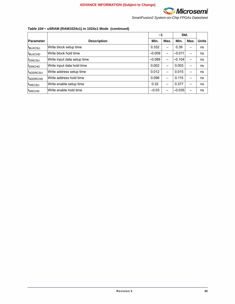
SmartFusion2 System-on-Chip FPGAs Datasheet
Revision 3 93
ADVANCE INFORMATION (Subject to Change)
tBLKCSU Write block setup time 0.332 – 0.39 – ns
tBLKCHD Write block hold time –0.009 – –0.011 – ns
tDINCSU Write input data setup time –0.089 – –0.104 – ns
tDINCHD Write input data hold time 0.002 – 0.003 – ns
tADDRCSU Write address setup time 0.012 – 0.015 – ns
tADDRCHD Write address hold time 0.098 – 0.115 – ns
tWECSU Write enable setup time 0.32 – 0.377 – ns
tWECHD Write enable hold time –0.03 – –0.035 – ns
Table 104 • uSRAM (RAM1024x1) in 1024x1 Mode (continued)
Parameter Description
–1 Std.
UnitsMin. Max. Min. Max.

SmartFusion2 DC and Switching Characteristics
94 Revision 3
ADVANCE INFORMATION (Subject to Change)
Table 105 • uSRAM (RAM512x2) in 512x2 Mode
Parameter Description
–1 Std.
UnitsMin. Max. Min. Max.
tCY Read clock period 0.836 – 0.984 – ns
tCLKMPWH Read clock minimum pulse width High 0.296 – 0.348 – ns
tCLKMPWL Read clock minimum pulse width Low 0.324 – 0.382 – ns
tPLCY Read pipelined clock period 1.989 – 2.34 – ns
tPLCLKMPWH Read pipelined clock minimum pulse width High 0.259 – 0.305 – ns
tPLCLKMPWL Read pipelined clock minimum pulse width Low 0.296 – 0.348 – ns
tCLPL1 Minimum pipelined clock low phase in order to prevent glitcheswith pipelined register in latch mode
TBD – TBD – ns
tCLK2Q Read access time with pipelined register – 0.37 – 0.435 ns
Read access time with pipelined register in latch mode – TBD – TBD ns
Read access time without pipelined register – 1.954 – 2.299 ns
tADDRSU Read address setup time in synchronous mode 0.294 – 0.345 – ns
Read address setup time in asynchronous mode 1.849 – 2.175 – ns
tADDRHD Read address hold time in synchronous mode 0.131 – 0.154 – ns
Read address hold time in asynchronous mode 0.092 – 0.108 – ns
tRDENSU Read enable setup time 0.245 – 0.289 – ns
tRDENHD Read enable hold time 0.074 – 0.087 – ns
tBLKSU Read block select setup time (with pipelined register enabled) 1.901 – 2.237 – ns
tBLKHD Read block select hold time (with pipelined register enabled) 0.001 – 0.001 – ns
tBLK2Q Read block select to out disable time (when pipelined register isdisabled)
– 2.272 – 2.673 ns
Read block select to out enable time (when pipelined registered isdisabled)
– TBD – TBD ns
tBLKMPW Read block select minimum pulse width TBD – TBD – ns
tRSTREM Read asynchronous reset removal time (pipelined clock) TBD – TBD – ns
Read asynchronous reset removal time (non-pipelined clock) TBD – TBD – ns
tRSTREC Read asynchronous reset recovery time (pipelined clock) 0.546 – 0.642 – ns
Read asynchronous reset recovery time (non-pipelined clock) 0.085 – 0.099 – ns
tR2Q Read asynchronous reset to Output Propagation Delay (withpipeline register enabled)
– 1.041 – 1.225 ns
Read Asynchronous Reset to Output Propagation Delay (withpipeline register disabled)
– 0.937 – 1.102 ns
tSRSTSU Read Synchronous Reset Setup Time 0.25 – 0.294 – ns
tSRSTHD Read Synchronous Reset Hold Time 0.074 – 0.087 – ns
tCCY Write Clock Period 1.49 – 1.752 – ns
tCCLKMPWH Write Clock Minimum Pulse Width High 0.506 – 0.596 – ns
tCCLKMPWL Write Clock Minimum Pulse Width Low 0.297 – 0.349 – ns
tBLKCSU Write Block Setup Time 0.332 – 0.39 – ns
tBLKCHD Write Block Hold Time –0.009 – –0.011 – ns

SmartFusion2 System-on-Chip FPGAs Datasheet
Revision 3 95
ADVANCE INFORMATION (Subject to Change)
tDINCSU Write Input Data setup Time –0.025 – –0.03 – ns
tDINCHD Write Input Data hold Time 0.002 – 0.003 – ns
tADDRCSU Write Address Setup Time 0.012 – 0.015 – ns
tADDRCHD Write Address Hold Time 0.098 – 0.115 – ns
tWECSU Write Enable Setup Time 0.32 – 0.377 – ns
tWECHD Write Enable Hold Time –0.03 – –0.035 – ns
Table 105 • uSRAM (RAM512x2) in 512x2 Mode (continued)
Parameter Description
–1 Std.
UnitsMin. Max. Min. Max.
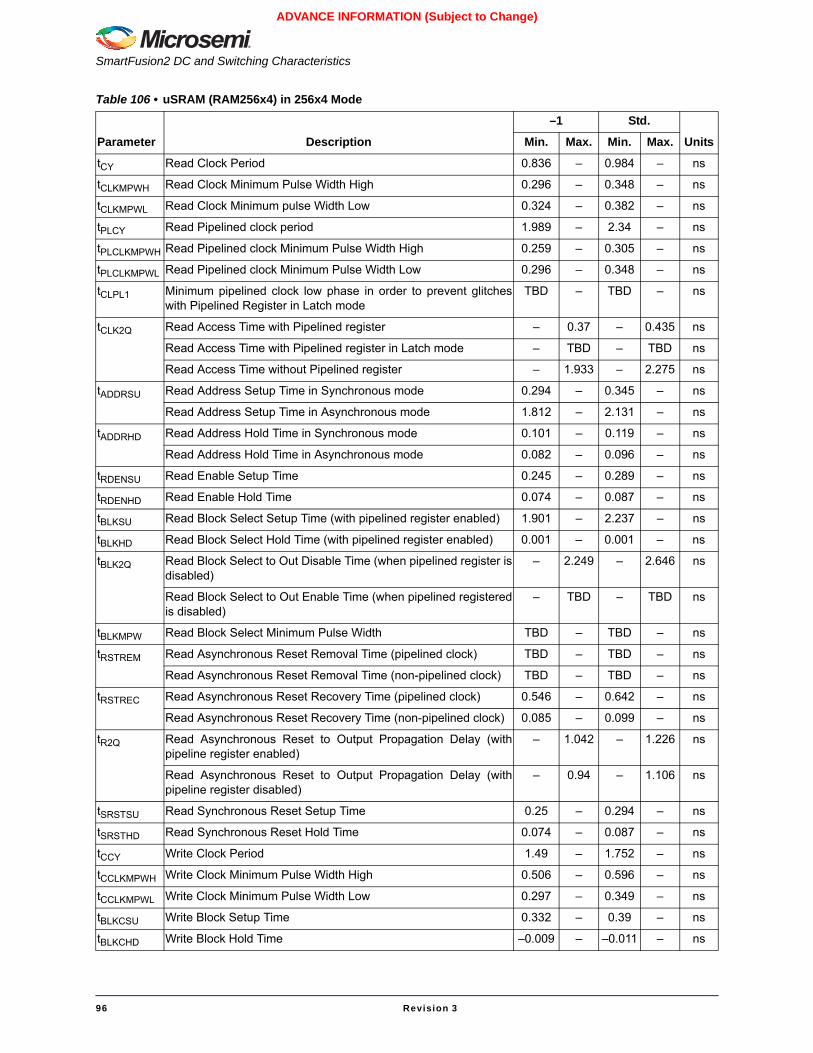
SmartFusion2 DC and Switching Characteristics
96 Revision 3
ADVANCE INFORMATION (Subject to Change)
Table 106 • uSRAM (RAM256x4) in 256x4 Mode
Parameter Description
–1 Std.
UnitsMin. Max. Min. Max.
tCY Read Clock Period 0.836 – 0.984 – ns
tCLKMPWH Read Clock Minimum Pulse Width High 0.296 – 0.348 – ns
tCLKMPWL Read Clock Minimum pulse Width Low 0.324 – 0.382 – ns
tPLCY Read Pipelined clock period 1.989 – 2.34 – ns
tPLCLKMPWH Read Pipelined clock Minimum Pulse Width High 0.259 – 0.305 – ns
tPLCLKMPWL Read Pipelined clock Minimum Pulse Width Low 0.296 – 0.348 – ns
tCLPL1 Minimum pipelined clock low phase in order to prevent glitcheswith Pipelined Register in Latch mode
TBD – TBD – ns
tCLK2Q Read Access Time with Pipelined register – 0.37 – 0.435 ns
Read Access Time with Pipelined register in Latch mode – TBD – TBD ns
Read Access Time without Pipelined register – 1.933 – 2.275 ns
tADDRSU Read Address Setup Time in Synchronous mode 0.294 – 0.345 – ns
Read Address Setup Time in Asynchronous mode 1.812 – 2.131 – ns
tADDRHD Read Address Hold Time in Synchronous mode 0.101 – 0.119 – ns
Read Address Hold Time in Asynchronous mode 0.082 – 0.096 – ns
tRDENSU Read Enable Setup Time 0.245 – 0.289 – ns
tRDENHD Read Enable Hold Time 0.074 – 0.087 – ns
tBLKSU Read Block Select Setup Time (with pipelined register enabled) 1.901 – 2.237 – ns
tBLKHD Read Block Select Hold Time (with pipelined register enabled) 0.001 – 0.001 – ns
tBLK2Q Read Block Select to Out Disable Time (when pipelined register isdisabled)
– 2.249 – 2.646 ns
Read Block Select to Out Enable Time (when pipelined registeredis disabled)
– TBD – TBD ns
tBLKMPW Read Block Select Minimum Pulse Width TBD – TBD – ns
tRSTREM Read Asynchronous Reset Removal Time (pipelined clock) TBD – TBD – ns
Read Asynchronous Reset Removal Time (non-pipelined clock) TBD – TBD – ns
tRSTREC Read Asynchronous Reset Recovery Time (pipelined clock) 0.546 – 0.642 – ns
Read Asynchronous Reset Recovery Time (non-pipelined clock) 0.085 – 0.099 – ns
tR2Q Read Asynchronous Reset to Output Propagation Delay (withpipeline register enabled)
– 1.042 – 1.226 ns
Read Asynchronous Reset to Output Propagation Delay (withpipeline register disabled)
– 0.94 – 1.106 ns
tSRSTSU Read Synchronous Reset Setup Time 0.25 – 0.294 – ns
tSRSTHD Read Synchronous Reset Hold Time 0.074 – 0.087 – ns
tCCY Write Clock Period 1.49 – 1.752 – ns
tCCLKMPWH Write Clock Minimum Pulse Width High 0.506 – 0.596 – ns
tCCLKMPWL Write Clock Minimum Pulse Width Low 0.297 – 0.349 – ns
tBLKCSU Write Block Setup Time 0.332 – 0.39 – ns
tBLKCHD Write Block Hold Time –0.009 – –0.011 – ns
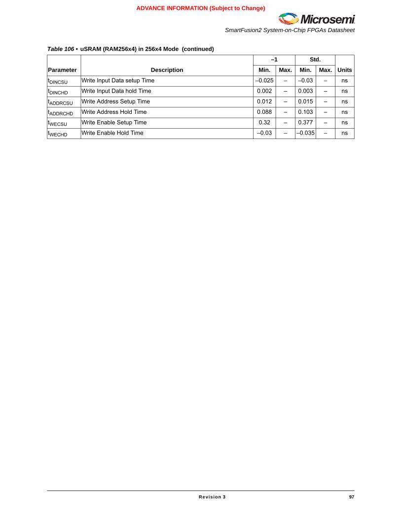
SmartFusion2 System-on-Chip FPGAs Datasheet
Revision 3 97
ADVANCE INFORMATION (Subject to Change)
tDINCSU Write Input Data setup Time –0.025 – –0.03 – ns
tDINCHD Write Input Data hold Time 0.002 – 0.003 – ns
tADDRCSU Write Address Setup Time 0.012 – 0.015 – ns
tADDRCHD Write Address Hold Time 0.088 – 0.103 – ns
tWECSU Write Enable Setup Time 0.32 – 0.377 – ns
tWECHD Write Enable Hold Time –0.03 – –0.035 – ns
Table 106 • uSRAM (RAM256x4) in 256x4 Mode (continued)
Parameter Description
–1 Std.
UnitsMin. Max. Min. Max.

SmartFusion2 DC and Switching Characteristics
98 Revision 3
ADVANCE INFORMATION (Subject to Change)
Table 107 • uSRAM (RAM128x8) in 128x8 Mode
Parameter Description
–1 Std.
UnitsMin. Max. Min. Max.
tCY Read Clock Period 0.836 – 0.984 – ns
tCLKMPWH Read Clock Minimum Pulse Width High 0.296 – 0.348 – ns
tCLKMPWL Read Clock Minimum pulse Width Low 0.324 – 0.382 – ns
tPLCY Read Pipelined clock period 1.989 – 2.34 – ns
tPLCLKMPWH Read Pipelined clock Minimum Pulse Width High 0.259 – 0.305 – ns
tPLCLKMPWL Read Pipelined clock Minimum Pulse Width Low 0.296 – 0.348 – ns
tCLPL1 Minimum pipelined clock low phase in order to prevent glitcheswith Pipelined Register in Latch mode
TBD – TBD – ns
tCLK2Q Read Access Time with Pipelined register – 0.37 – 0.435 ns
Read Access Time with Pipelined register in Latch mode – TBD – TBD ns
Read Access Time without Pipelined register – 1.898 – 2.233 ns
tADDRSU Read Address Setup Time in Synchronous mode 0.294 – 0.345 – ns
Read Address Setup Time in Asynchronous mode 1.791 – 2.107 – ns
tADDRHD Read Address Hold Time in Synchronous mode 0.101 – 0.119 – ns
Read Address Hold Time in Asynchronous mode 0.082 – 0.096 – ns
tRDENSU Read Enable Setup Time 0.245 – 0.289 – ns
tRDENHD Read Enable Hold Time 0.074 – 0.087 – ns
tBLKSU Read Block Select Setup Time (with pipelined register enabled) 1.901 – 2.237 – ns
tBLKHD Read Block Select Hold Time (with pipelined register enabled) 0.001 – 0.001 – ns
tBLK2Q Read Block Select to Out Disable Time (when pipelined register isdisabled)
– 2.211 – 2.601 ns
Read Block Select to Out Enable Time (when pipelined registeredis disabled)
– TBD – TBD ns
tBLKMPW Read Block Select Minimum Pulse Width TBD – TBD – ns
tRSTREM Read Asynchronous Reset Removal Time (pipelined clock) TBD – TBD – ns
Read Asynchronous Reset Removal Time (non-pipelined clock) TBD – TBD – ns
tRSTREC Read Asynchronous Reset Recovery Time (pipelined clock) 0.546 – 0.642 – ns
Read Asynchronous Reset Recovery Time (non-pipelined clock) 0.085 – 0.099 – ns
tR2Q Read Asynchronous Reset to Output Propagation Delay (withpipeline register enabled)
– 1.042 – 1.226 ns
Read Asynchronous Reset to Output Propagation Delay (withpipeline register disabled)
– 0.94 – 1.106 ns
tSRSTSU Read Synchronous Reset Setup Time 0.25 – 0.294 – ns
tSRSTHD Read Synchronous Reset Hold Time 0.074 – 0.087 – ns
tCCY Write Clock Period 1.49 – 1.752 – ns
tCCLKMPWH Write Clock Minimum Pulse Width High 0.506 – 0.596 – ns
tCCLKMPWL Write Clock Minimum Pulse Width Low 0.297 – 0.349 – ns
tBLKCSU Write Block Setup Time 0.332 – 0.39 – ns
tBLKCHD Write Block Hold Time –0.009 – –0.011 – ns
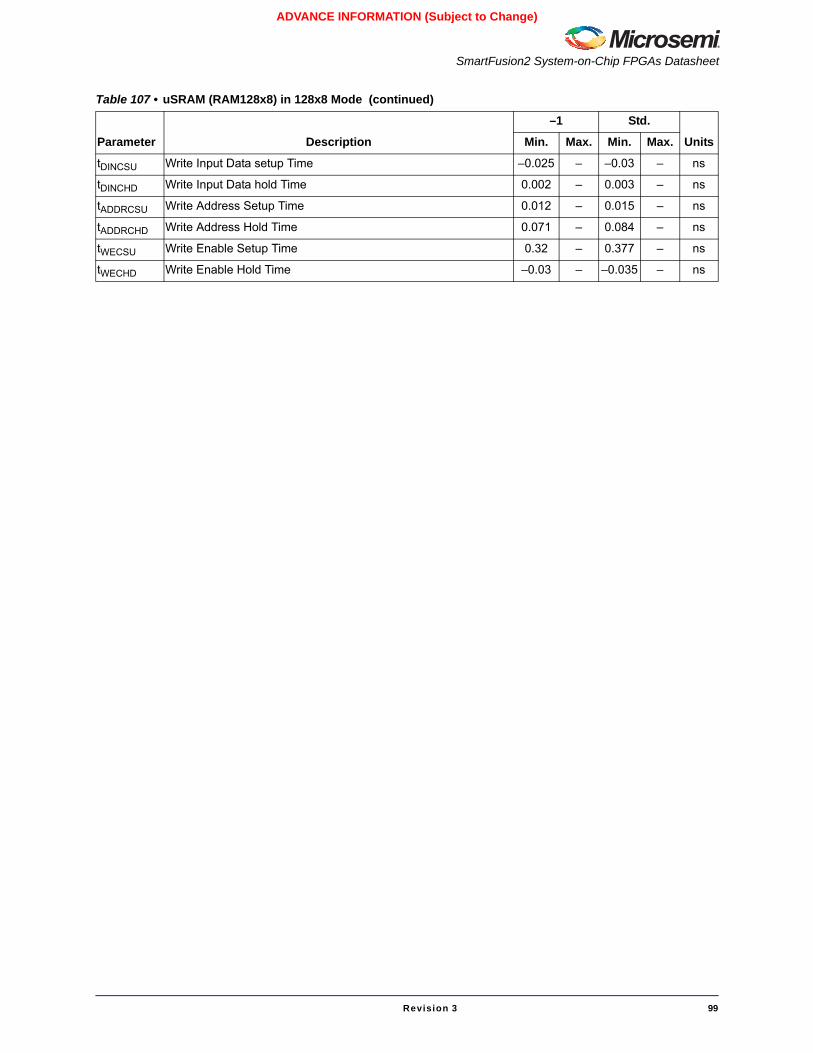
SmartFusion2 System-on-Chip FPGAs Datasheet
Revision 3 99
ADVANCE INFORMATION (Subject to Change)
tDINCSU Write Input Data setup Time –0.025 – –0.03 – ns
tDINCHD Write Input Data hold Time 0.002 – 0.003 – ns
tADDRCSU Write Address Setup Time 0.012 – 0.015 – ns
tADDRCHD Write Address Hold Time 0.071 – 0.084 – ns
tWECSU Write Enable Setup Time 0.32 – 0.377 – ns
tWECHD Write Enable Hold Time –0.03 – –0.035 – ns
Table 107 • uSRAM (RAM128x8) in 128x8 Mode (continued)
Parameter Description
–1 Std.
UnitsMin. Max. Min. Max.

SmartFusion2 DC and Switching Characteristics
100 Revision 3
ADVANCE INFORMATION (Subject to Change)
Table 108 • uSRAM (RAM128x9) in 128x9 Mode
Parameter Description
–1 Std.
UnitsMin. Max. Min. Max.
tCY Read Clock Period 0.836 – 0.984 – ns
tCLKMPWH Read Clock Minimum Pulse Width High 0.296 – 0.348 – ns
tCLKMPWL Read Clock Minimum pulse Width Low 0.324 – 0.382 – ns
tPLCY Read Pipelined clock period 1.989 – 2.34 – ns
tPLCLKMPWH Read Pipelined clock Minimum Pulse Width High 0.259 – 0.305 – ns
tPLCLKMPWL Read Pipelined clock Minimum Pulse Width Low 0.296 – 0.348 – ns
tCLPL1 Minimum pipelined clock low phase in order to prevent glitcheswith Pipelined Register in Latch mode
TBD – TBD – ns
tCLK2Q Read Access Time with Pipelined register – 0.37 – 0.435 ns
Read Access Time with Pipelined register in Latch mode – TBD – TBD ns
Read Access Time without Pipelined register – 1.898 – 2.233 ns
tADDRSU Read Address Setup Time in Synchronous mode 0.294 – 0.345 – ns
Read Address Setup Time in Asynchronous mode 1.791 – 2.107 – ns
tADDRHD Read Address Hold Time in Synchronous mode 0.101 – 0.119 – ns
Read Address Hold Time in Asynchronous mode 0.082 – 0.096 – ns
tRDENSU Read Enable Setup Time 0.245 – 0.289 – ns
tRDENHD Read Enable Hold Time 0.074 – 0.087 – ns
tBLKSU Read Block Select Setup Time (with pipelined register enabled) 1.901 – 2.237 – ns
tBLKHD Read Block Select Hold Time (with pipelined register enabled) 0.001 – 0.001 – ns
tBLK2Q Read Block Select to Out Disable Time (when pipelined register isdisabled)
– 2.211 – 2.601 ns
Read Block Select to Out Enable Time (when pipelined registeredis disabled)
– TBD – TBD ns
tBLKMPW Read Block Select Minimum Pulse Width TBD – TBD – ns
tRSTREM Read Asynchronous Reset Removal Time (pipelined clock) TBD – TBD – ns
Read Asynchronous Reset Removal Time (non-pipelined clock) TBD – TBD – ns
tRSTREC Read Asynchronous Reset Recovery Time (pipelined clock) 0.546 – 0.642 – ns
Read Asynchronous Reset Recovery Time (non-pipelined clock) 0.085 – 0.099 – ns
tR2Q Read Asynchronous Reset to Output Propagation Delay (withpipeline register enabled)
– 1.042 - 1.226 ns
Read Asynchronous Reset to Output Propagation Delay (withpipeline register disabled)
– 0.94 - 1.106 ns
tSRSTSU Read Synchronous Reset Setup Time 0.25 – 0.294 – ns
tSRSTHD Read Synchronous Reset Hold Time 0.074 – 0.087 – ns
tCCY Write Clock Period 1.49 – 1.752 – ns
tCCLKMPWH Write Clock Minimum Pulse Width High 0.506 – 0.596 – ns
tCCLKMPWL Write Clock Minimum Pulse Width Low 0.297 – 0.349 – ns
tBLKCSU Write Block Setup Time 0.332 – 0.39 – ns
tBLKCHD Write Block Hold Time –0.009 – –0.011 – ns

SmartFusion2 System-on-Chip FPGAs Datasheet
Revision 3 101
ADVANCE INFORMATION (Subject to Change)
tDINCSU Write Input Data setup Time –0.025 – –0.03 – ns
tDINCHD Write Input Data hold Time 0.002 – 0.003 – ns
tADDRCSU Write Address Setup Time 0.012 – 0.015 – ns
tADDRCHD Write Address Hold Time 0.071 – 0.084 – ns
tWECSU Write Enable Setup Time 0.32 – 0.377 – ns
tWECHD Write Enable Hold Time –0.03 – –0.035 – ns
Table 108 • uSRAM (RAM128x9) in 128x9 Mode (continued)
Parameter Description
–1 Std.
UnitsMin. Max. Min. Max.
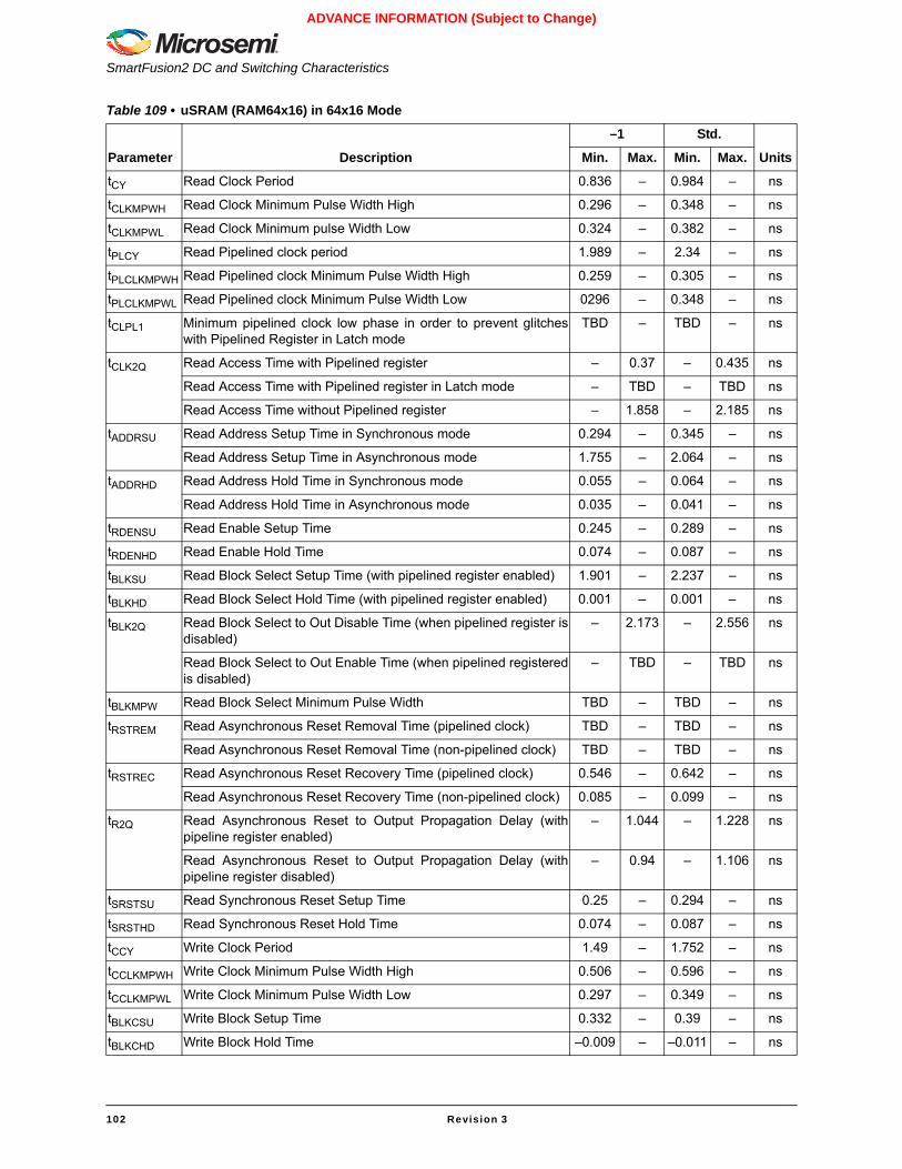
SmartFusion2 DC and Switching Characteristics
102 Revision 3
ADVANCE INFORMATION (Subject to Change)
Table 109 • uSRAM (RAM64x16) in 64x16 Mode
Parameter Description
–1 Std.
UnitsMin. Max. Min. Max.
tCY Read Clock Period 0.836 – 0.984 – ns
tCLKMPWH Read Clock Minimum Pulse Width High 0.296 – 0.348 – ns
tCLKMPWL Read Clock Minimum pulse Width Low 0.324 – 0.382 – ns
tPLCY Read Pipelined clock period 1.989 – 2.34 – ns
tPLCLKMPWH Read Pipelined clock Minimum Pulse Width High 0.259 – 0.305 – ns
tPLCLKMPWL Read Pipelined clock Minimum Pulse Width Low 0296 – 0.348 – ns
tCLPL1 Minimum pipelined clock low phase in order to prevent glitcheswith Pipelined Register in Latch mode
TBD – TBD – ns
tCLK2Q Read Access Time with Pipelined register – 0.37 – 0.435 ns
Read Access Time with Pipelined register in Latch mode – TBD – TBD ns
Read Access Time without Pipelined register – 1.858 – 2.185 ns
tADDRSU Read Address Setup Time in Synchronous mode 0.294 – 0.345 – ns
Read Address Setup Time in Asynchronous mode 1.755 – 2.064 – ns
tADDRHD Read Address Hold Time in Synchronous mode 0.055 – 0.064 – ns
Read Address Hold Time in Asynchronous mode 0.035 – 0.041 – ns
tRDENSU Read Enable Setup Time 0.245 – 0.289 – ns
tRDENHD Read Enable Hold Time 0.074 – 0.087 – ns
tBLKSU Read Block Select Setup Time (with pipelined register enabled) 1.901 – 2.237 – ns
tBLKHD Read Block Select Hold Time (with pipelined register enabled) 0.001 – 0.001 – ns
tBLK2Q Read Block Select to Out Disable Time (when pipelined register isdisabled)
– 2.173 – 2.556 ns
Read Block Select to Out Enable Time (when pipelined registeredis disabled)
– TBD – TBD ns
tBLKMPW Read Block Select Minimum Pulse Width TBD – TBD – ns
tRSTREM Read Asynchronous Reset Removal Time (pipelined clock) TBD – TBD – ns
Read Asynchronous Reset Removal Time (non-pipelined clock) TBD – TBD – ns
tRSTREC Read Asynchronous Reset Recovery Time (pipelined clock) 0.546 – 0.642 – ns
Read Asynchronous Reset Recovery Time (non-pipelined clock) 0.085 – 0.099 – ns
tR2Q Read Asynchronous Reset to Output Propagation Delay (withpipeline register enabled)
– 1.044 – 1.228 ns
Read Asynchronous Reset to Output Propagation Delay (withpipeline register disabled)
– 0.94 – 1.106 ns
tSRSTSU Read Synchronous Reset Setup Time 0.25 – 0.294 – ns
tSRSTHD Read Synchronous Reset Hold Time 0.074 – 0.087 – ns
tCCY Write Clock Period 1.49 – 1.752 – ns
tCCLKMPWH Write Clock Minimum Pulse Width High 0.506 – 0.596 – ns
tCCLKMPWL Write Clock Minimum Pulse Width Low 0.297 – 0.349 – ns
tBLKCSU Write Block Setup Time 0.332 – 0.39 – ns
tBLKCHD Write Block Hold Time –0.009 – –0.011 – ns

SmartFusion2 System-on-Chip FPGAs Datasheet
Revision 3 103
ADVANCE INFORMATION (Subject to Change)
tDINCSU Write Input Data setup Time 0.017 – 0.02 – ns
tDINCHD Write Input Data hold Time 0.002 – 0.003 – ns
tADDRCSU Write Address Setup Time 0.012 – 0.015 – ns
tADDRCHD Write Address Hold Time –0.043 – –0.05 – ns
tWECSU Write Enable Setup Time 0.32 – 0.377 – ns
tWECHD Write Enable Hold Time –0.03 – –0.035 – ns
Table 109 • uSRAM (RAM64x16) in 64x16 Mode (continued)
Parameter Description
–1 Std.
UnitsMin. Max. Min. Max.
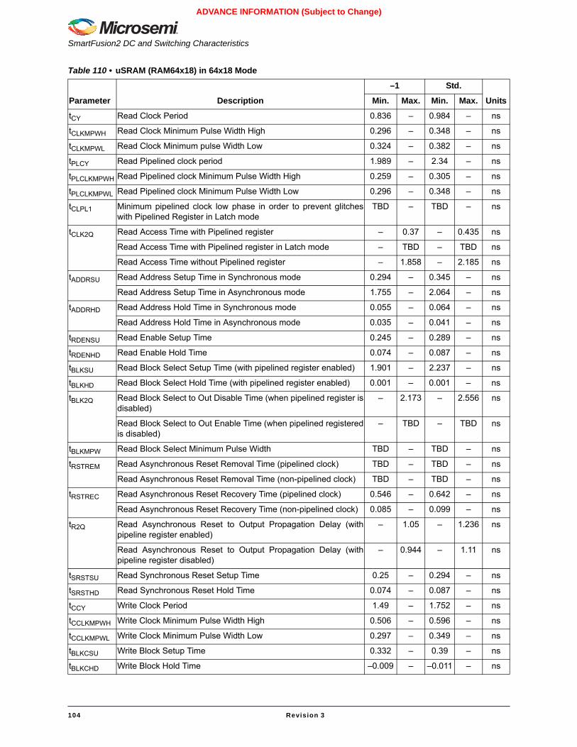
SmartFusion2 DC and Switching Characteristics
104 Revision 3
ADVANCE INFORMATION (Subject to Change)
Table 110 • uSRAM (RAM64x18) in 64x18 Mode
Parameter Description
–1 Std.
UnitsMin. Max. Min. Max.
tCY Read Clock Period 0.836 – 0.984 – ns
tCLKMPWH Read Clock Minimum Pulse Width High 0.296 – 0.348 – ns
tCLKMPWL Read Clock Minimum pulse Width Low 0.324 – 0.382 – ns
tPLCY Read Pipelined clock period 1.989 – 2.34 – ns
tPLCLKMPWH Read Pipelined clock Minimum Pulse Width High 0.259 – 0.305 – ns
tPLCLKMPWL Read Pipelined clock Minimum Pulse Width Low 0.296 – 0.348 – ns
tCLPL1 Minimum pipelined clock low phase in order to prevent glitcheswith Pipelined Register in Latch mode
TBD – TBD – ns
tCLK2Q Read Access Time with Pipelined register – 0.37 – 0.435 ns
Read Access Time with Pipelined register in Latch mode – TBD – TBD ns
Read Access Time without Pipelined register – 1.858 – 2.185 ns
tADDRSU Read Address Setup Time in Synchronous mode 0.294 – 0.345 – ns
Read Address Setup Time in Asynchronous mode 1.755 – 2.064 – ns
tADDRHD Read Address Hold Time in Synchronous mode 0.055 – 0.064 – ns
Read Address Hold Time in Asynchronous mode 0.035 – 0.041 – ns
tRDENSU Read Enable Setup Time 0.245 – 0.289 – ns
tRDENHD Read Enable Hold Time 0.074 – 0.087 – ns
tBLKSU Read Block Select Setup Time (with pipelined register enabled) 1.901 – 2.237 – ns
tBLKHD Read Block Select Hold Time (with pipelined register enabled) 0.001 – 0.001 – ns
tBLK2Q Read Block Select to Out Disable Time (when pipelined register isdisabled)
– 2.173 – 2.556 ns
Read Block Select to Out Enable Time (when pipelined registeredis disabled)
– TBD – TBD ns
tBLKMPW Read Block Select Minimum Pulse Width TBD – TBD – ns
tRSTREM Read Asynchronous Reset Removal Time (pipelined clock) TBD – TBD – ns
Read Asynchronous Reset Removal Time (non-pipelined clock) TBD – TBD – ns
tRSTREC Read Asynchronous Reset Recovery Time (pipelined clock) 0.546 – 0.642 – ns
Read Asynchronous Reset Recovery Time (non-pipelined clock) 0.085 – 0.099 – ns
tR2Q Read Asynchronous Reset to Output Propagation Delay (withpipeline register enabled)
– 1.05 – 1.236 ns
Read Asynchronous Reset to Output Propagation Delay (withpipeline register disabled)
– 0.944 – 1.11 ns
tSRSTSU Read Synchronous Reset Setup Time 0.25 – 0.294 – ns
tSRSTHD Read Synchronous Reset Hold Time 0.074 – 0.087 – ns
tCCY Write Clock Period 1.49 – 1.752 – ns
tCCLKMPWH Write Clock Minimum Pulse Width High 0.506 – 0.596 – ns
tCCLKMPWL Write Clock Minimum Pulse Width Low 0.297 – 0.349 – ns
tBLKCSU Write Block Setup Time 0.332 – 0.39 – ns
tBLKCHD Write Block Hold Time –0.009 – –0.011 – ns

SmartFusion2 System-on-Chip FPGAs Datasheet
Revision 3 105
ADVANCE INFORMATION (Subject to Change)
tDINCSU Write Input Data setup Time 0.017 – 0.02 – ns
tDINCHD Write Input Data hold Time 0.002 – 0.003 – ns
tADDRCSU Write Address Setup Time 0.012 – 0.015 – ns
tADDRCHD Write Address Hold Time –0.043 – –0.05 – ns
tWECSU Write Enable Setup Time 0.32 – 0.377 – ns
tWECHD Write Enable Hold Time –0.03 – –0.035 – ns
Table 110 • uSRAM (RAM64x18) in 64x18 Mode (continued)
Parameter Description
–1 Std.
UnitsMin. Max. Min. Max.
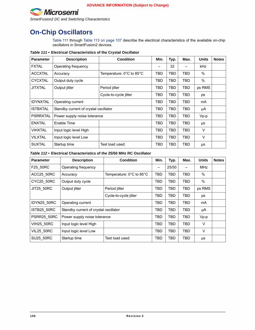
SmartFusion2 DC and Switching Characteristics
106 Revision 3
ADVANCE INFORMATION (Subject to Change)
On-Chip OscillatorsTable 111 through Table 113 on page 107 describe the electrical characteristics of the available on-chiposcillators in SmartFusion2 devices.
Table 111 • Electrical Characteristics of the Crystal Oscillator
Parameter Description Condition Min. Typ. Max. Units Notes
FXTAL Operating frequency – 32 – kHz
ACCXTAL Accuracy Temperature: 0°C to 85°C TBD TBD TBD %
CYCXTAL Output duty cycle TBD TBD TBD %
JITXTAL Output jitter Period jitter TBD TBD TBD ps RMS
Cycle-to-cycle jitter TBD TBD TBD ps
IDYNXTAL Operating current TBD TBD TBD mA
ISTBXTAL Standby current of crystal oscillator TBD TBD TBD µA
PSRRXTAL Power supply noise tolerance TBD TBD TBD Vp-p
ENXTAL Enable Time TBD TBD TBD µs
VIHXTAL Input logic level High TBD TBD TBD V
VILXTAL Input logic level Low TBD TBD TBD V
SUXTAL Startup time Test load used: TBD TBD TBD µs
Table 112 • Electrical Characteristics of the 25/50 MHz RC Oscillator
Parameter Description Condition Min. Typ. Max. Units Notes
F25_50RC Operating frequency – 25/50 – MHz
ACC25_50RC Accuracy Temperature: 0°C to 85°C TBD TBD TBD %
CYC25_50RC Output duty cycle TBD TBD TBD %
JIT25_50RC Output jitter Period jitter TBD TBD TBD ps RMS
Cycle-to-cycle jitter TBD TBD TBD ps
IDYN25_50RC Operating current TBD TBD TBD mA
ISTB25_50RC Standby current of crystal oscillator TBD TBD TBD µA
PSRR25_50RC Power supply noise tolerance TBD TBD TBD Vp-p
VIH25_50RC Input logic level High TBD TBD TBD V
VIL25_50RC Input logic level Low TBD TBD TBD V
SU25_50RC Startup time Test load used: TBD TBD TBD µs
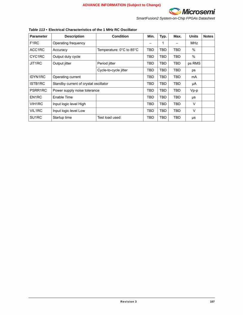
SmartFusion2 System-on-Chip FPGAs Datasheet
Revision 3 107
ADVANCE INFORMATION (Subject to Change)
Table 113 • Electrical Characteristics of the 1 MHz RC Oscillator
Parameter Description Condition Min. Typ. Max. Units Notes
F1RC Operating frequency – 1 – MHz
ACC1RC Accuracy Temperature: 0°C to 85°C TBD TBD TBD %
CYC1RC Output duty cycle TBD TBD TBD %
JIT1RC Output jitter Period jitter TBD TBD TBD ps RMS
Cycle-to-cycle jitter TBD TBD TBD ps
IDYN1RC Operating current TBD TBD TBD mA
ISTB1RC Standby current of crystal oscillator TBD TBD TBD µA
PSRR1RC Power supply noise tolerance TBD TBD TBD Vp-p
EN1RC Enable Time TBD TBD TBD µs
VIH1RC Input logic level High TBD TBD TBD V
VIL1RC Input logic level Low TBD TBD TBD V
SU1RC Startup time Test load used: TBD TBD TBD µs
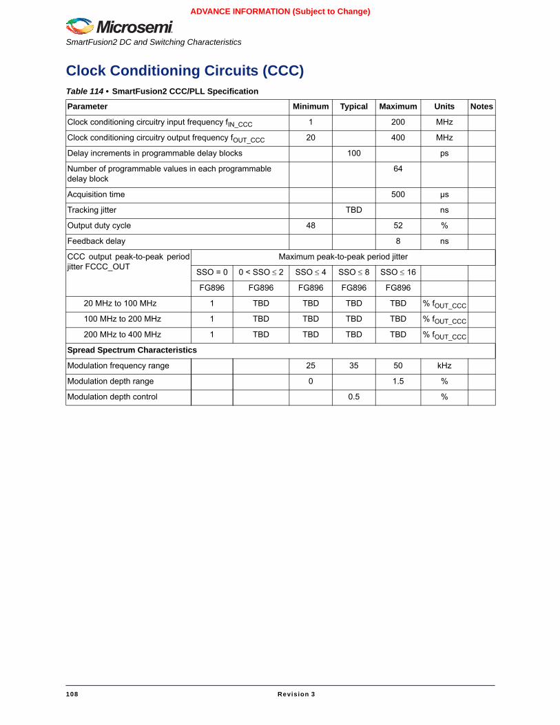
SmartFusion2 DC and Switching Characteristics
108 Revision 3
ADVANCE INFORMATION (Subject to Change)
Clock Conditioning Circuits (CCC)Table 114 • SmartFusion2 CCC/PLL Specification
Parameter Minimum Typical Maximum Units Notes
Clock conditioning circuitry input frequency fIN_CCC 1 200 MHz
Clock conditioning circuitry output frequency fOUT_CCC 20 400 MHz
Delay increments in programmable delay blocks 100 ps
Number of programmable values in each programmable delay block
64
Acquisition time 500 µs
Tracking jitter TBD ns
Output duty cycle 48 52 %
Feedback delay 8 ns
CCC output peak-to-peak periodjitter FCCC_OUT
Maximum peak-to-peak period jitter
SSO = 0 0 < SSO ≤ 2 SSO ≤ 4 SSO ≤ 8 SSO ≤ 16
FG896 FG896 FG896 FG896 FG896
20 MHz to 100 MHz 1 TBD TBD TBD TBD % fOUT_CCC
100 MHz to 200 MHz 1 TBD TBD TBD TBD % fOUT_CCC
200 MHz to 400 MHz 1 TBD TBD TBD TBD % fOUT_CCC
Spread Spectrum Characteristics
Modulation frequency range 25 35 50 kHz
Modulation depth range 0 1.5 %
Modulation depth control 0.5 %
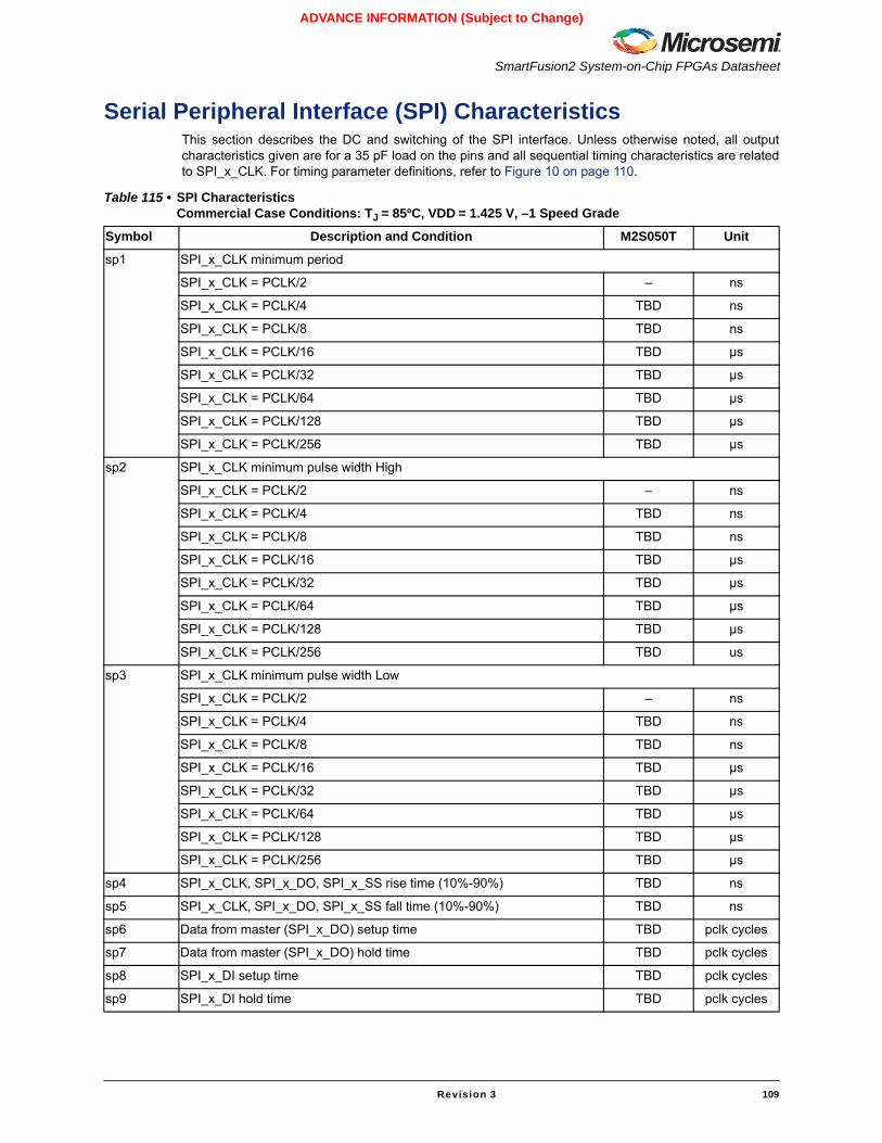
SmartFusion2 System-on-Chip FPGAs Datasheet
Revision 3 109
ADVANCE INFORMATION (Subject to Change)
Serial Peripheral Interface (SPI) CharacteristicsThis section describes the DC and switching of the SPI interface. Unless otherwise noted, all outputcharacteristics given are for a 35 pF load on the pins and all sequential timing characteristics are relatedto SPI_x_CLK. For timing parameter definitions, refer to Figure 10 on page 110.
Table 115 • SPI CharacteristicsCommercial Case Conditions: TJ = 85ºC, VDD = 1.425 V, –1 Speed Grade
Symbol Description and Condition M2S050T Unit
sp1 SPI_x_CLK minimum period
SPI_x_CLK = PCLK/2 – ns
SPI_x_CLK = PCLK/4 TBD ns
SPI_x_CLK = PCLK/8 TBD ns
SPI_x_CLK = PCLK/16 TBD µs
SPI_x_CLK = PCLK/32 TBD µs
SPI_x_CLK = PCLK/64 TBD µs
SPI_x_CLK = PCLK/128 TBD µs
SPI_x_CLK = PCLK/256 TBD µs
sp2 SPI_x_CLK minimum pulse width High
SPI_x_CLK = PCLK/2 – ns
SPI_x_CLK = PCLK/4 TBD ns
SPI_x_CLK = PCLK/8 TBD ns
SPI_x_CLK = PCLK/16 TBD µs
SPI_x_CLK = PCLK/32 TBD µs
SPI_x_CLK = PCLK/64 TBD µs
SPI_x_CLK = PCLK/128 TBD µs
SPI_x_CLK = PCLK/256 TBD us
sp3 SPI_x_CLK minimum pulse width Low
SPI_x_CLK = PCLK/2 – ns
SPI_x_CLK = PCLK/4 TBD ns
SPI_x_CLK = PCLK/8 TBD ns
SPI_x_CLK = PCLK/16 TBD µs
SPI_x_CLK = PCLK/32 TBD µs
SPI_x_CLK = PCLK/64 TBD µs
SPI_x_CLK = PCLK/128 TBD µs
SPI_x_CLK = PCLK/256 TBD µs
sp4 SPI_x_CLK, SPI_x_DO, SPI_x_SS rise time (10%-90%) TBD ns
sp5 SPI_x_CLK, SPI_x_DO, SPI_x_SS fall time (10%-90%) TBD ns
sp6 Data from master (SPI_x_DO) setup time TBD pclk cycles
sp7 Data from master (SPI_x_DO) hold time TBD pclk cycles
sp8 SPI_x_DI setup time TBD pclk cycles
sp9 SPI_x_DI hold time TBD pclk cycles
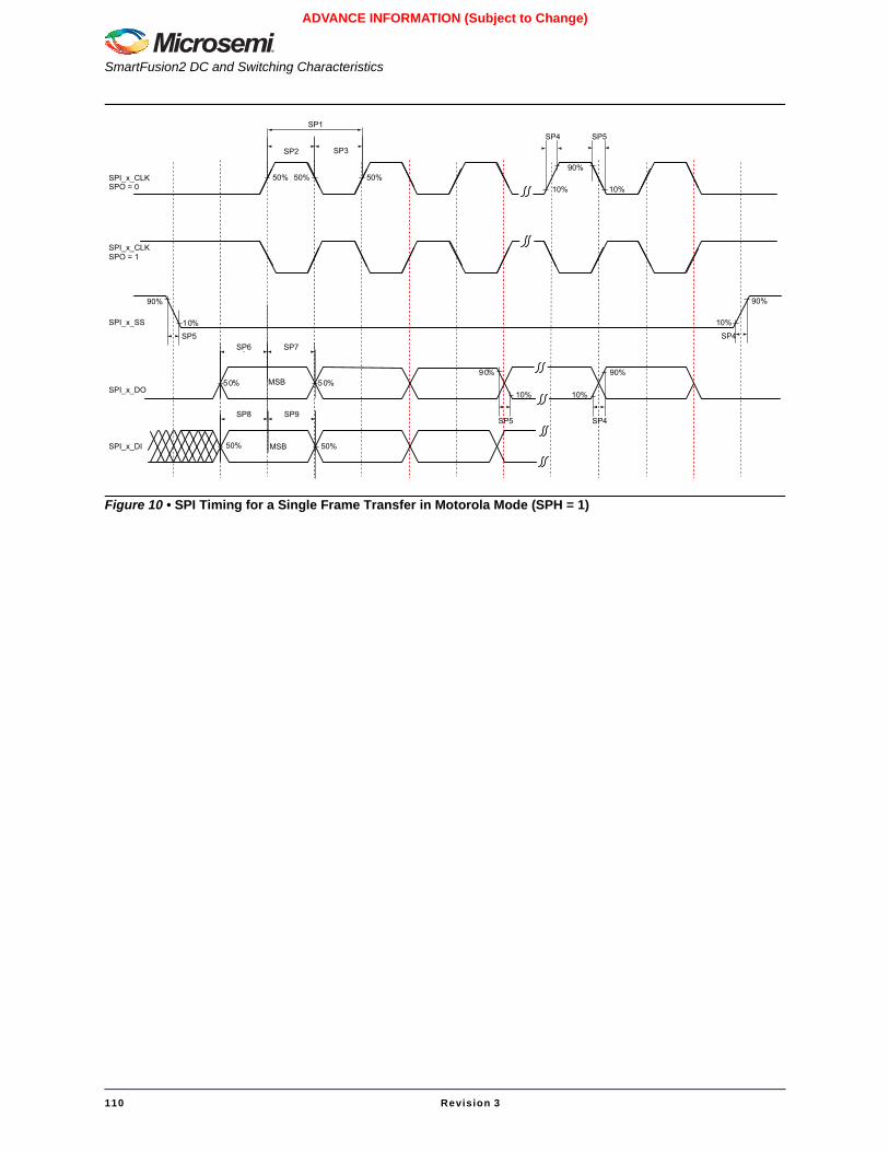
SmartFusion2 DC and Switching Characteristics
110 Revision 3
ADVANCE INFORMATION (Subject to Change)
Figure 10 • SPI Timing for a Single Frame Transfer in Motorola Mode (SPH = 1)
SPI_x_CLKSPO = 0
SPI_x_DO
SP6 SP7
50%50% MSB
50% 50% 50%
SP2
SP1
90%
10% 10%
SP4 SP5
SP8 SP9
50%50% MSBSPI_x_DI
10%
90%
SP5
90%
10%
SP4
90%
10%10%
SP4SP5
90%
SPI_x_SS
SPI_x_CLKSPO = 1
SP3
SmartFusion2 System-on-Chip FPGAs Datasheet
Revision 3 111
ADVANCE INFORMATION (Subject to Change)
Inter-Integrated Circuit (I2C) CharacteristicsThis section describes the DC and switching of the I2C interface. Unless otherwise noted, all outputcharacteristics given are for a 100 pF load on the pins. For timing parameter definitions, refer toFigure 11 on page 112.
Table 116 • I2C CharacteristicsCommercial Case Conditions: TJ = 85ºC, VDD = 1.14 V, –1 Speed Grade
Parameter Definition Condition Value Unit
VIL Minimum input low voltage – See Table 19 onpage 29
–
Maximum input low voltage – See Table 19 –
VIH Minimum input high voltage – See Table 19 –
Maximum input high voltage – See Table 19 –
VOL Maximum output voltage low IOL = TBD See Table 19 –
IIL Input current High – See Table 19 –
IIH Input current Low – See Table 19 –
Vhyst Hysteresis of Schmitt triggerinputs
– See Table 18 onpage 28
V
TFALL Fall time VIHmin to VILMax, Cload = 400 pF TBD ns
VIHmin to VILMax, Cload = 100 pF TBD ns
TRISE Rise time VILMax to VIHmin, Cload = 400 pF TBD ns
VILMax to VIHmin, Cload = 100 pF TBD ns
Cin Pin capacitance VIN = 0, f = 1.0 MHz TBD pF
Rpull-up Output buffer maximum pull-down resistance
– TBD Ω
Rpull-down Output buffer maximum pull-upresistance
– TBD Ω
Dmax Maximum data rate Fast mode TBD Kbps
tLOW Low period of I2C_x_SCL – TBD pclk cycles
tHIGH High period of I2C_x_SCL – TBD pclk cycles
tHD;STA START hold time – TBD pclk cycles
tSU;STA START setup time – TBD pclk cycles
tHD;DAT DATA hold time – TBD pclk cycles
tSU;DAT DATA setup time – TBD pclk cycles
tSU;STO STOP setup time – TBD pclk cycles
tFILT Maximum spike width filtered – TBD ns
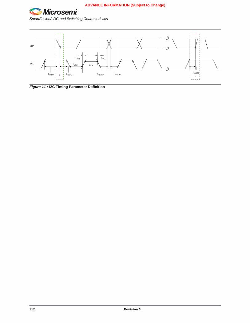
SmartFusion2 DC and Switching Characteristics
112 Revision 3
ADVANCE INFORMATION (Subject to Change)
Figure 11 • I2C Timing Parameter Definition
SCL
TRISE TFALL
tLOW
tHD;STA
SDA
tHIGH
tHD;DAT tSU;DATtSU;STOtSU;STA S
P
Revision 3 113
Datasheet Information
List of ChangesThe following table lists critical changes that were made in each revision of the datasheet.
Revision Changes Page
Revision 3(February 2013)
SmartFusion2 product brief and pin information has been removed from the datasheetand published in separate documents: SmartFusion2 Product Brief and SmartFusion2Pin Descriptions (SAR 45184).
N/A
Revision 2(February 2013)
Table 1 • Absolute Maximum Ratings and Table 2 • Recommended OperatingConditions were updated with the new pin names and latest values (SAR 45081).
7, 8
The storage temperature minimum value was added to Table 1 • Absolute MaximumRatings, including a note with references to additional tables (SAR 44887).
7
In EQ 1 , TJ – θA was corrected to TJ – TA (SAR 44109). 10
Timing tables were updated with respect to slew and configuration. AC and DCspecifications were placed in separate tables. Values were added to replace TBD in anumber of tables in the "User I/O Characteristics" section (SAR 44471).
24
The termination scheme for the differential I/O test setup in the "Output Buffer and ACLoading" section was corrected (SAR 43591).
25
The worst commercial-case conditions for Table 27 • LVCMOS 2.5 V ReceiverCharacteristics were changed from VDDI = 3.0 V to VDDI = 2.375 V (SAR 44471).
32
The following tables were revised to remove typical and minimum Fmax values andchange maximum Fmax values (SAR 44471):Table 68 • LVDS DC Voltage SpecificationTable 80 • Mini-LVDS DC Voltage SpecificationTable 84 • RSDS DC Voltage Specification
636971
Table 99 • RAM1K18 – Dual-Port Mode for Depth × Width Configuration 2k × 9through Table 102 • RAM1K18 – Dual-Port Mode for Depth × Width Configuration 16k× 1 are new (SAR 44471).
87 to 90
Table 104 • uSRAM (RAM1024x1) in 1024x1 Mode through Table 109 • uSRAM(RAM64x16) in 64x16 Mode are new (SAR 44471).
92 to 102
Revision 1(January 2013)
Table 1 • Absolute Maximum Ratings is new. In Table 2 • Recommended OperatingConditions, the expression "VDDI0" in the values for VREFx was corrected to"VDDIx." VCCENVM was corrected to VPPNVM (SAR 42461). VDDIx was defineddifferently for different types of I/O banks (SAR 43850).
7, 8
The "Power Supply Sequencing and Power-On Reset (Commercial and Industrial)"section was revised to correct the available ramp rate options from "50 µs, 100 µs,1 ms, and 100 ms" to "50 µs, 1 ms, 10 ms, and 100 ms." Each selection representsthe maximum ramp rate to apply to VDD and VPP. The user can set the ramp ratesetting using Libero SOC (SARs 41970, 42401).
9
The units for input leakage current (IIL/IIH) were corrected from mA to µA in the DCvoltage tables (SAR 43848).
29 to 41
A note to reference IBIS models for a detailed I/V curve was added to transmitter drivestrength tables for LVTTL/LVCMOS 3.3 V through LVCMOS 1.2 V (SAR 42171). Formore information, refer to the IBIS Models: Background and Usage application note.
30 to 41
Datasheet Information
114 Revision 3
Datasheet CategoriesCategoriesIn order to provide the latest information to designers, some datasheet parameters are published beforedata has been fully characterized from silicon devices. The data provided for a given device, ashighlighted in Table 1 on page 1 is designated as either "Product Brief," "Advance," "Preliminary," or"Production." The definitions of these categories are as follows:
Product BriefThe product brief is a summarized version of a datasheet (advance or production) and contains generalproduct information. This document gives an overview of specific device and family information.
AdvanceThis version contains initial estimated information based on simulation, other products, devices, or speedgrades. This information can be used as estimates, but not for production. This label only applies to theDC and Switching Characteristics chapter of the datasheet and will only be used when the data has notbeen fully characterized.
PreliminaryThe datasheet contains information based on simulation and/or initial characterization. The information isbelieved to be correct, but changes are possible.
ProductionThis version contains information that is considered to be final.
Export Administration Regulations (EAR) The products described in this document are subject to the Export Administration Regulations (EAR).They could require an approved export license prior to export from the United States. An export includesrelease of product or disclosure of technology to a foreign national inside or outside the United States.
Safety Critical, Life Support, and High-Reliability Applications Policy
The products described in this advance status document may not have completed the Microsemiqualification process. Products may be amended or enhanced during the product introduction andqualification process, resulting in changes in device functionality or performance. It is the responsibility ofeach customer to ensure the fitness of any product (but especially a new product) for a particularpurpose, including appropriateness for safety-critical, life-support, and other high-reliability applications.Consult the Microsemi SoC Products Group Terms and Conditions for specific liability exclusions relatingto life-support applications. A reliability report covering all of the SoC Products Group’s products isavailable at http://www.microsemi.com/soc/documents/ORT_Report.pdf. Microsemi also offers a varietyof enhanced qualification and lot acceptance screening procedures. Contact your local sales office foradditional reliability information.


51700115-3/2.13
© 2013 Microsemi Corporation. All rights reserved. Microsemi and the Microsemi logo are trademarks ofMicrosemi Corporation. All other trademarks and service marks are the property of their respective owners.
Microsemi Corporation (NASDAQ: MSCC) offers a comprehensive portfolio of semiconductorsolutions for: aerospace, defense and security; enterprise and communications; and industrialand alternative energy markets. Products include high-performance, high-reliability analog andRF devices, mixed signal and RF integrated circuits, customizable SoCs, FPGAs, andcomplete subsystems. Microsemi is headquartered in Aliso Viejo, Calif. Learn more atwww.microsemi.com.
Microsemi Corporate HeadquartersOne Enterprise, Aliso Viejo CA 92656 USAWithin the USA: +1 (949) 380-6100Sales: +1 (949) 380-6136Fax: +1 (949) 215-4996
Mouser Electronics
Authorized Distributor
Click to View Pricing, Inventory, Delivery & Lifecycle Information: Microchip:
M2S005-FG484 M2S010-FG484 M2S050T-FG896
Related Documents