SM34020A GRAPHICS SYSTEM PROCESSOR SGUS057 - FEBRUARY 2005 1 POST OFFICE BOX 1443 • HOUSTON, TEXAS 77251-1443 D Class B High-Reliability Processing D 1-µm CMOS Technology D Military Operating Temperature Range -40°C to 110°C D SM34020A-32/40 125 / 100-ns Instruction Cycle Time D Fully Programmable 32-Bit General-Purpose Processor With 512-Megabyte Linear Address Range (Bit Addressable) D Second-Generation Graphics System Processor - Object-Code Compatible With the SMJ34010 - Enhanced Instruction Set - Optimized Graphics Instructions - Coprocessor Interface D Pixel Processing, XY Addressing, and Window Checking Built Into the Instruction Set D Programmable 1-, 2-, 4-, 8-, 16-, or 32-Bit Pixel Size With 16 Boolean and Six Arithmetic Pixel Processing Options (Raster Ops) D 512-Byte LRU On-Chip Instruction Cache D Optimized DRAM / VRAM Interface - Page-Mode for Burst Memory Operations - Dynamic Bus Sizing (16-Bit and 32-Bit Transfers) - Byte-Oriented CAS Strobes D Flexible Host Processor Interface - Supports Host Transfers - Direct Access to All of the SMJ34020A Address Space - Implicit Addressing - Prefetch for Enhanced Read Access D Programmable CRT Control - Composite Sync Mode - Separate Sync Mode - Synchronization to External Sync D Direct Support for Special Features of 1M VRAMs - Load Write Mask - Load Color Mask - Block Write - Write Using the Write Mask D Flexible Multi-Processor Interface D Packaging Options - 145-Pin Grid Array Ceramic Package (GB Suffix) description The SM34020A graphics system processor (GSP) is the second generation of an advanced high-performance CMOS 32-bit microprocessor optimized for graphics display systems. With a built-in instruction cache, the ability to simultaneously access memory and registers, and an instruction set designed to expedite raster graphics operations, the SM34020A provides user-programmable control of the CRT interface as well as the memory interface (both standard DRAM and multiport video RAM). The 4-gigabit (512-megabyte) physical address space is addressable on bit boundaries using variable width data fields (1 to 32 bits). Additional graphics addressing modes support 1-, 2-, 4-, 8-, 16- and 32-bit wide pixels. 145-PIN GRID ARRAY PACKAGE ( TOP VIEW ) A B C D E F G H J K L M N P R 1 2 3 4 5 6 7 8 9 10 11 12 13 14 15 132-PIN QUAD FLATPACK ( TOP VIEW ) PRODUCTION DATA information is current as of publication date. Products conform to specifications per the terms of Texas Instruments standard warranty. Production processing does not necessarily include testing of all parameters. Copyright 2004, Texas Instruments Incorporated Please be aware that an important notice concerning availability, standard warranty, and use in critical applications of Texas Instruments semiconductor products and disclaimers thereto appears at the end of this data sheet. On products compliant to MILĆPRFĆ38535, all parameters are tested unless otherwise noted. On all other products, production processing does not necessarily include testing of all parameters. Not Recommended for New Designs

Welcome message from author
This document is posted to help you gain knowledge. Please leave a comment to let me know what you think about it! Share it to your friends and learn new things together.
Transcript
������������ � ������ � ����
SGUS057 − FEBRUARY 2005
1POST OFFICE BOX 1443 • HOUSTON, TEXAS 77251−1443
� Class B High-Reliability Processing
� 1-µm CMOS Technology
� Military Operating Temperature Range−40°C to 110°C
� SM34020A-32/40125/100-ns Instruction Cycle Time
� Fully Programmable 32-BitGeneral-Purpose Processor With512-Megabyte Linear Address Range(Bit Addressable)
� Second-Generation Graphics SystemProcessor− Object-Code Compatible With the
SMJ34010− Enhanced Instruction Set− Optimized Graphics Instructions− Coprocessor Interface
� Pixel Processing, XY Addressing, andWindow Checking Built Into the InstructionSet
� Programmable 1-, 2-, 4-, 8-, 16-, or 32-BitPixel Size With 16 Boolean and SixArithmetic Pixel Processing Options(Raster Ops)
� 512-Byte LRU On-Chip Instruction Cache
� Optimized DRAM/VRAM Interface− Page-Mode for Burst Memory Operations− Dynamic Bus Sizing (16-Bit and
32-Bit Transfers)− Byte-Oriented CAS Strobes
� Flexible Host Processor Interface− Supports Host Transfers− Direct Access to All of the SMJ34020A
Address Space− Implicit Addressing− Prefetch for Enhanced Read Access
� Programmable CRT Control− Composite Sync Mode− Separate Sync Mode− Synchronization to External Sync
� Direct Support for Special Features of1M VRAMs− Load Write Mask− Load Color Mask− Block Write− Write Using the Write Mask
� Flexible Multi-Processor Interface� Packaging Options
− 145-Pin Grid Array Ceramic Package(GB Suffix)
description
The SM34020A graphics system processor (GSP) is the second generation of an advanced high-performanceCMOS 32-bit microprocessor optimized for graphics display systems. With a built-in instruction cache, the abilityto simultaneously access memory and registers, and an instruction set designed to expedite raster graphicsoperations, the SM34020A provides user-programmable control of the CRT interface as well as the memoryinterface (both standard DRAM and multiport video RAM). The 4-gigabit (512-megabyte) physical addressspace is addressable on bit boundaries using variable width data fields (1 to 32 bits). Additional graphicsaddressing modes support 1-, 2-, 4-, 8-, 16- and 32-bit wide pixels.
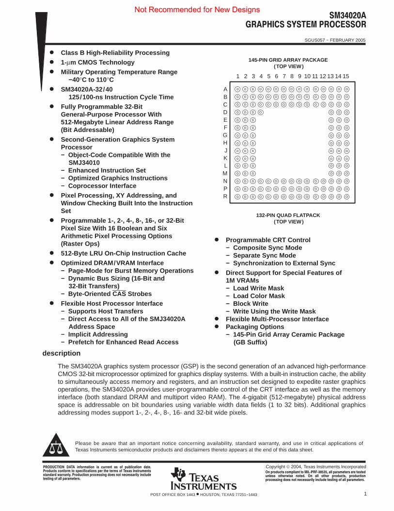
145-PIN GRID ARRAY PACKAGE(TOP VIEW)
ABCDEFGHJKLMNPR
1 2 3 4 5 6 7 8 9 10 11 12 13 14 15
132-PIN QUAD FLATPACK(TOP VIEW)
��� ���� ���� ����������� �� ����!�� �� �� "�#$������� %��!&��%���� ������� �� �"!����������� "!� �'! �!��� �� �!(�� �������!�������%��% )������*& ��%������ "���!����+ %�!� ��� �!�!�����$* ���$�%!�!����+ �� �$$ "����!�!��&
Copyright 2004, Texas Instruments Incorporated
Please be aware that an important notice concerning availability, standard warranty, and use in critical applications ofTexas Instruments semiconductor products and disclaimers thereto appears at the end of this data sheet.
�� "��%���� ���"$���� �� ��,-.-�/0�01 �$$ "����!�!�� ��! �!��!%��$!�� ��'!�)��! ���!%& �� �$$ ��'!� "��%����1 "��%������"���!����+ %�!� ��� �!�!�����$* ���$�%! �!����+ �� �$$ "����!�!��&
Not Recommended for New Designs
������������ � ������ � ����
SGUS057 − FEBRUARY 2005
2 POST OFFICE BOX 1443 • HOUSTON, TEXAS 77251−1443
architecture
The SM34020A is a CMOS 32-bit processor with hardware support for graphics operations such as pixel blocktransfers (PIXBLTS) during raster operations and curve-drawing algorithms. Also included is a complete set ofgeneral-purpose instructions with addressing modes tuned to support high-level languages. In addition to itsability to address a large external memory range, the SM34020A contains 30 general-purpose 32-bit registers,a hardware stack pointer, and a 512-byte instruction cache. On-chip functions include 64 programmable I/Oregisters that control CRT timing, input /output control, and parameters required by some instructions. TheSM34020A directly interfaces to DRAMs and VRAMs and generates raster control signals. The SM34020A canbe configured to operate as a standalone processor, or it can be used as a graphics engine with a host system.The host interface provides a generalized communication port for any standard host processor. The SM34020Aalso accommodates a multiprocessing or direct memory access (DMA) environment through the request/grantinterface protocols. Virtual memory systems are supported through bus-fault detection and instructioncontinuation.
The SM34020A provides single-cycle execution of general-purpose instructions and most common integerarithmetic and Boolean operations from its instruction cache. Additionally, the SM34020A incorporates ahardware barrel shifter that provides a single-state bidirectional shift-and-rotate function for 1 to 32 bits.
The local-memory controller is designed to optimize memory access operations. It also supports pipelinememory write operations of variable-sized fields and allows memory access and instruction execution inparallel.
The SM34020A graphics-processing hardware supports pixel and pixel-array processing capabilities for bothmonochrome and color systems at a variety of pixel sizes. The hardware incorporates two-operand andthree-operand raster operations with Boolean and arithmetic operations, XY addressing, window clipping,window-checking operations, 1 to n bits-per-pixel transforms, transparency, and plane masking. Thearchitecture further supports operations on single pixel transfer (PIXT) instructions or on two-dimensionalarrays of arbitrary size (PIXBLTS).
The SM34020A flexible graphics-processing capabilities allow software-based graphics algorithms withoutsacrificing performance. These algorithms include clipping to arbitrary window size, custom incremental-curvedrawing, two-operand raster operations, and masked two-operand raster operations.
The SM34020A provides for extensions to the basic architecture through the coprocessor interface. Specialinstructions and cycle timings are included to enhance data flow to coprocessors without requiring thecoprocessor to decode the instruction stream, generate system addresses, or move data for the coprocessorthrough the SM34020A.
Table 1. Orderable Parts
ORDERABLE PART NUMBER INSTRUCTION CYCLE TEMPERATURE RANGE
SM34020AGBS40 100 ns −40°C to 110C
SM34020AGBS32† 125 ns −40°C to 110C
† Potential release
Not Recommended for New Designs
������������ � ������ � ����
SGUS057 − FEBRUARY 2005
3POST OFFICE BOX 1443 • HOUSTON, TEXAS 77251−1443
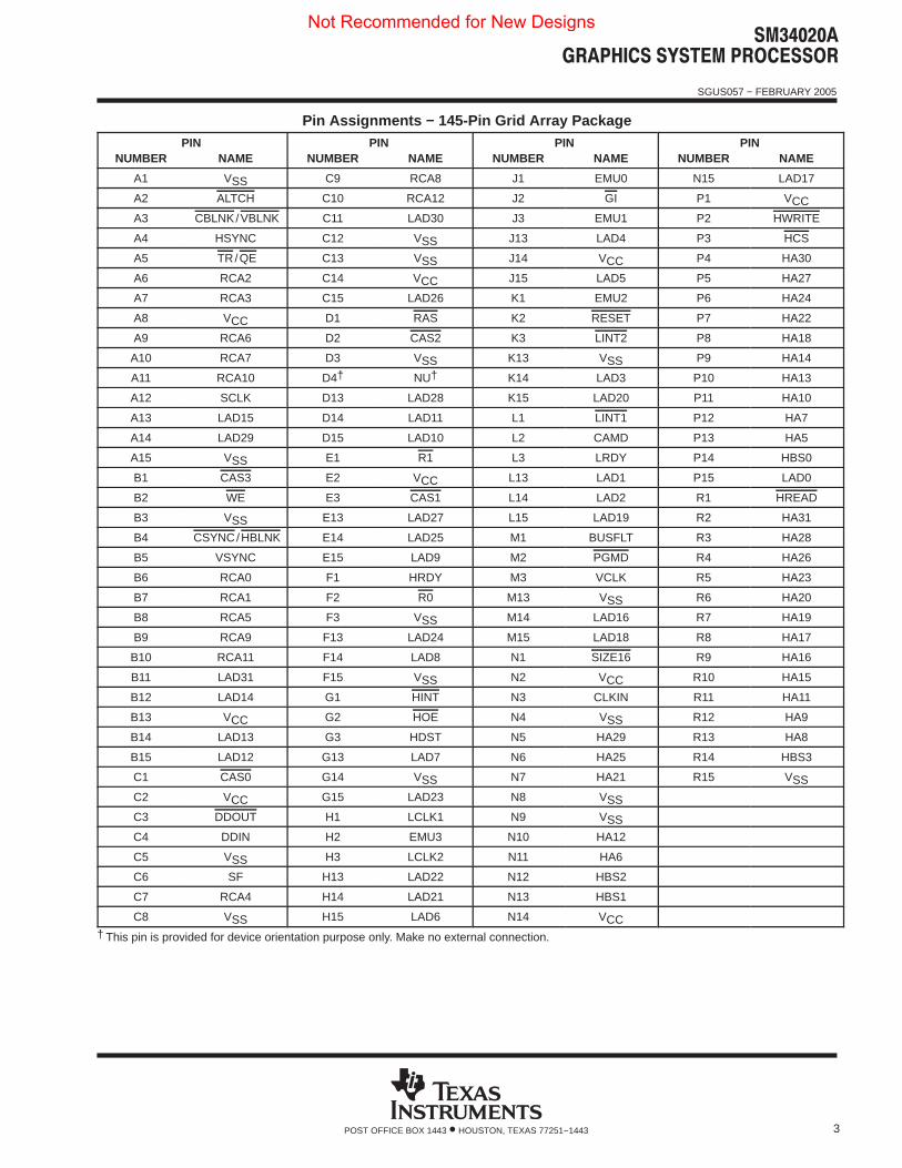
Pin Assignments − 145-Pin Grid Array PackagePIN PIN PIN PIN
NUMBER NAME NUMBER NAME NUMBER NAME NUMBER NAME
A1 VSS C9 RCA8 J1 EMU0 N15 LAD17
A2 ALTCH C10 RCA12 J2 GI P1 VCC
A3 CBLNK/VBLNK C11 LAD30 J3 EMU1 P2 HWRITE
A4 HSYNC C12 VSS J13 LAD4 P3 HCS
A5 TR/QE C13 VSS J14 VCC P4 HA30
A6 RCA2 C14 VCC J15 LAD5 P5 HA27
A7 RCA3 C15 LAD26 K1 EMU2 P6 HA24
A8 VCC D1 RAS K2 RESET P7 HA22
A9 RCA6 D2 CAS2 K3 LINT2 P8 HA18
A10 RCA7 D3 VSS K13 VSS P9 HA14
A11 RCA10 D4† NU† K14 LAD3 P10 HA13
A12 SCLK D13 LAD28 K15 LAD20 P11 HA10
A13 LAD15 D14 LAD11 L1 LINT1 P12 HA7
A14 LAD29 D15 LAD10 L2 CAMD P13 HA5
A15 VSS E1 R1 L3 LRDY P14 HBS0
B1 CAS3 E2 VCC L13 LAD1 P15 LAD0
B2 WE E3 CAS1 L14 LAD2 R1 HREAD
B3 VSS E13 LAD27 L15 LAD19 R2 HA31
B4 CSYNC/HBLNK E14 LAD25 M1 BUSFLT R3 HA28
B5 VSYNC E15 LAD9 M2 PGMD R4 HA26
B6 RCA0 F1 HRDY M3 VCLK R5 HA23
B7 RCA1 F2 R0 M13 VSS R6 HA20
B8 RCA5 F3 VSS M14 LAD16 R7 HA19
B9 RCA9 F13 LAD24 M15 LAD18 R8 HA17
B10 RCA11 F14 LAD8 N1 SIZE16 R9 HA16
B11 LAD31 F15 VSS N2 VCC R10 HA15
B12 LAD14 G1 HINT N3 CLKIN R11 HA11
B13 VCC G2 HOE N4 VSS R12 HA9
B14 LAD13 G3 HDST N5 HA29 R13 HA8
B15 LAD12 G13 LAD7 N6 HA25 R14 HBS3
C1 CAS0 G14 VSS N7 HA21 R15 VSS
C2 VCC G15 LAD23 N8 VSSC3 DDOUT H1 LCLK1 N9 VSS
C4 DDIN H2 EMU3 N10 HA12
C5 VSS H3 LCLK2 N11 HA6
C6 SF H13 LAD22 N12 HBS2
C7 RCA4 H14 LAD21 N13 HBS1
C8 VSS H15 LAD6 N14 VCC† This pin is provided for device orientation purpose only. Make no external connection.
Not Recommended for New Designs
������������ � ������ � ����
SGUS057 − FEBRUARY 2005
4 POST OFFICE BOX 1443 • HOUSTON, TEXAS 77251−1443
Terminal Functions
TERMINALDESCRIPTION
NAME TYPE† DESCRIPTION
LOCAL MEMORY INTERFACE
ALTCH OAddress latch. The high-to-low transitions of ALTCH can be used to capture the address and status available on LAD.A transparent latch (such as a 54ALS373) maintains the current address and status as long as ALTCH remains low.
BUSFLT I
Bus fault. External logic asserts BUSFLT high to the SM34020A to indicate that an error or fault has occurred on thecurrent bus cycle. BUSFLT is also used with LRDY to generate externally requested bus cycle retries so that the entirememory address is presented again on LAD.
In the emulation mode, BUSFLT is used for write protecting mapped memory (by disabling CAS outputs for the currentcycle).
DDIN OData bus direction in enable. DDIN is used to drive the active-high output enables on bidirectional transceivers (suchas the 54ALS623). The transceivers buffer data input and output on LAD0−LAD31 when the SM34020A is interfacedto several memories.
DDOUT OData bus direction output enable. DDOUT drives the active-low output enables on bidirectional transceivers (such asthe 54ALS623). The transceivers buffer data input and output on LAD0−LAD31.
LAD0−LAD31 I/O32-bit multiplexed local address/data bus. At the beginning of a memory cycle, the word address is output onLAD4−LAD31 and the cycle status is output on LAD0−LAD3. After the address is presented, LAD0−LAD31 are usedfor transferring data within the SM34020A system. LAD0 is the LSB and LAD31 is the MSB.
LRDY I
Local ready. External circuitry drives LRDY low to inhibit the SM34020A from completing a local-memory cycle it hasinitiated. While LRDY remains low, the SM34020A waits unless the SM34020A loses bus priority or is given an externalRETRY request (through BUSFLT). Wait states are generated in increments of one full LCLK1 cycle. LRDY can be drivenlow to extend local memory-read and memory-write cycles, VRAM serial-data-register-transfer cycles, andDRAM-refresh cycles. During internal cycles, the SM34020A ignores LRDY.
PGMD I
Page mode. The memory-decode logic asserts PGMD low if the currently addressed memory supports burst (pagemode) accesses. Burst accesses occur as a series of CAS cycles for a single RAS cycle to memory. LRDY is used withBUSFLT to describe the cycle termination status for a memory cycle.
PGMD is also used in emulation mode for mapping memory.
SIZE16 I
Bus size. The memory-decode logic can pull SIZE16 low if the currently addressed memory or port supports only 16-bittransfers. SIZE16 can also be used to determine which 16 bits of the data bus are used for a data transfer.
In the emulation mode, SIZE16 is used to select the size of mapped memory.
DRAM AND VRAM CONTROL
CAMD IColumn-address mode. CAMD dynamically shifts the column address on the RCA0−RCA12 bus to allow the mixingof DRAM and VRAM address matrices using the same multiplexed address RCA0−RCA12 signals.
CAS0−CAS3 OFour column-address strobes. CAS outputs drive the CAS inputs of DRAMs and VRAMs. CAS0−CAS3 strobe thecolumn address on RCA0−RCA12 to the memory. The four CAS strobes provide byte write-access to the memory.
RAS ORow-address strobe. RAS output drives the RAS inputs of DRAMs and VRAMs. RAS strobes the row address onRCA0−RCA12 to memory.
RCA0−RCA12 O
Thirteen multiplexed row-address/column-address signals. At the beginning of a memory-access cycle, the row addressfor DRAMs is present on RCA0−RCA12. The row address contains the most significant address bits for the memory.As the cycle progresses, the memory column address is placed on RCA0−RCA12. The addresses that are actuallyoutput during row and column times depend on the memory configuration (set by RCM0 and RCM1 in the CONFIGregister) and the state of CAMD during the access. RCA0 is the LSB, and RCA12 is the MSB.
SF OSpecial function pin. SF is the special-function signal to 1M VRAMs that allows the use of block write, load write mask,load color mask, and write using write mask. SF is also used to differentiate instructions and addresses for thecoprocessor as part of the coprocessor interface.
TR/QE OTransfer/output-enable. TR/QE drives the TR/QE input of VRAMs. During a local memory-read cycle, TR/QE functionsas an active-low output enable to gate from memory to LAD0−LAD31. During special VRAM function cycles, TR/QEcontrols the type of cycle that is performed.
† I = input, O = output‡ For proper SM34020A operation, all VCC and VSS pins must be connected externally.
Not Recommended for New Designs
������������ � ������ � ����
SGUS057 − FEBRUARY 2005
5POST OFFICE BOX 1443 • HOUSTON, TEXAS 77251−1443
Terminal Functions (Continued)
TERMINALDESCRIPTION
NAME TYPE† DESCRIPTION
DRAM AND VRAM CONTROL (CONTINUED)
WE O Write enable. The active low WE drives the WE inputs of DRAMs and VRAMs. WE can also be used as the activelow write enable to static memories and other devices connected to the SM34020A local interface. During alocal-memory read cycle, WE remains inactive high while CAS is strobed active low. During a local-memory writecycle, WE is strobed active low before CAS. During VRAM serial-data-register transfer cycles, the state of WE atthe falling edge of RAS controls the direction of the transfer.
HOST INTERFACE
HA5−HA31 I Twenty-seven host address input signals. A host can access a long word by placing the address on these lines.HA5−HA31 correspond to LAD5−LAD31 that output the address to the local memory.
HBS0−HBS3 I Four host byte selects. HBS0−HBS3 identify which bytes within the long word are being selected.
HCS I Host chip select. A host drives HCS low to latch the current host address present on HA5−HA31 and the host byteselects on HBS0−HBS3. HCS also enables host access cycles to the SM34020A I/O registers or local memory.During the low-to-high transition of RESET, the level on HCS determines whether the SM34020A is halted (HCSis high for host-present mode) or whether it begins executing its reset service routine (HCS is low for self-bootstrapmode).
HDST O Host data-latch strobe. The rising edge of HDST latches data from the SM34020A local address space to theexternal host data latch on host read accesses. HDST can be used in conjunction with HRDY to indicate that datais valid in the external data latch.
HINT O Host Interrupt. HINT allows the SM34020A to interrupt a host by setting the INTOUT bit in the HSTCTLL I/O register.HINT can also be used to interrupt the host if a BUSFLT or RETRY occurs due to a host access cycle.
HOE O Host data latch output enable. HOE enables data from host data latches to the SM34020A local address spaceon host write cycles. HOE can be used in conjunction with HRDY to indicate data has been written to memory fromthe external data latch.
HRDY O Host ready. HRDY is normally low and goes high to indicate that the SM34020A is ready to complete a host-initiatedread or write cycle. If the SM34020A is ready to accept the access request, HRDY is driven high and the host canproceed with the access. A host can use HRDY logically combined with HDST and HOE to determine when thelocal bus access cycles have completed.
HREAD I Host read strobe. HREAD is driven low during a read request from a host processor. This notifies the SM34020Athat the host is requesting access to the I/O registers or to local memory. HREAD should not be asserted at thesame time that HWRITE is asserted.
HWRITE I Host write strobe. HWRITE is driven low to indicate a write request by a host processor. This notifies the SM34020Athat a write request is pending. The rising edge of HWRITE is used to indicate that the host has latched data tobe written in the external data transceivers. HWRITE should not be asserted at the same time HREAD is asserted.
SYSTEM CONTROL
CLKIN I Clock input. CLKIN generates LCLK1 and LCLK2, to which all processor functions in the SM34020A aresynchronous. A separate asynchronous input clock (VCLK) controls the video timing and video registers.
LCLK1, LCLK2 O Local output clocks. LCLK1 and LCLK2 are 90 degrees out of phase with each other. They provide convenientsynchronous control of external circuitry to the internal timing. All signals output from the SM34020A (except theCRT timing signals) are synchronous to LCLK1 and LCLK2.
LINT1, LINT2 I Local interrupt requests. Interrupts from external devices are transmitted to the SM34020A on LINT1 and LINT2.Each local interrupt signal activates the request for one of two interrupt request levels. An external device generatesan interrupt request by driving the appropriate interrupt request pin to its active-low state. LINT1, LINT2 shouldremain low until the SM34020A recognizes it. LINT1, LINT2 can be applied asynchronously to the SM34020A asthey are synchronized internally before use.
RESET I System reset. During normal operation, RESET is driven low to reset the SM34020A. When RESET is assertedlow, the SM34020A internal registers are set to an initial known state and all output and bidirectional pins are driveneither to inactive levels or to the high-impedance state. The SM34020A behavior following reset depends on thelevel of the HCS input just before the low-to-high transition of RESET. If HCS is low, the SM34020A beginsexecuting the instructions pointed to by the reset vector. If HCS is high, the SM34020A is halted until a hostprocessor writes a 0 to the HLT bit in the HSTCTLL register.
† I = input, O = output‡ For proper SM34020A operation, all VCC and VSS pins must be connected externally.
Not Recommended for New Designs
������������ � ������ � ����
SGUS057 − FEBRUARY 2005
6 POST OFFICE BOX 1443 • HOUSTON, TEXAS 77251−1443
Terminal Functions (Continued)
TERMINALDESCRIPTION
NAME TYPE† DESCRIPTION
POWER
VCC‡ I Nominal 5-V power supply inputs. Five pins on QFP; Nine pins on PGA.
VSS‡ I Electrical ground inputs. Nine pins on QFP; 17 pins on PGA.
EMULATION CONTROL
EMU0−EMU2 I Emulation pins 0−2
EMU3 O Emulation pin 3
MULTIPROCESSOR INTERFACE
GI I Bus grant input. External bus arbitration logic drives GI low to enable the SM34020A to gain access to thelocal-memory bus. The SM34020A must release the bus if GI is high so that another device can access the bus.
R1, R0 O Bus request and control. R1 and R0 indicate a request for use of the bus in a multiprocessor system; they aredecoded as shown below:
R1 R0 Bus Request Type L L High-priority bus request L H Bus-cycle termination H L Low-priority bus request H H No bus request pending
A high-priority bus request provides for VRAM serial-data-register transfer cycles (midline or blanked), DRAMrefresh (when 12 or more refresh cycles are pending), or a host-initiated access. The external arbitration logicshould grant the request as soon as possible by asserting GI low.
A low-priority bus request is used to provide for CPU-requested access and DRAM refresh (when less than12 refresh cycles are pending).
Bus-cycle termination status is provided so that the arbitration logic can determine that the device currentlyaccessing the bus is completing an access, and other devices can compete for the next bus cycle. Ano-bus-request-pending status is output when the currently active device does not require the bus on subsequentcycles.
VIDEO INTERFACE
CBLNK / VBLNK O Composite blanking /vertical blanking. CBLNK / VBLNK can be programmed to select one of two blankingfunctions:
Composite blanking for blanking the display during both horizontal and vertical retrace periods incomposite-sync-video modeVertical blanking for blanking the display during vertical retrace in separate-sync-video mode.
Immediately following reset, CBLNK / VBLNK is configured as a CBLNK output.
CSYNC / HBLNK I/O Composite sync /horizontal blanking. CSYNC / HBLNK can be programmed to select one of two functions:Composite sync (either input or output as set by a control bit in the DPYCTL register) incomposite-sync-video mode:As an input, extracts HSYNC and VSYNC from externally generated horizontal sync pulsesAs an output, CSYNC / HBLNK generates active-low composite-sync pulses from either externallygenerated HSYNC and VSYNC signals or signals generated by the SM34020A on-chip video timersHorizontal blank (output only) for blanking the display during horizontal retrace in separate-sync-videomode.
Immediately following reset, CSYNC / HBLNK is configured as a CSYNC input.† I = input, O = output‡ For proper SM34020A operation, all VCC and VSS pins must be connected externally.
Not Recommended for New Designs
������������ � ������ � ����
SGUS057 − FEBRUARY 2005
7POST OFFICE BOX 1443 • HOUSTON, TEXAS 77251−1443
Terminal Functions (Continued)
TERMINALDESCRIPTION
NAME TYPE† DESCRIPTION
VIDEO INTERFACE (CONTINUED)
HSYNC I/O Horizontal sync. HSYNC is the horizontal sync signal that controls external video circuitry. HSYNC can beprogrammed to be either an input or an output by modifying a control bit in the DPYCTL register.
As an output, HSYNC is the active-low horizontal-sync signal generated by the SM34020A on-chip videotimers.As an input, HSYNC synchronizes the SM34020A video-control registers to externally generatedhorizontal-sync pulses. The actual synchronization can be programmed to begin at any VCLK cycle; thisallows for any external pipelining of signals.
Immediately following reset, HSYNC is configured as an input.
SCLK I Serial data clock. SCLK is the same as the signal that drives VRAM serial data registers. SCLK allows the SM34020Ato track the VRAM serial-data-register count, providing serial-register transfer and midline-reload cycles. (SCLK canbe asynchronous to VCLK; however, it typically has a frequency that is a multiple of the VCLK frequency).
VCLK I Video clock. VCLK is derived from a multiple of the video system’s dot clock and is used internally to drive the videotiming logic.
VSYNC I/O Vertical sync. VSYNC is the vertical sync signal that controls external video circuitry. VSYNC can be programmedto be either an input or an output by modifying a control bit in the DPYCTL register.
As an output, VSYNC is the active-low vertical-sync signal generated by the SM34020A on-chip video timers.As an input, VSYNC synchronizes the SM34020A video-control registers to externally generatedvertical-sync pulses. The actual synchronization can be programmed to begin at any horizontal line; thisallows for any external pipelining of signals.
Immediately following reset, VSYNC is configured as an input.† I = input, O = output‡ For proper SM34020A operation, all VCC and VSS pins must be connected externally.
Not Recommended for New Designs
������������ � ������ � ����
SGUS057 − FEBRUARY 2005
8 POST OFFICE BOX 1443 • HOUSTON, TEXAS 77251−1443
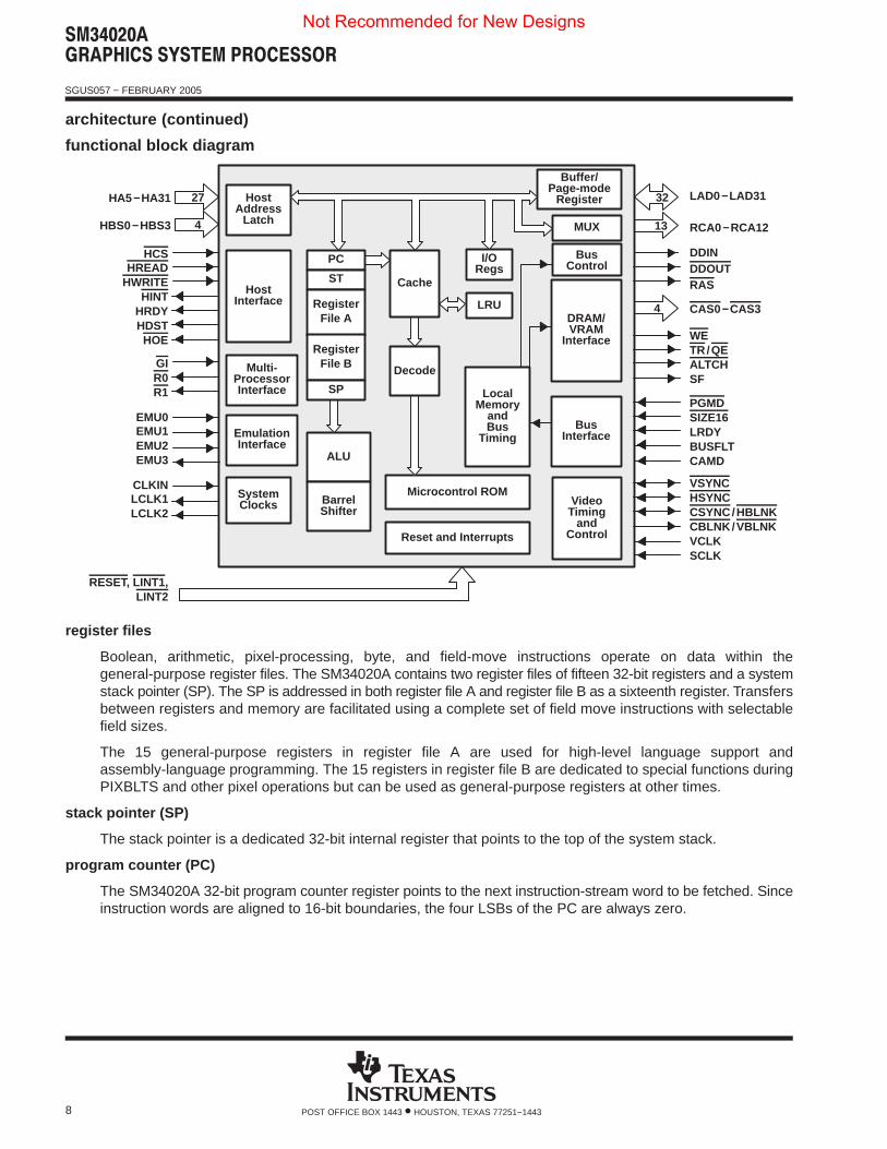
architecture (continued)
functional block diagram
Register
HA5−HA31
HBS0−HBS3
HCSHREAD
HWRITEHINT
HRDYHDSTHOE
GIR0R1
EMU0EMU1EMU2EMU3
CLKINLCLK1LCLK2
RESET, LINT1,LINT2
LAD0−LAD31
RCA0−RCA12
DDINDDOUTRAS
CAS0 −CAS3
WETR/QEALTCHSF
PGMDSIZE16LRDYBUSFLTCAMD
VSYNCHSYNCCSYNC/HBLNKCBLNK /VBLNKVCLKSCLK
27
4
32
13
HostAddress
Latch
HostInterface
Multi-ProcessorInterface
EmulationInterface
SystemClocks
Buffer/
MUX
Bus
DRAM/VRAM
Interface
BusInterface
VideoTiming
andControl
LocalMemory
andBus
Timing
I/O
LRU
Regs
ALU
BarrelShifter
Microcontrol ROM
Reset and Interrupts
Control
Page-modeRegister
Cache
PC
ST
SP
Decode
4RegisterFile A
RegisterFile B
register files
Boolean, arithmetic, pixel-processing, byte, and field-move instructions operate on data within thegeneral-purpose register files. The SM34020A contains two register files of fifteen 32-bit registers and a systemstack pointer (SP). The SP is addressed in both register file A and register file B as a sixteenth register. Transfersbetween registers and memory are facilitated using a complete set of field move instructions with selectablefield sizes.
The 15 general-purpose registers in register file A are used for high-level language support andassembly-language programming. The 15 registers in register file B are dedicated to special functions duringPIXBLTS and other pixel operations but can be used as general-purpose registers at other times.
stack pointer (SP)
The stack pointer is a dedicated 32-bit internal register that points to the top of the system stack.
program counter (PC)
The SM34020A 32-bit program counter register points to the next instruction-stream word to be fetched. Sinceinstruction words are aligned to 16-bit boundaries, the four LSBs of the PC are always zero.
Not Recommended for New Designs
������������ � ������ � ����
SGUS057 − FEBRUARY 2005
9POST OFFICE BOX 1443 • HOUSTON, TEXAS 77251−1443
instruction cache
An on-chip cache contains 512 bytes of RAM and provides unimpeded access to instructions. The cacheoperates automatically and is transparent to software. The cache is divided into four 128-byte segments.Associated with each segment is a 22-bit segment start address register (SSA) to identify the addresses inmemory corresponding to the current contents of the cache segment. Each cache segment is further partitionedinto eight subsegments of four long words (32 bits) each. Each subsegment has an associated present (P) flagto indicate whether or not the subsegment contains valid data.
The cache is loaded only when an instruction requested by the execution section of the SM34020A is not alreadycontained within the cache. A least-recently-used (LRU) algorithm determines which of the four segments ofthe cache is overwritten with new data. For this purpose, an internal four-by-two LRU stack keeps track of cacheusage. Although the cache is loaded so as to always fill a subsegment completely, not all eight subsegmentswithin a segment are necessarily filled (this is dependent upon the instruction stream).
status register
The status register (ST) is a special purpose 32-bit register dedicated to status codes set by the results of implicitand explicit compare operations and parameters used to specify the length and behavior of fields 0 and 1. Duringan interrupt, when the IX bit in the ST is placed on the stack, it indicates that execution of an interruptableinstruction (PIXBLT, FILL or LINE) was halted to service the interrupt. The single-step bit causes a trap to thesingle-step vector (located at address FFFF FBE0h) after the execution of one instruction when the bit is sethigh. Normal program execution occurs when the bit is set low.
fields, bytes, words, long words, pixels and pixel arrays
The SM34020A outputs a 28-bit address on LAD4−LAD31 that is valid at the falling edge of ALTCH. The mostsignificant 27 bits (LAD5−LAD31) define a 32-bit-long word of physical memory; logically, however, theSM34020A views memory data as fields addressable at the bit level. The least significant bit of the 28-bitaddress (LAD4) is used to select the odd or even word when accessing 16-bit memories (indicated by SIZE16asserted low). Primitive data types supported by the SM34020A include bytes, words, long words, pixels, twoindependent fields of from 1 to 32 bits, and user-defined pixel arrays.
Words and long words, respectively, refer to 16- and 32-bit values that are aligned on 32-bit boundaries.
The two independent fields are referenced as field 0 and field 1. The attributes of these fields (field size and signextension within a register) are defined in the status register as FS0, FE0, FS1, and FE1. Fields 0 and 1 arespecified independently to be signed or unsigned and from 1 to 32 bits in length. Bytes are special 8-bit casesof the field data type, while pixels are 1, 2, 4, 8, 16, or 32 bits in length. In general, fields (including bytes) canstart and terminate on arbitrary bit boundaries; however, pixels must pack evenly into 32-bit-long words.
pixel operations
Pixel arrays are two-dimensional data types of user-defined width, length, pixel depth (number of bits per pixel),and pitch (distance between rows). A pixel or pixel array can be accessed by means of either its memory addressor its XY coordinates. Transfers of individual pixels or pixel blocks are influenced by the pixel processing,transparency, window checking, plane masking, pixel masking, or corner adjustment operations selected. Forfurther information, see the TMS32020 User’s Guide, literature number SPVU019.
Not Recommended for New Designs
������������ � ������ � ����
SGUS057 − FEBRUARY 2005
10 POST OFFICE BOX 1443 • HOUSTON, TEXAS 77251−1443
transparency
Transparency is a mechanism that allows the surrounding pixels in an array to be specified as invisible. Thisis useful for ensuring that only the object and not the rectangle surrounding it are written to the display. TheSM34020A provides four transparency modes:
� No transparency� Transparency on result equal zero� Transparency on source equal COLOR0� Transparency on destination equal COLOR0� Refer to the TMS34020 User’s Guide for more information.
I/O registers
The SM34020A contains an on-chip block of sixty-four 16-bit locations (mapped into the SM34020A memoryaddress space) that are used for I/O control registers. Eight of these are used by the host interface logic andare not available to the user. Forty-seven I/O registers control parameters necessary to configure the operationand report status of the following interfaces:
� Host interface� Local memory� Video timing� Screen refresh� External interrupts� Internal interrupts
host interface registers
The host interface registers (HSTDATA, HSTADRL, HSTADRH, HSTCTLL, and HSTCTLH) are provided tofacilitate communications between the SM34020A and a host processor and maintain compatibility with theSMJ34010. The registers are mapped into five of the I/O locations accessible to the SM34020A.
Two of these registers (HSTCTLL and HSTCTLH) are used to provide control by the host. This control consistsof the passing of interrupt requests, flushing the instruction cache, halting the SM34020A, transmitting anon-maskable interrupt request to the SM34020A, enabling emulation interrupts, and setting host accessmodes and configurations.
The other three registers are simple read/write registers to allow the SM34020A software to leave addressesfor the host at a known location and allow compatibility with some SMJ34010 software.
memory interface control registers
Some of the I/O registers are used to control various local memory interface functions, including:
� Frequency of DRAM refresh cycles� Masking (read/write protection) of individual color planes� DRAM row/column addressing configuration� Accessing mode (big endian/little endian)� Bus fault and retry recovery
video timing and screen refresh
Twenty-eight I/O registers are dedicated to video timing and screen refresh functions. The SM34020A can beconfigured to drive composite sync or separate sync displays.
In composite sync mode, the SM34020A can be set to extract VSYNC and HSYNC from an external CSYNCor it can be used to generate CSYNC from separate VSYNC and HSYNC inputs. Internally, the SM34020A canbe set to preset the horizontal and vertical counts on receipt of an external sync signal. This allowscompensation for any combination of internal and external delays that occur in the video synchronizationprocess. The
Not Recommended for New Designs
������������ � ������ � ����
SGUS057 − FEBRUARY 2005
11POST OFFICE BOX 1443 • HOUSTON, TEXAS 77251−1443
video timing and screen refresh (continued)
HCOUNT register is loaded from SETHCNT by an external HSYNC, VCOUNT is loaded from SETVCNT on anexternal VSYNC, and an external CSYNC loads both HCOUNT and VCOUNT from SETHCNT and SETVCNT,respectively.
The SM34020A directly supports VRAMs by generating the serial-data-register transfer cycles necessary torefresh the display. The memory locations from which the display information is taken, as well as the numberof horizontal scan lines displayed between serial-data-register transfer cycles, are programmable.
The SM34020A supports various display resolutions and either interlaced or noninterlaced video. TheSM34020A can optionally be programmed to synchronize to externally generated sync signals so that imagescreated by the SM34020A can be superimposed upon images created externally. The external sync mode canalso be used to synchronize the video signals generated by two or more SM34020As in a multiple-SM34020Agraphics system.
CPU control registers
Five of the I/O registers (CONVDP, CONVMP, CONVSP, CONTROL, and PSIZE) provide CPU control toconfigure the SM34020A for operation with specific characteristics. These characteristics include pitches forpixel transfers, window checking mode, Boolean or arithmetic pixel processing operation, transparency mode,PIXBLT direction control, and pixel size.
interrupt interface registers
Two dedicated I/O registers (INTENB and INTPEND) monitor and mask interrupt requests to the SM34020A,including two externally generated interrupts and three internally generated interrupts. An internal interruptrequest can be generated on one of the following conditions.
� Window violation: an attempt has been made to write a pixel to a location inside or outside a specifiedwindow boundary.
� Host interrupt: the host processor has set the interrupt request bit in the host control register.� Display interrupt: a specified horizontal line in the frame has been displayed on the screen.� Bus fault� Single-step emulator
A nonmaskable interrupt occurs when the host processor sets a control bit in the host interface register (NMIin HSTCTLH). The host-initiated interrupt is associated with a mode bit (NMIM in HSTCTLH) that enables anddisables saving of the processor state on the stack when the interrupt occurs. This is useful if the host wishesto use the host interrupt before releasing the SM34020A to execute instructions (that is, before the stack pointeris initialized). A dedicated terminal controls the SM34020A reset function.
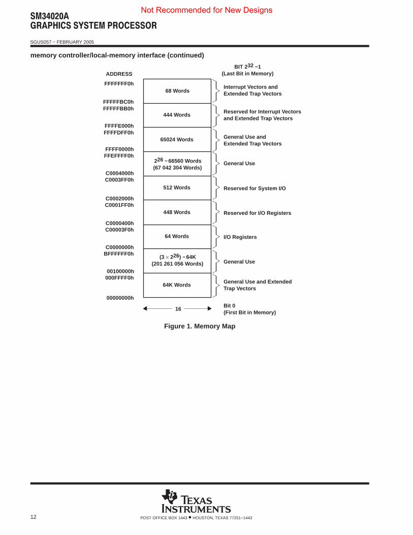
memory controller/local-memory interface
The memory controller manages the SM34020A interface to the local memory and automatically performs thebit alignment and masking necessary to access data located at arbitrary bit boundaries within memory. Thememory controller operates autonomously with respect to the CPU. It has a write queue one field (1 to 32 bits)deep that permits it to complete those memory cycles necessary to insert a field into memory without delayingthe execution of subsequent instructions. Only when a second memory operation is required before completionof the first operation is the SM34020A forced to defer execution of the subsequent instruction.
The SM34020A directly interfaces to standard DRAMs and in particular, to standard video RAMs (VRAMs) suchas the SMJ44C25x multiport VRAMs. The SM34020A memory interface consists of the local address/data bus(LAD), the DRAM row/column address (RCA) bus, and associated control signals. The currently selected wordaddress (28 bits) and status (4 bits) are multiplexed with data on LAD. The RCA bus allows direct connectionto address/address multiplexed DRAMs from 64K to 16M. Refresh for DRAMs is supported by CAS-before-RAS(CBR) refresh cycles.
Not Recommended for New Designs
������������ � ������ � ����
SGUS057 − FEBRUARY 2005
12 POST OFFICE BOX 1443 • HOUSTON, TEXAS 77251−1443
memory controller/local-memory interface (continued)
BIT 232 −1(Last Bit in Memory)
68 Words
226 −66560 Words(67 042 304 Words)
(3 × 226) −64K(201 261 056 Words)
444 Words
65024 Words
512 Words
448 Words
64 Words
64K Words
Interrupt Vectors andExtended Trap Vectors
Reserved for Interrupt Vectorsand Extended Trap Vectors
General Use andExtended Trap Vectors
General Use and ExtendedTrap Vectors
Bit 0(First Bit in Memory)
General Use
Reserved for System I/O
Reserved for I/O Registers
I/O Registers
General Use
ADDRESS
FFFFFFF0h
FFFFFBC0hFFFFFBB0h
FFFFE000hFFFFDFF0h
FFFF0000hFFEFFFF0h
C0004000hC0003FF0h
C0002000hC0001FF0h
C0000400hC00003F0h
C0000000hBFFFFFF0h
00100000h000FFFF0h
00000000h
16
Figure 1. Memory Map
Not Recommended for New Designs
������������ � ������ � ����
SGUS057 − FEBRUARY 2005
13POST OFFICE BOX 1443 • HOUSTON, TEXAS 77251−1443
reset
Reset puts the SM34020A into a known initial state. This state is entered when the input signal at RESET isasserted low. While RESET remains asserted, all outputs are in a known state, no DRAM refresh cycles takeplace, and no screen refresh cycles are performed.
The state of the HCS input on the CLKIN cycle before the low-to-high transition of RESET determines whetherthe SM34020A is halted or begins executing instructions. The SM34020A can be in one of two modes,host-present or self-bootstrap mode.
Host-present mode: if HCS is high at the end of reset, SM34020A instruction execution halts and remains halteduntil the host clears the HLT (halt) bit in HSTCTLH (host control register). Following reset, the RAS cyclesrequired to initialize the dynamic RAMs are performed automatically by the GSP memory control logic. The hostcan request a memory access after the eight RAS initialization cycles have completed. The SM34020Aautomatically performs DRAM refresh cycles at regular intervals although the SM34020A remains halted untilthe host clears the HLT bit. Only then does SM34020A fetch the level-0 vector address from locationFFFFFFE0h and begin executing the reset service routine.
Self-bootstrap mode: if HCS is low at the end of reset, the SM34020A first performs eight refresh cycles toinitialize the DRAMs. Immediately following the eight refresh cycles, the GSP fetches the level-0 vector addressfrom location FFFFFFE0h and begins executing the reset service routine.
At the time the SM34020A fetches the level-0 vector address (the reset vector), the least significant four bits(bit address part) are used to load configuration data that establishes the initial condition of thebig-endian/little-endian mode and the current RCA bus configuration bits in the CONFIG register as describedin the I/O register section.
Unlike other interrupts and software traps, reset does not save the previous ST or PC values (this can also occuron host initiated nonmaskable interrupts if the NMIM bit in HSTCTLH is set to a 1) because the value of the stackpointer just before a reset is generally not valid. Saving these values on the stack could contaminate validmemory locations. A TRAP 0 instruction, which uses the same vector address as reset, similarly does not savethe ST or PC values.
asserting reset
A reset is initiated by asserting RESET to its active-low level. To reset the SM34020A at power up, RESET mustremain active low for a minimum of 40 local clock periods (LCLK1 and LCLK2) after power levels have becomestable. At times other than power up, the SM34020A can be reset by holding RESET low for a minimum of fourlocal clock periods; the GSP enters an internal reset state for 34 local clock cycles. While in the internal resetstate and RESET is high, memory-refresh cycles occur.
reset and multiprocessor synchronization
The synchronization of multiple SM34020As sharing a local memory is done using the RESET input. In systemswhere the multiprocessor interface is used to control the access to a common memory, the processors mustbe synchronized. Synchronization is achieved by taking RESET high within a specific interval relative to CLKIN.This can be done by using CLKIN to clock the RESET as received by the SM34020As. All SM34020As to besynchronized should use the same CLKIN and RESET inputs. All of the local memory and bus control signalsshould be connected in parallel (without buffers) between the processors. After power up, the processors arenot necessarily synchronized with respect to the particular quarter cycle in progress. The rising edge of RESETis used to set the SM34020A to a particular quarter cycle by adding Q1 cycles. All SM34020As in amultiprocessor environment operate on the same quarter cycle within 10 quarter cycles after the rising edgeof RESET.
Not Recommended for New Designs
������������ � ������ � ����
SGUS057 − FEBRUARY 2005
14 POST OFFICE BOX 1443 • HOUSTON, TEXAS 77251−1443
reset and DRAM/VRAM initialization
The SM34020A drives its RAS signal inactive high as long as RESET remains low. The specifications for certainDRAM and VRAM devices require that RAS be driven inactive-high for 1 millisecond after power is stable toprovide the proper conditions for the DRAMs. Typically, eight RAS cycles are also required to initialize theDRAMs for proper operation. In general, holding RESET low for t microseconds ensures that RAS remains highinitially for t−(10tQ) microseconds, tQ being the quarter-cycle time as defined by the input clock period, tc(CHI).The SM34020A memory controller automatically inserts the required eight RAS cycles after all resets (afterpower up or after the internal reset state) by issuing CAS-before-RAS refresh cycles before it allows the CPUaccess to memory. A host must delay requests to memory until the initialization cycles have had sufficient timeto complete. Immediately following reset, the SM34020A is set to perform a refresh sequence every eightcycles.
At times other than power up, to maintain the memory in DRAMs and do a reset, the RESET pulse must notexceed the maximum refresh interval of the DRAMs minus the time for the SM34020A to refresh the memories.On reset, the SM34020A is set to do a refresh cycle every eight local clock periods. A 30-MHz (CLKIN) systemwith one (refresh) bank of D/VRAM would be completely refreshed in one sixteenth of the total memory refreshinterval. The reset pulse then should not exceed about fifteen-sixteenths of the total refresh interval requiredby the DRAMs to maintain memory integrity.
If RESET remains low longer than the maximum refresh interval specified for the memory, the previous contentsof the local memory can not be valid after the reset.
initial state following reset
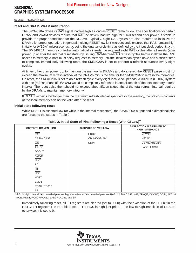
While RESET is asserted low (or while in the internal reset state), the SM34020A output and bidirectional pinsare forced to the states in Table 2.
Table 2. Initial State of Pins Following a Reset (With GI Low) †
OUTPUTS DRIVEN HIGH OUTPUTS DRIVEN LOWBIDIRECTIONALS DRIVEN TO
HIGH IMPEDANCE
RAS HRDY VSYNC
CAS0−CAS3 CBLNK/VBLNK HSYNC
WE DDIN CSYNC/HBLNK
TR/QE LAD0−LAD31
DDOUT
ALTCH
HINT
R0
R1
HOE
HDST
EMU3
RCA0−RCA12
SF† If GI is high, then all GI-controlled pins are high-impedance. GI-controlled pins are RAS, CAS0−CAS3, WE, TR/QE, DDOUT, DDIN, ALTCH,
HOE, HDST, RCA0−RCA12, LAD0−LAD31, and SF.
Immediately following reset, all I/O registers are cleared (set to 0000) with the exception of the HLT bit in theHSTCTLH register. The HLT bit is set to 1 if HCS is high just prior to the low-to-high transition of RESET;otherwise, it is set to 0.
Not Recommended for New Designs
������������ � ������ � ����
SGUS057 − FEBRUARY 2005
15POST OFFICE BOX 1443 • HOUSTON, TEXAS 77251−1443
reset and DRAM/VRAM initialization (continued)
Just prior to the execution of the first instruction in the reset routine, the SM34020A internal registers are in thefollowing states:
� General-purpose register files A and B are uninitialized.� The ST is set to 0000 0010h.� The PC contains the most-significant 28 bits of the vector fetched from memory address FFFF FFE0h (the
least significant four bits of the PC are set to zero).� The BEN bit in the I/O register CONFIG is set to the least significant bit read from the vector fetched from
memory address FFFF FFE0h.� The CBP, RCM0, and RCM1 bits in the I/O register CONFIG are set to the corresponding bits read from
the vector fetched from memory address FFFF FFE0h. The configuration byte protect bit (CBP) can be sethigh to prevent further modification of the lower eight bits of the I/O register CONFIG.
The state of the instruction cache at this time is as follows:
� The SSA (segment start address) registers are uninitialized.� The LRU (least recently used) stack is set to the initial sequence 0, 1, 2, 3, where 0 occupies the most
recently used position and 3 occupies the least recently used position.� All P (present) flags are cleared to 0s.
local memory and DRAM/VRAM interface
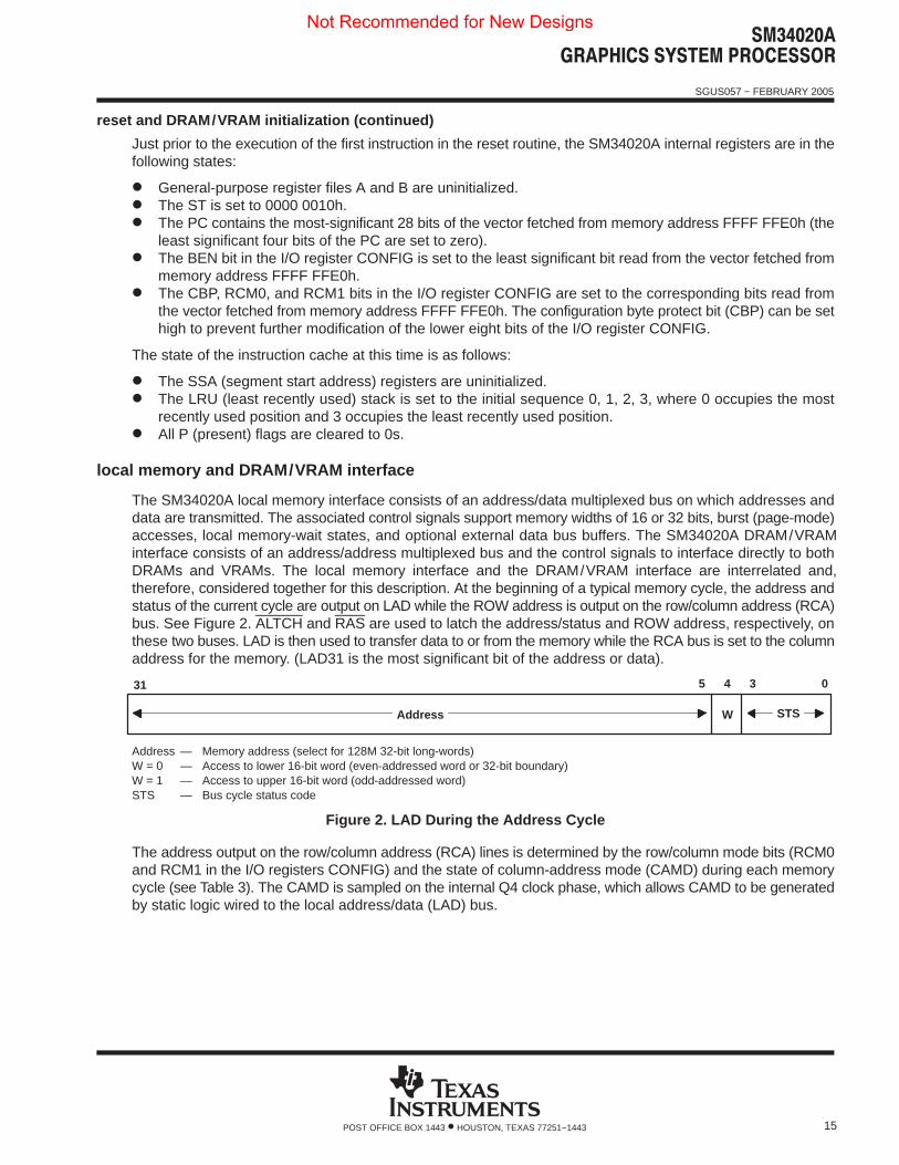
The SM34020A local memory interface consists of an address/data multiplexed bus on which addresses anddata are transmitted. The associated control signals support memory widths of 16 or 32 bits, burst (page-mode)accesses, local memory-wait states, and optional external data bus buffers. The SM34020A DRAM/VRAMinterface consists of an address/address multiplexed bus and the control signals to interface directly to bothDRAMs and VRAMs. The local memory interface and the DRAM/VRAM interface are interrelated and,therefore, considered together for this description. At the beginning of a typical memory cycle, the address andstatus of the current cycle are output on LAD while the ROW address is output on the row/column address (RCA)bus. See Figure 2. ALTCH and RAS are used to latch the address/status and ROW address, respectively, onthese two buses. LAD is then used to transfer data to or from the memory while the RCA bus is set to the columnaddress for the memory. (LAD31 is the most significant bit of the address or data).
W
31 5 4 3 0
Address STS
Address — Memory address (select for 128M 32-bit long-words)W = 0 — Access to lower 16-bit word (even-addressed word or 32-bit boundary)W = 1 — Access to upper 16-bit word (odd-addressed word)STS — Bus cycle status code
Figure 2. LAD During the Address Cycle
The address output on the row/column address (RCA) lines is determined by the row/column mode bits (RCM0and RCM1 in the I/O registers CONFIG) and the state of column-address mode (CAMD) during each memorycycle (see Table 3). The CAMD is sampled on the internal Q4 clock phase, which allows CAMD to be generatedby static logic wired to the local address/data (LAD) bus.
Not Recommended for New Designs
������������ � ������ � ����
SGUS057 − FEBRUARY 2005
16 POST OFFICE BOX 1443 • HOUSTON, TEXAS 77251−1443
local memory and DRAM/VRAM interface (continued)
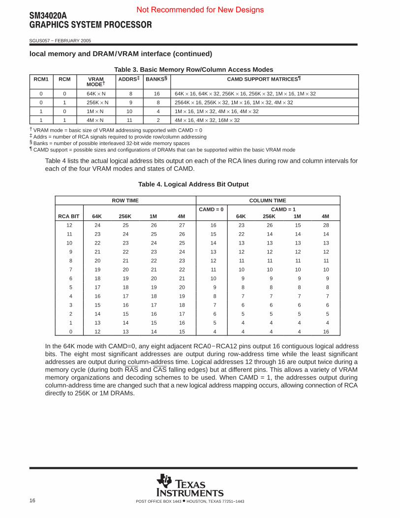
Table 3. Basic Memory Row/Column Access ModesRCM1 RCM VRAM
MODE†ADDRS‡ BANKS § CAMD SUPPORT MATRICES¶
0 0 64K × N 8 16 64K × 16, 64K × 32, 256K × 16, 256K × 32, 1M × 16, 1M × 32
0 1 256K × N 9 8 2564K × 16, 256K × 32, 1M × 16, 1M × 32, 4M × 32
1 0 1M × N 10 4 1M × 16, 1M × 32, 4M × 16, 4M × 32
1 1 4M × N 11 2 4M × 16, 4M × 32, 16M × 32
† VRAM mode = basic size of VRAM addressing supported with CAMD = 0‡ Addrs = number of RCA signals required to provide row/column addressing§ Banks = number of possible interleaved 32-bit wide memory spaces¶ CAMD support = possible sizes and configurations of DRAMs that can be supported within the basic VRAM mode
Table 4 lists the actual logical address bits output on each of the RCA lines during row and column intervals foreach of the four VRAM modes and states of CAMD.
Table 4. Logical Address Bit Output
ROW TIME COLUMN TIME
CAMD = 0 CAMD = 1RCA BIT 64K 256K 1M 4M 64K 256K 1M 4M
12 24 25 26 27 16 23 26 15 28
11 23 24 25 26 15 22 14 14 14
10 22 23 24 25 14 13 13 13 13
9 21 22 23 24 13 12 12 12 12
8 20 21 22 23 12 11 11 11 11
7 19 20 21 22 11 10 10 10 10
6 18 19 20 21 10 9 9 9 9
5 17 18 19 20 9 8 8 8 8
4 16 17 18 19 8 7 7 7 7
3 15 16 17 18 7 6 6 6 6
2 14 15 16 17 6 5 5 5 5
1 13 14 15 16 5 4 4 4 4
0 12 13 14 15 4 4 4 4 16
In the 64K mode with CAMD=0, any eight adjacent RCA0−RCA12 pins output 16 contiguous logical addressbits. The eight most significant addresses are output during row-address time while the least significantaddresses are output during column-address time. Logical addresses 12 through 16 are output twice during amemory cycle (during both RAS and CAS falling edges) but at different pins. This allows a variety of VRAMmemory organizations and decoding schemes to be used. When CAMD = 1, the addresses output duringcolumn-address time are changed such that a new logical address mapping occurs, allowing connection of RCAdirectly to 256K or 1M DRAMs.
Not Recommended for New Designs
������������ � ������ � ����
SGUS057 − FEBRUARY 2005
17POST OFFICE BOX 1443 • HOUSTON, TEXAS 77251−1443
local memory and DRAM/VRAM interface (continued)
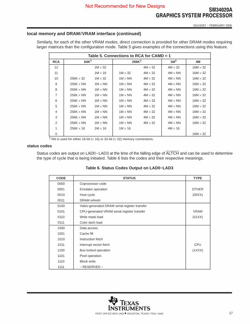
Similarly, for each of the other VRAM modes, direct connection is provided for other DRAM modes requiringlarger matrices than the configuration mode. Table 5 gives examples of the connections using this feature.
Table 5. Connections to RCA for CAMD = 1RCA 64K† 256K† 1M† 4M
12 1M × 32 4M × 32 4M × 32 16M × 32
11 1M × 16 1M × 32 4M × 32 4M × NN 16M × 32
10 256K × 32 1M × 32 1M × NN 4M × 32 4M × NN 16M × 32
9 256K × NN 1M × NN 1M × NN 4M × 32 4M × NN 16M × 32
8 256K × NN 1M × NN 1M × NN 4M × 32 4M × NN 16M × 32
7 256K × NN 1M × NN 1M × NN 4M × 32 4M × NN 16M × 32
6 256K × NN 1M × NN 1M × NN 4M × 32 4M × NN 16M × 32
5 256K × NN 1M × NN 1M × NN 4M × 32 4M × NN 16M × 32
4 256K × NN 1M × NN 1M × NN 4M × 32 4M × NN 16M × 32
3 256K × NN 1M × NN 1M × NN 4M × 32 4M × NN 16M × 32
2 256K × NN 1M × NN 1M × NN 4M × 32 4M × NN 16M × 32
1 256K × 16 1M × 16 1M × 16 4M × 16
0 16M × 32† NN is used for either 16-bit (× 16) or 32-bit (× 32) memory connections.
status codes
Status codes are output on LAD0−LAD3 at the time of the falling edge of ALTCH and can be used to determinethe type of cycle that is being initiated. Table 6 lists the codes and their respective meanings.
Table 6. Status Codes Output on LAD0−LAD3
CODE STATUS TYPE
0000 Coprocessor code
0001 Emulator operation OTHER
0010 Host cycle (00XX)
0011 DRAM refresh
0100 Video-generated DRAM serial register transfer
0101 CPU-generated VRAM serial register transfer VRAM
0110 Write mask load (01XX)
0111 Color latch load
1000 Data access
1001 Cache fill
1010 Instruction fetch
1011 Interrupt vector fetch CPU
1100 Bus locked operation (1XXX)
1101 Pixel operation
1110 Block write
1111 − RESERVED −
Not Recommended for New Designs
������������ � ������ � ����
SGUS057 − FEBRUARY 2005
18 POST OFFICE BOX 1443 • HOUSTON, TEXAS 77251−1443
dynamic bus sizing
The SM34020A supports dynamic bus sizing between 16 and 32 bits on any local memory access. Anyport /memory that is only 16 bits wide must assert SIZE16 low during Q1 (to be valid at the start of Q2) of thebus cycle accessing the even memory word (LAD4 = 0) corresponding to its address.The SM34020A thenperforms another memory access to the next 16-bit (odd) word in memory. The SM34020A samples SIZE16at the start of Q2 in the second cycle (access to odd word address) to determine to which half of LAD the portor memory is aligned. If the port is on LAD0−LAD15, SIZE16 should be low during the second cycle access (oddword); otherwise, if the port is on LAD16−LAD31, SIZE16 must be high at this time. The SM34020A alwaysperforms two memory cycles to access the 16-bit wide memories, even when attempting only a 16-bit transfer.
The SM34020A outputs the four CAS strobes and LAD bus initially aligned for a 32-bit bus. If the memory is16 bits wide, the two most significant CAS strobes are swapped with the two least significant strobes when itaccesses the second word and the halves of LAD are also swapped; therefore, 16-bit memories need to respondonly to the two CAS strobes corresponding to the upper or lower 16 bits of LAD to which they are connected.
Note that devices connected to LAD0−LAD15 transfer the least significant word during the first cycle and themost significant word during the second cycle. Data accesses on LAD16−LAD31 transfer the most significantword first, then the least significant word.
The second memory cycle forced by SIZE16 is performed as a page mode access if PGMD was low during thefirst access. A read-write cycle to the 16-bit page-mode memory requires five bus cycles that occur as address,read0, read1, write0, write1. If a 16-bit transfer is interrupted due to a bus fault, the restart causes the entireaccess to be restarted.
For memory that supports page-mode accesses (PGMD low), SIZE16 is sampled during each access tomemory. If SIZE16 is high on the even word access, then a 32-bit transfer occurs over LAD0−LAD31. If SIZE16is low on the even word access (16-bit wide memory), then it is sampled again on the odd word access todetermine to which half of LAD the memory is connected (low for connection to LAD0−LAD15 or high forconnection to LAD16−LAD31).
special 1-M VRAM cycles
The SM34020A provides control for special function VRAM cycles that are available in the 1-M devices. Thesecycles are obtained by the appropriate timing control of SF, CAS, TR/QE, and WE of the VRAMs at the fallingedge of RAS. The cycles include:
� Load write mask� Load color mask� Block write (no mask)� Block write (current mask)� Write using mask� Alternate write transfer
In addition, other special modes can be implemented by using external logic.
multiprocessor arbitration
The multiprocessor interface allows multiple processors to operate in a system sharing the same local memory.The use of the bus grant in GI and the priority request signals R0 and R1 allows a flexible method of passingcontrol from one processor to another. The control scheme allows local memory cycles to occur back-to-back,even when passing control from one SM34020A to another. Synchronization of multiple SM34020As in a systemoccurs at reset with the rising edge of RESET meeting the setup and hold requirements to CLKIN, so allSM34020As are certain to respond to RESET during the same quarter cycle. RESET is not required to besynchronous to CLKIN except to allow synchronization of multiple SM34020As in a system.
Not Recommended for New Designs
������������ � ������ � ����
SGUS057 − FEBRUARY 2005
19POST OFFICE BOX 1443 • HOUSTON, TEXAS 77251−1443
multiprocessor arbitration (continued)
The GI priority for multiprocessing environments is determined by arbitration logic external to the SM34020A.If GI goes inactive-high, the SM34020A releases the bus on the next available cycle boundary. If the cycle inprogress has not successfully completed, the SM34020A restarts the cycle upon regaining control of the bus.Normally, if the SM34020A asserts both R0 and R1 low, it should be given the control of the bus by the arbitrator.
host interface
The SM34020A host interface allows the local memory to be mapped into the host address space. TheSM34020A acts as a DRAM controller for the host. The address for the host access is latched within theSM34020A; however, the data for the access is transferred using external transceivers. The host selects theaddress of a 32-bit long word for an access using the 27 host address lines, HA5−HA31. If the host desires byteaddressability, it can select the active bytes for the access by using HBS0−HBS3. The SM34020A always reads32 bits from memory; however, on host writes, it uses the host byte selects to enable CAS0−CAS3 to memory.The address and byte selects are latched at the falling edge of HCS within the SM34020A. The host indicatesa read or write by asserting HREAD or HWRITE (as appropriate) either before or after HCS. (Note that HREADand HWRITE must never be asserted at the same time.)
The SM34020A responds to a host read request by latching the requested data in the external latches andproviding HRDY to the host, indicating that the read cycle is completing. The rising edge of HDST with HRDYhigh indicates data is latched in the external transceivers.
The host indicates that a write to a particular location is required by providing the address and assertingHWRITE. The host must maintain both HCS and HWRITE asserted until valid data is in the transceivers. (Therising edge of HOE with HRDY high indicates that the data previously stored in the external transceivers hasbeen written to memory.) Typically, the rising edge of HWRITE is used to strobe the data into the latches andsignal the SM34020A that the write access can start. The SM34020A uses its byte-write capability to write onlyto the selected bytes.
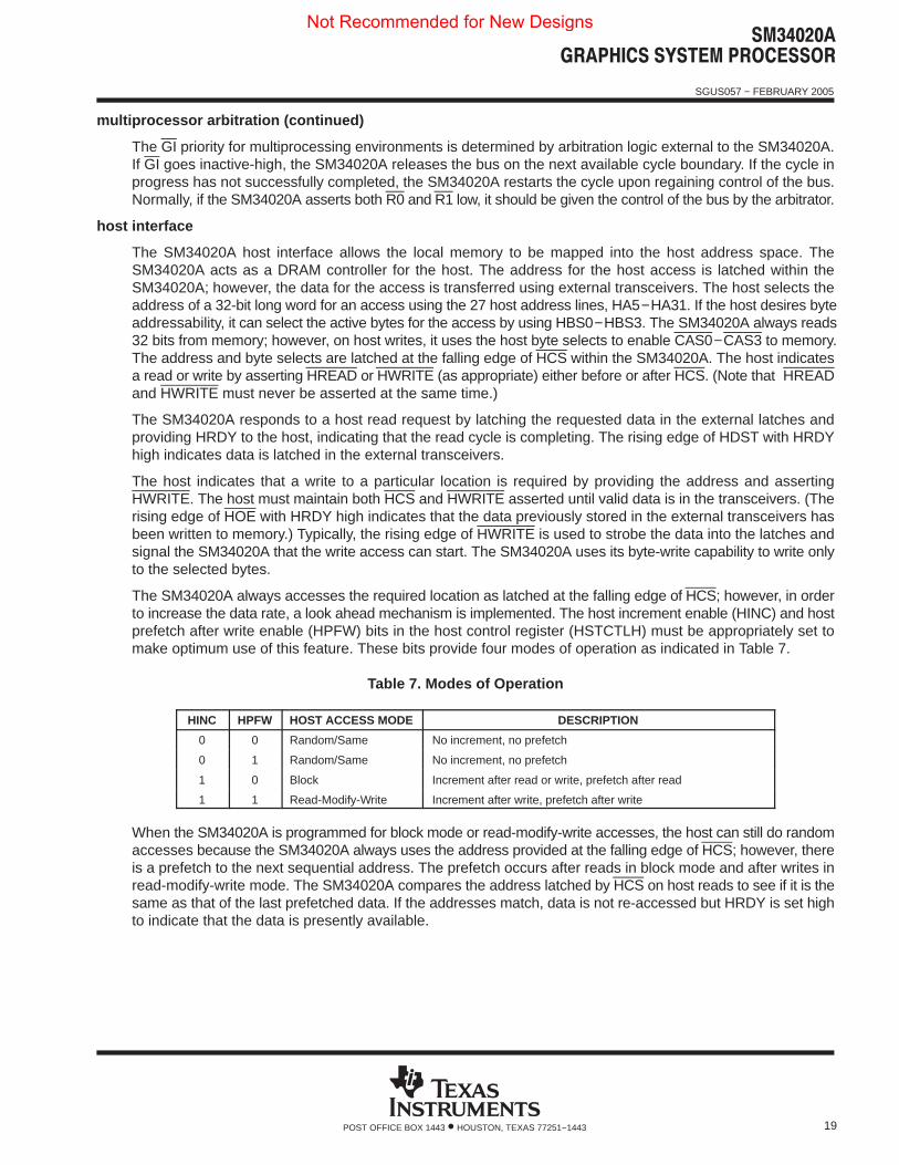
The SM34020A always accesses the required location as latched at the falling edge of HCS; however, in orderto increase the data rate, a look ahead mechanism is implemented. The host increment enable (HINC) and hostprefetch after write enable (HPFW) bits in the host control register (HSTCTLH) must be appropriately set tomake optimum use of this feature. These bits provide four modes of operation as indicated in Table 7.
Table 7. Modes of Operation
HINC HPFW HOST ACCESS MODE DESCRIPTION
0 0 Random/Same No increment, no prefetch
0 1 Random/Same No increment, no prefetch
1 0 Block Increment after read or write, prefetch after read
1 1 Read-Modify-Write Increment after write, prefetch after write
When the SM34020A is programmed for block mode or read-modify-write accesses, the host can still do randomaccesses because the SM34020A always uses the address provided at the falling edge of HCS; however, thereis a prefetch to the next sequential address. The prefetch occurs after reads in block mode and after writes inread-modify-write mode. The SM34020A compares the address latched by HCS on host reads to see if it is thesame as that of the last prefetched data. If the addresses match, data is not re-accessed but HRDY is set highto indicate that the data is presently available.
Not Recommended for New Designs
������������ � ������ � ����
SGUS057 − FEBRUARY 2005
20 POST OFFICE BOX 1443 • HOUSTON, TEXAS 77251−1443
dynamic bus sizing on host accesses
If the host makes a read access to a 16-bit wide memory, the SM34020A automatically does the second cyclerequired to read the rest of the 32-bit word (even if the host did not require a 32-bit cycle). The external logicmust comprehend the sense of SIZE16 or the CAS strobes during the accesses in order to route the data intothe proper external host data transceivers. The SM34020A uses the host byte selects HBS0−HBS3 to enablethe CAS strobes when doing a host write.
coprocessor interface
Support for coprocessors is provided through special instructions and bus cycles that allow communication withthe coprocessor. A coprocessor can be register based, depending on the SM34020A to do all addresscalculations, or it can operate as its own bus controller, using the multiprocessor arbitration scheme. Five basiccycles are provided for direct communication and control of coprocessors:
� SM34020A to coprocessor� Coprocessor to SM34020A� Move memory to coprocessor� Move coprocessor to memory� Coprocessor internal command
The first four of these cycles provide for command of the coprocessor in addition to the movement of parametersto and from the coprocessor. In this manner, parameters can be sent to the coprocessor and operated uponwithout an explicit coprocessor command cycle.
instruction set
The SM34020A instruction set can be divided into five categories:
� Graphics instructions� Coprocessor instructions� Move instructions� General-purpose instructions� Program control and context switching
Specialized graphics instructions manipulate pixel data that is accessed using memory addresses orXY coordinates. These instructions include graphics operations, such as array and raster operations, pixelprocessing, windowing, plane masking, pixel masking, and transparency. Coprocessor instructions allow for thecontrol and data flow to and from coprocessors that reside in the system. Move instructions comprehend thebit-addressing and field operations, which manipulate fields of data using linear addressing for transfer to andfrom memory and the register file. General-purpose instructions provide a complete set of arithmetic andBoolean operations on the register file as well as general program control and data processing. Program controland context switching instructions allow the user to control flow and to save and restore information usinginstructions with both register-direct and absolute operands.
clock stretch
The SM34020A supports a clock stretching mechanism.
With advances in semiconductor manufacturing, newer versions of the SM34020A can be made, eachsupporting a higher CLKIN frequency. The increase in CLKIN frequency means that the SM34020A machinecycles execute more quickly, with a consequent increase in code execution speed. However, there comes apoint when, as the machine cycle time becomes shorter, the local-memory control signals begin to violate DRAMand VRAM timing parameters for certain types of memory access.
Not Recommended for New Designs
������������ � ������ � ����
SGUS057 − FEBRUARY 2005
21POST OFFICE BOX 1443 • HOUSTON, TEXAS 77251−1443
clock stretch (continued)
The clock-stretch mechanism allows the SM34020A to slow down and execute those critical local-memorycycles while still benefiting from the accelerated processing allowed by higher CLKIN frequencies duringnoncritical memory access cycles.
Exact timing issues vary from system to system, reflecting differences in bus buffering, etc., but, broadlyspeaking, the clock-stretch mechanism allows the system designer to interface to slower memory devices thanthe designer could use if no stretch mechanism was available.
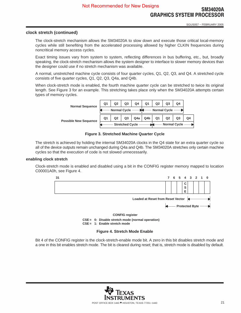
A normal, unstretched machine cycle consists of four quarter cycles, Q1, Q2, Q3, and Q4. A stretched cycleconsists of five quarter cycles, Q1, Q2, Q3, Q4a, and Q4b.
When clock-stretch mode is enabled, the fourth machine quarter cycle can be stretched to twice its originallength. See Figure 3 for an example. This stretching takes place only when the SM34020A attempts certaintypes of memory cycles.
Q4Q3Q2Q1Q4bQ4aQ3Q2Q1
Stretched Cycle Normal Cycle
Normal Cycle Normal Cycle
Q4Q3Q2Q1Q4Q3Q2Q1Normal Sequence
Possible New Sequence
Figure 3. Stretched Machine Quarter Cycle
The stretch is achieved by holding the internal SM34020A clocks in the Q4 state for an extra quarter cycle soall of the device outputs remain unchanged during Q4a and Q4b. The SM34020A stretches only certain machinecycles so that the execution of code is not slowed unnecessarily.
enabling clock stretch
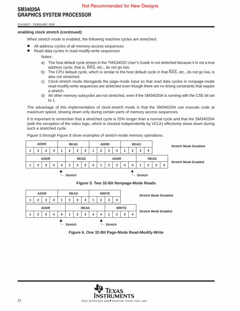
Clock-stretch mode is enabled and disabled using a bit in the CONFIG register memory mapped to locationC00001A0h, see Figure 4.
01234567
CSE
Loaded at Reset from Reset Vector
Protected Byte
CONFIG register
CSE = 0: Disable stretch mode (normal operation)CSE = 1: Enable stretch mode
31
Figure 4. Stretch Mode Enable
Bit 4 of the CONFIG register is the clock-stretch-enable mode bit. A zero in this bit disables stretch mode anda one in this bit enables stretch mode. The bit is cleared during reset; that is, stretch mode is disabled by default.
Not Recommended for New Designs
������������ � ������ � ����
SGUS057 − FEBRUARY 2005
22 POST OFFICE BOX 1443 • HOUSTON, TEXAS 77251−1443
enabling clock stretch (continued)
When stretch mode is enabled, the following machine cycles are stretched:
� All address cycles of all memory-access sequences� Read data cycles in read-modify-write sequences
Notes:
a) The host default cycle shown in the TMS34020 User’s Guide is not stretched because it is not a trueaddress cycle; that is, RAS, etc., do not go low.
b) The CPU default cycle, which is similar to the host default cycle in that RAS, etc., do not go low, isalso not stretched.
c) Clock-stretch mode disregards the page-mode input so that read data cycles in nonpage-moderead-modify-write sequences are stretched even though there are no timing constraints that requirea stretch.
d) All other memory subcycles are not stretched, even if the SM34020A is running with the CSE bit setto 1.
The advantage of this implementation of clock-stretch mode is that the SM34020A can execute code atmaximum speed, slowing down only during certain parts of memory access sequences.
It is important to remember that a stretched cycle is 25% longer than a normal cycle and that the SM34020A(with the exception of the video logic, which is clocked independently by VCLK) effectively slows down duringsuch a stretched cycle.
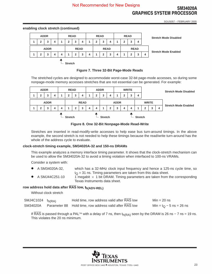
Figure 5 through Figure 8 show examples of stretch-mode memory operations.
READADDRREADADDR
4321432143214321
READADDRREADADDR
4321443143244321 1 2
Stretch Stretch
Stretch Mode Enabled
Stretch Mode Disabled
Figure 5. Two 32-Bit Nonpage-Mode Reads
WRITEREADADDR
432143214321
WRITEREADADDR
432443244321 1 1
Stretch Stretch
Stretch Mode Enabled
Stretch Mode Disabled
Figure 6. One 32-Bit Page-Mode Read-Modify-Write
Not Recommended for New Designs
������������ � ������ � ����
SGUS057 − FEBRUARY 2005
23POST OFFICE BOX 1443 • HOUSTON, TEXAS 77251−1443
enabling clock stretch (continued)
READREADREADADDR
4321432143214321
READREADREADADDR
432143143244321 1 2
Stretch
Stretch Mode Enabled
Stretch Mode Disabled
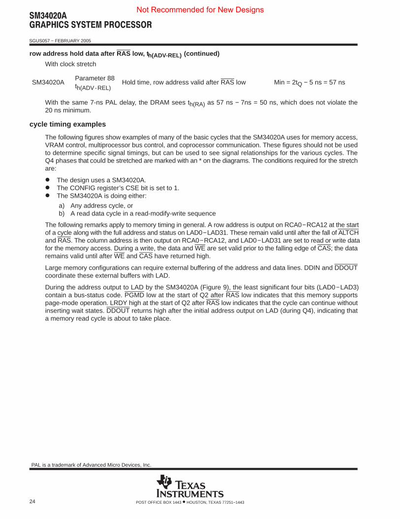
Figure 7. Three 32-Bit Page-Mode Reads
The stretched cycles are designed to accommodate worst-case 32-bit page-mode accesses, so during somenonpage-mode memory accesses stretches that are not essential can be generated. For example:
WRITEADDRREADADDR
4321432143214321
WRITEADDRREADADDR
4321443443244321 1 2
Stretch Stretch
Stretch Mode Enabled
Stretch Mode Disabled
1
Stretch
Figure 8. One 32-Bit Nonpage-Mode Read-Write
Stretches are inserted in read-modify-write accesses to help ease bus turn-around timings. In the aboveexample, the second stretch is not needed to help these timings because the read/write turn-around has thewhole of the address cycle to evaluate.
clock-stretch timing example, SM34020A-32 and 150-ns DRAMs
This example analyzes a memory interface timing parameter. It shows that the clock-stretch mechanism canbe used to allow the SM34020A-32 to avoid a timing violation when interfaced to 100-ns VRAMs.
Consider a system with:
� A SM34020A-32, which has a 32-MHz clock input frequency and hence a 125-ns cycle time, sotQ = 31 ns. Timing parameters are taken from this data sheet.
� A SMJ44C251-10 1 megabit × 1 bit DRAM. Timing parameters are taken from the correspondingTexas Instruments data sheet.
row address hold data after RAS low, th(ADV-REL)
Without clock stretch
SMJ4C1024 th(RA) Hold time, row address valid after RAS low Min = 20 ns
SM34020A Parameter 88 Hold time, row address valid after RAS low Min = tQ − 5 ns = 26 ns
If RAS is passed through a PAL with a delay of 7 ns, then th(RA) seen by the DRAM is 26 ns − 7 ns = 19 ns.This violates the 20 ns minimum.
Not Recommended for New Designs
������������ � ������ � ����
SGUS057 − FEBRUARY 2005
24 POST OFFICE BOX 1443 • HOUSTON, TEXAS 77251−1443
row address hold data after RAS low, th(ADV-REL) (continued)
With clock stretch
SM34020AParameter 88th(ADV-REL)
Hold time, row address valid after RAS low Min = 2tQ − 5 ns = 57 ns
With the same 7-ns PAL delay, the DRAM sees th(RA) as 57 ns − 7ns = 50 ns, which does not violate the20 ns minimum.
cycle timing examples
The following figures show examples of many of the basic cycles that the SM34020A uses for memory access,VRAM control, multiprocessor bus control, and coprocessor communication. These figures should not be usedto determine specific signal timings, but can be used to see signal relationships for the various cycles. TheQ4 phases that could be stretched are marked with an * on the diagrams. The conditions required for the stretchare:
� The design uses a SM34020A.� The CONFIG register’s CSE bit is set to 1.� The SM34020A is doing either:
a) Any address cycle, orb) A read data cycle in a read-modify-write sequence
The following remarks apply to memory timing in general. A row address is output on RCA0−RCA12 at the startof a cycle along with the full address and status on LAD0−LAD31. These remain valid until after the fall of ALTCHand RAS. The column address is then output on RCA0−RCA12, and LAD0−LAD31 are set to read or write datafor the memory access. During a write, the data and WE are set valid prior to the falling edge of CAS; the dataremains valid until after WE and CAS have returned high.
Large memory configurations can require external buffering of the address and data lines. DDIN and DDOUTcoordinate these external buffers with LAD.
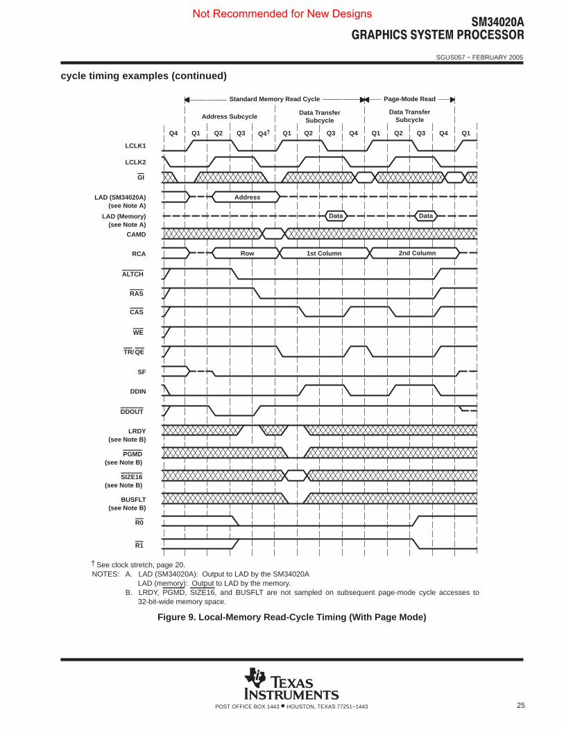
During the address output to LAD by the SM34020A (Figure 9), the least significant four bits (LAD0−LAD3)contain a bus-status code. PGMD low at the start of Q2 after RAS low indicates that this memory supportspage-mode operation. LRDY high at the start of Q2 after RAS low indicates that the cycle can continue withoutinserting wait states. DDOUT returns high after the initial address output on LAD (during Q4), indicating thata memory read cycle is about to take place.
PAL is a trademark of Advanced Micro Devices, Inc.
Not Recommended for New Designs
������������ � ������ � ����
SGUS057 − FEBRUARY 2005
25POST OFFICE BOX 1443 • HOUSTON, TEXAS 77251−1443
cycle timing examples (continued)
BUSFLT(see Note B)
LRDY(see Note B)
DDIN
SF
RCA
CAMD
LCLK2
LCLK1
GI
ALTCH
RAS
CAS
WE
TR/ QE
DDOUT
PGMD(see Note B)
SIZE16(see Note B)
Q4 Q1 Q2 Q3 Q1 Q2 Q3 Q4 Q1 Q2 Q3 Q4 Q1
Address
Row 1st Column 2nd Column
Address SubcycleData Transfer
SubcycleData Transfer
Subcycle
Data Data
R0
R1
Standard Memory Read Cycle Page-Mode Read
LAD (SM34020A)(see Note A)
LAD (Memory)(see Note A)
Q4†
† See clock stretch, page 20.NOTES: A. LAD (SM34020A): Output to LAD by the SM34020A
LAD (memory): Output to LAD by the memory.B. LRDY, PGMD, SIZE16, and BUSFLT are not sampled on subsequent page-mode cycle accesses to
32-bit-wide memory space.
Figure 9. Local-Memory Read-Cycle Timing (With Page Mode)
Not Recommended for New Designs
������������ � ������ � ����
SGUS057 − FEBRUARY 2005
26 POST OFFICE BOX 1443 • HOUSTON, TEXAS 77251−1443
cycle timing examples (continued)
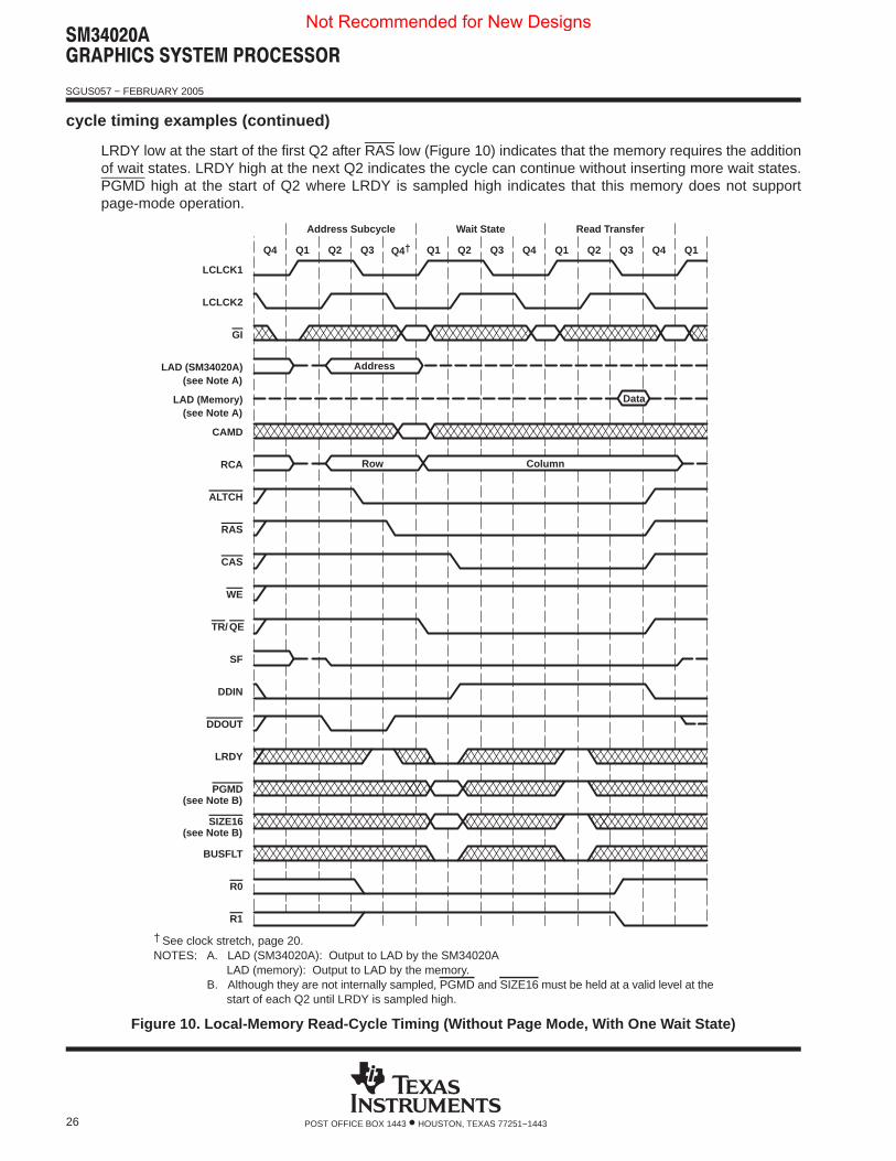
LRDY low at the start of the first Q2 after RAS low (Figure 10) indicates that the memory requires the additionof wait states. LRDY high at the next Q2 indicates the cycle can continue without inserting more wait states.PGMD high at the start of Q2 where LRDY is sampled high indicates that this memory does not supportpage-mode operation.
LCLCK1
LCLCK2
GI
LAD (SM34020A)
LAD (Memory)
CAMD
RCA
ALTCH
RAS
CAS
WE
TR/ QE
SF
DDIN
DDOUT
LRDY
PGMD
SIZE16
BUSFLT
R0
R1
Q4 Q1 Q2 Q3 Q1 Q2 Q3 Q4 Q1 Q2 Q3 Q4 Q1
Address
Column
Address Subcycle Wait State Read Transfer
Data
Row
Q4†
(see Note A)
(see Note A)
(see Note B)
(see Note B)
† See clock stretch, page 20.NOTES: A. LAD (SM34020A): Output to LAD by the SM34020A
LAD (memory): Output to LAD by the memory.B. Although they are not internally sampled, PGMD and SIZE16 must be held at a valid level at the
start of each Q2 until LRDY is sampled high.
Figure 10. Local-Memory Read-Cycle Timing (Without Page Mode, With One Wait State)
Not Recommended for New Designs
������������ � ������ � ����
SGUS057 − FEBRUARY 2005
27POST OFFICE BOX 1443 • HOUSTON, TEXAS 77251−1443
cycle timing examples (continued)
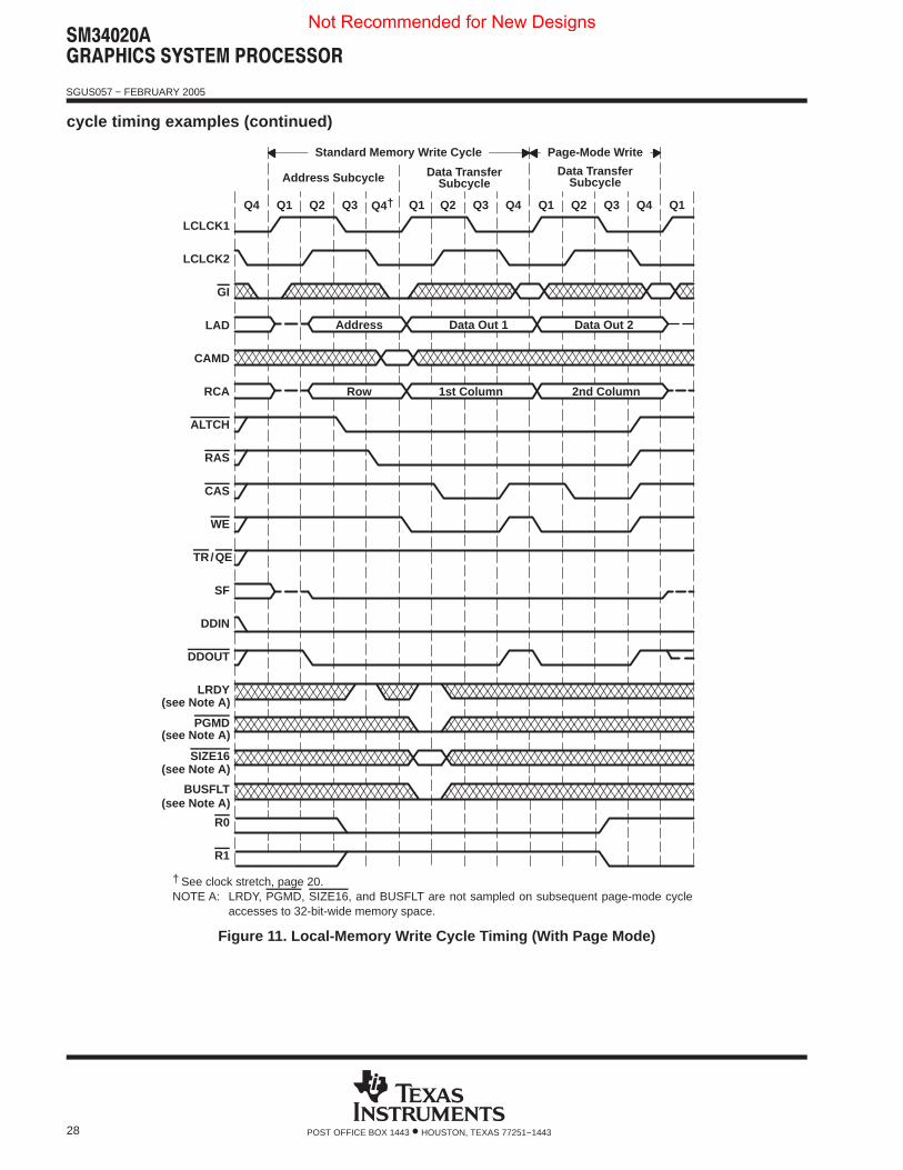
During the address output to LAD by the SM34020A (Figure 11), the least significant four bits (LAD0−LAD3)contain a bus-status code. PGMD low at the start of Q2 after RAS low indicates that this memory supportspage-mode operation. LRDY high at the start of Q2 after RAS low indicates that the cycle can continue withoutinserting wait states.
DDOUT remains low after the initial address output on LAD (during Q4 after RAS goes low), indicating that amemory write cycle is about to take place.
Not Recommended for New Designs
������������ � ������ � ����
SGUS057 − FEBRUARY 2005
28 POST OFFICE BOX 1443 • HOUSTON, TEXAS 77251−1443
cycle timing examples (continued)
LCLCK1
LCLCK2
GI
LAD
CAMD
RCA
ALTCH
RAS
CAS
WE
TR/QE
SF
DDIN
DDOUT
LRDY
PGMD
SIZE16
BUSFLT
R0
R1
Q4 Q1 Q2 Q3 Q1 Q2 Q3 Q4 Q1 Q2 Q3 Q4 Q1
Address
Row 1st Column 2nd Column
Address Subcycle Data TransferSubcycle
Data TransferSubcycle
Data Out 1 Data Out 2
Standard Memory Write Cycle Page-Mode Write
Q4†
(see Note A)
(see Note A)
(see Note A)
(see Note A)
† See clock stretch, page 20.NOTE A: LRDY, PGMD, SIZE16, and BUSFLT are not sampled on subsequent page-mode cycle
accesses to 32-bit-wide memory space.
Figure 11. Local-Memory Write Cycle Timing (With Page Mode)
Not Recommended for New Designs
������������ � ������ � ����
SGUS057 − FEBRUARY 2005
29POST OFFICE BOX 1443 • HOUSTON, TEXAS 77251−1443
cycle timing examples (continued)
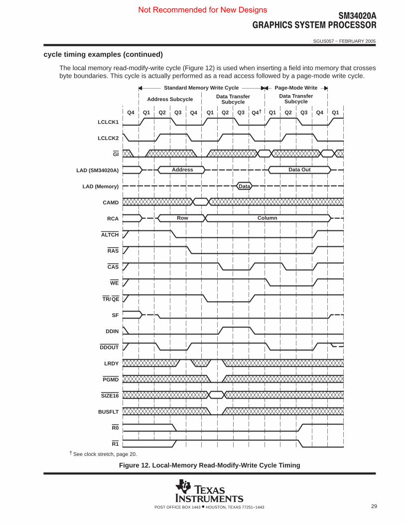
The local memory read-modify-write cycle (Figure 12) is used when inserting a field into memory that crossesbyte boundaries. This cycle is actually performed as a read access followed by a page-mode write cycle.
Q4 Q1 Q2 Q3 Q1 Q2 Q3 Q1 Q2 Q3 Q4 Q1
Address
Row Column
Address Subcycle Data TransferSubcycle
Data TransferSubcycle
Data
Data Out
Standard Memory Write Cycle Page-Mode Write
LCLCK1
LCLCK2
GI
LAD (SM34020A)
LAD (Memory)
CAMD
RCA
ALTCH
RAS
CAS
WE
TR/QE
SF
DDIN
DDOUT
LRDY
PGMD
SIZE16
BUSFLT
R0
R1
Q4 Q4†
† See clock stretch, page 20.
Figure 12. Local-Memory Read-Modify-Write Cycle Timing
Not Recommended for New Designs
������������ � ������ � ����
SGUS057 − FEBRUARY 2005
30 POST OFFICE BOX 1443 • HOUSTON, TEXAS 77251−1443
cycle timing examples (continued)
The refresh pseudo-address output to RCA0−RCA12 and LAD0−LAD31 comes from the 16-bit refreshaddress register (I/O register C000 01F0h) that is incremented after each refresh cycle (Figure 13). The 16 bitsof address are placed on LAD16−LAD31; all other LAD bus lines are zero. The logical addresses onRCA0−RCA12 corresponding to LAD16−LAD31 also output the address from the refresh-address register.
Although PGMD and SIZE16 are ignored during a refresh cycle, they should be held at valid levels. LRDY andBUSFLT are not sampled until the start of the first Q2 cycle after RAS has gone low.
If a refresh cycle is aborted due to a high-priority bus request (assuming LRDY is low at Q2 after RAS low), abus fault, or an external retry, then the count of refreshes pending is not decremented and the samepseudo-address is reissued when the refresh is restarted.
Not Recommended for New Designs
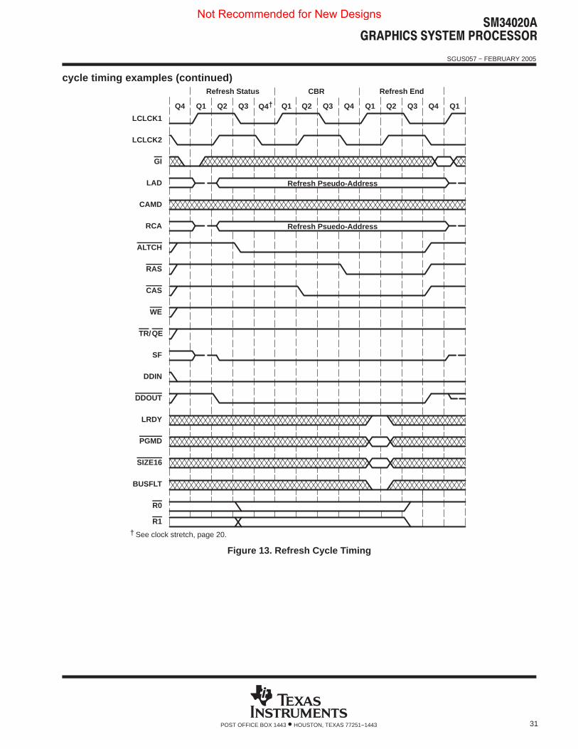
������������ � ������ � ����
SGUS057 − FEBRUARY 2005
31POST OFFICE BOX 1443 • HOUSTON, TEXAS 77251−1443
cycle timing examples (continued)
Q4 Q1 Q2 Q3 Q1 Q2 Q3 Q4 Q1 Q2 Q3 Q4 Q1
Refresh Pseudo-Address
Refresh Psuedo-Address
Refresh Status Refresh EndCBR
LCLCK1
LCLCK2
GI
LAD
CAMD
RCA
ALTCH
RAS
CAS
WE
TR/QE
SF
DDIN
DDOUT
LRDY
PGMD
SIZE16
BUSFLT
R0
R1
Q4†
† See clock stretch, page 20.
Figure 13. Refresh Cycle Timing
Not Recommended for New Designs
������������ � ������ � ����
SGUS057 − FEBRUARY 2005
32 POST OFFICE BOX 1443 • HOUSTON, TEXAS 77251−1443
cycle timing examples (continued)
When SIZE16 is selected low (Figure 14), the SM34020A performs a second cycle to read (or write) theremaining 16 bits of the word. Reads always access all 32 bits (all CAS strobes are active). Internally, theSM34020A latches both the high and the low words obtained on the first read cycle. The sense of SIZE16 onthe second (odd-word) access is used to determine which half of the bus is to be sampled to replace the dataword latched during the first cycle.
Not Recommended for New Designs
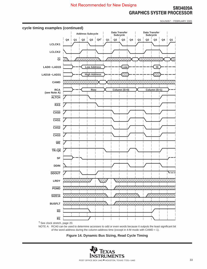
������������ � ������ � ����
SGUS057 − FEBRUARY 2005
33POST OFFICE BOX 1443 • HOUSTON, TEXAS 77251−1443
cycle timing examples (continued)
Row Column (S=0) Column (S=1)
Q4 Q1 Q2 Q3 Q1 Q2 Q3 Q4 Q1 Q2 Q3 Q4 Q1
Low Address
Address Subcycle Data Transfer Data TransferSubcycle Subcycle
High Address
HiLow
LCLCK1
LCLCK2
GI
LAD0−LAD15
LAD16−LAD31
CAMD
RCA
ALTCH
RAS
CAS0
CAS1
CAS2
CAS3
WE
TR/QE
SF
DDIN
DDOUT
LRDY
PGMD
SIZE16
BUSFLT
R0
R1
Q4†
(see Note A)
† See clock stretch, page 20.NOTE A: RCA0 can be used to determine accesses to odd or even words because it outputs the least significant bit
of the word address during the column-address time (except in 4-M mode with CAMD = 1).
Figure 14. Dynamic Bus Sizing, Read Cycle Timing
Not Recommended for New Designs
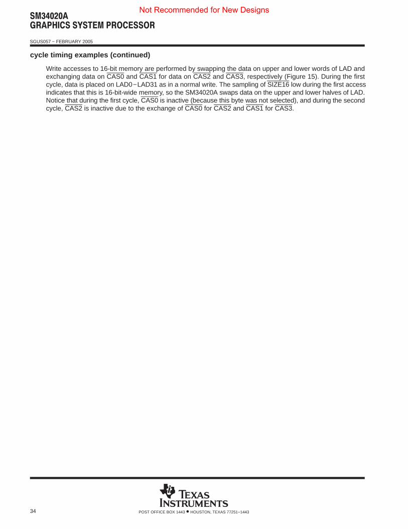
������������ � ������ � ����
SGUS057 − FEBRUARY 2005
34 POST OFFICE BOX 1443 • HOUSTON, TEXAS 77251−1443
cycle timing examples (continued)
Write accesses to 16-bit memory are performed by swapping the data on upper and lower words of LAD andexchanging data on CAS0 and CAS1 for data on CAS2 and CAS3, respectively (Figure 15). During the firstcycle, data is placed on LAD0−LAD31 as in a normal write. The sampling of SIZE16 low during the first accessindicates that this is 16-bit-wide memory, so the SM34020A swaps data on the upper and lower halves of LAD.Notice that during the first cycle, CAS0 is inactive (because this byte was not selected), and during the secondcycle, CAS2 is inactive due to the exchange of CAS0 for CAS2 and CAS1 for CAS3.
Not Recommended for New Designs
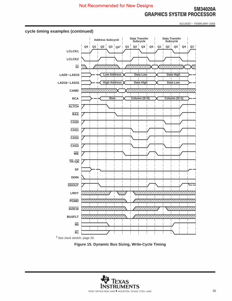
������������ � ������ � ����
SGUS057 − FEBRUARY 2005
35POST OFFICE BOX 1443 • HOUSTON, TEXAS 77251−1443
cycle timing examples (continued)
Row Column (S=0) Column (S=1)
Q4 Q1 Q2 Q3 Q1 Q2 Q3 Q4 Q1 Q2 Q3 Q4 Q1
Low Address
Address Subcycle Data Transfer Data TransferSubcycle Subcycle
High Address
Data Low
Data High
Data High
Data Low
LCLCK1
LCLCK2
GI
LAD0−LAD15
LAD16−LAD31
CAMD
RCA
ALTCH
RAS
CAS0
CAS1
CAS2
CAS3
WE
TR/QE
SF
DDIN
DDOUT
LRDY
PGMD
SIZE16
BUSFLT
R0
R1
Q4†
† See clock stretch, page 20.
Figure 15. Dynamic Bus Sizing, Write-Cycle Timing
Not Recommended for New Designs
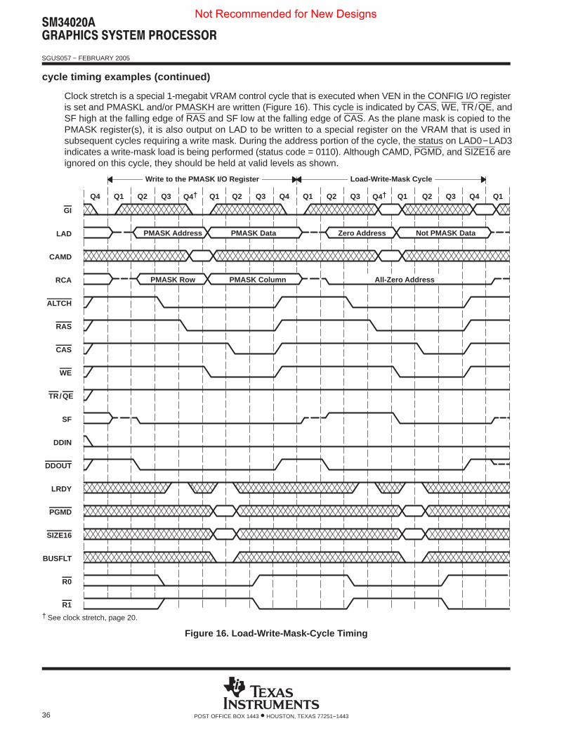
������������ � ������ � ����
SGUS057 − FEBRUARY 2005
36 POST OFFICE BOX 1443 • HOUSTON, TEXAS 77251−1443
cycle timing examples (continued)
Clock stretch is a special 1-megabit VRAM control cycle that is executed when VEN in the CONFIG I/O registeris set and PMASKL and/or PMASKH are written (Figure 16). This cycle is indicated by CAS, WE, TR/QE, andSF high at the falling edge of RAS and SF low at the falling edge of CAS. As the plane mask is copied to thePMASK register(s), it is also output on LAD to be written to a special register on the VRAM that is used insubsequent cycles requiring a write mask. During the address portion of the cycle, the status on LAD0−LAD3indicates a write-mask load is being performed (status code = 0110). Although CAMD, PGMD, and SIZE16 areignored on this cycle, they should be held at valid levels as shown.
Q4 Q1 Q2 Q3 Q1 Q2 Q3 Q4 Q1 Q2 Q3 Q1
PMASK Row
PMASK Address PMASK Data Zero Address
Q2 Q3 Q4 Q1
Not PMASK Data
PMASK Column All-Zero Address
Write to the PMASK I/O Register Load-Write-Mask Cycle
GI
LAD
CAMD
RCA
ALTCH
RAS
CAS
WE
TR/QE
SF
DDIN
DDOUT
LRDY
PGMD
SIZE16
BUSFLT
R0
R1
Q4† Q4†
† See clock stretch, page 20.
Figure 16. Load-Write-Mask-Cycle Timing
Not Recommended for New Designs
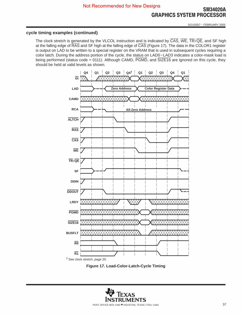
������������ � ������ � ����
SGUS057 − FEBRUARY 2005
37POST OFFICE BOX 1443 • HOUSTON, TEXAS 77251−1443
cycle timing examples (continued)
The clock stretch is generated by the VLCOL instruction and is indicated by CAS, WE, TR/QE, and SF highat the falling edge of RAS and SF high at the falling edge of CAS (Figure 17). The data in the COLOR1 registeris output on LAD to be written to a special register on the VRAM that is used in subsequent cycles requiring acolor latch. During the address portion of the cycle, the status on LAD0−LAD3 indicates a color-mask load isbeing performed (status code = 0111). Although CAMD, PGMD, and SIZE16 are ignored on this cycle, theyshould be held at valid levels as shown.
Q4 Q1 Q2 Q3 Q1 Q2 Q3 Q4 Q1
All-Zero Address
Zero Address Color Register Data
GI
LAD
CAMD
RCA
ALTCH
RAS
CAS
WE
TR/QE
SF
DDIN
DDOUT
LRDY
PGMD
SIZE16
BUSFLT
R0
R1
Q4†
† See clock stretch, page 20.
Figure 17. Load-Color-Latch-Cycle Timing
Not Recommended for New Designs
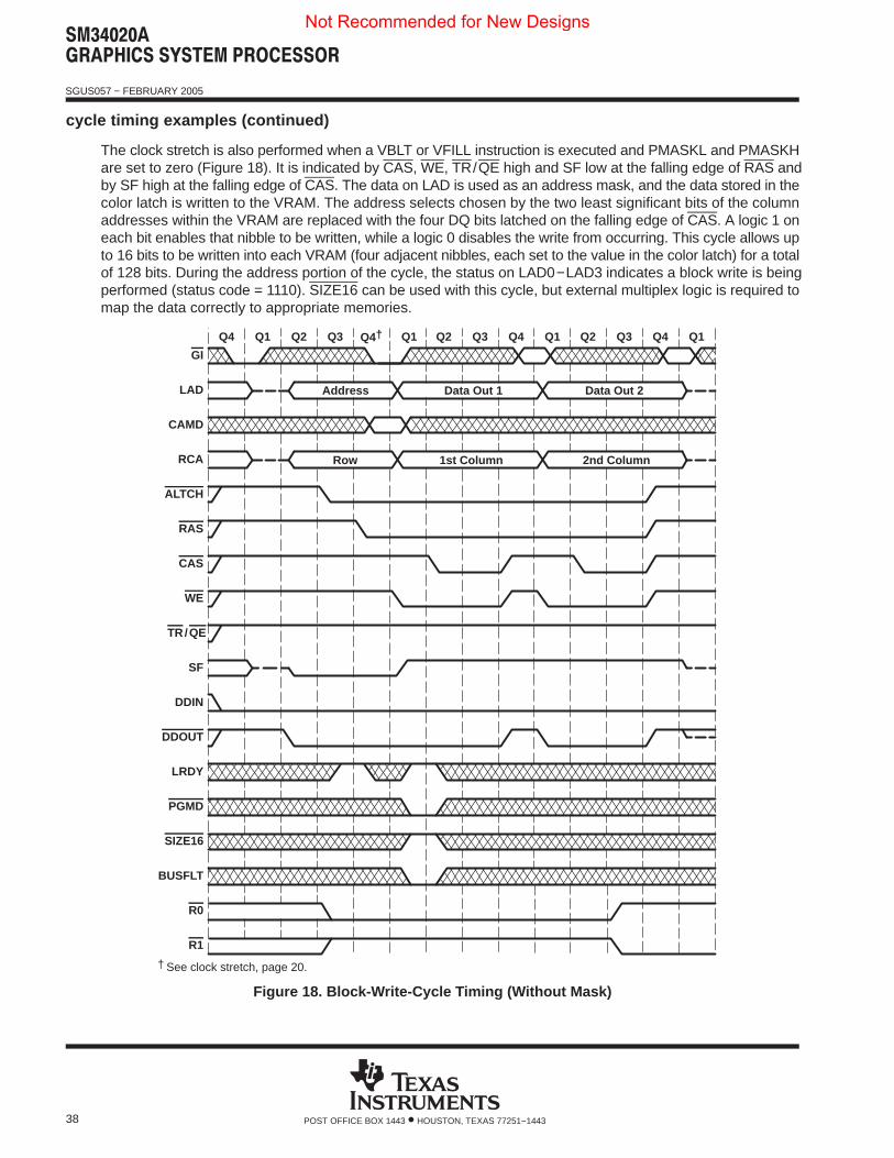
������������ � ������ � ����
SGUS057 − FEBRUARY 2005
38 POST OFFICE BOX 1443 • HOUSTON, TEXAS 77251−1443
cycle timing examples (continued)
The clock stretch is also performed when a VBLT or VFILL instruction is executed and PMASKL and PMASKHare set to zero (Figure 18). It is indicated by CAS, WE, TR/QE high and SF low at the falling edge of RAS andby SF high at the falling edge of CAS. The data on LAD is used as an address mask, and the data stored in thecolor latch is written to the VRAM. The address selects chosen by the two least significant bits of the columnaddresses within the VRAM are replaced with the four DQ bits latched on the falling edge of CAS. A logic 1 oneach bit enables that nibble to be written, while a logic 0 disables the write from occurring. This cycle allows upto 16 bits to be written into each VRAM (four adjacent nibbles, each set to the value in the color latch) for a totalof 128 bits. During the address portion of the cycle, the status on LAD0−LAD3 indicates a block write is beingperformed (status code = 1110). SIZE16 can be used with this cycle, but external multiplex logic is required tomap the data correctly to appropriate memories.
Q4 Q1 Q2 Q3 Q1 Q2 Q3 Q4 Q1
Row
Address Data Out 1
Q2 Q3 Q4 Q1
Data Out 2
1st Column 2nd Column
GI
LAD
CAMD
RCA
ALTCH
RAS
CAS
WE
TR/QE
SF
DDIN
DDOUT
LRDY
PGMD
SIZE16
BUSFLT
R0
R1
Q4†
† See clock stretch, page 20.
Figure 18. Block-Write-Cycle Timing (Without Mask)
Not Recommended for New Designs
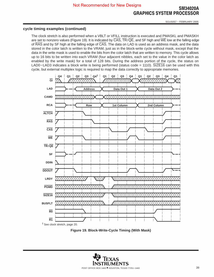
������������ � ������ � ����
SGUS057 − FEBRUARY 2005
39POST OFFICE BOX 1443 • HOUSTON, TEXAS 77251−1443
cycle timing examples (continued)
The clock stretch is also performed when a VBLT or VFILL instruction is executed and PMASKL and PMASKHare set to nonzero values (Figure 19). It is indicated by CAS, TR/QE, and SF high and WE low at the falling edgeof RAS and by SF high at the falling edge of CAS. The data on LAD is used as an address mask, and the datastored in the color latch is written to the VRAM, just as in the block-write cycle without mask, except that thedata in the write mask is used to enable the bits from the color latch that are written to memory. This cycle allowsup to 16 bits to be written into each VRAM (four adjacent nibbles, each set to the value in the color latch asenabled by the write mask) for a total of 128 bits. During the address portion of the cycle, the status onLAD0−LAD3 indicates a block write is being performed (status code = 1110). SIZE16 can be used with thiscycle, but external multiplex logic is required to map the data correctly to appropriate memories.
Q4 Q1 Q2 Q3 Q1 Q2 Q3 Q4 Q1
Row
Address Data Out 1
Q2 Q3 Q4 Q1
Data Out 2
1st Column 2nd Column
GI
LAD
CAMD
RCA
ALTCH
RAS
CAS
WE
TR/QE
SF
DDIN
DDOUT
LRDY
PGMD
SIZE16
BUSFLT
R0
R1
Q4†
† See clock stretch, page 20.
Figure 19. Block-Write-Cycle Timing (With Mask)
Not Recommended for New Designs
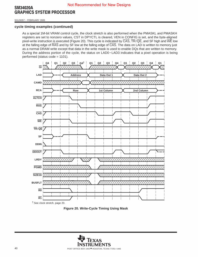
������������ � ������ � ����
SGUS057 − FEBRUARY 2005
40 POST OFFICE BOX 1443 • HOUSTON, TEXAS 77251−1443
cycle timing examples (continued)
As a special 1M-bit VRAM control cycle, the clock stretch is also performed when the PMASKL and PMASKHregisters are set to nonzero values, CST in DPYCTL is cleared, VEN in CONFIG is set, and the byte-alignedpixel-write instruction is executed (Figure 20). This cycle is indicated by CAS, TR/QE, and SF high and WE lowat the falling edge of RAS and by SF low at the falling edge of CAS. The data on LAD is written to memory justas a normal DRAM write except that data in the write mask is used to enable DQs that are written to memory.During the address portion of the cycle, the status on LAD0−LAD3 indicates that a pixel operation is beingperformed (status code = 1101).
Q4 Q1 Q2 Q3 Q1 Q2 Q3 Q4 Q1
Row
Address Data Out 1
Q2 Q3 Q4 Q1
Data Out 2
1st Column 2nd Column
GI
LAD
CAMD
RCA
ALTCH
RAS
CAS
WE
TR/QE
SF
DDIN
DDOUT
LRDY
PGMD
SIZE16
BUSFLT
R0
R1
Q4†
† See clock stretch, page 20.
Figure 20. Write-Cycle Timing Using Mask
Not Recommended for New Designs
������������ � ������ � ����
SGUS057 − FEBRUARY 2005
41POST OFFICE BOX 1443 • HOUSTON, TEXAS 77251−1443
cycle timing examples (continued)
The VRAM cycle shown in Figure 21 is issued in any of three ways:
� Pixel operation instruction with CST in DPYCTL set� Horizontal blank reload cycle requested by the video-control logic with VCE in DPYCTL cleared� Video timeout due to SCOUNT match with the value in MLRNXT and VCE and SSV in DPYCTL cleared
This cycle is indicated by TR/QE and SF low and CAS and WE high at the time RAS goes low. The timing ofthe low-to-high transition of TR/QE is dependent upon the timing of SCLK when doing a midline reload cycle.During the address portion of the cycle, the status on LAD0−LAD3 indicates either a video-initiated VRAMmemory-to-register transfer (status code = 0100), or a CPU-initiated VRAM memory-to-register transfer(status code = 0101).
Not Recommended for New Designs
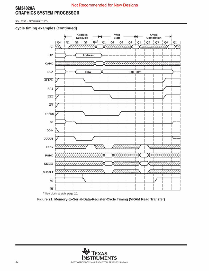
������������ � ������ � ����
SGUS057 − FEBRUARY 2005
42 POST OFFICE BOX 1443 • HOUSTON, TEXAS 77251−1443
cycle timing examples (continued)
Q4 Q1 Q2 Q3 Q1 Q2 Q3 Q4 Q1 Q2 Q3 Q4 Q1
Row
Address
Tap Point
AddressSubcycle
WaitState
CycleCompletion
GI
LAD
CAMD
RCA
ALTCH
RAS
CAS
WE
TR/QE
SF
DDIN
DDOUT
LRDY
PGMD
SIZE16
BUSFLT
R0
R1
Q4†
† See clock stretch, page 20.
Figure 21. Memory-to-Serial-Data-Register-Cycle Timing (VRAM Read Transfer)
Not Recommended for New Designs
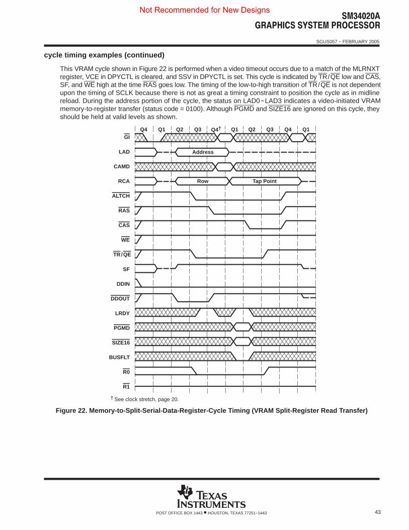
������������ � ������ � ����
SGUS057 − FEBRUARY 2005
43POST OFFICE BOX 1443 • HOUSTON, TEXAS 77251−1443
cycle timing examples (continued)
This VRAM cycle shown in Figure 22 is performed when a video timeout occurs due to a match of the MLRNXTregister, VCE in DPYCTL is cleared, and SSV in DPYCTL is set. This cycle is indicated by TR/QE low and CAS,SF, and WE high at the time RAS goes low. The timing of the low-to-high transition of TR/QE is not dependentupon the timing of SCLK because there is not as great a timing constraint to position the cycle as in midlinereload. During the address portion of the cycle, the status on LAD0−LAD3 indicates a video-initiated VRAMmemory-to-register transfer (status code = 0100). Although PGMD and SIZE16 are ignored on this cycle, theyshould be held at valid levels as shown.
Q4 Q1 Q2 Q3 Q1 Q2 Q3 Q4 Q1
Row
Address
Tap Point
GI
LAD
CAMD
RCA
ALTCH
RAS
CAS
WE
TR/QE
SF
DDIN
DDOUT
LRDY
PGMD
SIZE16
BUSFLT
R0
R1
Q4†
† See clock stretch, page 20.
Figure 22. Memory-to-Split-Serial-Data-Register-Cycle Timing (VRAM Split-Register Read Transfer)
Not Recommended for New Designs
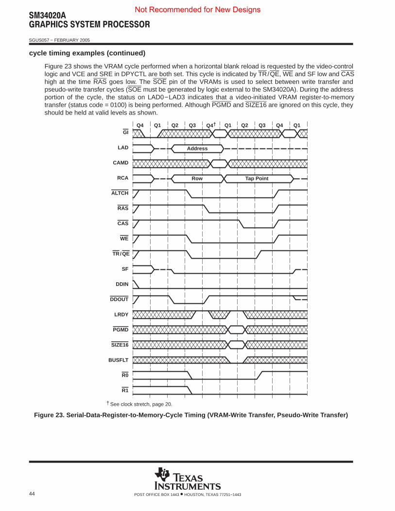
������������ � ������ � ����
SGUS057 − FEBRUARY 2005
44 POST OFFICE BOX 1443 • HOUSTON, TEXAS 77251−1443
cycle timing examples (continued)
Figure 23 shows the VRAM cycle performed when a horizontal blank reload is requested by the video-controllogic and VCE and SRE in DPYCTL are both set. This cycle is indicated by TR/QE, WE and SF low and CAShigh at the time RAS goes low. The SOE pin of the VRAMs is used to select between write transfer andpseudo-write transfer cycles (SOE must be generated by logic external to the SM34020A). During the addressportion of the cycle, the status on LAD0−LAD3 indicates that a video-initiated VRAM register-to-memorytransfer (status code = 0100) is being performed. Although PGMD and SIZE16 are ignored on this cycle, theyshould be held at valid levels as shown.
Q4 Q1 Q2 Q3 Q1 Q2 Q3 Q4 Q1
Row
Address
Tap Point
GI
LAD
CAMD
RCA
ALTCH
RAS
CAS
WE
TR/QE
SF
DDIN
DDOUT
LRDY
PGMD
SIZE16
BUSFLT
R0
R1
Q4†
† See clock stretch, page 20.
Figure 23. Serial-Data-Register-to-Memory-Cycle Timing (VRAM-Write Transfer, Pseudo-Write Transfer)
Not Recommended for New Designs
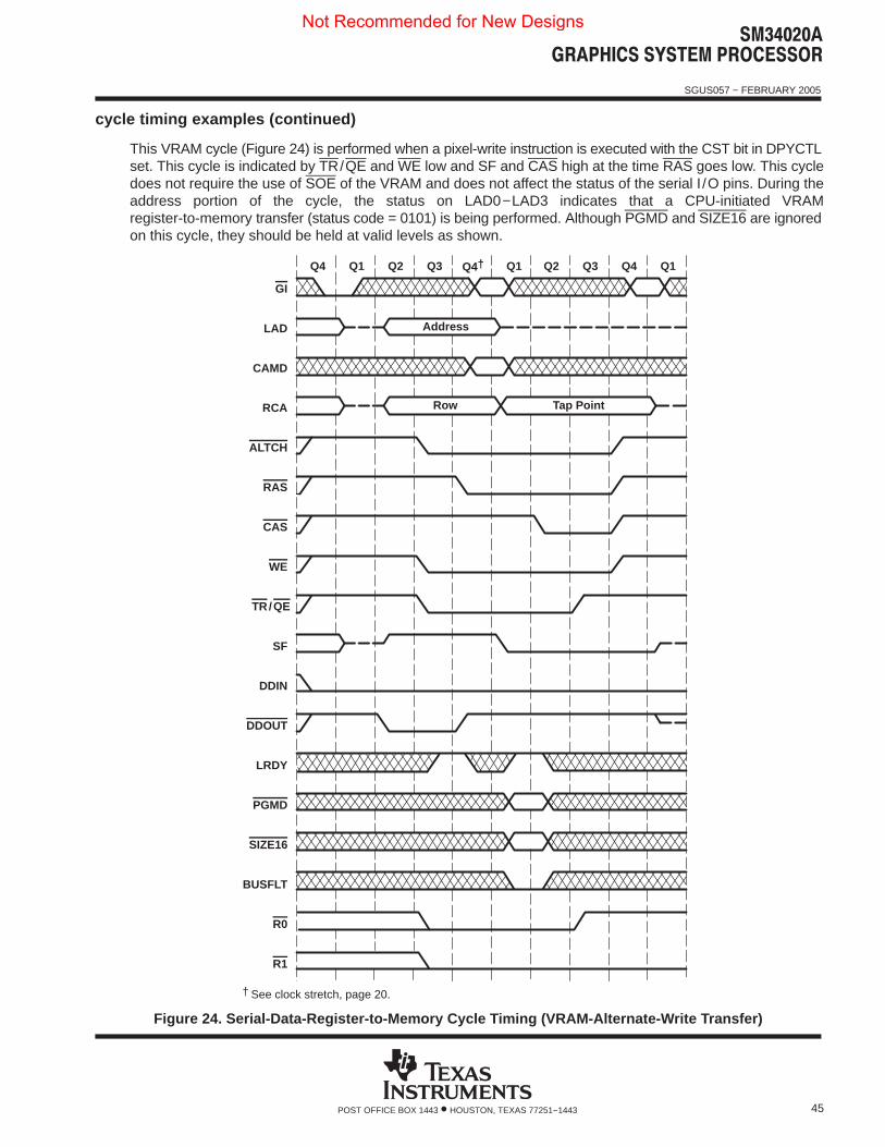
������������ � ������ � ����
SGUS057 − FEBRUARY 2005
45POST OFFICE BOX 1443 • HOUSTON, TEXAS 77251−1443
cycle timing examples (continued)
This VRAM cycle (Figure 24) is performed when a pixel-write instruction is executed with the CST bit in DPYCTLset. This cycle is indicated by TR/QE and WE low and SF and CAS high at the time RAS goes low. This cycledoes not require the use of SOE of the VRAM and does not affect the status of the serial I /O pins. During theaddress portion of the cycle, the status on LAD0−LAD3 indicates that a CPU-initiated VRAMregister-to-memory transfer (status code = 0101) is being performed. Although PGMD and SIZE16 are ignoredon this cycle, they should be held at valid levels as shown.
Q4 Q1 Q2 Q3 Q1 Q2 Q3 Q4 Q1
Row
Address
Tap Point
GI
LAD
CAMD
RCA
ALTCH
RAS
CAS
WE
TR/QE
SF
DDIN
DDOUT
LRDY
PGMD
SIZE16
BUSFLT
R0
R1
Q4†
† See clock stretch, page 20.
Figure 24. Serial-Data-Register-to-Memory Cycle Timing (VRAM-Alternate-Write Transfer)
Not Recommended for New Designs
������������ � ������ � ����
SGUS057 − FEBRUARY 2005
46 POST OFFICE BOX 1443 • HOUSTON, TEXAS 77251−1443
cycle timing examples (continued)
In Figure 25, transition points are shown for R0 and R1 to indicate where they occur relative to the other signals.
This example indicates that the SM34020A has control of the bus, yields control, and then regains control. TheSM34020A regains bus mastership as soon as GI is driven active (low). R0 and R1 could be outputting any ofthe codes with the exception of the access-termination code. The bus arbitration logic must control the timingof GI to all of the processors requiring the bus.
It is recommended that SM34020A clock stretch not be used in multiprocessor systems.
Not Recommended for New Designs
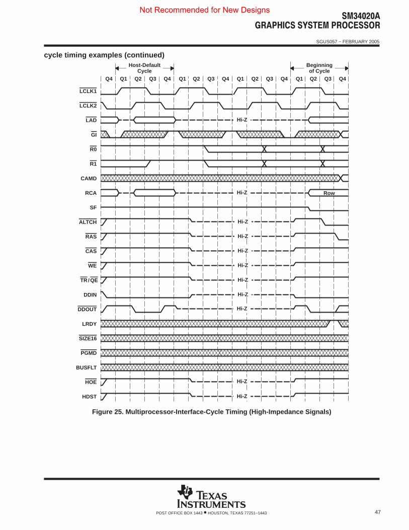
������������ � ������ � ����
SGUS057 − FEBRUARY 2005
47POST OFFICE BOX 1443 • HOUSTON, TEXAS 77251−1443
cycle timing examples (continued)
Q4 Q1 Q2 Q3 Q4 Q1 Q2 Q3 Q4 Q1 Q2 Q3 Q4 Q1 Q2 Q3 Q4
Row
Hi-Z
Hi-Z
Hi-Z
Hi-Z
Hi-Z
Hi-Z
Hi-Z
Hi-Z
Hi-Z
Hi-Z
Hi-Z
Host-DefaultCycle
Beginningof Cycle
LCLK1
LCLK2
LAD
GI
R0
R1
CAMD
RCA
SF
ALTCH
RAS
CAS
WE
TR/QE
DDIN
DDOUT
LRDY
SIZE16
PGMD
BUSFLT
HOE
HDST
Figure 25. Multiprocessor-Interface-Cycle Timing (High-Impedance Signals)
Not Recommended for New Designs
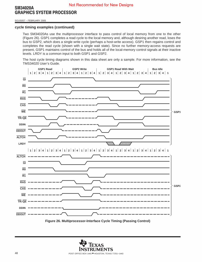
������������ � ������ � ����
SGUS057 − FEBRUARY 2005
48 POST OFFICE BOX 1443 • HOUSTON, TEXAS 77251−1443
cycle timing examples (continued)
Two SM34020As use the multiprocessor interface to pass control of local memory from one to the other(Figure 26). GSP1 completes a read cycle to the local memory and, although desiring another read, loses thebus to GSP2, which does a single write cycle (perhaps a host-write access). GSP1 then regains control andcompletes the read cycle (shown with a single wait state). Since no further memory-access requests arepresent, GSP1 maintains control of the bus and holds all of the local-memory control signals at their inactivelevels. LRDY is a common input to both GSP1 and GSP2.
The host cycle timing diagrams shown in this data sheet are only a sample. For more information, see theTMS34020 User’s Guide.
1 2 3 4 1 2 3 4 1 2 3 4 1 2 3 4 1 2 3 4 1 2 3 4 1 2 3 4 1 2 3 4 1
1 2 3 4 1 2 3 4 1 2 3 4 1 2 3 4 1 2 3 4 1 2 3 4 1 2 3 4 1 2 3 4 1
GSP1 Read GSP2 Write GSP1 Read With Wait Bus Idle
GSP1
GI
R0
R1
RAS
CAS
WE
TR/QE
DDIN
DDOUT
ALTCH
LRDY
ALTCH
GI
R0
R1
RAS
CAS
WE
TR/QE
DDIN
DDOUT
GSP2
Figure 26. Multiprocessor-Interface Cycle Timing (Passing Control)
Not Recommended for New Designs
������������ � ������ � ����
SGUS057 − FEBRUARY 2005
49POST OFFICE BOX 1443 • HOUSTON, TEXAS 77251−1443
cycle timing examples (continued)
In Figure 27, the host-access request is synchronized to the SM34020A at the beginning of Q4 so that thelocal-memory cycle can begin in Q1. If the external host-access request occurs after the setup time requirementbefore Q4, the request is not considered until the next Q4 cycle. In order to provide back-to-back accesses asindicated in this example, the host must remove HCS on receipt of HRDY and reassert it before Q4 (it can alsoremove and reassert HREAD with HCS).
Not Recommended for New Designs
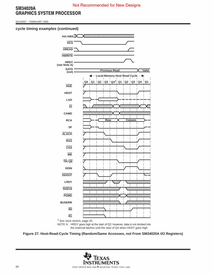
������������ � ������ � ����
SGUS057 − FEBRUARY 2005
50 POST OFFICE BOX 1443 • HOUSTON, TEXAS 77251−1443
cycle timing examples (continued)
Q4 Q1 Q2 Q3 Q1 Q2 Q3 Q4 Q1
Row Column
HOE
HDST
LAD
GI
CAMD
RCA
SF
ALACH
RAS
CAS
WE
TR/QE
DDIN
DDOUT
LRDY
SIZE16
PGMD
BUSERR
R0
R1
Previous Read Valid
Local-Memory Host Read Cycle
HA/HBS
HCS
HREAD
HWRITE
HRDY
DATA(out)
Q4†
(see Note A)
† See clock stretch, page 20.NOTE A: HRDY goes high at the start of Q2; however, data is not strobed into
the external latches until the start of Q4 when HDST goes high.
Figure 27. Host-Read-Cycle Timing (Random/Same Accesses, not From SM34020A I/O Registers)
Not Recommended for New Designs
������������ � ������ � ����
SGUS057 − FEBRUARY 2005
51POST OFFICE BOX 1443 • HOUSTON, TEXAS 77251−1443
cycle timing examples (continued)
The host-access request is synchronized to the SM34020A at the beginning of Q4 so that the local memory cyclecan begin in Q1.
In block mode (prefetch after read), the SM34020A automatically initiates sequential read accesses as soonas the host deasserts the current read request. In this example, the host reads a location and must wait for thefirst access to complete. When the host removes HREAD (Figure 28), indicating the end of the first read, theSM34020A starts to prefetch the next sequential location. When the host makes the next request, theSM34020A has prefetched the data so that the host reads with no delay. While in block mode, the SM34020Acontinues to prefetch data for the host read each time the host removes either HREAD or HCS. If the addresspresent and latched at the falling edge of HCS matches the previously prefetched address, HRDY is assertedhigh so that the host can read with no delay.
In read-modify-write mode (prefetch after write), the SM34020A initiates the read access as soon as the currentwrite request is deasserted.
Not Recommended for New Designs
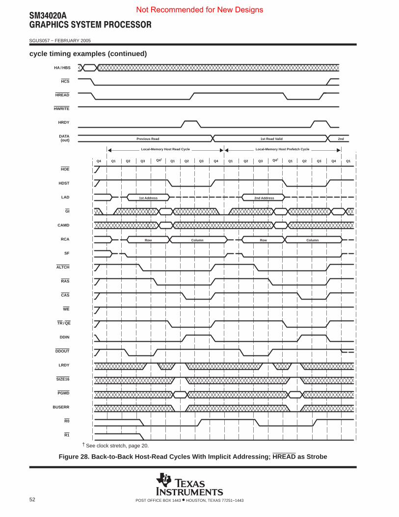
������������ � ������ � ����
SGUS057 − FEBRUARY 2005
52 POST OFFICE BOX 1443 • HOUSTON, TEXAS 77251−1443
cycle timing examples (continued)
Q4†Q4 Q1 Q2 Q3 Q1 Q2 Q3 Q4 Q1
Row Column
Previous Read 1st Read Valid
1st Address
Row Column
2nd Address
Q2 Q3 Q1 Q2 Q3 Q4 Q1
2nd
Local-Memory Host Read Cycle Local-Memory Host Prefetch Cycle
HA / HBS
HCS
HREAD
HWRITE
HRDY
HOE
HDST
LAD
GI
CAMD
RCA
SF
ALTCH
RAS
CAS
WE
TR / QE
DDIN
DDOUT
LRDY
SIZE16
PGMD
BUSERR
R0
R1
DATA(out)
Q4†
† See clock stretch, page 20.
Figure 28. Back-to-Back Host-Read Cycles With Implicit Addressing; HREAD as Strobe
Not Recommended for New Designs

������������ � ������ � ����
SGUS057 − FEBRUARY 2005
53POST OFFICE BOX 1443 • HOUSTON, TEXAS 77251−1443
cycle timing examples (continued)
The host read of the SM34020A I/O registers (Figure 29) suppresses the generation of TR/QE and CAS so thatdata is read from the SM34020A rather than from memory. DDOUT is enabled so that data can flow throughexternal buffers on LAD to the host data latches. The SM34020A I/O registers can be accessed in any of thehost access modes (random/same, block, or read-modify-write).
Not Recommended for New Designs
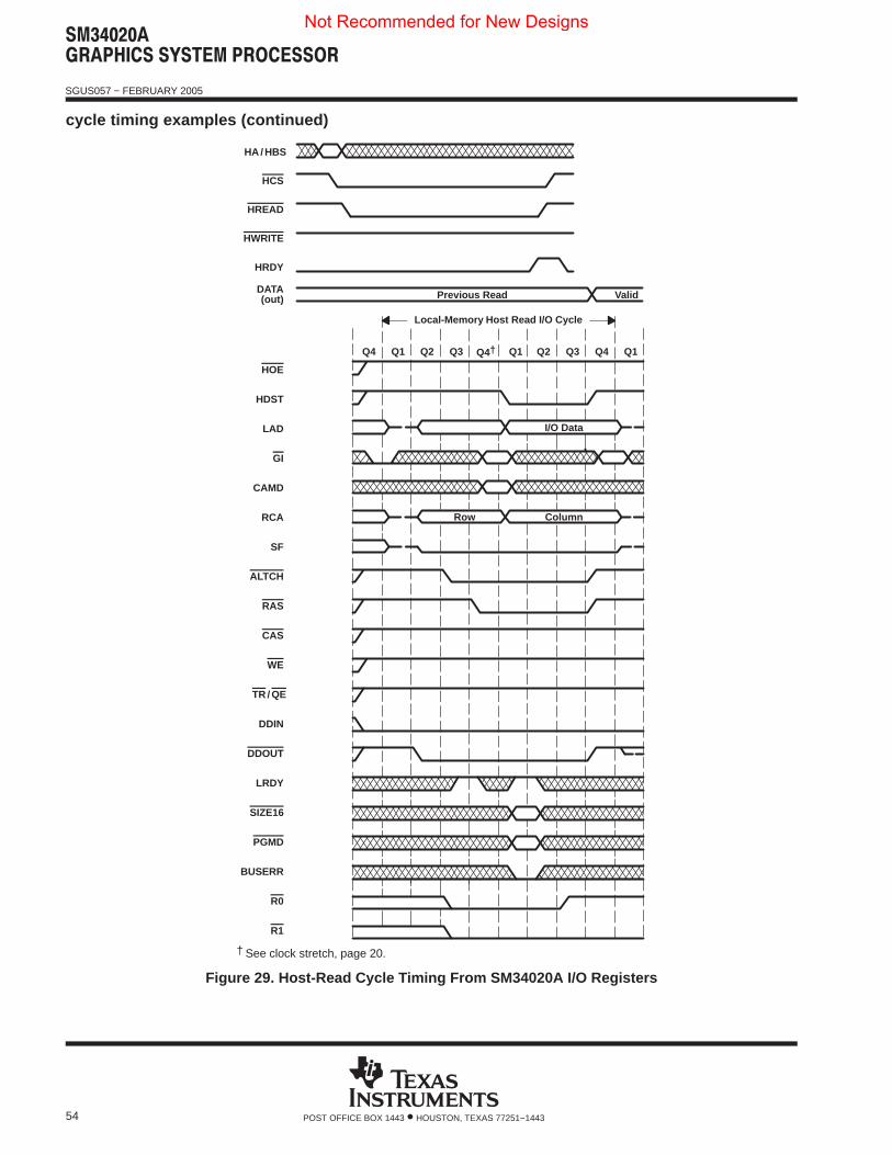
������������ � ������ � ����
SGUS057 − FEBRUARY 2005
54 POST OFFICE BOX 1443 • HOUSTON, TEXAS 77251−1443
cycle timing examples (continued)
Q4 Q1 Q2 Q3 Q1 Q2 Q3 Q4 Q1
Row Column
Previous Read Valid
I/O Data
Local-Memory Host Read I/O Cycle
HA / HBS
HCS
HREAD
HWRITE
HRDY
HOE
HDST
LAD
GI
CAMD
RCA
SF
ALTCH
RAS
CAS
WE
TR / QE
DDIN
DDOUT
LRDY
SIZE16
PGMD
BUSERR
R0
R1
DATA(out)
Q4†
† See clock stretch, page 20.
Figure 29. Host-Read Cycle Timing From SM34020A I/O Registers
Not Recommended for New Designs
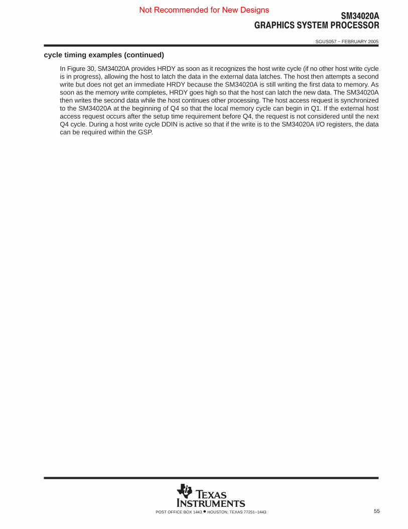
������������ � ������ � ����
SGUS057 − FEBRUARY 2005
55POST OFFICE BOX 1443 • HOUSTON, TEXAS 77251−1443
cycle timing examples (continued)
In Figure 30, SM34020A provides HRDY as soon as it recognizes the host write cycle (if no other host write cycleis in progress), allowing the host to latch the data in the external data latches. The host then attempts a secondwrite but does not get an immediate HRDY because the SM34020A is still writing the first data to memory. Assoon as the memory write completes, HRDY goes high so that the host can latch the new data. The SM34020Athen writes the second data while the host continues other processing. The host access request is synchronizedto the SM34020A at the beginning of Q4 so that the local memory cycle can begin in Q1. If the external hostaccess request occurs after the setup time requirement before Q4, the request is not considered until the nextQ4 cycle. During a host write cycle DDIN is active so that if the write is to the SM34020A I/O registers, the datacan be required within the GSP.
Not Recommended for New Designs
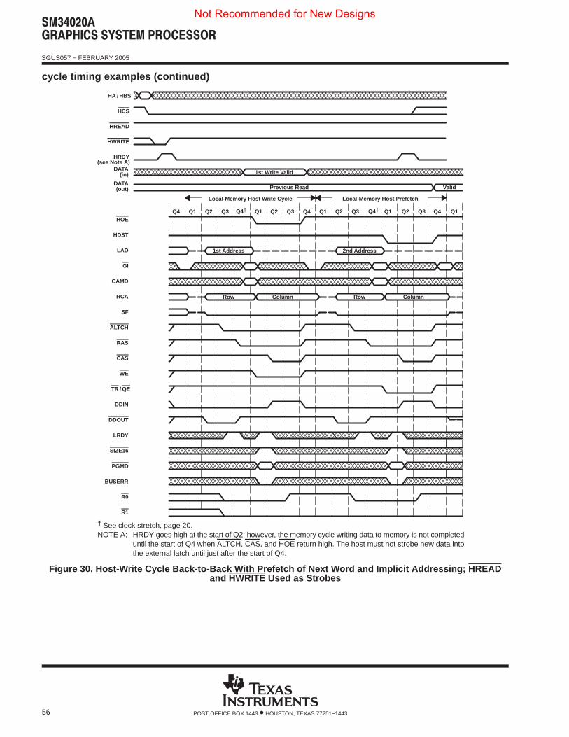
������������ � ������ � ����
SGUS057 − FEBRUARY 2005
56 POST OFFICE BOX 1443 • HOUSTON, TEXAS 77251−1443
cycle timing examples (continued)
Q4 Q1 Q2 Q3 Q1 Q2 Q3 Q4 Q1
Row Column
1st Write Valid
Local-Memory Host Write Cycle
Q2 Q3 Q1 Q2 Q3 Q4 Q1
Row Column
1st Address 2nd Address
Local-Memory Host Prefetch
ValidPrevious Read
HA / HBS
HCS
HREAD
HWRITE
HRDY
HOE
HDST
LAD
GI
CAMD
RCA
SF
ALTCH
RAS
CAS
WE
TR / QE
DDIN
DDOUT
LRDY
SIZE16
PGMD
BUSERR
R0
R1
DATA(out)
DATA(in)
Q4† Q4†
(see Note A)
† See clock stretch, page 20.NOTE A: HRDY goes high at the start of Q2; however, the memory cycle writing data to memory is not completed
until the start of Q4 when ALTCH, CAS, and HOE return high. The host must not strobe new data intothe external latch until just after the start of Q4.
Figure 30. Host-Write Cycle Back-to-Back With Prefetch of Next Word and Implicit Addressing; HREADand HWRITE Used as Strobes
Not Recommended for New Designs
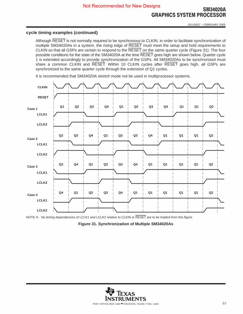
������������ � ������ � ����
SGUS057 − FEBRUARY 2005
57POST OFFICE BOX 1443 • HOUSTON, TEXAS 77251−1443
cycle timing examples (continued)
Although RESET is not normally required to be synchronous to CLKIN, in order to facilitate synchronization ofmultiple SM34020As in a system, the rising edge of RESET must meet the setup and hold requirements toCLKIN so that all GSPs are certain to respond to the RESET on the same quarter cycle (Figure 31). The fourpossible conditions for the state of the SM34020A at the time RESET goes high are shown below. Quarter cycle1 is extended accordingly to provide synchronization of the GSPs. All SM34020As to be synchronized mustshare a common CLKIN and RESET. Within 10 CLKIN cycles after RESET goes high, all GSPs aresynchronized to the same quarter cycle through the extension of Q1 cycles.
It is recommended that SM34020A stretch mode not be used in multiprocessor systems.
CLKIN
RESET
Q2 Q3 Q4 Q1 Q2 Q3 Q4 Q1 Q1 Q1 Q2
Q3 Q4 Q1 Q2 Q3 Q4 Q1 Q1 Q1 Q1 Q2
Q4 Q1 Q2 Q3 Q4 Q1 Q1 Q1 Q1 Q1 Q2
LCLK1
LCLK2
LCLK1
LCLK2
LCLK1
LCLK2
LCLK1
LCLK2
Case 1
Case 2
Case 3
Case 4
Q2 Q3 Q4 Q1 Q2 Q3 Q4 Q1 Q1 Q2Q1
NOTE A: No timing dependencies of LCLK1 and LCLK2 relative to CLKIN or RESET are to be implied from this figure.
Figure 31. Synchronization of Multiple SM34020As
Not Recommended for New Designs
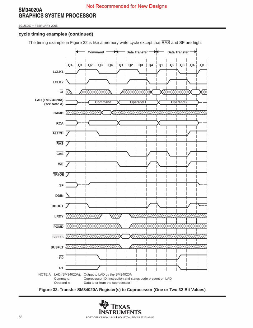
������������ � ������ � ����
SGUS057 − FEBRUARY 2005
58 POST OFFICE BOX 1443 • HOUSTON, TEXAS 77251−1443
cycle timing examples (continued)
The timing example in Figure 32 is like a memory write cycle except that RAS and SF are high.
LCLK1
LCLK2
GI
ALTCH
RAS
WE
Q4 Q1 Q2 Q3 Q4 Q1 Q2 Q3 Q4 Q1
R1
LAD (TMS34020A)Command
Q2 Q3 Q4 Q1
CAMD
RCA
CAS
TR/QE
SF
DDIN
DDOUT
R0
Operand 1 Operand 2
PGMD
SIZE16
LRDY
BUSFLT
Command Data Transfer Data Transfer
(see Note A)
NOTE A: LAD (SM34020A): Output to LAD by the SM34020ACommand: Coprocessor ID, instruction and status code present on LADOperand n: Data to or from the coprocessor
Figure 32. Transfer SM34020A Register(s) to Coprocessor (One or Two 32-Bit Values)
Not Recommended for New Designs
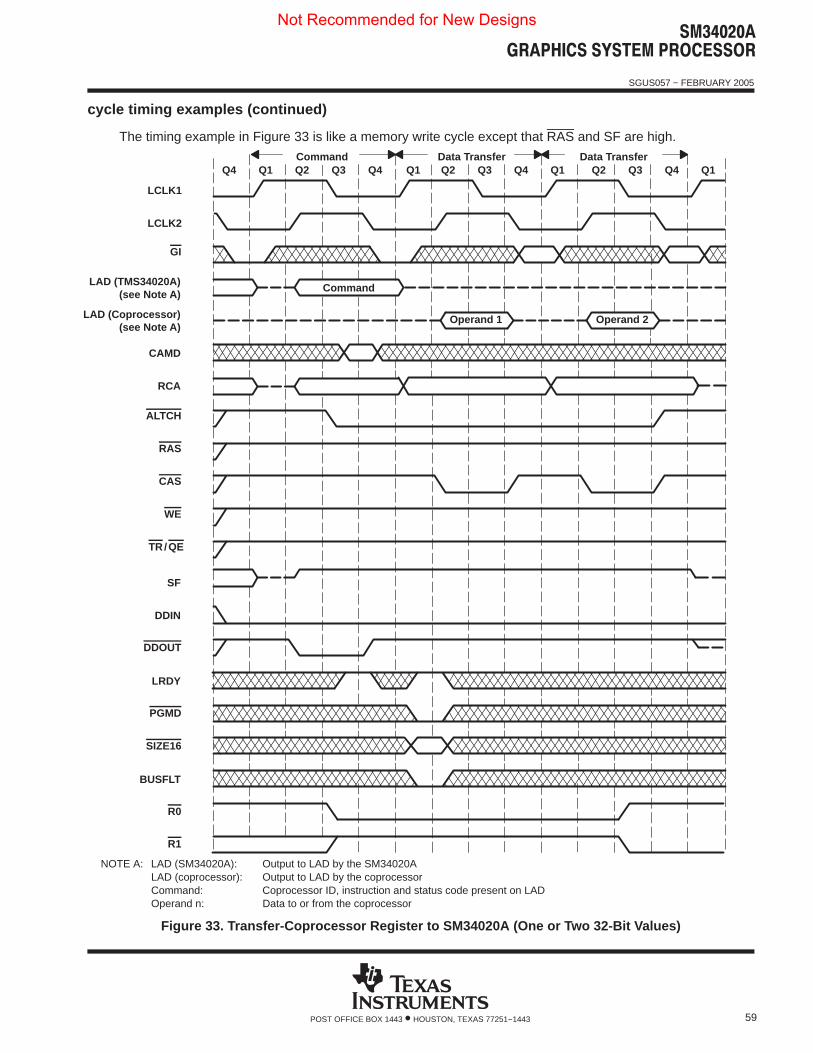
������������ � ������ � ����
SGUS057 − FEBRUARY 2005
59POST OFFICE BOX 1443 • HOUSTON, TEXAS 77251−1443
cycle timing examples (continued)
The timing example in Figure 33 is like a memory write cycle except that RAS and SF are high.
LCLK1
LCLK2
GI
ALTCH
RAS
WE
Q4 Q1 Q2 Q3 Q4 Q1 Q2 Q3 Q4 Q1
R1
LAD (TMS34020A) Command
Q2 Q3 Q4 Q1
LAD (Coprocessor)
CAMD
CAS
TR/QE
SF
DDIN
DDOUT
R0
Operand 1 Operand 2
PGMD
SIZE16
LRDY
BUSFLT
Command Data Transfer Data Transfer
RCA
(see Note A)
(see Note A)
NOTE A: LAD (SM34020A): Output to LAD by the SM34020ALAD (coprocessor): Output to LAD by the coprocessorCommand: Coprocessor ID, instruction and status code present on LADOperand n: Data to or from the coprocessor
Figure 33. Transfer-Coprocessor Register to SM34020A (One or Two 32-Bit Values)
Not Recommended for New Designs
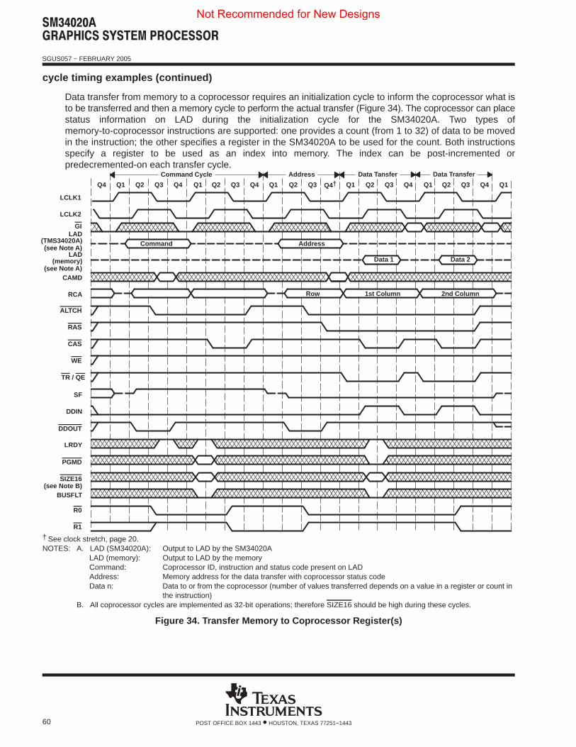
������������ � ������ � ����
SGUS057 − FEBRUARY 2005
60 POST OFFICE BOX 1443 • HOUSTON, TEXAS 77251−1443
cycle timing examples (continued)
Data transfer from memory to a coprocessor requires an initialization cycle to inform the coprocessor what isto be transferred and then a memory cycle to perform the actual transfer (Figure 34). The coprocessor can placestatus information on LAD during the initialization cycle for the SM34020A. Two types ofmemory-to-coprocessor instructions are supported: one provides a count (from 1 to 32) of data to be movedin the instruction; the other specifies a register in the SM34020A to be used for the count. Both instructionsspecify a register to be used as an index into memory. The index can be post-incremented orpredecremented-on each transfer cycle.
GILAD
Command Address
ALTCH
RAS
WE
Q4 Q1 Q2 Q3 Q4 Q1 Q2 Q3 Q4 Q1
R1
Q2 Q3 Q1
CAMD
CAS
TR / QE
SF
DDIN
DDOUT
R0
Data 1
PGMD
SIZE16
LRDY
BUSFLT
RCA
LADData 2
2nd Column1st ColumnRow
Q2 Q3 Q4 Q1 Q2 Q3 Q4 Q1
LCLK1
LCLK2
(TMS34020A)
(memory)
Command Cycle Address Data Tansfer Data Transfer
Q4†
(see Note A)
(see Note A)
(see Note B)
† See clock stretch, page 20.NOTES: A. LAD (SM34020A): Output to LAD by the SM34020A
LAD (memory): Output to LAD by the memoryCommand: Coprocessor ID, instruction and status code present on LADAddress: Memory address for the data transfer with coprocessor status codeData n: Data to or from the coprocessor (number of values transferred depends on a value in a register or count in
the instruction)B. All coprocessor cycles are implemented as 32-bit operations; therefore SIZE16 should be high during these cycles.
Figure 34. Transfer Memory to Coprocessor Register(s)
Not Recommended for New Designs
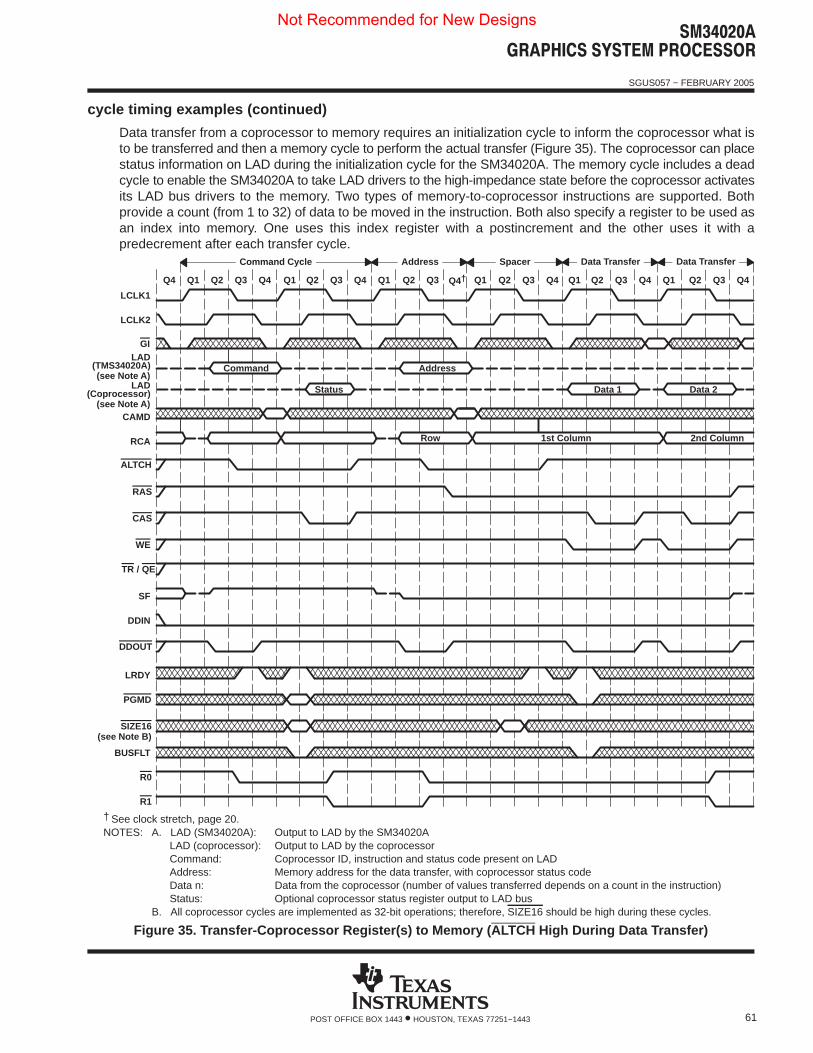
������������ � ������ � ����
SGUS057 − FEBRUARY 2005
61POST OFFICE BOX 1443 • HOUSTON, TEXAS 77251−1443
cycle timing examples (continued)
Data transfer from a coprocessor to memory requires an initialization cycle to inform the coprocessor what isto be transferred and then a memory cycle to perform the actual transfer (Figure 35). The coprocessor can placestatus information on LAD during the initialization cycle for the SM34020A. The memory cycle includes a deadcycle to enable the SM34020A to take LAD drivers to the high-impedance state before the coprocessor activatesits LAD bus drivers to the memory. Two types of memory-to-coprocessor instructions are supported. Bothprovide a count (from 1 to 32) of data to be moved in the instruction. Both also specify a register to be used asan index into memory. One uses this index register with a postincrement and the other uses it with apredecrement after each transfer cycle.
LCLK1
LCLK2
CAMD
RCA
LAD
Q4 Q1 Q2 Q3 Q4 Q1 Q2 Q3 Q4 Q1
LADCommand
Q2 Q3 Q1
SF
DDIN
Data 1
LRDY
BUSFLT
Address
Data 2
2nd Column1st ColumnRow
Q2 Q3 Q4 Q1 Q2 Q3 Q4 Q1 Q2 Q3 Q4
(TMS34020A)
(Coprocessor) Status
GI
ALTCH
RAS
CAS
WE
TR / QE
DDOUT
PGMD
SIZE16(see Note B)
R0
R1
Command Cycle Address Data Transfer Data TransferSpacer
Q4†
(see Note A)
(see Note A)
† See clock stretch, page 20.NOTES: A. LAD (SM34020A): Output to LAD by the SM34020A
LAD (coprocessor): Output to LAD by the coprocessorCommand: Coprocessor ID, instruction and status code present on LADAddress: Memory address for the data transfer, with coprocessor status codeData n: Data from the coprocessor (number of values transferred depends on a count in the instruction)Status: Optional coprocessor status register output to LAD bus
B. All coprocessor cycles are implemented as 32-bit operations; therefore, SIZE16 should be high during these cycles.
Figure 35. Transfer-Coprocessor Register(s) to Memory (ALTCH High During Data Transfer)
Not Recommended for New Designs
������������ � ������ � ����
SGUS057 − FEBRUARY 2005
62 POST OFFICE BOX 1443 • HOUSTON, TEXAS 77251−1443
cycle timing examples (continued)
The timing example in Figure 36 is like a memory write cycle except that RAS and SF are high.
A coprocessor internal command assumes no transfer of operands or results but causes the coprocessor toexecute some internal function. The coprocessor can place status information on LAD during the cycle for theSM34020A.
Not Recommended for New Designs
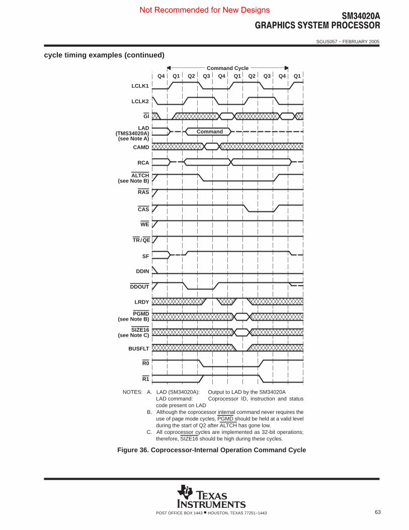
������������ � ������ � ����
SGUS057 − FEBRUARY 2005
63POST OFFICE BOX 1443 • HOUSTON, TEXAS 77251−1443
cycle timing examples (continued)
GI
ALTCH(see Note B)
RAS
WE
Q4 Q1 Q2 Q3 Q4 Q1 Q2 Q3 Q4 Q1
R1
LADCommand
CAMD
CAS
TR/QE
SF
DDIN
DDOUT
R0
PGMD(see Note B)
SIZE16(see Note C)
LRDY
BUSFLT
RCA
LCLK1
LCLK2
(TMS34020A)
Command Cycle
(see Note A)
NOTES: A. LAD (SM34020A): Output to LAD by the SM34020ALAD command: Coprocessor ID, instruction and statuscode present on LAD
B. Although the coprocessor internal command never requires theuse of page mode cycles, PGMD should be held at a valid levelduring the start of Q2 after ALTCH has gone low.
C. All coprocessor cycles are implemented as 32-bit operations;therefore, SIZE16 should be high during these cycles.
Figure 36. Coprocessor-Internal Operation Command Cycle
Not Recommended for New Designs
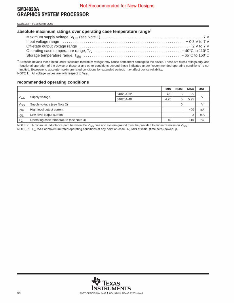
������������ � ������ � ����
SGUS057 − FEBRUARY 2005
64 POST OFFICE BOX 1443 • HOUSTON, TEXAS 77251−1443
absolute maximum ratings over operating case temperature range †
Maximum supply voltage, VCC (see Note 1) 7 V. . . . . . . . . . . . . . . . . . . . . . . . . . . . . . . . . . . . . . . . . . . . . . . . . . . . Input voltage range − 0.3 V to 7 V. . . . . . . . . . . . . . . . . . . . . . . . . . . . . . . . . . . . . . . . . . . . . . . . . . . . . . . . . . . . . . . . Off-state output voltage range − 2 V to 7 V. . . . . . . . . . . . . . . . . . . . . . . . . . . . . . . . . . . . . . . . . . . . . . . . . . . . . . . . . Operating case temperature range, TC − 40°C to 110°C. . . . . . . . . . . . . . . . . . . . . . . . . . . . . . . . . . . . . . . . . . . . . Storage temperature range, Tstg − 65°C to 150°C. . . . . . . . . . . . . . . . . . . . . . . . . . . . . . . . . . . . . . . . . . . . . . . . . .
† Stresses beyond those listed under “absolute maximum ratings” may cause permanent damage to the device. These are stress ratings only, andfunctional operation of the device at these or any other conditions beyond those indicated under “recommended operating conditions” is notimplied. Exposure to absolute-maximum-rated conditions for extended periods may affect device reliability.
NOTE 1: All voltage values are with respect to VSS.
recommended operating conditions
MIN NOM MAX UNIT
VCC Supply voltage34020A-32 4.5 5 5.5
VVCC Supply voltage34020A-40 4.75 5 5.25
V
VSS Supply voltage (see Note 2) 0 V
IOH High-level output current 400 µA
IOL Low-level output current 2 mA
TC Operating case temperature (see Note 3) − 40 110 °C
NOTE 2: A minimum inductance path between the VSS pins and system ground must be provided to minimize noise on VSS.NOTE 3: TC MAX at maximum rated operating conditions at any point on case. TC MIN at initial (time zero) power up.
Not Recommended for New Designs
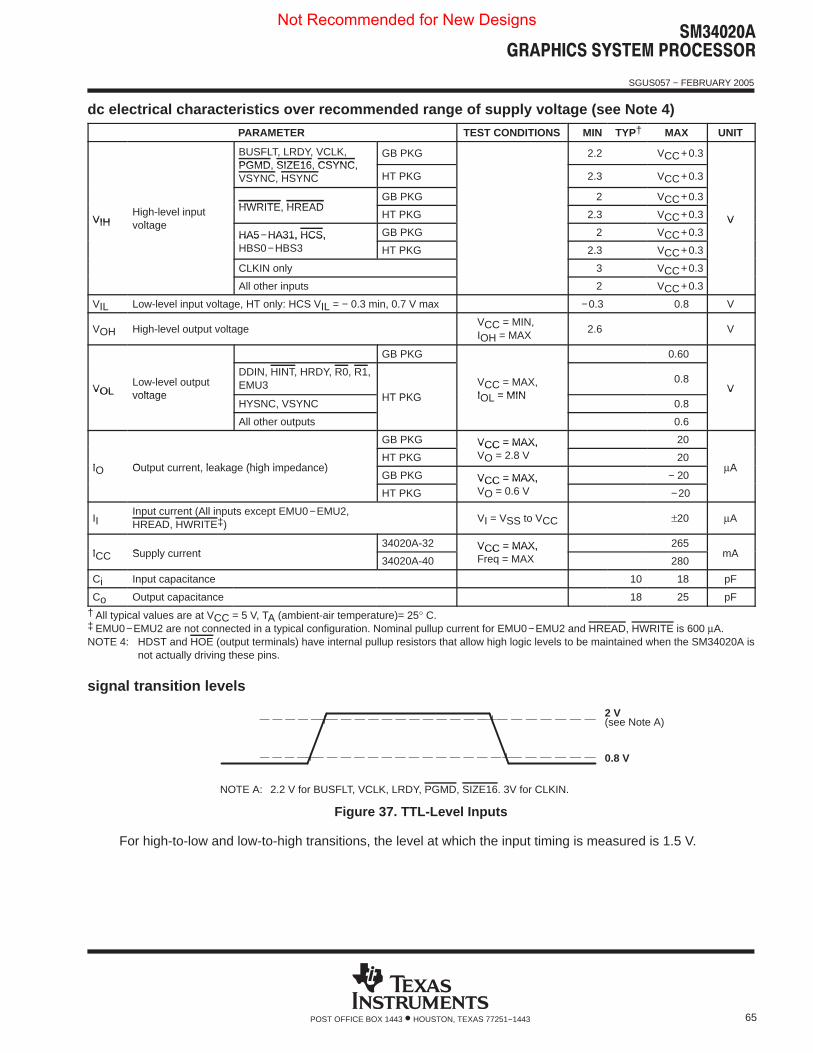
������������ � ������ � ����
SGUS057 − FEBRUARY 2005
65POST OFFICE BOX 1443 • HOUSTON, TEXAS 77251−1443
dc electrical characteristics over recommended range of supply voltage (see Note 4)
PARAMETER TEST CONDITIONS MIN TYP† MAX UNIT
BUSFLT, LRDY, VCLK,PGMD, SIZE16, CSYNC,
GB PKG 2.2 VCC+0.3PGMD, SIZE16, CSYNC,VSYNC, HSYNC HT PKG 2.3 VCC+0.3
HWRITE, HREADGB PKG 2 VCC+0.3
VIHHigh-level inputvoltage
HWRITE, HREADHT PKG 2.3 VCC+0.3 VVIH voltage
HA5−HA31, HCS, GB PKG 2 VCC+0.3V
HA5−HA31, HCS,HBS0−HBS3 HT PKG 2.3 VCC+0.3
CLKIN only 3 VCC+0.3
All other inputs 2 VCC+0.3
VIL Low-level input voltage, HT only: HCS VIL = − 0.3 min, 0.7 V max −0.3 0.8 V
VOH High-level output voltageVCC = MIN,IOH = MAX
2.6 V
GB PKG 0.60
VOLLow-level outputvoltage
DDIN, HINT, HRDY, R0, R1,EMU3
HT PKGVCC = MAX,IOL = MIN
0.8VVOL voltage
HYSNC, VSYNCHT PKG
CCIOL = MIN
0.8
V
All other outputs 0.6
GB PKG VCC = MAX, 20
IO Output current, leakage (high impedance)HT PKG
VCC = MAX,VO = 2.8 V 20
AIO Output current, leakage (high impedance)GB PKG VCC = MAX, − 20
µA
HT PKG
VCC = MAX,VO = 0.6 V −20
IIInput current (All inputs except EMU0−EMU2,HREAD, HWRITE‡)
VI = VSS to VCC ±20 µA
ICC Supply current34020A-32 VCC = MAX, 265
mAICC Supply current34020A-40
VCC = MAX,Freq = MAX 280
mA
Ci Input capacitance 10 18 pF
Co Output capacitance 18 25 pF
† All typical values are at VCC = 5 V, TA (ambient-air temperature)= 25° C.‡ EMU0−EMU2 are not connected in a typical configuration. Nominal pullup current for EMU0−EMU2 and HREAD, HWRITE is 600 µA.NOTE 4: HDST and HOE (output terminals) have internal pullup resistors that allow high logic levels to be maintained when the SM34020A is
not actually driving these pins.
signal transition levels
2 V(see Note A)
0.8 V
NOTE A: 2.2 V for BUSFLT, VCLK, LRDY, PGMD, SIZE16. 3V for CLKIN.
Figure 37. TTL-Level Inputs
For high-to-low and low-to-high transitions, the level at which the input timing is measured is 1.5 V.
Not Recommended for New Designs
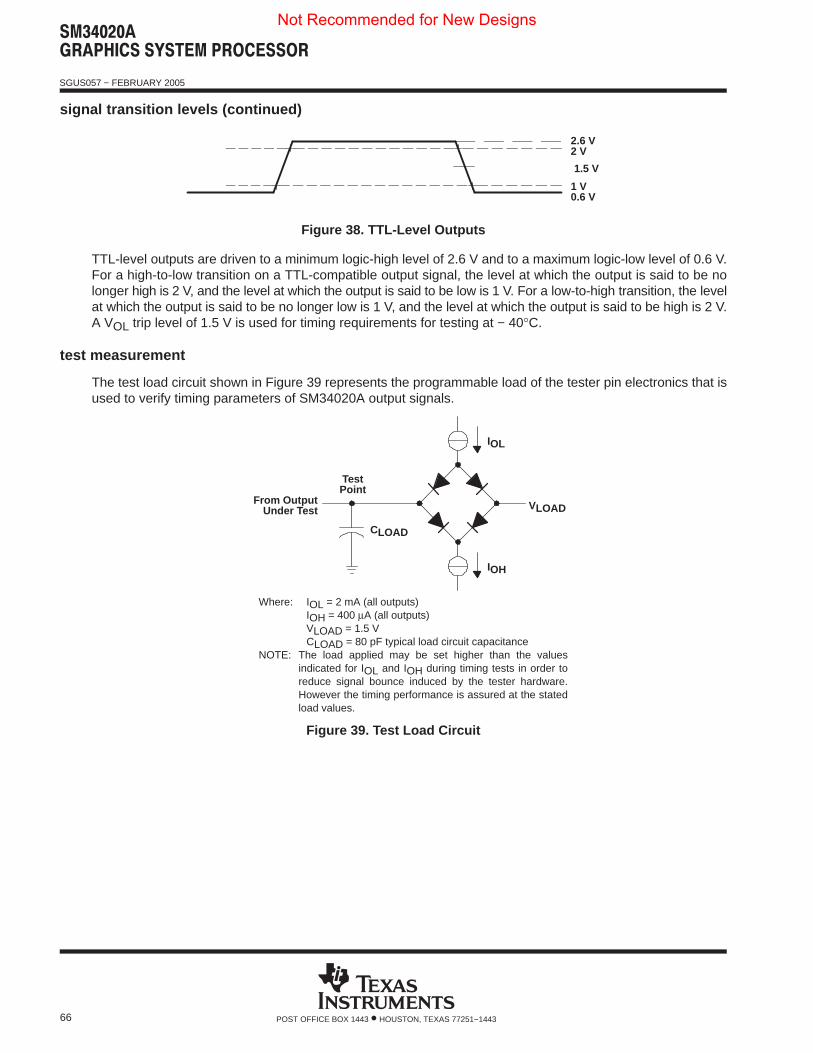
������������ � ������ � ����
SGUS057 − FEBRUARY 2005
66 POST OFFICE BOX 1443 • HOUSTON, TEXAS 77251−1443
signal transition levels (continued)
2.6 V2 V
1 V0.6 V
1.5 V
Figure 38. TTL-Level Outputs
TTL-level outputs are driven to a minimum logic-high level of 2.6 V and to a maximum logic-low level of 0.6 V.For a high-to-low transition on a TTL-compatible output signal, the level at which the output is said to be nolonger high is 2 V, and the level at which the output is said to be low is 1 V. For a low-to-high transition, the levelat which the output is said to be no longer low is 1 V, and the level at which the output is said to be high is 2 V.A VOL trip level of 1.5 V is used for timing requirements for testing at − 40°C.
test measurement
The test load circuit shown in Figure 39 represents the programmable load of the tester pin electronics that isused to verify timing parameters of SM34020A output signals.
IOL
VLOAD
IOH
CLOAD
TestPoint
From OutputUnder Test
Where: IOL = 2 mA (all outputs)IOH = 400 µA (all outputs)VLOAD = 1.5 VCLOAD = 80 pF typical load circuit capacitance
NOTE: The load applied may be set higher than the valuesindicated for IOL and IOH during timing tests in order toreduce signal bounce induced by the tester hardware.However the timing performance is assured at the statedload values.
Figure 39. Test Load Circuit
Not Recommended for New Designs
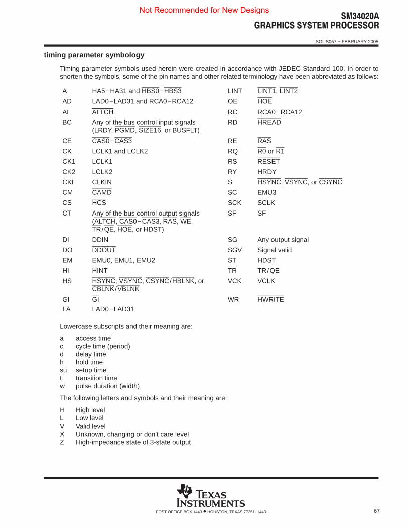
������������ � ������ � ����
SGUS057 − FEBRUARY 2005
67POST OFFICE BOX 1443 • HOUSTON, TEXAS 77251−1443
timing parameter symbology
Timing parameter symbols used herein were created in accordance with JEDEC Standard 100. In order toshorten the symbols, some of the pin names and other related terminology have been abbreviated as follows:
A HA5−HA31 and HBS0−HBS3 LINT LINT1, LINT2
AD LAD0−LAD31 and RCA0−RCA12 OE HOE
AL ALTCH RC RCA0−RCA12
BC Any of the bus control input signals(LRDY, PGMD, SIZE16, or BUSFLT)
RD HREAD
CE CAS0−CAS3 RE RAS
CK LCLK1 and LCLK2 RQ R0 or R1
CK1 LCLK1 RS RESET
CK2 LCLK2 RY HRDY
CKI CLKIN S HSYNC, VSYNC, or CSYNC
CM CAMD SC EMU3
CS HCS SCK SCLK
CT Any of the bus control output signals(ALTCH, CAS0−CAS3, RAS, WE,TR/QE, HOE, or HDST)
SF SF
DI DDIN SG Any output signal
DO DDOUT SGV Signal valid
EM EMU0, EMU1, EMU2 ST HDST
HI HINT TR TR/QE
HS HSYNC, VSYNC, CSYNC/HBLNK, orCBLNK/VBLNK
VCK VCLK
GI GI WR HWRITELA LAD0−LAD31
Lowercase subscripts and their meaning are:
a access timec cycle time (period)d delay timeh hold timesu setup timet transition timew pulse duration (width)
The following letters and symbols and their meaning are:
H High levelL Low levelV Valid levelX Unknown, changing or don’t care levelZ High-impedance state of 3-state output
Not Recommended for New Designs
������������ � ������ � ����
SGUS057 − FEBRUARY 2005
68 POST OFFICE BOX 1443 • HOUSTON, TEXAS 77251−1443
general notes on timing parameters
The period of the local clocks (LCLK1 and LCLK2) is four times the period of the input clock (CLKIN).
The quarter cycle time (tQ) that appears in the following tables is one quarter of a local output clock period orequal to the input clock period, tc(CKI).
All output signals from the SM34020A are derived from an internal clock such that all output transitions for agiven quarter cycle occur with a minimum of skewing relative to each other. In the timing diagrams, thetransitions of all output signals are shown with respect to the local clocks (LCLK1 and LCLK2). The local clockedge used as a reference occurs one internal clock cycle before the transition specified.
The signal combinations shown in the timing parameters are for timing reference only; they do not necessarilyrepresent actual cycles. For actual cycle descriptions, see the cycle timing section of this specification.
Not Recommended for New Designs
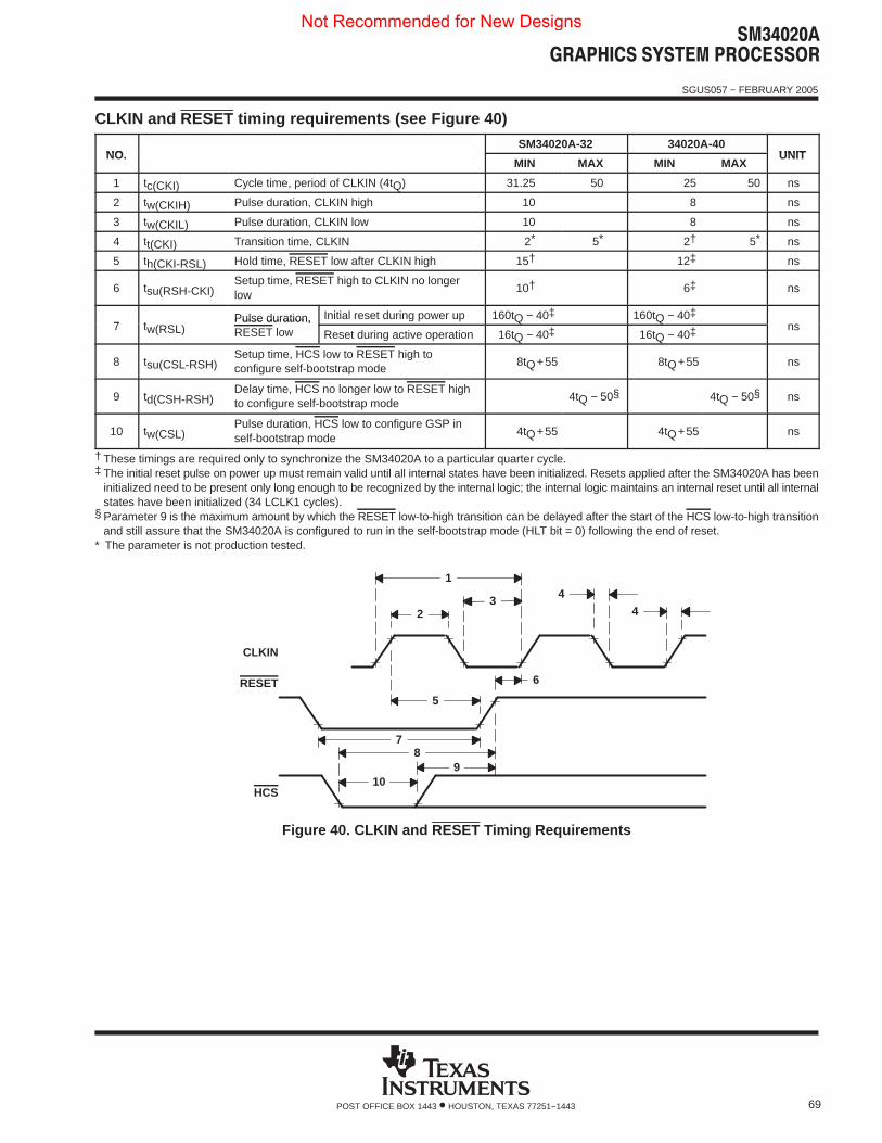
������������ � ������ � ����
SGUS057 − FEBRUARY 2005
69POST OFFICE BOX 1443 • HOUSTON, TEXAS 77251−1443
CLKIN and RESET timing requirements (see Figure 40)
NO.SM34020A-32 34020A-40
UNITNO.MIN MAX MIN MAX
UNIT
1 tc(CKI) Cycle time, period of CLKIN (4tQ) 31.25 50 25 50 ns
2 tw(CKIH) Pulse duration, CLKIN high 10 8 ns
3 tw(CKIL) Pulse duration, CLKIN low 10 8 ns
4 tt(CKI) Transition time, CLKIN 2* 5* 2† 5* ns
5 th(CKI-RSL) Hold time, RESET low after CLKIN high 15† 12‡ ns
6 tsu(RSH-CKI)Setup time, RESET high to CLKIN no longerlow
10† 6‡ ns
7 tw(RSL)Pulse duration, Initial reset during power up 160tQ − 40‡ 160tQ − 40‡
ns7 tw(RSL)Pulse duration,RESET low Reset during active operation 16tQ − 40‡ 16tQ − 40‡ ns
8 tsu(CSL-RSH)Setup time, HCS low to RESET high toconfigure self-bootstrap mode
8tQ+55 8tQ+55 ns
9 td(CSH-RSH)Delay time, HCS no longer low to RESET highto configure self-bootstrap mode
4tQ − 50§ 4tQ − 50§ ns
10 tw(CSL)Pulse duration, HCS low to configure GSP inself-bootstrap mode
4tQ+55 4tQ+55 ns
† These timings are required only to synchronize the SM34020A to a particular quarter cycle.‡ The initial reset pulse on power up must remain valid until all internal states have been initialized. Resets applied after the SM34020A has been
initialized need to be present only long enough to be recognized by the internal logic; the internal logic maintains an internal reset until all internalstates have been initialized (34 LCLK1 cycles).
§ Parameter 9 is the maximum amount by which the RESET low-to-high transition can be delayed after the start of the HCS low-to-high transitionand still assure that the SM34020A is configured to run in the self-bootstrap mode (HLT bit = 0) following the end of reset.
* The parameter is not production tested.
2
1
34
4
5
6
78
910
CLKIN
RESET
HCS
Figure 40. CLKIN and RESET Timing Requirements
Not Recommended for New Designs
������������ � ������ � ����
SGUS057 − FEBRUARY 2005
70 POST OFFICE BOX 1443 • HOUSTON, TEXAS 77251−1443
local-bus timing: output clocks (see Note 5 and Figure 41)
NO.SM34020A-32 34020A-40
UNITNO.MIN MAX MIN MAX
UNIT
11 tc(LCK)Cycle time, period of local clocks LCLK1,LCLK2
4tc(CKI)†+ s†* 4tc(CKI)+ s†*‡ ns
12 tw(LCKH) Pulse duration, local clock high 2tQ−15 2tQ −13.5 ns
12a tw(LCKH) Pulse duration, LCLK1 high (see Note 6) 2tQ−10 2tQ−7 ns
13 tw(LCKL) Pulse duration, local clock low 2tQ−15+ s 2tQ −13.5+ s ns
13a tw(LCKL) Pulse duration, LCLK1 low (see Note 6) 2tQ−10+ s 2tQ−7+ s ns
14 tt(LCK) Transition time, LCLK1 or LCLK2 15 13.5 ns
15 th(CK1H-CK2L) Hold time, LCLK2 low after LCLK1 high tQ−15 tQ−13.5 ns
16 th(CK2H-CK1H) Hold time, LCLK1 high after LCLK2 high tQ−15 tQ−13.5 ns
17 th(CK1L-CK2H) Hold time, LCLK2 high after LCLK1 low tQ−15 tQ−13.5 ns
18 th(CK2L-CK1L) Hold time, LCLK1 low after LCLK2 low tQ−15+ s tQ−13.5+ s ns
19 th(CK1H-CK2H) Hold time, LCLK2 high after LCLK1 high 3tQ−15 3tQ−13.5 ns
20 th(CK2H-CK1L) Hold time, LCLK1 low after LCLK2 high 3tQ−15+ s 3tQ−13.5+ s ns
21 th(CK1L-CK2L) Hold time, LCLK2 low after LCLK1 low 3tQ−15+ s 3tQ−13.5+ s ns
22 th(CK2L-CK1H) Hold time, LCLK1 high after LCLK2 low 3tQ−15+ s 3tQ−13.5+ s ns
† This parameter can also be specified as 4tQ.* The parameter is not production tested.NOTES: 5. s = tQ if using the clock stretch;
s = 0 otherwise6. Parameters 12a and 13a are specified with 1.5 V timing levels (parameters 12 and 13 are specified with standard timing voltage
levels).
LCLK1
LCLK2
Q1 Q2 Q3 Q4 Q1 Q2 Q3 Q4 Q1 Q2
14
14
14
11
12
13
19
21
22
15
16
1718
11
12
1314
20
12a
13a
NOTE A: Although LCLK1 and LCLK2 are derived from CLKIN, no timing relationship between CLKIN and the local clocks is to be assumed,except the period of the local clocks is four times the period of CLKIN.
Figure 41. Local-Bus Timing: Output Clocks
Not Recommended for New Designs
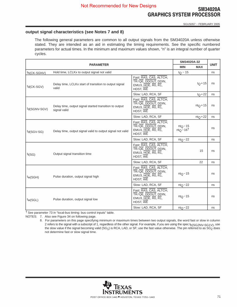
������������ � ������ � ����
SGUS057 − FEBRUARY 2005
71POST OFFICE BOX 1443 • HOUSTON, TEXAS 77251−1443
output signal characteristics (see Notes 7 and 8)
The following general parameters are common to all output signals from the SM34020A unless otherwisestated. They are intended as an aid in estimating the timing requirements. See the specific numberedparameters for actual times. In the minimum and maximum values shown, “n” is an integral number of quartercycles.
PARAMETERSM34020A-32
UNITPARAMETERMIN MAX
UNIT
th(CK-SGNV) Hold time, LCLKx to output signal not valid tQ − 15 ns
td(CK-SGV)Delay time, LCLKx start of transition to output signalvalid
Fast: RAS, CAS, ALTCH,TR/QE, DDOUT, DDIN,EMU3, HOE, R0, R1,HDST, WE
tQ+15 ns
Slow: LAD, RCA, SF tQ+22 ns
td(SGNV-SGV)Delay time, output signal started transition to outputsignal valid
Fast: RAS, CAS, ALTCH,TR/QE, DDOUT, DDIN,EMU3, HOE, R0, R1,HDST, WE
ntQ+15 ns
Slow: LAD, RCA, SF ntQ+22 ns
td(SGV-SG) Delay time, output signal valid to output signal not valid
Fast: RAS, CAS, ALTCH,TR/QE, DDOUT, DDIN,EMU3, HOE, R0, R1,HDST, WE
ntQ−15ntQ−16† ns
Slow: LAD, RCA, SF ntQ−22 ns
tt(SG) Output signal transition time
Fast: RAS, CAS, ALTCH,TR/QE, DDOUT, DDIN,EMU3, HOE, R0, R1,HDST, WE
15 ns
Slow: LAD, RCA, SF 22 ns
tw(SGH) Pulse duration, output signal high
Fast: RAS, CAS, ALTCH,TR/QE, DDOUT, DDIN,EMU3, HOE, R0, R1,HDST, WE
ntQ−15 ns
Slow: LAD, RCA, SF ntQ−22 ns
tw(SGL) Pulse duration, output signal low
Fast: RAS, CAS, ALTCH,TR/QE, DDOUT, DDIN,EMU3, HOE, R0, R1,HDST, WE
ntQ−15 ns
Slow: LAD, RCA, SF ntQ−22 ns† See parameter 73 in “local-bus timing: bus control inputs” table.NOTES: 7. Also see Figure 34 on following page.
8. For parameters on this page specifying minimum or maximum times between two output signals, the word fast or slow in column2 refers to the signal with a subscript of 1, regardless of the other signal. For example, if you are using the spec th(SG2NV-SG1V), usethe slow value if the signal becoming valid (SG1) is RCA, LAD, or SF; use the fast value otherwise. The pin referred to as SG2 doesnot determine fast or slow signal time.
Not Recommended for New Designs
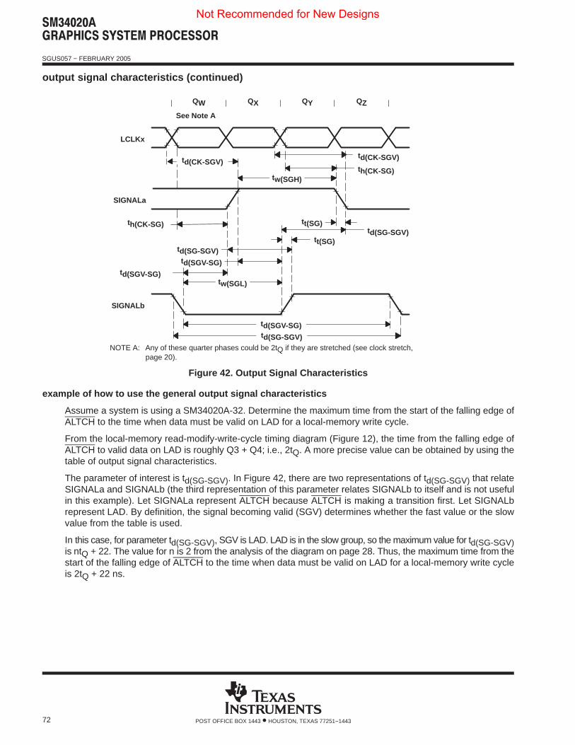
������������ � ������ � ����
SGUS057 − FEBRUARY 2005
72 POST OFFICE BOX 1443 • HOUSTON, TEXAS 77251−1443
output signal characteristics (continued)
QW QX QY QZ
tt(SG)td(SG-SGV)
td(SGV-SG)
th(CK-SG)
td(CK-SGV)
th(CK-SG)
LCLKx
SIGNALa
SIGNALb
tw(SGH)
tw(SGL)
td(SGV-SG)td(SG-SGV)
td(CK-SGV)
td(SGV-SG)
td(SG-SGV)
tt(SG)
See Note A
NOTE A: Any of these quarter phases could be 2tQ if they are stretched (see clock stretch,page 20).
Figure 42. Output Signal Characteristics
example of how to use the general output signal characteristics
Assume a system is using a SM34020A-32. Determine the maximum time from the start of the falling edge ofALTCH to the time when data must be valid on LAD for a local-memory write cycle.
From the local-memory read-modify-write-cycle timing diagram (Figure 12), the time from the falling edge ofALTCH to valid data on LAD is roughly Q3 + Q4; i.e., 2tQ. A more precise value can be obtained by using thetable of output signal characteristics.
The parameter of interest is td(SG-SGV). In Figure 42, there are two representations of td(SG-SGV) that relateSIGNALa and SIGNALb (the third representation of this parameter relates SIGNALb to itself and is not usefulin this example). Let SIGNALa represent ALTCH because ALTCH is making a transition first. Let SIGNALbrepresent LAD. By definition, the signal becoming valid (SGV) determines whether the fast value or the slowvalue from the table is used.
In this case, for parameter td(SG-SGV), SGV is LAD. LAD is in the slow group, so the maximum value for td(SG-SGV)is ntQ + 22. The value for n is 2 from the analysis of the diagram on page 28. Thus, the maximum time from thestart of the falling edge of ALTCH to the time when data must be valid on LAD for a local-memory write cycleis 2tQ + 22 ns.
Not Recommended for New Designs
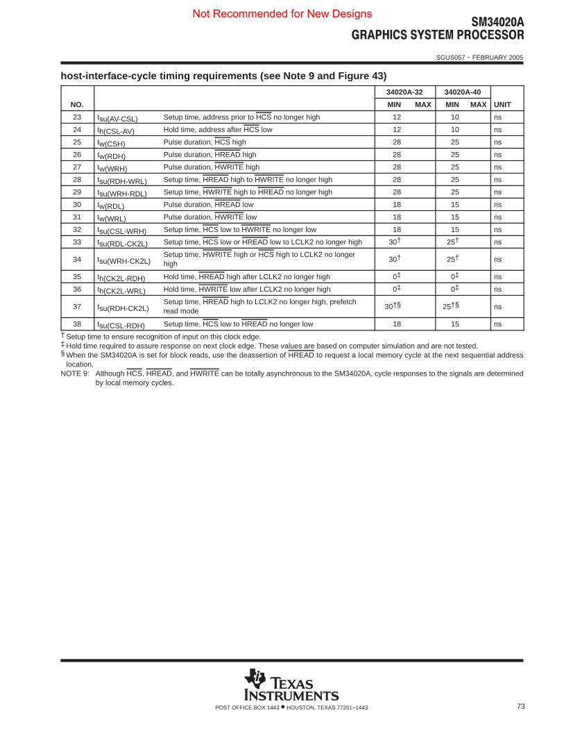
������������ � ������ � ����
SGUS057 − FEBRUARY 2005
73POST OFFICE BOX 1443 • HOUSTON, TEXAS 77251−1443
host-interface-cycle timing requirements (see Note 9 and Figure 43)
34020A-32 34020A-40
NO. MIN MAX MIN MAX UNIT
23 tsu(AV-CSL) Setup time, address prior to HCS no longer high 12 10 ns
24 th(CSL-AV) Hold time, address after HCS low 12 10 ns
25 tw(CSH) Pulse duration, HCS high 28 25 ns
26 tw(RDH) Pulse duration, HREAD high 28 25 ns
27 tw(WRH) Pulse duration, HWRITE high 28 25 ns
28 tsu(RDH-WRL) Setup time, HREAD high to HWRITE no longer high 28 25 ns
29 tsu(WRH-RDL) Setup time, HWRITE high to HREAD no longer high 28 25 ns
30 tw(RDL) Pulse duration, HREAD low 18 15 ns
31 tw(WRL) Pulse duration, HWRITE low 18 15 ns
32 tsu(CSL-WRH) Setup time, HCS low to HWRITE no longer low 18 15 ns
33 tsu(RDL-CK2L) Setup time, HCS low or HREAD low to LCLK2 no longer high 30† 25† ns
34 tsu(WRH-CK2L)Setup time, HWRITE high or HCS high to LCLK2 no longerhigh
30† 25† ns
35 th(CK2L-RDH) Hold time, HREAD high after LCLK2 no longer high 0‡ 0‡ ns
36 th(CK2L-WRL) Hold time, HWRITE low after LCLK2 no longer high 0‡ 0‡ ns
37 tsu(RDH-CK2L)Setup time, HREAD high to LCLK2 no longer high, prefetchread mode
30†§ 25†§ ns
38 tsu(CSL-RDH) Setup time, HCS low to HREAD no longer low 18 15 ns
† Setup time to ensure recognition of input on this clock edge.‡ Hold time required to assure response on next clock edge. These values are based on computer simulation and are not tested.§ When the SM34020A is set for block reads, use the deassertion of HREAD to request a local memory cycle at the next sequential address
location.NOTE 9: Although HCS, HREAD, and HWRITE can be totally asynchronous to the SM34020A, cycle responses to the signals are determined
by local memory cycles.
Not Recommended for New Designs
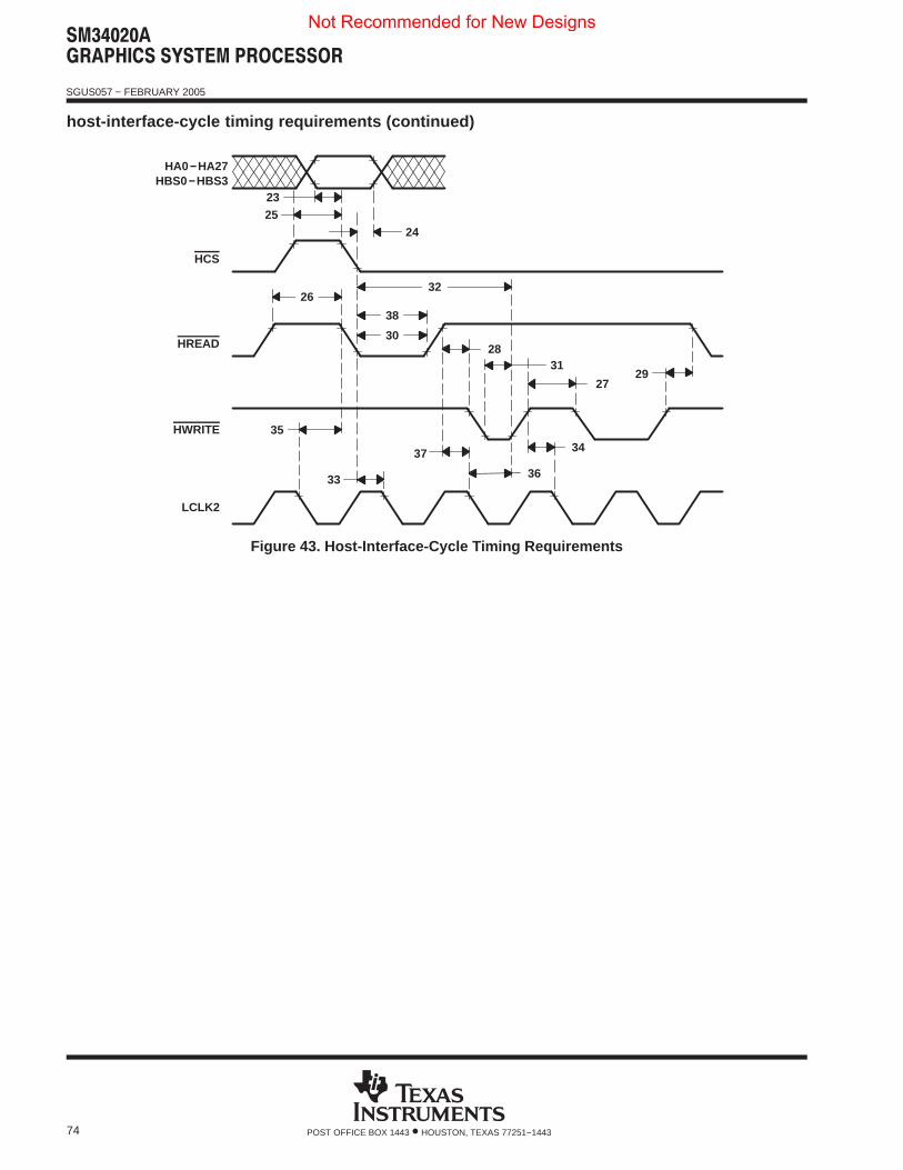
������������ � ������ � ����
SGUS057 − FEBRUARY 2005
74 POST OFFICE BOX 1443 • HOUSTON, TEXAS 77251−1443
host-interface-cycle timing requirements (continued)
HA0−HA27HBS0−HBS3
2325
35
33
37
29
24
2831
27
34
36
3226
38
30
HCS
HREAD
HWRITE
LCLK2
Figure 43. Host-Interface-Cycle Timing Requirements
Not Recommended for New Designs
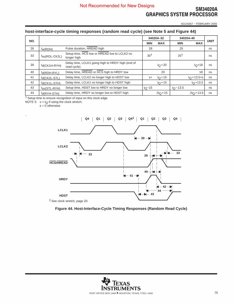
������������ � ������ � ����
SGUS057 − FEBRUARY 2005
75POST OFFICE BOX 1443 • HOUSTON, TEXAS 77251−1443
host-interface-cycle timing responses (random read cycle) (see Note 5 and Figure 44)
NO.34020A-32 34020A-40
UNITNO.MIN MAX MIN MAX
UNIT
26 tw(RDH) Pulse duration, HREAD high 28 25 ns
33 tsu(RDL-CK2L)Setup time, HCS low or HREAD low to LCLK2 nolonger high
30† 25† ns
39 td(CK1H-RYH)Delay time, LCLK1 going high to HRDY high (end ofread cycle)
tQ+20 tQ+18 ns
40 td(RDH-RYL) Delay time, HREAD or HCS high to HRDY low 20 18 ns
41 td(CK2L-STL) Delay time, LCLK2 no longer high to HDST low s+ tQ+15 tQ+13.5+s ns
42 td(CK1L-STH) Delay time, LCLK1 no longer high to HDST high tQ+15 tQ+13.5 ns
43 tsu(STL-RYH) Setup time, HDST low to HRDY no longer low tQ−15 tQ−13.5 ns
44 td(RYH-STH) Delay time, HRDY no longer low to HDST high 2tQ+15 2tQ+13.5 ns
† Setup time to ensure recognition of input on this clock edgeNOTE 5: s = tQ if using the clock stretch;
s = 0 otherwise
.Q4 Q1 Q2 Q3 Q4‡ Q1 Q2 Q3 Q4
LCLK1
LCLK2
HCS/HREAD
HRDY
HDST
33
43
3326
4041
39
4244
‡ See clock stretch, page 20.
Figure 44. Host-Interface-Cycle Timing Responses (Random Read Cycle)
Not Recommended for New Designs
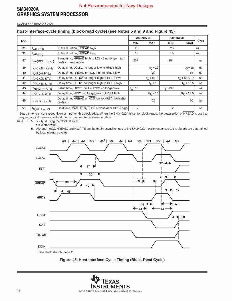
������������ � ������ � ����
SGUS057 − FEBRUARY 2005
76 POST OFFICE BOX 1443 • HOUSTON, TEXAS 77251−1443
host-interface-cycle timing (block-read cycle) (see Notes 5 and 9 and Figure 45)
NO.34020A-32 34020A-40
UNITNO.MIN MAX MIN MAX
UNIT
26 tw(RDH) Pulse duration, HREAD high 28 25 ns
30 tw(RDL) Pulse duration, HREAD low 18 15 ns
37 tsu(RDH-CK2L)Setup time, HREAD high to LCLK2 no longer high,prefetch read mode
30† 25† ns
39 td(CK1H-RYH) Delay time, LCLK1 no longer low to HRDY high tQ+20 tQ+18 ns
40 td(RDH-RYL) Delay time, HREAD or HCS high to HRDY low 20 18 ns
41 td(CK2L-STL) Delay time, LCLK2 no longer high to HDST low tQ+15+s tQ+13.5+ s ns
42 td(CK1L-STH) Delay time, LCLK1 no longer high to HDST high tQ+15 tQ+13.5 ns
43 tsu(STL-RYH) Setup time, HDST low to HRDY no longer low tQ−15 tQ−13.5 ns
44 td(RYH-STH) Delay time, HRDY no longer low to HDST high 2tQ+15 2tQ+13.5 ns
45 td(RDL-RYH)Delay time, HREAD or HCS low to HRDY high afterprefetch
25 20 ns
50 th(STH-CTV) Hold time, CAS, TR/QE, DDIN valid after HDST high − 2 − 2 ns
† Setup time to ensure recognition of input on this clock edge. When the SM34020A is set for block reads, the deassertion of HREAD is used torequest a local memory cycle at the next sequential address location.
NOTES: 5. s = tQ if using the clock stretch; s = 0 otherwise
9. Although HCS, HREAD, and HWRITE can be totally asynchronous to the SM34020A, cycle responses to the signals are determinedby local memory cycles.
HDST
HRDY
HREAD
HCS
LCLK2
LCLK1
43
40
37
42
2639
Q4 Q1 Q2 Q3 Q4‡ Q1 Q2 Q3 Q4 Q1 Q2 Q3 Q4
45
41 44
40
26
37
30
‡ See clock stretch, page 20.
CAS
TR/QE
DDIN
50
Figure 45. Host-Interface-Cycle Timing (Block-Read Cycle)
Not Recommended for New Designs
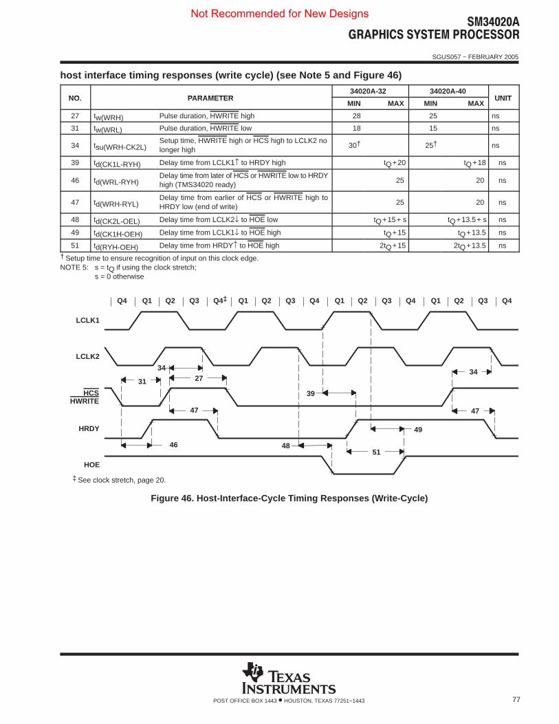
������������ � ������ � ����
SGUS057 − FEBRUARY 2005
77POST OFFICE BOX 1443 • HOUSTON, TEXAS 77251−1443
host interface timing responses (write cycle) (see Note 5 and Figure 46)
NO. PARAMETER34020A-32 34020A-40
UNITNO. PARAMETERMIN MAX MIN MAX
UNIT
27 tw(WRH) Pulse duration, HWRITE high 28 25 ns
31 tw(WRL) Pulse duration, HWRITE low 18 15 ns
34 tsu(WRH-CK2L)Setup time, HWRITE high or HCS high to LCLK2 nolonger high
30† 25† ns
39 td(CK1L-RYH) Delay time from LCLK1↑ to HRDY high tQ+20 tQ+18 ns
46 td(WRL-RYH)Delay time from later of HCS or HWRITE low to HRDYhigh (TMS34020 ready)
25 20 ns
47 td(WRH-RYL)Delay time from earlier of HCS or HWRITE high toHRDY low (end of write)
25 20 ns
48 td(CK2L-OEL) Delay time from LCLK2↓ to HOE low tQ+15+ s tQ+13.5+ s ns
49 td(CK1�-OEH) Delay time from LCLK1↓ to HOE high tQ+15 tQ+13.5 ns
51 td(RYH-OEH) Delay time from HRDY↑ to HOE high 2tQ+15 2tQ+13.5 ns
† Setup time to ensure recognition of input on this clock edge.NOTE 5: s = tQ if using the clock stretch;
s = 0 otherwise
49
39
4846
34
HOE
HRDY
HCSHWRITE
LCLK2
LCLK1
Q4Q3Q2Q1Q4Q3Q2Q1Q4Q3Q2Q1Q4‡Q3Q2Q1Q4
34
51
47
2731
47
‡ See clock stretch, page 20.
Figure 46. Host-Interface-Cycle Timing Responses (Write-Cycle)
Not Recommended for New Designs
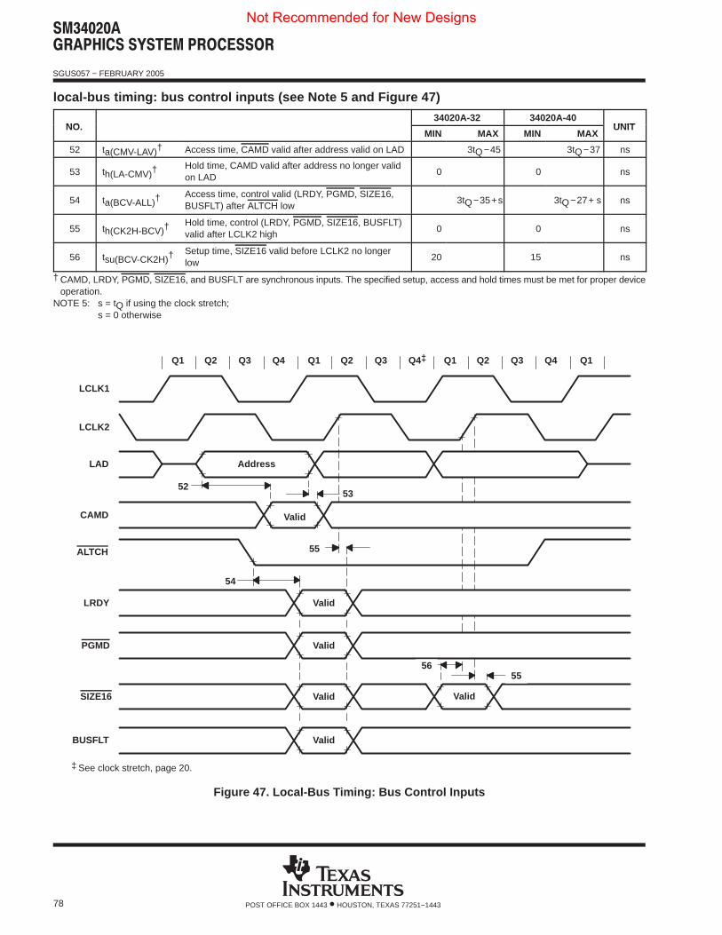
������������ � ������ � ����
SGUS057 − FEBRUARY 2005
78 POST OFFICE BOX 1443 • HOUSTON, TEXAS 77251−1443
local-bus timing: bus control inputs (see Note 5 and Figure 47)
NO.34020A-32 34020A-40
UNITNO.MIN MAX MIN MAX
UNIT
52 ta(CMV-LAV)† Access time, CAMD valid after address valid on LAD 3tQ−45 3tQ−37 ns
53 th(LA-CMV)†Hold time, CAMD valid after address no longer validon LAD
0 0 ns
54 ta(BCV-ALL)†Access time, control valid (LRDY, PGMD, SIZE16,BUSFLT) after ALTCH low
3tQ−35+s 3tQ−27+ s ns
55 th(CK2H-BCV)†Hold time, control (LRDY, PGMD, SIZE16, BUSFLT)valid after LCLK2 high
0 0 ns
56 tsu(BCV-CK2H)†Setup time, SIZE16 valid before LCLK2 no longerlow
20 15 ns
† CAMD, LRDY, PGMD, SIZE16, and BUSFLT are synchronous inputs. The specified setup, access and hold times must be met for proper deviceoperation.
NOTE 5: s = tQ if using the clock stretch; s = 0 otherwise
Address
5352
54
Valid
Valid
Valid
Valid
Valid
LAD
BUSFLT
SIZE16
PGMD
LRDY
ALTCH
CAMD
LCLK2
LCLK1
Q1Q4Q3Q2Q1Q4‡Q3Q2Q1Q4Q3Q2Q1
Valid
55
5556
‡ See clock stretch, page 20.
Figure 47. Local-Bus Timing: Bus Control Inputs
Not Recommended for New Designs
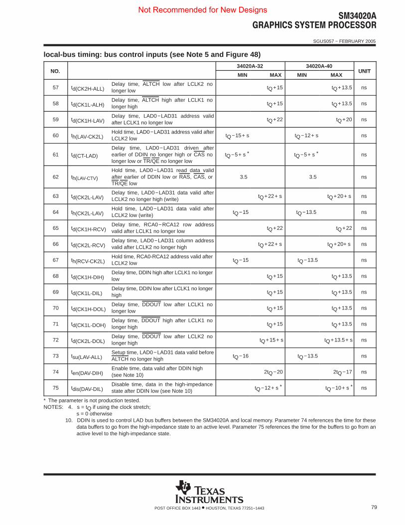
������������ � ������ � ����
SGUS057 − FEBRUARY 2005
79POST OFFICE BOX 1443 • HOUSTON, TEXAS 77251−1443
local-bus timing: bus control inputs (see Note 5 and Figure 48)
NO.34020A-32 34020A-40
UNITNO.MIN MAX MIN MAX
UNIT
57 td(CK2H-ALL)Delay time, ALTCH low after LCLK2 nolonger low
tQ+15 tQ+13.5 ns
58 td(CK1L-ALH)Delay time, ALTCH high after LCLK1 nolonger high
tQ+15 tQ+13.5 ns
59 td(CK1H-LAV)Delay time, LAD0−LAD31 address validafter LCLK1 no longer low
tQ+22 tQ+20 ns
60 th(LAV-CK2L)Hold time, LAD0−LAD31 address valid afterLCLK2 low
tQ−15+ s tQ−12+ s ns
61 td(CT-LAD)
Delay time, LAD0−LAD31 driven afterearlier of DDIN no longer high or CAS nolonger low or TR/QE no longer low
tQ−5+ s * tQ−5+ s * ns
62 th(LAV-CTV)
Hold time, LAD0−LAD31 read data validafter earlier of DDIN low or RAS, CAS, orTR/QE low
3.5 3.5 ns
63 td(CK2L-LAV)Delay time, LAD0−LAD31 data valid afterLCLK2 no longer high (write)
tQ+22+ s tQ+20+ s ns
64 th(CK2L-LAV)Hold time, LAD0−LAD31 data valid afterLCLK2 low (write)
tQ−15 tQ−13.5 ns
65 td(CK1H-RCV)Delay time, RCA0−RCA12 row addressvalid after LCLK1 no longer low
tQ+22 tQ+22 ns
66 td(CK2L-RCV)Delay time, LAD0−LAD31 column addressvalid after LCLK2 no longer high
tQ+22+ s tQ+20+ s ns
67 th(RCV-CK2L)Hold time, RCA0-RCA12 address valid afterLCLK2 low
tQ−15 tQ−13.5 ns
68 td(CK1H-DIH)Delay time, DDIN high after LCLK1 no longerlow
tQ+15 tQ+13.5 ns
69 td(CK1L-DIL)Delay time, DDIN low after LCLK1 no longerhigh
tQ+15 tQ+13.5 ns
70 td(CK1H-DOL)Delay time, DDOUT low after LCLK1 nolonger low
tQ+15 tQ+13.5 ns
71 td(CK1L-DOH)Delay time, DDOUT high after LCLK1 nolonger high
tQ+15 tQ+13.5 ns
72 td(CK2L-DOL)Delay time, DDOUT low after LCLK2 nolonger high
tQ+15+ s tQ+13.5+ s ns
73 tsu(LAV-ALL)Setup time, LAD0−LAD31 data valid beforeALTCH no longer high
tQ−16 tQ−13.5 ns
74 ten(DAV-DIH)Enable time, data valid after DDIN high(see Note 10)
2tQ−20 2tQ−17 ns
75 tdis(DAV-DIL)Disable time, data in the high-impedancestate after DDIN low (see Note 10)
tQ−12+ s * tQ−10+ s * ns
* The parameter is not production tested.NOTES: 4. s = tQ if using the clock stretch;
s = 0 otherwise10. DDIN is used to control LAD bus buffers between the SM34020A and local memory. Parameter 74 references the time for these
data buffers to go from the high-impedance state to an active level. Parameter 75 references the time for the buffers to go from anactive level to the high-impedance state.
Not Recommended for New Designs
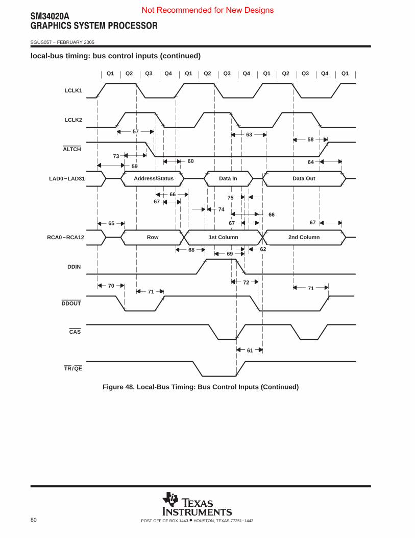
������������ � ������ � ����
SGUS057 − FEBRUARY 2005
80 POST OFFICE BOX 1443 • HOUSTON, TEXAS 77251−1443
local-bus timing: bus control inputs (continued)
2nd Column1st ColumnRow
Data OutData InAddress/Status
Q1 Q2 Q3 Q4 Q1 Q2 Q3 Q4 Q1 Q2 Q3 Q4 Q1
DDOUT
67
67
60 6459
73
LAD0−LAD31
DDIN
RCA0−RCA12
ALTCH
LCLK2
LCLK1
71
68
66
65
6358
57
71
69
67
70
74
72
TR/QE
CAS
66
75
62
61
Figure 48. Local-Bus Timing: Bus Control Inputs (Continued)
Not Recommended for New Designs
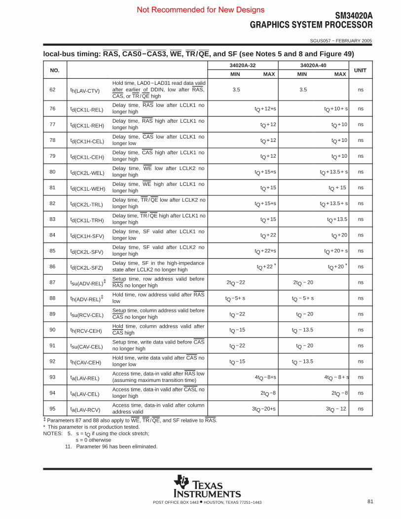
������������ � ������ � ����
SGUS057 − FEBRUARY 2005
81POST OFFICE BOX 1443 • HOUSTON, TEXAS 77251−1443
local-bus timing: RAS , CAS0 −CAS3, WE, TR/QE, and SF (see Notes 5 and 8 and Figure 49)
NO.34020A-32 34020A-40
UNITNO.MIN MAX MIN MAX
UNIT
62 th(LAV-CTV)
Hold time, LAD0−LAD31 read data validafter earlier of DDIN, low after RAS,CAS, or TR/QE high
3.5 3.5 ns
76 td(CK1L-REL)Delay time, RAS low after LCLK1 nolonger high
tQ+12+s tQ+10+ s ns
77 td(CK1L-REH)Delay time, RAS high after LCLK1 nolonger high
tQ+12 tQ+10 ns
78 td(CK1H-CEL)Delay time, CAS low after LCLK1 nolonger low
tQ+12 tQ+10 ns
79 td(CK1L-CEH)Delay time, CAS high after LCLK1 nolonger high
tQ+12 tQ+10 ns
80 td(CK2L-WEL)Delay time, WE low after LCLK2 nolonger high
tQ+15+s tQ+13.5+ s ns
81 td(CK1L-WEH)Delay time, WE high after LCLK1 nolonger high
tQ+15 tQ + 15 ns
82 td(CK2L-TRL)Delay time, TR/QE low after LCLK2 nolonger high
tQ+15+s tQ+13.5+ s ns
83 td(CK1L-TRH)Delay time, TR/QE high after LCLK1 nolonger high
tQ+15 tQ+13.5 ns
84 td(CK1H-SFV)Delay time, SF valid after LCLK1 nolonger low
tQ+22 tQ+20 ns
85 td(CK2L-SFV)Delay time, SF valid after LCLK2 nolonger high
tQ+22+s tQ+20+ s ns
86 td(CK2L-SFZ)Delay time, SF in the high-impedancestate after LCLK2 no longer high
tQ+22 * tQ+20 * ns
87 tsu(ADV-REL)‡Setup time, row address valid beforeRAS no longer high
2tQ−22 2tQ − 20 ns
88 th(ADV-REL)‡Hold time, row address valid after RASlow
tQ−5+ s tQ − 5+ s ns
89 tsu(RCV-CEL)Setup time, column address valid beforeCAS no longer high
tQ−22 tQ − 20 ns
90 th(RCV-CEH)Hold time, column address valid afterCAS high
tQ−15 tQ − 13.5 ns
91 tsu(CAV-CEL)Setup time, write data valid before CASno longer high
tQ−22 tQ − 20 ns
92 th(CAV-CEH)Hold time, write data valid after CAS nolonger low
tQ−15 tQ − 13.5 ns
93 ta(LAV-REL)Access time, data-in valid after RAS low(assuming maximum transition time)
4tQ−8+s 4tQ − 8+ s ns
94 ta(LAV-CEL)Access time, data-in valid after CASL nolonger high
2tQ−8 2tQ −8 ns
95 ta(LAV-RCV)Access time, data-in valid after columnaddress valid
3tQ−20+s 3tQ − 12 ns
‡ Parameters 87 and 88 also apply to WE, TR/QE, and SF relative to RAS.* This parameter is not production tested.NOTES: 5. s = tQ if using the clock stretch;
s = 0 otherwise11. Parameter 96 has been eliminated.
Not Recommended for New Designs
������������ � ������ � ����
SGUS057 − FEBRUARY 2005
82 POST OFFICE BOX 1443 • HOUSTON, TEXAS 77251−1443
local-bus timing: RAS , CAS0 −CAS3, WE, TR/QE, and SF (see Notes 5 and 11 and Figure 49)(continued)
NO.34020A-32 34020A-40
UNITNO.MIN MAX MIN MAX
UNIT
97 tsu(WEL-CEL)Setup time, write low before CAS nolonger high (on write cycles)
tQ−15 tQ − 13.5 ns
98 tw(REH) Pulse duration, RAS high 4tQ−12+ s 4tQ − 10+ s ns
99 tw(REL) Pulse duration, RAS low 4ntQ−12+ s’ 4n tQ − 4+ s’ ns
100 tw(CEH) Pulse duration, CAS high 2tQ−12 2tQ − 10 ns
101 tw(CEL) Pulse duration, CAS low 2tQ−12 2tQ − 8 ns
102 td(REL-CEH)Delay time, RAS low to CAS no longerlow
4tQ−12+ s 4tQ − 4+s ns
NOTES: 5. s = tQ if using the clock stretch; s = 0 otherwises’ is 2tQ when using the clock stretch since both the address cycle and read cycle of a Read-Modify-Write will be stretched.
11. Parameter 96 has been eliminated.
Not Recommended for New Designs
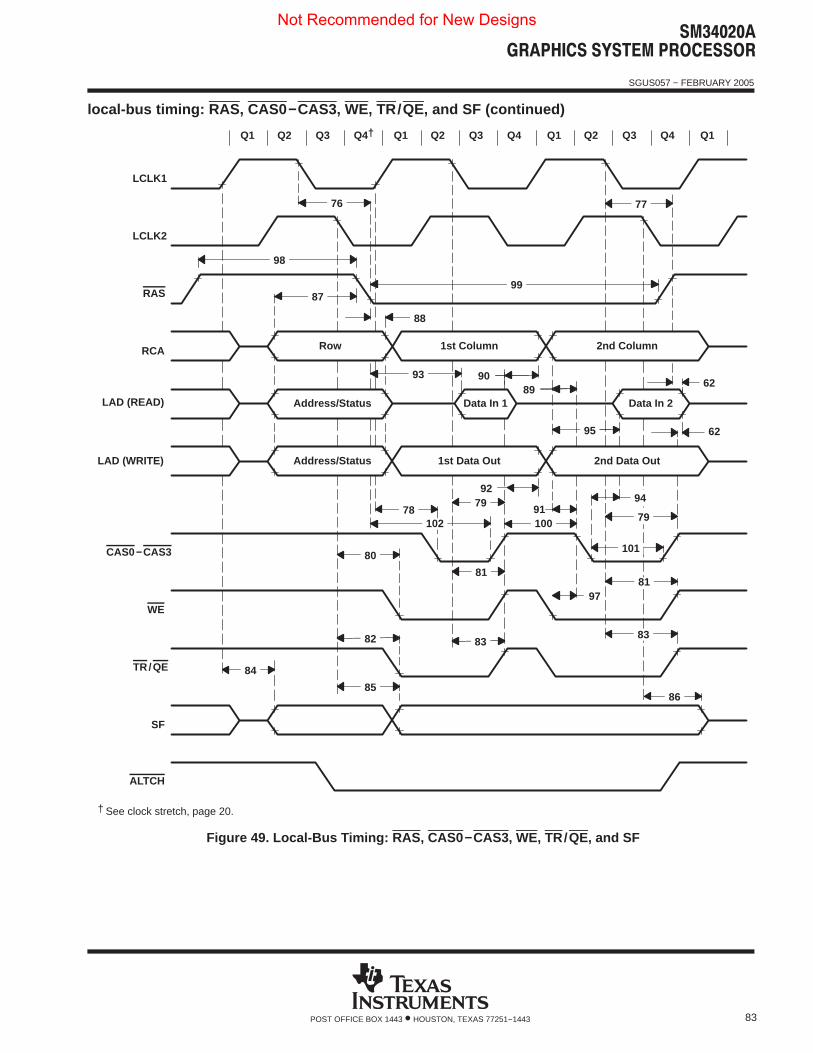
������������ � ������ � ����
SGUS057 − FEBRUARY 2005
83POST OFFICE BOX 1443 • HOUSTON, TEXAS 77251−1443
local-bus timing: RAS , CAS0 −CAS3, WE, TR/QE, and SF (continued)
91
2nd Data Out1st Data OutAddress/Status
Data In 2Data In 1Address/Status
2nd Column1st ColumnRow
ALTCH
SF
TR/QE
WE
CAS0 −CAS3
LAD (WRITE)
LAD (READ)
RCA
RAS
LCLK2
LCLK1
Q1 Q2 Q3 Q4† Q1 Q2 Q3 Q4 Q1 Q2 Q3 Q4 Q1
8685
84
838382
8197
81
80
9279
8990
10278
62
62
101
100
93
88
87
77
99
76
98
79
94
95
† See clock stretch, page 20.
Figure 49. Local-Bus Timing: RAS , CAS0 −CAS3, WE, TR/QE, and SF
Not Recommended for New Designs
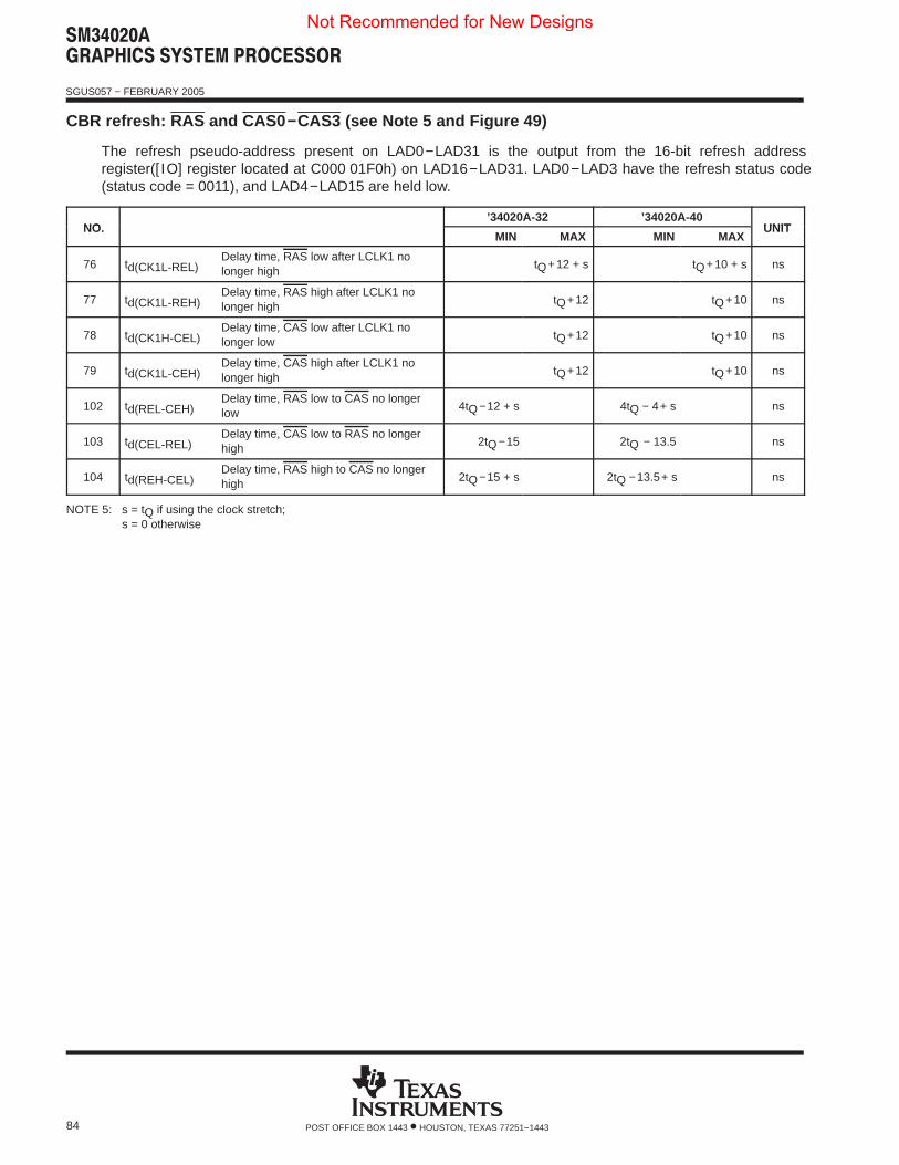
������������ � ������ � ����
SGUS057 − FEBRUARY 2005
84 POST OFFICE BOX 1443 • HOUSTON, TEXAS 77251−1443
CBR refresh: RAS and CAS0 −CAS3 (see Note 5 and Figure 49)
The refresh pseudo-address present on LAD0−LAD31 is the output from the 16-bit refresh addressregister([ IO] register located at C000 01F0h) on LAD16−LAD31. LAD0−LAD3 have the refresh status code(status code = 0011), and LAD4−LAD15 are held low.
NO.’34020A-32 ’34020A-40
UNITNO.MIN MAX MIN MAX
UNIT
76 td(CK1L-REL)Delay time, RAS low after LCLK1 nolonger high
tQ+12 + s tQ+10 + s ns
77 td(CK1L-REH)Delay time, RAS high after LCLK1 nolonger high
tQ+12 tQ+10 ns
78 td(CK1H-CEL)Delay time, CAS low after LCLK1 nolonger low
tQ+12 tQ+10 ns
79 td(CK1L-CEH)Delay time, CAS high after LCLK1 nolonger high
tQ+12 tQ+10 ns
102 td(REL-CEH)Delay time, RAS low to CAS no longerlow
4tQ−12 + s 4tQ − 4+ s ns
103 td(CEL-REL)Delay time, CAS low to RAS no longerhigh
2tQ−15 2tQ − 13.5 ns
104 td(REH-CEL)Delay time, RAS high to CAS no longerhigh
2tQ−15 + s 2tQ −13.5+ s ns
NOTE 5: s = tQ if using the clock stretch; s = 0 otherwise
Not Recommended for New Designs
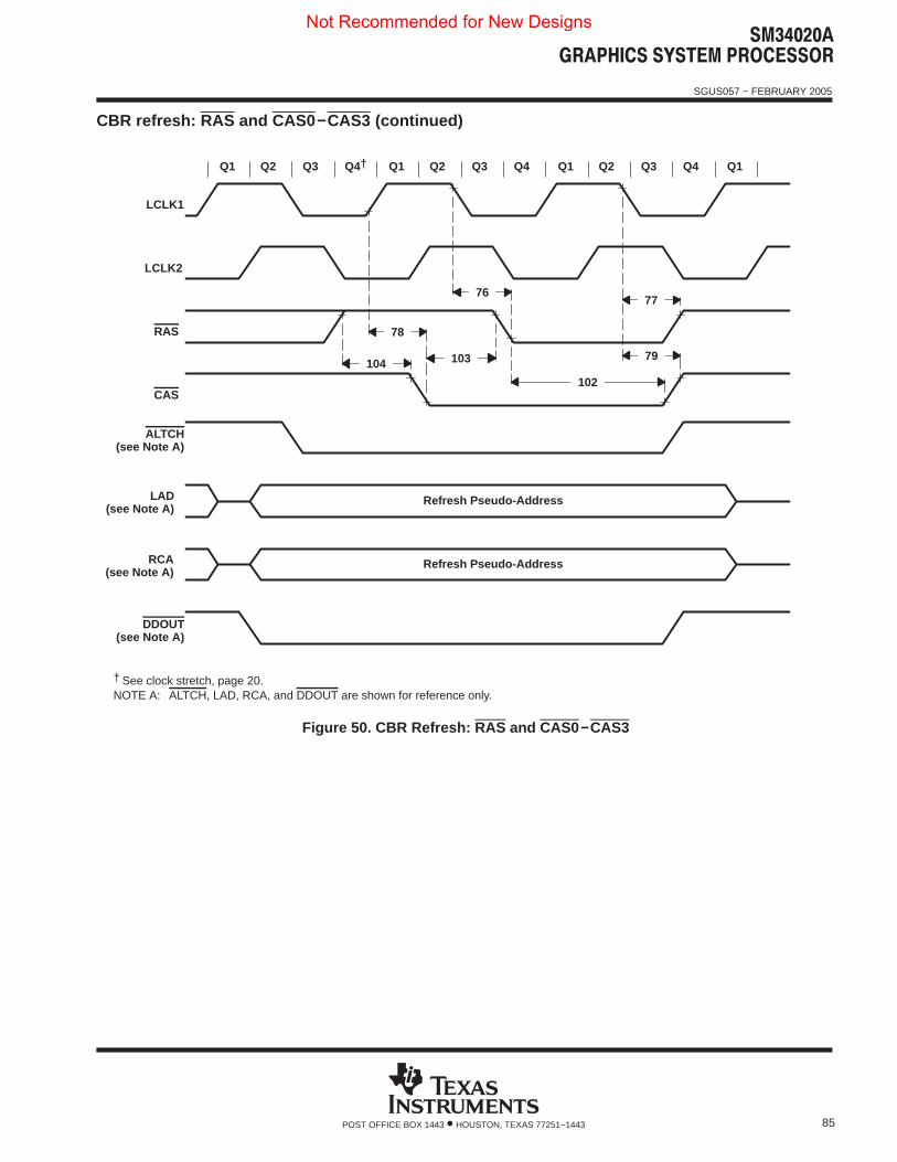
������������ � ������ � ����
SGUS057 − FEBRUARY 2005
85POST OFFICE BOX 1443 • HOUSTON, TEXAS 77251−1443
CBR refresh: RAS and CAS0 −CAS3 (continued)
DDOUT(see Note A)
RCA(see Note A)
LAD(see Note A)
ALTCH(see Note A)
CAS
RAS
LCLK2
LCLK1
Refresh Pseudo-Address
Refresh Pseudo-Address
Q1 Q2 Q3 Q4† Q1 Q2 Q3 Q4 Q1 Q2 Q3 Q4 Q1
79
102
103
7776
78
104
† See clock stretch, page 20.NOTE A: ALTCH, LAD, RCA, and DDOUT are shown for reference only.
Figure 50. CBR Refresh: RAS and CAS0 −CAS3
Not Recommended for New Designs
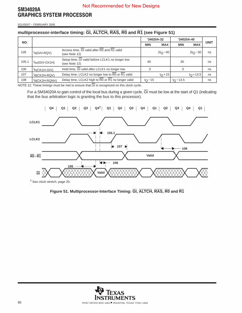
������������ � ������ � ����
SGUS057 − FEBRUARY 2005
86 POST OFFICE BOX 1443 • HOUSTON, TEXAS 77251−1443
multiprocessor-interface timing: GI , ALTCH, RAS, R0 and R1 (see Figure 51)
NO.’34020A-32 ’34020A-40
UNITNO.MIN MAX MIN MAX
UNIT
105 ta(GIV-RQV)Access time, GI valid after R0 and R1 valid(see Note 12)
2tQ−40 2tQ−30 ns
105.1 tsu(GIV-CK1H)Setup time, GI valid before LCLK1 no longer low(see Note 12)
40 35 ns
106 th(CK1H-GIV) Hold time, GI valid after LCLK1 no longer low 0 0 ns
107 td(CK2H-RQV) Delay time, LCLK2 no longer low to R0 or R1 valid tQ+15 tQ+13.5 ns
108 td(CK2H-RQNV) Delay time, LCLK2 high to R0 or R1 no longer valid tQ−15 tQ−13.5 ns
NOTE 12: These timings must be met to ensure that GI is recognized on this clock cycle.
For a SM34020A to gain control of the local bus during a given cycle, GI must be low at the start of Q1 (indicatingthat the bus arbitration logic is granting the bus to this processor).
GI
R0−R1
LCLK2
LCLK1
106105
Q4 Q1 Q2 Q3 Q4† Q1 Q2 Q3 Q4 Q1 Q2 Q3 Q4 Q1
Valid
Valid
108107
105.1
† See clock stretch, page 20.
† See clock stretch, page 20.
Figure 51. Multiprocessor-Interface Timing: GI , ALTCH, RAS, R0 and R1
Not Recommended for New Designs
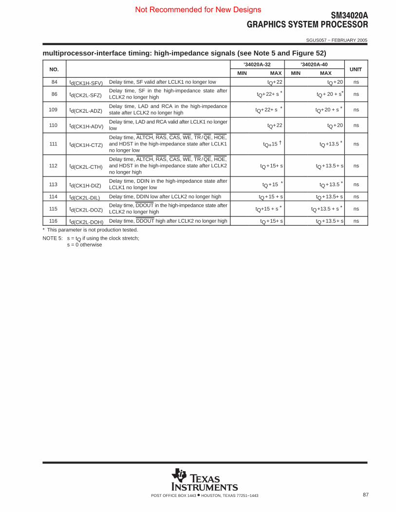
������������ � ������ � ����
SGUS057 − FEBRUARY 2005
87POST OFFICE BOX 1443 • HOUSTON, TEXAS 77251−1443
multiprocessor-interface timing: high-impedance signals (see Note 5 and Figure 52)
NO.’34020A-32 ’34020A-40
UNITNO.MIN MAX MIN MAX
UNIT
84 td(CK1H-SFV) Delay time, SF valid after LCLK1 no longer low tQ+22 tQ+20 ns
86 td(CK2L-SFZ)Delay time, SF in the high-impedance state afterLCLK2 no longer high
tQ+22+ s * tQ+ 20 + s* ns
109 td(CK2L-ADZ)Delay time, LAD and RCA in the high-impedancestate after LCLK2 no longer high
tQ+22+ s * tQ+20 + s * ns
110 td(CK1H-ADV)Delay time, LAD and RCA valid after LCLK1 no longerlow
tQ+22 tQ+20 ns
111 td(CK1H-CTZ)
Delay time, ALTCH, RAS, CAS, WE, TR/QE, HOE,and HDST in the high-impedance state after LCLK1no longer low
tQ+15 † tQ+13.5 * ns
112 td(CK2L-CTH)
Delay time, ALTCH, RAS, CAS, WE, TR/QE, HOE,and HDST in the high-impedance state after LCLK2no longer high
tQ+15+ s tQ+13.5+ s ns
113 td(CK1H-DIZ)Delay time, DDIN in the high-impedance state afterLCLK1 no longer low
tQ+15 * tQ+13.5 * ns
114 td(CK2L-DIL) Delay time, DDIN low after LCLK2 no longer high tQ+15 + s tQ+13.5+ s ns
115 td(CK2L-DOZ)Delay time, DDOUT in the high-impedance state afterLCLK2 no longer high
tQ+15 + s * tQ+13.5 + s * ns
116 td(CK2L-DOH) Delay time, DDOUT high after LCLK2 no longer high tQ+15+ s tQ+13.5+ s ns
* This parameter is not production tested.
NOTE 5: s = tQ if using the clock stretch; s = 0 otherwise
Not Recommended for New Designs
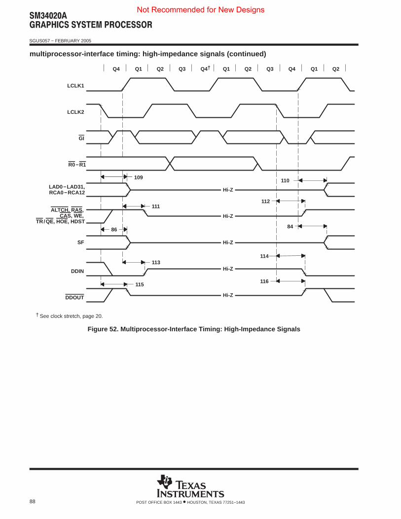
������������ � ������ � ����
SGUS057 − FEBRUARY 2005
88 POST OFFICE BOX 1443 • HOUSTON, TEXAS 77251−1443
multiprocessor-interface timing: high-impedance signals (continued)
110
DDOUT
DDIN
SF
ALTCH, RAS,CAS, WE,
TR/QE, HOE, HDST
LAD0−LAD31,RCA0−RCA12
R0−R1
GI
LCLK2
LCLK1
Q2Q1Q4Q3Q2Q1Q4†Q3Q2Q1Q4
Hi-Z
Hi-Z
Hi-Z
Hi-Z
Hi-Z
86
112
84
109
115
111
113114
116
† See clock stretch, page 20.
Figure 52. Multiprocessor-Interface Timing: High-Impedance Signals
Not Recommended for New Designs
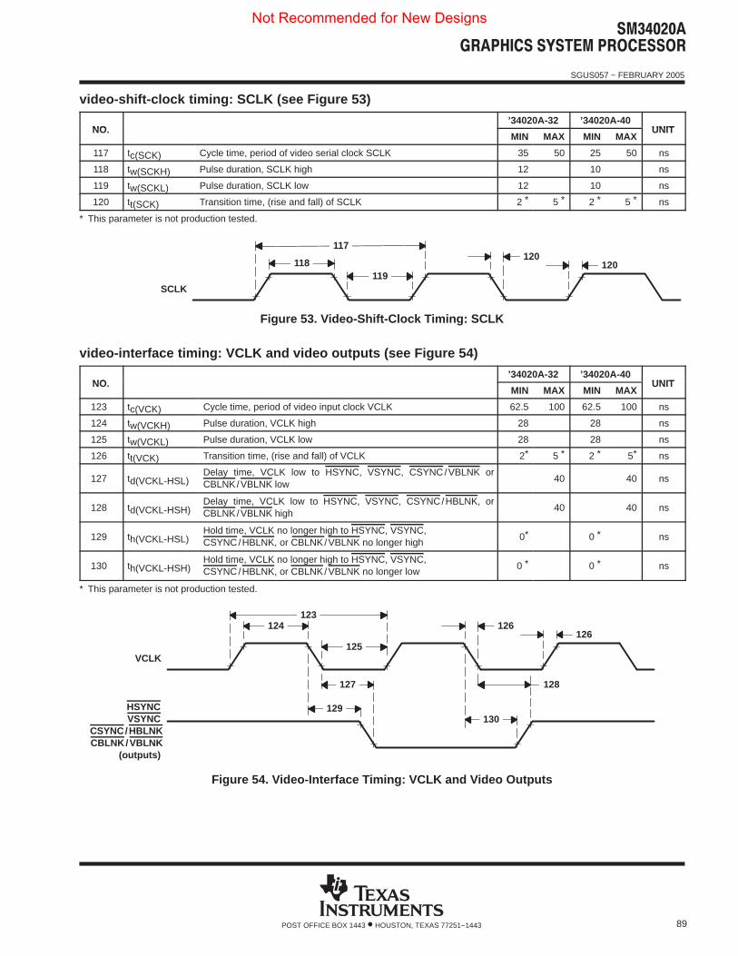
������������ � ������ � ����
SGUS057 − FEBRUARY 2005
89POST OFFICE BOX 1443 • HOUSTON, TEXAS 77251−1443
video-shift-clock timing: SCLK (see Figure 53)
NO.’34020A-32 ’34020A-40
UNITNO.MIN MAX MIN MAX
UNIT
117 tc(SCK) Cycle time, period of video serial clock SCLK 35 50 25 50 ns
118 tw(SCKH) Pulse duration, SCLK high 12 10 ns
119 tw(SCKL) Pulse duration, SCLK low 12 10 ns
120 tt(SCK) Transition time, (rise and fall) of SCLK 2 * 5 * 2 * 5 * ns
* This parameter is not production tested.
SCLK
120120
117
119118
Figure 53. Video-Shift-Clock Timing: SCLK
video-interface timing: VCLK and video outputs (see Figure 54)
NO.’34020A-32 ’34020A-40
UNITNO.MIN MAX MIN MAX
UNIT
123 tc(VCK) Cycle time, period of video input clock VCLK 62.5 100 62.5 100 ns
124 tw(VCKH) Pulse duration, VCLK high 28 28 ns
125 tw(VCKL) Pulse duration, VCLK low 28 28 ns
126 tt(VCK) Transition time, (rise and fall) of VCLK 2* 5 * 2 * 5* ns
127 td(VCKL-HSL)Delay time, VCLK low to HSYNC, VSYNC, CSYNC/VBLNK orCBLNK/VBLNK low
40 40 ns
128 td(VCKL-HSH)Delay time, VCLK low to HSYNC, VSYNC, CSYNC/HBLNK, orCBLNK/VBLNK high
40 40 ns
129 th(VCKL-HSL)Hold time, VCLK no longer high to HSYNC, VSYNC,CSYNC/HBLNK, or CBLNK/VBLNK no longer high
0* 0 * ns
130 th(VCKL-HSH)Hold time, VCLK no longer high to HSYNC, VSYNC,CSYNC/HBLNK, or CBLNK/VBLNK no longer low
0 * 0 * ns
* This parameter is not production tested.
VCLK
HSYNCVSYNC
CSYNC/HBLNKCBLNK /VBLNK
(outputs)
130
127
129
128
126126
123
125
124
Figure 54. Video-Interface Timing: VCLK and Video Outputs
Not Recommended for New Designs
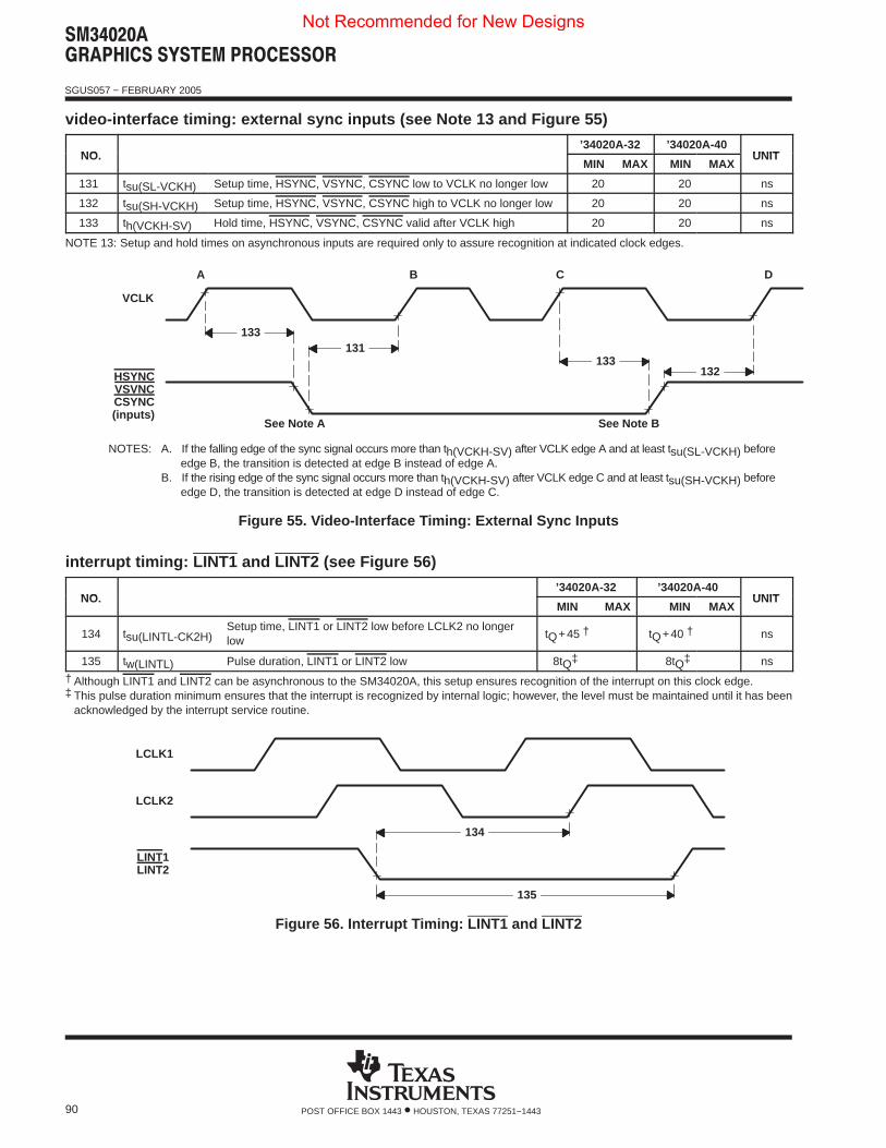
������������ � ������ � ����
SGUS057 − FEBRUARY 2005
90 POST OFFICE BOX 1443 • HOUSTON, TEXAS 77251−1443
video-interface timing: external sync inputs (see Note 13 and Figure 55)
NO.’34020A-32 ’34020A-40
UNITNO.MIN MAX MIN MAX
UNIT
131 tsu(SL-VCKH) Setup time, HSYNC, VSYNC, CSYNC low to VCLK no longer low 20 20 ns
132 tsu(SH-VCKH) Setup time, HSYNC, VSYNC, CSYNC high to VCLK no longer low 20 20 ns
133 th(VCKH-SV) Hold time, HSYNC, VSYNC, CSYNC valid after VCLK high 20 20 ns
NOTE 13: Setup and hold times on asynchronous inputs are required only to assure recognition at indicated clock edges.
See Note BSee Note A
DCBA
HSYNCVSVNCCSYNC(inputs)
VCLK
132133
131133
NOTES: A. If the falling edge of the sync signal occurs more than th(VCKH-SV) after VCLK edge A and at least tsu(SL-VCKH) beforeedge B, the transition is detected at edge B instead of edge A.
B. If the rising edge of the sync signal occurs more than th(VCKH-SV) after VCLK edge C and at least tsu(SH-VCKH) beforeedge D, the transition is detected at edge D instead of edge C.
Figure 55. Video-Interface Timing: External Sync Inputs
interrupt timing: LINT1 and LINT2 (see Figure 56)
NO.’34020A-32 ’34020A-40
UNITNO.MIN MAX MIN MAX
UNIT
134 tsu(LINTL-CK2H)Setup time, LINT1 or LINT2 low before LCLK2 no longerlow
tQ+45 † tQ+40 † ns
135 tw(LINTL) Pulse duration, LINT1 or LINT2 low 8tQ‡ 8tQ‡ ns
† Although LINT1 and LINT2 can be asynchronous to the SM34020A, this setup ensures recognition of the interrupt on this clock edge.‡ This pulse duration minimum ensures that the interrupt is recognized by internal logic; however, the level must be maintained until it has been
acknowledged by the interrupt service routine.
LINT1 LINT2
LCLK2
LCLK1
135
134
Figure 56. Interrupt Timing: LINT1 and LINT2
Not Recommended for New Designs
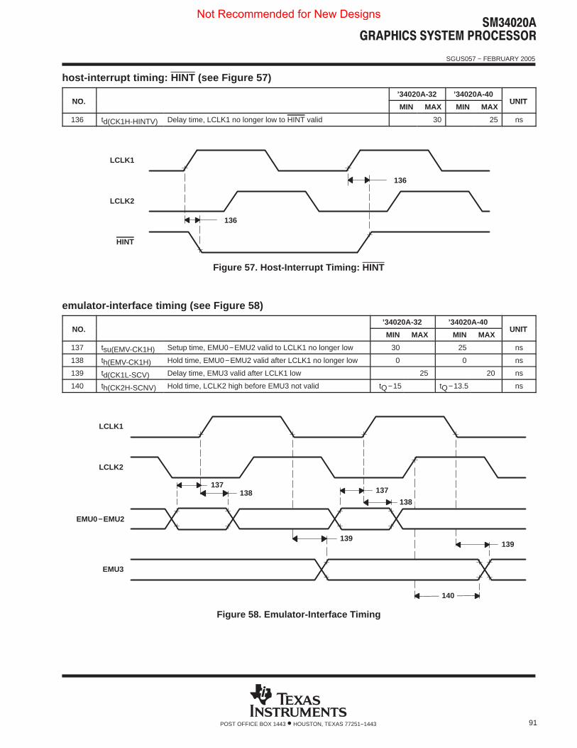
������������ � ������ � ����
SGUS057 − FEBRUARY 2005
91POST OFFICE BOX 1443 • HOUSTON, TEXAS 77251−1443
host-interrupt timing: HINT (see Figure 57)
NO.’34020A-32 ’34020A-40
UNITNO.MIN MAX MIN MAX
UNIT
136 td(CK1H-HINTV) Delay time, LCLK1 no longer low to HINT valid 30 25 ns
HINT
LCLK2
LCLK1
136
136
Figure 57. Host-Interrupt Timing: HINT
emulator-interface timing (see Figure 58)
NO.’34020A-32 ’34020A-40
UNITNO.MIN MAX MIN MAX
UNIT
137 tsu(EMV-CK1H) Setup time, EMU0−EMU2 valid to LCLK1 no longer low 30 25 ns
138 th(EMV-CK1H) Hold time, EMU0−EMU2 valid after LCLK1 no longer low 0 0 ns
139 td(CK1L-SCV) Delay time, EMU3 valid after LCLK1 low 25 20 ns
140 th(CK2H-SCNV) Hold time, LCLK2 high before EMU3 not valid tQ−15 tQ−13.5 ns
EMU3
EMU0−EMU2
LCLK2
LCLK1
139139
137138137
138
140
Figure 58. Emulator-Interface Timing
Not Recommended for New Designs
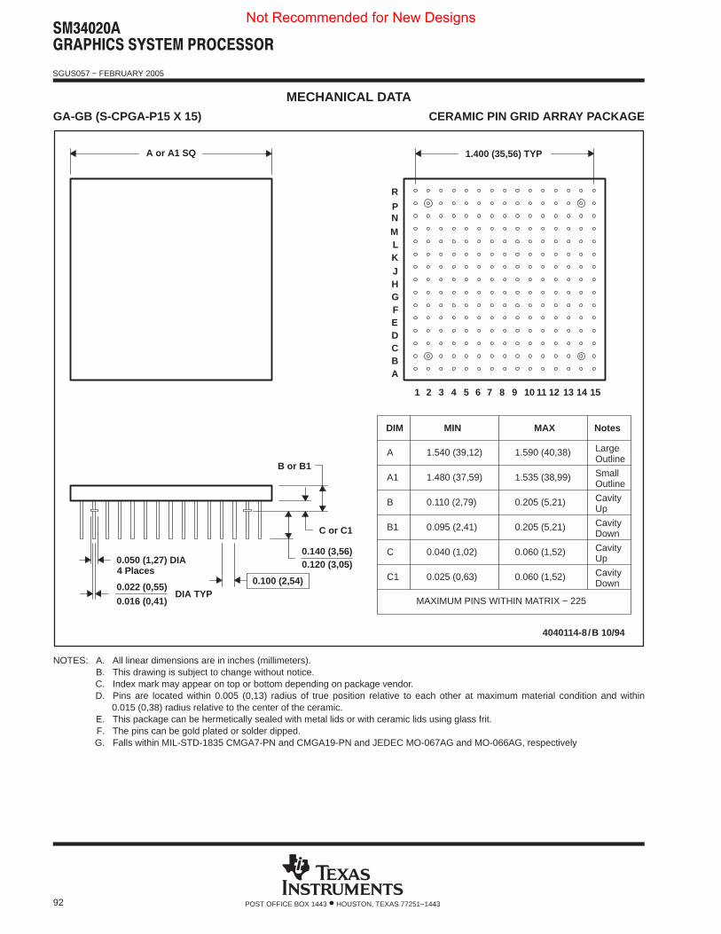
������������ � ������ � ����
SGUS057 − FEBRUARY 2005
92 POST OFFICE BOX 1443 • HOUSTON, TEXAS 77251−1443
MECHANICAL DATAGA-GB (S-CPGA-P15 X 15) CERAMIC PIN GRID ARRAY PACKAGE
4040114-8 /B 10/94
DownCavity
UpCavity
DownCavity
CavityUp
OutlineSmall
OutlineLarge
MAXIMUM PINS WITHIN MATRIX − 225
C1 0.025 (0,63) 0.060 (1,52)
0.060 (1,52)0.040 (1,02)C
B1 0.095 (2,41) 0.205 (5,21)
0.205 (5,21)0.110 (2,79)B
A1 1.480 (37,59) 1.535 (38,99)
1.590 (40,38)
DIM MIN MAX Notes
1.540 (39,12)A
A or A1 SQ
4 Places
DIA TYP
1.400 (35,56) TYP
0.050 (1,27) DIA 0.120 (3,05)
0.016 (0,41)
0.022 (0,55)
0.140 (3,56)
B or B1
C or C1
JHGFEDC
AB
1 2 3 4 5 6 7 8 9
K
10
L
11 12
M
13
N
14
P
0.100 (2,54)
15
R
NOTES: A. All linear dimensions are in inches (millimeters).B. This drawing is subject to change without notice.C. Index mark may appear on top or bottom depending on package vendor.D. Pins are located within 0.005 (0,13) radius of true position relative to each other at maximum material condition and within
0.015 (0,38) radius relative to the center of the ceramic.E. This package can be hermetically sealed with metal lids or with ceramic lids using glass frit.F. The pins can be gold plated or solder dipped.G. Falls within MIL-STD-1835 CMGA7-PN and CMGA19-PN and JEDEC MO-067AG and MO-066AG, respectively
Not Recommended for New Designs
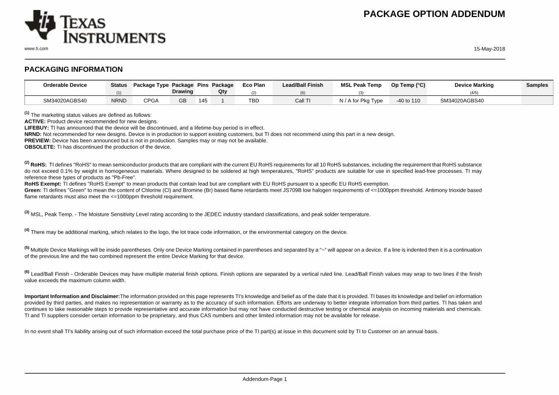
PACKAGE OPTION ADDENDUM
www.ti.com 15-May-2018
Addendum-Page 1
PACKAGING INFORMATION
Orderable Device Status(1)
Package Type PackageDrawing
Pins PackageQty
Eco Plan(2)
Lead/Ball Finish(6)
MSL Peak Temp(3)
Op Temp (°C) Device Marking(4/5)
Samples
SM34020AGBS40 NRND CPGA GB 145 1 TBD Call TI N / A for Pkg Type -40 to 110 SM34020AGBS40 (1) The marketing status values are defined as follows:ACTIVE: Product device recommended for new designs.LIFEBUY: TI has announced that the device will be discontinued, and a lifetime-buy period is in effect.NRND: Not recommended for new designs. Device is in production to support existing customers, but TI does not recommend using this part in a new design.PREVIEW: Device has been announced but is not in production. Samples may or may not be available.OBSOLETE: TI has discontinued the production of the device.
(2) RoHS: TI defines "RoHS" to mean semiconductor products that are compliant with the current EU RoHS requirements for all 10 RoHS substances, including the requirement that RoHS substancedo not exceed 0.1% by weight in homogeneous materials. Where designed to be soldered at high temperatures, "RoHS" products are suitable for use in specified lead-free processes. TI mayreference these types of products as "Pb-Free".RoHS Exempt: TI defines "RoHS Exempt" to mean products that contain lead but are compliant with EU RoHS pursuant to a specific EU RoHS exemption.Green: TI defines "Green" to mean the content of Chlorine (Cl) and Bromine (Br) based flame retardants meet JS709B low halogen requirements of <=1000ppm threshold. Antimony trioxide basedflame retardants must also meet the <=1000ppm threshold requirement.
(3) MSL, Peak Temp. - The Moisture Sensitivity Level rating according to the JEDEC industry standard classifications, and peak solder temperature.
(4) There may be additional marking, which relates to the logo, the lot trace code information, or the environmental category on the device.
(5) Multiple Device Markings will be inside parentheses. Only one Device Marking contained in parentheses and separated by a "~" will appear on a device. If a line is indented then it is a continuationof the previous line and the two combined represent the entire Device Marking for that device.
(6) Lead/Ball Finish - Orderable Devices may have multiple material finish options. Finish options are separated by a vertical ruled line. Lead/Ball Finish values may wrap to two lines if the finishvalue exceeds the maximum column width.
Important Information and Disclaimer:The information provided on this page represents TI's knowledge and belief as of the date that it is provided. TI bases its knowledge and belief on informationprovided by third parties, and makes no representation or warranty as to the accuracy of such information. Efforts are underway to better integrate information from third parties. TI has taken andcontinues to take reasonable steps to provide representative and accurate information but may not have conducted destructive testing or chemical analysis on incoming materials and chemicals.TI and TI suppliers consider certain information to be proprietary, and thus CAS numbers and other limited information may not be available for release.
In no event shall TI's liability arising out of such information exceed the total purchase price of the TI part(s) at issue in this document sold by TI to Customer on an annual basis.
IMPORTANT NOTICE
Texas Instruments Incorporated (TI) reserves the right to make corrections, enhancements, improvements and other changes to itssemiconductor products and services per JESD46, latest issue, and to discontinue any product or service per JESD48, latest issue. Buyersshould obtain the latest relevant information before placing orders and should verify that such information is current and complete.TI’s published terms of sale for semiconductor products (http://www.ti.com/sc/docs/stdterms.htm) apply to the sale of packaged integratedcircuit products that TI has qualified and released to market. Additional terms may apply to the use or sale of other types of TI products andservices.Reproduction of significant portions of TI information in TI data sheets is permissible only if reproduction is without alteration and isaccompanied by all associated warranties, conditions, limitations, and notices. TI is not responsible or liable for such reproduceddocumentation. Information of third parties may be subject to additional restrictions. Resale of TI products or services with statementsdifferent from or beyond the parameters stated by TI for that product or service voids all express and any implied warranties for theassociated TI product or service and is an unfair and deceptive business practice. TI is not responsible or liable for any such statements.Buyers and others who are developing systems that incorporate TI products (collectively, “Designers”) understand and agree that Designersremain responsible for using their independent analysis, evaluation and judgment in designing their applications and that Designers havefull and exclusive responsibility to assure the safety of Designers' applications and compliance of their applications (and of all TI productsused in or for Designers’ applications) with all applicable regulations, laws and other applicable requirements. Designer represents that, withrespect to their applications, Designer has all the necessary expertise to create and implement safeguards that (1) anticipate dangerousconsequences of failures, (2) monitor failures and their consequences, and (3) lessen the likelihood of failures that might cause harm andtake appropriate actions. Designer agrees that prior to using or distributing any applications that include TI products, Designer willthoroughly test such applications and the functionality of such TI products as used in such applications.TI’s provision of technical, application or other design advice, quality characterization, reliability data or other services or information,including, but not limited to, reference designs and materials relating to evaluation modules, (collectively, “TI Resources”) are intended toassist designers who are developing applications that incorporate TI products; by downloading, accessing or using TI Resources in anyway, Designer (individually or, if Designer is acting on behalf of a company, Designer’s company) agrees to use any particular TI Resourcesolely for this purpose and subject to the terms of this Notice.TI’s provision of TI Resources does not expand or otherwise alter TI’s applicable published warranties or warranty disclaimers for TIproducts, and no additional obligations or liabilities arise from TI providing such TI Resources. TI reserves the right to make corrections,enhancements, improvements and other changes to its TI Resources. TI has not conducted any testing other than that specificallydescribed in the published documentation for a particular TI Resource.Designer is authorized to use, copy and modify any individual TI Resource only in connection with the development of applications thatinclude the TI product(s) identified in such TI Resource. NO OTHER LICENSE, EXPRESS OR IMPLIED, BY ESTOPPEL OR OTHERWISETO ANY OTHER TI INTELLECTUAL PROPERTY RIGHT, AND NO LICENSE TO ANY TECHNOLOGY OR INTELLECTUAL PROPERTYRIGHT OF TI OR ANY THIRD PARTY IS GRANTED HEREIN, including but not limited to any patent right, copyright, mask work right, orother intellectual property right relating to any combination, machine, or process in which TI products or services are used. Informationregarding or referencing third-party products or services does not constitute a license to use such products or services, or a warranty orendorsement thereof. Use of TI Resources may require a license from a third party under the patents or other intellectual property of thethird party, or a license from TI under the patents or other intellectual property of TI.TI RESOURCES ARE PROVIDED “AS IS” AND WITH ALL FAULTS. TI DISCLAIMS ALL OTHER WARRANTIES ORREPRESENTATIONS, EXPRESS OR IMPLIED, REGARDING RESOURCES OR USE THEREOF, INCLUDING BUT NOT LIMITED TOACCURACY OR COMPLETENESS, TITLE, ANY EPIDEMIC FAILURE WARRANTY AND ANY IMPLIED WARRANTIES OFMERCHANTABILITY, FITNESS FOR A PARTICULAR PURPOSE, AND NON-INFRINGEMENT OF ANY THIRD PARTY INTELLECTUALPROPERTY RIGHTS. TI SHALL NOT BE LIABLE FOR AND SHALL NOT DEFEND OR INDEMNIFY DESIGNER AGAINST ANY CLAIM,INCLUDING BUT NOT LIMITED TO ANY INFRINGEMENT CLAIM THAT RELATES TO OR IS BASED ON ANY COMBINATION OFPRODUCTS EVEN IF DESCRIBED IN TI RESOURCES OR OTHERWISE. IN NO EVENT SHALL TI BE LIABLE FOR ANY ACTUAL,DIRECT, SPECIAL, COLLATERAL, INDIRECT, PUNITIVE, INCIDENTAL, CONSEQUENTIAL OR EXEMPLARY DAMAGES INCONNECTION WITH OR ARISING OUT OF TI RESOURCES OR USE THEREOF, AND REGARDLESS OF WHETHER TI HAS BEENADVISED OF THE POSSIBILITY OF SUCH DAMAGES.Unless TI has explicitly designated an individual product as meeting the requirements of a particular industry standard (e.g., ISO/TS 16949and ISO 26262), TI is not responsible for any failure to meet such industry standard requirements.Where TI specifically promotes products as facilitating functional safety or as compliant with industry functional safety standards, suchproducts are intended to help enable customers to design and create their own applications that meet applicable functional safety standardsand requirements. Using products in an application does not by itself establish any safety features in the application. Designers mustensure compliance with safety-related requirements and standards applicable to their applications. Designer may not use any TI products inlife-critical medical equipment unless authorized officers of the parties have executed a special contract specifically governing such use.Life-critical medical equipment is medical equipment where failure of such equipment would cause serious bodily injury or death (e.g., lifesupport, pacemakers, defibrillators, heart pumps, neurostimulators, and implantables). Such equipment includes, without limitation, allmedical devices identified by the U.S. Food and Drug Administration as Class III devices and equivalent classifications outside the U.S.TI may expressly designate certain products as completing a particular qualification (e.g., Q100, Military Grade, or Enhanced Product).Designers agree that it has the necessary expertise to select the product with the appropriate qualification designation for their applicationsand that proper product selection is at Designers’ own risk. Designers are solely responsible for compliance with all legal and regulatoryrequirements in connection with such selection.Designer will fully indemnify TI and its representatives against any damages, costs, losses, and/or liabilities arising out of Designer’s non-compliance with the terms and provisions of this Notice.
Mailing Address: Texas Instruments, Post Office Box 655303, Dallas, Texas 75265Copyright © 2018, Texas Instruments Incorporated
Related Documents