DRV8809 DRV8810 www.ti.com SLVS854D – JULY 2008 – REVISED MAY 2012 COMBINATION MOTOR DRIVERS WITH DC-DC CONVERTERS Check for Samples: DRV8809, DRV8810 1FEATURES • Three Integrated DC-DC Converters – On/Off Selectable Using C_SELECT Pin and 2• Configurable to Eight Modes of Combination Serial Interface Motor Driver – Outputs Programmable With External – Bipolar Stepper Motor Driver Resistor Network From 1.5 V to VDIN × 0.8 – 16-Step Current-Mode Control – 1.5-A Output Capability for All Three – 800-mA Average Output Current as Channels Stepper Motor Drive • 7-V to 40-V Operating Voltage Range for DC- – DC Motor Driver DC Converters – 800-mA Maximum Continuous Current • Two Serial Interfaces for Communications and 8-A/500-ns or 3-A/100-ms Peak • Thermally-Enhanced Surface-Mount 64-Pin Current for Each DC Motor Drive QFP PowerPAD™ Package – Low ON resistance R ds(ON) = 0.55 Ω at (Eco-Friendly – RoHS and No Sb/Br) T J = 25°C (Typ) • Power-Down Function (Deep-Sleep Mode) • Reset Signal Output (Active Low) • Reset (All Clear) Control Input DESCRIPTION/ORDERING INFORMATION The DRV8809/DRV8810 provides an integrated motor driver solution. The chip has four H-bridges internally and is configurable to eight different modes of combination motor driver control. The output driver block for each H-bridge consists of N-channel power MOSFETs configured as full H-bridges to drive the motor windings. The stepper motor control has a 16-step mode programmable through the three-wire serial interface (SPI). The SPI input pins are 3.3-V compatible and 5-V tolerant. The DRV8809/DRV8810 has three DC-DC switch-mode buck converters to generate a programmable output voltage from 1.5 V to 80% of VDIN (Channel A) or up to 10 V (for Channel B and Channel C), with up to 1.5-A load current capability. The outputs are selected using the C_SELECT terminal at start-up or using serial interface during operation. An internal shutdown function is provided for overcurrent protection (OCP), short-circuit protection, overvoltage/undervoltage lockout (UVLO), and thermal shutdown (TSD). Also, the device has a reset function that operates at power on and at input to the In-Reset pin. ORDERING INFORMATION T A PACKAGE (1) (2) ORDERABLE PART NUMBER TOP-SIDE MARKING DRV8809A0PAP DRV8809A0PAP –40°C to 50°C Plastic QFP 64 (S-PQFP-G64) DRV8810A0PAP DRV8810A0PAP (1) For the most current package and ordering information, see the Package Option Addendum at the end of this document, or see the TI website at www.ti.com. (2) Package drawings, thermal data, and symbolization are available at www.ti.com/packaging. 1 Please be aware that an important notice concerning availability, standard warranty, and use in critical applications of Texas Instruments semiconductor products and disclaimers thereto appears at the end of this data sheet. 2PowerPAD is a trademark of Texas Instruments Inc. PRODUCTION DATA information is current as of publication date. Copyright © 2008–2012, Texas Instruments Incorporated Products conform to specifications per the terms of the Texas Instruments standard warranty. Production processing does not necessarily include testing of all parameters.

Welcome message from author
This document is posted to help you gain knowledge. Please leave a comment to let me know what you think about it! Share it to your friends and learn new things together.
Transcript
DRV8809DRV8810
www.ti.com SLVS854D –JULY 2008–REVISED MAY 2012
COMBINATION MOTOR DRIVERS WITH DC-DC CONVERTERSCheck for Samples: DRV8809, DRV8810
1FEATURES • Three Integrated DC-DC Converters– On/Off Selectable Using C_SELECT Pin and
2• Configurable to Eight Modes of CombinationSerial InterfaceMotor Driver
– Outputs Programmable With External– Bipolar Stepper Motor DriverResistor Network From 1.5 V to VDIN × 0.8– 16-Step Current-Mode Control
– 1.5-A Output Capability for All Three– 800-mA Average Output Current asChannelsStepper Motor Drive
• 7-V to 40-V Operating Voltage Range for DC-– DC Motor DriverDC Converters
– 800-mA Maximum Continuous Current• Two Serial Interfaces for Communicationsand 8-A/500-ns or 3-A/100-ms Peak• Thermally-Enhanced Surface-Mount 64-PinCurrent for Each DC Motor Drive
QFP PowerPAD™ Package– Low ON resistance Rds(ON) = 0.55 Ω at(Eco-Friendly – RoHS and No Sb/Br)TJ = 25°C (Typ)
• Power-Down Function (Deep-Sleep Mode)• Reset Signal Output (Active Low)• Reset (All Clear) Control Input
DESCRIPTION/ORDERING INFORMATIONThe DRV8809/DRV8810 provides an integrated motor driver solution. The chip has four H-bridges internally andis configurable to eight different modes of combination motor driver control.
The output driver block for each H-bridge consists of N-channel power MOSFETs configured as full H-bridges todrive the motor windings. The stepper motor control has a 16-step mode programmable through the three-wireserial interface (SPI). The SPI input pins are 3.3-V compatible and 5-V tolerant.
The DRV8809/DRV8810 has three DC-DC switch-mode buck converters to generate a programmable outputvoltage from 1.5 V to 80% of VDIN (Channel A) or up to 10 V (for Channel B and Channel C), with up to 1.5-Aload current capability. The outputs are selected using the C_SELECT terminal at start-up or using serialinterface during operation.
An internal shutdown function is provided for overcurrent protection (OCP), short-circuit protection,overvoltage/undervoltage lockout (UVLO), and thermal shutdown (TSD). Also, the device has a reset functionthat operates at power on and at input to the In-Reset pin.
ORDERING INFORMATIONTA PACKAGE (1) (2) ORDERABLE PART NUMBER TOP-SIDE MARKING
DRV8809A0PAP DRV8809A0PAP–40°C to 50°C Plastic QFP 64 (S-PQFP-G64)
DRV8810A0PAP DRV8810A0PAP
(1) For the most current package and ordering information, see the Package Option Addendum at the end of this document, or see the TIwebsite at www.ti.com.
(2) Package drawings, thermal data, and symbolization are available at www.ti.com/packaging.
1
Please be aware that an important notice concerning availability, standard warranty, and use in critical applications ofTexas Instruments semiconductor products and disclaimers thereto appears at the end of this data sheet.
2PowerPAD is a trademark of Texas Instruments Inc.
PRODUCTION DATA information is current as of publication date. Copyright © 2008–2012, Texas Instruments IncorporatedProducts conform to specifications per the terms of the TexasInstruments standard warranty. Production processing does notnecessarily include testing of all parameters.

Voltage
charge
pump
Thermal
Shut down
Temperature
Sens :
Pre-TSD or
Tsens (analog)
Freq divider
for DC/DC
Freq divider
Motor PWM
DC/DC
convertor
Ch-A
DC/DC
convertor
Ch-B
DC/DC
convertor
Ch-C
Vout 1
Vout 2
Vout 3
LOGIC_OUT
FBB
OD_B
FBA
OD_A
FBC
OD_C
OSCM_mon
LGND
OUTA+
RSA
OUTA-
OUTB+
RSB
OUTB-
OUTC+
RSC
OUTC-
OUTD+
RSD
OUTD-
To Highside
gate drive
Cstorage
TH_OUT
C_SELECT
DC
Motor
Motor Drive
Output
Control C
VM
Motor Drive
Output
Control D
DC
Motor
VM
Stepper
Motor
Motor Drive
Output
Control A
Motor Drive
Output
Control B
VM
VM
CLK_AB
nORT
PHASE_SD PHASE_SC
MGND
MGND
To
H-bridges
VM
ENABLE_SC
nSLEEPVREF_AB
VREF_CD
DATA_ABSTROBE_ABNCENABLE_SD
VM
Regulator
Internal
supply
OSCi
6.4MHz
Setup / ex-setup
registers
Cbkt
Pre-Drive, Latch
Registers &
control circuitry
Serial Interface C-DSerial Interface A-B
DCDC_MODE
OSCD_mon
Voltage
Supervisory
To
DC/DC
VDIN
In-Reset
0.1uF
0.01uF
Pin # 61
Data_AB
Data_AB
Data_AB
(NC)
(NC)
PHASE_SB
Data_AB
(NC)
Pin # 60
CLK_CD
PHASE_LCD
PHASE_SC
PHASE_SC
PHASE_LCD
PHASE_SC
CLK_CD
(NC)
Pin # 59
Data_CD
(NC)
PHASE_SD
PHASE_SD
(NC)
PHASE_SD
Data_CD
(NC)
Pin # 51
STROBE_CD
ENABLE_LCD
ENABLE_SC
ENABLE_SC
ENABLE_LCD
ENABLE_SC
STROBE_CD
(NC)
Pin # 62
CLK_AB
CLK_AB
CLK_AB
PHASE_LAB
PHASE_LAB
PHASE_SA
CLK_AB
PHASE_UL
Pin # 55
STROBE_AB
STROBE_AB
STROBE_AB
ENABLE_LAB
ENABLE_LAB
ENABLE_SA
STROBE_AB
ENABLE_UL
Pin # 54
(NC)
(NC)
(NC)
(NC)
(NC)
ENABLE_SB
(NC)
(NC)
Pin # 50
(NC)
(NC)
ENABLE_SD
ENABLE_SD
(NC)
ENABLE_SD
(NC)
(NC)
MTR Config ;
Stepper x 2
Stepper + LDC
Step + SDCx2
LDC + SDCx2
LDC x 2
SDC x 4
Large Stepper
Ultra Large DC
VM
VCP CP1 CP2
DRV8809DRV8810SLVS854D –JULY 2008–REVISED MAY 2012 www.ti.com
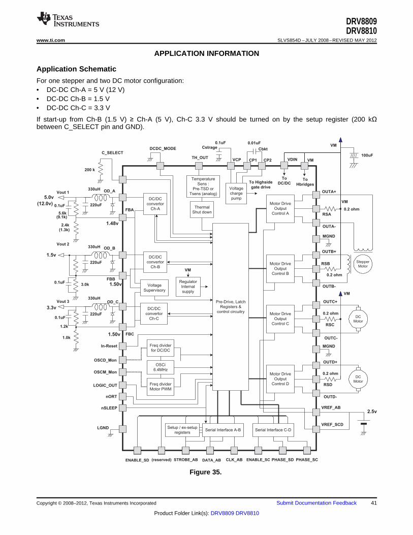
BLOCK DIAGRAM(One Stepper Motor and Two DC Motor Drives)
2 Submit Documentation Feedback Copyright © 2008–2012, Texas Instruments Incorporated
Product Folder Link(s): DRV8809 DRV8810

Test-LGND
MGND
OUTA–
RSA
RSA
OUTA+
MGND
MGND
OUTB+
RSB
RSB
OUTB–
MGND
LGND
DCDC_MODE
FBC
GND
MGND
OUTD–
RSD
RSD
OUTD+
MGND
MGND
OUTC+
RSC
RSC
OUTC–
MGND
LGND
OD_A
OD_A
1
2
3
4
5
6
7
8
9
10
11
12
13
14
15
16
48
47
46
45
44
43
42
41
40
39
38
37
36
35
34
33
17
18
19
20
21
22
23
24
25
26
27
28
29
30
31
32
64
63
62
61
60
59
58
57
56
55
54
53
52
51
50
49
OD
_C
OD
_C
OD
_B
OD
_B
FB
B
VC
P
OS
CD
_m
on
CP
2
CP
1
VD
IN
VD
IN
VD
IN
VM
VR
EF
_A
B
VR
EF
_C
D
FB
A
In-R
eset
nS
LE
EP
CL
K_A
B
DA
TA
_A
B
CLK
_C
D
DA
TA
_C
D
OS
CM
_m
on
LG
ND
nO
RT
ST
RO
BE
_A
B
(nc)
LO
GIC
_O
UT
TH
_O
UT
ST
RO
BE
_C
D
(nc)
C_S
ELE
CT
PAP PACKAGE(TOP VIEW)
DRV8809DRV8810
www.ti.com SLVS854D –JULY 2008–REVISED MAY 2012
PAP PACKAGE(TOP VIEW)
TERMINAL FUNCTIONSTERMINAL
PULLUP/ SHUNTI/O DESCRIPTIONNAME IN NAME IN PULLDOWN RESISTORNO. SETUP MODE OPERATION
1 Test-LGND Test-LGND - Low power or analog ground
2 MGND MGND - Power ground for motor
3 OUTA- OUTA- O Motor-drive output for winding A–
4 RSA RSA I Channel A current-sense resistor
5 RSA RSA I Channel A current-sense resistor
6 OUTA+ OUTA+ O Motor-drive output for winding A+
7 MGND MGND - Power ground for motor
8 MGND MGND - Power ground for motor
9 OUTB+ OUTB+ O Motor-drive output for winding B+
10 RSB RSB I Channel B current-sense resistor
11 RSB RSB I Channel B current-sense resistor
12 OUTB- OUTB- O Motor-drive output for winding B–
13 MGND MGND - Power ground for motor
14 LGND LGND - Low-power or analog ground
15 DCDC_MODE DCDC_MODE I Up 200 kΩ DC-DC Ch-B/Ch-C operation mode select
16 FBC FBC I Feedback signal for DC-DC converter C
17 OD_C OD_C O Output for DC-DC switch mode regulator C
18 OD_C OD_C O Output for DC-DC switch mode regulator C
19 OD_B OD_B O Output for DC-DC switch mode regulator B
20 OD_B OD_B O Output for DC-DC switch mode regulator B
21 FBB FBB I Feedback signal for DC-DC converter B
Copyright © 2008–2012, Texas Instruments Incorporated Submit Documentation Feedback 3
Product Folder Link(s): DRV8809 DRV8810

DRV8809DRV8810SLVS854D –JULY 2008–REVISED MAY 2012 www.ti.com
TERMINAL FUNCTIONS (continued)
TERMINALPULLUP/ SHUNTI/O DESCRIPTIONNAME IN NAME IN PULLDOWN RESISTORNO. SETUP MODE OPERATION
22 VCP VCP - Charge pump capacitor
23 OSCD_mon OSCD_mon O OSCD clock monitoring
24 CP2 CP2 - Charge-pump bucket capacitor (high side)
25 CP1 CP1 - Charge-pump bucket capacitor (low side)
26 VDIN VDIN Voltage supply for DC-DC converter
27 VDIN VDIN Voltage supply for DC-DC converter
28 VDIN VDIN Voltage supply for DC-DC converter
29 VM VM - Voltage supply for motors
Voltage reference for maximum stepper motor30 VREF_AB VREF_AB I current through A and B bridges
Voltage reference for maximum stepper motor31 VREF_CD VREF_CD I current through C and D bridges
32 FBA FBA I Feedback signal for DC-DC converter A
33 OD_A OD_A O Output for DC-DC switch mode regulator A
34 OD_A OD_A O Output for DC-DC switch mode regulator A
35 LGND LGND - Low-power or analog ground
36 MGND MGND - Power ground for motor
37 OUTC– OUTC– O Motor-drive output for winding C–
38 RSC RSC I Channel C current-sense resistor
39 RSC RSC I Channel C current-sense resistor
40 OUTC+ OUTC+ O Motor-drive output for winding C+
41 MGND MGND - Power ground for motor
42 MGND MGND - Power ground for motor
43 OUTD+ OUTD+ O Motor-drive output for winding D+
44 RSD RSD I Channel D current-sense resistor
45 RSD RSD I Channel D current-sense resistor
46 OUTD– OUTD– O Motor drive output for winding D–
47 MGND MGND - Power ground for motor
48 GND GND - Must be grounded
49 C_SELECT C_SELECT I Up 200 kΩ DC-DC converter selector
50 - ENABLE_SD I Down 100 kΩ Enable input for DC motor D control
50 - Reserved I Down 100 kΩ Reserved for DC motor operation
51 STROBE_CD ENABLE_SC I Down 100 kΩ Enable for DC motor C control
51 STROBE_CD ENABLE_LCD I Down 100 kΩ Enable for large DC motor CD control
Serial interface data strobe for H-bridge C, D51 STROBE_CD STROBE_CD I Down 100 kΩ stepper motor drive (latch on rising edge)
52 TH_OUT TH_OUT O Open drain Temperature-sensing output
53 LOGIC OUT LOGIC OUT O Open drain Protection-monitoring output
54 - Reserved I Down 100 kΩ Reserved for four DC motor operation
54 - ENABLE_SB I Down 100 kΩ Enable for DC motor B control
Serial interface data strobe for H-bridge A, B55 STROBE_ AB STROBE_ AB I Down 100 kΩ stepper motor drive (latch on rising edge)
55 STROBE_AB ENABLE_LAB I Down 100 kΩ Enable for large DC motor AB control
55 STROBE_AB ENABLE_SA I Down 100 kΩ Enable for DC motor A control
56 nORT nORT O Open drain Reset output (open drain)
57 LGND LGND - Low power or analog ground
58 OSCM_mon OSCM_mon O Open drain OSCM clock monitoring
4 Submit Documentation Feedback Copyright © 2008–2012, Texas Instruments Incorporated
Product Folder Link(s): DRV8809 DRV8810

DRV8809DRV8810
www.ti.com SLVS854D –JULY 2008–REVISED MAY 2012
TERMINAL FUNCTIONS (continued)
TERMINALPULLUP/ SHUNTI/O DESCRIPTIONNAME IN NAME IN PULLDOWN RESISTORNO. SETUP MODE OPERATION
59 DATA_CD PHASE_SD I Down 100 kΩ Serial input data for H-bridge C and D control
59 DATA_CD DATA_CD I Down 100 kΩ Serial input data for H-bridge C and D control
60 CLK_CD PHASE_SC I Down 100 kΩ Phase input for DC motor C control
60 CLK_CD CLK_CD I Down 100 kΩ Clock input synchronization for serial data CD
60 CLK_CD PHASE_LCD I Down 100 kΩ Phase input for large DC motor CD control
61 DATA_AB DATA_AB I Down 100 kΩ Serial input data for H-bridge A and B control
61 DATA_AB PHASE_SB I Down 100 kΩ Phase input for DC motor B control
62 CLK_AB CLK_AB I Down 100 kΩ Clock input synchronization for serial data AB
62 CLK_AB PHASE_LAB I Down 100 kΩ Phase input for large DC motor AB control
62 CLK_AB PHASE_SA I Down 100 kΩ Phase input for DC motor A control
63 nSLEEP=L nSLEEP I Down 100 kΩ Enable/disable (part can be in sleep state)
64 In-Reset In-Reset I Up 200 kΩ Reset (L: Reset, H/open: Normal operation)
Table 1. Alternate Functions of Select Pins By Operation Mode
PINCONFIG
50 51 54 55 59 60 61 62
Default Name ENABLE_SD ENABLE_SC ENABLE_SB STROBE_AB PHASE_ SD PHASE_SC DATA_AB CLK_AB
Dual Stepper - STROBE_CD - STROBE_AB DATA_CD CLK_CD DATA_AB CLK_AB
Stepper + - ENABLE_LCD - STROBE_AB - PHASE_LCD DATA_AB CLK_ABLarge DC
Stepper + Dual ENABLE_SD ENABLE_SC - STROBE_AB PHASE_SD PHASE_SC DATA_AB CLK_ABSmall DC
Large DC + ENABLE_SD ENABLE_SC - ENABLE_LAB PHASE _SD PHASE_SC - PHASE_LABDual Small DC
Dual Large DC - ENABLE_LCD - ENABLE_LAB - PHASE_LCD - PHASE_LAB
Quad Small ENABLE_SD ENABLE_SC ENABLE_SB ENABLE_SA PHASE_SD PHASE_SC PHASE_SB PHASE_SADC
Large Stepper - STROBE_CD - STROBE_AB DATA_CD CLK_CD DATA_AB CLK_AB
Ultra-Large DC - - - ENABLE_UL - - - PHASE_UL
Copyright © 2008–2012, Texas Instruments Incorporated Submit Documentation Feedback 5
Product Folder Link(s): DRV8809 DRV8810
External3.3 V
supply
1 k(external)
W
GND
# Th_out
# Logic_out
# nORT
# OSCM_mon
# OSCD_mon
Internal
3.3v
supply
GND
200k ohm
(+/- 40%)
Soft start
Control
Internal
3.3v
supply
GND
200k ohm
(+/- 40%)
Reset
Control
Hysteresis
Deglitch
100k ohm
(+/- 30%)
Serial
InterfaceHysteresis
GND GND
# DCDC_MODE
# In-Reset
External
3.3v
supply
# Th_OUT
# LOGIC_OUT
# nORT
# OSCM_mon
# OSCD_mon
1k ohm
( external )
GND
# C_SELECT
# nSLEEP
# ENABLE_x
# STROBE_CD/ENABLE
# STROBE_AB/ENABLE
# DATA_CD/PHASE
# CLK_CD/PHASE
# DATA_AB/ENABLE
# CLK_AB/ENABLE
1) Pin open ; 3.0 to 3.3v ; A /ON, B /ON, C /ON
2) External R to GND ( 200kO +/-10% );
1.3 to 2.0v ; DC_MODE Dependant
3) GND; 0.0 to 0.3v ; All off
Deglitch is for In-Reset only
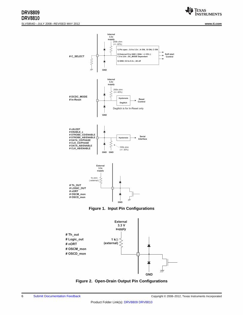
DRV8809DRV8810SLVS854D –JULY 2008–REVISED MAY 2012 www.ti.com
Figure 1. Input Pin Configurations
Figure 2. Open-Drain Output Pin Configurations
6 Submit Documentation Feedback Copyright © 2008–2012, Texas Instruments Incorporated
Product Folder Link(s): DRV8809 DRV8810

DRV8809DRV8810
www.ti.com SLVS854D –JULY 2008–REVISED MAY 2012
ABSOLUTE MAXIMUM RATINGSover operating free-air temperature range (unless otherwise noted)
VM Supply voltage (1) 50 V
Logic input voltage range, serial I/F inputs, and reset (2) –0.3 V to 5.5 V
Continuous total power dissipation (θJA = 20°C/W) 4 W
Continuous motor-drive output current for each H-bridge (100 ms) 3 A
Peak motor-drive output current for each H-bridge (500 ns) 8 A
Continuous DC-DC converter output current 1.5 A
Continuous DC-DC converter output current ODB, C in parallel mode 3.0 A
TJ Operating junction temperature range (1 h) 0°C to 150°C
Tstg Storage temperature range –65°C to 150°C
Lead temperature 1.6 mm (1/16 in) from case for 10 s 260°C
ESD levels on every pin, Human-Body Model (HBM) 2 kV
(1) Stresses beyond those listed under "absolute maximum ratings" may cause permanent damage to the device. These are stress ratingsonly and functional operation of the device at these or any other conditions beyond those indicated under "recommended operatingconditions" is not implied. Exposure to absolute-maximum-rated conditions for extended periods may affect device reliability.
(2) The negative spike less than –5 V and narrower than 50-ns duration should not cause any problem.
RECOMMENDED OPERATING CONDITIONSMIN NOM MAX UNIT
Supply voltage, VM for motor control 18 27 40 V
Supply voltage for DC-DC converter (VDIN) 7 27 40 V
Average output current for motor driver for each H-bridge 800 mA
DC output current for DC-DC converter 1.2 A
DC output current for DC-DC in Ch-B/C parallel mode 2.4 A
Operating ambient temperature (1) –40 50 °C
Operating junction temperature 0 120 °C
(1) If the total power is less than 4 W, then the operating ambient temperature range is -40°C to 60°C.
ELECTRICAL CHARACTERISTICSTJ = 0°C to 120°C, VM = 40 V (unless otherwise noted)
PARAMETER TEST CONDITIONS MIN TYP MAX UNIT
Supply (Sleep) Current
ISLEEP1 Supply (sleep) current 1 nSLEEP = L, DC-DC all off 4 5 mA
ISLEEP2 Supply (sleep) current 2 nSLEEP = L, VM = 8 V, Full duty cycle 7 10 mA
ISLEEP3 Supply (sleep) current 3 nSLEEP = L, VM = 40 V, Full duty cycle 8 10 mA
ELECTRICAL CHARACTERISTICSTJ = 0°C to 120°C, VM = 7 V to 40 V (unless otherwise noted)
PARAMETER TEST CONDITIONS MIN TYP MAX UNIT
Digital Interface Circuit
VIH Digital high-level input voltage Digital inputs (1) 2 5 V
IIH Digital high-level input current Digital inputs 100 μA
VIL Digital low-level input voltage Digital inputs 0.8 V
IIL Digital low-level input current Digital inputs 100 μA
Vhys Digital input hysteresis Digital inputs 0.3 0.45 0.6 V
Tdegl Digital input deglitch time In-Reset 2.5 7.5 μs
(1) Absolute maximum rating for charge-pump circuit is 60 V.
Copyright © 2008–2012, Texas Instruments Incorporated Submit Documentation Feedback 7
Product Folder Link(s): DRV8809 DRV8810

DRV8809DRV8810SLVS854D –JULY 2008–REVISED MAY 2012 www.ti.com
ELECTRICAL CHARACTERISTICS (continued)TJ = 0°C to 120°C, VM = 7 V to 40 V (unless otherwise noted)
PARAMETER TEST CONDITIONS MIN TYP MAX UNIT
Charge-Pump VCP (CP = 0.1 μF to 0.47 μF, Cbk = 0.01 μF ± 10%)
VO(CP) Output voltage ILOAD = 0 mA, VM > VthVM2 VM + 10 VM + 13 V
f(CP) Switching frequency 1.6 MHz
tstart Start-up time CStorage = 0.1 μF, VM ≥ 16 V 0.5 2 ms
Internal Clock OSCi
fOSCi System clock frequency 5.76 6.4 7.04 MHz
VREF Input
VREF Reference voltage input 0.8 2.5 3.6 V
Ileak-vr Input leak current 1 μA
C_SELECT for DC-DC Start-Up Selection (DCDC_MODE = L)
Vcs0 DC-DC all off 0 0.3 V
Vcs1 DC-DC all off Pull down by external 200-kΩ resistor 1.3 2 V
Turn on ODA then ODBVcs2 As pin open 3 3.3 Vand ODC
C_SELECT for DC-DC Start-Up Selection (DCDC_MODE = H or Open, Ch-B/C Parallel Mode)
Vcs0 DC-DC all off 0 0.3 V
Vcs1 Turn on ODB/C then ODA Pull down by external 200-kΩ resistor 1.3 2 V
Vcs2 Turn on ODA then ODB/C As pin open 3 3.6 V
Three DC-DC Converters (2)
1.25 =VDINOPE Operating supply voltage Ratio to VOUT(DC) VVO
VoutA = 1.5 V – 30 V, 20 V ≤ VDIN < 40 V –3 VO 3ODA VoutB/C = 1.5 V – 10 V, 6.5 V ≤ VDIN < 20 V –3 VO 5ODB Programmable with external %ODC reference on FBX VthVM– < VDIN < 6.5 V, VO ≤ 3.3 V –3 VO 5
× VDIN > 1.25 × Vout (largest)
VFB FBX feedback voltage For ODA/B/C 1.50 V
IO ODx ODx output current (dc) With external L and C 1.5 A
ODBC output current (DC)IO ODBC With external L and C DCDC_MODE = H 3 Ain Ch-B/Ch-C parallel mode
IO ODx2 Output current (dc) at low VDIN VDIN = 7 V, VO = 5 V 0.8 A
IO ODx3 Output current (dc) at low VDIN VDIN = 7 V, VO = 3.3 V 1.5 A
fOSCD Switching (chopping frequency) fOSCD = (0,0) 90 100 110 kHz
TJ = 25°C 0.35FET ON resistance at 0.8 A forRds(ON) ΩOD_x TJ = 120°C 0.50
5.5-V VO at VDIN = VthV_ 4 VVDIN = VthV_, VthV_ = 5-V load (dc)5 V-Low VO voltage to 5.5 V –30 %= 0.5 A (3)
VO voltage drop from VDIN 1 V
VO setting without kick UVPVo_min6 when VDIN = VthVM+ VthVM+ = 6-V load (DC) = 0.5 A (4) 6 V
(VO setting at VDIN = 10 V)
(2) DCDC_MODE = H, Ch-B and Ch-C are in parallel driving mode.(3) Lower VDIN decrease gate drive and the voltage drop is increased. Specified by bench characterization only.(4) VOUT (at VDIN = VthVM+) is lower than VO setting. When VDIN is down to VthVM+, undervoltage protection (UVP) shuts down the
device, in case the VO is set as VO > 7 V. Specified by design.
8 Submit Documentation Feedback Copyright © 2008–2012, Texas Instruments Incorporated
Product Folder Link(s): DRV8809 DRV8810

DRV8809DRV8810
www.ti.com SLVS854D –JULY 2008–REVISED MAY 2012
ELECTRICAL CHARACTERISTICS (continued)TJ = 0°C to 120°C, VM = 7 V to 40 V (unless otherwise noted)
PARAMETER TEST CONDITIONS MIN TYP MAX UNIT
Three DC-DC Converter Protection
Overcurrent detect for OD_xIO DD ODx Peak current in each ON cycle 1.8 3 Asource
tFILTOCP OCP filtering time By OSCi cycles 2 cycles
Number of subsequent chopping cycles choptODSD DC-DC shutdown filter 4with OCP detection cycles
Percentage of nominal Voutx detected atVovpx Overvoltage protection (OVP) 25 30 35 %VFB
Percentage of nominal Voutx detected atVuvpx Undervoltage protection (UVP) -25 -30 -35 %VFB (VFB decreasing)
tVfilter OVP/UVP filtering time 3 8 13 us
tsst Start-up time with soft start 56 ms
Vstover Start-up overshoot Ratio to VO 3 %
VM Supervisory
VthVM– nORT for VM low threshold VM decreasing 4.5 5 6 V
VthVM+ nORT for VM high threshold VM increasing 5.5 6 7 V
VthVMh nORT for VM detect hysteresis (VthVM+) - (VthV—) 0.5 1 V
VthVM2 For motor driver off (5) 15 V
tVM filt VM monitor filtering time For VM threshold detect 10 30 μs
Thermal Shutdown (TSD)
TTSD Thermal shutdown set points 150 170 190 °C
Temperature Sense, Pre TSD (See Extended Setup Register Definition)
Register selectable,TTSD0 Temperature sense point 0 130 150 170 °CAssert logic H at TH_OUT
Register selectable,TTSD1 Temperature sense point 1 120 140 160 °CAssert logic H at TH_OUT
TH_OUT (analog out)Tc_sens Specified by design 6 mV/°Ctemperature coefficient
RESET/nORT: Open-Drain Outputs (nORT, LOGIC_OUT, TH_OUT)
VOH High-state voltage RL = 1 kΩ to 3.3 V 3 V
VOL Low-state voltage RL = 1 kΩ to 3.3 V 0.3 V
IOL Low-state sink current VO = 0.4 V 3 mA
tr Rise time 10% to 90% 1 μs
tf Fall time 90% to 10% 50 ns
RESET/nORT Delay: Start-Up Sequence
Reset deassertion from VthVM+ < VDIN fortord1 nORT delay 1 300 390 msDC-DC wake up falling
From one DC-DC wake up to followingtord3 DC-DC turnon delay 1.7 msDC-DC to go soft-start sequence
Reset deassertion from 2nd DC-DC waketord4 nORT delay 4 120 180 msup
In-Reset
In-Reset assertion to nORTtreset In-Reset falling to nORT failing 5 10 μsassertion delay
(5) No nORT assertion to VthVM2 detection
Copyright © 2008–2012, Texas Instruments Incorporated Submit Documentation Feedback 9
Product Folder Link(s): DRV8809 DRV8810
DRV8809DRV8810SLVS854D –JULY 2008–REVISED MAY 2012 www.ti.com
ELECTRICAL CHARACTERISTICS (continued)TJ = 0°C to 120°C, VM = 7 V to 40 V (unless otherwise noted)
PARAMETER TEST CONDITIONS MIN TYP MAX UNIT
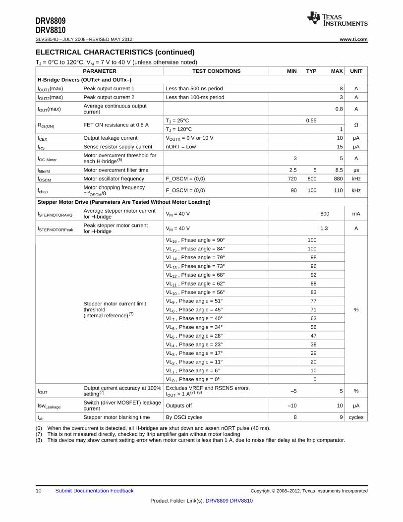
H-Bridge Drivers (OUTx+ and OUTx–)
IOUT1(max) Peak output current 1 Less than 500-ns period 8 A
IOUT2(max) Peak output current 2 Less than 100-ms period 3 A
Average continuous outputIOUT(max) 0.8 Acurrent
TJ = 25°C 0.55Rds(ON) FET ON resistance at 0.8 A Ω
TJ = 120°C 1
ICEX Output leakage current VOUTX = 0 V or 10 V 10 μA
IRS Sense resistor supply current nORT = Low 15 μA
Motor overcurrent threshold forIOC Motor 3 5 Aeach H-bridge (6)
tfilterM Motor overcurrent filter time 2.5 5 8.5 μs
fOSCM Motor oscillator frequency F_OSCM = (0,0) 720 800 880 kHz
Motor chopping frequencyfchop F_OSCM = (0,0) 90 100 110 kHz= fOSCM/8
Stepper Motor Drive (Parameters Are Tested Without Motor Loading)
Average stepper motor currentISTEPMOTORAVG VM = 40 V 800 mAfor H-bridge
Peak stepper motor currentISTEPMOTORPeak VM = 40 V 1.3 Afor H-bridge
VL16 , Phase angle = 90° 100
VL15 , Phase angle = 84° 100
VL14 , Phase angle = 79° 98
VL13 , Phase angle = 73° 96
VL12 , Phase angle = 68° 92
VL11 , Phase angle = 62° 88
VL10 , Phase angle = 56° 83
VL9 , Phase angle = 51° 77Stepper motor current limitthreshold VL8 , Phase angle = 45° 71 %(internal reference) (7)
VL7 , Phase angle = 40° 63
VL6 , Phase angle = 34° 56
VL5 , Phase angle = 28° 47
VL4 , Phase angle = 23° 38
VL3 , Phase angle = 17° 29
VL2 , Phase angle = 11° 20
VL1 , Phase angle = 6° 10
VL0 , Phase angle = 0° 0
Output current accuracy at 100% Excludes VREF and RSENS errors,IOUT –5 5 %setting (7) IOUT > 1 A (7) (8)
Switch (driver MOSFET) leakageIswLeakage Outputs off –10 10 μAcurrent
tab Stepper motor blanking time By OSCi cycles 8 9 cycles
(6) When the overcurrent is detected, all H-bridges are shut down and assert nORT pulse (40 ms).(7) This is not measured directly, checked by Itrip amplifier gain without motor loading(8) This device may show current setting error when motor current is less than 1 A, due to noise filter delay at the Itrip comparator.
10 Submit Documentation Feedback Copyright © 2008–2012, Texas Instruments Incorporated
Product Folder Link(s): DRV8809 DRV8810
DRV8809DRV8810
www.ti.com SLVS854D –JULY 2008–REVISED MAY 2012
ELECTRICAL CHARACTERISTICS (continued)TJ = 0°C to 120°C, VM = 7 V to 40 V (unless otherwise noted)
PARAMETER TEST CONDITIONS MIN TYP MAX UNIT
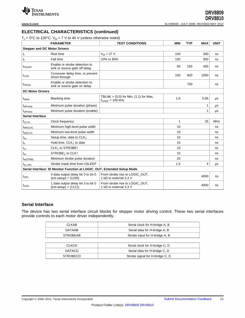
Stepper and DC Motor Drivers
tr Rise time VM = 27 V 100 300 ns
tf Fall time 20% to 80% 100 300 ns
Enable or strobe detection totPDOFF 50 150 400 nssink or source gate off delay
Crossover delay time, to preventtCOD 100 600 1000 nsshoot through
Enable or strobe detection totPDON 750 nssink or source gate on delay
DC Motor Drivers
TBLNK = (0,0) for Min, (1,1) for Max,tblank Blanking time 1.6 5.65 μsfCHOP = 100 kHz
twPminp Minimum pulse duration (phase) 1 μs
twPmine Minimum pulse duration (enable) 1 μs
Serial Interface
f(CLK) Clock frequency 1 25 MHz
twh(CLK) Minimum high-level pulse width 10 ns
twl(CLK) Minimum low-level pulse width 10 ns
tsu Setup time, data to CLK↓ 10 ns
th Hold time, CLK↓ to data 10 ns
tcs CLK↓ to STROBE↑ 10 ns
tsc STROBE↓ to CLK↑ 10 ns
tw(STRB) Minimum strobe pulse duration 20 ns
tss_min Strobe mask time from nSLEEP 1.5 4 μs
Serial Interface: ID Monitor Function at LOGIC_OUT, Extended Setup Mode
0 data output delay bit 3 to bit 0 From strobe rise to LOGIC_OUT,tODL 4000 ns(ext-setup) = (1100) 1 kΩ to external 3.3 V
1 data output delay bit 3 to bit 0 From strobe rise to LOGIC_OUT,tODH 4000 ns(ext-setup) = (1111) 1 kΩ to external 3.3 V
Serial Interface
The device has two serial interface circuit blocks for stepper motor driving control. These two serial interfacesprovide controls to each motor driver independently.
CLKAB Serial clock for H-bridge A, B
DATAAB Serial data for H-bridge A, B
STROBEAB Strobe input for H-bridge A, B
CLKCD Serial clock for H-bridge C, D
DATACD Serial data for H-bridge C, D
STROBECD Strobe signal for H-bridge C, D
Copyright © 2008–2012, Texas Instruments Incorporated Submit Documentation Feedback 11
Product Folder Link(s): DRV8809 DRV8810
DATA
CLK
Strobe
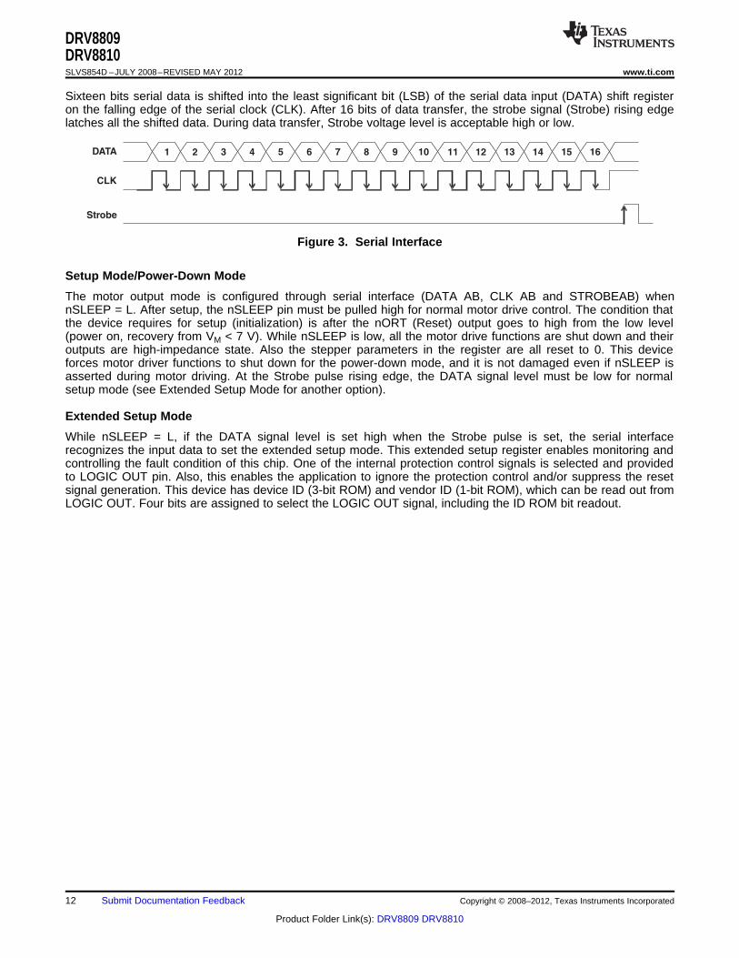
1 2 3 4 5 6 7 8 9 10 11 12 13 14 15 16
DRV8809DRV8810SLVS854D –JULY 2008–REVISED MAY 2012 www.ti.com
Sixteen bits serial data is shifted into the least significant bit (LSB) of the serial data input (DATA) shift registeron the falling edge of the serial clock (CLK). After 16 bits of data transfer, the strobe signal (Strobe) rising edgelatches all the shifted data. During data transfer, Strobe voltage level is acceptable high or low.
Figure 3. Serial Interface
Setup Mode/Power-Down Mode
The motor output mode is configured through serial interface (DATA AB, CLK AB and STROBEAB) whennSLEEP = L. After setup, the nSLEEP pin must be pulled high for normal motor drive control. The condition thatthe device requires for setup (initialization) is after the nORT (Reset) output goes to high from the low level(power on, recovery from VM < 7 V). While nSLEEP is low, all the motor drive functions are shut down and theiroutputs are high-impedance state. Also the stepper parameters in the register are all reset to 0. This deviceforces motor driver functions to shut down for the power-down mode, and it is not damaged even if nSLEEP isasserted during motor driving. At the Strobe pulse rising edge, the DATA signal level must be low for normalsetup mode (see Extended Setup Mode for another option).
Extended Setup Mode
While nSLEEP = L, if the DATA signal level is set high when the Strobe pulse is set, the serial interfacerecognizes the input data to set the extended setup mode. This extended setup register enables monitoring andcontrolling the fault condition of this chip. One of the internal protection control signals is selected and providedto LOGIC OUT pin. Also, this enables the application to ignore the protection control and/or suppress the resetsignal generation. This device has device ID (3-bit ROM) and vendor ID (1-bit ROM), which can be read out fromLOGIC OUT. Four bits are assigned to select the LOGIC OUT signal, including the ID ROM bit readout.
12 Submit Documentation Feedback Copyright © 2008–2012, Texas Instruments Incorporated
Product Folder Link(s): DRV8809 DRV8810

Data
Clock
Strobe
Serial interface C-D: Set C-D motor operating parameters
16-bit shift register
16-bit latch (C-D drivers)
Serial Interface A-B: Set A-B motor operating parameters and access to setup/extended setup register
16-bit shift register
16-bit latch (A-B drivers)
16-bit latch (setup)
16-bit latch (extended setup)
Latchselect
Protection detectsignal selector
orDevice ID/Vendor ID
(ROM)
DRV8809DRV8810
www.ti.com SLVS854D –JULY 2008–REVISED MAY 2012
A. A-B register at EXT-setup mode has device/vendor ID ROM. The ID must be read out at LOGIC OUT pin.
Figure 4. Serial Interface A-B
Figure 5. Serial Interface C-D
Copyright © 2008–2012, Texas Instruments Incorporated Submit Documentation Feedback 13
Product Folder Link(s): DRV8809 DRV8810
Data
Clock
Strobe
twl(clk) twh(clk)
tw(strb)
tcs
tsu th
Bit 0 Bit 1 Bit 15 Bit 16 = H
nSleep ( Don't care )
tss_min
twl(clk) twh(clk)
tw(strb)
tcs
tsu th
Bit 0 Bit 1 Bit 15 Bit 16 = LData
Clock
Strobe
nSleeptss_min
( Don't care )
Data
Clock
Strobe
twl(clk) twh(clk)
tw(strb)
tcs
tsu th
Bit 0 Bit 1 Bit 15Bit 14
nSleep
DRV8809DRV8810SLVS854D –JULY 2008–REVISED MAY 2012 www.ti.com
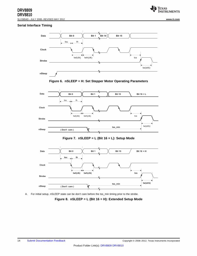
Serial Interface Timing
Figure 6. nSLEEP = H: Set Stepper Motor Operating Parameters
Figure 7. nSLEEP = L (Bit 16 = L): Setup Mode
A. For initial setup, nSLEEP state can be don’t care before the tss_min timing prior to the strobe.
Figure 8. nSLEEP = L (Bit 16 = H): Extended Setup Mode
14 Submit Documentation Feedback Copyright © 2008–2012, Texas Instruments Incorporated
Product Folder Link(s): DRV8809 DRV8810

DRV8809DRV8810
www.ti.com SLVS854D –JULY 2008–REVISED MAY 2012
Setup Register Bit Assignment
Setup register bits are assigned for motor configuration, blanking time, gain, and DC-DC switches. This registercan be accessed only in Setup mode (nSLEEP = L and bit 16 data = L) .
Table 2. Setup Register
BIT NO. NAME DEFAULT DESCRIPTION
0 Motor select 0 0 Motor configuration, < 2,1,0 > (0,0,0): Stepper × 2 (default)(0,0,1): Stepper + LDC, (0,1,0): Stepper + 2 × sDCs1 Motor select 1 0(0,1,1): DCL + 2 × sDC, (1,0,0): DCL × 2 (1,0,1): 4 × sDC
2 Motor select 2 0 (1,1,0): Large stepper (1,1,1): Ultra-large DC
3 TBLNK AB0 0 Tblank for DC motor driving, Tblank is inserted at any phase changeand beginning of each chopping cycle.4 TBLNK AB1 0AB1 AB0: Blanking time for A/B side drivers,
5 TBLNK CD0 0 CD1 CD0: Blanking time for C/D side drivers,00: (1 ÷ fCHOP) ÷ 8 × 5 (= 6.25 μs) (default)01: (1 ÷ fCHOP) ÷ 8 × 6 (= 7.50 μs)10: (1 ÷ fCHOP) ÷ 8 × 3 (= 3.75 μs)6 TBLNK CD1 011: (1 ÷ fCHOP) ÷ 8 × 4 (= 5.00 μs)For stepper motor driving, only the fixed blanking time is applied.
7 DC/DC_A SW 0 DC-DC ODA control, 0: ON (default), 1: OFF
8 DC/DC_B SW 0 DC-DC ODB control, 0: ON (default), 1: OFF
DC-DC ODC control, 0: ON (default), 1: OFF9 DC/DC_C SW 0 This bit is ignored when DCDC_MODE = H or open
10 Motor_AB gain 0 0: 1/10 (default), 1: 0
11 Motor_CD gain 0 0: 1/10 (default), 1: 0
12 OSCD frequency 0 0 <1,0> = (0,0) 100 kHz (default)(0,1) 50 kHz(1,0) 200 kHz(1,1) 132.5 kHz13 OSCD frequency 1 0These setup bits can be changed when the DC-DC regulators are inoperation.
14 OSCM frequency 0 0 <1,0> = (0,0) 800 kHz (default)(0,1) 400 kHz(1,0) 1.06 MHz15 OSCM frequency 1 0(1,1) 1.6 MHz
The device can be configured to one out of eight different motor control combination modes. When the device ispowered on or is recovering from reset, the mode can be selected by writing to the setup register through theserial interface AB, during Setup mode (nSLEEP = L).
Table 3. DC and Stepper Motor Configuration
SETUP REGISTER H-BRIDGE AND MOTOR CONFIGURATION
BIT 2 BIT 1 BIT 0 OUTA+, OUTA– OUTB+, OUTB– OUTC+, OUTC– OUTD+, OUTD–
0 0 0 Stepper motor drive Stepper motor drive
0 0 1 Stepper motor drive Large DC motor drive
0 1 0 Stepper motor drive DC motor drive DC motor drive
0 1 1 Large DC motor drive DC motor drive DC motor drive
1 0 0 Large DC motor drive Large DC motor drive
1 0 1 DC motor drive DC motor drive DC motor drive DC motor drive
1 1 0 Large stepper motor drive: A + B for first winding, C + D for second winding
1 1 1 Ultra-large DC motor drive
Default setting is (M0, M1, M2) = (0, 0,0)
Copyright © 2008–2012, Texas Instruments Incorporated Submit Documentation Feedback 15
Product Folder Link(s): DRV8809 DRV8810
DRV8809DRV8810SLVS854D –JULY 2008–REVISED MAY 2012 www.ti.com
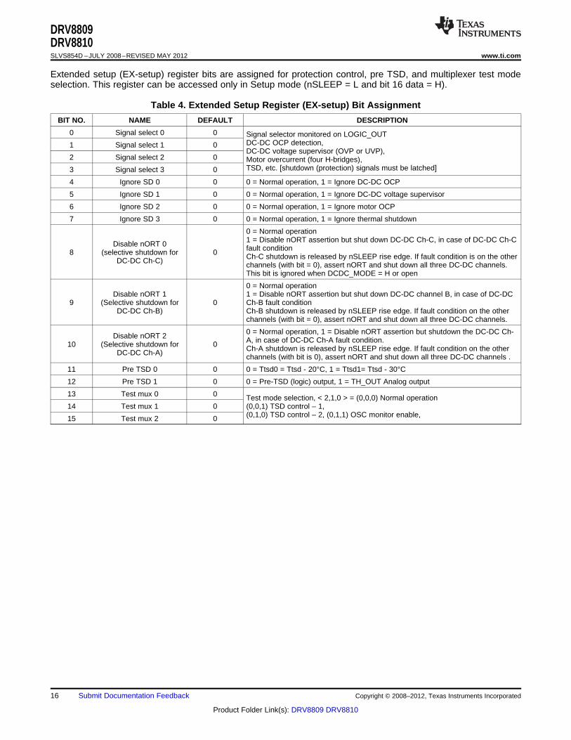
Extended setup (EX-setup) register bits are assigned for protection control, pre TSD, and multiplexer test modeselection. This register can be accessed only in Setup mode (nSLEEP = L and bit 16 data = H).
Table 4. Extended Setup Register (EX-setup) Bit Assignment
BIT NO. NAME DEFAULT DESCRIPTION
0 Signal select 0 0 Signal selector monitored on LOGIC_OUTDC-DC OCP detection,1 Signal select 1 0DC-DC voltage supervisor (OVP or UVP),
2 Signal select 2 0 Motor overcurrent (four H-bridges),TSD, etc. [shutdown (protection) signals must be latched]3 Signal select 3 0
4 Ignore SD 0 0 0 = Normal operation, 1 = Ignore DC-DC OCP
5 Ignore SD 1 0 0 = Normal operation, 1 = Ignore DC-DC voltage supervisor
6 Ignore SD 2 0 0 = Normal operation, 1 = Ignore motor OCP
7 Ignore SD 3 0 0 = Normal operation, 1 = Ignore thermal shutdown
0 = Normal operation1 = Disable nORT assertion but shut down DC-DC Ch-C, in case of DC-DC Ch-CDisable nORT 0 fault condition8 (selective shutdown for 0 Ch-C shutdown is released by nSLEEP rise edge. If fault condition is on the otherDC-DC Ch-C) channels (with bit = 0), assert nORT and shut down all three DC-DC channels.This bit is ignored when DCDC_MODE = H or open
0 = Normal operationDisable nORT 1 1 = Disable nORT assertion but shut down DC-DC channel B, in case of DC-DC
9 (Selective shutdown for 0 Ch-B fault conditionDC-DC Ch-B) Ch-B shutdown is released by nSLEEP rise edge. If fault condition on the other
channels (with bit = 0), assert nORT and shut down all three DC-DC channels.
0 = Normal operation, 1 = Disable nORT assertion but shutdown the DC-DC Ch-Disable nORT 2 A, in case of DC-DC Ch-A fault condition.10 (Selective shutdown for 0 Ch-A shutdown is released by nSLEEP rise edge. If fault condition on the otherDC-DC Ch-A) channels (with bit is 0), assert nORT and shut down all three DC-DC channels .
11 Pre TSD 0 0 0 = Ttsd0 = Ttsd - 20°C, 1 = Ttsd1= Ttsd - 30°C
12 Pre TSD 1 0 0 = Pre-TSD (logic) output, 1 = TH_OUT Analog output
13 Test mux 0 0 Test mode selection, < 2,1,0 > = (0,0,0) Normal operation14 Test mux 1 0 (0,0,1) TSD control – 1,
(0,1,0) TSD control – 2, (0,1,1) OSC monitor enable,15 Test mux 2 0
16 Submit Documentation Feedback Copyright © 2008–2012, Texas Instruments Incorporated
Product Folder Link(s): DRV8809 DRV8810
DRV8809DRV8810
www.ti.com SLVS854D –JULY 2008–REVISED MAY 2012
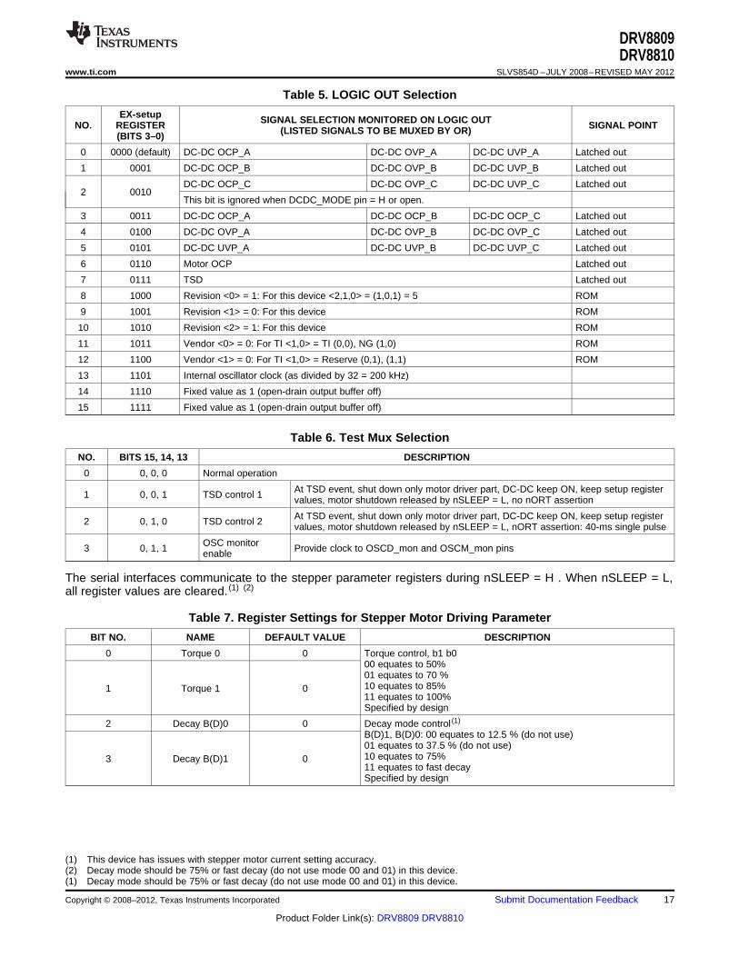
Table 5. LOGIC OUT Selection
EX-setup SIGNAL SELECTION MONITORED ON LOGIC OUTNO. REGISTER SIGNAL POINT(LISTED SIGNALS TO BE MUXED BY OR)(BITS 3–0)
0 0000 (default) DC-DC OCP_A DC-DC OVP_A DC-DC UVP_A Latched out
1 0001 DC-DC OCP_B DC-DC OVP_B DC-DC UVP_B Latched out
DC-DC OCP_C DC-DC OVP_C DC-DC UVP_C Latched out2 0010
This bit is ignored when DCDC_MODE pin = H or open.
3 0011 DC-DC OCP_A DC-DC OCP_B DC-DC OCP_C Latched out
4 0100 DC-DC OVP_A DC-DC OVP_B DC-DC OVP_C Latched out
5 0101 DC-DC UVP_A DC-DC UVP_B DC-DC UVP_C Latched out
6 0110 Motor OCP Latched out
7 0111 TSD Latched out
8 1000 Revision <0> = 1: For this device <2,1,0> = (1,0,1) = 5 ROM
9 1001 Revision <1> = 0: For this device ROM
10 1010 Revision <2> = 1: For this device ROM
11 1011 Vendor <0> = 0: For TI <1,0> = TI (0,0), NG (1,0) ROM
12 1100 Vendor <1> = 0: For TI <1,0> = Reserve (0,1), (1,1) ROM
13 1101 Internal oscillator clock (as divided by 32 = 200 kHz)
14 1110 Fixed value as 1 (open-drain output buffer off)
15 1111 Fixed value as 1 (open-drain output buffer off)
Table 6. Test Mux Selection
NO. BITS 15, 14, 13 DESCRIPTION
0 0, 0, 0 Normal operation
At TSD event, shut down only motor driver part, DC-DC keep ON, keep setup register1 0, 0, 1 TSD control 1 values, motor shutdown released by nSLEEP = L, no nORT assertion
At TSD event, shut down only motor driver part, DC-DC keep ON, keep setup register2 0, 1, 0 TSD control 2 values, motor shutdown released by nSLEEP = L, nORT assertion: 40-ms single pulse
OSC monitor3 0, 1, 1 Provide clock to OSCD_mon and OSCM_mon pinsenable
The serial interfaces communicate to the stepper parameter registers during nSLEEP = H . When nSLEEP = L,all register values are cleared. (1) (2)
Table 7. Register Settings for Stepper Motor Driving Parameter
BIT NO. NAME DEFAULT VALUE DESCRIPTION
0 Torque 0 0 Torque control, b1 b000 equates to 50%01 equates to 70 %10 equates to 85%1 Torque 1 011 equates to 100%Specified by design
2 Decay B(D)0 0 Decay mode control (1)
B(D)1, B(D)0: 00 equates to 12.5 % (do not use)01 equates to 37.5 % (do not use)10 equates to 75%3 Decay B(D)1 011 equates to fast decaySpecified by design
(1) This device has issues with stepper motor current setting accuracy.(2) Decay mode should be 75% or fast decay (do not use mode 00 and 01) in this device.(1) Decay mode should be 75% or fast decay (do not use mode 00 and 01) in this device.
Copyright © 2008–2012, Texas Instruments Incorporated Submit Documentation Feedback 17
Product Folder Link(s): DRV8809 DRV8810

DRV8809DRV8810SLVS854D –JULY 2008–REVISED MAY 2012 www.ti.com
Table 7. Register Settings for Stepper Motor Driving Parameter (continued)
BIT NO. NAME DEFAULT VALUE DESCRIPTION
4 Current B(D)0 0
5 Current B(D)1 0Phase B(D) current level setting (1)
6 Current B(D)2 0
7 Current B(D)3 0
Control direction of current flow through winding B(D). A logic 1 allows8 Phase B(D) 0 conventional current flow from OUTB(D)+ to OUTB(D)–.
9 Decay A(C)0 0 Decay mode control (1)
A(C)1, A(C)0: 00 equates to 12.5 % (do not use)01 equates to 37.5 % (do not use)
10 Decay A(C)1 0 10 equates to 75%11 equates to fast decay
11 Current A(C)0 0
12 Current A(C)1 0Phase A current level setting (1)
13 Current A(C)2 0
14 Current A(C)3 0
Control direction of current flow through winding A(C). A logic 1 allows15 Phase A(C) 0 conventional current flow from OUTA(C)+ to OUTA(C)–.
Table 8. Torque Control Bit
VREF INPUT CONTROL MOTOR TORQUE
BIT VALUE ROUGH OUTPUT CURRENT SETTING
Torque 0, 1 = 0, 0 50% high power consumption, I(max) = VREF * gain/RSense
Torque 0, 1 = 0, 1 70% power
Torque 0, 1 = 1, 0 85% power
Torque 0, 1 = 1, 1 100% power
Table 9. Decay Mode Control Bit
BIT VALUE DECAY MODE SETTING
Decay x0, x1 = 0, 0 12.5% decay mode (do not use)
Decay x0, x1 = 0, 1 37.5% decay mode (do not use)
Decay x0, x1 = 1, 0 75% decay mode
Decay x0, x1 = 1, 1 100% fast decay mode
Table 10. Current Flow Direction Bit
BIT VALUE CURRENT DIRECTION
Phase X = 0 OUTx+ = L, OUTx– = H
Phase X = 1 OUTx+ = H, OUTx– = L
Table 11. Revision Code/Vendor Code ROM Readout at LOGIC OUT
EX-setup REGISTERNO. SIGNAL SELECTION MONITORED ON LOGIC OUT(BITS 3–0)
8 1000 Revision <0> = 1: For this device * <2,1,0> = (1,0,1) = 5
9 1001 Revision <1> = 0: For this device
10 1010 Revision <2> = 1: For this device
11 1011 Vendor <0> = 0: For TI <1,0> = TI (0,0), NG(1,0)
12 1100 Vendor <1> = 0: For TI <1,0> = Reserve (0,1), (1,1)
18 Submit Documentation Feedback Copyright © 2008–2012, Texas Instruments Incorporated
Product Folder Link(s): DRV8809 DRV8810

DRV8809DRV8810
www.ti.com SLVS854D –JULY 2008–REVISED MAY 2012
Table 12. Different Motor Drive Configuration Pinouts (Selected By Setup Register Bits 0 to 3)
<setup> 0 (0,0,0) 1 (0,0,1) 2 (0,1,0) 3 (0,1,1) 4 (1,0,0) 5 (1,0,1) 6 (1,1,0) 7 (1,1,1)
STEPPER STEPPER MTR DC (LARGE)STEPPER DC (LARGE) DC (SMALL) LARGE ULTRA-SETUP MTR AND DC AND DC AND DCMTR ×2 ×2 ×4 STEPPER LARGE DC(LARGE) (SMALL) ×2 (SMALL) ×2
1 Test-LGND
2 MGND
3 OUTA– OUTA– OUTA– OUTA– OUTLAB– OUTLAB– OUTSA– OUTLAB– OUTULABCD–
4 RSA1 RSA1 RSA1 RSA1 RSLAB1 RSLAB1 RSA1 RSLAB1 RSULABCD1
5 RSA2 RSA2 RSA2 RSA2 RSLAB2 RSLAB2 RSA2 RSLAB2 RSULABCD1
6 OUTA+ OUTA+ OUTA+ OUTA+ OUTLAB+ OUTLAB+ OUTSA+ OUTLAB+ OUTULABCD+
7 MGND
8 MGND
9 OUTB+ OUTB+ OUTB+ OUTB+ OUTLAB+ OUTLAB+ OUTSB+ OUTLAB+ OUTULABCD+
10 RSB2 RSB2 RSB2 RSB2 RSLAB2 RSLAB2 RSB2 RSLAB2 RSULABCD1
11 RSB1 RSB1 RSB1 RSB1 RSLAB1 RSLAB1 RSB1 RSLAB1 RSULABCD1
12 OUTB– OUTB– OUTB– OUTB– OUTLAB– OUTLAB– OUTSB– OUTLAB– OUTULABCD–
13 MGND
14 LGND
15 DCDC_MODE
16 FBC
17 OD_C
18 OD_C
19 OD_B
20 OD_B
21 FBB
22 VCP
23 OSCD_mon
24 CP2
25 CP1
26 VDIN
27 VDIN
28 VDIN
29 VM
30 VREF_AB
31 VREF_CD
32 FBA
33 ODA
34 ODA
35 LGND
36 MGND
37 OUTC– OUTC– OUTLCD– OUTSC– OUTSC– OUTLCD– OUTSC– OUTLCD– OUTULABCD–
38 RSC1 RSC1 RSLCD1 RSC1 RSC1 RSLCD1 RSC1 RSLCD1 RSULABCD1
39 RSC2 RSC2 RSLCD2 RSC2 RSC2 RSLCD2 RSC2 RSLCD2 RSULABCD1
40 OUTC+ OUTC+ OUTLCD+ OUTSC+ OUTSC+ OUTLCD+ OUTSC+ OUTLCD+ OUTLABCD+
41 MGND
42 MGND
43 OUTD+ OUTD+ OUTLCD+ OUTSD+ OUTSD+ OUTLCD+ OUTSD+ OUTSD+ OUTULABCD+
44 RSD2 RSD2 RSLCD2 RSD2 RSD2 RSLCD2 RSD2 RSD2 RSULABCD1
45 RSD1 RSD1 RSLCD1 RSD1 RSD1 RSLCD1 RSD1 RSD1 RSULABCD1
46 OUTD– OUTD– OUTLCD– OUTSD– OUTSD– OUTLCD– OUTSD– OUTSD– OUTULABCD–
47 MGND
48 GND
49 C_SELECT
Copyright © 2008–2012, Texas Instruments Incorporated Submit Documentation Feedback 19
Product Folder Link(s): DRV8809 DRV8810
Stepper
Motor
OUTA-
RSA
OUTA+
OUTB+
RSB
OUTB-
OUTC-
RSC
OUTC+
OUTD+
RSD
OUTD-
Motor Drive
Output
Control C
VM
Motor Drive
OutputControl D
VM
Motor DriveOutput
Control A
Motor Drive
Output
Control B
VM
VM
Pre Drive
and
Control
Pre Driveand
Control
VREF_AB
NC
STROBE_AB
DATA_AB
CLK_AB
VREF_CD
NC
STROBE_CD
DATA_CD
CLK_CD
StepperMotor
DRV8809DRV8810SLVS854D –JULY 2008–REVISED MAY 2012 www.ti.com
Table 12. Different Motor Drive Configuration Pinouts (Selected By Setup Register Bits 0 to 3) (continued)<setup> 0 (0,0,0) 1 (0,0,1) 2 (0,1,0) 3 (0,1,1) 4 (1,0,0) 5 (1,0,1) 6 (1,1,0) 7 (1,1,1)
STEPPER STEPPER MTR DC (LARGE)STEPPER DC (LARGE) DC (SMALL) LARGE ULTRA-SETUP MTR AND DC AND DC AND DCMTR ×2 ×2 ×4 STEPPER LARGE DC(LARGE) (SMALL) ×2 (SMALL) ×2
50 - - - ENABLE_SD ENABLE_SD - ENABLE_SD -
ENABLE_ ENABLE_51 STROBE_CD STROBE_CD ENABLE_LCD ENABLE_SC ENABLE_SC ENABLE_SCLCD LCD
52 TH_OUT
53 LOGIC OUT
54 - - - - - - ENABLE_SB -
ENABLE_ ENABLE_ ENABLE_55 STROBE AB STROBE AB STROBE AB STROBE AB ENABLE_LAB ENABLE_SALAB LAB ABCD
56 nORT
57 LGND
58 OSCM_mon
59 DATA_CD DATA_CD - PHASE SD PHASE SD - PHASE SD -
60 CLK_CD CLK_CD PHASE_LCD PHASE SC PHASE SC PHASE_LCD PHASE SC PHASE_LCD
61 DATA_AB DATA_AB DATA_AB DATA_AB - - PHASE SB -
62 CLK_AB CLK_AB CLK_AB CLK_AB PHASE_LAB PHASE_LAB PHASE SA PHASE_LAB PHASE_ABCD
63 nSLEEP=L nSLEEP=H
64 In-Reset
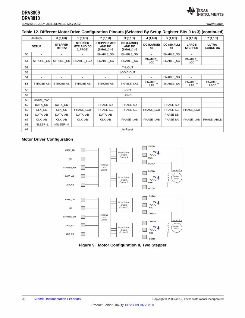
Motor Driver Configuration
Figure 9. Motor Configuration 0, Two Stepper
20 Submit Documentation Feedback Copyright © 2008–2012, Texas Instruments Incorporated
Product Folder Link(s): DRV8809 DRV8810

Stepper
Motor
OUTA-
RSA
OUTA+
OUTB+
RSB
OUTB-
OUTSC-
RSC
OUTSC+
OUTSD+
RSD
OUTSD-
Motor Drive
Output
Control C
VM
Motor Drive
Output
Control D
VM
Motor Drive
Output
Control A
Motor Drive
Output
Control B
VM
VM
Pre Drive
and
Control
Pre Drive
and
Control
DC
Motor
DC
Motor
VREF_AB
NC
STROBE_AB
DATA_AB
CLK_AB
VREF_CD
ENABLE_SD
ENABLE_SC
PHASE_SD
PHASE_SC
Stepper
Motor
OUTA-
RSA
OUTA+
OUTB+
RSB
OUTB-
OUTLCD-
RSLB
Motor Drive
Output
Control C
Motor Drive
Output
Control D
Motor Drive
Output
Control A
Motor Drive
Output
Control B
VM
VM
Pre Drive
and
Control
Pre Drive
and
Control
VREF_AB
NC
STROBE_AB
DATA_AB
CLK_AB
VREF_CD
NC
ENABLE_LCD
NC
PHASE_LCD
RSLB
OUTLCD+
VM
Large
DC
MotorOUTLCD+
OUTLCD-
DRV8809DRV8810
www.ti.com SLVS854D –JULY 2008–REVISED MAY 2012
Figure 10. Motor Configuration 1, One Stepper and One Large DC
Figure 11. Motor Configuration 2, One Stepper and Two Small DCs
Copyright © 2008–2012, Texas Instruments Incorporated Submit Documentation Feedback 21
Product Folder Link(s): DRV8809 DRV8810

Motor Drive
Output
Control C
Motor Drive
Output
Control D
Motor Drive
OutputControl A
Motor Drive
Output
Control B
Pre Drive
and
Control
Pre Driveand
Control
VREF_AB
NC
ENABLE_LAB
NC
PHASE_LAB
VREF_CD
NC
ENABLE_LCD
NC
PHASE_LCD
OUTLAB-
RSLAB
OUTLAB+
OUTLAB+
RSLAB
OUTLAB-
VM
LargeDC
Motor
OUTLCD-
RSLCD
OUTLCD-
RSLCD
OUTLCD+
OUTLCD+
VM
Large
DC
Motor
OUTLAB-
RSLAB
OUTLAB+
OUTLAB+
RSLAB
OUTLAB-
OUTSC-
RSC
OUTSC+
OUTSD+
RSD
OUTSD-
Motor Drive
Output
Control C
VM
Motor Drive
Output
Control D
VM
Motor Drive
Output
Control A
Motor Drive
Output
Control B
VM
Pre Drive
and
Control
Pre Drive
and
Control
DC
Motor
DC
Motor
VREF_AB
NC
ENABLE_LAB
NC
PHASE_LAB
Large
DC
Motor
VREF_CD
ENABLE_SD
ENABLE_SC
PHASE_SD
PHASE_SC
DRV8809DRV8810SLVS854D –JULY 2008–REVISED MAY 2012 www.ti.com
Figure 12. Motor Configuration 3, One Large DC and Two Small DCs
Figure 13. Motor Configuration 4, Two Large DCs
22 Submit Documentation Feedback Copyright © 2008–2012, Texas Instruments Incorporated
Product Folder Link(s): DRV8809 DRV8810

Stepper
Motor
OUTA-
RSA
OUTA+
OUTB+
RSB
OUTB-
OUTC-
RSC
OUTC+
OUTD+
RSD
OUTD-
Motor Drive
Output
Control C
VM
Motor Drive
Output
Control D
Motor Drive
Output
Control A
Motor Drive
Output
Control B
VM
Pre Drive
and
Control
Pre Drive
and
Control
VREF_AB
NC
STROBE_AB
DATA_AB
CLK_AB
VREF_CD
NC
STROBE_CD
DATA_CD
CLK_CD
OUTSA-
RSA
OUTSA+
OUTSB+
RSB
OUTSB-
OUTSC-
RSC
OUTSC+
OUTSD+
RSD
OUTSD-
Motor Drive
Output
Control C
VM
Motor DriveOutput
Control D
VM
Motor DriveOutput
Control A
Motor Drive
Output
Control B
VM
VM
Pre Drive
and
Control
Pre Drive
and
Control
DC
Motor
DCMotor
VREF_AB
ENABLE_SB
ENABLE_SA
PHASE_SB
PHASE_SA
VREF_CD
ENABLE_SD
ENABLE_SC
PHASE_SD
PHASE_SC
DC
Motor
DC
Motor
DRV8809DRV8810
www.ti.com SLVS854D –JULY 2008–REVISED MAY 2012
Figure 14. Motor Configuration 5, Four Small DCs
Figure 15. Motor Configuration 6, Single Large Stepper Motor
Copyright © 2008–2012, Texas Instruments Incorporated Submit Documentation Feedback 23
Product Folder Link(s): DRV8809 DRV8810

OUTSA-
RSA
OUTSA+
OUTSB+
OUTSB-
OUTSC-
OUTSC+
OUTSD+
OUTSD-
Motor Drive
Output
Control C
Motor Drive
Output
Control D
Motor Drive
Output
Control A
Motor Drive
Output
Control B
VM
Pre Drive
and
Control
Pre Drive
and
Control
VREF_AB
ENABLE_SB
ENABLE_SA
PHASE_SB
PHASE_SA
VREF_CD
ENABLE_SD
ENABLE_SC
PHASE_SD
PHASE_SC
DC
Moto
r
DRV8809DRV8810SLVS854D –JULY 2008–REVISED MAY 2012 www.ti.com
Figure 16. Motor Configuration 7, Ultra-Large DC
24 Submit Documentation Feedback Copyright © 2008–2012, Texas Instruments Incorporated
Product Folder Link(s): DRV8809 DRV8810

Enableor Phase reversalor Itrip detection
Sink or sourcegate off to on
Sink or sourcegate on to off
Current senseblanking time
tPDON
tPDOFF tCOD
tBLANK – DC motor blanking time
tabStepper blanking time
DRV8809DRV8810
www.ti.com SLVS854D –JULY 2008–REVISED MAY 2012
Bipolar Current Regulated Stepper Motor Drive
The following functionality is common to all the H-bridge drives. A crossover delay is inherent to the controlcircuitry to prevent cross conduction of the upper and lower switches on the same side of the H-bridge. Ablanking (deglitch) time is incorporated to prevent false triggering due to initial current spikes at turnon with adischarged capacitive load.
The stepper motor current can be programmed to 16 different current levels using a 4-bit register. The averagecurrent level for a particular angular rotation is shown in Table 14.
Figure 17. Crossover and Blanking Timing for H-Bridge
For stepper motor configured H-bridges, only tab (stepper blanking time) is set for current sensing. For DCmotor-configured H-bridges, tBLANK is included to ignore huge current spike due to rush current to varistorcapacitance.
Copyright © 2008–2012, Texas Instruments Incorporated Submit Documentation Feedback 25
Product Folder Link(s): DRV8809 DRV8810

Control logic
& Pre-driver
Current
Sens
Currentlimit
Rsens
VM
MGND
overcurrent
detect
Protect
disable
Protection
control &
nORT assertion
Charge
pump RSA
OUTA
OUTA/
VM
Rsens
VMRSB
OUTB
OUTB/
StepperMotor
Setup/ex-setupregister
Stepper
parameterregister
Torque,Decay,
Current,& Phase
DATA_AB
CLK_AB
Strobe_AB
VMsupervisor
(15v)turn on/off
OSCM( 800kHz )
OSCi( 6.4MHz )
OSCM_mon
DRV8809DRV8810SLVS854D –JULY 2008–REVISED MAY 2012 www.ti.com
Short/Open for Motor Outputs
When a short/open situation happens, the protection circuit prevents device damage under certain conditions(short at start up, etc).
Figure 18. Stepper Motor Driver
26 Submit Documentation Feedback Copyright © 2008–2012, Texas Instruments Incorporated
Product Folder Link(s): DRV8809 DRV8810

RdsON vs Idrain
Rd
sO
N (
)W
Idrain (A)
T = 120°CJ
T = 70°CJ
T = 25°CJ
0.5 1 1.5 2 2.5 3 3.5
0.4
0.5
0.6
0.7
0.8
0.9
1.0
DRV8809DRV8810
www.ti.com SLVS854D –JULY 2008–REVISED MAY 2012
Table 13. Angular Rotation Setting for Stepping Motor Driver (Parameter Bit in Stepper Register)
BIT 14 BIT 13 BIT 12 BIT 11 BIT 7 BIT 6 BIT 5 BIT 4SET
CURRENT CURRENT CURRENT CURRENT CURRENT CURRENT CURRENT CURRENTSTEP ANGLEA A A A B B B B(deg)
(C) 3 (C) 2 (C) 1 (C) 0 (D) 3 (D) 2 (D) 1 (D) 0
16 90 H H H H L L L L
15 84.4 H H H H L L L H
14 78.8 H H H L L L H L
13 73.1 H H L H L L H H
12 67.5 H H L L L H L L
11 61.2 H L H H L H L H
10 56.3 H L H L L H H L
9 50.6 H L L H L H H H
8 45 H L L L H L L L
7 39.4 L H H H H L L H
6 33.8 L H H L H L H L
5 28.1 L H L H H L H H
4 22.5 L H L L H H L L
3 16.9 L L H H H H L H
2 11.3 L L H L H H H L
1 5.6 L L L H H H H H
0 0 L L L L H H H H
A. This plot includes both actual device characterization data and extrapolated data.
B. Actual device has self-heating effect to increase the junction temperature, with continuous loading current more than1 A.
C. The device temperature is set to 70°C for the Rds(ON) test.
Figure 19. Typical Rds(ON) Value vs Drain Current (DMOS FET in H-Bridge)
Copyright © 2008–2012, Texas Instruments Incorporated Submit Documentation Feedback 27
Product Folder Link(s): DRV8809 DRV8810

OSCM( 800kHz )
DCMotor
Control logic
& Pre-driver
Current
Sens
Current
limit
Rsens
VM
MGND
overcurrentdetect
Protectdisable
Protection
control &
nORT assertion
Chargepump Rssx
OUTx
OUTx/
VM
OSCi( 6.4MHz )
Enable_x
Phase_x
VMsupervisor
(15v)turn on/off
OSCM_mon
DRV8809DRV8810SLVS854D –JULY 2008–REVISED MAY 2012 www.ti.com
Figure 20. DC Motor Drive
The motor configuration setup bits in the setup register can select three types of DC motor driving: utilizing asingle H-bridge, utilizing two (A and B, or C and D) H-bridges in parallel, or utilizing four H-bridges in parallel.
For the setup register value (bit 2,1,0) = (1,0,1), the device configuration is 4× DC motor, which enables each H-bridge to drive a DC motor independently. The ENABLEx and PHASEx input terminals are reassigned from theserial interface pins and some reserved pins, after nSLEEP pin is set to H.
For the setup register value (bit 2,1,0) = (0,1,1), the device configuration is 1× large DC + 2× DC motor mode.The large DC driving utilizes two H-bridges in parallel and controlled by ENABLE_AB and PHASE_AB pins. TwoRsens pins should be connected together.
The VREF inputs are used for the Rsense comparator reference voltage. VREF_AB provides the voltage to bothH-bridge A and B, and VREF_CD provides the voltage for H-bridge C and D.
Table 14. DC Motor Drive Truth Table
FAULT nSLEEP ENABLEX PHASEX + HIGH SIDE + LOW SIDE - HIGH SIDE - LOW SIDECONDITION
0 0 X X OFF OFF OFF OFF
0 1 0 X OFF OFF OFF OFF
0 1 1 0 OFF ON ON OFF
0 1 1 1 ON OFF OFF ON
Motor OCP 1 X X OFF OFF OFF OFF
TSD X X X OFF OFF OFF OFF
28 Submit Documentation Feedback Copyright © 2008–2012, Texas Instruments Incorporated
Product Folder Link(s): DRV8809 DRV8810
Outputvoltage
supervisor
Overcurrentsense
Control logicand predriver
Current limit
Overcurrentdetect
Protectdisable
Soft start,
Protection control, and
nORT assertion
Chargepump
VM
OD_x
FBx
Vref1.5 V
UVP(-30%)
Disable(mask)
C_SELECT
Setup/Extended Setup
register
OVP(+30%)
OSCD(100 kHz)
OSCi(6.4 MHz)
DRV8809DRV8810
www.ti.com SLVS854D –JULY 2008–REVISED MAY 2012
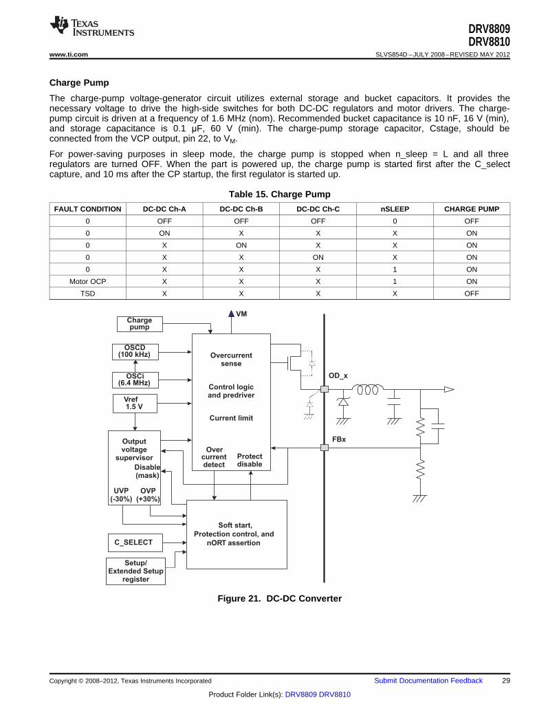
Charge Pump
The charge-pump voltage-generator circuit utilizes external storage and bucket capacitors. It provides thenecessary voltage to drive the high-side switches for both DC-DC regulators and motor drivers. The charge-pump circuit is driven at a frequency of 1.6 MHz (nom). Recommended bucket capacitance is 10 nF, 16 V (min),and storage capacitance is 0.1 μF, 60 V (min). The charge-pump storage capacitor, Cstage, should beconnected from the VCP output, pin 22, to VM.
For power-saving purposes in sleep mode, the charge pump is stopped when n_sleep = L and all threeregulators are turned OFF. When the part is powered up, the charge pump is started first after the C_selectcapture, and 10 ms after the CP startup, the first regulator is started up.
Table 15. Charge Pump
FAULT CONDITION DC-DC Ch-A DC-DC Ch-B DC-DC Ch-C nSLEEP CHARGE PUMP
0 OFF OFF OFF 0 OFF
0 ON X X X ON
0 X ON X X ON
0 X X ON X ON
0 X X X 1 ON
Motor OCP X X X 1 ON
TSD X X X X OFF
Figure 21. DC-DC Converter
Copyright © 2008–2012, Texas Instruments Incorporated Submit Documentation Feedback 29
Product Folder Link(s): DRV8809 DRV8810
DRV8809DRV8810SLVS854D –JULY 2008–REVISED MAY 2012 www.ti.com
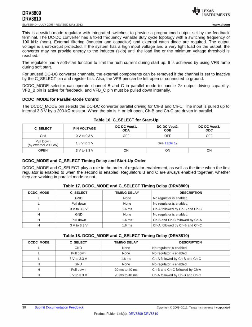
This is a switch-mode regulator with integrated switches, to provide a programmed output set by the feedbackterminal. The DC-DC converter has a fixed frequency variable duty cycle topology with a switching frequency of100 kHz (nom). External filtering (inductor and capacitor) and external catch diode are required. The outputvoltage is short-circuit protected. If the system has a high input voltage and a very light load on the output, theconverter may not provide energy to the inductor (skip) until the load line or the minimum voltage threshold isreached.
The regulator has a soft-start function to limit the rush current during start up. It is achieved by using VFB rampduring soft start.
For unused DC-DC converter channels, the external components can be removed if the channel is set to inactiveby the C_SELECT pin and register bits. Also, the VFB pin can be left open or connected to ground.
DCDC_MODE selector can operate channel B and C in parallel mode to handle 2× output driving capability.VFB_B pin is active for feedback, and VFB_C pin must be pulled down internally.
DCDC_MODE for Parallel-Mode Control
The DCDC_MODE pin selects the DC-DC converter parallel driving for Ch-B and Ch-C. The input is pulled up tointernal 3.3 V by a 200-kΩ resistor. When the pin is H or left open, Ch-B and Ch-C are driven in parallel.
Table 16. C_SELECT for Start-Up
DC-DC Vout1, DC-DC Vout2, DC-DC Vout3,C_SELECT PIN VOLTAGE ODA ODB ODC
Gnd 0 V to 0.3 V OFF OFF OFF
Pull Down 1.3 V to 2 V See Table 17(by external 200 kW)
OPEN 3 V to 3.3 V ON ON ON
DCDC_MODE and C_SELECT Timing Delay and Start-Up Order
DCDC_MODE and C_SELECT play a role in the order of regulator enablement, as well as the time when the firstregulator is enabled to when the second is enabled. Regulators B and C are always enabled together, whetherthey are working in parallel mode or not.
Table 17. DCDC_MODE and C_SELECT Timing Delay (DRV8809)
DCDC_MODE C_SELECT TIMING DELAY DESCRIPTION
L GND None No regulator is enabled.
L Pull down None No regulator is enabled.
L 3 V to 3.3 V 1.6 ms Ch-A followed by Ch-B and Ch-C
H GND None No regulator is enabled.
H Pull down 1.6 ms Ch-B and Ch-C followed by Ch-A
H 3 V to 3.3 V 1.6 ms Ch-A followed by Ch-B and Ch-C
Table 18. DCDC_MODE and C_SELECT Timing Delay (DRV8810)
DCDC_MODE C_SELECT TIMING DELAY DESCRIPTION
L GND None No regulator is enabled.
L Pull down None No regulator is enabled.
L 3 V to 3.3 V 1.6 ms Ch-A followed by Ch-B and Ch-C
H GND None No regulator is enabled.
H Pull down 20 ms to 40 ms Ch-B and Ch-C followed by Ch-A
H 3 V to 3.3 V 20 ms to 40 ms Ch-A followed by Ch-B and Ch-C
30 Submit Documentation Feedback Copyright © 2008–2012, Texas Instruments Incorporated
Product Folder Link(s): DRV8809 DRV8810
1.60
1.80
2.00
2.20
2.40
2.60
0 30 60 90 120 150 180
Temperature ( deg C )
Tsen
so
utp
ut
vo
lta
ge
(V
)
DRV8809DRV8810
www.ti.com SLVS854D –JULY 2008–REVISED MAY 2012
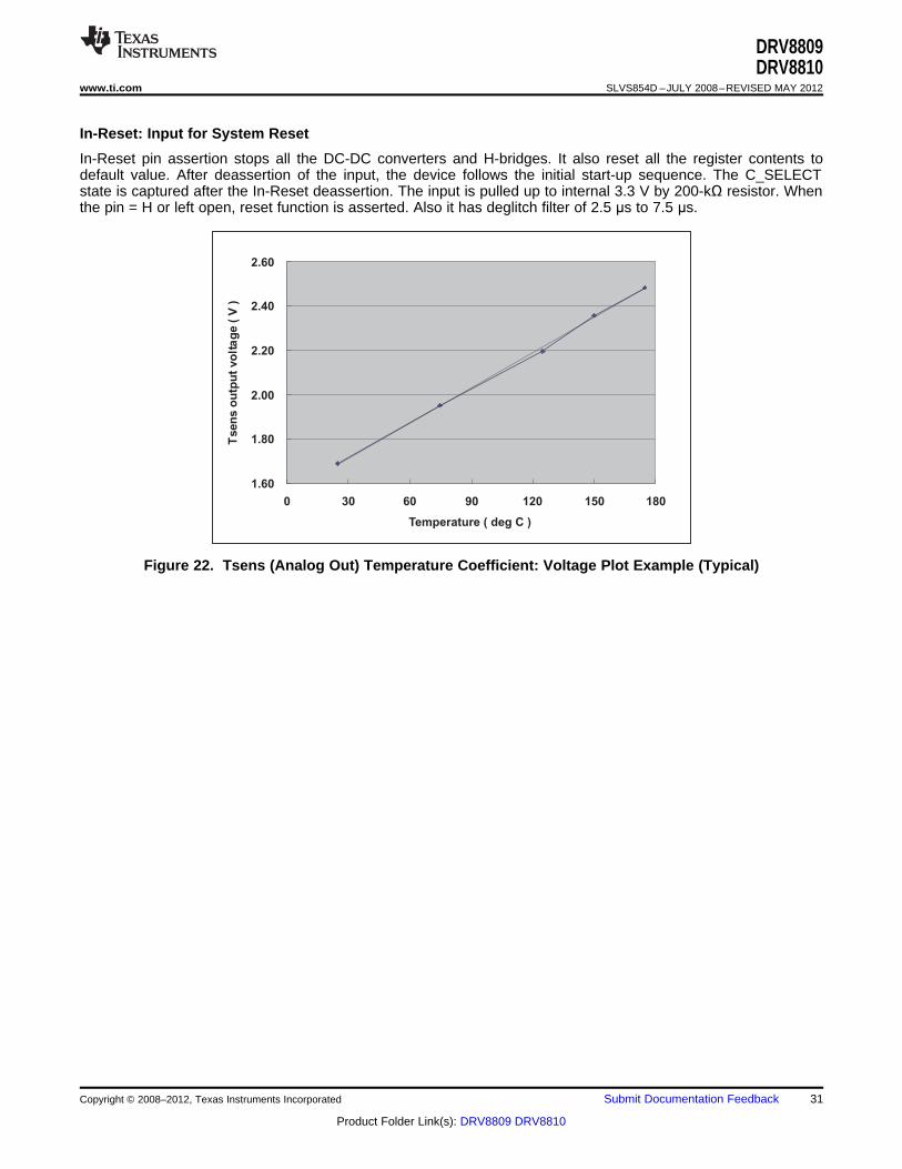
In-Reset: Input for System Reset
In-Reset pin assertion stops all the DC-DC converters and H-bridges. It also reset all the register contents todefault value. After deassertion of the input, the device follows the initial start-up sequence. The C_SELECTstate is captured after the In-Reset deassertion. The input is pulled up to internal 3.3 V by 200-kΩ resistor. Whenthe pin = H or left open, reset function is asserted. Also it has deglitch filter of 2.5 μs to 7.5 μs.
Figure 22. Tsens (Analog Out) Temperature Coefficient: Voltage Plot Example (Typical)
Copyright © 2008–2012, Texas Instruments Incorporated Submit Documentation Feedback 31
Product Folder Link(s): DRV8809 DRV8810
Delay(Note B)
VM=5.0v
VM=6.0v
VthVM+
VthVM-
120 ms(20 ms +100 ms)
(= L )
(= H )
Capture C_selectthen startCharge Pump
10 ms(Note A)
C P start to
D C/D C d elay
VM(CSELECT = Open)
VCP
DC/DC_A
DC/DC_B
DC/DC_C
nORT
Protection mask:OCP/OVP/UVP
for CH-A/B/C
DRV8809DRV8810SLVS854D –JULY 2008–REVISED MAY 2012 www.ti.com
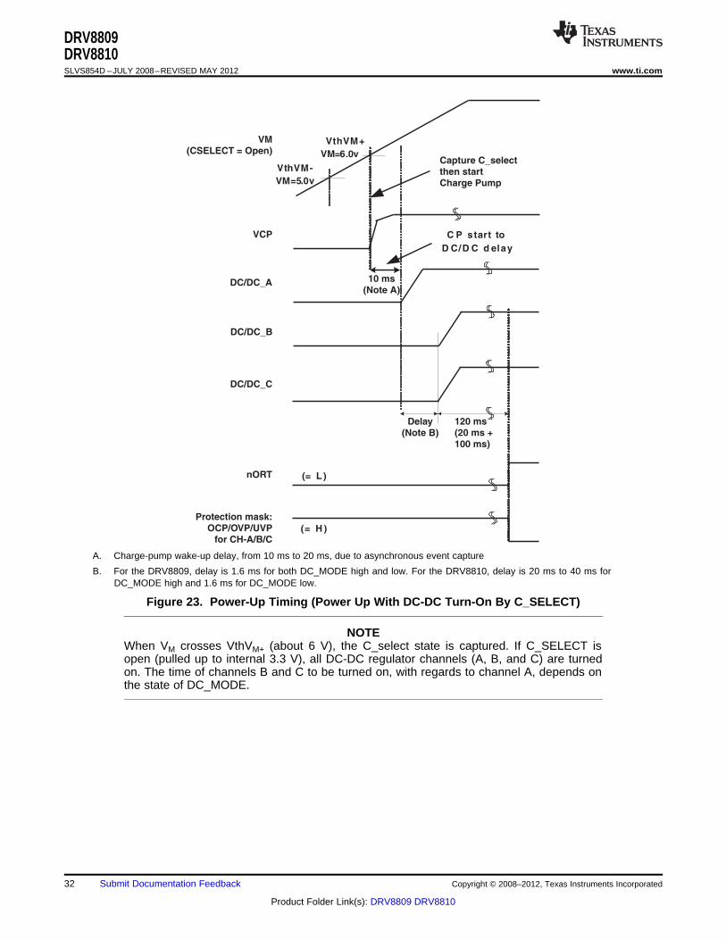
A. Charge-pump wake-up delay, from 10 ms to 20 ms, due to asynchronous event capture
B. For the DRV8809, delay is 1.6 ms for both DC_MODE high and low. For the DRV8810, delay is 20 ms to 40 ms forDC_MODE high and 1.6 ms for DC_MODE low.
Figure 23. Power-Up Timing (Power Up With DC-DC Turn-On By C_SELECT)
NOTEWhen VM crosses VthVM+ (about 6 V), the C_select state is captured. If C_SELECT isopen (pulled up to internal 3.3 V), all DC-DC regulator channels (A, B, and C) are turnedon. The time of channels B and C to be turned on, with regards to channel A, depends onthe state of DC_MODE.
32 Submit Documentation Feedback Copyright © 2008–2012, Texas Instruments Incorporated
Product Folder Link(s): DRV8809 DRV8810

See Note B
120 ms(See Note A)
DRV8809DRV8810
www.ti.com SLVS854D –JULY 2008–REVISED MAY 2012
Figure 24. Power-Up Timing (Power Up Without DC-DC Turn-On: C_SELECT = GND)
NOTEWhen VM crosses VthVM+ (about 6 V) with C_SELECT = GND, none of the threeregulators are turned on. The nORT output is released to H after 300 ms from the VthVM+crossing.
A. 120 ms to 140 ms due to asynchronous event capture
B. After VM power up, DC-DC starts at the setup register strobe.
Figure 25. Power-Up Timing (DC-DC Regulator Wake Up by Setup Register)
Copyright © 2008–2012, Texas Instruments Incorporated Submit Documentation Feedback 33
Product Folder Link(s): DRV8809 DRV8810
DC/DC_C
nORT
protection
mask
DC/DC_B
VM=6.0v
VM
VthVM+
120 ms
( = H )
( = L )
DC/DC_A
Setup register
strobe
(off -> on )
( off -> on )
( off -> on )
See Note A
( CSELECT
= GND )
[ Setup (9,8,7)
=(0,0,0) ]
Delay(Note B)
DRV8809DRV8810SLVS854D –JULY 2008–REVISED MAY 2012 www.ti.com
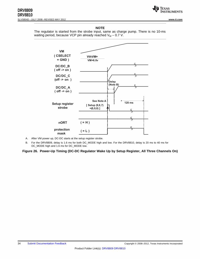
NOTEThe regulator is started from the strobe input, same as charge pump. There is no 10-mswaiting period, because VCP pin already reached VM – 0.7 V.
A. After VM power up, DC-DC starts at the setup register strobe.
B. For the DRV8809, delay is 1.6 ms for both DC_MODE high and low. For the DRV8810, delay is 20 ms to 40 ms forDC_MODE high and 1.6 ms for DC_MODE low.
Figure 26. Power-Up Timing (DC-DC Regulator Wake Up by Setup Register, All Three Channels On)
34 Submit Documentation Feedback Copyright © 2008–2012, Texas Instruments Incorporated
Product Folder Link(s): DRV8809 DRV8810
10 ms
(Note A)
DRV8809DRV8810
www.ti.com SLVS854D –JULY 2008–REVISED MAY 2012
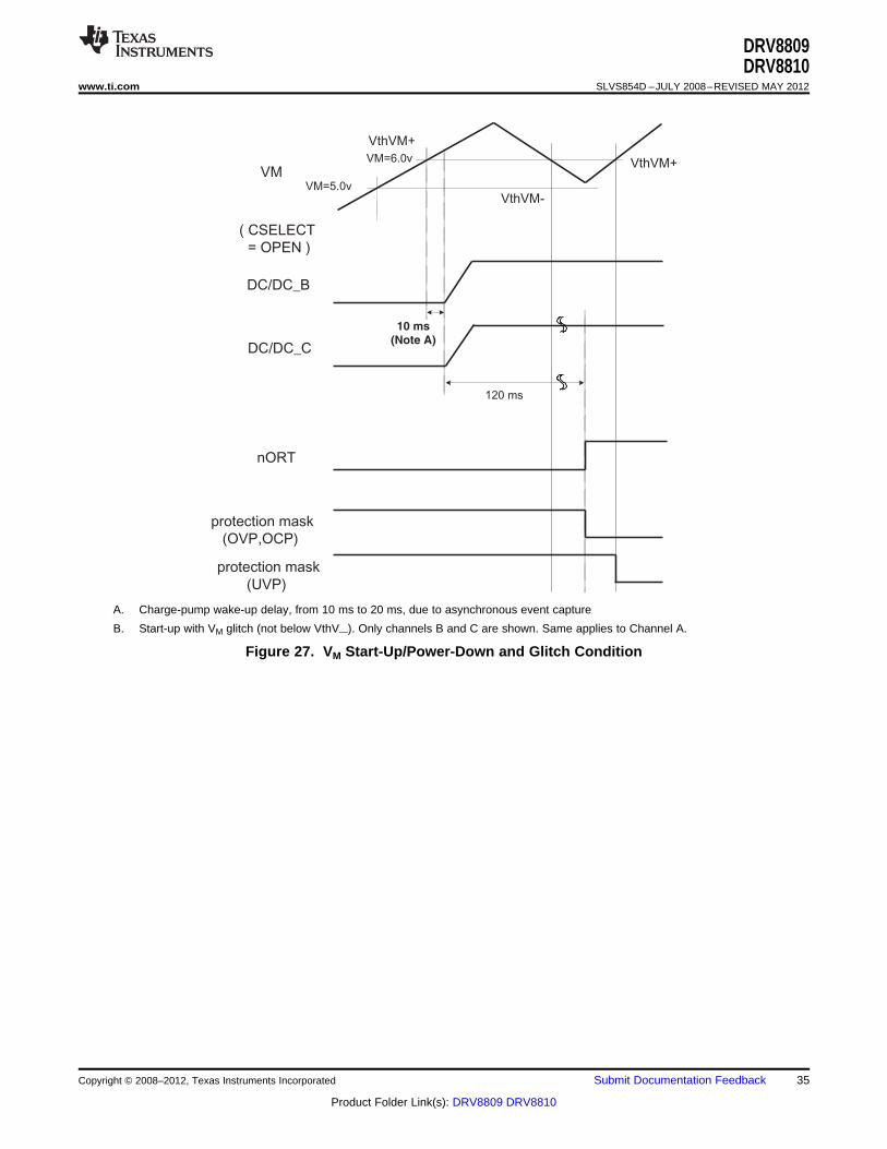
A. Charge-pump wake-up delay, from 10 ms to 20 ms, due to asynchronous event capture
B. Start-up with VM glitch (not below VthV—). Only channels B and C are shown. Same applies to Channel A.
Figure 27. VM Start-Up/Power-Down and Glitch Condition
Copyright © 2008–2012, Texas Instruments Incorporated Submit Documentation Feedback 35
Product Folder Link(s): DRV8809 DRV8810

DC/DC_C
nORT
protection
mask
DC/DC_B
VM=6.0vVM
VthVM+
VthVM-
Shutdown
MaskVM=5.0v
10 ms
(Note A)
10 ms
(Note A)
DRV8809DRV8810SLVS854D –JULY 2008–REVISED MAY 2012 www.ti.com
A. Charge-pump wake-up delay, from 10 ms to 20 ms, due to asynchronous event capture
B. Start-up with VM glitch (below VthV_). Only channels B and C are shown. Same applies to Channel A.
Figure 28. VM Startup/Power-Down and Glitch Condition
A. Only channels B and C are shown. Same applies to Channel A.
Figure 29. Power Down (Normal)
36 Submit Documentation Feedback Copyright © 2008–2012, Texas Instruments Incorporated
Product Folder Link(s): DRV8809 DRV8810

DC/DC_C
nORT
protection
mask
40 ms
in case
t <120 ms
DC/DC_B
VM=5.0v
VM=6.0v
VM
VthVM+
VthVM-
VthVM+
Shutdown
Restart
= L
= H
t 120 ms
10 ms(Note A)
( CSELECT
= OPEN )
10 ms(Note A)
DC/DC_C
nORT
protection
mask
DC/DC_B
VM=6.0vVM
VthVM+
VthVM-Mask
VM=5.0v
DRV8809DRV8810
www.ti.com SLVS854D –JULY 2008–REVISED MAY 2012
A. Only channels B and C are shown. Same applies to Channel A.
Figure 30. Power Down (Glitch on VM)
A. Charge-pump wake-up delay, from 10 ms to 20 ms, due to asynchronous event capture
B. Only channels B and C are shown. Same applies to Channel A.
Figure 31. Power Down (Glitch on VM Below VthV_)
Copyright © 2008–2012, Texas Instruments Incorporated Submit Documentation Feedback 37
Product Folder Link(s): DRV8809 DRV8810
OSCM
Phase
tBlank(1,0) *1
fChop8 x OSCM clocks
ResyncResync ResyncResync
n=6(n=6)
n=3
tBlank
(0,1) *2
*1 : Setup register bit <4,3> = ( 1,0 ) : tBlank = OSCM clock x 3 (or bit <5,6> for H-bridge C,D channel )
*2 : Setup register bit <4,3> = ( 0,1 ) : tBlank = OSCM clock x 6 (or bit <5,6> for H-bridge C,D channel )
n=6
n=3
n=6
n=3 n=3 n=3
(n=6)
nORT
InReset
10 us
DRV8809DRV8810SLVS854D –JULY 2008–REVISED MAY 2012 www.ti.com
Figure 32. Shutdown by In-Reset
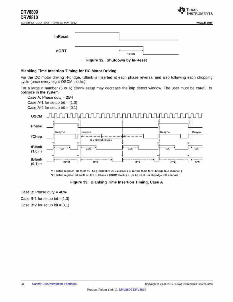
Blanking Time Insertion Timing for DC Motor Driving
For the DC motor driving H-bridge, tBlank is inserted at each phase reversal and also following each choppingcycle (once every eight OSCM clocks).
For a large n number (5 or 6) tBlank setup may decrease the itrip detect window. The user must be careful tooptimize in the system.
Case A: Phase duty = 25%Case A*1 for setup bit = (1,0)Case A*2 for setup bit = (0,1)
Figure 33. Blanking Time Insertion Timing, Case A
Case B: Phase duty = 40%
Case B*1 for setup bit =(1,0)
Case B*2 for setup bit =(0,1)
38 Submit Documentation Feedback Copyright © 2008–2012, Texas Instruments Incorporated
Product Folder Link(s): DRV8809 DRV8810

(n=3)
OSCM
Phase
tBlank(1,0) *1
fChop8 x OSCM clocks
ResyncResync ResyncResync
n=6
n=3
tBlank
(0,1) *2
*1 : Setup register bit <4,3> = ( 1,0 ) : tBlank = OSCM clock x 3 (or bit <5,6> for H-bridge C,D channel )
*2 : Setup register bit <4,3> = ( 0,1 ) : tBlank = OSCM clock x 6 (or bit <5,6> for H-bridge C,D channel )
n=6
n=3
n=6
n=3 n=3
(n=6)
8 x OSCM clocks
(n=6)
DRV8809DRV8810
www.ti.com SLVS854D –JULY 2008–REVISED MAY 2012
Figure 34. Blanking Time Insertion Timing, Case B
Copyright © 2008–2012, Texas Instruments Incorporated Submit Documentation Feedback 39
Product Folder Link(s): DRV8809 DRV8810
DRV8809DRV8810SLVS854D –JULY 2008–REVISED MAY 2012 www.ti.com
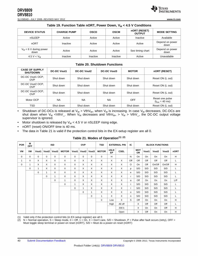
Table 19. Function Table nORT, Power Down, VM < 4.5 V Conditions
nORT (RESET)DEVICE STATUS CHARGE PUMP OSCD OSCM MODE SETTINGOUTPUT
nSLEEP Active Active Active Inactive Available
Depend on powernORT Inactive Active Active Active down
VM < 6 V during power Depend on powerActive Active Active See timing chartdown down
4.5 V < VM Inactive Inactive Inactive Active Unavailable
Table 20. Shutdown Functions
CASE OF SUPPLY DC-DC Vout1 DC-DC Vout2 DC-DC Vout3 MOTOR nORT (RESET)SHUTDOWN
DC-DC Vout1 OCP, Shut down Shut down Shut down Shut down Reset ON (L out)OVP
DC-DC Vout2 OCP, Shut down Shut down Shut down Shut down Reset ON (L out)OVP
DC-DC Vout3 OCP, Shut down Shut down Shut down Shut down Reset ON (L out)OVP
Reset one pulseMotor OCP NA NA NA OFF (tlow = 40 ms)
TSD Shut down Shut down Shut down Shut down Reset ON (L out)
• Shutdown of DC-DCs is released at VM > VthVM+ when VM is increasing. In case VM decreases, DC-DCs areshut down when VM <VthV_. When VM decreases and VthVM+ > VM > VthV_, the DC-DC output voltagesupervisor is ignored.
• Motor shutdown is released by VM < 4.5 V or nSLEEP rising edge.• nORT (reset) ON/OFF time is 40 ms.• The data in Table 21 is valid if the protection control bits in the EX-setup register are all 0.
Table 21. Modes of Operation (1) (2)
MPOR ISD OVP TSD EXTERNAL PIN IC BLOCK FUNCTIONSOFF
nSLE MOTVM VM Vout1 Vout2 Vout3 MOTOR Vout1 Vout2 Vout3 MOTOR CSEL Vout1 Vout2 Vout3 nORTEP OR
0 0 0 0 0 0 0 0 0 0 H N On On On On H
1 X X X X X X X X X X X Off Off Off Off Off L
0 1 X X X X X X X X X X O On Off On/Off On/Off H
0 1 X X X X X X X X X p S/D S/D S/D S/D L
0 1 X X X X X X X X e S/D S/D S/D S/D L
0 1 X X X X X X X r S/D S/D S/D S/D L
0 1 X X X X X X a Off On On On L/P
0 1 X X X X X t S/D S/D S/D S/D L
0 1 X X X X I S/D S/D S/D S/D L
0 1 X X X o S/D S/D S/D S/D L
0 1 X X n S/D S/D S/D S/D L
0 Low X S Off On On On H
High All off X Off Off Off L
200 k X On On Off H
Open X Off On On H
(1) Valid only if the protection control bits (in EX-setup register) are all 0.(2) N = Normal operation, S = Sleep mode, 0 = Off, 1 = On, X = Don’t care, S/D = Shutdown, P = Pulse after fault occurs (retry), OFF =
Must toggle sleep terminal or power-on reset (nORT), S/D = Must do a power-on reset (nORT)
40 Submit Documentation Feedback Copyright © 2008–2012, Texas Instruments Incorporated
Product Folder Link(s): DRV8809 DRV8810
Vout 1
Vout 2
Vout 3
LOGIC_OUT
FBB
OD_B
FBA
OD_A
OD_C
OSCM_Mon
LGND
OUTA+
RSA
OUTA-
OUTB+
RSB
OUTB-
OUTC+
OUTD+
RSD
OUTD-
C_SELECT
DC
Motor
VM
DC
Motor
Stepper
Motor
CLK_AB
nORT
PHASE_SD PHASE_SC
MGND
MGND
VM
ENABLE_SC
nSLEEP VREF_AB
VREF_SCD
DATA_ABSTROBE_AB(reserved)ENABLE_SD
VM
100uF
0.2 ohm
0.2 ohm
0.2 ohm
0.2 ohm
2.5v
0.1uF
330uH
330uH
330uH
220uF
220uF
220uF
1.2k
1.0k
3.3v
1.5v
5.0v
1.48v
1.50v
1.50v
3.0k
5.6k
2.4k
200 k
Voltage
charge
pump
Thermal
Shut down
Temperature
Sens :
Pre-TSD or
Tsens (analog)
Freq divider
for DC/DC
Freq divider
Motor PWM
DC/DC
convertor
Ch-A
DC/DC
convertor
Ch-B
DC/DC
convertor
Ch-C
OUTC-
To Highside
gate drive
Motor Drive
Output
Control C
Motor Drive
Output
Control D
Motor Drive
Output
Control A
Motor Drive
Output
Control B
VM
To
Hbridges
VM
Regulator
Internal
supply
OSCi
6.4MHz
Setup / ex-setup
registers
Pre-Drive, Latch
Registers &
control circuitry
Serial Interface C-DSerial Interface A-B
Voltage
Supervisory
Cstrage
TH_OUT
CbktDCDC_MODE
0.01uF
OSCD_Mon
FBC
(12.0v)
(9.1k)
(1.3k)
0.1uF
0.1uF
0.1uF
To
DC/DC
VDIN
In-Reset
VCP CP1 CP2
RSC
DRV8809DRV8810
www.ti.com SLVS854D –JULY 2008–REVISED MAY 2012
APPLICATION INFORMATION
Application Schematic
For one stepper and two DC motor configuration:• DC-DC Ch-A = 5 V (12 V)• DC-DC Ch-B = 1.5 V• DC-DC Ch-C = 3.3 V
If start-up from Ch-B (1.5 V) ≥ Ch-A (5 V), Ch-C 3.3 V should be turned on by the setup register (200 kΩbetween C_SELECT pin and GND).
Figure 35.
Copyright © 2008–2012, Texas Instruments Incorporated Submit Documentation Feedback 41
Product Folder Link(s): DRV8809 DRV8810

PACKAGE OPTION ADDENDUM
www.ti.com 26-Aug-2013
Addendum-Page 1
PACKAGING INFORMATION
Orderable Device Status(1)
Package Type PackageDrawing
Pins PackageQty
Eco Plan(2)
Lead/Ball Finish MSL Peak Temp(3)
Op Temp (°C) Device Marking(4/5)
Samples
DRV8809PAP ACTIVE HTQFP PAP 64 160 Green (RoHS& no Sb/Br)
CU NIPDAU Level-3-260C-168 HR -10 to 50 DRV88091
(1) The marketing status values are defined as follows:ACTIVE: Product device recommended for new designs.LIFEBUY: TI has announced that the device will be discontinued, and a lifetime-buy period is in effect.NRND: Not recommended for new designs. Device is in production to support existing customers, but TI does not recommend using this part in a new design.PREVIEW: Device has been announced but is not in production. Samples may or may not be available.OBSOLETE: TI has discontinued the production of the device.
(2) Eco Plan - The planned eco-friendly classification: Pb-Free (RoHS), Pb-Free (RoHS Exempt), or Green (RoHS & no Sb/Br) - please check http://www.ti.com/productcontent for the latest availabilityinformation and additional product content details.TBD: The Pb-Free/Green conversion plan has not been defined.Pb-Free (RoHS): TI's terms "Lead-Free" or "Pb-Free" mean semiconductor products that are compatible with the current RoHS requirements for all 6 substances, including the requirement thatlead not exceed 0.1% by weight in homogeneous materials. Where designed to be soldered at high temperatures, TI Pb-Free products are suitable for use in specified lead-free processes.Pb-Free (RoHS Exempt): This component has a RoHS exemption for either 1) lead-based flip-chip solder bumps used between the die and package, or 2) lead-based die adhesive used betweenthe die and leadframe. The component is otherwise considered Pb-Free (RoHS compatible) as defined above.Green (RoHS & no Sb/Br): TI defines "Green" to mean Pb-Free (RoHS compatible), and free of Bromine (Br) and Antimony (Sb) based flame retardants (Br or Sb do not exceed 0.1% by weightin homogeneous material)
(3) MSL, Peak Temp. -- The Moisture Sensitivity Level rating according to the JEDEC industry standard classifications, and peak solder temperature.
(4) There may be additional marking, which relates to the logo, the lot trace code information, or the environmental category on the device.
(5) Multiple Device Markings will be inside parentheses. Only one Device Marking contained in parentheses and separated by a "~" will appear on a device. If a line is indented then it is a continuationof the previous line and the two combined represent the entire Device Marking for that device.
Important Information and Disclaimer:The information provided on this page represents TI's knowledge and belief as of the date that it is provided. TI bases its knowledge and belief on informationprovided by third parties, and makes no representation or warranty as to the accuracy of such information. Efforts are underway to better integrate information from third parties. TI has taken andcontinues to take reasonable steps to provide representative and accurate information but may not have conducted destructive testing or chemical analysis on incoming materials and chemicals.TI and TI suppliers consider certain information to be proprietary, and thus CAS numbers and other limited information may not be available for release.
In no event shall TI's liability arising out of such information exceed the total purchase price of the TI part(s) at issue in this document sold by TI to Customer on an annual basis.
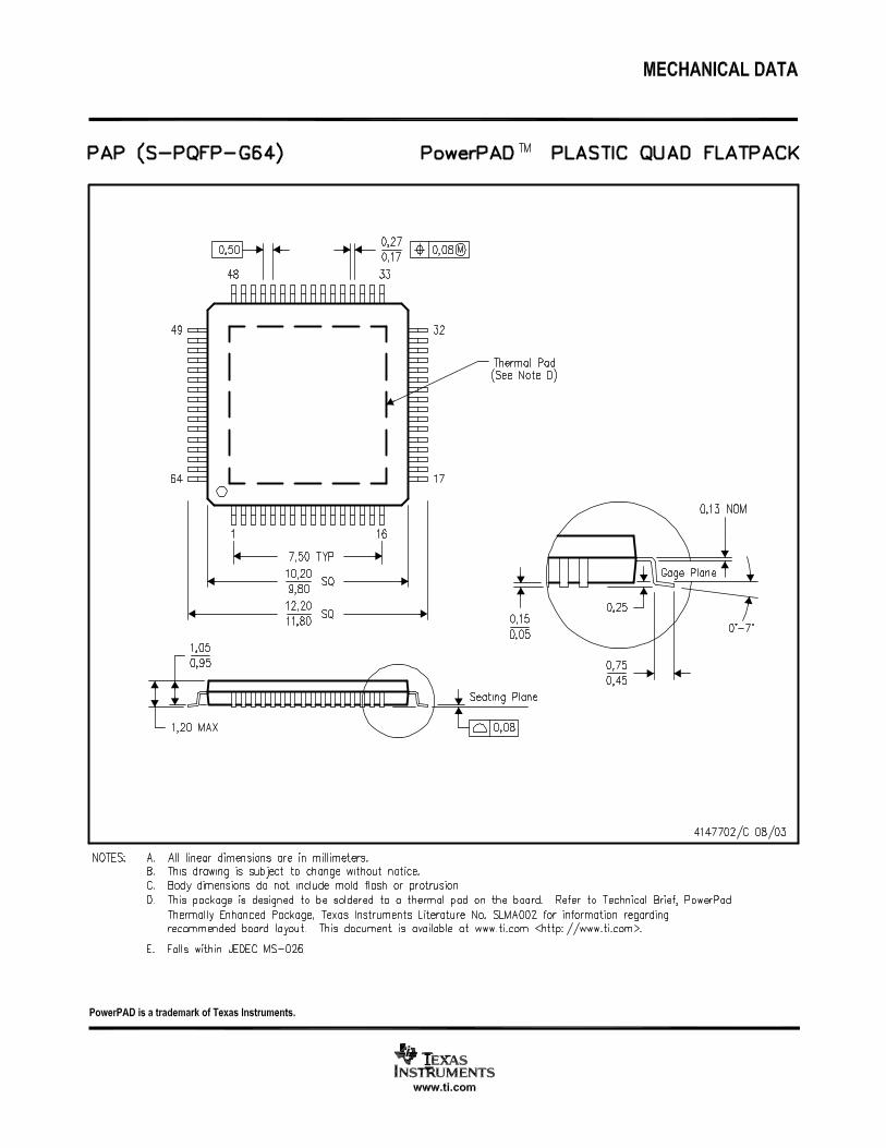


IMPORTANT NOTICE
Texas Instruments Incorporated and its subsidiaries (TI) reserve the right to make corrections, enhancements, improvements and otherchanges to its semiconductor products and services per JESD46, latest issue, and to discontinue any product or service per JESD48, latestissue. Buyers should obtain the latest relevant information before placing orders and should verify that such information is current andcomplete. All semiconductor products (also referred to herein as “components”) are sold subject to TI’s terms and conditions of salesupplied at the time of order acknowledgment.
TI warrants performance of its components to the specifications applicable at the time of sale, in accordance with the warranty in TI’s termsand conditions of sale of semiconductor products. Testing and other quality control techniques are used to the extent TI deems necessaryto support this warranty. Except where mandated by applicable law, testing of all parameters of each component is not necessarilyperformed.
TI assumes no liability for applications assistance or the design of Buyers’ products. Buyers are responsible for their products andapplications using TI components. To minimize the risks associated with Buyers’ products and applications, Buyers should provideadequate design and operating safeguards.
TI does not warrant or represent that any license, either express or implied, is granted under any patent right, copyright, mask work right, orother intellectual property right relating to any combination, machine, or process in which TI components or services are used. Informationpublished by TI regarding third-party products or services does not constitute a license to use such products or services or a warranty orendorsement thereof. Use of such information may require a license from a third party under the patents or other intellectual property of thethird party, or a license from TI under the patents or other intellectual property of TI.
Reproduction of significant portions of TI information in TI data books or data sheets is permissible only if reproduction is without alterationand is accompanied by all associated warranties, conditions, limitations, and notices. TI is not responsible or liable for such altereddocumentation. Information of third parties may be subject to additional restrictions.
Resale of TI components or services with statements different from or beyond the parameters stated by TI for that component or servicevoids all express and any implied warranties for the associated TI component or service and is an unfair and deceptive business practice.TI is not responsible or liable for any such statements.
Buyer acknowledges and agrees that it is solely responsible for compliance with all legal, regulatory and safety-related requirementsconcerning its products, and any use of TI components in its applications, notwithstanding any applications-related information or supportthat may be provided by TI. Buyer represents and agrees that it has all the necessary expertise to create and implement safeguards whichanticipate dangerous consequences of failures, monitor failures and their consequences, lessen the likelihood of failures that might causeharm and take appropriate remedial actions. Buyer will fully indemnify TI and its representatives against any damages arising out of the useof any TI components in safety-critical applications.
In some cases, TI components may be promoted specifically to facilitate safety-related applications. With such components, TI’s goal is tohelp enable customers to design and create their own end-product solutions that meet applicable functional safety standards andrequirements. Nonetheless, such components are subject to these terms.
No TI components are authorized for use in FDA Class III (or similar life-critical medical equipment) unless authorized officers of the partieshave executed a special agreement specifically governing such use.
Only those TI components which TI has specifically designated as military grade or “enhanced plastic” are designed and intended for use inmilitary/aerospace applications or environments. Buyer acknowledges and agrees that any military or aerospace use of TI componentswhich have not been so designated is solely at the Buyer's risk, and that Buyer is solely responsible for compliance with all legal andregulatory requirements in connection with such use.
TI has specifically designated certain components as meeting ISO/TS16949 requirements, mainly for automotive use. In any case of use ofnon-designated products, TI will not be responsible for any failure to meet ISO/TS16949.
Products Applications
Audio www.ti.com/audio Automotive and Transportation www.ti.com/automotive
Amplifiers amplifier.ti.com Communications and Telecom www.ti.com/communications
Data Converters dataconverter.ti.com Computers and Peripherals www.ti.com/computers
DLP® Products www.dlp.com Consumer Electronics www.ti.com/consumer-apps
DSP dsp.ti.com Energy and Lighting www.ti.com/energy
Clocks and Timers www.ti.com/clocks Industrial www.ti.com/industrial
Interface interface.ti.com Medical www.ti.com/medical
Logic logic.ti.com Security www.ti.com/security
Power Mgmt power.ti.com Space, Avionics and Defense www.ti.com/space-avionics-defense
Microcontrollers microcontroller.ti.com Video and Imaging www.ti.com/video
RFID www.ti-rfid.com
OMAP Applications Processors www.ti.com/omap TI E2E Community e2e.ti.com
Wireless Connectivity www.ti.com/wirelessconnectivity
Mailing Address: Texas Instruments, Post Office Box 655303, Dallas, Texas 75265Copyright © 2013, Texas Instruments Incorporated
Related Documents


![[Revised]the combination of social media and marketing](https://static.cupdf.com/doc/110x72/554eed9db4c905d51b8b5502/revisedthe-combination-of-social-media-and-marketing.jpg)


