Slowed Recombination via Tunable Surface Energetics in Perovskite Solar Cells Dane W. deQuilettes, 1 Jason Jungwan Yoo, 2,3 Roberto Brenes, 4 Felix Utama Kosasih, 5 Madeleine Laitz, 4 Benjia Dak Dou, 1 Seong Sik Shin, 3* Caterina Ducati, 5 Moungi Bawendi, 2* Vladimir Bulović 1,4* 1 Research Laboratory of Electronics, Massachusetts Institute of Technology, 77 Massachusetts Avenue, Cambridge, Massachusetts, USA 2 Department of Chemistry, Massachusetts Institute of Technology, 77 Massachusetts Avenue, Cambridge, Massachusetts, USA 3 Division of Advanced Materials, Korea Research Institute of Chemical Technology, Daejeon, Republic of Korea. 4 Department of Electrical Engineering and Computer Science, Massachusetts Institute of Technology, Cambridge, MA, USA. 5 Department of Materials Science and Metallurgy, University of Cambridge, 27 Charles Babbage Road, Cambridge CB3 0FS, UK. *Corresponding Authors: [email protected], [email protected], and [email protected]

Welcome message from author
This document is posted to help you gain knowledge. Please leave a comment to let me know what you think about it! Share it to your friends and learn new things together.
Transcript
Slowed Recombination via Tunable Surface Energetics in Perovskite Solar
Cells
Dane W. deQuilettes,1 Jason Jungwan Yoo,2,3 Roberto Brenes,4 Felix Utama Kosasih,5
Madeleine Laitz,4 Benjia Dak Dou,1 Seong Sik Shin,3* Caterina Ducati,5 Moungi Bawendi,2*
Vladimir Bulović1,4*
1 Research Laboratory of Electronics, Massachusetts Institute of Technology, 77 Massachusetts
Avenue, Cambridge, Massachusetts, USA
2 Department of Chemistry, Massachusetts Institute of Technology, 77 Massachusetts Avenue,
Cambridge, Massachusetts, USA
3 Division of Advanced Materials, Korea Research Institute of Chemical Technology, Daejeon,
Republic of Korea.
4 Department of Electrical Engineering and Computer Science, Massachusetts Institute of
Technology, Cambridge, MA, USA.
5 Department of Materials Science and Metallurgy, University of Cambridge, 27 Charles
Babbage Road, Cambridge CB3 0FS, UK.
*Corresponding Authors: [email protected], [email protected], and [email protected]
Abstract
Metal halide perovskite semiconductors have the potential to reach the optoelectronic quality of
meticulously grown inorganic materials, but with a distinct advantage of being solution
processable. Currently, perovskite photovoltaic device performance is limited by charge carrier
recombination loss at surfaces and interfaces.1-3 Indeed, the highest quality perovskite films are
achieved with molecular surface passivation,2,4 for example with n-trioctylphosphine oxide,5 but
these treatments are often labile and electrically insulating.6 The introduction of a thin 2D
perovskite layer on the bulk 3D perovskite offers a promising alternative in reducing non-radiative
energy loss while also improving device fill factor and open circuit voltage.7-9 But, thus far, it has
been unclear how best to design and optimize 2D/3D heterostructures and whether critical material
properties, such as charge carrier lifetime, can reach values as high as ligand-based approaches.
Here, we perform an in-depth characterization of 2D/3D perovskite interfaces that have led to
certified power conversion efficiencies exceeding 25% and show that 2D layers are inherently
capable of pushing beyond molecular passivation strategies with even greater tunability. We set
new benchmarks for photoluminescence lifetime, reaching values > 30 μs, and perovskite/charge
transport layer surface recombination velocity with values < 7 cm s-1. We use quantitative X-ray
spectroscopy to directly visualize how treatment with hexylammonium bromide not only
selectively targets defects at surfaces and grain boundaries, but also forms a bandgap grading
extending > 100 nm into the bulk layer. We expect these results to be a starting point for more
sophisticated engineering of 2D/3D heterostructures with surface fields that exclusively repel
charge carriers from defective regions while also enabling efficient charge transfer. It is likely that
the precise manipulation of energy bands will enable perovskite-based photovoltaics, light
emitting devices, and photocatalysts to operate closer to their theoretical performance limits.10
Ultralong Photoluminscence Lifetimes with HABr Treatment
Here, we study mixed-cation lead halide perovskite ((FAPbI3)1-x(MAPbBr3)x) layers (see SI for
preparation details) post-treated with a low concentration (10-50 mM) solution of hexylammonium
bromide (HABr) in chloroform (Figure 1a), following our previous work that led to a certified
power conversion efficiency (PCE) of 25.2%.11,12 In Figure 1b, we perform cross-sectional bright
field transmission electron microscopy (TEM) to directly image a thin (~ 40 nm) 2D layer that
forms on top of the 3D bulk perovskite after treatment with 10 mM of HABr,11 which is absent in
the control sample (Figure S1). We confirm the quality of this 2D layer by fabricating solar cells
and showing that the introduction of this 2D layer improves device PCE from ~21% to a certified
value of 24.4% (Figure 1c). Importantly, key enhancements are achieved in the open circuit voltage
(Voc) (92% of radiative limit – see SI and Figure S2) and fill factor (FF), indicating a significant
reduction in non-radiative loss13 (see refs11,12 for device statistics). We note that the small
improvement in the short circuit current density (Jsc) in the certified device is attributed to the
addition of an antireflective coating. Although it is now well-known that the introduction of 2D
layers lead to improvements in device performance, the compositional, structural, and
photophysical origins of such enhancements are relatively unexplored.14 For the first time, we
reveal the key features of this 2D/3D interface that lead to exceptional device performance,
revealing clear strategies to achieve charge carrier lifetimes and interfacial recombination
velocities necessary to reach 30% PCE.3
One fundamental metric in determining the quality of a photoactive layer is the photoluminescence
(PL) lifetime,15,16 where longer lifetimes typically correlate with higher PCEs.17,18 Unpassivated
bulk perovskite films deposited on glass now routinely demonstrate lifetimes ~ 1 μs,16,19 which can
be further improved to values as high as 8 μs with surface passivating molecules such as n-
trioctylphosphine oxide (TOPO)5 or up to 18 μs with solvent additives.19 The PL lifetimes of bare
2D/3D heterostructures on glass are typically only slightly longer than the as-grown 3D bulk layers
with lifetimes ranging from hundreds of ns to a few μs.20,21 To determine how our isolated 2D/3D
layers on glass compare to these values, we globally fit time-resolved PL decay measurements at
a range of excitation fluences when excited from the glass side using the standard kinetic rate
equation15 (see SI for fitting details). For the control sample (Figure 1d), we report an effective
lifetime, τeff, of 6.1 ± 0.9 μs (95% confidence interval (CI), 1/τeff = k1 = 1.6 ± 0.2 x10⁵ s-1), consistent
with a high-quality as-grown layer.22 For a champion 50 mM HABr treated sample (Figure 1e),
we report an impressive lifetime of 32.7 ± 7.9 μs (95% CI, k1 = 3.1 ± 0.9 x10⁴ s-1). This value is
higher than all previous reports for 2D/3D architectures, surpasses all previous perovskite records,
and is more than twice the 14.2 μs record of a GaAs double heterostructure.23 In fact, this value is
approaching the lower bound of the radiative lifetime limit (~ ≥ 60 μs) set by the background
doping density (see SI for details). We note that the effective internal second-order recombination
rate constant (𝑘2,𝑒𝑓𝑓𝑖𝑛𝑡 = 5.5x10⁻¹¹ cm3 s-1) for the 50 mM HABr treated sample is lower than the
control sample (𝑘2𝑖𝑛𝑡
= 7.4x10⁻¹⁰ cm3 s-1, see Figure S3 and S4) and other reported 𝑘2𝑖𝑛𝑡 values,15,24
suggesting slowed radiative recombination, which we explore in more detail below. In addition,
consistent with a reduction in non-radiative loss, Figure 1f shows an improvement in the PL
quantum efficiency (PLQE) of a typical treated sample compared to the control when measured at
1-sun equivalent absorbed photon flux (i.e. ~ 60 mW/cm2, λexc = 532 nm).
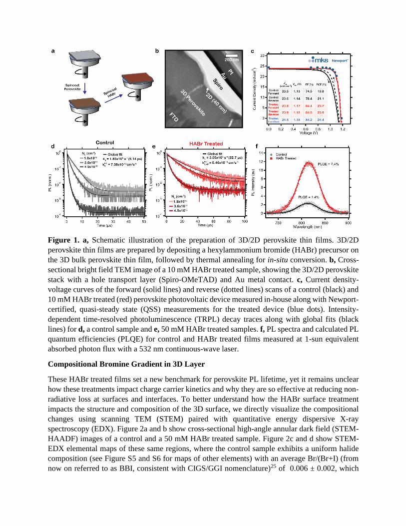
Figure 1. a, Schematic illustration of the preparation of 3D/2D perovskite thin films. 3D/2D
perovskite thin films are prepared by depositing a hexylammonium bromide (HABr) precursor on
the 3D bulk perovskite thin film, followed by thermal annealing for in-situ conversion. b, Cross-
sectional bright field TEM image of a 10 mM HABr treated sample, showing the 3D/2D perovskite
stack with a hole transport layer (Spiro-OMeTAD) and Au metal contact. c, Current density-
voltage curves of the forward (solid lines) and reverse (dotted lines) scans of a control (black) and
10 mM HABr treated (red) perovskite photovoltaic device measured in-house along with Newport-
certified, quasi-steady state (QSS) measurements for the treated device (blue dots). Intensity-
dependent time-resolved photoluminescence (TRPL) decay traces along with global fits (black
lines) for d, a control sample and e, 50 mM HABr treated samples. f, PL spectra and calculated PL
quantum efficiencies (PLQE) for control and HABr treated films measured at 1-sun equivalent
absorbed photon flux with a 532 nm continuous-wave laser.
Compositional Bromine Gradient in 3D Layer
These HABr treated films set a new benchmark for perovskite PL lifetime, yet it remains unclear
how these treatments impact charge carrier kinetics and why they are so effective at reducing non-
radiative loss at surfaces and interfaces. To better understand how the HABr surface treatment
impacts the structure and composition of the 3D surface, we directly visualize the compositional
changes using scanning TEM (STEM) paired with quantitative energy dispersive X-ray
spectroscopy (EDX). Figure 2a and b show cross-sectional high-angle annular dark field (STEM-
HAADF) images of a control and a 50 mM HABr treated sample. Figure 2c and d show STEM-
EDX elemental maps of these same regions, where the control sample exhibits a uniform halide
composition (see Figure S5 and S6 for maps of other elements) with an average Br/(Br+I) (from
now on referred to as BBI, consistent with CIGS/GGI nomenclature)25 of 0.006 ± 0.002, which

matches well with the solution stoichiometry (BBIsolution = 0.008). In contrast, the treated sample
shows large variations in halide composition, where Br is primarily concentrated at the top surface
and grain boundaries (see Figure S7 for maps of all elements), which are regions known to have
the highest defect densities.26,27 We also note clear evidence of PbI2 deposits at the grain
boundaries in the control, which disappear after the HABr treatment (see Figures S6 and S7),
indicating the in-situ surface reaction of HABr with PbI2 to form a lower dimensional perovskite,
consistent with other reports.9 These in-situ reactions are strongly dependent on the as-grown
perovskite surface chemistry, the location and concentration of PbI2, and the size and chemical
structure of the aromatic or aliphatic organic salt.28
From first inspection of Figure 2d, it is unclear whether the Br-rich strip is located in the 2D layer
or the bulk 3D layer. As this would have major implications for the electronic structure of these
materials and their shared interface, we perform a detailed analysis of key elemental line profiles
of the sample stack to identify the interface positions and composition (see SI for fitting details
and Figure S8). Using this analysis, Figure 2e,f show the positions of each interface along with
fitting ranges for the control and HABr treated samples. Importantly, Figure 2f shows that in the
treated sample, the Br concentration peaks in the bulk 3D layer and a small amount of Br is present
in the 2D layer (see Figure S9). In fact, not only is Br concentrated in the 3D layer, but we are able
to directly visualize a gradient extending >100 nm into the bulk film (see Figure S10 for additional
line profiles). We hypothesize that this halide exchange leads to a bandgap (Eg) gradient and in
Figure 2g predict how Eg changes as a function of BBI using functional dependencies previously
reported (see Figure S11).29,30 Previously, halide compositional gradients have been pursued
through surface treatments with formamidinium and methylammonium halides,31,32 but these
treatments do not lead to the formation of a 2D layer, which is beneficial for device stability.33
Here we show the formation of both a compositional gradient in the bulk layer, commonly found
in record setting PV architectures,32,34,35 as well as a protective 2D perovskite layer on top.36 Each
of these beneficial effects have been achieved separately through complex processing, but here we
have achieved both through one simple deposition step.
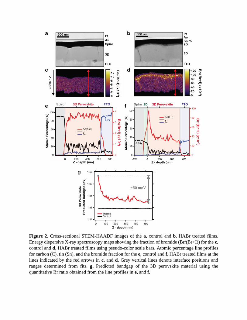
Figure 2. Cross-sectional STEM-HAADF images of the a, control and b, HABr treated films.
Energy dispersive X-ray spectroscopy maps showing the fraction of bromide (Br/(Br+I)) for the c,
control and d, HABr treated films using pseudo-color scale bars. Atomic percentage line profiles
for carbon (C), tin (Sn), and the bromide fraction for the e, control and f, HABr treated films at the
lines indicated by the red arrows in c, and d. Grey vertical lines denote interface positions and
ranges determined from fits. g, Predicted bandgap of the 3D perovskite material using the
quantitative Br ratio obtained from the line profiles in e, and f.
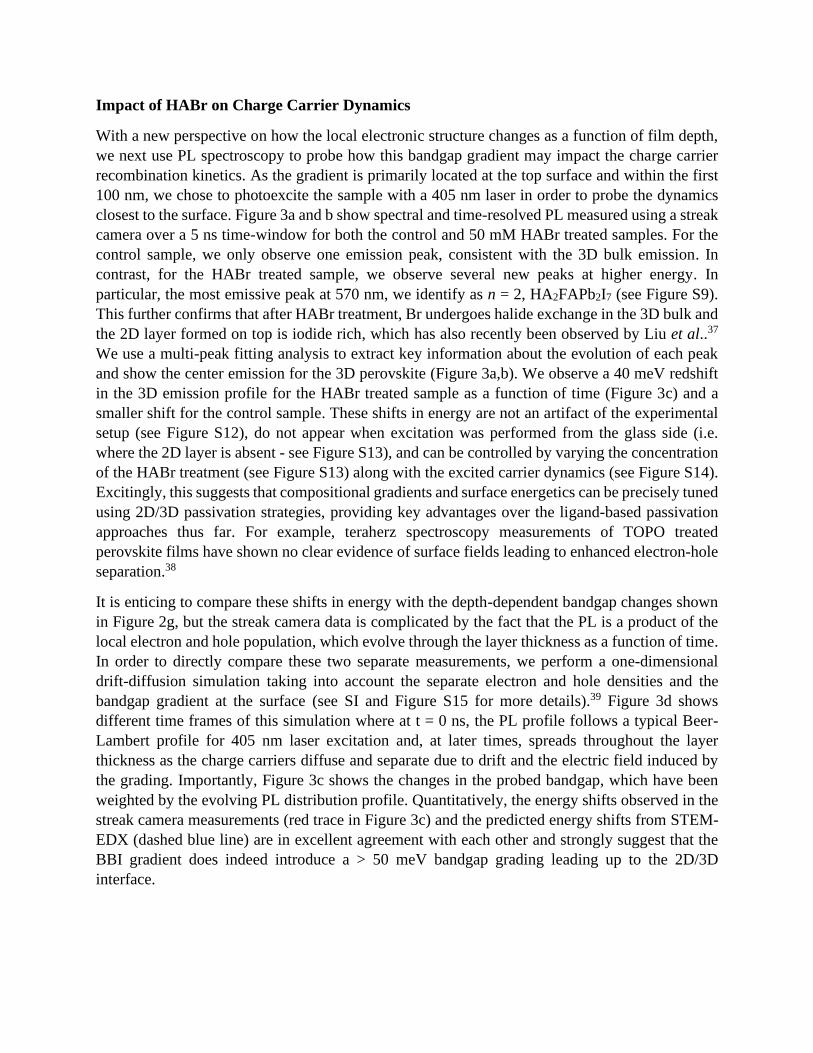
Impact of HABr on Charge Carrier Dynamics
With a new perspective on how the local electronic structure changes as a function of film depth,
we next use PL spectroscopy to probe how this bandgap gradient may impact the charge carrier
recombination kinetics. As the gradient is primarily located at the top surface and within the first
100 nm, we chose to photoexcite the sample with a 405 nm laser in order to probe the dynamics
closest to the surface. Figure 3a and b show spectral and time-resolved PL measured using a streak
camera over a 5 ns time-window for both the control and 50 mM HABr treated samples. For the
control sample, we only observe one emission peak, consistent with the 3D bulk emission. In
contrast, for the HABr treated sample, we observe several new peaks at higher energy. In
particular, the most emissive peak at 570 nm, we identify as n = 2, HA2FAPb2I7 (see Figure S9).
This further confirms that after HABr treatment, Br undergoes halide exchange in the 3D bulk and
the 2D layer formed on top is iodide rich, which has also recently been observed by Liu et al..37
We use a multi-peak fitting analysis to extract key information about the evolution of each peak
and show the center emission for the 3D perovskite (Figure 3a,b). We observe a 40 meV redshift
in the 3D emission profile for the HABr treated sample as a function of time (Figure 3c) and a
smaller shift for the control sample. These shifts in energy are not an artifact of the experimental
setup (see Figure S12), do not appear when excitation was performed from the glass side (i.e.
where the 2D layer is absent - see Figure S13), and can be controlled by varying the concentration
of the HABr treatment (see Figure S13) along with the excited carrier dynamics (see Figure S14).
Excitingly, this suggests that compositional gradients and surface energetics can be precisely tuned
using 2D/3D passivation strategies, providing key advantages over the ligand-based passivation
approaches thus far. For example, teraherz spectroscopy measurements of TOPO treated
perovskite films have shown no clear evidence of surface fields leading to enhanced electron-hole
separation.38
It is enticing to compare these shifts in energy with the depth-dependent bandgap changes shown
in Figure 2g, but the streak camera data is complicated by the fact that the PL is a product of the
local electron and hole population, which evolve through the layer thickness as a function of time.
In order to directly compare these two separate measurements, we perform a one-dimensional
drift-diffusion simulation taking into account the separate electron and hole densities and the
bandgap gradient at the surface (see SI and Figure S15 for more details).39 Figure 3d shows
different time frames of this simulation where at t = 0 ns, the PL profile follows a typical Beer-
Lambert profile for 405 nm laser excitation and, at later times, spreads throughout the layer
thickness as the charge carriers diffuse and separate due to drift and the electric field induced by
the grading. Importantly, Figure 3c shows the changes in the probed bandgap, which have been
weighted by the evolving PL distribution profile. Quantitatively, the energy shifts observed in the
streak camera measurements (red trace in Figure 3c) and the predicted energy shifts from STEM-
EDX (dashed blue line) are in excellent agreement with each other and strongly suggest that the
BBI gradient does indeed introduce a > 50 meV bandgap grading leading up to the 2D/3D
interface.
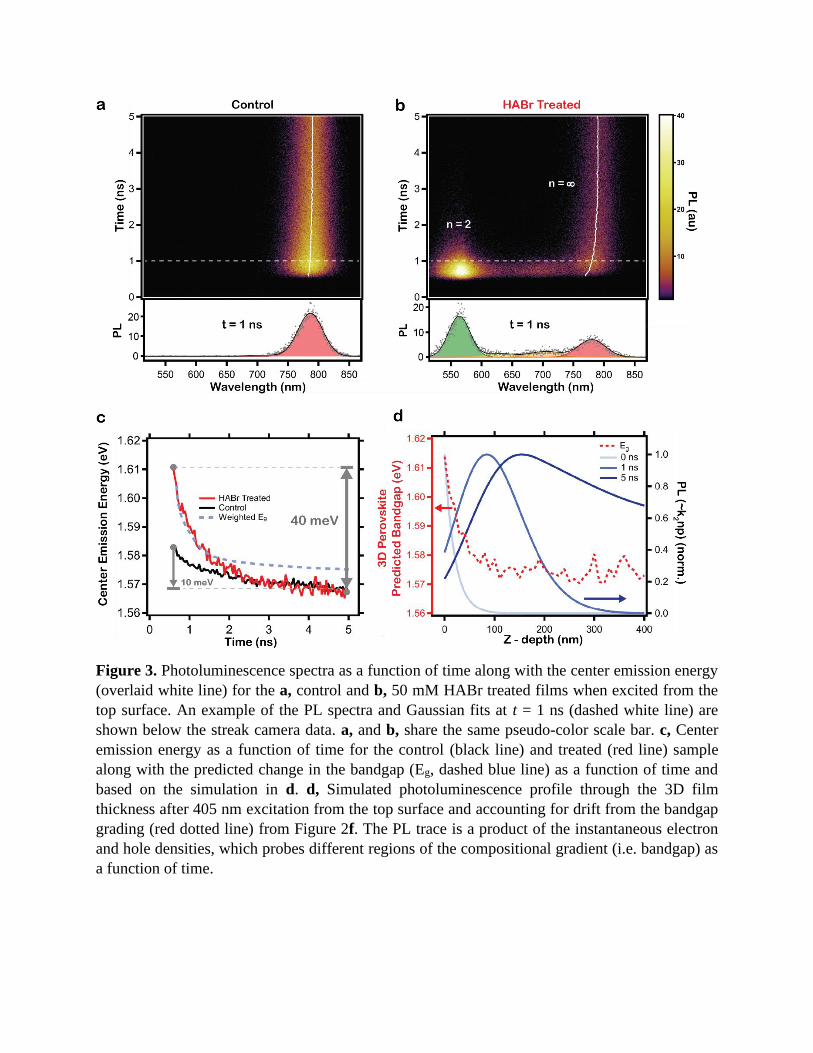
Figure 3. Photoluminescence spectra as a function of time along with the center emission energy
(overlaid white line) for the a, control and b, 50 mM HABr treated films when excited from the
top surface. An example of the PL spectra and Gaussian fits at t = 1 ns (dashed white line) are
shown below the streak camera data. a, and b, share the same pseudo-color scale bar. c, Center
emission energy as a function of time for the control (black line) and treated (red line) sample
along with the predicted change in the bandgap (Eg, dashed blue line) as a function of time and
based on the simulation in d. d, Simulated photoluminescence profile through the 3D film
thickness after 405 nm excitation from the top surface and accounting for drift from the bandgap
grading (red dotted line) from Figure 2f. The PL trace is a product of the instantaneous electron
and hole densities, which probes different regions of the compositional gradient (i.e. bandgap) as
a function of time.
Ultralow Interfacial Recombination at HTL
Based on the shared conclusion obtained from separate EDX and streak camera measurements
described above, we propose a schematic of the energy level diagram of the 2D/3D heterointerface,
consistent with previously reported UPS measurements28 and the expected changes in the
conduction band energy as a function of Br composition (Figure 4a).31 Bandgap gradings are nearly
ubiquitous in achieving world-record PCEs in a host of PV materials, including CdTe,34 GaAs,35
CIGS,40 quantum dots,41 and tandem architectures,42-44 but are far less developed for perovskites.
The built-in electric field due to the compositional grading is dependent both on the grading’s
depth and magnitude, with common values for other PV technologies ranging from 1.5 to 10 kV
cm-1.39,41 Although the perovskite bandgap grading we measure (~ 50 meV) appears moderate
compared to most CIGS bandgap gradings (~200 meV),39 the grading occurs over such a shallow
depth that it leads to a similar or even greater built-in electric field of up to 9 kV cm-1 (Figure 4b).
Importantly, Figure 4b shows the impact of the 50 meV bandgap grading on the charge carrier
density distributions (i.e. PL ∝ k2np - see Figure S16 for electron and hole density maps) as a
function of depth and time when excited from the substrate side (opposite of 2D/3D interface). At
early times, emission is concentrated under the generation profile and then spreads through the
film thickness due to diffusion. The ≤ 9 kV cm-1 field strength leads to a ~80% reduction in the
electron density near the surface/interface, which are known to possess high densities of defects in
perovskites.2 Surface fields not only repel carriers from defective regions at the surface, but also
cause spatial separation of electrons and holes which has previously been shown to lead to
depressed radiative recombination rates (i.e. lower PLQE) and slowed recombination in materials
such as InP.10,45 We capture this effect in the lower fitted 𝑘2,𝑒𝑓𝑓𝑖𝑛𝑡 in our samples (Figures 1e and
4a). In fact, we find that slowed recombination is a general phenomenon in other 2D/3D
heterostructures (i.e. treatment with phenethylammonium iodide (PEAI), see Figure S17), and can
be explained through band bending (see SI and Figure S18), where the extent of field induced
charge separation can be evaluated from the 𝑘2,𝑒𝑓𝑓𝑖𝑛𝑡 value along with the appearance of a drift-
induced fast PL decay component46 when excited from the top surface (see SI and Figures S14 and
S17-19). PL spectroscopy therefore serves as a simple and readily accessible tool to quickly
evaluate surface energetics47 and tune new chemical surface modifications and heterostructures.
To better understand the impact of both the 2D layer and the bandgap gradient on interfacial
recombination and device performance, we deposit a hole transport layer (HTL), Spiro-OMeTAD,
on top of the 2D/3D heterostructure following our typical high performing device architecture (see
Figure 1b and 1c). Figure 4c shows the time-resolved PL decay trace of the control/HTL bilayer
decaying several orders of magnitude over the first 100s of nanoseconds, consistent with other
reports.48 Conversely, the treated/HTL sample has a fast initial decay, which is attributed to hole
extraction (i.e. majority surface recombination velocity (SRV),48 followed by a very slow decay
(i.e. minority SRV). We quantify these differences in decay kinetics by determining the upper limit
of the SRV, following the approach described by Wang et al. (see SI).23,48 For the control sample,
we fit an SRV of < 3500 cm/s, consistent with the 3100 cm/s value previously reported for Spiro-
OMeTAD.48 The treated sample demonstrates an SRV orders of magnitude lower, reaching values
as low as < 7 cm/s. To the best of our knowledge, this is the lowest SRV reported for any perovskite
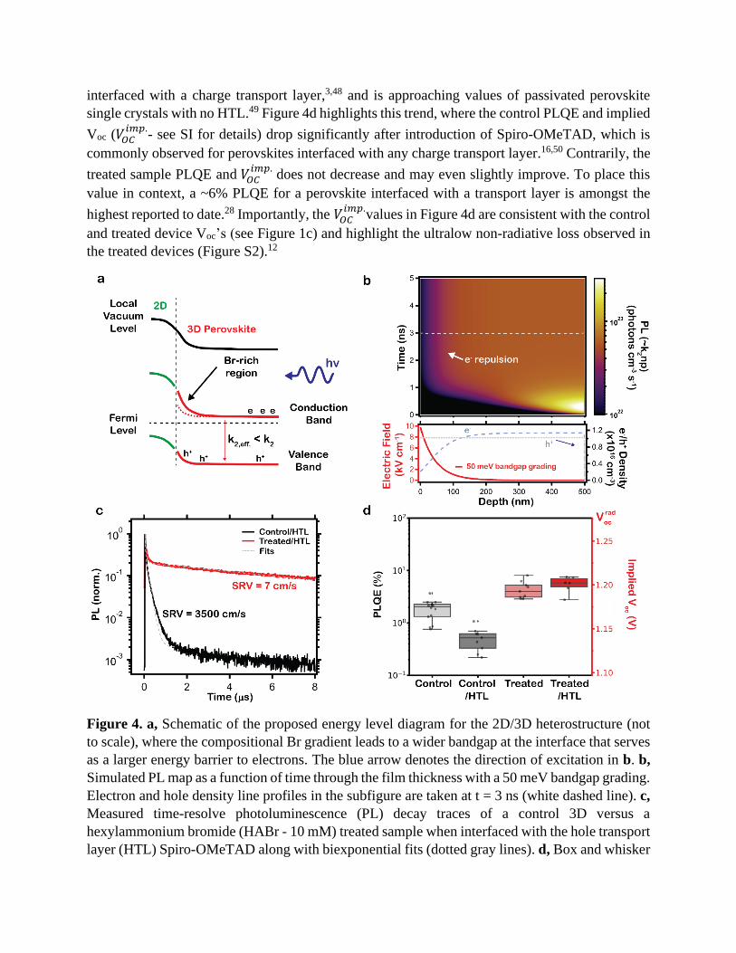
interfaced with a charge transport layer,3,48 and is approaching values of passivated perovskite
single crystals with no HTL.49 Figure 4d highlights this trend, where the control PLQE and implied
Voc (𝑉𝑂𝐶𝑖𝑚𝑝.
- see SI for details) drop significantly after introduction of Spiro-OMeTAD, which is
commonly observed for perovskites interfaced with any charge transport layer.16,50 Contrarily, the
treated sample PLQE and 𝑉𝑂𝐶𝑖𝑚𝑝.
does not decrease and may even slightly improve. To place this
value in context, a ~6% PLQE for a perovskite interfaced with a transport layer is amongst the
highest reported to date.28 Importantly, the 𝑉𝑂𝐶𝑖𝑚𝑝.
values in Figure 4d are consistent with the control
and treated device Voc’s (see Figure 1c) and highlight the ultralow non-radiative loss observed in
the treated devices (Figure S2).12
Figure 4. a, Schematic of the proposed energy level diagram for the 2D/3D heterostructure (not
to scale), where the compositional Br gradient leads to a wider bandgap at the interface that serves
as a larger energy barrier to electrons. The blue arrow denotes the direction of excitation in b. b,
Simulated PL map as a function of time through the film thickness with a 50 meV bandgap grading.
Electron and hole density line profiles in the subfigure are taken at t = 3 ns (white dashed line). c,
Measured time-resolve photoluminescence (PL) decay traces of a control 3D versus a
hexylammonium bromide (HABr - 10 mM) treated sample when interfaced with the hole transport
layer (HTL) Spiro-OMeTAD along with biexponential fits (dotted gray lines). d, Box and whisker
plots of measured PL quantum efficiency (PLQE) and calculations of implied open circuit voltages
(Voc) of a control (sample size, n =14) and control/hole transport layer (HTL) (n = 9) versus a
HABr treated (10 mM) film (n = 9) and treated/HTL bilayer (n = 6). All measurements were taken
on distinct samples, with HTL layers deposited on previously measured control and treated
samples. Center line, median; box limits, upper and lower quartile; whiskers, 1.5x interquartile
range; diamond data points, outliers.
Although the use of 2D/3D heterostructures have become nearly ubiquitous in achieving record-
setting PCE’s for perovskites,8,12 it has been unclear how these types of chemical treatments lead
to improved charge carrier dynamics on the nanoscale. Our work provides several key insights
demonstrating how treatment with HABr enables PCEs ~ 25%. We show that HABr treatment
primarily forms an iodine-rich 2D layer on top of the 3D bulk layer and Br penetrates >100 nm
into the 3D layer and selectively targets the top surface and grain boundaries. At these surfaces,
energy gradings create electric fields that repel charge carriers away from defects and also slow
the rate of radiative recombination. This approach provides unique advantages over ligand-based
strategies thus far and has enabled new material benchmarks with PL lifetimes > 30 μs and ultralow
surface recombination velocities of < 7 cm/s when contacted with a hole transport layer.
Furthermore, we identify clear future research directions in tuning energy level diagrams through
engineering of halide composition and aliphatic salt concentration and show that PL lifetime
measurements can be used as a rapid feedback tool to optimize surface energetics. With better
control of surface fields that repel charge carriers away from defective surfaces while facilitating
more efficient charge transfer, it is likely solar cells and other optoelectronic devices will approach
their thermodynamic limits.
Data Availability
The data that support the findings of this study are available from the corresponding authors
upon reasonable request.
Code Availability
The MATLAB and Python code used in this work are available from the corresponding authors
upon reasonable request.
Acknowledgements
D.W.D., R.B., M.L., M.B. and V.B. acknowledge support for this project through the MIT-Tata
GridEdge Solar Research Program, which is funded by the Tata Trusts. J.J.Y. was funded by the
Institute for Soldier Nanotechnology (ISN) grant W911NF-13-D-0001. This work has also been
supported in part by the Department of Energy (DOE), Office of Energy Efficiency and Renewable
Energy (EERE), Award Number: DE-EE0009512. M.L. and R.B. acknowledge support from the
National Science Foundation Graduate Research Fellowship under Grant Number: 1122374. R.B.
acknowledges support from MathWorks through the MathWorks Engineering Fellowship. F.U.K.
thanks the Jardine Foundation and Cambridge Trust for a doctoral scholarship. S.S.S. was
supported by a grant from the Korea Research Institute of Chemical Technology (KRICT), South
Korea (KS2022-10); the Korea Institute of Energy Technology Evaluation and Planning (KETEP)
and the Ministry of Trade Industry & Energy (MOTIE) of the Republic of Korea (NO.
20183010014470). D.W.D. thanks David Fenning (UCSD) and Roderick MacKenzie (U.
Nottingham) for valuable discussions.
Contributions
D.W.D., J.J.Y., M.B., and V.B. conceived and designed the experiments. D.W.D., J.J.Y., M.L.,
R.B., and B.D.D. performed the optical characterization of the perovskite films. F.U.K. performed
the (S)TEM/EDX measurements and D.W.D. and F.U.K. performed the analysis of the data with
supervision from C.D.. D.W.D., R.B., and M.L. wrote the MATLAB and Python code for fitting
PL data and performing drift-diffusion simulations. J.J.Y. prepared the perovskite films and
devices with supervision from S.S.S.. D.W.D wrote the first draft of the manuscript with early
drafts edited by J.J.Y. and all authors contributed feedback and comments. M.G.B and V.B.
directed and supervised the research.
Competing Interests
V.B. is an advisor to Swift Solar, a US company developing perovskite photovoltaics, and is the
co-founder of Ubiquitous Energy, a US company developing visibly transparent photovoltaics.
D.W.D. is a co-founder of Optigon, Inc., a US company developing metrology tools for the
photovoltaics industry.
Additional Information
Supplementary Information
This file contains Supplementary Methods, Supplementary Figures S1-S19, and Supplementary
References.
Materials & Correspondence
Correspondence and requests for materials should be addressed to Vladimir Bulović.
References
1 Perini, C. A. R., Doherty, T. A. S., Stranks, S. D., Correa-Baena, J.-P. & Hoye, R. L. Z.
Pressing challenges in halide perovskite photovoltaics—from the atomic to module level.
Joule 5, 1024-1030 (2021).
2 Gao, F., Zhao, Y., Zhang, X. & You, J. Recent progresses on defect passivation toward
efficient perovskite solar cells. Adv. Energy Mater. 10 (2019).
3 Diekmann, J. et al. Pathways toward 30% efficient single‐junction perovskite solar cells
and the role of mobile ions. Solar RRL 5 (2021).
4 Braly, I. L. et al. Hybrid perovskite films approaching the radiative limit with over 90%
photoluminescence quantum efficiency. Nat. Photon. 12, 355-361 (2018).
5 deQuilettes, D. W. et al. Photoluminescence lifetimes exceeding 8 μs and quantum yields
exceeding 30% in hybrid perovskite thin films by ligand passivation. ACS Energy Lett. 1,
438-444 (2016).
6 Yang, X. et al. Efficient green light-emitting diodes based on quasi-two-dimensional
composition and phase engineered perovskite with surface passivation. Nat. Commun. 9,
570 (2018).
7 Hu, Y. et al. Hybrid perovskite/perovskite heterojunction solar cells. ACS Nano 10, 5999-
6007 (2016).
8 Jung, E. H. et al. Efficient, stable and scalable perovskite solar cells using poly(3-
hexylthiophene). Nature 567, 511-515 (2019).
9 Proppe, A. H. et al. Multication perovskite 2D/3D interfaces form via progressive
dimensional reduction. Nat. Commun. 12, 3472 (2021).
10 Zhang, Z. & Yates, J. T., Jr. Band bending in semiconductors: Chemical and physical
consequences at surfaces and interfaces. Chem. Rev. 112, 5520-5551 (2012).
11 Yoo, J. J. et al. An interface stabilized perovskite solar cell with high stabilized efficiency
and low voltage loss. Energy Environ. Sci. 12, 2192-2199 (2019).
12 Yoo, J. J. et al. Efficient perovskite solar cells via improved carrier management. Nature
590, 587-593 (2021).
13 Brenes, R., Laitz, M., Jean, J., deQuilettes, D. W. & Bulović, V. Benefit from photon
recycling at the maximum-power point of state-of-the-art perovskite solar cells. Phys. Rev.
Appl. 12 (2019).
14 Motti, S. G. et al. Heterogeneous photon recycling and charge diffusion enhance charge
transport in quasi-2D lead-halide perovskite films. Nano Lett. 19, 3953-3960 (2019).
15 deQuilettes, D. W. et al. Charge-carrier recombination in halide perovskites. Chem. Rev.
119, 11007-11019 (2019).
16 Kirchartz, T., Márquez, J. A., Stolterfoht, M. & Unold, T. Photoluminescence‐based
characterization of halide perovskites for photovoltaics. Adv. Energy Mater. 10 (2020).
17 Ohnesorge, B. et al. Minority-carrier lifetime and efficiency of Cu(In,Ga)Se2 solar cells.
Appl. Phys. Lett. 73, 1224-1226 (1998).
18 McConnell, S. R. K. a. R. Requirements for a 20%-efficient polycrystalline GaAs solar
cell. AIP Conf. Proc. 404, 191-205 (1997).
19 Gutierrez-Partida, E. et al. Large-grain double cation perovskites with 18 μs lifetime and
high luminescence yield for efficient inverted perovskite solar cells. ACS Energy Lett. 6,
1045-1054 (2021).
20 Jiang, Q. et al. Surface passivation of perovskite film for efficient solar cells. Nat. Photon.
13, 460-466 (2019).
21 He, T. et al. Reduced-dimensional perovskite photovoltaics with homogeneous energy
landscape. Nat. Commun. 11, 1672 (2020).
22 Wei, M. et al. Combining efficiency and stability in mixed tin-lead perovskite solar cells
by capping grains with an ultrathin 2D layer. Adv. Mater. 32, e1907058 (2020).
23 Olson, J. M., Ahrenkiel, R. K., Dunlavy, D. J., Keyes, B. & Kibbler, A. E. Ultralow
recombination velocity at Ga0.5In0.5P/GaAs heterointerfaces. Appl. Phys. Lett. 55, 1208-
1210 (1989).
24 Crothers, T. W. et al. Photon reabsorption masks intrinsic bimolecular charge-carrier
recombination in CH3NH3PbI3 perovskite. Nano Lett. 17, 5782-5789 (2017).
25 Frisk, C. et al. Optimizing Ga-profiles for highly efficient Cu(In, Ga)Se2 thin film solar
cells in simple and complex defect models. J. Phys. D: Appl. Phys. 47 (2014).
26 deQuilettes, D. W. et al. Solar cells. Impact of microstructure on local carrier lifetime in
perovskite solar cells. Science 348, 683-686 (2015).
27 Yang, Y. et al. Top and bottom surfaces limit carrier lifetime in lead iodide perovskite
films. Nat. Energy 2 (2017).
28 Sutanto, A. A. et al. 2D/3D perovskite engineering eliminates interfacial recombination
losses in hybrid perovskite solar cells. Chem 7, 1903-1916 (2021).
29 Jesper Jacobsson, T. et al. Exploration of the compositional space for mixed lead halogen
perovskites for high efficiency solar cells. Energy Environ. Sci. 9, 1706-1724 (2016).
30 Li, Y. et al. Bandgap tuning strategy by cations and halide ions of lead halide perovskites
learned from machine learning. RSC Adv. 11, 15688-15694 (2021).
31 Cho, K. T. et al. Highly efficient perovskite solar cells with a compositionally engineered
perovskite/hole transporting material interface. Energy Environ. Sci. 10, 621-627 (2017).
32 Fu, F. et al. Compositionally graded absorber for efficient and stable near-infrared-
transparent perovskite solar cells. Adv. Sci. 5, 1700675 (2018).
33 Yang, G. et al. Stable and low-photovoltage-loss perovskite solar cells by multifunctional
passivation. Nat. Photon. 15, 681-689 (2021).
34 Poplawsky, J. D. et al. Structural and compositional dependence of the CdTexSe1-x alloy
layer photoactivity in CdTe-based solar cells. Nat. Commun. 7, 12537 (2016).
35 Hwang, S.-T. et al. Bandgap grading and Al0.3Ga0.7As heterojunction emitter for highly
efficient GaAs-based solar cells. Sol. Energy Mater. Sol. Cells 155, 264-272 (2016).
36 Smith, I. C., Hoke, E. T., Solis-Ibarra, D., McGehee, M. D. & Karunadasa, H. I. A layered
hybrid perovskite solar-cell absorber with enhanced moisture stability. Angew. Chem. Int.
Ed. 53, 11232-11235 (2014).
37 Liu, X. et al. Influence of halide choice on formation of low‐dimensional perovskite
interlayer in efficient perovskite solar cells. Energy Environ. Mater. (2021).
38 Guzelturk, B. et al. Terahertz emission from hybrid perovskites driven by ultrafast charge
separation and strong electron-phonon coupling. Adv. Mater. 30 (2018).
39 Weiss, T. P. et al. Bulk and surface recombination properties in thin film semiconductors
with different surface treatments from time-resolved photoluminescence measurements.
Sci. Rep. 9, 5385 (2019).
40 Feurer, T. et al. Single-graded CIGS with narrow bandgap for tandem solar cells. Sci.
Technol. Adv. Mater. 19, 263-270 (2018).
41 Kim, J. Y. et al. Single-step fabrication of quantum funnels via centrifugal colloidal casting
of nanoparticle films. Nat. Commun. 6, 7772 (2015).
42 Brown, G. F., Ager, J. W., Walukiewicz, W. & Wu, J. Finite element simulations of
compositionally graded InGaN solar cells. Sol. Energy Mater. Sol. Cells 94, 478-483
(2010).
43 Takamoto, T., Ikeda, E., Kurita, H. & Ohmori, M. Over 30% efficient InGaP/GaAs tandem
solar cells. Appl. Phys. Lett. 70, 381-383 (1997).
44 Bertness, K. A. et al. 29.5%‐efficient GaInP/GaAs tandem solar cells. Appl. Phys. Lett. 65,
989-991 (1994).
45 Hollingsworth, R. E. & Sites, J. R. Photoluminescence dead layer in p‐type InP. J. Appl.
Phys. 53, 5357-5358 (1982).
46 Kanevce, A., Levi, D. H. & Kuciauskas, D. The role of drift, diffusion, and recombination
in time-resolved photoluminescence of CdTe solar cells determined through numerical
simulation. Prog. Photovolt.: Res. Appl. 22, 1138-1146 (2014).
47 Gfroerer, T. H. Photoluminescence analysis of surfaces and interfaces. Encycl. Anal. Chem.
(2006).

48 Wang, J. et al. Reducing surface recombination velocities at the electrical contacts will
improve perovskite photovoltaics. ACS Energy Lett. 4, 222-227 (2018).
49 Fang, H. H. et al. Ultrahigh sensitivity of methylammonium lead tribromide perovskite
single crystals to environmental gases. Sci. Adv. 2, e1600534 (2016).
50 Stolterfoht, M. et al. The impact of energy alignment and interfacial recombination on the
internal and external open-circuit voltage of perovskite solar cells. Energy Environ. Sci.
12, 2778-2788 (2019).
Supporting Information for:
Slowed Recombination via Tunable Surface Energetics in Perovskite Solar
Cells
Dane W. deQuilettes,1 Jason Jungwan Yoo,2,3 Roberto Brenes,4 Felix Utama Kosasih,5
Madeleine Laitz,4 Benjia Dak Dou,1 Seong Sik Shin,3* Caterina Ducati,5 Moungi Bawendi,2*
Vladimir Bulovic1,4*
1 Research Laboratory of Electronics, Massachusetts Institute of Technology, 77 Massachusetts
Avenue, Cambridge, Massachusetts, USA
2 Department of Chemistry, Massachusetts Institute of Technology, 77 Massachusetts Avenue,
Cambridge, Massachusetts, USA
3 Division of Advanced Materials, Korea Research Institute of Chemical Technology, Daejeon,
Republic of Korea.
4 Department of Electrical Engineering and Computer Science, Massachusetts Institute of
Technology, Cambridge, MA, USA.
5 Department of Materials Science and Metallurgy, University of Cambridge, 27 Charles
Babbage Road, Cambridge CB3 0FS, UK.
*Corresponding Authors: [email protected], [email protected], and [email protected]
Sample Preparation
Chemicals
DI water, urea, hydrochloric acid (HCl, 37 wt. % in water), thioglycolic acid (TGA, 98%),
SnCl2·2H2O (>99.995%), dimethylformamide (DMF), dimethyl sulfoxide (DMSO), diethyl ether,
chlorobenzene, chloroform, isopropyl alcohol, lithium Bis(trifluoromethanesulfonyl)imide salt
(Li-TFSI), and 4-tert-butylpyridine (tBP) were purchased from Sigma-Aldrich. 2,2',7,7'-
Tetrakis(N,N -di-p -methoxyphenylamino)-9,9'-spirobifluorene (Spiro-OMeTAD, LT-S922) and
Tris(2-(1H -pyrazol-1-yl)-4-tert-butylpyridine)-
cobalt(III)Tris(bis(trifluoromethylsulfonyl)imide)) salt (Co(III) TFSI) were purchased from
Lumtec. Methylammonium chloride (MACl), formamidinium iodide (FAI), methylammonium
bromide (MABr), and n-hexylammonium bromide were purchased from GreatCell Solar
Materials. Lead iodide (PbI2) and lead bromide (PbBr2) were purchased from TCI America. Au
pellets were purchased from Kurt J. Lesker.
Perovskite Thin Film and Device Fabrication
The perovskite samples were prepared following our previous reports.1 Briefly, the perovskite
solution, which was prepared by mixing 1.53 M PbI2, 1.4 M FAI, 0.5 M MACl, and 0.0122 M
MAPbBr3 in DMF:DMSO=8:1, is deposited onto either a glass substrate or a SnO2 electron
transport layer via spin coating at 1000 rpm for 10 sec, and 5000 rpm for 30 sec (both 2000 rpm
ramp), followed by dripping of 600 uL of diethyl ether 10 sec into the 5000 rpm setting. Next, the
perovskite film is annealed at 100 °C for 60 min. For the 2D perovskite passivation,
hexylammonium bromide dissolved in chloroform was deposited at 3000 rpm for 30 sec and
annealed at 100 °C for 5 min. The hole transporting layer (HTL) was deposited by mixing 50 mg
of Spiro-OMeTAD, 19.5 µL of tBP, 5 µL of Co(III) TFSI solution (0.25 M in acetonitrile), 11.5
µL of Li-TFSI solution (1.8 M in acetonitrile), and 547 µL of chlorobenzene. 70 µL of the HTL
solution was loaded onto the perovskite substrate and spin coated at 4000 rpm for 20 sec (2000
rpm ramp). The Au electrode (100 nm) was deposited by thermal evaporation.
Device Characterization
Current density-voltage (J-V) curves were recorded using a solar simulator (Newport, Oriel Class
AAA, 91195A) and a source meter (Keithley 2420) in ambient lab environment. The illumination
was set to AM 1.5G and calibrated to 100 mW/cm2 using a calibrated silicon reference cell. The
step voltage was 10 mV and the delay time was 50 ms. The active area was controlled by using a
dark mask with a defined aperture of 0.096 cm2.
(Scanning) Transmission Electron Microscopy ((S)TEM) Methods
For (S)TEM characterization, cross-sectional lamellae were prepared with an FEI Helios Nanolab
Dualbeam FIB/SEM following a standard procedure described elsewhere.2 The lamellae were
immediately transferred into an FEI Tecnai Osiris (S)TEM, minimizing air exposure to ~2 min.
This instrument was operated with a 200 kV beam. Bright field TEM images were acquired using
a Gatan UltraScan1000XP camera, with a pixel size of 1.2 nm and an electron dose of ~56 e-/Å2.
This dose is approximately half of the reported damage threshold for hybrid halide perovskites.3
STEM-HAADF images were acquired using a Fischione detector, with a beam current of ~140 pA
and a dwell time of 1 μs/pixel. STEM-EDX data was obtained using a Bruker Super-X silicon drift
detector system with a collection solid angle of ~0.9 sr, a beam current of ~140 pA, a dwell time
of 30 ms/pixel, a spatial sampling of 10 nm/pixel, and a spectral resolution of 5 eV/channel. The
electron dose for STEM-EDX was ~2620 e-/Å2, a value previously optimised with respect to beam-
induced specimen damage and EDX data quality.2 STEM-EDX data was processed in HyperSpy,
an open-source Python package for multidimensional data analysis.4 First, the EDX data was
spectrally rebinned to 20 eV/channel, then denoised using principal component analysis to increase
the signal-to-noise ratio.5,6 Subsequently, the background-corrected intensities of X-ray peaks of
interest were extracted. To obtain quantitative elemental maps, Cliff-Lorimer quantification was
performed in each pixel using the X-ray peak intensity values.7 Bright field TEM images and
thickness determination measurements were performed using the open-source software ImageJ
(https://imagej.nih.gov/ij/). Analysis of STEM-EDX images was performed in Igor Pro 7 using the
Image Processing Package. Ratio maps are produced by dividing the quantitative data matrix of
one element by the other. Thresholding masks were applied to I and Br/(Br+I) maps as small
background counts could make the Br/(Br+I) ratio values unphysically high in the region above
the perovskite layer (i.e. Spiro-OMeTAD layer). The thresholding value was set right before the
point at which I background counts started to appear at the top of the Spiro layer and far away
from the regions where I counts are expected (i.e. in the 2D and 3D perovskite layers).
Time-Resolved Photoluminescence Measurements
A 405 nm or 470 nm pulsed diode laser (LDH series) was used to photoexcite samples with
repetition rates ranging from 5-125 kHz. The sample PL emission was filtered through a 700 nm
long pass filter and directed to either a Micro Photon Devices (MPD) PDM Series single photon
avalanche photodiode with a 50 μm active area or a PMA Hybrid 50 detector. Photon arrival times
were time-tagged using a time-correlated single photon counter (Picoquant- TimeHarp 260) and
data was collected using the Picoquant TimeHarp 260 software.
Photoluminescence Quantum Efficiency (PLQE) Measurements
PLQE measurements were acquired using a center-mount integrating sphere setup (Labsphere
CSTM-QEIS-060-SF) and Ocean Optics USB-4000 spectrometer. The integrating sphere setup
was intensity calibrated with a quartz tungsten halogen lamp (Newport 63355) with known spectral
irradiance. A fiber-coupled 405 nm diode laser in continuous-wave (CW) mode (PDL-800 LDH-
P-C-405B) was collimated with a triplet collimator (Thorlabs TC18FC-405) to produce a beam
with an approximate 1/e2 diameter of 900 μm (measured with a CCD Camera beam profiler,
Thorlabs BC106N-VIS/M). The laser power density was set to ~70 mW/cm2 in order to create an
absorbed photon flux roughly equivalent to AM1.5 solar illumination conditions.8 Data was
collected and analyzed using custom software written in Python. The PLQE was determined by
following the protocol described by de Mello et al.,9 with a scattering correction.
Streak Camera Spectroscopy Measurements
Optical spectroscopy was performed using a Nikon Eclipse-Ti inverted microscope fitted with an
infinity corrected 20 × dry objective (Nikon S Plan Fluor, NA = 0.45). A 405 nm pulsed diode
laser (PDL-800 LDH-P-C-405B, 300 ps pulse width) was used for excitation with repetition rate
of 62.5 kHz. The laser beam and sample emission were filtered through a 405 nm dichroic
beamsplitter (Nikon DiO1-R405) and 450 nm long pass filter then coupled in free space into a
streak camera (Hamamatsu C5680) equipped with a slow speed sweep unit (M5677). The time
delay between the laser source and sweep unit was controlled using a digital delay generator
(Stanford Research Systems, Inc. Model DG645). Data was collected using the time-correlated
single photon counting mode in the HPD-TA 8.4.0 software (Hamamatsu). Individual spectral
peak information was extracted by fitting each temporal slice with either a single Gaussian
function (for control samples) or the summation of four Gaussian functions in the case of the
2D/3D heterostructure using custom code written in Python.
Interface and Edge Detection Using STEM-EDX Line Profiles
STEM-EDX line profiles in regions of interest were fit with a Gaussian error function (i.e. integral
of Gaussian function) of the form:
𝑓(𝑑) = 𝐴
2[1 + 𝑒𝑟𝑓 (
𝑑−𝜇
√2𝜎)] + 𝐶 (S1)
where A is the amplitude, d is the depth, μ is the interface position between the two layers, σ is the
Gaussian width, and C is the offset.
The variables A, μ, σ ,and C were set as free variables and a least squares cost/objective function
was minimized using a truncated Newton algorithm (i.e. New Conjugate-Gradient Method) as
implemented in the SciPy library in Python.
Global Fitting of Intensity Dependent Time-Resolved PL
The time-resolved charge carrier recombination kinetics have shown to following a standard rate
equation over a wide range of carrier densities10-12 of the form:
𝑑𝑛
𝑑𝑡= −𝑘1𝑛 − 𝑘2𝑛2 − 𝑘3𝑛3 (S2)
where n is the electron charge carrier density, k1 is the first-order Shockley-Read-Hall (SRH)
trapping (non-radiative) rate constant, k2 is the (effective) internal second-order band-to-band
(radiative) recombination rate constant, and k3 is the third-order Auger (non-radiative)
recombination rate constant.
Solutions to this ordinary differential equation, n, were numerically solved using the SciPy library
in Python. The simulated PL decay traces are calculated using the n values as inputs into equation
S3:
𝑃𝐿(𝑡) = 𝑃𝑒𝑠𝑐𝑘2𝑛(𝑡)2 (S3)
The measured PL signal, y(t), is then scaled with a scaling factor, A, and an offset, C
𝑦(𝑡) = 𝐴 ∙ 𝑃𝐿(𝑡) + 𝐶 (S4)
Above, Pesc is the escape probability calculated following previous reports.8
𝑃𝑒𝑠𝑐 =∫ 𝑎(𝐸)
∞0 𝜙𝐵𝐵(𝑇,𝐸)𝑑𝐸
∫ 4𝛼(𝐸)𝑑𝑛𝑟2(𝐸)𝜙𝐵𝐵(𝑇,𝐸)𝑑𝐸
∞0
(S5)
Here a is the material absorptivity, α is the absorption coefficient, d is the film thickness, nr is the
refractive index, and ΦBB is the black body spectrum given by:
𝜙𝐵𝐵(𝑇, 𝐸) = 2𝜋𝐸2
ℎ3𝑐2
1
𝑒(
𝐸𝑘𝑇
)−1
(S6)
Initial carrier densities used as initial conditions were determined by measuring the laser power
along with the beam spot size at the sample plane (with a beam profiler) and calculated using the
following equation:
𝑛0 =𝑃(1−10−𝑂𝐷)𝜆𝑒𝑥𝑐
𝑓ℎ𝑐(𝜋𝑟2𝑑) (S7)
Where P is the laser power, OD is the optical density at the excitation wavelength, λexc is the laser
excitation wavelength, f is the laser frequency/repetition rate, h is the Planck constant, c is the
speed of light, r is the 1/e2 radius of the Gaussian excitation profile, and d is the film thickness.
At the highest laser power in our experiments, the maximum carrier density was calculated to be
~ 1x1016 cm-3 and therefore we ignored the Auger (i.e. k3n3 term in equation S2) as it was expected
to account for <1% of the total decay rate at t = 0 (where the carrier density would be highest).
Reduced chi-squared surfaces were generated by calculating the magnitude of the error vector (i.e.
for three different decay traces) over a matrix of k1 and k2 values, logarithmically spanning 3-4
orders of magnitude. The minimum of this surface was determined through an automated search
function as implemented in the NumPy library in Python.
Determination of Confidence Intervals
Custom Python code was written to perform support plane error analysis and used to determine
the 95% confidence intervals using the methodology described in the PicoQuant Fluofit Manual
(see section 6.3.1- Support Plane Method).13 Here, the tolerance of the reduced chi-squared value,
𝜒𝑡𝑜𝑙.2 , was determined using the equation:
𝜒𝑡𝑜𝑙.2
𝜒𝑚𝑖𝑛2 = 1 +
𝑝
𝜐𝐹(𝑝, 𝜐, 𝑃) (S8)
The confidence interval surfaces are determined by defining a tolerance over which the error
becomes unacceptable. The tolerance level is determined from F-statistics, where 𝐹(𝑝, 𝜐, 𝑃) takes
into account the number of parameters, p, the degrees of freedom, v, and a probability P determined
by the confidence interval of interest (i.e. 95%). For our simulation and fitting, 𝐹(2,8,0.95), and
therefore 𝜒𝑡𝑜𝑙.
2
𝜒𝑚𝑖𝑛2 = 1.96.
Drift-Diffusion Numerical Simulations
One-dimensional drift-diffusion simulations were performed using modified MATLAB code
developed by Weiss et al.,14 where the accuracy was previously verified against standard Sentaurus
Technology Computer Aided Design (TCAD) simulations. Briefly, the separate electron and hole
densities are numerically solved using a set of coupled partial differential equations (PDE’s) in the
MATLAB pdepe solver. The transport equations for electron (n) and holes (p) can be described
by:
𝜕𝑛
𝜕𝑡= 𝐺 + 𝑘𝐵𝑇𝜇𝑛
𝜕2𝑛
𝜕𝑧2 − 𝜇𝑛𝜕
𝜕𝑧(𝑛𝐸𝑛) + ∑ (𝑒𝑒,𝑖 − 𝑒𝑐,𝑖) − 𝑅𝑟𝑎𝑑𝑖 (S9)
𝜕𝑝
𝜕𝑡= 𝐺 + 𝑘𝐵𝑇𝜇𝑝
𝜕2𝑝
𝜕𝑧2 − 𝜇𝑝𝜕
𝜕𝑧(𝑝𝐸𝑝) + ∑ (ℎ𝑒,𝑖 − ℎ𝑐,𝑖) − 𝑅𝑟𝑎𝑑𝑖 (S10)
kB is the Boltzmann constant, T is the temperature, μn and μp are the electron and hole mobilities,
respectively, z is the depth in the thin semiconducting film, En and Ep are the electric field
magnitudes (i.e. strength), ee,i , ec,i, he,i , hc,i are the electron and hole emission and capture rates
into a midgap defect state with index, i, and Rrad is the total radiative recombination rate. These
equations do not explicitly solve for the electric field profile through the use of the Poisson
equation. Instead, the bandgap grading is used to calculate the electric field profile as shown in
equation S17.
The emission and capture rates are calculated using standard textbook equations defined as:
𝑒𝑒,𝑖 = 𝑛𝑡,𝑖𝜎𝑛,𝑖𝑣𝑡𝑁𝐶exp (−𝐸𝑡,𝑖
𝑘𝐵𝑇) (S11)
𝑒𝑐,𝑖 = 𝑛(𝑁𝑡,𝑖 − 𝑛𝑡,𝑖)𝜎𝑛,𝑖𝑣𝑡 (S12)
ℎ𝑐,𝑖 = (𝑁𝑡,𝑖 − 𝑛𝑡,𝑖)𝜎𝑝,𝑖𝑣𝑡𝑁𝑉exp (−𝐸𝑔−𝐸𝑡,𝑖
𝑘𝐵𝑇) (S13)
𝑒𝑐,𝑖 = 𝑝𝑛𝑡,𝑖𝜎𝑝,𝑖𝑣𝑡 (S14)
Where Nt,i is the total defect density, Et,i is the energy of the trap state relative to the conduction
band energy, 𝜎𝑛,𝑖 and 𝜎𝑝,𝑖 are the electron and hole capture cross-sections, respectively, 𝑣𝑡 is the
thermal velocity of the charge carriers, and NC and NV are the conduction and valence band
effective density of states. The rate equation for the density of occupied trap states, nt,i, can then
be written as
𝜕𝑛𝑡,𝑖
𝜕𝑡= −𝑒𝑒,𝑖 + 𝑒𝑐,𝑖 + ℎ𝑒,𝑖 − ℎ𝑐,𝑖 (S15)
The total radiative recombination rate is defined as
𝑅𝑟𝑎𝑑 = 𝑘2((𝑛0 + ∆𝑛)(𝑝0 + ∆𝑝) − 𝑛0𝑝0) (S16)
Electric field Strength Calculation
As the Br/(Br+I) gradient measured in the main article is primarily expected to impact the
conduction band energy (EC),15 the electric field strength for electrons is calculated by taking the
derivative of the conduction band grading with respect to position. This same equation can also be
modified to calculate the electric field profile for the valence band energy, which was done for
Figure S18.
𝐸𝑛 = 𝑑𝐸𝐶
𝑑𝑧 (S17)
Initial Conditions
In equations S9 and S10, G is the generation rate defined as 𝐺(𝑧, 𝑡) = 𝛼𝜆𝑁0𝐼𝑙𝑎𝑠𝑒𝑟(t)exp (−𝛼𝜆𝑧).
Where 𝛼𝜆 is the absorption coefficient (2x105 cm-1) at the laser excitation wavelength (405 nm),
N0 is the absorbed photon flux determined from the excitation power and spot size, and Ilaser(t) is
the normalized laser pulse profile which is approximated as a Gaussian function with a 500 ps
pulse width.
Boundary Conditions
Surface recombination velocities (SRV) are defined at both the top surface and the back surface
(i.e. glass substrate side) using the equation described elswhere14,16 and shown below:
𝑘𝐵𝑇𝜇𝑛𝜕𝑛
𝑑𝑧|
𝑧=0,𝑑+ 𝜇𝑛𝑛|𝑧=0,𝑑𝐸𝑛 = −
𝑛𝑝−𝑛0𝑝0
𝑛𝑆𝑓𝑟𝑜𝑛𝑡,𝑏𝑎𝑐𝑘−1 +𝑝𝑆𝑓𝑟𝑜𝑛𝑡,𝑏𝑎𝑐𝑘
−1 |𝑧=0,𝑑
(S18)
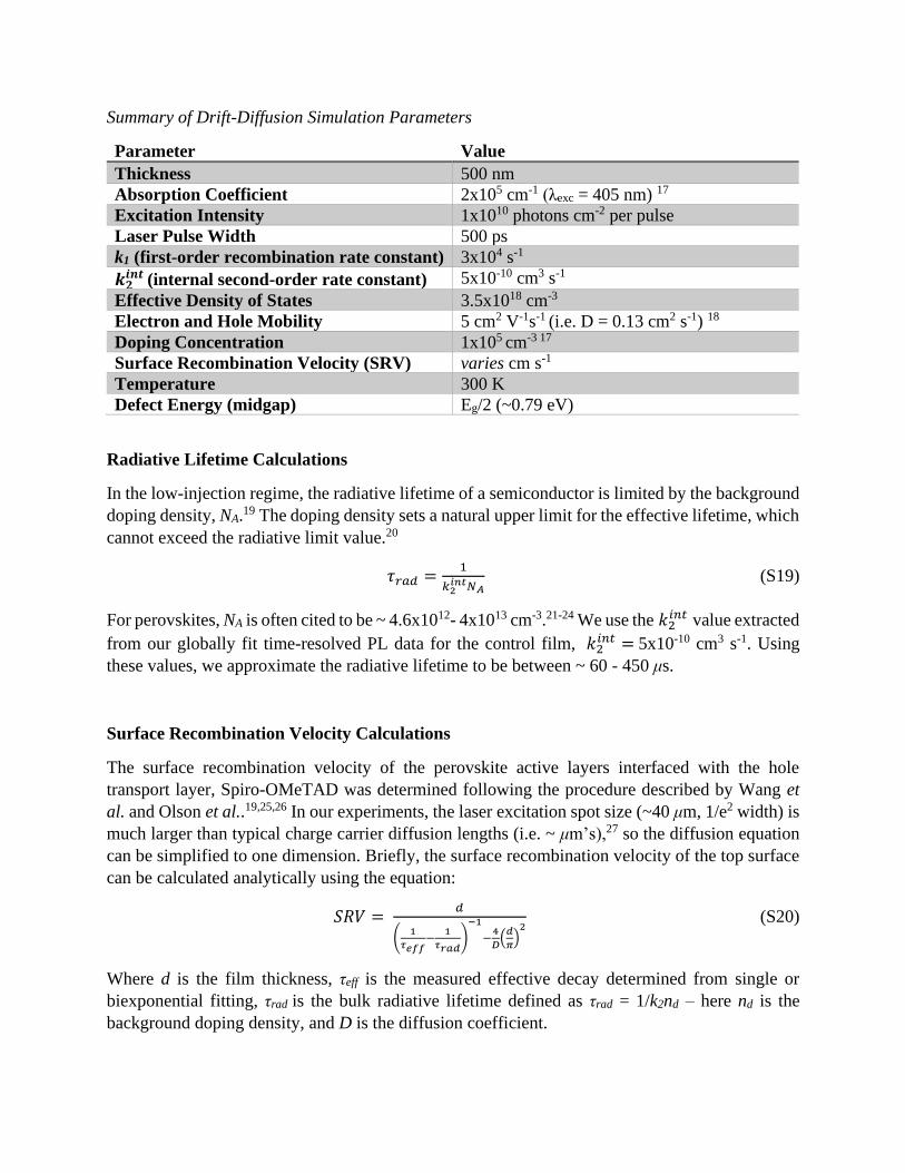
Summary of Drift-Diffusion Simulation Parameters
Parameter Value
Thickness 500 nm
Absorption Coefficient 2x105 cm-1 (λexc = 405 nm) 17
Excitation Intensity 1x10¹⁰ photons cm-2 per pulse
Laser Pulse Width 500 ps
k1 (first-order recombination rate constant) 3x10⁴ s-1
𝒌𝟐𝒊𝒏𝒕
(internal second-order rate constant) 5x10⁻¹⁰ cm3 s-1
Effective Density of States 3.5x1018 cm-3
Electron and Hole Mobility 5 cm2 V-1s-1 (i.e. D = 0.13 cm2 s-1) 18
Doping Concentration 1x105 cm-3 17
Surface Recombination Velocity (SRV) varies cm s-1
Temperature 300 K
Defect Energy (midgap) Eg/2 (~0.79 eV)
Radiative Lifetime Calculations
In the low-injection regime, the radiative lifetime of a semiconductor is limited by the background
doping density, NA.19 The doping density sets a natural upper limit for the effective lifetime, which
cannot exceed the radiative limit value.20
𝜏𝑟𝑎𝑑 =1
𝑘2𝑖𝑛𝑡𝑁𝐴
(S19)
For perovskites, NA is often cited to be ~ 4.6x10¹²- 4x1013 cm-3.21-24 We use the 𝑘2𝑖𝑛𝑡 value extracted
from our globally fit time-resolved PL data for the control film, 𝑘2𝑖𝑛𝑡 = 5x10⁻¹⁰ cm3 s-1. Using
these values, we approximate the radiative lifetime to be between ~ 60 - 450 μs.
Surface Recombination Velocity Calculations
The surface recombination velocity of the perovskite active layers interfaced with the hole
transport layer, Spiro-OMeTAD was determined following the procedure described by Wang et
al. and Olson et al..19,25,26 In our experiments, the laser excitation spot size (~40 μm, 1/e2 width) is
much larger than typical charge carrier diffusion lengths (i.e. ~ μm’s),27 so the diffusion equation
can be simplified to one dimension. Briefly, the surface recombination velocity of the top surface
can be calculated analytically using the equation:
𝑆𝑅𝑉 = 𝑑
(1
𝜏𝑒𝑓𝑓−
1
𝜏𝑟𝑎𝑑)
−1
−4
𝐷(
𝑑
𝜋)
2 (S20)
Where d is the film thickness, τeff is the measured effective decay determined from single or
biexponential fitting, τrad is the bulk radiative lifetime defined as τrad = 1/k2nd – here nd is the
background doping density, and D is the diffusion coefficient.
This assumes the bottom SRV is negligible (i.e. ~ 0), which we believe to be a valid assumption
considering passivation of just the top surface with n-trioctylphosphine oxide (TOPO) can yield
internal PLQE’s as high as 97.1%.8 The SRV values calculated using this equation are also
consistent with a slightly modified version of a similar equation described in the work of Olson et
al..19 We highlight that τrad >> τeff for most perovskite samples interfaced with a hole transport
layer, and therefore the determination of this value (and the assumption of nd) does not significantly
impact the extracted SRV values presented in the main article.
Radiative Voc and Implied Voc Calculations
We calculate the radiative open circuit voltage (𝑉𝑂𝐶𝑟𝑎𝑑) of our devices using the relation outlined
by Rau28 and the certified external quantum efficiency (EQEPV) reported in Figure S2.
𝑉𝑂𝐶𝑟𝑎𝑑 =
𝑘𝑇
𝑞𝑙𝑛 (
𝐽𝑆𝐶
𝐽0,𝑟𝑎𝑑+ 1) =
𝑘𝑇
𝑞𝑙𝑛 (
∫ 𝐸𝑄𝐸𝑃𝑉(𝐸)𝜙𝐴𝑀1.5(𝐸)𝑑𝐸
𝐸𝛾
∫ 𝐸𝑄𝐸𝑃𝑉(𝐸)𝜙𝐵𝐵(𝐸)𝑑𝐸
𝐸𝛾
+ 1) (S21)
where k is the Boltzmann constant, and T is the temperature q is the elementary charge, JSC is the
short circuit current, J0,rad is the equilibrium radiative dark saturation current, E is the photon
energy incident on the cell’s surface, 𝜙𝐴𝑀1.5 is the Air Mass 1.5, global-tilt solar irradiance
spectrum.
We obtain a 𝑉𝑂𝐶𝑟𝑎𝑑 = 1.276 V, which is similar to values calculated for other FAPbI3 based
devices.29
The quasi Fermi level splitting, which is often referred to as the implied open circuit voltage
(𝑉𝑂𝐶𝑖𝑚𝑝.
), is calculated using the following equation30:
𝑉𝑂𝐶𝑖𝑚𝑝. = 𝑉𝑂𝐶
𝑟𝑎𝑑 + 𝑘𝑇
𝑞𝑙𝑛(𝑃𝐿𝑄𝐸) (S22)
Explanation of PL Behaviour of 2D/3D Perovskite Heterostructures
Surface energy potentials induced by chemical treatment and applied biases have been shown to
significantly impact the rate of radiative recombination of InP,31-33 CdS,34 and GaAs.35 The impact
of surface treatments on the rate of radiative recombination is relatively unexplored for metal
halide perovskites, especially in the case of organic salts (i.e. HABr or PEAI) and the formation
of 2D/3D heterostructures. This understanding is critical to distribution of charge carriers through
the material stack and therefore the operation of nearly all perovskite-based optoelectronic devices.
Indeed, just from performing simple time-resolved PL decay measurements and exciting the
sample from the front and back side at different laser intensities, it is clear that the 2D/3D
heterostructure leads to unique charge carrier dynamics distinct from bare 3D films (see Figure
S19). Here we summarize the distinct behaviours and perform a set of physically-informed
numerical simulations that, for the first time, reproduce these observations:
1) Excitation from the front surface (i.e. 2D side) shows a very rapid decrease in the PL intensity
– this drop can be as large as 2 orders of magnitude (see Figures S17 and S19). This drop in
intensity is dependent on the concentration of the surface treatment (see Figure S14).
2) Excitation from the back side (i.e. 3D side) results in less of a rapid decay and instead the PL
decay can be significantly extended, relative to the control sample (see Figure S19). The extension
in PL lifetime is dependent on the concentration of the surface treatment (see Figure S14).
3) Excitation from the back side and global fitting of intensity dependent TRPL decay traces yields
an effective internal radiative recombination, 𝑘2,𝑒𝑓𝑓𝑖𝑛𝑡 , that is much lower than what is typically
observed for bare 3D films. This reduction in 𝑘2,𝑒𝑓𝑓𝑖𝑛𝑡 is observed for several different 2D/3D
systems including HABr and PEAI treated films (see Figures S3, S4, and S17).
In order to better understand 3), we perform a 1-D numerical simulation of the electron and hole
densities as a function of time and film depth. Figure S18 shows the energy level diagrams used
for the simulation. In the control case, flat bands are used, and in the treated case 100 meV and
200 meV band bending values are used. The energy grading values are defined by difference in
energy between flat band region and maximum energy of the band (i.e. difference in energy value
at a depth of 0 nm minus the value at a depth of 500 nm). For these specific simulations, we seek
to isolate how band bending and the spatial separation of electron and holes impact the PL emission
rate. Therefore, we used all the parameter values described in Table 1, but set the surface
recombination velocities for the front and back surfaces to 0 in order to remove the impact of this
term on the local electron and hole densities. In addition, the electron mobility, μe, was set to 0.23
cm2 V-1 s-1 and the hole mobility was set to 17.5 cm2 V-1 s-1 which are measured values reported
by Zhai et al. for a mixed formamidinium(FA)/methylammonium(MA) perovskite system.36 We
perform this simulation using the same parameters for Figure S18b, c, and d and only change the
shape of the energy level diagram – to isolate the impact of band bending. Figure S18 shows that
the PL intensity decreases across the film thickness with the energy gradings and especially at the
top surface where electrons are being repelled and holes accumulate.
In order to quantify the change in overall PL emission rate, we take the average PL across the
whole PL intensity map. For the flat band scenario, the average PL (PLavg.) is 1.3x10²³ photons
cm-3 s-1, for 100 meV of band bending PLavg. = 1.0x10²³ photons cm-3 s-1, and for 200 meV, PLavg.
= 2.2x10²² photons cm-3 s-1. As 𝑘2𝑖𝑛𝑡 is an intrinsic material parameter and was kept constant for
these simulations, the origin of PLavg. changing for the band bending scenarios is due to the local
product of the electron and hole densities decreasing (i.e. 𝑃𝐿 ~ 𝑘2𝑖𝑛𝑡𝑛𝑝). Although these changes
PL emission rate vary locally (see Figure S18c and d), we use the average values to quantify the
extent of electron-hole separation. These values come out as a constant, and are absorbed into an
effective recombination rate constant, 𝑘2,𝑒𝑓𝑓𝑖𝑛𝑡 . Therefore, we use the PLavg. values and their relative
ratios to quantify the impact on 𝑘2,𝑒𝑓𝑓𝑖𝑛𝑡 . We note that the reference value is 5x10⁻¹⁰ cm3s-1 for the
flat band scenario, which we extracted from global fits to the intensity-dependent TRPL of the
control sample (see Figure S3). Importantly, for the 200 meV band bending scenario, we observe
a significant reduction in the 𝑘2,𝑒𝑓𝑓𝑖𝑛𝑡 value, which matches well with 𝑘2,𝑒𝑓𝑓
𝑖𝑛𝑡 extracted from the
global fits the HABr and PEAI treated samples shown in Figures S4 and S17. We highlight that

the change in PLavg,. and hence 𝑘2,𝑒𝑓𝑓𝑖𝑛𝑡 , is highly dependent on the magnitude and shape of band
bending as well as other factors such as the electron and hole mobilities and film thickness. These
simulations therefore capture the important photophysical processes, and could be further
improved with accurate measurements of the band structure as well as electron and hole mobilities.
Next, we test the numerical model’s ability to capture observations 1) and 2). For comparison, we
measured the TRPL dynamics when photoexciting (λexc = 405 nm, 62.5 kHz, 20 nJ cm-2 per pulse,
N0 ~ 6x1014 cm-3) the front and back surfaces of a control, 10 mM HABr, and 30 mM HABr treated
samples (Figure S14a and b). We perform the same simulations for the flat band and band bending
scenarios shown in Figure S18, but incorporate a front surface recombination velocity (SRV) of
25 cm s-1 and keep the back SRV = 0 cm s-1, consistent with the top surface being the primary
source of non-radiative defects.8,37 Figure S14c, shows the presence of a fast drop in PL that
increases in magnitude with larger band bending and when the sample is excited from the front
surface. Contrarily, when the sample is excited from the back side, Figure S14d shows that the PL
lifetime becomes longer with increasing band bending. Both of these observations in the simulated
data are consistent with experimental measurements in Figure S14a and b and are a result of field-
induced spatial separation of electrons and holes.
We highlight that the magnitude of the fast PL decay feature when the sample is excited from the
front surface and the determination of 𝑘2,𝑒𝑓𝑓𝑖𝑛𝑡 when photoexciting the sample from the back side
can be used as quantitative metrics to describe the extent of band bending and electron and hole
separation. For example, a larger reduction in the PL when excited from the front side and a lower
𝑘2,𝑒𝑓𝑓𝑖𝑛𝑡 translate to larger band bending, according to our numerical model predictions. This
conclusion is consistent with higher concentrations of surface treatments leading to larger band
bending and slower radiative recombination (see Figure S14).
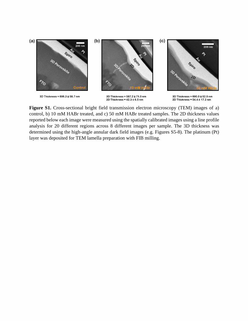
Figure S1. Cross-sectional bright field transmission electron microscopy (TEM) images of a)
control, b) 10 mM HABr treated, and c) 50 mM HABr treated samples. The 2D thickness values
reported below each image were measured using the spatially calibrated images using a line profile
analysis for 20 different regions across 8 different images per sample. The 3D thickness was
determined using the high-angle annular dark field images (e.g. Figures S5-8). The platinum (Pt)
layer was deposited for TEM lamella preparation with FIB milling.
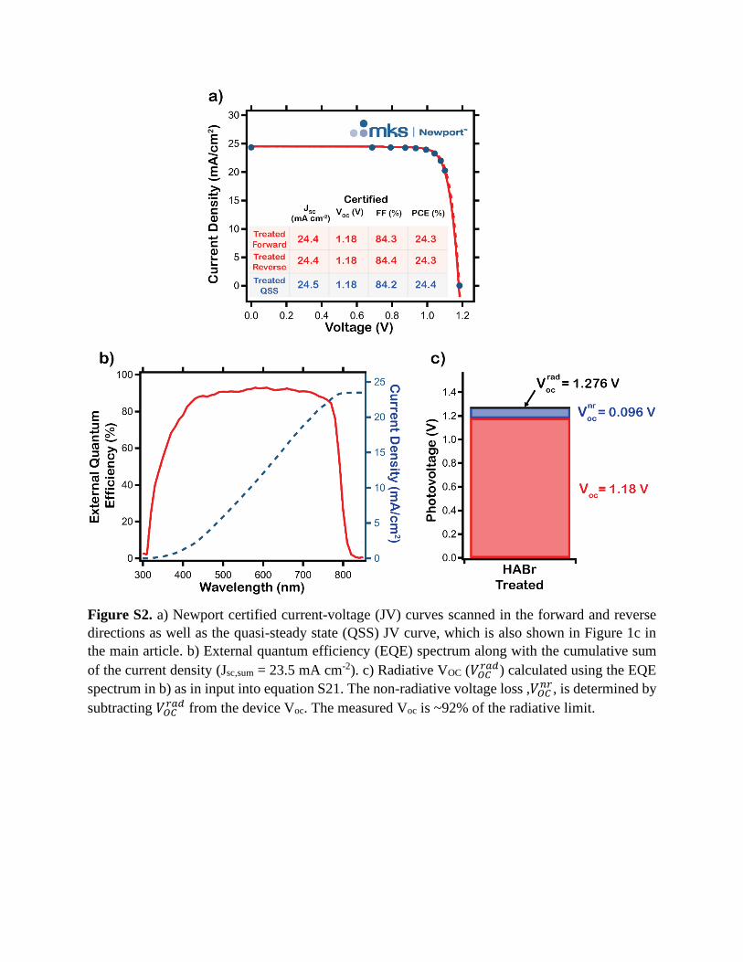
Figure S2. a) Newport certified current-voltage (JV) curves scanned in the forward and reverse
directions as well as the quasi-steady state (QSS) JV curve, which is also shown in Figure 1c in
the main article. b) External quantum efficiency (EQE) spectrum along with the cumulative sum
of the current density (Jsc,sum = 23.5 mA cm-2). c) Radiative VOC (𝑉𝑂𝐶𝑟𝑎𝑑) calculated using the EQE
spectrum in b) as in input into equation S21. The non-radiative voltage loss ,𝑉𝑂𝐶𝑛𝑟, is determined by
subtracting 𝑉𝑂𝐶𝑟𝑎𝑑 from the device Voc. The measured Voc is ~92% of the radiative limit.
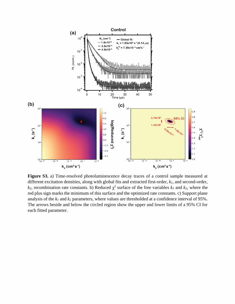
Figure S3. a) Time-resolved photoluminescence decay traces of a control sample measured at
different excitation densities, along with global fits and extracted first-order, k1, and second-order,
k2, recombination rate constants. b) Reduced χ2 surface of the free variables k1 and k2, where the
red plus sign marks the minimum of this surface and the optimized rate constants. c) Support plane
analysis of the k1 and k2 parameters, where values are thresholded at a confidence interval of 95%.
The arrows beside and below the circled region show the upper and lower limits of a 95% CI for
each fitted parameter.
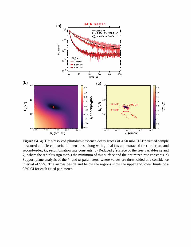
Figure S4. a) Time-resolved photoluminescence decay traces of a 50 mM HABr treated sample
measured at different excitation densities, along with global fits and extracted first-order, k1, and
second-order, k2, recombination rate constants. b) Reduced χ2surface of the free variables k1 and
k2, where the red plus sign marks the minimum of this surface and the optimized rate constants. c)
Support plane analysis of the k1 and k2 parameters, where values are thresholded at a confidence
interval of 95%. The arrows beside and below the regions show the upper and lower limits of a
95% CI for each fitted parameter.
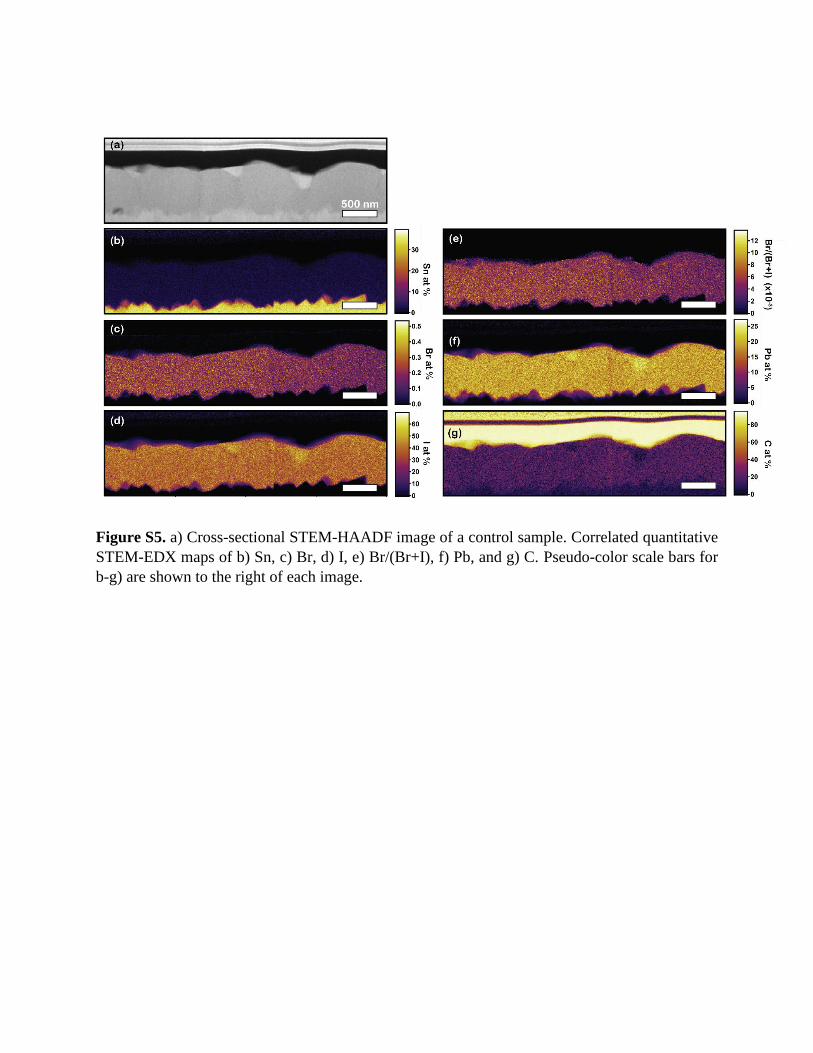
Figure S5. a) Cross-sectional STEM-HAADF image of a control sample. Correlated quantitative
STEM-EDX maps of b) Sn, c) Br, d) I, e) Br/(Br+I), f) Pb, and g) C. Pseudo-color scale bars for
b-g) are shown to the right of each image.
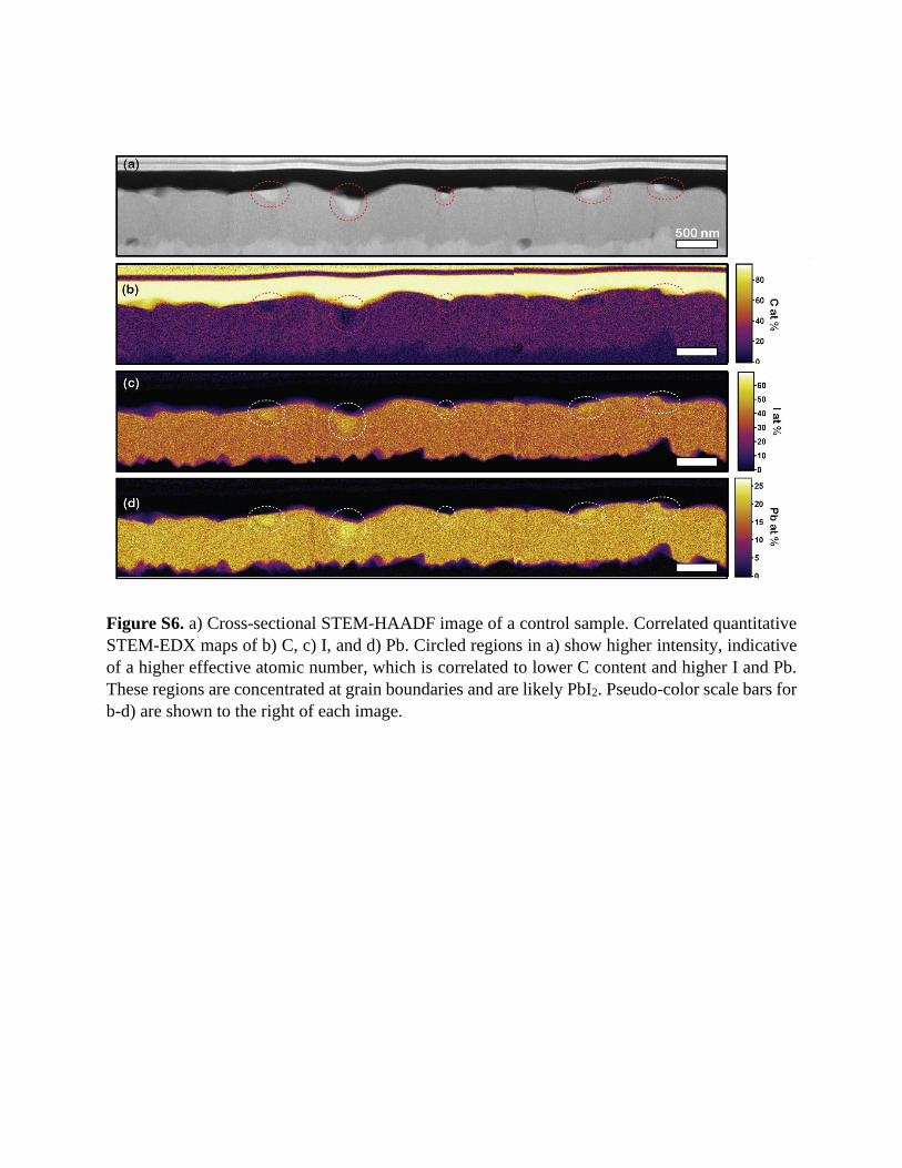
Figure S6. a) Cross-sectional STEM-HAADF image of a control sample. Correlated quantitative
STEM-EDX maps of b) C, c) I, and d) Pb. Circled regions in a) show higher intensity, indicative
of a higher effective atomic number, which is correlated to lower C content and higher I and Pb.
These regions are concentrated at grain boundaries and are likely PbI2. Pseudo-color scale bars for
b-d) are shown to the right of each image.
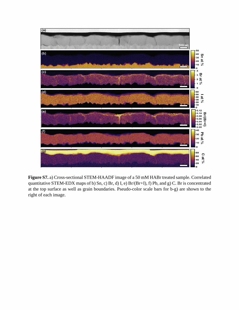
Figure S7. a) Cross-sectional STEM-HAADF image of a 50 mM HABr treated sample. Correlated
quantitative STEM-EDX maps of b) Sn, c) Br, d) I, e) Br/(Br+I), f) Pb, and g) C. Br is concentrated
at the top surface as well as grain boundaries. Pseudo-color scale bars for b-g) are shown to the
right of each image.
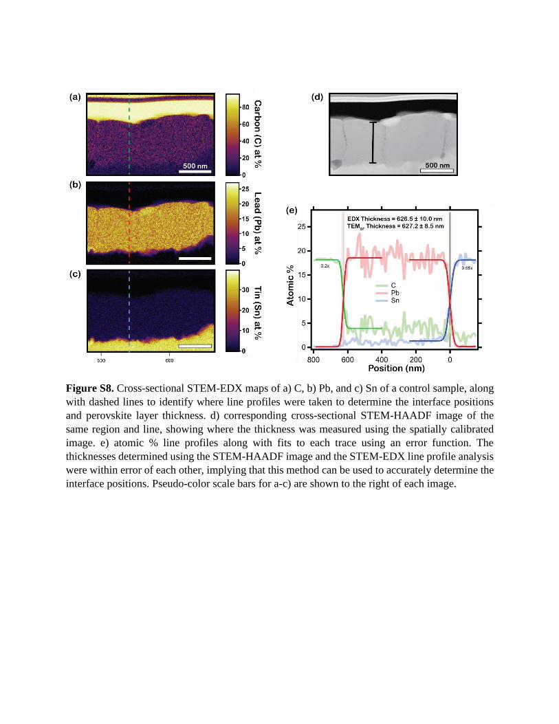
Figure S8. Cross-sectional STEM-EDX maps of a) C, b) Pb, and c) Sn of a control sample, along
with dashed lines to identify where line profiles were taken to determine the interface positions
and perovskite layer thickness. d) corresponding cross-sectional STEM-HAADF image of the
same region and line, showing where the thickness was measured using the spatially calibrated
image. e) atomic % line profiles along with fits to each trace using an error function. The
thicknesses determined using the STEM-HAADF image and the STEM-EDX line profile analysis
were within error of each other, implying that this method can be used to accurately determine the
interface positions. Pseudo-color scale bars for a-c) are shown to the right of each image.
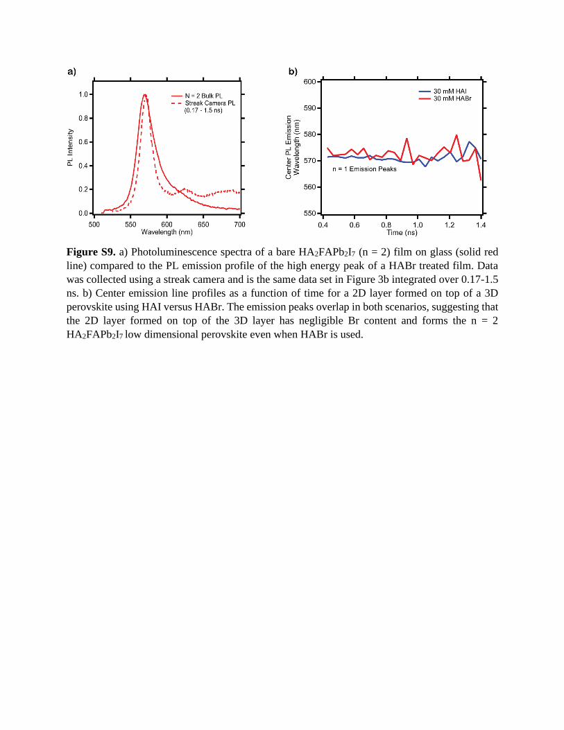
Figure S9. a) Photoluminescence spectra of a bare HA2FAPb2I7 (n = 2) film on glass (solid red
line) compared to the PL emission profile of the high energy peak of a HABr treated film. Data
was collected using a streak camera and is the same data set in Figure 3b integrated over 0.17-1.5
ns. b) Center emission line profiles as a function of time for a 2D layer formed on top of a 3D
perovskite using HAI versus HABr. The emission peaks overlap in both scenarios, suggesting that
the 2D layer formed on top of the 3D layer has negligible Br content and forms the n = 2
HA2FAPb2I7 low dimensional perovskite even when HABr is used.
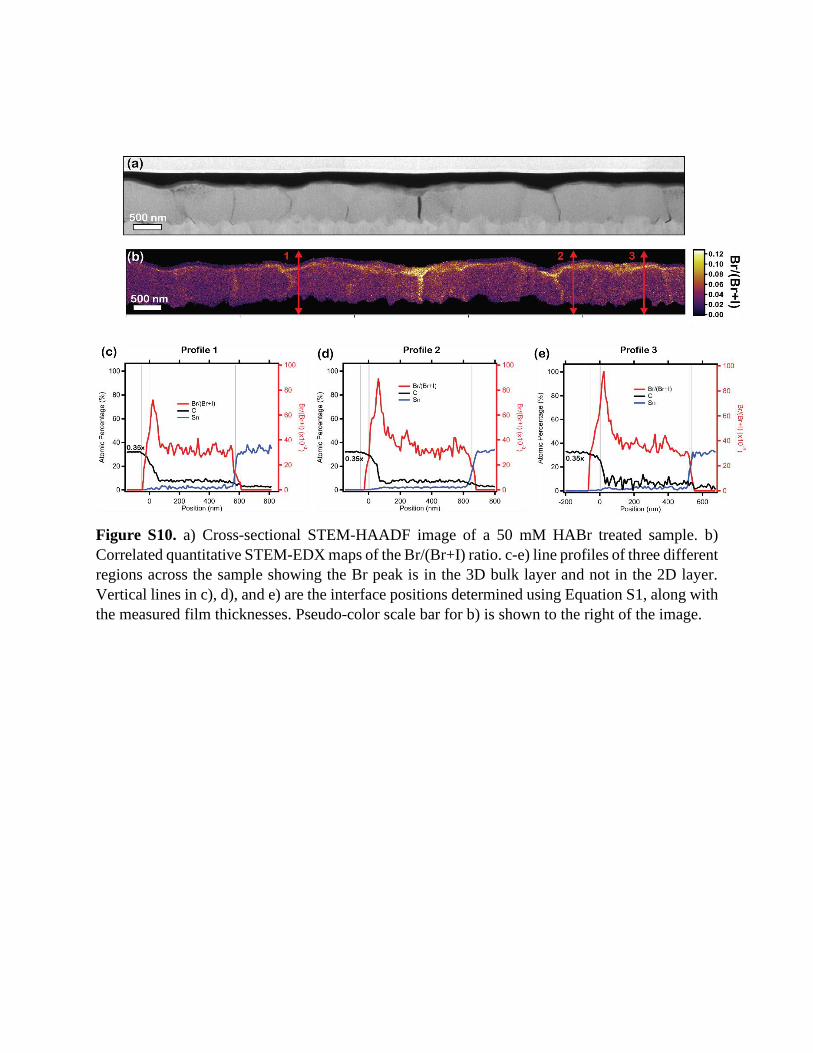
Figure S10. a) Cross-sectional STEM-HAADF image of a 50 mM HABr treated sample. b)
Correlated quantitative STEM-EDX maps of the Br/(Br+I) ratio. c-e) line profiles of three different
regions across the sample showing the Br peak is in the 3D bulk layer and not in the 2D layer.
Vertical lines in c), d), and e) are the interface positions determined using Equation S1, along with
the measured film thicknesses. Pseudo-color scale bar for b) is shown to the right of the image.
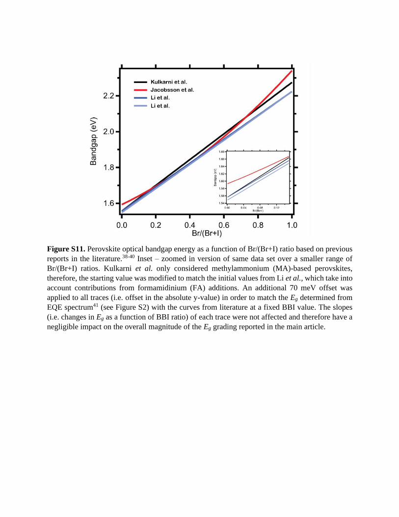
Figure S11. Perovskite optical bandgap energy as a function of Br/(Br+I) ratio based on previous
reports in the literature.38-40 Inset – zoomed in version of same data set over a smaller range of
Br/(Br+I) ratios. Kulkarni et al. only considered methylammonium (MA)-based perovskites,
therefore, the starting value was modified to match the initial values from Li et al., which take into
account contributions from formamidinium (FA) additions. An additional 70 meV offset was
applied to all traces (i.e. offset in the absolute y-value) in order to match the Eg determined from
EQE spectrum41 (see Figure S2) with the curves from literature at a fixed BBI value. The slopes
(i.e. changes in Eg as a function of BBI ratio) of each trace were not affected and therefore have a
negligible impact on the overall magnitude of the Eg grading reported in the main article.
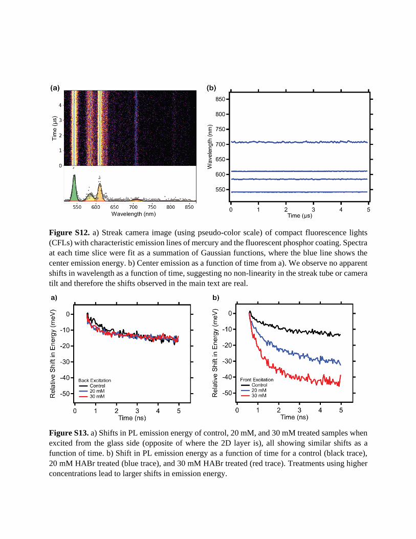
Figure S12. a) Streak camera image (using pseudo-color scale) of compact fluorescence lights
(CFLs) with characteristic emission lines of mercury and the fluorescent phosphor coating. Spectra
at each time slice were fit as a summation of Gaussian functions, where the blue line shows the
center emission energy. b) Center emission as a function of time from a). We observe no apparent
shifts in wavelength as a function of time, suggesting no non-linearity in the streak tube or camera
tilt and therefore the shifts observed in the main text are real.
Figure S13. a) Shifts in PL emission energy of control, 20 mM, and 30 mM treated samples when
excited from the glass side (opposite of where the 2D layer is), all showing similar shifts as a
function of time. b) Shift in PL emission energy as a function of time for a control (black trace),
20 mM HABr treated (blue trace), and 30 mM HABr treated (red trace). Treatments using higher
concentrations lead to larger shifts in emission energy.
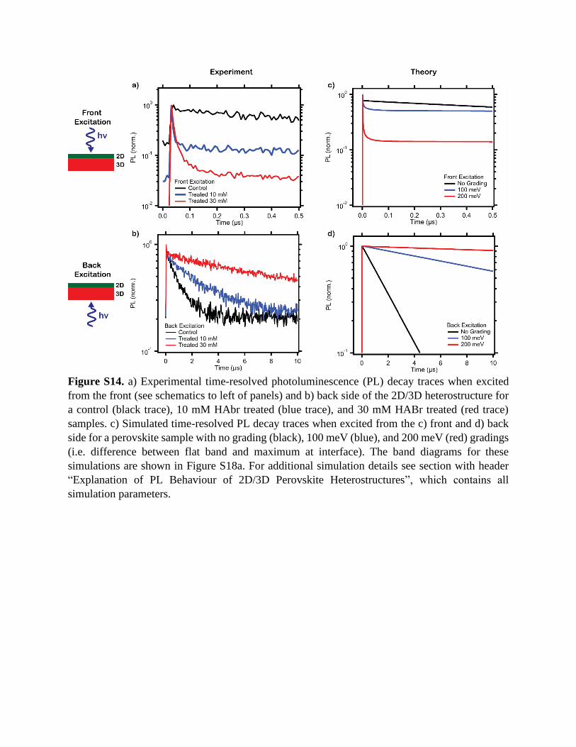
Figure S14. a) Experimental time-resolved photoluminescence (PL) decay traces when excited
from the front (see schematics to left of panels) and b) back side of the 2D/3D heterostructure for
a control (black trace), 10 mM HAbr treated (blue trace), and 30 mM HABr treated (red trace)
samples. c) Simulated time-resolved PL decay traces when excited from the c) front and d) back
side for a perovskite sample with no grading (black), 100 meV (blue), and 200 meV (red) gradings
(i.e. difference between flat band and maximum at interface). The band diagrams for these
simulations are shown in Figure S18a. For additional simulation details see section with header
“Explanation of PL Behaviour of 2D/3D Perovskite Heterostructures”, which contains all
simulation parameters.
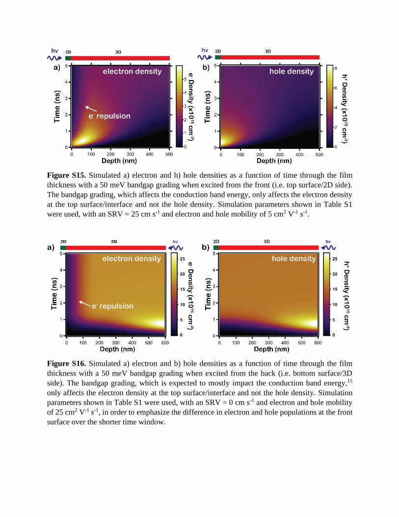
Figure S15. Simulated a) electron and b) hole densities as a function of time through the film
thickness with a 50 meV bandgap grading when excited from the front (i.e. top surface/2D side).
The bandgap grading, which affects the conduction band energy, only affects the electron density
at the top surface/interface and not the hole density. Simulation parameters shown in Table S1
were used, with an SRV = 25 cm s-1 and electron and hole mobility of 5 cm2 V-1 s-1.
Figure S16. Simulated a) electron and b) hole densities as a function of time through the film
thickness with a 50 meV bandgap grading when excited from the back (i.e. bottom surface/3D
side). The bandgap grading, which is expected to mostly impact the conduction band energy,15
only affects the electron density at the top surface/interface and not the hole density. Simulation
parameters shown in Table S1 were used, with an SRV = 0 cm s-1 and electron and hole mobility
of 25 cm2 V-1 s-1, in order to emphasize the difference in electron and hole populations at the front
surface over the shorter time window.
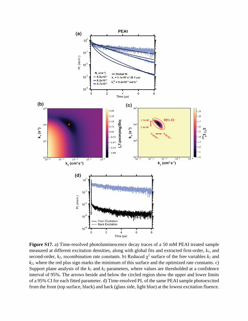
Figure S17. a) Time-resolved photoluminescence decay traces of a 50 mM PEAI treated sample
measured at different excitation densities, along with global fits and extracted first-order, k1, and
second-order, k2, recombination rate constants. b) Reduced χ2 surface of the free variables k1 and
k2, where the red plus sign marks the minimum of this surface and the optimized rate constants. c)
Support plane analysis of the k1 and k2 parameters, where values are thresholded at a confidence
interval of 95%. The arrows beside and below the circled region show the upper and lower limits
of a 95% CI for each fitted parameter. d) Time-resolved PL of the same PEAI sample photoexcited
from the front (top surface, black) and back (glass side, light blue) at the lowest excitation fluence.
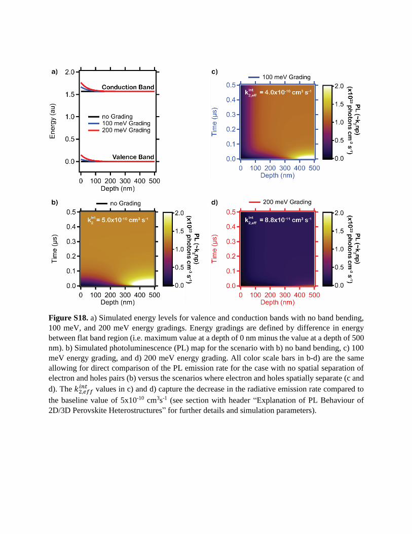
Figure S18. a) Simulated energy levels for valence and conduction bands with no band bending,
100 meV, and 200 meV energy gradings. Energy gradings are defined by difference in energy
between flat band region (i.e. maximum value at a depth of 0 nm minus the value at a depth of 500
nm). b) Simulated photoluminescence (PL) map for the scenario with b) no band bending, c) 100
meV energy grading, and d) 200 meV energy grading. All color scale bars in b-d) are the same
allowing for direct comparison of the PL emission rate for the case with no spatial separation of
electron and holes pairs (b) versus the scenarios where electron and holes spatially separate (c and
d). The 𝑘2,𝑒𝑓𝑓𝑖𝑛𝑡 values in c) and d) capture the decrease in the radiative emission rate compared to
the baseline value of 5x10⁻¹⁰ cm3s-1 (see section with header “Explanation of PL Behaviour of
2D/3D Perovskite Heterostructures” for further details and simulation parameters).
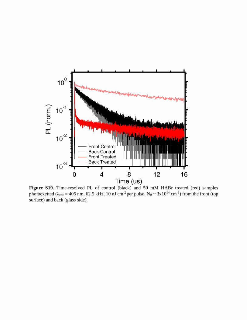
Figure S19. Time-resolved PL of control (black) and 50 mM HABr treated (red) samples
photoexcited (λexc = 405 nm, 62.5 kHz, 10 nJ cm-2 per pulse, N0 ~ 3x1014 cm-3) from the front (top
surface) and back (glass side).
References
(1) Yoo, J. J.; Seo, G.; Chua, M. R.; Park, T. G.; Lu, Y.; Rotermund, F.; Kim, Y. K.;
Moon, C. S.; Jeon, N. J.; Correa-Baena, J. P.; Bulovic, V.; Shin, S. S.; Bawendi, M. G.; Seo, J.
Efficient perovskite solar cells via improved carrier management. Nature 2021, 590, 587-593.
(2) Kosasih, F. U.; Cacovich, S.; Divitini, G.; Ducati, C. Nanometric Chemical
Analysis of Beam‐Sensitive Materials: A Case Study of STEM‐EDX on Perovskite Solar Cells.
Small Methods 2020, 5.
(3) Rothmann, M. U.; Li, W.; Zhu, Y.; Liu, A.; Ku, Z.; Bach, U.; Etheridge, J.; Cheng,
Y. B. Structural and Chemical Changes to CH3 NH3 PbI3 Induced by Electron and Gallium Ion
Beams. Adv. Mater. 2018, 30, e1800629.
(4) de la Peña, F.; Prestat, E.; Fauske, V. T.; Burdet, P.; Furnival, T.; Jokubauskas, P.;
Nord, M.; Ostasevicius, T.; MacArthur, K. E.; Johnstone, D. N.; Sarahan, M.; Lähnemann, J.;
Taillon, J.; Aarholt, T.; Migunov, V.; Eljarrat, A.; Caron, J.; Mazzucco, S.; Martineau, B.;
Somnath, S.; Poon, T.; Walls, M.; Slater, T.; Tappy, N.; Cautaerts, N.; Winkler, F.; Donval, G.;
Myers, J. C. Hyperspy v1.6.1. Zenodo 2020.
(5) Cacovich, S.; Matteocci, F.; Abdi-Jalebi, M.; Stranks, S. D.; Di Carlo, A.; Ducati,
C.; Divitini, G. Unveiling the Chemical Composition of Halide Perovskite Films Using
Multivariate Statistical Analyses. ACS Appl. Energy Mater. 2018, 1, 7174-7181.
(6) Pearson, K. LIII. On lines and planes of closest fit to systems of points in space.
The London, Edinburgh, and Dublin Philosophical Magazine and Journal of Science 2010, 2, 559-
572.
(7) Cliff, G.; Lorimer, G. W. The quantitative analysis of thin specimens. J. Microsc.
1975, 103, 203-207.
(8) Braly, I. L.; deQuilettes, D. W.; Pazos-Outón, L. M.; Burke, S.; Ziffer, M. E.;
Ginger, D. S.; Hillhouse, H. W. Hybrid perovskite films approaching the radiative limit with over
90% photoluminescence quantum efficiency. Nat. Photon. 2018, 12, 355-361.
(9) de Mello, J. C.; Wittmann, H. F.; Friend, R. H. An improved experimental
determination of external photoluminescence quantum efficiency. Adv. Mater. 1997, 9, 230-232.
(10) Wolff, C. M.; Bourelle, S. A.; Phuong, L. Q.; Kurpiers, J.; Feldmann, S.;
Caprioglio, P.; Marquez, J. A.; Wolansky, J.; Unold, T.; Stolterfoht, M.; Shoaee, S.; Deschler, F.;
Neher, D. Orders of Recombination in Complete Perovskite Solar Cells – Linking Time‐Resolved
and Steady‐State Measurements. Adv. Energy Mater. 2021, 11.
(11) deQuilettes, D. W.; Frohna, K.; Emin, D.; Kirchartz, T.; Bulovic, V.; Ginger, D. S.;
Stranks, S. D. Charge-Carrier Recombination in Halide Perovskites. Chem. Rev. 2019, 119, 11007-
11019.
(12) Herz, L. M. Charge-Carrier Dynamics in Organic-Inorganic Metal Halide
Perovskites. Annu. Rev. Phys. Chem. 2016, 67, 65-89.
(13) PicoQuant. FluoFit: Global Fluorescence Decay Data Analysis Software - User's
Manual and Technical Data Ver. 4.2. 2018, 35-36.
(14) Weiss, T. P.; Bissig, B.; Feurer, T.; Carron, R.; Buecheler, S.; Tiwari, A. N. Bulk
and surface recombination properties in thin film semiconductors with different surface treatments
from time-resolved photoluminescence measurements. Sci. Rep. 2019, 9, 5385.
(15) Cho, K. T.; Paek, S.; Grancini, G.; Roldán-Carmona, C.; Gao, P.; Lee, Y.;
Nazeeruddin, M. K. Highly efficient perovskite solar cells with a compositionally engineered
perovskite/hole transporting material interface. Energy Environ. Sci. 2017, 10, 621-627.
(16) Aberle, A. G.; Glunz, S.; Warta, W. Impact of illumination level and oxide
parameters on Shockley–Read–Hall recombination at the Si‐SiO2interface. J. Appl. Phys. 1992,
71, 4422-4431.
(17) Brenes, R.; Laitz, M.; Jean, J.; deQuilettes, D. W.; Bulović, V. Benefit from Photon
Recycling at the Maximum-Power Point of State-of-the-Art Perovskite Solar Cells. Phys. Rev.
Appl. 2019, 12.
(18) deQuilettes, D. W.; Brenes, R.; Laitz, M.; Motes, B. T.; Glazov, M. M.; Bulović,
V. Impact of Photon Recycling, Grain Boundaries, and Nonlinear Recombination on Energy
Transport in Semiconductors. ACS Photonics 2021.
(19) Olson, J. M.; Ahrenkiel, R. K.; Dunlavy, D. J.; Keyes, B.; Kibbler, A. E. Ultralow
recombination velocity at Ga0.5In0.5P/GaAs heterointerfaces. Appl. Phys. Lett. 1989, 55, 1208-
1210.
(20) Kirchartz, T. High open-circuit voltages in lead-halide perovskite solar cells:
experiment, theory and open questions. Phil. Trans. R. Soc. A 2019, 377, 20180286.
(21) Chen, Y.; Yi, H. T.; Wu, X.; Haroldson, R.; Gartstein, Y. N.; Rodionov, Y. I.;
Tikhonov, K. S.; Zakhidov, A.; Zhu, X. Y.; Podzorov, V. Extended carrier lifetimes and diffusion
in hybrid perovskites revealed by Hall effect and photoconductivity measurements. Nat. Commun.
2016, 7, 12253.
(22) Euvrard, J.; Gunawan, O.; Zhong, X.; Harvey, S. P.; Kahn, A.; Mitzi, D. B. p-Type
molecular doping by charge transfer in halide perovskite. Mater. Adv. 2021, 2, 2956-2965.
(23) Lin, Y.; Shao, Y.; Dai, J.; Li, T.; Liu, Y.; Dai, X.; Xiao, X.; Deng, Y.; Gruverman,
A.; Zeng, X. C.; Huang, J. Metallic surface doping of metal halide perovskites. Nat. Commun.
2021, 12, 7.
(24) Gutierrez-Partida, E.; Hempel, H.; Caicedo-Dávila, S.; Raoufi, M.; Peña-Camargo,
F.; Grischek, M.; Gunder, R.; Diekmann, J.; Caprioglio, P.; Brinkmann, K. O.; Köbler, H.;
Albrecht, S.; Riedl, T.; Abate, A.; Abou-Ras, D.; Unold, T.; Neher, D.; Stolterfoht, M. Large-
Grain Double Cation Perovskites with 18 μs Lifetime and High Luminescence Yield for Efficient
Inverted Perovskite Solar Cells. ACS Energy Lett. 2021, 6, 1045-1054.
(25) Sproul, A. B. Dimensionless solution of the equation describing the effect of
surface recombination on carrier decay in semiconductors. J. Appl. Phys. 1994, 76, 2851-2854.
(26) Wang, J.; Fu, W.; Jariwala, S.; Sinha, I.; Jen, A. K. Y.; Ginger, D. S. Reducing
Surface Recombination Velocities at the Electrical Contacts Will Improve Perovskite
Photovoltaics. ACS Energy Lett. 2018, 4, 222-227.
(27) Saidaminov, M. I.; Williams, K.; Wei, M.; Johnston, A.; Quintero-Bermudez, R.;
Vafaie, M.; Pina, J. M.; Proppe, A. H.; Hou, Y.; Walters, G.; Kelley, S. O.; Tisdale, W. A.; Sargent,
E. H. Multi-cation perovskites prevent carrier reflection from grain surfaces. Nat. Mater. 2020, 19,
412-418.
(28) Rau, U. Reciprocity relation between photovoltaic quantum efficiency and
electroluminescent emission of solar cells. Phys. Rev. B 2007, 76.
(29) Jiang, Q.; Zhao, Y.; Zhang, X.; Yang, X.; Chen, Y.; Chu, Z.; Ye, Q.; Li, X.; Yin,
Z.; You, J. Surface passivation of perovskite film for efficient solar cells. Nat. Photon. 2019, 13,
460-466.
(30) Liu, Z.; Krückemeier, L.; Krogmeier, B.; Klingebiel, B.; Márquez, J. A.; Levcenko,
S.; Öz, S.; Mathur, S.; Rau, U.; Unold, T.; Kirchartz, T. Open-Circuit Voltages Exceeding 1.26 V
in Planar Methylammonium Lead Iodide Perovskite Solar Cells. ACS Energy Lett. 2018, 4, 110-
117.
(31) Street, R. A.; Williams, R. H.; Bauer, R. S. Influence of the surface on
photoluminescence from indium phosphide crystals. J. Vac. Sci. Technol. 1980, 17, 1001-1004.
(32) Hollingsworth, R. E.; Sites, J. R. Photoluminescence dead layer inp‐type InP. J.
Appl. Phys. 1982, 53, 5357-5358.
(33) Ando, K.; Yamamoto, A.; Yamaguchi, M. Bias‐dependent photoluminescence
intensities inn‐InP Schottky diodes. J. Appl. Phys. 1980, 51, 6432-6434.
(34) Hetrick, R. E.; Yeung, K. F. Effect of Surface Electric Fields on Radiative
Recombination in CdS. J. Appl. Phys. 1971, 42, 2882-2885.
(35) Langmann, U. Photoluminescence ofn-GaAs at transparent Schottky contacts.
Appl. Phys. 1973, 1, 219-221.
(36) Zhai, Y.; Wang, K.; Zhang, F.; Xiao, C.; Rose, A. H.; Zhu, K.; Beard, M. C.
Individual Electron and Hole Mobilities in Lead-Halide Perovskites Revealed by Noncontact
Methods. ACS Energy Lett. 2019, 5, 47-55.
(37) deQuilettes, D. W.; Koch, S.; Burke, S.; Paranji, R. K.; Shropshire, A. J.; Ziffer, M.
E.; Ginger, D. S. Photoluminescence Lifetimes Exceeding 8 μs and Quantum Yields Exceeding
30% in Hybrid Perovskite Thin Films by Ligand Passivation. ACS Energy Lett. 2016, 1, 438-444.
(38) Jesper Jacobsson, T.; Correa-Baena, J.-P.; Pazoki, M.; Saliba, M.; Schenk, K.;
Grätzel, M.; Hagfeldt, A. Exploration of the compositional space for mixed lead halogen
perovskites for high efficiency solar cells. Energy Environ. Sci. 2016, 9, 1706-1724.
(39) Kulkarni, S. A.; Baikie, T.; Boix, P. P.; Yantara, N.; Mathews, N.; Mhaisalkar, S.
Band-gap tuning of lead halide perovskites using a sequential deposition process. J. Mater. Chem.
A 2014, 2, 9221-9225.
(40) Li, Y.; Lu, Y.; Huo, X.; Wei, D.; Meng, J.; Dong, J.; Qiao, B.; Zhao, S.; Xu, Z.;
Song, D. Bandgap tuning strategy by cations and halide ions of lead halide perovskites learned
from machine learning. RSC Adv. 2021, 11, 15688-15694.
(41) Krückemeier, L.; Rau, U.; Stolterfoht, M.; Kirchartz, T. How to Report Record
Open‐Circuit Voltages in Lead‐Halide Perovskite Solar Cells. Adv. Energy Mater. 2019, 10.
Related Documents