1. General description The UCODE HSL IC, SL3ICS3001 (UCODE High frequency Smart Label) is a dedicated chip for passive smart tags and labels, especially for supply chain management and logistics applications in the US, where operating distances of several meters can be realized. Further, the UCODE HSL technology platform is also designed for operation under European regulations. This integrated circuit is the first member of a product family of smart label ICs targeted to be compliant with the future ISO standards 18000-4 and 18000-6 for item management. The UCODE HSL system offers the possibility of operating labels simultaneously in the field of the interrogator antenna (Anticollision, Collision Arbitration). The UCODE HSL family of ICs is especially designed for long range applications. The tag requires no internal power supply. Its contactless interface generates the power supply via the antenna circuit by propagative energy transmission from the interrogator (read/write device), while the system clock is generated by an on-board oscillator. The contactless interface demodulates data transmitted from the interrogator to the UCODE HSL based tag, and further modulates the electromagnetic field provided by the interrogator for data transmission from the UCODE HSL based tag to the interrogator. A generic RFID system consists of an interrogator (base station) that runs the RFID protocol, as well as one or more tags. The tag itself includes an SL3ICS3001 chip and an antenna tuned to the carrier frequency of the interrogator, and a package to hold the chip and antenna together. When placed in the RF field of an interrogator, a SL3ICS3001 based tag will begin to power up. If the field is strong enough, the tag IC will execute a power-on reset and will be ready to receive commands. Each command begins with a preamble and start delimiter that, taken together, enable the tag to perform clock and data recovery on the incoming signal. Data to and from the tag is checked for errors using a CRC. Therefore, CRC fields are present in all interrogator commands and in all tag responses. Additional data protection is provided by Manchester encoding on the forward (interrogator to tag) link and FM0 encoding on the return (tag to interrogator) link. The interrogator can perform a number of functions on tags in its field. For example, the interrogator can send a command sequence, which allows it to identify multiple tags in its RF field simultaneously. Alternatively, it can select a subset of the tags in the field based on tag memory contents. It can also read data stored on a tag in its field, as well as write data to such a tag. In addition, it can simultaneously write data to an arbitrary subset of the tags in the field. SL3ICS3001 UCODE HSL Rev. 3.1 — 9 July 2012 072831 Product data sheet COMPANY PUBLIC

Welcome message from author
This document is posted to help you gain knowledge. Please leave a comment to let me know what you think about it! Share it to your friends and learn new things together.
Transcript

1. General description
The UCODE HSL IC, SL3ICS3001 (UCODE High frequency Smart Label) is a dedicated chip for passive smart tags and labels, especially for supply chain management and logistics applications in the US, where operating distances of several meters can be realized. Further, the UCODE HSL technology platform is also designed for operation under European regulations.
This integrated circuit is the first member of a product family of smart label ICs targeted to be compliant with the future ISO standards 18000-4 and 18000-6 for item management.
The UCODE HSL system offers the possibility of operating labels simultaneously in the field of the interrogator antenna (Anticollision, Collision Arbitration).
The UCODE HSL family of ICs is especially designed for long range applications.
The tag requires no internal power supply. Its contactless interface generates the power supply via the antenna circuit by propagative energy transmission from the interrogator (read/write device), while the system clock is generated by an on-board oscillator. The contactless interface demodulates data transmitted from the interrogator to the UCODE HSL based tag, and further modulates the electromagnetic field provided by the interrogator for data transmission from the UCODE HSL based tag to the interrogator.
A generic RFID system consists of an interrogator (base station) that runs the RFID protocol, as well as one or more tags. The tag itself includes an SL3ICS3001 chip and an antenna tuned to the carrier frequency of the interrogator, and a package to hold the chip and antenna together.
When placed in the RF field of an interrogator, a SL3ICS3001 based tag will begin to power up. If the field is strong enough, the tag IC will execute a power-on reset and will be ready to receive commands. Each command begins with a preamble and start delimiter that, taken together, enable the tag to perform clock and data recovery on the incoming signal. Data to and from the tag is checked for errors using a CRC. Therefore, CRC fields are present in all interrogator commands and in all tag responses. Additional data protection is provided by Manchester encoding on the forward (interrogator to tag) link and FM0 encoding on the return (tag to interrogator) link.
The interrogator can perform a number of functions on tags in its field. For example, the interrogator can send a command sequence, which allows it to identify multiple tags in its RF field simultaneously. Alternatively, it can select a subset of the tags in the field based on tag memory contents. It can also read data stored on a tag in its field, as well as write data to such a tag. In addition, it can simultaneously write data to an arbitrary subset of the tags in the field.
SL3ICS3001UCODE HSLRev. 3.1 — 9 July 2012072831
Product data sheetCOMPANY PUBLIC
NXP Semiconductors SL3ICS3001UCODE HSL
Signals enter the chip through the RF front end, where both tag power and the modulation envelope are recovered. Tag power is regulated and bias voltages are generated in one part of the analog section. In another part of the analog section, the modulation envelope is applied to a clock and data recovery circuit. In the case of a valid command, the first part of the input signal is the preamble and start delimiter, which will be followed by a specific tag command and any additional fields that command may require. All valid digital data is processed in the digital section data path, which is controlled by the digital control module. If a read or write is to be executed, the EEPROM block will be accessed. If data is to be sent from the tag to the interrogator in response to the command, the digital section sends the output pattern back to the RF front end, where the impedance modulation that constitutes backscatter is executed.
2. Features and benefits
2.1 RF interface features
Contactless transmission of data and supply energy (no battery needed)
Operating distance, depending on antenna geometry and local regulations, up to 8.4 m for a single antenna
Operating frequency within the released operating bands from 860 MHz to 960 MHz and from 2.4 GHz to 2.5 GHz
High data integrity: 16 bit CRC, framing
True anticollision for collision arbitration
Write distance is 70% of reading distance
2.2 Memory features
2048 bits including lock bits
64 bits UID in memory bytes 0 to 7
216 bytes with user definable access conditions for memory bytes 8 to 223
2.3 Security features
Unique serial number for each device
Lock mechanism (write protection) for each byte
2.4 Operating distances features
RFID tags based on the SL3ICS3001 silicon may achieve operating distances according the following formula:
PTAG ... minimum required RF power for the tag
GTAG ... Gain of the tag antenna
EIRP ... Transmitted RF power
... wavelength
Ptag EIRP Gtag
4R---------- 2
=
SL3ICS3001_072831 All information provided in this document is subject to legal disclaimers. © NXP B.V. 2012. All rights reserved.
Product data sheetCOMPANY PUBLIC
Rev. 3.1 — 9 July 2012072831 2 of 54
NXP Semiconductors SL3ICS3001UCODE HSL
Rmax ... maximum achieved operating distance for a lossless, matched /2-dipole.
The maximum write distance is around 70% of the read distance.
[1] Current CEPT/ETSI regulations [CEPT1], [ETSI1].
[2] Proposal for future CEPT/ETSI regulations.
[3] FCC regulation [FCC1].
[4] In many other countries regulations either similar to FCC or CEPT/ETSI may apply.
[5] Current CEPT/ETSI regulations [CEPT2], [ETSI2].
[6] FCC regulation [FCC1].
[7] In many other countries regulations either similar to FCC or CEPT/ETSI may apply.
[8] These distances are typical values for general tags and labels. A special tag antenna design or reflection could achieve higher values.
[9] Practical usable read distance values may be notable lower, strongly depending on application set-up, damping by environment materials and the quality of the matching between tag antenna and chip impedance.
The maximum write distance is around 70% of the read distance.
Table 1. Operating distances for UCODE HSL based tags and labels in released frequency bands
Frequency range Region Available power Calculated read distance single antenna[8][9]
Unit
868.4 to 868.65 MHz (UHF) Europe [1] 0.5 W ERP 4.0 m
865.5 to 867.6 MHz (UHF) Europe [2] 2 W ERP 8.0 m
902 to 928 MHz (UHF) America [3] 4 W EIRP 8.4 m
860 to 930 MHz (UHF) Others [4] m
2.400 GHz to 2.4835 GHz Europe [5] 0.5 W EIRP outdoor
0.6 m
2.400 GHz to 2.4835 GHz Europe [5] 4 W EIRP indoor 1.8 m
2.400 GHz to 2.4835 GHz America [6] 4 W EIRP 1.8 m
2.400 GHz to 2.4835 GHz Others [7] m
Rmax
EIRP GTAG 2
4 2 PTAG-------------------------------------------=
SL3ICS3001_072831 All information provided in this document is subject to legal disclaimers. © NXP B.V. 2012. All rights reserved.
Product data sheetCOMPANY PUBLIC
Rev. 3.1 — 9 July 2012072831 3 of 54
NXP Semiconductors SL3ICS3001UCODE HSL
2.5 Air interface standards
The SL3ICS30 is fully supporting standardization on air interfaces. The SL3ICS30 is targeted to be compliant with the following air interfaces:
ISO 18000-4
Information Technology - Radio Frequency Identification (RFID) for Item Management - Part 4: Parameters for Air Interface Communications at 2.45 GHz
ISO 18000-6
Information Technology - Radio Frequency Identification (RFID) for Item Management - Part 6: Parameters for Air Interface Communications at 860 - 930 MHz
ANSI/INCITS 256-2001
Radio Frequency Identification (RFID) Part 3 - 2.45 GHz
ANSI/INCITS 256-2001
Radio Frequency Identification (RFID) Part 4 - UHF
2.6 Application standards
The SL3ICS30 is also fully supporting application standardization. The SL3ICS30 is targeted to be compliant with the following application standards:
MH10.8.4
Radio Frequency Identification for Returnable Containers and Cable Reels
AIAG B-11
Automotive Tire and Wheel Label Radio Frequency (RFID) Identification Standard
EAN.UCC GTAGTM
Global tag initiative
ISO 18185
Freight Containers - Radio-frequency communication protocol for electronic seal
3. Applications
Asset management
Supply chain management
Item level tagging
Container identification
Pallet and case tracking
Product authentication
Windshield tagging
4. Ordering information
Table 2. Ordering information
Type number Package
Name Description Version
SL3ICS3001FW/V7 Wafer Bumped die on sawn wafer -
SL3ICS3001_072831 All information provided in this document is subject to legal disclaimers. © NXP B.V. 2012. All rights reserved.
Product data sheetCOMPANY PUBLIC
Rev. 3.1 — 9 July 2012072831 4 of 54
NXP Semiconductors SL3ICS3001UCODE HSL
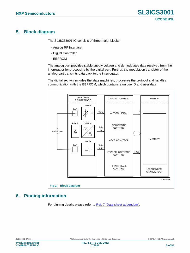
5. Block diagram
The SL3ICS3001 IC consists of three major blocks:
- Analog RF Interface
- Digital Controller
- EEPROM
The analog part provides stable supply voltage and demodulates data received from the interrogator for processing by the digital part. Further, the modulation transistor of the analog part transmits data back to the interrogator.
The digital section includes the state machines, processes the protocol and handles communication with the EEPROM, which contains a unique ID and user data.
6. Pinning information
For pinning details please refer to Ref. 7 “Data sheet addendum”.
Fig 1. Block diagram
001aai335
MOD
DEMOD
VREG
VDD
datain
dataout
R/W
ANALOGUERF INTERFACE
PAD
PAD
RECT
DIGITAL CONTROL
ANTENNA
ANTICOLLISION
READ/WRITECONTROL
ACCES CONTROL
EEPROM INTERFACECONTROL
RF INTERFACECONTROL
EEPROM
MEMORY
SEQUENCERCHARGE PUMP
SL3ICS3001_072831 All information provided in this document is subject to legal disclaimers. © NXP B.V. 2012. All rights reserved.
Product data sheetCOMPANY PUBLIC
Rev. 3.1 — 9 July 2012072831 5 of 54
NXP Semiconductors SL3ICS3001UCODE HSL
7. Functional description
7.1 Power transfer
The interrogator provides a RF field that powers the tag containing the SL3ICS3001 and an antenna. The tag antenna transforms the impedance of free space to the chip input impedance in order to get the maximum possible power for the SL3ICS3001 on the tag.
The RF field, which is oscillating on the operating frequency provided by the interrogator, is rectified to provide smoothed DC voltage to the analog and digital modules of the IC.
The antenna that is attached to the chip has to support the rectifier structure on the chip by having no short circuit between the two antenna connectors (e.g. simple dipole structure). There will appear a DC voltage on the chip inputs during chip operation.
The RF field has to be turned on whenever the tag should operate. This also includes response time (backscatter) and the EEPROM programming process.
7.2 Operation frequency
The SL3ICS3001 supports global operation in different frequency bands. In principle, the SL3ICS3001 has no restriction on the operating frequency. Based on regulation requirements the SL3ICS3001 is released for the following frequency bands.
7.3 Data transfer
7.3.1 Forward link
The SL3ICS3001 supports Manchester Code amplitude modulation. For data transmission, the interrogator switches between two values of emitted power.
Details are described in Section 9.
7.3.2 Return link
As the energy of the RF field is used and required for operation, the tag communicates back to the interrogator by changing its load to the RF field. For high frequencies, the behaviour of the RF field (electromagnetic field) may be described by travelling waves. Therefore, this method is called backscatter.
Details are described in Section 9.
Table 3. Released operating frequency bands
Frequency band Limit Unit
Lower Upper
UHF 860 960 MHz
2.45 GHz 2.4 2.5 GHz
SL3ICS3001_072831 All information provided in this document is subject to legal disclaimers. © NXP B.V. 2012. All rights reserved.
Product data sheetCOMPANY PUBLIC
Rev. 3.1 — 9 July 2012072831 6 of 54
NXP Semiconductors SL3ICS3001UCODE HSL
8. Protocol
8.1 Major digital states
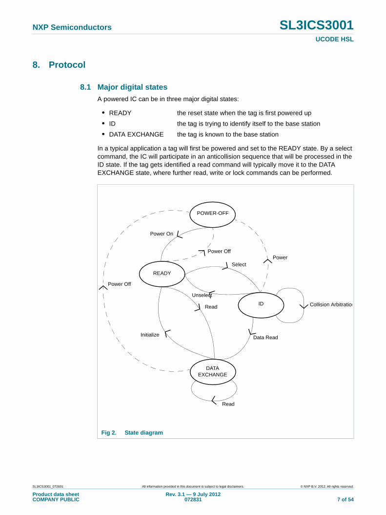
A powered IC can be in three major digital states:
• READY the reset state when the tag is first powered up
• ID the tag is trying to identify itself to the base station
• DATA EXCHANGE the tag is known to the base station
In a typical application a tag will first be powered and set to the READY state. By a select command, the IC will participate in an anticollision sequence that will be processed in the ID state. If the tag gets identified a read command will typically move it to the DATA EXCHANGE state, where further read, write or lock commands can be performed.
Fig 2. State diagram
POWER-OFF
READY
ID
DATA EXCHANGE
Power On
Power OffPower
Data Read
Collision Arbitration
Power Off
Select
Unselect
Read
Initialize
Read
SL3ICS3001_072831 All information provided in this document is subject to legal disclaimers. © NXP B.V. 2012. All rights reserved.
Product data sheetCOMPANY PUBLIC
Rev. 3.1 — 9 July 2012072831 7 of 54
NXP Semiconductors SL3ICS3001UCODE HSL
State transition description
• Power-On
– state change when interrogator field is turned on
• Power-Off
– state change when interrogator field is turned off
• Select
state change due to selection of tag by GROUP_SELECT commands
• Unselect
– state change due to deselection of tag by GROUP_UNSELECT commands
• Data_Read
– state change due to first read access in collision arbitration process
• Read
– state change due to read access independent of collision arbitration process
• Initialize
– state change due to deselection of all tags by the INITIALIZE command
As the state machine only supports 3 active states (READY, ID and DATA_EXCHANGE), only 3 opportunities of the tag status exist when the tag comes into the ready state after the power-off state.
1. The tag is new in this environment or was out of the field for a long while. In this case the tag should stay in the ready state until a new collision arbitration loop is initiated by a GROUP_SELECT command.
2. The tag has been participating in a collision arbitration and lost power through field nulls or just came out of the operating range. In this case, the tag has lost one or more collision arbitration commands and should therefore no longer participate in the active collision arbitration round. It should stay in the ready state until a new collision arbitration loop is initiated by a GROUP_SELECT command.
3. The tag had been selected already and was powered-down due to field nulls or short time being out of the operating range. In this case the tag no longer needs to be considered in the collision arbitration loops of this interrogator. Interrogators using the GROUP_SELECT_FLAG and GROUP_UNSELECT_ FLAG commands appropriately do not need to handle tags with DE_SB set and therefore limit the number of tags for the next collision arbitration loop to only those tags that have not been handled before.
By use of above mechanism each field null shorter than tDE_SB, which is at least several seconds does not require a tag to be handled more than once in the collision arbitration. In general the use of the DE_SB bit improves the number of tags identified within a certain time especially for large tag numbers when field nulls exist.
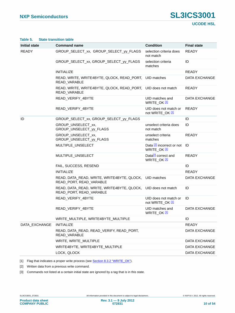
The exact transition between these states is specified in Table 5.
SL3ICS3001_072831 All information provided in this document is subject to legal disclaimers. © NXP B.V. 2012. All rights reserved.
Product data sheetCOMPANY PUBLIC
Rev. 3.1 — 9 July 2012072831 8 of 54
NXP Semiconductors SL3ICS3001UCODE HSL
8.2 Command overview
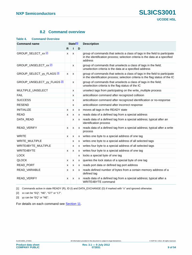
[1] Commands active in state READY (R), ID (I) and DATA_EXCHANGE (D) if marked with “x” and ignored otherwise.
[2] xx can be “EQ”, “NE”, “GT” or “LT”.
[3] yy can be “EQ” or “NE”.
For details on each command see Section 11.
Table 4. Command Overview
Command name State[1] Description
R I D
GROUP_SELECT_xx [2] x x group of commands that selects a class of tags in the field to participate in the identification process; selection criteria is the data at a specified address
GROUP_UNSELECT_xx [2] x group of commands that unselects a class of tags in the field; unselection criteria is the data at a specified address
GROUP_SELECT_yy_FLAGS [3] x x group of commands that selects a class of tags in the field to participate in the identification process; selection criteria is the flag status of the IC
GROUP_UNSELECT_yy_FLAGS [3] x group of commands that unselects a class of tags in the field; unselection criteria is the flag status of the IC
MULTIPLE_UNSELECT x unselect tags from participating on the write_multiple process
FAIL x anticollision command after recognized collision
SUCCESS x anticollision command after recognized identification or no-response
RESEND x anticollision command after incorrect response
INITIALIZE x x x moves all tags in the READY state
READ x x x reads data of a defined tag from a special address
DATA_READ x x reads data of a defined tag from a special address; typical after an identification process
READ_VERIFY x x x reads data of a defined tag from a special address; typical after a write process
WRITE x x x writes one byte to a special address of one tag
WRITE_MULTIPLE x x writes one byte to a special address of all selected tags
WRITE4BYTE_MULTIPLE x x writes four byte to a special address of all selected tags
WRITE4BYTE x x x writes four byte to a special address of one tag
LOCK x locks a special byte of one tag
QLOCK x x x queries the lock status of a special byte of one tag
READ_PORT x x x reads port data or defined tag port address
READ_VARIABLE x x x reads defined number of bytes from a certain memory address of a defined tag
READ_VERIFY x x x reads data of a defined tag from a special address; typical after a WRITE4BYTE command
SL3ICS3001_072831 All information provided in this document is subject to legal disclaimers. © NXP B.V. 2012. All rights reserved.
Product data sheetCOMPANY PUBLIC
Rev. 3.1 — 9 July 2012072831 9 of 54
NXP Semiconductors SL3ICS3001UCODE HSL
[1] Flag that indicates a proper write process (see Section 8.3.2 “WRITE_OK”).
[2] Written data from a previous write command.
[3] Commands not listed at a certain initial state are ignored by a tag that is in this state.
Table 5. State transition table
Initial state Command name Condition Final state
READY GROUP_SELECT_xx, GROUP_SELECT_yy_FLAGS selection criteria does not match
READY
GROUP_SELECT_xx, GROUP_SELECT_yy_FLAGS selection criteria matches
ID
INITIALIZE READY
READ, WRITE, WRITE4BYTE, QLOCK, READ_PORT, READ_VARABLE
UID matches DATA EXCHANGE
READ, WRITE, WRITE4BYTE, QLOCK, READ_PORT, READ_VARABLE
UID does not match READY
READ_VERIFY_4BYTE UID matches and WRITE_OK [1]
DATA EXCHANGE
READ_VERIFY_4BYTE UID does not match or not WRITE_OK [1]
READY
ID GROUP_SELECT_xx, GROUP_SELECT_yy_FLAGS ID
GROUP_UNSELECT_xx, GROUP_UNSELECT_yy_FLAGS
unselect criteria does not match
ID
GROUP_UNSELECT_xx, GROUP_UNSELECT_yy_FLAGS
unselect criteria matches
READY
MULTIPLE_UNSELECT Data [2] incorrect or not WRITE_OK [1]
ID
MULTIPLE_UNSELECT Data[2] correct and WRITE_OK [1]
READY
FAIL, SUCCESS, RESEND ID
INITIALIZE READY
READ, DATA_READ, WRITE, WRITE4BYTE, QLOCK, READ_PORT, READ_VARABLE
UID matches DATA EXCHANGE
READ, DATA_READ, WRITE, WRITE4BYTE, QLOCK, READ_PORT, READ_VARABLE
UID does not match ID
READ_VERIFY_4BYTE UID does not match or not WRITE_OK [1]
ID
READ_VERIFY_4BYTE UID matches and WRITE_OK [1]
DATA EXCHANGE
WRITE_MULTIPLE, WRITE4BYTE_MULTIPLE ID
DATA_EXCHANGE INITIALIZE READY
READ, DATA_READ, READ_VERIFY, READ_PORT, READ_VARABLE
DATA EXCHANGE
WRITE, WRITE_MULTIPLE DATA EXCHANGE
WRITE4BYTE, WRITE4BYTE_MULTIPLE DATA EXCHANGE
LOCK, QLOCK DATA EXCHANGE
SL3ICS3001_072831 All information provided in this document is subject to legal disclaimers. © NXP B.V. 2012. All rights reserved.
Product data sheetCOMPANY PUBLIC
Rev. 3.1 — 9 July 2012072831 10 of 54
NXP Semiconductors SL3ICS3001UCODE HSL
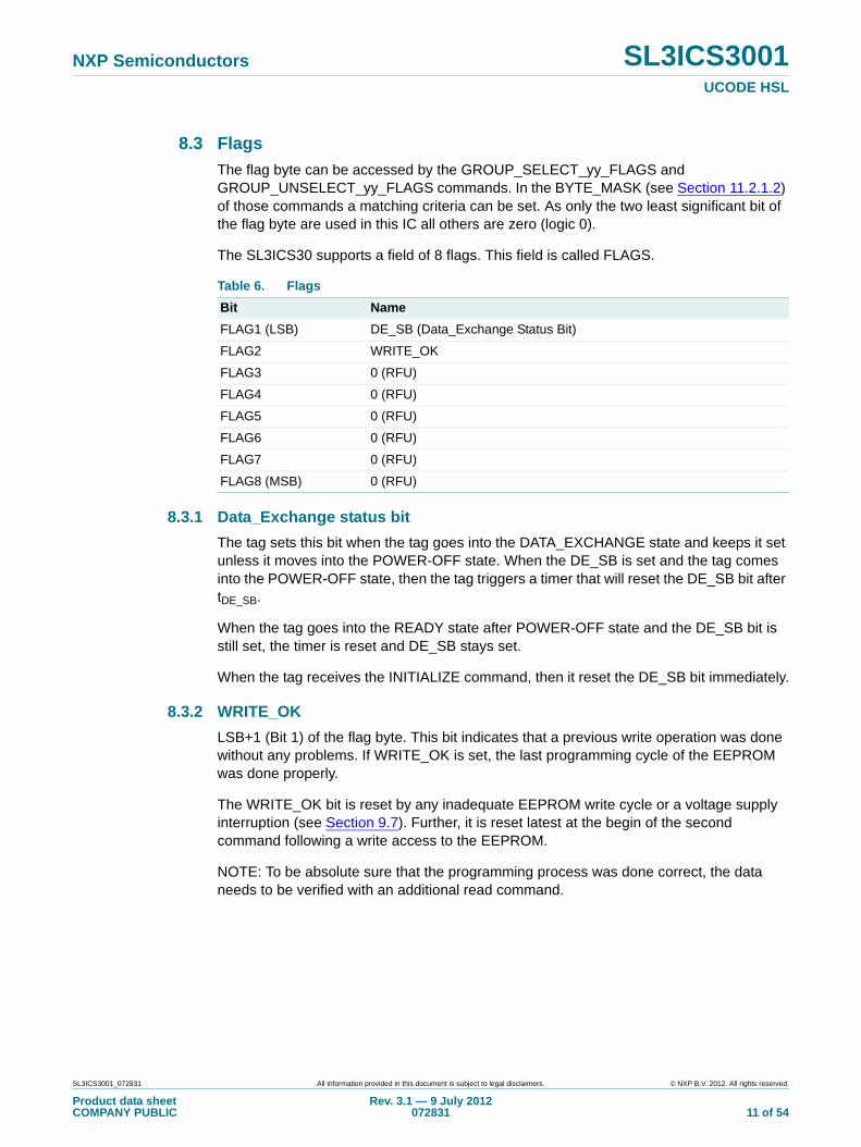
8.3 Flags
The flag byte can be accessed by the GROUP_SELECT_yy_FLAGS and GROUP_UNSELECT_yy_FLAGS commands. In the BYTE_MASK (see Section 11.2.1.2) of those commands a matching criteria can be set. As only the two least significant bit of the flag byte are used in this IC all others are zero (logic 0).
The SL3ICS30 supports a field of 8 flags. This field is called FLAGS.
8.3.1 Data_Exchange status bit
The tag sets this bit when the tag goes into the DATA_EXCHANGE state and keeps it set unless it moves into the POWER-OFF state. When the DE_SB is set and the tag comes into the POWER-OFF state, then the tag triggers a timer that will reset the DE_SB bit after tDE_SB.
When the tag goes into the READY state after POWER-OFF state and the DE_SB bit is still set, the timer is reset and DE_SB stays set.
When the tag receives the INITIALIZE command, then it reset the DE_SB bit immediately.
8.3.2 WRITE_OK
LSB+1 (Bit 1) of the flag byte. This bit indicates that a previous write operation was done without any problems. If WRITE_OK is set, the last programming cycle of the EEPROM was done properly.
The WRITE_OK bit is reset by any inadequate EEPROM write cycle or a voltage supply interruption (see Section 9.7). Further, it is reset latest at the begin of the second command following a write access to the EEPROM.
NOTE: To be absolute sure that the programming process was done correct, the data needs to be verified with an additional read command.
Table 6. Flags
Bit Name
FLAG1 (LSB) DE_SB (Data_Exchange Status Bit)
FLAG2 WRITE_OK
FLAG3 0 (RFU)
FLAG4 0 (RFU)
FLAG5 0 (RFU)
FLAG6 0 (RFU)
FLAG7 0 (RFU)
FLAG8 (MSB) 0 (RFU)
SL3ICS3001_072831 All information provided in this document is subject to legal disclaimers. © NXP B.V. 2012. All rights reserved.
Product data sheetCOMPANY PUBLIC
Rev. 3.1 — 9 July 2012072831 11 of 54
NXP Semiconductors SL3ICS3001UCODE HSL
8.4 Lockable state machine
This state machine is used to control the possibility of locking bytes in the EEPROM.
The lockable state machine has 2 states, IDLE and LOCKABLE. Initially, the state is IDLE. After any valid READ, DATA_READ, WRITE and QLOCK commands to the tag, the state becomes LOCKABLE, and locks on that dedicated byte are allowed. The specified address (starting address) is saved.
If a LOCK command to the same address of the same tag is received and the state is LOCKABLE, the lock proceeds.
If any other command is received, including a command to another tags, or any command packet has an error, the state returns to IDLE and the lock is no longer allowed.
See also Section 10 and Section 11.
8.5 Collision arbitration, anticollision
The interrogator may use the GROUP_SELECT and GROUP_UNSELECT commands to define all or a subset of tags in the field to participate in the collision arbitration. It then may use the identification commands to run the collision arbitration algorithm.
For the collision arbitration, the tag supports two pieces of hardware on the tag:
• an 8-bit counter: COUNT
• a random ‘1’ or ‘0’ generator
In the beginning, a group of tags is moved to the ID state by GROUP_SELECT commands, and their internal counters are set to logic 0. Subsets of the group may be unselected by GROUP_UNSELECT commands back to the READY state. Other groups can be selected before the identification process begins. Simulation results show no advantage in identifying one large group or a few smaller groups.
After above described selection, the following loop should be performed:
1. All tags in the ID state with the counter COUNT at ’0’ transmit their ID. This set initially includes all the selected tags.
2. If more than one tag transmits, the base station receives an erroneous response. The FAIL command shall be sent.
3. All tags receiving a FAIL command with COUNT not equal to logic 0 will increment COUNT. That is, they move further away from being able to transmit. All tags receiving FAIL, having a COUNT of ’0’ (those that just transmitted) will generate a random number. Those that roll a ’1’ will increment COUNT and will not transmit. Those that roll a zero will keep COUNT at zero and send their UID again. One of four possibilities now occurs:
4. If more than one tag transmits, the FAIL step 2 repeats. (Possibility 1)
5. If all tags roll a ’1’, none transmits. The interrogator receives nothing. It sends the SUCCESS command. All the counters decrement, and the tags with a count of ‘0’ transmit. Typically, this returns to step 2. (Possibility 2)
SL3ICS3001_072831 All information provided in this document is subject to legal disclaimers. © NXP B.V. 2012. All rights reserved.
Product data sheetCOMPANY PUBLIC
Rev. 3.1 — 9 July 2012072831 12 of 54
NXP Semiconductors SL3ICS3001UCODE HSL
6. If only one tag transmits and the ID is received correctly, the base station shall send the DATA_READ command with the ID. If the DATA_READ command is received correctly, then that tag moves to the DATA_EXCHANGE state and will transmit its data. The base station shall sends SUCCESS. All tags in the ID state decrement COUNT.
7. If only one tag has a count of ‘1’ and transmits, step 5 or 6 repeats. If more than one tag transmits, step 2 repeats. (Possibility 3)
8. If only one tag transmits and the ID is received with an error, the base station shall send the RESEND command. If the ID is received correctly, step 5 repeats. If the ID is received again some variable number of times (this number can be set based on the level of error handling desired for the system), it is assumed that more than one tag is transmitting, and step 2 repeats. (Possibility 4)
8.6 Data exchange sequences
8.6.1 Forward link
Every command starts with a command header consisting of PREAMBLE_DETECT, PREAMBLE and START DELIMITER. In this document, the appearance of these sequences is given in NRZ format. A NRZ ‘1’ means maximum field strength and NRZ ‘0’ means lower or even zero field (see also Section 9.3). Compared to the Manchester coded data, these sequences are given in halfbits.
All other transmitted data will be defined Manchester coded. This means that the digital data will be defined by a falling or rising transition in the middle of the bit. Furthermore, this means that a Manchester coded bit can be defined by two halfbits of a NRZ code.
The forward link consists of the following sequences:
• PREAMBLE_DETECT
no transition allowed during this time
• PREAMBLE
tag calibrates onto forward data rate
• START DELIMITER (STDEL)
tag verifies its calibration
• COMMAND (CMD)
• Address + Byte Mask + Data
only if required by the command
• CRC - 16
16 check bits, calculated from COMMAND + Address + Byte Mask + Data
• WAIT
only if COMMAND was a WRITE, to power the tag during EEPROM write
SL3ICS3001_072831 All information provided in this document is subject to legal disclaimers. © NXP B.V. 2012. All rights reserved.
Product data sheetCOMPANY PUBLIC
Rev. 3.1 — 9 July 2012072831 13 of 54
NXP Semiconductors SL3ICS3001UCODE HSL
8.6.1.1 Preamble
8.6.1.2 START DELIMITER
IC supports two Start Delimiters. See also Section 9.2.1 “Communication rate”.
8.6.2 Return link
A return link header consists of QUIET and RETURN_PREAMBLE. Just like the forward link header, this will be defined via NRZ coding. Here a NRZ ‘1’ means that the IC shortens the input pins. A NRZ ‘0’ does not affect the chip input impedance (see also Section 9.3).
Return data will be encoded in FM0. This means that on every edge of a bit a transition will occur. The digital data will be encoded by adding or non adding a transition in the middle of the bit. One FM0 bit is defined by 2 NRZ halfbits.
The return link consists of the following sequences, and starts immediately after the end of the forward link:
• QUIET
– no transition allowed during this time
• RETURN PREAMBLE
– interrogator may calibrate onto return data rate
• DATA
– return data
• CRC - 16
– 16 check bits, calculated from DATA
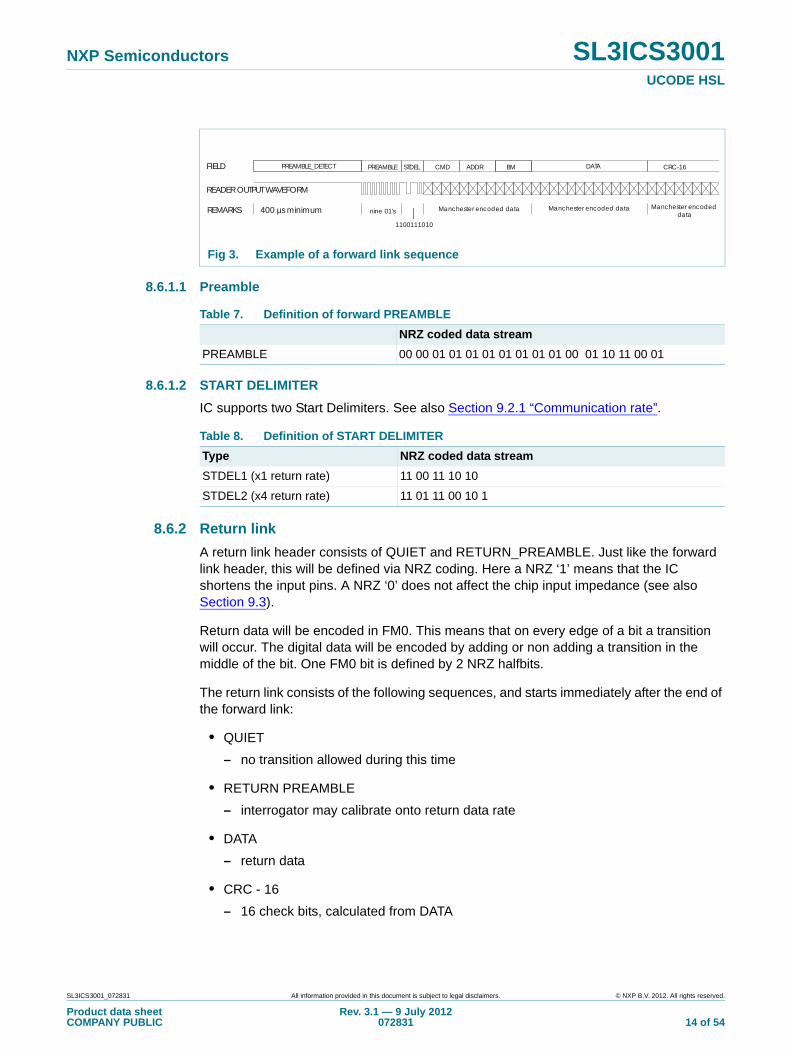
Fig 3. Example of a forward link sequence
Manchester encoded dataManchester encoded data
CMD CRC-16
REMARKS
READER OUTPUT WAVEFORM
PREAMBLE_DETECT
400 µs minimum
FIELD
nine 01's
PREAMBLE
1100111010
STDEL DATA
Manchester encoded data
ADDR BM
Table 7. Definition of forward PREAMBLE
NRZ coded data stream
PREAMBLE 00 00 01 01 01 01 01 01 01 01 00 01 10 11 00 01
Table 8. Definition of START DELIMITER
Type NRZ coded data stream
STDEL1 (x1 return rate) 11 00 11 10 10
STDEL2 (x4 return rate) 11 01 11 00 10 1
SL3ICS3001_072831 All information provided in this document is subject to legal disclaimers. © NXP B.V. 2012. All rights reserved.
Product data sheetCOMPANY PUBLIC
Rev. 3.1 — 9 July 2012072831 14 of 54
NXP Semiconductors SL3ICS3001UCODE HSL
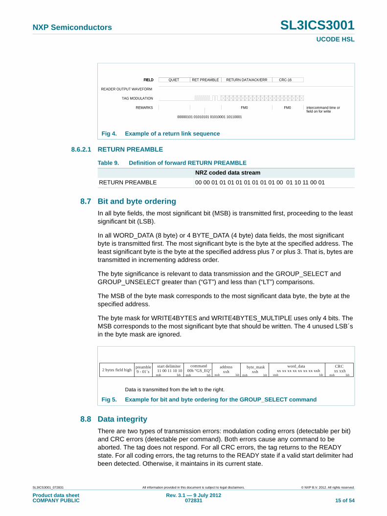
8.6.2.1 RETURN PREAMBLE
8.7 Bit and byte ordering
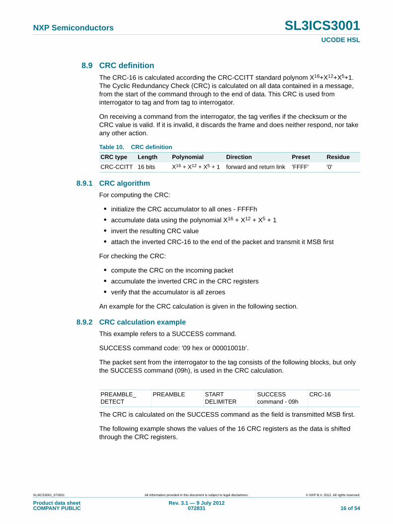
In all byte fields, the most significant bit (MSB) is transmitted first, proceeding to the least significant bit (LSB).
In all WORD_DATA (8 byte) or 4 BYTE_DATA (4 byte) data fields, the most significant byte is transmitted first. The most significant byte is the byte at the specified address. The least significant byte is the byte at the specified address plus 7 or plus 3. That is, bytes are transmitted in incrementing address order.
The byte significance is relevant to data transmission and the GROUP_SELECT and GROUP_UNSELECT greater than (“GT”) and less than (“LT”) comparisons.
The MSB of the byte mask corresponds to the most significant data byte, the byte at the specified address.
The byte mask for WRITE4BYTES and WRITE4BYTES_MULTIPLE uses only 4 bits. The MSB corresponds to the most significant byte that should be written. The 4 unused LSB´s in the byte mask are ignored.
8.8 Data integrity
There are two types of transmission errors: modulation coding errors (detectable per bit) and CRC errors (detectable per command). Both errors cause any command to be aborted. The tag does not respond. For all CRC errors, the tag returns to the READY state. For all coding errors, the tag returns to the READY state if a valid start delimiter had been detected. Otherwise, it maintains in its current state.
Fig 4. Example of a return link sequence
RETURN DATA/ACK/ERR
REMARKS
TAG MODULATION
READER OUTPUT WAVEFORM
FM0
00000101 01010101 01010001 10110001
FIELDFIELDFIELD QUIET RET PREAMBLE CRC-16
FM0 intercommand time orfield on for write
Table 9. Definition of forward RETURN PREAMBLE
NRZ coded data stream
RETURN PREAMBLE 00 00 01 01 01 01 01 01 01 01 00 01 10 11 00 01
Data is transmitted from the left to the right.
Fig 5. Example for bit and byte ordering for the GROUP_SELECT command
2 bytes field highpreamble 9 - 01´s
start delimiter 11 00 11 10 10
msb lsb
command 00h “GS_EQ”
msb lsb
address xxh
msb lsb
byte_mask xxh
msb lsb
CRC xx xxh msb lsb
word_data xx xx xx xx xx xx xx xxh msb lsb
SL3ICS3001_072831 All information provided in this document is subject to legal disclaimers. © NXP B.V. 2012. All rights reserved.
Product data sheetCOMPANY PUBLIC
Rev. 3.1 — 9 July 2012072831 15 of 54
NXP Semiconductors SL3ICS3001UCODE HSL
8.9 CRC definition
The CRC-16 is calculated according the CRC-CCITT standard polynom X16+X12+X5+1. The Cyclic Redundancy Check (CRC) is calculated on all data contained in a message, from the start of the command through to the end of data. This CRC is used from interrogator to tag and from tag to interrogator.
On receiving a command from the interrogator, the tag verifies if the checksum or the CRC value is valid. If it is invalid, it discards the frame and does neither respond, nor take any other action.
8.9.1 CRC algorithm
For computing the CRC:
• initialize the CRC accumulator to all ones - FFFFh
• accumulate data using the polynomial X16 + X12 + X5 + 1
• invert the resulting CRC value
• attach the inverted CRC-16 to the end of the packet and transmit it MSB first
For checking the CRC:
• compute the CRC on the incoming packet
• accumulate the inverted CRC in the CRC registers
• verify that the accumulator is all zeroes
An example for the CRC calculation is given in the following section.
8.9.2 CRC calculation example
This example refers to a SUCCESS command.
SUCCESS command code: '09 hex or 00001001b’.
The packet sent from the interrogator to the tag consists of the following blocks, but only the SUCCESS command (09h), is used in the CRC calculation.
The CRC is calculated on the SUCCESS command as the field is transmitted MSB first.
The following example shows the values of the 16 CRC registers as the data is shifted through the CRC registers.
Table 10. CRC definition
CRC type Length Polynomial Direction Preset Residue
CRC-CCITT 16 bits X16 + X12 + X5 + 1 forward and return link 'FFFF' '0'
PREAMBLE_ DETECT
PREAMBLE START DELIMITER
SUCCESS command - 09h
CRC-16
SL3ICS3001_072831 All information provided in this document is subject to legal disclaimers. © NXP B.V. 2012. All rights reserved.
Product data sheetCOMPANY PUBLIC
Rev. 3.1 — 9 July 2012072831 16 of 54

NXP Semiconductors SL3ICS3001UCODE HSL
Table 11. Practical example of CRC calculation for a 'SUCCESS' command in the Interrogator
Step Input (SUCCESS Cmd) Calculated CRC in interrogator
1 0 'EFDF'
2 0 'CF9F'
3 0 '8F1F'
4 0 '0E1F'
5 1 '0C1F'
6 0 '183E'
7 0 '307C'
8 1 '70D9'
Table 12. Practical example of CRC checking for a 'SUCCESS' command in the Tag
Step Input (Sent CRC-16) Calculated CRC in interrogator
0 '70D9'
1 0 'E1B2'
2 1 'C364'
3 1 '86C8'
4 1 '0D90'
5 0 '1B20'
6 0 '3640'
7 0 '6C80'
8 0 'D900'
9 1 'B200'
10 1 '6400'
11 0 'C800'
12 1 '9000'
13 1 '2000'
14 0 '4000'
15 0 '8000'
16 1 '0000'
SL3ICS3001_072831 All information provided in this document is subject to legal disclaimers. © NXP B.V. 2012. All rights reserved.
Product data sheetCOMPANY PUBLIC
Rev. 3.1 — 9 July 2012072831 17 of 54
NXP Semiconductors SL3ICS3001UCODE HSL
9. Communication timing and waveforms
9.1 Forward link
The tag front end effectively filters out short power interruption. Longer power interruptions will be detected and are interpreted as communication, tag writing, or, if exceeding a certain criteria in duration, may generate a tag reset (see Section 9.7).
If tag power is to be maintained between commands, the interrogator field must be kept on. If power is interrupted within tSD (as if might happen during interrogator frequency hops from one channel to another), the tag may interpret the hop event as the beginning of the PREAMBLE field. The tag will not succeed to decode the first command that follows the hop. If a data stream with 10 closely-spaced rising edges (i.e. 10 Manchester 0's) is sent to the tag immediately after a known brief power interruption event, however, the first command following the event will be decoded (that command must start with the PREAMBLE_DETECT field). The sequence that provides the ten rising edges to the tag is called TAG RESYNC.
In order for a write to be successful, tag power must be maintained throughout the tEEwrite execution time. Furthermore, the on-chip supply voltage required for a successful write is higher than that required for a successful read (this asymmetry causes the asymmetry between tag read and write ranges). Power interruptions during the write cycle may be unavoidable, however, resulting in corrupted or unreliable data. The commands READ_VERIFY, MULTIPLE_UNSELECT, GROUP_ SELECT_ FLAGS, and GROUP_ UNSELECT_ FLAGS are used to identify bad data immediately after the WRITE, WRITE4BYTE, WRITE_MULTIPLE, WRITE4BYTE_ MULTIPLE or LOCK process so that it can be rewritten. Please see Section 11. for details regarding those commands.
9.1.1 Communication rate
As the chip supports two different values of modulation index (see Table 15) in the forward link, there are also different limits for the communication rate.
[1] Type 18 % is intended to be used to fit into CEPT/ETSI and FCC regulations (for details see Section 16 “References”).
[2] Type 100% is intended to be used for FCC regulations only (for details see Section Section 16 “References”).
Table 13. Definition of TAG RESYNC
NRZ coded data stream
TAG RESYNC 01 01 01 01 01 01 01 01 01 01
Table 14. Forward data rate
Modulation index Forward data rate
Type 18% [1] 18% 8 to 40 kBits/s
Type 100% [2] 100% 30 to 40 kBits/s
SL3ICS3001_072831 All information provided in this document is subject to legal disclaimers. © NXP B.V. 2012. All rights reserved.
Product data sheetCOMPANY PUBLIC
Rev. 3.1 — 9 July 2012072831 18 of 54
NXP Semiconductors SL3ICS3001UCODE HSL
9.1.2 Modulation Waveform of Interrogator Modulation
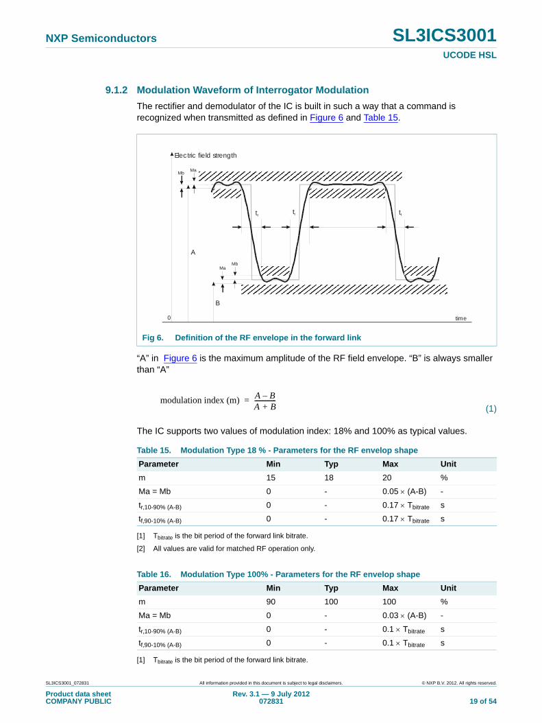
The rectifier and demodulator of the IC is built in such a way that a command is recognized when transmitted as defined in Figure 6 and Table 15.
“A” in Figure 6 is the maximum amplitude of the RF field envelope. “B” is always smaller than “A”
(1)
The IC supports two values of modulation index: 18% and 100% as typical values.
[1] Tbitrate is the bit period of the forward link bitrate.
[2] All values are valid for matched RF operation only.
[1] Tbitrate is the bit period of the forward link bitrate.
Fig 6. Definition of the RF envelope in the forward link
Table 15. Modulation Type 18 % - Parameters for the RF envelop shape
Parameter Min Typ Max Unit
m 15 18 20 %
Ma = Mb 0 - 0.05 (A-B) -
tr,10-90% (A-B) 0 - 0.17 Tbitrate s
tf,90-10% (A-B) 0 - 0.17 Tbitrate s
Table 16. Modulation Type 100% - Parameters for the RF envelop shape
Parameter Min Typ Max Unit
m 90 100 100 %
Ma = Mb 0 - 0.03 (A-B) -
tr,10-90% (A-B) 0 - 0.1 Tbitrate s
tf,90-10% (A-B) 0 - 0.1 Tbitrate s
Elec tric field strength
MbMa
A
B
MbMa
0
tftf
tr
time
modulation index (m) A B–A B+--------------=
SL3ICS3001_072831 All information provided in this document is subject to legal disclaimers. © NXP B.V. 2012. All rights reserved.
Product data sheetCOMPANY PUBLIC
Rev. 3.1 — 9 July 2012072831 19 of 54
NXP Semiconductors SL3ICS3001UCODE HSL
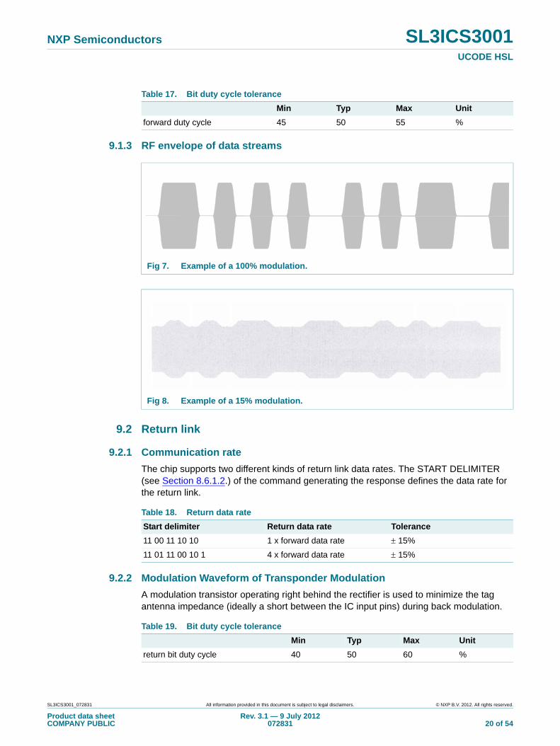
9.1.3 RF envelope of data streams
9.2 Return link
9.2.1 Communication rate
The chip supports two different kinds of return link data rates. The START DELIMITER (see Section 8.6.1.2.) of the command generating the response defines the data rate for the return link.
9.2.2 Modulation Waveform of Transponder Modulation
A modulation transistor operating right behind the rectifier is used to minimize the tag antenna impedance (ideally a short between the IC input pins) during back modulation.
Table 17. Bit duty cycle tolerance
Min Typ Max Unit
forward duty cycle 45 50 55 %
Fig 7. Example of a 100% modulation.
Fig 8. Example of a 15% modulation.
Table 18. Return data rate
Start delimiter Return data rate Tolerance
11 00 11 10 10 1 x forward data rate 15%
11 01 11 00 10 1 4 x forward data rate 15%
Table 19. Bit duty cycle tolerance
Min Typ Max Unit
return bit duty cycle 40 50 60 %
SL3ICS3001_072831 All information provided in this document is subject to legal disclaimers. © NXP B.V. 2012. All rights reserved.
Product data sheetCOMPANY PUBLIC
Rev. 3.1 — 9 July 2012072831 20 of 54
NXP Semiconductors SL3ICS3001UCODE HSL
9.3 Bit Coding
9.3.1 Forward Link
Maximum RF field is a NRZ ‘1’ (“A” in Figure 6), modulated RF field level equals NRZ ‘0’ (“B” in Figure 6).
9.3.2 Return Link
NRZ ‘0’ is no modulation, that means a high chip input impedance.
NRZ ‘1’ is a modulation (modulation transistor turned on), that means a very low chip input impedance.
Within the FM0 encoded data patterns, a logical ‘0’ is transmitted, if there is transition at the midbit. A logical ‘1’ is transmitted if no transition occurs at the midbit. Note: in FM0 encoding a transition occurs additionally at all bit boundaries.
9.4 Response Time
The tag immediately starts sending back the return sequence after a correct command was received. As this sequence starts with a QUIET field (see Section 8.6.2) the interrogator may use the time for that field for settling its receiver section.
9.5 Regeneration Time
After a response of the tag or the end of a WAIT field, the tag is immediately able to receive a new command sequence from the interrogator. This sequence will again start with a PREAMBLE DETECT field.
Therefore a Manchester’0’ is “01” in NRZ.
Fig 9. Definition of a Manchester ‘0’
Therefore a Manchester’0’ is “01” in NRZ.
Fig 10. Definition of a Manchester ‘1’.
field modulated
field not modulated
field modulated
field not modulated
Table 20. Maximum interrogator settling time
QUIET field length 16 Treturn bit rate - 0.75 Tforward bit rate
SL3ICS3001_072831 All information provided in this document is subject to legal disclaimers. © NXP B.V. 2012. All rights reserved.
Product data sheetCOMPANY PUBLIC
Rev. 3.1 — 9 July 2012072831 21 of 54
NXP Semiconductors SL3ICS3001UCODE HSL
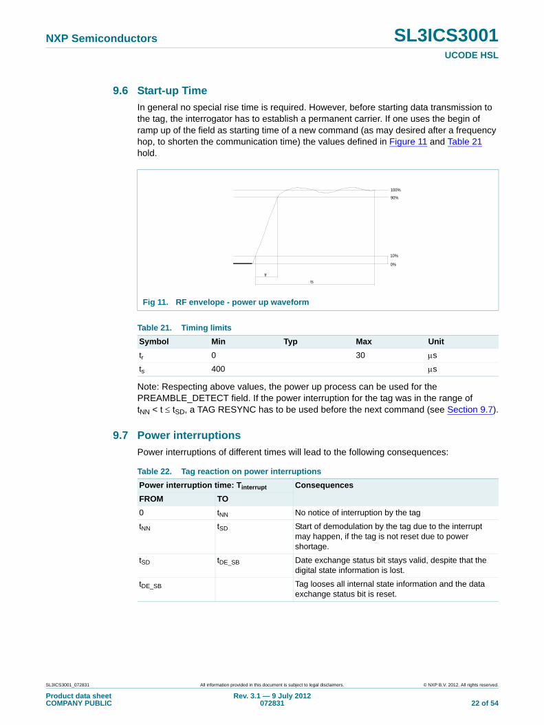
9.6 Start-up Time
In general no special rise time is required. However, before starting data transmission to the tag, the interrogator has to establish a permanent carrier. If one uses the begin of ramp up of the field as starting time of a new command (as may desired after a frequency hop, to shorten the communication time) the values defined in Figure 11 and Table 21 hold.
Note: Respecting above values, the power up process can be used for the PREAMBLE_DETECT field. If the power interruption for the tag was in the range of tNN < t tSD, a TAG RESYNC has to be used before the next command (see Section 9.7).
9.7 Power interruptions
Power interruptions of different times will lead to the following consequences:
Fig 11. RF envelope - power up waveform
Table 21. Timing limits
Symbol Min Typ Max Unit
tr 0 30 s
ts 400 s
tr
ts
0%
100%
10%
90%
Table 22. Tag reaction on power interruptions
Power interruption time: Tinterrupt Consequences
FROM TO
0 tNN No notice of interruption by the tag
tNN tSD Start of demodulation by the tag due to the interrupt may happen, if the tag is not reset due to power shortage.
tSD tDE_SB Date exchange status bit stays valid, despite that the digital state information is lost.
tDE_SB Tag looses all internal state information and the data exchange status bit is reset.
SL3ICS3001_072831 All information provided in this document is subject to legal disclaimers. © NXP B.V. 2012. All rights reserved.
Product data sheetCOMPANY PUBLIC
Rev. 3.1 — 9 July 2012072831 22 of 54
NXP Semiconductors SL3ICS3001UCODE HSL
10. Memory
• Tag memory size:
– 2048 bits
• ID memory size:
– 8 bytes
• User memory size:
– 216 bytes
All transmitted ADDRESS fields in the forward link has to be within the range of 0 to 223 (‘0h’ to ‘DFh’), as this address refers to byte units. If an ADDRESS field is received that exceeds ‘DFh’, the command is ignored.
Each byte has an associated lock bit. If this lock bit is set to ‘1’ the data of the byte cannot be changed anymore. This means that no more write commands can be processed on that byte.
Note: In case a read command uses a valid value for ADDRESS, but the number of bytes read by the command exceed ‘DFh’ is not defined.
10.1 Memory organization
The memory is organized byte-wise. Each byte has a dedicated lock bit.
Writing with the commands WRITE4BYTE and WRITE4BYTE_MULTIPLE is only possible on a 4 byte boundary: 0, 4, 8, …
10.2 Definition of block contents
10.2.1 UID
The Unique ID (UID) is a 64 bit number, and is located in the bytes from 0 to 7. The most significant byte is stored on byte location 0. The bytes associated with the UID have to be locked latest after final label test.
10.3 Configuration of delivered ICs
Table 23. Configuration of delivered ICs
Memory Address Memory Content Lock Status Comment
Byte 0, 1 E0, 04 hex locked unique serial number
Byte 2 - 7 xx hex locked unique serial number
Byte 8 - 10 00 hex unlocked user memory
Byte 11 02 hex unlocked user memory
Byte 12 - 17 FF hex unlocked user memory
Byte 18 - 219 00 hex unlocked user memory
Byte 220 - 223 57 5F 4F 4B hex unlocked “w_ok” in ASCII, user memory
SL3ICS3001_072831 All information provided in this document is subject to legal disclaimers. © NXP B.V. 2012. All rights reserved.
Product data sheetCOMPANY PUBLIC
Rev. 3.1 — 9 July 2012072831 23 of 54
NXP Semiconductors SL3ICS3001UCODE HSL
11. Commands
11.1 Definitions
Table 24. Command codes and format
Command name Code Parameters
GROUP_SELECT_EQ 00h ADDRESS BYTE_MASK WORD_DATA
GROUP_SELECT_NE 01h ADDRESS BYTE_MASK WORD_DATA
GROUP_SELECT_GT 02h ADDRESS BYTE_MASK WORD_DATA
GROUP_SELECT_LT 03h ADDRESS BYTE_MASK WORD_DATA
GROUP_UNSELECT_EQ 04h ADDRESS BYTE_MASK WORD_DATA
GROUP_UNSELECT_NE 05h ADDRESS BYTE_MASK WORD_DATA
GROUP_UNSELECT_GT 06h ADDRESS BYTE_MASK WORD_DATA
GROUP_UNSELECT_LT 07h ADDRESS BYTE_MASK WORD_DATA
FAIL 08h none
SUCCESS 09h none
INITIALIZE 0Ah none
DATA_READ 0Bh ID ADDRESS
READ 0Ch ID ADDRESS
WRITE 0Dh ID ADDRESS BYTE_DATA
WRITE_MULTIPLE 0Eh ADDRESS BYTE_DATA
LOCK 0Fh ID ADDRESS
QUERY_LOCK 11h ID ADDRESS
READ_VERIFY 12h ID ADDRESS
MULTIPLE_UNSELECT 13h ADDRESS BYTE_DATA
RESEND 15h none
CALIBRATE 16h none
GROUP_SELECT_EQ_FLAGS 17h BYTE_MASK BYTE_DATA
GROUP_SELECT_NE_FLAGS 18h BYTE_MASK BYTE_DATA
GROUP_UNSELECT_EQ_FLAGS 19h BYTE_MASK BYTE_DATA
GROUP_UNSELECT_NE_FLAGS 1Ah BYTE_MASK BYTE_DATA
WRITE4BYTE 1Bh ID ADDRESS BYTE_MASK 4BYTE_DATA
WRITE4BYTE_MULTIPLE 1Ch ADDRESS BYTE_MASK 4BYTE_DATA
READ_VERIFY_4BYTE 1Dh ID ADDRESS
READ_VARIABLE 51h ID ADDRESS LENGTH
READ_PORT 52h ID ADDRESS
SL3ICS3001_072831 All information provided in this document is subject to legal disclaimers. © NXP B.V. 2012. All rights reserved.
Product data sheetCOMPANY PUBLIC
Rev. 3.1 — 9 July 2012072831 24 of 54
NXP Semiconductors SL3ICS3001UCODE HSL
Table 25. Command fields
Field name Field size
COMMAND 1 byte
ADDRESS 1 byte
BYTE_MASK 1 byte
ID 8 bytes
WORD_DATA 8 bytes
BYTE_DATA 1 byte
4BYTE_DATA 4 bytes
LENGTH 1 byte
Table 26. Tag response
Response name Response size Value
ACKNOWLEDGE 1 byte 00
ACKNOWLEDGE_NOK 1 byte 00
ACKNOWLEDGE_OK 1 byte 01
ERROR_NOK 1 byte FE
ERROR 1 byte FF
ERROR_OK 1 byte FF
ID 8 bytes n/a
WORD_DATA 8 bytes n/a
BYTE_DATA 1 byte n/a
CRC 2 bytes n/a
VARIABLE_DATA LENGTH bytes n/a
SL3ICS3001_072831 All information provided in this document is subject to legal disclaimers. © NXP B.V. 2012. All rights reserved.
Product data sheetCOMPANY PUBLIC
Rev. 3.1 — 9 July 2012072831 25 of 54
NXP Semiconductors SL3ICS3001UCODE HSL
11.2 Selection commands
Selection commands define a subset of tags in the field to be identified or written to and may be used as part of the collision arbitration.
11.2.1 Data comparison for selection commands
11.2.1.1 Data comparison for selection commands on memory
Each select command of the commands
GROUP_SELECT_EQ, GROUP_SELECT_NE, GROUP_SELECT_GT, GROUP_SELECT_LT, GROUP_UNSELECT_EQ, GROUP_UNSELECT_NE, GROUP_UNSELECT_GT, GROUP_UNSELECT_LT
has three arguments (parameter and data):
• ADDRESS
• BYTE_MASK
• WORD_DATA
and the tag shall do one of four possible comparisons:
• EQ: M equal D
• NE: M not equal D
• GT: M greater than D
• LT: M lower than D
The argument of the comparison are:
[1] M = M0 + M1 * 28 + M2 * 216 + M3 * 224 + M4 * 232 + M5 * 240 + M6 * 248 + M7 * 256
and the argument of the command:
[1] D = D0 + D1 * 28 + D2 * 216 + D3 * 224 + D4 * 232 + D5 * 240 + D6 * 248 + D7 * 256
M7 MSB M6 M5 M4 M3 M2 M1 M0 LSB
Tag memory content at ADDRESS+0
Tag memory content at ADDRESS+1
Tag memory content at ADDRESS+2
Tag memory content at ADDRESS+3
Tag memory content at ADDRESS+4
Tag memory content at ADDRESS+5
Tag memory content at ADDRESS+6
Tag memory content at ADDRESS+7
D7 MSB D6 D5 D4 D3 D2 D1 D0 LSB
First byte after command
Last byte after command
SL3ICS3001_072831 All information provided in this document is subject to legal disclaimers. © NXP B.V. 2012. All rights reserved.
Product data sheetCOMPANY PUBLIC
Rev. 3.1 — 9 July 2012072831 26 of 54
NXP Semiconductors SL3ICS3001UCODE HSL
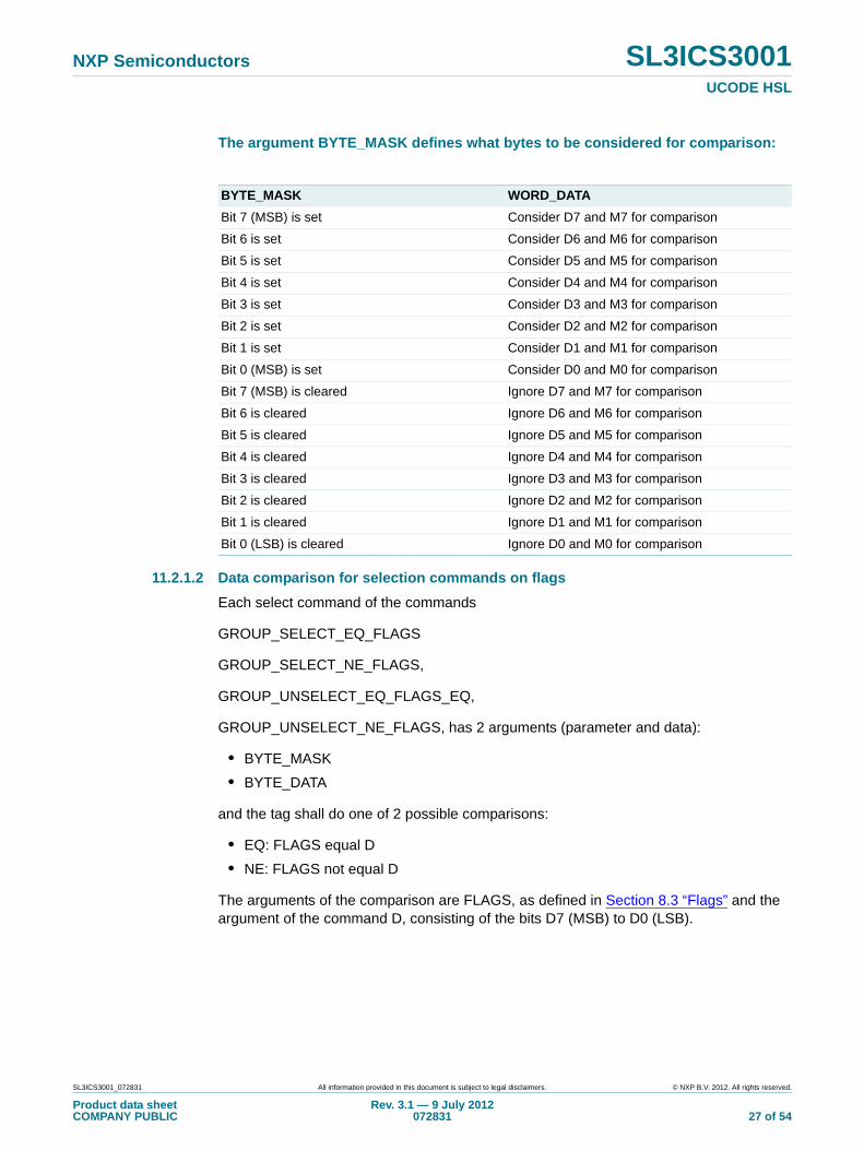
The argument BYTE_MASK defines what bytes to be considered for comparison:
11.2.1.2 Data comparison for selection commands on flags
Each select command of the commands
GROUP_SELECT_EQ_FLAGS
GROUP_SELECT_NE_FLAGS,
GROUP_UNSELECT_EQ_FLAGS_EQ,
GROUP_UNSELECT_NE_FLAGS, has 2 arguments (parameter and data):
• BYTE_MASK
• BYTE_DATA
and the tag shall do one of 2 possible comparisons:
• EQ: FLAGS equal D
• NE: FLAGS not equal D
The arguments of the comparison are FLAGS, as defined in Section 8.3 “Flags” and the argument of the command D, consisting of the bits D7 (MSB) to D0 (LSB).
BYTE_MASK WORD_DATA
Bit 7 (MSB) is set Consider D7 and M7 for comparison
Bit 6 is set Consider D6 and M6 for comparison
Bit 5 is set Consider D5 and M5 for comparison
Bit 4 is set Consider D4 and M4 for comparison
Bit 3 is set Consider D3 and M3 for comparison
Bit 2 is set Consider D2 and M2 for comparison
Bit 1 is set Consider D1 and M1 for comparison
Bit 0 (MSB) is set Consider D0 and M0 for comparison
Bit 7 (MSB) is cleared Ignore D7 and M7 for comparison
Bit 6 is cleared Ignore D6 and M6 for comparison
Bit 5 is cleared Ignore D5 and M5 for comparison
Bit 4 is cleared Ignore D4 and M4 for comparison
Bit 3 is cleared Ignore D3 and M3 for comparison
Bit 2 is cleared Ignore D2 and M2 for comparison
Bit 1 is cleared Ignore D1 and M1 for comparison
Bit 0 (LSB) is cleared Ignore D0 and M0 for comparison
SL3ICS3001_072831 All information provided in this document is subject to legal disclaimers. © NXP B.V. 2012. All rights reserved.
Product data sheetCOMPANY PUBLIC
Rev. 3.1 — 9 July 2012072831 27 of 54

NXP Semiconductors SL3ICS3001UCODE HSL
The argument BYTE_MASK defines what bytes to be considered for comparison:
Formula describing in the EQUAL function:
The EQUAL comparison passes, if
is true.
Formula describing in the UNEQUAL function:
The UNEQUAL comparison passes, if
is true.
BYTE_MASK WORD_DATA
Bit 7 (MSB) is set Consider D7 and FLAG7 for comparison
Bit 6 is set Consider D6 and FLAG6 for comparison
Bit 5 is set Consider D5 and FLAG5 for comparison
Bit 4 is set Consider D4 and FLAG4 for comparison
Bit 3 is set Consider D3 and FLAG3 for comparison
Bit 2 is set Consider D2 and FLAG2 for comparison
Bit 1 is set Consider D1 and FLAG1 for comparison
Bit 0 (MSB) is set Consider D0 and FLAG0 for comparison
Bit 7 (MSB) is cleared Ignore D7 and FLAG7 for comparison
Bit 6 is cleared Ignore D6 and FLAG6 for comparison
Bit 5 is cleared Ignore D5 and FLAG5 for comparison
Bit 4 is cleared Ignore D4 and FLAG4 for comparison
Bit 3 is cleared Ignore D3 and FLAG3 for comparison
Bit 2 is cleared Ignore D2 and FLAG2 for comparison
Bit 1 is cleared Ignore D1 and FLAG1 for comparison
Bit 0 (LSB) is cleared Ignore D0 and FLAG0 for comparison
!B7 D7 FLAG7= + !B6 D6 FLAG6= + !B5 D5 FLAG5= + !B4 D4 FLAG4= +
!B3 D3 FLAG3= + !B2 D2 FLAG2= + !B1 D1 FLAG1= + !B0 D0 FLAG0= +
+B7 D7! FLAG7 = B6 D6! FLAG6 B5 D5! FLAG5 B4 D4! FLAG4 =+=+=+
B3 D3! FLAG3 = B2 D2! FLAG2 B1 D1! FLAG1 B0 D0! FLAG0 =+=+=+
SL3ICS3001_072831 All information provided in this document is subject to legal disclaimers. © NXP B.V. 2012. All rights reserved.
Product data sheetCOMPANY PUBLIC
Rev. 3.1 — 9 July 2012072831 28 of 54
NXP Semiconductors SL3ICS3001UCODE HSL
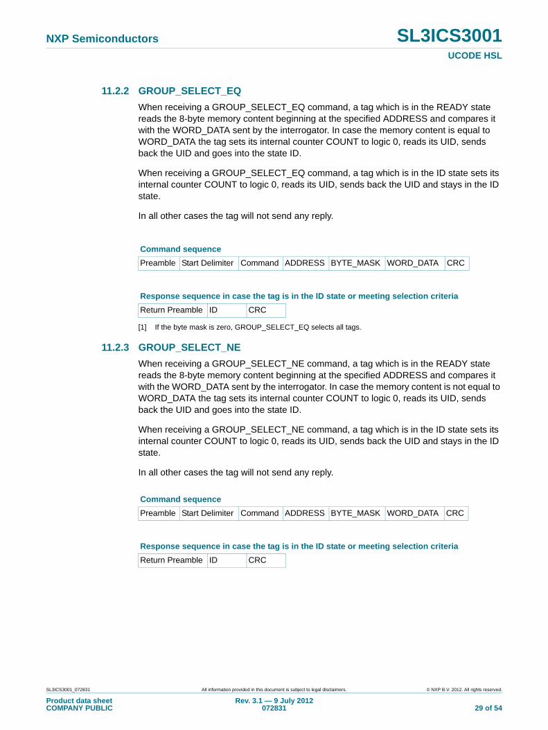
11.2.2 GROUP_SELECT_EQ
When receiving a GROUP_SELECT_EQ command, a tag which is in the READY state reads the 8-byte memory content beginning at the specified ADDRESS and compares it with the WORD_DATA sent by the interrogator. In case the memory content is equal to WORD_DATA the tag sets its internal counter COUNT to logic 0, reads its UID, sends back the UID and goes into the state ID.
When receiving a GROUP_SELECT_EQ command, a tag which is in the ID state sets its internal counter COUNT to logic 0, reads its UID, sends back the UID and stays in the ID state.
In all other cases the tag will not send any reply.
[1] If the byte mask is zero, GROUP_SELECT_EQ selects all tags.
11.2.3 GROUP_SELECT_NE
When receiving a GROUP_SELECT_NE command, a tag which is in the READY state reads the 8-byte memory content beginning at the specified ADDRESS and compares it with the WORD_DATA sent by the interrogator. In case the memory content is not equal to WORD_DATA the tag sets its internal counter COUNT to logic 0, reads its UID, sends back the UID and goes into the state ID.
When receiving a GROUP_SELECT_NE command, a tag which is in the ID state sets its internal counter COUNT to logic 0, reads its UID, sends back the UID and stays in the ID state.
In all other cases the tag will not send any reply.
Command sequence
Preamble Start Delimiter Command ADDRESS BYTE_MASK WORD_DATA CRC
Response sequence in case the tag is in the ID state or meeting selection criteria
Return Preamble ID CRC
Command sequence
Preamble Start Delimiter Command ADDRESS BYTE_MASK WORD_DATA CRC
Response sequence in case the tag is in the ID state or meeting selection criteria
Return Preamble ID CRC
SL3ICS3001_072831 All information provided in this document is subject to legal disclaimers. © NXP B.V. 2012. All rights reserved.
Product data sheetCOMPANY PUBLIC
Rev. 3.1 — 9 July 2012072831 29 of 54
NXP Semiconductors SL3ICS3001UCODE HSL
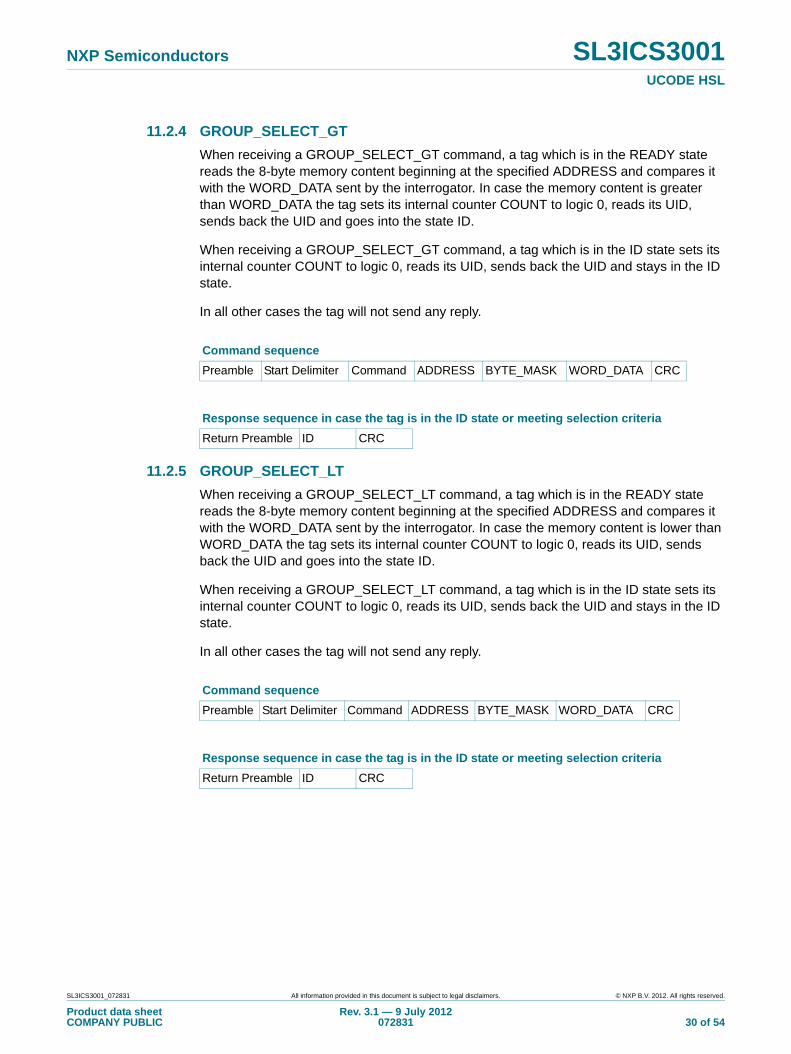
11.2.4 GROUP_SELECT_GT
When receiving a GROUP_SELECT_GT command, a tag which is in the READY state reads the 8-byte memory content beginning at the specified ADDRESS and compares it with the WORD_DATA sent by the interrogator. In case the memory content is greater than WORD_DATA the tag sets its internal counter COUNT to logic 0, reads its UID, sends back the UID and goes into the state ID.
When receiving a GROUP_SELECT_GT command, a tag which is in the ID state sets its internal counter COUNT to logic 0, reads its UID, sends back the UID and stays in the ID state.
In all other cases the tag will not send any reply.
11.2.5 GROUP_SELECT_LT
When receiving a GROUP_SELECT_LT command, a tag which is in the READY state reads the 8-byte memory content beginning at the specified ADDRESS and compares it with the WORD_DATA sent by the interrogator. In case the memory content is lower than WORD_DATA the tag sets its internal counter COUNT to logic 0, reads its UID, sends back the UID and goes into the state ID.
When receiving a GROUP_SELECT_LT command, a tag which is in the ID state sets its internal counter COUNT to logic 0, reads its UID, sends back the UID and stays in the ID state.
In all other cases the tag will not send any reply.
Command sequence
Preamble Start Delimiter Command ADDRESS BYTE_MASK WORD_DATA CRC
Response sequence in case the tag is in the ID state or meeting selection criteria
Return Preamble ID CRC
Command sequence
Preamble Start Delimiter Command ADDRESS BYTE_MASK WORD_DATA CRC
Response sequence in case the tag is in the ID state or meeting selection criteria
Return Preamble ID CRC
SL3ICS3001_072831 All information provided in this document is subject to legal disclaimers. © NXP B.V. 2012. All rights reserved.
Product data sheetCOMPANY PUBLIC
Rev. 3.1 — 9 July 2012072831 30 of 54
NXP Semiconductors SL3ICS3001UCODE HSL
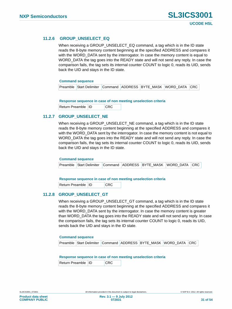
11.2.6 GROUP_UNSELECT_EQ
When receiving a GROUP_UNSELECT_EQ command, a tag which is in the ID state reads the 8-byte memory content beginning at the specified ADDRESS and compares it with the WORD_DATA sent by the interrogator. In case the memory content is equal to WORD_DATA the tag goes into the READY state and will not send any reply. In case the comparison fails, the tag sets its internal counter COUNT to logic 0, reads its UID, sends back the UID and stays in the ID state.
11.2.7 GROUP_UNSELECT_NE
When receiving a GROUP_UNSELECT_NE command, a tag which is in the ID state reads the 8-byte memory content beginning at the specified ADDRESS and compares it with the WORD_DATA sent by the interrogator. In case the memory content is not equal to WORD_DATA the tag goes into the READY state and will not send any reply. In case the comparison fails, the tag sets its internal counter COUNT to logic 0, reads its UID, sends back the UID and stays in the ID state.
11.2.8 GROUP_UNSELECT_GT
When receiving a GROUP_UNSELECT_GT command, a tag which is in the ID state reads the 8-byte memory content beginning at the specified ADDRESS and compares it with the WORD_DATA sent by the interrogator. In case the memory content is greater than WORD_DATA the tag goes into the READY state and will not send any reply. In case the comparison fails, the tag sets its internal counter COUNT to logic 0, reads its UID, sends back the UID and stays in the ID state.
Command sequence
Preamble Start Delimiter Command ADDRESS BYTE_MASK WORD_DATA CRC
Response sequence in case of non meeting unselection criteria
Return Preamble ID CRC
Command sequence
Preamble Start Delimiter Command ADDRESS BYTE_MASK WORD_DATA CRC
Response sequence in case of non meeting unselection criteria
Return Preamble ID CRC
Command sequence
Preamble Start Delimiter Command ADDRESS BYTE_MASK WORD_DATA CRC
Response sequence in case of non meeting unselection criteria
Return Preamble ID CRC
SL3ICS3001_072831 All information provided in this document is subject to legal disclaimers. © NXP B.V. 2012. All rights reserved.
Product data sheetCOMPANY PUBLIC
Rev. 3.1 — 9 July 2012072831 31 of 54
NXP Semiconductors SL3ICS3001UCODE HSL
11.2.9 GROUP_UNSELECT_LT
When receiving a GROUP_UNSELECT_LT command, a tag which is in the ID state reads the 8-byte memory content beginning at the specified ADDRESS and compares it with the WORD_DATA sent by the interrogator. In case the memory content is lower than WORD_DATA the tag goes into the READY state and will not send any reply. In case the comparison fails, the tag sets its internal counter COUNT to logic 0, reads its UID, sends back the UID and stays in the ID state.
11.2.10 MULTIPLE_UNSELECT
When receiving a MULTIPLE_UNSELECT command, a tag which is in the ID state reads the 1-byte memory content beginning at the specified ADDRESS and compares it with the BYTE_DATA sent by the interrogator. In case the memory content is equal to BYTE_DATA and the flag WRITE_OK is set, then the tag goes into the state READY and will not send any reply. In case the comparison fails, the tag sets its internal counter COUNT to logic 0, reads its UID and sends back the UID.
This command may be used to unselect all tags that had a successful write, while tags that had a weak write or write problems stay selected.
Command sequence
Preamble Start Delimiter Command ADDRESS BYTE_MASK WORD_DATA CRC
Response sequence in case of non meeting unselection criteria
Return Preamble ID CRC
Command sequence
Preamble Start Delimiter Command ADDRESS BYTE_MASK WORD_DATA CRC
Response sequence in case of non meeting unselection criteria
Return Preamble ID CRC
SL3ICS3001_072831 All information provided in this document is subject to legal disclaimers. © NXP B.V. 2012. All rights reserved.
Product data sheetCOMPANY PUBLIC
Rev. 3.1 — 9 July 2012072831 32 of 54
NXP Semiconductors SL3ICS3001UCODE HSL
11.2.11 GROUP_SELECT_EQ_FLAGS
When receiving a GROUP_SELECT_EQ_FLAGS command, a tag which is in the READY state compares the FLAGS with the BYTE_DATA sent by the interrogator. In case the FLAGS are equal to BYTE_DATA the tag sets its internal counter COUNT to logic 0, reads its UID, sends back the UID and goes into the state ID.
When receiving a GROUP_SELECT_EQ_FLAGS command, a tag which is in the ID state sets its internal counter COUNT to logic 0, reads its UID, sends back the UID and stays in the ID state.
In all other cases the tag will not send any reply.
[1] If the byte mask is zero, GROUP_SELECT_EQ_FLAGS selects all tags.
11.2.12 GROUP_SELECT_NE_FLAGS
When receiving a GROUP_SELECT_NE_FLAGS command, a tag which is in the READY state compares the FLAGS with the BYTE_DATA sent by the interrogator. In case the FLAGS are not equal to BYTE_DATA the tag sets its internal counter COUNT to 0, reads it UID, sends back its UID and goes into the state ID.
When receiving a GROUP_SELECT_ NE_FLAGS command a tag which is in the ID state sets its internal counter COUNT to logic 0, reads its UID, sends back the UID and goes in the ID state.
In all other cases the tag will not send a reply.
Command sequence
Preamble Start Delimiter Command ADDRESS BYTE_MASK WORD_DATA CRC
Response sequence in case the tag is in the ID state or meeting selection criteria
Return Preamble ID CRC
Command sequence
Preamble Start Delimiter Command ADDRESS BYTE_MASK WORD_DATA CRC
Response sequence in case the tag is in the ID state or meeting selection criteria
Return Preamble ID CRC
SL3ICS3001_072831 All information provided in this document is subject to legal disclaimers. © NXP B.V. 2012. All rights reserved.
Product data sheetCOMPANY PUBLIC
Rev. 3.1 — 9 July 2012072831 33 of 54
NXP Semiconductors SL3ICS3001UCODE HSL
11.2.13 GROUP_UNSELECT_EQ_FLAGS
When receiving a GROUP_UNSELECT_EQ_FLAGS command, a tag which is in the ID state compares the FLAGS with the BYTE_DATA sent by the interrogator. In case the FLAGS are equal to BYTE_DATA the tag goes into the state READY and will not reply. In case the comparison fails, the tag sets its internal counter COUNT to logic 0, reads its UID, sends back the UID and stays in the state ID.
In all other cases the tag will not send any reply.
11.2.14 GROUP_UNSELECT_NE_FLAGS
When receiving a GROUP_UNSELECT_NE_FLAGS command, a tag which is in the ID state compares the FLAGS with the BYTE_DATA sent by the interrogator. In case the FLAGS are not equal to BYTE_DATA the tag goes into the state READY and will not reply. In case the comparison fails, the tag sets its internal counter COUNT to logic 0, reads its UID, sends back the UID and stays in the state ID.
In all other cases the tag will not send any reply.
Command sequence
Preamble Start Delimiter Command ADDRESS BYTE_MASK WORD_DATA CRC
Response sequence in case of non meeting unselection criteria
Return Preamble ID CRC
Command sequence
Preamble Start Delimiter Command ADDRESS BYTE_MASK WORD_DATA CRC
Response sequence in case of non meeting unselection criteria
Return Preamble ID CRC
SL3ICS3001_072831 All information provided in this document is subject to legal disclaimers. © NXP B.V. 2012. All rights reserved.
Product data sheetCOMPANY PUBLIC
Rev. 3.1 — 9 July 2012072831 34 of 54
NXP Semiconductors SL3ICS3001UCODE HSL
11.3 Identification commands
Identification commands are used to run the multiple tag identification protocol.
11.3.1 FAIL
The identification algorithm uses FAIL when more than one tag tried to identify itself at the same time. Some tags back off and some tags retransmit.
In case its internal counter COUNT is not zero or the random generator result is ‘1’, then COUNT shall be increased by ‘1’, unless it is FFh.
If the resulting COUNT value is ‘0’, then the tag reads its UID and sends it back.
11.3.2 SUCCESS
SUCCESS initiates identification of the next set of tags. It is used in two cases:
• When all tags receiving FAIL backed off and did not transmit, SUCCESS causes those same tags to transmit again.
• After any read or write command moved an identified tag to DATA_EXCHANGE, SUCCESS causes the next subset of selected but unidentified tags to transmit.
In case its internal counter COUNT is not zero, it will be decreased by ‘1’.
If the resulting COUNT value is ‘0’, then the tag reads its UID and sends it back.
Command sequence
Preamble Start Delimiter Command CRC
Response sequence in case of COUNT equals zero
Return Preamble ID CRC
Command sequence
Preamble Start Delimiter Command CRC
Response sequence in case of COUNT equals zero
Return Preamble ID CRC
SL3ICS3001_072831 All information provided in this document is subject to legal disclaimers. © NXP B.V. 2012. All rights reserved.
Product data sheetCOMPANY PUBLIC
Rev. 3.1 — 9 July 2012072831 35 of 54
NXP Semiconductors SL3ICS3001UCODE HSL
11.3.3 RESEND
The identification algorithm uses RESEND when only one tag transmitted but the UID was received in error. The tag that transmitted resends its UID.
If the COUNT value is ‘0’, then the tag reads its UID and sends it back.
11.3.4 INITIALIZE
When receiving an INITIALIZE command a tag goes into the READY state and resets the Data_Exchange Status Bit.
The tag will not send any response.
11.4 Data Transfer commands
Data Transfer commands are used to read or write data from or to the memory.
11.4.1 READ
When receiving the READ command, a tag which is any powered state compares the sent ID with its UID. In case the ID is equal to the UID, the tag moves to the DATA_EXCHANGE state, reads the 8 byte memory content beginning at the specified ADDRESS and sends back its content in the response.
Further, the tag marks the byte at ADDRESS lockable in the lockable state machine.
In all other cases the tag will not send any reply.
Command sequence
Preamble Start Delimiter Command CRC
Response sequence in case of COUNTER equals zero
Return Preamble ID CRC
Command sequence
Preamble Start Delimiter Command CRC
Command sequence
Preamble Start Delimiter Command ID ADDRESS CRC
Response sequence in case of matching UID
Return Preamble WORD_DATA CRC
SL3ICS3001_072831 All information provided in this document is subject to legal disclaimers. © NXP B.V. 2012. All rights reserved.
Product data sheetCOMPANY PUBLIC
Rev. 3.1 — 9 July 2012072831 36 of 54
NXP Semiconductors SL3ICS3001UCODE HSL
11.4.2 READ_VARIABLE
When receiving the READ_VARIABLE command, a tag which is in any powered state compares the sent ID with its UID. In case the ID is equal to the UID, the tag moves to the DATA_EXCHANGE state, reads as many bytes as specified in BYTE_MASK of the memory content beginning at the specified ADDRESS and sends back its content in the response.
The number given in BYTE_MASK is one less than the number of 8byte-blocks that will be transmitted.
EXAMPLE A value of '06' in the BYTE_MASK field requests to send seven 8byte-blocks.
In all other cases the tag will not send any reply.
Note: Also in case the command uses a valid value for ADDRESS, but the number of bytes read by the command exceed address ‘DFh’ the command will be executed. However, the content of the addresses exceeding ‘DFh’ is not defined.
11.4.3 DATA_READ
When receiving the DATA_READ command, a tag which is in the ID or DATA_EXCHANGE state compares the sent ID with its UID. In case the ID is equal to the UID, the tag moves to the DATA_EXCHANGE state, reads the 8 byte memory content beginning at the specified ADDRESS and sends back its content in the response.
Further the tag marks the byte at ADDRESS lockable in the lockable state machine.
In all other cases the tag will not send any reply.
Command sequence
Preamble Start Delimiter Command ID ADDRESS LENGTH CRC
Response sequence in case of matching UID
Return Preamble VARIABLE_DATA CRC
Command sequence
Preamble Start Delimiter Command ID ADDRESS CRC
Response sequence in case of matching UID
Return Preamble WORD_DATA CRC
SL3ICS3001_072831 All information provided in this document is subject to legal disclaimers. © NXP B.V. 2012. All rights reserved.
Product data sheetCOMPANY PUBLIC
Rev. 3.1 — 9 July 2012072831 37 of 54
NXP Semiconductors SL3ICS3001UCODE HSL
11.4.4 READ_VERIFY
When receiving the READ_VERIFY command, the tag compares the sent ID with its UID. In case the ID is equal to the UID and the WRITE_OK flag is set, the tag moves to the DATA_EXCHANGE state, reads the 1-byte memory content at the specified address and sends back its content in the response.
Further, the tag marks the byte at ADDRESS lockable in the lockable state machine.
In all other cases the tag will not send any reply.
11.4.5 READ_VERIFY_4BYTES
When receiving the READ_VERIFY_4BYTE command, the tag compares the sent ID with its UID. In case the ID is equal to the UID and the WRITE_OK flag is set, the tag moves to the DATA_EXCHANGE state, reads the 4-byte memory content at the specified address and send back its content in the response.
In all other cases the tag will not send any reply.
BYTE_MASK of the command
ADDRESSbit of BYTE_MASK to select whether byte should be written
[ADDRESS+0]B7
[ADDRESS+1]B6
[ADDRESS+2]B5
[ADDRESS+3]B4
Command sequence
Preamble Start Delimiter Command ID ADDRESS CRC
Response sequence in case of matching UID and WRITE_OK
Return Preamble BYTE_DATA CRC
Command sequence
Preamble Start Delimiter Command ID ADDRESS CRC
Response sequence in case of matching UID and WRITE_OK
Return Preamble 4BYTE_DATA CRC
SL3ICS3001_072831 All information provided in this document is subject to legal disclaimers. © NXP B.V. 2012. All rights reserved.
Product data sheetCOMPANY PUBLIC
Rev. 3.1 — 9 July 2012072831 38 of 54
NXP Semiconductors SL3ICS3001UCODE HSL
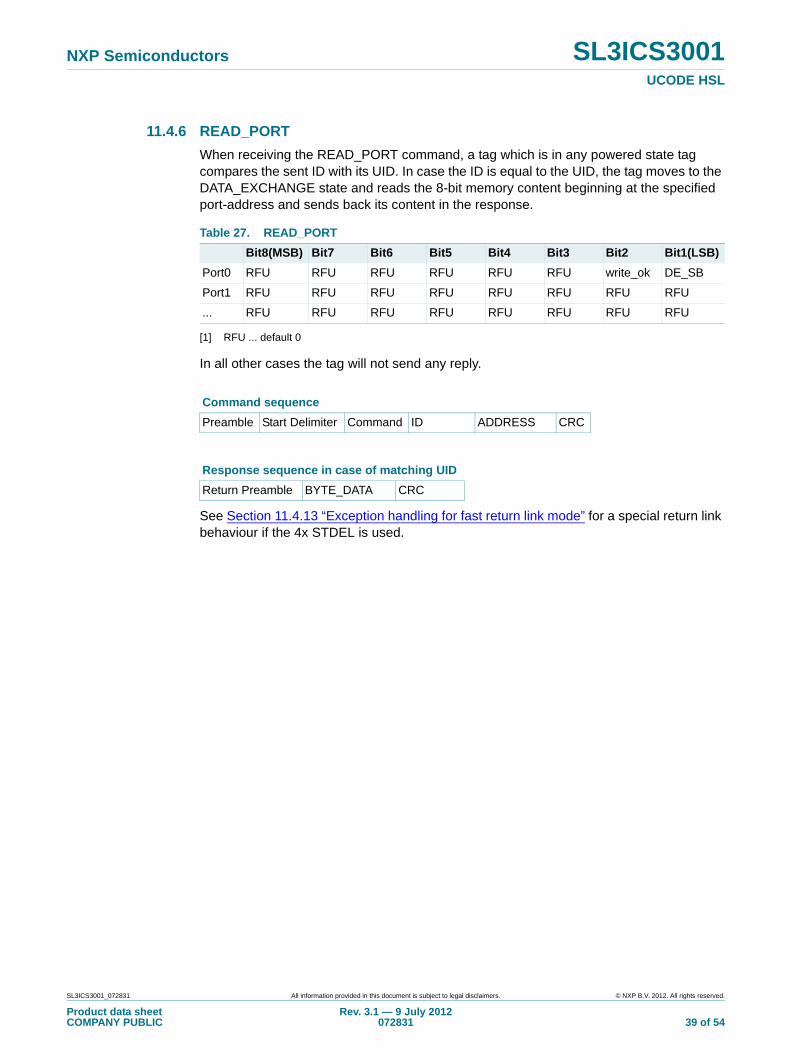
11.4.6 READ_PORT
When receiving the READ_PORT command, a tag which is in any powered state tag compares the sent ID with its UID. In case the ID is equal to the UID, the tag moves to the DATA_EXCHANGE state and reads the 8-bit memory content beginning at the specified port-address and sends back its content in the response.
[1] RFU ... default 0
In all other cases the tag will not send any reply.
See Section 11.4.13 “Exception handling for fast return link mode” for a special return link behaviour if the 4x STDEL is used.
Table 27. READ_PORT
Bit8(MSB) Bit7 Bit6 Bit5 Bit4 Bit3 Bit2 Bit1(LSB)
Port0 RFU RFU RFU RFU RFU RFU write_ok DE_SB
Port1 RFU RFU RFU RFU RFU RFU RFU RFU
... RFU RFU RFU RFU RFU RFU RFU RFU
Command sequence
Preamble Start Delimiter Command ID ADDRESS CRC
Response sequence in case of matching UID
Return Preamble BYTE_DATA CRC
SL3ICS3001_072831 All information provided in this document is subject to legal disclaimers. © NXP B.V. 2012. All rights reserved.
Product data sheetCOMPANY PUBLIC
Rev. 3.1 — 9 July 2012072831 39 of 54
NXP Semiconductors SL3ICS3001UCODE HSL
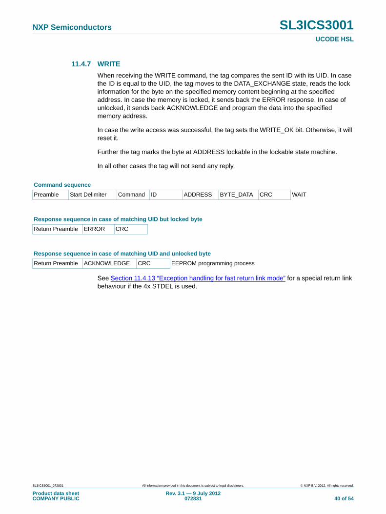
11.4.7 WRITE
When receiving the WRITE command, the tag compares the sent ID with its UID. In case the ID is equal to the UID, the tag moves to the DATA_EXCHANGE state, reads the lock information for the byte on the specified memory content beginning at the specified address. In case the memory is locked, it sends back the ERROR response. In case of unlocked, it sends back ACKNOWLEDGE and program the data into the specified memory address.
In case the write access was successful, the tag sets the WRITE_OK bit. Otherwise, it will reset it.
Further the tag marks the byte at ADDRESS lockable in the lockable state machine.
In all other cases the tag will not send any reply.
See Section 11.4.13 “Exception handling for fast return link mode” for a special return link behaviour if the 4x STDEL is used.
Command sequence
Preamble Start Delimiter Command ID ADDRESS BYTE_DATA CRC WAIT
Response sequence in case of matching UID but locked byte
Return Preamble ERROR CRC
Response sequence in case of matching UID and unlocked byte
Return Preamble ACKNOWLEDGE CRC EEPROM programming process
SL3ICS3001_072831 All information provided in this document is subject to legal disclaimers. © NXP B.V. 2012. All rights reserved.
Product data sheetCOMPANY PUBLIC
Rev. 3.1 — 9 July 2012072831 40 of 54
NXP Semiconductors SL3ICS3001UCODE HSL
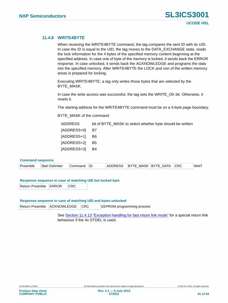
11.4.8 WRITE4BYTE
When receiving the WRITE4BYTE command, the tag compares the sent ID with its UID. In case the ID is equal to the UID, the tag moves to the DATA_EXCHANGE state, reads the lock information for the 4 bytes of the specified memory content beginning at the specified address. In case one of byte of the memory is locked, it sends back the ERROR response. In case unlocked, it sends back the ACKNOWLEDGE and programs the data into the specified memory. After WRITE4BYTE the LOCK and non of the written memory areas is prepared for locking.
Executing WRITE4BYTE, a tag only writes those bytes that are selected by the BYTE_MASK.
In case the write access was successful, the tag sets the WRITE_OK bit. Otherwise, it resets it.
The starting address for the WRITE4BYTE command must be on a 4-byte page boundary.
BYTE_MASK of the command
ADDRESS bit of BYTE_MASK to select whether byte should be written
[ADDRESS+0] B7
[ADDRESS+1] B6
[ADDRESS+2] B5
[ADDRESS+3] B4
See Section 11.4.13 “Exception handling for fast return link mode” for a special return link behaviour if the 4x STDEL is used.
Command sequence
Preamble Start Delimiter Command ID ADDRESS BYTE_MASK BYTE_DATA CRC WAIT
Response sequence in case of matching UID but locked byte
Return Preamble ERROR CRC
Response sequence in case of matching UID and bytes unlocked
Return Preamble ACKNOWLEDGE CRC EEPROM programming process
SL3ICS3001_072831 All information provided in this document is subject to legal disclaimers. © NXP B.V. 2012. All rights reserved.
Product data sheetCOMPANY PUBLIC
Rev. 3.1 — 9 July 2012072831 41 of 54
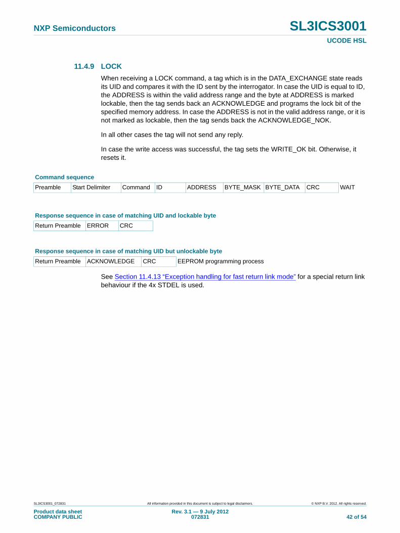
NXP Semiconductors SL3ICS3001UCODE HSL
11.4.9 LOCK
When receiving a LOCK command, a tag which is in the DATA_EXCHANGE state reads its UID and compares it with the ID sent by the interrogator. In case the UID is equal to ID, the ADDRESS is within the valid address range and the byte at ADDRESS is marked lockable, then the tag sends back an ACKNOWLEDGE and programs the lock bit of the specified memory address. In case the ADDRESS is not in the valid address range, or it is not marked as lockable, then the tag sends back the ACKNOWLEDGE_NOK.
In all other cases the tag will not send any reply.
In case the write access was successful, the tag sets the WRITE_OK bit. Otherwise, it resets it.
See Section 11.4.13 “Exception handling for fast return link mode” for a special return link behaviour if the 4x STDEL is used.
Command sequence
Preamble Start Delimiter Command ID ADDRESS BYTE_MASK BYTE_DATA CRC WAIT
Response sequence in case of matching UID and lockable byte
Return Preamble ERROR CRC
Response sequence in case of matching UID but unlockable byte
Return Preamble ACKNOWLEDGE CRC EEPROM programming process
SL3ICS3001_072831 All information provided in this document is subject to legal disclaimers. © NXP B.V. 2012. All rights reserved.
Product data sheetCOMPANY PUBLIC
Rev. 3.1 — 9 July 2012072831 42 of 54
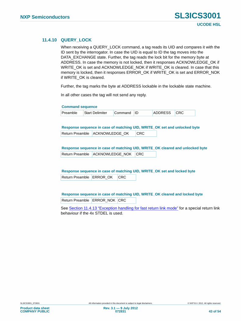
NXP Semiconductors SL3ICS3001UCODE HSL
11.4.10 QUERY_LOCK
When receiving a QUERY_LOCK command, a tag reads its UID and compares it with the ID sent by the interrogator. In case the UID is equal to ID the tag moves into the DATA_EXCHANGE state. Further, the tag reads the lock bit for the memory byte at ADDRESS. In case the memory is not locked, then it responses ACKNOWLEDGE_OK if WRITE_OK is set and ACKNOWLEDGE_NOK if WRITE_OK is cleared. In case that this memory is locked, then it responses ERROR_OK if WRITE_OK is set and ERROR_NOK if WRITE_OK is cleared.
Further, the tag marks the byte at ADDRESS lockable in the lockable state machine.
In all other cases the tag will not send any reply.
See Section 11.4.13 “Exception handling for fast return link mode” for a special return link behaviour if the 4x STDEL is used.
Command sequence
Preamble Start Delimiter Command ID ADDRESS CRC
Response sequence in case of matching UID, WRITE_OK set and unlocked byte
Return Preamble ACKNOWLEDGE_OK CRC
Response sequence in case of matching UID, WRITE_OK cleared and unlocked byte
Return Preamble ACKNOWLEDGE_NOK CRC
Response sequence in case of matching UID, WRITE_OK set and locked byte
Return Preamble ERROR_OK CRC
Response sequence in case of matching UID, WRITE_OK cleared and locked byte
Return Preamble ERROR_NOK CRC
SL3ICS3001_072831 All information provided in this document is subject to legal disclaimers. © NXP B.V. 2012. All rights reserved.
Product data sheetCOMPANY PUBLIC
Rev. 3.1 — 9 July 2012072831 43 of 54

NXP Semiconductors SL3ICS3001UCODE HSL
11.4.11 WRITE_MULTIPLE
This command is used to write to and to verify multiple tags in parallel.
When receiving the WRITE_MULTIPLE command, a tag which is in the ID state or the DATA_EXCHANGE state reads the lock information for the byte on the specified memory content beginning at the specified ADDRESS. In case the memory is locked, it does nothing. In case unlocked, it programs the BYTE_DATA into the specified memory.
In case the write access was successful, the tag sets the WRITE_OK bit. Otherwise, it resets it.
The tag will not send any response.
Remark: As there is not tag response following this command, the 1 x STDEL has to be used
11.4.12 WRITE4BYTE_MULTIPLE
This command is used to write to and to verify multiple tags in parallel.
When receiving the WRITE4BYTE_MULTIPLE command, a tag which is in the ID state or the DATA_EXCHANGE state reads the lock information for the byte on the specified memory content beginning at the specified ADDRESS. In case the memory is locked, it does nothing. In case unlocked, it programs the BYTE_DATA into the specified memory.
Executing WRITE4BYTE_MULTIPLE a tag only writes those bytes that are selected by the BYTE_MASK.
In case the write access was successful, the tag sets the WRITE_OK bit. Otherwise, it resets it.
The starting address for the WRITE4BYTE_MULTIPLE command must be on a 4-byte page boundary.
The tag will not send any response.
BYTE_MASK of the command:
ADDRESS bit of BYTE_MASK to select whether byte should be written
[ADDRESS+0] B7
[ADDRESS+1] B6
[ADDRESS+2] B5
[ADDRESS+3] B4
Remark: As there is not tag response following this command, the 1 x STDEL has to be used
Command sequence
Preamble Start Delimiter Command ADDRESS BYTE_DATA CRC WAIT
Command sequence
Preamble Start Delimiter Command ADDRESS BYTE_MASK 4BYTE_DATA CRC WAIT
SL3ICS3001_072831 All information provided in this document is subject to legal disclaimers. © NXP B.V. 2012. All rights reserved.
Product data sheetCOMPANY PUBLIC
Rev. 3.1 — 9 July 2012072831 44 of 54
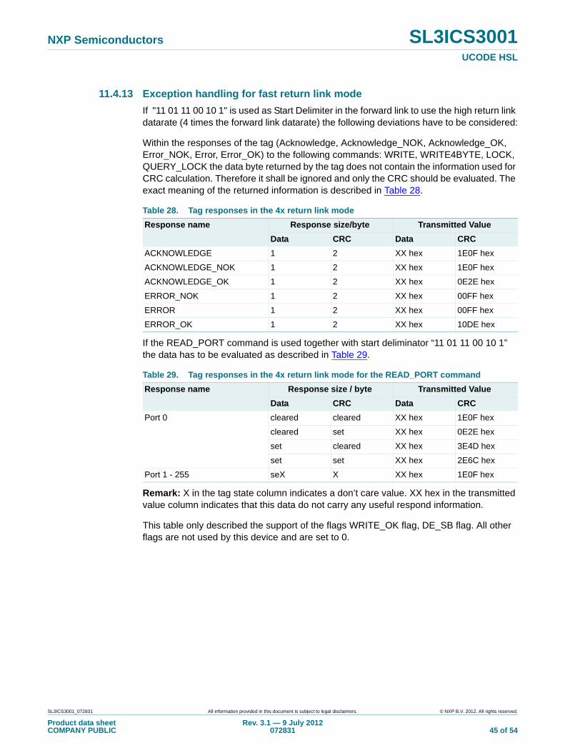
NXP Semiconductors SL3ICS3001UCODE HSL
11.4.13 Exception handling for fast return link mode
If "11 01 11 00 10 1" is used as Start Delimiter in the forward link to use the high return link datarate (4 times the forward link datarate) the following deviations have to be considered:
Within the responses of the tag (Acknowledge, Acknowledge_NOK, Acknowledge_OK, Error_NOK, Error, Error_OK) to the following commands: WRITE, WRITE4BYTE, LOCK, QUERY_LOCK the data byte returned by the tag does not contain the information used for CRC calculation. Therefore it shall be ignored and only the CRC should be evaluated. The exact meaning of the returned information is described in Table 28.
If the READ_PORT command is used together with start deliminator “11 01 11 00 10 1” the data has to be evaluated as described in Table 29.
Remark: X in the tag state column indicates a don’t care value. XX hex in the transmitted value column indicates that this data do not carry any useful respond information.
This table only described the support of the flags WRITE_OK flag, DE_SB flag. All other flags are not used by this device and are set to 0.
Table 28. Tag responses in the 4x return link mode
Response name Response size/byte Transmitted Value
Data CRC Data CRC
ACKNOWLEDGE 1 2 XX hex 1E0F hex
ACKNOWLEDGE_NOK 1 2 XX hex 1E0F hex
ACKNOWLEDGE_OK 1 2 XX hex 0E2E hex
ERROR_NOK 1 2 XX hex 00FF hex
ERROR 1 2 XX hex 00FF hex
ERROR_OK 1 2 XX hex 10DE hex
Table 29. Tag responses in the 4x return link mode for the READ_PORT command
Response name Response size / byte Transmitted Value
Data CRC Data CRC
Port 0 cleared cleared XX hex 1E0F hex
cleared set XX hex 0E2E hex
set cleared XX hex 3E4D hex
set set XX hex 2E6C hex
Port 1 - 255 seX X XX hex 1E0F hex
SL3ICS3001_072831 All information provided in this document is subject to legal disclaimers. © NXP B.V. 2012. All rights reserved.
Product data sheetCOMPANY PUBLIC
Rev. 3.1 — 9 July 2012072831 45 of 54
NXP Semiconductors SL3ICS3001UCODE HSL
12. Limiting values
Please refer to Ref. 7 “Data sheet addendum”.
13. Characteristics
13.1 DC characteristics
[1] The measured operating voltage is the open-circuit voltage of a source with a 50 output impedance.
13.2 AC characteristics
Table 30. DC characteristicsVDD > VDDmin; VSS = 0 V; Tamb = 40 to 85 C; all voltages with respect to VSS unless otherwise specified.
Symbol Parameter Conditions Min Max Unit
VRFP, min minimum supply voltage range for communication except EEPROM programming
[1] 1.15 1.55 V
VRFP, write minimum supply voltage for EEPROM programming
[1] 2.10 2.40 V
Table 31. AC characteristicsVDD > VDDmin; VSS = 0 V; Tamb = 40 to 85 C; all voltages with respect to VSS unless otherwise specified.
Symbol Parameter Conditions Min Max Unit
tDE_SB Storage time for Data_Exchange Status Bit
IC temperature: 0 to 50 C
4 - s
IC temperature:-30C to 60 C
2 - s
tEEwrite Required time for programming the EEPROM
13.3 - ms
tEEwrite Power interruptions, no notice - 0.5 s
tSD Power interruptions, start of demodulation
0.5 250 s
SL3ICS3001_072831 All information provided in this document is subject to legal disclaimers. © NXP B.V. 2012. All rights reserved.
Product data sheetCOMPANY PUBLIC
Rev. 3.1 — 9 July 2012072831 46 of 54
NXP Semiconductors SL3ICS3001UCODE HSL
14. Package outline
Please refer to Ref. 7 “Data sheet addendum”.
15. Abbreviations
16. References
[1] [CEPT1] — CEPT REC 70-03 Annex 1
[2] [CEPT1] — CEPT REC 70-03 Annex 1
[3] [CEPT2] — CEPT REC 70-03 Annex 11
[4] [ETSI1] — ETSI EN 330 220-1
[5] [ETSI2] — ETSI EN 330 440-1
[6] [FCC1] — FCC Part 15 Section 247
[7] Data sheet addendum — SL3ICS3001 Bumped Wafer Specfication, document number: 0707**1
Table 32. Abbreviations
Acronym Description
ID Tag identification number sent by the interrogator
UID Unique Tag identification number stored in the tag
Forward link Transmitted data from the interrogator to the tag
Return link Transmitted data from the tag to the interrogator
CRC Cyclic Redundancy Check
EEPROM Electrically Erasable and Programmable Read Only Memory
xxh Value in hexadecimal notation
IC Integrated Circuit
LSB Least Significant Bit or Byte
MSB Most Significant Bit or Byte
RF Radio Frequency
NRZ Non-return to zero coding
FM0 Bi phase space modulation
1. ** ... document version number
SL3ICS3001_072831 All information provided in this document is subject to legal disclaimers. © NXP B.V. 2012. All rights reserved.
Product data sheetCOMPANY PUBLIC
Rev. 3.1 — 9 July 2012072831 47 of 54
NXP Semiconductors SL3ICS3001UCODE HSL
17. Revision history
Table 33. Revision history
Document ID Release date Data sheet status Change notice Supersedes
SL3ICS3001_072831 v. 3.1 20120709 Product data sheet - SL3ICS3001_072831 v. 3.0
Modifications: • Table 2 “Ordering information”: Type number changed into SL3ICS3001FW/V7
SL3ICS3001_072831 v. 3.0 20090702 Product data sheet 072820
Modifications: • The format of this data sheet has been redesigned to comply with the new identity guidelines of NXP Semiconductors.
• Legal texts have been adapted to the new company name where appropriate.
• Change of product status.
• Section 3 “Applications” and Section 4 “Ordering information”: added
072820 September 2003 Objective data sheet 072811
• Update
072811 April 2003 Objective data sheet 072810
• Update
072810 June 2002 Objective data sheet
SL3ICS3001_072831 All information provided in this document is subject to legal disclaimers. © NXP B.V. 2012. All rights reserved.
Product data sheetCOMPANY PUBLIC
Rev. 3.1 — 9 July 2012072831 48 of 54
NXP Semiconductors SL3ICS3001UCODE HSL
18. Legal information
18.1 Data sheet status
[1] Please consult the most recently issued document before initiating or completing a design.
[2] The term ‘short data sheet’ is explained in section “Definitions”.
[3] The product status of device(s) described in this document may have changed since this document was published and may differ in case of multiple devices. The latest product status information is available on the Internet at URL http://www.nxp.com.
18.2 Definitions
Draft — The document is a draft version only. The content is still under internal review and subject to formal approval, which may result in modifications or additions. NXP Semiconductors does not give any representations or warranties as to the accuracy or completeness of information included herein and shall have no liability for the consequences of use of such information.
Short data sheet — A short data sheet is an extract from a full data sheet with the same product type number(s) and title. A short data sheet is intended for quick reference only and should not be relied upon to contain detailed and full information. For detailed and full information see the relevant full data sheet, which is available on request via the local NXP Semiconductors sales office. In case of any inconsistency or conflict with the short data sheet, the full data sheet shall prevail.
Product specification — The information and data provided in a Product data sheet shall define the specification of the product as agreed between NXP Semiconductors and its customer, unless NXP Semiconductors and customer have explicitly agreed otherwise in writing. In no event however, shall an agreement be valid in which the NXP Semiconductors product is deemed to offer functions and qualities beyond those described in the Product data sheet.
18.3 Disclaimers
Limited warranty and liability — Information in this document is believed to be accurate and reliable. However, NXP Semiconductors does not give any representations or warranties, expressed or implied, as to the accuracy or completeness of such information and shall have no liability for the consequences of use of such information. NXP Semiconductors takes no responsibility for the content in this document if provided by an information source outside of NXP Semiconductors.
In no event shall NXP Semiconductors be liable for any indirect, incidental, punitive, special or consequential damages (including - without limitation - lost profits, lost savings, business interruption, costs related to the removal or replacement of any products or rework charges) whether or not such damages are based on tort (including negligence), warranty, breach of contract or any other legal theory.
Notwithstanding any damages that customer might incur for any reason whatsoever, NXP Semiconductors’ aggregate and cumulative liability towards customer for the products described herein shall be limited in accordance with the Terms and conditions of commercial sale of NXP Semiconductors.
Right to make changes — NXP Semiconductors reserves the right to make changes to information published in this document, including without limitation specifications and product descriptions, at any time and without notice. This document supersedes and replaces all information supplied prior to the publication hereof.
Suitability for use — NXP Semiconductors products are not designed, authorized or warranted to be suitable for use in life support, life-critical or safety-critical systems or equipment, nor in applications where failure or malfunction of an NXP Semiconductors product can reasonably be expected to result in personal injury, death or severe property or environmental damage. NXP Semiconductors and its suppliers accept no liability for inclusion and/or use of NXP Semiconductors products in such equipment or applications and therefore such inclusion and/or use is at the customer’s own risk.
Applications — Applications that are described herein for any of these products are for illustrative purposes only. NXP Semiconductors makes no representation or warranty that such applications will be suitable for the specified use without further testing or modification.
Customers are responsible for the design and operation of their applications and products using NXP Semiconductors products, and NXP Semiconductors accepts no liability for any assistance with applications or customer product design. It is customer’s sole responsibility to determine whether the NXP Semiconductors product is suitable and fit for the customer’s applications and products planned, as well as for the planned application and use of customer’s third party customer(s). Customers should provide appropriate design and operating safeguards to minimize the risks associated with their applications and products.
NXP Semiconductors does not accept any liability related to any default, damage, costs or problem which is based on any weakness or default in the customer’s applications or products, or the application or use by customer’s third party customer(s). Customer is responsible for doing all necessary testing for the customer’s applications and products using NXP Semiconductors products in order to avoid a default of the applications and the products or of the application or use by customer’s third party customer(s). NXP does not accept any liability in this respect.
Limiting values — Stress above one or more limiting values (as defined in the Absolute Maximum Ratings System of IEC 60134) will cause permanent damage to the device. Limiting values are stress ratings only and (proper) operation of the device at these or any other conditions above those given in the Recommended operating conditions section (if present) or the Characteristics sections of this document is not warranted. Constant or repeated exposure to limiting values will permanently and irreversibly affect the quality and reliability of the device.
Terms and conditions of commercial sale — NXP Semiconductors products are sold subject to the general terms and conditions of commercial sale, as published at http://www.nxp.com/profile/terms, unless otherwise agreed in a valid written individual agreement. In case an individual agreement is concluded only the terms and conditions of the respective agreement shall apply. NXP Semiconductors hereby expressly objects to applying the customer’s general terms and conditions with regard to the purchase of NXP Semiconductors products by customer.
No offer to sell or license — Nothing in this document may be interpreted or construed as an offer to sell products that is open for acceptance or the grant, conveyance or implication of any license under any copyrights, patents or other industrial or intellectual property rights.
Document status[1][2] Product status[3] Definition
Objective [short] data sheet Development This document contains data from the objective specification for product development.
Preliminary [short] data sheet Qualification This document contains data from the preliminary specification.
Product [short] data sheet Production This document contains the product specification.
SL3ICS3001_072831 All information provided in this document is subject to legal disclaimers. © NXP B.V. 2012. All rights reserved.
Product data sheetCOMPANY PUBLIC
Rev. 3.1 — 9 July 2012072831 49 of 54
NXP Semiconductors SL3ICS3001UCODE HSL
Export control — This document as well as the item(s) described herein may be subject to export control regulations. Export might require a prior authorization from competent authorities.
Quick reference data — The Quick reference data is an extract of the product data given in the Limiting values and Characteristics sections of this document, and as such is not complete, exhaustive or legally binding.
Non-automotive qualified products — Unless this data sheet expressly states that this specific NXP Semiconductors product is automotive qualified, the product is not suitable for automotive use. It is neither qualified nor tested in accordance with automotive testing or application requirements. NXP Semiconductors accepts no liability for inclusion and/or use of non-automotive qualified products in automotive equipment or applications.
In the event that customer uses the product for design-in and use in automotive applications to automotive specifications and standards, customer (a) shall use the product without NXP Semiconductors’ warranty of the product for such automotive applications, use and specifications, and (b)
whenever customer uses the product for automotive applications beyond NXP Semiconductors’ specifications such use shall be solely at customer’s own risk, and (c) customer fully indemnifies NXP Semiconductors for any liability, damages or failed product claims resulting from customer design and use of the product for automotive applications beyond NXP Semiconductors’ standard warranty and NXP Semiconductors’ product specifications.
Translations — A non-English (translated) version of a document is for reference only. The English version shall prevail in case of any discrepancy between the translated and English versions.
18.4 TrademarksNotice: All referenced brands, product names, service names and trademarks are the property of their respective owners.
UCODE — is a trademark of NXP B.V.
19. Contact information
For more information, please visit: http://www.nxp.com
For sales office addresses, please send an email to: [email protected]
SL3ICS3001_072831 All information provided in this document is subject to legal disclaimers. © NXP B.V. 2012. All rights reserved.
Product data sheetCOMPANY PUBLIC
Rev. 3.1 — 9 July 2012072831 50 of 54
NXP Semiconductors SL3ICS3001UCODE HSL
20. Tables
Table 1. Operating distances for UCODE HSL based tags and labels in released frequency bands . . . . . . .3
Table 2. Ordering information. . . . . . . . . . . . . . . . . . . . . .4Table 3. Released operating frequency bands. . . . . . . . .6Table 4. Command Overview . . . . . . . . . . . . . . . . . . . . . .9Table 5. State transition table . . . . . . . . . . . . . . . . . . . . .10Table 6. Flags. . . . . . . . . . . . . . . . . . . . . . . . . . . . . . . . . 11Table 7. Definition of forward PREAMBLE . . . . . . . . . . .14Table 8. Definition of START DELIMITER . . . . . . . . . . .14Table 9. Definition of forward RETURN PREAMBLE . . .15Table 10. CRC definition . . . . . . . . . . . . . . . . . . . . . . . . .16Table 11. Practical example of CRC calculation for a
'SUCCESS' command in the Interrogator. . . . .17Table 12. Practical example of CRC checking for a
'SUCCESS' command in the Tag . . . . . . . . . . .17Table 13. Definition of TAG RESYNC. . . . . . . . . . . . . . . .18Table 14. Forward data rate . . . . . . . . . . . . . . . . . . . . . . .18Table 15. Modulation Type 18 % - Parameters for the RF
envelop shape . . . . . . . . . . . . . . . . . . . . . . . . .19Table 16. Modulation Type 100% - Parameters for the RF
envelop shape . . . . . . . . . . . . . . . . . . . . . . . . .19Table 17. Bit duty cycle tolerance. . . . . . . . . . . . . . . . . . .20Table 18. Return data rate . . . . . . . . . . . . . . . . . . . . . . . .20Table 19. Bit duty cycle tolerance. . . . . . . . . . . . . . . . . . .20Table 20. Maximum interrogator settling time. . . . . . . . . .21Table 21. Timing limits . . . . . . . . . . . . . . . . . . . . . . . . . . .22Table 22. Tag reaction on power interruptions . . . . . . . . .22Table 23. Configuration of delivered ICs . . . . . . . . . . . . .23Table 24. Command codes and format . . . . . . . . . . . . . .24Table 25. Command fields . . . . . . . . . . . . . . . . . . . . . . . .25Table 26. Tag response . . . . . . . . . . . . . . . . . . . . . . . . . .25Table 27. READ_PORT . . . . . . . . . . . . . . . . . . . . . . . . . .39Table 28. Tag responses in the 4x return link mode. . . . .45Table 29. Tag responses in the 4x return link mode for the
READ_PORT command. . . . . . . . . . . . . . . . . .45Table 30. DC characteristics . . . . . . . . . . . . . . . . . . . . . .46Table 31. AC characteristics . . . . . . . . . . . . . . . . . . . . . .46Table 32. Abbreviations . . . . . . . . . . . . . . . . . . . . . . . . . .47Table 33. Revision history . . . . . . . . . . . . . . . . . . . . . . . .48
SL3ICS3001_072831 All information provided in this document is subject to legal disclaimers. © NXP B.V. 2012. All rights reserved.
Product data sheetCOMPANY PUBLIC
Rev. 3.1 — 9 July 2012072831 51 of 54
NXP Semiconductors SL3ICS3001UCODE HSL
21. Figures
Fig 1. Block diagram . . . . . . . . . . . . . . . . . . . . . . . . . . . .5Fig 2. State diagram. . . . . . . . . . . . . . . . . . . . . . . . . . . . .7Fig 3. Example of a forward link sequence . . . . . . . . . .14Fig 4. Example of a return link sequence . . . . . . . . . . .15Fig 5. Example for bit and byte ordering for the
GROUP_SELECT command. . . . . . . . . . . . . . . .15Fig 6. Definition of the RF envelope in the forward link .19Fig 7. Example of a 100% modulation. . . . . . . . . . . . . .20Fig 8. Example of a 15% modulation. . . . . . . . . . . . . . .20Fig 9. Definition of a Manchester ‘0’ . . . . . . . . . . . . . . .21Fig 10. Definition of a Manchester ‘1’. . . . . . . . . . . . . . . .21Fig 11. RF envelope - power up waveform . . . . . . . . . . .22
SL3ICS3001_072831 All information provided in this document is subject to legal disclaimers. © NXP B.V. 2012. All rights reserved.
Product data sheetCOMPANY PUBLIC
Rev. 3.1 — 9 July 2012072831 52 of 54
NXP Semiconductors SL3ICS3001UCODE HSL
22. Contents
1 General description . . . . . . . . . . . . . . . . . . . . . . 1
2 Features and benefits . . . . . . . . . . . . . . . . . . . . 22.1 RF interface features . . . . . . . . . . . . . . . . . . . . 22.2 Memory features. . . . . . . . . . . . . . . . . . . . . . . . 22.3 Security features. . . . . . . . . . . . . . . . . . . . . . . . 22.4 Operating distances features . . . . . . . . . . . . . . 22.5 Air interface standards . . . . . . . . . . . . . . . . . . . 42.6 Application standards . . . . . . . . . . . . . . . . . . . . 4
3 Applications . . . . . . . . . . . . . . . . . . . . . . . . . . . . 4
4 Ordering information. . . . . . . . . . . . . . . . . . . . . 4
5 Block diagram . . . . . . . . . . . . . . . . . . . . . . . . . . 5
6 Pinning information. . . . . . . . . . . . . . . . . . . . . . 5
7 Functional description . . . . . . . . . . . . . . . . . . . 67.1 Power transfer . . . . . . . . . . . . . . . . . . . . . . . . . 67.2 Operation frequency . . . . . . . . . . . . . . . . . . . . . 67.3 Data transfer . . . . . . . . . . . . . . . . . . . . . . . . . . . 67.3.1 Forward link . . . . . . . . . . . . . . . . . . . . . . . . . . . 67.3.2 Return link . . . . . . . . . . . . . . . . . . . . . . . . . . . . 6
8 Protocol . . . . . . . . . . . . . . . . . . . . . . . . . . . . . . . 78.1 Major digital states . . . . . . . . . . . . . . . . . . . . . . 7
State transition description . . . . . . . . . . . . . . . . .88.2 Command overview . . . . . . . . . . . . . . . . . . . . . 98.3 Flags. . . . . . . . . . . . . . . . . . . . . . . . . . . . . . . . 118.3.1 Data_Exchange status bit. . . . . . . . . . . . . . . . 118.3.2 WRITE_OK. . . . . . . . . . . . . . . . . . . . . . . . . . . 118.4 Lockable state machine . . . . . . . . . . . . . . . . . 128.5 Collision arbitration, anticollision. . . . . . . . . . . 128.6 Data exchange sequences . . . . . . . . . . . . . . . 138.6.1 Forward link . . . . . . . . . . . . . . . . . . . . . . . . . . 138.6.1.1 Preamble . . . . . . . . . . . . . . . . . . . . . . . . . . . . 148.6.1.2 START DELIMITER . . . . . . . . . . . . . . . . . . . . 148.6.2 Return link . . . . . . . . . . . . . . . . . . . . . . . . . . . 148.6.2.1 RETURN PREAMBLE . . . . . . . . . . . . . . . . . . 158.7 Bit and byte ordering . . . . . . . . . . . . . . . . . . . 158.8 Data integrity. . . . . . . . . . . . . . . . . . . . . . . . . . 158.9 CRC definition . . . . . . . . . . . . . . . . . . . . . . . . 168.9.1 CRC algorithm . . . . . . . . . . . . . . . . . . . . . . . . 168.9.2 CRC calculation example . . . . . . . . . . . . . . . . 16
9 Communication timing and waveforms. . . . . 189.1 Forward link . . . . . . . . . . . . . . . . . . . . . . . . . . 189.1.1 Communication rate . . . . . . . . . . . . . . . . . . . . 189.1.2 Modulation Waveform of Interrogator
Modulation . . . . . . . . . . . . . . . . . . . . . . . . . . . 199.1.3 RF envelope of data streams . . . . . . . . . . . . . 209.2 Return link . . . . . . . . . . . . . . . . . . . . . . . . . . . 209.2.1 Communication rate . . . . . . . . . . . . . . . . . . . . 20
9.2.2 Modulation Waveform of Transponder Modulation . . . . . . . . . . . . . . . . . . . . . . . . . . . 20
9.3 Bit Coding . . . . . . . . . . . . . . . . . . . . . . . . . . . 219.3.1 Forward Link . . . . . . . . . . . . . . . . . . . . . . . . . 219.3.2 Return Link. . . . . . . . . . . . . . . . . . . . . . . . . . . 219.4 Response Time . . . . . . . . . . . . . . . . . . . . . . . 219.5 Regeneration Time. . . . . . . . . . . . . . . . . . . . . 219.6 Start-up Time . . . . . . . . . . . . . . . . . . . . . . . . . 229.7 Power interruptions . . . . . . . . . . . . . . . . . . . . 22
10 Memory . . . . . . . . . . . . . . . . . . . . . . . . . . . . . . 2310.1 Memory organization . . . . . . . . . . . . . . . . . . . 2310.2 Definition of block contents . . . . . . . . . . . . . . 2310.2.1 UID. . . . . . . . . . . . . . . . . . . . . . . . . . . . . . . . . 2310.3 Configuration of delivered ICs . . . . . . . . . . . . 23
11 Commands. . . . . . . . . . . . . . . . . . . . . . . . . . . . 2411.1 Definitions . . . . . . . . . . . . . . . . . . . . . . . . . . . 2411.2 Selection commands . . . . . . . . . . . . . . . . . . . 2611.2.1 Data comparison for selection commands . . 2611.2.1.1 Data comparison for selection commands on
memory . . . . . . . . . . . . . . . . . . . . . . . . . . . . . 26The argument of the comparison are: . . . . . . . 26and the argument of the command: . . . . . . . . . 26The argument BYTE_MASK defines what bytes to be considered for comparison: . . . . . . 27
11.2.1.2 Data comparison for selection commands on flags . . . . . . . . . . . . . . . . . . . . . . . . . . . . . 27The argument BYTE_MASK defines what bytes to be considered for comparison: . . . . . . 28
11.2.2 GROUP_SELECT_EQ. . . . . . . . . . . . . . . . . . 2911.2.3 GROUP_SELECT_NE. . . . . . . . . . . . . . . . . . 2911.2.4 GROUP_SELECT_GT. . . . . . . . . . . . . . . . . . 3011.2.5 GROUP_SELECT_LT . . . . . . . . . . . . . . . . . . 3011.2.6 GROUP_UNSELECT_EQ . . . . . . . . . . . . . . 3111.2.7 GROUP_UNSELECT_NE . . . . . . . . . . . . . . . 3111.2.8 GROUP_UNSELECT_GT . . . . . . . . . . . . . . . 3111.2.9 GROUP_UNSELECT_LT. . . . . . . . . . . . . . . . 3211.2.10 MULTIPLE_UNSELECT. . . . . . . . . . . . . . . . . 3211.2.11 GROUP_SELECT_EQ_FLAGS. . . . . . . . . . . 3311.2.12 GROUP_SELECT_NE_FLAGS . . . . . . . . . . . 3311.2.13 GROUP_UNSELECT_EQ_FLAGS . . . . . . . . 3411.2.14 GROUP_UNSELECT_NE_FLAGS . . . . . . . . 3411.3 Identification commands . . . . . . . . . . . . . . . . 3511.3.1 FAIL . . . . . . . . . . . . . . . . . . . . . . . . . . . . . . . . 3511.3.2 SUCCESS . . . . . . . . . . . . . . . . . . . . . . . . . . . 3511.3.3 RESEND . . . . . . . . . . . . . . . . . . . . . . . . . . . . 3611.3.4 INITIALIZE . . . . . . . . . . . . . . . . . . . . . . . . . . . 3611.4 Data Transfer commands . . . . . . . . . . . . . . . 36
SL3ICS3001_072831 All information provided in this document is subject to legal disclaimers. © NXP B.V. 2012. All rights reserved.
Product data sheetCOMPANY PUBLIC
Rev. 3.1 — 9 July 2012072831 53 of 54
continued >>
NXP Semiconductors SL3ICS3001UCODE HSL
11.4.1 READ . . . . . . . . . . . . . . . . . . . . . . . . . . . . . . . 3611.4.2 READ_VARIABLE . . . . . . . . . . . . . . . . . . . . . 3711.4.3 DATA_READ. . . . . . . . . . . . . . . . . . . . . . . . . . 3711.4.4 READ_VERIFY. . . . . . . . . . . . . . . . . . . . . . . . 3811.4.5 READ_VERIFY_4BYTES. . . . . . . . . . . . . . . . 3811.4.6 READ_PORT . . . . . . . . . . . . . . . . . . . . . . . . . 3911.4.7 WRITE . . . . . . . . . . . . . . . . . . . . . . . . . . . . . . 4011.4.8 WRITE4BYTE. . . . . . . . . . . . . . . . . . . . . . . . . 4111.4.9 LOCK . . . . . . . . . . . . . . . . . . . . . . . . . . . . . . . 4211.4.10 QUERY_LOCK . . . . . . . . . . . . . . . . . . . . . . . . 4311.4.11 WRITE_MULTIPLE. . . . . . . . . . . . . . . . . . . . . 4411.4.12 WRITE4BYTE_MULTIPLE . . . . . . . . . . . . . . . 4411.4.13 Exception handling for fast return link mode. . 45
12 Limiting values. . . . . . . . . . . . . . . . . . . . . . . . . 46
13 Characteristics. . . . . . . . . . . . . . . . . . . . . . . . . 4613.1 DC characteristics . . . . . . . . . . . . . . . . . . . . . 4613.2 AC characteristics. . . . . . . . . . . . . . . . . . . . . . 46
14 Package outline . . . . . . . . . . . . . . . . . . . . . . . . 47
15 Abbreviations. . . . . . . . . . . . . . . . . . . . . . . . . . 47
16 References . . . . . . . . . . . . . . . . . . . . . . . . . . . . 47
17 Revision history. . . . . . . . . . . . . . . . . . . . . . . . 48
18 Legal information. . . . . . . . . . . . . . . . . . . . . . . 4918.1 Data sheet status . . . . . . . . . . . . . . . . . . . . . . 4918.2 Definitions. . . . . . . . . . . . . . . . . . . . . . . . . . . . 4918.3 Disclaimers . . . . . . . . . . . . . . . . . . . . . . . . . . . 4918.4 Trademarks. . . . . . . . . . . . . . . . . . . . . . . . . . . 50
19 Contact information. . . . . . . . . . . . . . . . . . . . . 50
20 Tables . . . . . . . . . . . . . . . . . . . . . . . . . . . . . . . . 51
21 Figures . . . . . . . . . . . . . . . . . . . . . . . . . . . . . . . 52
22 Contents . . . . . . . . . . . . . . . . . . . . . . . . . . . . . . 53
© NXP B.V. 2012. All rights reserved.
For more information, please visit: http://www.nxp.comFor sales office addresses, please send an email to: [email protected]
Date of release: 9 July 2012072831
Please be aware that important notices concerning this document and the product(s)described herein, have been included in section ‘Legal information’.
Related Documents