SKYPER 32 PRO R © by SEMIKRON Rev. 5.0 – 17.10.2018 1 SKYPER ® Driver Core IGBT Driver Core Order Nr.: L6100202 SKYPER 32 PRO R Features • Two output channels • Integrated potential free power supply • Under voltage protection prim/sec • Driver interlock top / bottom • Dynamic short circuit protection • Halt status with failure management • External failure input (sec.) • Soft turn-off • UL recognized, ROHS • IEC 60068-1 (climate) 40/085/56, no condensation and no dripping water permitted, non-corrosive, climate class 3K3 acc. EN60721 • Coated with varnish Typical Applications* • Driver for IGBT modules in bridge circuits in industrial application • DC bus voltage up to 1200V Footnotes with external high voltage diode Please Note: the insulation test is not performed as a series test at SEMIKRON and must be performed by the user according to VDE 0110-20 Isolation coordination in compliance with EN50178 PD2 Operating temperature is real ambient temperature around the driver core Degree of protection: IP00 This is an electrostatic discharge sensitive device (ESDS), international standard IEC 60747-1, chapter IX. *IMPORTANT INFORMATION AND WARNINGS The specifications of SEMIKRON products may not be considered as guarantee or assurance of product characteristics ("Beschaffenheitsgarantie"). The specifications of SEMIKRON products describe only the usual characteristics of products to be expected in typical applications, which may still vary depending on the specific application. Therefore, products must be tested for the respective application in advance. Application adjustments may be Absolute Maximum Ratings Symbol Conditions Values Unit V s Supply voltage primary 16 V V iH Input signal voltage (HIGH) Vs + 0.3 V V iL Input signal voltage (LOW) GND - 0.3 V Iout PEAK Output peak current 15 A Iout AVmax Output average current 50 mA f max Max. switching frequency 50 kHz V CE Collector emitter voltage sense across the IGBT 1700 V dv/dt Rate of rise and fall of voltage secondary to primary side 50 kV/μs V isol IO Insulation test voltage input - output (AC, rms, 2s) 4000 V V isolPD Partial discharge extinction voltage, rms, Q PD ≤ 10pC 1500 V V isol12 Insulation test voltage output 1 - output 2 (AC, rms, 2s) 1500 V R Gon min Minimum rating for external R Gon 1.5 Ω R Goff min Minimum rating for external R Goff 1.5 Ω Q out/pulse Max. rating for output charge per pulse 6.3 μC T op Operating temperature -40 ... 85 °C T stg Storage temperature -40 ... 85 °C Characteristics Symbol Conditions min. typ. max. Unit V s Supply voltage primary side 14.4 15 15.6 V I S0 Supply current primary (no load) 80 mA Supply current primary side (max.) 500 mA V i Input signal voltage on / off 15 / 0 V V IT+ Input threshold voltage (HIGH) 12.3 V V IT- Input threshold voltage (LOW) 4.6 V R IN Input resistance (switching/HALT signal) 100 kΩ V G(on) Turn on output voltage 15 V V G(off) Turn off output voltage -7 V f ASIC Asic system switching frequency 8 MHz t d(on)IO Input-output turn-on propagation time 1.2 μs t d(off)IO Input-output turn-off propagation time 1.2 μs t d(err) Error input-output propagation time 3.1 5.8 μs t pRESET Error reset time 0.009 ms t TD Top-Bot interlock dead time 0 4.3 μs C ps Coupling capacitance prim sec 12 pF w weight 34 g MTBF Mean Time Between Failure 1.3 10 6 h

Welcome message from author
This document is posted to help you gain knowledge. Please leave a comment to let me know what you think about it! Share it to your friends and learn new things together.
Transcript

SKYPER 32 PRO R
SKYPER®
Driver Core
IGBT Driver CoreOrder Nr.: L6100202
SKYPER 32 PRO R
Features• Two output channels• Integrated potential free power supply• Under voltage protection prim/sec• Driver interlock top / bottom• Dynamic short circuit protection• Halt status with failure management• External failure input (sec.)• Soft turn-off• UL recognized, ROHS• IEC 60068-1 (climate) 40/085/56, no
condensation and no dripping water permitted, non-corrosive, climate class 3K3 acc. EN60721
• Coated with varnishTypical Applications*• Driver for IGBT modules in bridge
circuits in industrial application• DC bus voltage up to 1200V
Footnoteswith external high voltage diodePlease Note: the insulation test is not performed as a series test at SEMIKRON and must be performed by the useraccording to VDE 0110-20
Isolation coordination in compliance with EN50178 PD2Operating temperature is real ambient temperature around the driver coreDegree of protection: IP00
© by SEMIKRON
This is an electrostatic discharge sensitive device (ESDS), international standard IEC 60747-1, chapter IX.
*IMPORTANT INFORMATION AND WARNINGSThe specifications of SEMIKRON products may not be considered as guarantee or assurance of product characteristics ("Beschaffenheitsgarantie"). The specifications of SEMIKRON products describe only the usual characteristics of products to be expected in typical applications, which may still vary depending on the specific application. Therefore, products must be tested for the respective application in advance. Application adjustments may be
Absolute Maximum Ratings Symbol Conditions Values Unit
Vs Supply voltage primary 16 VViH Input signal voltage (HIGH) Vs + 0.3 VViL Input signal voltage (LOW) GND - 0.3 VIoutPEAK Output peak current 15 AIoutAVmax Output average current 50 mAfmax Max. switching frequency 50 kHzVCE
Collector emitter voltage sense across the IGBT 1700 V
dv/dt Rate of rise and fall of voltage secondary to primary side 50 kV/µs
Visol IOInsulation test voltage input - output (AC, rms, 2s) 4000 V
VisolPDPartial discharge extinction voltage, rms, QPD ≤ 10pC 1500 V
Visol12Insulation test voltage output 1 - output 2 (AC, rms, 2s) 1500 V
RGon min Minimum rating for external RGon 1.5 ΩRGoff min Minimum rating for external RGoff 1.5 ΩQout/pulse Max. rating for output charge per pulse 6.3 µCTop Operating temperature -40 ... 85 °CTstg Storage temperature -40 ... 85 °C
Characteristics Symbol Conditions min. typ. max. Unit
Vs Supply voltage primary side 14.4 15 15.6 VIS0 Supply current primary (no load) 80 mA
Supply current primary side (max.) 500 mAVi Input signal voltage on / off 15 / 0 VVIT+ Input threshold voltage (HIGH) 12.3 VVIT- Input threshold voltage (LOW) 4.6 VRIN
Input resistance (switching/HALT signal) 100 kΩ
VG(on) Turn on output voltage 15 VVG(off) Turn off output voltage -7 VfASIC Asic system switching frequency 8 MHztd(on)IO Input-output turn-on propagation time 1.2 µstd(off)IO Input-output turn-off propagation time 1.2 µstd(err) Error input-output propagation time 3.1 5.8 µstpRESET Error reset time 0.009 mstTD Top-Bot interlock dead time 0 4.3 µsCps Coupling capacitance prim sec 12 pFw weight 34 gMTBF Mean Time Between Failure 1.3 106h
Rev. 5.0 – 17.10.2018 1

SKYPER 32 PRO R
2
necessary. The user of SEMIKRON products is responsible for the safety of their applications embedding SEMIKRON products and must take adequate safety measures to prevent the applications from causing a physical injury, fire or other problem if any of SEMIKRON products become faulty. The user is responsible to make sure that the application design is compliant with all applicable laws, regulations, norms and standards. Except as otherwise explicitly approved by SEMIKRON in a written document signed by authorized representatives of SEMIKRON, SEMIKRON products may not be used in any applications where a failure of the product or any consequences of the use thereof can reasonably be expected to result in personal injury. No representation or warranty is given and no liability is assumed with respect to the accuracy, completeness and/or use of any information herein, including without limitation, warranties of non-infringement of intellectual property rights of any third party. SEMIKRON does not assume any liability arising out of the applications or use of any product; neither does it convey any license under its patent rights, copyrights, trade secrets or other intellectual property rights, nor the rights of others. SEMIKRON makes no representation or warranty of non-infringement or alleged non-infringement of intellectual property rights of any third party which may arise from applications. Due to technical requirements our products may contain dangerous substances. For information on the types in question please contact the nearest SEMIKRON sales office. This document supersedes and replaces all information previously supplied and may be superseded by updates. SEMIKRON reserves the right to make changes.
SKYPER®
Driver Core
IGBT Driver CoreOrder Nr.: L6100202
SKYPER 32 PRO R
Features• Two output channels• Integrated potential free power supply• Under voltage protection prim/sec• Driver interlock top / bottom• Dynamic short circuit protection• Halt status with failure management• External failure input (sec.)• Soft turn-off• UL recognized, ROHS• IEC 60068-1 (climate) 40/085/56, no
condensation and no dripping water permitted, non-corrosive, climate class 3K3 acc. EN60721
• Coated with varnishTypical Applications*• Driver for IGBT modules in bridge
circuits in industrial application• DC bus voltage up to 1200V
Footnoteswith external high voltage diodePlease Note: the insulation test is not performed as a series test at SEMIKRON and must be performed by the useraccording to VDE 0110-20
Isolation coordination in compliance with EN50178 PD2Operating temperature is real ambient temperature around the driver coreDegree of protection: IP00
Rev. 5.0 – 17.10.2018 © by SEMIKRON

SKYPER® 32PRO R
1 2018-08-20 – Rev05 © by SEMIKRON
Technical Explanations
Revision 05 Status: Prepared by: Approved by: Date:
Niklas Hofstötter, Johannes Krapp Marco Honsberg 20.08.2018
This Technical Explanation is valid for the following parts: Related Documents:
part number: L6100202 title: Data Sheet SKYPER 32PRO R
date code (YYWW): ≥ 1838
SKYPER® 32PRO R
Content
Application and Handling Instructions ...................................................................................................................................... 2
Further application support ....................................................................................................................................................... 3
General Description .................................................................................................................................................................. 4
Features of SKYPER 32PRO ................................................................................................................................................... 4
Block diagram ........................................................................................................................................................................... 5
Dimensions ............................................................................................................................................................................... 5
PIN Array – Primary Side ......................................................................................................................................................... 6
PIN Array – Secondary Side ..................................................................................................................................................... 7
Driver Performance .................................................................................................................................................................. 8
Insulation .................................................................................................................................................................................. 8
Isolation Test Voltage ............................................................................................................................................................... 9
Auxiliary Power Supply ............................................................................................................................................................. 9
Under Voltage Reset (UVR) ..................................................................................................................................................... 9
Under Voltage Protection (UVP) primary ................................................................................................................................ 10
Under Voltage Protection secondary ...................................................................................................................................... 10
Input Signals ........................................................................................................................................................................... 10
Short Pulse Suppression (SPS) ............................................................................................................................................. 11
Failure Management............................................................................................................................................................... 11
Halt Logic Signal (HLS) .......................................................................................................................................................... 12
Dead Time generation (Interlock TOP / BOT) adjustable (DT) ............................................................................................... 12
Dynamic Short Circuit Protection by VCEsat monitoring / de-saturation monitoring (DSCP) ..................................................... 13
Adjustment of DSCP............................................................................................................................................................... 14
High Voltage Diode for DSCP ................................................................................................................................................ 14
Gate resistors ......................................................................................................................................................................... 15
Soft Turn-Off (STO) ................................................................................................................................................................ 15
External Error Input (EEI) ....................................................................................................................................................... 16
Application Example ............................................................................................................................................................... 16
Mounting Notes ...................................................................................................................................................................... 17
Environmental Conditions ....................................................................................................................................................... 18
Marking ................................................................................................................................................................................... 19

SKYPER® 32PRO R
2 2018-08-20 – Rev05 © by SEMIKRON
Application and Handling Instructions
Please provide for static discharge protection during handling. As long as the hybrid driver is not completely assembled, the input terminals have to be short-circuited. Persons working with devices have to wear a grounded bracelet. Any synthetic floor coverings must not be statically chargeable. Even during transportation the input terminals have to be short-circuited using, for example, conductive rubber. Worktables have to be grounded. The same safety requirements apply to MOSFET- and IGBT-modules.
Any parasitic inductances within the DC-link have to be minimised. Over-voltages may be absorbed by C- or RCD-snubbers between main terminals for PLUS and MINUS of the power module.
When first operating a newly developed circuit, SEMIKRON recommends to apply low collector voltage and load current in the beginning and to increase these values gradually, observing the turn-off behaviour of the free-wheeling diode and the turn-off voltage spikes generated across the IGBT. An oscillograph check will be necessary. Additionally, the case temperature of the module has to be monitored. When the circuit operates correctly under rated operation conditions, short-circuit testing may be done, starting again with low collector voltage.
It is important to feed any errors back to the control circuit and to switch off the device immediately in failure events. Repeated turn-on of the IGBT into a short circuit with a high frequency may destroy the device.
The inputs of the hybrid driver are sensitive to over-voltage. Voltages higher than VS +0,3V or below -0,3V may destroy these inputs. Therefore, control signal over-voltages exceeding the above values have to be avoided.
The connecting leads between hybrid driver and the power module should be as short as possible (max. 20cm), the driver leads should be twisted.
When handling the driver, do not pick up the driver at the transformers. The driver MUST be handled at the PCB sides.
Correct handling Wrong handling
Please note:
Unless otherwise specified, all values in this technical explanation are typical values. Typical values are the average values expected in large quantities and are provided for information purposes only. These values can and do vary in different applications. All operating parameters should be validated by user’s technical experts for each application.

SKYPER® 32PRO R
3 2018-08-20 – Rev05 © by SEMIKRON
UL specified remarks
The equipment shall be installed in compliance with the mounting and spacing requirements of the end-use application.
SKYPER 32 shall be supplied by an isolated limited voltage / limited current source or a Class 2 source. The 15 A peak rating is an instantaneous peak rating only.
These devices do not incorporate solid-state motor overload protection. The need for overload protection and over-current protection devices shall be determined in the end-use product.
These devices have not been evaluated to over-voltage, over-current, and over-temperature control, and may need to be subjected to the applicable end-product tests.
Temperature and tests shall be considered in the end use. Due to the limited current source, only the effect of heat generating components in this device on adjacent components in the end product needs to be considered.
Connectors have not been evaluated field wiring; all connections are to be factory wired only.
Further application support
Latest information is available at http://www.semikron.com. For design support please read the SEMIKRON Application Manual Power Modules available at http://www.semikron.com.
SKYPER® 32PRO R
4 2018-08-20 – Rev05 © by SEMIKRON
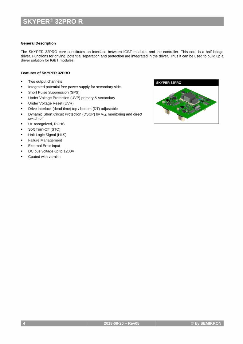
SKYPER 32PRO
General Description
The SKYPER 32PRO core constitutes an interface between IGBT modules and the controller. This core is a half bridge driver. Functions for driving, potential separation and protection are integrated in the driver. Thus it can be used to build up a driver solution for IGBT modules. Features of SKYPER 32PRO
Two output channels
Integrated potential free power supply for secondary side
Short Pulse Suppression (SPS)
Under Voltage Protection (UVP) primary & secondary
Under Voltage Reset (UVR)
Drive interlock (dead time) top / bottom (DT) adjustable
Dynamic Short Circuit Protection (DSCP) by VCE monitoring and direct switch off
UL recognized, ROHS
Soft Turn-Off (STO)
Halt Logic Signal (HLS)
Failure Management
External Error Input
DC bus voltage up to 1200V
Coated with varnish

SKYPER® 32PRO R
5 2018-08-20 – Rev05 © by SEMIKRON
Block diagram
Block diagram
Power
Supply
TOP
Power
Supply
BOT
Power Driver TOP
Power Driver BOT
Error Processing TOP- VCE monitoring
Error Processing BOT- VCE monitoring
Signal Processing:- short pulse suppression
- drive interlock top / bottom
- under voltage protection
- halt mode
DC/DC converter control
PRIM_TOP_IN
PRIM_BOT_IN
PRIM_HALT_IN
PRIM_PWR_15P
PRIM_HALT_OUT
PRIM_PWR_GND
SEC_TOP_VCE_CFG
SEC_TOP_VCE_IN
SEC_TOP_15P
SEC_TOP_GND
SEC_TOP_IGBT_ON
SEC_TOP_IGBT_OFF
SEC_TOP_8N
SEC_BOT_VCE_CFG
SEC_BOT_VCE_IN
SEC_BOT_15P
SEC_BOT_GND
SEC_BOT_IGBT_ON
SEC_BOT_IGBT_OFF
SEC_BOT_8N
PRIM_nPWRFAIL_IN
Under Voltage
Protection TOP
Soft
Turn-Off TOP
Under Voltage
Protection BOT
Soft
Turn-Off BOT
SEC_TOP_IGBT_SOFTOFF
SEC_TOP_ERR_IN
SEC_BOT_ERR_IN
SEC_BOT_IGBT_SOFTOFF
Dimensions
Dimensions in mm (bottom view) (top view)
±0,2mm unless otherwise noted

SKYPER® 32PRO R
6 2018-08-20 – Rev05 © by SEMIKRON
PIN Array – Primary Side
Connectors Connector X10 / X11 (RM2,54, 10pin)
2,54
2,5
4
8,1
3 ±
0,2
SQ 0,64
±0,25mm unless otherwise noted
PIN Signal Function Specification
X10:01 PRIM_nPWRFAIL_IN Under Voltage Reset (supervisor reset to be driven by an external circuitry)
Inverted 15 V logic; 100kOhm impedance; LOW = hold; HIGH = normal operation
X10:02 reserved
X10:03 PRIM_HALT_OUT Driver core status output Digital 15 V logic; max. 2mA; LOW = ready to operate; HIGH = not ready to operate
X10:04 PRIM_HALT_IN Driver core status input Digital 15 V logic; 100kOhm impedance; LOW = enable driver; HIGH = disable driver
X10:05 PRIM_PWR_GND GND for power supply and GND for digital signals
X10:06 PRIM_PWR_GND GND for power supply and GND for digital signals
X10:07 PRIM_TOP_IN Switching signal input (TOP switch) Digital 15 V logic; 100kOhm impedance; LOW = TOP switch off; HIGH = TOP switch on
X10:08 PRIM_BOT_IN Switching signal input (BOTTOM switch) Digital 15 V logic; 100kOhm impedance; LOW = BOT switch off; HIGH = BOT switch on
X10:09 PRIM_PWR_15P Drive core power supply Stabilised +15V ±4%
X10:10 PRIM_PWR_15P Drive core power supply Stabilised +15V ±4%
X11:01 reserved
X11:02 reserved
X11:03 PRIM_PWR_GND GND for power supply and GND for digital signals
X11:04 PRIM_PWR_GND GND for power supply and GND for digital signals
X11:05 PRIM_CFG_TDT2_IN Digital adjustment of locking time Dead time bit #2
X11:06 PRIM_CFG_SELECT_IN Signal for neutralizing locking function
X11:07 PRIM_CFG_TDT3_IN Digital adjustment of locking time Dead time bit #3
X11:08 PRIM_CFG_TDT1_IN Digital adjustment of locking time Dead time bit #1
X11:09 PRIM_PWR_GND GND for power supply and GND for digital signals
X11:10 PRIM_PWR_GND GND for power supply and GND for digital signals

SKYPER® 32PRO R
7 2018-08-20 – Rev05 © by SEMIKRON
PIN Array – Secondary Side
Connectors Connector X100 / X200 (RM2,54, 10pin)
2,54
2,5
4
8,1
3 ±
0,2
SQ 0,64
±0,25mm unless otherwise noted
PIN Signal Function Specification
X100:01 SEC_TOP_VCE_CFG Input reference voltage adjustment
X100:02 SEC_TOP_VCE_IN Input VCE monitoring
X100:03 SEC_TOP_15P Output power supply Stabilised +15V / max. 10mA 1)
X100:04 SEC_TOP_ERR_IN External error input Voltage input; 6,6kOhm impedance; LOW = ERROR
X100:05 SEC_TOP_IGBT_ON Switch on signal TOP IGBT
X100:06 SEC_TOP_IGBT_OFF Switch off signal TOP IGBT
X100:07 SEC_TOP_GND GND for power supply and GND for digital signals
X100:08 SEC_TOP_GND GND for power supply and GND for digital signals
X100:09 SEC_TOP_IGBT_SOFTOFF Control input for setting soft turn-off TOP IGBT
X100:10 SEC_TOP_8N Output power supply Stabilised -7V / max. 10mA 1)
X200:01 SEC_BOT_VCE_CFG Input reference voltage adjustment
X200:02 SEC_ BOT_VCE_IN Input VCE monitoring
X200:03 SEC_ BOT_15P Output power supply Stabilised +15V / max. 10mA 1)
X200:04 SEC_ BOT_ERR_IN External error input Voltage input; 6,6kOhm impedance; LOW = ERROR
X200:05 SEC_ BOT_IGBT_ON Switch on signal BOT IGBT
X200:06 SEC_ BOT_IGBT_OFF Switch off signal BOT IGBT
X200:07 SEC_ BOT_GND GND for power supply and GND for digital signals
X200:08 SEC_ BOT_GND GND for power supply and GND for digital signals
X200:09 SEC_BOT_IGBT_SOFTOFF Control input for setting soft turn-off BOT IGBT
X200:10 SEC_BOT_8N Output power supply Stabilised -7V / max. 10mA 1)
1) The average output current of the driver will be reduced accordingly.

SKYPER® 32PRO R
8 2018-08-20 – Rev05 © by SEMIKRON
Driver Performance The driver is designed for application with half bridges or single modules and a maximum gate charge per pulse < 6,3µC. The charge necessary to switch the IGBT is mainly depending on the IGBT’s chip size, the DC-link voltage and the gate voltage. This correlation is shown in module datasheets. It should, however, be considered that the driver is turned on at +15V and turned off at -7V. Therefore, the gate voltage will change by 22V during each switching procedure. Unfortunately, many datasheets do not show negative gate voltages. In order to determine the required charge, the upper leg of the charge curve may be prolonged to +22V for determination of approximate charge per switch. The medium output current of the driver is determined by the switching frequency and the gate charge. The maximum switching frequency may be calculated with the shown equations and is limited by the average current of the driver power supply and the power dissipation of driver components.
Calculation Switching Frequency Maximum Switching Frequency @ different Gate Charges @ Tamb=25°C
fmax: Maximum switching frequency *
IoutAVmax: Maximum output average current
QGE: Gate charge of the driven IGBT *@ Tamb=25°C 0 kHz
10 kHz
20 kHz
30 kHz
40 kHz
50 kHz
60 kHz
0 µC 1 µC 2 µC 3 µC 4 µC 5 µC 6 µC 7 µC
gate charge
sw
itch
ing
fre
qu
en
cy
Calculation Average Output Current Average Output Current as a Function of the Ambient Temperature
GEswAV QfIout
IoutAV: Average output current
fsw: Switching frequency
QGE: Gate charge of the driven IGBT
0 mA
10 mA
20 mA
30 mA
40 mA
50 mA
60 mA
0 °C 10 °C 20 °C 30 °C 40 °C 50 °C 60 °C 70 °C 80 °C 90 °C
ambient temperature
av
era
ge
ou
tpu
t c
urr
en
t
Insulation
Magnetic transformers are used for insulation between gate driver primary and secondary side. The transformer set consists of pulse transformers which are used bidirectional for turn-on and turn-off signals of the IGBT and the error feedback between secondary and primary side, and a DC/DC converter. This converter provides a potential separation (galvanic separation) and power supply for the two secondary (TOP and BOT) sides of the driver. Thus, external transformers for power supply are not required.
Creepage and Clearance Distance in mm
Primary to secondary Min. 12,2
Please note:
The maximum value of the switching frequency is limited to 50kHz due to switching reasons.
GE
maxAVmax
Q
Ioutf

SKYPER® 32PRO R
9 2018-08-20 – Rev05 © by SEMIKRON
Isolation Test Voltage
The isolation test voltage represents a measure of immunity to transient voltages. The maximum test voltage and time applied once between input and output, and once between output 1 and output 2 are indicated in the absolute maximum ratings. The high-voltage isolation tests and repeated tests of an isolation barrier can degrade isolation capability due to partial discharge. Repeated isolation voltage tests should be performed with reduced voltage. The test voltage must be reduced by 20% for each repeated test. The isolation of the isolation barrier (transformer) is checked in the part. With exception of the isolation barrier, no active parts, which could break through are used. An isolation test is not performed as a series test. Therefore, the user can perform once the isolation test with voltage and time indicated in the absolute maximum ratings. Auxiliary Power Supply
A few basic rules should be followed when dimensioning the customer side power supply for the driver. The following table shows the required features of an appropriate power supply.
Requirements of the auxiliary power supply
Regulated power supply +15V ±4%
Maximum rise time of auxiliary power supply 50ms
Minimum peak current of auxiliary supply 1A
Power on reset completed after 150ms
The supplying switched mode power supply may not be turned-off for a short time as consequence of its current limitation. Its output characteristic needs to be considered. Switched mode power supplies with fold-back characteristic or hiccup-mode can create problems if no sufficient over current margin is available. The voltage has to rise continuously and without any plateau formation as shown in the following diagram.
Rising slope of the power supply voltage
If the power supply is able to provide a higher current, a peak current will flow in the first instant to charge up the input capacitances on the driver. Its peak current value will be limited by the power supply and the effective impedances (e.g. distribution lines), only. It is recommended to avoid the paralleling of several customer side power supply units. Their different set current limitations may lead to dips in the supply voltage. The driver is ready for operation typically 150ms after turning on the supply voltage. The driver error signal PRIM_HOLD_OUT and PRIM_HOLD_IN are operational after this time. Without any error present, the PRIM_HOLD_OUT signal will be reset. To assure a high level of system safety the TOP and BOT signal inputs should stay in a defined state (OFF state, LOW) during driver turn-on time. Only after the end of the power-on-reset, IGBT switching operation shall be permitted. Under Voltage Reset (UVR)
Please note:
Do not apply switching signals during power on reset.
Please note:
An isolation test is not performed at SEMIKRON as a series test.

SKYPER® 32PRO R
10 2018-08-20 – Rev05 © by SEMIKRON
The Under Voltage Reset circuit configures the driver core to hold in a reset state during power on and power off. UVR can be thought of as a supplement function to the build in power-on-reset by the user. While in reset, the driver is held in its initial condition until PRIM_nPWRFAIL_IN is forced into HIGH state. Once the system reset sequence completes, the driver core is ready to operate.
UVR input Application Hints
PRIM_nPWRFAIL_IN
GND
User Side
PRIM_PWR_GND
C1nF
INPUT UVR
SIGNAL
PRIM_PWR_GND
A capacitor is connected to the input to obtain high noise immunity. Disabling of the Under Voltage Reset function (PRIM_nPWRFAIL_IN) can be achieved by no connection or connection to +15V.
Under Voltage Protection (UVP) primary
The internally detected supply voltage of the driver has an under voltage protection. The table below gives an overview of the trip level.
Supply voltage UVP level
Regulated +15V ±4% 13,5V
If the internally detected supply voltage of the driver falls below this level, the IGBTs will be switched off (IGBT driving signals set to LOW). The input side switching signals of the driver will be ignored. The error memory will be set, and the output PRIM_HOLD_OUT changes to the HIGH state. Under Voltage Protection secondary
This function monitors the rectified voltage on the secondary side. If the voltage drops, the IGBTs will be switched off (IGBT driving signal set to LOW). The input side switching signals of the driver will be ignored. The error memory will be set, and the output PRIM_HOLD_OUT changes to the HIGH state.
Output voltage UVP level
Regulated +15V 12V
Input Signals
The signal transfer to each IGBT is made with pulse transformers, used for switching on and switching off of the IGBT. The inputs have a Schmitt Trigger characteristic and a positive / active high logic (input HIGH = IGBT on; input LOW = IGBT off). It is mandatory to use circuits which switch active to +15V and 0V. Pull up and open collector output stages must not be used for TOP / BOT control signals. It is recommended choosing the line drivers according to the demanded length of the signal wires.
Please note:
It is not permitted to apply switching pulses shorter than 1µs.
Please note:
Do not use PRIM_nPWRFAIL_IN to place the driver core into halt mode during operation.
SKYPER® 32PRO R
11 2018-08-20 – Rev05 © by SEMIKRON
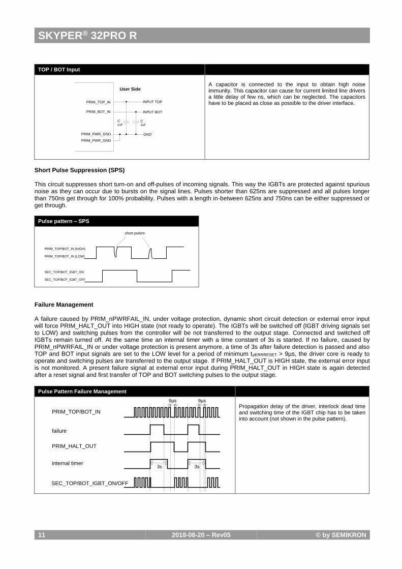
TOP / BOT Input
PRIM_TOP_IN
PRIM_PWR_GND
PRIM_BOT_IN
GND
User Side
PRIM_PWR_GND
C1nF
C1nF
INPUT TOP
INPUT BOT
A capacitor is connected to the input to obtain high noise immunity. This capacitor can cause for current limited line drivers a little delay of few ns, which can be neglected. The capacitors have to be placed as close as possible to the driver interface.
Short Pulse Suppression (SPS)
This circuit suppresses short turn-on and off-pulses of incoming signals. This way the IGBTs are protected against spurious noise as they can occur due to bursts on the signal lines. Pulses shorter than 625ns are suppressed and all pulses longer than 750ns get through for 100% probability. Pulses with a length in-between 625ns and 750ns can be either suppressed or get through.
Pulse pattern – SPS
short pulses
PRIM_TOP/BOT_IN (HIGH)
PRIM_TOP/BOT_IN (LOW)
SEC_TOP/BOT_IGBT_ON
SEC_TOP/BOT_IGBT_OFF
Failure Management
A failure caused by PRIM_nPWRFAIL_IN, under voltage protection, dynamic short circuit detection or external error input will force PRIM_HALT_OUT into HIGH state (not ready to operate). The IGBTs will be switched off (IGBT driving signals set to LOW) and switching pulses from the controller will be not transferred to the output stage. Connected and switched off IGBTs remain turned off. At the same time an internal timer with a time constant of 3s is started. If no failure, caused by PRIM_nPWRFAIL_IN or under voltage protection is present anymore, a time of 3s after failure detection is passed and also TOP and BOT input signals are set to the LOW level for a period of minimum tpERRRESET > 9µs, the driver core is ready to operate and switching pulses are transferred to the output stage. If PRIM_HALT_OUT is HIGH state, the external error input is not monitored. A present failure signal at external error input during PRIM_HALT_OUT in HIGH state is again detected after a reset signal and first transfer of TOP and BOT switching pulses to the output stage.
Pulse Pattern Failure Management
PRIM_TOP/BOT_IN
failure
PRIM_HALT_OUT
SEC_TOP/BOT_IGBT_ON/OFF
internal timer3s
9µs
3s
9µs
Propagation delay of the driver, interlock dead time and switching time of the IGBT chip has to be taken into account (not shown in the pulse pattern).

SKYPER® 32PRO R
12 2018-08-20 – Rev05 © by SEMIKRON
Halt Logic Signal (HLS)
The Halt Logic Signals PRIM_HALT_IN and PRIM_HALT_OUT show and control the drive core status. The driver core is placed into halt mode by setting PRIM_HALT_IN into HIGH state (disable driver). This signal can gather disable signals of other hardware components for stopping operation and switching off the IGBT. A HIGH signal will set the driver core into HOLD and switching pulses from the controller will be not transferred to the output stage. The input and output have Schmitt Trigger characteristic. Pull up and open collector output stages must not be used.
Connection PRIM_HALT_OUT and PRIM_HALT_IN Connection PRIM_HALT_OUT (PRIM_HALT_IN not used)
User Side
PRIM_HALT_OUT
PRIM_HALT_IN
≥1
INPUT STATUS
User Side
PRIM_HALT_OUT
PRIM_HALT_IN
Dead Time generation (Interlock TOP / BOT) adjustable (DT)
The DT circuit prevents, that TOP and BOT IGBT of one half bridge are switched on at the same time (shoot through). The dead time is not added to a dead time given by the controller. Thus the total dead time is the maximum of "built in dead time" and "controller dead time". It is possible to control the driver with one switching signal and its inverted signal.
Pulse pattern – DT
PRIM_TOP_IN (LOW)
PRIM_TOP_IN (HIGH)
SEC_TOP_IGBT_ON
PRIM_BOT_IN (HIGH)
PRIM_BOT_IN (LOW)
SEC_TOP_IGBT_OFF
SEC_BOT_IGBT_ON
SEC_BOT_IGBT_OFF
td(on;off)IO
tTD
The total propagation delay of the driver is the sum of interlock
dead time (tTD) and driver input output signal propagation delay (td(on;off)IO) as shown in the pulse pattern. Moreover the switching time of the IGBT chip has to be taken into account (not shown in the pulse pattern).
In case both channel inputs (PRIM_TOP_IN and
PRIM_BOT_IN) are at high level, the IGBTs will be turned off. If only one channel is switching, there will be no interlock dead
time.
The dead time can be adjusted and the locking function may be neutralized as shown in the following table.
Adjustment of Dead time / Neutralizing Locking Functions
Please note:
No error message will be generated when overlap of switching signals occurs.
Please note:
A HIGH signal @ PRIM_HALT_IN does not generate a HIGH signal @ PRIM_HALT_OUT. After LOW signal @ PRIM_HALT_IN the gate driver is enable do operate.
Please note:
PRIM_HALT_OUT must be always connected with PRIM_HALT_IN. PRIM_HALT_OUT is not short circuit proof.

SKYPER® 32PRO R
13 2018-08-20 – Rev05 © by SEMIKRON
Interlock time [µs]
PRIM_CFG_TDT1_IN PRIM_CFG_TDT2_IN PRIM_CDG_TDT3_IN PRIM_CFG_SELECT_IN
1 GND GND open open
1,3 GND GND GND open
2 GND open open open
2,3 GND open GND open
3 open GND open open
3,3 open GND GND open
4 * open open open open
4,3 open open GND open
no interlock open open open GND
* Factory setting
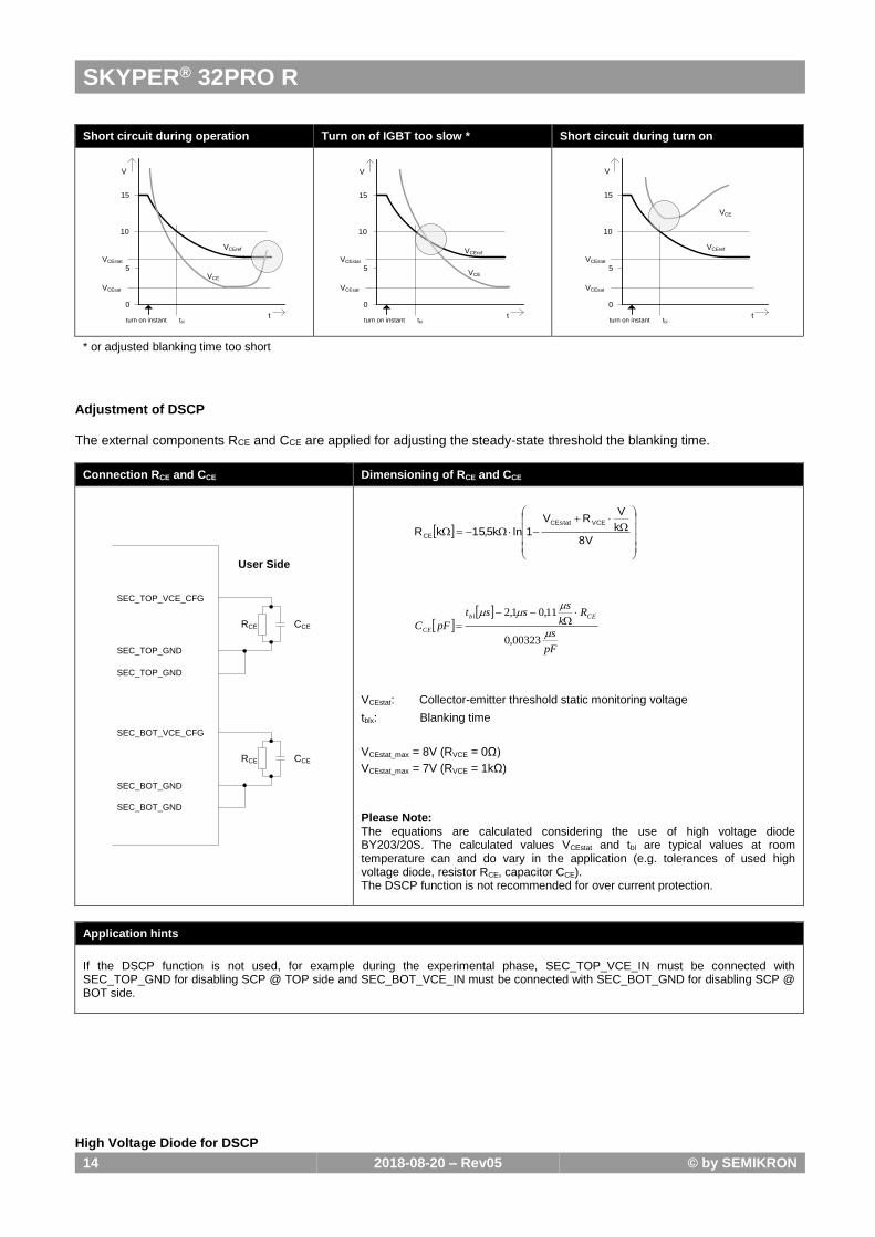
Dynamic Short Circuit Protection by VCEsat monitoring / de-saturation monitoring (DSCP)
The DSCP circuit is responsible for short circuit sensing. It monitors the collector-emitter voltage VCE of the IGBT during its on-state. Due to the direct measurement of VCEsat on the IGBT's collector, the DSCP circuit switches off the IGBTs and an error is indicated. The reference voltage VCEref may dynamically be adapted to the IGBTs switching behaviour. Immediately after turn-on of the IGBT, a higher value is effective than in steady state. This value will, however, be reset, when the IGBT is turned off. VCEstat is the steady-state value of VCEref and is adjusted to the required maximum value for each IGBT by an external resistor RCE. It may not exceed 10V. The time constant for the delay (exponential shape) of VCEref may be controlled by an external capacitor CCE, which is connected in parallel to RCE. It controls the blanking time tbl which passes after turn-on of the IGBT before the VCEsat monitoring is activated. This makes an adaptation to any IGBT switching behaviour possible.
Reference Voltage (VCEref) Characteristic
5
10
15
V
t
VCEstat
VCEsat
VCEref
VCE
turn on instant
0
tbl
After tbl has passed, the VCE monitoring will be triggered as soon as VCE > VCEref and will turn off the IGBT. The error memory will be set, and the output PRIM_HOLD_OUT changes to the HIGH state. Possible failure modes are shows in the following pictures.
Please note:
The dead time has to be longer than the turn-off delay time of the IGBT in any case. This is to avoid that one IGBT is turned on before the other one is not completely discharged. If the dead time is too short, the heat generated by the short circuit current may destroy the module in the event of a short circuit in top or bottom arm.
The average output current is available at each output channel. It is not possible to interconnect the output channels to achieve a higher average output current by neutralizing the locking function.
SKYPER® 32PRO R
14 2018-08-20 – Rev05 © by SEMIKRON
Short circuit during operation Turn on of IGBT too slow * Short circuit during turn on
5
10
15
V
t
VCEstat
VCEsat
VCEref
VCE
turn on instant
0
tbl
5
10
15
V
t
VCEstat
VCEsat
VCEref
VCE
turn on instant
0
tbl
5
10
15
V
t
VCEstat
VCEsat
VCEref
VCE
turn on instant
0
tbl
* or adjusted blanking time too short
Adjustment of DSCP
The external components RCE and CCE are applied for adjusting the steady-state threshold the blanking time.
Connection RCE and CCE Dimensioning of RCE and CCE
User Side
RCE
SEC_BOT_VCE_CFG
SEC_TOP_VCE_CFG
SEC_TOP_GND
SEC_TOP_GND
SEC_BOT_GND
SEC_BOT_GND
CCE
RCE CCE
V8
k
VRV
1lnk5,15kRVCECEstat
CE
pF
s
Rk
ssst
pFCCEbl
CE
00323,0
11,01,2
VCEstat: Collector-emitter threshold static monitoring voltage
tblx: Blanking time
VCEstat_max = 8V (RVCE = 0Ω)
VCEstat_max = 7V (RVCE = 1kΩ)
Please Note: The equations are calculated considering the use of high voltage diode BY203/20S. The calculated values VCEstat and tbl are typical values at room temperature can and do vary in the application (e.g. tolerances of used high voltage diode, resistor RCE, capacitor CCE). The DSCP function is not recommended for over current protection.
Application hints
If the DSCP function is not used, for example during the experimental phase, SEC_TOP_VCE_IN must be connected with SEC_TOP_GND for disabling SCP @ TOP side and SEC_BOT_VCE_IN must be connected with SEC_BOT_GND for disabling SCP @ BOT side.
High Voltage Diode for DSCP

SKYPER® 32PRO R
15 2018-08-20 – Rev05 © by SEMIKRON
The high voltage diode blocks the high voltage during IGBT off state. The connection of this diode between driver and IGBT is shown in the following schematic.
Connection High Voltage Diode Characteristics
User Side
RCE
SEC_BOT_VCE_CFG
SEC_TOP_VCE_CFG
SEC_TOP_GND
SEC_TOP_GND
SEC_BOT_GND
SEC_BOT_GND
CCE
RCE CCE
Load
TOP
BOT
SEC_TOP_VCE_IN
BY203/20S
BY203/20S
SEC_BOT_VCE_IN
RVCE
RVCE
Reverse blocking voltage of the diode shall be higher than the
used IGBT. Reverse recovery time of the fast diode shall be lower than VCE
rising of the used IGBT. Forward voltage of the diode: 1,5V @ 2mA forward current
(Tj=25°C). A collector series resistance RVCE (1kΩ / 0,4W) must be connected for 1700V IGBT operation.
Gate resistors
The output transistors of the driver are MOSFETs. The sources of the MOSFETs are separately connected to external terminals in order to provide setting of the turn-on and turn-off speed of each IGBT by the external resistors RGon and RGoff. As an IGBT has input capacitance (varying during switching time) which must be charged and discharged, both resistors will dictate what time must be taken to do this. The final value of the resistance is difficult to predict, because it depends on many parameters as DC link voltage, stray inductance of the circuit, switching frequency and type of IGBT.
Connection RGon, RGoff Application Hints
User Side
SEC_BOT_IGBT_ON
SEC_TOP_IGBT_ON
SEC_TOP_GND
SEC_TOP_GND
SEC_BOT_GND
SEC_BOT_GND
SEC_TOP_IGBT_OFF
SEC_BOT_IGBT_OFF
RGon
RGoff
RGE
RGon
RGoff
RGE
Load
TOP
BOT
10K
10K
The gate resistor influences the switching time, switching losses, dv/dt behaviour, etc. and has to be selected very carefully. Due to this influence a general value for the gate resistors cannot be recommended. The gate resistor has to be optimized according to switching behaviour and over voltage peaks within the specific circuitry. By increasing RGon the turn-on speed will decrease. The reverse peak current of the free-wheeling diode will diminish. By increasing RGoff the turn-off speed of the IGBT will decrease. The inductive peak over voltage during turn-off will diminish. In order to ensure locking of the IGBT even when the driver supply voltage is turned off, a resistance (RGE) has to be integrated.
Soft Turn-Off (STO)
Please note:
Do not connect the terminals SEC_TOP_IGBT_ON with SEC_TOP_IGBT_OFF and SEC_BOT_IGBT_ON with SEC_BOT_IGBT_OFF, respectively.

SKYPER® 32PRO R
16 2018-08-20 – Rev05 © by SEMIKRON
In the event of short circuit, the STO circuit increases the resistance in series with RGoff and turns-off the IGBT at lower speed. This produces smaller voltage spike above the collector emitter of the IGBT by reducing the di/dt value. Because in short-circuit conditions the IGBT's peak current increases and some stray inductance is always present in power circuits, it must fall to zero in a longer time than at normal operation. The soft turn-off time can be adjusted by connection an external resistor RGoff_SC.
Connection RGoff_SC Application Hints
User Side
SEC_TOP_IGBT_SOFTOFF
SEC_BOT_IGBT_SOFTOFF
SEC_BOT_PWR_8N
SEC_TOP_PWR_8N
RGoff_SC
RGoff_SC
The turn-off behaviour and over voltage peaks depends on DC link voltage, stray inductance of the power circuits, type of IGBT, etc. and has to be selected according the specific application. Due to this influence a general value for RGoff_SC cannot be recommended. The resistor has to be selected according to the behaviour of the specific circuitry. The soft turn-off time is limited to 10µs. After this time the output stage turn-off with used RGoff. Disabling of Soft Turn-Off can be achieved by RGoff_SC = 0Ω or wire bridge.
External Error Input (EEI)
The external error inputs on the secondary side (high potential) of the gate driver can be used for external fault signals from e. g. an over current protection circuit or over temperature protection circuit to place the gate driver into halt mode. Disabling of this function can be achieved by no connection or connection to +15V (e. g. SEC_TOP_15P, SEC_BOT_15P to SEC_TOP_ERR_IN and SEC_BOT_ERR_IN). It is possible to use only one error input.
Connection EEI
User Side
SEC_TOP_GND
EXTERNAL
ERROR
SIGNAL
+
-
15V
10K
20K
10VRef
SEC_BOT_GND
EXTERNAL
ERROR
SIGNAL
+
-
15V
10K
20K
10VRef
Connection example with using an external transistor in switch mode.
Application Example
Please note:
The soft turn-off function is no complete protection from induced over voltage in the event of short-circuit turn-off. A HIGH signal at PRIM_HALT_IN does not activate a soft turn-off.

SKYPER® 32PRO R
17 2018-08-20 – Rev05 © by SEMIKRON
Connection Schematic
1nF
100V
+15V
1nF
100V
INPUT BOT
INPUT TOP
1nF
100V
220µF
35V
1nF
100V
STATUS OUTPUT
BY203/20S
50V
330pF18k
Ron
Roff 10k
DC-
DC+
load
1nF
100V
STATUS INPUT >1_
x1
x2
y
x2
EXTERNAL ERROR SIGNAL
BY203/20S
50V
330pF18k
Ron
Roff 10k
Roff_sc
Roff_sc
SEC_TOP_VCE_CFG
SEC_TOP_VCE_IN
SEC_TOP_15P
SEC_TOP_ERR_IN
SEC_TOP_IGBT_ON
SEC_TOP_IGBT_OFF
SEC_TOP_GND
SEC_TOP_GND
SEC_BOT_VCE_CFG
SEC_BOT_VCE_IN
SEC_BOT_15P
SEC_BOT_ERR_IN
SEC_BOT_IGBT_ON
SEC_BOT_IGBT_OFF
SEC_BOT_GND
SEC_BOT_GND
PRIM_PWR_GND
PRIM_PWR_GND
PRIM_TOP_IN
PRIM_BOT_IN
PRIM_PWR_15P
PRIM_PWR_15P
PRIM_PWR_GND
PRIM_PWR_GND
PRIM_CFG_TDT2_IN
PRIM_CFG_SELECT_IN
SKYPERTM 32PRO
SEC_TOP_IGBT_SOFTOFF
SEC_TOP_8N
SEC_BOT_IGBT_SOFTOFF
SEC_BOT_8N
PRIM_nPWRFAIL_IN
PRIM_HALT_OUT
PRIM_HALT_IN
PRIM_CFG_TDT_3_IN
PRIM_CFG_TDT1_IN
PRIM_PWR_GND
PRIM_PWR_GND
- application example for 1200V IGBT - dead time: 3µs - UVR disable - VCEref = 5,5V
- tbl = 5,1µs - EEI TOP enable (using external transistor in switch mode) - EEI BOT disable - STO
Mounting Notes
Soldering Hints Finished Hole & Pad Size in mm
The temperature of the solder must not exceed 260°C, and solder time must not exceed 10 seconds.
The ambient temperature must not exceed the specified maximum storage temperature of the driver.
The solder joints should be in accordance to IPC A 610 Revision D (or later) - Class 3 (Acceptability of Electronic Assemblies) to ensure an optimal connection between driver core and printed circuit board.
Ø 1,1 ±0,05
pad size: min. 1,8
The connection between driver core and printed circuit board should be mechanical reinforced by using support posts.
Please note:
The driver is not suited for hot air reflow or infrared reflow processes.

SKYPER® 32PRO R
18 2018-08-20 – Rev05 © by SEMIKRON
Use of Support Posts
Product information of suitable support posts and distributor contact information is available at e.g. http://www.richco-inc.com (e.g. series DLMSPM,
LCBST).
When using the support posts the support post length has to be longer than 12,4mm.
Environmental Conditions
The driver core is type tested under the environmental conditions below.
Conditions Values (max.)
Vibration Sinusoidal sweep 20Hz … 500Hz, 5g, 26 sweeps per axis (x, y, z)
- Tested acc. IEC 68-2-6
- Connection between driver core and printed circuit board mechanical reinforced by using support posts.
Shock Half-sinusoidal pulse, 5g, shock width 18ms, 3 shocks in each direction (±x, ±y, ±z), 18 shocks in total
- Tested acc. IEC 68-2-27
- Connection between driver core and printed circuit board mechanical reinforced by using support posts.
The characteristics and further environmental conditions are indicated in the data sheet.
Please note:
The use of agressive materials in cleaning process of driver core may be detrimental for the device parameters.

SKYPER® 32PRO R
19 2018-08-20 – Rev05 © by SEMIKRON
Marking
Every driver core is marked. The marking contains the following items.
DISCLAIMER
SEMIKRON reserves the right to make changes without further notice herein to improve reliability, function or design. Information furnished in this document is believed to be accurate and reliable. However, no representation or warranty is given and no liability is assumed with respect to the accuracy or use of such information. SEMIKRON does not assume any liability arising out of the application or use of any product or circuit described herein. Furthermore, this technical information may not be considered as an assurance of component characteristics. No warranty or guarantee expressed or implied is made regarding delivery, performance or suitability. This document supersedes and replaces all information previously supplied and may be superseded by updates without further notice.
SEMIKRON products are not authorized for use in life support appliances and systems without the express written approval by SEMIKRON.
www.SEMIKRON.com
Related Documents