ST Sitronix ST7565P 65 x 132 Dot Matrix LCD Controller/Driver Ver 2.1b 1/71 2009/09/14 FEATURES Directly display RAM data through Display Data RAM RAM capacity : 65 x 132 = 8580 bits Display duty selectable by select pin 1/65 duty : 65 common x 132 segment 1/49 duty : 49 common x 132 segment 1/33 duty : 33 common x 132 segment 1/55 duty : 55 common x 132 segment 1/53 duty : 53 common x 132 segment High-speed 8-bit MPU interface: ST7565P can be connected directly to both the 80x86 series MPUs and the 6800 series MPUs. Serial interface (SPI-4) is also supported. Abundant command functions: Display data read/write, display ON/OFF, Normal/ Reverse display mode, page address set, display start line set, column address set, status read, display all points ON, LCD bias set, electronic volume, read-modify-write, set segment driver direction, power save mode, set common output direction, set V0 regulator internal resistor ratio. Built-in low power consumption power circuits: Booster, Regulator and Follower. Booster circuit supports 2X/3X/4X/5X/6X boost level. External reference voltage (VDD2) for booster circuits. High-accuracy Regulator with contrast control (EV) and built-in V0 voltage regulator resistors. (Thermal gradient = –0.05%/°C) Built-in Follower for LCD bias voltages. Embedded R-C oscillation circuit. Support external clock input. Extremely low power consumption: 60uA (operating, bare chip with internal power) ( V DD –V SS = V DD2 –V SS = 3V, Booster x4, V0 = 11V ). Condition: display pattern is “OFF”; use normal mode. Wide application voltage range: Logic power: V DD – V SS = 1.8V to 3.3V (typical) Analog power: V DD2 – V SS = 2.4V to 3.3V (typical) Maximum Booster limitation: V OUT = 13.5V LCD Vop: V0 – V SS = 3.0V to 12.0V Wide operation temperature range: –30 to 85°C CMOS process. Package type: Bare chip (COG) and TCP. ST7565P is not designed for resistance to light or resistance to radiation. GENERAL DESCRIPTION ST7565P is a single-chip dot-matrix LCD driver that can be connected directly to a microprocessor bus. 8-bit parallel or serial display data sent from the microprocessor is stored in the internal Display Data RAM and this chip generates LCD driving signals independent of the microprocessor. Each data bits (65x132) of the internal Display Data RAM is 1-to-1 correspondence with each pixels (65x132) on the LCD panel, therefore, ST7565P enables displays with a high degree of freedom. Moreover, the display area can be extended horizontally by using Master/Slave feature. With the abundant embedded circuits (2~6 times booster circuit, V0 regulator with contrast control for LCD voltage adjustment, voltage follower with bias selection and R-C oscillation circuit), ST7565P can be used to create a display system with the lowest power consumption and the fewest external components for high-performance portable devices. PART NO. VRS temperature gradient VRS range ST7565P -0.05%/°C 2.1V 0.03V ST7565P 6800 , 8080 , 4-Line interface Sitronix Technology Corp. reserves the right to change the contents in this document without prior notice.

Welcome message from author
This document is posted to help you gain knowledge. Please leave a comment to let me know what you think about it! Share it to your friends and learn new things together.
Transcript
ST
Sitronix ST7565P
65 x 132 Dot Matrix LCD Controller/Driver
Ver 2.1b 1/71 2009/09/14
FFEEAATTUURREESS Directly display RAM data through Display Data RAM RAM capacity : 65 x 132 = 8580 bits Display duty selectable by select pin
1/65 duty : 65 common x 132 segment 1/49 duty : 49 common x 132 segment 1/33 duty : 33 common x 132 segment 1/55 duty : 55 common x 132 segment 1/53 duty : 53 common x 132 segment
High-speed 8-bit MPU interface: ST7565P can be connected directly to both the 80x86 series MPUs and the 6800 series MPUs. Serial interface (SPI-4) is also supported.
Abundant command functions: Display data read/write, display ON/OFF, Normal/ Reverse display mode, page address set, display start line set, column address set, status read, display all points ON, LCD bias set, electronic volume, read-modify-write, set segment driver direction, power save mode, set common output direction, set V0 regulator internal resistor ratio.
Built-in low power consumption power circuits: Booster, Regulator and Follower.
Booster circuit supports 2X/3X/4X/5X/6X boost level. External reference voltage (VDD2) for booster circuits.
High-accuracy Regulator with contrast control (EV) and built-in V0 voltage regulator resistors. (Thermal gradient = –0.05%/°C)
Built-in Follower for LCD bias voltages. Embedded R-C oscillation circuit.
Support external clock input. Extremely low power consumption:
60uA (operating, bare chip with internal power) ( VDD–VSS = VDD2–VSS = 3V, Booster x4, V0 = 11V ). Condition: display pattern is “OFF”; use normal mode.
Wide application voltage range: Logic power: VDD – VSS = 1.8V to 3.3V (typical) Analog power: VDD2 – VSS = 2.4V to 3.3V (typical) Maximum Booster limitation: VOUT = 13.5V LCD Vop: V0 – VSS = 3.0V to 12.0V
Wide operation temperature range: –30 to 85°C CMOS process. Package type: Bare chip (COG) and TCP. ST7565P is not designed for resistance to light or
resistance to radiation.
GGEENNEERRAALL DDEESSCCRRIIPPTTIIOONN ST7565P is a single-chip dot-matrix LCD driver that can be connected directly to a microprocessor bus. 8-bit parallel or serial display data sent from the microprocessor is stored in the internal Display Data RAM and this chip generates LCD driving signals independent of the microprocessor. Each data bits (65x132) of the internal Display Data RAM is 1-to-1 correspondence with each pixels (65x132) on the LCD panel, therefore, ST7565P enables displays with a high degree of freedom.
Moreover, the display area can be extended horizontally by using Master/Slave feature. With the abundant embedded circuits (2~6 times booster circuit, V0 regulator with contrast control for LCD voltage adjustment, voltage follower with bias selection and R-C oscillation circuit), ST7565P can be used to create a display system with the lowest power consumption and the fewest external components for high-performance portable devices.
PART NO. VRS temperature gradient VRS range
ST7565P -0.05%/°C 2.1V ± 0.03V
ST7565P 6800 , 8080 , 4-Line interface
Sitronix Technology Corp. reserves the right to change the contents in this document without prior notice.

ST7565P
Ver 2.1b 2/71 2009/09/14
SSTT77556655PP PPaadd AArrrraannggeemmeenntt((CCOOGG))
PAD No Bump Size Chip Size
001~012, 103~114, 129~276 40µm x 90µm 9,336µm x 1,000µm
013~102 56µm x 60µm Bump Pitch
115, 290 90µm x 25.5µm 58µm (Min.)
116~128, 277~289 90µm x 40µm Bump Height
17µm (Typ)
Chip Thickness
635µm
Use select pin to define display duty as following table:
SEL 3 , 2 , 1 DUTY BIAS
0 , 0 , 0 1/65 1/9 or 1/7
0 , 0 , 1 1/49 1/8 or 1/6
0 , 1 , 0 1/33 1/6 or 1/5
0 , 1 , 1 1/55 1/8 or 1/6
1 , 0 , 0 1/53 1/8 or 1/6
1, X , X ----- -----

ST7565P
Ver 2.1b 3/71 2009/09/14
PPaadd CCeenntteerr CCoooorrddiinnaatteess ((11//6655 DDuuttyy))
PAD No. PIN Name X Y
1 COM[53] 4241 374
2 COM[54] 4183 374
3 COM[55] 4125 374
4 COM[56] 4067 374
5 COM[57] 4009 374
6 COM[58] 3951 374
7 COM[59] 3893 374
8 COM[60] 3835 374
9 COM[61] 3777 374
10 COM[62] 3719 374
11 COM[63] 3661 374
12 COMS1 3603 374
13 FRS 3443 389
14 FR 3369 389
15 CL 3295 389
16 /DOF 3221 389
17 VSS 3147 389
18 /CS1 3073 389
19 CS2 2999 389
20 VDD 2925 389
21 /RES 2851 389
22 A0 2777 389
23 VSS 2703 389
24 /WR(R/W) 2629 389
25 /RD(E) 2555 389
26 VDD 2481 389
27 D0 2407 389
28 D1 2333 389
29 D2 2259 389
30 D3 2185 389
31 D4 2111 389
32 D5 2037 389
33 D6 1963 389
34 D7 1889 389
35 VDD 1815 389
36 VDD2 1741 389
37 VDD2 1667 389
38 VSS 1593 389
39 VSS 1519 389
40 VSS 1445 389
41 VSS 1371 389
42 VOUT 1297 389
43 VOUT 1223 389
44 CAP5P 1149 389
45 CAP5P 1075 389
46 CAP1N 1001 389
47 CAP1N 927 389
Units: µm
PAD No. PIN Name X Y
48 CAP3P 853 389
49 CAP3P 779 389
50 CAP1N 705 389
51 CAP1N 631 389
52 CAP1P 557 389
53 CAP1P 483 389
54 CAP2P 409 389
55 CAP2P 335 389
56 CAP2N 261 389
57 CAP2N 187 389
58 CAP4P 113 389
59 CAP4P 39 389
60 VSS -35 389
61 VSS -109 389
62 VRS -183 389
63 VRS -257 389
64 VDD2 -331 389
65 VDD -405 389
66 V4 -479 389
67 V4 -553 389
68 V3 -627 389
69 V3 -701 389
70 V2 -775 389
71 V2 -849 389
72 V1 -923 389
73 V1 -997 389
74 V0 -1071 389
75 V0 -1145 389
76 VR -1219 389
77 VR -1293 389
78 VDD -1367 389
79 VDD2 -1441 389
80 TEST0 -1515 389
81 TEST1 -1589 389
82 TEST2 -1663 389
83 TEST3 -1737 389
84 TEST4 -1811 389
85 TEST5 -1885 389
86 VDD -1959 389
87 M/S -2033 389
88 CLS -2107 389
89 VSS -2181 389
90 C86 -2255 389
91 P/S -2329 389
92 VDD -2403 389
93 /HPM -2477 389
94 VSS -2551 389

ST7565P
Ver 2.1b 4/71 2009/09/14
PAD No. PIN Name X Y
95 IRS -2625 389
96 VDD -2699 389
97 SEL1 -2773 389
98 VSS -2847 389
99 SEL2 -2921 389
100 VDD -2995 389
101 SEL3 -3069 389
102 VSS -3143 389
103 COM[31] -3606 374
104 COM[30] -3664 374
105 COM[29] -3722 374
106 COM[28] -3780 374
107 COM[27] -3838 374
108 COM[26] -3896 374
109 COM[25] -3954 374
110 COM[24] -4012 374
111 COM[23] -4070 374
112 COM[22] -4128 374
113 COM[21] -4186 374
114 COM[20] -4244 374
115 (NC) -4542 404
116 COM[19] -4542 351
117 COM[18] -4542 293
118 COM[17] -4542 235
119 COM[16] -4542 177
120 COM[15] -4542 119
121 COM[14] -4542 61
122 COM[13] -4542 3
123 COM[12] -4542 -55
124 COM[11] -4542 -113
125 COM[10] -4542 -171
126 COM[9] -4542 -229
127 COM[8] -4542 -287
128 COM[7] -4542 -345
129 COM[6] -4267 -374
130 COM[5] -4209 -374
131 COM[4] -4151 -374
132 COM[3] -4093 -374
133 COM[2] -4035 -374
134 COM[1] -3977 -374
135 COM[0] -3919 -374
136 COMS2 -3861 -374
137 SEG[0] -3803 -374
138 SEG[1] -3745 -374
139 SEG[2] -3687 -374
140 SEG[3] -3629 -374
141 SEG[4] -3571 -374
142 SEG[5] -3513 -374
143 SEG[6] -3455 -374
144 SEG[7] -3397 -374
145 SEG[8] -3339 -374
146 SEG[9] -3281 -374
PAD No. PIN Name X Y
147 SEG[10] -3223 -374
148 SEG[11] -3165 -374
149 SEG[12] -3107 -374
150 SEG[13] -3049 -374
151 SEG[14] -2991 -374
152 SEG[15] -2933 -374
153 SEG[16] -2875 -374
154 SEG[17] -2817 -374
155 SEG[18] -2759 -374
156 SEG[19] -2701 -374
157 SEG[20] -2643 -374
158 SEG[21] -2585 -374
159 SEG[22] -2527 -374
160 SEG[23] -2469 -374
161 SEG[24] -2411 -374
162 SEG[25] -2353 -374
163 SEG[26] -2295 -374
164 SEG[27] -2237 -374
165 SEG[28] -2179 -374
166 SEG[29] -2121 -374
167 SEG[30] -2063 -374
168 SEG[31] -2005 -374
169 SEG[32] -1947 -374
170 SEG[33] -1889 -374
171 SEG[34] -1831 -374
172 SEG[35] -1773 -374
173 SEG[36] -1715 -374
174 SEG[37] -1657 -374
175 SEG[38] -1599 -374
176 SEG[39] -1541 -374
177 SEG[40] -1483 -374
178 SEG[41] -1425 -374
179 SEG[42] -1367 -374
180 SEG[43] -1309 -374
181 SEG[44] -1251 -374
182 SEG[45] -1193 -374
183 SEG[46] -1135 -374
184 SEG[47] -1077 -374
185 SEG[48] -1019 -374
186 SEG[49] -961 -374
187 SEG[50] -903 -374
188 SEG[51] -845 -374
189 SEG[52] -787 -374
190 SEG[53] -729 -374
191 SEG[54] -671 -374
192 SEG[55] -613 -374
193 SEG[56] -555 -374
194 SEG[57] -497 -374
195 SEG[58] -439 -374
196 SEG[59] -381 -374
197 SEG[60] -323 -374
198 SEG[61] -265 -374
ST7565P
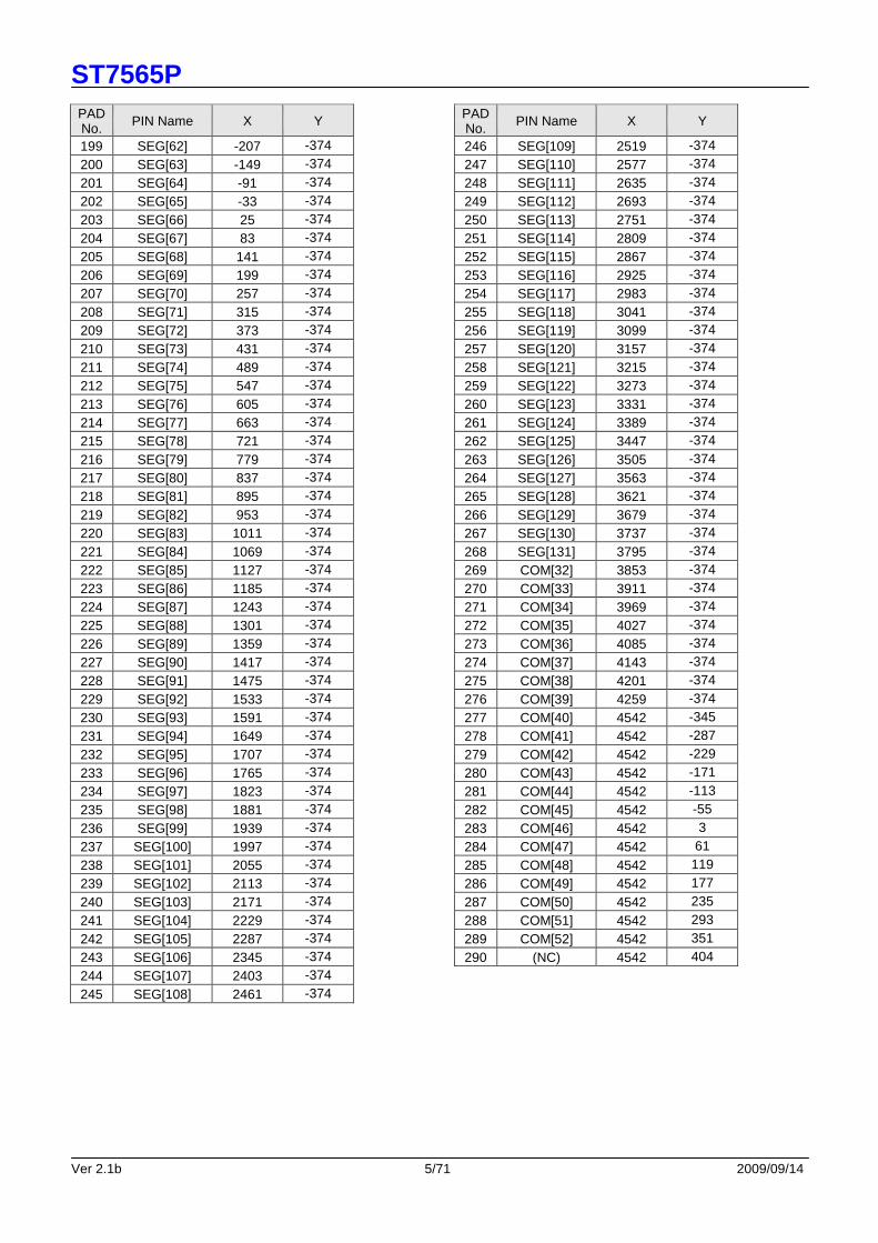
Ver 2.1b 5/71 2009/09/14
PAD No. PIN Name X Y
199 SEG[62] -207 -374
200 SEG[63] -149 -374
201 SEG[64] -91 -374
202 SEG[65] -33 -374
203 SEG[66] 25 -374
204 SEG[67] 83 -374
205 SEG[68] 141 -374
206 SEG[69] 199 -374
207 SEG[70] 257 -374
208 SEG[71] 315 -374
209 SEG[72] 373 -374
210 SEG[73] 431 -374
211 SEG[74] 489 -374
212 SEG[75] 547 -374
213 SEG[76] 605 -374
214 SEG[77] 663 -374
215 SEG[78] 721 -374
216 SEG[79] 779 -374
217 SEG[80] 837 -374
218 SEG[81] 895 -374
219 SEG[82] 953 -374
220 SEG[83] 1011 -374
221 SEG[84] 1069 -374
222 SEG[85] 1127 -374
223 SEG[86] 1185 -374
224 SEG[87] 1243 -374
225 SEG[88] 1301 -374
226 SEG[89] 1359 -374
227 SEG[90] 1417 -374
228 SEG[91] 1475 -374
229 SEG[92] 1533 -374
230 SEG[93] 1591 -374
231 SEG[94] 1649 -374
232 SEG[95] 1707 -374
233 SEG[96] 1765 -374
234 SEG[97] 1823 -374
235 SEG[98] 1881 -374
236 SEG[99] 1939 -374
237 SEG[100] 1997 -374
238 SEG[101] 2055 -374
239 SEG[102] 2113 -374
240 SEG[103] 2171 -374
241 SEG[104] 2229 -374
242 SEG[105] 2287 -374
243 SEG[106] 2345 -374
244 SEG[107] 2403 -374
245 SEG[108] 2461 -374
PAD No. PIN Name X Y
246 SEG[109] 2519 -374
247 SEG[110] 2577 -374
248 SEG[111] 2635 -374
249 SEG[112] 2693 -374
250 SEG[113] 2751 -374
251 SEG[114] 2809 -374
252 SEG[115] 2867 -374
253 SEG[116] 2925 -374
254 SEG[117] 2983 -374
255 SEG[118] 3041 -374
256 SEG[119] 3099 -374
257 SEG[120] 3157 -374
258 SEG[121] 3215 -374
259 SEG[122] 3273 -374
260 SEG[123] 3331 -374
261 SEG[124] 3389 -374
262 SEG[125] 3447 -374
263 SEG[126] 3505 -374
264 SEG[127] 3563 -374
265 SEG[128] 3621 -374
266 SEG[129] 3679 -374
267 SEG[130] 3737 -374
268 SEG[131] 3795 -374
269 COM[32] 3853 -374
270 COM[33] 3911 -374
271 COM[34] 3969 -374
272 COM[35] 4027 -374
273 COM[36] 4085 -374
274 COM[37] 4143 -374
275 COM[38] 4201 -374
276 COM[39] 4259 -374
277 COM[40] 4542 -345
278 COM[41] 4542 -287
279 COM[42] 4542 -229
280 COM[43] 4542 -171
281 COM[44] 4542 -113
282 COM[45] 4542 -55
283 COM[46] 4542 3
284 COM[47] 4542 61
285 COM[48] 4542 119
286 COM[49] 4542 177
287 COM[50] 4542 235
288 COM[51] 4542 293
289 COM[52] 4542 351
290 (NC) 4542 404
ST7565P
Ver 2.1b 6/71 2009/09/14
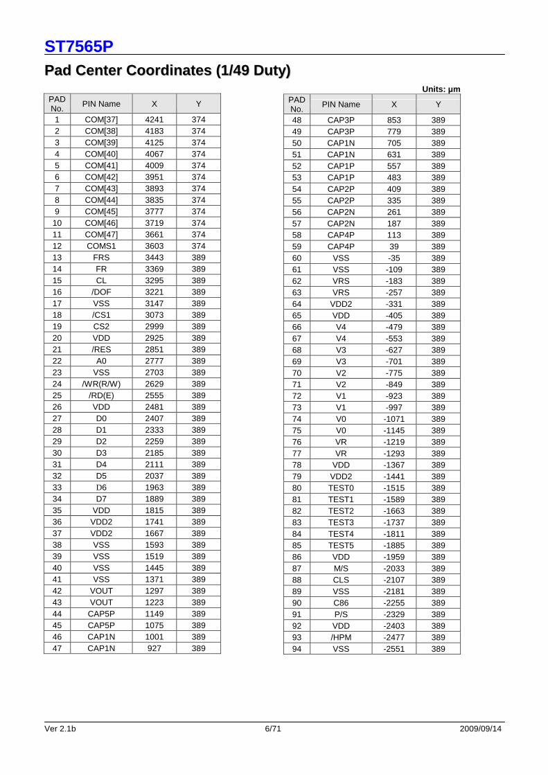
PPaadd CCeenntteerr CCoooorrddiinnaatteess ((11//4499 DDuuttyy)) PAD No. PIN Name X Y
1 COM[37] 4241 374 2 COM[38] 4183 374 3 COM[39] 4125 374 4 COM[40] 4067 374 5 COM[41] 4009 374 6 COM[42] 3951 374 7 COM[43] 3893 374 8 COM[44] 3835 374 9 COM[45] 3777 374
10 COM[46] 3719 374 11 COM[47] 3661 374 12 COMS1 3603 374 13 FRS 3443 389 14 FR 3369 389 15 CL 3295 389 16 /DOF 3221 389 17 VSS 3147 389 18 /CS1 3073 389 19 CS2 2999 389 20 VDD 2925 389 21 /RES 2851 389 22 A0 2777 389 23 VSS 2703 389 24 /WR(R/W) 2629 389 25 /RD(E) 2555 389 26 VDD 2481 389 27 D0 2407 389 28 D1 2333 389 29 D2 2259 389 30 D3 2185 389 31 D4 2111 389 32 D5 2037 389 33 D6 1963 389 34 D7 1889 389 35 VDD 1815 389 36 VDD2 1741 389 37 VDD2 1667 389 38 VSS 1593 389 39 VSS 1519 389 40 VSS 1445 389 41 VSS 1371 389 42 VOUT 1297 389 43 VOUT 1223 389 44 CAP5P 1149 389 45 CAP5P 1075 389 46 CAP1N 1001 389 47 CAP1N 927 389
Units: µm PAD No. PIN Name X Y
48 CAP3P 853 389 49 CAP3P 779 389 50 CAP1N 705 389 51 CAP1N 631 389 52 CAP1P 557 389 53 CAP1P 483 389 54 CAP2P 409 389 55 CAP2P 335 389 56 CAP2N 261 389 57 CAP2N 187 389 58 CAP4P 113 389 59 CAP4P 39 389 60 VSS -35 389 61 VSS -109 389 62 VRS -183 389 63 VRS -257 389 64 VDD2 -331 389 65 VDD -405 389 66 V4 -479 389 67 V4 -553 389 68 V3 -627 389 69 V3 -701 389 70 V2 -775 389 71 V2 -849 389 72 V1 -923 389 73 V1 -997 389 74 V0 -1071 389 75 V0 -1145 389 76 VR -1219 389 77 VR -1293 389 78 VDD -1367 389 79 VDD2 -1441 389 80 TEST0 -1515 389 81 TEST1 -1589 389 82 TEST2 -1663 389 83 TEST3 -1737 389 84 TEST4 -1811 389 85 TEST5 -1885 389 86 VDD -1959 389 87 M/S -2033 389 88 CLS -2107 389 89 VSS -2181 389 90 C86 -2255 389 91 P/S -2329 389 92 VDD -2403 389 93 /HPM -2477 389 94 VSS -2551 389

ST7565P
Ver 2.1b 7/71 2009/09/14
PAD No. PIN Name X Y
95 IRS -2625 389 96 VDD -2699 389 97 SEL1 -2773 389 98 VSS -2847 389 99 SEL2 -2921 389
100 VDD -2995 389 101 SEL3 -3069 389 102 VSS -3143 389 103 Reserve -3606 374 104 Reserve -3664 374 105 Reserve -3722 374 106 Reserve -3780 374 107 Reserve -3838 374 108 Reserve -3896 374 109 Reserve -3954 374 110 Reserve -4012 374 111 COM[23] -4070 374 112 COM[22] -4128 374 113 COM[21] -4186 374 114 COM[20] -4244 374 115 (NC) -4542 404 116 COM[19] -4542 351 117 COM[18] -4542 293 118 COM[17] -4542 235 119 COM[16] -4542 177 120 COM[15] -4542 119 121 COM[14] -4542 61 122 COM[13] -4542 3 123 COM[12] -4542 -55 124 COM[11] -4542 -113 125 COM[10] -4542 -171 126 COM[9] -4542 -229 127 COM[8] -4542 -287 128 COM[7] -4542 -345 129 COM[6] -4267 -374 130 COM[5] -4209 -374 131 COM[4] -4151 -374 132 COM[3] -4093 -374 133 COM[2] -4035 -374 134 COM[1] -3977 -374 135 COM[0] -3919 -374 136 COMS2 -3861 -374 137 SEG[0] -3803 -374 138 SEG[1] -3745 -374 139 SEG[2] -3687 -374 140 SEG[3] -3629 -374 141 SEG[4] -3571 -374 142 SEG[5] -3513 -374 143 SEG[6] -3455 -374 144 SEG[7] -3397 -374 145 SEG[8] -3339 -374 146 SEG[9] -3281 -374
PAD No. PIN Name X Y
147 SEG[10] -3223 -374 148 SEG[11] -3165 -374 149 SEG[12] -3107 -374 150 SEG[13] -3049 -374 151 SEG[14] -2991 -374 152 SEG[15] -2933 -374 153 SEG[16] -2875 -374 154 SEG[17] -2817 -374 155 SEG[18] -2759 -374 156 SEG[19] -2701 -374 157 SEG[20] -2643 -374 158 SEG[21] -2585 -374 159 SEG[22] -2527 -374 160 SEG[23] -2469 -374 161 SEG[24] -2411 -374 162 SEG[25] -2353 -374 163 SEG[26] -2295 -374 164 SEG[27] -2237 -374 165 SEG[28] -2179 -374 166 SEG[29] -2121 -374 167 SEG[30] -2063 -374 168 SEG[31] -2005 -374 169 SEG[32] -1947 -374 170 SEG[33] -1889 -374 171 SEG[34] -1831 -374 172 SEG[35] -1773 -374 173 SEG[36] -1715 -374 174 SEG[37] -1657 -374 175 SEG[38] -1599 -374 176 SEG[39] -1541 -374 177 SEG[40] -1483 -374 178 SEG[41] -1425 -374 179 SEG[42] -1367 -374 180 SEG[43] -1309 -374 181 SEG[44] -1251 -374 182 SEG[45] -1193 -374 183 SEG[46] -1135 -374 184 SEG[47] -1077 -374 185 SEG[48] -1019 -374 186 SEG[49] -961 -374 187 SEG[50] -903 -374 188 SEG[51] -845 -374 189 SEG[52] -787 -374 190 SEG[53] -729 -374 191 SEG[54] -671 -374 192 SEG[55] -613 -374 193 SEG[56] -555 -374 194 SEG[57] -497 -374 195 SEG[58] -439 -374 196 SEG[59] -381 -374 197 SEG[60] -323 -374 198 SEG[61] -265 -374

ST7565P
Ver 2.1b 8/71 2009/09/14
PAD No. PIN Name X Y
199 SEG[62] -207 -374 200 SEG[63] -149 -374 201 SEG[64] -91 -374 202 SEG[65] -33 -374 203 SEG[66] 25 -374 204 SEG[67] 83 -374 205 SEG[68] 141 -374 206 SEG[69] 199 -374 207 SEG[70] 257 -374 208 SEG[71] 315 -374 209 SEG[72] 373 -374 210 SEG[73] 431 -374 211 SEG[74] 489 -374 212 SEG[75] 547 -374 213 SEG[76] 605 -374 214 SEG[77] 663 -374 215 SEG[78] 721 -374 216 SEG[79] 779 -374 217 SEG[80] 837 -374 218 SEG[81] 895 -374 219 SEG[82] 953 -374 220 SEG[83] 1011 -374 221 SEG[84] 1069 -374 222 SEG[85] 1127 -374 223 SEG[86] 1185 -374 224 SEG[87] 1243 -374 225 SEG[88] 1301 -374 226 SEG[89] 1359 -374 227 SEG[90] 1417 -374 228 SEG[91] 1475 -374 229 SEG[92] 1533 -374 230 SEG[93] 1591 -374 231 SEG[94] 1649 -374 232 SEG[95] 1707 -374 233 SEG[96] 1765 -374 234 SEG[97] 1823 -374 235 SEG[98] 1881 -374 236 SEG[99] 1939 -374 237 SEG[100] 1997 -374 238 SEG[101] 2055 -374 239 SEG[102] 2113 -374 240 SEG[103] 2171 -374 241 SEG[104] 2229 -374 242 SEG[105] 2287 -374 243 SEG[106] 2345 -374 244 SEG[107] 2403 -374 245 SEG[108] 2461 -374
PAD No. PIN Name X Y
246 SEG[109] 2519 -374 247 SEG[110] 2577 -374 248 SEG[111] 2635 -374 249 SEG[112] 2693 -374 250 SEG[113] 2751 -374 251 SEG[114] 2809 -374 252 SEG[115] 2867 -374 253 SEG[116] 2925 -374 254 SEG[117] 2983 -374 255 SEG[118] 3041 -374 256 SEG[119] 3099 -374 257 SEG[120] 3157 -374 258 SEG[121] 3215 -374 259 SEG[122] 3273 -374 260 SEG[123] 3331 -374 261 SEG[124] 3389 -374 262 SEG[125] 3447 -374 263 SEG[126] 3505 -374 264 SEG[127] 3563 -374 265 SEG[128] 3621 -374 266 SEG[129] 3679 -374 267 SEG[130] 3737 -374 268 SEG[131] 3795 -374 269 Reserve 3853 -374 270 Reserve 3911 -374 271 Reserve 3969 -374 272 Reserve 4027 -374 273 Reserve 4085 -374 274 Reserve 4143 -374 275 Reserve 4201 -374 276 Reserve 4259 -374 277 COM[24] 4542 -345 278 COM[25] 4542 -287 279 COM[26] 4542 -229 280 COM[27] 4542 -171 281 COM[28] 4542 -113 282 COM[29] 4542 -55 283 COM[30] 4542 3 284 COM[31] 4542 61 285 COM[32] 4542 119 286 COM[33] 4542 177 287 COM[34] 4542 235 288 COM[35] 4542 293 289 COM[36] 4542 351 290 (NC) 4542 404
ST7565P
Ver 2.1b 9/71 2009/09/14
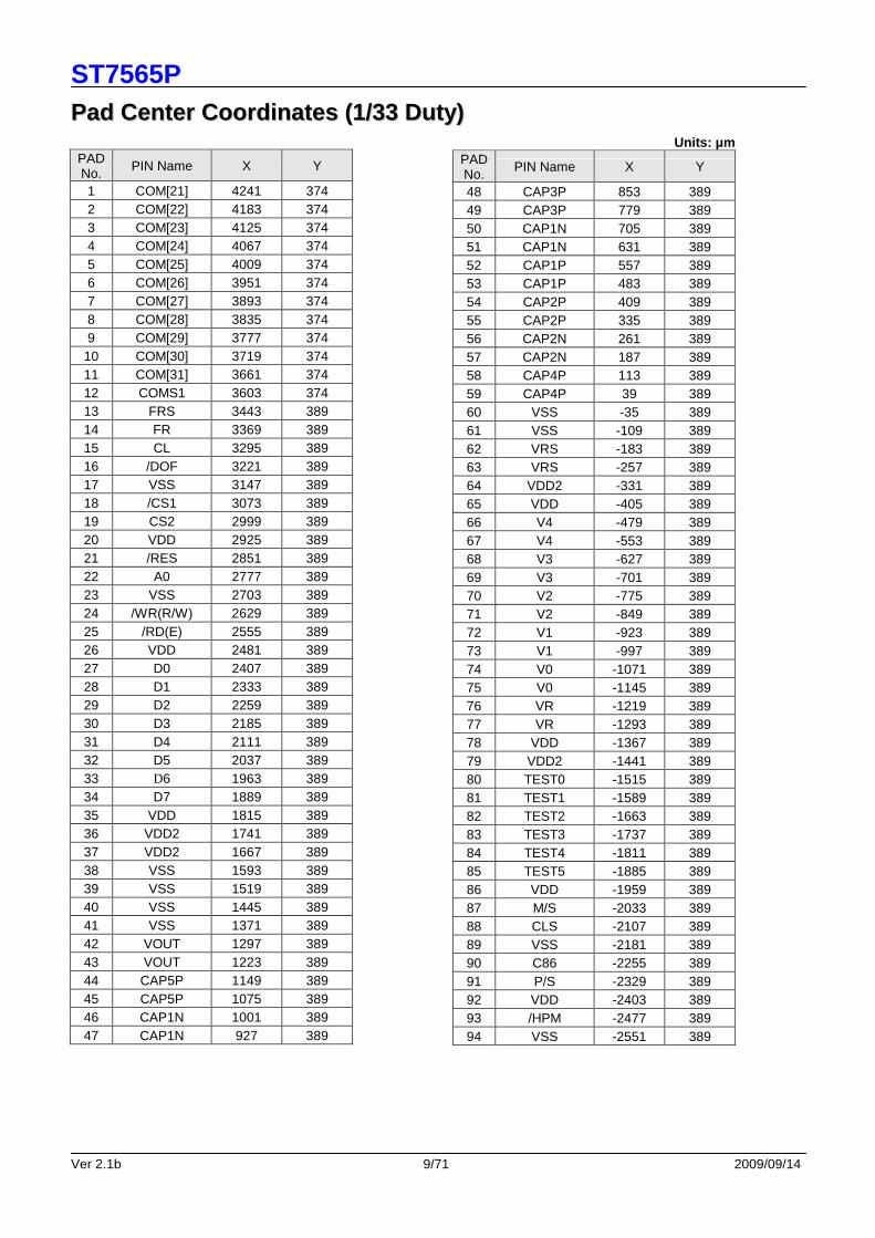
PPaadd CCeenntteerr CCoooorrddiinnaatteess ((11//3333 DDuuttyy)) PAD No. PIN Name X Y
1 COM[21] 4241 374 2 COM[22] 4183 374 3 COM[23] 4125 374 4 COM[24] 4067 374 5 COM[25] 4009 374 6 COM[26] 3951 374 7 COM[27] 3893 374 8 COM[28] 3835 374 9 COM[29] 3777 374
10 COM[30] 3719 374 11 COM[31] 3661 374 12 COMS1 3603 374 13 FRS 3443 389 14 FR 3369 389 15 CL 3295 389 16 /DOF 3221 389 17 VSS 3147 389 18 /CS1 3073 389 19 CS2 2999 389 20 VDD 2925 389 21 /RES 2851 389 22 A0 2777 389 23 VSS 2703 389 24 /WR(R/W) 2629 389 25 /RD(E) 2555 389 26 VDD 2481 389 27 D0 2407 389 28 D1 2333 389 29 D2 2259 389 30 D3 2185 389 31 D4 2111 389 32 D5 2037 389 33 D6 1963 389 34 D7 1889 389 35 VDD 1815 389 36 VDD2 1741 389 37 VDD2 1667 389 38 VSS 1593 389 39 VSS 1519 389 40 VSS 1445 389 41 VSS 1371 389 42 VOUT 1297 389 43 VOUT 1223 389 44 CAP5P 1149 389 45 CAP5P 1075 389 46 CAP1N 1001 389 47 CAP1N 927 389
Units: µm PAD No. PIN Name X Y
48 CAP3P 853 389 49 CAP3P 779 389 50 CAP1N 705 389 51 CAP1N 631 389 52 CAP1P 557 389 53 CAP1P 483 389 54 CAP2P 409 389 55 CAP2P 335 389 56 CAP2N 261 389 57 CAP2N 187 389 58 CAP4P 113 389 59 CAP4P 39 389 60 VSS -35 389 61 VSS -109 389 62 VRS -183 389 63 VRS -257 389 64 VDD2 -331 389 65 VDD -405 389 66 V4 -479 389 67 V4 -553 389 68 V3 -627 389 69 V3 -701 389 70 V2 -775 389 71 V2 -849 389 72 V1 -923 389 73 V1 -997 389 74 V0 -1071 389 75 V0 -1145 389 76 VR -1219 389 77 VR -1293 389 78 VDD -1367 389 79 VDD2 -1441 389 80 TEST0 -1515 389 81 TEST1 -1589 389 82 TEST2 -1663 389 83 TEST3 -1737 389 84 TEST4 -1811 389 85 TEST5 -1885 389 86 VDD -1959 389 87 M/S -2033 389 88 CLS -2107 389 89 VSS -2181 389 90 C86 -2255 389 91 P/S -2329 389 92 VDD -2403 389 93 /HPM -2477 389 94 VSS -2551 389

ST7565P
Ver 2.1b 10/71 2009/09/14
PAD No. PIN Name X Y
95 IRS -2625 389 96 VDD -2699 389 97 SEL1 -2773 389 98 VSS -2847 389 99 SEL2 -2921 389
100 VDD -2995 389 101 SEL3 -3069 389 102 VSS -3143 389 103 Reserve -3606 374 104 Reserve -3664 374 105 Reserve -3722 374 106 Reserve -3780 374 107 Reserve -3838 374 108 Reserve -3896 374 109 Reserve -3954 374 110 Reserve -4012 374 111 Reserve -4070 374 112 Reserve -4128 374 113 Reserve -4186 374 114 Reserve -4244 374 115 (NC) -4542 404 116 Reserve -4542 351 117 Reserve -4542 293 118 Reserve -4542 235 119 Reserve -4542 177 120 COM[15] -4542 119 121 COM[14] -4542 61 122 COM[13] -4542 3 123 COM[12] -4542 -55 124 COM[11] -4542 -113 125 COM[10] -4542 -171 126 COM[9] -4542 -229 127 COM[8] -4542 -287 128 COM[7] -4542 -345 129 COM[6] -4267 -374 130 COM[5] -4209 -374 131 COM[4] -4151 -374 132 COM[3] -4093 -374 133 COM[2] -4035 -374 134 COM[1] -3977 -374 135 COM[0] -3919 -374 136 COMS2 -3861 -374 137 SEG[0] -3803 -374 138 SEG[1] -3745 -374 139 SEG[2] -3687 -374 140 SEG[3] -3629 -374 141 SEG[4] -3571 -374 142 SEG[5] -3513 -374 143 SEG[6] -3455 -374 144 SEG[7] -3397 -374 145 SEG[8] -3339 -374 146 SEG[9] -3281 -374
PAD No. PIN Name X Y
147 SEG[10] -3223 -374 148 SEG[11] -3165 -374 149 SEG[12] -3107 -374 150 SEG[13] -3049 -374 151 SEG[14] -2991 -374 152 SEG[15] -2933 -374 153 SEG[16] -2875 -374 154 SEG[17] -2817 -374 155 SEG[18] -2759 -374 156 SEG[19] -2701 -374 157 SEG[20] -2643 -374 158 SEG[21] -2585 -374 159 SEG[22] -2527 -374 160 SEG[23] -2469 -374 161 SEG[24] -2411 -374 162 SEG[25] -2353 -374 163 SEG[26] -2295 -374 164 SEG[27] -2237 -374 165 SEG[28] -2179 -374 166 SEG[29] -2121 -374 167 SEG[30] -2063 -374 168 SEG[31] -2005 -374 169 SEG[32] -1947 -374 170 SEG[33] -1889 -374 171 SEG[34] -1831 -374 172 SEG[35] -1773 -374 173 SEG[36] -1715 -374 174 SEG[37] -1657 -374 175 SEG[38] -1599 -374 176 SEG[39] -1541 -374 177 SEG[40] -1483 -374 178 SEG[41] -1425 -374 179 SEG[42] -1367 -374 180 SEG[43] -1309 -374 181 SEG[44] -1251 -374 182 SEG[45] -1193 -374 183 SEG[46] -1135 -374 184 SEG[47] -1077 -374 185 SEG[48] -1019 -374 186 SEG[49] -961 -374 187 SEG[50] -903 -374 188 SEG[51] -845 -374 189 SEG[52] -787 -374 190 SEG[53] -729 -374 191 SEG[54] -671 -374 192 SEG[55] -613 -374 193 SEG[56] -555 -374 194 SEG[57] -497 -374 195 SEG[58] -439 -374 196 SEG[59] -381 -374 197 SEG[60] -323 -374 198 SEG[61] -265 -374

ST7565P
Ver 2.1b 11/71 2009/09/14
PAD No. PIN Name X Y
199 SEG[62] -207 -374 200 SEG[63] -149 -374 201 SEG[64] -91 -374 202 SEG[65] -33 -374 203 SEG[66] 25 -374 204 SEG[67] 83 -374 205 SEG[68] 141 -374 206 SEG[69] 199 -374 207 SEG[70] 257 -374 208 SEG[71] 315 -374 209 SEG[72] 373 -374 210 SEG[73] 431 -374 211 SEG[74] 489 -374 212 SEG[75] 547 -374 213 SEG[76] 605 -374 214 SEG[77] 663 -374 215 SEG[78] 721 -374 216 SEG[79] 779 -374 217 SEG[80] 837 -374 218 SEG[81] 895 -374 219 SEG[82] 953 -374 220 SEG[83] 1011 -374 221 SEG[84] 1069 -374 222 SEG[85] 1127 -374 223 SEG[86] 1185 -374 224 SEG[87] 1243 -374 225 SEG[88] 1301 -374 226 SEG[89] 1359 -374 227 SEG[90] 1417 -374 228 SEG[91] 1475 -374 229 SEG[92] 1533 -374 230 SEG[93] 1591 -374 231 SEG[94] 1649 -374 232 SEG[95] 1707 -374 233 SEG[96] 1765 -374 234 SEG[97] 1823 -374 235 SEG[98] 1881 -374 236 SEG[99] 1939 -374 237 SEG[100] 1997 -374 238 SEG[101] 2055 -374 239 SEG[102] 2113 -374 240 SEG[103] 2171 -374 241 SEG[104] 2229 -374 242 SEG[105] 2287 -374 243 SEG[106] 2345 -374 244 SEG[107] 2403 -374 245 SEG[108] 2461 -374
PAD No. PIN Name X Y
246 SEG[109] 2519 -374 247 SEG[110] 2577 -374 248 SEG[111] 2635 -374 249 SEG[112] 2693 -374 250 SEG[113] 2751 -374 251 SEG[114] 2809 -374 252 SEG[115] 2867 -374 253 SEG[116] 2925 -374 254 SEG[117] 2983 -374 255 SEG[118] 3041 -374 256 SEG[119] 3099 -374 257 SEG[120] 3157 -374 258 SEG[121] 3215 -374 259 SEG[122] 3273 -374 260 SEG[123] 3331 -374 261 SEG[124] 3389 -374 262 SEG[125] 3447 -374 263 SEG[126] 3505 -374 264 SEG[127] 3563 -374 265 SEG[128] 3621 -374 266 SEG[129] 3679 -374 267 SEG[130] 3737 -374 268 SEG[131] 3795 -374 269 Reserve 3853 -374 270 Reserve 3911 -374 271 Reserve 3969 -374 272 Reserve 4027 -374 273 Reserve 4085 -374 274 Reserve 4143 -374 275 Reserve 4201 -374 276 Reserve 4259 -374 277 Reserve 4542 -345 278 Reserve 4542 -287 279 Reserve 4542 -229 280 Reserve 4542 -171 281 Reserve 4542 -113 282 Reserve 4542 -55 283 Reserve 4542 3 284 Reserve 4542 61 285 COM[16] 4542 119 286 COM[17] 4542 177 287 COM[18] 4542 235 288 COM[19] 4542 293 289 COM[20] 4542 351 290 (NC) 4542 404

ST7565P
Ver 2.1b 12/71 2009/09/14
PPaadd CCeenntteerr CCoooorrddiinnaatteess ((11//5555 DDuuttyy)) PAD No. PIN Name X Y
1 COM[43] 4241 374 2 COM[44] 4183 374 3 COM[45] 4125 374 4 COM[46] 4067 374 5 COM[47] 4009 374 6 COM[48] 3951 374 7 COM[49] 3893 374 8 COM[50] 3835 374 9 COM[51] 3777 374
10 COM[52] 3719 374 11 COM[53] 3661 374 12 COMS1 3603 374 13 FRS 3443 389 14 FR 3369 389 15 CL 3295 389 16 /DOF 3221 389 17 VSS 3147 389 18 /CS1 3073 389 19 CS2 2999 389 20 VDD 2925 389 21 /RES 2851 389 22 A0 2777 389 23 VSS 2703 389 24 /WR(R/W) 2629 389 25 /RD(E) 2555 389 26 VDD 2481 389 27 D0 2407 389 28 D1 2333 389 29 D2 2259 389 30 D3 2185 389 31 D4 2111 389 32 D5 2037 389 33 D6 1963 389 34 D7 1889 389 35 VDD 1815 389 36 VDD2 1741 389 37 VDD2 1667 389 38 VSS 1593 389 39 VSS 1519 389 40 VSS 1445 389 41 VSS 1371 389 42 VOUT 1297 389 43 VOUT 1223 389 44 CAP5P 1149 389 45 CAP5P 1075 389 46 CAP1N 1001 389 47 CAP1N 927 389
Units: µm PAD No. PIN Name X Y
48 CAP3P 853 389 49 CAP3P 779 389 50 CAP1N 705 389 51 CAP1N 631 389 52 CAP1P 557 389 53 CAP1P 483 389 54 CAP2P 409 389 55 CAP2P 335 389 56 CAP2N 261 389 57 CAP2N 187 389 58 CAP4P 113 389 59 CAP4P 39 389 60 VSS -35 389 61 VSS -109 389 62 VRS -183 389 63 VRS -257 389 64 VDD2 -331 389 65 VDD -405 389 66 V4 -479 389 67 V4 -553 389 68 V3 -627 389 69 V3 -701 389 70 V2 -775 389 71 V2 -849 389 72 V1 -923 389 73 V1 -997 389 74 V0 -1071 389 75 V0 -1145 389 76 VR -1219 389 77 VR -1293 389 78 VDD -1367 389 79 VDD2 -1441 389 80 TEST0 -1515 389 81 TEST1 -1589 389 82 TEST2 -1663 389 83 TEST3 -1737 389 84 TEST4 -1811 389 85 TEST5 -1885 389 86 VDD -1959 389 87 M/S -2033 389 88 CLS -2107 389 89 VSS -2181 389 90 C86 -2255 389 91 P/S -2329 389 92 VDD -2403 389 93 /HPM -2477 389 94 VSS -2551 389

ST7565P
Ver 2.1b 13/71 2009/09/14
PAD No. PIN Name X Y
95 IRS -2625 389 96 VDD -2699 389 97 SEL1 -2773 389 98 VSS -2847 389 99 SEL2 -2921 389
100 VDD -2995 389 101 SEL3 -3069 389 102 VSS -3143 389 103 Reserve -3606 374 104 Reserve -3664 374 105 Reserve -3722 374 106 Reserve -3780 374 107 Reserve -3838 374 108 COM[26] -3896 374 109 COM[25] -3954 374 110 COM[24] -4012 374 111 COM[23] -4070 374 112 COM[22] -4128 374 113 COM[21] -4186 374 114 COM[20] -4244 374 115 (NC) -4542 404 116 COM[19] -4542 351 117 COM[18] -4542 293 118 COM[17] -4542 235 119 COM[16] -4542 177 120 COM[15] -4542 119 121 COM[14] -4542 61 122 COM[13] -4542 3 123 COM[12] -4542 -55 124 COM[11] -4542 -113 125 COM[10] -4542 -171 126 COM[9] -4542 -229 127 COM[8] -4542 -287 128 COM[7] -4542 -345 129 COM[6] -4267 -374 130 COM[5] -4209 -374 131 COM[4] -4151 -374 132 COM[3] -4093 -374 133 COM[2] -4035 -374 134 COM[1] -3977 -374 135 COM[0] -3919 -374 136 COMS2 -3861 -374 137 SEG[0] -3803 -374 138 SEG[1] -3745 -374 139 SEG[2] -3687 -374 140 SEG[3] -3629 -374 141 SEG[4] -3571 -374 142 SEG[5] -3513 -374 143 SEG[6] -3455 -374 144 SEG[7] -3397 -374 145 SEG[8] -3339 -374 146 SEG[9] -3281 -374
PAD No. PIN Name X Y
147 SEG[10] -3223 -374 148 SEG[11] -3165 -374 149 SEG[12] -3107 -374 150 SEG[13] -3049 -374 151 SEG[14] -2991 -374 152 SEG[15] -2933 -374 153 SEG[16] -2875 -374 154 SEG[17] -2817 -374 155 SEG[18] -2759 -374 156 SEG[19] -2701 -374 157 SEG[20] -2643 -374 158 SEG[21] -2585 -374 159 SEG[22] -2527 -374 160 SEG[23] -2469 -374 161 SEG[24] -2411 -374 162 SEG[25] -2353 -374 163 SEG[26] -2295 -374 164 SEG[27] -2237 -374 165 SEG[28] -2179 -374 166 SEG[29] -2121 -374 167 SEG[30] -2063 -374 168 SEG[31] -2005 -374 169 SEG[32] -1947 -374 170 SEG[33] -1889 -374 171 SEG[34] -1831 -374 172 SEG[35] -1773 -374 173 SEG[36] -1715 -374 174 SEG[37] -1657 -374 175 SEG[38] -1599 -374 176 SEG[39] -1541 -374 177 SEG[40] -1483 -374 178 SEG[41] -1425 -374 179 SEG[42] -1367 -374 180 SEG[43] -1309 -374 181 SEG[44] -1251 -374 182 SEG[45] -1193 -374 183 SEG[46] -1135 -374 184 SEG[47] -1077 -374 185 SEG[48] -1019 -374 186 SEG[49] -961 -374 187 SEG[50] -903 -374 188 SEG[51] -845 -374 189 SEG[52] -787 -374 190 SEG[53] -729 -374 191 SEG[54] -671 -374 192 SEG[55] -613 -374 193 SEG[56] -555 -374 194 SEG[57] -497 -374 195 SEG[58] -439 -374 196 SEG[59] -381 -374 197 SEG[60] -323 -374 198 SEG[61] -265 -374

ST7565P
Ver 2.1b 14/71 2009/09/14
PAD No. PIN Name X Y
199 SEG[62] -207 -374 200 SEG[63] -149 -374 201 SEG[64] -91 -374 202 SEG[65] -33 -374 203 SEG[66] 25 -374 204 SEG[67] 83 -374 205 SEG[68] 141 -374 206 SEG[69] 199 -374 207 SEG[70] 257 -374 208 SEG[71] 315 -374 209 SEG[72] 373 -374 210 SEG[73] 431 -374 211 SEG[74] 489 -374 212 SEG[75] 547 -374 213 SEG[76] 605 -374 214 SEG[77] 663 -374 215 SEG[78] 721 -374 216 SEG[79] 779 -374 217 SEG[80] 837 -374 218 SEG[81] 895 -374 219 SEG[82] 953 -374 220 SEG[83] 1011 -374 221 SEG[84] 1069 -374 222 SEG[85] 1127 -374 223 SEG[86] 1185 -374 224 SEG[87] 1243 -374 225 SEG[88] 1301 -374 226 SEG[89] 1359 -374 227 SEG[90] 1417 -374 228 SEG[91] 1475 -374 229 SEG[92] 1533 -374 230 SEG[93] 1591 -374 231 SEG[94] 1649 -374 232 SEG[95] 1707 -374 233 SEG[96] 1765 -374 234 SEG[97] 1823 -374 235 SEG[98] 1881 -374 236 SEG[99] 1939 -374 237 SEG[100] 1997 -374 238 SEG[101] 2055 -374 239 SEG[102] 2113 -374 240 SEG[103] 2171 -374 241 SEG[104] 2229 -374 242 SEG[105] 2287 -374 243 SEG[106] 2345 -374 244 SEG[107] 2403 -374 245 SEG[108] 2461 -374
PAD No. PIN Name X Y
246 SEG[109] 2519 -374 247 SEG[110] 2577 -374 248 SEG[111] 2635 -374 249 SEG[112] 2693 -374 250 SEG[113] 2751 -374 251 SEG[114] 2809 -374 252 SEG[115] 2867 -374 253 SEG[116] 2925 -374 254 SEG[117] 2983 -374 255 SEG[118] 3041 -374 256 SEG[119] 3099 -374 257 SEG[120] 3157 -374 258 SEG[121] 3215 -374 259 SEG[122] 3273 -374 260 SEG[123] 3331 -374 261 SEG[124] 3389 -374 262 SEG[125] 3447 -374 263 SEG[126] 3505 -374 264 SEG[127] 3563 -374 265 SEG[128] 3621 -374 266 SEG[129] 3679 -374 267 SEG[130] 3737 -374 268 SEG[131] 3795 -374 269 Reserve 3853 -374 270 Reserve 3911 -374 271 Reserve 3969 -374 272 Reserve 4027 -374 273 Reserve 4085 -374 274 COM[27] 4143 -374 275 COM[28] 4201 -374 276 COM[29] 4259 -374 277 COM[30] 4542 -345 278 COM[31] 4542 -287 279 COM[32] 4542 -229 280 COM[33] 4542 -171 281 COM[34] 4542 -113 282 COM[35] 4542 -55 283 COM[36] 4542 3 284 COM[37] 4542 61 285 COM[38] 4542 119 286 COM[39] 4542 177 287 COM[40] 4542 235 288 COM[41] 4542 293 289 COM[42] 4542 351 290 (NC) 4542 404

ST7565P
Ver 2.1b 15/71 2009/09/14
PPaadd CCeenntteerr CCoooorrddiinnaatteess ((11//5533 DDuuttyy)) PAD No. PIN Name X Y
1 COM[41] 4241 374 2 COM[42] 4183 374 3 COM[43] 4125 374 4 COM[44] 4067 374 5 COM[45] 4009 374 6 COM[46] 3951 374 7 COM[47] 3893 374 8 COM[48] 3835 374 9 COM[49] 3777 374
10 COM[50] 3719 374 11 COM[51] 3661 374 12 COMS1 3603 374 13 FRS 3443 389 14 FR 3369 389 15 CL 3295 389 16 /DOF 3221 389 17 VSS 3147 389 18 /CS1 3073 389 19 CS2 2999 389 20 VDD 2925 389 21 /RES 2851 389 22 A0 2777 389 23 VSS 2703 389 24 /WR(R/W) 2629 389 25 /RD(E) 2555 389 26 VDD 2481 389 27 D0 2407 389 28 D1 2333 389 29 D2 2259 389 30 D3 2185 389 31 D4 2111 389 32 D5 2037 389 33 D6 1963 389 34 D7 1889 389 35 VDD 1815 389 36 VDD2 1741 389 37 VDD2 1667 389 38 VSS 1593 389 39 VSS 1519 389 40 VSS 1445 389 41 VSS 1371 389 42 VOUT 1297 389 43 VOUT 1223 389 44 CAP5P 1149 389 45 CAP5P 1075 389 46 CAP1N 1001 389 47 CAP1N 927 389
Units: µm PAD No. PIN Name X Y
48 CAP3P 853 389 49 CAP3P 779 389 50 CAP1N 705 389 51 CAP1N 631 389 52 CAP1P 557 389 53 CAP1P 483 389 54 CAP2P 409 389 55 CAP2P 335 389 56 CAP2N 261 389 57 CAP2N 187 389 58 CAP4P 113 389 59 CAP4P 39 389 60 VSS -35 389 61 VSS -109 389 62 VRS -183 389 63 VRS -257 389 64 VDD2 -331 389 65 VDD -405 389 66 V4 -479 389 67 V4 -553 389 68 V3 -627 389 69 V3 -701 389 70 V2 -775 389 71 V2 -849 389 72 V1 -923 389 73 V1 -997 389 74 V0 -1071 389 75 V0 -1145 389 76 VR -1219 389 77 VR -1293 389 78 VDD -1367 389 79 VDD2 -1441 389 80 TEST0 -1515 389 81 TEST1 -1589 389 82 TEST2 -1663 389 83 TEST3 -1737 389 84 TEST4 -1811 389 85 TEST5 -1885 389 86 VDD -1959 389 87 M/S -2033 389 88 CLS -2107 389 89 VSS -2181 389 90 C86 -2255 389 91 P/S -2329 389 92 VDD -2403 389 93 /HPM -2477 389 94 VSS -2551 389

ST7565P
Ver 2.1b 16/71 2009/09/14
PAD No. PIN Name X Y
95 IRS -2625 389 96 VDD -2699 389 97 SEL1 -2773 389 98 VSS -2847 389 99 SEL2 -2921 389
100 VDD -2995 389 101 SEL3 -3069 389 102 VSS -3143 389 103 Reserve -3606 374 104 Reserve -3664 374 105 Reserve -3722 374 106 Reserve -3780 374 107 Reserve -3838 374 108 Reserve -3896 374 109 COM[25] -3954 374 110 COM[24] -4012 374 111 COM[23] -4070 374 112 COM[22] -4128 374 113 COM[21] -4186 374 114 COM[20] -4244 374 115 (NC) -4542 404 116 COM[19] -4542 351 117 COM[18] -4542 293 118 COM[17] -4542 235 119 COM[16] -4542 177 120 COM[15] -4542 119 121 COM[14] -4542 61 122 COM[13] -4542 3 123 COM[12] -4542 -55 124 COM[11] -4542 -113 125 COM[10] -4542 -171 126 COM[9] -4542 -229 127 COM[8] -4542 -287 128 COM[7] -4542 -345 129 COM[6] -4267 -374 130 COM[5] -4209 -374 131 COM[4] -4151 -374 132 COM[3] -4093 -374 133 COM[2] -4035 -374 134 COM[1] -3977 -374 135 COM[0] -3919 -374 136 COMS2 -3861 -374 137 SEG[0] -3803 -374 138 SEG[1] -3745 -374 139 SEG[2] -3687 -374 140 SEG[3] -3629 -374 141 SEG[4] -3571 -374 142 SEG[5] -3513 -374 143 SEG[6] -3455 -374 144 SEG[7] -3397 -374 145 SEG[8] -3339 -374 146 SEG[9] -3281 -374
PAD No. PIN Name X Y
147 SEG[10] -3223 -374 148 SEG[11] -3165 -374 149 SEG[12] -3107 -374 150 SEG[13] -3049 -374 151 SEG[14] -2991 -374 152 SEG[15] -2933 -374 153 SEG[16] -2875 -374 154 SEG[17] -2817 -374 155 SEG[18] -2759 -374 156 SEG[19] -2701 -374 157 SEG[20] -2643 -374 158 SEG[21] -2585 -374 159 SEG[22] -2527 -374 160 SEG[23] -2469 -374 161 SEG[24] -2411 -374 162 SEG[25] -2353 -374 163 SEG[26] -2295 -374 164 SEG[27] -2237 -374 165 SEG[28] -2179 -374 166 SEG[29] -2121 -374 167 SEG[30] -2063 -374 168 SEG[31] -2005 -374 169 SEG[32] -1947 -374 170 SEG[33] -1889 -374 171 SEG[34] -1831 -374 172 SEG[35] -1773 -374 173 SEG[36] -1715 -374 174 SEG[37] -1657 -374 175 SEG[38] -1599 -374 176 SEG[39] -1541 -374 177 SEG[40] -1483 -374 178 SEG[41] -1425 -374 179 SEG[42] -1367 -374 180 SEG[43] -1309 -374 181 SEG[44] -1251 -374 182 SEG[45] -1193 -374 183 SEG[46] -1135 -374 184 SEG[47] -1077 -374 185 SEG[48] -1019 -374 186 SEG[49] -961 -374 187 SEG[50] -903 -374 188 SEG[51] -845 -374 189 SEG[52] -787 -374 190 SEG[53] -729 -374 191 SEG[54] -671 -374 192 SEG[55] -613 -374 193 SEG[56] -555 -374 194 SEG[57] -497 -374 195 SEG[58] -439 -374 196 SEG[59] -381 -374 197 SEG[60] -323 -374 198 SEG[61] -265 -374

ST7565P
Ver 2.1b 17/71 2009/09/14
PAD No. PIN Name X Y
199 SEG[62] -207 -374 200 SEG[63] -149 -374 201 SEG[64] -91 -374 202 SEG[65] -33 -374 203 SEG[66] 25 -374 204 SEG[67] 83 -374 205 SEG[68] 141 -374 206 SEG[69] 199 -374 207 SEG[70] 257 -374 208 SEG[71] 315 -374 209 SEG[72] 373 -374 210 SEG[73] 431 -374 211 SEG[74] 489 -374 212 SEG[75] 547 -374 213 SEG[76] 605 -374 214 SEG[77] 663 -374 215 SEG[78] 721 -374 216 SEG[79] 779 -374 217 SEG[80] 837 -374 218 SEG[81] 895 -374 219 SEG[82] 953 -374 220 SEG[83] 1011 -374 221 SEG[84] 1069 -374 222 SEG[85] 1127 -374 223 SEG[86] 1185 -374 224 SEG[87] 1243 -374 225 SEG[88] 1301 -374 226 SEG[89] 1359 -374 227 SEG[90] 1417 -374 228 SEG[91] 1475 -374 229 SEG[92] 1533 -374 230 SEG[93] 1591 -374 231 SEG[94] 1649 -374 232 SEG[95] 1707 -374 233 SEG[96] 1765 -374 234 SEG[97] 1823 -374 235 SEG[98] 1881 -374 236 SEG[99] 1939 -374 237 SEG[100] 1997 -374 238 SEG[101] 2055 -374 239 SEG[102] 2113 -374 240 SEG[103] 2171 -374 241 SEG[104] 2229 -374 242 SEG[105] 2287 -374 243 SEG[106] 2345 -374 244 SEG[107] 2403 -374 245 SEG[108] 2461 -374
PAD No. PIN Name X Y
246 SEG[109] 2519 -374 247 SEG[110] 2577 -374 248 SEG[111] 2635 -374 249 SEG[112] 2693 -374 250 SEG[113] 2751 -374 251 SEG[114] 2809 -374 252 SEG[115] 2867 -374 253 SEG[116] 2925 -374 254 SEG[117] 2983 -374 255 SEG[118] 3041 -374 256 SEG[119] 3099 -374 257 SEG[120] 3157 -374 258 SEG[121] 3215 -374 259 SEG[122] 3273 -374 260 SEG[123] 3331 -374 261 SEG[124] 3389 -374 262 SEG[125] 3447 -374 263 SEG[126] 3505 -374 264 SEG[127] 3563 -374 265 SEG[128] 3621 -374 266 SEG[129] 3679 -374 267 SEG[130] 3737 -374 268 SEG[131] 3795 -374 269 Reserve 3853 -374 270 Reserve 3911 -374 271 Reserve 3969 -374 272 Reserve 4027 -374 273 Reserve 4085 -374 274 Reserve 4143 -374 275 COM[26] 4201 -374 276 COM[27] 4259 -374 277 COM[28] 4542 -345 278 COM[29] 4542 -287 279 COM[30] 4542 -229 280 COM[31] 4542 -171 281 COM[32] 4542 -113 282 COM[33] 4542 -55 283 COM[34] 4542 3 284 COM[35] 4542 61 285 COM[36] 4542 119 286 COM[37] 4542 177 287 COM[38] 4542 235 288 COM[39] 4542 293 289 COM[40] 4542 351 290 (NC) 4542 404
ST7565P
Ver 2.1b 18/71 2009/09/14
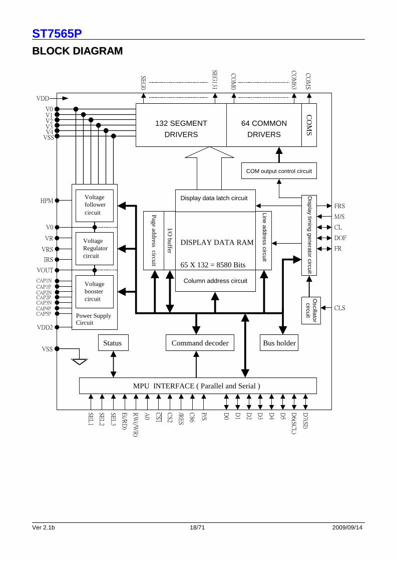
BBLLOOCCKK DDIIAAGGRRAAMM
MPU INTERFACE ( Parallel and Serial )
Command decoderStatus Bus holder
DISPLAY DATA RAM
65 X 132 = 8580 Bits
Column address circuit
I/O buffer
Page address circuit
Line address circuit
Display data latch circuit
Oscillatorcircuit
Display tim
ing generator circuit
132 SEGMENT
DRIVERS
64 COMMON
DRIVERS
COM output control circuit
CO
MS
VSS
V0V1V2V3V4
V0
VR
VRS
IRS
VOUT
HPM
CAP1NCAP1PCAP2NCAP2PCAP3NCAP4PCAP5P Power Supply
CircuitVDD2
VSS
Voltageboostercircuit
VoltageRegulatorcircuit
Voltagefollowercircuit
SE
G0
SE
G131
CO
M0
CO
M63
CO
MS
FRS
M/S
CL
DOF
FR
CLS
D7(S
I)
D6(S
CL
)
D5
D4
D3
D2
D1
D0
P/S
C86
CS2
/RE
S
CS1
A0
RW
(/WR
)
E(/R
D)
SE
L3
SE
L2
SE
L1
VDD
ST7565P
Ver 2.1b 19/71 2009/09/14
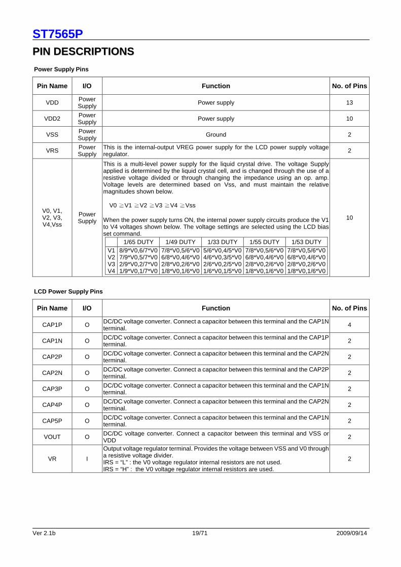
PPIINN DDEESSCCRRIIPPTTIIOONNSS
Power Supply Pins
Pin Name I/O Function No. of Pins
VDD Power Supply Power supply 13
VDD2 Power Supply Power supply 10
VSS Power Supply Ground 2
VRS Power Supply
This is the internal-output VREG power supply for the LCD power supply voltage regulator. 2
V0, V1, V2, V3, V4,Vss
Power Supply
This is a multi-level power supply for the liquid crystal drive. The voltage Supply applied is determined by the liquid crystal cell, and is changed through the use of a resistive voltage divided or through changing the impedance using an op. amp. Voltage levels are determined based on Vss, and must maintain the relative magnitudes shown below.
V0 ≧V1 ≧V2 ≧V3 ≧V4 ≧Vss When the power supply turns ON, the internal power supply circuits produce the V1 to V4 voltages shown below. The voltage settings are selected using the LCD bias set command.
1/65 DUTY 1/49 DUTY 1/33 DUTY 1/55 DUTY 1/53 DUTY V1 V2 V3 V4
8/9*V0,6/7*V0 7/9*V0,5/7*V0 2/9*V0,2/7*V0 1/9*V0,1/7*V0
7/8*V0,5/6*V0 6/8*V0,4/6*V0 2/8*V0,2/6*V0 1/8*V0,1/6*V0
5/6*V0,4/5*V0 4/6*V0,3/5*V0 2/6*V0,2/5*V0 1/6*V0,1/5*V0
7/8*V0,5/6*V0 6/8*V0,4/6*V0 2/8*V0,2/6*V0 1/8*V0,1/6*V0
7/8*V0,5/6*V0 6/8*V0,4/6*V0 2/8*V0,2/6*V0 1/8*V0,1/6*V0
10
LCD Power Supply Pins
Pin Name I/O Function No. of Pins
CAP1P O DC/DC voltage converter. Connect a capacitor between this terminal and the CAP1N terminal. 4
CAP1N O DC/DC voltage converter. Connect a capacitor between this terminal and the CAP1P terminal. 2
CAP2P O DC/DC voltage converter. Connect a capacitor between this terminal and the CAP2N terminal. 2
CAP2N O DC/DC voltage converter. Connect a capacitor between this terminal and the CAP2P terminal. 2
CAP3P O DC/DC voltage converter. Connect a capacitor between this terminal and the CAP1N terminal. 2
CAP4P O DC/DC voltage converter. Connect a capacitor between this terminal and the CAP2N terminal. 2
CAP5P O DC/DC voltage converter. Connect a capacitor between this terminal and the CAP1N terminal. 2
VOUT O DC/DC voltage converter. Connect a capacitor between this terminal and VSS or VDD 2
VR I
Output voltage regulator terminal. Provides the voltage between VSS and V0 through a resistive voltage divider. IRS = “L” : the V0 voltage regulator internal resistors are not used. IRS = “H” : the V0 voltage regulator internal resistors are used.
2

ST7565P
Ver 2.1b 20/71 2009/09/14
System Bus Connection Pins
Pin Name I/O Function No. of Pins
D5 to D0 D6 (SCL) D7 (SI)
I/O
This is an 8-bit bi-directional data bus that connects to an 8-bit or 16-bit standard MPU data bus. When the serial interface (SPI-4) is selected (P/S = “L”) : D7 : serial data input (SI) ; D6 : the serial clock input (SCL). D0 to D5 should be connected to VDD or floating. When the chip select is not active, D0 to D7 are set to high impedance.
8
A0 I
This is connect to the least significant bit of the normal MPU address bus, and it determines whether the data bits are data or command. A0 = “H”: Indicates that D0 to D7 are display data. A0 = “L”: Indicates that D0 to D7 are control data.
1
/RES I When /RES is set to “L”, the register settings are initialized (cleared). The reset operation is performed by the /RES signal level. 1
/CS1 CS2 I This is the chip select signal. When /CS1 = “L” and CS2 = “H”, then the chip select
becomes active, and data/command I/O is enabled. 2
/RD (E) I
• When connected to 8080 series MPU, this pin is treated as the “/RD” signal of the 8080 MPU and is LOW-active. The data bus is in an output status when this signal is “L”. • When connected to 6800 series MPU, this pin is treated as the “E” signal of the 6800 MPU and is HIGH-active. This is the enable clock input terminal of the 6800 Series MPU.
1
/WR (R/W)
I
• When connected to 8080 series MPU, this pin is treated as the “/WR” signal of the 8080 MPU and is LOW-active. The signals on the data bus are latched at the rising edge of the /WR signal. • When connected to 6800 series MPU, this pin is treated as the “R/W” signal of the 6800 MPU and decides the access type : When R/W = “H”: Read. When R/W = “L”: Write.
1
C86 I This is the MPU interface selection pin. C86 = “H”: 6800 Series MPU interface. C86 = “L”: 8080 Series MPU interface.
1
P/S I
This pin configures the interface to be parallel mode or serial mode. P/S = “H”: Parallel data input/output. P/S = “L”: Serial data input. The following applies depending on the P/S status:
P/S Data/Command Data Read/Write Serial Clock
“H” A0 D0 to D7 /RD, /WR X
“L” A0 SI (D7) Write only SCL (D6)
When P/S = “L”, D0 to D5 must be fixed to “H”. /RD (E) and /WR (R/W) are fixed to either “H” or “L”. The serial access mode does NOT support read operation.
1

ST7565P
Ver 2.1b 21/71 2009/09/14
Pin Name I/O Function No. of Pins
CLS I
Selection pin to enable or disable the internal display clock oscillator circuit. CLS = “H” : use internal oscillator circuit . CLS = “L” : use external clock input (internal oscillator is disabled). When CLS = “L”, input the external display clock through the CL terminal.
1
M/S I
This terminal selects the master/slave operation for the ST7565P Series chips. Master operation outputs the timing signals that are required for the LCD display, while slave operation input the timing signals required for the liquid crystal display. That synchronized the liquid crystal display system between Master and Slave. M/S = “H” Master operation M/S = “L” Slave operation
M/S CLS Oscillator Circuit
Power Supply Circuit
CL FR DOF
“H” “H” “L”
Enabled Disabled
Enabled Enabled
Output Input
Output Output
Output Output
“L” “H” “L”
Disabled Disabled
Disabled Disabled
Input Input
Input Input
Input Input
1
CL I/O
This is the display clock input terminal The following is true depending on the M/S and CLS status.
M/S CLS CL
“H” “H” “L”
Output Input
“L” “H” “L”
Input Input
1
FR O This is the liquid crystal alternating current signal terminal. 1 /DOF O This is the LCD blanking control terminal. 1 FRS O Reserved 1
IRS I
This terminal selects the resistors for the V0 voltage level adjustment. IRS = “H”: Use the internal resistors IRS = “L”: Do not use the internal resistors. The V0 voltage level is regulated by an external resistive voltage divider attached to the VR terminal
1
/HPM
I This is the power control terminal for the power supply circuit for liquid crystal drive. /HPM = “H”: Normal mode /HPM = “L”: High power mode
1
SEL3 SEL2 SEL1
I
These pins are DUTY selection. SEL 3 , 2 , 1 DUTY BIAS
0 , 0 , 0 1/65 1/9 or 1/7
0 , 0 , 1 1/49 1/8 or 1/6
0 , 1 , 0 1/33 1/6 or 1/5
0 , 1 , 1 1/55 1/8 or 1/6
1 , 0 , 0 1/53 1/8 or 1/6
1, X , X ----- -----
3
TEST0 ~ 5 I These are terminals for IC testing. They are set to open. 6

ST7565P
Ver 2.1b 22/71 2009/09/14
LCD Driver Pins
Pin Name I/O Function No. of Pins
SEG0 to
SEG131 O
These are the LCD segment drive outputs. Through a combination of the contents of the display RAM and with the FR signal, a single level is selected from VSS, V3, V2 and V0.
Output Voltage RAM DATA FR
Normal Display Reverse Display
H H V0 V2
H L VSS V3
L H V2 V0
L L V3 VSS
Power save VSS
132
COM0 to
COMn O
Through a combination of the contents of the scan data and with the FR signal, a single level is selected from VSS, V4, V1 and V0.
Scan Data FR Output Voltage
H H VSS
H L V0
L H V1
L L V4
Power save VSS
67
COMS O These are the COM output terminals for the indicator. Both terminals output the same signal. Leave these open if they are not used.
2
ST7565P I/O PIN ITO Resister Limitation PIN Name ITO Resister TEST0…5 Floating VDD, VDD2, VSS, VOUT, VR, VRS <100Ω V0, V1, V2, V3, V4, CAP1P, CAP1N, CAP2P, CAP2N, CAP 3P, CAP4P, CAP5P <500Ω /CS1, CS2, CL, E, R/W, A0, D0…D7, <1KΩ FR, /DOF, C86, P/S, M/S, /HPM,SEL1…SEL3, CLS, IRS < 5KΩ /RES <10KΩ

ST7565P
Ver 2.1b 23/71 2009/09/14
DDEESSCCRRIIPPTTIIOONN OOFF FFUUNNCCTTIIOONNSS
The MPU Interface
Selecting the Interface Type
With the ST7565P chips, data transfers are done through an 8-bit parallel data bus (D7 to D0) or through a serial data input (SI). By setting the P/S terminal to “H” or “L”, it sets the
access mode to be either parallel or serial mode as shown in Table 1.
Table 1
P/S /CS1 CS2 A0 /RD /WR C86 D7 D6 D5~D0
H: Parallel mode /CS1 CS2 A0 /RD /WR C86 D7 D6 D5~D0
L: Serial mode /CS1 CS2 A0 — — — SI SCL (HZ) “—” indicates fixed to either “H” or to “L”
The Parallel Interface
When the parallel interface has been selected (P/S =“H”), the interface can be connected directly to either 8080 or
6800 Series MPU (as shown in Table 2) by setting the C86 terminal to either “H” or “L”.
Table 2
C86 (P/S=H) /CS1 CS2 A0 E(/RD) R/W(/WR) D7~D0
H: 6800 Series /CS1 CS2 A0 E R/W D7~D0
L: 8080 Series /CS1 CS2 A0 /RD /WR D7~D0 Moreover, data bus signals are recognized according to the combination of A0, /RD (E), /WR (R/W) signals.
The functions are shown as below in Table 3.
Table 3
Shared 6800 Series 8080 Series
A0 R/W /RD /WR Function
1 1 0 1 Reads the display data
1 0 1 0 Writes the display data
0 1 0 1 Status read
0 0 1 0 Write control data (command)

ST7565P
Ver 2.1b 24/71 2009/09/14
The Serial Interface
When the serial interface has been selected (P/S = “L”) then when the chip is in active state (/CS1 = “L” and CS2 = “H”) the serial data input (SI) and the serial clock input (SCL) can be received. The serial data is read from the serial data input pin in the rising edge of the serial clocks D7, D6 through D0, in this order. This data is converted to 8 bits parallel data in the rising edge of the eighth serial clock for the processing.
The A0 input is used to determine whether or the serial data input is display data or command data; when A0 = “H”, the data is display data, and when A0 = “L” then the data is command data. The A0 input is read and used for detection every 8th rising edge of the serial clock after the chip becomes active. Figure 1 is a serial interface signal chart.
Figure 1 * When the chip is not active, the shift registers and the counter are reset to their initial states. * Reading is not possible while in serial interface mode. * Caution is required on the SCL signal when it comes to line-end reflections and external noise. We recommend that operation
be rechecked on the actual equipment.
The Chip Select
The ST7565P have two chip select terminals: /CS1 and CS2. The MPU interface or the serial interface is enabled only when /CS1 = “L” and CS2 = “H”.
When the chip select is inactive, D0 to D7 enter a high impedance state, and the A0, /RD, and /WR inputs are inactive. When the serial interface is selected, the shift register and the counter are reset.
The Accessing the Display Data RAM and the Internal Registers
Data transfer at a higher speed is ensured since the MPU is required to satisfy the cycle time (tCYC) requirement alone in accessing the ST7565P. Wait time may not be considered. And, in the ST7565P, each time data is sent from the MPU, a type of pipeline process between LSIs is performed through the bus holder attached to the internal data bus. Internal data bus. For example, when the MPU writes data to the display data RAM, once the data is stored in the bus holder, then it is written to the display data RAM before the next data write cycle. Moreover, when the MPU reads the display data RAM,
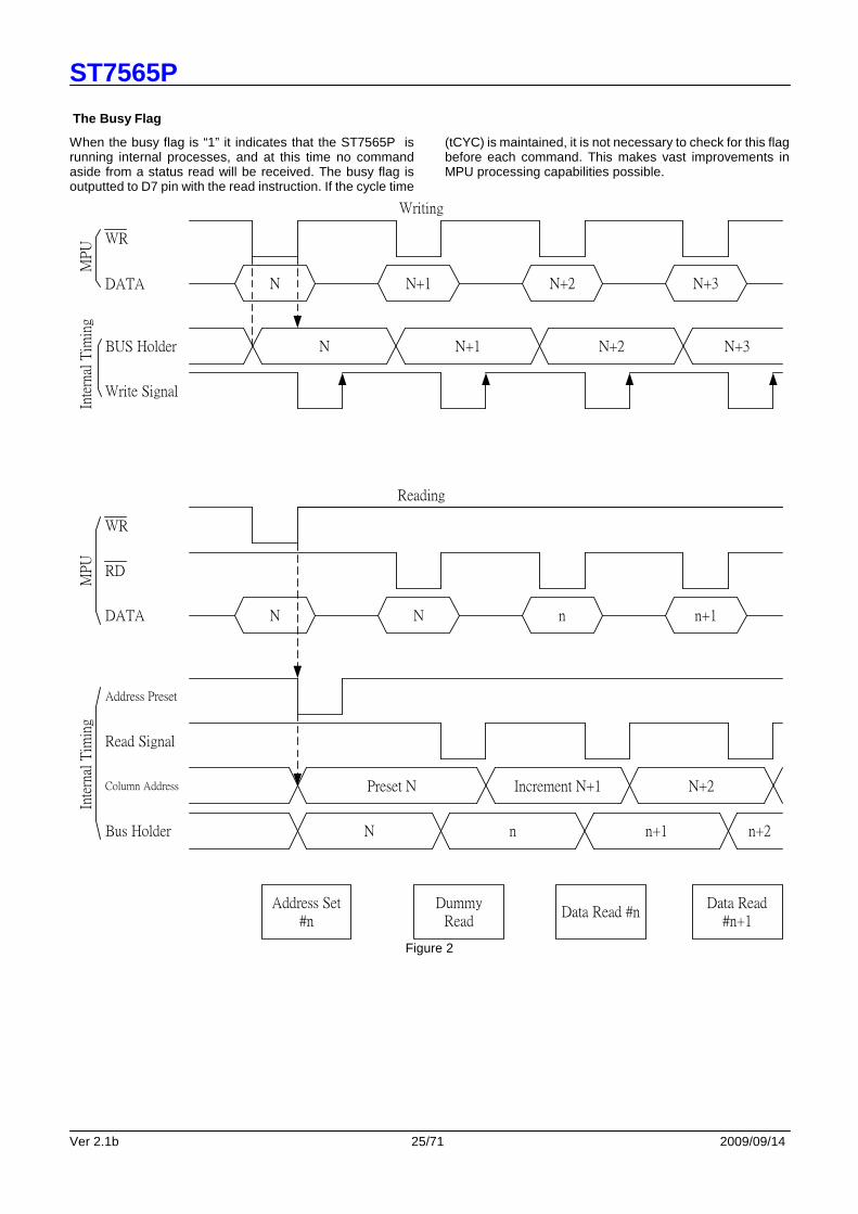
the first data read cycle (dummy) stores the read data in the bus holder, and then the data is read from the bus holder to the system bus at the next data read cycle. There is a certain restriction in the read sequence of the display data RAM. Please be advised that data of the specified address is not generated by the read instruction issued immediately after the address setup. This data is generated in data read of the second time. Thus, a dummy read is required whenever the address setup or write cycle operation is conducted. This relationship is shown in Figure 2.
ST7565P
Ver 2.1b 25/71 2009/09/14
The Busy Flag
When the busy flag is “1” it indicates that the ST7565P is running internal processes, and at this time no command aside from a status read will be received. The busy flag is outputted to D7 pin with the read instruction. If the cycle time
(tCYC) is maintained, it is not necessary to check for this flag before each command. This makes vast improvements in MPU processing capabilities possible.
N N+1 N+2 N+3
N+3N+2N+1N
DATA
BUS Holder
Write Signal
WR
MP
UIn
tern
al T
imin
g
Writing
DATA
WR
MP
U
Reading
N N n n+1
RD
Preset N Increment N+1 N+2
n n+1N n+2
Address Preset
Read Signal
Column Address
Bus Holder
Inte
rnal
Tim
ing
Address Set#n
DummyRead
Data Read #nData Read
#n+1
Figure 2

ST7565P
Ver 2.1b 26/71 2009/09/14
Display Data RAM
The display data RAM stores the dot data for the LCD. It has a 65 (8 page x 8 bit +1) x 132 bit structure. As is shown in Figure 3, the D7 to D0 display data from the MPU corresponds to the LCD display common direction; there are few constraints at the time of display data transfer when multiple ST7565P are used, thus and display structures can be created easily and with a high degree of freedom.
Moreover, reading from and writing to the display RAM from the MPU side is performed through the I/O buffer, which is an independent operation from signal reading for the liquid crystal driver. Consequently, even if the display data RAM is accessed asynchronously during liquid crystal display, it will not cause adverse effects on the display (such as flickering).
0
1
0
0
1
1
0
0
1
0
1
0
0
1
0
1
0
0
1
0
0
0
0
0
0
D0
D1
D2
D3
D4
-
Display data RAM
COM0
COM1
COM2
COM3
COM4
-
Liquid crystal display
Figure 3
The Page Address Circuit
Page address of the display data RAM is specified through the Page Address Set Command. The page address must be specified again when changing pages to perform access.
Page address 8 (D3, D2, D1, D0 = 1, 0, 0, 0) is a special RAM for icons, and only display data D0 is used (refer to Figure 4)
The Column Addresses
The display data RAM column address is specified by the Column Address Set command. The specified column address is incremented (+1) with each display data read/write command. This allows the MPU display data to be accessed continuously. Moreover, the incrementing of column addresses stops with 83H. Because the column address is independent of the page address, when moving, for example, from page 0 column 83H to page 1 column 00H,
it is necessary to respective both the page address and the column address. Furthermore, as is shown in Table 4, the ADC command (segment driver direction select command) can be used to reverse the relationship between the display data RAM column address and the segment output. Because of this, the constraints on the IC layout when the LCD module is assembled can be minimized. As is shown in Figure 4.
Table 4
SEG Output ADC
SEG0 SEG 131
(D0) “0” (D0) “1”
0 (H) → Column Address → 83 (H) 83 (H) ← Column Address ← 0 (H)
The Line Address Circuit
The line address circuit, as shown in Table 4, specifies the line address relating to the COM output when the contents of the display data RAM are displayed. Using the display start line address set command, what is normally the top line of the display can be specified (this is the COM0 output when the common output mode is normal, and the COM63 output
for ST7565P , the detail is shown page.11 The display area is a 65 line area for the ST7565P. If the line addresses are changed dynamically using the display start line address set command, screen scrolling, page swapping, etc. can be performed.

ST7565P
Ver 2.1b 27/71 2009/09/14
Page Address
D3 D2 D1 D0 Data
Line Address
When the common output is normal
COM Output
D0 00H COM0 D1 01H COM1 D2 02H COM2 D3 03H COM3 D4 04H COM4 D5 05H COM5 D6 06H COM6
0 0 0 0
D7
Page 0
07H COM7 D0 08H COM8 D1 09H COM9 D2 0AH COM10 D3 0BH COM11 D4 0CH COM12 D5 0DH COM13 D6 0EH COM14
0 0 0 1
D7
Page 1
0FH COM15 D0 10H COM16 D1 11H COM17 D2 12H COM18 D3 13H COM19 D4 14H COM20 D5 15H COM21 D6 16H COM22
0 0 1 0
D7
Page 2
17H COM23 D0 18H COM24 D1 19H COM25 D2 1AH COM26 D3 1BH COM27 D4 1CH COM28 D5 1DH COM29 D6 1EH COM30
0 0 1 1
D7
Page 3
1FH COM31 D0 20H COM32 D1 21H COM33 D2 22H COM34 D3 23H COM35 D4 24H COM36 D5 25H COM37 D6 26H COM38
0 1 0 0
D7
Page 4
27H COM39 D0 28H COM40 D1 29H COM41 D2 2AH COM42 D3 2BH COM43 D4 2CH COM44 D5 2DH COM45 D6 2EH COM46
0 1 0 1
D7
Page 5
2FH COM47 D0 30H COM48 D1 31H COM49 D2 32H COM50 D3 33H COM51 D4 34H COM52 D5 35H COM53 D6 36H COM54
0 1 1 0
D7
Page 6
37H COM55 D0 38H COM56 D1 39H COM57 D2 3AH COM58 D3 3BH COM59 D4 3CH COM60 D5 3DH COM61 D6 3EH COM62
0 1 1 1
D7
Page 7
3FH
COM63 1 0 0 0 D0 Page 8 COMS
00
01
02
03
04
05
06
07
08
7B
7C
7D
7E
7F
80
81
82
83
0 D0
83
82
81
80
7F
7E
7D
7C
7B 08
07
06
05
04
03
02
01
00
1 D0 A
DC
Col
umn
addr
ess
Regardless of the display start line address, 1/65duty => 64th line, 1/49duty =>48th line.
S0
S1
S2
S3
S4
S5
S6
S7
S8
S12
3
S12
4
S12
5
S12
6
S12
7
S12
8
S12
9
S13
0
S13
1
LCD
O
ut 1/33duty =>32th line,
1/55duty =>54th line, 1/53duty =>52th line.
Figure 4

ST7565P
Ver 2.1b 28/71 2009/09/14
The Display Data Latch Circuit
The display data latch circuit is a latch that temporarily stores the display data that is output to the liquid crystal driver circuit from the display data RAM.
Because the display normal/reverse status, display ON/OFF status, and display all points ON/OFF commands control only the data within the latch, they do not change the data within the display data RAM itself.
The Oscillator Circuit
This is a CR-type oscillator that produces the display clock. The oscillator is only enabled when M/S= “H” and CLS = “H”.
When CLS = “L” the oscillation stops, and the external clock is input through the CL terminal.
Display Timing Generator Circuit
The display timing generator circuit generates the timing signal to the line address circuit and the display data latch circuit using the display clock. The display data is latched into the display data latch circuit synchronized with the display clock, and is output to the data driver output terminal. Reading to the display data liquid crystal driver circuits is completely independent of accesses to the display data RAM by the MPU. Consequently, even if the display data
RAM is accessed asynchronously during liquid crystal display, there is absolutely no adverse effect (such as flickering) on the display. Moreover, the display timing generator circuit generates the common timing and the liquid crystal alternating current signal (FR) from the display clock. It generates a drive wave form using a 2 frame alternating current drive method, as is shown in Figure 5, for the liquid crystal drive circuit.
Two-frame alternating current drive waveform
64 65 1 2 3 4 5 6 60 61 62 63 64 65 1 2 3 4 5 6
V0V1
V4VSS
COM0
V0
V1
V4
Vss
COM1
VSS
V3
V2
V0
RAM Data
SEGn
FR
CL
Figure 5

ST7565P
Ver 2.1b 29/71 2009/09/14
The Common Output Status Select Circuit
In the ST7565P chips, the COM output scan direction can be selected by the common output status select command.
(See Table 6.) Consequently, the constraints in IC layout at the time of LCD module assembly can be minimized.
Table 6
COM Scan Direction Status
1/65 DUTY 1/49 DUTY 1/33 DUTY 1/55 DUTY 1/53 DUTY Normal Reverse
COM0 → COM63 COM63 → COM0
COM0 → COM47 COM47 → COM0
COM0 → COM31 COM31 → COM0
COM0 → COM53 COM53 → COM0
COM0 → COM51 COM51 → COM0
Common output pins
Duty COM dir COM[0:15] COM[16:23] COM[24:26] COM[27:36] COM[37:39] COM[40:47] COM[48:63] COMS 0 COM[0:63] COMS
1/65 1 COM[63:0] COMS 0 COM[0:23] reserve COM[24:47] COMS
1/49 1 COM[47:24] reserve COM[23:0] COMS 0 COM[0:15] reserve COM[16:31] COMS
1/33 1 COM[31:16] reserve COM[15:0] COMS 0 COM[0:26] reserve COM[27:53] COMS
1/55 1 COM[53:27] reserve COM[26:0] COMS 0 COM[0:25] reserve COM[26:51] COMS
1/53 1 COM[51:26] reserve COM[25:0] COMS
ST7565P
Ver 2.1b 30/71 2009/09/14
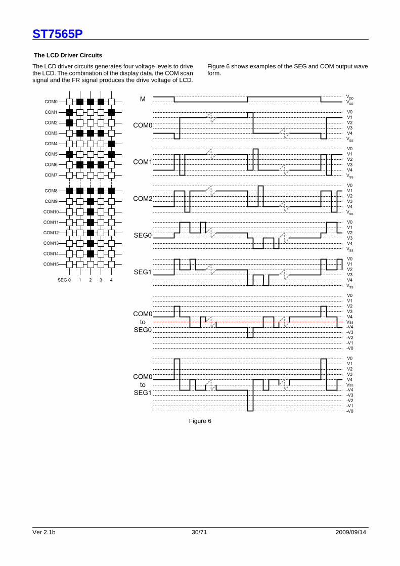
The LCD Driver Circuits
The LCD driver circuits generates four voltage levels to drive the LCD. The combination of the display data, the COM scan signal and the FR signal produces the drive voltage of LCD.
Figure 6 shows examples of the SEG and COM output wave form.
SEG 0 1
COM1
COM2
COM3
COM4
COM5
COM6
COM7
COM8
COM9
COM10
COM11
COM12
COM13
COM14
VDD
VSS
M
V0
V1
V2
V3
V4
VSS
COM0
to
SEG1-V4
-V3
-V2
-V1
-V0
V0
V1
V2
V3
V4
VSS
COM0
to
SEG0-V4
-V3
-V2
-V1
-V0
V0
V1
V2
V3
V4
VSS
SEG1
V0
V1
V2
V3
V4
VSS
SEG0
V0
V1
V2
V3
V4
VSS
COM2
COM1
V0
V1
V2
V3
V4
VSS
V0
V1
V2
V3
V4
VSS
COM0
COM0
COM15
2 3 4
Figure 6
ST7565P
Ver 2.1b 31/71 2009/09/14
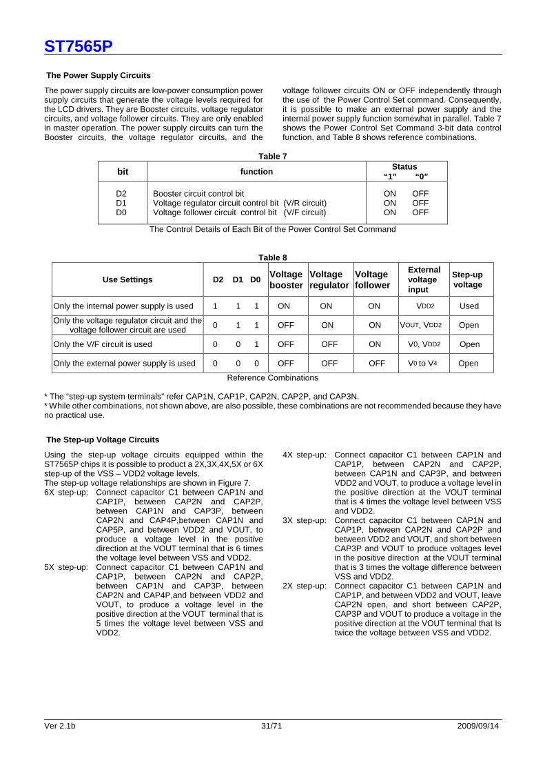
The Power Supply Circuits
The power supply circuits are low-power consumption power supply circuits that generate the voltage levels required for the LCD drivers. They are Booster circuits, voltage regulator circuits, and voltage follower circuits. They are only enabled in master operation. The power supply circuits can turn the Booster circuits, the voltage regulator circuits, and the
voltage follower circuits ON or OFF independently through the use of the Power Control Set command. Consequently, it is possible to make an external power supply and the internal power supply function somewhat in parallel. Table 7 shows the Power Control Set Command 3-bit data control function, and Table 8 shows reference combinations.
Table 7
bit function Status “1” “0”
D2 D1 D0
Booster circuit control bit Voltage regulator circuit control bit (V/R circuit) Voltage follower circuit control bit (V/F circuit)
ON OFF ON OFF ON OFF
The Control Details of Each Bit of the Power Control Set Command
Table 8
Use Settings D2 D1 D0 Voltage booster
Voltage regulator
Voltage follower
External voltage input
Step-up voltage
Only the internal power supply is used 1 1 1 ON ON ON VDD2 Used
Only the voltage regulator circuit and the voltage follower circuit are used
0 1 1 OFF ON ON VOUT, VDD2 Open
Only the V/F circuit is used 0 0 1 OFF OFF ON V0, VDD2 Open
Only the external power supply is used 0 0 0 OFF OFF OFF V0 to V4 Open
Reference Combinations * The “step-up system terminals” refer CAP1N, CAP1P, CAP2N, CAP2P, and CAP3N. * While other combinations, not shown above, are also possible, these combinations are not recommended because they have no practical use.
The Step-up Voltage Circuits
Using the step-up voltage circuits equipped within the ST7565P chips it is possible to product a 2X,3X,4X,5X or 6X step-up of the VSS – VDD2 voltage levels. The step-up voltage relationships are shown in Figure 7. 6X step-up: Connect capacitor C1 between CAP1N and
CAP1P, between CAP2N and CAP2P, between CAP1N and CAP3P, between CAP2N and CAP4P,between CAP1N and CAP5P, and between VDD2 and VOUT, to produce a voltage level in the positive direction at the VOUT terminal that is 6 times the voltage level between VSS and VDD2.
5X step-up: Connect capacitor C1 between CAP1N and CAP1P, between CAP2N and CAP2P, between CAP1N and CAP3P, between CAP2N and CAP4P,and between VDD2 and VOUT, to produce a voltage level in the positive direction at the VOUT terminal that is 5 times the voltage level between VSS and VDD2.
4X step-up: Connect capacitor C1 between CAP1N and CAP1P, between CAP2N and CAP2P, between CAP1N and CAP3P, and between VDD2 and VOUT, to produce a voltage level in the positive direction at the VOUT terminal that is 4 times the voltage level between VSS and VDD2.
3X step-up: Connect capacitor C1 between CAP1N and CAP1P, between CAP2N and CAP2P and between VDD2 and VOUT, and short between CAP3P and VOUT to produce voltages level in the positive direction at the VOUT terminal that is 3 times the voltage difference between VSS and VDD2.
2X step-up: Connect capacitor C1 between CAP1N and CAP1P, and between VDD2 and VOUT, leave CAP2N open, and short between CAP2P, CAP3P and VOUT to produce a voltage in the positive direction at the VOUT terminal that Is twice the voltage between VSS and VDD2.

ST7565P
Ver 2.1b 32/71 2009/09/14
2x voltage booster circuit
CAP1N
CAP1P
C1
CAP5POPEN
VDD2 or VSS
VOUT
C1
CAP2NOPEN
CAP4POPEN
CAP2P
CAP3P
3x voltage booster circuit
CAP1N
CAP1P
C1
CAP5POPEN
VDD2 or VSS
VOUT
C1
CAP4POPEN
CAP3P
CAP2N
CAP2P
C1
3x boost voltage relationship
VSS
VDD2
VOUT<=3xVDD2
Do NOT over voltagelimitation
2x boost voltage relationship
VSS
VDD2
VOUT<=2xVDD2
Do NOT over voltagelimitation
4x voltage booster circuit
CAP1N
CAP1P
C1
CAP5POPEN
VDD2 or VSS
VOUT
C1
CAP4POPEN
CAP2N
CAP2P
C1
CAP3P
C1
4x boost voltage relationship
VSS
VDD2
VOUT<=4xVDD2
Do NOT over voltagelimitation
5x voltage booster circuit
CAP1N
CAP1P
C1
CAP5POPEN
VDD2 or VSS
VOUT
C1
CAP4P
CAP2N
CAP2P
C1
CAP3P
C1
C1
5x boost voltage relationship
VSS
VDD2
VOUT<=5xVDD2
Do NOT over voltagelimitation
6x boost voltage relationship
VSS
VDD2
VOUT<=6xVDD2
Do NOT over voltagelimitation
6x voltage booster circuit
CAP1N
CAP1P
C1
VDD2 or VSS
VOUT
C1
CAP4P
CAP2N
CAP2P
C1
CAP3P
C1
C1
CAP5PC1
Figure 7 * The VDD2 voltage range must be set so that the VOUT terminal voltage does not exceed the absolute maximum rated value. * The maximum voltage of the booster capacitor terminals are : VMAX: CAP5P > CAP4P > CAP3P > CAP2P > CAP1P > CAP2N = CAP1N.
ST7565P
Ver 2.1b 33/71 2009/09/14
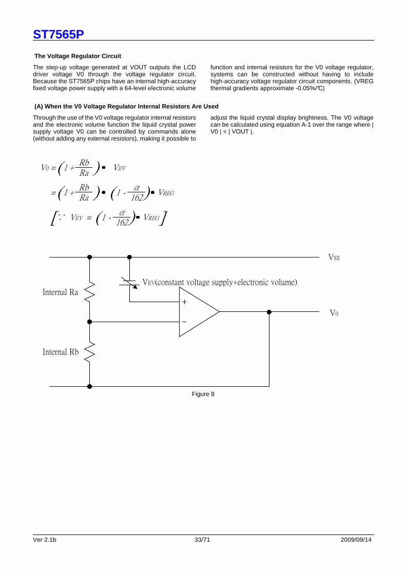
The Voltage Regulator Circuit
The step-up voltage generated at VOUT outputs the LCD driver voltage V0 through the voltage regulator circuit. Because the ST7565P chips have an internal high-accuracy fixed voltage power supply with a 64-level electronic volume
function and internal resistors for the V0 voltage regulator, systems can be constructed without having to include high-accuracy voltage regulator circuit components. (VREG thermal gradients approximate -0.05%/°C)
(A) When the V0 Voltage Regulator Internal Resistors Are Used
Through the use of the V0 voltage regulator internal resistors and the electronic volume function the liquid crystal power supply voltage V0 can be controlled by commands alone (without adding any external resistors), making it possible to
adjust the liquid crystal display brightness. The V0 voltage can be calculated using equation A-1 over the range where | V0 | < | VOUT |.
( )RbRa
+1 VEVV0 =
=( )RbRa
+1 ( 1 -α162) VREG
[∵ VEV = ( 1 -α162) VREG]
Internal RaVEV(constant voltage supply+electronic volume)
VSS
V0
Internal Rb
Figure 8
ST7565P
Ver 2.1b 34/71 2009/09/14
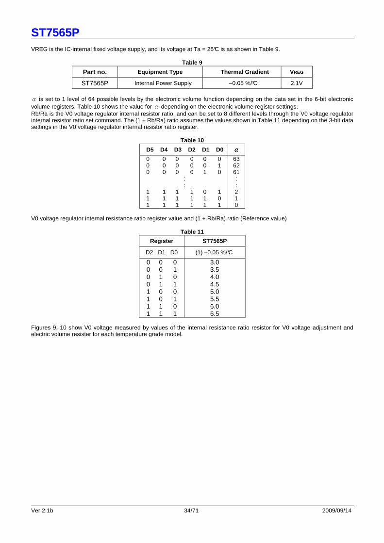
VREG is the IC-internal fixed voltage supply, and its voltage at Ta = 25°C is as shown in Table 9.
Table 9
Part no. Equipment Type Thermal Gradient VREG
ST7565P Internal Power Supply –0.05 %/°C 2.1V α is set to 1 level of 64 possible levels by the electronic volume function depending on the data set in the 6-bit electronic volume registers. Table 10 shows the value for α depending on the electronic volume register settings. Rb/Ra is the V0 voltage regulator internal resistor ratio, and can be set to 8 different levels through the V0 voltage regulator internal resistor ratio set command. The (1 + Rb/Ra) ratio assumes the values shown in Table 11 depending on the 3-bit data settings in the V0 voltage regulator internal resistor ratio register.
Table 10
D5 D4 D3 D2 D1 D0 αααα 0 0 0 0 0 0 0 0 0 0 0 1 0 0 0 0 1 0 : : 1 1 1 1 0 1 1 1 1 1 1 0 1 1 1 1 1 1
63 62 61 : : 2 1 0
V0 voltage regulator internal resistance ratio register value and (1 + Rb/Ra) ratio (Reference value)
Table 11
Register ST7565P
D2 D1 D0 (1) –0.05 %/°C
0 0 0 0 0 1 0 1 0 0 1 1 1 0 0 1 0 1 1 1 0 1 1 1
3.0 3.5 4.0 4.5 5.0 5.5 6.0 6.5
Figures 9, 10 show V0 voltage measured by values of the internal resistance ratio resistor for V0 voltage adjustment and electric volume resister for each temperature grade model.

ST7565P
Ver 2.1b 35/71 2009/09/14
0000
1111
2222
3333
4444
5555
6666
7777
8888
9999
10101010
11111111
12121212
13131313
14141414
15151515
00H 1FH 3FH
V0UNIT:V
000001010011100101110111
V0 voltage regulator internal resistor ratio setD2,D1,D0
Electronic volume registered D5 ~ D0
Ta = 25 °C and booster off ,regulator,follower on VDD=3V
Figure 9 : (1) For ST7565P the Thermal Gradient = -0.05%/°C
The V0 voltage as a function of the V0 voltage regulator internal resistor ratio register and the electronic volume register. Setup example: When selecting Ta = 25°C and V0 = 7V f or an ST7565P on which Temperature gradient = –0.05%/°C. Using Figure 9 and the equation A-1, the following setup is enabled. At this time, the variable range and the notch width of the V0 voltage is, as shown Table 13, as dependent on the electronic volume.
Table 12 Register
Contents D5 D4 D3 D2 D1 D0
For V0 voltage regulator Electronic Volume
— — — 0 1 0
1 0 0 1 0 1
Table 13
V0 Min Typ Max Units Variable Range Notch width
5.1 (63 levels) 7.0 (central value) 8.4 (0 level) [V] 51 [mV]

ST7565P
Ver 2.1b 36/71 2009/09/14
(B) When an External Resistance is Used (The V 0 Voltage Regulator Internal Resistors Are Not Used) (1)
The liquid crystal power supply voltage V0 can also be set without using the V0 voltage regulator internal resistors (IRS terminal = “L”) by adding resistors Ra’ and Rb’ between VDD and VR, and between VR and V0, respectively. When this is done, the use of the electronic volume function makes it possible to adjust the brightness of the liquid crystal display
by controlling the liquid crystal power supply voltage V0 through commands. In the range where | V0 | < | VOUT |, the V0 voltage can be calculated using equation B-1 based on the external resistances Ra’ and Rb’.
( )Rb'Ra'
+1 VEVV0 =
=( )Rb'Ra'
+1 ( 1 -α162) VREG
[∵ VEV = ( 1 -α162) VREG]
External resistor Ra'
VEV(fixed voltage power supply+electronic volume)
VSS
V0
External resistor Rb'
Figure 11 Setup example: When selecting Ta = 25°C and V0 = 7 V for ST7565P the temperature gradient = –0.05%/°C. When the central value of the electron volume register is (D5, D4, D3, D2, D1, D0) = (1, 0, 0, 0, 0, 0), then α = 31 and VREG = 2.1V so, according to equation B-1,
=( )Rb'Ra'
+1 ( 1 -31162) (2.1)7V
=( )Rb'Ra'
+1 ( 1 -α162) VREGV0
Moreover, when the value of the current running through Ra’ and Rb’ is set to 5 uA, Ra’ + Rb’ = 1.4MΩ (Equation B-3)
Consequently, by equations B-2 and B-3,
=Rb'Ra'
3.12
Ra' = 340kΩ
Rb' = 1060kΩ
At this time, the V0 voltage variable range and notch width, based on the electron volume function, is as given in Table 14.
Table 14
V0 Min Typ Max Units Variable Range Notch width
5.3 (63 levels) 7.0 (central value) 8.6 (0 level) [V] 52 [mV]

ST7565P
Ver 2.1b 37/71 2009/09/14
(C) When External Resistors are Used (The V0 Voltage Regulator Internal Resistors Are Not Used) (2)
When the external resistor described above are used, adding a variable resistor as well makes it possible to perform fine adjustments on Ra’ and Rb’, to set the liquid crystal drive voltage V0. In this case, the use of the electronic volume function makes it possible to control the liquid crystal power supply voltage V0 by commands to adjust the liquid crystal display brightness.
In the range where | V0 | < | VOUT | the V0 voltage can be calculated by equation C-1 below based on the R1 and R2 (variable resistor) and R3 settings, where R2 can be subjected to fine adjustments (Δ R2).
( )R3+R2-ΔR2R1+ΔR2
+1 VEVV0 =
=( )+1 ( 1 -α162) VREG
[∵ VEV = ( 1 -α162) VREG]
R3+R2-ΔR2R1+ΔR2
External resistor R1
VEV(fixed voltage power supply+electronic volume)
VSS
V0
External resistor R3
VR
ΔR2External
resistor R2
Rb'
Ra'
Figure 12 Setup example: When selecting Ta = 25°C and V0= 5 to 9 V (using R2) for an ST7565P the temperature gradient = –0.05%/°C. When the central value for the electronic volume register is set at (D5, D4, D3, D2, D1, D0) = (1, 0, 0, 0, 0, 0), then α = 31 and VREG = 2.1 V so, according to equation C-1, when ∆R2 = 0 Ω, in order to make V0 = 9 V,
( R3+R2R1
+19V = ) ( 1 -31162) (2.1)
When ΔR2 = R2, in order to make V = –5 V,
( R3R1+R2
+15V = ) ( 1 -31162) (2.1)
When the current flowing VDD and V0 is set to 5 uA, R1 + R2 + R3 = 1.4MΩ (Equation C-4) With this, according to equation C-2, C-3 and C-4,
R1 = 264kΩ
R2 = 211kΩ
R3 = 925kΩ
The V0 voltage variable range and notch width based on the electron volume function is as shown in Table 15.
Table 15
V0 Min Typ Max Units Variable Range Notch width
5.5 (63 levels) 7.3 (central value) 9 (0 level) [V] 56 [mV]

ST7565P
Ver 2.1b 38/71 2009/09/14
* When the V0 voltage regulator internal resistors or the electronic volume function is used, it is necessary to at least set the voltage regulator circuit and the voltage follower circuit to an operating mode using the power control set commands. Moreover, it is necessary to provide a voltage from VOUT when the Booster circuit is OFF. * The VR terminal is enabled only when the V0 voltage regulator internal resistors are not used (i.e. the IRS terminal = “L”). When the V0 voltage regulator internal resistors are used (i.e. when the IRS terminal = “H”), then the VR terminal is left open. * Because the input impedance of the VR terminal is high, it is necessary to take into consideration short leads, shield cables, etc. to handle noise.
The LCD Voltage Generator Circuit
The V0 voltage is produced by a resistive voltage divider within the IC, and can be produced at the V1, V2, V3, and V4 voltage levels required for liquid crystal driving. Moreover,
when the voltage follower changes the impedance, it provides V1, V2, V3 and V4 to the liquid crystal drive circuit.
High Power Mode
The power supply circuit equipped in the ST7565P chips has very low power consumption (normal mode: HPM = “H”). However, for LCD panels with large loads (size), th is low-power power supply may cause display quality to degrade. When this occurs, set the HPM terminal to “ L” (high power mode) can improve the display quality.
SITRONIX recommends that the display should be checked on actual equipment to determine whether or not to use this mode. Moreover, if the improvement to the display is inadequate even after high power mode has been set, then it is necessary to add a liquid crystal drive power supply externally.
The Internal Power Supply Shutdown Command Sequence
The sequence shown in Figure 13 is recommended for shutting down the internal power supply, first placing the
power supply in power saver mode and then turning the power supply OFF.
Sequence Details Command address (Command, status) D7 D6 D5 D4 D3 D2 D1 D0 Step1 Display OFF 1 0 1 0 1 1 1 0 Power saver Step2 Display all points ON 1 0 1 0 0 1 0 1 commands End Internal power supply OFF (compound)
Figure 13
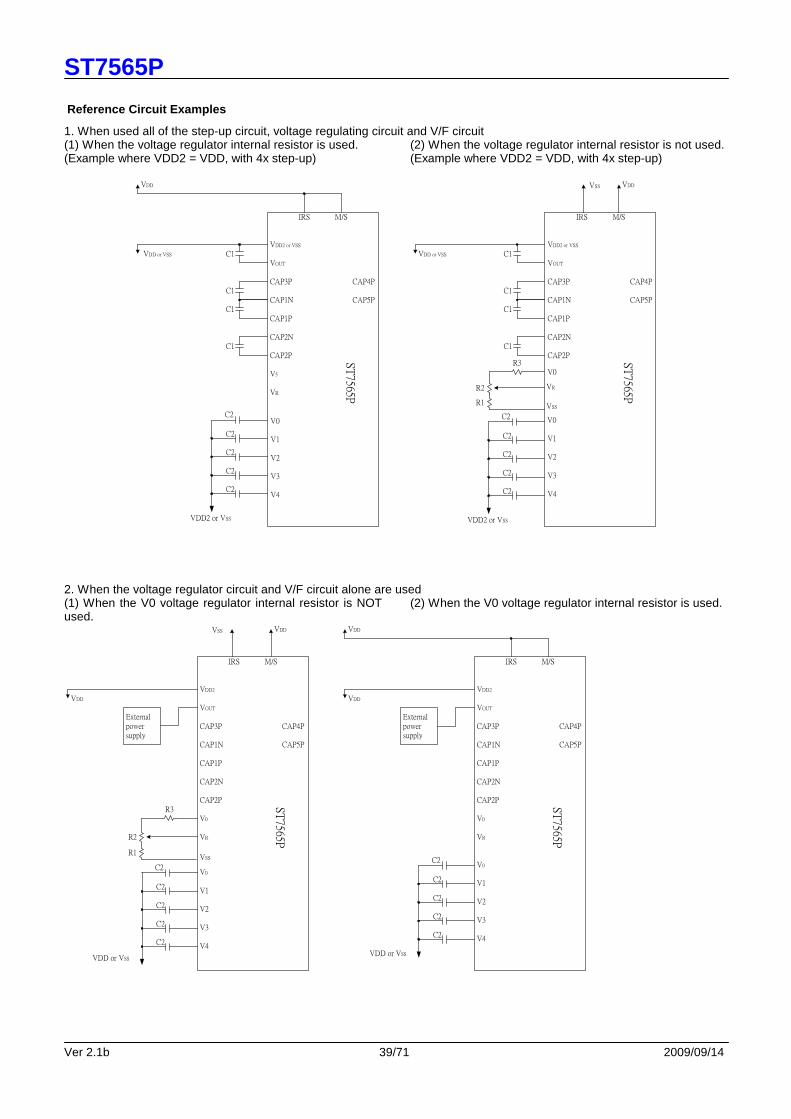
ST7565P
Ver 2.1b 39/71 2009/09/14
Reference Circuit Examples
1. When used all of the step-up circuit, voltage regulating circuit and V/F circuit (1) When the voltage regulator internal resistor is used. (Example where VDD2 = VDD, with 4x step-up)
(2) When the voltage regulator internal resistor is not used. (Example where VDD2 = VDD, with 4x step-up)
VDD2 or VSS
VOUT
CAP3P
CAP1N
CAP1P
CAP2N
CAP2P
V5
VR
ST
7565P
IRS M/S
C1
C1
C1
C1
C2
C2
C2
C2
VDD
VDD or VSS
VDD2 or VSS
VOUT
CAP3P
CAP1N
CAP1P
CAP2N
CAP2P
V0
VR
VSS
V1
V2
V3
V4
V0
ST
7565P
IRS M/S
C1
C1
C1
C1
VDD or VSS
VDD
R3
R2
R1
CAP4P
CAP5P
CAP4P
CAP5P
VDD2 or VSS
V1
V2
V3
V4
V0C2
C2
C2
C2
C2
VDD2 or VSS
C2
VSS
2. When the voltage regulator circuit and V/F circuit alone are used (1) When the V0 voltage regulator internal resistor is NOT used.
(2) When the V0 voltage regulator internal resistor is used.
VDD2
VOUT
CAP3P
CAP1N
CAP1P
CAP2N
CAP2P
V0
VR
ST
7565P
IRS M/S
VDD
VDD
R3
R2
R1
VDD2
VOUT
CAP3P
CAP1N
CAP1P
CAP2N
CAP2P
V0
VR
V0
V1
V2
V3
V4
ST
7565P
IRS M/S
VDD
VDD
External power supply
External power supply
CAP4P
CAP5P
CAP4P
CAP5P
VSS
V0
V1
V2
V3
V4
VSS
C2
C2
C2
C2
VDD or VSS
C2
C2
C2
C2
C2
VDD or VSS
C2

ST7565P
Ver 2.1b 40/71 2009/09/14
(3) When the V/F circuit alone is used (4) When the built-in power is not used
VSS
VOUT
CAP3P
CAP1N
CAP1P
CAP2N
CAP2P
V0
VR
V0
V1
V2
V3
V4
ST
7565P
IRS M/S
VDD
VSS
External power supply
VSS
VOUT
CAP3P
CAP1N
CAP1P
CAP2N
CAP2P
V0
VR
ST
7565P
IRS M/S
VDD
VSS
External power supply
CAP4P
CAP5P
CAP4P
CAP5P
VDD or VSS
V0
V1
V2
V3
V4
VDD or VSS
VSS
C2
C2
C2
C2
VDD or VSS
C2
Item Set value units
C1 C2
1.0 to 4.7 0.1 to 4.7
uF uF
C1 and C2 are determined by the size of the LCD being driven. * 1. Because the VR terminal input impedance is high, use short leads and shielded lines. * 2. C1 and C2 are determined by the size of the LCD being driven. Select a value that will stabilize the liquid crystal drive voltage. Example of the process which determines the capacitor values: * Turn the voltage regulator circuit and voltage follower circuit ON and supply a voltage to VOUT from the outside. * Determine C2 by displaying an LCD pattern with a heavy load (such as horizontal stripes) and selecting a C2 that stabilizes the liquid crystal drive voltages (V0 to V4). Note that all C2 capacitors must have the same capacitance value. * Next turn all the power supplies ON and determine C1.
ST7565P
Ver 2.1b 41/71 2009/09/14
The Reset Circuit
When the /RES input comes to the “L” level, these LSIs return to the default state. Their default states are as follows: 1. Display OFF 2. Normal display 3. ADC select: Normal (ADC command D0 = “L”) 4. Power control register: (D2, D1, D0) = (0, 0, 0) 5. Serial interface internal register data clear 6. LCD power supply bias rate:
1/65 DUTY = 1/9 bias 1/49,1/55,1/53 DUTY = 1/8 bias 1/33 DUTY = 1/6 bias
7. All-indicator lamps-on OFF (All-indicator lamps ON/OFF command D0 = “L”)
8. Power saving clear 9. V0 voltage regulator internal resistors Ra and Rb
separation 10. Output conditions of SEG and COM terminals
SEG=VSS , COM=VSS 11. Read modify write OFF 12. Display start line set to first line 13. Column address set to Address 0 14. Page address set to Page 0 15. Common output status normal 16. V0 voltage regulator internal resistor ratio set mode
clear 17. Clear Electronic volume register :
(D5, D4, D3, D2, D1, D0) = (1, 0. 0, 0, 0,0) 18. Test mode clear
On the other hand, when the reset command is used, the above default settings from 11 to 18 are only executed. When the power is turned on, the IC internal state becomes unstable, and it is necessary to initialize it using the /RES terminal. After the initialization, each input terminal should be controlled normally. Moreover, when the control signal from the MPU is in the high impedance, an over current may flow to the IC. After applying a current, it is necessary to take proper measures to prevent the input terminal from getting into the high impedance state. If the internal liquid crystal power supply circuit is not used on ST7565P,it is necessary that /RES is “H” when the external liquid crystal power supply is turned on. This IC has the function to discharge V0 when /RES is “L,” and the external power supply short-circuits to Vss when /RES is “L.” This means that an internal resistor is connected between VSS and V0. While /RES is “L,” the oscillator works but the display timing generator stops, and the CL, FR and /DOF terminals are fixed to “H.” The terminals D0 to D7 are not affected. The VSS level is output to SEG and COM output terminals after a success hardware reset.
ST7565P
Ver 2.1b 42/71 2009/09/14
CCOOMMMMAANNDDSS The ST7565P identify the data bus signals by a combination of A0, /RD (E), /WR(R/W) signals. Command interpretation and execution does not depend on the external clock, but rather is performed through internal timing only, and thus the processing is fast enough that normally a busy check is not required. In the 8080 MPU interface, commands are launched by inputting a low pulse to the RD terminal for reading, and inputting a low pulse to the /WR terminal for writing. In the 6800 Series MPU interface, the interface is placed in a read mode when an “H” signal is input to the R/W terminal and placed in a write mode when a “L” signal is input to the R/W terminal and then the command is launched by inputting a high pulse to the E terminal. Consequently, the 6800 Series MPU interface is different than the 80x86 Series MPU interface in that in the explanation of commands and the display commands the status read and display data read /RD (E) becomes “1(H)”. In the explanations below the commands are explained using the 8080 Series MPU interface as the example. When the serial interface is selected, the data is input in sequence starting with D7. <Explanation of Commands>
Display ON/OFF
This command turns the display ON and OFF. E R/W
A0 /RD /WR
D7 D6 D5 D4 D3 D2 D1 D0
Setting 0 1 0
1 0 1 0 1 1 1 1
0 Display ON Display OFF
When the display OFF command is executed when in the display all points ON mode, power saver mode is entered. See the section on the power saver for details.
Display Start Line Set
This command is used to specify the display start line address of the display data RAM shown in Figure 4. For further details see the explanation of this function in “The Line Address Circuit”.
E R/W A0 /RD /WR
D7 D6 D5 D4 D3 D2 D1 D0
Line address 0 1 0
0 1 0 0 0 0 0 0 0 0 0 0 0 1 0 0 0 0 1 0
↓ 1 1 1 1 1 0 1 1 1 1 1 1
0 1 2 ↓ 62 63
Page Address Set
This command specifies the page address corresponding to the low address when the MPU accesses the display data RAM (see Figure 4). Specifying the page address and column address enables to access a desired bit of the display data RAM. Changing the page address does not accompany a change in the status display.
E R/W A0 /RD /WR
D7 D6 D5 D4 D3 D2 D1 D0
Page address 0 1 0
1 0 1 1 0 0 0 0 0 0 0 1 0 0 1 0
↓ 0 1 1 1 1 0 0 0
0 1 2 ↓ 7 8

ST7565P
Ver 2.1b 43/71 2009/09/14
Column Address Set
This command specifies the column address of the display data RAM shown in Figure 4. The column address is split into two sections (the higher 4 bits and the lower 4 bits) when it is set (fundamentally, set continuously). Each time the display data RAM is accessed, the column address automatically increments (+1), making it possible for the MPU to continuously read from/write to the display data. The column address increment is topped at 83H. This does not change the page address continuously. See the function explanation in “The Column Address Circuit,” for details.
E R/W A0 /RD /WR
D7 D6 D5 D4 D3 D2 D1 D0 A7 A6 A 5 A4 A3 A2 A1 A0
Column address
High bits → Low bits →
0 1 0
0 0 0 1 A7 A6 A5 A4 0 0 0 0 0 0 0 0 0 A3 A2 A1 A0 0 0 0 0 0 0 0 1
0 0 0 0 0 0 1 0 ↓
1 0 0 0 0 0 1 0 1 0 0 0 0 0 1 1
0 1 2 ↓
130 131
Status Read
E R/W A0 /RD /WR
D7 D6 D5 D4 D3 D2 D1 D0 0 0 1 BUSY ADC ON/OFF RESET 0 0 0 0
BUSY
BUSY = 1: it indicates that either processing is occurring internally or a reset condition is in process. BUSY = 0: A new command can be accepted . if the cycle time can be satisfied, there is no need to check
for BUSY conditions.
ADC
This shows the relationship between the column address and the segment driver. 0: Reverse (column address 131-n ↔ SEG n) 1: Normal (column address n ↔ SEG n) (The ADC command switches the polarity.)
ON/OFF
ON/OFF: indicates the display ON/OFF state. 0: Display ON 1: Display OFF (This display ON/OFF command switches the polarity.)
RESET
This indicates that the chip is in the process of initialization either because of a /RES signal or because of a reset command.
0: Operating state 1: Reset in progress
Display Data Write
This command writes 8-bit data to the specified display data RAM address. Since the column address is automatically incremented by “1” after the write, the MPU can write the display data.
E R/W A0 /RD /WR
D7 D6 D5 D4 D3 D2 D1 D0 1 1 0 Write data

ST7565P
Ver 2.1b 44/71 2009/09/14
Display Data Read
This command reads 8-bit data from the specified display data RAM address. Since the column address is automatically incremented by “1” after the read, the CPU can continuously read multiple-word data. One dummy read is required immediately after the column address has been set. See the function explanation in “Display Data RAM” for the explanation of accessing the internal registers. When the serial interface is used, reading of the display data becomes unavailable.
E R/W A0 /RD /WR
D7 D6 D5 D4 D3 D2 D1 D0 1 0 1 Read data
ADC Select (Segment Driver Direction Select)
This command can reverse the correspondence between the display RAM data column address and the segment driver output. Thus, sequence of the segment driver output pins may be reversed by the command. See the column address circuit for the detail. Increment of the column address (by “1”) accompanying the reading or writing the display data is done according to the column address indicated in Figure 4.
E R/W A0 /RD /WR
D7 D6 D5 D4 D3 D2 D1 D0
Setting 0 1 0
1 0 1 0 0 0 0 0
1 Normal Reverse
Display Normal/Reverse
This command can reverse the lit and unlit display without overwriting the contents of the display data RAM. When this is done the display data RAM contents are maintained.
E R/W A0 /RD /WR
D7 D6 D5 D4 D3 D2 D1 D0
Setting 0 1 0
1 0 1 0 0 1 1 0
1
RAM Data “H” LCD ON voltage (normal)
RAM Data “L” LCD ON voltage (reverse)
Display All Points ON/OFF
This command makes it possible to force all display points ON regardless of the content of the display data RAM. The contents of the display data RAM are maintained when this is done. This command takes priority over the display normal/reverse command.
E R/W A0 /RD /WR
D7 D6 D5 D4 D3 D2 D1 D0
Setting 0 1 0
1 0 1 0 0 1 0 0
1 Normal display mode Display all points ON
When the display is in an OFF mode, executing the display all points ON command will place the display in power save mode. For details, see the Power Save section.

ST7565P
Ver 2.1b 45/71 2009/09/14
LCD Bias Set
This command selects the voltage bias ratio required for the liquid crystal display.
Select Status E R/W A0 /RD /WR
D7 D6 D5 D4 D3 D2 D1 D0 1/65duty 1/49duty 1/33duty 1/55duty 1/53duty
1/9 bias 1/8 bias 1/6 bias 1/8 bias 1/8 bias 0 1 0
1 0 1 0 0 0 1 0
1 1/7 bias 1/6 bias 1/5 bias 1/6 bias 1/6 bias
Read/Modify/Write
This command is used paired with the “END” command. Once this command has been input, the display data read command does not change the column address, but only the display data write command increments (+1) the column address. This mode is maintained until the END command is input. When the END command is input, the column address returns to the address it was at when the read/modify/write command was entered. This function makes it possible to reduce the load on the MPU when there are repeating data changes in a specified display region, such as when there is a blanking cursor.
E R/W A0 /RD /WR
D7 D6 D5 D4 D3 D2 D1 D0 0 1 0 1 1 1 0 0 0 0 0
Yes
No
Read-Modify-Write
Done
Page Address Set
Column Address Set
Finished?
Dummy Read
Read-Modify-Write Cycle
Data Read
Modify Data
Data Write (at same Address)
Figure 24 Command Sequence For read modify write
Figure 25
Column address
Read-modify-write mode set
N N+1 N+2 N+3 N+m N
End
Return
ST7565P
Ver 2.1b 46/71 2009/09/14
End
This command releases the read/modify/write mode, and returns the column address to the address it was at when the mode was entered.
E R/W A0 /RD /WR
D7 D6 D5 D4 D3 D2 D1 D0 0 1 0 1 1 1 0 1 1 1 0
Reset
This command initializes the display start line, the column address, the page address, the common output mode, the V0 voltage regulator internal resistor ratio, the electronic volume, and the static indicator are reset, and the read/modify/write mode and test mode are released. There is no impact on the display data RAM. See the function explanation in “Reset” for details. The reset operation is performed after the reset command is entered.
E R/W A0 /RD /WR
D7 D6 D5 D4 D3 D2 D1 D0 0 1 0 1 1 1 0 0 0 1 0
The initialization when the power supply is applied must be done through applying a reset signal to the /RES terminal. The reset command must not be used instead.
Common Output Mode Select
This command can select the scan direction of the COM output terminal. For details, see the function explanation in “Common Output Mode Select Circuit.”
Selected Mode E R/W
A0 /RD /WR
D7 D6 D5 D4 D3 D2 D1 D0
1/65duty 1/49duty 1/33duty 1/55duty 1/53duty
0 1 0 1 1 0 0 0 * * * 1
Normal Reverse
COM0→COM63 COM63→COM0
COM0→COM47 COM47→COM0
COM0→COM31 COM31→COM0
COM0→COM53 COM53→COM0
COM0→COM51 COM51→COM0
* Disabled bit
ST7565P
Ver 2.1b 47/71 2009/09/14
Power Controller Set
This command sets the power supply circuit functions. See the function explanation in “The Power Supply Circuit,” for details.
E R/W A0 /RD /WR
D7 D6 D5 D4 D3 D2 D1 D0
Selected Mode 0 0 1 0 1 0
1 Booster circuit: OFF Booster circuit: ON
0 1
Voltage regulator circuit: OFF Voltage regulator circuit: ON
0 1 0
0 1
Voltage follower circuit: OFF Voltage follower circuit: ON
V0 Voltage Regulator Internal Resistor Ratio Set
This command sets the V0 voltage regulator internal resistor ratio. For details, see the function explanation is “The Voltage Regulator circuit " and Table 11.
E R/W A0 /RD /WR
D7 D6 D5 D4 D3 D2 D1 D0
Rb/Ra Ratio
0 1 0
0 0 1 0 0 0 0 0 0 0 1 0 1 0 ↓ 1 1 1 1 1 1
Small
↓
Large
The Electronic Volume (Double Byte Command)
This command makes it possible to adjust the brightness of the liquid crystal display by controlling the LCD drive voltage V0 through the output from the voltage regulator circuits of the internal liquid crystal power supply. This command is a two byte command used as a pair with the electronic volume mode set command and the electronic volume register set command, and both commands must be issued one after the other.
The Electronic Volume Mode Set
When this command is input, the electronic volume register set command becomes enabled. Once the electronic volume mode has been set, no other command except for the electronic volume register command can be used. Once the electronic volume register set command has been used to set data into the register, then the electronic volume mode is released.
E R/W A0 /RD /WR
D7 D6 D5 D4 D3 D2 D1 D0 0 1 0 1 0 0 0 0 0 0 1
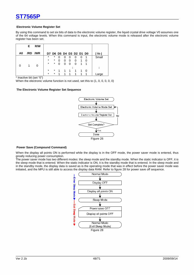
ST7565P
Ver 2.1b 48/71 2009/09/14
Electronic Volume Register Set
By using this command to set six bits of data to the electronic volume register, the liquid crystal drive voltage V0 assumes one of the 64 voltage levels. When this command is input, the electronic volume mode is released after the electronic volume register has been set.
E R/W A0 /RD /WR
D7 D6 D5 D4 D3 D2 D1 D0
| V0 |
0 1 0
* * 0 0 0 0 0 1 * * 0 0 0 0 1 0 * * 0 0 0 0 1 1
↓ * * 1 1 1 1 1 0 * * 1 1 1 1 1 1
Small
↓
Large * Inactive bit (set “0”) When the electronic volume function is not used, set this to (1, 0, 0, 0, 0, 0)
The Electronic Volume Register Set Sequence
Figure 26
Power Save (Compound Command)
When the display all points ON is performed while the display is in the OFF mode, the power saver mode is entered, thus greatly reducing power consumption. The power saver mode has two different modes: the sleep mode and the standby mode. When the static indicator is OFF, it is the sleep mode that is entered. When the static indicator is ON, it is the standby mode that is entered. In the sleep mode and in the standby mode, the display data is saved as is the operating mode that was in effect before the power saver mode was initiated, and the MPU is still able to access the display data RAM. Refer to figure 28 for power save off sequence.
Figure 28
ST7565P
Ver 2.1b 49/71 2009/09/14
Sleep Mode
This stops all operations in the LCD display system, and as long as there are no accesses from the MPU, the consumption current is reduced to a value near the static current. The internal modes during sleep mode are as follows: 1. The oscillator circuit and the LCD power supply circuit are halted. 2. All liquid crystal drive circuits are halted, and the segment in common drive outputs output a VSS level. 3. The static drive system does not operate.
The Booster Ratio (Double Byte Command)
This command makes it possible to select step-up ratio. It is used when the power control set have turn on the internal booster circuit. This command is a two byte command used as a pair with the booster ratio select mode set command and the booster ratio register set command, and both commands must be issued one after the other.
Booster Ratio Select Mode Set
When this command is input, the Booster ratio register set command becomes enabled. Once the booster ratio select mode has been set, no other command except for the booster ratio register command can be used. Once the booster ratio register set command has been used to set data into the register, then the booster ratio select mode is released.
E R/W A0 /RD /WR
D7 D6 D5 D4 D3 D2 D1 D0 0 1 0 1 1 1 1 1 0 0 0
Booset Ratio Register Set
By using this command to set two bits of data to the booster ratio register, it can be select what kind of the booster ratio can be used. When this command is input, the booster ratio select mode is released after the booster ratio register has been set.
E R/W A0 /RD /WR
D7 D6 D5 D4 D3 D2 D1 D0
Booster ratio
select
0 1 0 * * * * * * 0 0 * * * * * * 0 1 * * * * * * 1 1
2x,3x,4x 5x 6x
* Inactive bit (set “0”) When the booster ratio select function is not used, set this to (0, 0) 2x,3x,4x step-up mode.

ST7565P
Ver 2.1b 50/71 2009/09/14
The booster ratio Register Set Sequence
Booster Ratio Set
Done
Booster Ratio Select Mode
Set
Booster Ratio Register Set
Set Complete?
Yes
No
Figure 29
NOP
Non-Operation Command
E R/W A0 /RD /WR
D7 D6 D5 D4 D3 D2 D1 D0 0 1 0 1 1 1 0 0 0 1 1
Test
This is a command for IC chip testing. Please do not use it. If the test command is used by accident, it can be cleared by applying a “L” signal to the /RES input by the reset command or by using an NOP.
E R/W A0 /RD /WR
D7 D6 D5 D4 D3 D2 D1 D0 0 1 0 1 1 1 1 1 1 * *
* Inactive bit Note: The ST7565P maintain their operating modes until something happens to change them. Consequently, excessive
external noise, etc., can change the internal modes of the ST7565P . Thus in the packaging and system design it is necessary to suppress the noise or take measure to prevent the noise from influencing the chip. Moreover, it is recommended that the operating modes be refreshed periodically to prevent the effects of unanticipated noise.

ST7565P
Ver 2.1b 51/71 2009/09/14
Table 16: Table of ST7565P Commands (Note) *: disabled data
Command Code Command
A0 /RD /WR D7 D6 D5 D4 D3 D2 D1 D0 Function
(1) Display ON/OFF 0 1 0 1 0 1 0 1 1 1 0 1
LCD display ON/OFF 0: OFF, 1: ON
(2) Display start line set 0 1 0 0 1 Display start address Sets the display RAM display start line address
(3) Page address set 0 1 0 1 0 1 1 Page address Sets the display RAM page address
(4) Column address set upper bit Column address set lower bit
0 1 0 0 1 0
0 0 0 1 Most significant column address
0 0 0 0 Least significant column address
Sets the most significant 4 bits of the display RAM column address. Sets the least significant 4 bits of the display RAM column address.
(5) Status read 0 0 1 Status 0 0 0 0 Reads the status data
(6) Display data write 1 1 0 Write data Writes to the display RAM
(7) Display data read 1 0 1 Read data Reads from the display RAM
(8) ADC select 0 1 0 1 0 1 0 0 0 0 0 1
Sets the display RAM address SEG output correspondence 0: normal, 1: reverse
(9) Display normal/ reverse 0 1 0 1 0 1 0 0 1 1 0
1
Sets the LCD display normal/ reverse 0: normal, 1: reverse
(10) Display all points ON/OFF 0 1 0 1 0 1 0 0 1 0 0
1
Display all points 0: normal display 1: all points ON
(11) LCD bias set 0 1 0 1 0 1 0 0 0 1 0 1
Sets the LCD drive voltage bias ratio 0: 1/9 bias, 1: 1/7 bias (ST7565P)
(12) Read/modify/write 0 1 0 1 1 1 0 0 0 0 0 Column address increment At write: +1 At read: 0
(13) End 0 1 0 1 1 1 0 1 1 1 0 Clear read/modify/write
(14) Reset 0 1 0 1 1 1 0 0 0 1 0 Internal reset
(15) Common output mode select 0 1 0 1 1 0 0 0 * * *
1
Select COM output scan direction 0: normal direction 1: reverse direction
(16) Power control set 0 1 0 0 0 1 0 1 Operating mode
Select internal power supply operating mode
(17) V0 voltage regulator internal resistor ratio set
0 1 0 0 0 1 0 0 Resistor ratio
Select internal resistor ratio(Rb/Ra) mode
(18) Electronic volume mode set
Electronic volume register set
0 1 0 1 0 0 0 0 0 0 1 0 0 Electronic volume value
Set the V0 output voltage electronic volume register
(20) Booster ratio set 0 1 0 1 1 1 1 1 0 0 0 0 0 0 0 0 0 step-up
value
select booster ratio 00: 2x,3x,4x 01: 5x 11: 6x
(21) Power saver Display OFF and display all points ON compound command
(22) NOP 0 1 0 1 1 1 0 0 0 1 1 Command for non-operation
(23) Test 0 1 0 1 1 1 1 * * * * Command for IC test. Do not use this command

ST7565P
Ver 2.1b 52/71 2009/09/14
CCOOMMMMAANNDD DDEESSCCRRIIPPTTIIOONN
Instruction Setup: Reference
(1) Initialization Note: With this IC, when the power is applied, LCD driving non-selective potentials V2 and V3 (SEG pin) and V1 and V4 (COM pin) are output through the LCD driving output pins SEG and COM. When electric charge is remaining in the smoothing capacitor connecting between the LCD driving voltage output pins (V0 ~ V4) and the VSS pin, the picture on the display may become totally dark instantaneously when the power is turned on. To avoid occurrence of such a failure, we recommend the following flow when turning on the power. 1. When the built-in power is being used immediatel y after turning on the power:
* The target time of 5ms will result to vary depending on the panel characteristics and the capacitance of the smoothing capacitor. Therefore, we suggest you to conduct an operation check using the actual equipment. Notes: Refer to respective sections or paragraphs listed below.
*1: Description of functions; Resetting circuit *2: Command description; LCD bias setting *3: Command description; ADC selection *4: Command description; Common output state selection *5: Description of functions; Power circuit & Command description; Setting the built-in resistance radio for regulation of the V0 voltage *6: Description of functions; Power circuit & Command description; Electronic volume control *7: Description of functions; Power circuit & Command description; Power control setting
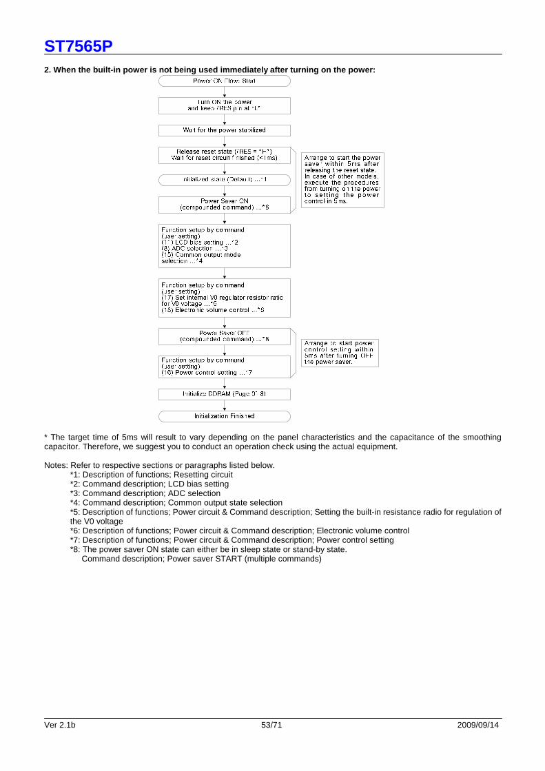
ST7565P
Ver 2.1b 53/71 2009/09/14
2. When the built-in power is not being used immedi ately after turning on the power:
* The target time of 5ms will result to vary depending on the panel characteristics and the capacitance of the smoothing capacitor. Therefore, we suggest you to conduct an operation check using the actual equipment. Notes: Refer to respective sections or paragraphs listed below.
*1: Description of functions; Resetting circuit *2: Command description; LCD bias setting *3: Command description; ADC selection *4: Command description; Common output state selection *5: Description of functions; Power circuit & Command description; Setting the built-in resistance radio for regulation of the V0 voltage *6: Description of functions; Power circuit & Command description; Electronic volume control *7: Description of functions; Power circuit & Command description; Power control setting *8: The power saver ON state can either be in sleep state or stand-by state. Command description; Power saver START (multiple commands)
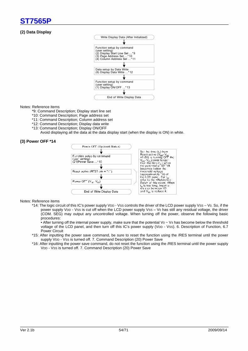
ST7565P
Ver 2.1b 54/71 2009/09/14
(2) Data Display
Write Display Data (After Initialized)
Data setup by Data Write(6) Display Data Write ...*12
Function setup by command(user setting)(2) Display Start Line Set ...*9(3) Page Address Set ...*10(4) Column Address Set ...*11
Function setup by command(user setting)(1) Display ON/OFF ...*13
End of Write Display Data
Notes: Reference items
*9: Command Description; Display start line set *10: Command Description; Page address set *11: Command Description; Column address set *12: Command Description; Display data write *13: Command Description; Display ON/OFF Avoid displaying all the data at the data display start (when the display is ON) in white.
(3) Power OFF *14
Notes: Reference items
*14: The logic circuit of this IC’s power supply VDD - VSS controls the driver of the LCD power supply VSS – V0. So, if the power supply VDD - VSS is cut off when the LCD power supply VSS – V0 has still any residual voltage, the driver (COM. SEG) may output any uncontrolled voltage. When turning off the power, observe the following basic procedures: • After turning off the internal power supply, make sure that the potential V0 ~ V4 has become below the threshold voltage of the LCD panel, and then turn off this IC’s power supply (VDD - VSS). 6. Description of Function, 6.7 Power Circuit
*15: After inputting the power save command, be sure to reset the function using the /RES terminal until the power supply VDD - VSS is turned off. 7. Command Description (20) Power Save
*16: After inputting the power save command, do not reset the function using the /RES terminal until the power supply VDD - VSS is turned off. 7. Command Description (20) Power Save

ST7565P
Ver 2.1b 55/71 2009/09/14
Refresh
It is recommended to turn on the refresh sequence regularly at a specified interval.
Precautions on Turning off the power
<Turning the power (VDD - VSS) off> 1) Power Save (The LCD powers (V0 - VSS) are off.) → Reset input → Power (VDD - VSS) OFF
• Observe tL > tH.
• When tL < tH, an irregular display may occur.
Set tL on the MPU according to the software. tH is determined according to the external capacitor C2 (smoothing capacitor of V0 ~ V4) and the driver’s discharging capacity.
ResetPowersave
Power Off
tL
1.8V
VSS
VSS
tH
V0V1V2V3V4
COM
SEG
VDD
RES
Since the power (VDD-VSS) is cut off,the output comes not to be fixed.
VOUT
Above Vth of the LCD Panel.
Under Vth of the LCD Panel.Depends on the LCD Modulecharacteristic (around 0.2~1V).

ST7565P
Ver 2.1b 56/71 2009/09/14
<Turning the power (VDD - VSS) off : When command control is not possible.> 2) Reset (The LCD powers (VDD - VSS) are off.) → Power (VDD - VSS) OFF
• Observe tL > tH.
• When tL < tH, an irregular display may occur.
For tL, make the power (VDD - VSS) falling characteristics longer or consider any other method.
tH is determined according to the external capacity C2 (smoothing capacity of V0 to V4) and the driver’s discharging capacity. Reset Power Off
tL
1.8V
VSS
COM
SEG
VDD
RES
Since the power (VDD-VSS) is cutoff,the output comes not be fixed.
tH
V0V1V2V3V4
VSS
Above Vth of the LCD Panel.
VOUT
Under Vth of the LCD Panel.Depends on the LCD Modulecharacteristic (around 0.2~1V).
<Reference Data>
V0 voltage falling (discharge) time (tH) after the process of operation → power save → reset.
V0 voltage falling (discharge) time (tH) after the process of operation → reset.
5.0
4.0
3.0
2.4
1.8
1.00.50
50
100
VDD-VSS(V)
C2 : V0 to V4 capacity (uF)
V0
voltag
e fa
llin
g tim
e (m
Sec
)
Figure 31
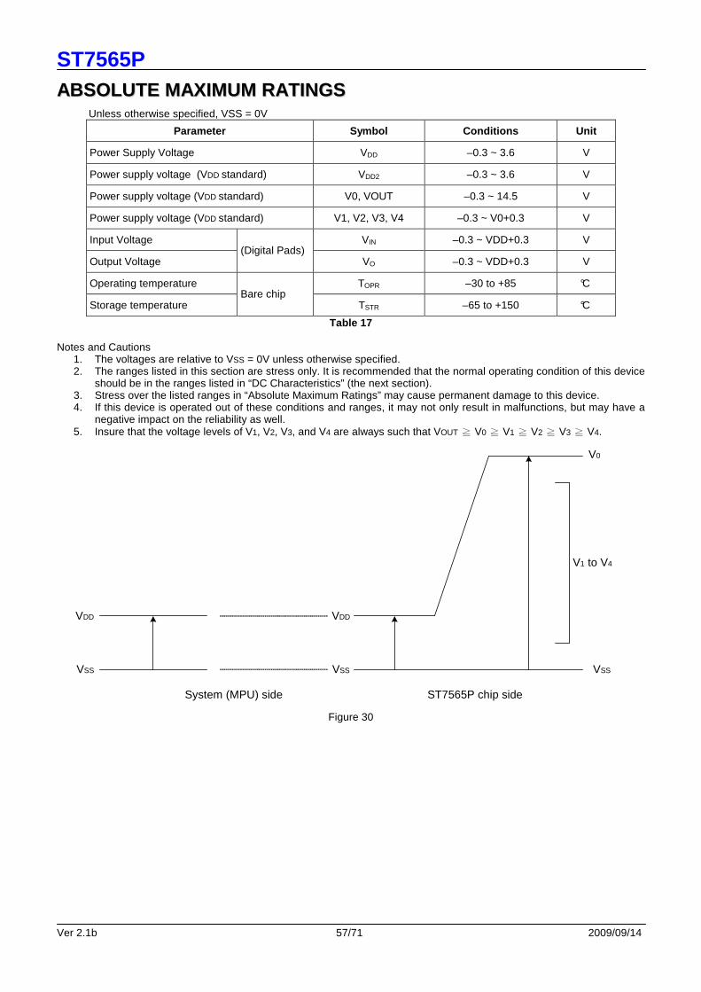
ST7565P
Ver 2.1b 57/71 2009/09/14
AABBSSOOLLUUTTEE MMAAXXIIMMUUMM RRAATTIINNGGSS Unless otherwise specified, VSS = 0V
Parameter Symbol Conditions Unit
Power Supply Voltage VDD –0.3 ~ 3.6 V
Power supply voltage (VDD standard) VDD2 –0.3 ~ 3.6 V
Power supply voltage (VDD standard) V0, VOUT –0.3 ~ 14.5 V
Power supply voltage (VDD standard) V1, V2, V3, V4 –0.3 ~ V0+0.3 V
Input Voltage VIN –0.3 ~ VDD+0.3 V
Output Voltage (Digital Pads)
VO –0.3 ~ VDD+0.3 V
Operating temperature TOPR –30 to +85 °C
Storage temperature Bare chip
TSTR –65 to +150 °C
Table 17 Notes and Cautions
1. The voltages are relative to VSS = 0V unless otherwise specified. 2. The ranges listed in this section are stress only. It is recommended that the normal operating condition of this device
should be in the ranges listed in “DC Characteristics” (the next section). 3. Stress over the listed ranges in “Absolute Maximum Ratings” may cause permanent damage to this device. 4. If this device is operated out of these conditions and ranges, it may not only result in malfunctions, but may have a
negative impact on the reliability as well. 5. Insure that the voltage levels of V1, V2, V3, and V4 are always such that VOUT ≧ V0 ≧ V1 ≧ V2 ≧ V3 ≧ V4.
System (MPU) side ST7565P chip side
V0
VSS
V1 to V4
VSS
VDD
VSS
VDD
Figure 30

ST7565P
Ver 2.1b 58/71 2009/09/14
DDCC CCHHAARRAACCTTEERRIISSTTIICCSS Unless otherwise specified, VSS = 0 V, VDD = 3.0 V ± 10%, Ta = –30 to 85°C
Table 18 Rating
Item Symbol Condition Min. Typ. Max.
Units Applicable
Pin
Operating Voltage (1) VDD 1.8 — 3.3 V VSS*1
Operating Voltage (2) VDD2 (Related to VSS) 2.4 — 3.3 V VSS
High-level Input Voltage VIHC 0.8 x VDD — VDD V *3
Low-level Input Voltage VILC VSS — 0.2 x VDD V *3
High-level Output Voltage VOHC IOH = –1 mA 0.8 x VDD — VDD V *4
Low-level Output Voltage VOLC IOL = 1 mA VSS — 0.2 x VDD V *4
Input leakage current ILI VIN = VDD or VSS –1.0 — 1.0 µA *5
Output leakage current ILO VIN = VDD or VSS –3.0 — 3.0 µA *6
V0 = 13.0V — 2.0 3.5 Liquid Crystal Driver ON Resistance RON
Ta = 25°C (Related to VSS) V0 = 8.0V — 3.2 5.4
KΩ SEGn COMn *7
Static Consumption Current ISSQ — 0.01 2 µA VDD, VDD2
Output Leakage Current I5Q
V0 = 13.0 V (Related to VSS)
— 0.01 10 µA V0
Input Terminal Capacitance CIN Ta = 25°C , f = 1 MHz — 5.0 8.0 pF
Internal Oscillator fOSC 17 20 24 kHz *8
External Input fCL
1/65 duty 1/33 duty Ta = 25°C
17 20 24 kHz CL
Internal Oscillator fOSC 25 30 35 kHz *8
Oscillator Frequency
External Input fCL
1/49 duty 1/53 duty 1/55 duty
Ta = 25°C 25 30 35 kHz CL

ST7565P
Ver 2.1b 59/71 2009/09/14
Table 19
Rating Item Symbol Condition
Min. Typ. Max. Units
Applicable Pin
Input voltage VDD2 (Relative to VSS) 2.4 — 3.3 V VSS
Supply Step-up output voltage Circuit VOUT (Relative to VSS) — — 13.5 V VOUT
Voltage regulator Circuit Operating
Voltage VOUT (Relative to VSS) 6.0 — 13.5 V VOUT
Voltage Follower Circuit Operating
Voltage V0 (Relative to VSS) 4.0 — 13.0 V V0 * 9 In
tern
al P
ower
Base Voltage VR Ta = 25°C , (Relative to V SS) –0.05%/°C 2.07 2.10 2.13 V *10
• Dynamic Consumption Current : During Display, wit h the Internal Power Supply OFF Current consumed by t otal ICs
when an external power supply is used . Table 20
Rating Test pattern Symbol Condition
Min. Typ. Max. Units Notes
Display Pattern OFF IDD VDD = 3.0 V,
V0 – VSS = 11.0 V — 16 27 µA *11
Display Pattern Checker IDD VDD = 3.0 V,
V0 – VSS = 11.0 V — 19 32 µA *11
• Dynamic Consumption Current : During Display, wit h the Internal Power Supply ON
Table 21 Rating
Test pattern Symbol Condition Min. Typ. Max.
Units Notes
Normal Mode — 90 130 Display
Pattern OFF IDD VDD = 3.0 V,
Quad step-up voltage. V0 –VSS = 11.0 V High-Power Mode — 128 193
µA *12
Normal Mode — 100 147 Display Pattern Checker
IDD VDD = 3.0 V,
Quad step-up voltage. V0 –VSS = 11.0 V High-Power Mode — 135 205
µA *12
• Consumption Current at Time of Power Saver Mode : VSS = -3.0 V ± 10%
Table 22 Rating
Item Symbol Condition Min. Typ. Max.
Units Notes
Sleep mode IDD Ta = 25°C — 0.1 4
Standby Mode IDD Ta = 25°C — 5 10 µA
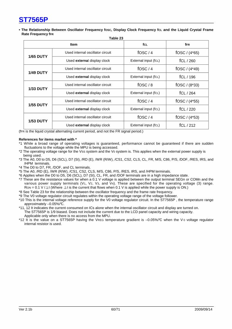
ST7565P
Ver 2.1b 60/71 2009/09/14
• The Relationship Between Oscillator Frequency f OSC, Display Clock Frequency f CL and the Liquid Crystal Frame
Rate Frequency f FR Table 23
Item fCL fFR
Used internal oscillator circuit fOSC / 4 fOSC / (4*65) 1/65 DUTY
Used externa l display clock External input (fCL) fCL / 260
Used internal oscillator circuit fOSC / 4 fOSC / (4*49) 1/49 DUTY
Used external display clock External input (fCL) fCL / 196
Used internal oscillator circuit fOSC / 8 fOSC / (8*33) 1/33 DUTY
Used external display clock External input (fCL) fCL / 264
Used internal oscillator circuit fOSC / 4 fOSC / (4*55) 1/55 DUTY
Used external display clock External input (fCL) fCL / 220
Used internal oscillator circuit fOSC / 4 fOSC / (4*53) 1/53 DUTY
Used external display clock External input (fCL) fCL / 212
(fFR is the liquid crystal alternating current period, and not the FR signal period.) References for items market with * *1 While a broad range of operating voltages is guaranteed, performance cannot be guaranteed if there are sudden
fluctuations to the voltage while the MPU is being accessed. *2 The operating voltage range for the VSS system and the V0 system is. This applies when the external power supply is
being used. *3 The A0, D0 to D5, D6 (SCL), D7 (SI), /RD (E), /WR (R/W), /CS1, CS2, CLS, CL, FR, M/S, C86, P/S, /DOF, /RES, IRS, and
/HPM terminals. *4 The D0 to D7, FR, /DOF, and CL terminals. *5 The A0, /RD (E), /WR (R/W), /CS1, CS2, CLS, M/S, C86, P/S, /RES, IRS, and /HPM terminals. *6 Applies when the D0 to D5, D6 (SCL), D7 (SI), CL, FR, and /DOF terminals are in a high impedance state. *7 These are the resistance values for when a 0.1 V voltage is applied between the output terminal SEGn or COMn and the
various power supply terminals (V1, V2, V3, and V4). These are specified for the operating voltage (3) range. RON = 0.1 V /ΔI (Where ΔI is the current that flows when 0.1 V is applied while the power supply is ON.)
*8 See Table 23 for the relationship between the oscillator frequency and the frame rate frequency. *9 The V0 voltage regulator circuit regulates within the operating voltage range of the voltage follower. *10 This is the internal voltage reference supply for the V0 voltage regulator circuit. In the ST7565P , the temperature range
approximately –0.05%/°C. *11, 12 It indicates the current consumed on ICs alone when the internal oscillator circuit and display are turned on.
The ST7565P is 1/9 biased. Does not include the current due to the LCD panel capacity and wiring capacity. Applicable only when there is no access from the MPU.
*12 It is the value on a ST7565P having the VREG temperature gradient is –0.05%/°C when the V 0 voltage regulator internal resistor is used.
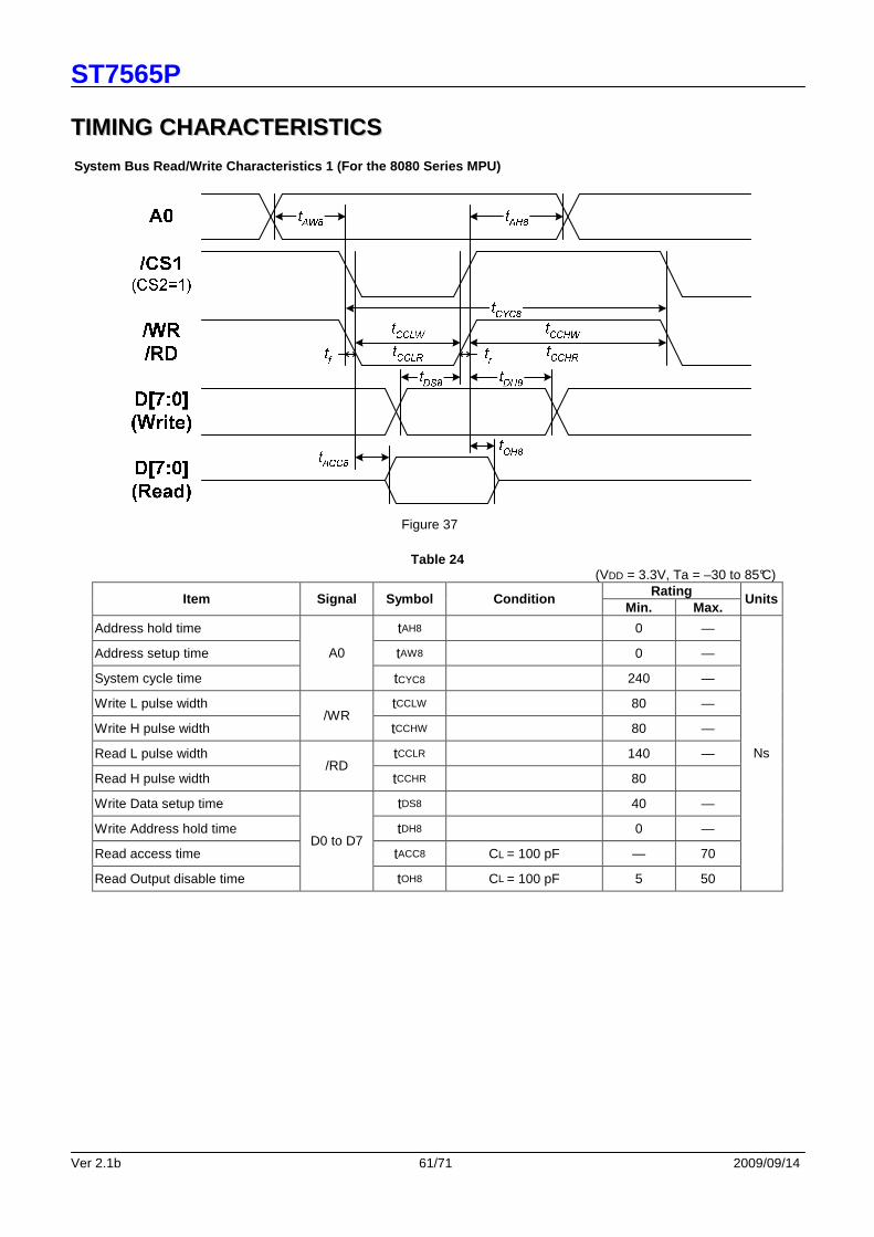
ST7565P
Ver 2.1b 61/71 2009/09/14
TTIIMMIINNGG CCHHAARRAACCTTEERRIISSTTIICCSS
System Bus Read/Write Characteristics 1 (For the 808 0 Series MPU)
Figure 37
Table 24 (VDD = 3.3V, Ta = –30 to 85°C)
Rating Item Signal Symbol Condition
Min. Max. Units
Address hold time tAH8 0 —
Address setup time tAW8 0 —
System cycle time
A0
tCYC8 240 —
Write L pulse width tCCLW 80 —
Write H pulse width /WR
tCCHW 80 —
Read L pulse width tCCLR 140 —
Read H pulse width /RD
tCCHR 80
Write Data setup time tDS8 40 —
Write Address hold time tDH8 0 —
Read access time tACC8 CL = 100 pF — 70
Read Output disable time
D0 to D7
tOH8 CL = 100 pF 5 50
Ns

ST7565P
Ver 2.1b 62/71 2009/09/14
Table 25
(VDD = 2.7V, Ta = –30 to 85°C) Rating
Item Signal Symbol Condition Min. Max.
Units
Address hold time tAH8 0 —
Address setup time tAW8 0 —
System cycle time
A0
tCYC8 400 —
Write L pulse width tCCLW 220 —
Write H pulse width WR
tCCHW 180 —
Read L pulse width tCCLR 220 —
Read H pulse width RD
tCCHR 180 —
Write Data setup time tDS8 40 —
Write Address hold time tDH8 0 —
Read access time tACC8 CL = 100 pF — 140
Read Output disable time
D0 to D7
tOH8 CL = 100 pF 10 100
ns
Table 26
(VDD = 1.8V, Ta = –30 to 85°C) Rating
Item Signal Symbol Condition Min. Max.
Units
Address hold time tAH8 0 —
Address setup time tAW8 0 —
System cycle time
A0
tCYC8 640 —
Write L pulse width tCCLW 360 —
Write H pulse width WR
tCCHW 280 —
Read L pulse width tCCLR 360 —
Read H pulse width RD
tCCHR 280
Write Data setup time tDS8 80 —
Write Address hold time tDH8 0 —
Read access time tACC8 CL = 100 pF — 240
Read Output disable time
D0 to D7
tOH8 CL = 100 pF 10 200
ns
*1 The input signal rise time and fall time (tr, tf) is specified at 15 ns or less. When the system cycle time is extremely fast,
(tr +tf) ≦ (tCYC8 – tCCLW – tCCHW) for (tr + tf) ≦ (tCYC8 – tCCLR – tCCHR) are specified. *2 All timing is specified using 20% and 80% of VDD as the reference. *3 tCCLW and tCCLR are specified as the overlap between /CS1 being “L” (CS2 = “H”) and /WR and /RD being at the “L” level.

ST7565P
Ver 2.1b 63/71 2009/09/14
System Bus Read/Write Characteristics 2 (For the 680 0 Series MPU)
Figure 38
Table 27 (VDD = 3.3V, Ta = –30 to 85°C)
Rating Item Signal Symbol Condition
Min. Max. Units
Address hold time tAH6 0 —
Address setup time tAW6 0 —
System cycle time
A0
tCYC6 240 —
Enable L pulse width (WRITE) tEWLW 80 —
Enable H pulse width (WRITE) tEWHW 80 —
Enable L pulse width (READ) tEWLR 80 —
Enable H pulse width (READ)
E
tEWHR 140
WRITE Data setup time tDS6 40 —
WRITE Address hold time tDH6 0 —
READ access time tACC6 CL = 100 pF — 70
READ Output disable time
D0 to D7
tOH6 CL = 100 pF 5 50
ns
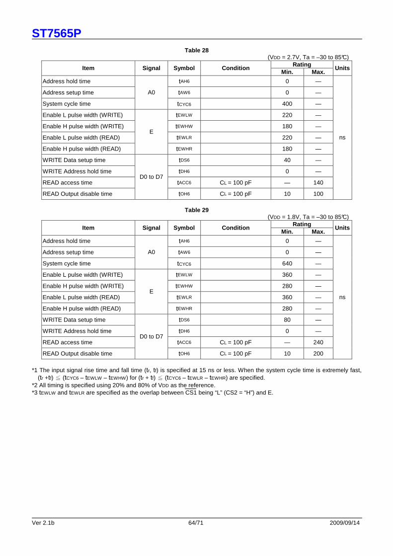
ST7565P
Ver 2.1b 64/71 2009/09/14
Table 28
(VDD = 2.7V, Ta = –30 to 85°C) Rating
Item Signal Symbol Condition Min. Max.
Units
Address hold time tAH6 0 —
Address setup time tAW6 0 —
System cycle time
A0
tCYC6 400 —
Enable L pulse width (WRITE) tEWLW 220 —
Enable H pulse width (WRITE) tEWHW 180 —
Enable L pulse width (READ) tEWLR 220 —
Enable H pulse width (READ)
E
tEWHR 180 —
WRITE Data setup time tDS6 40 —
WRITE Address hold time tDH6 0 —
READ access time tACC6 CL = 100 pF — 140
READ Output disable time
D0 to D7
tOH6 CL = 100 pF 10 100
ns
Table 29
(VDD = 1.8V, Ta = –30 to 85°C) Rating
Item Signal Symbol Condition Min. Max.
Units
Address hold time tAH6 0 —
Address setup time tAW6 0 —
System cycle time
A0
tCYC6 640 —
Enable L pulse width (WRITE) tEWLW 360 —
Enable H pulse width (WRITE) tEWHW 280 —
Enable L pulse width (READ) tEWLR 360 —
Enable H pulse width (READ)
E
tEWHR 280 —
WRITE Data setup time tDS6 80 —
WRITE Address hold time tDH6 0 —
READ access time tACC6 CL = 100 pF — 240
READ Output disable time
D0 to D7
tOH6 CL = 100 pF 10 200
ns
*1 The input signal rise time and fall time (tr, tf) is specified at 15 ns or less. When the system cycle time is extremely fast,
(tr +tf) ≦ (tCYC6 – tEWLW – tEWHW) for (tr + tf) ≦ (tCYC6 – tEWLR – tEWHR) are specified. *2 All timing is specified using 20% and 80% of VDD as the reference. *3 tEWLW and tEWLR are specified as the overlap between CS1 being “L” (CS2 = “H”) and E.
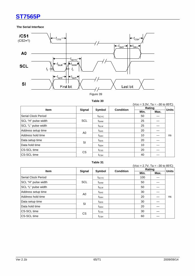
ST7565P
Ver 2.1b 65/71 2009/09/14
The Serial Interface
Figure 39
Table 30 (VDD = 3.3V, Ta = –30 to 85°C)
Rating Item Signal Symbol Condition
Min. Max. Units
Serial Clock Period tSCYC 50 —
SCL “H” pulse width tSHW 25 —
SCL “L” pulse width
SCL
tSLW 25 —
Address setup time tSAS 20 —
Address hold time A0
tSAH 10 —
Data setup time tSDS 20 —
Data hold time SI
tSDH 10 —
CS-SCL time tCSS 20 —
CS-SCL time CS
tCSH 40 —
ns
Table 31
(VDD = 2.7V, Ta = –30 to 85°C) Rating
Item Signal Symbol Condition Min. Max.
Units
Serial Clock Period tSCYC 100 —
SCL “H” pulse width tSHW 50 —
SCL “L” pulse width
SCL
tSLW 50 —
Address setup time tSAS 30 —
Address hold time A0
tSAH 20 —
Data setup time tSDS 30 —
Data hold time SI
tSDH 20 —
CS-SCL time tCSS 30 —
CS-SCL time CS
tCSH 60 —
ns
ST7565P
Ver 2.1b 66/71 2009/09/14
Table 32
(VDD = 1.8V, Ta = –30 to 85°C) Rating
Item Signal Symbol Condition Min. Max.
Units
Serial Clock Period tSCYC 200 —
SCL “H” pulse width tSHW 80 —
SCL “L” pulse width
SCL
tSLW 80 —
Address setup time tSAS 60 —
Address hold time A0
tSAH 30 —
Data setup time tSDS 60 —
Data hold time SI
tSDH 30 —
CS-SCL time tCSS 40 —
CS-SCL time CS
tCSH 100 —
ns
*1 The input signal rise and fall time (tr, tf) are specified at 15 ns or less. *2 All timing is specified using 20% and 80% of VDD as the standard.
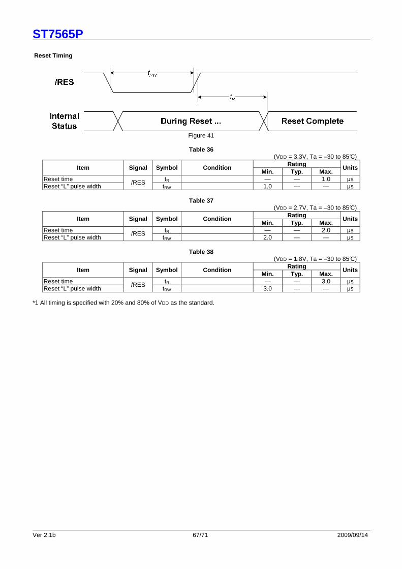
ST7565P
Ver 2.1b 67/71 2009/09/14
Reset Timing
Figure 41
Table 36
(VDD = 3.3V, Ta = –30 to 85°C) Rating
Item Signal Symbol Condition Min. Typ. Max.
Units
Reset time tR — — 1.0 µs Reset “L” pulse width
/RES tRW 1.0 — — µs
Table 37
(VDD = 2.7V, Ta = –30 to 85°C) Rating
Item Signal Symbol Condition Min. Typ. Max.
Units
Reset time tR — — 2.0 µs Reset “L” pulse width
/RES tRW 2.0 — — µs
Table 38
(VDD = 1.8V, Ta = –30 to 85°C) Rating
Item Signal Symbol Condition Min. Typ. Max.
Units
Reset time tR — — 3.0 µs Reset “L” pulse width
/RES tRW 3.0 — — µs
*1 All timing is specified with 20% and 80% of VDD as the standard.

ST7565P
Ver 2.1b 68/71 2009/09/14
TTHHEE MMPPUU IINNTTEERRFFAACCEE ((RREEFFEERREENNCCEE EEXXAAMMPPLLEESS)) ST7565P can be connected to either 80X86 series MPUs or 68000 series MPU. Moreover, by using the serial interface, it is possible to operate ST7565P with fewer signal pins. The display area can be extended horizontally by using two ST7565P chips. Two chip select signals can be used to select the individual ICs to access. (1) 8080 Series MPUs
A0
A1 to A7IORQ
DO to D7RDWRRES
VCC
GND
MP
U
A0
CS2
DO to D7RDWRRES
VDD
VSS
ST
7565
P
CS1Decoder
RESET
C86
P/S
VDD
VSS
Figure 42-1
(2) 6800 Series MPUs
A0
A1 to A15VMA
DO to D7E
R/WRES
VCC
GND
A0
CS2
DO to D7ER/WRES
VDD
VSS
CS1Decoder
RESET
C86
P/S
VDD
VSS
MPU
ST
7565
P
Figure 42-2
(3) Using the Serial Interface
A0
A1 to A7
Port 1Port 2
RES
VCC
GND
A0
CS2
SISCLRES
VDD
VSS
CS1Decoder
RESET
C86
P/S
VDD or VSS
VSS
MPU
ST
7565
P
Figure 42-3

ST7565P
Ver 2.1b 69/71 2009/09/14
CCOONNNNEECCTTIIOONNSS BBEETTWWEEEENN LLCCDD DDRRIIVVEERRSS ((RREEFFEERREENNCCEE EEXXAAMMPPLLEE)) The display area of LCD panel can be extended horizontally by using two ST7565P chips. Use a same equipment type. (1) ST7565P (master) → ST7565P (slave)
ST
7565
S
Sla
ve
ST
7565
S M
aste
r
M/S
FR
CL
DOF
FR
CL
DOF
Output Input
VDD
VSS
CLS CLS M/S
ST
7565
S
Sla
ve
ST
7565
S M
aste
r
M/S
FR
CL
DOF
FR
CL
DOF
Output Input
VDD
VSS
CLS CLS M/S
Figure 43-1
ST
7565P
SLA
VE
ST
7565P
MA
ST
ER
ST
7565P
MA
ST
ER
ST
7565P
SLA
VE
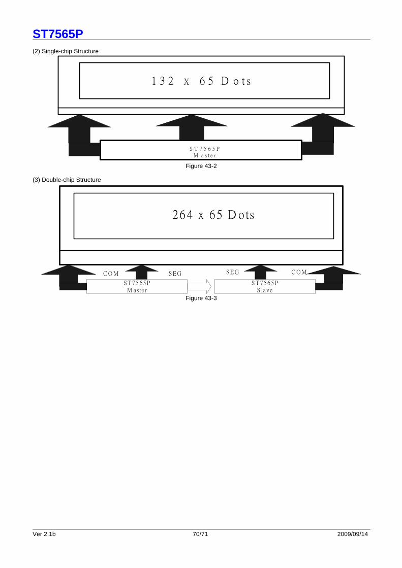
ST7565P
Ver 2.1b 70/71 2009/09/14
(2) Single-chip Structure
S T 7 5 6 5 PM a s t e r
1 3 2 X 6 5 D o t s
Figure 43-2 (3) Double-chip Structure
264 x 65 D o ts
S T 7 5 6 5 PM aste r
S T 7 5 6 5 PS lav e
C O M S E G S E G C O M
Figure 43-3
ST7565P
Ver 2.1b 71/71 2009/09/14
CChhaannggee NNootteess
2004.04.05 Ver 1.2a Modify Serial interface Timing Character. 2004.05.18 Ver 1.3 Change Temperature compensation rate to -0.05%/OC. 2004.05.31 Ver 1.4 Add I/O pin ITO resistor limitation. 2004.06.24 Ver 1.5 Modify Page 2 PAD Diagram. 2004.07.14 Ver 1.6 Modify Page 19 V1~V4 voltage setting with different bias set command.
2005.09.22 Ver 1.7
Modify Feature Description; Modify operating temperature; Modify PIN Name: PAD 80~85 to TEST0~5; Modify Absolute Maximum Ratings; Modify Ta of DC Characteristics and Reset Timing; Remove redundant Page 28; Modify reference voltage to Vss (Page 58, 59).
2006.02.13 Ver 1.8
Modify the description of DC characteristics. Modify function description. Redraw figures. Redraw the PAD DIAGRAM. Highlight the HPM (High Power Mode) description. Put emphasis on the power OFF procedure (Page 56-57).
2006/03/10 Ver 1.9 Fix Ver. 1.8: Booster Circuit mistake (Booster X6, Page 32).
2007/11/06 Ver 1.9a Modify PAD pitch between COM[40] and alignment mark of PAD DIAGRAM. (Page 2).
2008/02/19 Ver 1.9b Modify Page 2 information: PAD 115, 290 and alignment mark drawing. Modify some description for easy understanding.
2008/03/14 Ver 1.9c Modify Ver 1.9c mistake: alignment mark coordinate. Add VIN and VO in Absolute Maximum Ratings. Modify description in Absolute Maximum Ratings.
2008/04/10 Ver 2.0
Remove Static Indicator function and command. Reserved FRS pin function. Truncated Alignment mark coordinate. Rewrite some description. Update timing figures and naming.
2008/07/15 Ver 2.1 Modify Page 2 information: bump size of PAD 115, 290. 2009/02/23 Ver 2.1a Modify mistake of Status Read. 2009/09/14 Ver 2.1b Modify the mistake of The Reset Circuit.
Related Documents


