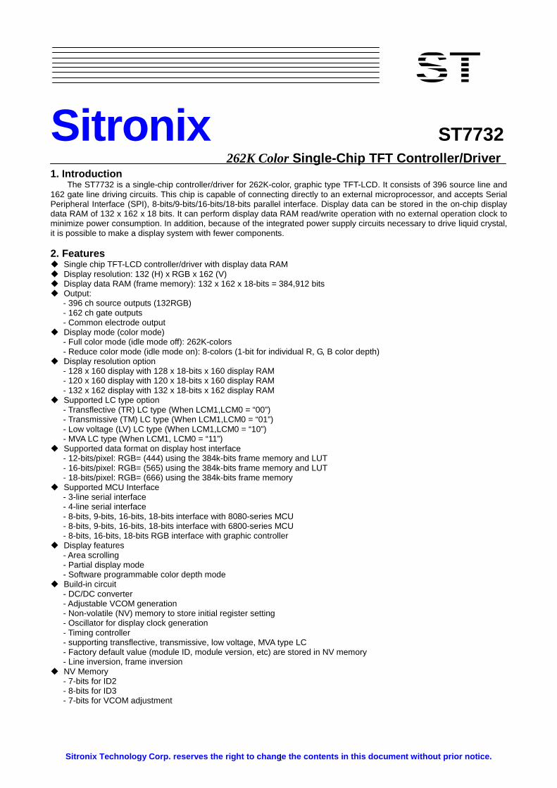
ST Sitronix ST7732 262K Color Single-Chip TFT Controller/Driver Sitronix Technology Corp. reserves the right to change the contents in this document without prior notice. 1 1. Introduction The ST7732 is a single-chip controller/driver for 262K-color, graphic type TFT-LCD. It consists of 396 source line and 162 gate line driving circuits. This chip is capable of connecting directly to an external microprocessor, and accepts Serial Peripheral Interface (SPI), 8-bits/9-bits/16-bits/18-bits parallel interface. Display data can be stored in the on-chip display data RAM of 132 x 162 x 18 bits. It can perform display data RAM read/write operation with no external operation clock to minimize power consumption. In addition, because of the integrated power supply circuits necessary to drive liquid crystal, it is possible to make a display system with fewer components. 2. Features Single chip TFT-LCD controller/driver with display data RAM Display resolution: 132 (H) x RGB x 162 (V) Display data RAM (frame memory): 132 x 162 x 18-bits = 384,912 bits Output: - 396 ch source outputs (132RGB) - 162 ch gate outputs - Common electrode output Display mode (color mode) - Full color mode (idle mode off): 262K-colors - Reduce color mode (idle mode on): 8-colors (1-bit for individual R, G, B color depth) Display resolution option - 128 x 160 display with 128 x 18-bits x 160 display RAM - 120 x 160 display with 120 x 18-bits x 160 display RAM - 132 x 162 display with 132 x 18-bits x 162 display RAM Supported LC type option - Transflective (TR) LC type (When LCM1,LCM0 = “00”) - Transmissive (TM) LC type (When LCM1,LCM0 = “01”) - Low voltage (LV) LC type (When LCM1,LCM0 = “10”) - MVA LC type (When LCM1, LCM0 = “11”) Supported data format on display host interface - 12-bits/pixel: RGB= (444) using the 384k-bits frame memory and LUT - 16-bits/pixel: RGB= (565) using the 384k-bits frame memory and LUT - 18-bits/pixel: RGB= (666) using the 384k-bits frame memory Supported MCU Interface - 3-line serial interface - 4-line serial interface - 8-bits, 9-bits, 16-bits, 18-bits interface with 8080-series MCU - 8-bits, 9-bits, 16-bits, 18-bits interface with 6800-series MCU - 8-bits, 16-bits, 18-bits RGB interface with graphic controller Display features - Area scrolling - Partial display mode - Software programmable color depth mode Build-in circuit - DC/DC converter - Adjustable VCOM generation - Non-volatile (NV) memory to store initial register setting - Oscillator for display clock generation - Timing controller - supporting transflective, transmissive, low voltage, MVA type LC - Factory default value (module ID, module version, etc) are stored in NV memory - Line inversion, frame inversion NV Memory - 7-bits for ID2 - 8-bits for ID3 - 7-bits for VCOM adjustment

Welcome message from author
This document is posted to help you gain knowledge. Please leave a comment to let me know what you think about it! Share it to your friends and learn new things together.
Transcript
ST
Sitronix ST7732 262K Color Single-Chip TFT Controller/Driver
Sitronix Technology Corp. reserves the right to chan ge the contents in this document without prior noti ce. 1
1. Introduction The ST7732 is a single-chip controller/driver for 262K-color, graphic type TFT-LCD. It consists of 396 source line and
162 gate line driving circuits. This chip is capable of connecting directly to an external microprocessor, and accepts Serial Peripheral Interface (SPI), 8-bits/9-bits/16-bits/18-bits parallel interface. Display data can be stored in the on-chip display data RAM of 132 x 162 x 18 bits. It can perform display data RAM read/write operation with no external operation clock to minimize power consumption. In addition, because of the integrated power supply circuits necessary to drive liquid crystal, it is possible to make a display system with fewer components. 2. Features Single chip TFT-LCD controller/driver with display data RAM Display resolution: 132 (H) x RGB x 162 (V) Display data RAM (frame memory): 132 x 162 x 18-bits = 384,912 bits Output:
- 396 ch source outputs (132RGB) - 162 ch gate outputs - Common electrode output
Display mode (color mode) - Full color mode (idle mode off): 262K-colors - Reduce color mode (idle mode on): 8-colors (1-bit for individual R, G, B color depth)
Display resolution option - 128 x 160 display with 128 x 18-bits x 160 display RAM - 120 x 160 display with 120 x 18-bits x 160 display RAM - 132 x 162 display with 132 x 18-bits x 162 display RAM
Supported LC type option - Transflective (TR) LC type (When LCM1,LCM0 = “00”) - Transmissive (TM) LC type (When LCM1,LCM0 = “01”) - Low voltage (LV) LC type (When LCM1,LCM0 = “10”) - MVA LC type (When LCM1, LCM0 = “11”)
Supported data format on display host interface - 12-bits/pixel: RGB= (444) using the 384k-bits frame memory and LUT - 16-bits/pixel: RGB= (565) using the 384k-bits frame memory and LUT - 18-bits/pixel: RGB= (666) using the 384k-bits frame memory
Supported MCU Interface - 3-line serial interface - 4-line serial interface - 8-bits, 9-bits, 16-bits, 18-bits interface with 8080-series MCU - 8-bits, 9-bits, 16-bits, 18-bits interface with 6800-series MCU - 8-bits, 16-bits, 18-bits RGB interface with graphic controller
Display features - Area scrolling - Partial display mode - Software programmable color depth mode
Build-in circuit - DC/DC converter - Adjustable VCOM generation - Non-volatile (NV) memory to store initial register setting - Oscillator for display clock generation - Timing controller - supporting transflective, transmissive, low voltage, MVA type LC - Factory default value (module ID, module version, etc) are stored in NV memory - Line inversion, frame inversion
NV Memory - 7-bits for ID2 - 8-bits for ID3 - 7-bits for VCOM adjustment
ST7732
Ver 1.5.1 2007-11
2
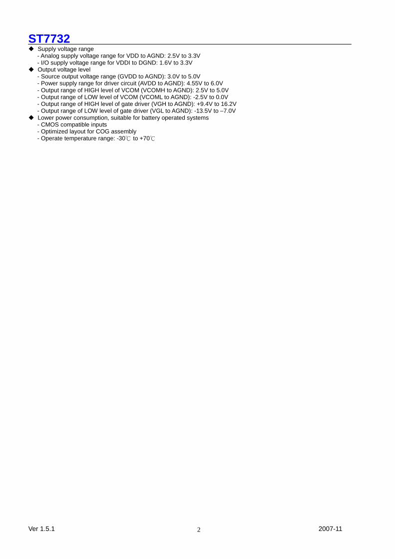
Supply voltage range - Analog supply voltage range for VDD to AGND: 2.5V to 3.3V - I/O supply voltage range for VDDI to DGND: 1.6V to 3.3V
Output voltage level - Source output voltage range (GVDD to AGND): 3.0V to 5.0V - Power supply range for driver circuit (AVDD to AGND): 4.55V to 6.0V - Output range of HIGH level of VCOM (VCOMH to AGND): 2.5V to 5.0V - Output range of LOW level of VCOM (VCOML to AGND): -2.5V to 0.0V - Output range of HIGH level of gate driver (VGH to AGND): +9.4V to 16.2V - Output range of LOW level of gate driver (VGL to AGND): -13.5V to –7.0V
Lower power consumption, suitable for battery operated systems - CMOS compatible inputs - Optimized layout for COG assembly - Operate temperature range: -30 to + 70
ST7732
Ver 1.5.1 2007-11
3
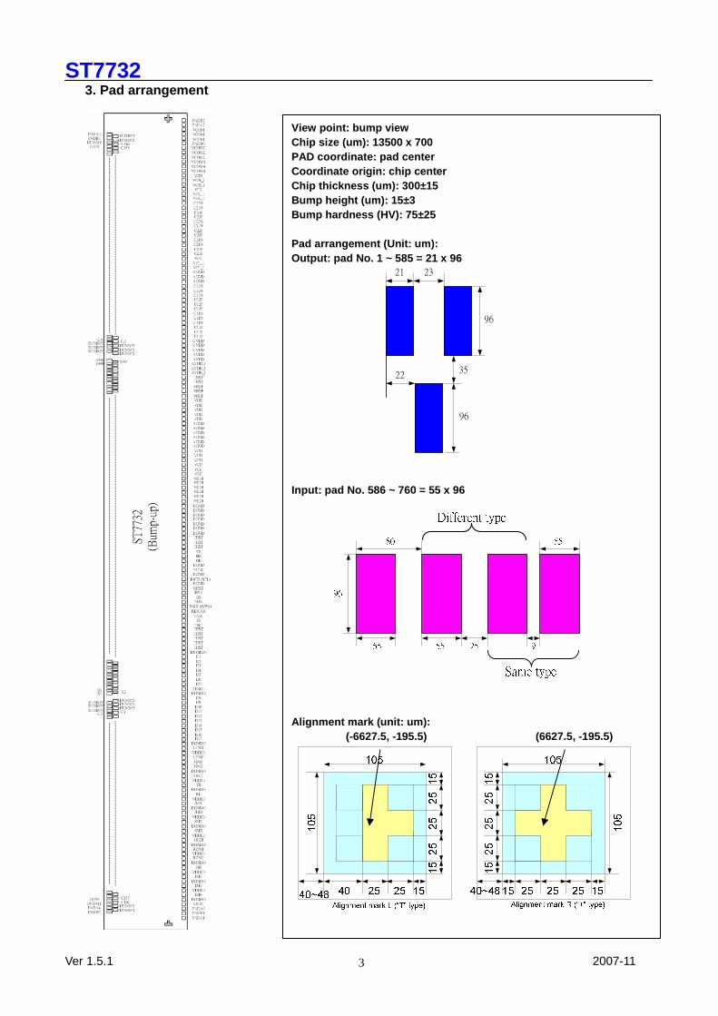
3. Pad arrangement
View point: bump view Chip size (um): 13500 x 700 PAD coordinate: pad center Coordinate origin: chip center Chip thickness (um): 300±15 Bump height (um): 15±3 Bump hardness (HV): 75±25 Pad arrangement (Unit: um): Output: pad No. 1 ~ 585 = 21 x 96
21 23
96
35
96
22
Input: pad No. 586 ~ 760 = 55 x 96
Alignment mark (unit: um):
(-6627.5, -195.5) (6627.5, -195.5)

ST7732
Ver 1.5.1 2007-11
4
4. Pad Center Coordinates PAD No. PIN Name X Y PAD No. PIN Name X Y
1 PADA3 6424 239 41 G92 5544 239
2 DUMMY 6402 108 42 G90 5522 108
3 PADB3 6380 239 43 G88 5500 239
4 DUMMY 6358 108 44 G86 5478 108
5 DUMMY 6336 239 45 G84 5456 239
6 G162 6314 108 46 G82 5434 108
7 G160 6292 239 47 G80 5412 239
8 G158 6270 108 48 G78 5390 108
9 G156 6248 239 49 G76 5368 239
10 G154 6226 108 50 G74 5346 108
11 G152 6204 239 51 G72 5324 239
12 G150 6182 108 52 G70 5302 108
13 G148 6160 239 53 G68 5280 239
14 G146 6138 108 54 G66 5258 108
15 G144 6116 239 55 G64 5236 239
16 G142 6094 108 56 G62 5214 108
17 G140 6072 239 57 G60 5192 239
18 G138 6050 108 58 G58 5170 108
19 G136 6028 239 59 G56 5148 239
20 G134 6006 108 60 G54 5126 108
21 G132 5984 239 61 G52 5104 239
22 G130 5962 108 62 G50 5082 108
23 G128 5940 239 63 G48 5060 239
24 G126 5918 108 64 G46 5038 108
25 G124 5896 239 65 G44 5016 239
26 G122 5874 108 66 G42 4994 108
27 G120 5852 239 67 G40 4972 239
28 G118 5830 108 68 G38 4950 108
29 G116 5808 239 69 G36 4928 239
30 G114 5786 108 70 G34 4906 108
31 G112 5764 239 71 G32 4884 239
32 G110 5742 108 72 G30 4862 108
33 G108 5720 239 73 G28 4840 239
34 G106 5698 108 74 G26 4818 108
35 G104 5676 239 75 G24 4796 239
36 G102 5654 108 76 G22 4774 108
37 G100 5632 239 77 G20 4752 239
38 G98 5610 108 78 G18 4730 108
39 G96 5588 239 79 G16 4708 239
40 G94 5566 108 80 G14 4686 108

ST7732
Ver 1.5.1 2007-11
5
PAD No. PIN Name X Y PAD No. PIN Name X Y
81 G12 4664 239 121 S368 3784 239
82 G10 4642 108 122 S367 3762 108
83 G8 4620 239 123 S366 3740 239
84 G6 4598 108 124 S365 3718 108
85 G4 4576 239 125 S364 3696 239
86 G2 4554 108 126 S363 3674 108
87 DUMMY 4532 239 127 S362 3652 239
88 DUMMY 4510 108 128 S361 3630 108
89 DUMMY 4488 239 129 S360 3608 239
90 DUMMY 4466 108 130 S359 3586 108
91 DUMMY 4444 239 131 S358 3564 239
92 DUMMY 4422 108 132 S357 3542 108
93 S396 4400 239 133 S356 3520 239
94 S395 4378 108 134 S355 3498 108
95 S394 4356 239 135 S354 3476 239
96 S393 4334 108 136 S353 3454 108
97 S392 4312 239 137 S352 3432 239
98 S391 4290 108 138 S351 3410 108
99 S390 4268 239 139 S350 3388 239
100 S389 4246 108 140 S349 3366 108
101 S388 4224 239 141 S348 3344 239
102 S387 4202 108 142 S347 3322 108
103 S386 4180 239 143 S346 3300 239
104 S385 4158 108 144 S345 3278 108
105 S384 4136 239 145 S344 3256 239
106 S383 4114 108 146 S343 3234 108
107 S382 4092 239 147 S342 3212 239
108 S381 4070 108 148 S341 3190 108
109 S380 4048 239 149 S340 3168 239
110 S379 4026 108 150 S339 3146 108
111 S378 4004 239 151 S338 3124 239
112 S377 3982 108 152 S337 3102 108
113 S376 3960 239 153 S336 3080 239
114 S375 3938 108 154 S335 3058 108
115 S374 3916 239 155 S334 3036 239
116 S373 3894 108 156 S333 3014 108
117 S372 3872 239 157 S332 2992 239
118 S371 3850 108 158 S331 2970 108
119 S370 3828 239 159 S330 2948 239
120 S369 3806 108 160 S329 2926 108

ST7732
Ver 1.5.1 2007-11
6
PAD No. PIN Name X Y PAD No. PIN Name X Y
161 S328 2904 239 201 S288 2024 239
162 S327 2882 108 202 S287 2002 108
163 S326 2860 239 203 S286 1980 239
164 S325 2838 108 204 S285 1958 108
165 S324 2816 239 205 S284 1936 239
166 S323 2794 108 206 S283 1914 108
167 S322 2772 239 207 S282 1892 239
168 S321 2750 108 208 S281 1870 108
169 S320 2728 239 209 S280 1848 239
170 S319 2706 108 210 S279 1826 108
171 S318 2684 239 211 S278 1804 239
172 S317 2662 108 212 S277 1782 108
173 S316 2640 239 213 S276 1760 239
174 S315 2618 108 214 S275 1738 108
175 S314 2596 239 215 S274 1716 239
176 S313 2574 108 216 S273 1694 108
177 S312 2552 239 217 S272 1672 239
178 S311 2530 108 218 S271 1650 108
179 S310 2508 239 219 S270 1628 239
180 S309 2486 108 220 S269 1606 108
181 S308 2464 239 221 S268 1584 239
182 S307 2442 108 222 S267 1562 108
183 S306 2420 239 223 S266 1540 239
184 S305 2398 108 224 S265 1518 108
185 S304 2376 239 225 S264 1496 239
186 S303 2354 108 226 S263 1474 108
187 S302 2332 239 227 S262 1452 239
188 S301 2310 108 228 S261 1430 108
189 S300 2288 239 229 S260 1408 239
190 S299 2266 108 230 S259 1386 108
191 S298 2244 239 231 S258 1364 239
192 S297 2222 108 232 S257 1342 108
193 S296 2200 239 233 S256 1320 239
194 S295 2178 108 234 S255 1298 108
195 S294 2156 239 235 S254 1276 239
196 S293 2134 108 236 S253 1254 108
197 S292 2112 239 237 S252 1232 239
198 S291 2090 108 238 S251 1210 108
199 S290 2068 239 239 S250 1188 239
200 S289 2046 108 240 S249 1166 108

ST7732
Ver 1.5.1 2007-11
7
PAD No. PIN Name X Y PAD No. PIN Name X Y
241 S248 1144 239 281 S208 264 239
242 S247 1122 108 282 S207 242 108
243 S246 1100 239 283 S206 220 239
244 S245 1078 108 284 S205 198 108
245 S244 1056 239 285 S204 176 239
246 S243 1034 108 286 S203 154 108
247 S242 1012 239 287 S202 132 239
248 S241 990 108 288 S201 110 108
249 S240 968 239 289 S200 88 239
250 S239 946 108 290 S199 66 108
251 S238 924 239 291 DUMMY 44 239
252 S237 902 108 292 DUMMY 22 108
253 S236 880 239 293 DUMMY 0 239
254 S235 858 108 294 DUMMY -22 108
255 S234 836 239 295 DUMMY -44 239
256 S233 814 108 296 S198 -66 108
257 S232 792 239 297 S197 -88 239
258 S231 770 108 298 S196 -110 108
259 S230 748 239 299 S195 -132 239
260 S229 726 108 300 S194 -154 108
261 S228 704 239 301 S193 -176 239
262 S227 682 108 302 S192 -198 108
263 S226 660 239 303 S191 -220 239
264 S225 638 108 304 S190 -242 108
265 S224 616 239 305 S189 -264 239
266 S223 594 108 306 S188 -286 108
267 S222 572 239 307 S187 -308 239
268 S221 550 108 308 S186 -330 108
269 S220 528 239 309 S185 -352 239
270 S219 506 108 310 S184 -374 108
271 S218 484 239 311 S183 -396 239
272 S217 462 108 312 S182 -418 108
273 S216 440 239 313 S181 -440 239
274 S215 418 108 314 S180 -462 108
275 S214 396 239 315 S179 -484 239
276 S213 374 108 316 S178 -506 108
277 S212 352 239 317 S177 -528 239
278 S211 330 108 318 S176 -550 108
279 S210 308 239 319 S175 -572 239
280 S209 286 108 320 S174 -594 108

ST7732
Ver 1.5.1 2007-11
8
PAD No. PIN Name X Y PAD No. PIN Name X Y
321 S173 -616 239 361 S133 -1496 239
322 S172 -638 108 362 S132 -1518 108
323 S171 -660 239 363 S131 -1540 239
324 S170 -682 108 364 S130 -1562 108
325 S169 -704 239 365 S129 -1584 239
326 S168 -726 108 366 S128 -1606 108
327 S167 -748 239 367 S127 -1628 239
328 S166 -770 108 368 S126 -1650 108
329 S165 -792 239 369 S125 -1672 239
330 S164 -814 108 370 S124 -1694 108
331 S163 -836 239 371 S123 -1716 239
332 S162 -858 108 372 S122 -1738 108
333 S161 -880 239 373 S121 -1760 239
334 S160 -902 108 374 S120 -1782 108
335 S159 -924 239 375 S119 -1804 239
336 S158 -946 108 376 S118 -1826 108
337 S157 -968 239 377 S117 -1848 239
338 S156 -990 108 378 S116 -1870 108
339 S155 -1012 239 379 S115 -1892 239
340 S154 -1034 108 380 S114 -1914 108
341 S153 -1056 239 381 S113 -1936 239
342 S152 -1078 108 382 S112 -1958 108
343 S151 -1100 239 383 S111 -1980 239
344 S150 -1122 108 384 S110 -2002 108
345 S149 -1144 239 385 S109 -2024 239
346 S148 -1166 108 386 S108 -2046 108
347 S147 -1188 239 387 S107 -2068 239
348 S146 -1210 108 388 S106 -2090 108
349 S145 -1232 239 389 S105 -2112 239
350 S144 -1254 108 390 S104 -2134 108
351 S143 -1276 239 391 S103 -2156 239
352 S142 -1298 108 392 S102 -2178 108
353 S141 -1320 239 393 S101 -2200 239
354 S140 -1342 108 394 S100 -2222 108
355 S139 -1364 239 395 S99 -2244 239
356 S138 -1386 108 396 S98 -2266 108
357 S137 -1408 239 397 S97 -2288 239
358 S136 -1430 108 398 S96 -2310 108
359 S135 -1452 239 399 S95 -2332 239
360 S134 -1474 108 400 S94 -2354 108
ST7732
Ver 1.5.1 2007-11
9
PAD No. PIN Name X Y PAD No. PIN Name X Y
401 S93 -2376 239 441 S53 -3256 239
402 S92 -2398 108 442 S52 -3278 108
403 S91 -2420 239 443 S51 -3300 239
404 S90 -2442 108 444 S50 -3322 108
405 S89 -2464 239 445 S49 -3344 239
406 S88 -2486 108 446 S48 -3366 108
407 S87 -2508 239 447 S47 -3388 239
408 S86 -2530 108 448 S46 -3410 108
409 S85 -2552 239 449 S45 -3432 239
410 S84 -2574 108 450 S44 -3454 108
411 S83 -2596 239 451 S43 -3476 239
412 S82 -2618 108 452 S42 -3498 108
413 S81 -2640 239 453 S41 -3520 239
414 S80 -2662 108 454 S40 -3542 108
415 S79 -2684 239 455 S39 -3564 239
416 S78 -2706 108 456 S38 -3586 108
417 S77 -2728 239 457 S37 -3608 239
418 S76 -2750 108 458 S36 -3630 108
419 S75 -2772 239 459 S35 -3652 239
420 S74 -2794 108 460 S34 -3674 108
421 S73 -2816 239 461 S33 -3696 239
422 S72 -2838 108 462 S32 -3718 108
423 S71 -2860 239 463 S31 -3740 239
424 S70 -2882 108 464 S30 -3762 108
425 S69 -2904 239 465 S29 -3784 239
426 S68 -2926 108 466 S28 -3806 108
427 S67 -2948 239 467 S27 -3828 239
428 S66 -2970 108 468 S26 -3850 108
429 S65 -2992 239 469 S25 -3872 239
430 S64 -3014 108 470 S24 -3894 108
431 S63 -3036 239 471 S23 -3916 239
432 S62 -3058 108 472 S22 -3938 108
433 S61 -3080 239 473 S21 -3960 239
434 S60 -3102 108 474 S20 -3982 108
435 S59 -3124 239 475 S19 -4004 239
436 S58 -3146 108 476 S18 -4026 108
437 S57 -3168 239 477 S17 -4048 239
438 S56 -3190 108 478 S16 -4070 108
439 S55 -3212 239 479 S15 -4092 239
440 S54 -3234 108 480 S14 -4114 108
ST7732
Ver 1.5.1 2007-11
10
PAD No. PIN Name X Y PAD No. PIN Name X Y
481 S13 -4136 239 521 G43 -5016 239
482 S12 -4158 108 522 G45 -5038 108
483 S11 -4180 239 523 G47 -5060 239
484 S10 -4202 108 524 G49 -5082 108
485 S9 -4224 239 525 G51 -5104 239
486 S8 -4246 108 526 G53 -5126 108
487 S7 -4268 239 527 G55 -5148 239
488 S6 -4290 108 528 G57 -5170 108
489 S5 -4312 239 529 G59 -5192 239
490 S4 -4334 108 530 G61 -5214 108
491 S3 -4356 239 531 G63 -5236 239
492 S2 -4378 108 532 G65 -5258 108
493 S1 -4400 239 533 G67 -5280 239
494 DUMMY -4422 108 534 G69 -5302 108
495 DUMMY -4444 239 535 G71 -5324 239
496 DUMMY -4466 108 536 G73 -5346 108
497 DUMMY -4488 239 537 G75 -5368 239
498 DUMMY -4510 108 538 G77 -5390 108
499 DUMMY -4532 239 539 G79 -5412 239
500 G1 -4554 108 540 G81 -5434 108
501 G3 -4576 239 541 G83 -5456 239
502 G5 -4598 108 542 G85 -5478 108
503 G7 -4620 239 543 G87 -5500 239
504 G9 -4642 108 544 G89 -5522 108
505 G11 -4664 239 545 G91 -5544 239
506 G13 -4686 108 546 G93 -5566 108
507 G15 -4708 239 547 G95 -5588 239
508 G17 -4730 108 548 G97 -5610 108
509 G19 -4752 239 549 G99 -5632 239
510 G21 -4774 108 550 G101 -5654 108
511 G23 -4796 239 551 G103 -5676 239
512 G25 -4818 108 552 G105 -5698 108
513 G27 -4840 239 553 G107 -5720 239
514 G29 -4862 108 554 G109 -5742 108
515 G31 -4884 239 555 G111 -5764 239
516 G33 -4906 108 556 G113 -5786 108
517 G35 -4928 239 557 G115 -5808 239
518 G37 -4950 108 558 G117 -5830 108
519 G39 -4972 239 559 G119 -5852 239
520 G41 -4994 108 560 G121 -5874 108

ST7732
Ver 1.5.1 2007-11
11
PAD No. PIN Name X Y PAD No. PIN Name X Y
561 G123 -5896 239 601 RCM[1] -5280 -239
562 G125 -5918 108 602 DGNDO -5200 -239
563 G127 -5940 239 603 SRGB -5120 -239
564 G129 -5962 108 604 VDDIO -5040 -239
565 G131 -5984 239 605 SMX -4960 -239
566 G133 -6006 108 606 DGNDO -4880 -239
567 G135 -6028 239 607 SMY -4800 -239
568 G137 -6050 108 608 VDDIO -4720 -239
569 G139 -6072 239 609 IDM -4640 -239
570 G141 -6094 108 610 DGNDO -4560 -239
571 G143 -6116 239 611 REV -4480 -239
572 G145 -6138 108 612 VDDIO -4400 -239
573 G147 -6160 239 613 RL -4320 -239
574 G149 -6182 108 614 DGNDO -4240 -239
575 G151 -6204 239 615 TB -4160 -239
576 G153 -6226 108 616 VDDIO -4080 -239
577 G155 -6248 239 617 SHUT -4000 -239
578 G157 -6270 108 618 DGNDO -3920 -239
579 G159 -6292 239 619 GM[1] -3840 -239
580 G161 -6314 108 620 GM[0] -3760 -239
581 DUMMY -6336 239 621 LCM[0] -3680 -239
582 DUMMY -6358 108 622 VDDIO -3600 -239
583 PADA4 -6380 239 623 LCM[1] -3520 -239
584 DUMMY -6402 108 624 DGNDO -3440 -239
585 PADB4 -6424 239 625 D[17] -3360 -239
586 PADA1 -6464 -239 626 D[16] -3280 -239
587 PADB1 -6400 -239 627 D[15] -3200 -239
588 PADA0 -6320 -239 628 D[14] -3120 -239
589 EXTC -6240 -239 629 D[13] -3040 -239
590 DGNDO -6160 -239 630 D[12] -2960 -239
591 IM[0] -6080 -239 631 D[11] -2880 -239
592 VDDIO -6000 -239 632 D[10] -2800 -239
593 IM[1] -5920 -239 633 D[9] -2720 -239
594 DGNDO -5840 -239 634 D[8] -2640 -239
595 IM[2] -5760 -239 635 DGNDO -2560 -239
596 VDDIO -5680 -239 636 TESEL -2480 -239
597 P68 -5600 -239 637 D[7] -2400 -239
598 DGNDO -5520 -239 638 D[6] -2320 -239
599 RCM[0] -5440 -239 639 D[5] -2240 -239
600 VDDIO -5360 -239 640 D[4] -2160 -239

ST7732
Ver 1.5.1 2007-11
12
PAD No. PIN Name X Y PAD No. PIN Name X Y
641 D[3] -2080 -239 681 VDDI 960 -239
642 D[2] -2000 -239 682 VDDI 1024 -239
643 D[1] -1920 -239 683 VCC 1104 -239
644 D[0] (SDA) -1840 -239 684 VCC 1168 -239
645 TPO[8] -1760 -239 685 VCC 1232 -239
646 TPO[7] -1680 -239 686 VCI1 1312 -239
647 TPO[6] -1600 -239 687 VCI1 1376 -239
648 TPO[5] -1520 -239 688 VCI1 1440 -239
649 TPO[4] -1440 -239 689 AGND 1520 -239
650 OSC -1360 -239 690 AGND 1584 -239
651 TE -1280 -239 691 AGND 1648 -239
652 CSX -1200 -239 692 AGND 1712 -239
653 RDX (E) -1120 -239 693 AGND 1776 -239
654 WRX (D/CX) -1040 -239 694 AGND 1840 -239
655 SDA -960 -239 695 VDD 1920 -239
656 GS -880 -239 696 VDD 1984 -239
657 4WSPI -800 -239 697 VDD 2048 -239
658 RESX -720 -239 698 VDD 2112 -239
659 DGND -640 -239 699 VDD 2176 -239
660 D/CX(SCL) -560 -239 700 VREF 2256 -239
661 DGND -480 -239 701 VREF 2320 -239
662 PCLK -400 -239 702 VREF 2384 -239
663 DGND -320 -239 703 TPI[1] 2464 -239
664 DE -240 -239 704 TPI[2] 2544 -239
665 HS -160 -239 705 AVDD 2624 -239
666 VS -80 -239 706 AVDD 2688 -239
667 TPO[3] 0 -239 707 AVDD 2752 -239
668 TPO[2] 80 -239 708 AVDD_O 2816 -239
669 TPO[1] 160 -239 709 AVDD_O 2880 -239
670 DGND 240 -239 710 GVDD 2960 -239
671 DGND 304 -239 711 GVDD 3024 -239
672 DGND 368 -239 712 GVDD 3088 -239
673 DGND 432 -239 713 C11P 3168 -239
674 DGND 496 -239 714 C11P 3232 -239
675 DGND 560 -239 715 C11P 3296 -239
676 DGND 624 -239 716 C11N 3376 -239
677 VDDI 704 -239 717 C11N 3440 -239
678 VDDI 768 -239 718 C11N 3504 -239
679 VDDI 832 -239 719 C12P 3584 -239
680 VDDI 896 -239 720 C12P 3648 -239
ST7732
Ver 1.5.1 2007-11
13
PAD No. PIN Name X Y PAD No. PIN Name X Y
721 C12P 3712 -239
722 C12N 3792 -239
723 C12N 3856 -239
724 C12N 3920 -239
725 AGND 4000 -239
726 AGND 4064 -239
727 AGND 4128 -239
728 VCL 4208 -239
729 VCL 4272 -239
730 VCL_O 4336 -239
731 C21P 4416 -239
732 C21P 4480 -239
733 C21N 4560 -239
734 C21N 4624 -239
735 C22P 4704 -239
736 C22P 4768 -239
737 C22N 4848 -239
738 C22N 4912 -239
739 C23P 4992 -239
740 C23P 5056 -239
741 C23N 5136 -239
742 C23N 5200 -239
743 VGL 5280 -239
744 VGL 5344 -239
745 VGL 5408 -239
746 VGH_O 5488 -239
747 VGH 5552 -239
748 VGH 5616 -239
749 VCOMH 5696 -239
750 VCOMH 5760 -239
751 VCOMH 5824 -239
752 VCOML 5904 -239
753 VCOML 5968 -239
754 VCOML 6032 -239
755 PADB0 6112 -239
756 VCOM 6192 -239
757 VCOM 6256 -239
758 VCOM 6320 -239
759 PADA2 6400 -239
760 PADB2 6464 -239
ST7732
Ver 1.5.1 2007-11
14
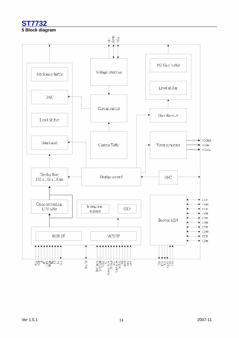
5 Block diagram
ST7732
Ver 1.5.1 2007-11
15
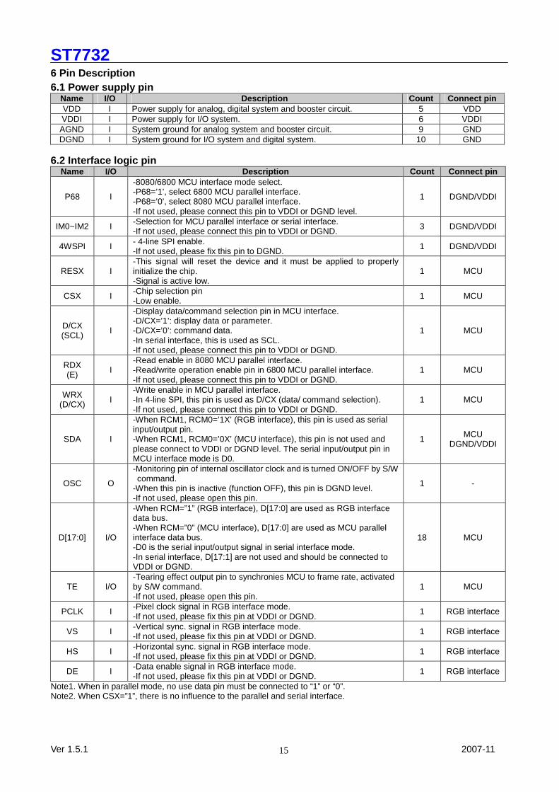
6 Pin Description 6.1 Power supply pin
Name I/O Description Count Connect pin VDD I Power supply for analog, digital system and booster circuit. 5 VDD VDDI I Power supply for I/O system. 6 VDDI AGND I System ground for analog system and booster circuit. 9 GND DGND I System ground for I/O system and digital system. 10 GND
6.2 Interface logic pin
Name I/O Description Count Connect pin
P68 I
-8080/6800 MCU interface mode select. -P68=’1’, select 6800 MCU parallel interface. -P68=’0’, select 8080 MCU parallel interface. -If not used, please connect this pin to VDDI or DGND level.
1 DGND/VDDI
IM0~IM2 I -Selection for MCU parallel interface or serial interface. -If not used, please connect this pin to VDDI or DGND. 3 DGND/VDDI
4WSPI I - 4-line SPI enable. -If not used, please fix this pin to DGND. 1 DGND/VDDI
RESX I -This signal will reset the device and it must be applied to properly initialize the chip. -Signal is active low.
1 MCU
CSX I -Chip selection pin -Low enable. 1 MCU
D/CX (SCL) I
-Display data/command selection pin in MCU interface. -D/CX=’1’: display data or parameter. -D/CX=’0’: command data. -In serial interface, this is used as SCL. -If not used, please connect this pin to VDDI or DGND.
1 MCU
RDX (E) I
-Read enable in 8080 MCU parallel interface. -Read/write operation enable pin in 6800 MCU parallel interface. -If not used, please connect this pin to VDDI or DGND.
1 MCU
WRX (D/CX) I
-Write enable in MCU parallel interface. -In 4-line SPI, this pin is used as D/CX (data/ command selection). -If not used, please connect this pin to VDDI or DGND.
1 MCU
SDA I
-When RCM1, RCM0=’1X’ (RGB interface), this pin is used as serial input/output pin. -When RCM1, RCM0=’0X’ (MCU interface), this pin is not used and please connect to VDDI or DGND level. The serial input/output pin in MCU interface mode is D0.
1 MCU DGND/VDDI
OSC O
-Monitoring pin of internal oscillator clock and is turned ON/OFF by S/W command.
-When this pin is inactive (function OFF), this pin is DGND level. -If not used, please open this pin.
1 -
D[17:0] I/O
-When RCM=”1” (RGB interface), D[17:0] are used as RGB interface data bus. -When RCM=”0” (MCU interface), D[17:0] are used as MCU parallel interface data bus. -D0 is the serial input/output signal in serial interface mode. -In serial interface, D[17:1] are not used and should be connected to VDDI or DGND.
18 MCU
TE I/O -Tearing effect output pin to synchronies MCU to frame rate, activated by S/W command. -If not used, please open this pin.
1 MCU
PCLK I -Pixel clock signal in RGB interface mode. -If not used, please fix this pin at VDDI or DGND.
1 RGB interface
VS I -Vertical sync. signal in RGB interface mode. -If not used, please fix this pin at VDDI or DGND. 1 RGB interface
HS I -Horizontal sync. signal in RGB interface mode. -If not used, please fix this pin at VDDI or DGND. 1 RGB interface
DE I -Data enable signal in RGB interface mode. -If not used, please fix this pin at VDDI or DGND. 1 RGB interface
Note1. When in parallel mode, no use data pin must be connected to “1” or “0”. Note2. When CSX=”1”, there is no influence to the parallel and serial interface.
ST7732
Ver 1.5.1 2007-11
16
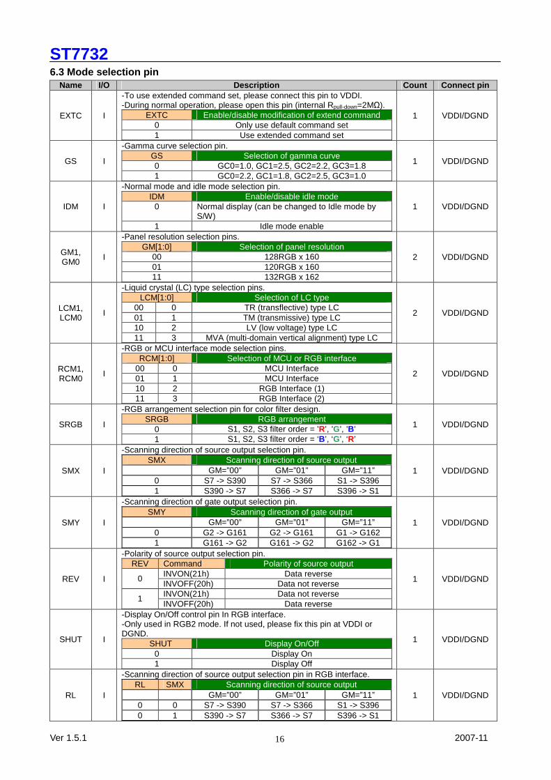
6.3 Mode selection pin Name I/O Description Count Connect pin
EXTC I
-To use extended command set, please connect this pin to VDDI. -During normal operation, please open this pin (internal Rpull-down=2MΩ).
EXTC Enable/disable modification of extend command 0 Only use default command set 1 Use extended command set
1 VDDI/DGND
GS I
-Gamma curve selection pin. GS Selection of gamma curve 0 GC0=1.0, GC1=2.5, GC2=2.2, GC3=1.8 1 GC0=2.2, GC1=1.8, GC2=2.5, GC3=1.0
1 VDDI/DGND
IDM I
-Normal mode and idle mode selection pin. IDM Enable/disable idle mode
0 Normal display (can be changed to Idle mode by S/W)
1 Idle mode enable
1 VDDI/DGND
GM1, GM0
I
-Panel resolution selection pins. GM[1:0] Selection of panel resolution
00 128RGB x 160 01 120RGB x 160 11 132RGB x 162
2 VDDI/DGND
LCM1, LCM0 I
-Liquid crystal (LC) type selection pins. LCM[1:0] Selection of LC type
00 0 TR (transflective) type LC 01 1 TM (transmissive) type LC 10 2 LV (low voltage) type LC 11 3 MVA (multi-domain vertical alignment) type LC
2 VDDI/DGND
RCM1, RCM0
I
-RGB or MCU interface mode selection pins. RCM[1:0] Selection of MCU or RGB interface
00 0 MCU Interface 01 1 MCU Interface 10 2 RGB Interface (1) 11 3 RGB Interface (2)
2 VDDI/DGND
SRGB I
-RGB arrangement selection pin for color filter design. SRGB RGB arrangement
0 S1, S2, S3 filter order = ’R’, ’G’, ’B’ 1 S1, S2, S3 filter order = ‘B’, ‘G’, ‘R’
1 VDDI/DGND
SMX I
-Scanning direction of source output selection pin. SMX Scanning direction of source output
GM=”00” GM=”01” GM=”11” 0 S7 -> S390 S7 -> S366 S1 -> S396 1 S390 -> S7 S366 -> S7 S396 -> S1
1 VDDI/DGND
SMY I
-Scanning direction of gate output selection pin. SMY Scanning direction of gate output
GM=”00” GM=”01” GM=”11” 0 G2 -> G161 G2 -> G161 G1 -> G162 1 G161 -> G2 G161 -> G2 G162 -> G1
1 VDDI/DGND
REV I
-Polarity of source output selection pin. REV Command Polarity of source output
INVON(21h) Data reverse 0 INVOFF(20h) Data not reverse INVON(21h) Data not reverse 1 INVOFF(20h) Data reverse
1 VDDI/DGND
SHUT I
-Display On/Off control pin In RGB interface. -Only used in RGB2 mode. If not used, please fix this pin at VDDI or DGND.
SHUT Display On/Off 0 Display On 1 Display Off
1 VDDI/DGND
RL I
-Scanning direction of source output selection pin in RGB interface. RL SMX Scanning direction of source output
GM=”00” GM=”01” GM=”11” 0 0 S7 -> S390 S7 -> S366 S1 -> S396 0 1 S390 -> S7 S366 -> S7 S396 -> S1
1 VDDI/DGND

ST7732
Ver 1.5.1 2007-11
17
1 0 S390 -> S7 S366 -> S7 S396 -> S1 1 1 S7 -> S390 S7 -> S366 S1 -> S396
TB I
-Scanning direction of gate output selection pin in RGB interface. TB SMY Scanning direction of gate output
GM=”00” GM=”01” GM=”11” 0 0 G2 -> G161 G2 -> G161 G1 -> G162
0 1 G161 -> G2 G161 -> G2 G162 -> G1
1 0 G161 -> G2 G161 -> G2 G162 -> G1
1 1 G2 -> G161 G2 -> G161 G1 -> G162
1 VDDI/DGND
TESEL I/O -Input mode: Please fix this pin at VDDI or DGND level. -Output mode: If this pin neither fix on panel internally nor FPC, it must be changed to output mode. (refer to the application note)
1 VDDI/DGND
6.4 Driver output pin Name I/O Description Count Connect pin S1 to S396 O - Source driver output pins. 396 -
G1 to G162
O - Gate driver output pins. 162 -
VCI1 I/O - A reference voltage for step-up circuit 1. - Connect a capacitor for stabilization. 3 Capacitor
AVDD I - Power input pin for analog circuits. - In normal usage, connect it to AVDDO. 3 AVDDO
AVDDO O - Output of step-up circuit 1 - Connect a capacitor for stabilization.
2 Capacitor
VCL I - Power input pin for VCOM circuit. - In normal usage, connect it to VCLO. 2 VCLO
VCLO O - A power output pin of step-up circuit 4. - When VCOML is higher than AGND, VCLO=AGND. - Connect a capacitor for stabilization.
1 Capacitor
VGH I - Power input pin for gate driver circuit. - In normal usage, connect it to VGHO. 2 VGHO
VGHO O - Positive output pin of the step-up circuit 2. - Connect a capacitor for stabilization. 1 Capacitor
VGL I - Power input pin for gate driver circuit. - Negative output of the step-up circuit 2 is connected inside the driver. - Connect a capacitor for stabilization.
3 VGLO
VREF O - A reference voltage for power system. - Connect a capacitor for stabilization. 3 Capacitor
GVDD O
- A power output of grayscale voltage generator. - Connect a capacitor for stabilization. - When internal GVDD generator is not used, connect an external power supply (AVDD-0.5V) to this pin.
3 Capacitor
VCOMH O - Positive voltage output of VCOM. - Connect a capacitor for stabilization. 3 Capacitor
VCOML O - Negative voltage output of VCOM. - Connect a capacitor for stabilization. 3 Capacitor
VCOM O - A power supply for the TFT-LCD common electrode. 3 Common electrode
C11P, C11N C12P, C12N
O - Capacitor connecting pins for step-up circuit 1 (for AVDDO) 12 Step-up Capacitor
C21P, C21N C22P, C22N C23P, C23N
O - Capacitor connecting pins for step-up circuit 2 and 4 (for VGHO, VGLO, VCLO) 12 Step-up
Capacitor
VDDIO O -VDDI voltage output level for monitoring. 8 - DGNDO O -DGND voltage output level for monitoring. 10 -
VCC O -Monitoring pin of internal digital reference voltage. -Connect a capacitor for stabilization. 3 Capacitor
6.5 Test ping Name I/O Description Count Connect pin
ST7732
Ver 1.5.1 2007-11
18
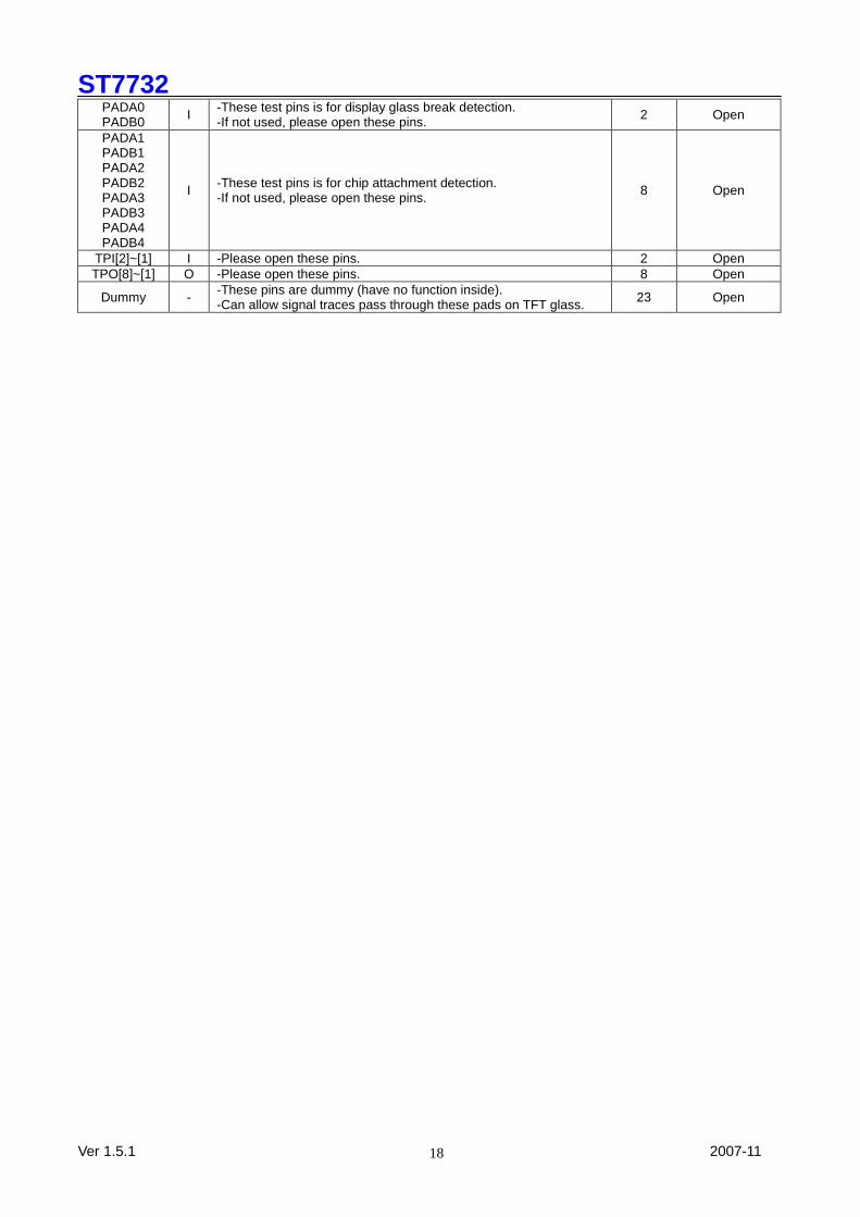
PADA0 PADB0 I -These test pins is for display glass break detection.
-If not used, please open these pins. 2 Open
PADA1 PADB1 PADA2 PADB2 PADA3 PADB3 PADA4 PADB4
I -These test pins is for chip attachment detection. -If not used, please open these pins. 8 Open
TPI[2]~[1] I -Please open these pins. 2 Open TPO[8]~[1] O -Please open these pins. 8 Open
Dummy - -These pins are dummy (have no function inside). -Can allow signal traces pass through these pads on TFT glass. 23 Open

ST7732
Ver 1.5.1 2007-11
19
7. Driver electrical characteristics 7.1 Absolute operation range
Item Symbol Rating Unit Supply voltage VDD - 0.3 ~ +4.6 V
Supply voltage (Logic) VDDI - 0.3 ~ +4.6 V Supply voltage (Digital) VCC -0.3 ~ +4.6 V Driver supply voltage VGH-VGL -0.3 ~ +30.0 V
Logic input voltage range VIN 0.3 ~ VDDI + 0.3 V Logic output voltage range VO 0.3 ~ VDDI + 0.3 V
Operating temperature range TOPR -40 ~ +85 Storage temperature range TSTG -55 ~ +125
Note: If one of the above items is exceeded its maximum limitation momentarily, the quality of the product may be degraded. Absolute maximum limitation, therefore, specify the values exceeding which the product may be physically damaged. Be sure to use the product within the recommend range.
7.2 DC characteristic
Specification Parameter Symbol Condition Min TYP Max
Unit Related Pins
Power & operation voltage System voltage VDD Operating voltage 2.5 2.8 3.3 V Interface operation voltage VDDI I/O supply voltage 1.6 1.8/2.8 3.3 V
Digital operating voltage VCC Digital supply voltage
1.6 2.0 V
Gate driver high voltage VGH 9.41 16.17 V Gate driver low voltage VGL -13.48 -7.06 V Gate driver supply voltage | VGH-VGL | 16.47 29.65 V
Input / Output Logic-high input voltage VIH 0.7VDDI VDDI V Note 1 Logic-low input voltage VIL VSS 0.3VDDI V Note 1 Logic-high output voltage VOH IOH = -1.0mA 0.8VDDI VDDI V Note 1 Logic-low output voltage VOL IOL = +1.0mA VSS 0.2VDDI V Note 1 Logic-high input current IIH VIN = VDDI 1 uA Note 1 Logic-low input current IIL VIN = VSS -1 uA Note 1 Input leakage current IIL IOH = -1.0mA -0.1 +0.1 uA Note 1 VCOM voltage VCOM high voltage VCOMH Ccom=12nF 2.5 5.0 V VCOM low voltage VCOML Ccom=12nF -2.5 0.0 V VCOM amplitude VCOMAC |VCOMH-VCOML| 4.0 6.0 V Source driver Source output range Vsout 0.1 AVDD-0.1 V Gamma reference voltage
GVDD 3.0 5.0 V
Source output settling time Tr Below with 99%
precision 30 us Note 2
Sout >=4.2V, Sout<=0.8V 20 mV Note 2 Output deviation voltage
(Source output channel) Vdev 4.2V>Sout>0.8V 15 mV
Output offset voltage VOFFSET 35 mV Note 3 Step-up circuit Internal reference voltage VREF 0 1 %
1st step-up (VDDx2) voltage AVDD 4.95 *4 6.0 *5 V
1st step-up (VDDx2) drop voltage VDDx2,dorp
I AVDD = 1.0mA (include panel
loading) 5% %
Linear range VLinear 0.2 AVDD-0.2 V Note 1: VDDI=1.6 to 3.3V, VDD=2.5 to 3.3V, AGND=DGND=0V, TA=-30 to 70 Note 2, Source channel loading= 10pF/channel, Gate channel loading=50pF/channel. Note 3, The Max. value is between measured point of source output and gamma setting value. Note 4, VDD=2.6V or VCI1=2.6V Note 5, VDD=3.0V or VCI1=3.0V

ST7732
Ver 1.5.1 2007-11
20
7.3 Power consumption
Current consumption Typical Maximum Operation mode Inversion
mode Image IDDI (uA)
IDD (mA)
IDDI (mA)
IDD (mA)
One Line Note 1 1 1.10 -Normal mode
One Line Note 2 1 1.10
-Partial + Idle mode (40 lines) One Line Note 3 1 0.3
-Sleep-in mode N/A N/A 1 3uA
Notes: 1. All pixels black. 2. Grayscale from top to bottom. 3. Black & white checker board 4 by 4.
ST7732
Ver 1.5.1 2007-11
21
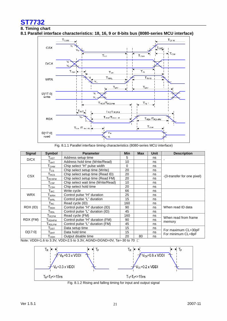
8. Timing chart 8.1 Parallel interface characteristics: 18, 16, 9 o r 8-bits bus (8080-series MCU interface)
Fig. 8.1.1 Parallel interface timing characteristics (8080-series MCU interface)
Signal Symbol Parameter Min Max Unit Description
TAST Address setup time 5 ns D/CX TAHT Address hold time (Write/Read) 10 ns
-
TCHW Chip select “H” pulse width 0 ns TCS Chip select setup time (Write) 20 ns TRCS Chip select setup time (Read ID) 20 ns
TRCSFM Chip select setup time (Read FM) 20 ns TCSF Chip select wait time (Write/Read) 10 ns
CSX
TCSH Chip select hold time 20 ns
-(3-transfer for one pixel)
TWC Write cycle 66 ns TWRH Control pulse “H” duration 25 ns WRX TWRL Control pulse “L” duration 15 ns
TRC Read cycle (ID) 160 ns TRDH Control pulse “H” duration (ID) 90 ns RDX (ID) TRDL Control pulse “L” duration (ID) 45 ns
When read ID data
TRCFM Read cycle (FM) 160 ns TRDHFM Control pulse “H” duration (FM) 90 ns RDX (FM) TRDLFM Control pulse “L” duration (FM) 45 ns
When read from frame memory
TDST Data setup time 15 ns TDHT Data hold time 15 ns D[17:0] TODH Output disable time 20 80 ns
For maximum CL=30pF For minimum CL=8pF
Note: VDDI=1.6 to 3.3V, VDD=2.5 to 3.3V, AGND=DGND=0V, Ta=-30 to 70
Fig. 8.1.2 Rising and falling timing for input and output signal
ST7732
Ver 1.5.1 2007-11
22
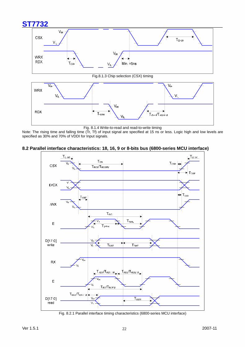
Fig.8.1.3 Chip selection (CSX) timing
Fig. 8.1.4 Write-to-read and read-to-write timing
Note: The rising time and falling time (Tr, Tf) of input signal are specified at 15 ns or less. Logic high and low levels are specified as 30% and 70% of VDDI for Input signals.
8.2 Parallel interface characteristics: 18, 16, 9 o r 8-bits bus (6800-series MCU interface)
Fig. 8.2.1 Parallel interface timing characteristics (6800-series MCU interface)
ST7732
Ver 1.5.1 2007-11
23
Signal Symbol Parameter Min Max Unit Description
TAST Address setup time 5 ns D/CX TAHT Address hold time (Write/Read) 10 ns
-
TCHW Chip select “H” pulse width 0 ns TCS Chip select setup time (Write) 20 ns TRCS Chip select setup time (Read ID) 20 ns
TRCSFM Chip select setup time (Read FM) 20 ns TCSF Chip select wait time (Write/Read) 10 ns
CSX
TCSH Chip select hold time 20 ns
-
TWC Write cycle 66 ns TWRH Control pulse “H” duration 25 ns WRX TWRL Control pulse “L” duration 15 ns
TRC Read cycle (ID) 160 ns TRDH Control pulse “H” duration (ID) 90 ns RDX (ID) TRDL Control pulse “L” duration (ID) 45 ns
When read ID data
TRCFM Read cycle (FM) 160 ns TRDHFM Control pulse “H” duration (FM) 90 ns RDX (FM) TRDLFM Control pulse “L” duration (FM) 45 ns
When read from frame memory
TDST Data setup time 15 ns TDHT Data hold time 15 ns D[17:0] TODH Output disable time 20 80 ns
For maximum CL=30pF For minimum CL=8pF
Note 1: VDDI=1.6 to 3.3V, VDD=2.5 to 3.3V, AGND=DGND=0V, Ta=-30 to 70 Note 2: The rising time and falling time (Tr, Tf) of input signal are specified at 15 ns or less. Logic high and low levels are specified as 30% and 70% of VDDI for Input signals
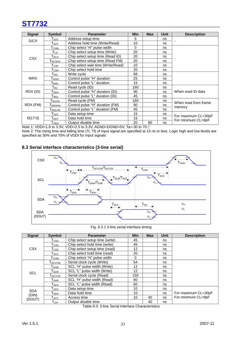
8.3 Serial interface characteristics (3-line serial )
CSXVIH
VIL TCHW
TCSH
TOH
TCSS
SCL
SDA
SDA
(DOUT)
TSCC
TSCYCW/TSCYCR
TACC
VIH
VIL
VIH
VIL
VIH
VIL
VIH
VIL
TSDS TSDH
TSHW/TSHR
TSLW/TSLR
Fig. 8.3.1 3-line serial interface timing
Signal Symbol Parameter Min Max Unit Description
TCSS Chip select setup time (write) 45 ns TCSH Chip select hold time (write) 45 ns TCSS Chip select setup time (read) 12 ns TSCC Chip select hold time (read) 20 ns
CSX
TCHW Chip select “H” pulse width 0 ns
TSCYCW Serial clock cycle (Write) 54 ns TSHW SCL “H” pulse width (Write) 12 ns TSLW SCL “L” pulse width (Write) 12 ns
TSCYCR Serial clock cycle (Read) 150 ns TSHR SCL “H” pulse width (Read) 60 ns
SCL
TSLR SCL “L” pulse width (Read) 60 ns
TSDS Data setup time 10 ns TSDH Data hold time 10 ns TACC Access time 10 40 ns
SDA (DIN)
(DOUT) TOH Output disable time 40 ns
For maximum CL=30pF For minimum CL=8pF
Table 8.3: 3-line Serial Interface Characteristics
ST7732
Ver 1.5.1 2007-11
24
Note 1: VDDI=1.6 to 3.3V, VDD=2.5 to 3.3V, AGND=DGND=0V, Ta=-30 to 70 Note 2: The rising time and falling time (Tr, Tf) of input signal are specified at 15 ns or less. Logic high and low levels are specified as 30% and 70% of VDDI for Input signals.
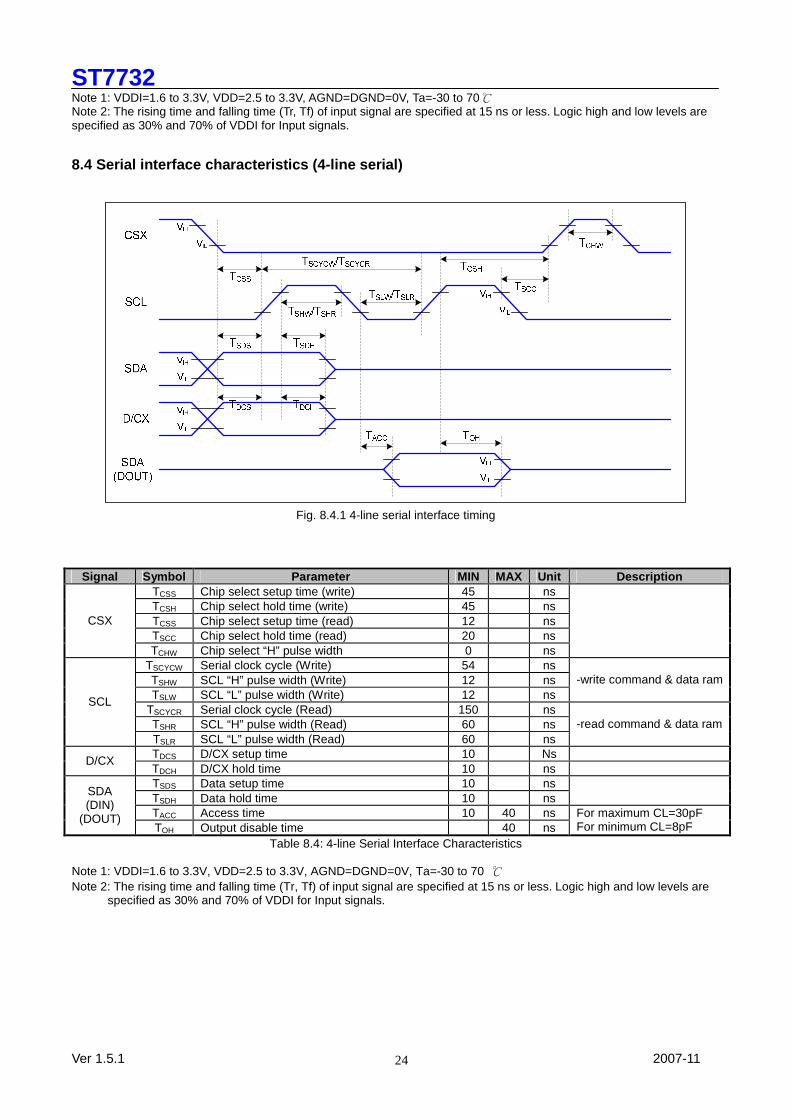
8.4 Serial interface characteristics (4-line serial )
Fig. 8.4.1 4-line serial interface timing
Signal Symbol Parameter MIN MAX Unit Description TCSS Chip select setup time (write) 45 ns TCSH Chip select hold time (write) 45 ns TCSS Chip select setup time (read) 12 ns TSCC Chip select hold time (read) 20 ns
CSX
TCHW Chip select “H” pulse width 0 ns
TSCYCW Serial clock cycle (Write) 54 ns TSHW SCL “H” pulse width (Write) 12 ns TSLW SCL “L” pulse width (Write) 12 ns
-write command & data ram
TSCYCR Serial clock cycle (Read) 150 ns TSHR SCL “H” pulse width (Read) 60 ns
SCL
TSLR SCL “L” pulse width (Read) 60 ns -read command & data ram
TDCS D/CX setup time 10 Ns D/CX TDCH D/CX hold time 10 ns TSDS Data setup time 10 ns TSDH Data hold time 10 ns
TACC Access time 10 40 ns
SDA (DIN)
(DOUT) TOH Output disable time 40 ns
For maximum CL=30pF For minimum CL=8pF
Table 8.4: 4-line Serial Interface Characteristics Note 1: VDDI=1.6 to 3.3V, VDD=2.5 to 3.3V, AGND=DGND=0V, Ta=-30 to 70 Note 2: The rising time and falling time (Tr, Tf) of input signal are specified at 15 ns or less. Logic high and low levels are
specified as 30% and 70% of VDDI for Input signals.
ST7732
Ver 1.5.1 2007-11
25
9. Function description 9.1 Interface type selection The selection of given interfaces are done by setting P68, IM2, IM1, and IM0 pins as shown in following table. Table 9.1.1 Selection of MCU interface
P68 IM2 IM1 IM0 Interface Read back selection - 0 - - 3-line serial interface Via the read instruction 0 1 0 0 8080 MCU 8-bit parallel RDX strobe (8-bit read data and 8-bit read parameter) 0 1 0 1 8080 MCU 16-bit parallel RDX strobe (16-bit read data and 8-bit read parameter) 0 1 1 0 8080 MCU 9-bit parallel RDX strobe (9-bit read data and 8-bit read parameter) 0 1 1 1 8080 MCU 18-bit parallel RDX strobe (18-bit read data and 8-bit read parameter) - 0 - - 3-line serial interface Via the read instruction 1 1 0 0 6800 MCU 8-bit parallel E strobe (8-bit read data and 8-bit read parameter) 1 1 0 1 6800 MCU 16-bit parallel E strobe (16-bit read data and 8-bit read parameter) 1 1 1 0 6800 MCU 9-bit parallel E strobe (9-bit read data and 8-bit read parameter) 1 1 1 1 6800 MCU 18-bit parallel E strobe (18-bit read data and 8-bit read parameter)
Table 9.1.2 Pin connection according to various MCU interface
P68 IM2 IM1 IM0 Interface RDX WRX D/CX Read back selection - 0 - - 3-line serial interface Note1 Note1 SCL D[17:1]: unused, D0: SDA 0 1 0 0 8080 8-bit parallel RDX WRX D/CX D[17:8]: unused, D7-D0: 8-bit data
0 1 0 1 8080 16-bit parallel RDX WRX D/CX D[17:16]: unused, D15-D0: 16-bit data
0 1 1 0 8080 9-bit parallel RDX WRX D/CX D[17:9]: unused, D8-D0: 9-bit data 0 1 1 1 8080 18-bit parallel RDX WRX D/CX D17-D0: 18-bit data - 0 - - 3-line serial interface Note1 D/CX SCL D[17:1]: unused, D0: SDA 1 1 0 0 6800 8-bit parallel E WRX RS D[17:8]: unused, D7-D0: 8-bit data
1 1 0 1 6800 16-bit parallel E WRX RS D[17:16]: unused, D15-D0: 16-bit data
1 1 1 0 6800 9-bit parallel E WRX RS D[17:9]: unused, D8-D0: 9-bit data 1 1 1 1 6800 18-bit parallel E WRX RS D17-D0: 18-bit data
Note 1. Unused pins can be open, or connected to DGND or VDDI. 9.2 8080-series MCU parallel interface (P68=’0’) The MCU can use one of following interfaces: 11-lines with 8-data parallel interface, 12-lines with 9-data parallel interface, 19-line with 16-data parallel interface or 21-lines with 18-data parallel interface. The chip-select CSX (active low) enables/disables the parallel interface. RESX (active low) is an external reset signal. WRX is the parallel data write enable, RDX is the parallel data read enable and D[17:0] is parallel data bus. The LCD driver reads the data at the rising edge of WRX signal. The D/CX is the data/command flag. When D/CX=’1’, D[17:0] bits is either display data or command parameter. When D/C=’0’, D[17:0] bits is command. The 6800-series bi-directional interface can be used for communication between the micro controller and LCD driver. The selection of this interface is done when P68 pin is in low state (DGND). Interface bus width can be selected with IM2, IM1 and IM0. The interface functions of 8080-series parallel interface are given in following table. Table 9.2.1 The function of 8080-series parallel interface
P68 IM2 IM1 IM0 Interface D/CX RDX WRX Read back selection 0 1 ↑ Write 8-bit command (D7 to D0) 1 1 ↑ Write 8-bit display data or 8-bit parameter (D7 to D0) 1 ↑ 1 Read 8-bit display data (D7 to D0)
0 1 0 0 8-bit parallel
1 ↑ 1 Read 8-bit parameter or status (D7 to D0) 0 1 ↑ Write 8-bit command (D7 to D0) 1 1 ↑ Write 16-bit display data or 8-bit parameter (D15 to D0) 1 ↑ 1 Read 16-bit display data (D15 to D0)
0 1 0 1 16-bit parallel
1 ↑ 1 Read 8-bit parameter or status (D7 to D0) 0 1 ↑ Write 8-bit command (D7 to D0) 1 1 ↑ Write 9-bit display data or 8-bit parameter (D8 to D0) 1 ↑ 1 Read 9-bit display data (D8 to D0)
0 1 1 0 9-bit parallel
1 ↑ 1 Read 8-bit parameter or status (D7 to D0) 0 1 ↑ Write 8-bit command (D7 to D0) 1 1 ↑ Write 18-bit display data or 8-bit parameter (D17 to D0) 1 ↑ 1 Read 18-bit display data (D17 to D0)
0 1 1 1 18-bit parallel
1 ↑ 1 Read 8-bit parameter or status (D7 to D0) Note: applied for command code: DAh, DBh, DCh, 04h, 09h, 0Ah, 0Bh, 0Ch, 0Dh, 0Eh, 0Fh

ST7732
Ver 1.5.1 2007-11
26
9.2.1 Write cycle sequence The write cycle means that the host writes information (command or/and data) to the display via the interface. Each write cycle (WRX high-low-high sequence) consists of 3 control signals (D/CX, RDX, WRX) and data signals (D[17:0]). D/CX bit is a control signal, which tells if the data is a command or a data. The data signals are the command if the control signal is low (=’0’) and vice versa it is data (=’1’).
Fig. 9.2.1 8080-series WRX protocol
Note: WRX is an unsynchronized signal (It can be stopped).
Fig. 9.2.2 8080-series parallel bus protocol, write to register or display RAM
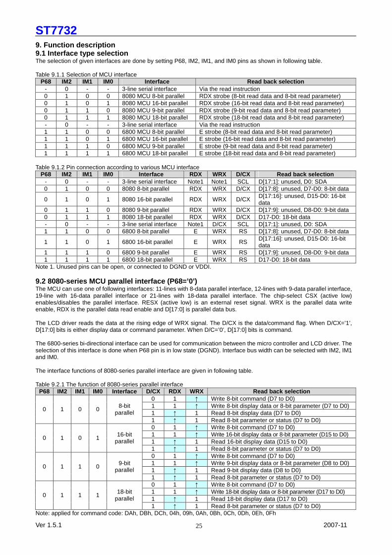
9.2.2 Read cycle sequence The read cycle (RDX high-low-high sequence) means that the host reads information from LCD driver via interface. The driver sends data (D[17:0]) to the host when there is a falling edge of RDX and the host reads data when there is a rising edge of RDX.
ST7732
Ver 1.5.1 2007-11
27
Fig. 9.2.3 8080-series RDX protocol
Note: RDX is an unsynchronized signal (It can be stopped).
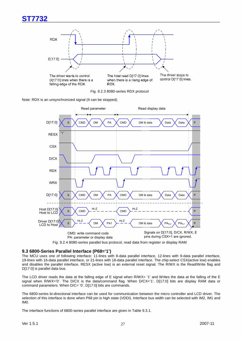
CMD DM PA CMD DM & data Data DataS P
CMD DM PA CMD DM & data Data DataS P
D[17:0]
RESX
CSX
D/CX
RDX
WRX
D[17:0]
Host D[17:0]Host to LCD
Driver D[17:0]LCD to Host
“1”
Hi-Z
Read parameter Read display data
CMD: write command code
PA: parameter or display data
Signals on D[17:0], D/CX, R/WX, E
pins during CSX=1 are ignored.
DM PA1 DM & data PAN-2 PAN-1 PS
CMD CMDS PHi-Z Hi-Z
Hi-Z
Fig. 9.2.4 8080-series parallel bus protocol, read data from register or display RAM
9.3 6800-Series Parallel Interface (P68=’1’) The MCU uses one of following interface: 11-lines with 8-data parallel interface, 12-lines with 9-data parallel interface, 19-lines with 16-data parallel interface, or 21-lines with 18-data parallel interface. The chip-select CSX(active low) enables and disables the parallel interface. RESX (active low) is an external reset signal. The R/WX is the Read/Write flag and D[17:0] is parallel data bus. The LCD driver reads the data at the falling edge of E signal when R/WX= ‘1’ and Writes the data at the falling of the E signal when R/WX=’0’. The D/CX is the data/command flag. When D/CX=’1’, D[17:0] bits are display RAM data or command parameters. When D/C= ‘0’, D[17:0] bits are commands. The 6800-series bi-directional interface can be used for communication between the micro controller and LCD driver. The selection of this interface is done when P68 pin is high state (VDDI). Interface bus width can be selected with IM2, IM1 and IM0. The interface functions of 6800-series parallel interface are given in Table 9.3.1.
ST7732
Ver 1.5.1 2007-11
28
Table 9.3.1 The function of 6800-series parallel interface P68 IM2 IM1 IM0 Interface D/CX R/WX E Function
0 0 ↓ Write 8-bit command (D7 to D0) 1 0 ↓ Write 8-bit display data or 8-bit parameter (D7 to D0) 1 1 ↓ Read 8-bit Display data (D7 to D0)
1 1 0 0 8-bit Parallel
1 1 ↓ Read 8-bit parameter or status (D7 to D0) 0 0 ↓ Write 8-bit command (D7 to D0) 1 0 ↓ Write 16-bit display data or 8-bit parameter (D15 to D0) 1 1 ↓ Read 16-bit Display data (D15 to D0)
1 1 0 1 16-bit Parallel
1 1 ↓ Read 8-bit parameter or status (D7 to D0) 0 0 ↓ Write 8-bit command (D7 to D0) 1 0 ↓ Write 9-bit display data or 8-bit parameter (D8 to D0) 1 1 ↓ Read 9-bit Display data (D8 to D0)
1 1 1 0 9-bit Parallel
1 1 ↓ Read 8-bit parameter or status (D7 to D0) 0 0 ↓ Write 8-bit command (D7 to D0) 1 0 ↓ Write 18-bit display data or 8-bit parameter (D17 to D0) 1 1 ↓ Read 18-bit Display data (D17 to D0)
1 1 1 1 18-bit Parallel
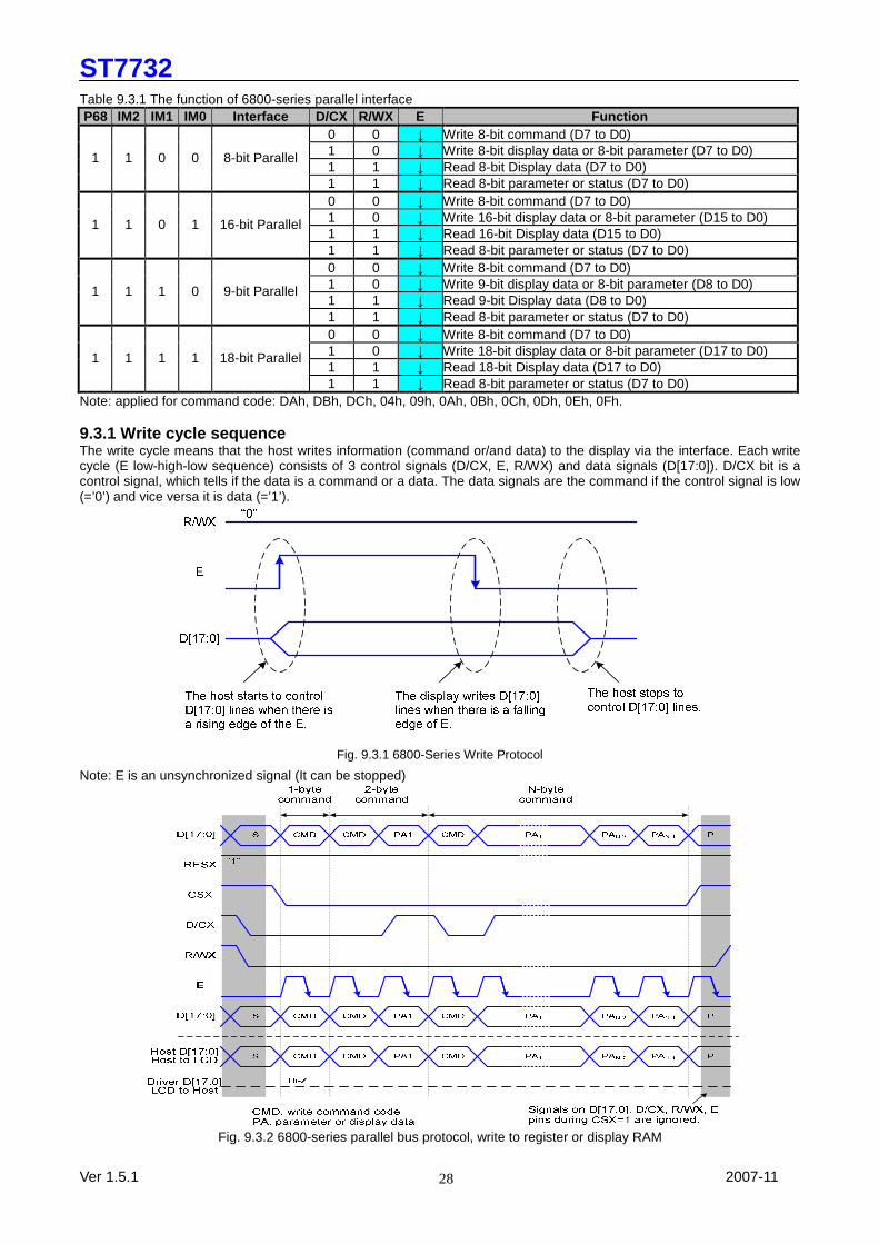
1 1 ↓ Read 8-bit parameter or status (D7 to D0) Note: applied for command code: DAh, DBh, DCh, 04h, 09h, 0Ah, 0Bh, 0Ch, 0Dh, 0Eh, 0Fh. 9.3.1 Write cycle sequence The write cycle means that the host writes information (command or/and data) to the display via the interface. Each write cycle (E low-high-low sequence) consists of 3 control signals (D/CX, E, R/WX) and data signals (D[17:0]). D/CX bit is a control signal, which tells if the data is a command or a data. The data signals are the command if the control signal is low (=’0’) and vice versa it is data (=’1’).
Fig. 9.3.1 6800-Series Write Protocol
Note: E is an unsynchronized signal (It can be stopped)
Fig. 9.3.2 6800-series parallel bus protocol, write to register or display RAM
ST7732
Ver 1.5.1 2007-11
29
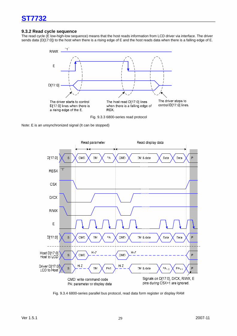
9.3.2 Read cycle sequence The read cycle (E low-high-low sequence) means that the host reads information from LCD driver via interface. The driver sends data (D[17:0]) to the host when there is a rising edge of E and the host reads data when there is a falling edge of E.
Fig. 9.3.3 6800-series read protocol
Note: E is an unsynchronized signal (It can be stopped)
Fig. 9.3.4 6800-series parallel bus protocol, read data form register or display RAM
ST7732
Ver 1.5.1 2007-11
30
9.4 Serial interface The selection of this interface is done by IM2. See the Table 9.4.1. Table 9.4.1 Selection of serial interface
IM2 4WSPI Interface Read back selection 0 0 3-line serial interface Via the read instruction (8-bit, 24-bit and 32-bit read parameter) 0 1 4-line serial interface Via the read instruction (8-bit, 24-bit and 32-bit read parameter)
The serial interface is either 3-lines/9-bits or 4-lines/8-bts bi-directional interface for communication between the micro controller and the LCD driver. The 3-lines serial interface use: CSX (chip enable), SCL (serial clock) and SDA (serial data input/output), and the 4-lines serial interface use: CSX (chip enable), D/CX (data/ command flag), SCL (serial clock) and SDA (serial data input/output). Serial clock (SCL) is used for interface with MCU only, so it can be stopped when no communication is necessary. 9.4.1 Command Write Mode The write mode of the interface means the micro controller writes commands and data to the LCD driver. 3-lines serial data packet contains a control bit D/CX and a transmission byte. In 4-lines serial interface, data packet contains just transmission byte and control bit D/CX is transferred by the D/CX pin. If D/CX is “low”, the transmission byte is interpreted as a command byte. If D/CX is “high”, the transmission byte is stored in the display data RAM (memory write command), or command register as parameter. Any instruction can be sent in any order to the driver. The MSB is transmitted first. The serial interface is initialized when CSX is high. In this state, SCL clock pulse or SDA data have no effect. A falling edge on CSX enables the serial interface and indicates the start of data transmission.
Fig. 9.4.1 Serial interface data stream format
When CSX is “high”, SCL clock is ignored. During the high period of CSX the serial interface is initialized. At the falling edge of CSX, SCL can be high or low (see Fig 9.4.2). SDA is sampled at the rising edge of SCL. D/CX indicates whether the byte is command (D/CX=’0’) or parameter/RAM data (D/CX=’1’). D/CX is sampled when first rising edge of SCL (3-lines serial interface) or 8th rising edge of SCL (4-lines serial interface). If CSX stays low after the last bit of command/data byte, the serial interface expects the D/CX bit (3-lines serial interface) or D7 (4-lines serial interface) of the next byte at the next rising edge of SCL.
ST7732
Ver 1.5.1 2007-11
31
Fig. 9.4.2 3-line serial interface write protocol (write to register with control bit in transmission)
Fig. 9.4.3 4-line serial interface write protocol (write to register with control bit in transmission)
9.4.2 Read Functions The read mode of the interface means that the micro controller reads register value from the driver. To achieve read function, the micro controller first has to send a command (read ID or register command) and then the following byte is transmitted in the opposite direction. After that CSX is required to go to high before a new command is send (see the below figure). The driver samples the SDA (input data) at rising edge of SCL, but shifts SDA (output data) at the falling edge of SCL. Thus the micro controller is supported to read at the rising edge of SCL. After the read status command has been sent, the SDA line must be set to tri-state no later than at the falling edge of SCL of the last bit. 3-line serial protocol (for RDID1/RDID2/RDID3/0Ah/0Bh/0Ch/0Dh/0Eh/0Fh command: 8-bit read):
ST7732
Ver 1.5.1 2007-11
32
3-line serial protocol (for RDDID command: 24-bit read)
3-line Serial Protocol (for RDDST command: 32-bit read)
Fig. 9.4.4 3-line serial interface read protocol
4-line serial protocol (for RDID1/RDID2/RDID3/0Ah/0Bh/0Ch/0Dh/0Eh/0Fh command: 8-bit read):
ST7732
Ver 1.5.1 2007-11
33
4-line serial protocol (for RDDID command: 24-bit read)
4-line Serial Protocol (for RDDST command: 32-bit read)
Host
Driver
Fig. 9.4.5 4-line serial interface read protocol
ST7732
Ver 1.5.1 2007-11
34
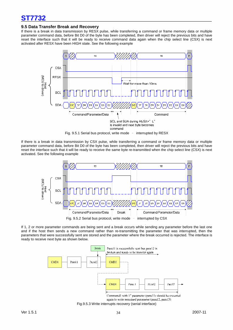
9.5 Data Transfer Break and Recovery If there is a break in data transmission by RESX pulse, while transferring a command or frame memory data or multiple parameter command data, before Bit D0 of the byte has been completed, then driver will reject the previous bits and have reset the interface such that it will be ready to receive command data again when the chip select line (CSX) is next activated after RESX have been HIGH state. See the following example
Host
(MCU to driver)
Fig. 9.5.1 Serial bus protocol, write mode – interrupted by RESX
If there is a break in data transmission by CSX pulse, while transferring a command or frame memory data or multiple parameter command data, before Bit D0 of the byte has been completed, then driver will reject the previous bits and have reset the interface such that it will be ready to receive the same byte re-transmitted when the chip select line (CSX) is next activated. See the following example
Fig. 9.5.2 Serial bus protocol, write mode – interrupted by CSX
If 1, 2 or more parameter commands are being sent and a break occurs while sending any parameter before the last one and if the host then sends a new command rather than re-transmitting the parameter that was interrupted, then the parameters that were successfully sent are stored and the parameter where the break occurred is rejected. The interface is ready to receive next byte as shown below.
Fig.9.5.3 Write interrupts recovery (serial interface)
ST7732
Ver 1.5.1 2007-11
35
If a 2 or more parameter commands are being sent and a break occurs by the other command before the last one is sent, then the parameters that were successfully sent are stored and the other parameter of that command remains previous value.
Fig. 9.5.4 Write interrupts recovery (both serial and parallel Interface)
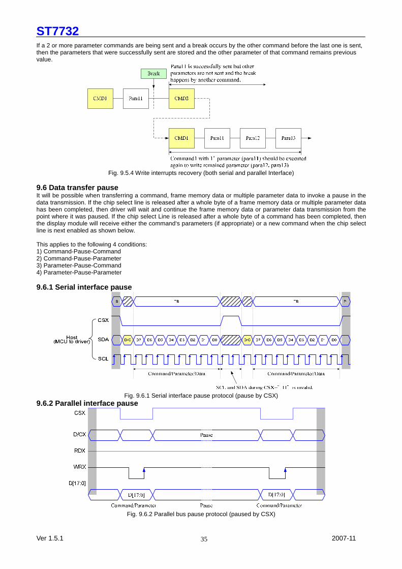
9.6 Data transfer pause It will be possible when transferring a command, frame memory data or multiple parameter data to invoke a pause in the data transmission. If the chip select line is released after a whole byte of a frame memory data or multiple parameter data has been completed, then driver will wait and continue the frame memory data or parameter data transmission from the point where it was paused. If the chip select Line is released after a whole byte of a command has been completed, then the display module will receive either the command‘s parameters (if appropriate) or a new command when the chip select line is next enabled as shown below. This applies to the following 4 conditions: 1) Command-Pause-Command 2) Command-Pause-Parameter 3) Parameter-Pause-Command 4) Parameter-Pause-Parameter 9.6.1 Serial interface pause
Fig. 9.6.1 Serial interface pause protocol (pause by CSX)
9.6.2 Parallel interface pause
Fig. 9.6.2 Parallel bus pause protocol (paused by CSX)
ST7732
Ver 1.5.1 2007-11
36
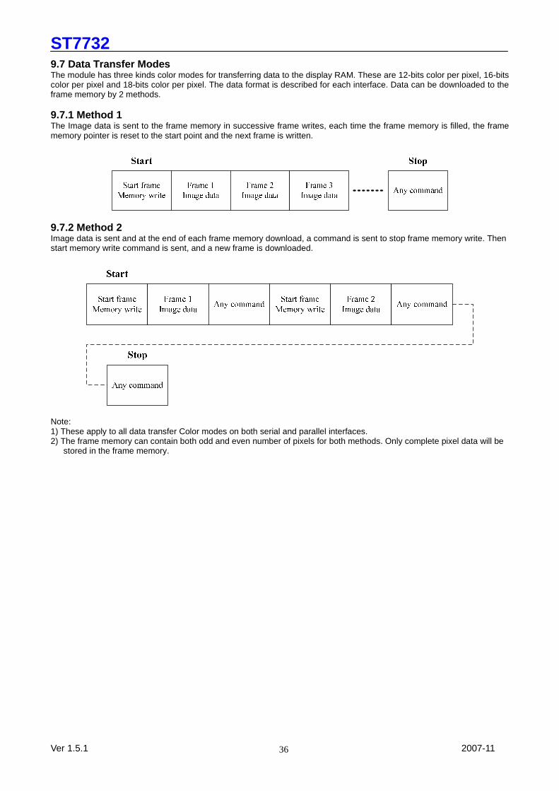
9.7 Data Transfer Modes The module has three kinds color modes for transferring data to the display RAM. These are 12-bits color per pixel, 16-bits color per pixel and 18-bits color per pixel. The data format is described for each interface. Data can be downloaded to the frame memory by 2 methods. 9.7.1 Method 1 The Image data is sent to the frame memory in successive frame writes, each time the frame memory is filled, the frame memory pointer is reset to the start point and the next frame is written.
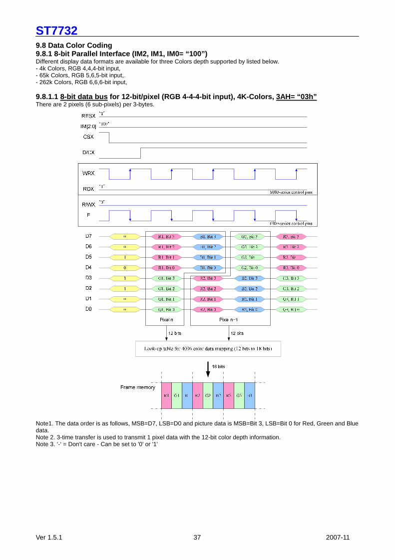
9.7.2 Method 2 Image data is sent and at the end of each frame memory download, a command is sent to stop frame memory write. Then start memory write command is sent, and a new frame is downloaded.
Note: 1) These apply to all data transfer Color modes on both serial and parallel interfaces. 2) The frame memory can contain both odd and even number of pixels for both methods. Only complete pixel data will be
stored in the frame memory.
ST7732
Ver 1.5.1 37 2007-11
9.8 Data Color Coding 9.8.1 8-bit Parallel Interface (IM2, IM1, IM0= “100 ”) Different display data formats are available for three Colors depth supported by listed below. - 4k Colors, RGB 4,4,4-bit input, - 65k Colors, RGB 5,6,5-bit input,. - 262k Colors, RGB 6,6,6-bit input, 9.8.1.1 8-bit data bus for 12-bit/pixel (RGB 4-4-4-bit input), 4K-Colors, 3AH= “03h” There are 2 pixels (6 sub-pixels) per 3-bytes.
Note1. The data order is as follows, MSB=D7, LSB=D0 and picture data is MSB=Bit 3, LSB=Bit 0 for Red, Green and Blue data. Note 2. 3-time transfer is used to transmit 1 pixel data with the 12-bit color depth information. Note 3. ‘-‘ = Don't care - Can be set to '0' or '1'
ST7732
Ver 1.5.1 38 2007-11
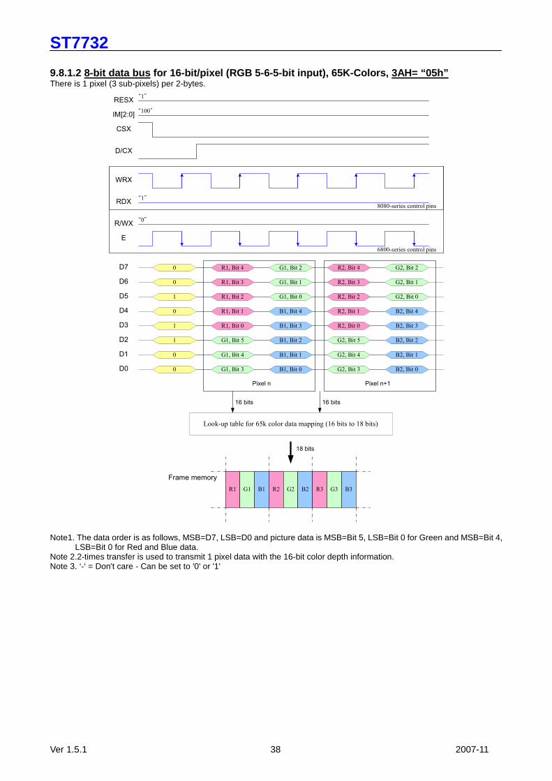
9.8.1.2 8-bit data bus for 16-bit/pixel (RGB 5-6-5-bit input), 65K-Colors , 3AH= “05h” There is 1 pixel (3 sub-pixels) per 2-bytes.
R1, Bit 4 G1, Bit 20
R1, Bit 3 G1, Bit 10
R1, Bit 2 G1, Bit 01
R1, Bit 1 B1, Bit 40
R1, Bit 0 B1, Bit 31
G1, Bit 5 B1, Bit 21
G1, Bit 4 B1, Bit 10
G1, Bit 3 B1, Bit 00
8080-series control pins
6800-series control pins
RESX
IM[2:0]
CSX
D/CX
“1”
“100”
WRX
RDX“1”
R/WX
E
D7
D6
D5
D4
D3
D2
D1
D0
Pixel n Pixel n+1
Look-up table for 65k color data mapping (16 bits to 18 bits)
16 bits 16 bits
R1 G1 B1 R2 G2 B2 R3 G3 B3
18 bits
Frame memory
R2, Bit 4 G2, Bit 2
R2, Bit 3 G2, Bit 1
R2, Bit 2 G2, Bit 0
R2, Bit 1 B2, Bit 4
R2, Bit 0 B2, Bit 3
G2, Bit 5 B2, Bit 2
G2, Bit 4 B2, Bit 1
G2, Bit 3 B2, Bit 0
“0”
Note1. The data order is as follows, MSB=D7, LSB=D0 and picture data is MSB=Bit 5, LSB=Bit 0 for Green and MSB=Bit 4,
LSB=Bit 0 for Red and Blue data. Note 2.2-times transfer is used to transmit 1 pixel data with the 16-bit color depth information. Note 3. ‘-‘ = Don't care - Can be set to '0' or '1'
ST7732
Ver 1.5.1 39 2007-11
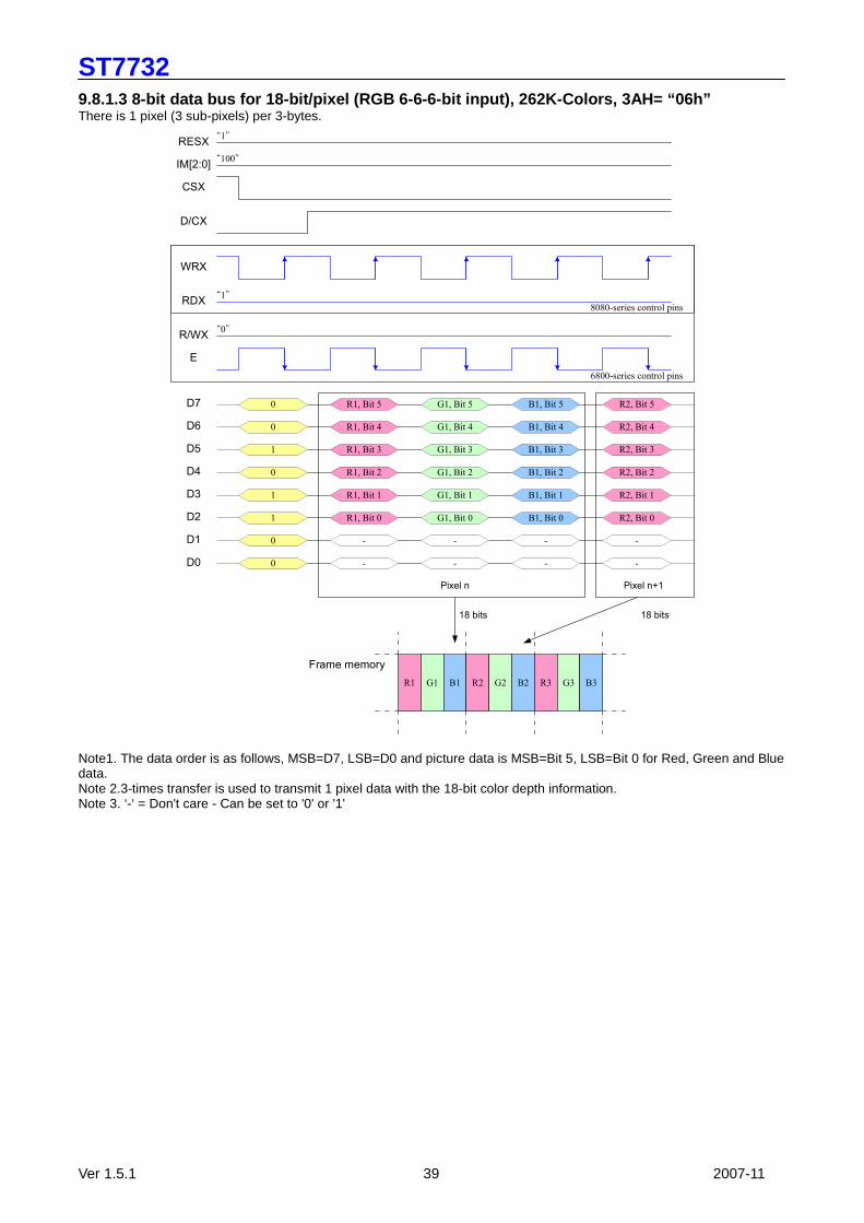
9.8.1.3 8-bit data bus for 18-bit/pixel (RGB 6-6-6- bit input), 262K-Colors, 3AH= “06h” There is 1 pixel (3 sub-pixels) per 3-bytes.
R1, Bit 4
0
R1, Bit 3
0
R1, Bit 2
1
R1, Bit 1
0
R1, Bit 0
1
R1, Bit 5
1
- -0
- -0
8080-series control pins
6800-series control pins
RESX
IM[2:0]
CSX
D/CX
“1”
“100”
WRX
RDX“1”
R/WX
E
D7
D6
D5
D4
D3
D2
D1
D0
Pixel n Pixel n+1
18 bits 18 bits
R1 G1 B1 R2 G2 B2 R3 G3 B3
Frame memory
- -
- -
G1, Bit 4
G1, Bit 3
G1, Bit 2
G1, Bit 1
G1, Bit 0
G1, Bit 5
B1, Bit 4
B1, Bit 3
B1, Bit 2
B1, Bit 1
B1, Bit 0
B1, Bit 5
R2, Bit 4
R2, Bit 3
R2, Bit 2
R2, Bit 1
R2, Bit 0
R2, Bit 5
“0”
Note1. The data order is as follows, MSB=D7, LSB=D0 and picture data is MSB=Bit 5, LSB=Bit 0 for Red, Green and Blue data. Note 2.3-times transfer is used to transmit 1 pixel data with the 18-bit color depth information. Note 3. ‘-‘ = Don't care - Can be set to '0' or '1'

ST7732
Ver 1.5.1 40 2007-11
9.8.2 16-Bit Parallel Interface (IM2,IM1, IM0= “101 ”) Different display data formats are available for three colors depth supported by listed below. - 4k colors, RGB 4,4,4-bit input - 65k colors, RGB 5,6,5-bit input - 262k colors, RGB 6,6,6-bit input 9.8.2.1 16-bit data bus for 12-bit/pixel (RGB 4-4-4-bit input), 4K-Colors, 3AH= “03h” There is 1 pixel (3 sub-pixels) per 1 bytes, 12-bit/pixel.
Note1. The data order is as follows, MSB=D11, LSB=D0 and picture data is MSB=Bit 3, LSB=Bit 0 for Red, Green and Blue data. Note 2.1-times transfer (D11 to D0) is used to transmit 1 pixel data with the 12-bit color depth information.

ST7732
Ver 1.5.1 41 2007-11
9.8.2.2 16-bit data bus for 16-bit/pixel (RGB 5-6-5 -bit input), 65K-Colors, 3AH= “05h” There is 1 pixel (3 sub-pixels) per 1 bytes, 16-bit/pixel.
Note1. The data order is as follows, MSB=D15, LSB=D0 and picture data is MSB=Bit 5, LSB=Bit 0 for Green, and MSB=Bit
4, LSB=Bit 0 for Red and Blue data. Note 2.1-times transfer (D15 to D0) is used to transmit 1 pixel data with the 16-bit color depth information. Note 3. ‘-‘ = Don't care - Can be set to '0' or '1'
ST7732
Ver 1.5.1 42 2007-11
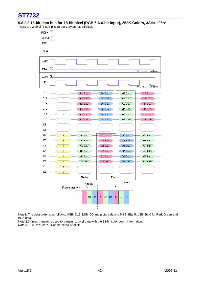
9.8.2.3 16-bit data bus for 18-bit/pixel (RGB 6-6-6 -bit input), 262K-Colors, 3AH= “06h” There are 2 pixel (6 sub-pixels) per 3 bytes, 18-bit/pixel.
Note1. The data order is as follows, MSB=D15, LSB=D0 and picture data is MSB=Bits 5, LSB=Bit 0 for Red, Green and Blue data. Note 2.3-times transfer is used to transmit 1 pixel data with the 18-bit color depth information. Note 3. ‘-‘ = Don't care - Can be set to '0' or '1'
ST7732
Ver 1.5.1 43 2007-11
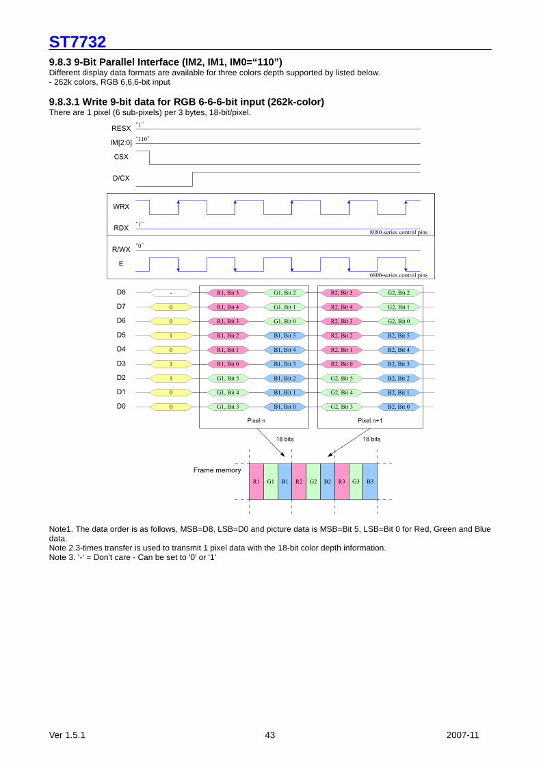
9.8.3 9-Bit Parallel Interface (IM2, IM1, IM0=“110” ) Different display data formats are available for three colors depth supported by listed below. - 262k colors, RGB 6,6,6-bit input 9.8.3.1 Write 9-bit data for RGB 6-6-6-bit input (2 62k-color) There are 1 pixel (6 sub-pixels) per 3 bytes, 18-bit/pixel.
R1, Bit 40
R1, Bit 30
R1, Bit 21
R1, Bit 10
R1, Bit 01
R1, Bit 5
1
0
0
8080-series control pins
6800-series control pins
RESX
IM[2:0]
CSX
D/CX
“1”
“110”
WRX
RDX“1”
R/WX
E
D7
D6
D5
D4
D3
D2
D1
D0
Pixel n Pixel n+1
18 bits 18 bits
R1 G1 B1 R2 G2 B2 R3 G3 B3
Frame memory
G1, Bit 4
G1, Bit 3
G1, Bit 2
G1, Bit 1
G1, Bit 0
B1, Bit 4
B1, Bit 3
B1, Bit 2
B1, Bit 1
B1, Bit 0
B1, Bit 5
R2, Bit 4
R2, Bit 3
R2, Bit 2
R2, Bit 1
R2, Bit 0
R2, Bit 5
“0”
-
G1, Bit 5
D8
G2, Bit 4
G2, Bit 3
G2, Bit 5
B2, Bit 4
B2, Bit 3
B2, Bit 2
B2, Bit 1
B2, Bit 0
B2, Bit 5
G2, Bit 2
G2, Bit 1
G2, Bit 0
Note1. The data order is as follows, MSB=D8, LSB=D0 and picture data is MSB=Bit 5, LSB=Bit 0 for Red, Green and Blue data. Note 2.3-times transfer is used to transmit 1 pixel data with the 18-bit color depth information. Note 3. ‘-‘ = Don't care - Can be set to '0' or '1'

ST7732
Ver 1.5.1 44 2007-11
9.8.4 18-Bit Parallel Interface (IM2, IM1, IM0=“111 ”) Different display data formats are available for three colors depth supported by listed below. - 4k colors, RGB 4,4,4-bit input - 65k colors, RGB 5,6,5-bit input - 262k colors, RGB 6,6,6-bit input. 9.8.4.1 18-bit data bus for 12-bit/pixel (RGB 4-4-4-bit input), 4K-Colors, 3AH=“03h” There are 1 pixel (3 sub-pixels) per 1 byte, 12-bit/pixel.
Note1. The data order is as follows, MSB=D11, LSB=D0 and picture data is MSB=Bit 3, LSB=Bit 0 for Red, Green and Blue data. Note 2.1-times transfer is used to transmit 1 pixel data with the 12-bit color depth information.

ST7732
Ver 1.5.1 45 2007-11
9.8.4.2 18-bit data bus for 16-bit/pixel (RGB 5-6-5 -bit input), 65K-Colors, 3AH=“05h” There are 1 pixel (3 sub-pixels) per 1 byte, 16-bit/pixel.
Note1. The data order is as follows, MSB=D15, LSB=D0 and picture data is MSB=Bit 5, LSB=Bit 0 for Green, and MSB=Bit
4, LSB=Bit 0 for Red and Blue data. Note 2.1-time transfer is used to transmit 1 pixel data with the 16-bit color depth information.
ST7732
Ver 1.5.1 46 2007-11
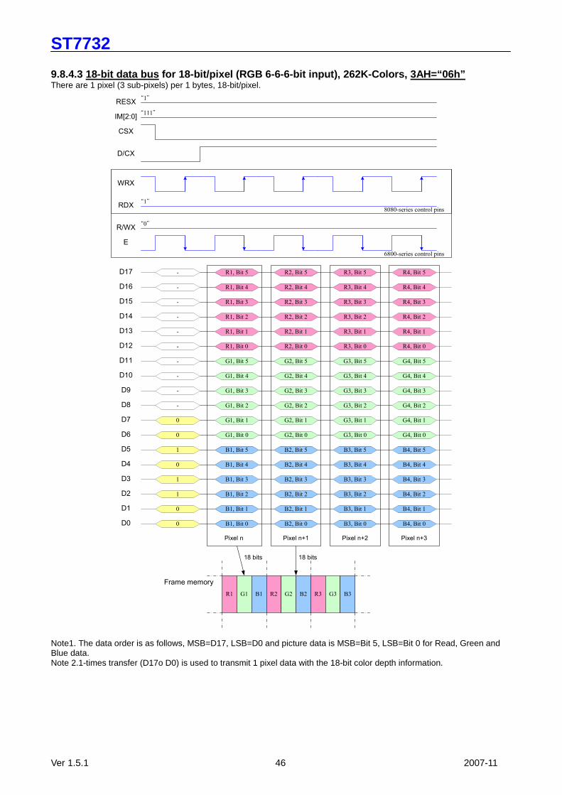
9.8.4.3 18-bit data bus for 18-bit/pixel (RGB 6-6-6-bit input), 262K-Color s, 3AH=“06h” There are 1 pixel (3 sub-pixels) per 1 bytes, 18-bit/pixel.
-
-
-
-
G1, Bit 3
-
G1, Bit 2
-
G1, Bit 1
-
G1, Bit 0
-
8080-series control pins
6800-series control pins
RESX
IM[2:0]
CSX
D/CX
“1”
“111”
WRX
RDX“1”
R/WX
E
D15
D14
D13
D12
D11
D10
D9
D8
Pixel n Pixel n+1
18 bits 18 bits
R1 G1 B1 R2 G2 B2 R3 G3 B3
Frame memory
R1, Bit 3
0
R1, Bit 2
0
R1, Bit 1
1
R1, Bit 0
0
1
1
0
0
D7
D6
D5
D4
D3
D2
D1
D0
B1, Bit 3
B1, Bit 2
B1, Bit 1
B1, Bit 0
G2, Bit 3
G2, Bit 2
G2, Bit 1
G2, Bit 0
R2, Bit 3
R2, Bit 2
R2, Bit 1
R2, Bit 0
B2, Bit 3
B2, Bit 2
B2, Bit 1
B2, Bit 0
G3, Bit 3
G3, Bit 2
G3, Bit 1
G3, Bit 0
R3, Bit 3
R3, Bit 2
R3, Bit 1
R3, Bit 0
B3, Bit 3
B3, Bit 2
B3, Bit 1
B3, Bit 0
G4, Bit 3
G4, Bit 2
G4, Bit 1
G4, Bit 0
R4, Bit 3
R4, Bit 2
R4, Bit 1
R4, Bit 0
B4, Bit 3
B4, Bit 2
B4, Bit 1
B4, Bit 0
Pixel n+2 Pixel n+3
“0”
-
-
D17
D16 R1, Bit 4 R2, Bit 4 R3, Bit 4 R4, Bit 4
G1, Bit 5
G1, Bit 4
G2, Bit 5
G2, Bit 4
G3, Bit 5
G3, Bit 4
G4, Bit 5
G4, Bit 4
B1, Bit 4 B2, Bit 4 B3, Bit 4 B4, Bit 4
R1, Bit 5 R2, Bit 5 R3, Bit 5 R4, Bit 5
B1, Bit 5 B2, Bit 5 B3, Bit 5 B4, Bit 5
Note1. The data order is as follows, MSB=D17, LSB=D0 and picture data is MSB=Bit 5, LSB=Bit 0 for Read, Green and Blue data. Note 2.1-times transfer (D17o D0) is used to transmit 1 pixel data with the 18-bit color depth information.

ST7732
Ver 1.5.1 47 2007-11
9.8.5 3-line serial Interface Different display data formats are available for three colors depth supported by the LCM listed below. 4k colors, RGB 4-4-4-bit input 65k colors, RGB 5-6-5-bit input 262k colors, RGB 6-6-6-bit input 9.8.5.1 Write data for 12-bit/pixel (RGB 4-4-4-bit input), 4K-Colors, 3AH=“03h”
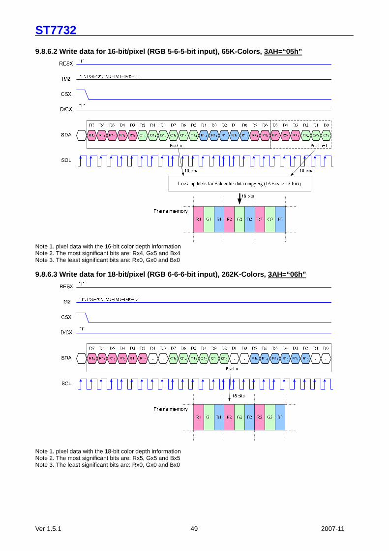
Note 1. pixel data with the 12-bit color depth information Note 2. The most significant bits are: Rx3, Gx3 and Bx3 Note 3. The least significant bits are: Rx0, Gx0 and Bx0 9.8.5.2 Write data for 16-bit/pixel (RGB 5-6-5-bit input), 65K-Colors, 3AH=“05h”
Note 1. pixel data with the 16-bit color depth information Note 2. The most significant bits are: Rx4, Gx5 and Bx4 Note 3. The least significant bits are: Rx0, Gx0 and Bx0
ST7732
Ver 1.5.1 48 2007-11
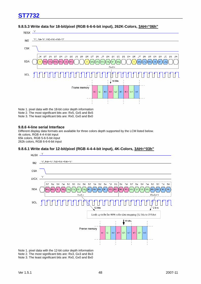
9.8.5.3 Write data for 18-bit/pixel (RGB 6-6-6-bit input), 262K-Colors, 3AH=“06h”
Note 1. pixel data with the 18-bit color depth information Note 2. The most significant bits are: Rx5, Gx5 and Bx5 Note 3. The least significant bits are: Rx0, Gx0 and Bx0 9.8.6 4-line serial Interface Different display data formats are available for three colors depth supported by the LCM listed below. 4k colors, RGB 4-4-4-bit input 65k colors, RGB 5-6-5-bit input 262k colors, RGB 6-6-6-bit input 9.8.6.1 Write data for 12-bit/pixel (RGB 4-4-4-bit input), 4K-Colors, 3AH=“03h”
Note 1. pixel data with the 12-bit color depth information Note 2. The most significant bits are: Rx3, Gx3 and Bx3 Note 3. The least significant bits are: Rx0, Gx0 and Bx0
ST7732
Ver 1.5.1 49 2007-11
9.8.6.2 Write data for 16-bit/pixel (RGB 5-6-5-bit input), 65K-Colors, 3AH=“05h”
Note 1. pixel data with the 16-bit color depth information Note 2. The most significant bits are: Rx4, Gx5 and Bx4 Note 3. The least significant bits are: Rx0, Gx0 and Bx0 9.8.6.3 Write data for 18-bit/pixel (RGB 6-6-6-bit input), 262K-Colors, 3AH=“06h”
Note 1. pixel data with the 18-bit color depth information Note 2. The most significant bits are: Rx5, Gx5 and Bx5 Note 3. The least significant bits are: Rx0, Gx0 and Bx0

ST7732
Ver 1.5.1 50 2007-11
9.9 RGB interface 9.9.1 General Description The module uses 6, 16 and 18-bit parallel RGB interface which includes: VS, HS, DE, PCLK, D[17:0]. The interface is activated after Power-On sequence (See section Power-On/Off Sequence) Pixel clock (PCLK) is running all the time without stopping and it is used to enter VS, HS, DE and D[17:0] states at the rising edge of the PCLK. The PCLK cannot be used as continues internal clock for other functions of the display module e.g. Sleep-In mode etc. Vertical synchronization (VS) is used to tell the driver when a new frame of the display is beginning. This is negative (‘0’, low) active and its state is read by the driver at the rising edge of he PCLK signal. Horizontal synchronization (HS) is used to tell the driver when a new line of the frame is beginning. This is negative (‘0’, low) active and its state is read by the driver at the rising edge of the PCLK signal. Data Enable (DE) is used to tell the driver when the RGB information will be transferred ti the driver. This is a positive (‘1’, high) active and its state is read by the driver at the rising edge of the PCLK signal. D[17:0] (18-bit: R5-R0, G5-G0 and B5-B0; 16-bit: R4-R0, G5-G0 and B4-B0) are used to tell what is the information of the image that is transferred on the display (When DE=’1’ and at the rising edge of PCLK). D[17:0] can be ‘0’ (low) or ‘1’ (high). These lines are read by the driver at the rising edge of the PCLK signal. The PCLK cycle is described in the following figure.
Fig. 9.9.1 PCLK cycle
Note: PCLK is an unsynchronized signal (It can be stopped).
ST7732
Ver 1.5.1 51 2007-11
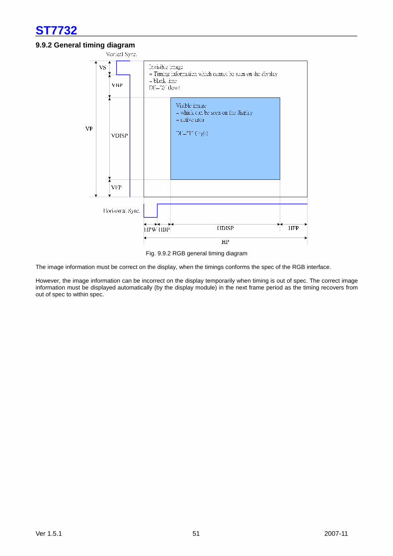
9.9.2 General timing diagram
Fig. 9.9.2 RGB general timing diagram
The image information must be correct on the display, when the timings conforms the spec of the RGB interface. However, the image information can be incorrect on the display temporarily when timing is out of spec. The correct image information must be displayed automatically (by the display module) in the next frame period as the timing recovers from out of spec to within spec.
ST7732
Ver 1.5.1 52 2007-11
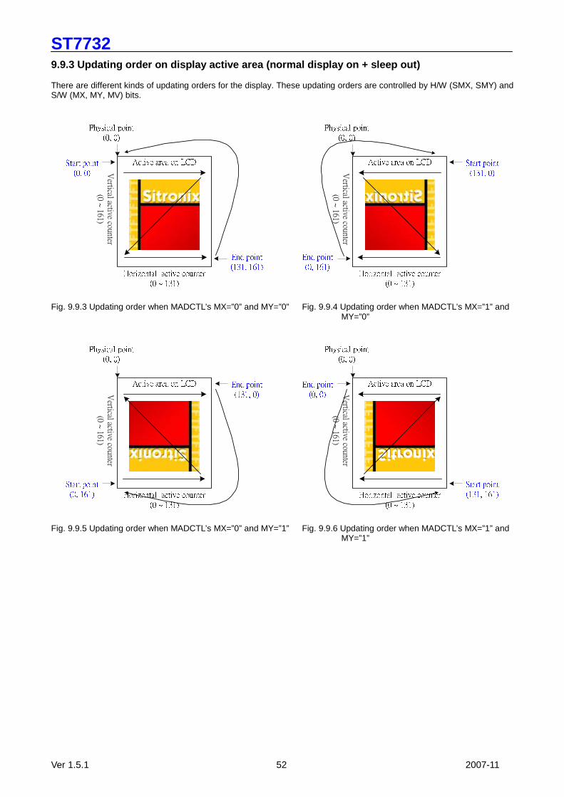
9.9.3 Updating order on display active area (normal display on + sleep out)
There are different kinds of updating orders for the display. These updating orders are controlled by H/W (SMX, SMY) and S/W (MX, MY, MV) bits.
Vertical active counter
(0 ~ 161)
Vertical active counter
(0 ~ 161)
Fig. 9.9.3 Updating order when MADCTL’s MX=”0” and MY=”0” Fig. 9.9.4 Updating order when MADCTL’s MX=”1” and
MY=”0”
Vertical active counter
(0 ~ 161)
Vertical active counter
(0 ~ 161)
Fig. 9.9.5 Updating order when MADCTL’s MX=”0” and MY=”1” Fig. 9.9.6 Updating order when MADCTL’s MX=”1” and
MY=”1”

ST7732
Ver 1.5.1 53 2007-11
Table 9.9.1 Rules for updating order
Condition Horizontal Counter
Vertical Counter
An active VS signal is received Return to 0 Return to 0 Signal pixel information of the active area is received Increment by 1 No change An active HS signal between two active area lines Return to 0 Increment by 1 The horizontal counter is larger than 239 and the vertical counter is larger than 319 Return to 0 Return to 0 Note 1. Pixel order is RGB on the display. Note 2. Data streaming direction from the host to the display is described in the following figure.
Fig. 9.9.3 Data streaming order for RGB interface
9.9.4 RGB Interface Bus Width set All 4-kinds of bus width can be available in RGB interface mode (selected by COLMOD (3Ah) command for 6-bit, 16-bit and 18-bit data width) VIPF[3:0] D17 D16 D15 D14 D13 D12 D11 D10 D9 D8 D7 D6 D5 D4 D3 D2 D1 D0 Bus
width 0101 R4 R3 R2 R1 R0 x G5 G4 G3 G2 G1 G0 B4 B3 B2 B1 B0 x 16-bit
data 0110 R5 R4 R3 R2 R1 R0 G5 G4 G3 G2 G1 G0 B5 B4 B3 B2 B1 B0 18-bit
data x x x x x x x x x x X x R5 R4 R3 R2 R1 R0 x x x x x x x x x x X X G5 G4 G3 G2 G1 G0 1110 x x x x x x x x x x x X B5 B4 B3 B2 B1 B0
6-bit data
Note 1: When VIPF[3:0]=”1110”, 6-bit data width of 3-times transfer is used to transmit 1 pixel data with the 18-bit color depth information.
Note 2: Only VIPF[3:0]= ”0101” , “0110” and “1110” are valid on RGB I/F, Others are invalid. Note 3. ‘x’ Don’t care, but need to set VDDI or DGND level. 9.9.5 RGB Interface Mode Set Table 9.9.5.1 RGB Interface Mode Setting
RGB I/F Mode PCLK DE VS HS Video Data
bus D[17:0] Register for Blanking
Porch setting Reference clock for
Display RGB Mode 1 Used Used Used Used Used Not Used Internal Oscillator RGB Mode 2 Used Used Used Used Used Used Internal Oscillator
There are 2-kinds of RGB mode which is selected by RCM1 & RCM0 hardware pins. In RGB Mode 1 (RCM1, RCM0 = “10”), writing data to frame memory is done by PCLK and data bus (D[17:0]), when DE is in high state. The external synchronization signals (PCLK, VS and HS) are used for internal display signals. So, controller (host) must always transfer PCLK, VS, HS and DE signals to driver. In RGB Mode 2 (RCM1, RCM0 = “11”), blanking porch setting of VS and HS signals are defined by RGBBPCTR (B5h) command. DE pin is used for data making. When DE pin is high, valid data is directly stored to frame memory. In the contrast, if DE pin is low the data of frame memory will keep same status.
ST7732
Ver 1.5.1 54 2007-11
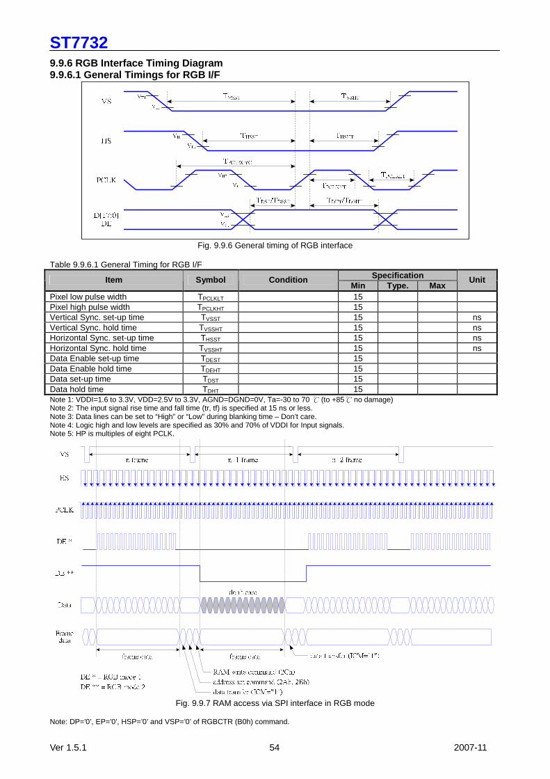
9.9.6 RGB Interface Timing Diagram 9.9.6.1 General Timings for RGB I/F
Fig. 9.9.6 General timing of RGB interface
Table 9.9.6.1 General Timing for RGB I/F
Specification Item Symbol Condition Min Type. Max
Unit
Pixel low pulse width TPCLKLT 15 Pixel high pulse width TPCLKHT 15 Vertical Sync. set-up time TVSST 15 ns Vertical Sync. hold time TVSSHT 15 ns Horizontal Sync. set-up time THSST 15 ns Horizontal Sync. hold time TVSSHT 15 ns Data Enable set-up time TDEST 15 Data Enable hold time TDEHT 15 Data set-up time TDST 15 Data hold time TDHT 15 Note 1: VDDI=1.6 to 3.3V, VDD=2.5V to 3.3V, AGND=DGND=0V, Ta=-30 to 70 (to +85 no damage) Note 2: The input signal rise time and fall time (tr, tf) is specified at 15 ns or less. Note 3: Data lines can be set to “High” or “Low” during blanking time – Don’t care. Note 4: Logic high and low levels are specified as 30% and 70% of VDDI for Input signals. Note 5: HP is multiples of eight PCLK.
Fig. 9.9.7 RAM access via SPI interface in RGB mode
Note: DP=’0’, EP=’0’, HSP=’0’ and VSP=’0’ of RGBCTR (B0h) command.

ST7732
Ver 1.5.1 55 2007-11
9.9.6.2 RGB Interface Mode 1 Timing Diagram
Fig. 9.9.8 RGB mode 1 timing diagram
Note: DP=’0’, EP=’0’, HSP=’0’ and VSP=’0’ of RGBCTR (B0h) command.
Fig. 9.9.9 Vertical and horizontal timing of RGB interface

ST7732
Ver 1.5.1 56 2007-11
Table 9.9.6.2 Vertical and Horizontal Timing for RGB I/F Specification Item Symbol Condition
Min Type. Max Unit
Vertical Timing Vertical cycle period TVP GM=”00”&”01” 166 172 HS Vertical low pulse width TVS 2 4 HS Vertical front porch TVFP 2 4 HS Vertical back porch TVBP 2 4 HS Vertical data start line TVS + TVBP 4 8 HS Vertical blanking period TVBL TVS + TVBP + TVFP 6 12 HS Vertical active area TVDISP GM=”00”&”01” 160 HS Vertical refresh rate TVRR Frame rate 61.75 65 68.25 Hz Horizontal Timing Horizontal cycle period THP GM=”00”&”01” 160 745 PCLK Horizontal low pulse width THS 2 256 PCLK Horizontal front porch THFP 2 256 PCLK Horizontal back porch THBP 2 256 PCLK Horizontal data start point THS + THBP 30 766 PCLK Horizontal blanking period THBL 32 768 PCLK Horizontal active area THDISP GM=”00”&”01” 128 PCLK
TPCLKCYC 100 579 ns fPCLKCYC
GM=”00” TVRR=65Hz 1.7 10 MHz
TPCLKCYC 100 610 ns Pixel clock cycle
fPCLKCYC GM=”01”
TVRR=65Hz 1.6 10 MHz Note 1. VDDI=1.6 to 3.3V, VDD=2.5V to 3.3V, AGND=DGND=0V, Ta=-30 to 70 Note 2. Data lines can be set to “High” or “Low” during blanking time – Don’t care. Note 3. HP is multiples of eight PCLK.

ST7732
Ver 1.5.1 57 2007-11
9.9.6.3 RGB Interface Mode 2 Timing Diagram
VS
HS
DE
HS
PCLK
DE
Data bus
Latch data
V back porch (TVS+TVBP)
1 frame (TVP)
V front porch (TVFP)
1 line (THP)
H back porch (THS+THBP) Valid data (THDISP)H front porch (THFP)
Invalid
Invalid
Invalid
Dn
DnD1
D1
D2
D2
D3
D3
“1"
“1"
Fig. 9.9.10 RGB mode 2 timing diagram
Fig. 9.9.11 RGB mode 2 vertical timing diagram
Note: DP=’0’, EP=’0’, HSP=’0’ and VSP=’0’ of RGBCTR (B0h) command.
HS
D[17:0]
PCLK
THFP=10 PCLKTHS+THBP=10 PCLK THDISP=130 PCLK
THP= 150 PCLK
Horizontal timing for RGB I/F
Invalid Invalid
Fig. 9.9.12 RGB mode 2
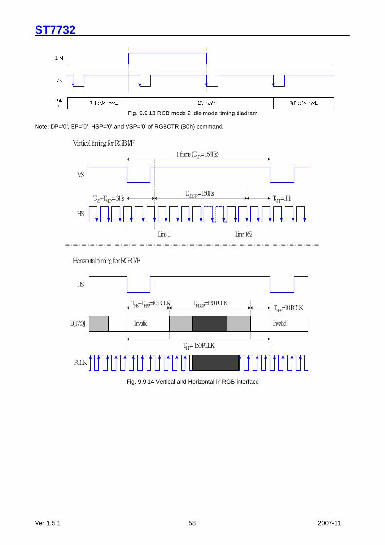
ST7732
Ver 1.5.1 58 2007-11
Fig. 9.9.13 RGB mode 2 idle mode timing diadram
Note: DP=’0’, EP=’0’, HSP=’0’ and VSP=’0’ of RGBCTR (B0h) command.
VS
HS
TVS+TVBP=3Hs TVFP=1Hs
Vertical timingforRGBI/F
HS
D[17:0]
PCLK
THFP=10PCLKTHS+THBP=10PCLK THDISP=130PCLK
THP=150PCLK
Horizontal timingforRGBI/F
1frame(TVP=164Hs)
TVDISP
=160Hs
Line1 Line162
Invalid Invalid
Fig. 9.9.14 Vertical and Horizontal in RGB interface
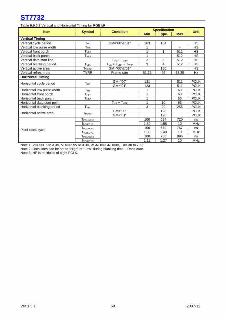
ST7732
Ver 1.5.1 59 2007-11
Table 9.9.6.3 Vertical and Horizontal Timing for RGB I/F Specification Item Symbol Condition
Min Type. Max Unit
Vertical Timing Vertical cycle period TVP GM=”00”&”01” 163 164 HS Vertical low pulse width TVS 1 4 HS Vertical front porch TVFP 1 1 512 HS Vertical back porch TVBP 1 512 HS Vertical data start line TVS + TVBP 2 3 512 HS Vertical blanking period TVBL TVS + TVBP + TVFP 3 4 512 HS Vertical active area TVDISP GM=”00”&”01” 160 HS Vertical refresh rate TVRR Frame rate 61.75 65 68.25 Hz Horizontal Timing
GM=”00” 131 511 PCLK Horizontal cycle period THP GM=”01” 123 511 PCLK
Horizontal low pulse width THS 1 63 PCLK Horizontal front porch THFP 1 63 PCLK Horizontal back porch THBP 1 63 PCLK Horizontal data start point THS + THBP 1 10 63 PCLK Horizontal blanking period THBL 3 20 256 PCLK
GM=”00” 128 PCLK Horizontal active area THDISP GM=”01” 120 PCLK
TPCLKCYC 100 634 720 ns fPCLKCYC
1.39 1.58 10 MHz
TPCLKCYC 100 670 767 ns fPCLKCYC
1.30 1.49 10 MHz
TPCLKCYC 100 788 896 ns
Pixel clock cycle
fPCLKCYC
1.12 1.27 10 MHz Note 1. VDDI=1.6 to 3.3V, VDD=2.5V to 3.3V, AGND=DGND=0V, Ta=-30 to 70 Note 2. Data lines can be set to “High” or “Low” during blanking time – Don’t care. Note 3. HP is multiples of eight PCLK.

ST7732
Ver 1.5.1 60 2007-11
9.9.6.4 Power On Sequence on RGB Mode 2 The Driver operates power up and display ON by VDD, VDDI, SHUT, VS, HS, DE, PCLK on RGB mode 2 as show as following figure.
VDD
VDDI
RESX
SHUT
PCLK
HS
DE
VS
1 2 3 4 5 6 7 8 9 10 11 12 13 14 15
Display high voltage
Display
Source output
Vcom output
Gate output
Internal counter
Internal oscillator
TVDD-VDDI
TRS-SH
TVDD-SH
TPCLK-SH
TSH-LCD
TSH-ON
Display on
Normal display
Normal display
Normal display
Blanking display (over 1 frame)
Fig. 9.9.15 Power-ON sequence in RGB mode 2
Table 9.9.6.4 Power ON AC Characteristics
Characteristics Symbol Min Typ Max Unit Remark VDD On to VDDI On TVDD-VDDI 0 ns Note1
VDDI/VDD on to falling edge of SHUT TVDD-SH 1 ms RESX to falling of SHUT TRS-SH 10 us
Signals input to falling edge of SHUT * TCLK-SH 1 PCLK Note2 Falling edge of SHUT to LCD power ON TSH-LCD 120 ms
Falling edge of SHUT to Display start TSH-ON 10 VS Note 1: TVDDI-VDD can be <=0ns, >0ns. In any case, VDDI and VDD power up sequence should not have any impact on
the driver / display functionalities / performance. Note 2: Signals mean VS, HS, DE and PCLK signal. Note 3: DP=’0’, EP=’0’, HSP=’0’ and VSP=’0’ of RGBCTR (B0h) command.
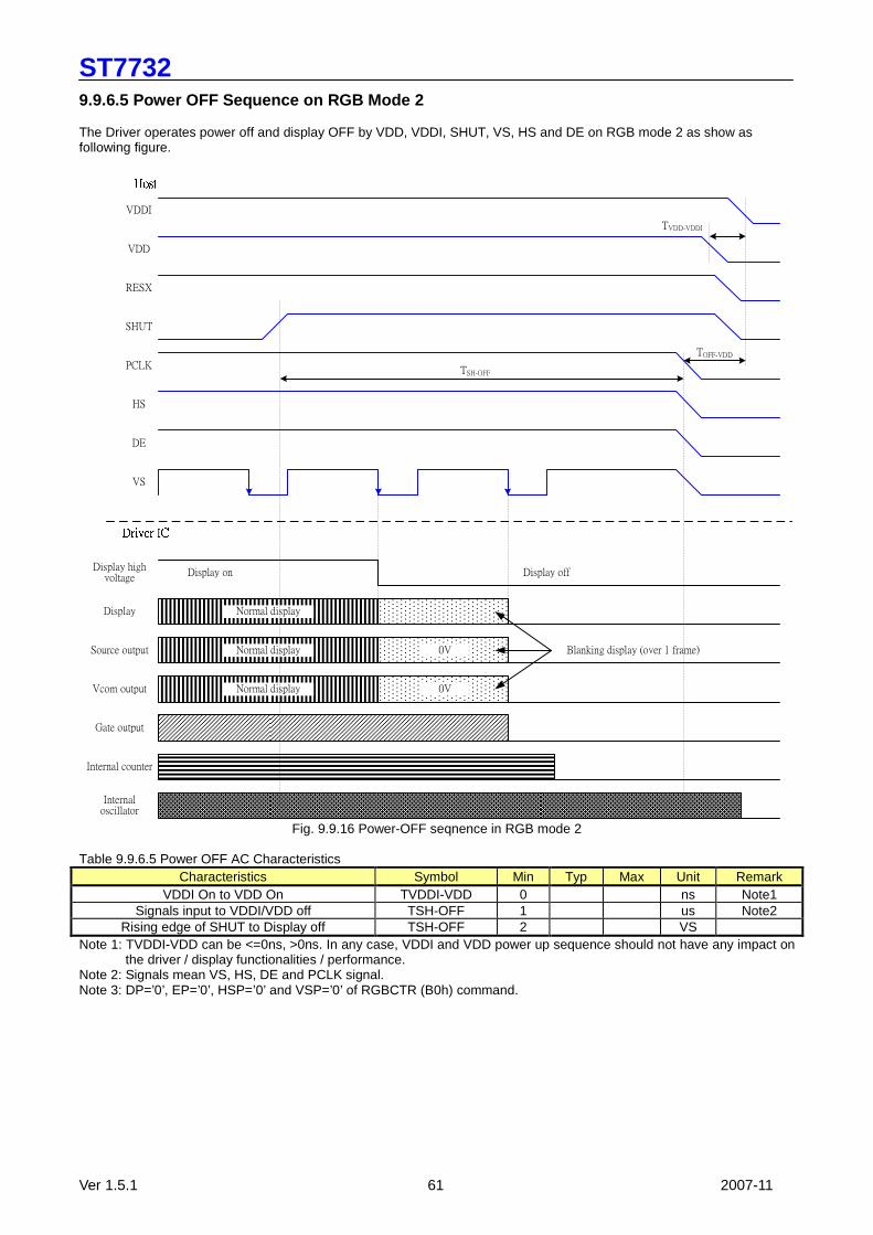
ST7732
Ver 1.5.1 61 2007-11
9.9.6.5 Power OFF Sequence on RGB Mode 2 The Driver operates power off and display OFF by VDD, VDDI, SHUT, VS, HS and DE on RGB mode 2 as show as following figure.
VDDI
VDD
RESX
SHUT
PCLK
HS
DE
VS
Display high voltage
Display
Source output
Vcom output
Gate output
Internal counter
Internal oscillator
Display off
Normal display
Display on
Normal display
Normal display
0V
0V
Blanking display (over 1 frame)
TVDD-VDDI
TOFF-VDD
TSH-OFF
Fig. 9.9.16 Power-OFF seqnence in RGB mode 2
Table 9.9.6.5 Power OFF AC Characteristics
Characteristics Symbol Min Typ Max Unit Remark VDDI On to VDD On TVDDI-VDD 0 ns Note1
Signals input to VDDI/VDD off TSH-OFF 1 us Note2 Rising edge of SHUT to Display off TSH-OFF 2 VS
Note 1: TVDDI-VDD can be <=0ns, >0ns. In any case, VDDI and VDD power up sequence should not have any impact on the driver / display functionalities / performance.
Note 2: Signals mean VS, HS, DE and PCLK signal. Note 3: DP=’0’, EP=’0’, HSP=’0’ and VSP=’0’ of RGBCTR (B0h) command.

ST7732
Ver 1.5.1 62 2007-11
9.9.7 RGB Data Color Coding 9.9.7.1 16-bit/pixel Color Order on the RGB Interfa ce
Note 1: The data order is as follows, MSB=D17, LSB=D0 and picture data is MSB=Bit5, LSB=Bit0 for Green data and
MSB=Bit4, LSB=Bit0 for Red and Blue data. Note 2: ‘-’ Don’t care, but need set to VDDI or DGND level.
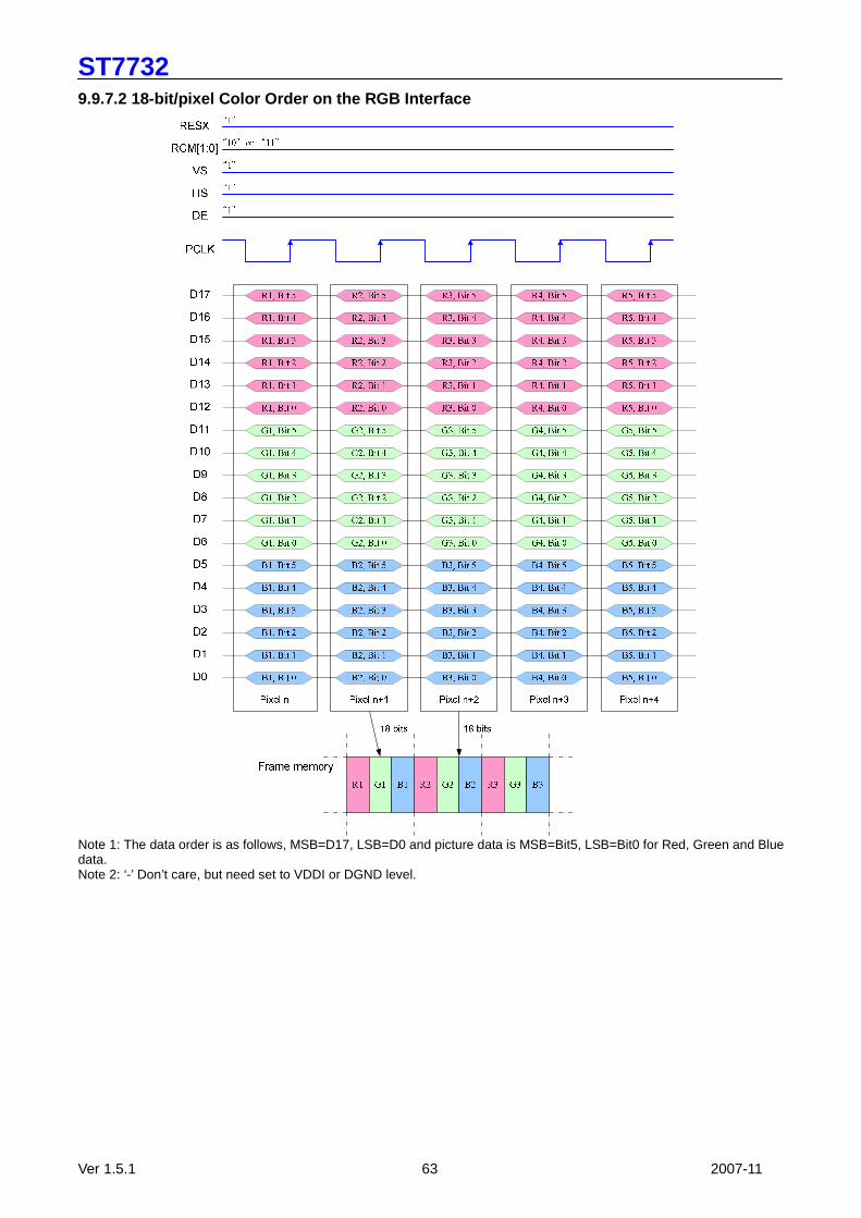
ST7732
Ver 1.5.1 63 2007-11
9.9.7.2 18-bit/pixel Color Order on the RGB Interfa ce
Note 1: The data order is as follows, MSB=D17, LSB=D0 and picture data is MSB=Bit5, LSB=Bit0 for Red, Green and Blue data. Note 2: ‘-’ Don’t care, but need set to VDDI or DGND level.
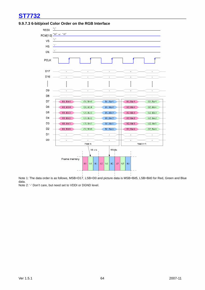
ST7732
Ver 1.5.1 64 2007-11
9.9.7.3 6-bit/pixel Color Order on the RGB Interfac e
Note 1: The data order is as follows, MSB=D17, LSB=D0 and picture data is MSB=Bit5, LSB=Bit0 for Red, Green and Blue data. Note 2: ‘-’ Don’t care, but need set to VDDI or DGND level.
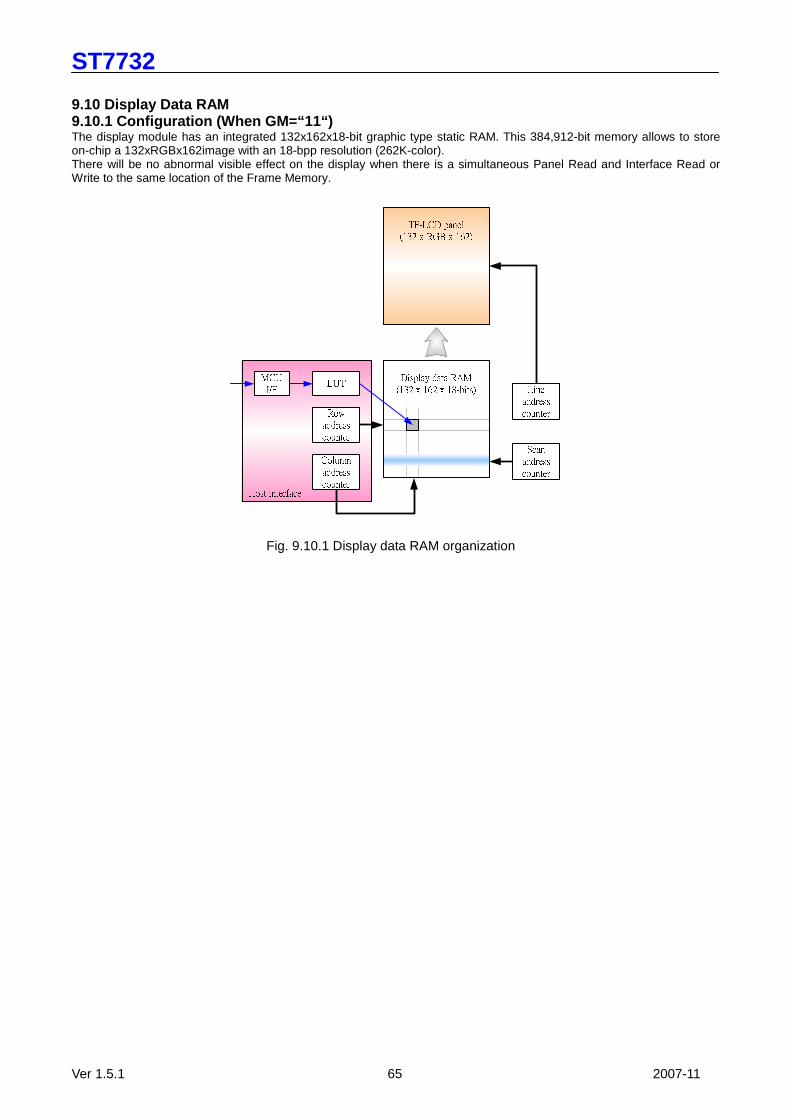
ST7732
Ver 1.5.1 65 2007-11
9.10 Display Data RAM 9.10.1 Configuration (When GM=“11“) The display module has an integrated 132x162x18-bit graphic type static RAM. This 384,912-bit memory allows to store on-chip a 132xRGBx162image with an 18-bpp resolution (262K-color). There will be no abnormal visible effect on the display when there is a simultaneous Panel Read and Interface Read or Write to the same location of the Frame Memory.
Fig. 9.10.1 Display data RAM organization
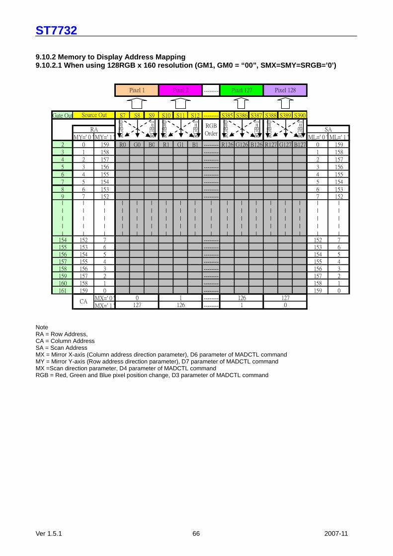
ST7732
Ver 1.5.1 66 2007-11
9.10.2 Memory to Display Address Mapping 9.10.2.1 When using 128RGB x 160 resolution (GM1, G M0 = “00”, SMX=SMY=SRGB=’0’)
--------
Gate Out S7 S8 S9 S10 S11 S12 -------- S385 S386 S387 S388 S389 S390
MY=' 0 ' MY=' 1 ' ML=' 0 ' ML=' 1 '
2 0 159 R0 G0 B0 R1 G1 B1 -------- R126 G126 B126 R127 G127 B127 0 159
3 1 158 -------- 1 158
4 2 157 -------- 2 157
5 3 156 -------- 3 156
6 4 155 -------- 4 155
7 5 154 -------- 5 154
8 6 153 -------- 6 1539 7 152 -------- 7 152|
|
|
|
|
|
|
|
|
|
|
|
|
|
|
|
|
|
|
|
|
|
|
|
|
|
|
|
|
|
|
|
|
|
|
|
|
|
|
|
|
|
|
|
|
|
|
|
|
|
|
|
|
|
|
|
|
|
|
|
|
|
|
|
|
|
|
|
|
|
|
|
|
|
|
|
|
|
|
|
|
|
|
|
|
|
|
|
|
|154 152 7 -------- 152 7155 153 6 -------- 153 6156 154 5 -------- 154 5157 155 4 -------- 155 4158 156 3 -------- 156 3159 157 2 -------- 157 2160 158 1 -------- 158 1
161 159 0 -------- 159 0
MX=' 0 ' --------
MX=' 1 ' --------
Pixel 1 Pixel 2 Pixel 127 Pixel 128
Source OutR
GB
=0
RG
B=
1
RG
B=
0
RG
B=
1
RGB
Order RG
B=
0
RG
B=
1
RG
B=
0
RG
B=
1
RA SA
CA0 1 126 127
127 126 1 0
Note RA = Row Address, CA = Column Address SA = Scan Address MX = Mirror X-axis (Column address direction parameter), D6 parameter of MADCTL command MY = Mirror Y-axis (Row address direction parameter), D7 parameter of MADCTL command MX =Scan direction parameter, D4 parameter of MADCTL command RGB = Red, Green and Blue pixel position change, D3 parameter of MADCTL command
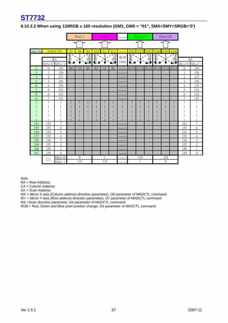
ST7732
Ver 1.5.1 67 2007-11
9.10.2.2 When using 120RGB x 160 resolution (GM1, G M0 = “01”, SMX=SMY=SRGB=’0’)
--------
Gate Out S7 S8 S9 S10 S11 S12 -------- S361 S362 S363 S364 S365 S366
MY=' 0 ' MY=' 1 ' ML=' 0 ' ML=' 1 '
2 0 159 R0 G0 B0 R1 G1 B1 -------- R118 G118 B118 R119 G119 B119 0 159
3 1 158 -------- 1 158
4 2 157 -------- 2 157
5 3 156 -------- 3 156
6 4 155 -------- 4 155
7 5 154 -------- 5 154
8 6 153 -------- 6 1539 7 152 -------- 7 152|
|
|
|
|
|
|
|
|
|
|
|
|
|
|
|
|
|
|
|
|
|
|
|
|
|
|
|
|
|
|
|
|
|
|
|
|
|
|
|
|
|
|
|
|
|
|
|
|
|
|
|
|
|
|
|
|
|
|
|
|
|
|
|
|
|
|
|
|
|
|
|
|
|
|
|
|
|
|
|
|
|
|
|
|
|
|
|
|
|154 152 7 -------- 152 7155 153 6 -------- 153 6156 154 5 -------- 154 5157 155 4 -------- 155 4158 156 3 -------- 156 3159 157 2 -------- 157 2160 158 1 -------- 158 1
161 159 0 -------- 159 0
MX=' 0 ' --------
MX=' 1 ' --------
119119 118 1 0
CA0 1 118
RG
B=
0
RG
B=
1
RG
B=
0
RG
B=
1
RA SA
Source Out
RG
B=
0
RG
B=
1
RG
B=
0
RG
B=
1
RGB
Order
Pixel 1 Pixel 2 Pixel 119 Pixel 120
Note RA = Row Address, CA = Column Address SA = Scan Address MX = Mirror X-axis (Column address direction parameter), D6 parameter of MADCTL command MY = Mirror Y-axis (Row address direction parameter), D7 parameter of MADCTL command MX =Scan direction parameter, D4 parameter of MADCTL command RGB = Red, Green and Blue pixel position change, D3 parameter of MADCTL command
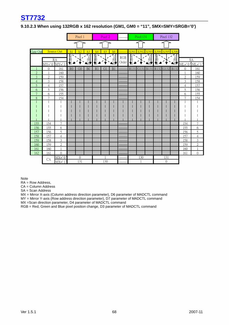
ST7732
Ver 1.5.1 68 2007-11
9.10.2.3 When using 132RGB x 162 resolution (GM1, G M0 = “11”, SMX=SMY=SRGB=’0’)
--------
Gate Out S1 S2 S3 S4 S5 S6 -------- S391 S392 S393 S394 S395 S396
MY=' 0 ' MY=' 1 ' ML=' 0 ' ML=' 1 '
1 0 161 R0 G0 B0 R1 G1 B1 -------- R131 G131 B131 R132 G132 B132 0 1612 1 160 -------- 1 1603 2 159 -------- 2 1594 3 158 -------- 3 1585 4 157 -------- 4 1576 5 156 -------- 5 1567 6 155 -------- 6 1558 7 154 -------- 7 154|
|
|
|
|
|
|
|
|
|
|
|
|
|
|
|
|
|
|
|
|
|
|
|
|
|
|
|
|
|
|
|
|
|
|
|
|
|
|
|
|
|
|
|
|
|
|
|
|
|
|
|
|
|
|
|
|
|
|
|
|
|
|
|
|
|
|
|
|
|
|
|
|
|
|
|
|
|
|
|
|
|
|
|
|
|
|
|
|
|155 154 7 -------- 154 7156 155 6 -------- 155 6157 156 5 -------- 156 5158 157 4 -------- 157 4159 158 3 -------- 158 3160 159 2 -------- 159 2161 160 1 -------- 160 1
162 161 0 -------- 161 0
MX=' 0 ' --------
MX=' 1 ' --------
Pixel 1 Pixel 2 Pixel 131 Pixel 132
Source Out
RG
B=
0
RG
B=
1
RG
B=
0
RG
B=
1
RGB
Order RG
B=
0
RG
B=
1
RG
B=
0
RG
B=
1
RA SA
CA0 1 130 131
131 130 1 0
Note RA = Row Address, CA = Column Address SA = Scan Address MX = Mirror X-axis (Column address direction parameter), D6 parameter of MADCTL command MY = Mirror Y-axis (Row address direction parameter), D7 parameter of MADCTL command MX =Scan direction parameter, D4 parameter of MADCTL command RGB = Red, Green and Blue pixel position change, D3 parameter of MADCTL command
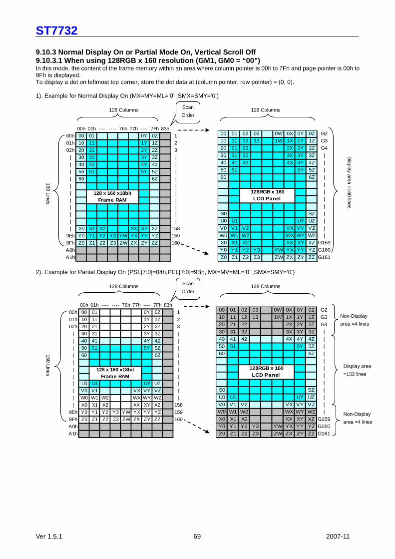
ST7732
Ver 1.5.1 69 2007-11
9.10.3 Normal Display On or Partial Mode On, Vertic al Scroll Off 9.10.3.1 When using 128RGB x 160 resolution (GM1, G M0 = “00”) In this mode, the content of the frame memory within an area where column pointer is 00h to 7Fh and page pointer is 00h to 9Fh is displayed. To display a dot on leftmost top corner, store the dot data at (column pointer, row pointer) = (0, 0). 1). Example for Normal Display On (MX=MY=ML=’0’ ,SMX=SMY=’0’)
2). Example for Partial Display On (PSL[7:0]=04h,PEL[7:0]=9Bh, MX=MV=ML=’0’ ,SMX=SMY=’0’)
128 Columns 128 Columns
160 Lines
Scan
Order
00 01 02 03 0W 0X 0Y 0Z G2
10 11 12 13 1W 1X 1Y 1Z G3
20 21 22 2X 2Y 2Z G4
30 31 32 3X 3Y 3Z |
40 41 42 4X 4Y 4Z |
50 51 5Y 5Z |
60 6Z |
|
|
|
|
S0 SZ |
U0 U1 UY UZ |
V0 V1 V2 VX VY VZ |
W0 W1 W2 WX WY WZ |
X0 X1 X2 XX XY XZ G159
Y0 Y1 Y2 Y3 YW YX YY YZ G160
Z0 Z1 Z2 Z3 ZW ZX ZY ZZ G161
128RGB x 160LCD Panel
Non-Display
area =4 lines
Display area
=152 lines
Non-Display
area =4 lines
00h 01h ---- ---- 76h 77h ---- 7Fh 83h
00h 00 01 0Y 0Z 1
01h 10 11 1Y 1Z 202h 20 21 2Y 2Z 3
| 30 31 3Y 3Z |
| 40 41 4Y 4Z |
| 50 51 5Y 5Z |
| 60 6Z |
| |
| |
| || U0 U1 UY UZ |
| V0 V1 VX VY VZ |
| W0 W1 W2 WX WY WZ |
| X0 X1 X2 XX XY XZ 158
9Eh Y0 Y1 Y2 Y3 YW YX YY YZ 159
9Fh Z0 Z1 Z2 Z3 ZW ZX ZY ZZ 160
A0h
A1h
128 x 160 x18bitFrame RAM
128 Columns
00h 01h ---- ---- 76h 77h ---- 7Fh 83h
00h 00 01 0Y 0Z 1
01h 10 11 1Y 1Z 202h 20 21 2Y 2Z 3
| 30 31 3Y 3Z |
| 40 41 4Y 4Z |
| 50 51 5Y 5Z |
| 60 6Z |
| |
| |
| || |
| |
| |
| X0 X1 X2 XX XY XZ 158
9Eh Y0 Y1 Y2 Y3 YW YX YY YZ 159
9Fh Z0 Z1 Z2 Z3 ZW ZX ZY ZZ 160
A0h
A1h
128 x 160 x18bitFrame RAM
128 Columns
160 Lines
Display area =
160 lines
Scan
Order
00 01 02 03 0W 0X 0Y 0Z G2
10 11 12 13 1W 1X 1Y 1Z G3
20 21 22 2X 2Y 2Z G4
30 31 32 3X 3Y 3Z |
40 41 42 4X 4Y 4Z |
50 51 5Y 5Z |
60 6Z |
|
|
|
|
S0 SZ |
U0 U1 UY UZ |
V0 V1 V2 VX VY VZ |
W0 W1 W2 WX WY WZ |
X0 X1 X2 XX XY XZ G159
Y0 Y1 Y2 Y3 YW YX YY YZ G160
Z0 Z1 Z2 Z3 ZW ZX ZY ZZ G161
128RGB x 160LCD Panel

ST7732
Ver 1.5.1 70 2007-11
9.10.3.2 When using 120RGB x 160 resolution (GM1, G M0 = “01”) In this mode, contents of the frame memory within an area where column pointer is 00h to 77h and page pointer is 00h to 9Fh is displayed. To display a dot on leftmost top corner, store the dot data at (column pointer, row pointer) = (0, 0). 1). Example for Normal Display On (MX=MY=ML=’0’, SMX=SMY=’0’)
2). Example for Partial Display On (PSL[7:0]=04h,PEL[7:0]=9Bh, MX=MV=ML=’0’, SMX=SMY=’0’)
120 Columns
00h 01h ---- ---- 76h 77h ---- 81h 83h
00h 00 01 02 0Y 0Z 1
01h 10 11 12 1Y 1Z 2
02h 20 21 22 2Y 2Z 3
| 30 31 32 3Y 3Z |
| 40 41 42 4Y 4Z |
| 50 51 5Y 5Z |
| 60 6Z |
| |
| |
| |
| U0 U1 UY UZ |
| V0 V1 V2 VY VZ |
| W0 W1 W2 WY WZ |
| X0 X1 X2 XY XZ 158
9Eh Y0 Y1 Y2 YY YZ 159
9Fh Z0 Z1 Z2 ZY ZZ 160
A0hA1h
120 x 160 x18 bitFrame RAM
Unusedarea
120 Columns
160 Lines
Scan
Order
Non-Display
area =4 lines
Display area
=152 lines
Non-Display
area =4 lines
00 01 02 0Y 0Z G210 11 12 1Y 1Z G3
20 21 22 2Y 2Z G4
30 31 32 3Y 3Z |40 41 42 4Y 4Z |
50 51 5Y 5Z |
60 6Z |
||
|
|
S0 SZ |
U0 U1 UY UZ |V0 V1 V2 VY VZ |
W0 W1 W2 WY WZ |
X0 X1 X2 XY XZ G159
Y0 Y1 Y2 YY YZ G160Z0 Z1 Z2 ZY ZZ G161
120RGB x 160LCD Panel
120 Columns
00h 01h ---- ---- 76h 77h ---- 81h 83h
00h 00 01 02 0Y 0Z 1
01h 10 11 12 1Y 1Z 2
02h 20 21 22 2Y 2Z 3
| 30 31 32 3Y 3Z |
| 40 41 42 4Y 4Z |
| 50 51 5Y 5Z |
| 60 6Z |
| |
| |
| |
| |
| |
| W0 W1 WZ |
| X0 X1 X2 XY XZ 158
9Eh Y0 Y1 Y2 YY YZ 159
9Fh Z0 Z1 Z2 ZY ZZ 160
A0hA1h
120 x 160 x18 bitFrame RAM
Unusedarea
120 Columns
160 Lines
Display area =
160 lines
Scan
Order
00 01 02 0Y 0Z G210 11 12 1Y 1Z G3
20 21 22 2Y 2Z G430 31 32 3Y 3Z |
40 41 42 4Y 4Z |
50 51 5Y 5Z |60 6Z |
|
|
|
|
S0 SZ |U0 U1 UY UZ |
V0 V1 V2 VY VZ |
W0 W1 W2 WY WZ |X0 X1 X2 XY XZ G159
Y0 Y1 Y2 YY YZ G160Z0 Z1 Z2 ZY ZZ G161
120RGB x 160LCD Panel
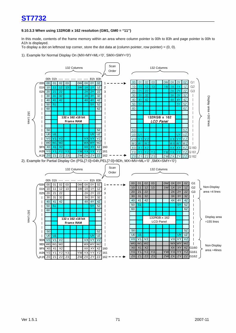
ST7732
Ver 1.5.1 71 2007-11
9.10.3.3 When using 132RGB x 162 resolution (GM1, G M0 = “11”) In this mode, contents of the frame memory within an area where column pointer is 00h to 83h and page pointer is 00h to A1h is displayed. To display a dot on leftmost top corner, store the dot data at (column pointer, row pointer) = (0, 0). 1). Example for Normal Display On (MX=MY=ML=’0’, SMX=SMY=’0’)
2). Example for Partial Display On (PSL[7:0]=04h,PEL[7:0]=9Dh, MX=MV=ML=’0’ ,SMX=SMY=’0’)
132 Columns
00h 01h ---- ---- ---- ---- ---- 81h 83h00h 00 01 02 03 0W 0X 0Y 0Z 1
01h 10 11 12 13 1W 1X 1Y 1Z 2
02h 20 21 22 2X 2Y 2Z 3| 30 31 32 3X 3Y 3Z |
| 40 41 42 4X 4Y 4Z |
| 50 51 5Y 5Z || 60 6Z |
| |
| || |
| || S0 SZ |
| U0 U1 UY UZ |
9Dh V0 V1 V2 VX VY VZ |9Eh W0 W1 W2 WX WY WZ |
9Fh X0 X1 X2 XX XY XZ 160
A0h Y0 Y1 Y2 Y3 YW YX YY YZ 161A1h Z0 Z1 Z2 Z3 ZW ZX ZY ZZ 162
132 x 162 x18 bitFrame RAM
132 Columns
162 Lines
Scan
Order
00 01 02 03 0W 0X 0Y 0Z G1
10 11 12 13 1W 1X 1Y 1Z G2
20 21 22 2X 2Y 2Z G3
30 31 32 3X 3Y 3Z |
40 41 42 4X 4Y 4Z |
50 51 5Y 5Z |
60 6Z |
|
|
|
|
S0 SZ |
U0 U1 UY UZ |
V0 V1 V2 VX VY VZ |
W0 W1 W2 WX WY WZ |
X0 X1 X2 XX XY XZ G160
Y0 Y1 Y2 Y3 YW YX YY YZ G161
Z0 Z1 Z2 Z3 ZW ZX ZY ZZ G162
132RGB x 162LCD Panel
Non-Display
area =4 lines
Display area
=155 lines
Non-Display
area =4lines
132 Columns
00h 01h ---- ---- ---- ---- ---- 81h 83h00h 00 01 02 03 0W 0X 0Y 0Z 1
01h 10 11 12 13 1W 1X 1Y 1Z 2
02h 20 21 22 2X 2Y 2Z 3| 30 31 32 3X 3Y 3Z |
| 40 41 42 4X 4Y 4Z |
| 50 51 5Y 5Z || 60 6Z |
| |
| || |
| || S0 SZ |
| U0 U1 UY UZ |
| V0 V1 V2 VX VY VZ || W0 W1 W2 WX WY WZ |
9Fh X0 X1 X2 XX XY XZ 160
A0h Y0 Y1 Y2 Y3 YW YX YY YZ 161A1h Z0 Z1 Z2 Z3 ZW ZX ZY ZZ 162
132 x 162 x18 bitFrame RAM
132 Columns
162 Lines
Display area =
162 lines
Scan
Order
00 01 02 03 0W 0X 0Y 0Z G1
10 11 12 13 1W 1X 1Y 1Z G2
20 21 22 2X 2Y 2Z G3
30 31 32 3X 3Y 3Z |
40 41 42 4X 4Y 4Z |
50 51 5Y 5Z |
60 6Z |
|
|
|
|
S0 SZ |
U0 U1 UY UZ |
V 0 V 1 V 2 V X V Y V Z |
W0 W1 W2 WX WY WZ |
X0 X1 X2 XX XY XZ G160
Y0 Y1 Y2 Y3 YW YX YY YZ G161
Z0 Z1 Z2 Z3 ZW ZX ZY ZZ G162
132RGB x 162132RGB x 162132RGB x 162132RGB x 162
LCD PanelLCD PanelLCD PanelLCD Panel
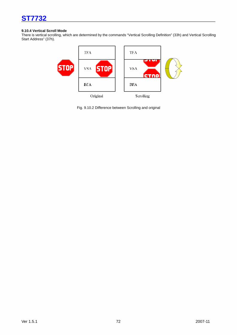
ST7732
Ver 1.5.1 72 2007-11
9.10.4 Vertical Scroll Mode There is vertical scrolling, which are determined by the commands “Vertical Scrolling Definition” (33h) and Vertical Scrolling Start Address” (37h).
Fig. 9.10.2 Difference between Scrolling and original
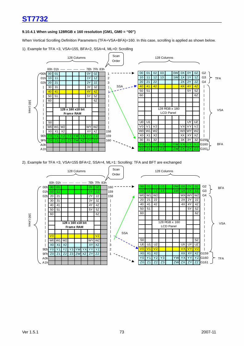
ST7732
Ver 1.5.1 73 2007-11
9.10.4.1 When using 128RGB x 160 resolution (GM1, G M0 = “00”) When Vertical Scrolling Definition Parameters (TFA+VSA+BFA)=160. In this case, scrolling is applied as shown below. 1). Example for TFA =3, VSA=155, BFA=2, SSA=4, ML=0: Scrolling
2). Example for TFA =3, VSA=155 BFA=2, SSA=4, ML=1: Scrolling: TFA and BFT are exchanged
128 Columns 128 Columns
160 Lines
Scan
Order
TFA
VSA
BFA
SSA
00h 01h ---- ---- ---- ---- 7Eh 7Fh 83h
00h 00 01 0Y 0Z 16001h 10 11 1Y 1Z 159
02h 20 21 2Y 2Z 158
| 30 31 3Y 3Z |
| 40 41 4Y 4Z |
| 50 51 5Y 5Z |
| 60 6Z || |
| || || |
| V0 VZ || W0 W1 W2 WY WZ |
| X0 X1 X2 XY XZ 3
9Eh Y0 Y1 Y2 Y3 YW YX YY YZ 2
9Fh Z0 Z1 Z2 Z3 ZW XZ ZY ZZ 1
A0hA1h
128 x 160 x18 bitFrame RAM
00 01 02 03 0W 0X 0Y 0Z G2
10 11 12 13 1W 1X 1Y 1Z G3
W0 W1 W2 WX WY WZ G4
20 21 22 2X 2Y 2Z |
40 41 42 4X 4Y 4Z |
50 51 5Y 5Z |
60 6Z |
|
|
|
|
|
S0 SZ |
U0 U1 U2 UX UY UZ |
V0 V1 V2 VX VY VZ |
X0 X1 X2 XX XY XZ G159
Y0 Y1 Y2 Y3 YW YX YY YZ G160
Z0 Z1 Z2 Z3 ZW ZX ZY ZZ G161
128 RGB x 160LCD Panel
128 Columns
00h 01h ---- ---- ---- ---- 7Eh 7Fh 83h
00h 00 01 0Y 0Z 101h 10 11 1Y 1Z 2
02h 20 21 2Y 2Z 3
| 30 31 3Y 3Z |
| 40 41 4Y 4Z |
| 50 51 5Y 5Z |
| 60 6Z || |
| || || |
| S0 || W0 W1 W2 WY WZ |
| X0 X1 X2 XY XZ 158
9Eh Y0 Y1 Y2 Y3 YW YX YY YZ 159
9Fh Z0 Z1 Z2 Z3 ZW XZ ZY ZZ 160
A0hA1h
128 x 160 x18 bitFrame RAM
128 Columns
160 Lines
Scan
Order
00 01 02 03 0W 0X 0Y 0Z G2
10 11 12 13 1W 1X 1Y 1Z G3
20 21 22 2X 2Y 2Z G4
40 41 42 4X 4Y 4Z |
50 51 5Y 5Z |
60 6Z |
|
|
|
|
|
U0 U1 UY UZ |
V0 V1 V2 VX VY VZ |
W0 W1 W2 WX WY WZ |
X0 X1 X2 XX XY XZ |
30 31 32 3X 3Y 3Z G159
Y0 Y1 Y2 Y3 YW YX YY YZ G160
Z0 Z1 Z2 Z3 ZW ZX ZY ZZ G161
128 RGB x 160LCD Panel
TFA
VSA
BFA
SSA
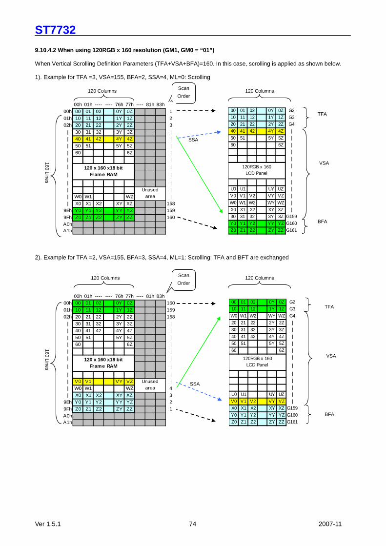
ST7732
Ver 1.5.1 74 2007-11
9.10.4.2 When using 120RGB x 160 resolution (GM1, G M0 = “01”) When Vertical Scrolling Definition Parameters (TFA+VSA+BFA)=160. In this case, scrolling is applied as shown below. 1). Example for TFA =3, VSA=155, BFA=2, SSA=4, ML=0: Scrolling
2). Example for TFA =2, VSA=155, BFA=3, SSA=4, ML=1: Scrolling: TFA and BFT are exchanged
120 Columns 120 Columns
160 Lines
Scan
Order
TFA
VSA
BFA
SSA
00h 01h ---- ---- 76h 77h ---- 81h 83h
00h 00 01 02 0Y 0Z 160
01h 10 11 12 1Y 1Z 159
02h 20 21 22 2Y 2Z 158
| 30 31 32 3Y 3Z |
| 40 41 42 4Y 4Z |
| 50 51 5Y 5Z |
| 60 6Z |
| |
| |
| |
| |
| V0 V1 VY VZ |
| W0 W1 WZ 4
| X0 X1 X2 XY XZ 3
9Eh Y0 Y1 Y2 YY YZ 2
9Fh Z0 Z1 Z2 ZY ZZ 1
A0hA1h
120 x 160 x18 bitFrame RAM
Unusedarea
00 01 02 0Y 0Z G210 11 12 1Y 1Z G3
W0 W1 W2 WY WZ G420 21 22 2Y 2Z |
30 31 32 3Y 3Z |
40 41 42 4Y 4Z |50 51 5Y 5Z |
60 6Z |
|
|
|
||
U0 U1 UY UZ |
V0 V1 V2 VY VZ |X0 X1 X2 XY XZ G159
Y0 Y1 Y2 YY YZ G160Z0 Z1 Z2 ZY ZZ G161
120RGB x 160LCD Panel
120 Columns 120 Columns
160 Lines
Scan
Order
TFA
VSA
BFA
SSA
00h 01h ---- ---- 76h 77h ---- 81h 83h
00h 00 01 02 0Y 0Z 1
01h 10 11 12 1Y 1Z 2
02h 20 21 22 2Y 2Z 3
| 30 31 32 3Y 3Z |
| 40 41 42 4Y 4Z |
| 50 51 5Y 5Z |
| 60 6Z |
| |
| |
| |
| |
| |
| W0 W1 WZ |
| X0 X1 X2 XY XZ 158
9Eh Y0 Y1 Y2 YY YZ 159
9Fh Z0 Z1 Z2 ZY ZZ 160
A0hA1h
120 x 160 x18 bitFrame RAM
Unusedarea
00 01 02 0Y 0Z G210 11 12 1Y 1Z G3
20 21 22 2Y 2Z G440 41 42 4Y 4Z |
50 51 5Y 5Z |
60 6Z ||
|
|
|
|
U0 U1 UY UZ |V0 V1 V2 VY VZ |
W0 W1 W2 WY WZ |
X0 X1 X2 XY XZ |30 31 32 3Y 3Z G159
Y0 Y1 Y2 YY YZ G160Z0 Z1 Z2 ZY ZZ G161
120RGB x 160LCD Panel

ST7732
Ver 1.5.1 75 2007-11
9.10.4.3 When using 132RGB x 162 resolution (GM1, G M0 = “11”) When Vertical Scrolling Definition Parameters (TFA+VSA+BFA)=162. In this case, scrolling is applied as shown below. 1). Example for TFA =3, VSA=157, BFA=2, SSA=4, ML=0: Scrolling
2). Example for TFA =3, VSA=157, BFA=2, SSA=4, ML=1: Scrolling: TFA and BFT are exchanged
132 Columns 132 Columns
162 Lines
Scan
Order
BFA
VSA
TFA
00h 01h ---- ---- ---- ---- ---- 81h 83h
00h 00 01 02 03 0W 0X 0Y 0Z 162
01h 10 11 12 13 1W 1X 1Y 1Z 161
02h 20 21 22 2X 2Y 2Z 160
| 30 31 32 3X 3Y 3Z |
| 40 41 42 4X 4Y 4Z |
| 50 51 5Y 5Z |
| 60 6Z |
| |
| |
| |
| |
| S0 SZ |
| U0 U1 UY UZ |
| V0 V1 V2 VX VY VZ |
| W0 W1 W2 WX WY WZ |
9Fh X0 X1 X2 XX XY XZ 3
A0h Y0 Y1 Y2 Y3 YW YX YY YZ 2
A1h Z0 Z1 Z2 Z3 ZW ZX ZY ZZ 1
132 x 162 x18 bitFrame RAM
SSA
00 01 02 03 0W 0X 0Y 0Z G1
10 11 12 13 1W 1X 1Y 1Z G2
W0 W1 W2 WX WY WZ G3
20 21 22 2X 2Y 2Z |
30 31 32 3X 3Y 3Z |
40 41 42 4X 4Y 4Z |
50 51 5Y 5Z |
60 6Z |
|
|
|
|
S0 SZ |
U0 U1 UY UZ |
V 0 V 1 V 2 V X V Y V Z |
X0 X1 X2 XX XY XZ G160
Y0 Y1 Y2 Y3 YW YX YY YZ G161
Z0 Z1 Z2 Z3 ZW ZX ZY ZZ G162
132RGB x 162132RGB x 162132RGB x 162132RGB x 162
LCD PanelLCD PanelLCD PanelLCD Panel
132 Columns 132 Columns
162 Lines
Scan
Order
TFA
VSA
BFA
00h 01h ---- ---- ---- ---- ---- 81h 83h00h 00 01 02 03 0W 0X 0Y 0Z 1
01h 10 11 12 13 1W 1X 1Y 1Z 2
02h 20 21 22 2X 2Y 2Z 3| 30 31 32 3X 3Y 3Z |
| 40 41 42 4X 4Y 4Z |
| 50 51 5Y 5Z || 60 6Z |
| |
| || |
| || S0 SZ |
| U0 U1 UY UZ |
| V0 V1 V2 VX VY VZ || W0 W1 W2 WX WY WZ |
9Fh X0 X1 X2 XX XY XZ 160
A0h Y0 Y1 Y2 Y3 YW YX YY YZ 161A1h Z0 Z1 Z2 Z3 ZW ZX ZY ZZ 162
132 x 162 x18 bitFrame RAM
00 01 02 03 0W 0X 0Y 0Z G1
10 11 12 13 1W 1X 1Y 1Z G2
20 21 22 2X 2Y 2Z G3
40 41 42 4X 4Y 4Z |
50 51 5Y 5Z |
60 6Z |
|
|
|
|
S0 SZ |
U0 U1 UY UZ |
V 0 V 1 V 2 V X V Y V Z |
W0 W1 W2 WX WY WZ |
X0 X1 X2 XX XY XZ |
30 31 32 3X 3Y 3Z G160
Y0 Y1 Y2 Y3 YW YX YY YZ G161
Z0 Z1 Z2 Z3 ZW ZX ZY ZZ G162
132RGB x 162132RGB x 162132RGB x 162132RGB x 162
LCD PanelLCD PanelLCD PanelLCD Panel
SSA

ST7732
Ver 1.5.1 76 2007-11
9.10.5 Vertical Scroll Example 9.10.5.1 Vertical Scroll Example (GM1, GM0 = “00” & GM 1, GM0=“01” ) There are 2 types of vertical scrolling, which are determined by the commands “Vertical Scrolling Definition” (33h) and “Vertical Scrolling Start Address” (37h). Case 1: TFA + VSA + BFA ≠160 N/A. Do not set TFA + VSA + BFA≠160. In that case, unexpected picture will be shown. Case 2: TFA + VSA + BFA=160 (Scrolling) Example1) When MADCTL parameter ML=”0”, TFA=0, VSA=160, BFA=0 and VSCSAD=80.
Example2) When MADCTL parameter ML=”1”, TFA=30, VSA=130, BFA=0 and VSCSAD=80.

ST7732
Ver 1.5.1 77 2007-11
9.10.5.2 Vertical Scroll Example (GM1, GM0 = “11”) There are 2 types of vertical scrolling, which are determined by the commands “Vertical Scrolling Definition” (33h) and “Vertical Scrolling Start Address” (37h). Case 1: TFA + VSA + BFA ≠162 N/A. Do not set TFA + VSA + BFA≠162. In that case, unexpected picture will be shown. Case 2: TFA + VSA + BFA=162 (Scrolling) Example1) When MADCTL parameter ML=”0”, TFA=0, VSA=162, BFA=0 and VSCSAD=40.
Example2) When MADCTL parameter ML=”1”, TFA=30, VSA=132, BFA=0 and VSCSAD=40.
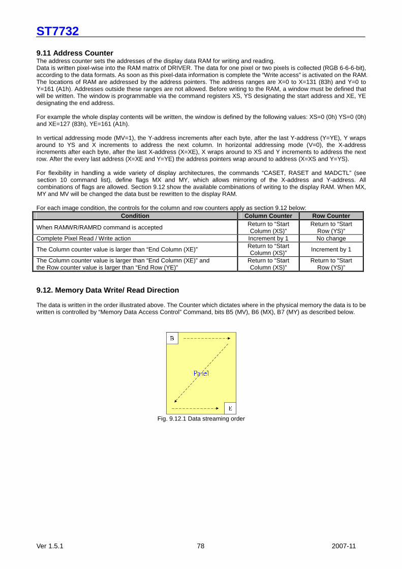
ST7732
Ver 1.5.1 78 2007-11
9.11 Address Counter The address counter sets the addresses of the display data RAM for writing and reading. Data is written pixel-wise into the RAM matrix of DRIVER. The data for one pixel or two pixels is collected (RGB 6-6-6-bit), according to the data formats. As soon as this pixel-data information is complete the “Write access” is activated on the RAM. The locations of RAM are addressed by the address pointers. The address ranges are X=0 to X=131 (83h) and Y=0 to Y=161 (A1h). Addresses outside these ranges are not allowed. Before writing to the RAM, a window must be defined that will be written. The window is programmable via the command registers XS, YS designating the start address and XE, YE designating the end address. For example the whole display contents will be written, the window is defined by the following values: XS=0 (0h) YS=0 (0h) and XE=127 (83h), YE=161 (A1h). In vertical addressing mode (MV=1), the Y-address increments after each byte, after the last Y-address (Y=YE), Y wraps around to YS and X increments to address the next column. In horizontal addressing mode (V=0), the X-address increments after each byte, after the last X-address (X=XE), X wraps around to XS and Y increments to address the next row. After the every last address (X=XE and Y=YE) the address pointers wrap around to address (X=XS and Y=YS). For flexibility in handling a wide variety of display architectures, the commands “CASET, RASET and MADCTL” (see section 10 command list), define flags MX and MY, which allows mirroring of the X-address and Y-address. All combinations of flags are allowed. Section 9.12 show the available combinations of writing to the display RAM. When MX, MY and MV will be changed the data bust be rewritten to the display RAM. For each image condition, the controls for the column and row counters apply as section 9.12 below:
Condition Column Counter Row Counter
When RAMWR/RAMRD command is accepted Return to “Start Column (XS)”
Return to “Start Row (YS)”
Complete Pixel Read / Write action Increment by 1 No change
The Column counter value is larger than “End Column (XE)” Return to “Start Column (XS)” Increment by 1
The Column counter value is larger than “End Column (XE)” and the Row counter value is larger than “End Row (YE)”
Return to “Start Column (XS)”
Return to “Start Row (YS)”
9.12. Memory Data Write/ Read Direction The data is written in the order illustrated above. The Counter which dictates where in the physical memory the data is to be written is controlled by “Memory Data Access Control” Command, bits B5 (MV), B6 (MX), B7 (MY) as described below.
Fig. 9.12.1 Data streaming order

ST7732
Ver 1.5.1 79 2007-11
9.12.1.1 When 128RGBx160 (GM=’00’)
MV MX MV CASET RASET 0 0 0 Direct to Physical Column Pointer Direct to Physical Row Pointer 0 0 1 Direct to Physical Column Pointer Direct to (159-Physical Row Pointer) 0 1 0 Direct to (127-Physical Column Pointer) Direct to Physical Row Pointer 0 1 1 Direct to (127-Physical Column Pointer) Direct to (159-Physical Row Pointer) 1 0 0 Direct to Physical Row Pointer Direct to Physical Column Pointer 1 0 1 Direct to (159-Physical Row Pointer) Direct to Physical Column Pointer 1 1 0 Direct to Physical Row Pointer Direct to (127-Physical Column Pointer) 1 1 1 Direct to (159-Physical Row Pointer) Direct to (127-Physical Column Pointer)
9.12.1.2 When 120RGBx160 (GM=’01’)
MV MX MV CASET RASET 0 0 0 Direct to Physical Column Pointer Direct to Physical Row Pointer 0 0 1 Direct to Physical Column Pointer Direct to (159-Physical Row Pointer) 0 1 0 Direct to (119-Physical Column Pointer) Direct to Physical Row Pointer 0 1 1 Direct to (119-Physical Column Pointer) Direct to (159-Physical Row Pointer) 1 0 0 Direct to Physical Row Pointer Direct to Physical Column Pointer 1 0 1 Direct to (159-Physical Row Pointer) Direct to Physical Column Pointer 1 1 0 Direct to Physical Row Pointer Direct to (119-Physical Column Pointer) 1 1 1 Direct to (159-Physical Row Pointer) Direct to (119-Physical Column Pointer)
9.12.1.3 When 132RGBx162 (GM=’11’)
MV MX MV CASET RASET 0 0 0 Direct to Physical Column Pointer Direct to Physical Row Pointer 0 0 1 Direct to Physical Column Pointer Direct to (161-Physical Row Pointer) 0 1 0 Direct to (131-Physical Column Pointer) Direct to Physical Row Pointer 0 1 1 Direct to (131-Physical Column Pointer) Direct to (161-Physical Row Pointer) 1 0 0 Direct to Physical Row Pointer Direct to Physical Column Pointer 1 0 1 Direct to (161-Physical Row Pointer) Direct to Physical Column Pointer 1 1 0 Direct to Physical Row Pointer Direct to (131-Physical Column Pointer) 1 1 1 Direct to (161-Physical Row Pointer) Direct to (131-Physical Column Pointer)
Note: Data is always written to the Frame Memory in the same order, regardless of the Memory Write Direction set by MADCTL bits B7 (MY), B6 (MX), B5 (MV). The write order for each pixel unit is
One pixel unit represents 1 column and 1page counter value on the Frame Memory.

ST7732
Ver 1.5.1 80 2007-11
9.12.2 Frame Data Write Direction According to the MADCTL parameters (MV, MX and MY)
MADCTL Parameter Display Data
Direction MV MX MY
Image in the Host (MPU)
Image in the Driver (DDRAM)
Normal 0 0 0
Y-Mirror 0 0 1
X-Mirror 0 1 0
X-Mirror Y-Mirror
0 1 1
X-Y Exchange 1 0 0
X-Y Exchange Y-Mirror
1 0 1
X-Y Exchange X-Mirror
1 1 0
X-Y Exchange X-Mirror Y-Mirror
1 1 1
H/W position (0,0)
F
H/W position (0,0)
F
H/W position (0,0)
X-Y address (0,0)
X: RASET
Y: CASET B
H/W position (0,0)
X-Y address (0,0)
X: RASET
Y: CASET F
H/W position (0,0) F
B
X-Y address (0,0)
X: CASET
Y: RASET
B
F
H/W position (0,0) X-Y address (0,0)
X: CASET
Y: RASET
H/W position (0,0)
X-Y address (0,0)
X: CASET
Y: RASET B
F
B
F
H/W position (0,0)
X-Y address (0,0)
X: CASET
Y: RASET
B
F
B
F
B
F
B
F
B
F
B
F
B
F
B
F
B
F
B X-Y address (0,0)
X: RASET
Y: CASET
B
X-Y address (0,0)
X: RASET
Y: CASET
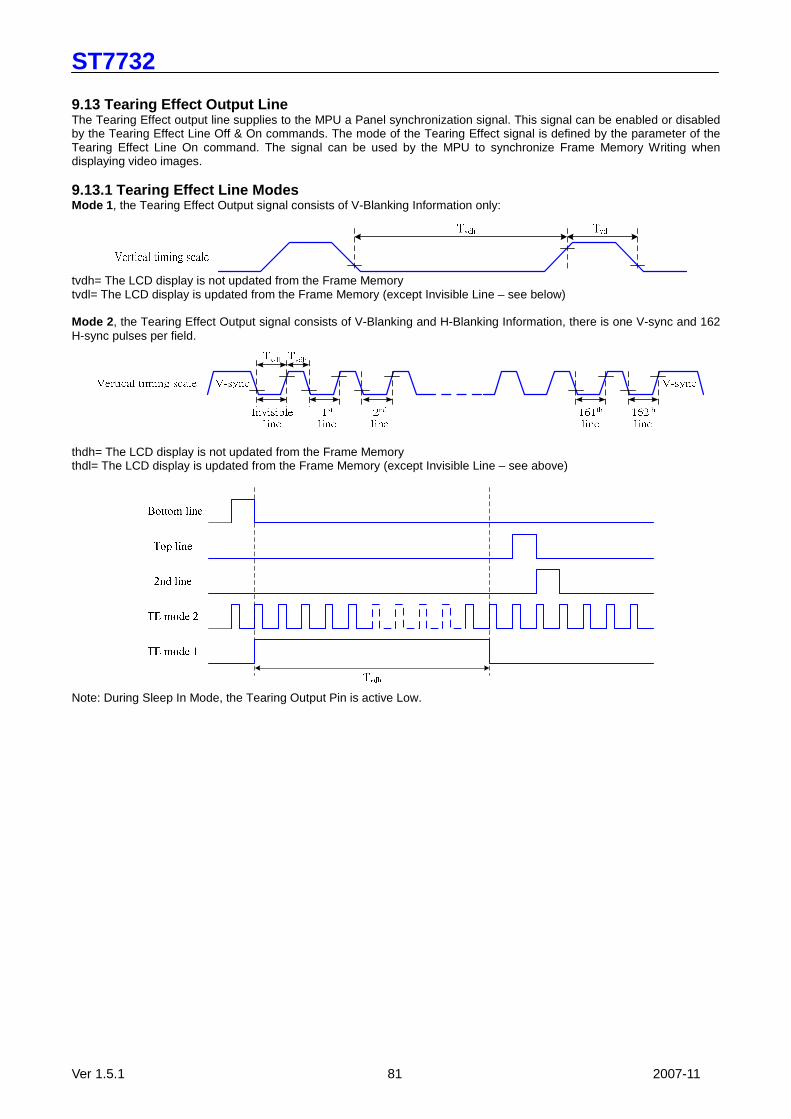
ST7732
Ver 1.5.1 81 2007-11
9.13 Tearing Effect Output Line The Tearing Effect output line supplies to the MPU a Panel synchronization signal. This signal can be enabled or disabled by the Tearing Effect Line Off & On commands. The mode of the Tearing Effect signal is defined by the parameter of the Tearing Effect Line On command. The signal can be used by the MPU to synchronize Frame Memory Writing when displaying video images. 9.13.1 Tearing Effect Line Modes Mode 1 , the Tearing Effect Output signal consists of V-Blanking Information only:
tvdh= The LCD display is not updated from the Frame Memory tvdl= The LCD display is updated from the Frame Memory (except Invisible Line – see below) Mode 2 , the Tearing Effect Output signal consists of V-Blanking and H-Blanking Information, there is one V-sync and 162 H-sync pulses per field.
thdh= The LCD display is not updated from the Frame Memory thdl= The LCD display is updated from the Frame Memory (except Invisible Line – see above)
Note: During Sleep In Mode, the Tearing Output Pin is active Low.
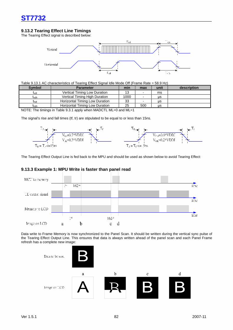
ST7732
Ver 1.5.1 82 2007-11
9.13.2 Tearing Effect Line Timings The Tearing Effect signal is described below:
Table 9.13.1 AC characteristics of Tearing Effect Signal Idle Mode Off (Frame Rate = 58.9 Hz)
Symbol Parameter min max unit description tvdl Vertical Timing Low Duration 13 - ms tvdh Vertical Timing High Duration 1000 - µs thdl Horizontal Timing Low Duration 33 - µs thdh Horizontal Timing Low Duration 25 500 µs
NOTE: The timings in Table 9.3.1 apply when MADCTL ML=0 and ML=1 The signal’s rise and fall times (tf, tr) are stipulated to be equal to or less than 15ns.
The Tearing Effect Output Line is fed back to the MPU and should be used as shown below to avoid Tearing Effect: 9.13.3 Example 1: MPU Write is faster than panel re ad
Data write to Frame Memory is now synchronized to the Panel Scan. It should be written during the vertical sync pulse of the Tearing Effect Output Line. This ensures that data is always written ahead of the panel scan and each Panel Frame refresh has a complete new image:
B
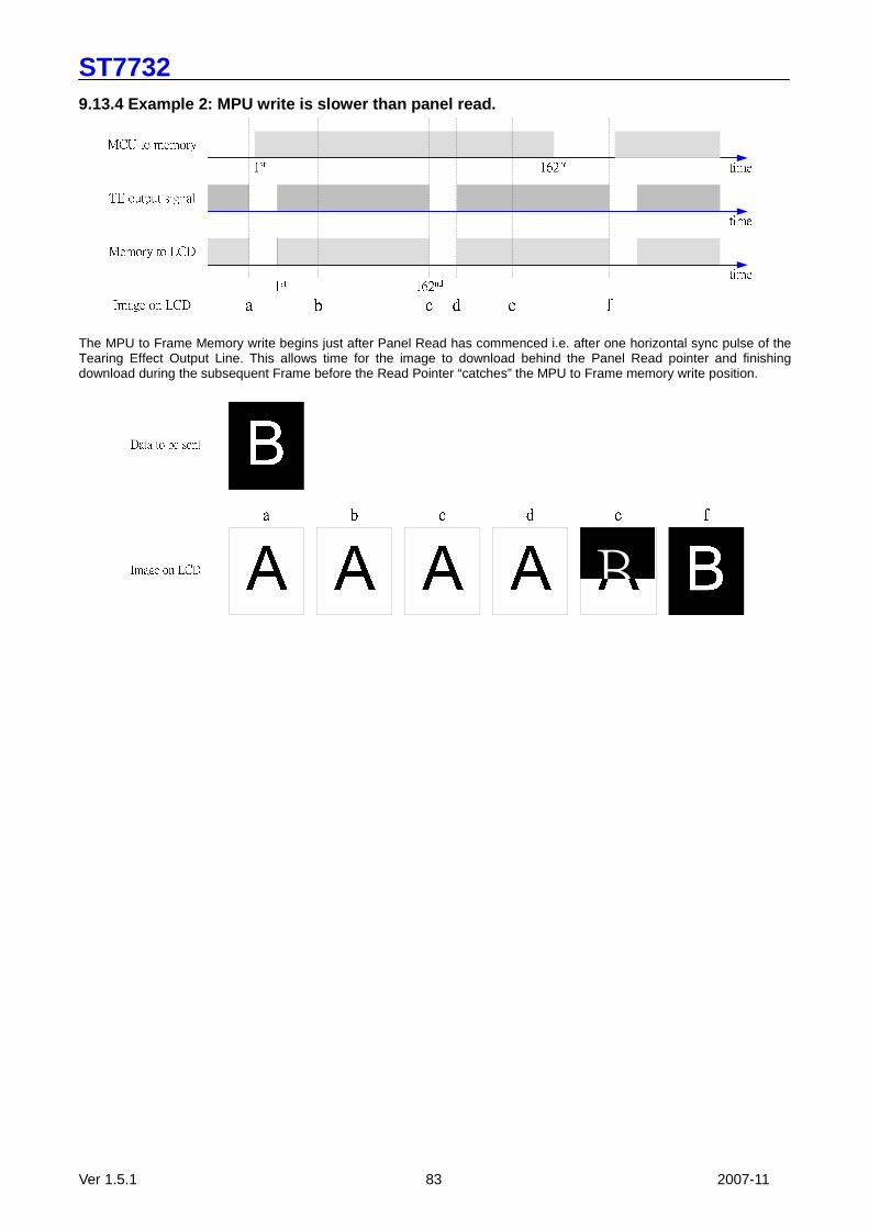
ST7732
Ver 1.5.1 83 2007-11
9.13.4 Example 2: MPU write is slower than panel re ad.
The MPU to Frame Memory write begins just after Panel Read has commenced i.e. after one horizontal sync pulse of the Tearing Effect Output Line. This allows time for the image to download behind the Panel Read pointer and finishing download during the subsequent Frame before the Read Pointer “catches” the MPU to Frame memory write position.
B
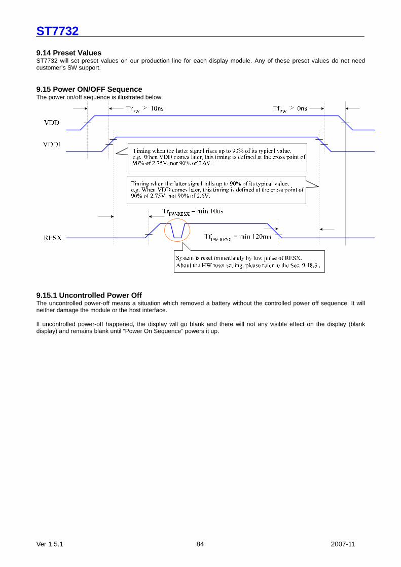
ST7732
Ver 1.5.1 84 2007-11
9.14 Preset Values ST7732 will set preset values on our production line for each display module. Any of these preset values do not need customer’s SW support. 9.15 Power ON/OFF Sequence The power on/off sequence is illustrated below:
9.15.1 Uncontrolled Power Off The uncontrolled power-off means a situation which removed a battery without the controlled power off sequence. It will neither damage the module or the host interface. If uncontrolled power-off happened, the display will go blank and there will not any visible effect on the display (blank display) and remains blank until “Power On Sequence” powers it up.
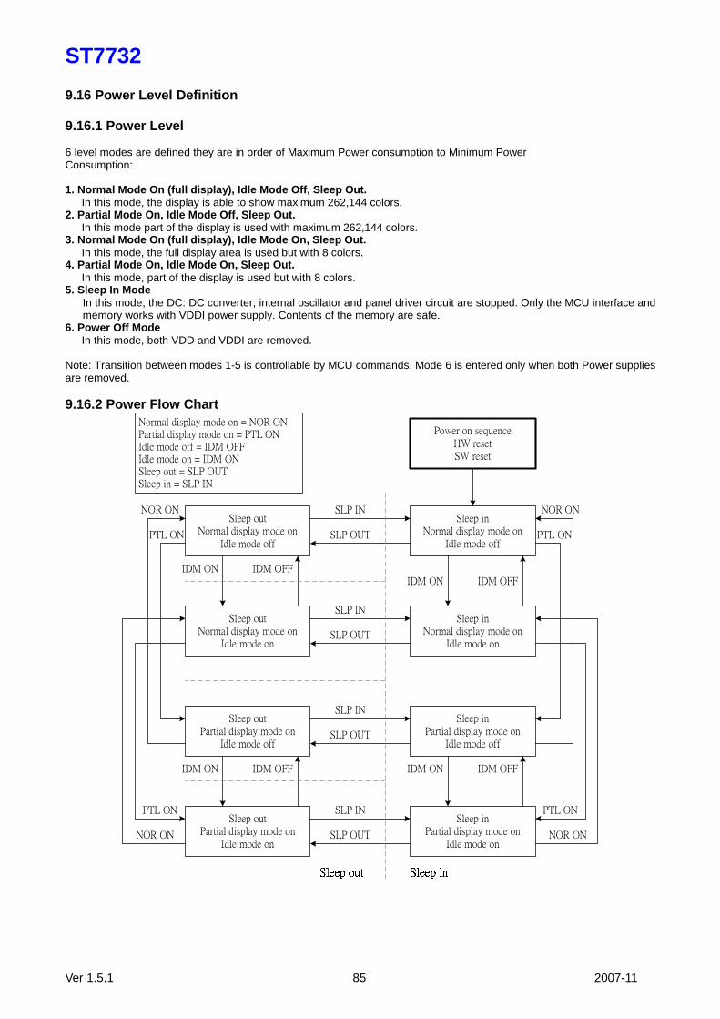
ST7732
Ver 1.5.1 85 2007-11
9.16 Power Level Definition 9.16.1 Power Level 6 level modes are defined they are in order of Maximum Power consumption to Minimum Power Consumption: 1. Normal Mode On (full display), Idle Mode Off, Sl eep Out.
In this mode, the display is able to show maximum 262,144 colors. 2. Partial Mode On, Idle Mode Off, Sleep Out.
In this mode part of the display is used with maximum 262,144 colors. 3. Normal Mode On (full display), Idle Mode On, Slee p Out.
In this mode, the full display area is used but with 8 colors. 4. Partial Mode On, Idle Mode On, Sleep Out.
In this mode, part of the display is used but with 8 colors. 5. Sleep In Mode
In this mode, the DC: DC converter, internal oscillator and panel driver circuit are stopped. Only the MCU interface and memory works with VDDI power supply. Contents of the memory are safe.
6. Power Off Mode In this mode, both VDD and VDDI are removed.
Note: Transition between modes 1-5 is controllable by MCU commands. Mode 6 is entered only when both Power supplies are removed. 9.16.2 Power Flow Chart
Sleep outNormal display mode on
Idle mode off
Sleep inNormal display mode on
Idle mode off
Sleep outNormal display mode on
Idle mode on
Sleep inNormal display mode on
Idle mode on
Sleep outPartial display mode on
Idle mode off
Sleep inPartial display mode on
Idle mode off
Sleep outPartial display mode on
Idle mode on
Sleep inPartial display mode on
Idle mode on
SLP IN
SLP IN
SLP IN
SLP IN
SLP OUT
SLP OUT
SLP OUT
SLP OUT
IDM ON IDM OFFIDM ON IDM OFF
PTL ON
NOR ON
PTL ON
NOR ON
IDM ON IDM OFF
PTL ON
NOR ON
PTL ON
NOR ON
IDM ON IDM OFF
Power on sequenceHW resetSW reset
Normal display mode on = NOR ONPartial display mode on = PTL ONIdle mode off = IDM OFFIdle mode on = IDM ONSleep out = SLP OUTSleep in = SLP IN
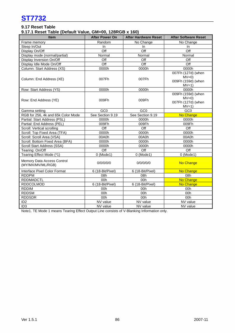
ST7732
Ver 1.5.1 86 2007-11
9.17 Reset Table 9.17.1 Reset Table (Default Value, GM=00, 128RGB x 160)
Item After Power On After Hardware Reset After Software Reset Frame memory Random No Change No Change Sleep In/Out In In In Display On/Off Off Off Off Display mode (normal/partial) Normal Normal Normal Display Inversion On/Off Off Off Off Display Idle Mode On/Off Off Off Off Column: Start Address (XS) 0000h 0000h 0000h
Column: End Address (XE) 007Fh 007Fh
007Fh (127d) (when MV=0)
009Fh (159d) (when MV=1)
Row: Start Address (YS) 0000h 0000h 0000h
Row: End Address (YE) 009Fh 009Fh
009Fh (159d) (when MV=0)
007Fh (127d) (when MV=1)
Gamma setting GC0 GC0 GC0 RGB for 256, 4k and 65k Color Mode See Section 9.19 See Section 9.19 No Change Partial: Start Address (PSL) 0000h 0000h 0000h Partial: End Address (PEL) 009Fh 009Fh 009Fh Scroll: Vertical scrolling Off Off Off Scroll: Top Fixed Area (TFA) 0000h 0000h 0000h Scroll: Scroll Area (VSA) 00A0h 00A0h 00A0h Scroll: Bottom Fixed Area (BFA) 0000h 0000h 0000h Scroll Start Address (SSA) 0000h 0000h 0000h Tearing: On/Off Off Off Off Tearing Effect Mode (*1) 0 (Mode1) 0 (Mode1) 0 (Mode1)
Memory Data Access Control (MY/MX/MV/ML/RGB) 0/0/0/0/0 0/0/0/0/0 No Change
Interface Pixel Color Format 6 (18-Bit/Pixel) 6 (18-Bit/Pixel) No Change RDDPM 08h 08h 08h RDDMADCTL 00h 00h No Change RDDCOLMOD 6 (18-Bit/Pixel) 6 (18-Bit/Pixel) No Change RDDIM 00h 00h 00h RDDSM 00h 00h 00h RDDSDR 00h 00h 00h ID2 NV value NV value NV value ID3 NV value NV value NV value Note1. TE Mode 1 means Tearing Effect Output Line consists of V-Blanking Information only.
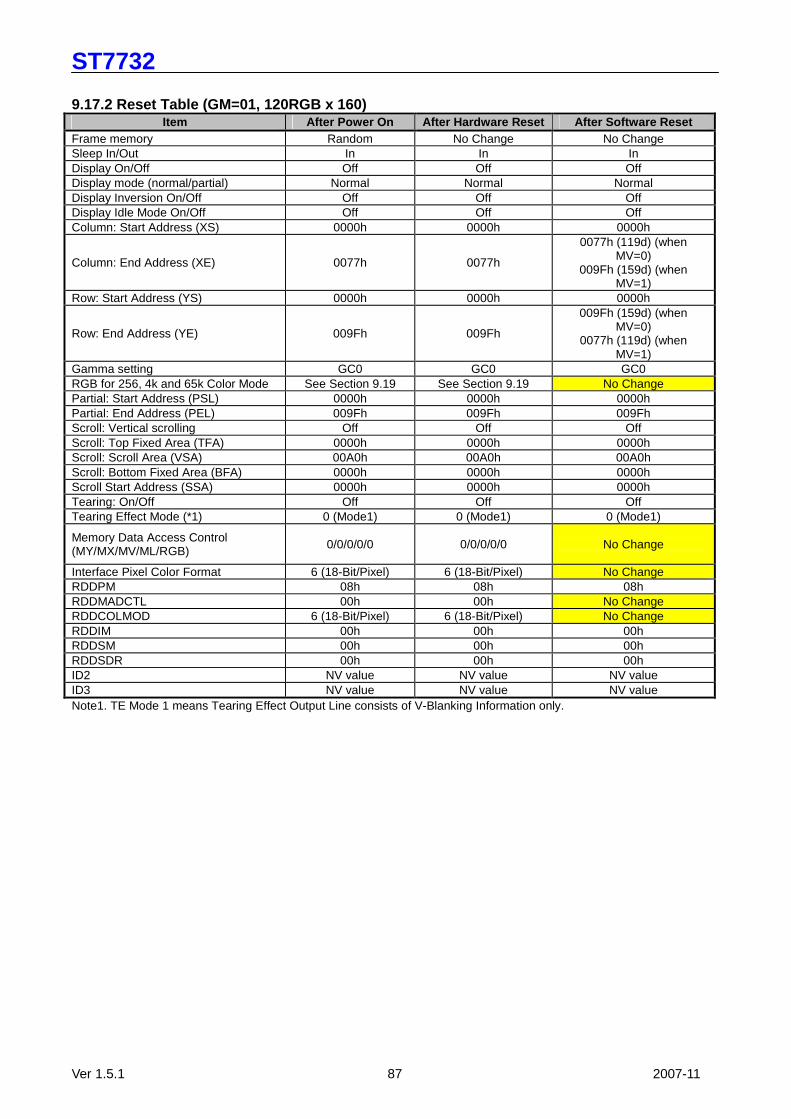
ST7732
Ver 1.5.1 87 2007-11
9.17.2 Reset Table (GM=01, 120RGB x 160)
Item After Power On After Hardware Reset After Software Reset Frame memory Random No Change No Change Sleep In/Out In In In Display On/Off Off Off Off Display mode (normal/partial) Normal Normal Normal Display Inversion On/Off Off Off Off Display Idle Mode On/Off Off Off Off Column: Start Address (XS) 0000h 0000h 0000h
Column: End Address (XE) 0077h 0077h
0077h (119d) (when MV=0)
009Fh (159d) (when MV=1)
Row: Start Address (YS) 0000h 0000h 0000h
Row: End Address (YE) 009Fh 009Fh
009Fh (159d) (when MV=0)
0077h (119d) (when MV=1)
Gamma setting GC0 GC0 GC0 RGB for 256, 4k and 65k Color Mode See Section 9.19 See Section 9.19 No Change Partial: Start Address (PSL) 0000h 0000h 0000h Partial: End Address (PEL) 009Fh 009Fh 009Fh Scroll: Vertical scrolling Off Off Off Scroll: Top Fixed Area (TFA) 0000h 0000h 0000h Scroll: Scroll Area (VSA) 00A0h 00A0h 00A0h Scroll: Bottom Fixed Area (BFA) 0000h 0000h 0000h Scroll Start Address (SSA) 0000h 0000h 0000h Tearing: On/Off Off Off Off Tearing Effect Mode (*1) 0 (Mode1) 0 (Mode1) 0 (Mode1)
Memory Data Access Control (MY/MX/MV/ML/RGB) 0/0/0/0/0 0/0/0/0/0 No Change
Interface Pixel Color Format 6 (18-Bit/Pixel) 6 (18-Bit/Pixel) No Change RDDPM 08h 08h 08h RDDMADCTL 00h 00h No Change RDDCOLMOD 6 (18-Bit/Pixel) 6 (18-Bit/Pixel) No Change RDDIM 00h 00h 00h RDDSM 00h 00h 00h RDDSDR 00h 00h 00h ID2 NV value NV value NV value ID3 NV value NV value NV value Note1. TE Mode 1 means Tearing Effect Output Line consists of V-Blanking Information only.
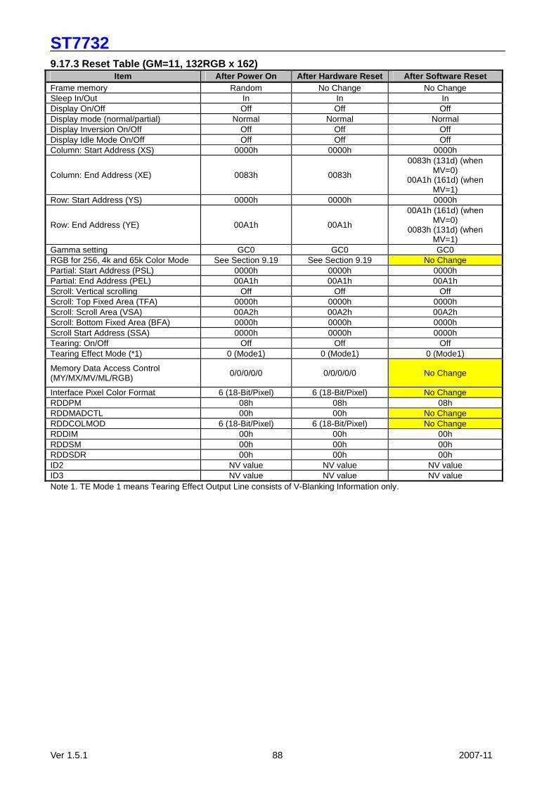
ST7732
Ver 1.5.1 88 2007-11
9.17.3 Reset Table (GM=11, 132RGB x 162) Item After Power On After Hardware Reset After Software Reset
Frame memory Random No Change No Change Sleep In/Out In In In Display On/Off Off Off Off Display mode (normal/partial) Normal Normal Normal Display Inversion On/Off Off Off Off Display Idle Mode On/Off Off Off Off Column: Start Address (XS) 0000h 0000h 0000h
Column: End Address (XE) 0083h 0083h
0083h (131d) (when MV=0)
00A1h (161d) (when MV=1)
Row: Start Address (YS) 0000h 0000h 0000h
Row: End Address (YE) 00A1h 00A1h
00A1h (161d) (when MV=0)
0083h (131d) (when MV=1)
Gamma setting GC0 GC0 GC0 RGB for 256, 4k and 65k Color Mode See Section 9.19 See Section 9.19 No Change Partial: Start Address (PSL) 0000h 0000h 0000h Partial: End Address (PEL) 00A1h 00A1h 00A1h Scroll: Vertical scrolling Off Off Off Scroll: Top Fixed Area (TFA) 0000h 0000h 0000h Scroll: Scroll Area (VSA) 00A2h 00A2h 00A2h Scroll: Bottom Fixed Area (BFA) 0000h 0000h 0000h Scroll Start Address (SSA) 0000h 0000h 0000h Tearing: On/Off Off Off Off Tearing Effect Mode (*1) 0 (Mode1) 0 (Mode1) 0 (Mode1)
Memory Data Access Control (MY/MX/MV/ML/RGB)
0/0/0/0/0 0/0/0/0/0 No Change
Interface Pixel Color Format 6 (18-Bit/Pixel) 6 (18-Bit/Pixel) No Change RDDPM 08h 08h 08h RDDMADCTL 00h 00h No Change RDDCOLMOD 6 (18-Bit/Pixel) 6 (18-Bit/Pixel) No Change RDDIM 00h 00h 00h RDDSM 00h 00h 00h RDDSDR 00h 00h 00h ID2 NV value NV value NV value ID3 NV value NV value NV value Note 1. TE Mode 1 means Tearing Effect Output Line consists of V-Blanking Information only.
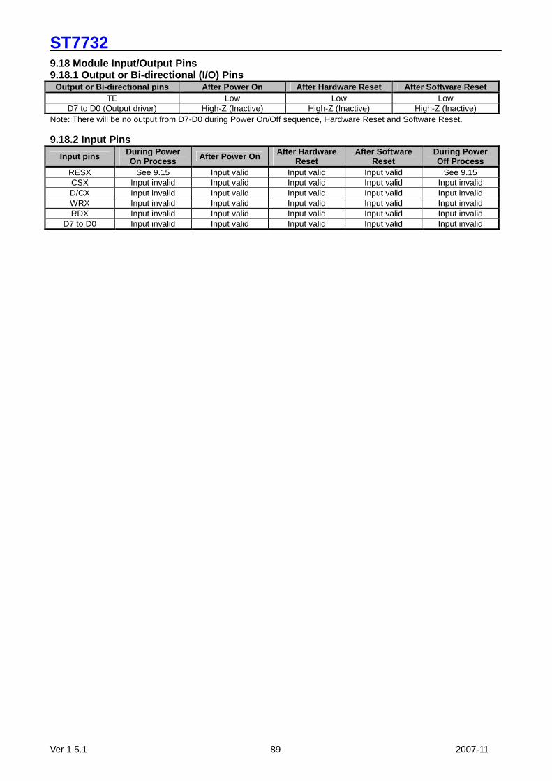
ST7732
Ver 1.5.1 89 2007-11
9.18 Module Input/Output Pins 9.18.1 Output or Bi-directional (I/O) Pins
Output or Bi-directional pins After Power On After Hardware Reset After Software Reset TE Low Low Low
D7 to D0 (Output driver) High-Z (Inactive) High-Z (Inactive) High-Z (Inactive) Note: There will be no output from D7-D0 during Power On/Off sequence, Hardware Reset and Software Reset. 9.18.2 Input Pins
Input pins During Power On Process After Power On After Hardware
Reset After Software
Reset During Power Off Process
RESX See 9.15 Input valid Input valid Input valid See 9.15 CSX Input invalid Input valid Input valid Input valid Input invalid D/CX Input invalid Input valid Input valid Input valid Input invalid WRX Input invalid Input valid Input valid Input valid Input invalid RDX Input invalid Input valid Input valid Input valid Input invalid
D7 to D0 Input invalid Input valid Input valid Input valid Input invalid

ST7732
Ver 1.5.1 90 2007-11
9.18.3 Reset Timing
Table 9.18.2.1 Reset input timing
VSS=0V, VDDI=1.65V to 1.95V, VDD=2.5V to 2.9V, Ta = -30 to 70 ) Symbol Parameter Related Pins MIN TYP MAX Note Unit
tRESW *1) Reset low pulse width RESX 10 - - - us
tREST *2) Reset complete time - 120 - - - ms
Note 1 Spike due to an electrostatic discharge on RESX line does not cause irregular system reset according to the table below. Note 2.It will be necessary to wait 120 msec before sending next command; this is allowing time for the supply voltages and
clock circuits to stabilize. Note 3 During Reset Complete Time, ID2 and VCOMOF value in OTP will be latched to internal register during this
period.This loading is done every time when there is H/W reset complete time (tREST) within 120ms after a rising edge of RESX.
Note 4 Spike Rejection also applies during a valid reset pulse as shown below:
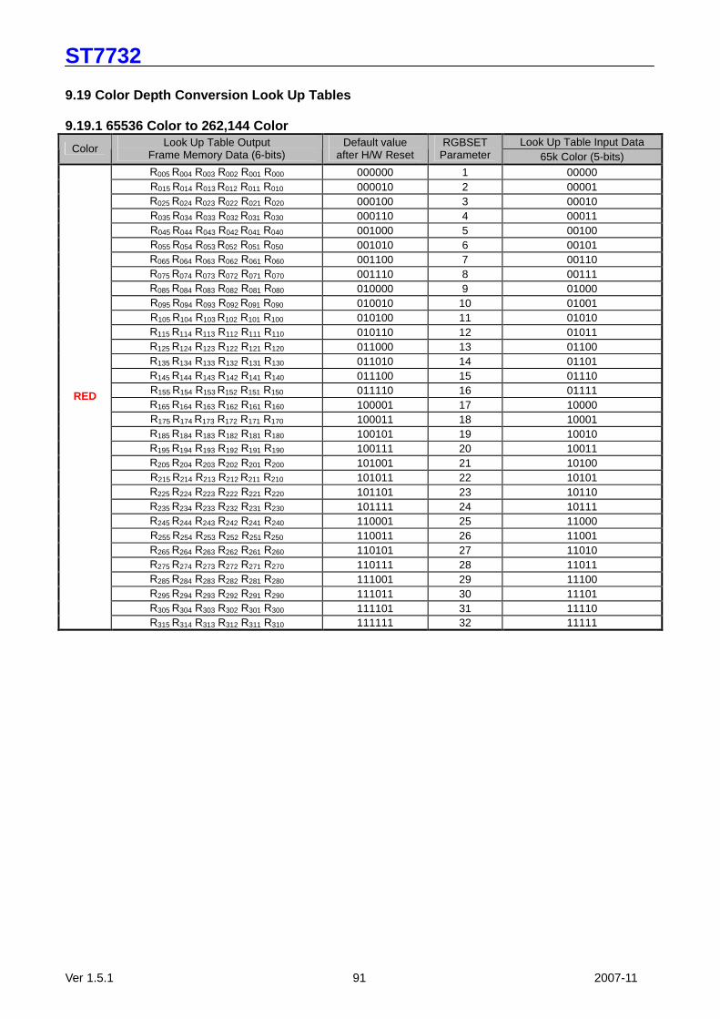
ST7732
Ver 1.5.1 91 2007-11
9.19 Color Depth Conversion Look Up Tables 9.19.1 65536 Color to 262,144 Color
Look Up Table Input Data Color Look Up Table Output
Frame Memory Data (6-bits) Default value
after H/W Reset RGBSET
Parameter 65k Color (5-bits) R005 R004 R003 R002 R001 R000 000000 1 00000 R015 R014 R013 R012 R011 R010 000010 2 00001 R025 R024 R023 R022 R021 R020 000100 3 00010 R035 R034 R033 R032 R031 R030 000110 4 00011 R045 R044 R043 R042 R041 R040 001000 5 00100 R055 R054 R053 R052 R051 R050 001010 6 00101 R065 R064 R063 R062 R061 R060 001100 7 00110 R075 R074 R073 R072 R071 R070 001110 8 00111 R085 R084 R083 R082 R081 R080 010000 9 01000 R095 R094 R093 R092 R091 R090 010010 10 01001 R105 R104 R103 R102 R101 R100 010100 11 01010 R115 R114 R113 R112 R111 R110 010110 12 01011 R125 R124 R123 R122 R121 R120 011000 13 01100 R135 R134 R133 R132 R131 R130 011010 14 01101 R145 R144 R143 R142 R141 R140 011100 15 01110 R155 R154 R153 R152 R151 R150 011110 16 01111 R165 R164 R163 R162 R161 R160 100001 17 10000 R175 R174 R173 R172 R171 R170 100011 18 10001 R185 R184 R183 R182 R181 R180 100101 19 10010 R195 R194 R193 R192 R191 R190 100111 20 10011 R205 R204 R203 R202 R201 R200 101001 21 10100 R215 R214 R213 R212 R211 R210 101011 22 10101 R225 R224 R223 R222 R221 R220 101101 23 10110 R235 R234 R233 R232 R231 R230 101111 24 10111 R245 R244 R243 R242 R241 R240 110001 25 11000 R255 R254 R253 R252 R251 R250 110011 26 11001 R265 R264 R263 R262 R261 R260 110101 27 11010 R275 R274 R273 R272 R271 R270 110111 28 11011 R285 R284 R283 R282 R281 R280 111001 29 11100 R295 R294 R293 R292 R291 R290 111011 30 11101 R305 R304 R303 R302 R301 R300 111101 31 11110
RED
R315 R314 R313 R312 R311 R310 111111 32 11111
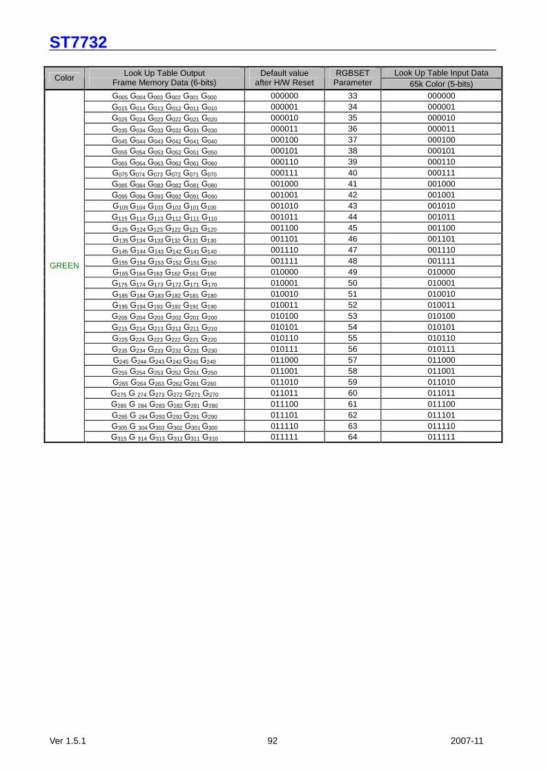
ST7732
Ver 1.5.1 92 2007-11
Look Up Table Input Data
Color Look Up Table Output Frame Memory Data (6-bits)
Default value after H/W Reset
RGBSET Parameter 65k Color (5-bits)
G005 G004 G003 G002 G001 G000 000000 33 000000 G015 G014 G013 G012 G011 G010 000001 34 000001 G025 G024 G023 G022 G021 G020 000010 35 000010 G035 G034 G033 G032 G031 G030 000011 36 000011 G045 G044 G043 G042 G041 G040 000100 37 000100 G055 G054 G053 G052 G051 G050 000101 38 000101 G065 G064 G063 G062 G061 G060 000110 39 000110 G075 G074 G073 G072 G071 G070 000111 40 000111 G085 G084 G083 G082 G081 G080 001000 41 001000 G095 G094 G093 G092 G091 G090 001001 42 001001 G105 G104 G103 G102 G101 G100 001010 43 001010 G115 G114 G113 G112 G111 G110 001011 44 001011 G125 G124 G123 G122 G121 G120 001100 45 001100 G135 G134 G133 G132 G131 G130 001101 46 001101 G145 G144 G143 G142 G141 G140 001110 47 001110 G155 G154 G153 G152 G151 G150 001111 48 001111 G165 G164 G163 G162 G161 G160 010000 49 010000 G175 G174 G173 G172 G171 G170 010001 50 010001 G185 G184 G183 G182 G181 G180 010010 51 010010 G195 G194 G193 G192 G191 G190 010011 52 010011 G205 G204 G203 G202 G201 G200 010100 53 010100 G215 G214 G213 G212 G211 G210 010101 54 010101 G225 G224 G223 G222 G221 G220 010110 55 010110 G235 G234 G233 G232 G231 G230 010111 56 010111 G245 G244 G243 G242 G241 G240 011000 57 011000 G255 G254 G253 G252 G251 G250 011001 58 011001 G265 G264 G263 G262 G261 G260 011010 59 011010 G275 G 274 G273 G272 G271 G270 011011 60 011011 G285 G 284 G283 G282 G281 G280 011100 61 011100 G295 G 294 G293 G292 G291 G290 011101 62 011101 G305 G 304 G303 G302 G301 G300 011110 63 011110
GREEN
G315 G 314 G313 G312 G311 G310 011111 64 011111

ST7732
Ver 1.5.1 93 2007-11
Look Up Table Input Data
Color Look Up Table Output Frame Memory Data (6-bits)
Default value after H/W Reset
RGBSET Parameter 65k Color (5-bits)
G325 G324 G323 G322 G321 G320 100000 65 100000 G335 G334 G333 G332 G331 G330 100001 66 100001 G345 G344 G343 G342 G341 G340 100010 67 100010 G355 G354 G353 G352 G351 G350 100011 68 100011 G365 G364 G363 G362 G361 G360 100100 69 100100 G375 G374 G373 G372 G371 G370 100101 70 100101 G385 G384 G383 G382 G381 G380 100110 71 100110 G395 G394 G393 G392 G391 G390 100111 72 100111 G405 G404 G403 G402 G401 G400 101000 73 101000 G415 G414 G413 G412 G411 G410 101001 74 101001 G425 G424 G423 G422 G421 G420 101010 75 101010 G435 G434 G433 G432 G431 G430 101011 76 101011 G445 G444 G443 G442 G441 G440 101100 77 101100 G455 G454 G453 G452 G451 G450 101101 78 101101 G465 G464 G463 G462 G461 G460 101110 79 101110 G475 G474 G473 G472 G471 G470 101111 80 101111 G485 G484 G483 G482 G481 G480 110000 81 110000 G495 G494 G493 G492 G491 G490 110001 82 110001 G505 G504 G503 G502 G501 G500 110010 83 110010 G515 G514 G513 G512 G511 G510 110011 84 110011 G525 G524 G523 G522 G521 G520 110100 85 110100 G535 G534 G533 G532 G531 G530 110101 86 110101 G545 G544 G543 G542 G541 G540 110110 87 110110 G555 G554 G553 G552 G551 G550 110111 88 110111 G565 G564 G563 G562 G561 G560 111000 89 111000 G575 G574 G573 G572 G571 G570 111001 90 111001 G585 G584 G583 G582 G581 G580 111010 91 111010 G595 G594 G593 G592 G591 G590 111011 92 111011 G605 G604 G603 G602 G601 G600 111100 93 111100 G615 G614 G613 G612 G611 G610 111101 94 111101 G625 G624 G623 G622 G621 G620 111110 95 111110
GREEN
G635 G634 G633 G632 G631 G630 111111 96 111111

ST7732
Ver 1.5.1 94 2007-11
Look Up Table Input Data
Color Look Up Table Output Frame Memory Data (6-bits)
Default value after H/W Reset
RGBSET Parameter 65k Color (5-bits)
B005 B004 B003 B002 B001 B000 000000 97 00000 B015 B014 B013 B012 B011 B010 000010 98 00001 B025 B024 B023 B022 B021 B020 000100 99 00010 B035 B034 B033 B032 B031 B030 000110 100 00011 B045 B044 B043 B042 B041 B040 001000 101 00100 B055 B054 B053 B052 B051 B050 001010 102 00101 B065 B064 B063 B062 B061 B060 001100 103 00110 B075 B074 B073 B072 B071 B070 001110 104 00111 B085 B084 B083 B082 B081 B080 010000 105 01000 B095 B094 B093 B092 B091 B090 010010 106 01001 B105 B104 B103 B102 B101 B100 010100 107 01010 B115 B114 B113 B112 B111 B110 010110 108 01011 B125 B124 B123 B122 B121 B120 011000 109 01100 B135 B134 B133 B132 B131 B130 011010 110 01101 B145 B144 B143 B142 B141 B140 011100 111 01110 B155 B154 B153 B152 B151 B150 011110 112 01111 B165 B164 B163 B162 B161 B160 100001 113 10000 B175 B174 B173 B172 B171 B170 100011 114 10001 B185 B184 B183 B182 B181 B180 100101 115 10010 B195 B194 B193 B192 B191 B190 100111 116 10011 B205 B204 B203 B202 B201 B200 101001 117 10100 B215 B214 B213 B212 B211 B210 101011 118 10101 B225 B224 B223 B222 B221 B220 101101 119 10110 B235 B234 B233 B232 B231 B230 101111 120 10111 B245 B244 B243 B242 B241 B240 110001 121 11000 B255 B254 B253 B252 B251 B250 110011 122 11001 B265 B264 B263 B262 B261 B260 110101 123 11010 B275 B274 B273 B272 B271 B270 110111 124 11011 B285 B284 B283 B282 B281 B280 111001 125 11100 B295 B294 B293 B292 B291 B290 111011 126 11101 B305 B304 B303 B302 B301 B300 111101 127 11110
BLUE
B315 B314 B313 B312 B311 B310 111111 128 11111
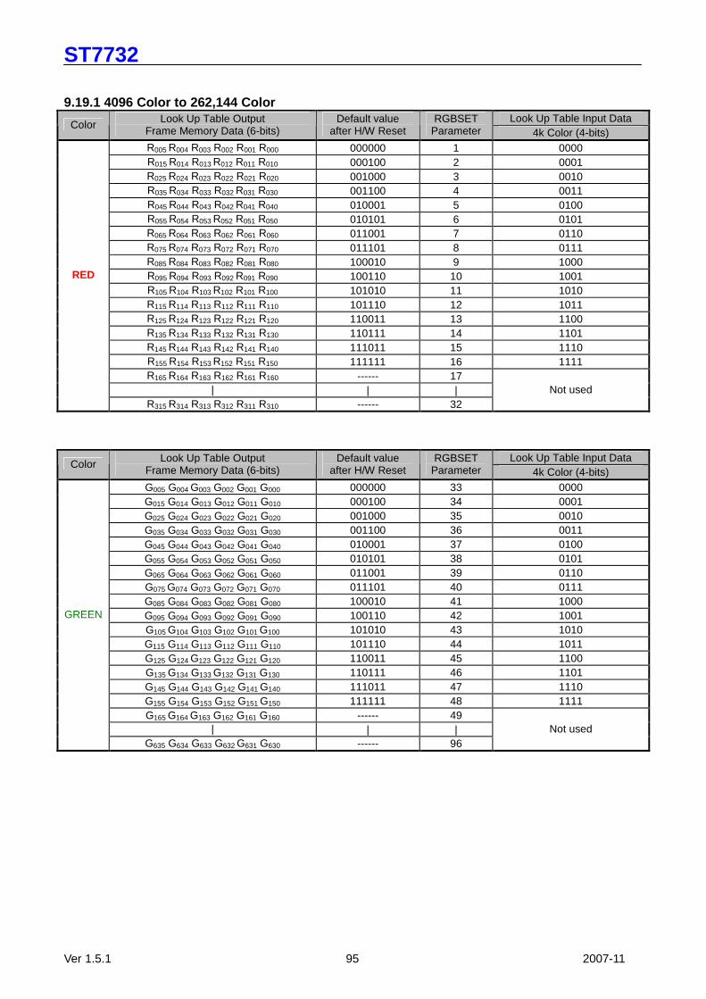
ST7732
Ver 1.5.1 95 2007-11
9.19.1 4096 Color to 262,144 Color Look Up Table Input Data
Color Look Up Table Output Frame Memory Data (6-bits)
Default value after H/W Reset
RGBSET Parameter 4k Color (4-bits)
R005 R004 R003 R002 R001 R000 000000 1 0000 R015 R014 R013 R012 R011 R010 000100 2 0001 R025 R024 R023 R022 R021 R020 001000 3 0010 R035 R034 R033 R032 R031 R030 001100 4 0011 R045 R044 R043 R042 R041 R040 010001 5 0100 R055 R054 R053 R052 R051 R050 010101 6 0101 R065 R064 R063 R062 R061 R060 011001 7 0110 R075 R074 R073 R072 R071 R070 011101 8 0111 R085 R084 R083 R082 R081 R080 100010 9 1000 R095 R094 R093 R092 R091 R090 100110 10 1001 R105 R104 R103 R102 R101 R100 101010 11 1010 R115 R114 R113 R112 R111 R110 101110 12 1011 R125 R124 R123 R122 R121 R120 110011 13 1100 R135 R134 R133 R132 R131 R130 110111 14 1101 R145 R144 R143 R142 R141 R140 111011 15 1110 R155 R154 R153 R152 R151 R150 111111 16 1111 R165 R164 R163 R162 R161 R160 ------ 17
| | |
RED
R315 R314 R313 R312 R311 R310 ------ 32 Not used
Look Up Table Input Data Color Look Up Table Output
Frame Memory Data (6-bits) Default value
after H/W Reset RGBSET
Parameter 4k Color (4-bits) G005 G004 G003 G002 G001 G000 000000 33 0000 G015 G014 G013 G012 G011 G010 000100 34 0001 G025 G024 G023 G022 G021 G020 001000 35 0010 G035 G034 G033 G032 G031 G030 001100 36 0011 G045 G044 G043 G042 G041 G040 010001 37 0100 G055 G054 G053 G052 G051 G050 010101 38 0101 G065 G064 G063 G062 G061 G060 011001 39 0110 G075 G074 G073 G072 G071 G070 011101 40 0111 G085 G084 G083 G082 G081 G080 100010 41 1000 G095 G094 G093 G092 G091 G090 100110 42 1001 G105 G104 G103 G102 G101 G100 101010 43 1010 G115 G114 G113 G112 G111 G110 101110 44 1011 G125 G124 G123 G122 G121 G120 110011 45 1100 G135 G134 G133 G132 G131 G130 110111 46 1101 G145 G144 G143 G142 G141 G140 111011 47 1110 G155 G154 G153 G152 G151 G150 111111 48 1111 G165 G164 G163 G162 G161 G160 ------ 49
| | |
GREEN
G635 G634 G633 G632 G631 G630 ------ 96 Not used
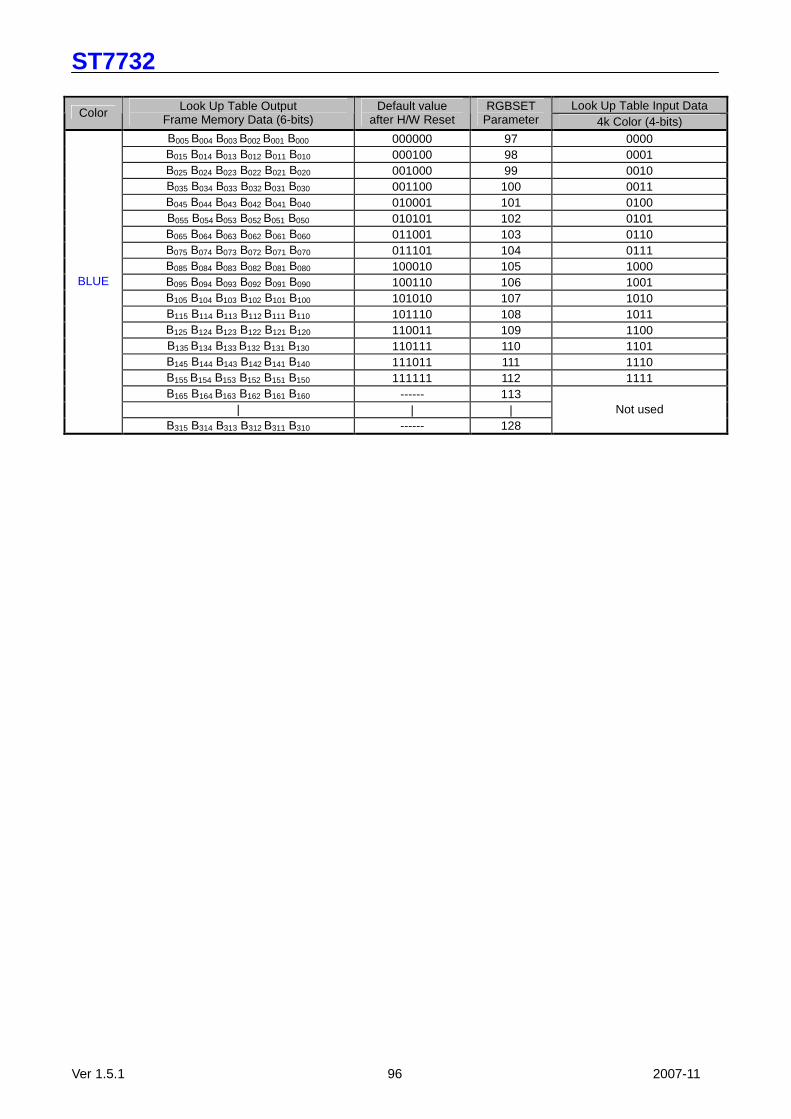
ST7732
Ver 1.5.1 96 2007-11
Look Up Table Input Data
Color Look Up Table Output Frame Memory Data (6-bits)
Default value after H/W Reset
RGBSET Parameter 4k Color (4-bits)
B005 B004 B003 B002 B001 B000 000000 97 0000 B015 B014 B013 B012 B011 B010 000100 98 0001 B025 B024 B023 B022 B021 B020 001000 99 0010 B035 B034 B033 B032 B031 B030 001100 100 0011 B045 B044 B043 B042 B041 B040 010001 101 0100 B055 B054 B053 B052 B051 B050 010101 102 0101 B065 B064 B063 B062 B061 B060 011001 103 0110 B075 B074 B073 B072 B071 B070 011101 104 0111 B085 B084 B083 B082 B081 B080 100010 105 1000 B095 B094 B093 B092 B091 B090 100110 106 1001 B105 B104 B103 B102 B101 B100 101010 107 1010 B115 B114 B113 B112 B111 B110 101110 108 1011 B125 B124 B123 B122 B121 B120 110011 109 1100 B135 B134 B133 B132 B131 B130 110111 110 1101 B145 B144 B143 B142 B141 B140 111011 111 1110 B155 B154 B153 B152 B151 B150 111111 112 1111 B165 B164 B163 B162 B161 B160 ------ 113
| | |
BLUE
B315 B314 B313 B312 B311 B310 ------ 128 Not used

ST7732
Ver 1.5.1 97 2007-11
9.20 Sleep Out-Command and Self-Diagnostic Function s of the Display Module 9.20.1 Register Loading Detection Sleep Out-command (See section 10.1.12 “Sleep Out (11h)”) is a trigger for an internal function of the display module, which indicates, if the display module loading function of factory default values from EEPROM (or similar device) to registers of the display controller is working properly. There are compared factory values of the EEPROM and register values of the display controller by the display controller. If those both values (EEPROM and register values) are same, there is inverted (=increased by 1) a bit, which is defined in command 10.1.10 “Read Display Self-Diagnostic Result (0Fh)” (=RDDSDR) (The used bit of this command is D7). If those both values are not same, this bit (D7) is not inverted (= increased by 1). The flow chart for this internal function is following:
Note: There is not compared and loaded register values, which can be changed by user (00h to AFh and DAh to DDh), by
the display module.
Sleep In (10h)
Sleep Out Mode Sleep In Mode
Sleep Out (11h)
Compares EEPROM and register values
Are EEPROM and register values same ?
D7 inverted
No
Yes
RDDSDR’s D7=0
Power on sequence HW reset SW reset
Loads values from EEPROM to registers

ST7732
Ver 1.5.1 98 2007-11
9.20.2 Functionality Detection Sleep Out-command (See section 10.1.12 “Sleep Out (11h)”) is a trigger for an internal function of the display module, which indicates, if the display module is still running and meets functionality requirements. The internal function (= the display controller) is comparing, if the display module is still meeting functionality requirements (only Booster voltage level). If functionality requirement is met, there is inverted (= increased by 1) a bit, which defined in command 10.1.10 “Read Display Self- Diagnostic Result (0Fh)” (= RDDSDR) (The used bit of this command is D6). If functionality requirement is not same, this bit (D6) is not inverted (= increased by 1). The flow chart for this internal function is following:
Note: There is needed 120msec after Sleep Out -command, when there is changing from Sleep In –mode to Sleep Out
-mode, before there is possible to check if functionality requirements are met and a value of RDDSDR’s D6 is valid. Otherwise, there is 120msec delay for D6’s value, when Sleep Out –command is sent in Sleep Out -mode.
Sleep In (10h)
Sleep Out Mode Sleep In Mode
Sleep Out (11h)
Checks Booster voltage levels and other functionalities
Is functionality requirement met?
D6 inverted
No
Yes
RDDSDR’s D6=0
Power on sequence HW reset SW reset
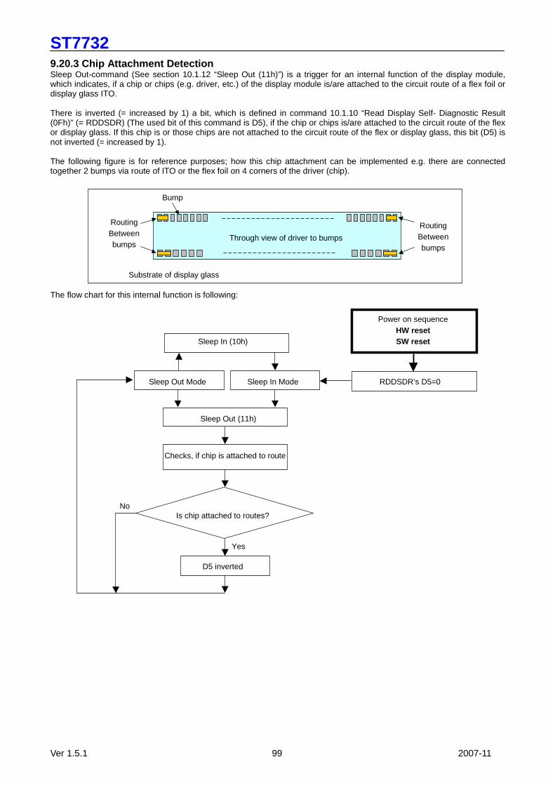
ST7732
Ver 1.5.1 99 2007-11
9.20.3 Chip Attachment Detection Sleep Out-command (See section 10.1.12 “Sleep Out (11h)”) is a trigger for an internal function of the display module, which indicates, if a chip or chips (e.g. driver, etc.) of the display module is/are attached to the circuit route of a flex foil or display glass ITO. There is inverted (= increased by 1) a bit, which is defined in command 10.1.10 “Read Display Self- Diagnostic Result (0Fh)” (= RDDSDR) (The used bit of this command is D5), if the chip or chips is/are attached to the circuit route of the flex or display glass. If this chip is or those chips are not attached to the circuit route of the flex or display glass, this bit (D5) is not inverted (= increased by 1). The following figure is for reference purposes; how this chip attachment can be implemented e.g. there are connected together 2 bumps via route of ITO or the flex foil on 4 corners of the driver (chip).
The flow chart for this internal function is following:
Sleep In (10h)
Sleep Out Mode Sleep In Mode
Sleep Out (11h)
Checks, if chip is attached to route
Is chip attached to routes?
D5 inverted
No
Yes
RDDSDR’s D5=0
Power on sequence HW reset SW reset
Bump
Routing Between bumps
Routing Between bumps
Substrate of display glass
Through view of driver to bumps
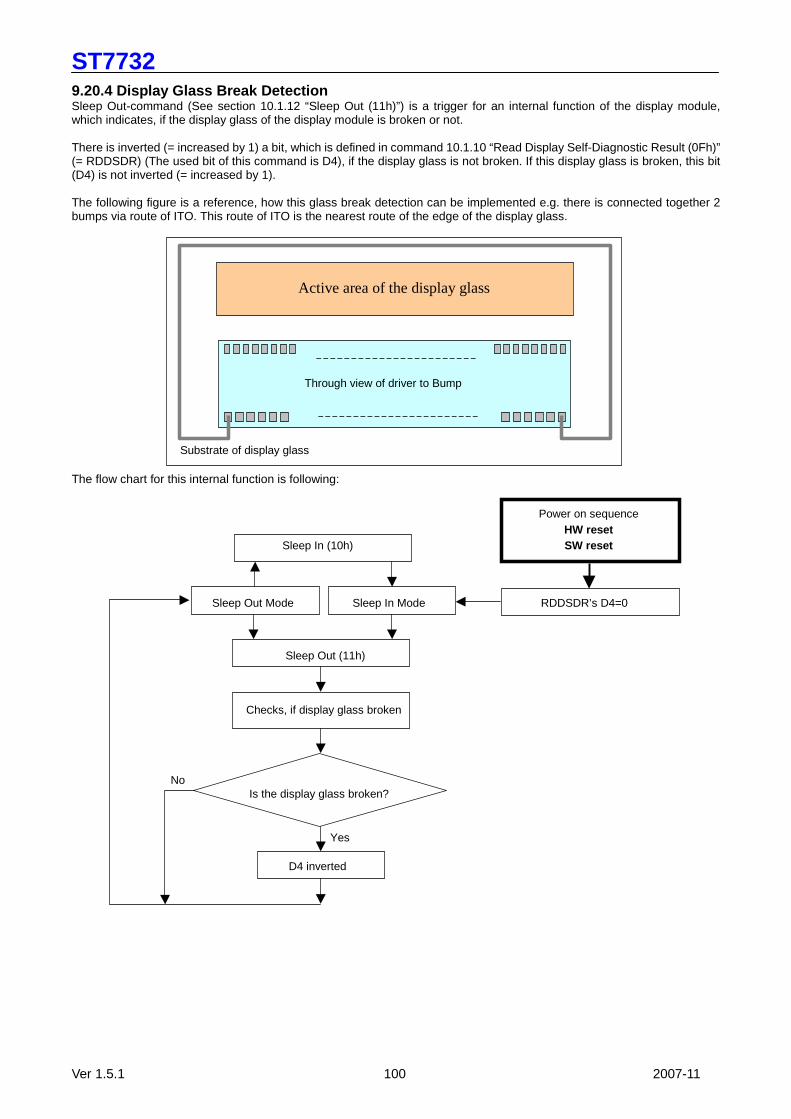
ST7732
Ver 1.5.1 100 2007-11
9.20.4 Display Glass Break Detection Sleep Out-command (See section 10.1.12 “Sleep Out (11h)”) is a trigger for an internal function of the display module, which indicates, if the display glass of the display module is broken or not. There is inverted (= increased by 1) a bit, which is defined in command 10.1.10 “Read Display Self-Diagnostic Result (0Fh)” (= RDDSDR) (The used bit of this command is D4), if the display glass is not broken. If this display glass is broken, this bit (D4) is not inverted (= increased by 1). The following figure is a reference, how this glass break detection can be implemented e.g. there is connected together 2 bumps via route of ITO. This route of ITO is the nearest route of the edge of the display glass.
The flow chart for this internal function is following:
Sleep In (10h)
Sleep Out Mode Sleep In Mode
Sleep Out (11h)
Checks, if display glass broken
Is the display glass broken?
D4 inverted
No
Yes
RDDSDR’s D4=0
Power on sequence HW reset SW reset
Active area of the display glass
Through view of driver to Bump
Substrate of display glass

ST7732
Ver 1.5.1 101 2007-11
9.21 External Light Source The operation of the module can meet customer’s Environmental reliability requirements. 9.22 Oscillator The chip has on-chip oscillator that does not require external components. This oscillator output signal is used for system clock generation for internal display operation. 9.23 System Clock Generator The timing generator produces the various signals to driver the internal circuitty. Internal chip operation is not affected by operations on the data bus. 9.24 Instruction Decoder and Register The instruction decoder indentifies command words arriving at the interface and routes the following data bytes to their destination. The command set can be found in “Command” section. 9.25 Source Driver The source driver block includes 132x3 source outputs (S1 to S396), which should be connected directly to the TFT-LCD. The source output signals are generated in the data processing block after the data is read out of the RAM and latched, which represent the simulatance selected rows. 9.26 Gate Driver The gate driver block includes 162 channel gate output (G1 to G162) which should be connected directly to the TFT-LCD. 9.27 VSYNC Interface The ST7732 incorporates a VSYNC I/F, which enables to display a moving picture which only system interface and frame-synchronizing signal. The interface enables to display moving pictures with minimum modification to a conventional systern.
The VSYNC-I/F is turned ON by VSYNC-I/F ON(ADH) command and turned OFF by VSYNC-I/F(ACH) command. In VSYNC-I/F mode, internal display operations are synchronized with VS. The VSYNC-I/F enables to display a moving picture through a system interface in higher speed than the internal display operations by some degree. The VSYNC-I/F executes display operations only with internal clocks generated by internal oscillators and VS input. All display data are stored in RAM so that only the data relevant to updating a screen are transferred to minimize data transmission while displaying a moving picture.

ST7732
Ver 1.5.1 102 2007-11
-Leading Mode
-Lagging Mode
1. In RCM[1:0]=”01” mode, writing data to RAM on rising edge of VS signal. 2. If high pulse of VS signal should large than 1-lines. 3. The BP and FP should follow conditions: BP≧2-lines, FP≧2-lines and BP+FP =16-lines 4. The signals (CSX, WRX, D/CX and VS) of VSYNC I/F should follow MCU Parallel Interface AC timing. The VSYNC-I/F has limits on the minimum RAM write speed through the system interface and the frequency of the internal clocks. It requires a RAM write speed more than the calculated result from the following formula. -Internal clock frequency (fosc)[Hz] = Frame Frequency x (DisplayLines+FrontPorch(VSFP)+Bac kPorch(VSBP)) x 16(clocks) x fluctuation
Example of RAMs writes speed and the frequency of the internal clocks in VSYNC-I/F mode is as follows.
Example: Display size= 132 RGB x 162 lines, Raster rows= 162 lines, Back/Front porch: 14/2 lines(VSBP = 1110, VSFP
= 0010 of AFH), Frame frequency = 60 Hz
Internal clock frequency (fosc)[Hz] = 60Hz x (162 +2+14) x 16 clocks x 1.1/0.9 = 209 kHz
When calculating an internal clock frequency, possible causes of fluctuations must also be taken into consideration. In this example, the allowance for the fluctuation is x10% from the center value and the
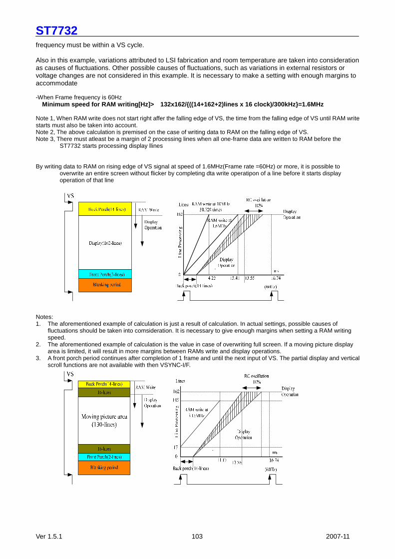
ST7732
Ver 1.5.1 103 2007-11
frequency must be within a VS cycle. Also in this example, variations attributed to LSI fabrication and room temperature are taken into consideration as causes of fluctuations. Other possible causes of fluctuations, such as variations in external resistors or voltage changes are not considered in this example. It is necessary to make a setting with enough margins to accommodate -When Frame frequency is 60Hz Minimum speed for RAM writing[Hz]> 132x162/((14+ 162+2)lines x 16 clock)/300kHz=1.6MHz Note 1, When RAM write does not start right affer the falling edge of VS, the time from the falling edge of VS until RAM write starts must also be taken into account. Note 2, The above calculation is premised on the case of writing data to RAM on the falling edge of VS. Note 3, There must atleast be a margin of 2 processing lines when all one-frame data are written to RAM before the
ST7732 starts processing display llines By writing data to RAM on rising edge of VS signal at speed of 1.6MHz(Frame rate =60Hz) or more, it is possible to
overwrite an entire screen without flicker by completing dta write operatipon of a line before it starts display operation of that line
Notes: 1. The aforementioned example of calculation is just a result of calculation. In actual settings, possible causes of
fluctuations should be taken into comsideration. It is necessary to give enough margins when setting a RAM writing speed.
2. The aforementioned example of calculation is the value in case of overwriting full screen. If a moving picture display area is limited, it will result in more margins between RAMs write and display operations.
3. A front porch period continues after completion of 1 frame and until the next input of VS. The partial display and vertical scroll functions are not available with then VSYNC-I/F.
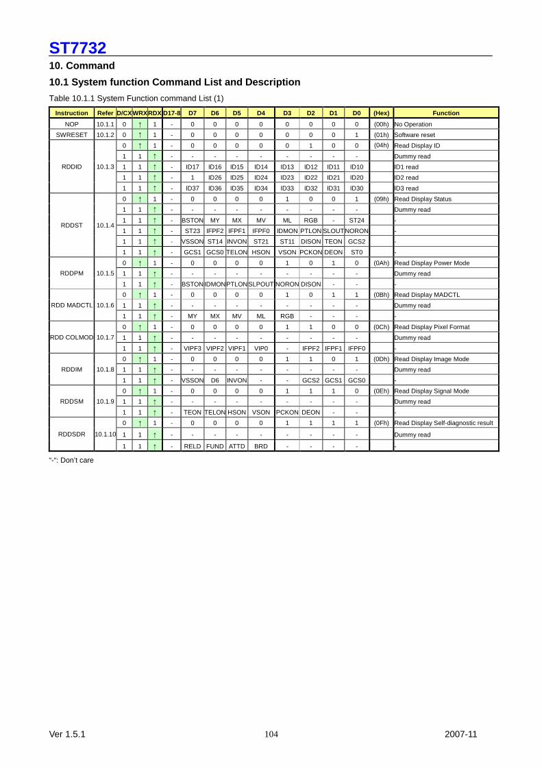
ST7732
Ver 1.5.1 2007-11 104
10. Command
10.1 System function Command List and Description
Table 10.1.1 System Function command List (1)
Instruction Refer D/CX WRX RDX D17-8 D7 D6 D5 D4 D3 D2 D1 D0 (Hex) Function
NOP 10.1.1 0 ↑ 1 - 0 0 0 0 0 0 0 0 (00h) No Operation
SWRESET 10.1.2 0 ↑ 1 - 0 0 0 0 0 0 0 1 (01h) Software reset
0 ↑ 1 - 0 0 0 0 0 1 0 0 (04h) Read Display ID
1 1 ↑ - - - - - - - - - Dummy read
1 1 ↑ - ID17 ID16 ID15 ID14 ID13 ID12 ID11 ID10 ID1 read
1 1 ↑ - 1 ID26 ID25 ID24 ID23 ID22 ID21 ID20 ID2 read
RDDID 10.1.3
1 1 ↑ - ID37 ID36 ID35 ID34 ID33 ID32 ID31 ID30 ID3 read
0 ↑ 1 - 0 0 0 0 1 0 0 1 (09h) Read Display Status
1 1 ↑ - - - - - - - - - Dummy read
1 1 ↑ - BSTON MY MX MV ML RGB - ST24 -
1 1 ↑ - ST23 IFPF2 IFPF1 IFPF0 IDMON PTLON SLOUT NORON -
1 1 ↑ - VSSON ST14 INVON ST21 ST11 DISON TEON GCS2 -
RDDST 10.1.4
1 1 ↑ - GCS1 GCS0 TELON HSON VSON PCKON DEON ST0 -
0 ↑ 1 - 0 0 0 0 1 0 1 0 (0Ah) Read Display Power Mode
1 1 ↑ - - - - - - - - - Dummy read RDDPM 10.1.5
1 1 ↑ - BSTON IDMON PTLON SLPOUT NORON DISON - - -
0 ↑ 1 - 0 0 0 0 1 0 1 1 (0Bh) Read Display MADCTL
1 1 ↑ - - - - - - - - - Dummy read RDD MADCTL 10.1.6
1 1 ↑ - MY MX MV ML RGB - - - -
0 ↑ 1 - 0 0 0 0 1 1 0 0 (0Ch) Read Display Pixel Format
1 1 ↑ - - - - - - - - - Dummy read RDD COLMOD 10.1.7
1 1 ↑ - VIPF3 VIPF2 VIPF1 VIP0 - IFPF2 IFPF1 IFPF0 -
0 ↑ 1 - 0 0 0 0 1 1 0 1 (0Dh) Read Display Image Mode
1 1 ↑ - - - - - - - - - Dummy read RDDIM 10.1.8
1 1 ↑ - VSSON D6 INVON - - GCS2 GCS1 GCS0 -
0 ↑ 1 - 0 0 0 0 1 1 1 0 (0Eh) Read Display Signal Mode
1 1 ↑ - - - - - - - - - Dummy read RDDSM 10.1.9
1 1 ↑ - TEON TELON HSON VSON PCKON DEON - - -
0 ↑ 1 - 0 0 0 0 1 1 1 1 (0Fh) Read Display Self-diagnostic result
1 1 ↑ - - - - - - - - - Dummy read RDDSDR 10.1.10
1 1 ↑ - RELD FUND ATTD BRD - - - - -
“-“: Don’t care
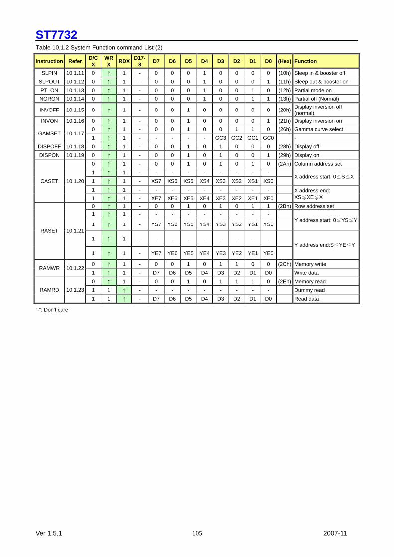
ST7732
Ver 1.5.1 2007-11 105
Table 10.1.2 System Function command List (2)
Instruction Refer D/CX
WRX
RDX D17-
8 D7 D6 D5 D4 D3 D2 D1 D0 (Hex) Function
SLPIN 10.1.11 0 ↑ 1 - 0 0 0 1 0 0 0 0 (10h) Sleep in & booster off
SLPOUT 10.1.12 0 ↑ 1 - 0 0 0 1 0 0 0 1 (11h) Sleep out & booster on
PTLON 10.1.13 0 ↑ 1 - 0 0 0 1 0 0 1 0 (12h) Partial mode on
NORON 10.1.14 0 ↑ 1 - 0 0 0 1 0 0 1 1 (13h) Partial off (Normal)
INVOFF 10.1.15 0 ↑ 1 - 0 0 1 0 0 0 0 0 (20h) Display inversion off (normal)
INVON 10.1.16 0 ↑ 1 - 0 0 1 0 0 0 0 1 (21h) Display inversion on
0 ↑ 1 - 0 0 1 0 0 1 1 0 (26h) Gamma curve select GAMSET 10.1.17
1 ↑ 1 - - - - - GC3 GC2 GC1 GC0 -
DISPOFF 10.1.18 0 ↑ 1 - 0 0 1 0 1 0 0 0 (28h) Display off
DISPON 10.1.19 0 ↑ 1 - 0 0 1 0 1 0 0 1 (29h) Display on
0 ↑ 1 - 0 0 1 0 1 0 1 0 (2Ah) Column address set
1 ↑ 1 - - - - - - - - -
1 ↑ 1 - XS7 XS6 XS5 XS4 XS3 XS2 XS1 XS0 X address start: 0 S X≦ ≦
1 ↑ 1 - - - - - - - - -
CASET 10.1.20
1 ↑ 1 - XE7 XE6 XE5 XE4 XE3 XE2 XE1 XE0
X address end: XS XE X≦ ≦
0 ↑ 1 - 0 0 1 0 1 0 1 1 (2Bh) Row address set
1 ↑ 1 - - - - - - - - -
1 ↑ 1 - YS7 YS6 YS5 YS4 YS3 YS2 YS1 YS0 Y address start: 0≦YS Y≦
1 ↑ 1 - - - - - - - - -
RASET 10.1.21
1 ↑ 1 - YE7 YE6 YE5 YE4 YE3 YE2 YE1 YE0
Y address end:S YE Y≦ ≦
0 ↑ 1 - 0 0 1 0 1 1 0 0 (2Ch) Memory write RAMWR 10.1.22
1 ↑ 1 - D7 D6 D5 D4 D3 D2 D1 D0 Write data
0 ↑ 1 - 0 0 1 0 1 1 1 0 (2Eh) Memory read
1 1 ↑ - - - - - - - - - Dummy read RAMRD 10.1.23
1 1 ↑ - D7 D6 D5 D4 D3 D2 D1 D0 Read data
“-“: Don’t care

ST7732
Ver 1.5.1 2007-11 106
Table 10.1.3 System Function command List (3)
Instruction Refer D/CXWRXRDX D17-8 D7 D6 D5 D4 D3 D2 D1 D0 (Hex) Function
0 ↑ 1 - 0 0 1 1 0 0 0 0 (30h) Partial start/end address set
1 ↑ 1 - - - - - - - - -
1 ↑ 1 - PSL7 PSL6 PSL5 PSL4 PSL3 PSL2 PSL1 PSL0 Partial start address (0,1,2, ..P)
1 ↑ 1 - - - - - - - - -
PTLAR 10.1.25
1 ↑ 1 - PEL7 PEL6 PEL5 PEL4 PEL3 PEL2 PEL1 PEL0 Partial end address (0,1,2, .., P)
0 ↑ 1 - 0 0 1 1 0 0 1 1 (33h) Scroll area set
1 ↑ 1 - - - - - - - - -
1 ↑ 1 - TFA7 TFA6 TFA5 TFA4 TFA3 TFA2 TFA1 TFA0 Top fixed area (0,1,2, .., S)
1 ↑ 1 - - - - - - - - -
1 ↑ 1 - VSA7 VSA6 VSA5 VSA4 VSA3VSA2 VSA1 VSA0 Vertical scroll area (0,1,2, .., S)
1 ↑ 1 - - - - - - - - -
SCRLAR 10.1.26
1 ↑ 1 - BFA7 BFA6 BFA5 BFA4 BFA3 BFA2 BFA1 BFA0 Bottom fixed area (0,1,2, .., S)
TEOFF 10.1.27 0 ↑ 1 - 0 0 1 1 0 1 0 0 (34h) Tearing effect line off
0 ↑ 1 - 0 0 1 1 0 1 0 1 (35h) Tearing effect mode set & on TEON 10.1.28
1 ↑ 1 - - - - - - - - TELOM Mode1: TELOM=”0” Mode2: TELOM=”1”
0 ↑ 1 - 0 0 1 1 0 1 1 0 (36h) Memory data access control MADCTL 10.1.29
1 ↑ 1 - MY MX MV ML RGB - - - -
0 ↑ 1 - 0 0 1 1 0 1 1 1 (37h) Scroll start address of RAM
1 ↑ 1 - - - - - - - - - SSA = 0, 1, 2, …, 131 VSCSAD 10.1.30
1 ↑ 1 - SSA7 SSA6 SSA5 SSA4 SSA3SSA2 SSA1 SSA0
IDMOFF 10.1.31 0 ↑ 1 - 0 0 1 1 1 0 0 0 (38h) Idle mode off
IDMON 10.1.32 0 ↑ 1 - 0 0 1 1 1 0 0 1 (39h) Idle mode on
0 ↑ 1 - 0 0 1 1 1 0 1 0 (3Ah) Interface pixel format COLMOD 10.1.33
1 ↑ 1 - VIPF3 VIPF2VIPF1 VIPF0 - IFPF2IFPF1 IFPF0 Interface format
0 ↑ 1 - 1 1 0 1 1 0 1 0 (DAh) Read ID1
1 1 ↑ - - - - - - - - - Dummy read RDID1 10.1.34
1 1 ↑ - ID17 ID16 ID15 ID14 ID13 ID12 ID11 ID10 Read parameter
0 ↑ 1 - 1 1 0 1 1 0 1 1 (DBh) Read ID2
1 1 ↑ - - - - - - - - - Dummy read RDID2 10.1.35
1 1 ↑ - 1 ID26 ID25 ID24 ID23 ID22 ID21 ID20 Read parameter
0 ↑ 1 - 1 1 0 1 1 1 0 0 (DCh) Read ID3
1 1 ↑ - - - - - - - - - Dummy read RDID3 10.1.36
1 1 ↑ - ID37 ID36 ID35 ID34 ID33 ID32 ID31 ID30 Read parameter
“-“: Don’t care
Note 1: After the H/W reset by RESX pin or S/W reset by SWRESET command, each internal register becomes default state (Refer
“RESET TABLE” section)
Note 2: Undefined commands are treated as NOP (00 h) command.
Note 3: B0 to D9 and DA to F are for factory use of driver supplier.
Note 4: Commands 10h, 12h, 13h, 20h, 21h, 26h, 28h, 29h, 30h, 33h, 36h (ML parameter only), 37h, 38h and 39h are updated during
V-sync when Module is in Sleep Out Mode to avoid abnormal visual effects. During Sleep In mode, these commands are updated
immediately. Read status (09h), Read Display Power Mode (0Ah), Read Display MADCTL (0Bh), Read Display Pixel Format (0Ch),
Read Display Image Mode (0Dh), Read Display Signal Mode (0Eh) and Read Display Self Diagnostic Result (0Fh) of these
commands are updated immediately both in Sleep In mode and Sleep Out mode.
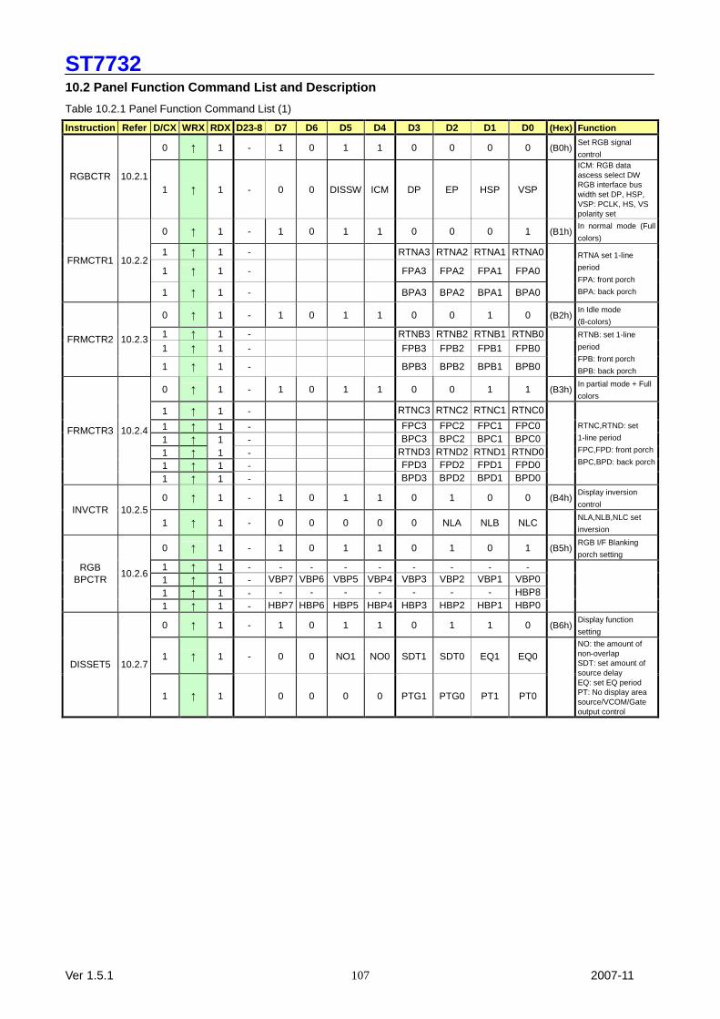
ST7732
Ver 1.5.1 2007-11 107
10.2 Panel Function Command List and Description
Table 10.2.1 Panel Function Command List (1)
Instruction Refer D/CX WRX RDX D23-8 D7 D6 D5 D4 D3 D2 D1 D0 (Hex) Function
0 ↑ 1 - 1 0 1 1 0 0 0 0 (B0h) Set RGB signal
control
RGBCTR 10.2.1 1 ↑ 1 - 0 0 DISSW ICM DP EP HSP VSP
ICM: RGB data ascess select DW RGB interface bus width set DP, HSP, VSP: PCLK, HS, VS polarity set
0 ↑ 1 - 1 0 1 1 0 0 0 1 (B1h) In normal mode (Full
colors)
1 ↑ 1 - RTNA3 RTNA2 RTNA1 RTNA0
1 ↑ 1 - FPA3 FPA2 FPA1 FPA0 FRMCTR1 10.2.2
1 ↑ 1 - BPA3 BPA2 BPA1 BPA0
RTNA set 1-line
period
FPA: front porch
BPA: back porch
0 ↑ 1 - 1 0 1 1 0 0 1 0 (B2h) In Idle mode
(8-colors)
1 ↑ 1 - RTNB3 RTNB2 RTNB1 RTNB0
1 ↑ 1 - FPB3 FPB2 FPB1 FPB0 FRMCTR2 10.2.3
1 ↑ 1 - BPB3 BPB2 BPB1 BPB0
RTNB: set 1-line
period
FPB: front porch
BPB: back porch 0 ↑ 1 - 1 0 1 1 0 0 1 1 (B3h)
In partial mode + Full
colors
1 ↑ 1 - RTNC3 RTNC2 RTNC1 RTNC0
1 ↑ 1 - FPC3 FPC2 FPC1 FPC0 1 ↑ 1 - BPC3 BPC2 BPC1 BPC0 1 ↑ 1 - RTND3 RTND2 RTND1 RTND0 1 ↑ 1 - FPD3 FPD2 FPD1 FPD0
FRMCTR3 10.2.4
1 ↑ 1 - BPD3 BPD2 BPD1 BPD0
RTNC,RTND: set
1-line period
FPC,FPD: front porch
BPC,BPD: back porch
0 ↑ 1 - 1 0 1 1 0 1 0 0 (B4h) Display inversion
control INVCTR 10.2.5
1 ↑ 1 - 0 0 0 0 0 NLA NLB NLC NLA,NLB,NLC set
inversion
0 ↑ 1 - 1 0 1 1 0 1 0 1 (B5h) RGB I/F Blanking
porch setting
1 ↑ 1 - - - - - - - - - 1 ↑ 1 - VBP7 VBP6 VBP5 VBP4 VBP3 VBP2 VBP1 VBP0 1 ↑ 1 - - - - - - - - HBP8
RGB BPCTR
10.2.6
1 ↑ 1 - HBP7 HBP6 HBP5 HBP4 HBP3 HBP2 HBP1 HBP0
0 ↑ 1 - 1 0 1 1 0 1 1 0 (B6h) Display function
setting
1 ↑ 1 - 0 0 NO1 NO0 SDT1 SDT0 EQ1 EQ0 DISSET5 10.2.7
1 ↑ 1 0 0 0 0 PTG1 PTG0 PT1 PT0
NO: the amount of non-overlap SDT: set amount of source delay EQ: set EQ period PT: No display area source/VCOM/Gate output control
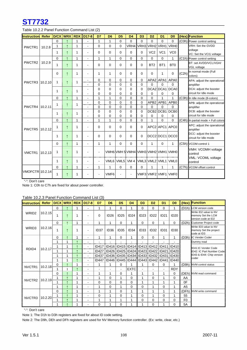
ST7732
Ver 1.5.1 2007-11 108
Table 10.2.2 Panel Function Command List (2)
Instruction Refer D/CX WRX RDX D17-8 D7 D6 D5 D4 D3 D2 D1 D0 (Hex) Function 0 ↑ 1 - 1 1 0 0 0 0 0 0 (C0h) Power control setting
1 ↑ 1 - 0 0 0 VRH4 VRH3 VRH2 VRH1 VRH0 PWCTR1 10.2.8
1 ↑ 1 - 0 0 0 0 0 VC2 VC1 VC0
VRH: Set the GVDD voltage VC: Set the VCI1 voltage
0 ↑ 1 - 1 1 0 0 0 0 0 1 (C1h) Power control setting PWCTR2 10.2.9
1 ↑ 1 - 0 0 0 0 0 BT2 BT1 BT0 BT: set AVDD/VCL/VGH/ VGL voltage
0 ↑ 1 - 1 1 0 0 0 0 1 0 (C2h) In normal mode (Full
colors)
- 0 0 0 0 0 APA2 APA1 APA0 1 ↑ 1
- 0 0 0 0 0 0 0 0 - 0 0 0 0 0 DCA2 DCA1 DCA0
PWCTR3 10.2.10
1 ↑ 1 - 0 0 0 0 0 0 0 0
APA: adjust the operational amplifier
DCA: adjust the booster circuit for Idle mode
0 ↑ 1 - 1 1 0 0 0 0 1 1 (C3h) In Idle mode (8-colors)
- 0 0 0 0 0 APB2 APB1 APB0 1 ↑ 1
- 0 0 0 0 0 0 0 0 - 0 0 0 0 0 DCB2 DCB1 DCB0
PWCTR4 10.2.11
1 ↑ 1 - 0 0 0 0 0 0 0 0
APB: adjust the operational
amplifier DCB: adjust the booster circuit for Idle mode
0 ↑ 1 - 1 1 0 0 0 1 0 0 (C4h) In partial mode + Full colors
1 ↑ 1 - 0 0 0 0 0 APC2 APC1 APC0 PWCTR5 10.2.12
1 ↑ 1 - 0 0 0 0 0 DCC2 DCC1 DCC0
APC: adjust the operational
amplifier DCC: adjust the booster circuit for Idle mode
0 ↑ 1 - 1 1 0 0 0 1 0 1 (C5h) VCOM control 1
1 ↑ 1 - - VMH6 VMH 5 VMH4 VMH3 VMH2 VMH1 VMH0 VMCTR1 10.2.13
1 ↑ 1 - - VML6 VML5 VM 4 VML3 VML2 VML1 VML0
VMH: VCOMH voltage control VML: VCOML voltage control
0 ↑ 1 - 1 1 0 0 0 1 1 1 (C7h) VCOM offset control
VMOFCTR 10.2.14 1 ↑ 1 - - VMF6 - - VMF3 VMF2 VMF1 VMF0
“-“: Don’t care Note 1: C0h to C7h are fixed for about power controller. Table 10.2.3 Panel Function Command List (3) Instruction Refer D/CX WRX RDX D17-8 D7 D6 D5 D4 D3 D2 D1 D0 (Hex) Function
0 ↑ 1 - 1 1 0 1 0 0 0 1 (D1h) LCM version code
WRID2 10.2.15 1 ↑ 1 - 0 ID26 ID25 ID24 ID23 ID22 ID21 ID20
Write ID2 value to NV memory Set the LCM version code at ID2
0 ↑ 1 - 1 1 0 1 0 0 1 0 (D2h) Customer Project code
WRID3 10.2.16 1 ↑ 1 - ID37 ID36 ID35 ID34 ID33 ID32 ID31 ID30
Write ID3 value to NV memory Set the project code at ID3
0 ↑ 1 - 1 1 0 1 0 0 1 1 (D3h) IC Vender Coder
1 1 ↑ - - - - - - - - - Dummy read
1 1 ↑ - ID417 ID416 ID415 ID414 ID413 ID412 ID411 ID410 1 1 ↑ - ID427 ID426 ID425 ID424 ID423 ID422 ID421 ID420 1 1 ↑ - ID437 ID436 ID435 ID434 ID433 ID432 ID431 ID430
RDID4 10.2.17
1 1 ↑ - ID447 ID446 ID445 ID444 ID443 ID442 ID441 ID440
ID41:IC Vender Code ID42: IC Part Number Code ID43 & ID44: Chip version coder
0 ↑ 1 - 1 1 0 1 1 0 0 1 (D9h) NVM control status NVCTR1 10.2.18
1 1 ↑ - - - - EXTC - - - RDY
0 ↑ 1 - 1 1 0 1 1 1 1 0 (DEh) NVM read command
1 ↑ 1 - 1 0 1 0 1 0 1 0 AA 1 ↑ 1 - 0 0 0 0 1 1 1 1 0F
NVCTR2 10.2.19
1 ↑ 1 - 1 0 1 0 0 1 0 1 A5
0 ↑ 1 - 1 1 0 1 1 1 1 1 (DFh) NVM write command
1 ↑ 1 - 0 1 0 1 0 1 0 1 55 1 ↑ 1 - 1 1 1 1 0 0 0 0 F0
NVCTR3 10.2.20
1 ↑ 1 - 0 1 0 1 1 0 1 0 5A
“-“: Don’t care
Note 1: The D1h to D3h registers are fixed for about ID code setting.
Note 2: The D9h, DEh and DFh registers are used for NV Memory function controller. (Ex: write, clear, etc.)

ST7732
Ver 1.5.1 2007-11 109
Table 10.2.4 Panel Function Command List (4) Instruction Refer D/CX WRXRDX D17-8 D7 D6 D5 D4 D3 D2 D1 D0 (Hex) Function
0 ↑ 1 - 1 1 1 0 0 0 0 0 (E0h) Set Gamma correction
1 ↑ 1 - - - - - RFP3 RFP2 RFP1 RFP0
1 ↑ 1 - - - - PKP04 PKP03 PKP02 PKP01 PKP00
1 ↑ 1 - - - - PKP14 PKP13 PKP12 PKP11 PKP10
1 ↑ 1 - - - - PKP24 PKP23 PKP22 PKP21 PKP20
1 ↑ 1 - - - - PKP34 PKP33 PKP32 PKP31 PKP30
1 ↑ 1 - - - - PKP44 PKP43 PKP42 PKP41 PKP40
1 ↑ 1 - - - - - PKP53 PKP52 PKP51 PKP50
1 ↑ 1 - - - - - PKP63 PKP62 PKP61 PKP60
1 ↑ 1 - - - - - PKP73 PKP72 PKP71 PKP70
1 ↑ 1 - - - - - PKP83 PKP82 PKP81 PKP80
1 ↑ 1 - - - - RFP14 RFP13 RFP12 RFP11 RFP10
1 ↑ 1 - - - OSP14 OSP13 OSP12 OSP11 OSP10
GAMCTRP1 10.2.21
1 ↑ 1 - - - - - OSP3 OSP2 OSP1 OSP0
Gamma adjustment (+ polarity)
0 ↑ 1 - 1 1 1 0 0 0 0 0 (E1h) Set Gamma correction
1 ↑ 1 - - - - - RFN3 RFN2 RFN1 RFN0
1 ↑ 1 - - - - PKN04 PKN03 PKN02 PKN01 PKN00
1 ↑ 1 - - - - PKN14 PKN13 PKN12 PKN11 PKN10
1 ↑ 1 - - - - PKN24 PKN23 PKN22 PKN21 PKN20
1 ↑ 1 - - - - PKN34 PKN33 PKN32 PKN31 PKN30
1 ↑ 1 - - - - PKN44 PKN43 PKN42 PKN41 PKN40
1 ↑ 1 - - - - - PKN53 PKN52 PKN51 PKN50
1 ↑ 1 - - - - - PKN63 PKN62 PKN61 PKN60
1 ↑ 1 - - - - - PKN73 PKN72 PKN71 PKN70
1 ↑ 1 - - - - - PKN83 PKN82 PKN81 PKN80
1 ↑ 1 - - - - RFN14 RFN13 RFN12 RFN11 RFN10
1 ↑ 1 - - - - OSN14 OSN13 OSN12 OSN11 OSN10
GAMCTRN1 10.2.22
1 ↑ 1 - - - - - OSN3 OSN2 OSN1 OSN0
Gamma adjustment (- polarity)
0 ↑ 1 - 1 1 1 1 0 0 0 1 (F1h) NVM write function ON/OFF AUTO CTRL
10.2.231 ↑ 1 -
NVM PROG
0 0 0 1 0 0 0
0 ↑ 1 - 1 1 1 1 0 0 1 0 (F2h) Oscillator frequency setting OSCADJ 10.2.24
1 ↑ 1 - 0 0 0 0 0 OSC SEL2
OSC SEL1
OSC SEL0
0 ↑ 1 - 1 1 1 1 0 1 0 1 (F5h) Display function control DISPCTRL 10.2.25
1 ↑ 1 - PDM1 PDM0 FLM C8ON EQPW1EQPW0EQVDD ENGS
0 ↑ 1 - 1 1 1 1 0 1 1 0 (F6h) Default mode setting DEFADJ 10.2.26
1 ↑ 1 - 0 1 0 0 0 1 0 TESEL
OE
“-“: Don’t care
Note 1: E0-E1 registers are fixed for about Gamma adjusting.
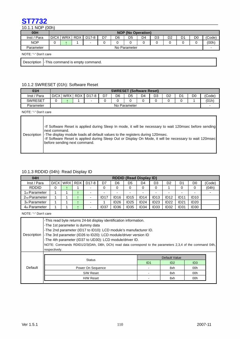
ST7732
Ver 1.5.1 2007-11 110
10.1.1 NOP (00h) 00H NOP (No Operation)
Inst / Para D/CX WRX RDX D17-8 D7 D6 D5 D4 D3 D2 D1 D0 (Code) NOP 0 ↑ 1 - 0 0 0 0 0 0 0 0 (00h)
Parameter No Parameter -
NOTE: “-“ Don’t care
Description -This command is empty command.
10.1.2 SWRESET (01h): Software Reset 01H SWRESET (Software Reset)
Inst / Para D/CX WRX RDX D17-8 D7 D6 D5 D4 D3 D2 D1 D0 (Code) SWRESET 0 ↑ 1 - 0 0 0 0 0 0 0 1 (01h) Parameter No Parameter -
NOTE: “-“ Don’t care
Description
-If Software Reset is applied during Sleep In mode, it will be necessary to wait 120msec before sending next command. -The display module loads all default values to the registers during 120msec. -If Software Reset is applied during Sleep Out or Display On Mode, it will be necessary to wait 120msec before sending next command.
10.1.3 RDDID (04h): Read Display ID
04H RDDID (Read Display ID) Inst / Para D/CX WRX RDX D17-8 D7 D6 D5 D4 D3 D2 D1 D0 (Code)
RDDID 0 ↑ 1 - 0 0 0 0 0 1 0 0 (04h) 1st Parameter 1 1 ↑ - - - - - - - - - - 2nd Parameter 1 1 ↑ - ID17 ID16 ID15 ID14 ID13 ID12 ID11 ID10 3rt Parameter 1 1 ↑ - 1 ID26 ID25 ID24 ID23 ID22 ID21 ID20 4th Parameter 1 1 ↑ - ID37 ID36 ID35 ID34 ID33 ID32 ID31 ID30
NOTE: “-“ Don’t care
Description
-This read byte returns 24-bit display identification information. -The 1st parameter is dummy data -The 2nd parameter (ID17 to ID10): LCD module’s manufacturer ID. -The 3rd parameter (ID26 to ID20): LCD module/driver version ID -The 4th parameter (ID37 to UD30): LCD module/driver ID. NOTE: Commands RDID1/2/3(DAh, DBh, DCh) read data correspond to the parameters 2,3,4 of the command 04h,
respectively.
Default
Default Value Status
ID1 ID2 ID3
Power On Sequence - 8xh 00h
S/W Reset - 8xh 00h
H/W Reset - 8xh 00h

ST7732
Ver 1.5.1 2007-11 111
10.1.4 RDDST (09h): Read Display Status 09H RDDST (Read Display Status)
Inst / Para D/CX WRX RDX D17-8 D7 D6 D5 D4 D3 D2 D1 D0 (Code) RDDST 0 ↑ 1 - 0 0 0 0 1 0 0 1 (09h)
1st Parameter 1 1 ↑ - - - - - - - - - - 2nd Parameter 1 1 ↑ - BSTON MY MX MV ML RGB - ST24 3rd Parameter 1 1 ↑ - ST23 IFPF2 IFPF1 IFPF0 IDMON PTLON SLOUT NORON 4th Parameter 1 1 ↑ - VSSON ST14 INVON ST12 ST11 DISON TEON GCS2 5th Parameter 1 1 ↑ - GCS1 GCS0 TELOM HSON VSON PCKON DEON ST0
NOTE: “-“ Don’t care
Description
This command indicates the current status of the display as described in the table below:
Bit Description Value BSTON Booster Voltage Status ‘1’ =Booster on,
‘0’ =Booster off MY Row Address Order (MY) ‘1’ =Decrement, (Bottom to Top, when MADCTL (36h) D7=’1’)
‘0’ =Increment, (Top to Bottom, when MADCTL (36h) D7=’0’) MX Column Address Order (MX) ‘1’ =Decrement, (Right to Left, when MADCTL (36h) D6=’1’)
‘0’ =Increment, (Left to Right, when MADCTL (36h) D6=’1’) MV Row/Column Exchange (MV) ‘1’ = Row/column exchange, (when MADCTL (36h) D5=’1’)
‘0’ = Normal, (when MADCTL (36h) D5=’0’) ML Scan Address Order (ML) ‘1’ =Decrement,
(LCD refresh Top to Bottom, when MADCTL (36h) D4=’1’) ‘0’=Increment, (LCD refresh Bottom to Top, when MADCTL (36h) D4=’0’)
RGB RGB/ BGR Order (RGB) ‘1’ =BGR, (When MADCTL (36h) D3=’1’) ‘0’ =RGB, (When MADCTL (36h) D3=’0’)
ST24 For Future Use ‘0’ ST23 For Future Use ‘0’ IFPF2 IFPF1 IFPF0
Interface Color Pixel Format Definition
“011” = 12-bit / pixel, “101” = 16-bit / pixel, “110” = 18-bit / pixel, others are no define
IDMON Idle Mode On/Off ‘1’ = On, “0” = Off PTLON Partial Mode On/Off ‘1’ = On, “0” = Off SLPOUT Sleep In/Out ‘1’ = Out, “0” = In NORON
Display Normal Mode On/Off ‘1’ = Normal Display, ‘0’ = Partial Display
VSSON Vertical Scrolling Status ‘1’ = Scroll on,“0” = Scroll off ST14 Horizontal Scroll Status ‘0’ INVON Inversion Status ‘1’ = On, “0” = Off ST12 All Pixels On (Not Used) ‘0’ ST11 All Pixels Off (Not Used) ‘0’ DISON Display On/Off ‘1’ = On, “0” = Off TEON Tearing effect line on/off ‘1’ = On, “0” = Off GCSEL2 GCSEL1
GCSEL0 Gamma Curve Selection
“000” = GC0 “001” = GC1 “010” = GC2 “011” = GC3 ”100” to “111” = Not defined
TELOM Tearing effect line mode ‘0’ = mode1, ‘1’ = mode2 HSON Horizontal Sync. (HS, RGB
I/F) ‘1’ = On, ‘0’ = Off
VSON Vertical Sync, (VS, RGB I/F) ‘1’ = On, ‘0’ = Off PCLKON Pixel Clock (PCLK, RGB I/F) ‘1’ = On, ‘0’ = Off DEON Data Enable (DE, RGB I/F) ‘1’ = On, ‘0’ = Off ST0 For Future Use ‘0’
Note: ST0, ST5, ST9, ST11-ST15, ST19, ST23, ST24 are set to ‘0’, when RGB I/F.

ST7732
Ver 1.5.1 2007-11 112
Default
Status Default Value (ST31 to ST0) ST[31-24] ST[23-16] ST[15-8] ST[7-0]
Power On Sequence 0000-0000 0110-0001 0000-0000 0000-0000 S/W Reset 0xxx0xx00 0xxx-0001 0000-0000 0000-0000 H/W Reset 0000-0000 0110-0001 0000-0000 0000-0000
10.1.5 RDDPM (0Ah): Read Display Power Mode
0AH RDDPM (Read Display Power Mode) Inst / Para D/CX WRX RDX D17-8 D7 D6 D5 D4 D3 D2 D1 D0 (Code) RDDPM 0 ↑ 1 - 0 0 0 0 1 0 1 0 (0Ah)
1st Parameter 1 1 ↑ - - - - - - - - - - 2nd Parameter 1 1 ↑ BSTON IDMON PTLON SLPOUT NORON DISON D1 D0
NOTE: “-” Don’t care, can be set to VDDI or DGND level
Description
This command indicates the current status of the display as described in the table below:
Bit Description Value BSTON Booster Voltage Status
‘1’ =Booster on, ‘0’ =Booster off
IDMON Idle Mode On/Off ‘1’ = Idle Mode On, ‘0’ = Idle Mode Off
PTLON Partial Mode On/Off ‘1’ = Partial Mode On, ‘0’ = Partial Mode Off
SLPON Sleep In/Out ‘1’ = Sleep Out, ‘0’ = Sleep In
NORON Display Normal Mode On/Off
‘1’ = Normal Display, ‘0’ = Partial Display
DISON Display On/Off ‘1’ = Display On, ‘0’ = Display Off
D1 Not Used ‘0’ D0 Not Used ‘0’
Default
Status Default Value (D7 to D0) Power On Sequence 0000_1000(08h)
S/W Reset 0000_1000(08h) H/W Reset 0000_1000(08h)
10.1.6 RDDMADCTL (0Bh): Read Display MADCTL
0BH RDDMADCTL (Read Display MADCTL) Inst / Para D/CX WRX RDX D17-8 D7 D6 D5 D4 D3 D2 D1 D0 (Code)
RDDMADCTL 0 ↑ 1 - 0 0 0 0 1 0 1 1 (0Bh) 1st Parameter 1 1 ↑ - - - - - - - - - - 2nd Parameter 1 1 ↑ MY MX MV ML RGB - D1 D0
NOTE: “-” Don’t care, can be set to VDDI or DGND level
Description
This command indicates the current status of the display as described in the table below:
Bit Description Value
MX Row Address Order ‘1’ = Bottom to Top (When MADCTL B7=’1’) ‘0’ = Top to Bottom (When MADCTL B7=’0’)
MY Column Address Order ‘1’ = Right to Left (When MADCTL B6=’1’) ‘0’ = Left to Right (When MADCTL B6=’0’)
MV Row/Column Order (MV) ‘1’ = Row/column exchange (MV=1) ‘0’ = Normal (MV=0)
ML Vertical Refresh Order ‘1’ =LCD Refresh Bottom to Top ‘0’ =LCD Refresh Top to Bottom
RGB RGB/BGR Order ‘1’ =BGR, “0”=RGB D1 Not Used ‘0’ D0 Not Used ‘0’

ST7732
Ver 1.5.1 2007-11 113
Default
Status Default Value (D7 to D0) Power On Sequence 0000_0000 (00h)
S/W Reset No change H/W Reset 0000_0000 (00h)
10.1.7 RDDCOLMOD (0Ch): Read Display Pixel Format 0CH RDDCOLMOD (Read Display Pixel Format)
Inst / Para D/CX WRX RDX D17-8 D7 D6 D5 D4 D3 D2 D1 D0 (Code) RDDCOLMOD 0 ↑ 1 - 0 0 0 0 1 1 0 0 (0Ch) 1st Parameter 1 1 ↑ - - - - - - - - - - 2nd Parameter 1 1 ↑ - VIPF3 VIPF2 VIPF1 VIPF0 - IFPF2 IFPF1 IFPF0
NOTE: “-” Don’t care, can be set to VDDI or DGND level
Description
This command indicates the current status of the display as described in the table below:
IFPF[2:0] MCU Interface Color Format 011 3 12-bit/pixel 101 5 16-bit/pixel 110 6 18-bit/pixel 111 7 No used
Others are no define and invalid
VIFPF[2:0] RGB Interface Color Format 0101 5 16-bit/pixel (1-times data transfer) 0110 6 18-bit/pixel (1-times data transfer) 0111 7 No used 1110 14 18-bit/pixel (3-times data transfer)
Others are no define and invalid
Default
Status Default Value IFPF[2:0] VIPF[3:0]
Power On Sequence 0110 (18 bits/pixel) 0110 (18 bits/pixel) S/W Reset No Change No Change H/W Reset 0110 (18 bits/pixel) 0110 (18 bits/pixel)
10.1.8 RDDIM (0Dh): Read Display Image Mode
0DH RDDIM (0Dh): Read Display Image Mode Inst / Para D/CX WRX RDX D17-8 D7 D6 D5 D4 D3 D2 D1 D0 (Code)
RDDIM 0 ↑ 1 - 0 0 0 0 1 1 0 1 (0Dh) 1st Parameter 1 1 ↑ - - - - - - - - - - 2nd Parameter 1 1 ↑ - VSSON D6 INVON D4 D3 GCS2 GCS1 GCS0
NOTE: “-” Don’t care, can be set to VDDI or DGND level
Description
This command indicates the current status of the display as described in the table below:
Bit Description Value
VSSON Vertical Scrolling On/Off “1” = Vertical scrolling is On, “0” = Vertical scrolling is Off
D6 Horizontal Scrolling On/Off “0” (Not used)
INVON Inversion On/Off “1” = Inversion is On, “0” = Inversion is Off
D4 All Pixels On “0” (Not used) D3 All Pixels Off “0” (Not used)
GCS2 GCS1
GCS0 Gamma Curve Selection
“000” = GC0, “001” = GC1, “010” = GC2, “011” = GC3, ”100” to “111” = Not defined
Default
Status Default Value(D7 to D0) Power On Sequence 0000_0000 (00h)
S/W Reset 0000_0000 (00h) H/W Reset 0000_0000 (00h)
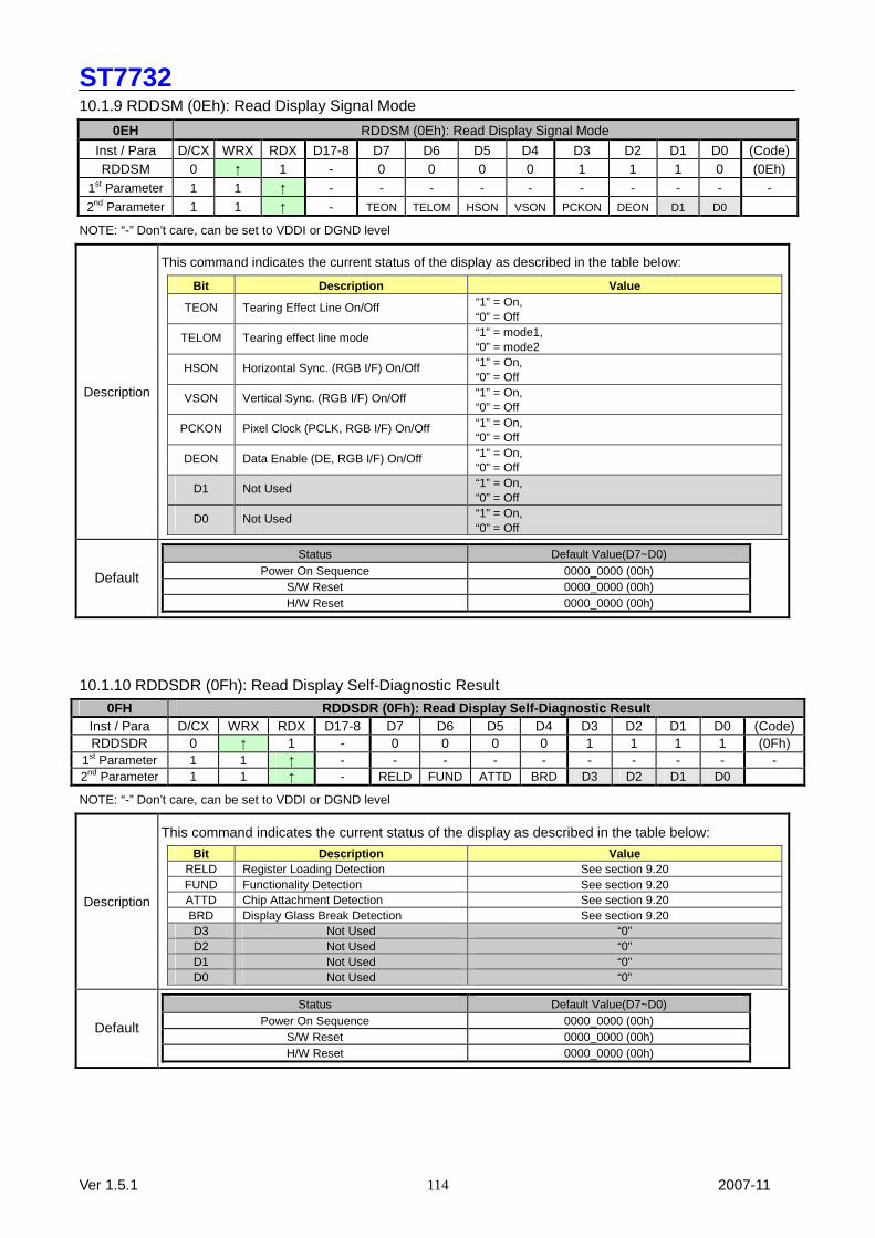
ST7732
Ver 1.5.1 2007-11 114
10.1.9 RDDSM (0Eh): Read Display Signal Mode
0EH RDDSM (0Eh): Read Display Signal Mode
Inst / Para D/CX WRX RDX D17-8 D7 D6 D5 D4 D3 D2 D1 D0 (Code) RDDSM 0 ↑ 1 - 0 0 0 0 1 1 1 0 (0Eh)
1st Parameter 1 1 ↑ - - - - - - - - - -
2nd Parameter 1 1 ↑ - TEON TELOM HSON VSON PCKON DEON D1 D0
NOTE: “-” Don’t care, can be set to VDDI or DGND level
Description
This command indicates the current status of the display as described in the table below:
Bit Description Value
TEON Tearing Effect Line On/Off “1” = On, “0” = Off
TELOM Tearing effect line mode “1” = mode1, “0” = mode2
HSON Horizontal Sync. (RGB I/F) On/Off “1” = On, “0” = Off
VSON Vertical Sync. (RGB I/F) On/Off “1” = On, “0” = Off
PCKON Pixel Clock (PCLK, RGB I/F) On/Off “1” = On, “0” = Off
DEON Data Enable (DE, RGB I/F) On/Off “1” = On, “0” = Off
D1 Not Used “1” = On, “0” = Off
D0 Not Used “1” = On, “0” = Off
Default
Status Default Value(D7~D0) Power On Sequence 0000_0000 (00h)
S/W Reset 0000_0000 (00h) H/W Reset 0000_0000 (00h)
10.1.10 RDDSDR (0Fh): Read Display Self-Diagnostic Result 0FH RDDSDR (0Fh): Read Display Self-Diagnostic Result
Inst / Para D/CX WRX RDX D17-8 D7 D6 D5 D4 D3 D2 D1 D0 (Code) RDDSDR 0 ↑ 1 - 0 0 0 0 1 1 1 1 (0Fh)
1st Parameter 1 1 ↑ - - - - - - - - - - 2nd Parameter 1 1 ↑ - RELD FUND ATTD BRD D3 D2 D1 D0
NOTE: “-” Don’t care, can be set to VDDI or DGND level
Description
This command indicates the current status of the display as described in the table below:
Bit Description Value RELD Register Loading Detection See section 9.20 FUND Functionality Detection See section 9.20 ATTD Chip Attachment Detection See section 9.20 BRD Display Glass Break Detection See section 9.20 D3 Not Used “0” D2 Not Used “0” D1 Not Used “0” D0 Not Used “0”
Default
Status Default Value(D7~D0) Power On Sequence 0000_0000 (00h)
S/W Reset 0000_0000 (00h) H/W Reset 0000_0000 (00h)
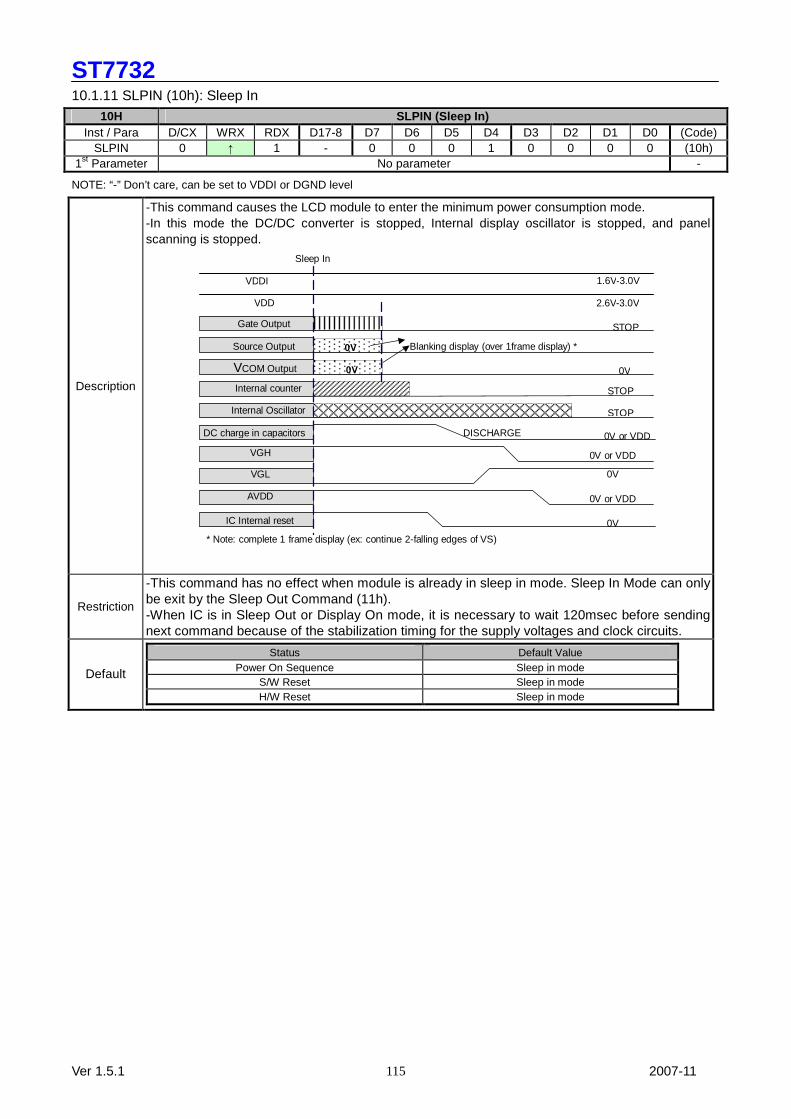
ST7732
Ver 1.5.1 2007-11 115
10.1.11 SLPIN (10h): Sleep In
10H SLPIN (Sleep In) Inst / Para D/CX WRX RDX D17-8 D7 D6 D5 D4 D3 D2 D1 D0 (Code)
SLPIN 0 ↑ 1 - 0 0 0 1 0 0 0 0 (10h) 1st Parameter No parameter -
NOTE: “-” Don’t care, can be set to VDDI or DGND level
Description
-This command causes the LCD module to enter the minimum power consumption mode. -In this mode the DC/DC converter is stopped, Internal display oscillator is stopped, and panel scanning is stopped.
Restriction
-This command has no effect when module is already in sleep in mode. Sleep In Mode can only be exit by the Sleep Out Command (11h). -When IC is in Sleep Out or Display On mode, it is necessary to wait 120msec before sending next command because of the stabilization timing for the supply voltages and clock circuits.
Default
Status Default Value Power On Sequence Sleep in mode
S/W Reset Sleep in mode H/W Reset Sleep in mode
Sleep In
VDDI 1.6V-3.0V
VDD Gate Output
Source Output 0V Blanking display (over 1frame display) * VCOM Output 0V
2.6V-3.0V
STOP
0V
Internal counter STOP Internal Oscillator STOP
DC charge in capacitors DISCHARGE 0V or VDD
VGH 0V or VDD
VGL 0V
AVDD 0V or VDD
IC Internal reset 0V
* Note: complete 1 frame display (ex: continue 2-falling edges of VS)
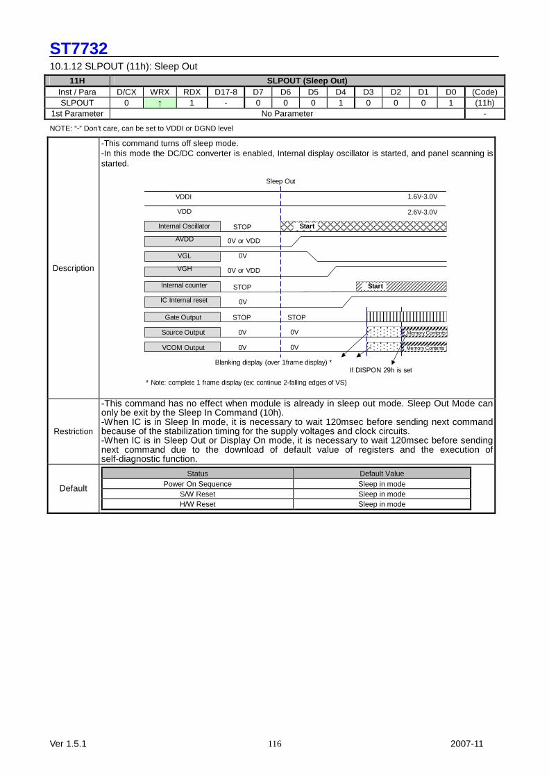
ST7732
Ver 1.5.1 2007-11 116
10.1.12 SLPOUT (11h): Sleep Out 11H SLPOUT (Sleep Out)
Inst / Para D/CX WRX RDX D17-8 D7 D6 D5 D4 D3 D2 D1 D0 (Code) SLPOUT 0 ↑ 1 - 0 0 0 1 0 0 0 1 (11h)
1st Parameter No Parameter -
NOTE: “-” Don’t care, can be set to VDDI or DGND level
Description
-This command turns off sleep mode. -In this mode the DC/DC converter is enabled, Internal display oscillator is started, and panel scanning is started.
Restriction
-This command has no effect when module is already in sleep out mode. Sleep Out Mode can only be exit by the Sleep In Command (10h). -When IC is in Sleep In mode, it is necessary to wait 120msec before sending next command because of the stabilization timing for the supply voltages and clock circuits. -When IC is in Sleep Out or Display On mode, it is necessary to wait 120msec before sending next command due to the download of default value of registers and the execution of self-diagnostic function.
Default
Status Default Value Power On Sequence Sleep in mode
S/W Reset Sleep in mode H/W Reset Sleep in mode
Sleep Out
VDDI 1.6V-3.0V
VDD Internal Oscillator STOP Start
AVDD 0V or VDD
VGL 0V
VGH 0V or VDD Internal counter STOP Start
IC Internal reset 0V
2.6V-3.0V
Gate Output Source Output VCOM Output
STOP
0V
0V
STOP 0V
0V
Memory Contents
Memory Contents
Blanking display (over 1fram e display) * If DISPON 29h is set
* Note: complete 1 frame display (ex: continue 2-falling edges of VS)
ST7732
Ver 1.5.1 2007-11 117
10.1.13 PTLON (12h): Partial Display Mode On
12H PTLON (12h): Partial Display Mode On Inst / Para D/CX WRX RDX D17-8 D7 D6 D5 D4 D3 D2 D1 D0 (Code)
PTLON 0 ↑ 1 - 0 0 0 1 0 0 1 0 (12h) 1st Parameter No Parameter -
NOTE: “-” Don’t care, can be set to VDDI or DGND level
Description -This command turns on Partial mode. The partial mode window is described by the Partial Area command (30h) -To leave Partial mode, the Normal Display Mode On command (13H) should be written.
Default
Status Default Value Power On Sequence Normal Mode On
S/W Reset Normal Mode On H/W Reset Normal Mode On
10.1.14 NORON (13h): Normal Display Mode On
13H NORON (Normal Display Mode On) Inst / Para D/CX WRX RDX D17-8 D7 D6 D5 D4 D3 D2 D1 D0 (Code) NORON 0 ↑ 1 - 0 0 0 1 0 0 1 1 (13h)
1st Parameter No Parameter -
NOTE: “-” Don’t care, can be set to VDDI or DGND level
Description -This command returns the display to normal mode. -Normal display mode on means Partial mode off, Scroll mode Off. -Exit from NORON by the Partial mode On command (12h)
Default
Status Default Value Power On Sequence Normal Mode On
S/W Reset Normal Mode On H/W Reset Normal Mode On
10.1.15 INVOFF (20h): Display Inversion Off 20H IVNOFF (Normal Display Mode Off)
Inst / Para D/CX WRX RDX D17-8 D7 D6 D5 D4 D3 D2 D1 D0 (Code) INVOFF 0 ↑ 1 - 0 0 1 0 0 0 0 0 (20h)
1st Parameter No Parameter -
NOTE: “-” Don’t care, can be set to VDDI or DGND level
Description
-This command is used to recover from display inversion mode.
Default
Status Default Value Power On Sequence Display Inversion off
S/W Reset Display Inversion off H/W Reset Display Inversion off
Top-Left (0,0) (Example)
Memory Display

ST7732
Ver 1.5.1 2007-11 118
10.1.16 INVON (21h): Display Inversion On
21H IVNOFF (Display Inversion On) Inst / Para D/CX WRX RDX D17-8 D7 D6 D5 D4 D3 D2 D1 D0 (Code)
INVON 0 ↑ 1 - 0 0 1 0 0 0 0 1 (21h) 1st Parameter No Parameter -
NOTE: “-” Don’t care, can be set to VDDI or DGND level
Description
-This command is used to enter into display inversion mode -To exit from Display Inversion On, the Display Inversion Off command (20h) should be written.
Default
Status Default Value Power On Sequence Display Inversion off
S/W Reset Display Inversion off H/W Reset Display Inversion off
10.1.17 GAMSET (26h): Gamma Set 26H GAMSET (Gamma Set)
Inst / Para D/CX WRX RDX D17-8 D7 D6 D5 D4 D3 D2 D1 D0 (Code) GAMSET 0 ↑ 1 - 0 0 1 0 0 1 1 0 (26h)
1st Parameter 1 ↑ 1 - - - - - GC3 GC2 GC1 GC0
NOTE: “-” Don’t care, can be set to VDDI or DGND level
Description
-This command is used to select the desired Gamma curve for the current display. A maximum of 4 curves can be selected. The curves are defined in section 9.17 The curve is selected by setting the appropriate bit in the parameter as described in the Table.
GC [7:0] Parameter Curve Selected GS=1 GS=0
01h GC0 Gamma Curve 1 (G2.2) Gamma Curve 1 (G1.0) 02h GC1 Gamma Curve 2 (G1.8) Gamma Curve 2 (G2.5) 04h GC2 Gamma Curve 3 (G2.5) Gamma Curve 3 (G2.2) 08h GC3 Gamma Curve 4 (G1.0) Gamma Curve 4 (G1.8)
Note: All other values are undefined.
Default
Status Default Value Power On Sequence 01h
S/W Reset 01h H/W Reset 01h
Top-Left (0,0) (Example)
Memory Display
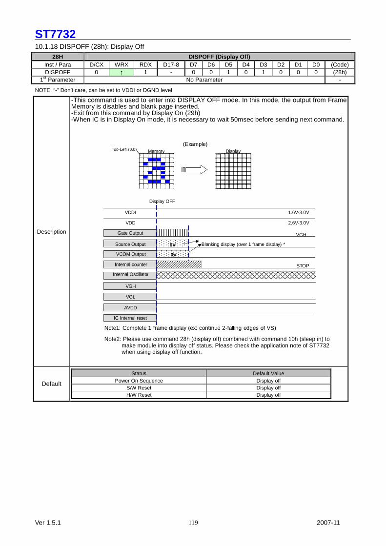
ST7732
Ver 1.5.1 2007-11 119
10.1.18 DISPOFF (28h): Display Off 28H DISPOFF (Display Off)
Inst / Para D/CX WRX RDX D17-8 D7 D6 D5 D4 D3 D2 D1 D0 (Code) DISPOFF 0 ↑ 1 - 0 0 1 0 1 0 0 0 (28h)
1st Parameter No Parameter -
NOTE: “-” Don’t care, can be set to VDDI or DGND level
Description
-This command is used to enter into DISPLAY OFF mode. In this mode, the output from Frame Memory is disables and blank page inserted. -Exit from this command by Display On (29h) -When IC is in Display On mode, it is necessary to wait 50msec before sending next command.
Default
Status Default Value Power On Sequence Display off
S/W Reset Display off H/W Reset Display off
Top-Left (0,0) (Example)
Memory Display
VDDI
Display OFF
1.6V-3.0V
VDD Gate Output
Source Output 0V Blanking display (over 1 frame display) *
2.6V-3.0V
VGH
VCOM Output 0V
Internal counter STOP Internal Oscillator
VGH
VGL
AVDD
IC Internal reset
Note1: Complete 1 frame display (ex: continue 2-falling edges of VS) Note2: Please use command 28h (display off) combined with command 10h (sleep in) to
make module into display off status. Please check the application note of ST7732 when using display off function.
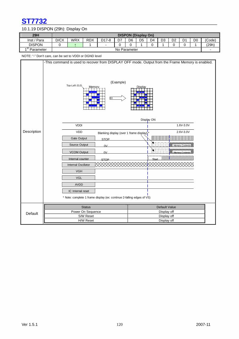
ST7732
Ver 1.5.1 2007-11 120
10.1.19 DISPON (29h): Display On
29H DISPON (Display On) Inst / Para D/CX WRX RDX D17-8 D7 D6 D5 D4 D3 D2 D1 D0 (Code) DISPON 0 ↑ 1 - 0 0 1 0 1 0 0 1 (29h)
1st Parameter No Parameter -
NOTE: “-” Don’t care, can be set to VDDI or DGND level
Description
-This command is used to recover from DISPLAY OFF mode. Output from the Frame Memory is enabled.
Default
Status Default Value Power On Sequence Display off
S/W Reset Display off H/W Reset Display off
Top-Left (0,0) (Example)
Memory Display
VDDI
VDD Gate Output
Source Output
Display ON
Blanking display (over 1 frame display) *
STOP
0V
1.6V-3.0V
2.6V-3.0V
Memory Contents
VCOM Output 0V Memory Contents Internal counter STOP Start
Internal Oscillator
VGH
VGL
AVDD
IC Internal reset
* Note: complete 1 frame display (ex: continue 2-falling edges of VS)
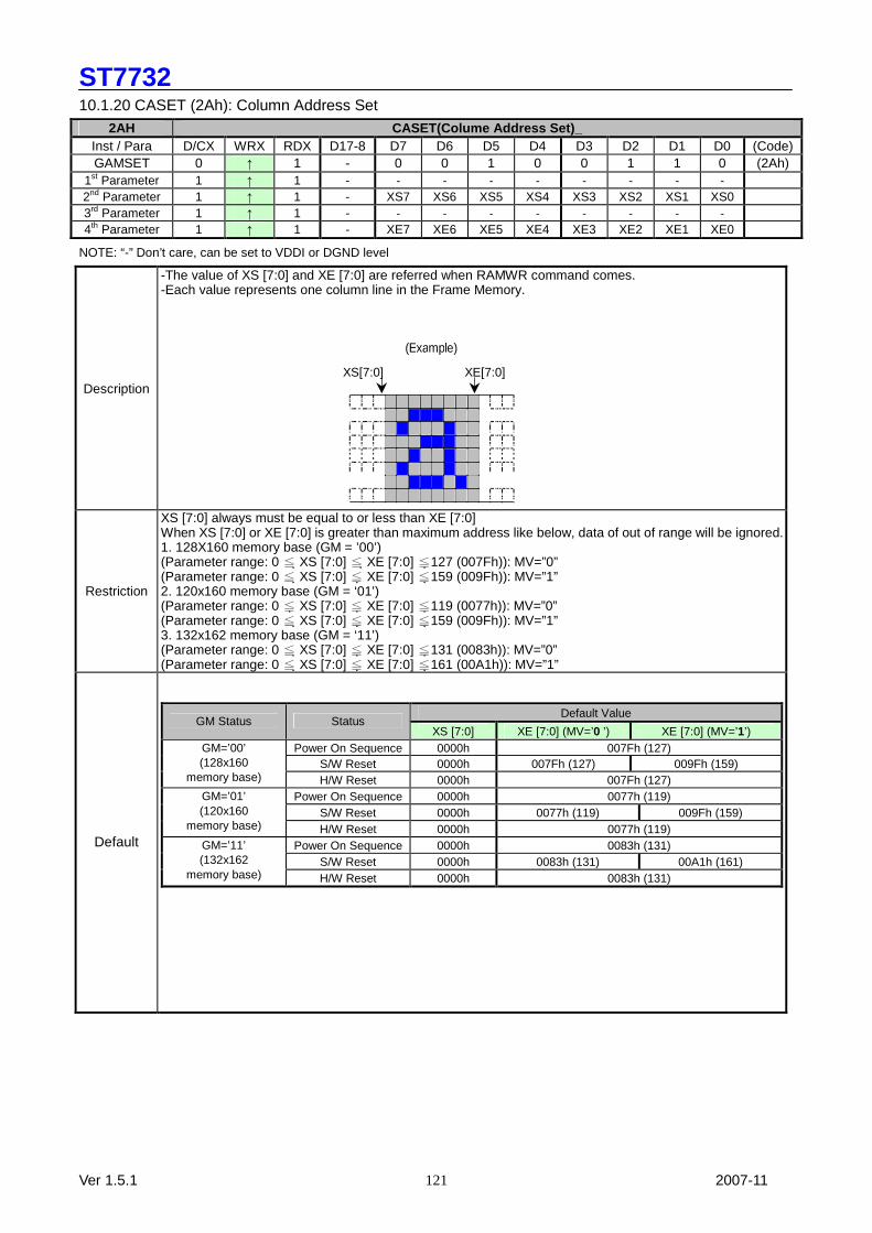
ST7732
Ver 1.5.1 2007-11 121
10.1.20 CASET (2Ah): Column Address Set 2AH CASET(Colume Address Set)_
Inst / Para D/CX WRX RDX D17-8 D7 D6 D5 D4 D3 D2 D1 D0 (Code) GAMSET 0 ↑ 1 - 0 0 1 0 0 1 1 0 (2Ah)
1st Parameter 1 ↑ 1 - - - - - - - - - 2nd Parameter 1 ↑ 1 - XS7 XS6 XS5 XS4 XS3 XS2 XS1 XS0 3rd Parameter 1 ↑ 1 - - - - - - - - - 4th Parameter 1 ↑ 1 - XE7 XE6 XE5 XE4 XE3 XE2 XE1 XE0
NOTE: “-” Don’t care, can be set to VDDI or DGND level
Description
-The value of XS [7:0] and XE [7:0] are referred when RAMWR command comes. -Each value represents one column line in the Frame Memory.
Restriction
XS [7:0] always must be equal to or less than XE [7:0] When XS [7:0] or XE [7:0] is greater than maximum address like below, data of out of range will be ignored. 1. 128X160 memory base (GM = ’00’) (Parameter range: 0 ≦ XS [7:0] ≦ XE [7:0] ≦ 127 (007Fh)): MV=”0” (Parameter range: 0 ≦ XS [7:0] ≦ XE [7:0] ≦ 159 (009Fh)): MV=”1” 2. 120x160 memory base (GM = ‘01’) (Parameter range: 0 ≦ XS [7:0] ≦ XE [7:0] ≦ 119 (0077h)): MV=”0” (Parameter range: 0 ≦ XS [7:0] ≦ XE [7:0] ≦ 159 (009Fh)): MV=”1” 3. 132x162 memory base (GM = ‘11’) (Parameter range: 0 ≦ XS [7:0] ≦ XE [7:0] ≦ 131 (0083h)): MV=”0” (Parameter range: 0 ≦ XS [7:0] ≦ XE [7:0] ≦ 161 (00A1h)): MV=”1”
Default
Default Value GM Status Status
XS [7:0] XE [7:0] (MV=’0 ’) XE [7:0] (MV=’1’) Power On Sequence 0000h 007Fh (127)
S/W Reset 0000h 007Fh (127) 009Fh (159) GM=’00’ (128x160
memory base) H/W Reset 0000h 007Fh (127) Power On Sequence 0000h 0077h (119)
S/W Reset 0000h 0077h (119) 009Fh (159) GM=’01’ (120x160
memory base) H/W Reset 0000h 0077h (119) Power On Sequence 0000h 0083h (131)
S/W Reset 0000h 0083h (131) 00A1h (161) GM=’11’ (132x162
memory base) H/W Reset 0000h 0083h (131)
(Example) XS[7:0] XE[7:0]
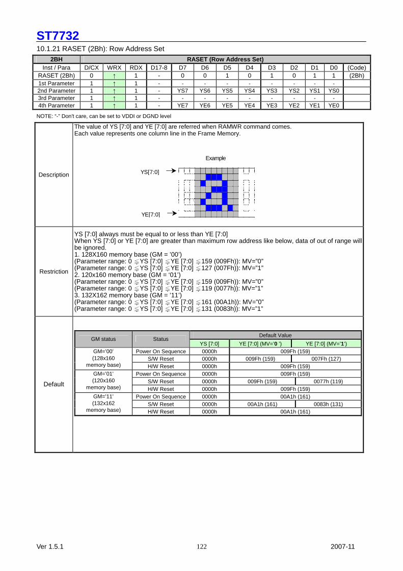
ST7732
Ver 1.5.1 2007-11 122
10.1.21 RASET (2Bh): Row Address Set 2BH RASET (Row Address Set)
Inst / Para D/CX WRX RDX D17-8 D7 D6 D5 D4 D3 D2 D1 D0 (Code) RASET (2Bh) 0 ↑ 1 - 0 0 1 0 1 0 1 1 (2Bh) 1st Parameter 1 ↑ 1 - - - - - - - - - 2nd Parameter 1 ↑ 1 - YS7 YS6 YS5 YS4 YS3 YS2 YS1 YS0 3rd Parameter 1 ↑ 1 - - - - - - - - - 4th Parameter 1 ↑ 1 - YE7 YE6 YE5 YE4 YE3 YE2 YE1 YE0
NOTE: “-” Don’t care, can be set to VDDI or DGND level
Description
The value of YS [7:0] and YE [7:0] are referred when RAMWR command comes. Each value represents one column line in the Frame Memory.
Restriction
YS [7:0] always must be equal to or less than YE [7:0] When YS [7:0] or YE [7:0] are greater than maximum row address like below, data of out of range will be ignored. 1. 128X160 memory base (GM = ’00’) (Parameter range: 0 ≦ YS [7:0] ≦ YE [7:0] ≦ 159 (009Fh)): MV=”0” (Parameter range: 0 ≦ YS [7:0] ≦ YE [7:0] ≦ 127 (007Fh)): MV=”1” 2. 120x160 memory base (GM = ‘01’) (Parameter range: 0 ≦ YS [7:0] ≦ YE [7:0] ≦ 159 (009Fh)): MV=”0” (Parameter range: 0 ≦ YS [7:0] ≦ YE [7:0] ≦ 119 (0077h)): MV=”1” 3. 132X162 memory base (GM = ’11’) (Parameter range: 0 ≦ YS [7:0] ≦ YE [7:0] ≦ 161 (00A1h)): MV=”0” (Parameter range: 0 ≦ YS [7:0] ≦ YE [7:0] ≦ 131 (0083h)): MV=”1”
Default
Default Value GM status Status
YS [7:0] YE [7:0] (MV=’0 ’) YE [7:0] (MV=’1’) Power On Sequence 0000h 009Fh (159)
S/W Reset 0000h 009Fh (159) 007Fh (127) GM=’00’ (128x160
memory base) H/W Reset 0000h 009Fh (159) Power On Sequence 0000h 009Fh (159)
S/W Reset 0000h 009Fh (159) 0077h (119) GM=’01’ (120x160
memory base) H/W Reset 0000h 009Fh (159) Power On Sequence 0000h 00A1h (161)
S/W Reset 0000h 00A1h (161) 0083h (131) GM=’11’ (132x162
memory base) H/W Reset 0000h 00A1h (161)
YS[7:0]
YE[7:0]
Example

ST7732
Ver 1.5.1 2007-11 123
10.1.22 RAMWR (2Ch): Memory Write
2CH RAMWR (Memory Write) Inst / Para D/CX WRX RDX D17-8 D7 D6 D5 D4 D3 D2 D1 D0 (Code) RAMWR 0 ↑ 1 - 0 0 1 0 1 1 0 0 (2Ch)
1st Parameter 1 ↑ 1 D17-8 D7 D6 D5 D4 D3 D2 D1 D0 - ∣ 1 ↑ 1 ∣ ∣ ∣ ∣ ∣ ∣ ∣ ∣ ∣ ∣
Nth Parameter 1 ↑ 1 D17-8 D7 D6 D5 D4 D3 D2 D1 D0 -
NOTE: “-” Don’t care, can be set to VDDI or DGND level
Description
-When this command is accepted, the column register and the row register are reset to the Start Column/Start Row positions. -The Start Column/Start Row positions are different in accordance with MADCTL setting. (See section 9.12) -Sending any other command can stop Frame Write. In all color modes, there is no restriction on length of parameters. -1. 128X160 memory base (GM = ‘00’) 128x160x18-bit memory can be written by this command Memory range: (0000h,0000h) -> (007Fh, 09Fh) -2. 120x160 memory base (GM = ‘01’) 120x160x18-bit memory can be written on this command. Memory range: (0000h,0000h) -> (0077h,09Fh) -3. 132x162 memory base (GM = ‘11’) 132x162x18-bit memory can be written on this command. Memory range: (0000h,0000h) -> (0083h,00A1h)
Default
Status Default Value Power On Sequence Contents of memory is set randomly
S/W Reset Contents of memory is not cleared H/W Reset Contents of memory is not cleared
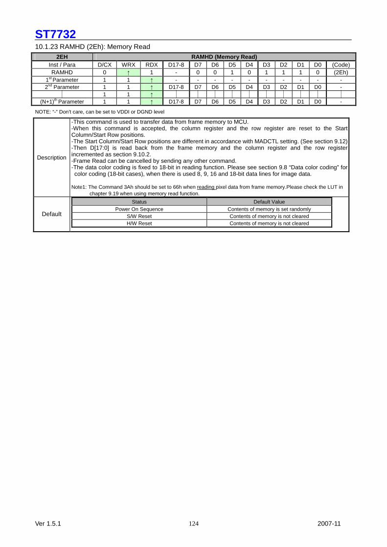
ST7732
Ver 1.5.1 2007-11 124
10.1.23 RAMHD (2Eh): Memory Read
2EH RAMHD (Memory Read) Inst / Para D/CX WRX RDX D17-8 D7 D6 D5 D4 D3 D2 D1 D0 (Code) RAMHD 0 ↑ 1 - 0 0 1 0 1 1 1 0 (2Eh)
1st Parameter 1 1 ↑ - - - - - - - - - - 2nd Parameter 1 1 ↑ D17-8 D7 D6 D5 D4 D3 D2 D1 D0 - ∣ 1 1 ↑ ∣ ∣ ∣ ∣ ∣ ∣ ∣ ∣ ∣ ∣
(N+1)th Parameter 1 1 ↑ D17-8 D7 D6 D5 D4 D3 D2 D1 D0 -
NOTE: “-” Don’t care, can be set to VDDI or DGND level
Description
-This command is used to transfer data from frame memory to MCU. -When this command is accepted, the column register and the row register are reset to the Start Column/Start Row positions. -The Start Column/Start Row positions are different in accordance with MADCTL setting. (See section 9.12) -Then D[17:0] is read back from the frame memory and the column register and the row register incremented as section 9.10.2. -Frame Read can be cancelled by sending any other command. -The data color coding is fixed to 18-bit in reading function. Please see section 9.8 “Data color coding” for color coding (18-bit cases), when there is used 8, 9, 16 and 18-bit data lines for image data.
Note1: The Command 3Ah should be set to 66h when reading pixel data from frame memory.Please check the LUT in
chapter 9.19 when using memory read function.
Default
Status Default Value Power On Sequence Contents of memory is set randomly
S/W Reset Contents of memory is not cleared H/W Reset Contents of memory is not cleared
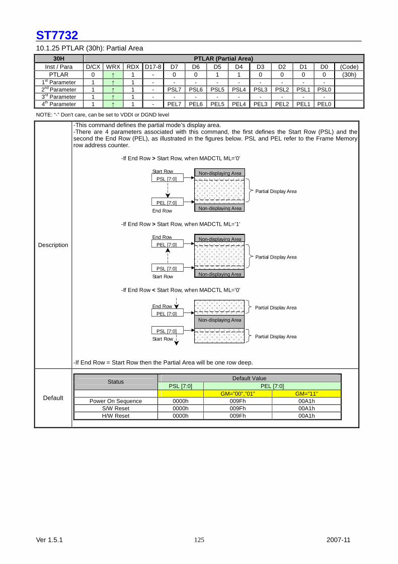
ST7732
Ver 1.5.1 2007-11 125
10.1.25 PTLAR (30h): Partial Area
30H PTLAR (Partial Area) Inst / Para D/CX WRX RDX D17-8 D7 D6 D5 D4 D3 D2 D1 D0 (Code)
PTLAR 0 ↑ 1 - 0 0 1 1 0 0 0 0 (30h) 1st Parameter 1 ↑ 1 - - - - - - - - - 2nd Parameter 1 ↑ 1 - PSL7 PSL6 PSL5 PSL4 PSL3 PSL2 PSL1 PSL0 3rd Parameter 1 ↑ 1 - - - - - - - - - 4th Parameter 1 ↑ 1 - PEL7 PEL6 PEL5 PEL4 PEL3 PEL2 PEL1 PEL0
NOTE: “-” Don’t care, can be set to VDDI or DGND level
Description
-This command defines the partial mode’s display area. -There are 4 parameters associated with this command, the first defines the Start Row (PSL) and the second the End Row (PEL), as illustrated in the figures below. PSL and PEL refer to the Frame Memory row address counter. -If End Row = Start Row then the Partial Area will be one row deep.
Default
Default Value Status
PSL [7:0] PEL [7:0] GM=”00”,”01” GM=”11”
Power On Sequence 0000h 009Fh 00A1h S/W Reset 0000h 009Fh 00A1h H/W Reset 0000h 009Fh 00A1h
-If End Row > Start Row, when MADCTL ML=’0’
Start Row
PSL [7:0] Non-displaying Area
Partial Display Area
PEL [7:0]
End Row Non-displaying Area
-If End Row > Start Row, when MADCTL ML=’1’
End Row
PEL [7:0] Non-displaying Area
Partial Display Area
PSL [7:0]
Start Row Non-displaying Area
-If End Row < Start Row, when MADCTL ML=’0’
End Row
PEL [7:0] Non-displaying Area
Partial Display Area
PSL [7:0]
Start Row Partial Display Area

ST7732
Ver 1.5.1 2007-11 126
10.1.26 SCRLAR (33h): Scroll Area
33H SCRLAR (Scrolll Area) Inst / Para D/CX WRX RDX D17-8 D7 D6 D5 D4 D3 D2 D1 D0 (Code)
PTLAR 0 ↑ 1 - 0 0 1 1 0 0 1 1 (33h) 1st Parameter 1 ↑ 1 - - - - - - - - - 2nd Parameter 1 ↑ 1 - TFA 7 TFA 6 TFA 5 TFA 4 TFA 3 TFA 2 TFA 1 TFA 0 3rd Parameter 1 ↑ 1 - - - - - - - - - 4th Parameter 1 ↑ 1 - VSA 7 VSA 6 VSA 5 VSA 4 VSA 3 VSA 2 VSA 1 VSA 0 5th Parameter 1 ↑ 1 - - - - - - - - - 6th Parameter 1 ↑ 1 - BFA 7 BFA 6 BFA 5 BFA 4 BFA 3 BFA 2 BFA 1 BFA 0
NOTE: “-” Don’t care, can be set to VDDI or DGND level
Description
-This command defines the Vertical Scrolling Area of the display. When MADCTL ML=0 -The 1st & 2nd parameter TFA [7:0] describes the Top Fixed Area (in No. of lines from Top of the Frame
Memory and Display). -The 3rd & 4th parameter VSA [7:0] describes the height of the Vertical Scrolling Area (in No. of lines of
the Frame Memory [not the display] from the Vertical Scrolling Start Address) -The first line appears immediately after the bottom most line of the Top Fixed Area. -The 5th & 6th parameter BFA [7:0] describes the Bottom Fixed Area (in No. of lines from Bottom of the
Frame Memory and Display). -TFA, VSA and BFA refer to the Frame Memory row address.
When MADCTL ML=1 -The 1st & 2nd parameter TFA [7:0] describes the Top Fixed Area (in No. of lines from Bottom
of the Frame Memory and Display). -The 3rd & 4th parameter VSA [7:0] describes the height of the Vertical Scrolling Area (in No.
of lines of the Frame Memory [not the display] from the Vertical Scrolling Start Address) -The first line appears immediately after the top most line of the Top Fixed Area. -The 5th & 6th parameter BFA [7:0] describes the Bottom Fixed Area (in No. of lines from Top
of the Frame Memory and Display).
See Section 9.10.4 for details of the Memory to Display Mapping.
-The condition is 0≦ (TFA+VSA+BFA) ≦ 162, otherwise Scrolling mode is undefined.
-In Vertical Scroll Mode, MADCTL parameter MV should be set to ‘0’-this only affects the Frame Memory
Write.
Default
Default Value Status
TFA [7:0] VSA [7:0] BFA [7:0] GM=”00”,”01” GM=”11”
Power On Sequence 0000h 00A0h 00A2h 0000h S/W Reset 0000h 00A0h 00A2h 0000h H/W Reset 0000h 00A0h 00A2h 0000h
Top-Left (0,0)
Top Fixed Area
TFA [7:0] Scroll Fixed Area
VSFA [7:0]
First line read from
Bottom Fixed Area BFA [7:0]
Top-Left (0,0)
Bottom Fixed Area
BFA [7:0]
Scroll Fixed Area
VSFA [7:0] Top Fixed Area
TFA [7:0]
First line read from
frame memory
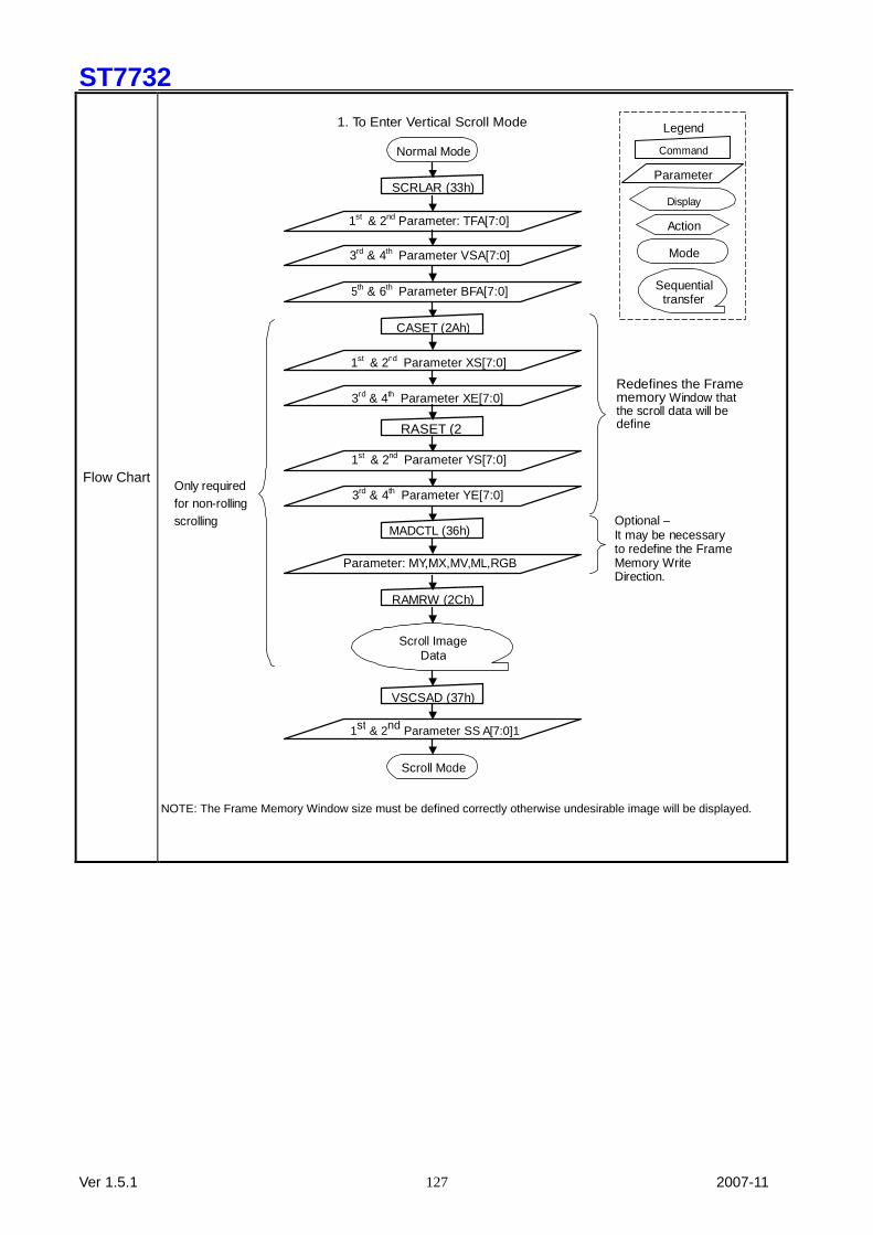
ST7732
Ver 1.5.1 2007-11 127
Flow Chart
NOTE: The Frame Memory Window size must be defined correctly otherwise undesirable image will be displayed.
1. To Enter Vertical Scroll Mode Legend
Normal Mode
SCRLAR (33h)
1st & 2nd Parameter: TFA[7:0]
3rd & 4th Parameter VSA[7:0]
5th & 6th Parameter BFA[7:0]
Command Parameter
Display
Action
Mode Sequential
transfer
CASET (2Ah)
1st & 2nd Parameter XS[7:0]
3rd & 4th Parameter XE[7:0]
Redefines the Frame memory Window that the scroll data will be define
Only required for non-rolling scrolling
RASET (2
1st & 2nd Parameter YS[7:0]
3rd & 4th Parameter YE[7:0]
MADCTL (36h)
Parameter: MY,MX,MV,ML,RGB
RAMRW (2Ch)
Scroll Image Data
VSCSAD (37h)
1st & 2nd Parameter SS A[7:0]1
Scroll Mode
Optional – It may be necessary to redefine the Frame Memory Write Direction.
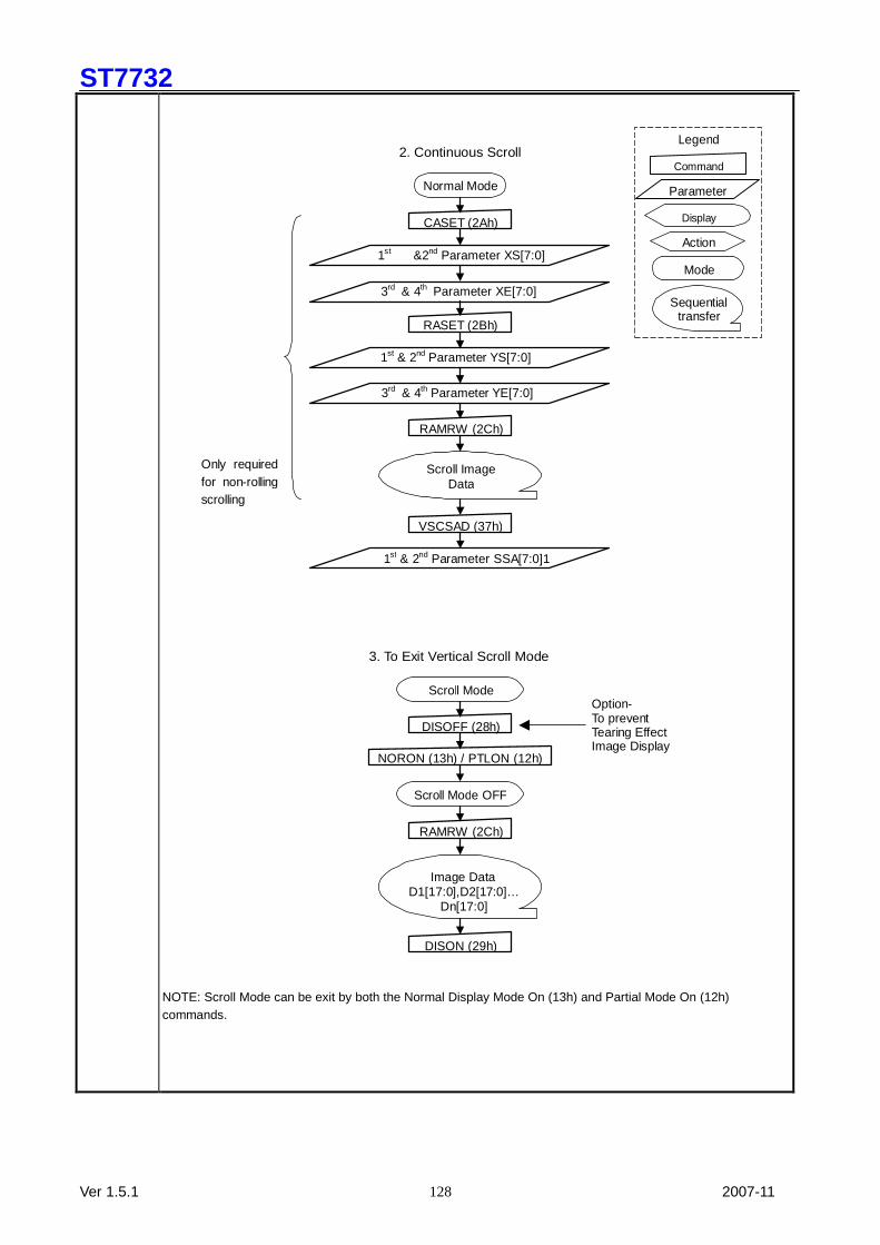
ST7732
Ver 1.5.1 2007-11 128
NOTE: Scroll Mode can be exit by both the Normal Display Mode On (13h) and Partial Mode On (12h) commands.
2. Continuous Scroll
Normal Mode
CASET (2Ah)
1st &2nd Parameter XS[7:0]
3rd & 4th Parameter XE[7:0]
RASET (2Bh)
Legend Command
Parameter
Display
Action
Mode Sequential
transfer
1st & 2nd Parameter YS[7:0]
3rd & 4th Parameter YE[7:0]
RAMRW (2Ch)
Only required for non-rolling scrolling
Scroll Image Data
VSCSAD (37h)
1st & 2nd Parameter SSA[7:0]1
3. To Exit Vertical Scroll Mode
Scroll Mode
DISOFF (28h)
NORON (13h) / PTLON (12h)
Option- To prevent Tearing Effect Image Display
Scroll Mode OFF
RAMRW (2Ch)
Image Data D1[17:0],D2[17:0]…
Dn[17:0]
DISON (29h)

ST7732
Ver 1.5.1 2007-11 129
10.1.27 TEOFF (34h): Tearing Effect Line OFF 34H TEOFF (Tearing Effect Line OFF)
Inst / Para D/CX WRX RDX D17-8 D7 D6 D5 D4 D3 D2 D1 D0 (Code) TEOFF 0 ↑ 1 - 0 0 1 1 0 1 0 0 (34h)
1st Parameter No Parameter -
NOTE: “-” Don’t care, can be set to VDDI or DGND level
Description -This command is used to turn OFF (Active Low) the Tearing Effect output signal from the TE signal line.
Default
Status Default Value
Power On Sequence OFF S/W Reset OFF H/W Reset OFF
10.1.28 TEON (35h): Tearing Effect Line ON
35H TEON (Tearing Effect Line ON) Inst / Para D/CX WRX RDX D17-8 D7 D6 D5 D4 D3 D2 D1 D0 (Code)
TEON 0 ↑ 1 - 0 0 1 1 0 1 0 1 (35h) 1st Parameter 1 ↑ 1 - 0 0 0 0 0 0 0 TELOM
NOTE: “-” Don’t care, can be set to VDDI or DGND level
Description
-This command is used to turn ON the Tearing Effect output signal from the TE signal line. -This output is not affected by changing MADCTL bit ML. -The Tearing Effect Line On has one parameter, which describes the mode of the Tearing Effect Output Line. (“-“=Don’t Care).
-When TELOM=’0’:
-When TELOM=’1’:
Note: During Sleep In Mode with Tearing Effect Line On, Tearing Effect Output pin will be active Low.
Default
Status Default Value
Power On Sequence Tearing effect off & TELOM=0 S/W Reset Tearing effect off & TELOM=0 H/W Reset Tearing effect off & TELOM=0
Vertical time scale
tvdl tvdh
The Tearing Effect Output line consists of V-Blanking information only.
The Tearing Effect Output line consists of both V-Blanking and H-Blinking information.
Vertical time scale
tvdl tvdh
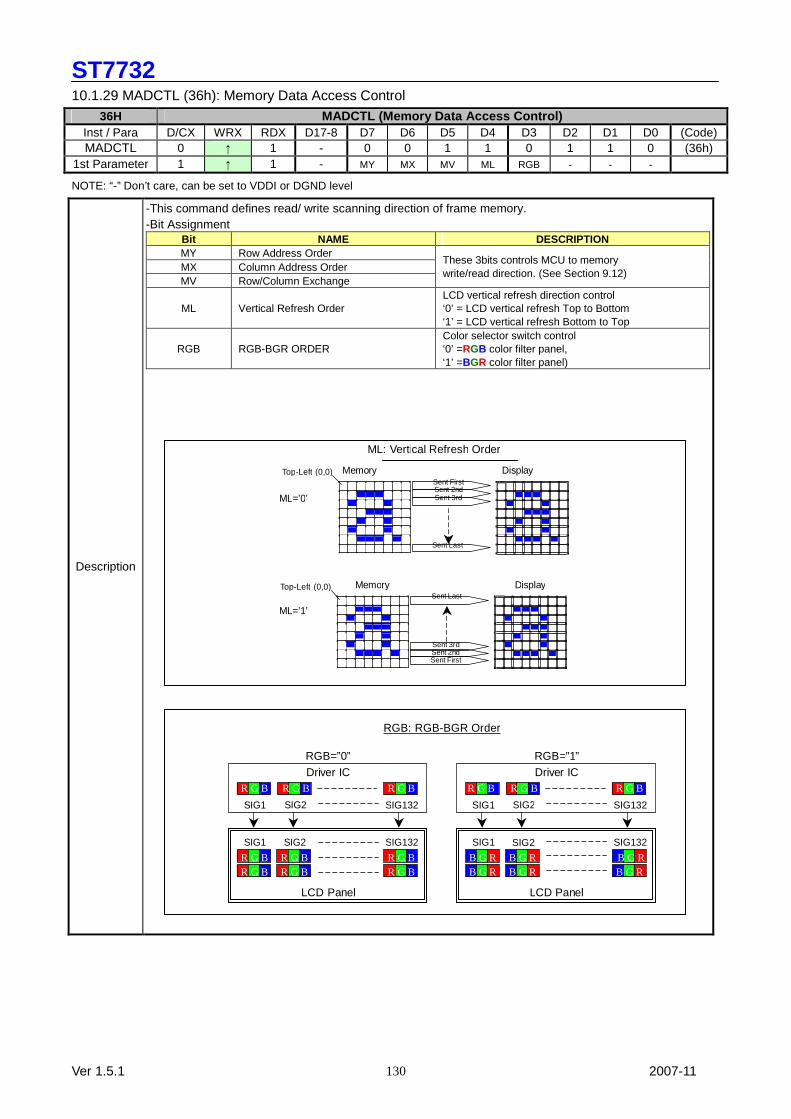
ST7732
Ver 1.5.1 2007-11 130
10.1.29 MADCTL (36h): Memory Data Access Control 36H MADCTL (Memory Data Access Control)
Inst / Para D/CX WRX RDX D17-8 D7 D6 D5 D4 D3 D2 D1 D0 (Code) MADCTL 0 ↑ 1 - 0 0 1 1 0 1 1 0 (36h)
1st Parameter 1 ↑ 1 - MY MX MV ML RGB - - -
NOTE: “-” Don’t care, can be set to VDDI or DGND level
Description
-This command defines read/ write scanning direction of frame memory. -Bit Assignment
Bit NAME DESCRIPTION MY Row Address Order MX Column Address Order MV Row/Column Exchange
These 3bits controls MCU to memory write/read direction. (See Section 9.12)
ML Vertical Refresh Order LCD vertical refresh direction control ‘0’ = LCD vertical refresh Top to Bottom ‘1’ = LCD vertical refresh Bottom to Top
RGB RGB-BGR ORDER Color selector switch control ‘0’ =RGB color filter panel, ‘1’ =BGR color filter panel)
Sent 3rd Sent 2nd Sent First
Memory Display Sent Last
Sent Last
ML: Vertical Refresh Order Memory Display
Sent First Sent 2nd Sent 3rd
Top-Left (0,0)
ML=’0’
Top-Left (0,0)
ML=’1’
RGB: RGB-BGR Order
R G B SIG1
RGB=”0” Driver IC
R G B SIG2
R G B SIG132
R G B SIG1
RGB=”1” Driver IC
R G B SIG2
R G B SIG132
SIG1
R G B
R G
SIG2
R G B
R G B
LCD Panel
SIG132
R G B
R G B
SIG1
B G R
SIG2
B G R B G R
LCD Panel
SIG132
B G R
B G R
R G B R G B R G B R G B R G B R G B
B G R B G R
B G R B G R
B G R B G R
R G B R G B
R G B R G B
R G B R G B
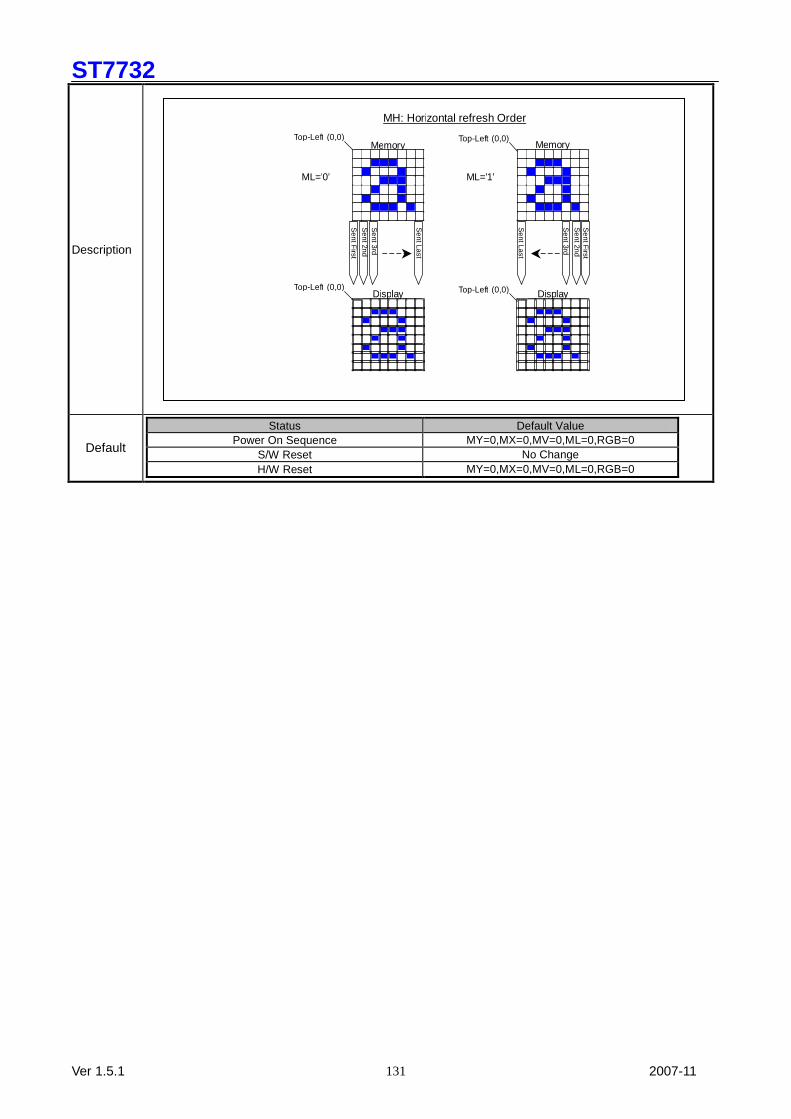
ST7732
Ver 1.5.1 2007-11 131
Description
Default
Status Default Value
Power On Sequence MY=0,MX=0,MV=0,ML=0,RGB=0 S/W Reset No Change H/W Reset MY=0,MX=0,MV=0,ML=0,RGB=0
Top-Left (0,0)
MH: Horizontal refresh Order
Top-Left (0,0) Memory Memory
ML=’0’ ML=’1’
Top-Left (0,0) Display Top-Left (0,0) Display
Sent F
irst S
ent 2nd S
ent 3rd
Sent Last
Sent Last
Sent 3rd
Sent 2nd
Sent F
irst

ST7732
Ver 1.5.1 2007-11 132
10.1.30 VSCSAD (37h): Vertical Scroll Start Address of RAM
37H VSCSAD (Vertical Scroll Start Address of RAM) Inst / Para D/CX WRX RDX D17-8 D7 D6 D5 D4 D3 D2 D1 D0 (Code) VSCSAD 0 ↑ 1 - 0 0 1 1 0 1 1 1 (37h) 1st Parameter 1 ↑ 1 - - - - - - - - - 2nd Parameter 1 ↑ 1 SSA7 SSA6 SSA5 SSA4 SSA3 SSA2 SSA1 SSA0
Note: “-” Don’t care, can be set to VDDI or DGND level
Description
-This command is used together with Vertical Scrolling Definition (33h). These two commands describe the scrolling area and the scrolling mode. -The Vertical Scrolling Start Address command has one parameter which describes which line in the Frame Memory will be written as the first line after the last line of the Top Fixed Area on the display as illustrated below: -This command Start the scrolling. -Exit from V-scrolling mode by commands Partial mode On (12h) or Normal mode On (13h). When MADCTL ML= ‘0’
Example: -When Top Fixed Area=Bottom Fixed Area=00, Vertical Scrolling Area=160 and Vertical Scrolling
Pointer SSA= ’3’.
When MADCTL ML = ‘1’ Example: -When Top Fixed Area= Bottom Fixed Area=00, Vertical Scrolling Area=160 and SSA= ’3’
NOTE: -When new Pointer position and Picture Data are sent, the result on the display will happen at the next Panel Scan to avoid tearing effect.
-SSA refers to the Frame Memory scan address.
Register Availability
Status Availability
Normal Mode On, Idle Mode Off, Sleep Out Yes
Normal Mode On, Idle Mode On, Sleep Out Yes
Partial Mode On, Idle Mode Off, Sleep Out No
Partial Mode On, Idle Mode On, Sleep Out No
Sleep In Yes
Default
Status Default Value
Power On Sequence 0000h S/W Reset 0000h H/W Reset 0000h
Top-Left (0,0)
SSA[7:0] Scroll start address
(Example)
Scan address Memory Display
0 G1 1 G2 2 G3 3 G4 ∣ | ∣ |
158 G159 159 G160
Top-Left (0,0)
SSA[7:0] Scroll start address
(Example)
Scan address Memory Display
159 G1 158 G2 ∣ G3 ∣ G4 3 | 2 | 1 G159 0 G160
ST7732
Ver 1.5.1 2007-11 133
10.1.31 IDMOFF (38h): Idle Mode Off
38H IDMOFF (Idle Mode Off)
Inst / Para D/CX WRX RDX D17-8 D7 D6 D5 D4 D3 D2 D1 D0 (Code) IDMOFF 0 ↑ 1 - 0 0 1 1 1 0 0 0 (38h)
1st Parameter No Parameter -
NOTE: “-” Don’t care, can be set to VDDI or DGND level
Description
-This command is used to recover from Idle mode on. -In the idle off mode,
1. LCD can display 4096, 65k or 262k colors. 2. Normal frame frequency is applied.
Default
Status Default Value
Power On Sequence Idle Mode Off S/W Reset Idle Mode Off H/W Reset Idle Mode Off
10.1.32 IDMON (39h): Idle Mode On
39H IDMON (Idle Mode On)
Inst / Para D/CX WRX RDX D17-8 D7 D6 D5 D4 D3 D2 D1 D0 (Code) IDMOFF 0 ↑ 1 - 0 0 1 1 1 0 0 1 (39h)
1st Parameter No Parameter -
NOTE: “-” Don’t care, can be set to VDDI or DGND level
Description
-This command is used to enter into Idle mode on. -There will be no abnormal visible effect on the display mode change transition. -In the idle on mode,
1. Color expression is reduced. The primary and the secondary colors using MSB of each R,G and B in the Frame Memory, 8 color depth data is displayed.
2. 8-Color mode frame frequency is applied. 3. Exit from IDMON by Idle Mode Off (38h) command
Color R5 R4 R3 R2 R1 R0 G5 G4 G3 G2 G1 G0 B5 B4 B3 B4 B1 B0
Black 0xxxxx 0xxxxx 0xxxxx
Blue 0xxxxx 0xxxxx 1xxxxx
Red 1xxxxx 0xxxxx 0xxxxx
Magenta 1xxxxx 0xxxxx 1xxxxx
Green 0xxxxx 1xxxxx 0xxxxx
Cyan 0xxxxx 1xxxxx 1xxxxx
Yellow 1xxxxx 1xxxxx 0xxxxx
White 1xxxxx 1xxxxx 1xxxxx
Top-Left (0,0) (Example)
Mem ory Display
ST7732
Ver 1.5.1 2007-11 134
Register Availability
Status Availability
Normal Mode On, Idle Mode Off, Sleep Out Yes
Normal Mode On, Idle Mode On, Sleep Out Yes
Partial Mode On, Idle Mode Off, Sleep Out No
Partial Mode On, Idle Mode On, Sleep Out No
Sleep In Yes
Default
Status Default Value
Power On Sequence Idle Mode Off S/W Reset Idle Mode Off H/W Reset Idle Mode Off
10.1.33 COLMOD (3Ah): Interface Pixel Format
3AH COLMOD (3Ah): Interface Pixel Format
Inst / Para D/CX WRX RDX D17-8 D7 D6 D5 D4 D3 D2 D1 D0 (Code) COLMOD 0 ↑ 1 - 0 0 1 1 1 0 1 0 (3Ah)
1st Parameter 1 ↑ 1 - VIPF3 VIPF2 VIPF1 VIPF0 - IFPF2 IFPF1 IFPF0
NOTE: “-” Don’t care, can be set to VDDI or DGND level
Description
This command is used to define the format of RGB picture data, which is to be transferred via the MCU interface and RGB interface. The formats are shown in the table:
IFPF[2:0] MCU Interface Color Format 011 3 12-bit/pixel 101 5 16-bit/pixel 110 6 18-bit/pixel 111 7 No used
Others are no define and invalid
VIFPF[2:0] RGB Interface Color Format 0101 5 16-bit/pixel (1-times data transfer) 0110 6 18-bit/pixel (1-times data transfer) 0111 7 No used 1110 14 18-bit/pixel (3-times data transfer)
Others are no define and invalid Note1: In 12-bit/Pixel, 16-bit/Pixel or 18-bit/Pixel mode, the LUT is applied to transfer data into the Frame Memory.
Note2: When RGB I/F the 12-bit/pixel don’t care
Note3: When VIPF[3:0]=”1110”,6-bit data width of 3-times transfer is used to transmit 1 pixel data with the 18-bit color
depth information.
Note4: The Command 3Ah should be set at 55h when writing 16-bit/pixel data into frame memory, but 3Ah should be
re-set to 66h when reading pixel data from frame memory. Please check the LUT in chapter 9.19 when using
memory read function.
Register Availability
Status Availability
Normal Mode On, Idle Mode Off, Sleep Out Yes
Normal Mode On, Idle Mode On, Sleep Out Yes
Partial Mode On, Idle Mode Off, Sleep Out No
Partial Mode On, Idle Mode On, Sleep Out No
Sleep In Yes
Default
Status Default Value
IFPF[2:0] VIPF[3:0]
Power On Sequence 0110(18-bit/Pixel) 0110(18-bit/Pixel)
S/W Reset No Change No Change
H/W Reset 0110(18-bit/Pixel) 0110(18-bit/Pixel)
ST7732
Ver 1.5.1 2007-11 135
10.1.34 RDID1 (DAh): Read ID1 Value
DAH RDID1 (Read ID1 Value)
Inst / Para D/CX WRX RDX D17-8 D7 D6 D5 D4 D3 D2 D1 D0 (Code) RDID1 0 ↑ 1 - 1 1 0 1 1 0 1 0 (DAh)
1st Parameter 1 1 ↑ - - - - - - - - - -
2nd Parameter 1 1 ↑ - ID17 ID16 ID15 ID14 ID13 ID12 ID11 ID10
NOTE: “-” Don’t care, can be set to VDDI or DGND level
Description
-This read byte returns 8-bit LCD module’s manufacturer ID -The 1st parameter is dummy data -The 2nd parameter (ID17 to ID10): LCD module’s manufacturer ID. NOTE: See command RDDID (04h), 2nd parameter.
Register Availability
Status Availability
Normal Mode On, Idle Mode Off, Sleep Out Yes
Normal Mode On, Idle Mode On, Sleep Out Yes
Partial Mode On, Idle Mode Off, Sleep Out No
Partial Mode On, Idle Mode On, Sleep Out No
Sleep In Yes
Default
Status Default Value
Power On Sequence -
S/W Reset -
H/W Reset -
10.1.35 RDID2 (DBh): Read ID2 Value
DBH RDID2 (Read ID2 Value)
Inst / Para D/CX WRX RDX D17-8 D7 D6 D5 D4 D3 D2 D1 D0 (Code) RDID2 0 ↑ 1 - 1 1 0 1 1 0 1 1 (DBh)
1st Parameter 1 1 ↑ - - - - - - - - - -
2nd Parameter 1 1 ↑ - 1 ID26 ID25 ID24 ID23 ID22 ID21 ID20
NOTE: “-” Don’t care, can be set to VDDI or DGND level
Description
-This read byte returns 8-bit LCD module/driver version ID -The 1st parameter is dummy data -The 2nd parameter (ID26 to ID20): LCD module/driver version ID -Parameter Range: ID=80h to FFh
ID26 to ID20 Version Changes
80h
81h
82h
83h
NOTE: See command RDDID (04h), 3rd parameter.
Register Availability
Status Availability
Normal Mode On, Idle Mode Off, Sleep Out Yes
Normal Mode On, Idle Mode On, Sleep Out Yes
Partial Mode On, Idle Mode Off, Sleep Out No
Partial Mode On, Idle Mode On, Sleep Out No
Sleep In Yes
Default
Status Default Value
Power On Sequence 80h
S/W Reset 80h
H/W Reset 80h

ST7732
Ver 1.5.1 2007-11 136
10.1.36 RDID3 (DCh): Read ID3 Value
DCH RDID3 (Read ID2 Value)
Inst / Para D/CX WRX RDX D17-8 D7 D6 D5 D4 D3 D2 D1 D0 (Code) RDID3 0 ↑ 1 - 1 1 0 1 1 1 0 0 (DCh)
1st Parameter 1 1 ↑ - - - - - - - - - -
2nd Parameter 1 1 ↑ - ID37 ID36 ID35 ID34 ID33 ID32 ID31 ID30
NOTE: “-” Don’t care, can be set to VDDI or DGND level
Description
-This read byte returns 8-bit LCD module/driver ID. -The 1st parameter is dummy data -The 2nd parameter (ID37 to ID30): LCD module/driver ID.
NOTE: See command RDDID (04h), 4th parameter.
Register Availability
Status Availability
Normal Mode On, Idle Mode Off, Sleep Out Yes
Normal Mode On, Idle Mode On, Sleep Out Yes
Partial Mode On, Idle Mode Off, Sleep Out No
Partial Mode On, Idle Mode On, Sleep Out No
Sleep In Yes
Default
Status Default Value
Power On Sequence 00h
S/W Reset 00h
H/W Reset 00h
10.2.1 RGBCTR (B0h): RGB signal control
B0H RGBCTR (RGB signal control) Inst / Para D/CX WRX RDX D17-8 D7 D6 D5 D4 D3 D2 D1 D0 (Code) RGBCTR 0 ↑ 1 - 1 0 1 1 0 0 0 0 (B0h)
1st Parameter 1 ↑ 1 - 0 0 DISSW ICM DP EP HSP VSP
NOTE: “-“ Don’t care
Description
-Set the operation status on the RGB interface. The setting becomes effective as soon as the command is received. -ICM: GRAM Write/Read frequency and data input select on the RGB interface
ICM Write/ Read frequency and input data select Write cycle Read cycle Data input 0 PCLK PCLK D[17:0] 1 SCL Internal oscillator SDA
Symbol Name Clock polarity set for RGB Interface
DP PCLK polarity set ‘1’ = data fetched at the falling edge ‘0’ = data fetched at the rising edge
EP Enable polarity set ‘1’ = Low enable for RGB interface ‘0’ = High enable for RGB interface
HSP Hsync polarity set ‘1’ = High level sync clock ‘0’ = Low level sync clock
VSP Vsync polarity set ‘1’ = High level sync clock ‘0’ = Low level sync clock
DISSW Disable S/W ‘1’ = Disable S/W control ‘0’ = Enable S/W control
Default
Status Default Value
ICM DP/EP/HSP/VSP Power On Sequence 0d 0d/0d/0d/0d
S/W Reset 0d 0d/0d/0d/0d H/W Reset 0d 0d/0d/0d/0d

ST7732
Ver 1.5.1 2007-11 137
10.2.2 FRMCTR1 (B1h): Frame Rate Control (In normal mode/ Full colors) B1H FRMCTR1 (Frame Rate Control)
Inst / Para D/CX WRX RDX D17-8 D7 D6 D5 D4 D3 D2 D1 D0 (Code) FRMCTR1 0 ↑ 1 - 1 0 1 1 0 0 0 1 (B1h)
1st Parameter 1 ↑ 1 - RTNA3 RTNA2 RTNA1 RTNA0 - 2nd Parameter 1 ↑ 1 - FPA3 FPA2 FPA1 FPA0 - 3rd Parameter 1 ↑ 1 - BPA3 BPA2 BPA1 BPA0 -
NOTE: “-“ Don’t care
Description
-Set the frame frequency of the full colors normal mode. - Frame rate=fosc/((RTNA + 18) x (LINE + FPA + BPA)) - 1 < FPA(front porch) + BPA(back porch)<=22
Default
Status Default Value
Power On Sequence 06h/03h/02h S/W Reset 06h/03h/02h H/W Reset 06h/03h/02h
10.2.3 FRMCTR2 (B2h): Frame Rate Control (In Idle mode/ 8-colors) B2H FRMCTR2 (Frame Rate Control)
Inst / Para D/CX WRX RDX D17-8 D7 D6 D5 D4 D3 D2 D1 D0 (Code) FRMCTR2 0 ↑ 1 - 1 0 1 1 0 0 1 0 (B2h)
1st Parameter 1 ↑ 1 - RTNB3 RTNB2 RTNB1 RTNB0 - 2nd Parameter 1 ↑ 1 - FPB3 FPB2 FPB1 FPB0 - 3rd Parameter 1 ↑ 1 - BPB3 BPB2 BPB1 BPB0 -
NOTE: “-“ Don’t care
Description
-Set the frame frequency of the Idle mode. - Frame rate=fosc/((RTNB + 18) x (LINE + FPB + BPB)) - 1 < FPB(front porch) + BPB(back porch)<=22
Default
Status Default Value
Power On Sequence 06h/03h/02h S/W Reset 06h/03h/02h H/W Reset 06h/03h/02h
10.2.4 FRMCTR3 (B3h): Frame Rate Control (In Partial mode/ full colors) B3H FRMCTR3 (Frame Rate Control)
Inst / Para D/CX WRX RDX D17-8 D7 D6 D5 D4 D3 D2 D1 D0 (Code) FRMCTR3 0 ↑ 1 - 1 0 1 1 0 0 1 1 (B3h)
1st Parameter 1 ↑ 1 - RTNC3 RTNC2 RTNC1 RTNC0 - 2nd Parameter 1 ↑ 1 - FPC3 FPC2 FPC1 FPC0 - 3rd Parameter 1 ↑ 1 - BPC3 BPC2 BPC1 BPC0 - 4th Parameter 1 ↑ 1 - RTND3 RTND2 RTND1 RTND0 5th Parameter 1 ↑ 1 - FPD3 FPD2 FPD1 FPD0 6th Parameter 1 ↑ 1 - BPD3 BPD2 BPD1 BPD0 -
NOTE: “-“ Don’t care
Description
-Set the frame frequency of the Partial mode/ full colors. - 1st parameter to 3rd parameter are used in line inversion mode. - 4th parameter to 6th parameter are used in frame inversion mode. - Frame rate=fosc/((RTNC + 18) x (LINE + FPC + BPC)) - 1 < FPC(front porch) + BPC(back porch)<=22
ST7732
Ver 1.5.1 2007-11 138
Default
Status Default Value
Power On Sequence 06h/03h/02h S/W Reset 06h/03h/02h H/W Reset 06h/03h/02h
10.2.5 INVCTR (B4h): Display Inversion Control B4H INVCTR (Display Inversion Control)
Inst / Para D/CX WRX RDX D17-8 D7 D6 D5 D4 D3 D2 D1 D0 (Code) INVCTR 0 ↑ 1 - 1 0 1 1 0 1 0 0 (B4h)
1st Parameter 1 ↑ 1 - 0 0 0 0 0 NLA NLB NLC 02h
NOTE: “-“ Don’t care
Description
-Display Inversion mode control
-NLA: Inversion setting in full colors normal mode (Normal mode on)
NLA Inversion setting in full Colors normal mode 0 Line Inversion 1 Frame Inversion
-NLB: Inversion setting in Idle mode (Idle mode on) NLB Inversion setting in Idle mode
0 Line Inversion 1 Frame Inversion
-NLC: Inversion setting in full colors partial mode (Partial mode on / Idle mode off) NLC Inversion setting in full Colors partial mode
0 Line Inversion 1 Frame Inversion
Default
Status Default Value
NLA NLB NLC B4h Power On Sequence 0d 1d 0d 02h
S/W Reset 0d 1d 0d 02h H/W Reset 0d 1d 0d 02h
10.2.6 RGBBPCTR (B5h): RGB Interface Blanking Porch setting
B5H RGBPSET (RGB Interface Blanking Porch setting) Inst / Para D/CX WRX RDX D17-8 D7 D6 D5 D4 D3 D2 D1 D0 (Code)
RGBBPCTR 0 ↑ 1 - 1 0 1 1 0 1 0 1 (B5h)
1st Parameter 1 ↑ 1 - - - - - - - - - -
2nd Parameter 1 ↑ 1 - VBP7 VBP6 VBP5 VBP4 VBP3 VBP2 VBP1 VBP0 -
3rd Parameter 1 ↑ 1 - - - - - - - - HBP8 -
4th Parameter 1 ↑ 1 - HBP7 HBP6 HBP5 HBP4 HBP3 HBP2 HBP1 HBP0 -
NOTE: “-“ Don’t care
Description -Set the blanking porch in the RGB interface -VBP:Vertical back porch -HBP:Horizontal back porch
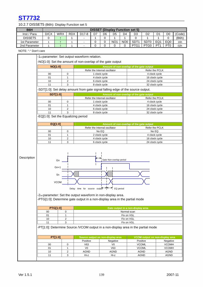
ST7732
Ver 1.5.1 2007-11 139
10.2.7 DISSET5 (B6h): Display Function set 5
B6H DISSET (Display Function set 5) Inst / Para D/CX WRX RDX D17-8 D7 D6 D5 D4 D3 D2 D1 D0 (Code) DISSET5 0 ↑ 1 - 1 0 1 1 0 1 1 0 (B6h)
1st Parameter 1 ↑ 1 - 0 0 NO1 NO0 SDT1 SDT0 EQ1 EQ0 16h 2nd Parameter 1 ↑ 1 - 0 0 0 0 PTG1 PTG0 PT1 PT0 02h
NOTE: “-“ Don’t care
Description
-1st parameter: Set output waveform relation.
-NO[1:0]: Set the amount of non-overlap of the gate output NO[1:0] Amount of non-overlap of the gate output Refer the Internal oscillator Refer the PCLK
00 0 1 clock cycle 4 clock cycle 01 1 4 clock cycle 16 clock cycle 10 2 6 clock cycle 24 clock cycle 11 3 8 clock cycle 32 clock cycle
-SDT[1:0]: Set delay amount from gate signal falling edge of the source output. SDT[1:0] Amount of non-overlap of the gate output Refer the Internal oscillator Refer the PCLK
00 0 1 clock cycle 4 clock cycle 01 1 4 clock cycle 16 clock cycle 10 2 6 clock cycle 24 clock cycle 11 3 8 clock cycle 32 clock cycle
-EQ[1:0]: Set the Equalizing period
-2nd parameter: Set the output waveform in non-display area. -PTG[1:0]: Determine gate output in a non-display area in the partial mode
-PT[1:0]: Determine Source /VCOM output in a non-display area in the partial mode
EQ[1:0] Amount of non-overlap of the gate output Refer the Internal oscillator Refer the PCLK
00 0 No EQ No EQ 01 1 2 clock cycle 4 clock cycle 10 2 4 clock cycle 16 clock cycle 11 3 6 clock cycle 24 clock cycle
PTG[1:0] Gate output in a non-display area 00 0 Normal scan 01 1 Fix on VGL 10 2 Fix on VGL 11 3 Fix on VGL
PT[1:0] Source output on non-display area VCOM output on non-display area Positive Negative Positive Negative
00 0 V63 V0 VCOML VCOMH 01 1 V0 V63 VCOML VCOMH 10 2 AGND AGND AGND AGND 11 3 Hi-z Hi-z AGND AGND
Gn Gate Non-overlap period
Gn+1
Sn
VCOM
Delay time for source output EQ period

ST7732
Ver 1.5.1 2007-11 140
10.2.8 PWCTR1 (C0h): Power Control 1
C0H PWCTR1 (Power Control 1) Inst / Para D/CX WRX RDX D17-8 D7 D6 D5 D4 D3 D2 D1 D0 (Code) PWCTR1 0 ↑ 1 - 1 1 0 0 0 0 0 0 (C0h)
1st Parameter 1 ↑ 1 - 0 0 0 VRH4 VRH3 VRH2 VRH1 VRH0 2nd Parameter 1 ↑ 1 - 0 0 0 0 0 VC2 VC1 VC0
NOTE: “-“ Don’t care
Description
-Set the GVDD and VCI1 voltage VRH[4:0] GVDD
00000 0 5.00 00001 1 4.75 00010 2 4.70 00011 3 4.65 00100 4 4.60 00101 5 4.55 00110 6 4.50 00111 7 4.45 01000 8 4.40 01001 9 4.35 01010 10 4.30 01011 11 4.25 01100 12 4.20 01101 13 4.15 01110 14 4.10 01111 15 4.05 10000 16 4.00 10001 17 3.95 10010 18 3.90 10011 19 3.85 10100 20 3.80 10101 21 3.75 10110 22 3.70 10111 23 3.65 11000 24 3.60 11001 25 3.55 11010 26 3.50 11011 27 3.45 11100 28 3.40 11101 29 3.35 11110 30 3.25 11111 31 3.00
VC[2:0] VCI1
000 0 2.75 001 1 2.70 010 2 2.65 011 3 2.60 100 4 2.55 101 5 2.50
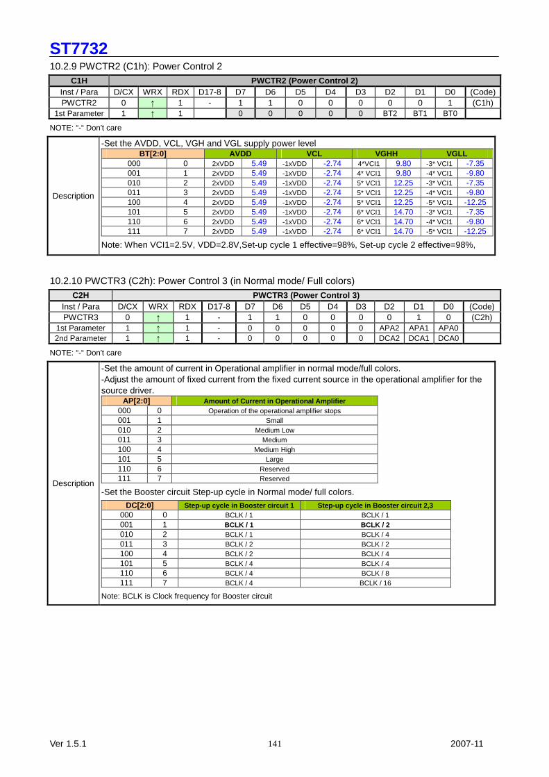
ST7732
Ver 1.5.1 2007-11 141
10.2.9 PWCTR2 (C1h): Power Control 2
C1H PWCTR2 (Power Control 2) Inst / Para D/CX WRX RDX D17-8 D7 D6 D5 D4 D3 D2 D1 D0 (Code) PWCTR2 0 ↑ 1 - 1 1 0 0 0 0 0 1 (C1h)
1st Parameter 1 ↑ 1 0 0 0 0 0 BT2 BT1 BT0
NOTE: “-“ Don’t care
Description
-Set the AVDD, VCL, VGH and VGL supply power level BT[2:0] AVDD VCL VGHH VGLL
000 0 2xVDD 5.49 -1xVDD -2.74 4*VCI1 9.80 -3* VCI1 -7.35 001 1 2xVDD 5.49 -1xVDD -2.74 4* VCI1 9.80 -4* VCI1 -9.80 010 2 2xVDD 5.49 -1xVDD -2.74 5* VCI1 12.25 -3* VCI1 -7.35 011 3 2xVDD 5.49 -1xVDD -2.74 5* VCI1 12.25 -4* VCI1 -9.80 100 4 2xVDD 5.49 -1xVDD -2.74 5* VCI1 12.25 -5* VCI1 -12.25 101 5 2xVDD 5.49 -1xVDD -2.74 6* VCI1 14.70 -3* VCI1 -7.35 110 6 2xVDD 5.49 -1xVDD -2.74 6* VCI1 14.70 -4* VCI1 -9.80 111 7 2xVDD 5.49 -1xVDD -2.74 6* VCI1 14.70 -5* VCI1 -12.25
Note: When VCI1=2.5V, VDD=2.8V,Set-up cycle 1 effective=98%, Set-up cycle 2 effective=98%,
10.2.10 PWCTR3 (C2h): Power Control 3 (in Normal mode/ Full colors) C2H PWCTR3 (Power Control 3)
Inst / Para D/CX WRX RDX D17-8 D7 D6 D5 D4 D3 D2 D1 D0 (Code) PWCTR3 0 ↑ 1 - 1 1 0 0 0 0 1 0 (C2h)
1st Parameter 1 ↑ 1 - 0 0 0 0 0 APA2 APA1 APA0 2nd Parameter 1 ↑ 1 - 0 0 0 0 0 DCA2 DCA1 DCA0
NOTE: “-“ Don’t care
Description
-Set the amount of current in Operational amplifier in normal mode/full colors. -Adjust the amount of fixed current from the fixed current source in the operational amplifier for the source driver.
AP[2:0] Amount of Current in Operational Amplifier 000 0 Operation of the operational amplifier stops 001 1 Small 010 2 Medium Low 011 3 Medium 100 4 Medium High 101 5 Large 110 6 Reserved 111 7 Reserved
-Set the Booster circuit Step-up cycle in Normal mode/ full colors. DC[2:0] Step-up cycle in Booster circuit 1 Step-up cycle in Booster circuit 2,3
000 0 BCLK / 1 BCLK / 1 001 1 BCLK / 1 BCLK / 2 010 2 BCLK / 1 BCLK / 4 011 3 BCLK / 2 BCLK / 2 100 4 BCLK / 2 BCLK / 4 101 5 BCLK / 4 BCLK / 4 110 6 BCLK / 4 BCLK / 8 111 7 BCLK / 4 BCLK / 16
Note: BCLK is Clock frequency for Booster circuit

ST7732
Ver 1.5.1 2007-11 142
10.2.11 PWCTR4 (C3h): Power Control 4 (in Idle mode/ 8-colors)
C3H PWCTR4 (Power Control 4) Inst / Para D/CX WRX RDX D17-8 D7 D6 D5 D4 D3 D2 D1 D0 (Code) PWCTR4 0 ↑ 1 - 1 1 0 0 0 0 1 1 (C3h)
1st Parameter 1 ↑ 1 - 0 0 0 0 0 APB2 APB1 APB0 2nd Parameter 1 ↑ 1 - 0 0 0 0 0 DCB2 DCB1 DCB0
NOTE: “-“ Don’t care
Description
-Set the amount of current in Operational amplifier in Idle mode/8 colors. -Adjust the amount of fixed current from the fixed current source in the operational amplifier for the source driver.
AP[2:0] Amount of Current in Operational Amplifier 000 0 Operation of the operational amplifier stops 001 1 Small 010 2 Medium Low 011 3 Medium 100 4 Medium High 101 5 Large 110 6 Reserved 111 7 Reserved
-Set the Booster circuit Step-up cycle in Idle mode/8 colors. DC[2:0] Step-up cycle in Booster circuit 1 Step-up cycle in Booster circuit 2,3
000 0 BCLK / 1 BCLK / 1 001 1 BCLK / 1 BCLK / 2 010 2 BCLK / 1 BCLK / 4 011 3 BCLK / 2 BCLK / 2 100 4 BCLK / 2 BCLK / 4 101 5 BCLK / 4 BCLK / 4 110 6 BCLK / 4 BCLK / 8 111 7 BCLK / 4 BCLK / 16
Note: BCLK is Clock frequency for Booster circuit
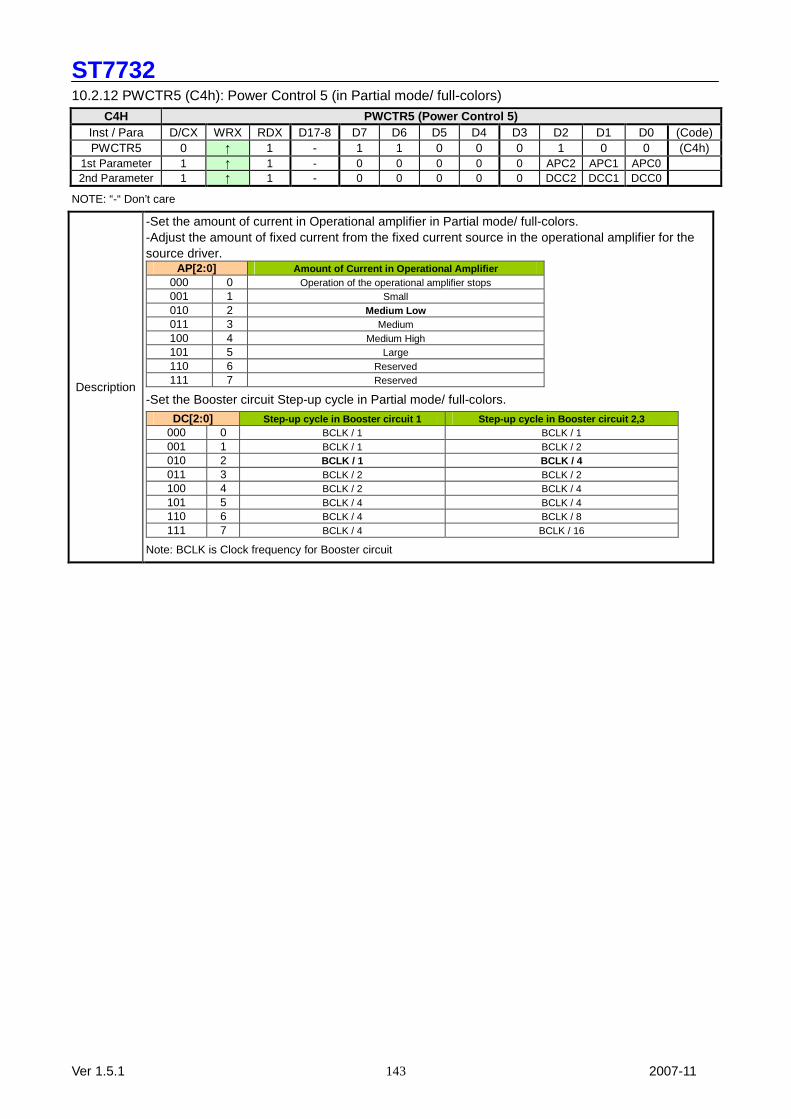
ST7732
Ver 1.5.1 2007-11 143
10.2.12 PWCTR5 (C4h): Power Control 5 (in Partial mode/ full-colors)
C4H PWCTR5 (Power Control 5) Inst / Para D/CX WRX RDX D17-8 D7 D6 D5 D4 D3 D2 D1 D0 (Code) PWCTR5 0 ↑ 1 - 1 1 0 0 0 1 0 0 (C4h)
1st Parameter 1 ↑ 1 - 0 0 0 0 0 APC2 APC1 APC0 2nd Parameter 1 ↑ 1 - 0 0 0 0 0 DCC2 DCC1 DCC0
NOTE: “-“ Don’t care
Description
-Set the amount of current in Operational amplifier in Partial mode/ full-colors. -Adjust the amount of fixed current from the fixed current source in the operational amplifier for the source driver.
AP[2:0] Amount of Current in Operational Amplifier 000 0 Operation of the operational amplifier stops 001 1 Small 010 2 Medium Low 011 3 Medium 100 4 Medium High 101 5 Large 110 6 Reserved 111 7 Reserved
-Set the Booster circuit Step-up cycle in Partial mode/ full-colors. DC[2:0] Step-up cycle in Booster circuit 1 Step-up cycle in Booster circuit 2,3
000 0 BCLK / 1 BCLK / 1 001 1 BCLK / 1 BCLK / 2 010 2 BCLK / 1 BCLK / 4 011 3 BCLK / 2 BCLK / 2 100 4 BCLK / 2 BCLK / 4 101 5 BCLK / 4 BCLK / 4 110 6 BCLK / 4 BCLK / 8 111 7 BCLK / 4 BCLK / 16
Note: BCLK is Clock frequency for Booster circuit
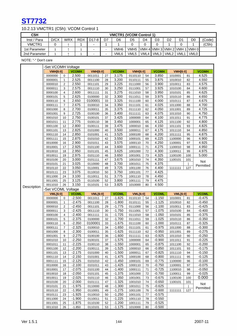
ST7732
Ver 1.5.1 2007-11 144
10.2.13 VMCTR1 (C5h): VCOM Control 1
C5H VMCTR1 (VCOM Control 1) Inst / Para D/CX WRX RDX D17-8 D7 D6 D5 D4 D3 D2 D1 D0 (Code) VMCTR1 0 ↑ 1 - 1 1 0 0 0 1 0 1 (C5h)
1st Parameter 1 ↑ 1 - - VMH6 VMH5 VMH 4 VMH 3 VMH 2 VMH 1 VMH 0 2nd Parameter 1 ↑ 1 - - VML6 VML5 VML4 VML3 VML2 VML1 VML0
NOTE: “-“ Don’t care
Description
-Set VCOMH Voltage VMH[6:0] VCOMH VMH[6:0] VCOMH VMH[6:0] VCOMH VMH[6:0] VCOMH
0000000 0 2.500 0011011 27 3.175 0110110 54 3.850 1010001 81 4.525 0000001 1 2.525 0011100 28 3.200 0110111 55 3.875 1010010 82 4.550 0000010 2 2.550 0011101 29 3.225 0111000 56 3.900 1010011 83 4.575 0000011 3 2.575 0011110 30 3.250 0111001 57 3.925 1010100 84 4.600 0000100 4 2.600 0011111 31 3.275 0111010 58 3.950 1010101 85 4.625 0000101 5 2.625 0100000 32 3.300 0111011 59 3.975 1010110 86 4.650 0000110 6 2.650 0100001 33 3.325 0111100 60 4.000 1010111 87 4.675 0000111 7 2.675 0100010 34 3.350 0111101 61 4.025 1011000 88 4.700 0001000 8 2.700 0100011 35 3.375 0111110 62 4.050 1011001 89 4.725 0001001 9 2.725 0100100 36 3.400 0111111 63 4.075 1011010 90 4.750 0001010 10 2.750 0100101 37 3.425 1000000 64 4.100 1011011 91 4.775 0001011 11 2.775 0100110 38 3.450 1000001 65 4.125 1011100 92 4.800 0001100 12 2.800 0100111 39 3.475 1000010 66 4.150 1011101 93 4.825 0001101 13 2.825 0101000 40 3.500 1000011 67 4.175 1011110 94 4.850 0001110 14 2.850 0101001 41 3.525 1000100 68 4.200 1011111 95 4.875 0001111 15 2.875 0101010 42 3.550 1000101 69 4.225 1100000 96 4.900 0010000 16 2.900 0101011 43 3.575 1000110 70 4.250 1100001 97 4.925 0010001 17 2.925 0101100 44 3.600 1000111 71 4.275 1100010 98 4.950 0010010 18 2.950 0101101 45 3.625 1001000 72 4.300 1100011 99 4.975 0010011 19 2.975 0101110 46 3.650 1001001 73 4.325 1100100 100 5.000 0010100 20 3.000 0101111 47 3.675 1001010 74 4.350 1100101 101 0010101 21 3.025 0110000 48 3.700 1001011 75 4.375 | 0010110 22 3.050 0110001 49 3.725 1001100 76 4.400 1111111 127
Not Permitted
0010111 23 3.075 0110010 50 3.750 1001101 77 4.425 0011000 24 3.100 0110011 51 3.775 1001110 78 4.450 0011001 25 3.125 0110100 52 3.800 1001111 79 4.475 0011010 26 3.150 0110101 53 3.825 1010000 80 4.500
-Set VCOML Voltage VML[6:0] VCOML VML[6:0] VCOML VML[6:0] VCOML VML[6:0] VCOML
0000000 0 -2.500 0011011 27 -1.825 0110110 54 -1.150 1010001 81 -0.475 0000001 1 -2.475 0011100 28 -1.800 0110111 55 -1.125 1010010 82 -0.450 0000010 2 -2.450 0011101 29 -1.775 0111000 56 -1.100 1010011 83 -0.425 0000011 3 -2.425 0011110 30 -1.750 0111001 57 -1.075 1010100 84 -0.400 0000100 4 -2.400 0011111 31 -1.725 0111010 58 -1.050 1010101 85 -0.375 0000101 5 -2.375 0100000 32 -1.700 0111011 59 -1.025 1010110 86 -0.350 0000110 6 -2.350 0100001 33 -1.675 0111100 60 -1.000 1010111 87 -0.325 0000111 7 -2.325 0100010 34 -1.650 0111101 61 -0.975 1011000 88 -0.300 0001000 8 -2.300 0100011 35 -1.625 0111110 62 -0.950 1011001 89 -0.275 0001001 9 -2.275 0100100 36 -1.600 0111111 63 -0.925 1011010 90 -0.250 0001010 10 -2.250 0100101 37 -1.575 1000000 64 -0.900 1011011 91 -0.225 0001011 11 -2.225 0100110 38 -1.550 1000001 65 -0.875 1011100 92 -0.200 0001100 12 -2.200 0100111 39 -1.525 1000010 66 -0.850 1011101 93 -0.175 0001101 13 -2.175 0101000 40 -1.500 1000011 67 -0.825 1011110 94 -0.150 0001110 14 -2.150 0101001 41 -1.475 1000100 68 -0.800 1011111 95 -0.125 0001111 15 -2.125 0101010 42 -1.450 1000101 69 -0.775 1100000 96 -0.100 0010000 16 -2.100 0101011 43 -1.425 1000110 70 -0.750 1100001 97 -0.075 0010001 17 -2.075 0101100 44 -1.400 1000111 71 -0.725 1100010 98 -0.050 0010010 18 -2.050 0101101 45 -1.375 1001000 72 -0.700 1100011 99 -0.025 0010011 19 -2.025 0101110 46 -1.350 1001001 73 -0.675 1100100 100 0.000 0010100 20 -2.000 0101111 47 -1.325 1001010 74 -0.650 1100101 101 0010101 21 -1.975 0110000 48 -1.300 1001011 75 -0.625 | 0010110 22 -1.950 0110001 49 -1.275 1001100 76 -0.600 1111111 127
Not Permitted
0010111 23 -1.925 0110010 50 -1.250 1001101 77 -0.575 0011000 24 -1.900 0110011 51 -1.225 1001110 78 -0.550 0011001 25 -1.875 0110100 52 -1.200 1001111 79 -0.525 0011010 26 -1.850 0110101 53 -1.175 1010000 80 -0.500

ST7732
Ver 1.5.1 2007-11 145
10.2.14 VMOFCTR (C7h): VCOM Offset Control C7H VMOFCTR (VCOM Offset Control)
Inst / Para D/CX WRX RDX D17-8 D7 D6 D5 D4 D3 D2 D1 D0 (Code)
VMOFCTR 0 ↑ 1 - 1 1 0 0 0 1 1 1 (C7h)
1st Parameter 1 ↑ 1 - - VMF6 - - VMF3 VMF2 VMF1 VMF0
NOTE: “-“ Don’t care, can be set to VDDI or DGND level
Description
-Set VCOM Voltage level for reduce the flicker issue VMF[6] VMF[3:0] VCOMH Output Level VCOML Output Level
0 0000 “VMH”-16d “VML”-16d 0 0001 “VMH”-15d “VML”-15d 0 0010 “VMH”-14d “VML”-14d 0 | | 0 1110 “VMH”-2d “VML”-2d 0 1111 “VMH”-1d “VML”-1d 1 0000 “VMH” “VML” 1 0001 “VMH”+1d “VML”+1d 1 0010 “VMH”+2d “VML”+2d 1 | | 1 1110 “VMH”+14d “VML”+14d 1 1111 “VMH”+15d “VML”+15d
- 1d=25mV, 2d=50mV 3d=75mv.... - 2.5V <= VMH ± nd <= 5.0V; -2. 5V <= VML ± nd<= 0V (n=0~15,16) - VMF[6] & VMF[3:0] are stored in NV memory to contrast.
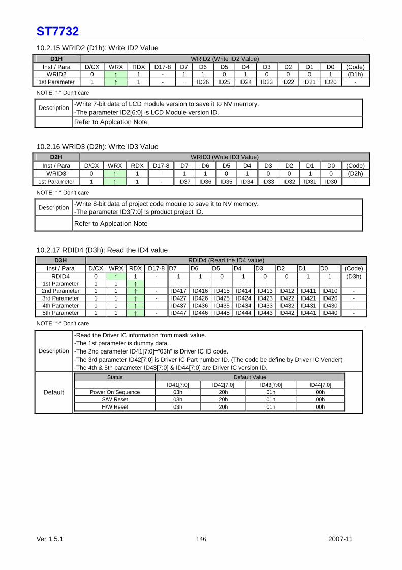
ST7732
Ver 1.5.1 2007-11
146
10.2.15 WRID2 (D1h): Write ID2 Value
D1H WRID2 (Write ID2 Value) Inst / Para D/CX WRX RDX D17-8 D7 D6 D5 D4 D3 D2 D1 D0 (Code)
WRID2 0 ↑ 1 - 1 1 0 1 0 0 0 1 (D1h) 1st Parameter 1 ↑ 1 - - ID26 ID25 ID24 ID23 ID22 ID21 ID20 -
NOTE: “-“ Don’t care
Description -Write 7-bit data of LCD module version to save it to NV memory. -The parameter ID2[6:0] is LCD Module version ID.
Refer to Applcation Note
10.2.16 WRID3 (D2h): Write ID3 Value
D2H WRID3 (Write ID3 Value) Inst / Para D/CX WRX RDX D17-8 D7 D6 D5 D4 D3 D2 D1 D0 (Code)
WRID3 0 ↑ 1 - 1 1 0 1 0 0 1 0 (D2h) 1st Parameter 1 ↑ 1 - ID37 ID36 ID35 ID34 ID33 ID32 ID31 ID30 -
NOTE: “-“ Don’t care
Description -Write 8-bit data of project code module to save it to NV memory. -The parameter ID3[7:0] is product project ID.
Refer to Applcation Note
10.2.17 RDID4 (D3h): Read the ID4 value
D3H RDID4 (Read the ID4 value) Inst / Para D/CX WRX RDX D17-8 D7 D6 D5 D4 D3 D2 D1 D0 (Code)
RDID4 0 ↑ 1 - 1 1 0 1 0 0 1 1 (D3h) 1st Parameter 1 1 ↑ - - - - - - - - - 2nd Parameter 1 1 ↑ - ID417 ID416 ID415 ID414 ID413 ID412 ID411 ID410 - 3rd Parameter 1 1 ↑ - ID427 ID426 ID425 ID424 ID423 ID422 ID421 ID420 - 4th Parameter 1 1 ↑ - ID437 ID436 ID435 ID434 ID433 ID432 ID431 ID430 - 5th Parameter 1 1 ↑ - ID447 ID446 ID445 ID444 ID443 ID442 ID441 ID440 -
NOTE: “-“ Don’t care
Description
-Read the Driver IC information from mask value. -The 1st parameter is dummy data. -The 2nd parameter ID41[7:0]=”03h” is Driver IC ID code. -The 3rd parameter ID42[7:0] is Driver IC Part number ID. (The code be define by Driver IC Vender) -The 4th & 5th parameter ID43[7:0] & ID44[7:0] are Driver IC version ID.
Default
Status Default Value
ID41[7:0] ID42[7:0] ID43[7:0] ID44[7:0] Power On Sequence 03h 20h 01h 00h
S/W Reset 03h 20h 01h 00h H/W Reset 03h 20h 01h 00h

ST7732
Ver 1.5.1 2007-11
147
10.2.18 NVFCTR1 (D9h): NV Memory Function Controller 1
D9H NVFCTR1 (NV Memory Function Controller 1) Inst / Para D/CX WRX RDX D17-8 D7 D6 D5 D4 D3 D2 D1 D0 (Code) NVFCTR1 0 ↑ 1 - 1 1 0 1 1 0 0 1 (D9h)
1st Parameter 1 1 ↑ - - - - EXTC - - - RDY -
NOTE: “-“ Don’t care
Description OTP Controller flag
Refer to Applcation Note
10.2.19 NVFCTR2 (DEh): NV Memory Function Controller 2
DEH NVFCTR1 (NV Memory Function Controller 2) Inst / Para D/CX WRX RDX D17-8 D7 D6 D5 D4 D3 D2 D1 D0 (Code)
NVFCTR1 0 ↑ 1 - 1 1 0 1 1 1 1 0 (DEh)
1st Parameter 1 ↑ 1 1 0 1 0 1 0 1 0 AA 2nd Parameter 1 ↑ 1 0 0 0 0 1 1 1 1 0F 3rd Parameter 1 ↑ 1 1 0 1 0 0 1 0 1 A5
NOTE: “-“ Don’t care
Description OTP Read Command
Refer to Applcation Note
10.2.20 NVFCTR3 (DFh): NV Memory Function Controller 3
DFH NVFCTR1 (NV Memory Function Controller 3 Inst / Para D/CX WRX RDX D17-8 D7 D6 D5 D4 D3 D2 D1 D0 (Code)
NVFCTR1 0 ↑ 1 - 1 1 0 1 1 1 1 1 (DFh)
1st Parameter 1 ↑ 1 0 1 0 1 0 1 0 1 55 2ndParameter 1 ↑ 1 1 1 1 1 0 0 0 0 F0 3rd Parameter 1 ↑ 1 0 1 0 1 1 0 1 0 5A
NOTE: “-“ Don’t care
Description OTP Write Command
Refer to Applcation Note
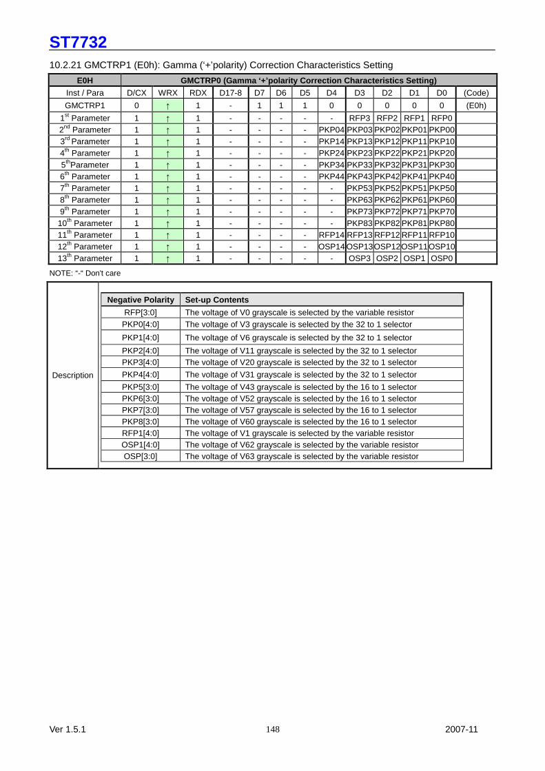
ST7732
Ver 1.5.1 2007-11
148
10.2.21 GMCTRP1 (E0h): Gamma (‘+’polarity) Correction Characteristics Setting
E0H GMCTRP0 (Gamma ‘+’polarity Correction Characteristic s Setting)
Inst / Para D/CX WRX RDX D17-8 D7 D6 D5 D4 D3 D2 D1 D0 (Code)
GMCTRP1 0 ↑ 1 - 1 1 1 0 0 0 0 0 (E0h)
1st Parameter 1 ↑ 1 - - - - - RFP3 RFP2 RFP1 RFP0 2nd Parameter 1 ↑ 1 - - - - PKP04 PKP03 PKP02 PKP01 PKP00 3rd Parameter 1 ↑ 1 - - - - PKP14 PKP13 PKP12 PKP11 PKP10 4th Parameter 1 ↑ 1 - - - - PKP24 PKP23 PKP22 PKP21 PKP20 5thParameter 1 ↑ 1 - - - - PKP34 PKP33 PKP32 PKP31 PKP30 6th Parameter 1 ↑ 1 - - - - PKP44 PKP43 PKP42 PKP41 PKP40 7th Parameter 1 ↑ 1 - - - - - PKP53 PKP52 PKP51 PKP50 8th Parameter 1 ↑ 1 - - - - - PKP63 PKP62 PKP61 PKP60 9th Parameter 1 ↑ 1 - - - - - PKP73 PKP72 PKP71 PKP70
10th Parameter 1 ↑ 1 - - - - - PKP83 PKP82 PKP81 PKP80 11th Parameter 1 ↑ 1 - - - - RFP14 RFP13 RFP12 RFP11 RFP10 12th Parameter 1 ↑ 1 - - - - OSP14 OSP13 OSP12OSP11 OSP10 13th Parameter 1 ↑ 1 - - - - - OSP3 OSP2 OSP1 OSP0
NOTE: “-“ Don’t care
Description
Negative Polarity Set-up Contents
RFP[3:0] The voltage of V0 grayscale is selected by the variable resistor PKP0[4:0] The voltage of V3 grayscale is selected by the 32 to 1 selector
PKP1[4:0] The voltage of V6 grayscale is selected by the 32 to 1 selector
PKP2[4:0] The voltage of V11 grayscale is selected by the 32 to 1 selector PKP3[4:0] The voltage of V20 grayscale is selected by the 32 to 1 selector
PKP4[4:0] The voltage of V31 grayscale is selected by the 32 to 1 selector
PKP5[3:0] The voltage of V43 grayscale is selected by the 16 to 1 selector PKP6[3:0] The voltage of V52 grayscale is selected by the 16 to 1 selector PKP7[3:0] The voltage of V57 grayscale is selected by the 16 to 1 selector PKP8[3:0] The voltage of V60 grayscale is selected by the 16 to 1 selector RFP1[4:0] The voltage of V1 grayscale is selected by the variable resistor OSP1[4:0] The voltage of V62 grayscale is selected by the variable resistor OSP[3:0] The voltage of V63 grayscale is selected by the variable resistor

ST7732
Ver 1.5.1 2007-11
149
10.2.22 GMCTRN1 (E1h): Gamma ‘-’polarity Correction Characteristics Setting
E1H GMCTRP0 (Gamma ‘+’polarity Correction Characteristic s Setting)
Inst / Para D/CX WRX RDX D17-8 D7 D6 D5 D4 D3 D2 D1 D0 (Code)
GMCTRP1 0 ↑ 1 - 1 1 1 0 0 0 0 1 (E1h)
1st Parameter 1 ↑ 1 - - - - - RFN3 RFN2 RFN1 RFN0 2nd Parameter 1 ↑ 1 - - - - PKN04 PKN03 PKN02 PKN01 PKN00 3rd Parameter 1 ↑ 1 - - - - PKN14 PKN13 PKN12 PKN11 PKN10 4th Parameter 1 ↑ 1 - - - - PKN24 PKN23 PKN22 PKN21 PKN20 5thParameter 1 ↑ 1 - - - - PKN34 PKN33 PKN32 PKN31 PKN30 6th Parameter 1 ↑ 1 - - - - PKN44 PKN43 PKN42 PKN41 PKN40 7th Parameter 1 ↑ 1 - - - - - PKN53 PKN52 PKN51 PKN50 8th Parameter 1 ↑ 1 - - - - - PKN63 PKN62 PKN61 PKN60 9th Parameter 1 ↑ 1 - - - - - PKN73 PKN72 PKN71 PKN70
10th Parameter 1 ↑ 1 - - - - - PKN83 PKN82 PKN81 PKN80 11th Parameter 1 ↑ 1 - - - - RFN14 RFN13 RFN12 RFN11 RFN10 12th Parameter 1 ↑ 1 - - - - OSN14 OSN13 OSN12 OSN11 OSN10 13th Parameter 1 ↑ 1 - - - - - OSN3 OSN2 OSN1 OSN0
NOTE: “-“ Don’t care
Description
Negative Polarity Set-up Contents
RFN[3:0] The voltage of V63 grayscale is selected by the variable resistor PKN0[4:0] The voltage of V60 grayscale is selected by the 32 to 1 selector
PKN1[4:0] The voltage of V57 grayscale is selected by the 32 to 1 selector
PKN2[4:0] The voltage of V52 grayscale is selected by the 32 to 1 selector PKN3[4:0] The voltage of V43 grayscale is selected by the 32 to 1 selector
PKN4[4:0] The voltage of V31 grayscale is selected by the 32 to 1 selector
PKN5[3:0] The voltage of V20 grayscale is selected by the 16 to 1 selector PKN6[3:0] The voltage of V11 grayscale is selected by the 16 to 1 selector PKN7[3:0] The voltage of V6 grayscale is selected by the 16 to 1 selector PKN8[3:0] The voltage of V3 grayscale is selected by the 16 to 1 selector RFN1[4:0] The voltage of V62 grayscale is selected by the variable resistor OSN1[4:0] The voltage of V1 grayscale is selected by the variable resistor OSN[3:0] The voltage of V0 grayscale is selected by the variable resistor
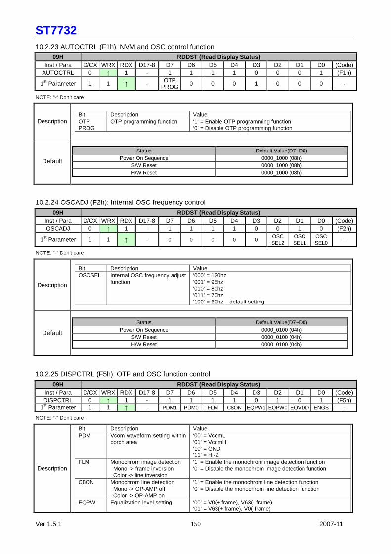
ST7732
Ver 1.5.1 2007-11
150
10.2.23 AUTOCTRL (F1h): NVM and OSC control function 09H RDDST (Read Display Status)
Inst / Para D/CX WRX RDX D17-8 D7 D6 D5 D4 D3 D2 D1 D0 (Code) AUTOCTRL 0 ↑ 1 - 1 1 1 1 0 0 0 1 (F1h)
1st Parameter 1 1 ↑ - OTP PROG 0 0 0 1 0 0 0 -
NOTE: “-“ Don’t care
Description Bit Description Value OTP PROG
OTP programming function ‘1’ = Enable OTP programming function ‘0’ = Disable OTP programming function
Default
Status Default Value(D7~D0) Power On Sequence 0000_1000 (08h)
S/W Reset 0000_1000 (08h) H/W Reset 0000_1000 (08h)
10.2.24 OSCADJ (F2h): Internal OSC frequency control 09H RDDST (Read Display Status)
Inst / Para D/CX WRX RDX D17-8 D7 D6 D5 D4 D3 D2 D1 D0 (Code) OSCADJ 0 ↑ 1 - 1 1 1 1 0 0 1 0 (F2h)
1st Parameter 1 1 ↑ - 0 0 0 0 0 OSC SEL2
OSC SEL1
OSC SEL0
-
NOTE: “-“ Don’t care
Description
Bit Description Value OSCSEL Internal OSC frequency adjust
function ‘000’ = 120hz ‘001’ = 95hz ‘010’ = 80hz ‘011’ = 70hz ‘100’ = 60hz – default setting
Default
Status Default Value(D7~D0) Power On Sequence 0000_0100 (04h)
S/W Reset 0000_0100 (04h) H/W Reset 0000_0100 (04h)
10.2.25 DISPCTRL (F5h): OTP and OSC function control 09H RDDST (Read Display Status)
Inst / Para D/CX WRX RDX D17-8 D7 D6 D5 D4 D3 D2 D1 D0 (Code) DISPCTRL 0 ↑ 1 - 1 1 1 1 0 1 0 1 (F5h)
1st Parameter 1 1 ↑ - PDM1 PDM0 FLM C8ON EQPW1 EQPW0 EQVDD ENGS -
NOTE: “-“ Don’t care
Description
Bit Description Value PDM Vcom waveform setting within
porch area ‘00’ = VcomL ‘01’ = VcomH ‘10’ = GND ‘11’ = Hi-Z
FLM Monochrom image detection Mono -> frame inversion Color -> line inversion
‘1’ = Enable the monochrom image detection function ‘0’ = Disable the monochrom image detection function
C8ON Monochrom line detection Mono -> OP-AMP off Color -> OP-AMP on
‘1’ = Enable the monochrom line detection function ‘0’ = Disable the monochrom line detection function
EQPW Equalization level setting ‘00’ = V0(+ frame), V63(- frame) ‘01’ = V63(+ frame), V0(-frame)
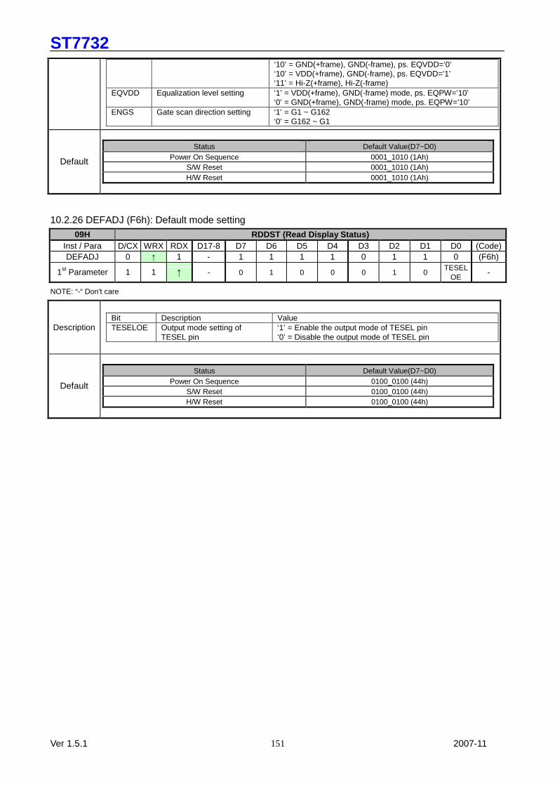
ST7732
Ver 1.5.1 2007-11
151
‘10’ = GND(+frame), GND(-frame), ps. EQVDD=’0’ ‘10’ = VDD(+frame), GND(-frame), ps. EQVDD=’1’ ‘11’ = Hi-Z(+frame), Hi-Z(-frame)
EQVDD Equalization level setting ‘1’ = VDD(+frame), GND(-frame) mode, ps. EQPW=’10’ ‘0’ = GND(+frame), GND(-frame) mode, ps. EQPW=’10’
ENGS Gate scan direction setting ‘1’ = G1 ~ G162 ‘0’ = G162 ~ G1
Default
Status Default Value(D7~D0) Power On Sequence 0001_1010 (1Ah)
S/W Reset 0001_1010 (1Ah) H/W Reset 0001_1010 (1Ah)
10.2.26 DEFADJ (F6h): Default mode setting 09H RDDST (Read Display Status)
Inst / Para D/CX WRX RDX D17-8 D7 D6 D5 D4 D3 D2 D1 D0 (Code) DEFADJ 0 ↑ 1 - 1 1 1 1 0 1 1 0 (F6h)
1st Parameter 1 1 ↑ - 0 1 0 0 0 1 0 TESEL
OE -
NOTE: “-“ Don’t care
Description Bit Description Value TESELOE Output mode setting of
TESEL pin ‘1’ = Enable the output mode of TESEL pin ‘0’ = Disable the output mode of TESEL pin
Default
Status Default Value(D7~D0) Power On Sequence 0100_0100 (44h)
S/W Reset 0100_0100 (44h) H/W Reset 0100_0100 (44h)

ST7732
Ver 1.5.1 2007-11
152
11. Power structure
11.1. Driver IC Operating voltages Specification
Remark 1. AVDD supply to all power source (exclude VGH, VGL) 2. Source output range: 0.1V ~ AVDD-0.1V 3. Linear Range: 0.2V ~ AVDD-0.2V (For all output voltage, but exclude VGH, VGL) 4. Above operating voltages is min range.
Fig. 11.1.1 Power Booster Level
VDD=(2.5V~3.3V)
AGND=0V
VGH (9.4V ~ 16.1V)
AVDD (4.95V ~ 6V)
GVDD (3.0V ~ 5.0V)
VCOMH (2.5V ~ 5.0V)
VCOML (-2.5V ~ 0.0V)
VCL (-2.5V ~ -2.9V)
VGL (-13.4V ~ -7.05V)
AVDD
Charge Pump
Reference Voltage
Internal
Reference Voltage
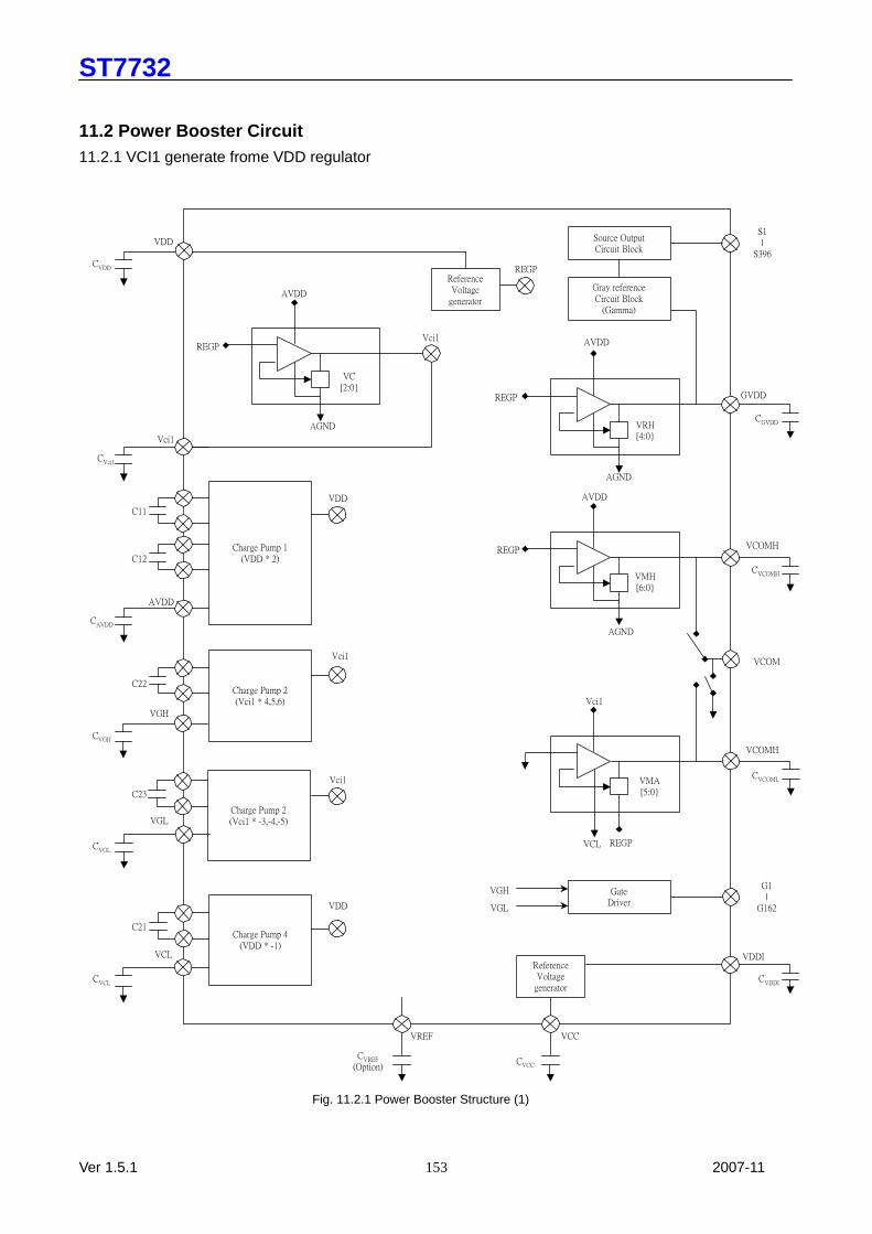
ST7732
Ver 1.5.1 2007-11
153
11.2 Power Booster Circuit 11.2.1 VCI1 generate frome VDD regulator
Charge Pump 1(VDD * 2)
ReferenceVoltage
generator
Charge Pump 2(Vci1 * 4,5,6)
Gray referenceCircuit Block
(Gamma)
Source OutputCircuit Block
GateDriver
REGP
REGP
REGP
REGP
Vci1
Vci1
AVDD
AVDD
AGND
Vci1
VCL REGP
VDD
CVDD
CVci1
C11
C12
CAVDD
VDD
Charge Pump 4(VDD * -1)
Charge Pump 2(Vci1 * -3,-4,-5)
VDD
Vci1
Vci1
VGH
VGL
VCL
C22
C21
C23
CVGH
CVGL
CVCL
AVDD
AGND
S1|
S396
AVDD
AGND
GVDD
CGVDD
VGH
VGL
VDDI
CVDDI
VRH[4:0
VMH[6:0
VMA[5:0
VC[2:0
CVCOML
CVCOMH
VCOMH
VCOMH
VCOM
G1|
G162
ReferenceVoltage
generator
CVCC
VCC
CVREF
(Option)
VREF
Fig. 11.2.1 Power Booster Structure (1)
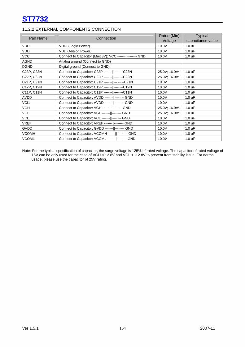
ST7732
Ver 1.5.1 2007-11
154
11.2.2 EXTERNAL COMPONENTS CONNECTION
Pad Name Connection Rated (Min)
Voltage Typical
capacitance value VDDI VDDI (Logic Power) 10.0V 1.0 uF VDD VDD (Analog Power) 10.0V 1.0 uF VCC Connect to Capacitor (Max 3V): VCC -------||-------- GND 10.0V 1.0 uF AGND Analog ground (Connect to GND) DGND Digital ground (Connect to GND) C23P, C23N Connect to Capacitor: C23P -------||--------C23N 25.0V; 16.0V* 1.0 uF C22P, C22N Connect to Capacitor: C22P -------||--------C22N 25.0V; 16.0V* 1.0 uF C21P, C21N Connect to Capacitor: C21P -------||--- -----C21N 10.0V 1.0 uF C12P, C12N Connect to Capacitor: C12P -------||--------C12N 10.0V 1.0 uF C11P, C11N Connect to Capacitor: C11P -------||--------C11N 10.0V 1.0 uF AVDD Connect to Capacitor: AVDD -------||-------- GND 10.0V 1.0 uF VCI1 Connect to Capacitor: AVDD -------||-------- GND 10.0V 1.0 uF VGH Connect to Capacitor: VGH -------||-------- GND 25.0V; 16.0V* 1.0 uF VGL Connect to Capacitor: VGL -------||-------- GND 25.0V; 16.0V* 1.0 uF VCL Connect to Capacitor: VCL -------||-------- GND 10.0V 1.0 uF VREF Connect to Capacitor: VREF -------||-------- GND 10.0V 1.0 uF GVDD Connect to Capacitor: GVDD -------||-------- GND 10.0V 1.0 uF VCOMH Connect to Capacitor: VCOMH-------||--------- GND 10.0V 1.0 uF VCOML Connect to Capacitor: VCOML -------||-------- GND 10.0V 1.0 uF
Note: For the typical specification of capacitor, the surge voltage is 125% of rated voltage. The capacitor of rated voltage of
16V can be only used for the case of VGH < 12.8V and VGL > -12.8V to prevent from stability issue. For normal usage, please use the capacitor of 25V rating.

ST7732
Ver 1.5.1 2007-11
155
12. Gamma structure
12.1 STRUCTURE OF GRAYSCALE AMPLIFIER The structure of grayscale amplifier is shown as below. 13 voltage levels (VIP(N)0-VIP(N)12) between GVDD and VGS are determined by the high/ mid/ low level adjustment registers.
Gray Level Voltage Formula (Positive) Voltage Formula (Negative)
0 VINP0 VINN0
1 VINP1 VINN1
2 V1-(V1-V3)*(16/30) V1-(V1-V3)*(18/30)
3 VINP2 VINP(N)2
4 V3-(V3-V6)*(11/30) V3-(V3-V6)*(12/30)
5 V3-(V3-V6)*(21/30) V3-(V3-V6)*(22/30)
6 VINP3 VINN3
7 V6-(V6-V11)*(7/30) V6-(V6-V11)*(7/30)
8 V6-(V6-V11)*(14/30) V6-(V6-V11)*(13/30)
9 V6-(V6-V11)*(20/30) V6-(V6-V11)*(19/30)
10 V6-(V6-V11)*(25/30) V6-(V6-V11)*(25/30)
11 VINP4 VINN4
12 V11-(V11-V20)*(4/30) V11-(V11-V20)*(4/36)
13 V11-(V11-V20)*(8/30) V11-(V11-V20)*(8/36)
14 V11-(V11-V20)*(12/30) V11-(V11-V20)*(12/36)
15 V11-(V11-V20)*(16/30) V11-(V11-V20)*(16/36)
16 V11-(V11-V20)*(19/30) V11-(V11-V20)*(20/36)
17 V11-(V11-V20)*(22/30) V11-(V11-V20)*(24/36)
18 V11-(V11-V20)*(25/30) V11-(V11-V20)*(28/36)
19 V11-(V11-V20)*(28/30) V11-(V11-V20)*(32/36)
20 VINP5 VINN5
21 V20-(V20-V31)*(3/30) V20-(V20-V32)*(3/36)
22 V20-(V20-V31)* (6/30) V20-(V20-V32)*(6/36)
23 V20-(V20-V31)* (9/30) V20-(V20-V32)*(9/36)
24 V20-(V20-V31)* (12/30) V20-(V20-V32)*(12/36)
25 V20-(V20-V31)* (15/30) V20-(V20-V32)*(15/36)
26 V20-(V20-V31)* (18/30) V20-(V20-V32)*(18/36)
27 V20-(V20-V31)* (21/30) V20-(V20-V32)*(21/36)
28 V20-(V20-V31)* (23/30) V20-(V20-V32)*(24/36)
29 V20-(V20-V31)* (25/30) V20-(V20-V32)*(27/36)
30 V20-(V20-V31)* (27/30) V20-(V20-V32)*(30/36)
31 VINP6 V20-(V20-V32)*(33/36)
32 V31-(V31-V43)*(3/36) VINN6
33 V31-(V31-V43)*(6/36) V32-(V32-V43)*(3/30)
34 V31-(V31-V43)*(9/36) V32-(V32-V43)*(5/30)
35 V31-(V31-V43)*(12/36) V32-(V32-V43)*(7/30)

ST7732
Ver 1.5.1 2007-11
156
36 V31-(V31-V43)*(15/36) V32-(V32-V43)*(9/30)
37 V31-(V31-V43)*(18/36) V32-(V32-V43)*(12/30)
38 V31-(V31-V43)*(21/36) V32-(V32-V43)*(15/30)
39 V31-(V31-V43)*(24/36) V32-(V32-V43)*(18/30)
40 V31-(V31-V43)*(27/36) V32-(V32-V43)*(21/30)
41 V31-(V31-V43)*(30/36) V32-(V32-V43)*(24/30)
42 V31-(V31-V43)*(33/36) V32-(V32-V43)*(27/30)
43 VINP7 VINN7
44 V43-(V43-V52)*(4/36) V43-(V43-V52)*(2/30)
45 V43-(V43-V52)*(8/36) V43-(V43-V52)*(5/30)
46 V43-(V43-V52)*(12/36) V43-(V43-V52)*(8/30)
47 V43-(V43-V52)*(16/36) V43-(V43-V52)*(11/30)
48 V43-(V43-V52)*(20/36) V43-(V43-V52)*(14/30)
49 V43-(V43-V52)*(24/36) V43-(V43-V52)*(18/30)
50 V43-(V43-V52)*(28/36) V43-(V43-V52)*(22/30)
51 V43-(V43-V52)*(32/36) V43-(V43-V52)*(26/30)
52 VINP8 VINN8
53 V52-(V52-V57)*(5/30) V52-(V52-V57)*(5/30)
54 V52-(V52-V57)*(11/30) V52-(V52-V57)*(10/30)
55 V52-(V52-V57)*(17/30) V52-(V52-V57)*(16/30)
56 V52-(V52-V57)*(23/30) V52-(V52-V57)*(23/30)
57 VINP9 VINN9
58 V57-(V57-V60)*(8/30) V57-(V57-V60)*(9/30)
59 V57-(V57-V60)*(18/30) V57-(V57-V60)*(19/30)
60 VINP10 VINN10
61 V60-(V60-V62)*(12/30) V60-(V60-V62)*(14/30)
62 VINP11 VINN11
63 VINP12 VINN12
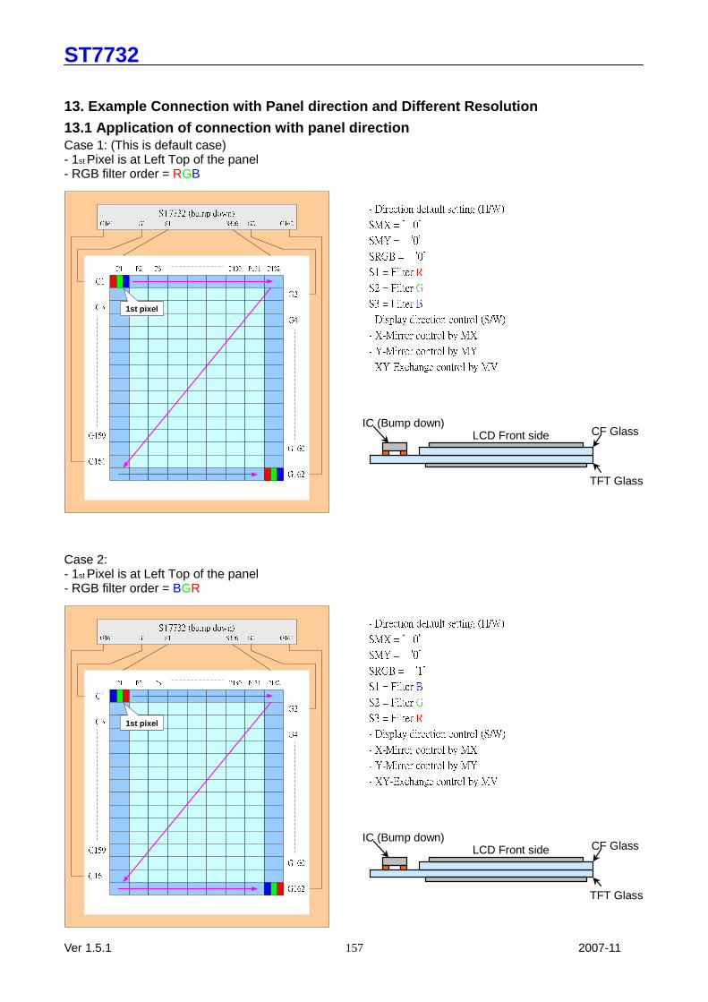
ST7732
Ver 1.5.1 2007-11
157
13. Example Connection with Panel direction and Dif ferent Resolution
13.1 Application of connection with panel direction Case 1: (This is default case) - 1st Pixel is at Left Top of the panel - RGB filter order = RGB
1st pixel
IC (Bump down)
LCD Front side CF Glass
TFT Glass
Case 2: - 1st Pixel is at Left Top of the panel - RGB filter order = BGR
1st pixel
IC (Bump down)
LCD Front side CF Glass
TFT Glass
ST7732
Ver 1.5.1 2007-11
158
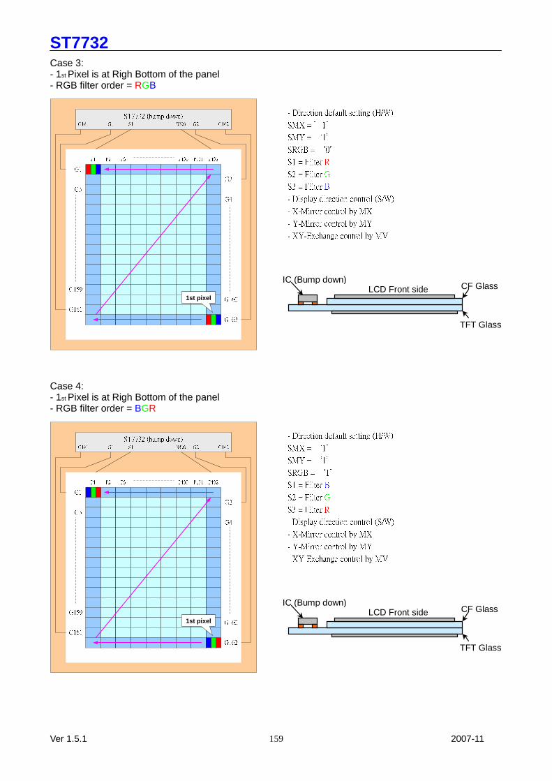
ST7732
Ver 1.5.1 2007-11
159
Case 3: - 1st Pixel is at Righ Bottom of the panel - RGB filter order = RGB
IC (Bump down)
LCD Front side CF Glass
TFT Glass
1st pixel
Case 4: - 1st Pixel is at Righ Bottom of the panel - RGB filter order = BGR
IC (Bump down)
LCD Front side CF Glass
TFT Glass
1st pixel
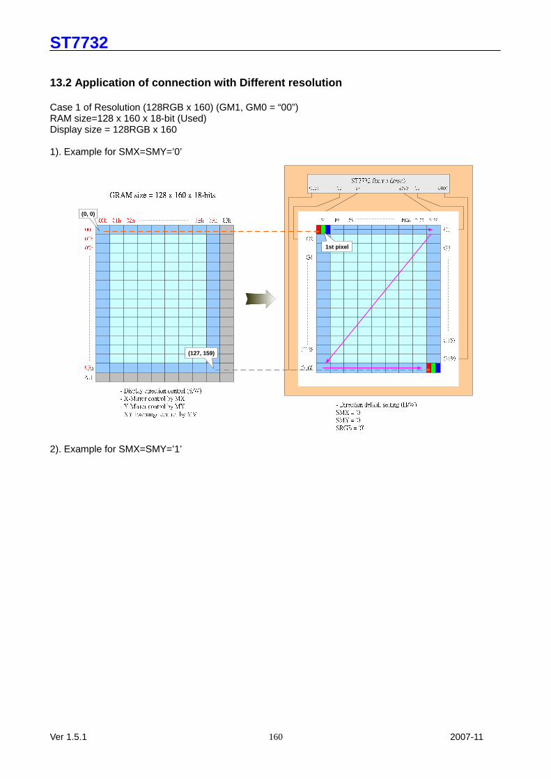
ST7732
Ver 1.5.1 2007-11
160
13.2 Application of connection with Different resol ution Case 1 of Resolution (128RGB x 160) (GM1, GM0 = “00”) RAM size=128 x 160 x 18-bit (Used) Display size = 128RGB x 160 1). Example for SMX=SMY=’0’
1st pixel
(127, 159)
(0, 0)
2). Example for SMX=SMY=’1’
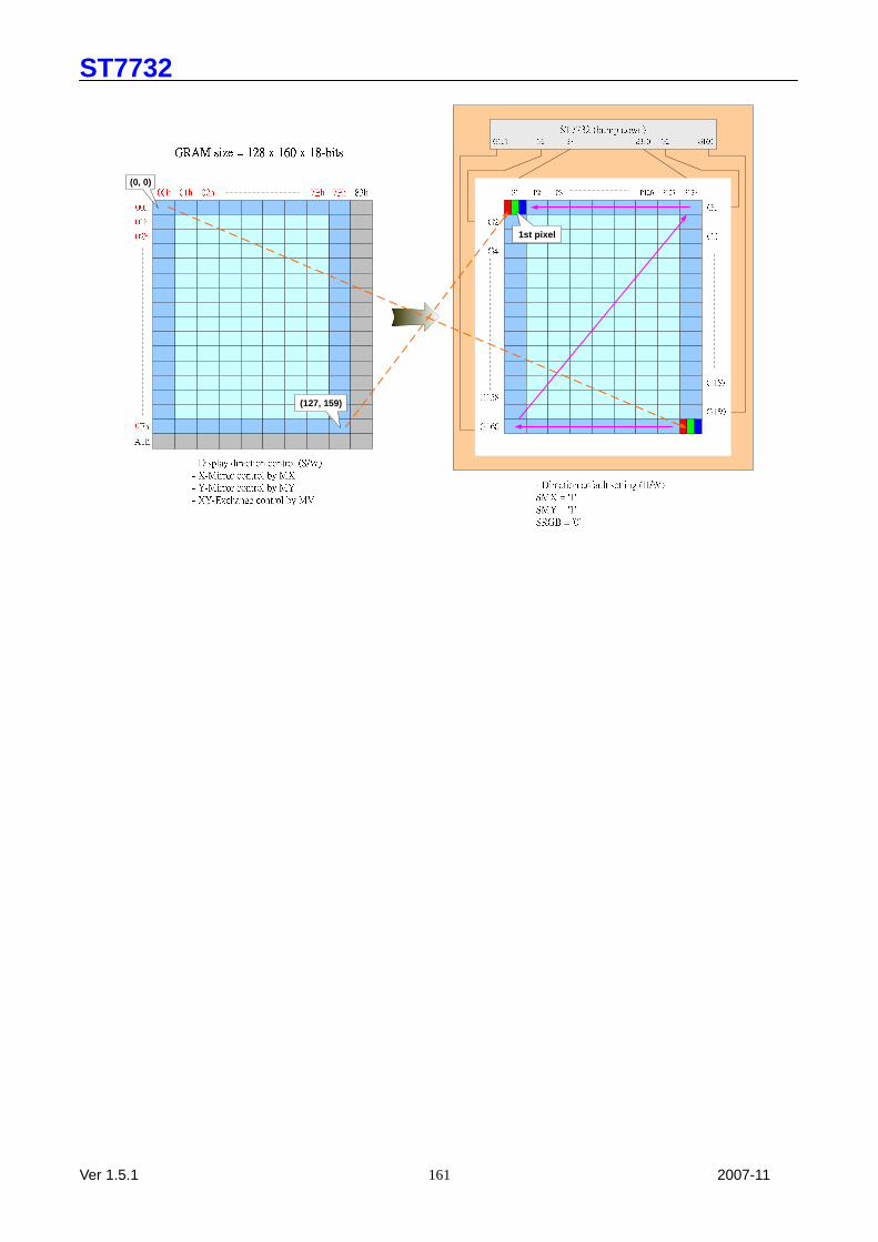
ST7732
Ver 1.5.1 2007-11
161
1st pixel
(127, 159)
(0, 0)
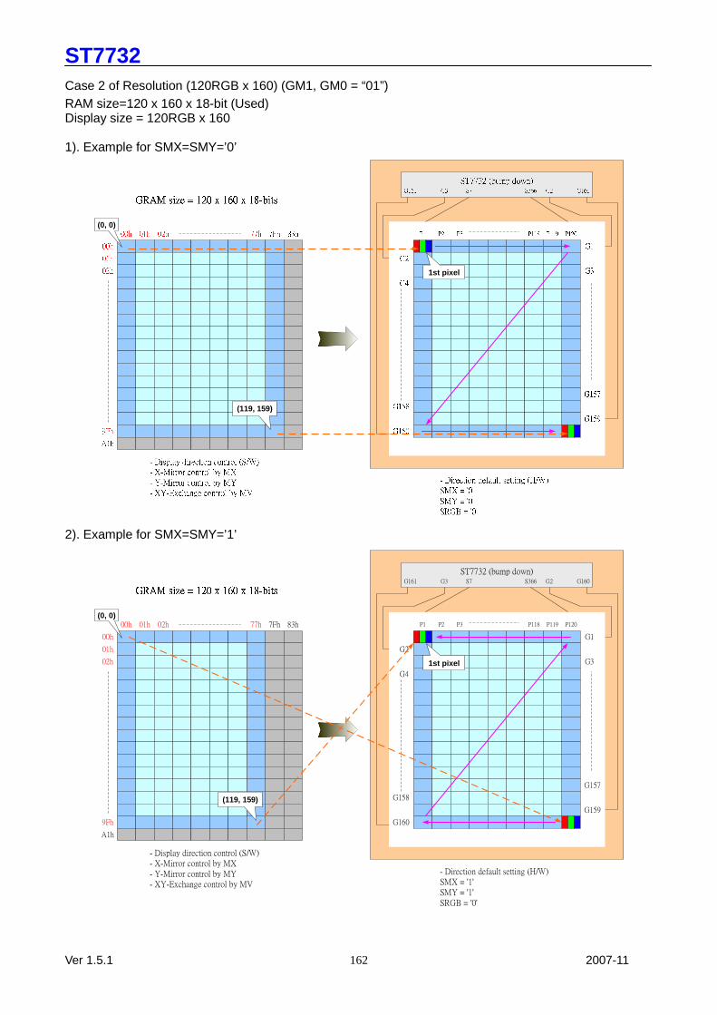
ST7732
Ver 1.5.1 2007-11
162
Case 2 of Resolution (120RGB x 160) (GM1, GM0 = “01”) RAM size=120 x 160 x 18-bit (Used) Display size = 120RGB x 160 1). Example for SMX=SMY=’0’
1st pixel
(0, 0)
(119, 159)
2). Example for SMX=SMY=’1’
G1
G2
G3
G4
G157
G159
G160
G158
1st pixel
ST7732 (bump down)G3G161 G2 G160S7 S366
00h 01h 02h 77h 7Fh 83h
00h
01h
02h
A1h
9Fh
- Display direction control (S/W)- X-Mirror control by MX- Y-Mirror control by MY- XY-Exchange control by MV
- Direction default setting (H/W)SMX = '1'SMY = '1'SRGB = '0'
(0, 0)
(119, 159)
P1 P2 P3 P118 P119 P120
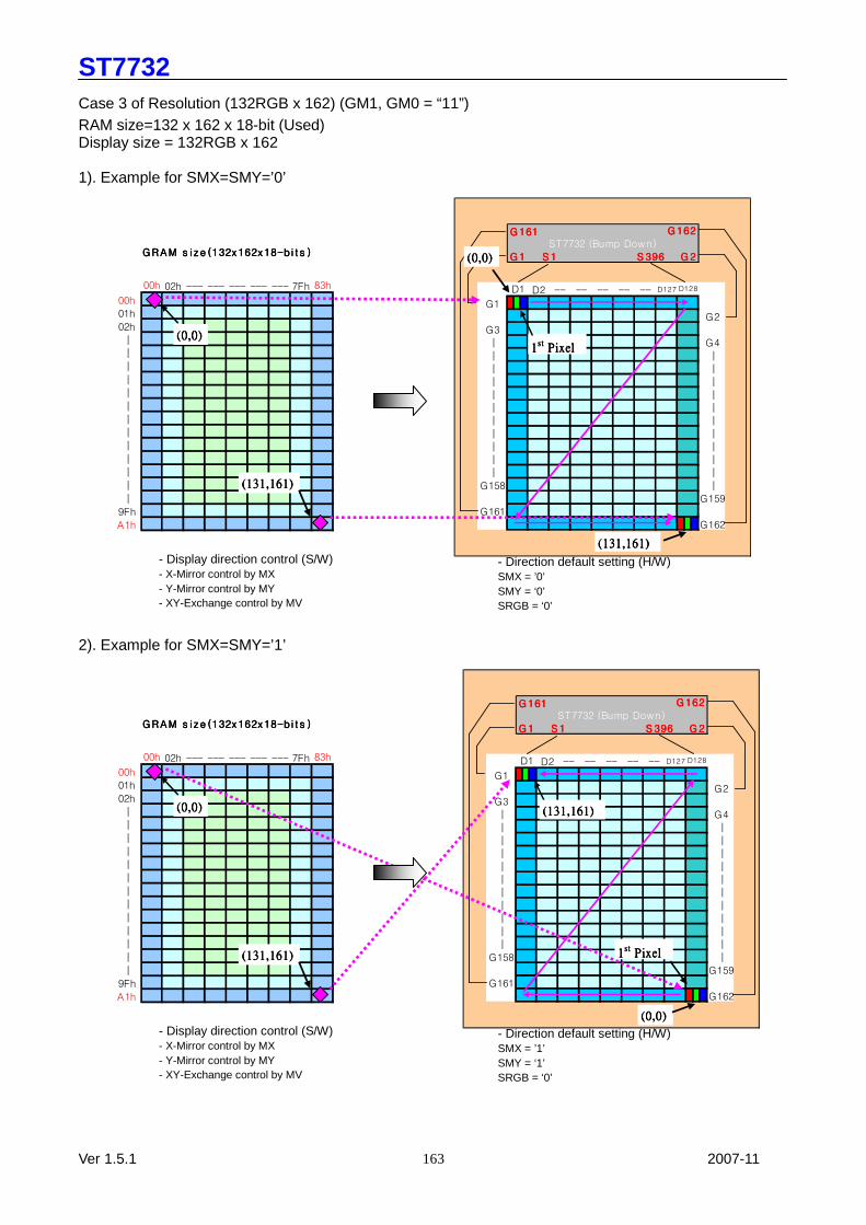
ST7732
Ver 1.5.1 2007-11
163
Case 3 of Resolution (132RGB x 162) (GM1, GM0 = “11”) RAM size=132 x 162 x 18-bit (Used) Display size = 132RGB x 162 1). Example for SMX=SMY=’0’
2). Example for SMX=SMY=’1’
G161G161G161G161
S 396S 396S 396S 396
D2 -- -- -- -- -- D127
G1
G2
G3
| G4
| |
| |
| |
| |
| |
| |
| |
| |
| |
| |
G158 |
G159
G161
G162
G162G162G162G162
ST7732 (Bump Down)
G1G1G1G1 S 1S 1S 1S 1 G2G2G2G2
D1 D128
1111stststst P ixel Pixel Pixel Pixel
(0,0)(0,0)(0,0)(0,0)
(131,161)(131,161)(131,161)(131,161)
02h --- --- --- --- --- 7Fh
00h01h
02h
||
|
||
|
||
|
||
|
|9Fh
A1h
00h 83h
GRAM s i z e (132x162x18-bi t s )GRAM s i z e (132x162x18-bi t s )GRAM s i z e (132x162x18-bi t s )GRAM s i z e (132x162x18-bi t s )
(0,0)(0,0)(0,0)(0,0)
(131,161)(131,161)(131,161)(131,161)
- Display direction control (S/W) - X-Mirror control by MX - Y-Mirror control by MY - XY-Exchange control by MV
- Direction default setting (H/W) SMX = ’1’ SMY = ‘1’ SRGB = ‘0’
G161G161G161G161
S 396S 396S 396S 396
D2 -- -- -- -- -- D127
G1
G2
G3
| G4
| |
| |
| |
| |
| |
| |
| |
| |
| |
| |
G158 |
G159
G161
G162
D1 D128
G1G1G1G1 S 1S 1S 1S 1 G2G2G2G2
G162G162G162G162
ST7732 (Bump Down)
1111stststst P ixel Pixel Pixel Pixel
(0,0)(0,0)(0,0)(0,0)
(131,161)(131,161)(131,161)(131,161)
02h --- --- --- --- --- 7Fh
00h01h
02h
||
|
||
|
||
|
||
|
|9Fh
A1h
00h 83h
GRAM s i z e (132x162x18-bi t s )GRAM s i z e (132x162x18-bi t s )GRAM s i z e (132x162x18-bi t s )GRAM s i z e (132x162x18-bi t s )
(0,0)(0,0)(0,0)(0,0)
(131,161)(131,161)(131,161)(131,161)
- Display direction control (S/W) - X-Mirror control by MX - Y-Mirror control by MY - XY-Exchange control by MV
- Direction default setting (H/W) SMX = ’0’ SMY = ‘0’ SRGB = ‘0’
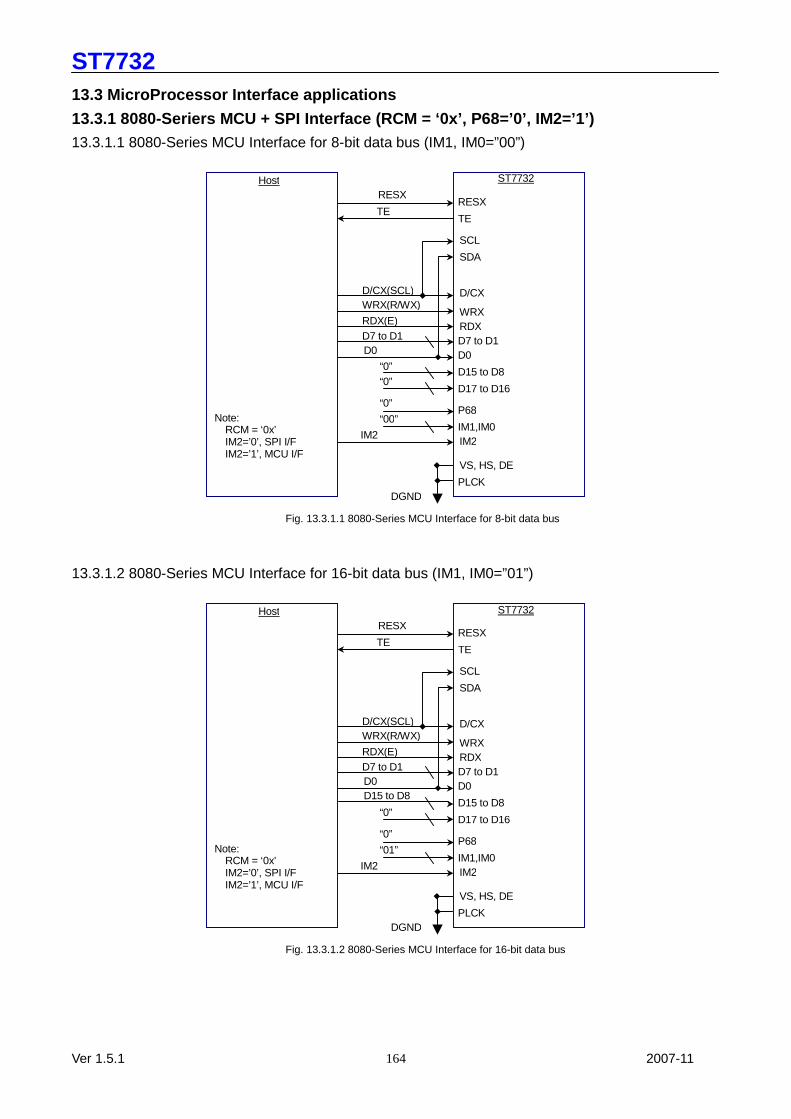
ST7732
Ver 1.5.1 2007-11
164
13.3 MicroProcessor Interface applications
13.3.1 8080-Seriers MCU + SPI Interface (RCM = ‘0x’ , P68=’0’, IM2=’1’) 13.3.1.1 8080-Series MCU Interface for 8-bit data bus (IM1, IM0=”00”)
13.3.1.2 8080-Series MCU Interface for 16-bit data bus (IM1, IM0=”01”)
Note: RCM = ‘0x’ IM2=’0’, SPI I/F IM2=’1’, MCU I/F
DGND
Host ST7732
RESX
TE
D/CX(SCL) WRX(R/WX)
RDX(E) D7 to D1 D0
“0”
“0”
“01”
IM2
RESX
TE
SCL
SDA
D/CX
WRX RDX D7 to D1 D0
D15 to D8
D17 to D16
P68
IM1,IM0 IM2
VS, HS, DE
PLCK
Fig. 13.3.1.2 8080-Series MCU Interface for 16-bit data bus
D15 to D8
Note: RCM = ‘0x’ IM2=’0’, SPI I/F IM2=’1’, MCU I/F
DGND
Host ST7732
RESX
TE
D/CX(SCL) WRX(R/WX)
RDX(E) D7 to D1 D0
“0” “0”
“0”
“00”
IM2
RESX
TE
SCL
SDA
D/CX
WRX RDX D7 to D1 D0
D15 to D8
D17 to D16
P68
IM1,IM0 IM2
VS, HS, DE
PLCK
Fig. 13.3.1.1 8080-Series MCU Interface for 8-bit data bus
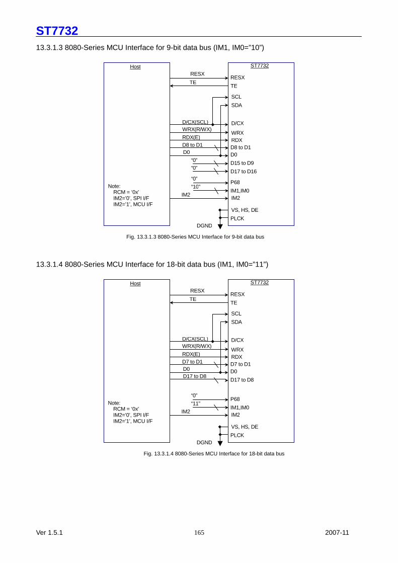
ST7732
Ver 1.5.1 2007-11
165
13.3.1.3 8080-Series MCU Interface for 9-bit data bus (IM1, IM0=”10”)
13.3.1.4 8080-Series MCU Interface for 18-bit data bus (IM1, IM0=”11”)
Note: RCM = ‘0x’ IM2=’0’, SPI I/F IM2=’1’, MCU I/F
DGND
Host ST7732
RESX
TE
D/CX(SCL) WRX(R/WX)
RDX(E) D7 to D1 D0
“0”
“11”
IM2
RESX
TE
SCL
SDA
D/CX
WRX RDX D7 to D1 D0
D17 to D8
P68
IM1,IM0 IM2
VS, HS, DE
PLCK
Fig. 13.3.1.4 8080-Series MCU Interface for 18-bit data bus
D17 to D8
Note: RCM = ‘0x’ IM2=’0’, SPI I/F IM2=’1’, MCU I/F
DGND
Host ST7732
RESX
TE
D/CX(SCL) WRX(R/WX)
RDX(E) D8 to D1 D0
“0” “0”
“0”
“10”
IM2
RESX
TE
SCL
SDA
D/CX
WRX RDX D8 to D1 D0
D15 to D9
D17 to D16
P68
IM1,IM0 IM2
VS, HS, DE
PLCK
Fig. 13.3.1.3 8080-Series MCU Interface for 9-bit data bus
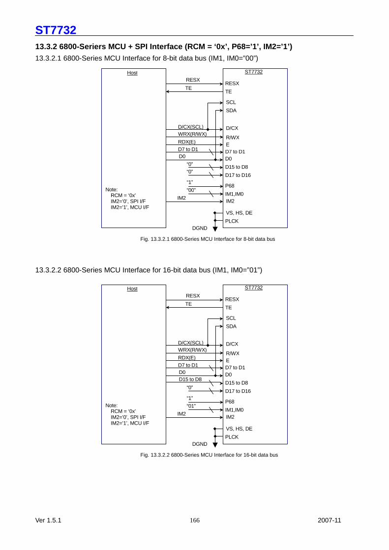
ST7732
Ver 1.5.1 2007-11
166
13.3.2 6800-Seriers MCU + SPI Interface (RCM = ‘0x’ , P68=’1’, IM2=’1’) 13.3.2.1 6800-Series MCU Interface for 8-bit data bus (IM1, IM0=”00”)
13.3.2.2 6800-Series MCU Interface for 16-bit data bus (IM1, IM0=”01”)
Note: RCM = ‘0x’ IM2=’0’, SPI I/F IM2=’1’, MCU I/F
DGND
Host ST7732
RESX
TE
D/CX(SCL) WRX(R/WX)
RDX(E) D7 to D1 D0
“0”
“1”
“01”
IM2
RESX
TE
SCL
SDA
D/CX
R/WX E D7 to D1 D0
D15 to D8
D17 to D16
P68
IM1,IM0 IM2
VS, HS, DE
PLCK
Fig. 13.3.2.2 6800-Series MCU Interface for 16-bit data bus
D15 to D8
Note: RCM = ‘0x’ IM2=’0’, SPI I/F IM2=’1’, MCU I/F
DGND
Host ST7732
RESX
TE
D/CX(SCL) WRX(R/WX)
RDX(E) D7 to D1 D0
“0” “0”
“1”
“00”
IM2
RESX
TE
SCL
SDA
D/CX
R/WX E D7 to D1 D0
D15 to D8
D17 to D16
P68
IM1,IM0 IM2
VS, HS, DE
PLCK
Fig. 13.3.2.1 6800-Series MCU Interface for 8-bit data bus
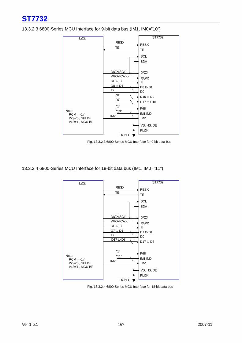
ST7732
Ver 1.5.1 2007-11
167
13.3.2.3 6800-Series MCU Interface for 9-bit data bus (IM1, IM0=”10”)
13.3.2.4 6800-Series MCU Interface for 18-bit data bus (IM1, IM0=”11”)
Note: RCM = ‘0x’ IM2=’0’, SPI I/F IM2=’1’, MCU I/F
DGND
Host ST7732
RESX
TE
D/CX(SCL) WRX(R/WX) RDX(E) D7 to D1 D0
“1”
“11”
IM2
RESX
TE
SCL
SDA
D/CX
R/WX E D7 to D1 D0
D17 to D8
P68
IM1,IM0 IM2
VS, HS, DE
PLCK
Fig. 13.3.2.4 6800-Series MCU Interface for 18-bit data bus
D17 to D8
Note: RCM = ‘0x’ IM2=’0’, SPI I/F IM2=’1’, MCU I/F
DGND
Host ST7732
RESX
TE
D/CX(SCL) WRX(R/WX)
RDX(E) D8 to D1 D0
“0” “0”
“1”
“10”
IM2
RESX
TE
SCL
SDA
D/CX
R/WX E D8 to D1 D0
D15 to D9
D17 to D16
P68
IM1,IM0 IM2
VS, HS, DE
PLCK
Fig. 13.3.2.3 6800-Series MCU Interface for 9-bit data bus
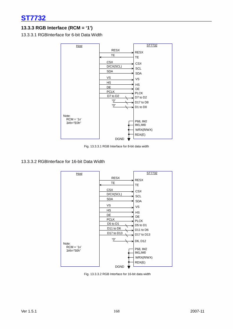
ST7732
Ver 1.5.1 2007-11
168
13.3.3 RGB Interface (RCM = ‘1’) 13.3.3.1 RGBInterface for 6-bit Data Width
13.3.3.2 RGBInterface for 16-bit Data Width
Note: RCM = ‘1x’ 3Ah=”50h”
DGND
Host ST7732
RESX
TE
D/CX(SCL)
HS
DE PCLK D5 to D1
“0”
RESX
TE
CSX
SDA
VS
HS DE PLCK D5 to D1
D6, D12
P68, IM2 IM1,IM0
WRX(R/WX)
RDX(E)
Fig. 13.3.3.2 RGB Interface for 16-bit data width
SCL
CSX
SDA
VS
D11 to D6 D11 to D6 D17 to D13 D17 to D13
Note: RCM = ‘1x’ 3Ah=”E0h”
DGND
Host ST7732
RESX
TE
D/CX(SCL)
HS
DE PCLK D7 to D2
“0”
RESX
TE
CSX
SDA
VS
HS DE PLCK D7 to D2
D17 to D8
P68, IM2 IM1,IM0
WRX(R/WX)
RDX(E)
Fig. 13.3.3.1 RGB Interface for 8-bit data width
SCL
CSX
SDA
VS
“0” D1 to D0
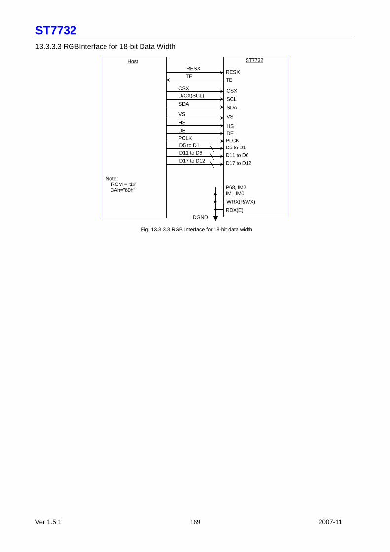
ST7732
Ver 1.5.1 2007-11
169
13.3.3.3 RGBInterface for 18-bit Data Width
Note: RCM = ‘1x’ 3Ah=”60h”
DGND
Host ST7732
RESX
TE
D/CX(SCL)
HS
DE PCLK D5 to D1
RESX
TE
CSX
SDA
VS
HS DE PLCK D5 to D1
P68, IM2 IM1,IM0
WRX(R/WX)
RDX(E)
Fig. 13.3.3.3 RGB Interface for 18-bit data width
SCL
CSX
SDA
VS
D11 to D6 D11 to D6 D17 to D12 D17 to D12

ST7732
Ver 1.5.1 2007-11
170
14. Revision History
ST7732 Specification Revision History
Version Date Description
0.x Preliminary version
1.0 2007/05/16 First issue
1.1 2007/06/12
Modify timing of 3-SPI and 4-SPI. (8.3, p-23; 8.4, p-24) Modify display off function. (10.1.18, p-120) Add notes of 262K read function (10.1.23, p-125; 10.1.33, p-135) Modify cap. rating voltage (11.2.2, p-155)
1.2 2007/07/10 Remove RGBSET command 2Dh (10.1.24 p-106, p-125)
1.3 2007/08 Modify timing of CSX hold time for all I/F(8.1, p-21; 8.2, p-23; 8.4, p-24) Modify the power system diagram(11.2.1, p-154) Correct the typo of component table(11.2.2, p-155)
1.3.1 2007/08 Modify component table(11.2, p-154,155)
1.4 2007/09 Revise the waiting time of HW reset(9.18.2 P91) Revise the description of command 01h, 10h,11h, 28h (10.1.2 P111; 10.1.11 P116; 10.1.12 P117; 10.1.18 P120)
1.5 2007/10
Modify the description of power on/off sequence(9.15 P84) Remove table 9.18.3.1 reset input timing(9.18.3 P90) Modify the figure of reset timing (9.18.3 P90) Modify the waiting time of SWReset to 120ms (10.1.2 P110) Modify the waiting time of SLPout mode to 120ms (10.1.12 P116)
1.5.1 2007/11
Modify SHUT description (6.3 P16) Modify TESEL description (6.3 P17) Modify RGB Mode2 power on sequence on figure 9.9.15 and table 9.9.6.4 (9.9.6.4 P60)
Related Documents