Sitronix ST7567 65 x 132 Dot Matrix LCD Controller/Driver Ver 0.1 1/46 2007/06/19 1. INTRODUCTION ST7567 is a single-chip dot matrix LCD driver which incorporates LCD controller and common/segment drivers. ST7567 can be connected directly to a microprocessor with 8-bit parallel interface or 4-line serial interface (SPI-4). Display data sent from MPU is stored in the internal Display Data RAM (DDRAM) of 65x132 bits. The display data bits which are stored in DDRAM are directly related to the pixels of LCD panel. ST7567 contains 132 segment-outputs, 64 common-outputs and 1 icon-common-output. With built-in oscillation circuit and low power consumption power circuit, ST7567 generates LCD driving signal without external clock or power, so that it is possible to make a display system with the fewest components and minimal power consumption. 2. FEATURES Single-chip LCD Controller & Driver On-chip Display Data RAM (DDRAM) Capacity: 65x132=8580 bits Directly display RAM pattern from DDRAM Selectable Display Duty (by SEL2 & SEL1) 1/65 duty : 65 common x 132 segment 1/55 duty : 55 common x 132 segment 1/49 duty : 49 common x 132 segment 1/33 duty : 33 common x 132 segment Microprocessor Interface Bidirectional 8-bit parallel interface supports: 8080-series and 6800-series MPU Serial interface (SPI-4) is also supported (write only) Abundant Functions Display ON/OFF, Normal/Reverse Display Mode, Set Display Start Line, Read IC Status, Set all Display Points ON, Set LCD Bias, Electronic Volume Control, Read-modify-Write, Select Segment Driver Direction, Power Saving Mode, Select Common Driver Direction, Select Voltage Regulator Resistor Ratio (for V0). External Hardware Reset Pin (RSTB) Built-in Oscillation Circuit No external component required Low Power Consumption Analog Circuit Voltage Booster (4X, 5X & 6X) High-accuracy Voltage Regulator for LCD Vop: (Thermal Gradient: -0.11%/°C) Voltage Follower for LCD Bias Voltage Wide Operation Voltage Range VDD1-VSS1=1.8V~3.3V VDD2-VSS2=2.4V~3.3V Recommend Vop Range: 4V~9.5V Temperature Range: -30~85°C Package Type: COG ST7567 6800 , 8080 , 4-Line Sitronix Technology Corp. reserves the right to change the contents in this document without prior notice.

Welcome message from author
This document is posted to help you gain knowledge. Please leave a comment to let me know what you think about it! Share it to your friends and learn new things together.
Transcript

Sitronix ST7567
65 x 132 Dot Matrix LCD Controller/Driver
Ver 0.1 1/46 2007/06/19
1. INTRODUCTION ST7567 is a single-chip dot matrix LCD driver which incorporates LCD controller and common/segment drivers. ST7567
can be connected directly to a microprocessor with 8-bit parallel interface or 4-line serial interface (SPI-4). Display data sent
from MPU is stored in the internal Display Data RAM (DDRAM) of 65x132 bits. The display data bits which are stored in
DDRAM are directly related to the pixels of LCD panel. ST7567 contains 132 segment-outputs, 64 common-outputs and 1
icon-common-output. With built-in oscillation circuit and low power consumption power circuit, ST7567 generates LCD
driving signal without external clock or power, so that it is possible to make a display system with the fewest components
and minimal power consumption.
2. FEATURES Single-chip LCD Controller & Driver On-chip Display Data RAM (DDRAM)
Ø Capacity: 65x132=8580 bits
Ø Directly display RAM pattern from DDRAM
Selectable Display Duty (by SEL2 & SEL1)
Ø 1/65 duty : 65 common x 132 segment
Ø 1/55 duty : 55 common x 132 segment
Ø 1/49 duty : 49 common x 132 segment
Ø 1/33 duty : 33 common x 132 segment
Microprocessor Interface
Ø Bidirectional 8-bit parallel interface supports:
8080-series and 6800-series MPU
Ø Serial interface (SPI-4) is also supported (write only)
Abundant Functions
Ø Display ON/OFF, Normal/Reverse Display Mode, Set
Display Start Line, Read IC Status, Set all Display
Points ON, Set LCD Bias, Electronic Volume Control,
Read-modify-Write, Select Segment Driver Direction,
Power Saving Mode, Select Common Driver Direction,
Select Voltage Regulator Resistor Ratio (for V0).
External Hardware Reset Pin (RSTB)
Built-in Oscillation Circuit
Ø No external component required
Low Power Consumption Analog Circuit
Ø Voltage Booster (4X, 5X & 6X)
Ø High-accuracy Voltage Regulator for LCD Vop:
(Thermal Gradient: -0.11%/°C)
Ø Voltage Follower for LCD Bias Voltage
Wide Operation Voltage Range
Ø VDD1-VSS1=1.8V~3.3V
Ø VDD2-VSS2=2.4V~3.3V
Ø Recommend Vop Range: 4V~9.5V
Temperature Range: -30~85°C Package Type: COG
ST7567 6800 , 8080 , 4-Line
Sitronix Technology Corp. reserves the right to change the contents in this document without prior notice.
ST7567
Ver 0.1 2/46 2007/06/19
3-1. ST7567 COG OUTLINE X
Y
27
12
54 38
16 11
16
35
10
35
10
7.5
Fig 1. Chip Outline
Chip Size: 4840 X 660 (+/- 15) Chip Thickness: 480 Bump Height: 15 Unit: um
Bump Size
PAD No. Size
1~12, 76~261 16 X 138.5
13~55, 65~75 50 X 45
56~64 45 X 45
Bump Pitch (minimum) PAD No. Size
1~12, 76~87, 88~108, 109~240, 241~261 Refer to Fig 1
13~55, 65~75 15
56~64 10
55-56, 64-65 12.5
* Refer to section “PAD CENTER COORDINATES” for ITO layout.

ST7567
Ver 0.1 3/46 2007/06/19
3-2. PAD CENTER COORDINATES
Fig 2. PAD Location
65 Duty
PAD NO. PIN Name X Y 1 COM[53] -2363.00 -74.25 2 COM[54] -2336.00 -227.75 3 COM[55] -2309.00 -74.25 4 COM[56] -2282.00 -227.75 5 COM[57] -2255.00 -74.25 6 COM[58] -2228.00 -227.75 7 COM[59] -2201.00 -74.25 8 COM[60] -2174.00 -227.75 9 COM[61] -2147.00 -74.25 10 COM[62] -2120.00 -227.75 11 COM[63] -2093.00 -74.25 12 COMS1 -2066.00 -227.75 13 CL -1970.00 -274.50 14 CSB -1905.00 -274.50 15 RSTB -1840.00 -274.50 16 A0 -1775.00 -274.50 17 RWR -1710.00 -274.50 18 ERD -1645.00 -274.50 19 VDDH -1580.00 -274.50 20 D0 -1515.00 -274.50 21 D1 -1450.00 -274.50 22 D2 -1385.00 -274.50 23 D3 -1320.00 -274.50 24 D4 -1255.00 -274.50 25 D5 -1190.00 -274.50 26 D6 -1125.00 -274.50 27 D7 -1060.00 -274.50 28 VDD1 -995.00 -274.50 29 VDD1 -930.00 -274.50 30 VDD2 -865.00 -274.50 31 VDD2 -800.00 -274.50 32 VDD2 -735.00 -274.50 33 VDD3 -670.00 -274.50 34 VSS1 -605.00 -274.50 35 VSS1 -540.00 -274.50 36 VSS3 -475.00 -274.50 37 VSS2 -410.00 -274.50 38 VSS2 -345.00 -274.50 39 VSS2 -280.00 -274.50 40 V0in -215.00 -274.50

ST7567
Ver 0.1 4/46 2007/06/19
PAD NO. PIN Name X Y
41 V0in -150.00 -274.50 42 V0s -85.00 -274.50 43 V0out -20.00 -274.50 44 V0out 45.00 -274.50 45 XV0out 110.00 -274.50 46 XV0out 175.00 -274.50 47 XV0s 240.00 -274.50 48 XV0in 305.00 -274.50 49 XV0in 370.00 -274.50 50 VMO 435.00 -274.50 51 VMO 500.00 -274.50 52 VGin 565.00 -274.50 53 VGin 630.00 -274.50 54 VGs 695.00 -274.50 55 VGout 760.00 -274.50 56 T[6] 820.00 -274.50 57 T[7] 875.00 -274.50 58 T[8] 930.00 -274.50 59 TFCOM 985.00 -274.50 60 T[1] 1040.00 -274.50 61 T[2] 1095.00 -274.50 62 T[3] 1150.00 -274.50 63 T[4] 1205.00 -274.50 64 T[5] 1260.00 -274.50 65 Vref 1320.00 -274.50 66 VSSL 1385.00 -274.50 67 VDDH 1450.00 -274.50 68 C86 1515.00 -274.50 69 PSB 1580.00 -274.50 70 SEL1 1645.00 -274.50 71 VSSL 1710.00 -274.50 72 SEL2 1775.00 -274.50 73 VDD1 1840.00 -274.50 74 VDD2 1905.00 -274.50 75 VDD3 1970.00 -274.50 76 COM[31] 2066.00 -74.25 77 COM[30] 2093.00 -227.75 78 COM[29] 2120.00 -74.25 79 COM[28] 2147.00 -227.75 80 COM[27] 2174.00 -74.25
PAD NO. PIN Name X Y
81 COM[26] 2201.00 -227.75 82 COM[25] 2228.00 -74.25 83 COM[24] 2255.00 -227.75 84 COM[23] 2282.00 -74.25 85 COM[22] 2309.00 -227.75 86 COM[21] 2336.00 -74.25 87 COM[20] 2363.00 -227.75 88 COM[19] 2363.00 74.25 89 COM[18] 2336.00 227.75 90 COM[17] 2309.00 74.25 91 COM[16] 2282.00 227.75 92 COM[15] 2255.00 74.25 93 COM[14] 2228.00 227.75 94 COM[13] 2201.00 74.25 95 COM[12] 2174.00 227.75 96 COM[11] 2147.00 74.25 97 COM[10] 2120.00 227.75 98 COM[9] 2093.00 74.25 99 COM[8] 2066.00 227.75 100 COM[7] 2039.00 74.25 101 COM[6] 2012.00 227.75 102 COM[5] 1985.00 74.25 103 COM[4] 1958.00 227.75 104 COM[3] 1931.00 74.25 105 COM[2] 1904.00 227.75 106 COM[1] 1877.00 74.25 107 COM[0] 1850.00 227.75 108 COMS2 1823.00 74.25 109 SEG[0] 1768.50 227.75 110 SEG[1] 1741.50 74.25 111 SEG[2] 1714.50 227.75 112 SEG[3] 1687.50 74.25 113 SEG[4] 1660.50 227.75 114 SEG[5] 1633.50 74.25 115 SEG[6] 1606.50 227.75 116 SEG[7] 1579.50 74.25 117 SEG[8] 1552.50 227.75 118 SEG[9] 1525.50 74.25 119 SEG[10] 1498.50 227.75 120 SEG[11] 1471.50 74.25

ST7567
Ver 0.1 5/46 2007/06/19
PAD NO. PIN Name X Y
121 SEG[12] 1444.50 227.75 122 SEG[13] 1417.50 74.25 123 SEG[14] 1390.50 227.75 124 SEG[15] 1363.50 74.25 125 SEG[16] 1336.50 227.75 126 SEG[17] 1309.50 74.25 127 SEG[18] 1282.50 227.75 128 SEG[19] 1255.50 74.25 129 SEG[20] 1228.50 227.75 130 SEG[21] 1201.50 74.25 131 SEG[22] 1174.50 227.75 132 SEG[23] 1147.50 74.25 133 SEG[24] 1120.50 227.75 134 SEG[25] 1093.50 74.25 135 SEG[26] 1066.50 227.75 136 SEG[27] 1039.50 74.25 137 SEG[28] 1012.50 227.75 138 SEG[29] 985.50 74.25 139 SEG[30] 958.50 227.75 140 SEG[31] 931.50 74.25 141 SEG[32] 904.50 227.75 142 SEG[33] 877.50 74.25 143 SEG[34] 850.50 227.75 144 SEG[35] 823.50 74.25 145 SEG[36] 796.50 227.75 146 SEG[37] 769.50 74.25 147 SEG[38] 742.50 227.75 148 SEG[39] 715.50 74.25 149 SEG[40] 688.50 227.75 150 SEG[41] 661.50 74.25 151 SEG[42] 634.50 227.75 152 SEG[43] 607.50 74.25 153 SEG[44] 580.50 227.75 154 SEG[45] 553.50 74.25 155 SEG[46] 526.50 227.75 156 SEG[47] 499.50 74.25 157 SEG[48] 472.50 227.75 158 SEG[49] 445.50 74.25 159 SEG[50] 418.50 227.75 160 SEG[51] 391.50 74.25
PAD NO. PIN Name X Y
161 SEG[52] 364.50 227.75 162 SEG[53] 337.50 74.25 163 SEG[54] 310.50 227.75 164 SEG[55] 283.50 74.25 165 SEG[56] 256.50 227.75 166 SEG[57] 229.50 74.25 167 SEG[58] 202.50 227.75 168 SEG[59] 175.50 74.25 169 SEG[60] 148.50 227.75 170 SEG[61] 121.50 74.25 171 SEG[62] 94.50 227.75 172 SEG[63] 67.50 74.25 173 SEG[64] 40.50 227.75 174 SEG[65] 13.50 74.25 175 SEG[66] -13.50 227.75 176 SEG[67] -40.50 74.25 177 SEG[68] -67.50 227.75 178 SEG[69] -94.50 74.25 179 SEG[70] -121.50 227.75 180 SEG[71] -148.50 74.25 181 SEG[72] -175.50 227.75 182 SEG[73] -202.50 74.25 183 SEG[74] -229.50 227.75 184 SEG[75] -256.50 74.25 185 SEG[76] -283.50 227.75 186 SEG[77] -310.50 74.25 187 SEG[78] -337.50 227.75 188 SEG[79] -364.50 74.25 189 SEG[80] -391.50 227.75 190 SEG[81] -418.50 74.25 191 SEG[82] -445.50 227.75 192 SEG[83] -472.50 74.25 193 SEG[84] -499.50 227.75 194 SEG[85] -526.50 74.25 195 SEG[86] -553.50 227.75 196 SEG[87] -580.50 74.25 197 SEG[88] -607.50 227.75 198 SEG[89] -634.50 74.25 199 SEG[90] -661.50 227.75 200 SEG[91] -688.50 74.25
ST7567
Ver 0.1 6/46 2007/06/19
PAD NO. PIN Name X Y
201 SEG[92] -715.50 227.75 202 SEG[93] -742.50 74.25 203 SEG[94] -769.50 227.75 204 SEG[95] -796.50 74.25 205 SEG[96] -823.50 227.75 206 SEG[97] -850.50 74.25 207 SEG[98] -877.50 227.75 208 SEG[99] -904.50 74.25 209 SEG[100] -931.50 227.75 210 SEG[101] -958.50 74.25 211 SEG[102] -985.50 227.75 212 SEG[103] -1012.50 74.25 213 SEG[104] -1039.50 227.75 214 SEG[105] -1066.50 74.25 215 SEG[106] -1093.50 227.75 216 SEG[107] -1120.50 74.25 217 SEG[108] -1147.50 227.75 218 SEG[109] -1174.50 74.25 219 SEG[110] -1201.50 227.75 220 SEG[111] -1228.50 74.25 221 SEG[112] -1255.50 227.75 222 SEG[113] -1282.50 74.25 223 SEG[114] -1309.50 227.75 224 SEG[115] -1336.50 74.25 225 SEG[116] -1363.50 227.75 226 SEG[117] -1390.50 74.25 227 SEG[118] -1417.50 227.75 228 SEG[119] -1444.50 74.25 229 SEG[120] -1471.50 227.75 230 SEG[121] -1498.50 74.25 231 SEG[122] -1525.50 227.75 232 SEG[123] -1552.50 74.25 233 SEG[124] -1579.50 227.75 234 SEG[125] -1606.50 74.25 235 SEG[126] -1633.50 227.75 236 SEG[127] -1660.50 74.25 237 SEG[128] -1687.50 227.75 238 SEG[129] -1714.50 74.25 239 SEG[130] -1741.50 227.75 240 SEG[131] -1768.50 74.25
PAD NO. PIN Name X Y
241 COM[32] -1823.00 227.75 242 COM[33] -1850.00 74.25 243 COM[34] -1877.00 227.75 244 COM[35] -1904.00 74.25 245 COM[36] -1931.00 227.75 246 COM[37] -1958.00 74.25 247 COM[38] -1985.00 227.75 248 COM[39] -2012.00 74.25 249 COM[40] -2039.00 227.75 250 COM[41] -2066.00 74.25 251 COM[42] -2093.00 227.75 252 COM[43] -2120.00 74.25 253 COM[44] -2147.00 227.75 254 COM[45] -2174.00 74.25 255 COM[46] -2201.00 227.75 256 COM[47] -2228.00 74.25 257 COM[48] -2255.00 227.75 258 COM[49] -2282.00 74.25 259 COM[50] -2309.00 227.75 260 COM[51] -2336.00 74.25 261 COM[52] -2363.00 227.75
Note: 1. Unit: um 2. This is the default PAD Center Coordinate Table with
1/65 Duty. Other duty output mapping can be found in Section 6. FUNCTION DESCRIPTION and Fig 9.
3. Tolerance: +/- 0.05 um.

ST7567
Ver 0.1 7/46 2007/06/19
4. BLOCK DIAGRAM
RSTB
CSB
A0 RW
RER
DD
0D
1D
2D
3D
4D
5D
6(SC
L)D
7(SD
A)
SEL1
SEL2
C86
PSB
Fig 3. Block Diagram

ST7567
Ver 0.1 8/46 2007/06/19
5. PIN DESCRIPTION LCD Driver Output Pins
Pin Name Type Description No. of Pins
SEG0 to SEG131 O
LCD segment driver outputs.
The display data and the frame control the output voltage.
Segment Driver Output Voltage Display data Frame
Normal Display Inverse Display H + VG VSS
H - VSS VG
L + VSS VG
L - VG VSS
Display OFF, Power Save VSS VSS
132
COM0 to COM63 O
LCD common driver outputs.
The internal scanning signal and the frame control the output voltage.
Common Driver Output Voltage Scan signal Frame
Normal Display Inverse Display H + XV0
H - V0
L + VM
L - VM
Display OFF, Power Save VSS
64
COMS1, COMS2
(COMS) O
LCD common driver outputs for icons.
The output signals of these two pins are the same.
When icon feature is not used, these pins should be left open. 2
Microprocessor Interface Pins Pin Name Type Description No. of Pins
RSTB I Hardware reset input pin. When RSTB is “L”, internal initialization is executed
and the internal registers will be initialized. 1
CSB I Chip select input pin. Interface access is enabled when CSB is “L”.
When CSB is non-active (CSB=“H”), D[7:0] pins are high impedance. 1
A0 I It determines whether the access is related to data or command.
A0=“H” : Indicates that signals on D[7:0] are display data.
A0=“L” : Indicates that signals on D[7:0] are command. 1
RWR I
Read/Write execution control pin. When PSB is “H”,
C86 MPU Type RWR Description
H 6800
series R/W
Read/Write control input pin.
R/W=“H”: read.
R/W=“L”: write.
L 8080
series /WR
Write enable input pin.
Signals on D[7:0] will be latched at the rising
edge of /WR signal.
RWR is not used in serial interface and should fix to “H” by VDD1 or VDDH.
1
ST7567
Ver 0.1 9/46 2007/06/19
Pin Name Type Description No. of Pins
ERD I
Read/Write execution control pin. When PSB is “H”,
C86 MPU Type ERD Description
H 6800
series E
Read/Write control input pin.
R/W=”H“: When E is “H”, D[7:0] are in output
mode.
R/W=”L“: Signals on D[7:0] are latched at the
falling edge of E signal.
L 8080
series /RD
Read enable input pin.
When /RD is “L”, D[7:0] are in output mode.
ERD is not used in serial interface and should fix to “H” by VDD1 or VDDH.
1
I/O When using 8-bit parallel interface: (6800 or 8080 mode) 8-bit bi-directional data bus. Connect to the data bus of 8-bit microprocessor.
When CSB is non-active (CSB=“H”), D[7:0] pins are high impedance.
D[7:0]
I
When using serial interface: 4-LINE D7=SDA : Serial data input.
D6=SCL : Serial clock input.
D[5:0] are not used and should connect to “H” by VDD1 or VDDH.
When CSB is non-active (CSB=“H”), D[7:0] pins are high impedance.
8
Note: 1. After VDD1 is turned ON, any MPU interface pins cannot be left floating.
Configuration Pins Pin Name Type Description No. of Pins
VDDH I Logic “1” level for option pins which should connect to “H”. 2 VSSL I Logical “0” level for option pins which should connect to “L”. 2 PSB I PSB selects the interface type: Serial or Parallel. 1
C86 I
C86 selects the microprocessor type in parallel interface mode.
PSB C86 Selected Interface “H” “H” Parallel 6800 Series MPU Interface
“H” “L” Parallel 8080 Series MPU Interface
“L” “X” Serial 4-Line SPI Interface
Please refer to “APPLICATION NOTES” and “Microprocessor Interface”
(Section 6) for detailed connection of the selected interface.
1
SEL[2:1] I
These pins select the display duty and bias of ST7567.
SEL2 SEL1 Duty Bias “L” “L” 1/65 1/9 or 1/7
“L” “H” 1/49 1/8 or 1/6
“H” “L” 1/33 1/6 or 1/5
“H” “H” 1/55 1/8 or 1/6
2
ST7567
Ver 0.1 10/46 2007/06/19
Power System Pins Pin Name Type Description No. of Pins
VDD1 Power Digital power. If VDD1=VDD2, connect to VDD2 externally. 3 VDD2 Power Analog power. If VDD1=VDD2, connect to VDD1 externally. 4 VDD3 Power Power for reference voltage circuit. 2 VSS1 Power Digital ground. Connect to VSS2 externally. 2 VSS2 Power Analog ground. Connect to VSS1 externally. 3 VSS3 Power Ground for reference voltage circuit. 1
V0out
V0in
V0s Power
V0 is the LCD driving voltage for common circuits at negative frame.
V0out is the output of V0 regulator. V0s is the feedback of V0 regulator.
V0in is the V0 input of common circuits.
Be sure that: V0 ≥ VG > VM > VSS ≥ XV0 (under operation).
V0out, V0in & V0s should be separated in ITO layout.
V0out, V0in & V0s should be connected together in FPC layout.
2 2 1
XV0out
XV0in
XV0s Power
XV0 is the LCD driving voltage for common circuits at positive frame.
XV0out is the output of XV0 regulator. XV0s is the feedback of XV0 regulator.
XV0in is the V0 input of common circuits.
XV0out, XV0in & XV0s should be separated in ITO layout.
XV0out, XV0in & XV0s should be connected together in FPC layout.
2 2 1
VGout
VGin
VGs Power
VG is the LCD driving voltage for segment circuits.
VGout is the output of VG regulator. VGs is the feedback of VG regulator.
VGin is the VG input of segment circuits.
VGout, VGin & VGs should be separated in ITO layout.
VGout, VGin & VGs should be connected together in FPC layout.
1.24 ≤ VG < VDD2.
1 2 1
VMO Power VM is the LCD driving voltage for common circuits.
0.62V ≤ VM < VDD2. 2
Test Pins Pin Name Type Description No. of Pins
Vref T Test pin for power system.
This pin must be left open (without any kinds of connection). 1
T1~T8 T Do NOT use. Reserved for testing.
Must be floating. 8
TFCOM T Do NOT use. Reserved for testing.
Must be floating. 1
CL T Do NOT use. Reserved for testing.
Must be floating. 1
ST7567
Ver 0.1 11/46 2007/06/19
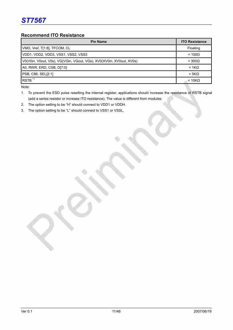
Recommend ITO Resistance Pin Name ITO Resistance
VMO, Vref, T[1:8], TFCOM, CL Floating
VDD1, VDD2, VDD3, VSS1, VSS2, VSS3 < 100Ω
V0(V0in, V0out, V0s), VG(VGin, VGout, VGs), XV0(XV0in, XV0out, XV0s) < 300Ω
A0, RWR, ERD, CSB, D[7:0] < 1KΩ
PSB, C86, SEL[2:1] < 5KΩ
RSTB *1 < 10KΩ
Note:
1. To prevent the ESD pulse resetting the internal register, applications should increase the resistance of RSTB signal
(add a series resistor or increase ITO resistance). The value is different from modules.
2. The option setting to be “H” should connect to VDD1 or VDDH.
3. The option setting to be “L” should connect to VSS1 or VSSL.
ST7567
Ver 0.1 12/46 2007/06/19
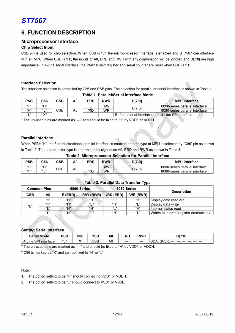
6. FUNCTION DESCRIPTION Microprocessor Interface Chip Select Input CSB pin is used for chip selection. When CSB is "L", the microprocessor interface is enabled and ST7567 can interface
with an MPU. When CSB is “H”, the inputs of A0, ERD and RWR with any combination will be ignored and D[7:0] are high
impedance. In 4-Line serial interface, the internal shift register and serial counter are reset when CSB is “H”.
Interface Selection The interface selection is controlled by C86 and PSB pins. The selection for parallel or serial interface is shown in Table 1.
Table 1. Parallel/Serial Interface Mode PSB C86 CSB A0 ERD RWR D[7:0] MPU Interface “H” “H” E R/W 6800-series parallel interface “H” “L” /RD /WR D[7:0] 8080-series parallel interface “L” “X”
CSB A0 --- --- Refer to serial interface. 4-Line SPI interface
* The un-used pins are marked as “---” and should be fixed to “H” by VDD1 or VDDH.
Parallel Interface When PSB= “H”, the 8-bit bi-directional parallel interface is enabled and the type of MPU is selected by “C86” pin as shown
in Table 2. The data transfer type is determined by signals on A0, ERD and RWR as shown in Table 3.
Table 2. Microprocessor Selection for Parallel Interface PSB C86 CSB A0 ERD RWR D[7:0] MPU Interface “H” “H” E R/W 6800-series parallel interface “H” “L” CSB A0 /RD /WR D[7:0] 8080-series parallel interface
Table 3. Parallel Data Transfer Type Common Pins 6800-Series 8080-Series CSB A0 E (ERD) R/W (RWR) /RD (ERD) /WR (RWR)
Description
“H” “H” “H” “L” “H” Display data read out “H” “H” “L” “H” “L” Display data write “L” “H” “H” “L” “H” Internal status read “L”
“L” “H” “L” “H” “L” Writes to internal register (instruction)
Setting Serial Interface Serial Mode PSB C86 CSB A0 ERD RWR D[7:0]
4-Line SPI interface “L” X CSB A0 --- --- SDA, SCLK, ---, ---, ---, ---, ---, --- * The un-used pins are marked as “---” and should be fixed to “H” by VDD1 or VDDH.
* C86 is marked as “X” and can be fixed to “H” or “L”.
Note:
1. The option setting to be “H” should connect to VDD1 or VDDH.
2. The option setting to be “L” should connect to VSS1 or VSSL.

ST7567
Ver 0.1 13/46 2007/06/19
4-line SPI interface (PSB=“L”, C86=“H” or “L”) When ST7567 is active (CSB=“L”), serial data (SDA) and serial clock (SCLK) inputs are enabled. When ST7567 is not
active (CSB=“H”), the internal 8-bit shift register and 3-bit counter are reset. Serial data on SDA is latched at the rising edge
of serial clock on SCLK. After the 8th serial clock, the serial data will be processed to be 8-bit parallel data. The address
selection pin (A0), which is latched at the 8th clock, indicates the 8-bit parallel data is display data or instruction. The 8-bit
parallel data will be display data when A0 is “H” and will be instruction when A0 is “L”. The read feature is not available in
this mode. The DDRAM column address pointer will be increased by one automatically after each byte of DDRAM access.
Please note that the SCLK signal quality is very important and external noise maybe causes unexpected data/instruction
latch.
Fig 4. 4-Line SPI Access
Note:
l Some MPU will set the interface to be Hi-Z (high impedance) mode when power saving mode or after hardware reset.
This is not allowed when the VDD1of ST7567 is turned ON. Because the floating input (especially for those control
pins such as CSB, RSTB, RWR or ERD…) maybe cause abnormal latch and cause abnormal display.
ST7567
Ver 0.1 14/46 2007/06/19
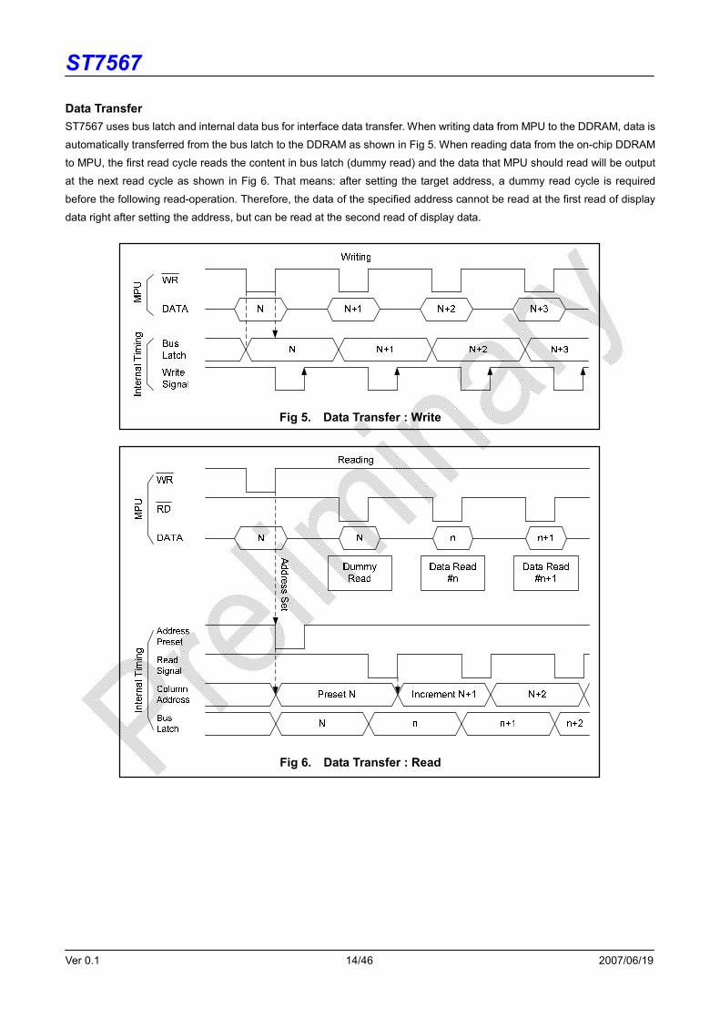
Data Transfer ST7567 uses bus latch and internal data bus for interface data transfer. When writing data from MPU to the DDRAM, data is
automatically transferred from the bus latch to the DDRAM as shown in Fig 5. When reading data from the on-chip DDRAM
to MPU, the first read cycle reads the content in bus latch (dummy read) and the data that MPU should read will be output
at the next read cycle as shown in Fig 6. That means: after setting the target address, a dummy read cycle is required
before the following read-operation. Therefore, the data of the specified address cannot be read at the first read of display
data right after setting the address, but can be read at the second read of display data.
Fig 5. Data Transfer : Write
Fig 6. Data Transfer : Read

ST7567
Ver 0.1 15/46 2007/06/19
Display Data RAM (DDRAM) ST7567 is built-in a RAM with 65X132 bit capacity which stores the display data. The display data RAM (DDRAM) store the
dot data of the LCD. It is an addressable array with 132 columns by 65 rows (8-page with 8-bit and 1-page with 1-bit). The
X-address is directly related to the column output number. Each pixel can be selected when the page and column
addresses are specified (please refer to Fig 7 for detailed illustration). The rows are divided into: 8 pages (Page-0 ~ Page-7)
each with 8 lines (for COM0~63) and Page-8 with only 1 line (COMS, for icon). The display data (D7~D0) corresponds to
the LCD common-line direction and D0 is on top. All pages can be accessed through D[7:0] directly except icon page. Icon
RAM uses only 1-bit of data bus (D0). Refer to Fig 8 for detailed illustration. The microprocessor can write to and read from
(only Parallel interfaces) DDRAM by the I/O buffer. Since the LCD controller operates independently, data can be written
into DDRAM at the same time as data is being displayed without causing the LCD flicker or data-conflict.
Fig 7. DDRAM Mapping Mode (Default Setting)
Fig 8. DDRAM Format

ST7567
Ver 0.1 16/46 2007/06/19
Addressing Data is downloaded into the Display Data RAM matrix in ST7567 as byte-format. The Display Data RAM has a matrix of 65
by 132 bits. The address ranges are: X=0~131 (column address), Y=0~8 (page address). Addresses outside these ranges
are not allowed.
Page Address Circuit This circuit provides the page address of DDRAM. It incorporates 4-bit Page Address Register which can be modified by
the “Page Address Set” instruction only. The Page Address must be set before accessing DDRAM content. Page Address
“8” is a special RAM area for the icons with only one valid bit: D0.
Column Address Circuit The column address of DDRAM is specified by the Column Address Set command. The column address is increased (+1)
after each display data access (read/write). This allows MPU accessing DDRAM content continuously. This feature stops at
the end of each page (Column Address “83h”) because the Column Address and Page Address circuits are independent.
For example, both Page Address and Column Address should be assigned for changing the DDRAM pointer from
(Page-0, Column-83h) to (Page-1, Column-0).
Furthermore, Register MX and MY makes it possible to invert the relationship between the DDRAM and the outputs
(COM/SEG). It is necessary to rewrite the display data into DDRAM after changing MX setting.

ST7567
Ver 0.1 17/46 2007/06/19
The relation between DDRAM and outputs with different MX or MY setting is shown below.
Fig 9. DDRAM and Output Map (COM/SEG)
ST7567
Ver 0.1 18/46 2007/06/19
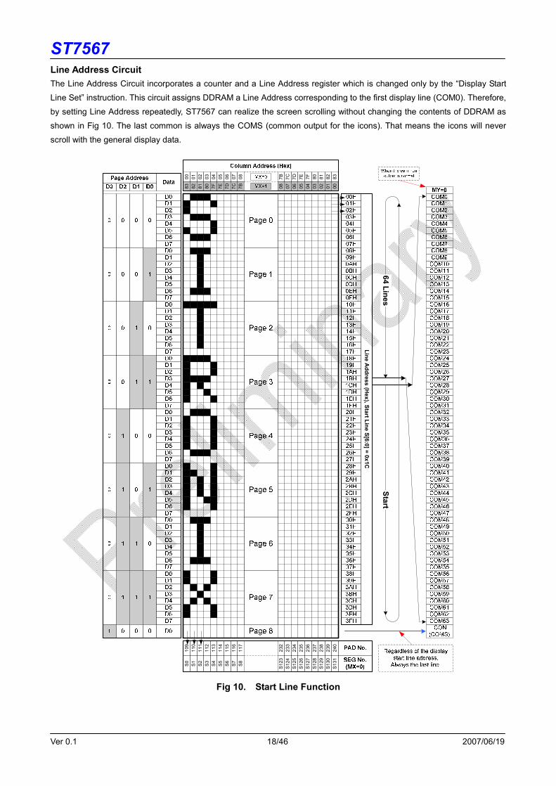
Line Address Circuit The Line Address Circuit incorporates a counter and a Line Address register which is changed only by the “Display Start
Line Set” instruction. This circuit assigns DDRAM a Line Address corresponding to the first display line (COM0). Therefore,
by setting Line Address repeatedly, ST7567 can realize the screen scrolling without changing the contents of DDRAM as
shown in Fig 10. The last common is always the COMS (common output for the icons). That means the icons will never
scroll with the general display data.
116
117
232
233
234
235
236
237
238
239
240
109
110
111
112
113
114
115
Start64 Lines
Line Address (H
ex), Start Line S[6:0] = 0x1C83 82 81 80 7F 7E 7D 7C 7B 000102030405060708
00 01 02 03 04 05 06 07 08 838281807F7E7D7C7B
S7
S8
S12
3S
124
S12
5S
126
S12
7S
128
S12
9S
130
S13
1
S0
S1
S2
S3
S4
S5
S6
Fig 10. Start Line Function

ST7567
Ver 0.1 19/46 2007/06/19
Display Data Latch Circuit The display data latch circuit latches temporarily display data of each segment output which will be output at the next clock.
The special functions such as reverse display, display OFF and display all points ON only change the data in the latch and
the content in the Display Data RAM is not changed.
Oscillation Circuit The built-in oscillation circuit generates the system clock for the liquid crystal driving circuit. The oscillation circuit is enabled
after initializing ST7567. The clock will not be output to reduce the power consumption.
Liquid Crystal Driver Power Circuit The built-in power circuits generate the voltage levels which are necessary to drive the liquid crystal. It consumes low power
with the fewest external components. The built-in power system has voltage booster, voltage regulator and voltage follower
circuits. Before power ST7567 OFF, a Power OFF procedure is needed (please refer to the OPERATION FLOW section).
External Components of Power Circuit The recommended external power components need only 2 capacitors. The detailed values of these two capacitors are
determined by the panel size and loading.
VGGrnerator
V0Generator
XV0Generator
V0
VG
XV0
VSS
IC Internal IC External
VSS
VDD2C1
C2
C1: 0.1uF~1.0uF(Non-Polar/6V)
C2: 0.1uF~1.0uF(Non-Polar/16V)
R1: Reserved(Default NC)
R1
Fig 11. Power Circuit
Regulator Circuit The built-in high accuracy regulation circuit has 8 regulation ratios and each one has 64 EV-levels for voltage adjustment.
Without additional external component, the output voltage can be changed by instructions such as “Regulation Ratio” and
“Set EV”. The temperature compensation coefficient of the built-in regulator is -0.11%/°C. The detailed setting method can
be found in the INSTRUCTION DESCRIPTION section.
ST7567
Ver 0.1 20/46 2007/06/19
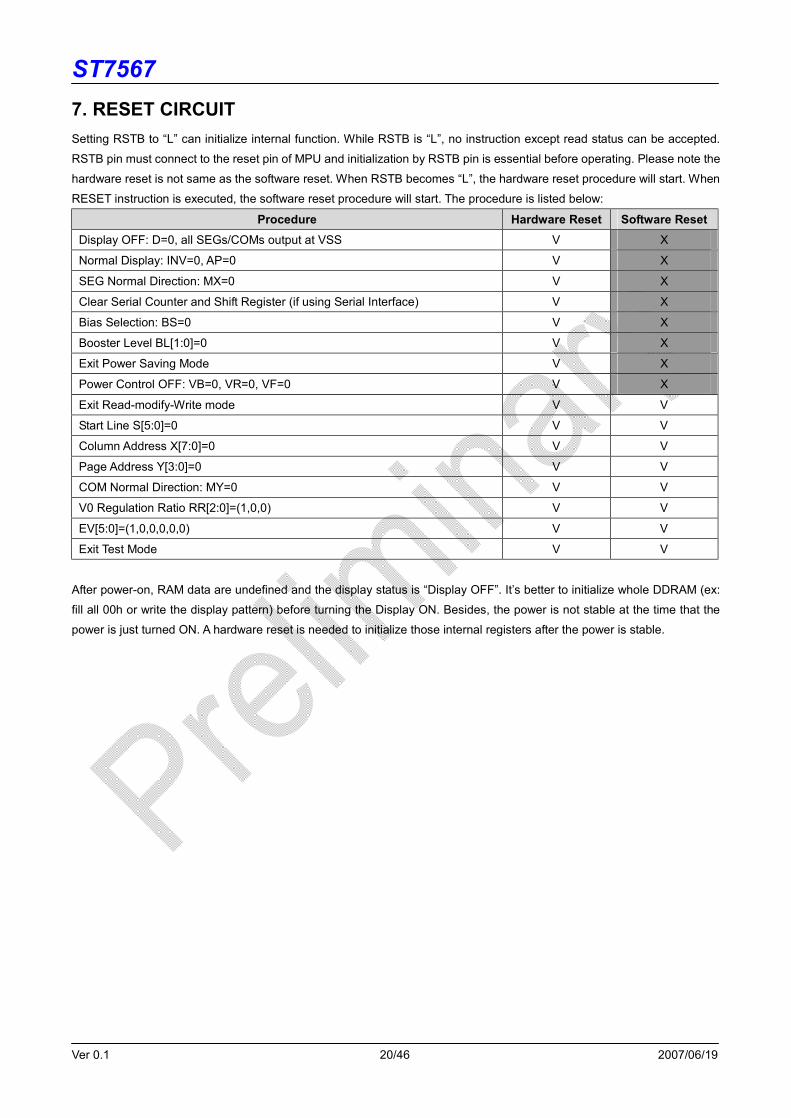
7. RESET CIRCUIT Setting RSTB to “L” can initialize internal function. While RSTB is “L”, no instruction except read status can be accepted.
RSTB pin must connect to the reset pin of MPU and initialization by RSTB pin is essential before operating. Please note the
hardware reset is not same as the software reset. When RSTB becomes “L”, the hardware reset procedure will start. When
RESET instruction is executed, the software reset procedure will start. The procedure is listed below:
Procedure Hardware Reset Software Reset Display OFF: D=0, all SEGs/COMs output at VSS V X
Normal Display: INV=0, AP=0 V X
SEG Normal Direction: MX=0 V X
Clear Serial Counter and Shift Register (if using Serial Interface) V X
Bias Selection: BS=0 V X
Booster Level BL[1:0]=0 V X
Exit Power Saving Mode V X
Power Control OFF: VB=0, VR=0, VF=0 V X
Exit Read-modify-Write mode V V
Start Line S[5:0]=0 V V
Column Address X[7:0]=0 V V
Page Address Y[3:0]=0 V V
COM Normal Direction: MY=0 V V
V0 Regulation Ratio RR[2:0]=(1,0,0) V V
EV[5:0]=(1,0,0,0,0,0) V V
Exit Test Mode V V
After power-on, RAM data are undefined and the display status is “Display OFF”. It’s better to initialize whole DDRAM (ex:
fill all 00h or write the display pattern) before turning the Display ON. Besides, the power is not stable at the time that the
power is just turned ON. A hardware reset is needed to initialize those internal registers after the power is stable.
ST7567
Ver 0.1 21/46 2007/06/19
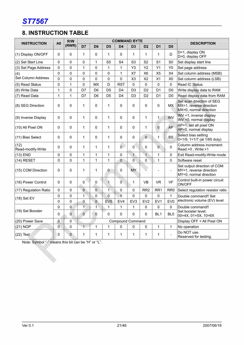
8. INSTRUCTION TABLE COMMAND BYTE INSTRUCTION A0 R/W
(RWR) D7 D6 D5 D4 D3 D2 D1 D0 DESCRIPTION
(1) Display ON/OFF 0 0 1 0 1 0 1 1 1 D D=1, display ON D=0, display OFF
(2) Set Start Line 0 0 0 1 S5 S4 S3 S2 S1 S0 Set display start line (3) Set Page Address 0 0 1 0 1 1 Y3 Y2 Y1 Y0 Set page address
0 0 0 0 0 1 X7 X6 X5 X4 Set column address (MSB) (4) Set Column Address 0 0 0 0 0 0 X3 X2 X1 X0 Set column address (LSB) (5) Read Status 0 1 0 MX D RST 0 0 0 0 Read IC Status (6) Write Data 1 0 D7 D6 D5 D4 D3 D2 D1 D0 Write display data to RAM (7) Read Data 1 1 D7 D6 D5 D4 D3 D2 D1 D0 Read display data from RAM
(8) SEG Direction 0 0 1 0 1 0 0 0 0 MX Set scan direction of SEG MX=1, reverse direction MX=0, normal direction
(9) Inverse Display 0 0 1 0 1 0 0 1 1 INV INV =1, inverse display INV =0, normal display
(10) All Pixel ON 0 0 1 0 1 0 0 1 0 AP AP=1, set all pixel ON AP=0, normal display
(11) Bias Select 0 0 1 0 1 0 0 0 1 BS Select bias setting 0=1/9; 1=1/7 (at 1/65 duty)
(12) Read-modify-Write 0 0 1 1 1 0 0 0 0 0 Column address increment:
Read:+0 , Write:+1 (13) END 0 0 1 1 1 0 1 1 1 0 Exit Read-modify-Write mode (14) RESET 0 0 1 1 1 0 0 0 1 0 Software reset
(15) COM Direction 0 0 1 1 0 0 MY - - - Set output direction of COM MY=1, reverse direction MY=0, normal direction
(16) Power Control 0 0 0 0 1 0 1 VB VR VF Control built-in power circuit ON/OFF
(17) Regulation Ratio 0 0 0 0 1 0 0 RR2 RR1 RR0 Select regulation resistor ratio 0 0 1 0 0 0 0 0 0 1 (18) Set EV 0 0 0 0 EV5 EV4 EV3 EV2 EV1 EV0
Double command!! Set electronic volume (EV) level
0 0 1 1 1 1 1 0 0 0 (19) Set Booster
0 0 0 0 0 0 0 0 BL1 BL0
Double command!! Set booster level: 00=4X, 01=5X, 10=6X
(20) Power Save 0 0 Compound Command Display OFF + All Pixel ON (21) NOP 0 0 1 1 1 0 0 0 1 1 No operation
(22) Test 0 0 1 1 1 1 1 1 1 - Do NOT use. Reserved for testing.
Note: Symbol “-” means this bit can be “H” or “L”.

ST7567
Ver 0.1 22/46 2007/06/19
9. INSTRUCTION DESCRIPTION Display ON/OFF The D flag selects the display mode.
A0 R/W(RWR) D7 D6 D5 D4 D3 D2 D1 D0 0 0 1 0 1 0 1 1 1 D
D=1: Normal Display Mode. D=0: Display OFF. All SEGs/COMs output with VSS. Set Start Line This instruction sets the line address of the Display Data RAM to determine the initial display line. The display data of the specified line address is displayed at the top row (COM0) of the LCD panel.
A0 R/W(RWR) D7 D6 D5 D4 D3 D2 D1 D0 0 0 0 1 S5 S4 S3 S2 S1 S0
S5 S4 S3 S2 S1 S0 Line address 0 0 0 0 0 0 0 0 0 0 0 0 1 1 0 0 0 0 1 0 2 0 0 0 0 1 1 3 : : : : : : : 1 1 1 1 0 1 61 1 1 1 1 1 0 62 1 1 1 1 1 1 63
Set Page Address Y [3:0] defines the Y address vector address of the display RAM.
A0 R/W(RWR) D7 D6 D5 D4 D3 D2 D1 D0 0 0 1 0 1 1 Y3 Y2 Y1 Y0
Y3 Y2 Y1 Y0 Page Address Valid Bit
0 0 0 0 Page0 D0~ D7 0 0 0 1 Page1 D0~ D7 0 0 1 0 Page2 D0~ D7 : : : : : : 0 1 1 0 Page6 D0~ D7 0 1 1 1 Page7 D0~ D7 1 0 0 0 Page8 (icon page) D0
ST7567
Ver 0.1 23/46 2007/06/19
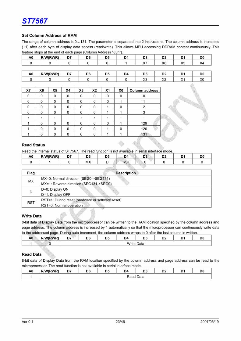
Set Column Address of RAM The range of column address is 0…131. The parameter is separated into 2 instructions. The column address is increased (+1) after each byte of display data access (read/write). This allows MPU accessing DDRAM content continuously. This feature stops at the end of each page (Column Address “83h”).
A0 R/W(RWR) D7 D6 D5 D4 D3 D2 D1 D0 0 0 0 0 0 1 X7 X6 X5 X4
A0 R/W(RWR) D7 D6 D5 D4 D3 D2 D1 D0 0 0 0 0 0 0 X3 X2 X1 X0
X7 X6 X5 X4 X3 X2 X1 X0 Column address 0 0 0 0 0 0 0 0 0 0 0 0 0 0 0 0 1 1 0 0 0 0 0 0 1 0 2 0 0 0 0 0 0 1 1 3 : : : : : : : : : 1 0 0 0 0 0 0 1 129 1 0 0 0 0 0 1 0 120 1 0 0 0 0 0 1 1 131
Read Status Read the internal status of ST7567. The read function is not available in serial interface mode.
A0 R/W(RWR) D7 D6 D5 D4 D3 D2 D1 D0 0 1 0 MX D RST 0 0 0 0
Flag Description
MX MX=0: Normal direction (SEG0->SEG131) MX=1: Reverse direction (SEG131->SEG0)
D D=0: Display ON D=1: Display OFF
RST RST=1: During reset (hardware or software reset) RST=0: Normal operation
Write Data 8-bit data of Display Data from the microprocessor can be written to the RAM location specified by the column address and page address. The column address is increased by 1 automatically so that the microprocessor can continuously write data to the addressed page. During auto-increment, the column address wraps to 0 after the last column is written.
A0 R/W(RWR) D7 D6 D5 D4 D3 D2 D1 D0 1 0 Write Data
Read Data 8-bit data of Display Data from the RAM location specified by the column address and page address can be read to the microprocessor. The read function is not available in serial interface mode.
A0 R/W(RWR) D7 D6 D5 D4 D3 D2 D1 D0 1 1 Read Data

ST7567
Ver 0.1 24/46 2007/06/19
SEG Direction
A0 R/W(RWR) D7 D6 D5 D4 D3 D2 D1 D0 0 0 1 0 1 0 0 0 0 MX
Flag Description
MX MX=0: Normal direction (SEG0->SEG131) MX=1: Reverse direction (SEG131->SEG0)
Inverse Display This instruction changes the selected and non-selected voltage of SEG. The display will be inversed (white -> Black, Black
-> White) while the display data in the Display Data RAM is never changed.
A0 R/W(RWR) D7 D6 D5 D4 D3 D2 D1 D0 0 0 1 0 1 0 0 1 1 INV
Flag Description
INV INV=0: Normal display INV =1: Inverse display
All Pixel ON This instruction will let all segments output the selected voltage and make all pixels turned ON.
A0 R/W(RWR) D7 D6 D5 D4 D3 D2 D1 D0 0 0 1 0 1 0 0 1 0 AP
Flag Description
AP AP =0: Normal display AP =1: All pixels ON
Bias Select Select LCD bias ratio of the voltage required for driving the LCD.
A0 R/W(RWR) D7 D6 D5 D4 D3 D2 D1 D0 0 0 1 0 1 0 0 0 1 BS
Bias Duty
BS=0 BS=1 1/65 1/9 1/7 1/49 1/8 1/6 1/33 1/6 1/5 1/55 1/8 1/6
Reference LCD Bias Voltage (1/65 Duty with 1/9 Bias)
Symbol Bias Voltage V0 V0 VG 2/9 x V0 VM 1/9 x V0 VSS VSS
Please Note: * VG range: 1.24V ≤ VG < VDD2. * VM range: 0.62V ≤ VM < VDD2.
ST7567
Ver 0.1 25/46 2007/06/19
Read-modify-Write This command is used paired with the “END” instruction. Once this command has been input, the display data read operation will not change the column address, but only the display data write operation will increase the column address (X[7:0]+1). This mode is maintained until the END command is input. This function makes it possible to reduce the load on the MPU when there are repeating data changes in a specified display region, such as a blanking cursor.
A0 R/W(RWR) D7 D6 D5 D4 D3 D2 D1 D0 0 0 1 1 1 0 0 0 0 0
* In Read-modify-Write mode, other instructions aside from display data read/write commands can also be used.
Yes
No
Read-Modify-Write
Done
Page Address Set
Column Address Set
Finished?
Dummy Read
Read-Modify-Write Cycle
Data Read
Modify Data
Data Write (at same Address)
END When the END command is input, the Read-modify-Write mode is released and the column address returns to the address it was when the Read-modify-Write instruction was entered.
A0 R/W(RWR) D7 D6 D5 D4 D3 D2 D1 D0 0 0 1 1 1 0 1 1 1 0
RESET This instruction resets Start Line (S[5:0]), Column Address (X[7:0]), Page Address (Y[3:0]) and COM Direction (MY) to their default setting. Please note this instruction is not complete same as hardware reset (RSTB=L) and cannot initialize the built-in power circuit which is initialized by the RSTB pin. The detailed information is in “Section 7. RESET CIRCUIT”.
A0 R/W(RWR) D7 D6 D5 D4 D3 D2 D1 D0 0 0 1 1 1 0 0 0 1 0
ST7567
Ver 0.1 26/46 2007/06/19
COM Direction This instruction controls the common output status which changes the vertical display direction. The detailed information can be found in Fig 9.
A0 R/W(RWR) D7 D6 D5 D4 D3 D2 D1 D0 0 0 1 1 0 0 MY - - -
Flag Description
MY MY=0: Normal direction (COM0->COM63) MY=1: Reverse direction (COM63->COM0)
Power Control This instruction controls the built-in power circuits. Typically, these 3 flags are turned ON at the same time.
A0 R/W(RWR) D7 D6 D5 D4 D3 D2 D1 D0 0 0 0 0 1 0 1 VB VR VF
Flag Description
VB VB=0: Built-in Booster OFF VB=1: Built-in Booster ON
VR VR=0: Built-in Regulator OFF VR=1: Built-in Regulator ON
VF VF=0: Built-in Follower OFF VF=1: Built-in Follower ON
Regulation Ratio This instruction controls the regulation ratio of the built-in regulator.
A0 R/W(RWR) D7 D6 D5 D4 D3 D2 D1 D0 0 0 0 0 1 0 0 RR2 RR1 RR0
RR2 RR1 RR0 Regulation Ratio (RR)
0 0 0 3.0 0 0 1 3.5 0 1 0 4.0 0 1 1 4.5 1 0 0 5.0 1 0 1 5.5 1 1 0 6.0 1 1 1 6.5
The operation voltage (V0) calculation formula is shown below: (RR comes from Regulation Ratio, EV comes from EV[5:0]) V0 = RR X [ 1 – (63 – EV) / 162 ] X 2.1, or V0 = RR X [ ( 99 + EV ) / 162 ] X 2.1
SYMBOL REGISTER VALUE RR RR[2:0] 3, 3.5, 4, 4.5, 5, 5.5, 6 and 6.5 EV EV[5:0] 0~63
ST7567
Ver 0.1 27/46 2007/06/19
Set EV This is double byte instruction. The first byte set ST7567 into EV adjust mode and the following instruction will change the EV setting. That means these 2 bytes must be used together. They control the electronic volume to adjust a suitable V0 voltage for the LCD.
A0 R/W(RWR) D7 D6 D5 D4 D3 D2 D1 D0 0 0 1 0 0 0 0 0 0 1 0 0 0 0 EV5 EV4 EV3 EV2 EV1 EV0
Yes
No
Electronic Volume Set
Done
Set EV (byte-1)(0x81)
Set EV (byte-2)(depends on requirement)
Set Complete?
The maximum voltage that can be generated is dependent on the VDD2 voltage and the loading of LCD module. There are 8 V0 voltage curve can be selected. It is recommended the EV should be close to the center (1FH) for easy contrast adjustment. Please refer to the “Selection of Application Voltage” section for detailed information.
EV[5:0] and RR[2:0] vs. V0 Voltage
Fig 21 Setting V0 Voltage

ST7567
Ver 0.1 28/46 2007/06/19
Power Save (Compound Instruction) This is compound instruction. The 1st instruction is Display OFF (D=0) and the 2nd instruction is All Pixel ON (AP=1). The Power Save mode starts the following procedure: (the display data and register settings are still kept except D-Flag and AP-Flag) 1. Stops internal oscillation circuit; 2. Stops the built-in power circuits; 3. Stops the LCD driving circuits and keeps the common and segment outputs at VSS.
Normal Mode
Power Save Mode
Display OFF (AEH)
All Pixel ON (A5H)
Enter Power Save Mode
Normal Mode
Power Save Mode
Display ON (AFH)
Exit Power Save Mode
Cancel All Pixel ON (A4H)
After exiting Power Save mode, the settings will return to be as they were before. Set Booster This is double byte instruction. The first byte set ST7567 into booster configuration mode and the following instruction will change the booster setting. That means these 2 bytes must be used together. They control the built-in booster circuit to provide the power source of the built-in regulator. ST7567 booster is built-in booster capacitors. The only external component is a keep capacitor between V0 and XV0. Booster level can be changed with instruction only without changing hardware connection.
A0 R/W(RWR) D7 D6 D5 D4 D3 D2 D1 D0 0 0 1 1 1 1 1 0 0 0 0 0 0 0 0 0 0 0 BL1 BL0
Booster Ratio Set
Done
Set Booster (byte-1)(F8H)
Set Booster (byte-2)(depends on requirement)
Set Complete?
Yes
No
NOP “No Operation” instruction. ST7567 will do nothing when receiving this instruction.
A0 R/W(RWR) D7 D6 D5 D4 D3 D2 D1 D0 0 0 1 1 1 0 0 0 1 1
Test The test mode is reserved for IC testing. Please don’t use this instruction. If the test mode is enabled accidentally, it can be cleared by: issuing an “L” pulse on RSTB pin, issuing RESET instruction or issuing NOP instruction.
A0 R/W(RWR) D7 D6 D5 D4 D3 D2 D1 D0 0 0 1 1 1 1 1 1 1 -
Note: “-” means “1” or “0”.
ST7567
Ver 0.1 29/46 2007/06/19
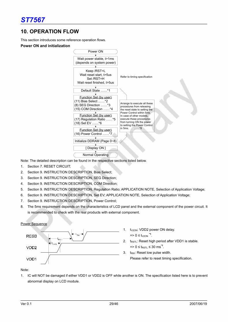
10. OPERATION FLOW This section introduces some reference operation flows.
Power ON and initialization Power ON
Wait power stable, t>1ms(depends on system power)
Keep /RST=LWait reset start, t>5us
Set /RST=HWait reset finished, t>5us
Function Set (by user)(11) Bias Select ……*2(8) SEG Direction ……*3(15) COM Direction ……*4
[ Display ON ]
Normal Operating
Function Set (by user)(16) Power Control ……*7
Function Set (by user)(17) Regulation Ratio ……*5(18) Set EV ……*6
Initialize DDRAM (Page 0~8)
Default State ……*1
Arrange to execute all theseprocedures from releasingthe reset state to setting thePower Control within 5ms.In case of other models,execute these proceduresfrom turning ON the powerto setting the Power Controlin 5ms. ……*8
Refer to timing specification
Note: The detailed description can be found in the respective sections listed below.
1. Section 7. RESET CIRCUIT;
2. Section 9. INSTRUCTION DESCRIPTION, Bias Select;
3. Section 9. INSTRUCTION DESCRIPTION, SEG Direction;
4. Section 9. INSTRUCTION DESCRIPTION, COM Direction;
5. Section 9. INSTRUCTION DESCRIPTION, Regulation Ratio; APPLICATION NOTE, Selection of Application Voltage;
6. Section 9. INSTRUCTION DESCRIPTION, Set EV; APPLICATION NOTE, Selection of Application Voltage;
7. Section 9. INSTRUCTION DESCRIPTION, Power Control;
8. The 5ms requirement depends on the characteristics of LCD panel and the external component of the power circuit. It
is recommended to check with the real products with external component.
Power Sequence
1. tV2ON: VDD2 power ON delay.
=> 0 ≤ tV2ON *1. 2. tRSTL: Reset high period after VDD1 is stable.
=> 0 ≤ tRSTL ≤ 30 ms*1. 3. tRW: Reset low pulse width.
Please refer to reset timing specification.
Note:
1. IC will NOT be damaged if either VDD1 or VDD2 is OFF while another is ON. The specification listed here is to prevent
abnormal display on LCD module.

ST7567
Ver 0.1 30/46 2007/06/19
Power OFF Flow and Sequence ST7567 will go into power save mode by issuing the Power Save instruction (Display OFF + All Pixel ON). The LCD driving
outputs are fixed to VSS, built-in power circuits are turned OFF and a discharge process starts.
Normal Mode
Power OFF
Display OFF (AEH)
All Pixel ON (A5H)
Power OFF Flow
Wait 250ms
Turn VDD1~VDD3 OFF
Instruction Flow
After the built-in power circuits are turned OFF and
completely discharged, the power (VDD1 and VDD2)
can be removed.

ST7567
Ver 0.1 31/46 2007/06/19
Power-Save Flow and Sequence ENTERING THE POWER SAVE MODE
Normal Mode
Power Save Mode
Display OFF (AEH)
All Pixel ON (A5H)
Enter Power Save Mode
EXITING THE POWER SAVE MODE
Normal Mode
Power Save Mode
Display ON (AFH)
Exit Power Save Mode
Cancel All Pixel ON (A4H)
INTERNAL SEQUENCE of EXIT POWER SAVE MODE
After receiving “PD=0”, the internal circuits (Power) will starts the following procedure.
Note:
1. The power stable time is determined by LCD panel loading.
2. The power stable time in this figure is base on: LCD Panel Size = 1.4” with C1=1uF, C2=1uF.

ST7567
Ver 0.1 32/46 2007/06/19
11. LIMITING VALUES In accordance with the Absolute Maximum Rating System; please refer to notes 1 and 2.
Parameter Symbol Conditions Unit
Digital Power Supply Voltage VDD1 -0.3 ~ 3.6 V
Analog Power supply voltage VDD2 -0.3 ~ 3.6 V
LCD Power supply voltage V0-XV0 -0.3 ~ 16 V
LCD Power driving voltage VG, VM -0.3 ~ VDD2 V
Operating temperature TOPR –30 to +85 °C
Storage temperature TSTR –65 to +150 °C
Notes 1. Stresses above those listed under Limiting Values may cause permanent damage to the device.
2. Parameters are valid over operating temperature range unless otherwise specified. All voltages are with respect to
VSS unless otherwise noted.
3. Insure the voltage levels of V0, VDD2, VG, VM, VSS and XV0 always match the correct relation:
V0 ≥ VDD2 > VG > VM > VSS ≥ XV0
ST7567
Ver 0.1 33/46 2007/06/19
12. HANDLING Inputs and outputs are protected against electrostatic discharge in normal handling. However, to be totally safe, it is
desirable to take normal precautions appropriate to handling MOS devices.
13. DC CHARACTERISTICS VDD1=1.8V to 3.3V, VSS=0V; Tamb = -30°C to +85°C; unless otherwise specified.
Rating Item Symbol Condition
Min. Typ. Max. Unit
Applicable Pin
Operating Voltage (1) VDD1 1.8 — 3.3 V VDD1
Operating Voltage (2) VDD2 2.4 — 3.3 V VDD2
Input High-level Voltage VIHC V MPU
Interface
Input Low-level Voltage VILC V MPU
Interface
Output High-level Voltage VOHC IOUT=1mA, VDD1=1.8V V D[7:0]
Output Low-level Voltage VOLC IOUT=-1mA, VDD1=1.8V V D[7:0]
Input Leakage Current ILI μA MPU
Interface
Output Leakage Current ILO μA MPU
Interface
Vop=9V, ΔV=0.9V KΩ COMx Liquid Crystal Driver ON
Resistance RON Ta=25°C
VG=2V, ΔV=0.2V KΩ SEGx
Frame Frequency FR FR default (1,0,0)
Ta = 25°C Hz
Note:
1. Recommend application Vop range : 4V ~ 9.5V.
2. LCD module size : 1.8” (max).
Current consumption: During Display, with internal power system, current consumed by whole IC (bare die).
Rating Test Pattern Symbol Condition
Min. Typ. Max. Unit Note
Display Pattern: SNOW
(Static) ISS
VDD1=VDD2=3.0V,
Booster X5
VOP = 9.0 V, Bias=1/9
Ta=25°C
μA
Power Down ISS VDD1=VDD2=3.0V,
Ta=25°C μA

ST7567
Ver 0.1 34/46 2007/06/19
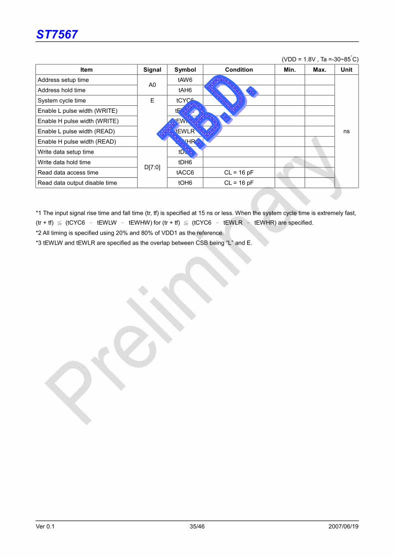
14. TIMING CHARACTERISTICS System Bus Timing for 6800 Series MPU
(VDD = 3.3V , Ta =-30~85°C)
Item Signal Symbol Condition Min. Max. Unit Address setup time tAW6
Address hold time A0
tAH6
System cycle time tCYC6
Enable L pulse width (WRITE) tEWLW
Enable H pulse width (WRITE) tEWHW
Enable L pulse width (READ) tEWLR
Enable H pulse width (READ)
E
tEWHR
Write data setup time tDS6
Write data hold time tDH6
Read data access time tACC6 CL = 16 pF
Read data output disable time
D[7:0]
tOH6 CL = 16 pF
ns
(VDD = 2.8V , Ta =-30~85°C)
Item Signal Symbol Condition Min. Max. Unit Address setup time tAW6
Address hold time A0
tAH6
System cycle time tCYC6
Enable L pulse width (WRITE) tEWLW
Enable H pulse width (WRITE) tEWHW
Enable L pulse width (READ) tEWLR
Enable H pulse width (READ)
E
tEWHR
Write data setup time tDS6
Write data hold time tDH6
Read data access time tACC6 CL = 16 pF
Read data output disable time
D[7:0]
tOH6 CL = 16 pF
ns
ST7567
Ver 0.1 35/46 2007/06/19
(VDD = 1.8V , Ta =-30~85°C)
Item Signal Symbol Condition Min. Max. Unit Address setup time tAW6
Address hold time A0
tAH6
System cycle time tCYC6
Enable L pulse width (WRITE) tEWLW
Enable H pulse width (WRITE) tEWHW
Enable L pulse width (READ) tEWLR
Enable H pulse width (READ)
E
tEWHR
Write data setup time tDS6
Write data hold time tDH6
Read data access time tACC6 CL = 16 pF
Read data output disable time
D[7:0]
tOH6 CL = 16 pF
ns
*1 The input signal rise time and fall time (tr, tf) is specified at 15 ns or less. When the system cycle time is extremely fast, (tr + tf) ≦ (tCYC6 – tEWLW – tEWHW) for (tr + tf) ≦ (tCYC6 – tEWLR – tEWHR) are specified.
*2 All timing is specified using 20% and 80% of VDD1 as the reference.
*3 tEWLW and tEWLR are specified as the overlap between CSB being “L” and E.
ST7567
Ver 0.1 36/46 2007/06/19
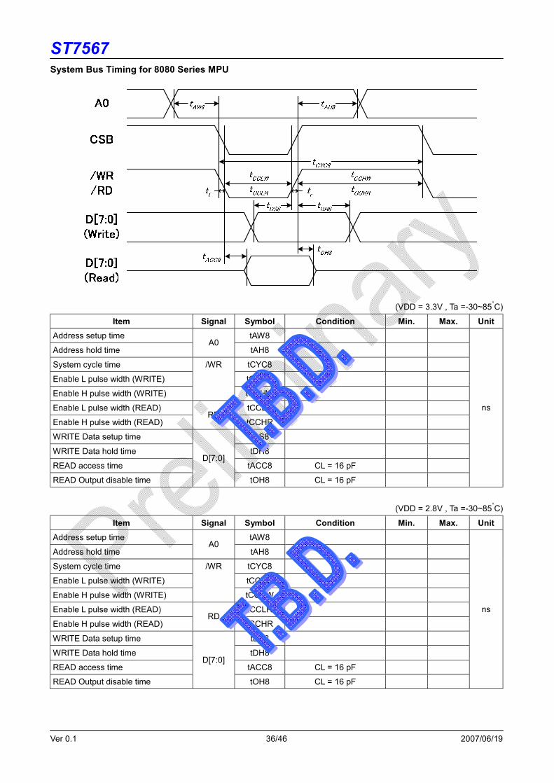
System Bus Timing for 8080 Series MPU
(VDD = 3.3V , Ta =-30~85°C)
Item Signal Symbol Condition Min. Max. Unit Address setup time tAW8
Address hold time A0
tAH8
System cycle time tCYC8
Enable L pulse width (WRITE) tCCLW
Enable H pulse width (WRITE)
/WR
tCCHW
Enable L pulse width (READ) tCCLR
Enable H pulse width (READ) RD
tCCHR
WRITE Data setup time tDS8
WRITE Data hold time tDH8
READ access time tACC8 CL = 16 pF
READ Output disable time
D[7:0]
tOH8 CL = 16 pF
ns
(VDD = 2.8V , Ta =-30~85°C)
Item Signal Symbol Condition Min. Max. Unit Address setup time tAW8
Address hold time A0
tAH8
System cycle time tCYC8
Enable L pulse width (WRITE) tCCLW
Enable H pulse width (WRITE)
/WR
tCCHW
Enable L pulse width (READ) tCCLR
Enable H pulse width (READ) RD
tCCHR
WRITE Data setup time tDS8
WRITE Data hold time tDH8
READ access time tACC8 CL = 16 pF
READ Output disable time
D[7:0]
tOH8 CL = 16 pF
ns
ST7567
Ver 0.1 37/46 2007/06/19
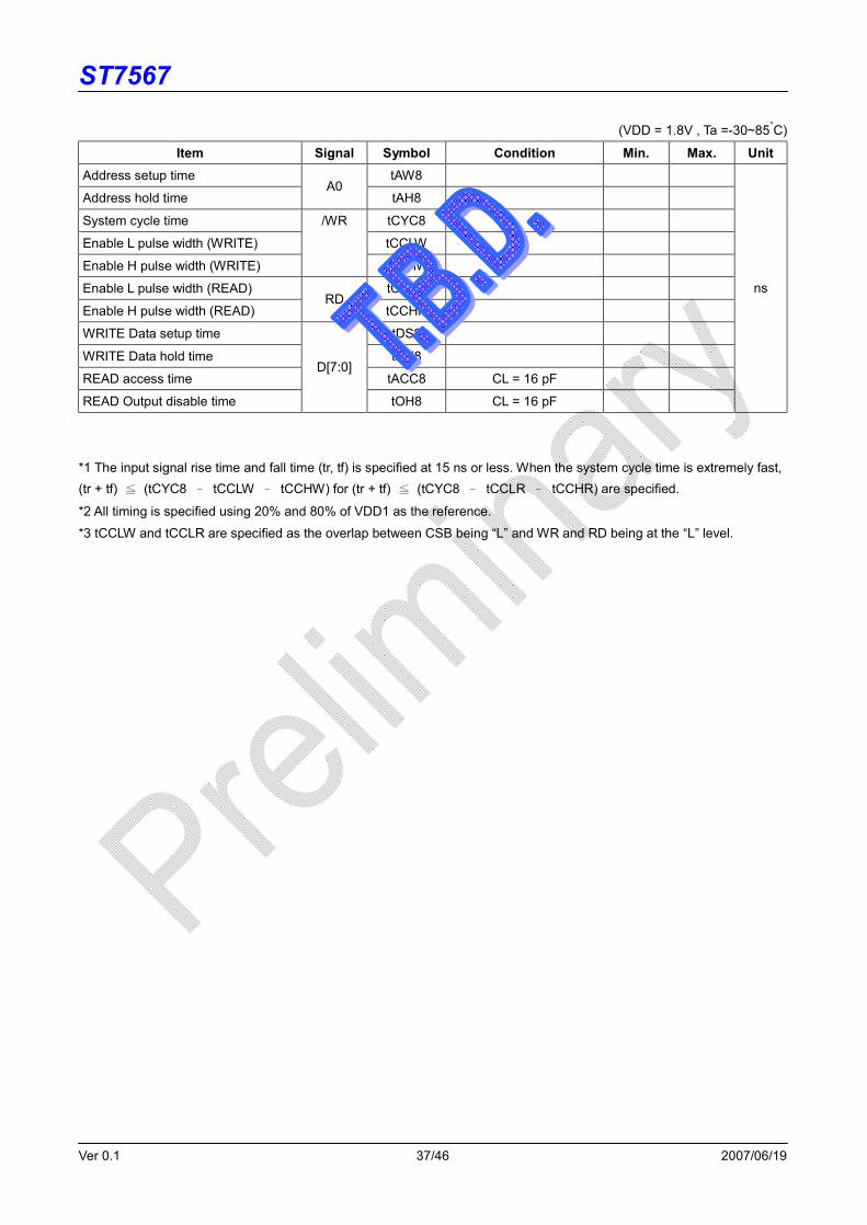
(VDD = 1.8V , Ta =-30~85°C)
Item Signal Symbol Condition Min. Max. Unit Address setup time tAW8
Address hold time A0
tAH8
System cycle time tCYC8
Enable L pulse width (WRITE) tCCLW
Enable H pulse width (WRITE)
/WR
tCCHW
Enable L pulse width (READ) tCCLR
Enable H pulse width (READ) RD
tCCHR
WRITE Data setup time tDS8
WRITE Data hold time tDH8
READ access time tACC8 CL = 16 pF
READ Output disable time
D[7:0]
tOH8 CL = 16 pF
ns
*1 The input signal rise time and fall time (tr, tf) is specified at 15 ns or less. When the system cycle time is extremely fast, (tr + tf) ≦ (tCYC8 – tCCLW – tCCHW) for (tr + tf) ≦ (tCYC8 – tCCLR – tCCHR) are specified.
*2 All timing is specified using 20% and 80% of VDD1 as the reference.
*3 tCCLW and tCCLR are specified as the overlap between CSB being “L” and WR and RD being at the “L” level.
ST7567
Ver 0.1 38/46 2007/06/19
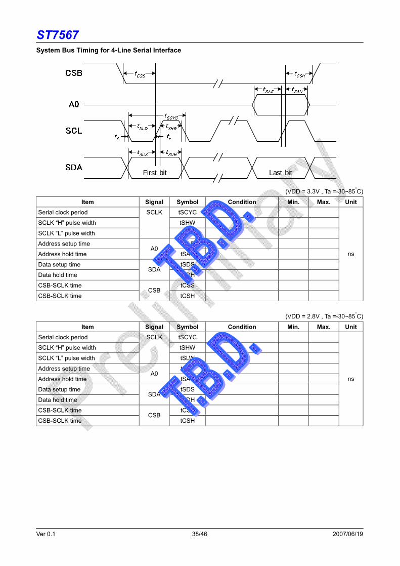
System Bus Timing for 4-Line Serial Interface
First bit Last bit
(VDD = 3.3V , Ta =-30~85°C)
Item Signal Symbol Condition Min. Max. Unit Serial clock period tSCYC
SCLK “H” pulse width tSHW
SCLK “L” pulse width
SCLK
tSLW
Address setup time tSAS
Address hold time A0
tSAH
Data setup time tSDS
Data hold time SDA
tSDH
CSB-SCLK time tCSS
CSB-SCLK time CSB
tCSH
ns
(VDD = 2.8V , Ta =-30~85°C)
Item Signal Symbol Condition Min. Max. Unit Serial clock period tSCYC
SCLK “H” pulse width tSHW
SCLK “L” pulse width
SCLK
tSLW
Address setup time tSAS
Address hold time A0
tSAH
Data setup time tSDS
Data hold time SDA
tSDH
CSB-SCLK time tCSS
CSB-SCLK time CSB
tCSH
ns

ST7567
Ver 0.1 39/46 2007/06/19
(VDD = 1.8V , Ta =-30~85°C)
Item Signal Symbol Condition Min. Max. Unit Serial clock period tSCYC
SCLK “H” pulse width tSHW
SCLK “L” pulse width
SCLK
tSLW
Address setup time tSAS
Address hold time A0
tSAH
Data setup time tSDS
Data hold time SDA
tSDH
CSB-SCLK time tCSS
CSB-SCLK time CSB
tCSH
ns
*1 The input signal rise and fall time (tr, tf) are specified at 15 ns or less.
*2 All timing is specified using 20% and 80% of VDD1 as the standard.

ST7567
Ver 0.1 40/46 2007/06/19
Hardware Reset Timing
During Reset ...
RESB
InternalStatus Reset Finished
tRW
tR
(VDD = 3.3V , Ta =-30~85°C)
Item Symbol Condition Min. Max. Unit Reset time tR
Reset “L” pulse width tRW us
(VDD = 2.8V , Ta =-30~85°C)
Item Symbol Condition Min. Max. Unit Reset time tR
Reset “L” pulse width tRW us
(VDD = 1.8V , Ta =-30~85°C)
Item Symbol Condition Min. Max. Unit Reset time tR
Reset “L” pulse width tRW us
ST7567
Ver 0.1 41/46 2007/06/19
APPLICATION NOTE Application Circuits
VDD3VDD2VDD1SEL2VSSLSEL1PSBC86VDDHVSSLVrefT[5]T[4]T[3]T[2]T[1]TFCOMT[8]T[7]T[6]VGoutVGsVGinVGinVMOVMOXV0inXV0inXV0sXV0outXV0outV0outV0outV0sV0inV0inVSS2VSS2VSS2VSS3VSS1VSS1VDD3VDD2VDD2VDD2VDD1
VDD1D7D6D5D4D3D2D1D0VDDHERDRWRA0RSTBCSBCL
12
1112
261260
241
242
240
7677
8687
8988
109108
110
75
64
59
56
54
47
42
34
20
13
VG
VSS
VDD
D7
D6
D5
D4
D3
D2
D1
D0
E
R/W
A0
RSTB
CSB
V0
TP3
R1Default
NC
TP1
TP2
C2
XV0
C1
6800 InterfaceDuty: 1/33Booster X4
Vop: 5.5~6.7V
C1=0.1uF~1uF (6V)
C2=0.1uF~1uF (16V)
Bias: 1/6

ST7567
Ver 0.1 42/46 2007/06/19
VDD3VDD2VDD1SEL2VSSLSEL1PSBC86VDDHVSSLVrefT[5]T[4]T[3]T[2]T[1]TFCOMT[8]T[7]T[6]VGoutVGsVGinVGinVMOVMOXV0inXV0inXV0sXV0outXV0outV0outV0outV0sV0inV0inVSS2VSS2VSS2VSS3VSS1VSS1VDD3VDD2VDD2VDD2VDD1
VDD1D7D6D5D4D3D2D1D0VDDHERDRWRA0RSTBCSBCL
12
1112
261260
241
242
240
7677
8687
8988
109108
110
75
64
59
56
54
47
42
34
20
13
VG
VSS
VDD
D7
D6
D5
D4
D3
D2
D1
D0
/RD
/RW
A0
RSTB
CSB
V0
TP3
R1Default
NC
TP1
TP2
C2
XV0
C1
8080 InterfaceDuty: 1/55Booster X4
Vop: 6.0~7.5V
C1=0.1uF~1uF (6V)
C2=0.1uF~1uF (16V)
Bias: 1/6
ST7567
Ver 0.1 43/46 2007/06/19
VDD3VDD2VDD1SEL2VSSLSEL1PSBC86VDDHVSSLVrefT[5]T[4]T[3]T[2]T[1]TFCOMT[8]T[7]T[6]VGoutVGsVGinVGinVMOVMOXV0inXV0inXV0sXV0outXV0outV0outV0outV0sV0inV0inVSS2VSS2VSS2VSS3VSS1VSS1VDD3VDD2VDD2VDD2VDD1
VDD1D7D6D5D4D3D2D1D0VDDHERDRWRA0RSTBCSBCL
12
1112
261260
241
242
240
7677
8687
8988
109108
110
75
64
59
56
54
47
42
34
20
13
VG
VSS
VDD
SDA
SCLK
A0
RSTB
CSB
V0
TP3
R1Default
NC
TP1
TP2
C2
XV0
C1
Serial 4-Line SPIDuty: 1/49Booster X4
Vop: 6.0~7.0V
C1=0.1uF~1uF (6V)
C2=0.1uF~1uF (16V)
Bias: 1/6
ST7567
Ver 0.1 44/46 2007/06/19
Selection of Application Voltage Power Range Summary
l Positive Booster: (VDD2 x PCn x BE) ≥ V0 or (VDD2 x PCn x BE) ≥ Vop;
l Negative Booster: [–VDD2 x (PCn - 1) x BE] ≤ XV0 or [VDD2 x (PCn - 1) x BE] ≥ (Vop - VG),
where VG = Vop x 2 / N;
l Vop requirement: [VDD2 x (PCn - 1) x BE] ≥ [Vop x (N - 2) / N] or [Vop ≤ VDD2 x (PCn – 1) x BE x N / (N - 2)]. l PCn is the booster stage and BE is the booster efficiency. Referential values are listed below: (assume VDD2=2.4V)
Module Size ≤ 1.4”: BE=80% (min);
Module Size = 1.4”~1.8”: BE=76% (min).
Actual BE should be determined by module loading and ITO resistance value.
l 1.24 ≤ VG < VDD2. Recommend VG is: VDD2-VG around 0.5~0.8V.
l VM=VG/2 and 0.62V ≤ VM < VDD2.
l The worse condition should be considered:
Low temperature effect and display on with snow pattern on panel (max: 1.8”).
Referential LCD Module Setting
VDD1=1.8V ~ 3.3V, VDD2=2.4V ~ 3.3V, Panel Size=1.4”, Ta=-30~85°C
Duty Booster Vop Bias
Note: It is recommended to reserve some range for user adjustment and temperature effect.
ST7567
Ver 0.1 45/46 2007/06/19
ITO Layout Reference
FPCPIN
FPCPIN
FPCPIN
FPCPIN
FPCPIN
FPCPIN
FPCPIN
FPCPIN
ST7567
Ver 0.1 46/46 2007/06/19
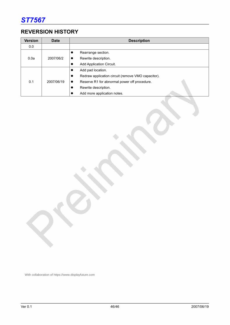
REVERSION HISTORY Version Date Description
0.0
0.0a 2007/06/2
l Rearrange section.
l Rewrite description.
l Add Application Circuit.
0.1 2007/06/19
l Add pad location.
l Redraw application circuit (remove VMO capacitor).
l Reserve R1 for abnormal power off procedure.
l Rewrite description.
l Add more application notes.
With collaboration of https://www.displayfuture.com
Related Documents


