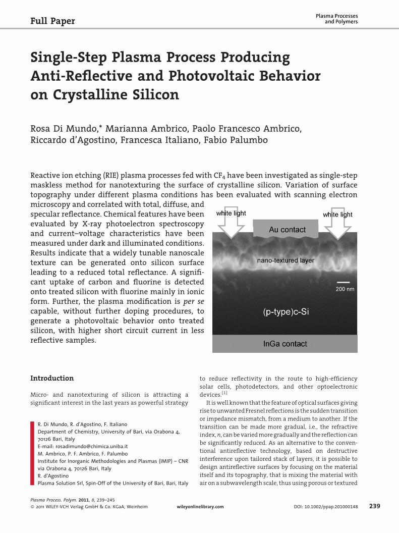
Single-Step Plasma Process Producing Anti-Reflective and Photovoltaic Behavior on Crystalline Silicon Rosa Di Mundo,* Marianna Ambrico, Paolo Francesco Ambrico, Riccardo d’Agostino, Francesca Italiano, Fabio Palumbo Introduction Micro- and nanotexturing of silicon is attracting a significant interest in the last years as powerful strategy to reduce reflectivity in the route to high-efficiency solar cells, photodetectors, and other optoelectronic devices. [1] It is well known that the feature of optical surfaces giving rise to unwanted Fresnel reflections is the sudden transition or impedance mismatch, from a medium to another. If the transition can be made more gradual, i.e., the refractive index, n, can be varied more gradually and the reflection can be significantly reduced. As an alternative to the conven- tional antireflective technology, based on destructive interference upon tailored stack of layers, it is possible to design antireflective surfaces by focusing on the material itself and its topography, that is mixing the material with air on a subwavelength scale, thus using porous or textured Full Paper R. Di Mundo, R. d’Agostino, F. Italiano Department of Chemistry, University of Bari, via Orabona 4, 70126 Bari, Italy E-mail: [email protected] M. Ambrico, P. F. Ambrico, F. Palumbo Institute for Inorganic Methodologies and Plasmas (IMIP) – CNR via Orabona 4, 70126 Bari, Italy R. d’Agostino Plasma Solution Srl, Spin-Off of the University of Bari, Bari, Italy Reactive ion etching (RIE) plasma processes fed with CF 4 have been investigated as single-step maskless method for nanotexturing the surface of crystalline silicon. Variation of surface topography under different plasma conditions has been evaluated with scanning electron microscopy and correlated with total, diffuse, and specular reflectance. Chemical features have been evaluated by X-ray photoelectron spectroscopy and current–voltage characteristics have been measured under dark and illuminated conditions. Results indicate that a widely tunable nanoscale texture can be generated onto silicon surface leading to a reduced total reflectance. A signifi- cant uptake of carbon and fluorine is detected onto treated silicon with fluorine mainly in ionic form. Further, the plasma modification is per se capable, without further doping procedures, to generate a photovoltaic behavior onto treated silicon, with higher short circuit current in less reflective samples. Plasma Process. Polym. 2011, 8, 239–245 ß 2011 WILEY-VCH Verlag GmbH & Co. KGaA, Weinheim wileyonlinelibrary.com DOI: 10.1002/ppap.201000148 239

Welcome message from author
This document is posted to help you gain knowledge. Please leave a comment to let me know what you think about it! Share it to your friends and learn new things together.
Transcript
Full Paper
Single-Step Plasma Process ProducingAnti-Reflective and Photovoltaic Behavioron Crystalline Silicon
Rosa Di Mundo,* Marianna Ambrico, Paolo Francesco Ambrico,Riccardo d’Agostino, Francesca Italiano, Fabio Palumbo
Reactive ion etching (RIE) plasma processes fed with CF4 have been investigated as single-stepmaskless method for nanotexturing the surface of crystalline silicon. Variation of surfacetopography under different plasma conditions has been evaluated with scanning electronmicroscopy and correlated with total, diffuse, andspecular reflectance. Chemical features have beenevaluated by X-ray photoelectron spectroscopyand current–voltage characteristics have beenmeasured under dark and illuminated conditions.Results indicate that a widely tunable nanoscaletexture can be generated onto silicon surfaceleading to a reduced total reflectance. A signifi-cant uptake of carbon and fluorine is detectedonto treated silicon with fluorine mainly in ionicform. Further, the plasma modification is per secapable, without further doping procedures, togenerate a photovoltaic behavior onto treatedsilicon, with higher short circuit current in lessreflective samples.
Introduction
Micro- and nanotexturing of silicon is attracting a
significant interest in the last years as powerful strategy
R. Di Mundo, R. d’Agostino, F. ItalianoDepartment of Chemistry, University of Bari, via Orabona 4,70126 Bari, ItalyE-mail: [email protected]. Ambrico, P. F. Ambrico, F. PalumboInstitute for Inorganic Methodologies and Plasmas (IMIP) – CNRvia Orabona 4, 70126 Bari, ItalyR. d’AgostinoPlasma Solution Srl, Spin-Off of the University of Bari, Bari, Italy
Plasma Process. Polym. 2011, 8, 239–245
� 2011 WILEY-VCH Verlag GmbH & Co. KGaA, Weinheim wileyonlin
to reduce reflectivity in the route to high-efficiency
solar cells, photodetectors, and other optoelectronic
devices.[1]
It iswell knownthat the featureofoptical surfacesgiving
rise tounwantedFresnel reflections is thesuddentransition
or impedance mismatch, from a medium to another. If the
transition can be made more gradual, i.e., the refractive
index,n, canbevariedmoregraduallyand the reflectioncan
be significantly reduced. As an alternative to the conven-
tional antireflective technology, based on destructive
interference upon tailored stack of layers, it is possible to
design antireflective surfaces by focusing on the material
itself and its topography, that is mixing the material with
air on a subwavelength scale, thus using porous or textured
elibrary.com DOI: 10.1002/ppap.201000148 239
240
R. Di Mundo, M. Ambrico, P. F. Ambrico, R. d’Agostino, F. Italiano, F. Palumbo
surfaces. Such an effect was argued by Bernhard to occur
over the eye of the night flying moth, covered with a fine
regular hexagonal array of protuberances which have a
period of about 200nm, a similar depth and a cross-section
that is approximately sinusoidal: the natural corrugation
provides a mixed solid/air layer with graded refractive
index.[2] This phoenomenon canbe interpretedbyusing the
theories of the effective medium approximation and/or
the gradient refractive index. The former considers the
layer with a certain rough or porous topography like an
homogeneous medium with an effective refractive index
betweenthesubstrateandtheair.[3] The latter, anextension
of the former, postulates a variation of topography along
the depth such that a continuous increase of refractive
index occurs fromair to the bulkmaterial.[4] This effectwas
first reproduced by Clapham and Hutley[5] by recording
finely spaced optical interference fringes in two orthogonal
directions of a photoresist, reaching results similar to
multilayer interference coating over the visible and the
near infrared.
The problemof surface reflection is particularly acute for
semiconductors which have very high values of refractive
index in the visible and the near-infrared spectral regions.
For crystalline silicon n is 3.8, and the reflection losses at
normal incidence are about 40%, representing a drawback
for solar cell applications and other optoelectronic devices.
Many texturing methods have been proposed in this
framework, generally based on various photolithographic
approaches,[6] electron beam lithography,[7] colloids aided
procedures,[8,9] wet etchingwith acids or bases, sometimes
assisted by metal or oxides catalysts.[10,11]
Needle-like, pyramid-like, or porous silicon surfaces
structures are obtained in most cases. In order to further
reduce reflectance, even complicated approaches to obtain
hierarchical structuring (micropyramids and nanostruc-
tures) have been tested.[12] These and other examples of
fabrication of micro/nanotextured (NT) silicon, both for
bottom–up and top–down procedures, are finely reviewed
in reference[13]
Among the top–down approaches, much attention is
nowadays given to plasma etching, for the intrinsic
possibility of easy scaling up to large substrates with good
dimensional control and also under maskless conditions.
In some cases these processes are called self-masked
since the discharge itself produces both nanomasks and the
etchant active species. This, for instance, is assumed to
occur inprocesses composedof consecutive stagesofCF4/O2
etching, SF6 etching, C4F8 passivation (commonly knownas
Bosch process or time-multiplexed etching process), result-
ing in highly antireflective silicon nanotips (SiNTs).[14]
Similar SiNTs have been produced with ECR plasmas fed
withSiH4, CH4,Ar, andH2where etching isbelieved tooccur
simultaneously to the formation of SiC nanomask.[15]
Further, SF6/O2 fed RIE processes have been shown to
Plasma Process. Polym. 2011, 8, 239–245
� 2011 WILEY-VCH Verlag GmbH & Co. KGaA, Weinheim
generate micron-sized needle-like and cylinder-like struc-
tures, probably as a consequence of non-homogeneous
masking by silicon oxide[16] or ‘‘inverted pyramids’’.[17]
H2 based plasmas with substrate biasing[18,19] or
heating[20] have been also shown to develop a nanotexture
onto silicon.
In several cases among those cited a remarkable
reduction of total reflectance is reported although an
optoelectronic characterization of the modified silicon is
rarely performed.[16]
The possibility of producing nanostructures uniformly,
though randomly, distributed onto the surfaces of various
polymers (polystyrene, polymethylmethacrilate, and
others) with fluorine or oxygen containing plasmas in
maskless single-step processes has been widely shown in
recent years and exploited for wetting and optical
applications of plastics.[21–23]
In particular with fluorocarbon plasmas reflectance has
been reduced without hindering polymer transparency.[22]
This nanotexturing method can be finely tuned with
varying plasma parameters, and, though themechanism is
not yet completely understood, it seems to be reasonably
originated by sputtered metals from electrodes, acting as
nanomask.[24] In thisworkaRIE radiofrequency (RF)process
fed with pure CF4 has been utilized to address nanoscale
surface texturing of crystalline silicon. The variation of
nanofeature shapes and sizes under different plasma
conditions has been evaluated and correlated with total,
diffuse, and specular reflectance. Chemical modification of
silicon surface has been assessed with X-ray photoelectron
Spectroscopy. Current–voltage characteristics under dark
and illuminated conditionshavealsobeenmeasuredon the
as obtained specimens in order to investigate the optoelec-
tronic variations that the plasma process itself can induce
on this material.
Experimental Part
P-type (100) crystalline silicon (c-Si) slabs (polished wafers, with
nominal resistivity 1–50V cm, thickness 0.7mm, from MEMC St.
Peters) were utilized as silicon substrates. Plasma treatment
experiments were run in a RF capacitively coupled parallel plate
plasma reactor. It consists of a cylindrical stainless steel vacuum
chamber (internal diameter of 30 cmandheight of 13 cm), pumped
by a turbomolecular-rotary pumping system. The pressure is
monitored by a capacitive membrane transducer (MKS instru-
ments, Baratron). The gas flow rates are controlled by electronic
mass flow controllers (Brooks Instruments). The plasma is ignited
with a 13.56MHz power supply (Caesar Dressler) through an
impedance matching unit. The upper stainless steel electrode
(20 cm diameter) is grounded while the bottom electrode (15 cm
diameter, spaced 5 cmapart), onwhich the substrates are placed, is
RF powered. A shower head inserted in the upper electrode allows
gas admission.
DOI: 10.1002/ppap.201000148
Single-Step Plasma Process Producing Anti-Reflective and Photovoltaic . . .
Discharges were fed with CF4 at a flow rate of 50 sccm and
constant pressure of 45mTorr. The effects of input power (100–
300W) and of treatment duration (20–60min) have been
investigated.
Samplesmorphologywasobservedat tilt angleof0and608with
a Zeiss EVO 40 VP scanning electronmicroscope (SEM) at a voltage
of 20 kV. Image J softwarewas used to process the acquired images
and measure the topographycal features.
Diffuse and total reflectance at 08 angle of incidence was
measured in the 200–1000nm range with unpolarized light by
means of a Varian Cary 5000 spectrophotometer equipped with a
diffuse reflectance accessory (DRA), whose integrated sphere can
separate the diffuse component from the total reflectance (the
specular component has been calculated by subtraction).
XPS analyseswere carried outwith Thermo
Electron Corporation Theta Probe Spectro-
meter using a monochromatic Al Ka X-ray
source (1 486.6 eV) at a spot size of 400mm
corresponding to a power of 100W at a take-
off angle of 538 from surface normal. Survey
(0–1200 eV) and high-resolution spectra were
recorded at a pass energy of 200 and 150eV,
respectively. The C1s signal for C–C(H) bonds,
with a binding energy of 284.7 eV, has been
used as an internal standard for the correction
of the samples charging.
The at.-% reported have been calculated by
using the sensitivity factors of the instrument
from the high-resolution peaks.
Best fitting of the XPS line shapes has been
performed by means of the instrument soft-
ware (Avantage). The full-width at half max-
imumofeach lineshapewasallowedtovary in
the range 1.8–2.4 eV.
The optoelectronic electrical characteriza-
tion has been performed on the as treated
silicon slabs (in this frame called NT-Si/(p-
type)c-Si junctions, where NT stands for
nanotextured), without any further doping
procedure.Auwasdepositedbyevaporationas
front side contact (0.2� 0.2 cm2) and an InGa
pastewaspaintedontheuntreatedbacksideof
theslabs for theohmiccontact formation.Dark
current and photocurrent density versus
voltage characteristics have been measured
byusingaKeithleyK617electrometerandaHP
DAC power supply. The white light of a
halogen lamp simulating solar spectrum
(AM 1.5G, standard CEI/IEC 904-3) with
irradiance 100mW/cm2 was used as light
irradiation source at room temperature in air.
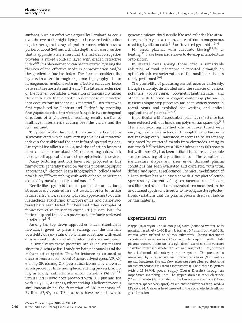
Figure 1. Top (left) and 608 tilted view (right) SEM images of crystalline silicon samplestreated in CF4 plasma at 100 (a), 200 (b), 300 W (c) for a treatment time of 20 min, and at100 W for 60 min (d).
Results and Discussion
Top (left) and 608 tilted view (right) SEM
images of silicon samples treated in CF4plasma at 100W (a), 200W (b), 300W (c)
Plasma Process. Polym. 2011, 8, 239–245
� 2011 WILEY-VCH Verlag GmbH & Co. KGaA, Weinheim
for a treatment time of 20min, and at 100W for 60min (d)
are reported in Figure 1.Generally it canbeappreciated that
a deep variation of both size and shape of the structures is
achieved as a function of the working conditions. The 100
and 200W samples after 20min treatment present similar
nanosharpened shape but at a different dimensional scale
(at 200Wstructures are taller, larger, andmore spaced). The
300W/20min sample displays paddle-like structures
(round, flat, and with a thinner base), while the sample
obtained at 100W for longer treatment time shows slender
stem-like structures. Features mean height increases with
input power (from 100 to around 400nm) and with
treatment duration: 60min stem-like structures are the
www.plasma-polymers.org 241
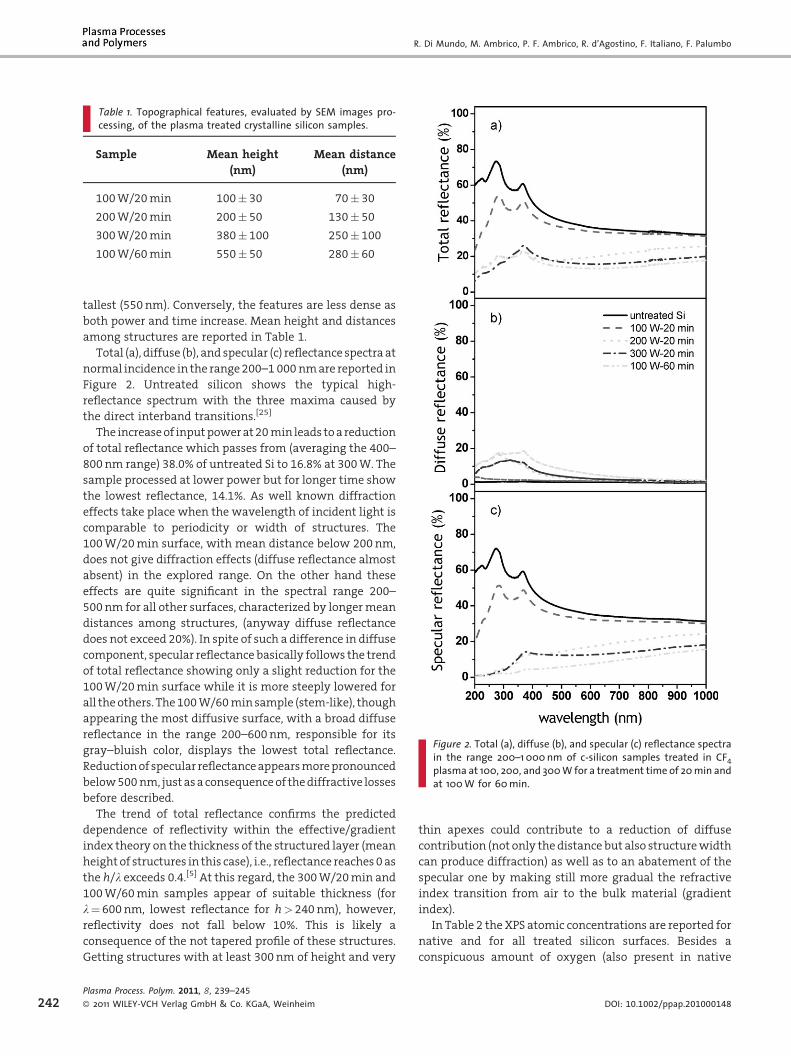
Table 1. Topographical features, evaluated by SEM images pro-cessing, of the plasma treated crystalline silicon samples.
Sample Mean height
(nm)
Mean distance
(nm)
100W/20min 100� 30 70� 30
200W/20min 200� 50 130� 50
300W/20min 380� 100 250� 100
100W/60min 550� 50 280� 60
Figure 2. Total (a), diffuse (b), and specular (c) reflectance spectrain the range 200–1 000 nm of c-silicon samples treated in CF4plasma at 100, 200, and 300 W for a treatment time of 20 min andat 100 W for 60 min.
242
R. Di Mundo, M. Ambrico, P. F. Ambrico, R. d’Agostino, F. Italiano, F. Palumbo
tallest (550nm). Conversely, the features are less dense as
both power and time increase. Mean height and distances
among structures are reported in Table 1.
Total (a), diffuse (b), and specular (c) reflectance spectraat
normal incidence in the range200–1 000nmare reported in
Figure 2. Untreated silicon shows the typical high-
reflectance spectrum with the three maxima caused by
the direct interband transitions.[25]
The increaseof inputpowerat20min leads toareduction
of total reflectance which passes from (averaging the 400–
800nm range) 38.0% of untreated Si to 16.8% at 300W. The
sample processed at lower power but for longer time show
the lowest reflectance, 14.1%. As well known diffraction
effects take place when the wavelength of incident light is
comparable to periodicity or width of structures. The
100W/20min surface, with mean distance below 200nm,
does not give diffraction effects (diffuse reflectance almost
absent) in the explored range. On the other hand these
effects are quite significant in the spectral range 200–
500nm for all other surfaces, characterized by longermean
distances among structures, (anyway diffuse reflectance
does not exceed 20%). In spite of such a difference in diffuse
component, specular reflectance basically follows the trend
of total reflectance showing only a slight reduction for the
100W/20min surface while it is more steeply lowered for
all theothers. The100W/60minsample (stem-like), though
appearing the most diffusive surface, with a broad diffuse
reflectance in the range 200–600nm, responsible for its
gray–bluish color, displays the lowest total reflectance.
Reductionof specular reflectanceappearsmorepronounced
below500nm, justasaconsequenceof thediffractive losses
before described.
The trend of total reflectance confirms the predicted
dependence of reflectivity within the effective/gradient
index theory on the thickness of the structured layer (mean
heightof structures in this case), i.e., reflectance reaches0as
the h/l exceeds 0.4.[5] At this regard, the 300W/20min and
100W/60min samples appear of suitable thickness (for
l¼ 600nm, lowest reflectance for h> 240nm), however,
reflectivity does not fall below 10%. This is likely a
consequence of the not tapered profile of these structures.
Getting structures with at least 300nm of height and very
Plasma Process. Polym. 2011, 8, 239–245
� 2011 WILEY-VCH Verlag GmbH & Co. KGaA, Weinheim
thin apexes could contribute to a reduction of diffuse
contribution (not only thedistance but also structurewidth
can produce diffraction) as well as to an abatement of the
specular one by making still more gradual the refractive
index transition from air to the bulk material (gradient
index).
In Table 2 the XPS atomic concentrations are reported for
native and for all treated silicon surfaces. Besides a
conspicuous amount of oxygen (also present in native
DOI: 10.1002/ppap.201000148
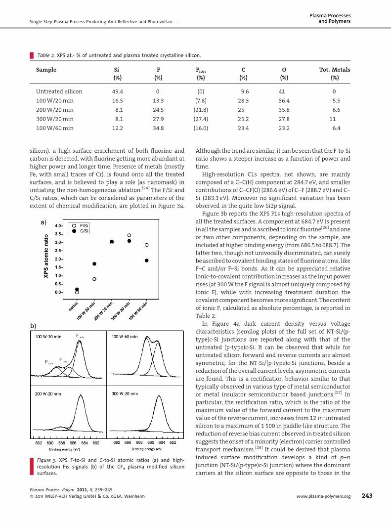
Table 2. XPS at.- % of untreated and plasma treated crystalline silicon.
Sample Si
(%)
F
(%)
Fion(%)
C
(%)
O
(%)
Tot. Metals
(%)
Untreated silicon 49.4 0 (0) 9.6 41 0
100W/20min 16.5 13.3 (7.8) 28.3 36.4 5.5
200W/20min 8.1 24.5 (21.8) 25 35.8 6.6
300W/20min 8.1 27.9 (27.4) 25.2 27.8 11
100W/60min 12.2 34.8 (16.0) 23.4 23.2 6.4
Single-Step Plasma Process Producing Anti-Reflective and Photovoltaic . . .
silicon), a high-surface enrichment of both fluorine and
carbon is detected, with fluorine gettingmore abundant at
higher power and longer time. Presence of metals (mostly
Fe, with small traces of Cr), is found onto all the treated
surfaces, and is believed to play a role (as nanomask) in
initiating the non-homogeneous ablation.[24] The F/Si and
C/Si ratios, which can be considered as parameters of the
extent of chemical modification, are plotted in Figure 3a.
Figure 3. XPS F-to-Si and C-to-Si atomic ratios (a) and high-resolution F1s signals (b) of the CF4 plasma modified siliconsurfaces.
Plasma Process. Polym. 2011, 8, 239–245
� 2011 WILEY-VCH Verlag GmbH & Co. KGaA, Weinheim
Although the trendare similar, it canbe seen that theF-to-Si
ratio shows a steeper increase as a function of power and
time.
High-resolution C1s spectra, not shown, are mainly
composed of a C–C(H) component at 284.7 eV, and smaller
contributions of C–CF(O) (286.6 eV) of C–F (288.7 eV) and C–
Si (283.3 eV). Moreover no significant variation has been
observed in the quite low Si2p signal.
Figure 3b reports the XPS F1s high-resolution spectra of
all the treated surfaces. A component at 684.7 eV is present
inall thesamplesand isascribed to ionicfluorine[26] andone
or two other components, depending on the sample, are
includedat higher binding energy (from686.5 to 688.7). The
latter two, though not univocally discriminated, can surely
beascribed to covalentbinding states offluorineatoms, like
F–C and/or F–Si bonds. As it can be appreciated relative
ionic-to-covalent contribution increases as the input power
rises (at 300W the F signal is almost uniquely composed by
ionic F), while with increasing treatment duration the
covalent componentbecomesmore significant. Thecontent
of ionic F, calculated as absolute percentage, is reported in
Table 2.
In Figure 4a dark current density versus voltage
characteristics (semilog plots) of the full set of NT-Si/(p-
type)c-Si junctions are reported along with that of the
untreated (p-type)c-Si. It can be observed that while for
untreated silicon forward and reverse currents are almost
symmetric, for the NT-Si/(p-type)c-Si junctions, beside a
reduction of the overall current levels, asymmetric currents
are found. This is a rectification behavior similar to that
typically observed in various type of metal semiconductor
or metal insulator semiconductor based junctions.[27] In
particular, the rectification ratio, which is the ratio of the
maximum value of the forward current to the maximum
value of the reverse current, increases from 12 in untreated
silicon to amaximum of 1 500 in paddle-like structure. The
reduction of reverse bias current observed in treated silicon
suggests theonset of aminority (electron) carrier controlled
transport mechanism.[28] It could be derived that plasma
induced surface modification develops a kind of p–n
junction (NT-Si/(p-type)c-Si junction) where the dominant
carriers at the silicon surface are opposite to those in the
www.plasma-polymers.org 243
-1.0 -0.5 0.0 0.5 1.010-5
10-3
10-1
10
a)
b)
1
103
Dar
k cu
rren
t den
sity
(mA
/cm
2 )
Voltage (V)
untreated pSi 100W 20 min 200W 20 min 300W 20 min 100W 60 min
-1.0 -0.5 0.0 0.5 1.010-2
100
102
Voltage (V)
Phot
ocur
rent
den
sity
(mA
/cm
2 )
Figure 4. Semilog plots of dark current density (a) and photo-current density (b) versus voltage characteristics of the full set ofNT-Si/(p-type)c-Si junctions, i.e., the plasma treated siliconsamples, along with that of the untreated (p-type)c-Si.
Table 3. Short circuit current (Jsc), open circuit voltages (Voc), andtotal reflectance averaged in the spectral range 400–800 nm (Rt)of untreated and CF4 plasma treated crystalline silicon.
Sample Jsc(mA/cm2)
Voc
(V)
Rt
(%)
Untreated silicon – – 38
100W/20min 0.285 0.230 35.1
200W/20min 1.06 0.177 19.9
300W/20min 4.25 0.153 16.8
100W/60min 2.70 0.200 14.2
244
R. Di Mundo, M. Ambrico, P. F. Ambrico, R. d’Agostino, F. Italiano, F. Palumbo
silicon bulk (in this case electrons instead of holes). The
presence of the electrical transport driven by minority
carriers also explains the appearance of a photovoltaic
behavior, appreciable in Figure 4b, where the photocurrent
density versus voltage is reported. NT-Si/(p-type)c-Si
junctions, in fact, show an open circuit voltage (Voc) as
well as a short circuit current density (Jsc) not observed on
the untreated (p-type)c-Si. It is worth remarking that this
occurs without any further doping procedure of the
textured silicon, instead utilized elsewhere.[16] The trend
of the short circuit current, which increases for samples
obtainedathigherpowerand time, ismostlya consequence
of the previously described reduction of reflectance, thus
the increaseof light trappingandoptical absorption (values
reported in Table 3, along with average total reflectance in
the spectral range 400–800nm). The open circuit voltage
(Voc) is a parameter inversely related to carrier recombina-
tion velocity, thus more dependent on surface chemical
Plasma Process. Polym. 2011, 8, 239–245
� 2011 WILEY-VCH Verlag GmbH & Co. KGaA, Weinheim
modification effects: it displays the highest value for the
100W/20min surface, that, as previously observed, shows
the poorest chemical and morphological modification.
Moreover this parameter has a perfect inverse linear
correlation with the surface content of ionic fluorine
determined with XPS (Table 2). Such an effect could be
indicative of a role of this species in increasing carrier
recombination velocity, and therefore, it will be handled in
detail, among others, within future investigations. It is
worth remarking that the behavior of photocurrent density
versus voltage between 0V and Voc is greatly affected by
shunt and series resistance effects, since the procedure of
junction building up has not been fully optimized. Anyway
under the present experimental conditions, the highest
photovoltaic efficiency h, i.e., the ratio of the maximum
outputpower tothe incident lightpower (100mW/cm2)has
been found in the junctions with the paddle-like and stem-
like structured surfaces (0.28 and 0.17); the best fill factor
(FF), defined as the ratio of the maximum power to the
product Jsc�Voc, has been found in the junction with
paddle-like structures (0.4). These results, though not
optimized, are similar to those reported for junctions
embedding silicon nanowire arrays grown onto silicon and
modified with elaborate doping procedures.[29,30] Deeper
investigations areneeded to improveperformances inview
of the simple, single-step process utilized.
Conclusion
Thisworkprovides an investigationof the capability of CF4-
fed RIE plasmas of generating a nanoscale texture onto
crystalline silicon and modulating light trapping and
optoelectronic behavior. Results indicate that this process
is highly efficient in developing silicon nanostructures
which can be widely tuned in both shape and scale with
playingwith input power and treatment time. Total optical
reflectance in the range 200–1 000nm is remarkably
lowered, especially at high power and time, in spite of
some diffraction losses in the short wavelength range. This
DOI: 10.1002/ppap.201000148
Single-Step Plasma Process Producing Anti-Reflective and Photovoltaic . . .
kind of plasma also deeply affects surface chemistry of
crystalline silicon, since a significant uptake of carbon and
fluorine is detected by XPS. Fluorine is present mostly as
ionic species, in particular at high power. These samples,
without any further doping or other procedure, show an
enhancement of the rectification features and under
illuminated conditions the appearance of a photovoltaic
behaviorwithhigher short circuit currents for less reflective
samples. Hence, the process here described represents a
single-step fastmethod for producing an antireflective p–n
junction with crystalline silicon.
Further investigations are necessary for tailoring the
structures profile (more tapered shape) to get still lower
reflectivity as well as for further improving performances
by better correlating chemical and optoelectronic effects.
Acknowledgements: The financial support of the regionalfunding-cod. 51-Public Laboratory of Apulian Industrial Researchof Plasmas ‘‘LIPP’’ is gratefully acknowledged.
Received: October 19, 2010; Revised: December 6, 2010; Accepted:December 9, 2010; DOI: 10.1002/ppap.201000148
Keywords: antireflective; crystalline silicon; nanotexturing/structuring; photovoltaic; plasma etching
[1] L. Tsakalakos, Mater. Sci. Eng. R 2008, 62, 175.[2] G. Bernhard, Endeavour 1967, 26, 79.[3] J. C. Maxwell Garnett, Philos. Trans. R. Soc., Lond. 1906, 205,
237.[4] D. H. Raguin, G. M. Morris, Appl. Opt. 1993, 32, 1154.[5] P. B. Clapham, M. C. Hutley, Nature 1973, 244, 281.[6] P. Lalanne, G. M. Morris, Nanotechnology 1997, 8, 53.[7] Y. Kanamori, M. Sasaki, K. Hane, Opt. Lett. 1999, 24, 1422.
Plasma Process. Polym. 2011, 8, 239–245
� 2011 WILEY-VCH Verlag GmbH & Co. KGaA, Weinheim
[8] W. Min, P. Jiang, B. Jiang, Nanotechnology 2008, 19, 475605.[9] N. C. Linn, C. H. sun, P. Jiang, Appl. Phys. Lett. 2007, 91, 101108.[10] S. Yae, T. Kobayashi, T. Kawagishi, N. Fukumuro, H. Matsuda,
Sol. Energy 2006, 80, 701.[11] M. Cao, X. Song, J. Zhai, J. Wang, Y. Wang, J. Phys. Chem. B
2006, 110, 13072.[12] Y. Xiu, S. Zhang, V. Yelundur, A. Rohatgi, D. W. Hess, C. P.
Wong, Langmuir 2008, 24, 10421.[13] S. Chattopadhyay, Y. F. Huang, Y. J. Jen, A. Ganguly, K. H. Chen,
L. C. Chen, Mater. Sci. Eng. R 2010, 69, 35.[14] C. Lee, S. Y. Bae, S. Mobasser, H. Manohara, Nano Lett. 2005, 5,
2438.[15] C. H. Hsu, H. C. Lo, C. F. Chen, C. T. Wu, J. S. Hwang, D. Das,
J. Tsai, L. C. Chen, K. H. Chen, Nano Lett. 2004, 4, 471.[16] J. Yoo, K. Kim, M. Thamilselvan, N. Lakshiminarayn, Y. K. Kim,
J. Lee, K. J. Yoo, J. Yi, J. Phys. D: Appl. Phys. 2008, 41, 125205.[17] M. Moreno, D. Daineka, P. Roca I. Cabarrocas, Sol. Energy
Mater. Sol. Cells 2010, 94, 733.[18] S. Xu, L. Levchenko, S. Y. Huang, K. Ostrikov, Appl. Phys. Lett.
2009, 95, 111505.[19] J. Shieh, C. H. Lin, M. C. Jang, J. Phys. D: Appl. Phys. 2007, 40,
2242.[20] I. Levchenko, S. Y. Huang, K. Ostrikov, S. Xu, Nanotechnology
2010, 21, 025605.[21] R. Di Mundo, F. Palumbo, R. d’Agostino, Langmuir 2008, 24,
5044.[22] R. DiMundo, V. De Benedictis, F. Palumbo, R. d’Agostino,Appl.
Surf. Sci. 2009, 255, 5461.[23] U. Schulz, P. Munzert, R. Leitel, I. Wending, N. Kaiser,
A. Tunnermann, Opt. Express 2007, 5, 13108.[24] K. Lilienthal, M. Stubenrauch, M. Fischer, A. Shober, J. Micro-
mech. Microeng. 2010, 20, 025017.[25] S. Adachi, J. Appl. Phys. 1989, 66, 3224.[26] J. F. Moulder, W. F. Stickle, P. E. Sobol, K. D. Bomben, ‘‘Hand-
book of X-ray Photoelectron Spectroscopy’’, Perkin Elm. Corp,Eden Prairie, Minnesota, USA 1992.
[27] E. H. Rhoderick, ‘‘Monographs in Electrical and ElectronicEngineering. Metal–Semiconductor Contacts’’, Clarendon,Oxford 1988.
[28] A. Vilan, O. Yaffe, A. Biller, A. Salomon, A. Kahn, D. Cahen,Adv.Mater. 2010, 22, 140.
[29] T. Steltzner, M. Pietsch, G. Andra, F. Falk, E. Ose, S. Christian-sen, Nanotechnology 2008, 19, 295203.
[30] E. C. Garnett, P. Yang, J. Am. Chem. Soc. 2008, 130, 9225.
www.plasma-polymers.org 245
Related Documents