Energies 2022, 15, 1622. https://doi.org/10.3390/en15051622 www.mdpi.com/journal/energies Review Single‐Stage Buck–Boost Inverters: A State‐of‐the‐Art Survey Mohammadreza Azizi 1 , Oleksandr Husev 2 and Dmitri Vinnikov 2, * 1 Faculty of Electrical Engineering, Malayer University, Malayer 6571995863, Iran; [email protected] 2 Department of Electrical Power Engineering and Mechatronics, Tallinn University of Technology, 19086 Tallinn, Estonia; [email protected] * Correspondence: [email protected] Abstract: Single‐stage buck–boost inverters have attracted the attention of many researchers, due to their ability to increase/decrease the output voltage in one power conversion stage. One of the most important uses of these inverters is in photovoltaic applications, where the voltage of the solar panels varies in a wide range. In recent years, many new inverters have been proposed to improve the performance of existing structures. In this paper, the state of the art of these single‐stage buck– boost inverters is discussed. The advantages and disadvantages of each structure are examined from different perspectives, such as the number of components, losses, and performance. Finally, in a general comparison, the properties of all structures are discussed and summarized in a table. Keywords: single‐stage inverter; buck–boost operation; survey 1. Introduction In electrical engineering, power electronics converters are of particular importance in the power conversion process. Today, power electronic converters are used in many devices and are increasingly replacing previous systems with their promising features. Paying attention to these converters, in terms of reliability, volume, and weight, is the subject of many studies. Considering the importance of renewable energy, many researchers have focused on converters of renewable systems, especially solar systems. Since solar panels have a low voltage, and this voltage varies under the influence of shading and temperature changes, in the existing common structures, a dc–dc boost converter is used in the first stage, and then a voltage source inverter (VSI) is used in the second stage. Two power conversion steps, and separate control of each of these converters, reduce the overall efficiency and increase the complexity of the system. It should also be noted that the use of transformers is not acceptable, due to the high volume and weight [1]. In the last decade, research has shifted to single‐stage buck–boost inverters. The main application of these structures is mainly in PV systems and electric vehicles (EVs). Due to environmental concerns and reduced consumption of fossil fuels, addressing this area and providing a structure with high capabilities is of great importance. In this regard, different structures are presented. Meanwhile, the current source inverter (CSI) has not received much attention, due to its large inductor, and only the boosting ability [2] and Z‐source inverter (ZSI), due to limited gain, shoot through (ST) problems and reliability [3]. Other structures have been developed over the years, and they have been analyzed in the following literature. In reference [4], several of these structures have been compared, based on the operating mode. Of course, this reference does not deal with the new structures. In reference [5], the author examines a limited, and relatively old, number of structures, along with some control methods of these inverters. Reference [6] examines the history of buck–boost single‐stage inverters over the past 25 years. In this study, the author addresses the challenges of these inverters, as well as their lack of acceptance in the industry, and compares these converters from different Citation: Azizi, M.; Husev, O.; Vinnikov, D. Single‐Stage Buck– Boost Inverters: A State‐of‐the‐Art Survey. Energies 2022, 15, 1622. https://doi.org/10.3390/en15051622 Academic Editor: Adolfo Dannier Received: 10 January 2022 Accepted: 17 February 2022 Published: 22 February 2022 Publisher’s Note: MDPI stays neutral with regard to jurisdictional claims in published maps and institutional affiliations. Copyright: © 2022 by the authors. Licensee MDPI, Basel, Switzerland. This article is an open access article distributed under the terms and conditions of the Creative Commons Attribution (CC BY) license (https://creativecommons.org/license s/by/4.0/).

Welcome message from author
This document is posted to help you gain knowledge. Please leave a comment to let me know what you think about it! Share it to your friends and learn new things together.
Transcript
Energies 2022, 15, 1622. https://doi.org/10.3390/en15051622 www.mdpi.com/journal/energies
Review
Single‐Stage Buck–Boost Inverters: A State‐of‐the‐Art Survey
Mohammadreza Azizi 1, Oleksandr Husev 2 and Dmitri Vinnikov 2,*
1 Faculty of Electrical Engineering, Malayer University, Malayer 6571995863, Iran; [email protected] 2 Department of Electrical Power Engineering and Mechatronics, Tallinn University of Technology,
19086 Tallinn, Estonia; [email protected]
* Correspondence: [email protected]
Abstract: Single‐stage buck–boost inverters have attracted the attention of many researchers, due to
their ability to increase/decrease the output voltage in one power conversion stage. One of the most
important uses of these inverters is in photovoltaic applications, where the voltage of the solar
panels varies in a wide range. In recent years, many new inverters have been proposed to improve
the performance of existing structures. In this paper, the state of the art of these single‐stage buck–
boost inverters is discussed. The advantages and disadvantages of each structure are examined from
different perspectives, such as the number of components, losses, and performance. Finally, in a
general comparison, the properties of all structures are discussed and summarized in a table.
Keywords: single‐stage inverter; buck–boost operation; survey
1. Introduction
In electrical engineering, power electronics converters are of particular importance
in the power conversion process. Today, power electronic converters are used in many
devices and are increasingly replacing previous systems with their promising features.
Paying attention to these converters, in terms of reliability, volume, and weight, is the
subject of many studies. Considering the importance of renewable energy, many
researchers have focused on converters of renewable systems, especially solar systems.
Since solar panels have a low voltage, and this voltage varies under the influence of
shading and temperature changes, in the existing common structures, a dc–dc boost
converter is used in the first stage, and then a voltage source inverter (VSI) is used in the
second stage. Two power conversion steps, and separate control of each of these
converters, reduce the overall efficiency and increase the complexity of the system. It
should also be noted that the use of transformers is not acceptable, due to the high volume
and weight [1]. In the last decade, research has shifted to single‐stage buck–boost
inverters. The main application of these structures is mainly in PV systems and electric
vehicles (EVs). Due to environmental concerns and reduced consumption of fossil fuels,
addressing this area and providing a structure with high capabilities is of great
importance. In this regard, different structures are presented. Meanwhile, the current
source inverter (CSI) has not received much attention, due to its large inductor, and only
the boosting ability [2] and Z‐source inverter (ZSI), due to limited gain, shoot through
(ST) problems and reliability [3]. Other structures have been developed over the years,
and they have been analyzed in the following literature. In reference [4], several of these
structures have been compared, based on the operating mode. Of course, this reference
does not deal with the new structures. In reference [5], the author examines a limited, and
relatively old, number of structures, along with some control methods of these inverters.
Reference [6] examines the history of buck–boost single‐stage inverters over the past 25
years. In this study, the author addresses the challenges of these inverters, as well as their
lack of acceptance in the industry, and compares these converters from different
Citation: Azizi, M.; Husev, O.;
Vinnikov, D. Single‐Stage Buck–
Boost Inverters: A State‐of‐the‐Art
Survey. Energies 2022, 15, 1622.
https://doi.org/10.3390/en15051622
Academic Editor: Adolfo Dannier
Received: 10 January 2022
Accepted: 17 February 2022
Published: 22 February 2022
Publisher’s Note: MDPI stays
neutral with regard to jurisdictional
claims in published maps and
institutional affiliations.
Copyright: © 2022 by the authors.
Licensee MDPI, Basel, Switzerland.
This article is an open access article
distributed under the terms and
conditions of the Creative Commons
Attribution (CC BY) license
(https://creativecommons.org/license
s/by/4.0/).
Energies 2022, 15, 1622 2 of 17
perspectives. The main focus of this study is mainly on Z‐source family inverters and
several differential converters, while other structures have not been studied.
Investigating the latest research, in this paper, the state of the art of single‐stage buck–
boost inverters has been studied. In general categorization, these inverters are divided
into five different types. For each category of these inverters, several general circuits of
them are illustrated, and each inverter has been examined from different perspectives,
such as the number of components, losses, etc. For a general evaluation, the characteristics
of different inverters are given in a table. This review and categorization will shed a light
on the path of those researchers who want to do research in this area.
2. Review of Single‐Stage Inverters
Single‐stage buck–boost inverters are inverters capable of increasing/decreasing the
output voltage in single power conversion. More attention of researchers to this type of
inverters, in the last decade, various structures of these inverters have been presented.
Although all of these structures have common features, they can be categorized. In this
study, these inverters are divided into five categories including differential connection,
split source, impedance source family, dc–dc converter combination, and multi‐level
based. For each category of these inverters, several structures are introduced, and their
general characteristics are discussed.
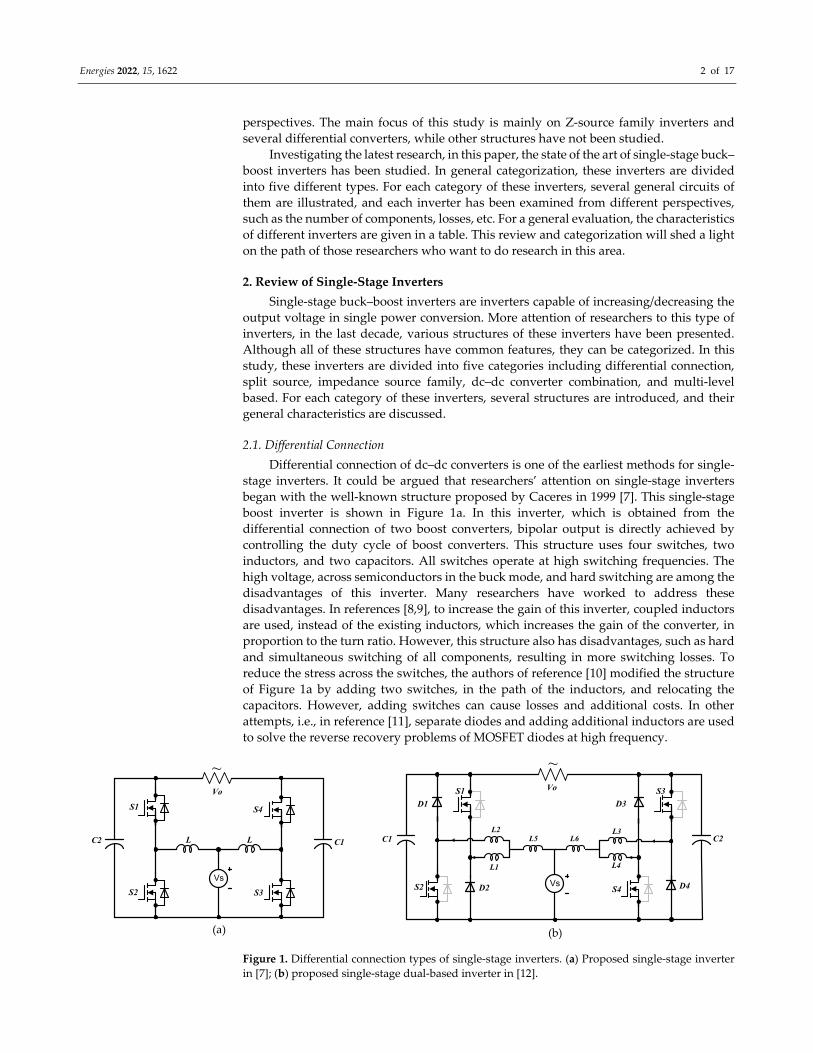
2.1. Differential Connection
Differential connection of dc–dc converters is one of the earliest methods for single‐
stage inverters. It could be argued that researchers’ attention on single‐stage inverters
began with the well‐known structure proposed by Caceres in 1999 [7]. This single‐stage
boost inverter is shown in Figure 1a. In this inverter, which is obtained from the
differential connection of two boost converters, bipolar output is directly achieved by
controlling the duty cycle of boost converters. This structure uses four switches, two
inductors, and two capacitors. All switches operate at high switching frequencies. The
high voltage, across semiconductors in the buck mode, and hard switching are among the
disadvantages of this inverter. Many researchers have worked to address these
disadvantages. In references [8,9], to increase the gain of this inverter, coupled inductors
are used, instead of the existing inductors, which increases the gain of the converter, in
proportion to the turn ratio. However, this structure also has disadvantages, such as hard
and simultaneous switching of all components, resulting in more switching losses. To
reduce the stress across the switches, the authors of reference [10] modified the structure
of Figure 1a by adding two switches, in the path of the inductors, and relocating the
capacitors. However, adding switches can cause losses and additional costs. In other
attempts, i.e., in reference [11], separate diodes and adding additional inductors are used
to solve the reverse recovery problems of MOSFET diodes at high frequency.
Figure 1. Differential connection types of single‐stage inverters. (a) Proposed single‐stage inverter
in [7]; (b) proposed single‐stage dual‐based inverter in [12].
L
S3S2
S4S1
Vs
L
Vo
C1C2
~
L1
S3
S2 S4
S1
Vs
C2C1
~
L2L5
L3
L4
L6
D1
D2
D3
D4
Vo
(a) (b)
Energies 2022, 15, 1622 3 of 17
Considering the structure of Figure 1a, for a more comprehensive structure in [12],
the authors present a symmetric dual‐based structure with the same number of switches.
As shown in Figure 1b, this structure consists of four switches, six inductors, four
separated diodes, two capacitors, and a source. The absence of shoot‐through (ST)
problems in this structure will be associated with increased reliability. In this structure,
using MOSFETs and separate diodes, the worry of reverse‐recovery issues of MOSFET
body diodes is eliminated. Therefore, high‐frequency switching can be achieved by silicon
semiconductors, which ultimately leads to a reduction in the volume of passive
components and increase in efficiency. Additionally, according to the author of the same
reference, current stresses have been eliminated for half of the switches. In addition to
these advantages, this structure has drawbacks, such as many inductors and complex
inductor current control on each side of the converter. In reference [13], the same author
suggests the use of coupled inductors for the same structure in Figure 1b, in order to
reduce the size of inductors. It should also be noted that differential‐mode inverters suffer
from current circulating problems and usually require large output capacitors. In the same
reference, the author has proposed the use of clamping switches, connected back‐to‐back
and parallel to the output capacitor, to solve the problem of circulating current in the
output. Some other similar differential structures are found in references [14–17]. Although,
in most differential structures, the boost converter has been used with some slight
changes; in some studies, such as reference [18], the differential inverter was obtained by
cascading a boost converters and a buck–boost converter. In this converter, the output
voltage is obtained from the voltage differential of the two converters. Although, in this
structure, the number of switches is minimal. However, there are still common differential
converter problems.
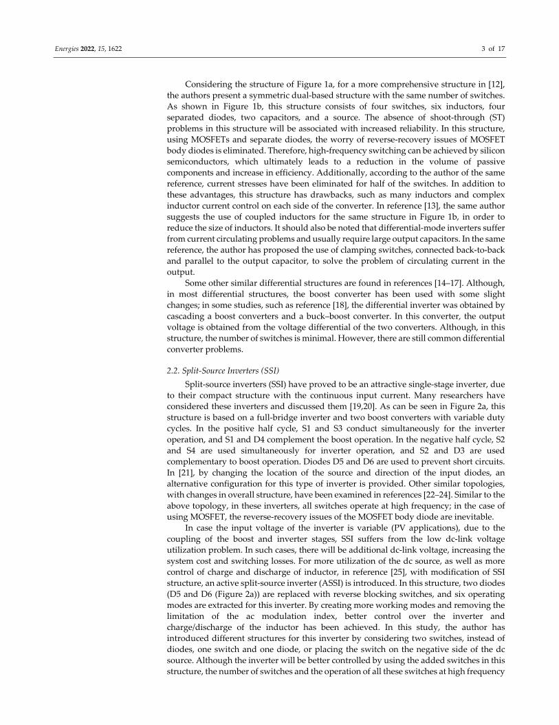
2.2. Split‐Source Inverters (SSI)
Split‐source inverters (SSI) have proved to be an attractive single‐stage inverter, due
to their compact structure with the continuous input current. Many researchers have
considered these inverters and discussed them [19,20]. As can be seen in Figure 2a, this
structure is based on a full‐bridge inverter and two boost converters with variable duty
cycles. In the positive half cycle, S1 and S3 conduct simultaneously for the inverter
operation, and S1 and D4 complement the boost operation. In the negative half cycle, S2
and S4 are used simultaneously for inverter operation, and S2 and D3 are used
complementary to boost operation. Diodes D5 and D6 are used to prevent short circuits.
In [21], by changing the location of the source and direction of the input diodes, an
alternative configuration for this type of inverter is provided. Other similar topologies,
with changes in overall structure, have been examined in references [22–24]. Similar to the
above topology, in these inverters, all switches operate at high frequency; in the case of
using MOSFET, the reverse‐recovery issues of the MOSFET body diode are inevitable.
In case the input voltage of the inverter is variable (PV applications), due to the
coupling of the boost and inverter stages, SSI suffers from the low dc‐link voltage
utilization problem. In such cases, there will be additional dc‐link voltage, increasing the
system cost and switching losses. For more utilization of the dc source, as well as more
control of charge and discharge of inductor, in reference [25], with modification of SSI
structure, an active split‐source inverter (ASSI) is introduced. In this structure, two diodes
(D5 and D6 (Figure 2a)) are replaced with reverse blocking switches, and six operating
modes are extracted for this inverter. By creating more working modes and removing the
limitation of the ac modulation index, better control over the inverter and
charge/discharge of the inductor has been achieved. In this study, the author has
introduced different structures for this inverter by considering two switches, instead of
diodes, one switch and one diode, or placing the switch on the negative side of the dc
source. Although the inverter will be better controlled by using the added switches in this
structure, the number of switches and the operation of all these switches at high frequency
Energies 2022, 15, 1622 4 of 17
are the disadvantages of this structure. Reverse‐blocking switches are also made by a
MOSFET or IGBT, in series with a diode, which ultimately increases the total number of
components. The current flow through the switch body diodes in these structures can
limit the use of MOSFETs because, at high frequencies, reverse‐recovery problems of the
MOSFET body diodes occur. Additionally, due to the limitation in increasing the duty
cycle of the boost converter, the capability of this structure in voltage increase is limited.
Figure 2. Split source inverters: (a) proposed single‐stage inverter based on SSI in [19]; (b) proposed
single‐stage inverter in [26].
In reference [26], the authors present a new single‐stage buck–boost inverter, based
on SSI. This structure consists of five switches, an inductor, a capacitor, and a source.
Figure 2b shows this structure. In this structure, a switch is added to an inverter leg of the
full‐bridge inverter, which performs the boost operation of the converter. Since the duty
cycle of the boost converter is not variable in this structure, it is easier to control the
inverter. This structure is also capable of bidirectional operation. As with other SSI
structures, all switches are switched at high frequencies, leading to the reverse‐recovery
issues of MOSFET body diode and losses. Therefore, IGBTs should normally be used,
which means that the advantages of MOSFET high frequency switching, such as fast
switching and lower losses, and the voltage drop across the conduction resistor cannot be
used. Moreover, to avoid short circuits in this structure, dead time between switches
should be considered.
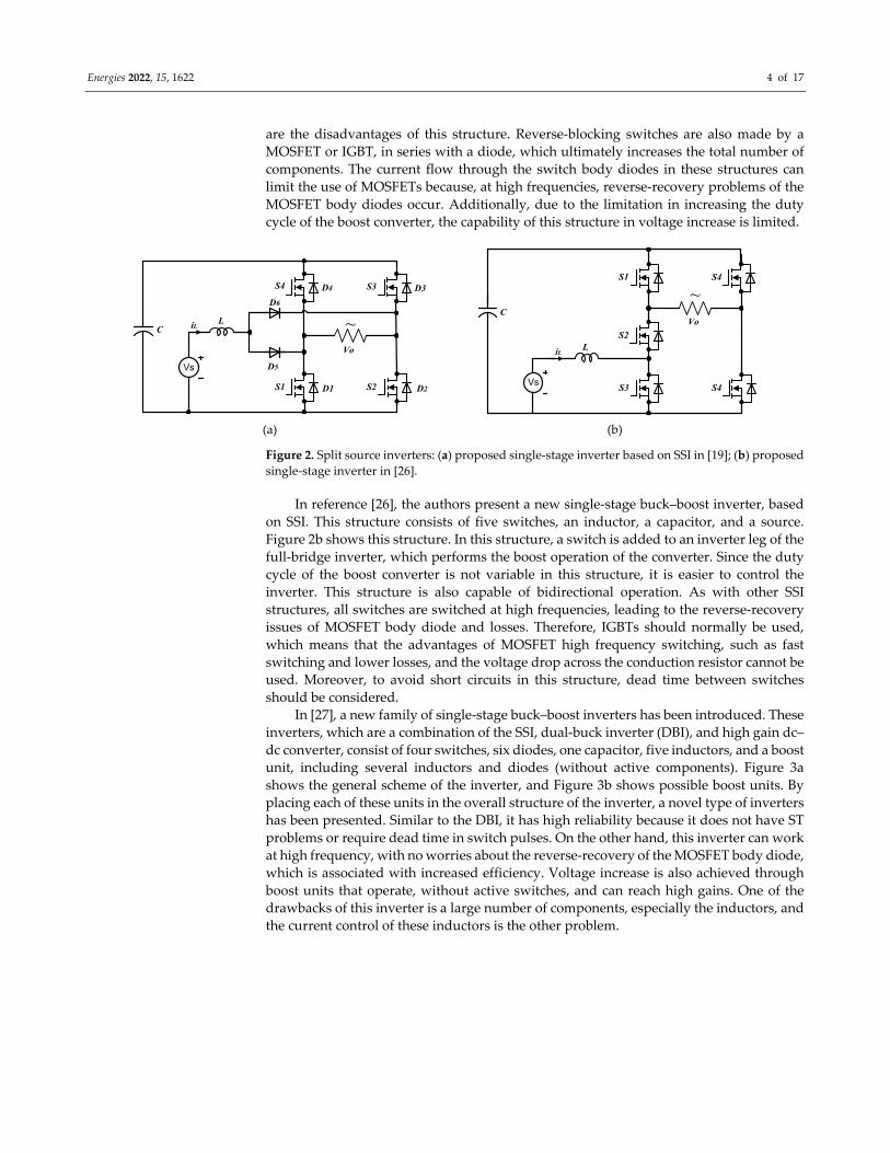
In [27], a new family of single‐stage buck–boost inverters has been introduced. These
inverters, which are a combination of the SSI, dual‐buck inverter (DBI), and high gain dc–
dc converter, consist of four switches, six diodes, one capacitor, five inductors, and a boost
unit, including several inductors and diodes (without active components). Figure 3a
shows the general scheme of the inverter, and Figure 3b shows possible boost units. By
placing each of these units in the overall structure of the inverter, a novel type of inverters
has been presented. Similar to the DBI, it has high reliability because it does not have ST
problems or require dead time in switch pulses. On the other hand, this inverter can work
at high frequency, with no worries about the reverse‐recovery of the MOSFET body diode,
which is associated with increased efficiency. Voltage increase is also achieved through
boost units that operate, without active switches, and can reach high gains. One of the
drawbacks of this inverter is a large number of components, especially the inductors, and
the current control of these inductors is the other problem.
L
S2
S4
D2
D4
D5
D6
iL ~
Vs
S1
S3
D1
Vo
C
D3
C
LS2
S4
iL
~
Vs
S1
S3 S4
Vo
(a) (b)
Energies 2022, 15, 1622 5 of 17
Figure 3. Combination of SSI, dual‐buck inverter [27]: (a) proposed structure; (b) boost units.
The utilization of boost units, to increase the gain of single‐stage inverters, to
overcome the boosting limit of SSI inverters, has been considered in some other studies.
In [28], a three‐phase SSI, along with boost units, has been presented. The boost unit in
this study consists of switches and inductors. The basis of this unit is based on parallel
charging of inductors and discharging them in series. By increasing the internal floors of
this unit, the inverter gain can be increased, according to a special equation. Although
switching these units is relatively simple, increasing the number of switches and variable
duty cycles are among the disadvantages of this structure.
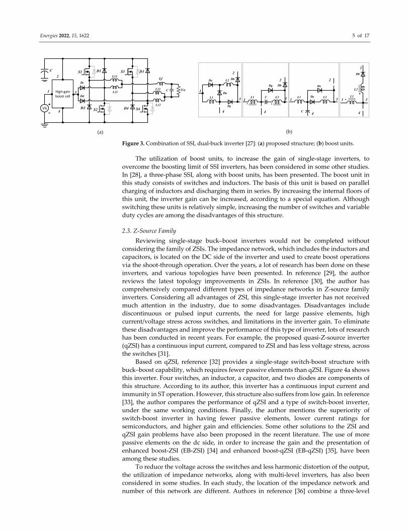
2.3. Z‐Source Family
Reviewing single‐stage buck–boost inverters would not be completed without
considering the family of ZSIs. The impedance network, which includes the inductors and
capacitors, is located on the DC side of the inverter and used to create boost operations
via the shoot‐through operation. Over the years, a lot of research has been done on these
inverters, and various topologies have been presented. In reference [29], the author
reviews the latest topology improvements in ZSIs. In reference [30], the author has
comprehensively compared different types of impedance networks in Z‐source family
inverters. Considering all advantages of ZSI, this single‐stage inverter has not received
much attention in the industry, due to some disadvantages. Disadvantages include
discontinuous or pulsed input currents, the need for large passive elements, high
current/voltage stress across switches, and limitations in the inverter gain. To eliminate
these disadvantages and improve the performance of this type of inverter, lots of research
has been conducted in recent years. For example, the proposed quasi‐Z‐source inverter
(qZSI) has a continuous input current, compared to ZSI and has less voltage stress, across
the switches [31].
Based on qZSI, reference [32] provides a single‐stage switch‐boost structure with
buck–boost capability, which requires fewer passive elements than qZSI. Figure 4a shows
this inverter. Four switches, an inductor, a capacitor, and two diodes are components of
this structure. According to its author, this inverter has a continuous input current and
immunity in ST operation. However, this structure also suffers from low gain. In reference
[33], the author compares the performance of qZSI and a type of switch‐boost inverter,
under the same working conditions. Finally, the author mentions the superiority of
switch‐boost inverter in having fewer passive elements, lower current ratings for
semiconductors, and higher gain and efficiencies. Some other solutions to the ZSI and
qZSI gain problems have also been proposed in the recent literature. The use of more
passive elements on the dc side, in order to increase the gain and the presentation of
enhanced boost‐ZSI (EB‐ZSI) [34] and enhanced boost‐qZSI (EB‐qZSI) [35], have been
among these studies.
To reduce the voltage across the switches and less harmonic distortion of the output,
the utilization of impedance networks, along with multi‐level inverters, has also been
considered in some studies. In each study, the location of the impedance network and
number of this network are different. Authors in reference [36] combine a three‐level
C S3
S4
D3
D4S2
D1
L11
High‐gain boost cell
Vs
1
2
4
3
S1
D2
Lf
L22
L12
L21 C
Dc
Dd
Vo
(a) (b)
4
3
2
1L1
L2
Db
L2DyL1
Dx
C
1
2
3
4
L2
Db
L1
Dq
C1
2
3
4
L2Dx
L1
Da1
2
3
4
Dy
Db
Energies 2022, 15, 1622 6 of 17
neutral point clamp structure and quasi‐Z‐source impedance network to provide a single‐
stage inverter that has both a continuous input current and reduced voltage across the
switches. The combination of impedance network structures and multi‐level inverters has
also been studied in references [37–40]. In these structures, the high number of switches
and impedance network considerations remains challenging.
Figure 4. Single‐stage inverters based on Z‐soucer family inverters. (a) Single‐stage switched‐boost
inverter in [32]; (b) proposed single‐stage qZSI‐based inverter with boost unit [41].
In [41–43], the authors introduced new qZSI‐based inverters using boost units with
coupled inductors. Figure 4b shows one of these inverters. These structures are
characterized by their high gain, which makes it possible to use them for PV purposes. In
[44], a high‐gain qZSI‐based inverter is provided using boost units that include an active
switch. References [45,46] also introduce and evaluate several single‐stage buck–boost
inverters, based on qZSI. Among the disadvantages of these structures is the need for a
large number of passive elements that increase the volume and weight of the inverter. ST
reliability is also another concern for these structures.
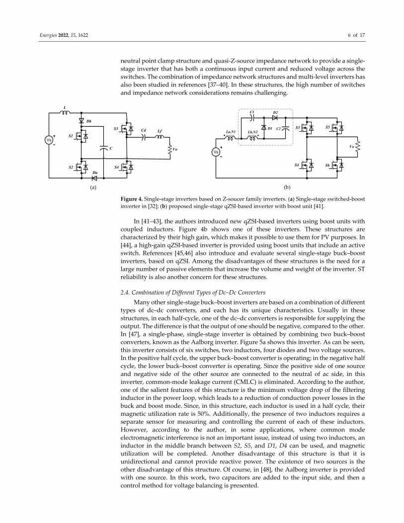
2.4. Combination of Different Types of Dc–Dc Converters
Many other single‐stage buck–boost inverters are based on a combination of different
types of dc–dc converters, and each has its unique characteristics. Usually in these
structures, in each half‐cycle, one of the dc–dc converters is responsible for supplying the
output. The difference is that the output of one should be negative, compared to the other.
In [47], a single‐phase, single‐stage inverter is obtained by combining two buck–boost
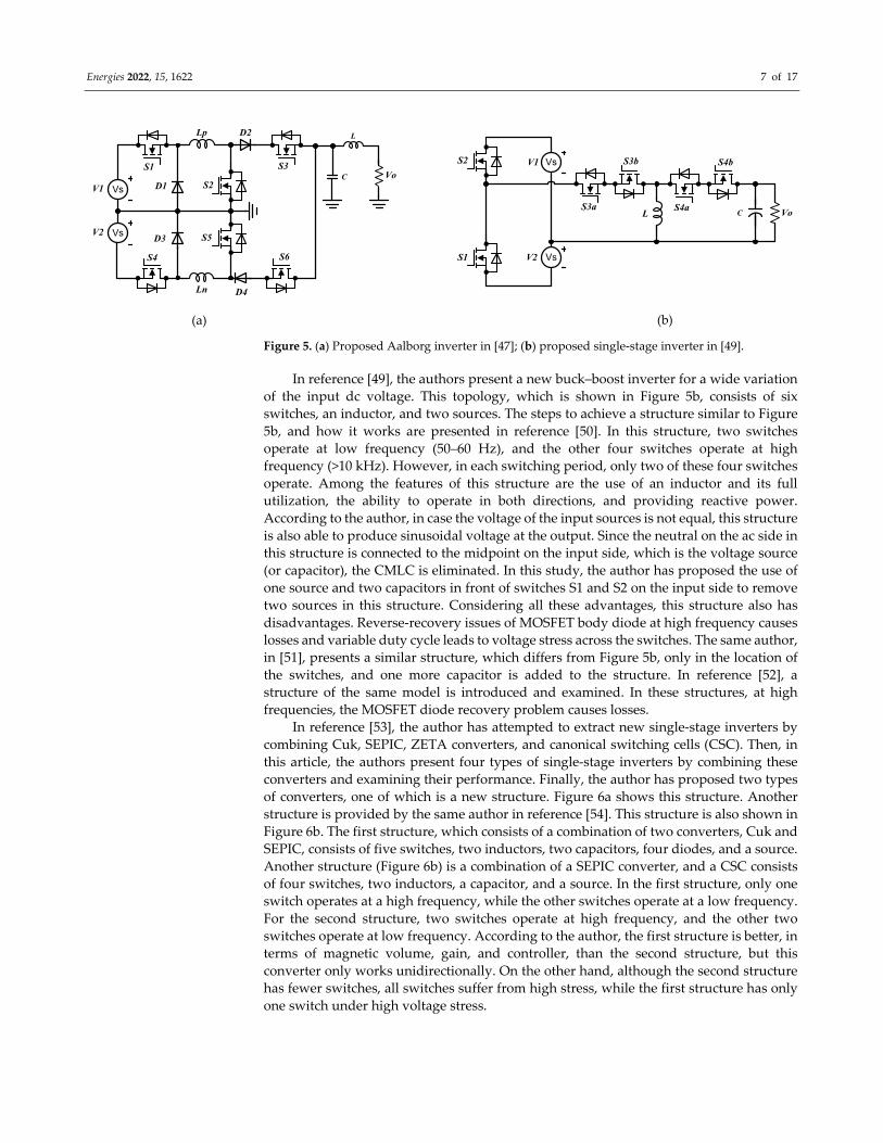
converters, known as the Aalborg inverter. Figure 5a shows this inverter. As can be seen,
this inverter consists of six switches, two inductors, four diodes and two voltage sources.
In the positive half cycle, the upper buck–boost converter is operating; in the negative half
cycle, the lower buck–boost converter is operating. Since the positive side of one source
and negative side of the other source are connected to the neutral of ac side, in this
inverter, common‐mode leakage current (CMLC) is eliminated. According to the author,
one of the salient features of this structure is the minimum voltage drop of the filtering
inductor in the power loop, which leads to a reduction of conduction power losses in the
buck and boost mode. Since, in this structure, each inductor is used in a half cycle, their
magnetic utilization rate is 50%. Additionally, the presence of two inductors requires a
separate sensor for measuring and controlling the current of each of these inductors.
However, according to the author, in some applications, where common mode
electromagnetic interference is not an important issue, instead of using two inductors, an
inductor in the middle branch between S2, S5, and D1, D4 can be used, and magnetic
utilization will be completed. Another disadvantage of this structure is that it is
unidirectional and cannot provide reactive power. The existence of two sources is the
other disadvantage of this structure. Of course, in [48], the Aalborg inverter is provided
with one source. In this work, two capacitors are added to the input side, and then a
control method for voltage balancing is presented.
S2 S4
VsS1
S3
C Vo
Da
Db
Cd Lf
L
Vs
S3 S5
S4 S6
Vo
La,N1 Lb,N2D1
D2C1
C2
(a) (b)
Energies 2022, 15, 1622 7 of 17
Figure 5. (a) Proposed Aalborg inverter in [47]; (b) proposed single‐stage inverter in [49].
In reference [49], the authors present a new buck–boost inverter for a wide variation
of the input dc voltage. This topology, which is shown in Figure 5b, consists of six
switches, an inductor, and two sources. The steps to achieve a structure similar to Figure
5b, and how it works are presented in reference [50]. In this structure, two switches
operate at low frequency (50–60 Hz), and the other four switches operate at high
frequency (>10 kHz). However, in each switching period, only two of these four switches
operate. Among the features of this structure are the use of an inductor and its full
utilization, the ability to operate in both directions, and providing reactive power.
According to the author, in case the voltage of the input sources is not equal, this structure
is also able to produce sinusoidal voltage at the output. Since the neutral on the ac side in
this structure is connected to the midpoint on the input side, which is the voltage source
(or capacitor), the CMLC is eliminated. In this study, the author has proposed the use of
one source and two capacitors in front of switches S1 and S2 on the input side to remove
two sources in this structure. Considering all these advantages, this structure also has
disadvantages. Reverse‐recovery issues of MOSFET body diode at high frequency causes
losses and variable duty cycle leads to voltage stress across the switches. The same author,
in [51], presents a similar structure, which differs from Figure 5b, only in the location of
the switches, and one more capacitor is added to the structure. In reference [52], a
structure of the same model is introduced and examined. In these structures, at high
frequencies, the MOSFET diode recovery problem causes losses.
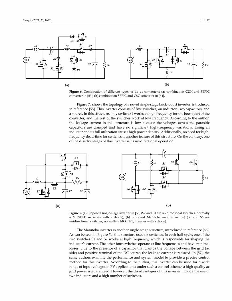
In reference [53], the author has attempted to extract new single‐stage inverters by
combining Cuk, SEPIC, ZETA converters, and canonical switching cells (CSC). Then, in
this article, the authors present four types of single‐stage inverters by combining these
converters and examining their performance. Finally, the author has proposed two types
of converters, one of which is a new structure. Figure 6a shows this structure. Another
structure is provided by the same author in reference [54]. This structure is also shown in
Figure 6b. The first structure, which consists of a combination of two converters, Cuk and
SEPIC, consists of five switches, two inductors, two capacitors, four diodes, and a source.
Another structure (Figure 6b) is a combination of a SEPIC converter, and a CSC consists
of four switches, two inductors, a capacitor, and a source. In the first structure, only one
switch operates at a high frequency, while the other switches operate at a low frequency.
For the second structure, two switches operate at high frequency, and the other two
switches operate at low frequency. According to the author, the first structure is better, in
terms of magnetic volume, gain, and controller, than the second structure, but this
converter only works unidirectionally. On the other hand, although the second structure
has fewer switches, all switches suffer from high stress, while the first structure has only
one switch under high voltage stress.
Vs
Vs
S1
S2
S3
S4
S5
S6
Lp
Ln
D1
D3
D2
D4
L
C
V1
V2
VoVs
Vs
S2
S1
V1
V2
VoS3a
S3b
S4a
S4b
CL
(a) (b)
Energies 2022, 15, 1622 8 of 17
Figure 6. Combination of different types of dc–dc converters: (a) combination CUK and SEPIC
converter in [53]; (b) combination SEPIC and CSC converter in [54].
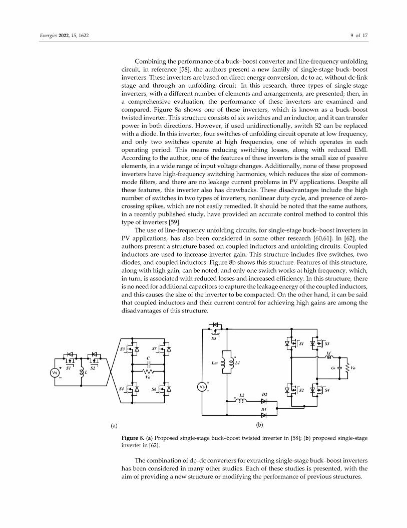
Figure 7a shows the topology of a novel single‐stage buck–boost inverter, introduced
in reference [55]. This inverter consists of five switches, an inductor, two capacitors, and
a source. In this structure, only switch S1 works at high frequency for the boost part of the
converter, and the rest of the switches work at low frequency. According to the author,
the leakage current in this structure is low because the voltages across the parasitic
capacitors are clamped and have no significant high‐frequency variations. Using an
inductor and its full utilization causes high power density. Additionally, no need for high‐
frequency dead‐time for switches is another feature of this structure. On the contrary, one
of the disadvantages of this inverter is its unidirectional operation.
Figure 7. (a) Proposed single‐stage inverter in [55] (S2 and S3 are unidirectional switches, normally
a MOSFET, in series with a diode); (b) proposed Manitoba inverter in [56] (S5 and S6 are
unidirectional switches, normally a MOSFET, in series with a diode).
The Manitoba inverter is another single‐stage structure, introduced in reference [56].
As can be seen in Figure 7b, this structure uses six switches. In each half‐cycle, one of the
two switches S1 and S2 works at high frequency, which is responsible for shaping the
inductor’s current. The other four switches operate at line frequencies and have minimal
losses. Due to the presence of a capacitor that clamps the voltage between the grid (ac
side) and positive terminal of the DC source, the leakage current is reduced. In [57], the
same authors examine the performance and system model to provide a precise control
method for this inverter. According to the author, this inverter can be used for a wide
range of input voltages in PV applications; under such a control scheme, a high‐quality ac
grid power is guaranteed. However, the disadvantages of this inverter include the use of
two inductors and a high number of switches.
Vs
VoS1
S2
S3
S4S5
L1 L2
D2
D3
D4
D5
C1
C2
Vs
VoS1
S2 S3
S4L1
L2
C2
C1
(a) (b)
Vs
L
S1S2
S3
S4
S5
C1 C2
Vo Vs
S1
S5 S6
S2
Vo
L1 L2 S3
S4
C
(a) (b)
Energies 2022, 15, 1622 9 of 17
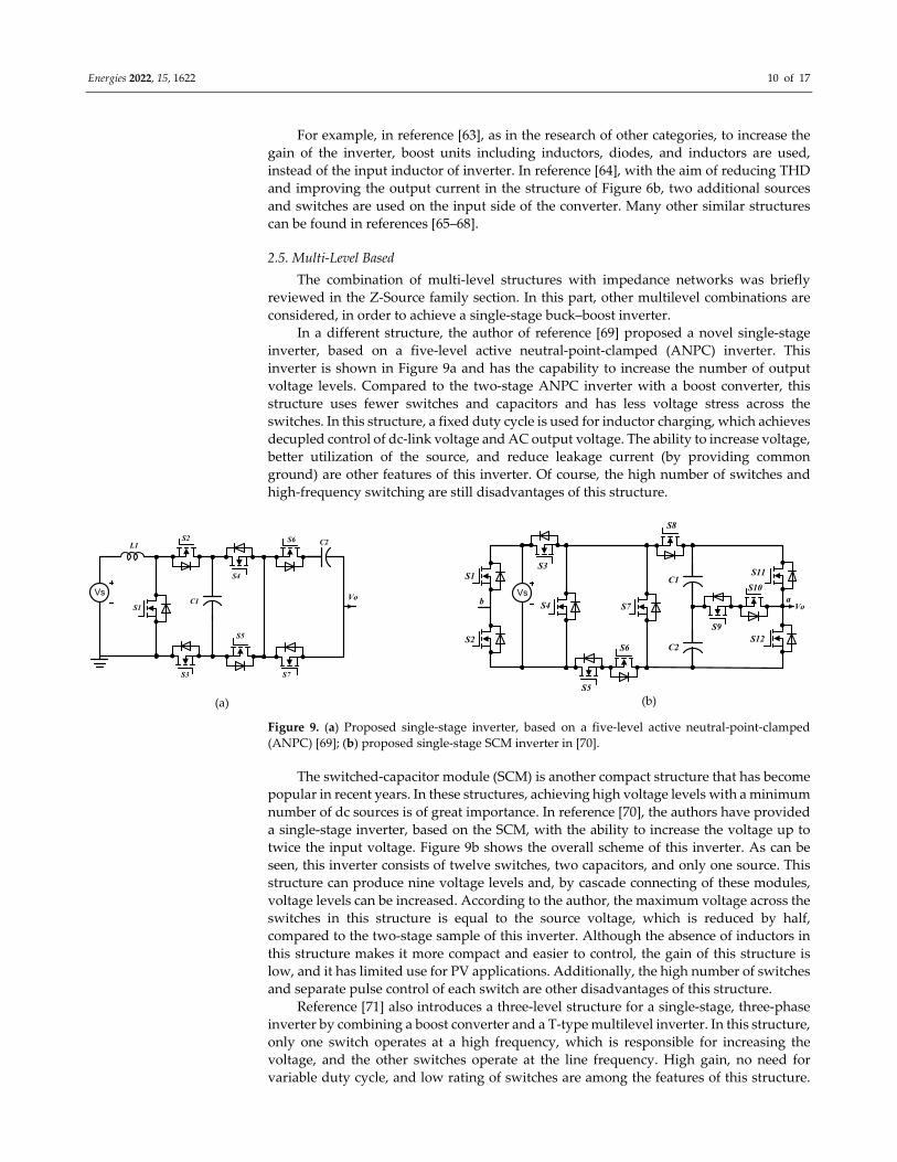
Combining the performance of a buck–boost converter and line‐frequency unfolding
circuit, in reference [58], the authors present a new family of single‐stage buck–boost
inverters. These inverters are based on direct energy conversion, dc to ac, without dc‐link
stage and through an unfolding circuit. In this research, three types of single‐stage
inverters, with a different number of elements and arrangements, are presented; then, in
a comprehensive evaluation, the performance of these inverters are examined and
compared. Figure 8a shows one of these inverters, which is known as a buck–boost
twisted inverter. This structure consists of six switches and an inductor, and it can transfer
power in both directions. However, if used unidirectionally, switch S2 can be replaced
with a diode. In this inverter, four switches of unfolding circuit operate at low frequency,
and only two switches operate at high frequencies, one of which operates in each
operating period. This means reducing switching losses, along with reduced EMI.
According to the author, one of the features of these inverters is the small size of passive
elements, in a wide range of input voltage changes. Additionally, none of these proposed
inverters have high‐frequency switching harmonics, which reduces the size of common‐
mode filters, and there are no leakage current problems in PV applications. Despite all
these features, this inverter also has drawbacks. These disadvantages include the high
number of switches in two types of inverters, nonlinear duty cycle, and presence of zero‐
crossing spikes, which are not easily remedied. It should be noted that the same authors,
in a recently published study, have provided an accurate control method to control this
type of inverters [59].
The use of line‐frequency unfolding circuits, for single‐stage buck–boost inverters in
PV applications, has also been considered in some other research [60,61]. In [62], the
authors present a structure based on coupled inductors and unfolding circuits. Coupled
inductors are used to increase inverter gain. This structure includes five switches, two
diodes, and coupled inductors. Figure 8b shows this structure. Features of this structure,
along with high gain, can be noted, and only one switch works at high frequency, which,
in turn, is associated with reduced losses and increased efficiency. In this structure, there
is no need for additional capacitors to capture the leakage energy of the coupled inductors,
and this causes the size of the inverter to be compacted. On the other hand, it can be said
that coupled inductors and their current control for achieving high gains are among the
disadvantages of this structure.
Figure 8. (a) Proposed single‐stage buck–boost twisted inverter in [58]; (b) proposed single‐stage
inverter in [62].
The combination of dc–dc converters for extracting single‐stage buck–boost inverters
has been considered in many other studies. Each of these studies is presented, with the
aim of providing a new structure or modifying the performance of previous structures.
VsS1 S2
S3 S5
S4 S6
L
C
Vo
Vs
Lf
Co Vo
S2
S1 S3
S4
S5
L1
L2
D1
D2
Lm
(a) (b)
Energies 2022, 15, 1622 10 of 17
For example, in reference [63], as in the research of other categories, to increase the
gain of the inverter, boost units including inductors, diodes, and inductors are used,
instead of the input inductor of inverter. In reference [64], with the aim of reducing THD
and improving the output current in the structure of Figure 6b, two additional sources
and switches are used on the input side of the converter. Many other similar structures
can be found in references [65–68].
2.5. Multi‐Level Based
The combination of multi‐level structures with impedance networks was briefly
reviewed in the Z‐Source family section. In this part, other multilevel combinations are
considered, in order to achieve a single‐stage buck–boost inverter.
In a different structure, the author of reference [69] proposed a novel single‐stage
inverter, based on a five‐level active neutral‐point‐clamped (ANPC) inverter. This
inverter is shown in Figure 9a and has the capability to increase the number of output
voltage levels. Compared to the two‐stage ANPC inverter with a boost converter, this
structure uses fewer switches and capacitors and has less voltage stress across the
switches. In this structure, a fixed duty cycle is used for inductor charging, which achieves
decupled control of dc‐link voltage and AC output voltage. The ability to increase voltage,
better utilization of the source, and reduce leakage current (by providing common
ground) are other features of this inverter. Of course, the high number of switches and
high‐frequency switching are still disadvantages of this structure.
Figure 9. (a) Proposed single‐stage inverter, based on a five‐level active neutral‐point‐clamped
(ANPC) [69]; (b) proposed single‐stage SCM inverter in [70].
The switched‐capacitor module (SCM) is another compact structure that has become
popular in recent years. In these structures, achieving high voltage levels with a minimum
number of dc sources is of great importance. In reference [70], the authors have provided
a single‐stage inverter, based on the SCM, with the ability to increase the voltage up to
twice the input voltage. Figure 9b shows the overall scheme of this inverter. As can be
seen, this inverter consists of twelve switches, two capacitors, and only one source. This
structure can produce nine voltage levels and, by cascade connecting of these modules,
voltage levels can be increased. According to the author, the maximum voltage across the
switches in this structure is equal to the source voltage, which is reduced by half,
compared to the two‐stage sample of this inverter. Although the absence of inductors in
this structure makes it more compact and easier to control, the gain of this structure is
low, and it has limited use for PV applications. Additionally, the high number of switches
and separate pulse control of each switch are other disadvantages of this structure.
Reference [71] also introduces a three‐level structure for a single‐stage, three‐phase
inverter by combining a boost converter and a T‐type multilevel inverter. In this structure,
only one switch operates at a high frequency, which is responsible for increasing the
voltage, and the other switches operate at the line frequency. High gain, no need for
variable duty cycle, and low rating of switches are among the features of this structure.
Vs
S1
S2
S3
S4
S5
S6
S7
S8
S9
S10
S11
S12
C1
C2
abVo
Vs VoS1
L1S2
S3
S4
S5
S6
S7
C1
C2
(a) (b)
Energies 2022, 15, 1622 11 of 17
On the other hand, this structure cannot be called a completely single‐stage inverter, and
the voltage balance of capacitors is one of the challenges of this structure.
3. General Comparison and Discussion
In this article, an attempt has been made to introduce and review the latest single‐
stage buck–boost inverters. To select a suitable structure for an especial application,
several factors should be considered. In this review, different structures were categorized,
and several examples were selected for each category. For each structure, its prominent
advantages and disadvantages were highlighted. In general, the main factors that affect
the use of a structure include the efficiency, size, cost, and reliability of the converter.
Investigation of losses, especially switching losses, in any structure is important. In
this regard, the use of MOSFET or IGBT and converter operating frequencies can be very
important.
Another important factor is the size of the converter. The operating frequency of the
converter affects the size of the passive elements. On the other hand, the losses of the
switches and heat generated from the losses are also effective in choosing the size of the
heatsink. The voltage and current passing through the passive elements in each structure
also affects their size by determining the energy level required by these elements.
As it is clear, one of the motivations for using single‐stage inverters is to reduce the
cost of these structures, compared to two‐stage structures. By examining different
structures, comparing the voltage/current stresses of semiconductor components, and,
finally, choosing a structure with minimal stress on these elements, the rating of
semiconductors can be reduced and, consequently, a significant reduction in cost can be
brought. Additionally, the size of passive elements and total number of circuit elements
are other factors affecting the cost.
The reliability of these structures also depends on factors such as the total number of
components and complexity of the circuit, voltage, and current stresses of the elements
and modulation.
After examining the structures compatible with the intended application, the above
factors can be compared and examined at constant power, in order to provide the best
option suitable for the consumer. With regard to these issues in choosing the right
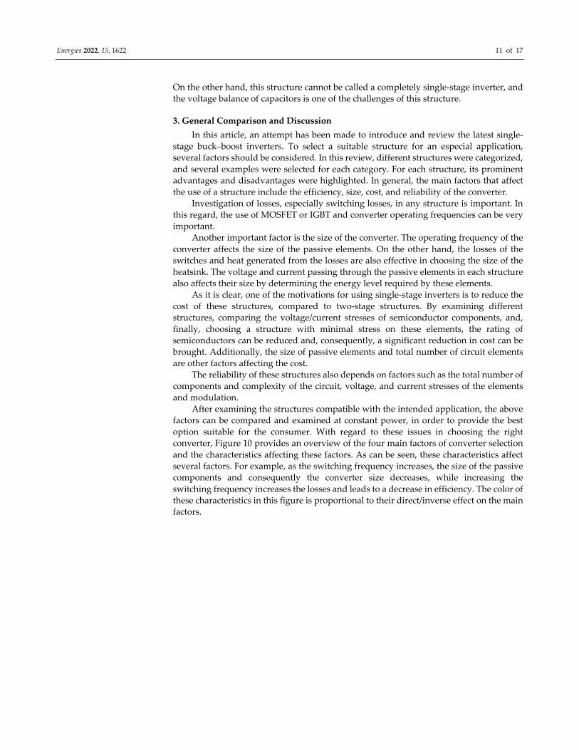
converter, Figure 10 provides an overview of the four main factors of converter selection
and the characteristics affecting these factors. As can be seen, these characteristics affect
several factors. For example, as the switching frequency increases, the size of the passive
components and consequently the converter size decreases, while increasing the
switching frequency increases the losses and leads to a decrease in efficiency. The color of
these characteristics in this figure is proportional to their direct/inverse effect on the main
factors.
Energies 2022, 15, 1622 12 of 17
Cost
Reliability
ProtectionSwitching frequency
Component number
Modulation
Heat sink
Component number
Component selection
Output Power
Protection
Component selection
SizeHeat sink
Component number
Component selection
Output power
Switching frequency
Efficiency
Component number
Modulation
Component selection
Converter selection
Figure 10. The main factors and other specifications in choosing the right converter.
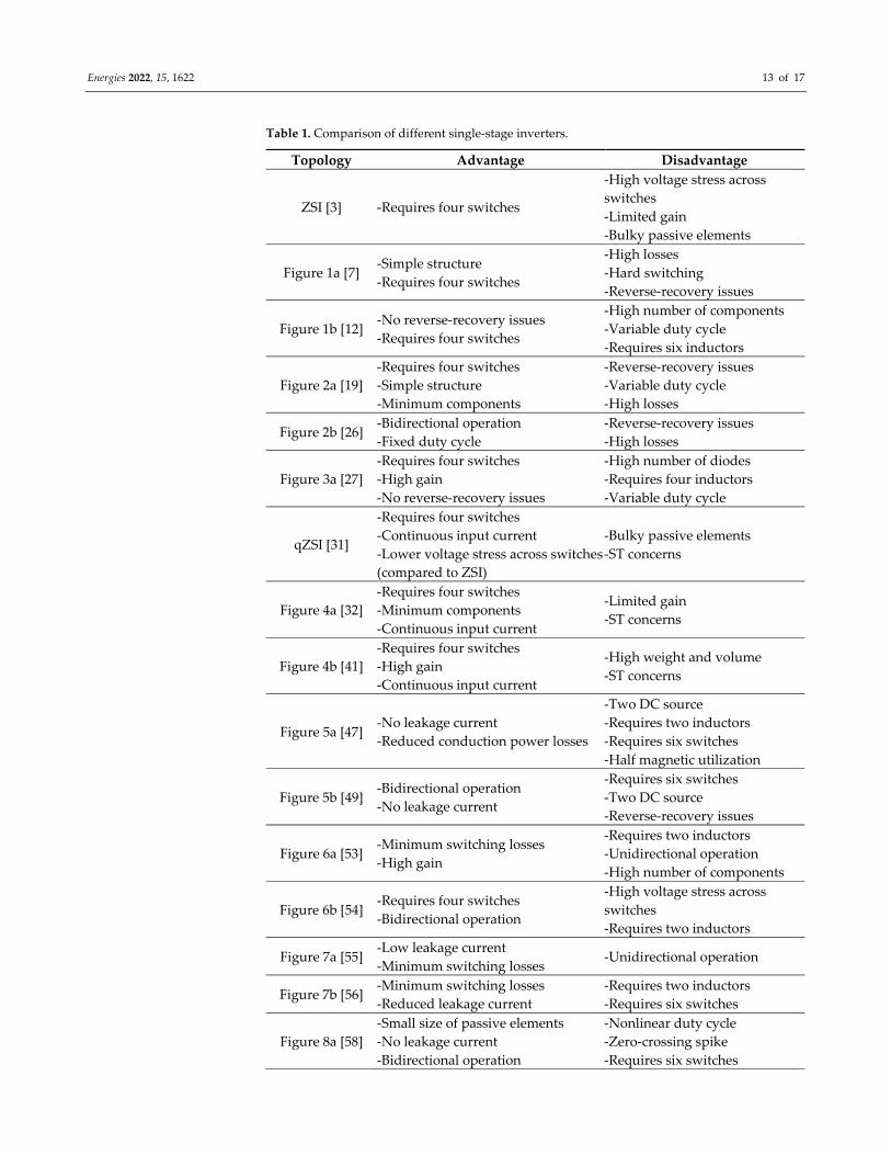
Table 1 summarizes the advantages and disadvantages of some of the structures
studied in this study. This table is intended for single‐phase structures. For a more
comprehensive comparison, ZSI and qZSI have also been added to this table as well‐
known inverters. The number of components, reverse‐recovery issues of MOSFET body
diodes at high switching frequencies, losses, number of input sources, leakage current in
PV applications, and some other features are examined in this table. It is clear that some
of the proposed new structures, reviewed in this study, are aimed at improving the
performance and troubleshooting existing structures. However, to overcome some of the
limitations, other elements should be added, which, in most cases, will cause other
drawbacks. For example, in [12,27], separate diodes have been used to solve MOSFET
reverse‐recovery issues. These diodes will affect the cost, losses, and size of the converter.
Boost units have been used in [27,28,41–45] to increase the gain of these inverters, which
is also associated with increasing the number of components and complexity of the
structure and, consequently, affecting the size, cost, losses, and reliability of the converter.
However, in [58], after introducing a novel family of unfolding single‐stage inverters, the
authors compare and evaluate the performance of the proposed inverters, offering an
inverter that has more components, but requires a smaller inductor and less voltage stress
across its switches. Additionally, in [70], the use of more switches, with less voltage stress
across the switches, is justified, which leads to the selection of switches with lower voltage
ratings and, consequently, less RDS‐on.
Energies 2022, 15, 1622 13 of 17
Table 1. Comparison of different single‐stage inverters.
Topology Advantage Disadvantage
ZSI [3] ‐Requires four switches
‐High voltage stress across
switches
‐Limited gain
‐Bulky passive elements
Figure 1a [7] ‐Simple structure
‐Requires four switches
‐High losses
‐Hard switching
‐Reverse‐recovery issues
Figure 1b [12] ‐No reverse‐recovery issues
‐Requires four switches
‐High number of components
‐Variable duty cycle
‐Requires six inductors
Figure 2a [19]
‐Requires four switches
‐Simple structure
‐Minimum components
‐Reverse‐recovery issues
‐Variable duty cycle
‐High losses
Figure 2b [26] ‐Bidirectional operation
‐Fixed duty cycle
‐Reverse‐recovery issues
‐High losses
Figure 3a [27]
‐Requires four switches
‐High gain
‐No reverse‐recovery issues
‐High number of diodes
‐Requires four inductors
‐Variable duty cycle
qZSI [31]
‐Requires four switches
‐Continuous input current
‐Lower voltage stress across switches
(compared to ZSI)
‐Bulky passive elements
‐ST concerns
Figure 4a [32]
‐Requires four switches
‐Minimum components
‐Continuous input current
‐Limited gain
‐ST concerns
Figure 4b [41]
‐Requires four switches
‐High gain
‐Continuous input current
‐High weight and volume
‐ST concerns
Figure 5a [47] ‐No leakage current
‐Reduced conduction power losses
‐Two DC source
‐Requires two inductors
‐Requires six switches
‐Half magnetic utilization
Figure 5b [49] ‐Bidirectional operation
‐No leakage current
‐Requires six switches
‐Two DC source
‐Reverse‐recovery issues
Figure 6a [53] ‐Minimum switching losses
‐High gain
‐Requires two inductors
‐Unidirectional operation
‐High number of components
Figure 6b [54] ‐Requires four switches
‐Bidirectional operation
‐High voltage stress across
switches
‐Requires two inductors
Figure 7a [55] ‐Low leakage current
‐Minimum switching losses ‐Unidirectional operation
Figure 7b [56] ‐Minimum switching losses
‐Reduced leakage current
‐Requires two inductors
‐Requires six switches
Figure 8a [58]
‐Small size of passive elements
‐No leakage current
‐Bidirectional operation
‐Nonlinear duty cycle
‐Zero‐crossing spike
‐Requires six switches
Energies 2022, 15, 1622 14 of 17
Figure 8b [62] ‐High gain
‐Minimum switching losses
‐Requires two inductors
‐Bulky passive elements
Figure 9a [69]
‐Fixed duty cycle
‐Decupled control of DC and AC
voltage
‐Reduce leakage current
‐Requires seven switches
‐High losses
Figure 9b [70]
‐Compact structures
‐High voltage levels
‐No inductor
‐Limited gain
‐Requires 12 switches
Considering these parameters, or other important parameters, it is worth mentioning
that, according to the advantages and disadvantages of each of these structures and
considered requirements, a trade‐off should be made to select the optimal inverter. It
should be noted that some of these problems can be solved by providing an accurate and
effective control method.
Single‐stage inverter technology seems to be advancing rapidly. As reviewed in the
previous section, the latest technologies seek to provide new solutions and solve existing
problems of this type of inverters. This study attempted to provide a general overview for
those researchers who work, or will work, in this field by presenting all the single‐stage
structures, together with the circuits of the latest structures. However, there are other
structures, such as single‐stage isolated structures, that are out of the scope of this study.
Given the intensified efforts of researchers, in this regard, it can be said that in the not‐
too‐distant future these inverters, with high capabilities, will find their place in various
applications.
4. Conclusions
In this study, the latest single‐stage buck–boost inverters were reviewed. These
structures were classified into five different categories. For each category, several
examples were examined, along with representations of their circuits. Then, other studies
that address the problems of these structures were introduced and reviewed. Different
structures were examined, in terms of performance, number of elements, switching
frequency, and losses. For a general comparison, the features of some of the most
prominent of these structures were summarized in a table. Given that each of the
structures has advantages and disadvantages, to select the appropriate inverter in each
application, a trade‐off should be made between these features.
Author Contributions: Conceptualization, O.H. and D.V.; methodology, O.H.; software, M.A.;
validation, M.A., O.H. and D.V.; formal analysis, M.A.; investigation, M.A.; resources, O.H.; data
curation, D.V.; writing—original draft preparation, M.A.; writing—review and editing, O.H.;
visualization, M.A.; supervision, D.V.; project administration, O.H.; funding acquisition, O.H. All
authors have read and agreed to the published version of the manuscript.
Funding: This research received no external funding.
Institutional Review Board Statement: Not applicable.
Informed Consent Statement: Not applicable.
Data Availability Statement: Not applicable.
Acknowledgments: This work was supported by the Estonian Research Council grant PRG675 and
by the Estonian Centre of Excellence in Zero Energy and Resource Efficient Smart Buildings and
Districts (ZEBE).
Conflicts of Interest: The authors declare no conflict of interest.
Energies 2022, 15, 1622 15 of 17
References
1. Kang, F.S.; Cho, S.E.; Park, S.J.; Kim, C.U.; Ise, T. A new control scheme of a cascaded transformer type multilevel PWM inverter
for a residential photovoltaic power conditioning system. Sol. Energy 2005, 78, 727–738.
2. Sahan, B.; Araujo, S.V.; Noeding, C.; Zacharias, P. Comparative evaluation of three‐phase current source inverters for grid
interfacing of distributed and renewable energy systems. IEEE Trans. Power Electron. 2010, 26, 2304–2318.
3. Li, J.; Liu, J.; Liu, Z. Comparison of Z‐source inverter and traditional two‐stage boost‐buck inverter in grid‐tied renewable
energy generation. In Proceedings of the 2009 IEEE 6th International Power Electronics and Motion Control Conference, Wuhan,
China, 17–20 May 2009; pp. 1493–1497.
4. Kumar, A.; Sensarma, P. Operating modes based review of single‐stage buck‐boost inverters. In Proceedings of the IECON
2019‐45th Annual Conference of the IEEE Industrial Electronics Society, Lisbon, Portugal, 14–17 October 2019; Volume 1, pp.
1904–1909.
5. Stone, A.; Rasheduzzaman, M.; Fajri, P. A Review of Single‐Phase Single‐Stage DC/AC Boost Inverter Topologies and Their
Controllers. In Proceedings of the 2018 IEEE Conference on Technologies for Sustainability (SusTech), Long Beach, CA, USA,
11–13 November 2018; pp. 1–8.
6. Tripathi, P.R.; Thakura, P.; Keshri, R.K.; Ghosh, S.; Guerrero, J.M. 25 years of single‐stage buck‐boost inverters: Development
and challenges. IEEE Ind. Electron. Mag. 2021. Available online: https://ieeexplore.ieee.org/document/9360729 (access on 30
January 2022).
7. Caceres, R.O.; Barbi, I. A boost DC‐AC converter: Analysis, design, and experimentation. IEEE Trans. Power Electron. 1999, 14,
134–141.
8. Chamarthi, P.; Rajeev, M.; Agarwal, V. A novel single stage zero leakage current transformer‐less inverter for grid connected
PV systems. In Proceedings of the 2015 IEEE 42nd Photovoltaic Specialist Conference (PVSC), New Orleans, LA, USA, 14–19
June 2015; pp. 1–5.
9. Zhao, B.; Abramovitz, A.; Ma, R.; Huangfu, Y. High gain single stage buck‐boost inverter. In Proceedings of the 2017 20th
International Conference on Electrical Machines and Systems (ICEMS), Sydney, NSW, Australia, 11–14 August 2017; pp. 1–5.
10. Babu, S.M.; Veeramallu, V.S.; Narasimharaju, B.L.; Rathore, A.K.; Krishnamoorthy, H.S. Novel Non‐Isolated Differential Buck‐
Boost Inverter with Single‐Stage Conversion and Reduced Device Voltage Stress. In Proceedings of the 2020 IEEE International
Conference on Power Electronics, Smart Grid and Renewable Energy (PESGRE2020), Cochin, India, 2–4 January 2020; pp. 1–5.
11. Khan, A.A.; Lu, Y.W.; Eberle, W.; Wang, L.; Khan, U.A.; Cha, H. Single‐phase split‐inductor differential boost inverters. IEEE
Trans. Power Electron. 2019, 35, 107–120.
12. Khan, A.A.; Cha, H. Dual‐buck‐structured high‐reliability and high‐efficiency single‐stage buck–boost inverters. IEEE Trans.
Ind. Electron. 2017, 65, 3176–3187.
13. Khan, A.A.; Eberle, W.; Wang, L.; Akbar, F.; Khan, U.A.; Lu, Y.W.; Agamy, M. Coupled‐inductor buck–boost inverter with
reduced current ripple. IEEE Trans. Power Electron. 2019, 35, 7933–7946.
14. Darwish, A.; Massoud, A.M.; Holliday, D.; Ahmed, S.; Williams, B.W. Single‐stage three‐phase differential‐mode buck‐boost
inverters with continuous input current for PV applications. IEEE Trans. Power Electron. 2016, 31, 8218–8236.
15. Khan, A.A.; Cha, H.; Khan, U.A.; Kim, H.G. Four‐switch buck‐boost inverter for stand‐alone and grid‐connected single‐phase
PV systems. In Proceedings of the 2017 IEEE 3rd International Future Energy Electronics Conference and ECCE Asia (IFEEC
2017‐ECCE Asia), Kaohsiung, Taiwan, 3–7 June 2017; pp. 460–465.
16. Mansour, A.S.; Osheba, O.D. Performance of a Single‐Stage Buck‐Boost Inverter Fed from a Photovoltaic Source Under Different
Meteorological Conditions. In Proceedings of the 2019 21st International Middle East Power Systems Conference (MEPCON),
Cairo, Egypt, 17–19 December 2019; pp. 151–157.
17. Tang, Y.; Bai, Y.; Kan, J.; Xu, F. Improved dual boost inverter with half cycle modulation. IEEE Trans. Power Electron. 2016, 32,
7543–7552.
18. Babu, S.M.; Veeramallu, V.S.; Narasimharaju, B.L.; Rathore, A.K.; Krishnamoorthy, H.S. Novel Single‐Stage Transformer‐less
Cascaded Differential Boost Single‐Phase PV Inverter for Grid‐Tied Applications. In Proceedings of the 2020 IEEE International
Conference on Power Electronics, Smart Grid and Renewable Energy (PESGRE2020), Cochin, India, 2–4 January 2020; pp. 1–5.
19. Nahavandi, A.; Roostaee, M.; Azizi, M.R. Single stage DC‐AC boost converter. In Proceedings of the 2016 7th Power Electronics
and Drive Systems Technologies Conference (PEDSTC), Tehran, Iran, 16–18 February 2016; pp. 362–366.
20. Abdelhakim, A.; Mattavelli, P.; Spiazzi, G. Three‐phase split‐source inverter (SSI): Analysis and modulation. IEEE Trans. Power
Electron. 2015, 31, 7451–7461.
21. Abdelhakim, A.; Mattavelli, P.; Davari, P.; Blaabjerg, F. Performance evaluation of the single‐phase split‐source inverter using
an alternative DC–AC configuration. IEEE Trans. Ind. Electron. 2017, 65, 363–373.
22. Li, H.; Meng, J.; Hu, M. A Novel Family of Integrated Step‐Up PV Micro‐Inverter. In Proceedings of the 2018 37th Chinese
Control Conference (CCC), Wuhan, China, 25–27 July 2018; pp. 7558–7563.
23. Ribeiro, H.; Silva, F.; Pinto, S.; Borges, B. Single stage inverter for PV applications with one cycle sampling technique in the
MPPT algorithm. In Proceedings of the 2009 35th Annual Conference of IEEE Industrial Electronics, Porto, Portugal, 3–5
November 2009; pp. 842–849.
24. Yao, Z.; Xu, J.; Wang, X.; Wang, C. An improved single‐stage buck‐boost grid‐connected inverter. In Proceedings of the 2017
20th International Conference on Electrical Machines and Systems (ICEMS), Sydney, Australia, 11–14 August 2017; pp. 1–4.
Energies 2022, 15, 1622 16 of 17
25. Yin, C.; Ding, W.; Ming, L.; Loh, P.C. Single‐Stage Active Split‐Source Inverter With High DC‐Link Voltage Utilization. IEEE
Trans. Power Electron. 2020, 36, 6699–6711.
26. Lee, S.S.; Tan, A.S.; Ishak, D.; Mohd‐Mokhtar, R. Single‐Phase Simplified Split‐Source Inverter (S 3 I) for Boost DC–AC Power
Conversion. IEEE Trans. Ind. Electron. 2018, 66, 7643–7652.
27. Akbar, F.; Cha, H.; Ahmed, H.F.; Khan, A.A. A family of single‐stage high‐gain dual‐buck split‐source inverters. IEEE J. Emerg.
Sel. Top. Power Electron. 2019, 8, 1701–1713.
28. Eskandari, B.; Azizi, M.; Roostaee, M.; Joorabi, M.K. Non‐Linear Modulation for High Gain Three‐Phase Boost Inverter. In
Proceedings of the 2020 11th Power Electronics, Drive Systems, and Technologies Conference (PEDSTC), Tehran, Iran, 4–6
February 2020; pp. 1–6.
29. Ellabban, O.; Abu‐Rub, H. Z‐source inverter: Topology improvements review. IEEE Ind. Electron. Mag. 2016, 10, 6–24.
30. Husev, O.; Blaabjerg, F.; Roncero‐Clemente, C.; Romero‐Cadaval, E.; Vinnikov, D.; Siwakoti, Y.P.; Strzelecki, R. Comparison of
impedance‐source networks for two and multilevel buck–boost inverter applications. IEEE Trans. Power Electron. 2016, 31, 7564–
7579.
31. Anderson, J.; Peng, F.Z. Four quasi‐Z‐source inverters. In Proceedings of the 2008 IEEE Power Electronics Specialists
Conference, Rhodes, Greece, 15–19 June 2008; pp. 2743–2749.
32. Nguyen, M.K.; Tran, T.T. A single‐phase single‐stage switched‐boost inverter with four switches. IEEE Trans. Power Electron.
2017, 33, 6769–6781.
33. Nguyen, M.K.; Lim, Y.C.; Park, S.J. A comparison between single‐phase quasi‐$ Z $‐source and quasi‐switched boost inverters.
IEEE Trans. Ind. Electron. 2015, 62, 6336–6344.
34. Fathi, H.; Madadi, H. Enhanced‐boost Z‐source inverters with switched Z‐impedance. IEEE Trans. Ind. Electron. 2015, 63, 691–
703.
35. Jagan, V.; Kotturu, J.; Das, S. Enhanced‐boost quasi‐Z‐source inverters with two‐switched impedance networks. IEEE Trans.
Ind. Electron. 2017, 64, 6885–6897.
36. Effah, F.B.; Wheeler, P.W.; Watson, A.J.; Clare, J.C. Quasi Z‐source NPC inverter for PV application. In Proceedings of the 2017
IEEE PES PowerAfrica, Accra, Ghana, 27–30 June 2017; pp. 153–158.
37. Manoj, P.; Kirubakaran, A.; Dhara, S.; Somasekhar, V.T. A Quasi‐Z‐Source Based Space Vector Modulated Cascaded Four‐Level
Inverter for Photovoltaic Applications. IEEE J. Emerg. Sel. Top. Power Electron. 2021. Available online:
https://ieeexplore.ieee.org/document/9605685 (access on 30 January 2022).
38. Gao, F.; Ge, X.; Wang, J. A single‐stage buck‐boost three‐level neutral‐point‐clamped inverter for the grid‐tied photovoltaic
power generation. In Proceedings of the 2013 IEEE Energy Conversion Congress and Exposition, Denver, CO, USA, 15–19
September 2013; pp. 547–553.
39. Bhattacharya, A. 3‐level Z‐source inverter based PV system with bidirectional buck‐boost BESS. In Proceedings of the 2016 IEEE
International Conference on Power Electronics, Drives and Energy Systems (PEDES), Trivandrum, India, 14–17 December 2016;
pp. 1–6.
40. Kumar, A.; Wang, Y.; Raghuram, M.; Pilli, N.K.; Singh, S.K.; Pan, X.; Xiong, X. A generalized switched inductor cell modular
multilevel inverter. IEEE Trans. Ind. Appl. 2019, 56, 507–518.
41. Ding, X.; Liu, Y.; Zhao, D.; Wu, W. Generalized cockcroft‐walton multiplier voltage Z‐source inverters. IEEE Trans. Power
Electron. 2019, 35, 7175–7190.
42. Ding, X.; Li, K.; Hao, Y.; Li, H.; Zhang, C. Family of the coupled‐inductor multiplier voltage rectifier quasi‐z‐source inverters.
IEEE Trans. Ind. Electron. 2020, 68, 4903–4915.
43. Ahmed, H.F.; Cha, H.; Kim, S.H.; Kim, H.G. Switched‐coupled‐inductor quasi‐Z‐source inverter. IEEE Trans. Power Electron.
2015, 31, 1241–1254.
44. Zhu, X.; Zhang, B.; Qiu, D. A high boost active switched quasi‐Z‐source inverter with low input current ripple. IEEE Trans. Ind.
Inform. 2019, 15, 5341–5354.
45. Shiluveru K, Singh A, Ahmad A, Singh RK. Hybrid buck–boost multioutput quasi‐Z‐source converter with dual DC and single
AC outputs. IEEE Trans. Power Electron. 2019, 35, 7246–7260.
46. Khan, A.A.; Cha, H.; Ahmed, H.F.; Kim, J.; Cho, J. A highly reliable and high‐efficiency quasi single‐stage buck–boost inverter.
IEEE Trans. Power Electron. 2016, 32, 4185–4198.
47. Wu, W.; Ji, J.; Blaabjerg, F. Aalborg inverter—A new type of “buck in buck, boost in boost” grid‐tied inverter. IEEE Trans. Power
Electron. 2014, 30, 4784–4793.
48. Zhang, S.; Wu, W.; Wang, H.; He, Y.; Chung, H.S.; Blaabjerg, F. Voltage balance control based Aalborg inverter with single
source in photovoltaic system. In Proceedings of the 2018 IEEE International Power Electronics and Application Conference
and Exposition (PEAC), Shenzhen, China, 4–7 November 2018; pp. 1–4.
49. Khan, A.A.; Lu, Y.W.; Eberle, W.; Wang, L.; Khan, U.A.; Agamy, M.; Cha, H. Single‐stage bidirectional buck–boost inverters
using a single inductor and eliminating the common‐mode leakage current. IEEE Trans. Power Electron. 2019, 35, 1269–1281.
50. Tang, Y.; Dong, X.; He, Y. Active buck–boost inverter. IEEE Trans. Ind. Electron. 2013, 61, 4691–4697.
51. Khan, A.A.; Lu, Y.W.; Khan, U.A.; Wang, L.; Eberle, W.; Agamy, M. Novel Transformerless Buck–Boost Inverters Without
Leakage Current. IEEE Trans. Ind. Electron. 2020, 67, 10442–10454.
Energies 2022, 15, 1622 17 of 17
52. Nishad, T.M.; Shafeeque, K.M. A novel single stage buck boost inverter for photovoltaic applications. In Proceedings of the 2016
International Conference on Electrical, Electronics, and Optimization Techniques (ICEEOT), Chennai, India, 3–5 March 2016;
pp. 3067–3071.
53. Kumar, A.; Sensarma, P. Derivation of single‐stage single‐phase fourth order buck‐boost inverters. In Proceedings of the 2018
IEEE International Conference on Power Electronics, Drives and Energy Systems (PEDES), Chennai, India, 18–21 December
2018; pp. 1–6.
54. Kumar, A.; Sensarma, P. A four‐switch single‐stage single‐phase buck–boost inverter. IEEE Trans. Power Electron. 2016, 32, 5282–
5292.
55. Akbar, F.; Cha, H.; Kim, H.G. Novel Virtual‐Ground Single‐Stage Single‐Inductor Transformerless Buck–Boost Inverter. IEEE
Trans. Ind. Electron. 2020, 68, 6927–6938.
56. Ho, C.N.; Siu, K.K. Manitoba inverter—Single‐phase single‐stage buck‐boost VSI topology. IEEE Trans. Power Electron. 2018, 34,
3445–3456.
57. Siu, K.K.; Ho, C.N. System Model and Performance Evaluation of Single‐Stage Buck–Boost‐Type Manitoba Inverter for PV
Applications. IEEE J. Emerg. Sel. Top. Power Electron. 2019, 8, 3457–3466.
58. Husev, O.; Matiushkin, O.; Roncero‐Clemente, C.; Blaabjerg, F.; Vinnikov, D. Novel family of single‐stage buck–boost inverters
based on unfolding circuit. IEEE Trans. Power Electron. 2018, 34, 7662–7676.
59. Husev, O.; Belikov, J.; Matiushkin, O.; Vinnikov, D.; Ahmadiahangar, R.; Kurdkandi, N.V. Optimal Tuning of Resonant and
Repetitive Based Controller for Single‐Phase Buck‐Boost Inverter with Unfolding Circuit. IEEE J. Emerg. Sel. Top. Ind. Electron.
2021. Available online: https://ieeexplore.ieee.org/document/9580568 (access on 30 January 2022).
60. Prasad, B.S.; Jain, S.; Agarwal, V. Universal single‐stage grid‐connected inverter. IEEE Trans. Energy Convers. 2008, 23, 128–137.
61. Fesenko, A.; Matiushkin, O.; Husev, O.; Vinnikov, D.; Strzelecki, R.; Kołodziejek, P. Design and Experimental Validation of a
Single‐Stage PV String Inverter with Optimal Number of Interleaved Buck‐Boost Cells. Energies 2021, 14, 2448.
62. Sreekanth, T.; Lakshminarasamma, N.; Mishra, M.K. A single‐stage grid‐connected high gain buck–boost inverter with
maximum power point tracking. IEEE Trans. Energy Convers. 2016, 32, 330–339.
63. Ahmed, H.F.; El Moursi, M.S.; Zahawi, B.; Al Hosani, K. Single‐Phase Photovoltaic Inverters With Common‐Ground and Wide
Buck–Boost Voltage Operation. IEEE Trans. Ind. Inform. 2021, 17, 8275–8287.
64. Nesrin, A.N.; Sukanya, M.; Joseph, K.D. Switched Dual Input Buckboost Inverter for Continuous Power Operation with Single
Stage Conversion. In Proceedings of the 2020 International Conference on Power Electronics and Renewable Energy
Applications (PEREA), Kannur, India, 27–28 November; pp. 1–6.
65. Azary, M.T.; Sabahi, M.; Babaei, E.; Meinagh, F.A. Modified single‐phase single‐stage grid‐tied flying inductor inverter with
MPPT and suppressed leakage current. IEEE Trans. Ind. Electron. 2017, 65, 221–231.
66. Yadav, S.S.; Chauhan, V.S.; Murugesan, S.; Murali, V. Solar Powered Buck Boost Inverter Based Inverter Topologies for
Domestic Applications. In Proceedings of the 2018 IEEE International Conference on Power Electronics, Drives and Energy
Systems (PEDES), Chennai, India, 18–21 December 2018; pp. 1–5.
67. Chamarthi, P.K.; Gupta, A.K.; Joshi, M.S.; Agarwal, V. A Single‐Stage Ċuk‐based Transformerless Inverter for 1‐ϕ Grid‐
Connected PV Systems. In Proceedings of the 2017 IEEE 44th Photovoltaic Specialist Conference (PVSC), Washington, DC, USA,
25–30 June 2017; pp. 2952–2956.
68. Jamatia, A.; Gautam, V.; Sensarma, P. Single Phase buck‐boost derived PV micro‐inverter with power decoupling capability. In
Proceedings of the 2016 IEEE International Conference on Power Electronics, Drives and Energy Systems (PEDES), Trivandrum,
India, 14–17 December 2016; pp. 1–6.
69. Lee, S.S.; Yang, Y.; Siwakoti, Y.P. A novel single‐stage five‐level common‐ground‐boost‐type active neutral‐point‐clamped (5L‐
CGBT‐ANPC) inverter. IEEE Trans. Power Electron. 2020, 36, 6192–6196.
70. Lee, S.S. Single‐stage switched‐capacitor module (S 3 CM) topology for cascaded multilevel inverter. IEEE Trans. Power Electron.
2018, 33, 8204–8207.
71. Nguyen, M.K.; Tran, V.T.; Do, D.T.; Wang, C. A Single‐Stage Boost‐Derived T‐Type Inverter with Self‐Balanced Capacitor
Voltage. IEEE J. Emerg. Sel. Top. Ind. Electron. 2021.Available online: https://ieeexplore.ieee.org/document/9552588 (access on 30
January 2022).
Related Documents