Circuits Syst Signal Process (2009) 28: 487–504 DOI 10.1007/s00034-008-9094-z Single-Reference Foreground Calibration of High-Resolution, High-Speed Pipeline ADCs A. Boni · C. Azzolini · D. Vecchi · G. Chiorboli Received: 29 February 2008 / Revised: 3 June 2008 / Published online: 10 January 2009 © Birkhäuser Boston 2009 Abstract The paper presents a digital foreground calibration technique for pipeline analog-to-digital converters (ADCs). While the conventional calibration approach re- quires additional buffered voltage references, the proposed technique requires only a voltage reference, already available in the converter, thus allowing a significant circuit simplification and silicon area savings. Since the number of buffered voltage references in the conventional calibration algorithm increases exponentially with the resolution of the conversion stages to be calibrated, the proposed technique is suitable for high-resolution, high-speed pipeline ADCs. Keywords Analog-to-digital converters · Pipeline ADCs · Calibration of ADCs · MOS analog circuits · Modeling · High-speed integrated circuits 1 Introduction Pipelined analog-to-digital converters (ADCs) [10] are used in many high-speed, high-resolution applications such as modern communications systems, requiring high sampling rate and dynamic range. Starting from 12-b resolution, either foreground A. Boni ( ) · C. Azzolini · G. Chiorboli Dipartimento di Ingegneria dell’Informazione, Università Degli Studi di Parma, Parma, Italy e-mail: [email protected] C. Azzolini e-mail: [email protected] G. Chiorboli e-mail: [email protected] D. Vecchi Broadcomm Inc., Kosterijland 14, 3981 AJ Bunnik, The Netherlands e-mail: [email protected]

Welcome message from author
This document is posted to help you gain knowledge. Please leave a comment to let me know what you think about it! Share it to your friends and learn new things together.
Transcript
Circuits Syst Signal Process (2009) 28: 487–504DOI 10.1007/s00034-008-9094-z
Single-Reference Foreground Calibrationof High-Resolution, High-Speed Pipeline ADCs
A. Boni · C. Azzolini · D. Vecchi · G. Chiorboli
Received: 29 February 2008 / Revised: 3 June 2008 / Published online: 10 January 2009© Birkhäuser Boston 2009
Abstract The paper presents a digital foreground calibration technique for pipelineanalog-to-digital converters (ADCs). While the conventional calibration approach re-quires additional buffered voltage references, the proposed technique requires onlya voltage reference, already available in the converter, thus allowing a significantcircuit simplification and silicon area savings. Since the number of buffered voltagereferences in the conventional calibration algorithm increases exponentially with theresolution of the conversion stages to be calibrated, the proposed technique is suitablefor high-resolution, high-speed pipeline ADCs.
Keywords Analog-to-digital converters · Pipeline ADCs · Calibration of ADCs ·MOS analog circuits · Modeling · High-speed integrated circuits
1 Introduction
Pipelined analog-to-digital converters (ADCs) [10] are used in many high-speed,high-resolution applications such as modern communications systems, requiring highsampling rate and dynamic range. Starting from 12-b resolution, either foreground
A. Boni (�) · C. Azzolini · G. ChiorboliDipartimento di Ingegneria dell’Informazione, Università Degli Studi di Parma, Parma, Italye-mail: [email protected]
C. Azzolinie-mail: [email protected]
G. Chiorbolie-mail: [email protected]
D. VecchiBroadcomm Inc., Kosterijland 14, 3981 AJ Bunnik, The Netherlandse-mail: [email protected]
488 Circuits Syst Signal Process (2009) 28: 487–504
[3, 10] or background [5] digital calibration is mandatory in order to limit the linear-ity errors (INL, DNL) mainly arising from the capacitor’s mismatch. The architectureof the converter, i.e. the resolution of each stage of the pipeline chain, is usually op-timized for power consumption, noise and gain-bandwidth product (GBW) of the in-volved operational amplifiers (OTAs) [6]. In high-speed and high-resolution ADCs,setting the resolution of the first conversion stages higher than the minimum one,i.e. 1-b, provides benefits in terms of power consumption and design constraints foreach OTA [16]. Nevertheless, a straightforward application of the conventional digi-tal foreground calibration [9, 10] to such conversion stages raises issues in terms ofcircuit complexity, due to the several buffered voltage references that are required forthe calibration procedure.
In this paper a simple foreground calibration method suitable for high-resolutionstages and using only one voltage reference, already available in the pipeline ADC,is proposed. Furthermore, this technique avoids substraction in the evaluation of thecalibration terms if the offset of the OTA is removed in the analog domain, thus pro-viding a significant simplification of the calibration core. The method was validatedby means of behavioral simulation in the design of a 14-b 100 MS/s pipelined ADC.
2 Mathematical Model
2.1 Pipeline Architecture
Figure 1 shows the architecture of a pipeline ADC composed of S stages with dig-ital calibration [2, 7, 15]. A single block, referred as a multiplier digital-to-analogconverter (MDAC), acts as a sample-and-hold (S/H), DAC, subtraction block andresidue amplifier. Such an MDAC block joined with a coarse ADC with Ni -b reso-lution forms the ith conversion stage (ADC-MDAC) of the pipeline ADC, providingNi -b as the result of the coarse conversion together with the analog residue, VOi [10].The output of the coarse conversion of each MDAC stage is combined by a logiccircuit, implementing the realignment and digital correction functions and providingthe output (N bit) of the overall ADC.
Usually, the ADC-MDAC stage (but the last one) is designed with Ni − 0.5-bresolution: therefore a threshold is removed from the coarse ADC. In addition, thevoltage gain of the multiplier-DAC is halved with respect to the basic pipeline imple-mentation, i.e. the gain is set to 2Ni−1. This solution saves a comparator in the coarseADC, simplifies the digital correction and tolerates an integral non linearity (INL)error for the coarse ADC as high as 0.5-LSB (referred to the coarse ADC itself, i.e.2VR/2Ni V) [11].
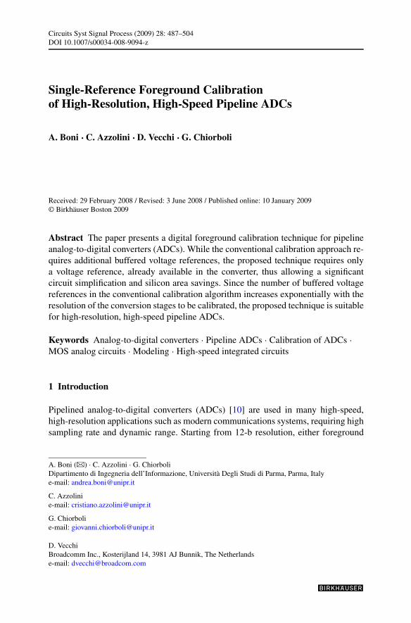
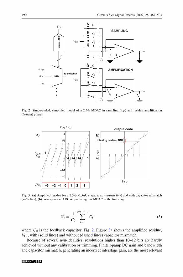
Furthermore, a three-level MDAC, using 0, ±VR as voltage references (2VR be-ing the ADC conversion range) saves a capacitor with respect to the well-knowntwo-level (using ±VR) implementations [10, 12]. Figure 2 shows a three-level 2.5-bMDAC in the sampling (top) and residue amplification phase (bottom). Such anMDAC exhibits 2Ni−1 nominally equal capacitors, Ci = C. For easier understanding,a single-ended MDAC is considered. Note that in the more realistic case of a fullydifferential MDAC, the voltage references become {VCM − VR,VCM,VCM + VR},VCM being the common-mode voltage reference.
Circuits Syst Signal Process (2009) 28: 487–504 489
Fig. 1 Black-box schematic of a pipeline ADC with S MDAC stages and digital calibration
In the amplification phase, each capacitor except C0 is connected to a correspon-dent analog MUX being controlled by the output of the coarse ADC. Considering theresidue amplification phase and using the charge conservation principle at the nega-tive input pin of the amplifier, the amplified residue voltage at the output of the ithstage in the ideal case is
VOi = GiVINi − VRDsi , (1)
where
Gi = 2Ni−1, (2)
Dsi = Di − (2Ni−1 − 1
), (3)
where an ideal opamp has been assumed where VINi is the input of the ith ADC-MDAC and Di is the output of the coarse Ni -b ADC. In the case of the 2.5-bMDAC in Fig. 2 the thresholds of the coarse ADC are at ±VR/8, ±3VR/8, ±5VR/8,Di ∈ {0 · · ·6} and Dsi ∈ {−3 · · ·3}.
Note that the mismatch occurring among the MDAC capacitors affects both theoutput residue, VOi , and the effective MDAC gain, G′
i :
VOi = G′i VINi − sign (Dsi ) VR
C0
|Dsi |∑
i=1
Ci, (4)
490 Circuits Syst Signal Process (2009) 28: 487–504
Fig. 2 Single-ended, simplified model of a 2.5-b MDAC in sampling (top) and residue amplification(bottom) phases
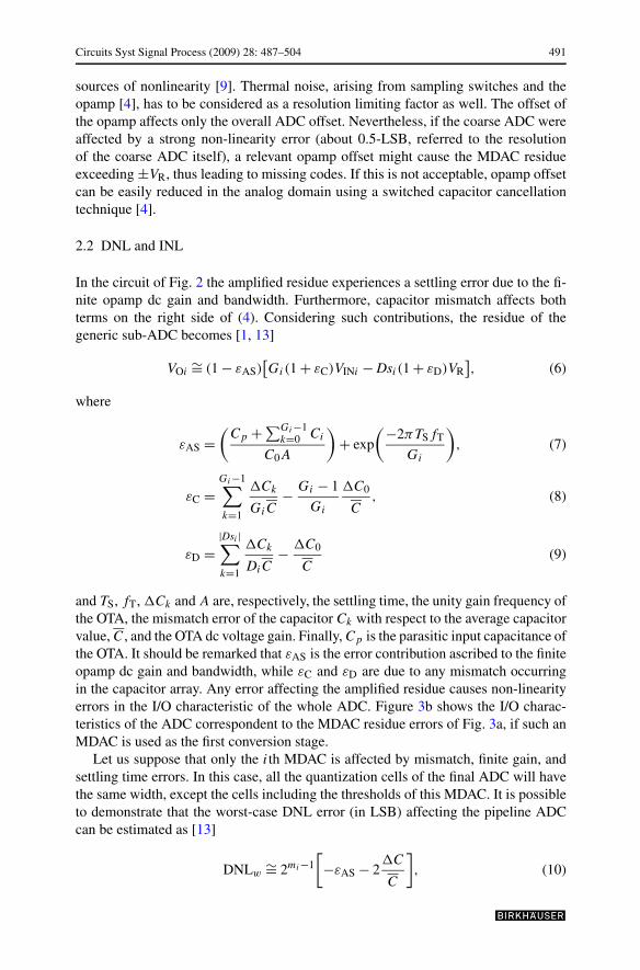
Fig. 3 (a) Amplified residue for a 2.5-b MDAC stage: ideal (dashed line) and with capacitor mismatch(solid line); (b) correspondent ADC output using this MDAC as the first stage
G′i = 1
C0
2Ni−1−1∑
i=0
Ci, (5)
where C0 is the feedback capacitor, Fig. 2. Figure 3a shows the amplified residue,VOi , with (solid lines) and without (dashed lines) capacitor mismatch.
Because of several non-idealities, resolutions higher than 10–12 bits are hardlyachieved without any calibration or trimming. Finite opamp DC gain and bandwidthand capacitor mismatch, generating an incorrect interstage gain, are the most relevant
Circuits Syst Signal Process (2009) 28: 487–504 491
sources of nonlinearity [9]. Thermal noise, arising from sampling switches and theopamp [4], has to be considered as a resolution limiting factor as well. The offset ofthe opamp affects only the overall ADC offset. Nevertheless, if the coarse ADC wereaffected by a strong non-linearity error (about 0.5-LSB, referred to the resolutionof the coarse ADC itself), a relevant opamp offset might cause the MDAC residueexceeding ±VR, thus leading to missing codes. If this is not acceptable, opamp offsetcan be easily reduced in the analog domain using a switched capacitor cancellationtechnique [4].
2.2 DNL and INL
In the circuit of Fig. 2 the amplified residue experiences a settling error due to the fi-nite opamp dc gain and bandwidth. Furthermore, capacitor mismatch affects bothterms on the right side of (4). Considering such contributions, the residue of thegeneric sub-ADC becomes [1, 13]
VOi∼= (1 − εAS)
[Gi(1 + εC)VINi − Dsi (1 + εD)VR
], (6)
where
εAS =(
Cp + ∑Gi−1k=0 Ci
C0A
)+ exp
(−2πTSfT
Gi
), (7)
εC =Gi−1∑
k=1
�Ck
GiC− Gi − 1
Gi
�C0
C, (8)
εD =|Dsi |∑
k=1
�Ck
DiC− �C0
C(9)
and TS, fT, �Ck and A are, respectively, the settling time, the unity gain frequency ofthe OTA, the mismatch error of the capacitor Ck with respect to the average capacitorvalue, C, and the OTA dc voltage gain. Finally, Cp is the parasitic input capacitance ofthe OTA. It should be remarked that εAS is the error contribution ascribed to the finiteopamp dc gain and bandwidth, while εC and εD are due to any mismatch occurringin the capacitor array. Any error affecting the amplified residue causes non-linearityerrors in the I/O characteristic of the whole ADC. Figure 3b shows the I/O charac-teristics of the ADC correspondent to the MDAC residue errors of Fig. 3a, if such anMDAC is used as the first conversion stage.
Let us suppose that only the ith MDAC is affected by mismatch, finite gain, andsettling time errors. In this case, all the quantization cells of the final ADC will havethe same width, except the cells including the thresholds of this MDAC. It is possibleto demonstrate that the worst-case DNL error (in LSB) affecting the pipeline ADCcan be estimated as [13]
DNLw∼= 2mi−1
[−εAS − 2
�C
C
], (10)
492 Circuits Syst Signal Process (2009) 28: 487–504
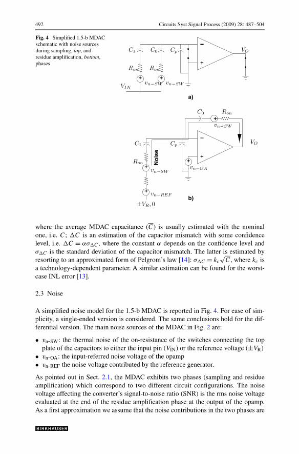
Fig. 4 Simplified 1.5-b MDACschematic with noise sourcesduring sampling, top, andresidue amplification, bottom,phases
where the average MDAC capacitance (C) is usually estimated with the nominalone, i.e. C; �C is an estimation of the capacitor mismatch with some confidencelevel, i.e. �C = ασ�C , where the constant α depends on the confidence level andσ�C is the standard deviation of the capacitor mismatch. The latter is estimated byresorting to an approximated form of Pelgrom’s law [14]: σ�C = kc
√C, where kc is
a technology-dependent parameter. A similar estimation can be found for the worst-case INL error [13].
2.3 Noise
A simplified noise model for the 1.5-b MDAC is reported in Fig. 4. For ease of sim-plicity, a single-ended version is considered. The same conclusions hold for the dif-ferential version. The main noise sources of the MDAC in Fig. 2 are:
• vn-SW: the thermal noise of the on-resistance of the switches connecting the topplate of the capacitors to either the input pin (VIN) or the reference voltage (±VR)
• vn-OA: the input-referred noise voltage of the opamp• vn-REF the noise voltage contributed by the reference generator.
As pointed out in Sect. 2.1, the MDAC exhibits two phases (sampling and residueamplification) which correspond to two different circuit configurations. The noisevoltage affecting the converter’s signal-to-noise ratio (SNR) is the rms noise voltageevaluated at the end of the residue amplification phase at the output of the opamp.As a first approximation we assume that the noise contributions in the two phases are
Circuits Syst Signal Process (2009) 28: 487–504 493
almost independent. This assumption allows us to easily obtain the overall MDACnoise, by superposition of the two noise power terms.
In the sampling phase the inputs and the output of the opamp are shorted to ground(or to any convenient dc voltage), thus the noise voltage at the opamp output is almostzero in this phase. For the same reason the contribution of the opamp noise is negli-gible in this phase. In contrast, the thermal noise of the on-resistance of the switchesis integrated by the total MDAC capacitance, Ctot = C1 + C0 = Gi · C0 at the bottomplate terminal of the capacitors, Fig. 4a. Therefore, the rms noise voltage sampled bythe MDAC is
vn-A =√
kT
Ctot. (11)
At the transition from the sampling to the residue amplification phase vn-A is sam-pled and transferred to the opamp output, leading to the noise contribution from thesampling phase, vn-SAM, equal to
vn-SAM = vn-A · Gi
=√
GikT
C0. (12)
Note that the opamp input capacitance, Cp , does not contribute to the overall noise,the input terminals being shorted to ground.
During the residue amplification phase, Fig. 4b, a voltage feedback is establishedand the circuit acts as a continuous-time voltage amplifier. Therefore both the thermalnoise voltage due to the switches and the input opamp noise are transferred to theopamp output, and their spectra are shaped by the transfer function of the voltageamplifier itself. Assuming a single-stage opamp and considering the feedback factorin the circuit of Fig. 4, Hr = 1
Gi, the noise bandwidth of the amplifier is
Beq ≈ π
2
gm
2πCLGi
, (13)
gm being the transconductance of the input MOS devices in the OTA and CL theoverall loading capacitance of the opamp in this phase,
CL = (Gi − 1)Cf + Cp
Gi + Cp
C0
+ CMDAC-(i+1) + CADC-i , (14)
CADC-i being the input capacitance of the flash sub-ADC and CMDAC-(i+1) the inputcapacitance of the next MDAC stage.
The opamp input noise is mainly contributed by the output noise current from theMOS input pair in = 4γ kT gm[A2/Hz], with γ ranging from 2/3 to 3 depending onthe process and on the gate length. From in the power spectral density of the input-referred noise voltage of the OTA is obtained as
en-OA =√
4γ kT
gm. (15)
494 Circuits Syst Signal Process (2009) 28: 487–504
The contribution of the noisy reference generator (±VR) is modelled with an equiva-lent noise resistance, Rref. Therefore the rms noise voltage at the opamp output relatedto the residue amplification phase is
v2n-RA = G2
i Beq
(4KT Ron + 4KT Rref + 4γ kT
gm
). (16)
Assuming that the switch size (i.e. its on-resistance) is scaled together with the capac-itance value, RON ≈ Ron/Gi . The overall output noise of the MDAC stage is obtainedby summing the contributions related to the sampling and to the residue amplificationphase,
v2n-OUT = ξ
[GikT
C0+ 4kT (Ron + Rref)
gmGi
4CL+ γKT Gi
CL
], (17)
where ξ = 1 for the single-ended arrangement of the MDAC and ξ = 2 holds for thedifferential scheme.
2.4 Model-Based Design Methodology
In a reasonable design approach for high-resolution pipeline ADCs, the maximumallowed INL, DNL, and output noise should be evaluated at first. In order to achievean effective resolution higher than N −1 bits, where N bits is the nominal resolution,both the DNL and INL should be below 1 LSB and the total output noise shouldbe well below the quantization noise. From the worst-case DNL and INL estimatederrors, suitable lower bounds are found for the opamp dc gain, A, and unity-gaintransition frequency, fT, and for the MDAC capacitance, C.
Similarly, a different constraint on the minimum value of C can be obtained from(17) (kT /C noise contribution) [4]. Nevertheless, while the noise contribution cannotbe removed, digital calibration can remove the nonlinearities arising from capacitormismatch. Therefore two lower bounds for the feedback capacitance of each stagecan be determined by the noise and linearity requirements. While the former shouldalways be satisfied, the latter can be bypassed, introducing a digital calibration of thestage. Because of the impact on the silicon area and power consumption, the calibra-tion will be introduced only when the minimum capacitance imposed by the linearityrequirements exceeds some threshold dictated by area and OTA transconductance(gm) constraints.
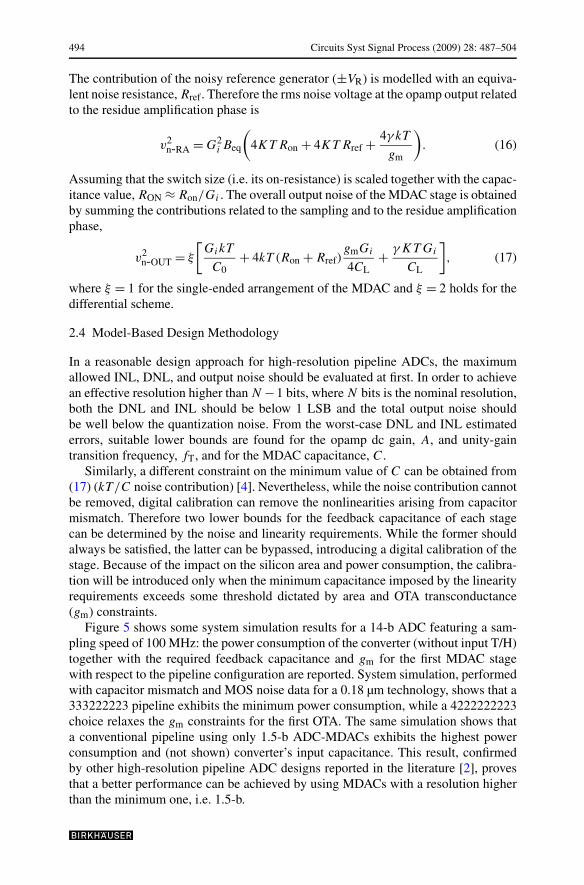
Figure 5 shows some system simulation results for a 14-b ADC featuring a sam-pling speed of 100 MHz: the power consumption of the converter (without input T/H)together with the required feedback capacitance and gm for the first MDAC stagewith respect to the pipeline configuration are reported. System simulation, performedwith capacitor mismatch and MOS noise data for a 0.18 µm technology, shows that a333222223 pipeline exhibits the minimum power consumption, while a 4222222223choice relaxes the gm constraints for the first OTA. The same simulation shows thata conventional pipeline using only 1.5-b ADC-MDACs exhibits the highest powerconsumption and (not shown) converter’s input capacitance. This result, confirmedby other high-resolution pipeline ADC designs reported in the literature [2], provesthat a better performance can be achieved by using MDACs with a resolution higherthan the minimum one, i.e. 1.5-b.
Circuits Syst Signal Process (2009) 28: 487–504 495
Fig. 5 Power consumption (left), C0 and gm (right, circles and diamonds, respectively) of the first stagevs. the 14-b ADC configuration
3 Calibration Method
Digital foreground calibration techniques are based on the measurement of the DNLerrors of the converter introduced by the stage under calibration and caused by mis-match occurring in the capacitor array, Fig. 2. When the input voltage of that MDACstage under calibration crosses a threshold of the correspondent coarse ADC, the out-put residue exhibits a variation which differs from the ideal value corresponding toVR. This difference corresponds to the DNL introduced by the stage under calibra-tion and should be subtracted from the actual value in order to remove the relatednonlinearity error from the ADC characteristic.
3.1 Conventional Foreground Calibration
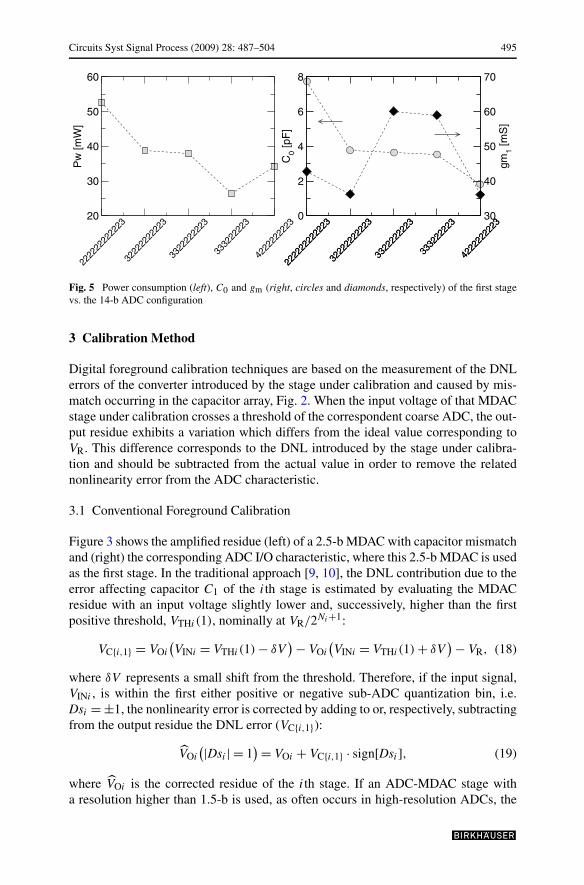
Figure 3 shows the amplified residue (left) of a 2.5-b MDAC with capacitor mismatchand (right) the corresponding ADC I/O characteristic, where this 2.5-b MDAC is usedas the first stage. In the traditional approach [9, 10], the DNL contribution due to theerror affecting capacitor C1 of the ith stage is estimated by evaluating the MDACresidue with an input voltage slightly lower and, successively, higher than the firstpositive threshold, VTHi (1), nominally at VR/2Ni+1:
VC{i,1} = VOi
(VINi = VTHi (1) − δV
) − VOi
(VINi = VTHi (1) + δV
) − VR, (18)
where δV represents a small shift from the threshold. Therefore, if the input signal,VINi , is within the first either positive or negative sub-ADC quantization bin, i.e.Dsi = ±1, the nonlinearity error is corrected by adding to or, respectively, subtractingfrom the output residue the DNL error (VC{i,1}):
V̂Oi
(|Dsi | = 1) = VOi + VC{i,1} · sign[Dsi], (19)
where V̂Oi is the corrected residue of the ith stage. If an ADC-MDAC stage witha resolution higher than 1.5-b is used, as often occurs in high-resolution ADCs, the
496 Circuits Syst Signal Process (2009) 28: 487–504
procedure described in (18) and (19) must be repeated for each sub-ADC quantizationbin. Since the DNL errors accumulate for |Dsi | increasing from 1 to 2Ni−1 − 1, theadditive correction terms must be accumulated as well. For |Dsi | = k:
V̂Oi (k) = VOi + sign(Dsi )
k∑
j=1
VC{i,j}. (20)
Such a procedure is insensitive to the nonlinearities occurring in the sub-ADC. In-deed, it can be proved that the DNL of the quantization bins corresponding to the j ththreshold of the sub-ADC in the ith stage can always be estimated as in (18) with anyinput voltage (within ±VR) if the sub-ADC output, Di , is forced to change from j −1to j [9]. Nevertheless, since the MDAC outputs must not exceed the ±VR boundaries,the DNL measurement should be performed near the nominal sub-ADC thresholds inorder to avoid the saturation of the following ADC-MDAC.
Note that the error evaluated as in (18) is measured in the digital domain usingthe following ADC-MDAC stages. This introduces some truncation error [10], lim-iting the minimum INL achievable through calibration. This issue can be relaxed byintroducing some extra bit in the last ADC stage (usually a flash converter).
3.2 Single-Reference Calibration
The main limit of the conventional foreground calibration is the requirement for2Ni−1 − 1 voltage references. Usually these voltage references are directly obtainedfrom the resistive divider used for the generation of the flash coarse-ADC thresholds.In the case of a high-resolution ADC (12–14-b), the noise requirements dictate rela-tively large capacitor values (1 ∼ 10 pF range) in the first MDAC stages. If the DNLmeasurement is performed at a high sampling speed, the MDAC input capacitance,when connected to a tap of the resistive divider, causes a significant disturbance andringing on the generated reference voltage together with unacceptably large settlingtimes. Note that performing the calibration at the nominal (high) sampling speed isalso a convenient choice to correct for the settling error, shown in the second term onthe right side of (7).
This situation must be avoided, since it can potentially lead to a significant error inthe DNL evaluation. Furthermore, if the resistive string is shared among several sub-ADCs, the quantization of the DNL error may fail if the injected disturbance causes ashift of the thresholds higher than 0.5-LSB (referred to the resolution of the resistivedivider). Therefore, buffering each voltage reference to be used for the calibration ismandatory, thus increasing the overall power consumption and the silicon area.
This problem is exacerbated in high-resolution pipeline ADCs where the firstADC-MDAC stages are designed with a resolution higher than 1.5-b, as explainedin Sect. 2.4. Since the error measurement in (18) has to be repeated for each positivethreshold, the number of introduced extra buffers increases exponentially with theresolution of the MDAC under calibration.
Such extra buffers can be avoided with a different approach for the measurement ofthe DNL error at each threshold of the ADC-MDAC under calibration. The proposed
Circuits Syst Signal Process (2009) 28: 487–504 497
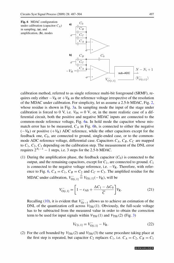
Fig. 6 MDAC configurationunder calibration (capacitor CA)in sampling, (a), andamplification, (b), modes
calibration method, referred to as single reference multi-bit foreground (SRMF), re-quires only either −VR or +VR as the reference voltage irrespective of the resolutionof the MDAC under calibration. For simplicity, let us assume a 2.5-b MDAC, Fig. 2,whose residue is shown in Fig. 3a. In sampling mode the input of the stage undercalibration is forced to 0 V, i.e. VIN = 0 V, or, in the more realistic case of a dif-ferential circuit, both the positive and negative MDAC inputs are connected to thecommon-mode reference voltage, Fig. 6a. In hold mode the capacitor whose mis-match error has to be measured, CA in Fig. 6b, is connected to either the negative(−VR) or positive (+VR) ADC reference, while the other capacitors except for thefeedback one, C0, are connected to ground, single-ended case, or to the common-mode ADC reference voltage, differential case. Capacitors CA, CB , CC are mappedto C1, C2, C3 depending on the calibration step. The measurement of the DNL errorrequires 2Ni−1 − 1 steps, i.e. 3 steps for the 2.5-b MDAC.
(1) During the amplification phase, the feedback capacitor (C0) is connected to theoutput, and the remaining capacitors, except for C1, are connected to ground. C1is connected to the negative voltage reference, i.e. −VR. Therefore, with refer-ence to Fig. 6, CA = C1, CB = C2 and CC = C3. The amplified residue for the
MDAC under calibration, V −O{i,1}
�= VO{i,1}(−VR), will be
V −O{i,1} =
[1 − εAS + �C1 − �C0
C
]VR. (21)
Recalling (10), it is evident that V −Oi−1 allows us to achieve an estimation of the
DNL of the quantization cell across VTHi (1). Obviously, the full-scale voltagehas to be subtracted from the measured value in order to obtain the correctionterm to be used for input signals within VTHi (1) and VTHi (2) (Fig. 3)
VC{i,1} = V −O{i,1} − VR. (22)
(2) For the cell bounded by VTHi (2) and VTHi (3) the same procedure taking place atthe first step is repeated, but capacitor C2 replaces C1, i.e. CA = C2, CB = C1
498 Circuits Syst Signal Process (2009) 28: 487–504
and CC = C3, Fig. 6. Similarly,
V −O{i,2} =
[1 − εAS + �C2
C− �C0
C
]VR. (23)
Due to the accumulation of the DNL error, the calibration term to be used whenthe ADC-MDAC input signal falls between VTHi (2) and VTHi (3) is
VC{i,2} = V −O{i,2} − VR + VC{i,1}. (24)
(3) The correction term to be used when the ADC-MDAC input signal is aboveVTHi (3) depends on C3 and, thus, CA = C3, CB = C1 and CC = C2.
Notice that the measured calibration terms are also used when the ADC-MDAC in-put signal is negative, due to the symmetry of the conversion characteristic. As for theconventional calibration, the residue if the MDAC under calibration, V −
O{i,x}, is mea-
sured in the digital domain, 〈V −O{i,x}〉, by means of the ADC based on the following
ADC-MDAC stages. It should be stressed that the proposed method requires only asingle ADC reference (either ±VR), already available and provided by either on-chipor off-chip buffers. Moreover the proposed calibration does not require substractionbetween two measured quantized residues to be performed. This allows a significantsimplification of the digital circuitry used for the evaluation of the calibration terms.
A drawback of the method is that the output of the MDAC under calibration isequal to VR + VC{i,j}, thus a positive error VC{i,j} causes the saturation of the follow-ing stages. In this case the correction term, VC{i,j} cannot be accurately estimated.This occurs when
�CJ − �C0
C> εAS. (25)
This effect can be avoided by deliberately reducing the gain of the MDAC stage,i.e. by increasing the value of the feedback capacitor to C0 + �C0G. The amount ofgain reduction (i.e. �C0G/C0) depends on settling, dc-gain and capacitor mismatcherrors,
�C0G
C∼= 3
√2σ�C
C− εAS. (26)
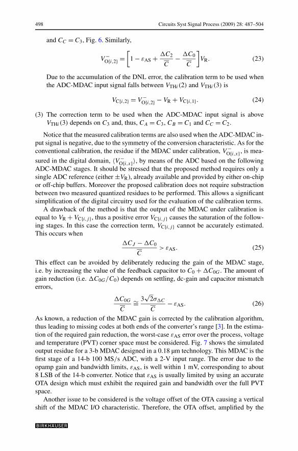
As known, a reduction of the MDAC gain is corrected by the calibration algorithm,thus leading to missing codes at both ends of the converter’s range [3]. In the estima-tion of the required gain reduction, the worst-case εAS error over the process, voltageand temperature (PVT) corner space must be considered. Fig. 7 shows the simulatedoutput residue for a 3-b MDAC designed in a 0.18 µm technology. This MDAC is thefirst stage of a 14-b 100 MS/s ADC, with a 2-V input range. The error due to theopamp gain and bandwidth limits, εAS, is well within 1 mV, corresponding to about8 LSB of the 14-b converter. Notice that εAS is usually limited by using an accurateOTA design which must exhibit the required gain and bandwidth over the full PVTspace.
Another issue to be considered is the voltage offset of the OTA causing a verticalshift of the MDAC I/O characteristic. Therefore, the OTA offset, amplified by the
Circuits Syst Signal Process (2009) 28: 487–504 499
Fig. 7 Design example: 3-b 100-MS/s MDAC output residue for different PVT corners (above) andsettling details (below)
MDAC gain, directly adds to the DNL measurement performed as in (21). If thisoffset is cancelled in the analog domain by a switched capacitor approach [4, 8],the proposed calibration technique can be used without any modification. Otherwise,the offset contribution to the DNL estimation can be easily removed by repeatingthe measurement in (21) with both ADC references (−VR and +VR) and taking thedifference between the two measurements:
VC{i,j} =(
V −O{i,j} − V +
O{i,j} − 2VR
2
)+ VC{i,j−1}, (27)
where V +O{i,1} is the MDAC output evaluated as in (21) but with +VR used instead
of −VR. Furthermore, the amount of gain reduction introduced for avoiding the sat-uration of the following ADC-MDAC stage, (26), should be modified for taking intoaccount the contribution of the OTA offset:
�C0G
C∼= 3
√2σ 2
C
C2
+ G2i σ
2OS − εAS, (28)
σOS being the standard deviation of the input-referred offset voltage of the OTA inthe ith stage.
500 Circuits Syst Signal Process (2009) 28: 487–504
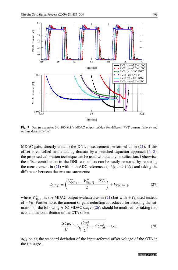
Fig. 8 Black-box schematic of the calibration hardware
3.3 Hardware Implementation
The top-level architecture of the ADC including calibration logic is shown in Fig. 8.The pipeline chain is composed of a front-end track and hold (THA), first and secondpipeline stages to be calibrated, and the remaining back-end stages, which do not re-quire calibration. Being encompassed between foreground techniques, the proposedcalibration begins at the chip power-on. A finite state machine (FSM) called “Mea-surement Unit” in Fig. 8 defines a sequence of operations aiming at the measurementof the correction terms V −
O{i,x}.In order to support SRMF calibration, the circuit of Fig. 2 is slightly modified: the
single-pole double-through (SPDT) switch connected to C0 is replaced by a single-pole triple-through (SPTT) switch allowing one to connect the top plate of C0 toa MUX output in sampling mode (instead of the MDAC input node). Furthermore,in calibration mode the coarse-ADC should be disabled and the MUX control inputdriven by the FSM. In sampling mode the FSM forces the output of each MUX to0 V (VCM in the differential configuration) and all the capacitors are connected tothe MUX’s output, while in amplification mode the FSM follows the previously de-scribed calibration steps. Indeed, at the first step, −VR is provided to C1 (i.e. nodeA, Fig. 2), while the other MUXs provide the 0-V reference (i.e. the common-modereference in the differential implementation) to C2 and C3. The digital output codeprovided by the converter based on the subsequent ADC-MDAC stages is stored intoan accumulator register. The measurement is repeated and averaged in order to reducethe noise contribution: this can be performed either by means of a running-averagealgorithm or by a simpler “add-and-shift” approach. The averaged output code is thensubtracted from the theoretical full-scale digital code in order to obtain the correctioncoefficient VCi,1 as in (22).
If the OTA offsets are not zeroed or cannot be neglected, a differential measure isrequired as in (27): in this case the averaging procedure is repeated using the oppositereference (i.e. +VR). The digital FSM repeats the measurement for all the capacitorsof the considered MDAC (thus storing VCi,2 and VCi,3). If several MDACs need to becalibrated, the calibration starts from the last MDAC up to the first one [3].
Circuits Syst Signal Process (2009) 28: 487–504 501
Table 1 Parameters of the firstfour MDAC stages Stage Resolution DC gain GBW Cap. Calib
n [b] [dB] [GHz] [pF]
1 3 95 1.2 3.5 yes
2 3 85 1.0 0.4 yes
3 3 72 0.9 2.1 no
4 2 60 0.4 0.5 no
During the regular operation of the ADC, the measurement unit is turned off andthe logic network called “Elaboration Unit” is turned on: the uncalibrated output wordis corrected in real-time elaboration on the basis of the previous measured errors. Thecorrection terms are summed by the elaboration unit to the uncalibrated code as in(20) and a calibrated output word is provided at the ADC output.
4 Simulation Results
The proposed calibration method was implemented in the design of a 14-bit,100 MS/s pipelined ADC in 0.18 µm CMOS. The converter is designed for a 3.3 Vsupply. Therefore the OTA stages are designed with both thick-oxide (3.3 V) andthin-oxide devices. The latter are used where the maximum drain-source, drain-gateand gate-source absolute voltage is always within 1.8 V. Protection diodes are intro-duced to avoid exceeding the voltage ratings during the power-on transient. The usageof thin-oxide devices provides a benefit in terms of a higher OTA bandwidth due totheir higher gm at the same gate area. Furthermore, their lower threshold voltage isbeneficial for designing the OTA with a large output swing. In order to prove theconcept of the proposed SRMF calibration, a high-level model of the calibrated ADCwas used. The effect of the OTA limited BW and gain on the amplified residue wasincluded in the model together with capacitor mismatch and OTA offset. The input-referred noise of the OTA, the equivalent noise of the switch in the “closed” state andthe noise from the reference voltage sources (±VR) were taken into account. Thishigh-level behavioral model based on a MATLAB description of the converter allowsprecise and fast simulations, and the performance of different calibration techniquescan be easily compared.
Design optimization analysis, mainly based on (10), worst-case INL estimation,and kT /C noise considerations, returns 333222223 architecture as a convenientchoice in terms of power consumption, Fig. 5. In the first MDAC stages the ca-pacitors were sized for a kT /C noise compatible with 13-b resolution. Capacitormismatch dictates for calibration in the first two stages (2.5-b). Table 1 reports thefollowing parameters for the first MDAC stages: coarse-ADC resolution, OTA dc-gain and gain-bandwidth product and capacitor value. These parameters, provided bydesign optimization, are used in the behavioral simulation of the converter. Figure 9shows the simulated nonlinearity errors estimated by means of the code-density algo-rithm without calibration (top) and with either conventional or offset-tolerant SMRFcalibration. The simulations were performed at the maximum sampling speed, i.e.
502 Circuits Syst Signal Process (2009) 28: 487–504
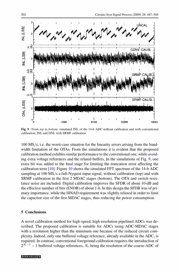
Fig. 9 From top to bottom: simulated INL of the 14-b ADC without calibration and with conventionalcalibration; INL and DNL with SRMF calibration
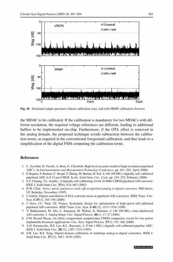
100 MS/s, i.e. the worst-case situation for the linearity errors arising from the band-width limitation of the OTAs. From the simulations it is evident that the proposedcalibration method exhibits similar performance to the conventional one, while avoid-ing extra voltage references and the related buffers. In the simulations of Fig. 9, oneextra bit was added to the final stage for limiting the truncation error affecting thecalibration term [10]. Figure 10 shows the simulated FFT spectrum of the 14-b ADCsampling at 100 MS/s a full-Nyquist input signal, without calibration (top) and withSRMF calibration in the first 2 MDAC stages (bottom). The OTA and switch resis-tance noise are included. Digital calibration improves the SFDR of about 10-dB andthe effective number of bits (ENOB) of about 1-b. In this design the SFDR was of pri-mary importance, while the SINAD requirement was slightly relaxed in order to limitthe capacitor size of the first MDAC stages, thus reducing the power consumption.
5 Conclusions
A novel calibration method for high-speed, high-resolution pipelined ADCs was de-scribed. The proposed calibration is suitable for ADCs using ADC-MDAC stageswith a resolution higher than the minimum one because of the reduced circuit com-plexity. Indeed, only one buffered voltage reference, already available in the ADC, isrequired. In contrast, conventional foreground calibration requires the introduction of2Ni−1 − 1 buffered voltage references, Ni being the resolution of the coarse-ADC of
Circuits Syst Signal Process (2009) 28: 487–504 503
Fig. 10 Simulated output spectrum without calibration (top), and with SRMF calibration (bottom)
the MDAC to be calibrated. If the calibration is mandatory for two MDACs with dif-ferent resolution, the required voltage references are different, leading to additionalbuffers to be implemented on-chip. Furthermore, if the OTA offset is removed inthe analog domain, the proposed technique avoids subtraction between the calibra-tion terms, as required in the conventional foreground calibration, and thus leads to asimplification of the digital FSM computing the calibration terms.
References
1. C. Azzolini, D. Vecchi, A. Boni, G. Chiorboli, High-level accurate model of high-resolution pipelinedADC’s. In Instrumentation and Measurement Technology Conference, pp. 261–265, April (2006)
2. P. Bogner, F. Kuttner, C. Kropf, T. Hartig, M. Burlan, H. Eul, A 14b 100 MS/s digitally self-calibratedpipelined ADC in 0.13 µm CMOS. In Int. Solid-State Circ. Conf., pp. 224–225, February (2006)
3. S.Y. Chuang, T.L. Sculley, A digitally self-calibrating 14-bit 10-MHz CMOS pipelined A/D converter.IEEE J. Solid State Circ. 37(6), 674–683 (2002)
4. D.W. Cline, Noise, speed, and power trade-offs in pipelined analog to digital converters. PhD thesis,UC Berkeley, November (1995)
5. I. Galton, Digital cancellation of D/A converter noise in pipelined A/D converters. IEEE Trans. Circ.Syst. II 47(3), 185–196 (2000)
6. J. Goes, J.C. Vital, J.E. Franca, Systematic design for optimization of high-speed self-calibratedpipelined A/D converters. IEEE Trans. Circ. Syst. II 45(12), 1513–1526 (1998)
7. V. Hakkarainen, M. Aho, L. Sumanen, M. Waltari, K. Halonen, A 14b 100-MS/s time-interleavedA/D converter. J. Analog Integr. Circ. Signal Process. 46(1), 17–27 (2006)
8. S.M. Rezaul Hasan, An offset compensated sampled-data CMOS comparator circuit for low-powerimplantable biosensor applications. Circ. Syst. Signal Process. 27(3), 351–366 (2008)
9. A.N. Karanicolas, H.S. Lee, K.L. Bacrania, A 15-bit 1-MS/s digitally self-calibrated pipeline ADC.IEEE J. Solid State Circ. 28(12), 1207–1215 (1993)
10. S.H. Lee, B.S. Song, Digital-domain calibration of multistep analog-to-digital converters. IEEE J.Solid State Circ. 27(12), 1667–1678 (1992)
504 Circuits Syst Signal Process (2009) 28: 487–504
11. S.H. Lewis, H.S. Fetterman, G.F. Gross, R. Ramachandran, T.R. Viswanathan, A 10-bit20-MSsample/s analog-to-digital converter. IEEE J. Solid State Circ. 27(3), 351–357 (1992)
12. Y.M. Lin, B. Kim, P.R. Gray, A 13-b 2.5-MHz self-calibrated pipelined A/D converter in 3-µm CMOS.IEEE J. Solid State Circ. 26(4), 628–636 (1991)
13. M. Parenti, D. Vecchi, A. Boni, G. Chiorboli, Systematic design and modelling of high-resolution,high-speed pipeline ADCs. Measurement 37(4), 344–351 (2005)
14. M.J.M. Pelgrom, A.C.J. Duinmaijer, A.P.G. Welbers, Matching properties of MOS transistors. IEEEJ. Solid State Circ. 24(5), 1433–1439 (1989)
15. M. Waltari, L. Sumanen, T. Korhonen, K.A.I. Halonen, A self-calibrated pipeline ADC with 200 MHzIF-sampling frontend. J. Analog Integr. Circ. Signal Process. 37(3), 201–213 (2003)
16. W.Y. Wenhua, D. Kelly, I. Mehr, M.T. Sayuk, L. Singer, A 3-V 340-mW 14-b 75-Msample/s CMOSADC with 85-dB SFDR at Nyquist input. IEEE J. Solid State Circ. 36(12), 1931–1936 (2001)
Related Documents