REVIEW JANUARY-JUNE 2007 RSOFT DESIGN GROUP VOLUME 6 NUMBER 1 Modeling Surface Plasmon Biosensors The 10GBase-LRM and the OIF EDC for 10 Gb/s 1550 nm Links projects use OptSim for detailed analysis of systems deploying Electronic Dispersion Compensation Electronic Dispersion Compensation has recently gained atten- tion as a cost-effective, power-efficient, small form factor solution to mitigate the effects of dispersion in single- and multi-mode fiber optical communication systems. Currently the 10GBase-LRM standard achieves 10 Gb/s operation over 300 m of FDDI-grade legacy multimode fiber using EDC at the receiver section. The Optical Internetworking Forum is working on a set of application codes to standardize for the ITU G.959.1 new optical links that use EDC to extend the reach of present Optical Transport Networks at 10 Gb/s with 1600 ps/nm of dispersion (80 Km of G.652 fiber) to 2400 ps/nm (120 Km of fiber). The adoption of EDC, while a convenient solution to increase the network performance, has made it very challenging to analyze the interoperability between components. A link with a 10Gbps transmitter and a 10Gbps receiver with EDC doesn’t necessarily create a 10Gbps system. The transmitter’s compliance test should require estimation of its Transmitter Wavelength Dispersion Pen- alty (TWDP) in the presence of a Minimum Mean Squared Error (MMSE) based Decision Feedback Equalizer (DFE) at the receiving end. This approach has been chosen by the IEEE 10GBase-LRM task force and is currently under investigation in the OIF EDC for 10 Gb/s 1550 nm Links project. 1 Surface phenomena such as surface plasmon resonances play an important role in sensor technology since the behavior of elec- tromagnetic fields at material interfaces can be directly correlated to many physical and chemical properties of the materials. These sensing methods have the further benefit of allowing for accurate and non-invasive sensing that can provide immediate results both in and out of a laboratory. Sensors based on surface plasmons are being increasingly incorporated directly into larger systems to detect many properties, including temperature and the presence or concentration of particular compounds in medical, industrial, or other fields. The need to incorporate optical sensors into a wide variety of appli- cations necessitates the creation of smaller sensors that are easy to fabricate with and used in existing semiconductor technology. How- ever, as the size of any optical device, including sensors, decreases, the need for simulation software increases. RSoft’s software tools, specifically FullWAVE, can be used to accurately model the elec- tromagnetic fields at material interfaces where surface phenomena such as surface plasmons occur. FullWAVE provides a full-vector solution and allows optical design engineers to use complex mate- rial definitions, arbitrary device geometries, non- uniform grids, and so- phisticated measure- ment techniques to cre- ate new sensor designs and fine tune existing designs for specific ap- plications. As an example of the kind of sensor that could be modeled is described in Ref. [1]. It consists of a small inter- ferometer in an SOI waveguide structure that functions much like a classic Mach-Zhender device. A small gold plate is embedded in the waveguide so that the material to be studied lies on top of the plate, and the silicon waveguide and oxide buffer layer lie below it. Light incident on the plate from the propagating mode in the SOI waveguide couples into two surface plasmon modes, Detailed Analysis of FFE, DFE and MLSE Electronic Equalization in Single- and Multi-mode Systems in OptSim 4.6 continued on page 2 continued on page 2 FIGURE 1: MODELING SURFACE PLASMON BIOSENSORS FIGURE 1 OPTSIM PROJECT OF AN ITU G.959.1 SYSTEM DEPLOYING 120 KM SMF AND MMSE-DFE - EYE DIAGRAMS (A) WITHOUT EDC (B) WITH EDC.

Welcome message from author
This document is posted to help you gain knowledge. Please leave a comment to let me know what you think about it! Share it to your friends and learn new things together.
Transcript

REVIEWJANUARY-JUNE 2007 RSOFT DESIGN GROUP
VOLUME 6NUMBER 1
Modeling Surface Plasmon Biosensors
The 10GBase-LRM and the OIF EDC for 10 Gb/s 1550 nm Links projects use OptSim for detailed analysis of systems deploying Electronic Dispersion Compensation
Electronic Dispersion Compensation has recently gained atten-tion as a cost-effective, power-effi cient, small form factor solution to mitigate the effects of dispersion in single- and multi-mode fi ber optical communication systems. Currently the 10GBase-LRM standard achieves 10 Gb/s operation over 300 m of FDDI-grade legacy multimode fi ber using EDC at the receiver section. The Optical Internetworking Forum is working on a set of application codes to standardize for the ITU G.959.1 new optical links that use EDC to extend the reach of present Optical Transport Networks at 10 Gb/s with 1600 ps/nm of dispersion (80 Km of G.652 fi ber) to 2400 ps/nm (120 Km of fi ber).
The adoption of EDC, while a convenient solution to increase the network performance, has made it very challenging to analyze the interoperability between components. A link with a 10Gbps transmitter and a 10Gbps receiver with EDC doesn’t necessarily create a 10Gbps system. The transmitter’s compliance test should require estimation of its Transmitter Wavelength Dispersion Pen-alty (TWDP) in the presence of a Minimum Mean Squared Error
(MMSE) based Decision Feedback Equalizer (DFE) at the receiving end. This approach has been chosen by the IEEE 10GBase-LRM task force and is currently under investigation in the OIF EDC for 10 Gb/s 1550 nm Links project.
1
Surface phenomena such as surface plasmon resonances play an important role in sensor technology since the behavior of elec-tromagnetic fi elds at material interfaces can be directly correlated to many physical and chemical properties of the materials. These sensing methods have the further benefi t of allowing for accurate and non-invasive sensing that can provide immediate results both in and out of a laboratory. Sensors based on surface plasmons are being increasingly incorporated directly into larger systems to detect many properties, including temperature and the presence or concentration of particular compounds in medical, industrial, or other fi elds.
The need to incorporate optical sensors into a wide variety of appli-cations necessitates the creation of smaller sensors that are easy to fabricate with and used in existing semiconductor technology. How-ever, as the size of any optical device, including sensors, decreases, the need for simulation software increases. RSoft’s software tools, specifi cally FullWAVE, can be used to accurately model the elec-tromagnetic fi elds at material interfaces where surface phenomena such as surface plasmons occur. FullWAVE provides a full-vector solution and allows optical design engineers to use complex mate-
rial defi nitions, arbitrary device geometries, non-
uniform grids, and so-phisticated measure-ment techniques to cre-ate new sensor designs and fi ne tune existing designs for specifi c ap-plications.
As an example of the kind of sensor that could be modeled is described in Ref. [1]. It consists of a small inter-
ferometer in an SOI waveguide structure that functions much like a classic Mach-Zhender device. A small gold plate is embedded in the waveguide so that the material to be studied lies on top of the plate, and the silicon waveguide and oxide buffer layer lie below it. Light incident on the plate from the propagating mode in the SOI waveguide couples into two surface plasmon modes,
Detailed Analysis of FFE, DFE and MLSE Electronic Equalization in Single- and Multi-mode Systems in OptSim 4.6
continued on page 2
continued on page 2
FIGURE 1: MODELING SURFACE PLASMON BIOSENSORS
FIGURE 1 OPTSIM PROJECT OF AN ITU G.959.1 SYSTEM DEPLOYING 120 KM SMF AND MMSE-DFE - EYE DIAGRAMS (A) WITHOUT EDC (B) WITH EDC.
2
Software models are a viable solution to study the effect of electron-ic equalization in single- and multi-mode systems. RSoft’s OptSim provides an ideal framework and for this reason the software is used in both the 10GBase-LRM and the OIF EDC projects. OptSim includes models of Feed-Forward, Decision Feedback EDCs and Maximum Likelihood Sequence Estimators that enable the user to compare the performance of different electronic equalization tech-niques. The inclusion of an optimal MMSE-DFE model enables the user to carry out TWDP and transmitter compliance analysis. Figure 1 shows an OptSim project of an ITU G.959.1 system deploying an external modulation transmitter coupled with 120 Km of SM Fiber and using EDC at the receiver section.
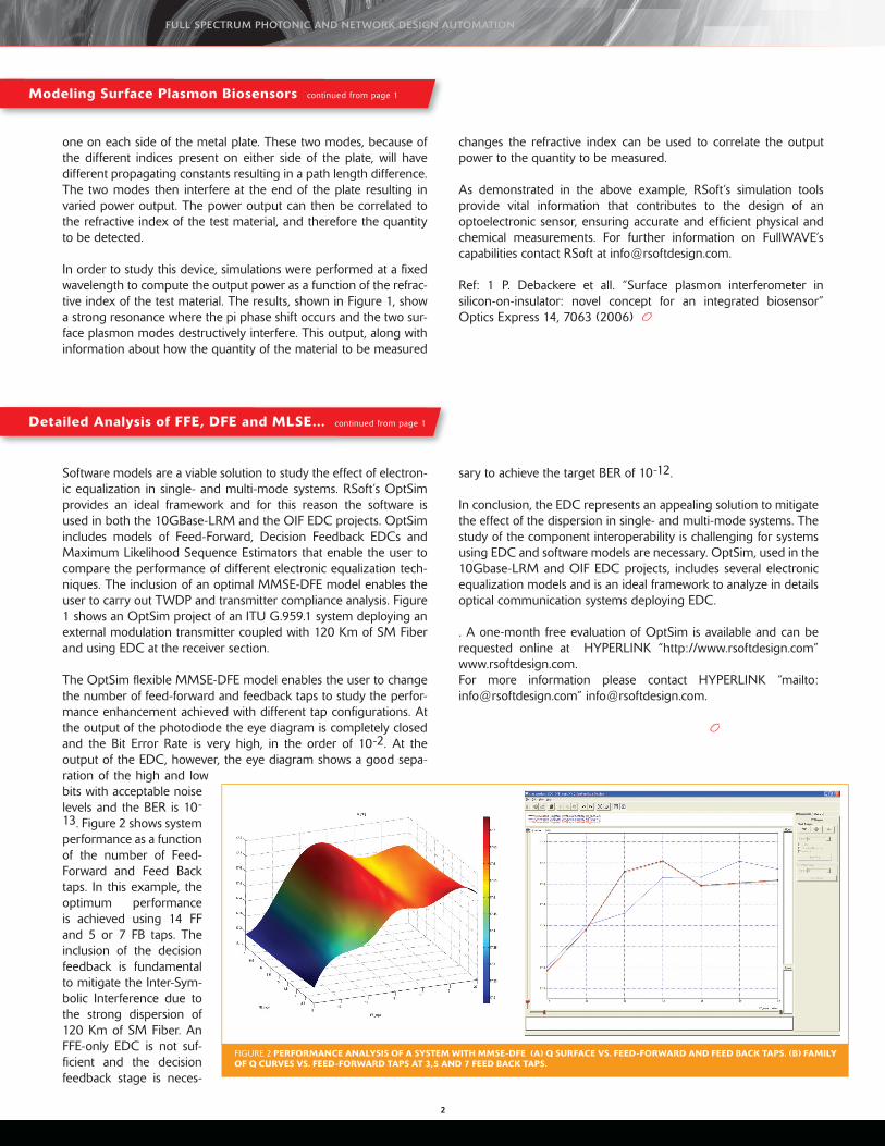
The OptSim fl exible MMSE-DFE model enables the user to change the number of feed-forward and feedback taps to study the perfor-mance enhancement achieved with different tap confi gurations. At the output of the photodiode the eye diagram is completely closed and the Bit Error Rate is very high, in the order of 10-2. At the output of the EDC, however, the eye diagram shows a good sepa-ration of the high and low bits with acceptable noise levels and the BER is 10-13. Figure 2 shows system performance as a function of the number of Feed-Forward and Feed Back taps. In this example, the optimum performance is achieved using 14 FF and 5 or 7 FB taps. The inclusion of the decision feedback is fundamental to mitigate the Inter-Sym-bolic Interference due to the strong dispersion of 120 Km of SM Fiber. An FFE-only EDC is not suf-fi cient and the decision feedback stage is neces-
sary to achieve the target BER of 10-12.
In conclusion, the EDC represents an appealing solution to mitigate the effect of the dispersion in single- and multi-mode systems. The study of the component interoperability is challenging for systems using EDC and software models are necessary. OptSim, used in the 10Gbase-LRM and OIF EDC projects, includes several electronic equalization models and is an ideal framework to analyze in details optical communication systems deploying EDC.
. A one-month free evaluation of OptSim is available and can be requested online at HYPERLINK “http://www.rsoftdesign.com” www.rsoftdesign.com. For more information please contact HYPERLINK “mailto:[email protected]” [email protected].
one on each side of the metal plate. These two modes, because of the different indices present on either side of the plate, will have different propagating constants resulting in a path length difference. The two modes then interfere at the end of the plate resulting in varied power output. The power output can then be correlated to the refractive index of the test material, and therefore the quantity to be detected.
In order to study this device, simulations were performed at a fi xed wavelength to compute the output power as a function of the refrac-tive index of the test material. The results, shown in Figure 1, show a strong resonance where the pi phase shift occurs and the two sur-face plasmon modes destructively interfere. This output, along with information about how the quantity of the material to be measured
FIGURE 2 PERFORMANCE ANALYSIS OF A SYSTEM WITH MMSE-DFE (A) Q SURFACE VS. FEED-FORWARD AND FEED BACK TAPS. (B) FAMILY OF Q CURVES VS. FEED-FORWARD TAPS AT 3,5 AND 7 FEED BACK TAPS.
changes the refractive index can be used to correlate the output power to the quantity to be measured.
As demonstrated in the above example, RSoft’s simulation tools provide vital information that contributes to the design of an optoelectronic sensor, ensuring accurate and effi cient physical and chemical measurements. For further information on FullWAVE’s capabilities contact RSoft at [email protected].
Ref: 1 P. Debackere et all. “Surface plasmon interferometer in silicon-on-insulator: novel concept for an integrated biosensor” Optics Express 14, 7063 (2006)
Modeling Surface Plasmon Biosensors continued from page 1
Detailed Analysis of FFE, DFE and MLSE... continued from page 1
FULL SPECTRUM PHOTONIC AND NETWORK DESIGN AUTOMATION

A.V.: For us, there is a constant search for cost-effective technologies. The objective is to develop new technology, which can add both capabilities and features to the network, but at the same time reduce network capital and operational expenditures.
RSoft: How has OptSim helped meet with these challenges?
A.V.: OptSim is comprehensive simulation tool which can reli-ably model DWDM / CWDM networks, all-optical networks, metro systems, FTTx/PON systems or OTDM / OCDMA systems. It is valuable in supporting selection of technologies for metro WDM and access networks, linking design optimization and supporting novel modulation formats.
RSoft: Why did you decide to work with RSoft Design Group for design and simulation software?
A.V.: We have thoroughly analyzed all available tools, particularly ones that support a wide range of link optimization applications including power budget, gain balancing and amplifi er positioning, transmission impairments, power transients, all-optical gain control design and edge design / validation. RSoft appealed to us. First-time users were able to quickly learn it. It had a friendly user interface and extensive library of predefi ned components. We also got the impression that RSoft was not only interested in selling OptSim to us, but also to understand our needs and to be a supporting partner in our on-going research.
RSoft: How do you see the need and demand for photonic modeling software in the next generation applications?
A.V.: Time to market is more important than ever. Therefore, S/W tools will continue to play a keyrole in design optimization and overall time reduction. When discussing modeling software role in research and development, I am sure S/W tools will continue to help us in creation of innovative solutions for next generation networks and “exploration of unknown”.
RSoft: Thank you for your time, Dr. Vukovic, and we wish you good luck in your research!
3
RSoft: Dr. Vukovic, please tell us a little about Communications Research Centre Canada (CRC).
A.V.: Based in Ottawa, the CRC is the federal government’s primary laboratory for research and development (R&D) in advanced communications, including wireless technologies, broad-band networks, satellite systems, broadcasting and photonics. CRC is recognized for its technological breakthroughs, such as invention of several types of fi bre Bragg grating components, the licensing of patents and sharing technical expertise with companies worldwide. CRC has a strong tradition to inspire and value innovation.
RSoft: Dr. Vukovic, could you tell us about your research at the CRC?
A.V.: My role is to provide research leadership on network concepts, architectures and building blocks for next generation network solutions. My research focus is on development, verifi cation and validation of optical communication architectures, control and management solutions for network level solutions. Our research is supported by one of the key facilities of our Optical Networking Laboratory (ONL) - the All Optical Network (AON) Demonstrator. It houses both simulation environments and testbeds for scientists, engineers, M.Sc. and Ph.D. students. Moreover, the AON helped us to attract both academia, national and international industrial partners and technology leaders for collaboration and innovative developments.
RSoft: How does this research help in technology transfer and in the development of the next generation all-optical networks?
A.V.: The key is to understand future market needs and partner with industrial counterparts early in technology development. My recent experience with Bayspec (world supplier of optical perfor-mance monitors) or with DuPont Photonics Technologies (supplier of reconfi gurable optical add / drop multiplexers) are examples of how alliance between our R&D and industry development can lead to highly marketable products.
RSoft: What kind of challenges do you face in your research?
DR. ALEX VUKOVIC
RSoft Interview with Dr. Alex Vukovic, Communications Research Centre Canada (CRC)
Dr. Alex Vukovic is a research scientist with the Communications Research Centre Canada (CRC). With a career that spans over 20 years, he provides research and technology leadership in the areas of optical communications, network architecture and system development. As an internationally recognized authority in his fi eld, Alex is a scientifi c committee chairman, world-wide invited speaker and lecturer, technology adviser, leader of international committees and industry programs and recipient of many prestigious awards, including Nortel and IASTED. At CRC, Alex provides research leadership in the areas of network concepts and building blocks for next-generation communication networks. He is also an Adjunct Professor at the University of Ottawa and IEEE Senior Member.
FULL SPECTRUM PHOTONIC AND NETWORK DESIGN AUTOMATION
OptSim™, the industry-leading and award-winning optical-system simulation tool, has long been used for the design and simulation of fi ber-amplifi er based systems, thanks to its comprehensive models for erbium-doped and erbium-ytterbium co-doped amplifi ers. Design engineers have found OptSim to be an excellent addition to their design fl ow in a wide range of applications, from opti-cally amplifi ed links for metropolitan and transoceanic networks, to master-oscil-lator power amplifi ers. Now, with the introduction of the OptSim-LAD inter-face, these same designers will be able to leverage Liekki’s extensive fi ber-ampli-fi er and fi ber-laser simulation capabilities within the context of OptSim’s compre-hensive system simulation capabilities.
The Liekki Application Designer (LAD) from Finnish specialty fi ber manufacturer Liekki (www.liekki.com) is a powerful simulation platform for the analysis of fi ber-amplifi er and fi ber-laser based sys-tems. Available through RSoft Design Group, LAD includes support for Er- and Yb-doped fi ber, cladding-pumped designs, multimode effects, and transient phenomena. The OptSim-LAD interface allows OptSim schematics to interface with the Liekki Application Designer (LAD), thereby permitting designs developed in LAD to be easily deployed within an OptSim schematic. As a result, OptSim’s already powerful doped-fi ber simu-lation capabilities become signifi cantly enhanced via the inclusion of LAD’s state-of-the art capabilities, particularly those related to Yb-doped fi ber and analysis of fi ber-laser based systems.
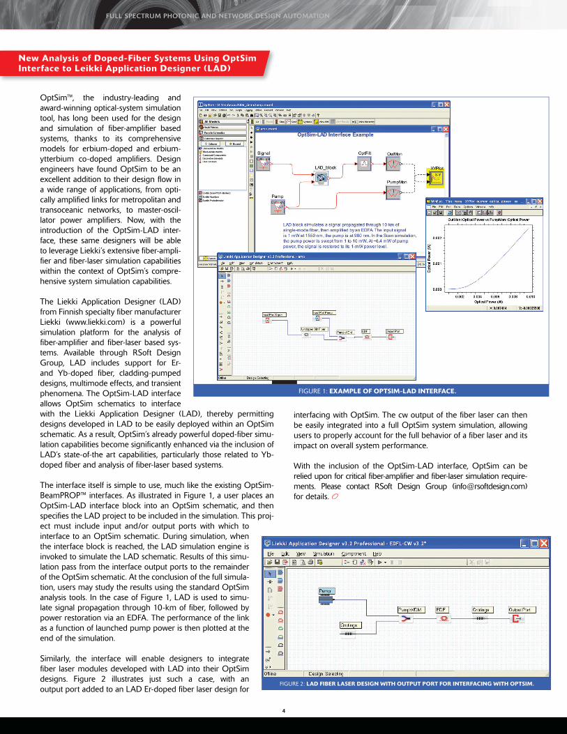
The interface itself is simple to use, much like the existing OptSim-BeamPROP™ interfaces. As illustrated in Figure 1, a user places an OptSim-LAD interface block into an OptSim schematic, and then specifi es the LAD project to be included in the simulation. This proj-ect must include input and/or output ports with which to interface to an OptSim schematic. During simulation, when the interface block is reached, the LAD simulation engine is invoked to simulate the LAD schematic. Results of this simu-lation pass from the interface output ports to the remainder of the OptSim schematic. At the conclusion of the full simula-tion, users may study the results using the standard OptSim analysis tools. In the case of Figure 1, LAD is used to simu-late signal propagation through 10-km of fi ber, followed by power restoration via an EDFA. The performance of the link as a function of launched pump power is then plotted at the end of the simulation.
Similarly, the interface will enable designers to integrate fi ber laser modules developed with LAD into their OptSim designs. Figure 2 illustrates just such a case, with an output port added to an LAD Er-doped fi ber laser design for
interfacing with OptSim. The cw output of the fi ber laser can then be easily integrated into a full OptSim system simulation, allowing users to properly account for the full behavior of a fi ber laser and its impact on overall system performance.
With the inclusion of the OptSim-LAD interface, OptSim can be relied upon for critical fi ber-amplifi er and fi ber-laser simulation require-ments. Please contact RSoft Design Group ([email protected]) for details.
FIGURE 2: LAD FIBER LASER DESIGN WITH OUTPUT PORT FOR INTERFACING WITH OPTSIM.
4
New Analysis of Doped-Fiber Systems Using OptSim Interface to Leikki Application Designer (LAD)
FIGURE 1: EXAMPLE OF OPTSIM-LAD INTERFACE.
FULL SPECTRUM PHOTONIC AND NETWORK DESIGN AUTOMATION
knowing everything! By good fortune, although spontaneous emission is a quantum effect, the SE rate and Green function can be calculated to a high degree of accuracy within classical electro-magnetism and can thus be found using FDTD. In this treatment, the atomic dipole is replaced by a localized current source and the energy and fi eld profi les radiated by the source yield the SE rate and Green function respectively. However, these calculations require very precise arrangement of initial conditions and simulation set-tings, and extensive post-processing of the FDTD results making their calculation tedious and error-prone.
RSoft is therefore releasing the FullWAVE Radiation Dynamics Toolkit, teaming Q-Finder with two new FullWAVE drivers: SERate and FWGreen. An open-systems calculation now consists simply of drawing the structure and choosing the position of the source. SER-ate then drives FullWAVE to calculate emission rates from either the work done on the fi eld by the source, or from the integrated power through a surface enclosing the source. The SE rate can be found both for CW and pulsed sources (the latter producing a full SE spec-trum in a single run). For the same source, FWGreen can obtain both spatial and spectral Green functions or LDOS (currently in 2DTE polarization only). The tools have been extensively tested against analytic and numerical literature results; some examples of impor-tant structures are shown in the fi gures. The FWRDT is fully integrated into the MOST scanning/optimization system, so that emission rates can be characterized as a function of all relevant parameters. For further information on the FullWAVE radiation Dynamics Toolkit, please contact RSoft Design Group at [email protected].
While raw simulation performance in modeling tools is critical, fl exible and convenient, post-processing and driver tools are also vital for effi cient and useful simulation. With this knowledge, RSoft continu-ally works to strengthening its suite of analysis and post-processing tools. The FullWAVE Radiation Dynamics Toolkit is the latest addition to this effort.
Modelling open systems is becoming increasingly important in nanophotonics. By open systems, we mean photonic structures where the escape of light into the environment is a central property of interest, rather than a parasitic effect such as waveguide losses due to surface roughness. The best-known systems are optical nano-cavities in slab photonic crystals, which can exhibit Qs of over a
million. Such structures may form the basis of future high-speed ultra-compact optical switches. Nano-cavities are typically modelled using the fi nite-difference time-domain (FDTD) method but the calculations are time-consuming and tricky to set up. To simplify such calculations, in 2005 RSoft released an intelligent automated driver for the FullWAVE FDTD engine. Q-Finder automatically searches for and refi nes resonant modes and extracts resonant frequencies and Q-factors. Using fast harmonic analysis techniques, high accuracy results can be obtained from relatively short propagations, even for nano-cavities with Q’s in excess of a million. While mode profi les and Q factors are suffi cient for modelling passive devices such as switches, researchers are now moving to study the infl uence of pho-tonic crystals and other nano-structures on active systems, and the role of spontaneous emission is central.
By Fermi’s golden rule, the spontaneous emission (SE) rate depends not just on the atomic properties, but also on the local density of states (LDOS) of electromagnetic modes, and the LDOS is strongly sensitive to the refractive index distribution thus the free-space SE rate can be modifi ed by placing an emitter in a nano-structure. Indeed, the original motivation of Yablanovitch and John in indepen-dently proposing photonic crystals was the goal of manipulating the SE rate, especially for creating ultralow-threshold lasers.
The calculation of SE rates and the LDOS is therefore increasingly important. The LDOS is also closely related to the electromagnetic Green function of the system. This complicated but powerful math-ematical object, which can be thought of as the impulse response of the structure, encapsulates all the linear properties of the system: knowing the Green function is essentially equivalent to
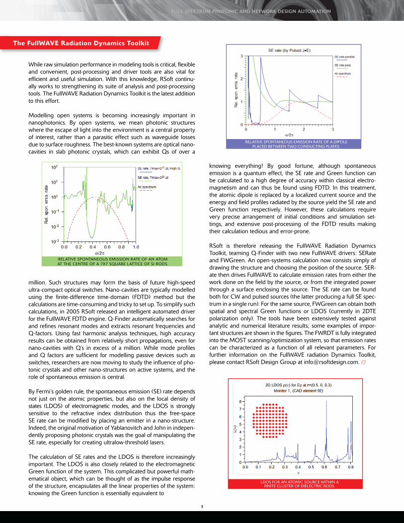
RELATIVE SPONTANEOUS EMISSION RATE OF AN ATOMAT THE CENTRE OF A 7X7 SQUARE LATTICE OF SI RODS.
RELATIVE SPONTANEOUS EMISSION RATE OF A DIPOLEPLACED BETWEEN TWO CONDUCTING PLATES.
LDOS FOR AN ATOMIC SOURCE WITHIN A FINITE CLUSTER OF DIELECTRIC RODS.
5
The FullWAVE Radiation Dynamics Toolkit
FULL SPECTRUM PHOTONIC AND NETWORK DESIGN AUTOMATION
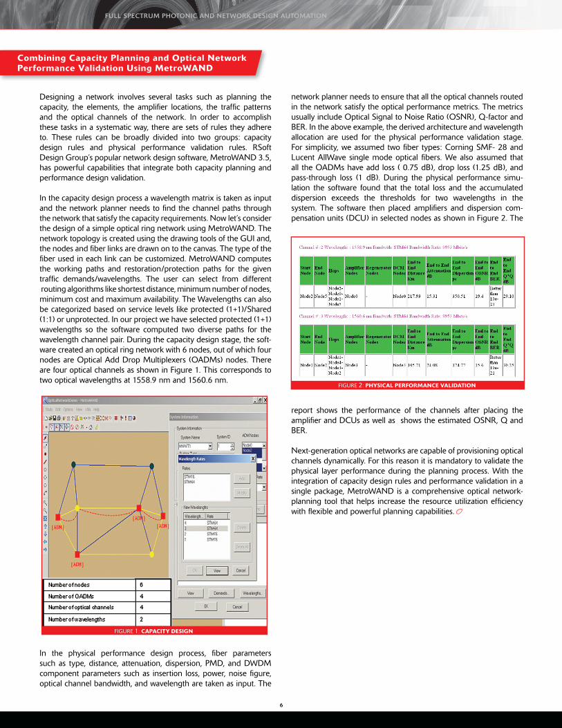
network planner needs to ensure that all the optical channels routed in the network satisfy the optical performance metrics. The metrics usually include Optical Signal to Noise Ratio (OSNR), Q-factor and BER. In the above example, the derived architecture and wavelength allocation are used for the physical performance validation stage. For simplicity, we assumed two fi ber types: Corning SMF- 28 and Lucent AllWave single mode optical fi bers. We also assumed that all the OADMs have add loss ( 0.75 dB), drop loss (1.25 dB), and pass-through loss (1 dB). During the physical performance simu-lation the software found that the total loss and the accumulated dispersion exceeds the thresholds for two wavelengths in the system. The software then placed amplifi ers and dispersion com-pensation units (DCU) in selected nodes as shown in Figure 2. The
report shows the performance of the channels after placing the amplifi er and DCUs as well as shows the estimated OSNR, Q and BER.
Next-generation optical networks are capable of provisioning optical channels dynamically. For this reason it is mandatory to validate the physical layer performance during the planning process. With the integration of capacity design rules and performance validation in a single package, MetroWAND is a comprehensive optical network-planning tool that helps increase the resource utilization effi ciency with fl exible and powerful planning capabilities.
6
Designing a network involves several tasks such as planning the capacity, the elements, the amplifi er locations, the traffi c patterns and the optical channels of the network. In order to accomplish these tasks in a systematic way, there are sets of rules they adhere to. These rules can be broadly divided into two groups: capacity design rules and physical performance validation rules. RSoft Design Group’s popular network design software, MetroWAND 3.5, has powerful capabilities that integrate both capacity planning and performance design validation.
In the capacity design process a wavelength matrix is taken as input and the network planner needs to fi nd the channel paths through the network that satisfy the capacity requirements. Now let’s consider the design of a simple optical ring network using MetroWAND. The network topology is created using the drawing tools of the GUI and, the nodes and fi ber links are drawn on to the canvas. The type of the fi ber used in each link can be customized. MetroWAND computes the working paths and restoration/protection paths for the given traffi c demands/wavelengths. The user can select from different routing algorithms like shortest distance, minimum number of nodes, minimum cost and maximum availability. The Wavelengths can also be categorized based on service levels like protected (1+1)/Shared (1:1) or unprotected. In our project we have selected protected (1+1) wavelengths so the software computed two diverse paths for the wavelength channel pair. During the capacity design stage, the soft-ware created an optical ring network with 6 nodes, out of which four nodes are Optical Add Drop Multiplexers (OADMs) nodes. There are four optical channels as shown in Figure 1. This corresponds to two optical wavelengths at 1558.9 nm and 1560.6 nm.
In the physical performance design process, fi ber parameters such as type, distance, attenuation, dispersion, PMD, and DWDM component parameters such as insertion loss, power, noise fi gure, optical channel bandwidth, and wavelength are taken as input. The
Combining Capacity Planning and Optical Network Performance Validation Using MetroWAND
FULL SPECTRUM PHOTONIC AND NETWORK DESIGN AUTOMATION
FIGURE 1: CAPACITY DESIGN
FIGURE 2: PHYSICAL PERFORMANCE VALIDATION
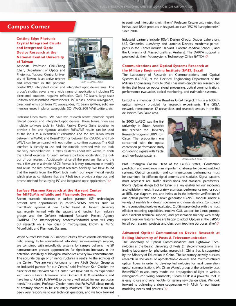
Cutting Edge Photonic Crystal Integrated Cicuits and Integrated Optic Device Research at the National Central University of TaiwanAssociate Professor Chii-Chang Chen, Department of Optics and Photonics, National Central Univer-sity of Taiwan, is an active teacher and researcher in the photonic crystal (PC) integrated circuit and integrated optic device area. The group’s studies cover a very wide range of applications including PC directional couplers, negative refraction, GaN PC lasers, large-scale uniform self-assembled microspheres, PC lenses, hollow waveguides, directional emission from PC waveguides, PC beam splitters, solid im-mersion lenses in planar waveguide, SOI AWG, SOI MMI splitters, etc.
Professor Chen states: “We have two research teams: photonic crystal related devices and integrated optic devices. These teams often use multiple software tools in RSoft’s Passive Device Suite together to provide a fast and rigorous solution: FullWAVE results can be used as the input to a BeamPROP calculation and the simulation results between FullWAVE and BeamPROP or between BandSOLVE and Full-WAVE can be compared with each other to confi rm accuracy. The GUI interface is friendly to use and the tutorials provided with the tools are very comprehensive. It takes students about two weeks to fi nish the tutorial exercises for each software package accelerating the out-put of our research. Additionally, since all the program fi les and the result fi les are in a simple ASCII format, it is very convenient to modify and reuse the fi les providing great research fl exibility. We have found that the results from the RSoft tools match our experimental results which give us confi dence that the RSoft tools provide a rigorous and precise method for studying PC and integrated optic applications.”
Surface Plasmon Research at the Harvard Centerfor MIPS:Microfluidic and Plasmonic Systems.Recent dramatic advances in surface plasmon (SP) technologiespresent new opportunities in MEMS/NEMS devices such as microfl uidic systems. A new Center based at Harvard Universitywas recently formed with the support and funding from industry groups and the Defense Advanced Research Project Agency (DARPA). The interdisciplinary academic/industrial team will carry out research on a new class of microsystems, known as MIPS: Microfl uidic and Plasmonic Systems.
When Surface Plasmon (SP) nanostructures, which enable electromag-netic energy to be concentrated into deep sub-wavelength regions, are combined with microfl uidic systems for sample delivery, the SP nanostructures present opportunities for signifi cant increases in the detection sensitivity of biological molecules at very low concentrations. The accurate design of SP nanostructures is central to the activities of the Center. “We are very fortunate to have RSoft Design Group as an industrial partner for our Center,” said Professor Ken Crozier, the director of the Harvard MIPS Center. “We have had much experience with various Finite Difference Time Domain (FDTD) simulations, and have found RSoft’s FullWAVE to be very well suited for our particular needs,” he added. Professor Crozier noted that FullWAVE allows metals of arbitrary shapes to be accurately modeled. “The RSoft team has been very responsive to our technical questions, and we look forward
to continued interactions with them.” Professor Crozier also noted that he has used RSoft products in his graduate class “ES275 Nanophotonics” since 2004.
Industrial partners include RSoft Design Group, Draper Laboratory, U.S. Genomics, LumArray, and Luminus Devices. Academic partici-pants in the Center include Harvard, Harvard Medical School ), and the University of Massachusetts at Amherst. The DARPA support is provided via their Microsystems Technology Offi ce (MTO).
Communications and Optical Systems Research at the Military Engineering Institute ( IME), BrazilThe Laboratory of Research on Communications and Optical Systems (LaRSO), at the Electrical Engineering Department of the Military Engineering Institute (IME) has multi-disciplinary research ac-tivities that focus on optical signal processing, optical communications performance evaluation, optical monitoring, and estimation systems.
LaRSO is a member of the Brazilian GIGA Project. This is a 600Km optical network provided for research experiments. The GIGA network interconnects 17 universities and research centers in the Rio de Janeiro-São Paulo area.
In 2003 LaRSO was the fi rst university in South America that received the University Research Program (URP) from Cisco. The proposition was concerned with the optical contention performance study considering signals with fractal and non-fractal patterns.
Prof. Rosângela Coelho, Head of the LaRSO states, “Contention prediction and avoidance is an important challenge for packet switched systems. Optical contention and communications performance must be examined for different signal-patterns and statistics. Signal-patterns must represent real traffi c distributions and statistical parameters. RSoft’s OptSim design tool for Linux is a key enabler for our modeling and validation needs. It accurately estimates performance metrics such as BER, eye-diagram, etc. and helps us in the behavior verifi cation of our optical pattern and packet generator (O2PG) module under a variety of real-life link design scenarios and noise statistics. Compared to the competing tools we evaluated, OptSim provided us with the most effi cient modeling capabilities, intuitive GUI, support for Linux, prompt and excellent technical support, and presentation-friendly web-ready report creation features. We are happy to adopt OptSim at the LaRSO for all our research projects and classroom teaching purposes alike.”
Advanced Optical Communication Device Research at Beijing University of Posts & TelecommunicationThe laboratory of Optical Communications and Lightwave Tech-nologies at the Beijing University of Posts & Telecommunications, is a leading laboratory for photonics research in China that is supported by the Ministry of Education in China. The laboratory actively pursues research in the areas of optoelectronic devices and microstructured optical fi bers in order to develop technologies for next generation optical communications. Mr. Zinan Wang’s group at the university uses BeamPROP to accurately model the propagation of light in various waveguides. Mr. Wang comments, “BeamPROP is a powerful tool. It is easy to use and very fl exible for testing new design ideas. We look forward to bolstering a close cooperation with RSoft for our future modeling needs and projects.”
7
CHII-CHANG CHEN
ROSÃNGELA COELHO
Campus Corner
FULL SPECTRUM PHOTONIC AND NETWORK DESIGN AUTOMATION

8
Visit us at the following tradeshows – 2007 first half SHOW LOCATION DATE BOOTH # SHOW LOCATION DATE BOOTH #
FOE Tokyo, Japan 24-26 Jan. 4-37
Photonics West 2007 San Jose, CA 23-25 Jan. 533
Nanotech Tokyo, Japan 21-23 Feb. E-03
Advanced Lithography 2007 San Jose, CA 27-28 Feb. 718
OFC/NFOEC 2007 Anaheim, CA 27-29 Mar. 2729
Laser Expo 2007 Yokohama, Kanagawa Japan 25-27 April
CLEO 2007 Baltimore, MD 8-10 May 1829
Photonics North/Education Ottawa, Ontario Canada 3-7 June
(formally Microlithography)
& Training In Optics & Photonics
NEW YORK corporate headquarters400 Executive Boulevard, Ste. 100Ossining, NY 10562 USA
PHONE: 914.923.2164EMAIL: [email protected]: www.rsoftdesign.com
JAPAN offi ceRsoft Design Group JapanKKMatsura Building 2F, 1-9-6 ShibaMinato-ku, Tokyo, 105-0014 Japan
PHONE: + 81.3.5484.6670EMAIL: [email protected]
UK offi ceRSoft Design UK, Ltd.11 Swinborne DriveSpringwood Industrial EstateBaintree, Essex CM7 2YP
PHONE: 44 (0) 1376 528556EMAIL: [email protected]
STTR Phase II to Fund Engineering Solutions for Aerospace ApplicationsRSoft Design Group and the University of California, Santa Barbara, were recently awarded a Small Business Technology Transfer (STTR) Phase I I by the US Navy. Funding for the award is being used to develop advanced WDM fiber optic network architecture analysis, modeling, optimization and demonstration for aerospace platforms. The contract, which runs through 2009, totals $1.6 million.
RSoft joins Two Consortiums-OIF and IOE PCB ManufacturingRSoft Design Group became the newest member to the prestigious Optical Internetworking Forum (OIF). RSoft’s role in the forum will be to provide modeling tools and simulation models to support the consortium project on EDC for 10 Gb/s 1550 nm Links.
RSoft Design UK has also joined the Integrated Optical and Elec-tronic Interconnect PCB Manufacturing consortium, which is one of the Flagship projects under the Innovative electronics Manufactur-ing Research Centre (IeMRC). The consortium is using RSoft’s soft-ware for the design and modeling of the optical interconnect, and RSoft will also develop additional capabilities to address the need for the new interconnect technologies being developed within this project.
For further RSoft partnerships, associations and memberships, please visit RSoft website www.rsoftdesign.com.
RSoft Sponsors APOC Best Student Paper AwardsFor the third straight year, RSoft proudly sponsored the Best Student Paper Awards at APOC on September 3-7, 2006 in Gwangju, South Korea. The Best Student Awards were created to encourage partici-pation and to motivate active involvement of young engineers and scientists in APOC. The winners are as follows:
1) “Silica nanotaper optics with Bragg-fi ber structure” [L. Ma, Tohoku Univ. (Japan)]
2) “Towards effi cient unidirectional photonic crystal light emitters” [S. Kim, KAIST (Korea)]
3) “Performance of the OSNR monitoring technique based on improved polarization-nulling method” [H. Y. Choi, KAIST (Korea)]
4) “An improved fairness algorithm for resilient packet ring network” [W. Tang, Nanyang Tech. Univ. (Singapore)]
BRIEFS
Related Documents