Welcome message from author
This document is posted to help you gain knowledge. Please leave a comment to let me know what you think about it! Share it to your friends and learn new things together.
Transcript
Single-Grain Silicon TFTs on aPlastic Substrate by Doctor Blade
Coating of Cyclopentasilane
Miki Trifunovic
Master of Science Thesis
in
Electrical Engineering, Microelectronics
Thesis Committee Members:Prof. R. Ishihara (Supervisor)
Prof. C.I.M. BeenakkerProf. A. Bossche
Ir. J. Zhang
Responsible Professor: Prof. P.M. Sarro
Faculty of Electrical Engineering,Mathematics and Computer Science,
Delft University of Technology,
The Netherlands
June 5, 2012

i
Preface
This thesis is written as a partial satisfaction for the requirements of theMaster
of Science Degree in Microelectronics at the faculty of Electrical Engineering,Mathematics and Computer Science, at Delft University of Technology.
The work is essentially combining the inexpensiveness of solution processingand the quality of crystalline silicon transistors. The contribution of this workwill lead to the fabrication of quality transistors on �exible substrates using thenew liquid silicon material that has only recently been discovered for electricalapplications.
In this process, di�culties have arisen in some aspects and it was the helpof many people that have brought this thesis to a success. I would therefore liketo thank the following people:
� Prof. P.M. Sarro as the responsible professor for enabling my thesis work.
� Prof. R. Ishihara for his daily supervision and guidance during the courseof my project. Also, for the many discussions during meetings and helpingme publish some of my work.
� Prof. R. van Swaaij and Prof. A. Bossche for their support as MasterCoordinators.
� Prof. C.I.M. Beenakker and Prof. A. Bossche for their participation inthe thesis defense committee.
� Jin Zhang and Michiel van der Zwan for their processing support anddiscussions.
� To all members of the TFT group that have helped me enjoy my timein this research group including: Sten Vollebregt, Aslihan Arslan, DanielTajari Mofrad, Pengfei Sun.
� To my peers, fellow master students, that have experienced the same cur-riculum.
� My family for supporting me always.
� Finally, I would like to thank anyone that have helped me in any wayduring my Masters, including DIMES technicians, teachers, bachelor stu-dents, etc.
Miki Trifunovic05/28/12

ii
Abstract
Liquid silicon is found as the material combining both the advantages of highquality silicon devices and the low cost solution processing method. Single-Grain Thin-Film Transistors can be produced by Excimer Laser Annealing ofthe resulting �lm and grain location control by the µ-Czochralski process. Otherworks have used spin-coating and inkjet printing for liquid silicon based devices,however both processes are not roll-to-roll process compatible. In addition ahigh thermal annealing step (650°C), incompatible to plastics, is required forthe reduction of hydrogen content before laser crystallization.
In this work, both issues are focused on. A precursor of the gravure printingprocess, doctor blade coating, is used to imitate a roll-to-roll compatible solutionprocess and is optimized to produce uniform �lms of liquid silicon. ExcimerLaser Annealing is used as a low temperature pre-annealing method to decreasethe hydrogen content for crystallization.
Pure cyclopentasilane has been used as the liquid silicon material. Silicondioxide surface modi�cation by 0.55%HF dip results in a better wetting of theliquid together with an elevated temperature of 70°C. Higher temperatures leadto even better wetting properties, but more liquid silicon will evaporate.
After UV polymerization of the CPS for 20 minutes and thermal annealingat 350°C for 1 hour, an a-Si layer has been formed. Excimer Laser pre-annealingof many low energy shots removes hydrogen without signi�cant deterioration ofthe �lm. A maximum grain size of 5µm has been produced by using a longpulse con�gured laser recipe that decreases the number of shots linearly whileincreasing the laser energy density by 50mJ/cm².
SG-TFTs on polyimide have been manufactured at the maximum processingtemperature of 350°C. The mobility of the NMOS was ..., and the mobility ofthe PMOS was .... [to be obtained by mid June].
Finally, a next step towards gravure printing has been taken, by advancingthe doctor blade coating method to the removal of the excess layer while keepingthe cavity patterns in the �lm �lled. Blade elasticity is a dominant factor inmanual blading. An elastic blade can remove more excess than a rigid bladesince the �exibility allows adjustment on the surface, but will also remove theliquid from inside the patterns. A combination of a rigid blade and the carefulexcess removal by the elastic blade gives the best results.
This work shows the potential of liquid silicon, and brings us closer to themass production on �exible substrates using this new material.
iii

iv
Contents
Preface i
Abstract iii
List of Figures vii
List of Tables xii
Abbreviations xv
1 Introduction 1
2 Solution TFT process and liquid Silicon 52.1 Solution Processing . . . . . . . . . . . . . . . . . . . . . . . . . . 62.2 Semiconductors . . . . . . . . . . . . . . . . . . . . . . . . . . . . 10
2.2.1 Organic Semiconductors . . . . . . . . . . . . . . . . . . . 112.2.2 Solid Silicon . . . . . . . . . . . . . . . . . . . . . . . . . . 162.2.3 Liquid Silicon . . . . . . . . . . . . . . . . . . . . . . . . . 19
3 Doctor Blade Coating of Liquid Silicon 253.1 Theory . . . . . . . . . . . . . . . . . . . . . . . . . . . . . . . . . 26
3.1.1 Doctor blade coating . . . . . . . . . . . . . . . . . . . . . 263.1.2 Surface Free Energy . . . . . . . . . . . . . . . . . . . . . 273.1.3 a-Si �lm formation from liquid silicon . . . . . . . . . . . 30
3.2 Experimental . . . . . . . . . . . . . . . . . . . . . . . . . . . . . 323.2.1 Equipment . . . . . . . . . . . . . . . . . . . . . . . . . . 323.2.2 Working procedure . . . . . . . . . . . . . . . . . . . . . . 373.2.3 Boundary Conditions . . . . . . . . . . . . . . . . . . . . 38
3.3 Characterization Experiments . . . . . . . . . . . . . . . . . . . . 383.3.1 Film breaking . . . . . . . . . . . . . . . . . . . . . . . . . 403.3.2 Liquid Silicon . . . . . . . . . . . . . . . . . . . . . . . . . 413.3.3 Surface Free Energy . . . . . . . . . . . . . . . . . . . . . 423.3.4 Blade types . . . . . . . . . . . . . . . . . . . . . . . . . . 453.3.5 Post-deposition variations . . . . . . . . . . . . . . . . . . 46
3.4 Film spreading recipe . . . . . . . . . . . . . . . . . . . . . . . . 46
v
vi CONTENTS
3.4.1 Spin-Coating . . . . . . . . . . . . . . . . . . . . . . . . . 483.4.2 Blading . . . . . . . . . . . . . . . . . . . . . . . . . . . . 493.4.3 Combination . . . . . . . . . . . . . . . . . . . . . . . . . 52
3.5 Conclusions and Recommendations . . . . . . . . . . . . . . . . . 52
4 Low Temperature Annealing and Crystallization 554.1 Pre-anneal e�ects on Hydrogen concentration . . . . . . . . . . . 564.2 Experimental . . . . . . . . . . . . . . . . . . . . . . . . . . . . . 58
4.2.1 Excimer Laser setup . . . . . . . . . . . . . . . . . . . . . 584.2.2 Approach . . . . . . . . . . . . . . . . . . . . . . . . . . . 594.2.3 Results . . . . . . . . . . . . . . . . . . . . . . . . . . . . 60
4.3 Conclusions and recommendations . . . . . . . . . . . . . . . . . 64
5 l-Si SG-TFT on Polyimide 655.1 Transistor structure . . . . . . . . . . . . . . . . . . . . . . . . . 65
5.1.1 Fabrication procedure . . . . . . . . . . . . . . . . . . . . 665.1.2 Polyimide . . . . . . . . . . . . . . . . . . . . . . . . . . . 68
5.2 TFT characteristics . . . . . . . . . . . . . . . . . . . . . . . . . . 685.3 Results . . . . . . . . . . . . . . . . . . . . . . . . . . . . . . . . . 705.4 Conclusions . . . . . . . . . . . . . . . . . . . . . . . . . . . . . . 70
6 Excess Liquid Silicon Removal for Gravure Printing 716.1 Experimental Results . . . . . . . . . . . . . . . . . . . . . . . . . 71
6.1.1 Excess removal . . . . . . . . . . . . . . . . . . . . . . . . 726.1.2 Pattern deformation . . . . . . . . . . . . . . . . . . . . . 736.1.3 Time Dependency . . . . . . . . . . . . . . . . . . . . . . 756.1.4 Liquid silicon . . . . . . . . . . . . . . . . . . . . . . . . . 766.1.5 Surface modi�cation . . . . . . . . . . . . . . . . . . . . . 78
6.2 Conclusions and Recommendations . . . . . . . . . . . . . . . . . 79
7 Conclusions and Recommendations 837.1 Doctor Blade coating Liquid Silicon . . . . . . . . . . . . . . . . 837.2 Low Temperature Annealing . . . . . . . . . . . . . . . . . . . . . 847.3 Liquid silicon devices . . . . . . . . . . . . . . . . . . . . . . . . . 857.4 Excess removal using doctor blade . . . . . . . . . . . . . . . . . 857.5 Recommendations . . . . . . . . . . . . . . . . . . . . . . . . . . 86
A Market Analysis 89A.1 Radical innovation . . . . . . . . . . . . . . . . . . . . . . . . . . 89A.2 Associated costs . . . . . . . . . . . . . . . . . . . . . . . . . . . 90A.3 Applications . . . . . . . . . . . . . . . . . . . . . . . . . . . . . . 91
B Printer types for electronics fabrication 93B.1 Impact Printers . . . . . . . . . . . . . . . . . . . . . . . . . . . . 93
B.1.1 Gravure Printing . . . . . . . . . . . . . . . . . . . . . . . 94B.1.2 Other impact printers . . . . . . . . . . . . . . . . . . . . 97
B.2 Non-Impact printers . . . . . . . . . . . . . . . . . . . . . . . . . 100
CONTENTS vii
B.2.1 Inkjet . . . . . . . . . . . . . . . . . . . . . . . . . . . . . 101B.2.2 Electrophotography . . . . . . . . . . . . . . . . . . . . . 103
B.3 Conclusion . . . . . . . . . . . . . . . . . . . . . . . . . . . . . . 104
C Thin-Film Transistor 107C.1 OTFT Characteristics . . . . . . . . . . . . . . . . . . . . . . . . 107C.2 Transistor Con�guration . . . . . . . . . . . . . . . . . . . . . . . 108
D SFE Results 111
E Excimer Laser Crystallization 113E.1 Crystallization process . . . . . . . . . . . . . . . . . . . . . . . . 113E.2 Crystallization problems . . . . . . . . . . . . . . . . . . . . . . . 114
Bibliography 117
Abbreviations 123

viii CONTENTS
List of Figures
1.1 Flexible display (a) and �exible solar panel (b) . . . . . . . . . . 11.2 Super E-paper . . . . . . . . . . . . . . . . . . . . . . . . . . . . 21.3 Flowchart of the SG-TFT fabrication process from the liquid silicon 4
2.1 Overview of di�erent types of impact and non-impact printers [13] 92.2 Schematic of the di�erence between doctor blade coating and
gravure printing. . . . . . . . . . . . . . . . . . . . . . . . . . . . 102.3 Bonding representation of two carbon molecules with σv-bonds
and π-bonds (a), and its band representation (b).[21] . . . . . . . 132.4 Bonding representation of benzene with σv-bonds and π-bonds (a),
and its band representation (b).[21] . . . . . . . . . . . . . . . . . 142.5 Bonding representation of an arbitrary polymer (a), and its band
representation (b).[21] . . . . . . . . . . . . . . . . . . . . . . . . 152.6 Performance of the p-type organic material pentacene (a), and n-
type F16CuPc (b), both fabricated in a CMOS design on a plasticsubstrate. [24] . . . . . . . . . . . . . . . . . . . . . . . . . . . . . 16
2.7 SG-TFT fabrication process using the μ-Czochralski method. Theplastic substrate in (a), followed by deposition of a SiO2 layer (b).A grain �lter is etched in this layer (c). Subsequent a-Si depo-sition �lls the cavity (d). Excimer laser melts the top layer andleaves a seed of a-Si at the bottom of the cavity which grows tobecome a crystalline island on the surface (e). Within this islanda TFT is created (f). [28] . . . . . . . . . . . . . . . . . . . . . . 18
2.8 CPS synthesis . . . . . . . . . . . . . . . . . . . . . . . . . . . . . 212.9 Three main structures of CPS (a). Infrared spectra displaying
vibrational frequencies associated to the CPS, red lines indicatingthe twist and envelope structures. The green dotted lines indicateintermediate structures after the formation of the Si-H-Si bridgebond (b). [4] . . . . . . . . . . . . . . . . . . . . . . . . . . . . . 22
2.10 TFTs constructed with liquid silicon using inkjet printing, spin-coating, and chemical vapor deposition. Transfer characteristicsin (a), output characteristics in (b), image of the TFT using SEM(c), and the schematic of the TFT structure (d). [1] . . . . . . . 23
ix
x LIST OF FIGURES
2.11 Single-Grain TFTs constructed with liquid silicon using spin-coating. NMOS and PMOS transfer characteristics in (a) and(b) respectively, SEM image of the SG-TFT in (c), and the SG-TFT schematic in (d). [2] . . . . . . . . . . . . . . . . . . . . . . 23
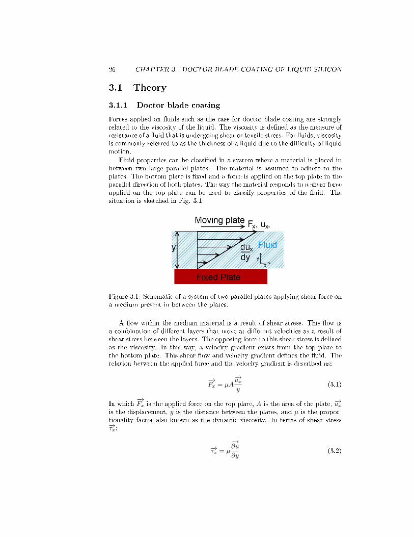
3.1 Schematic of a system of two parallel plates applying shear forceon a medium present in between the plates. . . . . . . . . . . . . 26
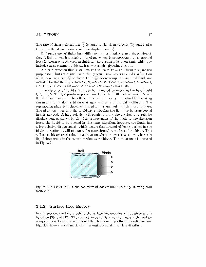
3.2 Schematic of the top view of doctor blade coating, showing trailformation. . . . . . . . . . . . . . . . . . . . . . . . . . . . . . . . 27
3.3 Surface energies de�nition schematic . . . . . . . . . . . . . . . . 283.4 Si 2p XPS spectra of a-Si �lm for di�erent UV exposure times
of CPS: a. 3, b. 5, and c. 15 minutes (a) [7]. Gel permeationchromatogram of liquid silicon (b). CPS in toluene in a. andUV-irradiated CPS in toluene in b. [1] The broad peak indicatesthe polysilanes of various molecular weights. . . . . . . . . . . . . 32
3.5 MBRAUN Glovebox [39] . . . . . . . . . . . . . . . . . . . . . . . 333.6 UV AHAND 250GS wavelength over wavelength in (a) and in-
tensity over distance in (b).[39] . . . . . . . . . . . . . . . . . . . 343.7 DekTak graphs with pro�les from various surfaces on which liquid
silicon has been transformed into amorphous silicon. The areawhere the amorphous silicon has been removed is where the layerwas broken. . . . . . . . . . . . . . . . . . . . . . . . . . . . . . . 41
3.8 Contact angle graphs, di�erent surface modi�cations on di�erenttypes of oxide, using pure CPS. . . . . . . . . . . . . . . . . . . . 43
3.9 Surface Free energy �gures using 3.15. Extracting theγS (a), andthe γL (b) by sweeping the respective parameters. . . . . . . . . 44
3.10 Surface energies calculated using Neumann's method . . . . . . . 453.11 Blade type results of silicon only (a), silicon and rubber (b), and
rubber with additional applied force (c) . . . . . . . . . . . . . . 463.12 RAMAN spectroscopy result of a thin a-Si �lm (a) and a thick
a-Si �lm (b), both annealed at 350°C for 1 hour. . . . . . . . . . 473.13 FTIR graph of absorption peak integrals at 640cm−1, for three
UV exposure conditions . . . . . . . . . . . . . . . . . . . . . . . 473.14 Spin-coating experiment results. Double coating of CPS and UV
pre-exposed CPS (a), 20 minutes UV pre-exposed CPS only (b),20 minutes UV pre-exposed CPS only with 0.2μm �lter (c). . . . 48
3.15 Pro�les of a-Si layers deposited on the wafer with 1 by 1 mm 250nm deep square patterns. Fully covered layer in (a), and bulgedsquare coverage in (b). . . . . . . . . . . . . . . . . . . . . . . . . 50
3.16 SEM images of liquid silicon covering a pattern instead of �llingit (a), and the �lling of the grain �lter (b) . . . . . . . . . . . . . 51
3.17 Some blading experiment results for the formation of a �lm. Sil-icon blade spreading and rubber scraping with partly hard rub-ber scraping (a), silicon blade spreading with partly mild rubberscraping (b), edge formation and cracking in 500nm square waferwith a small part showing a uniform layer (c). . . . . . . . . . . . 52
LIST OF FIGURES xi
3.18 Results of the combined coating methods blading and subsequentspin-coating at 500RPM (a), 1000RPM (b), 1000RPM on a poly-imide substrate (c). . . . . . . . . . . . . . . . . . . . . . . . . . . 53
4.1 Maximum shootable energy before which the silicon �lm startscracking as a function of the number of Excimer Laser shots.Pretreatment at 300°C (a) and untreated a-Si �lm (b) [49] . . . . 57
4.2 Demonstration of laser pre-annealing bene�ts. Single shot with-out pre-annealing at 500 mJ/cm² (a), 90 shots at 100 mJ/cm²(b), and a pre-annealed sample with maximum laser energy den-sity of 550 mJ/cm² (c) . . . . . . . . . . . . . . . . . . . . . . . . 57
4.3 Exitech M8000V Excimer Laser system schematic [48] . . . . . . 584.4 Visual representation of the recipe types ramped single shot (a),
linear decrease (b), and exponential decrease (c). . . . . . . . . . 594.5 Laser energies from which the �lm starts to show signs of defects
for every laser recipe type(a). Maximum grain size obtained forthe particular recipe type (b). . . . . . . . . . . . . . . . . . . . . 60
4.6 Excimer laser irradiation results short pulse. Single shot (a)against an exponentially decreased number of shot with increas-ing shot densities of 50 mJ/cm² starting at 150 mJ/cm²(b), start-ing at 200 mJ/cm² (c) and at 250 mJ/cm² (d), with a maximumof 500 mJ/cm² for all cases. . . . . . . . . . . . . . . . . . . . . . 62
4.7 Excimer laser irradiation results long pulse. Linear recipe forwhich the biggest grain sizes have been obtained. 4 and 3 micronpitch image (a), and 3 and 2 micron pitch image (b). . . . . . . . 63
4.8 ERD setup schematic[50] . . . . . . . . . . . . . . . . . . . . . . 634.9 RBS setup schematic[50] . . . . . . . . . . . . . . . . . . . . . . . 64
5.1 SG-TFT fabrication process both with (b steps) and without (asteps) an additional polyimide layer. The polyimide layer hasbeen omitted in this schematic after step 1, however step 1 showsits designated position. . . . . . . . . . . . . . . . . . . . . . . . . 66
5.2 Chemical structure of the Polyamic Acid Durimide (a)[32], andthe Imide monomer . . . . . . . . . . . . . . . . . . . . . . . . . . 68
6.1 Films within patterns getting pulled out by the excess layer con-nected to the �lm inside. Optical microscope view (a), a SEMimage of such a pattern (b), and a SEM image of a bigger pattern(c). . . . . . . . . . . . . . . . . . . . . . . . . . . . . . . . . . . . 73
6.2 Bubble bursting of CPS due to excess CPS on top of a �lled pattern. 736.3 Di�erent ways of pattern �lling. . . . . . . . . . . . . . . . . . . . 746.4 Deformation of supposedly dewetted patterns. . . . . . . . . . . . 746.5 RAMAN spectroscopy measurements of �lled and dewetted pat-
terns. . . . . . . . . . . . . . . . . . . . . . . . . . . . . . . . . . 75
xii LIST OF FIGURES
6.6 Dewetting against deformation schematic when properly �lled (a)and when poorly �lled (b). The proof of a thin layer within the250nm deep pattern (c). . . . . . . . . . . . . . . . . . . . . . . . 76
6.7 E�ect of pattern depth on liquid silicon . . . . . . . . . . . . . . 766.8 Results of time dependency experiments, good adhesion in the
initial thick layer area (a), area outside this initial layer after (b),and the transition from initial layer to the bladed area outside (c). 77
6.9 Various UV exposure times. No UV exposure before blading (a).10 minute UV exposure before blading on top of a wafer (b), butmany intermediate exposures during blading (c). . . . . . . . . . 77
6.10 Blading results on plasma oxidized surface. . . . . . . . . . . . . 786.11 Di�erence in blading of the excess on regular surface and plasma
oxidized surface. . . . . . . . . . . . . . . . . . . . . . . . . . . . 796.12 Blading results on HF dipped surface. . . . . . . . . . . . . . . . 796.13 Recommended setup mainly based on high adhesion within the
pattern, and poor adhesion outside, with a poor adhesive blade. . 81
B.1 The master plates for four main impact printers [13] . . . . . . . 94B.2 Gravure printing schematic [13] . . . . . . . . . . . . . . . . . . . 95B.3 Letterpress schematic diagram [13] . . . . . . . . . . . . . . . . . 98B.4 Lithography/O�set printing schematic diagram [13] . . . . . . . . 99B.5 Screen printing schematic [13] . . . . . . . . . . . . . . . . . . . . 100B.6 Inkjet printing schematic [13] . . . . . . . . . . . . . . . . . . . . 102B.7 Electrophotography schematic [13] . . . . . . . . . . . . . . . . . 103
C.1 Various TFT structures [12] . . . . . . . . . . . . . . . . . . . . . 109
List of Tables
2.1 Comparing conventional and solution processing . . . . . . . . . 72.2 List solution processing types . . . . . . . . . . . . . . . . . . . . 82.3 Printing advantages in electronics . . . . . . . . . . . . . . . . . . 92.4 Types of materials used as inks for printing dielectrics and their
properties . . . . . . . . . . . . . . . . . . . . . . . . . . . . . . . 102.5 Types of materials used as inks for printing conductors and their
properties . . . . . . . . . . . . . . . . . . . . . . . . . . . . . . . 112.6 General information Cyclopentasilane . . . . . . . . . . . . . . . 20
3.1 Processing varieties from liquid silicon to amorphous silicon �lm 39
B.1 Typical values for gravure printing processes [13] . . . . . . . . . 97B.2 Comparative analysis of the various printer types . . . . . . . . . 105
xiii

xiv LIST OF TABLES
Abbreviations
AMOLED Active-Matrix Organic Lighte-Emitting-Diodea-Si amorphous silicona-Si:H hydrogenated amorphous siliconBJT Bipolar Junction TransistorCMOS Complementary Metal-Oxide-SemiconductorCPS Cyclopentasilanec-Si single-crystalline siliconERD Elastic Recoil DetectionFTIR Fourier Transform Infrared SpectroscopyGF Grain FilterGPC Gel Permeation ChromatographyHF Hydro�uoric acidHOMO Highest Occupied Molecular OrbitalIC Integrated CircuitICP Inductively Coupled PlasmaIPA IsopropanolLCD Liquid-Crystal displayLUMO Lowest Unoccupied Molecular OrbitalMOSFET Metal-Oxide-Semiconductor Field-E�ect TransistorNIP Non-impact PrintersOLED Organic Light-Emitting-DiodeOPRA Overlay Printing Registration AccuracyOTFT Organic Thin-Film TransistorPCB Printed Circuit BoardPECVD Plasma-Enhanced Chemical Vapor DepositionRBS Rutherford Backscattering SpectroscopyRFID Radio-frequency Identi�cationRIE Reactive-Ion EtchingRPM Rounds per minuteSFE Surface Free EnergySG-TFT Single-Grain Thin-Film TransistorTEOS Tetraethylorthosilicate (Si{OCH2CH3}4)TFT Thin-Film TransistorUV Ultraviolet lightXPS X-ray Photoelectron Spectroscopy
xv

xvi LIST OF TABLES
Chapter 1
Introduction
As electronic chips make up an increasing part of our daily lives, there is abig desire for the optimization in production methods. One interpretation ofMoore's Law de�nes a period of 18 months in which chip performance doubles,and as the physical limitations in chips are being approached, other ways ofimproving chip fabrication is being investigated.
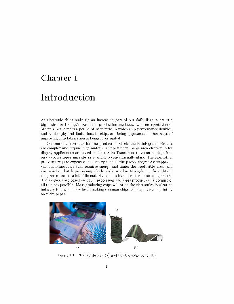
Conventional methods for the production of electronic integrated circuitsare complex and require high material compatibility. Large area electronics fordisplay applications are based on Thin-Film Transistors that can be depositedon top of a supporting substrate, which is conventionally glass. The fabricationprocesses require expensive machinery such as the photolithography stepper, avacuum atmosphere that requires energy and limits the producible area, andare based on batch processing which leads to a low throughput. In addition,the process wastes a lot of its materials due to its subtractive processing nature.The methods are based on batch processing and mass production is because ofall this not possible. Mass producing chips will bring the electronics fabricationindustry to a whole new level, making common chips as inexpensive as printingon plain paper.
(a) (b)
Figure 1.1: Flexible display (a) and �exible solar panel (b)
1
2 CHAPTER 1. INTRODUCTION
With the help of low-temperature processing, plastic substrates may be usedfor the production of �exible, light-weight, inexpensive displays as well as solarpanels, as shown in Fig. 1.1. In addition, conventional vacuum processinglimits the maximum obtainable sizes of these displays due to the limiting sizeof the vacuum chamber. Therefore, a process which does not require a vacuumambient will not only lead to large scale manufacturing of displays, but allowsroll-to-roll production.
Solution processing is an alternative way of processing electronics which hasa potential to be used for mass production ends. Although still at its infancy,a lot of research is focusing on �nding the right types of materials that canbe incorporated as inks into mass producing printing machinery. Most of theresearch has focused on organic materials due to their ease in conversion tosolutions that can be used as inks. However, these materials still experiencepoor material properties limiting their electrical performance at the level ofhydrogenized amorphous silicon. This makes them only suitable for limitedapplications. In addition, the materials are quite unstable.
Problem
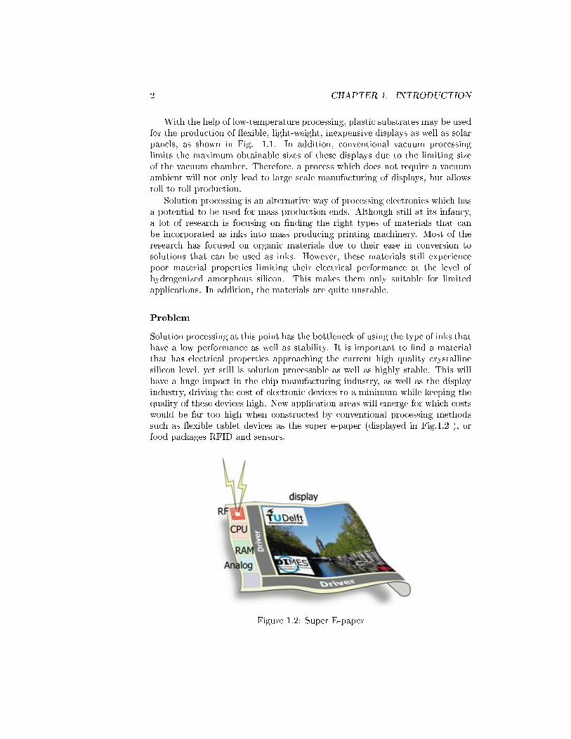
Solution processing at this point has the bottleneck of using the type of inks thathave a low performance as well as stability. It is important to �nd a materialthat has electrical properties approaching the current high quality crystallinesilicon level, yet still is solution processable as well as highly stable. This willhave a huge impact in the chip manufacturing industry, as well as the displayindustry, driving the cost of electronic devices to a minimum while keeping thequality of these devices high. New application areas will emerge for which costswould be far too high when constructed by conventional processing methodssuch as �exible tablet devices as the super e-paper (displayed in Fig.1.2 ), orfood packages RFID and sensors.
Figure 1.2: Super E-paper
3
Liquid silicon has been introduced in other works by Shimoda et al. [1]among others. They have shown the possibility of transforming a precursorinto amorphous silicon by a combination of photopolymerization and thermalannealing. Also Zhang et al. [2] have reported the fabrication of Single-GrainThin-Film transistors. Both use a thermal annealing temperature which is toohigh to be used on plastic substrates. They also used spin-coating and inkjetprinting for the deposition of the material, however, neither can be used inroll-to-roll applications.
Approach
In this work, the following three approaches were taken to solve the problems:
1. A doctor blade coating method is introduced for depositing the liquidsilicon material over a surface which is compatible to roll-to-roll processing.This method may in the future be extended into slot-die coating and �nallygravure printing, a widely accepted printing method that is known forhigh-speed mass production.
2. The second issue of a thermal annealing temperature, incompatible toplastic substrates is dealt with by using Excimer Laser annealing thatallows dehydrogenation and melting of thin layers without the penetrationof the heat to more sensitive underlying layers such as �exible substrates.
3. A SG-TFT device will be fabricated on a polyimide substrate by the doctorblade coating of liquid silicon. For the �rst time, high quality silicondevices will be produced on a plastic substrate, bringing high electricalperformance and solution processing together.
Working method
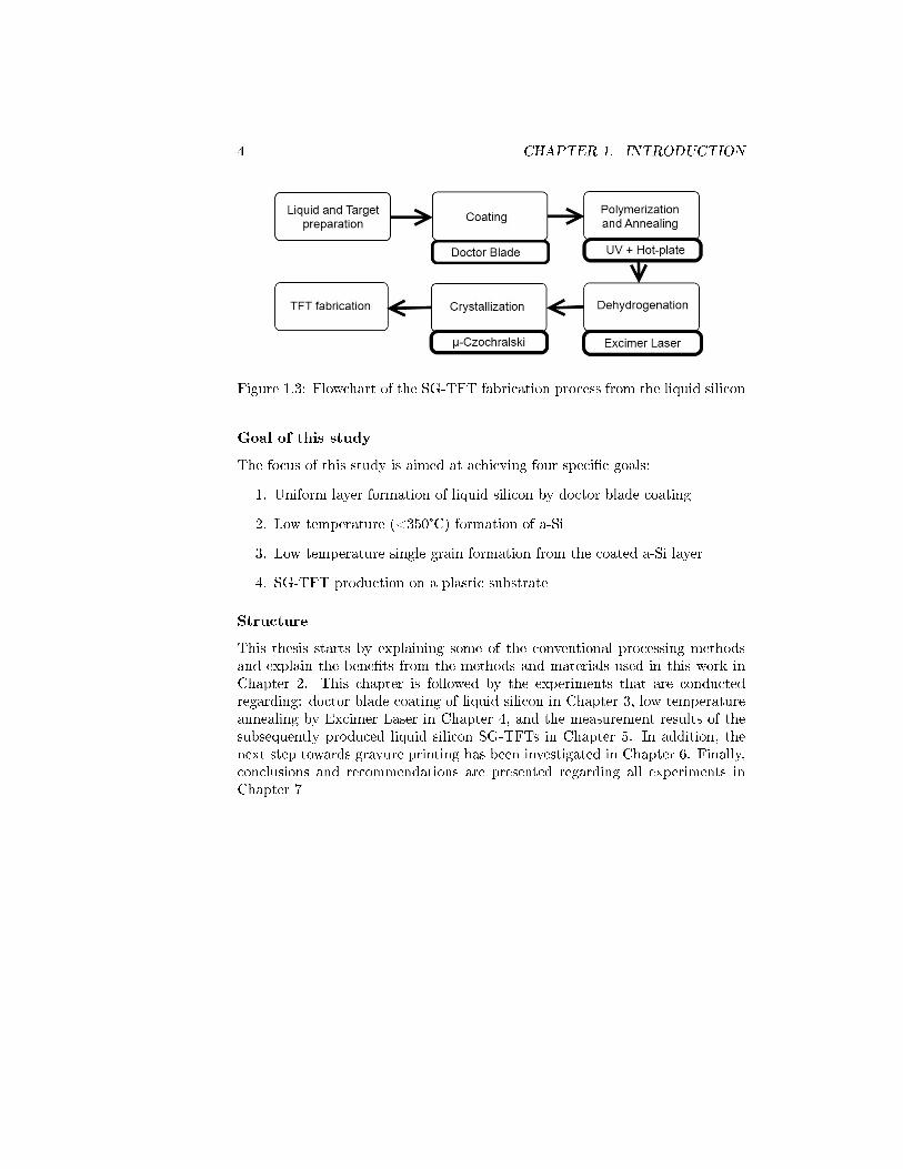
A general method of producing an amorphous silicon �lm from the liquid siliconhas been adapted using many di�erent variables aimed to optimize the methodof fabricating a uniform �lm by doctor blade coating. Fig. 1.3 shows the�owchart from liquid silicon to the SG-TFT. The focus in this work was inthe liquid and target preparation step, coating step, and the dehydrogenationstep. The coating has been performed on substrates with grain �lters thatallow location controlled crystallization during the subsequent Excimer Laserirradiation. This irradiation process uses various recipes but is generally basedon shooting at low energy densities to remove hydrogen content from the �lmthat cause deterioration of the �lm when exposed to crystallizing energy levels,followed by shooting at increasing energy levels. Finally, the single crystals areused to fabricate the SG-TFTs. Substrates with a polyimide layer depositedon top of the single-crystalline substrate before oxide deposition are used. Thesubstrate allows peeling o� of the polyimide layer to obtain a fully �exible result.
4 CHAPTER 1. INTRODUCTION
Figure 1.3: Flowchart of the SG-TFT fabrication process from the liquid silicon
Goal of this study
The focus of this study is aimed at achieving four speci�c goals:
1. Uniform layer formation of liquid silicon by doctor blade coating
2. Low temperature (<350°C) formation of a-Si
3. Low temperature single grain formation from the coated a-Si layer
4. SG-TFT production on a plastic substrate
Structure
This thesis starts by explaining some of the conventional processing methodsand explain the bene�ts from the methods and materials used in this work inChapter 2. This chapter is followed by the experiments that are conductedregarding: doctor blade coating of liquid silicon in Chapter 3, low temperatureannealing by Excimer Laser in Chapter 4, and the measurement results of thesubsequently produced liquid silicon SG-TFTs in Chapter 5. In addition, thenext step towards gravure printing has been investigated in Chapter 6. Finally,conclusions and recommendations are presented regarding all experiments inChapter 7
Chapter 2
Solution TFT process and
liquid Silicon
Many of the electronic devices nowadays, are built using silicon, and the processhas been optimized up to a certain extent for this material. Alternative materialsare being researched now that physical limitations start to play a role. Yet analternative way of processing may lead to inexpensive device fabrication formerlyconsidered as impossible for silicon devices.
Solution processing has gained immense popularity, however pure silicon can-not be used in this process due to its high melting point of 1414°C incompatiblewith many other materials. Organic materials are attractive due to their easein dissolving without losing their electrical properties. The organic electricalcharacteristics are quite poor as well as unstable, but they seem to be accept-able for some applications such as Organic Light-Emitting-Diodes (OLEDs) butcannot be integrated in more complex circuitry. Organic material properties arecurrently being optimized and have recently surpassed the level of hydrogenizedamorphous silicon (a-Si:H), conventionally used for display applications.
The liquid silicon precursor used in this work can be solution processed sim-ilar to organic materials, however, they can be crystallized into polycrystallinesilicon that already have two orders of magnitude higher mobility than the cur-rent best organic mobility. In addition, when the location of these crystalsare controlled, the channel of the transistor can be positioned within a crystalgrain, which is one of the great advantages of Single-Grain Thin-Film Transistor(SG-TFT).
In this chapter a description will be given on solution processing, which willbe compared to conventional processing methods. This section is followed bythe characteristics of organic semiconductors, silicon as it is used nowadays, anda full description of the liquid silicon material used in this work.
5
6 CHAPTER 2. SOLUTION TFT PROCESS AND LIQUID SILICON
2.1 Solution Processing
A type of processing that uses solutions or liquids for the fabrication of electronicdevices is called solution processing. This type of processing has attracted a lotof attention recently due to the many advantages over conventional processing.Two di�erent types of conventional processing need to be discussed.
The �rst one is the use of Metal-Oxide-Semiconductor Field-E�ect Transis-tors (MOSFETs) or Bipolar Junction Transistors (BJTs) that use the bulk ofthe silicon material as the channel and are produced by traditional processingmethods that start with the wafers produced by the Czochralski and/or Float-ing Zone methods. These wafers are further processed by means of subtractiveprocessing using photolithography and masking layers. High quality devices areproduced in this way.
A second type of process focuses on the production of devices such as Thin-Film Transistors (TFTs) on top of a supporting substrate, such as the case fordisplays. In general this is done on top of glass, however, when su�ciently lowtemperatures are reached, deposition on �exible substrates may be possible aswell. Current technologies use Plasma-Enhanced Chemical-Vapor Deposition(PECVD) for the deposition of the various layers and use a-Si:H as the semi-conductor layer. For display applications, the quality of the devices do not haveto be high.
In both cases, a highly controlled atmosphere is required and many di�erentsteps are necessary to produce various patterns on the substrate as well asdoping of the layers within the bulk of the material. Material wastage and timeconsumption is a central issue in both cases. It is therefore necessary to �nda way to produce high quality devices in a less stringent ambient with highthroughput at low temperatures.
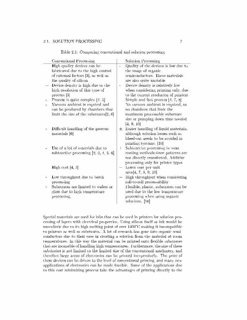
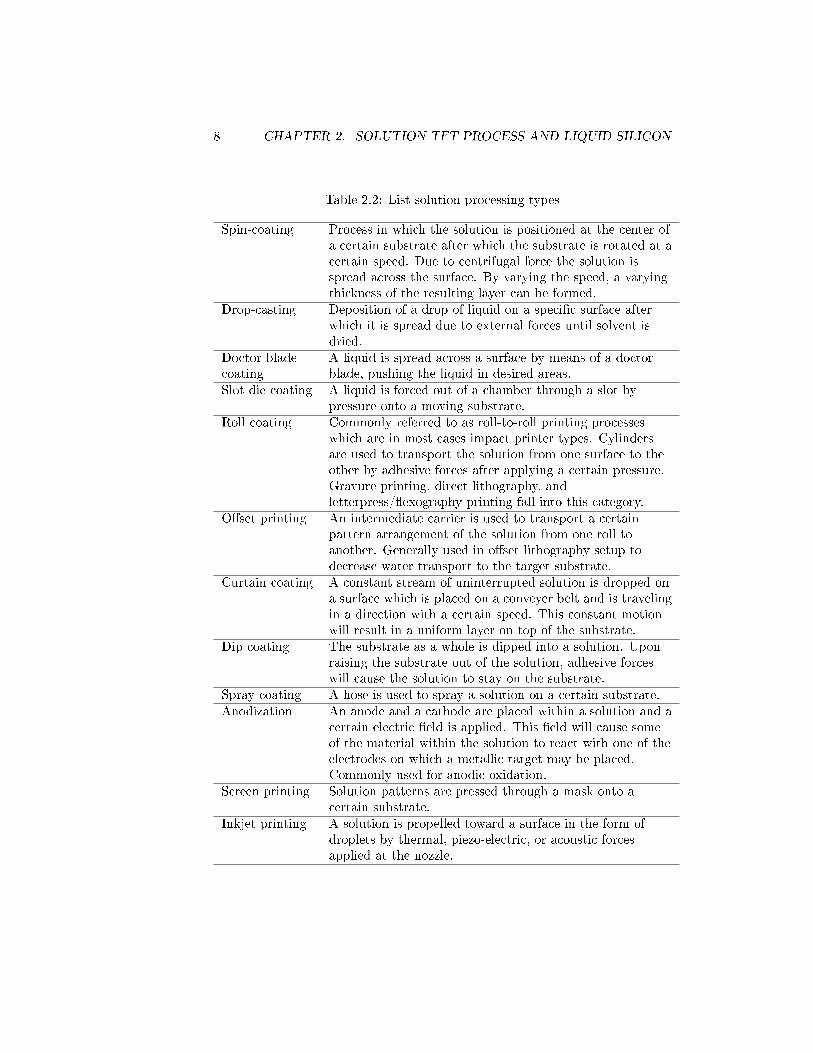
As an alternative to the conventional processing, solution processing gainedpopularity due to their ability to overcome most of the issues of current pro-cesses. Table 2.1 compares solution processing to conventional processing. Inessence, the solution process itself, is the various uses of solutions or liquidsto create electronic devices such as TFTs. Some of the most commonly usedsolution process, that is also used in conventional processing for instance, isspin-coating. Table 2.2 gives a list of all solution processing types currentlyused and researched [6, 11].
The e�ects of these di�erent types of processes on the thin �lm quality ofthe deposited layer are mainly dependent on the concentration of semiconductormaterial in the solution and its solubility, evaporation rate of the solvent, andproperties of the target surface[9].
Printing is the process of reproducing by means of applying ink to a substrateinto a certain arrangement, and is an advanced solution processing technique.Today's wildly used applications include the printing of mass produced newspa-pers, magazines, books, packages, etc. Printers known for their mass productionqualities would be a useful tool for constructing cheap electronic devices allow-ing to deposit already patterned layers onto various substrates. This makes themanufacturing process of electronic devices a lot simpler and less expensive.
2.1. SOLUTION PROCESSING 7
Table 2.1: Comparing conventional and solution processing
Conventional Processing Solution Processing+ High quality devices can be
fabricated due to the high controlof external factors [3], as well asthe quality of silicon
- Quality of the devices is low due tothe usage of organicsemiconductors. These materialsare also quite unstable
+ Device density is high due to thehigh resolution of this type ofprocess [3]
- Device density is relatively lowwhen considering printing only, dueto the current resolution of printers
- Process is quite complex [4, 5] + Simple and fast process [4, 7, 8]- Vacuum ambient is required and
can be produced by chambers thatlimit the size of the substrates[2, 6]
+ No vacuum ambient is required, sono chambers that limit themaximum processable substratesize or pumping down time needed[4, 9, 10]
- Di�cult handling of the gaseousmaterials [6]
± Easier handling of liquid materials,although solution issues such asbleed-out needs to be avoided inprinting systems. [10]
- Use of a lot of materials due tosubtractive processing [2, 3, 4, 5, 6]
± Subtractive processing in mostcoating methods since patterns arenot directly transferred. Additiveprocessing only for printer types
- High cost [4, 5] + Lower cost per unitarea[4, 7, 8, 9, 10]
- Low throughput due to batchprocessing
+ High throughput when consideringroll-to-roll processability
- Substrates are limited to wafers orglass due to high temperatureprocessing.
+ Flexible, plastic, substrates can beused due to the low temperatureprocessing when using organicsolutions. [10]
Special materials are used for inks that can be used in printers for solution pro-cessing of layers with electrical properties. Using silicon itself as ink would beunrealistic due to its high melting point of over 1400°C making it incompatibleto printers as well as substrates. A lot of research has gone into organic semi-conductors due to their ease in creating a solution from the material at roomtemperatures. In this way the material can be printed onto �exible substratesthat are incapable of handling high temperatures. Furthermore, the size of thesesubstrates is not limited to the limited size of the conventional machinery, andtherefore large areas of electronics can be printed inexpensively. The price ofthese devices can be driven to the level of conventional printing, and many newapplications of electronics can be made feasible. Some of the applications dueto this cost minimizing process take the advantages of printing directly to the
8 CHAPTER 2. SOLUTION TFT PROCESS AND LIQUID SILICON
Table 2.2: List solution processing types
Spin-coating Process in which the solution is positioned at the center ofa certain substrate after which the substrate is rotated at acertain speed. Due to centrifugal force the solution isspread across the surface. By varying the speed, a varyingthickness of the resulting layer can be formed.
Drop-casting Deposition of a drop of liquid on a speci�c surface afterwhich it is spread due to external forces until solvent isdried.
Doctor bladecoating
A liquid is spread across a surface by means of a doctorblade, pushing the liquid in desired areas.
Slot die coating A liquid is forced out of a chamber through a slot bypressure onto a moving substrate.
Roll coating Commonly referred to as roll-to-roll printing processeswhich are in most cases impact printer types. Cylindersare used to transport the solution from one surface to theother by adhesive forces after applying a certain pressure.Gravure printing, direct lithography, andletterpress/�exography printing fall into this category.
O�set printing An intermediate carrier is used to transport a certainpattern arrangement of the solution from one roll toanother. Generally used in o�set lithography setup todecrease water transport to the target substrate.
Curtain coating A constant stream of uninterrupted solution is dropped ona surface which is placed on a conveyer belt and is travelingin a direction with a certain speed. This constant motionwill result in a uniform layer on top of the substrate.
Dip coating The substrate as a whole is dipped into a solution. Uponraising the substrate out of the solution, adhesive forceswill cause the solution to stay on the substrate.
Spray coating A hose is used to spray a solution on a certain substrate.Anodization An anode and a cathode are placed within a solution and a
certain electric �eld is applied. This �eld will cause someof the material within the solution to react with one of theelectrodes on which a metallic target may be placed.Commonly used for anodic oxidation.
Screen printing Solution patterns are pressed through a mask onto acertain substrate.
Inkjet printing A solution is propelled toward a surface in the form ofdroplets by thermal, piezo-electric, or acoustic forcesapplied at the nozzle.
2.1. SOLUTION PROCESSING 9
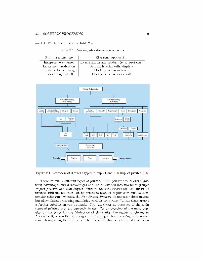
market [12] these are listed in Table 2.3 .
Table 2.3: Printing advantages in electronics
Printing advantage Electronic application
Inexpensive as paper Integration in any product (e. g. packages)Large area production Billboards, solar cells, displaysFlexible substrate usage Clothing, anti-vandalismHigh throughput[10] Cheaper electronics overall
Figure 2.1: Overview of di�erent types of impact and non-impact printers [13]
There are many di�erent types of printers. Each printer has its own signif-icant advantages and disadvantages and can be divided into two main groups:Impact printers and Non-Impact Printers. Impact Printers are also known asprinters with masters that can be reused to produce highly reproducible inex-pensive print runs, whereas the Non-Impact Printers do not use a �xed masterbut allow digital processing and highly variable print runs. Within these groupsa further subdivision can be made. Fig. 2.1 shows an overview of the maintypes of printers that are currently in use. For an overview of the most pop-ular printer types for the fabrication of electronics, the reader is referred toAppendix B, where the advantages, disadvantages, basic working and currentresearch regarding the printer type is presented, after which a �nal conclusion
10 CHAPTER 2. SOLUTION TFT PROCESS AND LIQUID SILICON
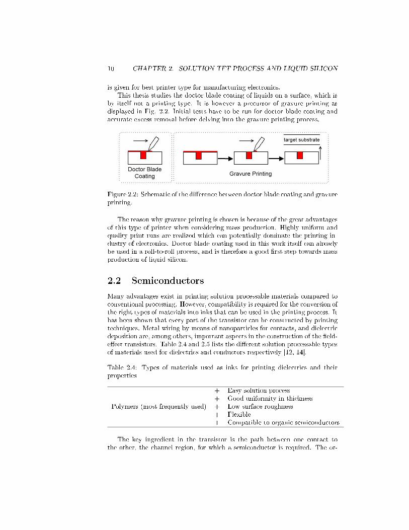
is given for best printer type for manufacturing electronics.This thesis studies the doctor blade coating of liquids on a surface, which is
by itself not a printing type. It is however a precursor of gravure printing asdisplayed in Fig. 2.2. Initial tests have to be run for doctor blade coating andaccurate excess removal before delving into the gravure printing process.
Figure 2.2: Schematic of the di�erence between doctor blade coating and gravureprinting.
The reason why gravure printing is chosen is because of the great advantagesof this type of printer when considering mass production. Highly uniform andquality print runs are realized which can potentially dominate the printing in-dustry of electronics. Doctor blade coating used in this work itself can alreadybe used in a roll-to-roll process, and is therefore a good �rst step towards massproduction of liquid silicon.
2.2 Semiconductors
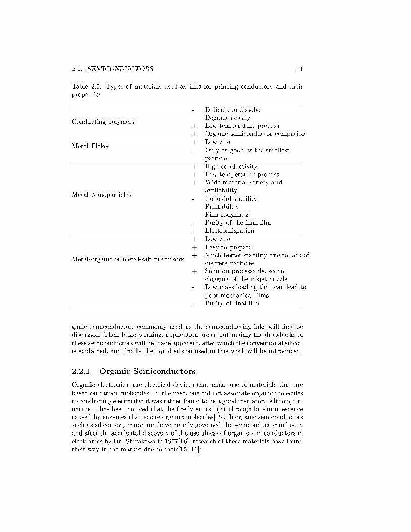
Many advantages exist in printing solution processable materials compared toconventional processing. However, compatibility is required for the conversion ofthe right types of materials into inks that can be used in the printing process. Ithas been shown that every part of the transistor can be constructed by printingtechniques. Metal wiring by means of nanoparticles for contacts, and dielectricdeposition are, among others, important aspects in the construction of the �eld-e�ect transistors. Table 2.4 and 2.5 lists the di�erent solution processable typesof materials used for dielectrics and conductors respectively [12, 14].
Table 2.4: Types of materials used as inks for printing dielectrics and theirproperties
Polymers (most frequently used)
+ Easy solution process+ Good uniformity in thickness+ Low surface roughness+ Flexible+ Compatible to organic semiconductors
The key ingredient in the transistor is the path between one contact tothe other, the channel region, for which a semiconductor is required. The or-
2.2. SEMICONDUCTORS 11
Table 2.5: Types of materials used as inks for printing conductors and theirproperties
Conducting polymers
- Di�cult to dissolve- Degrades easily+ Low temperature process+ Organic semiconductor compatible
Metal Flakes+ Low cost- Only as good as the smallest
particle
Metal Nanoparticles
+ High conductivity+ Low temperature process+ Wide material variety and
availability- Colloidal stability- Printability- Film roughness- Purity of the �nal �lm- Electromigration
Metal-organic or metal-salt precursors
+ Low cost+ Easy to prepare+ Much better stability due to lack of
discrete particles+ Solution processable, so no
clogging of the inkjet nozzle- Low mass loading that can lead to
poor mechanical �lms- Purity of �nal �lm
ganic semiconductor, commonly used as the semiconducting inks will �rst bediscussed. Their basic working, application areas, but mainly the drawbacks ofthese semiconductors will be made apparent, after which the conventional siliconis explained, and �nally the liquid silicon used in this work will be introduced.
2.2.1 Organic Semiconductors
Organic electronics, are electrical devices that make use of materials that arebased on carbon molecules. In the past, one did not associate organic moleculesto conducting electricity; it was rather found to be a good insulator. Although innature it has been noticed that the �re�y emits light through bio-luminescencecaused by enzymes that excite organic molecules[15]. Inorganic semiconductorssuch as silicon or germanium have mainly governed the semiconductor industryand after the accidental discovery of the usefulness of organic semiconductors inelectronics by Dr. Shirakawa in 1977[16], research of these materials have foundtheir way in the market due to their[15, 16]:
12 CHAPTER 2. SOLUTION TFT PROCESS AND LIQUID SILICON
� Signi�cant fabrication cost reduction due to solution processability of thematerials,
� Low temperature processing that allow these materials to be deposited oninexpensive �exible substrates,
� Molecular tunability, allowing the materials to change properties such asvolatility, solubility, and wetting characteristics.
Unlike high quality single-crystalline silicon materials, these organics are builtin TFT processes much like a-Si:H. Research today has advanced the mobilityof organic semiconductors to surpass the level of a-Si:H (1 cm²/Vs) [17, 18, 19].Although these are still nowhere near the mobility of single-crystalline silicon,which is three orders of magnitude higher [16], they show their potential inrather inexpensive applications.
The basis for the conduction of organic materials are slightly di�erent fromtheir inorganic counterparts. Bonds play a major role in these devices, and thissection will be devoted to the understanding of their operating principles.
Conduction in general
A discussion about charge transport is directly related to the bonding propertiesof various materials. In both inorganic and organic semiconductors, covalentbonds are the main bond type that keep the molecule together. This typeof bond is based on the attraction of two atoms due to its desire to �ll theelectron shells around the atoms. Sharing of electrons among the two atomsrealizes this desire. Both silicon as well as carbon for example can share fourelectrons with neighboring atoms. Within this type of bonding, the electronsbecome a pair and orbit around the pair of atoms; they cannot move aroundfreely and therefore do not conduct electricity unlike metals that are boundby a cloud of valence electrons that move around freely. Covalent bonds ininorganic semiconductors are relatively weaker so that some of the electronsmay be thermally activated. These materials can conduct to a certain extentand are hence called semiconductors [20].
The interaction of two atoms results in splitting of the quantized energylevel into two discrete energies. When many atoms interact with each other,the energy will be split into a band of discrete energy levels. In some materialsthere are energy levels for which the electron can not occupy. These are calledforbidden energies, or the bandgap [20]. Various models try to describe thisband theory further through the use of Schrödinger's equation (e. g. TheKronig-Penny Model, the Ziman model, and the Feynman model). The readeris referred to [15] for a more thorough understanding of the band theory.
Out of the many energy bands that exist due to the interaction of multipleatoms, the two highest bands are of particular interest: the valence band andthe conduction band. In insulators the valence band is �lled with electrons,and the conduction band is completely empty. The bands are separated by abandgap, and an application of an electric �eld will not cause the electrons to
2.2. SEMICONDUCTORS 13
change energy levels when the bandgap is su�ciently large for the electrons tocross. No current will �ow through the material since no electrons are activated.A partially empty band results in the possibility of electrons increasing theirenergy level due to an applied electric �eld and move through the material. Thenet �ow of these electrons will de�ne the current. This situation happens forsemiconductors in which thermally activated electrons can cross the bandgapand jump into the conduction band allowing the material to conduct current toa certain extent since the bands are not completely �lled or empty. In metals,two situations may exist regarding the band �lling. The �rst case is a fullyoccupied valence band, and a partially �lled conduction band that allow theseelectrons to move freely when an electric �eld is applied. The second possibilityis that valence and conduction bands overlap so that electrons do not have tobridge a bandgap and can easily occupy other energy states [20].
Organic conduction
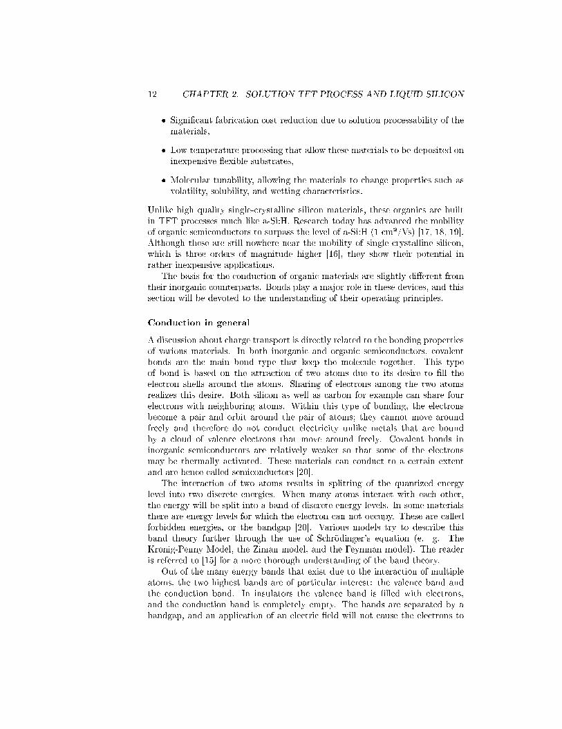
Compared to inorganic semiconductors, organic semiconductors that use cova-lent bonding interaction have quite a large bandgap that prevents the materialfrom conducting electrons. So the electrons inside this material need to be as-sisted in order for them to raise their energy and be able to move around. Twocarbon atoms interacting with each other are joined by one covalent bond dueto the pairing of one of the dangling bonds of each atom. This e�ect can be seenas the pairing of s orbitals and is therefore also known as σv-bonds. Each carbonatom has 4 dangling bonds and can form covalent bonds with four other atoms.It can also however form a pair with the already interacting carbon atom andcreate weaker bonds perpendicular to the σv-bond plane. This weaker bond issimilar to the structure of two p-orbitals and is therefore known as π-bonds.The electron con�guration of Carbon: 1s², 2s², 2p², the sigma bonds lie closerto the atoms and are therefore stronger [15] The Fig. 2.3 shows this situation.
(a) (b)
Figure 2.3: Bonding representation of two carbon molecules with σv-bonds andπ-bonds (a), and its band representation (b).[21]
14 CHAPTER 2. SOLUTION TFT PROCESS AND LIQUID SILICON
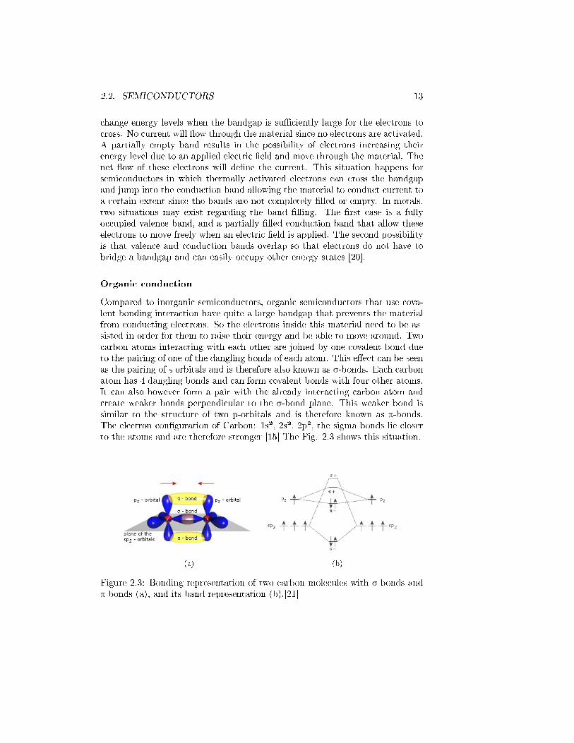
(a) (b)
Figure 2.4: Bonding representation of benzene with σv-bonds and π-bonds (a),and its band representation (b).[21]
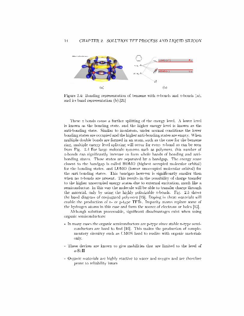
These π-bonds cause a further splitting of the energy level. A lower levelis known as the bonding state, and the higher energy level is known as theanti-bonding state. Similar to insulators, under normal conditions the lowerbonding states are occupied and the higher anti-bonding states are empty. Whenmultiple double bonds are formed in an atom, such as the case for the benzenering, multiple energy level splitting will occur for every π-bond as can be seenfrom Fig. 2.4 For large molecule systems such as polymers, this number ofπ-bonds can signi�cantly increase to form whole bands of bonding and anti-bonding states. These states are separated by a bandgap. The energy stateclosest to the bandgap is called HOMO (highest occupied molecular orbital)for the bonding states, and LUMO (lowest unoccupied molecular orbital) forthe anti-bonding states. This bandgap however is signi�cantly smaller thanwhen no π-bonds are present. This results in the possibility of charge transferto the higher unoccupied energy states due to external excitation, much like asemiconductor. In this way the molecule will be able to transfer charge throughthe material, only by using the highly polarizable π-bonds. Fig. 2.5 showsthe band diagram of conjugated polymers [15]. Doping in these materials willenable the production of n- or p-type TFTs. Impurity atoms replace some ofthe hydrogen atoms in this case and form the source of electrons or holes [15].
Although solution processable, signi�cant disadvantages exist when usingorganic semiconductors:
- In many cases the organic semiconductors are p-type since stable n-type semi-conductors are hard to �nd [16]. This makes the production of comple-mentary circuitry such as CMOS hard to realize with organic materialsonly.
- These devices are known to give mobilities that are limited to the level ofa-Si:H
- Organic materials are highly reactive to water and oxygen and are thereforeprone to reliability issues
2.2. SEMICONDUCTORS 15
(a) (b)
Figure 2.5: Bonding representation of an arbitrary polymer (a), and its bandrepresentation (b).[21]
Polymers and Small molecule organic systems
Long polymer chains with alternating double bonds or π-bonds are being usedas organic semiconductors. Polymer materials generally are hard to purify sincethey have a large variation in molecular size. They may also have structuraldefects due to monomer mislinkage that can induce traps against charge carriers.Large polymer chains are however not the only way for organic materials tobehave as semiconductors. Small-molecule organic semiconductors can behavein a similar fashion and form the alternative to polymer organics. Due to theirsmall size they can assemble more easily into regular geometric arrangements.This tendency towards the formation of molecular crystals lead to larger carriermobilities than compared to disordered chains of polymers. A few di�erencesbetween the two types should however be noted [16, 17, 22]:
� Small-molecule organic semiconductors are commonly deposited from thevapor phase whilst polymeric semiconductors are deposited from the solu-tion. Solution processability is an important factor for printed electronics.Polymeric solvents are however known to be quite toxic since they are ei-ther chlorinated or aromatic.
� Small-molecule systems, when deposited on low roughness surfaces canform a highly ordered crystalline region leading to e�cient π-stacking andtherefore higher mobilities than polymers.
� Small-molecules are more easily puri�ed than polymers since their struc-ture is well de�ned.
Research so far
A lot of research is being conducted in organic electronics. Organic devices areconstructed with higher mobilities and with higher stability [17, 18, 22, 23], andhave already come to the level of a-Si:H (1cm²/Vs). However, it is still a long
16 CHAPTER 2. SOLUTION TFT PROCESS AND LIQUID SILICON
way before reaching the high quality crystalline silicon level that have mobilitiesof a few orders of magnitudes higher.
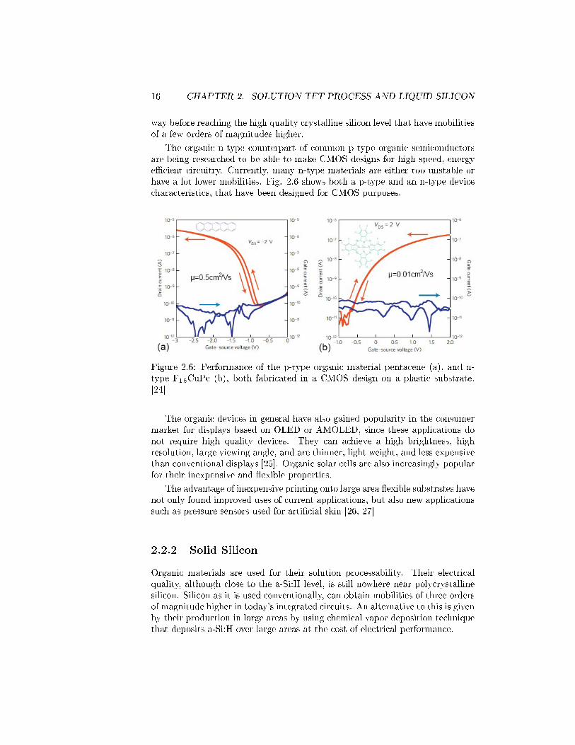
The organic n-type counterpart of common p-type organic semiconductorsare being researched to be able to make CMOS designs for high speed, energye�cient circuitry. Currently, many n-type materials are either too unstable orhave a lot lower mobilities. Fig. 2.6 shows both a p-type and an n-type devicecharacteristics, that have been designed for CMOS purposes.
Figure 2.6: Performance of the p-type organic material pentacene (a), and n-type F16CuPc (b), both fabricated in a CMOS design on a plastic substrate.[24]
The organic devices in general have also gained popularity in the consumermarket for displays based on OLED or AMOLED, since these applications donot require high quality devices. They can achieve a high brightness, highresolution, large viewing angle, and are thinner, light weight, and less expensivethan conventional displays [25]. Organic solar cells are also increasingly popularfor their inexpensive and �exible properties.
The advantage of inexpensive printing onto large area �exible substrates havenot only found improved uses of current applications, but also new applicationssuch as pressure sensors used for arti�cial skin [26, 27]
2.2.2 Solid Silicon
Organic materials are used for their solution processability. Their electricalquality, although close to the a-Si:H level, is still nowhere near polycrystallinesilicon. Silicon as it is used conventionally, can obtain mobilities of three ordersof magnitude higher in today's integrated circuits. An alternative to this is givenby their production in large areas by using chemical vapor deposition techniquethat deposits a-Si:H over large areas at the cost of electrical performance.
2.2. SEMICONDUCTORS 17
Amorphous and polycrystalline silicon
Silicon is the most common known and widely used semiconductor in the elec-tronics industry. Various types of semiconductors are de�ned by their crystalstructure.
Amorphous silicon is a cluster of silicon atoms with random orientationsthroughout the material. It has relatively low electrical performance and iscurrently mainly used in its hydrogenated form as solar cells or display TFTs.
Polycrystalline silicon is a material formed as a combination of multiplecrystals. It can be directly deposited on a substrate, or formed from an al-ready deposited a-Si �lm. Excimer laser can be used on such a �lm to createa polysilicon layer that can achieve higher mobilities. These mobilities howeverare limited to approximately 50 to 100 cm²/Vs. This is due to crystal grainboundaries that are formed from randomly produced grains during laser crys-tallisation. Removal of these grain boundaries can lead to devices approachingthe single-crystalline silicon level, however careful control of grain formation isimportant.
Single Grain Thin Film Transistor
The Thin-Film Transistor (TFT) is a device that is similar to the MOSFET,except that the device is produced on top of a supporting substrate rather thanwithin the bulk of the substrate material. The reader is referred to Appendix Cfor a more detailed description about the characteristics of this type of device.
The main application for this type of device was the display industry wherelarge area displays are produced by manufacturing TFTs on top of a glass sub-strate. This is usually done by PECVD of hydrogenated amorphous silicon(a-Si:H) as the semiconductor, although organic semiconductors have in some in-stances been used as well, such as Active-Matrix Organic Light-Emitting Diodes(AMOLEDs). Producing devices on a large area was the main aim of this typeof device. The solution processable organic materials allowed even lower tem-perature processing, so that other substrates such as plastics could be used thatare much thinner, cheaper and �exible.
Many of the TFT types such as organic semiconductor based ones or amor-phous silicon based ones still su�er from low mobilities. High mobility TFTs aredesirable to be able to integrate more complicated devices on plastic substrates.Currently many of the �exible displays require external drivers that prevent the�nal product from being fully �exible.
The quality of the a-Si semiconductor can be increased by Excimer Lasercrystallization of the �lm into polycrystalline silicon. The random grain bound-aries limit the electrical performance of the device. When the location of thesegrain boundaries and therefore single grains are controlled, high quality devicesmay be produced within a single grain.
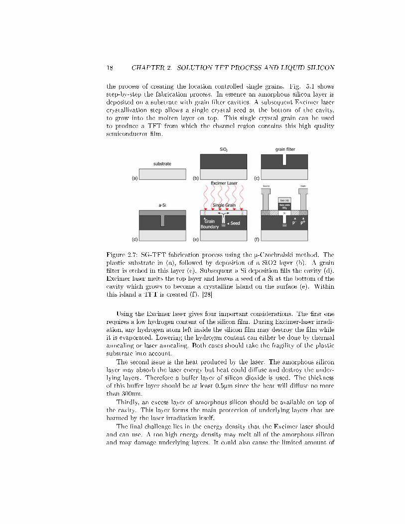
Single-Grain TFTs are TFTs that are constructed within a single grain froma polysilicon �lm. The location of grains produced during laser crystallisationare carefully controlled by grain �lter cavities. The μ-Czochralski method is
18 CHAPTER 2. SOLUTION TFT PROCESS AND LIQUID SILICON
the process of creating the location controlled single grains. Fig. 5.1 showsstep-by-step the fabrication process. In essence an amorphous silicon layer isdeposited on a substrate with grain �lter cavities. A subsequent Excimer lasercrystallization step allows a single crystal seed at the bottom of the cavity,to grow into the molten layer on top. This single crystal grain can be usedto produce a TFT from which the channel region contains this high qualitysemiconductor �lm.
Figure 2.7: SG-TFT fabrication process using the μ-Czochralski method. Theplastic substrate in (a), followed by deposition of a SiO2 layer (b). A grain�lter is etched in this layer (c). Subsequent a-Si deposition �lls the cavity (d).Excimer laser melts the top layer and leaves a seed of a-Si at the bottom of thecavity which grows to become a crystalline island on the surface (e). Withinthis island a TFT is created (f). [28]
Using the Excimer laser gives four important considerations. The �rst onerequires a low hydrogen content of the silicon �lm. During Excimer-laser irradi-ation, any hydrogen atom left inside the silicon �lm may destroy the �lm whileit is evaporated. Lowering the hydrogen content can either be done by thermalannealing or laser annealing. Both cases should take the fragility of the plasticsubstrate into account.
The second issue is the heat produced by the laser. The amorphous siliconlayer may absorb the laser energy but heat could di�use and destroy the under-lying layers. Therefore a bu�er layer of silicon dioxide is used. The thicknessof this bu�er layer should be at least 0.5μm since the heat will di�use no morethan 300nm.
Thirdly, an excess layer of amorphous silicon should be available on top ofthe cavity. This layer forms the main protection of underlying layers that areharmed by the laser irradiation itself.
The �nal challenge lies in the energy density that the Excimer laser shouldand can use. A too high energy density may melt all of the amorphous siliconand may damage underlying layers. It could also cause the limited amount of
2.2. SEMICONDUCTORS 19
hydrogen atoms to destroy the silicon �lm more easily. A high energy densityleads however to larger grains. On the other hand, a lower energy density willresult in smaller grain sizes. A bigger thickness of amorphous silicon layer couldincrease the possibility to enhance the energy density of the laser. A thickerlayer may however have more hydrogen atoms that can result in ablation. [2, 29]
2.2.3 Liquid Silicon
Organic semiconductors su�er from poor stability, and relatively poor electricalperformance and are therefore still not vastly implemented in today's more com-plex products, despite the fact that they are compatible to solution processing.Inorganic materials are more stable, can get higher mobilities but are di�cultto use into solution processing. One example is the use of metal chalcogenidesemiconductors achieving a mobility of 10cm²/Vs. Mobilities of solution pro-cessed devices approaching the crystalline silicon level are desired and wouldopen up many possibilities.
Silicon in conventional fabrication techniques has a melting temperature of1414°C [30]. This means that for printing the silicon as a liquid, not only isthere a lot of energy needed, the printer itself as well as the substrate, needto be compatible to this high temperature. Flexible substrates such as plasticshave no chance of surviving when processed in this way. Lowering the fabricationtemperature is of essence when considering material compatibility and machineand energy costs. This is the area where organic devices have an advantageof low temperature solution processing, with the lack the quality and stability.Being able to process silicon at lower temperatures, and yet producing a highquality and stable device is essential. Using silicon in its purest form is out ofthe question.
A compound that can transform into high quality silicon at low temperaturesmay be the solution to this problem. This compound has been found in 1973 [31]but has only recently found to be useful for microelectronic applications. Dr.Shimoda et al. describe the compound used, and its transformation to silicon�lms [4, 5]. They have successfully fabricated poly-crystalline silicon deviceswith the formation of an a-Si layer at a maximum processing temperature of430°C.
Cyclopentasilane for liquid silicon
To create a high quality silicon layer, the required compound should be carbon-and oxygen free [1, 7, 8]. Dangling bonds should then be avoided by hydrogena-tion. The choice of the compound is then limited to a composition of siliconand hydrogen atoms as either a straight molecule (SinH2n+2), a cyclic compound(SinH2n), or a multicycled compound (SinH2n−2) [6]. In order to transform fromthese compounds to a high quality silicon layer, the compound needs to poly-merize. A cyclic structure is preferred due to its high reactivity with light sothat photopolymerization can occur e�ciently, these will undergo ring-opening
20 CHAPTER 2. SOLUTION TFT PROCESS AND LIQUID SILICON
as they are exposed to UV light [6]. A single cyclic structure is preferred overthe multicycled structure due to its ease of synthesis and puri�cation.
The number of silicon elements in the single cyclic structure should be care-fully chosen. According to [1, 8], when n is more than or equal to three, thecompound is liquid at room temperature and will transform into a-Si when atemperature of 300°C is reached. For n smaller than ten, the boiling point of thecompound will be less than 300°C, which would mean that the compound evap-orates before it decomposes to amorphous silicon. This problem can however besolved by the photopolymerizing the compound before thermal annealing. Thecompound Cyclopentasilane, Si5H10 has been chosen for its high photo reactiv-ity on UV light and its relative stability[8]. In this work, the term liquid siliconis used for any compound used in solution processing that can be transformedinto an amorphous silicon �lm. This includes: pure CPS, UV irradiated CPS,CPS mixed with an organic solution, and the combination of UV irradiation ofthe CPS mixture.
The compound is also highly reactive to oxygen and should therefore beprocessed in an inert gas ambient. When it is exposed to air, the material willin�ammate. Adding oxygen however after the photopolymerization step andduring thermal treatment can create silicon dioxide �lms instead of a-Si. Table2.6 lists the general information of CPS. For more detailed information aboutthe compound, the reader is referred to the datasheets [32].
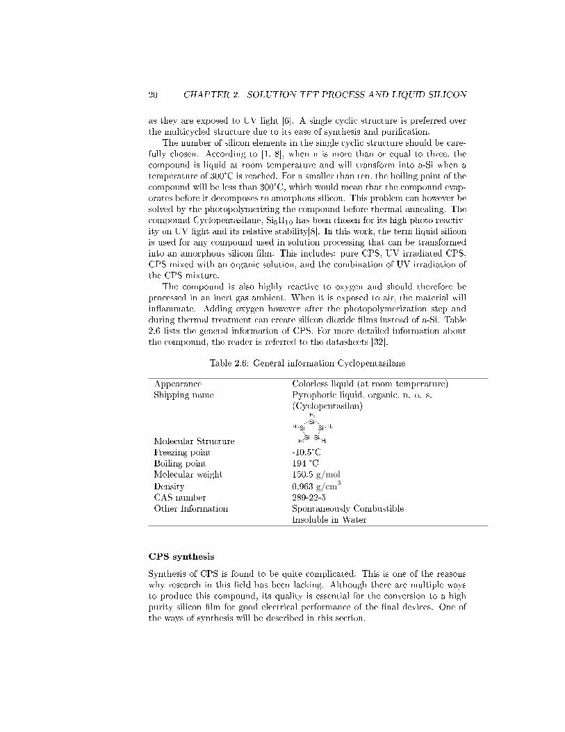
Table 2.6: General information Cyclopentasilane
Appearance Colorless liquid (at room temperature)Shipping name Pyrophoric liquid, organic, n. o. s.
(Cyclopentasilan)
Molecular StructureFreezing point -10.5°CBoiling point 194 °CMolecular weight 150.5 g/mol
Density 0.963 g/cm3
CAS number 289-22-5Other Information Spontaneously Combustible
Insoluble in Water
CPS synthesis
Synthesis of CPS is found to be quite complicated. This is one of the reasonswhy research in this �eld has been lacking. Although there are multiple waysto produce this compound, its quality is essential for the conversion to a highpurity silicon �lm for good electrical performance of the �nal devices. One ofthe ways of synthesis will be described in this section.
2.2. SEMICONDUCTORS 21
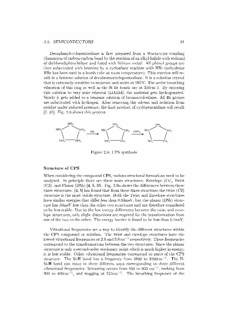
Decaphenylcyclopentasilane is �rst prepared from a Wurtz-type coupling(formation of carbon-carbon bond by the reaction of an alkyl-halide with sodium)of dichlorodiphenylsilane and fused with lithium metal. All phenyl groups arethen substituted with bromine by a cyclosilane reaction with HBr (anhydrousHBr has been used in a bomb tube at room temperature). This reaction will re-sult in a benzene solution of decabromocyclopentasilane. It is a colorless crystalthat is extremely sensitive to moisture and melts at 195°C. The active breathingvibration of this ring as well as the Si-Br bonds are at 510cm-1. By exposingthis solution to very pure ethereal (LiAlH4), the material gets hydrogenated.Slowly it gets added to a benzene solution of bromocyclosilane. All Br groupsare substituted with hydrogen. After removing the solvent and isolation fromresidue under reduced pressure, the �nal product of cyclopentasilane will result[7, 31]. Fig. 2.8 shows this process.
Figure 2.8: CPS synthesis
Structure of CPS
When considering the compound CPS, various structural formations need to beanalyzed. In principle there are three main structures: Envelope (Cs), Twist(C2), and Planar (D5h) [4, 5, 33]. Fig. 2.9a shows the di�erences between thesethree structures. [4, 5] has found that from these three structures the twist (C2)structure is the most stable structure. Both the Twist and Envelope structureshave similar energies that di�er less than 0.03meV, but the planar (D5h) struc-ture has 50meV less than the other two structures and are therefore consideredto be less stable. Due to the low energy di�erences between the twist and enve-lope structures, only slight distortions are required for the transformation fromone of the two to the other. The energy barrier is found to be less than 0.1meV.
Vibrational frequencies are a way to identify the di�erent structures withinthe CPS compound or solution. The twist and envelope structures have thelowest vibrational frequencies at 2.6 and 3.8cm−1 respectively. These frequenciescorrespond to the transformations between the two structures. Since the planarstructure is only a second-order stationary point which is much higher in energy,it is less stable. Other vibrational frequencies correspond to parts of the CPSstructure. The Si-H bond has a frequency from 2100 to 2200cm−1. The H-Si-H bond can move in three di�erent ways corresponding to three di�erentvibrational frequencies: Scissoring occurs from 850 to 950 cm−1, rocking from300 to 400cm−1, and wagging at 725cm−1. The breathing frequency of the
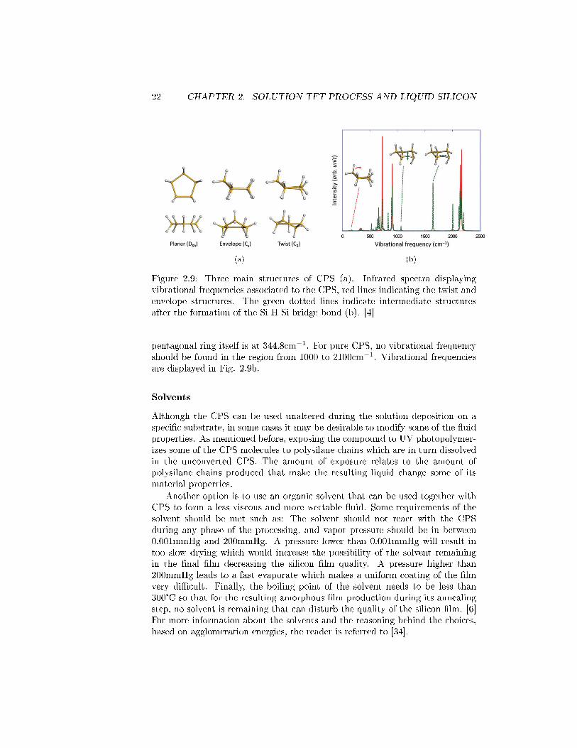
22 CHAPTER 2. SOLUTION TFT PROCESS AND LIQUID SILICON
(a) (b)
Figure 2.9: Three main structures of CPS (a). Infrared spectra displayingvibrational frequencies associated to the CPS, red lines indicating the twist andenvelope structures. The green dotted lines indicate intermediate structuresafter the formation of the Si-H-Si bridge bond (b). [4]
pentagonal ring itself is at 344.8cm−1. For pure CPS, no vibrational frequencyshould be found in the region from 1000 to 2100cm−1. Vibrational frequenciesare displayed in Fig. 2.9b.
Solvents
Although the CPS can be used unaltered during the solution deposition on aspeci�c substrate, in some cases it may be desirable to modify some of the �uidproperties. As mentioned before, exposing the compound to UV photopolymer-izes some of the CPS molecules to polysilane chains which are in turn dissolvedin the unconverted CPS. The amount of exposure relates to the amount ofpolysilane chains produced that make the resulting liquid change some of itsmaterial properties.
Another option is to use an organic solvent that can be used together withCPS to form a less viscous and more wettable �uid. Some requirements of thesolvent should be met such as: The solvent should not react with the CPSduring any phase of the processing, and vapor pressure should be in between0.001mmHg and 200mmHg. A pressure lower than 0.001mmHg will result intoo slow drying which would increase the possibility of the solvent remainingin the �nal �lm decreasing the silicon �lm quality. A pressure higher than200mmHg leads to a fast evaporate which makes a uniform coating of the �lmvery di�cult. Finally, the boiling point of the solvent needs to be less than300°C so that for the resulting amorphous �lm production during its annealingstep, no solvent is remaining that can disturb the quality of the silicon �lm. [6]For more information about the solvents and the reasoning behind the choices,based on agglomeration energies, the reader is referred to [34].
2.2. SEMICONDUCTORS 23
Research so far
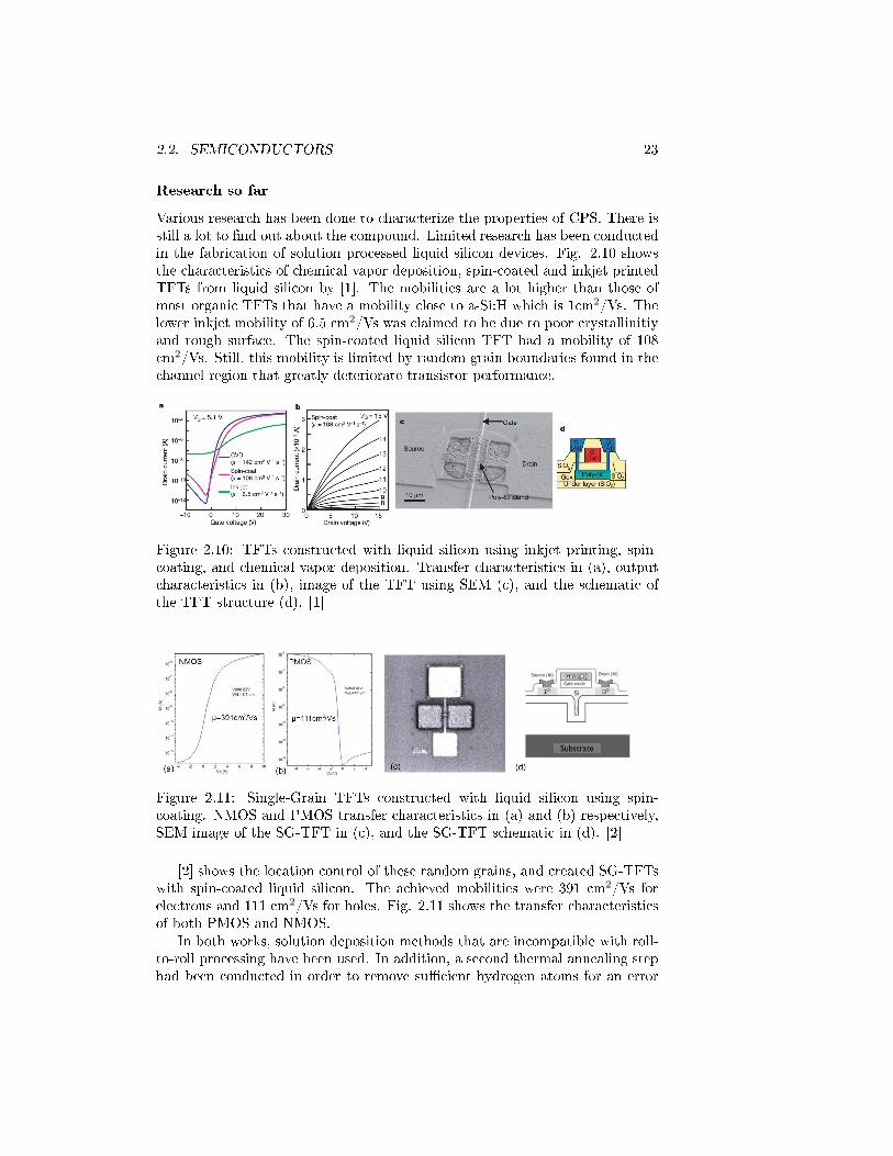
Various research has been done to characterize the properties of CPS. There isstill a lot to �nd out about the compound. Limited research has been conductedin the fabrication of solution processed liquid silicon devices. Fig. 2.10 showsthe characteristics of chemical vapor deposition, spin-coated and inkjet printedTFTs from liquid silicon by [1]. The mobilities are a lot higher than those ofmost organic TFTs that have a mobility close to a-Si:H which is 1cm2/Vs. Thelower inkjet mobility of 6.5 cm2/Vs was claimed to be due to poor crystallinitiyand rough surface. The spin-coated liquid silicon TFT had a mobility of 108cm2/Vs. Still, this mobility is limited by random grain boundaries found in thechannel region that greatly deteriorate transistor performance.
Figure 2.10: TFTs constructed with liquid silicon using inkjet printing, spin-coating, and chemical vapor deposition. Transfer characteristics in (a), outputcharacteristics in (b), image of the TFT using SEM (c), and the schematic ofthe TFT structure (d). [1]
Figure 2.11: Single-Grain TFTs constructed with liquid silicon using spin-coating. NMOS and PMOS transfer characteristics in (a) and (b) respectively,SEM image of the SG-TFT in (c), and the SG-TFT schematic in (d). [2]
[2] shows the location control of these random grains, and created SG-TFTswith spin-coated liquid silicon. The achieved mobilities were 391 cm2/Vs forelectrons and 111 cm2/Vs for holes. Fig. 2.11 shows the transfer characteristicsof both PMOS and NMOS.
In both works, solution deposition methods that are incompatible with roll-to-roll processing have been used. In addition, a second thermal annealing stephad been conducted in order to remove su�cient hydrogen atoms for an error
24 CHAPTER 2. SOLUTION TFT PROCESS AND LIQUID SILICON
free laser crystallization. This second thermal annealing step makes the wholeprocess still incompatible to plastic substrates.
Therefore, in this work, the liquid silicon material has been spread by theprecursor of gravure printing: doctor blade coating. This method is compatiblewith roll-to-roll fabrication. In addition, the second thermal annealing step hasbeen replaced by an Excimer Laser pre-annealing step which is known to unalterthe properties of underlying layers such as the plastic substrate.
Chapter 3
Doctor Blade Coating of
Liquid Silicon
In a gravure printing system the blade is known as the soul of the printer. It isa tool used to remove excess ink that has been covering the surface of a certainpatterned substrate, and de�ne the patterned areas containing ink and the non-patterned areas that are clean as a result of the blading. The excess ink maybe reused and the patterns on the roll or substrate are transferred to a targetsurface. Due to its direct in�uence to the printing result, any defects on theblade will signi�cantly in�uence the �nal result. In electronics this may be thedi�erence between working and failing of an IC.
In this work, the blade has not been used as a scraping tool but as a spreadingtool. In this way, an excess layer is left on top of the substrates while the patternsare �lled. For the production of Single-Grain Thin-Film Transistors (SG-TFTs),the position of single crystal grains are controlled by grain �lter cavities thatneed to be �lled with the liquid silicon. The excess liquid silicon �lm formed ontop of the patterned layer is needed for the grains to grow into during ExcimerLaser crystallization as well as the protection of underlying layers. The thicknessof this layer partly determines the maximum shootable laser energy density andtherefore the maximum obtainable grain size. A layer thickness of at least 100nm is desired to be able to shoot energies similar to [2].
In this chapter, the main goal was to use the doctor blade coating methodfor the deposition of a uniform amorphous silicon layer using the liquid siliconmaterial. First the theory enabling this uniformity is discussed. This section isfollowed by the experimental part, introducing a list of equipment that has beenused as well as the general production method in Section 3.2. Followed by asection explaining the initial experiments for evaluating some of the liquid siliconcharacteristics. Next, the main experiments for the formation of the amorphoussilicon layer is presented, and �nally conclusions and recommendations are given.
25
26 CHAPTER 3. DOCTOR BLADE COATING OF LIQUID SILICON
3.1 Theory
3.1.1 Doctor blade coating
Forces applied on �uids such as the case for doctor blade coating are stronglyrelated to the viscosity of the liquid. The viscosity is de�ned as the measure ofresistance of a �uid that is undergoing shear or tensile stress. For �uids, viscosityis commonly referred to as the thickness of a liquid due to the di�culty of liquidmotion.
Fluid properties can be classi�ed in a system where a material is placed inbetween two large parallel plates. The material is assumed to adhere to theplates. The bottom plate is �xed and a force is applied on the top plate in theparallel direction of both plates. The way the material responds to a shear forceapplied on the top plate can be used to classify properties of the �uid. Thesituation is sketched in Fig. 3.1
Figure 3.1: Schematic of a system of two parallel plates applying shear force ona medium present in between the plates.
A �ow within the medium material is a result of shear stress. This �ow isa combination of di�erent layers that move at di�erent velocities as a result ofshear stress between the layers. The opposing force to this shear stress is de�nedas the viscosity. In this way, a velocity gradient exists from the top plate tothe bottom plate. This shear �ow and velocity gradient de�nes the �uid. Therelation between the applied force and the velocity gradient is described as:
−→Fx = µA
−→uxy
(3.1)
In which−→Fx is the applied force on the top plate, A is the area of the plate, −→ux
is the displacement, y is the distance between the plates, and µ is the propor-tionality factor also known as the dynamic viscosity. In terms of shear stress−→τx:
−→τx = µ
−→∂u
∂y(3.2)
3.1. THEORY 27
The rate of shear deformation−→ux
y is equal to the shear velocity−−→∂ux
∂y and is alsoknown as the shear strain or relative displacement −→γx.
Di�erent types of �uids have di�erent proportionality constants or viscosi-ties. A �uid in which a relative rate of movement is proportional to the appliedforce is known as a Newtonian �uid. In this system µ is a constant. This typeincludes most common �uids such as water, air, glycerin, oils, etc.
A non-Newtonian �uid is one where the shear stress and shear rate are notproportional but are related. µ in this system is not a constant and is a functionof either shear stress −→τx or shear strain −→γx. More complex structured �uids areincluded for this �uid type such as polymers or solutions, suspensions, emulsions,etc. Liquid silicon is assumed to be a non-Newtonian �uid. [35]
The viscosity of liquid silicon can be increased by exposing the base liquidCPS to UV. The UV produces polysilane chains that will lead to a more viscousliquid. The increase in viscosity will result in di�culty in doctor blade coatingthe material. In doctor blade coating, the situation is slightly di�erent; Thetop moving plate is replaced with a plate perpendicular to the bottom plate.The plate also digs into the liquid layer allowing the liquid to be transportedin this method. A high velocity will result in a low shear velocity or relativedisplacement as shown by Eq. 3.2. A movement of the blade in one directionforces the liquid to be pushed in this same direction, however, the liquid hasa low relative displacement, which means that instead of being pushed in thebladed direction, it will pile up and escape through the edges of the blade. Thiswill cause bigger tracks than in a situation where the viscosity is low, where theliquid �ows easily in the same direction as the blade. The situation is illustratedin Fig. 3.2
Figure 3.2: Schematic of the top view of doctor blade coating, showing trailformation.
3.1.2 Surface Free Energy
In this section, the theory behind the surface free energies will be given and isbased on [36] and [37]. The contact angle (θ) is a way to measure the surfaceenergy interactions between a liquid that has been deposited on a solid surface.Fig. 3.3 shows the schematic of the energies present in such a situation.
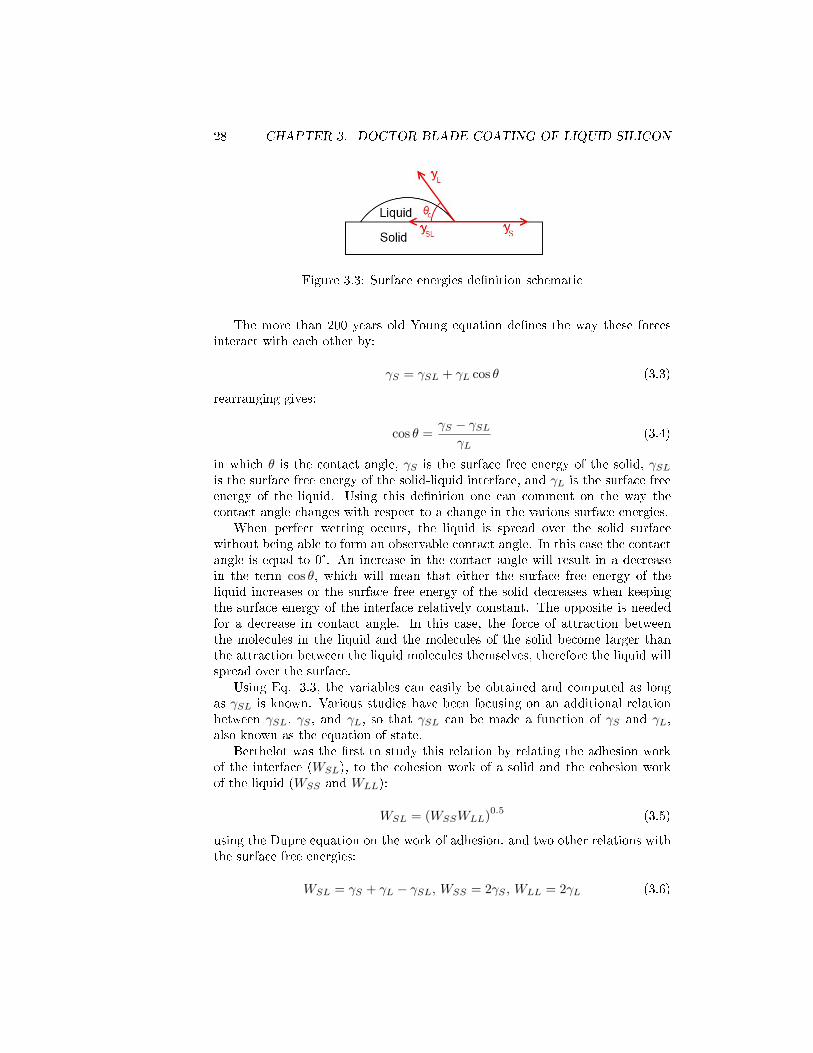
28 CHAPTER 3. DOCTOR BLADE COATING OF LIQUID SILICON
Figure 3.3: Surface energies de�nition schematic
The more than 200 years old Young equation de�nes the way these forcesinteract with each other by:
γS = γSL + γL cos θ (3.3)
rearranging gives:
cos θ =γS − γSL
γL(3.4)
in which θ is the contact angle, γS is the surface free energy of the solid, γSLis the surface free energy of the solid-liquid interface, and γL is the surface freeenergy of the liquid. Using this de�nition one can comment on the way thecontact angle changes with respect to a change in the various surface energies.
When perfect wetting occurs, the liquid is spread over the solid surfacewithout being able to form an observable contact angle. In this case the contactangle is equal to 0°. An increase in the contact angle will result in a decreasein the term cos θ, which will mean that either the surface free energy of theliquid increases or the surface free energy of the solid decreases when keepingthe surface energy of the interface relatively constant. The opposite is neededfor a decrease in contact angle. In this case, the force of attraction betweenthe molecules in the liquid and the molecules of the solid become larger thanthe attraction between the liquid molecules themselves, therefore the liquid willspread over the surface.
Using Eq. 3.3, the variables can easily be obtained and computed as longas γSL is known. Various studies have been focusing on an additional relationbetween γSL, γS , and γL, so that γSL can be made a function of γS and γL,also known as the equation of state.
Berthelot was the �rst to study this relation by relating the adhesion workof the interface (WSL), to the cohesion work of a solid and the cohesion workof the liquid (WSS and WLL):
WSL = (WSSWLL)0.5 (3.5)
using the Dupre equation on the work of adhesion, and two other relations withthe surface free energies:
WSL = γS + γL − γSL, WSS = 2γS , WLL = 2γL (3.6)
3.1. THEORY 29
a de�nition of γSL in terms of γS and γL had been constructed which is alsoknown as the Berthelot hypothesis:
γSL = γS + γL − 2 (γSγL)0.5 (3.7)
which forms the base of following theories attempting to accurately relate γSLto γS and γL.
Grifalco and Good introduce the parameter φ in which the type of interfacialinteractions is further de�ned:
γSL = γS + γL − 2φ (γSγL)0.5 (3.8)
Neumann et al. derive three equations de�ning γSL , the �rst one was basedon thermodynamics, and the other two were based on the Berthelot hypothesis:
γSL ={(γS)
0.5 − (γL)0.5}/{1− 0.015 (γSγL)
0.5}
(3.9)
γSL = γS + γL − 2 (γSγL)0.5
exp{−β1 (γL − γS)2
}(3.10)
γSL = γS + γL − 2 (γSγL)0.5{1− β2 (γL − γS)2
}(3.11)
Where β1 = 0.0001247 and β2 = 0.0001057, both are experimentally deter-mined.
Partition to SFE components
Fowkes initiated the idea of a partitioning of the SFE into components due tovarious interfacial interactions. In this way the SFE of the solid is a sum ofvarious interactive components:
γS = γdS + γpS + γhS + γiS + γabS + γoS (3.12)
the d, p, h, i, ab, and o, stood for the dispersion, polar, hydrogen bond, induc-tion, acid-base, and remaining interactions respectively. The individual com-ponents can be computed in various ways such as the Fowkes method, Owens-Wendt method, and the Van Oss-Chaudhury-Good method. They all requirethe measurements of multiple liquids. A second requirement is that one of theliquids is a dispersion liquid such as diiodomethane.
In this work we have measured multiple liquids: CPS, UV-exposed CPS,and CPS with cyclooctane solution, however, none of these are full dispersionliquids and can therefore not be used to compute the individual components ofthe SFEs.
30 CHAPTER 3. DOCTOR BLADE COATING OF LIQUID SILICON
3.1.3 a-Si �lm formation from liquid silicon
In the experiments, liquid silicon material is used to produce an amorphoussilicon �lm out of a liquid. The term liquid silicon in this context di�ers fromthe liquid silicon used in [1] and [2], and applies to any liquid that has beenused in this work to form the desired amorphous silicon �lm. This includes pureCPS as well as a mixture of CPS and an organic solvent, as well as a either ofthe liquids, exposed to UV. The description of the �lm formation is given usingCPS since this forms the base material.
The compound CPS can be used to form an amorphous silicon �lm aftervarious processing steps. The compound is liquid at room temperatures, trans-forms at plastic compatible temperatures and may be used to crystallize into ahigher quality silicon. Due to this property it can be seen as bringing qualityto solution processing.
The compound reacts strongly to oxygen and water. Processing can thereforenot occur in oxygen and water rich ambient for a high quality a-Si �lm formation.Although vacuum is not required, as is the case in conventional processing, anambient of an inert gas such as nitrogen should be used [6].
When the temperature of the compound is increased to above 300°C, thehydrogen bonds break and leave the material, and as a result, pure silicon isleft [4, 5]. One speci�c issue in this scenario is the fact that the boiling point ofCPS is much lower than this decomposition temperature. Simply heating thecompound to the high temperature will therefore evaporate most of the CPS sothat almost no a-Si layer can be formed. In order to decrease the volatility ofthe material, ring-opening polymerization is required [30, 7].
Photopolymerization The compound can be photopolymerized by exposingit to UV light of a certain range of wavelengths that can break the Si-Si bonds(53kcal/mol). The CPS ring structure opens and can transform into �(SiH2)5-radicals. Wavelengths in between 360nm and 420nm give the best results [6, 11].Wavelengths shorter than 300nm can result in the formation of componentsthat are insoluble and in addition cause di�culty in forming a high qualityamorphous �lm. Wavelengths above 420nm polymerize the compound slowly.Using wavelengths of the speci�ed range will also prevent breaking the chemicalbond of an organic solvent that may be optionally used together with CPS. Thisprevents impurity carbon atoms from getting mixed into the silicon network [34].According to Dr. Shimoda, a wavelength of 365nm gives the best results.
The UV light will structurally cause a deviation in the envelope constructionof CPS, in which the Si atom outside the Si plane deviates at a vibrationalfrequency of 73.5cm-1 [4]. The UV exposure opens these rings and the resultingopened structures can subsequently join other opened CPS structures end-to-end to form long chains called polysilanes that are non-volatile. More Si-Sibonds can however be broken by the UV exposure, making the availability ofsingle long polysilane chains low. The silicon radicals that are produced by thebreaking of the Si-Si bonds can react to oxygen at the surface forming Si2O3 after5 minutes of UV exposure, and Si(SiO2) after 15 minutes of UV exposure[7].
3.1. THEORY 31
The resulting silane compound radicals are insoluble in most common or-ganic solvents, however it has proven to be soluble in the original low ordersilane compound of CPS, as well as a mixture of CPS with a common organicsolvent [7, 8]. In this way, during UV exposure the created polysilane chainsare immediately dissolved in the precursor. UV exposure of CPS can make theliquid more viscous at �rst. After su�cient UV exposure, the liquid transformsinto a white solid. This happens when the average chain length of the polysi-lane chains go up to 400 monomer elements [34]. The length of the polysilanechains due to this UV polymerization have a great e�ect on the viscosity, wet-tability, melting point, boiling point, and adhesion to the substrate, and willincrease these values as the chain length increases. The reactivity with oxygenwill become lower. [34]
The UV exposure of the compound may also break Si-H bonds (76 kcal/mol).This will cause complications in the production of polysilane chains, and willlead to non-linearities in the chain structure, especially in the beginning of theexposure process. More bonds break with increasing exposure times. It hasbeen shown that after 5 minutes of UV exposure already most of the Si atomshave lost one hydrogen atom. After 15 minutes of exposure time, hydrogenatoms cannot be detected anymore. This e�ect is shown by x-ray photoelectronspectroscopy (XPS) of the Si 2p spectrum in Fig. 3.4a. The basis of thisexperiment lies in the fact that when a hydrogen atom is attached to a siliconatom, the binding energy will increase by 0.3 eV for every binding. The peak of99.68 eV is accounted to the neutral silicon. The peak at 99.08 eV correspondsto silicon among other silicon atoms, so the removal of most of the hydrogenatoms. The other peak at 102.48 eV relates to the generation of unsaturatedsurface states due to UV exposure. After 15 minutes of UV exposure the surfaceis fully oxidized to Si(SiO2) and a electron binding energy of 103.15 eV results,which also con�rms the lack of hydrogen in the �lm. [7]. Fig. 3.4b. shows theresults of gel permeation chromatography (GPC) where the size of the producedpolymers are visualized as the broad peak formation.
Thermal Annealing Although most hydrogen atoms are removed duringthe UV exposure process, there is still a need to transform the polysilanes toa three dimensional amorphous network. For this an elevated temperature isrequired that is higher in energy than the binding energies of Si-Si and Si-H.Temperatures less than 300°C are insu�cient to decompose the polysilanes, andit will be impossible to construct a quality silicon �lm. The upper limit of thetemperature is de�ned by the substrate. Although for the construction of poly-crystalline silicon, an annealing temperature of higher than 550°C is required,exposing the amorphous �lm to Excimer laser is an alternative way to trans-form the amorphous material into polycrystalline silicon, resulting in higherelectrical properties without having to expose the substrate to such high tem-peratures [2, 6, 11]. Previous works [1, 2] have constructed an amorphous siliconlayer from liquid silicon at an anealing temperature of 430°C. A second thermalanneal step was used for dehydrogenation before Excimer Laser crystallization
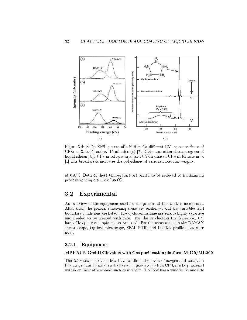
32 CHAPTER 3. DOCTOR BLADE COATING OF LIQUID SILICON
(a) (b)
Figure 3.4: Si 2p XPS spectra of a-Si �lm for di�erent UV exposure times ofCPS: a. 3, b. 5, and c. 15 minutes (a) [7]. Gel permeation chromatogram ofliquid silicon (b). CPS in toluene in a. and UV-irradiated CPS in toluene in b.[1] The broad peak indicates the polysilanes of various molecular weights.
at 650°C. Both of these temperature are aimed to be reduced to a maximumprocessing temperature of 350°C.
3.2 Experimental
An overview of the equipment used for the process of this work is introduced.After that, the general processing steps are explained and the variables andboundary conditions are listed. The cyclopentasilane material is highly sensitiveand needed to be treated with care. For the production the Glovebox, UVlamp, Hot-plate and spin-coater are used. For the measurements the RAMANspectroscope, Optical microscope, SEM, FTIR and DekTak pro�lometer wereused.
3.2.1 Equipment
MBRAUNGmbHGlovebox with Gas puri�cation platformMB20/MB200
The Glovebox is a sealed box that can limit the levels of oxygen and water. Inthis way, materials sensitive to these components, such as CPS, can be processedwithin an inert atmosphere such as nitrogen. The box has a window on one side
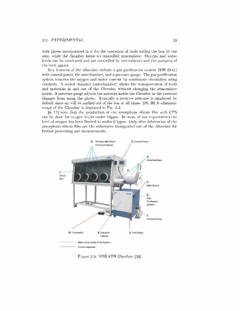
3.2. EXPERIMENTAL 33
with gloves incorporated in it for the operation of tools within the box by theuser, while the chamber keeps its controlled atmosphere. Oxygen and waterlevels can be monitored and are controlled by recirculators and the pumping ofthe inert gasses.
Key features of the Glovebox include a gas puri�cation system (MB 20-G)with control panel, the antechamber, and a pressure gauge. The gas puri�cationsystem removes the oxygen and water content by continuous circulation usingcatalysts. A sealed chamber (antechamber) allows the transportation of toolsand materials in and out of the Glovebox without changing the atmosphereinside. A pressure gauge adjusts the pressure inside the Glovebox as the pressurechanges from using the gloves. Typically a positive pressure is employed bydefault since air will be pushed out of the box at all times. [38, 39] A schematicimage of the Glovebox is displayed in Fig. 3.5.
[6, 11] note that the production of the amorphous silicon �lm with CPScan be done for oxygen levels under 10ppm. In most of our experiments thelevel of oxygen has been limited to under 0.1ppm. Only after fabrication of theamorphous silicon �lm are the substrates transported out of the Glovebox forfurther processing and measurements.
Figure 3.5: MBRAUN Glovebox [39]
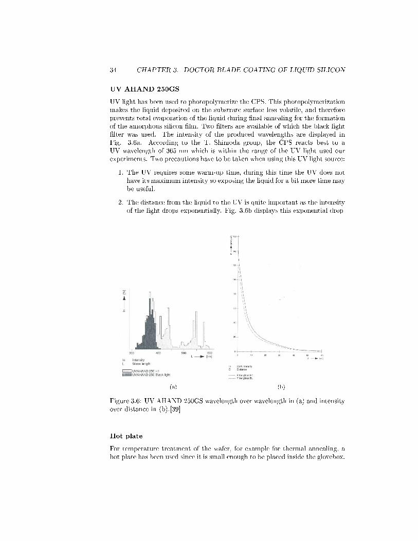
34 CHAPTER 3. DOCTOR BLADE COATING OF LIQUID SILICON
UV AHAND 250GS
UV light has been used to photopolymerize the CPS. This photopolymerizationmakes the liquid deposited on the substrate surface less volatile, and thereforeprevents total evaporation of the liquid during �nal annealing for the formationof the amorphous silicon �lm. Two �lters are available of which the black light�lter was used. The intensity of the produced wavelengths are displayed inFig. 3.6a. According to the T. Shimoda group, the CPS reacts best to aUV wavelength of 365 nm which is within the range of the UV light used ourexperiments. Two precautions have to be taken when using this UV light source:
1. The UV requires some warm-up time, during this time the UV does nothave its maximum intensity so exposing the liquid for a bit more time maybe useful.
2. The distance from the liquid to the UV is quite important as the intensityof the light drops exponentially. Fig. 3.6b displays this exponential drop
(a) (b)
Figure 3.6: UV AHAND 250GS wavelength over wavelength in (a) and intensityover distance in (b).[39]
Hot plate
For temperature treatment of the wafer, for example for thermal annealing, ahot plate has been used since it is small enough to be placed inside the glovebox.
3.2. EXPERIMENTAL 35
It is able to reach high appropriate processing temperatures while the user isallowed to observe changes of the heated sample. Overshoot of approximately 10°C is a problem with this device even for temperature increases of 10°C. Sincethe release of hydrogen atoms during annealing produce silicon radicals anddangling bonds, the liquid silicon material is prone to contamination even in acontrolled atmosphere with limited levels of oxygen and water. A quartz lid hastherefore been used when annealing the substrate to the high temperature sothat no air can enter the amorphous �lm during heating and release of hydrogenatoms cause a slight overpressure inside the lid.
Optical Microscope
An optical microscope has been used as a preliminary analysis of the wafer. Im-ages could be taken by a mounted camera on top of the microscope. From theseimages a �rst impression can be made from the resulting �lm after annealing,but also from laser crystallisation for the next chapter.
SEM
The scanning-electron microscope gives a more thorough analysis of the waythe patterns on the substrate are �lled by the solution. It is a high resolutionmicroscope that can produce images in the nanometer range. The basic workingis the collection of various signals that are formed when a focused beam of highenergy electrons are incidented to a sample. The large amount of kinetic energyof the electron is during absorption of the sample transformed into: secondaryelectrons, backscattered electrons, di�racted backscattered electrons, photons,visible light and heat. Secondary electrons and backscattered electrons are themost important elements for the imaging of the sample. A cross-section of thewafer is viewed by carefully breaking the wafer with the resulting amorphous�lm from the liquid silicon compound. This not only shows the �lling of the basicpatterns, also grain �lters are analyzed in this way during the �rst experiments.The downside of this experiment is that the broken wafer cannot be used forfurther processing. [40]
Renishaw's inVia Raman Microscope
The optical microscope only gives away the position of the liquid silicon by achange in color. To be sure that this change in color is accounted to the de-posited solution, RAMAN spectroscopy is used. The basic working of this toolis identi�cation of a vibrational frequency shift of re�ected light from a sample,compared to the original laser source incidented on a sample. This frequencyshift is also known as the RAMAN e�ect and is based on the molecular defor-mation of the sample into oscillating dipoles due to the electromagnetic wavefrom the excitation source. The periodic deformation results in the materialspeci�c vibration of the molecules. By far, most of the re-emitted photons aresubject to Rayleigh scattering that has the exact same frequency as the original
36 CHAPTER 3. DOCTOR BLADE COATING OF LIQUID SILICON
light source and is of no use for measurement purposes. Only 0.001% of there�ected light is the result of Stokes e�ect and needs to be �ltered. [41]
With this method, the di�erence between amorphous silicon and crystallinesilicon can be visualized. Crystalline silicon will re-emit a narrow peak at avibrational frequency of 521cm−1 due to a high uniformity of bond angles andbond lengths in the material. Due to a wide array of bond angles, energiesand lengths as well as dangling bonds, amorphous has a wider peak in thevibrational spectra positioned at 480cm−1. Since CPS is transformed to anamorphous silicon �lm on top of a crystalline silicon wafer the two peaks can bedistinguished and it can therefore be determined if there has been an amorphoussilicon formation. The light source used for this type of measurement maycrystallize the amorphous silicon itself so a low intensity of 125 µW has beenused for the measurement. [42]
Veeco Dektak 150 Pro�lometer
The two-dimensional, pro�le of any surface can be visualized by using the Dek-tak 150. It uses a high quality, low force stylus (Low-Inertia Sensor, LIS 3) thatruns in a straight line across a surface and plots the changes in height of thestylus while it encounters various patterns on the target surface. A resolution of1 Å can be achieved, at the lowest range setting of 6.5 μm, which was commonlyused in this work since pattern depths were less than 500nm. Due to the limitedrange setting, accuracy issues were inevitable. The force of the stylus was setat 1mg. A video camera allowed the manual positioning of the stylus.[43]
FTIR Spectrometer
Fourier Transform Infrared spectroscopy is a tool that can measure the amountof certain atomic bonds present inside a �lm. In this work, the bounded hy-drogen content is measured within the a-Si �lm formed from liquid silicon. Asource of infrared radiation is sent to through a sample which absorbs some ofthe radiation. This molecular absorption and transmission is measured. Theabsorption peaks are related to the vibrational frequencies of certain bondingtypes (vibrations with a transition dipole moment). In this way, the bondedhydrogen can be measured by sensing the distinctive wagging and stretchingvibrations of the monohydride (Si-H), the dihydride (SiH2) and the trihydride(SiH3). The wagging mode of the con�gurations (e.g. the degenerated rockingand wagging of Si-H and SiH3, and the pure rocking for SiH2) are all locatedat 640cm−1. The amount of bonded hydrogen present inside the �lm (NH) isrelated to the integrated absorption of the prede�ned absorption peak. In caseof the wagging mode:
I640 =
ˆ ( aω
)dω (3.13)
NH640= A640 · I640 (3.14)
3.2. EXPERIMENTAL 37
I640 is the integrated absorption of the 640cm−1 absorption peak, α is the ab-sorption coe�cient found from the measurement, ω is the vibrational frequency,and A640 is the proportionality factor which related to the strength of oscil-lation. This proportionality factor is experimentally determined for which theconstant 1.6·10¹9cm−2 is commonly used for a-Si:H. In this work the I640 ofdi�erent UV exposure times and thermal annealing procedures are evaluated.Note that only bound Hydrogen atoms are obtained in this way. [44, 45]
3.2.2 Working procedure
Initial experiments were conducted using a template procedure from which manyvariations have been tested for the optimization of the �lm formation process.This template is based on [2]:
1. A crystalline silicon wafer is prepared on top of which TEOS is depositedusing PECVD and is patterned.
2. On top of the substrate a predetermined number of drops of 100%CPSwill be deposited by means of a pipette.
3. The drop will be spread by a doctor blade that will lead to a �lling of anypatterns that are present on the surface.
4. After having spread the CPS across the full wafer, the excess is left on topof the wafer to form a protective layer for the Excimer Laser process.
5. The substrate will then be exposed to UV lighting for 10 minutes, dur-ing which the CPS on top of the substrate polymerizes to polysilanes,preventing the �lm from evaporating during the annealing step.
6. The wafer is placed on the hot-plate, and is covered with a quartz lid toprotect the �lm from oxidizing during this annealing step while allowingthe evaporated hydrogen to escape. This hot plate is heated to 200°C.
7. After 1 minute of thermal treatment of 200°C, the temperature of thehotplate is increased to 430°C in 10 minutes.
8. After 1 hour of 430°C thermal annealing, the wafer is slowly cooled downto room temperature.
Changes to this basic procedure have been applied to understand how the �uidbehaves and which procedure gives the best results. Besides the 100% pure CPSthat has been used in many of our experiments we can use other variations onthe liquid silicon material for the creation of the amorphous �lm.
The variations to the liquid silicon that we have used include pure CPSexposed to UV for di�erent numbers of minutes, as well as the CPS mixed withthe organic solvent cyclooctane with 20%wt. of CPS against the solvent. UVexposure of this mixture has also been used for a similar liquid silicon as used
38 CHAPTER 3. DOCTOR BLADE COATING OF LIQUID SILICON
in [2]. The time of the UV exposure is varied but it is ensured that the resulting�uid does not solidify as it is the case for long UV exposure times.
Many di�erent changes can be made within this template procedure. Table3.1 lists these varieties.
The initial approach was to try various combinations on a substrate to seewhat combination gives what type of e�ect. This was followed by a numberof repetitions of the best results and attempts to optimize the best obtainedresults.
3.2.3 Boundary Conditions
The experimental methods we used had a number of limitations. These lim-itations slowed down the optimization process and made repeating processesinevitable as well as inconsistent.
Blading Many di�erent variables existed during the blading of the liquid siliconon the substrate. This was primarily due to the physical inconsistencysince blading was not automated but done by hand. Speed, force, angle ofblade, blading directions, vibrations from the hand were all variables thatcould not be kept as a constant and should always be accounted for.
Impurity Wafers as the target substrates transported into the glovebox fromthe open air have some oxygen or water molecules sticking on the surface.This would in�uence the way the liquid silicon is spread on the wafer aswell as the purity of the deposited material. Another important aspect wasthe way the 100% CPS was stored for usage. This was in a brown jar ontop of a shelf inside the glovebox. The glovebox although limited in waterand oxygen content, could cause degrading of the material over time dueto not only the molecules in the atmosphere, but also temperature changesfrom the hot-plate placed inside the box. Transportation of tools insidethe glovebox increases the oxygen and water content to 15ppm at most.
Equipment Inaccuracies during measurement can be misleading for the judg-ment of the �nal result. Primary judgment in many cases come from theoptical microscope. Roughness of the surface although visible opticallythrough changes in colors, was not detectable using the pro�lometer orother tools that we have used.
3.3 Characterization Experiments
Before attempting to get the best amorphous silicon �lms, some basic charac-teristics of the liquid silicon material should be identi�ed. In this section, someimportant aspects of the liquid are presented: Thickness of the �lm, the e�ect ofdi�erent types of liquid silicon, the surface free energies of various surfaces thatwe have used, the RAMAN proof that the liquid indeed transforms into amor-phous silicon, and FTIR results for the e�ect of the variations to the standardprocedure to the bounded hydrogen content.
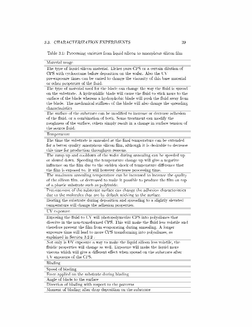
3.3. CHARACTERIZATION EXPERIMENTS 39
Table 3.1: Processing varieties from liquid silicon to amorphous silicon �lm
Material usage
The type of liquid silicon material. Either pure CPS or a certain dilution ofCPS with cyclooctane before deposition on the wafer. Also the UVpre-exposure times can be varied to change the viscosity of this base materialor other properties of the �uid.The type of material used for the blade can change the way the �uid is spreadon the substrate. A hydrophillic blade will cause the �uid to stick more to thesurface of the blade whereas a hydrophobic blade will push the �uid away fromthe blade. The mechanical sti�ness of the blade will also change the spreadingcharacteristicsThe surface of the substrate can be modi�ed to increase or decrease adhesionof the �uid, or a combination of both. Some treatment can modify theroughness of the surface, others simply result in a change in surface tension ofthe source �uid.
Temperature
The time the substrate is annealed at the �nal temperature can be extendedfor a better quality amorphous silicon �lm, although it is desirable to decreasethis time for production throughput reasons.The ramp up and cooldown of the wafer during annealing can be speeded upor slowed down. Speeding the temperature change up will give a negativein�uence on the �lm due to the sudden shock of temperature di�erence thatthe �lm is exposed to. It will however decrease processing time.The maximum annealing temperature can be increased to increase the qualityof the silicon �lm, or decreased to make it possible to produce the �lm on topof a plastic substrate such as polyimide.Pretreatment of the substrate surface can change the adhesion characteristicsdue to the molecules that are by default sticking to the surface.Heating the substrate during deposition and spreading to a slightly elevatedtemperature will change the adhesion properties.
UV exposure
Exposing the �uid to UV will photopolymerize CPS into polysilanes thatdissolve in the non-transformed CPS. This will make the �uid less volatile andtherefore prevent the �lm from evaporating during annealing. A longerexposure time will lead to more CPS transforming into polysilanes, asexplained in Section 3.2.2 .Not only is UV exposure a way to make the liquid silicon less volatile, the�uidic properties will change as well. Exposure will make the liquid moreviscous which will give a di�erent e�ect when spread on the substrate afterUV exposure of the CPS.
Blading
Speed of bladingForce applied on the substrate during bladingAngle of blade to the surfaceDirection of blading with respect to the patternsMoment of blading after drop deposition on the substrate
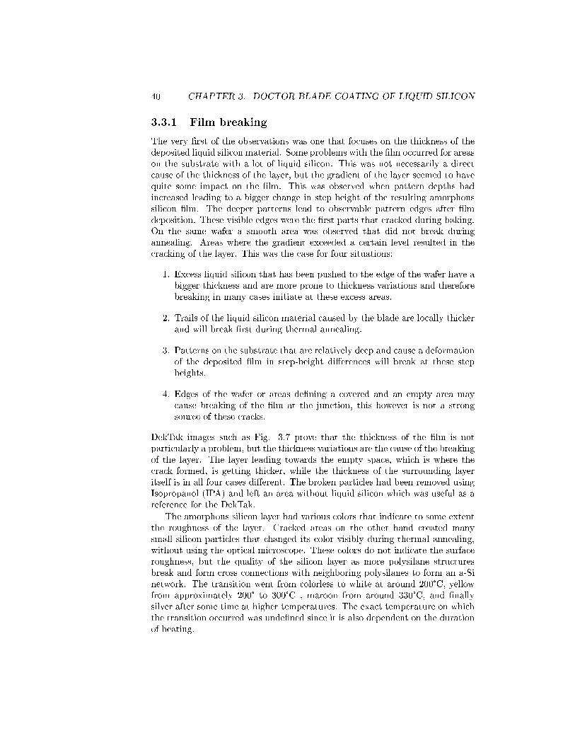
40 CHAPTER 3. DOCTOR BLADE COATING OF LIQUID SILICON
3.3.1 Film breaking
The very �rst of the observations was one that focuses on the thickness of thedeposited liquid silicon material. Some problems with the �lm occurred for areason the substrate with a lot of liquid silicon. This was not necessarily a directcause of the thickness of the layer, but the gradient of the layer seemed to havequite some impact on the �lm. This was observed when pattern depths hadincreased leading to a bigger change in step height of the resulting amorphoussilicon �lm. The deeper patterns lead to observable pattern edges after �lmdeposition. These visible edges were the �rst parts that cracked during baking.On the same wafer a smooth area was observed that did not break duringannealing. Areas where the gradient exceeded a certain level resulted in thecracking of the layer. This was the case for four situations:
1. Excess liquid silicon that has been pushed to the edge of the wafer have abigger thickness and are more prone to thickness variations and thereforebreaking in many cases initiate at these excess areas.
2. Trails of the liquid silicon material caused by the blade are locally thickerand will break �rst during thermal annealing.
3. Patterns on the substrate that are relatively deep and cause a deformationof the deposited �lm in step-height di�erences will break at these stepheights.
4. Edges of the wafer or areas de�ning a covered and an empty area maycause breaking of the �lm at the junction, this however is not a strongsource of these cracks.
DekTak images such as Fig. 3.7 prove that the thickness of the �lm is notparticularly a problem, but the thickness variations are the cause of the breakingof the layer. The layer leading towards the empty space, which is where thecrack formed, is getting thicker, while the thickness of the surrounding layeritself is in all four cases di�erent. The broken particles had been removed usingIsopropanol (IPA) and left an area without liquid silicon which was useful as areference for the DekTak.
The amorphous silicon layer had various colors that indicate to some extentthe roughness of the layer. Cracked areas on the other hand created manysmall silicon particles that changed its color visibly during thermal annealing,without using the optical microscope. These colors do not indicate the surfaceroughness, but the quality of the silicon layer as more polysilane structuresbreak and form cross connections with neighboring polysilanes to form an a-Sinetwork. The transition went from colorless to white at around 200°C, yellowfrom approximately 200° to 300°C , maroon from around 330°C, and �nallysilver after some time at higher temperatures. The exact temperature on whichthe transition occurred was unde�ned since it is also dependent on the durationof heating.
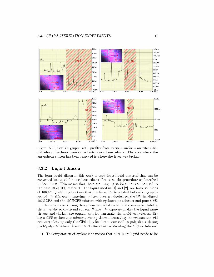
3.3. CHARACTERIZATION EXPERIMENTS 41
Figure 3.7: DekTak graphs with pro�les from various surfaces on which liq-uid silicon has been transformed into amorphous silicon. The area where theamorphous silicon has been removed is where the layer was broken.
3.3.2 Liquid Silicon
The term liquid silicon in this work is used for a liquid material that can beconverted into a solid amorphous silicon �lm using the procedure as describedin Sec. 3.2.2. This means that there are many variations that can be used tothe base 100%CPS material. The liquid used in [1] and [2], are both solutionsof 100%CPS with cyclooctane that has been UV irradiated before being spin-coated. In this work, experiments have been conducted on the UV irradiated100%CPS and the 100%CPS mixture with cyclooctane solution and pure CPS.
The advantage of using the cyclooctane solution is the increasing wettabilitycharacteristic of the liquid silicon. While UV exposure makes the liquid moreviscous and thicker, the organic solution can make the liquid less viscous. Us-ing a CPS-cyclooctane mixture, during thermal annealing the cyclooctane willevaporate leaving only the CPS that has been converted to polysilanes duringphotopolymerization. A number of issues exist when using the organic solution:
1. The evaporation of cyclooctane means that a lot more liquid needs to be
42 CHAPTER 3. DOCTOR BLADE COATING OF LIQUID SILICON
deposited to get a similar amorphous �lm thickness as when using pureCPS. When only small amounts are used, as possible for blading, thesolution quickly dries out.
2. The mixture introduces carbon atoms in the �lm that degrade its quality,although the boiling point of cyclooctane (149°C) is slightly lower thanthat of CPS (194°C).
3. When using only a little amount of the liquid silicon, which is possiblefor doctor blade coating, the organic solution dries rapidly. For spin-coating this problem does not exist, as large amount of the liquid siliconis deposited and spread across the wafer in a matter of seconds. In doctorblade coating however, drying will occur during every movement of theblade causing uniformity issues.
4. Grain �lter cavities �lled with the mixture of CPS and cyclooctane resultin amorphous silicon that has shrunk inside the �lter. As the cyclooctaneevaporates, part of the amorphous silicon is already solidi�ed and cannotre�ll the grain �lter. Smaller cavities inside the grain �lter will causeissues during laser crystallization.
Due to these issues, this work does not use any organic solution for the produc-tion of the liquid silicon SG-TFT.
Exposing the CPS to UV, will make the liquid more viscous. A longerexposure time results in more polysilane production while at the same timebeing dissolved into the source CPS material. Varying this exposure time canchange the properties of the liquid silicon such as viscosity, volatility as wellas wettability. Increasing the viscosity through UV exposure has lead to trackformation when doctor blade coating which is undesirable. Omission of this stepresults in the evaporation of CPS before the decomposition to a silicon �lm.
3.3.3 Surface Free Energy
The way a liquid reacts to a solid surface is dependent on the surface energiesassociated to both materials. These surface energies can be obtained by mea-suring the way a droplet is formed on the solid surface, i.e. the contact angle.A liquid can in this way obtain controlled spreading as is also used in o�setlithography printing.
Three surface modi�cation techniques as well as a number of di�erent sub-strates have been tested. The modi�cation techniques are: 0.55%HF dip for 4minute which is a common way to remove native oxide from a silicon wafer ata rate of 15nm/min, O2 plasma and Argon plasma that bombard the surface,making it rougher. The HF dip does not signi�cantly deform the patterns onthe substrate, and Argon is a heavier alternative to Oxygen. Fig. 3.8 shows thedi�erent contact angles of pure CPS. The two thermal oxide surfaces indicatedi�erent sessions. It is important to note however that in most cases the contactangle reduced over time indicating a dependence on the time that the liquid is in
3.3. CHARACTERIZATION EXPERIMENTS 43
Figure 3.8: Contact angle graphs, di�erent surface modi�cations on di�erenttypes of oxide, using pure CPS.
contact with the surface. The experimental data is based on the contact anglesapproximately 1 to 2 seconds after droplet deposition. The main conclusionsthat could be derived from these were:
Temperature An elevated temperature of the substrate has a big e�ect on thewettability of the liquid silicon. This is both because it is more di�cultfor the molecules within a droplet to stay together due to thermal motion,and because the liquid reacts in some way with the oxide surface. Bothe�ects allow the liquid to spread over time.
Surface treatment 0.55%HF dip for 4 minutes gave the best wettability prop-erties compared to most of the plasma surface modi�cation types. Addingthe elevated temperature of 75°C shows that the HF treatment gives betterwettability than high pressure, 550W Argon, that shows a lower contactangle at room temperatures. The plasma treatment, bombards the surfacewith either Oxygen or the heavier Argon molecules which make the surfacemore rough allowing more of the liquid silicon molecules to react to thesurface. The HF however makes the surface more smooth which allows aneasier spreading. Varying the plasma conditions for Oxygen plasma gaveonly limited variations to the �nal contact angle.
Liquid Silicon The variations of the liquid silicon material from the base CPScompound has di�erent e�ects on the contact angle. A 20wt.% of CPS incyclooctane reduces the contact angle on all surface to zero. UV exposingthe base CPS material makes the liquid more viscous, which lead to ahigher contact angle on all surfaces.
Material The surface material, although for SG-TFT a TEOS surface is re-quired, for the �nal gravure printing cylinder, other material types may beused. Aluminum showed the highest wettability of liquid silicon, whereassilicon nitride gave the highest contact angle of 33.4°.
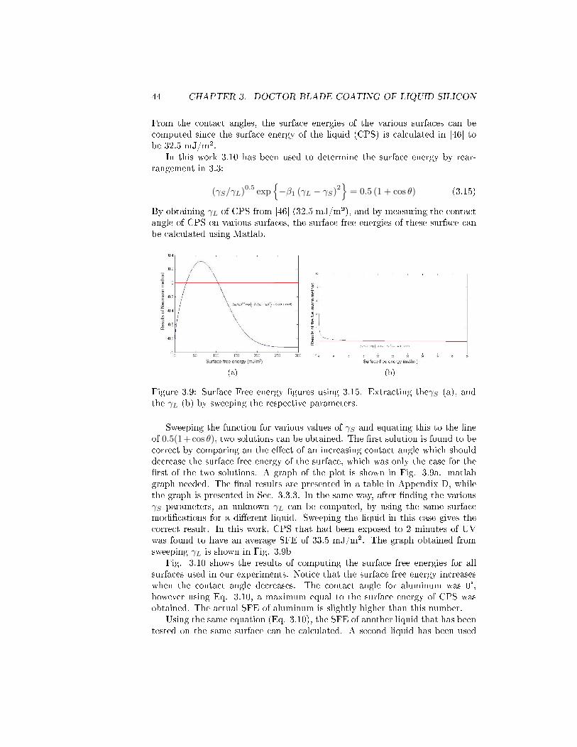
44 CHAPTER 3. DOCTOR BLADE COATING OF LIQUID SILICON
From the contact angles, the surface energies of the various surfaces can becomputed since the surface energy of the liquid (CPS) is calculated in [46] tobe 32.5 mJ/m².
In this work 3.10 has been used to determine the surface energy by rear-rangement in 3.3:
(γS/γL)0.5
exp{−β1 (γL − γS)2
}= 0.5 (1 + cos θ) (3.15)
By obtaining γL of CPS from [46] (32.5 mJ/m²), and by measuring the contactangle of CPS on various surfaces, the surface free energies of these surface canbe calculated using Matlab.
(a) (b)
Figure 3.9: Surface Free energy �gures using 3.15. Extracting theγS (a), andthe γL (b) by sweeping the respective parameters.
Sweeping the function for various values of γS and equating this to the lineof 0.5(1+cos θ), two solutions can be obtained. The �rst solution is found to becorrect by comparing an the e�ect of an increasing contact angle which shoulddecrease the surface free energy of the surface, which was only the case for the�rst of the two solutions. A graph of the plot is shown in Fig. 3.9a. matlabgraph needed. The �nal results are presented in a table in Appendix D, whilethe graph is presented in Sec. 3.3.3. In the same way, after �nding the variousγS parameters, an unknown γL can be computed, by using the same surfacemodi�cations for a di�erent liquid. Sweeping the liquid in this case gives thecorrect result. In this work, CPS that had been exposed to 2 minutes of UVwas found to have an average SFE of 33.5 mJ/m². The graph obtained fromsweeping γL is shown in Fig. 3.9b
Fig. 3.10 shows the results of computing the surface free energies for allsurfaces used in our experiments. Notice that the surface free energy increaseswhen the contact angle decreases. The contact angle for aluminum was 0°,however using Eq. 3.10, a maximum equal to the surface energy of CPS wasobtained. The actual SFE of aluminum is slightly higher than this number.
Using the same equation (Eq. 3.10), the SFE of another liquid that has beentested on the same surface can be calculated. A second liquid has been used
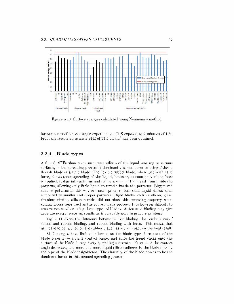
3.3. CHARACTERIZATION EXPERIMENTS 45
Figure 3.10: Surface energies calculated using Neumann's method
for one series of contact angle experiments: CPS exposed to 2 minutes of UV.From the results an average SFE of 33.5 mJ/m² has been obtained.
3.3.4 Blade types
Although SFEs show some important e�ects of the liquid reacting to varioussurfaces, in the spreading process it dominantly comes down to using either a�exible blade or a rigid blade. The �exible rubber blade, when used with littleforce, allows some spreading of the liquid, however, as soon as a minor forceis applied, it digs into patterns and removes some of the liquid from inside thepatterns, allowing only little liquid to remain inside the patterns. Bigger andshallow patterns in this way are more prone to lose their liquid silicon thancompared to smaller and deeper patterns. Rigid blades such as silicon, glass,titanium nitride, silicon nitride, did not show this removing property whensimilar forces were used as the rubber blade process. It is however di�cult toremove excess when using these types of blades. Automated blading may giveaccurate excess removing results as is currently used in gravure printers.
Fig. 3.11 shows the di�erence between silicon blading, the combination ofsilicon and rubber blading, and rubber blading with force. This shows thatusing the force applied on the rubber blade has a big impact on the �nal result.
SFE energies have limited in�uence on the blade type since none of theblade types have a large contact angle, and since the liquid sticks onto thesurface of the blade during every spreading movement. Over time the contactangle decreases, and more and more liquid silicon adheres to the blade makingthe type of the blade insigni�cant. The elasticity of the blade proves to be thedominant factor in this manual spreading process.
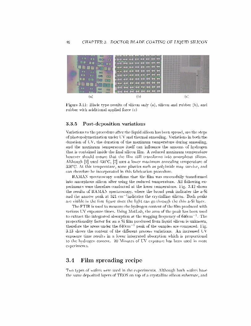
46 CHAPTER 3. DOCTOR BLADE COATING OF LIQUID SILICON
(a) (b) (c)
Figure 3.11: Blade type results of silicon only (a), silicon and rubber (b), andrubber with additional applied force (c)
3.3.5 Post-deposition variations
Variations to the procedure after the liquid silicon has been spread, are the stepsof photopolymerization under UV and thermal annealing. Variations in both theduration of UV, the duration of the maximum temperature during annealing,and the maximum temperature itself can in�uence the amount of hydrogenthat is contained inside the �nal silicon �lm. A reduced maximum temperaturehowever should ensure that the �lm still transforms into amorphous silicon.Although [2] used 430°C, [7] uses a lower maximum annealing temperature of350°C. At this temperature, some plastics such as polyimide may survive, andcan therefore be incorporated in this fabrication procedure.
RAMAN spectroscopy con�rms that the �lm was successfully transformedinto amorphous silicon after using the reduced temperature. All following ex-periments were therefore conducted at the lower temperature. Fig. 3.12 showsthe results of RAMAN spectroscopy, where the broad peak indicates the a-Siand the narrow peak at 521 cm−1indicates the crystalline silicon. Both peaksare visible in the �rst �gure since the light can go through the thin a-Si layer.
The FTIR is used to measure the hydrogen content of the �lm produced withvarious UV exposure times. Using MatLab, the area of the peak has been usedto extract the integrated absorption at the wagging frequency of 640cm−1. Theproportionality factor for an a-Si �lm produced from liquid silicon is unknown,therefore the areas under the 640cm−1 peak of the samples are compared. Fig.3.13 shows the content of the di�erent process variations. An increased UVexposure time results in a lower integrated absorption which is proportionalto the hydrogen content. 20 Minutes of UV exposure has been used in mostexperiments.
3.4 Film spreading recipe
Two types of wafers were used in the experiments. Although both wafers havethe same deposited layers of TEOS on top of a crystalline silicon substrate, and
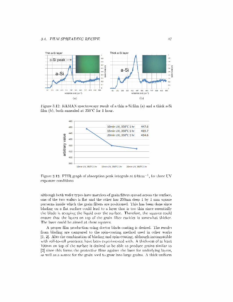
3.4. FILM SPREADING RECIPE 47
(a) (b)
Figure 3.12: RAMAN spectroscopy result of a thin a-Si �lm (a) and a thick a-Si�lm (b), both annealed at 350°C for 1 hour.
Figure 3.13: FTIR graph of absorption peak integrals at 640cm−1, for three UVexposure conditions
although both wafer types have matrices of grain �lters spread across the surface,one of the two wafers is �at and the other has 250nm deep 1 by 1 mm squarepatterns inside which the grain �lters are positioned. This has been done sinceblading on a �at surface could lead to a layer that is too thin since essentiallythe blade is scraping the liquid over the surface. Therefore, the squares couldensure that the layers on top of the grain �lter cavities is somewhat thicker.The laser could be aimed at these squares.
A proper �lm production using doctor blade coating is desired. The resultsfrom blading are compared to the spin-coating method used in other works[1, 2]. Also the combination of blading and spin-coating, although incompatiblewith roll-to-roll processes, have been experimented with. A thickness of at least100nm on top of the surface is desired to be able to produce grains similar to[2] since this forms the protective �lms against the laser for underlying layers,as well as a source for the grain seed to grow into large grains. A thick uniform
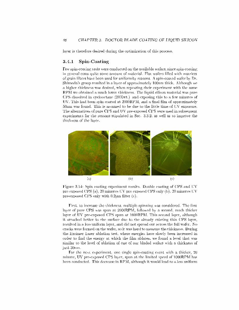
48 CHAPTER 3. DOCTOR BLADE COATING OF LIQUID SILICON
layer is therefore desired during the optimization of this process.
3.4.1 Spin-Coating
Few spin-coating tests were conducted on the available wafers, since spin-coatingin general costs quite some amount of material. Flat wafers �lled with matricesof grain �lters have been used for uniformity reasons. A spin-coated wafer by Dr.Shimoda's group resulted in a layer of approximately 100nm thick. Although wea higher thickness was desired, when repeating their experiment with the sameRPM we obtained a much lower thickness. The liquid silicon material was pureCPS dissolved in cyclooctane (20%wt.) and exposing this to a few minutes ofUV. This had been spin-coated at 2000RPM, and a �nal �lm of approximately50nm was found. This is assumed to be due to the little time of UV exposure.The alternatives of pure CPS and UV pre-exposed CPS were used in subsequentexperiments for the reasons stipulated in Sec. 3.3.2, as well as to improve thethickness of the layer.
(a) (b) (c)
Figure 3.14: Spin-coating experiment results. Double coating of CPS and UVpre-exposed CPS (a), 20 minutes UV pre-exposed CPS only (b), 20 minutes UVpre-exposed CPS only with 0.2μm �lter (c).
First, to increase the thickness, multiple spinning was considered. The �rstlayer of pure CPS was spun at 2000RPM, followed by a second, much thickerlayer of UV pre-exposed CPS spun at 1000RPM. This second layer, althoughit attached better to the surface due to the already existing thin CPS layer,resulted in a less uniform layer, and did not spread out across the full wafer. Nocracks were formed on the wafer, so it was hard to measure the thickness. Duringthe Excimer Laser ablation test, where energies have slowly been increased inorder to �nd the energy at which the �lm ablates, we found a level that wassimilar to the level of ablation of one of our bladed wafers with a thickness ofjust 30nm.
For the next experiment, one single spin-coating event with a thicker, 20minute, UV pre-exposed CPS layer, spun at the limited speed of 1000RPM hasbeen conducted. This decrease in RPM, although it would lead to a less uniform
3.4. FILM SPREADING RECIPE 49
spread of the liquid, the irregularities caused by the �rst spinning event in theprevious experiment caused the limited spread of the liquid silicon material.This decrease in spin speed will result in a thicker layer and even if it would notcover the whole wafer, we wished for it to cover at least some limited numberof dies.
The second experiment, as expected, did not cover the wafer well even thoughan increased amount of UV pre-exposed CPS had been used compared to theprevious experiment. The covered area broke completely due to the thicknessvariations combined with the large amount of di�erent sized polysilanes thatcause the �nal layer to lack uniformity and spreadability. Although the thicknessof the cracks was approximately 400 to 450nm as observed from the DekTakpro�lometer, the test of �ltering out di�erent lengths of polysilanes had notbeen executed before. Some parts of �lms from this experiment had a thicknessof 50 to 100nm.
The third spin-coating experiment had been conducted by using the exactsame UV pre-exposure time from the second experiment of 20 minutes, and�ltering various sized polysilanes out with a 0.2μm �lter. Only little liquid hadbeen deposited due to the �lter which reduced the total amount. This littleliquid �rst of all resulted in a worse wafer coverage, and also created a layerthat had cracked all over.
From these experiments the CPS with pre-exposed UV lead to many errorsin the resulting �lm. Using CPS only for spin-coating will result in a thicknesswhich is too low. A combination of a pre-existing layer such as used in the�rst of the listed experiments, should help cover a bigger area with the liquidsilicon material. This is due to the time-dependency of the liquid with theTEOS as found in the SFE experiments in Sec. 3.3.3. But to prevent using alot of CPS material for this initial layer, the layer can be bladed with limitednumber of droplets to at least cover the whole wafer once. The three spin-coatingexperiment results are displayed in Fig. 3.14.
3.4.2 Blading
Blade types have been investigated in Sec. 3.3.4 and it was found that the rigidblade type was a good way to spread the liquid silicon and �ll the patterns,whereas a �exible blade type could be used to remove excess liquid. A com-bination of the two lead to the 1 by 1 mm squares losing their contents dueto the size of these squares and the rubber blade. The resulting thickness wasapproximately 30nm. The combination had also been tested with less force onthe rubber blade and omission of the rubber blade. Cracks in the latter processwere only observed in limited parts, and revealed a thickness ranging from 200to 300nm which was our desired thickness. It was also found that the resultinglayer did not �ll the squares but simply formed a layer with a similar step height.Grain �lters however did get completely �lled displayed in Fig. 3.16.
Care has to be taken when a step height in any part of the wafer is presentsince this in many cases leads to a crack in the resulting a-Si layer. Although thesurface modi�cation techniques on the blade would have limited e�ect, the sur-
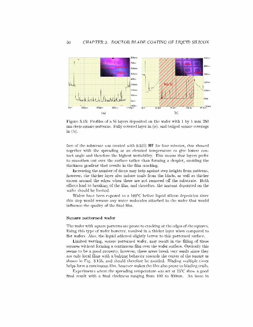
50 CHAPTER 3. DOCTOR BLADE COATING OF LIQUID SILICON
(a) (b)
Figure 3.15: Pro�les of a-Si layers deposited on the wafer with 1 by 1 mm 250nm deep square patterns. Fully covered layer in (a), and bulged square coveragein (b).
face of the substrate was treated with 0.55% HF for four minutes, that showedtogether with the spreading at an elevated temperature to give lowest con-tact angle and therefore the highest wettability. This means that layers preferto smoothen out over the surface rather than forming a droplet, avoiding thethickness gradient that results in the �lm cracking.
Increasing the number of drops may help against step heights from patterns,however, the thicker layer also induce trails from the blade, as well as thickerexcess around the edges when these are not removed o� the substrate. Bothe�ects lead to breaking of the �lm, and therefore, the amount deposited on thewafer should be limited.
Wafers have been exposed to a 100°C before liquid silicon deposition sincethis step would remove any water molecules attached to the wafer that wouldin�uence the quality of the �nal �lm.
Square patterned wafer
The wafer with square patterns are prone to cracking at the edges of the squares.Using this type of wafer however, resulted in a thicker layer when compared to�at wafers. Also, the liquid adhered slightly better to this patterned surface.
Limited wetting, square patterned wafer, may result in the �lling of thesesquares without forming a continuous �lm over the wafer surface. Optically thisseems to be a good property, however, these areas break very easily since theyare only local �lms with a bulging behavior towards the center of the square asshown in Fig. 3.15b, and should therefore be avoided. Blading multiple timeshelps form a continuous �lm, however makes the �lm also prone to blading trails.
Experiments where the spreading temperature was set at 75°C show a good�nal result with a �nal thickness ranging from 100 to 300nm. An issue in
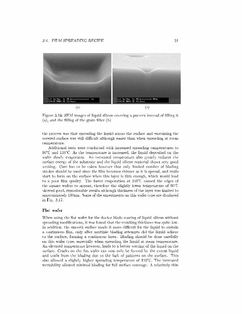
3.4. FILM SPREADING RECIPE 51
(a) (b)
Figure 3.16: SEM images of liquid silicon covering a pattern instead of �lling it(a), and the �lling of the grain �lter (b)
the process was that spreading the liquid across the surface and sustaining thecovered surface was still di�cult although easier than when spreading at roomtemperature.
Additional tests were conducted with increased spreading temperatures to90°C and 110°C. As the temperature is increased, the liquid deposited on thewafer slowly evaporates. An increased temperature also greatly reduces thesurface energy of the substrate and the liquid silicon material shows very goodwetting. Care has to be taken however that only limited number of bladingstrokes should be used since the �lm becomes thinner as it is spread, and trailsstart to form on the surface when this layer is thin enough, which would leadto a poor �lm quality. The faster evaporation at 110°C caused the edges ofthe square wafers to appear, therefore the slightly lower temperature of 90°Cshowed good, reproducible results although thickness of the layer was limited toapproximately 100nm. Some of the experiments on this wafer type are displayedin Fig. 3.17.
Flat wafer
When using the �at wafer for the doctor blade coating of liquid silicon withoutspreading modi�cations, it was found that the resulting thickness was quite low.In addition, the smooth surface made it more di�cult for the liquid to sustaina continuous �lm, only after multiple blading attempts did the liquid adhereto the surface, forming a continuous layer. Blading should be done carefullyon this wafer type, especially when spreading the liquid at room temperature.An elevated temperature however, leads to a better wetting of the liquid on thesurface. Cracks on the �at wafer can now only be formed by the excess liquidand trails from the blading due to the lack of patterns on the surface. Thisalso allowed a slightly higher spreading temperature of 110°C. The increasedwettability allowed minimal blading for full surface coverage. A relatively thin
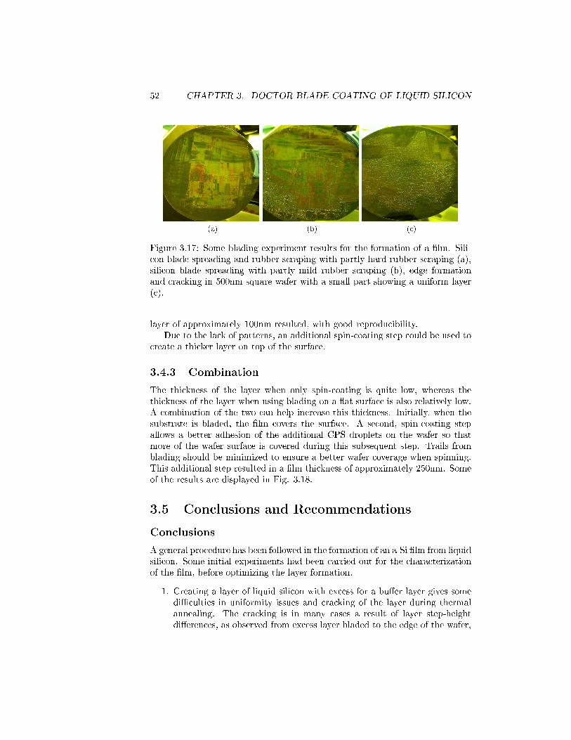
52 CHAPTER 3. DOCTOR BLADE COATING OF LIQUID SILICON
(a) (b) (c)
Figure 3.17: Some blading experiment results for the formation of a �lm. Sili-con blade spreading and rubber scraping with partly hard rubber scraping (a),silicon blade spreading with partly mild rubber scraping (b), edge formationand cracking in 500nm square wafer with a small part showing a uniform layer(c).
layer of approximately 100nm resulted, with good reproducibility.Due to the lack of patterns, an additional spin-coating step could be used to
create a thicker layer on top of the surface.
3.4.3 Combination
The thickness of the layer when only spin-coating is quite low, whereas thethickness of the layer when using blading on a �at surface is also relatively low.A combination of the two can help increase this thickness. Initially, when thesubstrate is bladed, the �lm covers the surface. A second, spin-coating stepallows a better adhesion of the additional CPS droplets on the wafer so thatmore of the wafer surface is covered during this subsequent step. Trails fromblading should be minimized to ensure a better wafer coverage when spinning.This additional step resulted in a �lm thickness of approximately 250nm. Someof the results are displayed in Fig. 3.18.
3.5 Conclusions and Recommendations
Conclusions
A general procedure has been followed in the formation of an a-Si �lm from liquidsilicon. Some initial experiments had been carried out for the characterizationof the �lm, before optimizing the layer formation.
1. Creating a layer of liquid silicon with excess for a bu�er layer gives somedi�culties in uniformity issues and cracking of the layer during thermalannealing. The cracking is in many cases a result of layer step-heightdi�erences, as observed from excess layer bladed to the edge of the wafer,
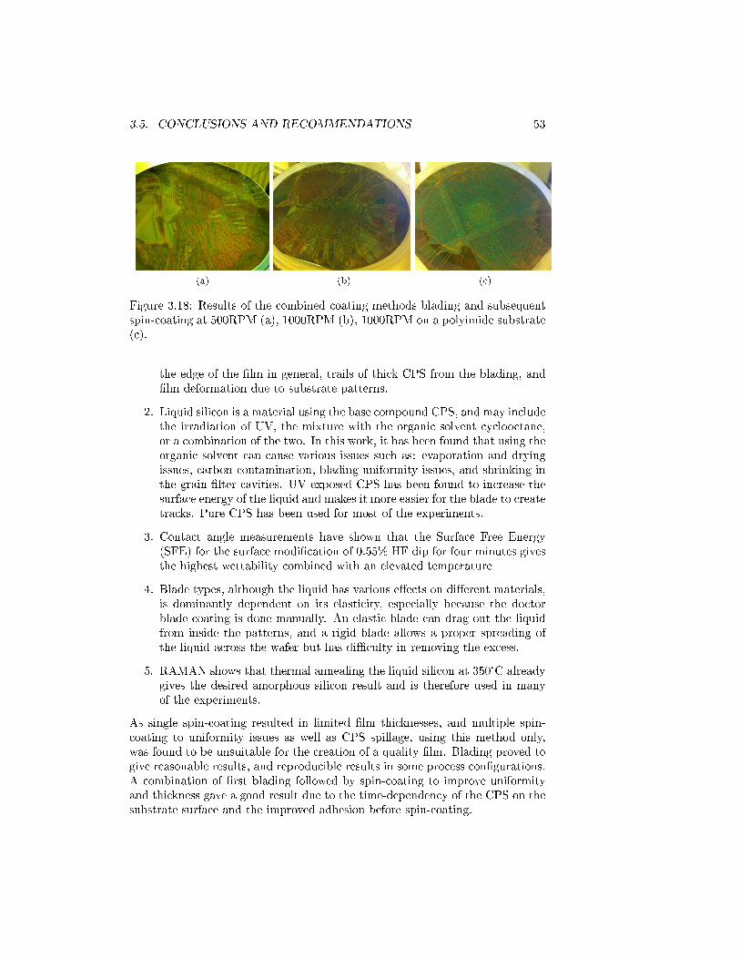
3.5. CONCLUSIONS AND RECOMMENDATIONS 53
(a) (b) (c)
Figure 3.18: Results of the combined coating methods blading and subsequentspin-coating at 500RPM (a), 1000RPM (b), 1000RPM on a polyimide substrate(c).
the edge of the �lm in general, trails of thick CPS from the blading, and�lm deformation due to substrate patterns.
2. Liquid silicon is a material using the base compound CPS, and may includethe irradiation of UV, the mixture with the organic solvent cyclooctane,or a combination of the two. In this work, it has been found that using theorganic solvent can cause various issues such as: evaporation and dryingissues, carbon contamination, blading uniformity issues, and shrinking inthe grain �lter cavities. UV exposed CPS has been found to increase thesurface energy of the liquid and makes it more easier for the blade to createtracks. Pure CPS has been used for most of the experiments.
3. Contact angle measurements have shown that the Surface Free Energy(SFE) for the surface modi�cation of 0.55% HF dip for four minutes givesthe highest wettability combined with an elevated temperature
4. Blade types, although the liquid has various e�ects on di�erent materials,is dominantly dependent on its elasticity, especially because the doctorblade coating is done manually. An elastic blade can drag out the liquidfrom inside the patterns, and a rigid blade allows a proper spreading ofthe liquid across the wafer but has di�culty in removing the excess.
5. RAMAN shows that thermal annealing the liquid silicon at 350°C alreadygives the desired amorphous silicon result and is therefore used in manyof the experiments.
As single spin-coating resulted in limited �lm thicknesses, and multiple spin-coating to uniformity issues as well as CPS spillage, using this method only,was found to be unsuitable for the creation of a quality �lm. Blading proved togive reasonable results, and reproducible results in some process con�gurations.A combination of �rst blading followed by spin-coating to improve uniformityand thickness gave a good result due to the time-dependency of the CPS on thesubstrate surface and the improved adhesion before spin-coating.
54 CHAPTER 3. DOCTOR BLADE COATING OF LIQUID SILICON
An increased number of droplets improve the coverage of the liquid acrossthe wafer. A continuous layer is more quickly formed, however, thick tracks canbe produced by blading this large amount of liquid that can break. Using lessliquid silicon, may cause di�culty in covering the full wafer so multiple bladestrokes may be necessary but will in its turn cause tracks on the �lm that areprone to breaking or create a low quality �lm. Elevated temperatures will leadto a thinner �lm and make it easier to leave tracks. A solution to all this isby increasing the spreading temperature to approximately 100°C so that thewetting and creation of a continuous layer is possible with limited blade strokes.This increase in temperature can however cause slight evaporation of the �lmbut is not a big issue.
The best results were obtained with:
� 250nm deep 1 by 1 mm square wafer, 4 minute 0.55% HF dip, 100°Cpre-annealing, 70°C blading of 45µl CPS
Thicknesses was approximately 200nm. Reproducibility however was poor. Areproducible result could be obtained with:
� Flat grain-�lter-only wafer, 4 minute 0.55% HF dip, 100°C pre-annealing,110°C blading of 45µl CPS
� 250nm deep 1 by 1 mm square wafer, 4 minute 0.55% HF dip, 100°Cpre-annealing, 90°C blading of 45µl CPS
The resulting thickness in both cases is approximately 100nm. Although thickerlayers were desired, these layers are good enough for the SG-TFT processingand does not use a spin-coating step that wastes a lot of material.
Recommendations
For the layer formation, it is very important to use fresh CPS. Oxidized CPSresults in a high possibility of cracks due to oxygen molecules present inside theamorphous silicon layer that disturb the �lm integrity during annealing.
Any sign of trails by the blade that appear locally thicker on the �lm may beremoved since this layer will crack undoubtedly and may degrade a neighboringsilicon layer.
A further investigation is required in thermal annealing of the �lm. Crackingis a result of a di�erence in thermal expansion coe�cients. Slowing down theheating process may prevent cracking altogether. A way of removing local thickareas has however a higher priority.
Automated blading may help the issues of tracks formed by the blade sincea small blade is currently being used to be able to be held by hand but whichhas only the size of a fourth of a wafer. The blade should currently therefore beused at least in four strokes. A machine that could uniformly spread a blade ofthe size of a full wafer should be able to remove the trail formation issues.
Chapter 4
Low Temperature Annealing
and Crystallization
Excimer Laser Crystallization (ELC) is a liquid phase crystallization methodand is a way to crystallize an a-Si �lm into polysilicon. Another crystallizationmethod is the Solid Phase Crystallization, however, the intragrain defect densityis higher and therefore mobilities of the �nal devices would be lower than whenusing ELC.
The basic working of the ELC process is the use of a high power short wave-length pulsed light source. The shortness of the wavelength ensures a shallowabsorption depth of the laser in the a-Si �lm (approximately 6.6nm associatedto the absorption coe�cient of about 1.51 · 106cm−1) . In addition, there isa low spacial coherence of the light source, which therefore makes the processfast and suitable for the crystallization of thin �lms without having a thermalimpact on underlying layers that may have thermal constraints such as in thecase for plastic substrates or for 3D-IC purposes.
Within the Excimer laser electrons collide with a rare gas such as Kr orXe which in turn get into an excited state or even become positively ionized.These excited atoms will form dimers with halogen molecules such as F or Cl.Within several nanoseconds the excited molecule will fall back to its groundstate and will in the process emit UV light. The molecule in its ground statewill immediately dissociate and the whole process will repeat itself. Excimercomes from the "excited dimer" that is produced in this process and is thecause of the UV light emission.[47, 48]
Crystallization occurs when the molten a-Si layer cools down since the melt-ing point of c-Si is much lower. Crystallization of the a-Si produces heat thatenables subsequent crystallization of amorphous layers.
A crystal seed is left a the bottom of the cavity as the layer on top getsmolten by the laser. This allows a single crystal to grow from inside the grain�lter to the surface area. The thicker the area, the more the grains can growwhen high laser energies are used. The a-Si layer serves also as a protection of
55
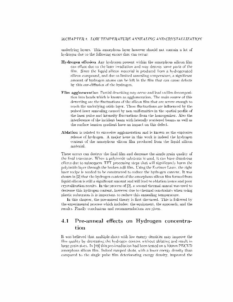
56CHAPTER 4. LOWTEMPERATURE ANNEALING AND CRYSTALLIZATION
underlying layers. This amorphous layer however should not contain a lot ofhydrogen due to the following errors that can occur:
Hydrogen e�usion Any hydrogen present within the amorphous silicon �lmcan e�use due to the laser irradiation and may destroy some parts of the�lm. Since the liquid silicon material is produced from a hydrogenatedsilicon compound, and due to limited annealing temperature, a signi�cantamount of hydrogen atoms can be left in the �lm that can cause defectsby this out-di�usion of the hydrogen.
Film agglomeration Partial dewetting may occur and lead to �lm decomposi-tion into beads which is known as agglomeration. The main source of thisdewetting are the �uctuations of the silicon �lm that are severe enough toreach the underlying oxide layer. These �uctuations are in�uenced by thepulsed-laser annealing caused by non-uniformities in the spatial pro�le ofthe laser pulse and intensity �uctuations from the homogenizer. Also theinterference of the incident beam with laterally scattered beams as well asthe surface tension gradient have an impact on this defect.
Ablation is related to excessive agglomeration and is known as the explosiverelease of hydrogen. A major issue in this work is indeed the hydrogencontent of the amorphous silicon �lm produced from the liquid siliconmaterial.
These errors can destroy the �nal �lm and decrease the single grain quality ofthe �nal transistor. When a polyimide substrate is used, it can have disastrouse�ects due to subsequent TFT processing steps that will signi�cantly harm thepolyimide layer through the broken a-Si �lm. Using the Excimer Laser, the rightlaser recipe is needed to be constructed to reduce the hydrogen content. It wasshown in [2] that the hydrogen content of the amorphous silicon �lm formed fromliquid silicon is still a signi�cant amount and will lead to ablation issues and poorcrystallization results. In the process of [2], a second thermal anneal was used todecrease this hydrogen content, however due to thermal constraints when usingplastic substrates it is important to reduce this annealing temperature.
In this chapter, the pre-anneal theory is �rst discussed. This is followed bythe experimental process which includes: the equipment, the approach, and theresults. Finally conclusions and recommendations are given.
4.1 Pre-anneal e�ects on Hydrogen concentra-
tion
It was believed that multiple shots with low energy densities may improve the�lm quality by decreasing the hydrogen content without ablating and result inlarge grain sizes. In [49] this pre-irradiation had been tested on a 100nm PECVDamorphous silicon �lm. Indeed ramped shots, with a lower energy density thancompared to the single pulse �lm deteriorating energy density, improved the
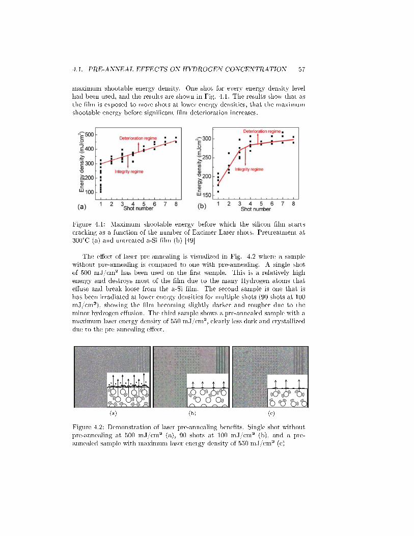
4.1. PRE-ANNEAL EFFECTS ON HYDROGEN CONCENTRATION 57
maximum shootable energy density. One shot for every energy density levelhad been used, and the results are shown in Fig. 4.1. The results show that asthe �lm is exposed to more shots at lower energy densities, that the maximumshootable energy before signi�cant �lm deterioration increases.
Figure 4.1: Maximum shootable energy before which the silicon �lm startscracking as a function of the number of Excimer Laser shots. Pretreatment at300°C (a) and untreated a-Si �lm (b) [49]
The e�ect of laser pre-annealing is visualized in Fig. 4.2 where a samplewithout pre-annealing is compared to one with pre-annealing. A single shotof 500 mJ/cm² has been used on the �rst sample. This is a relatively highenergy and destroys most of the �lm due to the many Hydrogen atoms thate�use and break loose from the a-Si �lm. The second sample is one that ishas been irradiated at lower energy densities for multiple shots (90 shots at 100mJ/cm²), showing the �lm becoming slightly darker and rougher due to theminor hydrogen e�usion. The third sample shows a pre-annealed sample with amaximum laser energy density of 550 mJ/cm², clearly less dark and crystallizeddue to the pre-annealing e�ect.
(a) (b) (c)
Figure 4.2: Demonstration of laser pre-annealing bene�ts. Single shot withoutpre-annealing at 500 mJ/cm² (a), 90 shots at 100 mJ/cm² (b), and a pre-annealed sample with maximum laser energy density of 550 mJ/cm² (c)
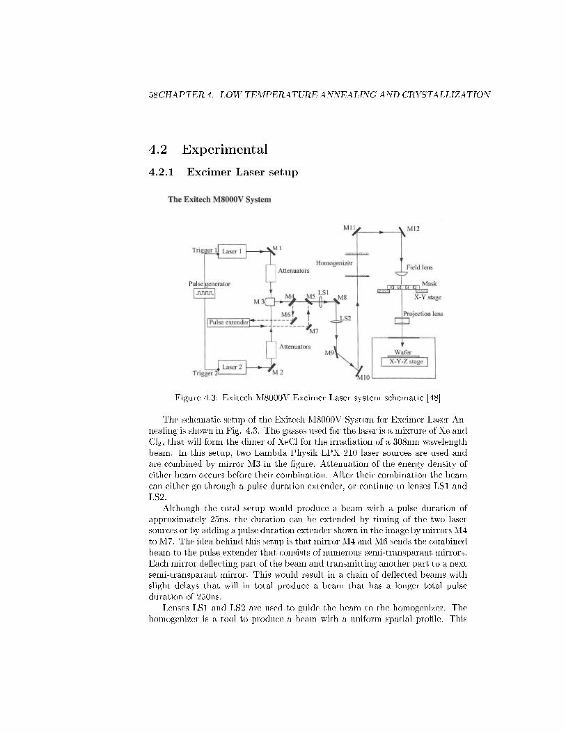
58CHAPTER 4. LOWTEMPERATURE ANNEALING AND CRYSTALLIZATION
4.2 Experimental
4.2.1 Excimer Laser setup
Figure 4.3: Exitech M8000V Excimer Laser system schematic [48]
The schematic setup of the Exitech M8000V System for Excimer Laser An-nealing is shown in Fig. 4.3. The gasses used for the laser is a mixture of Xe andCl2, that will form the dimer of XeCl for the irradiation of a 308nm wavelengthbeam. In this setup, two Lambda Physik LPX 210 laser sources are used andare combined by mirror M3 in the �gure. Attenuation of the energy density ofeither beam occurs before their combination. After their combination the beamcan either go through a pulse duration extender, or continue to lenses LS1 andLS2.
Although the total setup would produce a beam with a pulse duration ofapproximately 25ns, the duration can be extended by timing of the two lasersources or by adding a pulse duration extender shown in the image by mirrors M4to M7. The idea behind this setup is that mirror M4 and M6 sends the combinedbeam to the pulse extender that consists of numerous semi-transparant mirrors.Each mirror de�ecting part of the beam and transmitting another part to a nextsemi-transparant mirror. This would result in a chain of de�ected beams withslight delays that will in total produce a beam that has a longer total pulseduration of 250ns.
Lenses LS1 and LS2 are used to guide the beam to the homogenizer. Thehomogenizer is a tool to produce a beam with a uniform spatial pro�le. This
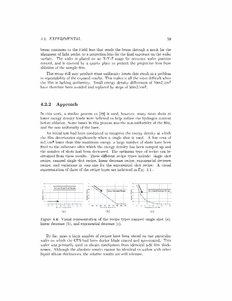
4.2. EXPERIMENTAL 59
beam continues to the Field lens that sends the beam through a mask for thealignment of light paths, to a projection lens for the �nal exposure on the wafersurface. The wafer is placed on an X-Y-Z stage for accurate wafer positioncontrol, and is covered by a quartz plate to protect the projection lens fromablation of the sample �lm.
This setup still may produce some uniformity issues that result in a problemin repeatability of the exposed results. This makes it all the more di�cult whenthe �lm is lacking uniformity. Small energy density di�erences of 10mJ/cm²have therefore been avoided and replaced by steps of 50mJ/cm².
4.2.2 Approach
In this work, a similar process to [49] is used, however, many more shots atlower energy density levels were believed to help reduce the hydrogen contentbefore ablation. Some issues in this process was the non-uniformity of the �lm,and the non-uniformity of the laser.
An initial test had been conducted to recognize the energy density at whichthe �lm deteriorates signi�cantly when a single shot is used. A few tens ofmJ/cm² lower than this maximum energy, a large number of shots have been�red to the substrate after which the energy density has been ramped up andthe number of shots had been decreased. The optimum type of recipe can beobtained from these results. These di�erent recipe types include: single shotrecipe, ramped single shot recipe, linear decrease recipe, exponential decreaserecipe, and variations in step size for the exponential shot recipe. A visualrepresentation of three of the recipe types are indicated in Fig. 4.4 .
(a) (b) (c)
Figure 4.4: Visual representation of the recipe types ramped single shot (a),linear decrease (b), and exponential decrease (c).
By far, most a large number of recipes have been tested on one particularwafer on which the CPS had been doctor blade coated and spin-coated,. Thiswafer was primarily used to obtain conclusions from identical a-Si �lm thick-nesses. Although the absolute results cannot be identical to wafers with otherliquid silicon thicknesses, the relative results are still relevant.
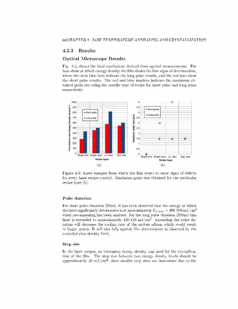
60CHAPTER 4. LOWTEMPERATURE ANNEALING AND CRYSTALLIZATION
4.2.3 Results
Optical Microscope Results
Fig. 4.5, shows the �nal conclusions derived from optical measurements. Thebars show at which energy density the �lm shows the �rst signs of deterioration,where the dark blue bars indicate the long pulse results, and the red bars showthe short pulse results. The red and blue markers indicate the maximum ob-tained grain size using the speci�c type of recipe for short pulse and long pulserespectively.
(a) (b)
Figure 4.5: Laser energies from which the �lm starts to show signs of defectsfor every laser recipe type(a). Maximum grain size obtained for the particularrecipe type (b).
Pulse duration
For short pulse duration (25ns), it has been observed that the energy at whichthe layer signi�cantly deteriorates is at approximatelyE1,max = 260-300 mJ/cm²when pre-annealing has been omitted. For the long pulse duration (250ns) thislimit is extended to approximately 420-440 mJ/cm². Extending the pulse du-ration will decrease the cooling rate of the molten silicon which would resultin bigger grains. It will also help against �lm deterioration as observed by theextended shot density limit.
Step size
In the laser recipes, an increasing energy density was used for the crystalliza-tion of the �lm. The step size between two energy density levels should beapproximately 50 mJ/cm², since smaller step sizes are inaccurate due to the
4.2. EXPERIMENTAL 61
inconsistency of the laser energy. Bigger step sizes usually deteriorate the �lmearlier and may approach the level of a single shot recipe. A �nal jump from aseries of 50 mJ/cm² should not exceed 150 mJ/cm².
Recipe types
Using this �rst deterioration energy with the single shot tests, various recipescan be tested. [49] obtained good results with ramped single shots, however,increasing the number of shots at lower energy densities could lead to betterremoval of the hydrogen atoms while maintaining the quality of the �lm. Singleshots, ramped single shots, exponential decrease shots, and linear decrease shots,have been compared. Single shots gave the lowest maximum shootable energyand in many cases could not form grains before �lm deterioration. Rampedsingle shots gave reasonable results with maximum grain sizes in the short pulsecon�guration similar to the two remaining recipe types, however, the deteriora-tion of the �lm occurs earlier. The exponential decrease of shots was comparedto the linear decrease of shots, and although similar results were obtained forthe short pulse con�guration, the long pulse con�guration showed better resultsfor the linear decrease recipe. This is mainly due to the starting energy of theexponential decrease recipe, which was too low. This resulted in a fast decreaseof shots to 1, so that the nature of the recipe approached the level of rampedsingle shot recipes.
Starting energy density
The starting energy for all recipes should be below the deterioration energy,E1,max, obtained for the single shot experiments. Comparing the starting en-ergies, an energy density at about 100 mJ/cm² lower than E1,max would leadto similar results compared to energies starting a lot lower than this. Startingenergy density of only a few tens of mJ/cm² lower than E1,max results in biggergrain sizes, however, deterioration of the �lm occurs at an earlier stage. Fig.4.6 illustrates that when E1,max is found to be 260 mJ/cm², using the �rst pre-annealing energy density at 200 or 150 mJ/cm² has only little in�uence to boththe deterioration energy and the grain size. Using the slightly lower energy of250 mJ/cm² however will increase the maximum grain size as well as an earlierinitial deterioration energy. This has also been found for linear decrease of theshot number, as well as in the long pulse series.
The results of the long pulse linear recipe that gave the biggest grains areshown in Fig. 4.7. The recipe starts at 350 mJ/cm², so only slightly lower thanthe E1,max with 70 shots, that have been decreased with 10 shots every timeand increased energy densities at steps of 50 mJ/cm² until 800 mJ/cm². Finallya jump has been made to 950 mJ/cm².
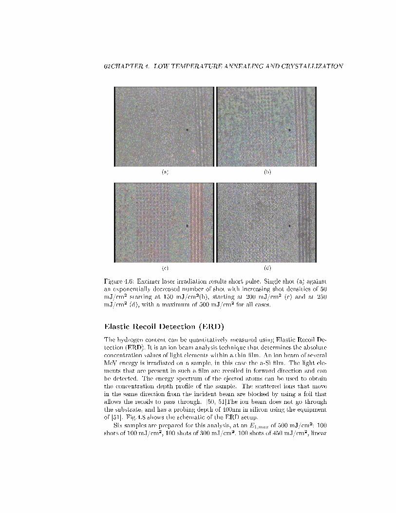
62CHAPTER 4. LOWTEMPERATURE ANNEALING AND CRYSTALLIZATION
(a) (b)
(c) (d)
Figure 4.6: Excimer laser irradiation results short pulse. Single shot (a) againstan exponentially decreased number of shot with increasing shot densities of 50mJ/cm² starting at 150 mJ/cm²(b), starting at 200 mJ/cm² (c) and at 250mJ/cm² (d), with a maximum of 500 mJ/cm² for all cases.
Elastic Recoil Detection (ERD)
The hydrogen content can be quantitatively measured using Elastic Recoil De-tection (ERD). It is an ion beam analysis technique that determines the absoluteconcentration values of light elements within a thin �lm. An ion beam of severalMeV energy is irradiated on a sample, in this case the a-Si �lm. The light ele-ments that are present in such a �lm are recoiled in forward direction and canbe detected. The energy spectrum of the ejected atoms can be used to obtainthe concentration depth pro�le of the sample. The scattered ions that movein the same direction from the incident beam are blocked by using a foil thatallows the recoils to pass through. [50, 51]The ion beam does not go throughthe substrate, and has a probing depth of 400nm in silicon using the equipmentof [51]. Fig.4.8 shows the schematic of the ERD setup.
Six samples are prepared for this analysis, at an E1,max of 500 mJ/cm²: 100shots of 100 mJ/cm², 100 shots of 300 mJ/cm², 100 shots of 450 mJ/cm², linear
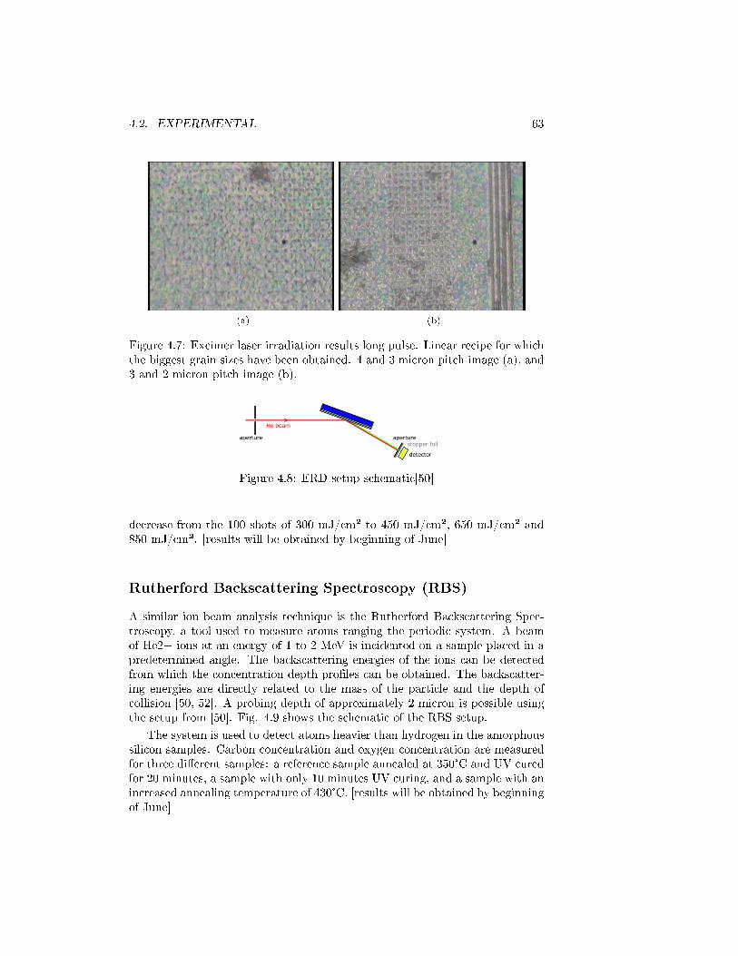
4.2. EXPERIMENTAL 63
(a) (b)
Figure 4.7: Excimer laser irradiation results long pulse. Linear recipe for whichthe biggest grain sizes have been obtained. 4 and 3 micron pitch image (a), and3 and 2 micron pitch image (b).
Figure 4.8: ERD setup schematic[50]
decrease from the 100 shots of 300 mJ/cm² to 450 mJ/cm², 650 mJ/cm² and850 mJ/cm². [results will be obtained by beginning of June]
Rutherford Backscattering Spectroscopy (RBS)
A similar ion beam analysis technique is the Rutherford Backscattering Spec-troscopy, a tool used to measure atoms ranging the periodic system. A beamof He2+ ions at an energy of 1 to 2 MeV is incidented on a sample placed in apredetermined angle. The backscattering energies of the ions can be detectedfrom which the concentration depth pro�les can be obtained. The backscatter-ing energies are directly related to the mass of the particle and the depth ofcollision [50, 52]. A probing depth of approximately 2 micron is possible usingthe setup from [50]. Fig. 4.9 shows the schematic of the RBS setup.
The system is used to detect atoms heavier than hydrogen in the amorphoussilicon samples. Carbon concentration and oxygen concentration are measuredfor three di�erent samples: a reference sample annealed at 350°C and UV curedfor 20 minutes, a sample with only 10 minutes UV curing, and a sample with anincreased annealing temperature of 430°C. [results will be obtained by beginningof June]
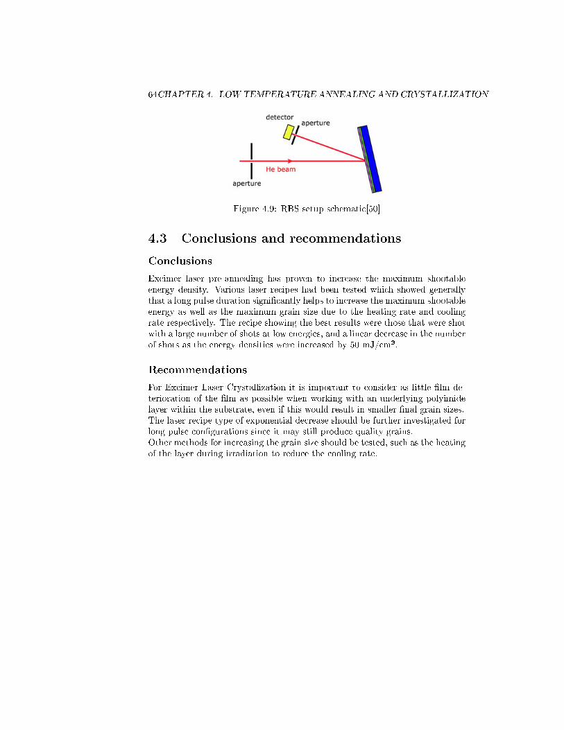
64CHAPTER 4. LOWTEMPERATURE ANNEALING AND CRYSTALLIZATION
Figure 4.9: RBS setup schematic[50]
4.3 Conclusions and recommendations
Conclusions
Excimer laser pre-annealing has proven to increase the maximum shootableenergy density. Various laser recipes had been tested which showed generallythat a long pulse duration signi�cantly helps to increase the maximum shootableenergy as well as the maximum grain size due to the heating rate and coolingrate respectively. The recipe showing the best results were those that were shotwith a large number of shots at low energies, and a linear decrease in the numberof shots as the energy densities were increased by 50 mJ/cm².
Recommendations
For Excimer Laser Crystallization it is important to consider as little �lm de-terioration of the �lm as possible when working with an underlying polyimidelayer within the substrate, even if this would result in smaller �nal grain sizes.The laser recipe type of exponential decrease should be further investigated forlong pulse con�gurations since it may still produce quality grains.Other methods for increasing the grain size should be tested, such as the heatingof the layer during irradiation to reduce the cooling rate.
Chapter 5
l-Si SG-TFT on Polyimide
As the liquid silicon layer �lls the grain �lter cavities, and forms amorphous sil-icon during annealing. The samples are exposed to Excimer laser for hydrogenremoval and crystallization. The position of the single crystal grains are accu-rately controlled by the grain �lters, and within these grains, monocrystallinesilicon channels can be formed for high quality devices.
So far reports have been made of liquid silicon devices that have been spin-coated and inkjetted without grain location control in [1] and spin-coated withgrain location control in [2]. The latter have produced TFTs at temperaturesincompatible with plastics such as polyimide due to the annealing of the liq-uid silicon layer for transformation into an amorphous silicon network and theremoval of hydrogen atoms that can have detrimental e�ects during laser crys-tallization.
In this work, the annealing temperature of the transformation from liquidsilicon to an amorphous silicon network has been reduced from 430°C to 350°C,and the hydrogen removal has been conducted with a laser pre-annealing treat-ment similar to [49]. With this decrease of temperature, the compatibility topolyimide has been realized and devices both on polyimide as well as deviceswithout the additional polyimide layer have been constructed and measured.
5.1 Transistor structure
A schematic of the device fabrication process is given in Fig. 5.1. The processis similar to [2], and uses a µ-Czochralski process for the controlled growth ofthe crystalline silicon grains. Notice that in this schematic the polyimide layerhas been left out after step 1, although both processes, with and without thislayer, have been used for our �nal devices. Step 7a is used when the polyimidelayer has been omitted, whereas step 7b is used for when a polyimide layer hadbeen implemented in the process. For the protection of this layer, additionalaluminum has been used to protect the underlying polyimide layer during theactivation of implanted dopants through Excimer laser.
65
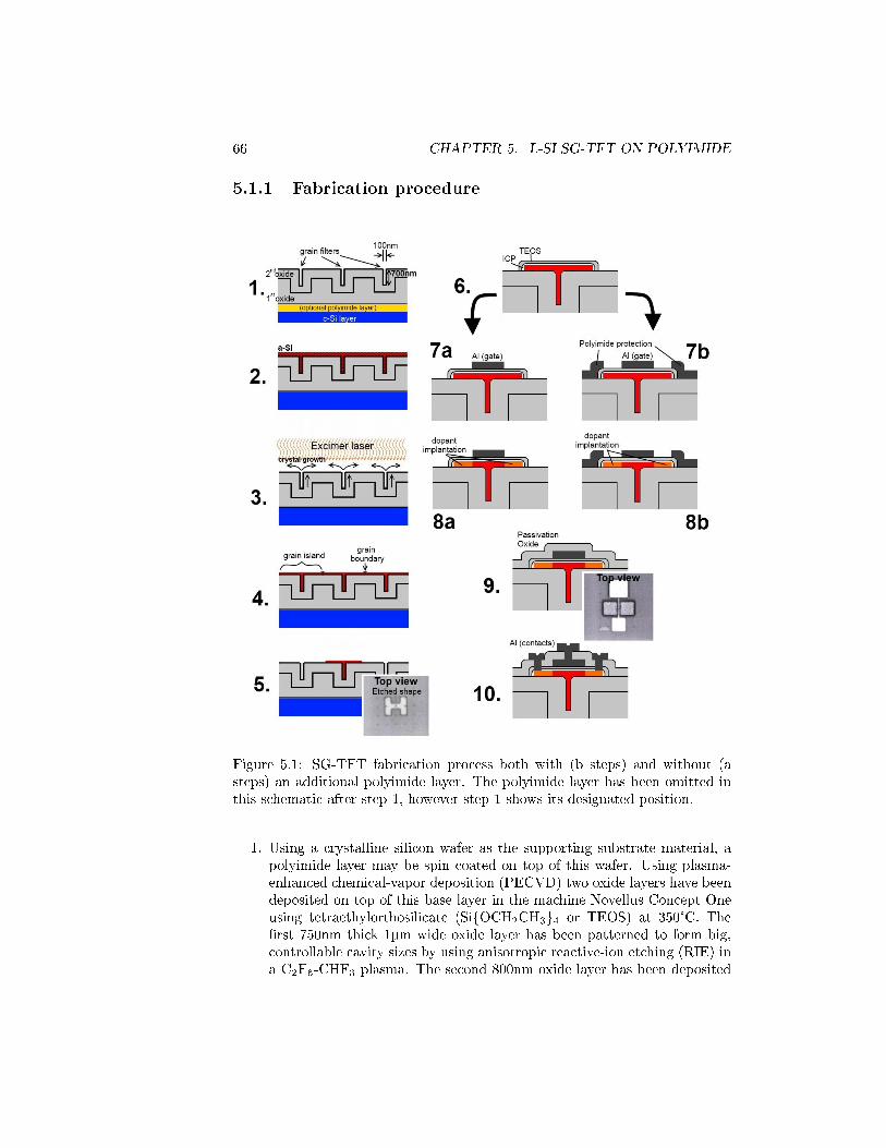
66 CHAPTER 5. L-SI SG-TFT ON POLYIMIDE
5.1.1 Fabrication procedure
Figure 5.1: SG-TFT fabrication process both with (b steps) and without (asteps) an additional polyimide layer. The polyimide layer has been omitted inthis schematic after step 1, however step 1 shows its designated position.
1. Using a crystalline silicon wafer as the supporting substrate material, apolyimide layer may be spin coated on top of this wafer. Using plasma-enhanced chemical-vapor deposition (PECVD) two oxide layers have beendeposited on top of this base layer in the machine Novellus Concept Oneusing tetraethylorthosilicate (Si{OCH2CH3}4 or TEOS) at 350°C. The�rst 750nm thick 1µm wide oxide layer has been patterned to form big,controllable cavity sizes by using anisotropic reactive-ion etching (RIE) ina C2F6-CHF3 plasma. The second 800nm oxide layer has been deposited
5.1. TRANSISTOR STRUCTURE 67
by the same PECVD process to decrease the cavity size to a grain �lterlevel. The grain �lters have a depth of 700nm and a diameter of 100nm.
2. According to the process described in Chapter 3, an amorphous �lm ismanufactured from the bladed liquid silicon material. A thickness of ap-proximately 200nm is desired using pure CPS, 20 minutes of UV exposure,and thermal annealing at 350°C for 1 hour in an nitrogen ambient withoxygen and water levels in below 0.1ppm.
3. Using the Exitech M8000V System for Excimer Laser Irradiation of theamorphous silicon layer, the top amorphous silicon layer is molten untila crystal seed is left at the bottom of the grain �lter. The laser inducescrystallization as explained in Appendix E
4. Crystal growth in every grain �lter induced by the Excimer Laser willcontinue at high energy densities, until either a defect of the �lm occurs,or the crystal growth collides with a crystal grown from a neighboringgrain �lter. This collision causes a halt to the grain �lter size increase andwill form grain boundaries at those positions.
5. Grain islands are formed with RIE. These islands are positioned in a waythat the channel region exists in the single crystalline area produced fromone single grain �lter.
6. For the production of a gate oxide layer, to types of oxide are formed ontop of the crystalline silicon area. Using inductively coupled plasma (ICP),high quality oxide is grown at a mere 250°C with less plasma damage onthe oxide than when using PECVD TEOS. This made out the �rst 14nmof the gate oxide layer for a good semiconductor-oxide interface. Afterthis �rst layer, PECVD TEOS has been used for another 22nm oxide at350°C to speed up the process.
7. The aluminum gate has been sputtered on top of the gate oxide by usingthe Trikon Technology Sigma 201 cluster tool at room temperature. Thealuminum has a 0.1% silicon content to prevent spiking due to di�usion,and has a thickness of 675nm. For the polyimide version (7b) the alu-minum used to protect the underlying polyimide layer should not containany silicon for accurate removal of the layer after dopant activation.
8. The aluminum gate pattern has been used as the mask for self-alignmentof the ion implantation of the source and drain regions. For PMOS, 1·10¹6
ions/cm² boron atoms at 20keV were used, and for NMOS TFTs, 1·10¹6
ions/cm² phosphorus atoms at 70keV were implanted. Both dopant typeswere activated using Excimer laser with an energy density of 300mJ/cm²at room temperature.
9. The total device structure is passivated again using PECVD TEOS, forprotection of devices and insulation between conductors.
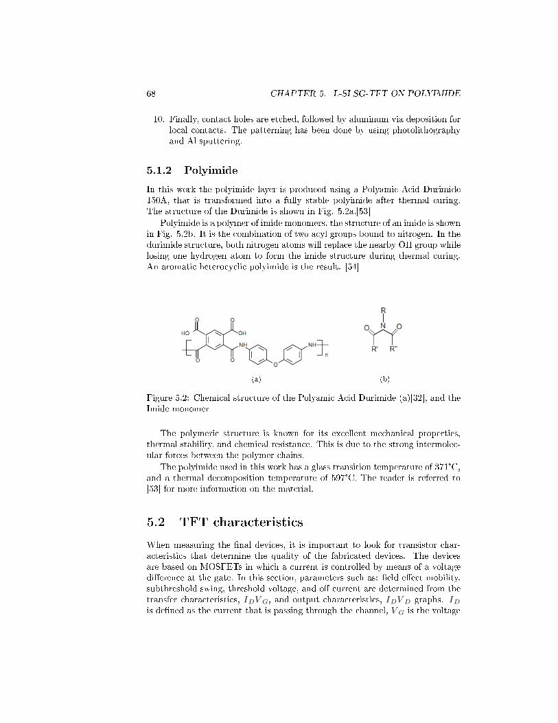
68 CHAPTER 5. L-SI SG-TFT ON POLYIMIDE
10. Finally, contact holes are etched, followed by aluminum via deposition forlocal contacts. The patterning has been done by using photolithographyand Al sputtering.
5.1.2 Polyimide
In this work the polyimide layer is produced using a Polyamic Acid Durimide150A, that is transformed into a fully stable polyimide after thermal curing.The structure of the Durimide is shown in Fig. 5.2a.[53]
Polyimide is a polymer of imide monomers, the structure of an imide is shownin Fig. 5.2b. It is the combination of two acyl groups bound to nitrogen. In thedurimide structure, both nitrogen atoms will replace the nearby OH group whilelosing one hydrogen atom to form the imide structure during thermal curing.An aromatic heterocyclic polyimide is the result. [54]
(a) (b)
Figure 5.2: Chemical structure of the Polyamic Acid Durimide (a)[32], and theImide monomer
The polymeric structure is known for its excellent mechanical properties,thermal stability, and chemical resistance. This is due to the strong intermolec-ular forces between the polymer chains.
The polyimide used in this work has a glass transition temperature of 371°C,and a thermal decomposition temperature of 597°C. The reader is referred to[53] for more information on the material.
5.2 TFT characteristics
When measuring the �nal devices, it is important to look for transistor char-acteristics that determine the quality of the fabricated devices. The devicesare based on MOSFETs in which a current is controlled by means of a voltagedi�erence at the gate. In this section, parameters such as: �eld e�ect mobility,subthreshold swing, threshold voltage, and o� current are determined from thetransfer characteristics, IDV G, and output characteristics, IDV D graphs. IDis de�ned as the current that is passing through the channel, V G is the voltage
5.2. TFT CHARACTERISTICS 69
applied at the gate while the voltage di�erence across the channel is kept con-stant, and V D is de�ned as the voltage applied at the drain contact assumingthat the source contact is set at 0V (ground). [47, 48]
Field E�ect Mobility
Mobility is related to the carrier transport through a material as a result ofan induced electric �eld, and is one of the most important parameters of thetransistor. The current that runs through the device has various operatingmodes and is de�ned by Eq. 5.1.
ID =
{µFE,nCox
WL
[(VGS − Vth)VDS − V 2
DS
2
]Linear region
µFE,nCox
2WL (VGS − Vth)2 Saturation region
(5.1)
Where ID is the drain current; µn is the electron �eld-e�ect mobility; Coxis the oxide capacitance; W and L are the width and length of the channelrespectively; VGS is the gate to source voltage; Vth is the threshold voltageandVDS is the drain to source voltage.
From the saturated region, the mobility can be extracted by measuring theslope of the IDV G curve while keeping the drain voltage at a constant saturatedlevel:
µFE,n =
(∂√ID
∂VGS
√2L
CoxW
)2VDS=level of saturation
(5.2)
Subthreshold Swing
The subthreshold swing (S) is a parameter that de�nes the quality of the turn-on characteristics of the device. It can be obtained from the weak invertingregime, which occurs at VGS < Vth. In this regime the swing is de�ned as thegate voltage required to increase the drain current by an order of magnitude.This parameter determines the semiconductor/dielectric interface trap densityand is de�ned as:
S =
[∂ ln (IDS)
∂VGS
]−1(5.3)
S =kT
qln 10
(1 +
Cdepl + CitCox
)(5.4)
In which k is the Boltzmann's constant; T the temperature in Kelvin; q is thecharge; Cdepl is the capacitance of the depletion region; Cox is the capacitanceof the gate-oxide, and Cit is the capacitance of the interface states which is inparallel to the depletion capacitance.
70 CHAPTER 5. L-SI SG-TFT ON POLYIMIDE
Threshold Voltage
The property that de�nes the gate voltage on which the device turns on is thethreshold voltage. This voltage needs to be su�ciently low for the device tobe operational with limited supplying energy. It is physically de�ned as theformation of an inversion layer on the semiconductor-oxide interface that allowscharge carriers to move from the source and drain regions.
O�-current
The o�-current is the current �owing through the channel while no voltage isapplied at the gate. This current should be as low as possible to obtain a properswitch-like function.
5.3 Results
[Results will be obtained by mid June]
5.4 Conclusions
[Results will be obtained by mid June]
Chapter 6
Excess Liquid Silicon Removal
for Gravure Printing
Chapter 3 has discussed the doctor blade coating of liquid silicon onto a pat-terned substrate: a process that can be regarded as a precursor of the gravureprinting system. The process allows the liquid to be spread across the patternedsurface without the need of removing any liquid that is not �lling a pattern.
Excess liquid silicon removal is another precursor of gravure printing whichrequires any excess liquid to be scraped o� the patterned substrate. The resultis that the liquid will only �ll patterned cavities �lled with the speci�c liquid.The �nal transition towards gravure printing would require this substrate withthe liquid to be pressed against a target surface.
The focus in this chapter was on spreading the liquid silicon while �llingpatterns and removing excess liquid in non-patterned areas.
6.1 Experimental Results
The substrates used in this chapter are di�erent from the ones used in Chapter 3in the cavity patterns produced in the TEOS layer. The wafers do not have anygrain �lters but various pattern sizes ranging from a few tens of micrometers toa square of 1 by 1 micrometer. The shape of most of the patterns are like theletter "H" which is a common structure used for the production gates or thechannel region. The depth of these patterns have been varied from 0 to 1000nm. Many of the experiments however, were conducted using a depth of 250nmwhich is a typical thickness for a semiconductor layer. Grain �lters are omittedsince the aim of this work looks at producing a transistor using the �lled cavity,or by gravure printing the pattern on a target substrate. In both cases, thegrain �lters are not required.
The desired result is either a completely �lled pattern, a pattern that is only�lled in the corners, or a bulging/dewetted pattern. Although the latter twocan not be used directly for gravure printing ends, these results allow further
71
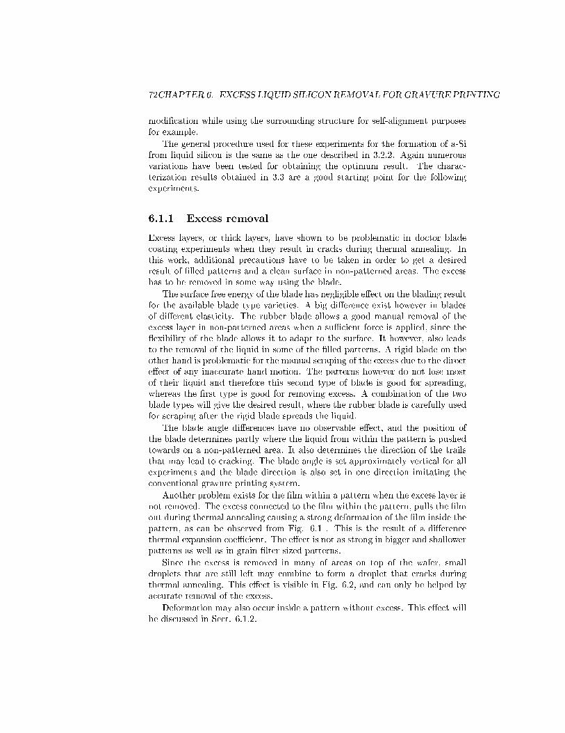
72CHAPTER 6. EXCESS LIQUID SILICON REMOVAL FORGRAVURE PRINTING
modi�cation while using the surrounding structure for self-alignment purposesfor example.
The general procedure used for these experiments for the formation of a-Sifrom liquid silicon is the same as the one described in 3.2.2. Again numerousvariations have been tested for obtaining the optimum result. The charac-terization results obtained in 3.3 are a good starting point for the followingexperiments.
6.1.1 Excess removal
Excess layers, or thick layers, have shown to be problematic in doctor bladecoating experiments when they result in cracks during thermal annealing. Inthis work, additional precautions have to be taken in order to get a desiredresult of �lled patterns and a clean surface in non-patterned areas. The excesshas to be removed in some way using the blade.
The surface free energy of the blade has negligible e�ect on the blading resultfor the available blade type varieties. A big di�erence exist however in bladesof di�erent elasticity. The rubber blade allows a good manual removal of theexcess layer in non-patterned areas when a su�cient force is applied, since the�exibility of the blade allows it to adapt to the surface. It however, also leadsto the removal of the liquid in some of the �lled patterns. A rigid blade on theother hand is problematic for the manual scraping of the excess due to the directe�ect of any inaccurate hand motion. The patterns however do not lose mostof their liquid and therefore this second type of blade is good for spreading,whereas the �rst type is good for removing excess. A combination of the twoblade types will give the desired result, where the rubber blade is carefully usedfor scraping after the rigid blade spreads the liquid.
The blade angle di�erences have no observable e�ect, and the position ofthe blade determines partly where the liquid from within the pattern is pushedtowards on a non-patterned area. It also determines the direction of the trailsthat may lead to cracking. The blade angle is set approximately vertical for allexperiments and the blade direction is also set in one direction imitating theconventional gravure printing system.
Another problem exists for the �lm within a pattern when the excess layer isnot removed. The excess connected to the �lm within the pattern, pulls the �lmout during thermal annealing causing a strong deformation of the �lm inside thepattern, as can be observed from Fig. 6.1 . This is the result of a di�erencethermal expansion coe�cient. The e�ect is not as strong in bigger and shallowerpatterns as well as in grain �lter sized patterns.
Since the excess is removed in many of areas on top of the wafer, smalldroplets that are still left may combine to form a droplet that cracks duringthermal annealing. This e�ect is visible in Fig. 6.2, and can only be helped byaccurate removal of the excess.
Deformation may also occur inside a pattern without excess. This e�ect willbe discussed in Sect. 6.1.2.
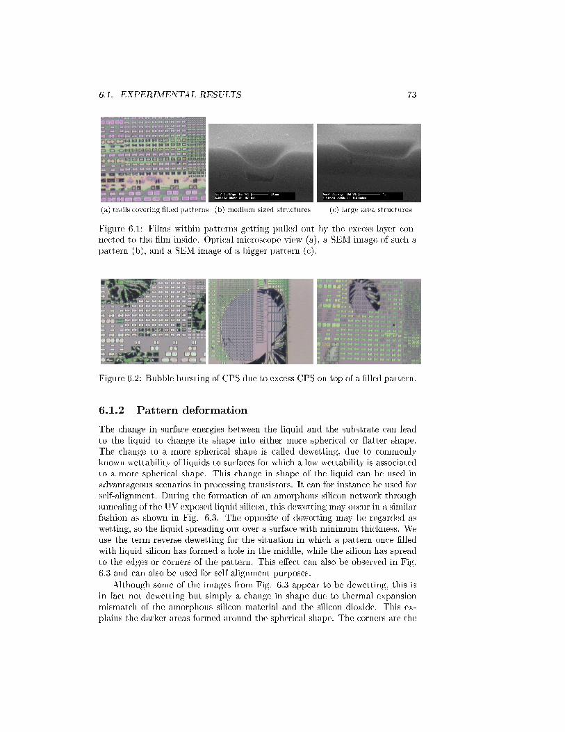
6.1. EXPERIMENTAL RESULTS 73
(a) trails covering �lled patterns (b) medium sized structures (c) large area structures
Figure 6.1: Films within patterns getting pulled out by the excess layer con-nected to the �lm inside. Optical microscope view (a), a SEM image of such apattern (b), and a SEM image of a bigger pattern (c).
Figure 6.2: Bubble bursting of CPS due to excess CPS on top of a �lled pattern.
6.1.2 Pattern deformation
The change in surface energies between the liquid and the substrate can leadto the liquid to change its shape into either more spherical or �atter shape.The change to a more spherical shape is called dewetting, due to commonlyknown wettability of liquids to surfaces for which a low wettability is associatedto a more spherical shape. This change in shape of the liquid can be used inadvantageous scenarios in processing transistors. It can for instance be used forself-alignment. During the formation of an amorphous silicon network throughannealing of the UV exposed liquid silicon, this dewetting may occur in a similarfashion as shown in Fig. 6.3. The opposite of dewetting may be regarded aswetting, so the liquid spreading out over a surface with minimum thickness. Weuse the term reverse dewetting for the situation in which a pattern once �lledwith liquid silicon has formed a hole in the middle, while the silicon has spreadto the edges or corners of the pattern. This e�ect can also be observed in Fig.6.3 and can also be used for self alignment purposes.
Although some of the images from Fig. 6.3 appear to be dewetting, this isin fact not dewetting but simply a change in shape due to thermal expansionmismatch of the amorphous silicon material and the silicon dioxide. This ex-plains the darker areas formed around the spherical shape. The corners are the
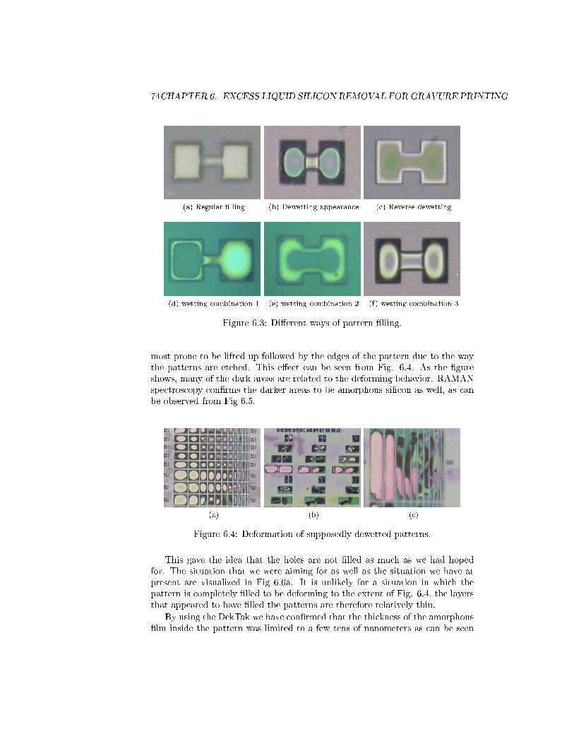
74CHAPTER 6. EXCESS LIQUID SILICON REMOVAL FORGRAVURE PRINTING
(a) Regular �lling (b) Dewetting appearance (c) Reverse dewetting
(d) wetting combination 1 (e) wetting combination 2 (f) wetting combination 3
Figure 6.3: Di�erent ways of pattern �lling.
most prone to be lifted up followed by the edges of the pattern due to the waythe patterns are etched. This e�ect can be seen from Fig. 6.4. As the �gureshows, many of the dark areas are related to the deforming behavior. RAMANspectroscopy con�rms the darker areas to be amorphous silicon as well, as canbe observed from Fig 6.5.
(a) (b) (c)
Figure 6.4: Deformation of supposedly dewetted patterns.
This gave the idea that the holes are not �lled as much as we had hopedfor. The situation that we were aiming for as well as the situation we have atpresent are visualized in Fig 6.6a. It is unlikely for a situation in which thepattern is completely �lled to be deforming to the extent of Fig. 6.4, the layersthat appeared to have �lled the patterns are therefore relatively thin.
By using the DekTak we have con�rmed that the thickness of the amorphous�lm inside the pattern was limited to a few tens of nanometers as can be seen
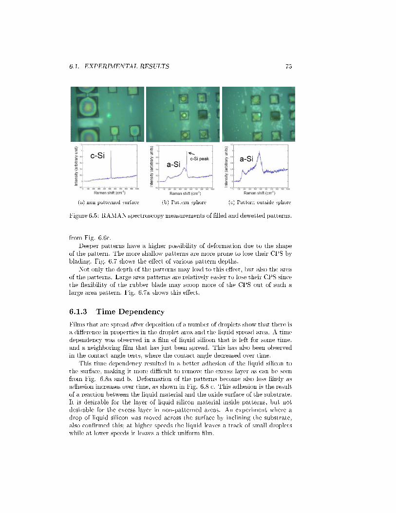
6.1. EXPERIMENTAL RESULTS 75
(a) non-patterned surface (b) Pattern sphere (c) Pattern outside sphere
Figure 6.5: RAMAN spectroscopy measurements of �lled and dewetted patterns.
from Fig. 6.6c.Deeper patterns have a higher possibility of deformation due to the shape
of the pattern. The more shallow patterns are more prone to lose their CPS byblading. Fig. 6.7 shows the e�ect of various pattern depths.
Not only the depth of the patterns may lead to this e�ect, but also the areaof the patterns. Large area patterns are relatively easier to lose their CPS sincethe �exibility of the rubber blade may scoop more of the CPS out of such alarge area pattern. Fig. 6.7a shows this e�ect.
6.1.3 Time Dependency
Films that are spread after deposition of a number of droplets show that there isa di�erence in properties in the droplet area and the liquid spread area. A timedependency was observed in a �lm of liquid silicon that is left for some time,and a neighboring �lm that has just been spread. This has also been observedin the contact angle tests, where the contact angle decreased over time.
This time dependency resulted in a better adhesion of the liquid silicon tothe surface, making it more di�cult to remove the excess layer as can be seenfrom Fig. 6.8a and b. Deformation of the patterns become also less likely asadhesion increases over time, as shown in Fig. 6.8 c. This adhesion is the resultof a reaction between the liquid material and the oxide surface of the substrate.It is desirable for the layer of liquid silicon material inside patterns, but notdesirable for the excess layer in non-patterned areas. An experiment where adrop of liquid silicon was moved across the surface by inclining the substrate,also con�rmed this; at higher speeds the liquid leaves a track of small dropletswhile at lower speeds it leaves a thick uniform �lm.
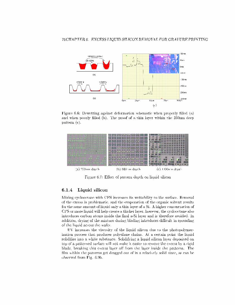
76CHAPTER 6. EXCESS LIQUID SILICON REMOVAL FORGRAVURE PRINTING
(c)
Figure 6.6: Dewetting against deformation schematic when properly �lled (a)and when poorly �lled (b). The proof of a thin layer within the 250nm deeppattern (c).
(a) 270nm depth (b) 800nm depth (c) 1100nm depth
Figure 6.7: E�ect of pattern depth on liquid silicon
6.1.4 Liquid silicon
Mixing cyclooctane with CPS increases its wettability to the surface. Removalof the excess is problematic, and the evaporation of the organic solvent resultsfor the same amount of liquid only a thin layer of a-Si. A higher concentration ofCPS or more liquid will help create a thicker layer, however, the cyclooctane alsointroduces carbon atoms inside the �nal a-Si layer and is therefore avoided. Inaddition, drying of the mixture during blading introduces di�cult in spreadingof the liquid across the wafer.
UV increases the viscosity of the liquid silicon due to the photopolymer-ization process that produces polysilane chains. At a certain point the liquidsolidi�es into a white substance. Solidifying a liquid silicon layer deposited ontop of a patterned surface will not make it easier to remove the excess by a rigidblade, breaking this excess layer o� from the layer inside the patterns. The�lm within the patterns get dragged out of in a relatively solid state, as can beobserved from Fig. 6.9b.
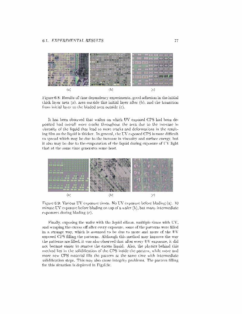
6.1. EXPERIMENTAL RESULTS 77
(a) (b) (c)
Figure 6.8: Results of time dependency experiments, good adhesion in the initialthick layer area (a), area outside this initial layer after (b), and the transitionfrom initial layer to the bladed area outside (c).
It has been observed that wafers on which UV exposed CPS had been de-posited had overall more cracks throughout the area due to the increase inviscosity of the liquid that lead to more tracks and deformations in the result-ing �lm as the liquid is thicker. In general, the UV exposed CPS is more di�cultto spread which may be due to the increase in viscosity and surface energy, butit also may be due to the evaporation of the liquid during exposure of UV lightthat at the same time generates some heat.
(a) (b) (c)
Figure 6.9: Various UV exposure times. No UV exposure before blading (a). 10minute UV exposure before blading on top of a wafer (b), but many intermediateexposures during blading (c).
Finally, exposing the wafer with the liquid silicon, multiple times with UV,and scraping the excess o� after every exposure, some of the patterns were �lledin a strange way, which is assumed to be due to more and more of the UVexposed CPS �lling the patterns. Although this method may improve the waythe patterns are �lled, it was also observed that after every UV exposure, it didnot became easier to remove the excess liquid. Also, the physics behind thismethod lies in the solidi�cation of the CPS inside the pattern, while more andmore new CPS material �lls the pattern at the same time with intermediatesolidi�cation steps. This may also cause integrity problems. The pattern �llingfor this situation is depicted in Fig.6.9c.
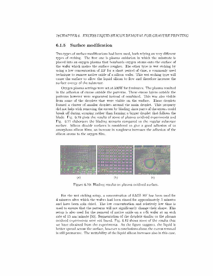
78CHAPTER 6. EXCESS LIQUID SILICON REMOVAL FORGRAVURE PRINTING
6.1.5 Surface modi�cation
Two types of surface modi�cations had been used, both relying on very di�erenttypes of etching. The �rst one is plasma oxidation in which the substrate isplaced into an oxygen plasma that bombards oxygen atoms onto the surface ofthe wafer which makes the surface rougher. The other type is wet etching byusing a low concentration of HF for a short period of time, a commonly usedtechnique to remove native oxide of a silicon wafer. This wet etching type willcause the surface to allow the liquid silicon to �ow and therefore increase thesurface energy of the substrate.
Oxygen plasma settings were set at 500W for 8 minutes. The plasma resultedin the adhesion of excess outside the patterns. These excess layers outside thepatterns however were segmented instead of combined. This was also visiblefrom some of the droplets that were visible on the surface. These dropletsformed a cluster of smaller droplets around the main droplet. This propertydid not help with removing the excess by blading since parts of the excess couldbreak o� during scraping rather than forming a bigger droplet that follows theblade. Fig. 6.10 gives the results of some of plasma oxidized experiments andFig. 6.11 elaborates the blading scenario compared to the regular substratesurface. Silicon dioxide surfaces is considered to give a good adhesion of toamorphous silicon �lms, an increase in roughness increases the adhesion of thesilicon atoms to the oxygen �lm.
(a) (b) (c)
Figure 6.10: Blading results on plasma oxidized surface.
For the wet etching setup, a concentration of 0.55% HF has been used for4 minutes after which the wafers had been rinsed for approximately 5 minutesand have been spin dried. The low concentration and relatively low time isused to ensure that the patterns will not signi�cantly change their shape. Thissetup is also used for the removal of native oxide on a c-Si wafer at an etchrate of 15 nm/minute [55]. Segmentation of the droplets similar to the plasmaoxidized experiments were not found. Fig. 6.12 shows some of the results thatwe have obtained from the experiments. As the �gure suggests, the liquid isbetter spread across the surface, however a conclusions about the excess removalis still premature. The wettability of the liquid silicon increases also in this case.
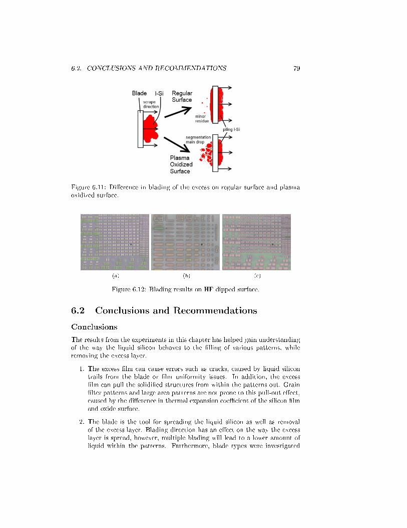
6.2. CONCLUSIONS AND RECOMMENDATIONS 79
Figure 6.11: Di�erence in blading of the excess on regular surface and plasmaoxidized surface.
(a) (b) (c)
Figure 6.12: Blading results on HF dipped surface.
6.2 Conclusions and Recommendations
Conclusions
The results from the experiments in this chapter has helped gain understandingof the way the liquid silicon behaves to the �lling of various patterns, whileremoving the excess layer.
1. The excess �lm can cause errors such as cracks, caused by liquid silicontrails from the blade or �lm uniformity issues. In addition, the excess�lm can pull the solidi�ed structures from within the patterns out. Grain�lter patterns and large area patterns are not prone to this pull-out e�ect,caused by the di�erence in thermal expansion coe�cient of the silicon �lmand oxide surface.
2. The blade is the tool for spreading the liquid silicon as well as removalof the excess layer. Blading direction has an e�ect on the way the excesslayer is spread, however, multiple blading will lead to a lower amount ofliquid within the patterns. Furthermore, blade types were investigated
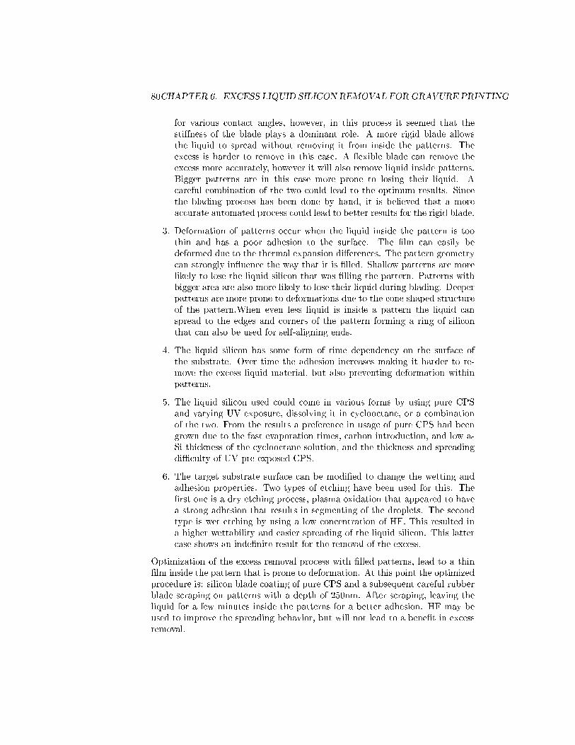
80CHAPTER 6. EXCESS LIQUID SILICON REMOVAL FORGRAVURE PRINTING
for various contact angles, however, in this process it seemed that thesti�ness of the blade plays a dominant role. A more rigid blade allowsthe liquid to spread without removing it from inside the patterns. Theexcess is harder to remove in this case. A �exible blade can remove theexcess more accurately, however it will also remove liquid inside patterns.Bigger patterns are in this case more prone to losing their liquid. Acareful combination of the two could lead to the optimum results. Sincethe blading process has been done by hand, it is believed that a moreaccurate automated process could lead to better results for the rigid blade.
3. Deformation of patterns occur when the liquid inside the pattern is toothin and has a poor adhesion to the surface. The �lm can easily bedeformed due to the thermal expansion di�erences. The pattern geometrycan strongly in�uence the way that it is �lled. Shallow patterns are morelikely to lose the liquid silicon that was �lling the pattern. Patterns withbigger area are also more likely to lose their liquid during blading. Deeperpatterns are more prone to deformations due to the cone shaped structureof the pattern.When even less liquid is inside a pattern the liquid canspread to the edges and corners of the pattern forming a ring of siliconthat can also be used for self-aligning ends.
4. The liquid silicon has some form of time dependency on the surface ofthe substrate. Over time the adhesion increases making it harder to re-move the excess liquid material, but also preventing deformation withinpatterns.
5. The liquid silicon used could come in various forms by using pure CPSand varying UV exposure, dissolving it in cyclooctane, or a combinationof the two. From the results a preference in usage of pure CPS had beengrown due to the fast evaporation times, carbon introduction, and low a-Si thickness of the cyclooctane solution, and the thickness and spreadingdi�culty of UV pre-exposed CPS.
6. The target substrate surface can be modi�ed to change the wetting andadhesion properties. Two types of etching have been used for this. The�rst one is a dry etching process, plasma oxidation that appeared to havea strong adhesion that results in segmenting of the droplets. The secondtype is wet etching by using a low concentration of HF. This resulted ina higher wettability and easier spreading of the liquid silicon. This lattercase shows an inde�nite result for the removal of the excess.
Optimization of the excess removal process with �lled patterns, lead to a thin�lm inside the pattern that is prone to deformation. At this point the optimizedprocedure is: silicon blade coating of pure CPS and a subsequent careful rubberblade scraping on patterns with a depth of 250nm. After scraping, leaving theliquid for a few minutes inside the patterns for a better adhesion. HF may beused to improve the spreading behavior, but will not lead to a bene�t in excessremoval.
6.2. CONCLUSIONS AND RECOMMENDATIONS 81
Recommendations
An automated blading machine could provide a consistent way of scraping o� ex-cess with a rigid blade type, as it is being used in conventional gravure systems.Current manual blading introduces many variables that cannot be controlledand are not present in automated systems.
The main issue at this moment is actually the poor �lling of the patterns,and their deformation. Filling can be improved by creating a situation in whicha liquid that has poor wettability in non-patterned areas, but can easily enterthe patterns and have a strong adhesion to the insides of the patterns. Surface-material wise, this would mean that the surface may be made of silicon nitride oranother material with very low surface energy, while the patterns inside can havea surface of HF etched or a modi�cation that leads to high surface adhesion andwettability. It must however be ensured that the adhesion to the non-patternedsurface is minimal which is many cases related to a surface with a very lowsurface energy. The blade itself can also be made from a silicon nitride materialto minimize the adhesion of the liquid to the blade.
Either CPS or UV pre-exposed CPS need to be used in this scenario sinceit is assumed that UV pre-exposed CPS will not be di�cult to remove fromthe surface anymore due to the increase in hydrophobicity of the silicon nitridesurface.
Figure 6.13: Recommended setup mainly based on high adhesion within thepattern, and poor adhesion outside, with a poor adhesive blade.
To prevent pattern deformation, patterns that are once �lled need to restfor some time for the liquid silicon to react to the surface within the patternfor a stronger adhesion. When transistors are made from this �lled patterns,maximum adhesion is desired and some resting time is therefore required. Inthe blading process, relatively deep patterns with small areas are preferred. Thetotal situation is illustrated in Fig. 6.13.

82CHAPTER 6. EXCESS LIQUID SILICON REMOVAL FORGRAVURE PRINTING
Chapter 7
Conclusions and
Recommendations
Liquid Silicon is used as a way of taking the advantages of a cheap, low tem-perature, solution fabrication process, and the high electrical property of sili-con transistors. Doctor blade coating is a �rst step towards gravure printingsystems allowing roll-to-roll mass production of electronics. Using location con-trolled grain �lters and Excimer Laser pre-annealing, high quality Single-GrainThin-Film Transistors can be manufactured on plastic substrates.
7.1 Doctor Blade coating Liquid Silicon
Some basic characteristics of liquid silicon have been investigated, and a methodfor obtaining a good a-Si layer is achieved. The obtained characteristics arelisted:
Excess liquid Excess liquid can induce large stepheights that break duringthermal annealing due to thermal expansion. Instances at which theselarge �lm gradient can occur are besides excess layers from the largeamount of liquid, trails caused by blading, and substrate patterns.
Pure CPS is the preferred material to work with as liquid silicon. Manip-ulations of this base material can increase its viscosity, or decrease itssurface free energy. UV light causes the production of polysilanes withinthe material that thicken the liquid. These result in a higher possibility ofblading trails as well as a poorer wettability. Mixing cyclooctane increaseswettability however a number of issues exist: carbon is introduced in theresulting a-Si �lm, the resulting �lm evaporates leaving only a thin layerof polysilane content on the surface, a-Si in grain �lters shrink due to this,and the solution dries quickly leading to uniformity issues when blading.
Surface Free Energy High wettability of the liquid is desired and can be
83
84 CHAPTER 7. CONCLUSIONS AND RECOMMENDATIONS
obtained by surface modi�cation techniques. Increasing the number ofdroplets will only create thicker tracks when doctor blade coating whichcan crack. 0.55% HF treatment for four minutes together with an el-evated temperature gives the highest surface free energy (SFE) of thesurface resulting in high wettability. Wettability increased over time dueto reactions of the material to the surface. Care has to be taken for theevaporation of liquid silicon when spread at elevated temperatures.
Blade types The SFE of the blade is not a dominant factor when doctor bladecoating due to the errors that may result from manual blading. Elasticityhowever gives a signi�cant e�ect. Flexible blades such as rubber adjust tothe surface even if the blade is not positioned accurately. This �exibilityenables an ease in removing the liquid, and may also remove liquid frominside the patterns. A more rigid blade allows a better spreading of theliquid across the surface.
Using these characteristics the liquid silicon has been either spin-coated, bladed,or the two have been combined. Spin-coating gives poor adhesion and a lot ofwasted liquid silicon. Blading gives good results when a patterned wafer with 1by 1 mm square patterns are used instead of a �at wafer. For the �at wafer case,blading will result in a thin layer of approximately 30nm. Adding a spin-coatingstep to this layer improves liquid silicon adhesion and leads to a good layer witha thickness of approximately 250nm. The best results are obtained by using0.55%HF dip for four minutes on a wafer with 1 by 1 mm square patterns, whilespreading 6 drops (total 45µl) at an elevated temperature of 70°C for both typesof wafers. A more reproducible result with a thickness of approximately 100nmwas obtained when spreading at an elevated temperature of 90°C for the squarepatterned wafer, and 110°C for the �at wafer. The wafers have been exposed to20 minutes of UV for photopolymerization, and have been annealed at 350°Cfor 1 hour.
7.2 Low Temperature Annealing
Similar works of liquid silicon [2] have obtained a SG-TFT using the same mate-rial, however a second thermal annealing step of 650°C was used that made theprocess incompatible with plastic substrates. This second annealing step wasnecessary for reducing the oxygen content for the subsequent Excimer LaserCrystallization process. Low temperature annealing by using the same ExcimerLaser will lead to a maximum processing temperature of 350°C for which poly-imide substrates can be used.
Excimer Laser pre-annealing has been investigated by [49] for the removalof hydrogen without �lm deterioration, and has been further explored in thiswork. Several conclusions have been made:
Long pulse A longer pulse duration (250ns) lead to higher maximum shootableenergies than short pulse duration (25ns). As a result, bigger grains were
7.3. LIQUID SILICON DEVICES 85
produced in this con�guration. The reason for this is the decrease incooling rate.
Step size Laser recipes with a step size of smaller than 50mJ/cm² are proneto laser uniformity and inconsistency issues. Step sizes a lot bigger than50mJ/cm², takes away the e�ect of laser pre-annealing.
Starting energy When the starting energy of the laser recipe is a lot lowerthan the level of �rst deterioration, the �lm is less disturbed. A laserenergy just below the level of �rst deterioration will produce more �lmdisturbances, however will result in bigger grain sizes.
Recipe type A large number of energy shots have been shot at the beginningto remove more hydrogen at these low energy levels. The decrease innumber of shots have been done linearly and exponentially. For shortpulse con�guration, the results were similar. For long pulse con�guration,the linear decrease recipe resulted in bigger grain sizes due to the fastdecay of shot number in the exponential setup.
The recipe that has achieved the biggest grain size of 5µm grains was: a startingenergy of 350 mJ/cm² for 70 shots, with steps of 50 mJ/cm² and decreasing shotcount by 10 until 1, and a �nal jump of 150 mJ/cm² at 800 mJ/cm². A lowerstarting energy density is desired when the polyimide substrate is used to ensureits survival.
7.3 Liquid silicon devices
[Results will be obtained by mid June]
7.4 Excess removal using doctor blade
The next step towards a gravure printing system is the process of using thedoctor blade to remove excess liquid in non-patterned areas, after the liquidhas been spread across a substrate. The patterns are cavities of various shapes,and these require to be �lled completely for the gravure printing process. Othercharacteristics of the liquid silicon has been analyzed for this type of solutionprocessing.
Excess liquid The excess in this process is slightly di�erent from the excessin the doctor-blade coating section. The excess needs to be completelyremoved in this process. Any leftovers can produce cracks similar to theprevious process. A smooth layer however, which was acceptable in theother process, may pull out some of the middle sized patterns in this pro-cess due to thermal expansion. Blade types are preferred to be rubberwhen excess needs to be removed, however, this blade type may also re-move the liquid from inside the patterns, and is generally not a good way
86 CHAPTER 7. CONCLUSIONS AND RECOMMENDATIONS
for spreading the liquid. Using a silicon blade for spreading and carefulrubber blading for excess removal will give the best results.
Deformation Many patterns were �lled with a very thin layer. This thinlayer, when adhesion lacks, may easily deform during the annealing step.A deeper pattern is more prone to deformation due to the shape of thepattern. A too shallow pattern on the other hand may lose all of its liquidsilicon content.
Time dependency Liquid silicon reacts to the TEOS surface as has also beenobserved during the SFE experiments. This enables an improvement inadhesion that can prevent deformation during the annealing step. Excessliquid should be fully removed before pursuing a strategy using this timedependency.
Other types of liquid silicon gave similar issues as with the doctor blade coatingcase. Surface modi�cations of HF dip and O2 plasma were used, however none ofthem showed a signi�cant improvement in �lling properties and excess removal.O2 plasma even improved adhesion of the liquid to the surface. The best resultsof �lling were obtained when pure CPS was spread by silicon blade after whichthe excess is carefully removed by the rubber blade. These results lead to a thinlayer within the patterns, which still needs to be optimized for the productionof a completely �lled pattern.
7.5 Recommendations
Doctor blade coating
Oxygen contamination of the CPS gives disastrous e�ects on the formation ofthe a-Si �lm. Cracking occurs earlier in the annealing process, and in general abigger part of the area breaks. The CPS should be refreshed once every two tothree weeks.
When blading the liquid silicon, trails from the blade are in some casesvisible. These are thick and narrow lines that are the �rst to break duringthermal annealing. The trails may be carefully removed before UV exposure bya tissue to ensure that the cracked trail does not drag neighboring a-Si layers.
Breaking of the layer is the result of thermal expansion. This may be helpedby slowing down the annealing temperature process over many hours. This ofcourse is not desirable when considering a roll-to-roll process.
Automated blading can help remove many variables induced by manual blad-ing, and may spread a liquid silicon layer in a consistent way. It is much moreaccurate, and a large blade should be mounted so that multiple blading is notrequired in order to spread the liquid over the whole wafer.
7.5. RECOMMENDATIONS 87
Low temperature annealing
Additional precautions have to be taken when handling a wafer with a polyimidesubstrate. Any damage through Excimer Laser crystallization or annealing cansigni�cantly impact the polyimide layer in subsequent processing steps. A lowerinitial energy density is desired at the cost of the grain size.
The linear decrease came out to be give the best results in the long pulsecon�guration. The exponential recipe decreased to a shot count of 1 very rapidlyin this con�guration, as the �lm could handle much higher energies. This reduc-tion in shot count made the results of the exponential recipe similar to the onewith single ramped shots. A much higher initial energy, or higher shot countis required to be able to remove hydrogen in this recipe type at higher energylevels.
Other methods for increasing the grain size should be tested. Heating of thewafer for instance, during laser irradiation, could reduce the cooling rate whichleads to the formation of bigger grains.
Excess removal
Similar to doctor blade coating, automated blading will have many bene�ts inthis process. Due to the increased accuracy and stability of the blade, a rigidblade type may be chosen to remove the excess layers.
Main issue in this work during this process was the lack of �lling of the pat-terns, while excess is in many cases not completely removed. Fundamentally, adecrease in wettability in the non-patterned areas is desired, while wettabilityand adhesion should increase within the patterns. Again the automated rigidblading will lead to less liquid being dragged out of the pattern. Surface modi-�cation techniques may however allow even better �lling of the patterns in thissense. Using silicon nitride or another material with a lower SFE will lead tobetter excess removal, whereas HF dip or an alternative with better adhesionwould lead to a better �lling of the patterns.
Time dependency of the liquid silicon should be explored further. As adhe-sion increases, �lm deformation may decreases, which may relate to the crackingof some of the layers.

88 CHAPTER 7. CONCLUSIONS AND RECOMMENDATIONS
Appendix A
Market Analysis
A.1 Radical innovation
In the business world, two types of innovation exist within the research depart-ment. The �rst type is called the incremental innovation, where research isbased on building upon current existing products. For example, Intel's PentiumIII to the Pentium IV processor is an innovation of this type. The productsare fundamentally similar; however the latter is simply a better version of theformer. This type of innovation is usually safe, and causes a steady increasein product quality. The only risk is that a competitor brings a product on themarket that is radically di�erent.
That brings us to the second type of innovation, which is the radical in-novation. An innovative product of this type is fundamentally di�erent fromits predecessors. It may cause a complete change in the competing basis of acertain industrial sector. An example would be the change from cellular phones,to smart phones, to smart phones with touch screens, every innovative changebrings the competing basis to a fundamentally di�erent level. This type of in-novation is in most cases hard to achieve and is therefore not a reliable sourceof increase in product quality
In many cases a company has the choice to invest in many di�erent innovativeprojects. It is common however to spend the bigger part of the innovative budgetin the incremental type of innovation. However, should a company be preparedfor future changes in the competing race, a signi�cant share of the budget shouldgo to radical innovation. By doing so, a company is up-to-date and can keep upwith its competitors or even become a pioneer in a new revolutionizing product.[56]
That is exactly what the project described in this paper is aiming for. Liquidsilicon is still at its infancy, and many researchers either still focus on improvingcurrent displays by making them sharper, or faster. Other research is also basedon radical innovation, but more in the sector of �exible displays using organicsemiconductors.
89
90 APPENDIX A. MARKET ANALYSIS
By exploiting the potential of liquid silicon, the best of both the high qualitydisplays as well as the cheap and �exible organic displays can be achieved.The whole basis of competition within the display sector, or even in any chipfabricating sector, will change. One important claim to consider is the claim ofsolution processing beating the costs of conventional processing.
A.2 Associated costs
Current organic solution processing has been reviewed. In this case it is oftenclaimed that the main advantage of this type of processing lies in the cheapfabrication method. A careful analysis is required to value this claim. Highquality transistors are still hard to achieve with this type of processing, especiallywhen using organic semiconductors. Printing a complete device will have to becompared to manufacturing in the conventional method. In this sense, althoughprinting of organic TFT's loses ground in the quality of transistors, it has a muchlower cost per unit area of a substrate. Several important points are discussed[3]:
� Although it is said that solution processing is useful for its lower costin processing, it will not achieve a lower cost for linewidths of over 1micrometer. This is because in this regime there are many lithographictools available that have been highly depreciated. Creating lines witha width of more than a micrometer is therefore cheaper in the case oflithography tooling.
� Although theoretically it is believed that printing can bring an eventuallower cost for the fabrication of devices, the actual process machinerystill needs to be developed and made suitable for mass IC production.Although the general idea of the technology is available for other sectors,a machine for accurately printing full devices on a mass scale still needsto be developed. On the other hand, conventional processing of siliconis based on many decades of optimization, and have settled a good solidbases to improve upon. It would be hard to convince these machine ownersto move on to the new era of printing chips.
� Process complexity in any case would be reduced in solution processingmethods which will decrease the overall costs and increase the throughputof devices fabricated. This is due to its principal idea of additive process-ing rather than subtractive processing where lithography is used to usemasks, develop the masking layer, baking the masking layer, etching, andremoving the masking layer. It will lead to a reduction of overall stepcount, raw material costs and tooling costs. In this sense costs are greatlyreduced.
� Low-cost substrates can be handled and potentially, roll-to-roll processingcan be used to increase the throughput to a level of mass production.Tools for high registration accuracy is required when multiple layers need
A.3. APPLICATIONS 91
to be deposited on the same respective devices. This again is accountedfor the development of the IC printing devices.
� Although cost per substrate area may be much lower when consideringconventional processing methods, the cost per transistor, or the cost perfunction is much higher due to the worse resolution for current printingmethods as well as the electronic quality limitations of the organic tran-sistor.
� Cost advantages are depending on speci�c process �ows used
A.3 Applications
Printed electronics make it economically attractive in area-constrained applica-tions rather than requiring functional density[3, 57]
+ displays, sensors (functional density of sensors dominant on size and form-factor of sensing element), RFID tags (operating at relatively low frequen-cies such that the size of the antenna and passive components dominateoverall size of the tag
Easy integration of mutually incompatible and diverse materials on the samesubstrate
+ various sensor types and tags with multiple functions
Relatively poor performance due to low temperature process, lack of self align-ment, poor �lm quality, large linewidth, low performance materials are used.Frequency of operation should therefore be less than 1MHz and the device shouldbe relatively large.
+ displays, simple sensing elements
RFID focus on lower cost (eliminate expensive chip attach), however, thesewill have a limited performance
Printed array sensors performance trade-o�s, integration of disparate mate-rials on the same substrate
Displays costs per unit area, before only low resolution displays were pro-duced, for high resolution, the electronics should be of higher quality or acompatible back plane technology required.

92 APPENDIX A. MARKET ANALYSIS
Appendix B
Printer types for electronics
fabrication
B.1 Impact Printers
Impact printers are the oldest type of printers known to man. The many types ofimpact printers are fundamentally based on a print master which is coated withink and transferred to a substrate upon contact. This full contact propertymakes the resulting images highly reproducible. The fact that the process isbased on bringing ink and substrate into contact by a speci�c force will lead tothe danger of wear of the master. Nevertheless the process is used nowadaysin areas where mass production of the prints is needed due to the speed andreproductive quality of this type. The master therefore needs to be highly stableand carefully optimized. Printers of this type include: letterpress, lithography,screen, and gravure printers [13]. Their main properties are:
+ High speeds can be achieved due to cylinder to cylinder, or roll to roll,printing [13]
+ The process can be converted into a web-fed process, rather than sheet pressprocess. This makes high speeds possible, however, they have longer set-up times, more start-up waste, and it makes it di�cult to print on varyingformats or substrates. They have a great advantage however in longerprint runs. [13]
+ High repetitive quality [13, 10]
- They have defectivity challenges due to the direct contact of the master withthe substrate. [3]
- Ink splitting should be taken into account. It is a process where, the ink to betransported is split when the master is released from the target substrate,causing a thinner printed layer than what might be hoped for.
93
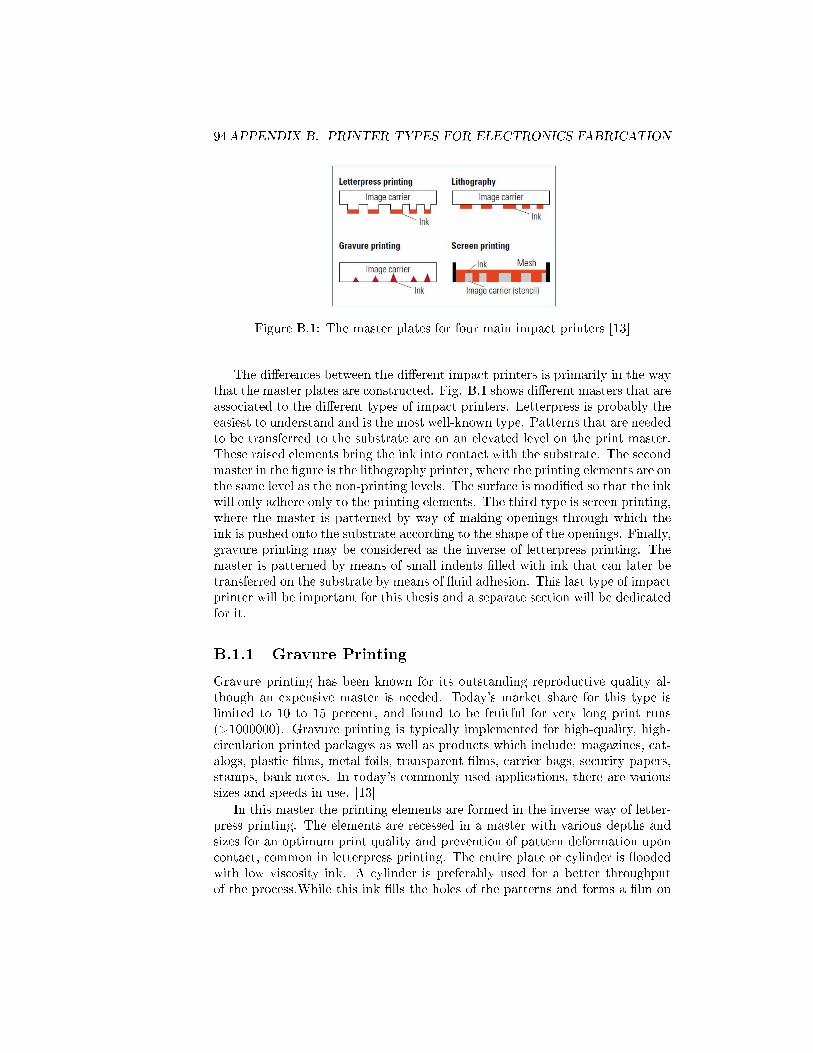
94APPENDIX B. PRINTER TYPES FOR ELECTRONICS FABRICATION
Figure B.1: The master plates for four main impact printers [13]
The di�erences between the di�erent impact printers is primarily in the waythat the master plates are constructed. Fig. B.1 shows di�erent masters that areassociated to the di�erent types of impact printers. Letterpress is probably theeasiest to understand and is the most well-known type. Patterns that are neededto be transferred to the substrate are on an elevated level on the print master.These raised elements bring the ink into contact with the substrate. The secondmaster in the �gure is the lithography printer, where the printing elements are onthe same level as the non-printing levels. The surface is modi�ed so that the inkwill only adhere only to the printing elements. The third type is screen printing,where the master is patterned by way of making openings through which theink is pushed onto the substrate according to the shape of the openings. Finally,gravure printing may be considered as the inverse of letterpress printing. Themaster is patterned by means of small indents �lled with ink that can later betransferred on the substrate by means of �uid adhesion. This last type of impactprinter will be important for this thesis and a separate section will be dedicatedfor it.
B.1.1 Gravure Printing
Gravure printing has been known for its outstanding reproductive quality al-though an expensive master is needed. Today's market share for this type islimited to 10 to 15 percent, and found to be fruitful for very long print runs(>1000000). Gravure printing is typically implemented for high-quality, high-circulation printed packages as well as products which include: magazines, cat-alogs, plastic �lms, metal foils, transparent �lms, carrier bags, security papers,stamps, bank notes. In today's commonly used applications, there are varioussizes and speeds in use. [13]
In this master the printing elements are formed in the inverse way of letter-press printing. The elements are recessed in a master with various depths andsizes for an optimum print quality and prevention of pattern deformation uponcontact, common in letterpress printing. The entire plate or cylinder is �oodedwith low viscosity ink. A cylinder is preferably used for a better throughputof the process.While this ink �lls the holes of the patterns and forms a �lm on
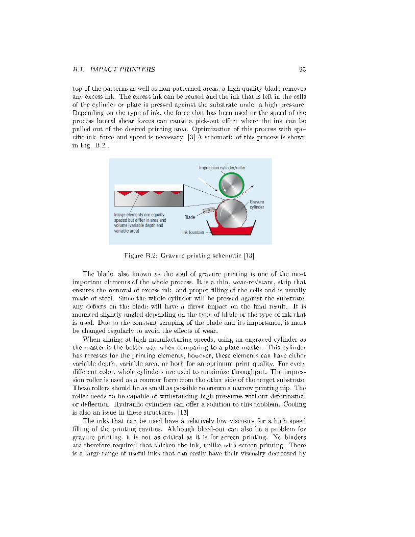
B.1. IMPACT PRINTERS 95
top of the patterns as well as non-patterned areas, a high quality blade removesany excess ink. The excess ink can be reused and the ink that is left in the cellsof the cylinder or plate is pressed against the substrate under a high pressure.Depending on the type of ink, the force that has been used or the speed of theprocess lateral shear forces can cause a pick-out e�ect where the ink can bepulled out of the desired printing area. Optimization of this process with spe-ci�c ink, force and speed is necessary. [3] A schematic of this process is shownin Fig. B.2 .
Figure B.2: Gravure printing schematic [13]
The blade, also known as the soul of gravure printing is one of the mostimportant elements of the whole process. It is a thin, wear-resistant, strip thatensures the removal of excess ink, and proper �lling of the cells and is usuallymade of steel. Since the whole cylinder will be pressed against the substrate,any defects on the blade will have a direct impact on the �nal result. It ismounted slightly angled depending on the type of blade or the type of ink thatis used. Due to the constant scraping of the blade and its importance, it mustbe changed regularly to avoid the e�ects of wear.
When aiming at high manufacturing speeds, using an engraved cylinder asthe master is the better way when comparing to a plate master. This cylinderhas recesses for the printing elements, however, these elements can have eithervariable depth, variable area, or both for an optimum print quality. For everydi�erent color, whole cylinders are used to maximize throughput. The impres-sion roller is used as a counter force from the other side of the target substrate.These rollers should be as small as possible to ensure a narrow printing nip. Theroller needs to be capable of withstanding high pressures without deformationor de�ection. Hydraulic cylinders can o�er a solution to this problem. Coolingis also an issue in these structures. [13]
The inks that can be used have a relatively low viscosity for a high speed�lling of the printing cavities. Although bleed-out can also be a problem forgravure printing, it is not as critical as it is for screen printing. No bindersare therefore required that thicken the ink, unlike with screen printing. Thereis a large range of useful inks that can easily have their viscosity decreased by
96APPENDIX B. PRINTER TYPES FOR ELECTRONICS FABRICATION
creating a solution out of them. Toluene and Xylene are typically used solventssince they are transparent, can dissolve many types of inks and dry fairly quickly.The �nal ink is kept in an ink pan in which the gravure cylinder is inserted.The cylinder must not form foams or splash inks to maintain a high quality ink�lling of the cells. When the ink is transferred to the �nal substrate, it will notbe able to be transferred completely which is also the case for the other impactprinters. The ink will split depending on variables such as: thickness of theink layer, period of contact, contact pressure, rheological ink properties suchas viscosity and wetting properties, temperature ratios, surface properties andabsorption properties. In the case of gravure printing, two additional variablescan in�uence this ink splitting, such as the shape of the cells and the �lling levelof the cells.[13]
To summarize, there are a few key aspects of the gravure printing processthat make them suitable for the mass production of electronics:
+ Very high image quality [12, 13]
+ Very high speed [3]
+ Very good image reproduction [13, 10]
+ Good uniformity [3]
+ Low line-edge roughness [3]
+ Good compatibility with many materials [12]
+ Wide range of thicknesses possible due to the cell structure [3]
+ Good scalability up to a linewidth below 20µm [3]
- Expensive Cylinder [12, 13]
- Limited by overlay printing registration accuracy (OPRA) [58]
- Separate cells on the cylinder prevent this type of printer to create smoothstraight lines. [59]
For the implementation in electronics fabrication, it is important to know theoperating regime of the process currently in use. Table B.1 summarizes some ofthe typical values associated to gravure printing.
Research has been conducted on the printability of electronics using thistype of printing[58, 60]. The bene�ts of gravure printing has attracted manyresearchers. Already many electronic devices have been proven to be produciblewith this type of printing such as OLEDs[61, 62, 63] and basic circuit elements[12, 64, 65].
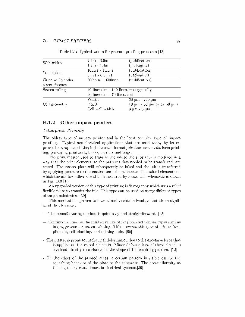
B.1. IMPACT PRINTERS 97
Table B.1: Typical values for gravure printing processes [13]
Web width2.4m - 3.6m (publication)1.2m - 1.4m (packaging)
Web speed10m/s - 15m/s (publication)5m/s - 6.5m/s (packaging)
Gravure Cylindercircumference
800mm - 1600mm (publication)
Screen ruling 40 lines/cm - 140 lines/cm (typically60 lines/cm - 70 lines/cm)
Cell geometryWidth 30 μm - 230 μmDepth 10 μm - 30 μm (max 50 μm)Cell wall width 3 μm - 5 μm
B.1.2 Other impact printers
Letterpress Printing
The oldest type of impact printer and is the least complex type of impactprinting. Typical non-electrical applications that are used today by letter-press/�exographic printing include small-format jobs, business cards, form print-ing, packaging printwork, labels, carriers and bags.
The print master used to transfer the ink to the substrate is modi�ed in away that the print elements, so the patterns that needed to be transferred, areraised. The master plate will subsequently be inked and the ink is transferredby applying pressure to the master, onto the substrate. The raised elements onwhich the ink has adhered will be transferred by force. The schematic is shownin Fig. B.3 [13]
An upgraded version of this type of printing is �exography which uses a relief�exible plate to transfer the ink. This type can be used on many di�erent typesof target substrates. [59]
This method has proven to have a fundamental advantage but also a signif-icant disadvantage:
+ The manufacturing method is quite easy and straightforward. [12]
+ Continuous lines can be printed unlike other pixelated printer types such asinkjet, gravure or screen printing. This prevents this type of printer frompinholes, cell blocking, and missing dots. [66]
- The master is prone to mechanical deformation due to the excessive force thatis applied on the raised elements. Minor deformations of these elementscan lead directly to a change in the shape of the resulting pattern. [12]
- On the edges of the printed areas, a certain pattern is visible due to thesquashing behavior of the plate to the substrate. The non-uniformity atthe edges may cause issues in electrical systems.[59]
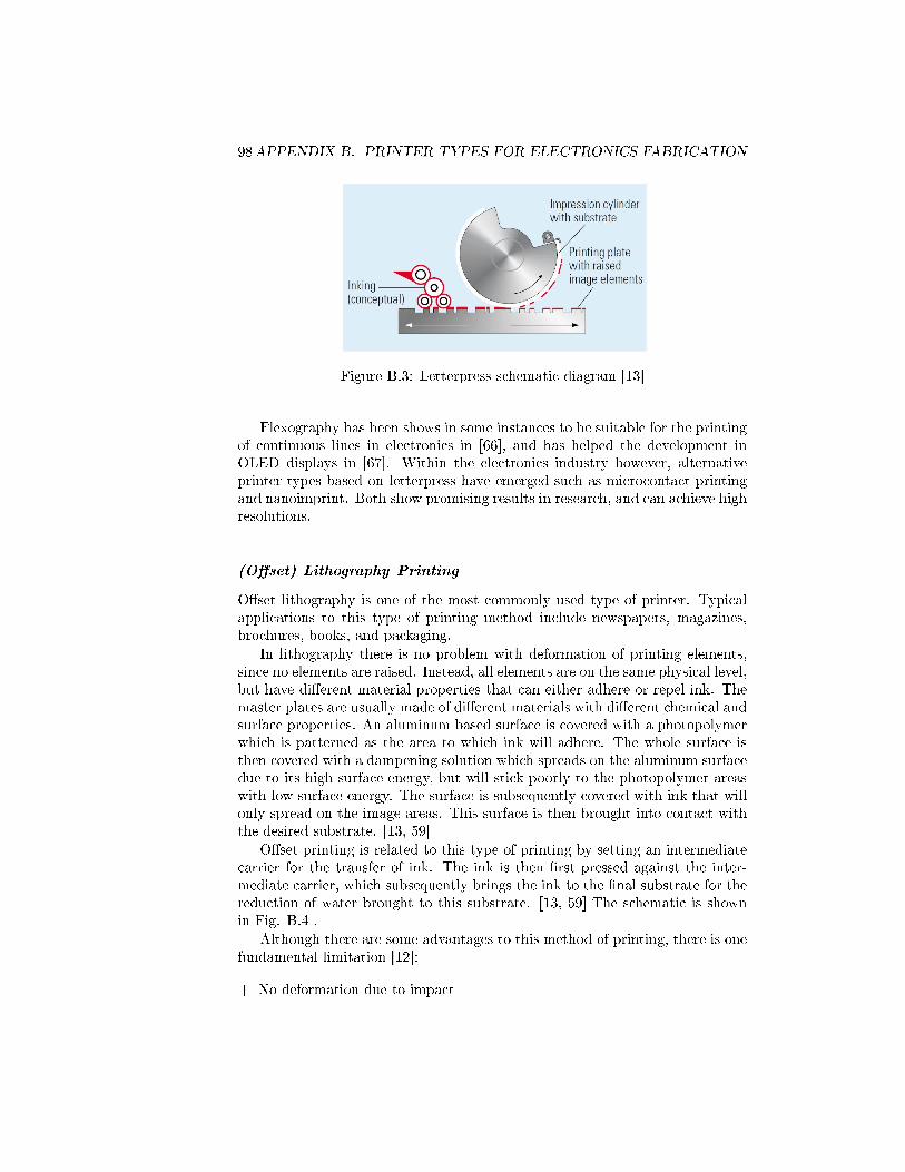
98APPENDIX B. PRINTER TYPES FOR ELECTRONICS FABRICATION
Figure B.3: Letterpress schematic diagram [13]
Flexography has been shows in some instances to be suitable for the printingof continuous lines in electronics in [66], and has helped the development inOLED displays in [67]. Within the electronics industry however, alternativeprinter types based on letterpress have emerged such as microcontact printingand nanoimprint. Both show promising results in research, and can achieve highresolutions.
(O�set) Lithography Printing
O�set lithography is one of the most commonly used type of printer. Typicalapplications to this type of printing method include newspapers, magazines,brochures, books, and packaging.
In lithography there is no problem with deformation of printing elements,since no elements are raised. Instead, all elements are on the same physical level,but have di�erent material properties that can either adhere or repel ink. Themaster plates are usually made of di�erent materials with di�erent chemical andsurface properties. An aluminum based surface is covered with a photopolymerwhich is patterned as the area to which ink will adhere. The whole surface isthen covered with a dampening solution which spreads on the aluminum surfacedue to its high surface energy, but will stick poorly to the photopolymer areaswith low surface energy. The surface is subsequently covered with ink that willonly spread on the image areas. This surface is then brought into contact withthe desired substrate. [13, 59]
O�set printing is related to this type of printing by setting an intermediatecarrier for the transfer of ink. The ink is then �rst pressed against the inter-mediate carrier, which subsequently brings the ink to the �nal substrate for thereduction of water brought to this substrate. [13, 59] The schematic is shownin Fig. B.4 .
Although there are some advantages to this method of printing, there is onefundamental limitation [12]:
+ No deformation due to impact
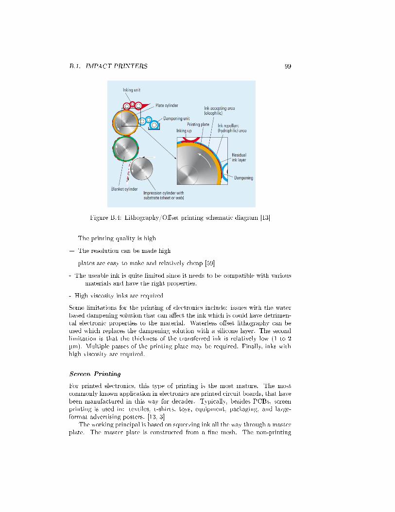
B.1. IMPACT PRINTERS 99
Figure B.4: Lithography/O�set printing schematic diagram [13]
+ The printing quality is high
+ The resolution can be made high
+ plates are easy to make and relatively cheap [59]
- The useable ink is quite limited since it needs to be compatible with variousmaterials and have the right properties.
- High viscosity inks are required
Some limitations for the printing of electronics include: issues with the waterbased dampening solution that can a�ect the ink which is could have detrimen-tal electronic properties to the material. Waterless o�set lithography can beused which replaces the dampening solution with a silicone layer. The secondlimitation is that the thickness of the transferred ink is relatively low (1 to 2µm). Multiple passes of the printing plate may be required. Finally, inks withhigh viscosity are required.
Screen Printing
For printed electronics, this type of printing is the most mature. The mostcommonly known application in electronics are printed circuit boards, that havebeen manufactured in this way for decades. Typically, besides PCBs, screenprinting is used in: textiles, t-shirts, toys, equipment, packaging, and large-format advertising posters. [13, 3]
The working principal is based on squeezing ink all the way through a masterplate. The master plate is constructed from a �ne mesh. The non-printing
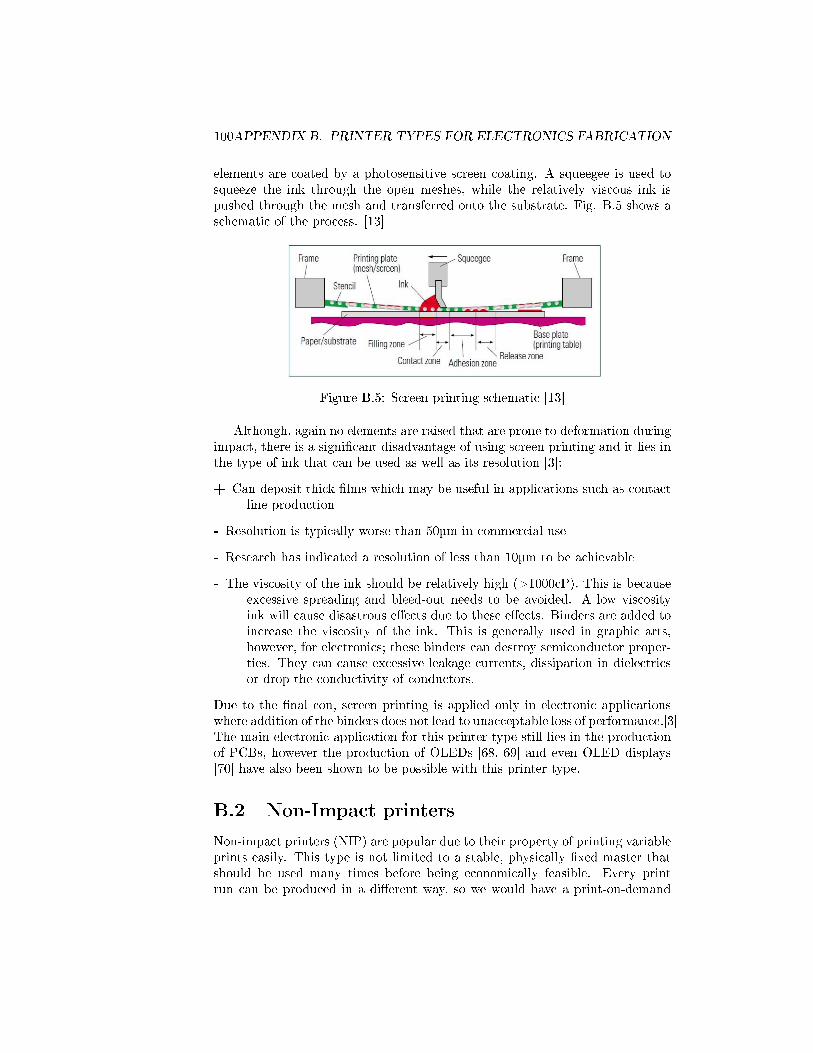
100APPENDIX B. PRINTER TYPES FOR ELECTRONICS FABRICATION
elements are coated by a photosensitive screen coating. A squeegee is used tosqueeze the ink through the open meshes, while the relatively viscous ink ispushed through the mesh and transferred onto the substrate. Fig. B.5 shows aschematic of the process. [13]
Figure B.5: Screen printing schematic [13]
Although, again no elements are raised that are prone to deformation duringimpact, there is a signi�cant disadvantage of using screen printing and it lies inthe type of ink that can be used as well as its resolution [3]:
+ Can deposit thick �lms which may be useful in applications such as contactline production
- Resolution is typically worse than 50µm in commercial use
- Research has indicated a resolution of less than 10µm to be achievable
- The viscosity of the ink should be relatively high (>1000cP). This is becauseexcessive spreading and bleed-out needs to be avoided. A low viscosityink will cause disastrous e�ects due to these e�ects. Binders are added toincrease the viscosity of the ink. This is generally used in graphic arts,however, for electronics; these binders can destroy semiconductor proper-ties. They can cause excessive leakage currents, dissipation in dielectricsor drop the conductivity of conductors.
Due to the �nal con, screen printing is applied only in electronic applicationswhere addition of the binders does not lead to unacceptable loss of performance.[3]The main electronic application for this printer type still lies in the productionof PCBs, however the production of OLEDs [68, 69] and even OLED displays[70] have also been shown to be possible with this printer type.
B.2 Non-Impact printers
Non-impact printers (NIP) are popular due to their property of printing variableprints easily. This type is not limited to a stable, physically �xed master thatshould be used many times before being economically feasible. Every printrun can be produced in a di�erent way, so we would have a print-on-demand
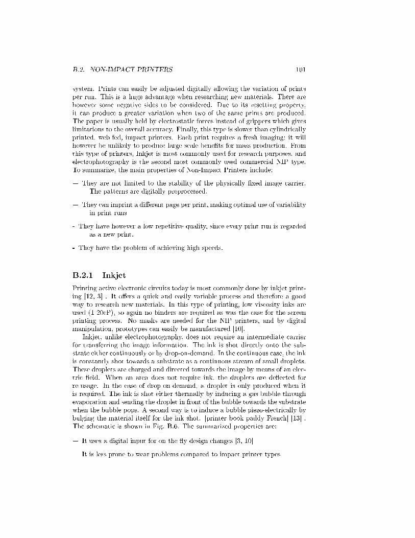
B.2. NON-IMPACT PRINTERS 101
system. Prints can easily be adjusted digitally allowing the variation of printsper run. This is a huge advantage when researching new materials. There arehowever some negative sides to be considered. Due to its resetting property,it can produce a greater variation when two of the same prints are produced.The paper is usually held by electrostatic forces instead of grippers which giveslimitations to the overall accuracy. Finally, this type is slower than cylindricallyprinted, web-fed, impact printers. Each print requires a fresh imaging; it willhowever be unlikely to produce large scale bene�ts for mass production. Fromthis type of printers, Inkjet is most commonly used for research purposes, andelectrophotography is the second most commonly used commercial NIP type.To summarize, the main properties of Non-Impact Printers include:
+ They are not limited to the stability of the physically �xed image carrier.The patterns are digitally preprocessed.
+ They can imprint a di�erent page per print, making optimal use of variabilityin print runs
- They have however a low repetitive quality, since every print run is regardedas a new print.
- They have the problem of achieving high speeds.
B.2.1 Inkjet
Printing active electronic circuits today is most commonly done by inkjet print-ing [12, 3] . It o�ers a quick and easily variable process and therefore a goodway to research new materials. In this type of printing, low viscosity inks areused (1-20cP), so again no binders are required as was the case for the screenprinting process. No masks are needed for the NIP printers, and by digitalmanipulation, prototypes can easily be manufactured [10].
Inkjet, unlike electrophotography, does not require an intermediate carrierfor transferring the image information. The ink is shot directly onto the sub-strate either continuously or by drop-on-demand. In the continuous case, the inkis constantly shot towards a substrate as a continuous stream of small droplets.These droplets are charged and directed towards the image by means of an elec-tric �eld. When an area does not require ink, the droplets are de�ected forre-usage. In the case of drop-on-demand, a droplet is only produced when itis required. The ink is shot either thermally by inducing a gas bubble throughevaporation and sending the droplet in front of the bubble towards the substratewhen the bubble pops. A second way is to induce a bubble piezo-electrically bybulging the material itself for the ink shot. [printer book paddy French] [13] .The schematic is shown in Fig. B.6. The summarized properties are:
+ It uses a digital input for on the �y design changes [3, 10]
+ It is less prone to wear problems compared to impact printer types
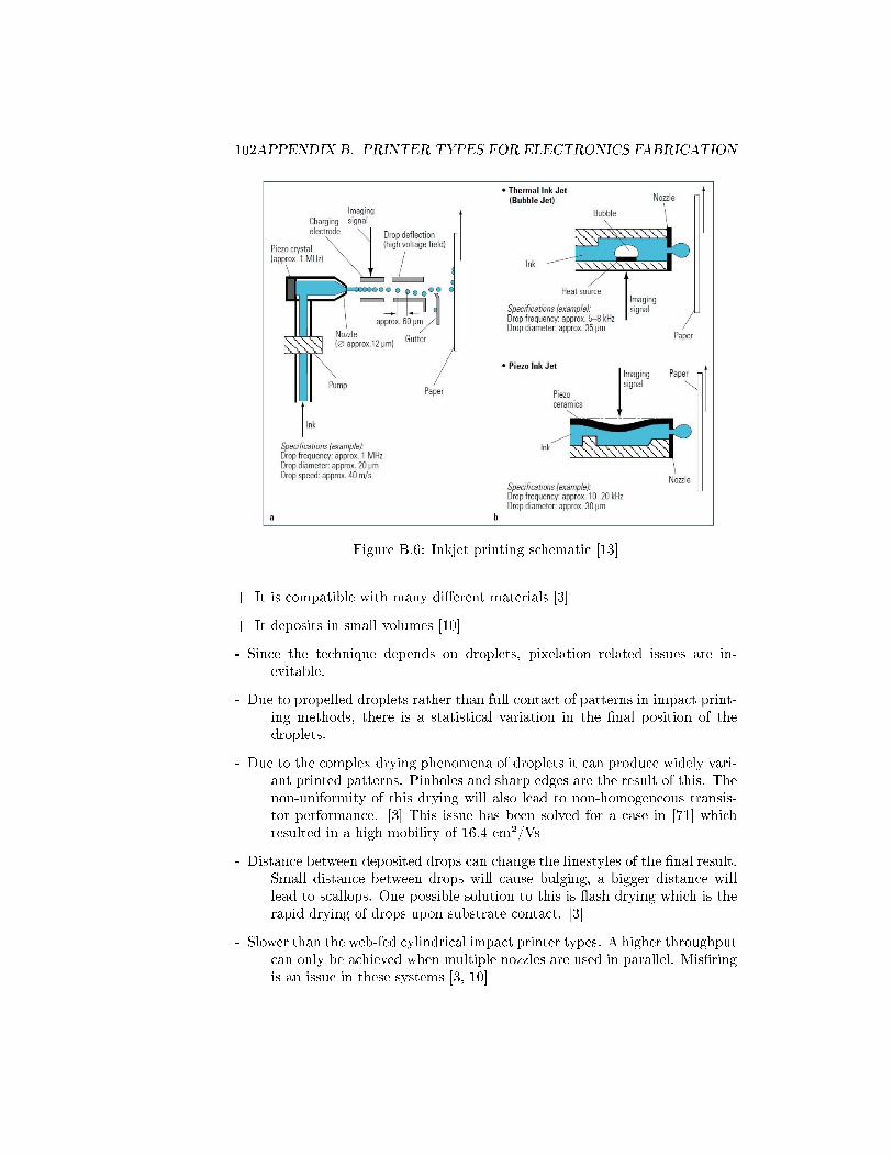
102APPENDIX B. PRINTER TYPES FOR ELECTRONICS FABRICATION
Figure B.6: Inkjet printing schematic [13]
+ It is compatible with many di�erent materials [3]
+ It deposits in small volumes [10]
- Since the technique depends on droplets, pixelation related issues are in-evitable.
- Due to propelled droplets rather than full contact of patterns in impact print-ing methods, there is a statistical variation in the �nal position of thedroplets.
- Due to the complex drying phenomena of droplets it can produce widely vari-ant printed patterns. Pinholes and sharp edges are the result of this. Thenon-uniformity of this drying will also lead to non-homogeneous transis-tor performance. [3] This issue has been solved for a case in [71] whichresulted in a high mobility of 16.4 cm²/Vs
- Distance between deposited drops can change the linestyles of the �nal result.Small distance between drops will cause bulging, a bigger distance willlead to scallops. One possible solution to this is �ash drying which is therapid drying of drops upon substrate contact. [3]
- Slower than the web-fed cylindrical impact printer types. A higher throughputcan only be achieved when multiple nozzles are used in parallel. Mis�ringis an issue in these systems [3, 10]
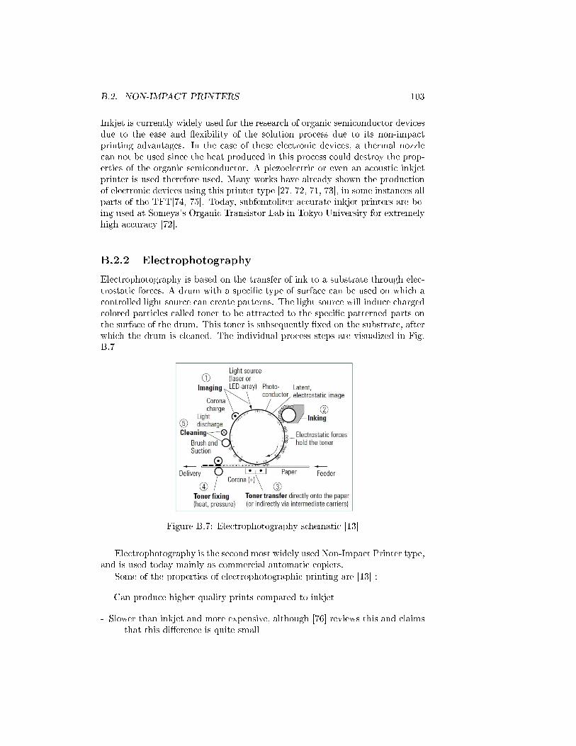
B.2. NON-IMPACT PRINTERS 103
Inkjet is currently widely used for the research of organic semiconductor devicesdue to the ease and �exibility of the solution process due to its non-impactprinting advantages. In the case of these electronic devices, a thermal nozzlecan not be used since the heat produced in this process could destroy the prop-erties of the organic semiconductor. A piezoelectric or even an acoustic inkjetprinter is used therefore used. Many works have already shown the productionof electronic devices using this printer type [27, 72, 71, 73], in some instances allparts of the TFT[74, 75]. Today, subfemtoliter accurate inkjet printers are be-ing used at Someya's Organic Transistor Lab in Tokyo University for extremelyhigh accuracy [72].
B.2.2 Electrophotography
Electrophotography is based on the transfer of ink to a substrate through elec-trostatic forces. A drum with a speci�c type of surface can be used on which acontrolled light source can create patterns. The light source will induce chargedcolored particles called toner to be attracted to the speci�c patterned parts onthe surface of the drum. This toner is subsequently �xed on the substrate, afterwhich the drum is cleaned. The individual process steps are visualized in Fig.B.7
Figure B.7: Electrophotography schematic [13]
Electrophotography is the second most widely used Non-Impact Printer type,and is used today mainly as commercial automatic copiers.
Some of the properties of electrophotographic printing are [13] :
+ Can produce higher quality prints compared to inkjet
- Slower than inkjet and more expensive, although [76] reviews this and claimsthat this di�erence is quite small
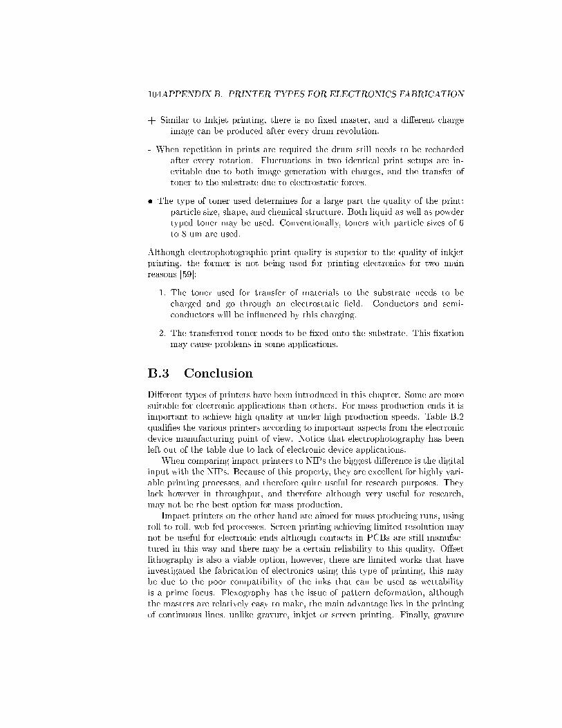
104APPENDIX B. PRINTER TYPES FOR ELECTRONICS FABRICATION
+ Similar to Inkjet printing, there is no �xed master, and a di�erent chargeimage can be produced after every drum revolution.
- When repetition in prints are required the drum still needs to be rechardedafter every rotation. Fluctuations in two identical print setups are in-evitable due to both image generation with charges, and the transfer oftoner to the substrate due to electrostatic forces.
� The type of toner used determines for a large part the quality of the print:particle size, shape, and chemical structure. Both liquid as well as powdertyped toner may be used. Conventionally, toners with particle sizes of 6to 8 um are used.
Although electrophotographic print quality is superior to the quality of inkjetprinting, the former is not being used for printing electronics for two mainreasons [59]:
1. The toner used for transfer of materials to the substrate needs to becharged and go through an electrostatic �eld. Conductors and semi-conductors will be in�uenced by this charging.
2. The transferred toner needs to be �xed onto the substrate. This �xationmay cause problems in some applications.
B.3 Conclusion
Di�erent types of printers have been introduced in this chapter. Some are moresuitable for electronic applications than others. For mass production ends it isimportant to achieve high quality at under high production speeds. Table B.2quali�es the various printers according to important aspects from the electronicdevice manufacturing point of view. Notice that electrophotography has beenleft out of the table due to lack of electronic device applications.
When comparing impact printers to NIPs the biggest di�erence is the digitalinput with the NIPs. Because of this property, they are excellent for highly vari-able printing processes, and therefore quite useful for research purposes. Theylack however in throughput, and therefore although very useful for research,may not be the best option for mass production.
Impact printers on the other hand are aimed for mass producing runs, usingroll-to-roll, web-fed processes. Screen printing achieving limited resolution maynot be useful for electronic ends although contacts in PCBs are still manufac-tured in this way and there may be a certain reliability to this quality. O�setlithography is also a viable option, however, there are limited works that haveinvestigated the fabrication of electronics using this type of printing, this maybe due to the poor compatibility of the inks that can be used as wettabilityis a prime focus. Flexography has the issue of pattern deformation, althoughthe masters are relatively easy to make, the main advantage lies in the printingof continuous lines, unlike gravure, inkjet or screen printing. Finally, gravure
B.3. CONCLUSION 105
Table B.2: Comparative analysis of the various printer types
TypicalResolution
InkViscosity
Mainadvantage
Maindisadvantage
Gravure + low Excellentreproducibilityand �delity
expensivemaster
Flexography ± low continuous lineprintability
patterndeformation
O�setLithogra-
phy
+ high fast andaccurate
limited inkcompatibility
Screen - high reliable low resolutionInkjet + low digital input low throughput
printing has gained quite some attention due to its high reproducibility and �-delity over long print runs. In addition, the throughput is high and many typesof inks may be used. The cost of creating the master is relatively high, however,print runs exceeding over 1,000,000 runs, compensate for the costs and makethis type of printing rather inexpensive.
For electronics, many di�erent printers may be used but are suitable forperhaps various parts of the transistor. A combination of printing types may bethe most e�cient way to create low cost large area electronics. One particularprinter type, gravure printing, has proven to be the most interesting for massproduction ends. For research however, it is more useful to produce easilymanipulable devices, and therefore the non-impact printer type inkjet printing,is the most suitable for the early stages of printing electronics due to its digitalinput and high resolution.

106APPENDIX B. PRINTER TYPES FOR ELECTRONICS FABRICATION
Appendix C
Thin-Film Transistor
Thin-�lm transistors are di�erent from conventional MOSFET's and BJT's inone essential aspect: they can be built on top of a certain substrate. Todaymany of the applications of these devices are especially large area displays. Inthese products the devices are manufactured on top of a glass substrate andoperate by directly in�uencing the emission of light through the display. In thisexample, it is not essential to create the devices at lower temperatures due tothe temperature stability of the glass substrate. Solution processing in this caseis still however desirable for larger area displays, �exible displays, and cheaperdisplays.
In essence, thin-�lm transistors are a type of MOSFET's built on top of asubstrate. Today, many of the displays are created using hydrogenated amor-phous silicon (a-Si:H) as the semiconductor. It is important to notice that mostof the devices in this Appendix are focused on organic semiconductors sincethese are the main type of solution processable semiconductors and thereforethe direct competitor of the liquid silicon material. Organic semiconductorswere preferred due to their solubility with many common solvents without los-ing their original semiconducting function. These organic semiconductors havefundamental limitations to their stability, and therefore the impact of di�erentdevice con�gurations and processing methods to the �nal device is quite big,whereas this would not be the case for conventionally processed TFT's. Solu-tion processed devices which is necessary for the printing of devices is mainlyfocused from an organic TFT point of view.
C.1 OTFT Characteristics
For the organic transistor, current �ow is limited as well as their reliability [2, 8].The main charge carrier transport occurs in the �rst 50 angström of the organicsemiconductor layer, away from the semiconductor-dielectric interface [9]. Thisinterface is therefore essential for the quality of the device. The thickness ofthe semiconductor layer ranges typically from 200-500 angström. Thinner �lms
107
108 APPENDIX C. THIN-FILM TRANSISTOR
could fail due to incomplete surface coverage [9].The deposition of the semiconductor layer in this type of transistor becomes
crucial. There are three important points about deposition conditions [9]. The�rst one is the deposition rate; it can directly a�ect the crystallinity and mor-phology of the resulting layer. A high deposition rate leads to high nucleationdensities. These nucleation densities are related to the grain sizes within a �lm.A high nucleation density corresponds to a high concentration of small grains. Ahighly crystalline �lm that consists of larger grains, gives better characteristicsof the �nal device, as is the case for the di�erent crystal structures of siliconbased devices. Bigger grain sizes are therefore desirable, since grain boundariesdeteriorate the current �ow of the device. Additional energy is required for thecharge carriers to move from one grain to the other. High deposition rates arein this case not desired; however it could also induce the formation of a di�erentpacking order which may improve the device performance. The surface of thesubstrate and substrate temperature also has a great impact on the formationof the �lm. Substrates with grooves in a particular direction may induce anordering of the organic molecules in a way that improves the charge carriertransport. Finally, post-deposition treatments can also help improve the deviceperformance.
C.2 Transistor Con�guration
The basic construction of TFT's can be divided into four groups dependingon the position of the gate, semiconductor and contacts. Each has its ownadvantages as well as disadvantages and will brie�y be described below. Againit is important to consider the organic variant of these devices. These devicesare shown in Fig. C.1.
� Top-Gate-Bottom-Contact
� Bottom-Gate-Top-Contact
� Bottom-Gate-Bottom-Contact
� Substrate-Gate-Bottom-Contact
Notice that the combination of Top-Gate-Top-Contact has been left out.This is primarily due to the poor reliability of the organic semiconductor. Inmost cases it is undesirable to build upon an organic semiconductor as thermalsensitivity and contamination may impact the semiconductor characteristics andtherefore the properties of the �nal device.
The di�erent gate positions relate to some important device characteristics.A top-gate (staggered) con�guration compared to the bottom-gate (inverted-staggered) con�guration gives:
+ The spacing between source and drain and therefore the essential channellength can be determined early on the design, as the contacts are depositedat an earlier stage.
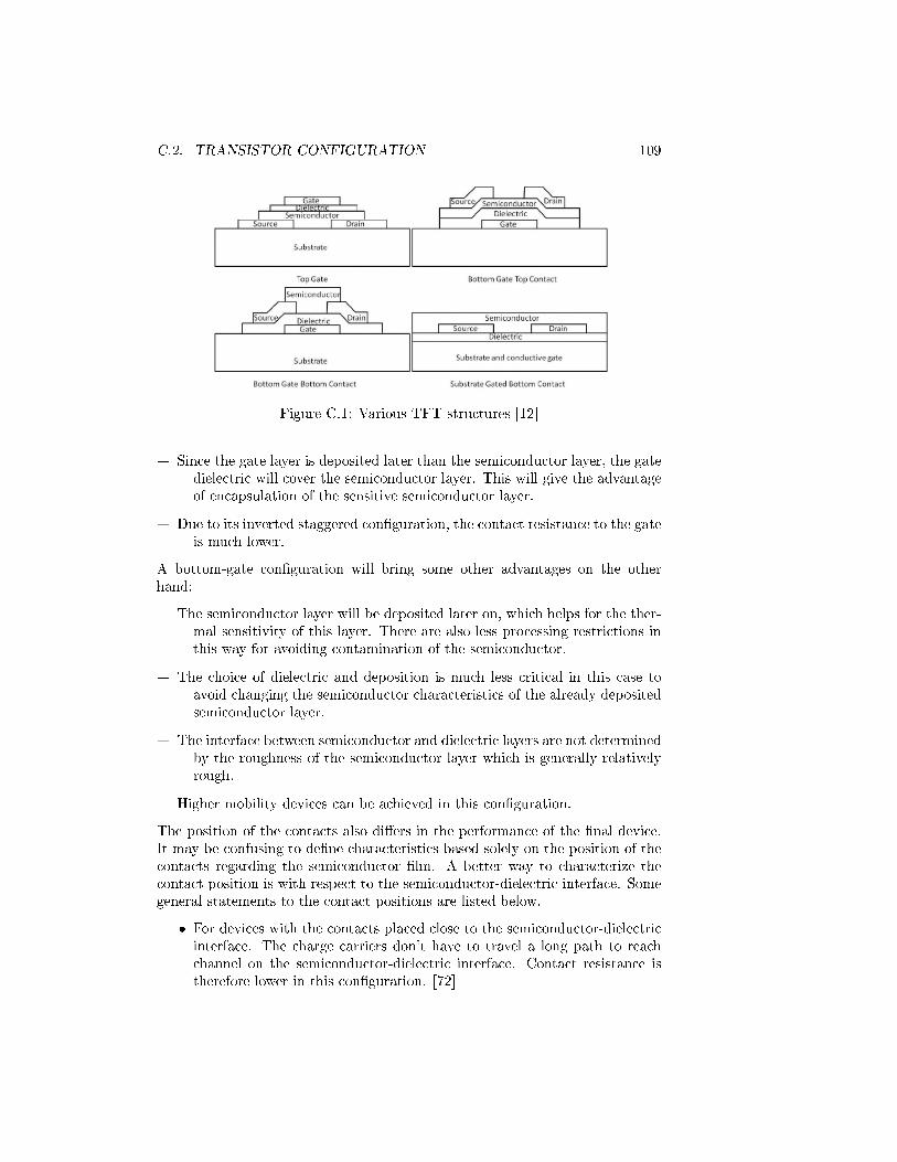
C.2. TRANSISTOR CONFIGURATION 109
Figure C.1: Various TFT structures [12]
+ Since the gate layer is deposited later than the semiconductor layer, the gatedielectric will cover the semiconductor layer. This will give the advantageof encapsulation of the sensitive semiconductor layer.
+ Due to its inverted staggered con�guration, the contact resistance to the gateis much lower.
A bottom-gate con�guration will bring some other advantages on the otherhand:
+ The semiconductor layer will be deposited later on, which helps for the ther-mal sensitivity of this layer. There are also less processing restrictions inthis way for avoiding contamination of the semiconductor.
+ The choice of dielectric and deposition is much less critical in this case toavoid changing the semiconductor characteristics of the already depositedsemiconductor layer.
+ The interface between semiconductor and dielectric layers are not determinedby the roughness of the semiconductor layer which is generally relativelyrough.
+ Higher mobility devices can be achieved in this con�guration.
The position of the contacts also di�ers in the performance of the �nal device.It may be confusing to de�ne characteristics based solely on the position of thecontacts regarding the semiconductor �lm. A better way to characterize thecontact position is with respect to the semiconductor-dielectric interface. Somegeneral statements to the contact positions are listed below.
� For devices with the contacts placed close to the semiconductor-dielectricinterface. The charge carriers don't have to travel a long path to reachchannel on the semiconductor-dielectric interface. Contact resistance istherefore lower in this con�guration. [72]
110 APPENDIX C. THIN-FILM TRANSISTOR
� It is undesirable to have the semiconductor placed before the contactsare placed due to the instability of the organic semiconductor that maytherefore be in�uenced by the subsequent contact deposition.
Although some of these characteristics are only limited to the processing of or-ganic transistors, it is important to know what the alternative for liquid siliconsolution processed devices can provide. Some of the information in this sectionmay also apply to liquid silicon devices, although it is relatively more stable. Inthe �nal design of the device, the exact worst con�guration for organic transis-tors will be used due to the way liquid silicon Single-Grain Thin-Film Transistorsare constructed.
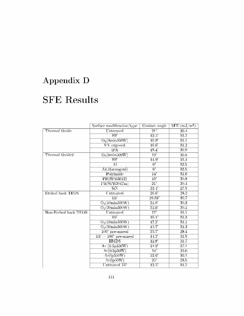
Appendix D
SFE Results
Surface modi�cation/type Contact angle SFE (mJ/m²)Thermal Oxide Untreated 21° 30.4
HF 12.5° 31.7O2(8min500W) 16.9° 31.1UV exposed 16.6° 31.2
IPA 18.4° 30.9Thermal Oxide2 O2(8min500W) 19° 30.8
HF 14.9° 31.4Al 0° 32.5
Al(Marangoni) 0° 32.5Polyimide 14° 31.6
PR(SPR3012) 19° 30.8PR(SPR3017m) 21° 30.4
SiN 33.4° 27.5Etched back TEOS Untreated 26.6° 29.2
HF 19.33° 30.7O2(10min500W) 21.8° 30.3O2(30min300W) 22.6° 30.1
Non-Etched back TEOS Untreated 17° 31.1HF 16.1° 31.3
O2(10min500W) 17.2° 31.1O2(30min300W) 15.7° 31.3100° pre-anneal 25.7° 29.4
HF + 100° pre-anneal 14.2° 31.5HMDS 12.8° 31.7
Ar (0.5p350W) 34.9° 27.1Ar(0.5p50W) 10° 32.0Ar(lp350W) 22.6° 30.1Ar(lp50W) 25° 29.5
Untreated 75° 12.5° 31.7
111
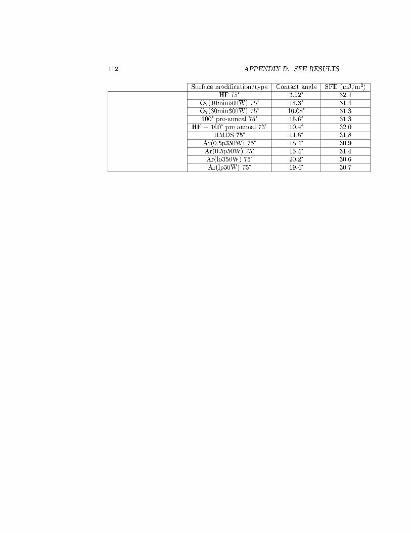
112 APPENDIX D. SFE RESULTS
Surface modi�cation/type Contact angle SFE (mJ/m²)HF 75° 3.92° 32.4
O2(10min500W) 75° 14.8° 31.4O2(30min300W) 75° 16.08° 31.3100° pre-anneal 75° 15.6° 31.3
HF + 100° pre-anneal 75° 10.4° 32.0HMDS 75° 11.8° 31.8
Ar(0.5p350W) 75° 18.4° 30.9Ar(0.5p50W) 75° 15.4° 31.4Ar(lp350W) 75° 20.2° 30.6Ar(lp50W) 75° 19.4° 30.7
Appendix E
Excimer Laser Crystallization
E.1 Crystallization process
Two types of crystallisation occur in the ELC process. [47, 48]
Explosive Crystallization
The melting point of a-Si is a few hundred degrees lower than crystalline silicon(1414°C). This di�erence in melting point lies at the core of the explosive crys-tallization process. When the a-Si is molten, it is rapidly cooled with respect tothe crystalline silicon, which will cause crystallization of the liquid into polysil-icon areas (only at very high cooling rates and lack of crystalline fractions willthe liquid solidify back into an amorphous solid). The heat produced by thecrystallization of the silicon liquid will further melt the remaining a-Si whichagain proceeds to solidify due to the supercooled surrounding. In this way themolten layer moves deeper into the total �lm leaving a trail of �ne polysilicongrains behind. The whole process is self-sustaining and is continued until thereis a su�cient loss of heat that is required for the further melting of a-Si.
Melting and Solidi�cation
When a certain threshold is reached by the laser, the �ne polysilicon grainsthat were previously formed by explosive crystallization, remelts at the surface.This remelting of the polysilicon is not as severely supercooled as is the case forexplosive crystallization. Therefore the solidi�cation rate is much lower, whichresults in a reduced number of granular planar defects, and an increased grainsize.
At this second remelting energy a di�erence between complete melt andincomplete melt can be recognized. In the event of a complete melt, there areno crystalline seeds left for regrowth. Therefore, before solidi�cation may occur,homogeneous nucleation is required. These nucleï will stabilize under certainthermal conditions. After the formation of nucleï, the �lm will solidify rapidly.
113
114 APPENDIX E. EXCIMER LASER CRYSTALLIZATION
The nucleation rate is strongly dependent on temperature, and will result ina �nal �lm in which small grains coexist with larger ones. In a near completemelt condition, some �ne polycrystalline grains from the explosive crystallizationsurvive. Solidi�cation will initiate at the remaining polycrystalline grains dueto heterogenous nucleation rather than the homogenous nucleation. Grain sizewill increase signi�cantly and will grow beyond the �lm thickness. This processis called superlateral growth.
Keeping these processes in mind, grain sizes can be enlarged by increasingthe lateral growth interval. This can be done by reducing the cooling rate ofthe molten silicon. Heating of the substrate, extension of the pulse duration, orsimultaneous irradiation of the sample from the front and backside are some ofthe possible options. Shooting multiple pulses at a sample can also increase thegrain size due to the growth of preferential orientation of the grains.
E.2 Crystallization problems
Some issues when producing the crystalline �lm may also occur:
Random grain boundaries Grains that are grown from di�erent seeds cancollide. During crystallization the silicon will expand due to the densitydi�erence between solid and liquid phase silicon. The higher density solidsilicon has little e�ect in the vertical growth direction, however, horizon-tally the liquid will be pushed by the crystallizing solid silicon. At theinterface between two growing grains the liquid will built and preventfurther growth. This results in high defect density grain boundaries andshould be avoided when constructing polycrystalline silicon TFTs in thisway.
Breakdown growth The rate of growth of the crystalline silicon may be toohigh which may lead to misplacement of atoms that result in stackingfaults and twins and may even lead to complete breakdown. Orientationof the crystal highly in�uences this type of error.
Thermal stress Rapid cooling may induce thermal stresses that will result inplanar defects during lateral growth. Tensile elastic strain in the siliconbuilds up until yielding of the material occurs. Again crystallographicorientation is important for this type of error.
Film cracks These are formed as a release of thermal stress due to steps inthe �lm that have been lithographically produced. The di�erence in ther-mal expansion rates of silicon and silicon dioxide lie at the source of thisproblem.
Hydrogen e�usion Any hydrogen present within the amorphous silicon �lmcan be e�use due to the laser irradiation and may destroy some parts ofthe �lm. Since the liquid silicon material is produced from a hydrogenated
E.2. CRYSTALLIZATION PROBLEMS 115
silicon compound, and due to limited annealing temperature, a signi�cantamount of hydrogen atoms can be left in the �lm that can cause defectsby this out-di�usion of the hydrogen.
Film agglomeration Partial dewetting may occur and lead to �lm decomposi-tion into beads which is known as agglomeration. The main source of thisdewetting are the �uctuations of the silicon �lm that are severe enough toreach the underlying oxide layer. These �uctuations are in�uenced by thepulsed-laser annealing caused by non-uniformities in the spatial pro�le ofthe laser pulse and intensity �uctuations from the homogenizer. Also theinterference of the incident beam with laterally scattered beams as well asthe surface tension gradient have an impact on this defect.
Ablation is related to excessive agglomeration and is known as the explosiverelease of hydrogen. A major issue in this work is indeed the hydrogencontent of the amorphous silicon �lm produced from the liquid siliconmaterial.

116 APPENDIX E. EXCIMER LASER CRYSTALLIZATION
Bibliography
[1] T. Shimoda, et al. �Solution-processed silicon �lms and transistors�, Naturevol. 440, 6 April 2006, pp. 783-786
[2] J. Zhang, R. Ishihara, H. Tagagishi, R. Kawajiri, T. Shimoda and C. I.M. Beenakker, �Single-Grain Si TFTs using Spin-Coated Liquid-Silicon�,IEDM11, 2011, IEEE, pp. 339-342
[3] V. Subramanian, et al. �Printed Electronics for Low-Cost Electronic Sys-tems: Technology Status and Application Development�, Department ofElectrical Engineering and Computer Sciences, University of California,Berkeley, IEEE, 2008.
[4] A. Sugiyama, T. Shimoda, and D. H. Chi, �Ab initio study of the polymer-ization of cyclopentasilane�, Molecular Physics, vol. 108, No. 12, 20 June2010, pp. 1649-1653
[5] P. V. Dung, P. T. Lam, N. D. Duc, A. Sugiyama, T. Shimoda, D. H.Chi, �First-principles study of the thermally induced polymerization of cy-clopentasilane�, Computational Materials Science 49, 2010, pp. S21-S24,Elsevier
[6] H. Iwasawa et al. �Silane Polymer and Method for Forming Silicon Film�,US Patent 2009/0215920 A1, Aug. 27, 2009
[7] D. L. Kim et al. �The E�ect of Ultraviolet Exposure on Solution Process ofSilicon Thin Film�, Electrochemical and Solid-State Letters, 12, 2009, pp.E23-E25
[8] [book] David B. Mitzi "Solution processing of Inorganic Materials", JohnWiley & Sons, Inc., Hoboken, New Jersey, 2009
[9] M. M. Ling and Zhenan Bao, �Thin Film Depostition, Patterning, andPrinting in Organic Thin Film Transistors�, Department of Chemical En-gineering, Stanford University, American Chemical Society, 2004.
[10] J. Verilhac et al. �Step toward robust and reliable amorphous polymer�eld-e�ect transistors and logic functions made by the use of roll to rollcompatible printing processes�, Organic Electronics 11, 2010, pp. 456-462
117
118 BIBLIOGRAPHY
[11] C. Y. Woo, C. Y. Ho, K. H. Seok, L. Y. Hee, �Solar cell manufactured usingamorphous and nanocrystalline silicon composite thin �lm, and process formanufacturing the same�, European Patent Application, EP 2 040 310 A2,March 25, 2009
[12] Alejandro de la Fuente Vornbrock, �Roll Printed Electronics: Developmentand Scaling of Gravure Printing Techniques�, Electrical Engineering andComputer Sciences, University of California at Berkeley, Dec. 29th, 2009
[13] [book] Helmut Kipphan, �Handbook of Print Media, Technologies and Pro-duction Methods�, Springer- Verlag, Berlin Heidelberg New York, 2001
[14] J. Perelaer, et al. "Printed electronics: the challenges involved in print-ing devices, interconnects, and contacts based on inorganic materials", J.Mater. Chem., 2010, 20, 8446-8453
[15] [Book] L. Solymar, D. Walsh, "Electrical Properties of Materials", OxfordUniversity Press, 7th edition
[16] [Book] D. R. Gamota, P. Brazis, K. Kalyanasundaram, J. Zhang, "PrintedOrganic and Molecular Electronics", Kluwer Academic Publishers, ISBN:1 4020 7707 6
[17] H. Ebata, T. Izawa, E. Miyazaki, K. Takimiya, M. Ikeda, H. Kuwabara,and T. Yui, "Highly Soluble [1]Benzothieno[3,2-b]benzothiophene (BTBT)Derivatives for High-Performance, Solution-Processed Organic Field-E�ectTransistors", J. Am. Chem. Soc. 2007, vol. 129, no 51, pp. 15732-15733
[18] T. Endo, T. Nagase, T. Kobayashi, K. Takimiya, M. Ikeda, and H.Naito, "Solution-Processed Dioctylbenzothienobenzothiophene-Based Top-Gate Organic Transistors with High Mobility, Low Threshold Voltage, andHigh Electrical Stability", Applied Physics Express 3, 2010, 121601
[19] T. Uemura, Y. Hirose, M. Uno, K. Takimiya, J. Takeya, "Very High Mo-bility in Solution-Processed Organic Thin-Film Transistors of Highly Or-dered [1]Benzothieno[3,2-b]benzothiophene Derivatives", Applied PhysicsExpress, vol. 2, 2009, issue 11, 111501, ISSN 188207784
[20] [Book] D. A. Neamen, "Semiconductor Physics and Devices, Basic Princi-ples" R. D. Irwin, Inc., 2003, third edition
[21] [Webpage] organic semiconductor worldwww.orgworld.de
[22] E. Hengge and G. Bauer, �Cyclopentasilane, the First Unsubstituted CyclicSilicon Hydride�, Angew. Chem. Internat. Edit. / Vol. 12, No. 4, 1973, page316
[23] U. Zschieschang et al. "Dinaphto[2,3-b:2',3'-f]thieno[3,2-b]thiophene(DNTT) thin-�lm transistors with improved performance and stability",Organic Electronics 12, 2011, pp. 1370-1375
BIBLIOGRAPHY 119
[24] T. Sekitani, U. Zschieschang, H. Klak and T. Someya, "Flexible organictransistors and circuits with extreme bending stability", Nature Materials,Vol. 9, 2010, pp. 1015-1022
[25] Organic Electronics, a future promise powerpoint presentationwww.phy.iitkgp.ernet.in/ptaccd2/ppt/ADhar.pdf
[26] T. Someya, et al. "A large-area, �exible pressure sensor matrix with organic�eld-e�ect transistors for arti�cial skin applications", PNAS, July 6, 2004,vol. 101, no. 27, pp. 9966-9970
[27] Y. Noguchi, T. Sekitani, and T. Someya, "Organic-transistor-based �exiblepressure sensors using ink-jet-printed electrodes and gate dielectric layers",Applied Physics Letters 89, 253507, 2006
[28] W. Chim, "A Flexible Electronic PAper with Integrated Display Driverusing Single Grain TFT Technology", 2009, Msc. Thesis
[29] Ryoichi Ishihara, Tao Chen, Michiel van der Zwan, Ming He, H. Schellevisand Kees Beenakker, "Single-grain Si TFTs for high-speed �exible electron-ics", Proc. SPIE 7956, 795605 (2011); http://dx.doi.org/10.1117/12.876649
[30] L. Rosenberg, �Spray-on Silicon�, Nature vol. 440, 6 April 2006, pp. 749,750
[31] E. Hengge and G. Bauer, �Cyclopentasilane, the First Unsubstituted CyclicSilicon Hydride�, Angew. Chem. Internat. Edit. / Vol. 12, No. 4, 1973, page316
[32] [Datasheet] Cyclopentasilan, 10149984-EN-GHS, Tri Chemical Laborato-ries Inc.
[33] V. S. Mastryukov et al. �Structure and Conformations of Cyclopentasilane,Si5H10�, J. Phys. Chem. A, Vol. 103, No. 28, 1999, pp. 5581-5584
[34] Shimoda et al. "High order silane composition and method of manufactur-ing a �lm-coated substrate", US 2011/0318939 A1, Dec. 29, 2011
[35] R. Darby, "Chemical engineering �uid mechanics", Dekker, Chapter 3,"Fluid properties in perspective", 1996
[36] M. �enkiewicz, "Methods for the calculation of surface free energy ofsolids", Journal of Achievements in Materials and Manufacturing Engi-neering, Vol. 24, Issue 1, Sept. 2007, pp. 137-145
[37] D. P. Subedi, "Contact Angle Measurement for The Surface Characteriza-tion of Solids", The Himalayan Physics, Vol. II, May 2011
[38] [Webpage] Interactive Learning Paradigm Incorporatedhttp://www.ilpi.com/inorganic/glassware/glovebox.html
120 BIBLIOGRAPHY
[39] [Manual] MBRAUN GmbH Operating Manual Glove Box Systems
[40] [Webpage] Geochemical Instrumentation and Analysishttp://serc.carleton.edu/research_education/geochemsheets/
techniques/SEM.html
[41] [Webpage] Princeton Instruments, Raman spectroscopy basicshttp://www.princetoninstruments.com/cms/index.php/
library/37-application-a-tech-notes-sorted-by-product/
spectroscopy-cameras/spec-10-ccd
[42] T. Deschains et al. "Characterization of Amorphous and MicrocrystallineSilicon using Raman Spectroscopy", Thermo Fisher Scienti�c Inc., Appli-cation Note 51735, 2009
[43] [Webpage] Dektak 150 Surface Pro�ler brochurehttp://caat.engr.ucf.edu/aboutcaat/brochures/Dektak-150_
brochure.pdf
[44] N. Gorczak, "The role of hydrogen in the crystallisation process of hydro-genated amorphous silicon �lms", PVMD, TU Delft report, 2009
[45] [Webpage] Thermo Nicolet, "Introduction to Fourier Transform InfraredSpectrometry"mmrc.caltech.edu/FTIR/FTIRintro.pdf
[46] T. Masuda, et al. "Spectral parameters and Hamaker constants of siliconhydride compounds and organic solvents", Journal of Colloid and InterfaceScience 340, 2009, pp. 298-305
[47] P. van der Wilt "Formation of Crystalline-Silicon Islands for Thin-FilmTransistors by Excimer-Laser-Induced Lateral Growth", PhD thesis, DelftUniversity of Technology, 2003, ISBN 90-6464-066-1
[48] M. He "Crystallographic Orientation- and Location-controlled Si SingleGrains on an Amorphous Substrate for Large Area Electronics", PhD the-sis, Delft University of Technology, 2007, ISBN 978-90-8559-306-5
[49] V. Privitera et al. "Low-Temperature Annealing Combined with LaserCrystallization for Polycrystalline Silicon TFTs on Polymeric Substrate",Journal of The Electrochemical Society, 155 (10), H764-H770, 2008
[50] [Webpage] AccTecBV Material Analysiswww.acctec.nl
[51] [Webpage] Interface Science Western Researchwww.uwo.ca/isw/facilities/Tandetron/ERD.htm
[52] [Webpage] Sciptopicswww.scitopics.com/Rutherford_Backscattering_Spectrometry_RBS.
html
BIBLIOGRAPHY 121
[53] [Datasheet] Polyamic Acid Durimide 100, Technical Product Information,Fuji�lm
[54] [Webpage] Polymer Science Learning Centerwww.pslc.ws/macrog/imide.htm
[55] V. Gonda, "Excimer laser annealing for ultrashallow junctions and con-tacts", PhD thesis, 2008, ISBN 978-90-8559-475-8
[56] [Book] Harvard Business Essentials, "Managing Creativity and Innovation,Practical Strategies to Encourage Creativity", Harvard Business Press,2003
[57] M. A. M. Leenen et al. "Printable electronics - �exibility for the future",Phys. Status Solidi A 206, No. 4, 588-597, 2009
[58] J. Noh, et al. �Scalability of Roll-to-Roll Gravure-Printed Electrodes onPlastic Foils�, IEEE Transactions on Electronics Packaging Manufacturing,Vol. 33, No. 4, October 2010
[59] Anne Blayo and Bernard Pineaux, "Printing processes and theirpotential for RFID printing", sOc-EUSAI '05 Proceedings, ACM,New York, NY, USA, 27-30. DOI=10.1145/1107548.1107559http://doi.acm.org/10.1145/1107548.1107559
[60] J.-W. Lee, et al. "A comparative study on roll-to-roll gravure printing onPET and BOPP webs with aqueous ink", Progress in Organic Coatings 64,2009, pp. 98-108
[61] R. Kopola, et al. "Gravure printed organic light emitting diodes for lightingapplications", Thin Solid Films 517, 2009, pp. 5757-5762
[62] M. Tuomikoski, et al. "Gravure printed optoelectronic thin �lms for �exiblepolymer LEDs and microsystems", Optical MEMS and Their ApplicationsConference, 2005, pp. 141-142
[63] H. Nakajima, et al, "Flexible OLEDs Poster with Gravure Printing Method,SID 05 Digest, 30.2, 2005, pp. 1196-1199
[64] K. E. Lilja, et al. "Gravure printed organic rectifying diodes operating athigh frequencies", Organic Electronics 10, 2009, pp. 1011-1014
[65] D. Sung, et al. "Scaling and Optimization of Gravure-Printed SilverNanoparticle Lines for Printed Electronics", IEEE Transactions on Compo-nents and Packaging Technologies, Vol. 33, No. 1, March 2010, pp. 105-114
[66] D. Deganello, et al. "Patterning of micro-scale conductive networks usingreel-to-reel �exographic printing", Thin Solid Films 518 (2010), pp. 6113-6116
122 BIBLIOGRAPHY
[67] J. Onohara, et al. "Development of Polymer Light-Emitting Diode (PLED)Displays using The Relief Printing Method", SID 11 Digest, 62.2, 2011, pp.928-931
[68] G. E. Jabbour, et al. "Screen Printing for the Fabrication of Organic Light-Emitting Devices", IEEE Journal on Selected Topics in Quantum Electron-ics, Vol. 7, No. 5, Sept/Oct 2001
[69] D.-H. Lee, et al. "Single-layer organic-light-emitting devices fabricated byscreen printing method", Korean J. Chem. Eng., Vol. 25, No. 1, 2008, pp.176-180
[70] J. Bimstock et al. "Screen-printed passive matrix displays based on light-emitting polymers", Applied Physics Letters, Vol. 78, No. 24, 2001, pp.3905-3907
[71] H. Minemawari, et al. "Inkjet printing of single-crystal �lms", Nature, vol.475, 2011, pp. 364-367
[72] T. Sekitani, et al. "Organic transistors manufactured using inkjet technol-ogy with subfemtoliter accuracy", PNAS, April 1, 2008, vol. 105, no. 13,pp. 4976-4980
[73] S.-C. Chang, et al. "Multicolor Organic Light-Emitting Diodes Processedby Hybrid Inkjet Printing", Advanced Materials, Vol. 11, No. 9, 1999, pp.734-737
[74] R. Parashkov, E. Becker, T. Riedl, H. H. Johannes, W. Kowalsky, "LargeArea Electronics Using Printing Methods", Proceedings of the IEEE 93,1321-1329 (2005).
[75] H. Sirringhaus, et al. "High-Resolution Inkjet Printing of All-Polymer Tran-sistor Circuits", Science, Vol. 290, 2000, pp. 2123-2126
[76] [Webpage] American Printerhttp://americanprinter.com/alt/your-turn/deprez-inkjet-72008/
List of Publications
M. Trifunovic, T. Yokota, Y. Kato, T. Tokuhara, I. Hirata, I. Osaka, K. Takimiya,T. Sekitani, T. Someya, R. Ishihara, "OTFT with PNDT3BT-20 dispersed so-lution by drop casting method", International Workshop on Active-Matrix Flat-panel Displays and Devices (AMFPD12), Kyoto, Japan, 2012
R. Ishihara, J. Zhang, M. Trifunovic, M. van der Zwan, H. Takagishi, R.Kawajiri, T. Shimoda and C.I.M. Beenakker, "Single-grain Si TFTs fabricatedby liquid-Si and long-pulse excimer-laser", The Electrochemical Society's 222ndMeeting, Thin �lm transistor technologies 11 (ECS TFT-11), (Abstract Ac-cepted)
To be submitted
"Single-Grain Si TFTs on plastic" IEEE International Electron Device Meeting(IEDM)
123
Related Documents