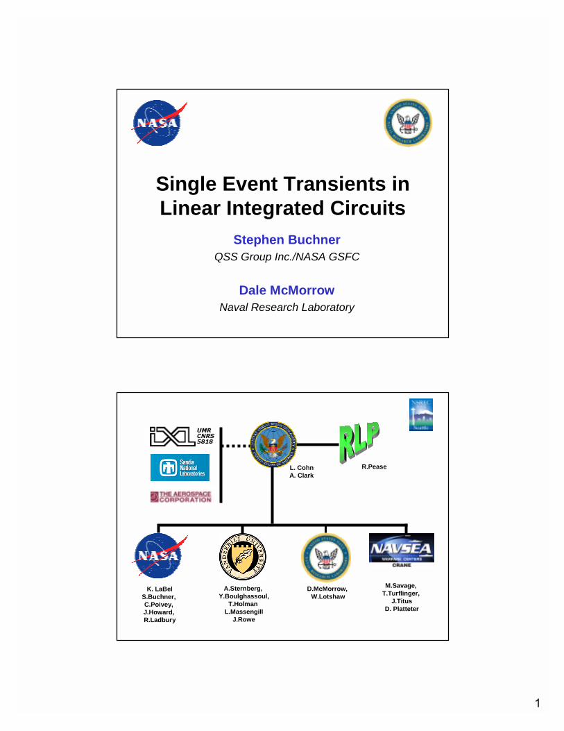
1 Single Event Transients in Linear Integrated Circuits Stephen Buchner QSS Group Inc./NASA GSFC Dale McMorrow Naval Research Laboratory K. LaBel S.Buchner, C.Poivey, J.Howard, R.Ladbury A.Sternberg, Y.Boulghassoul, T.Holman L.Massengill J.Rowe D.McMorrow, W.Lotshaw M.Savage, T.Turflinger, J.Titus D. Platteter L. Cohn A. Clark R.Pease

Welcome message from author
This document is posted to help you gain knowledge. Please leave a comment to let me know what you think about it! Share it to your friends and learn new things together.
Transcript
1
Single Event Transients in Linear Integrated Circuits
Stephen BuchnerQSS Group Inc./NASA GSFC
Dale McMorrowNaval Research Laboratory
K. LaBelS.Buchner, C.Poivey, J.Howard, R.Ladbury
A.Sternberg, Y.Boulghassoul,
T.Holman L.Massengill
J.Rowe
D.McMorrow, W.Lotshaw
M.Savage, T.Turflinger,
J.TitusD. Platteter
L. CohnA. Clark
R.Pease

2
Course Outline1. Introduction2. Fundamental Mechanisms
– Charge generation– Charge collection – Device Response
3. Computer Simulation- Device simulation- Circuit simulation
4. SET testing– Broad Beam of Protons and Heavy ions– Pulsed laser light
5. Case Studies6. Mitigation7. Conclusions
1. Introduction

3
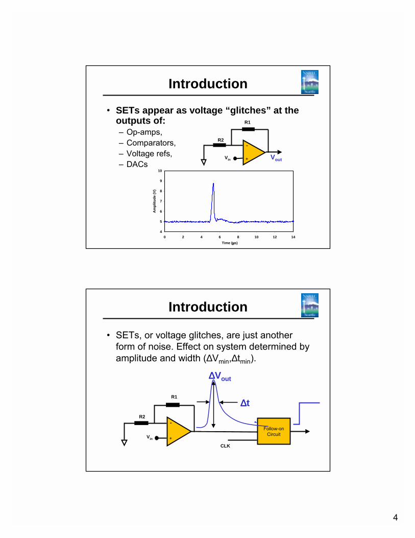
Introduction• Definition of a SET
An SET is a temporary disruption to the output of a device (transistor) or circuit caused by an ionizing particle passing through the device.
• SETs occur in Digital and Analog circuits.DSETs and ASETs
• SETs occur in bipolar, CMOS, BiCMOS and compound semiconductor (III-V) technologies.
Introduction• This Short Course deals with ASETs in
Linear Integrated Circuits.– Op-amps– Comparators– Voltage references– Pulse width modulators– Voltage controlled oscillators– DC/DC Converters– Phase Lock Loops– Digital-to-Analog Converters
4
Introduction
• SETs appear as voltage “glitches” at the outputs of:– Op-amps, – Comparators, – Voltage refs, – DACs
4
5
6
7
8
9
10
0 2 4 6 8 10 12 14Time (µµµµs)
Am
plitu
de (V
)
R1
Vout
-
+Vin
R2
Introduction
• SETs, or voltage glitches, are just another form of noise. Effect on system determined by amplitude and width (∆Vmin,∆tmin).
-
+Vin
R1
R2
CLK
Follow-onCircuit
∆∆∆∆t
∆∆∆∆Vout

5
Introduction
0 5 10 15123456785
6
7
8
9
10
5.0
5.5
6.0
6.5
7.00.0
2.0
4.0
6.0
5.0
5.5
6.0
6.5
Q16
Time (m icroseconds)
Q20
Vou
t (V)
Q18
Q9Q19
Q2Q4Q5
• ASETs assume a wide variety of shapes. In the LM124 there are at least five different types.
ASETs in Op-amps (LM124)
Buchner et al IEEE TNS 2004
• Each ASET type also has avariety of amplitudes.
• Not all ASETs pose a threat.• Transient widths often related
to circuit bandwidth.
Introduction
• ASETs are all either positive-going or negative-going depending on whether output is high or low.
ASETs in Voltage Compators (LM119)
Buchner et al HEART 2001
• The shape stays the same as ∆V and ∆t change.
Q6
Q3
Q2
0
1
2
3
4
5
0 0.2 0.4 0.6 0.8 1
Time (µµµµs)
0
1
3
4
5
2
0
1
3
4
5
2

6
Introduction
SETs appear as disruptions to the outputs of:
Voltage Controlled Oscillators Pulse Width Modulators
Chen et al IEEE TNS 2003 Howard et al Data Workshop 2003
Introduction
• Topex/Poseidon (OP-15)…………..1993• SOHO (LM/PM139)………………... 1996• Cassini (LM139)……………………. 1998-2002• TDRS (LM139)………………………1997• MPTB (LM124 and LM139) ……….1997• MAP (LM139)………………………..2001
Satellites Exhibiting ASETs (Partial List)
7
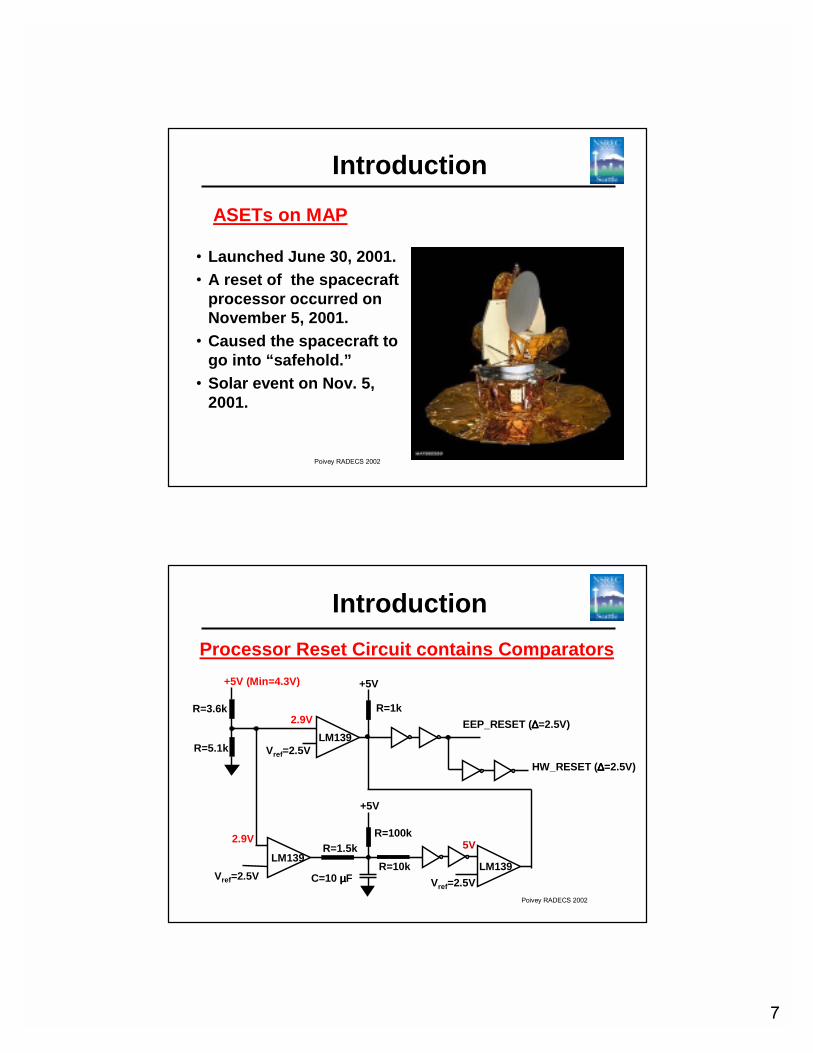
Introduction
• Launched June 30, 2001.• A reset of the spacecraft
processor occurred on November 5, 2001.
• Caused the spacecraft to go into “safehold.”
• Solar event on Nov. 5, 2001.
ASETs on MAP
Poivey RADECS 2002
Introduction
R=3.6k
LM139
LM139LM139
R=5.1k
R=10kR=1.5k
R=1k
R=100k
C=10 µµµµFVref=2.5V Vref=2.5V
Vref=2.5V
+5V (Min=4.3V)
+5V
EEP_RESET (∆∆∆∆=2.5V)
+5V
Poivey RADECS 2002
Processor Reset Circuit contains Comparators
2.9V
2.9V 5V
HW_RESET (∆∆∆∆=2.5V)

8
IntroductionASETs for the LM139 Comparator
-4
-2
0
2
4
1.2 10-5 1.4 10-5 1.6 10-5 1.8 10-5 2 10-5 2.2 10-5 2.4 10-5 2.6 10-5 2.8 10-5
Out
put V
olta
ge (
V)
T ime (s)
LM139, Vcc
=+/-5, δVi=800mV, LET=18.7 MeV-cm2/mg
Vt = 2.5 V
Poivey RADECS 2002
Introduction
• ASETs occur in a wide variety of linear devices.• The nature of the ASET depends on the device.• ASETs have caused problems in a number of
spacecraft.
Summary:

9
2. Fundamental Mechanisms
Fundamental MechanismsInteraction of ions with matter
1. Coulomb interaction between nucleus and bound electrons.
2. It requires, on average, 3.6 eV to create 1 electron-hole pair in Si.
3. Energetic electrons (delta rays) create additional e-h pairs as they move through lattice.
4. Result is a track of charge with a diameter < 1 µm.
SILICON
Ionization

10
Fundamental MechanismsInteraction of ions with matter
1. Coulomb interaction between nucleus and bound electrons.
2. It requires, on average, 3.6 eV to create 1 electron-hole pair in Si.
3. Energetic electrons (delta rays) create additional e-h pairs as they move through lattice.
4. Result is a track of charge with a diameter < 1 µm.
5. Charge Track expands rapidly via diffusion.
Ionization
SILICON
Fundamental MechanismsInteraction of ions with matter
1. In the presence of a p-n junction charge is collected via drift in the junction electric field.
Ionization
SILICON
N-type
P-type

11
Fundamental MechanismsUnbiased p-n Junction.
EC
EV
EF
p-Typen-Type
Depletion Layer
E
Fundamental MechanismsForward-biased p-n junction.
EC
EV
p-Typen-Type
Depletion Layer
- +
E
12
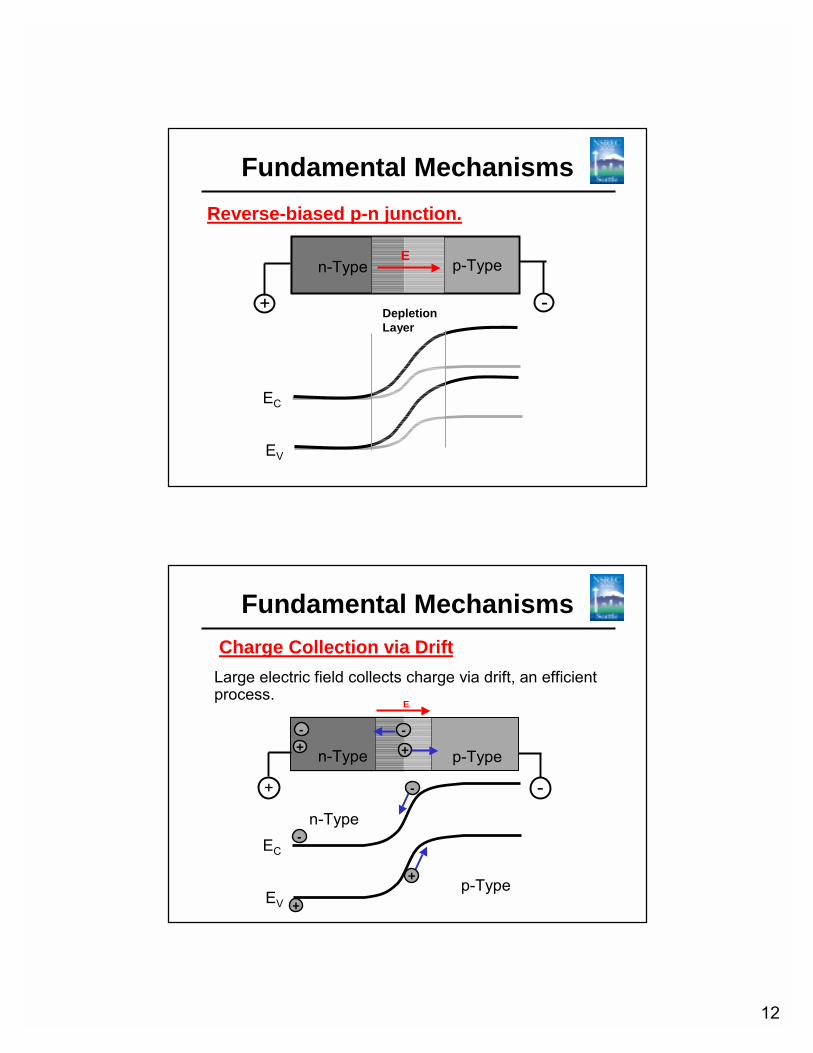
Fundamental MechanismsReverse-biased p-n junction.
EC
EV
p-Typen-Type
Depletion Layer
+ -
E
Fundamental MechanismsCharge Collection via Drift
n-Type
p-Type
EC
EV
+ -
n-Type+
+
+
-
-
-
p-Type+-
Large electric field collects charge via drift, an efficient process.
E
13
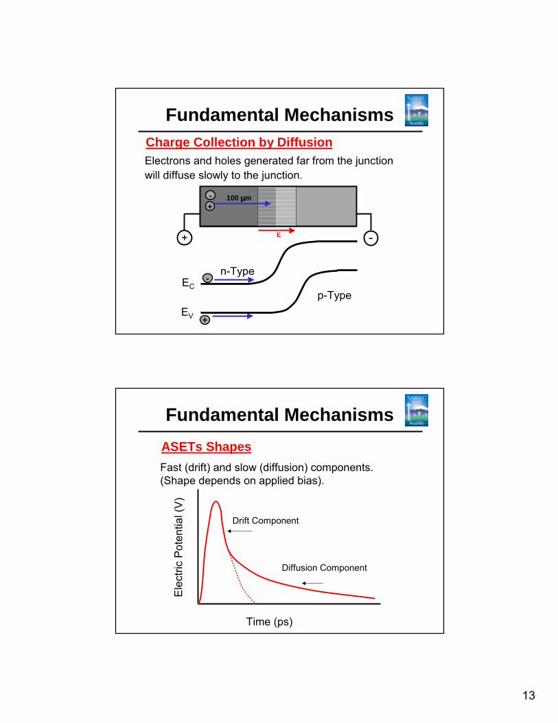
Fundamental MechanismsCharge Collection by Diffusion
n-Type
p-TypeEC
EV
+-
-
+
-+
100 µµµµm
Electrons and holes generated far from the junction will diffuse slowly to the junction.
E
Fundamental MechanismsASETs Shapes
Time (ps)
Ele
ctri c
Pot
entia
l (V
)
Drift Component
Diffusion Component
Fast (drift) and slow (diffusion) components.(Shape depends on applied bias).

14
Fundamental MechanismsBipolar Transistor
Emitter Base Collector
Emitter CollectorBase
n p n
EC
EV
Two back-to-back p-n junctions.
EF
Fundamental Mechanisms
Holes injected into C/B junction drift into base and turn the transistor more on.
Emitter CollectorBase
n p n
V1
V2
Emitter Base Collector
+
--
+
Forward-active mode
15
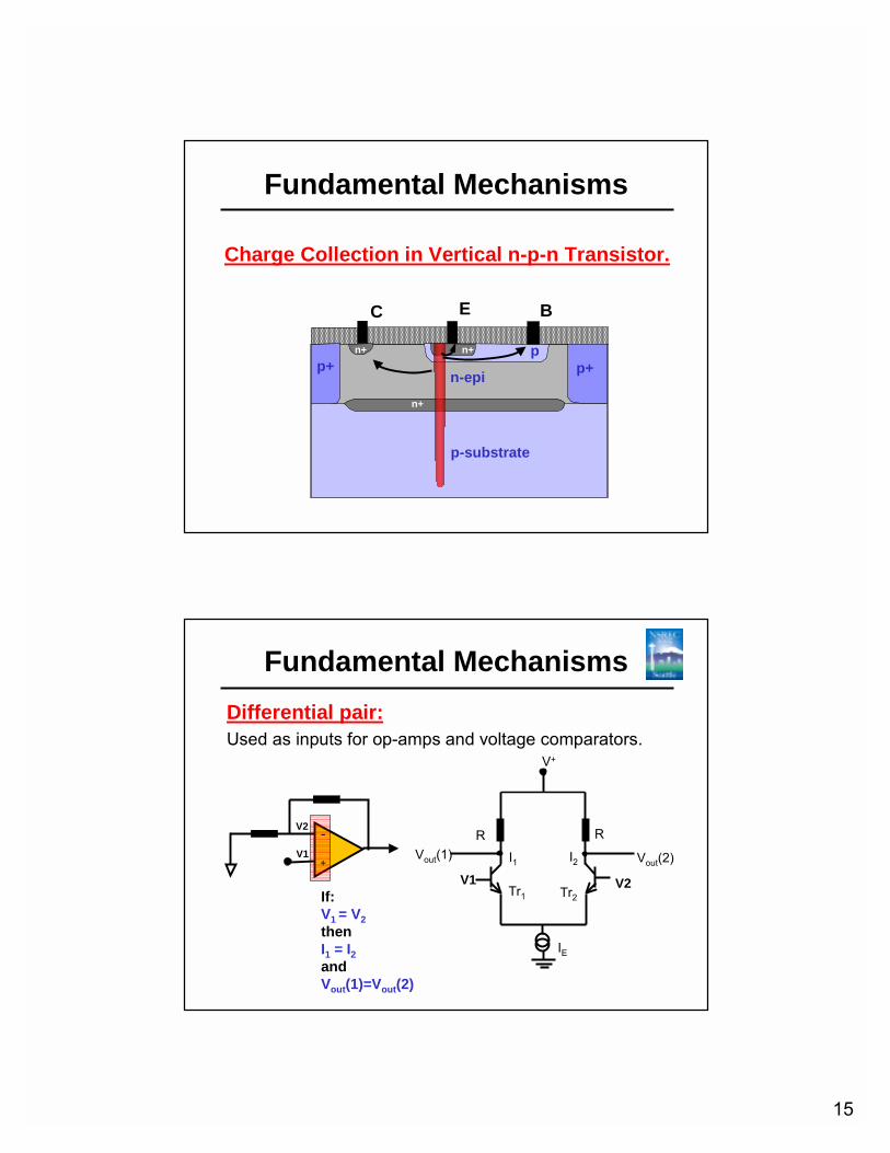
Fundamental Mechanisms
C E B
p-substrate
n+
n+ n+
n-epi p+p+p
Charge Collection in Vertical n-p-n Transistor.
Fundamental MechanismsDifferential pair:Used as inputs for op-amps and voltage comparators.
If:V1 = V2thenI1 = I2andVout(1)=Vout(2)
-
+V1
V2
V+
V1
R
I1
R
I2
V2Tr1 Tr2
IE
Vout(2)Vout(1)

16
Fundamental Mechanisms
V+
V1
R
I1
R
I2
V2Tr1 Tr2
IE
Vout(2)
If:V1 > V2thenI1 > I2andVout(2) is highVout(1) is low
Differential pair:
Vout(1)
Fundamental Mechanisms
As V1-V2 increases,more charge is neededto produce an ASET.
Differential pair:
V+
V1
R
I1
R
I2
V2Tr1 Tr2
IE
Assume V1 > V2

17
Fundamental MechanismsLM111
• Input transistors are most sensitive to SETs.
• SETs propagate from input transistor to output.
VIN
VOUT
Fundamental Mechanisms
• Particles passing through matter produce electron-hole pairs.
• Electric fields associated with p-n junctions separate the electrons and holes.
• This causes a change in the potential at the node.• In a BJT the charge can make a transistor more
conducting and that alters the internal potentials.• The potential disturbance travels through the circuit
to the output where it appears as an ASET.
Summary
18
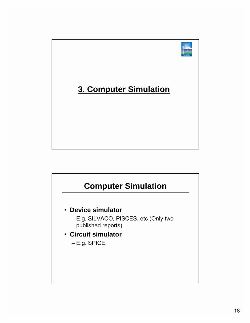
3. Computer Simulation
• Device simulator– E.g. SILVACO, PISCES, etc (Only two
published reports)• Circuit simulator
– E.g. SPICE.
Computer Simulation

19
1. Device SimulationSimulation of the device behavior by the solution of the following equations describing charge flow in the device.
Computer Simulation
• Maxwell’s Equations• Poisson’s Equations• Continuity Equations• Carrier Transport Equations
Non-linear differential equations cannot be solvedanalytically. A computer is used to solve the equationsnumerically in space and time.
Computer Simulation
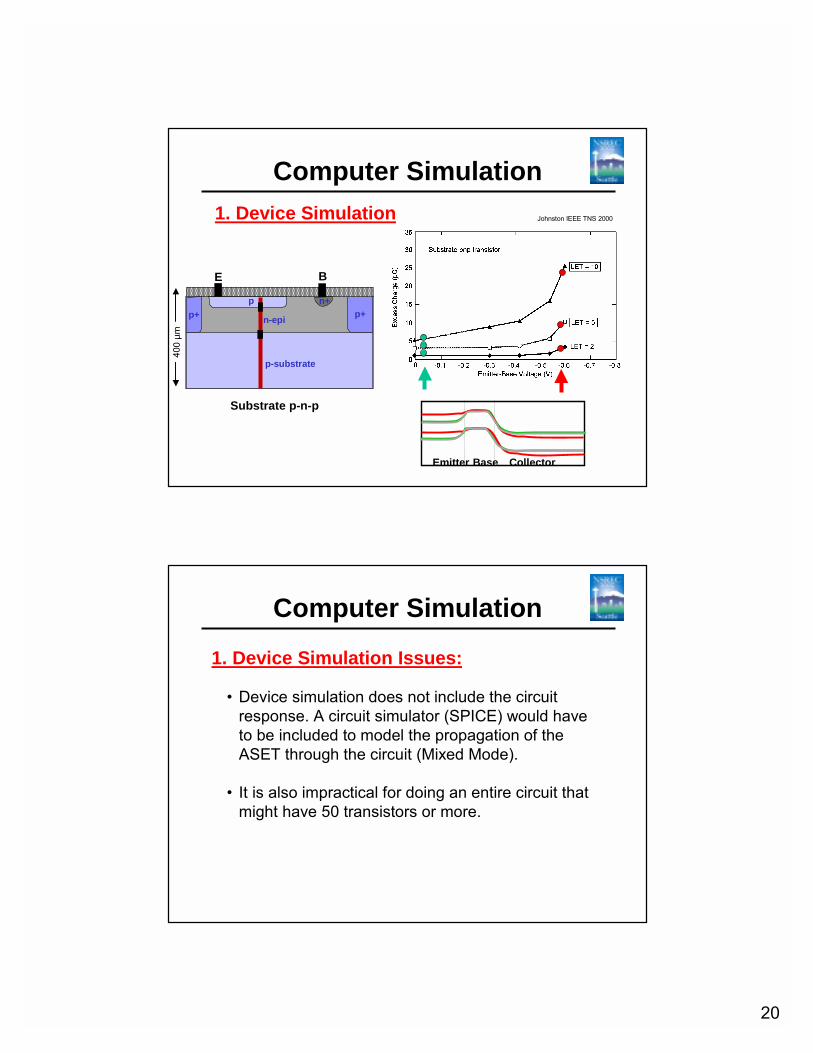
Johnston IEEE TNS 2000
1. Device Simulation
VBE = -0.42 V – weakly on.Substrate p-n-p
p-substrate
n+
n-epi
pp+p+
E B
400
µm
20
Computer SimulationJohnston IEEE TNS 20001. Device Simulation
Substrate p-n-p
p-substrate
n+
n-epi
pp+p+
E B
400
µm
Emitter Base Collector
Computer Simulation
1. Device Simulation Issues:
• Device simulation does not include the circuit response. A circuit simulator (SPICE) would have to be included to model the propagation of the ASET through the circuit (Mixed Mode).
• It is also impractical for doing an entire circuit that might have 50 transistors or more.
21
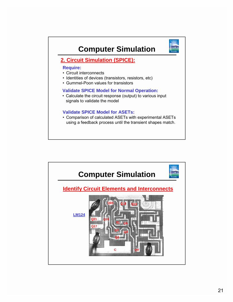
Computer Simulation2. Circuit Simulation (SPICE):Require:• Circuit interconnects• Identities of devices (transistors, resistors, etc)• Gummel-Poon values for transistors
Validate SPICE Model for Normal Operation:• Calculate the circuit response (output) to various input
signals to validate the model
Validate SPICE Model for ASETs:• Comparison of calculated ASETs with experimental ASETs
using a feedback process until the transient shapes match.
Computer Simulation
Identify Circuit Elements and Interconnects
LM124
Q17
Q21
Q19
C
Q20
Q16 Q15
R1
Q9
Q2
Q3
Q4
Q5

22
Q2Q3 Q4
Q5
Q19Q15Q16
Q14
Q13
Q11
Q10Q8
Q7Q12
Q9
Q6
Q21Q17
Q18 Q20 R1
R2
C1
Vin(-)
Vin(+)
V+
V-
Vout
Q2Q3 Q4
Q5
Q19Q15Q16
Q14
Q13
Q11
Q10Q8
Q7Q12
Q9
Q6
Q21Q17
Q18 Q20 R1
R2
C1
Vin(-)
Vin(+)
V+
V-
Vout
Computer Simulation
Identify Circuit Elements and Interconnects
LM124
Computer SimulationNeed SPICE Transistor Parameters
LM124
• Obtain SPICE transistor parameters from data sheets or from manufacturer.
• Otherwise, must isolate transistor with focused ion beam (FIB) milling and measure I-V curves to obtain Gummel-Poonparameters.

23
Computer Simulation
SPICE Validation – Small and Large Input Signals
Sternberg IEEE TNS 2002
+
-
Input:100 mV10 µµµµs
Output
LM124
Q2Q3 Q4
Q5
Q19Q15Q16
Q14
Q13
Q11
Q10Q8
Q7Q12
Q9
Q6
Q21Q17
Q18 Q20 R1
R2
C1
Vin(-)
Vin(+)
V+
V-
Vout
Q2Q3 Q4
Q5
Q19Q15Q16
Q14
Q13
Q11
Q10Q8
Q7Q12
Q9
Q6
Q21Q17
Q18 Q20 R1
R2
C1
Vin(-)
Vin(+)
V+
V-
Vout
Computer SimulationSpice Model (LM124) Validation –Shape of I(t) does not affect ASET
I(t)
I(t)
I(t)
C/B
E/B
E/C

24
Computer Simulation
SPICE Simulation – ASET Validation via Iteration
Compare SETs generated by pulsed laser or ion microprobe with those calculated using SPICE.
Agreement?Poor
Modify circuit anddevice parameters.
Good
Stop.
Computer Simulation
SPICE Simulation – ASET Validation
25
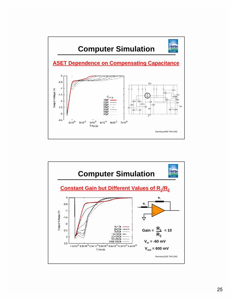
Computer Simulation
ASET Dependence on Compensating Capacitance
Sternberg IEEE TNS 2002
Computer Simulation
Constant Gain but Different Values of R1/R2
Sternberg IEEE TNS 2002
+
-R2
R1
Gain = = 10R1R2
Vin
Vout = 600 mV
Vin = -60 mV

26
Computer Simulation
Summary• Device simulation provides detailed information about
mechanisms responsible for ASETs.• Circuit simulation is suitable for studying ASETs with
response times longer than the charge collection time.• The validity of the circuit model is established by comparing
actual and calculated responses to input signals, but that is not sufficient………..
• The model must also be validated by comparing calculated ASET shapes with those obtained experimentally.
• Circuit simulation can be used to study effects of circuit parameters on ASET shapes.
4. ASET Testing

27
ASET Testing
Testing Approaches:1. Broad beam of heavy ions or protons
2. Pulsed Laser
3. Ion micro-probe
4. Radioactive source (252Cf)
ASET Testing
1. Broad Beam of Heavy Ions
28
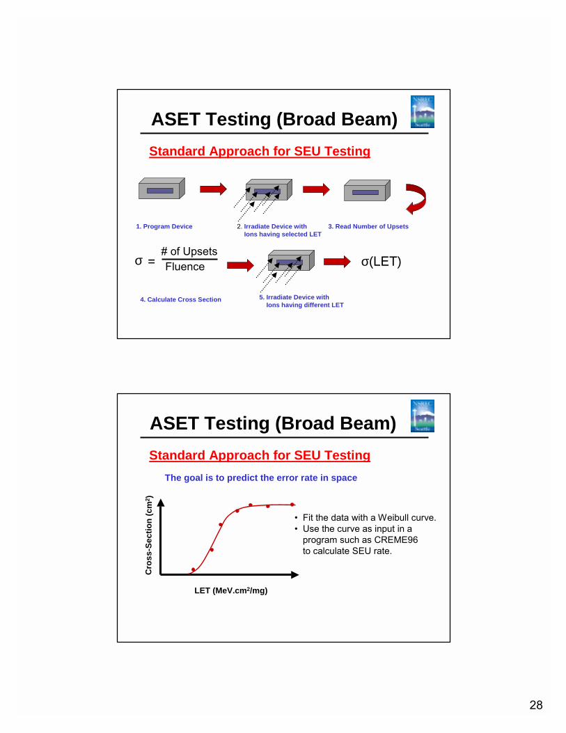
ASET Testing (Broad Beam)Standard Approach for SEU Testing
1. Program Device 2. Irradiate Device withIons having selected LET
3. Read Number of Upsets
σ =# of UpsetsFluence
4. Calculate Cross Section 5. Irradiate Device withIons having different LET
σ(LET)
ASET Testing (Broad Beam)Standard Approach for SEU Testing
LET (MeV.cm2/mg)
Cro
ss-S
e ctio
n (c
m2 )
• Fit the data with a Weibull curve.• Use the curve as input in a
program such as CREME96to calculate SEU rate.
The goal is to predict the error rate in space
29
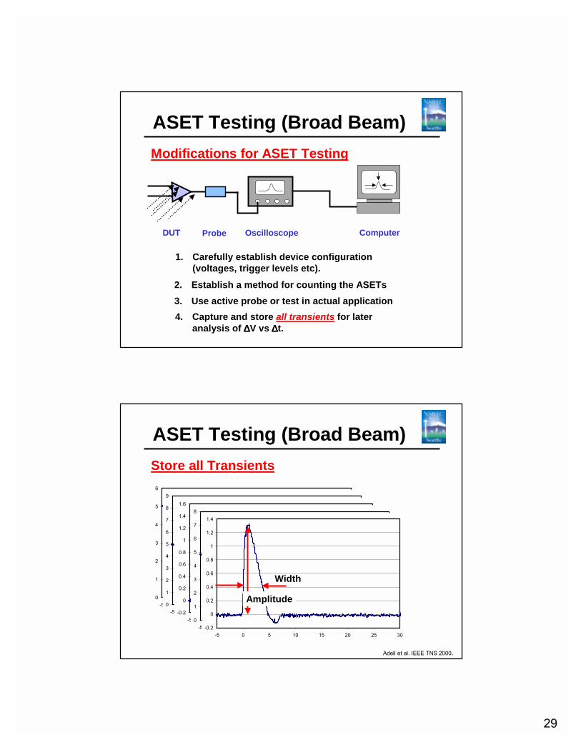
ASET Testing (Broad Beam)Modifications for ASET Testing
DUT Oscilloscope ComputerProbe
1. Carefully establish device configuration(voltages, trigger levels etc).
4. Capture and store all transients for later analysis of ∆∆∆∆V vs ∆∆∆∆t.
2. Establish a method for counting the ASETs3. Use active probe or test in actual application
ASET Testing (Broad Beam)Store all Transients
0
1
2
3
4
5
6
-5 0 5 10 15 20 25 300
1
2
3
4
5
6
7
8
9
-5 0 5 10 15 20 25 30-0.2
0
0.2
0.4
0.6
0.8
1
1.2
1.4
1.6
-5 0 5 10 15 20 25 300
1
2
3
4
5
6
7
8
-5 0 5 10 15 20 25-0.2
0
0.2
0.4
0.6
0.8
1
1.2
1.4
-5 0 5 10 15 20 25 30
Width
Amplitude
Adell et al. IEEE TNS 2000.
30
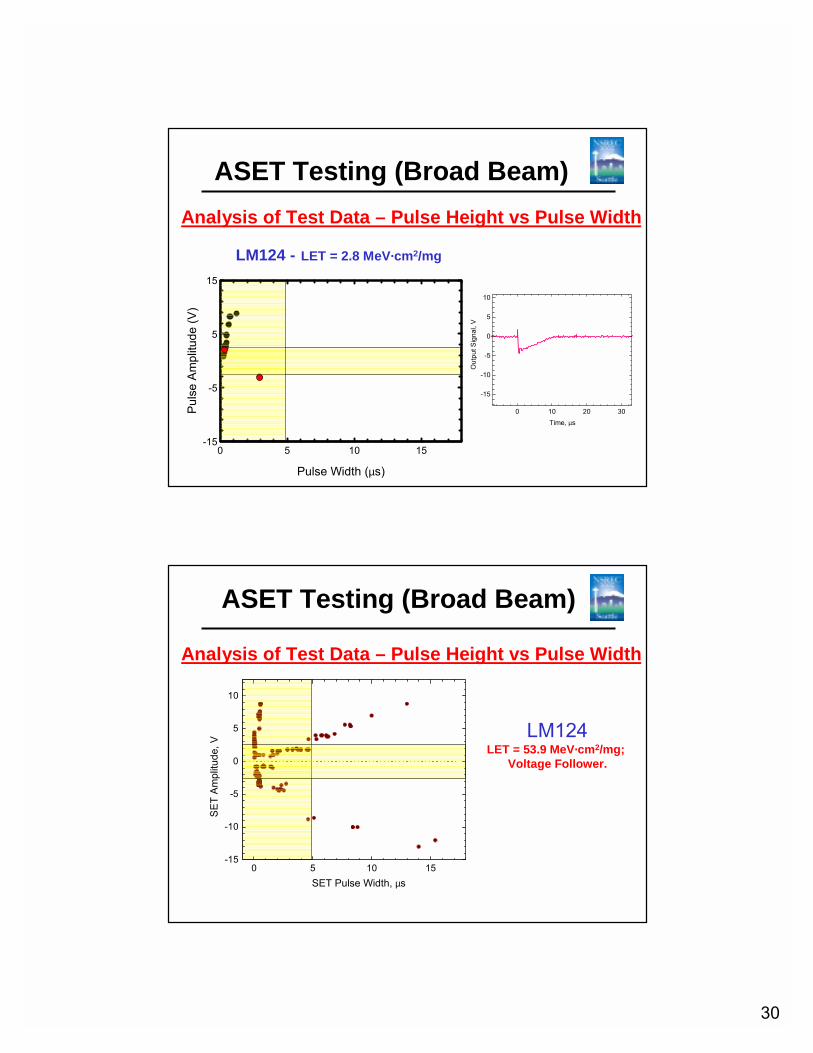
ASET Testing (Broad Beam)Analysis of Test Data – Pulse Height vs Pulse Width
LM124 - LET = 2.8 MeV·cm2/mg
-15
-5
5
15
0 5 10 15
Pulse Width (µs)
Pul
se A
mpl
itude
(V)
0 10 20 30
-15
-10
-5
0
5
10
Out
put S
igna
l, V
Time, µs
ASET Testing (Broad Beam)
Analysis of Test Data – Pulse Height vs Pulse Width
0 5 10 15-15
-10
-5
0
5
10
SE
T A
mpl
itude
, V
SET Pulse Width, µs
LM124LET = 53.9 MeV·cm2/mg;
Voltage Follower.
31
1.E-06
1.E-05
1.E-04
1.E-03
1.E-02
0 20 40 60 80 100 120
LET (MeV.cm2/mg)
Cro
ss-S
ectio
n (c
m2 )
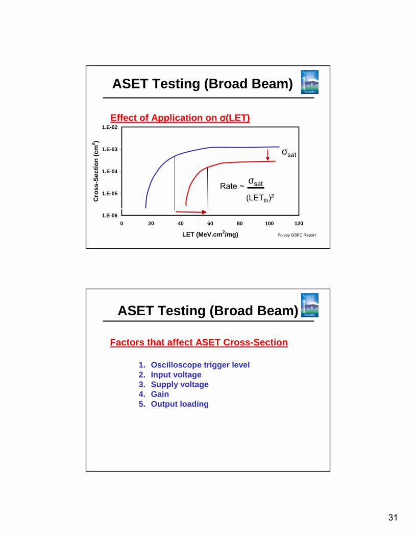
ASET Testing (Broad Beam)
Poivey GSFC Report
Effect of Application on σσσσ(LET)
Rate ~ σsat
(LETth)2
σsat
ASET Testing (Broad Beam)
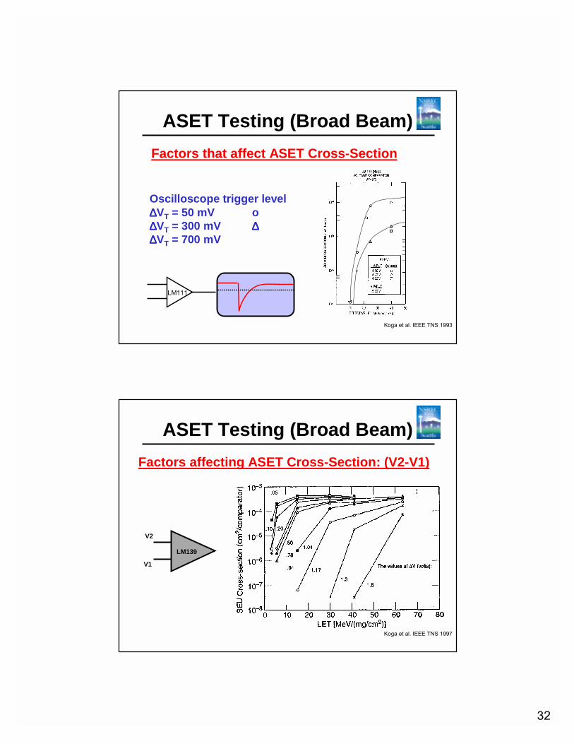
Factors that affect ASET Cross-Section
1. Oscilloscope trigger level2. Input voltage3. Supply voltage4. Gain5. Output loading
32
ASET Testing (Broad Beam)
Koga et al. IEEE TNS 1993
Factors that affect ASET Cross-Section
Oscilloscope trigger level∆∆∆∆VT = 50 mV o∆∆∆∆VT = 300 mV ∆∆∆∆∆∆∆∆VT = 700 mV
LM111
ASET Testing (Broad Beam)
Koga et al. IEEE TNS 1997
Factors affecting ASET Cross-Section: (V2-V1)
LM139
V2
V1

33
ASET Testing (Broad Beam)
Koga et al. IEEE TNS 1997
Factors affecting ASET Cross-Section: Vs
LM111
V+
V-
1.0E-07
1.0E-05
1.0E-03
0 10 20 30 40 50 60 70
LET (MeV.cm2/mg)
Cro
ss S
ectio
n (c
m2 /d
evic
e) Vs = +/-15V, ∆Vin=50 mV
Vs = +/-5V, ∆Vin=50 mV
ASET Testing (Broad Beam)Factors affecting ASET Cross-Section: Output Loading
LM119
V+
V-
-1
0
1
2
3
4
5
6
0 2 4 6 8 10
Time (µµµµs)
Am
plitu
de (V
)
R=0.17 kΩΩΩΩ
R=1.7 kΩΩΩΩ
R
5.0 V
0
1
2
3
4
5
6
0 2 4 6 8 10
Time (µµµµs)
Am
plitu
de (V
)
34
ASET Testing (Broad Beam)
Poivey GSFC Report
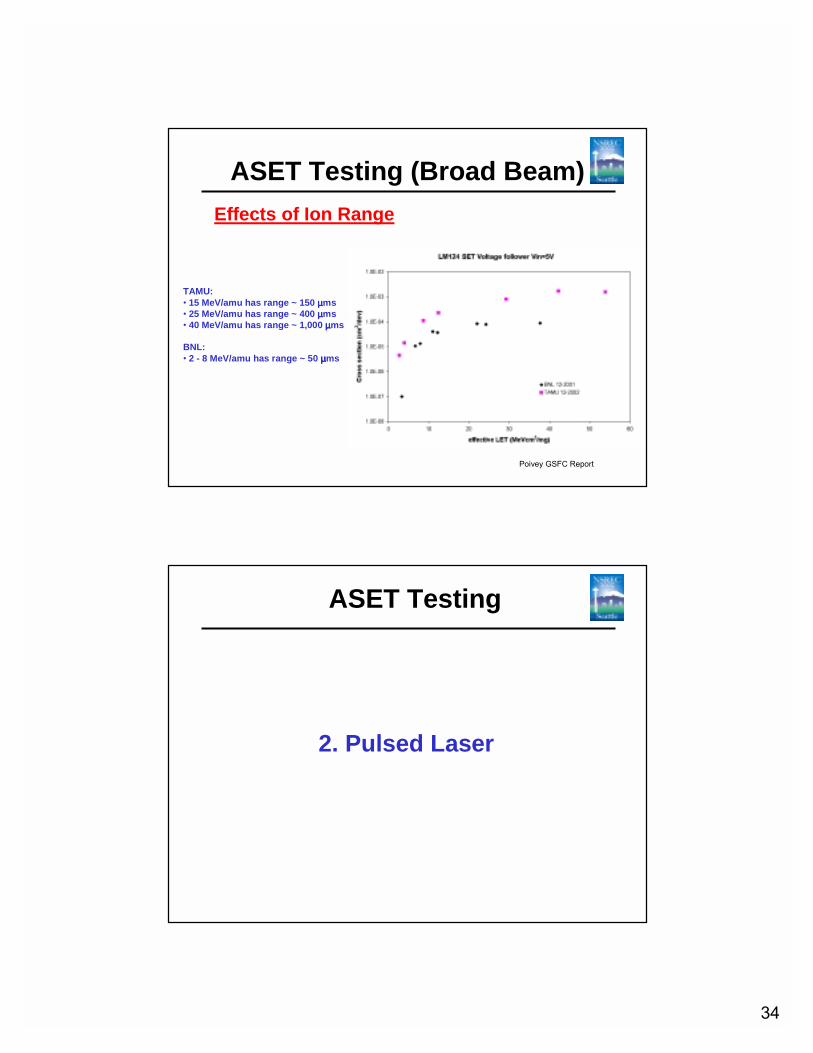
Effects of Ion Range
TAMU:• 15 MeV/amu has range ~ 150 µµµµms• 25 MeV/amu has range ~ 400 µµµµms• 40 MeV/amu has range ~ 1,000 µµµµms
BNL:• 2 - 8 MeV/amu has range ~ 50 µµµµms
2. Pulsed Laser
ASET Testing
35
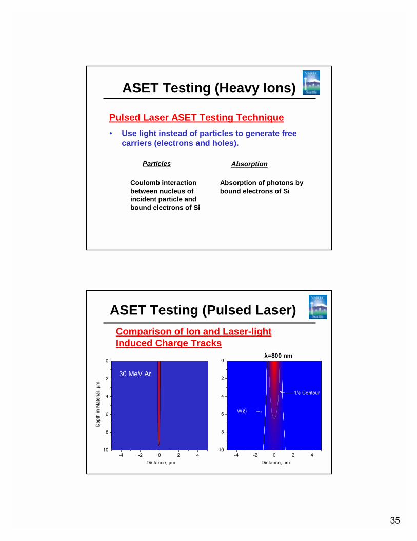
ASET Testing (Heavy Ions)
Pulsed Laser ASET Testing Technique• Use light instead of particles to generate free
carriers (electrons and holes).
Coulomb interactionbetween nucleus ofincident particle andbound electrons of Si
AbsorptionParticles
Absorption of photons bybound electrons of Si
-4 -2 0 2 410
8
6
4
2
0
w(z)
1/e Contour
Distance, µm
Dep
th in
Mat
eria
l, µm
ASET Testing (Pulsed Laser)
-4 -2 0 2 410
8
6
4
2
0
w(z)
1/e Contour
Distance, µm
µ
λλλλ=590 nm λλλλ=800 nm
30 MeV Ar
Comparison of Ion and Laser-light Induced Charge Tracks
36
ASET Testing (Heavy Ions)
Pulsed Laser ASET Testing Technique• Can focus light to a diameter of ~ 1 µµµµm to
obtain spatial information – origins of ASETs.• Light source must be a pulsed laser with
pulse width shorter than the response time of the circuit ~ 1 ps.
• Particularly well suited for studying ASETs in linear devices because sensitive areas are large compared to size of beam and relatively little metal on surfaces to block beam.
ASET Testing (Pulsed Laser)
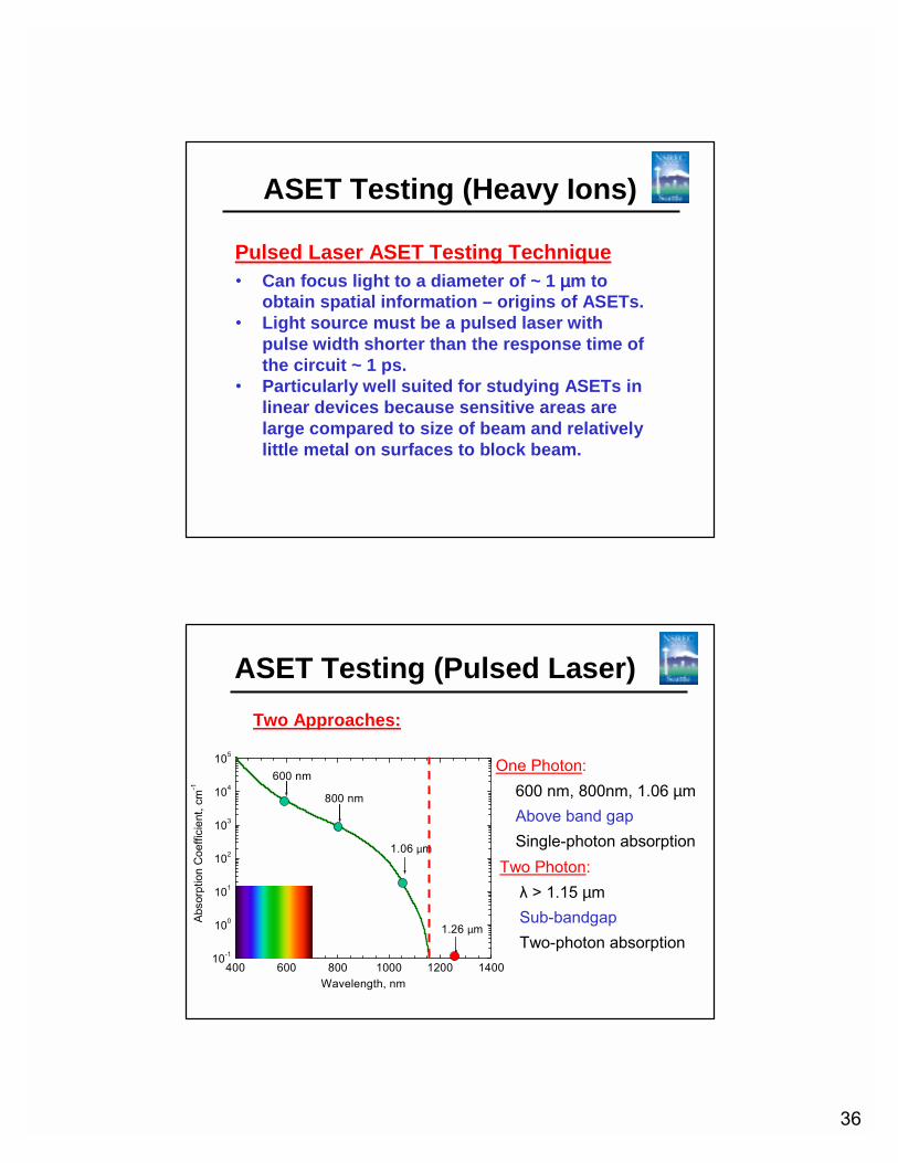
One Photon:600 nm, 800nm, 1.06 µmAbove band gapSingle-photon absorption
400 600 800 1000 1200 140010-1
100
101
102
103
104
105
1.06 µm
1.26 µm
800 nm
600 nm
Abs
orpt
ion
Coe
ffici
ent,
cm-1
Wavelength, nm
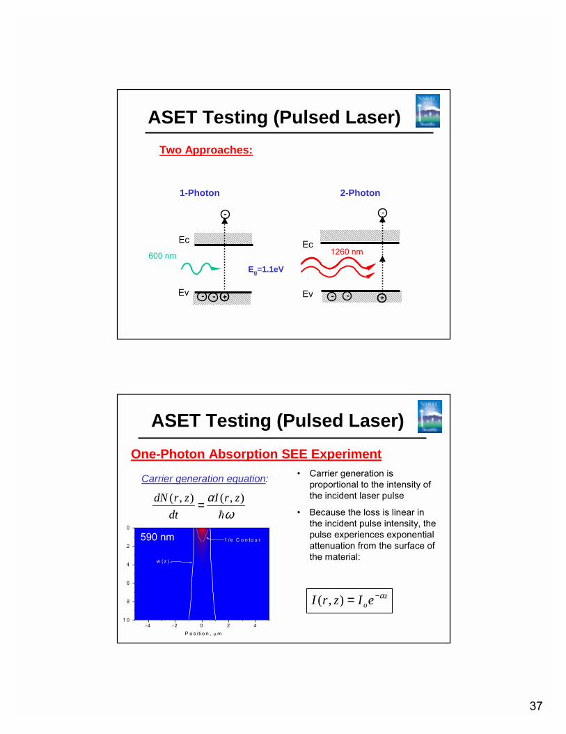
Two Approaches:
Two Photon:λ > 1.15 µmSub-bandgapTwo-photon absorption
37
ASET Testing (Pulsed Laser)Two Approaches:
600 nm
Ec
Ev
Ec
Ev
1260 nm
+- -
-
--- -
1-Photon 2-Photon
Eg=1.1eV
+
-
• Carrier generation is proportional to the intensity of the incident laser pulse
• Because the loss is linear in the incident pulse intensity, the pulse experiences exponential attenuation from the surface of the material:
ASET Testing (Pulsed Laser)
ωα
),( ),( zrIdt
zrdN =
Carrier generation equation:
zoeIzrI α−=),(
- 4 - 2 0 2 41 0
8
6
4
2
0
w ( z )
1 /e C o n to u r
P o s it io n , µ m
One-Photon Absorption SEE Experiment
38
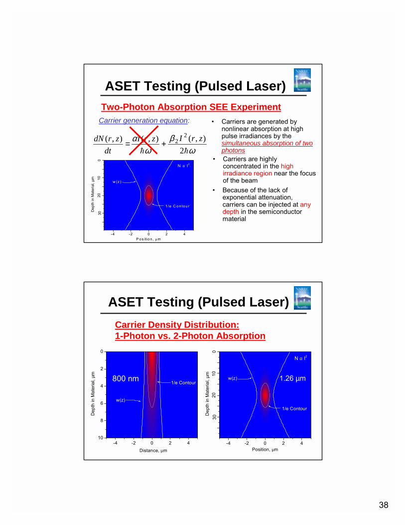
ASET Testing (Pulsed Laser)
• Carriers are generated by nonlinear absorption at high pulse irradiances by the simultaneous absorption of two photonsω
βω
α 2
),(),( ),( 22 zrIzrI
dtzrdN +=
Carrier generation equation:
-4 -2 0 2 4
030
1020
N α I2
w (z )
1 /e C o n tou r
P os itio n , µm
Dep
th in
Mat
eria
l, µm
Two-Photon Absorption SEE Experiment
• Carriers are highly concentrated in the high irradiance region near the focus of the beam
• Because of the lack of exponential attenuation, carriers can be injected at any depth in the semiconductor material
-4 -2 0 2 4
030
1020
N α I2
w(z)
1/e Contour
Position, µm
Dep
th in
Mat
eria
l, µm µ
Carrier Density Distribution:1-Photon vs. 2-Photon Absorption
ASET Testing (Pulsed Laser)
-4 -2 0 2 410
8
6
4
2
0
w(z)
1/e Contour
Distance, µm
Dep
th in
Mat
eria
l, µm 800 nm
39
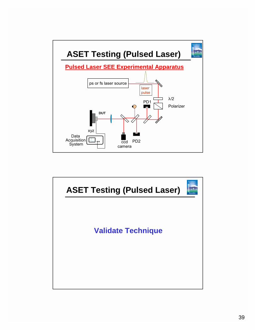
ASET Testing (Pulsed Laser)
ps or fs laser source
Polarizer
λ/2
DUT
xyz
laser pulse
ccdcamera
PD2
PD1
Pulsed Laser SEE Experimental Apparatus
Validate Technique
ASET Testing (Pulsed Laser)
40
Q2Q3 Q4
Q5
Q19Q15Q16
Q14
Q13
Q11
Q10Q8
Q7Q12
Q9
Q6
Q21Q17
Q18 Q20 R1
R2
C1
Vin(-)
Vin(+)
V+
V-
Vout
Q2Q3 Q4
Q5
Q19Q15Q16
Q14
Q13
Q11
Q10Q8
Q7Q12
Q9
Q6
Q21Q17
Q18 Q20 R1
R2
C1
Vin(-)
Vin(+)
V+
V-
Vout
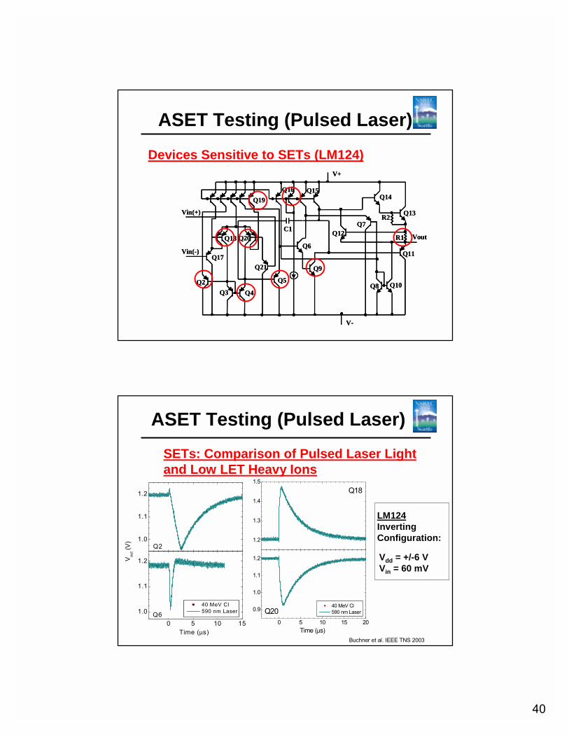
ASET Testing (Pulsed Laser)
Devices Sensitive to SETs (LM124)
ASET Testing (Pulsed Laser)
0 5 10 15
1.0
1.1
1.2
1.0
1.1
1.2
40 MeV Cl 590 nm LaserQ6
Time (µs)
Vou
t (V)
Q2
0 5 10 15 20
0.9
1.0
1.1
1.2
1.2
1.3
1.4
1.5
Q20
Time (µs)
40 MeV Cl 590 nm Laser
Q18
LM124Inverting Configuration:
Vdd = +/-6 VVin = 60 mV
Buchner et al. IEEE TNS 2003
SETs: Comparison of Pulsed Laser Light and Low LET Heavy Ions
41
0 5 10 1556789
10
5.0
5.5
6.0
6.5
7.0
Q20
Time, ms
Q18
0 5 10 150.0
2.0
4.0
6.0
5.0
5.5
6.0
6.5
Vou
t (V)
Time, µs
Q9Q19
Q2Q4Q5
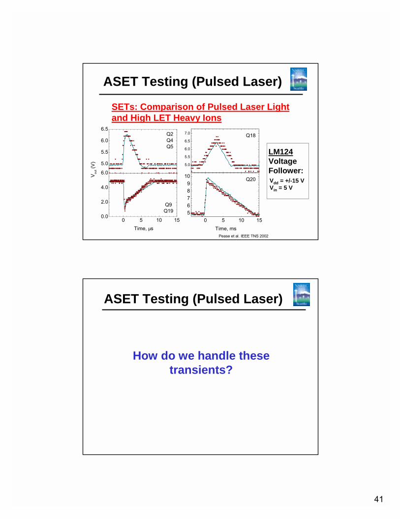
ASET Testing (Pulsed Laser)
LM124 Voltage Follower:Vdd = +/-15 VVin = 5 V
Pease et al. IEEE TNS 2002
SETs: Comparison of Pulsed Laser Light and High LET Heavy Ions
How do we handle these transients?
ASET Testing (Pulsed Laser)
42
ASET Testing (Pulsed Laser)
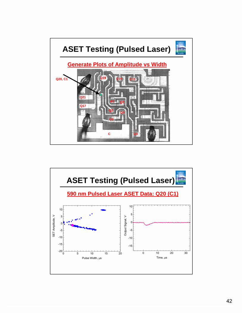
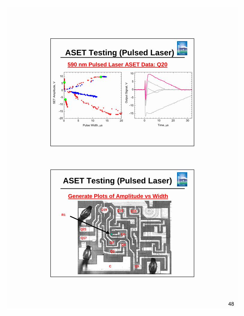
Generate Plots of Amplitude vs Width
Q17
Q21
Q19
C
Q16 Q15
R1
Q9
Q2
Q3
Q4
Q5
Q20, C1
0 5 10 15 20-20
-15
-10
-5
0
5
10
Q20 V∆∆∆∆t Plot
SET
Am
plitu
de, V
Pulse Width, µs
0 10 20 30
-15
-10
-5
0
5
10
Out
put S
igna
l, V
Time, µs
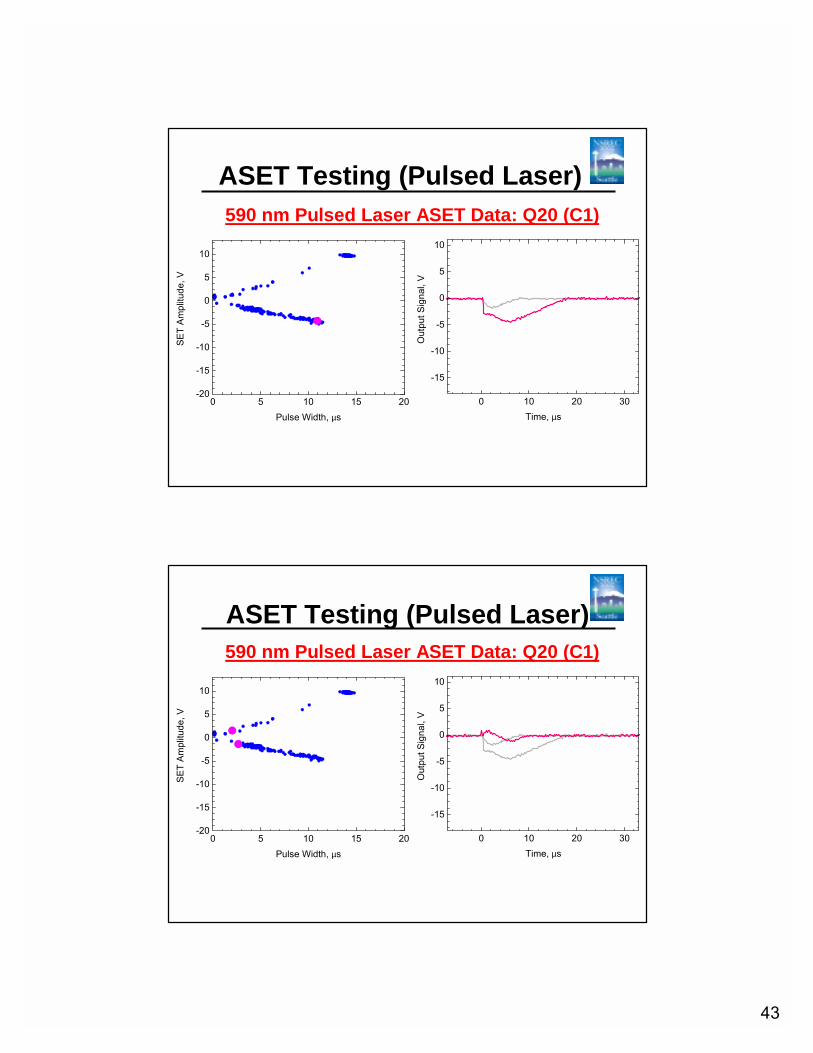
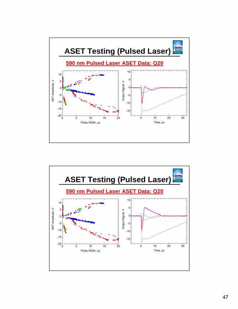
ASET Testing (Pulsed Laser)590 nm Pulsed Laser ASET Data: Q20 (C1)
43
0 5 10 15 20-20
-15
-10
-5
0
5
10
Q20 V∆∆∆∆t Plot
SET
Am
plitu
de, V
Pulse Width, µs
0 10 20 30
-15
-10
-5
0
5
10
Out
put S
igna
l, V
Time, µs
590 nm Pulsed Laser ASET Data: Q20 (C1)
ASET Testing (Pulsed Laser)
0 5 10 15 20-20
-15
-10
-5
0
5
10
Q20 V∆∆∆∆t Plot
SET
Am
plitu
de, V
Pulse Width, µs
0 10 20 30
-15
-10
-5
0
5
10
Out
put S
igna
l, V
Time, µs
590 nm Pulsed Laser ASET Data: Q20 (C1)
ASET Testing (Pulsed Laser)

44
0 5 10 15 20-20
-15
-10
-5
0
5
10
Q20 V∆∆∆∆t Plot
SET
Am
plitu
de, V
Pulse Width, µs
0 10 20 30
-15
-10
-5
0
5
10
Out
put S
igna
l, V
Time, µs
ASET Testing (Pulsed Laser)590 nm Pulsed Laser ASET Data: Q20 (C1)
0 5 10 15 20-20
-15
-10
-5
0
5
10
Q20 V∆∆∆∆t Plot
SET
Am
plitu
de, V
Pulse Width, µs
0 10 20 30
-15
-10
-5
0
5
10
Out
put S
igna
l, V
Time, µs
ASET Testing (Pulsed Laser)590 nm Pulsed Laser ASET Data: Q20 (C1)
45
ASET Testing (Pulsed Laser)
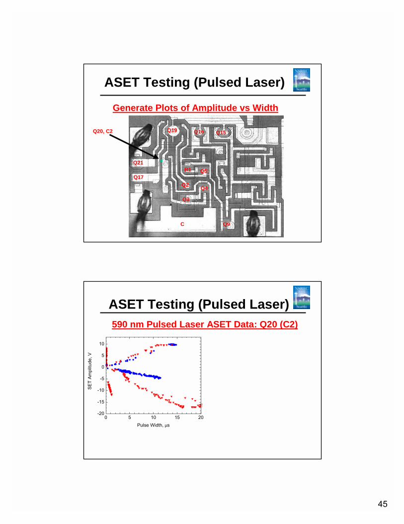
Generate Plots of Amplitude vs Width
Q17
Q21
Q19
C
Q16 Q15
R1
Q9
Q2
Q3
Q4
Q5
Q20, C2
0 5 10 15 20-20
-15
-10
-5
0
5
10
Q20 V∆∆∆∆t Plot
SET
Ampl
itude
, V
Pulse Width, µs
ASET Testing (Pulsed Laser)590 nm Pulsed Laser ASET Data: Q20 (C2)

46
0 5 10 15 20-20
-15
-10
-5
0
5
10
Q20 V∆∆∆∆t Plot
SET
Ampl
itude
, V
Pulse Width, µs
0 10 20 30
-15
-10
-5
0
5
10
Out
put S
igna
l, V
Time, µs
ASET Testing (Pulsed Laser)590 nm Pulsed Laser ASET Data: Q20 (C2)
0 5 10 15 20-20
-15
-10
-5
0
5
10
Q20 V∆∆∆∆t Plot
SET
Ampl
itude
, V
Pulse Width, µs
0 10 20 30
-15
-10
-5
0
5
10
Out
put S
igna
l, V
Time, µs
ASET Testing (Pulsed Laser)590 nm Pulsed Laser ASET Data: Q20
47
0 5 10 15 20-20
-15
-10
-5
0
5
10
Q20 V∆∆∆∆t Plot
SET
Ampl
itude
, V
Pulse Width, µs
0 10 20 30
-15
-10
-5
0
5
10
Out
put S
igna
l, V
Time, µs
ASET Testing (Pulsed Laser)590 nm Pulsed Laser ASET Data: Q20
0 5 10 15 20-20
-15
-10
-5
0
5
10
Q20 V∆∆∆∆t Plot
SET
Ampl
itude
, V
Pulse Width, µs
0 10 20 30
-15
-10
-5
0
5
10
Out
put S
igna
l, V
Time, µs
ASET Testing (Pulsed Laser)590 nm Pulsed Laser ASET Data: Q20
48
0 5 10 15 20-20
-15
-10
-5
0
5
10
Q20 V∆∆∆∆t Plot
SET
Ampl
itude
, V
Pulse Width, µs
0 10 20 30
-15
-10
-5
0
5
10
Out
put S
igna
l, V
Time, µs
ASET Testing (Pulsed Laser)590 nm Pulsed Laser ASET Data: Q20
ASET Testing (Pulsed Laser)
Generate Plots of Amplitude vs Width
Q17
Q21
Q19
C
Q16 Q15
Q9
Q2
Q3
Q4
Q5
R1

49
0.0 0.5 1.0 1.5 2.0 2.5 3.0-10
-5
0
5
10Q20 V∆∆∆∆t Plot
SET
Am
plitu
de, V
Pulse Width, µs0 5 10 15
0
5
10
Out
put S
igna
l, V
Time, µs
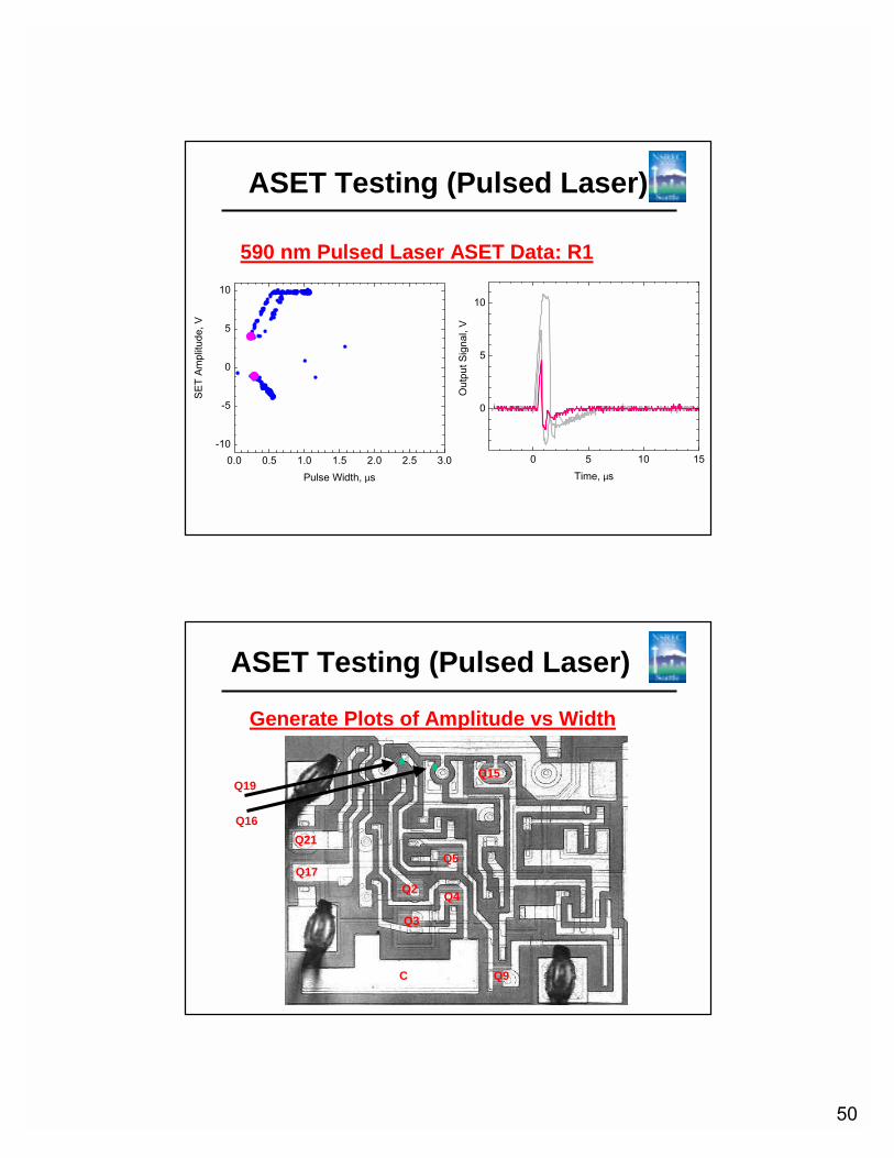
590 nm Pulsed Laser ASET Data: R1
ASET Testing (Pulsed Laser)
0.0 0.5 1.0 1.5 2.0 2.5 3.0-10
-5
0
5
10Q20 V∆∆∆∆t Plot
SET
Am
plitu
de, V
Pulse Width, µs0 5 10 15
0
5
10
Out
put S
igna
l, V
Time, µs
ASET Testing (Pulsed Laser)
590 nm Pulsed Laser ASET Data: R1
50
0.0 0.5 1.0 1.5 2.0 2.5 3.0-10
-5
0
5
10Q20 V∆∆∆∆t Plot
SET
Am
plitu
de, V
Pulse Width, µs
0 5 10 15
0
5
10
Out
put S
igna
l, V
Time, µs
ASET Testing (Pulsed Laser)
590 nm Pulsed Laser ASET Data: R1
ASET Testing (Pulsed Laser)
Generate Plots of Amplitude vs Width
Q17
Q21
C
Q15
Q9
Q2
Q3
Q4
Q5
Q19
Q16

51
0 5 10 15 20 25 30
-20
-15
-10
-5
0
Q20 V∆∆∆∆t Plot
SET
Am
plitu
de, V
Pulse Width, µs0 10 20 30
-20
-15
-10
-5
0
Out
put S
igna
l, V
Time, µs
ASET Testing (Pulsed Laser)
590 nm Pulsed Laser ASET Data: Q19
-5 0 5 10 15 20 25 30 35
-20
-15
-10
-5
0
5
10
Out
put S
igna
l, V
Time, µs
0.0 5.0 10.0 15.0 20.0 25.0
-20
-15
-10
-5
0
5
10
Q20 V∆∆∆∆t Plot
SET
Ampl
itude
, V
Pulse Width, µs
ASET Testing (Pulsed Laser)
590 nm Pulsed Laser ASET Data: Q16

52
0 5 10 15 20 25 30
-20
-15
-10
-5
0
5
10
Q2
Q18Q5
Q4
Q9,Q16,Q19Q20
Q20
R1,Q6,Q16SE
T Pu
lse
Ampl
itude
, V
SET Pulse Width, µs
ASET Testing (Pulsed Laser)
590 nm Pulsed Laser ASET Data: All Nodes
0 5 10 15 20 25 30
-20
-15
-10
-5
0
5
10
Q2
Q18Q5
Q4
Q9,Q16,Q19Q20
Q20
R1,Q6,Q16
SET
Puls
e Am
plitu
de, V
SET Pulse Width, µs
ASET Testing (Pulsed Laser)
Comparison of Heavy Ion and Laser Data
0 5 10 15-15
-10
-5
0
5
10
SET
Am
plitu
de, V
SET Pulse Width, µs
53
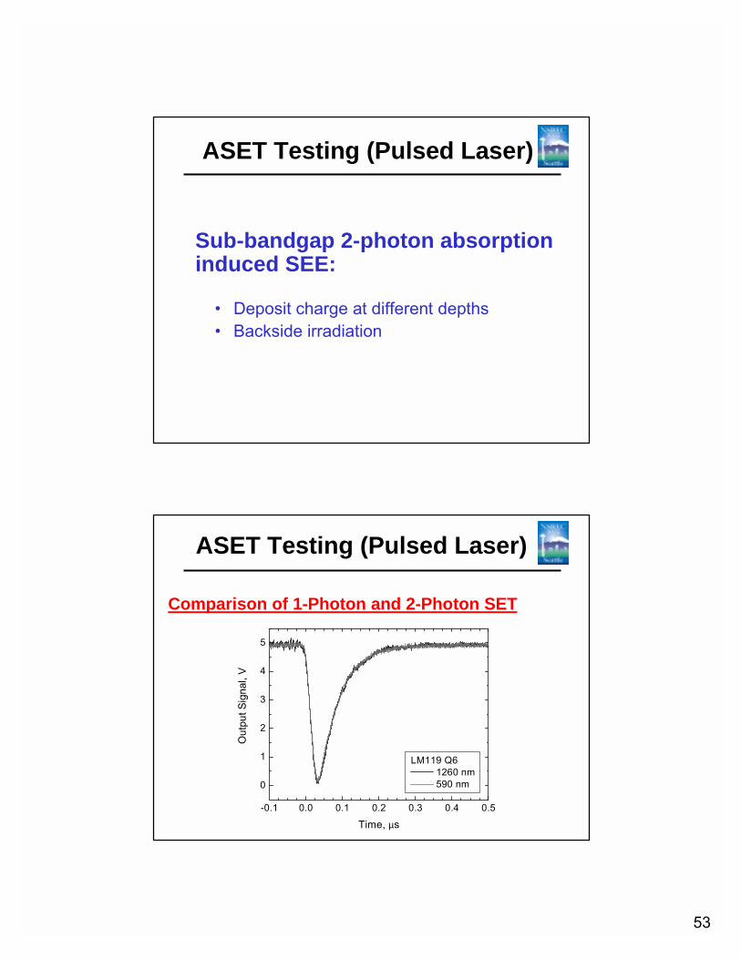
ASET Testing (Pulsed Laser)
Sub-bandgap 2-photon absorption induced SEE:
• Deposit charge at different depths• Backside irradiation
ASET Testing (Pulsed Laser)
-0.1 0.0 0.1 0.2 0.3 0.4 0.5
0
1
2
3
4
5
Out
put S
igna
l, V
Time, µs
LM119 Q6 1260 nm 590 nm
Comparison of 1-Photon and 2-Photon SET
54
C1C2
E
B
OverlayersP (C1)P (E) N+ (B)
P+ (iso)P+ (iso)
N (base)
P (substrate)
12 µm
P (C2)
N+ (buried layer)
P
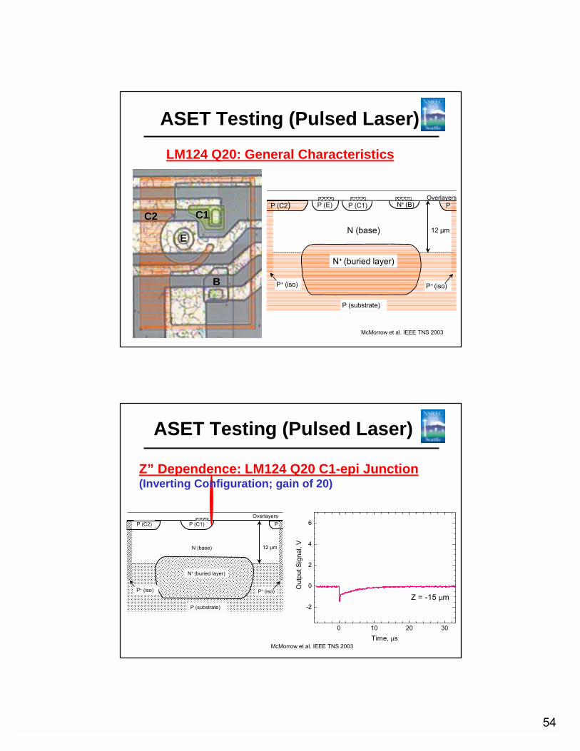
ASET Testing (Pulsed Laser)
LM124 Q20: General Characteristics
McMorrow et al. IEEE TNS 2003
OverlayersP (C1)
P+ (iso)P+ (iso)
N (base)
P (substrate)
12 µm
P (C2)
N+ (buried layer)
P
0 10 20 30
-2
0
2
4
6
Z = -15 µm
Out
put S
igna
l, V
Time, µs
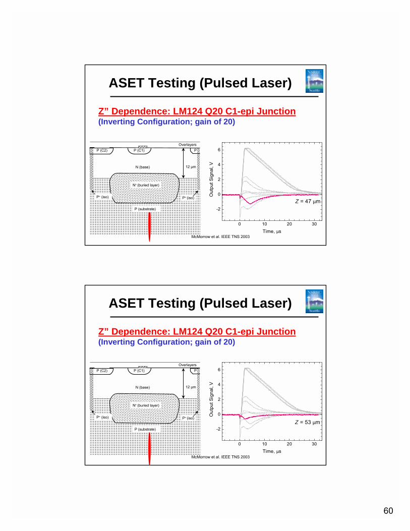
Z” Dependence: LM124 Q20 C1-epi Junction(Inverting Configuration; gain of 20)
ASET Testing (Pulsed Laser)
McMorrow et al. IEEE TNS 2003

55
OverlayersP (C1)
P+ (iso)P+ (iso)
N (base)
P (substrate)
12 µm
P (C2)
N+ (buried layer)
P
0 10 20 30
-2
0
2
4
6
Z = -6 µm
Out
put S
igna
l, V
Time, µs
Z” Dependence: LM124 Q20 C1-epi Junction(Inverting Configuration; gain of 20)
ASET Testing (Pulsed Laser)
McMorrow et al. IEEE TNS 2003
OverlayersP (C1)
P+ (iso)P+ (iso)
N (base)
P (substrate)
12 µm
P (C2)
N+ (buried layer)
P
0 10 20 30
-2
0
2
4
6
Z = -2 µm
Out
put S
igna
l, V
Time, µs
Z” Dependence: LM124 Q20 C1-epi Junction(Inverting Configuration; gain of 20)
ASET Testing (Pulsed Laser)
McMorrow et al. IEEE TNS 2003

56
OverlayersP (C1)
P+ (iso)P+ (iso)
N (base)
P (substrate)
12 µm
P (C2)
N+ (buried layer)
P
0 10 20 30
-2
0
2
4
6
Z = 0 µm
Out
put S
igna
l, V
Time, µs
Z” Dependence: LM124 Q20 C1-epi Junction(Inverting Configuration; gain of 20)
ASET Testing (Pulsed Laser)
McMorrow et al. IEEE TNS 2003
OverlayersP (C1)
P+ (iso)P+ (iso)
N (base)
P (substrate)
12 µm
P (C2)
N+ (buried layer)
P
0 10 20 30
-2
0
2
4
6
Z = 4 µm
Out
put S
igna
l, V
Time, µs
Z” Dependence: LM124 Q20 C1-epi Junction(Inverting Configuration; gain of 20)
ASET Testing (Pulsed Laser)
McMorrow et al. IEEE TNS 2003

57
OverlayersP (C1)
P+ (iso)P+ (iso)
N (base)
P (substrate)
12 µm
P (C2)
N+ (buried layer)
P
0 10 20 30
-2
0
2
4
6
Z = 7 µm
Out
put S
igna
l, V
Time, µs
Z” Dependence: LM124 Q20 C1-epi Junction(Inverting Configuration; gain of 20)
ASET Testing (Pulsed Laser)
McMorrow et al. IEEE TNS 2003
OverlayersP (C1)
P+ (iso)P+ (iso)
N (base)
P (substrate)
12 µm
P (C2)
N+ (buried layer)
P
0 10 20 30
-2
0
2
4
6
Z = 13 µm
Out
put S
igna
l, V
Time, µs
Z” Dependence: LM124 Q20 C1-epi Junction(Inverting Configuration; gain of 20)
ASET Testing (Pulsed Laser)
McMorrow et al. IEEE TNS 2003

58
OverlayersP (C1)
P+ (iso)P+ (iso)
N (base)
P (substrate)
12 µm
P (C2)
N+ (buried layer)
P
0 10 20 30
-2
0
2
4
6
Z = 20 µm
Out
put S
igna
l, V
Time, µs
Z” Dependence: LM124 Q20 C1-epi Junction(Inverting Configuration; gain of 20)
ASET Testing (Pulsed Laser)
McMorrow et al. IEEE TNS 2003
OverlayersP (C1)
P+ (iso)P+ (iso)
N (base)
P (substrate)
12 µm
P (C2)
N+ (buried layer)
P
0 10 20 30
-2
0
2
4
6
Z = 25 µm
Out
put S
igna
l, V
Time, µs
Z” Dependence: LM124 Q20 C1-epi Junction(Inverting Configuration; gain of 20)
ASET Testing (Pulsed Laser)
McMorrow et al. IEEE TNS 2003

59
0 10 20 30
-2
0
2
4
6
Z = 38 µm
Out
put S
igna
l, V
Time, µs
OverlayersP (C1)
P+ (iso)P+ (iso)
N (base) 12 µm
P (C2)
N+ (buried layer)
P
P (substrate)
Z” Dependence: LM124 Q20 C1-epi Junction(Inverting Configuration; gain of 20)
ASET Testing (Pulsed Laser)
McMorrow et al. IEEE TNS 2003
OverlayersP (C1)
P+ (iso)P+ (iso)
N (base)
P (substrate)
12 µm
P (C2)
N+ (buried layer)
P
0 10 20 30
-2
0
2
4
6
Z = 44 µm
Out
put S
igna
l, V
Time, µs
Z” Dependence: LM124 Q20 C1-epi Junction(Inverting Configuration; gain of 20)
ASET Testing (Pulsed Laser)
McMorrow et al. IEEE TNS 2003
60
0 10 20 30
-2
0
2
4
6
Z = 47 µm
Out
put S
igna
l, V
Time, µs
OverlayersP (C1)
P+ (iso)P+ (iso)
N (base) 12 µm
P (C2)
N+ (buried layer)
P
P (substrate)
Z” Dependence: LM124 Q20 C1-epi Junction(Inverting Configuration; gain of 20)
ASET Testing (Pulsed Laser)
McMorrow et al. IEEE TNS 2003
0 10 20 30
-2
0
2
4
6
Z = 53 µm
Out
put S
igna
l, V
Time, µs
OverlayersP (C1)
P+ (iso)P+ (iso)
N (base) 12 µm
P (C2)
N+ (buried layer)
P
P (substrate)
Z” Dependence: LM124 Q20 C1-epi Junction(Inverting Configuration; gain of 20)
ASET Testing (Pulsed Laser)
McMorrow et al. IEEE TNS 2003
61
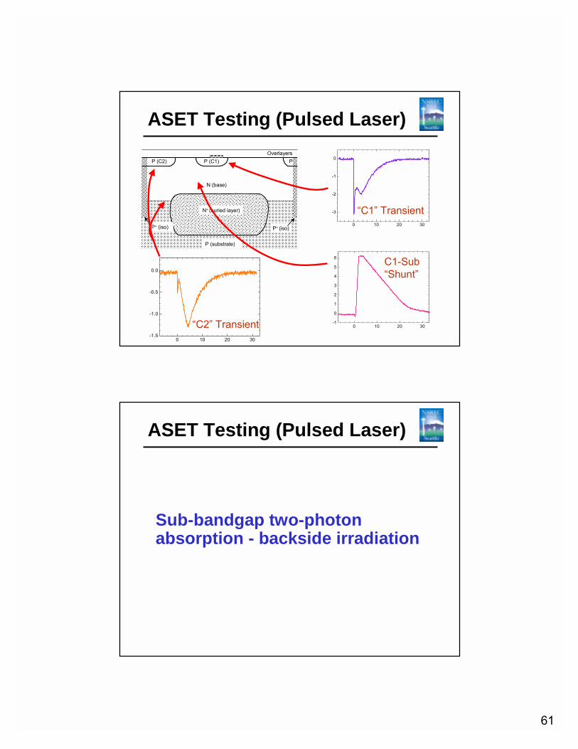
0 10 20 30-1
0
1
2
3
4
5
6
OverlayersP (C1)
P+ (iso)P+ (iso)
N (base)
P (substrate)
P (C2)
N+ (buried layer)
P
0 10 20 30
-3
-2
-1
0
0 10 20 30-1.5
-1.0
-0.5
0.0
“C1” Transient
“C2” Transient
C1-Sub“Shunt”
ASET Testing (Pulsed Laser)
ASET Testing (Pulsed Laser)
Sub-bandgap two-photon absorption - backside irradiation

62
ASET Testing (Pulsed Laser)
Surface elements opaque to optical excitation
Tightly focused two-photon excitation
source
Substrate transparent to single photon
sub-bandgap excitationCircuit Layer(s)
Region of 2 PhotonCarrier Generation
Backside “Through-Wafer” TPA Illumination
McMorrow et al. IEEE TNS 2004
ASET Testing (Pulsed Laser)
Back Side Front Side
Photomicrograph of Q20 in LM124 Captured with NIR InGaAs Camera

63
ASET Testing (Pulsed Laser)
0 5 10 15 20
0.0
1.0
2.0Q18
Out
put S
igna
l, V
Time, µs
0.0
0.5
1.0
1.5 Q18
Front Side Back Side
Backside “Through-Wafer” TPA IlluminationLM124 Operational Amplifier
McMorrow IEEE TNS 2004
ASET Testing (Pulsed Laser)
X-Y Scanning……..

64
ASET Testing (Pulsed Laser)
2D Scan of LM6144 Op-Amp
Area 1
V. Pouget, IXL, France
ASET Testing (Pulsed Laser)
2D Scan of LM6144 Op-Amp
V. Pouget, IXL, France
0
1
2
3
4
5
6
7
8
9
10
0.00 10.00 20.00 30.00 40.00 50.00
Time (µµµµs)
Am
plitu
de (V
)

65
ASET Testing (Pulsed Laser)
2D Scan of LM6144 Op-Amp
V. Pouget, IXL, France
ASET Testing
Summary• ASET testing has unique aspects.
– Sensitivity to configuration– Need to capture transients– Analysis to determine which transients are of concern
• The approaches discussed in this section are in large part a result of the DTRA program.
• The best approach is to use a number of different experimental methods including:– Broad beam of heavy ions– Focused beam of heavy ions– Pulsed laser (1-photon and 2-photon)
• ASET sensitivity depends critically on configuration.
66
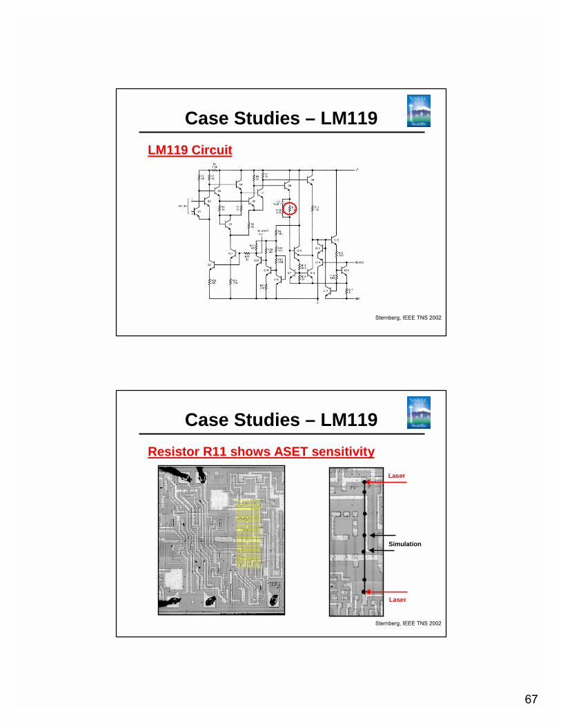
5. Case Studies
ASETs Originating in Resistors in LM119 Voltage Comparator
67
Case Studies – LM119
Sternberg, IEEE TNS 2002
LM119 Circuit
Case Studies – LM119
Sternberg, IEEE TNS 2002
Resistor R11 shows ASET sensitivity
Laser
Laser
Simulation

68
Case Studies – LM119
Sternberg, IEEE TNS 2002
Comparison of experimental and simulated results
Spreading Resistance for Input Transistors in LM111 Voltage
Comparator

69
Case Studies – LM111
Pease et al. IEEE TNS 2002
Validating the SPICE Model for the LM111
I(t)
I(t)
I(t)
C/B
E/B
E/C
CASE STUDIES LM111
Pease et al. IEEE TNS 2002
Location of ASETs in LM111Induced by ion microprobePhotomicrograph
Of LM111 input
Validating the SPICE Model for the LM111

70
Case Studies – LM111
Sternberg, IEEE TNS 2002
Validating the SPICE Model for the LM111
Base
Collector
Emitter
Case Studies – LM111
Pease, IEEE TNS 2002
Validating the SPICE Model for the LM111
71
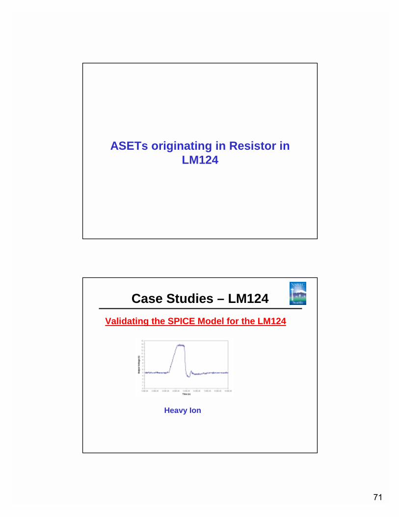
ASETs originating in Resistor in LM124
Case Studies – LM124Validating the SPICE Model for the LM124
Heavy Ion

72
Case Studies – LM124Validating the SPICE Model for the LM124
“R1”
Case Studies – LM124Validating the SPICE Model for the LM124
-1
0
1
2
3
4
-10 -8 -6 -4 -2 0 2 4 6 8 10
Time (µµµµs)
Am
plitu
de (V
)
Pulsed LaserHeavy Ion

73
Case Studies – LM124Validating the SPICE Model for the LM124
Q2Q3 Q4
Q5
Q19Q15Q16
Q14
Q13
Q11
Q10Q8
Q7Q12
Q9
Q6
Q21Q17
Q18 Q20 R1
R2
C1
Vin(-)
Vin(+)
V+
V-
Vout
Q2Q3 Q4
Q5
Q19Q15Q16
Q14
Q13
Q11
Q10Q8
Q7Q12
Q9
Q6
Q21Q17
Q18 Q20 R1
R2
C1
Vin(-)
Vin(+)
V+
V-
Vout
Case Studies – LM124
Pease, SEE Symposium 2004
Validating the SPICE Model for the LM124
R1 has a transistorstructure but thebase is left floatingand so it acts as aresistor.
SPICE

74
Long-Duration Pulses(LDPs)
ASET width determined by device bandwidth.
Case Studies
Unity gain bandwidth = 35 kHz Unity gain bandwidth = 300 MHz
0
0.5
1
1.5
2
2.5
3
3.5
4
4.5
0 50 100 150 200 250 300 350 400
Time (ns)
Am
pltiu
de (V
)
LMH6628OP293
300 us
30 ns

75
Case Studies – LM6144Long-Duration Pulses observed in Heavy-Ion Testing of LM6144 Op-Amp.
Boughassoul et al. IEEE TNS 2004
Unity-gain bandwidth - 17 MHz
((((∆∆∆∆t < 1µµµµs)
Only observed for LETs > 50 MeV.cm2/mg
Case Studies – LM6144
Laser Scan identified the origins of the LDPs
-9 V to –9.25 V 9.2 V to 9.8 VBoughassoul et al. IEEE TNS 2004

76
Case Studies – LM6144
Laser Scan identified the origins of the LDPsEffect of light:
• Illuminator• Scattered laser light• Room lights
Strikes to other transistors• Stops the transient
LDPs (in dark) depend on supply voltage:
Vdd = ± 10V, ∆t=25 msVdd = ± 7.5V, ∆t=45 msVdd = ± 5.0V, ∆t=100 ms
Boughassoul et al. IEEE TNS 2004
Case Studies – LM6144
Used SPICE to model effects
• Able to simulate all effects• Pulse Length vs supply voltage
Boughassoul et al. IEEE TNS 2004

77
Case Studies – LM6144
Used SPICE to model effects
• Suggested hardeningapproach – adding capacitors across C/Bof two transistors in the bias/startup circuit.
Boughassoul et al. IEEE TNS 2004
6. ASET Mitigation

78
ASET MitigationApproaches
• Repeat the Measurement Housekeeping measurement can be repeated three times
•Device Level Epitaxial layers (SOI) to limit charge collection
• Circuit Level Low bandpass filter to remove ASETs
• Circuit/Subsystem Level Triple Modular Redundancy (TMR)
ASET Mitigation
Van Vonno, IEEE TNS 2001
Triple Modular Redundancy
Cin
Rin
CinRin

79
ASET Mitigation
Van Vonno, IEEE TNS 2001
Minimum Input Overdrive for ASET-free Operation
- Depends on Input Resistance and Capacitance
0
20
40
60
80
100
120
140
160
0 20 40 60 80 100 120
Input Resistance (Kohms)
Inpu
t Ove
rdriv
e (m
V)Cin = 0 pF
Cin = 100 pF
9 V15 V30 V
9 V15 V30 V
7. Summary & Conclusions
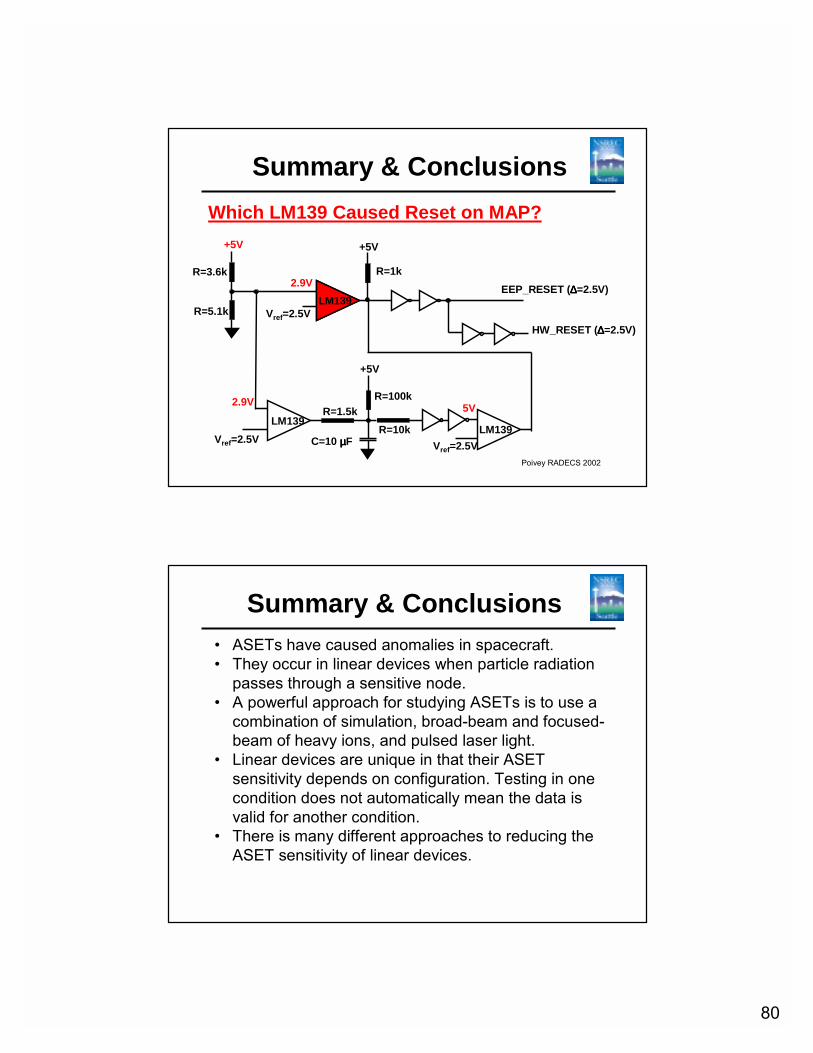
80
Summary & Conclusions
R=3.6k
LM139
LM139LM139
R=5.1k
R=10kR=1.5k
R=1k
R=100k
C=10 µµµµFVref=2.5V Vref=2.5V
Vref=2.5V
+5V
+5V
EEP_RESET (∆∆∆∆=2.5V)
HW_RESET (∆∆∆∆=2.5V)
+5V
Poivey RADECS 2002
2.9V
2.9V 5V
Which LM139 Caused Reset on MAP?
LM139
Summary & Conclusions• ASETs have caused anomalies in spacecraft.• They occur in linear devices when particle radiation
passes through a sensitive node.• A powerful approach for studying ASETs is to use a
combination of simulation, broad-beam and focused-beam of heavy ions, and pulsed laser light.
• Linear devices are unique in that their ASET sensitivity depends on configuration. Testing in one condition does not automatically mean the data is valid for another condition.
• There is many different approaches to reducing the ASET sensitivity of linear devices.
Related Documents