CSE 141, S2'06 Jeff Brown Single-Cycle CPU Datapath Design "The Do-It-Yourself CPU Kit"

Welcome message from author
This document is posted to help you gain knowledge. Please leave a comment to let me know what you think about it! Share it to your friends and learn new things together.
Transcript
CSE 141, S2'06 Jeff Brown
Single-Cycle CPUDatapath Design
"The Do-It-Yourself CPU Kit"
CSE 141, S2'06 Jeff Brown
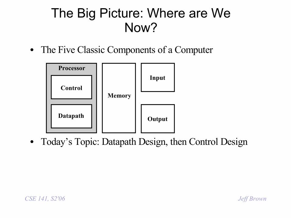
The Big Picture: Where are We Now?
• The Five Classic Components of a Computer
• Today’s Topic: Datapath Design, then Control Design
Control
Datapath
Memory
Processor
Input
Output
CSE 141, S2'06 Jeff Brown
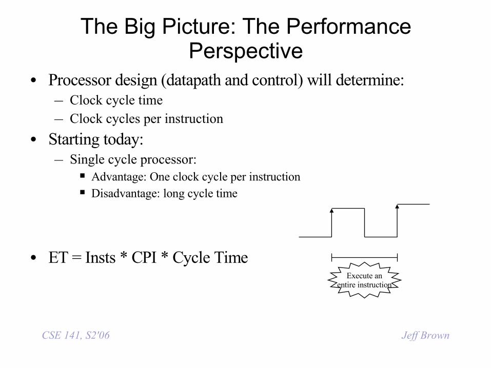
The Big Picture: The Performance Perspective
• Processor design (datapath and control) will determine:– Clock cycle time
– Clock cycles per instruction
• Starting today:– Single cycle processor:
Advantage: One clock cycle per instruction Disadvantage: long cycle time
• ET = Insts * CPI * Cycle TimeExecute an
entire instruction
CSE 141, S2'06 Jeff Brown
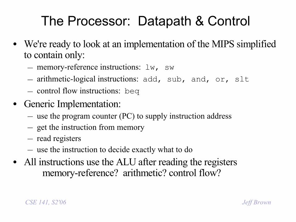
• We're ready to look at an implementation of the MIPS simplified to contain only:– memory-reference instructions: lw, sw
– arithmetic-logical instructions: add, sub, and, or, slt
– control flow instructions: beq
• Generic Implementation:– use the program counter (PC) to supply instruction address
– get the instruction from memory
– read registers
– use the instruction to decide exactly what to do
• All instructions use the ALU after reading the registersmemory-reference? arithmetic? control flow?
The Processor: Datapath & Control
CSE 141, S2'06 Jeff Brown
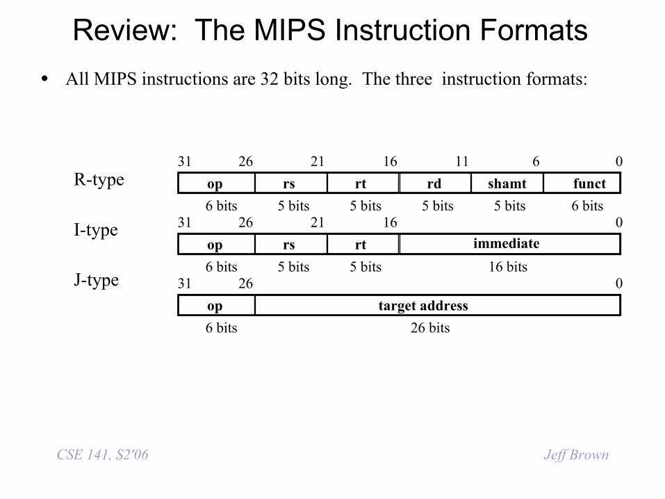
Review: The MIPS Instruction Formats
• All MIPS instructions are 32 bits long. The three instruction formats:
R-type
I-type
J-typeop target address
02631
6 bits 26 bits
op rs rt rd shamt funct
061116212631
6 bits 6 bits5 bits5 bits5 bits5 bits
op rs rt immediate
016212631
6 bits 16 bits5 bits5 bits
CSE 141, S2'06 Jeff Brown
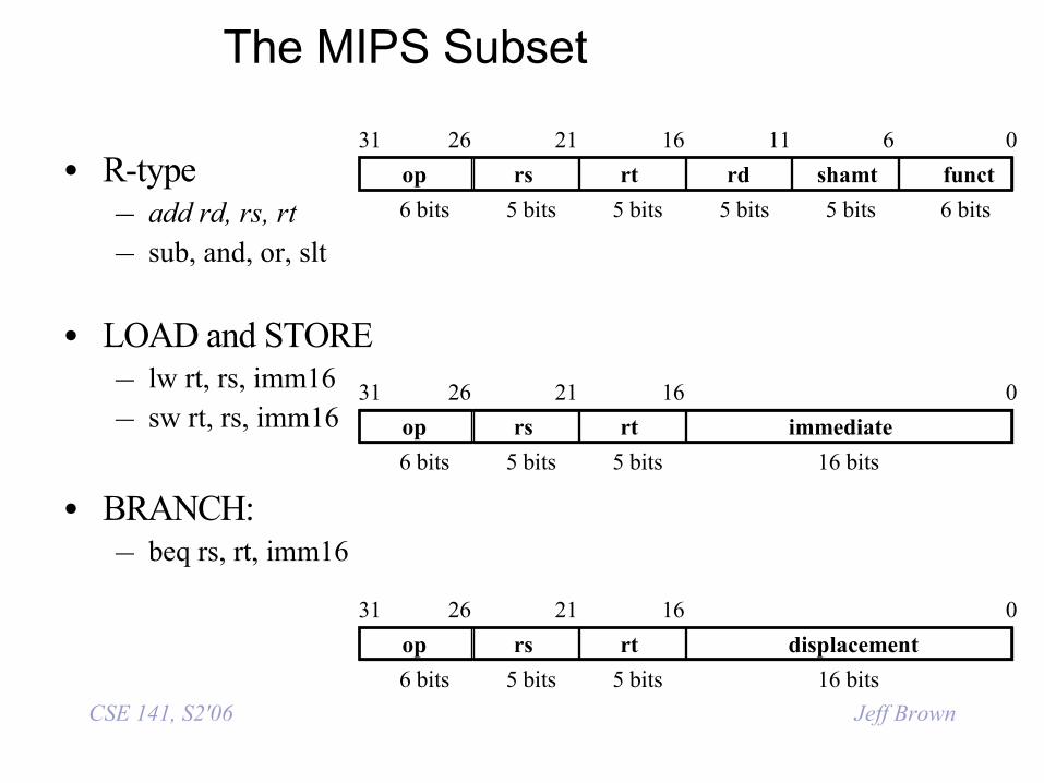
The MIPS Subset
• R-type– add rd, rs, rt
– sub, and, or, slt
• LOAD and STORE– lw rt, rs, imm16
– sw rt, rs, imm16
• BRANCH:– beq rs, rt, imm16
op rs rt rd shamt funct
061116212631
6 bits 6 bits5 bits5 bits5 bits5 bits
op rs rt immediate
016212631
6 bits 16 bits5 bits5 bits
op rs rt displacement
016212631
6 bits 16 bits5 bits5 bits
CSE 141, S2'06 Jeff Brown
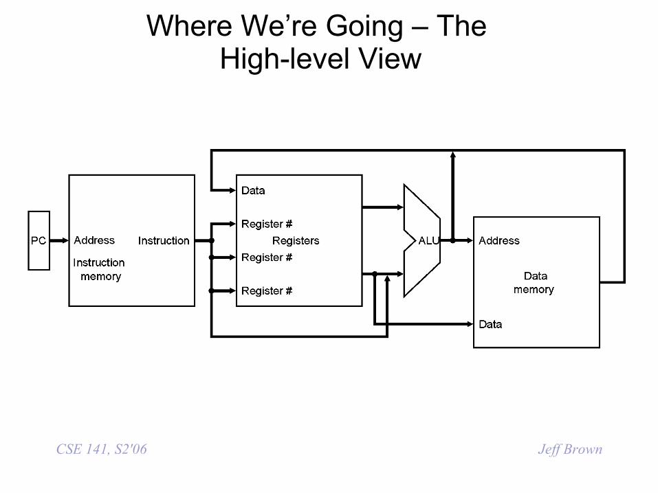
Where We’re Going – The High-level View
CSE 141, S2'06 Jeff Brown
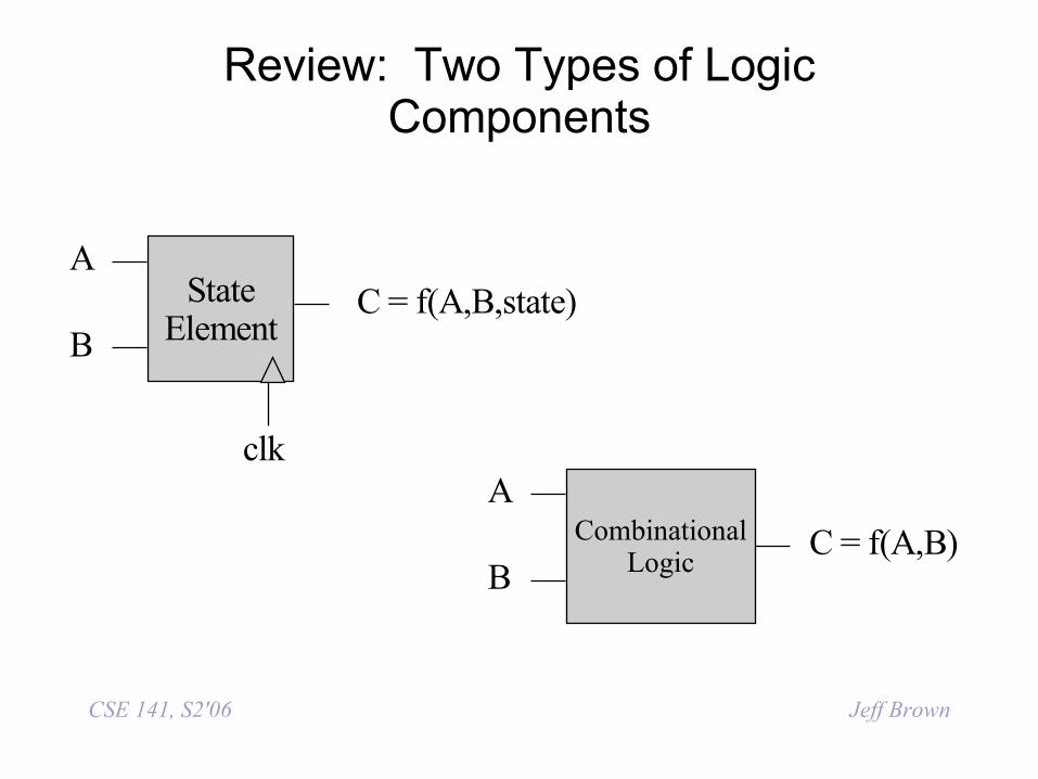
Review: Two Types of Logic Components
StateElement
clk
A
BC = f(A,B,state)
CombinationalLogic
A
BC = f(A,B)
CSE 141, S2'06 Jeff Brown
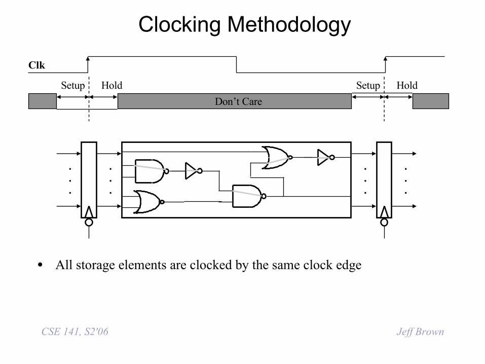
Clocking Methodology
• All storage elements are clocked by the same clock edge
Clk
Don’t Care
Setup Hold
.
.
.
.
.
.
.
.
.
.
.
.
Setup Hold
CSE 141, S2'06 Jeff Brown
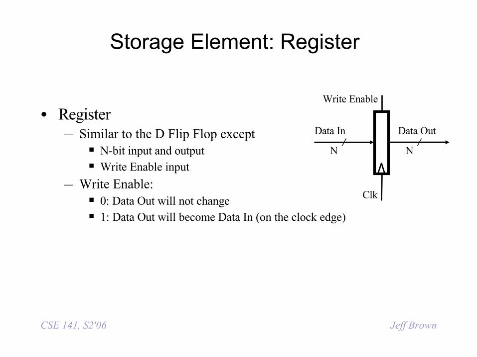
Storage Element: Register
• Register– Similar to the D Flip Flop except
N-bit input and output Write Enable input
– Write Enable: 0: Data Out will not change 1: Data Out will become Data In (on the clock edge)
Clk
Data In
Write Enable
N N
Data Out
CSE 141, S2'06 Jeff Brown
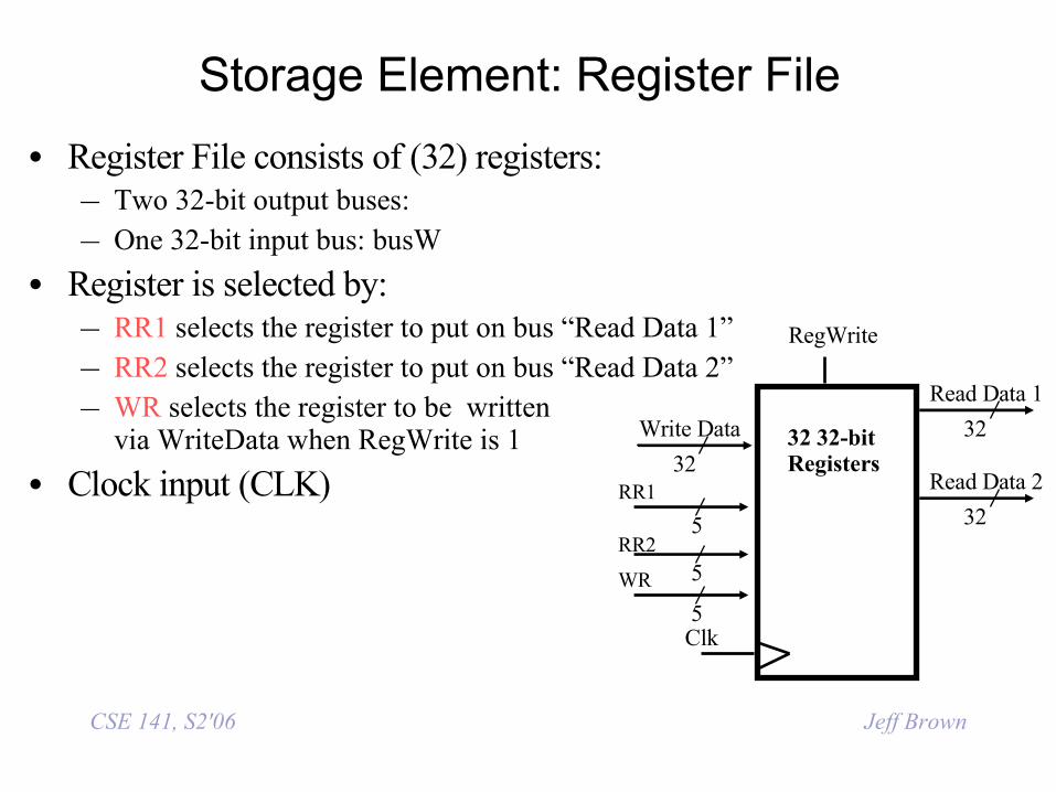
Storage Element: Register File
• Register File consists of (32) registers:– Two 32-bit output buses:
– One 32-bit input bus: busW
• Register is selected by:– RR1 selects the register to put on bus “Read Data 1”
– RR2 selects the register to put on bus “Read Data 2”
– WR selects the register to be writtenvia WriteData when RegWrite is 1
• Clock input (CLK)
Clk
Write Data
RegWrite
32
32
Read Data 1
32
Read Data 2
32 32-bitRegisters
5
5
5
RR1
RR2
WR
CSE 141, S2'06 Jeff Brown
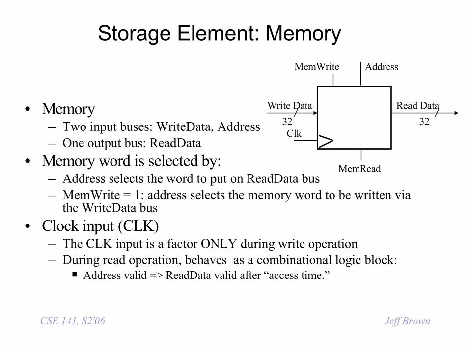
Storage Element: Memory
• Memory– Two input buses: WriteData, Address– One output bus: ReadData
• Memory word is selected by:– Address selects the word to put on ReadData bus– MemWrite = 1: address selects the memory word to be written via
the WriteData bus
• Clock input (CLK) – The CLK input is a factor ONLY during write operation– During read operation, behaves as a combinational logic block:
Address valid => ReadData valid after “access time.”
Clk
Write Data
MemWrite
32 32
Read Data
Address
MemRead
CSE 141, S2'06 Jeff Brown
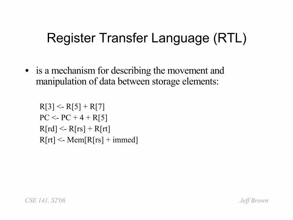
Register Transfer Language (RTL)
• is a mechanism for describing the movement and manipulation of data between storage elements:
R[3] <- R[5] + R[7]PC <- PC + 4 + R[5]R[rd] <- R[rs] + R[rt]R[rt] <- Mem[R[rs] + immed]
CSE 141, S2'06 Jeff Brown
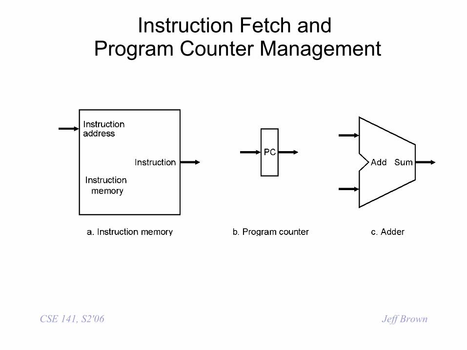
Instruction Fetch and Program Counter Management
CSE 141, S2'06 Jeff Brown
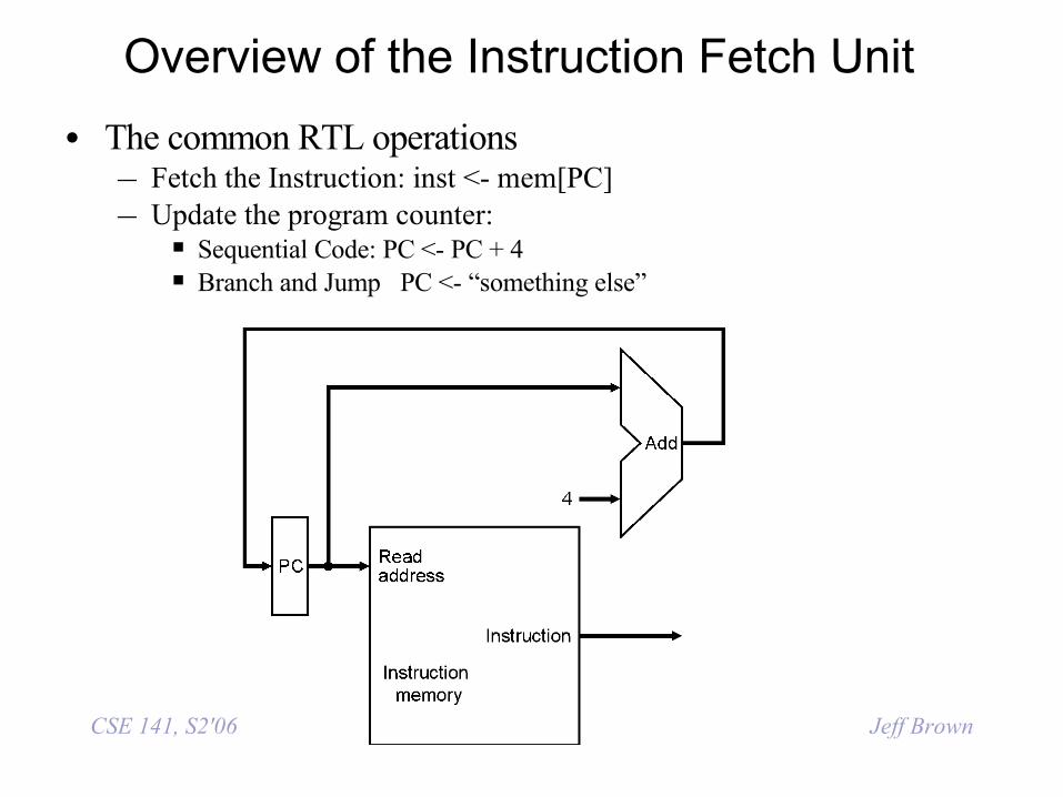
Overview of the Instruction Fetch Unit
• The common RTL operations– Fetch the Instruction: inst <- mem[PC]– Update the program counter:
Sequential Code: PC <- PC + 4 Branch and Jump PC <- “something else”
CSE 141, S2'06 Jeff Brown
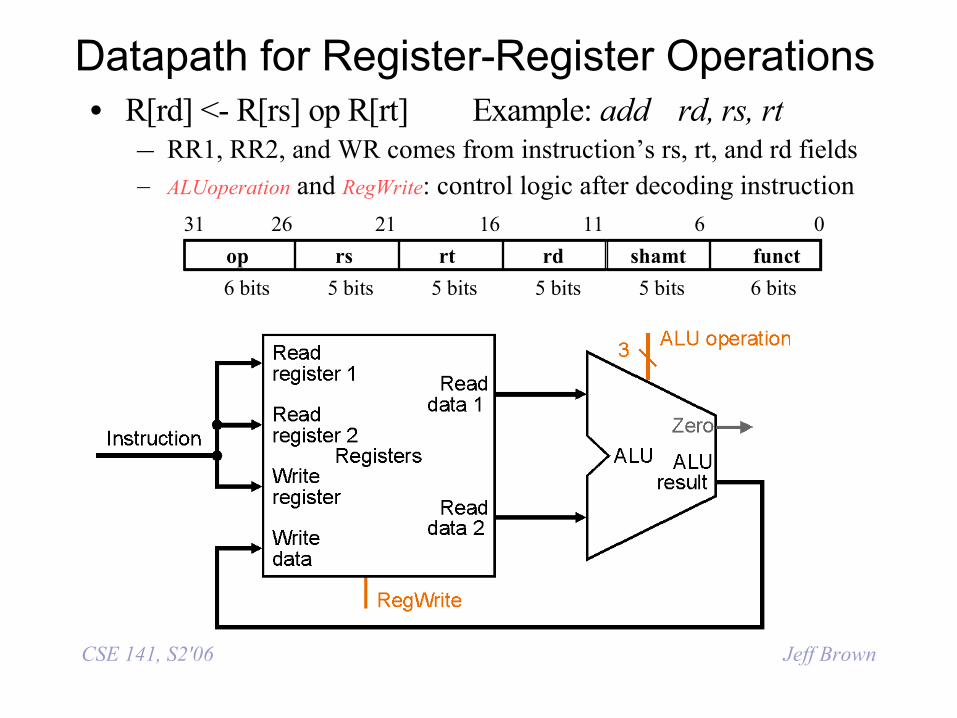
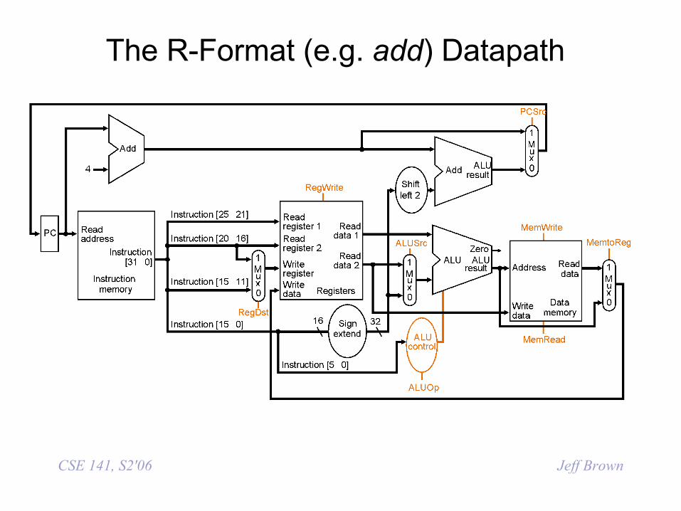
Datapath for Register-Register Operations• R[rd] <- R[rs] op R[rt] Example: add rd, rs, rt
– RR1, RR2, and WR comes from instruction’s rs, rt, and rd fields– ALUoperation and RegWrite: control logic after decoding instruction
op rs rt rd shamt funct
061116212631
6 bits 6 bits5 bits5 bits5 bits5 bits
CSE 141, S2'06 Jeff Brown
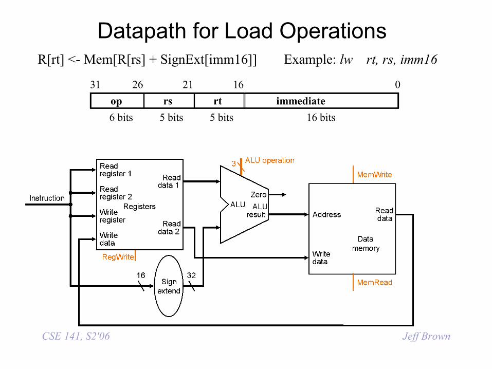
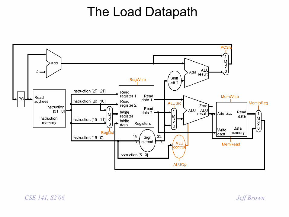
Datapath for Load OperationsR[rt] <- Mem[R[rs] + SignExt[imm16]] Example: lw rt, rs, imm16
op rs rt immediate
016212631
6 bits 16 bits5 bits5 bits
CSE 141, S2'06 Jeff Brown
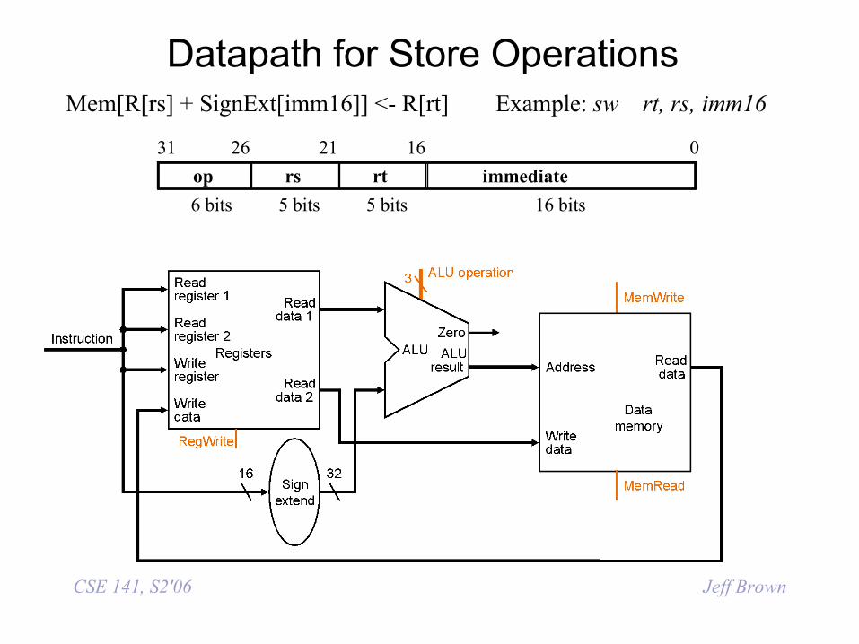
Datapath for Store OperationsMem[R[rs] + SignExt[imm16]] <- R[rt] Example: sw rt, rs, imm16
op rs rt immediate
016212631
6 bits 16 bits5 bits5 bits
CSE 141, S2'06 Jeff Brown
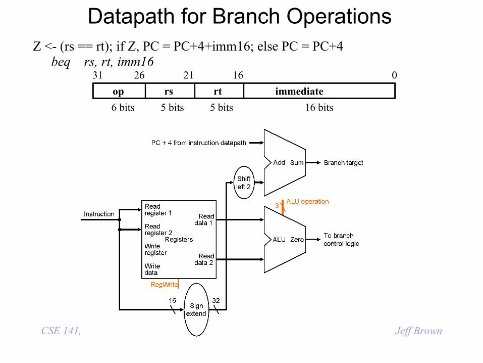
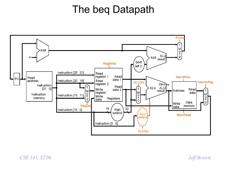
Datapath for Branch Operations
op rs rt immediate
016212631
6 bits 16 bits5 bits5 bits
Z <- (rs == rt); if Z, PC = PC+4+imm16; else PC = PC+4 beq rs, rt, imm16
CSE 141, S2'06 Jeff Brown
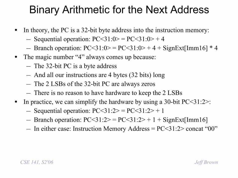
Binary Arithmetic for the Next Address
• In theory, the PC is a 32-bit byte address into the instruction memory:
– Sequential operation: PC<31:0> = PC<31:0> + 4
– Branch operation: PC<31:0> = PC<31:0> + 4 + SignExt[Imm16] * 4
• The magic number “4” always comes up because:
– The 32-bit PC is a byte address
– And all our instructions are 4 bytes (32 bits) long
– The 2 LSBs of the 32-bit PC are always zeros
– There is no reason to have hardware to keep the 2 LSBs
• In practice, we can simplify the hardware by using a 30-bit PC<31:2>:
– Sequential operation: PC<31:2> = PC<31:2> + 1
– Branch operation: PC<31:2> = PC<31:2> + 1 + SignExt[Imm16]
– In either case: Instruction Memory Address = PC<31:2> concat “00”
CSE 141, S2'06 Jeff Brown
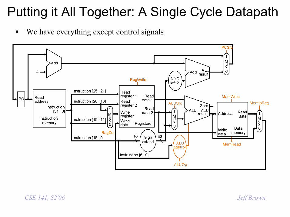
Putting it All Together: A Single Cycle Datapath
• We have everything except control signals
CSE 141, S2'06 Jeff Brown
The R-Format (e.g. add) Datapath
CSE 141, S2'06 Jeff Brown
The Load Datapath

CSE 141, S2'06 Jeff Brown
The store Datapath
CSE 141, S2'06 Jeff Brown
The beq Datapath
CSE 141, S2'06 Jeff Brown
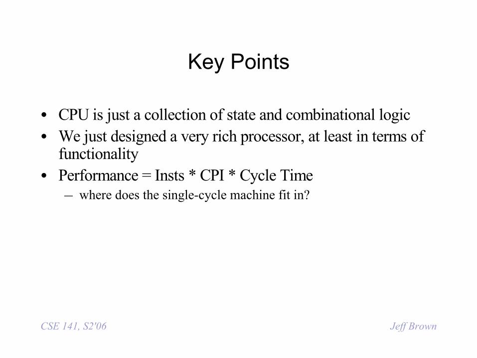
Key Points
• CPU is just a collection of state and combinational logic• We just designed a very rich processor, at least in terms of
functionality• Performance = Insts * CPI * Cycle Time
– where does the single-cycle machine fit in?
Related Documents