Single crystal field-effect transistors based on layered semiconductors Dissertation zur Erlangung des akademischen Grades des Doktors der Naturwissenschaften (Dr. rer. nat.) an der Universität Konstanz Fachbereich Physik vorgelegt von Roswitha Zeis April 2005 Referent: Prof. Dr. Ernst Bucher Referent: Prof. Dr. Peter Wyder

Welcome message from author
This document is posted to help you gain knowledge. Please leave a comment to let me know what you think about it! Share it to your friends and learn new things together.
Transcript
Single crystal field-effect transistors based on
layered semiconductors
Dissertation
zur Erlangung des akademischen Grades des Doktors der Naturwissenschaften
(Dr. rer. nat.) an der Universität Konstanz
Fachbereich Physik
vorgelegt von
Roswitha Zeis
April 2005
Referent: Prof. Dr. Ernst Bucher Referent: Prof. Dr. Peter Wyder

meinen Eltern
Elfriede und Alfred Zeis
i

ii
DANK
Von der Idee bis zur Fertigstellung haben viele Menschen zumGelingen dieser Arbeit beigetragen. Bei ihnen allen mochte ichmich bedanken.
Mein besonderer Dank gilt:
Meinem Doktorvater Prof. Ernst Bucher fur die besondere Gelegen-heit, die er mir bot, an den Bell Laboratorien zu forschen und seineUnterstutzung auch in schweren Krisen,
Prof. Peter Wyder fur die spontane Zusage zur Zweitkorrektur,
Dr. Ch. Kloc fur die hervorragende fachliche Betreuung, die tatkraftigeUnterstutzung im Labor und den personlichen, freundschaftlichen Um-gangston,
Dr. C. Besnard fur das solidarische Miteinander nicht nur bei fachlichenFragestellungen,
Prof. T. Siegrist fur seine Diskussionsfreude und Hilfsbereitschaft injeder Lebenslage,
C. G. Maclennan fur die nette Einfuhrung in die amerikanische Lebens-weise und haufiges Korrekturlesen,
allen Mitarbeitern der Bell Laboratorien fur die angenehme Arbeits-atmosphare,
H. Riazi-Nejad fur die Hilfestellung bei computertechnischen Proble-men,
der Konrad Adenauer Stiftung, dem Deutschen Akademischen Aus-tauschdienst und der Landesgraduiertenforderung fur die finanzelle Unter-stutzung.
iii

iv
List of publications
1. Zeis R, Siegrist T, Kloc ChSingle-crystal field-effect transistors based on copper phthalocyanineApplied Physics Letters 86 (2) 022103
2. Zeis R, Takimiya K, Kunugi Y, Konda Y, Niihara N, OtsuboT, Kloc ChSingle crystal field-effect transistors based on selenium containing or-ganic semiconductor accepted in Japanese Journal of Applied Physics
3. Zeis R, Besnard C, Siegrist T, Schlockermann C, Chi X, KlocChField-effect studies on rubrene and impurities of rubrene submitted toChemistry of Materials
4. Kloc Ch, Zeis R, Williamson E, Chi X, Siegrist T, RamirezAP.Molecular engineering of TCNQ Perylene single crystals for n-type fieldeffect transistor in preparation
5. Podzorov V, Gershenson ME, Kloc Ch, Zeis R, Bucher EHigh-mobility field-effect transistors based on transition metal dichalco-genides Applied Physics Letters 84 (17): 3301 -3303
6. Moon H, Zeis R, Borkent JE, Besnard C, Lovinger A, SiegristT, Kloc Ch, Bao ZSynthesis, Crystal structure and Transistor Performance of TetraceneDerivatives Journal of the American Chemical Society (Communica-tion); 2004; 1 26 (47) 1 5322-15323
7. Roberson L, Kowalik J, Tolbert L, Kloc Ch, Zeis R, Chi X,Wilkins CPentacene Disproportionation during Sublimation for Field-Effect Tran-sistors Journal of the American Chemical Society 127 (9) 3069-3075;(Article)
8. Takimiya K, Zeis R, Kloc Ch, Kunugi Y, Konda Y, NiiharaN, Otsubo TEvaluation of single crystal and thin film field-effect Transistor basedon 2,6-Diphenybenzodichalcogenophenes in preparation
v
9. Siegrist T, Kloc Ch, Zeis R, Schlockermann C, Chapman BD,Pindak R, Siddons DP, Checco A, Ocko BMTopographic imaging of grain boundaries in single crystal rubrene inpreparation
vi
Contents
1 Introduction 1
2 The field effect transistor 52.1 The principle of a FET . . . . . . . . . . . . . . . . . . . . . . 52.2 Basic characteristics of a FET . . . . . . . . . . . . . . . . . . 8
2.2.1 Field-effect threshold . . . . . . . . . . . . . . . . . . 92.2.2 Sub-threshold slope . . . . . . . . . . . . . . . . . . . . 112.2.3 Field-effect mobility . . . . . . . . . . . . . . . . . . . 12
3 The crystal material 153.1 Charge transport in organic single crystals . . . . . . . . . . . 15
3.1.1 Band and hopping transport . . . . . . . . . . . . . . . 173.1.2 The concept of polaron hopping . . . . . . . . . . . . . 203.1.3 Multiple trapping and release model . . . . . . . . . . 203.1.4 Structure of organic single crystals . . . . . . . . . . . 21
3.2 Transition metal dichalcogenides . . . . . . . . . . . . . . . . . 23
4 Device fabrication 254.1 Crystal growth . . . . . . . . . . . . . . . . . . . . . . . . . . 25
4.1.1 Organic material . . . . . . . . . . . . . . . . . . . . . 254.1.2 Transition metal dichalcogenides . . . . . . . . . . . . 27
4.2 Fabrication of the FET structures . . . . . . . . . . . . . . . . 29
5 Rubrene 355.1 Introduction . . . . . . . . . . . . . . . . . . . . . . . . . . . . 355.2 Rubrene room temperature measurements . . . . . . . . . . . 365.3 Rubrene low temperature measurements . . . . . . . . . . . . 39
6 Impurities 436.1 Impurities of rubrene . . . . . . . . . . . . . . . . . . . . . . . 436.2 Impurities of pentacene . . . . . . . . . . . . . . . . . . . . . . 47
vii
7 Copper phthalocyanine 517.1 The technical relevance of Cu-Pc . . . . . . . . . . . . . . . . 517.2 Crystal structure and rocking curve . . . . . . . . . . . . . . . 527.3 FET-characteristics of Cu-Pc . . . . . . . . . . . . . . . . . . 54
8 Tetracene Derivatives 578.1 Crystal structure and mobility . . . . . . . . . . . . . . . . . . 57
9 Diphenybenzo- dichalcogenophenes 639.1 Using single crystals to evaluate new material . . . . . . . . . 639.2 The FET-performance of DPh-BDXs . . . . . . . . . . . . . . 64
10 Perylene-TCNQ 7110.1 Introduction . . . . . . . . . . . . . . . . . . . . . . . . . . . . 7110.2 Crystal growth and structure Perylene-TCNQ . . . . . . . . . 7210.3 FET measurements . . . . . . . . . . . . . . . . . . . . . . . . 74
11 Summary of OFETs 77
12 Transition metal dichalcogenides 8312.1 TMDs for FET devices? . . . . . . . . . . . . . . . . . . . . . 8312.2 FET-characteristics of WSe2 . . . . . . . . . . . . . . . . . . . 84
13 Conclusion 93
14 Zusammenfassung 97
viii
Chapter 1
Introduction
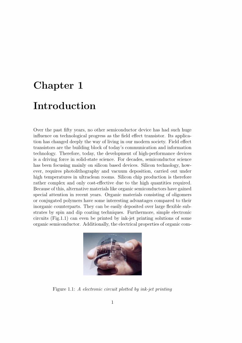
Over the past fifty years, no other semiconductor device has had such hugeinfluence on technological progress as the field effect transistor. Its applica-tion has changed deeply the way of living in our modern society. Field effecttransistors are the building block of today’s communication and informationtechnology. Therefore, today, the development of high-performance devicesis a driving force in solid-state science. For decades, semiconductor sciencehas been focusing mainly on silicon based devices. Silicon technology, how-ever, requires photolithography and vacuum deposition, carried out underhigh temperatures in ultraclean rooms. Silicon chip production is thereforerather complex and only cost-effective due to the high quantities required.Because of this, alternative materials like organic semiconductors have gainedspecial attention in recent years. Organic materials consisting of oligomersor conjugated polymers have some interesting advantages compared to theirinorganic counterparts. They can be easily deposited over large flexible sub-strates by spin and dip coating techniques. Furthermore, simple electroniccircuits (Fig.1.1) can even be printed by ink-jet printing solutions of someorganic semiconductor. Additionally, the electrical properties of organic com-
Figure 1.1: A electronic circuit plotted by ink-jet printing
1
2 CHAPTER 1. INTRODUCTION
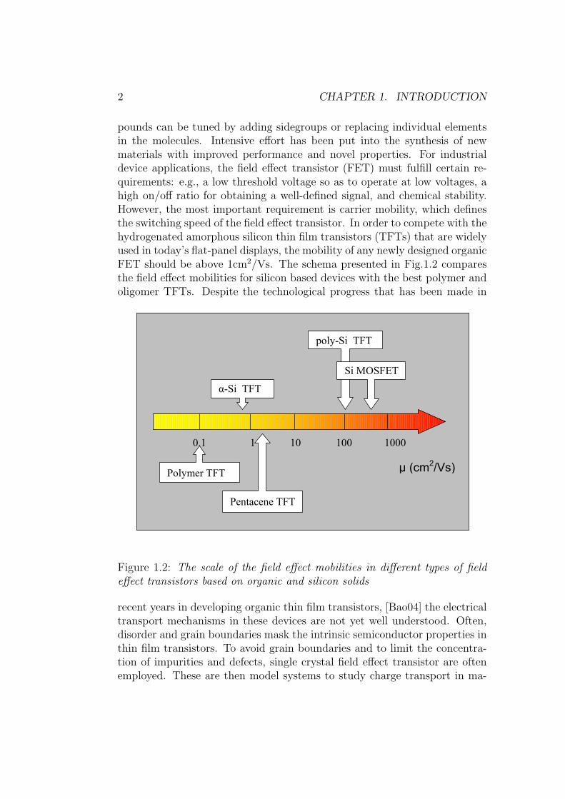
pounds can be tuned by adding sidegroups or replacing individual elementsin the molecules. Intensive effort has been put into the synthesis of newmaterials with improved performance and novel properties. For industrialdevice applications, the field effect transistor (FET) must fulfill certain re-quirements: e.g., a low threshold voltage so as to operate at low voltages, ahigh on/off ratio for obtaining a well-defined signal, and chemical stability.However, the most important requirement is carrier mobility, which definesthe switching speed of the field effect transistor. In order to compete with thehydrogenated amorphous silicon thin film transistors (TFTs) that are widelyused in today’s flat-panel displays, the mobility of any newly designed organicFET should be above 1cm2/Vs. The schema presented in Fig.1.2 comparesthe field effect mobilities for silicon based devices with the best polymer andoligomer TFTs. Despite the technological progress that has been made in
0.1 1 1000 10010
Polymer TFT
Pentacene TFT
α-Si TFT
poly-Si TFT
Si MOSFET
µ (cm2/Vs)
Figure 1.2: The scale of the field effect mobilities in different types of fieldeffect transistors based on organic and silicon solids
recent years in developing organic thin film transistors, [Bao04] the electricaltransport mechanisms in these devices are not yet well understood. Often,disorder and grain boundaries mask the intrinsic semiconductor properties inthin film transistors. To avoid grain boundaries and to limit the concentra-tion of impurities and defects, single crystal field effect transistor are oftenemployed. These are then model systems to study charge transport in ma-
3
terials and the relationship between molecular and crystal structure. I hadthe opportunity to perform much of my thesis research at Bell Laboratories,where material research is top-ranking. Therefore I had access to a broadspectrum of various types of materials.
A big part of my thesis is dedicated to the materials rubrene andpentacene, due to their prominent position in the research of organicfield effect transistors.
Substituted tetracenes are prime examples of how device perfor-mance can be improved by adding functionalizing sidegroups.
Another focus was on copper phthalocyanine, a material that is ofspecial interest for technical applications because of its thermal andchemical stability.
A different approach is mixing two organic compounds TCNQ andPerylene which leads to a class of material called charge-transfersalts.
In cooperation with V. Podzorov (Rutgers University, USA), I workedon field effect transistors based on layered transition metal dichalco-genide. Their crystal structures are closely related to those of organicmaterials.
The materials I investigated were synthesized by H. Katz (Bell Laborato-ries, USA), Zh. Bao (Stanford University, USA), C. Nuckolls (ColumbiaUniversity, USA) and K. Takimiya (Hiroshima University, Japan). At BellLaboratories, Ch. Kloc and E. Bucher grow the crystals. T. Siegrist and C.Besnard performed the X-ray structure analysis.
4 CHAPTER 1. INTRODUCTION
Chapter 2
The field effect transistor
This chapter presents a short historical retrospective of the development ofthe first field effect transistor (FET) at Bell Laboratories, followed by a briefintroduction to its operating mode. The second part of the chapter will focuson the basic characteristics of a field effect device.
2.1 The principle of a FET
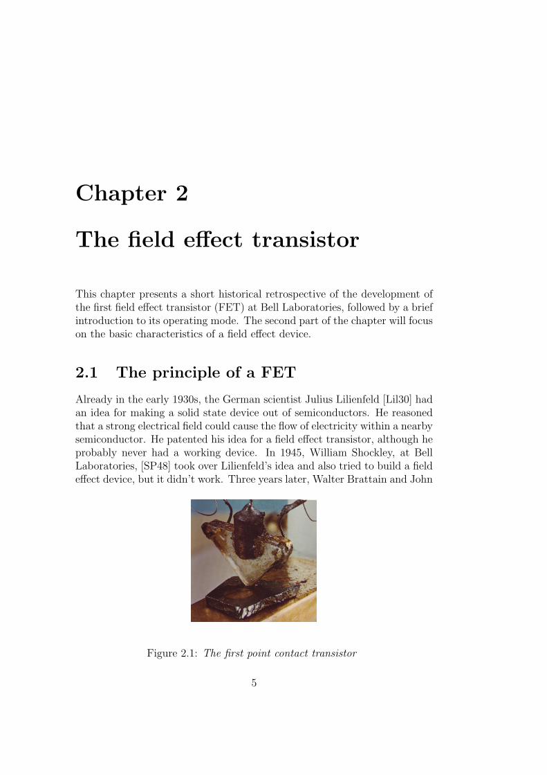
Already in the early 1930s, the German scientist Julius Lilienfeld [Lil30] hadan idea for making a solid state device out of semiconductors. He reasonedthat a strong electrical field could cause the flow of electricity within a nearbysemiconductor. He patented his idea for a field effect transistor, although heprobably never had a working device. In 1945, William Shockley, at BellLaboratories, [SP48] took over Lilienfeld’s idea and also tried to build a fieldeffect device, but it didn’t work. Three years later, Walter Brattain and John
Figure 2.1: The first point contact transistor
5
6 CHAPTER 2. THE FIELD EFFECT TRANSISTOR
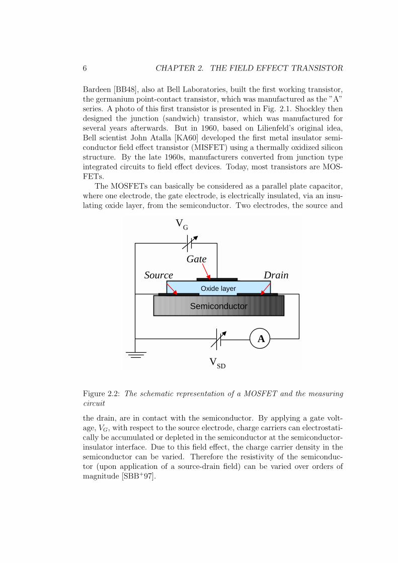
Bardeen [BB48], also at Bell Laboratories, built the first working transistor,the germanium point-contact transistor, which was manufactured as the ”A”series. A photo of this first transistor is presented in Fig. 2.1. Shockley thendesigned the junction (sandwich) transistor, which was manufactured forseveral years afterwards. But in 1960, based on Lilienfeld’s original idea,Bell scientist John Atalla [KA60] developed the first metal insulator semi-conductor field effect transistor (MISFET) using a thermally oxidized siliconstructure. By the late 1960s, manufacturers converted from junction typeintegrated circuits to field effect devices. Today, most transistors are MOS-FETs.
The MOSFETs can basically be considered as a parallel plate capacitor,where one electrode, the gate electrode, is electrically insulated, via an insu-lating oxide layer, from the semiconductor. Two electrodes, the source and
DrainGate
Semiconductor
Oxide layer
A
Source
VG
VSD
Figure 2.2: The schematic representation of a MOSFET and the measuringcircuit
the drain, are in contact with the semiconductor. By applying a gate volt-age, VG, with respect to the source electrode, charge carriers can electrostati-cally be accumulated or depleted in the semiconductor at the semiconductor-insulator interface. Due to this field effect, the charge carrier density in thesemiconductor can be varied. Therefore the resistivity of the semiconduc-tor (upon application of a source-drain field) can be varied over orders ofmagnitude [SBB+97].
2.1. THE PRINCIPLE OF A FET 7
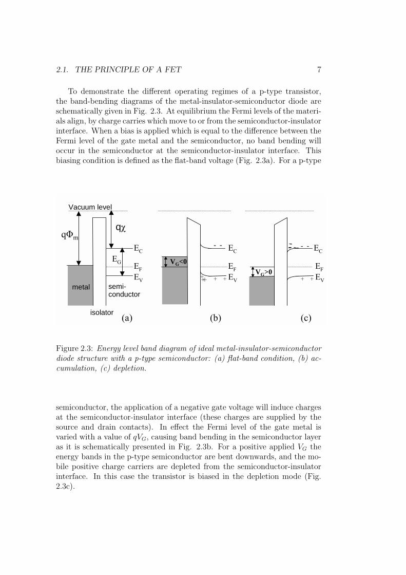
To demonstrate the different operating regimes of a p-type transistor,the band-bending diagrams of the metal-insulator-semiconductor diode areschematically given in Fig. 2.3. At equilibrium the Fermi levels of the materi-als align, by charge carries which move to or from the semiconductor-insulatorinterface. When a bias is applied which is equal to the difference between theFermi level of the gate metal and the semiconductor, no band bending willoccur in the semiconductor at the semiconductor-insulator interface. Thisbiasing condition is defined as the flat-band voltage (Fig. 2.3a). For a p-type
EC
qχ
Vacuum level
qΦm
EG
EV
EF
EC
metal
isolator
semi-conductor
(a)
EV
EC
EFVG<0
+ + ++
- -
+
(b)
EV
EFVG>0
-- - - -
+ +
(c)
-
Figure 2.3: Energy level band diagram of ideal metal-insulator-semiconductordiode structure with a p-type semiconductor: (a) flat-band condition, (b) ac-cumulation, (c) depletion.
semiconductor, the application of a negative gate voltage will induce chargesat the semiconductor-insulator interface (these charges are supplied by thesource and drain contacts). In effect the Fermi level of the gate metal isvaried with a value of qVG, causing band bending in the semiconductor layeras it is schematically presented in Fig. 2.3b. For a positive applied VG theenergy bands in the p-type semiconductor are bent downwards, and the mo-bile positive charge carriers are depleted from the semiconductor-insulatorinterface. In this case the transistor is biased in the depletion mode (Fig.2.3c).
8 CHAPTER 2. THE FIELD EFFECT TRANSISTOR
2.2 Basic characteristics of a FET
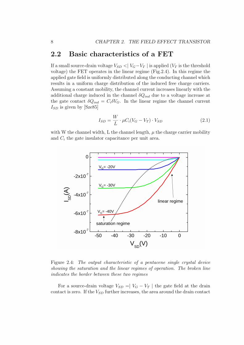
If a small source-drain voltage VSD <| VG−VT | is applied (VT is the thresholdvoltage) the FET operates in the linear regime (Fig.2.4). In this regime theapplied gate field is uniformly distributed along the conducting channel whichresults in a uniform charge distribution of the induced free charge carriers.Assuming a constant mobility, the channel current increases linearly with theadditional charge induced in the channel δQind due to a voltage increase atthe gate contact δQind = CiδVG. In the linear regime the channel currentISD is given by [Sze85]
ISD =W
L· µCi(VG − VT ) · VSD (2.1)
with W the channel width, L the channel length, µ the charge carrier mobilityand Ci the gate insulator capacitance per unit area.
-50 -40 -30 -20 -10 0-8x10⁻⁷
-6x10⁻⁷
-4x10⁻⁷
-2x10⁻⁷
0
I SD(A
)
VSD(V)
VG= -40V
VG= -30V
VG= -20V
saturation regime
linear regime
Figure 2.4: The output characteristic of a pentacene single crystal deviceshowing the saturation and the linear regimes of operation. The broken lineindicates the border between these two regimes
For a source-drain voltage VSD =| VG − VT | the gate field at the draincontact is zero. If the VSD further increases, the area around the drain contact
2.2. BASIC CHARACTERISTICS OF A FET 9
becomes depleted with no induced free carriers. This phenomenon is calledthe pinch-off effect and beyond this point the channel current saturates. Inthis regime, the channel current is given by [Sze85]
ISD =W
2L· µCi(VG − VT )2 (2.2)
Both the linear and the saturation regimes are indicated in the output char-acteristics (Fig.2.4) of a pentacene single crystal transistor. Note that in thesaturation regime the channel current quadratically increases with the gatevoltage in contrast to the linear regime.
The current in a MOSFET is transported predominantly by carriers ofone polarity only (e.g., holes in a p-type device). Therefore, the MOSFET isusually referred to as a unipolar device. This is the case for all the organicsingle crystal devices I investigated. Specifically, the p-type conductivityhas been observed, for instance, in anthracene, tetracene, pentacene, pery-lene, rubrene, whereas the n-type conductivity was observed in TCNQ andPerylene-TCNQ (see chapter 10). In principle, the unipolar operation can beexplained by the choice of metallic contacts that are efficient injectors of onlyone type of carrier. To realize an ambipolar transistor, which can operateas either an n-type and p-type transistor, holes and electrons have to be in-jected from the same electrode. The main difficulty therefore is that a goodcontact for one charge polarity typically results in an injection barrier forthe other polarity. However, this injection barrier can be reduced by using amaterial with a smaller energy gap. Furthermore, the width of an injectionbarrier can be narrowed by applying a large source and drain field, or by theaccumulation of high charge carrier densities in the channel by means of thefield-effect [Sze85]. For sufficiently high amounts of accumulated charge, theinjection barrier becomes small enough to allow tunnelling from the electrodeinto the semiconductor. Besides the small band gap of the semiconductor,the purity of the crystal material also plays an important role in minimizingtrapping effects. Only WSe2 (see chapter 12) fulfills these requirements andambipolar operation has been observed.
To evaluate the device performance, the main characteristics, includingthe charge carrier mobility (µ), the field-effect threshold (VT ), and the sub-threshold slope (S), were taken from the conventional MOSFET theory. Theyare summarized below.
2.2.1 Field-effect threshold
The threshold voltage VT is a measure of the amount of charge that mustbe electrostatically induced in order to switch on the electrical conduction in
10 CHAPTER 2. THE FIELD EFFECT TRANSISTOR
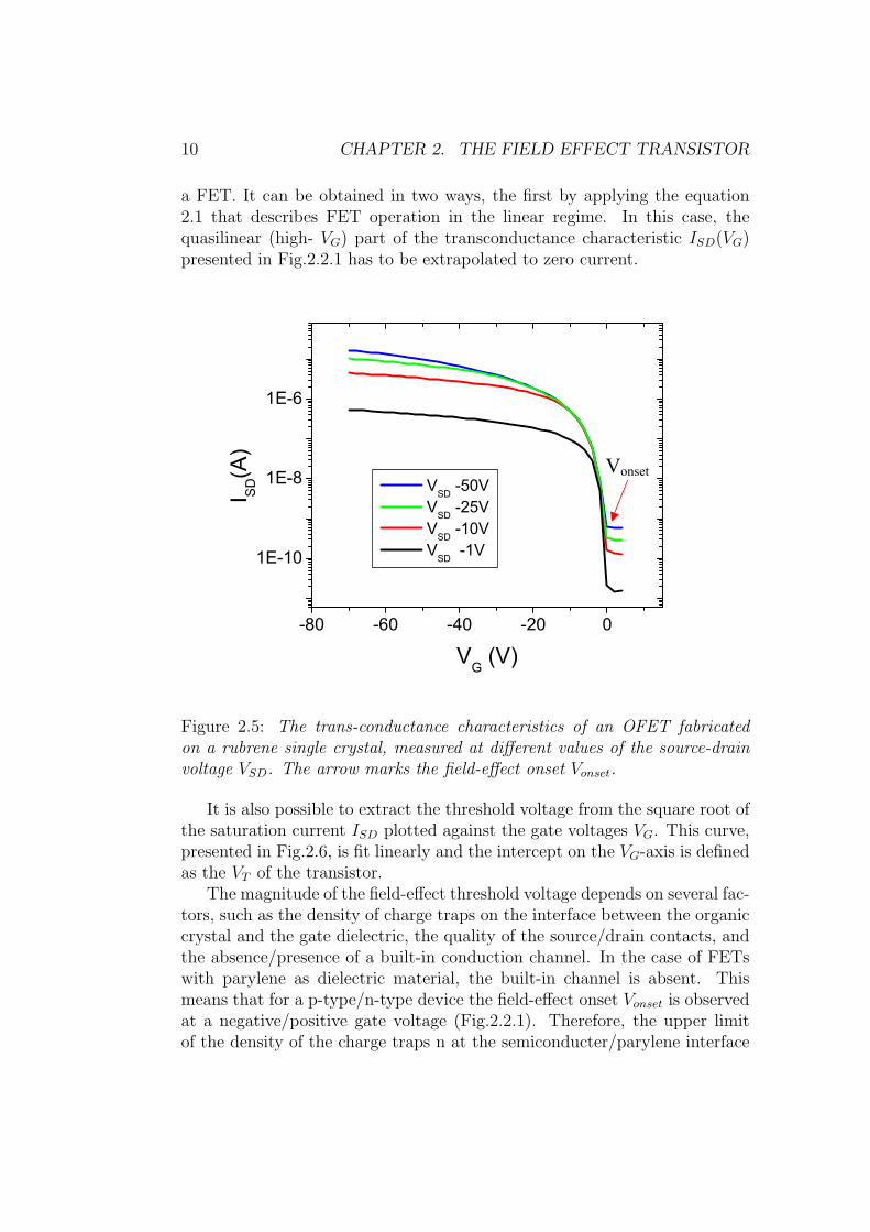
a FET. It can be obtained in two ways, the first by applying the equation2.1 that describes FET operation in the linear regime. In this case, thequasilinear (high- VG) part of the transconductance characteristic ISD(VG)presented in Fig.2.2.1 has to be extrapolated to zero current.
-80 -60 -40 -20 0
1E-10
1E-8
1E-6
VSD -50V VSD -25V VSD -10V VSD -1V
I SD(A
)
VG (V)
Vonset
Figure 2.5: The trans-conductance characteristics of an OFET fabricatedon a rubrene single crystal, measured at different values of the source-drainvoltage VSD. The arrow marks the field-effect onset Vonset.
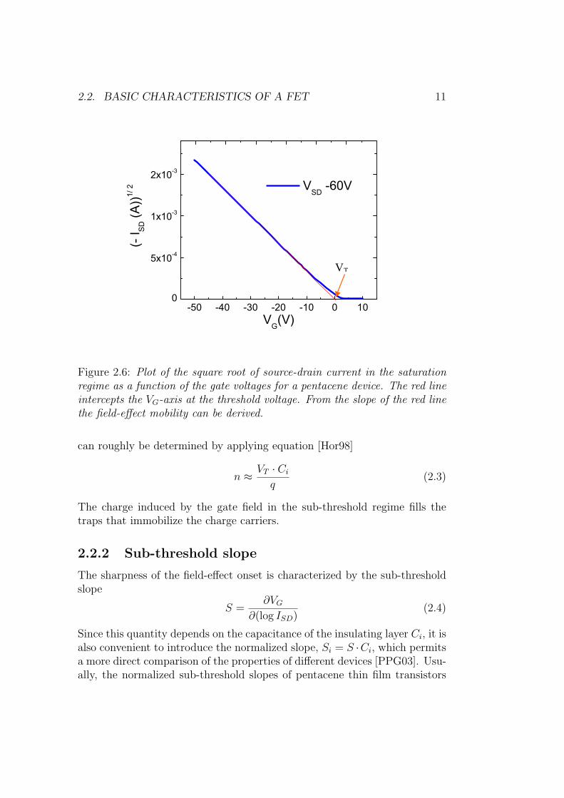
It is also possible to extract the threshold voltage from the square root ofthe saturation current ISD plotted against the gate voltages VG. This curve,presented in Fig.2.6, is fit linearly and the intercept on the VG-axis is definedas the VT of the transistor.
The magnitude of the field-effect threshold voltage depends on several fac-tors, such as the density of charge traps on the interface between the organiccrystal and the gate dielectric, the quality of the source/drain contacts, andthe absence/presence of a built-in conduction channel. In the case of FETswith parylene as dielectric material, the built-in channel is absent. Thismeans that for a p-type/n-type device the field-effect onset Vonset is observedat a negative/positive gate voltage (Fig.2.2.1). Therefore, the upper limitof the density of the charge traps n at the semiconducter/parylene interface
2.2. BASIC CHARACTERISTICS OF A FET 11
-50 -40 -30 -20 -10 0 100
5x10⁻⁴
1x10⁻³
2x10⁻³
VSD -60V
(- I S
D (A
))1/ 2
VG(V)
VT
Figure 2.6: Plot of the square root of source-drain current in the saturationregime as a function of the gate voltages for a pentacene device. The red lineintercepts the VG-axis at the threshold voltage. From the slope of the red linethe field-effect mobility can be derived.
can roughly be determined by applying equation [Hor98]
n ≈ VT · Ci
q(2.3)
The charge induced by the gate field in the sub-threshold regime fills thetraps that immobilize the charge carriers.
2.2.2 Sub-threshold slope
The sharpness of the field-effect onset is characterized by the sub-thresholdslope
S =∂VG
∂(log ISD)(2.4)
Since this quantity depends on the capacitance of the insulating layer Ci, it isalso convenient to introduce the normalized slope, Si = S ·Ci, which permitsa more direct comparison of the properties of different devices [PPG03]. Usu-ally, the normalized sub-threshold slopes of pentacene thin film transistors
12 CHAPTER 2. THE FIELD EFFECT TRANSISTOR
(Si = 15− 80V ·nF/decade · cm2) [DKP+99, DPK+99, LGNJ97] are referredto as a standard of comparison. However, for single crystal devices, a smallervalue of Si can be achieved. So far, pentacene (Si = 3V ·nF/decade·cm2)(seechapter 6) and rubrene (1.7V ·nF/decade·cm2) [PSL+03] single crystal FETsexhibit the sharpest field-effect onset.
It is commonly believed that the sub-threshold slope is mainly determinedby the quality of the insulator/semiconductor interface [Sze85]. This is def-initely the case for Si MOSFETs, where the resistance of source and draincontacts is low and does not depend on the gate voltage. In contrast, thecontact resistance in the OFETs (Schottky-type FETs) is high; it dependsnon-linearly on VG as the result. The subthreshold slope also reflects thequality of contacts (see also chapter 9).
2.2.3 Field-effect mobility
Starting from the trans-conductance characteristics, the mobility of carriersµ at the surface of single crystals can be estimated in the linear regime ofthe device operation by applying Eq. 2.5 [Sze85].
µ =L
W · Ci · VSD
· (∂ISD
∂VG
) (2.5)
There, the conductivity of the channel (σ = enµ) varies linearly with thedensity of mobile field-induced charges n. This definition of µ assumes thatall charge carriers with the density
n =Ci · (VG − VT )
e(2.6)
induced by the transverse electric field above the threshold, are mobile. Forrubrene single crystal devices, this assumption can be justified, because onlya very weak dependence µ(VG) is observed. However, the mobilities in otherorganic devices and amorphous silicon (α-Si:H) FETs [SHS89] are stronglyVG-dependent. In these cases, most of the charge above the field-effect thresh-old is induced into the in-gap localized states and only a small fraction isinduced into the conduction band. For this reason, the calculated value ofthe mobility, using Eq. 2.5, is underestimated.
Additionally, the field-effect mobility µ can also be derived from the gatevoltage dependence of the saturation current by applying Eq. 2.2. The plotof the square root of ISD versus the VG leads to a straight line (Fig.2.6).
µ =2L
Ci ·W· (∂
√ISD
∂VG
)2 (2.7)
2.2. BASIC CHARACTERISTICS OF A FET 13
As shown by Eq.2.7, the mobility increases quadratically with the slope ofthis line.
For the different crystal materials that have been investigated the mo-bility of the field-induced carriers varies over a wide range (see chapter 11).Distinguished are rubrene and WSe2 with a hole mobility of 13 cm2/Vs and475 cm2/Vs measured at room temperature.
14 CHAPTER 2. THE FIELD EFFECT TRANSISTOR
Chapter 3
The crystal material
The field effect geometry allows me to investigate the transport properties ofvarious organic as well as inorganic single crystals. To investigate the chargetransport in these crystal materials, different models are introduced.
3.1 Charge transport in organic single crys-
tals
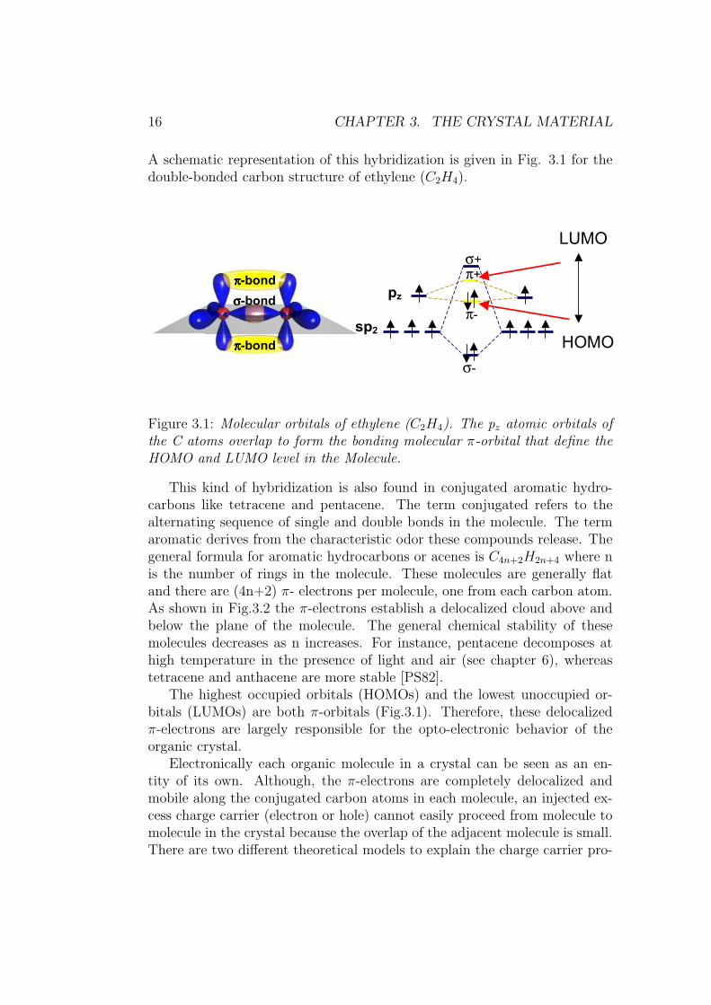
Molecular crystals are composed of discrete molecules held together by weakvan der Waals forces and the molecules themselves consist of atoms heldtogether by covalent bonds. For this reason, the crystals are quite brittle,exhibit low melting points and often show poor electrical conductivity. Be-cause of the weak nature of the bonding between molecules in a molecularsolid, it is to be expected that the properties of the individual molecule areretained in the solid state to a far greater extend than would be found insolids exhibiting other types of bonding. It is therefore important to under-stand the properties of atomic carbon itself and the intramolecular bondingmechanisms of hydrocarbons [PS82].
Carbon, in the ground state, has four electrons in the outer electroniclevel. The orbitals of these electron may mix under the creation of fourequivalent degenerate orbitals, referred to as sp3 hybrid orbitals in a tetra-hedral orientation around the carbon atom. Methane exemplifies this typeof bond. If only three chemical bonds are formed, they have three coplanarsp2 hybridized orbitals which are at an angle of 120 apart from each other.These bonds are called σ-bonds, and are associated with a highly localizedelectron density in the plane of the molecule. The one remaining free electronper carbon atom resides in the pz orbital, perpendicular to the plane of thesp2. The pz on the neighboring atoms overlap to form so called π-bonds.
15
16 CHAPTER 3. THE CRYSTAL MATERIAL
A schematic representation of this hybridization is given in Fig. 3.1 for thedouble-bonded carbon structure of ethylene (C2H4).
ππππ-bond
ππππ-bond
σσσσ-bond
σ+ π+
σ-
π-
pz
sp2
LUMO
HOMO
Figure 3.1: Molecular orbitals of ethylene (C2H4). The pz atomic orbitals ofthe C atoms overlap to form the bonding molecular π-orbital that define theHOMO and LUMO level in the Molecule.
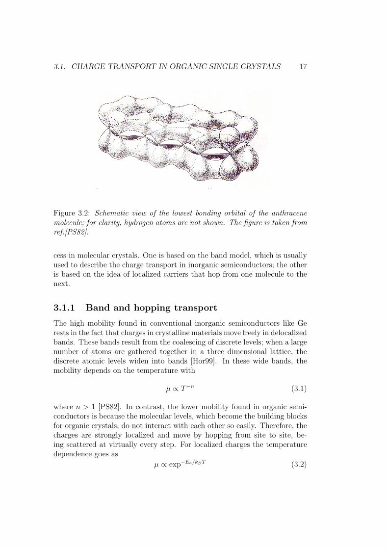
This kind of hybridization is also found in conjugated aromatic hydro-carbons like tetracene and pentacene. The term conjugated refers to thealternating sequence of single and double bonds in the molecule. The termaromatic derives from the characteristic odor these compounds release. Thegeneral formula for aromatic hydrocarbons or acenes is C4n+2H2n+4 where nis the number of rings in the molecule. These molecules are generally flatand there are (4n+2) π- electrons per molecule, one from each carbon atom.As shown in Fig.3.2 the π-electrons establish a delocalized cloud above andbelow the plane of the molecule. The general chemical stability of thesemolecules decreases as n increases. For instance, pentacene decomposes athigh temperature in the presence of light and air (see chapter 6), whereastetracene and anthacene are more stable [PS82].
The highest occupied orbitals (HOMOs) and the lowest unoccupied or-bitals (LUMOs) are both π-orbitals (Fig.3.1). Therefore, these delocalizedπ-electrons are largely responsible for the opto-electronic behavior of theorganic crystal.
Electronically each organic molecule in a crystal can be seen as an en-tity of its own. Although, the π-electrons are completely delocalized andmobile along the conjugated carbon atoms in each molecule, an injected ex-cess charge carrier (electron or hole) cannot easily proceed from molecule tomolecule in the crystal because the overlap of the adjacent molecule is small.There are two different theoretical models to explain the charge carrier pro-
3.1. CHARGE TRANSPORT IN ORGANIC SINGLE CRYSTALS 17
Figure 3.2: Schematic view of the lowest bonding orbital of the anthracenemolecule; for clarity, hydrogen atoms are not shown. The figure is taken fromref.[PS82].
cess in molecular crystals. One is based on the band model, which is usuallyused to describe the charge transport in inorganic semiconductors; the otheris based on the idea of localized carriers that hop from one molecule to thenext.
3.1.1 Band and hopping transport
The high mobility found in conventional inorganic semiconductors like Gerests in the fact that charges in crystalline materials move freely in delocalizedbands. These bands result from the coalescing of discrete levels; when a largenumber of atoms are gathered together in a three dimensional lattice, thediscrete atomic levels widen into bands [Hor99]. In these wide bands, themobility depends on the temperature with
µ ∝ T−n (3.1)
where n > 1 [PS82]. In contrast, the lower mobility found in organic semi-conductors is because the molecular levels, which become the building blocksfor organic crystals, do not interact with each other so easily. Therefore, thecharges are strongly localized and move by hopping from site to site, be-ing scattered at virtually every step. For localized charges the temperaturedependence goes as
µ ∝ exp−Ea/kBT (3.2)
18 CHAPTER 3. THE CRYSTAL MATERIAL
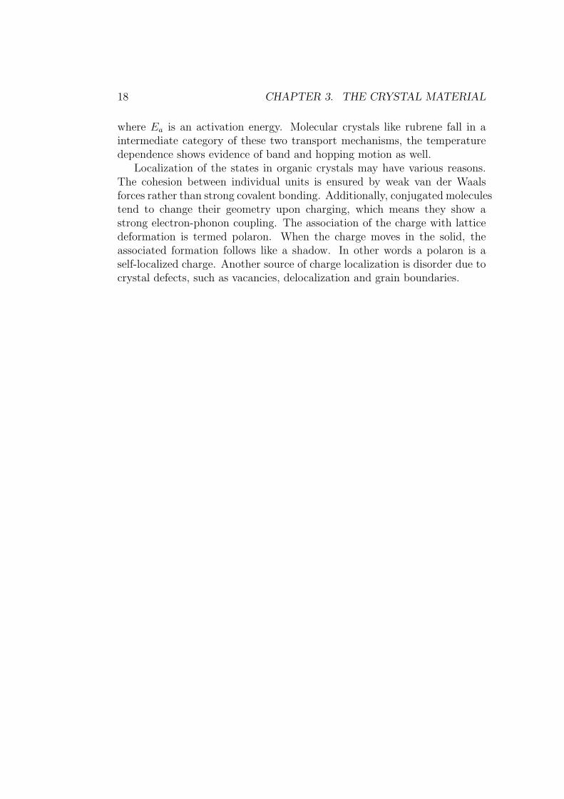
where Ea is an activation energy. Molecular crystals like rubrene fall in aintermediate category of these two transport mechanisms, the temperaturedependence shows evidence of band and hopping motion as well.
Localization of the states in organic crystals may have various reasons.The cohesion between individual units is ensured by weak van der Waalsforces rather than strong covalent bonding. Additionally, conjugated moleculestend to change their geometry upon charging, which means they show astrong electron-phonon coupling. The association of the charge with latticedeformation is termed polaron. When the charge moves in the solid, theassociated formation follows like a shadow. In other words a polaron is aself-localized charge. Another source of charge localization is disorder due tocrystal defects, such as vacancies, delocalization and grain boundaries.
3.1. CHARGE TRANSPORT IN ORGANIC SINGLE CRYSTALS 19
Applied voltage
•Delocalized electron
Lattice vibration•
•Scattered electron
Lattice vibration
•• •
Electron localizedby defectsor disorder
•• •
•• •
(b) Hopping conduction
(a) Band type conduction
Figure 3.3: Transport mechanisms in solids. (a) Band transport. In a perfectcrystal, depicted as the straight line, a free carrier is delocalized, and it movesas a plane wave without scattering. In a real crystal, there are always latticevibrations or phonons that disrupt the crystal symmetry. These phononsscatter the electron and thereby reduce its mobility. Lowering the temperaturewill therefore increase the mobility. (b) Hopping transport. If the carrieris localized due to defects, disorder or selflocalization, e.g. in the case ofpolarons, the lattice vibrations are essential for a carrier to move from onesite to another. For hopping transport the mobility increases with increasingtemperature. The figure is adapted from ref. [PS82]
20 CHAPTER 3. THE CRYSTAL MATERIAL
3.1.2 The concept of polaron hopping
As already mentioned above, the quasiparticle polaron results from the cou-pling of charge with the deformation of the lattice associated with the charge.The polaron is termed ”small” when the deformation region is comparable tothe size of the molecule. The theory of small polaron transport was alreadydeveloped in the late fifties by Yamashita and Kurosawa [YK58], and Hol-stein [Hol59]. In this theory, Holstein used a used a Hamiltonien composedof three terms, one that accounts for the lattice, the second for the electronand the last one for the electron phonon coupling. The lattice componentconsists of a sum of harmonic oscillators that vibrate at a frequency ωo. Thedominant parameter of the electron component is J, the so-called electrontransfer, or overlap integral. The magnitude of the electron-phonon couplingcan be quantified through the so-called polaron binding energy Eb, whichcorresponds to the energy gain due to the polarisation and deformation ofthe lattice. The small polaron limit corresponds to strong coupling, whereEb J , in which case the electronic term can be treated as a perturbation.Polaron motion takes place via a succession of random jumps, in each ofwhich the electron hops to the neighbor site. Later, the concept of polaronhopping was improved by Emin [Emi85]. He introduced the concept of co-incidence, where site jumps occur when the energy state of the second sitecoincidences with the first one. Such a coincidence is achieved by thermaldeformation of the lattice. Emin [EH69] also made a distinction betweenadiabatic and non-adiabatic processes. In the former, the lifetime of the co-incidence is much larger than the electron transit time, in which case theelectron has time to follow the lattice deformations. In the high temperaturelimit, the mobility of the adiabatic small polaron is given by Eq.3.3.
µ =ωoqδ
2
2πkBT· exp(− Eb
kBT) (3.3)
Here δ stands for the mean intermolecular distance. At low temperatures,the variation of the mobility is found to deviate from the thermally activatedlaw [Hor99].
3.1.3 Multiple trapping and release model
The temperature dependent transport data for organic single crystals can alsobe interpreted in terms of a multiple trapping and release model. In fact, thismodel has been developed to account for the charge transport in amorphoussilicon[LS70], where the carrier mobility is significantly lower than for singlecrystals. This comes from localized levels (traps) in the energy gap, due to
3.1. CHARGE TRANSPORT IN ORGANIC SINGLE CRYSTALS 21
defects like dangling bounds in the amorphous material. However, the modelcan also be applied [PMB+04] to explain the thermally activated and gatebias dependent behavior of field-effect mobility in an organic single crystal.
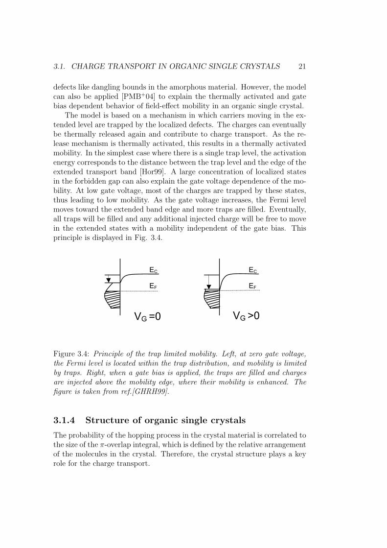
The model is based on a mechanism in which carriers moving in the ex-tended level are trapped by the localized defects. The charges can eventuallybe thermally released again and contribute to charge transport. As the re-lease mechanism is thermally activated, this results in a thermally activatedmobility. In the simplest case where there is a single trap level, the activationenergy corresponds to the distance between the trap level and the edge of theextended transport band [Hor99]. A large concentration of localized statesin the forbidden gap can also explain the gate voltage dependence of the mo-bility. At low gate voltage, most of the charges are trapped by these states,thus leading to low mobility. As the gate voltage increases, the Fermi levelmoves toward the extended band edge and more traps are filled. Eventually,all traps will be filled and any additional injected charge will be free to movein the extended states with a mobility independent of the gate bias. Thisprinciple is displayed in Fig. 3.4.
EC
EF
EC
EF
VG =0 VG >0
Figure 3.4: Principle of the trap limited mobility. Left, at zero gate voltage,the Fermi level is located within the trap distribution, and mobility is limitedby traps. Right, when a gate bias is applied, the traps are filled and chargesare injected above the mobility edge, where their mobility is enhanced. Thefigure is taken from ref.[GHRH99].
3.1.4 Structure of organic single crystals
The probability of the hopping process in the crystal material is correlated tothe size of the π-overlap integral, which is defined by the relative arrangementof the molecules in the crystal. Therefore, the crystal structure plays a keyrole for the charge transport.
22 CHAPTER 3. THE CRYSTAL MATERIAL
The strong interactions between the atoms determine the packing in co-valent and ionic crystals. In covalent crystals, the electronic distribution willbe localized in preferred directions, due to the fact that electron pairs areshared between the atoms. An example therefore is diamond, where all fourelectrons in the outer electronic level of carbon participate and form covalentbonds, building tetrahedrons with fixed angles. The ions in ionic crystalscan be approximated as charged spheres, which are bonded by electrostaticinteractions. Because of the spherical nature of the atoms and the rela-tively strong interactions between them, the crystal structure can be seen asformed by closed packing of anions (cations) with the cations (anions) fillingthe tetrahedral and octahedral holes.
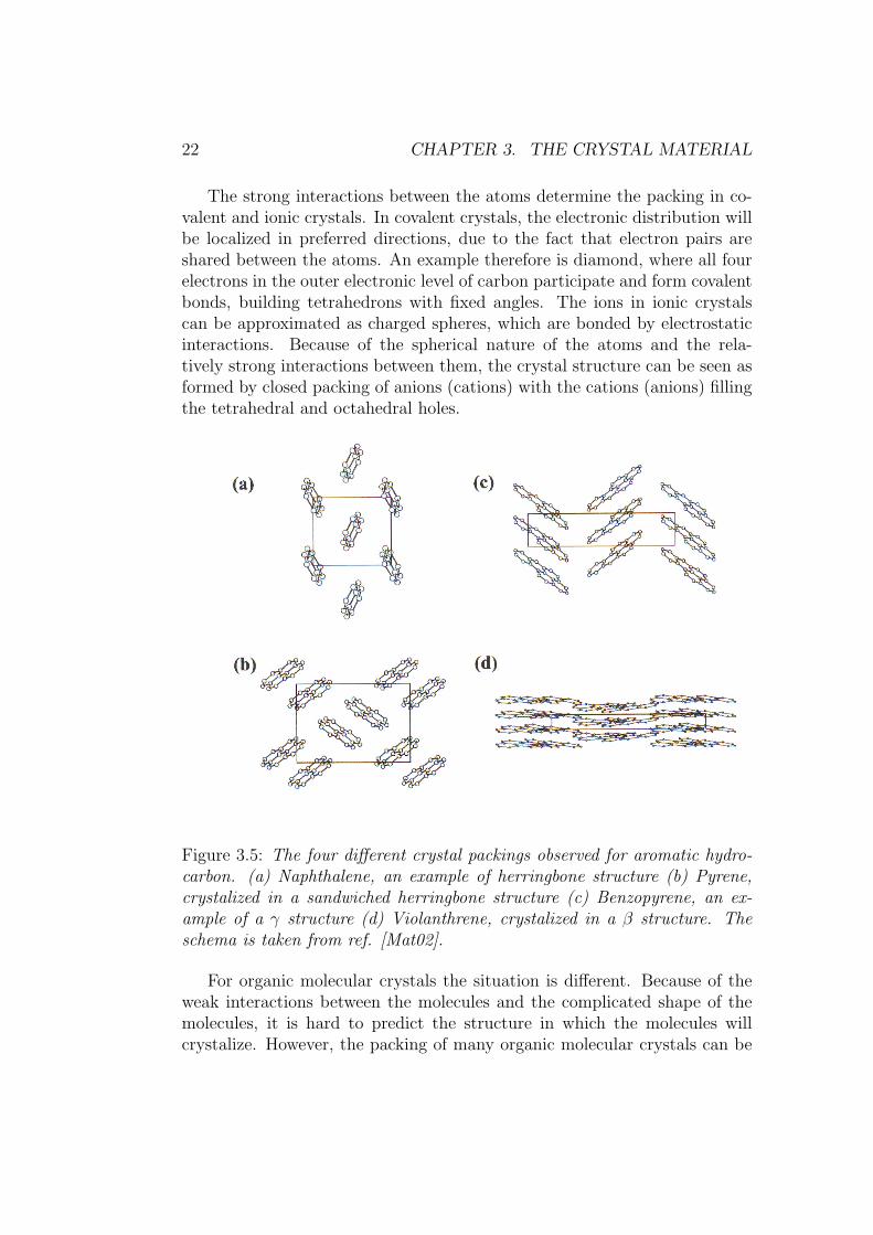
Figure 3.5: The four different crystal packings observed for aromatic hydro-carbon. (a) Naphthalene, an example of herringbone structure (b) Pyrene,crystalized in a sandwiched herringbone structure (c) Benzopyrene, an ex-ample of a γ structure (d) Violanthrene, crystalized in a β structure. Theschema is taken from ref. [Mat02].
For organic molecular crystals the situation is different. Because of theweak interactions between the molecules and the complicated shape of themolecules, it is hard to predict the structure in which the molecules willcrystalize. However, the packing of many organic molecular crystals can be
3.2. TRANSITION METAL DICHALCOGENIDES 23
classified into some general structure types. Based on a study that Gavez-zotti et al. [GD88] performed on planar aromatic hydrocarbons, four basicstructural types were defined. These four crystal types are shown in Fig. 3.5.All of these crystal types are built in a layered structure, but the structurein the layers varies from type to type. Naphthalene is a prime example of aherringbone structure. In addition to naphthalene, anthracene and tetracenewere also found to crystalize in this particular structure. In the second typetwo parallel oriented molecules together form a herringbone structure. Thiscrystal arrangement is called sandwiched herringbone structure. The thirdstructure type is characterized by a shorter axis length, therefore the her-ringbone pattern is flattened in one direction. This is even more the case forthe final type, the β-structure, which is closely related to the graphite struc-ture and the crystal structures of layered transition metal dichalcogenides.In his attempt to link the the geometrical properties of the molecule with thecrystal structure Gavezotti et al. found some general trends. Disk-shapedmolecules tend to crystallize into β structures, because the C-C interactionspromote parallel stacking whereas elongated molecules with H-atoms on therim prefer herringbone stacking. However, a given substance may crystal-lize in various structures: especially for copper phthalocyanine [MT83] andpentacene [Mat02] many polymorphisms are known.
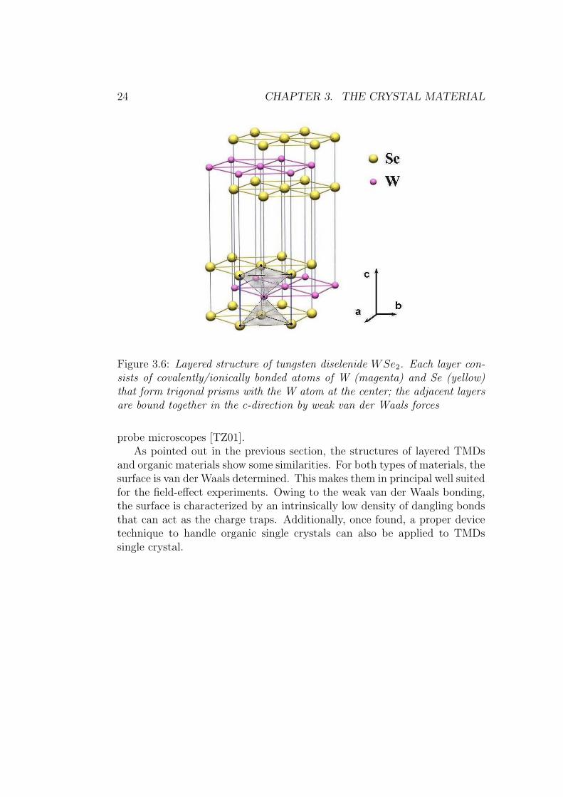
3.2 Transition metal dichalcogenides
The transition metal dichalcogenides (TMDs) belong to the class of layeredinorganic semiconductors with a chemical formula MX2, where M stands fora transition metal and X - for Se, S or Te [Lie77, Buc92]. Single crystals ofTMDs are formed by stacks of X-M-X layers (Fig. 3.6). Atoms within eachlayer are held together by strong covalent-ionic mixed bonds, whereas the lay-ers are weakly bonded to each other by van der Waals forces. The bondinganisotropy defines the unique morphology of single crystals of these com-pounds as thin, flexible and easy-to-cleave platelets with atomically smooth(a,b)-facets. The electronic properties of TMDs vary from semiconducting(e.g. WSe2) to superconducting (e.g. NbSe2) [Lie77, Buc92]. The semicon-ducting members of this class are considered to be promising materials forsolar cells, photoelectrochemical cells and p-n-junctions [SELS+83, SLSO+85,TW85]. Similarly to graphite, the layered TMDs can form nanostructures,such as fullerene-like nanoparticles [TMGH92], nanocrystals [ZLH+96] andnanotubes [Rem01]. Because of the outstanding chemical inertness andunique shapes of these nanostructures, they may have numerous potentialapplications ranging from solid lubricants [Rap97] to the tips in scanning
24 CHAPTER 3. THE CRYSTAL MATERIAL
Figure 3.6: Layered structure of tungsten diselenide WSe2. Each layer con-sists of covalently/ionically bonded atoms of W (magenta) and Se (yellow)that form trigonal prisms with the W atom at the center; the adjacent layersare bound together in the c-direction by weak van der Waals forces
probe microscopes [TZ01].As pointed out in the previous section, the structures of layered TMDs
and organic materials show some similarities. For both types of materials, thesurface is van der Waals determined. This makes them in principal well suitedfor the field-effect experiments. Owing to the weak van der Waals bonding,the surface is characterized by an intrinsically low density of dangling bondsthat can act as the charge traps. Additionally, once found, a proper devicetechnique to handle organic single crystals can also be applied to TMDssingle crystal.
Chapter 4
Device fabrication
In this chapter, I will outline the individual steps to fabricate a field effecttransistor. After a presentation of the crystal growth for organic materialsand transition metal dichalcogenides, I will focus on the difficulties of gentlydepositing electrodes and a dielectric layer for a ready device.
4.1 Crystal growth
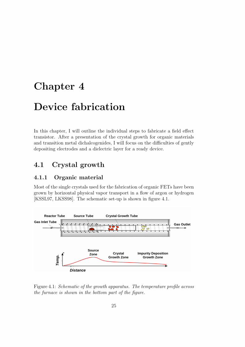
4.1.1 Organic material
Most of the single crystals used for the fabrication of organic FETs have beengrown by horizontal physical vapor transport in a flow of argon or hydrogen[KSSL97, LKSS98]. The schematic set-up is shown in figure 4.1.
Crystal Growth TubeSource TubeReactor Tube
Gas OutletGas Inlet Tube
Distance
Tem
p.
Source Zone Crystal
Growth ZoneImpurity Deposition
Growth Zone
Figure 4.1: Schematic of the growth apparatus. The temperature profile acrossthe furnace is shown in the bottom part of the figure.
25
26 CHAPTER 4. DEVICE FABRICATION
The crystals are grown in a horizontal two-zone furnace. The startingmaterial volatilizes and is carried away from the source zone by a stream ofgas. In the growth zone crystals nucleate and grow free-standing, stress-freeinto the quartz tube. In addition, the growth technique is a very efficientpurification technique. More volatile impurities will condense in the impu-rity deposition zone, and less volatile impurities will remain in the sourcezone. The evaporating material is heated to typically around 300°C in thefirst zone of a two-zone furnace. The second zone of the furnace is held atapproximately 200°. Of course, the temperature of the furnace has to be ad-justed for each substance individually. For instance, copper phthalocyaninehas a lower vapor pressure [YTAKK95] than rubrene [BGMP04]; therefore ahigher source temperature is required for its growth. Heating is applied by aresistance wire and using thermocouples the temperature can be checked andstabilized. The horizontal setting is used for experimental convenience. Theadvantage of this geometry is that the starting material can be inserted eas-ily and both the residual starting material and the crystals can be removedeasily after growth.
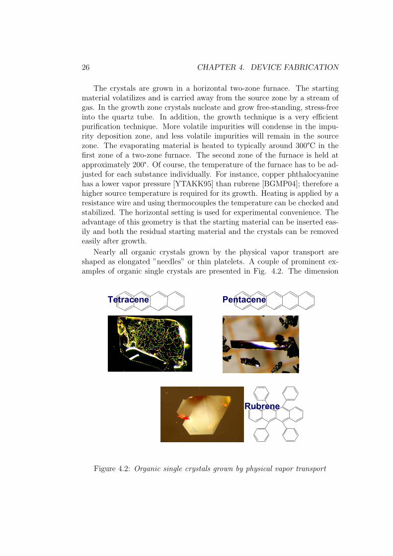
Nearly all organic crystals grown by the physical vapor transport areshaped as elongated ”needles” or thin platelets. A couple of prominent ex-amples of organic single crystals are presented in Fig. 4.2. The dimension
Pentacene Tetracene
Rubrene
Figure 4.2: Organic single crystals grown by physical vapor transport
4.1. CRYSTAL GROWTH 27
of the crystals can range from several millimeters to several centimeters inwidth and length. The crystal thickness also varies between 10 and 400µm.
Many authors [JBP04, BGMP04, BLR04] claim that to achieve a highfield effect mobility, the starting material must be pre-purified using severalre-growth cycles. This conclusion is different from my experience. Impuritiesthat can act as traps for charge carriers and therefore reduce the field effectmobility exist not only as byproducts in the commercial powder, they are alsoformed during the growth process. Photo-induced reactions with O2 and theformation of other disproportionation products are known for most organicmolecules [JBP04, RKT+]. Consequently, using multiple sublimations, espe-cially for growth processes performed in the light and at high temperatures,might lead to increased impurities and could seriously deteriorate the desiredelectronic transport properties of the crystals.
In some experiments (see chapters 5 and 6), I used crystals which weregrown in a sealed ampoule. Therefore, previously sublimed crystals, grownin a flow of inert gas, were further used for typical vacuum-sealed ampoulegrowth. This last procedure resulted in crystals growing in smaller temper-ature gradients close to thermodynamic equilibrium and produced thickercrystals.
4.1.2 Transition metal dichalcogenides
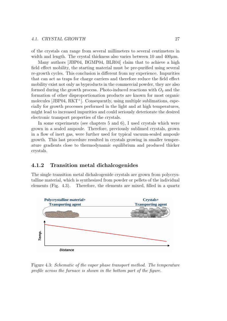
The single transition metal dichalcogenide crystals are grown from polycrys-talline material, which is synthesized from powder or pellets of the individualelements (Fig. 4.3). Therefore, the elements are mixed, filled in a quartz
Crystals+Transporting agent
Polycrystalline material+Transporting agent
Distance
Tem
p.
Figure 4.3: Schematic of the vapor phase transport method. The temperatureprofile across the furnace is shown in the bottom part of the figure.
28 CHAPTER 4. DEVICE FABRICATION
tube and sealed under vacuum to remove oxygen as a reactant. To facilitatethe sealing of the tube, inert helium gas is introduced into the tube. Thetube is sealed using a hydrogen-oxygen torch. To make sure that a reactionoccurs, the ampoules are kept at high temperatures (below 600°C) for sev-eral days. In the next step the crystals are grown by vapor phase transport.Here, the polycrystalline material plus the transporting agent like I2, Se andS are inserted at one end of a silica tube and sealed. Then, the ampoule isplaced in a two zone furnace and kept in a temperature gradient going fromaround 900°C to 1000°C. The schematic of the vapor phase transport method(VPT) is displayed in Fig. 4.3. Within several weeks, up to 300 µm thickand 1-2 cm2 large platelets are formed. Some results of these crystal growthprocesses are shown in Fig. 4.4.
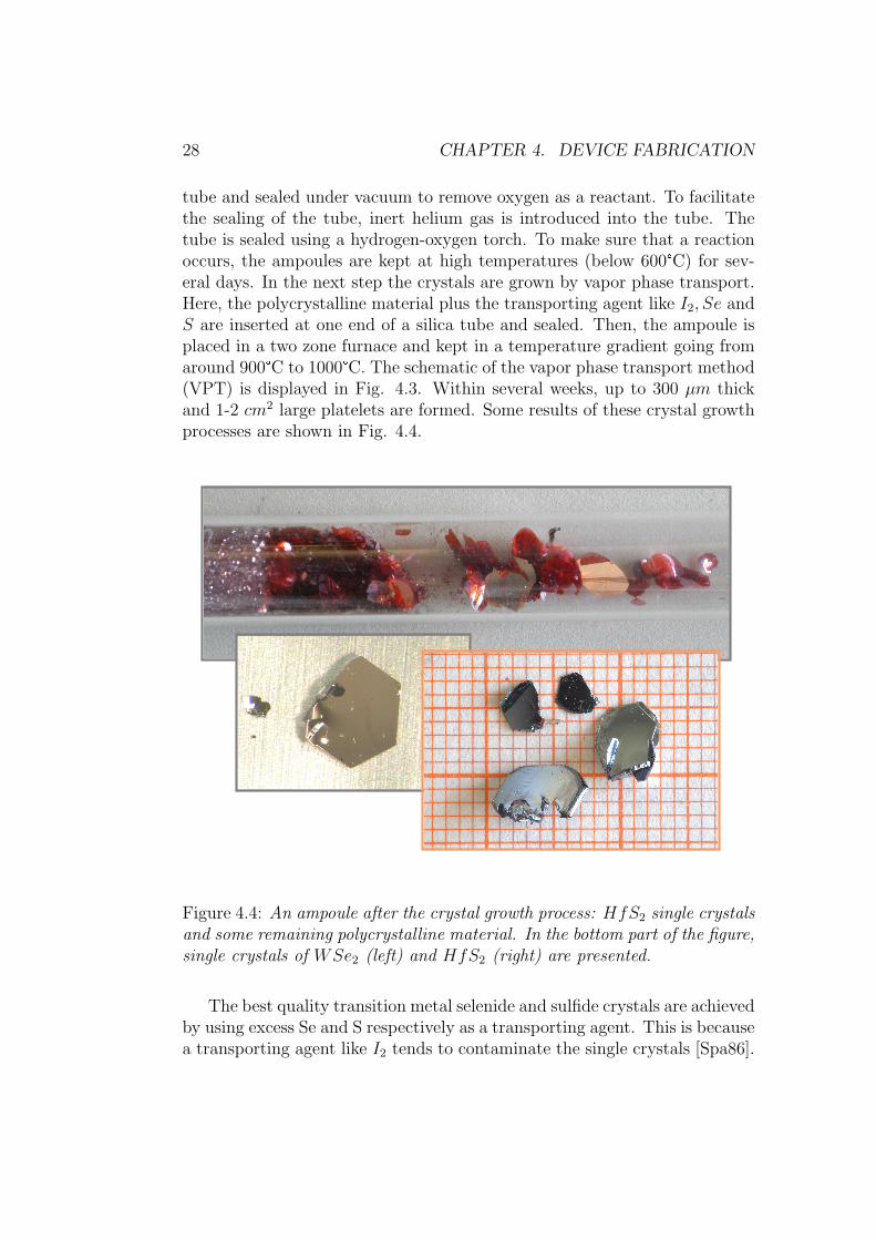
Figure 4.4: An ampoule after the crystal growth process: HfS2 single crystalsand some remaining polycrystalline material. In the bottom part of the figure,single crystals of WSe2 (left) and HfS2 (right) are presented.
The best quality transition metal selenide and sulfide crystals are achievedby using excess Se and S respectively as a transporting agent. This is becausea transporting agent like I2 tends to contaminate the single crystals [Spa86].
4.2. FABRICATION OF THE FET STRUCTURES 29
4.2 Fabrication of the FET structures
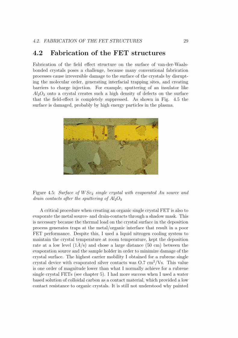
Fabrication of the field effect structure on the surface of van-der-Waals-bonded crystals poses a challenge, because many conventional fabricationprocesses cause irreversible damage to the surface of the crystals by disrupt-ing the molecular order, generating interfacial trapping sites, and creatingbarriers to charge injection. For example, sputtering of an insulator likeAl2O3 onto a crystal creates such a high density of defects on the surfacethat the field-effect is completely suppressed. As shown in Fig. 4.5 thesurface is damaged, probably by high energy particles in the plasma.
Figure 4.5: Surface of WSe2 single crystal with evaporated Au source anddrain contacts after the sputtering of Al2O3
A critical procedure when creating an organic single crystal FET is also toevaporate the metal source- and drain-contacts through a shadow mask. Thisis necessary because the thermal load on the crystal surface in the depositionprocess generates traps at the metal/organic interface that result in a poorFET performance. Despite this, I used a liquid nitrogen cooling system tomaintain the crystal temperature at room temperature, kept the depositionrate at a low level (1A/s) and chose a large distance (50 cm) between theevaporation source and the sample holder in order to minimize damage of thecrystal surface. The highest carrier mobility I obtained for a rubrene singlecrystal device with evaporated silver contacts was O.7 cm2/Vs. This valueis one order of magnitude lower than what I normally achieve for a rubrenesingle crystal FETs (see chapter 5). I had more success when I used a waterbased solution of colloidal carbon as a contact material, which provided a lowcontact resistance to organic crystals. It is still not understood why painted
30 CHAPTER 4. DEVICE FABRICATION
graphite contacts act so well for the charge injection in organic FETs. Severalattempts to create a home-made conducting paste based on gold powder withproperties similar to the purchased carbon paint failed even though gold hasthe same work-function as graphite (4.8 eV). A disadvantage of this methodis that it is often painstakingly difficult to prepare small and nicely-shapedcontacts on the hydrophobic surfaces of the organic crystals.
In the future, it would be useful to better understand the mechanism ofdamaging of organic crystals in the process of contact fabrication in order tomake the preparation of high-quality contacts routinely possible with manydifferent metals. In particular, preparation of high quality contacts will helpto elucidate the role of the work function of the metallic electrodes, whichseems to play a less prominent role than was initially expected [VFO+04,BGMP04].
Concerning this matter, transition metal dichalcogenides are more robust.In general, the thermal deposition of metals on the crystal surface is trouble-free; it is even possible to sputter the contacts. Occasionally, I observedinstead of homogenous metal overlayers the formation of three-dimensionalmetal clusters, because the interaction between the surface of van-der-Waals-bonded crystal and adsorbed metals is weak.
After many attempts, it became clear that sputtering of Al2O3, as wellas other dielectrics like SiO2 and Teflon on the surface of the crystals willnot lead to a working device. An experience which I share with all researchgroups active in this field. So for a long time, finding a suitable gate dielec-tric material and therefore the right technique, was the limiting step in thedevice fabrication. The breakthrough came with using thin polymer filmsof parylene as a gate dielectric material [DFG+98, PPG03]. Parylene wasdeveloped over thirty years ago primarily to provide a protective coating forprinted circuit boards. Today, it is also used for medical coating applications.This material with a dielectric constant ε= 2.65 forms transparent pinhole-free conformal coatings with excellent mechanical and dielectric properties:the breakdown electric field can be as high as ∼10 MV/cm for the thickness0.1µm.
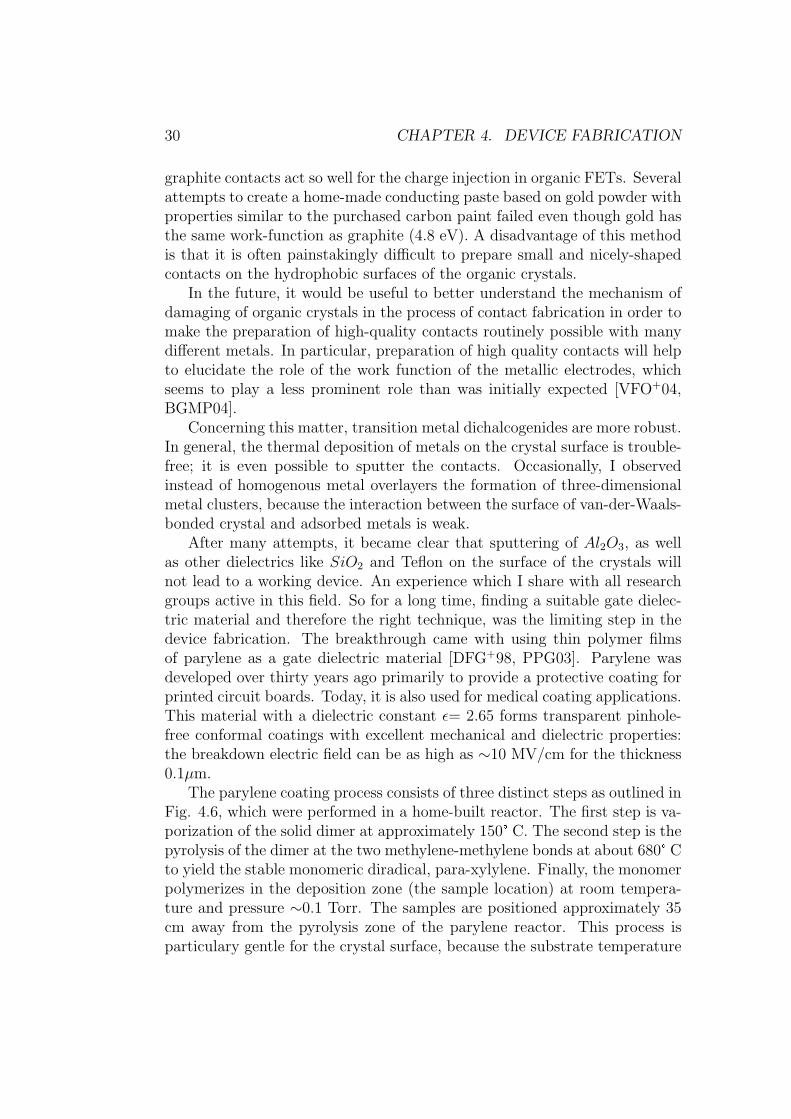
The parylene coating process consists of three distinct steps as outlined inFig. 4.6, which were performed in a home-built reactor. The first step is va-porization of the solid dimer at approximately 150° C. The second step is thepyrolysis of the dimer at the two methylene-methylene bonds at about 680° Cto yield the stable monomeric diradical, para-xylylene. Finally, the monomerpolymerizes in the deposition zone (the sample location) at room tempera-ture and pressure ∼0.1 Torr. The samples are positioned approximately 35cm away from the pyrolysis zone of the parylene reactor. This process isparticulary gentle for the crystal surface, because the substrate temperature
4.2. FABRICATION OF THE FET STRUCTURES 31
never rises more than a few degrees above ambient and since parylene ischemically inert it does not react with crystal material. A necessary fourthcomponent in this system is the mechanical vacuum pump and associatedprotective traps. It is important to mention that parylene was depositedonto the crystals with prefabricated source and drain contacts with wiresalready attached, otherwise connecting the contact pads might be difficult.This is simply because parylene uniformly covers the hole sample and thesample holder. The thickness of the parylene layers was determined with a
DimerDi-Para-Xylene
CH2H2C
CH2H2C
vaporizer
175ºC
1 Torr
Monomer
CH2CH2
CH2 CH2
Pyrolysis furnace
650ºC
0.5 Torr
PolymerPoly(Para-Xylene)
CH2H2C
n
Depositionchamber
ColdTrap
25ºC
0.1 Torr
-200ºC
0.001 Torr
Figure 4.6: The parylene coating process
profilometer. They ranged between 0.5 and 1.7µm. From this value (t) andthe tabulated dielectric constant of parylene (εr= 2.65) the gate insulatorcapacitance per unit area (Ci) was calculated by applying Eq. 4.1,
Ci =εr · εo
t(4.1)
assuming the simple model of a parallel-plate capacitor.On top of the parylene layer, between the source and drain, the gate
electrodes were painted with colloidal graphite paint. Besides carbon painta 30 nm thick silver film was also deposited as a gate contact material. A
32 CHAPTER 4. DEVICE FABRICATION
disadvantage of this method is that the thermal load of the evaporationprocess sometimes damages the parylene layer; in that case a huge leakagecurrent is observed.
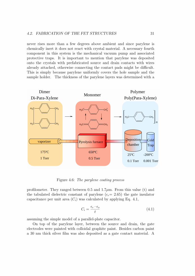
The described fabrication technique is distinguished by its generality andreproducibility. With parylene as a gate insulator material, I was able tosuccessfully produce FETs based on a variety of organic as well as transitionmetal dichalcogenide semiconductors. The output of working devices, at leastfor rubrene single crystal FETs, approached 100%. Additionally, the parylenefilms deposited onto crystals withstand multiple thermal cycling between 300K and 10 K, an important feature for low temperature measurements. Aschematic and a photo of a ready device are shown in Fig. 4.7.
Gate material: C-paint or ev. Ag
Drain material:C-paint
Source material:C-paint
Single crystal
Dielectric material:Parylene
Source
Drain
Gate
Figure 4.7: A schema of a FET, summarizing all materials used for the devicefabrication. The bottom part of the figure shows a photo of a pentacene singlecrystal field effect transistor.
At room temperature, the transistor characteristic was measured using aHP test fixture connected to a HP 4145B semiconductor parameter analyzer.The low temperature measurements were performed in helium atmosphere ina Quantum Design cryostat with a secondary Pt100 resistor in proximity to
4.2. FABRICATION OF THE FET STRUCTURES 33
the sample to crosscheck the temperature. Data were also collected with anHP 4145B semiconductor parameter analyzer. In all the measurements, thesource-drain voltage VSD and the gate voltage VG were applied with respectto the grounded source contact (see Fig. 2.2).
34 CHAPTER 4. DEVICE FABRICATION
Chapter 5
Rubrene
Field effect transistors based on rubrene single crystals demonstrate a max-imal hole mobility of 13 cm2/Vs. The mobility values obtained from theFET characteristics are reproducible and nearly electric field independent. Astrong anisotropy of the mobility has been observed. The mobility increasesvery slightly with cooling but decreases significantly at low temperatures.
5.1 Introduction
Rubrene is distinguished from all other organic semiconductors by an ex-ceptionally high carrier mobility of 30 cm2/Vs at 200 K [PMB+04] in singlecrystal field effect transistors. This places it in the center of interest ofmany groups working on plastic electronics. Pentacene and related acenes,oligothiophenes and fullerenes are the most studied organic FET materialstoday, and have the highest reported mobility, around ten times lower thanrubrene. The carrier transport mechanism in all of these organic semicon-ductors is still not well understood. The lack of defect-free crystals and theimmaturity of organic FET technology seem to limit wider applications oforganic semiconductors in microelectronics. In particular, it is still impossi-ble to predict how far, in what way the room temperature mobility can beincreased, and why the mobility in organic semiconductors doesn’t increasedramatically upon cooling. Therefore, I believe that further study of thetechnology and the operation of the rubrene single crystal FET will signifi-cantly contribute to improving the properties of other FETs and lead to thedesign of molecules with the desired enhanced properties. Nevertheless, thecurrently achievable mobility in thin-film organic FETs, such as amorphoussilicon, is high enough for many practical applications like organic LEDs,FETs and solar cells. Still, an increase of mobility would simplify circuit de-
35
36 CHAPTER 5. RUBRENE
sign and allow fabrication of high frequency microelectronic devices. Rubrenehas many advantages; it is commercially available and therefore easy to ac-quire. When grown from the vapor phase, rubrene forms large, orthorhom-bic, high quality crystals characterized by a small mosaic spread. Measuredphysical parameters such as high mobility have been reproduced in severallaboratories using different crystal growth and FET preparation methods[PPG04, PMB+04, SdBIM04, BLR04, GHK+04]. In this Chapter, I com-pare rubrene single crystal FETs using Parylene as a dielectric material andcompare my results with those reported earlier [GHK+04, PPG04, PMB+04].
5.2 Rubrene room temperature measurements
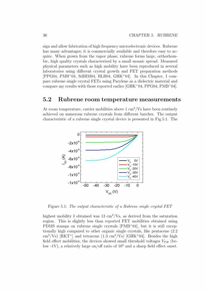
At room temperature, carrier mobilities above 1 cm2/Vs have been routinelyachieved on numerous rubrene crystals from different batches. The outputcharacteristic of a rubrene single crystal device is presented in Fig.5.1. The
-50 -40 -30 -20 -10 0-1x10⁻⁵
-1x10⁻⁵
-8x10⁻⁶
-6x10⁻⁶
-4x10⁻⁶
-2x10⁻⁶
0
I SD (A
)
VSD
(V)
VG 0V VG -10V VG -20V VG -30V VG -40V
Figure 5.1: The output characteristic of a Rubrene single crystal FET
highest mobility I obtained was 13 cm2/Vs, as derived from the saturationregion. This is slightly less than reported FET mobilities obtained usingPDMS stamps on rubrene single crystals [PMB+04], but it is still excep-tionally high compared to other organic single crystals, like pentacene (2.2cm2/Vs) [RKT+] and tetracene (1.3 cm2/Vs) [GHK+04]. Besides the highfield effect mobilities, the devices showed small threshold voltages VTH (be-low -1V), a relatively large on/off ratio of 105 and a sharp field effect onset.
5.2. RUBRENE ROOM TEMPERATURE MEASUREMENTS 37
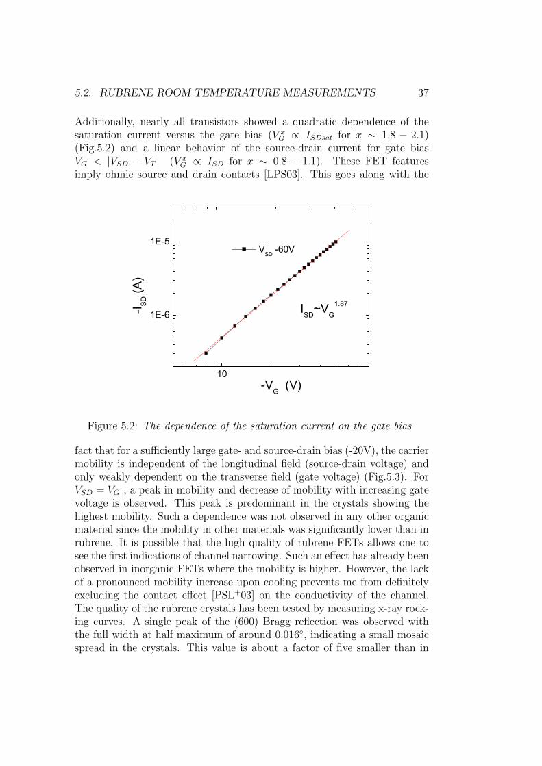
Additionally, nearly all transistors showed a quadratic dependence of thesaturation current versus the gate bias (V x
G ∝ ISDsat for x ∼ 1.8 − 2.1)(Fig.5.2) and a linear behavior of the source-drain current for gate biasVG < |VSD − VT | (V x
G ∝ ISD for x ∼ 0.8 − 1.1). These FET featuresimply ohmic source and drain contacts [LPS03]. This goes along with the
10
1E-6
1E-5
ISD~VG1.87
VSD -60V
-I SD (A
)
-VG (V)
Figure 5.2: The dependence of the saturation current on the gate bias
fact that for a sufficiently large gate- and source-drain bias (-20V), the carriermobility is independent of the longitudinal field (source-drain voltage) andonly weakly dependent on the transverse field (gate voltage) (Fig.5.3). ForVSD = VG , a peak in mobility and decrease of mobility with increasing gatevoltage is observed. This peak is predominant in the crystals showing thehighest mobility. Such a dependence was not observed in any other organicmaterial since the mobility in other materials was significantly lower than inrubrene. It is possible that the high quality of rubrene FETs allows one tosee the first indications of channel narrowing. Such an effect has already beenobserved in inorganic FETs where the mobility is higher. However, the lackof a pronounced mobility increase upon cooling prevents me from definitelyexcluding the contact effect [PSL+03] on the conductivity of the channel.The quality of the rubrene crystals has been tested by measuring x-ray rock-ing curves. A single peak of the (600) Bragg reflection was observed withthe full width at half maximum of around 0.016, indicating a small mosaicspread in the crystals. This value is about a factor of five smaller than in
38 CHAPTER 5. RUBRENE
-80 -60 -40 -20 0 20
0
5
10
15
VSD -1V VSD -10V VSD -25V VSD -50V
µµ µµ (c
m2 /V
s)
VG (V)
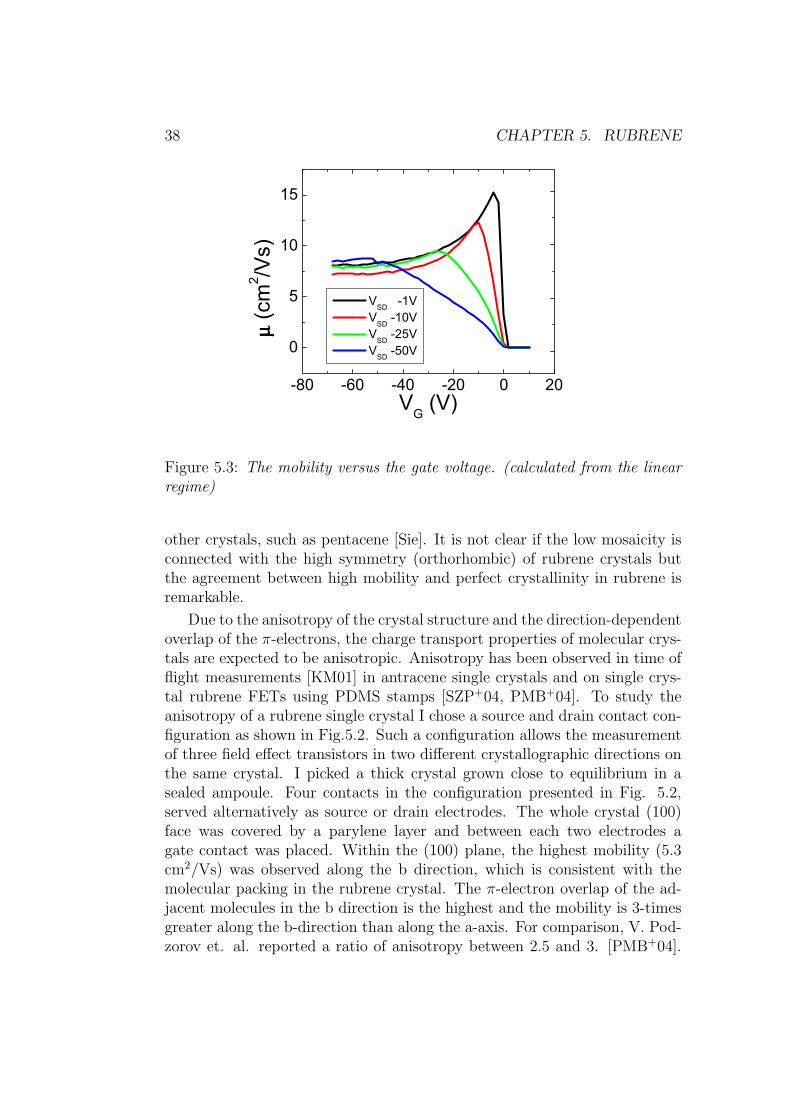
Figure 5.3: The mobility versus the gate voltage. (calculated from the linearregime)
other crystals, such as pentacene [Sie]. It is not clear if the low mosaicity isconnected with the high symmetry (orthorhombic) of rubrene crystals butthe agreement between high mobility and perfect crystallinity in rubrene isremarkable.
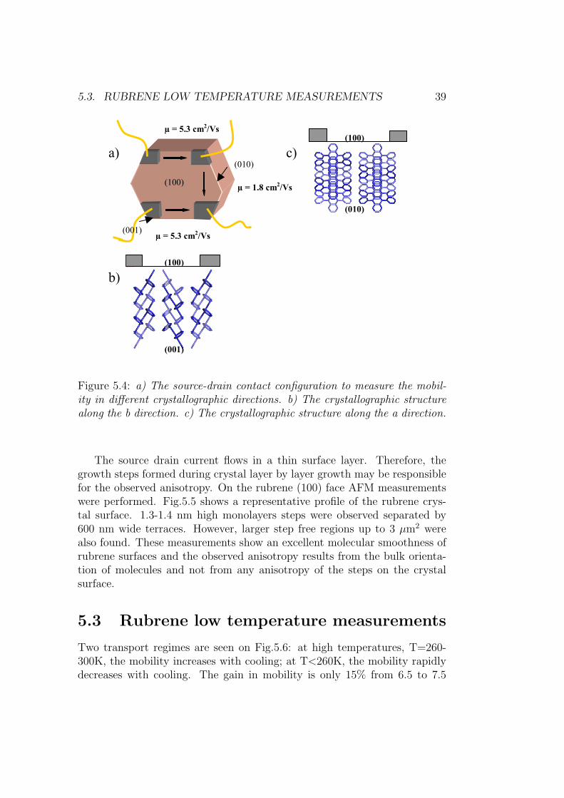
Due to the anisotropy of the crystal structure and the direction-dependentoverlap of the π-electrons, the charge transport properties of molecular crys-tals are expected to be anisotropic. Anisotropy has been observed in time offlight measurements [KM01] in antracene single crystals and on single crys-tal rubrene FETs using PDMS stamps [SZP+04, PMB+04]. To study theanisotropy of a rubrene single crystal I chose a source and drain contact con-figuration as shown in Fig.5.2. Such a configuration allows the measurementof three field effect transistors in two different crystallographic directions onthe same crystal. I picked a thick crystal grown close to equilibrium in asealed ampoule. Four contacts in the configuration presented in Fig. 5.2,served alternatively as source or drain electrodes. The whole crystal (100)face was covered by a parylene layer and between each two electrodes agate contact was placed. Within the (100) plane, the highest mobility (5.3cm2/Vs) was observed along the b direction, which is consistent with themolecular packing in the rubrene crystal. The π-electron overlap of the ad-jacent molecules in the b direction is the highest and the mobility is 3-timesgreater along the b-direction than along the a-axis. For comparison, V. Pod-zorov et. al. reported a ratio of anisotropy between 2.5 and 3. [PMB+04].
5.3. RUBRENE LOW TEMPERATURE MEASUREMENTS 39
µ = 1.8 cm2/Vs
µ = 5.3 cm2/Vs
µ = 5.3 cm2/Vs
(001)
(010)
(010)
(100)
(001)
(100)
(100)
a) c)
b)
Figure 5.4: a) The source-drain contact configuration to measure the mobil-ity in different crystallographic directions. b) The crystallographic structurealong the b direction. c) The crystallographic structure along the a direction.
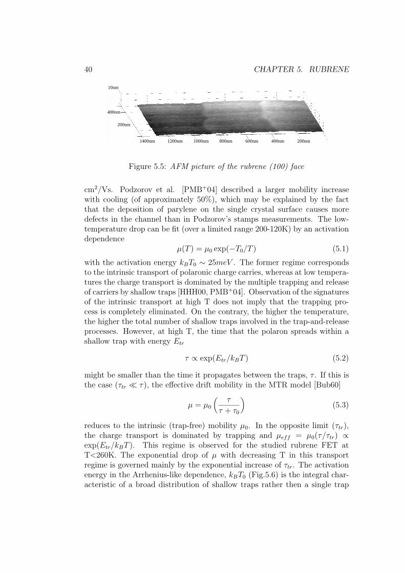
The source drain current flows in a thin surface layer. Therefore, thegrowth steps formed during crystal layer by layer growth may be responsiblefor the observed anisotropy. On the rubrene (100) face AFM measurementswere performed. Fig.5.5 shows a representative profile of the rubrene crys-tal surface. 1.3-1.4 nm high monolayers steps were observed separated by600 nm wide terraces. However, larger step free regions up to 3 µm2 werealso found. These measurements show an excellent molecular smoothness ofrubrene surfaces and the observed anisotropy results from the bulk orienta-tion of molecules and not from any anisotropy of the steps on the crystalsurface.
5.3 Rubrene low temperature measurements
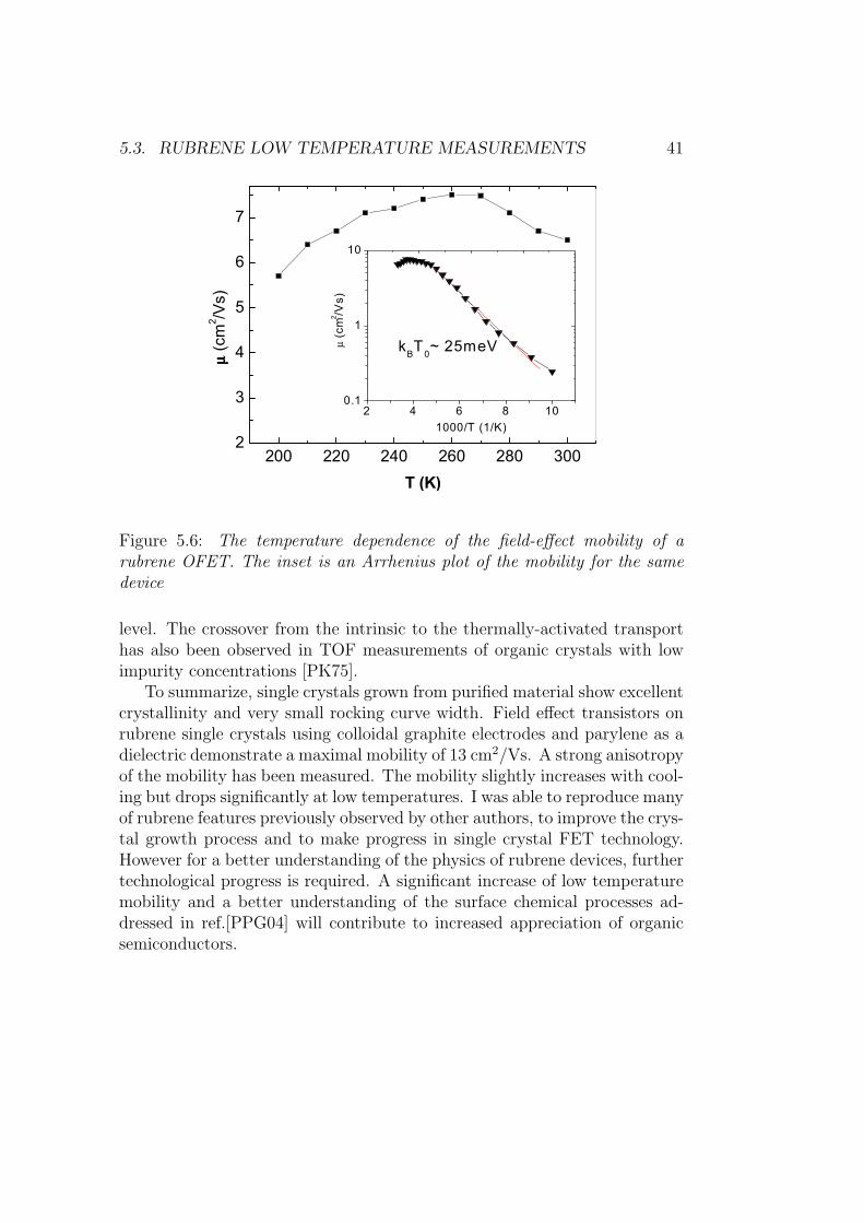
Two transport regimes are seen on Fig.5.6: at high temperatures, T=260-300K, the mobility increases with cooling; at T<260K, the mobility rapidlydecreases with cooling. The gain in mobility is only 15% from 6.5 to 7.5
40 CHAPTER 5. RUBRENE
200nm400nm600nm800nm1000nm1200nm 1400nm
200nm
400nm
10nm
Figure 5.5: AFM picture of the rubrene (100) face
cm2/Vs. Podzorov et al. [PMB+04] described a larger mobility increasewith cooling (of approximately 50%), which may be explained by the factthat the deposition of parylene on the single crystal surface causes moredefects in the channel than in Podzorov’s stamps measurements. The low-temperature drop can be fit (over a limited range 200-120K) by an activationdependence
µ(T ) = µ0 exp(−T0/T ) (5.1)
with the activation energy kBT0 ∼ 25meV . The former regime correspondsto the intrinsic transport of polaronic charge carries, whereas at low tempera-tures the charge transport is dominated by the multiple trapping and releaseof carriers by shallow traps [HHH00, PMB+04]. Observation of the signaturesof the intrinsic transport at high T does not imply that the trapping pro-cess is completely eliminated. On the contrary, the higher the temperature,the higher the total number of shallow traps involved in the trap-and-releaseprocesses. However, at high T, the time that the polaron spreads within ashallow trap with energy Etr
τ ∝ exp(Etr/kBT ) (5.2)
might be smaller than the time it propagates between the traps, τ . If this isthe case (τtr τ), the effective drift mobility in the MTR model [Bub60]
µ = µ0
(τ
τ + τ0
)(5.3)
reduces to the intrinsic (trap-free) mobility µ0. In the opposite limit (τtr),the charge transport is dominated by trapping and µeff = µ0(τ/τtr) ∝exp(Etr/kBT ). This regime is observed for the studied rubrene FET atT<260K. The exponential drop of µ with decreasing T in this transportregime is governed mainly by the exponential increase of τtr. The activationenergy in the Arrhenius-like dependence, kBT0 (Fig.5.6) is the integral char-acteristic of a broad distribution of shallow traps rather then a single trap
5.3. RUBRENE LOW TEMPERATURE MEASUREMENTS 41
200 220 240 260 280 3002
3
4
5
6
7
2 4 6 8 100.1
1
10
kBT0~ 25meVµ (c
m2 /V
s)
1000/T (1/K)
µµ µµ (c
m2 /V
s)
T (K)
200 220 240 260 280 3003
4
5
6
7
µµ µµ (c
m2 /V
s)
T (K)
Figure 5.6: The temperature dependence of the field-effect mobility of arubrene OFET. The inset is an Arrhenius plot of the mobility for the samedevice
level. The crossover from the intrinsic to the thermally-activated transporthas also been observed in TOF measurements of organic crystals with lowimpurity concentrations [PK75].
To summarize, single crystals grown from purified material show excellentcrystallinity and very small rocking curve width. Field effect transistors onrubrene single crystals using colloidal graphite electrodes and parylene as adielectric demonstrate a maximal mobility of 13 cm2/Vs. A strong anisotropyof the mobility has been measured. The mobility slightly increases with cool-ing but drops significantly at low temperatures. I was able to reproduce manyof rubrene features previously observed by other authors, to improve the crys-tal growth process and to make progress in single crystal FET technology.However for a better understanding of the physics of rubrene devices, furthertechnological progress is required. A significant increase of low temperaturemobility and a better understanding of the surface chemical processes ad-dressed in ref.[PPG04] will contribute to increased appreciation of organicsemiconductors.

42 CHAPTER 5. RUBRENE
Chapter 6
Impurities
Obtaining pure crystals of a high quality is the first challenge in the processof making single-crystal organic field-effect transistors. Structural defectsand impurities in crystals can seriously deteriorate the desired electronictransport properties of the crystal by creating physical and chemical traps.In the case of anthacene for example, it has been shown that even ppmtraces of the natural impurity tetracene will form charge traps for holes andelectrons [Kar90]. Due to the prominent position of rubrene and pentacenein the research of OFETs, this chapter focuses on their impurities, whichare formed during the growth process or already exist as byproducts in thecommercial powder.
6.1 Impurities of rubrene
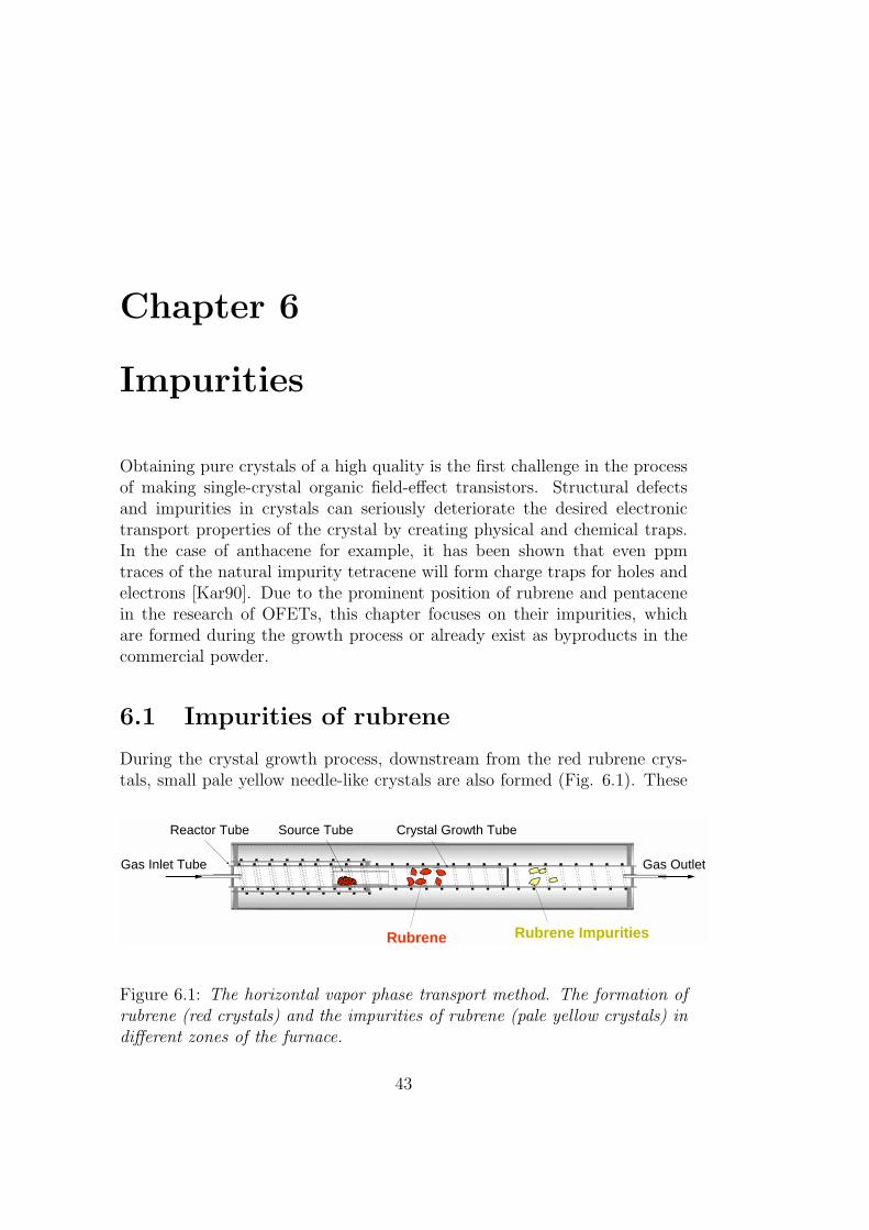
During the crystal growth process, downstream from the red rubrene crys-tals, small pale yellow needle-like crystals are also formed (Fig. 6.1). These
Crystal Growth TubeSource TubeReactor Tube
Gas Inlet Tube Gas Outlet
Rubrene Rubrene Impurities
Figure 6.1: The horizontal vapor phase transport method. The formation ofrubrene (red crystals) and the impurities of rubrene (pale yellow crystals) indifferent zones of the furnace.
43
44 CHAPTER 6. IMPURITIES
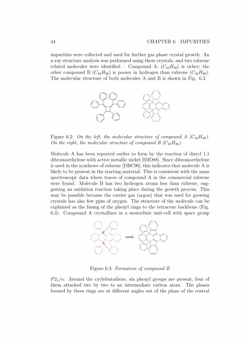
impurities were collected and used for further gas phase crystal growth. Anx-ray structure analysis was performed using these crystals, and two rubrenerelated molecules were identified . Compound A, (C42H30) is richer; theother compound B (C42H26) is poorer in hydrogen than rubrene (C42H28).The molecular structure of both molecules A and B is shown in Fig. 6.2.
Figure 6.2: On the left, the molecular structure of compound A (C42H30).On the right, the molecular structure of compound B (C42H26)
Molecule A has been reported earlier to form by the reaction of diaryl 1,1dibromoethylene with active metallic nickel [IMO88]. Since dibromoethyleneis used in the syntheses of rubrene [DBC90], this indicates that molecule A islikely to be present in the starting material. This is consistent with the massspectroscopy data where traces of compound A in the commercial rubrenewere found. Molecule B has two hydrogen atoms less than rubrene, sug-gesting an oxidation reaction taking place during the growth process. Thismay be possible because the carrier gas (argon) that was used for growingcrystals has also few ppm of oxygen. The structure of the molecule can beexplained as the fusing of the phenyl rings to the tetracene backbone (Fig.6.3). Compound A crystallizes in a monoclinic unit-cell with space group
Figure 6.3: Formation of compound B
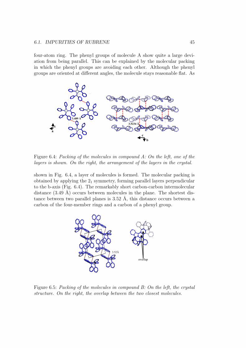
P21/n. Around the cyclobutadiene, six phenyl groups are present, four ofthem attached two by two to an intermediate carbon atom. The planesformed by these rings are at different angles out of the plane of the central
6.1. IMPURITIES OF RUBRENE 45
four-atom ring. The phenyl groups of molecule A show quite a large devi-ation from being parallel. This can be explained by the molecular packingin which the phenyl groups are avoiding each other. Although the phenylgroups are oriented at different angles, the molecule stays reasonable flat. As
b c
c a
3.5234 Å
3.489 Å
Figure 6.4: Packing of the molecules in compound A: On the left, one of thelayers is shown. On the right, the arrangement of the layers in the crystal.
shown in Fig. 6.4, a layer of molecules is formed. The molecular packing isobtained by applying the 21 symmetry, forming parallel layers perpendicularto the b-axis (Fig. 6.4). The remarkably short carbon-carbon intermoleculardistance (3.49 A) occurs between molecules in the plane. The shortest dis-tance between two parallel planes is 3.52 A, this distance occurs between acarbon of the four-member rings and a carbon of a phenyl group.
3.52Å
overlap
Figure 6.5: Packing of the molecules in compound B: On the left, the crystalstructure. On the right, the overlap between the two closest molecules.
46 CHAPTER 6. IMPURITIES
The molecules constituting compound B have a structure very similar torubrene. The two five-member rings are fused with the tetracene-like partof the rubrene molecule. This arrangement breaks the extended aromaticsystem on the tetracene backbone, producing a curvature. The molecule isquite bulky due to two remaining phenyl groups that are pointing outwards.To take care of these and pack as efficiently as possible, the molecules asso-ciate pairwise, turning the phenyl groups in opposite directions (Fig. 6.5).The distance between two molecules in such a dimer is 3.521 A and there isan overlap of the two molecules via two phenyl groups [Bes04].
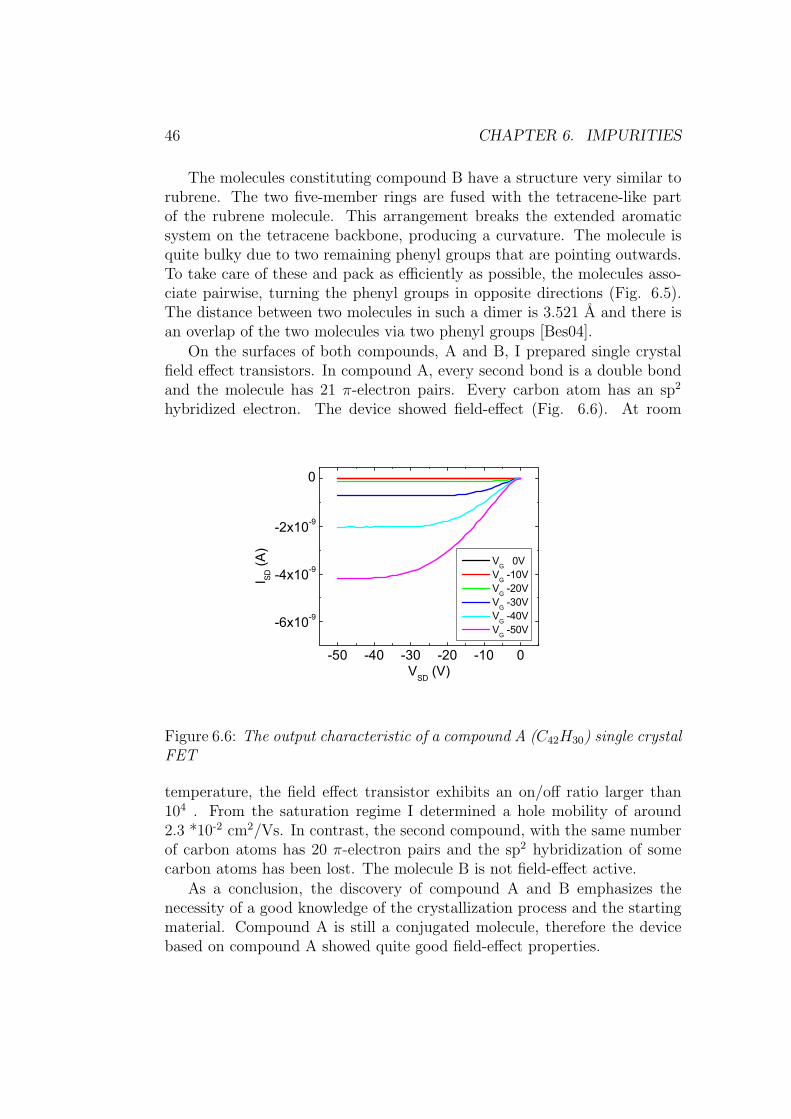
On the surfaces of both compounds, A and B, I prepared single crystalfield effect transistors. In compound A, every second bond is a double bondand the molecule has 21 π-electron pairs. Every carbon atom has an sp2
hybridized electron. The device showed field-effect (Fig. 6.6). At room
-50 -40 -30 -20 -10 0
-6x10⁻⁹
-4x10⁻⁹
-2x10⁻⁹
0
I SD (A
)
VSD (V)
VG 0V VG -10V VG -20V VG -30V VG -40V VG -50V
Figure 6.6: The output characteristic of a compound A (C42H30) single crystalFET
temperature, the field effect transistor exhibits an on/off ratio larger than104 . From the saturation regime I determined a hole mobility of around2.3 *10-2 cm2/Vs. In contrast, the second compound, with the same numberof carbon atoms has 20 π-electron pairs and the sp2 hybridization of somecarbon atoms has been lost. The molecule B is not field-effect active.
As a conclusion, the discovery of compound A and B emphasizes thenecessity of a good knowledge of the crystallization process and the startingmaterial. Compound A is still a conjugated molecule, therefore the devicebased on compound A showed quite good field-effect properties.
6.2. IMPURITIES OF PENTACENE 47
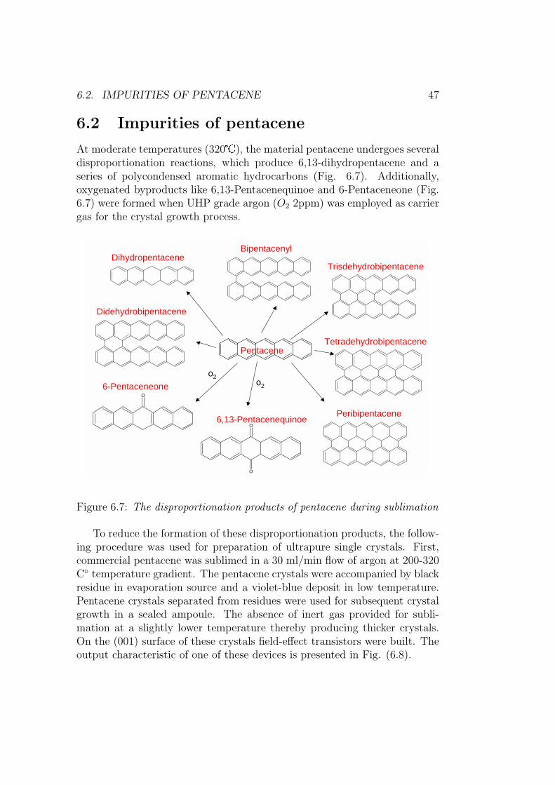
6.2 Impurities of pentacene
At moderate temperatures (320), the material pentacene undergoes severaldisproportionation reactions, which produce 6,13-dihydropentacene and aseries of polycondensed aromatic hydrocarbons (Fig. 6.7). Additionally,oxygenated byproducts like 6,13-Pentacenequinoe and 6-Pentaceneone (Fig.6.7) were formed when UHP grade argon (O2 2ppm) was employed as carriergas for the crystal growth process.
DihydropentaceneBipentacenyl
Didehydrobipentacene
Trisdehydrobipentacene
Tetradehydrobipentacene
Peribipentacene
Pentacene
O
O
O6-Pentaceneone
6,13-Pentacenequinoe
o2o2
Figure 6.7: The disproportionation products of pentacene during sublimation
To reduce the formation of these disproportionation products, the follow-ing procedure was used for preparation of ultrapure single crystals. First,commercial pentacene was sublimed in a 30 ml/min flow of argon at 200-320C temperature gradient. The pentacene crystals were accompanied by blackresidue in evaporation source and a violet-blue deposit in low temperature.Pentacene crystals separated from residues were used for subsequent crystalgrowth in a sealed ampoule. The absence of inert gas provided for subli-mation at a slightly lower temperature thereby producing thicker crystals.On the (001) surface of these crystals field-effect transistors were built. Theoutput characteristic of one of these devices is presented in Fig. (6.8).
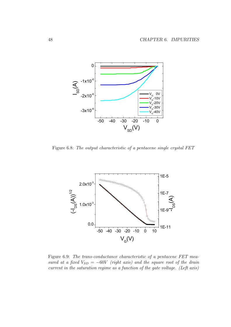
48 CHAPTER 6. IMPURITIES
-50 -40 -30 -20 -10 0
-3x10⁻⁶
-2x10⁻⁶
-1x10⁻⁶
0
I SD(A
)
VSD(V)
VG 0V VG-10V VG-20V VG-30V VG-40V
Figure 6.8: The output characteristic of a pentacene single crystal FET
-50 -40 -30 -20 -10 0 100.0
1.0x10⁻³
2.0x10⁻³
-I DS(A)
(-I DS(A))1
/2
VG(V)
1E-11
1E-9
1E-7
1E-5
Figure 6.9: The trans-conductance characteristic of a pentacene FET mea-sured at a fixed VSD = −60V (right axis) and the square root of the draincurrent in the saturation regime as a function of the gate voltage. (Left axis)
6.2. IMPURITIES OF PENTACENE 49
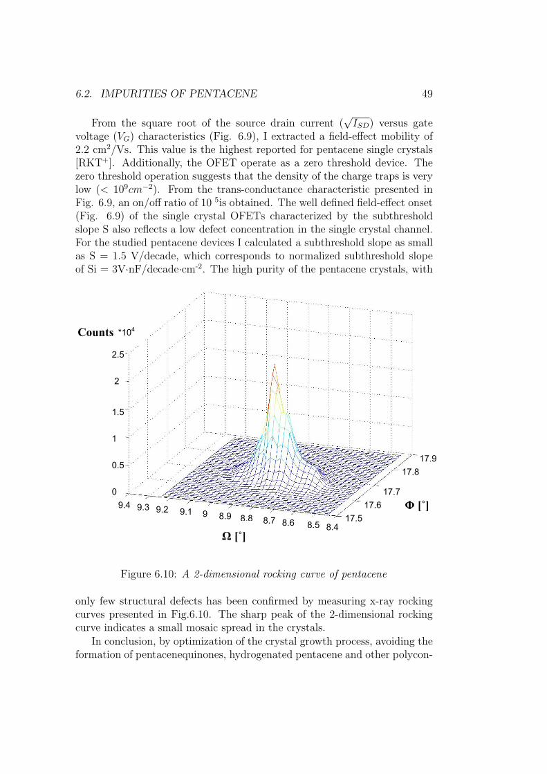
From the square root of the source drain current (√
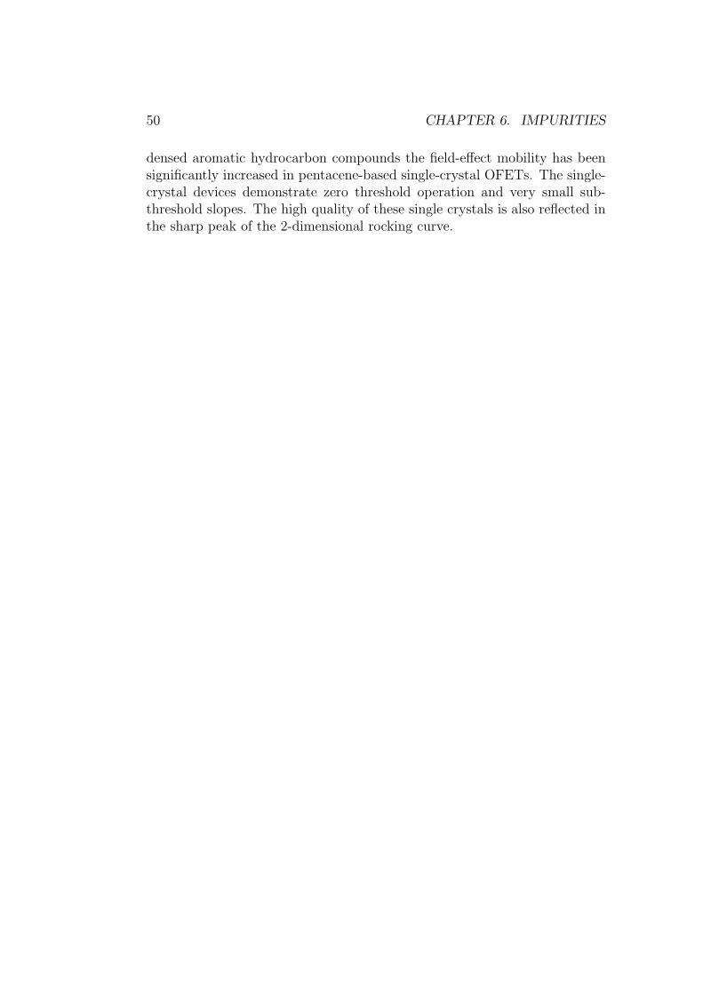
ISD) versus gatevoltage (VG) characteristics (Fig. 6.9), I extracted a field-effect mobility of2.2 cm2/Vs. This value is the highest reported for pentacene single crystals[RKT+]. Additionally, the OFET operate as a zero threshold device. Thezero threshold operation suggests that the density of the charge traps is verylow (< 109cm−2). From the trans-conductance characteristic presented inFig. 6.9, an on/off ratio of 10 5is obtained. The well defined field-effect onset(Fig. 6.9) of the single crystal OFETs characterized by the subthresholdslope S also reflects a low defect concentration in the single crystal channel.For the studied pentacene devices I calculated a subthreshold slope as smallas S = 1.5 V/decade, which corresponds to normalized subthreshold slopeof Si = 3V·nF/decade·cm-2. The high purity of the pentacene crystals, with
17.5
17.7
17.8 17.9
17.6 9.4 9.3 9.2 9.18.8 8.7
9 8.9 8.6 8.4 8.5
2.5
2
1.5
1
0.5
0
*104
Ω [˚]
Φ [˚]
Counts
Figure 6.10: A 2-dimensional rocking curve of pentacene
only few structural defects has been confirmed by measuring x-ray rockingcurves presented in Fig.6.10. The sharp peak of the 2-dimensional rockingcurve indicates a small mosaic spread in the crystals.
In conclusion, by optimization of the crystal growth process, avoiding theformation of pentacenequinones, hydrogenated pentacene and other polycon-
50 CHAPTER 6. IMPURITIES
densed aromatic hydrocarbon compounds the field-effect mobility has beensignificantly increased in pentacene-based single-crystal OFETs. The single-crystal devices demonstrate zero threshold operation and very small sub-threshold slopes. The high quality of these single crystals is also reflected inthe sharp peak of the 2-dimensional rocking curve.
Chapter 7
Copper phthalocyanine
In this chapter the performance of single crystal field effect transistors basedon Copper phthalocyanine (Cu-Pc) is evaluated. These FETs function as p-channel accumulation-mode devices. The high charge carrier mobility com-bined with a low field-effect threshold along with the highly stable chemicalnature of Cu-Pc make it an attractive candidate for device applications.
7.1 The technical relevance of Cu-Pc
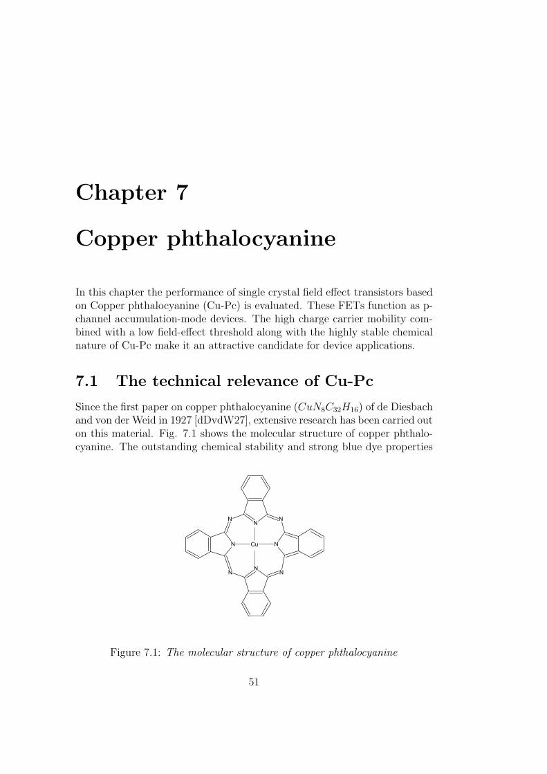
Since the first paper on copper phthalocyanine (CuN8C32H16) of de Diesbachand von der Weid in 1927 [dDvdW27], extensive research has been carried outon this material. Fig. 7.1 shows the molecular structure of copper phthalo-cyanine. The outstanding chemical stability and strong blue dye properties
NN N
N
NNN
N Cu
Figure 7.1: The molecular structure of copper phthalocyanine
51
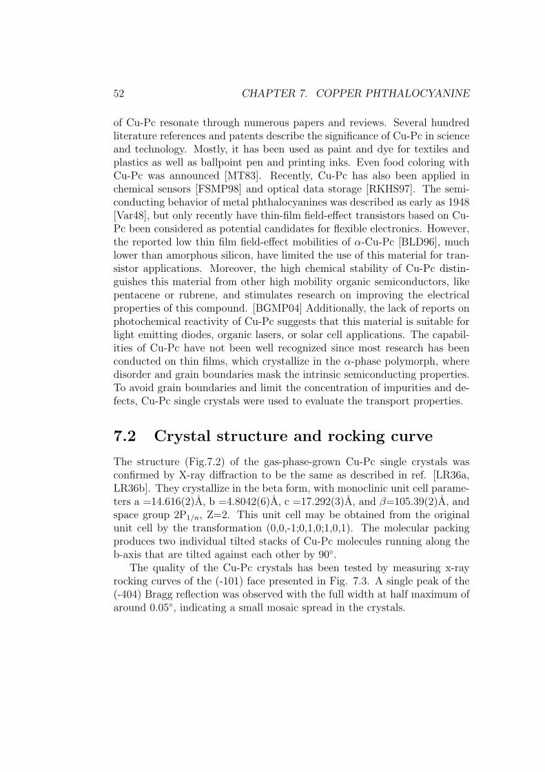
52 CHAPTER 7. COPPER PHTHALOCYANINE
of Cu-Pc resonate through numerous papers and reviews. Several hundredliterature references and patents describe the significance of Cu-Pc in scienceand technology. Mostly, it has been used as paint and dye for textiles andplastics as well as ballpoint pen and printing inks. Even food coloring withCu-Pc was announced [MT83]. Recently, Cu-Pc has also been applied inchemical sensors [FSMP98] and optical data storage [RKHS97]. The semi-conducting behavior of metal phthalocyanines was described as early as 1948[Var48], but only recently have thin-film field-effect transistors based on Cu-Pc been considered as potential candidates for flexible electronics. However,the reported low thin film field-effect mobilities of α-Cu-Pc [BLD96], muchlower than amorphous silicon, have limited the use of this material for tran-sistor applications. Moreover, the high chemical stability of Cu-Pc distin-guishes this material from other high mobility organic semiconductors, likepentacene or rubrene, and stimulates research on improving the electricalproperties of this compound. [BGMP04] Additionally, the lack of reports onphotochemical reactivity of Cu-Pc suggests that this material is suitable forlight emitting diodes, organic lasers, or solar cell applications. The capabil-ities of Cu-Pc have not been well recognized since most research has beenconducted on thin films, which crystallize in the α-phase polymorph, wheredisorder and grain boundaries mask the intrinsic semiconducting properties.To avoid grain boundaries and limit the concentration of impurities and de-fects, Cu-Pc single crystals were used to evaluate the transport properties.
7.2 Crystal structure and rocking curve
The structure (Fig.7.2) of the gas-phase-grown Cu-Pc single crystals wasconfirmed by X-ray diffraction to be the same as described in ref. [LR36a,LR36b]. They crystallize in the beta form, with monoclinic unit cell parame-ters a =14.616(2)A, b =4.8042(6)A, c =17.292(3)A, and β=105.39(2)A, andspace group 2P1/n, Z=2. This unit cell may be obtained from the originalunit cell by the transformation (0,0,-1;0,1,0;1,0,1). The molecular packingproduces two individual tilted stacks of Cu-Pc molecules running along theb-axis that are tilted against each other by 90.
The quality of the Cu-Pc crystals has been tested by measuring x-rayrocking curves of the (-101) face presented in Fig. 7.3. A single peak of the(-404) Bragg reflection was observed with the full width at half maximum ofaround 0.05, indicating a small mosaic spread in the crystals.
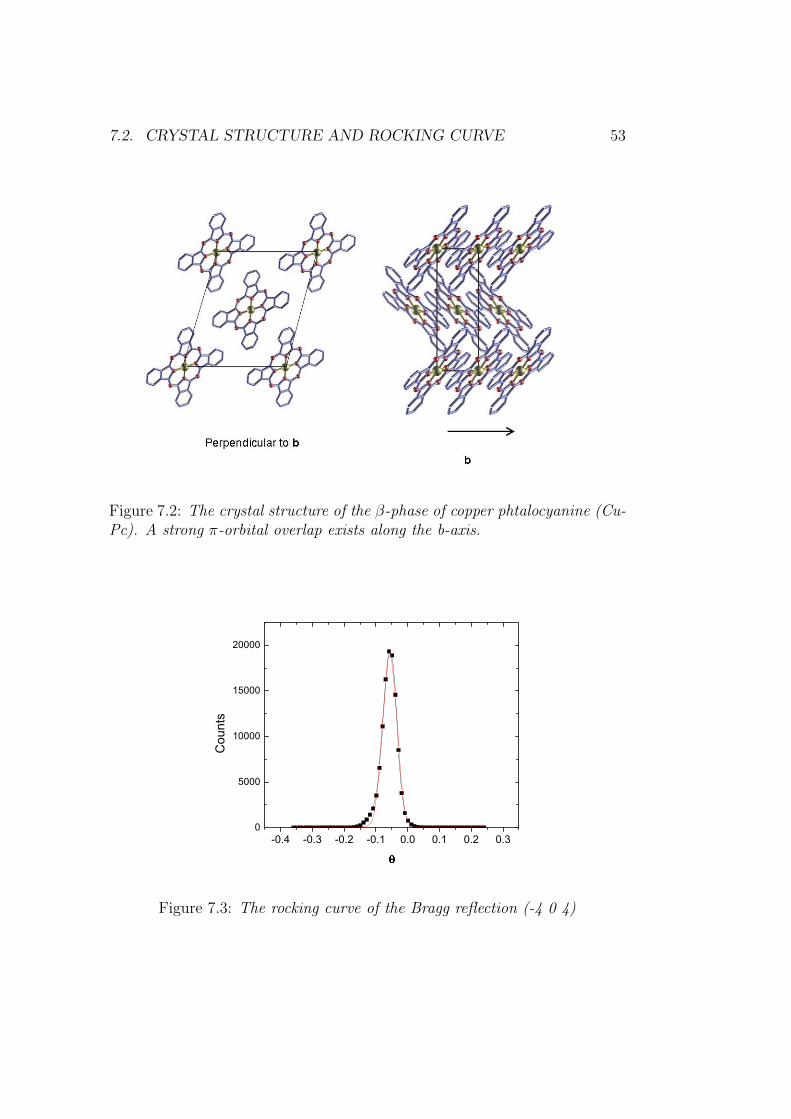
7.2. CRYSTAL STRUCTURE AND ROCKING CURVE 53
Figure 7.2: The crystal structure of the β-phase of copper phtalocyanine (Cu-Pc). A strong π-orbital overlap exists along the b-axis.
-0.4 -0.3 -0.2 -0.1 0.0 0.1 0.2 0.30
5000
10000
15000
20000
Counts
θθθθ
Figure 7.3: The rocking curve of the Bragg reflection (-4 0 4)
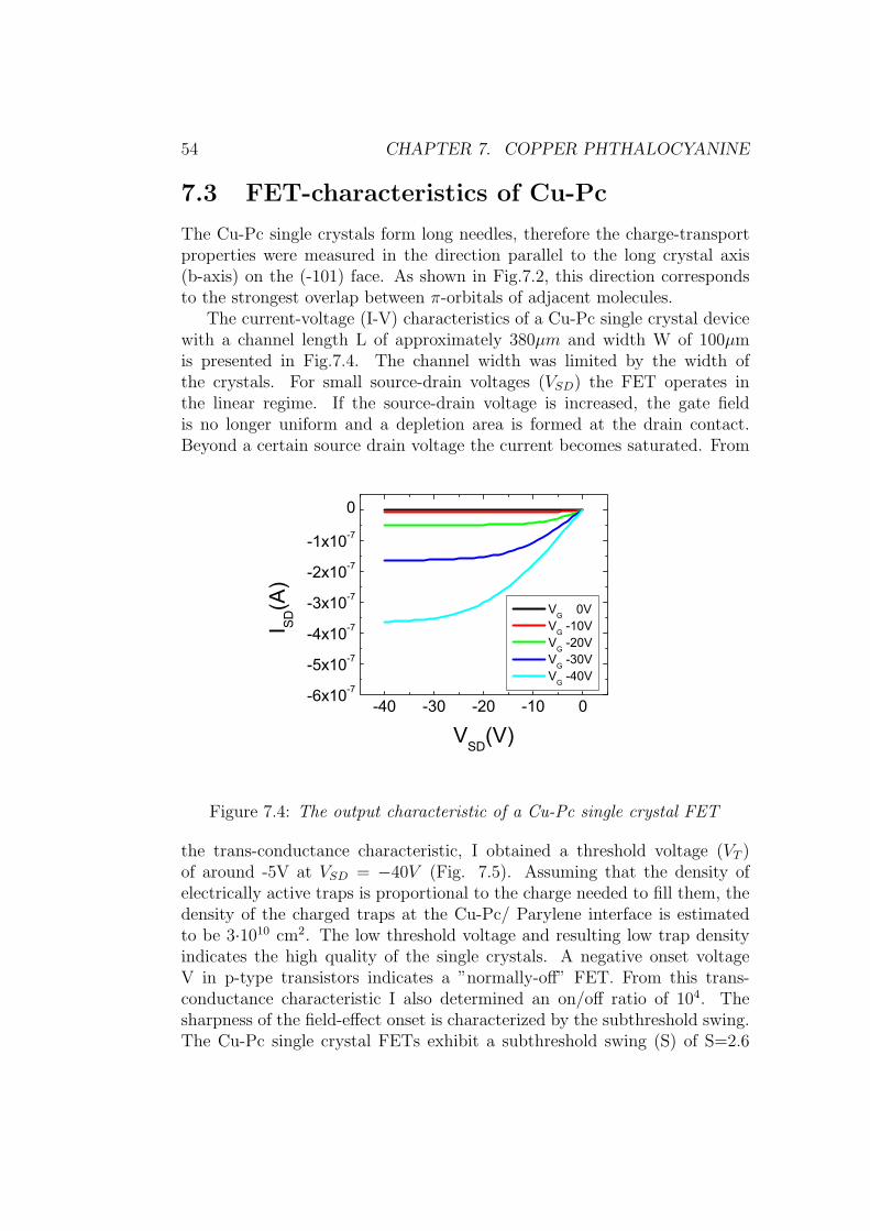
54 CHAPTER 7. COPPER PHTHALOCYANINE
7.3 FET-characteristics of Cu-Pc
The Cu-Pc single crystals form long needles, therefore the charge-transportproperties were measured in the direction parallel to the long crystal axis(b-axis) on the (-101) face. As shown in Fig.7.2, this direction correspondsto the strongest overlap between π-orbitals of adjacent molecules.
The current-voltage (I-V) characteristics of a Cu-Pc single crystal devicewith a channel length L of approximately 380µm and width W of 100µmis presented in Fig.7.4. The channel width was limited by the width ofthe crystals. For small source-drain voltages (VSD) the FET operates inthe linear regime. If the source-drain voltage is increased, the gate fieldis no longer uniform and a depletion area is formed at the drain contact.Beyond a certain source drain voltage the current becomes saturated. From
-40 -30 -20 -10 0-6x10⁻⁷
-5x10⁻⁷
-4x10⁻⁷
-3x10⁻⁷
-2x10⁻⁷
-1x10⁻⁷
0
I SD(A
)
VSD(V)
VG 0V VG -10V VG -20V VG -30V VG -40V
Figure 7.4: The output characteristic of a Cu-Pc single crystal FET
the trans-conductance characteristic, I obtained a threshold voltage (VT )of around -5V at VSD = −40V (Fig. 7.5). Assuming that the density ofelectrically active traps is proportional to the charge needed to fill them, thedensity of the charged traps at the Cu-Pc/ Parylene interface is estimatedto be 3·1010 cm2. The low threshold voltage and resulting low trap densityindicates the high quality of the single crystals. A negative onset voltageV in p-type transistors indicates a ”normally-off” FET. From this trans-conductance characteristic I also determined an on/off ratio of 104. Thesharpness of the field-effect onset is characterized by the subthreshold swing.The Cu-Pc single crystal FETs exhibit a subthreshold swing (S) of S=2.6
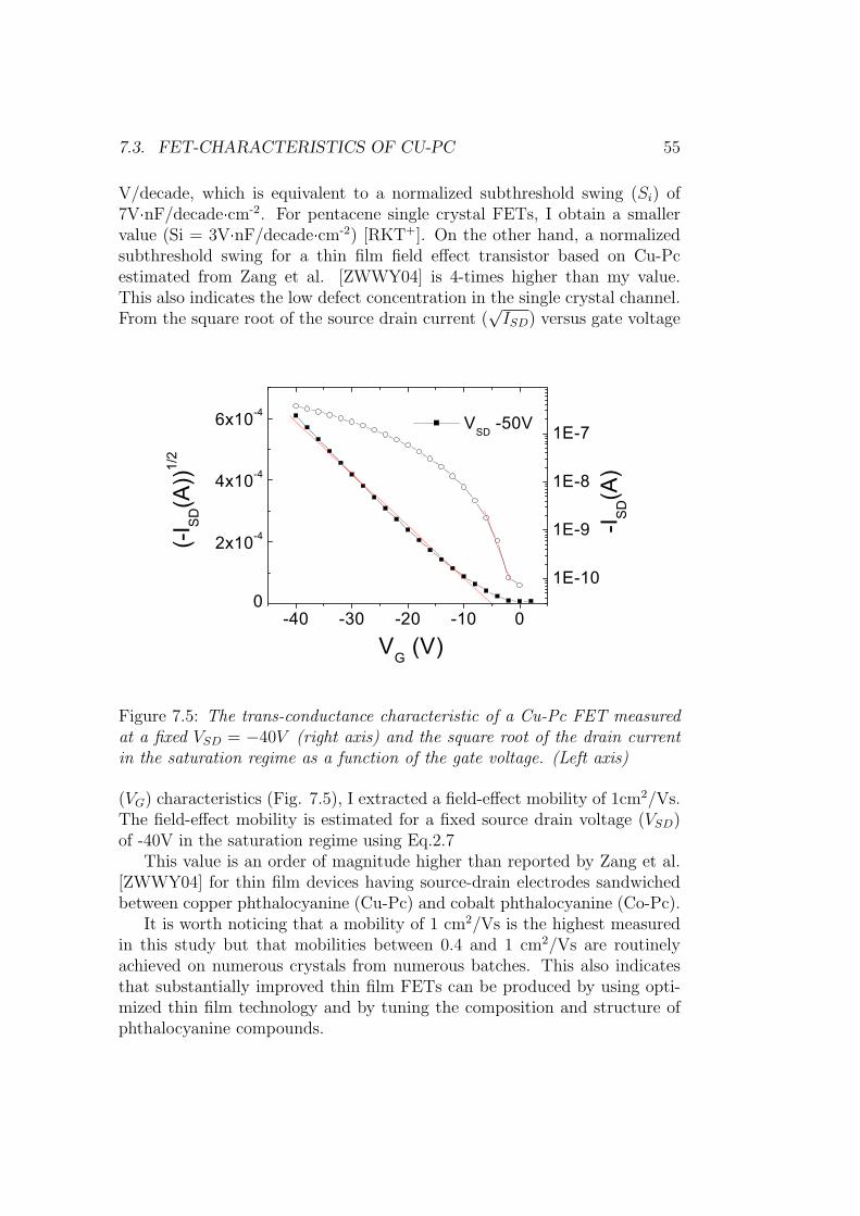
7.3. FET-CHARACTERISTICS OF CU-PC 55
V/decade, which is equivalent to a normalized subthreshold swing (Si) of7V·nF/decade·cm-2. For pentacene single crystal FETs, I obtain a smallervalue (Si = 3V·nF/decade·cm-2) [RKT+]. On the other hand, a normalizedsubthreshold swing for a thin film field effect transistor based on Cu-Pcestimated from Zang et al. [ZWWY04] is 4-times higher than my value.This also indicates the low defect concentration in the single crystal channel.From the square root of the source drain current (
√ISD) versus gate voltage
-40 -30 -20 -10 00
2x10⁻⁴
4x10⁻⁴
6x10⁻⁴ VSD -50V
-I SD(A
)
(-I S
D(A
))1/
2
VG (V)
1E-10
1E-9
1E-8
1E-7
Figure 7.5: The trans-conductance characteristic of a Cu-Pc FET measuredat a fixed VSD = −40V (right axis) and the square root of the drain currentin the saturation regime as a function of the gate voltage. (Left axis)
(VG) characteristics (Fig. 7.5), I extracted a field-effect mobility of 1cm2/Vs.The field-effect mobility is estimated for a fixed source drain voltage (VSD)of -40V in the saturation regime using Eq.2.7
This value is an order of magnitude higher than reported by Zang et al.[ZWWY04] for thin film devices having source-drain electrodes sandwichedbetween copper phthalocyanine (Cu-Pc) and cobalt phthalocyanine (Co-Pc).
It is worth noticing that a mobility of 1 cm2/Vs is the highest measuredin this study but that mobilities between 0.4 and 1 cm2/Vs are routinelyachieved on numerous crystals from numerous batches. This also indicatesthat substantially improved thin film FETs can be produced by using opti-mized thin film technology and by tuning the composition and structure ofphthalocyanine compounds.
56 CHAPTER 7. COPPER PHTHALOCYANINE
In summary, for CuPc devices a room temperature mobility of about 1cm2/Vs and an on/off ratio larger than 104 can be achieved. These transistorparameters are comparable with widely used amorphous silicon and the high-est hole mobilities reported for ”conventional organic semiconductors” liketetracene (1.3 cm2/Vs) [GHK+04] or pentacene (2.2 cm2/Vs) [RKT+] (2-2.5cm2/Vs) [BLC+]. Taking into account the exceptional chemical stability ofcopper phthalocyanine, this semiconductor seems to be the material of choicefor field effect transistors in displays and organic solar cells. In both these ap-plications, the large amount of light emitted (display) or absorbed (solar cells)would require a very stable semiconductor, and arenes (which photodimer-izes and oxidizes) [RKT+] or rubrene (which photo-oxidizes) [PPG04] do notsatisfy this requirement.
Chapter 8
Tetracene Derivatives
The substitution of hydrogen atoms by large, polarizable halogen atoms onthe tetracene molecule changes only a little the HOMO and LUMO levels;mainly it affects the packing of the molecules. In this chapter, I discuss thedifferent crystal structures of Tetracene derivates and correlate them withtheir field effect mobilities.
8.1 Crystal structure and mobility
Quantum mechanical calculations have predicted that high mobility in OFETscan be obtained when conjugated molecules have strong interactions withneighboring molecules to maximize the overlap of π molecular orbitals [CBB01].In addition, Curtis and coworkers have recently made a structural analysison some common organic semiconductors, discussing the correlation betweensolid state packing and transport [CCK04]. Theoretically speaking, a cofa-cial π stacking structure is expected to provide more efficient orbital over-lap and thereby facilitate carrier transport. So far, however, most of theorganic semiconductors that have shown high mobility and high on/off ra-tio in polycrystalline thin film devices have a herringbone structure whichreduces the overlap [NLGJ98]. In fact, there has been little experimental ev-idence that π stacked materials have higher mobility. This may be becauseof the scarcity of π stacked materials [PCF+02, AEP02] and the difficultyof examining transport properties at molecular levels. The mobility in poly-crystalline films is not intrinsic but depends on the purity of the conjugatedmolecules and on the film morphology. Single crystal devices, which are inprinciple free of grain boundaries, are ideal for the investigation of intrinsiccarrier transport properties of molecular semiconductors. In order to studythe effect of molecular packing on charge transport, it would be optimal to
57
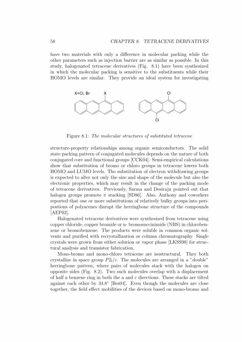
58 CHAPTER 8. TETRACENE DERIVATIVES
have two materials with only a difference in molecular packing while theother parameters such as injection barrier are as similar as possible. In thisstudy, halogenated tetracene derivatives (Fig. 8.1) have been synthesizedin which the molecular packing is sensitive to the substituents while theirHOMO levels are similar. They provide an ideal system for investigating
XX=Cl, Br Cl
Cl
Figure 8.1: The molecular structures of substituted tetracene
structure-property relationships among organic semiconductors. The solidstate packing pattern of conjugated molecules depends on the nature of bothconjugated core and functional groups [CCK04]. Semi-empirical calculationsshow that substitution of bromo or chloro groups in tetracene lowers bothHOMO and LUMO levels. The substitution of electron withdrawing groupsis expected to alter not only the size and shape of the molecule but also theelectronic properties, which may result in the change of the packing modeof tetracene derivatives. Previously, Sarma and Desiraju pointed out thathalogen groups promote π stacking [SD86]. Also, Anthony and coworkersreported that one or more substitutions of relatively bulky groups into peri-postions of polyacenes disrupt the herringbone structure of the compounds[AEP02].
Halogenated tetracene derivatives were synthesized from tetracene usingcopper chloride, copper bromide or n- bromosuccinimide (NBS) in chloroben-zene or bromobenzene. The products were soluble in common organic sol-vents and purified with recrystallization or column chromatography. Singlecrystals were grown from either solution or vapor phase [LKSS98] for struc-tural analysis and transistor fabrication.
Mono-bromo and mono-chloro tetracene are isostructural. They bothcrystallize in space group P2l/c. The molecules are arranged in a ”double”herringbone pattern, where pairs of molecules stack with the halogen onopposite sides (Fig. 8.2). Two such molecules overlap with a displacementof half a benzene ring in both the a and c directions. These stacks are tiltedagainst each other by 34.8 [Bes04]. Even though the molecules are closetogether, the field effect mobilities of the devices based on mono-bromo and
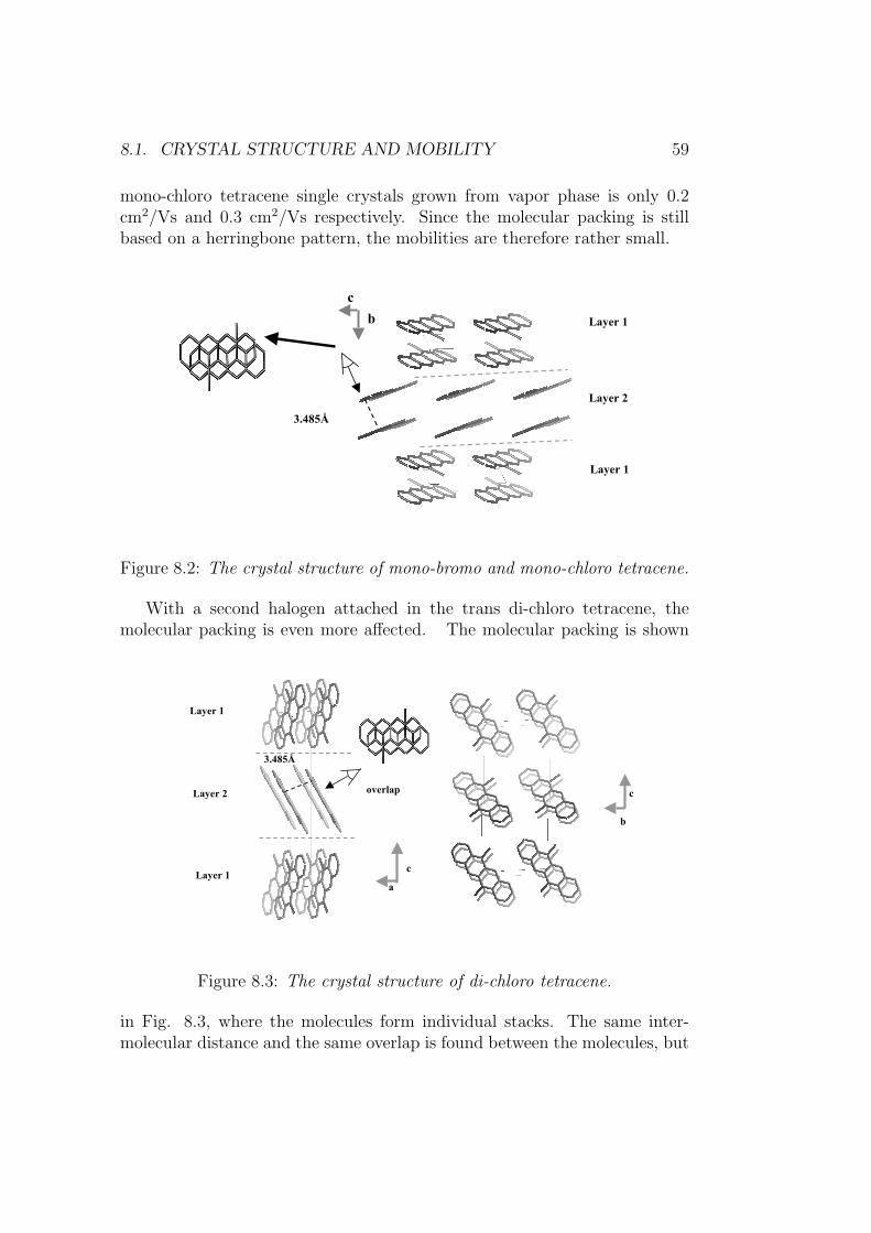
8.1. CRYSTAL STRUCTURE AND MOBILITY 59
mono-chloro tetracene single crystals grown from vapor phase is only 0.2cm2/Vs and 0.3 cm2/Vs respectively. Since the molecular packing is stillbased on a herringbone pattern, the mobilities are therefore rather small.
3.485Å
Layer 1
Layer 2
Layer 1
b c
Figure 8.2: The crystal structure of mono-bromo and mono-chloro tetracene.
With a second halogen attached in the trans di-chloro tetracene, themolecular packing is even more affected. The molecular packing is shown
c
a
c
b
overlap
Layer 1
Layer 1
Layer 2
3.485Å
Figure Error! No text of specified style in document.-1: Crystal structure of trans di-chloro tetracene.
Figure 8.3: The crystal structure of di-chloro tetracene.
in Fig. 8.3, where the molecules form individual stacks. The same inter-molecular distance and the same overlap is found between the molecules, but
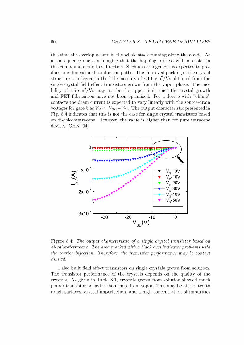
60 CHAPTER 8. TETRACENE DERIVATIVES
this time the overlap occurs in the whole stack running along the a-axis. Asa consequence one can imagine that the hopping process will be easier inthis compound along this direction. Such an arrangement is expected to pro-duce one-dimensional conduction paths. The improved packing of the crystalstructure is reflected in the hole mobility of ∼1.6 cm2/Vs obtained from thesingle crystal field effect transistors grown from the vapor phase. The mo-bility of 1.6 cm2/Vs may not be the upper limit since the crystal growthand FET-fabrication have not been optimized. For a device with ”ohmic”contacts the drain current is expected to vary linearly with the source-drainvoltages for gate bias VG < |VSD−VT |. The output characteristic presented inFig. 8.4 indicates that this is not the case for single crystal transistors basedon di-chlorotetracene. However, the value is higher than for pure tetracenedevices [GHK+04].
-30 -20 -10 0-3x10⁻⁷
-2x10⁻⁷
-1x10⁻⁷
0
I SD(A
)
VSD(V)
VG 0V VG-10V VG-20V VG-30V VG-40V VG-50V
Figure 8.4: The output characteristic of a single crystal transistor based ondi-chlorotetracene. The area marked with a black oval indicates problems withthe carrier injection. Therefore, the transistor performance may be contactlimited.
I also built field effect transistors on single crystals grown from solution.The transistor performance of the crystals depends on the quality of thecrystals. As given in Table 8.1, crystals grown from solution showed muchpoorer transistor behavior than those from vapor. This may be attributed torough surfaces, crystal imperfection, and a high concentration of impurities
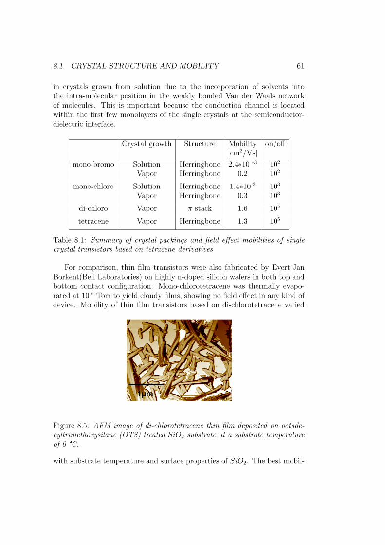
8.1. CRYSTAL STRUCTURE AND MOBILITY 61
in crystals grown from solution due to the incorporation of solvents intothe intra-molecular position in the weakly bonded Van der Waals networkof molecules. This is important because the conduction channel is locatedwithin the first few monolayers of the single crystals at the semiconductor-dielectric interface.
Crystal growth Structure Mobility on/off[cm2/Vs]
mono-bromo Solution Herringbone 2.4∗10 -3 102
Vapor Herringbone 0.2 102
mono-chloro Solution Herringbone 1.4∗10-3 103
Vapor Herringbone 0.3 103
di-chloro Vapor π stack 1.6 105
tetracene Vapor Herringbone 1.3 105
Table 8.1: Summary of crystal packings and field effect mobilities of singlecrystal transistors based on tetracene derivatives
For comparison, thin film transistors were also fabricated by Evert-JanBorkent(Bell Laboratories) on highly n-doped silicon wafers in both top andbottom contact configuration. Mono-chlorotetracene was thermally evapo-rated at 10-6 Torr to yield cloudy films, showing no field effect in any kind ofdevice. Mobility of thin film transistors based on di-chlorotetracene varied
1µm1µm
Figure 8.5: AFM image of di-chlorotetracene thin film deposited on octade-cyltrimethoxysilane (OTS) treated SiO2 substrate at a substrate temperatureof 0 °C.
with substrate temperature and surface properties of SiO2. The best mobil-
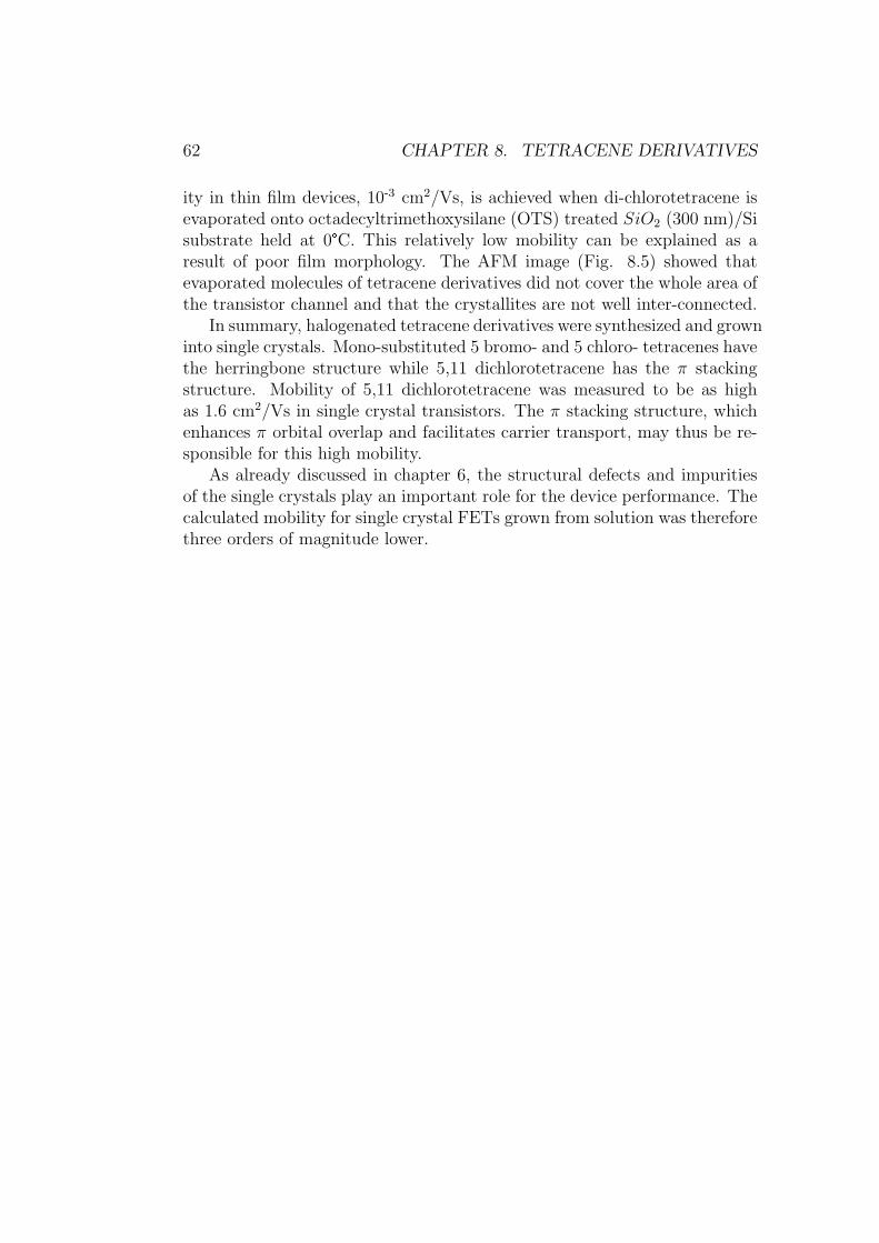
62 CHAPTER 8. TETRACENE DERIVATIVES
ity in thin film devices, 10-3 cm2/Vs, is achieved when di-chlorotetracene isevaporated onto octadecyltrimethoxysilane (OTS) treated SiO2 (300 nm)/Sisubstrate held at 0°C. This relatively low mobility can be explained as aresult of poor film morphology. The AFM image (Fig. 8.5) showed thatevaporated molecules of tetracene derivatives did not cover the whole area ofthe transistor channel and that the crystallites are not well inter-connected.
In summary, halogenated tetracene derivatives were synthesized and growninto single crystals. Mono-substituted 5 bromo- and 5 chloro- tetracenes havethe herringbone structure while 5,11 dichlorotetracene has the π stackingstructure. Mobility of 5,11 dichlorotetracene was measured to be as highas 1.6 cm2/Vs in single crystal transistors. The π stacking structure, whichenhances π orbital overlap and facilitates carrier transport, may thus be re-sponsible for this high mobility.
As already discussed in chapter 6, the structural defects and impuritiesof the single crystals play an important role for the device performance. Thecalculated mobility for single crystal FETs grown from solution was thereforethree orders of magnitude lower.
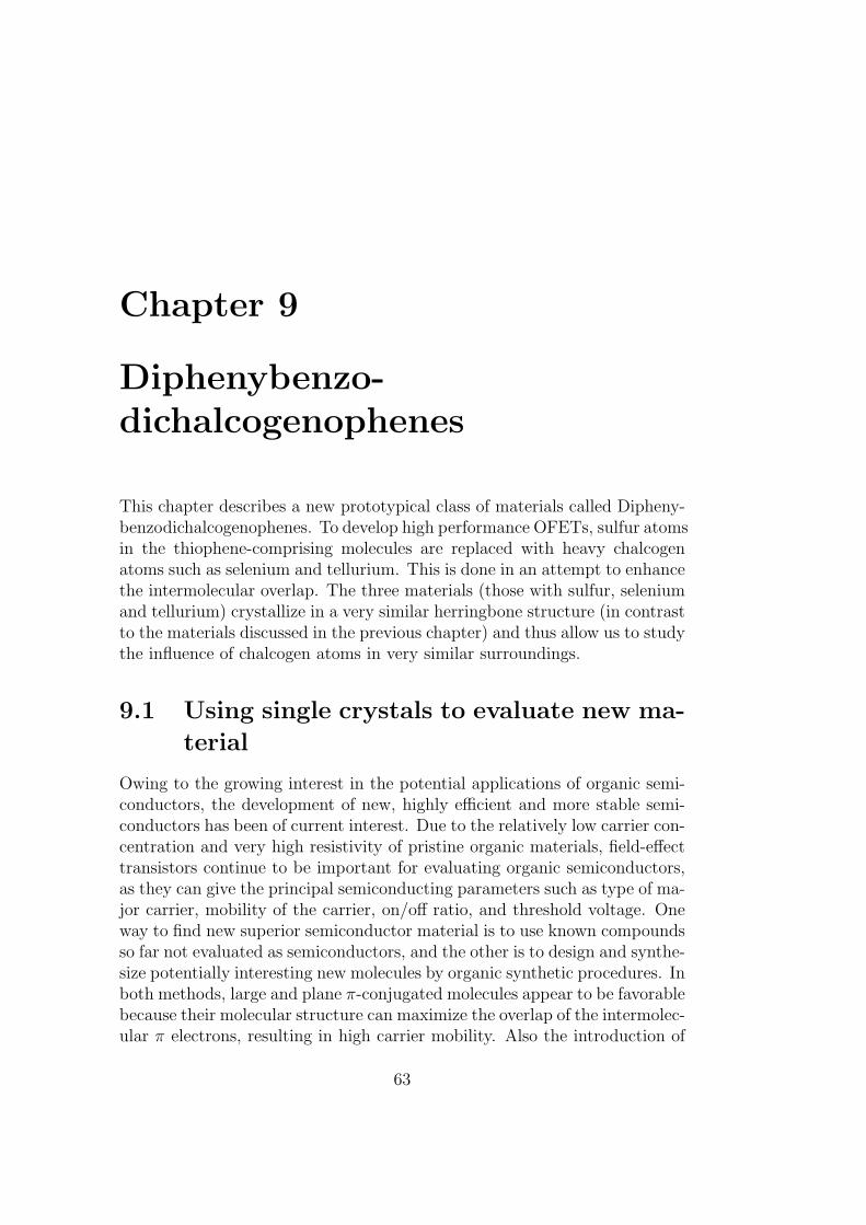
Chapter 9
Diphenybenzo-dichalcogenophenes
This chapter describes a new prototypical class of materials called Dipheny-benzodichalcogenophenes. To develop high performance OFETs, sulfur atomsin the thiophene-comprising molecules are replaced with heavy chalcogenatoms such as selenium and tellurium. This is done in an attempt to enhancethe intermolecular overlap. The three materials (those with sulfur, seleniumand tellurium) crystallize in a very similar herringbone structure (in contrastto the materials discussed in the previous chapter) and thus allow us to studythe influence of chalcogen atoms in very similar surroundings.
9.1 Using single crystals to evaluate new ma-
terial
Owing to the growing interest in the potential applications of organic semi-conductors, the development of new, highly efficient and more stable semi-conductors has been of current interest. Due to the relatively low carrier con-centration and very high resistivity of pristine organic materials, field-effecttransistors continue to be important for evaluating organic semiconductors,as they can give the principal semiconducting parameters such as type of ma-jor carrier, mobility of the carrier, on/off ratio, and threshold voltage. Oneway to find new superior semiconductor material is to use known compoundsso far not evaluated as semiconductors, and the other is to design and synthe-size potentially interesting new molecules by organic synthetic procedures. Inboth methods, large and plane π-conjugated molecules appear to be favorablebecause their molecular structure can maximize the overlap of the intermolec-ular π electrons, resulting in high carrier mobility. Also the introduction of
63
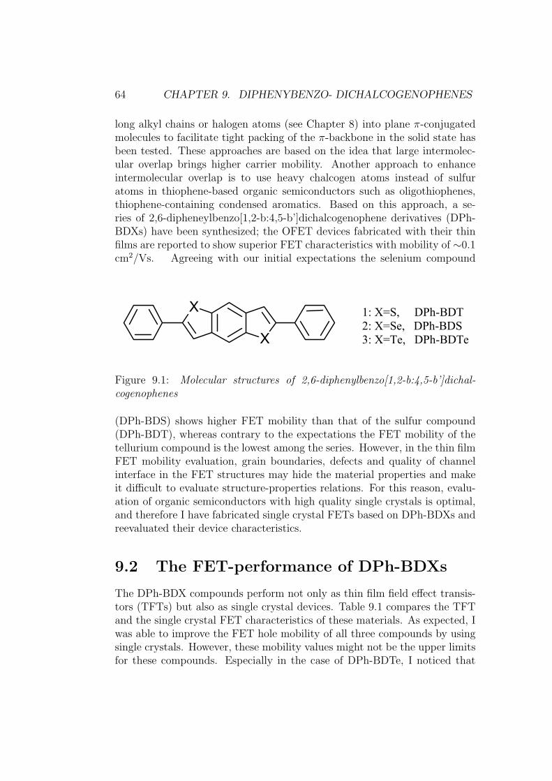
64 CHAPTER 9. DIPHENYBENZO- DICHALCOGENOPHENES
long alkyl chains or halogen atoms (see Chapter 8) into plane π-conjugatedmolecules to facilitate tight packing of the π-backbone in the solid state hasbeen tested. These approaches are based on the idea that large intermolec-ular overlap brings higher carrier mobility. Another approach to enhanceintermolecular overlap is to use heavy chalcogen atoms instead of sulfuratoms in thiophene-based organic semiconductors such as oligothiophenes,thiophene-containing condensed aromatics. Based on this approach, a se-ries of 2,6-dipheneylbenzo[1,2-b:4,5-b’]dichalcogenophene derivatives (DPh-BDXs) have been synthesized; the OFET devices fabricated with their thinfilms are reported to show superior FET characteristics with mobility of ∼0.1cm2/Vs. Agreeing with our initial expectations the selenium compound
X
X
1: X=S, DPh-BDT 2: X=Se, DPh-BDS 3: X=Te, DPh-BDTe
Figure 9.1: Molecular structures of 2,6-diphenylbenzo[1,2-b:4,5-b’]dichal-cogenophenes
(DPh-BDS) shows higher FET mobility than that of the sulfur compound(DPh-BDT), whereas contrary to the expectations the FET mobility of thetellurium compound is the lowest among the series. However, in the thin filmFET mobility evaluation, grain boundaries, defects and quality of channelinterface in the FET structures may hide the material properties and makeit difficult to evaluate structure-properties relations. For this reason, evalu-ation of organic semiconductors with high quality single crystals is optimal,and therefore I have fabricated single crystal FETs based on DPh-BDXs andreevaluated their device characteristics.
9.2 The FET-performance of DPh-BDXs
The DPh-BDX compounds perform not only as thin film field effect transis-tors (TFTs) but also as single crystal devices. Table 9.1 compares the TFTand the single crystal FET characteristics of these materials. As expected, Iwas able to improve the FET hole mobility of all three compounds by usingsingle crystals. However, these mobility values might not be the upper limitsfor these compounds. Especially in the case of DPh-BDTe, I noticed that
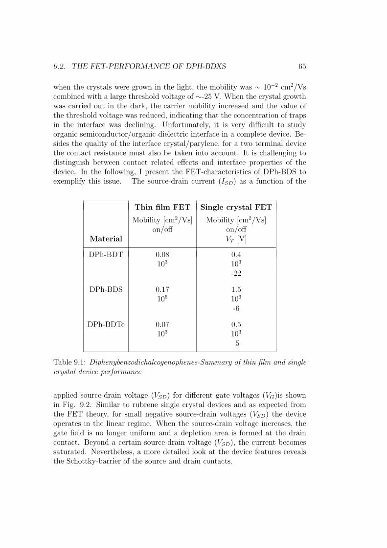
9.2. THE FET-PERFORMANCE OF DPH-BDXS 65
when the crystals were grown in the light, the mobility was ∼ 10−2 cm2/Vscombined with a large threshold voltage of ∼-25 V. When the crystal growthwas carried out in the dark, the carrier mobility increased and the value ofthe threshold voltage was reduced, indicating that the concentration of trapsin the interface was declining. Unfortunately, it is very difficult to studyorganic semiconductor/organic dielectric interface in a complete device. Be-sides the quality of the interface crystal/parylene, for a two terminal devicethe contact resistance must also be taken into account. It is challenging todistinguish between contact related effects and interface properties of thedevice. In the following, I present the FET-characteristics of DPh-BDS toexemplify this issue. The source-drain current (ISD) as a function of the
Thin film FET Single crystal FET
Mobility [cm2/Vs] Mobility [cm2/Vs]on/off on/off
Material VT [V]
DPh-BDT 0.08 0.4103 103
-22
DPh-BDS 0.17 1.5105 103
-6
DPh-BDTe 0.07 0.5103 103
-5
Table 9.1: Diphenybenzodichalcogenophenes-Summary of thin film and singlecrystal device performance
applied source-drain voltage (VSD) for different gate voltages (VG)is shownin Fig. 9.2. Similar to rubrene single crystal devices and as expected fromthe FET theory, for small negative source-drain voltages (VSD) the deviceoperates in the linear regime. When the source-drain voltage increases, thegate field is no longer uniform and a depletion area is formed at the draincontact. Beyond a certain source-drain voltage (VSD), the current becomessaturated. Nevertheless, a more detailed look at the device features revealsthe Schottky-barrier of the source and drain contacts.
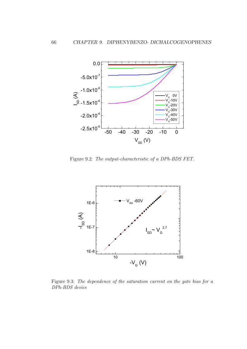
66 CHAPTER 9. DIPHENYBENZO- DICHALCOGENOPHENES
-50 -40 -30 -20 -10 0-2.5x10⁻⁶
-2.0x10⁻⁶
-1.5x10⁻⁶
-1.0x10⁻⁶
-5.0x10⁻⁷
0.0
I SD (A
)
VSD
(V)
VG 0V V
G-10V
VG-20V V
G-30V
VG-40V V
G-50V
Figure 9.2: The output-characteristic of a DPh-BDS FET.
10 1001E-8
1E-7
1E-6
ISD~ VG2.7-I SD
(A)
-VG (V)
VSD -60V
Figure 9.3: The dependence of the saturation current on the gate bias for aDPh-BDS device
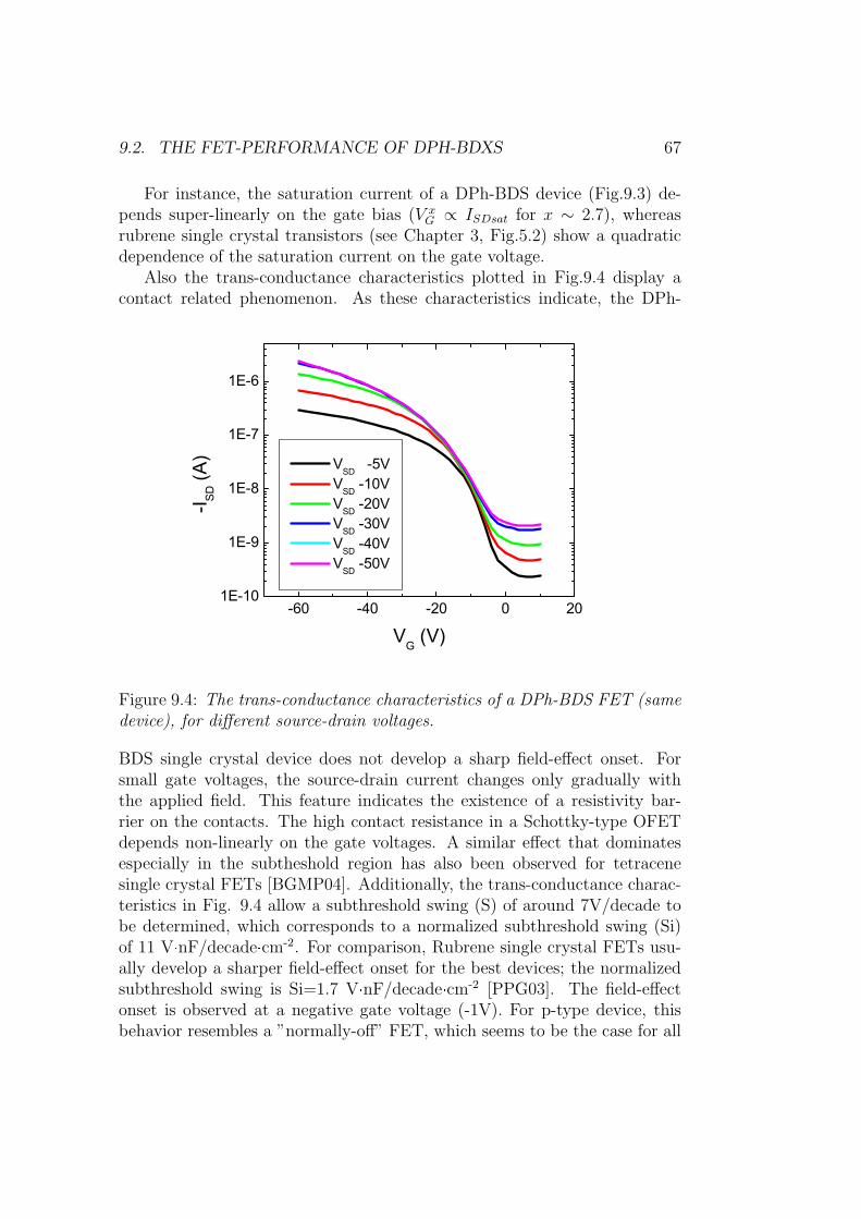
9.2. THE FET-PERFORMANCE OF DPH-BDXS 67
For instance, the saturation current of a DPh-BDS device (Fig.9.3) de-pends super-linearly on the gate bias (V x
G ∝ ISDsat for x ∼ 2.7), whereasrubrene single crystal transistors (see Chapter 3, Fig.5.2) show a quadraticdependence of the saturation current on the gate voltage.
Also the trans-conductance characteristics plotted in Fig.9.4 display acontact related phenomenon. As these characteristics indicate, the DPh-
-60 -40 -20 0 201E-10
1E-9
1E-8
1E-7
1E-6
VSD -5V VSD -10V VSD -20V VSD -30V VSD -40V VSD -50V
-I SD (A
)
VG (V)
Figure 9.4: The trans-conductance characteristics of a DPh-BDS FET (samedevice), for different source-drain voltages.
BDS single crystal device does not develop a sharp field-effect onset. Forsmall gate voltages, the source-drain current changes only gradually withthe applied field. This feature indicates the existence of a resistivity bar-rier on the contacts. The high contact resistance in a Schottky-type OFETdepends non-linearly on the gate voltages. A similar effect that dominatesespecially in the subtheshold region has also been observed for tetracenesingle crystal FETs [BGMP04]. Additionally, the trans-conductance charac-teristics in Fig. 9.4 allow a subthreshold swing (S) of around 7V/decade tobe determined, which corresponds to a normalized subthreshold swing (Si)of 11 V·nF/decade·cm-2. For comparison, Rubrene single crystal FETs usu-ally develop a sharper field-effect onset for the best devices; the normalizedsubthreshold swing is Si=1.7 V·nF/decade·cm-2 [PPG03]. The field-effectonset is observed at a negative gate voltage (-1V). For p-type device, thisbehavior resembles a ”normally-off” FET, which seems to be the case for all
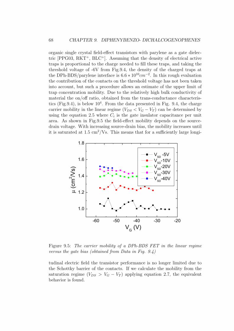
68 CHAPTER 9. DIPHENYBENZO- DICHALCOGENOPHENES
organic single crystal field-effect transistors with parylene as a gate dielec-tric [PPG03, RKT+, BLC+]. Assuming that the density of electrical activetraps is proportional to the charge needed to fill these traps, and taking thethreshold voltage of -6V from Fig.9.4, the density of the charged traps atthe DPh-BDS/parylene interface is 6.6 ∗ 1010cm−2. In this rough evaluationthe contribution of the contacts on the threshold voltage has not been takeninto account, but such a procedure allows an estimate of the upper limit oftrap concentration mobility. Due to the relatively high bulk conductivity ofmaterial the on/off ratio, obtained from the trans-conductance characteris-tics (Fig.9.4), is below 104. From the data presented in Fig. 9.4, the chargecarrier mobility in the linear regime (VDS < VG − VT ) can be determined byusing the equation 2.5 where Ci is the gate insulator capacitance per unitarea. As shown in Fig.9.5 the field-effect mobility depends on the source-drain voltage. With increasing source-drain bias, the mobility increases untilit is saturated at 1.5 cm2/Vs. This means that for a sufficiently large longi-
-60 -50 -40 -30 -20
1.0
1.2
1.4
1.6
1.8
VSD -5V VSD-10V VSD-20V VSD-30V VSD-40V
VG (V)
µ (c
m2 /V
s)
Figure 9.5: The carrier mobility of a DPh-BDS FET in the linear regimeversus the gate bias (obtained from Data in Fig. 9.4)
tudinal electric field the transistor performance is no longer limited due tothe Schottky barrier of the contacts. If we calculate the mobility from thesaturation regime (VDS > VG − VT ) applying equation 2.7, the equivalentbehavior is found.
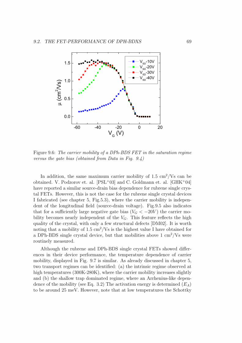
9.2. THE FET-PERFORMANCE OF DPH-BDXS 69
-60 -40 -20 0 20
0.0
0.5
1.0
1.5 VSD-10V VSD-20V VSD-30V VSD-40V
µ (c
m2 /V
s)
VG (V)
Figure 9.6: The carrier mobility of a DPh-BDS FET in the saturation regimeversus the gate bias (obtained from Data in Fig. 9.4)
In addition, the same maximum carrier mobility of 1.5 cm2/Vs can beobtained. V. Podzorov et. al. [PSL+03] and C. Goldmann et. al. [GHK+04]have reported a similar source-drain bias dependence for rubrene single crys-tal FETs. However, this is not the case for the rubrene single crystal devicesI fabricated (see chapter 5, Fig.5.3), where the carrier mobility is indepen-dent of the longitudinal field (source-drain voltage). Fig.9.5 also indicatesthat for a sufficiently large negative gate bias (VG < −20V ) the carrier mo-bility becomes nearly independent of the VG. This feature reflects the highquality of the crystal, with only a few structural defects [DM02]. It is worthnoting that a mobility of 1.5 cm2/Vs is the highest value I have obtained fora DPh-BDS single crystal device, but that mobilities above 1 cm2/Vs wereroutinely measured.
Although the rubrene and DPh-BDS single crystal FETs showed differ-ences in their device performance, the temperature dependence of carriermobility, displayed in Fig. 9.7 is similar. As already discussed in chapter 5,two transport regimes can be identified: (a) the intrinsic regime observed athigh temperatures (300K-280K), where the carrier mobility increases slightlyand (b) the shallow trap dominated regime, where an Arrhenius-like depen-dence of the mobility (see Eq. 3.2) The activation energy is determined (EA)to be around 25 meV. However, note that at low temperatures the Schottky
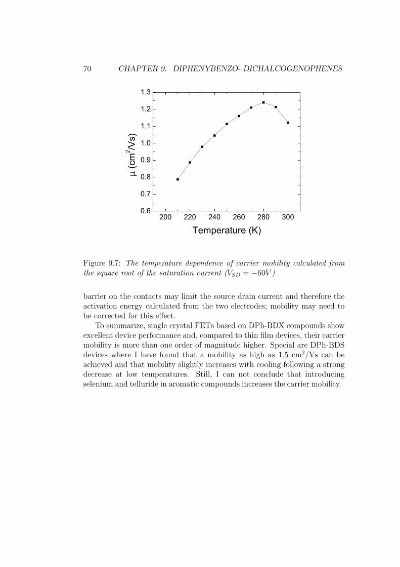
70 CHAPTER 9. DIPHENYBENZO- DICHALCOGENOPHENES
200 220 240 260 280 3000.6
0.7
0.8
0.9
1.0
1.1
1.2
1.3
µ (c
m2 /V
s)
Temperature (K)
Figure 9.7: The temperature dependence of carrier mobility calculated fromthe square root of the saturation current (VSD = −60V )
barrier on the contacts may limit the source drain current and therefore theactivation energy calculated from the two electrodes; mobility may need tobe corrected for this effect.
To summarize, single crystal FETs based on DPh-BDX compounds showexcellent device performance and, compared to thin film devices, their carriermobility is more than one order of magnitude higher. Special are DPh-BDSdevices where I have found that a mobility as high as 1.5 cm2/Vs can beachieved and that mobility slightly increases with cooling following a strongdecrease at low temperatures. Still, I can not conclude that introducingselenium and telluride in aromatic compounds increases the carrier mobility.
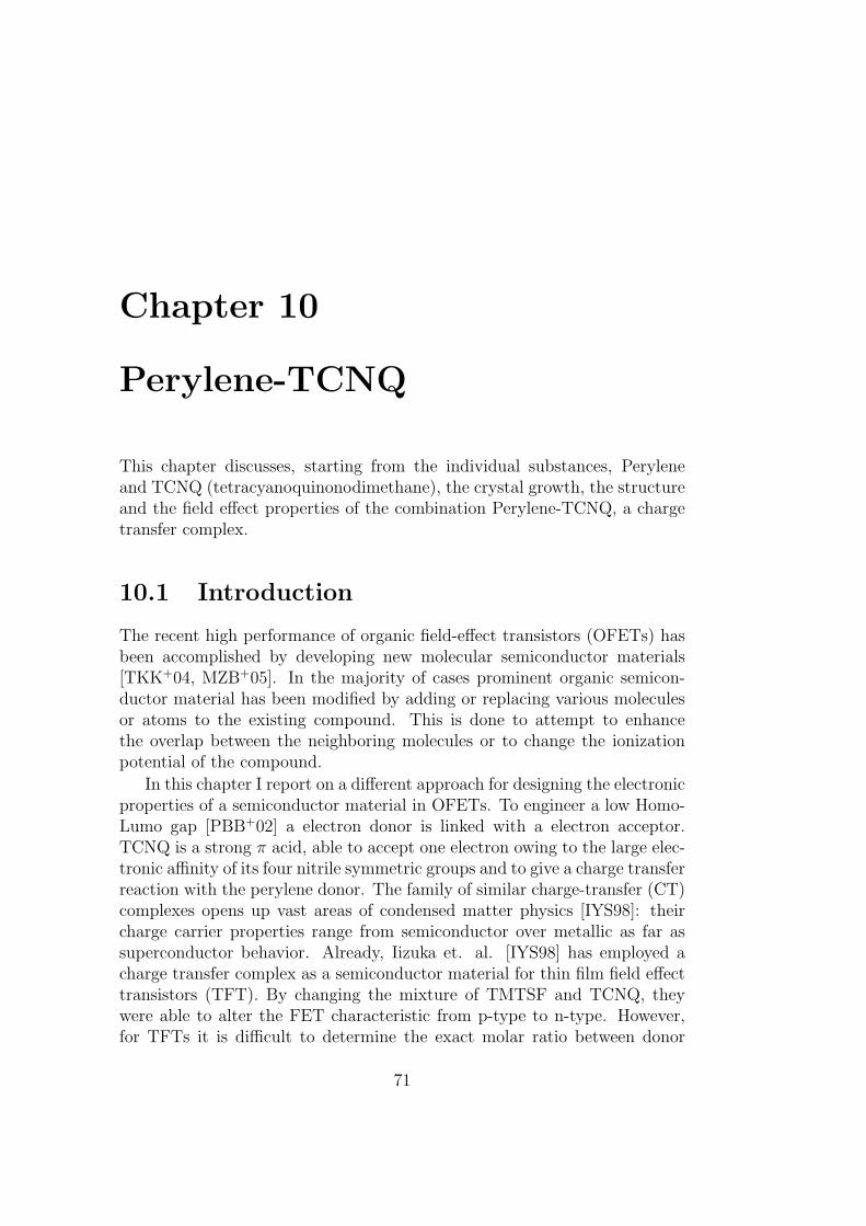
Chapter 10
Perylene-TCNQ
This chapter discusses, starting from the individual substances, Peryleneand TCNQ (tetracyanoquinonodimethane), the crystal growth, the structureand the field effect properties of the combination Perylene-TCNQ, a chargetransfer complex.
10.1 Introduction
The recent high performance of organic field-effect transistors (OFETs) hasbeen accomplished by developing new molecular semiconductor materials[TKK+04, MZB+05]. In the majority of cases prominent organic semicon-ductor material has been modified by adding or replacing various moleculesor atoms to the existing compound. This is done to attempt to enhancethe overlap between the neighboring molecules or to change the ionizationpotential of the compound.
In this chapter I report on a different approach for designing the electronicproperties of a semiconductor material in OFETs. To engineer a low Homo-Lumo gap [PBB+02] a electron donor is linked with a electron acceptor.TCNQ is a strong π acid, able to accept one electron owing to the large elec-tronic affinity of its four nitrile symmetric groups and to give a charge transferreaction with the perylene donor. The family of similar charge-transfer (CT)complexes opens up vast areas of condensed matter physics [IYS98]: theircharge carrier properties range from semiconductor over metallic as far assuperconductor behavior. Already, Iizuka et. al. [IYS98] has employed acharge transfer complex as a semiconductor material for thin film field effecttransistors (TFT). By changing the mixture of TMTSF and TCNQ, theywere able to alter the FET characteristic from p-type to n-type. However,for TFTs it is difficult to determine the exact molar ratio between donor
71
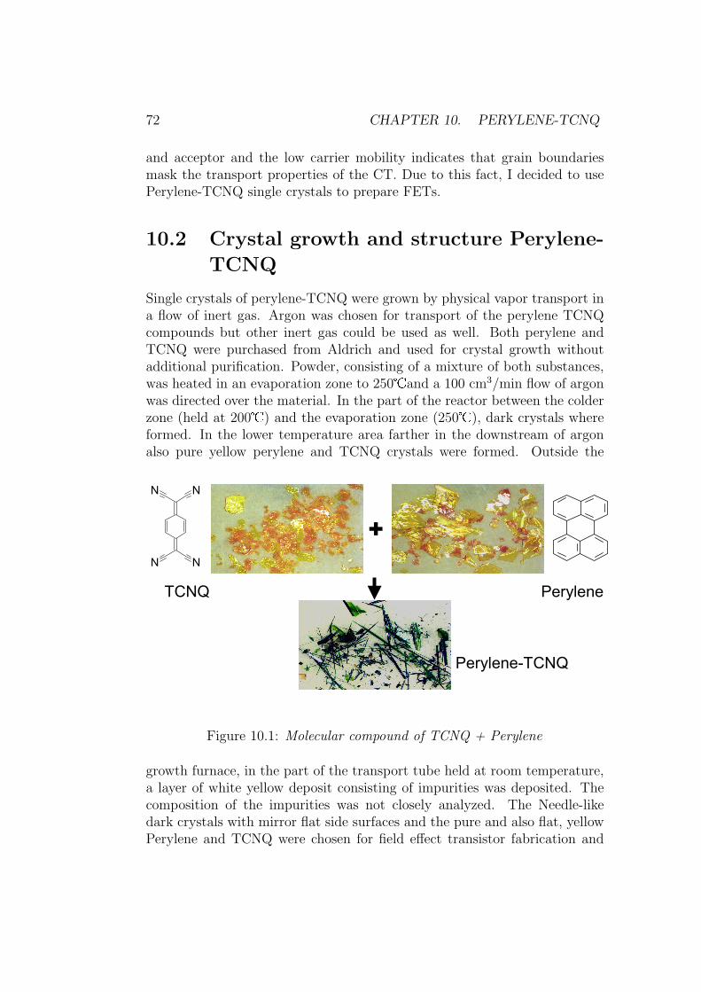
72 CHAPTER 10. PERYLENE-TCNQ
and acceptor and the low carrier mobility indicates that grain boundariesmask the transport properties of the CT. Due to this fact, I decided to usePerylene-TCNQ single crystals to prepare FETs.
10.2 Crystal growth and structure Perylene-
TCNQ
Single crystals of perylene-TCNQ were grown by physical vapor transport ina flow of inert gas. Argon was chosen for transport of the perylene TCNQcompounds but other inert gas could be used as well. Both perylene andTCNQ were purchased from Aldrich and used for crystal growth withoutadditional purification. Powder, consisting of a mixture of both substances,was heated in an evaporation zone to 250and a 100 cm3/min flow of argonwas directed over the material. In the part of the reactor between the colderzone (held at 200) and the evaporation zone (250), dark crystals whereformed. In the lower temperature area farther in the downstream of argonalso pure yellow perylene and TCNQ crystals were formed. Outside the
TCNQ
Perylene-TCNQ
Perylene
+
NN
N N
Figure 10.1: Molecular compound of TCNQ + Perylene
growth furnace, in the part of the transport tube held at room temperature,a layer of white yellow deposit consisting of impurities was deposited. Thecomposition of the impurities was not closely analyzed. The Needle-likedark crystals with mirror flat side surfaces and the pure and also flat, yellowPerylene and TCNQ were chosen for field effect transistor fabrication and
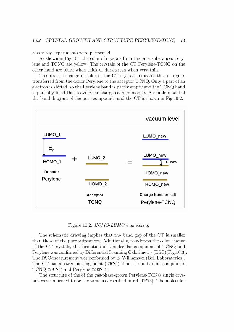
10.2. CRYSTAL GROWTH AND STRUCTURE PERYLENE-TCNQ 73
also x-ray experiments were performed.As shown in Fig.10.1 the color of crystals from the pure substances Pery-
lene and TCNQ are yellow. The crystals of the CT Perylene-TCNQ on theother hand are black when thick or dark green when very thin.
This drastic change in color of the CT crystals indicates that charge istransferred from the donor Perylene to the acceptor TCNQ. Only a part of anelectron is shifted, so the Perylene band is partly empty and the TCNQ bandis partially filled thus leaving the charge carriers mobile. A simple model ofthe band diagram of the pure compounds and the CT is shown in Fig.10.2.
Perylene-TCNQ
vacuum level
LUMO_1LUMO_1
HOMO_1HOMO_1LUMO_2LUMO_2
HOMO_2HOMO_2
++ ==
LUMO_newLUMO_new
HOMO_newHOMO_new
HOMO_newHOMO_new
LUMO_newLUMO_newEg
Egnew
Donator
Charge transfer salt
Perylene
Acceptor
TCNQ
Figure 10.2: HOMO-LUMO engineering
The schematic drawing implies that the band gap of the CT is smallerthan those of the pure substances. Additionally, to address the color changeof the CT crystals, the formation of a molecular compound of TCNQ andPerylene was confirmed by Differential Scanning Calorimetry (DSC)(Fig.10.3).The DSC-measurement was performed by E. Williamson (Bell Laboratories).The CT has a lower melting point (260) than the individual compoundsTCNQ (297) and Perylene (283).
The structure of the of the gas-phase-grown Perylene-TCNQ single crys-tals was confirmed to be the same as described in ref.[TP73]. The molecular
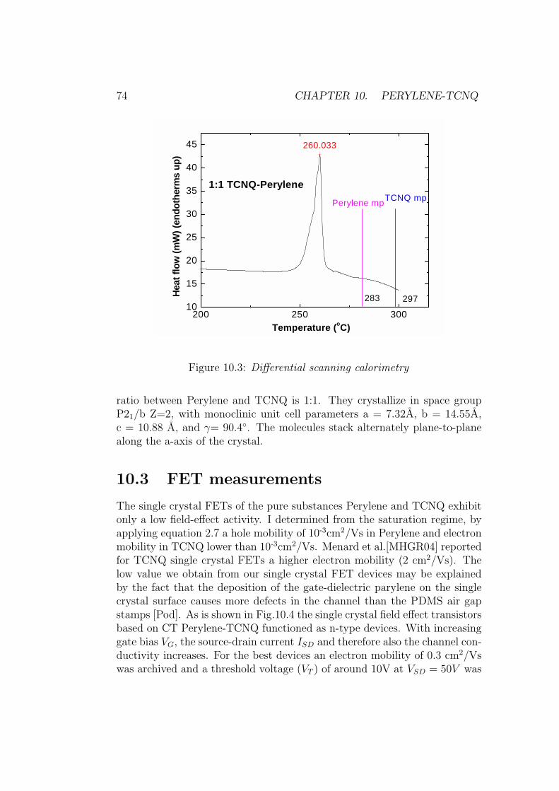
74 CHAPTER 10. PERYLENE-TCNQ
200 250 30010
15
20
25
30
35
40
45 260.033
Temperature (oC)
TCNQ mpPerylene mp
297283Hea
t flo
w (m
W) (
endo
ther
ms
up)
1:1 TCNQ-Perylene
Figure 10.3: Differential scanning calorimetry
ratio between Perylene and TCNQ is 1:1. They crystallize in space groupP21/b Z=2, with monoclinic unit cell parameters a = 7.32A, b = 14.55A,c = 10.88 A, and γ= 90.4. The molecules stack alternately plane-to-planealong the a-axis of the crystal.
10.3 FET measurements
The single crystal FETs of the pure substances Perylene and TCNQ exhibitonly a low field-effect activity. I determined from the saturation regime, byapplying equation 2.7 a hole mobility of 10-3cm2/Vs in Perylene and electronmobility in TCNQ lower than 10-3cm2/Vs. Menard et al.[MHGR04] reportedfor TCNQ single crystal FETs a higher electron mobility (2 cm2/Vs). Thelow value we obtain from our single crystal FET devices may be explainedby the fact that the deposition of the gate-dielectric parylene on the singlecrystal surface causes more defects in the channel than the PDMS air gapstamps [Pod]. As is shown in Fig.10.4 the single crystal field effect transistorsbased on CT Perylene-TCNQ functioned as n-type devices. With increasinggate bias VG, the source-drain current ISD and therefore also the channel con-ductivity increases. For the best devices an electron mobility of 0.3 cm2/Vswas archived and a threshold voltage (VT ) of around 10V at VSD = 50V was
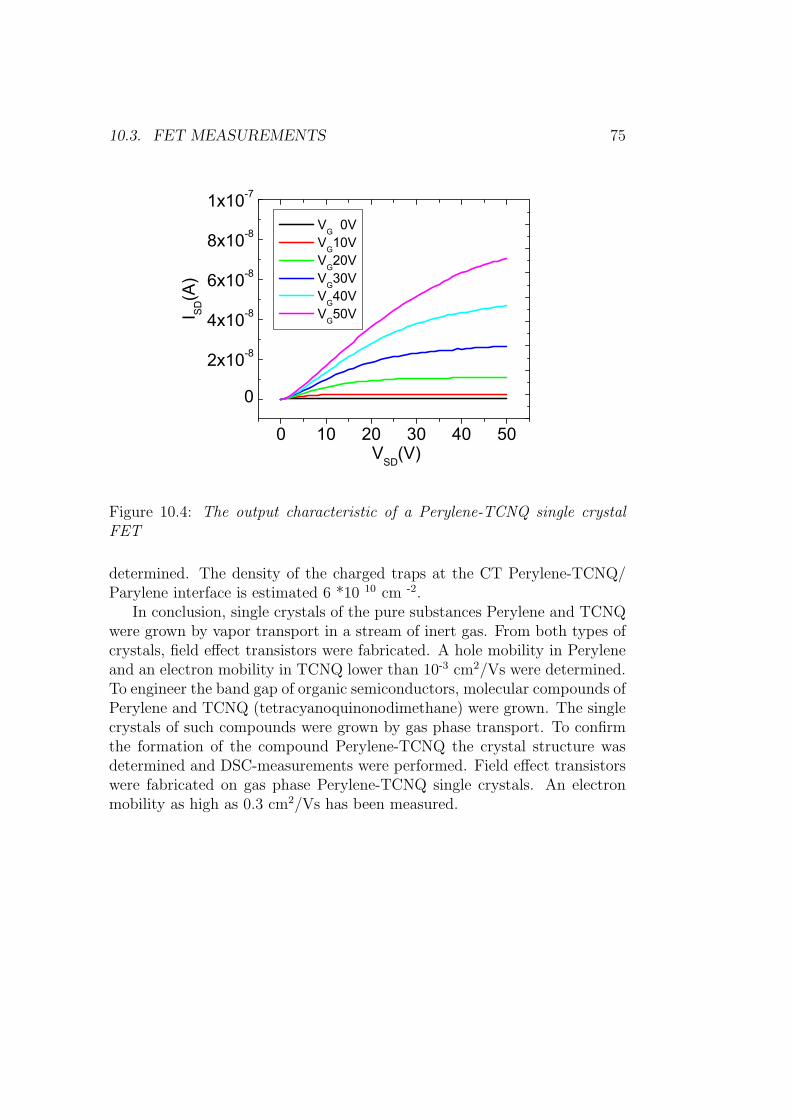
10.3. FET MEASUREMENTS 75
0 10 20 30 40 50
0
2x10⁻⁸
4x10⁻⁸
6x10⁻⁸
8x10⁻⁸
1x10⁻⁷I S
D(A
)
VSD(V)
VG 0V VG10V VG20V VG30V VG40V VG50V
Figure 10.4: The output characteristic of a Perylene-TCNQ single crystalFET
determined. The density of the charged traps at the CT Perylene-TCNQ/Parylene interface is estimated 6 *10 10 cm -2.
In conclusion, single crystals of the pure substances Perylene and TCNQwere grown by vapor transport in a stream of inert gas. From both types ofcrystals, field effect transistors were fabricated. A hole mobility in Peryleneand an electron mobility in TCNQ lower than 10-3 cm2/Vs were determined.To engineer the band gap of organic semiconductors, molecular compounds ofPerylene and TCNQ (tetracyanoquinonodimethane) were grown. The singlecrystals of such compounds were grown by gas phase transport. To confirmthe formation of the compound Perylene-TCNQ the crystal structure wasdetermined and DSC-measurements were performed. Field effect transistorswere fabricated on gas phase Perylene-TCNQ single crystals. An electronmobility as high as 0.3 cm2/Vs has been measured.

76 CHAPTER 10. PERYLENE-TCNQ
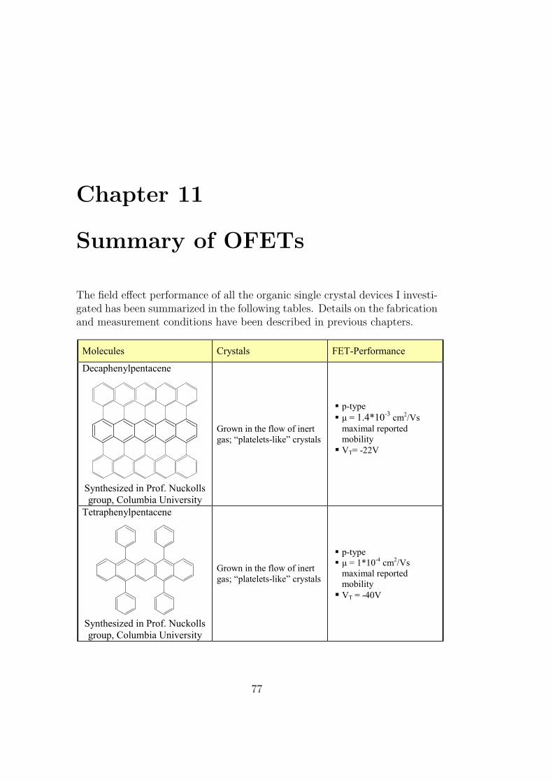
Chapter 11
Summary of OFETs
The field effect performance of all the organic single crystal devices I investi-gated has been summarized in the following tables. Details on the fabricationand measurement conditions have been described in previous chapters.
Molecules Crystals FET-Performance
Decaphenylpentacene
Synthesized in Prof. Nuckolls group, Columbia University
Grown in the flow of inert gas; “platelets-like” crystals
p-type µ = 1.4*10-3 cm2/Vs maximal reported mobility VT= -22V
Tetraphenylpentacene
Synthesized in Prof. Nuckolls group, Columbia University
Grown in the flow of inert gas; “platelets-like” crystals
p-type µ = 1*10-4 cm2/Vs maximal reported mobility VT = -40V
77
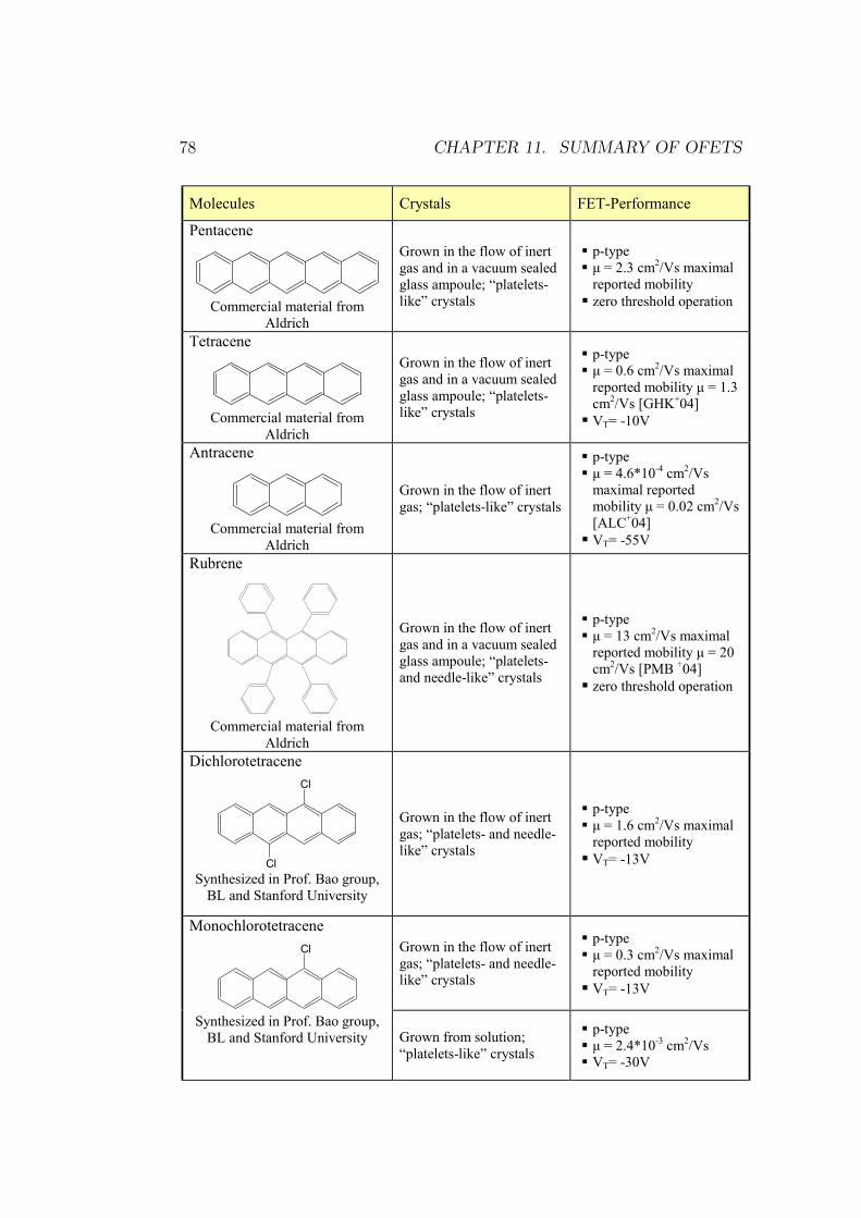
78 CHAPTER 11. SUMMARY OF OFETS
Molecules Crystals FET-Performance
Pentacene
Commercial material from
Aldrich
Grown in the flow of inert gas and in a vacuum sealed glass ampoule; “platelets- like” crystals
p-type µ = 2.3 cm2/Vs maximal reported mobility zero threshold operation
Tetracene
Commercial material from
Aldrich
Grown in the flow of inert gas and in a vacuum sealed glass ampoule; “platelets- like” crystals
p-type µ = 0.6 cm2/Vs maximal reported mobility µ = 1.3 cm2/Vs [GHK+04] VT= -10V
Antracene
Commercial material from
Aldrich
Grown in the flow of inert gas; “platelets-like” crystals
p-type µ = 4.6*10-4 cm2/Vs maximal reported mobility µ = 0.02 cm2/Vs [ALC+04] VT= -55V
Rubrene
Commercial material from
Aldrich
Grown in the flow of inert gas and in a vacuum sealed glass ampoule; “platelets- and needle-like” crystals
p-type µ = 13 cm2/Vs maximal reported mobility µ = 20 cm2/Vs [PMB +04] zero threshold operation
Dichlorotetracene Cl
Cl Synthesized in Prof. Bao group,
BL and Stanford University
Grown in the flow of inert gas; “platelets- and needle- like” crystals
p-type µ = 1.6 cm2/Vs maximal reported mobility VT= -13V
Grown in the flow of inert gas; “platelets- and needle- like” crystals
p-type µ = 0.3 cm2/Vs maximal reported mobility VT= -13V
Monochlorotetracene Cl
Synthesized in Prof. Bao group,
BL and Stanford University
Grown from solution; “platelets-like” crystals
p-type µ = 2.4*10-3 cm2/Vs VT= -30V
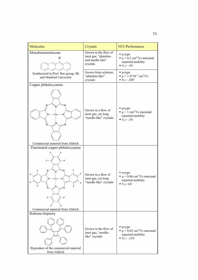
79
Molecules Crystals FET-Performance Grown in the flow of inert gas; “platelets- and needle-like” crystals
p-type µ = 0.2 cm2/Vs maximal reported mobility VT= -5V
Monobromotetracene Br
Synthesized in Prof. Bao group, BL
and Stanford University
Grown from solution; “platelets-like” crystals
p-type µ = 1.4*10-3 cm2/Vs VT= -30V
Copper phthalocyanine
NN N
N
N NN
N Cu
Commercial material from Aldrich
Grown in a flow of inert gas; cm long “needle-like” crystals
p-type µ = 1 cm2/Vs maximal reported mobility VT= -5V
Fluorinated copper phthalocyanine
NN N
N
N NN
N Cu
FF
F
F
FF
F F
FF
F
F
FF
FF
Commercial material from Aldrich
Grown in a flow of inert gas; cm long “needle-like” crystals
n-type µ = 0.06 cm2/Vs maximal reported mobility VT= 6V
Rubrene-Impurity
Byproduct of the commercial material
from Aldrich
Grown in the flow of inert gas; “needle-like” crystals
p-type µ = 0.02 cm2/Vs maximal reported mobility VT= -15V
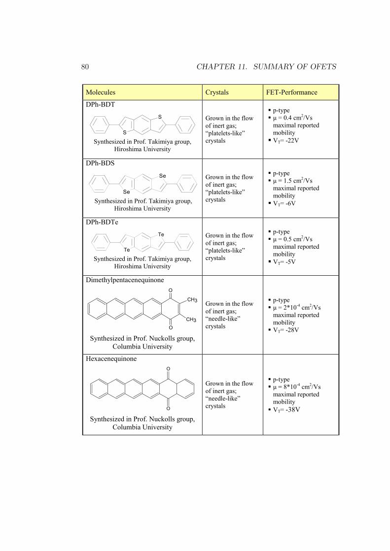
80 CHAPTER 11. SUMMARY OF OFETS
Molecules Crystals FET-Performance
DPh-BDT
S
S
Synthesized in Prof. Takimiya group,
Hiroshima University
Grown in the flow of inert gas; “platelets-like” crystals
p-type µ = 0.4 cm2/Vs maximal reported mobility VT= -22V
DPh-BDS
Se
Se
Synthesized in Prof. Takimiya group, Hiroshima University
Grown in the flow of inert gas; “platelets-like” crystals
p-type µ = 1.5 cm2/Vs maximal reported mobility VT= -6V
DPh-BDTe
Te
Te
Synthesized in Prof. Takimiya group,
Hiroshima University
Grown in the flow of inert gas; “platelets-like” crystals
p-type µ = 0.5 cm2/Vs maximal reported mobility VT= -5V
Dimethylpentacenequinone O
O
CH3
CH3
Synthesized in Prof. Nuckolls group,
Columbia University
Grown in the flow of inert gas; “needle-like” crystals
p-type µ = 2*10-4 cm2/Vs maximal reported mobility VT= -28V
Hexacenequinone O
O Synthesized in Prof. Nuckolls group,
Columbia University
Grown in the flow of inert gas; “needle-like” crystals
p-type µ = 8*10-4 cm2/Vs maximal reported mobility VT= -38V
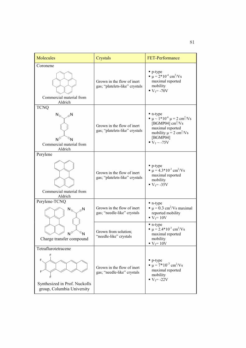
81
Molecules Crystals FET-Performance
Coronene
Commercial material from
Aldrich
Grown in the flow of inert gas; “platelets-like” crystals
p-type µ = 2*10-4 cm2/Vs maximal reported mobility VT= -70V
TCNQ NN
N N Commercial material from
Aldrich
Grown in the flow of inert gas; “platelets-like” crystals
n-type µ ~ 1*10-6 µ = 2 cm2/Vs [BGMP04] cm2/Vs maximal reported mobility µ = 2 cm2/Vs [BGMP04] VT ~ -75V
Perylene
Commercial material from
Aldrich
Grown in the flow of inert gas; “platelets-like” crystals
p-type µ = 4.3*10-3 cm2/Vs maximal reported mobility VT= -35V
Grown in the flow of inert gas; “needle-like” crystals
n-type µ = 0.3 cm2/Vs maximal reported mobility VT= 10V
Perylene-TCNQ
NN
N N Charge transfer compound
Grown from solution; “needle-like” crystals
n-type µ = 2.4*10-3 cm2/Vs maximal reported mobility VT= 10V
Tetraflurotetracene F
F
F
F
Synthesized in Prof. Nuckolls group, Columbia University
Grown in the flow of inert gas; “needle-like” crystals
p-type µ = 7*10-3 cm2/Vs maximal reported mobility VT= -22V

82 CHAPTER 11. SUMMARY OF OFETS
Chapter 12
Transition metaldichalcogenides
The inertness of the Van der Waals face of layered transition metal dichalco-genides (TMDs) against chemical reaction in general, and photocorrosion inparticular, is among the leading factors for the interest in photovoltaic basedmaterials [Buc92]. So far, they have not been considered to be promising assemiconductor materials for field effect transistors. In this chapter transi-tion metal dichalcogenides, in particular WSe2, will be evaluated for futuredevice applications.
12.1 TMDs for FET devices?
In modern electronics, the requirements for field effect devices are stringentand often contradictory, e.g., a combination of high charge carrier mobilityand mechanical flexibility. Neither of the developed types of FETs satisfiesthese requirements. For example, silicon FETs have a relatively high µ =500cm2/Vs [TTIT94]. However, because of high processing temperatures, theSi-based technology is incompatible with the emerging field of ”flexible” elec-tronics. On the other hand, the organic-based FETs that provide the basisfor inexpensive, flexible and lightweight electronic devices [SBB+97, Hor98,KB00, Rog01, DTK95, Kla02] are notoriously known for their low charge car-rier mobility and poor chemical stability. Although several novel materialshave recently been considered for FETs [RNJ99, KMD99, Dua03], the questfor new semiconducting materials and fabrication technologies is a high prior-ity task for the electronic industry. The FET performance depends criticallyon two parameters: the threshold gate voltage (VT ), corresponding to theformation of the conducting channel, and the mobility of the field-induced
83
84 CHAPTER 12. TRANSITION METAL DICHALCOGENIDES
charge carriers (µ). With respect to these parameters, conventional inorganicand organic semiconductors are at opposite ends of a wide spectrum of mate-rials potentially suitable for FET fabrication. Indeed, strong covalent bond-ing of atoms in inorganic semiconductors such as Si results in a small effectivemass of charge carriers and relatively high charge carrier mobility. However,the covalent bonding also leads to a large concentration of chemically activedangling bonds at the Si surface, which trap the field-induced charge. Fromthe year 1947, when J. Bardeen realized the importance of surface states, ittook more than two decades to invent the techniques for passivation of thesurface charge traps, a critical step in the Si-based FET technology [RH97].In contrast to Si, the surface of weakly bonded van-der-Waals organic semi-conductors (e.g., polyacenes [Hor98, KB00] and conjugated polymers [Sir99])is characterized by a low density of dangling bonds, and, hence, an intrin-sically low density of surface traps. This advantage, however, comes at theprice of a low carrier mobility (∼0.1-20 cm2/Vs) because of the large effec-tive mass of polaronic charge carriers in organic semiconductors (see, e.g.[KH81, PMB+04]).
Field effect transistors based on transition metal dichalcogenides com-bine several advantages of the existing FETs. The unique structure of thesematerials results in a highly inert, trap-free basal surface of the single crys-tals and enables fabrication of FETs with an intrinsically low field-effectthreshold and a high mobility of charge carriers, comparable to that in thebest single-crystal Si devices. The TMD-based transistors can operate inboth electron- and hole-accumulation modes depending on the polarity ofthe gate voltage (the so-called ambipolar operation, which is rarely observedin high-mobility FETs). Finally, these novel FETs survive bending, ow-ing to the mechanical flexibility of TMD crystals and the polymer parylenefilm used as the gate insulator. All these properties make the TMD-basedtransistors very attractive for applications in ”flexible” electronics. Field-effect activity has been observed for several transition metal dichalcogenides(WSe2, MoSe2, SnS2, HfS2). However, I focus on the characteristics of theWSe2-based device.
12.2 FET-characteristics of WSe2
The dependence of the source-drain current (ISD) on the gate voltage (VG)for a WSe2 FET, measured at a fixed source-drain voltage (VSD), the so-called trans-conductance characteristic, is shown in Fig. 12.1. Formation ofa conducting channel between the source and drain contacts is manifestedby the sharp increase of ISD by several orders of magnitude at both nega-
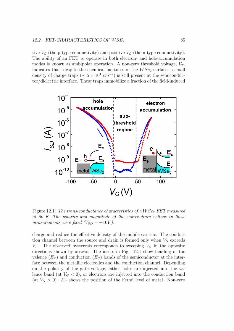
12.2. FET-CHARACTERISTICS OF WSE2 85
tive VG (the p-type conductivity) and positive VG (the n-type conductivity).The ability of an FET to operate in both electron- and hole-accumulationmodes is known as ambipolar operation. A non-zero threshold voltage, VT ,indicates that, despite the chemical inertness of the WSe2 surface, a smalldensity of charge traps (∼ 5× 1011cm−2) is still present at the semiconduc-tor/dielectric interface. These traps immobilize a fraction of the field-induced
VG (V)
Figure 12.1: The trans-conductance characteristics of a WSe2 FET measuredat 60 K. The polarity and magnitude of the source-drain voltage in thesemeasurements were fixed (VSD = +10V ).
charge and reduce the effective density of the mobile carriers. The conduc-tion channel between the source and drain is formed only when VG exceedsVT . The observed hysteresis corresponds to sweeping VG in the oppositedirections shown by arrows. The insets in Fig. 12.1 show bending of thevalence (EV ) and conduction (EC) bands of the semiconductor at the inter-face between the metallic electrodes and the conduction channel. Dependingon the polarity of the gate voltage, either holes are injected into the va-lence band (at VG < 0), or electrons are injected into the conduction band(at VG > 0). EF shows the position of the Fermi level of metal. Non-zero
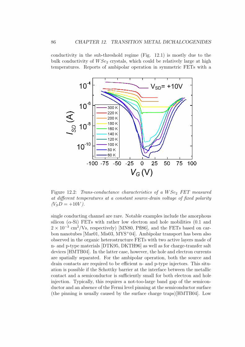
86 CHAPTER 12. TRANSITION METAL DICHALCOGENIDES
conductivity in the sub-threshold regime (Fig. 12.1) is mostly due to thebulk conductivity of WSe2 crystals, which could be relatively large at hightemperatures. Reports of ambipolar operation in symmetric FETs with a
VSD= +10V
VG (V)
Figure 12.2: Trans-conductance characteristics of a WSe2 FET measuredat different temperatures at a constant source-drain voltage of fixed polarity(VSD = +10V ).
single conducting channel are rare. Notable examples include the amorphoussilicon (α-Si) FETs with rather low electron and hole mobilities (0.1 and2 × 10−3 cm2/Vs, respectively) [MN80, Pfl86], and the FETs based on car-bon nanotubes [Mar01, Mis03, MYS+04]. Ambipolar transport has been alsoobserved in the organic heterostructure FETs with two active layers made ofn- and p-type materials [DTK95, DKTH96] as well as for charge-transfer saltdevices [HMTB04]. In the latter case, however, the hole and electron currentsare spatially separated. For the ambipolar operation, both the source anddrain contacts are required to be efficient n- and p-type injectors. This situ-ation is possible if the Schottky barrier at the interface between the metalliccontact and a semiconductor is sufficiently small for both electron and holeinjection. Typically, this requires a not-too-large band gap of the semicon-ductor and an absence of the Fermi level pinning at the semiconductor surface(the pinning is usually caused by the surface charge traps)[HMTB04]. Low
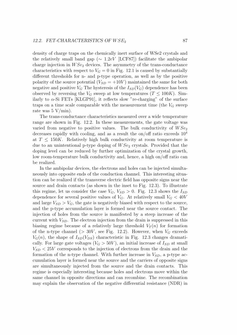
12.2. FET-CHARACTERISTICS OF WSE2 87
density of charge traps on the chemically inert surface of WSe2 crystals andthe relatively small band gap (∼ 1.2eV [LCF87]) facilitate the ambipolarcharge injection in WSe2 devices. The asymmetry of the trans-conductancecharacteristics with respect to VG = 0 in Fig. 12.1 is caused by substantiallydifferent thresholds for n- and p-type operation, as well as by the positivepolarity of the source potential (VSD = +10V ) maintained the same for bothnegative and positive VG The hysteresis of the ISD(VG) dependence has beenobserved by reversing the VG sweep at low temperatures (T ≤ 100K). Sim-ilarly to α-Si FETs [KLGP91], it reflects slow ”re-charging” of the surfacetraps on a time scale comparable with the measurement time (the VG sweeprate was 5 V/min).
The trans-conductance characteristics measured over a wide temperaturerange are shown in Fig. 12.2. In these measurements, the gate voltage wasvaried from negative to positive values. The bulk conductivity of WSe2
decreases rapidly with cooling, and as a result the on/off ratio exceeds 104
at T ≤ 150K. Relatively high bulk conductivity at room temperature isdue to an unintentional p-type doping of WSe2 crystals. Provided that thedoping level can be reduced by further optimization of the crystal growth,low room-temperature bulk conductivity and, hence, a high on/off ratio canbe realized.
In the ambipolar devices, the electrons and holes can be injected simulta-neously into opposite ends of the conduction channel. This interesting situa-tion can be realized if the transverse electric field has opposite signs near thesource and drain contacts (as shown in the inset to Fig. 12.3). To illustratethis regime, let us consider the case VG, VSD > 0. Fig. 12.3 shows the ISD
dependence for several positive values of VG. At relatively small VG < 40Vand large VSD > VG, the gate is negatively biased with respect to the source,and the p-type accumulation layer is formed near the source contact. Theinjection of holes from the source is manifested by a steep increase of thecurrent with VSD. The electron injection from the drain is suppressed in thisbiasing regime because of a relatively large threshold VT (n) for formationof the n-type channel (> 30V , see Fig. 12.2). However, when VG exceedsVG(n), the shape of ISD(VDS) characteristic in Fig. 12.3 changes dramati-cally. For large gate voltages (VG > 50V ), an initial increase of ISD at smallVSD < 25V corresponds to the injection of electrons from the drain and theformation of the n-type channel. With further increase in VSD, a p-type ac-cumulation layer is formed near the source and the carriers of opposite signsare simultaneously injected from the source and the drain contacts. Thisregime is especially interesting because holes and electrons move within thesame channel in opposite directions and can recombine. The recombinationmay explain the observation of the negative differential resistance (NDR) in
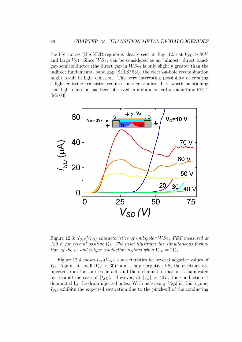
88 CHAPTER 12. TRANSITION METAL DICHALCOGENIDES
the I-V curves (the NDR regime is clearly seen in Fig. 12.3 at VSD > 30Vand large VG). Since WSe2 can be considered as an ”almost” direct band-gap semiconductor (the direct gap in WSe2 is only slightly greater than theindirect fundamental band gap [SELS+83]), the electron-hole recombinationmight result in light emission. This very interesting possibility of creatinga light-emitting transistor requires further studies. It is worth mentioningthat light emission has been observed in ambipolar carbon nanotube FETs[Mis03].
VG=10 V
VSD (V)
VSD = 2VG
VG
Figure 12.3: ISD(VDS) characteristics of ambipolar WSe2 FET measured at120 K for several positive VG. The inset illustrates the simultaneous forma-tion of the n- and p-type conduction regions when VSD = 2VG.
Figure 12.4 shows ISD(VSD) characteristics for several negative values ofVG. Again, at small |VG| < 30V and a large negative VS, the electrons areinjected from the source contact, and the n-channel formation is manifestedby a rapid increase of |ISD|. However, at |VG| > 40V , the conduction isdominated by the drain-injected holes. With increasing |VSD| in this regime,ISD exhibits the expected saturation due to the pinch-off of the conducting
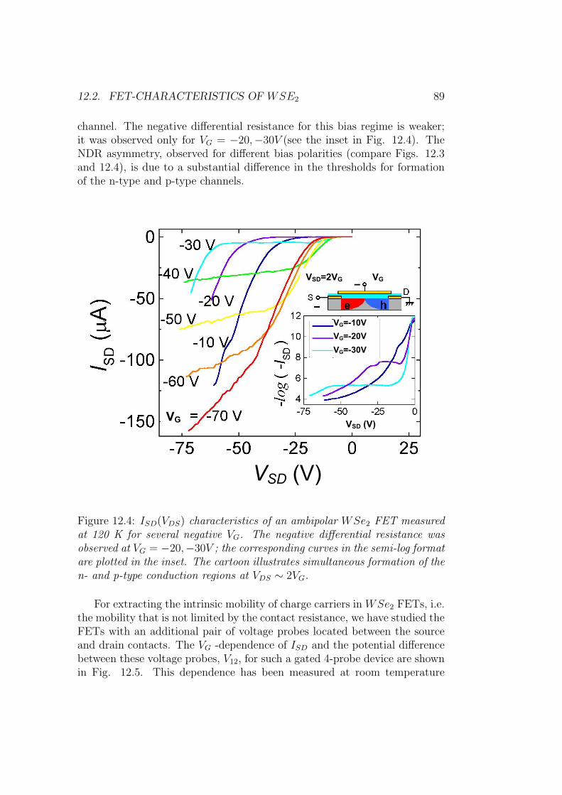
12.2. FET-CHARACTERISTICS OF WSE2 89
channel. The negative differential resistance for this bias regime is weaker;it was observed only for VG = −20,−30V (see the inset in Fig. 12.4). TheNDR asymmetry, observed for different bias polarities (compare Figs. 12.3and 12.4), is due to a substantial difference in the thresholds for formationof the n-type and p-type channels.
VSD (V)
VSD (V)
VSD=2VG VG
VG
VG=-10V VG=-20V VG=-30V
Figure 12.4: ISD(VDS) characteristics of an ambipolar WSe2 FET measuredat 120 K for several negative VG. The negative differential resistance wasobserved at VG = −20,−30V ; the corresponding curves in the semi-log formatare plotted in the inset. The cartoon illustrates simultaneous formation of then- and p-type conduction regions at VDS ∼ 2VG.
For extracting the intrinsic mobility of charge carriers in WSe2 FETs, i.e.the mobility that is not limited by the contact resistance, we have studied theFETs with an additional pair of voltage probes located between the sourceand drain contacts. The VG -dependence of ISD and the potential differencebetween these voltage probes, V12, for such a gated 4-probe device are shownin Fig. 12.5. This dependence has been measured at room temperature
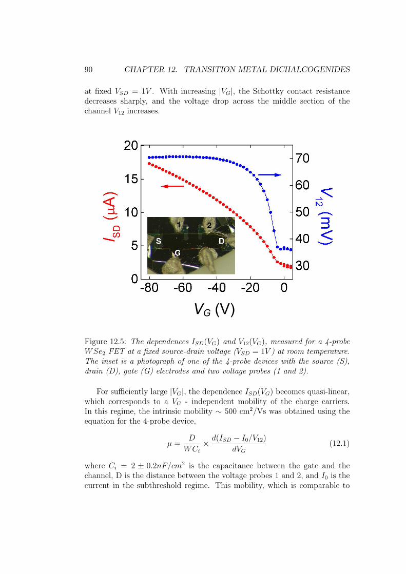
90 CHAPTER 12. TRANSITION METAL DICHALCOGENIDES
at fixed VSD = 1V . With increasing |VG|, the Schottky contact resistancedecreases sharply, and the voltage drop across the middle section of thechannel V12 increases.
VG (V)
Figure 12.5: The dependences ISD(VG) and V12(VG), measured for a 4-probeWSe2 FET at a fixed source-drain voltage (VSD = 1V ) at room temperature.The inset is a photograph of one of the 4-probe devices with the source (S),drain (D), gate (G) electrodes and two voltage probes (1 and 2).
For sufficiently large |VG|, the dependence ISD(VG) becomes quasi-linear,which corresponds to a VG - independent mobility of the charge carriers.In this regime, the intrinsic mobility ∼ 500 cm2/Vs was obtained using theequation for the 4-probe device,
µ =D
WCi
× d(ISD − I0/V12)
dVG
(12.1)
where Ci = 2 ± 0.2nF/cm2 is the capacitance between the gate and thechannel, D is the distance between the voltage probes 1 and 2, and I0 is thecurrent in the subthreshold regime. This mobility, which is comparable to
12.2. FET-CHARACTERISTICS OF WSE2 91
the mobility in commercial Si MOSFETs, demonstrates the great potentialof the WSe2 FETs. Note that the ”apparent” mobility, estimated from thedata in Fig. 12.5 using the conventional 2-probe expression,
µ =D
WCiVSD
× d(ISD − I0)
dVG
(12.2)
is much lower (∼ 100 cm2/Vs) because of the contact resistance.In conclusion, the layered TMDs combine the advantages of organic and
inorganic semiconductors: they provide surfaces with an intrinsically lowdensity of trap states and high carrier mobility. Especially promising char-acteristics have been observed for WSe2-based devices, which exhibit theintrinsic mobility ∼ 500 cm2/Vs for the field-induced holes at room temper-ature. This number is comparable to the mobility in the best (non-flexible)Si MOSFETs and exceeds µ in flexible organic TFTs by ∼ 3 orders of mag-nitude. In contrast to the Si devices, the WSe2 FETs can operate in theambipolar mode. To the best of our knowledge, this is the first observationof a high-mobility ambipolar regime in a planar symmetric FET. The practi-cal applications of the FETs based on transition metal dichalcogenides mightbe numerous, provided that the technology of highly-ordered TMD films isdeveloped. The ambipolar FETs can be used in complementary circuits thatrequire both n-type and p-type devices. These devices hold a great promisefor optoelectronic applications due to the possibility of radiative recombina-tion of electrons and holes simultaneously injected the conduction channel.The unique electrical characteristics, in combination with mechanical flexi-bility, make field effect transistors based on transition metal dichalcogenidesvery attractive for ”flexible” electronics.

92 CHAPTER 12. TRANSITION METAL DICHALCOGENIDES
Chapter 13
Conclusion
With parylene as a gate-dielectric material, I was able to successfully produceFETs based on a variety of organic as well as transition metal dichalcogenidesemiconductors. The results of this work are briefly summarized below.
By employing single crystals, the device performance, including thecharge carrier mobility, the field effect threshold, and the subthresholdslope, have been significantly improved. The FET characteristics areno longer limited by the disorder common for thin films.
To limit the concentration of impurities, it is preferable to grow crystalsby physical vapor transport since crystals grown from solution tend toincorporate the solvents into the intra-molecular position in the weaklybonded Van der Waals network of molecules.
However, organic materials especially are known for undergoing severaldisproportionation reactions during the sublimation process. The prod-ucts of these reactions may become embedded into the host crystal. Tolimit the formation of impurities and therefore improve the electroniccharge transport in the crystal the sublimation temperature and thepresence of oxygen during the growth process should be reduced.
If the structure of a molecules is conjugated, impurities themselves canshow field effect activity. In general, an important criterion for thechoice of potential organic semiconductor material seems to be to pickmolecules that consist of an alternating sequence of single and doublebonds which allow charge transport though the molecules.
So far, of all the organic semiconductor materials, rubrene exhibitsthe best device performance. A mobility anisotropy and an increase of
93
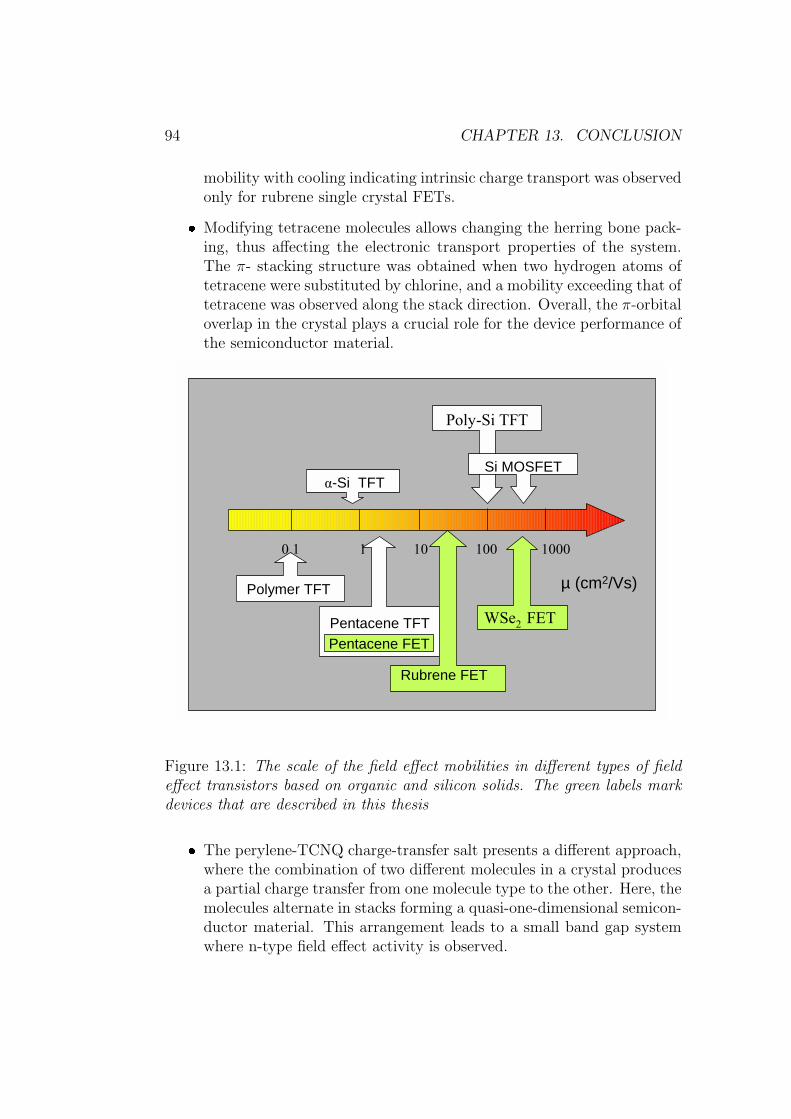
94 CHAPTER 13. CONCLUSION
mobility with cooling indicating intrinsic charge transport was observedonly for rubrene single crystal FETs.
Modifying tetracene molecules allows changing the herring bone pack-ing, thus affecting the electronic transport properties of the system.The π- stacking structure was obtained when two hydrogen atoms oftetracene were substituted by chlorine, and a mobility exceeding that oftetracene was observed along the stack direction. Overall, the π-orbitaloverlap in the crystal plays a crucial role for the device performance ofthe semiconductor material.
0.1 1 100010010
Polymer TFT
Pentacene TFT
µ (cm2/Vs)
α-Si TFT
Poly-Si TFT
Si MOSFET
0.1 100010010
Polymer TFT µ (cm2/Vs)
α-Si TFT
Poly-Si TFT
Si MOSFET
WSe2 FETPentacene TFT
Rubrene FET
Pentacene FET
1
Figure 13.1: The scale of the field effect mobilities in different types of fieldeffect transistors based on organic and silicon solids. The green labels markdevices that are described in this thesis
The perylene-TCNQ charge-transfer salt presents a different approach,where the combination of two different molecules in a crystal producesa partial charge transfer from one molecule type to the other. Here, themolecules alternate in stacks forming a quasi-one-dimensional semicon-ductor material. This arrangement leads to a small band gap systemwhere n-type field effect activity is observed.
95
Layered transition metal dichalcogenides are interesting alternative toorganic semiconductors. Similar to organic materials their surface isVan der Waals determined. Therefore, an intrinsic low density of trapstates at semiconductor/dielectic interface is observed. The WSe2-based devices with their high carrier mobilities and ambipolar operationare especially promising.
The schema presented in Fig.13.1 visualize the progress that has beenmade since the beginning of these thesis studies. The carrier mobilities Iachieved for the single crystal FETs based on layered semiconductors arecomparable with or even exceed those obtained for the best silicon baseddevices. Therefore, for future industrial applications, layered semiconductorsas presented in this thesis provide a promising basis for novel materials forinexpensive, flexible and lightweight electronic devices.

96 CHAPTER 13. CONCLUSION
Chapter 14
Zusammenfassung
Die Verwendung von Parylen als Dielektrikum ermoglichte mir die Unter-suchung von Einkristallfeldeffekttransitoren auf der Basis von organischenund anorganischen Halbleitermaterialien. Die Ergebnisse dieser Arbeit sindim folgenden zusammengefasst.
Die Kenndaten der Feldeffekttransistoren wie Ladungstragerbeweglich-keit, Steilheit und Schwellenspannung konnten durch die Verwendungvon Einkristallen deutlich verbessert werden, da der Ladungstransportin Einkristallen nicht durch Korngrenzen limitiert ist.
Aus der Gasphase gezogene Kristalle zeigen deutlich bessere Trans-porteigenschaften als jene aus der Losung. Da organischen Kristalle auseinzelnen Molekulen aufgebaut sind, welche nur durch van der WaalsKrafte zusammengehalten sind, werden Losungsmittelreste daher ein-fach ins Kristallgitter eingebaut.
Problematisch fur die Qualitat der Kristalle kann auch der Gasphasen-transport sein. Speziell fur Pentacen sind unter dem Einfluss vonhohen Temperaturen und Sauerstoff eine Vielzahl von Zerfallsproduk-ten bekannt. Diese konnen wiederum zu Kristallverunreinigungen undKristallbaufehlern fuhren. Daher hat sich das Zuchten der Penta-cenkristalle im Vakuum bei einer niedrigen Sublimationstemperaturbesonders bewahrt. Die Transporteigenschaften der Kristalle konntenaufgrund dieser Methode signifikant verbessert werden.
Auch Materialverunreinigungen selbst konnen Feldeffekt zeigen, fallsdie Verbindung eine konjugierte Molekulstruktur aufweist. Dies istgenerell ein wichtiges Kriterium fur die Auswahl potenzieller organ-ischer Halbleitermaterialien. Nur die konjugierte Struktur ermoglichteinen optimalen Ladungstragertransport im Molekul.
97
98 CHAPTER 14. ZUSAMMENFASSUNG
Von alle untersuchten organischen Halbleitern ist das Material Rubrenbesonders hervorzuheben. Die Rubren-Einkristalltransistoren weisendie hochste Ladungstragerbeweglichkeit und die niedrigste Schwellen-spannung auf. Faktoren wie Zunahme der Ladungstragerbeweglichkeitbei sinkenden Temperaturen und der Anisotropie der Ladungstrager-beweglichkeit bezuglich der Kristallstrukur deuten darauf hin, dassintrinsische Transporteigenschaften in Rubren-Einkristalltransistorenbeobachtet werden.
Werden bei einem Tetracenmolekul zwei Wasserstoffatome durch zweiChloratome ersetzt so hat dies vor allem Einfluss auf die Kristallstruk-tur. Durch diese Modifikation kann die Uberlappung der π-Orbitale imKristall verbessert werden, diese wiederum bestimmen wesentlich dieTransporteigenschaften des Materials. Daher wird fur Dichlorotetracen-Einkristalle eine hohere Ladungstragerbeweglichkeit gemessen als furreines Tetracen.
Das Kombinieren zweier Molekule Perylen und TCNQ fuhrt zu einerweiteren Materialklasse, den Ladungstransfer-Salzen. Die quasi eindi-mensionale Kristallstruktur befordert den parzillen Ladungstransferzwischen Perylen und TCNQ. Die Transistoren dieses Mischsystemssind n-type.
Die Familie der Schicht-Ubergangsmetall-Dichalkogenide sind eine in-teressannte Alternative zu organischen Halbleitern. Ahlich wie die or-ganischen Materialien besitzen auch sie eine van der Waals Oberfache,welche fur eine geringe Defektdichte am Interface Isolator / Halbleiterverantwortlich ist. Besonders vielversprechend sind WSe2-Einkristall-transistoren mit ihrer hohen Ladungstragermobilitat fur Locher undElektronen.
Bibliography
[AEP02] J. E. Anthony, D. L. Eaton, and S. R. Parkin. Org. Lett., 4:15,2002.
[Bao04] Zh. Bao. Nat. Mat., 3:137, 2004.
[BB48] J. Bardeen and W.H. Brattain. Phys. Rev., 74:230, 1948.
[Bes04] C. Besnard. PhD thesis, Lund, 2004.
[BGMP04] R.W. I. De Boer, M. E. Gershenson, A. F. Morpurgo, andV. Podorov. Phys. Status Solid, A 201 (6):1302, 2004.
[BLC+] V. Y. Butko, D. V. Lang, X. Chi, J. C. Lashley, and A. P.Ramirez. to be publised.
[BLD96] Zh. Bao, A. J. Lovinger, and A. Dodabalapur. Appl. Phys. Lett.,69:3066, 1996.
[BLR04] V. Y. Butko, J. C. Lashley, and A. P. Ramirez. cond-mat/0405077, 2004.
[Bub60] R. H. Bube. Photoconductivity in solids. Wiley, New York,1960.
[Buc92] E. Bucher. Photovoltaic properties of solid state junctions oflayered semiconductors, in Photoelectrochemistry and Photo-voltaics of Layered Semiconductors. Kluwer Academic Publish-ers, Dordrecht, Boston, London, 1992.
[CBB01] J. Cornil, D. Beljonne, and J. L. Bredas. Adv. Mater, 13:1053,2001.
[CCK04] M. D. Curtis, J. Cao, and J. W. J. Kampf. J. Am. Chem. Soc.,126:4318, 2004.
99
100 BIBLIOGRAPHY
[DBC90] J. A. Doge, J. D. Bain, and A. R. Chamberlin. J. Org. Chem.,55:4190, 1990.
[dDvdW27] H. de Diesbach and E. von der Weid. Helv. Chim. Acta, 10:886,1927.
[DFG+98] C. D. Dimitrakopoulos, B. K. Furman, T. Graham, S. Hegde,and S. Purushothaman. Syn. Met., 92:47, 1998.
[DKP+99] C. D. Dimitrakopoulos, I. Kymissis, S. Purushothaman, D. A.Neumayer, P. R. Duncombe, and R. B. Laibowitz. Adv. Mater.,11:1372, 1999.
[DKTH96] A. Dodabalapur, H. E. Katz, L. Torsi, and R. C. Haddon. Appl.Phys. Lett., 68:1108, 1996.
[DM02] C. D. Dimitrakopoulos and P. R. L. Malenfant. Adv. Mater.,14:99, 2002.
[DPK+99] C. D. Dimitrakopoulos, S. Purushothaman, J. Kymissis, A. Cal-legari, and J. M. Shaw. Science, 283:822, 1999.
[DTK95] A. Dodabalapur, L. Torsi, and H. E. Katz. Science, 268:270,1995.
[Dua03] X. Duan. Nature, 425:274, 2003.
[EH69] D. Emin and T. Holstein. Ann. Phys., 53:439, 1969.
[Emi85] D. Emin. Basic issue of electronic transport in insulating poly-mers. Marcel Dekker, New York, (1985).
[FSMP98] G. G. Fedoruk, D.I. Sagaidak, A. V. Misevich, and A. E.Pochtenny. Sensors and Actuators, B 48:351, 1998.
[GD88] A. Gravezzotti and G. R. Desiraju. Acta Cryst. B, 44:427, 1988.
[GHK+04] C. Goldmann, S. Haas, C. Krellner, K. P. Pernstich, D. J.Grundlach, and B. Batlogg. cond-mat/ 0403210, 2004.
[GHRH99] G.Horowitz, R. Hajlaoui, Bourguiga R, and R. Hajlaoui. Syn.Met., 101:401, 1999.
[HHH00] G. Horowitz, M. E. Hajlaoui, and R. Hajlaoui. J. Appl. Phys.,87:4456, 2000.
BIBLIOGRAPHY 101
[HMTB04] T. Hasegawa, K. Mattenberger, J. Takeya, and B. Batlogg.Phys. Rev. B, 69:245115, 2004.
[Hol59] T. Holstein. Ann. Phys., 8:343, 1959.
[Hor98] G. Horowitz. Adv. Mater., 10:365, 1998.
[Hor99] G. Horowitz. J. Mater. Chem., 44:2021, 1999.
[IMO88] M. Iyoda, A. Mizusuna, and M. Oda. Chem. Lett., 1:149, 1988.
[IYS98] T. Ishiguro, K. Yamaji, and G. Saito. Organic Superconductors.Springer-Verlag, Berlin, (1998).
[JBP04] O. D. Jurchescu, J. Baas, and T. T. M. Palstra. cond-mat/0404130, 2004.
[KA60] D. Khang and M.M. Atalla. Silicon-silicon dioxide field inducedsurface devices. In Carnegie Institute of Technology, editor, IRESolid-State Devices Res. Conf., Pittsburgh, Pa., 1960.
[Kar90] N. Karl. Defect control in Semiconductors. Elsevier NorthHoland, Amsterdam, 1990.
[KB00] H. E. Katz and Z. Bao. J. Phys. Chem., B 104:671, 2000.
[KH81] K. C. Kao and W. Hwang. Electrical Transport in Solids. Perg-amon Press, Oxford, 1981.
[Kla02] H. Klauk. J. Appl. Phys., 92:5259, 2002.
[KLGP91] J. Kanicki, F. R. Libsch, J. Griffith, and R. Polastre. J. Appl.Phys., 69:2339, 1991.
[KM01] N. Karl and J. Marktanner. Molecular crystals and liquid crys-tals, 355:149, 2001.
[KMD99] C. R. Kagan, D. B. Mitzi, and C. D. Dimitracopoulos. Science,286:945, 1999.
[KSSL97] Ch. Kloc, P. G. Simpkins, T. Siegrist, and R. A. Laudise. J.Cryst. Growth, 182:416, 1997.
[LCF87] J. R. Lince, D. J. Carre, and P. D. Fleischauer. Phys. Rev. B,36:1647, 1987.
102 BIBLIOGRAPHY
[LGNJ97] Y. Y. Lin, D. J. Gundlach, S. F. Nelson, and T. N. Jackson.IEEE Trans. Electron Devices, 44:1325, 1997.
[Lie77] R. M. A. Lieth. Preparation and Crystal Growth of Materialswith Layered Structures. D. Reidel Pub. Co., Dordrecht, Hol-land; Boston, USA, 1977.
[Lil30] J.E. Lilienfeld. U.S. patent, 1,745.175, 1930.
[LKSS98] R.A. Laudise, Ch. Kloc, P.G. Simpkins, and T. Siegrist. J.Cryst. Growth, 187:449, 1998.
[LPS03] T. Lindner, G. Paasch, and S. Scheinert. 48. InternationalesWissenschaftliches Kolloquium Technische Universitaet Ilme-nau, 2003.
[LR36a] R.P. Linstead and J.M Robertson. J. Chem. Soc. London, page1736, 1936.
[LR36b] R.P. Linstead and J.M Robertson. Strukturbericht, 4:320, 1936.
[LS70] P. G. LeComber and W. E. Spear. Phys. Rev. Lett., 25:509,1970.
[Mar01] R. Martel. Phys. Rev. Lett., 87:256805, 2001.
[Mat02] C. C. Mattheus. PhD thesis, Groningen, 2002.
[MHGR04] E. Menard, V. Podzorov S.-H. Hur, A. Gaur M.E Gershenson,and J. A. Rogers. Adv. Materials, 16:2097, 2004.
[Mis03] J. A. Misewich. Science, 300:783, 2003.
[MN80] M. Matsumura and Y. Nara. J. Appl. Phys., 51(12):6443, 1980.
[MT83] F. H. Moser and A.L. Thomas. The Phthalocyanines. CRC,1983.
[MYS+04] E. D. Minot, Y. Yaish, V. Sazonova, J. Y. Park, M. Brink, andP. L. McEuen. cond-mat/0211152, 2004.
[MZB+05] H. Moon, R. Zeis, J. E. Borkent, C. Besnard, A. Lovinger,T. Siegrist Ch. Kloc, and Z. Bao. JACS, 127:3069, 2005.
[NLGJ98] S. F. Nelson, Y.-Y. Lin, D. J. Gundlach, and T. N. Jackson.Appl. Phys. Lett., 72:1854, 1998.
BIBLIOGRAPHY 103
[PBB+02] D. F. Perepichka, M. R. Bryce, A. S. Batsanov, E. J. L.McInnes, J. P. Zhao, and R. D. Farley. Chem. Eur. J. 8, 20:4656,2002.
[PCF+02] T. M. Pappenfus, R. J. Chesterfield, C. D. Frisbie, K. R. Mann,J. Casado, J. D. Raff, and L. L. Miller. J. Am. Chem. Soc.,124:4184, 2002.
[Pfl86] H. Pfleiderer. IEEE Trans. Electron., Devices ED-33:145, 1986.
[PK75] K. H. Probst and N. Karl. Phys. Stat. Sol. (a), 27:499, 1975.
[PMB+04] V. Podzorov, E. Menard, A. Borissov, V. Kiryukhin, J. A.Rogers, and M. E. Gershenson. Phys. Rev. Lett., 93:1302, 2004.
[Pod] V. Podzorov. private communication.
[PPG03] V. Podzorov, V. M. Pudalov, and M. E. Gershenson. Appl.Phys. Lett., 82:1739, 2003.
[PPG04] V. Podzorov, V. M. Pudalov, and M. E. Gershenson. cond-mat/0406738, 2004.
[PS82] M. Pope and C. E. Swenberg. Electronic processes in organiccrystals. Oxford University Press, 1982.
[PSL+03] V. Podzorov, S. E. Sysoev, E. Loginova, V. M. Pudalov, andM. E. Gershenson. Appl. Phys. Lett., 82:3504, 2003.
[Rap97] L. Rapoport. Nature, 387:791, 1997.
[Rem01] M. Remskar. Science, 292:479, 2001.
[RH97] M. Riordan and L. Hoddeson. Crystal fire: the birth of infor-mation age. W.W. Norton & Co., New York London, 1997.
[RKHS97] T. Reinot, W. H. Kim, J. M. Hayes, and G. J. Small. J. Opt.Soc. Am., B 14:602, 1997.
[RKT+] L. Roberson, J. Kowalik, L. Tolbert, Ch. Kloc, R. Zeis, X. Chi,and C. Wilkins. to be publised.
[RNJ99] B. A. Ridley, B. Nivi, and J. M. Jacobson. Science, 286:746,1999.
[Rog01] J. A. Rogers. Proc. Natl. Acad. Sci., 98:4835, 2001.
104 BIBLIOGRAPHY
[SBB+97] Z. Shen, P.E. Burrows, V. Bulovic, S. R. Forrest, and M. E.Thompson. Science, 276:2009, 1997.
[SD86] J. A. R. P. Sarma and G. R. Desiraju. Acc. Chem. Res., 19:222,1986.
[SdBIM04] A. F. Strassen, R. W. I. d. Boer, N. N. Iosad, and A. F. Mor-purgo. cond-mat/0407293, 2004.
[SELS+83] R. Spaeh, U. Elrod, M. Lux-Steiner, E. Bucher, and S. Wagner.Appl. Phys. Lett., 43:79, 1983.
[SHS89] M. Shur, M. Hack, and J. G. Shaw. J. Appl. Phys., 66:3371,1989.
[Sie] T. Siegrist. private communication.
[Sir99] H. Sirringhaus. Nature, 401:685, 1999.
[SLSO+85] R. Spaeh, M. Lux-Steiner, M. Obergfell, E. Bucher, and S. Wag-ner. Appl. Phys. Lett., 47:871, 1985.
[SP48] W. Shockley and G.L. Person. Phys. Rev., 74:232, 1948.
[Spa86] R. Spaeh. PhD thesis, Konstanz, 1986.
[Sze85] S. M. Sze. Semiconductor Devices: Physics and Technology.Wiley, New York, 1985.
[SZP+04] V. C. Sundar, J. Zaumseil, V. Podzorov, E. Menard, R. L. Wil-lett, T. Someya, M. E. Gershenson, and J. A. Rogers. Science,303:1644, 2004.
[TKK+04] K. Takimiya, Y. Kunugi, Y. Konda, N. Niihara, and T. Otsubo.JACS, 126:5084, 2004.
[TMGH92] R. Tenne, L. Margulis, M. Genut, and G. Hodes. Nature,360:444, 1992.
[TP73] I. J. Tickle and C. Keith Prout. J.C.S. Perkin, page 720, 1973.
[TTIT94] S. Takagi, A. Toriumi, M. Iwase, and H. Tango. IEEE Trans.Electron Devices, 41:2357, 1994.
[TW85] R. Tenne and A. Wold. Appl. Phys. Lett., 47:707, 1985.
BIBLIOGRAPHY 105
[TZ01] R. Tenne and A. Zettl. Nanotubes from Inorganic Materials.Springer-Verlag, Berlin Heidelberg, 2001.
[Var48] A. T. Vartanyan. Zh. Fiz. Khim., 22:769, 1948.
[VFO+04] H. Vazquez, F. Flores, R. Oszwaldowski, J. Ortega, R. Perez,and A. Kahn. cond-mat/0405491, 2004.
[YK58] J. Yamashita and T. Kurosawa. J. Phys. Chem. Solids, 5:34,1958.
[YTAKK95] K. Yase, Y. Takahashi, N. Ara-Kato, and A. Kawazu. Jpn. J.Appl. Phys., 34:636, 1995.
[ZLH+96] J. Zhang, J. Liu, J. L. Huang, P. Kim, and C. M. Lieber. Sci-ence, 274:757, 1996.
[ZWWY04] J. Zhang, J. Wang, H. Wang, and D. Yan. Appl. Phys. Lett.,84:142, 2004.

106 BIBLIOGRAPHY
Related Documents