General Description The DS3881 is a single-channel cold-cathode fluores- cent lamp (CCFL) controller for automotive applications that provides up to 300:1 dimming. It is ideal for driving CCFLs used to backlight liquid crystal displays (LCDs) in navigation and infotainment applications and for dri- ving CCFLs used to backlight instrument clusters. The DS3881 is also appropriate for use in marine and avia- tion applications. The DS3881 features EMI suppression functionality and provides a lamp current overdrive mode for rapid lamp heating in cold weather conditions. The DS3881 sup- ports a single lamp configuration with fully independent lamp control and minimal external components. Multiple DS3881 controllers can be cascaded to sup- port applications requiring more than one lamp. Control of the DS3881, after initial programming setup, can be completely achieved through I 2 C software communica- tion. Many DS3881 functions are also pin-controllable if software control is not desired. Applications Automotive LCDs Instrument Clusters Marine and Aviation LCDs Features ♦ Single-Channel CCFL Controller for Backlighting LCD Panels and Instrument Clusters in Automotive Navigation/Infotainment Applications ♦ Minimal External Components Required ♦ I 2 C Interface ♦ Per-Channel Lamp-Fault Monitoring for Lamp- Open, Lamp-Overcurrent, Failure to Strike, and Overvoltage Conditions ♦ Status Register Reports Fault Conditions ♦ Accurate (±5%) Independent On-Board Oscillators for Lamp Frequency (40kHz to 100kHz) and DPWM Burst-Dimming Frequency (22.5Hz to 440Hz) ♦ Lamp and DPWM Frequencies can be Synchronized with External Sources to Reduce Visual LCD Artifacts in Video Applications ♦ Spread-Spectrum Lamp Clock Reduces EMI ♦ Lamp Frequency can be Stepped Up or Down to Move EMI Spurs Out of Band ♦ Lamp Current Overdrive Mode with Automatic Turn-Off Quickly Warms Lamp in Cold Temperatures ♦ Analog or Digital Brightness Control ♦ 300:1 Dimming Range Possible Using the Digital Brightness Control Option ♦ Programmable Soft-Start Minimizes Audible Transformer Noise ♦ On-Board Nonvolatile (NV) Memory Allows Device Customization ♦ 8-Byte NV User Memory for Storage of Serial Numbers and Date Codes ♦ Low-Power Standby Mode ♦ 4.75V to 5.25V Single-Supply Operation ♦ Temperature Range: -40°C to +105°C ♦ 24-Pin TSSOP Package DS3881 Single-Channel Automotive CCFL Controller ______________________________________________ Maxim Integrated Products 1 24 23 22 1 2 3 4 5 6 7 GB1 GA1 SCL SDA A0 FAULT TOP VIEW V CC PDN LCO BRIGHT LOSC 21 8 GND PSYNC 20 9 STEP POSC 19 10 N.C. A1 18 11 OVD1 GND_S 17 12 LCM1 SVML 16 13 SVMH 15 14 V CC LSYNC TSSOP DS3881 Pin Configuration Rev 1; 8/07 For pricing, delivery, and ordering information, please contact Maxim Direct at 1-888-629-4642, or visit Maxim’s website at www.maxim-ic.com. +Denotes lead-free package. Ordering Information Typical Operating Circuit appears at end of data sheet. PART TEMP RANGE PIN-PACKAGE DS3881E+ -40°C to +105°C 24 TSSOP (173 mils) DS3881E+T&R -40°C to +105°C 24 TSSOP (173 mils)

Welcome message from author
This document is posted to help you gain knowledge. Please leave a comment to let me know what you think about it! Share it to your friends and learn new things together.
Transcript

General DescriptionThe DS3881 is a single-channel cold-cathode fluores-cent lamp (CCFL) controller for automotive applicationsthat provides up to 300:1 dimming. It is ideal for drivingCCFLs used to backlight liquid crystal displays (LCDs)in navigation and infotainment applications and for dri-ving CCFLs used to backlight instrument clusters. TheDS3881 is also appropriate for use in marine and avia-tion applications.
The DS3881 features EMI suppression functionality andprovides a lamp current overdrive mode for rapid lampheating in cold weather conditions. The DS3881 sup-ports a single lamp configuration with fully independentlamp control and minimal external components.Multiple DS3881 controllers can be cascaded to sup-port applications requiring more than one lamp. Controlof the DS3881, after initial programming setup, can becompletely achieved through I2C software communica-tion. Many DS3881 functions are also pin-controllable ifsoftware control is not desired.
ApplicationsAutomotive LCDs
Instrument Clusters
Marine and Aviation LCDs
Features♦ Single-Channel CCFL Controller for Backlighting
LCD Panels and Instrument Clusters inAutomotive Navigation/Infotainment Applications
♦ Minimal External Components Required♦ I2C Interface♦ Per-Channel Lamp-Fault Monitoring for Lamp-
Open, Lamp-Overcurrent, Failure to Strike, andOvervoltage Conditions
♦ Status Register Reports Fault Conditions♦ Accurate (±5%) Independent On-Board Oscillators
for Lamp Frequency (40kHz to 100kHz) and DPWMBurst-Dimming Frequency (22.5Hz to 440Hz)
♦ Lamp and DPWM Frequencies can beSynchronized with External Sources to ReduceVisual LCD Artifacts in Video Applications
♦ Spread-Spectrum Lamp Clock Reduces EMI♦ Lamp Frequency can be Stepped Up or Down to
Move EMI Spurs Out of Band♦ Lamp Current Overdrive Mode with Automatic
Turn-Off Quickly Warms Lamp in ColdTemperatures
♦ Analog or Digital Brightness Control♦ 300:1 Dimming Range Possible Using the Digital
Brightness Control Option♦ Programmable Soft-Start Minimizes Audible
Transformer Noise♦ On-Board Nonvolatile (NV) Memory Allows Device
Customization♦ 8-Byte NV User Memory for Storage of Serial
Numbers and Date Codes♦ Low-Power Standby Mode♦ 4.75V to 5.25V Single-Supply Operation♦ Temperature Range: -40°C to +105°C♦ 24-Pin TSSOP Package
DS
38
81
Single-Channel Automotive CCFL Controller
______________________________________________ Maxim Integrated Products 1
24
23
22
1
2
3
4
5
6
7
GB1
GA1SCL
SDA
A0 FAULT
TOP VIEW
VCC
PDN
LCOBRIGHT
LOSC
21
8
GNDPSYNC
20
9
STEPPOSC
19
10
N.C.A1
18
11
OVD1GND_S
17
12
LCM1SVML
16
13SVMH
15
14
VCC
LSYNC
TSSOP
DS3881
Pin Configuration
Rev 1; 8/07
For pricing, delivery, and ordering information, please contact Maxim Direct at 1-888-629-4642,or visit Maxim’s website at www.maxim-ic.com.
+Denotes lead-free package.
Ordering Information
Typical Operating Circuit appears at end of data sheet.
PART TEMP RANGE PIN-PACKAGE
DS3881E+ -40°C to +105°C 24 TSSOP (173 mils)
DS3881E+T&R -40°C to +105°C 24 TSSOP (173 mils)

DS
38
81
Single-Channel Automotive CCFL Controller
2 _____________________________________________________________________
ABSOLUTE MAXIMUM RATINGS
RECOMMENDED OPERATING CONDITIONS(TA = -40°C to +105°C)
Stresses beyond those listed under “Absolute Maximum Ratings” may cause permanent damage to the device. These are stress ratings only, and functionaloperation of the device at these or any other conditions beyond those indicated in the operational sections of the specifications is not implied. Exposure toabsolute maximum rating conditions for extended periods may affect device reliability.
Voltage Range on VCC, SDA, and SCL Relative to Ground.....................................-0.5V to +6.0V
Voltage Range on Leads Other than VCC, SDA, and SCL ......................-0.5V to (VCC + 0.5V), not to exceed +6.0V
Operating Temperature Range .........................-40°C to +105°CEEPROM Programming Temperature Range .........0°C to +85°CStorage Temperature Range .............................-55°C to +125°CSoldering Temperature...................See J-STD-020 Specification
PARAMETER SYMBOL CONDITIONS MIN TYP MAX UNITS
Supply Voltage VCC (Note 1) 4.75 5.25 V
Input Logic 1 VIH 2.0VCC+ 0.3
V
Input Logic 0 VIL -0.3 1.0 V
SVML/H Voltage Range VSVM -0.3VCC +
0.3V
BRIGHT Voltage Range VBRIGHT -0.3VCC +
0.3V
LCM Voltage Range VLCM (Note 2) -0.3VCC +
0.3V
OVD Voltage Range VOVD (Note 2) -0.3VCC +
0.3V
Gate-Driver Output ChargeLoading
QG 20 nC
ELECTRICAL CHARACTERISTICS(VCC = +4.75V to +5.25V, TA = -40°C to +105°C.)
PARAMETER SYMBOL CONDITIONS MIN TYP MAX UNITS
Supply Current ICC GA, GB loaded with 600pF 12 mA
Input Leakage (Digital Pins) IL -1.0 +1.0 µA
Power-Down Current IPDN 1 mA
Output Leakage (SDA, FAULT) ILO High impedance -1.0 +1.0 µA
Low-Level Output Voltage(LSYNC, PSYNC)
VOL IOL = 4mA 0.4 V
VOL1 IOL1 = 3mA 0.4Low-Level Output Voltage(SDA, FAULT) VOL2 IOL2 = 6mA 0.6
V
Low-Level Output Voltage(GA1, GB1)
VOL3 IOL3 = 4mA 0.4 V
High-Level Output Voltage(LSYNC, PSYNC)
VOH IOH = -1mA 2.4 V

DS
38
81
Single-Channel Automotive CCFL Controller
_____________________________________________________________________ 3
ELECTRICAL CHARACTERISTICS (continued)(VCC = +4.75V to +5.25V, TA = -40°C to +105°C.)
PARAMETER SYMBOL CONDITIONS MIN TYP MAX UNITS
High-Level Output Voltage(GA, GB)
VOH1 IOH1 = -1mAVCC -0.4
V
UVLO Threshold: VCC Rising VUVLOR 4.3 V
UVLO Threshold: VCC Falling VUVLOF 3.7 V
UVLO Hysteresis VUVLOH 200 mV
SVML/H Threshold: Rising VSVMR 2.03 2.08 2.15 V
SVML/H Threshold: Falling VSVMF 1.95 2.02 2.07 V
LCM and OVD DC Bias Voltage VDCB 1.1 V
LCM and OVD Input Resistance RDCB 50 kΩLamp Off Threshold VLOT (Note 3) 0.22 0.25 0.28 V
Lamp Over Current VLOC (Note 3) 2.2 2.5 2.8 V
Lamp Regulation Threshold VLRT (Notes 3, 4) 0.9 1.0 1.1 V
OVD Threshold VOVDT (Note 3) 0.9 1.0 1.1 V
Lamp Frequency SourceFrequency Range
fLFS:OSC 40 100 kHz
Lamp Frequency SourceFrequency Tolerance
fLFS:TOL LOSC resistor ±2% over temperature -5 +5 %
Lamp Frequency ReceiverFrequency Range
fLFR:OSC 40 100 kHz
Lamp Frequency ReceiverDuty Cycle
fLFR:DUTY 40 60 %
DPWM Source (Resistor)Frequency Range
fDSR:OSC 22.5 440.0 Hz
DPWM Source (Resistor)Frequency Tolerance
fDSR:TOL POSC resistor ±2% over temperature -5 +5 %
DPWM Source (Ext. Clk)Frequency Range
fDSE:OSC 22.5 440.0 Hz
DPWM Source (Ext. Clk)Duty Cycle
fDFE:DUTY 40 60 %
DPWM ReceiverMin Pulse Width
tDR:MIN (Note 5) 25 µs
BRIGHT Voltage: MinimumBrightness
VBMIN 0.5 V
BRIGHT Voltage: MaximumBrightness
VBMAX 2.0 V
Gate Driver Output Rise/Fall Time tR / tF CL = 600pF 100 ns
GA1 and GB1 Duty Cycle (Note 6) 44 %

DS
38
81
Single-Channel Automotive CCFL Controller
4 _____________________________________________________________________
Note 1: All voltages are referenced to ground unless otherwise noted. Currents into the IC are positive, out of the IC negative.Note 2: During fault conditions, the AC-coupled feedback values are allowed to be below the absolute max rating of the LCM1 or
OVD1 pin for up to 1 second.Note 3: Voltage with respect to VDCB.Note 4: Lamp overdrive and analog dimming (based on reduction of lamp current) are disabled.Note 5: This is the minimum pulse width guaranteed to generate an output burst, which will generate the DS3881’s minimum burst
duty cycle. This duty cycle may be greater than the duty cycle of the PSYNC input. Once the duty cycle of the PSYNC inputis greater than the DS3881’s minimum duty cycle, the output’s duty cycle will track the PSYNC’s duty cycle. LeavingPSYNC low (0% duty cycle) disables the GA1 and GB1 outputs in DPWM receiver mode.
Note 6: This is the maximum lamp frequency duty cycle that will be generated at GA1 or GB1 outputs with spread-spectrum modu-lation disabled.
Note 7: I2C interface timing shown is for fast-mode (400kHz) operation. This device is also backward compatible with I2C standard-mode timing.
Note 8: After this period, the first clock pulse can be generated.Note 9: CB—total capacitance allowed on one bus line in picofarads.Note 10: EEPROM write time applies to all the EEPROM memory. EEPROM write begins after a stop condition occurs.Note 11: Guaranteed by design.
I2C AC ELECTRICAL CHARACTERISTICS (See Figure 9)(VCC = +4.75V to +5.25V, TA = -40°C to +105°C, timing referenced to VIL(MAX) and VIH(MIN).)
PARAMETER SYMBOL CONDITIONS MIN TYP MAX UNITS
SCL Clock Frequency fSCL (Note 7) 0 400 kHz
Bus Free Time Between Stop andStart Conditions
tBUF 1.3 µs
Hold Time (Repeated) StartCondition
tHD:STA (Note 8) 0.6 µs
Low Period of SCL tLOW 1.3 µs
High Period of SCL tHIGH 0.6 µs
Data Hold Time tHD:DAT 0 0.9 µs
Data Setup Time tSU:DAT 100 ns
Start Setup Time tSU:STA 0.6 µs
SDA and SCL Rise Time tR (Note 9)20+
0.1CB300 ns
SDA and SCL Fall Time tF (Note 9)20+
0.1CB300 ns
Stop Setup Time tSU:STO 0.6 µs
SDA and SCL CapacitiveLoading
CB (Note 9) 400 pF
EEPROM Write Time tW (Note 10) 20 30 ms
NONVOLATILE MEMORY CHARACTERISTICS(VCC = +4.75V to +5.25V)
PARAMETER SYMBOL CONDITIONS MIN TYP MAX UNITS
EEPROM Write Cycles +85°C (Note 11) 30,000

DS
38
81
Single-Channel Automotive CCFL Controller
_____________________________________________________________________ 5
ACTIVE SUPPLY CURRENTvs. SUPPLY VOLTAGE
DS38
81 to
c01
SUPPLY VOLTAGE (V)
SUPP
LY C
URRE
NT (m
A)
5.205.154.80 4.85 4.90 5.00 5.054.95 5.10
4.5
5.0
5.5
6.0
6.5
7.0
4.04.75 5.25
DPWM = 10%DPWM = 50%
DPWM = 100%
SVML< 2V
fLF:OSC = 64kHzGATE QC = 3.5nC
ACTIVE SUPPLY CURRENTvs. TEMPERATURE
DS38
81 to
c02
TEMPERATURE (°C)
SUPP
LY C
URRE
NT (m
A)
32.5
5.5
6.0
6.5
7.0
5.0-40.0 105
VCC = 4.75V
VCC = 5.0VVCC = 5.25V
DPWM = 100%
fLF:OSC = 64kHz
GATE QC = 3.5nC
INTERNAL FREQUENCY CHANGEvs. TEMPERATURE
DS38
81 to
c03
TEMPERATURE (°C)
FREQ
UENC
Y CH
ANGE
(%)
32.5
-0.8
-0.6
-0.4
-0.2
0
0.2
0.4
0.6
0.8
1.0
-1.0-40.0 105
DPWM FREQUENCY
LAMP FREQUENCY
TYPICAL OPERATION AT 11V
DS38
81 to
c04
10μs5.0V GA
10μs5.0V GB
10μs2.00V LCM
10μs2.00V OVD
TYPICAL OPERATION AT 13V DS
3881
toc0
5
10μs5.0V GA
10μs5.0V GB
10μs2.00V LCM
10μs2.00V OVD
TYPICAL OPERATION AT 16V
DS38
81to
c06
10μs5.0V GA
10μs5.0V GB
10μs2.00V LCM
10μs2.00V OVD
TYPICAL STARTUP WITH SVM
DS38
81 to
c07
2ms5.0V SVML
2ms5.0V GB
2ms2.00V LCM
2ms2.00V OVD
BURST DIMMING AT 150Hz AND 10%
DS38
81 to
c08
1ms5.0V GA
1ms5.0V GB
1ms2.00V LCM
1ms2.00V OVD
BURST DIMMING AT 150Hz AND 50%DS
3881
toc0
9
1ms5.0V GA
1ms5.0V GB
1ms2.00V LCM
1ms2.00V OVD
Typical Operating Characteristics(VCC = 5.0V, TA = +25°C, unless otherwise noted.)

DS
38
81
Single-Channel Automotive CCFL Controller
6 _____________________________________________________________________
Typical Operating Characteristics (continued)(VCC = 5.0V, TA = +25°C, unless otherwise noted.)
SOFT-START AT VINV = 16V
DS38
81 to
c10
50μs5.0V GA
50μs5.0V GB
50μs2.00V LCM
50μs2.00V OVD
LAMP STRIKE—EXPANDED VIEW
DS38
81 to
c11
1ms5.0V GA
1ms5.0V GB
1ms2.00V LCM
1ms2.00V OVD
LAMP STRIKE WITH OPEN LAMP,AUTO RETRY DISABLED
DS38
81 to
c12
0.5s5.0V GA
0.5s5.0V GB
0.5s2.00V LCM
0.5s2.00 OVD
LAMP OUT (LAMP OPENED),AUTO-RETRY DISABLED
DS38
81 to
c13
0.1s5.0V GA
0.1s5.0V GB
0.1s2.00V LCM
0.1s2.00V OVD
LAMP OPENED

DS
38
81
Single-Channel Automotive CCFL Controller
_____________________________________________________________________ 7
Pin Description
PIN NAME FUNCTION
1, 9 A0, A1 Address Select Input. Determines I2C slave address.
2 SDA S er i al D ata Inp ut / O utp ut. I2C b i d i r ecti onal d ata p i n, w hi ch r eq ui r es a p ul l up r esi stor to r eal i ze hi g h l og i c l evel s.
3 SCL Serial Clock Input. I2C clock input.
4 LSYNC
Lamp Frequency Input/Output. This pin is the input for an externally sourced lamp frequencywhen the DS3881 is configured as a lamp frequency receiver. If the DS3881 is configured as a lampfrequency source (i.e., the lamp frequency is generated internally), the frequency is output on this pin foruse by other lamp frequency receiver DS3881s.
5 LOSC Lam p Osci l l ator Resi stor Ad j ust. A r esi stor to g r ound on thi s l ead sets the fr eq uency of the i nter nal l am p osci l l ator .
6 BRIGHT Analog Brightness Control Input. Used to control the DPWM dimming feature. Ground if unused.
7 PSYNCD P W M Inp ut/Outp ut. Thi s p i n i s the i np ut for an exter nal l y g ener ated D P WM si g nal w hen the D S 3881 i sconfi g ur ed as a D P WM r ecei ver . If the D S 3881 i s confi g ur ed as a D P WM sour ce ( i .e., the D P WM si g nal i sg ener ated i nter nal l y) , the D P WM si g nal i s outp ut on thi s p i n for use b y other D P WM r ecei ver D S 3881s.
8 POSCDPWM Oscillator Resistor Adjust. A resistor to ground on this lead sets the frequency of the DPWMoscillator. This lead can optionally accept a 22.5Hz to 440Hz clock that will become the source timing ofthe internal DPWM signal.
10 GND_S I2C Interface Ground Connection. GND_S must be at the same potential as GND.
11 SVML Low-Supply Voltage Monitor Input. Used to monitor the inverter voltage for undervoltage conditions.
12 SVMH High-Supply Voltage Monitor Input. Used to monitor the inverter voltage for overvoltage conditions.
13, 21 VCC Power Supply Connections. Both pins must be connected.
14 LCM1Lamp Current Monitor Input. Lamp current is monitored by a resistor placed in series with the low voltageside of the lamp.
15 OVD1Overvoltage Detection. Lamp voltage is monitored by a capacitor divider placed on the high voltage sideof the transformer.
16 N.C. No Connection. Do not connect any signal to this pin.
17 STEPLamp Frequency Step Input. This active-high digital input moves the lamp oscillator frequency up or downby either 1%, 2%, 3%, or 4% as configured in the EMIC register. This pin is logically ORed with the STEPEbit in the EMIC register.
18 GND Ground Connection
19 LCOLamp Current Overdrive Enable Input. A high digital level at this input enables the lamp current overdrivecircuit. The amount of overdrive current is configured by the LCOC register. When this input is low, thelamp current is set to its nominal level. This pin is logically ORed with the LCOE bit in the LCOC register.
20 PDNLamp On/Off Control Input. A low digital level at this input turns the lamp on. A high digital level clears thefault logic, turns the lamp off, and places the device into the power-down mode. This pin is logically ORedwith the PDNE bit in the CR2 register.
22, 23 GA1, GB1 MOSFET A and B Gate Drive. Connect directly to logic-level mode n-channel MOSFET.
24 FAULT Active-Low Fault Output. This open-drain pin requires external pullup resistor to realize high-logic levels.

DS
38
81
Single-Channel Automotive CCFL Controller
8 _____________________________________________________________________
Functional Diagrams
GA1MOSFETGATEDRIVERS
GB1
OVD1OVERVOLTAGEDETECTION
LAMP FREQUENCYINPUT/OUTPUT [20.48MHz ~ 51.20MHz]
I2C DEVICECONFIGURATION AND
CONTROL PORT
22.5Hz TO 440Hz
EXTERNAL RESISTORLAMP FREQUENCY SET
GND
SINGLECCFL
CONTROLLER
EXTERNAL RESISTORDPWM FREQUENCY
SET/DPWM CLOCK INPUT
DPWM SIGNALINPUT/OUTPUT
ANALOG BRIGHTNESSCONTROL
SVMHSUPPLY VOLTAGEMONITOR—HIGH
[40kHz ~ 100kHz]
SystemEnable /
POR
EEPROM
8 BYTE USER MEMORY
CONTROL REGISTERS
FAULTCHANNEL FAULT
CHANNEL ENABLE
SDA
SCL
LSYNC
LOSC
PSYNC
BRIGHT
DPWMSIGNAL
2.0VSTATUS REGISTERS
PDN
LCO
2.0VSVMLSUPPLY VOLTAGEMONITOR—LOW
STEPSTEP LAMP FREQUENCYUP OR DOWN
40kHz TO 100kHzOSCILLATOR (±5%)
LCM1LAMP CURRENTMONITOR
VCC[4.75V TO 5.25V]
x512PLL
I2CINTERFACE
SYSTEMENABLE/
POR
FAULTHANDLING
22.5Hz TO440Hz
OSCILLATOR(±5%)
POSC
A0/A1GND_S
DPSS BITAT CR1.3
LFSS BITAT CR1.2
UVLO
VREF
MUXPOSCS BITAT CR1.1
MUXRGSO BITAT CR1.4
MUXDPSS BITAT CR1.3
RAMPGENERATOR
DS3881
Figure 1. Functional Diagram

DS
38
81
Single-Channel Automotive CCFL Controller
_____________________________________________________________________ 9
Detailed DescriptionThe DS3881 uses a push-pull drive scheme to converta DC voltage (8V to 16V) to the high-voltage (300VRMSto 1000VRMS) AC waveform that is required to powerthe CCFL. The push-pull drive scheme uses a minimalnumber of external components, which reduces assem-bly cost and makes the printed circuit board designeasy to implement. The push-pull drive scheme alsoprovides an efficient DC-to-AC conversion and pro-duces near-sinusoidal waveforms.
Each DS3881 drives two logic-level n-channelMOSFETs that are connected between the ends of astep-up transformer and ground (see the TypicalOperating Circuit). The transformer has a center tap onthe primary side that is connected to a DC voltage sup-ply. The DS3881 alternately turns on the two MOSFETsto create the high-voltage AC waveform on the sec-ondary side. By varying the duration of the MOSFETturn-on times, the CCFL current is able to be accuratelycontrolled.
A resistor in series with the CCFL’s ground connectionenables current monitoring. The voltage across thisresistor is fed to the lamp current monitor (LCM) inputand compared to an internal reference voltage to deter-
mine the duty cycle for the MOSFET gates. The CCFLreceives current monitoring and control, which maxi-mizes the lamp’s brightness and lifetime.
Block diagrams of the DS3881 are shown in Figures 1and 2. More operating details of the DS3881 are dis-cussed on the following pages of this data sheet.
Memory Registers and I2C-Compatible Serial Interface
The DS3881 uses an I2C-compatible serial interface forcommunication with the on-board EEPROM and SRAMconfiguration/status registers as well as user memory.The configuration registers, which are a mixture ofshadowed EEPROM and SRAM, allow the user to cus-tomize many DS3881 parameters such as the soft-startramp rate, the lamp and dimming frequency sources,brightness of the lamps, fault-monitoring options, chan-nel enabling/disabling, EMI control, and lamp currentoverdrive control. The eight bytes of NV user memorycan be used to store manufacturing data such as datecodes, serial numbers, or product identification num-bers. The device is shipped from the factory with theconfiguration registers programmed to a set of defaultconfiguration parameters. To inquire about custom pro-gramming, contact the factory.
GATEDRIVERS
MOSFETGATE
DRIVERS
GA1
GB1
DIGITALCCFL
CONTROLLER
CHANNEL FAULT
512 x LAMP FREQUENCY[20.48MHz ~ 51.20MHz]
LAMP FREQUENCY[40kHz ~ 80kHz]
DIMMING PWM SIGNAL
CHANNEL ENABLE
VLRT (1.0V NOMINAL)
LCM1LAMP CURRENTMONITOR
300mV
2.5V
LAMP OVERCURRENT
LAMP STRIKE AND REGULATION
LOCE BIT IN CR1.0
LAMP OUT
1.0V
OVD1OVERVOLTAGE DETECTOR
LAMP MAXIMUM VOLTAGE REGULATION
64 LAMP CYCLEINTEGRATOR
OVERVOLTAGE
Figure 2. Per Channel Logic Diagram
Functional Diagrams (continued)
DS
38
81
Single-Channel Automotive CCFL Controller
10 ____________________________________________________________________
Shadowed EEPROMThe DS3881 incorporates SRAM-shadowed EEPROMmemory locations for all memory that needs to beretained during power cycling. At power-up, SEEB (bit 7of the BLC register) is low, which causes the shadowedlocations to act as ordinary EEPROM. Setting SEEBhigh disables the EEPROM write function and causesthe shadowed locations to function as ordinary SRAMcells. This allows an infinite number of write cycles with-out causing EEPROM damage and also eliminates theEEPROM write time, tW from the write cycle. Becausememory changes made when SEEB is set high are notwritten to EEPROM, these changes are not retainedthrough power cycles, and the power-up EEPROM valuesare the last values written with SEEB low.
Lamp Dimming ControlThe DS3881 provides two independent methods oflamp dimming that can be combined to achieve a dim-ming ratio of 300:1 or greater. The first method is“burst” dimming, which uses a digital pulse-width-mod-ulated (DPWM) signal (22.5Hz to 440Hz) to control thelamp brightness. The second is “analog” dimming,which is accomplished by adjusting the lamp current.Burst dimming provides 128 linearly spaced brightnesssteps. Analog dimming provides smaller substeps thatallow incremental brightness changes between burstdimming steps. This ability is especially useful for low-brightness dimming changes, where using burst dim-ming alone would cause visible brightness stepchanges. Analog dimming also allows the brightness tobe reduced below the minimum burst dimming level,which provides for the maximum dimming range.
Burst dimming can be controlled using a user-suppliedanalog voltage on the BRIGHT pin or through the I2Cinterface. Analog dimming can only be controlledthrough the I2C interface. Therefore, for applications thatrequire the complete dimming range and resolution capa-bility of the DS3881, I2C dimming control must be used.
Burst DimmingBurst dimming increases/decreases the brightness byadjusting (i.e., modulating) the duty cycle of the DPWMsignal. During the high period of the DPWM cycle, thelamps are driven at the selected lamp frequency(40kHz to 100kHz) as shown in Figure 6. This part ofthe cycle is called the “burst” period because of thelamp frequency burst that occurs during this time.During the low period of the DPWM cycle, the controllerdisables the MOSFET gate drivers so the lamps are notdriven. This causes the current to stop flowing in thelamps, but the time is short enough to keep the lampsfrom de-ionizing.
The DS3881 can generate its own DPWM signal inter-nally (set DPSS = 0 in CR1), which can then besourced to other DS3881s if required, or the DPWM sig-nal can be supplied from an external source (set DPSS= 1 in CR1). To generate the DPWM signal internally,the DS3881 requires a clock (referred to as the dim-ming clock) to set the DPWM frequency. The user cansupply the dimming clock by setting POSCS = 1 in CR1and applying an external 22.5Hz to 440Hz signal at thePOSC pin, or the dimming clock can be generated bythe DS3881’s internal oscillator (set POSCS = 0 inCR1), in which case the frequency is set by an externalresistor at the POSC pin. These two dimming clockoptions are shown in Figure 3. Regardless of whetherthe dimming clock is generated internally or sourcedexternally, the POSCR0 and POSCR1 bits in CR2 mustbe set to match the desired dimming clock frequency.
The internally generated DPWM signal can be providedat the PSYNC I/O pin (set RGSO = 0 in CR1) for sourc-ing to other DS3881s, if any, in the circuit. This allowsall DS3881s in the system to be synchronized to thesame DPWM signal. A DS3881 that is generating theDPWM signal for other DS3881s in the system isreferred to as the DPWM source. When bringing in anexternally generated DPWM signal, either from anotherDS3881 acting as a DPWM source or from some otheruser-provided source, it is input into the PSYNC I/O pinof the DS3881, and the receiving DS3881 is referred toa DPWM receiver. In this mode, the BRIGHT and POSCinputs are disabled and should be grounded (seeFigure 5).
When the DPWM signal is generated internally, its dutycycle (and, thus, the lamp brightness) is controlledeither by a user-supplied analog voltage at the BRIGHTinput or through the I2C interface by varying the 7-bitPWM code in the BPWM register. When using theBRIGHT pin to control burst dimming, a voltage of lessthan 0.5V causes the DS3881 to operate with the mini-mum burst duty cycle, providing the lowest brightnesssetting, while any voltage greater than 2.0V causes a100% burst duty cycle (i.e., lamps always being dri-ven), which provides the maximum brightness. For volt-ages between 0.5V and 2V, the duty cycle varieslinearly between the minimum and 100%. Writing a non-zero PWM code to the BPWM register disables theBRIGHT pin and enables I2C burst dimming control.Setting the 7-bit PWM code to 0000001b causes theDS3881 to operate with the minimum burst duty cycle,while a setting of 1111111b causes a 100% burst dutycycle. For settings between these two codes, the dutycycle varies linearly between the minimum and 100%.

DS
38
81
Single-Channel Automotive CCFL Controller
____________________________________________________________________ 11
Analog DimmingAnalog dimming changes the brightness by increasingor decreasing the lamp current. The DS3881 accom-plishes this by making small shifts to the lamp regula-tion voltage, VLRT (see Figure 2). Analog dimming isonly possible by software communication with the lowerfive bits (LC4–LC0) in the BLC register. This function isnot pin controllable. The default power-on state of theLC bits is 00000b, which corresponds to 100% of thenominal current level. Therefore on power-up, analogdimming does not interfere with burst dimming func-tionality if it is not desired. Setting the LC bits to 11111breduces the lamp current to 35% of its nominal level. ForLC values between 11111b and 00000b, the lamp cur-rent varies linearly between 35% and 100% of nominal.
Lamp Frequency ConfigurationThe DS3881 can generate its own lamp frequencyclock internally (set LFSS = 0 in CR1), which can thenbe sourced to other DS3881s if required, or the lampclock can be supplied from an external source (setLFSS = 1 in CR1). When the lamp clock is internallygenerated, the frequency (40kHz to 100kHz) is set byan external resistor at the LOSC. In this case, theDS3881 can act as a lamp frequency source becausethe lamp clock is output at the LSYNC I/O pin for syn-chronizing any other DS3881s configured as lamp fre-quency receivers. While DS3881 is sourcing lampfrequency to other DS3881’s and spread-spectrummodulation or frequency step features are enabled, theLSYNC output is not affected by either EMI suppressionfeatures. The DS3881 acts as a lamp frequency receiv-er when the lamp clock is supplied externally. In thiscase, a 40kHz to 100kHz clock must be supplied at the
LSYNC I/O. The external clock can originate from theLSYNC I/O of a DS3881 configured as a lamp frequen-cy source or from some other source.
Configuring Systemswith Multiple DS3881s
The source and receiver options for the lamp frequencyclock and DPWM signal allow multiple DS3881s to besynchronized in systems requiring more than 1 lamp.The lamp and dimming clocks can either be generatedon board the DS3881 using external resistors to set thefrequency, or they can be sourced by the host systemto synchronize the DS3881 to other system resources.Figure 5 shows various multiple DS3881 configurationsthat allow both lamp and/or DPWM synchronization forall DS3881s in the system.
BRIGHT
PSYNC
POSC
2.0V
0.5V
22.5Hz TO 440Hz 22.5Hz TO 440Hz
EXTERNAL RESISTORSETS DPWM RATE
DPWMSIGNAL
ANALOG DIMMINGCONTROL VOLTAGE
RESISTOR-SET DIMMING CLOCK
BRIGHT
PSYNC
POSC
2.0V
0.5V
22.5Hz TO 440Hz
DPWMSIGNAL
EXTERNALDPWM CLOCK
ANALOG DIMMINGCONTROL VOLTAGE
EXTERNAL DIMMING CLOCK
Figure 3. DPWM Source Configuration Options
BRIGHT
PSYNC
POSC22.5Hz TO 440Hz
DPWMSIGNAL
DPWM RECEIVER
Figure 4. DPWM Receiver Configuration

DS
38
81
Single-Channel Automotive CCFL Controller
12 ____________________________________________________________________
2.0VBRIGHT
LAMP FREQUENCY SOURCEDPWM SOURCE
PSYNC
LSYNC
POSC
LOSC
0.5V
RESISTOR-SETDIMMING
FREQUENCY
RESISTOR-SETLAMP FREQUENCY
DS3881
BRIGHT
LAMP FREQUENCY RECEIVERDPWM RECEIVER
PSYNC
LSYNCPOSC
LOSC
DS3881
2.0VBRIGHT
LAMP FREQUENCY SOURCEDPWM SOURCE
PSYNC
LSYNC
POSC
LOSC
0.5V
ANALOGBRIGHTNESS
ANALOGBRIGHTNESS
RESISTOR-SETLAMP FREQUENCY
DIMMING CLOCK(22.5Hz TO 440Hz)
DPWM SIGNAL(22.5Hz TO 440Hz)
DS3881
BRIGHT
LAMP FREQUENCY RECEIVERDPWM RECEIVER
PSYNC
LSYNCPOSC
LOSC
DS3881
BRIGHT
LAMP FREQUENCY SOURCEDPWM RECEIVER
PSYNC
LSYNC
POSC
LOSCRESISTOR-SETLAMP FREQUENCY
DS3881
BRIGHT
LAMP FREQUENCY RECEIVERDPWM RECEIVER
PSYNC
LSYNCPOSC
LOSC
DS3881
2.0VBRIGHT
LAMP FREQUENCY RECEIVERDPWM SOURCE
PSYNC
LSYNC
POSC
LOSCN.C.
N.C.
N.C.
N.C.
N.C.
N.C.
N.C.
N.C.
N.C.
N.C.
N.C.
N.C.
N.C.
N.C.
N.C.
N.C.
N.C.
0.5V
RESISTOR-SETDIMMING FREQUENCY
DS3881
BRIGHT
LAMP FREQUENCY RECEIVERDPWM RECEIVER
PSYNC
LSYNCPOSC
LOSC
DS3881
2.0VBRIGHT
LAMP FREQUENCY RECEIVERDPWM SOURCE
PSYNC
LSYNC
POSC
LOSC
0.5V
ANALOGBRIGHTNESS
ANALOGBRIGHTNESS
LAMP CLOCK(40kHz TO 100kHz)
DIMMING CLOCK(22.5Hz TO 440Hz)
LAMP CLOCK(40kHz TO 100kHz)
DPWM SIGNAL(22.5Hz TO 440Hz)
LAMP CLOCK(40kHz TO 100kHz)
DS3881
BRIGHT
LAMP FREQUENCY RECEIVERDPWM RECEIVER
PSYNC
LSYNCPOSC
LOSC
DS3881
BRIGHT
LAMP FREQUENCY RECEIVERDPWM RECEIVER
PSYNC
LSYNC
POSC
LOSC
DS3881
BRIGHT
LAMP FREQUENCY RECEIVERDPWM RECEIVER
PSYNC
LSYNCPOSC
LOSC
DS3881
Figure 5. Frequency Configuration Options for Designs Using Multiple DS3881s

DS
38
81
Single-Channel Automotive CCFL Controller
____________________________________________________________________ 13
DPWM Soft-StartAt the beginning of each lamp burst, the DS3881 pro-vides a soft-start that slowly increases the MOSFETgate-driver duty cycle (see Figure 6). This minimizesthe possibility of audible transformer noise that couldresult from current surges in the transformer primary.The soft-start length is fixed at 16 lamp cycles, but thesoft-start ramp profile is programmable through thefour soft-start profile registers (SSP1/2/3/4) and canbe adjusted to match the application. There are seven
different driver duty cycles to select from to customizethe soft-start ramp (see Tables 4a and 4b). The avail-able duty cycles range from 0% to 19% in ~3% incre-ments. In addition, the MOSFET duty cycle from thelast lamp cycle of the previous burst can be used aspart of the soft-start ramp by using the most recentvalue duty cycle code. Each programmed MOSFETgate duty cycle repeats twice to make up the 16 soft-start lamp cycles.
1615141312111098765432
SSP1. 0-3
LAMP CURRENT
SOFT-START PROFILE REGISTER
SOFT-START
SOFT-START (EXPANDED)
22.5Hz TO 440Hz
DPWM SIGNAL
LAMP CURRENT
LAMP CYCLE GA1/GB1
MOSFET GATE DRIVERS
PROGRAMMABLE SOFT-START PROFILE WITH INCREASING MOSFET PULSE WIDTHS OVERA 16 LAMP CYCLE PERIOD RESULTS IN A LINEAR RAMP IN LAMP CURRENT.
SSP1. 4-7 SSP2. 0-3 SSP2. 4-7 SSP3. 0-3 SSP3. 4-7 SSP4. 0-3 SSP4. 4-7
1
Figure 6. Digital PWM Dimming and Soft-Start

DS
38
81
Single-Channel Automotive CCFL Controller
14 ____________________________________________________________________
Setting the Lamp and DimmingClock (DPWM) Frequencies
Using External ResistorsBoth the lamp and dimming clock frequencies can beset using external resistors. The resistance required foreither frequency can be determined using the followingformula:
where K = 1600kΩ • kHz for lamp frequency calculations.When calculating the resistor value for the dimming clockfrequency, K will be one of four values as determined bythe desired frequency and the POSCR0 and POSCR1 bitsettings as shown in the Control Register 2 (CR2) Table 6in the Detailed Register Descriptions section.
Example: Selecting the resistor values to configure aDS3881 to have a 50kHz lamp frequency and a 160Hzdimming clock frequency: For this configuration,POSCR0 and POSCR1 must be programmed to 1 and0, respectively, to select 90Hz to 220Hz as the dimmingclock frequency range. This sets K for the dimmingclock resistor (RPOSC) calculation to 4kΩ • kHz. For thelamp frequency resistor (RLOSC) calculation, K =1600kΩ • kHz, which sets the lamp frequency K valueregardless of the frequency. The formula above cannow be used to calculate the resistor values for RLOSCand RPOSC as follows:
Supply MonitoringThe DS3881 has supply voltage monitors (SVMs) forboth the inverter’s transformer DC supply (VINV) and itsown VCC supply to ensure that both voltage levels areadequate for proper operation. The transformer supplyis monitored for overvoltage conditions at the SVMH pinand undervoltage conditions at the SVML pin. Externalresistor-dividers at each SVM input feed into two com-parators (see Figure 7), both having 2V thresholds.Using the equation below to determine the resistor val-ues, the SVMH and SVML trip points (VTRIP) can becustomized to shut off the inverter when the trans-former’s supply voltage rises above or drops belowspecified values. Operating with the transformer’s sup-ply at too low of a level can prevent the inverter from
reaching the strike voltage and could potentially causenumerous other problems. Operating with the trans-former voltage at too high of a level can be damagingto the inverter components. Proper use of the SVMscan prevent these problems. If desired, the high and/orlow SVMs can be disabled by connecting the SVMHpin to GND and the SVML pin to VCC.
The VCC monitor is used as a 5V supply undervoltagelockout (UVLO) that prevents operation when theDS3881 does not have adequate voltage for its analogcircuitry to operate or to drive the external MOSFETs.The VCC monitor features hysteresis to prevent VCCnoise from causing spurious operation when VCC isnear the trip point. This monitor cannot be disabled byany means.
Fault MonitoringThe DS3881 provides extensive fault monitoring. It candetect open-lamp, lamp overcurrent, failure to strike,and overvoltage conditions. The DS3881 can be con-figured to disable the output if the channel enters afault state. Once a fault state has been entered, theFAULT output is asserted and the channel remains dis-abled until it is reset by a user or host control event.See Step 4, Fault Handling for more detail. The DS3881can also be configured to automatically attempt to cleara detected fault (except lamp overcurrent) by re-strik-ing the lamp. Configuration bits for the fault monitoringoptions are located in CR1 and CR2. The DS3881 alsohas real-time status indicator bits located in the SR1and SR2 register (SRAM) that assert whenever a corre-sponding fault occurs.
VR R
RTRIP . = ⎛
⎝⎜⎞⎠⎟
+2 0 1 2
1
Rk kHz
kHzk
Rk kHz
kHzk
LOSC
POSC
.
. .
= • =
= • =
160050
32 0
40 160
25 0
Ω Ω
Ω Ω
RK
fOSCOSC
=
SVML
R2
R1 2.0V
VINV
SVMH
R2
VTRIPVTRIP
R12.0V
VINV
DS3881
Figure 7. Setting the SVM Threshold Voltage

DS
38
81
Single-Channel Automotive CCFL Controller
____________________________________________________________________ 15
Figure 8 shows a flowchart of how the DS3881 controlsand monitors each lamp. The steps are as follows:
1) Supply Check—The lamps do not turn on unless theDS3881 supply voltage is above 4.3V and the volt-age at the supply voltage monitors, SVML and SVMH,are respectively above 2.0V and below 2.0V.
2) Strike Lamp—When both the DS3881 and the DCinverter supplies are at acceptable levels, theDS3881 attempts to strike the lamp. The DS3881slowly ramps up the MOSFET gate duty cycle untilthe lamp strikes. The controller detects that the lamphas struck by detecting current flow in the lamp,detected by the LCM1 pin. If during the strike ramp,the maximum allowable voltage is reached on theOVD1 pin, the controller stops increasing the MOS-FET gate duty cycle to keep from overstressing thesystem. The DS3881 goes into a fault handling state(step 4) if the lamp has not struck after the timeoutperiod as defined by the LST0 and LST1 control bitsin the SSP1 register. If an overvoltage event is detect-ed during the strike attempt, the DS3881 disables theMOSFET gate drivers and go into the fault handlingstate.
3) Run Lamp—Once the lamp is struck, the DS3881adjusts the MOSFET gate duty cycle to optimize thelamp current. The gate duty cycle is always con-strained to keep the system from exceeding themaximum allowable lamp voltage. The lamp current
sampling rate is user-selectable using the LSR0 andLSR1 bits in CR2. If lamp current ever drops below thelamp out reference point for the period as defined bythe LST0 and LST1 control bits in the SSP1 register,then the lamp is considered extinguished. In this case,the MOSFET gate drivers are disabled and the devicemoves to the fault handling stage.
4) Fault Handling—During fault handling, the DS3881performs an optional (user-selectable) automaticretry to attempt to clear all faults except a lamp over-current. The automatic retry makes 14 additionalattempts to rectify the fault before declaring thechannel in a fault state and permanently disablingthe channel. Between each of the 14 attempts, thecontroller waits 1024 lamp cycles. In the case of alamp overcurrent, the DS3881 instantaneouslydeclares the channel to be in a fault state and per-manently disables the channel. Once a fault state isentered, the channel remains in that state until one ofthe following occurs:
• VCC drops below the UVLO threshold.
• The SVML or SVMH thresholds are crossed.
• The PDN pin goes high.
• The PDNE software bit is written to a logic 1.
• The channel is disabled by the CH1D control bit.

DS
38
81
Single-Channel Automotive CCFL Controller
16 ____________________________________________________________________
MOSFET GATE DRIVERS ENABLED
DEVICE ANDINVERTER SUPPLIESAT PROPER LEVELS?
STRIKE LAMP[RAMP AND REGULATE TO
OVD THRESHOLD]
FAULT WAIT[1024 LAMP CYCLES]
LAMP STRIKE TIMEOUT[SEE REGISTER SSP1]
RUN LAMP[REGULATE LAMP
CURRENT BOUNDED BYLAMP VOLTAGE]
LAMP OUT TIMEOUT[SEE REGISTER SSP1]
INCREMENT FAULTCOUNTER / SET
FAULT_RT STATUS BIT
FAULT COUNTER = 15?
FAULT STATE[ACTIVATE FAULT OUTPUT]
LAMP OVERCURRENT[INSTANTANEOUS IF
ENABLED BY THELOCE BIT AT CR1.0]
NOYES
AUTORETRY ENABLED?[ARD BIT AT CR1.5]
NO YES
YES
OVERVOLTAGE[64 LAMP CYCLES]
SET LOUT_LSTATUS BIT
SET OV_LSTATUS BIT
SET STO_LSTATUS BIT
SET LOC_LSTATUS BIT
CLEARFAULT_RT
STATUS BIT
IF LAMP REGULATIONTHRESHOLD IS MET
RESET FAULT COUNTERAND FAULT OUTPUT
SET FAULT_LAND FAULT_RTSTATUS BITS
Figure 8. Fault-Handling Flowchart

DS
38
81
Single-Channel Automotive CCFL Controller
____________________________________________________________________ 17
EMI Suppression FunctionalityThe DS3881 contains two electromagnetic interferencesuppression features: spread-spectrum modulation andlamp oscillator frequency stepping. The first is the abili-ty to spread the spectrum of the lamp frequency. Bysetting either SS0 and/or SS1 in EMIC register, the con-troller can be configured to dither the lamp frequencyby ±1.5%, ±3%, or ±6%. By setting a non-zero value inSS0/1, spread-spectrum modulation is enabled andoscillator frequency stepping is disabled. In spread-spectrum modulation mode the dither modulation rateis also selectable by setting FS0/1/2, and has either atriangular (SSM = 0) or a pseudorandom profile (SSM =1). Users have the flexibility to choosing the best modu-lation rate (through FS0/1/2) for the application.
The second EMI suppression scheme is the ability tomove the lamp frequency up or down by 1%, 2%, 3%,or 4%. In this scheme, the actual radiated EMI is notreduced but it is moved out of a sensitive frequencyregion. STEPE bit and/or STEP pin is used to enablelamp frequency stepping (SS0/1 must be 0). Onceenabled, the FS0/1/2 value controls the lamp oscillatorfrequency shift. For example, if the lamp frequency cre-ates EMI disturbing an audio radio station, it can bemoved up or down slightly to slide the spurious interfer-er out of band.
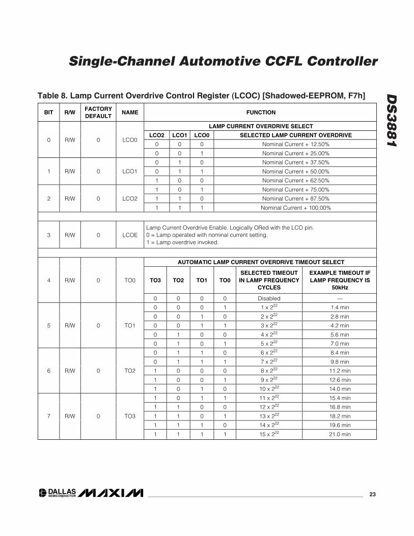
Lamp Current Overdrive FunctionalityAnother feature the DS3881 offers is the ability to over-drive the lamps to allow them to heat up quickly in coldenvironments. After setting the LCO0/1/2 bits in theLCOC register and enabling the LCOE bit or LCO pin,the DS3881 overdrives the nominal current settings in12.5% steps from 112.5% up to 200%. The DS3881accomplishes this by automatically shifting the lampregulation threshold, VLRT, upward to allow more cur-rent to flow in the lamps (Figure 2). This multileveladjustment makes it possible to slowly decrease thecurrent overdrive (through I2C) after the lamps havewarmed up, so the end user does not see any changein brightness when the overdrive is no longer needed.The DS3881 also features an optional timer capable ofautomatically turning off the current overdrive. Thistimer is adjustable from approximately 1.5 minutes to21 minutes (if a 50kHz lamp frequency is used).
Detailed Register DescriptionsThe DS3881’s register map is shown in Table 1.Detailed register and bit descriptions follow in the sub-sequent tables.
Table 1. Register MapBYTE
ADDRESSBYTENAME
FACTORYDEFAULT
BIT 7 BIT 6 BIT 5 BIT 4 BIT 3 BIT 2 BIT 1 BIT 0
E0h SR1 00h SVMH_RT SVML_RT LOC_L1 LOUT_L1 OV_L1 STO_L1 FAULT_L1 FAULT_RT1
E1h RSVD 00h RSVD RSVD RSVD RSVD RSVD RSVD RSVD RSVD
E2h BPWM 00h RSVD PWM6 PWM5 PWM4 PWM3 PWM2 PWM1 PWM0
E3h BLC 1Fh SEEB RSVD CH1D LC4 LC3 LC2 LC1 LC0
F0h SSP1 21h LST1MDC code for soft-start lampcycles 3, 4
LST0 M D C cod e for soft- star t l am p cycl es 1, 2
F1h SSP2 43h MDC code for soft-start lamp cycles 7, 8 MDC code for soft-start lamp cycles 5, 6
F2h SSP3 65h MDC code for soft-start lamp cycles 11, 12 MDC code for soft-start lamp cycles 9, 10
F3h SSP4 77h MDC code for soft-start lamp cycles 15, 16 MDC code for soft-start lamp cycles 13, 14
F4h CR1 00h DPD RSVD ARD RGSO DPSS LFSS POSCS LOCE
F5h CR2 08h PDNE RSVD RSVD LSR1 LSR0 POSCR1 POSCR0 UMWP
F6h EMIC 00h FS2 FS1 FS0 STEPE RSVD SSM SS1 SS0
F7h LCOC 00h TO3 TO2 TO1 TO0 LCOE LCO2 LCO1 LCO0
F8h–FFh USER 00h EE EE EE EE EE EE EE EE
Note 1: E0h–E3h are SRAM locations, and F0h–FFh are SRAM-shadowed EEPROM.Note 2: Altering the DS3881 configuration during active CCFL operation can cause serious adverse effects.
DS
38
81
Single-Channel Automotive CCFL Controller
18 ____________________________________________________________________
Table 2. Status Register 1 (SR1) [SRAM, E0h]
BIT R/WPOWER-UPDEFAULT
NAME FUNCTION
0 R 0 FAULT_RT
Fault Condition—Real Time. A real-time bit that indicates the current operating status ofchannel 1.0 = Normal condition1 = Fault condition
1 R 0 FAULT_LFault Condition—Latched. A latched bit that is set when the channel enters a faultcondition. This bit is cleared when read, regardless of the current state of fault.
2 R 0 STO_LLamp Strike Timeout—Latched. A latched bit that is set when the lamp fails to strike.This bit is cleared when read.
3 R 0 OV_LOvervoltage—Latched. A latched bit that is set when a lamp overvoltage is present forat least 64 lamp cycles. This bit is cleared when read.
4 R 0 LOUT_LLamp Out—Latched. A latched bit that is set when a lamp out is detected. This bit iscleared when read.
5 R 0 LOC_LLamp Overcurrent—Latched. A latched bit that is set when a lamp overcurrent isdetected. This bit is cleared when read.
6 R 0 SVML_RTSupply Voltage Monitor Low—Real Time. A real-time bit that reports the comparatoroutput of the SVML pin.
7 R 0 SVMH_RTSupply Voltage Monitor High—Real Time. A real-time bit that reports the comparatoroutput of the SVMH pin.
Note 1: Writing to this register has no effect on it.Note 2: See Figure 8 for more details on how the status bits are set.Note 3: SR1 is cleared when only the following occurs:
• VCC drops below the UVLO threshold.• The SVML or SVMH thresholds are crossed.• The PDN hardware pin goes high.• The PDNE software bit is written to a logic 1.• The channel is disabled by the CH1D control bit.
Table 3. Brightness Lamp Current Register (BLC) [SRAM, E3h]
BIT R/WFACTORYDEFAULT
NAME FUNCTION
0 R/W 0 LC0
1 R/W 0 LC1
2 R/W 0 LC2
3 R/W 0 LC3
4 R/W 0 LC4
These five control bits determine the target value for the lamp current. 11111b is35% of the nominal level and 00000b is 100% of the nominal level. These controlbits are used for fine adjustment of the lamp brightness.
5 R/W 0 CH1DChannel 1 Disable0 = Channel 1 enabled1 = Channel 1 disabled
6 R/W 0 RSVD Reserved. Should be set to 0.
7 R/W 0 SEEBSRAM-Shadowed EEPROM Write Control0 = Enables writes to EEPROM1 = Disables writes to EEPROM

DS
38
81
Single-Channel Automotive CCFL Controller
____________________________________________________________________ 19
Table 4a. Soft-Start Protocol Registers (SSPx) [Shadowed-EEPROM, F0h, F1h, F2h, F3h]
MSB LSBSSP# ADDR
FACTORYDEFAULT 7 6 5 4 3 2 1 0
SSP1 F0h 21h LST1 Lamp Cycles 3 and 4 LST0 Lamp Cycles 1 and 2
SSP2 F1h 43h RSVD Lamp Cycles 7 and 8 RSVD Lamp Cycles 5 and 6
SSP3 F2h 65h RSVD Lamp Cycles 11 and 12 RSVD Lamp Cycles 9 and 10
SSP4 F3h 77h RSVD Lamp Cycles 15 and 16 RSVD Lamp Cycles 13 and 14
Table 4b. MOSFET Duty Cycle (MDC)⎯Codes for Soft-Start Settings
BIT R/W NAME FUNCTION
0 R/W MDC0MDC0/1/2/3: These bits determine a MOSFET duty cycle that repeats twice in the
16 lamp cycle soft-start.1 R/W MDC1
MDC CODE MOSFET DUTY CYCLE MDC CODE MOSFET DUTY CYCLE
0h Fixed at 0% 4h Fixed at 13%2 R/W MDC2
1h Fixed at 3% 5h Fixed at 16%
2h Fixed at 6% 6h Fixed at 19%
3h Fixed at 9% 7h Most Recent Value3 R/W LST0 / RSVD
4 R/W MDC0LST0/1: These bits select strike and lamp out timeout. LST0 and LST1
control fault behavior for all lamps.
5 R/W MDC1 LST1 LST0STRIKE AND LAMP OUT TIMEOUT
(LAMP FREQUENCY CYCLES)EXAMPLE TIMEOUT IF
LAMP FREQUENCY IS 50kHz
0 0 32,768 0.66 seconds6 R/W MDC2
0 1 65,536 1.31 seconds
1 0 98,304 1.97 seconds7 R/W LST1 / RSVD
1 1 Reserved —

DS
38
81
Single-Channel Automotive CCFL Controller
20 ____________________________________________________________________
Table 5. Control Register 1 (CR1) [Shadowed-EEPROM, F4h]
BIT R/WFACTORYDEFAULT
NAME FUNCTION
0 R/W 0 LOCELamp Overcurrent Enable0 = Lamp overcurrent detection disabled.1 = Lamp overcurrent detection enabled.
1 R/W 0 POSCS
POSC Select. See POSCR0 and POSCR1 control bits in Control Register 2 to selectthe oscillator range.0 = POSC input is connected with a resistor to ground to set the frequency of theinternal PWM oscillator.1 = POSC input is a 22.5Hz to 440Hz clock.
2 R/W 0 LFSSLamp Frequency Source Select0 = Lamp frequency generated internally and sourced from the LSYNC output.1 = Lamp frequency generated externally and supplied to the LSYNC input.
3 R/W 0 DPSSDPWM Signal Source Select0 = DPWM signal generated internally and sourced from the PSYNC output.1 = DPWM signal generated externally and supplied to the PSYNC input.
4 R/W 0 RGSORamp Generator Source Option0 = Source DPWM at the PSYNC output.1 = Source internal ramp generator at the PSYNC output.
5 R/W 0 ARDAutoretry Disable0 = Autoretry function enabled.1 = Autoretry function disabled.
6 R/W 0 RSVD Reserved. Should be set to 0.
7 R/W 0 DPDDPWM Disable0 = DPWM function enabled.1 = DPWM function disabled.

DS
38
81
Single-Channel Automotive CCFL Controller
____________________________________________________________________ 21
Table 6. Control Register 2 (CR2) [Shadowed-EEPROM, F5h]BIT R/W DEFAULT NAME FUNCTION
0 R/W 0 UMWPUser Memory Write Protect0 = Write access blocked.1 = Write access permitted.
1 R/W 0 POSCR0
DPWM Oscillator Range Select. When using an external source for the dimming clock,these bits must be set to match the external oscillator’s frequency. When using aresistor to set the dimming frequency, these bits plus the external resistor control thefrequency.
POSCR1 POSCR0DIMMING CLOCK (DPWM)FREQUENCY RANGE (Hz)
k (kΩ • kHz)
0 0 22.5 to 55.0 1
0 1 45 to 110 2
1 0 90 to 220 4
2 R/W 0 POSCR1
1 1 180 to 440 8
Lamp Sample Rate Select. Determines the feedback sample rate of the LCM inputs.
LSR1 LSR0SELECTED LAMP SAMPLE
RATE
EXAMPLE SAMPLE RATEIF LAMP FREQUENCY IS
50kHz3 R/W 1 LSR0
0 0 4 Lamp Frequency Cycles 12,500Hz
0 1 8 Lamp Frequency Cycles 6250Hz
1 0 16 Lamp Frequency Cycles 3125Hz4 R/W 0 LSR1
1 1 32 Lamp Frequency Cycles 1563Hz
5 — 0 RSVD Reserved. This bit should be set to zero.
6 — 0 RSVD Reserved. This bit should be set to zero.
7 R/W 0 PDNEPower-Down. Logically ORed with the PDN pin. Setting this bit high resets the controller,clears the fault logic, and places the part in power-down mode. 0 = Normal. All circuitry isoff, except I2C interface.

DS
38
81
Single-Channel Automotive CCFL Controller
22 ____________________________________________________________________
Table 7. EMI Control Register (EMIC) [Shadowed-EEPROM, F6h]
BIT R/WFACTORYDEFAULT
NAME FUNCTION
LAMP OSCILLATOR SPREAD-SPECTRUM MODULATION SELECT
SS1 SS0 SELECTED LAMP FREQUENCY SPREAD0 R/W 0 SS0
0 0 SPREAD-SPECTRUM DISABLED
0 1 ±1.5%
1 0 ±3.0%1 R/W 0 SS1
1 1 ±6.0%
2 R/W 0 SSMLamp Oscillator Spread-Spectrum Modulation Select0 = Triangular modulation.1 = Pseudorandom modulation.
3 ⎯ ⎯ RSVD Reserved. This bit should be set to zero.
4 R/W 0 STEPELamp Frequency Step Enable. Logically ORed with the step invoked.0 = Lamp operates at nominal frequency.1 = Frequency step invoked.
LAMP OSCILLATOR FREQUENCY STEP SELECT
FS2 FS1 FS0SELECTED LAMP
FREQUENCY STEP(SS0 = 0 AND SS1= 0)
SPREAD-SPECTRUMMODULATION RATE
(SS0 AND/OR SS1 = 1)5 R/W 0 FS0
0 0 0 Step Up 1% Lamp Frequency x4
0 0 1 Step Up 2% Lamp Frequency x2
0 1 0 Step Up 3% Lamp Frequency x1
0 1 1 Step Up 4% Lamp Frequency x1/26 R/W 0 FS1
1 0 0 Step Down 1% Lamp Frequency x1/4
1 0 1 Step Down 2% Lamp Frequency x1/8
1 1 0 Step Down 3% Lamp Frequency x1/167 R/W 0 FS2
1 1 1 Step Down 4% Lamp Frequency x1/32
DS
38
81
Single-Channel Automotive CCFL Controller
____________________________________________________________________ 23
Table 8. Lamp Current Overdrive Control Register (LCOC) [Shadowed-EEPROM, F7h]
BIT R/WFACTORYDEFAULT
NAME FUNCTION
LAMP CURRENT OVERDRIVE SELECT
LCO2 LCO1 LCO0 SELECTED LAMP CURRENT OVERDRIVE
0 0 0 Nominal Current + 12.50%0 R/W 0 LCO0
0 0 1 Nominal Current + 25.00%
0 1 0 Nominal Current + 37.50%
0 1 1 Nominal Current + 50.00%1 R/W 0 LCO1
1 0 0 Nominal Current + 62.50%
1 0 1 Nominal Current + 75.00%
1 1 0 Nominal Current + 87.50%2 R/W 0 LCO2
1 1 1 Nominal Current + 100.00%
3 R/W 0 LCOELamp Current Overdrive Enable. Logically ORed with the LCO pin.0 = Lamp operated with nominal current setting.1 = Lamp overdrive invoked.
AUTOMATIC LAMP CURRENT OVERDRIVE TIMEOUT SELECT
TO3 TO2 TO1 TO0SELECTED TIMEOUTIN LAMP FREQUENCY
CYCLES
EXAMPLE TIMEOUT IFLAMP FREQUENCY IS
50kHz4 R/W 0 TO0
0 0 0 0 Disabled —
0 0 0 1 1 x 222 1.4 min
0 0 1 0 2 x 222 2.8 min
0 0 1 1 3 x 222 4.2 min
0 1 0 0 4 x 222 5.6 min
5 R/W 0 TO1
0 1 0 1 5 x 222 7.0 min
0 1 1 0 6 x 222 8.4 min
0 1 1 1 7 x 222 9.8 min
1 0 0 0 8 x 222 11.2 min
1 0 0 1 9 x 222 12.6 min
6 R/W 0 TO2
1 0 1 0 10 x 222 14.0 min
1 0 1 1 11 x 222 15.4 min
1 1 0 0 12 x 222 16.8 min
1 1 0 1 13 x 222 18.2 min
1 1 1 0 14 x 222 19.6 min
7 R/W 0 TO3
1 1 1 1 15 x 222 21.0 min

DS
38
81
Single-Channel Automotive CCFL Controller
24 ____________________________________________________________________
I2C DefinitionsThe following terminology is commonly used todescribe I2C data transfers:
Master Device: The master device controls the slavedevices on the bus. The master device generates SCLclock pulses, start, and stop conditions.
Slave Devices: Slave devices send and receive dataat the master’s request.
Bus Idle or Not Busy: Time between stop and startconditions when both SDA and SCL are inactive and intheir logic-high states.
Start Condition: A start condition is generated by themaster to initiate a new data transfer with a slave.Transitioning SDA from high to low while SCL remainshigh generates a start condition. See the timing dia-gram for applicable timing.
Stop Condition: A stop condition is generated by themaster to end a data transfer with a slave. TransitioningSDA from low to high while SCL remains high gener-ates a stop condition. See the timing diagram forapplicable timing.
Repeated Start Condition: The master can use arepeated start condition at the end of one data transferto indicate that it will immediately initiate a new datatransfer following the current one. Repeated starts arecommonly used during read operations to identify aspecific memory address to begin a data transfer. Arepeated start condition is issued identically to a nor-mal start condition. See the timing diagram for applica-ble timing.
Bit Write: Transitions of SDA must occur during the lowstate of SCL. The data on SDA must remain valid andunchanged during the entire high pulse of SCL plus thesetup and hold time requirements (see Figure 9). Data isshifted into the device during the rising edge of the SCL.
Bit Read: At the end of a write operation, the mastermust release the SDA bus line for the proper amount ofsetup time (see Figure 9) before the next rising edge ofSCL during a bit read. The device shifts out each bit ofdata on SDA at the falling edge of the previous SCLpulse and the data bit is valid at the rising edge of thecurrent SCL pulse. Remember that the master gener-ates all SCL clock pulses including when it is readingbits from the slave.
Acknowledgement (ACK and NACK): An acknowl-edgement (ACK) or not acknowledge (NACK) is alwaysthe 9th bit transmitted during a byte transfer. Thedevice receiving data (the master during a read or theslave during a write operation) performs an ACK bytransmitting a zero during the 9th bit. A device per-forms a NACK by transmitting a one during the 9th bit.Timing (Figure 9) for the ACK and NACK is identical toall other bit writes. An ACK is the acknowledgment thatthe device is properly receiving data. A NACK is usedto terminate a read sequence or as an indication thatthe device is not receiving data.
Byte Write: A byte write consists of 8 bits of informa-tion transferred from the master to the slave (most sig-nificant bit first) plus a 1-bit acknowledgement from theslave to the master. The 8 bits transmitted by the mas-ter are done according to the bit-write definition and theacknowledgement is read using the bit-read definition.
SDA
SCL
tHD:STA
tLOW
tHIGH
tR tF
tBUF
tHD:DAT
tSU:DAT REPEATEDSTART
tSU:STA
tHD:STA
tSU:STO
tSP
STOP
NOTE: TIMING IS REFERENCE TO VIL(MAX) AND VIH(MIN).
START
Figure 9. I2C Timing Diagram

DS
38
81
Single-Channel Automotive CCFL Controller
____________________________________________________________________ 25
Byte Read: A byte read is an 8-bit information transferfrom the slave to the master plus a 1-bit ACK or NACKfrom the master to the slave. The 8 bits of informationthat are transferred (most significant bit first) from theslave to the master are read by the master using the bitread definition above, and the master transmits an ACKusing the bit write definition to receive additional databytes. The master must NACK the last byte read to ter-minate communication so the slave will return control ofSDA to the master.
Slave Address Byte: Each slave on the I2C busresponds to a slave addressing byte sent immediatelyfollowing a start condition. The slave address byte(Figure 10) contains the slave address in the most sig-nificant seven bits and the R/W bit in the least signifi-cant bit. The DS3881’s slave address is 10100A1A00(binary), where A0 and A1 are the values of the addresspins (A0 and A1). The address pin allows the device torespond to one of four possible slave addresses. Bywriting the correct slave address with R/W = 0, themaster indicates it will write data to the slave. If R/W =1, the master will read data from the slave. If an incor-rect slave address is written, the DS3881 will assumethe master is communicating with another I2C deviceand ignore the communications until the next start con-dition is sent.
Memory Address: During an I2C write operation, themaster must transmit a memory address to identify thememory location where the slave is to store the data.The memory address is always the second byte trans-mitted during a write operation following the slaveaddress byte.
I2C CommunicationWriting a Data Byte to a Slave: The master must gen-erate a start condition, write the slave address byte(R/W = 0), write the memory address, write the byte ofdata, and generate a stop condition. Remember themaster must read the slave’s acknowledgement duringall byte write operations. See Figure 11 for more detail.
Acknowledge Polling: Any time EEPROM is written,the DS3881 requires the EEPROM write time (tW) afterthe stop condition to write the contents to EEPROM.During the EEPROM write time, the DS3881 will notacknowledge its slave address because it is busy. It ispossible to take advantage of that phenomenon byrepeatedly addressing the DS3881, which allows thenext byte of data to be written as soon as the DS3881 isready to receive the data. The alternative to acknowl-edge polling is to wait for a maximum period of tW toelapse before attempting to write again to the DS3881.
EEPROM Write Cycles: The number of times theDS3881’s EEPROM can be written before it fails isspecified in the Nonvolatile Memory Characteristicstable. This specification is shown at the worst-casewrite temperature. The DS3881 is typically capable ofhandling many additional write cycles when the writesare performed at room temperature.
Reading a Data Byte from a Slave: To read a singlebyte from the slave the master generates a start condi-tion, writes the slave address byte with R/W = 0, writesthe memory address, generates a repeated start condi-tion, writes the slave address with R/W = 1, reads thedata byte with a NACK to indicate the end of the trans-fer, and generates a stop condition. See Figure 11 formore detail.
7-BIT SLAVE ADDRESS
MOSTSIGNIFICANT BIT
A1, A0 PIN VALUE DETERMINESREAD OR WRITE
R/W1 0 1 0 0 A1 A0
Figure 10. DS3881’s Slave Address Byte

DS
38
81
Single-Channel Automotive CCFL Controller
26 ____________________________________________________________________
Applications InformationAddressing Multiple DS3881s
On a Common I2C BusEach DS3881 responds to one of four possible slaveaddresses based on the state of the address input pins(A0 and A1). For information about device addressing,see the I2C Communication section.
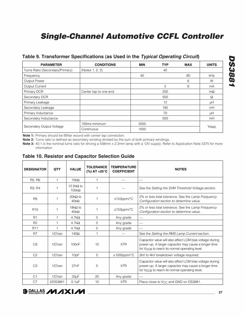
Setting the RMS Lamp CurrentResistor R7 and R8 in the Typical Operating Circuit setthe lamp current. R7 and R8 = 140Ω corresponds to a5mARMS lamp current as long as the current waveformis approximately sinusoidal. The formula to determinethe resistor value for a given sinusoidal lamp current is:
Component SelectionExternal component selection has a large impact on theoverall system performance and cost. The two mostimportant external components are the transformersand n-channel MOSFETs.
The transformer should be able to operate in the 40kHzto 80kHz frequency range of the DS3881, and the turnsratio should be selected so the MOSFET drivers run at28% to 35% duty cycle during steady state operation.The transformer must be able to withstand the highopen-circuit voltage that is used to strike the lamp.
Additionally, its primary/secondary resistance and induc-tance characteristics must be considered because theycontribute significantly to determining the efficiency andtransient response of the system. Table 9 shows a trans-former specification that has been used for a 12V invert-er supply, 438mm x 2.2mm lamp design.
The n-channel MOSFET must have a threshold voltagethat is low enough to work with logic-level signals, a lowon-resistance to maximize efficiency and limit the n-channel MOSFET’s power dissipation, and a break-down voltage high enough to handle the transient. Thebreakdown voltage should be a minimum of 3x theinverter voltage supply. Additionally, the total gatecharge must be less than QG, which is specified inthe Recommended Operating Conditions table. Thesespecifications are easily met by many of the dual n-channel MOSFETs now available in 8-pin SO pack-ages.
Table 10 lists suggested values for the external resistorsand capacitors used in the Typical Operating Circuit.
Power-Supply DecouplingTo achieve best results, it is highly recommended thata decoupling capacitor is used on the IC power-supplypin. Typical values of decoupling capacitors are 0.01µFor 0.1µF. Use a high-quality, ceramic, surface-mountcapacitor, and mount it as close as possible to the VCCand GND pins of the IC to minimize lead inductance.
RI xLAMP RMS
71
2
( )=
X X X X X X X X
1 0 1 0 A0 0A10
COMMUNICATIONS KEY
WRITE A SINGLE BYTE
8-BITS ADDRESS OR DATA
WHITE BOXES INDICATE THE MASTER IS CONTROLLING SDA
NOTES
2) THE FIRST BYTE SENT AFTER A START CONDITION IS ALWAYS THE SLAVE ADDRESS FOLLOWED BY THE READ/WRITE BIT.
SHADED BOXES INDICATE THE SLAVE IS CONTROLLING SDA
START ACK
NOTACK
S
S A A A PDATAMEMORY ADDRESS
1 0 1 0 A0 0A10 1 0 1 0 A0 1A10
READ A SINGLE BYTE
S A A SR A N PDATAMEMORY ADDRESS
A
P N
SR
STOP
REPEATEDSTART
1) ALL BYTES ARE SENT MOST SIGNIFICANT BIT FIRST.
Figure 11. I2C Communications Examples
DS
38
81
Single-Channel Automotive CCFL Controller
____________________________________________________________________ 27
Table 9. Transformer Specifications (as Used in the Typical Operating Circuit)
PARAMETER CONDITIONS MIN TYP MAX UNITS
Turns Ratio (Secondary/Primary) (Notes 1, 2, 3) 40
Frequency 40 80 kHz
Output Power 6 W
Output Current 5 8 mA
Primary DCR Center tap to one end 200 mΩSecondary DCR 500 ΩPrimary Leakage 12 µH
Secondary Leakage 185 mH
Primary Inductance 70 µH
Secondary Inductance 500 mH
100ms minimum 2000Secondary Output Voltage
Continuous 1000VRMS
Note 1: Primary should be Bifilar wound with center tap connection.Note 2: Turns ratio is defined as secondary winding divided by the sum of both primary windings.Note 3: 40:1 is the nominal turns ratio for driving a 438mm x 2.2mm lamp with a 12V supply. Refer to Application Note 3375 for more
information.
Table 10. Resistor and Capacitor Selection Guide
DESIGNATOR QTY VALUETOLERANCE(%) AT +25°C
TEMPERATURECOEFFICIENT
NOTES
R5, R6 1 10kΩ 1 — —
R3, R4 112.5kΩ to
105kΩ1 — See the Setting the SVM Threshold Voltage section.
R9 120kΩ to40kΩ
1 ≤153ppm/°C2% or less total tolerance. See the Lamp FrequencyConfiguration section to determine value.
R10 118kΩ to45kΩ
1 ≤153ppm/°C2% or less total tolerance. See the Lamp FrequencyConfiguration section to determine value.
R1 1 4.7kΩ 5 Any grade —
R2 1 4.7kΩ 5 Any grade —
R11 1 4.7kΩ 5 Any grade —
R7 1/Chan 140Ω 1 — See the Setting the RMS Lamp Current section.
C8 1/Chan 100nF 10 X7RC ap aci tor val ue w i l l al so affect LC M b i as vol tag e d ur i ng p ow er - up . A l ar g er cap aci tor m ay cause a l ong er ti m efor V D C B to r each i ts nor m al op er ati ng l evel .
C2 1/Chan 10pF 5 ±1000ppm/°C 2kV to 4kV breakdown voltage required.
C3 1/Chan 27nF 5 X7RC ap aci tor val ue w i l l al so affect LC M b i as vol tag e d ur i ng p ow er - up . A l ar g er cap aci tor m ay cause a l ong er ti m efor V D C B to r each i ts nor m al op er ati ng l evel .
C1 1/Chan 33µF 20 Any grade —
C7 2/DS3881 0.1µF 10 X7R Place close to VCC and GND on DS3881.

DS
38
81
Single-Channel Automotive CCFL Controller
Maxim cannot assume responsibility for use of any circuitry other than circuitry entirely embodied in a Maxim product. No circuit patent licenses areimplied. Maxim reserves the right to change the circuitry and specifications without notice at any time.
28 ____________________Maxim Integrated Products, 120 San Gabriel Drive, Sunnyvale, CA 94086 408-737-7600
© 2007 Maxim Integrated Products is a registered trademark of Maxim Integrated Products, Inc.
is a registered trademark of Dallas Semiconductor Corporation.
Heaney
INVERTER SUPPLYVOLTAGE (VINV)
(8V TO 16V)
GA1
LAMP CURRENT MONITOR
CCFL LAMP
GB1
OVD1
VCC
VCC VCC
VCC
BRIGHT
SVMH
LAMP BRIGHTNESS
TRANSFORMERDUAL POWERMOSFET
DEVICESUPPLY VOLTAGE
(5V ±5%)
OVERVOLTAGE DETECTION
LCM1
GND
LAMP FREQUENCYINPUT/OUTPUT
LSYNC
SCL
SDA
I2CCONFIGURATION
AND CONTROL PORT
FAULT
PSYNCDPWM SIGNALINPUT/OUTPUT
LOSC
POSC
LCO
PDNLAMP ON/OFF
LAMP CURRENTOVERDRIVE ENABLE
SVMLA0
A1
HARDWARECONTROL
STEP LAMPFREQUENCY
STEP
GND_S
R1 R2
R7
R9 R10
C2
C3
C7
R11
C8
R3 R4
R5 R6
C1
DS3881
Typical Operating Circuit
Chip InformationTRANSISTOR COUNT: 38,000
SUBSTRATE CONNECTED TO GROUND
Package InformationFor the latest package outline information, go towww.maxim-ic.com/DallasPackInfo.
Revision HistoryPages changed at Rev 1: 1, 19
Related Documents