Single-Channel, 128-/64-/32-Position, Up/Down, ±8% Resistor Tolerance, Nonvolatile Digital Potentiometer Data Sheet AD5111/AD5113/AD5115 Rev. B Document Feedback Information furnished by Analog Devices is believed to be accurate and reliable. However, no responsibility is assumed by Analog Devices for its use, nor for any infringements of patents or other rights of third parties that may result from its use. Specifications subject to change without notice. No license is granted by implication or otherwise under any patent or patent rights of Analog Devices. Trademarks and registered trademarks are the property of their respective owners. One Technology Way, P.O. Box 9106, Norwood, MA 02062-9106, U.S.A. Tel: 781.329.4700 ©2011–2012 Analog Devices, Inc. All rights reserved. Technical Support www.analog.com FEATURES Nominal resistor tolerance error: ±8% maximum Wiper current: ±6 mA Rheostat mode temperature coefficient: 35 ppm/°C Low power consumption: 2.5 µA max @ 2.7 V and 125°C Wide bandwidth: 4 MHz (5 kΩ option) Power-on EEPROM refresh time < 50 μs 50-year typical data retention at 125°C 1 million write cycles 2.3 V to 5.5 V supply operation Chip select enable multiple device operation Wide operating temperature: −40°C to +125°C Thin, 2 mm × 2 mm × 0.55 mm 8-lead LFCSP package APPLICATIONS Mechanical potentiometer replacement Portable electronics level adjustment Audio volume control Low resolution DAC LCD panel brightness and contrast control Programmable voltage to current conversion Programmable filters, delays, time constants Feedback resistor programmable power supply Sensor calibration FUNCTIONAL BLOCK DIAGRAM GND RDAC REGISTER UP/DOWN CONTROL LOGIC POWER-ON RESET V DD U/D CLK CS EEPROM DATA DATA A W B EN AD5111/ AD5113/ AD5115 09654-001 Figure 1. Table 1. ±8% Resistance Tolerance Family Model Resistance (kΩ) Position Interface AD5110 10, 80 128 I 2 C AD5111 10, 80 128 Up/down AD5112 5, 10, 80 64 I 2 C AD5113 5, 10, 80 64 Up/down AD5116 5, 10, 80 64 Push-button AD5114 10, 80 32 I 2 C AD5115 10, 80 32 Up/down GENERAL DESCRIPTION The AD5111/AD5113/AD5115 provide a nonvolatile solution for 128-/64-/32-position adjustment applications, offering guaranteed low resistor tolerance errors of ±8% and up to ±6 mA current density in the A, B, and W pins. The low resistor tolerance, low nominal temperature coefficient, and high bandwidth simplify open-loop applications, as well as tolerance matching applications. The new low wiper resistance feature minimizes the wiper resistance in the extremes of the resistor array to only 45 Ω, typical. A simple 3-wire up/down interface allows manual switching or high speed digital control with clock rates up to 50 MHz. The AD5111/AD5113/AD5115 are available in a 2 mm × 2 mm LFCSP package. The parts are guaranteed to operate over the extended industrial temperature range of −40°C to +125°C.

Welcome message from author
This document is posted to help you gain knowledge. Please leave a comment to let me know what you think about it! Share it to your friends and learn new things together.
Transcript

Single-Channel, 128-/64-/32-Position, Up/Down, ±8% Resistor Tolerance, Nonvolatile Digital Potentiometer
Data Sheet AD5111/AD5113/AD5115
Rev. B Document Feedback Information furnished by Analog Devices is believed to be accurate and reliable. However, no responsibility is assumed by Analog Devices for its use, nor for any infringements of patents or other rights of third parties that may result from its use. Specifications subject to change without notice. No license is granted by implication or otherwise under any patent or patent rights of Analog Devices. Trademarks and registered trademarks are the property of their respective owners.
One Technology Way, P.O. Box 9106, Norwood, MA 02062-9106, U.S.A. Tel: 781.329.4700 ©2011–2012 Analog Devices, Inc. All rights reserved. Technical Support www.analog.com
FEATURES Nominal resistor tolerance error: ±8% maximum Wiper current: ±6 mA Rheostat mode temperature coefficient: 35 ppm/°C Low power consumption: 2.5 µA max @ 2.7 V and 125°C Wide bandwidth: 4 MHz (5 kΩ option) Power-on EEPROM refresh time < 50 μs 50-year typical data retention at 125°C 1 million write cycles 2.3 V to 5.5 V supply operation Chip select enable multiple device operation Wide operating temperature: −40°C to +125°C Thin, 2 mm × 2 mm × 0.55 mm 8-lead LFCSP package
APPLICATIONS Mechanical potentiometer replacement Portable electronics level adjustment Audio volume control Low resolution DAC LCD panel brightness and contrast control Programmable voltage to current conversion Programmable filters, delays, time constants Feedback resistor programmable power supply Sensor calibration
FUNCTIONAL BLOCK DIAGRAM
GND
RDACREGISTER
UP/DOWNCONTROL
LOGIC
POWER-ONRESET
VDD
U/D
CLK
CS
EEPROMDATA
DATA
A
W
BEN
AD5111/AD5113/AD5115
0965
4-00
1
Figure 1.
Table 1. ±8% Resistance Tolerance Family Model Resistance (kΩ) Position Interface AD5110 10, 80 128 I2C AD5111 10, 80 128 Up/down AD5112 5, 10, 80 64 I2C AD5113 5, 10, 80 64 Up/down AD5116 5, 10, 80 64 Push-button AD5114 10, 80 32 I2C AD5115 10, 80 32 Up/down
GENERAL DESCRIPTION The AD5111/AD5113/AD5115 provide a nonvolatile solution for 128-/64-/32-position adjustment applications, offering guaranteed low resistor tolerance errors of ±8% and up to ±6 mA current density in the A, B, and W pins. The low resistor tolerance, low nominal temperature coefficient, and high bandwidth simplify open-loop applications, as well as tolerance matching applications.
The new low wiper resistance feature minimizes the wiper resistance in the extremes of the resistor array to only 45 Ω, typical.
A simple 3-wire up/down interface allows manual switching or high speed digital control with clock rates up to 50 MHz.
The AD5111/AD5113/AD5115 are available in a 2 mm × 2 mm LFCSP package. The parts are guaranteed to operate over the extended industrial temperature range of −40°C to +125°C.

AD5111/AD5113/AD5115 Data Sheet
Rev. B | Page 2 of 24
TABLE OF CONTENTS Features .............................................................................................. 1 Applications ....................................................................................... 1 Functional Block Diagram .............................................................. 1 General Description ......................................................................... 1 Revision History ............................................................................... 2 Specifications ..................................................................................... 3
Electrical Characteristics—AD5111 .......................................... 3 Electrical Characteristics—AD5113 .......................................... 5 Electrical Characteristics—AD5115 .......................................... 7 Interface Timing Specifications .................................................. 9 Timing Diagram ........................................................................... 9
Absolute Maximum Ratings .......................................................... 10 Thermal Resistance .................................................................... 10 ESD Caution ................................................................................ 10
Pin Configuration and Function Descriptions ........................... 11 Typical Performance Characteristics ........................................... 12
Test Circuits ..................................................................................... 17 Theory of Operation ...................................................................... 18
RDAC Register and EEPROM .................................................. 18 Basic Operation .......................................................................... 18 Low Wiper Resistance Feature ................................................. 18 Shutdown Mode ......................................................................... 18 EEPROM Write Operation ....................................................... 18 RDAC Architecture .................................................................... 19 Programming the Variable Resistor ......................................... 19 Programming the Potentiometer Divider ............................... 20 Terminal Voltage Operating Range ......................................... 20 Power-Up Sequence ................................................................... 21 Layout and Power Supply Biasing ............................................ 21
Outline Dimensions ....................................................................... 22 Ordering Guide .......................................................................... 22
REVISION HISTORY 11/12—Rev. A to Rev. B
Changed Low Power Consumption from 2.5 mA to 2.5 µA....... 1 Changed IDD Unit from mA to µA, Table 2 .................................... 3 Changed IDD Unit from mA to µA, Table 3 .................................... 5 Changed IDD Unit from mA to µA, Table 4 .................................... 7
4/12—Rev. 0 to Rev. A
Changes to Features Section............................................................ 1 Changes to Positive Supply Current, Table 2 ................................ 3 Changes to Positive Supply Current, Table 3 ................................ 5 Changes to Positive Supply Current, Table 4 ................................ 7 Updated Outline Dimensions ....................................................... 22
10/11—Revision 0: Initial Version

Data Sheet AD5111/AD5113/AD5115
Rev. B | Page 3 of 24
SPECIFICATIONS ELECTRICAL CHARACTERISTICS—AD5111 10 kΩ and 80 kΩ versions: VDD = 2.3 V to 5.5 V, VA = VDD, VB = 0 V, −40°C < TA < +125°C, unless otherwise noted.
Table 2. Parameter Symbol Test Conditions/Comments Min Typ1 Max Unit DC CHARACTERISTICS—RHEOSTAT MODE
Resolution N 7 Bits Resistor Integral Nonlinearity2 R-INL RAB = 10 kΩ, VDD = 2.3 V to 2.7 V −2.5 ±0.5 +2.5 LSB RAB = 10 kΩ, VDD = 2.7 V to 5.5 V −1 ±0.25 +1 LSB RAB = 80 kΩ −0.5 ±0.1 +0.5 LSB Resistor Differential Nonlinearity2 R-DNL −1 ±0.25 +1 LSB
Nominal Resistor Tolerance ΔRAB/RAB −8 +8 % Resistance Temperature Coefficient3 (ΔRAB/RAB)/ΔT × 106 35 ppm/°C Wiper Resistance RW Code = zero scale 70 140 Ω RBS Code = bottom scale 45 80 Ω
RTS Code = top scale 70 140 Ω
DC CHARACTERISTICS—POTENTIOMETER DIVIDER MODE
Integral Nonlinearity4 INL −0.5 ±0.15 +0.5 LSB
Differential Nonlinearity4 DNL −0.5 ±0.15 +0.5 LSB
Full-Scale Error VWFSE RAB = 10 kΩ −2.5 LSB RAB = 80 kΩ −1.5 LSB Zero-Scale Error VWZSE RAB = 10 kΩ 1.5 LSB RAB = 80 kΩ 0.5 LSB
Voltage Divider Temperature Coefficient3 (ΔVW/VW)/ΔT × 106 Code = half scale ±10 ppm/°C
RESISTOR TERMINALS
Maximum Continuous IA, IB, and IW Current3 RAB = 10 kΩ −6 +6 mA RAB = 80 kΩ −1.5 +1.5 mA
Terminal Voltage Range5 GND VDD V
Capacitance A, Capacitance B3, 6 CA, CB f = 1 MHz, measured to GND, code = half scale
20 pF
Capacitance W3, 6 CW f = 1 MHz, measured to GND, code = half scale
35 pF
Common-Mode Leakage Current3 VA = VW = VB −500 ±15 +500 nA
DIGITAL INPUTS
Input Logic3
High VINH 2 V Low VINL 0.8 V
Input Current3 IN ±1 µA
Input Capacitance3 CIN 5 pF
POWER SUPPLIES Single-Supply Power Range 2.3 5.5 V Positive Supply Current IDD VIH = VDD or VIL = GND, VDD = 5 V 0.75 3.5 µA VIH = VDD or VIL = GND, VDD = 2.7 V 2.5 µA VIH = VDD or VIL = GND, VDD = 2.3 V 2.4 µA EEMEM Store Current3, 7 IDD_NVM_STORE 2 mA
EEMEM Read Current3, 8 IDD_NVM_READ 320 µA
Power Dissipation9 PDISS VIH = VDD or VIL = GND 5 µW
Power Supply Rejection3 PSR ∆VDD/∆VSS = 5 V ± 10%
RAB = 10 kΩ −50 dB RAB = 80 kΩ −64 dB

AD5111/AD5113/AD5115 Data Sheet
Rev. B | Page 4 of 24
Parameter Symbol Test Conditions/Comments Min Typ1 Max Unit
DYNAMIC CHARACTERISTICS3, 10
Bandwidth BW Code = half scale, −3 dB RAB = 10 kΩ 2 MHz RAB = 80 kΩ 200 kHz Total Harmonic Distortion THD VA = VDD/2 + 1 V rms, VB = VDD/ 2, f
= 1 kHz, code = half scale
RAB = 10 kΩ −80 dB RAB = 80 kΩ −85 dB VW Settling Time ts VA = 5 V, VB = 0 V, ±0.5 LSB
error band
RAB = 10 kΩ 3 µs RAB = 80 kΩ 12 µs Resistor Noise Density eN_WB Code = half scale, TA = 25°C,
f = 100 kHz
RAB = 10 kΩ 9 nV/√Hz RAB = 80 kΩ 20 nV/√Hz
FLASH/EE MEMORY RELIABILITY3
Endurance11 TA = 25°C 1 MCycles 100 kCycles Data Retention12 50 Years
1 Typical values represent average readings at 25°C, VDD = 5 V, VSS = 0 V, and VLOGIC = 5 V. 2 R-INL is the deviation from an ideal value measured between the maximum resistance and the minimum resistance wiper positions. R-DNL measures the relative step
change from ideal between successive tap positions. The maximum wiper current is limited to 0.8 × VDD/RAB. 3 Guaranteed by design and characterization; not subject to production test. 4 INL and DNL are measured at VWB with the RDAC configured as a potentiometer divider similar to a voltage output DAC. VA = VDD and VB = 0 V. DNL specification limits
of ±1 LSB maximum are guaranteed monotonic operating conditions. 5 Resistor Terminal A, Resistor Terminal B, and Resistor Terminal W have no limitations on current direction with respect to each other. 6 CA is measured with VW = VA = 2.5 V, CB is measured with VW = VB = 2.5 V, and CW is measured with VA = VB = 2.5 V. 7 Different from operating current; supply current for NVM program lasts approximately 30 ms. 8 Different from operating current; supply current for NVM read lasts approximately 20 µs. 9 PDISS is calculated from (IDD × VDD). 10 All dynamic characteristics use VDD = 5.5 V and VLOGIC = 5 V. 11 Endurance is qualified at 100,000 cycles per JEDEC Standard 22, Method A117 and measured at 150°C. 12 Retention lifetime equivalent at junction temperature (TJ) is 125°C per JEDEC Standard 22, Method A117. Retention lifetime based on an activation energy of 1 eV
derates with junction temperature in the Flash/EE memory.

Data Sheet AD5111/AD5113/AD5115
Rev. B | Page 5 of 24
ELECTRICAL CHARACTERISTICS—AD5113 5 kΩ, 10 kΩ, and 80 kΩ versions: VDD = 2.3 V to 5.5 V, VA = VDD, VB = 0 V, −40°C < TA < +125°C, unless otherwise noted.
Table 3. Parameter Symbol Test Conditions/Comments Min Typ1 Max Unit DC CHARACTERISTICS—RHEOSTAT MODE
Resolution N 6 Bits Resistor Integral Nonlinearity2 R-INL RAB = 5 kΩ, VDD = 2.3 V to 2.7 V −2.5 ±0.5 +2.5 LSB RAB = 5 kΩ, VDD = 2.7 V to 5.5 V −1 ±0.25 +1 LSB RAB = 10 kΩ −1 ±0.25 +1 LSB RAB = 80 kΩ −0.25 ±0.1 +0.25 LSB
Resistor Differential Nonlinearity2 R-DNL −1 ±0.25 +1 LSB
Nominal Resistor Tolerance ΔRAB/RAB −8 +8 % Resistance Temperature Coefficient3 (ΔRAB/RAB)/ΔT × 106 35 ppm/°C Wiper Resistance RW Code = zero scale 70 140 Ω RBS Code = bottom scale 45 80 Ω RTS Code = top scale 70 140 Ω
DC CHARACTERISTICS—POTENTIOMETER DIVIDER MODE
Integral Nonlinearity4 INL −0.5 ±0.15 +0.5 LSB Differential Nonlinearity4 DNL −0.5 ±0.15 +0.5 LSB
Full-Scale Error VWFSE RAB = 5 kΩ −2.5 LSB RAB =10 kΩ −1.5 LSB RAB = 80 kΩ −1 LSB Zero-Scale Error VWZSE RAB = 5 kΩ 1.5 LSB RAB =10 kΩ 1 LSB RAB = 80 kΩ 0.25 LSB
Voltage Divider Temperature Coefficient3 (ΔVW/VW)/ΔT × 106 Code = half scale ±10 ppm/°C
RESISTOR TERMINALS Maximum Continuous IA, IB, and IW
Current3 RAB = 5 kΩ, 10 kΩ −6 +6 mA RAB = 80 kΩ −1.5 +1.5 mA
Terminal Voltage Range5 GND VDD V Capacitance A, Capacitance B3, 6 CA, CB f = 1 MHz, measured to GND,
code = half scale 20 pF
Capacitance W3, 6 CW f = 1 MHz, measured to GND, code = half scale
35 pF
Common-Mode Leakage Current3 VA = VW = VB −500 ±15 +500 nA
DIGITAL INPUTS
Input Logic3
High VINH 2 V Low VINL 0.8 V
Input Current3 IN ±1 µA
Input Capacitance3 CIN 5 pF
POWER SUPPLIES Single-Supply Power Range 2.3 5.5 V Positive Supply Current IDD VIH = VDD or VIL = GND, VDD = 5 V 0.75 3.5 µA VIH = VDD or VIL = GND, VDD = 2.7 V 2.5 µA VIH = VDD or VIL = GND, VDD = 2.3 V 2.4 µA
EEMEM Store Current3, 7 IDD_NVM_STORE 2 mA
EEMEM Read Current3, 8 IDD_NVM_READ 320 µA
Power Dissipation9 PDISS VIH = VDD or VIL = GND 5 µW Power Supply Rejection3 PSR ∆VDD/∆VSS = 5 V ± 10%
RAB = 5 kΩ −43 dB RAB =10 kΩ −50 dB RAB = 80 kΩ −64 dB

AD5111/AD5113/AD5115 Data Sheet
Rev. B | Page 6 of 24
Parameter Symbol Test Conditions/Comments Min Typ1 Max Unit
DYNAMIC CHARACTERISTICS3, 10
Bandwidth BW Code = half scale, −3 dB RAB = 5 kΩ 4 MHz RAB = 10 kΩ 2 MHz RAB = 80 kΩ 200 kHz Total Harmonic Distortion THD VA = VDD/2 + 1 V rms, VB = VDD/2,
f = 1 kHz, code = half scale
RAB = 5 kΩ −75 dB RAB = 10 kΩ −80 dB RAB = 80 kΩ −85 dB VW Settling Time ts VA = 5 V, VB = 0 V,
±0.5 LSB error band
RAB = 5 kΩ 2.5 µs RAB = 10 kΩ 3 µs RAB = 80 kΩ 10 µs Resistor Noise Density eN_WB Code = half scale, TA = 25°C,
f = 100 kHz
RAB = 5 kΩ 7 nV/√Hz RAB = 10 kΩ 9 nV/√Hz RAB = 80 kΩ 20 nV/√Hz
FLASH/EE MEMORY RELIABILITY3
Endurance11 TA = 25°C 1 MCycles 100 kCycles Data Retention12 50 Years
1 Typical values represent average readings at 25°C, VDD = 5 V, VSS = 0 V, and VLOGIC = 5 V. 2 R-INL is the deviation from an ideal value measured between the maximum resistance and the minimum resistance wiper positions. R-DNL measures the relative step
change from ideal between successive tap positions. The maximum wiper current is limited to 0.8 × VDD/RAB. 3 Guaranteed by design and characterization; not subject to production test. 4 INL and DNL are measured at VWB with the RDAC configured as a potentiometer divider similar to a voltage output DAC. VA = VDD and VB = 0 V. DNL specification limits
of ±1 LSB maximum are guaranteed monotonic operating conditions. 5 Resistor Terminal A, Resistor Terminal B, and Resistor Terminal W have no limitations on current direction with respect to each other. 6 CA is measured with VW = VA = 2.5 V, CB is measured with VW = VB = 2.5 V, and CW is measured with VA = VB = 2.5 V. 7 Different from operating current; supply current for NVM program lasts approximately 30 ms. 8 Different from operating current; supply current for NVM read lasts approximately 20 µs. 9 PDISS is calculated from (IDD × VDD). 10 All dynamic characteristics use VDD = 5.5 V and VLOGIC = 5 V. 11 Endurance is qualified at 100,000 cycles per JEDEC Standard 22, Method A117 and measured at 150°C. 12 Retention lifetime equivalent at junction temperature (TJ) is 125°C per JEDEC Standard 22, Method A117. Retention lifetime based on an activation energy of 1 eV
derates with junction temperature in the Flash/EE memory.

Data Sheet AD5111/AD5113/AD5115
Rev. B | Page 7 of 24
ELECTRICAL CHARACTERISTICS—AD5115 10 kΩ and 80 kΩ versions: VDD = 2.3 V to 5.5 V, VA = VDD, VB = 0 V, −40°C < TA < +125°C, unless otherwise noted.
Table 4. Parameter Symbol Test Conditions/Comments Min Typ1 Max Unit DC CHARACTERISTICS—RHEOSTAT MODE
Resolution N 5 Bits Resistor Integral Nonlinearity2 R-INL −0.5 +0.5 LSB Resistor Differential Nonlinearity2 R-DNL −0.25 +0.25 LSB
Nominal Resistor Tolerance ΔRAB/RAB −8 +8 % Resistance Temperature Coefficient3 (ΔRAB/RAB)/ΔT × 106 35 ppm/°C Wiper Resistance RW Code = zero scale 70 140 Ω RBS Code = bottom scale 45 80 Ω
RTS Code = top scale 70 140 Ω
DC CHARACTERISTICS—POTENTIOMETER DIVIDER MODE
Integral Nonlinearity4 INL −0.25 +0.25 LSB Differential Nonlinearity4 DNL −0.25 +0.25 LSB
Full-Scale Error VWFSE RAB = 10 kΩ −1 LSB RAB = 80 kΩ −0.5 LSB Zero-Scale Error VWZSE RAB = 10 kΩ 1 LSB RAB = 80 kΩ 0.25 LSB Voltage Divider Temperature Coefficient3 (ΔVW/VW)/ΔT × 106 Code = half scale ±10 ppm/°C
RESISTOR TERMINALS Maximum Continuous IA, IB, and IW Current3 RAB = 10 kΩ −6 +6 mA
RAB = 80 kΩ −1.5 +1.5 mA Terminal Voltage Range5 GND VDD V Capacitance A, Capacitance B3, 6 CA, CB f = 1 MHz, measured to GND,
code = half scale 20 pF
Capacitance W3, 6 CW f = 1 MHz, measured to GND, code = half scale
35 pF
Common-Mode Leakage Current3 VA = VW = VB −500 ±15 +500 nA
DIGITAL INPUTS Input Logic3
High VINH 2 V Low VINL 0.8 V
Input Current3 IN ±1 μA
Input Capacitance3 CIN 5 pF
POWER SUPPLIES Single-Supply Power Range 2.3 5.5 V Positive Supply Current IDD VIH = VDD or VIL = GND, VDD = 5 V 0.75 3.5 μA VIH = VDD or VIL = GND, VDD = 2.7 V 2.5 μA VIH = VDD or VIL = GND, VDD = 2.3 V 2.4 μA EEMEM Store Current3, 7 IDD_NVM_STORE 2 mA
EEMEM Read Current3, 8 IDD_NVM_READ 320 μA
Power Dissipation9 PDISS VIH = VDD or VIL = GND 5 μW Power Supply Rejection3 PSR ∆VDD/∆VSS = 5 V ± 10%
RAB = 10 kΩ −50 dB RAB = 80 kΩ −64 dB

AD5111/AD5113/AD5115 Data Sheet
Rev. B | Page 8 of 24
Parameter Symbol Test Conditions/Comments Min Typ1 Max Unit
DYNAMIC CHARACTERISTICS3, 10
Bandwidth BW Code = half scale, −3 dB RAB = 10 kΩ 2 MHz RAB = 80 kΩ 200 kHz Total Harmonic Distortion THD VA = VDD/2 + 1 V rms, VB = VDD/2,
f = 1 kHz, code = half scale
RAB = 10 kΩ −80 dB RAB = 80 kΩ −85 dB VW Settling Time ts VA = 5 V, VB = 0 V, ±0.5 LSB error
band
RAB = 10 kΩ 2.7 μs
RAB = 80 kΩ 9.5 μs
Resistor Noise Density eN_WB Code = half scale, TA = 25°C, f = 100 kHz
RAB = 10 kΩ 9 nV/√Hz RAB = 80 kΩ 20 V
FLASH/EE MEMORY RELIABILITY3
Endurance11 TA = 25°C 1 MCycles 100 kCycles Data Retention12 50 Years
1 Typical values represent average readings at 25°C, VDD = 5 V, VSS = 0 V, and VLOGIC = 5 V. 2 R-INL is the deviation from an ideal value measured between the maximum resistance and the minimum resistance wiper positions. R-DNL measures the relative step
change from ideal between successive tap positions. The maximum wiper current is limited to 0.8 × VDD/RAB. 3 Guaranteed by design and characterization; not subject to production test. 4 INL and DNL are measured at VWB with the RDAC configured as a potentiometer divider similar to a voltage output DAC. VA = VDD and VB = 0 V. DNL specification limits
of ±1 LSB maximum are guaranteed monotonic operating conditions. 5 Resistor Terminal A, Resistor Terminal B, and Resistor Terminal W have no limitations on current direction with respect to each other. 6 CA is measured with VW = VA = 2.5 V, CB is measured with VW = VB = 2.5 V, and CW is measured with VA = VB = 2.5 V. 7 Different from operating current; supply current for NVM program lasts approximately 30 ms. 8 Different from operating current; supply current for NVM read lasts approximately 20 μs. 9 PDISS is calculated from (IDD × VDD). 10 All dynamic characteristics use VDD = 5.5 V and VLOGIC = 5 V. 11 Endurance is qualified at 100,000 cycles per JEDEC Standard 22, Method A117 and measured at 150°C. 12 Retention lifetime equivalent at junction temperature (TJ) is 125°C per JEDEC Standard 22, Method A117. Retention lifetime based on an activation energy of 1 eV
derates with junction temperature in the Flash/EE memory.

Data Sheet AD5111/AD5113/AD5115
Rev. B | Page 9 of 24
INTERFACE TIMING SPECIFICATIONS VDD = 2.3 V to 5.5 V; all specifications TMIN to TMAX, unless otherwise noted.
Table 5. Parameter Test Conditions/Comments Min Typ Max Unit Description fCLK VDD ≥ 2.7 V 50 MHz Clock frequency VDD < 2.7 V 25 MHz t1 25 ns CS setup time
t2 VDD ≥ 2.7 V 10 ns CLK low time
VDD < 2.7 V 20 ns t3 VDD ≥ 2.7 V 10 ns CLK high time
VDD < 2.7 V 20 ns t4 15 ns U/D setup time
t5 6 ns U/D hold time
t6 VDD ≥ 2.7 V 20 ns CS rise to CLK hold time
VDD < 2.7 V 40 ns t7 15 ns CS rising edge to next CLK ignored
t8 VDD ≥ 2.7 V 12 ns U/D minimum pulse time
VDD < 2.7 V 24 ns t9 12 ns U/D rise to CLK falling edge
t10 1 µs Minimum CS time
tEEPROM_PROGRAM1 15 50 ms Memory program time
tPOWER_UP2 50 µs Power-on EEPROM restore time
1 EEPROM program time depends on the temperature and EEPROM write cycles. Higher timing is expected at a lower temperature and higher write cycles. 2 Maximum time after VDD is equal to 2.3 V.
TIMING DIAGRAMS t1
RWB
CLK
CS
U/D
t2
t4 t5
t6t3 t10
t7
0965
4-00
2
Figure 2. Increment/Decrement Mode Timing
DATAEEPROM NEW DATA
tEEPROM_PROGRAM
t1
CLK
CS
U/D
t8 t6
0965
4-00
3
Figure 3. Storage Mode Timing
CS
CLK
U/D
t1 t9 t6
0965
4-00
4
Figure 4. Shutdown Mode Timing
AD5111/AD5113/AD5115 Data Sheet
Rev. B | Page 10 of 24
ABSOLUTE MAXIMUM RATINGS TA = 25°C, unless otherwise noted.
Table 6. Parameter Rating VDD to GND –0.3 V to +7.0 V VLOGIC to GND –0.3 V to +7.0 V VA, VW, VB to GND GND − 0.3 V to VDD + 0.3 V IA, IW, IB
Pulsed1 Frequency > 10 kHz
RAW = 5 kΩ and 10 kΩ ±6 mA/d2 RAW = 80 kΩ ±1.5 mA/d2
Frequency ≤ 10 kHz RAW = 5 kΩ and 10 kΩ ±6 mA/√d2 RAW = 80 kΩ ±1.5 mA/√d2
Continuous RAW = 5 kΩ and 10 kΩ ±6 mA RAW = 80 kΩ ±1.5 mA
Digital Inputs U/D, CLK, and CS −0.3 V to +7 V or VDD + 0.3 V (whichever is less)
Operating Temperature Range3 −40°C to +125°C Maximum Junction Temperature (TJ Max) 150°C Storage Temperature Range −65°C to +150°C Reflow Soldering
Peak Temperature 260°C Time at Peak Temperature 20 sec to 40 sec
Package Power Dissipation (TJ max − TA)/θJA 1 Maximum terminal current is bounded by the maximum current handling of
the switches, maximum power dissipation of the package, and maximum applied voltage across any two of the A, B, and W terminals at a given resistance.
2 Pulse duty factor. 3 Includes programming of EEPROM memory.
Stresses above those listed under Absolute Maximum Ratings may cause permanent damage to the device. This is a stress rating only; functional operation of the device at these or any other conditions above those indicated in the operational section of this specification is not implied. Exposure to absolute maximum rating conditions for extended periods may affect device reliability.
THERMAL RESISTANCE θJA is defined by JEDEC specification JESD-51, and the value is dependent on the test board and test environment.
Table 7. Thermal Resistance Package Type θJA θJC Unit 8-Lead LFCSP 901 25 °C/W
1 JEDEC 2S2P test board, still air (0 m/sec air flow).
ESD CAUTION

Data Sheet AD5111/AD5113/AD5115
Rev. B | Page 11 of 24
PIN CONFIGURATION AND FUNCTION DESCRIPTIONS
AD5111/AD5113/AD5115
3W
4B
1VDD
2A
6 CLK
5 GNDTOP VIEW
(Not to Scale)
8 CS
7 U/D
0965
4-00
6NOTES1. THE EXPOSED PAD IS INTERNALLY FLOATING.
Figure 5. Pin Configuration
Table 8. Pin Function Descriptions Pin No. Mnemonic Description 1 VDD Positive Power Supply. Decouple this pin with 0.1 µF ceramic capacitors and 10 µF capacitors. 2 A Terminal A of RDAC. GND ≤ VA ≤ VDD. 3 W Wiper Terminal of RDAC. GND ≤ VW ≤ VDD. 4 B Terminal B of RDAC. GND ≤ VB ≤ VDD. 5 GND Ground Pin, Logic Ground Reference. 6 CLK Clock Input. Each clock pulse executes the step-up or step-down of the resistance. The direction is determined
by the state of the U/D pin. CLK is a negative edge trigger. Data can be transferred at rates up to 50 MHz.
7 U/D Up/Down Selection Counter Control.
8 CS Chip Select. Active Low.
EPAD Exposed Pad. The exposed pad is internally floating.
AD5111/AD5113/AD5115 Data Sheet
Rev. B | Page 12 of 24
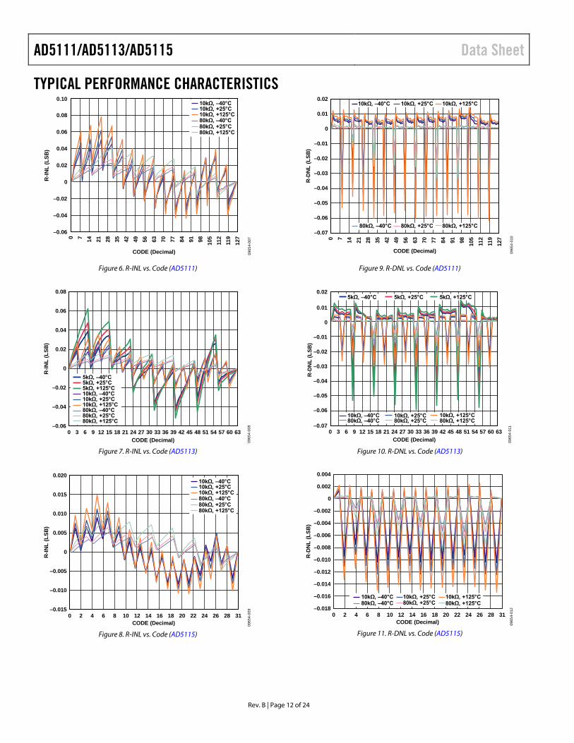
TYPICAL PERFORMANCE CHARACTERISTICS
–0.06
–0.04
CODE (Decimal)
R-IN
L (L
SB)
–0.02
0
0.02
0.04
0.06
0.08
0.10
0 7 14 21 28 35 42 49 56 63 70 77 84 91 98 105
1 12
119
127
10kΩ, –40°C10kΩ, +25°C10kΩ, +125°C80kΩ, –40°C80kΩ, +25°C80kΩ, +125°C
0965
4-00
7
Figure 6. R-INL vs. Code (AD5111)
–0.06
–0.04
–0.02
0
0.02
0.04
0.06
0.08
0 3 6 9 12 15 18 21 24 27 30 33 36 39 42 45 48 51 54 57 60 63
5kΩ, –40°C5kΩ, +25°C5kΩ, +125°C10kΩ, –40°C10kΩ, +25°C10kΩ, +125°C80kΩ, –40°C80kΩ, +25°C80kΩ, +125°C
CODE (Decimal)
R-IN
L (L
SB)
0965
4-00
8
Figure 7. R-INL vs. Code (AD5113)
–0.015
–0.010
–0.005
0
0.005
0.010
0.015
0.020
0 2 4 6 8 10 12 14 16 18 20 22 24 26 28 31
10kΩ, –40°C10kΩ, +25°C10kΩ, +125°C80kΩ, –40°C80kΩ, +25°C80kΩ, +125°C
CODE (Decimal)
R-IN
L (L
SB)
0965
4-00
9
Figure 8. R-INL vs. Code (AD5115)
–0.07
–0.06
–0.05
–0.04
–0.03
–0.02
–0.01
0
0.01
0.02
0 7 14 21 28 35 42 49 56 63 70 77 84 91 98 105
112
119
127
10kΩ, –40°C 10kΩ, +25°C 10kΩ, +125°C
80kΩ, –40°C 80kΩ, +25°C 80kΩ, +125°C
CODE (Decimal) 0965
4-01
0
R-D
NL
(LSB
)
Figure 9. R-DNL vs. Code (AD5111)
0 3 6 9 12 15 18 21 24 27 30 33 36 39 42 45 48 51 54 57 60 63
5kΩ, –40°C 5kΩ, +25°C 5kΩ, +125°C
10kΩ, –40°C 10kΩ, +25°C 10kΩ, +125°C80kΩ, –40°C 80kΩ, +25°C 80kΩ, +125°C
–0.07
–0.06
–0.05
–0.04
–0.03
–0.02
–0.01
0
0.01
0.02
CODE (Decimal) 0965
4-01
1
R-D
NL
(LSB
)
Figure 10. R-DNL vs. Code (AD5113)
0 2 4 6 8 10 12 14 16 18 20 22 24 26 28 31–0.018
–0.016
–0.014
–0.012
–0.010
–0.008
–0.006
–0.004
–0.002
0
0.002
0.004
10kΩ, –40°C 10kΩ, +25°C 10kΩ, +125°C80kΩ, –40°C 80kΩ, +25°C 80kΩ, +125°C
CODE (Decimal)
R-D
NL
(LSB
)
0965
4-01
2
Figure 11. R-DNL vs. Code (AD5115)

Data Sheet AD5111/AD5113/AD5115
Rev. B | Page 13 of 24
CODE (Decimal)
INL
(LSB
)
0 7 14 21 28 35 42 49 56 63 70 77 84 91 98 105
112
119
127
–0.08
–0.06
–0.04
–0.02
0
0.02
0.04
0.06
0.0810kΩ, –40°C10kΩ, +25°C10kΩ, +125°C80kΩ, –40°C80kΩ, +25°C80kΩ, +125°C
0965
4-01
3
Figure 12. INL vs. Code (AD5111)
5kΩ, –40°C5kΩ, +25°C5kΩ, +125°C10kΩ, –40°C10kΩ, +25°C10kΩ, +125°C80kΩ, –40°C80kΩ, +25°C80kΩ, +125°C
–0.08
–0.06
–0.04
–0.02
0
0.02
0.04
0.06
0.08
0 3 6 9 12 15 18 21 24 27 30 33 36 39 42 45 48 51 54 57 60 63CODE (Decimal)
INL
(LSB
)
0965
4-01
4
Figure 13. INL vs. Code (AD5113)
0 2 4 6 8 10 12 14 16 18 20 22 24 26 28 31CODE (Decimal)
INL
(LSB
)
–0.020
–0.015
–0.010
–0.005
0
0.005
0.010
0.01510kΩ, –40°C10kΩ, +25°C10kΩ, +125°C80kΩ, –40°C80kΩ, +25°C80kΩ, +125°C
0965
4-01
5
Figure 14. INL vs. Code (AD5115)
–0.07
–0.06
–0.05
–0.04
–0.03
–0.02
–0.01
0
0.01
0.02
0 7 14 21 28 35 42 49 56 63 70 77 84 91 98 105
112
119
127
10kΩ, –40°C 10kΩ, +25°C 10kΩ, +125°C80kΩ, –40°C 80kΩ, +25°C 80kΩ, +125°C
CODE (Decimal)
DN
L (L
SB)
0965
4-01
6
Figure 15. DNL vs. Code (AD5111)
–0.06
–0.05
–0.04
–0.03
–0.02
–0.01
0
0.01
0.02
0 3 6 9 12 15 18 21 24 27 30 33 36 39 42 45 48 51 54 57 60 63
5kΩ, –40°C 5kΩ, +25°C 5kΩ, +125°C10kΩ, –40°C 10kΩ, +25°C 10kΩ, +125°C
80kΩ, –40°C 80kΩ, +25°C 80kΩ, +125°C
CODE (Decimal)
DN
L (L
SB)
0965
4-01
7
Figure 16. DNL vs. Code (AD5113)
0965
4-01
8
0 2 4 6 8 10 12 14 16 18 20 22 24 26 28 31CODE (Decimal)
DN
L (L
SB)
–0.016
–0.014
–0.012
–0.010
–0.008
–0.006
–0.004
–0.002
0
0.002
0.00410kΩ, –40°C 10kΩ, +25°C 10kΩ, +125°C
80kΩ, –40°C 80kΩ, +25°C 80kΩ, +125°C
Figure 17. DNL vs. Code (AD5115)

AD5111/AD5113/AD5115 Data Sheet
Rev. B | Page 14 of 24
–100
0
100
200
300
SUPP
LY C
UR
REN
T (n
A)
400
500
600
700
800
–40 –25 –10 5 20 35TEMPERATURE (°C)
50 65 80 95 110 125
0965
4-01
9
VDD = 2.3VVDD = 3.3VVDD = 5V
Figure 18. Supply Current vs. Temperature
0
20
40
60
80
100
120
140
160
180
200
0 20 40 60
CODE (Decimal)
POTE
NTI
OM
ETER
MO
DE
TEM
PCO
(ppm
/°C
)
80 100 1200 10 20 30 40 50 600 5 10 15 20 25 30
AD5111AD5113AD5115
10kΩ80kΩ5kΩ
0965
4-02
0
VDD = 5V
Figure 19. Potentiometer Mode Tempco ((ΔVW/VW)/ΔT × 106) vs. Code
0
–60
–50
–40
–30
–20
–10
100M10M1M100k10k
GA
IN (d
B)
FREQUENCY (Hz)
0x20
0x10
0x08
0x04
0x020x01
0x00
0965
4-02
1
Figure 20. 5 kΩ Gain vs. Frequency vs. Code
0965
4-02
2
0
0.2
0.4
0.6
0.8
1.0
1.2
0.05 0.65 1.25 1.85 2.45 3.05 3.65 4.25 4.85
DIGITAL INPUT VOLTAGE (V)
SUPP
LY C
UR
REN
T (m
A)
VDD = 5VVDD = 3.3VVDD = 2.3V
TA = 25°C
Figure 21. Supply Current (IDD) vs. Digital Input Voltage
0
20
40
60
80
100
120
140
160
180
200
10kΩ80kΩ5kΩ
VDD = 5V
RH
EOST
AT
MO
DE
TEM
PCO
(ppm
/°C
)
0965
4-02
3
0 20 40 60
CODE (Decimal)
80 100 1200 10 20 30 40 50 600 5 10 15 20 25 30
AD5111AD5113AD5115
Figure 22. Rheostat Mode Tempco ((ΔRWB/RWB)/ΔT × 106) vs. Code
–50
–40
–30
–10
0
1M 10M100k10k
GA
IN (d
B)
FREQUENCY (Hz)
0x40
0x10
0x04
0x02
–20
–70
–60
0x08
0x01
0x20
0965
4-02
4
0x00
(0x20)
(0x08)
(0x02)
(0x01)
(0x04)
(0x00)
(0x10)
[0x10]
[0x04]
[0x01]
[0x00]
[0x02]
[0x08]
AD5111 (AD5113) [AD5115]
Figure 23. 10 kΩ Gain vs. Frequency vs. Code

Data Sheet AD5111/AD5113/AD5115
Rev. B | Page 15 of 24
–60
–50
–40
–30
–10
0
10k 1M100k
GA
IN (d
B)
FREQUENCY (Hz)
–20
–80
–70
0965
4-02
5
0x40
0x10
0x040x02
0x08
0x01
0x20
0x00
(0x20)
(0x08)
(0x02)(0x01)
(0x04)
(0x00)
(0x10)
[0x10]
[0x04]
[0x01][0x00]
[0x02]
[0x08]
AD5111 (AD5113) [AD5115]
Figure 24. 80 kΩ Gain vs. Frequency vs. Code 09
654-
049
–80
–70
–60
–50
–40
–30
–20
–10
0
10k 100k 1M 10M
PHA
SE (D
egre
es)
FREQUENCY (Hz)
FULL SCALEHALF SCALEQUARTER SCALE
RAB = 10kΩ
Figure 25. Normalized Phase Flatness vs. Frequency
0
–100
–90
–80
–70
–60
–50
–40
–30
–20
–10
THD
+ N
(dB
)
FREQUENCY (Hz)20 200 2k 20k 200k
10kΩ5kΩ
80kΩ
0965
4-02
7
VDD = 5VVA = 2.5V + 1VRMSVB = 2.5VCODE = HALF SCALENOISE FILTER = 22kHz
Figure 26. Total Harmonic Distortion + Noise (THD + N) vs. Frequency
0
10
20
30
40
50
60
70
BA
ND
WID
TH (M
Hz)
80
CODE (Decimal) 0965
4-02
8
5k + 250pF10k + 75pF10k + 150pF10k + 250pF80k + 0pF80k + 75pF
80k + 150pF80k + 250pF5k + 0pF5k + 75pF5k + 150pF10k + 0pF
0 10 20 30 40 50 600 5 10 15 20 25 300 5 10 15
AD5111AD5113AD5115
Figure 27. Maximum Bandwidth vs. Code vs. Net Capacitance
0
30
60
90IN
CR
EMEN
TAL
WIP
ER O
N R
ESIS
TAN
CE
(Ω)
120
150
0 1 2 3VDD (V)
4 5 6
5.5V5V3.3V2.7V2.3V
0965
4-02
9
TA = 25°C
Figure 28. Incremental Wiper On Resistance vs. VDD
THD
+ N
(dB
)
AMPLITUDE (V rms)
–90
–80
–70
–60
–50
–40
–30
–20
–10
0
0.001 0.01 0.1 1
0965
4-03
0
10kΩ5kΩ
80kΩ
VDD = 5VVA = 2.5V + VINVB = 2.5VfIN = 1kHzCODE = HALF SCALENOISE FILTER = 22kHz
Figure 29. Total Harmonic Distortion + Noise (THD + N) vs. Amplitude

AD5111/AD5113/AD5115 Data Sheet
Rev. B | Page 16 of 24
–0.10
–0.05
0
0.05
0.10
0.15
REL
ATIV
E VO
LTA
GE
(V)
0.20
0.25
0.30
0.35
–1 1 3 5TIME (µs)
7 9 0965
4-04
8
5kΩ10kΩ80kΩ
VDD = 5VVA = VDDVB = GND
Figure 30. Maximum Transition Glitch
0
0.2
0.4
0.6
0.8
1.0
1.2
0
0.0005
0.0010
0.0015
0.0020
0.0025
–400–500–600 –300 –200 –100 0 100 200 300 400 500 600
CU
MU
LATI
VE P
RO
BA
BIL
ITY
PRO
BA
BIL
ITY
DEN
SITY
RESISTOR DRIFT (ppm) 0965
4-05
0
Figure 31. Resistor Lifetime Drift
–70
–60
–50
–40
–30
–20
–10
0
FREQUENCY (Hz)
PSR
R (d
B)
0965
4-03
310 100 1k 10k 100k 1M
5kΩ10kΩ80kΩ
VDD = 5V ± 10% ACVA = 4VVB = GNDCODE = HALF SCALETA = 25°C
Figure 32. Power Supply Rejection Ratio (PSRR) vs. Frequency
–120
–100
–80
–60
–40
–20
0
20
40
60
80
100
0 0.5 1.0 1.5 2.0 2.5 3.0 3.5 4.0
VOLT
AG
E (µ
V)
TIME (µs) 0965
4-03
4
VDD = 5VVA = VDDVB = GNDCODE = HALF SCALE
Figure 33. Digital Feedthrough
–70
–60
–50
–40
–30
–20
–10
0
1k 10k 1M 10M
GA
IN (d
B)
FREQUENCY (Hz)
5kΩ10kΩ80kΩ
0965
4-03
5
Figure 34. Shutdown Isolation vs. Frequency
0
1
2
3
4
5
6
7
THEO
RET
ICA
L I M
AX
(mA
)
10kΩ80kΩ5kΩ
0 20 40 60
CODE (Decimal)
80 100 1200 10 20 30 40 50 600 5 10 15 20 25 30
AD5111AD5113AD5115
0965
4-03
6
Figure 35. Theoretical Maximum Current vs. Code

Data Sheet AD5111/AD5113/AD5115
Rev. B | Page 17 of 24
TEST CIRCUITS Figure 36 to Figure 41 define the test conditions used in the Specifications section.
AW
B
NC
IWDUT
VMS
NC = NO CONNECT 0965
4-03
7
Figure 36. Resistor Position Nonlinearity Error
(Rheostat Operation: R-INL, R-DNL)
AW
B
DUT
VMS
V+
V+ = VDD1LSB = V+/2N
0965
4-03
8
Figure 37. Potentiometer Divider Nonlinearity Error (INL, DNL)
0965
4-03
9
+
–
DUT
0.1V
= 0.1VIWB
IWB
W
B
NC = NO CONNECT
RW
A
NC
GND TO VDD
Figure 38. Wiper Resistance
AW
B VMS
~
VA
VDDV+
V+ = VDD ± 10%
ΔVMS%ΔVDD%PSS (%/%) =
PSRR (dB) = 20 logΔVMSΔVDD
0965
4-04
0
Figure 39. Power Supply Sensitivity (PSS, PSRR)
OFFSETGND
A
BDUT
W
+15V
VINVOUTAD8652
–15V2.5V
0965
4-04
1
Figure 40. Gain and Phase vs. Frequency
0965
4-04
2
DUT ICMW
B
VDD
GND
A
VDD
GND
GND
VDD
GND
VDD
Figure 41. Common-Mode Leakage Current

AD5111/AD5113/AD5115 Data Sheet
Rev. B | Page 18 of 24
THEORY OF OPERATION The AD5111/AD5113/AD5115 digital programmable resistors are designed to operate as true variable resistors for analog signals within the terminal voltage range of GND < VTERM < VDD. The resistor wiper position is determined by the RDAC register contents. The RDAC register acts as a scratchpad register that allows unlimited changes of resistance settings.
The RDAC register can be programmed with any position setting using the up/down interface. Once a desirable wiper position is found, this value can be stored in the EEPROM. Thereafter, the wiper position is always restored to that position for subsequent power-up. The storing of EEPROM data takes approximately 30 ms; during this time, the device is locked and does not accept any new operation, thus preventing any changes from taking place.
The AD5111/AD5113/AD5115 are designed to allow high speed digital control with clock rates up to 50 MHz.
RDAC REGISTER AND EEPROM
The RDAC register directly controls the position of the digital potentiometer wiper. For example, when the RDAC register is 0x40 (AD5111), the wiper is connected to midscale of the variable resistor. The RDAC register is a standard logic register; there is no restriction on the number of changes allowed.
Once a desirable wiper position is found, this value can be saved into the EEPROM. Thereafter, the wiper position is always set at that position for any future on-off-on power supply sequence or recall operation.
BASIC OPERATION When CS is pulled low, changing the resistance settings is achieved by clocking the CLK pin. It is negative edge triggered, and the direction of stepping into the RDAC register is determined by the state of the U/D input. When a specific state of the U/D remains, the device continues to change in the same direction under consecutive clocks until it comes to the end of the resistance setting. When the wiper reaches the maximum or minimum setting, additional CLK pulses do not change the wiper setting. Figure 2 shows a typical increment/decrement operation.
The U/D pin value can be changed only when the CLK pin is low.
LOW WIPER RESISTANCE FEATURE The AD5111/AD5113/AD5115 include a new feature to reduce the resistance between terminals. These extra steps are called bottom scale and top scale. At bottom scale, the typical wiper resistance decreases from 70 Ω to 45 Ω. At top scale, the resistance between Terminal A and Terminal W is decreased by 1 LSB and the total resistance is reduced to 70 Ω. The new extra steps are loaded automatically in the RDAC register after zero-scale or full-scale position has been reached.
The extra steps are not equal to 1 LSB and are not included in the INL, DNL, R-INL, and R-DNL specifications.
SHUTDOWN MODE This feature places Terminal A in open circuit, disconnected from the internal resistor, and connects Terminal W and Terminal B. A finite wiper resistance of 45 Ω is present between these two terminals. The command is sent by a low-to-high transition on the U/D pin, when CLK is high and CS is enabled. The command is executed on the CLK negative edge, as shown in Figure 4.
The AD5111/AD5113/AD5115 return the wiper to prior shutdown position if any other operation is performed.
EEPROM WRITE OPERATION The AD5111/AD5113/AD5115 contain an EEPROM that allows the wiper position storage. Once a desirable wiper position is found, this value can be saved into the EEPROM. Thereafter, the wiper position is always set at that position for any future power-up sequence or a memory recall operation.
During the storage cycle, the device is locked and does not accept any new operation, thus preventing any changes from taking place.
The write cycle is started by applying a pulse in the U/D pin when CS is enabled and CLK remains high, as shown in Figure 3. The write cycle takes approximately 20 ms.

Data Sheet AD5111/AD5113/AD5115
Rev. B | Page 19 of 24
RDAC ARCHITECTURE To achieve optimum performance, Analog Devices, Inc., has patented the RDAC segmentation architecture for all the digital potentiometers. In particular, the AD5111/AD5113/AD5115 employ a two-stage segmentation approach as shown in Figure 42. The AD5111/AD5113/AD5115 wiper switch is designed with the transmission gate CMOS topology and with the gate voltage derived from VDD.
RL
RL
RL
RL
RS
W
RS
A
B
BS
5-BIT/6-BIT/7-BITADDRESSDECODER
TS
0965
4-04
3
Figure 42. AD5111/AD5113/AD5115 Simplified RDAC Circuit
Low Wiper Resistance Feature
In addition, the AD5111/AD5113/AD5115 include a new feature to reduce the resistance between terminals. These extra steps are called bottom scale and top scale. At bottom scale, the typical wiper resistance decreases from 70 Ω to 45 Ω. At top scale, the resistance between Terminal A and Terminal W is decreased by 1 LSB and the total resistance is reduced to 70 Ω. The extra steps are not equal to 1 LSB and are not included in the INL, DNL, R-INL, and R-DNL specifications.
PROGRAMMING THE VARIABLE RESISTOR Rheostat Operation—±8% Resistor Tolerance
The AD5111/AD5113/AD5115 operate in rheostat mode when only two terminals are used as a variable resistor. The unused terminal can be floating or tied to the W terminal as shown in Figure 43.
A
W
B
A
W
B
A
W
B
0965
4-04
4
Figure 43. Rheostat Mode Configuration
The nominal resistance between Terminal A and Terminal B, RAB, is available in 5 kΩ, 10 kΩ, and 80 kΩ and has 128/64/32 tap points accessed by the wiper terminal. The 5-/6-/7-bit data in the RDAC latch is decoded to select one of the 128/64/32 possible wiper settings. The general equations for determining the digitally programmed output resistance between the W terminal and B terminal are
AD5111:
BSWB RR = Bottom scale (1)
WABWB RRD
DR +×=128
)( From 0 to 128 (2)
AD5113:
BSWB RR = Bottom scale (3)
WABWB RRD
DR +×=64
)( From 0 to 64 (4)
AD5115:
BSWB RR = Bottom scale (5)
WABWB RRD
DR +×=32
)( From 0 to 32 (6)
where: D is the decimal equivalent of the binary code in the 5-/6-/7-bit RDAC register; 128, 64, and 32 refer to the top scale step. RAB is the end-to-end resistance. RW is the wiper resistance. RBS is the wiper resistance at bottom scale.

AD5111/AD5113/AD5115 Data Sheet
Rev. B | Page 20 of 24
Similar to the mechanical potentiometer, the resistance of the RDAC between the W terminal and the A terminal also produces a digitally controlled complementary resistance, RWA. RWA starts at the maximum resistance value and decreases as the data loaded into the latch increases. The general equations for this operation are
AD5111:
WABAW RRR += Bottom scale (7)
WABAW RRDDR +×−
=128
128)( From 0 to 127 (8)
TSAW RR = Top scale (9)
AD5113:
WABAW RRR += Bottom scale (10)
WABAW RRDDR +×−
=64
64)( From 0 to 63 (11)
TSAW RR = Top scale (12)
AD5115:
WABAW RRR += Bottom scale (13)
WABAW RRDDR +×−
=32
32)( From 0 to 31 (14)
TSAW RR = Top scale (15)
where: D is the decimal equivalent of the binary code in the 5-/6-/7-bit RDAC register; 128, 64, and 32 refer to top scale step. RAB is the end-to-end resistance. RW is the wiper resistance. RTS is the wiper resistance at top scale.
Regardless of which setting the part is operating in, take care to limit the current between A to B, W to A, and W to B, to the maximum continuous current of ±6 mA (5 kΩ and 10 kΩ) or ±1.5 mA (80 kΩ), or pulse current specified in Table 6. Otherwise, degradation or possible destruction of the internal switch contact can occur.
PROGRAMMING THE POTENTIOMETER DIVIDER Voltage Output Operation
The digital potentiometer easily generates a voltage divider at W-to-B and W-to-A that is proportional to the input voltage at A-to-B, as shown in Figure 44. Unlike the polarity of VDD to GND, which must be positive, current across A-to-B, W-to-A, and W-to-B can be in either direction.
AVI
W
B
VO
0965
4-04
5
Figure 44. Potentiometer Mode Configuration
If ignoring the effect of the wiper resistance for simplicity, connecting Terminal A to 5 V and Terminal B to ground produces an output voltage at W to B ranging from 0 V to 5 V. The general equation defining the output voltage at VW with respect to ground for any valid input voltage applied to Terminal A and Terminal B, is
BAB
AWA
AB
WBW V
RDR
VR
DRDV ×+×=)()()( (16)
where: RWB(D) can be obtained from Equation 1 to Equation 6. RAW(D) can be obtained from Equation 7 to Equation 14.
Operation of the digital potentiometer in the divider mode results in a more accurate operation over temperature. Unlike the rheostat mode, the output voltage is dependent mainly on the ratio of the internal resistors, RWA and RWB, and not the absolute values. Therefore, the temperature drift reduces to 5 ppm/°C.
TERMINAL VOLTAGE OPERATING RANGE The AD5111/AD5113/AD5115 are designed with internal ESD diodes for protection. These diodes also set the voltage boundary of the terminal operating voltages. Positive signals present on the A, B, or W terminals that exceed VDD are clamped by the forward-biased diode. There is no polarity constraint between VA, VW, and VB, but they cannot be higher than VDD or lower than GND.

Data Sheet AD5111/AD5113/AD5115
Rev. B | Page 21 of 24
POWER-UP SEQUENCE
Because of the ESD protection diodes that limit the voltage compliance at the A, B, and W terminals (see Figure 45), it is important to power on VDD before applying any voltage to the A, B, and W terminals. Otherwise, the diodes are forward-biased such that VDD is powered on unintentionally and can affect other parts of the circuit. Similarly, VDD should be powered down last. The ideal power-on sequence is in the following order: GND, VDD, and VA/VB/VW. The order of powering VA, VB, VW and the digital inputs is not important as long as they are powered on after VDD.
GND
VDD
A
W
B
0965
4-04
6
Figure 45. Maximum Terminal Voltages Set by VDD and GND
LAYOUT AND POWER SUPPLY BIASING It is always a good practice to use compact, minimum lead length layout design. The leads to the input should be as direct as possible with a minimum conductor length. Ground paths should have low resistance and low inductance. It is also good practice to bypass the power supplies with quality capacitors. Apply low equivalent series resistance (ESR) 1 μF to 10 μF tantalum or electrolytic capacitors at the supplies to minimize any transient disturbance and to filter low frequency ripple. Figure 46 illustrates the basic supply bypassing configuration for the AD5111/AD5113/AD5115.
VDDVDD +
GND
C10.1µF
C210µF
AGND
AD5111/AD5113/AD5115
0965
4-04
7
Figure 46. Power Supply Bypassing

AD5111/AD5113/AD5115 Data Sheet
Rev. B | Page 22 of 24
OUTLINE DIMENSIONS
1.701.601.50
0.4250.3500.275
TOP VIEW
8
1
5
4
0.300.250.20
BOTTOM VIEW
PIN 1 INDEXAREA
2.00 BSC SQ
SEATINGPLANE
0.600.550.50
1.101.000.90
0.20 REF
0.175 REF
0.05 MAX0.02 NOM
0.50 BSC
EXPOSEDPAD
PIN 1INDICATOR(R 0.15)
FOR PROPER CONNECTION OFTHE EXPOSED PAD, REFER TOTHE PIN CONFIGURATION ANDFUNCTION DESCRIPTIONSSECTION OF THIS DATA SHEET.
07-1
1-20
11-B
Figure 47. 8-Lead Frame Chip Scale Package [LFCSP_UD]
2 mm × 2 mm Body, Very Thin, Dual Lead (CP-8-10) Dimensions shown in millimeters
ORDERING GUIDE
Model1, 2 RAB (kΩ) Resolution Temperature Range
Package Description
Package Option
Branding Code
AD5111BCPZ10-RL7 10 128 −40°C to +125°C 8-Lead LFCSP_UD CP-8-10 7S AD5111BCPZ10-500R7 10 128 −40°C to +125°C 8-Lead LFCSP_UD CP-8-10 7S AD5111BCPZ80-RL7 80 128 −40°C to +125°C 8-Lead LFCSP_UD CP-8-10 7T AD5111BCPZ80-500R7 80 128 −40°C to +125°C 8-Lead LFCSP_UD CP-8-10 7T AD5113BCPZ5-RL7 5 64 −40°C to +125°C 8-Lead LFCSP_UD CP-8-10 85 AD5113BCPZ5-500R7 5 64 −40°C to +125°C 8-Lead LFCSP_UD CP-8-10 85 AD5113BCPZ10-RL7 10 64 −40°C to +125°C 8-Lead LFCSP_UD CP-8-10 84 AD5113BCPZ10-500R7 10 64 −40°C to +125°C 8-Lead LFCSP_UD CP-8-10 84 AD5113BCPZ80-RL7 80 64 −40°C to +125°C 8-Lead LFCSP_UD CP-8-10 86 AD5113BCPZ80-500R7 80 64 −40°C to +125°C 8-Lead LFCSP_UD CP-8-10 86 AD5115BCPZ10-RL7 10 32 −40°C to +125°C 8-Lead LFCSP_UD CP-8-10 7Y AD5115BCPZ10-500R7 10 32 −40°C to +125°C 8-Lead LFCSP_UD CP-8-10 7Y AD5115BCPZ80-RL7 80 32 −40°C to +125°C 8-Lead LFCSP_UD CP-8-10 7Z AD5115BCPZ80-500R7 80 32 −40°C to +125°C 8-Lead LFCSP_UD CP-8-10 7Z EVAL-AD5111SDZ Evaluation Board 1 Z = RoHS Compliant Part. 2 The EVAL-AD5111SDZ has an RAB of 10 kΩ.

Data Sheet AD5111/AD5113/AD5115
Rev. B | Page 23 of 24
NOTES

AD5111/AD5113/AD5115 Data Sheet
Rev. B | Page 24 of 24
NOTES
©2011–2012 Analog Devices, Inc. All rights reserved. Trademarks and registered trademarks are the property of their respective owners. D09654-0-11/12(B)
Related Documents