Simultaneous Two-color Lasing in a Single CdSSe Heterostructure Nanosheet (Invited Paper) F Fan, † Z Liu, † L Yin, P L Nichols, H Ning, S Turkdogan and C Z Ning * School of Electrical, Computer, and Energy Engineering, Arizona State University, Tempe, Arizona 85287, USA † These authors contributed equally to this work. * [email protected], http://nanophotonics.asu.edu Abstract: The ability of a single monolithic semiconductor structure to emit or lase in a broad spectrum range is of great importance for many applications such as solid state lighting and multi-spectrum detection. But spectral range of a laser or light emitting diode made of a given semiconductor is typically limited by its emission or gain bandwidth. Due to lattice mismatch, it is typically difficult to grow thin film or bulk materials with very different bandgaps in a monolithic fashion. But nanomaterials such as nanowires, nanobelts, nanosheets provide a unique opportunity. Here we report our experimental results demonstrating simultaneous lasing in two visible colors at 526 nm and 624 nm from a single CdSSe heterostructure nanosheet at room temperature. The 97 nm wavelength separation of the two colors is significantly larger than the gain bandwidth of a typical single II-VI semiconductor material. Such lasing and light emission in a wide spectrum range from a single monolithic structure will have important applications mentioned above. PACs Code: Semiconductor Lasers (42.55.Px); Nanosheets (62.23.Kn); Heterostructures (79.60.Jv) 1. Introduction Realization of monolithic semiconductor structures with multiple or a wide range of bandgaps have many important applications in solid state lighting, high efficient solar cells, and multi-spectral detection. In solid state lighting applications, a single semiconductor structure or device capable of emitting or lasing in the entire visible range (400-700 nm) would have a fundamental impact to the ultimate solution of efficient lighting. It was recently demonstrated [1] that four lasers of discrete spectral lines are virtually indistinguishable from state of the art continuous-spectrum white reference illuminant, thus demonstrating the feasibility of laser lighting. In addition, lasers can be much more efficient than light emitting diodes (LEDs). Similarly, discrete multicolor lasers have many other applications such as full-color laser display [2], white laser illumination [1], and biological inspection [3]. Even though the experimental demonstration was carried out with four separate lasers [1], a much more preferred approach would be to have all lasers of different colors produced on a same platform in a compact fashion. But achieving such emission or lasing in a wide spectrum is fundamentally challenging for several reasons. First, typical semiconductors of a given composition under reasonable excitation conditions have a gain bandwidth less than 30 nm [4]-[12]. Wavelength tunability of a single mode, or mode separation of multiple modes, is thus limited by such a bandwidth. Second, to have emission bandwidth significantly broader than that of a

Welcome message from author
This document is posted to help you gain knowledge. Please leave a comment to let me know what you think about it! Share it to your friends and learn new things together.
Transcript

Simultaneous Two-color Lasing in a Single CdSSe
Heterostructure Nanosheet (Invited Paper)
F Fan,† Z Liu,
† L Yin, P L Nichols, H Ning, S Turkdogan and C Z Ning
*
School of Electrical, Computer, and Energy Engineering, Arizona State University, Tempe,
Arizona 85287, USA
† These authors contributed equally to this work.
*[email protected], http://nanophotonics.asu.edu
Abstract: The ability of a single monolithic semiconductor structure to emit or lase in a
broad spectrum range is of great importance for many applications such as solid state
lighting and multi-spectrum detection. But spectral range of a laser or light emitting diode
made of a given semiconductor is typically limited by its emission or gain bandwidth. Due
to lattice mismatch, it is typically difficult to grow thin film or bulk materials with very
different bandgaps in a monolithic fashion. But nanomaterials such as nanowires,
nanobelts, nanosheets provide a unique opportunity. Here we report our experimental
results demonstrating simultaneous lasing in two visible colors at 526 nm and 624 nm
from a single CdSSe heterostructure nanosheet at room temperature. The 97 nm
wavelength separation of the two colors is significantly larger than the gain bandwidth of a
typical single II-VI semiconductor material. Such lasing and light emission in a wide
spectrum range from a single monolithic structure will have important applications
mentioned above.
PACs Code: Semiconductor Lasers (42.55.Px); Nanosheets (62.23.Kn); Heterostructures
(79.60.Jv)
1. Introduction
Realization of monolithic semiconductor structures with multiple or a wide range of bandgaps have
many important applications in solid state lighting, high efficient solar cells, and multi-spectral detection.
In solid state lighting applications, a single semiconductor structure or device capable of emitting or lasing
in the entire visible range (400-700 nm) would have a fundamental impact to the ultimate solution of
efficient lighting. It was recently demonstrated [1] that four lasers of discrete spectral lines are virtually
indistinguishable from state of the art continuous-spectrum white reference illuminant, thus demonstrating
the feasibility of laser lighting. In addition, lasers can be much more efficient than light emitting diodes
(LEDs). Similarly, discrete multicolor lasers have many other applications such as full-color laser display
[2], white laser illumination [1], and biological inspection [3]. Even though the experimental
demonstration was carried out with four separate lasers [1], a much more preferred approach would be to
have all lasers of different colors produced on a same platform in a compact fashion. But achieving such
emission or lasing in a wide spectrum is fundamentally challenging for several reasons. First, typical
semiconductors of a given composition under reasonable excitation conditions have a gain bandwidth less
than 30 nm [4]-[12]. Wavelength tunability of a single mode, or mode separation of multiple modes, is thus
limited by such a bandwidth. Second, to have emission bandwidth significantly broader than that of a

single-composition material, heterogeneous integration or growth of different semiconductors is necessary.
Due to the large variation or significant mismatch of the lattice constants for semiconductors with distinct
material compositions, growth of such structures on a single substrate becomes extremely difficult. Finally,
even such materials could be grown, it is still a challenge to design an appropriate cavity structure to
support wavelengths that are widely separated. This is because the short-wavelength light will be strongly
absorbed by the narrow gap semiconductors involved, such that only the long-wavelength light can
eventually reach the threshold and become lasing. Various attempts have been made recently to overcome
these challenges and to extend the spectral range of light emission and lasing beyond the gain bandwidth of
a single material. Multi-color or dual-color lasing has been observed by placing multiple nanowires within
a microfiber [13], in multi-section quantum dot distributed feedback lasers [14], or by using fast-switching
of different dyes in a microfluidic channel [15]. However these multicolor lasers are either achieved in
separated devices, or with wavelength separation still limited within the gain bandwidth of a single
semiconductor material.
In this paper, we report the first experimental observation of simultaneous lasing in two visible colors
(at 526 and 624 nm, respectively) from a single monolithic semiconductor structure. The wavelength
separation of two lasing colors of 97 nm is much larger than the gain bandwidth of a single composition
semiconductor material. The unique structure in this paper that enabled such dual wavelength lasing is a
heterostructure nanosheet or nanobelt of the ternary semiconductor CdSSe produced in a single monolithic
growth. Our results were enabled by some unique quality of nanowires and nanobelts that have been the
focus of light emission and lasing research for the last 10 years [16]-[24]. Semiconductor nanowires and
nanobelts grown using the metal-catalyzed vapor-liquid-solid mechanism have opened new possibilities for
multi-color emission or lasing [17]-[22]. Even though semiconductor nanoparticles can also achieve
multi-color emissions, but it is typically challenging to spatially address or control each individual color,
since they are typically mixed uniformly. In addition, eventual electrical injection is needed for such
applications and the poor conductivity in nanoparticles make electrical injection very inefficient. One of
the important features of nanowires and nanobelts for our purpose is the ability to grow different materials
with different lattice constants without introducing too many defects to degrade optical properties. This
property has been utilized in the past to grow materials with very different or graded alloy compositions
[18]-[21] to achieve light emission in a wide range, mostly from different wires and more recently from a
single wire [25]. While we recently have demonstrated multi-color lasing from many wires on a single
substrate [18], but so far, multi-color lasing from a single nanowire or belt has not been demonstrated,
especially when the wavelength separation is wider than the gain bandwidth.
2. Sample Growth and Characterization
The CdSSe lateral heterostructure nanosheets were grown through a chemical vapor deposition (CVD)
approach using CdS and CdSe powders (Alfa Aesar, 99.99% purity) as source materials. Si substrate with
10 nm Au film as catalyst was used for the growth. The reactor was first evacuated to a pressure below 0.2
Torr by a mechanical pump. 150 sccm N2 was then introduced into the system, and flow was maintained
for 30 min prior to growth. In the first step of the growth, only CdS powder was thermally evaporated at
880°C for 1 hour. Subsequently, CdSe source was introduced into the furnace, while the temperature was
gradually lowered to 840°C and held for 40 min to grow the CdSe-rich sections. The growth processes is
similar to that of Ref. [26], but we reversed the growth sequence to grown CdS first. Such sequential
growth ensures a wide CdS-rich center section surrounded by CdSe-rich edges (see Fig.1B). The large
width of CdS-rich sections is especially significant as it needs to be wide enough to achieve sufficient
optical confinement for the shorter wavelength lasing modes.

The composition distribution on the CdSSe heterostructure nanosheet is shown in Fig. 1. Fig. 1A shows the
real color photoluminescence (PL) image of the heterostructure nanosheet under 405 nm continuous-wave
(CW) laser excitation. This nanosheet has width of 11.2 μm and length of 41.4 μm. As seen in the image,
the nanosheet consists of three stripes with green emission in the center (grown initially with CdS-rich
composition) and red/orange emission on both edges (grown subsequently with CdSe-rich composition).
Clearly the green stripe and the wider red/orange stripe form two rectangular, coupled cavities in a
side-by-side arrangement. With proper end facets, the three stripes can form three coupled cavities capable
of supporting various propagating modes along the length direction. Of particular interest are the two wider
stripes (the green one in the center and the red one on the right side) which form two rectangular, coupled
cavities in a side-by-side arrangement, as also schematically shown in Fig. 2C. We performed micro-PL
measurements by scanning the focused laser beam with a 1 μm across the width of the nanosheet along the
dashed line in Fig. 1A. The PL peak positions vary from green emission at 559 nm to orange emission at
602 nm with a transition occurring roughly at 3 micron in Fig.1C. Assuming the PL emission is from
ternary CdSxSe1-x, we use the interpolation formula [27]
𝐸𝑔(CdS𝑥Se1−𝑥) = 𝑥𝐸𝑔(CdS) + (1 − 𝑥)𝐸𝑔(CdSe) (1)
to fit the PL peak and to extract the alloy composition. The result is plotted in Fig.1C, where the sulfur
fraction along the scanning path with transition from 45% to 67%. To further confirm the composition
distribution across the heterojunction, the energy dispersive X-ray spectroscopy (EDS) in a transmission
electron microscope (TEM) is also performed along the same path as the PL scan. Fig. 1B shows the TEM
image of this nanosheet. The image was collected with a JEOL JEM-2010 High-Resolution TEM at 200 kV,
equipped with a Link energy dispersive X-ray spectroscopy (EDS) detector. The sulfur compositions
obtained from EDS line scan along the dashed line are plotted in Fig. 1C, consistent with the values from
micro-PL scanning.
3. Experimental and Simulation Results
Fig. 2A shows a PL image of another lateral heterostructure nanosheet. The dimensions of this
nanosheet are 25.0 μm (length) by 17.4 μm (width) by 200 nm (thickness). The nanosheet was cleaved
Figure 1 (A) Real-color PL image of a CdSSe lateral
heterostructure nanosheet excited by 405 continuous-wave laser. (B) TEM image of the same nanosheet. The scale
bars in (A) and (B) are 10 μm. (C) Comparison of sulfur
molar fraction between EDS scan (hallow triangles) and micro-PL scan (solid squares) along the white dashed line
in (A) and (B).
Figure 2 Real-color PL image of the nanosheet under low
pumping power density at room temperature (A) and under 409 kW/cm2 at 77K (B). The dashed lines in (B) denote the
side edges of the nanosheet. The scale bars in (A) and (B)
are 10 μm. (C) Schematic diagram of the nanosheet waveguide structures. (D) PL spectra at 77K under
increasing levels of pumping power density of 77, 173,
241, 338 and 668 kW/cm2 from bottom to top.

from a longer piece by the bend-to-fracture method [28]. With this procedure, high-quality end facets were
created to serve as facet reflectors and to define the laser cavities. The widths of the CdS-rich (green) and
CdSe-rich (orange) sections are 14.8 μm and 2.6 μm, with PL emission peaks at 546 nm (green) and 591
nm (orange), respectively. As shown in the PL image, there are broken nanosheet debris surrounding the
nanosheet of interest, observable by the lighter orange areas within the belt and the excess green areas
outside of the nanosheet perimeter. To demonstrate the capability of dual-color lasing, the sample was
transferred onto a sapphire substrate and loaded into a cryostat for low temperature measurement. We
optically pumped the nanosheet by the third harmonic of a Q-switched Nd:YAG laser (355 nm, 10 Hz, 9
ns). The laser was focused into a 120 μm by 60 μm elliptical beam at an angle of 60° from the sample
normal direction. The real-color image of single pulse induced lasing at higher pumping level at 77 K is
shown in Fig. 2B. As can be seen clearly, the largely uniform spontaneous emission of Fig. 2A is now
replaced by the green and orange bright spots along the end facets, signifying the occurrence of lasing. Due
to the gain-guiding effect and the refractive index contrast, green and orange emission can be
well-separated and confined in their own cavities, which is schematically shown in Fig. 2C. This is
reflected in Fig. 2B, where green and red emissions from the end facets are from the respective segments
of CdS-rich or CdSe-rich materials. The interaction between the green and orange modes is minimized in
this structure. The side-by-side arrangement is an important geometry for reaching the respective lasing
thresholds of both colors. This is in contrast to structures where bandgap changes along the length of a
nanowire [29], where short-wavelength emission from the wide bandgap region (CdS-rich) can be
significantly absorbed by the narrow bandgap region (CdSe-rich). Such absorption will increase the
threshold for the short wavelength lasing, very often to a degree that is too high to achieve lasing. Our
side-by-side arrangement minimizes such undesired absorption and allows the respective lasing thresholds
of both wavelengths to be reached.
Fig. 2D shows the PL spectra under excitation of a single pulse with increasing pump power density. At
lower pumping levels, only broadband spontaneous emission from the CdS-rich and CdSe-rich sections is
observed. With increasing pump pulse power, a narrow peak appears at 592 nm at an excitation level of
173 kW/cm2, indicating the onset of lasing for the orange color in the CdSe-rich section. The same is
observed for green color lasing at 534 nm in the CdS-rich section when the excitation level reaches 241
kW/cm2. The 58 nm separation of the two lasing peaks is much larger than the gain bandwidth of a typical
Zn-Cd-S-Se semiconductor material system including CdS or CdSe [2]-[8]. The narrowest linewidths of
Figure 4 2D Simulation of the optical modes of the CdSSe heterostructure nanosheet. The figure shows the cross section of a
nanosheet in the thickness-width plane. The propagation direction is perpendicular to the paper plane. (A) The schematic of the
nanosheet cross-section. The green (left) and red (right) rectangles
represent the CdS-rich (14.8 μm width) and CdSe rich segments (2.6 μm width), respectively. The thickness is 200 nm. (B-D): The
first three modes around 534 nm. (E-G): The first three modes
around 592 nm.
Figure 3 High resolution (black solid) and low
resolution (blue dash) spectra for the orange lasing peak pumped at 424 kW/cm2. The green, red and
blue vertical lines represent the wavelengths of TE10,
TE20 and TE30 transverse modes. Each transverse mode has 4 associated longitudinal modes. The
intensity of vertical lines of each group is calculated
by the Gaussian convolution.
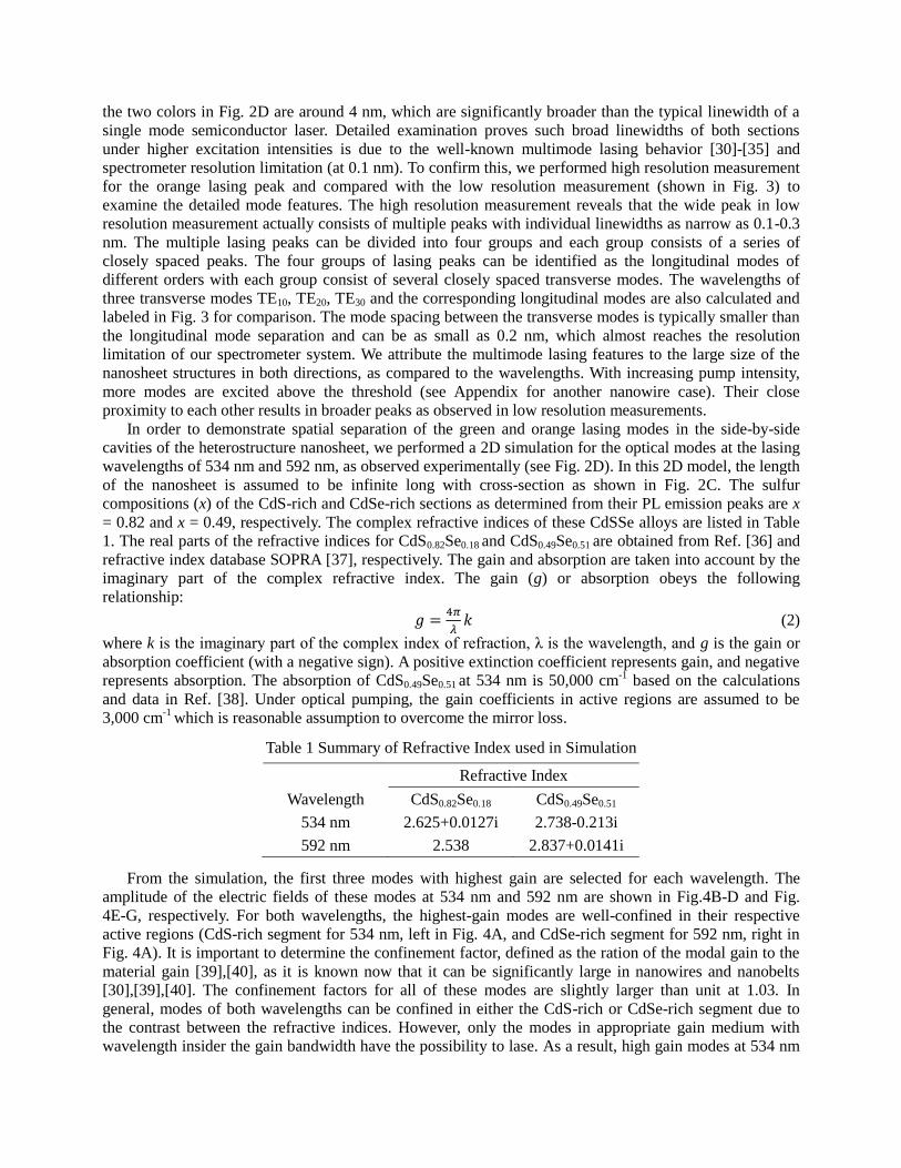
the two colors in Fig. 2D are around 4 nm, which are significantly broader than the typical linewidth of a
single mode semiconductor laser. Detailed examination proves such broad linewidths of both sections
under higher excitation intensities is due to the well-known multimode lasing behavior [30]-[35] and
spectrometer resolution limitation (at 0.1 nm). To confirm this, we performed high resolution measurement
for the orange lasing peak and compared with the low resolution measurement (shown in Fig. 3) to
examine the detailed mode features. The high resolution measurement reveals that the wide peak in low
resolution measurement actually consists of multiple peaks with individual linewidths as narrow as 0.1-0.3
nm. The multiple lasing peaks can be divided into four groups and each group consists of a series of
closely spaced peaks. The four groups of lasing peaks can be identified as the longitudinal modes of
different orders with each group consist of several closely spaced transverse modes. The wavelengths of
three transverse modes TE10, TE20, TE30 and the corresponding longitudinal modes are also calculated and
labeled in Fig. 3 for comparison. The mode spacing between the transverse modes is typically smaller than
the longitudinal mode separation and can be as small as 0.2 nm, which almost reaches the resolution
limitation of our spectrometer system. We attribute the multimode lasing features to the large size of the
nanosheet structures in both directions, as compared to the wavelengths. With increasing pump intensity,
more modes are excited above the threshold (see Appendix for another nanowire case). Their close
proximity to each other results in broader peaks as observed in low resolution measurements.
In order to demonstrate spatial separation of the green and orange lasing modes in the side-by-side
cavities of the heterostructure nanosheet, we performed a 2D simulation for the optical modes at the lasing
wavelengths of 534 nm and 592 nm, as observed experimentally (see Fig. 2D). In this 2D model, the length
of the nanosheet is assumed to be infinite long with cross-section as shown in Fig. 2C. The sulfur
compositions (x) of the CdS-rich and CdSe-rich sections as determined from their PL emission peaks are x
= 0.82 and x = 0.49, respectively. The complex refractive indices of these CdSSe alloys are listed in Table
1. The real parts of the refractive indices for CdS0.82Se0.18 and CdS0.49Se0.51 are obtained from Ref. [36] and
refractive index database SOPRA [37], respectively. The gain and absorption are taken into account by the
imaginary part of the complex refractive index. The gain (g) or absorption obeys the following
relationship:
𝑔 =4𝜋
𝜆𝑘 (2)
where k is the imaginary part of the complex index of refraction, λ is the wavelength, and g is the gain or
absorption coefficient (with a negative sign). A positive extinction coefficient represents gain, and negative
represents absorption. The absorption of CdS0.49Se0.51 at 534 nm is 50,000 cm-1
based on the calculations
and data in Ref. [38]. Under optical pumping, the gain coefficients in active regions are assumed to be
3,000 cm-1
which is reasonable assumption to overcome the mirror loss.
Table 1 Summary of Refractive Index used in Simulation
Refractive Index
Wavelength CdS0.82Se0.18 CdS0.49Se0.51
534 nm 2.625+0.0127i 2.738-0.213i
592 nm 2.538 2.837+0.0141i
From the simulation, the first three modes with highest gain are selected for each wavelength. The
amplitude of the electric fields of these modes at 534 nm and 592 nm are shown in Fig.4B-D and Fig.
4E-G, respectively. For both wavelengths, the highest-gain modes are well-confined in their respective
active regions (CdS-rich segment for 534 nm, left in Fig. 4A, and CdSe-rich segment for 592 nm, right in
Fig. 4A). It is important to determine the confinement factor, defined as the ration of the modal gain to the
material gain [39],[40], as it is known now that it can be significantly large in nanowires and nanobelts
[30],[39],[40]. The confinement factors for all of these modes are slightly larger than unit at 1.03. In
general, modes of both wavelengths can be confined in either the CdS-rich or CdSe-rich segment due to
the contrast between the refractive indices. However, only the modes in appropriate gain medium with
wavelength insider the gain bandwidth have the possibility to lase. As a result, high gain modes at 534 nm

(or 592 nm) can only lase in the CdS-rich (or CdSe- rich) active regions. The refractive index contrast and
the gain confinement ensure that the modes of both wavelengths are confined within their respective gain
media without much leakage to the lossy regions. This is especially important for the green modes, so that
they will not be subject to too strong absorption by the narrow gap material of the CdSe-rich side. The
simulation proves our previous statement that the CdSSe heterostructure nanosheet provides an appropriate
structure to support dual-wavelength lasing in a single structure.
The integrated light intensity is plotted as function of pumping power density on both log-log (Fig. 5A)
and linear scales (Fig. 5B) to corroborate the spectral features and to further establish the lasing behavior at
two distinct wavelengths. Shown in the Fig. 5B, the lasing intensity of both colors increase linearly with
pump power after threshold (260 kW/cm2 for the green modes and 230 kW/cm
2 for the orange modes). The
total spontaneous emission output increases much more slowly than the lasing modes in the high excitation
region, demonstrating the typical behavior associated with density clamping (or slowly increasing) near the
lasing threshold. The log-log scale of the lasing output as a function of the excitation power features the
well-known S-like behavior with three significantly different regions with different slopes, as indicated by
various straight lines used to extract the slopes. At low pumping, the spontaneous emission is dominant, so
the mode intensities increase linearly with a slope of 1.1 for orange and 1.3 for green. Around the
thresholds, the output intensities of both lasing modes show superlinear increases with slopes of 5.1 for
orange and 4.7 for green. With further increase of the excitation power, the slopes of both curves return to
1.1, indicating the above-threshold lasing operation of both colors. The dependence of total intensity on
pumping displays a typical threshold behavior of multimode lasing, which is somewhat more complicated
than that of a single mode laser. To examine the lasing threshold behavior including the multiple transverse
and longitudinal modes, experimental data of total light intensity as a function of total pump intensity
(shown in Fig. 5C) is fitted by the multimode lasing model proposed by Casperson [35]. In this model, the
total output power of multimode lasing is given by
𝐼𝑡 =𝑥0𝑝
(1+𝑥)[1−𝑝(1+𝑥)−1]1/2 (3)
where p is the pump laser power normalized to the lasing threshold and the parameter x is related to x0
through
𝑥
𝑥0= √
1+𝑥
1+𝑥−𝑝 (4)
Figure 5 (A) Output intensities of the two lasing colors versus pumping power
density at 77 K in double-log scale. The three straight lines indicate the slopes of three regions. (B) Same as in (A), but on linear scale, where we also show the
spontaneous emission (blue color with triangles) with a strong saturation after
the threshold. (C) Same as in (A), but shows the fitting with the multi-mode
laser model, as explained in the text.

Here x0 is a parameter proportional to the total spontaneous emission coupled into multiple lasing
modes. Mathematically x0 is proportional to the sum of the spontaneous emission factor β of each lasing
mode. For a conventional semiconductor laser, x0 is less than 0.001 [35]. For a semiconductor nanowire
laser, x0 becomes larger, around 0.02 [30],[33]. Fig. 5C shows the fitting result. The best fitting was
obtained when x0 was taken as 0.085 for green mode and 0.090 for orange mode. The relatively large x0 as
compared to nanowire lasers can be understood by the relationship between x0 and spontaneous emission
factor. x0= 0.02 was obtained when a clear set of longitudinal lasing modes was observed from the
nanowire. In our case, the multimode lasing from the nanosheet contains transverse in addition to
longitudinal modes. These transverse modes survive during the lasing process due to the large confinement
factor, as previously addressed. All of these modes contribute to the spontaneous emission factor x0 to
increase its magnitude. As a result, the light-in-light-out curve of nanosheet laser shows a slightly soft
threshold.
Room temperature (RT) lasing has also been achieved on a larger nanosheet (66.5 μm in length, 33.0
μm in width, and 200 nm in thickness). As shown in Fig. 6A, the widths of the green and the wider orange
stripes are around 30 μm and 3 μm, respectively. The real color lasing image and PL spectra evolution are
shown in Fig. 6B and 6C, respectively. The lasing wavelengths of the orange and green peaks are 613 nm
and 562 nm, respectively, with a wavelength separation of 51nm. The estimated threshold is 300 kW/cm2
for the green modes and 227 kW/cm2 for the orange modes. The lasing sequence for the two colors at RT is
consistent with the result at 77K, both exhibiting higher thresholds for the green modes than for the orange
modes. As in Fig.2, the main peaks shown in Fig.6B broadens as pumping power is increased due to the
excitation of increased number of modes, as we discussed in connection with Fig. 3.
Figure 6 Real-color PL image of the nanosheet at RT
under low pumping power density (A) and under 667
kW/cm2 (B). The scale bars in (A) and (B) are 25 μm.
(C) PL spectra at RT under increasing levels of pumping
power density of 114, 184, 257, 310 and 546 kW/cm2 from bottom to top respectively.

The wavelength separation of two lasing colors can be further expanded by improving the growth
methods of CdSSe nanosheet. The improved growing steps are the same as described in section 2 except
that we totally terminated the CdS source supply before introducing of CdSe source. By doing this, the
ions exchange between sulfur and selenium can be minimized during the second step of the growth and as
a result, the wavelength separation of two color lasing can be further expanded. Fig. 7 demonstrates the
two color lasing results of the nanosheet by changing the growth method. The lasing wavelengths are 526
nm and 624 nm respectively with a separation of 97 nm. The long wavelength has now been fully
expanded into the red color range. The dimensions of the nanosheet in Fig. 7A are 25.0 μm (length) by
17.4 μm (width) by 200 nm (thickness), much smaller than that of the nanosheets demonstrated above. As
a result, less significant multimode behavior is shown in Fig. 7C. Other features are similar to previous
ones.
4. Conclusion
To summarize, we demonstrated simultaneous lasing in two distinct visible colors from a single CdSSe
lateral heterostructure nanosheet. This demonstration was made possible by utilizing an important progress
made recently in the growth of nano-materials using the metal-catalyzed vapor-liquid-solid CVD growth.
The key material enabler is the virtually substrate-insensitive growth of a heterostructures with wide
composition variation within a single nanosheet. The side-by-side geometry overcomes one of the most
challenging issues with multi-color lasing: the absorption of short-wavelength light by the narrow gap
semiconductors. The dual-color lasing was established by a combination of different measurements
including high and low resolution spectral measurements, integrated light intensity measurements at
various pumping levels, and changes of near-field spatial profiles with pumping levels. The multimode
lasing behavior has been clearly shown in high resolution measurements. In low resolution measurements,
the observed linewidth broadening with increasing pump power is attributed to the increasing number of
modes contributing to the overall peak width. This has been known for multimode lasing in
semiconductors [30]-[35],[40]. One of the key quantities is the wavelength separation between the two
colors, which is eventually expanded to 97 nm at RT, much larger than the typical gain bandwidth of
semiconductor materials (< 30 nm) in this wavelength range. Lasing with such widely separated colors
from a single semiconductor structure can be important for many applications.
Figure 7 Real-color PL image of the nanosheet at RT by
changing growth method under low pumping power
density (A) and under high pumping power density (B). The scale bars in (A) and (B) are 10 μm. (C) PL spectra
at RT under increasing levels of pumping power density
of 196, 243 and 306 kW/cm2 from bottom to top respectively.
Acknowledgement: This research is supported by Army Research Office (Grant number
W911NF-08-1-0471, under Michael Gerhold).
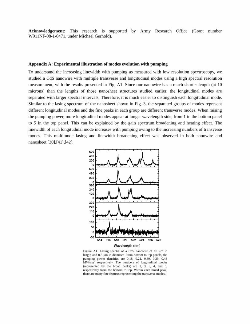
Appendix A: Experimental illustration of modes evolution with pumping
To understand the increasing linewidth with pumping as measured with low resolution spectroscopy, we
studied a CdS nanowire with multiple transverse and longitudinal modes using a high spectral resolution
measurement, with the results presented in Fig. A1. Since our nanowire has a much shorter length (at 10
microns) than the lengths of those nanosheet structures studied earlier, the longitudinal modes are
separated with larger spectral intervals. Therefore, it is much easier to distinguish each longitudinal mode.
Similar to the lasing spectrum of the nanosheet shown in Fig. 3, the separated groups of modes represent
different longitudinal modes and the fine peaks in each group are different transverse modes. When raising
the pumping power, more longitudinal modes appear at longer wavelength side, from 1 in the bottom panel
to 5 in the top panel. This can be explained by the gain spectrum broadening and heating effect. The
linewidth of each longitudinal mode increases with pumping owing to the increasing numbers of transverse
modes. This multimode lasing and linewidth broadening effect was observed in both nanowire and
nanosheet [30],[41],[42].
Figure A1. Lasing spectra of a CdS nanowire of 10 μm in
length and 0.5 μm in diameter. From bottom to top panels, the
pumping power densities are 0.18, 0.21, 0.30, 0.39, 0.43 MW/cm2 respectively. The numbers of longitudinal modes
(represented by the broad peaks) are 1, 3, 3, 4, and 5,
respectively from the bottom to top. Within each broad peak, there are many fine features representing the transverse modes.
References
[1] Neumann A, Wierer J J, Davis W, Ohno Y, Brueck S R J, Tsao J Y 2011 Four-color laser white illuminant
demonstrating high color-rendering quality Opt. Express 19 A982-90
[2] Hollemann G, Braun B, Dorsch F, Hennig P, Heist P, Krause U, Kutschki U, Hermann A V 2000 RGB lasers for
laser projection displays Proc. SPIE 3954 140-51
[3] Kotani A, Witek M A, Osiri J K, Wang H, Sinville R, Pincas H, Barany F, Soper S A 2012 EndoV/DNA ligase
mutation scanning assay using microchip capillary electrophoresis and dual-color laser-induced fluorescence
detection Anal. Methods 4 58-64
[4] Girndt A, Koch S W, Chow W W 1998 Microscopic theory of laser gain in semiconductor quantum wells. Appl.
Phys. A 66 1-12
[5] Yoshida H, Gonno Y, Nakano K, Taniguchi S, Hino T, Ishibashi A, Ikeda M, Chuang S L 1996 Gain
characteristics of gainguided II–VI laser diodes Appl. Phys. Lett. 69 3893-5
[6] Lougue F P, Rees P, Heffernan J F, Jordan C, Donegan J F, Hegarty J, Hiei F, Taniguchi S, Hino T, Nakano K,
Ishibashi A 1998 Optical gain in (Zn, Cd)Se-Zn(S, Se) quantum wells J. Opt. Soc. Am. B 15 1295-304
[7] Girndt A, Jahnke F, Knorr A, Koch S W, Chow W W 1997 Multi-Band bloch equations and gain spectra of
highly excited II-VI semiconductor quantum wells Phys. Stat. Sol. B 202 725-39
[8] Yamada Y, Masumotoa Y, Taguchi T 2002 Formation of optical gain due to exciton localization in
CdxZn1−xS-ZnS strained-layer quantum wells Physica B: Cond. Mat. 191 83-9
[9] Klingshirn C, Kalta H, Umlauffa M, Petria W, Majumdera F A, Bogdanova S V, Langbeina W, Grüna M,
Hettericha M, Geyzersb K P, Heukenb M, Naumovc A, Stanzlc H, Gebhardtc W 1994 Stimulated emission of II–
VI epitaxial layers J. Crys. Growth 138 786-90
[10] Motisuke P, Argüello CA, Luzzi R 1977 Effect of excited electron states lifetime on gain spectra of EHL in CdS
Solid State Commun. 23 617-20
[11] Kuball M, Jeon E S, Song Y K, Nurmikko A V, Kozodoy P, Abare A, Keller S, Coldren L A, Mishra U K,
DenBaars S P, Steigerwald D A 1997 Gain spectroscopy on InGaN/GaN quantum well diodes Appl. Phys. Lett.
70 2580-2
[12] Hakki B W, Paoli T L 1975 Gain spectra in GaAs double−heterostructure injection lasers J. Appl. Phys. 46
1299-306
[13] Ding Y, Yang Q, Guo X, Wang S, Gu F, Fu J, Wan Q, Cheng J, Tong L 2009 Nanowires/microfiber hybrid
structure multicolor laser Opt. Express 17 21813-8
[14] Naderi N A, Grillot F, Yang K, Wright J B, Gin A, Lester L F 2010 Two-color multi-section quantum dot
distributed feedback laser Opt. Express 18 27028-35
[15] Tang S K Y, Li Z, Abate A R, Agresti J J, Weitz D A, Psaltis D, Whitesides G M 2009 A multi-color
fast-switching microfluidic droplet dye laser Lab Chip 9 2767-71
[16] Ning C Z 2012 Semiconductor nanowire lasers In: Coleman J J, Bryce A C, Jagadish C. Semiconductors and
Semimetals (Burlington, Academic Press)
[17] Huang M H, Mao S, Feick H, Yan H, Wu Y, Kind H, Weber E, Russo R, Yang P D 2001 Room-Temperature
Ultraviolet Nanowire Nanolasers Science 292 1897-99
[18] Pan A L, Zhou W, Leong E S P, Liu R, Chin A H, Zou B, Ning C Z 2009 Continuous Alloy-Composition Spatial
Grading and Superbroad Wavelength-tunable nanowire lasers on a single chip Nano Lett. 9 784-8
[19] Pan A L, Liu R B, Sun M H, Ning C Z 2010 Spatial composition grading of quaternary ZnCdSSe alloy

nanowires with tunable light emission between 350 and 710 nm on a Single Substrate ACS. Nano 4, 671–80
[20] Liu Y, Zapien J A, Shan Y Y, Geng C Y, Lee C S, Lee S T 2005 Wavelength Controlled Lasing in ZnxCd1-xS
Single crystal nanoribbons Adv. Mater. 17 1372–77
[21] Zapien J, Liu Y, Shan Y, Tang H, Lee C, Lee S T 2007 Continuous near-infrared-to-ultraviolet lasing from II-VI
nanoribbons Appl. Phys. Lett. 90 213114–6
[22] Chin A H, Vaddiraju S, Maslov A V, Ning C N, Sunkara M K, Meyyappan M 2006 Near-infrared semiconductor
subwavelength-wire lasers Appl. Phys. Lett. 88 163115
[23] Duan X F, Huang Y, Agarwal R, Lieber C M 2003 Single-nanowire electrically driven lasers Nature 421 241-245
[24] Zimmler M A, Bao J, Capasso F, Muller S, Ronning C 2008 Laser action in nanowires: Observation of the
transition from amplified spontaneous emission to laser oscillation Appl. Phys. Lett. 93 051101
[25] Yang Z Y, Xu J Y, Wang P, Zhuang X J, Pan A L, Tong L M 2011 On-Nanowire spatial band gap design for white
light emission Nano Lett. 11 5085-89
[26] Kim Y L, Jung J H, Yoon H S, Song M S, Bae S H, Kim Y, Chen Z G, Zou J, Joyce H J, Gao Q, Tan H H,
Jagadish C 2010 CdS/CdSe lateral heterostructure nanobelts by a two-step physical vapor transport method
Nanotechnology 21 145602
[27] Kwon S J, Choi Y J, Park J H, Hwang I S, Park J G 2005 Structural and optical properties of CdSxSe1-x
nanowires Phys. Rev. B 72, 205312
[28] Tong L M, Lou J Y, Gattass R R, He S L, Chen X W, Liu L, Mazur E 2005 Assembly of silica nanowires on
silica aerogels for microphotonic devices Nano Lett. 5 259-62
[29] Gu F X, Yang Z Y, Yu H K, Xu J Y, Wang P, Tong L M, Pan A L 2011 Spatial bandgap engineering along single
alloy nanowires J. Am. Chem. Soc. 133 2037-9
[30] Zimmler M A, Capasso F, Muller S, Ronning C 2010 Optically pumped nanowire lasers: Invited review
Semicond. Sci. Technol. 25 024001
[31] O’Carroll D, Lieberwirth I, Redmond G 2007 Microcavity effects and optically pumped lasing in single
conjugated polymer nanowires Nature Nanotechnology 2 182-4
[32] Johnson J C, Yan H, Yang P D, Saykally R J 2003 Optical Cavity Effects in ZnO Nanowire Lasers and
Waveguides J. Phys. Chem. B 107 8816-28
[33] Oulton R F, Sorger V J, Zentgraf T, Ma R M, Gladden C, Dai L, Bartal G, Zhang X 2009 Plasmon lasers at deep
subwavelength scale Nature 461 629-32
[34] Ma R M, Oulton R F, Sorger V J, Bartal G, Zhang X 2011 Room-temperature sub-diffraction-limited plasmon
laser by total internal reflection Nature Material 10 110-3
[35] Casperson L W 1975 Threshold characteristics of multimode laser oscillators J. App. Phys. 46 5194-201
[36] Jensen B, Torabi A 1986 Refractive index of hexagonal II–VI compounds CdSe, CdS, and CdSexS1−x J. Opt. Soc.
Am. B 3 857-63
[37] Accessed October 18, 2012, at http://www.sspectra.com/sopra.html
[38] Gutowski J, Sebald K, Voss T 2009 Group III Condensed Matter: Volume 44B (Heidelberg, Springer Press)
[39] Maslov A V, Ning C Z 2004 Modal gain in a semiconductor nanowire laser with anisotropic bandstructrure IEEE
J. Quantum Electron 40 1389-97
[40] Ning C Z 2010 Semiconductor nanolasers Phys. Status Solidi B 247 774-88
[41] Agarwal R, Barrelet C J, Lieber C M 2005 Lasing in single cadmium sulfide nanowire optical cavities Nano Lett.
5 917-20

[42] Cao B, Jiang Y, Wang C, Wang W, Wang L, Niu M, Zhang W, Li Y, Lee S T 2007 Synthesis and Lasing
Properties of Highly Ordered CdS Nanowire Arrays Adv. Funct. Mater. 17 1501-6
Related Documents