Engineered Excellence A Journal for Process and Device Engineers INSIDE The Extended Gaussian Disorder Model in Atlas ....... 6 TCAD Simulation of Multiple Quantum Well Infrared Photodetector (QWIP)................... 10 Hints, Tips and Solutions .......................................... 16 Continued on page 2 ... Volume 23, Number 2, April, May, June 2013 that the selectivity ratio decreases with ion beam ener- gy, and therefore a typical energy used for this process is in the interval of 200 – 500 eV. The only real challenge in controlling the ion etching of the Nanostructures is the effect of redeposition [2]. The atoms removed (sput- tered) from the surface of material being etched will either escape back to the process chamber or collide with sidewalls of the structure. Since the majority of these sputtered atoms collide with the walls at very low energies there is high probability for them to stick to the wall and form a new layer. The redeposited layer is an amorphous mixture of the particles sputtered from different materials in the structure. For simplicity, we will call this newly formed material “alloy”. In the case where the substrate is a single material layer the alloy will consist mostly of the substrate material atoms but should have lower density. Redeposition Effect Redeposition considerably changes the geometrical dy- namics of the ion etching process. Without redeposition the etch rates would be nearly constant across the bottom of the trench being etched because the ion beam is usu- ally tilted by just few degrees and is constantly rotated. The only variable geometrical characteristics would be a faceted top corner of the mask which could result in a very slight change in ion beam visibility on the trench bottom. However, the picture is considerably different Simulation of Ion Beam Etching of Patterned Nanometer-scale Magnetic Structures for High-Density Storage Applications Introduction Fabrication of various nano-structures often requires mask controlled or patterned etching of materials. The chemical or wet etch methods cannot be used for nanoscale geometries due to the substantial isotropic component of etch rate. Therefore, various plasma or reactive ion etching method are typically used. Unfortunately, some materi- als do not easily form volatile reaction products and all types of chemically assist etching becomes problematic. Among those materials are elements such as Co, Ni, Fe, Pt, and Cr which are usually used in magnetic nano- structure technologies. Therefore, ion beam etching or ion milling is the most suitable method to pattern these materials [1]. The most promising magnetic nano-technology applica- tion is the Bit Pattern Media (BPM). The BPM technology has a potential to manufacture Hard Drive Discs (HDD) with density of up to few terabytes per square inch. To achieve such high density, huge arrays of single domain magnetic islands of ~10 nm diameter must be formed. Other essential requirements for manufacturing of high- density BPM are as small as possible distance between these magnetic islands and as vertical as possible side- walls of the islands. Ion Milling Ion milling is the leading candidate among etching techniques capable of meeting the requirements above [2]. No chemical process is involved and therefore the geometry of etched structure is determined mainly by mask geometry (thickness and slope), by parameters of the ion beam (energy, direction, rotation, density) and by the sputtering characteristics of the magnetic and mask material. The successful use of ion milling requires considerable etch rate selectivity between mask and magnetic materials. Fortunately, carbon hard masks typically have 3-5 times smaller ion etch rate then most magnetic materials. It is important to note

Welcome message from author
This document is posted to help you gain knowledge. Please leave a comment to let me know what you think about it! Share it to your friends and learn new things together.
Transcript

April, May, June 2013 Page 1 The Simulation Standard
Engineered Excellence A Journal for Process and Device Engineers
INSIDEThe Extended Gaussian Disorder Model in Atlas .......6TCAD Simulation of Multiple Quantum Well Infrared Photodetector (QWIP) ...................10Hints, Tips and Solutions ..........................................16
Continued on page 2 ...
Volume 23, Number 2, April, May, June 2013
that the selectivity ratio decreases with ion beam ener-gy, and therefore a typical energy used for this process is in the interval of 200 – 500 eV. The only real challenge in controlling the ion etching of the Nanostructures is the effect of redeposition [2]. The atoms removed (sput-tered) from the surface of material being etched will either escape back to the process chamber or collide with sidewalls of the structure. Since the majority of these sputtered atoms collide with the walls at very low energies there is high probability for them to stick to the wall and form a new layer. The redeposited layer is an amorphous mixture of the particles sputtered from different materials in the structure. For simplicity, we will call this newly formed material “alloy”. In the case where the substrate is a single material layer the alloy will consist mostly of the substrate material atoms but should have lower density.
Redeposition EffectRedeposition considerably changes the geometrical dy-namics of the ion etching process. Without redeposition the etch rates would be nearly constant across the bottom of the trench being etched because the ion beam is usu-ally tilted by just few degrees and is constantly rotated. The only variable geometrical characteristics would be a faceted top corner of the mask which could result in a very slight change in ion beam visibility on the trench bottom. However, the picture is considerably different
Simulation of Ion Beam Etching of Patterned Nanometer-scale Magnetic Structures for High-Density Storage Applications
IntroductionFabrication of various nano-structures often requires mask controlled or patterned etching of materials. The chemical or wet etch methods cannot be used for nanoscale geometries due to the substantial isotropic component of etch rate. Therefore, various plasma or reactive ion etching method are typically used. Unfortunately, some materi-als do not easily form volatile reaction products and all types of chemically assist etching becomes problematic. Among those materials are elements such as Co, Ni, Fe, Pt, and Cr which are usually used in magnetic nano-structure technologies. Therefore, ion beam etching or ion milling is the most suitable method to pattern these materials [1].
The most promising magnetic nano-technology applica-tion is the Bit Pattern Media (BPM). The BPM technology has a potential to manufacture Hard Drive Discs (HDD) with density of up to few terabytes per square inch. To achieve such high density, huge arrays of single domain magnetic islands of ~10 nm diameter must be formed. Other essential requirements for manufacturing of high-density BPM are as small as possible distance between these magnetic islands and as vertical as possible side-walls of the islands.
Ion MillingIon milling is the leading candidate among etching techniques capable of meeting the requirements above [2]. No chemical process is involved and therefore the geometry of etched structure is determined mainly by mask geometry (thickness and slope), by parameters of the ion beam (energy, direction, rotation, density) and by the sputtering characteristics of the magnetic and mask material. The successful use of ion milling requires considerable etch rate selectivity between mask and magnetic materials. Fortunately, carbon hard masks typically have 3-5 times smaller ion etch rate then most magnetic materials. It is important to note

The Simulation Standard Page 2 April, May, June 2013
when redeposition takes place. This is illustrated in Figure 1, which shows the etch dynamics in a 2D sec-tion of a line pattern. The dynamically formed alloy lay-er decreases the ion beam visibility at the bottom of the trench. Consequently, the effective etch area decreases when the trench becomes deeper. Simultaneously, par-ticles sputtered from the bottom of the deeper trench have a lower probability to escape back to the process chamber and therefore the alloy layer keeps growing on the sidewalls. As this process continues the redeposited layer is also getting etched by the incoming ion beam flux and, depending on the stage of the process, the bal-ance between etching and redeposition rate is changing.
Ion Milling SimulationThe complex dynamics and strong geometrical depen-dency of the redeposition effect make it almost impos-sible to develop a reliable and optimized ion milling based process without extensive simulation. Experi-mental test structures may help to determine some pa-rameters of the process, particularly the etching rates as a function of beam characteristics and incident an-gle. However, without detailed simulation it is impos-sible to predict how redeposition dynamics will express itself in real 3D structures.
To our knowledge, the Ion Milling module of Victory Process is the only tool capable of predictive 3D simulation of ion beam etching on a nanometer scale level. The following
are key capabilities of Victory Process and auxiliary Sil-vaco tools which allow accurate simulation of ion milling as well as process calibration and optimization:
• Accounting for ion beam tilt, rotation and divergence
• Full 3D visibility calculation for ion beam and sput-tered fluxes
• Experimental tables or semi-empirical models for angle dependency of etch rate
• Alloy redeposition model which takes into account the secondary fluxes of sputtered particles
• The secondary particle fluxes are proportional to lo-cal etch rate and can have specific spatial distribution (emission characteristic function). We use isotropic emission function in simulations presented in this paper
• Capability to take into account redeposition contribu-tion from secondary fluxes generated within adjacent domains
• Material-dependent redeposition efficiency allows us to account for the fact that some secondary flux par-ticles may not contribute to redeposited layer forma-tion even if they reach its surface
• Automatic extraction of 2D cut planes for direct com-parison with SEM pictures
• Extraction of key geometrical parameters from simu-lated structures: layer thickness, angles etc.
• Capability to setup designs of experiment with varia-tion of process conditions, material parameters as well as geometrical parameters of initial structure and masks
Typical Example – Densely Packed Magnetic BitsStructures with densely packed features are most challeng-ing for Ion Milling simulation. At the same time the large matrix of small magnetic islands as shown in Figure 2 is the ultimate goal of this technology. To demonstrate that Victory Process can handle such dense structures we per-formed an ion milling simulation within a simulation do-main indicated by the yellow box in the mask layout shown in Figure 3. The area outside the yellow box demonstrates 8 reflective/symmetric domains which are taken into ac-count only for redeposition. This means that the local etch rates in these domains are the same as in the main simula-tion domain but some portion of sputtered particles may reach the main domain and participate in redeposition.
The following settings were used for all simulations in this paper. The ion milling was performed with 250 eV Ar and a current density of 1.5 pA/μm2. The constantly ro-tated ion beam was tilted by 5° from surface normal and
Figure 1. Structure evolution during Ion Milling process. Green is etched material, violet is mask material, red is alloy. (the HTML version of this article includes more detailed animation).

April, May, June 2013 Page 3 The Simulation Standard
had flux divergence of 5°. The etched structure consisted of two layers: Chromium substrate material and the 20 nm hard Carbon mask. The etch rate versus angle func-tion for this simulation was obtain by the semi-empirical Yamanura model [3] using above ion beam settings and default values for these materials. Also, all parameters of “alloy” were the same as for Chromium except the density which was set to 80% of Chromium density. The milling rates as a function of incidence angle for all three materials are shown in Figure 4.
The result of ion milling simulation for the densely packed magnetic islands is shown in Figure 5. This picture con-firms that the simulator can capture main characteristics
of the ion milling process in 3D: faceting of hard mask, alloy thickness variation due to different proximity of neighboring island, and shallower etch depth in direc-tions toward closest neighbors (0, 60, 120,.. degrees).
Calibration of Ion Milling Simulation and Process OptimizationThe example in the previous section clearly shows that the Ion Milling model of Victory Process can be success-fully used for simulation of complex ion etching pro-cesses in Nanostructures. However, by no means is it a “push-button” solution, because some important mate-rial parameters are not known apriori and would require
Figure 2. Top-down image of dense pack of ion milled magnetic islands arranged in hexagonal formation. The pitch or distance between centers of the islands was ~20 nm. This is a fragment of the SEM picture from [2] reprinted with permission from the author Dan Kercher (HGST).
Figure 3. Mask layout with 10 nm islands and 15nm pitch.
Figure 4. Ion etch rate dependence on incident ion angle for three materials used in structures simulated in this paper.
Figure 5. The final structure after 5 minutes ion milling. Yellow is chromium, blue regions are hard masks and red layers are redeposited “alloy”.
The Simulation Standard Page 4 April, May, June 2013
some calibration. First of all, the built-in etch rate model may not match with experimental data for very low ion beam energies used in this application. Therefore, accu-rate measurements of etch rates at several angles for each material are usually required. However, it is impossible
to measure the etch rates and secondary effi ciency for re-deposited “alloy”. These parameters can be estimated by varying them in simulation and comparing results with experiments on simple test structures.
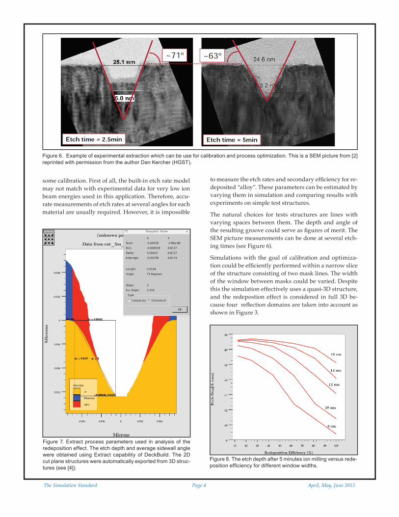
The natural choices for tests structures are lines with varying spaces between them. The depth and angle of the resulting groove could serve as fi gures of merit. The SEM picture measurements can be done at several etch-ing times (see Figure 6).
Simulations with the goal of calibration and optimiza-tion could be effi ciently performed within a narrow slice of the structure consisting of two mask lines. The width of the window between masks could be varied. Despite this the simulation effectively uses a quasi-3D structure, and the redepostion effect is considered in full 3D be-cause four refl ection domains are taken into account as shown in Figure 3.
Figure 6. Example of experimental extraction which can be use for calibration and process optimization. This is a SEM picture from [2] reprinted with permission from the author Dan Kercher (HGST).
Figure 7. Extract process parameters used in analysis of the redeposition effect. The etch depth and average sidewall angle were obtained using Extract capability of DeckBuild. The 2D cut plane structures were automatically exported from 3D struc-tures (see [4]).
Figure 8. The etch depth after 5 minutes ion milling versus rede-position effi ciency for different window widths.

April, May, June 2013 Page 5 The Simulation Standard
The simulation conditions, materials, etch rates and mask thickness were exactly the same as in the 3D test case described in the previous section. A simple Design of Experiment (DOE) was setup using the DBInternal tool of DeckBuild in which the window width was varied from 8 to 16 nm and redeposition efficiency was varied from 25% to 100%. The 3D structures were saved after 2, 3,4, and 5 minutes of ion milling. The etch depth and the average slope angle were extracted automatically from a 2D cut plane as shown in Figure 7.
The simulation results shown in Figure 8 could be used for calibration of the important secondary efficiency pa-rameter for redeposited alloy material. By measuring the etch depth in the test structure with mask windows of varying widths, one can easily find an optimum value for this parameter.
The results shown in Figure 9 highlight that the etch depth is not simply proportional to etch time. Moreover, if redeposition efficiency is high the ion milling effec-tively stops after approximately 4 minutes.
The sidewall slope angle could serve as another figure of merit for ion milling test structure simulation. These an-gle also depends on process conditions and structure ge-ometry. The sidewall slopes can be extracted from DOE simulations and compared with experimental angles obtained from the SEM pictures (see Figure 6). In our simulations these angles vary from 68° to 78° depending on conditions. The sidewall angles considerably depend on redeposition efficiency and less on the mask window width (see Figure 10). We believe that sidewall slopes can be more effectively controlled by other process param-eters, e.g. ion beam angle, the mask widow thickness and slope or even etch rate of redeposited alloy.
ConclusionsIt appears that Ion Beam Etching/Milling is emerging as a viable tool for several nanoscale technologies includ-ing high-density magnetic storage applications. This ar-ticle demonstrates that the Silvaco Victory Process simu-lator together with interactive and design of experiment tools could be very useful in design and optimization of this very advanced technology. The simulations in this article show that the Ion Milling models can successfully predict the key effects of the process including 3D rede-position of sputtered material.
Acknowledgment We would like to express our gratitude to researchers at San Jose Research Center HGST, a Western Digital com-pany, for their valuable suggestions which help us to im-prove the code and to expand our understanding of Ion Milling Process application to magnetic nanostructures.
References1. D. Kercher, Pattering Magnetic Nanostructures with Ions,
in Nanofabrication Handbook, editors S. Cabrini and S. Ka-wata, CRC Press, p. 421 (2012).
2. D.Kercher, Geometrical Limitations of Ar Ion Beam Etch-ing, EIPBN-2010.
3. A Semi-Empirical Model for the Simulation of Ion Mill-ing in VICTORY Process, Simulation Standard, October, November, December 2012. http://www.silvaco.com/tech_lib_TCAD/simulationstandard/2012/oct_nov_dec/a2/a-semi-empirical-model-for-the-simulation-of-Ion-milling-in-victory-process_a2.html.
4. Syntax Driven 2D Structure Export from 3D Structures and Extraction of 2D Volume Data Maps, Simulation Standard,, April, May, June 2012. http://www.silvaco.com/tech_lib_TCAD/simulationstandard/2012/apr_may_jun/a3/Syntax_Driven_2D_Structure_Export_from_3D_Structures_and_Extraction_of_2D_Volume_Data_Maps_a3.html.
Figure 9. The etch depth after ion milling for 2, 3, 4 and 5 min-utes versus mask window width. The green lines are obtained with 100% redeposition efficiency, while the red lines corre-spond to 80% redeposition efficiency.
Figure 10. Sidewall slope angles versus mask window width for deposition efficiencies from 40% to 100%.
Related Documents