Simple and Compact Dual Band-Notched Monopole Antenna Using U-Shaped Forms on the Conductor-backed Plane for UWB Applications M. Moosazadeh and Z. Esmati Department of Electrical Engineering, Urmia Branch, Islamic Azad University, Urmia, Iran [email protected], [email protected] Abstract A planar ultra-wideband antenna with dual band-notched characteristics is proposed. The main features of the proposed antenna are the extremely compact dimensions and band-notched characteristics that are obtained without modifying the radiator. The dual band-notched characteristics are achieved by a pair of mirror U-shaped slots and an inverted U-shaped slot at the conductor- backed plane. The measured results of the manufactured (15 mm × 15 mm) antenna on 1.6 mm FR4 substrate show that the antenna operates with VSWR less than two over the frequency band from 3 GHz to 11.2 GHz. That wideband is featured by the existence of two notched bands VSWR is more than five aimed at suppressing any interference from IEEE802.11a WLAN 5 GHz (5.15 GHz - 5.825 GHz) and ITU 8 GHz (8.025 GHz - 8.4 GHz) band. The antenna has a desirable VSWR level, radiation pattern, and gain characteristics for ultra wideband frequency band range. Index Terms – Coplanar waveguide (CPW) antennas, frequency band notched function, and ultra wideband (UWB) antenna. I. INTRODUCTION There is a tremendous applications that use the ultra wideband (UWB) technology due to its unlimited applications in short-range wireless communications. One of the key elements to secure a successful UWB system is an UWB antenna with compact dimensions, proper characteristics, and immunity to interferences from nearby systems that use parts of the UWB spectrum. The main parameters in designing UWB antennas, especially for indoor applications, are easy to manufacture structure, compact size, and omnidirectional radiation pattern across the band from 3.1 GHz to 10.6 GHz [1-2]. Different methods such as the truncated slot on the antenna patch have been proposed for increasing impedance bandwidth. Since there are several existing systems operating within the UWB frequency spectrum, such as the IEEE802.11a WLAN (5.15 GHz - 5.825 GHz) and the ITU (8.025 GHz - 8.4 GHz) the UWB antenna is required to have the capability to notch those bands and thus to cancel any interference between those systems and the UWB system. Some UWB antennas with band-notched characteristics are available in the published literature. One common method is to use different types of slots on the patch and ground plane and parasitic elements [3- 16]. Such antennas with various types of slots have large dimensions in comparison to that proposed antenna in this paper. In this paper, the target is to present a compact structure with dual band-notched characteristics that are achieved without modifying the patch in a step-by-step design procedure. The main radiator of the proposed antenna is a simple square patch that is fed using a microstrip line. The ground plane is located at the bottom layer with a pair of mirror semi C-shaped notches for a perfect matching. A conductor-backed plane that is used to achieve the band-notched characteristics of the antenna is located at the bottom layer. The first notched frequency band is achieved by using an inverted U-shaped slot embedded in the conductor-backed plane, whereas the second notched band is realized 1054-4887 © 201 ACES Submitted On: , 2013 Accepted On: . , 2013 1074 ACES JOURNAL, VOL. 28, No. 11, NOVEMBER 2013

Welcome message from author
This document is posted to help you gain knowledge. Please leave a comment to let me know what you think about it! Share it to your friends and learn new things together.
Transcript
Simple and Compact Dual Band-Notched Monopole Antenna Using U-Shaped Forms on the Conductor-backed Plane for UWB
Applications
M. Moosazadeh and Z. Esmati
Department of Electrical Engineering, Urmia Branch, Islamic Azad University, Urmia, Iran [email protected], [email protected]
Abstract� A planar ultra-wideband antenna with dual band-notched characteristics is proposed. The main features of the proposed antenna are the extremely compact dimensions and band-notched characteristics that are obtained without modifying the radiator. The dual band-notched characteristics are achieved by a pair of mirror U-shaped slots and an inverted U-shaped slot at the conductor-backed plane. The measured results of the manufactured (15 mm × 15 mm) antenna on 1.6 mm FR4 substrate show that the antenna operates with VSWR less than two over the frequency band from 3 GHz to 11.2 GHz. That wideband is featured by the existence of two notched bandsVSWR is more than five aimed at suppressing any interference from IEEE802.11a WLAN 5 GHz (5.15 GHz - 5.825 GHz) and ITU 8 GHz (8.025GHz - 8.4 GHz) band. The antenna has a desirable VSWR level, radiation pattern, and gain characteristics for ultra wideband frequency band range.
Index Terms – Coplanar waveguide (CPW) antennas, frequency band notched function, and ultra wideband (UWB) antenna.
I. INTRODUCTIONThere is a tremendous applications that use the
ultra wideband (UWB) technology due to its unlimited applications in short-range wireless communications. One of the key elements to secure a successful UWB system is an UWB antenna with compact dimensions, proper characteristics, and immunity to interferences from nearby systems that use parts of the UWB
spectrum. The main parameters in designing UWB antennas, especially for indoor applications, are easy to manufacture structure, compact size, and omnidirectional radiation pattern across the band from 3.1 GHz to 10.6 GHz [1-2]. Different methods such as the truncated slot on the antenna patch have been proposed for increasing impedance bandwidth. Since there are severalexisting systems operating within the UWB frequency spectrum, such as the IEEE802.11a WLAN (5.15 GHz - 5.825 GHz) and the ITU (8.025 GHz - 8.4 GHz) the UWB antenna is required to have the capability to notch those bands and thus to cancel any interference between those systems and the UWB system. Some UWB antennas with band-notched characteristics are available in the published literature. One common method is to use different types of slots on the patch and ground plane and parasitic elements [3-16]. Such antennas with various types of slots have large dimensions in comparison to that proposed antenna in this paper. In this paper, the target is to present a compact structure with dual band-notched characteristics that are achieved without modifying the patch in a step-by-step design procedure. The main radiator of the proposed antenna is a simple square patch that is fed using a microstrip line. The ground plane is located at the bottom layer with a pair of mirror semi C-shaped notches for a perfect matching. A conductor-backed plane that is used to achieve the band-notched characteristics of the antenna is located at the bottom layer. The first notched frequency band is achieved by using an inverted U-shaped slot embedded in the conductor-backed plane, whereas the second notched band is realized
1054-4887 © 201 ACES
Submitted On: ���� �, 2013 Accepted On: �. ��, 2013
1074 ACES JOURNAL, VOL. 28, No. 11, NOVEMBER 2013
by using a pair of mirror inverted U-shaped slots inside the conductor-backed plane. The final performance of the antenna is aimed at achieving the required UWB and to have dual notched bands that can be adjusted using an empirical formula. The impedance bandwidth is enhanced by using slotted conductor-backed plane. The presented design is validated by simulations and measurements.
II. ANTENNA DESIGNFigure 1 shows the configuration of the
proposed ultra-wideband (UWB) antenna. The top layer include the main radiator in the form of square patch with initial dimensions that are �� ���� � �"��#$�� × #$���� (where #$ is the guide wavelength, which is equal to c/(Z3� �& ) at the center of the UWB, i.e., at 6.85 GHz, and c is speed of light in free space). The bottom layer includes a pair of mirror semi C-shaped notches in the corners of the ground plane and slotted conductor-backed plane. In the design, the antenna is constructed with a substrate made of FR4, with thickness of 1.6 mm and relative dielectric � ������� %r = 4.4. The initial dimensions of the ��"������� ���� �� ���� � �"��#$ × #$������&���� ��the feed-line microstrip (Wf
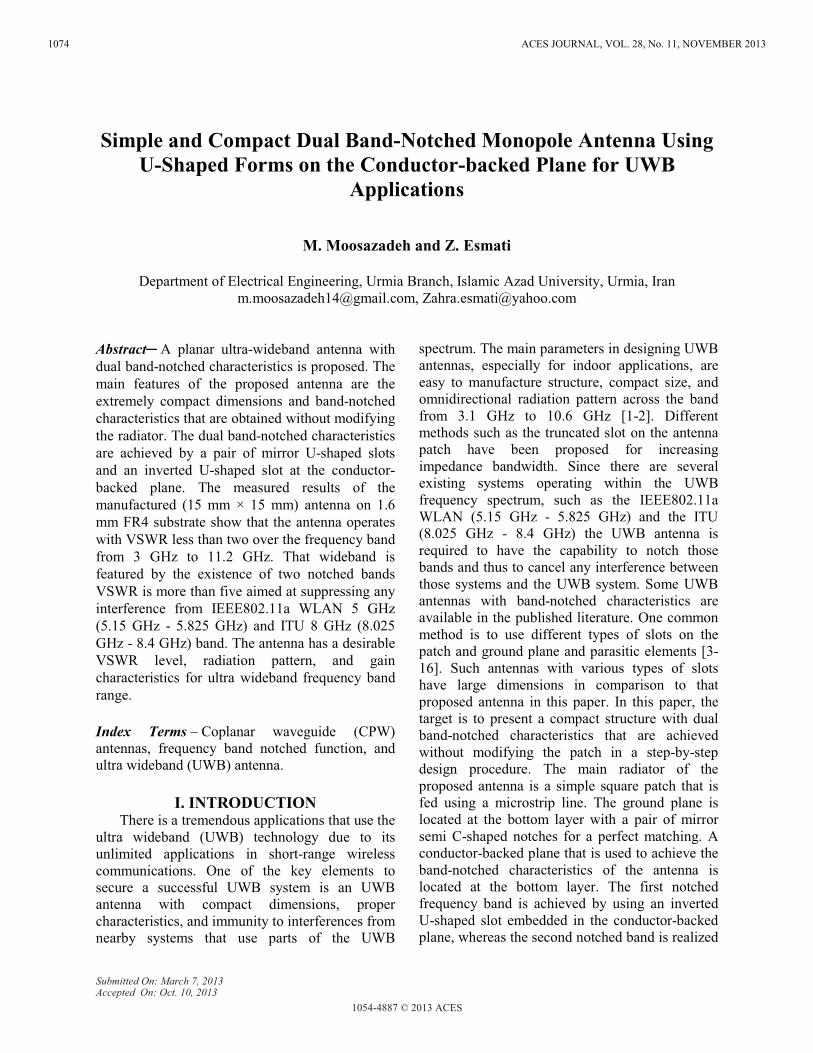
In order to show the impact of using the truncated ground plane, the antenna’s performance is simulated for different cases as indicated in Fig. 2 (a), (b), and (c). If the proposed antenna is used with the different structures of ground plane, rectangular-shaped and a pair of mirror L-shaped notches, in the manner shown in Fig. 2 (a) and (b) the impedance matching is poor at the frequency band between 8.5 GHz and 10.6 GHz, which should be part of the UWB spectrum. To improve the performance at that band, a pair of mirror semi C-shaped notches is included at the bottom layer with proper dimensions as depicted in Fig. 2 (c). It
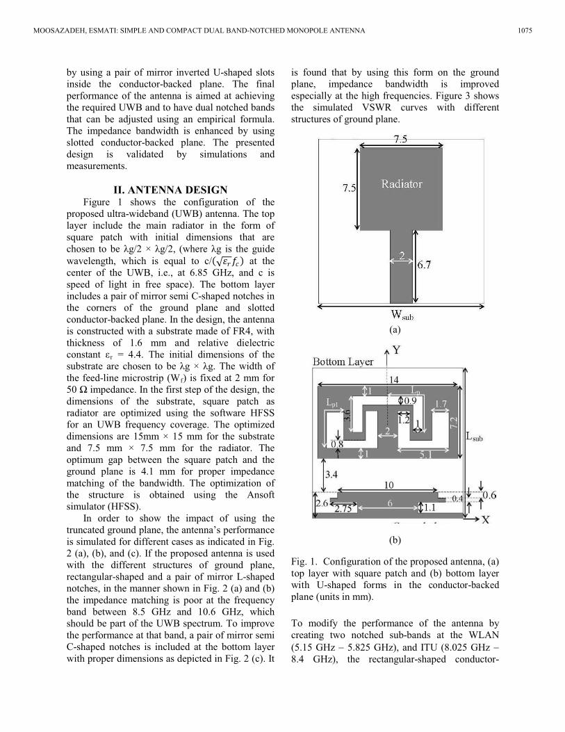
is found that by using this form on the ground plane, impedance bandwidth is improved especially at the high frequencies. Figure 3 shows the simulated VSWR curves with different structures of ground plane.
) is fixed at 2 mm for 50 '�������e. In the first step of the design, the dimensions of the substrate, square patch as radiator are optimized using the software HFSS for an UWB frequency coverage. The optimized dimensions are 15mm × 15 mm for the substrate and 7.5 mm × 7.5 mm for the radiator. The optimum gap between the square patch and the ground plane is 4.1 mm for proper impedance matching of the bandwidth. The optimization of the structure is obtained using the Ansoft simulator (HFSS).
(a)
(b)
Fig. 1. Configuration of the proposed antenna, (a) top layer with square patch and (b) bottom layer with U-shaped forms in the conductor-backed plane (units in mm).
To modify the performance of the antenna by creating two notched sub-bands at the WLAN (5.15 GHz � 5.825 GHz), and ITU (8.025 GHz �8.4 GHz), the rectangular-shaped conductor-
MOOSAZADEH, ESMATI: SIMPLE AND COMPACT DUAL BAND-NOTCHED MONOPOLE ANTENNA 1075
backed plane with the dimensions of 14 mm � 7.2 mm is slotted in the manner shown in Fig. 1 (b). A pair of mirror U-shaped slots at the two sides of the conductor is created the first notched band centered at 5.65 GHz, whereas the inverted U-shaped slot inside the conductor is responsible for making the second notched band centered at 8.1 GHz. The slot’s length Lp defines the first notched band, whereas the strip’s length Lp1 defines the second notched band. In this paper, the center-rejected frequency (fp and f p1) is approximately by, Lp = &4�> e3��� (1)
Lp1 = &4�> 1e3��� , (2)
3��� = 3� +12 + 3� �12h1+129a �
, (4)
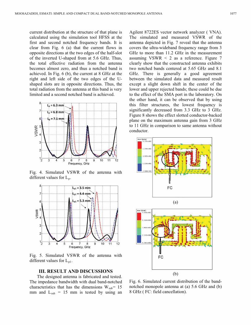
where c, h, Wf��%r������%eff are the second of light in free space, thickness of substrate, the width of the feed line, dielectric constant, and effective dielectric constant, respectively. Moreover, the relation between the center of the notched bands (fp and fp1) ������ ����& ����$��������������%eff,which can be calculated for the microstrip structures using the formula in [12]. For the notched bands that are cantered at the frequencies 5.65 GHz and 8.1 GHz, the values of the designed parameters Lp and Lp1 can be calculated using equations (1) and (2) as 7.1 mm and 5.3 mm. In order to verify the validity of the design equations (1) and (2), the performance of the antenna for different values of Lp and Lp1 is calculated using the simulation tool and the results are shown in Figs. 4 and 5. It is shown that the effective parameter in the position of the lower rejected sub-band is the length Lp shown in Fig. 1 (b). The simulated results for different values of this parameter are shown in Fig. 4. Decreasing that design parameter results in an increase in the frequency of the lower rejected sub-band with negligible effect on the upper rejected sub-band. Concerning the upper rejected sub-band, the main parameter that defines that band is shown to be Lp1. The simulated performance of the antenna for different values of that parameter is shown in Fig. 5. The decrease in the value of Lp1 causes the upper rejected sub-band to shift up in the frequency without almost any impact on the lower rejected sub-band. It is possible to show using the
design equation of microstrip structures [17] that for the utilized structure, the effective dielectric constant is given approximately ��� %eff = 3.2. If this value is substituted in equations (1) and (2) along with the values of Lp and Lp1that are used to generate the simulation results of Figs. 3 and 4, the location of the center of the notched bands ( fp and fp1) calculated from equations (1) and (2) are almost the same simulated values shown in Figs. 4 and 5. The whole structure of the antenna is optimized using HFSS for the widest possible bandwidth using the most compact structure. The optimal parameters of the constructed antenna are as follows: Wsub = 15 mm, L sub = 15 mm, Lp= 7.1 mm, and Lp1 = 5.3 mm.
Fig. 2. (a) Rectangular-shaped ground plane without notch, (b) ground plane with a pair of mirror L-shaped notches, and (c) ground plane with a pair of mirror semi C-shaped notches.
Fig. 3. Simulated VSWR for the different structures of ground slotted conductor-backed plane.
The other optimized dimensions of the antenna are indicated in Fig. 1. In order to show how the slotted conductor-backed plane becomes effective in the rejection of the dual-notched bands, the
1076 ACES JOURNAL, VOL. 28, No. 11, NOVEMBER 2013
current distribution at the structure of that plane is calculated using the simulation tool HFSS at the first and second notched frequency bands. It is clear from Fig. 6 (a) that the current flows in opposite directions at the two edges of the half-slot of the inverted U-shaped from at 5.6 GHz. Thus, the total effective radiation from the antenna becomes almost zero, and thus a notched band is achieved. In Fig. 6 (b), the current at 8 GHz at the right and left side of the two edges of the U-shaped slots are in opposite directions. Thus, the total radiation from the antenna at this band is very limited and a second notched band is achieved.
Fig. 4. Simulated VSWR of the antenna with different values for Lp.
Fig. 5. Simulated VSWR of the antenna with different values for Lp1.
III. RESULT AND DISCUSSIONSThe designed antenna is fabricated and tested.
The impedance bandwidth with dual band-notched characteristics that has the dimensions Wsub= 15 mm and Lsub = 15 mm is tested by using an
Agilent 8722ES vector network analyzer ( VNA). The simulated and measured VSWR of the antenna depicted in Fig. 7 reveal that the antenna covers the ultra-wideband frequency range from 3 GHz to more than 11.2 GHz in the measurement assuming VSWR < 2 as a reference. Figure 7 clearly show that the constructed antenna exhibits two notched bands centered at 5.65 GHz and 8.1 GHz. There is generally a good agreement between the simulated data and measured result except a slight down shift in the center of the lower and upper rejected bands; these could be due to the effect of the SMA port in the laboratory. On the other hand, it can be observed that by using this filter structures, the lowest frequency is significantly decreased from 3.3 GHz to 3 GHz. Figure 8 shows the effect slotted conductor-backed plane on the maximum antenna gain from 3 GHzto 11 GHz in comparison to same antenna without conductor.
(a)
(b)
Fig. 6. Simulated current distribution of the band-notched monopole antenna at (a) 5.6 GHz and (b) 8 GHz ( FC: field cancellation).
MOOSAZADEH, ESMATI: SIMPLE AND COMPACT DUAL BAND-NOTCHED MONOPOLE ANTENNA 1077
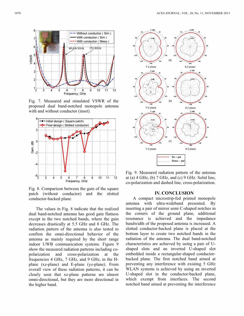
Fig. 7. Measured and simulated VSWR of the proposed dual band-notched monopole antenna with and without conductor (inset).
Fig. 8. Comparison between the gain of the square patch (without conductor) and the slotted conductor-backed plane.
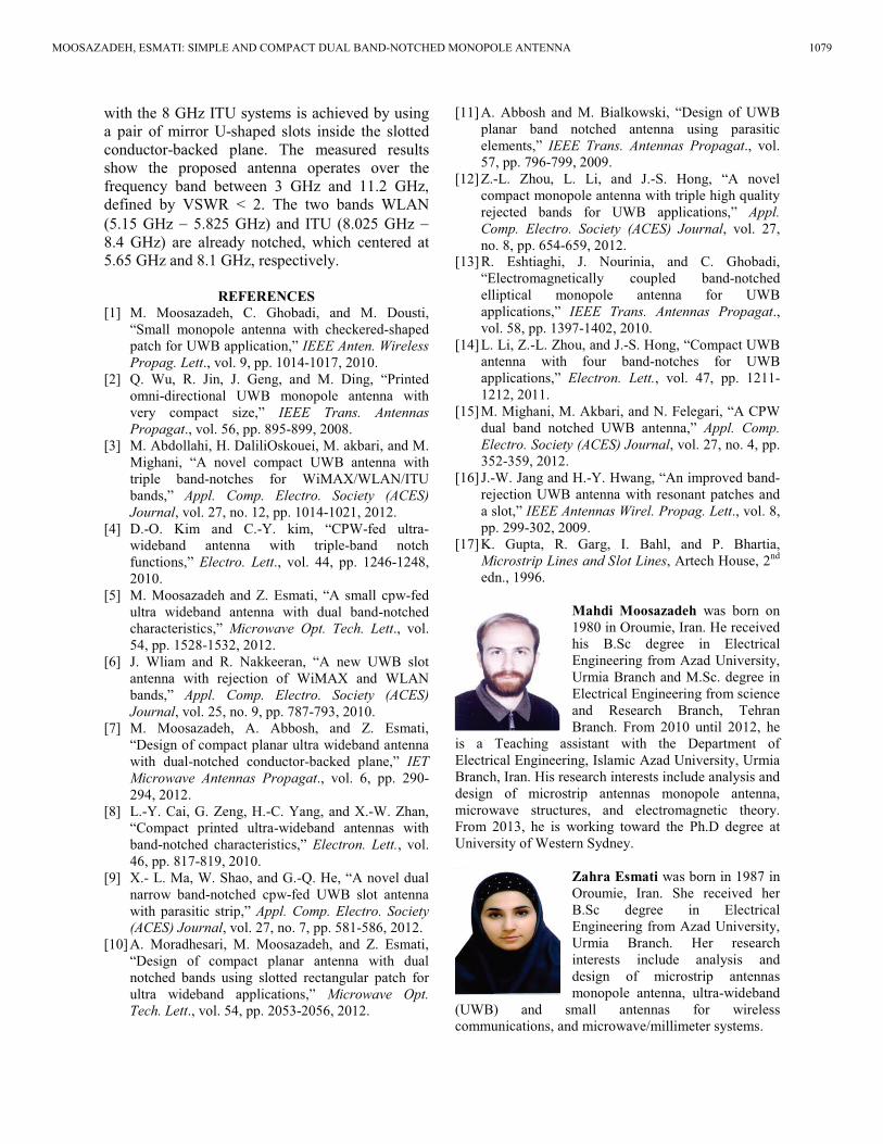
The values in Fig. 8 indicate that the realized dual band-notched antenna has good gain flatness except in the two notched bands, where the gain decreases drastically at 5.5 GHz and 8 GHz. The radiation pattern of the antenna is also tested to confirm the omni-directional behavior of the antenna as mainly required by the short range indoor UWB communication systems. Figure 9 show the measured radiation patterns including co-polarization and cross-polarization at the frequencies 4 GHz, 7 GHz, and 9 GHz, in the H-plane (xz-plane) and E-plane (yz-plane). From overall view of these radiation patterns, it can be clearly seen that xz-plane patterns are almost omni-directional, but they are more directional in the higher band.
Fig. 9. Measured radiation pattern of the antenna at (a) 4 GHz, (b) 7 GHz, and (c) 9 GHz. Solid line, co-polarization and dashed line, cross-polarization.
IV. CONCLUSIONA compact microstrip-fed printed monopole
antenna with ultra-wideband presented. By inserting a pair of mirror semi C-shaped notches in the corners of the ground plane, additional resonance is achieved and the impedance bandwidth of the proposed antenna is increased. A slotted conductor-backed plane is placed at the bottom layer to create two notched bands in the radiation of the antenna. The dual band-notched characteristics are achieved by using a pair of U-shaped slots and an inverted U-shaped slot embedded inside a rectangular-shaped conductor-backed plane. The first notched band aimed at preventing any interference with existing 5 GHz WLAN systems is achieved by using an inverted U-shaped slot in the conductor-backed plane, which exempt from interfaces. The second notched band aimed at preventing the interference
1078 ACES JOURNAL, VOL. 28, No. 11, NOVEMBER 2013
with the 8 GHz ITU systems is achieved by using a pair of mirror U-shaped slots inside the slotted conductor-backed plane. The measured results show the proposed antenna operates over the frequency band between 3 GHz and 11.2 GHz, defined by VSWR < 2. The two bands WLAN (5.15 GHz � 5.825 GHz) and ITU (8.025 GHz �8.4 GHz) are already notched, which centered at 5.65 GHz and 8.1 GHz, respectively.
REFERENCES[1] M. Moosazadeh, C. Ghobadi, and M. Dousti,
“Small monopole antenna with checkered-shaped patch for UWB application,” )���� �����6����� �"�%��(����., vol. 9, pp. 1014-1017, 2010.
[2] Q. Wu, R. Jin, J. Geng, and M. Ding, “Printed omni-directional UWB monopole antenna with very compact size,” )���� &��� �� ����� �"�%��(�., vol. 56, pp. 895-899, 2008.
[3] M. Abdollahi, H. DaliliOskouei, M. akbari, and M. Mighani, “A novel compact UWB antenna with triple band-notches for WiMAX/WLAN/ITU bands,” ����� $%���� ����%�� #%���� , $�#/�5%+����, vol. 27, no. 12, pp. 1014-1021, 2012.
[4] D.-O. Kim and C.-Y. kim, “CPW-fed ultra-wideband antenna with triple-band notch functions,” ����%�� ��., vol. 44, pp. 1246-1248, 2010.
[5] M. Moosazadeh and Z. Esmati, “A small cpw-fed ultra wideband antenna with dual band-notched characteristics,” ���%*�4�� ���� &���� ��., vol. 54, pp. 1528-1532, 2012.
[6] J. Wliam and R. Nakkeeran, “A new UWB slot antenna with rejection of WiMAX and WLAN bands,” ����� $%���� ����%�� #%���� , $�#/�5%+����, vol. 25, no. 9, pp. 787-793, 2010.
[7] M. Moosazadeh, A. Abbosh, and Z. Esmati, “Design of compact planar ultra wideband antenna with dual-notched conductor-backed plane,” )�&����%*�4�� ����� � "�%��(�., vol. 6, pp. 290-294, 2012.
[8] L.-Y. Cai, G. Zeng, H.-C. Yang, and X.-W. Zhan, “Compact printed ultra-wideband antennas with band-notched characteristics,” ����%��� ���, vol. 46, pp. 817-819, 2010.
[9] X.- L. Ma, W. Shao, and G.-Q. He, “A novel dual narrow band-notched cpw-fed UWB slot antenna with parasitic strip,” �����$%��������%��#%����, $�#/�5%+����, vol. 27, no. 7, pp. 581-586, 2012.
[10]A. Moradhesari, M. Moosazadeh, and Z. Esmati, “Design of compact planar antenna with dual notched bands using slotted rectangular patch for ultra wideband applications,” ���%*�4�� ����&������., vol. 54, pp. 2053-2056, 2012.
[11]A. Abbosh and M. Bialkowski, “Design of UWB planar band notched antenna using parasitic elements,” )���� &��� �� ����� � "�%��(�., vol. 57, pp. 796-799, 2009.
[12]Z.-L. Zhou, L. Li, and J.-S. Hong, “A novel compact monopole antenna with triple high quality rejected bands for UWB applications,” �����$%���� ����%�� #%���� , $�#/� 5%+����, vol. 27, no. 8, pp. 654-659, 2012.
[13]R. Eshtiaghi, J. Nourinia, and C. Ghobadi, “Electromagnetically coupled band-notched elliptical monopole antenna for UWB applications,” )���� &��� �� ����� � "�%��(�.,vol. 58, pp. 1397-1402, 2010.
[14]L. Li, Z.-L. Zhou, and J.-S. Hong, “Compact UWB antenna with four band-notches for UWB applications,”� ����%��� ���, vol. 47, pp. 1211-1212, 2011.
[15] M. Mighani, M. Akbari, and N. Felegari, “A CPWdual band notched UWB antenna,” ����� $%��������%��#%����, $�#/�5%+����, vol. 27, no. 4, pp. 352-359, 2012.
[16] J.-W. Jang and H.-Y. Hwang, “An improved band-rejection UWB antenna with resonant patches anda slot,” )���� ����� �6������"�%��(����., vol. 8, pp. 299-302, 2009.
[17]K. Gupta, R. Garg, I. Bahl, and P. Bhartia, ���% �������� �����#�%����� , Artech House, 2nd
edn., 1996.
Mahdi Moosazadeh was born on 1980 in Oroumie, Iran. He received his B.Sc degree in Electrical Engineering from Azad University, Urmia Branch and M.Sc. degree in Electrical Engineering from science and Research Branch, Tehran Branch. From 2010 until 2012, he
is a Teaching assistant with the Department of Electrical Engineering, Islamic Azad University, Urmia Branch, Iran. His research interests include analysis and design of microstrip antennas monopole antenna, microwave structures, and electromagnetic theory. From 2013, he is working toward the Ph.D degree at University of Western Sydney.
Zahra Esmati was born in 1987 in Oroumie, Iran. She received herB.Sc degree in Electrical Engineering from Azad University, Urmia Branch. Her research interests include analysis and design of microstrip antennas monopole antenna, ultra-wideband
(UWB) and small antennas for wireless communications, and microwave/millimeter systems.
MOOSAZADEH, ESMATI: SIMPLE AND COMPACT DUAL BAND-NOTCHED MONOPOLE ANTENNA 1079
Related Documents