996 IEEE JOURNAL OF SELECTED TOPICS IN QUANTUM ELECTRONICS, VOL. 18, NO. 2, MARCH/APRIL 2012 Silicon Photonics for Signal Processing of Tbit/s Serial Data Signals Leif Katsuo Oxenløwe, Hua. Ji, Michael Galili, Minhao Pu, Hao Hu, Hans Christian H. Mulvad, Kresten Yvind, Jørn M. Hvam, Anders Thomas Clausen, and Palle Jeppesen, Member, IEEE (Invited Paper) Abstract—In this paper, we describe our recent work on signal processing of terabit per second optical serial data signals using pure silicon waveguides. We employ nonlinear optical signal pro- cessing in nanoengineered silicon waveguides to perform demulti- plexing and optical waveform sampling of 1.28-Tbit/s data signals as well as wavelength conversion of up to 320-Gbit/s data signals. We demonstrate that the silicon waveguides are equally useful for amplitude and phase-modulated data signals. Index Terms—Optical fiber communication, optical fiber filters, optical switches, silicon photonics. I. INTRODUCTION T HE Nobel Prize of 2009, given in parts to Charles Kao for his achievements concerning the development of the optical fiber [1] has put a welcome focus on a hot topic: fiber op- tics and the accompanying Internet traffic, and not least the fact that the Internet produces as much CO 2 as the aviation industry today. But unlike the aviation industry, the Internet continues to grow at dramatic rates (60% per year) [2], so power consump- tion must be reduced, while allowing for increased capacity. Optics looks like a good candidate to do just as in [2]–[4] by extending the use of optical technologies from pure transport of data to also include optics for signal processing and control. A commonly prospected benefit would come from avoiding nu- merous optical-to-electrical and vice versa conversions by stay- ing in the optical domain—if proper optical solutions can be found. Silicon has key optical properties, such as a high refractive index and an indirect bandgap, which makes it very attractive for passive waveguiding. For active signal processing, Si is more challenging with only a very few demonstrations of active com- ponents realized in the Si material. Active devices in Si present a challenge because of the indirect bandgap of Si inhibiting light Manuscript received November 14, 2010; revised February 24, 2011; ac- cepted March 14, 2011. Date of publication September 6, 2011; date of current version March 2, 2012. This research was supported by the Danish Research Council funded under Project NANO-COM and the European Research Council starter under Grant Project SOCRATES. The authors are with the Department of Photonics Engineering, Technical University of Denmark, Kgs. Lyngby 2800, Denmark (e-mail: lkox@fotonik. dtu.dk; [email protected]; [email protected]; [email protected]; [email protected]; [email protected]; [email protected]; jmhv@ fotonik.dtu.dk; [email protected]; [email protected]). Color versions of one or more of the figures in this paper are available online at http://ieeexplore.ieee.org. Digital Object Identifier 10.1109/JSTQE.2011.2140093 emission, the absent electro-optic effect, impeding electro-optic modulation, and slow carrier dynamics associated with nonlin- ear absorption [21]. However, data modulators based on both Mach–Zehnder and ring-resonator structures have been demon- strated at data rates between 10 and 40 Gbit/s [6]–[8]. Another approach for making active devices based on the Si platform is bonding III–V semiconductor materials to Si waveguide struc- tures. This has proven to be a promising approach [5], where a variety of well-known active components in III–V materials can be coupled to silicon waveguides [9]. This approach has resulted in e.g., a 25-Gbit/s data modulator [10], an optical triplexer chip [11] and the integration of up to four highly efficient mi- crodisk lasers and Si structures [13]–[15]. Additionally, an op- tical frequency comb source, applicable to wavelength-division multiplexing or orthogonal frequency-division multiplexing has also been demonstrated based on this hybrid platform [12]. Another approach to do active signal processing in Si has been to use all-optical nonlinear effects in nanoengineered pure silicon waveguides. Basically, these waveguides are very nar- row, on the order of 250–500nm in cross section (here termed nanowires), which makes them very nonlinear, and thus data signals may be controlled by a pump pulse [16]. This all-optical approach is ultrafast and has resulted in 40- [17] and 160-Gbit/s all-optical signal processing [18] and signal processing of a 160- Gbit/s data signal [19], and very recently at DTU the record- breaking switching of a 1.28-Tbit/s data signal [20]. Adding other nonlinear materials to Si slot waveguides can induce a high nonlinearity but avoid the detrimental nonlinear absorp- tion of silicon. Such materials could be organic molecules [21], [22]. Very recently, the use of organic molecules was demon- strated to enable the making of a 40-Gbit/s data modulator [23] and promising attempts at demultiplexing a 170-Gbit/s data signal [24]. In an optical time-division multiplexed (OTDM) system, re- lying on direct detection, the underlying idea is to try to carry on the trend of generating higher serial line rates, which has historically led to cost and power reductions, but doing so in the optical domain. The overall goal is to design ultrahigh sym- bol rate systems with reduced component counts, so as to ease management and reduce power consumption. The challenge is to find the right solutions that will allow this. In this paper, we will revise our recent work on silicon nanowires for nonlinear signal processing of ultrahigh-speed serial data signals, such as switching of terabit per second data signals and wavelength conversion of 320-Gbit/s data. 1077-260X/$26.00 © 2011 IEEE

Welcome message from author
This document is posted to help you gain knowledge. Please leave a comment to let me know what you think about it! Share it to your friends and learn new things together.
Transcript
996 IEEE JOURNAL OF SELECTED TOPICS IN QUANTUM ELECTRONICS, VOL. 18, NO. 2, MARCH/APRIL 2012
Silicon Photonics for Signal Processing of Tbit/sSerial Data Signals
Leif Katsuo Oxenløwe, Hua. Ji, Michael Galili, Minhao Pu, Hao Hu, Hans Christian H. Mulvad, Kresten Yvind,Jørn M. Hvam, Anders Thomas Clausen, and Palle Jeppesen, Member, IEEE
(Invited Paper)
Abstract—In this paper, we describe our recent work on signalprocessing of terabit per second optical serial data signals usingpure silicon waveguides. We employ nonlinear optical signal pro-cessing in nanoengineered silicon waveguides to perform demulti-plexing and optical waveform sampling of 1.28-Tbit/s data signalsas well as wavelength conversion of up to 320-Gbit/s data signals.We demonstrate that the silicon waveguides are equally useful foramplitude and phase-modulated data signals.
Index Terms—Optical fiber communication, optical fiber filters,optical switches, silicon photonics.
I. INTRODUCTION
THE Nobel Prize of 2009, given in parts to Charles Kaofor his achievements concerning the development of the
optical fiber [1] has put a welcome focus on a hot topic: fiber op-tics and the accompanying Internet traffic, and not least the factthat the Internet produces as much CO2 as the aviation industrytoday. But unlike the aviation industry, the Internet continues togrow at dramatic rates (60% per year) [2], so power consump-tion must be reduced, while allowing for increased capacity.Optics looks like a good candidate to do just as in [2]–[4] byextending the use of optical technologies from pure transport ofdata to also include optics for signal processing and control. Acommonly prospected benefit would come from avoiding nu-merous optical-to-electrical and vice versa conversions by stay-ing in the optical domain—if proper optical solutions can befound.
Silicon has key optical properties, such as a high refractiveindex and an indirect bandgap, which makes it very attractivefor passive waveguiding. For active signal processing, Si is morechallenging with only a very few demonstrations of active com-ponents realized in the Si material. Active devices in Si presenta challenge because of the indirect bandgap of Si inhibiting light
Manuscript received November 14, 2010; revised February 24, 2011; ac-cepted March 14, 2011. Date of publication September 6, 2011; date of currentversion March 2, 2012. This research was supported by the Danish ResearchCouncil funded under Project NANO-COM and the European Research Councilstarter under Grant Project SOCRATES.
The authors are with the Department of Photonics Engineering, TechnicalUniversity of Denmark, Kgs. Lyngby 2800, Denmark (e-mail: [email protected]; [email protected]; [email protected]; [email protected];[email protected]; [email protected]; [email protected]; [email protected]; [email protected]; [email protected]).
Color versions of one or more of the figures in this paper are available onlineat http://ieeexplore.ieee.org.
Digital Object Identifier 10.1109/JSTQE.2011.2140093
emission, the absent electro-optic effect, impeding electro-opticmodulation, and slow carrier dynamics associated with nonlin-ear absorption [21]. However, data modulators based on bothMach–Zehnder and ring-resonator structures have been demon-strated at data rates between 10 and 40 Gbit/s [6]–[8]. Anotherapproach for making active devices based on the Si platform isbonding III–V semiconductor materials to Si waveguide struc-tures. This has proven to be a promising approach [5], where avariety of well-known active components in III–V materials canbe coupled to silicon waveguides [9]. This approach has resultedin e.g., a 25-Gbit/s data modulator [10], an optical triplexerchip [11] and the integration of up to four highly efficient mi-crodisk lasers and Si structures [13]–[15]. Additionally, an op-tical frequency comb source, applicable to wavelength-divisionmultiplexing or orthogonal frequency-division multiplexing hasalso been demonstrated based on this hybrid platform [12].
Another approach to do active signal processing in Si hasbeen to use all-optical nonlinear effects in nanoengineered puresilicon waveguides. Basically, these waveguides are very nar-row, on the order of 250–500 nm in cross section (here termednanowires), which makes them very nonlinear, and thus datasignals may be controlled by a pump pulse [16]. This all-opticalapproach is ultrafast and has resulted in 40- [17] and 160-Gbit/sall-optical signal processing [18] and signal processing of a 160-Gbit/s data signal [19], and very recently at DTU the record-breaking switching of a 1.28-Tbit/s data signal [20]. Addingother nonlinear materials to Si slot waveguides can induce ahigh nonlinearity but avoid the detrimental nonlinear absorp-tion of silicon. Such materials could be organic molecules [21],[22]. Very recently, the use of organic molecules was demon-strated to enable the making of a 40-Gbit/s data modulator [23]and promising attempts at demultiplexing a 170-Gbit/s datasignal [24].
In an optical time-division multiplexed (OTDM) system, re-lying on direct detection, the underlying idea is to try to carryon the trend of generating higher serial line rates, which hashistorically led to cost and power reductions, but doing so inthe optical domain. The overall goal is to design ultrahigh sym-bol rate systems with reduced component counts, so as to easemanagement and reduce power consumption. The challenge isto find the right solutions that will allow this.
In this paper, we will revise our recent work on siliconnanowires for nonlinear signal processing of ultrahigh-speedserial data signals, such as switching of terabit per seconddata signals and wavelength conversion of 320-Gbit/s data.
1077-260X/$26.00 © 2011 IEEE
OXENLØWE et al.: SILICON PHOTONICS FOR SIGNAL PROCESSING OF TBIT/S SERIAL DATA SIGNALS 997
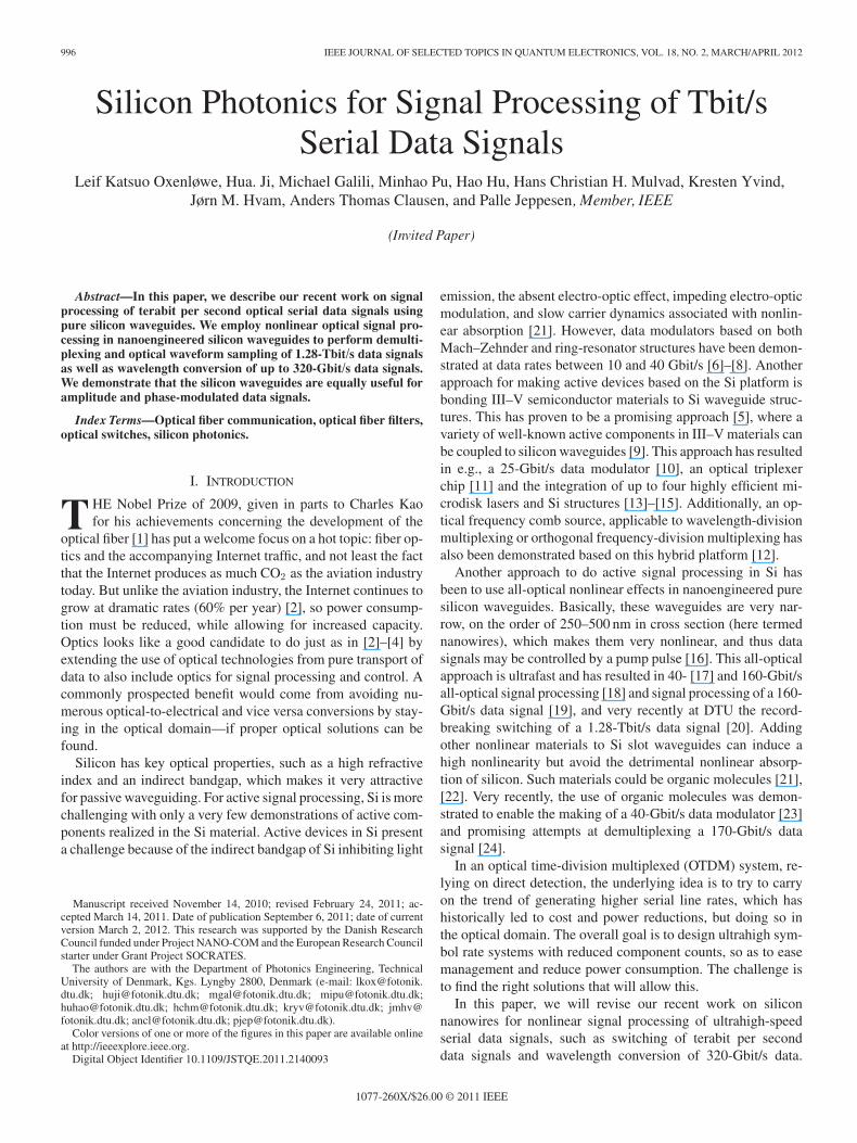
Fig. 1. Schematic of nonlinear effect exploited: four wave mixing.
We rely entirely on pure silicon waveguides and four-wavemixing in these to achieve the desired functionalities. Allexperiments are soundly backed up by solid bit error rate (BER)characterizations.
II. EXPERIMENTAL SETUPS
The underlying principle exploited for all the experimentscovered in this paper is four-wave mixing (FWM) in the siliconnanowire, as sketched in Fig. 1. The experimental setup usedfor the experiments is mostly common to all experiments andshown in Figs. 2 and 3. Fig. 3 shows the 1.28-Tbaud trans-mitter [25] setup used to demonstrate back-to-back 1.28-TbaudOOK 1.28-Tbit/s data generation and demultiplexing. The heartof an ultrahigh-speed serial data system is the short pulse gen-eration. Here, dispersion-flattened highly nonlinear fibers (DF-HNLF: D = −0.45 ps/nm·km and slope S = 0.006 ps/nm2 ·kmat 1550 nm, nonlinear coefficient γ = 10.5 W−1 ·km−1) areused to chirp the pulses followed by subsequent linear com-pression in dispersive fiber. The compressed pulses are around350-fs wide full-width at half-maximum (FWHM) out of the1.28-Tbit/s transmitter. The generated supercontinuum outputfrom DF-HNLF1 is split into two and filtered at separate wave-lengths, one for the control and one for the data. In the databranch, the pulses are compressed further in a second compres-sion stage with DF-HNLF2 followed by a 14-nm broad filter.The output from here is data modulated and multiplexed to a1.28-Tbaud pulse train. In this paper, all data modulation willonly be binary, so the 1.28 Tbaud will correspond to a 1.28-Tbit/ssingle-polarization, single-wavelength channel. To derive a con-trol pulse for demultiplexing, in this back-to-back scenario, thesecond branch is fed to a third pulse compression stage (Com-pressor 3). The principle here is the same as before: chirpingin a DF-HNLF and subsequent linear compression. The controlpulse wavelength is chosen at 1574 nm, i.e., in the L-band. Thismeans that the FWM product will be positioned even further upin the L-band. The control and data signals are coupled througha 3-dB coupler and sent into the Si-nanowire.
Fig. 3 shows a schematic of the full setup. The input powers tothe silicon waveguide are monitored on the second output of the3-dB coupler at the input to the waveguide. The port facing thewaveguide is connected to a tapered fiber (3-μm spot diameter),allowing for good coupling efficiency to the waveguide. TheSi waveguide is tapered down to 40 nm width in each end,coupling light into an overlaying polymer waveguide of 3.4-μmcross-sectional diameter, making the coupling loss about 2.6-dBper facet [26]. The 40-nm tip is achieved by e-beam lithographyand dry thermal oxidation to create an inverse taper coupler. The
overall fiber-to-fiber insertion loss is around 7.5 dB for a 5-mmlong device, and the propagation loss for the fabricated devicesused in these experiments is about 4.5 dB/cm. The nonlinearcoefficient γ of the used silicon nanowire is measured usingthe continuous wave (CW) SPM method to be around 4 ×10⁵ W−1 ·km−1 .
The output of the Si waveguide is in the L-band and is fil-tered out through a bandpass (BP) L-band 1-nm wide filterand preamplified in an L-band erbium-doped fiber amplifiers.The amplified demultiplexed data are photodetected and BERis measured. As a baseline for the L-band receiver, a 10-to-10-Gbit/s demultiplexing is performed for comparison with theterabit per second demultiplexing. This is necessary, as the C-and L-band receivers are very different, so comparing a C-bandback-to-back with the demultiplexed L-band FWM signal wouldnot make sense.
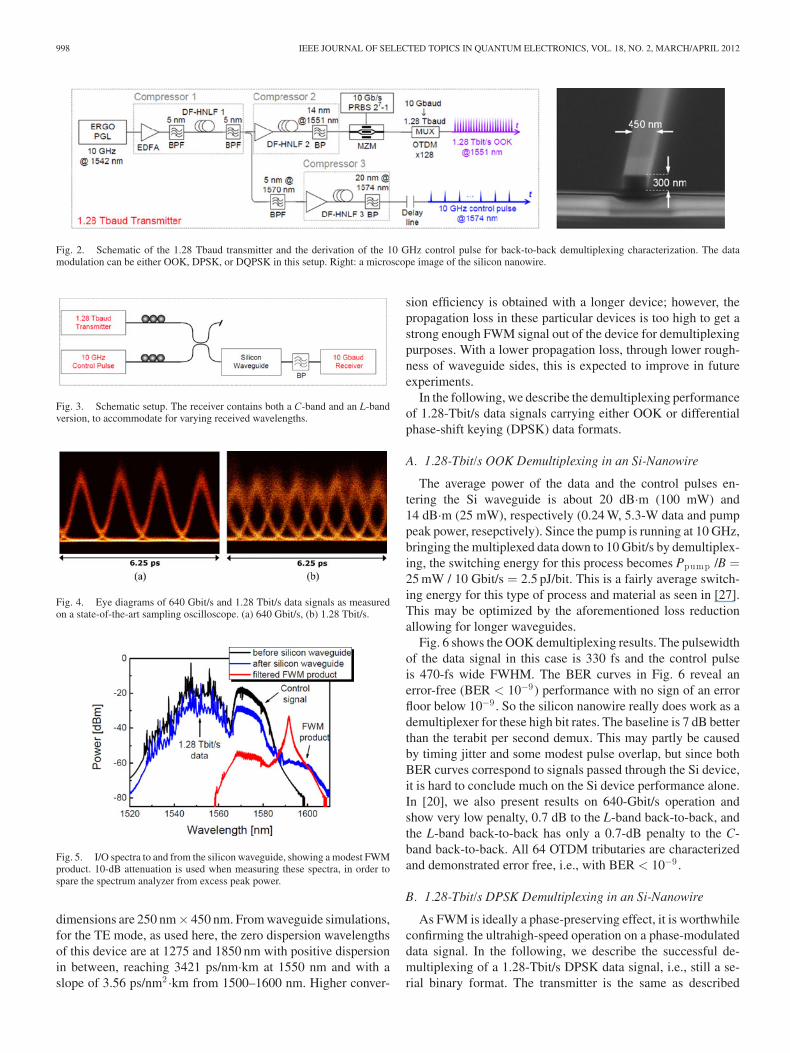
Fig. 4 shows eye diagrams of the generated data signals at640 Gbit/s and 1.28 Tbit/s using a commercial optical samplingoscilloscope. The eyes shown are in fact all 64 or 128 chan-nels, respectively, overlaid on each other, revealing good signalquality. It appears as if the pulses are stretched and extend intoneighboring time slots. In reality they do not, they are only 350fs wide, and the appearance in Fig. 4 is due to limited reso-lution bandwidth of the sampling oscilloscope, which is basedon HNLF with accompanying walkoff. As we will see later inthis paper, the data pulses in the 1.28-Tbit/s data signal can beresolved using an Si-nanowire, and when doing so, clear eyediagrams are obtained revealing no pulse tail overlap in the1.28-Tbit/s data signal.
III. EXPERIMENTAL DEMONSTRATIONS
The spectra involved are shown in Fig. 5. The input to thesilicon waveguide, the output of the silicon waveguide, andthe filtered FWM product are all shown together. The effectiveFWM conversion efficiency of the silicon waveguide can beestimated from the spectra. The FWM conversion efficiency iscalculated by integrating the optical spectra of the data and theFWM product, i.e., to obtain the average power of the outputdata signal and the FWM product, respectively. Then the dutycycle difference between the data signal and the pump (18 dBfor 640 Gbit/s and 21 dB for 1.28 Tbit/s) is considered, as wellas the insertion loss (7.5 dB). Thus, the effective fiber-to-fiberFWM conversion efficiency is estimated in decibel as
η=PFWM(out) − [Psignal(out) + Lossinsertion ] + dutycycle.
Therefore, even if the FWM product in Fig. 5 appears quitemodest, the actual conversion efficiency is really higher. In thiscase, the conversion efficiency is measured to −15.1 dB.
The relatively low conversion efficiency obtained here ispartly due to the long wavelength used. The conversion band-width is only about 18 nm for this particular device [20], andwith the wavelength allocation used here, the FWM product ison the edge of the conversion bandwidth.
A 5-mm long device is used here as a compromise betweenconversion efficiency and propagation loss. Its cross-sectional
998 IEEE JOURNAL OF SELECTED TOPICS IN QUANTUM ELECTRONICS, VOL. 18, NO. 2, MARCH/APRIL 2012
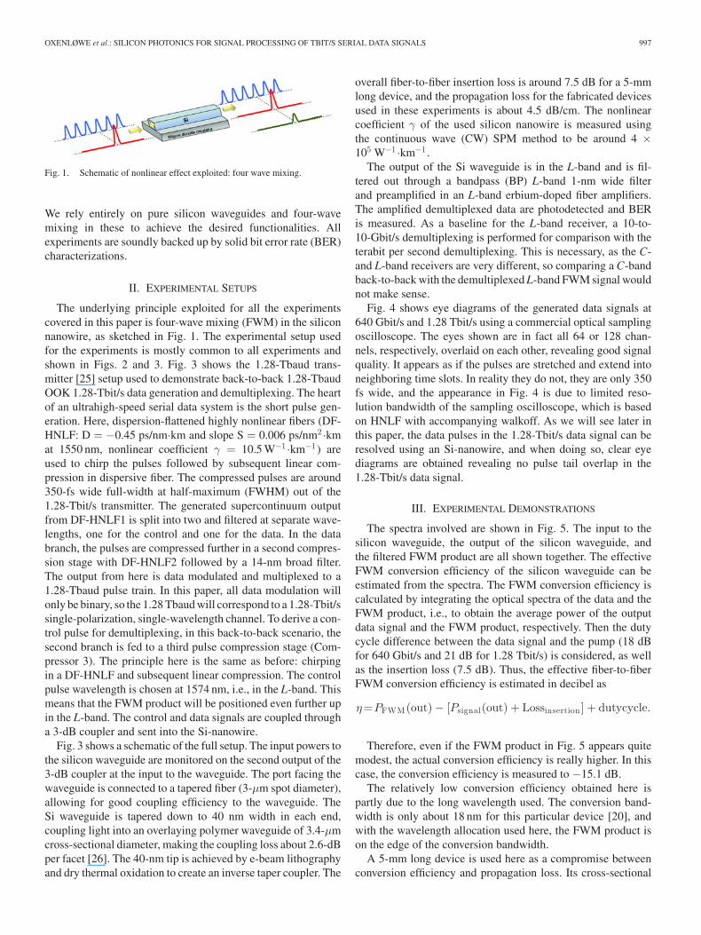
Fig. 2. Schematic of the 1.28 Tbaud transmitter and the derivation of the 10 GHz control pulse for back-to-back demultiplexing characterization. The datamodulation can be either OOK, DPSK, or DQPSK in this setup. Right: a microscope image of the silicon nanowire.
Fig. 3. Schematic setup. The receiver contains both a C-band and an L-bandversion, to accommodate for varying received wavelengths.
Fig. 4. Eye diagrams of 640 Gbit/s and 1.28 Tbit/s data signals as measuredon a state-of-the-art sampling oscilloscope. (a) 640 Gbit/s, (b) 1.28 Tbit/s.
Fig. 5. I/O spectra to and from the silicon waveguide, showing a modest FWMproduct. 10-dB attenuation is used when measuring these spectra, in order tospare the spectrum analyzer from excess peak power.
dimensions are 250 nm× 450 nm. From waveguide simulations,for the TE mode, as used here, the zero dispersion wavelengthsof this device are at 1275 and 1850 nm with positive dispersionin between, reaching 3421 ps/nm·km at 1550 nm and with aslope of 3.56 ps/nm2 ·km from 1500–1600 nm. Higher conver-
sion efficiency is obtained with a longer device; however, thepropagation loss in these particular devices is too high to get astrong enough FWM signal out of the device for demultiplexingpurposes. With a lower propagation loss, through lower rough-ness of waveguide sides, this is expected to improve in futureexperiments.
In the following, we describe the demultiplexing performanceof 1.28-Tbit/s data signals carrying either OOK or differentialphase-shift keying (DPSK) data formats.
A. 1.28-Tbit/s OOK Demultiplexing in an Si-Nanowire
The average power of the data and the control pulses en-tering the Si waveguide is about 20 dB·m (100 mW) and14 dB·m (25 mW), respectively (0.24 W, 5.3-W data and pumppeak power, resepctively). Since the pump is running at 10 GHz,bringing the multiplexed data down to 10 Gbit/s by demultiplex-ing, the switching energy for this process becomes Ppump /B =25 mW / 10 Gbit/s = 2.5 pJ/bit. This is a fairly average switch-ing energy for this type of process and material as seen in [27].This may be optimized by the aforementioned loss reductionallowing for longer waveguides.
Fig. 6 shows the OOK demultiplexing results. The pulsewidthof the data signal in this case is 330 fs and the control pulseis 470-fs wide FWHM. The BER curves in Fig. 6 reveal anerror-free (BER < 10−9) performance with no sign of an errorfloor below 10−9 . So the silicon nanowire really does work as ademultiplexer for these high bit rates. The baseline is 7 dB betterthan the terabit per second demux. This may partly be causedby timing jitter and some modest pulse overlap, but since bothBER curves correspond to signals passed through the Si device,it is hard to conclude much on the Si device performance alone.In [20], we also present results on 640-Gbit/s operation andshow very low penalty, 0.7 dB to the L-band back-to-back, andthe L-band back-to-back has only a 0.7-dB penalty to the C-band back-to-back. All 64 OTDM tributaries are characterizedand demonstrated error free, i.e., with BER < 10−9 .
B. 1.28-Tbit/s DPSK Demultiplexing in an Si-Nanowire
As FWM is ideally a phase-preserving effect, it is worthwhileconfirming the ultrahigh-speed operation on a phase-modulateddata signal. In the following, we describe the successful de-multiplexing of a 1.28-Tbit/s DPSK data signal, i.e., still a se-rial binary format. The transmitter is the same as described

OXENLØWE et al.: SILICON PHOTONICS FOR SIGNAL PROCESSING OF TBIT/S SERIAL DATA SIGNALS 999
Fig. 6. 1.28-Tbit/s demultiplexing results. Top: Autocorrelation traces of themultiplexed data and the control pulse. Bottom: BER curves for 1.28-Tbit/sdemultiplexing and as back-to-back a 10 Gbit/s to 10 Gbit/s demultiplexing.There is no error floor, but a 7-dB penalty. Also, the 10 Gbit/s C-band back-to-back is presented. The L-band and C-band preamplified receivers are differentand, hence, the curves have different slopes, but almost identical sensitivity.
earlier, except that the data modulator is swapped for a LiNbO3phase modulator. The multiplexer is designed to preserve a27–1 OOK data signal, and not designed for phase modu-lated signals, which simply turn into a pulse train with higherrepetition rates. Therefore, we do not take particular care tokeep the pseudo random binary sequence (PRBS) to the low27–1 sequence, and instead a 231–1 is used. This way, wecan more clearly see any pattern effects on the tributary rate,i.e., at 10 Gbit/s. The receiver is changed to a DPSK receiverwith balanced detection, see Fig. 7, following the Si-nanowiredemultiplexer.
The receiver may also be used for differential quadraturephase shift keying (DQPSK) data, but here we restrict ourselvesto DPSK. The device used here is identical in dimensions to theone used earlier, i.e., 5 mm × 250 nm × 450 nm. The insertionloss is only 6 dB for this device, owing to better fabrication;however, there are some minor reflections giving some feedbackto the waveguide.
Fig. 7 shows the spectra at the I/O of the Si-nanowire. Asbefore, the control and FWM product is in the L-band. The dataare at 1551 nm, the control at 1570 nm, and the FWM productat 1599 nm. The pulsewidths are 350 and 540 fs for the data
Fig. 7. 1.28-Tbit/s DPSK demultiplexing in an Si-nanowire and subsequentdemodulation in a delay interferometer (DLI) and balanced photo detection(BPD) receiver. Top: I/O spectra to/from the Si-nanowire and the filtered de-multiplexed FWM product to the receiver. Bottom: Schematic of receiver forDQPSK or DPSK data.
Fig. 8. 1.28-Tbit/s DPSK demultiplexing. Top: BER curves for eight consec-utive channels. Bottom: Error-free (< BER 10−9 ) demultiplexed eye diagram.
and control, respectively, see Fig. 9 (top). The data and pumpaverage input powers are 13.5 and 14 dB·m, respectively.
BER curves are presented in Fig. 8 for eight consecutivechannels. There is a clear error floor appearing in these curves,and half of them get BER below 10−9 and the rest merelybelow 10−8 . When checking with OOK data, at 640 Gbit/s and1.28 Tbit/s the same performance appears, and we conclude thatthe error floor must be isolated to the performance of the device,i.e., it is not due to the DPSK data format. At 640 Gbit/s, thereis still an error floor, but all measured channels are below BER
1000 IEEE JOURNAL OF SELECTED TOPICS IN QUANTUM ELECTRONICS, VOL. 18, NO. 2, MARCH/APRIL 2012
Fig. 9. 1.28-Tbit/s demultiplexing in an Si-nanowire. Characterisation of all128 channels. Top: Autocorrelation of 1.28-Tbit/s data signal and 10 GHzcontrol pulse. Bottom: Measured receiver sensitivities for all channels at BER= 10−4 .
of 10−9 . The demodulated, demultiplexed eye diagrams from1.28 Tbit/s appear clear and open though, see Fig. 8 (bottom).We expect the error floor to be due to excessive reflections fromthis particular device.
In order to characterize all 128 OTDM tributary channels ina practical way, the receiver power for each channel is mea-sured at the relatively high BER of 10−4 . This BER allows forfaster measurements, and is still below the standard forward er-ror correction (FEC) limit of BER 10−3 . All 128 channels arescanned through and readily yield a BER of 10−4 , i.e., below theFEC limit. Assuming a 7% FEC redundancy would then lead toa 1.19-Tbit/s data payload, i.e., a 1.19-Tbit/s error free DPSKdata signal is, thus, processed in this silicon nanowire. The re-sults are shown in Fig. 9 (bottom). There is about 4 dB variationin receiver sensitivity among all the channels. This variationstems from the slight difference among all the channels causedby the multiplexer.
C. 1.28-Tbit/s OOK All-Optical Sampling in an Si-Nanowire
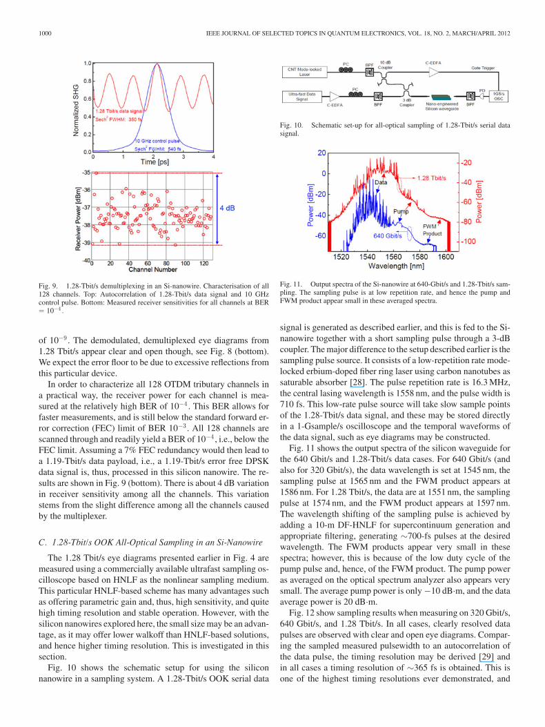
The 1.28 Tbit/s eye diagrams presented earlier in Fig. 4 aremeasured using a commercially available ultrafast sampling os-cilloscope based on HNLF as the nonlinear sampling medium.This particular HNLF-based scheme has many advantages suchas offering parametric gain and, thus, high sensitivity, and quitehigh timing resolution and stable operation. However, with thesilicon nanowires explored here, the small size may be an advan-tage, as it may offer lower walkoff than HNLF-based solutions,and hence higher timing resolution. This is investigated in thissection.
Fig. 10 shows the schematic setup for using the siliconnanowire in a sampling system. A 1.28-Tbit/s OOK serial data
Fig. 10. Schematic set-up for all-optical sampling of 1.28-Tbit/s serial datasignal.
Fig. 11. Output spectra of the Si-nanowire at 640-Gbit/s and 1.28-Tbit/s sam-pling. The sampling pulse is at low repetition rate, and hence the pump andFWM product appear small in these averaged spectra.
signal is generated as described earlier, and this is fed to the Si-nanowire together with a short sampling pulse through a 3-dBcoupler. The major difference to the setup described earlier is thesampling pulse source. It consists of a low-repetition rate mode-locked erbium-doped fiber ring laser using carbon nanotubes assaturable absorber [28]. The pulse repetition rate is 16.3 MHz,the central lasing wavelength is 1558 nm, and the pulse width is710 fs. This low-rate pulse source will take slow sample pointsof the 1.28-Tbit/s data signal, and these may be stored directlyin a 1-Gsample/s oscilloscope and the temporal waveforms ofthe data signal, such as eye diagrams may be constructed.
Fig. 11 shows the output spectra of the silicon waveguide forthe 640 Gbit/s and 1.28-Tbit/s data cases. For 640 Gbit/s (andalso for 320 Gbit/s), the data wavelength is set at 1545 nm, thesampling pulse at 1565 nm and the FWM product appears at1586 nm. For 1.28 Tbit/s, the data are at 1551 nm, the samplingpulse at 1574 nm, and the FWM product appears at 1597 nm.The wavelength shifting of the sampling pulse is achieved byadding a 10-m DF-HNLF for supercontinuum generation andappropriate filtering, generating ∼700-fs pulses at the desiredwavelength. The FWM products appear very small in thesespectra; however, this is because of the low duty cycle of thepump pulse and, hence, of the FWM product. The pump poweras averaged on the optical spectrum analyzer also appears verysmall. The average pump power is only −10 dB·m, and the dataaverage power is 20 dB·m.
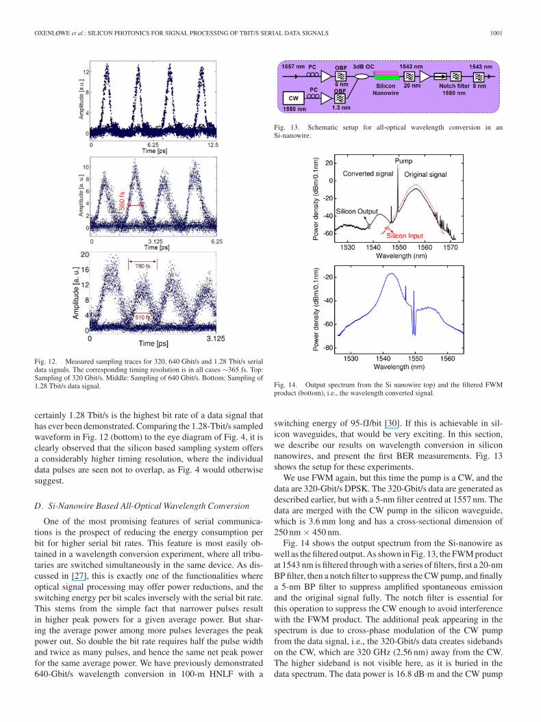
Fig. 12 show sampling results when measuring on 320 Gbit/s,640 Gbit/s, and 1.28 Tbit/s. In all cases, clearly resolved datapulses are observed with clear and open eye diagrams. Compar-ing the sampled measured pulsewidth to an autocorrelation ofthe data pulse, the timing resolution may be derived [29] andin all cases a timing resolution of ∼365 fs is obtained. This isone of the highest timing resolutions ever demonstrated, and
OXENLØWE et al.: SILICON PHOTONICS FOR SIGNAL PROCESSING OF TBIT/S SERIAL DATA SIGNALS 1001
Fig. 12. Measured sampling traces for 320, 640 Gbit/s and 1.28 Tbit/s serialdata signals. The corresponding timing resolution is in all cases ∼365 fs. Top:Sampling of 320 Gbit/s. Middle: Sampling of 640 Gbit/s. Bottom: Sampling of1.28 Tbit/s data signal.
certainly 1.28 Tbit/s is the highest bit rate of a data signal thathas ever been demonstrated. Comparing the 1.28-Tbit/s sampledwaveform in Fig. 12 (bottom) to the eye diagram of Fig. 4, it isclearly observed that the silicon based sampling system offersa considerably higher timing resolution, where the individualdata pulses are seen not to overlap, as Fig. 4 would otherwisesuggest.
D. Si-Nanowire Based All-Optical Wavelength Conversion
One of the most promising features of serial communica-tions is the prospect of reducing the energy consumption perbit for higher serial bit rates. This feature is most easily ob-tained in a wavelength conversion experiment, where all tribu-taries are switched simultaneously in the same device. As dis-cussed in [27], this is exactly one of the functionalities whereoptical signal processing may offer power reductions, and theswitching energy per bit scales inversely with the serial bit rate.This stems from the simple fact that narrower pulses resultin higher peak powers for a given average power. But shar-ing the average power among more pulses leverages the peakpower out. So double the bit rate requires half the pulse widthand twice as many pulses, and hence the same net peak powerfor the same average power. We have previously demonstrated640-Gbit/s wavelength conversion in 100-m HNLF with a
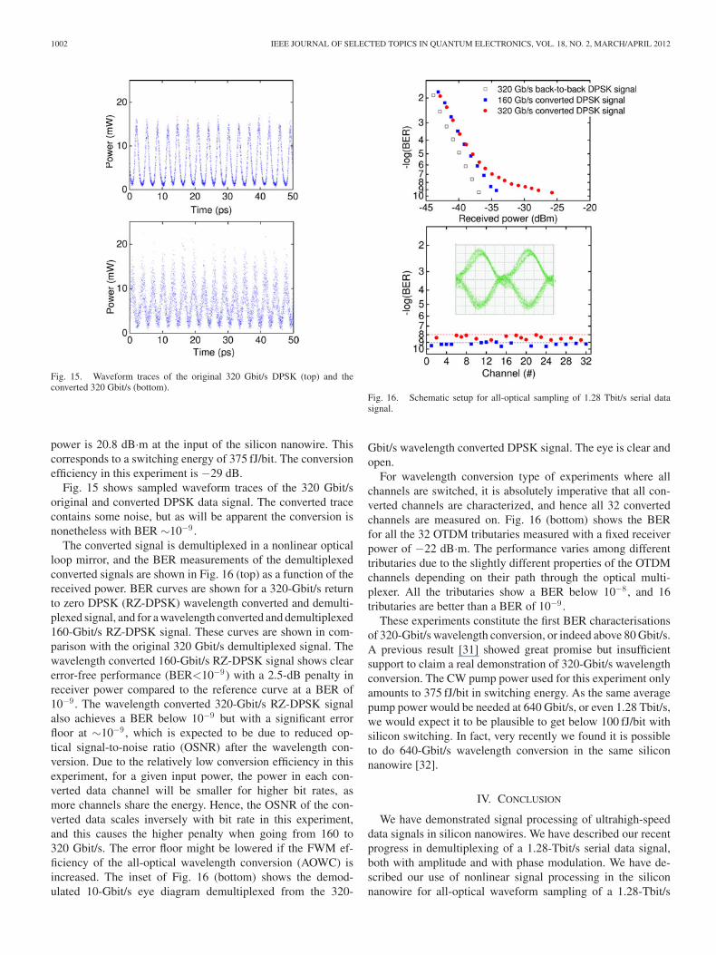
Fig. 13. Schematic setup for all-optical wavelength conversion in anSi-nanowire.
Fig. 14. Output spectrum from the Si nanowire top) and the filtered FWMproduct (bottom), i.e., the wavelength converted signal.
switching energy of 95-fJ/bit [30]. If this is achievable in sil-icon waveguides, that would be very exciting. In this section,we describe our results on wavelength conversion in siliconnanowires, and present the first BER measurements. Fig. 13shows the setup for these experiments.
We use FWM again, but this time the pump is a CW, and thedata are 320-Gbit/s DPSK. The 320-Gbit/s data are generated asdescribed earlier, but with a 5-nm filter centred at 1557 nm. Thedata are merged with the CW pump in the silicon waveguide,which is 3.6 mm long and has a cross-sectional dimension of250 nm × 450 nm.
Fig. 14 shows the output spectrum from the Si-nanowire aswell as the filtered output. As shown in Fig. 13, the FWM productat 1543 nm is filtered through with a series of filters, first a 20-nmBP filter, then a notch filter to suppress the CW pump, and finallya 5-nm BP filter to suppress amplified spontaneous emissionand the original signal fully. The notch filter is essential forthis operation to suppress the CW enough to avoid interferencewith the FWM product. The additional peak appearing in thespectrum is due to cross-phase modulation of the CW pumpfrom the data signal, i.e., the 320-Gbit/s data creates sidebandson the CW, which are 320 GHz (2.56 nm) away from the CW.The higher sideband is not visible here, as it is buried in thedata spectrum. The data power is 16.8 dB·m and the CW pump
1002 IEEE JOURNAL OF SELECTED TOPICS IN QUANTUM ELECTRONICS, VOL. 18, NO. 2, MARCH/APRIL 2012
Fig. 15. Waveform traces of the original 320 Gbit/s DPSK (top) and theconverted 320 Gbit/s (bottom).
power is 20.8 dB·m at the input of the silicon nanowire. Thiscorresponds to a switching energy of 375 fJ/bit. The conversionefficiency in this experiment is −29 dB.
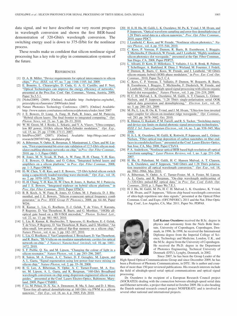
Fig. 15 shows sampled waveform traces of the 320 Gbit/soriginal and converted DPSK data signal. The converted tracecontains some noise, but as will be apparent the conversion isnonetheless with BER ∼10−9 .
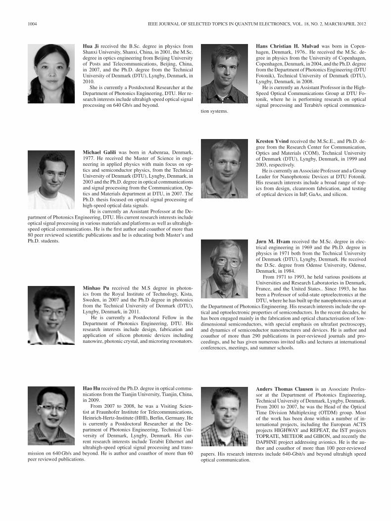
The converted signal is demultiplexed in a nonlinear opticalloop mirror, and the BER measurements of the demultiplexedconverted signals are shown in Fig. 16 (top) as a function of thereceived power. BER curves are shown for a 320-Gbit/s returnto zero DPSK (RZ-DPSK) wavelength converted and demulti-plexed signal, and for a wavelength converted and demultiplexed160-Gbit/s RZ-DPSK signal. These curves are shown in com-parison with the original 320 Gbit/s demultiplexed signal. Thewavelength converted 160-Gbit/s RZ-DPSK signal shows clearerror-free performance (BER<10−9) with a 2.5-dB penalty inreceiver power compared to the reference curve at a BER of10−9 . The wavelength converted 320-Gbit/s RZ-DPSK signalalso achieves a BER below 10−9 but with a significant errorfloor at ∼10−9 , which is expected to be due to reduced op-tical signal-to-noise ratio (OSNR) after the wavelength con-version. Due to the relatively low conversion efficiency in thisexperiment, for a given input power, the power in each con-verted data channel will be smaller for higher bit rates, asmore channels share the energy. Hence, the OSNR of the con-verted data scales inversely with bit rate in this experiment,and this causes the higher penalty when going from 160 to320 Gbit/s. The error floor might be lowered if the FWM ef-ficiency of the all-optical wavelength conversion (AOWC) isincreased. The inset of Fig. 16 (bottom) shows the demod-ulated 10-Gbit/s eye diagram demultiplexed from the 320-
Fig. 16. Schematic setup for all-optical sampling of 1.28 Tbit/s serial datasignal.
Gbit/s wavelength converted DPSK signal. The eye is clear andopen.
For wavelength conversion type of experiments where allchannels are switched, it is absolutely imperative that all con-verted channels are characterized, and hence all 32 convertedchannels are measured on. Fig. 16 (bottom) shows the BERfor all the 32 OTDM tributaries measured with a fixed receiverpower of −22 dB·m. The performance varies among differenttributaries due to the slightly different properties of the OTDMchannels depending on their path through the optical multi-plexer. All the tributaries show a BER below 10−8 , and 16tributaries are better than a BER of 10−9 .
These experiments constitute the first BER characterisationsof 320-Gbit/s wavelength conversion, or indeed above 80 Gbit/s.A previous result [31] showed great promise but insufficientsupport to claim a real demonstration of 320-Gbit/s wavelengthconversion. The CW pump power used for this experiment onlyamounts to 375 fJ/bit in switching energy. As the same averagepump power would be needed at 640 Gbit/s, or even 1.28 Tbit/s,we would expect it to be plausible to get below 100 fJ/bit withsilicon switching. In fact, very recently we found it is possibleto do 640-Gbit/s wavelength conversion in the same siliconnanowire [32].
IV. CONCLUSION
We have demonstrated signal processing of ultrahigh-speeddata signals in silicon nanowires. We have described our recentprogress in demultiplexing of a 1.28-Tbit/s serial data signal,both with amplitude and with phase modulation. We have de-scribed our use of nonlinear signal processing in the siliconnanowire for all-optical waveform sampling of a 1.28-Tbit/s
OXENLØWE et al.: SILICON PHOTONICS FOR SIGNAL PROCESSING OF TBIT/S SERIAL DATA SIGNALS 1003
data signal, and we have described our very recent progressin wavelength conversion and shown the first BER-baseddemonstration of 320-Gbit/s wavelength conversion. Theswitching energy used is down to 375-fJ/bit for the nonlinearprocess.
These results make us confident that silicon nonlinear signalprocessing has a key role to play in communication systems ofthe future.
REFERENCES
[1] D. A. B. Miller, “Device requirements for optical interconnects to siliconchips,” Proc. IEEE, vol. 97, no. 7, pp. 1166–1185, Jul. 2009.
[2] E. Bonetto, L. Chiaraviglio, D. Cuda, G. A. G. Castillo, and F. Neri,“Optical Technologies can improve the energy efficiency of networks,”presented at the Proc.Eur. Conf. Opt. Commun., Vienna, Austria, 2009,Paper Tu.5.5.1.
[3] [Nobel2009]. (2009). [Online]. Available: http: //nobelprize.org/nobel_prizes/physics/laureates/ 2009/index.html
[4] Nature Photonics Technology Conference. (2007). [Online] Available:http: //www.nature.com/natureconferences/photonics/index.html 2007
[5] J. E. Bowers, D. Liang, A. Fang, H. Park, R. Jones, and M. Paniccia,“Hybrid silicon lasers: The final frontier to integrated computing,” Opt.Photon. News, vol. 21, no. 5, pp. 28–33, 2010.
[6] W. M. Green, M. J. Rooks, L. Sekaric, and Y. A. Vlasov, “Ultra-compact,low RF power, 10 Gb/s silicon Mach-Zehnder modulator,” Opt. Exp.,vol. 15, no. 25, pp. 17106–17113, 2007.
[7] IntelPress2007. (2007). [Online]. Available: http://blogs.intel.com/research/2007/07/40g_modulator.php
[8] A. Biberman, N. Ophir, K. Bergman, S. Manipatruni, L. Chen, and M. Lip-son, “First experimental bit-error-rate validation of 12.5-Gb/s silicon mod-ulator enabling photonic networks-on-chip,” in Proc. Opt. Fiber Commun.,2010, pp. 1–3, Paper OMI1.
[9] R. Jones, M. N. Sysak, H. Park, A. W. Fang, H.-H. Chang, Y.-H. Kuo,J. E. Bowers, O. Raday, and O. Cohen, “Integrated hybrid lasers andamplifiers on a silicon platform,” in Proc. Opt. Fiber Commun., 2008,pp. 1–3, Paper OWM1.
[10] H.-W. Chen, Y.-H. Kuo, and J. E. Bowers, “25 Gb/s hybrid silicon switchusing a capacitively loaded traveling wave electrode,” Opt. Exp., vol. 18,no. 2, pp. 1070–1075, Jan. 2010.
[11] H.-H. Chang, Y.-H. Kuo, H.-W. Chen, R. Jones, A. Barkai, M. J. Paniccia,and J. E. Bowers, “Integrated triplexer on hybrid silicon platform,” inProc. Opt. Fiber Commun., 2010, Paper OThC4.
[12] B. R. Koch, A. W. Fang, R. Jones, O. Cohen, M. J. Paniccia, D. J. Blu-menthal, and J. E. Bowers, “Silicon evanescent optical frequency combgenerator,” in Proc. IEEE Group IV Photonics, 2008, pp. 64–66, PaperWD4.
[13] R. Kumar, L. Liu, G. Roelkens, E.-J. Geluk, T. de Vries, F. Karouta,P. Regreny, D. Van Thourhout, R. Baets, and G. Morthier, “10GHz all-optical gate based on a III-V/SOI microdisk,” Photon. Technol. Lett.,vol. 22, no. 13, pp. 981–983, 2010.
[14] L. Liu, R. Kumar, K. Huybrechts, T. Spuesens, G. Roelkens, E.-J. Geluk,T. de Vries, P. Regreny, D. Van Thourhout, R. Baets, and G. Morthier, “Anultra-small, low-power, all-optical flip-flop memory on a silicon chip,”Nature Photon., vol. 4, no. 3, pp. 182–187, 2010.
[15] L. Liu, G. Roelkens, J. Van Campenhout, J. Brouckaert, D. Van Thourhout,and R. Baets, “III-V/silicon-on-insulator nanophotonic cavities for opticalnetwork-on-chip,” J. Nanosci. Nanotechnol. (invited), vol. 10, pp. 1461–1472, 2010.
[16] S. F. Preble, Q. Xu, and M. Lipson, “Changing the colour of light in asilicon resonator,” Nature Photon., vol. 1, pp. 293–296, 2007.
[17] R. Salem, M. A. Foster, A. C. Turner, D. F. Geraghty, M. Lipson, andA. L. Gaeta, “Signal regeneration using low-power four-wave mixing onsilicon chip,” Nature Photon, vol. 2, pp. 35–38, 2008.
[18] B. G. Lee, A. Biberman, N. Ophir, A. C. Turner-Foster, M. A. Fos-ter, M. Lipson, A. L. Gaeta, and K. Bergman, “160-Gb/s Broadbandwavelength conversion on chip using dispersion-engineered silicon waveguides,” presented at the Conf. Lasers Electro-Optics, Baltimore, Mary-land, 2009, Paper CThBB1.
[19] F. Li, M. Pelusi, D.-X. Xu, A. Densmore, R. Ma, S. Janz, and D. J. Moss,“Error-free all-optical demultiplexing at 160 Gb/s via FWM in a siliconnanowire,” Opt. Exp., vol. 18, no. 4, p. 3905, Feb. 2010.
[20] H. Ji, H. Hu, M. Galili, L. K. Oxenløwe, M. Pu, K. Yvind, J. M. Hvam, andP. Jeppesen, “Optical waveform sampling and error-free demultiplexing of1.28 Tbit/s serial data in a silicon nanowire,” Proc. Opt. Fiber Commun.,2010, paper PDC7.
[21] J. Leuthold, C. Koos, and W. Freude, “Nonlinear silicon photonics,” Na-ture Photon., vol. 4, pp. 535–544, 2010.
[22] C. Koos, P. Vorreau, P. Dumon, R. Baets, B. Esembeson, I. Biaggio,T. Michinobu, F. Diederich, W. Freude, and J. Leuthold, “Highly-nonlinearsilicon photonics slot waveguide,” presented at the Opt. Fiber Commun.,San Diego, CA, 2008, Paper PDP25.
[23] L. Alloatti, D. Korn, D. Hillerkuss, T. Vallaitis, J. Li, R. Bonk, R. Palmer,T. Schellinger, A. Barklund, R. Dinu, J. Wieland, M. Fournier, J. Fedeli,P. Dumon, R. Baets, C. Koos, W. Freude, and J. Leuthold, “40 Gbit/ssilicon-organic hybrid (SOH) phase modulator,” in Proc. Eur. Conf. Opt.Commun., 2010, Paper Tu.5. C.4.
[24] C. Koos, C. P. Vorreau, T. Vallaitis, P. Dumon, W. Bogaerts, R. Baets,B. Esembeson, I. Biaggio, T. Michinobu, F. Diederich, W. Freude, andJ. Leuthold, “All-optical high-speed signal processing with silicon-organichybrid slot waveguides,” Nature Photon., vol. 3, pp. 216–219, 2009.
[25] H. C. H. Mulvad, L. K. Oxenløwe, M. Galili, A. T. Clausen, L- Gruner-Nielsen, and P. Jeppesen, “1.28 Tbit/s single-polarisation serial OOKoptical data generation and demultiplexing,” Electron. Lett., vol. 45,no. 5, pp. 280–281, 2009.
[26] M. Pu, L. Liu, H. Ou, K. Yvind, and J. M. Hvam, “Ultra-low-loss invertedtaper coupler for silicon-on-insulator ridge waveguide,” Opt. Commun.,vol. 283, pp. 3678–3682, Oct. 2010.
[27] K. Hinton, G. Raskutti, P. M. Farrell, and R. S. Tucker, “Switching energyand device size limits on digital photonic signal processing technologies,”IEEE J. Sel. Topics Quantum Electron., vol. 14, no. 3, pp. 938–945, May2008.
[28] H. Ji, L. K. Oxenløwe, M. Galili, K. Rottwitt, P. Jeppesen, and L. Gruner-Nielsen, “Fiber optical trap deposition of carbon nanotubes on fiber end-faces in a modelocked laser,” presented at the Conf. Lasers Electro-Optics,San Jose, CA, May 2008, Paper CTuV4.
[29] P. A. Andrekson, “Nonlinear optical BER based high resolution all-opticalwaveform sampling,” Laser Photon. Reviews, vol. 1, no. 3, pp. 231–248,2007.
[30] H. Hu, E. Palushani, M. Galili, H. C. Hansen Mulvad, A. T. Clausen,L. K. Oxenløwe, and P. Jeppesen, “640 Gbit/s and 1.28 Tbit/s polarisa-tion insensitive all optical wavelength conversion,” Opt. Exp., vol. 18,pp. 9961–9966, May 2010.
[31] A. Biberman, N. Ophir, A. C. Turner-Foster, M. A. Foster, M. Lipson,A. L. Gaeta, and K. Bergman, “On-chip wavelength multicasting of3×320-Gb/s pulsed-RZ optical data,” in Proc. Eur. Conf. Exhib. Opt.Commun., 2010, p. 1, Paper We.7.E.3.
[32] H. J. Hu, M. Galili, M. Pu, H. C. H. Mulvad, L. K. Oxenløwe, K. Yvind,J. M. Hvam, and P. Jeppesen, “Silicon chip based wavelength conversionof ultra-high repetition rate data signals,” presented at the Optical FiberCommun. Conf. and Expo. (OFC/NFOEC), 2011 and the Nat. Fiber OpticEng. Conf., Los Angeles, CA, Mar. 2011, Paper No. PDPA8.
Leif Katsuo Oxenløwe received the B.Sc. degree inphysics and astronomy from the Niels Bohr Insti-tute, University of Copenhagen, Copenhagen, Den-mark, in 1996. In 1998, he received the InternationalDiploma degree from the Imperial College of Sci-ence, Technology and Medicine, London, U.K., andthe M.Sc. degree from the University of Copenhagen.He received the Ph.D. degree in the Departmentof Photonics Engineering, Technical University ofDenmark (DTU), Lyngby, Denmark, in 2002.
Since 2007, he has been the Group Leader of theHigh-Speed Optical Communications Group and since December 2009, he hasbeen a Professor of Photonic Communications, in DTU. He is author and coau-thor of more than 150 peer reviewed publications. His research interests includethe field of ultrahigh-speed serial optical communications and optical signalprocessing.
Dr. Oxenløwe is the recipient of a European Research Council project(SOCRATES) dealing with the connection between ultrahigh-speed serial dataand Ethernet networks, a project that started in October 2009. He is also headingthe Danish national research council project NOSFERATU and is involved inseveral other national and international projects.
1004 IEEE JOURNAL OF SELECTED TOPICS IN QUANTUM ELECTRONICS, VOL. 18, NO. 2, MARCH/APRIL 2012
Hua Ji received the B.Sc. degree in physics fromShanxi University, Shanxi, China, in 2001, the M.Sc.degree in optics engineering from Beijing Universityof Posts and Telecommunications, Beijing, China,in 2007, and the Ph.D. degree from the TechnicalUniversity of Denmark (DTU), Lyngby, Denmark, in2010.
She is currently a Postdoctoral Researcher at theDepartment of Photonics Engineering, DTU. Her re-search interests include ultrahigh speed optical signalprocessing on 640 Gb/s and beyond.
Michael Galili was born in Aabenraa, Denmark,1977. He received the Master of Science in engi-neering in applied physics with main focus on op-tics and semiconductor physics, from the TechnicalUniversity of Denmark (DTU), Lyngby, Denmark, in2003 and the Ph.D. degree in optical communicationsand signal processing from the Communication, Op-tics and Materials department at DTU, in 2007. ThePh.D. thesis focused on optical signal processing ofhigh-speed optical data signals.
He is currently an Assistant Professor at the De-partment of Photonics Engineering, DTU. His current research interests includeoptical signal processing in various materials and platforms as well as ultrahigh-speed optical communications. He is the first author and coauthor of more than80 peer reviewed scientific publications and he is educating both Master’s andPh.D. students.
Minhao Pu received the M.S degree in photon-ics from the Royal Institute of Technology, Kista,Sweden, in 2007 and the Ph.D degree in photonicsfrom the Technical University of Denmark (DTU),Lyngby, Denmark, in 2011.
He is currently a Postdoctoral Fellow in theDepartment of Photonics Engineering, DTU. Hisresearch interests include design, fabrication andapplication of silicon photonic devices includingnanowire, photonic crystal, and microring resonators.
Hao Hu received the Ph.D. degree in optical commu-nications from the Tianjin University, Tianjin, China,in 2009.
From 2007 to 2008, he was a Visiting Scien-tist at Fraunhofer Institute for Telecommunications,Heinrich-Hertz-Institute (HHI), Berlin, Germany. Heis currently a Postdoctoral Researcher at the De-partment of Photonics Engineering, Technical Uni-versity of Denmark, Lyngby, Denmark. His cur-rent research interests include Terabit Ethernet andultrahigh-speed optical signal processing and trans-
mission on 640 Gb/s and beyond. He is author and coauthor of more than 60peer reviewed publications.
Hans Christian H. Mulvad was born in Copen-hagen, Denmark, 1976.. He received the M.Sc. de-gree in physics from the University of Copenhagen,Copenhagen, Denmark, in 2004, and the Ph.D. degreefrom the Department of Photonics Engineering (DTUFotonik), Technical University of Denmark (DTU),Lyngby, Denmark, in 2008.
He is currently an Assistant Professor in the High-Speed Optical Communications Group at DTU Fo-tonik, where he is performing research on opticalsignal processing and Terabit/s optical communica-
tion systems.
Kresten Yvind received the M.Sc.E., and Ph.D. de-gree from the Research Center for Communication,Optics and Materials (COM), Technical Universityof Denmark (DTU), Lyngby, Denmark, in 1999 and2003, respectively.
He is currently an Associate Professor and a GroupLeader for Nanophotonic Devices at DTU Fotonik.His research interests include a broad range of top-ics from design, cleanroom fabrication, and testingof optical devices in InP, GaAs, and silicon.
Jørn M. Hvam received the M.Sc. degree in elec-trical engineering in 1969 and the Ph.D. degree inphysics in 1971 both from the Technical Universityof Denmark (DTU), Lyngby, Denmark. He receivedthe D.Sc. degree from Odense University, Odense,Denmark, in 1984.
From 1971 to 1993, he held various positions atUniversities and Research Laboratories in Denmark,France, and the United States.. Since 1993, he hasbeen a Professor of solid-state optoelectronics at theDTU, where he has built up the nanophotonics area at
the Department of Photonics Engineering. His research interests include the op-tical and optoelectronic properties of semiconductors. In the recent decades, hehas been engaged mainly in the fabrication and optical characterisation of low-dimensional semiconductors, with special emphasis on ultrafast pectroscopy,and dynamics of semiconductor nanostructures and devices. He is author andcoauthor of more than 290 publications in peer-reviewed journals and pro-ceedings, and he has given numerous invited talks and lectures at internationalconferences, meetings, and summer schools.
Anders Thomas Clausen is an Associate Profes-sor at the Department of Photonics Engineering,Technical University of Denmark, Lyngby, Denmark.From 2001 to 2007, he was the Head of the OpticalTime Division Multiplexing (OTDM) group. Mostof the work has been done within a number of in-ternational projects, including the European ACTSprojects HIGHWAY and REPEAT, the IST projectsTOPRATE, METEOR and GIBON, and recently theDAPHNE project addressing avionics. He is the au-thor and coauthor of more than 100 peer-reviewed
papers. His research interests include 640-Gbit/s and beyond ultrahigh speedoptical communication.
OXENLØWE et al.: SILICON PHOTONICS FOR SIGNAL PROCESSING OF TBIT/S SERIAL DATA SIGNALS 1005
Palle Jeppesen (M’69) was born in Vordingborg,Denmark, in 1941. He received the M.Sc. degree inElectrophysics, Ph.D degree (Lic. techn.) and D.Sc.degree (Dr. techn.) in microwave solid state devices,all from the Technical University of Denmark (DTU),Lyngby, Denmark, in January 1967, 1970, and 1978,respectively. In 1967, he was working toward thePh.D. (licentiate) degree at Electromagnetics Insti-tute (EMI), DTU. From 1968 to 1969, he continuedthe Ph.D. study as Research Associate at Cornell Uni-versity, Ithaca, NY. In 1970, he completed the Ph.D.
study at EMI.From 1969 to 1970, he was a Project Engineer at Cayuga Associates, Ithaca,
NY; at both places he did research in the field of GaAs Gunn effect microwaveoscillators. From 1970 to 1972, he continued as Assistant Professor and Asso-ciate Professor from 1972 to 1984, in the EMI. In 1974, he changed subjectfrom Microwave Electronics to Optical Communication. In 1984, he was a Re-search Professor for 1984 to1989 as one of the first ten Research Professorsin Denmark. Since 1984, he has been a Full Professor. At EMI, he was theHead of Optogroup from 1974 to1988 and the Head of Center for BroadbandTelecommunications from 1988 to 1998. From 1982 to 1984, he also worked asa part time Manager of R&D at NKT Elektronik, now Draka Denmark OpticalCable, OFS Fitel Denmark and Tellabs Denmark. From 1998 to 2008 he wasthe Head of Systems Competence Area at Research Center COM. Since 2008,he has been an EU project Adviser at Department of Photonics Engineering(formerly Research Center COM). His current research interests include opticalsignal processing, optical multilevel modulation formats and 640–5000 Gbit/soptical communication.
Dr. Jeppesen has been the Chairman of the Danish Defense Research Council,member of NATO Research and Technology Board and NATO Science Commit-tee. He has also been a member of the Danish Technical Research Council, theboards of TERMA Elektronik, Kryolitselskabet Øresund, Telecom Danmark andDanish Electronics, Light and Acoustics and the Scientific Council for the Dan-ish National Encyclopedia. He has served many times at the technical programcommittees for the American conferences Optical Fiber Communication Con-ference (OFC) and Conference on Lasers and Electro-Optics (CLEO) and forthe European Conference on Optical Communication (ECOC). He was Confer-ence Chairman for ECOC 1981 and again for ECOC 2002, both in Copenhagen.He has been a member of the Scientific Advisory Board for Virtual PhotonicsIncorporated (VPI) 1997 to 2002. Since 2003, he has been a member of theBoard for the Gold Medal Fund for Alexander Foss, G.A. Hagemann and JuliusThomsen. He has also been Chairman of the peer review panel PE7 Systemsand Communication Engineering under the European Research Council since2009, and has been a member of the Danish Academy of Technical Sciencessince 1978. He is recipient of P. Gorm Petersens Memorial Stipend in 1974, theEsso Prize in 1978, Prize from Reinholdt W. Jorck og Hustrus Fond in 1987,the Villum Kann Rasmussen Prize in 1988, the Alexander Foss Gold Medal in2005, and he was appointed a Knight of the Order of Dannebrog in 2009.
Related Documents


