B. A. Bryce Brian A. Bryce, Jason J. Gorman, Sergiy Krylyuk, and Albert Davydov Silicon nanowire mass sensors

Welcome message from author
This document is posted to help you gain knowledge. Please leave a comment to let me know what you think about it! Share it to your friends and learn new things together.
Transcript

B.A.Bryce
Brian A. Bryce, Jason J. Gorman, Sergiy Krylyuk, and Albert Davydov
Silicon nanowire mass sensors
B.A.Bryce
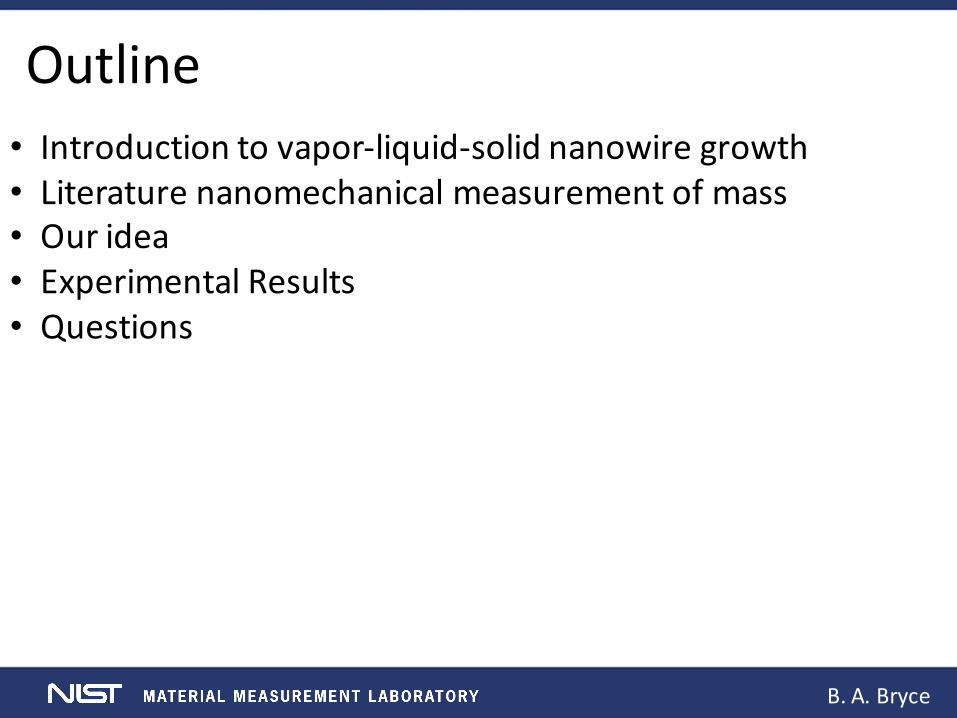
Outline• Introductiontovapor-liquid-solidnanowiregrowth• Literaturenanomechanical measurementofmass• Ouridea• ExperimentalResults• Questions
B.A.Bryce
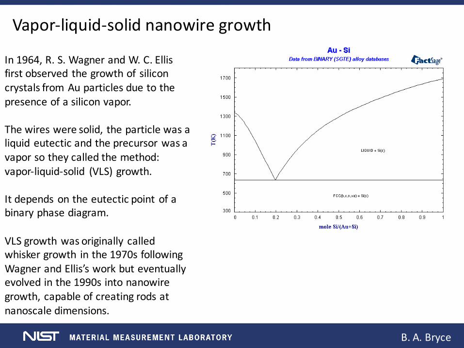
In1964,R.S.WagnerandW.C.Ellisfirstobserved thegrowthof siliconcrystalsfromAuparticlesduetothepresenceofasiliconvapor.
Thewiresweresolid, theparticlewasaliquideutecticandtheprecursorwasavaporsotheycalledthemethod:vapor-liquid-solid (VLS)growth.
Itdependsontheeutecticpointofabinaryphasediagram.
VLSgrowthwasoriginallycalledwhiskergrowth inthe1970sfollowingWagnerandEllis’sworkbuteventuallyevolvedinthe1990sintonanowiregrowth,capableofcreatingrodsatnanoscaledimensions.
Vapor-liquid-solidnanowiregrowth

B.A.Bryce
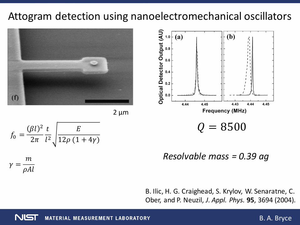
Attogram detectionusingnanoelectromechanicaloscillators
B.Ilic,H.G.Craighead,S.Krylov,W.Senaratne,C.Ober,andP.Neuzil,J.Appl.Phys.95,3694(2004).
𝑓" =𝛽𝑙 &
2𝜋𝑡𝑙&
𝐸12𝜌(1 + 4𝛾)
�
𝛾 =𝑚𝜌𝐴𝑙
Resolvablemass=0.39ag
B.A.Bryce
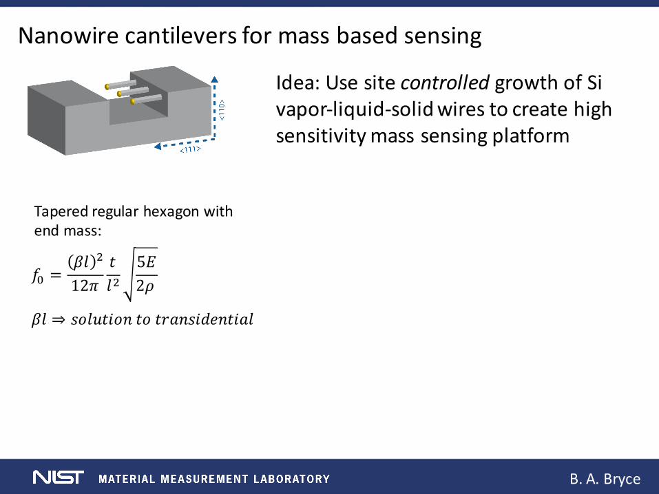
Nanowirecantileversformassbasedsensing
Idea:Usesitecontrolled growthofSivapor-liquid-solidwirestocreatehighsensitivitymasssensingplatform
𝑓" =𝛽𝑙 &
12𝜋𝑡𝑙&
5𝐸2𝜌
�
𝛽𝑙 ⇒ 𝑠𝑜𝑙𝑢𝑡𝑖𝑜𝑛𝑡𝑜𝑡𝑟𝑎𝑛𝑠𝑖𝑑𝑒𝑛𝑡𝑖𝑎𝑙
Taperedregularhexagonwithendmass:

B.A.Bryce
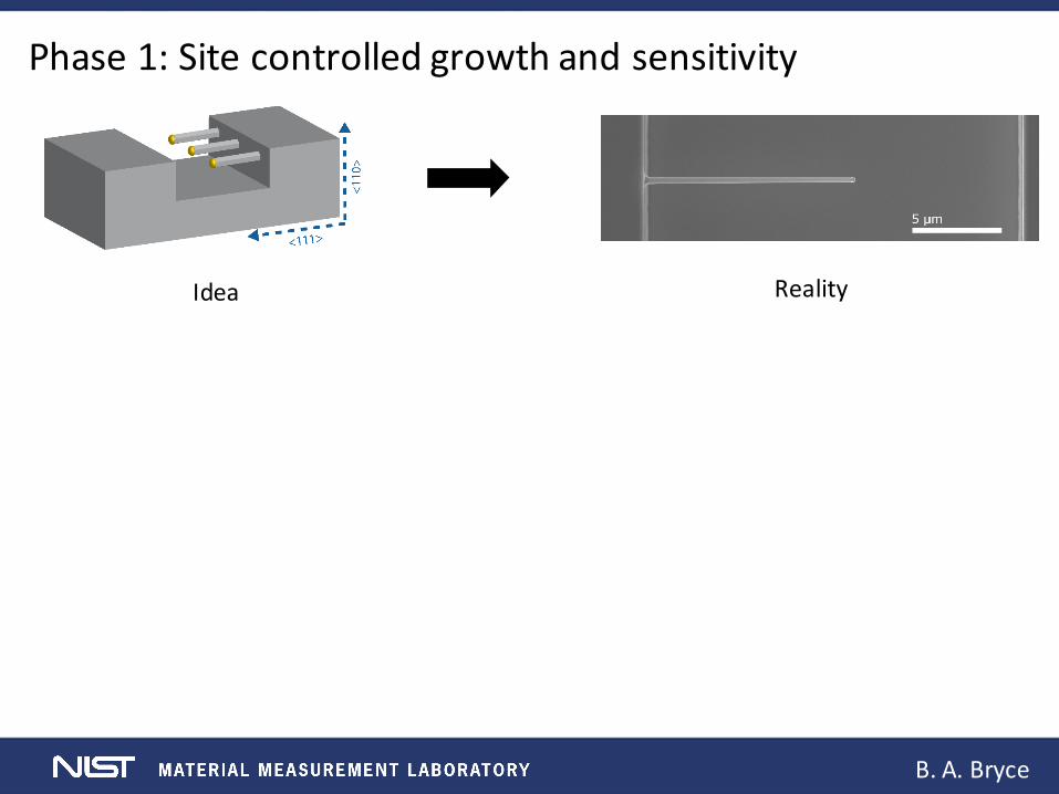
Phase1:Sitecontrolledgrowthandsensitivity
Idea Reality
𝑄 > 13000
Estimatedresolvablemass=0.07-0.14ag
𝜎F = 0.5 − 1𝐻𝑧

B.A.Bryce
Questions?

B.A.Bryce
SiliconnanowiremasssensorsBrianA.Bryce,JasonJ.Gorman,SergiyKrylyuk,andAlbertDavydov
20µm
Idea Reality
Betterthan0.14attogramsensitivity
(0.00000000000000000014 g)
B.A.Bryce
Attogram detectionusingnanoelectromechanicaloscillators
B.Ilic,H.G.Craighead,S.Krylov,W.Senaratne,C.Ober,andP.Neuzil,J.Appl.Phys.95,3694(2004).
2µm
𝑓" =𝛽𝑙 &
2𝜋𝑡𝑙&
𝐸12𝜌(1 + 4𝛾)
�
𝛾 =𝑚𝜌𝐴𝑙
𝑄 = 8500
Resolvablemass=0.39ag

B.A.Bryce
Measurementprinciple- Fabry–Pérot interferometer
𝑑LFF
𝑎 = 𝛼N cos 𝜔𝑡
𝑏 = 𝛼&cos(𝜔𝑡 +4𝜋𝑑LFF𝜆 )
Cantilever
Substrate

B.A.Bryce
Nanowirecantileversformassbasedsensing
Idea:Usesitecontrolled growthofSivapor-liquid-solidwirestocreatehighsensitivitymasssensingplatform
Motivation:
• Likelyhigh-Qaswiresaredamagefreeandsinglecrystal
• Auontipcanbefunctionalized andismostsensitivelocationformassloading
• CanbeintegratedwithotherSibasedtechnologytoallowformultiplexing
• Canbescaledtonanoscopic dimensions withoutelectronbeamlithography
• Highly integratedsensor isaninterestingmetrologysystem-on-a-moduleproblem
𝑓" =𝛽𝑙 &
12𝜋𝑡𝑙&
5𝐸2𝜌
�
Goal:OnechipandPCBwithsamemeasurementqualityasentirelabofequipment
𝛽𝑙 ⇒ 𝑠𝑜𝑙𝑢𝑡𝑖𝑜𝑛𝑡𝑜𝑡𝑟𝑎𝑛𝑠𝑖𝑑𝑒𝑛𝑡𝑖𝑎𝑙
Taperedregularhexagonwithendmass:

B.A.Bryce
Phase1:Showsitecontrolledgrowthonsidewallsofhigh-QVLScantilevers,andestimatemasssensitivity
Phase2:Integratephotodetector, andthermaldrivertoallowforpartialmultiplexing
Phase3:Integratelightsourceforfullmultiplexing
Phase4:Integratevacuumpumptocompletehigh resolutionmassdetectionsystem

B.A.Bryce
Phase1:Showsitecontrolledgrowthonsidewallsofhigh-QVLScantilevers,andestimatemasssensitivity

B.A.Bryce
4µm
1) Growawirewherewewant
2) Growitinaparticulardirection
3) Growone wire
Controlisneeded

B.A.Bryce
Nanowirereactor
SystemFeatures:q 4-zonefurnace;quartzreactorfor2”wafersq Variablepressure(3mTorr – 760Torr)withN2/H2 carriergasq SiH4 andSiCl4 precursorsq Insitu dopingforn- (PH3)and p- (BCl3)types
Exhaust
I II III IVInlet
SiNWsgrowthconditions:
Tgrowth =500-- 1050Cà 900C
P=10-- 760Torrà 600Torr
Growthrate=0.1-- 10um/min
SiH4v Sis400-650C
10-600 torr
SiCl4v Sis900C
B.A.Bryce
Phase1:Sitecontrolledgrowthandsensitivity
Idea Reality

B.A.Bryce
Theinstrument(Phase1)He
NeLaser
Polarizer Polarizer
BS
BS
LED
Köhler
illum
inatior
Objective Dichroicmirror
TubeLens CameraPhotodiode
He/Arinlet
Todrypump
VacuumChamber
OnXYZstage
ToElectronics

B.A.Bryce
Theinstrument(Phase1)
Photodetector TransimpedanceAmplifier
Piezo
NetworkAnalyzer

B.A.Bryce
Phase1:Sitecontrolledgrowthandsensitivity
Idea Reality
𝑄 > 13000
Estimatedresolvablemass=0.07-0.14ag
𝜎F = 0.5 − 1𝐻𝑧
B.A.Bryce
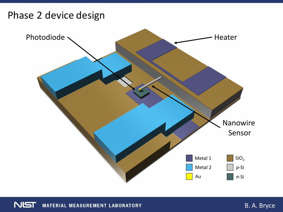
Phase2devicedesign
HeaterPhotodiode
NanowireSensor
Metal1
Metal2
Au
p-Si
n-Si
SiO2

B.A.Bryce
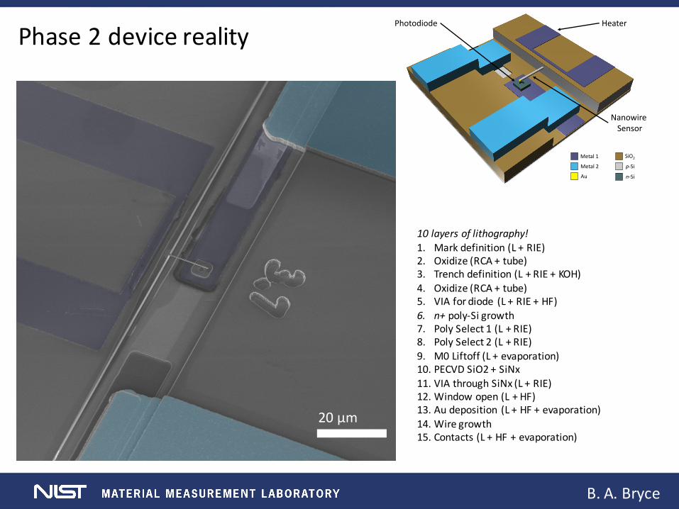
Phase2devicerealityHeaterPhotodiode
NanowireSensor
Metal1
Metal2
Au
p-Si
n-Si
SiO2
10layersoflithography!1. Markdefinition(L+RIE)2. Oxidize(RCA+tube)3. Trenchdefinition(L+RIE+KOH)4. Oxidize(RCA+tube)5. VIAfordiode (L+RIE+HF)6. n+ poly-Sigrowth7. PolySelect1(L+RIE)8. PolySelect2(L+RIE)9. M0Liftoff(L+evaporation)10. PECVDSiO2+SiNx11. VIAthroughSiNx (L+RIE)12. Windowopen(L+HF)13. Audeposition (L+HF+evaporation)14. Wiregrowth15. Contacts(L+HF+evaporation)
20µm

B.A.Bryce
20µm
Useyourtitleslideeffectively:• Coremessage• Getpeopletowanttolisten

B.A.Bryce
Brian A. Bryce, Jason J. Gorman, Sergiy Krylyuk, and Albert Davydov
Silicon nanowire mass sensors

B.A.Bryce
SiliconnanowiremasssensorsBrianA.Bryce,JasonJ.Gorman,SergiyKrylyuk,andAlbertDavydov
20µm
Idea Reality
Betterthan0.14attogramsensitivity
(0.00000000000000000014 g)

B.A.Bryce
20µm
Outlineswastetime*
*Exceptionfortalkslongerthan1hourorsuperformalsettings

B.A.Bryce
Outline• Introductiontovapor-liquid-solidnanowiregrowth• Literaturenanomechanical measurementofmass• Ouridea• ExperimentalResults• Questions
B.A.Bryce
20µm
Keeptexttominimum
Textheavyslidesaregenerallybad

B.A.Bryce
In1964,R.S.WagnerandW.C.Ellisfirstobserved thegrowthof siliconcrystalsfromAuparticlesduetothepresenceofasiliconvapor.
Thewiresweresolid, theparticlewasaliquideutecticandtheprecursorwasavaporsotheycalledthemethod:vapor-liquid-solid (VLS)growth.
Itdependsontheeutecticpointofabinaryphasediagram.
VLSgrowthwasoriginallycalledwhiskergrowth inthe1970sfollowingWagnerandEllis’sworkbuteventuallyevolvedinthe1990sintonanowiregrowth,capableofcreatingrodsatnanoscaledimensions.
Vapor-liquid-solidnanowiregrowth

B.A.Bryce
20µm
LabelthingsclearlyMakefontslargeenoughtoread

B.A.Bryce
Attogram detectionusingnanoelectromechanicaloscillators
B.Ilic,H.G.Craighead,S.Krylov,W.Senaratne,C.Ober,andP.Neuzil,J.Appl.Phys.95,3694(2004).
Resolvablemass=0.39agNoscale
Toosmall

B.A.Bryce
Attogram detectionusingnanoelectromechanicaloscillators
B.Ilic,H.G.Craighead,S.Krylov,W.Senaratne,C.Ober,andP.Neuzil,J.Appl.Phys.95,3694(2004).
2µm
𝑓" =𝛽𝑙 &
2𝜋𝑡𝑙&
𝐸12𝜌(1 + 4𝛾)
�
𝛾 =𝑚𝜌𝐴𝑙
𝑄 = 8500
Resolvablemass=0.39ag

B.A.Bryce
20µm
Clearlyexplainwhyyouhavemadedesignchoices

B.A.Bryce
Nanowirecantileversformassbasedsensing
Idea:Usesitecontrolled growthofSivapor-liquid-solidwirestocreatehighsensitivitymasssensingplatform
𝑓" =𝛽𝑙 &
12𝜋𝑡𝑙&
5𝐸2𝜌
�
𝛽𝑙 ⇒ 𝑠𝑜𝑙𝑢𝑡𝑖𝑜𝑛𝑡𝑜𝑡𝑟𝑎𝑛𝑠𝑖𝑑𝑒𝑛𝑡𝑖𝑎𝑙
Taperedregularhexagonwithendmass:

B.A.Bryce
Nanowirecantileversformassbasedsensing
Idea:Usesitecontrolled growthofSivapor-liquid-solidwirestocreatehighsensitivitymasssensingplatform
Motivation:
• Likelyhigh-Qaswiresaredamagefreeandsinglecrystal
• Auontipcanbefunctionalized andismostsensitivelocationformassloading
• CanbeintegratedwithotherSibasedtechnologytoallowformultiplexing
• Canbescaledtonanoscopic dimensions withoutelectronbeamlithography
• Highly integratedsensor isaninterestingmetrologysystem-on-a-moduleproblem
𝑓" =𝛽𝑙 &
12𝜋𝑡𝑙&
5𝐸2𝜌
�
Goal:OnechipandPCBwithsamemeasurementqualityasentirelabofequipment
𝛽𝑙 ⇒ 𝑠𝑜𝑙𝑢𝑡𝑖𝑜𝑛𝑡𝑜𝑡𝑟𝑎𝑛𝑠𝑖𝑑𝑒𝑛𝑡𝑖𝑎𝑙
Taperedregularhexagonwithendmass:

B.A.Bryce
20µm
Endwiththemessageyouwantremembered orsomethingtomake
peopletalktoyouafter

B.A.Bryce
Questions?
B.A.Bryce
Phase2devicerealityHeaterPhotodiode
NanowireSensor
Metal1
Metal2
Au
p-Si
n-Si
SiO2
10layersoflithography!1. Markdefinition(L+RIE)2. Oxidize(RCA+tube)3. Trenchdefinition(L+RIE+KOH)4. Oxidize(RCA+tube)5. VIAfordiode (L+RIE+HF)6. n+ poly-Sigrowth7. PolySelect1(L+RIE)8. PolySelect2(L+RIE)9. M0Liftoff(L+evaporation)10. PECVDSiO2+SiNx11. VIAthroughSiNx (L+RIE)12. Windowopen(L+HF)13. Audeposition (L+HF+evaporation)14. Wiregrowth15. Contacts(L+HF+evaporation)
20µm

B.A.Bryce
20µm
Generaladvice:• Youcanexpectyouraudiencetoretain
2-3thingsina15minutetalk• Knowyouraudience:whatinterests
them,whatdotheyknow,whatdotheynotknow
Related Documents