Silicon heterojunction solar cells : reduction of parasitic absorption Citation for published version (APA): Gatz, H. A. (2016). Silicon heterojunction solar cells : reduction of parasitic absorption. Technische Universiteit Eindhoven. Document status and date: Published: 07/12/2016 Document Version: Publisher’s PDF, also known as Version of Record (includes final page, issue and volume numbers) Please check the document version of this publication: • A submitted manuscript is the version of the article upon submission and before peer-review. There can be important differences between the submitted version and the official published version of record. People interested in the research are advised to contact the author for the final version of the publication, or visit the DOI to the publisher's website. • The final author version and the galley proof are versions of the publication after peer review. • The final published version features the final layout of the paper including the volume, issue and page numbers. Link to publication General rights Copyright and moral rights for the publications made accessible in the public portal are retained by the authors and/or other copyright owners and it is a condition of accessing publications that users recognise and abide by the legal requirements associated with these rights. • Users may download and print one copy of any publication from the public portal for the purpose of private study or research. • You may not further distribute the material or use it for any profit-making activity or commercial gain • You may freely distribute the URL identifying the publication in the public portal. If the publication is distributed under the terms of Article 25fa of the Dutch Copyright Act, indicated by the “Taverne” license above, please follow below link for the End User Agreement: www.tue.nl/taverne Take down policy If you believe that this document breaches copyright please contact us at: [email protected] providing details and we will investigate your claim. Download date: 03. Jul. 2022

Welcome message from author
This document is posted to help you gain knowledge. Please leave a comment to let me know what you think about it! Share it to your friends and learn new things together.
Transcript
Silicon heterojunction solar cells : reduction of parasiticabsorptionCitation for published version (APA):Gatz, H. A. (2016). Silicon heterojunction solar cells : reduction of parasitic absorption. Technische UniversiteitEindhoven.
Document status and date:Published: 07/12/2016
Document Version:Publisher’s PDF, also known as Version of Record (includes final page, issue and volume numbers)
Please check the document version of this publication:
• A submitted manuscript is the version of the article upon submission and before peer-review. There can beimportant differences between the submitted version and the official published version of record. Peopleinterested in the research are advised to contact the author for the final version of the publication, or visit theDOI to the publisher's website.• The final author version and the galley proof are versions of the publication after peer review.• The final published version features the final layout of the paper including the volume, issue and pagenumbers.Link to publication
General rightsCopyright and moral rights for the publications made accessible in the public portal are retained by the authors and/or other copyright ownersand it is a condition of accessing publications that users recognise and abide by the legal requirements associated with these rights.
• Users may download and print one copy of any publication from the public portal for the purpose of private study or research. • You may not further distribute the material or use it for any profit-making activity or commercial gain • You may freely distribute the URL identifying the publication in the public portal.
If the publication is distributed under the terms of Article 25fa of the Dutch Copyright Act, indicated by the “Taverne” license above, pleasefollow below link for the End User Agreement:www.tue.nl/taverne
Take down policyIf you believe that this document breaches copyright please contact us at:[email protected] details and we will investigate your claim.
Download date: 03. Jul. 2022
Silicon Heterojunction Solar Cells:
Reduction of parasitic absorption
Henriette A. Gatz

Silicon Heterojunction Solar Cells:
Reduction of parasitic absorption
PROEFSCHRIFT
ter verkrijging van de graad van doctor aan deTechnische Universiteit Eindhoven, op gezag van derector magnificus prof.dr.ir. F.P.T. Baaijens, voor een
commissie aangewezen door het College voorPromoties, in het openbaar te verdedigen
op woensdag 7 december 2016 om 16.00 uur
door
Henriette Andrea Gatz
geboren te Bielefeld, Duitsland
Dit proefschrift is goedgekeurd door de promotoren en de samenstelling vande promotiecomissie is als volgt:
voorzitter: prof.dr.ir. G.M.W. Kroesen1e promotor: prof.dr.ir. W.M.M. Kesselscopromotor: . prof.dr. J.K. Rath. (Indian Institute of Technology Madras)leden: prof.dr.ir. A.H.M. Smets (TUD). Prof.Dr. R. Schlatmann. (Hochschule für Technik und Wirtschaft Berlin). prof.dr.ir. M.C.M. van de Sanden. prof.dr.ir. G.P.J. Verbong
Het onderzoek dat in dit proefschrift wordt beschreven is uitgevoerd inovereenstemming met de TU/e Gedragscode Wetenschapsbeoefening.
.
This research is supported by the Dutch Technology Foundation STW, whichis part of the Netherlands Organisation for Scientific Research (NWO), andwhich is partly funded by the Ministry of Economic Affairs (FLASH Perspec-tief project 2.2: Novel multifunctional antireflecting, transparent, and conduc-tive emitters for heterojunction cells; STW project number 12169).
Copyright © 2016 Henriette A. Gatz, Eindhoven University of Technology
All rights reserved. No part of this publication may be reproduced in anyform, by print or photo print, microfilm or any other means, without writtenpermission by the author.
A catalogue record is available from the Eindhoven University of TechnologyLibrary, ISBN: 978-90-386-4190-4

v
Contents
1 Introduction 11.1 General introduction . . . . . . . . . . . . . . . . . . . . . . . . . . . 11.2 Aim and outline of this thesis . . . . . . . . . . . . . . . . . . . . . 2
2 Literature review 52.1 Basic working principles of solar cells . . . . . . . . . . . . . . . . 62.2 Silicon heterojunction solar cells . . . . . . . . . . . . . . . . . . . . 92.3 Recombination losses in silicon heterojunction solar cells . . . . 13
2.3.1 Bulk recombination . . . . . . . . . . . . . . . . . . . . . . . 13Radiative recombination . . . . . . . . . . . . . . . . . . . . 14Auger recombination . . . . . . . . . . . . . . . . . . . . . . 15Shockley-Read-Hall recombination . . . . . . . . . . . . . 15
2.3.2 Surface recombination . . . . . . . . . . . . . . . . . . . . . 16Surface passivation . . . . . . . . . . . . . . . . . . . . . . . 16
2.4 Parasitic absorption . . . . . . . . . . . . . . . . . . . . . . . . . . . 182.5 The emitter layer . . . . . . . . . . . . . . . . . . . . . . . . . . . . . 19
2.5.1 Nanocrystalline silicon oxide . . . . . . . . . . . . . . . . . 20Growth evolution . . . . . . . . . . . . . . . . . . . . . . . . 20Doping . . . . . . . . . . . . . . . . . . . . . . . . . . . . . . . 21Material preparation - plasma enhanced CVD . . . . . . 22Growth models . . . . . . . . . . . . . . . . . . . . . . . . . 23Material properties . . . . . . . . . . . . . . . . . . . . . . . 26Applications . . . . . . . . . . . . . . . . . . . . . . . . . . . 27
2.6 The transparent conductive oxide layer . . . . . . . . . . . . . . . 272.6.1 Degenerated semiconductor . . . . . . . . . . . . . . . . . 282.6.2 Scattering processes in transparent conductive
oxides . . . . . . . . . . . . . . . . . . . . . . . . . . . . . . . 292.6.3 Zinc oxide . . . . . . . . . . . . . . . . . . . . . . . . . . . . . 31
Carrier transport - comparison of ZnO and ITO . . . . . 32ZnO/emitter interface . . . . . . . . . . . . . . . . . . . . . 33Material preparation - atomic layer deposition . . . . . . 35
3 Experimental techniques and concepts 393.1 Device design . . . . . . . . . . . . . . . . . . . . . . . . . . . . . . . 40
3.1.1 Samples for material characterization . . . . . . . . . . . . 403.1.2 Passivation samples . . . . . . . . . . . . . . . . . . . . . . . 413.1.3 Solar cells . . . . . . . . . . . . . . . . . . . . . . . . . . . . . 41
3.2 Material preparation . . . . . . . . . . . . . . . . . . . . . . . . . . . 433.2.1 HF dip . . . . . . . . . . . . . . . . . . . . . . . . . . . . . . . 433.2.2 Plasma-enhanced chemical vapour deposition . . . . . . 443.2.3 Hot wire chemical vapour deposition . . . . . . . . . . . . 463.2.4 Atomic layer deposition . . . . . . . . . . . . . . . . . . . . 473.2.5 Radio frequency magnetron sputtering . . . . . . . . . . . 493.2.6 Thermal evaporation . . . . . . . . . . . . . . . . . . . . . . 50
3.3 Material characterization . . . . . . . . . . . . . . . . . . . . . . . . 503.3.1 Reflection and transmission . . . . . . . . . . . . . . . . . . 50
RT-mini setup . . . . . . . . . . . . . . . . . . . . . . . . . . 51UV-Vis-NIR spectrometer . . . . . . . . . . . . . . . . . . . 51
3.3.2 Spectroscopic ellipsometry . . . . . . . . . . . . . . . . . . 513.3.3 Activation energy . . . . . . . . . . . . . . . . . . . . . . . . 533.3.4 Four point probe . . . . . . . . . . . . . . . . . . . . . . . . . 543.3.5 Transmission electron microscopy . . . . . . . . . . . . . . 543.3.6 Raman spectroscopy . . . . . . . . . . . . . . . . . . . . . . 55
3.4 Device characterization . . . . . . . . . . . . . . . . . . . . . . . . . 573.4.1 Lifetime tester . . . . . . . . . . . . . . . . . . . . . . . . . . 57
Quasi transient mode . . . . . . . . . . . . . . . . . . . . . . 58Generalized mode . . . . . . . . . . . . . . . . . . . . . . . . 58Implied open circuit voltage . . . . . . . . . . . . . . . . . 59
3.4.2 Solar simulator . . . . . . . . . . . . . . . . . . . . . . . . . . 593.4.3 Spectral response setup . . . . . . . . . . . . . . . . . . . . 61
4 nc-SiOx:H(p) emitter layer for increased transmission 634.1 Introduction . . . . . . . . . . . . . . . . . . . . . . . . . . . . . . . . 644.2 Experimental details . . . . . . . . . . . . . . . . . . . . . . . . . . . 654.3 Results and discussion . . . . . . . . . . . . . . . . . . . . . . . . . . 684.4 Conclusions . . . . . . . . . . . . . . . . . . . . . . . . . . . . . . . . 77
5 Heat-withstanding surface passivation in combination with nc-SiOx:H(p)emitter layer 795.1 Introduction . . . . . . . . . . . . . . . . . . . . . . . . . . . . . . . . 805.2 Experimental details . . . . . . . . . . . . . . . . . . . . . . . . . . . 805.3 Results and discussion . . . . . . . . . . . . . . . . . . . . . . . . . . 84
5.3.1 Annealing of the layer stacks . . . . . . . . . . . . . . . . . 84
Low initial lifetime . . . . . . . . . . . . . . . . . . . . . . . 84Theory on annealing of a-Si:H i/p-stacks . . . . . . . . . 86Annealing behaviour of a-Si:H(i)/nc-SiOx:H(p) passiva-
tion stacks . . . . . . . . . . . . . . . . . . . . . . . 875.3.2 Influence of the i-layer buffer thickness . . . . . . . . . . . 885.3.3 Optical and electrical properties . . . . . . . . . . . . . . . 90
5.4 Conclusion . . . . . . . . . . . . . . . . . . . . . . . . . . . . . . . . . 91
6 ZnO:B front TCO in combination with nc-SiOx:H(p) emitter layer forincreased JSC in SHJ solar cells 936.1 Introduction . . . . . . . . . . . . . . . . . . . . . . . . . . . . . . . . 946.2 Experiment . . . . . . . . . . . . . . . . . . . . . . . . . . . . . . . . . 956.3 Results and discussion . . . . . . . . . . . . . . . . . . . . . . . . . . 986.4 Conclusion . . . . . . . . . . . . . . . . . . . . . . . . . . . . . . . . . 109
Bibliography 111
Summary 131
Conclusions 135
List of publications 137
Acknowledgements 139
Curriculum Vitae 141


1
Chapter 1
Introduction
1.1 General introduction
The world energy demand has been steadily increasing over the last decadesand is still growing rapidly. According to the INDC Scenario (based on the“Intended Nationally Determined Contributions” submitted by each countrythemselves), it already raised from around 11 million tons of oil equivalent(with 1 ton oil equivalent being equal to the energy released when burning1 ton of crude oil) in the year 2000 to around 13 million tons of oil equivalentin 2013 and will continue to around 16 million tons of oil equivalent in 2030[1]. This is caused by several aspects. Firstly, the world population is rapidlyincreasing. In 2015 it was estimated to be 7.3 billion people, until 2050 it isexpected to rise up to 9.7 billion people and in the year 2100 it might evenreach 11.2 billion people [2]. Moreover, growing industrialization in countrieswith a fast developing economy, such as India and China, has an impact. Atthe moment, a large fraction of the required energy is obtained from combus-tion of fossil energy sources, such as coal and oil. This comes with problemsof availability of resources, as well as environmental pollution. For example,the unabated combustion of oil and coal in power plants, vehicles, and in-dustrial facilities is expected to be linked to about 3 million premature deathsper year [3]. In order to sustain the earth environment, solutions for the in-creasing world energy demand have to be found. An increase of the efficiencyof energy conversion devices as well as an increased contribution of environ-mentally friendly energy sources and enhanced energy storage techniques areneeded.
In order to provide environmentally friendly energy numerous sourcescan be used, such as wind power, geothermal energy, hydro power, and solarpower. The sun is the largest readily available energy source for earth. Itsenergy can be harvested in several ways. A solar thermal collector can absorbthe sun light and use its energy to heat a transmission medium. A heated
2 Chapter 1. Introduction
fluid can then be used to power a turbine that generates electric current. Fordomestic use, the thermal energy can simply be used to heat water. With aphotovoltaic (PV) solar cell the radiative energy of the sun can be utilized togenerate electric current and thus electric energy. This energy can then eitherdirectly be used to power an electric device, it can be fed into the grid andthus being transported to different locations where it is consumed or it can bestored in batteries for use at later times. The utilisation of the radiation of thesun with solar cells comes with several advantages. No greenhouse gases orother environmental pollutions take place during electricity generation fromphotovoltaic devices. Unlike e.g. in the case of wind turbines, the electricitygeneration takes place quietly without disturbing animals or humans in itsdirect vicinity. Moreover, in remote off-grid regions solar cells often are oneof the easiest solutions in providing energy for local inhabitants.
Many different kinds of solar cells exist, exploiting different materials aswell as different concepts. Amongst them, silicon based solar cells stand outdue to the abundance and non-toxicity of silicon. Silicon heterojunction (SHJ)solar cells in particular combine high energy conversion efficiencies with thepotential of low production costs [4] [5]. However, in order to further promotethe use of solar cells, the improvement of SHJ solar cells has to be continued.
1.2 Aim and outline of this thesis
The main focus of the research described in this thesis lies in increasing theamount of light that can contribute to the electrical current generated by aSHJ solar cell. To this end, more transparent materials are utilized at thefront side of the SHJ solar cell. Thus, the short circuit current density, JSC,is enhanced and with it the solar cells’ efficiency. To achieve this, we inves-tigate the suitability of two alternative materials for implementation at theSHJ solar cell front side. These are boron-doped nanocrystalline silicon oxide(nc-SiOx:H(p)) to replace the common amorphous silicon emitter layer andboron-doped zinc oxide (ZnO:B) to replace the commonly used tin-doped in-dium oxide (ITO) as transparent conductive oxide (TCO) layer. After an opti-mization of the materials, SHJ solar cells with nc-SiOx:H(p) emitter layer andZnO:B front TCO have been realized and tested.
This work has been supported by the Dutch technology foundation “Sticht-ing voor de Technische Wetenschappen” (STW) as part of the “Perspectief pro-gram” “Fundamentals and Application of Silicon Heterojunction solar cells”(FLASH). STW facilitates knowledge transfer between technical science and
1.2. Aim and outline of this thesis 3
potential users such as e.g. industrial partners. To this end, contact betweenscientists and users is fostered. The FLASH program aims to reduce the pro-duction costs of SHJ solar cell by focusing on the following aspects [6]:
• Reducing material consumption
• Omitting the use of scarce materials
• Exploiting low-cost production processes, e.g. by using low-temperaturemethods to achieve a low thermal budget
• Improving the solar cells efficiency
In order to achieve this goal, primarily smart defect engineering and thedevelopment of new SHJ solar cell structures are investigated in the FLASHproject. Participating research institutes of this five year program are DelftUniversity of Technology, Eindhoven University of Technology, Radboud Uni-versity Nijmegen, and Utrecht University. The user committee consists ofECN Solar Energy, Hanwha Q-Cells, Meyer Burger Netherlands B.V.,OM&T B.V.|Moser Baer Technologies Europe, Oxford Instruments PlasmaTechnology, Roth & Rau B.V., and Tempress Systems B.V.. The particular re-search described in this thesis contributes to the FLASH projects objective toincrease the solar cells efficiency. Moreover, by replacing ITO, which containsthe not abundant material indium, we contribute to the projects goal of omit-ting the use of scarce materials. The research described in this thesis has beencarried out at Eindhoven University of Technology and Utrecht University.As part of Solliance, characterization facilities of the Energy research Centreof the Netherlands (ECN) have additionally been used.
This thesis is structured in six chapters. In Chapter 2, a detailed introduc-tion into the research field is given. The relevant theoretical background ispresented in order to give the reader a thorough understanding of the sub-ject. In Chapter 3 the experimental methods and concepts used to fabricateand analyse the samples utilized in the subsequent chapters are described.Chapter 4 focusses on the optimization of the nc-SiOx:H(p) material for im-plementation as emitter layer in SHJ solar cells. An optimized material withthe desired refractive index, a favourable large optical band gap, and a suit-able conductivity has been achieved. The decrease in optical absorption of thedeveloped layer stack of a-Si:H(i)/nc-SiOx:H(p) as compared to conventionala-Si:H(i)/a-Si:H(p) front side layer stacks of SHJ solar cells has been observed.Thereafter, an investigation of the effects of an implementation of the de-veloped nc-SiOx:H(p) emitter layer on the passivation properties on the c-Siwafer surface is given in Chapter 5. Outstanding thermal resistance, leading

4 Chapter 1. Introduction
to an improvement of passivation properties of a-Si:H(i)/nc-SiOx:H(p) layerstacks on c-Si wafer upon annealing to temperatures as high as 293°C, havebeen observed. In Chapter 6 the evaluation of the suitability of ZnO:B asfront TCO layer is given. The material is prepared by atomic layer depo-sition (ALD) using the novel boron precursor triisopropyl borate (TIB). Thenc-SiOx:H(p) layer and the ZnO:B material have successfully been implemen-ted in SHJ solar cells with remarkable JSC values. Moreover, indium freeSHJ solar cells have been realized by additional implementation of ZnO:Al asback-side TCO.
5
Chapter 2
Literature review
In this chapter a comprehensive review including theoretical background ofthe research carried out within the scope of this thesis is presented. Firstly,a general introduction into the physics of solar cells is given. Thereafter, thespecific features of silicon heterojunction (SHJ) solar cells are described. Thereason for their outstanding open circuit voltage V OC and thus their recordefficiency η is elucidated. The importance of a transparent front side of thecells, in order to enhance the short circuit current density JSC (and thus η) ofbifacially contacted SHJ solar cells, is elaborated.
The work described in this thesis aims for the reduction of parasitic ab-sorption in SHJ solar cells, in order to increase their JSC, by implementinga stack of hydrogenated nanocrystalline silicon oxide (nc-SiOx:H) and borondoped zinc oxide (ZnO:B). Therefore, one of the focuses of this chapter lies inthe description of these two materials. The multi-phase material structure ofnc-SiOx:H and its growth evolution is discussed. The possibility to influencethe material properties during the deposition process is explained. The func-tion of transparent conductive oxides in general and specific aspects regard-ing (doped) ZnO in particular are explained. A comparison with ITO is madeand work function differences as well as the properties of the TCO/emitterinterface are discussed. With this, the background of the research describedin this thesis is given.
6 Chapter 2. Literature review
2.1 Basic working principles of solar cells
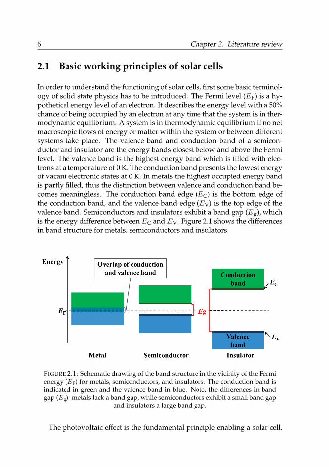
In order to understand the functioning of solar cells, first some basic terminol-ogy of solid state physics has to be introduced. The Fermi level (EF) is a hy-pothetical energy level of an electron. It describes the energy level with a 50%chance of being occupied by an electron at any time that the system is in ther-modynamic equilibrium. A system is in thermodynamic equilibrium if no netmacroscopic flows of energy or matter within the system or between differentsystems take place. The valence band and conduction band of a semicon-ductor and insulator are the energy bands closest below and above the Fermilevel. The valence band is the highest energy band which is filled with elec-trons at a temperature of 0 K. The conduction band presents the lowest energyof vacant electronic states at 0 K. In metals the highest occupied energy bandis partly filled, thus the distinction between valence and conduction band be-comes meaningless. The conduction band edge (EC) is the bottom edge ofthe conduction band, and the valence band edge (EV) is the top edge of thevalence band. Semiconductors and insulators exhibit a band gap (Eg), whichis the energy difference between EC and EV. Figure 2.1 shows the differencesin band structure for metals, semiconductors and insulators.
FIGURE 2.1: Schematic drawing of the band structure in the vicinity of the Fermienergy (EF) for metals, semiconductors, and insulators. The conduction band isindicated in green and the valence band in blue. Note, the differences in bandgap (Eg): metals lack a band gap, while semiconductors exhibit a small band gap
and insulators a large band gap.
The photovoltaic effect is the fundamental principle enabling a solar cell.
2.1. Basic working principles of solar cells 7
Upon illumination of the surface of a semiconductor or insulator with pho-tons of a high enough energy, electrons located in the material’s valence bandcan absorb this energy, overcome the band gap and become thereby excitedinto the conduction band. Electron vacancies (holes) are left in the valenceband. Without the presence of a built-in electric field, the excited electronswill over time fall back into the valence band and recombine with the holes.Depending on the type of material, different amounts of energy are needed toexcite the electrons. Insulators exhibit a large band gap. Therefore, sunlightis typically not energetic enough to excite the valance band electrons into theconduction band. This makes them not usable for solar cells. However, forhigher energy photons, e.g. from X-rays, an excitement of the electrons of in-sulators is possible. Semiconductors however, show excellent properties forthe use in solar cells. They exhibit a small band gap which makes it possiblefor sunlight to excite electrons to overcome this band gap.
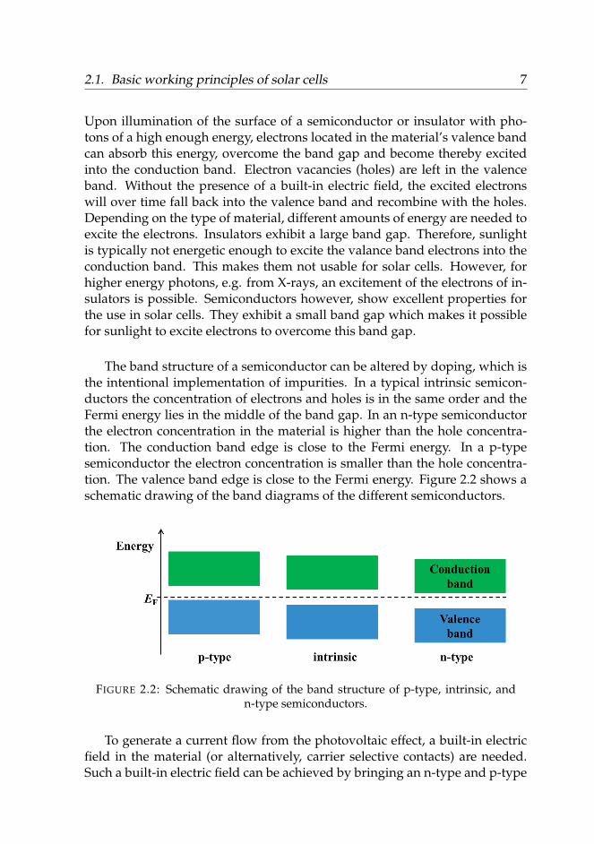
The band structure of a semiconductor can be altered by doping, which isthe intentional implementation of impurities. In a typical intrinsic semicon-ductors the concentration of electrons and holes is in the same order and theFermi energy lies in the middle of the band gap. In an n-type semiconductorthe electron concentration in the material is higher than the hole concentra-tion. The conduction band edge is close to the Fermi energy. In a p-typesemiconductor the electron concentration is smaller than the hole concentra-tion. The valence band edge is close to the Fermi energy. Figure 2.2 shows aschematic drawing of the band diagrams of the different semiconductors.
FIGURE 2.2: Schematic drawing of the band structure of p-type, intrinsic, andn-type semiconductors.
To generate a current flow from the photovoltaic effect, a built-in electricfield in the material (or alternatively, carrier selective contacts) are needed.Such a built-in electric field can be achieved by bringing an n-type and p-type
8 Chapter 2. Literature review
doped material in close contact with each other. Due to the gradient of elec-tron density, electrons from the n-type material close to the junction migratetowards the p-type material. There they recombine with holes from the p-typematerial. The lack of electron on the n-type side of the junction and the excessof them on the p-type side of the junctions leads to a built-in electric field. Thisarea of electron depletion on one side and hole depletion (due to the presenceof electrons) on the other side is called depletion region. The electrons andholes diffusing into this depletion region upon excitation are affected by theelectromotive force this region generates and thereby drift in opposite direc-tions. By electrically contacting both materials externally, an electric circuit isestablished and a direct current can be generated.
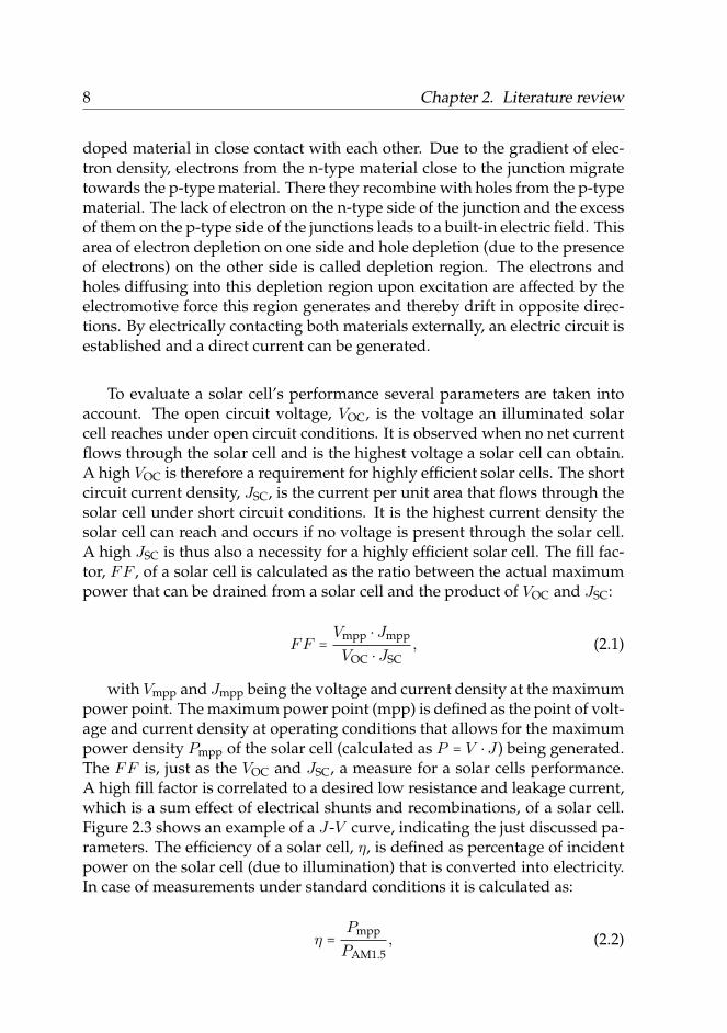
To evaluate a solar cell’s performance several parameters are taken intoaccount. The open circuit voltage, VOC, is the voltage an illuminated solarcell reaches under open circuit conditions. It is observed when no net currentflows through the solar cell and is the highest voltage a solar cell can obtain.A high VOC is therefore a requirement for highly efficient solar cells. The shortcircuit current density, JSC, is the current per unit area that flows through thesolar cell under short circuit conditions. It is the highest current density thesolar cell can reach and occurs if no voltage is present through the solar cell.A high JSC is thus also a necessity for a highly efficient solar cell. The fill fac-tor, FF , of a solar cell is calculated as the ratio between the actual maximumpower that can be drained from a solar cell and the product of VOC and JSC:
FF =Vmpp ⋅ Jmpp
VOC ⋅ JSC, (2.1)
with Vmpp and Jmpp being the voltage and current density at the maximumpower point. The maximum power point (mpp) is defined as the point of volt-age and current density at operating conditions that allows for the maximumpower density Pmpp of the solar cell (calculated as P = V ⋅ J) being generated.The FF is, just as the VOC and JSC, a measure for a solar cells performance.A high fill factor is correlated to a desired low resistance and leakage current,which is a sum effect of electrical shunts and recombinations, of a solar cell.Figure 2.3 shows an example of a J-V curve, indicating the just discussed pa-rameters. The efficiency of a solar cell, η, is defined as percentage of incidentpower on the solar cell (due to illumination) that is converted into electricity.In case of measurements under standard conditions it is calculated as:
η =Pmpp
PAM1.5, (2.2)
2.2. Silicon heterojunction solar cells 9
with PAM1.5 being equivalent to the irradiance of the AM1.5 solar spec-trum.
FIGURE 2.3: Example of an J-V curve of a solar cell indicating the importantparameters to evaluate the solar cell’s performance.
Several different types of solar cells exist, ranging from single junction tomulti junction concepts and exploiting the beneficial behaviour of many dif-ferent materials from organic to inorganic components. However, the photo-voltaics market is by far dominated by crystalline silicon solar cells. Besidesthe abundance of silicon, also the low toxicity of their main components is im-portant [7]. In the following we will focus on the outstanding and promisingsilicon heterojunction solar cells.
2.2 Silicon heterojunction solar cells
Silicon heterojunction (SHJ) solar cells are a very promising candidate forhighly efficient solar cells with fairly low manufacturing costs. Their mainpart consists of a crystalline silicon (c-Si) absorber coated with silicon thinfilms (e.g. amorphous silicon, a-Si:H) on both sides. Thereby, they combinethe advantages of the high efficiency of c-Si solar cells with the potential oflow production costs of thin film solar cells. For conventional SHJ solare cells,their high efficiencies are enabled by the excellent passivation of the c-Si wafersurface and the spatial separation of the recombination-active metal contactsfrom the emitter layer by a transparent conductive oxide (TCO) layer. Bothfactors, additionally to the use of thin wafers, lead to the high VOCs that SHJsolar cells are generally known for [8] [9] [10]. The recent efficiency record for
10 Chapter 2. Literature review
SHJ solar cells of 26.33% (in rear contacted design) exceeds even those of stan-dard crystalline silicon solar cells [11]. This outstanding efficiency is partlyattributed to the rear contacted design of the record SJH solar cells, by whichshading losses are omitted.
Due to their smart design, SHJ solar cells have several advantages overtraditional c-Si solar cells. Their thin film layers can be deposited at temper-atures ≤ 200°C, achieving a good material quality by subsequent annealing(also at temperatures ≤ 200°C). Compared to the process temperatures of dif-fused junction solar cells, which reach up to 900 - 1000°C [12], this leads to aremarkable reduction of the thermal budget during production. Thereby, thecarbon dioxide (CO2) emissions are reduced and the production costs low-ered. Additionally, thinner silicon wafer (< 100 µm) can be used [13], since atlower temperatures less warping effects take place. With reduced wafer thick-ness usually also a reduction of JSC takes place. However, the increase in VOCusually associated with the use of thinner wafers can compensate for this [9][10]. Additionally, the loss of current can be limited by improving the lighttrapping within the solar cell. Another advantage of SHJ solar cells is theirlower temperature coefficient of performance compared to c-Si solar cells [9].This means, the efficiency decrease under increased temperatures is smallerfor SHJ solar cells than for conventional c-Si solar cells. This is a result of theirhigh V OC [14].
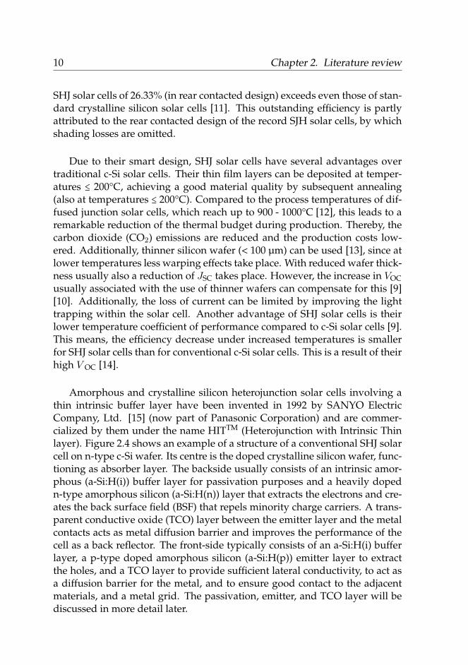
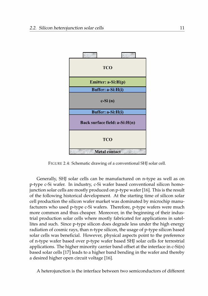
Amorphous and crystalline silicon heterojunction solar cells involving athin intrinsic buffer layer have been invented in 1992 by SANYO ElectricCompany, Ltd. [15] (now part of Panasonic Corporation) and are commer-cialized by them under the name HITTM (Heterojunction with Intrinsic Thinlayer). Figure 2.4 shows an example of a structure of a conventional SHJ solarcell on n-type c-Si wafer. Its centre is the doped crystalline silicon wafer, func-tioning as absorber layer. The backside usually consists of an intrinsic amor-phous (a-Si:H(i)) buffer layer for passivation purposes and a heavily dopedn-type amorphous silicon (a-Si:H(n)) layer that extracts the electrons and cre-ates the back surface field (BSF) that repels minority charge carriers. A trans-parent conductive oxide (TCO) layer between the emitter layer and the metalcontacts acts as metal diffusion barrier and improves the performance of thecell as a back reflector. The front-side typically consists of an a-Si:H(i) bufferlayer, a p-type doped amorphous silicon (a-Si:H(p)) emitter layer to extractthe holes, and a TCO layer to provide sufficient lateral conductivity, to act asa diffusion barrier for the metal, and to ensure good contact to the adjacentmaterials, and a metal grid. The passivation, emitter, and TCO layer will bediscussed in more detail later.
2.2. Silicon heterojunction solar cells 11
FIGURE 2.4: Schematic drawing of a conventional SHJ solar cell.
Generally, SHJ solar cells can be manufactured on n-type as well as onp-type c-Si wafer. In industry, c-Si wafer based conventional silicon homo-junction solar cells are mostly produced on p-type wafer [16]. This is the resultof the following historical development. At the starting time of silicon solarcell production the silicon wafer market was dominated by microchip manu-facturers who used p-type c-Si wafers. Therefore, p-type wafers were muchmore common and thus cheaper. Moreover, in the beginning of their indus-trial production solar cells where mostly fabricated for applications in satel-lites and such. Since p-type silicon does degrade less under the high energyradiation of cosmic rays, than n-type silicon, the usage of p-type silicon basedsolar cells was beneficial. However, physical aspects point to the preferenceof n-type wafer based over p-type wafer based SHJ solar cells for terrestrialapplications. The higher minority carrier band offset at the interface in c-Si(n)based solar cells [17] leads to a higher band bending in the wafer and therebya desired higher open circuit voltage [16].
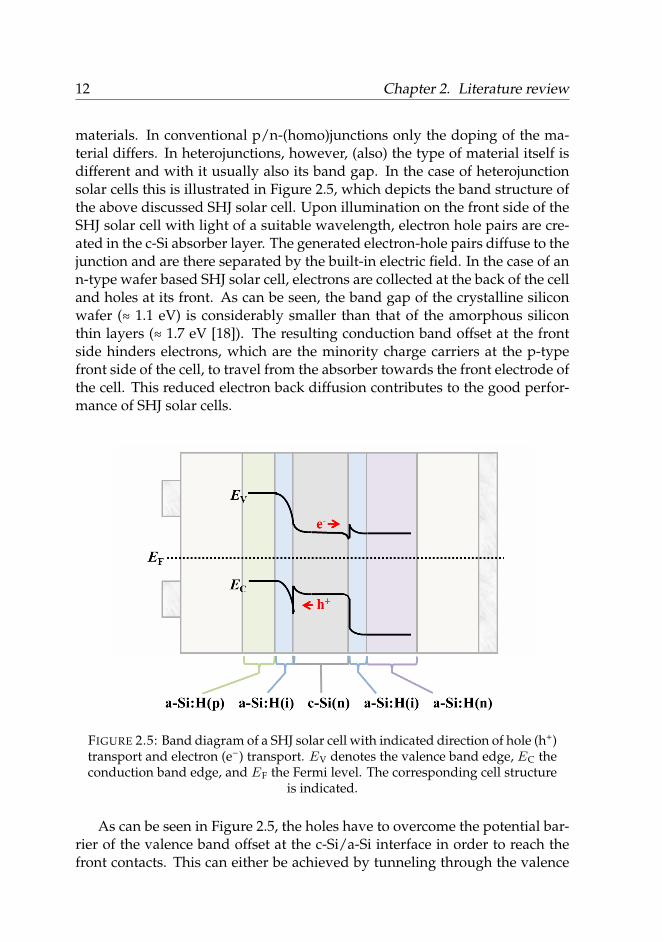
A heterojunction is the interface between two semiconductors of different
12 Chapter 2. Literature review
materials. In conventional p/n-(homo)junctions only the doping of the ma-terial differs. In heterojunctions, however, (also) the type of material itself isdifferent and with it usually also its band gap. In the case of heterojunctionsolar cells this is illustrated in Figure 2.5, which depicts the band structure ofthe above discussed SHJ solar cell. Upon illumination on the front side of theSHJ solar cell with light of a suitable wavelength, electron hole pairs are cre-ated in the c-Si absorber layer. The generated electron-hole pairs diffuse to thejunction and are there separated by the built-in electric field. In the case of ann-type wafer based SHJ solar cell, electrons are collected at the back of the celland holes at its front. As can be seen, the band gap of the crystalline siliconwafer (≈ 1.1 eV) is considerably smaller than that of the amorphous siliconthin layers (≈ 1.7 eV [18]). The resulting conduction band offset at the frontside hinders electrons, which are the minority charge carriers at the p-typefront side of the cell, to travel from the absorber towards the front electrode ofthe cell. This reduced electron back diffusion contributes to the good perfor-mance of SHJ solar cells.
FIGURE 2.5: Band diagram of a SHJ solar cell with indicated direction of hole (h+)transport and electron (e−) transport. EV denotes the valence band edge, EC theconduction band edge, and EF the Fermi level. The corresponding cell structure
is indicated.
As can be seen in Figure 2.5, the holes have to overcome the potential bar-rier of the valence band offset at the c-Si/a-Si interface in order to reach thefront contacts. This can either be achieved by tunneling through the valence
2.3. Recombination losses in silicon heterojunction solar cells 13
band spike, by hopping through the valence band tail states located in thea-Si:H(i) layer or via thermionic emission over the valence band offset [19][20]. During a tunnelling process a particle crosses a potential barrier of fi-nite height although the particle’s potential energy is lower than the barrierheight. This phenomena can not be described with the approaches of clas-sical mechanics, but only with quantum mechanics. Tunnelling of electronsfrom the atomic orbital of one atom to the atomic orbital of another atom isenabled by a finite overlap of these orbitals. During the single step tunnellingprocess electrons can overcome limited distances. The hopping mechanismworks accordingly but involves multiple steps over intermediate locations ina lattice, such that electrons can relocate over greater distances [21]. Duringthermionic emission electrons which possess energies just above the vacuumlevel (due to thermal energy) can overcome a potential barrier. The contri-bution of the different transport mechanisms depends on the barrier height.For a larger valence band offset and thus a higher transport barrier, the con-tribution of hopping and tunnelling increases, while thermionic emission di-minishes. This leads to a decrease of efficiency. Thus, a good band-alignmentat the p-n junction is highly important for the performance of SHJ solar cells[19].
2.3 Recombination losses in silicon heterojunction solarcells
In order to obtain a highly efficient solar cell, a high amount of the incidentlight has to be converted to electron hole pairs within the cell and these chargecarriers need to be collected by the electrodes of the solar cells. Recombinationof electrons and holes reduces the collection of current (thus the JSC) as wellas the forward bias injection current (thus V OC) and is therefore undesired.Several different recombination mechanisms are known and will be discussedin the following.
2.3.1 Bulk recombination
The term bulk recombination refers to recombination taking place in the bulkof a material (as opposed to its surface). During a recombination processan electron from the conduction band annihilates with a hole and therebyreleases part of its energy. Due to the law of conservation of energy, thischange in energy has to be transferred to a partner during the recombination.Depending on the type of recombination process, this partner can be eithera photon, a phonon or another electron or hole. In crystalline silicon one
14 Chapter 2. Literature review
distinguishes between three different types of recombination mechanisms:Radiative recombination (involving a photon as partner), Auger recombina-tion (requiring an additional electron or hole as partner), and Shockley-Read-Hall (SRH) recombination (involving phonons as recombination partners).All these recombination processes are described in great detail in [22]. More-over, midgap recombination can also include the release of a photon. An ex-ample for this is the luminescence of a-Si:H at 0.9 eV due to recombinationthrough midgap states [23].
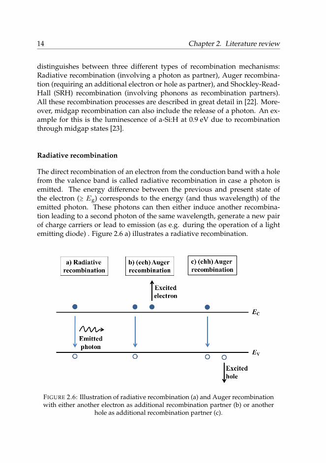
Radiative recombination
The direct recombination of an electron from the conduction band with a holefrom the valence band is called radiative recombination in case a photon isemitted. The energy difference between the previous and present state ofthe electron (≥ Eg) corresponds to the energy (and thus wavelength) of theemitted photon. These photons can then either induce another recombina-tion leading to a second photon of the same wavelength, generate a new pairof charge carriers or lead to emission (as e.g. during the operation of a lightemitting diode) . Figure 2.6 a) illustrates a radiative recombination.
FIGURE 2.6: Illustration of radiative recombination (a) and Auger recombinationwith either another electron as additional recombination partner (b) or another
hole as additional recombination partner (c).

2.3. Recombination losses in silicon heterojunction solar cells 15
Auger recombination
During an Auger recombination an electron from the conduction band recom-bines directly with a hole from the valence band. Other than in the radiativerecombination, the released energy is not transferred to a photon but to an-other electron or hole. This second electron (or hole) is thereby exited to ahigher energy level within the same energy band. This is illustrated in Fi-gure 2.6 b) and c). Mostly, this excited electron (or hole) then relaxes againand transfers the excess energy to phonons. Depending on the nature of thethird partner, the process is either called “eeh” (electron, electron, hole) or“ehh” (electron, hole, hole).
Shockley-Read-Hall recombination
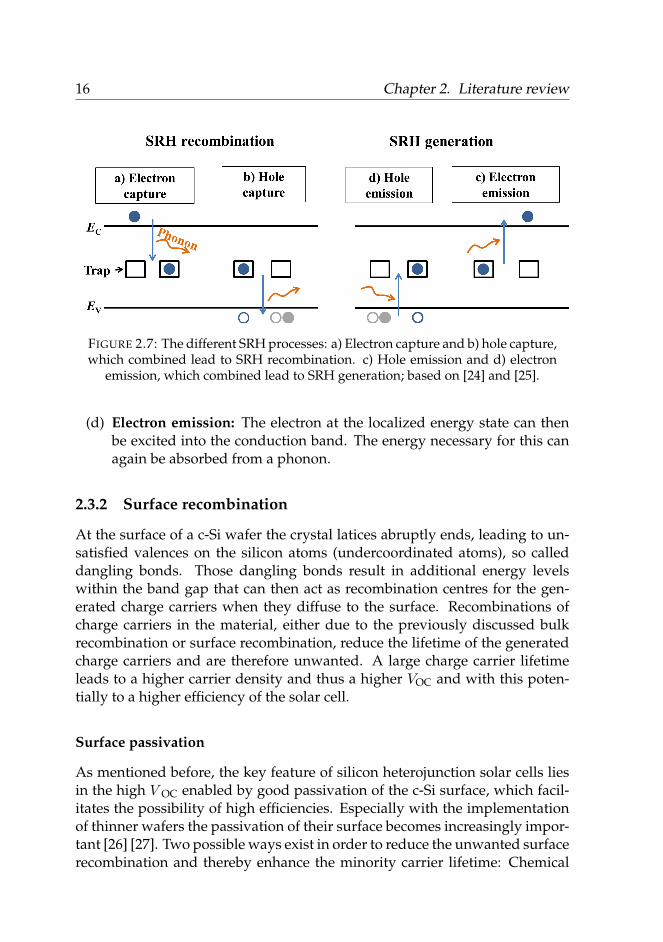
When an electron from the conduction band and a hole from the valence bandrecombine while involving a localized energy state in the band gap this iscalled Shockley-Read-Hall (SRH) recombination. The localized energy statesenabling SRH recombinations are created due to impurities such as dopantatoms or defects in the lattice. Such defects could be e.g. a missing host atomor a misplaced or interstitial located host atom. An interstitial site is an openspace that can be occupied but lies between the regular positions within theclose packed array of atoms. These localized energy states act as so calledrecombination centres or traps. Therefore, SRH recombination is also calledtrap-assisted recombination. Additional to SRH recombination, also a SRHgeneration is possible, resulting in the generation of an electron hole pair. Thedifferent process steps are illustrated in Figure 2.7:
(a) Electron capture: The electron falls back from the conduction band toa localized energy level within the band gap. The energy difference isnot released in form of a photon, but as lattice vibrations, which meansa phonon exchanges thermal energy with the surrounding material.
(b) Hole capture: From this localized energy state, the electron then furtherdecreases its energy by falling back into the valence band and recombin-ing with a hole. The energy difference is again released via a phonon.
(c) Hole emission: A hole can be excited from a localized energy state intothe valence band by absorbing a phonon. This results in a hole in theconduction band and an electron in the localized energy state. This pro-cess is the inverse of the hole capture process. An easier way to pictureit is an electron from the valence band getting excited into the localizedenergy state, leaving a hole in the valence band.
16 Chapter 2. Literature review
FIGURE 2.7: The different SRH processes: a) Electron capture and b) hole capture,which combined lead to SRH recombination. c) Hole emission and d) electron
emission, which combined lead to SRH generation; based on [24] and [25].
(d) Electron emission: The electron at the localized energy state can thenbe excited into the conduction band. The energy necessary for this canagain be absorbed from a phonon.
2.3.2 Surface recombination
At the surface of a c-Si wafer the crystal latices abruptly ends, leading to un-satisfied valences on the silicon atoms (undercoordinated atoms), so calleddangling bonds. Those dangling bonds result in additional energy levelswithin the band gap that can then act as recombination centres for the gen-erated charge carriers when they diffuse to the surface. Recombinations ofcharge carriers in the material, either due to the previously discussed bulkrecombination or surface recombination, reduce the lifetime of the generatedcharge carriers and are therefore unwanted. A large charge carrier lifetimeleads to a higher carrier density and thus a higher VOC and with this poten-tially to a higher efficiency of the solar cell.
Surface passivation
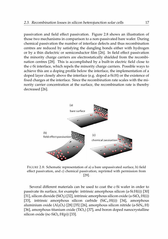
As mentioned before, the key feature of silicon heterojunction solar cells liesin the high V OC enabled by good passivation of the c-Si surface, which facil-itates the possibility of high efficiencies. Especially with the implementationof thinner wafers the passivation of their surface becomes increasingly impor-tant [26] [27]. Two possible ways exist in order to reduce the unwanted surfacerecombination and thereby enhance the minority carrier lifetime: Chemical
2.3. Recombination losses in silicon heterojunction solar cells 17
passivation and field effect passivation. Figure 2.8 shows an illustration ofthose two mechanisms in comparison to a non-passivated bare wafer. Duringchemical passivation the number of interface defects and thus recombinationcentres are reduced by satisfying the dangling bonds either with hydrogenor by a thin dielectric or semiconductor film [26]. In field effect passivationthe minority charge carriers are electrostatically shielded from the recombi-nation centres [28]. This is accomplished by a built-in electric field close tothe c-Si interface, which repels the minority charge carriers. Possible ways toachieve this are a doping profile below the interface, the implementation of adoped layer closely above the interface (e.g. doped a-Si:H) or the existence offixed charges at the interface. Since the recombination rate scales with the mi-nority carrier concentration at the surface, the recombination rate is therebydecreased [26].
FIGURE 2.8: Schematic representation of a) a bare unpassivated surface, b) fieldeffect passivation, and c) chemical passivation; reprinted with permission from
[29].
Several different materials can be used to coat the c-Si wafer in order topassivate its surface, for example: intrinsic amorphous silicon (a-Si:H(i)) [30][31], silicon dioxide (SiO2) [32], intrinsic amorphous silicon oxide (a-SiOx:H(i))[33], intrinsic amorphous silicon carbide (SiCx:H(i)) [34], amorphousaluminium oxide (Al2O3) [28] [35] [26], amorphous silicon nitride (a-SiNx:H)[36], amorphous titanium oxide (TiOx) [37], and boron doped nanocrystallinesilicon oxide (nc-SiOx:H(p)) [33].
18 Chapter 2. Literature review
In Chapter 5 we investigate the passivation properties of a-Si:H(i)/nc-SiOx:H(p) layer stacks. Reports suggest that when passivating the c-Si sur-face with an a-Si:H(i) layer, the material should be grown at a regime as closeas possible towards the amorphous/crystalline transition phase. Epitaxialgrowth however should be avoided [38] [39]. During deposition of the amor-phous silicon, often unfavourable silicon multihydrides are formed. Uponpost deposition annealing, hydrogen from these hydrides can become mobileand migrate towards unsatisfied silicon bonds, passivate them and thus in-crease the lifetime of the charge carriers within the sample [40]. The materialof the layers deposited on top of the passivation layer influences the passi-vation behaviour of the whole stack. It has been found, that the lifetime ofa sample passivated with a layer stack of a-Si:H(p)/a-Si:H(i) decreases uponannealing at lower temperatures as compared to the lifetime of a sample pas-sivated with only the a-Si:H(i) passivation layer [5]. For the comparison ofeither an a-Si:H(p) or a nc-SiOx:H(p) layer in combination with an a-Si:H(i)buffer layer it has been found, that nc-SiOx:H(p) can lead to a better passiva-tion [41]. This is attributed to the high amount of hydrogen in the gas compo-sition during deposition of the nc-SiOx:H(p) layer [42]. Thereby, hydrogen isgiven the chance to migrate towards the a-Si:H(i)/c-Si interface and enhancethe as-deposited passivation properties of the layer stack.
2.4 Parasitic absorption
To reach high efficiencies, a large amount of the photon energy incident onthe solar cell has to be converted into electrical energy. One of the limitingfactors to this is the parasitic absorption. This is the unwanted absorption oflight that does not contribute to the generation of charge carriers in the so-lar cell. Before reaching the active absorber layer of the cell, the light has topass several material layers. These layers can contribute to the parasitic ab-sorption of the solar cell. In a SHJ solar cell the complete light absorbed in anITO layer and about 70% of light absorbed in the a-Si:H(i) buffer layer can notbe used to generate electric energy [43]. Regarding the light absorbed in thea-Si:H(p) layer the amount contributing to the electricity generation is underdebate. While some authors claim the absorption to be completely parasitic[43], other authors assume that a part of the light absorbed in the a-Si:H(p)layer still contributes to the solar cell’s electricity generation [44].
The presence of free charge carriers in a material facilitate the possibilityof free carrier absorption. During this process free charge carriers are excitedby a photon into a higher state within the same energy band. Thus, from an
2.5. The emitter layer 19
optical point of view, the number of free charge carriers in a material shouldbe as small as possible. However, the charge carrier density n also influencesits conductivity σ according to
σ = n ⋅ e ⋅ µ, (2.3)
with e denoting the elementary charge and µ the mobility of the charge car-rier. Thus, a certain amount of charge carriers is needed in order to achieve asufficient conductivity. A balance between the materials transmittance and itsconductivity has to be found.
2.5 The emitter layer
The emitter layer forms together with the c-Si wafer the p-n junction of a SHJsolar cell. It has to be reasonably conductive to effectively extract the chargecarriers from the c-Si wafer, while at the same time being as transparent aspossible to not introduce too much parasitic absorption. A trade off betweenthese two material properties has to be made. A more transparent emitterlayer enables more light to reach the active absorber layer of the cell and canthus lead to an increase in JSC and therefore potentially higher efficiency of aSHJ solar cell. The application of a higher band gap emitter material suchas molybdenum oxide (MoOx) [45], microcrystalline silicon (µc-Si:H) [46],or amorphous silicon carbide (a-SiC:H) [16] comes to mind. Unfortunately,some of these materials come with challenges such as e.g. difficulties in bandalignment in the case of MoOx [45]. Another very promising candidate forthe replacement of the a-Si:H(p) is boron doped nanocrystalline silicon oxide(nc-SiOx:H(p)), which is investigated by many research groups [47] [48] [49][50].
A suitable emitter layer for SHJ solar cells has to exhibit several proper-ties. Its refractive index has to be favourable for light in-coupling towards thec-Si silicon wafer. This means, for the layer stack of TCO/emitter layer/bufferlayer/c-Si wafer, the refractive index should preferably consecutively increasefrom the refractive index of ambient air (n ≈ 1 [51]) towards those of crys-talline silicon (n ≈ 3.4 [52]) [53]. The ideal refractive index of the emitter layerwould be n ≈ 2.7 - 2.8. Conventional a-Si:H(p) emitter layers exhibit an un-favourable refractive index of n ≈ 3.9, which is even higher than those ofthe c-Si wafer. Thus, the widely tunable refractive index of nc-SiOx:H(p) isfavourable over a-Si:H(p) in terms of reflection minimization [53]. It has beenobserved that the following bulk properties of thick layers ensure their good
20 Chapter 2. Literature review
characteristics as emitter: an optical band gap of E04 > 2.2 eV and a conduc-tivity of σ ≥ 2 × 10⁻⁶ S/cm [48].
2.5.1 Nanocrystalline silicon oxide
In Chapter 4 and 5 we focus on the development of suitable nanocrystallinesilicon oxide (nc-SiOx:H) emitter layer for SHJ solar cells. In Chapter 6 theselayers are successfully integrated in SHJ solar cells. Therefore, we will thor-oughly discuss the nc-SiOx:H material, its properties, and its preparation inthe following.
Nanocrystalline silicon oxide is a wide band gap material consisting ofmixed phases. It is either described as silicon nanocrystallites in an amor-phous silicon oxide matrix [41] [54], or as a mixture of an amorphous siliconoxide phase (a-SiOx:H) and a nanocrystalline silicon phase (nc-Si:H) [55] [56][57]. Considering, that SiO:H consists of a Si:H matrix with island like ar-eas of Si:O in them [58], and that nanocrystalline silicon consists of an amor-phous and a nanocrystalline silicon phase [59], it becomes clear that bothdescriptions of nanocrystalline silicon oxide explain the same material. An-other term for the just described material is microcrystalline silicon oxide(µc-SiOx:H). However, when looking at it more precisely, the crystallites innc-SiOx:H are “nano sized” and have a length in the nanoscale range. This isapproximately 1 - 100 nm, in at least one dimension [60].
Growth evolution
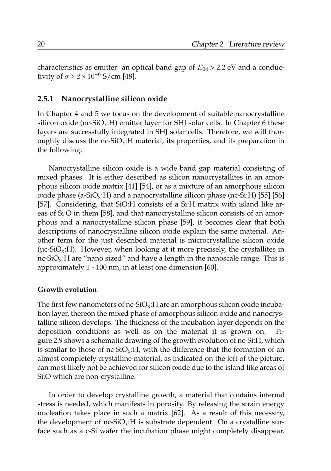
The first few nanometers of nc-SiOx:H are an amorphous silicon oxide incuba-tion layer, thereon the mixed phase of amorphous silicon oxide and nanocrys-talline silicon develops. The thickness of the incubation layer depends on thedeposition conditions as well as on the material it is grown on. Fi-gure 2.9 shows a schematic drawing of the growth evolution of nc-Si:H, whichis similar to those of nc-SiOx:H, with the difference that the formation of analmost completely crystalline material, as indicated on the left of the picture,can most likely not be achieved for silicon oxide due to the island like areas ofSi:O which are non-crystalline.
In order to develop crystalline growth, a material that contains internalstress is needed, which manifests in porosity. By releasing the strain energynucleation takes place in such a matrix [62]. As a result of this necessity,the development of nc-SiOx:H is substrate dependent. On a crystalline sur-face such as a c-Si wafer the incubation phase might completely disappear.
2.5. The emitter layer 21
FIGURE 2.9: Schematic drawing of the structure of nc-Si:H depending on thecrystalline fraction. Note, that in this drawing the area in which the crystallinitystill increases with increasing layer thickness is labelled “incubation zone”, whilewe refer to the first few nanometres of the layer in which crystalline growth hasnot yet appeared as “incubation layer”; reprinted from [61], with the permission
of AIP Publishing.
Also, on an oxide surface such as borosilicate glass the incubation phase isstill relatively small, compared to a non-oxide amorphous substrate such asa-Si:H [63] [64]. Treatment of the a-Si:H surface with e.g. a soft CO2 plasmacan help promote the nucleation of the following nanocrystalline layer [41][65]. With increasing thickness of the nc-SiOx:H(p) layer the amount of thecrystalline phase, as well as the size of the crystals, slowly increases. Rocai Cabarrocas et al. found a steady state of about 63% crystalline fraction for> 100 nm thick nc-Si:H layer grown on a glass substrate [64].
Doping
In a doped nc-SiOx it is the nanocrystalline silicon phase that determinesthe doping effect, since the doping efficiency in a-SiOx is comparably low[48] [55] [57]. In bulk silicon, boron doping leads to shallow energy levels≈ 0.044 eV above the valence band [66]. In silicon nanocrystals, the dopingprocess becomes more complicated due to their large surface area [66]. Ingeneral, nanocrystals have a tendency to stay intrinsic [67]. A low solubilityof boron in crystalline Si pushes out boron from the bulk during the crys-talline growth . Different calculations showed either a preferred location ofboron on the surface of the nanocrystals [68] [69] or inside the nanocrystalsclose to their surface [70] [71]. It has been found that boron location inside
22 Chapter 2. Literature review
silicon nanocrystals becomes more likely if the surface of the nanocrystals isoxidized [72].
The question whether or not electrically active doping of silicon nanocrys-tals can be achieved seems to be under debate in literature. In a review paperon doping of silicon nanocrystals Pi [66] states that neither surface nor inter-nal doping of the nanocrystals can produce free charge carriers, since they donot result in shallow energy levels. Therefore, the incorporation of doping inor on the outside of silicon nanocrystals does not lead to a doping in termsof electrical activity. However, in a review paper on nonthermal synthesisof semiconductor nanocrystals Kortshagen [73] comes to the conclusion thatthe electrical activity of doping in silicon nanocrystals has been confirmedby several studies [74] [75] [76] [77] [78] [79]. Moreover, it is know that theconductivity of a nc-SiOx:H layer is higher in the growth direction of the sil-icon nanocrystals (perpendicularto the substrate) than horizontally throughthe layer [56] [80]. Which leads to the conclusion, that an electrical activedoping of the silicon nanocrystals can be safely assumed for nanocrystallinesilicon oxide. This is supported by the knowledge that due to a reductionof charge carrier scattering, the conductivity in a nanocrystalline material isgenerally several orders of magnitude higher than those of the amorphousmaterial [7].
Material preparation - plasma enhanced CVD
nc-SiOx:H can be prepared by various methods such as radio frequencyplasma-enhanced chemical vapour deposition (RF-PECVD) (also called radiofrequency-glow discharge) [59] [81] or very high frequency plasma-enhancedchemical vapour deposition (VHF-PECVD) [82]. Moreover, multilayer struc-tures of silicon nanocrystals and SiO2 can be realized by co-sputtering [83].The nc-SiOx:H material of the samples prepared in Chapter 4 - 6 of this thesiswas grown by RF-PECVD. The PECVD method will be explained in Chap-ter 3 in detail. It can be summarized as a growth method for thin films bychemical deposition from a decomposed gas or mixture of gases. The plasmais essential for the decomposition of the gas. RF-PECVD prepared nc-SiOx:His usually grown from a gas mixture of silane (SiH4) as silicon and hydrogensource, and carbon dioxide (CO2) as oxygen source. Incorporation of carbonin the material due to dissociation of the CO2 molecule is expected to be verylow, an amount of about 2 at.% carbon has been reported by Gabriel et al.[57]. This gas mixture is diluted in hydrogen (H2), which during the depo-sition process dissociates into atomic hydrogen and promotes the crystalline
2.5. The emitter layer 23
growth. We will discuss the effect of the hydrogen dilution in detail later.As a boron dopant source, gases such as e.g. trimethylboron (B(CH3)3, TMB)for p-type doping or phosphine (PH3) for n-type doping can be added [81].Also diborane (B2H6) [84], and boron trifluoride (BF3) can be used to achieveboron doping in silicon based films [85]. However, diborane proves more un-stable than TMB, which might complicate the operation and maintenance ofa PECVD reactor due to the possibility of blocking of flow-meters caused bya decomposition of the gas [85], in addition to contaminating the hot sampleholder. For the use of boron trifluoride, it has been found that the gas phasedoping level has little influence on the microstructure of µc-Si:H(p). How-ever, a higher plasma power is necessary to achieve good material properties,as compared to the use of TMB [85]. Therefore, for the research described inChapter 4-6 TMB was chosen as dopant source.
Growth models
Three different growth models exist to explain the growth processes of nano-crystalline silicon, and thus also the growth of the nanocystalline silicon phasein nc-SiOx:H. In all of them the presence of hydrogen plays an importand rolefor the formation of crystallinity. In the following, the different models willbe summarized, based on [86] and [87].
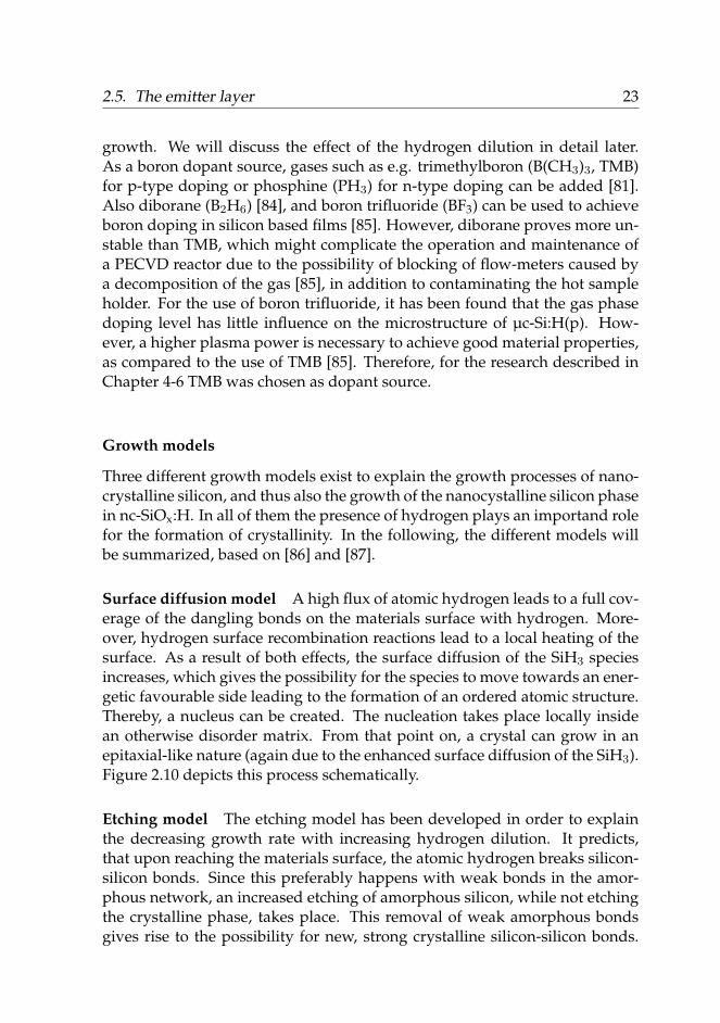
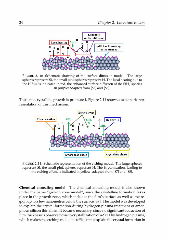
Surface diffusion model A high flux of atomic hydrogen leads to a full cov-erage of the dangling bonds on the materials surface with hydrogen. More-over, hydrogen surface recombination reactions lead to a local heating of thesurface. As a result of both effects, the surface diffusion of the SiH3 speciesincreases, which gives the possibility for the species to move towards an ener-getic favourable side leading to the formation of an ordered atomic structure.Thereby, a nucleus can be created. The nucleation takes place locally insidean otherwise disorder matrix. From that point on, a crystal can grow in anepitaxial-like nature (again due to the enhanced surface diffusion of the SiH3).Figure 2.10 depicts this process schematically.
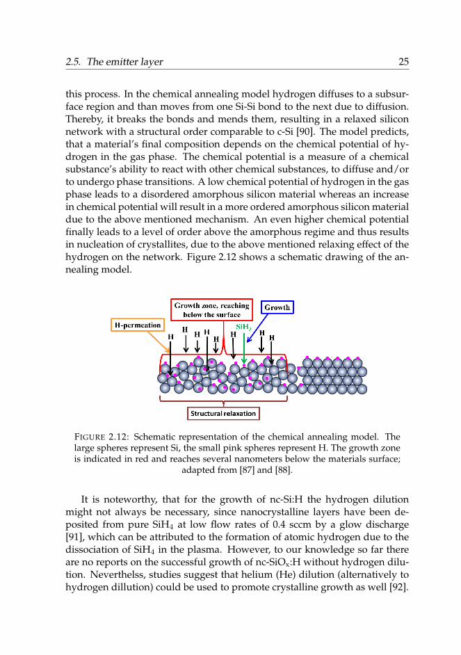
Etching model The etching model has been developed in order to explainthe decreasing growth rate with increasing hydrogen dilution. It predicts,that upon reaching the materials surface, the atomic hydrogen breaks silicon-silicon bonds. Since this preferably happens with weak bonds in the amor-phous network, an increased etching of amorphous silicon, while not etchingthe crystalline phase, takes place. This removal of weak amorphous bondsgives rise to the possibility for new, strong crystalline silicon-silicon bonds.
24 Chapter 2. Literature review
FIGURE 2.10: Schematic drawing of the surface diffusion model. The largespheres represent Si, the small pink spheres represent H. The local heating due tothe H flux is indicated in red, the enhanced surface diffusion of the SiH3 species
in purple; adapted from [87] and [88].
Thus, the crystalline growth is promoted. Figure 2.11 shows a schematic rep-resentation of this mechanism.
FIGURE 2.11: Schematic representation of the etching model. The large spheresrepresent Si, the small pink spheres represent H. The H-permeation, leading to
the etching effect, is indicated in yellow; adapted from [87] and [88].
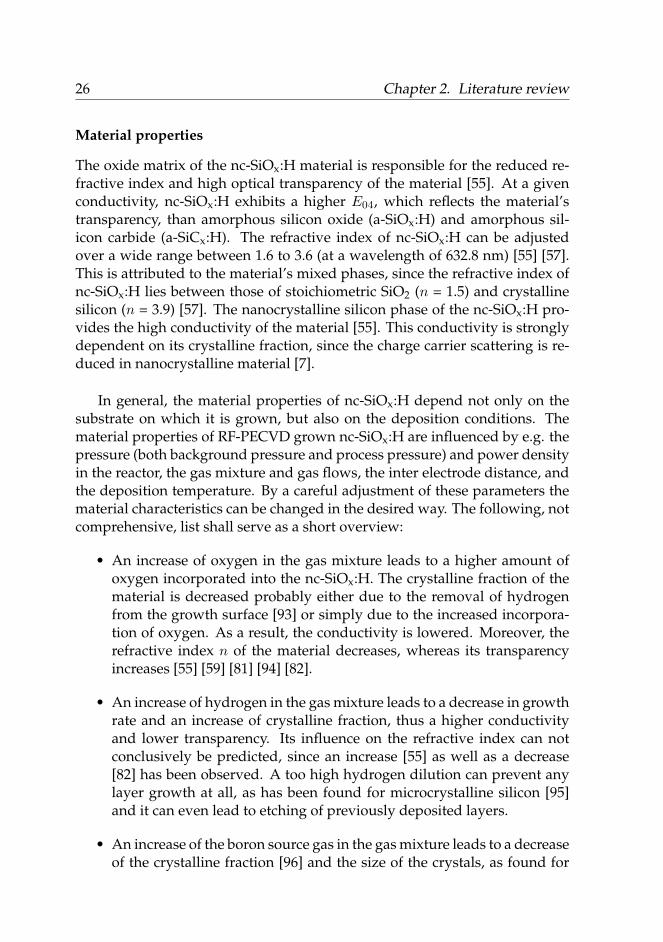
Chemical annealing model The chemical annealing model is also knownunder the name “growth zone model”, since the crystalline formation takesplace in the growth zone, which includes the film’s surface as well as the re-gion up to a few nanometres below the surface [89]. The model was developedto explain the crystal formation during hydrogen plasma treatment of amor-phous silicon thin films. It became necessary, since no significant reduction offilm thickness is observed due to crystallization of a-Si:H by hydrogen plasma,which makes the etching model insufficient to explain the crystal formation in
2.5. The emitter layer 25
this process. In the chemical annealing model hydrogen diffuses to a subsur-face region and than moves from one Si-Si bond to the next due to diffusion.Thereby, it breaks the bonds and mends them, resulting in a relaxed siliconnetwork with a structural order comparable to c-Si [90]. The model predicts,that a material’s final composition depends on the chemical potential of hy-drogen in the gas phase. The chemical potential is a measure of a chemicalsubstance’s ability to react with other chemical substances, to diffuse and/orto undergo phase transitions. A low chemical potential of hydrogen in the gasphase leads to a disordered amorphous silicon material whereas an increasein chemical potential will result in a more ordered amorphous silicon materialdue to the above mentioned mechanism. An even higher chemical potentialfinally leads to a level of order above the amorphous regime and thus resultsin nucleation of crystallites, due to the above mentioned relaxing effect of thehydrogen on the network. Figure 2.12 shows a schematic drawing of the an-nealing model.
FIGURE 2.12: Schematic representation of the chemical annealing model. Thelarge spheres represent Si, the small pink spheres represent H. The growth zoneis indicated in red and reaches several nanometers below the materials surface;
adapted from [87] and [88].
It is noteworthy, that for the growth of nc-Si:H the hydrogen dilutionmight not always be necessary, since nanocrystalline layers have been de-posited from pure SiH4 at low flow rates of 0.4 sccm by a glow discharge[91], which can be attributed to the formation of atomic hydrogen due to thedissociation of SiH4 in the plasma. However, to our knowledge so far thereare no reports on the successful growth of nc-SiOx:H without hydrogen dilu-tion. Neverthelss, studies suggest that helium (He) dilution (alternatively tohydrogen dillution) could be used to promote crystalline growth as well [92].
26 Chapter 2. Literature review
Material properties
The oxide matrix of the nc-SiOx:H material is responsible for the reduced re-fractive index and high optical transparency of the material [55]. At a givenconductivity, nc-SiOx:H exhibits a higher E04, which reflects the material’stransparency, than amorphous silicon oxide (a-SiOx:H) and amorphous sil-icon carbide (a-SiCx:H). The refractive index of nc-SiOx:H can be adjustedover a wide range between 1.6 to 3.6 (at a wavelength of 632.8 nm) [55] [57].This is attributed to the material’s mixed phases, since the refractive index ofnc-SiOx:H lies between those of stoichiometric SiO2 (n = 1.5) and crystallinesilicon (n = 3.9) [57]. The nanocrystalline silicon phase of the nc-SiOx:H pro-vides the high conductivity of the material [55]. This conductivity is stronglydependent on its crystalline fraction, since the charge carrier scattering is re-duced in nanocrystalline material [7].
In general, the material properties of nc-SiOx:H depend not only on thesubstrate on which it is grown, but also on the deposition conditions. Thematerial properties of RF-PECVD grown nc-SiOx:H are influenced by e.g. thepressure (both background pressure and process pressure) and power densityin the reactor, the gas mixture and gas flows, the inter electrode distance, andthe deposition temperature. By a careful adjustment of these parameters thematerial characteristics can be changed in the desired way. The following, notcomprehensive, list shall serve as a short overview:
• An increase of oxygen in the gas mixture leads to a higher amount ofoxygen incorporated into the nc-SiOx:H. The crystalline fraction of thematerial is decreased probably either due to the removal of hydrogenfrom the growth surface [93] or simply due to the increased incorpora-tion of oxygen. As a result, the conductivity is lowered. Moreover, therefractive index n of the material decreases, whereas its transparencyincreases [55] [59] [81] [94] [82].
• An increase of hydrogen in the gas mixture leads to a decrease in growthrate and an increase of crystalline fraction, thus a higher conductivityand lower transparency. Its influence on the refractive index can notconclusively be predicted, since an increase [55] as well as a decrease[82] has been observed. A too high hydrogen dilution can prevent anylayer growth at all, as has been found for microcrystalline silicon [95]and it can even lead to etching of previously deposited layers.
• An increase of the boron source gas in the gas mixture leads to a decreaseof the crystalline fraction [96] and the size of the crystals, as found for
2.6. The transparent conductive oxide layer 27
microcrystalline silicon [97]. This can be explained by an increased in-corporation of boron in the material, which leads to a higher structuraldisorder. Moreover, the scavenging effect of boron in the gas phase canlead to hydrogen abstraction from the material’s surface [98]. The sur-face thereby becomes reactive and diminishes the diffusion length ofsilicon species on it. Hence, the crystalline growth is decreased.
• With increased deposition temperature the crystal growth is enhanced,since the surface diffusion length of the atoms is enlarged [94] [99].However, for nc-Si:H it has been found, that from a temperature of≈ 400°C on, the crystalline fraction again decreases and at ≈ 500°C thematerial becomes completely amorphous [91]. This could be explainedby hydrogen effusion from the network at too high temperatures.
• By an increase in power the dissociation rate of SiH4 and CO2 riseswhich typically leads to a higher oxygen incorporation in the material[58] and an increased deposition rate [94].
Applications
nc-SiOx:H has found versatile applications in photovoltaic devices, such asanti-reflective or intermediate reflection layer in amorphous/microcrystallinetandem solar cells [55] [81], window layer in single junction microcrystallinesilicon solar cells [100], p-type and buffer layer for the bottom microcrystallinecell of tandem solar cells [101], or as contact layer between the TCO and thea-Si:H layer in thin film solar cells [102]. It should be pointed out, that its ap-plication in thin film solar cells led to an increased stability of the cells [81]as well as an improved contact to the zinc oxide (ZnO) implemented as frontTCO [57] [102]. In SHJ solar cells it has been implemented as intrinsic passi-vation layer [33] as back surface field [103], and as emitter layer [103]. Dueto its combination of highly conductive silicon nanocrystals with the highlytransparent silicon oxide matrix surrounding it, it is very suitable for this im-plementation as emitter layer. However, the material properties need to becarefully adjusted to assure good conductivity while still maintaining a highlytransparent layer. Chapter 4 is dedicated to this optimization.
2.6 The transparent conductive oxide layer
Transparent Conductive Oxides (TCO) have been intensively studied over thelast 40 years, due to their various applications. They have been utilized in en-ergy efficient windows, window heaters, liquid-crystal displays, light emit-ting diodes, and of course solar cells [104] [105]. Their main feature lies in the
28 Chapter 2. Literature review
combination of high electrical conductivity up to 104 S/cm with high trans-parency in the near infrared and visible wavelength range [105].
On the front side of SHJ solar cells a TCO layer serves several functions. Itacts as a conductor, since underlying emitter layers such as a-Si:H(p) are notconductive enough in lateral direction to efficiently transport the extractedcharge carriers to the front contact grid. At the same time it should be astransparent as possible, in order to not introduce too much parasitic absorp-tion. Additionally, it serves as anti reflection coating to enable the maximumamount of light to enter the solar cell. Moreover, the TCO has to provide agood contact to the emitter layer underneath as well as to the metal contactgrid on top. Last but not the least, it acts as metal diffusion barrier. This leadsto different requirements on the material properties [4]. In order to make goodcontacts between the TCO and the metal grid the formation of an insulatingoxide interlayer, such as e.g. silver oxide (Ag2O) in case of silver contacts,should be avoided [106]. The anti reflection properties of the TCO layer canbe achieved by adjusting the layer thickness. For this, the refractive index ofthe TCO and the emitter layer and, in case of implementation in solar mod-ules, the refractive index of the protective ehylene-vinyl acetate (EVA) coatingand the encapsulating glass, have to be taken into account.
A commonly used TCO for solar cells in research as well as in productionis tin-doped indium oxide (ITO). It exhibits a favourable combination of ahigh transparency due to its large band gap of about 4 eV and a high conduc-tivity caused by its highly n-type semiconductor nature. It can be depositedby physical vapour deposition methods such as electron beam evaporationand sputter deposition. However, ITO comes with the major drawback of notbeing texturable [107]. Due to this, as well as the scarcity and relative highcosts of indium, it is desirable to find an indium free alternative [108] [109],if possible even in combination with increased transmission and/or conduc-tivity. Therefore, many research groups are looking for an alternative such asantimony-doped tin oxide (ZnO:Sb, ATO) [110], aluminium doped zinc oxide(ZnO:Al, AZO) [111], gallium doped zinc oxide (ZnO:Ga, GZO) [112] [113],and boron doped zinc oxide (ZnO:B, BZO) [114].
2.6.1 Degenerated semiconductor
The typical semiconductor, such as ITO or ZnO significantly doped with agroup III element (B, Al, Ga, In), is a degenerated semiconductor and thusbehaves like a metal [115]. In the following we discuss non-degenerated anddegenerated n-type semiconductor. In a non-degenerated semiconductor the
2.6. The transparent conductive oxide layer 29
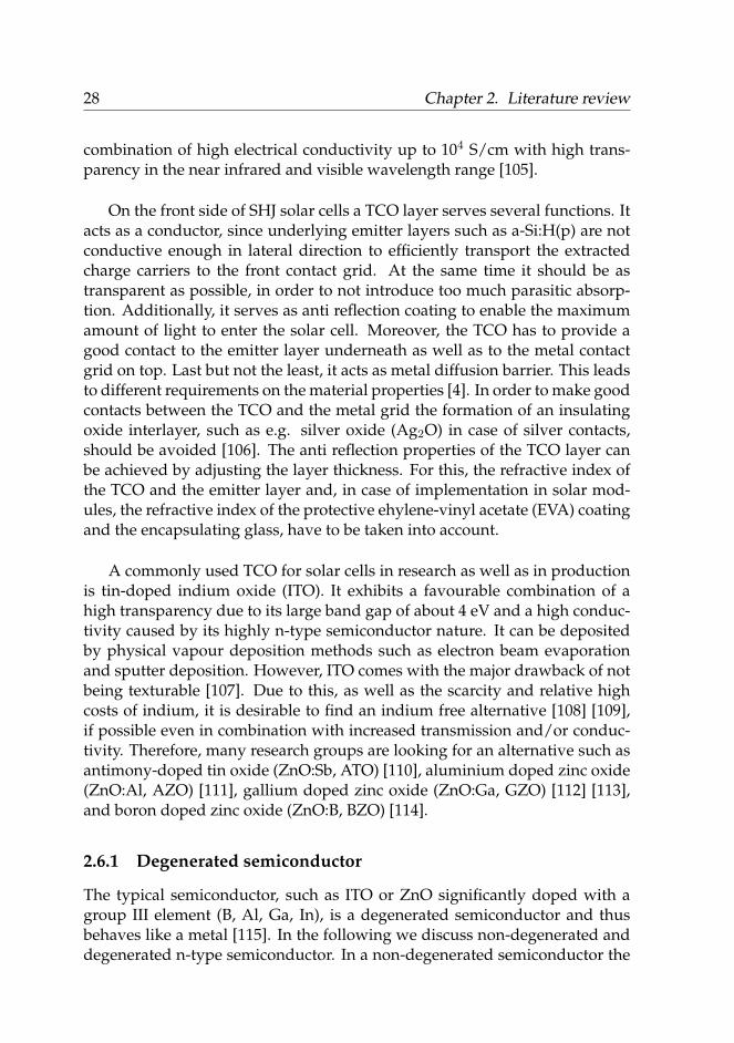
Fermi energy lies within the band gap (as previously shown in Figure 2.2).If the electron carrier concentration is larger than the conduction band edgedensity of states, electrons start populating states in the conduction band.The individual donor levels that exist in a non-degenerated semiconductorwithin the band gap merge together and form an impurity band that overlapswith the conduction band edge. This results in a band gap narrowing. TheFermi level is increased and pushed into the conduction band resulting in adegenerated semiconductor. Figure 2.13 shows the difference between a non-degenerated and a degenerated n-type semiconductor.
FIGURE 2.13: Schematic drawing of of the band diagram of a non-degeneratedand a degenerated n-type semiconductor; based on [116].
As a result of the large charge carrier density, the lower energy states inthe conduction band of a degenerated semiconductor are already occupied.Thus, a photon need to posses a higher energy than the electrical band gapto excite electrons from the valence band to the conduction band, since theelectron can not occupy a low energy state in the conduction band. This effectis called Burstein–Moss shift.
2.6.2 Scattering processes in transparent conductiveoxides
The conduction band of a TCO is partly filled with electrons. For standardTCOs, which are n-type, the resistivity ρ of the material can be determinedfrom Equation 2.3 and the following two relationships
ρ = 1
σ(2.4)
µ = e
m∗ ⋅ τ (2.5)
30 Chapter 2. Literature review
to:ρ = m∗
ne2τ. (2.6)
Here, σ denotes the electrical conductivity, m∗ the effective mass of the elec-tron, and τ the scattering time for Fermi surface electrons (i.e. the time in-terval between scattering processes) [104]. As can be seen in Equation 2.6,the resistivity of the material is reciprocal dependent on the scattering time(ρ ∝ τ−1), with a smaller scattering time leading to a higher resistivity. Thus,scattering processes of charge carriers within a TCO decrease or limit its con-ductivity. This is caused by the negative influence of the scattering processon the charge carriers mobility, as evident from Equation 2.5. The followingscattering processes can take place in TCOs:
• Ionized impurity scattering: Ionized impurities such as donors or ac-ceptors in the material, charged surface states or substitutional impuri-ties can lead to carrier scattering. This is a universal process in all ho-mogeneously doped semiconductors. It has been found to be the mainscattering process and limits the mobility in case the material exhibits acarrier concentration above 1019 cm−3 [104] [105] [117]. A specific case ofionized impurity scattering is the charged dislocation scattering. It cantake place when dislocations in an n-type material have an edge compo-nent1 introducing acceptor centres (dangling bonds). Following the lineof dislocation, the dangling bonds together become negatively chargedand introduce a space charge region around them. Electrons crossingthe dislocation can thereby scatter, which reduces the electron mobility[105] [119].
• Neutral impurity scattering: Neutral impurity scattering takes placeon neutral shallow impurities such as unionised donors (e.g. due todopant clustering at extremely high dopant concentrations) or neutraldefects. Since above ≈ 10 K the impurity atoms are partly ionized inmost commonly used semiconductors, neutral impurity scattering willnever be the only scattering mechanism at room temperatures. Othermechanisms such as lattice scattering or ionized impurity scattering willalso take place [120]. The group III elements (such as boron) in ZnO for
1An edge dislocation can be imagined as the abrupt end of an additional atomic plane, thatis inserted in a certain area of a crystal. In the area where the additional plane is still presentbut coming towards the end, the surrounding lattice is compressed. In the region close to thearea where the additional plane has ended, the surrounding lattice is under tension and thedistance of the atoms of the lattice are slightly larger than in the rest of the lattice [118].
2.6. The transparent conductive oxide layer 31
example show ionization energies ≈ 50 meV [105].
• Grain boundary limited transport: In polycrystalline material a largeamount of grain boundaries is present. These present a discontinuity inthe crystalline lattices, which introduces electronic defects in the bandgap of the semiconductor. These traps can then be filled with chargecarriers of the adjacent grains. A depletion zone is thereby formed onboth sides of the barrier, which leads to an energy barrier for passingcharge carriers. The effective mobility in the material can be assumedto be mainly dominated by thermionic emission [105] and tunnellingacross the barrier.
2.6.3 Zinc oxide
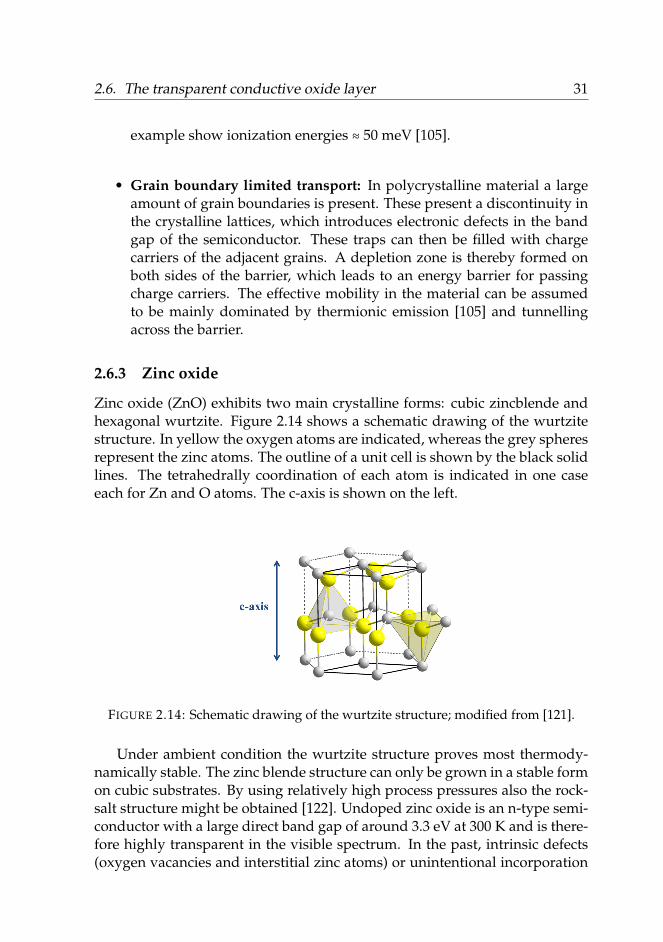
Zinc oxide (ZnO) exhibits two main crystalline forms: cubic zincblende andhexagonal wurtzite. Figure 2.14 shows a schematic drawing of the wurtzitestructure. In yellow the oxygen atoms are indicated, whereas the grey spheresrepresent the zinc atoms. The outline of a unit cell is shown by the black solidlines. The tetrahedrally coordination of each atom is indicated in one caseeach for Zn and O atoms. The c-axis is shown on the left.
FIGURE 2.14: Schematic drawing of the wurtzite structure; modified from [121].
Under ambient condition the wurtzite structure proves most thermody-namically stable. The zinc blende structure can only be grown in a stable formon cubic substrates. By using relatively high process pressures also the rock-salt structure might be obtained [122]. Undoped zinc oxide is an n-type semi-conductor with a large direct band gap of around 3.3 eV at 300 K and is there-fore highly transparent in the visible spectrum. In the past, intrinsic defects(oxygen vacancies and interstitial zinc atoms) or unintentional incorporation
32 Chapter 2. Literature review
of hydrogen or copper impurities during deposition of the material were oftennamed as a reason for this n-type behaviour [123]. As thoroughly discussedby Janotti et al. [124], the material science community recently tends moretowards the idea that oxygen vacancies are deep donors that thus can notcontribute to the material’s conductivities [125] [126] [127]. Also the contri-bution of Zn interstitials has been found to be an unlikely cause of the n-typebehaviour of as grown ZnO [128] [129]. Thus, impurities such as hydrogen,which is present in most of the growth or processing environment of ZnO,is expected to act as the shallow donor [130] [131]. A strong bond between Hand O is formed in the material, leading to the shallow donor behaviour [130].
Due to its intrinsic n-type nature, it is relatively easy to achieve n-typedoped ZnO. This can be done for example by doping ZnO with an element ofgroup III (boron (B), aluminium (Al), gallium (Ga) or indium (In)) [105]. Theelectrical properties of the ZnO can be varied from insulator over semiconduc-tor even towards a metal, while at the same time maintaining a high opticaltransparency [123]. Carrier concentrations over 1021 cm−3 can be achieved thisway [105]. For many applications p-type ZnO would also be desirable. How-ever, this seems rather difficult to achieve. A complex growth process, suchas co-doping, is needed. So far, p-type doping has either failed or resulted inan unstable material that loses its p-type character over time.
ZnO has found numerous applications, such as low-loss surface acousticwave (SAW) filters [132], gas sensors [133], varistors (voltage-dependent re-sistors) [134], and light-emitting diodes [135]. Moreover, zinc oxide is veryattractive for solar cell implementation. One of its advantages over the com-monly used ITO is its lower price [105] and it has been implemented as trans-parent electrodes in amorphous silicon thin film solar cells [136] and windowlayer and TCO in Cu(In,Ga)(S,Se)2 thin film solar cells [137] [138].
Carrier transport - comparison of ZnO and ITO
In Chapter 6 ZnO:B is implemented as front TCO in SHJ solar cells and com-pared to reference solar cells with ITO. Therefore, the differences in carriertransport of these two materials have to be considered. Ellmer et al. [105]investigated ZnO and ITO regarding their mobilities. It has been found, thatZnO shows a tendency to lower mobilities than ITO. They explain this by thefollowing factors:
2.6. The transparent conductive oxide layer 33
First of all, a larger amount of defects is present in ZnO compared to ITOif both materials are deposited under comparable conditions. In general, in-dium oxide also easily develops defects during the production process. How-ever, for magnetron sputtering, by which the ITO used in Chapter 6 is de-posited, the defect formation is expected to be rather low at moderate particleenergies [105]. ZnO usually contains a high amount of stacking faults which isoften combined with oxygen vacancies in their neighbourhood. These oxygenvacancies have a charge of Z = 2. Since µ∝ Z−2, the mobility is more stronglyreduced in case of oxygen vacancies compared to singly ionized dopants ofthe group III (B+, Al+, Ga+).
Second, ZnO is a polar semiconductor. Stress along the c-axis (see Fi-gure 2.14) can lead to electrical charges, thus piezoelectric activity. This in-trinsic stress can be induced by lattice mismatch between grains or growthdefects such as a non-perfect crystal structure within a grain. The therebyinduced charges at the grain barrier enhance scattering [105]. ITO is, unlikeZnO, a cubic material without piezoelectric effect and therefore inhibits lesscharged defects [105]. Moreover, ITO is outstanding in the way that even itsamorphous state shows high mobilities. This is most likely caused by thelarge contribution of the ns orbitals to the conductivity band. Neighbouringns orbitals have a large overlap with neighbouring orbitals. Their large radiicauses a considerable band dispersion [139]. Figure 2.15 shows a schematicrepresentation of the different orbitals of a) covalent semiconductors suchas silicon and b) post-transition metal oxide semiconductors such as indiumoxide. The large overlap of the metal ns-orbital in the case of a crystalline aswell as an amorphous structure of a post-transition metal oxide can clearlybee seen in Figure 2.15 b). Additionally, the surface of highly conductive ITOis found to be metallic due to metallic surface states (not because of conduc-tion band electrons) [140]. It is possible, that also at internal potential barriers(i.e. grain barriers) metallic surface states lower the barrier height. Thereby,the mobility would be enhanced.
ZnO/emitter interface
The behaviour of the TCO/emitter layer contact in SHJ solar cells has beeninvestigated by Ghahfarokhi [107]. In the following his findings are summa-rized. Commonly used TCO materials are n-type. Hence, an ohmic contactwith another n-type material can be achieved without much effort. In caseof n-type wafer based SHJ solar cells, as prepared in Chapter 6, this means agood ohmic contact towards the a-Si:H(n) BSF layer on the back of the solarcell can be accomplished. On the front side of the cell, however, the emitter
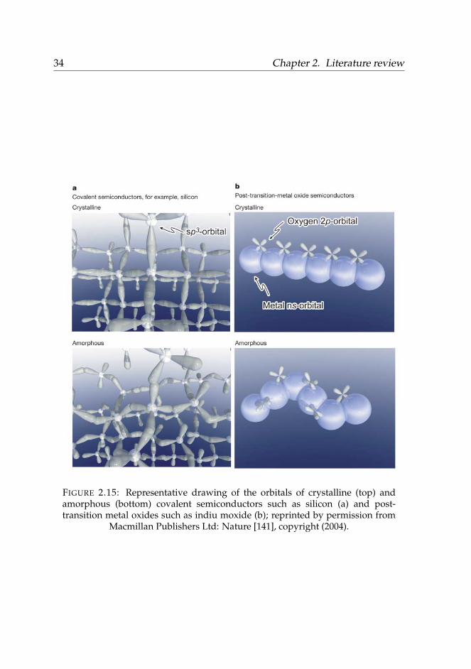
34 Chapter 2. Literature review
FIGURE 2.15: Representative drawing of the orbitals of crystalline (top) andamorphous (bottom) covalent semiconductors such as silicon (a) and post-transition metal oxides such as indiu moxide (b); reprinted by permission from
Macmillan Publishers Ltd: Nature [141], copyright (2004).
2.6. The transparent conductive oxide layer 35
layer consists of a p-type material. Hence, a tunnel contact has to be formedwhich requires the hole from the emitter layer to recombine with electronsfrom the TCO layer. An important aspect of this TCO/emitter contact is theband alignment. The TCO material has a lower work function than commona-Si:H(p) emitter layers and also nc-Si:H(p), which we implement to facilitatea good contact between the emitter and TCO material in Chapter 6. Thus, aSchottky barrier is generated at the interface. This means a depletion layeralmost free of charge carriers is formed at the junction. A potential barrieris created that needs to be overcome by charge carriers. In case of a lowTCO work function and/or a low doped emitter layer, the barrier high willincrease. Obviously, a large Schottky barrier height has an unfavourable ef-fect on the charge carrier transport and thus the FF and thereby the perfor-mance of a solar cell [142]. For a too high barrier, the J-V curve of the solarcell can even exhibit an S-shape. Moreover, the V OC can be decreased andeven the complete p-layer depleted [143]. Judging by this, it seems that a lowwork function TCO such as doped ZnO should be avoided for the implemen-tation as TCO on the p-type side of SHJ solar cells. However, Ghahfarokhifound that the previously mentioned effects can be overcome (also in case ofan nc-Si:H(p) emitter layer) if the emitter layer is highly conductive [107]. Weuse the same approach for the SHJ solar cells with ZnO:B TCO layer investi-gated in Chapter 6, by implementing the highly conductive nc-Si:H(p) contactlayer between the TCO and emitter layer.
Material preparation - atomic layer deposition
ZnO can be grown by various methods such as hydride vapour phase epitaxy(HVPE) [144], hybrid beam deposition (HBD) [145], molecular beam epitaxy(MBE) [146], laser molecular beam epitaxy (laser MBE) [147], pulsed laser de-position (PLD) [148], metal-organic chemical vapour deposition (MOCVD)[149] [150], photo assisted metal-organic chemical vapour deposition (photo-MOCVD) [151], expanding thermal plasma chemical vapour deposition (ETP-CVD) [152], plasma enhanced chemical vapour deposition (PECVD) [153],atmospheric pressure chemical vapour deposition (APCVD) [154], low pres-sure chemical vapor deposition (LPCVD) [155], sol-gel deposition [156], spraypyrolysis [157], sputtering [158], chemical bath deposition (CBD) [159], andatomic layer deposition (ALD) [114].
The ZnO implemented in SHJ solar cells in Chapter 6 is grown by atomiclayer deposition. The ALD process will be described in detail in Chapter 3. Itcan be shortly summarized as a preparation method for thin films based on
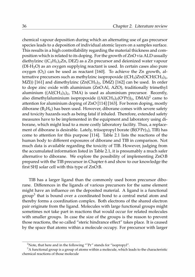
36 Chapter 2. Literature review
chemical vapour deposition during which an alternating use of gas precursorspecies leads to a deposition of individual atomic layers on a samples surface.This results in a high controllability regarding the material thickness and com-position which is related to its doping. For the growth of ZnO via ALD usuallydiethylzinc ((C2H5)2Zn, DEZ) as a Zn precursor and deionized water vapour(DI-H2O) as an oxygen supplying reactant is used. In certain cases also pureoxygen (O2) can be used as reactant [160]. To achieve the Zn growth, al-ternative precursors such as methylzinc isopropoxide ((CH3)Zn(OCH(CH3)2,MZI)) [161] and dimethylzinc (Zn(CH3)2, DMZ) [162] can be used. In orderto dope zinc oxide with aluminium (ZnO:Al, AZO), traditionally trimethylaluminium ((Al(CH3)3)2, TMA) is used as aluminium precursor. Recently,also dimethylaluminium isopropoxide ((Al(CH3)2(OiPr))2, DMAI)2 came toattention for aluminium doping of ZnO [114] [163]. For boron doping, mostlydiborane (B2H6) has been used. However, diborane comes with severe safetyand toxicity hazards such as being fatal if inhaled. Therefore, extended safetymeasures have to be implemented in the equipment and laboratory using di-borane, which might lead to a more costly laboratory facility. Thus, a replace-ment of diborane is desirable. Lately, triisopropyl borate (B(OiPr)3), TIB) hascome to attention for this purpose [114]. Table 2.1 lists the reactions of thehuman body to different exposures of diborane and TIB in comparison. Notmuch data is available regarding the toxicity of TIB. However, judging fromthe accumulated information listed in Table 2.1, it is presumably a much saferalternative to diborane. We explore the possibility of implementing ZnO:Bprepared with the TIB precursor in Chapter 6 and show to our knowledge thefirst SHJ solar cell with this type of ZnO:B.
TIB has a larger ligand than the commonly used boron precursor dibo-rane. Differences in the ligands of various precursors for the same elementmight have an influence on the deposited material. A ligand is a functionalgroup3 that is bound over a coordinated bond to a central metal atom andthereby forms a coordination complex. Both electrons of the shared electronpair originate from the ligand. Molecules with large functional groups mightsometimes not take part in reactions that would occur for related moleculeswith smaller groups. In case the size of the groups is the reason to preventthose reactions, the so called “steric hindrance effect” takes place. It is causedby the space that atoms within a molecule occupy. For precursor with larger
2Note, that here and in the following “iPr” stands for “isopropyl”.3A functional group is a group of atoms within a molecule, which leads to the characteristic
chemical reactions of those molecule
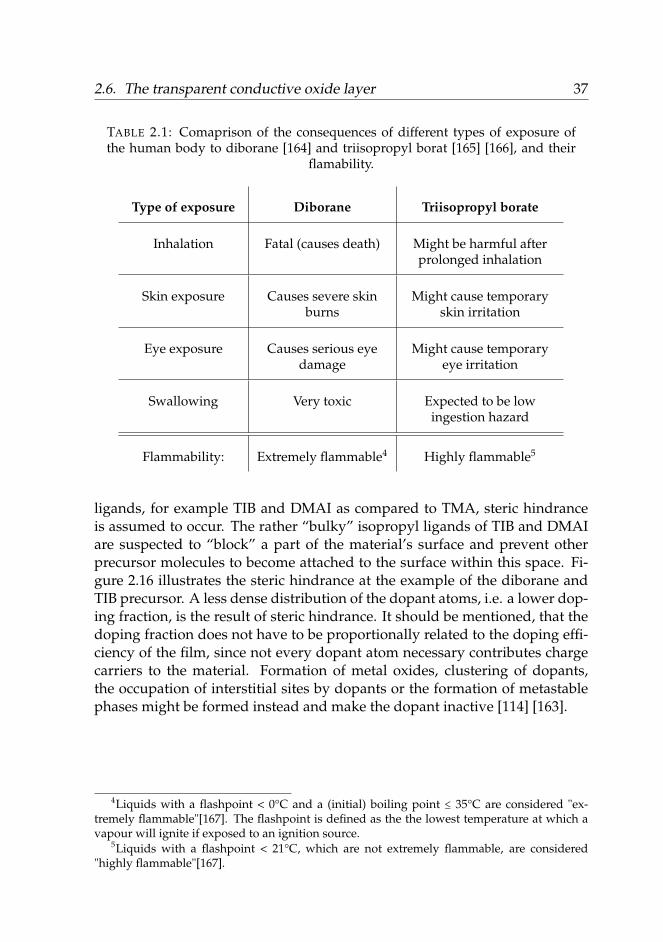
2.6. The transparent conductive oxide layer 37
TABLE 2.1: Comaprison of the consequences of different types of exposure ofthe human body to diborane [164] and triisopropyl borat [165] [166], and their
flamability.
Type of exposure Diborane Triisopropyl borate
Inhalation Fatal (causes death) Might be harmful afterprolonged inhalation
Skin exposure Causes severe skinburns
Might cause temporaryskin irritation
Eye exposure Causes serious eyedamage
Might cause temporaryeye irritation
Swallowing Very toxic Expected to be lowingestion hazard
Flammability: Extremely flammable4 Highly flammable5
ligands, for example TIB and DMAI as compared to TMA, steric hindranceis assumed to occur. The rather “bulky” isopropyl ligands of TIB and DMAIare suspected to “block” a part of the material’s surface and prevent otherprecursor molecules to become attached to the surface within this space. Fi-gure 2.16 illustrates the steric hindrance at the example of the diborane andTIB precursor. A less dense distribution of the dopant atoms, i.e. a lower dop-ing fraction, is the result of steric hindrance. It should be mentioned, that thedoping fraction does not have to be proportionally related to the doping effi-ciency of the film, since not every dopant atom necessary contributes chargecarriers to the material. Formation of metal oxides, clustering of dopants,the occupation of interstitial sites by dopants or the formation of metastablephases might be formed instead and make the dopant inactive [114] [163].
4Liquids with a flashpoint < 0°C and a (initial) boiling point ≤ 35°C are considered "ex-tremely flammable"[167]. The flashpoint is defined as the the lowest temperature at which avapour will ignite if exposed to an ignition source.
5Liquids with a flashpoint < 21°C, which are not extremely flammable, are considered"highly flammable"[167].
38 Chapter 2. Literature review
FIGURE 2.16: Schematic representation of the effect of steric hindrance shownfor the example of diborane and TIB; based on [163].
39
Chapter 3
Experimental techniques andconcepts
In this chapter, the experimental methods and concepts used for the researchcarried out within the scope of this thesis are described. First, the layer struc-ture of the deposited material samples and complete solar cells are illustrated.Thereafter, the different fabrication methods such as plasma enhanced chemi-cal vapour deposition (PECVD), hot wire chemical vapour deposition(HWCVD), atomic layer deposition (ALD), and magnetron sputtering, as wellas necessary steps to prepare the samples, are explained. The characterizationtechniques to evaluate the structure and the optical and electrical propertiesof the materials are presented. At the end, the setups and methods used to de-termine the performance of complete solar cell devices, i.e. the solar simulatorand spectral response setup, are presented.
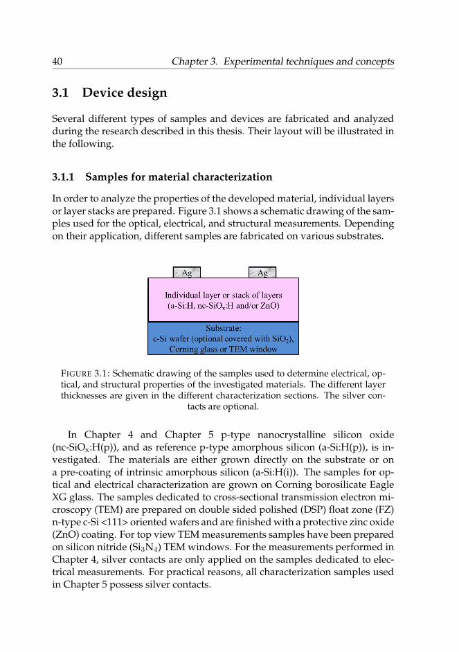
40 Chapter 3. Experimental techniques and concepts
3.1 Device design
Several different types of samples and devices are fabricated and analyzedduring the research described in this thesis. Their layout will be illustrated inthe following.
3.1.1 Samples for material characterization
In order to analyze the properties of the developed material, individual layersor layer stacks are prepared. Figure 3.1 shows a schematic drawing of the sam-ples used for the optical, electrical, and structural measurements. Dependingon their application, different samples are fabricated on various substrates.
FIGURE 3.1: Schematic drawing of the samples used to determine electrical, op-tical, and structural properties of the investigated materials. The different layerthicknesses are given in the different characterization sections. The silver con-
tacts are optional.
In Chapter 4 and Chapter 5 p-type nanocrystalline silicon oxide(nc-SiOx:H(p)), and as reference p-type amorphous silicon (a-Si:H(p)), is in-vestigated. The materials are either grown directly on the substrate or ona pre-coating of intrinsic amorphous silicon (a-Si:H(i)). The samples for op-tical and electrical characterization are grown on Corning borosilicate EagleXG glass. The samples dedicated to cross-sectional transmission electron mi-croscopy (TEM) are prepared on double sided polished (DSP) float zone (FZ)n-type c-Si <111> oriented wafers and are finished with a protective zinc oxide(ZnO) coating. For top view TEM measurements samples have been preparedon silicon nitride (Si3N4) TEM windows. For the measurements performed inChapter 4, silver contacts are only applied on the samples dedicated to elec-trical measurements. For practical reasons, all characterization samples usedin Chapter 5 possess silver contacts.
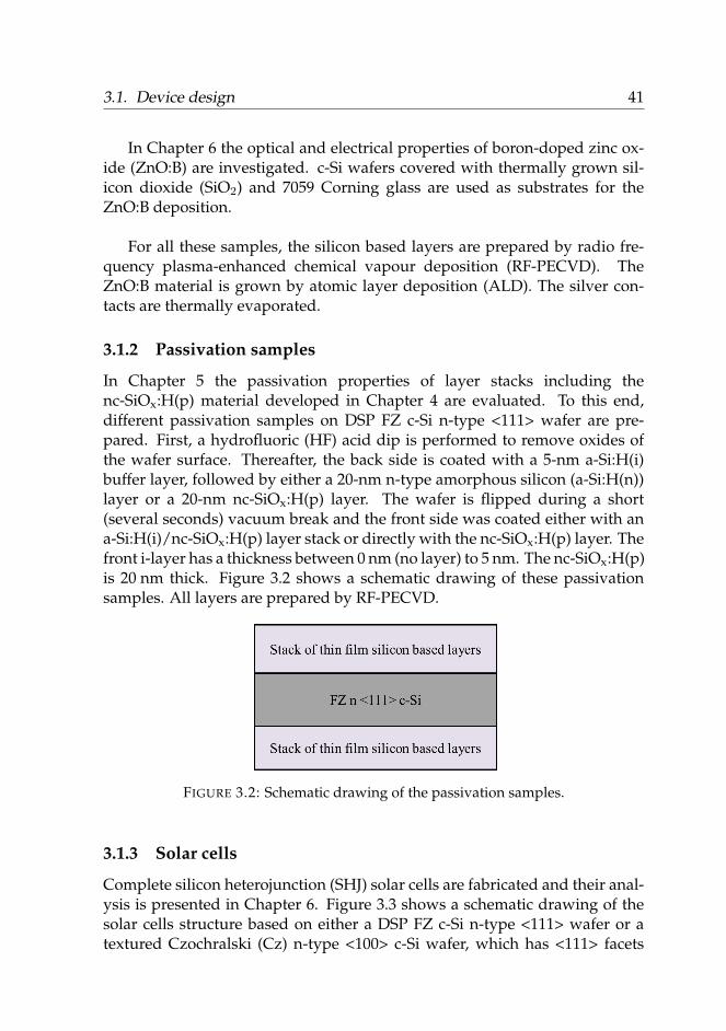
3.1. Device design 41
In Chapter 6 the optical and electrical properties of boron-doped zinc ox-ide (ZnO:B) are investigated. c-Si wafers covered with thermally grown sil-icon dioxide (SiO2) and 7059 Corning glass are used as substrates for theZnO:B deposition.
For all these samples, the silicon based layers are prepared by radio fre-quency plasma-enhanced chemical vapour deposition (RF-PECVD). TheZnO:B material is grown by atomic layer deposition (ALD). The silver con-tacts are thermally evaporated.
3.1.2 Passivation samples
In Chapter 5 the passivation properties of layer stacks including thenc-SiOx:H(p) material developed in Chapter 4 are evaluated. To this end,different passivation samples on DSP FZ c-Si n-type <111> wafer are pre-pared. First, a hydrofluoric (HF) acid dip is performed to remove oxides ofthe wafer surface. Thereafter, the back side is coated with a 5-nm a-Si:H(i)buffer layer, followed by either a 20-nm n-type amorphous silicon (a-Si:H(n))layer or a 20-nm nc-SiOx:H(p) layer. The wafer is flipped during a short(several seconds) vacuum break and the front side was coated either with ana-Si:H(i)/nc-SiOx:H(p) layer stack or directly with the nc-SiOx:H(p) layer. Thefront i-layer has a thickness between 0 nm (no layer) to 5 nm. The nc-SiOx:H(p)is 20 nm thick. Figure 3.2 shows a schematic drawing of these passivationsamples. All layers are prepared by RF-PECVD.
FIGURE 3.2: Schematic drawing of the passivation samples.
3.1.3 Solar cells
Complete silicon heterojunction (SHJ) solar cells are fabricated and their anal-ysis is presented in Chapter 6. Figure 3.3 shows a schematic drawing of thesolar cells structure based on either a DSP FZ c-Si n-type <111> wafer or atextured Czochralski (Cz) n-type <100> c-Si wafer, which has <111> facets
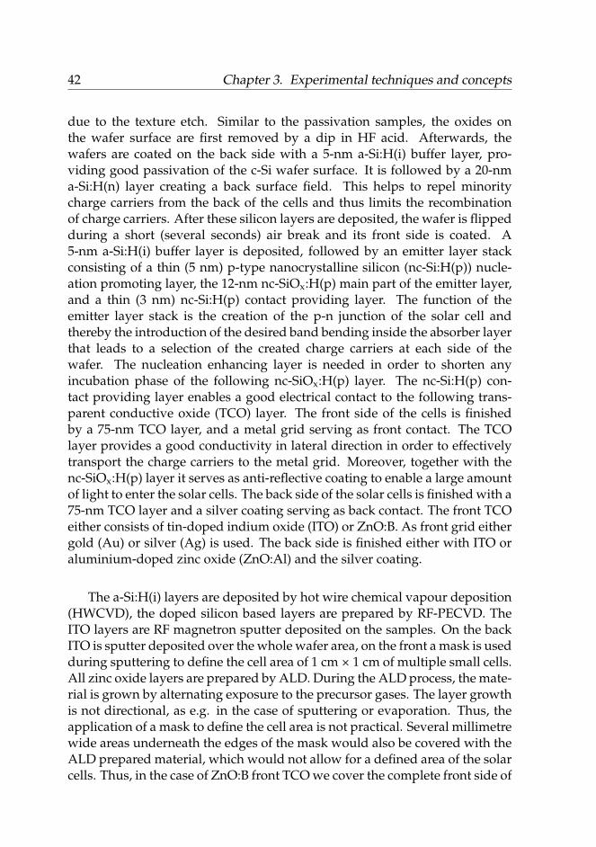
42 Chapter 3. Experimental techniques and concepts
due to the texture etch. Similar to the passivation samples, the oxides onthe wafer surface are first removed by a dip in HF acid. Afterwards, thewafers are coated on the back side with a 5-nm a-Si:H(i) buffer layer, pro-viding good passivation of the c-Si wafer surface. It is followed by a 20-nma-Si:H(n) layer creating a back surface field. This helps to repel minoritycharge carriers from the back of the cells and thus limits the recombinationof charge carriers. After these silicon layers are deposited, the wafer is flippedduring a short (several seconds) air break and its front side is coated. A5-nm a-Si:H(i) buffer layer is deposited, followed by an emitter layer stackconsisting of a thin (5 nm) p-type nanocrystalline silicon (nc-Si:H(p)) nucle-ation promoting layer, the 12-nm nc-SiOx:H(p) main part of the emitter layer,and a thin (3 nm) nc-Si:H(p) contact providing layer. The function of theemitter layer stack is the creation of the p-n junction of the solar cell andthereby the introduction of the desired band bending inside the absorber layerthat leads to a selection of the created charge carriers at each side of thewafer. The nucleation enhancing layer is needed in order to shorten anyincubation phase of the following nc-SiOx:H(p) layer. The nc-Si:H(p) con-tact providing layer enables a good electrical contact to the following trans-parent conductive oxide (TCO) layer. The front side of the cells is finishedby a 75-nm TCO layer, and a metal grid serving as front contact. The TCOlayer provides a good conductivity in lateral direction in order to effectivelytransport the charge carriers to the metal grid. Moreover, together with thenc-SiOx:H(p) layer it serves as anti-reflective coating to enable a large amountof light to enter the solar cells. The back side of the solar cells is finished with a75-nm TCO layer and a silver coating serving as back contact. The front TCOeither consists of tin-doped indium oxide (ITO) or ZnO:B. As front grid eithergold (Au) or silver (Ag) is used. The back side is finished either with ITO oraluminium-doped zinc oxide (ZnO:Al) and the silver coating.
The a-Si:H(i) layers are deposited by hot wire chemical vapour deposition(HWCVD), the doped silicon based layers are prepared by RF-PECVD. TheITO layers are RF magnetron sputter deposited on the samples. On the backITO is sputter deposited over the whole wafer area, on the front a mask is usedduring sputtering to define the cell area of 1 cm × 1 cm of multiple small cells.All zinc oxide layers are prepared by ALD. During the ALD process, the mate-rial is grown by alternating exposure to the precursor gases. The layer growthis not directional, as e.g. in the case of sputtering or evaporation. Thus, theapplication of a mask to define the cell area is not practical. Several millimetrewide areas underneath the edges of the mask would also be covered with theALD prepared material, which would not allow for a defined area of the solarcells. Thus, in the case of ZnO:B front TCO we cover the complete front side of
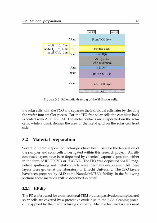
3.2. Material preparation 43
FIGURE 3.3: Schematic drawing of the SHJ solar cells.
the solar cells with the TCO and separate the individual cells later by cleavingthe wafer into smaller pieces. For the ITO-free solar cells the complete backis coated with ALD ZnO:Al. The metal contacts are evaporated on the solarcells, while a mask defines the area of the metal grid on the solar cell frontside.
3.2 Material preparation
Several different deposition techniques have been used for the fabrication ofthe samples and solar cells investigated within this research project. All sili-con based layers have been deposited by chemical vapour deposition, eitherin the form of RF-PECVD or HWCVD. The ITO was deposited via RF mag-netron sputtering and metal contacts were thermally evaporated. All theselayers were grown at the laboratory of Utrecht University. The ZnO layershave been prepared by ALD at the NanoLab@TU/e facility. In the followingsections these methods will be described in detail.
3.2.1 HF dip
The FZ wafers used for cross-sectional TEM studies, passivation samples, andsolar cells are covered by a protective oxide due to the RCA cleaning proce-dure applied by the manufacturing company. Also the textured wafers used
44 Chapter 3. Experimental techniques and concepts
for solar cell deposition are oxidized due to air exposure. Such oxides shouldbe removed before the deposition of the buffer layers. Otherwise, the oxides,due to their high band gap, could form a barrier for the carrier transport andthus deteriorate the solar cell’s performance. A two minute dip in 1% dilutedhydrofluoric (HF) acid at room temperature is performed to remove these ox-ide layers. Afterwards, the wafers are blown dry with nitrogen gas (N2) andthen loaded in the deposition setup.
3.2.2 Plasma-enhanced chemical vapour deposition
During plasma-enhanced chemical vapour deposition (PECVD) a thin layeris grown from a gas phase. An RF-electric discharge is created between twoelectrodes, enabling the chemical reactions necessary for this deposition. Inlaboratories and industry PECVD is a well established technique for thin filmmanufacturing. Due to the assistance of the plasma in decomposing the gasmolecules, favourably low deposition temperatures suitable for SHJ solar cellproduction are achieved.
During the work described in this thesis, amorphous and nanocrystallinesilicon based layers are deposited by 10 x 10 cm2 substrate area PECVD in aparallel plate reactor from pure silane (SiH4) or a silane containing gas mix-ture. For boron doping trimethylboron (B(CH3)3, TMB) and for phosphorousdoping phosphine (PH3) is added. To achieve nanocrystalline silicon oxide,carbon dioxide (CO2) and hydrogen (H2) is added. The reactor’s geometrycan be imagined in a simple way as a horizontal standing parallel plate ca-pacitor. The grounded substrate holder functions as the top electrode, whilethe bottom electrode is powered with a RF (13.56 MHz) alternating current tocreate a glow discharge. The plasma is ignited by the oscillating electrical fieldbetween the electrodes. Free electrons are accelerated by the electric field andcollide with gas molecules, which leads to a dissociation of the gas. Thereby,atoms, positive and negative ions, radicals (reactive molecules or atoms), andmore free electrons are produced. Secondary reactions take place betweenthose species. At high enough energies, silane molecules will dissociate with
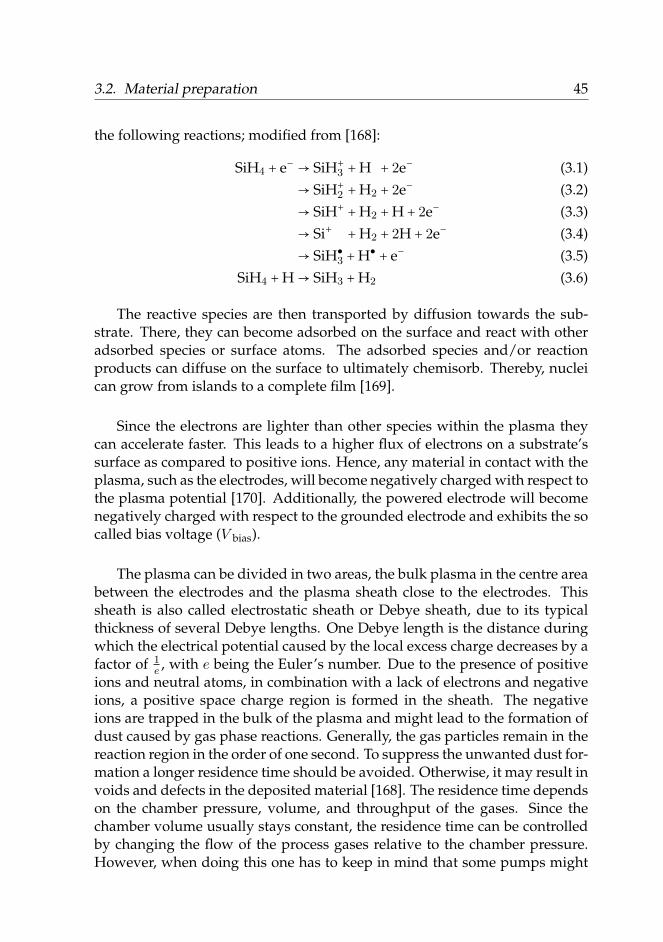
3.2. Material preparation 45
the following reactions; modified from [168]:
SiH4 + e− → SiH+
3 +H2 + 2e− (3.1)→ SiH+
2 +H2 + 2e− (3.2)→ SiH+ +H2 +H + 2e− (3.3)→ Si+H +H2 + 2H + 2e− (3.4)→ SiH
3 +H + e− (3.5)SiH4 +H→ SiH3 +H2 (3.6)
The reactive species are then transported by diffusion towards the sub-strate. There, they can become adsorbed on the surface and react with otheradsorbed species or surface atoms. The adsorbed species and/or reactionproducts can diffuse on the surface to ultimately chemisorb. Thereby, nucleican grow from islands to a complete film [169].
Since the electrons are lighter than other species within the plasma theycan accelerate faster. This leads to a higher flux of electrons on a substrate’ssurface as compared to positive ions. Hence, any material in contact with theplasma, such as the electrodes, will become negatively charged with respect tothe plasma potential [170]. Additionally, the powered electrode will becomenegatively charged with respect to the grounded electrode and exhibits the socalled bias voltage (V bias).
The plasma can be divided in two areas, the bulk plasma in the centre areabetween the electrodes and the plasma sheath close to the electrodes. Thissheath is also called electrostatic sheath or Debye sheath, due to its typicalthickness of several Debye lengths. One Debye length is the distance duringwhich the electrical potential caused by the local excess charge decreases by afactor of 1
e , with e being the Euler’s number. Due to the presence of positiveions and neutral atoms, in combination with a lack of electrons and negativeions, a positive space charge region is formed in the sheath. The negativeions are trapped in the bulk of the plasma and might lead to the formation ofdust caused by gas phase reactions. Generally, the gas particles remain in thereaction region in the order of one second. To suppress the unwanted dust for-mation a longer residence time should be avoided. Otherwise, it may result invoids and defects in the deposited material [168]. The residence time dependson the chamber pressure, volume, and throughput of the gases. Since thechamber volume usually stays constant, the residence time can be controlledby changing the flow of the process gases relative to the chamber pressure.However, when doing this one has to keep in mind that some pumps might
46 Chapter 3. Experimental techniques and concepts
pump certain gases more efficiently than other gases. In that case a changingof the process gas flow rate might alter the gas mixture present in the cham-ber. To further avoid any effects of potential dust, the electrode on which thesubstrate is mounted (grounded electrode) is usually the top electrode, allow-ing for the substrate to be mounted facing downwards.
The RF-PECVD depositions carried out within the research described inthis thesis have been performed in the PASTA (Process equipment for Amor-phous Silicon Thin-film Applications) reactor [171]. This multi-chamber highvacuum deposition system is equipped with different process chambers forintrinsic, n-type, and p-type material in order to suppress any cross contam-ination and unintentional doping. The intrinsic buffer layer and the subse-quent doped layers are deposited without an intermediate vacuum break.
3.2.3 Hot wire chemical vapour deposition
During hot wire chemical vapour deposition (HWCVD) a thin film is de-posited from a gas or gas mixture. To achieve this, the gas molecules haveto decompose. Unlike in PECVD, this does not happen as a result of collisionsbetween electrons and gas molecules. Instead, a hot catalyst enables catalyticor pyrolytic (thermochemical decomposition of organic molecules in the ab-sence of oxygen) reactions [172]. Resistively heated filaments (“hot wires”)serve as catalyst. A hot substrate is not inevitable for HWCVD deposition,since the substrate temperature can be adjusted independently of the filamenttemperature.
At filament temperatures above 1500°C, silane molecules are catalyticallydecomposed in the vicinity of the hot catalyst, resulting in silicon and hydro-gen atoms [173]:
SiH4 = Si + 4H. (3.7)
In the following, the atomic hydrogen reacts with silane as
H + SiH4 = SiH3 +H2, (3.8)
while H2 can form atomic hydrogen again:
H2 = H +H. (3.9)
The thin silicon layer is then deposited from these silicon and hydrogencontaining species.
3.2. Material preparation 47
HWCVD is also know as catalytic chemical vapour deposition (cat-CVD),initiated chemical vapour deposition (iCVD), thermal chemical vapour de-position (thermal CVD), and hot filament chemical vapour deposition (HF-CVD). Next to tungsten (W), tantalum (Ta) is a very common filament mate-rial for these depositions. During silicon deposition with tantalum filamentsdifferent types of silicides (binary metallic compounds involving silicon) arecreated. With time, this leads to a shell around the tantalum wire. By pro-longed vacuum annealing of the filament, the silicide can again be removed,resulting in a tantalum wire with almost identical diameter and resistance asin its pre-deposited state, as has been shown for tantalum filaments used fordevice quality deposition of a-Si:H(i) and µc-Si:H(i) [174].
In Chapter 6 HWCVD is used for the deposition of the a-Si:H(i) bufferlayers for SHJ solar cells. The reaction chamber is part of the PASTA system.The buffer layer and following doped layers are deposited without breakingthe vacuum in between. The layers are deposited on 10 x 10 cm2 substratearea from pure silane at a rate of 0.4 nm/s with the help of two tantalumfilaments of 3 mm diameter located 4 cm below the substrate.
3.2.4 Atomic layer deposition
Atomic layer deposition (ALD) is a process to deposit thin layers from a gas-phase using sequential self-limiting surface reactions. During a typical ALDprocess, the substrates surface is exposed to two or more different gases ina cyclical repeated manner. The individual gases are introduced separatelyinto the reactor chamber without an overlap in exposure time. To prevent anycombination of gas particles of the previously dosed precursor and volatileby-products of the reaction with the following precursor, the reactor chamberis purged between exposures. A new monolayer of material is grown on thesubstrate’s surface during each precursor exposure, in a self-limiting manner.This is caused by the newly grown species on the substrates, which acts asa passivator for further reactions with the same precursor gas. By the fol-lowing exposure to the reactant the surface is then reactivated. Due to thisself-limiting nature of the surface reaction processes, the material is slowlydeposited with a thickness controllability in the order of one Ångström [175](1 Ångström = 10−10 m, the typical order of magnitude of the distance be-tween atoms in a crystalline structure). Different types of ALD exist, suchas thermal ALD [176], plasma-assisted ALD [177], and radical enhanced ALD[178] (e.g. with the help of a hot filament).
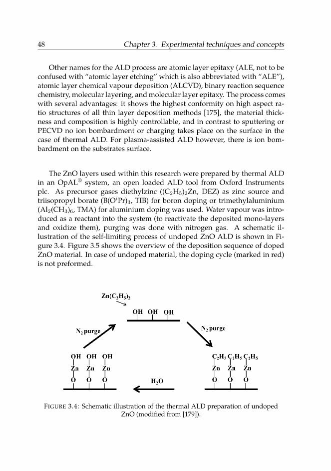
48 Chapter 3. Experimental techniques and concepts
Other names for the ALD process are atomic layer epitaxy (ALE, not to beconfused with “atomic layer etching” which is also abbreviated with “ALE”),atomic layer chemical vapour deposition (ALCVD), binary reaction sequencechemistry, molecular layering, and molecular layer epitaxy. The process comeswith several advantages: it shows the highest conformity on high aspect ra-tio structures of all thin layer deposition methods [175], the material thick-ness and composition is highly controllable, and in contrast to sputtering orPECVD no ion bombardment or charging takes place on the surface in thecase of thermal ALD. For plasma-assisted ALD however, there is ion bom-bardment on the substrates surface.
The ZnO layers used within this research were prepared by thermal ALDin an OpAL® system, an open loaded ALD tool from Oxford Instrumentsplc. As precursor gases diethylzinc ((C2H5)2Zn, DEZ) as zinc source andtriisopropyl borate (B(OiPr)3, TIB) for boron doping or trimethylaluminium(Al2(CH3)6, TMA) for aluminium doping was used. Water vapour was intro-duced as a reactant into the system (to reactivate the deposited mono-layersand oxidize them), purging was done with nitrogen gas. A schematic il-lustration of the self-limiting process of undoped ZnO ALD is shown in Fi-gure 3.4. Figure 3.5 shows the overview of the deposition sequence of dopedZnO material. In case of undoped material, the doping cycle (marked in red)is not preformed.
FIGURE 3.4: Schematic illustration of the thermal ALD preparation of undopedZnO (modified from [179]).
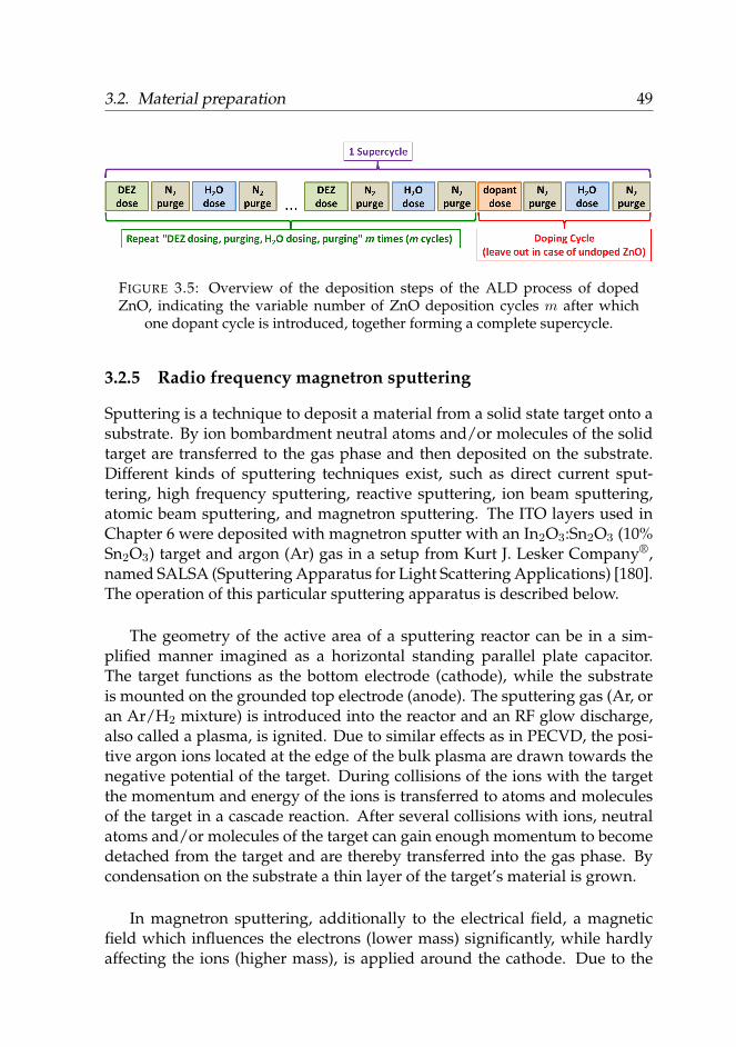
3.2. Material preparation 49
FIGURE 3.5: Overview of the deposition steps of the ALD process of dopedZnO, indicating the variable number of ZnO deposition cycles m after which
one dopant cycle is introduced, together forming a complete supercycle.
3.2.5 Radio frequency magnetron sputtering
Sputtering is a technique to deposit a material from a solid state target onto asubstrate. By ion bombardment neutral atoms and/or molecules of the solidtarget are transferred to the gas phase and then deposited on the substrate.Different kinds of sputtering techniques exist, such as direct current sput-tering, high frequency sputtering, reactive sputtering, ion beam sputtering,atomic beam sputtering, and magnetron sputtering. The ITO layers used inChapter 6 were deposited with magnetron sputter with an In2O3:Sn2O3 (10%Sn2O3) target and argon (Ar) gas in a setup from Kurt J. Lesker Company®,named SALSA (Sputtering Apparatus for Light Scattering Applications) [180].The operation of this particular sputtering apparatus is described below.
The geometry of the active area of a sputtering reactor can be in a sim-plified manner imagined as a horizontal standing parallel plate capacitor.The target functions as the bottom electrode (cathode), while the substrateis mounted on the grounded top electrode (anode). The sputtering gas (Ar, oran Ar/H2 mixture) is introduced into the reactor and an RF glow discharge,also called a plasma, is ignited. Due to similar effects as in PECVD, the posi-tive argon ions located at the edge of the bulk plasma are drawn towards thenegative potential of the target. During collisions of the ions with the targetthe momentum and energy of the ions is transferred to atoms and moleculesof the target in a cascade reaction. After several collisions with ions, neutralatoms and/or molecules of the target can gain enough momentum to becomedetached from the target and are thereby transferred into the gas phase. Bycondensation on the substrate a thin layer of the target’s material is grown.
In magnetron sputtering, additionally to the electrical field, a magneticfield which influences the electrons (lower mass) significantly, while hardlyaffecting the ions (higher mass), is applied around the cathode. Due to the
50 Chapter 3. Experimental techniques and concepts
Lorenz force, the electrons are forced on a helical trajectory. Thus, their pathwithin the plasma is enlarged leading to a higher number of collisions andwith this a higher number of ions. This allows for the use of favourablylow pressures, and thereby prevents further collisions between the sputteredatoms and the target [180].
3.2.6 Thermal evaporation
The metal contacts used for electrical measurements and solar cell contactingare applied by thermal evaporation in a low pressure evaporator. For thispurpose, the contact material (Ag or Au) is placed in a tungsten boat, whichis then heated by passing a current through it. The metal is thereby meltedand finally evaporated, while the tungsten boat remains solid due to its highmelting point of above 3000°C. The substrate is mounted facing down severaltens of centimetre above the boat, in order to allow the metal vapour to de-posit on the sample. The substrate temperature is kept below 100°C as a resultof low pressure and spatial distance to the heat source. To define the area ofthe contacts a metal mask is applied on the substrate.
3.3 Material characterization
The developed materials and solar cells are investigated in detail by severaldifferent characterization methods. The spectroscopic ellipsometry and thefour point probe measurements are performed at Eindhoven University ofTechnology. The TEM samples are investigated at the facility at Philips Re-search and Philips Innovation Services. For all other characterization tech-niques, setups located in the Solliance Laboratory at the High Tech CampusEindhoven, either from Utrecht University or from the Energy research Centreof the Netherlands (ECN) are used.
3.3.1 Reflection and transmission
Reflection and transmission measurements are performed with two differentdevices. An “RT-mini” setup operated with the software program SCOUT[181] is used to investigate the silicon based material, while the transmissionof the TCO layers is recorded with an UV-VIS-NIR spectrometer (Carry 5000,Agilent).
3.3. Material characterization 51
RT-mini setup
The RT-mini setup measures the specular reflection and transmission of theinvestigated sample in a wavelength range between 380-1050 nm. A halo-gen lamp is utilized as light source, while a photo-detector array is used forthe measurements. The software program SCOUT with the implemented OJLinter-band transition model [182], expressing the density of states distributionof an amorphous semiconductor, is used to determine the real (n) and imag-inary (k) part of the refractive index. By comparison to Optics2 simulations[183], it has been shown that this procedure gives correct simulation data forthe mixed-phase nc-SiOx:H(p) material [184]. The absorption coefficient (α),is determined from this as:
α = 4 ⋅ π ⋅ kλ
, (3.10)
with λ denoting the wavelength of the incident light. Additionally, the sam-ples thickness is extracted from the fit. Moreover, E04, the photon energyassociated with α = 10−4 cm−1, which serves as a measure for the band gap, iscalculated from the retrieved values. The nc-SiOx:H(p) samples used for thismeasurements were deposited on Corning borosilicate (Eagle XG) glass andhad a thickness of 185 (± 10) nm.
UV-Vis-NIR spectrometer
The UV-Vis-NIR spectrometer is used to measure the transmission data be-tween 175-3300 nm, allowing for an observation of a larger wavelength regionthan the RT-mini setup. Moreover, it possesses an integrating sphere enablinghighly precise measurements of the transmitted light, including the diffuselyscattered light. The samples used for this measurement were deposited onCorning borosilicate (Eagle XG) glass and had a structure of 5 nm a-Si:H(i) +10 nm a-Si:H(p), or 5 nm a-Si:H(i) + 20 nm nc-SiOx:H(p), respectively.
3.3.2 Spectroscopic ellipsometry
Spectroscopic ellipsometry (SE) uses polarized light to investigate the dielec-tric properties of thin films, such as the real and imaginary part of the refrac-tive index and the complex permittivity as well as the layer thickness. To thisend, the reflected or transmitted light is detected and the changes in polariza-tion are analyzed. Figure 3.6 shows a schematic drawing of the measurementsetup we use. The unpolarized light first passes through a polarization filter,resulting in linearly polarized light. Thereafter, it passes a rotating compen-sator and is incident on the substrate as linearly polarized light. After reflec-tion from the substrate the light is elliptically polarized. It then passes a fixed
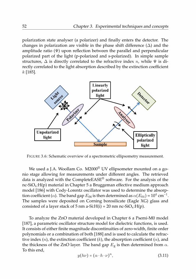
52 Chapter 3. Experimental techniques and concepts
polarization state analyser (a polarizer) and finally enters the detector. Thechanges in polarization are visible in the phase shift difference (∆) and theamplitude ratio (Ψ) upon reflection between the parallel and perpendicularpolarized part of the light (p-polarized and s-polarized). In simple samplestructures, ∆ is directly correlated to the refractive index n, while Ψ is di-rectly correlated to the light absorption described by the extinction coefficientk [185].
FIGURE 3.6: Schematic overview of a spectrometric ellipsometry measurement.
We used a J.A. Woollam Co. M2000® UV ellipsometer mounted on a go-nio stage allowing for measurements under different angles. The retrieveddata is analyzed with the CompleteEASE® software. For the analysis of thenc-SiOx:H(p) material in Chapter 5 a Bruggeman effective medium approachmodel [186] with Cody-Lorentz oscillator was used to determine the absorp-tion coefficient (α). The band gapE04 is then determined asα(E04) = 104 cm−1.The samples were deposited on Corning borosilicate (Eagle XG) glass andconsisted of a layer stack of 5 nm a-Si:H(i) + 20 nm nc-SiOx:H(p).
To analyze the ZnO material developed in Chapter 6 a Psemi-M0 model[187], a parametric oscillator structure model for dielectric functions, is used.It consists of either finite magnitude discontinuities of zero-width, finite orderpolynomials or a combination of both [188] and is used to calculate the refrac-tive index (n), the extinction coefficient (k), the absorption coefficient (α), andthe thickness of the ZnO layer. The band gap Eg is then determined from α.To this end,
y(hν) = (α ⋅ h ⋅ ν)n, (3.11)
3.3. Material characterization 53
where ν represents the frequency of the light wave and h the Planck constant,is plotted. Depending on the type of material different values for n have to bechosen. For direct band gap materials, such as ZnO, n = 2 holds. Eg = h ⋅ ν isthen retrieved as the intersection of the x-axis of the straight line fit throughthe plotted data. The samples were deposited on silicon wafers covered witha thermally grown SiO2 and consisted of 75 nm ZnO:B.
3.3.3 Activation energy
In a semiconductor the activation energyEA is the distance between the Fermilevel and the nearest band edge. Together with knowledge about the band gapvalue, the activation energy allows for a judgement of the location of the Fermilevel with respect to the conduction and valence band. We extract the activa-tion energy from the slope of the Arrhenius plot (the logarithm of the con-ductivity plotted against the inverse temperature) of temperature-dependentdark conductivity measurements in vacuum. As substrate, Corning EagleXG glass, which does not contribute to the measured conductivity becauseof its high resistivity, has been used. Two coplanar contacts, with a distanceof 0.5 mm between them and a contact length of 2 cm, have been applied onthe samples. The conductivity σ can be measured as
σ = I
V⋅ wl ⋅ d, (3.12)
with I denoting the measured current, V the applied voltage, w the distancebetween the contact, l the contact length, and d the film thickness. The con-ductivity depends on the material’s temperature T according to
σ(T ) = σ0 ⋅ exp( −EA
kB ⋅ T) , (3.13)
with σ0 being the conductivity prefactor and kB the Boltzmann constant. Equa-tion 3.13 can be transformed into
ln[σ(T )] = −EA
k⋅ 1
T+ ln(σ0). (3.14)
The activation energy is then extracted from plotting Equation 3.14. In our ex-periments we perform three heating/cooling cycles in a row with an anneal-ing at 140°C for 1h during each cycle. A cooling rate of 0.5°C/min was cho-sen. Due to setup specifications, the samples are heated rather rapidly, thusthe controlled slow cooling cycle is more suitable for precise measurements.We determine the activation energy from the third cooling cycle (thus after a
54 Chapter 3. Experimental techniques and concepts
total annealing time of 3h). The repeating of the heating/cooling cycle allowsfor an additional control of the material behaviour upon annealing/coolingin case of unexpected measurement results. In Chapter 4, the samples con-sist of 185 (± 10) nm nc-SiOx:H(p), whereas in Chapter 5 layer stacks of 5 nma-Si:H(i) and 20 nm nc-SiOx:H(p) are investigated.
3.3.4 Four point probe
The sheet resistance of a semiconductor can be measured with a four-pointprobe setup. It consists of four metal probes arranged in a straight line. Aset current is applied to the two outer probes, while the voltage drop over thetwo inner probes is measured. To ensure that measurements are performedin the regime of linear current-voltage dependency of the material, a currentsweep is performed. The sheet resistance Rsh (unit: Ω/◻) can be determinedfrom the current I and the voltage V from the equation
Rsh =π
ln(2) ⋅V
I. (3.15)
From this, the resistivity R (unit: Ω⋅cm) of a specific layer can be calculated as
R = Rsh ⋅ d, (3.16)
with d being the layer’s thickness. The investigated samples consist of 75 nmZnO:B deposited on either 7059 Corning glass, or silicon wafer covered withthermally grown SiO2.
3.3.5 Transmission electron microscopy
Transmission electron microscopy (TEM) is used to investigate the morpho-logical and crystallographic structure of the developed nc-SiOx:H(p) material.During the measurements an electron beam penetrates through a thin sample.Behind the sample a black and white image is created.
High resolution transmission electron microscopy (HRTEM) allows for anatomic resolution of the sample, thus the crystalline structure can be investi-gated. A simplified quantum mechanical explanation of an HRTEM’s func-tionality is as follows, considering individual electrons incident on the sam-ple. In the sample plane, the electron wave of the individual electron inter-feres with itself. This leads to a phase difference of the electron wave. Theamplitude of the electron wave in the image plane is then recorded and laterinterpreted. When imaging crystalline objects with HRTEM, they are often
3.3. Material characterization 55
aligned along their zone axis. That way the atoms form a column-like struc-ture along the direction of movement of the incident electron. The electron isattracted by the positive nuclei and thus changes its direction of movement.This leads to a pendular trajectory of the electron. This trajectory correspondsto a phase difference in the wave like nature of the electron. The electron exitwave that leaves the sample is a superposition between the original electronplane wave (before entering the sample) and several diffracted waves. Theatomic resolution patterns that are obtained reflect the symmetry of the crys-tal structure. Moreover, they contain the characteristic inter-atomic distancesoft he lattice under study. Fast Fourier Transformation (FFT) is used to dis-play the symmetry and periodicities locally in a TEM image.
Instead of creating a magnified image of the sample on the CCD camera,alternatively a diffraction pattern can be created by adjusting the projectionlenses (i.e. the post-specimen magnetic lenses) such that a magnified image ofthe back-focal plane can be recorded. Due to the wave like nature of electrons,the atoms of the sample, which have a large inter-atomic distance compared tothe electron’s wavelength, act as a diffraction grid. This results in diffractionpatterns in which the symmetry and spacings are characteristic for the crys-tal structure present, which are ring-shaped in the case of polycrystalline andamorphous solid samples. More discrete rings with higher intensity point to-wards a more crystalline material. Therefore, a comparison of the crystallinefraction of materials is possible with this technique.
For our research we use a JEM-ARM200F Cs-corrected Field EmissionTransmission Electron Microscope from JEOL operated at 200 kV. For top viewTEM a silicon nitride TEM window is used as substrate. The sample struc-tures consist of 5 nm a-Si:H(i) + 20 nm nc-SiOx:H(p). For cross-sectional TEM,a FZ c-Si <111> wafer is used and a protective ZnO coating is applied on topof the previously described sample structure. A thin lamella is then madefrom this cross-sectional sample with the help of a Focused Ion Beam (FIB).
3.3.6 Raman spectroscopy
During Raman spectroscopy the inelastic scattering between incident photonsand the material is utilized to investigate the bonding structure of a sample.Monochromatic light is incident on the sample. Most of the light is elasticallyscattered due to Rayleigh scattering. In a simplified view, some of the photonsabsorbed by the material, however, get scattered inelastically correspondingto the creation or annihilation of molecular vibrations, phonons, and other ex-citations of the material. When looking at it precisely, the light gets absorbed
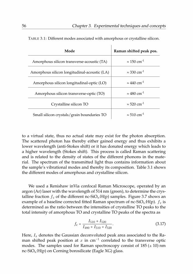
56 Chapter 3. Experimental techniques and concepts
TABLE 3.1: Different modes associated with amorphous or crystalline silicon.
Mode Raman shifted peak pos.
Amorphous silicon transverse-acoustic (TA) ≈ 150 cm-1
Amorphous silicon longitudinal-acoustic (LA) ≈ 330 cm-1
Amorphous silicon longitudinal-optic (LO) ≈ 440 cm-1
Amorphous silicon transverse-optic (TO) ≈ 480 cm-1
Crystalline silicon TO ≈ 520 cm-1
Small silicon crystals/grain boundaries TO ≈ 510 cm-1
to a virtual state, thus no actual state may exist for the photon absorption.The scattered photon has thereby either gained energy and thus exhibits alower wavelength (anti-Stokes shift) or it has donated energy which leads toa higher wavelength (Stokes shift). This process is called Raman scatteringand is related to the density of states of the different phonons in the mate-rial. The spectrum of the transmitted light thus contains information aboutthe sample’s vibrational modes and thereby its composition. Table 3.1 showsthe different modes of amorphous and crystalline silicon.
We used a Renishaw inVia confocal Raman Microscope, operated by anargon (Ar) laser with the wavelength of 514 nm (green), to determine the crys-talline fraction f c of the different nc-SiOx:H(p) samples. Figure 3.7 shows anexample of a baseline corrected fitted Raman spectrum of nc-SiOx:H(p). f c isdetermined as the ratio between the intensities of crystalline TO peaks to thetotal intensity of amorphous TO and crystalline TO peaks of the spectra as
fc =I510 + I520
I480 + I510 + I520. (3.17)
Here, Ix denotes the Gaussian deconvoluted peak area associated to the Ra-man shifted peak position at x in cm−1 correlated to the transverse opticmodes. The samples used for Raman spectroscopy consist of 185 (± 10) nmnc-SiOx:H(p) on Corning borosilicate (Eagle XG) glass.
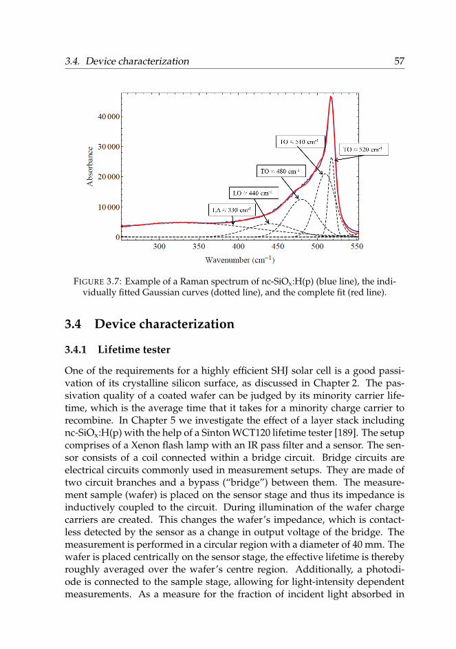
3.4. Device characterization 57
FIGURE 3.7: Example of a Raman spectrum of nc-SiOx:H(p) (blue line), the indi-vidually fitted Gaussian curves (dotted line), and the complete fit (red line).
3.4 Device characterization
3.4.1 Lifetime tester
One of the requirements for a highly efficient SHJ solar cell is a good passi-vation of its crystalline silicon surface, as discussed in Chapter 2. The pas-sivation quality of a coated wafer can be judged by its minority carrier life-time, which is the average time that it takes for a minority charge carrier torecombine. In Chapter 5 we investigate the effect of a layer stack includingnc-SiOx:H(p) with the help of a Sinton WCT120 lifetime tester [189]. The setupcomprises of a Xenon flash lamp with an IR pass filter and a sensor. The sen-sor consists of a coil connected within a bridge circuit. Bridge circuits areelectrical circuits commonly used in measurement setups. They are made oftwo circuit branches and a bypass (“bridge”) between them. The measure-ment sample (wafer) is placed on the sensor stage and thus its impedance isinductively coupled to the circuit. During illumination of the wafer chargecarriers are created. This changes the wafer’s impedance, which is contact-less detected by the sensor as a change in output voltage of the bridge. Themeasurement is performed in a circular region with a diameter of 40 mm. Thewafer is placed centrically on the sensor stage, the effective lifetime is therebyroughly averaged over the wafer’s centre region. Additionally, a photodi-ode is connected to the sample stage, allowing for light-intensity dependentmeasurements. As a measure for the fraction of incident light absorbed in
58 Chapter 3. Experimental techniques and concepts
the sample an optical constant correlated to the type of measurement sam-ple, has to be given as input parameter for the evaluation of the photodiodemeasurements. In case of a bare c-Si wafer, or a c-Si wafer coated with thinsilicon layers (on one or both both sides) a value of 0.7 is typically used. Forvery thin samples the optical constant is decreased, while surface texturing,as well as anti-reflective coatings, increase the optical constant to 1. This valueof 1 has arbitrary been chosen to be correlated to a photo generated currentof 38 mA/cm2 at 1 sun. Very thick, textured samples with an optimized antireflective coating can even reach optical constants values above 1, which is as-sociated to a generate photo current above 38 mA/cm2 [189]. The determineddata is analyzed with software provided by Sinton instruments. Dependingon the value of minority carrier lifetime different models and light pulses haveto be used. For lifetime values below 100 µs, the generalized mode in combi-nation with a slowly decaying light pulse was used. For lifetime values above100 µs a combination of a short light pulse and quasi transient mode was used[190].
Quasi transient mode
For this analysis technique, a light pulse that is short (< 10 µs) compared to theeffective minority carrier lifetime (>100 µs) is directed at the wafer. The decayin photoconductance caused by the recombination of the charge carriers isevaluated. The effective lifetime τ can then be determined as
τ = −∆n
d∆n/dt . (3.18)
Here, ∆n denotes the injection level and the denominator is the derivative ofsaid injection level.
Generalized mode
This analyzing technique unites the quasi transient mode with the quasisteady state mode, a mode used for low minority lifetimes of τ < 100 µs [191].The generalized mode can be used to measure effective lifetimes above andbelow 100 µs. However, the pulse length of the light flash needs to be adjustedto the effective lifetime by using a short pulse for τ > 100 µs and a long, slowlydecaying light pulse (decay ≈ 2.3 ms) for τ < 100 µs. The effective lifetime isthen calculated as
τ = ∆n
G − (d∆n/dt) . (3.19)
3.4. Device characterization 59
The value of the generation rate G depends on the measurementregime. In the transient regime G = 0 holds after the light pulse, which re-sults in Equation 3.18. In the quasi steady state regime d∆n/dt = 0 holds,resulting in
τ = ∆n
G. (3.20)
We chose for measurements in quasi transient mode for high lifetime val-ues (τ > 100 µs), since it evaluates the measurement without the need of datafrom the photodiode. This eliminates the possibility of measurement errorsdue to a wrong input of the optical constant. For low lifetime values (τ <100 µs), we chose for measurement in the generalized mode, since it resultsin slightly better lifetime evaluation as the quasi steady state mode. This isespecially the case for low lifetimes approaching the limit of 100 µs towardsmeasurements in quasi steady state mode [5].
Implied open circuit voltage
The implied V OC is a measure for the estimated V OC that a complete SHJsolar cell based on the evaluated lifetime sample will ideally yield. It assumesall following (additional component) layers to be loss-free. From the excesscarrier density and the separation of the quasi-Fermi levels at a light intensityof 1-sun the implied V OC can be determined as
VOC, implied = kB ⋅ Tq
⋅ ln(∆n(N +∆n)n2i
+ 1) . (3.21)
Depending on the wafer type N denotes either the donor density for n-typewafer or the acceptor density for p-type wafer, kB denotes the Boltzman’s con-stant, T the absolute temperature, q the elementary charge, ∆n the excess elec-tron density, which is assumed to be equal to the excess hole density for thiscalculation.
3.4.2 Solar simulator
The electrical behaviour of an illuminated solar cell can be imagined as a cur-rent source in parallel connection to a resistor (RP) and a diode (D), and ad-ditionally connected in series to another resistor (RS). This equivalent circuitis shown in Figure 3.8. The series resistances is caused by the parasitic resis-tances of a solar cell including various contact resistances [192]. The parallelresistance is caused by small leaks of current between the contacts. Ideally,RPshould be infinite and RS=0. RP and RS can be approximated from an exper-imental J-V curve as the inverse of the slope at the points of the open circuit
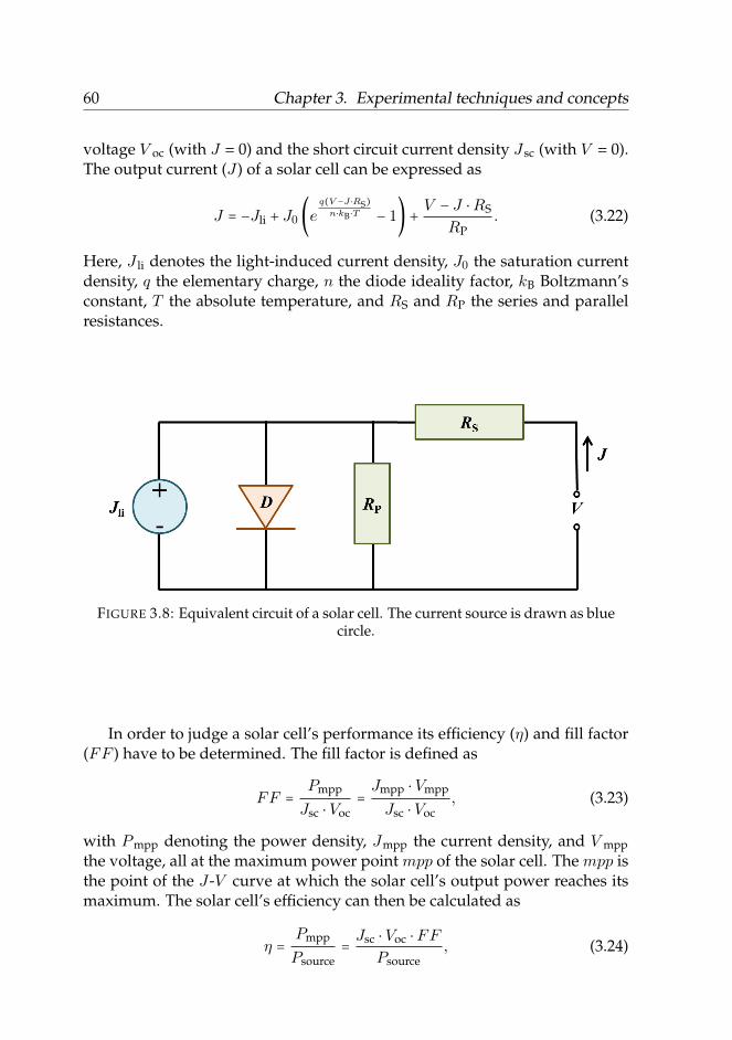
60 Chapter 3. Experimental techniques and concepts
voltage V oc (with J = 0) and the short circuit current density J sc (with V = 0).The output current (J) of a solar cell can be expressed as
J = −Jli + J0 (eq(V −J ⋅RS)
n⋅kB ⋅T − 1) + V − J ⋅RS
RP. (3.22)
Here, J li denotes the light-induced current density, J0 the saturation currentdensity, q the elementary charge, n the diode ideality factor, kB Boltzmann’sconstant, T the absolute temperature, and RS and RP the series and parallelresistances.
FIGURE 3.8: Equivalent circuit of a solar cell. The current source is drawn as bluecircle.
In order to judge a solar cell’s performance its efficiency (η) and fill factor(FF ) have to be determined. The fill factor is defined as
FF =Pmpp
Jsc ⋅ Voc=Jmpp ⋅ Vmpp
Jsc ⋅ Voc, (3.23)
with Pmpp denoting the power density, Jmpp the current density, and V mppthe voltage, all at the maximum power point mpp of the solar cell. The mpp isthe point of the J-V curve at which the solar cell’s output power reaches itsmaximum. The solar cell’s efficiency can then be calculated as
η =Pmpp
Psource= Jsc ⋅ Voc ⋅ FF
Psource, (3.24)
3.4. Device characterization 61
with P source being the power density of the incident light. In the case of stan-dard measurement conductions this would be PAM1.5:
η =Pmpp
Psource=Pmpp
PAM1.5. (3.25)
Chapter 2 gives a more detailed explanation of those parameters and their im-plication on a solar cell’s performance.
For the measurements carried out in Chapter 6 a dual beam “Super Solarsimulator” from WACOM ELECTRIC Co., Ltd. assuring a class AAA stan-dard, with an AM1.5 spectrum at an irradiance of 1-sun (1000 W/cm2) hasbeen used. A computer operated “Model 238 High Current Source MeasureUnit” from Keithley Instruments, Inc. was used as voltage source and currentmeter.
3.4.3 Spectral response setup
The spectral response setup is used to determine the solar cell’s response tothe individual frequencies of incident light. The output current of a solar cellis measured during illumination with monochromatic light. The spectral re-sponse (SR) is the ratio of the current generated by the solar cell to the powerincident on it. From this, the external quantum efficiency (EQE) can be cal-culated as the amount of electrons generated by the solar cell per incidentphoton on the solar cell. The EQE can be determined for each wavelength λand is expressed as:
EQE(λ) =Jph(λ)e ⋅Φph(λ)
. (3.26)
Here, λ denotes the photon wavelength, e the elementary charge, and Φph thephoton flux. Assuming a conformal response of the solar cell, the short circuitcurrent density (J sc) can be calculated from the measurements by convolutionin the following way:
Jsc = e ⋅ ∫ EQE(λ) ⋅ΦAM1.5(λ) dλ, (3.27)
where ΦAM1.5(λ) is the phonon flux of the AM1.5 spectrum. For the EQE mea-surements described in Chapter 6 an Optosolar (SR300) setup with a 250 Wxenon lamp and a Jobin Yvon iHR320 monochromator was used.

63
Chapter 4
nc-SiOx:H(p) emitter layer forincreased transmission
A promising way to further enhance the excellent characteristics of silicon het-erojunction (SHJ) solar cells is to enable more light to enter the crystalline sil-icon (c-Si) absorber of the cell while maintaining a simple cell configuration.Our approach is to replace the standard amorphous silicon (a-Si:H) emitterlayer with a more transparent nanocrystalline silicon oxide (nc-SiOx:H) layer.
In this chapter, we focus on optimizing the boron doped nc-SiOx:H ma-terial properties, grown by radio frequency (13.56 MHz) plasma-enhancedchemical vapour deposition (RF-PECVD), on the amorphous silicon bufferlayer. The optical and electrical properties of the material have been studiedon samples of 185 (± 10) nm prepared on Corning borosilicate glass (Eagle XG).An optimized p-type emitter layer with a lateral conductivity of7.9×10−4 S/cm, combined with a band gap of E04 = 2.33 eV has been fabri-cated.
Next, 20-nm thick nanocrystalline layers were successfully grown on a5-nm a-Si:H(i) layer. The crystallinity and thickness were confirmed by trans-mission electron microscopy (TEM). The effect of different ratios of trimethyl-boron to silane gas flow rates on the material properties was investigated.Despite its larger thickness of 20 nm, as compared to conventional windowa-Si:H p-layers of ≈ 10 nm, the novel layer stack of a-Si:H(i)/nc-SiOx:H(p)shows significantly enhanced transmission compared to the stack with a con-ventional a-Si:H(p) emitter. Altogether, the chosen material exhibits promisingcharacteristics for implementation in SHJ solar cells.
64 Chapter 4. nc-SiOx:H(p) emitter layer for increased transmission
4.1 Introduction
Silicon heterojunction (SHJ) solar cells in a back-contacted configuration holdthe record efficiency of 26.33% for crystalline silicon based solar cells [11].The general main feature of SHJ solar cells lies in their remarkable high opencircuit voltage, VOC, enabled by the excellent surface passivation of the crys-talline silicon wafer. To enable the outstanding efficiency of 26.33%, theirshort circuit current density, JSC, is enhanced by a fully back contacted de-sign. However, this design requires a much more complicated productionprocedure compared to bifacially contacted SHJ solar cells.
Standard SHJ solar cells are bifacially contacted and a huge interest liesin improving their performance. As mentioned in Chapter 2, several groupsare working towards the goal of an increased JSC by implementing a moretransparent window layer at the front side of the SHJ solar cell. Thus, increas-ing the JSC of SHJ solar cells while keeping the more simple front emitterbifacially cell design. Possible candidates are e.g. amorphous silicon carbide(a-SiC:H) [16], molybdenum oxide (MoOx, x < 3) [193], microcrystalline sili-con (µc-Si:H) [46], or aluminum oxide (Al2O3) in combination with ZnO asa hole selective contact [194]. However, some of them are currently facingdrawbacks such as e.g. high annealing temperatures (400°C for Al2O3) [195]or difficulties in band alignment (MoOx) [193] as well as a restrain to too lowpost deposition temperatures (< 100°C for MoOx) to avoid interface mixing.
To avoid these issues, we propose to replace the traditional amorphous sil-icon emitter layer by a more transparent nanocrystalline silicon oxide(nc-SiOx:H) layer. Mazzarella et al., in a research project parralel to this one,recently showed the possibility of this configuration [41]. This chapter focuseson optimizing the p-type nc-SiOx:H material properties for this purpose.
The general properties and features of nc-SiOx:H have been thoroughlydiscussed in Chapter 2. In the following, we will give a short summary re-garding the physics necessary to understand the research described in thischapter. nc-SiOx:H(p) is a mixed-phase material consisting of silicon nanocrystallites in an amorphous silicon oxide matrix [41] [54]. Hydrogenated sili-con oxide, in general, consists of an Si:H matrix that includes areas of Si:O [58].The growth evolution of nc-SiOx:H depends on the underlying seed material.On top of an a-Si:H substrate the first few nanometers of the layer consist ofan amorphous incubation phase. Thereon, the crystalline growth develops.The crystallinity gradually increases towards the top of the layer [64]. An ox-ide material (e.g. borosilicate glass) or a crystalline surface (e.g. c-Si wafer),
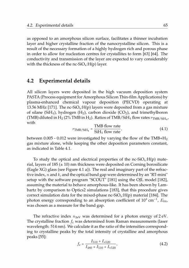
4.2. Experimental details 65
as opposed to an amorphous silicon surface, facilitates a thinner incubationlayer and higher crystalline fraction of the nanocrystalline silicon. This is aresult of the necessary formation of a highly hydrogen rich and porous phasein order to allow for nucleation centres for crystallites to form [63] [64]. Theconductivity and transmission of the layer are expected to vary considerablywith the thickness of the nc-SiOx:H(p) layer.
4.2 Experimental details
All silicon layers were deposited in the high vacuum deposition systemPASTA (Process equipment for Amorphous Silicon Thin-film Applications) byplasma-enhanced chemical vapour deposition (PECVD) operating at13.56 MHz [171]. The nc-SiOx:H(p) layers were deposited from a gas mixtureof silane (SiH4), hydrogen (H2), carbon dioxide (CO2), and trimethylboron(TMB) diluted in H2 (2% TMB in H2). Ratios of TMB/SiH4 flow rates rTMB/SiH4
,with
rTMB/SiH4= TMB flow rate
SiH4 flow rate, (4.1)
between 0.005 - 0.012 were investigated by varying the flow of the TMB+H2
gas mixture alone, while keeping the other deposition parameters constant,as indicated in Table 4.1.
To study the optical and electrical properties of the nc-SiOx:H(p) mate-rial, layers of 185 (± 10) nm thickness were deposited on Corning borosilicate(Eagle XG) glass (see Figure 4.1 a)). The real and imaginary part of the refrac-tive index, n and k, and the optical band gap were determined by an "RT-mini"setup with the software program "SCOUT" [181] using the OJL model [182],assuming the material to behave amorphous-like. It has been shown by Lam-bartz by comparison to Optics2 simulations [183], that this procedure givescorrect simulation data for the mixed-phase nc-SiOx:H(p) material [184]. Thephoton energy corresponding to an absorption coefficient of 104 cm−1, E04,was chosen as a measure for the band gap.
The refractive index n2eV was determined for a photon energy of 2 eV.The crystalline fraction fc was determined from Raman measurements (laserwavelength: 514 nm). We calculate it as the ratio of the intensities correspond-ing to crystalline peaks by the total intensity of crystalline and amorphouspeaks [55]:
fc =I510 + I≈520
I480 + I510 + I≈520, (4.2)
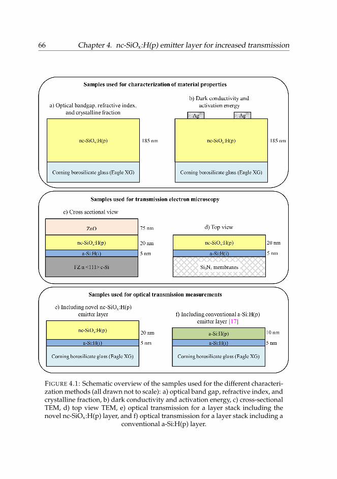
66 Chapter 4. nc-SiOx:H(p) emitter layer for increased transmission
FIGURE 4.1: Schematic overview of the samples used for the different characteri-zation methods (all drawn not to scale): a) optical band gap, refractive index, andcrystalline fraction, b) dark conductivity and activation energy, c) cross-sectionalTEM, d) top view TEM, e) optical transmission for a layer stack including thenovel nc-SiOx:H(p) layer, and f) optical transmission for a layer stack including a
conventional a-Si:H(p) layer.
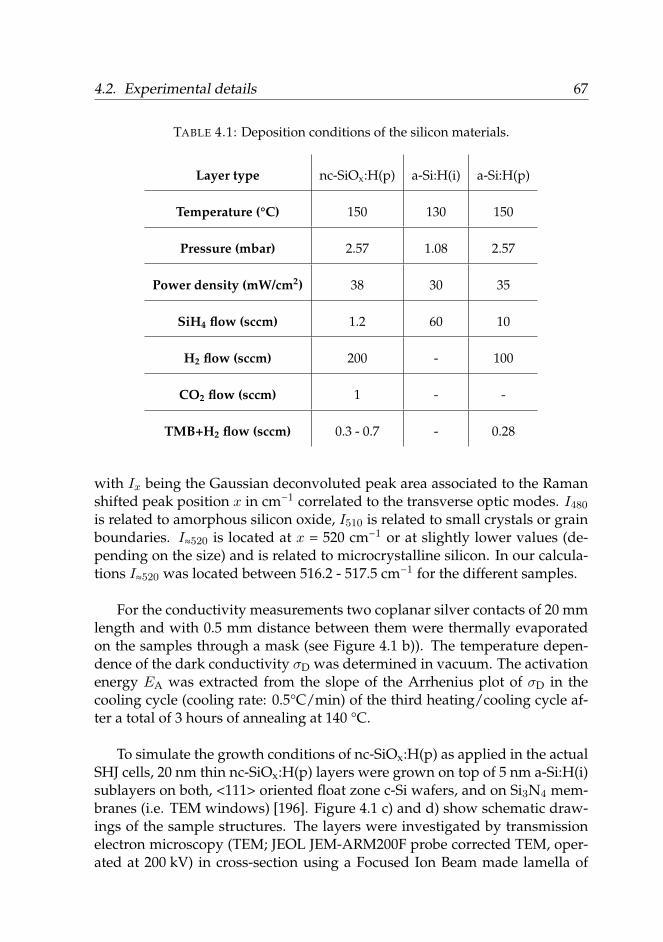
4.2. Experimental details 67
TABLE 4.1: Deposition conditions of the silicon materials.
Layer type nc-SiOx:H(p) a-Si:H(i) a-Si:H(p)
Temperature (°C) 150 130 150
Pressure (mbar) 2.57 1.08 2.57
Power density (mW/cm2) 38 30 35
SiH4 flow (sccm) 1.2 60 10
H2 flow (sccm) 200 - 100
CO2 flow (sccm) 1 - -
TMB+H2 flow (sccm) 0.3 - 0.7 - 0.28
with Ix being the Gaussian deconvoluted peak area associated to the Ramanshifted peak position x in cm−1 correlated to the transverse optic modes. I480is related to amorphous silicon oxide, I510 is related to small crystals or grainboundaries. I≈520 is located at x = 520 cm−1 or at slightly lower values (de-pending on the size) and is related to microcrystalline silicon. In our calcula-tions I≈520 was located between 516.2 - 517.5 cm−1 for the different samples.
For the conductivity measurements two coplanar silver contacts of 20 mmlength and with 0.5 mm distance between them were thermally evaporatedon the samples through a mask (see Figure 4.1 b)). The temperature depen-dence of the dark conductivity σD was determined in vacuum. The activationenergy EA was extracted from the slope of the Arrhenius plot of σD in thecooling cycle (cooling rate: 0.5°C/min) of the third heating/cooling cycle af-ter a total of 3 hours of annealing at 140 °C.
To simulate the growth conditions of nc-SiOx:H(p) as applied in the actualSHJ cells, 20 nm thin nc-SiOx:H(p) layers were grown on top of 5 nm a-Si:H(i)sublayers on both, <111> oriented float zone c-Si wafers, and on Si3N4 mem-branes (i.e. TEM windows) [196]. Figure 4.1 c) and d) show schematic draw-ings of the sample structures. The layers were investigated by transmissionelectron microscopy (TEM; JEOL JEM-ARM200F probe corrected TEM, oper-ated at 200 kV) in cross-section using a Focused Ion Beam made lamella of
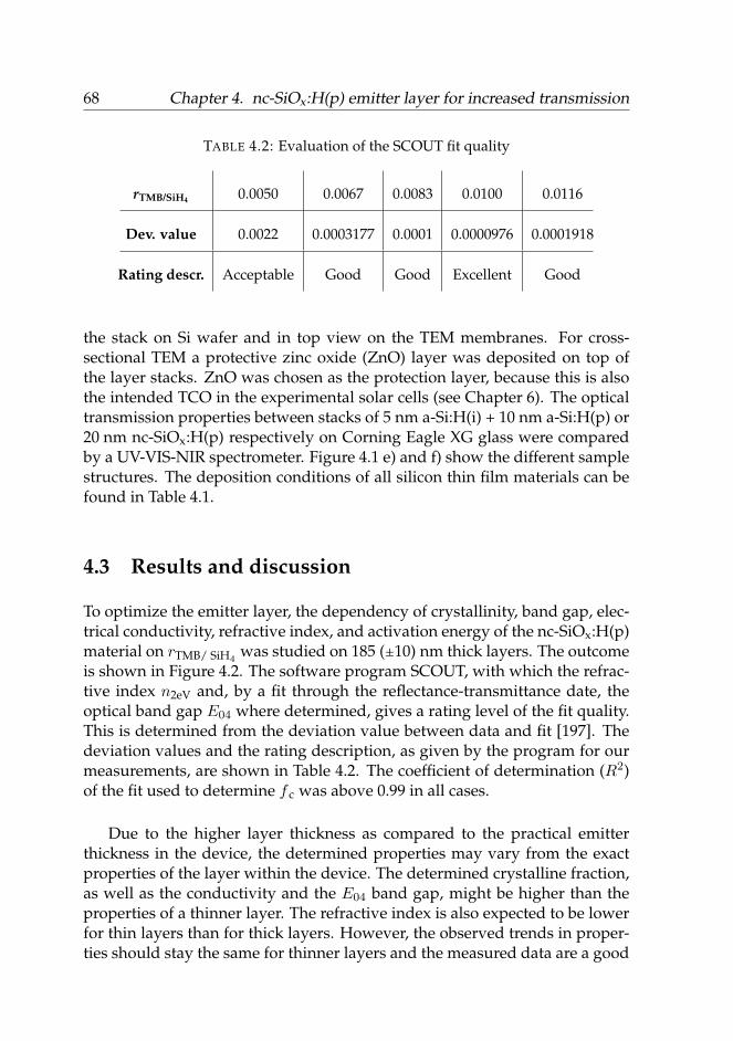
68 Chapter 4. nc-SiOx:H(p) emitter layer for increased transmission
TABLE 4.2: Evaluation of the SCOUT fit quality
rTMB/SiH4 0.0050 0.0067 0.0083 0.0100 0.0116
Dev. value 0.0022 0.0003177 0.0001 0.0000976 0.0001918
Rating descr. Acceptable Good Good Excellent Good
the stack on Si wafer and in top view on the TEM membranes. For cross-sectional TEM a protective zinc oxide (ZnO) layer was deposited on top ofthe layer stacks. ZnO was chosen as the protection layer, because this is alsothe intended TCO in the experimental solar cells (see Chapter 6). The opticaltransmission properties between stacks of 5 nm a-Si:H(i) + 10 nm a-Si:H(p) or20 nm nc-SiOx:H(p) respectively on Corning Eagle XG glass were comparedby a UV-VIS-NIR spectrometer. Figure 4.1 e) and f) show the different samplestructures. The deposition conditions of all silicon thin film materials can befound in Table 4.1.
4.3 Results and discussion
To optimize the emitter layer, the dependency of crystallinity, band gap, elec-trical conductivity, refractive index, and activation energy of the nc-SiOx:H(p)material on rTMB/ SiH4
was studied on 185 (±10) nm thick layers. The outcomeis shown in Figure 4.2. The software program SCOUT, with which the refrac-tive index n2eV and, by a fit through the reflectance-transmittance date, theoptical band gap E04 where determined, gives a rating level of the fit quality.This is determined from the deviation value between data and fit [197]. Thedeviation values and the rating description, as given by the program for ourmeasurements, are shown in Table 4.2. The coefficient of determination (R2)of the fit used to determine f c was above 0.99 in all cases.
Due to the higher layer thickness as compared to the practical emitterthickness in the device, the determined properties may vary from the exactproperties of the layer within the device. The determined crystalline fraction,as well as the conductivity and the E04 band gap, might be higher than theproperties of a thinner layer. The refractive index is also expected to be lowerfor thin layers than for thick layers. However, the observed trends in proper-ties should stay the same for thinner layers and the measured data are a good
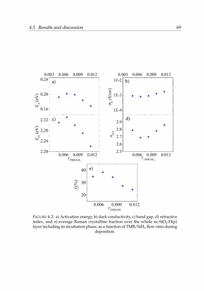
4.3. Results and discussion 69
FIGURE 4.2: a) Activation energy, b) dark conductivity, c) band gap, d) refractiveindex, and e) average Raman crystalline fraction over the whole nc-SiOx:H(p)layer including its incubation phase, as a function of TMB/SiH4 flow ratio during
deposition.
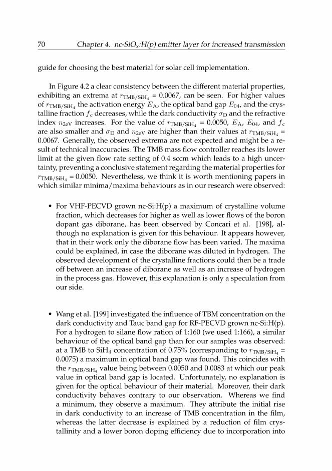
70 Chapter 4. nc-SiOx:H(p) emitter layer for increased transmission
guide for choosing the best material for solar cell implementation.
In Figure 4.2 a clear consistency between the different material properties,exhibiting an extrema at rTMB/SiH4
= 0.0067, can be seen. For higher valuesof rTMB/SiH4
the activation energy EA, the optical band gap E04, and the crys-talline fraction f c decreases, while the dark conductivity σD and the refractiveindex n2eV increases. For the value of rTMB/SiH4
= 0.0050, EA, E04, and f care also smaller and σD and n2eV are higher than their values at rTMB/SiH4
=0.0067. Generally, the observed extrema are not expected and might be a re-sult of technical inaccuracies. The TMB mass flow controller reaches its lowerlimit at the given flow rate setting of 0.4 sccm which leads to a high uncer-tainty, preventing a conclusive statement regarding the material properties forrTMB/SiH4
= 0.0050. Nevertheless, we think it is worth mentioning papers inwhich similar minima/maxima behaviours as in our research were observed:
• For VHF-PECVD grown nc-Si:H(p) a maximum of crystalline volumefraction, which decreases for higher as well as lower flows of the borondopant gas diborane, has been observed by Concari et al. [198], al-though no explanation is given for this behaviour. It appears however,that in their work only the diborane flow has been varied. The maximacould be explained, in case the diborane was diluted in hydrogen. Theobserved development of the crystalline fractions could then be a tradeoff between an increase of diborane as well as an increase of hydrogenin the process gas. However, this explanation is only a speculation fromour side.
• Wang et al. [199] investigated the influence of TBM concentration on thedark conductivity and Tauc band gap for RF-PECVD grown nc-Si:H(p).For a hydrogen to silane flow ration of 1:160 (we used 1:166), a similarbehaviour of the optical band gap than for our samples was observed:at a TMB to SiH4 concentration of 0.75% (corresponding to rTMB/SiH4 =0.0075) a maximum in optical band gap was found. This coincides withthe rTMB/SiH4 value being between 0.0050 and 0.0083 at which our peakvalue in optical band gap is located. Unfortunately, no explanation isgiven for the optical behaviour of their material. Moreover, their darkconductivity behaves contrary to our observation. Whereas we finda minimum, they observe a maximum. They attribute the initial risein dark conductivity to an increase of TMB concentration in the film,whereas the latter decrease is explained by a reduction of film crys-tallinity and a lower boron doping efficiency due to incorporation into
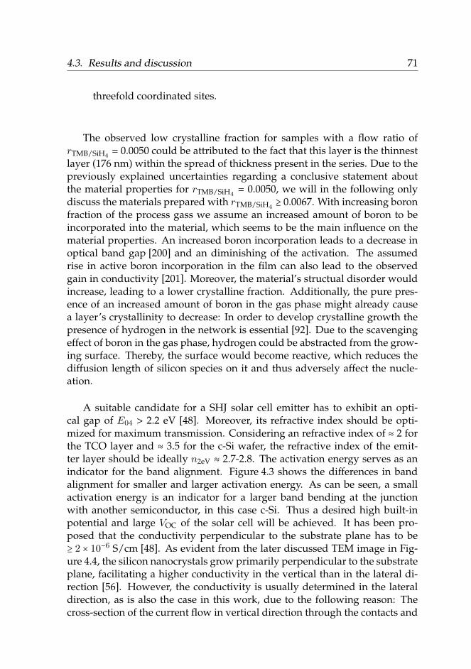
4.3. Results and discussion 71
threefold coordinated sites.
The observed low crystalline fraction for samples with a flow ratio ofrTMB/SiH4
= 0.0050 could be attributed to the fact that this layer is the thinnestlayer (176 nm) within the spread of thickness present in the series. Due to thepreviously explained uncertainties regarding a conclusive statement aboutthe material properties for rTMB/SiH4
= 0.0050, we will in the following onlydiscuss the materials prepared with rTMB/SiH4
≥ 0.0067. With increasing boronfraction of the process gass we assume an increased amount of boron to beincorporated into the material, which seems to be the main influence on thematerial properties. An increased boron incorporation leads to a decrease inoptical band gap [200] and an diminishing of the activation. The assumedrise in active boron incorporation in the film can also lead to the observedgain in conductivity [201]. Moreover, the material’s structual disorder wouldincrease, leading to a lower crystalline fraction. Additionally, the pure pres-ence of an increased amount of boron in the gas phase might already causea layer’s crystallinity to decrease: In order to develop crystalline growth thepresence of hydrogen in the network is essential [92]. Due to the scavengingeffect of boron in the gas phase, hydrogen could be abstracted from the grow-ing surface. Thereby, the surface would become reactive, which reduces thediffusion length of silicon species on it and thus adversely affect the nucle-ation.
A suitable candidate for a SHJ solar cell emitter has to exhibit an opti-cal gap of E04 > 2.2 eV [48]. Moreover, its refractive index should be opti-mized for maximum transmission. Considering an refractive index of ≈ 2 forthe TCO layer and ≈ 3.5 for the c-Si wafer, the refractive index of the emit-ter layer should be ideally n2eV ≈ 2.7-2.8. The activation energy serves as anindicator for the band alignment. Figure 4.3 shows the differences in bandalignment for smaller and larger activation energy. As can be seen, a smallactivation energy is an indicator for a larger band bending at the junctionwith another semiconductor, in this case c-Si. Thus a desired high built-inpotential and large VOC of the solar cell will be achieved. It has been pro-posed that the conductivity perpendicular to the substrate plane has to be≥ 2 × 10⁻⁶ S/cm [48]. As evident from the later discussed TEM image in Fig-ure 4.4, the silicon nanocrystals grow primarily perpendicular to the substrateplane, facilitating a higher conductivity in the vertical than in the lateral di-rection [56]. However, the conductivity is usually determined in the lateraldirection, as is also the case in this work, due to the following reason: Thecross-section of the current flow in vertical direction through the contacts and
72 Chapter 4. nc-SiOx:H(p) emitter layer for increased transmission
the film is several orders of magnitude higher than those in horizontal direc-tion through the film. For a large cross-section, the contact resistance is notnegligible anymore, which makes measurements in vertical direction increas-ingly difficult [202]. Nevertheless, Cuony et al. succeeded in measuring thecurrent - voltage curves in vertical direction of nc-SiOx:H(p) sandwiched be-tween two ZnO layers [80].
FIGURE 4.3: Band diagram of a junction between a p-type semiconductor andan n-type semiconductor. The acceptor level Eac and the activation energy EAof the p-type semiconductor, the conduction and valence band, EC and EV, theFermi level EF, and the band gap EG are indicated. The conditions for a smallactivation energy (left) and a larger activation energy (right) of the p-type layer
are shown for a constant band gap of the material.
Based on the data shown in Figure 4.2, the most promising emitter layermaterial was selected. The conductivities of all samples are around10−3 S/cm−1. The values for conductivity, refractive index, and activationenergy are in a suitable range for the use as emitter layer in SHJ. Thus, themost transparent material with E04 = 2.33 eV at rTMB/SiH4
= 0.006, with σD =7.9 × 10⁻⁴ S/cm, EA = 0.2 eV, and n2eV = 2.7 was chosen. Not only does itshow the highest band gap, it also exhibits a very favourable refractive index,as discussed above.
Notable is the high conductivity as compared to Mazzarella et al., whoalso designed a nc-SiOx:H(p) emitter layer. Their band gap (E04 = 2.23 eV)and refractive index (at a wavelength of 632 nm (corresponding to 1.96 eV)) ofn632 nm = 2.87 are comparable to our findings, but their reported conductivityof σD = 8.9×10⁻⁸ S/cm (on 100-200 nm thick films) is several orders of magni-tude lower [41]. However, since they do not give detailed information of theexact thickness of the measured sample, it is difficult to judge, whether or not
4.3. Results and discussion 73
the increased conductivity of our material might be caused by a larger thick-ness and thus larger crystallinity towards the top of the layer. Another possi-ble explanation could be, that their material was grown in a different plasmaregime than ours. It has been found by Gabriel et al. [57] that two differentplasma regimes exist. The first regime is characterized by a low pressure andhigh RF power. The second regime requires a high pressure and a low RFpower. With this knowledge, they have been able to fabricate nc-SiOx:H withdifferent combinations of crystalline fractions (which is related to the conduc-tivity) and refractive indices. For example, a silicon oxide material with arefractive index of n ≈ 2.4 can be achieved with crystalline fractions withinthe wide range of approximately 0.2 - 55%. Judging from these results, it is arealistic assumption that the materials of Mazzarella et al. and ours do exhibita different crystalline fraction and thus a different conductivity for the samerefractive index.
As mentioned before, the crystallinity of a nc-SiOx:H(p) layer depends,among others, on the material it is grown on and increases with increasinglayer thickness. To study the effect of rTMB/SiH4
on the crystallinity of realisticmaterial, 20-nm thick nc-SiOx:H(p) layers were prepared on a-Si:H(i) and in-vestigated by TEM (see Figure 4.1 c) and d)). Figure 4.4 shows cross-sectionalTEM images of the 5 nm a-Si:H(i) + 20 nm nc-SiOx:H(p) + ZnO layer stacksgrown on c-Si wafer with TMB to silane flow ratios of rTMB/SiH4
= 0.006 (a) andrTMB/SiH4
= 0.012 (b). The boundaries with the crystalline wafer are indicatedby the solid lines. By bare eye it is difficult to clearly distinguish betweenthe end of the a-Si:H(i) layer and the beginning of the nc-SiOx:H(p) layerfrom the image, due to the presence of an amorphous incubation phase of thenc-SiOx:H(p) layer. The dashed line indicates the approximate position of theboundary between the a-Si:H(i) and the nc-SiOx:H(p) layer. The a-Si:H(i) layerthickness of 5.0 (± 0.3) nm was determined from small changes in the densitycontrast of the TEM picture of the sample with rTMB/SiH4
= 0.006. This deter-mined value is in agreement with the 5 nm of a-Si:H(i) that we aimed to de-posit, as controlled by the deposition duration. However, the a-Si:H(i) layermight have become porous during the subsequent nc-SiOx:H(p) deposition,due to indiffusion of atomic hydrogen from the plasma. In case of pores with≤ 2 nm diameter, the distinction between the porous part of the a-Si:H(i) andthe porous incubation layer of the nc-SiOx:H(p) might have not been madecorrectly. Thus, the determined a-Si:H(i) layer thickness might not be accu-rate.
The crystal growth starts after the incubation layer and the crystallinefraction increases with increasing layer thickness. The regions indicated by
74 Chapter 4. nc-SiOx:H(p) emitter layer for increased transmission
the white lines are single crystals, as evident from selected area Fast FourierTransform analysis (not shown here). These crystals are not crystallographi-cally related to the substrate. Close inspection of the atomic resolution imagesshows that the Si crystals contain stacking faults and twin boundaries. A cleardecrease of the degree of crystallinity for higher TMB ratio is visible.
FIGURE 4.4: Cross-sectional TEM image of samples of c-Si wafer/5nm a-Si:H(i)/20nm nc-SiOx:H(p)/ZnO layer stacks witha) rTMB/SiH4
= 0.006 andb) rTMB/SiH4
= 0.012. Several crystals are indicated by white lines.
To further illustrate the differences in crystallinity, the electron dif-fraction patterns and the intensity profiles of the electron diffraction patternsof the 5 nm a Si:H(i) + 20 nm nc-SiOx:H(p) layer stacks grown at the two dif-ferent TMB/SiH4 ratios are depicted in Figure 4.5. The differences in intensityof the characteristic white lines of the diffraction patterns are clearly visible.These differences in the intensity profile further support the presence of alarger crystalline fraction at the smaller value of rTMB/SiH4
. To display thosedifferences, a vertical offset was applied to the curve for rTMB/SiH4
= 0.012. Thedecrease in crystallinity with increasing rTMB/SiH4
flow ratio can be explainedby an assumed increase of the boron fraction in the material, which generallyhinders the nucleation of nanocrystals due to a higher compositional disorder[200]. As previously discussed, another explanation could simply lie in theincreased amount of boron in the gas phase and its scavenging effect on hy-drogen. The lower amount of hydrogen on the surface leads to an increasedsurface reactivity. The reduced diffusion length of silicon species on the sur-face then derates crystalline growth.
4.3. Results and discussion 75
FIGURE 4.5: a) Electron diffraction patterns of sample stacks with rTMB/SiH4=
0.006 (left) and 0.012 (right) determined by top view HRTEM. The correspondingcrystal planes are indicated by the yellow numbers. b) Intensity profiles obtained
from the diffraction pattern by rotational averaging.
The growth of nc-SiOx:H is highly substrate and thickness dependent [63].To this end, the transmission of the SHJ front side for realistic emitter layers(i.e. with a thickness of 20 nm and grown on the actual amorphous siliconbuffer layer of 5 nm) was studied. Figure 4.6 shows the transmittance T as afunction of incident wavelength λ for the layer stack of a-Si:H(i)/nc-SiOx:H(p)(rTMB/SiH4
= 0.006) on Corning Eagle XG glass, with respect to the conven-tional stack of a-Si:H i/p on Corning Eagle XG glass. The data is corrected forthe reflection losses due to the glass substrate. For wavelengths larger than250 nm and up to 900 nm the novel layer stack shows a significant enhance-ment in transmission. The most significant increase can be seen at λ = 480 nmwith a transmission of 33% for the conventional stack of 5 nm a-Si:H(i)/10 nma-Si:H(p) and 47% for the stack including the novel layer consisting of 5 nma-Si:H(i)/20 nm nc-SiOx:H(p). This improvement is attributed to the lower re-fractive index of nc-SiOx:H(p) compared to a-Si:H(p). Figure 4.7 illustrates thedifferences in real and imaginary part of the refractive indices for nc-SiOx:H(p)(grown with rTMB/SiH4
= 0.006) and a conventional a-Si:H(p) layer.
It should be pointed out, that in order to compare the optical suitabilityof the different emitter layer materials, the effects of the refractive indices aswell as the necessary emitter layer thicknesses have to be taken into consid-eration (as done for the transmittance evaluation we discussed above). Thus,the sole examination of the refractive indices would not yet prove that thenc-SiOx:H(p) emitter would be optically superior.
76 Chapter 4. nc-SiOx:H(p) emitter layer for increased transmission
FIGURE 4.6: Transmittance as a function of wavelength for a conventionala-Si:H i/p stack (blue) and a novel a-Si:H(i)/nc-SiOx:H(p) stack (orange) (both
on Corning glass), as the passivation/emitter for SHJ solar cells.
FIGURE 4.7: Real (n, dashed line) and imaginary part (k, solid line) of the refrac-tive index for nc-SiOx:H(p) (orange) and a-Si:H(p) (blue) as a function of wave-
length.
4.4. Conclusions 77
4.4 Conclusions
The material properties of p-type nanocrystalline silicon oxide were optimizedfor the implementation as emitter layer in SHJ solar cells. The crystallinityof the layers with device-compatible thickness on amorphous substrate wasproven and the material shows favourable optical properties. A broad en-hancement in transmission mainly in the wavelength range between300-900 nm is demonstrated for the investigated a-Si:H(i)/nc-SiOx:H(p) layerstack with respect to that for a conventional counterpart of a-Si:H i/p stack.The reason for the increased transparency despite the increased thicknessof the 20 nm nc-SiOx:H(p) layer compared to conventional 10 nm a-Si:H(p)layer lies in the low real and imaginary part of the refractive index n andk of the nc-SiOx:H(p) material. These experimental results suggest that thenc-SiOx:H(p) layer is a promising candidate for SHJ solar cells. Upon imple-mentation of this layer, an increased JSC caused by the enhanced transmissionis expected.

79
Chapter 5
Heat-withstanding surfacepassivation in combination withnc-SiOx:H(p) emitter layer
One of the restrictions during silicon heterojunction (SHJ) solar cell produc-tion is the limitation to comparably low post processing temperatures due tothe deteriorating effect of high temperatures on the passivation properties ofintrinsic amorphous silicon (a-Si:H(i)) buffer layers combined with conven-tional boron doped amorphous silicon (a-Si:H(p)) emitter layers. We presentin this chapter a boron doped nanocrystalline silicon oxide (nc-SiOx:H(p)) ma-terial that is compatible with high-temperature processing steps.
Passivation samples consisting of 5 nm a-Si:H(i) buffer layer and 20 nmnc-SiOx:H(p) emitter layers on the back and the front of c-Si wafers have beeninvestigated. An increase in minority carrier lifetime with post deposition an-nealing temperatures up to 293°C has been observed. This improvement ofpassivation properties upon annealing at such high temperatures for a passi-vation stack including a p-type silicon based layer, is a remarkable discovery.
In a second step, the influence of the front buffer layer thickness in combi-nation with the novel emitter has been investigated. To this end, the impliedVOC of annealed semi cells with different buffer layer thickness have beenstudied.
80Chapter 5. Heat-withstanding surface passivation in combination with
nc-SiOx:H(p) emitter layer
5.1 Introduction
As mentioned in Chapter 2 and 4, a possibility to achieve a high short circuitcurrent density (JSC) but maintain the simple bifacially cell design of con-ventionally contacted SHJ solar cells lies in the implementation of a moretransparent front layer stack of SHJ solar cells. In the search for this, borondoped nanocrystalline silicon oxide (nc-SiOx:H(p)) has generated attention asthe emitter layer [47] [48] [49] [50]. The implementation of these materials haslead to an increase in JSC compared to the use of a conventional boron-dopedamorphous silicon (a-Si:H(p)) emitter layer [53]. In addition to a high JSC,another prerequisite to achieve outstanding high efficiencies is a high opencircuit voltage (VOC), requiring excellent surface passivation of the c-Si wafer.For conventional a-Si:H(p) emitter layer, the degradation of passivation prop-erties upon even moderate annealing temperatures has been a limiting factorduring post production processing [30] [203].
In the following, we present nc-SiOx:H(p) combined with an intrinsicamorphous silicon (a-Si:H(i)) buffer layer as thermally superior emitter layerwhose passivation properties improve upon annealing even up to temper-atures of 293°C. The beneficial behaviour of the material is attributed to thenatural spatial separation of hydrogen and most of the active boron within thenc-SiOx:H(p) material. Because the boron doping is not in direct vicinity to theSi-H bonds within the material, the Fermi-level dependent Si-H bond rupturetakes place at much higher temperatures in nc-SiOx:H(p) than in a-Si:H(p).
5.2 Experimental details
For this study, different samples consisting of thin silicon based layers de-posited on <111> oriented n-type Float Zone c-Si wafers (thickness ≈275 µm, resistivity ≈ 2-5 Ω⋅cm) have been fabricated. To remove the native ox-ide layer, the wafers were dipped for 2 minutes in 1% hydrofluoric acid (HF)solution (diluted in de-ionised water) and blown dry with nitrogen (N2) priorto deposition. All layers were deposited in the PASTA (Process equipmentfor Amorphous Silicon Thin-film Applications) parallel plate reactor usingradio frequency (13.56 MHz) plasma-enhanced chemical vapour deposition(RF-PECVD) [171]. The deposition conditions are shown in Table 5.1. Thetrimethylborone (TMB) and phosphine (PH3) was diluted in hydrogen (H2)(2% dopant gas in H2). The material properties of the nc-SiOx:H(p) layer,as determined in Chapter 4, are shown in Table 5.2. An extensive study ofthe nc-SiOx:H(p) material and its properties can be found in Chapter 4. The
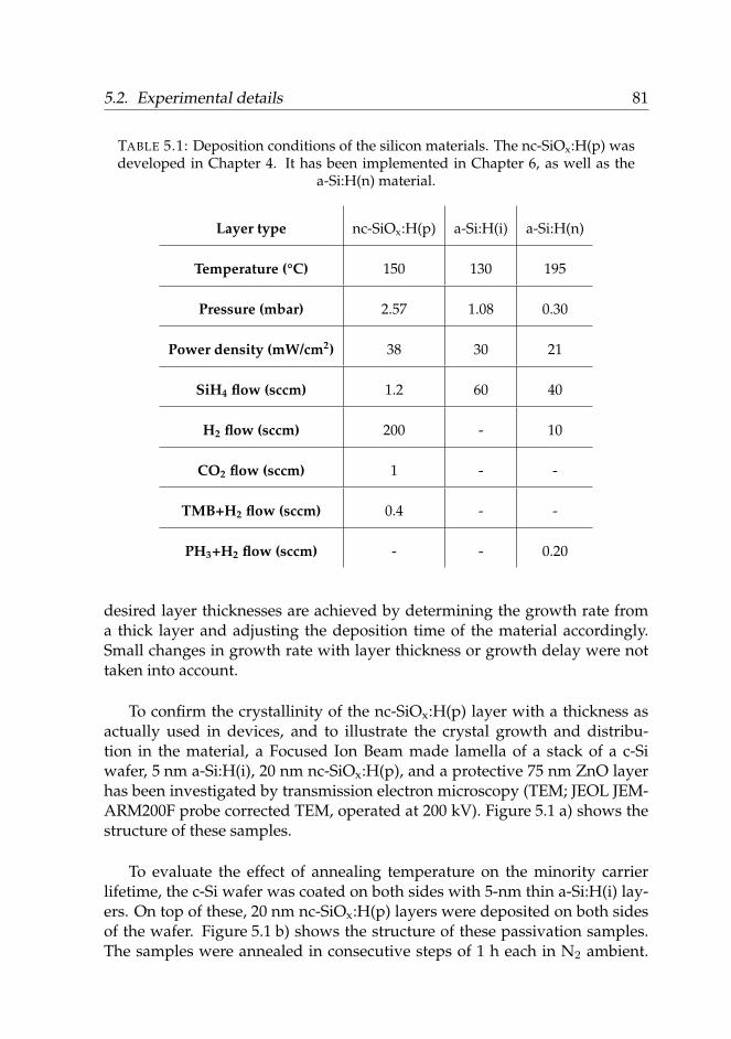
5.2. Experimental details 81
TABLE 5.1: Deposition conditions of the silicon materials. The nc-SiOx:H(p) wasdeveloped in Chapter 4. It has been implemented in Chapter 6, as well as the
a-Si:H(n) material.
Layer type nc-SiOx:H(p) a-Si:H(i) a-Si:H(n)
Temperature (°C) 150 130 195
Pressure (mbar) 2.57 1.08 0.30
Power density (mW/cm2) 38 30 21
SiH4 flow (sccm) 1.2 60 40
H2 flow (sccm) 200 - 10
CO2 flow (sccm) 1 - -
TMB+H2 flow (sccm) 0.4 - -
PH3+H2 flow (sccm) - - 0.20
desired layer thicknesses are achieved by determining the growth rate froma thick layer and adjusting the deposition time of the material accordingly.Small changes in growth rate with layer thickness or growth delay were nottaken into account.
To confirm the crystallinity of the nc-SiOx:H(p) layer with a thickness asactually used in devices, and to illustrate the crystal growth and distribu-tion in the material, a Focused Ion Beam made lamella of a stack of a c-Siwafer, 5 nm a-Si:H(i), 20 nm nc-SiOx:H(p), and a protective 75 nm ZnO layerhas been investigated by transmission electron microscopy (TEM; JEOL JEM-ARM200F probe corrected TEM, operated at 200 kV). Figure 5.1 a) shows thestructure of these samples.
To evaluate the effect of annealing temperature on the minority carrierlifetime, the c-Si wafer was coated on both sides with 5-nm thin a-Si:H(i) lay-ers. On top of these, 20 nm nc-SiOx:H(p) layers were deposited on both sidesof the wafer. Figure 5.1 b) shows the structure of these passivation samples.The samples were annealed in consecutive steps of 1 h each in N2 ambient.
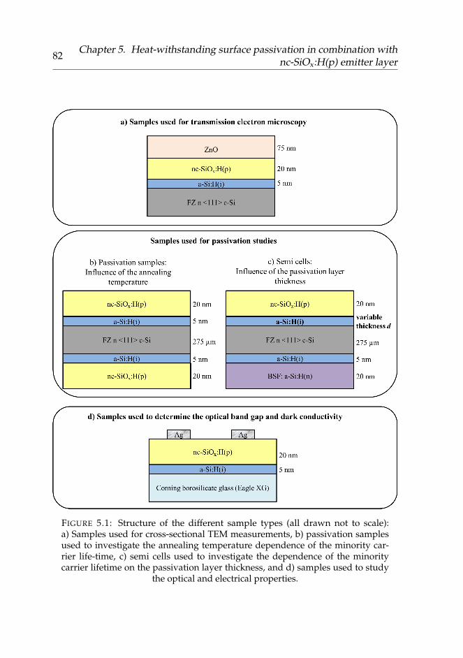
82Chapter 5. Heat-withstanding surface passivation in combination with
nc-SiOx:H(p) emitter layer
FIGURE 5.1: Structure of the different sample types (all drawn not to scale):a) Samples used for cross-sectional TEM measurements, b) passivation samplesused to investigate the annealing temperature dependence of the minority car-rier life-time, c) semi cells used to investigate the dependence of the minoritycarrier lifetime on the passivation layer thickness, and d) samples used to study
the optical and electrical properties.
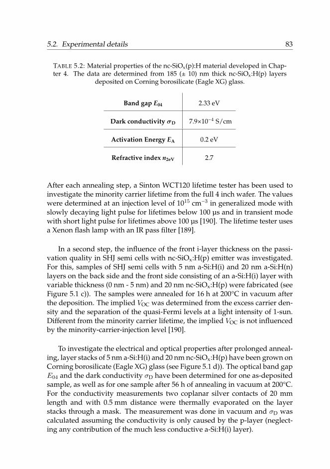
5.2. Experimental details 83
TABLE 5.2: Material properties of the nc-SiOx(p):H material developed in Chap-ter 4. The data are determined from 185 (± 10) nm thick nc-SiOx:H(p) layers
deposited on Corning borosilicate (Eagle XG) glass.
Band gap E04 2.33 eV
Dark conductivity σD 7.9×10⁻⁴ S/cm
Activation Energy EA 0.2 eV
Refractive index n2eV 2.7
After each annealing step, a Sinton WCT120 lifetime tester has been used toinvestigate the minority carrier lifetime from the full 4 inch wafer. The valueswere determined at an injection level of 1015 cm−3 in generalized mode withslowly decaying light pulse for lifetimes below 100 µs and in transient modewith short light pulse for lifetimes above 100 µs [190]. The lifetime tester usesa Xenon flash lamp with an IR pass filter [189].
In a second step, the influence of the front i-layer thickness on the passi-vation quality in SHJ semi cells with nc-SiOx:H(p) emitter was investigated.For this, samples of SHJ semi cells with 5 nm a-Si:H(i) and 20 nm a-Si:H(n)layers on the back side and the front side consisting of an a-Si:H(i) layer withvariable thickness (0 nm - 5 nm) and 20 nm nc-SiOx:H(p) were fabricated (seeFigure 5.1 c)). The samples were annealed for 16 h at 200°C in vacuum afterthe deposition. The implied VOC was determined from the excess carrier den-sity and the separation of the quasi-Fermi levels at a light intensity of 1-sun.Different from the minority carrier lifetime, the implied VOC is not influencedby the minority-carrier-injection level [190].
To investigate the electrical and optical properties after prolonged anneal-ing, layer stacks of 5 nm a-Si:H(i) and 20 nm nc-SiOx:H(p) have been grown onCorning borosilicate (Eagle XG) glass (see Figure 5.1 d)). The optical band gapE04 and the dark conductivity σD have been determined for one as-depositedsample, as well as for one sample after 56 h of annealing in vacuum at 200°C.For the conductivity measurements two coplanar silver contacts of 20 mmlength and with 0.5 mm distance were thermally evaporated on the layerstacks through a mask. The measurement was done in vacuum and σD wascalculated assuming the conductivity is only caused by the p-layer (neglect-ing any contribution of the much less conductive a-Si:H(i) layer).
84Chapter 5. Heat-withstanding surface passivation in combination with
nc-SiOx:H(p) emitter layer
The optical band gap E04 of the nc-SiOx:H(p) layers was determined forthe same 5 nm a-Si:H(i) and 20 nm nc-SiOx:H(p) samples by spectroscopicellipsometry (SE). The measurements were performed using a J.A. Woollam,Inc. M2000® UV ellipsometer. The data was analyzed using a Bruggemaneffective medium approach model [186].
5.3 Results and discussion
5.3.1 Annealing of the layer stacks
The cross-sectional TEM image in Figure 5.2 shows the wafer coated by ana-Si:H(i) buffer layer followed by the emitter layer of 20-nm nc-SiOx:H(p).The thickness of the buffer layer (5.0 ± 0.3 nm) was determined based onsmall density contrast changes in the TEM picture. As discussed in Chap-ter 4, this determined value might not be accurate. Nanocrystalline siliconoxide is a mixture of an amorphous silicon oxide phase (a-SiOx:H) and ananocrystalline silicon phase (nc-Si:H) [55] [56] [57]. Proof of the crystallinityof the thin nc-SiOx:H(p) layer is found. Doping takes mostly place in the nano-crystalline phase, since the doping efficiency in amorphous silicon oxide ismuch smaller [48] [55] [57]. The desired early nucleation of the nanocrystalsis clearly visible. Moreover, the increasing crystalline fraction with increasingp-layer thickness can be observed.
The dependence of the minority carrier lifetime τ of the passivation stack(see Figure 5.1 b)) on the annealing temperature T can be seen in Figure 5.3.The initial lifetime is rather low. The lifetime of the sample increases withsuccessive annealing treatment at increasing temperatures up to 293°C anddecreases at higher temperatures.
In the following, we will first analyze the reasons for the low initial life-time. Then a short summary of the theory behind the annealing behaviour ofcommon aSi:H i/p-stacks is given. Thereafter, we will explain why a-Si:H(i)/nc-SiOx:H(p) passivation stacks behave differently from amorphous i/p-stacks.
Low initial lifetime
The low minority carrier lifetime of 54 µs for the lowest annealing temper-ature of 150°C can be attributed to a high amount of defects in the a-Si:H(i)
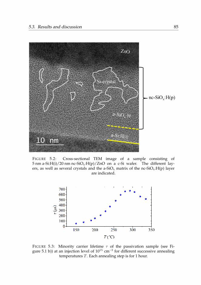
5.3. Results and discussion 85
FIGURE 5.2: Cross-sectional TEM image of a sample consisting of5 nm a-Si:H(i)/20 nm nc-SiOx:H(p)/ZnO on a c-Si wafer. The different lay-ers, as well as several crystals and the a-SiOx matrix of the nc-SiOx:H(p) layer
are indicated.
FIGURE 5.3: Minority carrier lifetime τ of the passivation sample (see Fi-gure 5.1 b)) at an injection level of 1015 cm−3 for different successive annealing
temperatures T . Each annealing step is for 1 hour.
86Chapter 5. Heat-withstanding surface passivation in combination with
nc-SiOx:H(p) emitter layer
material. The buffer layer is grown at a relatively low temperature of 130°C.According to the surface growth model, a non-equilibrium model that doesnot take thermodynamics into account, a low temperature does not provideenough energy for diffusion of the depositing species on the growing surface.This results in a rather disordered and porous material, leaving a high amountof dangling bonds at the c-Si surface. Another model that might explain theobserved behaviour is the growth zone model by Street, which takes the localthermal equilibrium into account. The location of the growth zone is belowthe substrate’s surface. The hydrogen atoms from the gas phase reaching thelayer’s surface diffuse into the growth zone and lead to a relaxation of thenetwork by H abstraction reactions. The energy released by these exothermicreactions enables the movement of Si species. In case of a low deposition tem-perature, especially near or below the gas transition temperature, the frozenor slow moving hydrogen leads to a disordered high defective material, thusa higher amount of dangling bonds [7] [204]. These dangling bonds act asrecombination centres in the band gap resulting in a low lifetime. Upon an-nealing the hydrogen in the a-Si:H(i) becomes mobile and propagates towardsthe c-Si surface, thus reduces the defect density. These effects are well knownand have been studied for a-Si:H(i)/c-Si/a-Si:H(i) passivation samples with-out doped layers [30] [205].
A beneficial effect of the high hydrogen concentration in the gas phaseduring nc-SiOx:H(p) deposition as compared to conventional emitter layerhas been observed by Mazzarella et al. [41]. The high amount of hydrogenduring the nc-SiOx:H(p) deposition, can lead to hydrogen diffusion towardsthe crystalline silicon wafer interface and thus to enhanced passivation prop-erties [42] compared to the same sample structure with standard a-Si:H(p)emitter layer. In our case however, this beneficial effect does not take placeduring deposition directly, as evident by the poor as-deposited lifetime. Ac-cording to the growth zone model by Street, the evolution of a material aswell as its final composition is influenced by the chemical potential of hydro-gen in the gas phase [90]. Possibly, a too high amount of hydrogen during thedeposition of the nc-SiOx lead to a high hydrogen chemical potential in thesample which is in equilibrium with the hydrogen chemical potential in thegas phase.
Theory on annealing of a-Si:H i/p-stacks
The increase of minority carrier lifetime at comparably high annealing tem-perature up to T = 293°C is in sharp contrast to the behaviour known fromsamples that include a-Si:H(p) layers. De Wolf et al. fabricated a-Si:H(i)/
5.3. Results and discussion 87
a-Si:H(p) stacks whose annealing properties degrade at temperatures above220°C [203]. Schüttauf et al. found that the passivation of a-Si:H(i)/a-Si:H(p)stacks deteriorates already upon annealing at temperatures as low as 150°C[30]. This commonly observed deterioration of the passivation at low anneal-ing temperatures of amorphous i/p-stacks is explained as follows. By ther-mal annealing at high enough temperatures Si-H bonds are ruptured and H2
is formed which consecutively effuses from the layer. The amount of energynecessary to break these Si-H bonds is Fermi level dependent, thus rupture ofSi-H bonds takes place at lower temperatures in the a-Si:H(p) layer comparedto the a-Si:H(i) layer [206]. As a result of the H2 effusion, the p-layer becomeshydrogen-deficient. This leads to an unfavourable hydrogen gradient be-tween the amorphous silicon layers. The hydrogen within the a-Si:H(i) layerbecomes mobile during annealing and, as a result of the unfavourable hydro-gen gradient, relocates from the intrinsic to the boron-doped layer. Thereby,the c-Si/a-Si:H(i) interface becomes depleted from hydrogen, resulting in adecrease of passivation quality [30].
Annealing behaviour of a-Si:H(i)/nc-SiOx:H(p) passivation stacks
For the a-Si:H(i)/nc-SiOx:H(p) layer stack the above discussed behaviour doesnot take place. Instead of a decrease of τ upon annealing, as common fora-Si:H i/p-layer passivation stacks, τ increases upon annealing for thea-Si:H(i)/nc-SiOx:H(p) passivation stack. We attribute this to the following.We assume a high fraction of the active boron (4-fold coordinated) to be lo-cated in the nanocrystalline silicon matrix, whereas the inactive boron (3 foldcoordinated) is mostly located in the amorphous silicon oxide (a-SiOx:H) do-main of the layer [63]. The concentration of active boron in this amorphousphase is expected to be much lower compared to typical a-Si:H(p). Thus, theFermi level of the amorphous silicon oxide domain within the nc-SiOx:H(p)layer will be closer to mid gap. Because hydrogen solubility in crystallinesilicon is very low, most of the hydrogen is expected to be located in thea-SiOx:H matrix, thus in the domains where the Fermi level is comparablyfar from the band edge. Therefore, the Fermi level dependent Si-H bond rup-ture, and thus the H2 effusion, will take place at much higher temperatures innc-SiOx:H(p) compared to the a-Si:H(p) layer. In this way, the a-SiOx:H partof the nc-SiOx:H(p) layer serves as a reservoir for atomic hydrogen that cankeep the c-Si/a-Si:H interface in an hydrogenated and well-passivated state.
Studies by Beyer indicate that for a-Si:O:H at low oxygen concentration(< 20%) the hydrogen effusion is smaller and the effusion peak shifts to a
88Chapter 5. Heat-withstanding surface passivation in combination with
nc-SiOx:H(p) emitter layer
higher temperature compared to pure a-Si:H [207]. Hence, we do not expectany significant increase of hydrogen diffusion/effusion in the a-SiOx:H ma-trix (rather decrease) due to the oxygen content in the material.
Hydrogen effusion from a-Si:H(i) and a-SiO:H(i) passivation layers uponannealing has also been investigated by Nakada et al. [208]. They attributehydrogen effusion in these layers to the combination of two phenomena. Onthe one hand, molecular H2 can effuse from internal surfaces and out-diffusethrough interconnected voids. In case of a less void rich material, this H2
out-diffusion is hindered and the effusion peak shifts towards higher temper-atures. In addition, atomic H can diffuse through the network and recombineat the surface of the layer to form H2 and thereby also effuse from the layer.This second mechanism benefits from a high amount of isolated voids in adense material. In case of a more compact material this atomic hydrogen dif-fusion is hindered and the effusion peak shifts towards higher temperatures.Especially notable, for a-SiO:H this peak even shifts towards higher temper-atures compared to a-Si:H. This is caused by a stronger Si-H bond due to thehigher electronegativity of O atoms backbonded to the Si-H [208]. We expectsimilar behaviour in the a-SiOx:H phase of the nc-SiOx:H(p) layers.
5.3.2 Influence of the i-layer buffer thickness
For implementation of the developed passivation stack in SHJ solar cells theideal i-layer thickness has to be found. A certain buffer i-layer thickness isessential to guarantee a sharp interface with the c-Si and a good passivationquality. On the other hand, the buffer layer also needs to be reasonably thinto limit the parasitic absorption of light [43]. To evaluate the influence of thei-layer thickness in our particular layer stack, SHJ semi cells with variablefront buffer layer thicknesses from 0 nm (no layer) to 5 nm have been fab-ricated in steps of 1 nm (see Figure 5.1 c)) and annealed for 16 h at 200°Cin vacuum to improve passivation properties. Instead of 293°C, which hasbeen proven to be the most beneficial annealing temperature for passivationproperties of this layer stack, the temperature of 200°C was chosen in order tocomply with the industry practice of manufacturing SHJ solar cells at temper-atures ≤ 200°C.
Figure 5.4 shows the dependence of the implied VOC at 1-sun light inten-sity on the i-layer thickness d. The sample where the nc-SiOx:H(p) was growndirectly on the wafer shows a poor implied VOC of only 579 mV. This is inagreement with the work of Rattanapan et al., who showed that nc-SiOx:H(p)
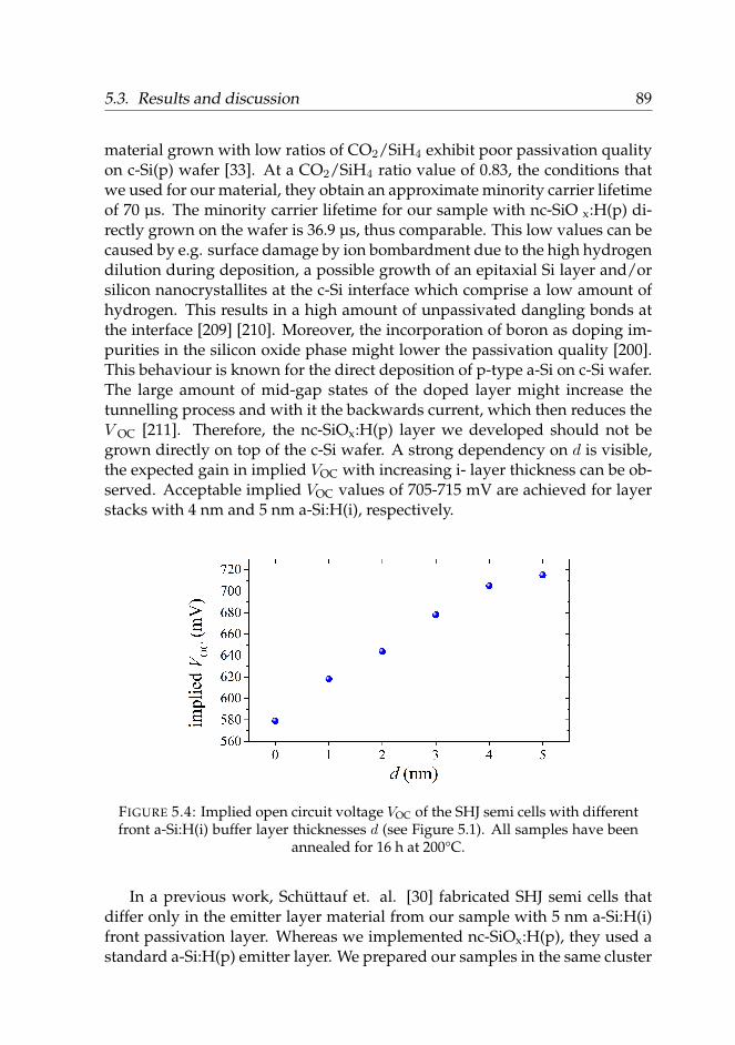
5.3. Results and discussion 89
material grown with low ratios of CO2/SiH4 exhibit poor passivation qualityon c-Si(p) wafer [33]. At a CO2/SiH4 ratio value of 0.83, the conditions thatwe used for our material, they obtain an approximate minority carrier lifetimeof 70 µs. The minority carrier lifetime for our sample with nc-SiO x:H(p) di-rectly grown on the wafer is 36.9 µs, thus comparable. This low values can becaused by e.g. surface damage by ion bombardment due to the high hydrogendilution during deposition, a possible growth of an epitaxial Si layer and/orsilicon nanocrystallites at the c-Si interface which comprise a low amount ofhydrogen. This results in a high amount of unpassivated dangling bonds atthe interface [209] [210]. Moreover, the incorporation of boron as doping im-purities in the silicon oxide phase might lower the passivation quality [200].This behaviour is known for the direct deposition of p-type a-Si on c-Si wafer.The large amount of mid-gap states of the doped layer might increase thetunnelling process and with it the backwards current, which then reduces theV OC [211]. Therefore, the nc-SiOx:H(p) layer we developed should not begrown directly on top of the c-Si wafer. A strong dependency on d is visible,the expected gain in implied VOC with increasing i- layer thickness can be ob-served. Acceptable implied VOC values of 705-715 mV are achieved for layerstacks with 4 nm and 5 nm a-Si:H(i), respectively.
FIGURE 5.4: Implied open circuit voltage VOC of the SHJ semi cells with differentfront a-Si:H(i) buffer layer thicknesses d (see Figure 5.1). All samples have been
annealed for 16 h at 200°C.
In a previous work, Schüttauf et. al. [30] fabricated SHJ semi cells thatdiffer only in the emitter layer material from our sample with 5 nm a-Si:H(i)front passivation layer. Whereas we implemented nc-SiOx:H(p), they used astandard a-Si:H(p) emitter layer. We prepared our samples in the same cluster
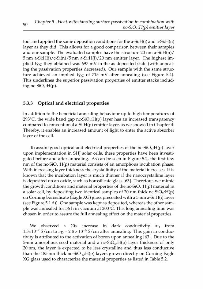
90Chapter 5. Heat-withstanding surface passivation in combination with
nc-SiOx:H(p) emitter layer
tool and applied the same deposition conditions for the a-Si:H(i) and a-Si:H(n)layer as they did. This allows for a good comparison between their samplesand our sample. The evaluated samples have the structure 20 nm a-Si:H(n)/5 nm a-Si:H(i)/c-Si(n)/5 nm a-Si:H(i)/20 nm emitter layer. The highest im-plied VOC they obtained was 697 mV in the as deposited state (with anneal-ing the passivation properties decreased). Our sample with the same struc-ture achieved an implied VOC of 715 mV after annealing (see Figure 5.4).This underlines the superior passivation properties of emitter stacks includ-ing nc-SiOx:H(p).
5.3.3 Optical and electrical properties
In addition to the beneficial annealing behaviour up to high temperatures of293°C, the wide band gap nc-SiOx:H(p) layer has an increased transparencycompared to conventional a-Si:H(p) emitter layer, as we showed in Chapter 4.Thereby, it enables an increased amount of light to enter the active absorberlayer of the cell.
To assure good optical and electrical properties of the nc-SiOx:H(p) layerupon implementation in SHJ solar cells, these properties have been investi-gated before and after annealing. As can be seen in Figure 5.2, the first fewnm of the nc-SiOx:H(p) material consists of an amorphous incubation phase.With increasing layer thickness the crystallinity of the material increases. It isknown that the incubation layer is much thinner if the nanocrystalline layeris deposited on an oxide, such as borosilicate glass [63]. Therefore, we mimicthe growth conditions and material properties of the nc-SiOx:H(p) material ina solar cell, by depositing two identical samples of 20-nm thick nc-SiOx:H(p)on Corning borosilicate (Eagle XG) glass precoated with a 5 nm a-Si:H(i) layer(see Figure 5.1 d)). One sample was kept as deposited, whereas the other sam-ple was annealed for 56 h in vacuum at 200°C. This long annealing time waschosen in order to assure the full annealing effect on the material properties.
We observed a 20× increase in dark conductivity σD from1.3×10−7 S/cm to σD = 2.6 × 10⁻⁶ S/cm after annealing. This gain in conduc-tivity is attributed to the activation of boron upon annealing [63]. Due to the5-nm amorphous seed material and a nc-SiOx:H(p) layer thickness of only20 nm, the layer is expected to be less crystalline and thus less conductivethan the 185 nm thick nc-SiO x:H(p) layers grown directly on Corning EagleXG glass used to characterize the material properties as listed in Table 5.2.
5.4. Conclusion 91
Not much research has been done on the influence of annealing on theband gap of nc-SiOx:H(p). It is known for a-SiOx:H(p), that annealing leadsto a decrease of optical band gap [212]. The effect of annealing temperatures≥ 800°C on undoped SiOx containing silicon nanocrystals has been observedby Nikitin et. al. [213] [214]. They find an increase of optical band gapwith increasing annealing temperatures and attribute it to an amorphous-to-crystalline transitions of Si clusters within the material. Figure 5.5 shows thedetermined absorption coefficients α as function of the photon energy E = hν(with h denoting the Planck’s constant and ν the photon frequency) for theannealed and as-deposited sample. The optical band gap E04 is determinedas 2.3 eV for the as-deposited sample and 2.4 eV for the annealed sample.Thus, a small increase in band gap is visible. However, it is difficult to makea solid statement about the development of the optical band gap. Becausenc-SiOx:H(p) is not a single phase material the modelling is not straightfor-ward, as evident from the work of Ilday et al. [215]. Thus, our simple ap-proach model results in a not negligible uncertainty of the determined bandgap values. Therefore, it is difficult to evaluate the optical properties. Theremight be a small difference in band gap, but due to accuracy limitations wecan not say this with certainty.
FIGURE 5.5: Absorption coefficient α as function of the photon energy for theannealed and as-deposited nc-SiOx:H(p) material.
5.4 Conclusion
In this chapter we have presented a nc-SiOx:H(p) material with superior ther-mal behaviour. a-Si:H(i)/nc-SiOx:H(p) passivation stacks exhibit an increase
92Chapter 5. Heat-withstanding surface passivation in combination with
nc-SiOx:H(p) emitter layer
in minority carrier lifetime even after annealing at relatively high tempera-tures up to 293°C. For an i/p-layer sample the observed behaviour is excep-tional. For samples with a-Si:H(i)/a-S:H(p) passivation stacks, it is knownthat the minority carrier lifetime decreases upon annealing at comparablymoderate temperatures of 220°C [203] or even 150°C [30]. The fact that anneal-ing temperatures well above the deposition temperature have a positive effectfor layer stacks including nc-SiOx:H(p) is remarkable. To our knowledge it hasnot been reported earlier that annealing complete passivation stacks includ-ing p-type silicon based layers at such high temperatures can improve theirpassivation properties. This outstanding behaviour is mostly attributed to thehydrogen bonds being located predominantly in the amorphous SiOx phasewhere the Fermi energy is deep in the gap. Thereby, the Fermi-level depen-dent Si-H bond rupture takes place at higher temperatures than for conven-tional a-Si:H(p).
This heat-withstanding emitter/passivation layer stack could be of highinterest for commercial solar cell producers, since it enables the use of higherpost processing temperatures in the production process. For instance, met-allization paste with higher curing temperatures leading to better metal gridconductivity and lower contact resistivity could be implemented. Moreover,transparent conductive oxide (TCO) layer produced at higher temperaturescould be applied in the SHJ solar cell.
93
Chapter 6
ZnO:B front TCO incombination with nc-SiOx:H(p)emitter layer for increased JSC inSHJ solar cells
In this chapter, the replacement of the conventional sputtered tin-doped in-dium oxide (ITO) on the silicon heterojunction (SHJ) solar cell front side withhighly transparent boron doped zinc oxide (ZnO:B) in combination with thep-type nanocrystalline silicon oxide (nc-SiOx:H(p)) emitter layer is investi-gated. Not only does the ZnO:B show a remarkably high transmission andprovides the desired indium-free alternative to ITO, it moreover is preparedby the soft method of atomic layer deposition (ALD) employing the noveltriisopropyl borate precursor, B(OiPr)3 (TIB), which presents an easy control-lable and safer alternative to commonly used boron precursors.
In a first step, the suitability of the ZnO:B for implementation as fronttransparent conductive oxide (TCO) in SHJ solar cells is evaluated. To thisend, the sheet resistance, transmission, refractive index, extinction coefficient,absorption coefficient, and optical band gap have been investigated for differ-ent doping levels of the material. Subsequently, the nc-SiOx:H(p) emitter layerand ZnO:B front TCO were implemented in SHJ solar cells. For comparison,SHJ solar cells with standard sputtered ITO have been made. The potential ofZnO:B grown with TIB as indium-free TCO with increased transmission forSHJ solar cells is evident from J-V -andEQE-characteristics. Furthermore, in-dium free SHJ solar cells with ALD deposited ZnO:B as front TCO and ZnO:Alas back TCO have been successfully demonstrated.
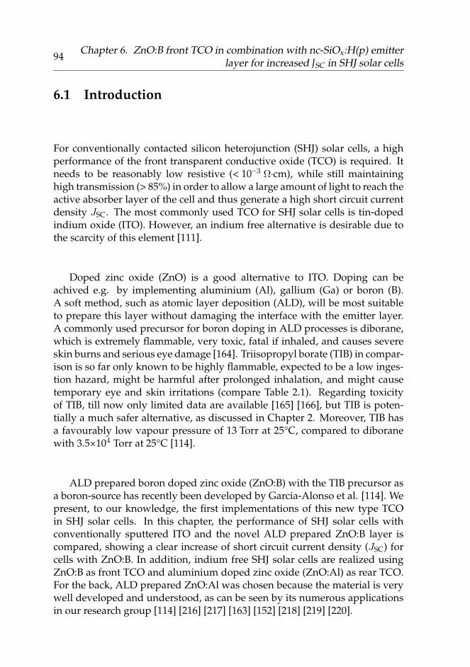
94Chapter 6. ZnO:B front TCO in combination with nc-SiOx:H(p) emitter
aaaaaaaaaaaaaaaaaaaa layer for increased JSC in SHJ solar cells
6.1 Introduction
For conventionally contacted silicon heterojunction (SHJ) solar cells, a highperformance of the front transparent conductive oxide (TCO) is required. Itneeds to be reasonably low resistive (< 10−3 Ω⋅cm), while still maintaininghigh transmission (> 85%) in order to allow a large amount of light to reach theactive absorber layer of the cell and thus generate a high short circuit currentdensity JSC. The most commonly used TCO for SHJ solar cells is tin-dopedindium oxide (ITO). However, an indium free alternative is desirable due tothe scarcity of this element [111].
Doped zinc oxide (ZnO) is a good alternative to ITO. Doping can beachived e.g. by implementing aluminium (Al), gallium (Ga) or boron (B).A soft method, such as atomic layer deposition (ALD), will be most suitableto prepare this layer without damaging the interface with the emitter layer.A commonly used precursor for boron doping in ALD processes is diborane,which is extremely flammable, very toxic, fatal if inhaled, and causes severeskin burns and serious eye damage [164]. Triisopropyl borate (TIB) in compar-ison is so far only known to be highly flammable, expected to be a low inges-tion hazard, might be harmful after prolonged inhalation, and might causetemporary eye and skin irritations (compare Table 2.1). Regarding toxicityof TIB, till now only limited data are available [165] [166], but TIB is poten-tially a much safer alternative, as discussed in Chapter 2. Moreover, TIB hasa favourably low vapour pressure of 13 Torr at 25°C, compared to diboranewith 3.5×10⁴ Torr at 25°C [114].
ALD prepared boron doped zinc oxide (ZnO:B) with the TIB precursor asa boron-source has recently been developed by Garcia-Alonso et al. [114]. Wepresent, to our knowledge, the first implementations of this new type TCOin SHJ solar cells. In this chapter, the performance of SHJ solar cells withconventionally sputtered ITO and the novel ALD prepared ZnO:B layer iscompared, showing a clear increase of short circuit current density (JSC) forcells with ZnO:B. In addition, indium free SHJ solar cells are realized usingZnO:B as front TCO and aluminium doped zinc oxide (ZnO:Al) as rear TCO.For the back, ALD prepared ZnO:Al was chosen because the material is verywell developed and understood, as can be seen by its numerous applicationsin our research group [114] [216] [217] [163] [152] [218] [219] [220].
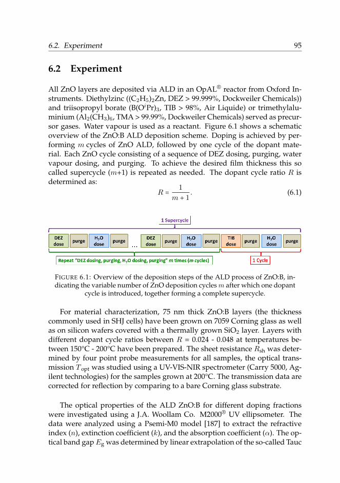
6.2. Experiment 95
6.2 Experiment
All ZnO layers are deposited via ALD in an OpAL® reactor from Oxford In-struments. Diethylzinc ((C2H5)2Zn, DEZ > 99.999%, Dockweiler Chemicals))and triisopropyl borate (B(OiPr)3, TIB > 98%, Air Liquide) or trimethylalu-minium (Al2(CH3)6, TMA > 99.99%, Dockweiler Chemicals) served as precur-sor gases. Water vapour is used as a reactant. Figure 6.1 shows a schematicoverview of the ZnO:B ALD deposition scheme. Doping is achieved by per-forming m cycles of ZnO ALD, followed by one cycle of the dopant mate-rial. Each ZnO cycle consisting of a sequence of DEZ dosing, purging, watervapour dosing, and purging. To achieve the desired film thickness this socalled supercycle (m+1) is repeated as needed. The dopant cycle ratio R isdetermined as:
R = 1
m + 1. (6.1)
FIGURE 6.1: Overview of the deposition steps of the ALD process of ZnO:B, in-dicating the variable number of ZnO deposition cyclesm after which one dopant
cycle is introduced, together forming a complete supercycle.
For material characterization, 75 nm thick ZnO:B layers (the thicknesscommonly used in SHJ cells) have been grown on 7059 Corning glass as wellas on silicon wafers covered with a thermally grown SiO2 layer. Layers withdifferent dopant cycle ratios between R = 0.024 - 0.048 at temperatures be-tween 150°C - 200°C have been prepared. The sheet resistance Rsh was deter-mined by four point probe measurements for all samples, the optical trans-mission T opt was studied using a UV-VIS-NIR spectrometer (Carry 5000, Ag-ilent technologies) for the samples grown at 200°C. The transmission data arecorrected for reflection by comparing to a bare Corning glass substrate.
The optical properties of the ALD ZnO:B for different doping fractionswere investigated using a J.A. Woollam Co. M2000® UV ellipsometer. Thedata were analyzed using a Psemi-M0 model [187] to extract the refractiveindex (n), extinction coefficient (k), and the absorption coefficient (α). The op-tical band gapEg was determined by linear extrapolation of the so-called Tauc
96Chapter 6. ZnO:B front TCO in combination with nc-SiOx:H(p) emitter
aaaaaaaaaaaaaaaaaaaa layer for increased JSC in SHJ solar cells
plots, which present (αhν)2 vs. hν for the direct band gap material [221] [222].
SHJ solar cells have been fabricated on textured <100> n-type Cz wafersc-Si (thickness ≈ 150 µm) , and on double side polished (DSP) <111> n-typeFZ c-Si wafers (thickness ≈ 275 µm). Figure 6.2 shows an overview of the dif-ferent samples. The arrangement of all thin-film silicon layers is the same foreach sample, whereas the TCO material (and for sample type IV also the frontcontact material) varies. In cell type I the ALD prepared ZnO:B (R = 0.040)is implemented as front TCO with ITO as back TCO. Cell type II serves asreference with ITO as front and back TCO. Both cell types are made on DSPas well as on textured wafers. All ZnO layers used in the SHJ solar cells havebeen grown at 200°C.
Cell type III realizes an indium free SHJ solar cell by using ZnO:B (R =0.040) as front TCO and ZnO:Al (R = 0.042) as back TCO on a DSP wafer. Celltype IV (on textured wafer), with ZnO:B as front TCO, ITO as back TCO, andgold (Au) as front grid contact is used for annealing studies.
All wafers are coated on both sides with a 5-nm intrinsic amorphous sili-con layer (a-Si:H(i)). Thereon, the rear is coated with 20 nm a-Si:H(n). After-wards the front is coated with the emitter layer stack, consisting of 5 nmnc-Si:H(p) to facilitate a fast nucleation of the silicon oxide layer, a 12 nmnc-SiOx:H(p) highly transparent emitter layer, and a 3 nm nc-Si:H(p) layerto improve the contact to the top TCO [7] [47]. The backside of the cell isthen finished with 75 nm TCO (RF-magnetron sputtered ITO, or in the caseof cell type III ALD prepared ZnO:Al), and 200 nm silver (Ag). As front TCO75 nm of either RF-magnetron sputtered ITO (sample type II) or ALD pre-pared ZnO:B (all other sample types) is used. During the ITO deposition, thesolar cell area of 1 cm × 1 cm is defined by a mask. Due to the nature of theALD process, the ZnO:B is deposited on the complete solar cell front side ofsample type I, III, and IV. Their individual cells are subsequently separated bycleaving the wafer. On top of the TCO, evaporated silver (sample type I-III)or gold (sample type IV) grids serve as front contacts.
All silicon base layer are prepared in the PASTA reactor [171]. The dopedlayers are deposited via plasma-enhanced chemical vapour deposition(PECVD). Other than in Chapter 4 - 5, the intrinsic amorphous silicon layerare not deposited by PECVD, but by hot wire chemical vapour deposition(HWCVD). This choice was made, after first test runs of SHJ solar cells of withthe PECVD deposited buffer layer exhibited an S-shaped illuminated cur-rent density-voltage (J-V ) characteristic. Therefore, we changed to HWCVD
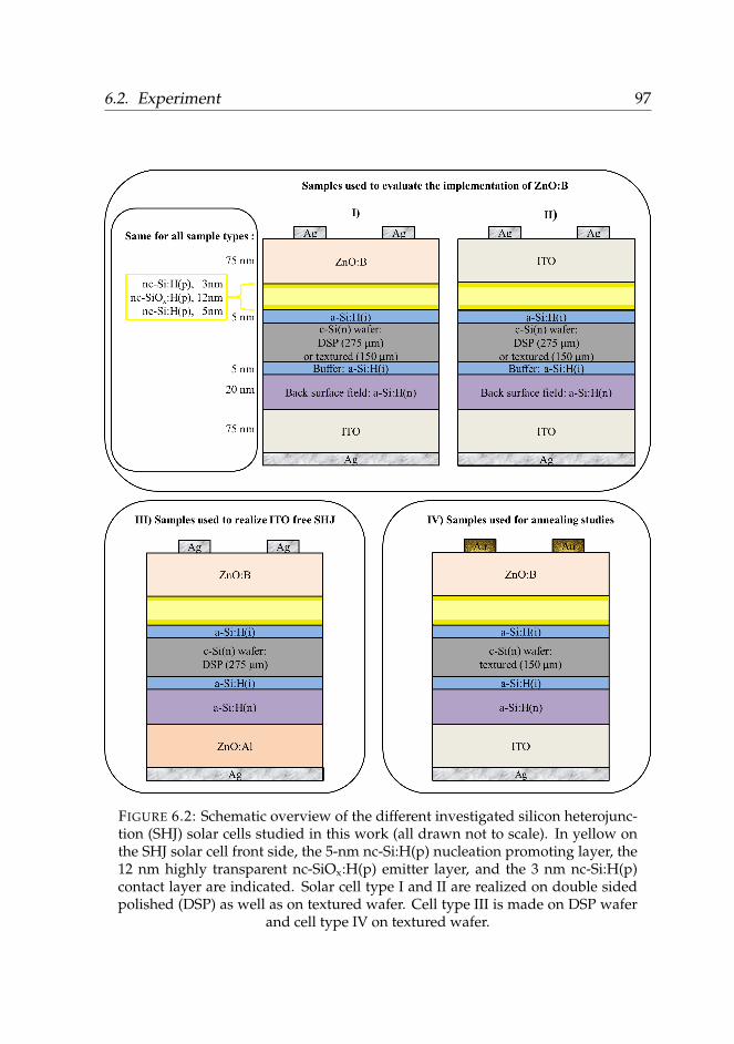
6.2. Experiment 97
FIGURE 6.2: Schematic overview of the different investigated silicon heterojunc-tion (SHJ) solar cells studied in this work (all drawn not to scale). In yellow onthe SHJ solar cell front side, the 5-nm nc-Si:H(p) nucleation promoting layer, the12 nm highly transparent nc-SiOx:H(p) emitter layer, and the 3 nm nc-Si:H(p)contact layer are indicated. Solar cell type I and II are realized on double sidedpolished (DSP) as well as on textured wafer. Cell type III is made on DSP wafer
and cell type IV on textured wafer.
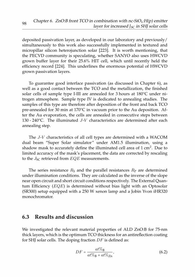
98Chapter 6. ZnO:B front TCO in combination with nc-SiOx:H(p) emitter
aaaaaaaaaaaaaaaaaaaa layer for increased JSC in SHJ solar cells
deposited passivation layer, as developed in our laboratory and previously/simultaneously to this work also successfully implemented in textured andmicropillar silicon heterojunction solar [223]. It is worth mentioning, thatthe PECVD community is speculating, whether SANYO also uses HWCVDgrown buffer layer for their 25.6% HIT cell, which until recently held theefficiency record [224]. This underlines the enormous potential of HWCVDgrown passivation layers.
To guarantee good interface passivation (as discussed in Chapter 6), aswell as a good contact between the TCO and the metallization, the finishedsolar cells of sample type I-III are annealed for 3 hours at 180°C under ni-trogen atmosphere. Sample type IV is dedicated to annealing studies. Thesamples of this type are therefore after deposition of the front and back TCOpre-annealed for 30 min at 170°C in vacuum prior to the Au deposition. Af-ter the Au evaporation, the cells are annealed in consecutive steps between130 - 240°C. The illuminated J-V characteristics are determined after eachannealing step.
The J-V characteristics of all cell types are determined with a WACOMdual beam “Super Solar simulator” under AM1.5 illumination, using ashadow mask to accurately define the illuminated cell area of 1 cm2. Due tolimited accuracy of the mask’s placement, the data are corrected by rescalingto the JSC retrieved from EQE measurements.
The series resistance RS and the parallel resistances RP are determinedunder illumination conditions. They are calculated as the inverse of the slopenear open circuit and short circuit conditions respectively. The External Quan-tum Efficiency (EQE) is determined without bias light with an Optosolar(SR300) setup equipped with a 250 W xenon lamp and a Jobin Yvon iHR320monochromator.
6.3 Results and discussion
We investigated the relevant material properties of ALD ZnO:B for 75-nmthick layers, which is the optimum TCO thickness for an antireflection coatingfor SHJ solar cells. The doping fraction DF is defined as:
DF = at%B
at%B + at%Zn, (6.2)
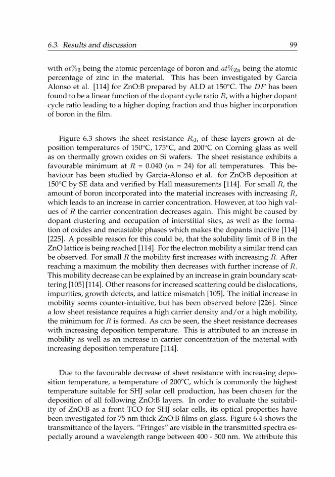
6.3. Results and discussion 99
with at%B being the atomic percentage of boron and at%Zn being the atomicpercentage of zinc in the material. This has been investigated by GarciaAlonso et al. [114] for ZnO:B prepared by ALD at 150°C. The DF has beenfound to be a linear function of the dopant cycle ratio R, with a higher dopantcycle ratio leading to a higher doping fraction and thus higher incorporationof boron in the film.
Figure 6.3 shows the sheet resistance Rsh of these layers grown at de-position temperatures of 150°C, 175°C, and 200°C on Corning glass as wellas on thermally grown oxides on Si wafers. The sheet resistance exhibits afavourable minimum at R = 0.040 (m = 24) for all temperatures. This be-haviour has been studied by Garcia-Alonso et al. for ZnO:B deposition at150°C by SE data and verified by Hall measurements [114]. For small R, theamount of boron incorporated into the material increases with increasing R,which leads to an increase in carrier concentration. However, at too high val-ues of R the carrier concentration decreases again. This might be caused bydopant clustering and occupation of interstitial sites, as well as the forma-tion of oxides and metastable phases which makes the dopants inactive [114][225]. A possible reason for this could be, that the solubility limit of B in theZnO lattice is being reached [114]. For the electron mobility a similar trend canbe observed. For small R the mobility first increases with increasing R. Afterreaching a maximum the mobility then decreases with further increase of R.This mobility decrease can be explained by an increase in grain boundary scat-tering [105] [114]. Other reasons for increased scattering could be dislocations,impurities, growth defects, and lattice mismatch [105]. The initial increase inmobility seems counter-intuitive, but has been observed before [226]. Sincea low sheet resistance requires a high carrier density and/or a high mobility,the minimum for R is formed. As can be seen, the sheet resistance decreaseswith increasing deposition temperature. This is attributed to an increase inmobility as well as an increase in carrier concentration of the material withincreasing deposition temperature [114].
Due to the favourable decrease of sheet resistance with increasing depo-sition temperature, a temperature of 200°C, which is commonly the highesttemperature suitable for SHJ solar cell production, has been chosen for thedeposition of all following ZnO:B layers. In order to evaluate the suitabil-ity of ZnO:B as a front TCO for SHJ solar cells, its optical properties havebeen investigated for 75 nm thick ZnO:B films on glass. Figure 6.4 shows thetransmittance of the layers. “Fringes” are visible in the transmitted spectra es-pecially around a wavelength range between 400 - 500 nm. We attribute this
100Chapter 6. ZnO:B front TCO in combination with nc-SiOx:H(p) emitter
aaaaaaaaaaaaaaaaaaaa layer for increased JSC in SHJ solar cells
FIGURE 6.3: Sheet resistance Rsh of ZnO:B (75 nm) for different dopant cy-cle ratios R deposited on Corning glass (circles) and thermally grown oxideon Si wafers (triangles) for different deposition temperatures T . For reference:
Rsh (ITO) = 48 Ω/2 on Corning glass.
to thin-film-interference, which is cause by the interference of light waves re-flected at the TCO layer ’s interfaces (to glass and to air) with each another. Alllayers exhibit good transmission over most of the wavelength range, whichmakes them optically favourable over ITO as front TCO. However, duringour research we discovered difficulties regarding the work function of ZnO:B,that will be discussed later.
FIGURE 6.4: Transmission Topt of ZnO:B films (deposited at T = 200°C) for 75 nmthin films as a function of the wavelength λ for different dopant cycle ratios.
Since the transmittance of the thin films on glass is influenced by its thick-ness (here 75 nm for all films) as well as by interference effects in the film,the optical properties have further been investigated. Figure 6.5 a) and b)
6.3. Results and discussion 101
show the refractive index n and the extinction coefficient k, for ALD ZnO:Bfilms deposited with various dopant cycle ratios R at 200°C. In simulationprograms these n and k values can be used for the modelling of optical stacks.As can be seen in Figure 6.5 a), at a given wavelength λ the refractive in-dex n decreases with increasing dopant cycle ratio R (corresponding to anincreasing boron content in the films). The same behaviour can be observedin Figure 6.5 b) for the extinction coefficient k. At a given λ, k decreases withincreasing R (in the low wavelength range). These behaviours of n and k areknown and have been attributed to an increase in the carrier concentrations inthe material [227], which has been found for increasing doping fraction in thedoping ratio range we investigated [114]. This is related to a change in bandgap, that we will discuss below.
Figure 6.5 c) shows the absorption coefficient α as a function of the photonenergy Eph. A blue shift is clearly visible in the absorption edge of the ZnO:Bwith increasing boron dopant cycle ratio R. The incorporation of boron in thematerial provides free charge carriers that shift the Fermi level into the con-duction band and thus widens the band gap according to the Burstein–Mosstheory [114] [227]. The Tauc plot ((αhν)2 vs. hν for direct band gap material)of the different ZnO:B films is shown in Figure 6.5 d). As can be seen in theinset of the figure, the optical band gap Eg increases with increasing R, andthus with increasing boron incorporation, which is in agreement with the pre-vious reported studies on ZnO:B deposited by ALD or sol-gel method [114][226] [227] [228]. The Burstein-Moss shift could be the dominant reason forthis band gap widening. Moreover, additional effects such as strain, grainsize, and imperfections in the lattice might contribute to this widening as well[228].
All investigated ZnO:B materials show good optical properties for all dop-ing ratios. Therefore, the most conductive ZnO:B, grown with R = 0.040 (T =200°C), has been chosen for implementation in the SHJ solar cells. The resis-tivity of the selected ZnO:B layer is 9.1×10⁻⁴ Ω⋅cm on Corning glass, whereasthe resistivity for our standard sputtered ITO is 3.6×10⁻⁴ Ω⋅cm for the same75 nm thick layer.
The emitter layer is preceded by a thin 3 nm nc-Si:H(p) layer in order tofacilitate a fast crystallization of the nc-SiOx:H(p) layer [63] [64], as discussedin Chapter 2, 4, and 5. Since the nc-Si:H(p) layer is followed by the depositionof an oxide layer, it is possible that the nc-Si:H(p) layer gets oxidized duringthis following deposition [7]. On top of the nc-SiOx:H(p) layer, another 3 nmthin nc-Si:H(p) layer is deposited, which is then followed with the TCO layer.
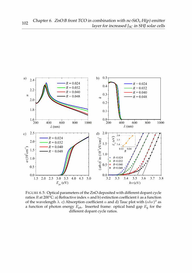
102Chapter 6. ZnO:B front TCO in combination with nc-SiOx:H(p) emitter
aaaaaaaaaaaaaaaaaaaa layer for increased JSC in SHJ solar cells
FIGURE 6.5: Optical parameters of the ZnO deposited with different dopant cycleratiosR at 200°C: a) Refractive index n and b) extinction coefficient k as a functionof the wavelength λ. c) Absorption coefficient α and d) Tauc plot with (αhν)2 asa function of photon energy Eph. Inserted frame: optical band gap Eg for the
different dopant cycle ratios.
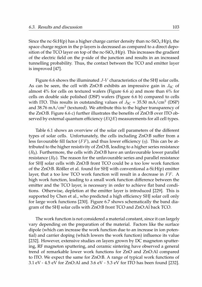
6.3. Results and discussion 103
Since the nc-Si:H(p) has a higher charge carrier density than nc-SiOx:H(p), thespace charge region in the p-layers is decreased as compared to a direct depo-sition of the TCO layer on top of the nc-SiOx:H(p). This increases the gradientof the electric field on the p-side of the junction and results in an increasedtunnelling probability. Thus, the contact between the TCO and emitter layeris improved [47].
Figure 6.6 shows the illuminated J-V characteristics of the SHJ solar cells.As can be seen, the cell with ZnO:B exhibits an impressive gain in JSC ofalmost 4% for cells on textured wafers (Figure 6.6 a) and more than 6% forcells on double side polished (DSP) wafers (Figure 6.6 b) compared to cellswith ITO. This results in outstanding values of JSC = 35.50 mA/cm2 (DSP)and 38.76 mA/cm2 (textured). We attribute this to the higher transparency ofthe ZnO:B. Figure 6.6 c) further illustrates the benefits of ZnO:B over ITO ob-served by external quantum efficiency (EQE) measurements for all cell types.
Table 6.1 shows an overview of the solar cell parameters of the differenttypes of solar cells. Unfortunately, the cells including ZnO:B suffer from aless favourable fill factor (FF ), and thus lower efficiency (η). This can be at-tributed to the higher resistivity of ZnO:B, leading to a higher series resistance(RS). Furthermore, the cells with ZnO:B have an unfavourable lower parallelresistance (RP). The reason for the unfavourable series and parallel resistancefor SHJ solar cells with ZnO:B front TCO could be a too low work functionof the ZnO:B. Rößler et al. found for SHJ with conventional a-Si:H(p) emitterlayer, that a too low TCO work function will result in a decrease in FF . Ahigh work function, leading to a small work function difference between theemitter and the TCO layer, is necessary in order to achieve flat band condi-tions. Otherwise, depletion at the emitter layer is introduced [229]. This issupported by Chen et al., who predicted a high efficiency SHJ solar cell onlyfor large work functions [230]. Figure 6.7 shows schematically the band dia-gram of the SHJ solar cells with ZnO:B front TCO and ZnO:Al back TCO.
The work function is not considered a material constant, since it can largelyvary depending on the preparation of the material. Factors like the surfacedipole (which can increase the work function due to an increase in ion poten-tial) and carrier doping (which lowers the work function) influence its value[232]. However, extensive studies on layers grown by DC magneton sputter-ing, RF magneton sputtering, and ceramic sintering have observed a generaltrend of remarkable lower work functions for ZnO and ZnO:Al comparedto ITO. We expect the same for ZnO:B. A range of typical work functions of3.1 eV - 4.5 eV for ZnO:Al and 3.6 eV - 5.3 eV for ITO has been found [232].
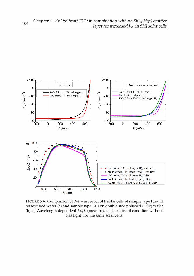
104Chapter 6. ZnO:B front TCO in combination with nc-SiOx:H(p) emitter
aaaaaaaaaaaaaaaaaaaa layer for increased JSC in SHJ solar cells
FIGURE 6.6: Comparison of J-V -curves for SHJ solar cells of sample type I and IIon textured wafer (a) and sample type I-III on double side polished (DSP) wafer(b). c) Wavelength dependent EQE (measured at short circuit condition without
bias light) for the same solar cells.
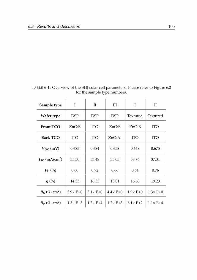
6.3. Results and discussion 105
TABLE 6.1: Overview of the SHJ solar cell parameters. Please refer to Figure 6.2for the sample type numbers.
Sample type I II III I II
Wafer type DSP DSP DSP Textured Textured
Front TCO ZnO:B ITO ZnO:B ZnO:B ITO
Back TCO ITO ITO ZnO:Al ITO ITO
VOC (mV) 0.685 0.684 0.658 0.668 0.675
JSC (mA/cm2) 35.50 33.48 35.05 38.76 37.31
FF (%) 0.60 0.72 0.66 0.64 0.76
η (%) 14.53 16.53 13.81 16.68 19.23
RS (Ω ⋅ cm2) 3.9× E+0 3.1× E+0 4.4× E+0 1.9× E+0 1.3× E+0
RP (Ω ⋅ cm2) 1.3× E+3 1.2× E+4 1.2× E+3 6.1× E+2 1.1× E+4
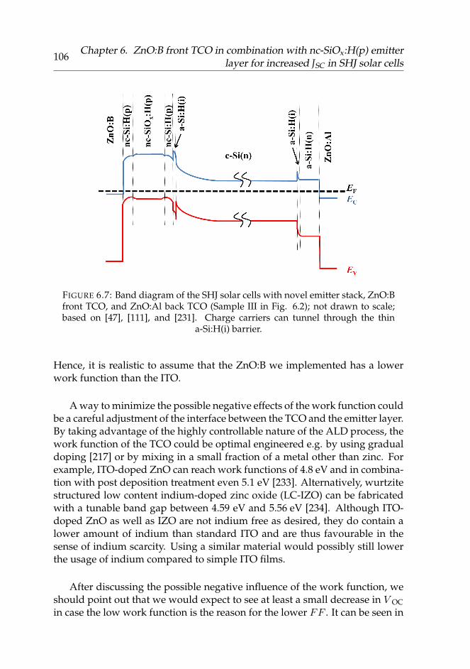
106Chapter 6. ZnO:B front TCO in combination with nc-SiOx:H(p) emitter
aaaaaaaaaaaaaaaaaaaa layer for increased JSC in SHJ solar cells
FIGURE 6.7: Band diagram of the SHJ solar cells with novel emitter stack, ZnO:Bfront TCO, and ZnO:Al back TCO (Sample III in Fig. 6.2); not drawn to scale;based on [47], [111], and [231]. Charge carriers can tunnel through the thin
a-Si:H(i) barrier.
Hence, it is realistic to assume that the ZnO:B we implemented has a lowerwork function than the ITO.
A way to minimize the possible negative effects of the work function couldbe a careful adjustment of the interface between the TCO and the emitter layer.By taking advantage of the highly controllable nature of the ALD process, thework function of the TCO could be optimal engineered e.g. by using gradualdoping [217] or by mixing in a small fraction of a metal other than zinc. Forexample, ITO-doped ZnO can reach work functions of 4.8 eV and in combina-tion with post deposition treatment even 5.1 eV [233]. Alternatively, wurtzitestructured low content indium-doped zinc oxide (LC-IZO) can be fabricatedwith a tunable band gap between 4.59 eV and 5.56 eV [234]. Although ITO-doped ZnO as well as IZO are not indium free as desired, they do contain alower amount of indium than standard ITO and are thus favourable in thesense of indium scarcity. Using a similar material would possibly still lowerthe usage of indium compared to simple ITO films.
After discussing the possible negative influence of the work function, weshould point out that we would expect to see at least a small decrease in V OCin case the low work function is the reason for the lower FF . It can be seen in
6.3. Results and discussion 107
the work of Varache et al. [235] as well as Bivour et al. [236], that it is possibleto observe a decrease of FF at smaller changes in work function and muchmore pronounced compared to the decrease of VOC. Nevertheless, the com-plete lack of a decrease of V OC, in case the low TCO work function does causethe decrease in FF for solar cells with ZnO:B front TCO, is still striking.
We now want to direct the readers attention to the solar cell parametersof the samples with ZnO:B front and ZnO:Al back TCO (sample type I) inTable 6.1. Not much difference in FF , JSC, and η is visible compared to thesolar cells with ZnO:B front and ITO back TCO (sample type III). A decrease inVOC can be seen for cells with ZnO:Al. We strongly suspect difficulties duringthe cleaving of the type III cell might have contributed to or entirely causedthis lower VOC [237] [238] due to edge defects. The lower work function of theZnO:Al compared to ITO, which on the p-side of a SHJ solar cell might resultin a reduced field effect passivation [229] [217], should not have a negative in-fluence on the n-side of the SHJ solar cell. As can be seen in Figure 6.7, on then-type side of a SHJ solar cell a low work function could even be beneficial.Therefore, also ZnO:B might be very suitable of implementation of the backof SHJ solar cells.
According to Kirner et al. [239], a large dopant density is required in theTCO and emitter layer to achieve a good TCO/emitter contact. That way, freeelectrons from the TCO can recombine loss free with holes from the emitterlayer. For our ZnO:B the dopant density is expected to be low due to thefollowing reasoning. The dopant density Nd is the number of dopant atomsper unit volume. It is related to the doping fraction DF , which in our caseis the ratio between the atomic percentage of boron and the atomic percent-age of boron and zinc. The DF of ZnO:B grown with TIB is low compared toZnO:Al doped with TMA or with dimethylaluminum isopropoxide (DMAI)for a given dopant cycle ratio R. For R = 0.05 a DF of 0.024 for dopant withthe TIB precursor, 0.032 for the use of DMAI and at R = 0.06 a DF of 0.064for the implementation of TMA has been found [114]. This can be attributedto precursor reactivity as well as the rather bulky isopropyl ligand of the TIB.Most likely steric hindrance on the film’s surface leads to a less dense appear-ance of the boron [114] [163]. Thus, also Nd should be comparably low for theZnO:B. Following the reasoning of Kirner et al., this should have a negativeimpact on the contact between the TCO and the emitter layer. Hence, a se-vere negative influence on the FF , a behaviour that is especially pronouncedfor low work function TCOs [239] could be the result. However, we assumethat not the dopant density by itself, but rather in combination with the dop-ing efficiency ηdoping is most important for a good TCO/emitter layer contact.
108Chapter 6. ZnO:B front TCO in combination with nc-SiOx:H(p) emitter
aaaaaaaaaaaaaaaaaaaa layer for increased JSC in SHJ solar cells
Although the DF (associated to Nd) of ZnO:B grown with TIB is rather low,it has been found for depositions at 150°C, that at a given DF the ηdoping ofthe ZnO:B severely outperforms the ηdoping of ZnO:Al grown with TMA [114].Thus, it is hard to judge, whether or not the low DF does increase the nega-tive effect of the low work function of our ZnO:B layer. However, a negativeeffect of a low ZnO:B work function might also appear in the case of a suffi-cient DF and ηdoping.
For ALD prepared hydrogenated indium oxide (In2O3:H), it has been sug-gested that hydrogen- and oxygen-containing species effuse from the In2O3:Hupon annealing. Due to a reaction with the silver contacts, this might lead toan insulating layer between the TCO and silver [106], thus increasing the con-tact resistance, which could be the reason for a low FF . To study whethersimilar effects occur in the case of ALD prepared ZnO:B, which also uses wa-ter vapour during the deposition, we pre-annealed sample type IV before de-positing the front contacts. To further inhibit oxidation of the metal grid, goldis chosen as contact material. The finished cells are then consecutively an-nealed while monitoring the FF and VOC after each annealing step. Since noimprovement in FF is seen for these cells compared to cell type I, we rule outthat contact oxidation plays a major role as a FF limiting factor. This is alsosupported by the following line of thoughts. It is evident from µc-Si:H grownon ZnO:Ga substrates that at the ZnO/Si interface the zinc oxide is reducedto zinc and the silicon is oxidized to silicon dioxide within a narrow thicknessrange [240]. However, charger carriers can tunnel through the silicon dioxidelayer if it is thin enough, which will only have a small influence on the solarcell’s efficiency. Moreover, similar interface reactions take place at the inter-face of silicon and tin oxide [241], which is widely used as tin-doped indiumoxide for SHJ solar cells without leading to interface problems. Additionally,we expect the ZnO to have a rather compact structure due to the nature of theALD process, which would hinder the oxygen and silicon diffusion necessaryto form a thick silicon dioxide layer at the interface [242].
As can be seen in Figure 6.8, annealing of the cells, even to 240°C, doesnot have a significant effect on the fill factor. Also the VOC, an indicator forthe solar cell´s passivation, stays remarkably stable. This is in sharp contrastto the passivation behavior observed on conventional passivation layer stackcontaining a-Si:H(p) layers (not using nc-SiOx:H), showing deterioration al-ready upon annealing at moderate temperatures of 220°C [203] or even 150°C[30].
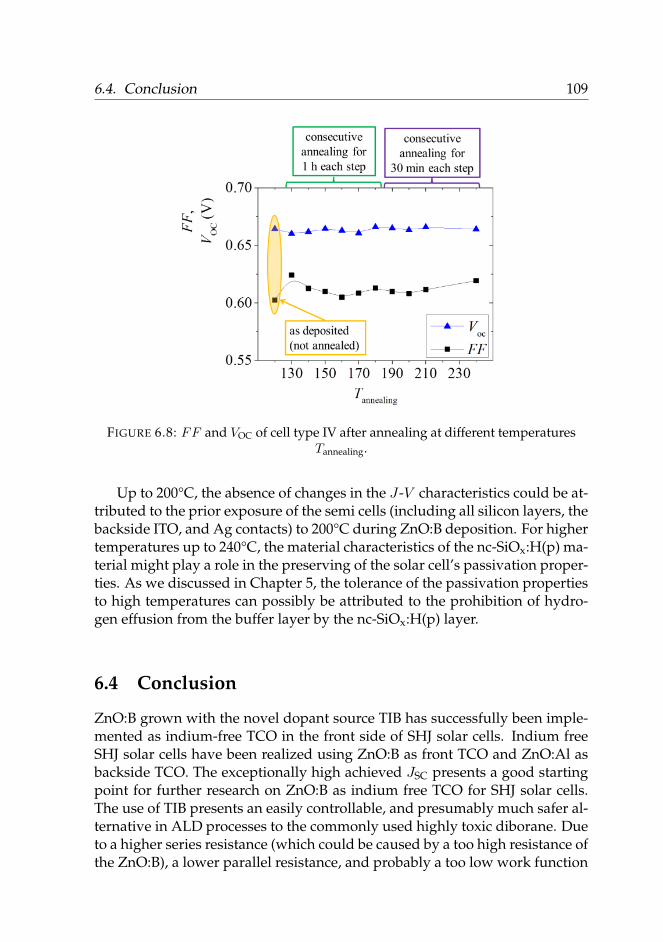
6.4. Conclusion 109
FIGURE 6.8: FF and VOC of cell type IV after annealing at different temperaturesTannealing.
Up to 200°C, the absence of changes in the J-V characteristics could be at-tributed to the prior exposure of the semi cells (including all silicon layers, thebackside ITO, and Ag contacts) to 200°C during ZnO:B deposition. For highertemperatures up to 240°C, the material characteristics of the nc-SiOx:H(p) ma-terial might play a role in the preserving of the solar cell’s passivation proper-ties. As we discussed in Chapter 5, the tolerance of the passivation propertiesto high temperatures can possibly be attributed to the prohibition of hydro-gen effusion from the buffer layer by the nc-SiOx:H(p) layer.
6.4 Conclusion
ZnO:B grown with the novel dopant source TIB has successfully been imple-mented as indium-free TCO in the front side of SHJ solar cells. Indium freeSHJ solar cells have been realized using ZnO:B as front TCO and ZnO:Al asbackside TCO. The exceptionally high achieved JSC presents a good startingpoint for further research on ZnO:B as indium free TCO for SHJ solar cells.The use of TIB presents an easily controllable, and presumably much safer al-ternative in ALD processes to the commonly used highly toxic diborane. Dueto a higher series resistance (which could be caused by a too high resistance ofthe ZnO:B), a lower parallel resistance, and probably a too low work function

110Chapter 6. ZnO:B front TCO in combination with nc-SiOx:H(p) emitter
aaaaaaaaaaaaaaaaaaaa layer for increased JSC in SHJ solar cells
of the ZnO:B, a decrease in fill factor compared to cells with standard ITO isobserved. A negative effect on the FF due to formation of an oxide interlayerbetween the ZnO:B and the emitter layer has been ruled out. The solar cellsshow remarkable thermal stabilities up to annealing temperatures of 240°C.Investigation of the influence of the ZnO:B work function and careful engi-neering of the Si-ZnO:B interface should result in increased efficiency.
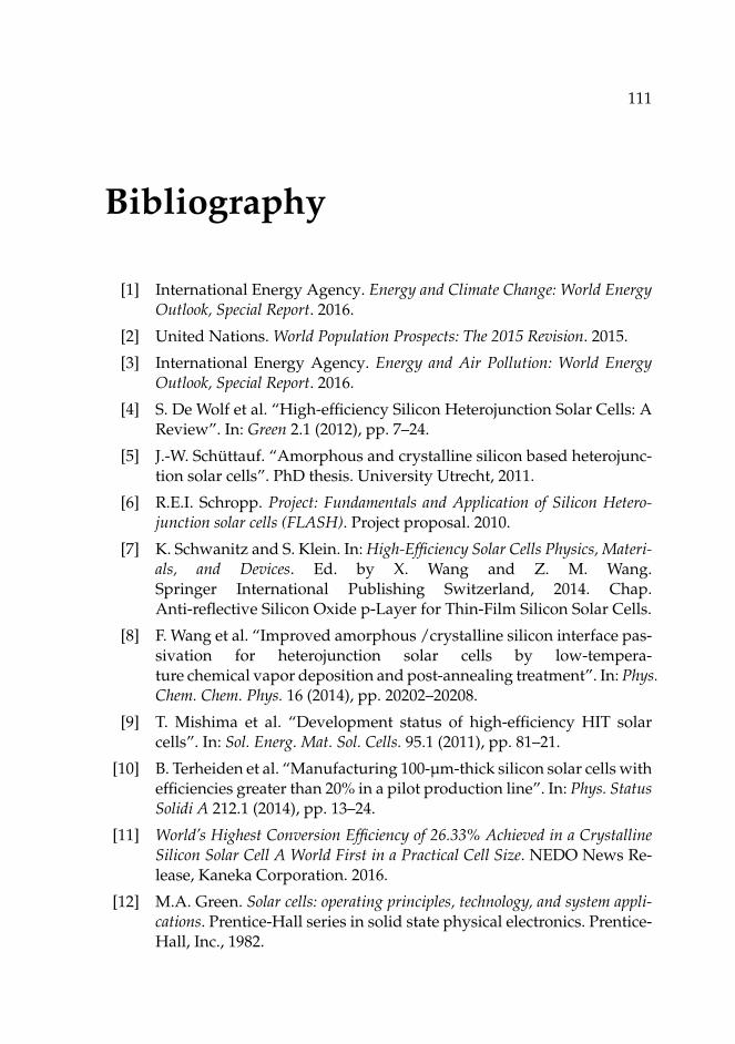
111
Bibliography
[1] International Energy Agency. Energy and Climate Change: World EnergyOutlook, Special Report. 2016.
[2] United Nations. World Population Prospects: The 2015 Revision. 2015.
[3] International Energy Agency. Energy and Air Pollution: World EnergyOutlook, Special Report. 2016.
[4] S. De Wolf et al. “High-efficiency Silicon Heterojunction Solar Cells: AReview”. In: Green 2.1 (2012), pp. 7–24.
[5] J.-W. Schüttauf. “Amorphous and crystalline silicon based heterojunc-tion solar cells”. PhD thesis. University Utrecht, 2011.
[6] R.E.I. Schropp. Project: Fundamentals and Application of Silicon Hetero-junction solar cells (FLASH). Project proposal. 2010.
[7] K. Schwanitz and S. Klein. In: High-Efficiency Solar Cells Physics, Materi-als, and Devices. Ed. by X. Wang and Z. M. Wang.Springer International Publishing Switzerland, 2014. Chap.Anti-reflective Silicon Oxide p-Layer for Thin-Film Silicon Solar Cells.
[8] F. Wang et al. “Improved amorphous /crystalline silicon interface pas-sivation for heterojunction solar cells by low-tempera-ture chemical vapor deposition and post-annealing treatment”. In: Phys.Chem. Chem. Phys. 16 (2014), pp. 20202–20208.
[9] T. Mishima et al. “Development status of high-efficiency HIT solarcells”. In: Sol. Energ. Mat. Sol. Cells. 95.1 (2011), pp. 81–21.
[10] B. Terheiden et al. “Manufacturing 100-µm-thick silicon solar cells withefficiencies greater than 20% in a pilot production line”. In: Phys. StatusSolidi A 212.1 (2014), pp. 13–24.
[11] World’s Highest Conversion Efficiency of 26.33% Achieved in a CrystallineSilicon Solar Cell A World First in a Practical Cell Size. NEDO News Re-lease, Kaneka Corporation. 2016.
[12] M.A. Green. Solar cells: operating principles, technology, and system appli-cations. Prentice-Hall series in solid state physical electronics. Prentice-Hall, Inc., 1982.
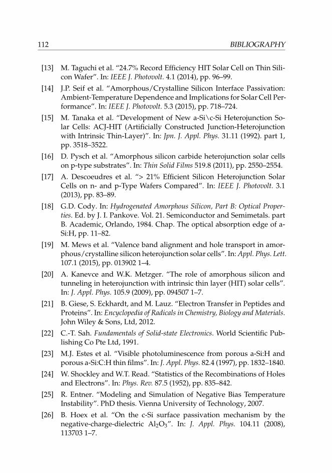
112 BIBLIOGRAPHY
[13] M. Taguchi et al. “24.7% Record Efficiency HIT Solar Cell on Thin Sili-con Wafer”. In: IEEE J. Photovolt. 4.1 (2014), pp. 96–99.
[14] J.P. Seif et al. “Amorphous/Crystalline Silicon Interface Passivation:Ambient-Temperature Dependence and Implications for Solar Cell Per-formance”. In: IEEE J. Photovolt. 5.3 (2015), pp. 718–724.
[15] M. Tanaka et al. “Development of New a-Si\c-Si Heterojunction So-lar Cells: ACJ-HIT (Artificially Constructed Junction-Heterojunctionwith Intrinsic Thin-Layer)”. In: Jpn. J. Appl. Phys. 31.11 (1992). part 1,pp. 3518–3522.
[16] D. Pysch et al. “Amorphous silicon carbide heterojunction solar cellson p-type substrates”. In: Thin Solid Films 519.8 (2011), pp. 2550–2554.
[17] A. Descoeudres et al. “> 21% Efficient Silicon Heterojunction SolarCells on n- and p-Type Wafers Compared”. In: IEEE J. Photovolt. 3.1(2013), pp. 83–89.
[18] G.D. Cody. In: Hydrogenated Amorphous Silicon, Part B: Optical Proper-ties. Ed. by J. I. Pankove. Vol. 21. Semiconductor and Semimetals. partB. Academic, Orlando, 1984. Chap. The optical absorption edge of a-Si:H, pp. 11–82.
[19] M. Mews et al. “Valence band alignment and hole transport in amor-phous/crystalline silicon heterojunction solar cells”. In: Appl. Phys. Lett.107.1 (2015), pp. 013902 1–4.
[20] A. Kanevce and W.K. Metzger. “The role of amorphous silicon andtunneling in heterojunction with intrinsic thin layer (HIT) solar cells”.In: J. Appl. Phys. 105.9 (2009), pp. 094507 1–7.
[21] B. Giese, S. Eckhardt, and M. Lauz. “Electron Transfer in Peptides andProteins”. In: Encyclopedia of Radicals in Chemistry, Biology and Materials.John Wiley & Sons, Ltd, 2012.
[22] C.-T. Sah. Fundamentals of Solid-state Electronics. World Scientific Pub-lishing Co Pte Ltd, 1991.
[23] M.J. Estes et al. “Visible photoluminescence from porous a-Si:H andporous a-Si:C:H thin films”. In: J. Appl. Phys. 82.4 (1997), pp. 1832–1840.
[24] W. Shockley and W.T. Read. “Statistics of the Recombinations of Holesand Electrons”. In: Phys. Rev. 87.5 (1952), pp. 835–842.
[25] R. Entner. “Modeling and Simulation of Negative Bias TemperatureInstability”. PhD thesis. Vienna University of Technology, 2007.
[26] B. Hoex et al. “On the c-Si surface passivation mechanism by thenegative-charge-dielectric Al2O3”. In: J. Appl. Phys. 104.11 (2008),113703 1–7.
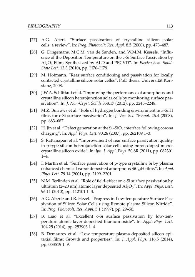
BIBLIOGRAPHY 113
[27] A.G. Aberl. “Surface passivation of crystalline silicon solarcells: a review”. In: Prog. Photovolt: Res. Appl. 8.5 (2000), pp. 473–487.
[28] G. Dingemans, M.C.M. van de Sanden, and W.M.M. Kessels. “Influ-ence of the Deposition Temperature on the c-Si Surface Passivation byAl2O3 Films Synthesized by ALD and PECVD”. In: Electrochem. Solid-State Lett. 13.3 (2010), pp. H76–H79.
[29] M. Hofmann. “Rear surface conditioning and passivation for locallycontacted crystalline silicon solar cellss”. PhD thesis. Universität Kon-stanz, 2008.
[30] J.W.A. Schüttauf et al. “Improving the performance of amorphous andcrystalline silicon heterojunction solar cells by monitoring surface pas-sivation”. In: J. Non-Cryst. Solids 358.17 (2012), pp. 2245–2248.
[31] M.Z. Burrows et al. “Role of hydrogen bonding environment in a-Si:Hfilms for c-Si surface passivation”. In: J. Vac. Sci. Technol. 26.4 (2008),pp. 683–687.
[32] H. Jin et al. “Defect generation at the Si–SiO2 interface following coronacharging”. In: Appl. Phys. Lett. 90.26 (2007), pp. 262109 1–3.
[33] S. Rattanapan et al. “Improvement of rear surface passivation qualityin p-type silicon heterojunction solar cells using boron-doped micro-crystalline silicon oxide”. In: Jpn. J. Appl. Phys. 50.8R (2011), pp. 0823011–4.
[34] I. Martín et al. “Surface passivation of p-type crystalline Si by plasmaenhanced chemical vapor deposited amorphous SiCx:H films”. In: Appl.Phys. Lett. 79.14 (2001), pp. 2199–2201.
[35] N.M. Terlinden et al. “Role of field-effect on c-Si surface passivation byultrathin (2–20 nm) atomic layer deposited Al2O3”. In: Appl. Phys. Lett.96.11 (2010), pp. 112101 1–3.
[36] A.G. Aberle and R. Hezel. “Progress in Low-temperature Surface Pas-sivation of Silicon Solar Cells using Remote-plasma Silicon Nitride”.In: Prog. Photovolt: Res. Appl. 5.1 (1997), pp. 29–50.
[37] B. Liao et al. “Excellent c-Si surface passivation by low-tem-perature atomic layer deposited titanium oxide”. In: Appl. Phys. Lett.104.25 (2014), pp. 253903 1–4.
[38] B. Demaurex et al. “Low-temperature plasma-deposited silicon epi-taxial films: Growth and properties”. In: J. Appl. Phys. 116.5 (2014),pp. 053519 1–9.
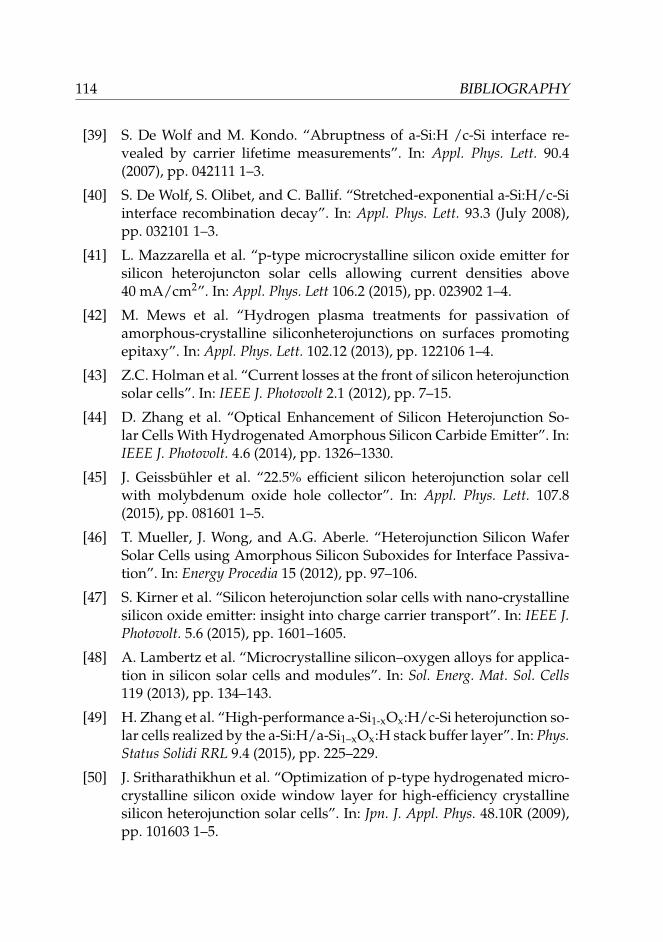
114 BIBLIOGRAPHY
[39] S. De Wolf and M. Kondo. “Abruptness of a-Si:H /c-Si interface re-vealed by carrier lifetime measurements”. In: Appl. Phys. Lett. 90.4(2007), pp. 042111 1–3.
[40] S. De Wolf, S. Olibet, and C. Ballif. “Stretched-exponential a-Si:H/c-Siinterface recombination decay”. In: Appl. Phys. Lett. 93.3 (July 2008),pp. 032101 1–3.
[41] L. Mazzarella et al. “p-type microcrystalline silicon oxide emitter forsilicon heterojuncton solar cells allowing current densities above40 mA/cm2”. In: Appl. Phys. Lett 106.2 (2015), pp. 023902 1–4.
[42] M. Mews et al. “Hydrogen plasma treatments for passivation ofamorphous-crystalline siliconheterojunctions on surfaces promotingepitaxy”. In: Appl. Phys. Lett. 102.12 (2013), pp. 122106 1–4.
[43] Z.C. Holman et al. “Current losses at the front of silicon heterojunctionsolar cells”. In: IEEE J. Photovolt 2.1 (2012), pp. 7–15.
[44] D. Zhang et al. “Optical Enhancement of Silicon Heterojunction So-lar Cells With Hydrogenated Amorphous Silicon Carbide Emitter”. In:IEEE J. Photovolt. 4.6 (2014), pp. 1326–1330.
[45] J. Geissbühler et al. “22.5% efficient silicon heterojunction solar cellwith molybdenum oxide hole collector”. In: Appl. Phys. Lett. 107.8(2015), pp. 081601 1–5.
[46] T. Mueller, J. Wong, and A.G. Aberle. “Heterojunction Silicon WaferSolar Cells using Amorphous Silicon Suboxides for Interface Passiva-tion”. In: Energy Procedia 15 (2012), pp. 97–106.
[47] S. Kirner et al. “Silicon heterojunction solar cells with nano-crystallinesilicon oxide emitter: insight into charge carrier transport”. In: IEEE J.Photovolt. 5.6 (2015), pp. 1601–1605.
[48] A. Lambertz et al. “Microcrystalline silicon–oxygen alloys for applica-tion in silicon solar cells and modules”. In: Sol. Energ. Mat. Sol. Cells119 (2013), pp. 134–143.
[49] H. Zhang et al. “High-performance a-Si1-xOx:H/c-Si heterojunction so-lar cells realized by the a-Si:H/a-Si1–xOx:H stack buffer layer”. In: Phys.Status Solidi RRL 9.4 (2015), pp. 225–229.
[50] J. Sritharathikhun et al. “Optimization of p-type hydrogenated micro-crystalline silicon oxide window layer for high-efficiency crystallinesilicon heterojunction solar cells”. In: Jpn. J. Appl. Phys. 48.10R (2009),pp. 101603 1–5.
BIBLIOGRAPHY 115
[51] R. Pendorf. “Tables of the Refractive Index for Standard Air and theRayleigh Scattering Coefficient for the Spectral Region between 0.2 and20.0 Li and Their Application to Atmospheric Optics”. In: J. Opt. Soc.Am. 47.2 (1957), pp. 176–182.
[52] D.F. Edwards and E. Ochoa. “Infrared refractive index of silicon”. In:Appl. Opt. 19.24 (1980), pp. 4130–4131.
[53] L. Mazzarella et al. “Nanocrystalline Silicon Oxide Emitters for SiliconHetero Junction Solar Cells”. In: Energy Procedia 77 (2015), pp. 304–310.
[54] J.P. Seif et al. “Amorphous silicon oxide window layers for high-efficiency silicon heterojunction solar cells”. In: J. Appl. Phys. 115.2(2014), pp. 024502 1–8.
[55] A. Lambertz, T. Grundler, and F. Finger. “Hydrogenated amorphoussilicon oxide containing a microcrystalline silicon phase and usage asan intermediate reflector in thin-film silicon solar cells”. In: J. Appl.Phys. 109.11 (2011), pp. 113109 1–10.
[56] S. Kirner et al. “The growth of microcrystalline silicon oxide thin filmsstudied by in situ plasma diagnostics”. In: Appl. Phys. Lett. 102.5 (2013),pp. 051906 1–4.
[57] O. Gabriel et al. “On the Plasma Chemistry During Plasma EnhancedChemical Vapor Deposition of Microcrystalline Silicon Oxides”. In:Plasma Process. Polym. 12.1 (2015), pp. 82–91.
[58] A. Sarker, C. Banerjee, and A.K. Barua. “Preparation and characteriza-tion of n-type microcrystalline hydrogenated silicon oxide films”. In: J.Phys. D: Appl. Phys. 35.11 (2002), pp. 1205–1209.
[59] D. Das, S. Mandal, and A.K. Barua. “Intrinsic hydrogenated microcrys-talline silicon oxide films prepared by RF glow discharge”. In: J. Mater.Sci. Lett. 17.24 (1998), pp. 2097–2100.
[60] International Organization for Standardization. Nanotechnologies - Ma-terials specifications - Guidance on specifying nano-objects. ISO/TS. 2011.
[61] K.-Y. Chan et al. “High-mobility microcrystalline silicon thin-film tran-sistors prepared near the transition to amorphous growth”. In: J. Appl.Phys. 104 (2008), pp. 054506 1–6.
[62] H. Fujiwara, M. Kondo, and A. Matsuda. “Stress-Induced Nucleationof Microcrystalline Silicon from Amorphous Phase”. In: Jpn. J. Appl.Phys 41.5R (2002). part 1, pp. 2821–2828.
[63] J.K. Rath and R.E.I. Schropp. “Incorporation of p-type microcrystallinesilicon films in amorphous silicon based solar cells in a superstratestructure”. In: Sol. Energy. Mat. Sol. Cells 53.1-2 (1998), pp. 189–203.
116 BIBLIOGRAPHY
[64] P. Roca i Cabarrocas et al. “Substrate selectivity in the formation of mi-crocrystalline silicon: Mechanisms and technological consequences”.In: Appl. Phys. Lett 66.26 (1995), pp. 3609–3611.
[65] N. Pellaton Vaucher et al. “Controlled nucleation of thin microcrys-talline layers for the recombination junction in a-Si stacked cells”. In:Sol. Energ. Mat. Sol. Cells. 49.1-4 (1997), pp. 27–33.
[66] X. Pi. “Doping Silicon Nanocrystals with Boron and Phosphorus”. In:J. Nanomater. 2012 (2012), pp. 1–9.
[67] S.C. Erwin et al. “Doping semiconductor nanocrystals”. In: Nature 436(2005), pp. 91–94.
[68] X. Chen, X. Pi, and D. Yang. “Critical role of dopant location for P-doped Si nanocrystals”. In: J. Phys. Chem. C 115.3 (2011), pp. 661–666.
[69] X.D. Pi, X.B. Chen, and D. Yang. “First-principles study of 2.2 nm sili-con nanocrystals doped with boron”. In: J. Phys. Chem. C 115.20 (2011),pp. 9838–9843.
[70] G. Cantele et al. “First-principles study of n- and p-doped silicon nan-oclusters”. In: Phys. Rev. B 72.11-15 (2005), pp. 113303 1–4.
[71] T.L. Chan et al. “Size limits on doping phosphorus into silicon nanocrys-tals”. In: Nano Lett. 8.2 (2008), pp. 596–600.
[72] J. Ma et al. “Effect of surface passivation on dopant distribution in Siquantum dots: the case of B and P doping”. In: Appl. Phys. Lett. 98.17(2011), pp. 173103 1–3.
[73] U. Kortshagen. “Nonthermal plasma synthesis of semiconductornanocrystals”. In: J. Phys. D: Appl. Phys. 42.11 (2009), pp. 113001 1–22.
[74] M. Fujii et al. “Hyperfine structure of the electron spin resonance ofphosphorus-doped Si nanocrystals”. In: Phys. Rev. Lett. 89.20-11 (2002),pp. 206805 1–4.
[75] M. Fujii et al. “Photoluminescence from Si nanocrystals dispersed inphosphosilicate glass thin films: improvement of photoluminescenceefficiency”. In: Appl. Phys. Lett. 75.2 (1999), pp. 184–186.
[76] K. Matsumoto, M. Fujii, and S. Hayashi. “Photoluminescence fromSi nanocrystals embedded in In doped SiO2”. In: Japan. J. Appl. Phys.45.12-16 (2006). part 2, pp. L450–L452.
[77] M. Fujii et al. “Photoluminescence from impurity codoped and com-pensated Si nanocrystals”. In: Appl. Phys. Lett. 87.21 (2005), pp. 2119191–3.
BIBLIOGRAPHY 117
[78] M. Fujii et al. “Control of photoluminescence properties of Si nanocrys-tals by simultaneously doping n- and p-type impurities”. In: Appl. Phys.Lett. 85.7 (2004), pp. 1158–1160.
[79] A. Mimura et al. “Photoluminescence and free-electron absorption inheavily phosphorus-doped Si nanocrystals”. In: Phys. Rev. B 62.19-15(2000), pp. 12625–12627.
[80] P. Cuony et al. “Silicon Filaments in Silicon Oxide for Next-GenerationPhotovoltaics”. In: Adv. Mater. 24.9 (2012), pp. 1182–1186.
[81] K. Schwanitz et al. “Anti-reflective microcrystalline silicon oxide p-layer for thin-film silicon solar cells on ZnO”. In: Sol. Energ. Mat. Sol.Cells. 105 (2012), pp. 187–191.
[82] P. Buehlmann et al. “In situ silicon oxide based intermediate reflectorfor thin-film silicon micromorph solar cells”. In: Appl. Phys. Lett. 91.14(2007), pp. 143505 1–3.
[83] M. Xie et al. “The location and doping effect of boron in Si nanocrys-tals embedded silicon oxide film”. In: Appl. Phys. Lett. 102.12 (2013),pp. 123108 1–4.
[84] Z.Y. Wu, B. Drevilllon, and M. Fang. “The incorporation of carbon ina-Si:H enhanced by boron doping”. In: J. Non-Cryst. Solids 137&138(1991). part 2, pp. 863–866.
[85] J. Koh et al. “Real time spectroscopic ellipsometry studies of the nu-cleation and growth of p-type microcrystalline silicon films on amor-phous silicon using B2H6, B(CH3)3 and BF3 dopant source gases”. In:J. Appl. Phys. 85.8 (1999), pp. 4141–4153.
[86] K.M.A. Rahman. “Nanocrystalline Silicon Solar Cells Deposited viaPulsed PECVD at 150°C Substrate Temperature”. PhD thesis. Univer-sity of Waterloo, 2010.
[87] A. Matsuda. In: Springer Handbook of Electronic and Photonic Materials.Ed. by S. Kasap and P. Capper. Springer, 2007. Chap. 26: Amorphousand Microcrysalline Silicon.
[88] By original work: Cdangderivative work (a): Sbyrnes321 (talk)deriva-tive work (b): Rfassbind (talk), (this version) - Crystalline polycrys-talline amorphous.svg, CC BY-SA 3.0, visited on 2016-09-20,https://commons.wikimedia.org/w/index.php?curid=35476650.
[89] R. Terasa et al. “Time-resolved layer thickness behavior of microcrys-talline and amorphous silicon samples after switching on a hydro-gen/silane VHF plasma”. In: J. Non-Cryst. Solids 299-302 (2002), pp. 58–62.
118 BIBLIOGRAPHY
[90] S. Pizzini. Advanced Silicon Materials for Photovoltaic Applications. JohnWiley & Sons, Inc, 2012.
[91] A. Matsuda. “Formation kinetics and control of microcrystallite in µc-Si:H from glow discharge plasma”. In: J. Non-Cryst. Solids 59 & 60.2(1983), pp. 767–774.
[92] A. Samanta and D. Das. “Studies on the structural properties of SiO:Hfilms prepared from (SiH4+CO2+He) plasma in RF-PECVD”. In: Sol.Energ. Mat. Sol. Cells. 93.5 (2009), pp. 588–596.
[93] S.M. Iftiquar. “The roles of deposition pressure and rf power in opto-electronic properties of a-SiO:H films”. In: J. Phys. D: Appl. Phys. 31.14(1998), pp. 1630–1641.
[94] S. Kirner. “Development of wide band gap materials for thin film sili-con solar cells”. PhD thesis. Technische Universität Berlin, 2013.
[95] C.C. Tsai et al. “Transition from Amorphous to Crystalline Silicon: Ef-fect of Hydrogen on Film Growth”. In: MRS Proceedings 118 (1988),pp. 49–55.
[96] W. Wensheng et al. “Preferred growth of nanocrystalline silicon inboron-doped nc-Si:H Films”. In: Vacuum 74.1 (2004), pp. 69–75.
[97] S.R. Jadkar et al. “Synthesis of highly conductive boron-doped p-typehydrogenated microcrystalline silicon (µc-Si:H) by a hot-wire chemicalvapor deposition (HWCVD) technique”. In: Sol. Energ. Mat. Sol. Cells.64.4 (2000), pp. 333–346.
[98] J. Perrin et al. “Sticking and recombination of the SiH3 radical on hy-drogenated amorphous silicon: The catalytic effect of diborane”. In:Surf. Sci. 210.1-2 (1989), pp. 114 –128.
[99] D. Das and A.K. Barua. “Highly Conducting Undoped mc-SiO:H FilmsPrepared by RF Glow Discharge”. In: Jpn. J. Appl. Phys 38.7A (1999), pp.L697–L699.
[100] V. Smirnov et al. “Microcrystalline silicon oxide (µc-SiOx:H) alloys: Aversatile material for application in thin film silicon single and tandemjunction solar cells”. In: J. Non-Cryst. Solids 358.17 (2012), pp. 1954–1957.
[101] N. Pingate, D. Yotsaksri, and P. Sich. “Microcrystalline SiO and its ap-plication to solar cell”. In: IEEE 4th World Conf. on Photovolt. Energyproceedings 2.2 (2006), pp. 1507–1508.
[102] J.H. Shim, S.-W. Ahn, and H.-M. Lee. “Microcrystalline silicon oxide(µc-SiO:H) alloys as a contact layer for highly efficient Si thin film solarcell”. In: Curr. Appl. Phys. 13.7 (2013), pp. 1401–1403.
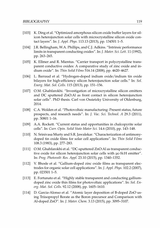
BIBLIOGRAPHY 119
[103] K. Ding et al. “Optimized amorphous silicon oxide buffer layers for sil-icon heterojunction solar cells with microcrystalline silicon oxide con-tact layers”. In: J. Appl. Phys. 113.13 (2013), pp. 134501 1–5.
[104] J.R. Bellingham, W.A. Phillips, and C.J. Adkins. “Intrinsic performancelimits in transparent conducting oxides”. In: J. Mater. Sci. Lett. 11 (1992),pp. 263–265.
[105] K. Ellmer and R. Mientus. “Carrier transport in polycrystalline trans-parent conductive oxides: A comparative study of zinc oxide and in-dium oxide”. In: Thin Solid Films 516.14 (2008), pp. 4620–4627.
[106] L. Barraud et al. “Hydrogen-doped indium oxide/indium tin oxidebilayers for high-efficiency silicon heterojunction solar cells.” In: Sol.Energ. Mat. Sol. Cells. 115 (2013), pp. 151–156.
[107] O.M. Ghahfarokhi. “Investigation of microcrystalline silicon emittersand DC sputtered ZnO:Al as front contact in silicon heterojunctionsolar cells”. PhD thesis. Carl von Ossietzky University of Oldenburg,2014.
[108] C.A. Wolden et al. “Photovoltaic manufacturing: Present status, futureprospects, and research needs”. In: J. Vac. Sci. Technol. A 29.3 (2011),pp. 30801 1–16.
[109] A.A. Rockett. “Current status and opportunities in chalcopyrite solarcells”. In: Curr. Opin. Solid State Mater Sci. 14.6 (2010), pp. 143–148.
[110] N. Srinivasa Murty and S.R. Jawalekar. “Characterization of antimony-doped tin oxide films for solar cell applications”. In: Thin Solid Films108.3 (1983), pp. 277–283.
[111] O.M. Ghahfarokhi et al. “DC-sputtered ZnO:Al as transparent conduc-tive oxide for silicon heterojunction solar cells with µc-Si:H emitter”.In: Prog. Photovolt: Res. Appl. 23.10 (2015), pp. 1340–1352.
[112] V. Bhosle et al. “Gallium-doped zinc oxide films as transparent elec-trodes for organic solar cell applications”. In: J. Appl. Phys. 102.2 (2007),pp. 023501 1–5.
[113] E. Fortunato et al. “Highly stable transparent and conducting gallium-doped zinc oxide thin films for photovoltaic applications”. In: Sol. En-erg. Mat. Sol. Cells. 92.12 (2008), pp. 1605–1610.
[114] D. Garcia-Alonso et al. “Atomic layer deposition of B-doped ZnO us-ing Triisopropyl Borate as the Boron precursor and Comparison withAl-doped ZnO”. In: J. Mater. Chem. 3.13 (2015), pp. 3095–3107.
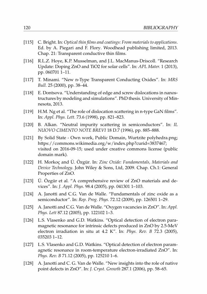
120 BIBLIOGRAPHY
[115] C. Bright. In: Optical thin films and coatings: From materials to applications.Ed. by A. Piegari and F. Flory. Woodhead publishing limited, 2013.Chap. 21: Transparent conductive thin films.
[116] R.L.Z. Hoye, K.P. Musselman, and J.L. MacManus-Driscoll. “ResearchUpdate: Doping ZnO and TiO2 for solar cells”. In: APL Mater. 1 (2013),pp. 060701 1–11.
[117] T. Minami. “New n-Type Transparent Conducting Oxides”. In: MRSBull. 25 (2000), pp. 38–44.
[118] E. Dontsova. “Understanding of edge and screw dislocations in nanos-tructures by modeling and simulations”. PhD thesis. University of Min-nesota, 2013.
[119] H.M. Ng et al. “The role of dislocation scattering in n-type GaN films”.In: Appl. Phys. Lett. 73.6 (1998), pp. 821–823.
[120] B. Alkan. “Neutral impurity scattering in semiconductors”. In: ILNUOVO CIMENTO NOTE BREVI 18 D.7 (1996), pp. 885–888.
[121] By Solid State - Own work, Public Domain, Wurtzite polyhedra.png;https://commons.wikimedia.org/w/index.php?curid=3837467;visited on 2016-09-15; used under creative commons license (publicdomain mark).
[122] H. Morkoç and Ü. Özgür. In: Zinc Oxide: Fundamentals, Materials andDevice Technology. John Wiley & Sons, Ltd, 2009. Chap. Ch.1: GeneralProperties of ZnO.
[123] Ü. Özgür et al. “A comprehensive review of ZnO materials and de-vices”. In: J. Appl. Phys. 98.4 (2005), pp. 041301 1–103.
[124] A. Janotti and C.G. Van de Walle. “Fundamentals of zinc oxide as asemiconductor”. In: Rep. Prog. Phys. 72.12 (2009), pp. 126501 1–29.
[125] A. Janotti and C.G. Van de Walle. “Oxygen vacancies in ZnO”. In: Appl.Phys. Lett 87.12 (2005), pp. 122102 1–3.
[126] L.S. Vlasenko and G.D. Watkins. “Optical detection of electron para-magnetic resonance for intrinsic defects produced in ZnO by 2.5-MeVelectron irradiation in situ at 4.2 K”. In: Phys. Rev. B 72.3 (2005),035203 1–12.
[127] L.S. Vlasenko and G.D. Watkins. “Optical detection of electron param-agnetic resonance in room-temperature electron-irradiated ZnO”. In:Phys. Rev. B 71.12 (2005), pp. 125210 1–6.
[128] A. Janotti and C. G. Van de Walle. “New insights into the role of nativepoint defects in ZnO”. In: J. Cryst. Growth 287.1 (2006), pp. 58–65.
BIBLIOGRAPHY 121
[129] A. Janotti and C.G. Van de Walle. “Native point defects in ZnO”. In:Phys. Rev. B 76.16 (2007), pp. 165202 1–22.
[130] C.G. Van de Walle. “Hydrogen as a Cause of Doping in Zinc Oxide”.In: Phys. Rev. Lett. 85.5 (2000), pp. 1012–1015.
[131] A. Janotti and C.G. Van de Walle. “Hydrogenmulticentrebonds”. In: Nat. Mater. 6 (2007), pp. 44 –47.
[132] N.W. Emanetoglu et al. “Epitaxial ZnO piezoelectric thin films for sawfilters”. In: Mater. Sci. Semicond. Process. 2.3 (1999), pp. 247–252.
[133] L. Wang et al. “ZnO nanorod gas sensor for ethanol detection”. In: Sens.Actuator. B Chem. 162.1 (2012), pp. 237–243.
[134] T.K. Gupta. “Application of zinc oxide varistors”. In: J. Am. Ceram. Soc.73.7 (1990), pp. 1817–1840.
[135] H. Huang et al. “ZnO-Based Fairly Pure Ultraviolet Light-Emitting Diodes With a Low Operation Voltage”. In: IEEE Electron De-vice Lett. 30.10 (2009), pp. 1063–1065.
[136] B. Rech and H. Wagner. “Potential of amorphous silicon for solar cells”.In: Appl. Phys. A 69.2 (1999), pp. 155–167.
[137] K. Ramanathan et al. “Properties of 19.2% efficiency ZnO/CdS/CuInGaSe2 thin-film solar cells”. In: Prog. Photovolt: Res. Appl. 11.4(2003), pp. 225–230.
[138] R. Klenk et al. “Solar cells based on CuInS2 - an overview”. In: ThinSolid Films 480–481 (2005), pp. 509–514.
[139] H.Q. Chiang et al. “High mobility transparent thin-film transistors withamorphous zinc tin oxide channel layer”. In: Appl. Phys. Lett. 86.1 (2005),pp. 013503 1–3.
[140] Y. Gassenbauer and A. Klein. “Electronic and Chemical Properties ofTin-Doped Indium Oxide (ITO) Surfaces and ITO /ZnPc InterfacesStudied In-situ by Photoelectron Spectroscopy”. In: J. Phys. Chem. B110 (2006), pp. 4793–4801.
[141] K. Nomura et al. “High-mobility microcrystalline silicon thin-film tran-sistors prepared near the transition to amorphous growth”. In: Nature432 (2004), pp. 448–492.
[142] M. Bivour et al. “Improving the a-Si:H(p) rear emitter contact of n-typesilicon solar cells”. In: Sol. Energ. Mat. Sol. Cells 106 (2012), pp. 11–16.
[143] E. Centurioni and D. Iencinella. “Role of Front Contact Work Functionon Amorphous Silicon/Crystalline Silicon Heterojunction Solar CellPerformance”. In: IEEE Electron Device Lett. 24.3 (2003), pp. 177–179.
122 BIBLIOGRAPHY
[144] M. Kasuga and S. Ogawa. “Electronic Properties of Vapor-Grown Heteroepitaxial ZnO Film on Sapphire”. In: Jpn. J. Appl. Phys22.5 (1983). part 1, pp. 794–798.
[145] Y.R. Ryu, T.S. Lee, and H.W. White. “A technique of hybrid beam depo-sition for synthesis of ZnO and other metal oxides”. In: J. Cryst. Growth261.4 (2004), pp. 502 –507.
[146] Y. Chen et al. “Plasma assisted molecular beam epitaxy of ZnO on c-plane sapphire: Growth and characterization”. In: J. Appl. Phys. 84.7(1998), pp. 3912–3918.
[147] Y. Segawa et al. “Growth of ZnO Thin Film by Laser MBE: Lasing ofExciton at Room Temperature”. In: Phys. Stat. Sol. 202.2 (1997), pp. 669–672.
[148] R.D. Vispute et al. “High quality crystalline ZnO buffer layers on sap-phire (001) by pulsed laser deposition for III–V nitrides”. In: Appl. Phys.Lett. 70.20 (1997), pp. 2735–2737.
[149] B. Hahn et al. “MOCVD layer growth of ZnO using DMZn and tertiarybutanol”. In: Semicond. Sci. Tech. 13.7 (1998), pp. 778–791.
[150] D.C. Look. “Recent advances in ZnO materials and devices”. In: Mat.Sci. Eng. B 80.1-3 (2001), pp. 383–387.
[151] M. Shimizu et al. “Photo-MOCVD of ZnO epitaxial films”. In: J. Cryst.Growth 99.1-4 (1990), pp. 399 –402.
[152] K. Sharma et al. “Expanding Thermal Plasma Chemical Vapour De-position of ZnO:Al Layers for CIGS Solar Cells”. In: Int. J. Photoenergy2014 (2015), pp. 253140 1–9.
[153] M.D. Barankin et al. “Plasma-enhanced chemical vapor deposition ofzinc oxide at atmospheric pressure and low temperature”. In: Sol. En-erg. Mat. Sol. Cells. 91.10 (2007), pp. 924 –930.
[154] J. van Deelen et al. “APCVD of ZnO:Al, insight and control by model-ing”. In: Surf. Coat. Technol. 230 (2013), pp. 239 –244.
[155] S. Faÿ et al. “Polycrystalline ZnO: B grown by LPCVD as TCO for thinfilm silicon solar cells”. In: Thin Solid Films 518.11 (2010), pp. 2961–2966.
[156] A.K.K. Kyaw, X.W. Sun, and C.Y. Jiang. “Efficient charge collectionwith sol-gel derived colloidal ZnO thin film in photovoltaic devices”.In: J. Sol-Gel Sci. Technol. 52 (2009), pp. 348–355.
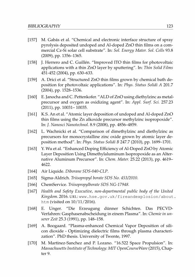
BIBLIOGRAPHY 123
[157] M. Gabás et al. “Chemical and electronic interface structure of spraypyrolysis deposited undoped and Al-doped ZnO thin films on a com-mercial Cz-Si solar cell substrate”. In: Sol. Energy Mater. Sol. Cells 93.8(2009), pp. 1356–1365.
[158] J. Herrero and C. Guillén. “Improved ITO thin films for photovoltaicapplications with a thin ZnO layer by sputtering”. In: Thin Solid Films451-452 (2004), pp. 630–633.
[159] A. Drici et al. “Structured ZnO thin films grown by chemical bath de-position for photovoltaic applications”. In: Phys. Status Solidi A 201.7(2004), pp. 1528–1536.
[160] E. Janocha and C. Pettenkofer. “ALD of ZnO using diethylzinc as metal-precursor and oxygen as oxidizing agent”. In: Appl. Surf. Sci. 257.23(2011), pp. 10031– 10035.
[161] K.S. An et al. “Atomic layer deposition of undoped and Al-doped ZnOthin films using the Zn alkoxide precursor methylzinc isopropoxide”.In: J. Nanosci Nanotechnol. 8.9 (2008), pp. 4856–4859.
[162] L. Wachnicki et al. “Comparison of dimethylzinc and diethylzinc asprecursors for monocrystalline zinc oxide grown by atomic layer de-position method”. In: Phys. Status Solidi B 247.7 (2010), pp. 1699–1701.
[163] Y. Wu et al. “Enhanced Doping Efficiency of Al-Doped ZnO by AtomicLayer Deposition Using Dimethylaluminum Isopropoxide as an Alter-native Aluminum Precursor”. In: Chem. Mater. 25.22 (2013), pp. 4619–4622.
[164] Air Liquide. Diborane SDS-040-CLP.
[165] Sigma-Aldrich. Triisopropyl borate SDS No. 453/2010.
[166] ChemService. Triisopropylborate SDS NG-17948.
[167] Health and Safety Executive, non-departmental public body of the UnitedKingdom. 2016. URL: www.hse.gov.uk/fireandexplosion/about.htm (visited on 10/11/2016).
[168] E. Unger. “Die Erzeugung dünner Schichten. Das PECVD-Verfahren: Gasphasenabscheidung in einem Plasma”. In: Chemie in un-serer Zeit 25.3 (1991), pp. 148–158.
[169] A. Boogaard. “Plasma-enhanced Chemical Vapor Deposition of sili-con dioxide - Optimizing dielectric films through plasma characteri-zation”. PhD thesis. University of Twente, 1997.
[170] M. Martinez-Sanchez and P. Lozano. “16.522 Space Propulsion”. In:Massachusetts Institute of Technology: MIT OpenCourseWare (2015), Chap-ter 9.
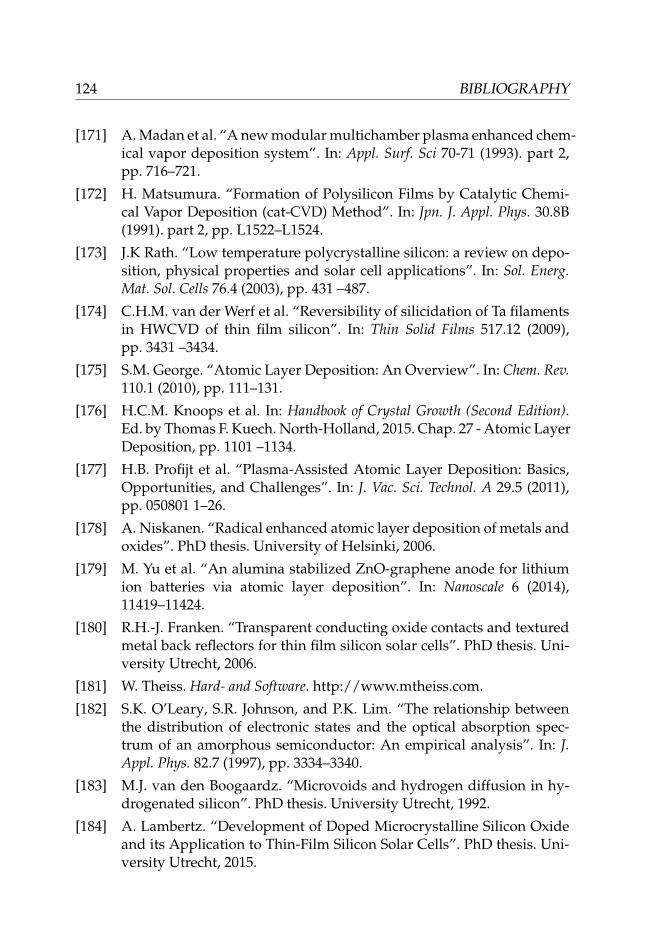
124 BIBLIOGRAPHY
[171] A. Madan et al. “A new modular multichamber plasma enhanced chem-ical vapor deposition system”. In: Appl. Surf. Sci 70-71 (1993). part 2,pp. 716–721.
[172] H. Matsumura. “Formation of Polysilicon Films by Catalytic Chemi-cal Vapor Deposition (cat-CVD) Method”. In: Jpn. J. Appl. Phys. 30.8B(1991). part 2, pp. L1522–L1524.
[173] J.K Rath. “Low temperature polycrystalline silicon: a review on depo-sition, physical properties and solar cell applications”. In: Sol. Energ.Mat. Sol. Cells 76.4 (2003), pp. 431 –487.
[174] C.H.M. van der Werf et al. “Reversibility of silicidation of Ta filamentsin HWCVD of thin film silicon”. In: Thin Solid Films 517.12 (2009),pp. 3431 –3434.
[175] S.M. George. “Atomic Layer Deposition: An Overview”. In: Chem. Rev.110.1 (2010), pp. 111–131.
[176] H.C.M. Knoops et al. In: Handbook of Crystal Growth (Second Edition).Ed. by Thomas F. Kuech. North-Holland, 2015. Chap. 27 - Atomic LayerDeposition, pp. 1101 –1134.
[177] H.B. Profijt et al. “Plasma-Assisted Atomic Layer Deposition: Basics,Opportunities, and Challenges”. In: J. Vac. Sci. Technol. A 29.5 (2011),pp. 050801 1–26.
[178] A. Niskanen. “Radical enhanced atomic layer deposition of metals andoxides”. PhD thesis. University of Helsinki, 2006.
[179] M. Yu et al. “An alumina stabilized ZnO-graphene anode for lithiumion batteries via atomic layer deposition”. In: Nanoscale 6 (2014),11419–11424.
[180] R.H.-J. Franken. “Transparent conducting oxide contacts and texturedmetal back reflectors for thin film silicon solar cells”. PhD thesis. Uni-versity Utrecht, 2006.
[181] W. Theiss. Hard- and Software. http://www.mtheiss.com.
[182] S.K. O’Leary, S.R. Johnson, and P.K. Lim. “The relationship betweenthe distribution of electronic states and the optical absorption spec-trum of an amorphous semiconductor: An empirical analysis”. In: J.Appl. Phys. 82.7 (1997), pp. 3334–3340.
[183] M.J. van den Boogaardz. “Microvoids and hydrogen diffusion in hy-drogenated silicon”. PhD thesis. University Utrecht, 1992.
[184] A. Lambertz. “Development of Doped Microcrystalline Silicon Oxideand its Application to Thin-Film Silicon Solar Cells”. PhD thesis. Uni-versity Utrecht, 2015.
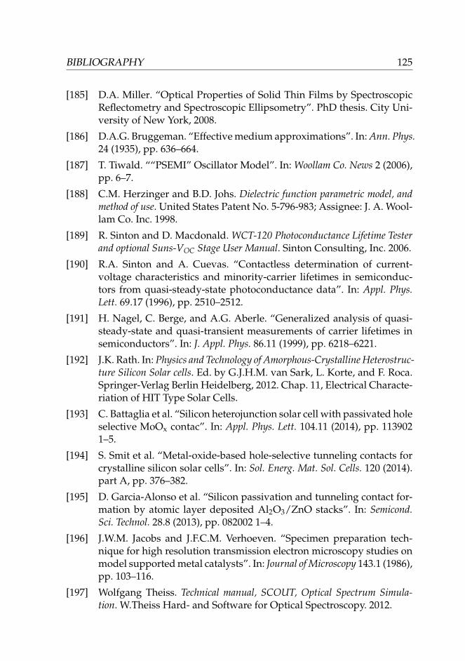
BIBLIOGRAPHY 125
[185] D.A. Miller. “Optical Properties of Solid Thin Films by SpectroscopicReflectometry and Spectroscopic Ellipsometry”. PhD thesis. City Uni-versity of New York, 2008.
[186] D.A.G. Bruggeman. “Effective medium approximations”. In: Ann. Phys.24 (1935), pp. 636–664.
[187] T. Tiwald. ““PSEMI” Oscillator Model”. In: Woollam Co. News 2 (2006),pp. 6–7.
[188] C.M. Herzinger and B.D. Johs. Dielectric function parametric model, andmethod of use. United States Patent No. 5-796-983; Assignee: J. A. Wool-lam Co. Inc. 1998.
[189] R. Sinton and D. Macdonald. WCT-120 Photoconductance Lifetime Testerand optional Suns-VOC Stage User Manual. Sinton Consulting, Inc. 2006.
[190] R.A. Sinton and A. Cuevas. “Contactless determination of current-voltage characteristics and minority-carrier lifetimes in semiconduc-tors from quasi-steady-state photoconductance data”. In: Appl. Phys.Lett. 69.17 (1996), pp. 2510–2512.
[191] H. Nagel, C. Berge, and A.G. Aberle. “Generalized analysis of quasi-steady-state and quasi-transient measurements of carrier lifetimes insemiconductors”. In: J. Appl. Phys. 86.11 (1999), pp. 6218–6221.
[192] J.K. Rath. In: Physics and Technology of Amorphous-Crystalline Heterostruc-ture Silicon Solar cells. Ed. by G.J.H.M. van Sark, L. Korte, and F. Roca.Springer-Verlag Berlin Heidelberg, 2012. Chap. 11, Electrical Characte-riation of HIT Type Solar Cells.
[193] C. Battaglia et al. “Silicon heterojunction solar cell with passivated holeselective MoOx contac”. In: Appl. Phys. Lett. 104.11 (2014), pp. 1139021–5.
[194] S. Smit et al. “Metal-oxide-based hole-selective tunneling contacts forcrystalline silicon solar cells”. In: Sol. Energ. Mat. Sol. Cells. 120 (2014).part A, pp. 376–382.
[195] D. Garcia-Alonso et al. “Silicon passivation and tunneling contact for-mation by atomic layer deposited Al2O3/ZnO stacks”. In: Semicond.Sci. Technol. 28.8 (2013), pp. 082002 1–4.
[196] J.W.M. Jacobs and J.F.C.M. Verhoeven. “Specimen preparation tech-nique for high resolution transmission electron microscopy studies onmodel supported metal catalysts”. In: Journal of Microscopy 143.1 (1986),pp. 103–116.
[197] Wolfgang Theiss. Technical manual, SCOUT, Optical Spectrum Simula-tion. W.Theiss Hard- and Software for Optical Spectroscopy. 2012.
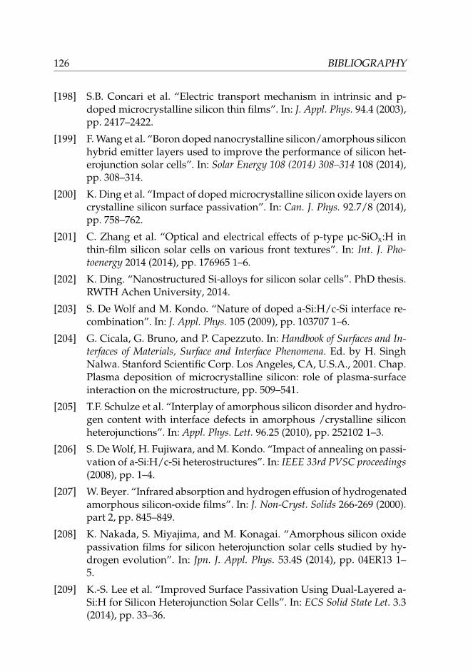
126 BIBLIOGRAPHY
[198] S.B. Concari et al. “Electric transport mechanism in intrinsic and p-doped microcrystalline silicon thin films”. In: J. Appl. Phys. 94.4 (2003),pp. 2417–2422.
[199] F. Wang et al. “Boron doped nanocrystalline silicon/amorphous siliconhybrid emitter layers used to improve the performance of silicon het-erojunction solar cells”. In: Solar Energy 108 (2014) 308–314 108 (2014),pp. 308–314.
[200] K. Ding et al. “Impact of doped microcrystalline silicon oxide layers oncrystalline silicon surface passivation”. In: Can. J. Phys. 92.7/8 (2014),pp. 758–762.
[201] C. Zhang et al. “Optical and electrical effects of p-type µc-SiOx:H inthin-film silicon solar cells on various front textures”. In: Int. J. Pho-toenergy 2014 (2014), pp. 176965 1–6.
[202] K. Ding. “Nanostructured Si-alloys for silicon solar cells”. PhD thesis.RWTH Achen University, 2014.
[203] S. De Wolf and M. Kondo. “Nature of doped a-Si:H/c-Si interface re-combination”. In: J. Appl. Phys. 105 (2009), pp. 103707 1–6.
[204] G. Cicala, G. Bruno, and P. Capezzuto. In: Handbook of Surfaces and In-terfaces of Materials, Surface and Interface Phenomena. Ed. by H. SinghNalwa. Stanford Scientific Corp. Los Angeles, CA, U.S.A., 2001. Chap.Plasma deposition of microcrystalline silicon: role of plasma-surfaceinteraction on the microstructure, pp. 509–541.
[205] T.F. Schulze et al. “Interplay of amorphous silicon disorder and hydro-gen content with interface defects in amorphous /crystalline siliconheterojunctions”. In: Appl. Phys. Lett. 96.25 (2010), pp. 252102 1–3.
[206] S. De Wolf, H. Fujiwara, and M. Kondo. “Impact of annealing on passi-vation of a-Si:H/c-Si heterostructures”. In: IEEE 33rd PVSC proceedings(2008), pp. 1–4.
[207] W. Beyer. “Infrared absorption and hydrogen effusion of hydrogenatedamorphous silicon-oxide films”. In: J. Non-Cryst. Solids 266-269 (2000).part 2, pp. 845–849.
[208] K. Nakada, S. Miyajima, and M. Konagai. “Amorphous silicon oxidepassivation films for silicon heterojunction solar cells studied by hy-drogen evolution”. In: Jpn. J. Appl. Phys. 53.4S (2014), pp. 04ER13 1–5.
[209] K.-S. Lee et al. “Improved Surface Passivation Using Dual-Layered a-Si:H for Silicon Heterojunction Solar Cells”. In: ECS Solid State Let. 3.3(2014), pp. 33–36.
BIBLIOGRAPHY 127
[210] J.-C. Hsiao et al. “Effect of Hydrogen Dilution on the Intrinsic a-Si:HFilm of the Heterojunction Silicon-Based Solar Cell”. In: J. Electrochem.Soc. 158.9 (2011). pp. H876-H878.
[211] M. Taguchi et al. “HIT cellsTM - High-efficient crystalline Si cells withnovel structure”. In: Prog. Photovolt. 8.5 (2000), pp. 503–513.
[212] J. Park et al. “Effect of thermal annealing on the optical and electri-cal properties of boron doped a-SiOx:H for thin-film silicon solar cellapplications”. In: Thin Solid Films 587 (2015), pp. 132–136.
[213] T. Nikitin and L. Khriachtchev. “Optical and Structural Properties of SiNanocrystals in SiO2 Films”. In: Nanomaterials 5.2 (2015), pp. 614–655.
[214] T. Nikitin et al. “Optical and structural properties of SiOx films grownby molecular beam deposition: Effect of the Si concentration and an-nealing temperature”. In: J. Appl. Phys. 112.9 (2012), pp. 094316 1–9.
[215] S. Ilday, G. Nogay, and R. Turan. “Spectroscopic ellipsometry studyof Si nanocrystals embedded in a SiOx matrix: Modeling and opticalcharacterization”. In: Appl. Surf. Sci. 318 (2014), pp. 256 –261.
[216] H.C.M. Knoops et al. “Optical modeling of plasma-deposited ZnOfilms: electron scattering at different length scales”. In: J. Vac. Sci. Tech-nol. A 33.2 (2015), pp. 021509 1–13.
[217] B. Macco et al. “Influence of transparent conductive oxides on passiva-tion of a-Si:H/c-Si heterojunctions as studies by atomic layer depositedAl-doped ZnO.” In: Semicond. Sci. Technol. 29 (2014), pp. 12200 1–5.
[218] Y. Wu et al. “Electrical transport and Al doping efficiency in nanoscaleZnO films prepared by atomic layer deposition”. In: J. Appl. Phys. 114.2(2013), pp. 024308 1–9.
[219] I.J.M. Erkens et al. “Room Temperature Sensing of O2 and CO byAtomic Layer Deposition Prepared ZnO Films Coated with Pt Nanopar-ticles”. In: ECS Trans. 58.10 (2013), pp. 203–214.
[220] A.D. Giddings et al. “Compositional and structural analysis of Aldoped ZnO multilayers by LEAP”. In: Microsc. Microanal. 20 (Suppl3) (2014).
[221] F.-C. Chiu. “Conduction Mechanisms in Resistance Switching Mem-ory Devices Using Transparent Boron Doped Zinc Oxide Films”. In:Materials 7.11 (2014), pp. 7339–7348.
[222] T. Prasada Rao et al. “Effect of stress on optical band gap of ZnO thinfilms with substrate temperature by spray pyrolysis”. In: J. Alloy. Comp485.1–2 (2009), pp. 413 –417.
128 BIBLIOGRAPHY
[223] L.W. Veldhuizen et al. “Textured and micropillar silicon heterojunctionsolar cells with hot-wire deposited passivation layer”. In: Thin SolidFilms (submitted) (2016).
[224] K. Masuko et al. “Achievement of More Than 25% Conversion Effi-ciency With Crystalline Silicon Heterojunction Solar Cell”. In: IEEE J.Photovolt. 4.6 (2014), pp. 1433–1435.
[225] B.N. Pawar, S.R. Jadkar, and M.G. Takwale. “Deposition and charac-terization of transparent and conductive sprayed ZnO:B thin films”.In: Journal of Physics and Chemistry of Solids 66.10 (2005), pp. 1779–1782.
[226] R.B.H. Tahar and N.B.H. Tahar. “Boron-doped zinc oxide thin filmsprepared by sol-gel technique.” In: J. Mater. Sci. 40.19 (2005), pp. 5285–5289.
[227] S. Kim et al. “Optical properties and electrical resistivity of boron-doped ZnO thin films grown by sol-gel dip-coating method”. In: Opt.Mater. 35.12 (2013), pp. 2418–2424.
[228] V. Kumar et al. “Structural, transport and optical properties of boron-doped zinc oxide nanocrystalline.” In: J. Mater. Sci. Technol. 27.6 (2011),pp. 481–488.
[229] R. Rößler et al. “Impact of the transparent conductive oxide work func-tion on injection-dependent a-Si:H/c-Si band bending and solar cellparameters.” In: J. Appl. Phys. 113.14 (2013), pp. 144513 1–8.
[230] A. Chen and K. Zhu. “Computer simulation of a-Si/c-Si heterojunctionsolar cell with high conversion efficiency.” In: Solar Energy 86.1 (2012),pp. 393–397.
[231] The Photovoltaics-Laboratory (PV-Lab) of IMT. a-Si/c-Si HeterojunctionSolar Cells. http://pvlab.epfl.ch/heterojunction_solar_cells, visited on2016-06-20.
[232] A. Klein et al. “Transparent Conducting Oxides for Photovoltaics: Ma-nipulation of Fermi Level, Work Function and Energy Band Align-ment.” In: Materials 3.11 (2010), pp. 4892–4914.
[233] C.-L. Tsai et al. “Induced increase in surface work function and surfaceenergy of indium tin oxide-doped ZnO films by (NH4)2Sx treatment.”In: J Appl Phys 101.11 (2007), pp. 113713 1–4.
[234] C. Huang et al. “Low content indium-doped zinc oxide films withtunable work function fabricated through magnetron sputtering.” In:Semicond. Sci. Technol. 25.4 (2010), pp. 045008 1–6.
BIBLIOGRAPHY 129
[235] R. Varache et al. “Silicon heterojunction solar cells: Optimization ofemitter and contact properties from analytical calculation and numer-ical simulation.” In: Mat. Sci. Eng. B 178.9 (2013), pp. 593–598.
[236] M. Bivour, S. Schröer, and M. Hermle. “Numerical analysis of electri-cal TCO/a-Si:H(p) contact properties for silicon heterojunction solarcells.” In: Energy Procedia 38 (2013), pp. 658–669.
[237] O. Breitenstein et al. “Shunts due to laser scribing of solar cells eval-uated by highly sensitive lock-in thermography”. In: Sol. Energ. Mat.Sol. Cells 65.1–4 (2001), pp. 55 –62.
[238] C. Allebé et al. “Silicon heterojunction solar cells with plated contactsfor low to medium concentration photovoltaics”. In: IEEE 42nd PVSCproceedings. 2015, pp. 1–4.
[239] S. Kirner et al. “The Influence of ITO Dopant Density on J-V Charac-teristics of Silicon Heterojunction Solar Cells: Experiments and Simu-lations”. In: Energy Procedia 77 (2015), pp. 725–732.
[240] H. Fujiwara, M. Kondo, and A. Matsuda. “Interface-layer formationin microcrystalline Si:H growth on ZnO substrates studied by real-time spectroscopic ellipsometry and infrared spectroscopy”. In: J. Appl.Phys. 93.5 (2003), pp. 2400–2409.
[241] F. Edelman et al. “Fast interfacial oxidation of amorphous Si1-xGex:Hby SnO2”. In: Appl. Phys. Lett. 67.3 (1995), pp. 389–391.
[242] W. Beyer, J. Hüpkes, and H. Stiebig. “Transparent conducting oxidefilms for thin film silicon photovoltaics”. In: Thin Solid Films 516.2–4(2007), pp. 147 –154.

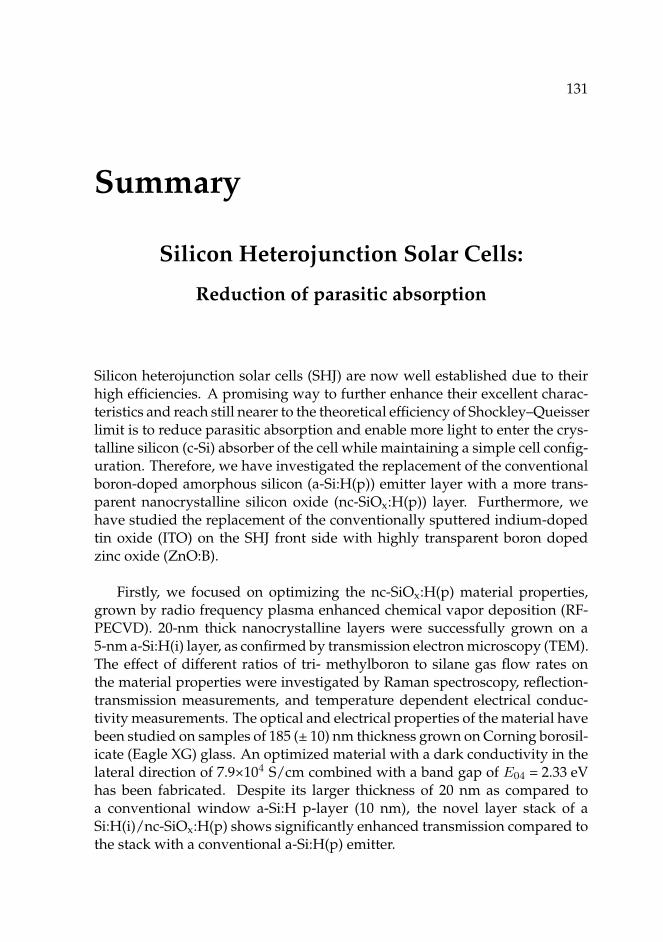
131
Summary
Silicon Heterojunction Solar Cells:
Reduction of parasitic absorption
Silicon heterojunction solar cells (SHJ) are now well established due to theirhigh efficiencies. A promising way to further enhance their excellent charac-teristics and reach still nearer to the theoretical efficiency of Shockley–Queisserlimit is to reduce parasitic absorption and enable more light to enter the crys-talline silicon (c-Si) absorber of the cell while maintaining a simple cell config-uration. Therefore, we have investigated the replacement of the conventionalboron-doped amorphous silicon (a-Si:H(p)) emitter layer with a more trans-parent nanocrystalline silicon oxide (nc-SiOx:H(p)) layer. Furthermore, wehave studied the replacement of the conventionally sputtered indium-dopedtin oxide (ITO) on the SHJ front side with highly transparent boron dopedzinc oxide (ZnO:B).
Firstly, we focused on optimizing the nc-SiOx:H(p) material properties,grown by radio frequency plasma enhanced chemical vapor deposition (RF-PECVD). 20-nm thick nanocrystalline layers were successfully grown on a5-nm a-Si:H(i) layer, as confirmed by transmission electron microscopy (TEM).The effect of different ratios of tri- methylboron to silane gas flow rates onthe material properties were investigated by Raman spectroscopy, reflection-transmission measurements, and temperature dependent electrical conduc-tivity measurements. The optical and electrical properties of the material havebeen studied on samples of 185 (± 10) nm thickness grown on Corning borosil-icate (Eagle XG) glass. An optimized material with a dark conductivity in thelateral direction of 7.9×10⁴ S/cm combined with a band gap of E04 = 2.33 eVhas been fabricated. Despite its larger thickness of 20 nm as compared toa conventional window a-Si:H p-layer (10 nm), the novel layer stack of aSi:H(i)/nc-SiOx:H(p) shows significantly enhanced transmission compared tothe stack with a conventional a-Si:H(p) emitter.
132 Summary
The high efficiencies of SHJ solar cells are enabled by their remarkablyhigh open circuit voltages (VOC). A key factor in achieving these values isa good passivation of the crystalline silicon wafer surface. One of the restric-tions during SHJ solar cell production is the limitation to comparably low postprocessing temperatures. This is caused by the deteriorating effect of hightemperatures on the passivation properties of the intrinsic amorphous sili-con (a-Si:H(i)) layers combined with conventional boron doped amorphoussilicon (a-Si:H(p)) emitter layers. Therefore, we have investigated the influ-ence of the nc-SiOx:H(p) material on the wafer passivation. Passivation stacksconsisting of a-Si:H(i) and nc-SiOx:H(p) emitter layers show an increase in mi-nority carrier lifetime with post deposition annealing temperatures even upto 293°C.
To our knowledge, there have been no earlier reports showing that an-nealing of complete passivation stacks including p-type silicon based layer atsuch high temperatures is beneficial. This favourable behaviour of the mate-rial is attributed to the natural spatial separation of hydrogen and most of theactive boron within the nc-SiOx:H(p) material. Because the boron doping isnot in direct vicinity to the Si-H bonds within the mixed phase material, theFermi-level dependent Si-H bond rupture takes place at a much higher tem-perature in nc-SiOx:H(p) than in a Si:H(p). This temperature-withstandingemitter/passivation layer stack could be of high interest for commercial solarcell producers, since it enables the use of higher post processing temperaturesin the production process. For instance, metallization paste with higher cur-ing temperatures leading to better metal grid conductivity and lower contactresistivity could be implemented.
For conventionally contacted SHJ solar cells, a high performance of thefront transparent conductive oxide (TCO) is required. It needs to be reason-ably low resistive while still maintaining high transmission in order to al-low a large amount of light to reach the active absorber layer of the cell andthus generate a high JSC. The most commonly used TCO for SHJ solar cellsin production is indium tin oxide (ITO). However, an indium free alterna-tive is desirable due to the scarcity of this element. Therefore, we explorethe possibility of implementing ZnO:B prepared by atomic layer deposition(ALD) with the novel triisopropyl borate (B(OiPr)3, TIB) precursor as frontTCO. A commonly used precursor for boron doping in ALD processes is di-borane, which is extremely flammable, very toxic, fatal if inhaled, and causessevere skin burns and serious eye damage. TIB in comparison is so far onlyknown to be highly flammable, expected to be a low ingestion hazard, mightbe harmful after prolonged inhalation, and might cause temporary eye and
Summary 133
skin irritations. Until now, only limited data are available on the toxicity ofTIB. However, TIB is potentially a much safer alternative. The suitability ofthe ZnO:B for implementation in SHJ solar cells has been evaluated. To thisend, the sheet resistance, transmission, refractive index, extinction coefficient,absorption coefficient, and optical band gap have been investigated for dif-ferent doping ratios of the material. The previously discussed temperature-withstanding properties of the emitter/passivation layer stack enable the useof a ZnO:B deposited at a comparably high temperature of 200°C. Upon im-plementation of nc-SiOx:H(p) as emitter layer and ZnO:B as front TCO in SHJsolar cells, outstanding JSC values of 35.50 mA/cm2 for cells on double sidedpolished wafer (DSP) and 38.76 mA/cm2 for cells on textured wafer are ob-served. For reference cells with nc-SiOx:H(p) emitter and ITO as front TCO,33.48 mA/cm2 (DSP) and 37.31 mA/cm2 (textured) of current density werereached. The potential of ZnO:B grown with TIB as indium-free TCO withincreased transmission for SHJ solar cells is thereby shown. Furthermore, in-dium free SHJ solar cells with ALD deposited ZnO:B as front TCO and ZnO:Alas back TCO have been successfully demonstrated.

135
Conclusions
This dissertation focuses on the reduction of the parasitic absorption in SHJsolar cells. The implementation of more transparent materials, in combinationwith replacing the scarce element indium by abundant materials, was investi-gated. To this end, the suitability of nanocrystalline silicon oxide (nc-SiOx:H))and boron doped zinc oxide (ZnO:B) for utilization at the front side of SHJsolar cells has been explored.
Firstly, an nc-SiOx:H(p) layer with sufficient conductivity and higher trans-parency than widely-used boron doped amorphous silicon (a-Si:H(p)) emitterlayer was developed. Increased thermal stability of the passivation propertiesof a-Si:H(i)/nc-SiOx:H(p) layer stacks, as compared to passivation stacks in-cluding the common a-Si:H(p) layer, was achieved. Thereafter, the usage of amore light transmitting transparent conductive oxide (TCO) on the front sideof SHJ solar cells was investigated. A commonly used TCO is tin doped in-dium oxide (ITO). However, an indium free alternative is desired due to thescarcity of indium. Therefore, we examined the suitability of ZnO:B preparedby atomic layer deposition (ALD). The material shows a favorable increasedtransparency over ITO. It is prepared with the novel precursor triisopropylborate (TIB) as boron dopant source. The conventionally used boron precur-sor diborane exhibits severe hazards such as being fatal if inhaled. TIB is ex-pected to be a less dangerous alternative to diborane. The implementation ofthe nc-SiOx:H(p) emitter in combination with the ZnO:B as front TCO in SHJsolar cells yielded the desired high short circuit current density (JSC) of 38.76mA/cm2. This is the result of the reduced parasitic absorption. Unfortunately,also the solar cells’ efficiency slightly decreased compared to SHJ solar cellswith nc-SiOx:H(p) emitter and ITO front TCO. The cause could be a decreasedconductivity and an unfavorable low work function of the ZnO:B comparedto ITO. Next to the achieved reduction of the parasitic absorption, indium freeSHJ solar cells have successfully been realized by replacing not only the frontside ITO with ZnO:B, but also the back side ITO with aluminum doped zincoxide (ZnO:Al).
The output of this research provides several applicable findings for the so-lar cell industry. First of all, nc-SiOx:H(p) emitter layers have good prospects
136 Conclusions
for implementation in SHJ solar cell production. This is caused not only bythe material’s increased transparency compared to common a-Si:H(p) emitterlayer, but also by its outstanding thermal behavior. The passivation prop-erties of a-Si:H(i)/nc-SiOx:H(p) layer stacks do not deteriorate upon goingto reasonably high temperatures, as is the case for conventional passivationstacks of a-Si:H(i)/a-Si:H(p). This releases the restraint to low post processingtemperatures during solar cell manufacturing and allows for the implemen-tation of a wider range of different TCO and metal grid materials. Secondly,TIB is a promising alternative to the common boron source diborane in ALDprocesses. Due to its expected lower hazard upon exposure to the humanbody, it should provide a safer work environment for researchers and factoryworkers. This might also reduce production costs as less safety measures canpossible be implemented. As a result, the usage of TIB as boron source couldbe favorable in many areas also beyond solar cell production.
As mentioned, the efficiency of solar cells with ZnO:B slightly decreasedas compared to solar cells with ITO. Future investigations should be carriedout to pinpoint the reason for this. Nevertheless, the achieved high JSC val-ues present a good starting point for further research on ZnO:B as indium freeTCO for SHJ solar cells. A detailed investigation of the Si-ZnO:B interface fol-lowed by a careful engineering of it, for example by implementing gradeddoping of the ZnO:B, could result in the desired increased efficiency. Due toits good transparency, other possible applications of the developed ZnO:B, forexample as the front TCO layer in perovskite solar cells, could be investigated.The successful manufacturing of indium free SHJ solar cells provides a step-stone towards the goal of omitting scarce materials for solar cell production.
137
List of publications
The content of this thesis is based on the following publications:
• H.A. Gatz, Y. Kuang, M.A. Verheijen, J.K. Rath, W.M.M. Kessels,R.E.I. Schropp, “p-type nc-SiOx:H emitter layer for silicon heterojunc-tion solar cells grown by RF-PECVD”, Materials Research Society Sym-posium Proceedings, No. 1770, pp. 7-12, (2015)
• H.A. Gatz, J.K. Rath, M.A. Verheijen, W.M.M. Kessels,R.E.I. Schropp, “Silicon heterojunction solar cell passivation in combi-nation with nanocrystalline silicon oxide emitters”, Phys. Status SolidiA 213, No. 7, pp. 1932–1936, (2016)
• H.A. Gatz, D. Koushik, J.K. Rath, W.M.M. Kessels, R.E.I. Schropp,“Atomic Layer Deposited ZnO:B As Transparent Conductive Oxide ForSilicon Heterojunction Solar Cells”, Energy Procedia, Vol. 92, pp. 624-632, (2016)
• L.W. Veldhuizen, W.J.C. Vijselaar, H.A. Gatz, J. Huskens, R.E.I. Schropp,“Textured and micropillar silicon heterojunction solar cellswith hot-wire deposited passivation layer”, submitted to Thin SolidFilms, (2016)

139
Acknowledgements
First, I would like to express my sincere gratitude to my promoter prof.dr.ir.Erwin Kessels. I am very grateful that he adopted me in his research groupand gave me the chance to finish my project under his supervision. His guid-ance and support, especially in the stressful end phase of my PhD, was ex-tremely helpful. Next to my promoter, I would also like to thank my co-promoter prof.dr. Jatin Rath. Regardless of my affiliation, he always treatedme like a member of his research group and supported me in carrying out myresearch in every possible way. I can not express the large impact that ourcountless discussions about the scientific part, as well as the characterizationmethods, had on the outcome of this project. I could not have wished for bet-ter support and scientific expertise. Moreover, I would like to thank prof.dr.Ruud Schropp for believing in my potential and giving me the chance to con-duct my research under his supervision and guidance. His door was alwaysopen for discussions and questions, and he was supportive and motivatingduring most of my PhD.
Besides my promoters, I would like to thank prof.dr.ir. Gerrit Kroesen,the chairman of my defense ceremony, for his moral and active support inenabling my PhD defense. Moreover, I would like to thank the rest of thecommittee members, prof.dr.ir. Arno Smets, Prof. Dr. Rutger Schlatmann,prof.dr.ir. Richard van de Sanden, and prof.dr.ir. Geert Verbon, for the evalu-ation of my thesis and the interest in my work.
Furthermore, I would like to thank all my fellow co-worker, office mates,and lab friends for the frightful discussions and the gezellige koffiepauze atUU, TU/e, and HTC. I would like to especially mention the following: Ioan-nis, like a safe and rescue team you joined our lab at the right time. I enjoyedour HF-dips as much as our coffee breaks while heating up samples. Rinny,thank you for helping me with administrative things in the beginning of myPhD and all the nice emails after the moving of the lab. Lianne, your supportwith all the forms applications I had to fill out has helped me a lot during mytime at TU/e. Jeanne, thank you for all the help with paper works and otherthings that need to be arranged (and for the nice breaks we had together ofcourse). Caspar, the introductory course in reactor repairing was extremely
140 Acknowledgements
helpful, as well as your technical support in person and remotely. Karine, I amvery grateful for all you PASTA recipes and your scientific and technical ad-vise. Klaas, thank you for all the freedom I had working in your lab. I enjoyedall the equipment training you gave as much as the coffee breaks and Dutchlessons I had with you and Marten. Cristian, if you wouldn’t have continuedresearching the boron doping mystery for almost one year, this thesis wouldhave been a chapter shorter. Sorry for the endless bubbler changes I causedyou and Jeroen and thank you both for all the technical help and support.Bart and Arjen, I appreciate all the repairs and depositions you did to supportmy project. Martin and Lourens, it was a pleasure having you as chauffeurduring our shared trips to Eindhoven. Akshatha, I very much enjoyed work-ing on ASTA with you during our combined experiments. I especially cherishthe lovely coffee and lunch breaks with Catarina and you. Pim and Ying-haun: I couldn’t have wished for better deposition-buddies. I’m happy weshared PASTA together and am grateful for all our discussions, shared work,and maintenance-time we spend together, as well as for your scientific advise.Dibya, I am happy you joined our TueTue team and value the time we spendtogether working on our paper. Dieuwertje, it was a great pleasure havingyou as a PhD student. Diana, thank you for teaching me everything aboutZnO:B and introducing me to the world of ALD. Diderick and Minne, I wasglad having you around as characterization experts. Jan-Willem, I profited alot from the instant knowledge-transfer you gave me at the beginning of myPhD. Andreas, thank you for your advise on silicon oxide and the nice visitat FZJ. Paula, thank you for your help with Optics2 and the support of myproject. Kees, it was nice having you as a fellow SHJ-expert around. Deborah,Hilde and Lourens, thank you for all the proof reading!
The Dutch province of Noord-Brabant and Solliance, a solar energy R&Dinitiative of ECN, Forschungszentrum Jülich, Holst Centre, Imec, TNO, andTU/e, are acknowledged for funding the TEM facility. Air Liquide is ac-knowledged for the donation of the TIB precursor.
141
Curriculum Vitae
2 2
2 2
Personal information
Name: Henriette A. Gatz
Date of birth: 20.11.1983
Place of birth: Bielefeld, Germany
2 2
Education
2013 - 2016 Continuation of PhD project at TU/e, The Netherlands
2011 – 2013 Begin of PhD project at Utrecht University, The Netherlands
2003 – 2010 Physics diploma at WWU Münster, Germany
2007 - 2008 Exchange student: University of Strathclyde, UK
2000 - 2003 Engelbert-Kaempfer Gymnasium, Germany
Related Documents