This is information on a product in full production. September 2014 DocID023109 Rev 7 1/12 12 SCT30N120 Silicon carbide Power MOSFET: 45 A, 1200 V, 80 mΩ , N-channel in HiP247™ package Datasheet - production data Figure 1. Internal schematic diagram Features • Very tight variation of on-resistance vs. temperature • Slight variation of switching losses vs. temperature • Very high operating temperature capability (200 °C) • Very fast and robust intrinsic body diode • Low capacitance • Easy to drive Applications • Solar inverters, UPS • Motor drives • High voltage DC-DC converters • Switch mode power supply Description This silicon carbide Power MOSFET is produced exploiting the advanced, innovative properties of wide bandgap materials. This results in unsurpassed on-resistance per unit area and very good switching performance almost independent of temperature. The outstanding thermal properties of the SiC material, combined with the device’s housing in the proprietary HiP247™ package, allows designers to use an industry- standard outline with significantly improved thermal capability. These features render the device perfectly suitable for high-efficiency and high power density applications. Note: The device meets ECOPACK standards, an environmentally-friendly grade of products commonly referred to as “halogen-free”. See Section 3: Package mechanical data. 1 2 3 HiP247™ Table 1. Device summary Order code Marking Package Packaging SCT30N120 SCT30N120 HiP247™ Tube www.st.com

Welcome message from author
This document is posted to help you gain knowledge. Please leave a comment to let me know what you think about it! Share it to your friends and learn new things together.
Transcript

This is information on a product in full production.
September 2014 DocID023109 Rev 7 1/12
12
SCT30N120
Silicon carbide Power MOSFET: 45 A, 1200 V, 80 mΩ, N-channel in HiP247™ package
Datasheet - production data
Figure 1. Internal schematic diagram
Features• Very tight variation of on-resistance vs.
temperature
• Slight variation of switching losses vs. temperature
• Very high operating temperature capability (200 °C)
• Very fast and robust intrinsic body diode
• Low capacitance
• Easy to drive
Applications• Solar inverters, UPS
• Motor drives
• High voltage DC-DC converters
• Switch mode power supply
DescriptionThis silicon carbide Power MOSFET is produced exploiting the advanced, innovative properties of wide bandgap materials. This results in unsurpassed on-resistance per unit area and very good switching performance almost independent of temperature. The outstanding thermal properties of the SiC material, combined with the device’s housing in the proprietary HiP247™ package, allows designers to use an industry-standard outline with significantly improved thermal capability. These features render the device perfectly suitable for high-efficiency and high power density applications.
Note: The device meets ECOPACK standards, an environmentally-friendly grade of products commonly referred to as “halogen-free”. See Section 3: Package mechanical data.
12
3
HiP247™
Table 1. Device summary
Order code Marking Package Packaging
SCT30N120 SCT30N120 HiP247™ Tube
www.st.com

Contents SCT30N120
2/12 DocID023109 Rev 7
Contents
1 Electrical ratings . . . . . . . . . . . . . . . . . . . . . . . . . . . . . . . . . . . . . . . . . . . . 3
2 Electrical characteristics . . . . . . . . . . . . . . . . . . . . . . . . . . . . . . . . . . . . . 4
2.1 Electrical characteristics (curves) . . . . . . . . . . . . . . . . . . . . . . . . . . . . . 6
3 Package mechanical data . . . . . . . . . . . . . . . . . . . . . . . . . . . . . . . . . . . . . 9
4 Revision history . . . . . . . . . . . . . . . . . . . . . . . . . . . . . . . . . . . . . . . . . . . 11

DocID023109 Rev 7 3/12
SCT30N120 Electrical ratings
1 Electrical ratings
Table 2. Absolute maximum ratings
Symbol Parameter Value Unit
VDS Drain-source voltage (VGS = 0) 1200 V
VGS Gate-source voltage -10/+25 V
IDDrain current (continuous) at TC = 25 °C (limited by die)
45 A
IDDrain current (continuous) at TC = 25 °C (limited by package)
40 A
ID Drain current (continuous) at TC = 100 °C 34 A
IDM (1)
1. Pulse width limited by safe operating area.
Drain current (pulsed) 90 A
PTOT Total dissipation at TC = 25 °C 270 W
Tstg Storage temperature-55 to 200
°C
Tj Max. operating junction temperature °C
Table 3. Thermal data
Symbol Parameter Value Unit
Rthj-case Thermal resistance junction-case max 0.65 °C/W
Rthj-amb Thermal resistance junction-ambient max 40 °C/W
Electrical characteristics SCT30N120
4/12 DocID023109 Rev 7
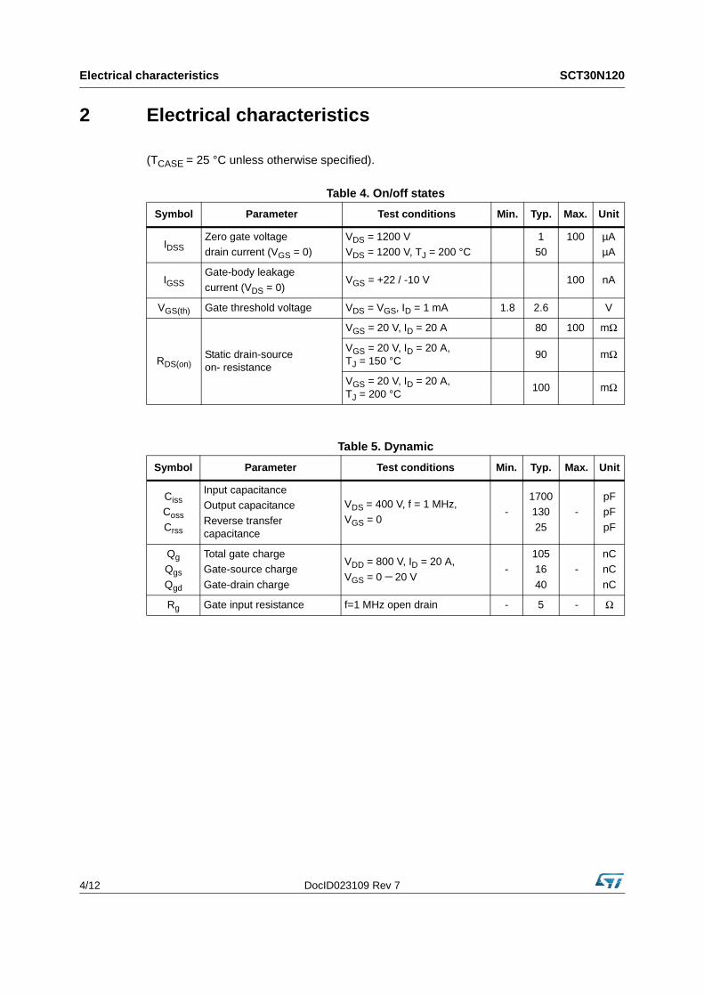
2 Electrical characteristics
(TCASE = 25 °C unless otherwise specified).
Table 4. On/off states
Symbol Parameter Test conditions Min. Typ. Max. Unit
IDSSZero gate voltage drain current (VGS = 0)
VDS = 1200 VVDS = 1200 V, TJ = 200 °C
150
100 µAµA
IGSSGate-body leakagecurrent (VDS = 0)
VGS = +22 / -10 V 100 nA
VGS(th) Gate threshold voltage VDS = VGS, ID = 1 mA 1.8 2.6 V
RDS(on)Static drain-source on- resistance
VGS = 20 V, ID = 20 A 80 100 mΩ
VGS = 20 V, ID = 20 A, TJ = 150 °C
90 mΩ
VGS = 20 V, ID = 20 A, TJ = 200 °C
100 mΩ
Table 5. Dynamic
Symbol Parameter Test conditions Min. Typ. Max. Unit
Ciss
Coss
Crss
Input capacitanceOutput capacitance
Reverse transfer capacitance
VDS = 400 V, f = 1 MHz, VGS = 0
-1700130
25
-pFpF
pF
Qg
Qgs
Qgd
Total gate chargeGate-source charge
Gate-drain charge
VDD = 800 V, ID = 20 A,
VGS = 0 − 20 V-
10516
40
-nCnC
nC
Rg Gate input resistance f=1 MHz open drain - 5 - Ω

DocID023109 Rev 7 5/12
SCT30N120 Electrical characteristics
Table 6. Switching energy (inductive load)
Symbol Parameter Test conditions Min. Typ. Max. Unit
Eon
Eoff
Turn-on switching losses
Turn-off switching losses
VDD = 800 V, ID = 20 A
RG= 6.8 Ω, VGS = -2/20 V-
500
350-
µJ
µJ
Eon
Eoff
Turn-on switching losses
Turn-off switching losses
VDD = 800 V, ID = 20 A
RG= 6.8 Ω, VGS = -2/20 VTJ= 150 °C
-500
400-
µJ
µJ
Table 7. Switching times
Symbol Parameter Test conditions Min. Typ. Max. Unit
td(on)V
tf(V)
td(off)V
tr(V)
Turn-on delay timeFall time
Turn-off delay timeRise time
VDD = 800 V, ID = 20 A,
RG = 0 Ω, VGS = 0/20 V-
1928
4520
-
nsns
nsns
Table 8. Reverse SiC diode characteristics
Symbol Parameter Test conditions Min Typ. Max Unit
VSD Diode forward voltage IF = 10 A, VGS = 0 - 3.5 - V
trrQrr
IRRM
Reverse recovery timeReverse recovery chargeReverse recovery current
ISD = 20 A, di/dt = 100 A/µsVDD = 800 V
-1401402
nsnCA

Electrical characteristics SCT30N120
6/12 DocID023109 Rev 7
2.1 Electrical characteristics (curves) Figure 2. Safe operating area Figure 3. Thermal impedance
Figure 4. Output characteristics (TJ=25°C) Figure 5. Output characteristics (TJ=200°C)
Figure 6. Transfer characteristics Figure 7. Power dissipation
ID
10
1
0.10.1 1 100 VDS(V)10
(A)
Opera
tion
in th
is ar
ea is
Limite
d by
max
RDS
(on)
100μs
1ms
10ms
1000
AM17527v1
10 10 10 10 10 tp(s)0
0.1
K
0.2
0.3
0.4
0.5
-6 -5 -4 -3 -2 10-1
AM17526v1
ID
30
20
10
00 2 VDS(V)6
(A)
4 8
40
50
60
70
80VGS=20V
18V
16V
14V
12V
10V
AM17518v1 ID
30
20
10
00 VDS(V)
(A)
40
50
60
70
80VGS=20V
18V16V
14V
12V
10V
2 64 8
AM17519v1
ID
15
10
5
00 4 VGS(V)8
(A)
2 6 10
20
25
12
30
35VDS=20V
200°C25°C
AM17521v1PD
-50 0 TC(°C)
(W)
50 1000
50
100
150
200
250TJ=200°C
150
AM17525v1

DocID023109 Rev 7 7/12
SCT30N120 Electrical characteristics
Figure 8. Gate charge vs gate-source voltage Figure 9. Capacitance variations
Figure 10. Switching energy vs. drain current Figure 11. Switching energy vs. junction temperature
Figure 12. Normalized BVDSS vs. temperature Figure 13. Normalized gate threshold voltage vs. temperature
VDD=800VID=20A
VGS
4
00 20 Qg(nC)
(V)
80
8
40 60 100
12
16
AM17529v1 C
1000
100
100 600 VDS(V)
(pF)
400 800
Ciss
Coss
Crss
200
AM17528v1
E
100
0 4 ID(A)
(μJ)
2 6
Eon
Eoff
8
Etot
10 12 14 16 18
200
300
400
500
600
700
800
0
VDD=VCLAMP=800V
VGS=-2V/20VRG=6.8ΩTJ=25°C ,
AM17530v1E
100
25 50 TJ(°C)
(μJ)
Eon
Eoff
75
Etot
100 125
200300400500600700800
0
90010001100
VDD=VCLAMP=800V
VGS=-2V/20VRG=6.8ΩID=20V ,
AM17531v1
BVDSS
-50 0 TJ(°C)
(norm)
50 1000.94
0.96
0.98
1.00
1.02
1.04ID=1mA
150
AM17523v1 VGS(th)
0.6
0.4
0.2
0-50 0 TJ(°C)
(norm)
0.8
50 100 150
ID=1mA
1.2
1.0
1.4
1.6
AM17522v1

Electrical characteristics SCT30N120
8/12 DocID023109 Rev 7
Figure 14. Normalized on-resistance vs. temperature
Figure 15. Body diode characteristics
RDS(on)
2.4
2.0
1.2
0.4
TJ(°C)
(norm)
7525 50 100 125 150 175
0.8
0
1.6
2.8
3.2
VGS=20VID=20A
AM17520v1VSD -5 -3
ISD(A)
(V) -4 -2 -1
-4
-2
TJ=-55°C
TJ=200°C
TJ=25°C
00
-8
-6
-12
-10
-16
-14
-18
AM17524v1

DocID023109 Rev 7 9/12
SCT30N120 Package mechanical data
3 Package mechanical data
In order to meet environmental requirements, ST offers these devices in different grades of ECOPACK® packages, depending on their level of environmental compliance. ECOPACK® specifications, grade definitions and product status are available at: www.st.com. ECOPACK® is an ST trademark.
Figure 16. HiP247™ drawing
8396756_A

Package mechanical data SCT30N120
10/12 DocID023109 Rev 7
Table 9. HiP247™ mechanical data
Dim.mm.
Min. Typ. Max.
A 4.85 5.15
A1 2.20 2.60
b 1.0 1.40
b1 2.0 2.40
b2 3.0 3.40
c 0.40 0.80
D 19.85 20.15
E 15.45 15.75
e 5.30 5.45 5.60
L 14.20 14.80
L1 3.70 4.30
L2 18.50
∅P 3.55 3.65
∅R 4.50 5.50
S 5.30 5.50 5.70

DocID023109 Rev 7 11/12
SCT30N120 Revision history
4 Revision history
Table 10. Document revision history
Date Revision Changes
10-May-2012 1 First release
21-May-2013 2Updated trr value in Table 8.
Updated dynamic parameters in Table 5, VGS(th) in Table 4 and Eon in Table 6.
24-Jun-2013 3Document status promoted from target to preliminary data.Added: Section 2.1: Electrical characteristics (curves)
11-Jul-2013 4Updated Figure 4: Output characteristics (TJ=25°C) and Figure 5: Output characteristics (TJ=200°C).
18-Dec-2013 5Updated parameters in Table 2: Absolute maximum ratings and Table 4: On/off states.
27-May-2014 6Added Table 7: Switching times.Updated Section 3: Package mechanical data.Minor text changes.
25-Sep-2014 7 Document status promoted from preliminary to production data.

SCT30N120
12/12 DocID023109 Rev 7
IMPORTANT NOTICE – PLEASE READ CAREFULLY
STMicroelectronics NV and its subsidiaries (“ST”) reserve the right to make changes, corrections, enhancements, modifications, and improvements to ST products and/or to this document at any time without notice. Purchasers should obtain the latest relevant information on ST products before placing orders. ST products are sold pursuant to ST’s terms and conditions of sale in place at the time of order acknowledgement.
Purchasers are solely responsible for the choice, selection, and use of ST products and ST assumes no liability for application assistance or the design of Purchasers’ products.
No license, express or implied, to any intellectual property right is granted by ST herein.
Resale of ST products with provisions different from the information set forth herein shall void any warranty granted by ST for such product.
ST and the ST logo are trademarks of ST. All other product or service names are the property of their respective owners.
Information in this document supersedes and replaces information previously supplied in any prior versions of this document.
© 2014 STMicroelectronics – All rights reserved
Related Documents


