SILICON BASED MULTILAYER PHOTOELECTRODES FOR PHOTOELECTROLYSIS OF WATER TO PRODUCE HYDROGEN FROM THE SUN by Faisal Faruque A thesis submitted to the faculty of The University of Utah in partial fulfillment of the requirements for the degree of Master of Science Department of Electrical and Computer Engineering The University of Utah May 2011

Welcome message from author
This document is posted to help you gain knowledge. Please leave a comment to let me know what you think about it! Share it to your friends and learn new things together.
Transcript
SILICON BASED MULTILAYER PHOTOELECTRODES FOR
PHOTOELECTROLYSIS OF WATER TO PRODUCE
HYDROGEN FROM THE SUN
by
Faisal Faruque
A thesis submitted to the faculty of
The University of Utah
in partial fulfillment of the requirements for the degree of
Master of Science
Department of Electrical and Computer Engineering
The University of Utah
May 2011

Copyright © Faisal Faruque 2011
All Rights Reserved
T h e U n i v e r s i t y o f U t a h G r a d u a t e S c h o o l
STATEMENT OF THESIS APPROVAL
The thesis of Faisal Faruque
has been approved by the following supervisory committee members:
Massood Tabib-Azar , Chair 01/28/2011
Date Approved
Faisal Khan , Member 01/31/2011
Date Approved
Hanseup Kim , Member 01/31/2011
Date Approved
and by Gianluca Lazzi , Chair of
the Department of Electrical and Computer Engineering
and by Charles A. Wight, Dean of The Graduate School.
ABSTRACT
The main objective of this work is to study different materials for the direct
photosynthesis of hydrogen from water. A variety of photocatalysts such as titanium
dioxide, titanium oxy-nitride, silicon carbide, and gallium nitride are being investigated
by others for the clean production of hydrogen for fuel cells and hydrogen economy. Our
approach was to deposit suitable metallic regions on photocatalyst nanoparticles to direct
the efficient synthesis of hydrogen to a particular site for convenient collection. We
studied different electrode metals such as gold, platinum, titanium, palladium, and
tungsten. We also studied different solar cell materials such as silicon (p- and n-types),
silicon carbide and titanium dioxide semiconductors in order to efficiently generate
electrons under illumination. We introduced a novel silicon-based multilayer
photosynthesis device to take advantage of suitable properties of silicon and tungsten to
efficiently produce hydrogen. The device consisted of a silicon (0.5mm) substrate, a
deposited atomic layer of Al2O3 (1nm), a doped polysilicon (0.1µm), and finally a
tungsten nanoporous (5-10nm) layer acting as an interface electrode with water. The
Al2O3 layer was introduced to reduce leakage current and to prevent the spreading of the
diffused p-n junction layer between the silicon and doped polysilicon layers. The surface
of the photoelectrode was coated with nanotextured tungsten nanopores (TNP), which
increased the surface area of the electrodes to the electrolyte, assisting in electron-hole
mobility, and acting as a photocatalyst. The reported device exhibited a fill factor (%FF)

iv
of 27.22% and solar-to-hydrogen conversion efficiency of 0.03174%. This thesis
describes the structures of the device, and offers a characterization and comparison
between different photoelectrodes.

I dedicate this thesis to my wonderful parents and loving sister, whose affection and
guidance always lead me to my dreams.
Also to my friend Todd Mckay, whose help cannot be put in words.
And finally to my fiancée, Tamara Zaman, whose love, support and enormous help has
always been the driving force behind my every success.
TABLE OF CONTENTS
ABSTRACT ................................................................................................................. iii
LIST OF FIGURES ................................................................................................... viii
ACKNOWLEDGEMENTS ........................................................................................ xii
Chapters
1. INTRODUCTION AND BACKGROUND ....................................................................1
1.1 History of Hydrogen ...............................................................................................2
1.2 Hydrogen Economy ................................................................................................3
1.3 Hydrogen Production ..............................................................................................4
1.3.1 Thermal ...........................................................................................................5
1.3.2 Electrochemical...............................................................................................8
1.3.3 Biological ........................................................................................................9
1.4 Motivation .............................................................................................................10
1.4.1 Next-generation energy source .....................................................................10
1.4.2 Solar-to-hydrogen efficiency ........................................................................11
1.5 Literature Survey: Photoelectrolysis for Hydrogen Production .............................12
1.5.1 Photoelectrolysis ...........................................................................................12
1.5.2 Photocatalysts ...............................................................................................15
1.5.3 Nanostructured surface .................................................................................15
2. HOMOGENOUS SEMICONDUCTING AND METALLIC ELECTRODES ..........20
2.1 Introduction ...........................................................................................................20
2.2 Experimental Setup ...............................................................................................21
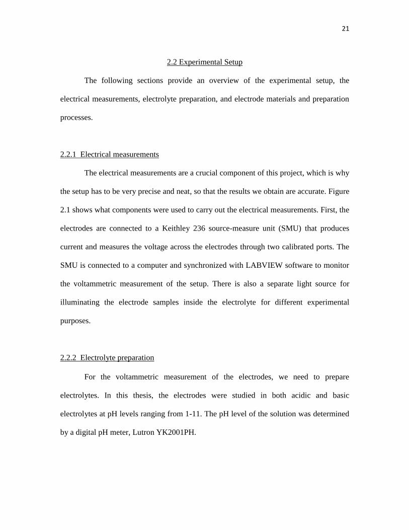
2.2.1 Electrical measurement .................................................................................21
2.2.2 Electrolyte preparation ..................................................................................21
2.2.3 Electrode materials and preparation..............................................................23
2.3 Metal-Metal Electrodes .........................................................................................23
2.3.1 Gold-gold electrodes .....................................................................................25
2.3.2 Gold-platinum electrodes ..............................................................................27
2.4 Semiconductor-Semiconductor Electrodes ...........................................................30
2.4.1 Silicon ...........................................................................................................32
2.4.2 Titanium dioxide (TiO2) ...............................................................................34
2.4.3 Silicon carbide (SiC) .....................................................................................35
vii
2.4.4 Silicon-silicon electrodes ..............................................................................35
2.4.5 Silicon-titanium dioxide electrodes ..............................................................39
2.4.6 Silicon carbide-titanium dioxide electrodes ..................................................40
2.5 The Effect of Photocatalyst Coating on Electrodes ..............................................43
2.5.1 What is a photocatalyst ................................................................................43
2.5.2 Why are photocatalysts needed? ..................................................................44
2.6 Conclusion ..........................................................................................................45
3. MULTILAYER DEVICES AND ELECTRODES ......................................................47
3.1 Introduction .........................................................................................................47
3.1.1 Simple electrodes versus multilayer electrodes ...........................................47
3.1.2 Multilayer electrodes and devices ................................................................49
3.2 Multilayer Structures ..........................................................................................50
3.2.1 Silicon (p- and n-type) substrate ..................................................................50
3.2.2 Atomic layer deposition (ALD) ...................................................................52
3.2.3 Polysilicon....................................................................................................53
3.3 Tungsten nanopores (TNP) .................................................................................54
3.3.1 Tungsten .......................................................................................................55
3.3.2 Process to grow TNP ...................................................................................55
3.3.3 SEM images .................................................................................................56
3.3.4 Device structure ...........................................................................................56
3.4 Comparison between Different Electrodes, Devices, Electrolyte Systems ........61
3.4.1 Silicon, polysilicon and photocatalyst metal coated electrodes ...................62
3.4.2 Silicon, polysilicon with TNP electrodes.....................................................65
3.4.3 Silicon, polysilicon with TNP and Al2O3 layer electrodes ..........................68
3.4.4 Comparison of turn on voltage (VON) ..........................................................71
3.5 Final Summary ...................................................................................................74
3.6 Conclusion .........................................................................................................74
4. CONCLUSION .............................................................................................................76
4.1 Future Work .......................................................................................................77
APPENDIX: ADDITIONAL DATA PERTAINING TO CHAPTER 2 ...........................79
REFERENCES .............................................................................................................92
LIST OF FIGURES
Figures
1.1 Examples of various hydrogen feedstocks ...................................................................6
1.2 Band position of anatase TiO2 (Eg = 3.2eV), in the presence of a pH 1 aqueous
electrolyte. The energy scale is indicated in electron volts (eV), using either an
NHE or vacuum level as a reference showing the condition for water splitting ......13
1.3 Band edges of p- and n-type semiconductors in aqueous electrolyte under
illumination ...............................................................................................................44
2.1 Experimental setup used to study different electrodes ..............................................22
2.2 Current vs. voltage graph of gold-gold electrodes in a basic solution of pH 11........26
2.3 VON vs. pH graphs for gold-gold electrodes ..............................................................27
2.4 Current vs. voltage graph of gold-platinum electrodes in a basic solution of pH
9.................................................................................................................................28
2.5 VON vs. pH graph for gold-platinum electrodes .........................................................29
2.6 VON vs. pH graph for platinum-gold electrode ..........................................................30
2.7 Band position of semiconductor with respect to the oxidation reduction potential
of water splitting electrical equivalent energy 1.229eV .............................................31
2.8 Simple diagram of photoactive semiconductor electrode setup for water
photoelectrolysis .........................................................................................................32
2.9 P- and n-type 4” silicon <100> wafers ......................................................................33
2.10 Silicon semiconductor electrode sample preparation ...............................................33
2.11 TiO2 films grown on Ti foil by anodic oxidation in 0.25M phosphoric acid ...........34
2.12 1cm x 1cm diced SiC wafer for electrode .................................................................35
ix
2.13 Current vs. voltage graph of p-type silicon as cathode and n-type silicon as
anode under dark and illuminated condition in pH 1 acidic solution .......................38
2.14 Current vs. voltage graph of p-type silicon as cathode and n-type silicon as
anode under dark and illuminated condition in pH 11 basic solution.......................38
2.15 Current vs. voltage graph of p-type silicon as cathode and n-type TiO2 as anode
under dark and illuminated condition in pH 9 basic solution ...................................40
2.16 Current vs. voltage graph of 4HN SiC as cathode and n-TiO2 as anode under
dark and illuminated condition in pH 1 acidic solution ............................................41
2.17 Simple diagram showing the work of a photocatalyst ..............................................44
2.18 Photocatalytic process of powdered photocatalyst ...................................................45
3.1 The photon energy from sunlight energizing the electrons and holes to flow in a)
opposite directions; The schematic diagram of b) bandgap structure of p- and n-
type silicon semiconductor and the flow directions of electrons and holes ...............49
3.2 Multilayer (left) and multigap (right) solar cell responses to different frequencies ...51
3.3 Diagram showing the polysilicon deposition on c-Si substrate and the VB and
CB position and the flow of electrons ........................................................................53
3.4 SEM images of TNP on the surface of n-silicon, Al2O3 and p+-polysilicon (top)
magnified (bottom) .....................................................................................................57
3.5 Cross sectional SEM image of the silicon-Al2O3-polysilicon-TNP layered
photoelectrode ............................................................................................................58
3.6 The device structure of the two photoelectrodes with p- / n- silicon, the Al2O3
layer, n+- /
p
+- polysilicon, and TNP on the surface ..................................................59
3.7 Photocathode (left) producing hydrogen and photoanode (right) producing
oxygen through photogenerated electron-hole pairs with the aid of sunlight and
water molecule splitting .............................................................................................60
3.8 Equipment setup for the a) current vs. voltage and efficiency measurement of
the photo electrodes; b) prepared sample electrodes ..................................................62
3.9 Current vs. voltage graph of p-Si, n+-polysilicon, Pt and n-Si, p
+-polysilicon, Ti
photoelectrodes in pH 9 basic solution with and without illumination ......................63
x
3.10 The quadrant showing the voltammetric analysis of the p-Si, n+
-polysilicon, Pt
and n-Si, p+-polysilicon, Ti photoelectrodes’ blue (dark), red (illuminated) and
green (power) plots ...................................................................................................64
3.11 Current vs. voltage graph of p-Si, n+-polysilicon, TNP, and n-Si, p
+-polysilicon,
TNP photoelectrodes in pH 11 basic solution with and without illumination ...........66
3.12 The quadrant showing the voltammetric analysis of the p-Si, n+-polysilicon,
TNP, and n-Si, p+-polysilicon, TNP photoelectrodes’ blue (dark), red
(illuminated) and green (power) plots......................................................................67
3.13 Current vs. voltage graph of p-Si, Al2O3, n+-polysilicon, TNP, and n-Si, Al2O3,
p+- polysilicon, TNP photoelectrodes in pH 11 basic solution with and without
illumination ...............................................................................................................69
3.14 The quadrant showing the voltammetric analysis of the p-Si, Al2O3, n+-
polysilicon, TNP, and n-Si, Al2O3, p+-polysilicon, TNP photoelectrodes’ blue
(dark),red (illuminated) and green (power) plots ......................................................70
3.15 VON vs. pH graphs under dark conditions for the photoelectrode pairs ....................72
3.16 VON vs. pH graphs under illumination for the photoelectrode pairs ........................73
A.1 Current vs. voltage graph gold-palladium electrodes in a basic solution of pH 9 ...80
A.2 VON vs. pH graph for gold-palladium electrode ........................................................80
A.3 VON vs. pH graph for palladium-gold electrode ........................................................81
A.4 Current vs. voltage graph gold-titanium electrodes in a basic solution of pH 3 .......81
A.5 VON vs. pH graph for titanium-gold electrode ..........................................................82
A.6 Current vs. voltage graph gold-tungsten electrodes in a basic solution of pH 11.....82
A.7 VON vs. pH graph for gold-tungsten electrode ..........................................................83
A.8 VON vs. pH graph for tungsten-gold electrode ..........................................................83
A.9 Current vs. voltage graph platinum-palladium electrodes in a basic solution of
pH 11 .........................................................................................................................84
A.10 VON vs. pH graph for platinum-palladium electrode ..............................................84
A.11 VON vs. pH graph for palladium-platinum electrode ..............................................85

xi
A.12 Current vs. voltage graph platinum-tungsten electrodes in a basic solution of
pH 3 .........................................................................................................................85
A.13 VON vs. pH graph for platinum-tungsten electrode .................................................86
A.14 VON vs. pH graph for tungsten-platinum electrode .................................................86
A.15 Current vs. voltage graph platinum-titanium electrodes in a basic solution of
pH 11 .......................................................................................................................87
A.16 VON vs. pH graph for platinum-titanium electrode .................................................87
A.17 VON vs. pH graph for titanium-platinum electrode .................................................88
A.18 Current vs. voltage graph palladium-tungsten electrodes in a basic solution of
pH 3 .........................................................................................................................88
A.19 VON vs. pH graph for palladium-tungsten electrode ...............................................89
A.20 VON vs. pH graph for tungsten-palladium electrode ...............................................89
A.21 Current vs. voltage graph titanium-tungsten electrodes in a basic solution of
pH 3 .........................................................................................................................90
A.22 VON vs. pH graph for titanium-tungsten electrode ..................................................90
A.23 VON vs. pH graph for tungsten-titanium electrode ..................................................91

ACKNOWLEDGEMENTS
This thesis would not have been possible without the support of many people. I
express my gratitude to my supervisor, Dr. Massood-Tabib Azar, who was of great help
and offered invaluable assistance. My heartfelt gratitude also goes out to the members of
my supervisory committee, Dr. Faisal Khan and Dr. Hanseup Kim, for their support. I
would also like to thank Dr. Phil Neudeck of NASA Glenn Research Center, Cleveland,
Ohio, for providing important samples.

CHAPTER 1
INTRODUCTION AND BACKGROUND
Solar energy delivers renewable, pollution-free power and has done so since
ancient times. The primary method of harnessing energy from sunlight relies on
photovoltaic (PV) panels, but that energy has limited utility without the robust methods to
store it. One method involves converting that energy to hydrogen by diverting the current
from PV panels to drive electrolysis, which already accounts for over 4% of worldwide
hydrogen production. To split water molecules into hydrogen and oxygen, the change in
Gibb’s free energy is 237.178kJ/mol [1], or the equivalent electrical potential of 1.229V
[1]. Traditionally, solar-powered electrolysis based on PV structure relies on external
circuitry to create an electrical potential difference across two electrodes separated by
water. Unfortunately, energy is lost in conversion. Photocatalysis decreases this loss by
introducing a catalyst through a process called photoelectrolysis.
Photoelectrolysis conducts electrolysis more efficiently than PV methods. While
PV cells convert solar energy to electrical energy, which drives a subsequent conversion
to chemical energy, photoelectrolysis converts solar energy directly into chemical energy
in a process akin to photosynthesis, the process by which plants convert solar energy to
chemical energy. The device described in this thesis has the ability to split water
molecules with photocatalytic reactions powered by sunlight.
2
By leveraging nanoarchitecture, the electrodes expose more surface area to
sunlight, provide nanochannels for electrons and holes to interact with electrolytes more
efficiently, improve photoion generation, and facilitate photoion mobility for electrolysis.
Chapters 2 and 3 discuss the structure of the device, its experimental measurement
characteristics, and the theories and concepts behind its design.
1.1 History of Hydrogen
In 1766, British scientist Henry Cavendish demonstrated to the Royal Society of
London that hydrogen was a distinct element or gas by causing it to separate through a
reaction between zinc metal and hydrochloric acid. Cavendish proved that hydrogen is a
lighter gas, and, when ignited with a spark, yields water [2].
Later, in 1785, French chemist Antoine Lavoisier studied Cavendish’s
experiments and concluded that oxygen and hydrogen are the two basic elements of
water. Lavoisier named the element hydrogen from two Greek words, hydro, meaning
water, and genes, meaning born of, in 1788 [3].
In 1800, scientists William Nicholson and Sir Anthony Carlisle first discovered
that applying current to water can produce hydrogen and oxygen, a process which was
later termed electrolysis [4]. Around 1839, a Swiss chemist, Christian Friedrich
Schoenbein, discovered the Fuel Cell Effect when he found that combining hydrogen and
oxygen gases produces water and an electric current [5]. In 1845, another English
scientist and judge, Sir William Grove, furthered Schoenbein’s discovery on a practical
scale by inventing a “gas battery” [6]. This achievement earned him the title “Father of
the Fuel Cell” [6].

3
It was not until 1970 that the phrase “hydrogen economy” was first coined by
electrochemists J. O’M Bockris and Neal Triner in a General Motors Technician meeting
[7]. Consequently, the late 20th
and 21st centuries saw many hydrogen-based industries,
hydrogen-powered vehicles, and hydrogen fuel cells. Iceland declared itself to be the first
complete hydrogen economy by 2030 [8].
1.2 Hydrogen Economy
Hydrogen economy: it might seem an implausible goal to attain, but attaining this
goal is not unprecedented. Even in the beginning of the 20th
century, the United States
(U.S.) had an energy system based on animals for food and transportation and wood for
heat energy. The transition from wood to coal to the increasing contribution of natural
gas, petroleum, nuclear energy, hydro-energy, and recently renewable energy has been
very significant in the last 150 years among developed countries like the U.S.. The
transition to renewable energy reflects more the diversification of energy resources than
actual transitions. Due to large-scale environmental concerns and natural energy crises,
this century has opted for the advent of technology to provide viable alternatives to meet
the ever-increasing domestic demands for energy. It is important to state that up until the
end of the 20th
century, the U.S. produced all of its required energy by itself. It was not
until the 1980s that the consumption of the natural gas surplus in domestic production
forced the U.S. to turn to other countries to import natural gas. In the year of 1994, the
U.S. imported more petroleum than it produced [9]. This increase in demand was
attributed to the industrial and technological revolution in addition to the rising domestic
consumption of fossil fuel. Access to energy was always meant to help in the

4
achievement of advanced technology and to help modernize the standard of living of
human kind. In reality, resources such as fossil fuels are limited; if that is not alarming
enough, harmful emissions as a result of overproduction cause environmental hazards.
These are a handful of the many driving forces behind the transition for coming up with a
new, pollution-free and abundant next generation energy resource.
Although a hydrogen economy sounds very promising for solving the energy
crisis, the production process of hydrogen has to be kept in mind. Only producing
hydrogen using renewable resources can make the idea a successful one. Hydrogen will
replace fossil fuel as an energy resource or energy carrier and also any other related
feedstock. The theory behind hydrogen economy is that hydrogen and electricity can
serve all the energy needs of society, and they would be permanent and independent. In
the end, the application of energy will stem from electricity, which in turn will be
produced from hydrogen fuel cells or any other means of hydrogen application.
Eventually, hydrogen and electricity will transform all aspects of modern day fossil fuel
usage so that the transition is successful and effective.
1.3 Hydrogen Production
Hydrogen production from all different processes is based on the separation of
hydrogen from hydrogen-containing feedstock. Each type of feedstock requires a
different method to extract hydrogen from it. Right now, there are three major
technologies behind hydrogen production with their own subcategories. These three
major technologies are thermal, electrochemical, and biological. Although the most
common method used is the thermal method, it has limitations and poses dangers to the

5
environment. The first reported commercial technology for producing hydrogen was
informed in the late 1920s when pure hydrogen was produced via water electrolysis.
Later, the industrial production of hydrogen moved to more fossil-based feedstocks, like
oil and coal, which are still the main source of hydrogen production today. There are
several feedstocks from which hydrogen can be separated. Figure 1.1 gives an overall
idea about different feedstocks available for hydrogen extraction.
In the Sections 1.3.1 through 1.3.3, the three main categories and their
subcategories for hydrogen production are discussed.
1.3.1 Thermal
In the thermal process, hydrogen is extracted by simply releasing it from the
feedstock by gas reforming and heating.
1.3.1.1 Steam reformation. Using natural gas as a feedstock, steam reforming
involves an endothermic conversion of methane (CH4) and water vapor (H2O) into
hydrogen (H2) and carbon monoxide (CO) (reaction 1.1). To reform, the required heat is
supplied from the combustion of natural gases, where the temperature is around 700C to
900C. Following this step, the hydrogen contains CO, which is then put through a water
gas shift (WGS) reaction to produce H2 and carbon dioxide (CO2) (reaction 1.2).
CH4 + H2O + (heat) → CO + 3H2 (1.1)
CO + H2O → CO2 + H2 + (heat) (1.2)

6
Figure 1.1 Examples of various hydrogen feedstocks
Another method to produce hydrogen through steam reformation is the partial
oxidation of natural gas, as CH4 and O2 go through a partial combustion to produce H2
and CO (reaction 1.3) and subsequently go through a WGS reaction (reaction 1.2) to form
H2 and CO2.
CH4 + ½ O2 → CO + 2H2 + (heat) (1.3)
1.3.1.2 Thermochemical water splitting. This process requires a heat-driven
chemical reaction to split water into hydrogen and oxygen. Due to the lower requirement

7
of electrical energy to split water at a high temperature (1000C) compared to electrolysis
(100C), the high temperature electrolyzer can operate at a rate of processing efficiency
higher than low-temperature electrolysis. The electrolyzer is the device setup used to
perform the electrolysis.
A typical electrolyzer capable of performing high-temperature water splitting is
normally based on a solid oxide fuel cell (SOFC), which operates at the range of 700C
to 1000C.
1.3.1.3 Gasification. The gasification process follows simple rules of nature
where it can break down almost any form of carbon-based feedstock into its chemical
components. These days, the modern gasifier exposes coal or biomass (C) in a controlled
chamber to high temperatures and pressure in the presence of air or oxygen, which forces
the molecules to break down, thus completing the chemical reaction and producing CO
and H2 (reaction 1.4). Next, they go through the WGS reaction (reaction 1.2) to form CO2
and H2.
C (coal or biomass) + H2O + heat → CO + H2 (1.4)
This gasifier, when used for coal gasification, generates a substantial amount of
CO2. These gasification processes are being optimized for hydrogen production by
improving the CO2 decarbonization, which involves capturing and filtering systems.
Also, if biomass is used instead of coal, the emission of CO2 will decrease significantly.
1.3.1.4 Pyrolysis. Pyrolysis involves the conversion of biomass into hydrogen
using a moderately high temperature gas reforming method. Although the field is
8
conducting research into hydrogen production, ways of making this process work include
steam gasification, gasification in supercritical water, and the application of the
thermochemical cycle. Additionally, there are bio-liquid feedstock such as sugar, sugar
alcohols (ethanol), bio oils, and wood chips.
1.3.2 Electrochemical
Two types of electrochemical processes to produce hydrogen are discussed in this
section.
1.3.2.1 Water electrolysis. Approximately 4% of the world’s current production
of hydrogen is satisfied by water electrolysis. Although this is a very small statistic, this
process is, in fact, a very promising one. The simplest way to explain water electrolysis is
that water is split into hydrogen and oxygen with the application of electrical energy
(reaction 1.5). In this process, one mole of water produces one mole of hydrogen gas and
a half mole of oxygen gas. For the water splitting reaction, at room temperature, 25C,
and 1bar, the change in Gibb’s free energy is 237.178kJ/mol [1], and when converted to
electrical energy it is 1.229V [1]. This required electrical energy can be applied from any
fuel cell, including PV cells.
H2O + electrical energy → H2 + 1/2 O2 (1.5)
Besides simple water electrolysis, there are also Alkaline electrolysis, Polymer
electrolyte membrane (PEM) electrolysis [1], high-temperature electrolysis, and more.
9
1.3.2.2 Photoelectrolysis. Instead of using a PV cell to convert solar energy into
electrical energy for electrolysis, Photoelectrolysis uses the same solar energy to directly
split the water molecule into hydrogen and oxygen. This form of electrolysis results in
the most clean and renewable energy solution in hydrogen production. There are
obstacles to this technology, such as the lack of efficient light absorption, the corrosion of
semiconductor photoelectrodes, the necessary research on the bandgap shifting of
different semiconductors, and surface chemistry modification. Despite these hindrances,
reducing the conventional two-step electrolysis process using PV cells into a single-step
process proves this technology to be one of the best solutions in hydrogen production.
1.3.3 Biological
Biological production processes for hydrogen are still in exploratory and research
phase. This section emphasizes on two methods.
1.3.3.1 Photobiological. There are two major steps in the photobiological
production of hydrogen: photosynthesis (reaction 1.6) and catalyzed hydrogen production
by hydrogenases (reaction 1.7), for example, green algae and cyanobacteria. During
photosynthesis, when plants produce oxygen, these microbes consume water to produce
hydrogen as a byproduct.
Photosynthesis: 2H2 O → 4H+ + 4e
- + O2 (1.6)

10
Hydrogen Production: 4H+ + 4e
- → 2H2 (1.7)
1.3.3.2 Anaerobic digestion. Anaerobic bacteria grow in the dark on
carbohydrate-rich substrates, such as biomass. These bacteria break down the biomass,
which is high in carbohydrates, very inexpensive, and plentiful. Ongoing extensive
research is trying to understand, control and find these specific bacteria which can
ferment organic materials to hydrogen.
1.4 Motivation
This section details the aspects that motivated the research for this thesis.
1.4.1 Next-generation energy source
Jules Verne mentioned in his novel, The Mysterious Island (1874), “I believe that
water will one day be employed as fuel, that hydrogen and oxygen which constitute it,
used singly or together, will furnish an inexhaustible source of heat and light, of an
intensity of which coal is not capable.” [10]
It is interesting to note that Verne observed the potential of water and hydrogen as
a substitute for depleting fossil fuels back in the late 1800s. Nonetheless, well over a
century later, modern science is yet to claim substantial progress in this field.
Electrolysis, as this thesis aims to illustrate, is one of the few innovative and
environment-friendly methods for harnessing energy from the abundant resource water.
Unfortunately, the techniques involved are not as simple, and it is the hydrogen in
water that scientists are most interested in, as it is strongly believed that hydrogen is

11
considered to be the next best solution to fossil fuels. The energy crisis and finite natural
resources are driving human civilization to the edge of last resorts. In order to uphold and
achieve advancement in technology, as well as modernization, a transition to a renewable
and clean energy resource is now imperative and only hydrogen can give us the answer.
As water is the most abundant resource on this planet, obtaining hydrogen from water is
the solution to the energy problem.
1.4.2 Solar-to-hydrogen efficiency
Required electrical energy to split the water molecule is 1.229V [1]. Reported
electrolysis potential of a system claiming 70-85% efficiency is 1.9V [11]. So the
efficiency margin comes around (1.23/1.9) × 100% = 65%, and the commercially
available PV cell’s efficiency is around 20% . So coupling the PV cell with electrolysis
efficiency gives 0.20 0.65 = 13% of solar-to-hydrogen efficiency
Although improving electrolysis efficiency can bring this percentage up, there
will continue to be a two-step energy loss due to external energy source, which is the PV
cell. Photoelectrolysis combines the technology of PV systems (solar energy harvesting)
and an electrolyzer (water splitting) into a single, monolithic device. For a direct
conversion system like photoelectrolysis, with a base PV efficiency of 20% and the
practical equivalent electrical potential to split water at 1.5V [11], the solar-to-hydrogen
efficiency goes up to 0.20
. This increase provides strong motivation
for working in the field of photoelectrolysis to produce hydrogen.

12
1.5 Literature Survey: Photoelectrolysis for Hydrogen Production
Water splitting using solar photon energy has been studied for a long time, since
the first reported photoelectrolysis of water by Fujishima Honda in 1972, using powder
and electrode systems [12]. Since that time, the technology related to photoelectrolysis
has improved remarkably and has been studied widely.
1.5.1 Photoelectrolysis
The general idea behind photoelectrolysis is similar to that behind the electrolysis
cell, where the difference is that at least one of the two electrodes in the electrolyzer is
semiconductor material. When photon energy from sunlight hits the surface of the
semiconductor photoelectrodes, which are inside an aqueous electrolyte, enough energy
is generated to split the water molecule to hydrogen and oxygen. In order for spontaneous
photoelectrolysis to occur, some necessary conditions must first be met. Under
illumination, the semiconductor conduction band (CB) edge should lie more negative
relative to the reduction potential of the water, while the valence band (VB) edge should
lie more positive to the oxidation potential referenced to Normal Hydrogen Electrode
(NHE). In most cases, the photovoltage developed between the photoelectrodes is less
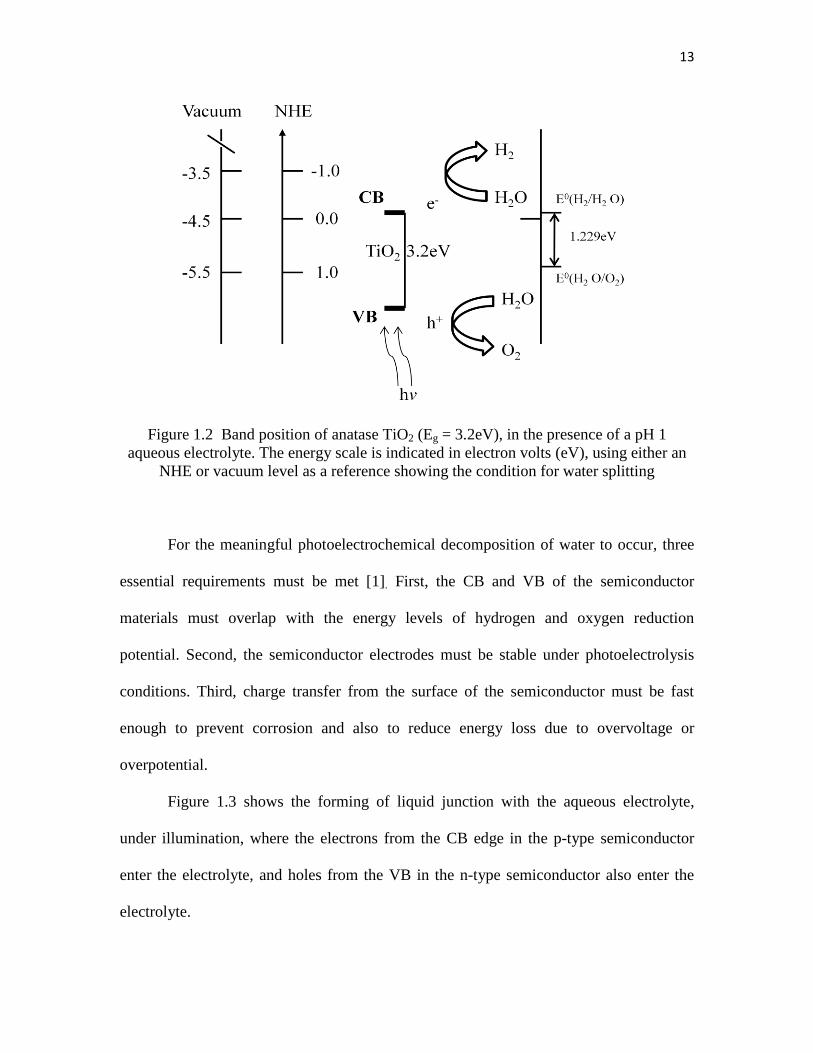
than the voltage required to split the water molecule. For example, in Figure 1.2, a widely
studied photoanode material, anatase TiO2 [1], 3.0eV bandgap generates a 0.7-0.9V when
illuminated which is not sufficient and an external electrical bias is needed to make up for
the insufficient voltage.
13
Figure 1.2 Band position of anatase TiO2 (Eg = 3.2eV), in the presence of a pH 1
aqueous electrolyte. The energy scale is indicated in electron volts (eV), using either an
NHE or vacuum level as a reference showing the condition for water splitting
For the meaningful photoelectrochemical decomposition of water to occur, three
essential requirements must be met [1]. First, the CB and VB of the semiconductor
materials must overlap with the energy levels of hydrogen and oxygen reduction
potential. Second, the semiconductor electrodes must be stable under photoelectrolysis
conditions. Third, charge transfer from the surface of the semiconductor must be fast
enough to prevent corrosion and also to reduce energy loss due to overvoltage or
overpotential.
Figure 1.3 shows the forming of liquid junction with the aqueous electrolyte,
under illumination, where the electrons from the CB edge in the p-type semiconductor
enter the electrolyte, and holes from the VB in the n-type semiconductor also enter the
electrolyte.

14
Figure 1.3 Band edges of p- and n-type semiconductors in
aqueous electrolyte under illumination
In recent years, articles related to solar energy conversion have drawn a lot of
attention, and they have been accumulating in scientific literature. Since 1990, the
amount of publication related to this field has increased exponentially, according to
Fujishima [12]. The upsurge of interest regarding this solar energy utilization has been
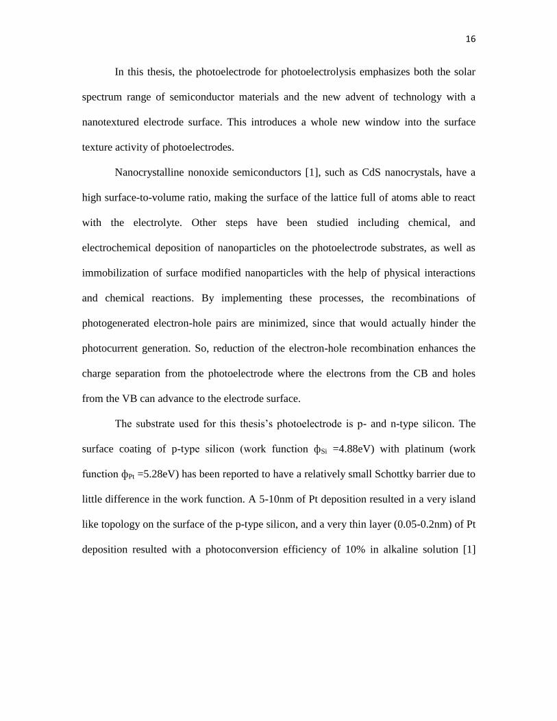
fueled by the energy crisis that emerged in recent decades. Table 1.1 includes the most
recent work on photoelectrolysis and the photoelectrode description. The table covers the
photoanode and photocathode material, electrolyte, incident photon to current efficiency
(IPCE), and solar-to-hydrogen conversion efficiency (ηSTH).

15
1.5.2 Photocatalysts
The use of photocatalysts to perform photoelectrolysis was first reported between
the late 1970s and 1980s. The photocatalysts were mainly TiO2 and SrTiO3. The TiO2
photocatalyst is active when another cocatalyst is modified with it and when the
electrolyte of the aqueous solution is suitable. Metal cations used to make stable
semiconductor oxide photocatalysts usually respond solely to UV light. Thus, band
engineering of the photocatalysts is needed to make them responsive to water splitting
reaction under visible light.
Table 1.2 is the library [13] of new photocatalysts that have been reported by
researchers recently. The main classifications are the overall water splitting into H2 and
O2 with and without the presence of reagents. Although this photocatalyst library does not
contain all reported photocatalysts, it certainly provides an overview of recent and
important ones.
1.5.3 Nanostructured surface
For successful photoelectrolysis, the photoelectrodes must absorb significant
amounts of sun light energy. Different kinds of inorganic semiconductors besides p-type
or n-type silicon, like amorphous silicon (a-Si) or crystalline silicon (c-Si), gallium
arsenide (GaAs), cadmium telluride (CdTee), gallium, phosphide (GaP), indium
phosphide (InP), copper indium diselenide (CIS), copper indium diselenide (CIGS), and
gallium indium phosphide (GaInP2) are popular semiconductors for absorbing and
converting solar energy into electrical energy [1].
16
In this thesis, the photoelectrode for photoelectrolysis emphasizes both the solar
spectrum range of semiconductor materials and the new advent of technology with a
nanotextured electrode surface. This introduces a whole new window into the surface
texture activity of photoelectrodes.
Nanocrystalline nonoxide semiconductors [1], such as CdS nanocrystals, have a
high surface-to-volume ratio, making the surface of the lattice full of atoms able to react
with the electrolyte. Other steps have been studied including chemical, and
electrochemical deposition of nanoparticles on the photoelectrode substrates, as well as
immobilization of surface modified nanoparticles with the help of physical interactions
and chemical reactions. By implementing these processes, the recombinations of
photogenerated electron-hole pairs are minimized, since that would actually hinder the
photocurrent generation. So, reduction of the electron-hole recombination enhances the
charge separation from the photoelectrode where the electrons from the CB and holes
from the VB can advance to the electrode surface.
The substrate used for this thesis’s photoelectrode is p- and n-type silicon. The
surface coating of p-type silicon (work function фSi =4.88eV) with platinum (work
function фPt =5.28eV) has been reported to have a relatively small Schottky barrier due to
little difference in the work function. A 5-10nm of Pt deposition resulted in a very island
like topology on the surface of the p-type silicon, and a very thin layer (0.05-0.2nm) of Pt
deposition resulted with a photoconversion efficiency of 10% in alkaline solution [1]
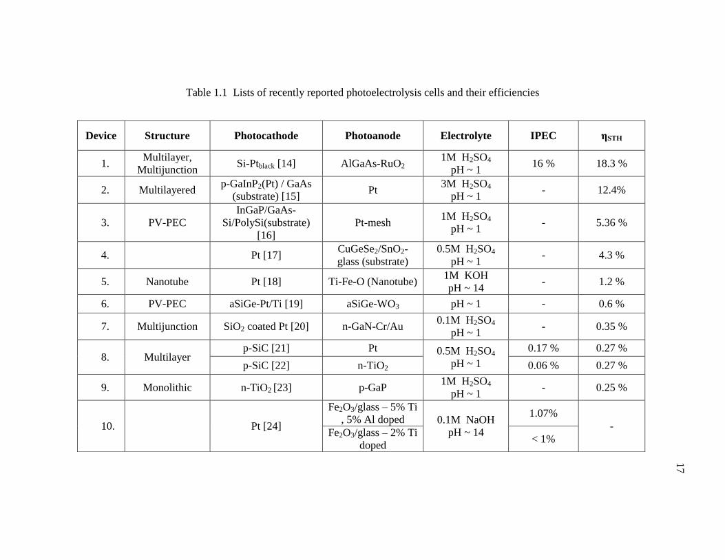
Table 1.1 Lists of recently reported photoelectrolysis cells and their efficiencies
Device Structure Photocathode Photoanode Electrolyte IPEC ηSTH
1. Multilayer,
Multijunction Si-Ptblack [14] AlGaAs-RuO2
1M H2SO4
pH ~ 1 16 % 18.3 %
2. Multilayered p-GaInP2(Pt) / GaAs
(substrate) [15] Pt
3M H2SO4
pH ~ 1 - 12.4%
3. PV-PEC
InGaP/GaAs-
Si/PolySi(substrate)
[16]
Pt-mesh 1M H2SO4
pH ~ 1 - 5.36 %
4. Pt [17] CuGeSe2/SnO2-
glass (substrate)
0.5M H2SO4
pH ~ 1 - 4.3 %
5. Nanotube Pt [18] Ti-Fe-O (Nanotube) 1M KOH
pH ~ 14 - 1.2 %
6. PV-PEC aSiGe-Pt/Ti [19] aSiGe-WO3 pH ~ 1 - 0.6 %
7. Multijunction SiO2 coated Pt [20] n-GaN-Cr/Au 0.1M H2SO4
pH ~ 1 - 0.35 %
8. Multilayer p-SiC [21] Pt 0.5M H2SO4
pH ~ 1
0.17 % 0.27 %
p-SiC [22] n-TiO2 0.06 % 0.27 %
9. Monolithic n-TiO2 [23] p-GaP 1M H2SO4
pH ~ 1 - 0.25 %
10. Pt [24]
Fe2O3/glass – 5% Ti
, 5% Al doped 0.1M NaOH
pH ~ 14
1.07%
- Fe2O3/glass – 2% Ti
doped < 1%
17
18
Table 1.2 Photocatalysts’ library
Photocatalysts response under visible light
UV light responsive
photocatalysts
H2 evolution
(sacrificial)
O2 evolution
(sacrificial)
Overall water splitting
Overall water
splitting
SrTiO3:Cr,Sb
SrTiO3:Cr,Ta
SrTiO3:Rh
SnNb2O6
ZnS:Cu
ZnS:Ni
ZnS:Pb,Cl
NAInS2
AgGaS2
CuInS2-AgInS2-
ZnS
In2O3(ZnO)3
TiO2:Cr.Sb
TiO2:Ni,Nb
PbMoO4:Cr
BiVO4
Bi2MoO6
Bi2WO6
AgNbO3
Ag3VO4
In2O3 (ZnO)3
SrTiO3:Rh-BiVO4
SrTiO3:Rh-Bi2MoO6
SrTiO3:Rh-WO3
ZnNb2O6
Sr2Nb2O7
Cs2Nb4O11
Ba5Nb4O15
ATaO3 (A=Li,Na,K)
NaTaO3:A
(A=Ln,Ca,Sr,Ba)
ATa2O6
(A=Mg,Ca,Sr,Ba)
Sr2Ta2O7
K3Ta3Si2O13
K3Ta3B2O12
K2LnTa5O15
AgTaO3

19
and 30% in acidic solution [1]. An open circuit voltage (VOC) of 0.685V [1] was reported
when Pt dots were deposited on an n-type silicon photoelectrode with a 5-20nm diameter.
There are also nanoarchitectured devices with p-type and n-type CdS, CdSe, CdTe and
GaN, GaAs, INP [1] reported in various literatures.
CHAPTER 2
HOMOGENOUS SEMICONDUCTING AND METALLIC ELECTRODES
2.1 Introduction
For hydrogen production, it is imperative to investigate different electrode
materials and their properties. Here, we investigate metallic electrodes, such as gold (Au),
platinum (Pt), palladium (Pd), titanium (Ti), and tungsten (W). In one case, we also
studied nanoporous tungsten to examine the effect of a very large electrode area on the
electrode hydrogen production efficiency. Semiconducting electrodes, such as titanium
dioxide (TiO2), silicon carbide (SiC) and both p- and n-type single crystal silicon (Si), are
also studied and discussed in this chapter. All these electrodes were used to generate
hydrogen in acidic as well basic electrolytes, with pH levels ranging from 1-13. The main
objective was to find the electrode material that produces the largest amount of hydrogen
at the lowest possible turn on voltage (VON), which is the turn on voltage at which
hydrogen is produced in cathode and observed as bubbles.
In Section 2.2, we discuss the experimental setup. Section 2.3 takes a closer look
at cathode and anode metal-metal electrodes in our electrochemical fuel cell. The next
section, 2.4, focuses on semiconductor-semiconductor electrodes. Section 2.5 talks about
the effect of coating the electrodes with various photocatalysts. Finally, Section 2.6
concludes this chapter.
21
2.2 Experimental Setup
The following sections provide an overview of the experimental setup, the
electrical measurements, electrolyte preparation, and electrode materials and preparation
processes.
2.2.1 Electrical measurements
The electrical measurements are a crucial component of this project, which is why
the setup has to be very precise and neat, so that the results we obtain are accurate. Figure
2.1 shows what components were used to carry out the electrical measurements. First, the
electrodes are connected to a Keithley 236 source-measure unit (SMU) that produces
current and measures the voltage across the electrodes through two calibrated ports. The
SMU is connected to a computer and synchronized with LABVIEW software to monitor
the voltammetric measurement of the setup. There is also a separate light source for
illuminating the electrode samples inside the electrolyte for different experimental
purposes.
2.2.2 Electrolyte preparation
For the voltammetric measurement of the electrodes, we need to prepare
electrolytes. In this thesis, the electrodes were studied in both acidic and basic
electrolytes at pH levels ranging from 1-11. The pH level of the solution was determined
by a digital pH meter, Lutron YK2001PH.
22
Figure 2.1 Experimental setup used to study different electrodes
Acidic electrolytes were prepared with diluted hydrochloric acid (HCl) mixed
with distilled (DI) water. For different pH levels of the acidic electrolytes, ranging from
1-6, the digital pH meter was used to calculate the H+ ion level of the solution. The
higher the concentration of HCl, the more H+ ions are injected into the electrolyte, and
the pH level decreases, thereby making it more acidic. Conversely, the basic electrolyte
was prepared with potassium hydroxide (KOH). The KOH injects OH- ions into the
solution, making it rich with hydroxyl ions. This basic electrolyte has a pH level ranging
from 8-13. This was determined by the digital pH meter.
Electrodes

23
2.2.3 Electrode materials and preparation
The electrodes that were used in this thesis were designed and created for
experimental purposes. The metal electrodes gold, platinum, palladium, titanium, and
tungsten were bought from the company Alfa AesarTM
with 99% purity. Samples were
cut and prepared so that the contact surface area of each was the same.
The semiconductor electrodes silicon carbide, gallium nitride and both p- and n-
type single crystal silicon were bought from a different manufacturer. Only the TiO2 was
prepared in our laboratory. A 0.5mm thickness of titanium (99% pure) source was
purchased from Alfa AesarTM
. Using an electrolyte of 0.5M phosphoric acid (H3PO4) and
a Keithley 236 SMU, an oxide (anatase) layer of 50-300µm was grown on the titanium
sample. [24]
2.3 Metal-Metal Electrodes
Section 2.2 outlines the setup for measuring the characteristics of metal-metal
electrodes. In addition, the reason behind selecting gold, platinum, palladium, titanium
and tungsten metals as electrodes are also discussed.
In the field of electrochemistry and electroanalytical chemistry, there are different
kinds of materials used for electrodes. Among them, gold is widely used. Gold is highly
conductive, as the concentration of free electrons is around 5.90×10²²
cm−3
[25]. It is also
very resistant to corrosion and oxidation, has good conductivity, ductility, and low
toxicity. In semiconductor industries, gold wire is being used to connect semiconductor
devices to their packages through a process called wire-bonding. For these reasons, gold
has always been a very suitable material for electronic experiments.

24
Another important and widely used electrode is platinum. Because of its
chemical inertness and high corrosion resistance, platinum is frequently used in chemical
experiments and other various electronic components. The standard hydrogen electrode
(SHE) also utilizes a platinized platinum electrode. Although it is a high-value metal, its
promising chemical properties make it an excellent candidate for electrodes.
After gold and platinum, the next suitable candidate for electrodes is palladium.
This metal has characteristics similar to gold and platinum, those of being highly
corrosion resistant and nontoxic. Palladium has been used for electronics besides
electrodes. The palladium-hydrogen electrode (Pd/H2) is one of the common reference
electrodes in electrochemical studies, similar to SHE (with platinum). Although
palladium is known for its hydrogen absorption characteristics, this feature is applicable
only in high temperature.
Titanium has the physical qualities of strength, durability, high resistance to
corrosion, low density, and biological compatibility. These characteristics make titanium
a very useful element for various applications. Titanium’s most common compound,
titanium dioxide (TiO2), is one of the most popular photocatalysts, and is also used as a
compound for industrial white pigments. Even though titanium gets oxidized during
anode-cathode experimentation when exposed to aqueous electrolytes, its chemical
properties and other various characteristics make titanium a very promising candidate for
electrode testing.
Tungsten is the last metal listed in this thesis as a candidate for electrode testing.
Most commonly known as tungsten-filament, this metal has the highest tensile strength
among metals in pure form. It is also very brittle, which makes it hard to work with. Due
25
to high covalent bonds formed between tungsten atoms and the 5d electrons, tungsten has
low thermal expansion and the highest melting point (3,422 oC, 6192
oF) in pure form.
Because of its strength at high temperatures and relative chemical inertia, tungsten is used
as electrodes in different electronic applications, which makes it a suitable transitional
metal for electrodes.
Due to the repetitive nature of the voltammetric behavior of metal-metal
electrodes, only the setups for gold-gold and gold-platinum electrodes are discussed in
Sections 2.3.1 and 2.3.2. For the other metal electrode combinations, which are gold-
palladium, gold-titanium, gold-tungsten, platinum-titanium, platinum-palladium,
platinum-tungsten, palladium-tungsten, and titanium-tungsten, setups have been included
in Appendix A.
2.3.1 Gold-gold electrodes
This section studies the gold-gold electrodes in acidic and basic (pH 1-11)
electrolytes both under illumination and in the dark. The surface areas of the gold
electrodes were 40mm2 (10mm [L] x 4mm [W]) on both sides, creating a total contact
area of 80mm2.
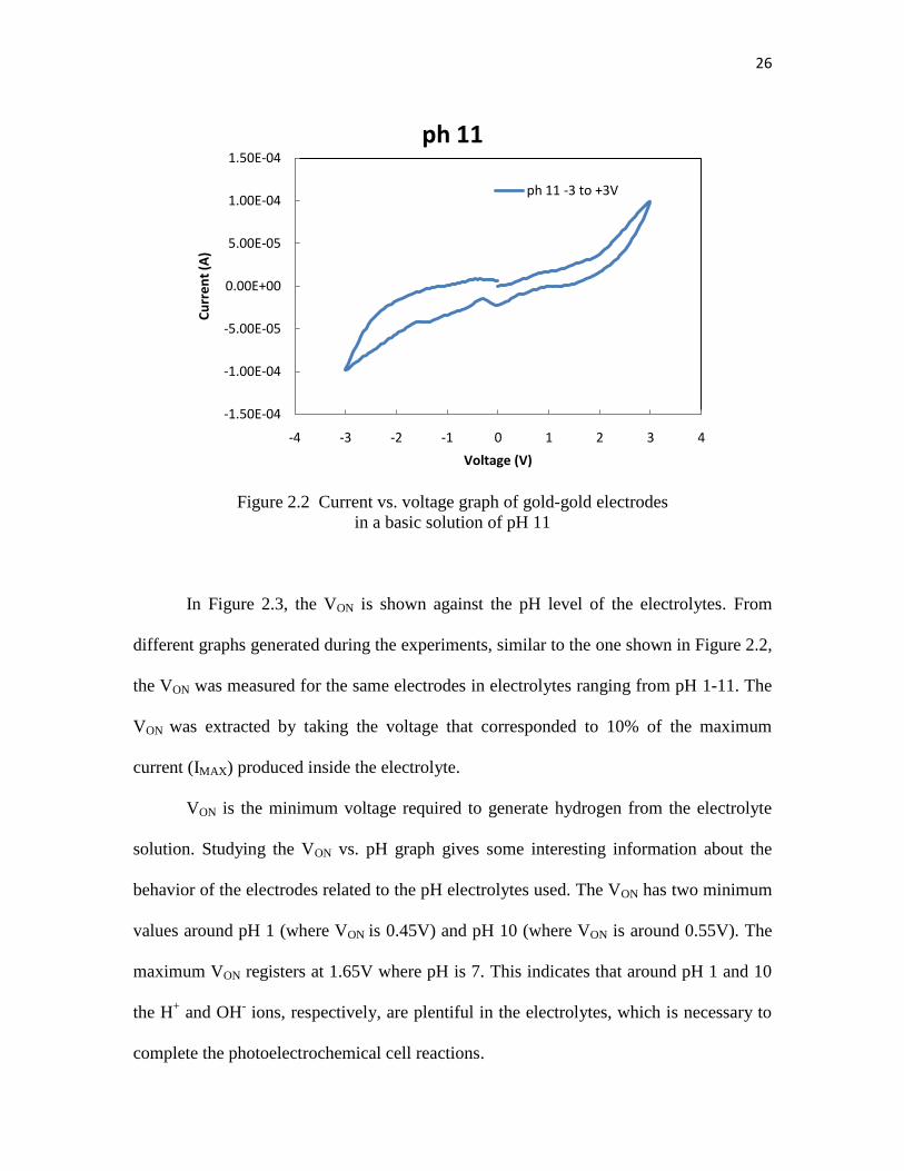
Figure 2.2 presents a graph of the voltammetric analysis of the gold-gold
electrode setup in a pH 11 basic solution The voltage level was raised from 0V to 3V,
then lowered to -3V and finally brought up to 0V again. The SMU calculated the current
level in the electrolyte, and this level was stored using the LABVIEW program on the
computer. This experiment was conducted with different pH levels ranging from 1-11.
Extrapolating the data from this set of experiments, Figure 2.3 was constructed.
26
Figure 2.2 Current vs. voltage graph of gold-gold electrodes
in a basic solution of pH 11
In Figure 2.3, the VON is shown against the pH level of the electrolytes. From
different graphs generated during the experiments, similar to the one shown in Figure 2.2,
the VON was measured for the same electrodes in electrolytes ranging from pH 1-11. The
VON was extracted by taking the voltage that corresponded to 10% of the maximum
current (IMAX) produced inside the electrolyte.
VON is the minimum voltage required to generate hydrogen from the electrolyte
solution. Studying the VON vs. pH graph gives some interesting information about the
behavior of the electrodes related to the pH electrolytes used. The VON has two minimum
values around pH 1 (where VON is 0.45V) and pH 10 (where VON is around 0.55V). The
maximum VON registers at 1.65V where pH is 7. This indicates that around pH 1 and 10
the H+ and OH
- ions, respectively, are plentiful in the electrolytes, which is necessary to
complete the photoelectrochemical cell reactions.
-1.50E-04
-1.00E-04
-5.00E-05
0.00E+00
5.00E-05
1.00E-04
1.50E-04
-4 -3 -2 -1 0 1 2 3 4
Cu
rre
nt
(A)
Voltage (V)
ph 11
ph 11 -3 to +3V
27
Figure 2.3 VON vs. pH graphs for gold-gold electrodes
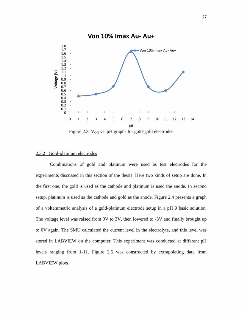
2.3.2 Gold-platinum electrodes
Combinations of gold and platinum were used as test electrodes for the
experiments discussed in this section of the thesis. Here two kinds of setup are done. In
the first one, the gold is used as the cathode and platinum is used the anode. In second
setup, platinum is used as the cathode and gold as the anode. Figure 2.4 presents a graph
of a voltammetric analysis of a gold-platinum electrode setup in a pH 9 basic solution.
The voltage level was raised from 0V to 3V, then lowered to -3V and finally brought up
to 0V again. The SMU calculated the current level in the electrolyte, and this level was
stored in LABVIEW on the computer. This experiment was conducted at different pH
levels ranging from 1-11. Figure 2.5 was constructed by extrapolating data from
LABVIEW plots.
00.10.20.30.40.50.60.70.80.9
11.11.21.31.41.51.61.71.8
0 1 2 3 4 5 6 7 8 9 10 11 12 13 14
Vo
ltag
e (
V)
pH
Von 10% Imax Au- Au+
Von 10% Imax Au- Au+

28
Figure 2.4 Current vs. voltage graph of gold-platinum electrodes
in a basic solution of pH 9
In Figure 2.5, the VON vs. pH graph was extrapolated from different current vs.
voltage graphs for pH level 1-11 solutions for gold-platinum electrodes. The first setup
was done such that the gold electrode was connected to the negative terminal, and the
platinum electrode connected to the positive terminal. In the next setup, the electrodes
were connected in the opposite order, which is explained in Figure 2.6.
Observing the VON vs. pH graph in Figure 2.5 shows that around pH 3 and pH 10,
the VON gives the lowest values of 0.65V and 0.55V respectively. It is necessary to
mention that in this setup, the gold was connected as negative electrode, where, during
the electrochemical reaction, electrons were released into the electrolyte thus reducing the
hydrogen to H+ ions, concurrently producing hydrogen gas. The platinum, which was
-6.00E-05
-5.00E-05
-4.00E-05
-3.00E-05
-2.00E-05
-1.00E-05
0.00E+00
1.00E-05
2.00E-05
3.00E-05
4.00E-05
5.00E-05
-4 -3 -2 -1 0 1 2 3 4
curr
en
t (A
)
Voltage (V)
ph 9 -3 to +3V
ph 9 -3 to +3V

29
Figure 2.5 VON vs. pH graph for gold-platinum electrode
connected as positive electrode, produced oxygen as corresponding to the other half of
the photoelectrochemical reaction.
Here, in Figure 2.6, VON vs. pH was plotted in the same way as the previous plot,
by extrapolating data from current vs. voltage graphs for pH 1-11 electrolytes, where the
gold was connected as positive electrode, and platinum was connected as negative
electrode. From characteristics depicted in Figure 2.6, it is clear that, near pH 3 and pH
10, the corresponding VON shows 0.3V and 0.75V. This means that when platinum is used
for negative electrodes, the tendency for it to give electrons to the electrolyte solution,
thus generating hydrogen gas in the cathode, is higher than gold when used as a negative
electrode.
00.10.20.30.40.50.60.70.80.9
11.11.21.31.41.5
0 1 2 3 4 5 6 7 8 9 10 11 12 13 14
Vo
ltag
e(V
)
pH
Von 10% Imax Au- Pt+
Von 10% Imax Au- Pt+

30
Figure 2.6 VON vs. pH graph for platinum-gold electrode
2.4 Semiconductor-semiconductor electrode
In section 2.3, various types of metal-metal electrodes were studied in order to
determine the best metal electrode for producing hydrogen from different pH levels of
aqueous solutions. In this chapter, three types of semiconductor-semiconductor electrodes
were studied: silicon (p- and n-type), silicon carbide (4HN-type), and titanium dioxide.
Certain criteria must be met for a spontaneous water-splitting reaction to occur,
for any kind of electrolysis. For example, under illumination, the semiconductor CB edge
should be at a position negative to the reduction potential of water, while the VB edge
should be at a positive position compared to the oxidation potential. Figure 2.7 explains
the necessary position for a bandgap with respect to the reduction and oxidation
00.10.20.30.40.50.60.70.80.9
11.11.21.31.41.51.61.71.8
0 1 2 3 4 5 6 7 8 9 10 11 12 13 14
Vo
ltag
e (
V)
pH
Von 10% Imax Pt- Au+
Von 10% Imax Pt- Au+
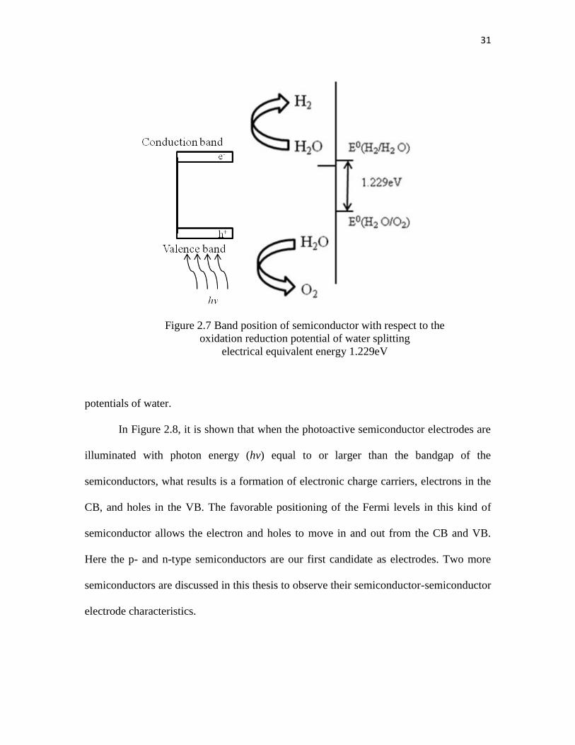
31
Figure 2.7 Band position of semiconductor with respect to the
oxidation reduction potential of water splitting
electrical equivalent energy 1.229eV
potentials of water.
In Figure 2.8, it is shown that when the photoactive semiconductor electrodes are
illuminated with photon energy (hv) equal to or larger than the bandgap of the
semiconductors, what results is a formation of electronic charge carriers, electrons in the
CB, and holes in the VB. The favorable positioning of the Fermi levels in this kind of
semiconductor allows the electron and holes to move in and out from the CB and VB.
Here the p- and n-type semiconductors are our first candidate as electrodes. Two more
semiconductors are discussed in this thesis to observe their semiconductor-semiconductor
electrode characteristics.
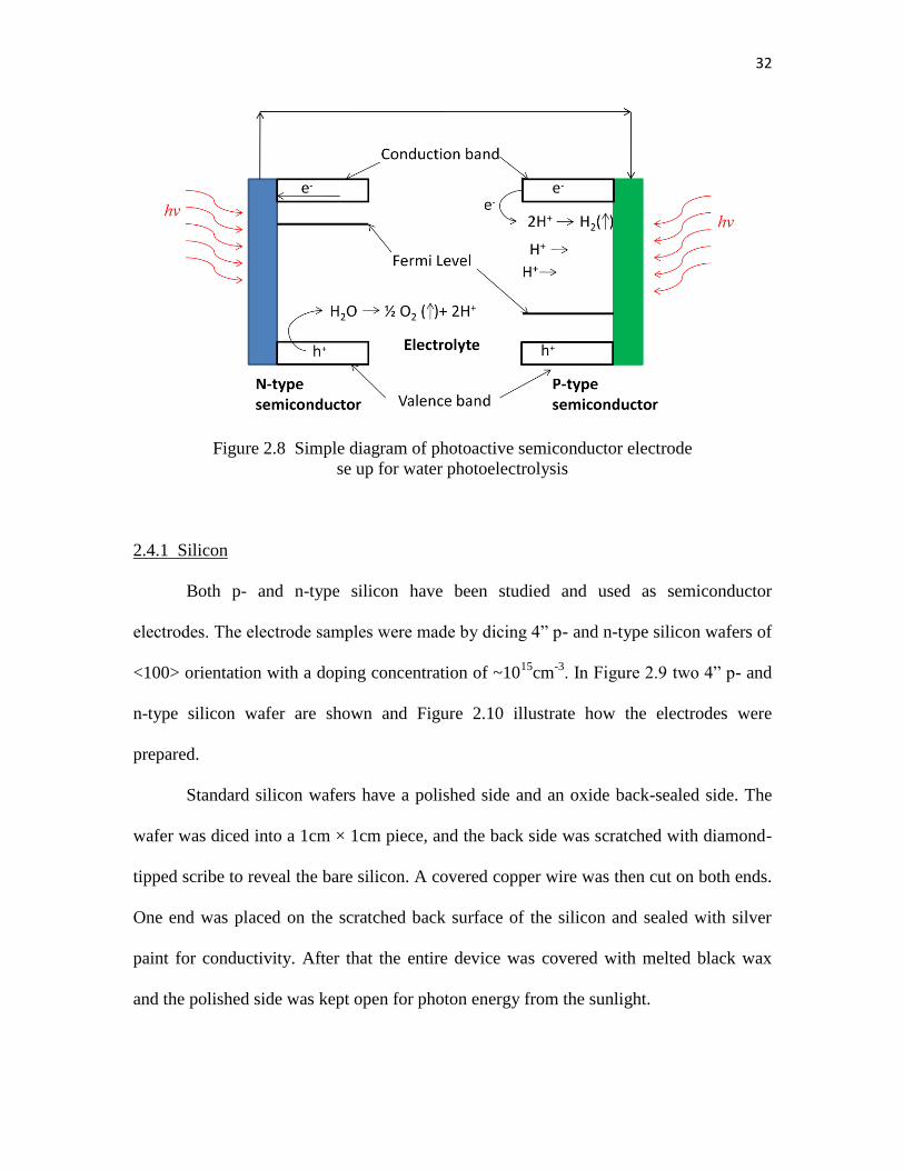
32
Figure 2.8 Simple diagram of photoactive semiconductor electrode
se up for water photoelectrolysis
2.4.1 Silicon
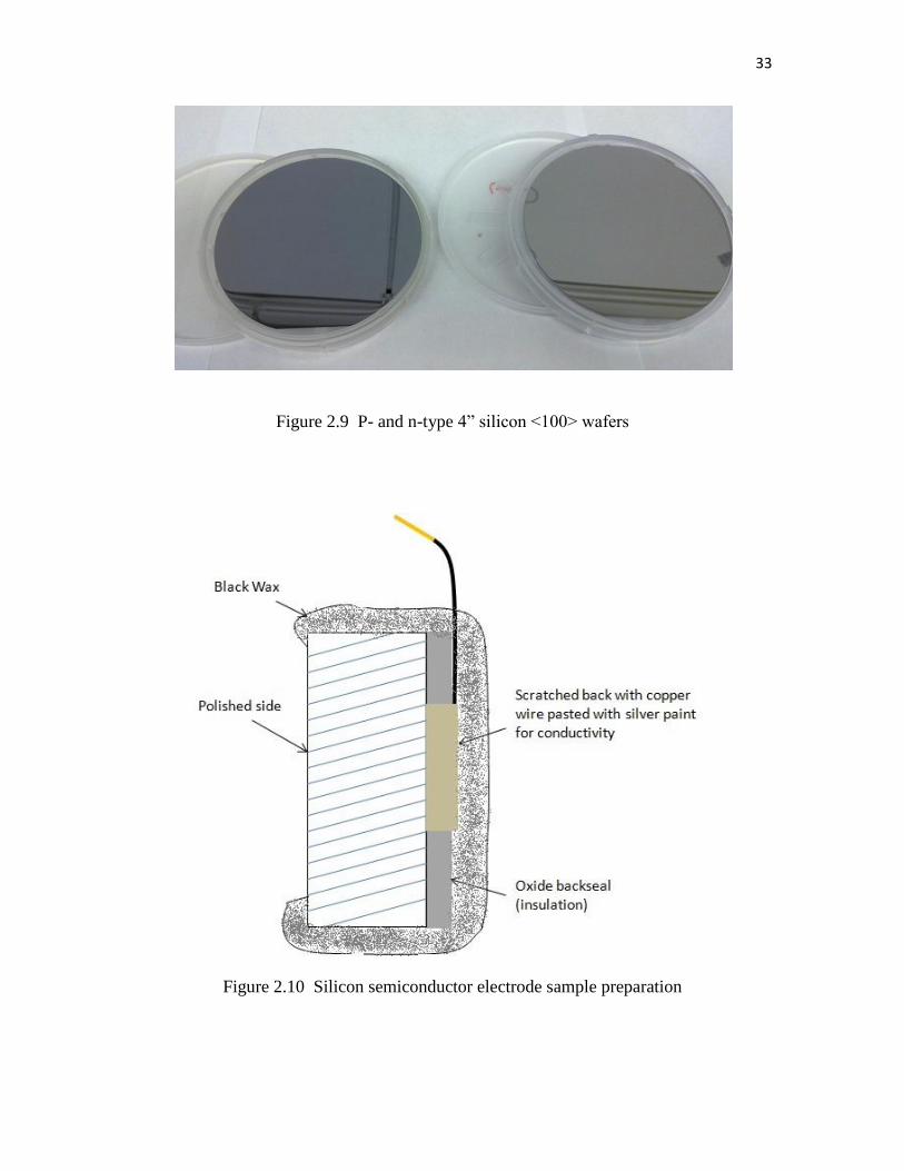
Both p- and n-type silicon have been studied and used as semiconductor
electrodes. The electrode samples were made by dicing 4” p- and n-type silicon wafers of
<100> orientation with a doping concentration of ~1015
cm-3
. In Figure 2.9 two 4” p- and
n-type silicon wafer are shown and Figure 2.10 illustrate how the electrodes were
prepared.
Standard silicon wafers have a polished side and an oxide back-sealed side. The
wafer was diced into a 1cm × 1cm piece, and the back side was scratched with diamond-
tipped scribe to reveal the bare silicon. A covered copper wire was then cut on both ends.
One end was placed on the scratched back surface of the silicon and sealed with silver
paint for conductivity. After that the entire device was covered with melted black wax
and the polished side was kept open for photon energy from the sunlight.
33
Figure 2.9 P- and n-type 4” silicon <100> wafers
Figure 2.10 Silicon semiconductor electrode sample preparation
34
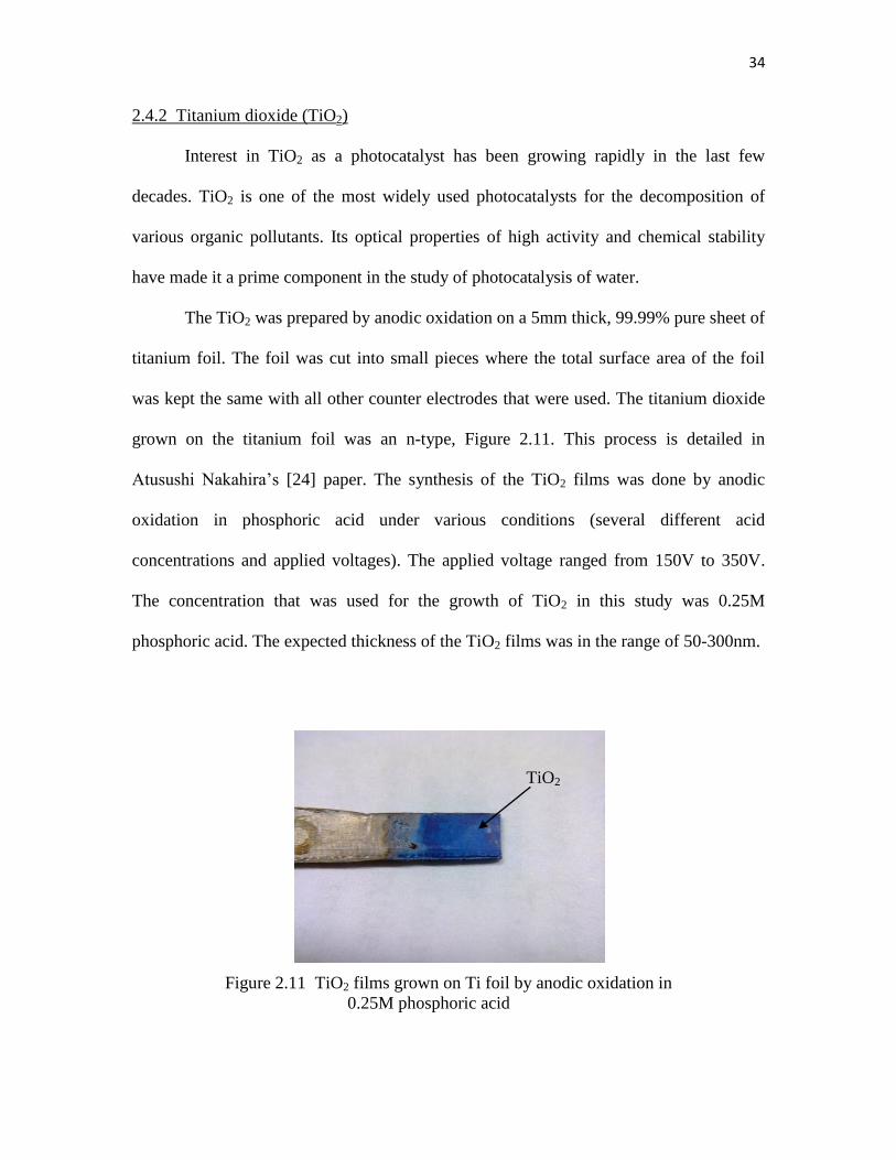
2.4.2 Titanium dioxide (TiO2)
Interest in TiO2 as a photocatalyst has been growing rapidly in the last few
decades. TiO2 is one of the most widely used photocatalysts for the decomposition of
various organic pollutants. Its optical properties of high activity and chemical stability
have made it a prime component in the study of photocatalysis of water.
The TiO2 was prepared by anodic oxidation on a 5mm thick, 99.99% pure sheet of
titanium foil. The foil was cut into small pieces where the total surface area of the foil
was kept the same with all other counter electrodes that were used. The titanium dioxide
grown on the titanium foil was an n-type, Figure 2.11. This process is detailed in
Atusushi Nakahira’s [24] paper. The synthesis of the TiO2 films was done by anodic
oxidation in phosphoric acid under various conditions (several different acid
concentrations and applied voltages). The applied voltage ranged from 150V to 350V.
The concentration that was used for the growth of TiO2 in this study was 0.25M
phosphoric acid. The expected thickness of the TiO2 films was in the range of 50-300nm.
Figure 2.11 TiO2 films grown on Ti foil by anodic oxidation in
0.25M phosphoric acid
TiO2
35
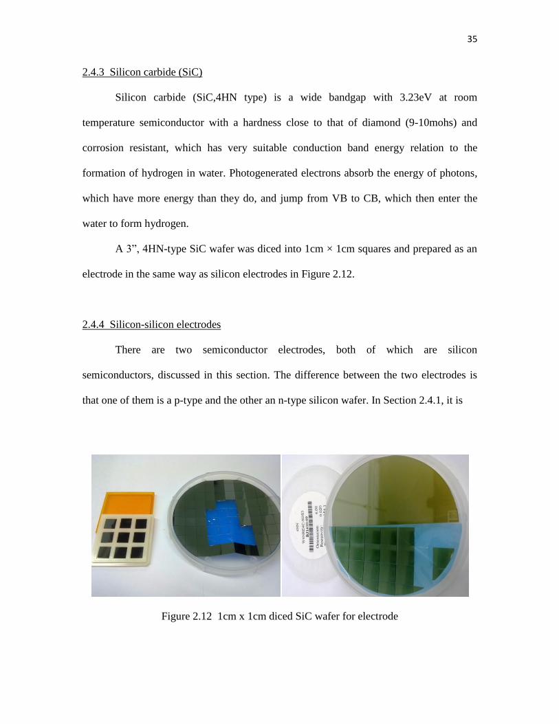
2.4.3 Silicon carbide (SiC)
Silicon carbide (SiC,4HN type) is a wide bandgap with 3.23eV at room
temperature semiconductor with a hardness close to that of diamond (9-10mohs) and
corrosion resistant, which has very suitable conduction band energy relation to the
formation of hydrogen in water. Photogenerated electrons absorb the energy of photons,
which have more energy than they do, and jump from VB to CB, which then enter the
water to form hydrogen.
A 3”, 4HN-type SiC wafer was diced into 1cm × 1cm squares and prepared as an
electrode in the same way as silicon electrodes in Figure 2.12.
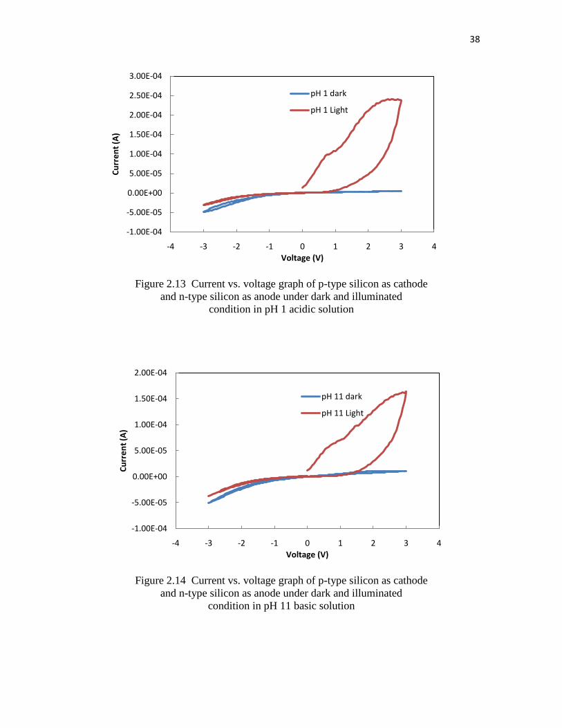
2.4.4 Silicon-silicon electrodes
There are two semiconductor electrodes, both of which are silicon
semiconductors, discussed in this section. The difference between the two electrodes is
that one of them is a p-type and the other an n-type silicon wafer. In Section 2.4.1, it is
Figure 2.12 1cm x 1cm diced SiC wafer for electrode

36
mentioned that p- and n-type semiconductor are the first choice as photoelectrodes due to
its suitable bandgap structure and Fermi level positioning for photogenerated electron-
hole pair. That is why p- and n-type silicon semiconductor is the first candidate for
semiconductor electrode testing. The electrolytes used in this experiment also range from
pH 1 acidic to pH 13 basic solutions. However, for convenience, only two kinds of pH
solutions are discussed in this section, acidic pH 1 and basic pH 11 solutions.
In order to explain the photoactive semiconductor electrodes’ characteristics,
voltammetric analysis was conducted under two conditions. First, the electrodes were put
inside the electrolytes and the current vs. voltage analysis was run under no illumination.
After the analysis was done, the electrodes were taken out and put inside a diluted BOE
(buffered oxide etch) to get rid of the thin layer of oxide formation on the surface due to
the anodizing effect. Once the oxide was etched off, both electrodes were put into the
electrolytes again and the current vs. voltage analyses were conducted under illumination.
The intensity of the light source was 197.35 .
As mentioned earlier the p-type silicon electrode was used as a photocathode
where H+ ions were reduced to hydrogen. The n-type silicon electrode was used as a
photoanode, where, due to water oxidation, oxygen gas was generated and H+ ions were
released.
Figures 2.13 and 2.14 show current vs. voltage plots both in pH 1 and pH 11
electrolytes for p- and n-type semiconductor electrodes. The current vs. voltage plot
without illumination (blue line) shows. In the figures the p-type silicon photocathode was
under negative bias (reverse bias), and the p-type silicon photoanode was under positive
bias (forward bias) when voltage was raised from 0V to 3V and brought down to 0V.
37
Conversely when the voltage was lowered from 0 to -3V then brought up to 0V, the
biasing of the electrodes was reversed. The p-type was used as a photoanode, which was
under positive bias (forward bias), and the n-type as a photocathode, which was under
negative bias (reverse bias). The blue line shows the condition where the current vs.
voltage plot were taken without illumination. As there was no light energy projected onto
the surface of the electrode, there was no noticeable photoreaction happening inside the
semiconductor, the blue line does not show any significant difference in forward or
reverse bias
However, when the electrodes are illuminated with a bright light source, the
current vs. voltage graph shows some significant change in its behavior. When photon
energy from the light source hits the surface of the semiconductor electrodes on the
surface of the n-type photoanode, water oxidation occurs due to the holes (h+) acceptation
in the valence band from the electrolytes. Oxygen gas is generated and, at the same time,
H+ ions are released. Concerning the p-type photocathode under illumination, the
electrons (e-) from the conduction band are released into the electrolytes, which then
reduce the H+ ions to H2 gas.
In studying Figures 2.13 and 2.14, it is clear that when the photogenerated
hydrogen experiment was conducted in the pH 1 acidic, in contrast to the pH 11 basic
solution, the maximum current measured was 2.50 E-04A. In the basic solution, the
highest current was 1.50E-04A. This is expected because, in the acidic solution, there are
more H+ ions than in the basic solution. In the basic solution, there are more OH
- ions. H
+
ions give more electrons for reducing hydrogen than producing hydrogen and more flow
in the electron concentration.
38
Figure 2.13 Current vs. voltage graph of p-type silicon as cathode
and n-type silicon as anode under dark and illuminated
condition in pH 1 acidic solution
Figure 2.14 Current vs. voltage graph of p-type silicon as cathode
and n-type silicon as anode under dark and illuminated
condition in pH 11 basic solution
-1.00E-04
-5.00E-05
0.00E+00
5.00E-05
1.00E-04
1.50E-04
2.00E-04
2.50E-04
3.00E-04
-4 -3 -2 -1 0 1 2 3 4
Cu
rre
nt
(A)
Voltage (V)
pH 1 dark
pH 1 Light
-1.00E-04
-5.00E-05
0.00E+00
5.00E-05
1.00E-04
1.50E-04
2.00E-04
-4 -3 -2 -1 0 1 2 3 4
Cu
rre
nt
(A)
Voltage (V)
pH 11 dark
pH 11 Light

39
2.4.5 Silicon-titanium dioxide electrodes
In this section two different kinds of semiconductor electrodes are used. For the
photocathode, p-type silicon was used. For the photoanode, an n-type TiO2 was used. The
TiO2 was grown on a 5mm thick, pure titanium foil using anodic oxidation. In previous
sections, it was explained how the n-type TiO2 was grown on the titanium foil.
TiO2 is a very popular photocatalyst in the field of photogenerated hydrogen for
water electrolysis. It is thus a good candidate for a potential electrode for the purpose of
generating oxygen in the photoanode.
In Figure 2.15 a pH 9 basic electrolyte was used to study the characteristics of n-
TiO2 for producing oxygen. This would prove TiO2 to be a suitable candidate for a
photoanode paired semiconductor photocathode. The current vs. voltage analysis was run
from -3V to 3V. When the current vs. voltage analysis was done under the dark condition
(blue line), it became clear that in forward bias mode, there were no photogenerated holes
being accepted in the photoanode, TiO2. Therefore, there is no noticeable current being
generated. However, under illumination (red line), it becomes clear that current is
generated around 1E-04A. This indicates that the TiO2 photoanode is accepting holes
generated due to photon energy from the electrolytes, and releasing H+ ions for the
photocathode to be reduced and produce hydrogen gas. It can also be seen that, in the
dark condition under the reverse bias, the electrodes are accepting and releasing holes and
electrons, therein generating a maximum 2E-04A current, but this is not due to photon
energy from the light source as both the blue and red line show the same plots of data.

40
Figure 2.15 Current vs. voltage graph of p-type silicon as cathode
and n-type TiO2 as anode under dark and illuminated
condition in pH 9 basic solution
2.4.6 Silicon carbide-titanium dioxide electrodes
The last sets of semiconductors that were used for the photoelectrolysis of water
are a 4HN-SiC and an n-TiO2. It might be confusing to observe that both of the electrodes
that are used here are N-type semiconductors, where it is clear that, in order to produce
hydrogen in the photocathode, an n-type semiconductor is required. The reason this
combination is used is to understand and study the ability of these two n-type
semiconductors to generate oxygen under illumination, where it could be easier to
determine which semiconductor would be better suited for a photoanode with a
photocathode. Figure 2.16 is the current vs. voltage graph of these two photoelectrodes in
pH 1 electrolyte.
-2.50E-04
-2.00E-04
-1.50E-04
-1.00E-04
-5.00E-05
0.00E+00
5.00E-05
1.00E-04
-4 -3 -2 -1 0 1 2 3 4
Cu
rre
nt
(A)
Voltage (V)
pH 9 dark
pH 9 Light

41
Figure 2.16 Current vs. voltage graph of 4HN SiC as cathode and
n-TiO2 as anode under dark and illuminated
condition in pH 1 acidic solution
In this setup, the 4HN-types SiC was used as a photocathode and the n-type TiO2
was used as the photoanode. In closely examining Figure 2.16, it is clear that, under no
illumination, the current vs. voltage curve shows very few signs of generating current.
Yet, under illumination it is visible that both of the N-type semiconductor electrodes
showed potential characteristics for producing oxygen as they accepted holes from the
electrolyte and oxidized water to release H+ ions.
The Table 2.1 summarizes the data collected through the experiments outlined
between sections 2.3 and 2.4.
-2.50E-05
-2.00E-05
-1.50E-05
-1.00E-05
-5.00E-06
0.00E+00
5.00E-06
1.00E-05
1.50E-05
2.00E-05
-3 -2 -1 0 1 2 3
Cu
rre
nt
(A)
Voltage (V)
Dark
Light

42
Table 2.1 Summary of maximum current IMAX, Lowest VON and pH level for metal-metal
electrodes and semiconductor-semiconductor photoelectrodes
Cathode( -ve) ,
Anode (+ve)
IMax (A), pH (at
5V)
Lowest VOn
(V), pH
Metal Electrodes
1. Au – Au 1.0E-04 (pH 11) 0.5 (pH 1)
2. Au(-ve) – Pt(+ve) 4.5E-05 ((pH 9) 0.3 (pH 3)
3. Au(-ve) – Pd(+ve) 6.0E-04 (pH 9) 0.5 (pH 10)
4. Au(+ve) – Ti(-ve) 2.2E-05 (pH 3) 0.9 (pH 3)
5. Au(-ve) – W(+ve) 7.2E-04 (pH 11) 0.2 (pH 3)
6. Pt(-ve) – Pd(+ve) 1.5E-04 (pH 11) 0.5 (pH 11)
7. Pt(-ve) – W(+ve) 8.0E-04 (pH 3) 0.3 (pH 3)
8. Pt(-ve) – Ti(+ve) 6.0E-05 (pH 11) 0.8 (pH 11)
9. Pd(+ve) – W(-ve) 1.5E-04 (pH 3) 0.5 (pH 3)
10. Ti(-ve) – W(+ve) 2.0E-04 (pH 3) 0.3 (pH 3)
Photocathode( -ve) ,
Photoanode (+ve)
IMax (A), pH (at
3V)
Lowest VOn
(V), pH
Semiconductor
Electrodes
1. P-Si(-ve)–N-Si(+ve)
6.0E-06 (pH 1)
Dark 0.2 (pH 1)
Illuminated 2.5E-04 (pH 1)
Illuminated
2. P-Si(-ve) - N-TiO2(+ve)
7.0E-06 (pH 9)
Dark 1.5 (pH 9)
Illuminated 9.5E-05 (pH 9)
Illuminated
3. N-SiC(-ve) – N-
TiO2(+ve)
1.0E-05 (pH 1)
Dark 0.5 (pH 1)
Illuminated 1.5E-05 (pH 1)
Illuminated
43
2.5 The Effect of Photocatalyst Coating on Electrodes
In this section, the effect of the photocatalyst on a semiconductor was studied in
order to locate a possible candidate for use as a photoelectrode in water electrolysis using
light energy. Sections 2.5.1 and 2.5.2 discuss what photocatalysts are and why we need
them.
2.5.1 What is a photocatalyst?
Catalysts work by changing the activation energy for a reaction, in other words,
the minimum energy needed for the reaction to occur. This is accomplished by providing
a new mechanism or reaction path through which the reaction can proceed. When the
new reaction path has lower activation energy, the reaction rate is increased and the
reaction is said to be catalyzed.
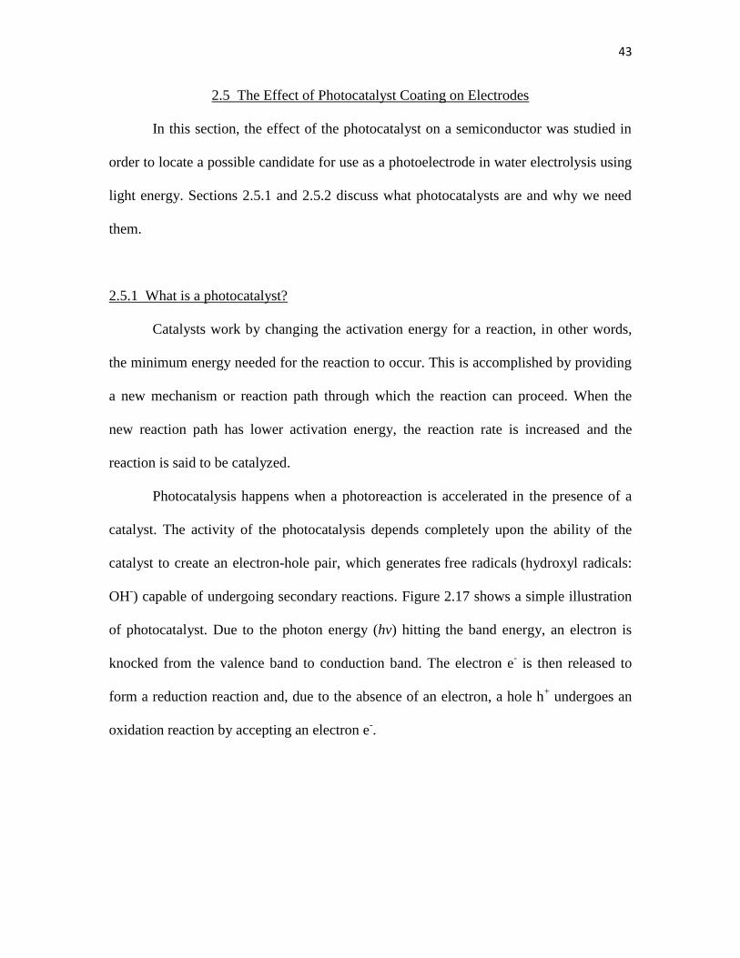
Photocatalysis happens when a photoreaction is accelerated in the presence of a
catalyst. The activity of the photocatalysis depends completely upon the ability of the
catalyst to create an electron-hole pair, which generates free radicals (hydroxyl radicals:
OH-) capable of undergoing secondary reactions. Figure 2.17 shows a simple illustration
of photocatalyst. Due to the photon energy (hv) hitting the band energy, an electron is
knocked from the valence band to conduction band. The electron e- is then released to
form a reduction reaction and, due to the absence of an electron, a hole h+ undergoes an
oxidation reaction by accepting an electron e-.

44
Figure 2.17 Simple diagram showing the work of a photocatalyst
2.5.2 Why are photocatalysts needed?
Although using photocatalysts to split water seems very intriguing, there are a
number of parameters to be concerned with. In Figure 2.18, some of the properties of
photocatalysts important to study are given. When light energy generates electrons and
holes, these have to migrate to the surface separately or else they will recombine with
each other. This again depends on the crystal property of the material. The better the
crystalline structure of the material, the fewer defects there are because the more defects
present in the material, the higher the chance of the photo-generated electrons and holes
recombining at certain sites due to those defects. Moreover, there is also a concern about
the number of active sites available on the surface for the photogenerated electrons and
holes to conduct redox reactions. This means that even if the electrons and holes have
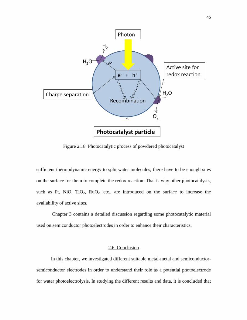
45
Figure 2.18 Photocatalytic process of powdered photocatalyst
sufficient thermodynamic energy to split water molecules, there have to be enough sites
on the surface for them to complete the redox reaction. That is why other photocatalysts,
such as Pt, NiO, TiO2, RuO2, etc., are introduced on the surface to increase the
availability of active sites.
Chapter 3 contains a detailed discussion regarding some photocatalytic material
used on semiconductor photoelectrodes in order to enhance their characteristics.
2.6 Conclusion
In this chapter, we investigated different suitable metal-metal and semiconductor-
semiconductor electrodes in order to understand their role as a potential photoelectrode
for water photoelectrolysis. In studying the different results and data, it is concluded that

46
silicon (p- and n-type) yield the best results among photoelectrode test results. Platinum
and tungsten were more photoactive as metal electrodes, generating hydrogen through the
photoelectrolysis of water.

CHAPTER 3
MULTILAYER DEVICES AND ELECTRODES
3.1 Introduction
This chapter focuses on the multilayer photoactive semiconductor electrodes, their
principles, and the device that was designed for this thesis. In the field of hydrogen
production that uses photoactive semiconductor electrodes, there are two kinds of
approaches: one being a single layer electrode and the other a multilayer electrode.
Multilayer device electrodes have been reported to exhibit a much more efficient
performance than the former. In this thesis, the multilayer device was constructed using a
silicon substrate, an atomic layer deposition of Al2O3, doped polysilicon and tungsten
nanopores (TNP) layers. The voltammetric and efficiency analyses were conducted and
are reported.
In Sections 3.1.1 and 3.1.2, the differences between single and multilayer
photoactive semiconductor electrodes and basic examples of multilayer device structures
and mechanisms are discussed.
3.1.1 Simple electrodes vs. multilayer electrodes
Single layer structure was the main concept behind the first solar device which
was constructed with p- and n-type semiconductors. It is known that p-type silicon has
impurities with 3 valence electron (such as boron), which when introduced to intrinsic
48
silicon semiconductors, create a vacant space for electrons where boron forms covalent
bonds using its 3 outer shell electrons with the 4 outer shell electrons of silicon. This
vacant space for electrons, which is also known as holes, makes the p-type extrinsic
silicon semiconductor. Additionally, in p-type semiconductors, the Fermi level lies close
to the VB, as there are more holes in a p-type semiconductor. When impurities with 5
valence electrons (such as phosphorous) are introduced to the intrinsic silicon, the 5
electrons in the outer shell try to make covalent bonds with the 4 outer shell electrons of
silicon. After creating 4 covalent bonds with the 4 outer shell electrons of silicon, there is
1 extra electron from the phosphorous that remains free. This extra electron can then
roam in the semiconductor, making the silicon an n-type semiconductor. In n-type, the
Fermi level lies close to the CB. Now, when these two p- and n-type silicon
semiconductors are used as photoactive electrodes to perform electrolysis of water, the
photon energy from sunlight knocks the electron from the VB to the CB, which then
enters the electrolyte.
Figure 3.1 explains the phenomenon of photon energy directing the flow of
electrons and holes inside the p- and n-type silicon semiconductors. This structure thus
represents the basic single layer semiconductor structure for photoactive electrodes. In
multilayer semiconductor electrodes, however, while the concept is nearly the same, the
structure is usually different. Instead of using 1 semiconductor (p- or n-type), various
layers of materials are used to ease the flow of electrons and holes to and from the
electrolyte.

49
Figure 3.1 The photon energy from sunlight energizing the electrons and holes to flow in
a) opposite directions; The schematic diagram of b) bandgap structure of p- and n-type
silicon semiconductor and the flow directions of electrons and holes
3.1.2 Multilayer electrodes and devices
As discussed in Section 3.1.1, in multilayer semiconductor electrode devices,
different combinations of structures have been reported. Multilayer solar cells have
recently reached an efficiency of 41% [27], which exceeds the previous record of 40%
[27] efficiency.
The multilayer solar cell, which comes from the concept of multiband cells, was
conceptualized by Martin Wolf who proposed the PV effect in 1960 [28]. In 1999, at a
Berkeley lab, Wladek Walukiewicz and others were working with solar cell designers at
a)
b)
50
Department of Energy’s National Renewable Energy Laboratory (NREL). Researchers
there were working on building a three-junction solar cell. When researchers from NREL
were trying to make semiconductor material with a 1eV bandgap using gallium indium
arsenide nitride alloys to achieve the desired bandgap, they created the first PV
semiconductor with a split bandgap.
Figure 3.2 is a simple diagram that explains the advantages of multiband cells.
This kind of structure consists of different layers. Each layer is a different alloy or
semiconductor with a different bandgap, which responds to a different frequency of
sunlight. Multiband structures involve multiple bandgaps with only a single layer of
material, whereas a multilayer solar cell comprises various layers of materials. The
device that has been reported in this thesis is a multilayer photoactive solar device.
3.2 Multilayer Structures
In this section, the structure of the multilayer device is discussed and the
construction process is described. Sections 3.2.1 and 3.2.3 focus on the silicon substrate,
the reason for the choice of silicon, Atomic Layer Deposition (ALD) of Al2O3 and doped
polysilicon.
3.2.1 Silicon (p- and n-type) substrate.
So far, the importance of silicon semiconductors (both p- and n-type) has been
discussed in terms of electrode purposes. Even though it is a poor absorber of the full
spectrum of light and requires a thick (several hundred microns) material coating,
crystalline silicon (c-Si) has always been used as a light absorbing semiconductor in

51
Figure 3.2 Multilayer (left) and multigap (right) solar cell responses
to different frequencies of sunlight
most solar cells. Because of its standard performance in solar cells with good efficiency
(12-18%, half to two-thirds of the theoretical maximum) and abundance on earth silicon
is always the first choice when it comes to microelectronics and semiconductor
industries.
Two types of crystalline silicon are being produced in industries. One is
monocrystalline silicon, which is made by slicing wafers up to 200mm in diameter and
500µm thick from a high-purity, single crystal boule. The other type is multicrystalline
silicon, which is made by first sawing a cast block of silicon into bars and then into
wafers.

52
The bandgap energy (Eg) of silicon crystalline is around 1.12eV, which
corresponds to the 1107nm wavelength (λ) of light (λg = 1.24 / Eg). Although the freqency
of the wavelength is near that of infrared light, the bandgap and the Fermi level positions
of both p- and n-type silicon semiconductors are nonetheless very suitable for solar
device structures.
Both p- and n-type c-Si wafers used were doped with phosphorous and boron
impurities, and their concentrations were around ~1015
cm-3
.
3.2.2 Atomic layer deposition (ALD )
The device reported in this thesis has a multilayer structure. In order to enhance
the mobility and generation of electron-hole pairs, a thin layer (0.1µm) of doped
polysilicon was deposited on the silicon substrate. Due to the structural design, which
will be explained later in this chapter, oppositely doped polysilicon was deposited on
both p- and n-type silicon substrates. It is known that if doped polysilicon (for example,
n+ polysilicon) was deposited on top of the p-type silicon, a p-n junction would form in
between. A p-n junction in semiconductor will act as a diode and will have an opposite
electric field, preventing the free electrons or holes from moving between the layers.
Therefore, in order to prevent the p-n junction, a very thin layer of Al2O3 (1nm) was first
deposited on both p- and n-type silicon substrates using ALD. This also reduces the
leakage current from the reported device.
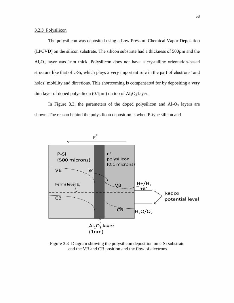
53
3.2.3 Polysilicon
The polysilicon was deposited using a Low Pressure Chemical Vapor Deposition
(LPCVD) on the silicon substrate. The silicon substrate had a thickness of 500µm and the
Al2O3 layer was 1nm thick. Polysilicon does not have a crystalline orientation-based
structure like that of c-Si, which plays a very important role in the part of electrons’ and
holes’ mobility and directions. This shortcoming is compensated for by depositing a very
thin layer of doped polysilicon (0.1µm) on top of Al2O3 layer.
In Figure 3.3, the parameters of the doped polysilicon and Al2O3 layers are
shown. The reason behind the polysilicon deposition is when P-type silicon and
Figure 3.3 Diagram showing the polysilicon deposition on c-Si substrate
and the VB and CB position and the flow of electrons
54
n+-polysilicon (highly doped ~10
20cm
-3) are joined together, there is an electric field (Ē)
created due to the surplus of holes in p-type silicon and electrons in n+-polysilicon;
however, due to the ALD layer of Al2O3 (1nm) in between them, the p-n junction
cannot form. Now, because of the presence of an electric field, the VB and CB bend
downwards in the p-type silicon and upwards in the n+-polysilicon near the ALD layer.
This creates a very suitable path for the electron to move against the electric field
through the polysilicon into the electrolyte. In the same way, the other electrode with the
n-type silicon, Al2O3 layer and p+-polysilicon structure was constructed where the
physics behind the design is similar to that of the p-silicon based electrode explained
above.
The structure of polysilicon is not the same as that of c-Si, which has an
orientation-based planar structure that helps the electrons and holes generated by the
photon energy to move through the structure easily. Polysilicon has a granular structure,
which means that there are random fissures that could act as a recombination site for the
electrons and holes generated. This problem was taken care of by making the polysilicon
layer very thin (0.1µm).
3.3 Tungsten Nanopores (TNP)
After the electrodes were prepared with a multilayer structure, they were finally
ready to be tested. In this step, in order to enhance the electrodes’ surface reaction with
the electrolyte and sunlight, and also to enhance the mobility of electron-hole pairs
generated from photon energy, the surface of the electrodes were nanotextured with TNP.
55
The following sections, 3.3.1 to 3.3.4, discuss tungsten material, its usefulness, the
process of how to grow TNP, and SEM images of the TNP.
3.3.1 Tungsten
Tungsten (W) is the last metal listed in this thesis as a candidate for metal
electrode testing. Most commonly known as tungsten-filament, this metal has the highest
tensile strength among metals in pure form and is very brittle, which makes it difficult to
work with. Due to strong covalent bonds formed between tungsten atoms and its 5d
electrons, tungsten has a low thermal expansion and the highest melting point (3422C,
6192F) among metals in pure form. Therefore, because of its strength at high
temperatures and relative chemical inertia, tungsten is used for electrodes in different
electronic applications, which makes it a suitable transitional metal for electrodes.
3.3.2 Process to grow TNP
Growing the TNP required several steps in a microfabrication facility. The steps
for growing the TNP on the surface of the polysilicon are as follows:
1. Sputtering 20nm of tungsten (W) on the target surface
2. Applying 1813 positive photoresist on the top of the sputtered tungsten surface
3. Spinning the photoresist for 200rpm for 60 seconds.
4. Prebaking the photoresist for 2 minutes in 110C on a hot plate.
5. Exposing it to ultraviolet (UV) light for 30 seconds
6. Developing the photoresist in 352 developer for 45 seconds
7. Post baking for 3 minutes in 120C

56
8. Dipping the photoresist in hydrogen peroxide (H2O2) for 40 seconds
9. Using oxygen plasma to remove the photoresist for 12 minutes
3.3.3 SEM images
The SEM images of the TNP are discussed in this section. Figure 3.4 shows the
top view of the TNP grown on one of the electrode surfaces. In the magnified version of
the image, it can be seen that the nanopores are in the range of 5-10nm in diameter. Next,
Figure 3.5 is a cross section of the photoelectrode with p-type silicon, Al2O3, n+-
polysilicon, and TNP on its surface. Although the purpose and function of the Al2O3 layer
between the silicon and polysilicon were to prevent the p-n+ junction from forming, the
phosphorus dopant seems to penetrate through the Al2O3 layer and move to the n-silicon
layer for about 0.05µm. However, the structure should still serve the purpose of the Al2O3
layer.
3.3.4 Device structure
In this section, Figure 3.6 illustrates reported device structure. The electric field
will be strong between the silicon (p- and n-) and oppositely, plus highly doped (n+- and
p+-) polysilicon, and suitable for the electrons and holes to move according to the
direction of the electric field. To prevent the p-n junction from forming and to reduce the
electric field, a thin layer of Al2O3 was introduced between the silicon and polysilicon
layers. This layer is so thin (1nm) that it does not hamper the electric field from forming
due to the (p- and n-) silicon and oppositely doped (n+- and
p
+-) polysilicon, thus making
it easy for the photogenerated electron-hole pairs to move through the thin Al2O3 layer..

57
Figure 3.4 SEM images of TNP on the surface of n-silicon, Al2O3 and p+-polysilicon
(top), magnified (bottom)
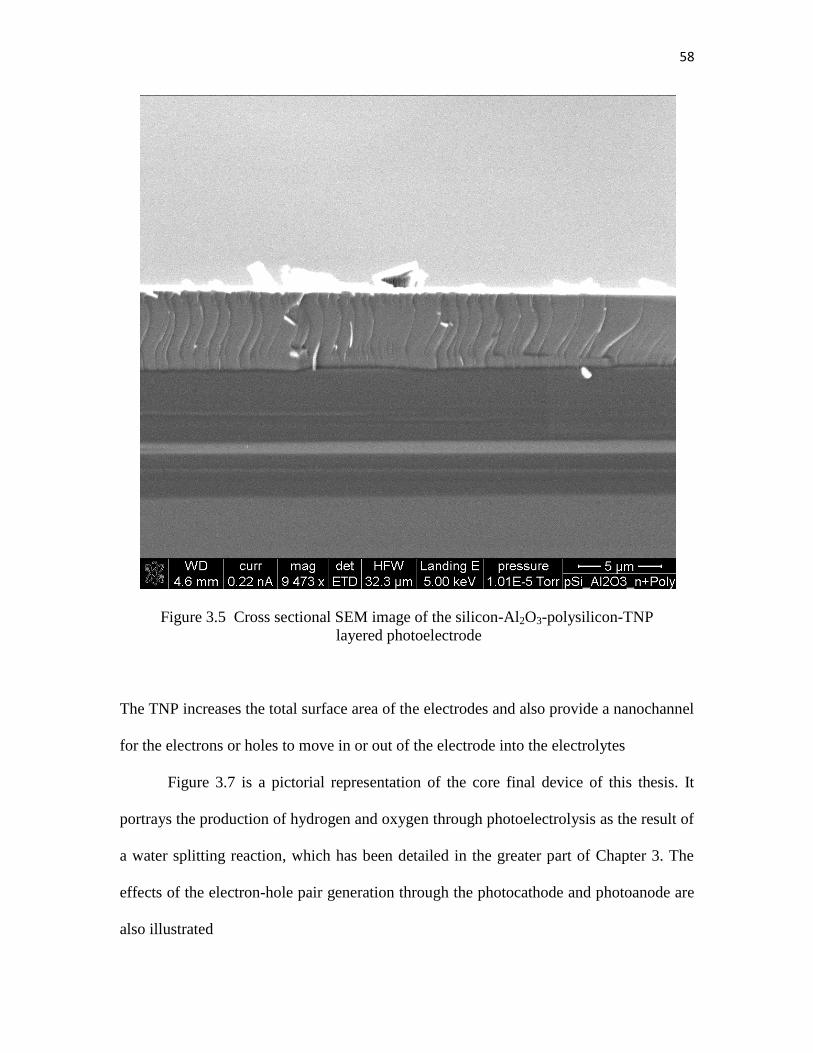
58
Figure 3.5 Cross sectional SEM image of the silicon-Al2O3-polysilicon-TNP
layered photoelectrode
The TNP increases the total surface area of the electrodes and also provide a nanochannel
for the electrons or holes to move in or out of the electrode into the electrolytes
Figure 3.7 is a pictorial representation of the core final device of this thesis. It
portrays the production of hydrogen and oxygen through photoelectrolysis as the result of
a water splitting reaction, which has been detailed in the greater part of Chapter 3. The
effects of the electron-hole pair generation through the photocathode and photoanode are
also illustrated

59
Fig
ure
3.6
T
he
dev
ice
stru
cture
of
the
two p
hoto
elec
trodes
wit
h p
- /
n-
sili
con,
the
Al 2
O3 l
ayer
, n
+-
/ p
+-
poly
sili
con, an
d T
NP
on t
he
surf
ace
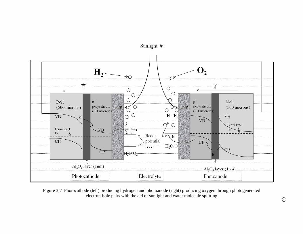
Figure 3.7 Photocathode (left) producing hydrogen and photoanode (right) producing oxygen through photogenerated
electron-hole pairs with the aid of sunlight and water molecule splitting 60
(
P-Si (500 microns)
VB
Fenni level EF \ ------~---
CB
AlP31ayer (lnm)
Photocathode
Sunlight hv
N-Si (500 microns)
VB
Electrolyte Photoanode
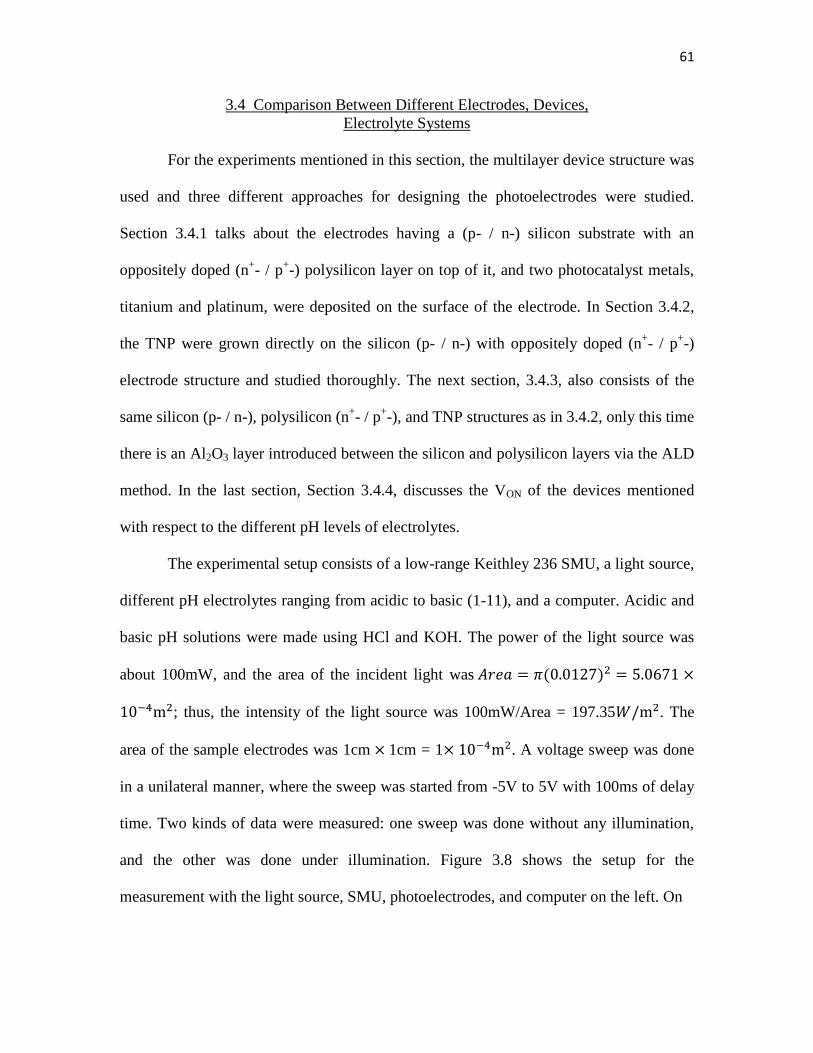
61
3.4 Comparison Between Different Electrodes, Devices,
Electrolyte Systems
For the experiments mentioned in this section, the multilayer device structure was
used and three different approaches for designing the photoelectrodes were studied.
Section 3.4.1 talks about the electrodes having a (p- / n-) silicon substrate with an
oppositely doped (n+- / p
+-) polysilicon layer on top of it, and two photocatalyst metals,
titanium and platinum, were deposited on the surface of the electrode. In Section 3.4.2,
the TNP were grown directly on the silicon (p- / n-) with oppositely doped (n+- / p
+-)
electrode structure and studied thoroughly. The next section, 3.4.3, also consists of the
same silicon (p- / n-), polysilicon (n+- / p
+-), and TNP structures as in 3.4.2, only this time
there is an Al2O3 layer introduced between the silicon and polysilicon layers via the ALD
method. In the last section, Section 3.4.4, discusses the VON of the devices mentioned
with respect to the different pH levels of electrolytes.
The experimental setup consists of a low-range Keithley 236 SMU, a light source,
different pH electrolytes ranging from acidic to basic (1-11), and a computer. Acidic and
basic pH solutions were made using HCl and KOH. The power of the light source was
about 100mW, and the area of the incident light was
; thus, the intensity of the light source was 100mW/Area = 197.35 . The
area of the sample electrodes was 1cm 1cm = 1 . A voltage sweep was done
in a unilateral manner, where the sweep was started from -5V to 5V with 100ms of delay
time. Two kinds of data were measured: one sweep was done without any illumination,
and the other was done under illumination. Figure 3.8 shows the setup for the
measurement with the light source, SMU, photoelectrodes, and computer on the left. On
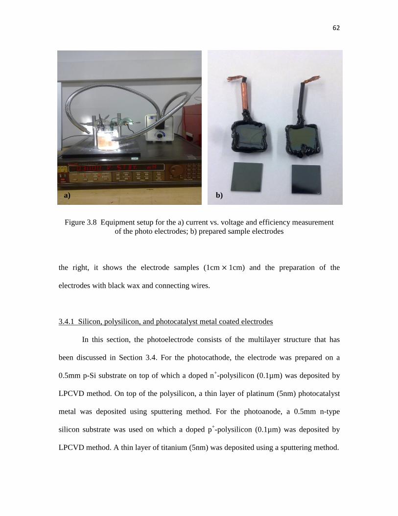
62
Figure 3.8 Equipment setup for the a) current vs. voltage and efficiency measurement
of the photo electrodes; b) prepared sample electrodes
the right, it shows the electrode samples (1cm 1cm) and the preparation of the
electrodes with black wax and connecting wires.
3.4.1 Silicon, polysilicon, and photocatalyst metal coated electrodes
In this section, the photoelectrode consists of the multilayer structure that has
been discussed in Section 3.4. For the photocathode, the electrode was prepared on a
0.5mm p-Si substrate on top of which a doped n+-polysilicon (0.1µm) was deposited by
LPCVD method. On top of the polysilicon, a thin layer of platinum (5nm) photocatalyst
metal was deposited using sputtering method. For the photoanode, a 0.5mm n-type
silicon substrate was used on which a doped p+-polysilicon (0.1µm) was deposited by
LPCVD method. A thin layer of titanium (5nm) was deposited using a sputtering method.
a) b)
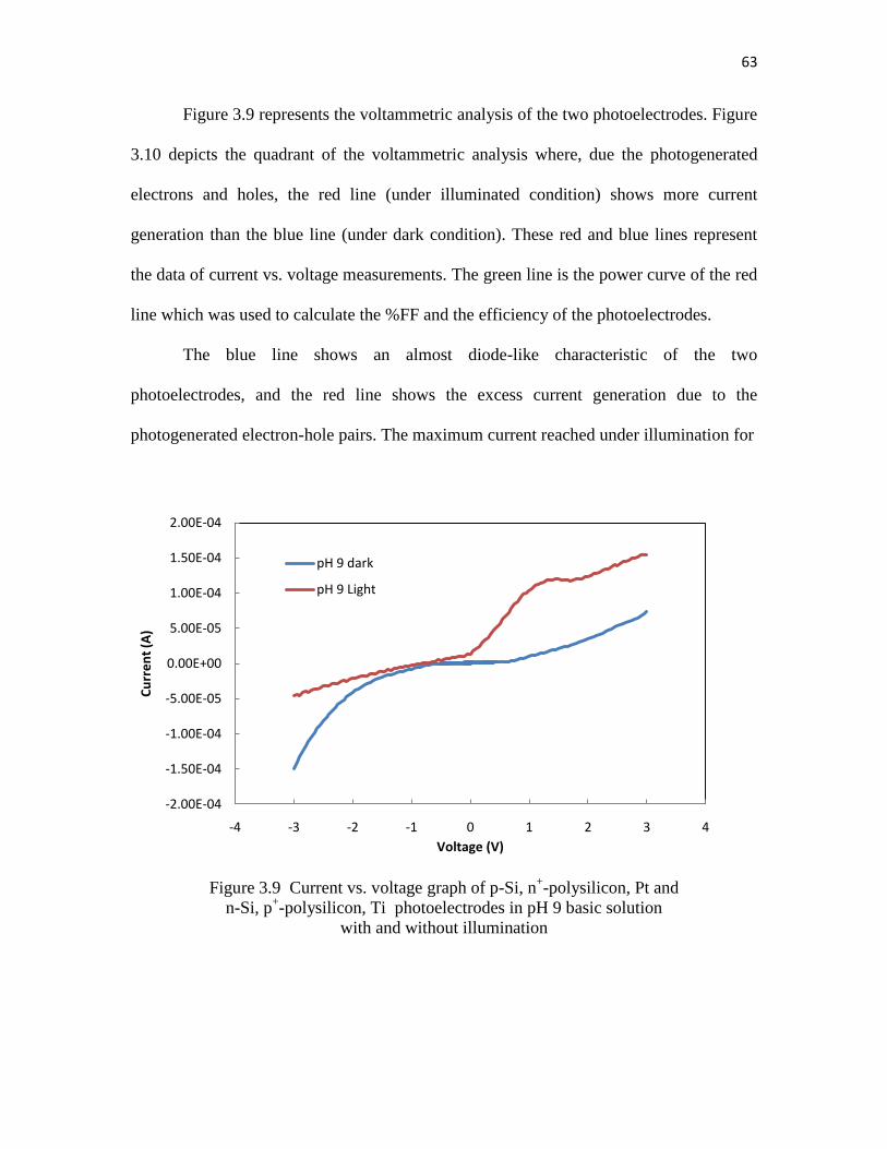
63
Figure 3.9 represents the voltammetric analysis of the two photoelectrodes. Figure
3.10 depicts the quadrant of the voltammetric analysis where, due the photogenerated
electrons and holes, the red line (under illuminated condition) shows more current
generation than the blue line (under dark condition). These red and blue lines represent
the data of current vs. voltage measurements. The green line is the power curve of the red
line which was used to calculate the %FF and the efficiency of the photoelectrodes.
The blue line shows an almost diode-like characteristic of the two
photoelectrodes, and the red line shows the excess current generation due to the
photogenerated electron-hole pairs. The maximum current reached under illumination for
Figure 3.9 Current vs. voltage graph of p-Si, n+-polysilicon, Pt and
n-Si, p+-polysilicon, Ti photoelectrodes in pH 9 basic solution
with and without illumination
-2.00E-04
-1.50E-04
-1.00E-04
-5.00E-05
0.00E+00
5.00E-05
1.00E-04
1.50E-04
2.00E-04
-4 -3 -2 -1 0 1 2 3 4
Cu
rre
nt
(A)
Voltage (V)
pH 9 dark
pH 9 Light
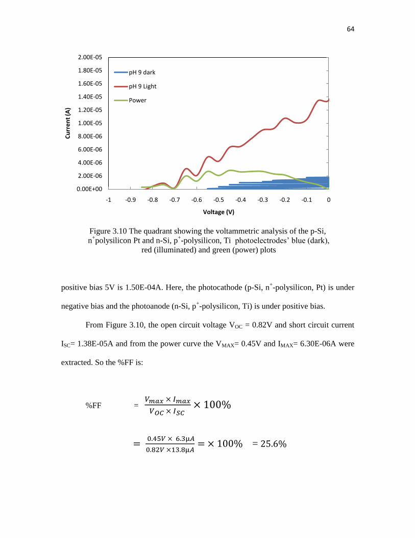
64
Figure 3.10 The quadrant showing the voltammetric analysis of the p-Si,
n+polysilicon Pt and n-Si, p
+-polysilicon, Ti photoelectrodes’ blue (dark),
red (illuminated) and green (power) plots
positive bias 5V is 1.50E-04A. Here, the photocathode (p-Si, n+-polysilicon, Pt) is under
negative bias and the photoanode (n-Si, p+-polysilicon, Ti) is under positive bias.
From Figure 3.10, the open circuit voltage VOC = 0.82V and short circuit current
ISC= 1.38E-05A and from the power curve the VMAX= 0.45V and IMAX= 6.30E-06A were
extracted. So the %FF is:
%FF =
=
0.00E+00
2.00E-06
4.00E-06
6.00E-06
8.00E-06
1.00E-05
1.20E-05
1.40E-05
1.60E-05
1.80E-05
2.00E-05
-1 -0.9 -0.8 -0.7 -0.6 -0.5 -0.4 -0.3 -0.2 -0.1 0
Cu
rre
nt
(A)
Voltage (V)
pH 9 dark
pH 9 Light
Power
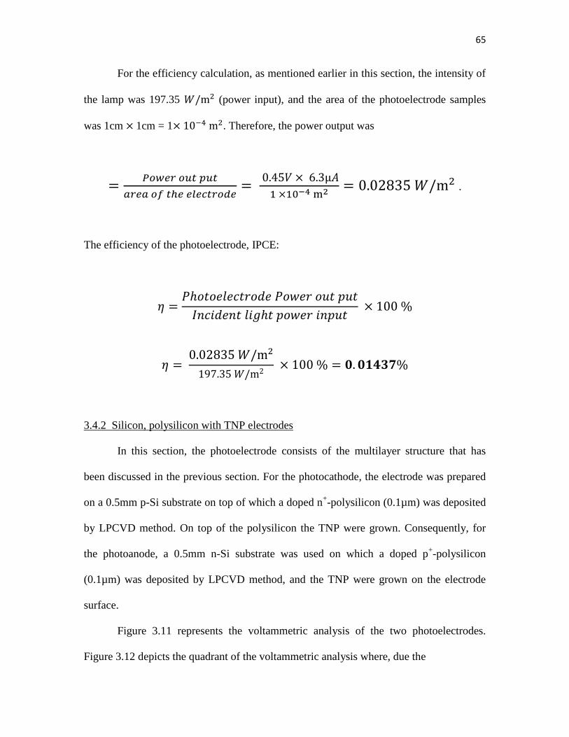
65
For the efficiency calculation, as mentioned earlier in this section, the intensity of
the lamp was 197.35 (power input), and the area of the photoelectrode samples
was 1cm 1cm = 1 . Therefore, the power output was
.
The efficiency of the photoelectrode, IPCE:
3.4.2 Silicon, polysilicon with TNP electrodes
In this section, the photoelectrode consists of the multilayer structure that has
been discussed in the previous section. For the photocathode, the electrode was prepared
on a 0.5mm p-Si substrate on top of which a doped n+-polysilicon (0.1µm) was deposited
by LPCVD method. On top of the polysilicon the TNP were grown. Consequently, for
the photoanode, a 0.5mm n-Si substrate was used on which a doped p+-polysilicon
(0.1µm) was deposited by LPCVD method, and the TNP were grown on the electrode
surface.
Figure 3.11 represents the voltammetric analysis of the two photoelectrodes.
Figure 3.12 depicts the quadrant of the voltammetric analysis where, due the
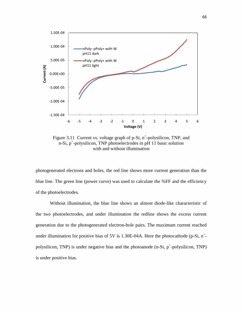
66
Figure 3.11 Current vs. voltage graph of p-Si, n+-polysilicon, TNP, and
n-Si, p+-polysilicon, TNP photoelectrodes in pH 11 basic solution
with and without illumination
photogenerated electrons and holes, the red line shows more current generation than the
blue line. The green line (power curve) was used to calculate the %FF and the efficiency
of the photoelectrodes.
Without illumination, the blue line shows an almost diode-like characteristic of
the two photoelectrodes, and under illumination the redline shows the excess current
generation due to the photogenerated electron-hole pairs. The maximum current reached
under illumination for positive bias of 5V is 1.30E-04A. Here the photocathode (p-Si, n+-
polysilicon, TNP) is under negative bias and the photoanode (n-Si, p+-polysilicon, TNP)
is under positive bias.
-1.50E-04
-1.00E-04
-5.00E-05
0.00E+00
5.00E-05
1.00E-04
1.50E-04
-6 -5 -4 -3 -2 -1 0 1 2 3 4 5 6
Cu
rre
nt
(A)
Voltage (V)
nPoly- pPoly+ with W pH11 dark
nPoly- pPoly+ with W pH11 light
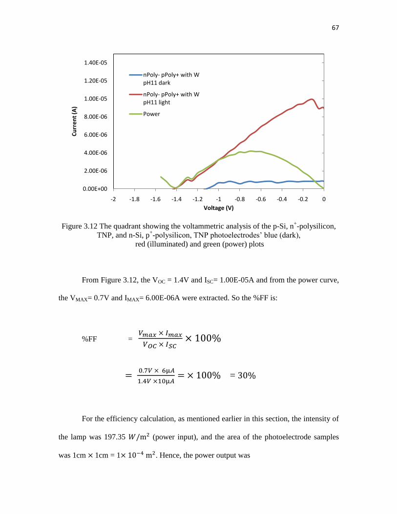
67
Figure 3.12 The quadrant showing the voltammetric analysis of the p-Si, n+-polysilicon,
TNP, and n-Si, p+-polysilicon, TNP photoelectrodes’ blue (dark),
red (illuminated) and green (power) plots
From Figure 3.12, the VOC = 1.4V and ISC= 1.00E-05A and from the power curve,
the VMAX= 0.7V and IMAX= 6.00E-06A were extracted. So the %FF is:
%FF =
=
For the efficiency calculation, as mentioned earlier in this section, the intensity of
the lamp was 197.35 (power input), and the area of the photoelectrode samples
was 1cm 1cm = 1 . Hence, the power output was
0.00E+00
2.00E-06
4.00E-06
6.00E-06
8.00E-06
1.00E-05
1.20E-05
1.40E-05
-2 -1.8 -1.6 -1.4 -1.2 -1 -0.8 -0.6 -0.4 -0.2 0
Cu
rre
nt
(A)
Voltage (V)
nPoly- pPoly+ with W pH11 dark
nPoly- pPoly+ with W pH11 light
Power

68
.
The efficiency of the photoelectrode, IPCE:
3.4.3 Silicon, polysilicon with TNP and Al2O3 layer electrodes
In this section, the photoelectrode consists of the multilayer structures discussed
in previous sections. For the photocathode, the electrode was prepared on a 0.5mm p-Si
substrate on top of which a doped n+-polysilicon (0.1µm) was deposited by LPCVD
method. On top of the polysilicon, the TNP were grown. Consequently, for the
photoanode, a 0.5mm n-Si substrate was used on which a doped p+-polysilicon (0.1µm)
was deposited by LPCVD method, and the TNP were grown on the electrode surface.. An
Al2O3 (1nm) layer was introduced between the Silicon and polysilicon layer to prevent
the leakage current from passing through and to prevent the p-n junction from forming
and thus reducing the electric field.
Figure 3.13 represents the voltammetric analysis of the two photoelectrodes.
Figure 3.14 depicts the quadrant of the voltammetric analysis where, due the
photogenerated electrons and holes, the red line shows more current generation than the

69
Figure 3.13 Current vs. voltage graph of p-Si, Al2O3, n+-polysilicon, TNP, and
n-Si, Al2O3, p+-polysilicon, TNP photoelectrodes in pH 11 basic solution
with and without illumination
blue line. The green line (power curve) was used to calculate the %FF and the efficiency
of the photoelectrodes.
Without illumination, the blue line shows an almost diode-like characteristic of
the two photoelectrodes, and under illumination the red line shows the excess current
generation due to the photogenerated electron-hole pairs. The maximum current reached
under illumination for positive bias of 5V is 2.00E-04A. Here the photocathode (p-Si,
Al2O3, n+-polysilicon, TNP) is under negative bias and the photoanode (n-Si, Al2O3, p
+-
polysilicon, TNP) is under positive bias.
-1.50E-04
-1.00E-04
-5.00E-05
0.00E+00
5.00E-05
1.00E-04
1.50E-04
2.00E-04
2.50E-04
-6 -5 -4 -3 -2 -1 0 1 2 3 4 5 6
Cu
rre
nt
(A)
Voltage (V)
(Al2O3)nPoly- pPoly+ with W pH11 dark
(Al2O3))nPoly- pPoly+ with W pH11 light

70
Figure 3.14 The quadrant showing the voltammetric analysis of the p-Si, Al2O3, n+-
polysilicon, TNP, and n-Si, Al2O3, p+-polysilicon, TNP photoelectrodes’
blue (dark), red (illuminated) and green (power) plots
From Figure 3.14, the VOC = 1.8V and ISC= 1.30E-05A and from the power curve
the VMAX= 0.7V and IMAX= 8.95E-06A were extracted. So the %FF is:
%FF =
=
0.00E+00
2.00E-06
4.00E-06
6.00E-06
8.00E-06
1.00E-05
1.20E-05
1.40E-05
1.60E-05
1.80E-05
2.00E-05
-2 -1.8 -1.6 -1.4 -1.2 -1 -0.8 -0.6 -0.4 -0.2 0
Cu
rre
nt
(A)
Voltage (V)
(Al2O3)nPoly- pPoly+ with W pH11 dark
(Al2O3))nPoly- pPoly+ with W pH11 light
power
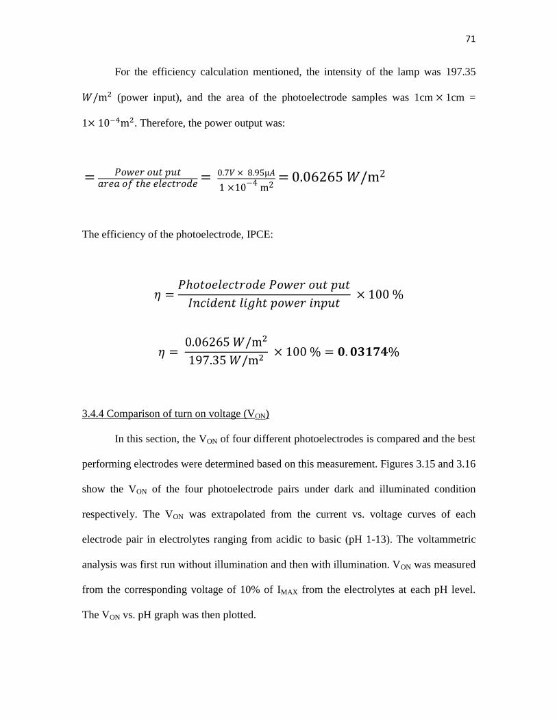
71
For the efficiency calculation mentioned, the intensity of the lamp was 197.35
(power input), and the area of the photoelectrode samples was 1cm 1cm =
1 . Therefore, the power output was:
The efficiency of the photoelectrode, IPCE:
3.4.4 Comparison of turn on voltage (VON)
In this section, the VON of four different photoelectrodes is compared and the best
performing electrodes were determined based on this measurement. Figures 3.15 and 3.16
show the VON of the four photoelectrode pairs under dark and illuminated condition
respectively. The VON was extrapolated from the current vs. voltage curves of each
electrode pair in electrolytes ranging from acidic to basic (pH 1-13). The voltammetric
analysis was first run without illumination and then with illumination. VON was measured
from the corresponding voltage of 10% of IMAX from the electrolytes at each pH level.
The VON vs. pH graph was then plotted.
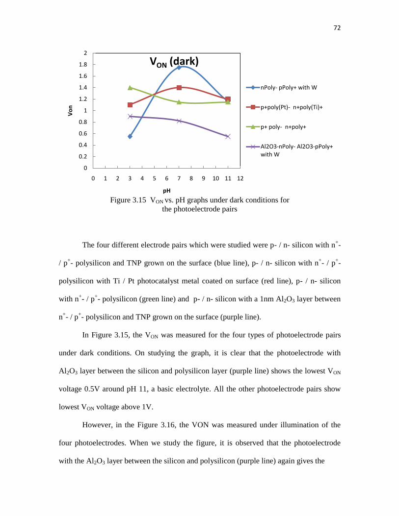
72
Figure 3.15 VON vs. pH graphs under dark conditions for
the photoelectrode pairs
The four different electrode pairs which were studied were p- / n- silicon with n+-
/ p+- polysilicon and TNP grown on the surface (blue line), p- / n- silicon with n
+- / p
+-
polysilicon with Ti / Pt photocatalyst metal coated on surface (red line), p- / n- silicon
with n+- / p
+- polysilicon (green line) and p- / n- silicon with a 1nm Al2O3 layer between
n+- / p
+- polysilicon and TNP grown on the surface (purple line).
In Figure 3.15, the VON was measured for the four types of photoelectrode pairs
under dark conditions. On studying the graph, it is clear that the photoelectrode with
Al2O3 layer between the silicon and polysilicon layer (purple line) shows the lowest VON
voltage 0.5V around pH 11, a basic electrolyte. All the other photoelectrode pairs show
lowest VON voltage above 1V.
However, in the Figure 3.16, the VON was measured under illumination of the
four photoelectrodes. When we study the figure, it is observed that the photoelectrode
with the Al2O3 layer between the silicon and polysilicon (purple line) again gives the
0
0.2
0.4
0.6
0.8
1
1.2
1.4
1.6
1.8
2
0 1 2 3 4 5 6 7 8 9 10 11 12
Vo
n
pH
VON (dark)
nPoly- pPoly+ with W
p+poly(Pt)- n+poly(Ti)+
p+ poly- n+poly+
Al2O3-nPoly- Al2O3-pPoly+ with W
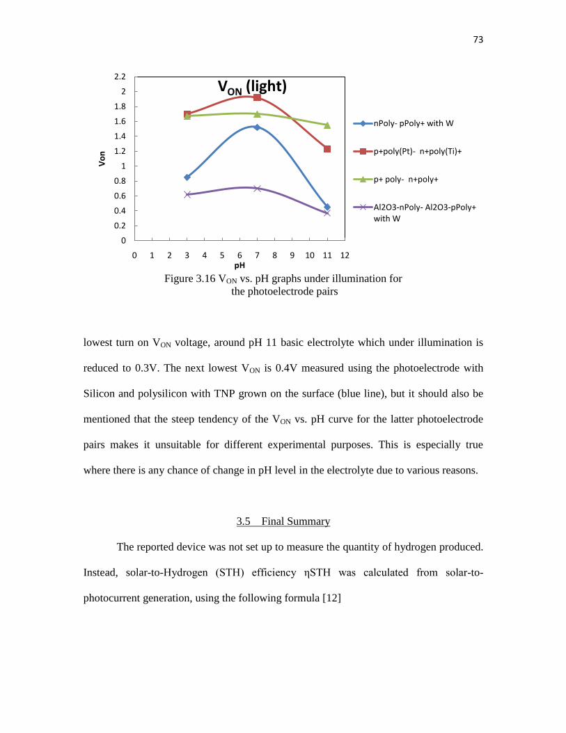
73
Figure 3.16 VON vs. pH graphs under illumination for
the photoelectrode pairs
lowest turn on VON voltage, around pH 11 basic electrolyte which under illumination is
reduced to 0.3V. The next lowest VON is 0.4V measured using the photoelectrode with
Silicon and polysilicon with TNP grown on the surface (blue line), but it should also be
mentioned that the steep tendency of the VON vs. pH curve for the latter photoelectrode
pairs makes it unsuitable for different experimental purposes. This is especially true
where there is any chance of change in pH level in the electrolyte due to various reasons.
3.5 Final Summary
The reported device was not set up to measure the quantity of hydrogen produced.
Instead, solar-to-Hydrogen (STH) efficiency ηSTH was calculated from solar-to-
photocurrent generation, using the following formula [12]
0
0.2
0.4
0.6
0.8
1
1.2
1.4
1.6
1.8
2
2.2
0 1 2 3 4 5 6 7 8 9 10 11 12
Vo
n
pH
VON (light)
nPoly- pPoly+ with W
p+poly(Pt)- n+poly(Ti)+
p+ poly- n+poly+
Al2O3-nPoly- Al2O3-pPoly+ with W

74
η
where Iph is the photocurrent density (A/m2), Vext is the external potential applied and IO
is the light intensity (W/m2). The STH efficiency measurement for our device was
performed under no external bias condition Vext = 0V. Table 3.1 summarizes the data
gathered from all three reported photoelectrode pairs from this thesis. A total of three
photoelectrode (PE) pairs had been studied: Silicon, Polysilicon and Photocatalyst Metal
Coated Electrodes (PE -1), Silicon, Polysilicon with TNP Electrodes (PE -2) and Silicon,
Polysilicon with TNP and Al2O3 Layer Electrodes (PE -3).
3.6 Conclusion
This chapter discusses the advantages of multilayer structures for photoelectrodes
and also describes different examples. The multilayer structure that has been used to
construct the devices in this thesis, were explained in detail. Furthermore, to understand
the design and to observe its performance, three kinds of photoelectrode structures were
studied for %FF and efficiency. From the study and calculation, the reported device with
a thin layer of Al2O3 between the silicon and polysilicon with the TNP on the surface
showed the maximum efficiency (0.03174%) among the three photoelectrodes. Also, to
further justify the finding, the VON of four different photoelectrodes including the
reported device, were studied. It was concluded that the device with the Al2O3 layer
between silicon and polysilicon gives the lowest VON, which indicates that the reported
device is superior to the other tested devices.

75
Table 3.1 Summary of %FF, IPCE (η), ηSTH and lowest VON for all
three kinds of photoelectrode pairs
Devices pH %FF IPCE, η ηSTH Lowest VON
PE - 1
Acidic - 1 40 % 0.02 % 0.065
%
1.1 (pH11) Neutral - 7 31 % 0.0118% 0.036 %
Alkaline - 9 25.6 % 0.0144% 0.04 %
PE - 2
Acidic - 3 25 % 0.01 % 0.033 %
0.5 (pH 11) Neutral - 7 33 % 0.014 % 0.031 %
Alkaline - 9 30 % 0.0213 % 0.04 %
PE - 3
Acidic - 3 33 % 0.023 % 0.042 %
0.4 (pH 11) Neutral - 7 22 % 0.01 % 0.034 %
Alkaline - 9 27.22% 0.03174 % 0.084 %

CHAPTER 4
CONCLUSION
A novel photoelectrode has been reported in this thesis to perform
photoelectrolysis with multilayer semiconductor devices having nanotextured surface.
Different photocatalyst metals were studied to find a metal layer suitable for the
photoelectrode device. Although the platinum and tungsten were found to be the most
photoactive metals, this thesis reported a TNP surface for the device built. The multilayer
semiconductor structure used in this thesis with p- / n- silicon substrate with n+- / p
+-
polysilicon layer on top of it was the base design for three different photoelectrode
devices that were studied. Among the three, the device made of silicon and polysilicon
layer with an Al2O3 layer in between (to prevent the forming of a p-n junction, thus
reducing the leakage current) and the TNP on the surface reported the highest photo
conversion efficiency (0.032%).
Voltammetric analysis was done to determine the current vs. voltage analysis of
the different metal and semiconductor electrode experiments. The semiconductor
electrode experiments for photoelectrode selection established the p- and n-type silicon as
the best choice for photo conversion of solar-to-electrical energy.

77
4.1 Future Work
Despite the magnitude of technological progress in today’s global economy, the
concept of relying on nanotechnology to provide a feasible and sustainable solution to the
energy crisis is ambitious but gaining momentum. The field is young and much research
is yet to be undertaken in order to develop innovations to address modern society’s high
demands for fossil-fuel based energy. A hydrogen economy is envisioned to be a solution
to all problems, so it is imperative to come up with a renewable energy source based on
hydrogen. Electrolysis of water to produce hydrogen accounts for 4% of hydrogen
production worldwide. Photoelectrolysis, as described in this thesis, is one of the cleanest
and most renewable forms of electrolysis which yields hydrogen. There are many
obstacles that are yet to be overcome before studies can be furthered and major advances
can be made to meet industrial and domestic consumption needs. The outcomes of
research in the field of photoelectrolysis to produce hydrogen attest a very important
transition in the area of energy resource for the next generation civilization, the hydrogen
economy.
The photoelectrode reported in this thesis has multilayer semiconductor structure
and a new concept ALD of a thin layer of insulator (Al2O3) between the silicon and
oppositely doped polysilicon. This insulating layer prevents the formation of p-n junction
between the two layers; also, due to its very thin deposition (1nm) it does not hamper the
electric field formed between the silicon and polysilicon. This ALD step can be used with
different types of material to reduce the leakage current effect in multilayer structured
photoelectrodes or PV cells.

78
Tungsten was used to form nanopores on the surface of the electrodes to enhance
the surface area and form nanochannels to improve mobility of electron-hole pairs in and
out of the electrolyte. This approach is still under extensive research. There is more
material to be studied to understand the nanopores’ implementation on the surface of
photoelectrodes.
APPENDIX
ADDITIONAL DATA PERTAINING TO CHAPTER 2
The metallic electrodes used in this chapter for the voltammetric analysis were
gold, platinum, palladium, titanium and tungsten. Each of the metals was combined with
another for the test. So, the combinations made were gold-gold, gold-platinum, gold-
palladium, gold-titanium, gold-tungsten, platinum-titanium, platinum-palladium,
platinum-tungsten, palladium-tungsten, and titanium-tungsten. The first two
combinations were discussed in Chapter 2. During the current vs. voltage measurement,
two kinds of setups were used. For example, in the gold-platinum setup, first the gold was
used as a cathode and the platinum as an anode. In the second step, gold was used as the
anode and platinum as the cathode.
The metallic electrode combinations were tested in acidic and basic electrolytes,
with pH level ranging from 1-11. For each of the combinations a VON vs. pH plot was
generated where the data was extrapolated from the current vs. voltage graphs. In this
appendix, the graphs for the rest of the metal electrode pair, gold-palladium, gold-
titanium, gold-tungsten, platinum-titanium, platinum-palladium, platinum-tungsten,
palladium-tungsten, and titanium-tungsten are shown in Figures A.1 to A.23.
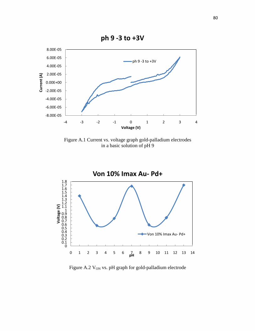
80
Figure A.1 Current vs. voltage graph gold-palladium electrodes
in a basic solution of pH 9
Figure A.2 VON vs. pH graph for gold-palladium electrode
-8.00E-05
-6.00E-05
-4.00E-05
-2.00E-05
0.00E+00
2.00E-05
4.00E-05
6.00E-05
8.00E-05
-4 -3 -2 -1 0 1 2 3 4
Cu
rre
nt
(A)
Voltage (V)
ph 9 -3 to +3V
ph 9 -3 to +3V
00.10.20.30.40.50.60.70.80.9
11.11.21.31.41.51.61.71.8
0 1 2 3 4 5 6 7 8 9 10 11 12 13 14
Vo
ltag
e (
V)
pH
Von 10% Imax Au- Pd+
Von 10% Imax Au- Pd+

81
Figure A.3 VON vs. pH graph for palladium-gold electrode
Figure A.4 Current vs. voltage graph gold-titanium electrodes
in a basic solution of pH 3
00.10.20.30.40.50.60.70.80.9
11.11.21.31.41.51.61.71.8
0 1 2 3 4 5 6 7 8 9 10 11 12 13 14
Vo
ltag
e (
V)
pH
Von 10% Imax Pd- Au+
Von 10% Imax Pd- Au+
-3.E-05
-2.E-05
-1.E-05
0.E+00
1.E-05
2.E-05
3.E-05
-4 -3 -2 -1 0 1 2 3 4
Cu
rre
nt
(A)
Voltage (V)
pH 3 -3V to +3V
pH 3 -3V to +3V

82
Figure A.5 VON vs. pH graph for titanium-gold electrode
Figure A.6 Current vs. voltage graph gold-tungsten electrodes
in a basic solution of pH 11
00.10.20.30.40.50.60.70.80.9
11.11.21.31.41.51.61.71.81.9
22.1
0 1 2 3 4 5 6 7 8 9 10 11 12 13 14
Vo
ltag
e (
V)
pH
Von 10% Imax Ti- Au+
Von 10% Imax Ti- Au+
-4.00E-04
-2.00E-04
0.00E+00
2.00E-04
4.00E-04
6.00E-04
8.00E-04
-4 -3 -2 -1 0 1 2 3 4
Cu
rre
nt
(A)
Voltage (V)
ph 11 -3 to +3V
ph 11 -3 to +3V

83
Figure A.7 VON vs. pH graph for gold-tungsten electrode
Figure A.8 VON vs. pH graph for tungsten-gold electrode
0
0.1
0.2
0.3
0.4
0.5
0.6
0.7
0.8
0.9
0 1 2 3 4 5 6 7 8 9 10 11 12 13 14
Vo
ltag
e (
V)
pH
Von 10% Imax Au- W+
Von 10% Imax Au- W+
0
0.2
0.4
0.6
0.8
1
1.2
1.4
1.6
1.8
2
0 1 2 3 4 5 6 7 8 9 10 11 12 13 14
Vo
ltag
e (
V)
pH
Von 10% Imax W- Au+
Von 10% Imax W- Au+
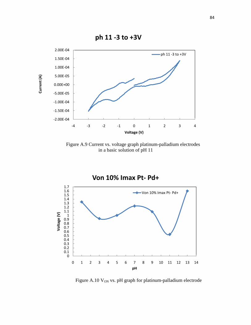
84
Figure A.9 Current vs. voltage graph platinum-palladium electrodes
in a basic solution of pH 11
Figure A.10 VON vs. pH graph for platinum-palladium electrode
-2.00E-04
-1.50E-04
-1.00E-04
-5.00E-05
0.00E+00
5.00E-05
1.00E-04
1.50E-04
2.00E-04
-4 -3 -2 -1 0 1 2 3 4
Cu
rre
nt
(A)
Voltage (V)
ph 11 -3 to +3V
ph 11 -3 to +3V
00.10.20.30.40.50.60.70.80.9
11.11.21.31.41.51.61.7
0 1 2 3 4 5 6 7 8 9 10 11 12 13 14
Vo
ltag
e (
V)
pH
Von 10% Imax Pt- Pd+
Von 10% Imax Pt- Pd+

85
Figure A.11 VON vs. pH graph for palladium-platinum electrode
Figure A.12 Current vs. voltage graph platinum-tungsten electrodes
in a basic solution of pH 3
00.10.20.30.40.50.60.70.80.9
11.11.21.31.41.51.61.7
0 1 2 3 4 5 6 7 8 9 10 11 12 13 14
Vo
ltag
e (
V)
pH
Von 10% Imax Pd- Pt+
Von 10% Imax Pd- Pt+
-1.00E-04
-8.00E-05
-6.00E-05
-4.00E-05
-2.00E-05
0.00E+00
2.00E-05
4.00E-05
6.00E-05
8.00E-05
1.00E-04
-4 -3 -2 -1 0 1 2 3 4
Cu
rre
nt
(A)
Voltage (V)
pH 3 -3V to +3V
pH 3 -3V to +3V
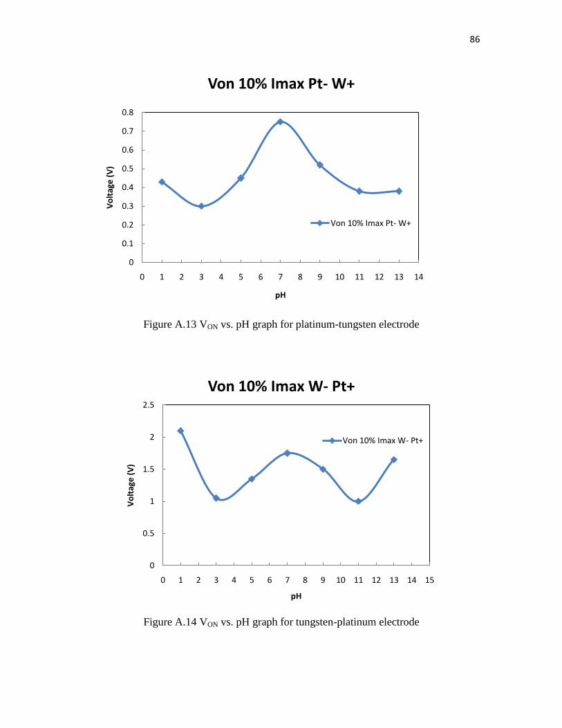
86
Figure A.13 VON vs. pH graph for platinum-tungsten electrode
Figure A.14 VON vs. pH graph for tungsten-platinum electrode
0
0.1
0.2
0.3
0.4
0.5
0.6
0.7
0.8
0 1 2 3 4 5 6 7 8 9 10 11 12 13 14
Vo
ltag
e (
V)
pH
Von 10% Imax Pt- W+
Von 10% Imax Pt- W+
0
0.5
1
1.5
2
2.5
0 1 2 3 4 5 6 7 8 9 10 11 12 13 14 15
Vo
ltag
e (
V)
pH
Von 10% Imax W- Pt+
Von 10% Imax W- Pt+

87
Figure A.15 Current vs. voltage graph platinum-titanium electrodes
in a basic solution of pH 11
Figure A.16 VON vs. pH graph for platinum-titanium electrode
-8.00E-05
-6.00E-05
-4.00E-05
-2.00E-05
0.00E+00
2.00E-05
4.00E-05
6.00E-05
8.00E-05
-4 -3 -2 -1 0 1 2 3 4
Cu
rre
nt
(A)
Voltage
ph 11 -3 to +3V
ph 11 -3 to +3V
00.10.20.30.40.50.60.70.80.9
11.11.21.31.41.51.6
0 1 2 3 4 5 6 7 8 9 10 11 12 13 14
Vo
ltag
e (
V)
pH
Von 10% Imax Pt- Ti+
Von 10% Imax Pt- Ti+

88
Figure A.17 VON vs. pH graph for titanium-platinum electrode
Figure A.18 Current vs. voltage graph palladium-tungsten electrodes
in a basic solution of pH 3
0
0.2
0.4
0.6
0.8
1
1.2
1.4
1.6
0 1 2 3 4 5 6 7 8 9 10 11 12 13 14
Vo
ltag
e (
V)
pH
Von 10% Imax Ti- Pt+
Von 10% Imax Ti- Pt+
-1.50E-04
-1.00E-04
-5.00E-05
0.00E+00
5.00E-05
1.00E-04
1.50E-04
2.00E-04
-4 -3 -2 -1 0 1 2 3 4
Cu
rre
nt
(A)
Voltage (V)
pH 3 -3V to +3V
pH 3 -3V to +3V
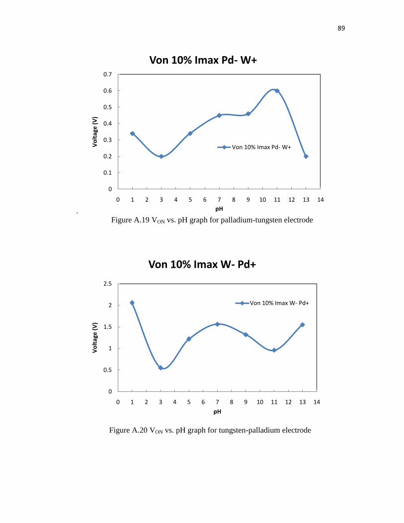
89
.
Figure A.19 VON vs. pH graph for palladium-tungsten electrode
Figure A.20 VON vs. pH graph for tungsten-palladium electrode
0
0.1
0.2
0.3
0.4
0.5
0.6
0.7
0 1 2 3 4 5 6 7 8 9 10 11 12 13 14
Vo
ltag
e (
V)
pH
Von 10% Imax Pd- W+
Von 10% Imax Pd- W+
0
0.5
1
1.5
2
2.5
0 1 2 3 4 5 6 7 8 9 10 11 12 13 14
Vo
ltag
e (
V)
pH
Von 10% Imax W- Pd+
Von 10% Imax W- Pd+
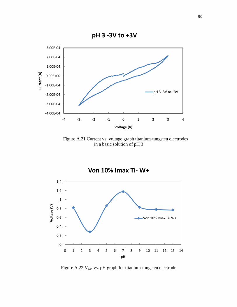
90
Figure A.21 Current vs. voltage graph titanium-tungsten electrodes
in a basic solution of pH 3
Figure A.22 VON vs. pH graph for titanium-tungsten electrode
-4.00E-04
-3.00E-04
-2.00E-04
-1.00E-04
0.00E+00
1.00E-04
2.00E-04
3.00E-04
-4 -3 -2 -1 0 1 2 3 4
Cu
rre
nt
(A)
Voltage (V)
pH 3 -3V to +3V
pH 3 -3V to +3V
0
0.2
0.4
0.6
0.8
1
1.2
1.4
0 1 2 3 4 5 6 7 8 9 10 11 12 13 14
Vo
ltag
e (
V)
pH
Von 10% Imax Ti- W+
Von 10% Imax Ti- W+
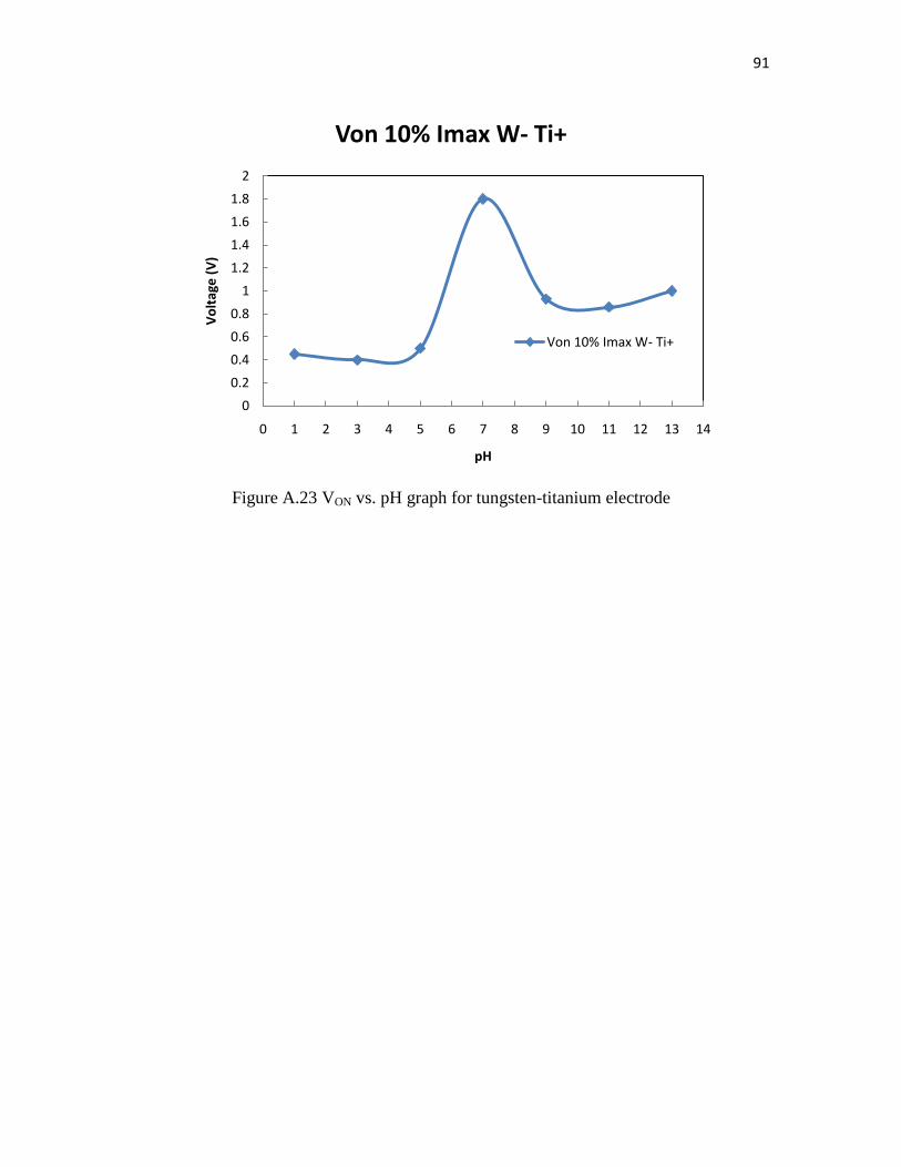
91
Figure A.23 VON vs. pH graph for tungsten-titanium electrode
0
0.2
0.4
0.6
0.8
1
1.2
1.4
1.6
1.8
2
0 1 2 3 4 5 6 7 8 9 10 11 12 13 14
Vo
ltag
e (
V)
pH
Von 10% Imax W- Ti+
Von 10% Imax W- Ti+

REFERENCES
1. Craig A. Grimes, Oomman K. Varghese, Sudhir Ranjan. Light, Water, Hydrogen
– The Solar Generation of Hydrogen by Water Photoelectrolysis– A. Grims, 2007
2. Henry Cavendish, (1766). "Three Papers Containing Experiments on Factitious
Air, by the Hon. Henry Cavendish.” Philosophical Transactions (The University
Press) 56: 141 – 184. doi:10.1098/rstl.1766.0019. Retrieved 6 November 2007.
3. "Hydrogen." Chemicool Periodic Table. Chemicool.com. 24 Feb. 2011. Web.
4/10/2011 <http://www.chemicool.com/elements/hydrogen.html>
4. http://www.rsc.org/chemistryworld/Issues/2003/August/electrolysis.asp Enterpris
e and electrolysis... Chemistry World,2003, Royal Society of Chemistry
5. Wikipedia. Retrieved 2011January. http://en.wikipedia.org/wiki/Fuel_cell#
History
6. William Robert Grove, "On a Gaseous Voltaic Battery." Philosophical Magazine
and Journal of Science vol. XXI (1842), pp 417-420.
7. National Hydrogen Association; United States Department of Energy. "The
History of Hydrogen".hydrogenassociation.org. National Hydrogen Association.
p. 1. Retrieved 17 December 2010
8. Hjálmar W. Hannesson, (2.8.2007). "Climate Change as a Global
Challenge.” Iceland Ministry for Foreign Affairs. Retrieved 2008-05-09
9. Fact Sheet Series: The Hydrogen Economy, U.S. Department of Energy,
Washington D.C., Rep. 1.008, 2011
10. Jules Verne. “Ch XI” in The Mysterious Island, vol. II. Middletown CT 06459:
Wesleyan University Press, 2001, pp. 327
11. Krishnan Rajeshwar, Robert D. McConnell, Stuart Licht. Solar Hydrogen
Generation: Toward a Renewable Energy Future. Springer 2008, p 57
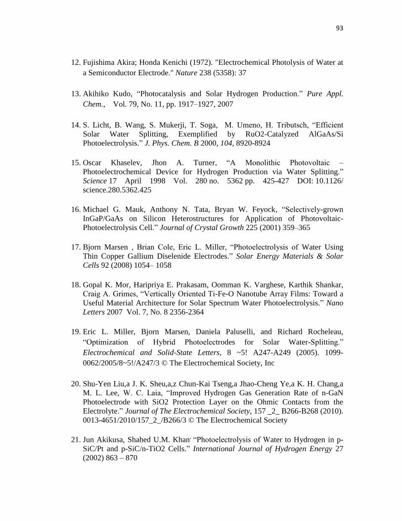
93
12. Fujishima Akira; Honda Kenichi (1972). "Electrochemical Photolysis of Water at
a Semiconductor Electrode." Nature 238 (5358): 37
13. Akihiko Kudo, “Photocatalysis and Solar Hydrogen Production.” Pure Appl.
Chem., Vol. 79, No. 11, pp. 1917–1927, 2007
14. S. Licht, B. Wang, S. Mukerji, T. Soga, M. Umeno, H. Tributsch, “Efficient
Solar Water Splitting, Exemplified by RuO2-Catalyzed AlGaAs/Si
Photoelectrolysis.” J. Phys. Chem. B 2000, 104, 8920-8924
15. Oscar Khaselev, Jhon A. Turner, “A Monolithic Photovoltaic –
Photoelectrochemical Device for Hydrogen Production via Water Splitting.”
Science 17 April 1998 Vol. 280 no. 5362 pp. 425-427 DOI: 10.1126/
science.280.5362.425
16. Michael G. Mauk, Anthony N. Tata, Bryan W. Feyock, “Selectively-grown
InGaP/GaAs on Silicon Heterostructures for Application of Photovoltaic-
Photoelectrolysis Cell.” Journal of Crystal Growth 225 (2001) 359–365
17. Bjorn Marsen , Brian Cole, Eric L. Miller, “Photoelectrolysis of Water Using
Thin Copper Gallium Diselenide Electrodes.” Solar Energy Materials & Solar
Cells 92 (2008) 1054– 1058
18. Gopal K. Mor, Haripriya E. Prakasam, Oomman K. Varghese, Karthik Shankar,
Craig A. Grimes, “Vertically Oriented Ti-Fe-O Nanotube Array Films: Toward a
Useful Material Architecture for Solar Spectrum Water Photoelectrolysis.” Nano
Letters 2007 Vol. 7, No. 8 2356-2364
19. Eric L. Miller, Bjorn Marsen, Daniela Paluselli, and Richard Rocheleau,
“Optimization of Hybrid Photoelectrodes for Solar Water-Splitting.”
Electrochemical and Solid-State Letters, 8 ~5! A247-A249 (2005). 1099-
0062/2005/8~5!/A247/3 © The Electrochemical Society, Inc
20. Shu-Yen Liu,a J. K. Sheu,a,z Chun-Kai Tseng,a Jhao-Cheng Ye,a K. H. Chang,a
M. L. Lee, W. C. Laia, “Improved Hydrogen Gas Generation Rate of n-GaN
Photoelectrode with SiO2 Protection Layer on the Ohmic Contacts from the
Electrolyte.” Journal of The Electrochemical Society, 157 _2_ B266-B268 (2010).
0013-4651/2010/157_2_/B266/3 © The Electrochemical Society
21. Jun Akikusa, Shahed U.M. Khan, “Photoelectrolysis of Water to Hydrogen in p-
SiC/Pt and p-SiC/n-TiO2 Cells.” International Journal of Hydrogen Energy 27
(2002) 863 – 870

94
22. A. J. Nozik, “p-n Photoelectrolysis Cells.” PACS numbers: 84.6O.Rb, 82.50.Et,
85.80.Dg, 73.4O.-c 1976
23. C. Jorand Sartoretti a, M. Ulmann a, B.D. Alexander a, J. Augustynski a, A.
Weidenkaff b, “Photoelectrochemical Oxidation of Water at Transparent Ferric
Oxide Film Electrodes.” Chemical Physics Letters 376 (2003) 194–200
24. Atsushi Nakahira, Koichi Konishi, Koji Yokota, Tetsuo Honma, Hirofumi
Aritani, Katsuhisa Tanaka, “Synthesis and Characterization of TiO2 Doped with P
Ions by Anodic Oxidation of Titanium in Acid Solution.” Journal of the Ceramic
Society of Japan 114 [1] 46-50, 2006
25. Wikipedia, August 2001 [update April 2011] [Online] Avalaible:
http://en.wikipedia.org/wiki/Gold [Accessed: 20 September 2010]
26. http://www.pvsolarchina.com/multilayer-solar-cell-conversion-efficiency-as-high-
as-41-1.html”
27. Andreas W. Bett, Frank Dimroth, Wolfgang Gutter, Raymond Hoeisel, Eduard
Olivia, Simon P. Philipps, Jan Schone, Gerald Siefer, Marc Steiner, Alexander
Wekkeli, Elke Welser, Matthias Meusel, Wolfgang Kostler, Gerhard Strobl
“Highest Efficiency Multi-Junction Solar Cell for Terrestrial and Space
Applications.” European Photovoltaic Solar Energy Conference and Exhibition,
September 2009
28. IEEE PV Specialists Conference, Silver Springs, MD, APL; chairman, Martin
Wolf. The first PVSC to include a session on terrestrial PV.
Related Documents