1 Signal Processing for Wireless Communications and Multimedia: Design, Tools, Architectures Advanced Digital System Design Course 2006, EPF-L Prof. Heinrich Meyr RWTH Aachen University , Germany and Chief Scientific Officer, CoWare Inc 2 Agenda Future Wireless Communication System Future Wireless Communication Systems and ist Impact on ESL The End of Moore´s Law Receiver Structure, Models and Performance Metrics Massive Parallel Processing on heterogeneous MPSoC Application Specific Processors Summary and Conclusions Agenda

Welcome message from author
This document is posted to help you gain knowledge. Please leave a comment to let me know what you think about it! Share it to your friends and learn new things together.
Transcript

1
Signal Processing for Wireless Communications
and Multimedia: Design, Tools, Architectures
Advanced Digital System Design Course 2006, EPF-L
Prof. Heinrich Meyr
RWTH Aachen University , Germanyand
Chief Scientific Officer, CoWare Inc
2
Agenda
Future Wireless Communication System
Future Wireless Communication Systems and ist Impact on ESL
The End of Moore´s Law
Receiver Structure, Models and Performance Metrics
Massive Parallel Processing on heterogeneous MPSoC
Application Specific Processors
Summary and Conclusions
Agenda

2
Future Wireless
Communication Systems
4
FixedDSL (→3 Mb/s)Intranet (100Mb/s) Wireless
WLAN (10-54 Mb/s) MobileUMTS (2 Mb/s)
Internet Access Today
3
5
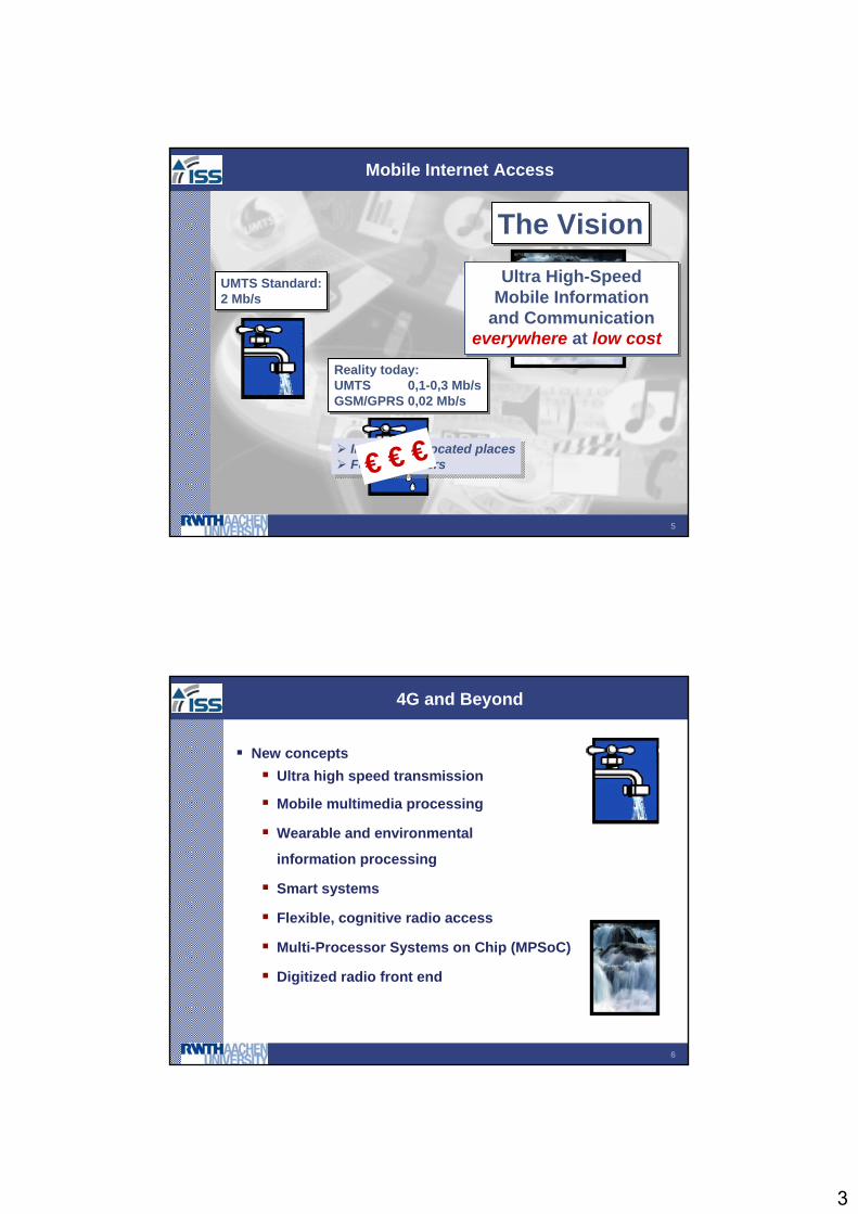
Mobile Internet Access
UMTS Standard:2 Mb/sUMTS Standard:2 Mb/s
The VisionThe Vision
Reality today:UMTS 0,1-0,3 Mb/sGSM/GPRS 0,02 Mb/s
Reality today:UMTS 0,1-0,3 Mb/sGSM/GPRS 0,02 Mb/s
Ultra High-SpeedMobile Information
and Communication
Ultra High-SpeedMobile Information
and Communicationeverywhere at low cost
In optimally located placesFor a few users
In optimally located placesFor a few users€ € €
6
4G and Beyond
New conceptsUltra high speed transmission
Mobile multimedia processing
Wearable and environmental
information processing
Smart systems
Flexible, cognitive radio access
Multi-Processor Systems on Chip (MPSoC)
Digitized radio front end

4
7
Mobile Applications and Services
Future mobile wireless internet services: Information (web browsing, …)Communication (VoIP, video, P2P, …)Entertainment (distributed gaming, …)
Challenging mobile application classesWearable and environmental information processing: work, sport, health care
e.g. location aware services, seamless mobile workingMobile multimedia processing
e.g. entertainment, information access, navigation,…
10
Future Wireless Systems: In a nutshell
Will be cognitivemultifunctionalsoftware definable
Will have
multiple Antennas
They will make use of ultra-complex signal processing to optimally use the availabel bandwidth
And process these algorithms on heterogeneous configurable computing engines

5
Future Wireless Communication Systems and its Impact on ESL
12
To meet the schedule of NGMN it is imperative to have a concurrent and iterative development and validationprocess to design
Standard
Development and validation of algorithm and HW/SW of the digital receiver
Application (SW) development
New approaches are needed !
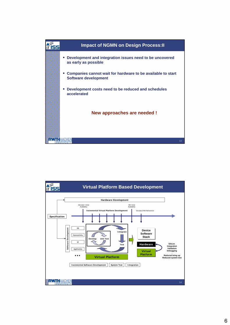
Impact of NGMN on Design Process: I
6
13
Impact of NGMN on Design Process:II
Development and integration issues need to be uncovered as early as possible
Companies cannot wait for hardware to be available to start Software development
Development costs need to be reduced and schedules accelerated
New approaches are needed !
14
Virtual Platform Based Development
Specification
Hardware Development
OS
Connectivity
UI
ApplicationSof
twar
e D
evel
opm
ent
…
Simulator InitialAvailability
Incremental Virtual Platform Development
Develop Unit Test
Integrate
Test
Virtual Platform
Incremental Software Development System Test
HW InitialAvailability
Simulator/HW Refinement
Virtual PlatformVirtual
Platform
Silicon IntegrationValidationDebugging
-Reduced bring up
Reduced system test
HardwareHardware
Device Software
Stack
Device Software
Stack
Integration
7
The End of Moore´s Law:
„Design Competence rules the World“
16
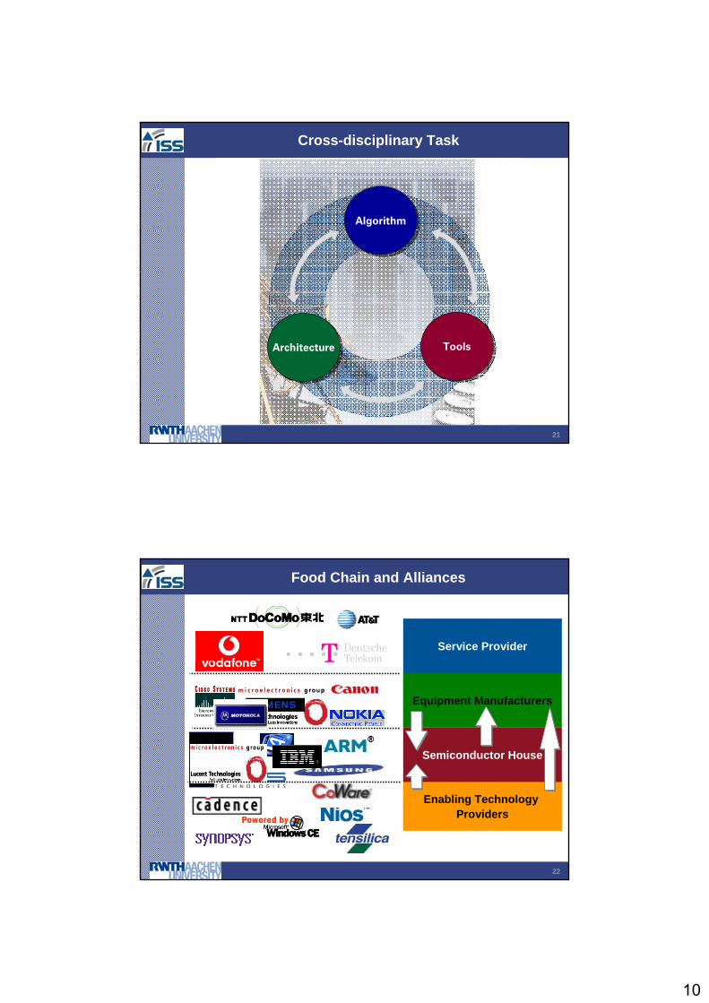
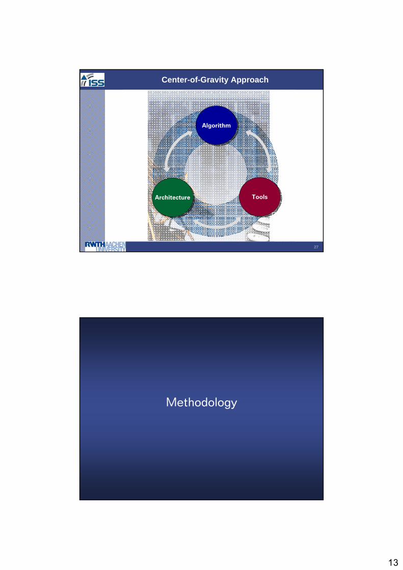
Cross-disciplinary Task Management
Analysis
The task comprises of many subtask in various disciplines
“The whole is more than the sum of the parts”
Conclusion
The solution requires the interaction of people in the various disciples
8
17
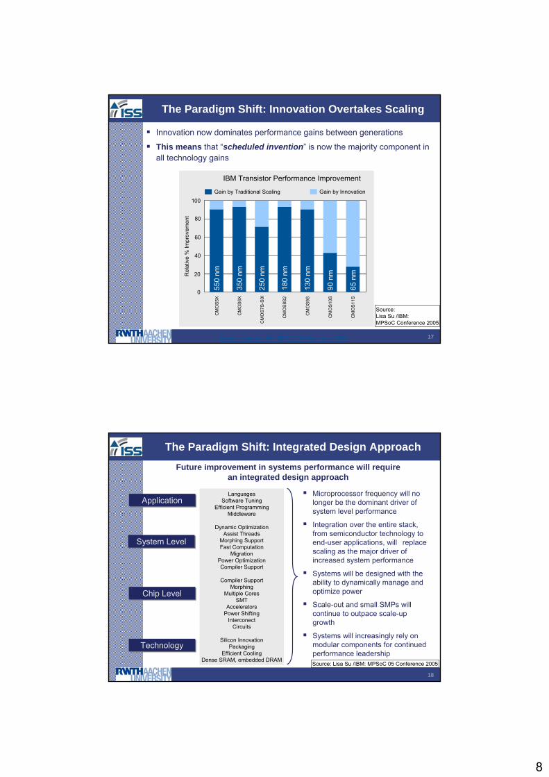
The Paradigm Shift: Innovation Overtakes Scaling
Innovation now dominates performance gains between generations
This means that “scheduled invention” is now the majority component in all technology gains
Source: Lisa Su /IBM: MPSoC 05 Conference 2005
100
80
60
40
20
0
IBM Transistor Performance Improvement
Gain by Traditional Scaling Gain by Innovation
CM
OS7
S-S0
I
CM
OS
5X
CM
OS
6X
CM
OS
8S2
CM
OS
9S
CM
OS1
0S
CM
OS1
1S
550
nm
350
nm
250
nm
180
nm
130
nm
90 n
m
65 n
mRel
ativ
e %
Impr
ovem
ent
Source: Lisa Su /IBM: MPSoC Conference 2005
18
The Paradigm Shift: Integrated Design Approach
Future improvement in systems performance will requirean integrated design approach
ApplicationApplication
System LevelSystem Level
Chip LevelChip Level
TechnologyTechnology
LanguagesSoftware Tuning
Efficient ProgrammingMiddleware
Dynamic OptimizationAssist Threads
Morphing SupportFast Computation
MigrationPower OptimizationCompiler Support
Compiler SupportMorphing
Multiple CoresSMT
AcceleratorsPower Shifting
InterconectCircuits
Silicon InnovationPackaging
Efficient CoolingDense SRAM, embedded DRAM
Microprocessor frequency will no longer be the dominant driver of system level performance
Integration over the entire stack, from semiconductor technology to end-user applications, will replace scaling as the major driver of increased system performance
Systems will be designed with the ability to dynamically manage and optimize power
Scale-out and small SMPs will continue to outpace scale-up growth
Systems will increasingly rely on modular components for continued performance leadershipSource: Lisa Su /IBM: MPSoC 05 Conference 2005
9
19
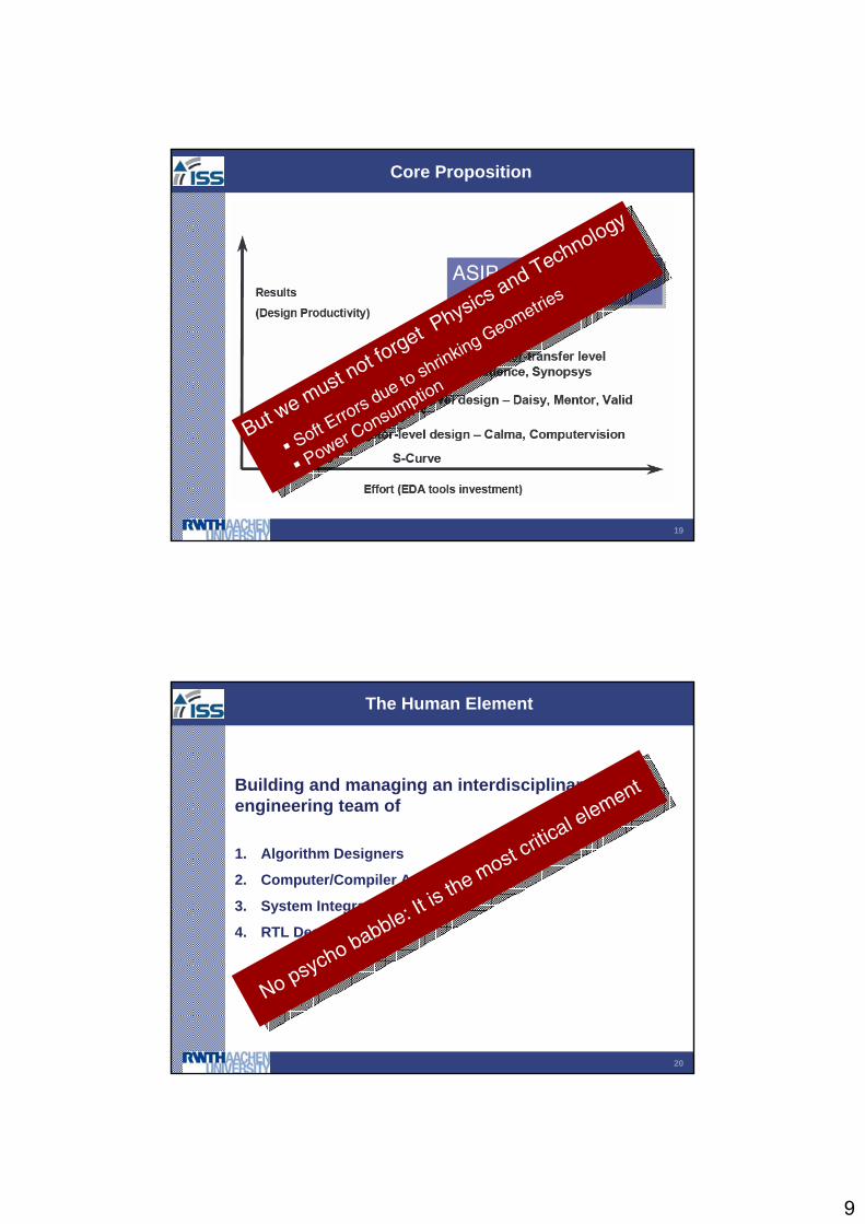
Core Proposition
ASIP based Platforms(heterogenousMPSoC)
ASIP based Platforms(heterogenousMPSoC)
But we must not forget Physics and Technology
Soft Erro
rs due to shrinking Geometries
Power Consumption
But we must not forget Physics and Technology
Soft Erro
rs due to shrinking Geometries
Power Consumption
20
Most critical problem: Design Competence
Building and managing an interdisciplinaryengineering team of
1. Algorithm Designers
2. Computer/Compiler Architects
3. System Integrators
4. RTL Designers
The Human Element
No psycho babble: It is the most critic
al element
No psycho babble: It is the most critic
al element
10
21
ArchitectureArchitecture
AlgorithmAlgorithm
ToolsTools
Cross-disciplinary Task
22
Food Chain and Alliances
Enabling Technology Providers
Service Provider
Semiconductor House
Equipment ManufacturersEquipment ManufacturersSIEMENS

11
23
Alliances and the Business Equation
Managing alliances is a key to success
EDA
Mobile provider
Semiconductor company
Receiver Structure , Models
and Performance Metrics
12
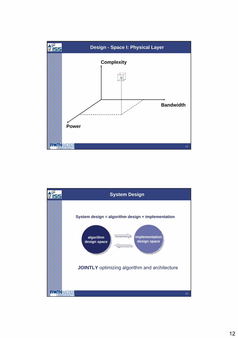
25
Design - Space I: Physical Layer
Bandwidth
Power
Complexity
26
System Design
System design = algorithm design + implementation
JOINTLY optimizing algorithm and architecture
algorithmdesign spacealgorithm
design spaceimplementationdesign space
implementationdesign space
13
27
ArchitectureArchitecture
AlgorithmAlgorithm
ToolsTools
Center-of-Gravity Approach
Methodology
14
29
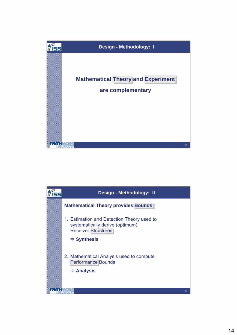
Design - Methodology: I
Mathematical Theory and Experiment
are complementary
30
Design - Methodology: II
Mathematical Theory provides Bounds
1. Estimation and Detection Theory used to systematically derive (optimum)Receiver Structures
Synthesis
2. Mathematical Analysis used to computePerformance Bounds
Analysis
15
31
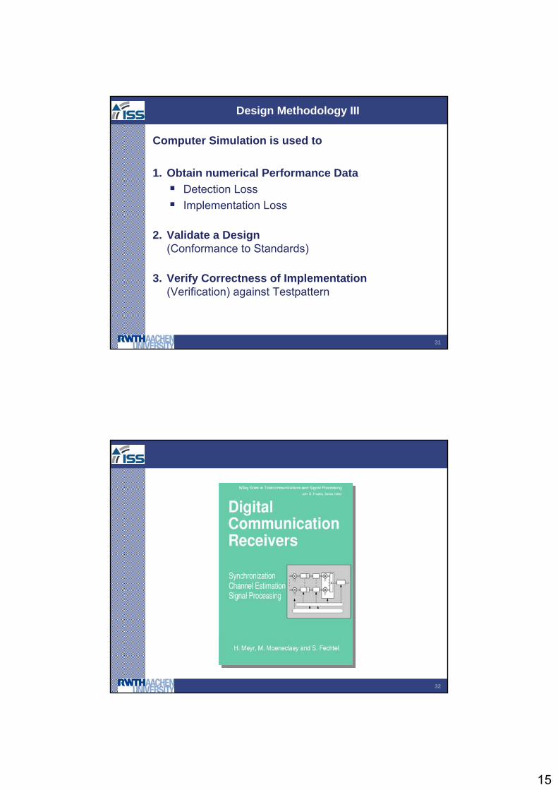
Design Methodology III
Computer Simulation is used to
1. Obtain numerical Performance DataDetection LossImplementation Loss
2. Validate a Design(Conformance to Standards)
3. Verify Correctness of Implementation(Verification) against Testpattern
32
16
Models
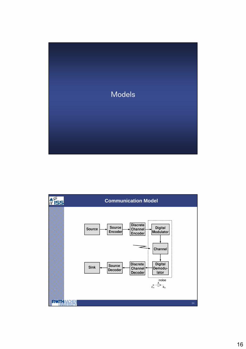
34
Communication Model

17
Signal Model
36

18
37
Received Bandlimited Signals
39
Approximation by BL Signals
{ } ωωω
dSxtxEBL
xBL ∫≥
=− )()( 2
∑−
k
ks kkTx )()( ϕ
Approx. of non-bandlimited Signal x(t) by BL -Signal
Truncation defines (2K+1) dim. Approx. In Vector space
19
40
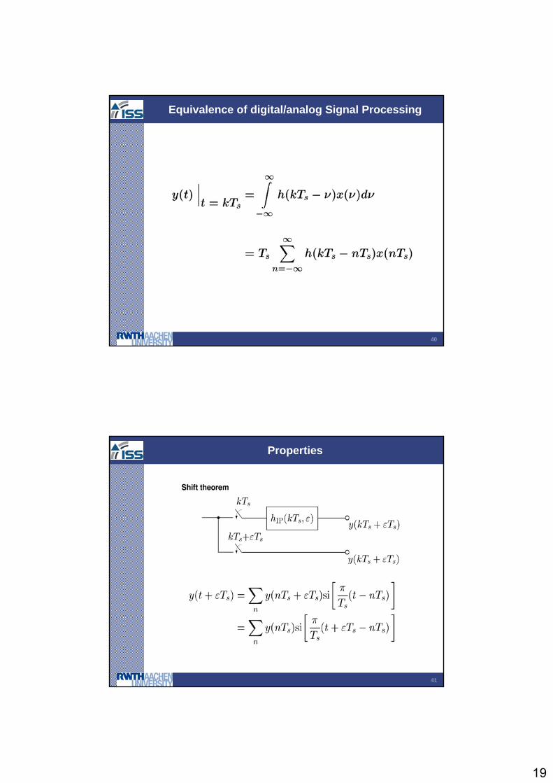
Equivalence of digital/analog Signal Processing
41
Properties
20
42
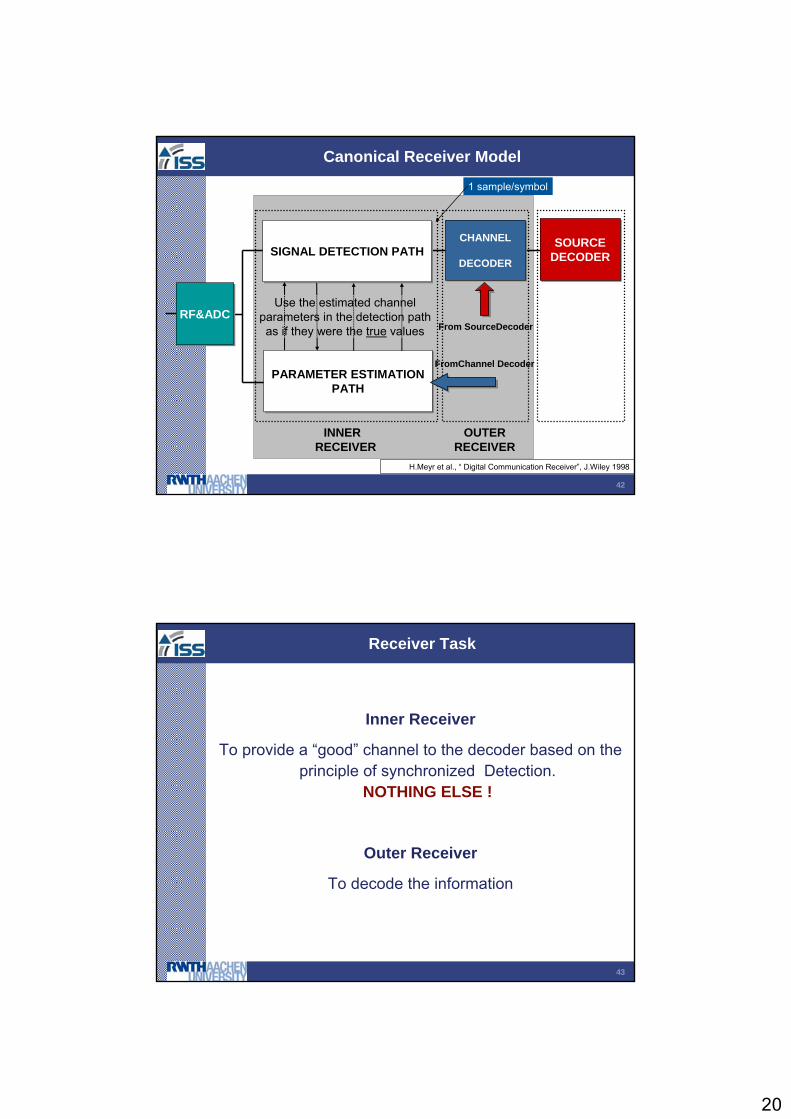
Canonical Receiver Model
SOURCEDECODERSOURCE
DECODER
RF&ADCRF&ADC
PARAMETER ESTIMATIONPATH
PARAMETER ESTIMATIONPATH
SIGNAL DETECTION PATHSIGNAL DETECTION PATH
INNER RECEIVER
OUTER RECEIVER
CHANNEL
DECODER
CHANNEL
DECODER
FromChannel Decoder
Use the estimated channel parameters in the detection pathas if they were the true values From SourceDecoder
H.Meyr et al., “ Digital Communication Receiver”, J.Wiley 1998
1 sample/symbol
43
Receiver Task
Inner Receiver
To provide a “good” channel to the decoder based on the principle of synchronized Detection.
NOTHING ELSE !
Outer Receiver
To decode the information
21
44
Performance Measure
Inner ReceiverProperties of the estimator
VarianceUnbiased
Outer ReceiverBit-error-rate of the coded system
45
Performance Loss
Detection Loss of synchronized DetectionΔ SNR (dB) required to achieve the performance of perfect channel knowledge . (Infinite Precision arithmetic assumed)
Implementation LossΔSNR (dB) resulting from finite precision arithmetic and algorithmic approximations

22
48
BER Performance
Source: Digital Communication Receivers, H. Meyr, M. Moeneclaey, S.A. Fechtel
49
Complexity DVB-S
Source: Digital Communication Receivers, H. Meyr, M. Moeneclaey, S.A. Fechtel
23
50
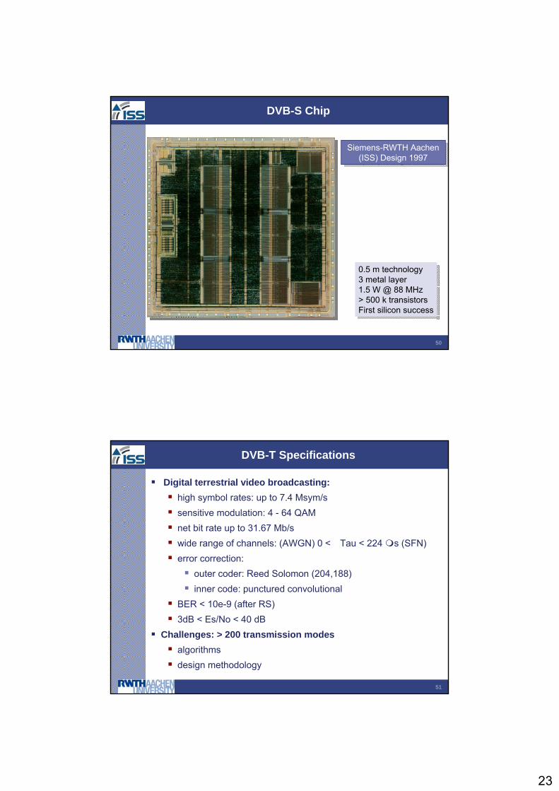
DVB-S Chip
0.5 m technology3 metal layer1.5 W @ 88 MHz> 500 k transistorsFirst silicon success
0.5 m technology3 metal layer1.5 W @ 88 MHz> 500 k transistorsFirst silicon success
Siemens-RWTH Aachen (ISS) Design 1997
Siemens-RWTH Aachen (ISS) Design 1997
51
DVB-T Specifications
Digital terrestrial video broadcasting:high symbol rates: up to 7.4 Msym/ssensitive modulation: 4 - 64 QAMnet bit rate up to 31.67 Mb/s wide range of channels: (AWGN) 0 < Tau < 224 s (SFN)error correction:
outer coder: Reed Solomon (204,188)inner code: punctured convolutional
BER < 10e-9 (after RS)3dB < Es/No < 40 dB
Challenges: > 200 transmission modesalgorithmsdesign methodology
24
52
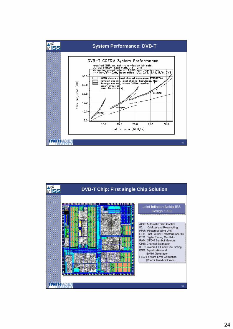
System Performance: DVB-T
53
DVB-T Chip: First single Chip Solution
AGC: Automatic Gain ControlIQ: IQ-Mixer and ResamplingPPU: Postprocessing UnitFFT: Fast Fourier Transform (2k,8k)DTO: Digital Timing OscillatorRAM: OFDM Symbol MemoryCHE: Channel EstimationIFFT: Inverse FFT and Fine TimingESG: Equalization and
Softbit GenerationFEC: Forward Error Correction
(Viterbi, Reed-Solomon)
Joint Infineon-Nokia-ISSDesign 1999
Joint Infineon-Nokia-ISSDesign 1999

25
54
DVB-T Complexity
Analog part : 10%Input interfacesDC removalanti-aliasing filterADC,AGC
Digital demodulator: 60 %Channel estimation and equalizationsynchronization control flow implementationFFT (alone 30%)
Channel decoder : 20 %Viterbi and RS decoder
Miscellaneous : 10%IIC bus controller, DAC
55
Design Space : Architecture and Algorithm
Inner Receiver
The algorithms of the inner receiver are never specified by the standard
BOTH algorithm and architecture space exploration
Outer Receiver
The decoder is exaclty specified in the standard
ONLY architecture space exploration
26
Massive Parallel Processing on
Heterogeneous MPSoC
58
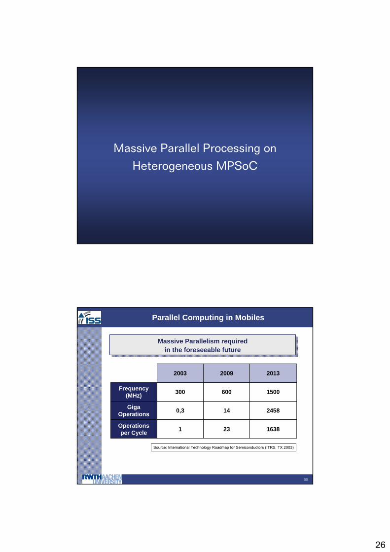
Parallel Computing in Mobiles
Source: International Technology Roadmap for Semiconductors (ITRS, TX 2003)
2003 2009 2013
Frequency (MHz) 300 600 1500
Giga Operations 0,3 14 2458
Operations per Cycle 1 23 1638
Massive Parallelism required in the foreseeable future
Massive Parallelism required in the foreseeable future
27
59
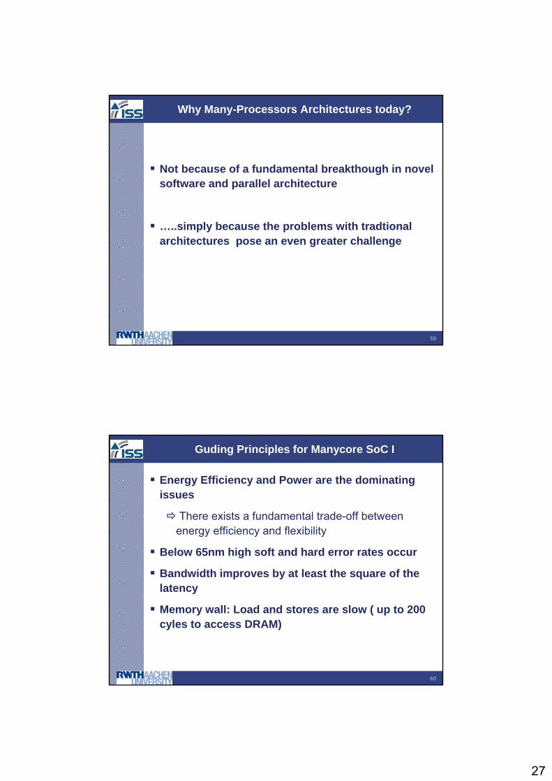
Why Many-Processors Architectures today?
Not because of a fundamental breakthough in novelsoftware and parallel architecture
…..simply because the problems with tradtionalarchitectures pose an even greater challenge
60
Guding Principles for Manycore SoC I
Energy Efficiency and Power are the dominatingissues
There exists a fundamental trade-off betweenenergy efficiency and flexibility
Below 65nm high soft and hard error rates occur
Bandwidth improves by at least the square of the latency
Memory wall: Load and stores are slow ( up to 200 cyles to access DRAM)
28
61
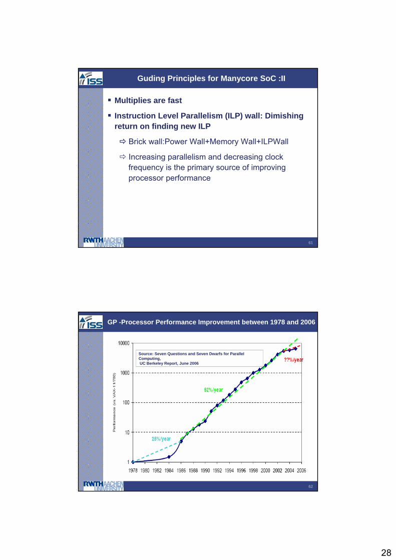
Guding Principles for Manycore SoC :II
Multiplies are fast
Instruction Level Parallelism (ILP) wall: Dimishingreturn on finding new ILP
Brick wall:Power Wall+Memory Wall+ILPWall
Increasing parallelism and decreasing clockfrequency is the primary source of improvingprocessor performance
62
GP -Processor Performance Improvement between 1978 and 2006
Source: Seven Questions and Seven Dwarfs for Parallel Computing,UC Berkeley Report, June 2006

29
63
Basic Blocks: Algorithm Types
“Switching from sequential to modestly parallel computing will make programming much more difficult…….without a dramatic improvement in
performance”
Parallel Computing
Source: Seven Questions and Seven Dwarfs for Parallel Computing,UC Berkeley Report, June 2006
We need to go to from multiple processors to many cores
64
The Need for New Architectures
Source: R.Subramanian.Berkeley Design Automation Inc
Microprocessor / DSP
Memory(Moore’sLaw)
2G
3G
4G
1GWireless
Algorithmic Complexity
(Shannon’s Law)
Time
Battery Power
30
65
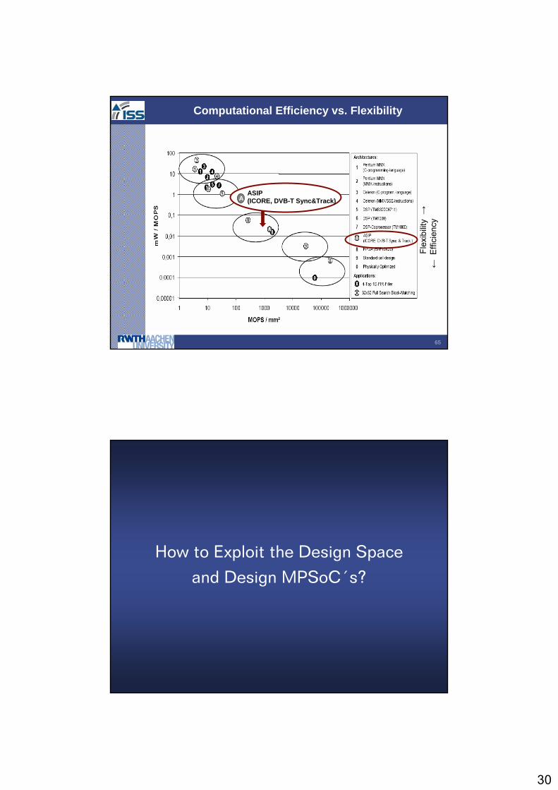
Computational Efficiency vs. Flexibility
Flex
ibili
ty →
←E
ffici
ency
ASIP(ICORE, DVB-T Sync&Track)A
How to Exploit the Design Space
and Design MPSoC´s?
31
67
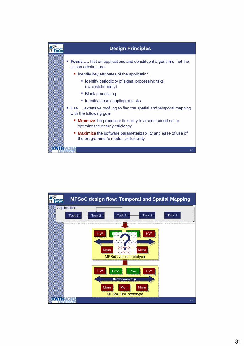
Design Principles
Focus …. first on applications and constituent algorithms, not the silicon architecture
Identify key attributes of the application
Identify periodicity of signal processing taks(cyclostationarity)
Block processing
Identify loose coupling of tasks
Use…. extensive profiling to find the spatial and temporal mapping with the following goal
Minimize the processor flexibility to a constrained set to optimize the energy efficiency
Maximize the software parameterizability and ease of use of the programmer’s model for flexibility
68
SpecificationSpecification
MPSoC virtual prototypeMPSoC virtual prototype
ProcProcHWHW
Network-on-ChipNetwork-on-Chip
ProcProc HWHW
MemMem MemMem MemMem
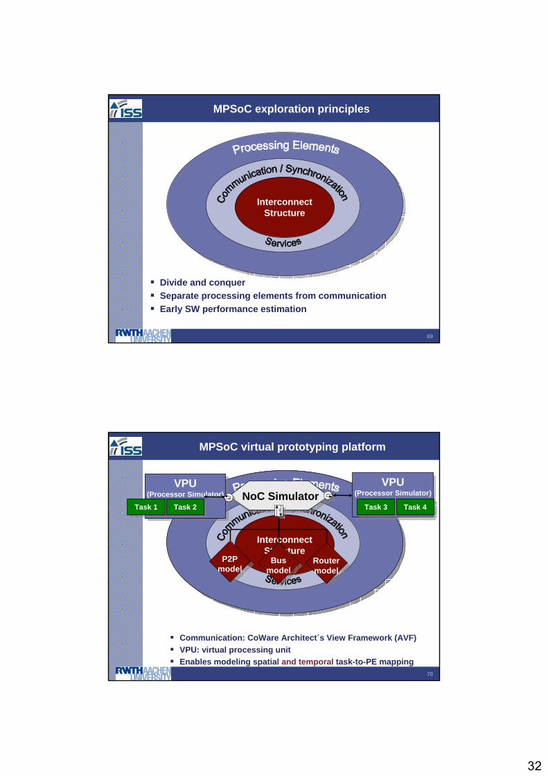
MPSoC design flow: Temporal and Spatial Mapping
Task 3Task 1
Application:
Task 2 Task 4 Task 5
?
MPSoC HW prototypeMPSoC HW prototype
ProcProcHWHW
Network-on-ChipNetwork-on-Chip
ProcProc HWHW
MemMem MemMem MemMem
32
69
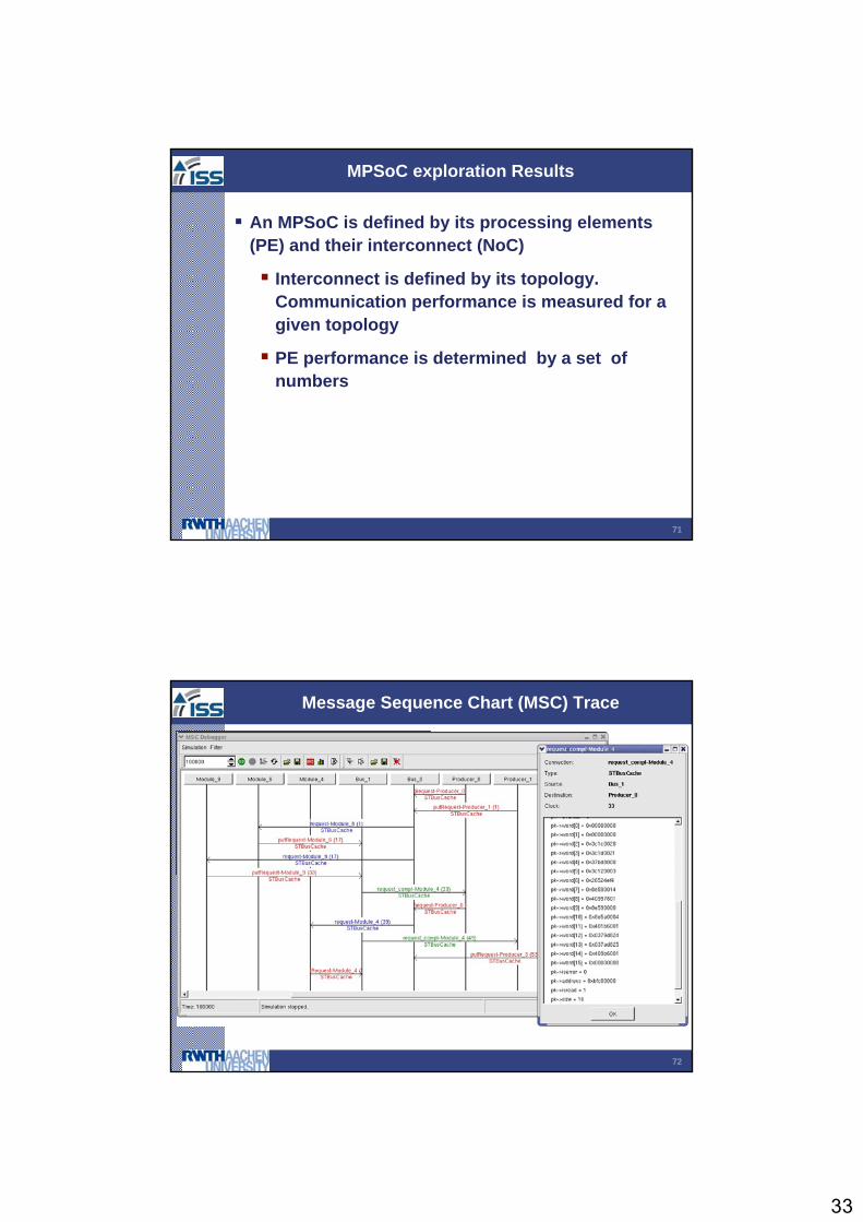
MPSoC exploration principles
InterconnectStructure
Divide and conquerSeparate processing elements from communicationEarly SW performance estimation
70
MPSoC virtual prototyping platform
InterconnectStructure
VPU(Processor Simulator)
VPU(Processor Simulator) NoC Simulator
VPU(Processor Simulator)
VPU(Processor Simulator)
Task 1Task 1 Task 2Task 2 Task 3Task 3 Task 4Task 4
P2P model
Bus model
Router model
Communication: CoWare Architect´s View Framework (AVF)VPU: virtual processing unitEnables modeling spatial and temporal task-to-PE mapping
33
71
MPSoC exploration Results
An MPSoC is defined by its processing elements(PE) and their interconnect (NoC)
Interconnect is defined by its topology. Communication performance is measured for a given topology
PE performance is determined by a set of numbers
72
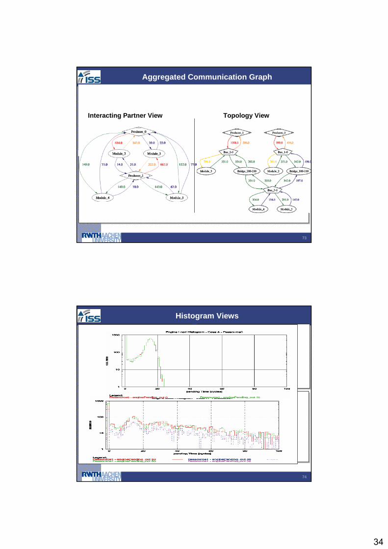
Message Sequence Chart (MSC) Trace
MessageSequenceChart
34
73
Aggregated Communication Graph MessageSequenceChart
Topology ViewInteracting Partner View
74
Topology ViewInteracting Partner View
Histogram ViewsMessageSequenceChart
Histogram

35
75
MPSoC Exploration Results: Communication
Source: Seven Questions and Seven Dwarfs for Parallel Computing,UC Berkeley Report, June 2006
76
The „Key Algorithm“ Propostion
Each application is composed of a small number of fundamental algorithms ( „Nuclei“) that represent a significant amount of the computation.
Focus on an efficient composition („design of an MPSoc) or mapping („programming of the MPSoC“)

36
77
Nuclei can be composed/mapped on a multiprocessorin three different ways
Temporally distributed or time-shared on a common processorSpatially distributed with each Nucleus occupyingone or more processorsPipelined: A single nucleus is distributed in time and space
In a given time slot a nucleus is running on a group of processorsOn a given processor a group of nucleuscomputation run over time
Composition of Nuclei
Source: Schaumont et. al.2001
78
Intel RMS View (Recognition, Mining,Synthesis)

37
Example: Baseband Processing for 4G
80
Canonical Receiver Model
SOURCEDECODERSOURCE
DECODER
RF&ADCRF&ADC
PARAMETER ESTIMATIONPATH
PARAMETER ESTIMATIONPATH
SIGNAL DETECTION PATHSIGNAL DETECTION PATH
INNER RECEIVER
OUTER RECEIVER
CHANNEL
DECODER
CHANNEL
DECODER
From Channel Decoder
Use the estimated channel parameters in the detection pathas if they were the true values From SourceDecoder
H.Meyr et al., “ Digital Communication Receiver”, J.Wiley 1998
1 sample/symbol
38
81
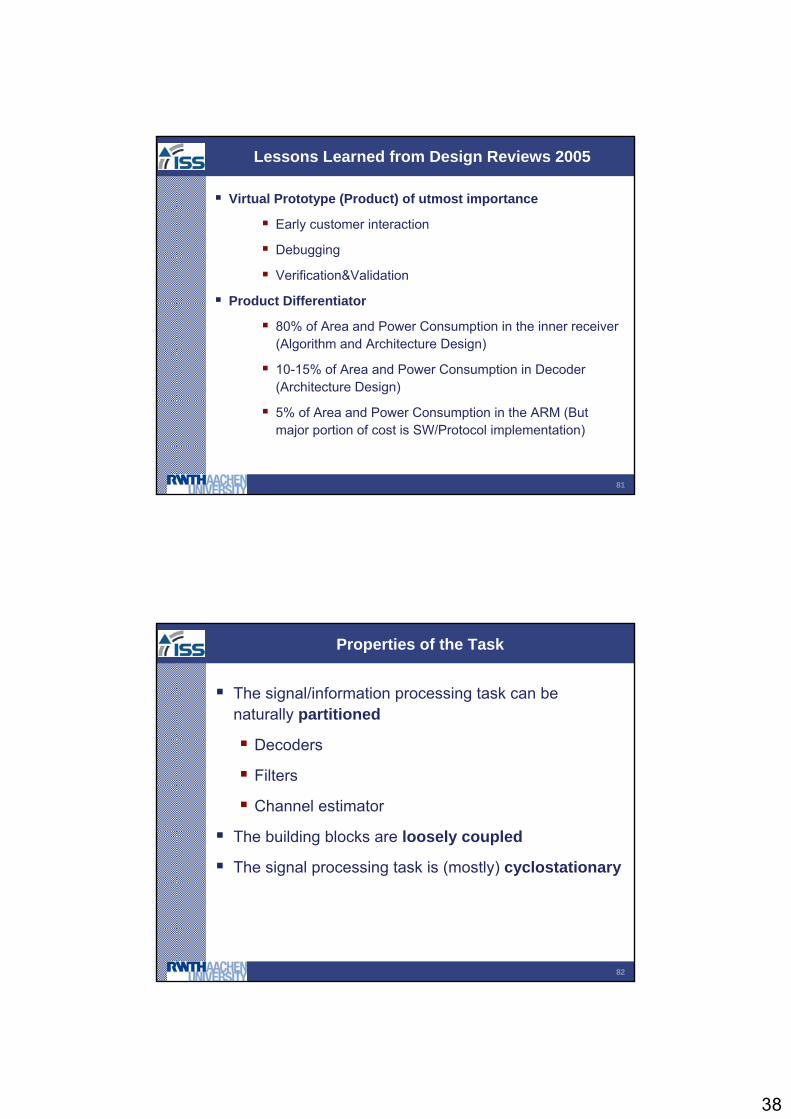
Lessons Learned from Design Reviews 2005
Virtual Prototype (Product) of utmost importance
Early customer interaction
Debugging
Verification&Validation
Product Differentiator
80% of Area and Power Consumption in the inner receiver(Algorithm and Architecture Design)
10-15% of Area and Power Consumption in Decoder (Architecture Design)
5% of Area and Power Consumption in the ARM (Butmajor portion of cost is SW/Protocol implementation)
82
Use A-Priori Knowledge of the Task
The signal/information processing task can be naturally partitioned
Decoders
Filters
Channel estimator
The building blocks are loosely coupled
The signal processing task is (mostly) cyclostationary
Properties of the Task
39
83
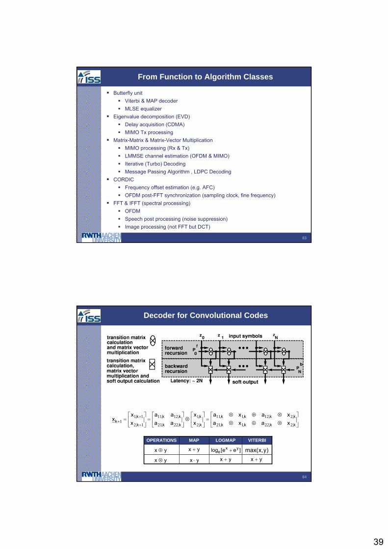
Basic Blocks: Algorithm Types
Butterfly unitViterbi & MAP decoderMLSE equalizer
Eigenvalue decomposition (EVD)Delay acquisition (CDMA)MIMO Tx processing
Matrix-Matrix & Matrix-Vector Multiplication MIMO processing (Rx & Tx)LMMSE channel estimation (OFDM & MIMO)Iterative (Turbo) DecodingMessage Passing Algorithm , LDPC Decoding
CORDICFrequency offset estimation (e.g. AFC)OFDM post-FFT synchronization (sampling clock, fine frequency)
FFT & IFFT (spectral processing)OFDMSpeech post processing (noise suppression)Image processing (not FFT but DCT)
From Function to Algorithm Classes
84
Decoder for Convolutional Codes
⎥⎦
⎤⎢⎣
⎡⊗⊕⊗⊗⊕⊗
=⎥⎦
⎤⎢⎣
⎡⊗⎥
⎦
⎤⎢⎣
⎡=⎥
⎦
⎤⎢⎣
⎡=
+
++
k,k,k,k,
k,k,k,k,
k,
k,
k,k,
k,k,
k,
k,k xaxa
xaxaxx
aaaa
xx
x222121
212111
2
1
2221
1211
12
111
VITERBILOGMAPMAPOPERATIONS
yx ⊕
yx ⊗
yx +
yx ⋅ yx + yx +
)y,xmax(]ee[log yxe +

40
85
Basic Blocks: Algorithm Types
Clock rate of processing elements (1/Tc)Sampling rate of the signal (1/Ts)Algorithm characteristic
Complexity (MOPS/sample)
Computational characteristicData flow
Data locality
Data storage
Parallelism
Control flow
Connectivity of algorithmsSpatial
Temporal
Algorithmic Descriptors
86
384 kbps UMTS Receiver BB Complexity
sampling rate [1/s]10
210
310
410
510
610
710
810
0
101
102
103
104
105
OP
s p
er s
ampl
e
384 kbps UMTS receiver, digital BB complexityMUSIC delay acq.
1 MOPS 10 MOPS 100 MOPS 1000 MOPS
AGC
AFC RRC pulse MF
Interpolation/decimation
CorrelatorsMax. ratio combining
Timing tracking Channel estimation
SIR estimationPath searcher
Turbo decoder

41
Hardware
88
Guding Principle
Employ all forms of Parallelism
42
89
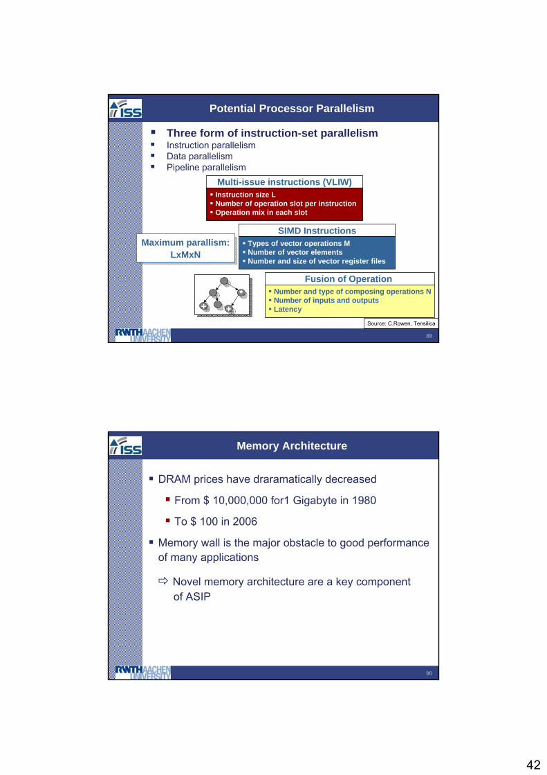
Potential Processor Parallelism
Multi-issue instructions (VLIW)
SIMD Instructions
Fusion of Operation Number and type of composing operations NNumber of inputs and outputsLatency
Types of vector operations MNumber of vector elementsNumber and size of vector register files
Instruction size LNumber of operation slot per instructionOperation mix in each slot
Maximum parallism:LxMxN
Maximum parallism:LxMxN
Three form of instruction-set parallelismInstruction parallelismData parallelismPipeline parallelism
Source: C.Rowen, Tensilica
**++ ++
90
Memory Architecture
DRAM prices have draramatically decreased
From $ 10,000,000 for1 Gigabyte in 1980
To $ 100 in 2006
Memory wall is the major obstacle to good performanceof many applications
Novel memory architecture are a key componentof ASIP
43
Programming Models and Design
Methodology
92
RF
Fron
tend
(Dow
n-/U
pcon
vers
ion)
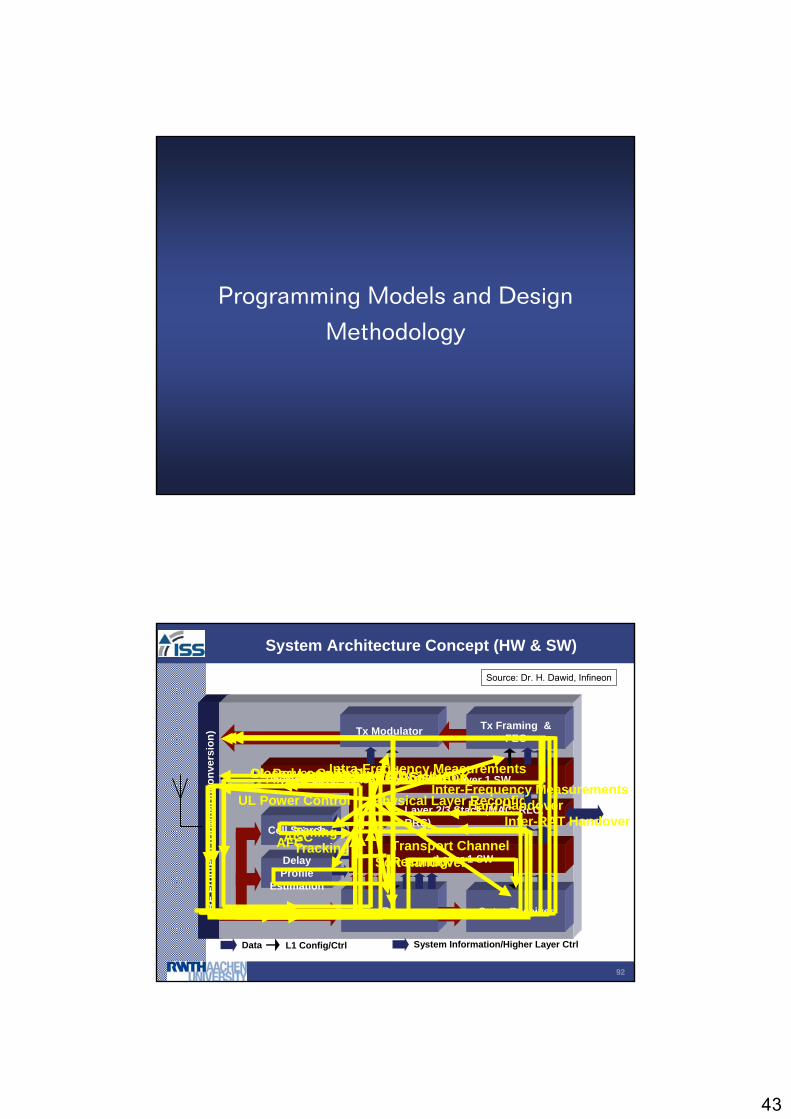
System Architecture Concept (HW & SW)
Tx Modulator
Inner Receiver
Tx Framing & FEC
Outer Receiver
Layer 1 SW
Cell Search
DelayProfile
Estimation
Physical Layer Scheduling & Ctrl Layer 1 SW
Data L1 Config/Ctrl System Information/Higher Layer Ctrl
Layer 2/3 Stack (MAC, RLC, RRC)
AFCAGCTimingTracking Transport Channel
Reconfig
Physical Layer ReconfigUL Power Control
DL Power ControlClosed Loop Tx DiversityHSDPA HARQ ACK/NACKHSUPA HARQ ControlHSUPA E-TFC SelectionIntra-Frequency Measurements
Soft Handover
Inter-Frequency MeasurementsHard Handover
Inter-RAT Handover
Source: Dr. H. Dawid, Infineon
44
93
Programming Models
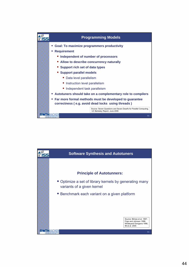
Goal: To maximize programmers productivityRequirement
Independent of number of processorsAllow to describe concurrency naturallySupport rich set of data typesSupport parallel models
Data level parallelism
Instruction level parallelism
Independent task paralleism
Autotuners should take on a complementary role to compilersFar more formal methods must be developed to guaranteecorrectness ( e.g. avoid dead locks using threads )
Source: Seven Questions and Seven Dwarfs for Parallel Computing,UC Berkeley Report, June 2006
94
Software Synthesis and Autotuners
Principle of Autotunners:
Optimize a set of library kernels by generating manyvariants of a given kernel
Benchmark each variant on a given platform
Source: Bilmes et al. 1997; Frigo and Johnson 1998;Whaleyand Dongarra 1998,IM et al. 2005
45
95
Conclusion
We are presently at a juncture of the semiconductorindustry as it seldom occurs
The existing ( RTL) design paradigm has reached its end-of-life we need to move to a higher level of abstraction(ESL) to keep the cost within resonable bounds
The existing processor multiprocessor architectures and the programing tools do not scale
we need much innovation in these areas to makeeconomic use of scaling
96
Application SpecificProcessors Design
46
97
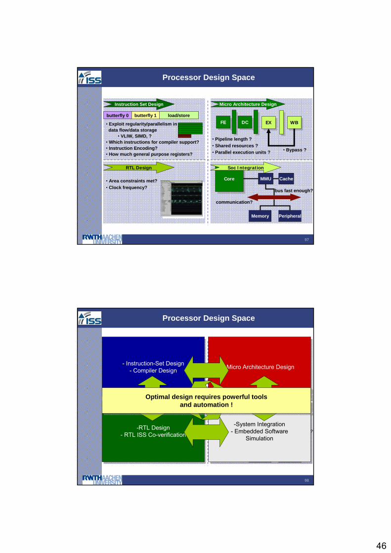
Processor Design Space
MMU
Memory Peripheral
CoreCore Cache
FEFE DCDC EXEX WBWB
• Bypass ?
• Pipeline length ?• Shared resources ?• Parallel execution units ?
bus fast enough?
butterfly 0 load/storebutterfly 1
communication?
• Exploit regularity/parallelism in data flow/data storage
• VLIW, SIMD, ? • Which instructions for compiler support?• Instruction Encoding?• How much general purpose registers?
• Area constraints met?• Clock frequency?
Instruction Set Design Micro Architecture Design
RTL Design Soc Integration
98
Processor Design Space
MMU
Memory Peripheral
CoreCore Cache
FEFE DCDC EXEX WBWB
• Bypass ?
• Pipeline length ?• Shared resources ?• Parallel execution units ?
bus fast enough?
butterfly 0 load/storebutterfly 1
communication?
• Exploit regularity/parallelism in data flow/data storage
• VLIW, SIMD, ? • Which instructions for compiler support?• Instruction Encoding?• How much general purpose registers?
• Area constraints met?• Clock frequency?
Instruction Set Design Micro Architecture Design
RTL Design Soc Integration
- Instruction-Set Design- Compiler Design
- Instruction-Set Design- Compiler Design -Micro Architecture Design-Micro Architecture Design
-RTL Design- RTL ISS Co-verification
-RTL Design- RTL ISS Co-verification
-System Integration- Embedded Software
Simulation
-System Integration- Embedded Software
Simulation
Optimal design requires powerful toolsand automation !
Optimal design requires powerful toolsand automation !
47
99
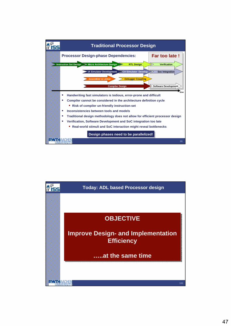
Far too late !Far too late !
Traditional Processor Design
Processor Design-phase Dependencies:
Handwriting fast simulators is tedious, error-prone and difficultCompiler cannot be considered in the architecture definition cycle
Risk of compiler un-friendly instruction-set Inconsistencies between tools and modelsTraditional design methodology does not allow for efficient processor designVerification, Software Development and SoC integration too late
Real-world stimuli and SoC interaction might reveal bottlenecks
Instruction Set Design
Compiler Design
Micro Architecture Design
IA Simulator Development
Assembler & Linker Debugger Coupling
Soc Integration
RTL Design
Software Development
Verification
CA Simulator Develop.
time
Design phases need to be parallelized!Design phases need to be parallelized!
100
OBJECTIVE
Improve Design- and Implementation Efficiency
…..at the same time
OBJECTIVE
Improve Design- and Implementation Efficiency
…..at the same time
Today: ADL based Processor design

48
101
Architecture Description Language based Processor Design
The purpose of an architecture description language (e.g LISA) is:
To allow for an iterative design to efficiently explore architecture alternatives
To jointly design “Architecture –Compiler” and on chip communication
To automatically generate hardware (path to implementation)
To automatically generate tools
Assembler ,Linker, Compiler, Simulator, co-simulation interfaces
From a single model at various level of temporal and spatial abstraction
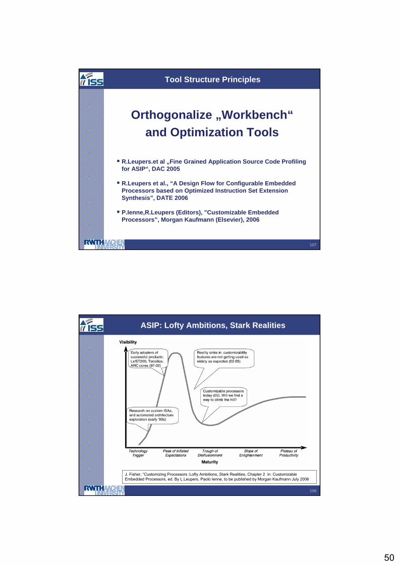
104
FFT Processor
Application
SoftwareTool Chain:Software
Tool Chain:LISATekLISATek
Processor Processor DesignerDesigner
DSP SampleVLIW Sample
RISC Sample
Empty Model
LISATek IP Samples
CustomProcessor
Model
LISA 2.0
GenerateTools
Function and instruction levelprofiling reveals hot-spots
special purpose instructions
Describe/AdoptProcessor Model
C-CompilerAssembler &
LinkerSimulator
Debugger & Profiler
49
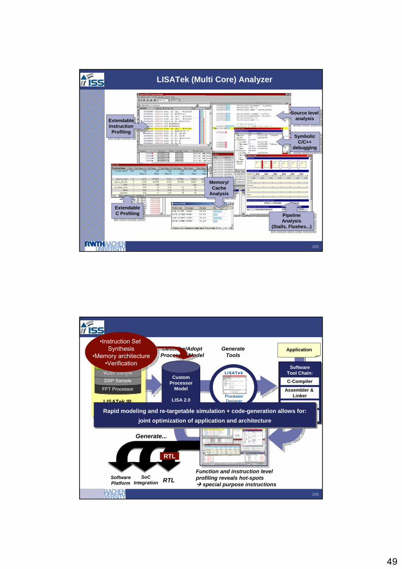
105
LISATek (Multi Core) Analyzer
ExtendableInstructionProfiling
ExtendableInstructionProfiling
Source levelanalysis
Source levelanalysis
SymbolicC/C++
debugging
SymbolicC/C++
debugging
ExtendableC Profiling
ExtendableC Profiling
PipelineAnalysis
(Stalls, Flushes...)
PipelineAnalysis
(Stalls, Flushes...)
Memory/Cache
Analysis
Memory/Cache
Analysis
106
RTL
SoftwarePlatform RTLSoC
Integration
Generate...
FFT Processor
Application
SoftwareTool Chain:Software
Tool Chain:LISATekLISATek
Processor Processor DesignerDesigner
DSP SampleVLIW Sample
RISC Sample
Empty Model
LISATek IP Samples
CustomProcessor
Model
LISA 2.0
GenerateTools
Function and instruction levelprofiling reveals hot-spots
special purpose instructions
Describe/AdoptProcessor Model
C-Compiler
Assembler & Linker
Simulator
Debugger & Profiler
Rapid modeling and re-targetable simulation + code-generation allows for:joint optimization of application and architecture
Rapid modeling and re-targetable simulation + code-generation allows for:joint optimization of application and architecture
•Instruction Set Synthesis
•Memory architecture•Verification
•Instruction Set Synthesis
•Memory architecture•Verification
50
107
Tool Structure Principles
Orthogonalize „Workbench“and Optimization Tools
R.Leupers.et al „Fine Grained Application Source Code Profilingfor ASIP“, DAC 2005
R.Leupers et al., “A Design Flow for Configurable Embedded Processors based on Optimized Instruction Set Extension Synthesis”, DATE 2006
P.Ienne,R.Leupers (Editors), "Customizable Embedded Processors”, Morgan Kaufmann (Elsevier), 2006
108
ASIP: Lofty Ambitions, Stark Realities
J. Fisher, “Customizing Processors :Lofty Ambitions, Stark Realities, Chapter 2 in: CustomizableEmbedded Processors, ed. By L.Leupers, Paolo Ienne, to be published by Morgan Kaufmann July 2006
51
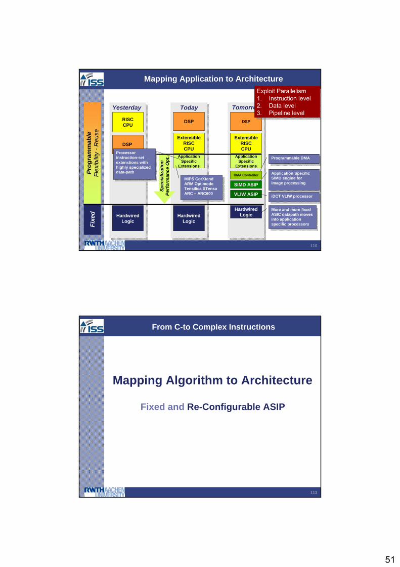
110
RISCCPU
DSP
HardwiredLogic
Mapping Application to Architecture
ApplicationSpecific
Extensions
ExtensibleRISCCPU
DSP
HardwiredLogic
VLIW ASIP
SIMD ASIP
DMA ControllerProg
ram
mab
leFl
exib
ility
-R
euse
Fixe
d
Today TomorrowYesterday
iDCT VLIW processoriDCT VLIW processor
Application Specific SIMD engine forimage processing
Application Specific SIMD engine forimage processing
Programmable DMAProgrammable DMA
More and more fixed ASIC datapath moves into application specific processors
More and more fixed ASIC datapath moves into application specific processors
ApplicationSpecific
Extensions
ExtensibleRISCCPU
DSP
Spec
ializ
atio
nPe
rfor
man
ce O
pt.
HardwiredLogic
MIPS CorXtendARM OptimodeTensilica XTensaARC – ARC600
MIPS CorXtendARM OptimodeTensilica XTensaARC – ARC600
Processor instruction-set extenstions with highly specialized data-path
Processor instruction-set extenstions with highly specialized data-path
Exploit Parallelism1. Instruction level2. Data level3. Pipeline level
Exploit Parallelism1. Instruction level2. Data level3. Pipeline level
113
Mapping Algorithm to Architecture
From C-to Complex Instructions
Fixed and Re-Configurable ASIP
52
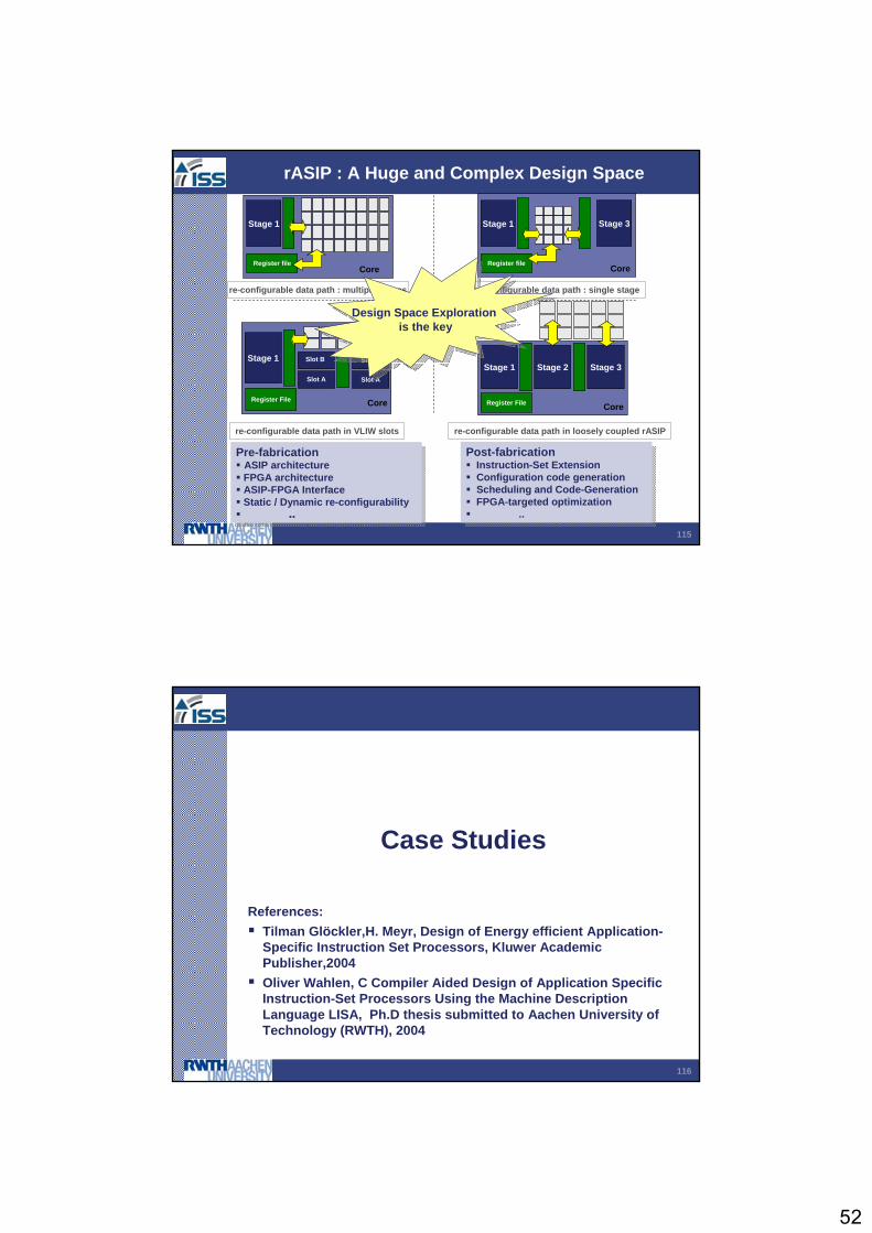
115
Stage 1
Register file
Stage 1 Stage 2 Stage 3
re-configurable data path : multiple stages
re-configurable data path in VLIW slots
re-configurable data path : single stage
re-configurable data path in loosely coupled rASIP
Register File Core
Core
Stage 1
Slot A
Register File Core
Slot A
Slot B Slot B
Stage 1
Register file Core
Stage 3
rASIP : A Huge and Complex Design Space
Post-fabricationInstruction-Set ExtensionConfiguration code generationScheduling and Code-GenerationFPGA-targeted optimization
..
Post-fabricationInstruction-Set ExtensionConfiguration code generationScheduling and Code-GenerationFPGA-targeted optimization
..
Pre-fabricationASIP architectureFPGA architectureASIP-FPGA InterfaceStatic / Dynamic re-configurability
..
Pre-fabricationASIP architectureFPGA architectureASIP-FPGA InterfaceStatic / Dynamic re-configurability
..
Design Space Exploration is the key
Design Space Exploration is the key
116
References:Tilman Glöckler,H. Meyr, Design of Energy efficient Application-Specific Instruction Set Processors, Kluwer Academic Publisher,2004Oliver Wahlen, C Compiler Aided Design of Application Specific Instruction-Set Processors Using the Machine Description Language LISA, Ph.D thesis submitted to Aachen University of Technology (RWTH), 2004
Case Studies
53
121
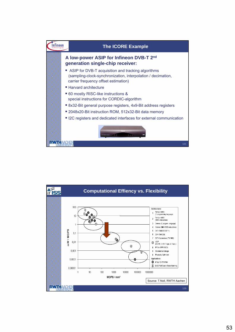
The ICORE Example
A low-power ASIP for Infineon DVB-T 2nd
generation single-chip receiver:ASIP for DVB-T acquisition and tracking algorithms
(sampling-clock-synchronization, interpolation / decimation, carrier frequency offset estimation)Harvard architecture60 mostly RISC-like instructions & special instructions for CORDIC-algorithm8x32-Bit general purpose registers, 4x9-Bit address registers2048x20-Bit instruction ROM, 512x32-Bit data memoryI2C registers and dedicated interfaces for external communication
129
Computational Effiency vs. Flexibility
Source: T.Noll, RWTH Aachen
54
130
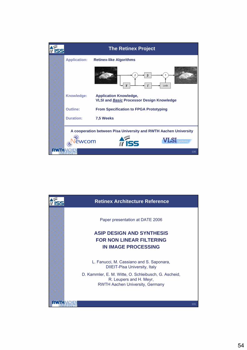
The Retinex Project
Application: Retinex-like Algorithms
Knowledge: Application Knowledge, VLSI and Basic Processor Design Knowledge
Outline: From Specification to FPGA Prototyping
Duration: 7,5 Weeks
β
ΓF LinSt
/ *
A cooperation between Pisa University and RWTH Aachen University
131
Retinex Architecture Reference
Paper presentation at DATE 2006
ASIP DESIGN AND SYNTHESIS FOR NON LINEAR FILTERING
IN IMAGE PROCESSING
L. Fanucci, M. Cassiano and S. Saponara, DIIEIT-Pisa University, Italy
D. Kammler, E. M. Witte, O. Schleibusch, G. Ascheid,R. Leupers and H. Meyr,
RWTH Aachen University, Germany
55
132
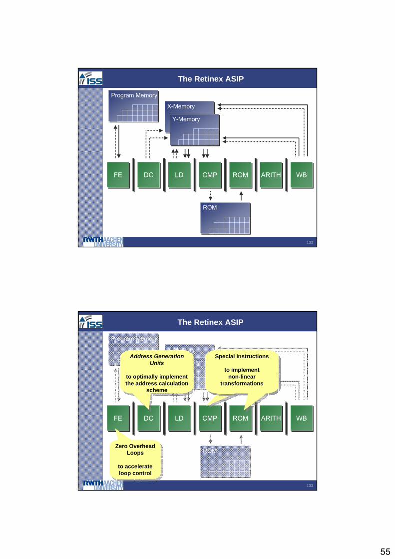
The Retinex ASIP
FEFE DCDC LDLD CMPCMP ROMROM ARITHARITH WBWB
Program MemoryProgram Memory
X-MemoryX-Memory
Y-MemoryY-Memory
ROMROM
133
The Retinex ASIP
FEFE DCDC LDLD CMPCMP ROMROM ARITHARITH WBWB
Program MemoryProgram Memory
X-MemoryX-Memory
Y-MemoryY-Memory
ROMROMZero OverheadLoops
to accelerateloop control
Zero OverheadLoops
to accelerateloop control
Address GenerationUnits
to optimally implement the address calculation
scheme
Address GenerationUnits
to optimally implement the address calculation
scheme
Special Instructions
to implement non-linear
transformations
Special Instructions
to implement non-linear
transformations
56
134
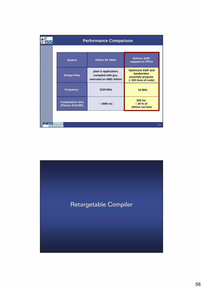
Performance Comparison
plain C-application, compiled with gcc,
executed on AMD Athlon
Optimized ASIP andhandwritten
assembly program (~100 lines of code)
Athlon XP 3000+ Retinex ASIP mapped on FPGA
2100 MHz 16 MHz
~ 3000 ms593 ms
~ 20 % of Athlon run-time
Design Flow
System
Frequency
Computation time(Picture 513x385)
Retargetable Compiler

57
136
Infineon PP32 Network Processor
0
20
40
60
80
100
120
140
160
180
200
frag tos hwacc route reed md5 crc
%
lccCoSy cycle countCoSy code size
0
20
40
60
80
100
120
140
160
180
200
frag tos hwacc route reed md5 crc
%
lccCoSy cycle countCoSy code size
137
ST200 VLIW Multimedia Processor
0
50
100
150
200
250
300
350
fir dct adpcm fht viterbigsm sieve
%
ST MultiflowCoSy cycle countCoSy code size
0
50
100
150
200
250
300
350
fir dct adpcm fht viterbigsm sieve
%
ST MultiflowCoSy cycle countCoSy code size
58
138
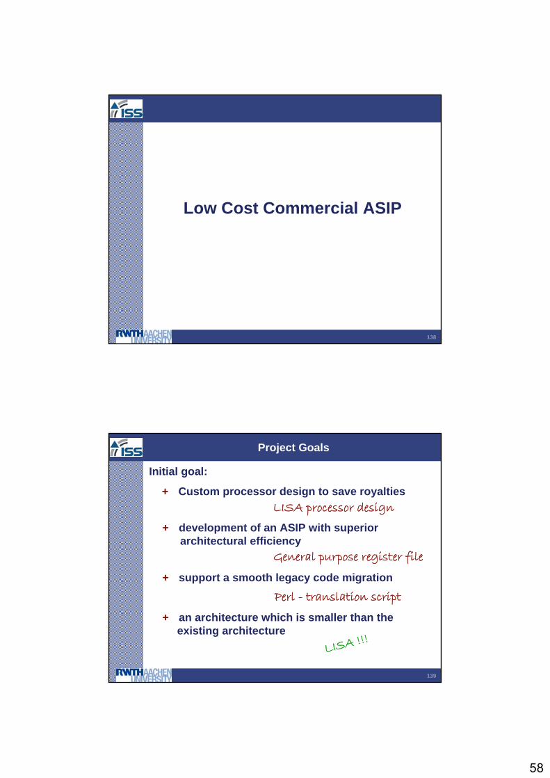
Increasing SW Content- but How?Low Cost Commercial ASIP
139
Project Goals
Initial goal:
+ Custom processor design to save royalties
+ development of an ASIP with superior architectural efficiency
+ support a smooth legacy code migration
+ an architecture which is smaller than the existing architecture
LISA processor design
General purpose register file
Perl - translation script
LISA !!!

59
140
Development Time Sheet
Initial Model 4 weeks
Design Space Analysis 3 weeks
Design Space Exploration 4 weeks- Address Calculation 1 week- Non-delayed Branches 1 week- Timing Improvement ½ week- Others 1½ weeks
Translation Script 5 weeks
Move Elimination 2 week
Verification Script 5 weeks
Synthesis & FPGA Mapping 1 day
FPGA System ( one time effort)10 weeks
Pha
se I
Pha
se II
141
Moving through the Design Space
1
2
3
4
5
6
7
First synthesis of verified RTL code, no port constraints, no optimizations
Memory port constraints, autom. optimization: path sharing
Grouping in functional units for more detailed analysis
Change in address calculationenabling resource sharing
Critical path analysis modification of fetch mechanism, optimization: decision minimization
Pin for FPGA prototype added
Implementation of non-delayed branches
prog-mem size reduction
Changed multiplier implementation from 32bit to 17bit
Removed functional unit grouping from
Final Synthesis: timing constraint adapted to synthesis results
8
9
10
3
1
2
3
4
5-7
8-910

60
Multimedia Processor
Processor Designer in a video deblocking unit

61
144Semiconductors
Multi standard video decoder IP
Coded bitstream
External memory
Reference frames
Deblocked frames
Core decoder
DBLK
145Semiconductors
Why Processor Designer ?
• Until now : a RTL block for each standard. => Make a generic block for all (changing !) video standards.
• A programmable architecture brings flexibility (C compilation).
• 288 conditionals filters (4 and 8 taps) to be done in 600 cycles.
• High throughput needed : custom operations and special memory addressing scheme are required.

62
146Semiconductors
DBLK architecture
DMA OUTDMA IN
Processor
Pixels memory
Prog. rom
Data ram
2x88 bits
147Semiconductors
Step 1 : function call
deblock()
DMA OUTDMA IN
Prog. rom
Data ram
Pixels memory
Application development :• Get quickly a C model for the system• Debug the application in a SystemC environment

63
148Semiconductors
Step 2 : integration of lt_risc_32p5• Provided model of RISC used• Compilation of application on the Lisa Processor• Memories latency are modelled in the pipeline
DMA OUTDMA IN
Prog. rom
Data ramProcessor(systemC/RTL)
Pixels memory
149Semiconductors
Step 3 : RTL generation and performance improvement
• RTL generation• C optimization• Asm. optimization• Use of specialized asm. instruction• Remove unnecessary asm. Instructions• Improve model for RTL generation (clock speed, area)
64
150Semiconductors
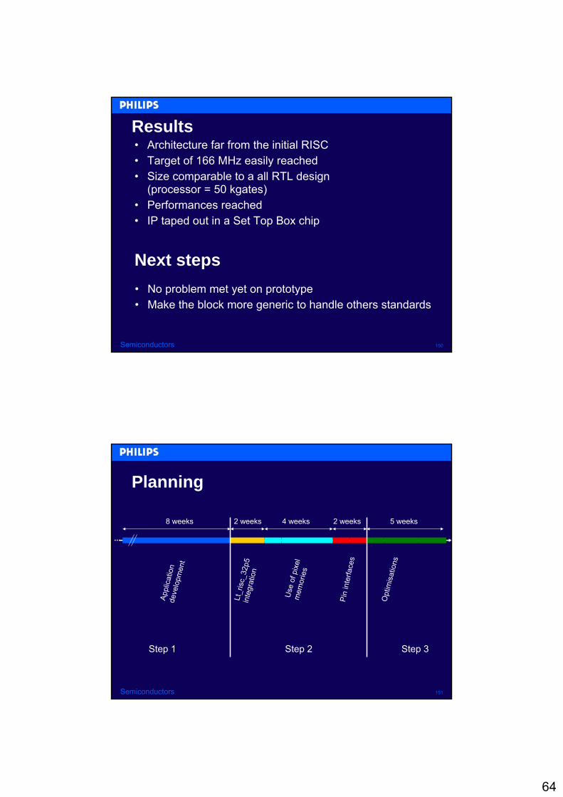
Results• Architecture far from the initial RISC• Target of 166 MHz easily reached• Size comparable to a all RTL design
(processor = 50 kgates)• Performances reached• IP taped out in a Set Top Box chip
Next steps• No problem met yet on prototype• Make the block more generic to handle others standards
151Semiconductors
Planning
8 weeks 2 weeks 4 weeks 2 weeks 5 weeks
Appl
icat
ion
deve
lopm
ent
Lt_r
isc_
32p5
inte
grat
ion
Use
of p
ixel
m
emor
ies
Pin
inte
rface
s
Opt
imis
atio
ns
Step 1 Step 2 Step 3
65
152Semiconductors
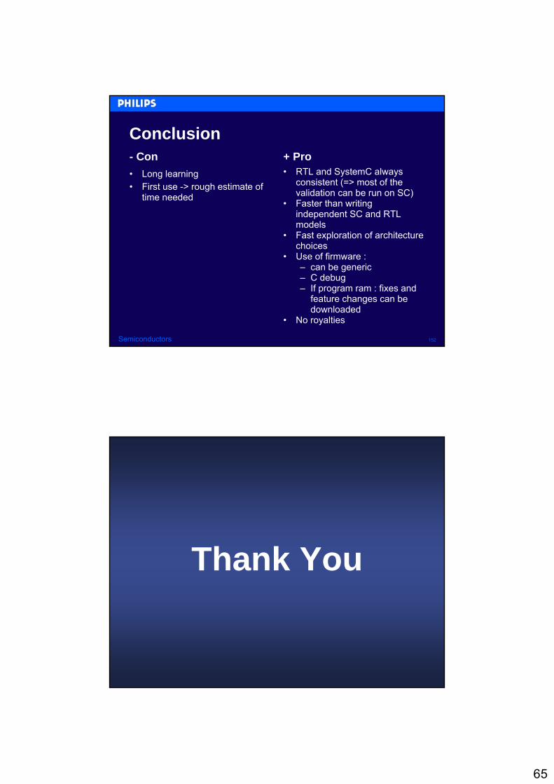
Conclusion- Con• Long learning• First use -> rough estimate of
time needed
+ Pro• RTL and SystemC always
consistent (=> most of the validation can be run on SC)
• Faster than writing independent SC and RTL models
• Fast exploration of architecture choices
• Use of firmware :– can be generic– C debug– If program ram : fixes and
feature changes can be downloaded
• No royalties
Thank You
Related Documents