Doctoral Thesis Signal Processing for Ultra Wideband Transceivers Christoph Krall ————————————– Faculty of Electrical Engineering and Information Technology Graz University of Technology, Austria First Examiner: Univ.-Prof. Dipl.-Ing. Dr.techn. Gernot Kubin Graz University of Technology, Austria Second Examiner: Prof. Dr.-Ing. Ilona Rolfes Leibniz Universit¨at Hannover, Germany Co-Advisor: Dipl.-Ing. Dr. Klaus Witrisal Graz University of Technology, Austria Graz, April 2008

Welcome message from author
This document is posted to help you gain knowledge. Please leave a comment to let me know what you think about it! Share it to your friends and learn new things together.
Transcript
Doctoral Thesis
Signal Processing for Ultra Wideband
Transceivers
Christoph Krall
————————————–
Faculty of Electrical Engineering and Information TechnologyGraz University of Technology, Austria
First Examiner:Univ.-Prof. Dipl.-Ing. Dr.techn. Gernot Kubin
Graz University of Technology, Austria
Second Examiner:Prof. Dr.-Ing. Ilona Rolfes
Leibniz Universitat Hannover, Germany
Co-Advisor:Dipl.-Ing. Dr. Klaus Witrisal
Graz University of Technology, Austria
Graz, April 2008
Kurzfassung
In dieser Dissertation werden neuartige Implementierungsansatze fur standardisierte undnicht standardisierte Ultra-Breitband (UBB) Systeme prasentiert. Diese Implementie-rungsmethoden inkludieren Signalverarbeitungsalgorithmen fur UBB Systeme im Sende-Empfanger Front-End sowie im digitalen Back-End.
Die Parallelisierung des Sende-Empfangers im Frequenzbereich wurde mit einer hybridenFilterbank durchgefuhrt. Das standardisierte MB-OFDM Signalisierungsschema erlaubteine Parallelisierung im Frequenzbereich durch die Verteilung der orthogonalen Trager aufmehrere Recheneinheiten. Weiters wurde die Kanalimpulsantwort im Frequenzbereich par-allelisiert und die dadurch auftretenden Effekte untersucht. Eine geringfugig schlechterePerformanz wurde beobachtet, welche auf die verkurzten Filterantworten und Fehlanpas-sungen im analogen Front-End zuruckgefuhrt werden koennen. Fur diese Performanzein-bußen wurden geeignete Fehlermaße definiert.
Fur die UBB Signalgenerierung wurde eine neuartige Methode erarbeitet. Zu diesemZweck werden mehrere Digital-zu-Analog Umsetzer in einer Struktur verwendet, um ei-ne flexible Signalgenerierung zu ermoglichen. Zuerst wurden die Umsetzer als ideal anden Abtastzeiten ausgerichtet angenommen, sodaß keine Fehlanpassungsspektren auftre-ten. Weiters wurden Zeitfehler betrachtet und eine Kompensationsarchitektur fur die auf-tretenden Fehler erarbeitet. Diese digitale Vorverzerrung wurde auf einem Demosystemimplementiert und kompensiert die Fehlanpassungsspektren um ca. 20 dB.
Des weiteren wurden Empfangerarchitekturen fur das standardisierte IEEE802.15.4a Si-gnalisierungsschema, welches breitbandige Pulse verwendet, untersucht. Drei Empfangerwurden in Einzel- und Mehrbenutzerszenarien verglichen. Ein in dieser Dissertation ausge-arbeiteter Empfanger zeigt einen großen Performanzgewinn, da der im Signal vorhandeneSpreizkode genutzt wird.
Um nichtlineare Verzerrungen welche bei hohen Datenraten in nichtkoharenten Empfanger-Front-Ends auftreten zu entzerren, wurde ein neuartiger Entzerralgorithmus ausgearbeitet.Der nichtline Entzerrer zweiter Ordnung wird mittels der Methode der kleinsten Fehler-quadrate optimiert und berechnet. Dieser nichtlineare Entzerrer ist eine Verallgemeinerungdes bekannten linearen Entzerrers. Weiters wurde dieser Entzerrer mit einem adaptivenLernalgorithmus verglichen, welcher asymptotisch gegen die hier vorgestellte Losung kon-vergiert. Dieser Entzerrer verbessert die nichtkodierte Bitfehlerrate um den Faktor 20.
i
Abstract
In this thesis novel implementation approaches for standardized and non-standardizedultra wide-band (UWB) systems are presented. These implementation approaches includesignal processing algorithms to achieve processing of UWB signals in transceiver front-endsand in digital back-ends.
A parallelization of the transceiver in the frequency-domain has been achieved withhybrid filterbank transceivers. The standardized MB-OFDM signaling scheme allows par-allelization in the frequency domain by distributing the orthogonal multicarrier modulationonto multiple units. Furthermore, the channel’s response to wideband signals has beenparallelized in the frequency domain and the effects of the parallelization have been investi-gated. Slight performance decreases are observed, where the limiting effects are truncatedsidelobes and filter mismatches in analog front-ends. Measures for the performance losshave been defined.
For UWB signal generation, a novel broadband signal generation approach is presented.For that purpose, multiple digital-to-analog converters are used in an array to achieveflexible (adaptive) signal generation. Firstly, the converters in the array are assumed to beperfectly aligned to the clock signals, such that no mismatch spectra occur. Secondly, timeoffsets are introduced in the converter model and a compensation algorithm is presented.A digital predistortion of the signals, to compensate for the mismatch spectra, is presentedand implemented, which achieves a reduction of the mismatch spectra by app. 20 dB.
Furthermore, receiver architectures for the standardized IEEE802.15.4a signaling scheme,which is a pulse-based signaling scheme, are investigated. A comparison of three receiversin single and multi-user environments is presented. It is seen that the receiver proposedin this thesis has superior performance in the multi-user case, because it uses spreadinginformation present in the standardized UWB signals.
To reduce the distortions encountered in non-coherent receiver architectures at highdata rates, a novel equalization algorithm for nonlinear receiver front-ends is presented.The nonlinear second-order equalizer can be optimized and computed according to a min-imum mean squared error (MMSE) criterion. It is found that the nonlinear equalizer is ageneralization of the linear equalizer equations. The solution is compared to an iterativelearning algorithm (LMS), which shows asymptotic convergence to the presented solution.The presented equalizer improves the uncoded BER floor by a factor of 20.
ii
Acknowledgement
First of all, I want to thank my two main supervisors throughout this thesis Dr. KlausWitrisal and Prof. Gernot Kubin for their continuous support and help. Many thanksalso to Prof. Ilona Rolfes from the University of Hannover, Germany for being the secondexaminer. I have to thank the Austrian Research Centers which funded this project,especially I want to thank Franco Fresolone, Gerhard Humer, and Reinhard Kloibhoferfor their help and support during the three years. Thanks also to the Christian DopplerForschungsgesellschaft for the three years funding of the project. My thanks also to Prof.Alle-Jan van der Veen and Dr. Geert Leus for their support and comments during myresearch visit in Delft. Thanks also to the Circuits and Systems Group at TU Delft, youmade life easier, far far away from home. Additionally, I want to thank Zoubir Irahhautenfor performing the measurements with me. Thanks also to Sven Dortmund from theInstitute of Radiofrequency and Microwave Engineering from University of Hanover forthe perfect measurements of our UWB antennas. Furthermore, I want to thank Dr.Heinz Koeppl from Ecole Polytechnique Federale de Lausanne, Switzerland for his valuablesuggestions and discussions. Thanks also to Manfred Stadler and Michael Leitner fromEPCOS OHG Deutschlandsberg for contributing the antennas and filters. Thanks also toall current and past members of SPSC who were with me the last three years. All yourinspiring discussions about work and non-work issues were very helpful for improving myskills and personality.
Furthermore, I want to thank my parents Maria and Johann Krall for their neverendingsupport during all the years since my birth. My thanks also include my two brothersHelmar and Hannes, with their families. Thanks also to my friends who were backing meup when I needed them, i.e., thanks Thomas, Johannes, Rene, Markus, Annika, Bettina,Andrea, Herbert, Franz, Lukas, Samantha, Stefan, Birgit, Doris, Christian M., ChristianS., Christian S., Christian T., Jurgen, Peter, Marco, Sebastian. Last but not least, I wantto thank Trent Reznor for making this awesome music and his continuous efforts againstmusic industry.
Graz, April 2008 Christoph Krall
iii

iv
Contents
1. Introduction 1
1.1. Motivation . . . . . . . . . . . . . . . . . . . . . . . . . . . . . . . . . . . . 3
1.2. Scope of the Work . . . . . . . . . . . . . . . . . . . . . . . . . . . . . . . . 4
1.3. Outline of the Thesis and Main Contributions . . . . . . . . . . . . . . . . . 5
2. Subband Modeling of UWB Transceivers 7
2.1. Standardized High-Speed UWB Signals . . . . . . . . . . . . . . . . . . . . 7
2.2. Modeling in Subbands . . . . . . . . . . . . . . . . . . . . . . . . . . . . . . 10
2.3. Parallel Transmitter Architecture for UWB OFDM Signals . . . . . . . . . 12
2.4. Subband Modeling of the Channel . . . . . . . . . . . . . . . . . . . . . . . 16
2.4.1. Design of the Filters for Subband Processing . . . . . . . . . . . . . 18
2.4.2. Frequency Response Masking Filter Design . . . . . . . . . . . . . . 19
2.4.3. Mapping the Transfer Function on the Filterbank . . . . . . . . . . . 21
2.4.4. Synthesizing the UWB Channel . . . . . . . . . . . . . . . . . . . . . 21
2.5. Parallel Receiver Architecture . . . . . . . . . . . . . . . . . . . . . . . . . . 22
2.6. Simulation Results . . . . . . . . . . . . . . . . . . . . . . . . . . . . . . . . 25
2.7. Conclusions . . . . . . . . . . . . . . . . . . . . . . . . . . . . . . . . . . . . 28
3. Pulse-Based UWB Communication 33
3.1. Introduction . . . . . . . . . . . . . . . . . . . . . . . . . . . . . . . . . . . . 33
3.2. Flexible Generation of UWB Signals . . . . . . . . . . . . . . . . . . . . . . 36
3.2.1. System Model . . . . . . . . . . . . . . . . . . . . . . . . . . . . . . . 37
3.2.2. Hardware Implementation . . . . . . . . . . . . . . . . . . . . . . . . 41
3.3. Compensation of Timing Offsets in TIDAC Structures . . . . . . . . . . . . 44
3.3.1. System Model . . . . . . . . . . . . . . . . . . . . . . . . . . . . . . . 45
3.3.2. Proposed Compensation Filters . . . . . . . . . . . . . . . . . . . . . 46
3.3.3. Timing Offset Identification . . . . . . . . . . . . . . . . . . . . . . . 47
3.4. Standardized IEEE 802.15.4a Receiver Architectures . . . . . . . . . . . . . 47
3.4.1. Standardized Signaling Scheme . . . . . . . . . . . . . . . . . . . . . 48
3.4.2. Receiver Architectures . . . . . . . . . . . . . . . . . . . . . . . . . . 49
v
3.4.3. Receiver Comparison . . . . . . . . . . . . . . . . . . . . . . . . . . . 53
3.5. Conclusions . . . . . . . . . . . . . . . . . . . . . . . . . . . . . . . . . . . . 56
4. Equalization for Nonlinear Receiver Front-Ends 59
4.1. Introduction . . . . . . . . . . . . . . . . . . . . . . . . . . . . . . . . . . . . 59
4.2. Equivalent Nonlinear System Model . . . . . . . . . . . . . . . . . . . . . . 61
4.2.1. Volterra Models . . . . . . . . . . . . . . . . . . . . . . . . . . . . . 62
4.2.2. Simplified Nonlinear System Model . . . . . . . . . . . . . . . . . . . 62
4.3. Nonlinear Equalization for Second-Order Volterra Systems . . . . . . . . . . 63
4.4. MMSE Volterra Filters . . . . . . . . . . . . . . . . . . . . . . . . . . . . . . 65
4.4.1. First-Order Equalizer . . . . . . . . . . . . . . . . . . . . . . . . . . 65
4.4.2. Second-Order Equalizer . . . . . . . . . . . . . . . . . . . . . . . . . 67
4.4.3. Adaptive Volterra Filters . . . . . . . . . . . . . . . . . . . . . . . . 69
4.4.4. Simulation Results . . . . . . . . . . . . . . . . . . . . . . . . . . . . 69
4.5. Conclusions . . . . . . . . . . . . . . . . . . . . . . . . . . . . . . . . . . . . 73
5. Conclusion and Outlook 75
A. UWB Chipsets 79
B. UWB Demonstrator 81
B.1. FPGA Hardware . . . . . . . . . . . . . . . . . . . . . . . . . . . . . . . . . 81
B.2. RF Front-End . . . . . . . . . . . . . . . . . . . . . . . . . . . . . . . . . . . 82
B.3. UWB Antennas . . . . . . . . . . . . . . . . . . . . . . . . . . . . . . . . . . 83
B.3.1. Matching . . . . . . . . . . . . . . . . . . . . . . . . . . . . . . . . . 85
B.3.2. Directivity Measurements . . . . . . . . . . . . . . . . . . . . . . . . 86
B.3.3. Gain Measurements . . . . . . . . . . . . . . . . . . . . . . . . . . . 91
C. Standardized UWB Channels 99
C.1. Statistical Channel Models . . . . . . . . . . . . . . . . . . . . . . . . . . . 99
C.1.1. Description of Different Propagation Effects . . . . . . . . . . . . . . 99
C.1.2. Statistical Modeling of the Path Loss Exponent . . . . . . . . . . . . 100
C.1.3. Fading . . . . . . . . . . . . . . . . . . . . . . . . . . . . . . . . . . . 102
C.1.4. General Shape of the Impulse Response . . . . . . . . . . . . . . . . 105
C.1.5. Path Interarrival Times . . . . . . . . . . . . . . . . . . . . . . . . . 105
C.1.6. Cluster Powers and Cluster Shapes . . . . . . . . . . . . . . . . . . . 106
C.2. Parameters of the IEEE 802.15.3a Channel Model . . . . . . . . . . . . . . 107
C.2.1. The Model . . . . . . . . . . . . . . . . . . . . . . . . . . . . . . . . 107
C.2.2. Channel Parameters . . . . . . . . . . . . . . . . . . . . . . . . . . . 108
C.3. The IEEE 802.15.4a Channel Model . . . . . . . . . . . . . . . . . . . . . . 109
C.3.1. The Model . . . . . . . . . . . . . . . . . . . . . . . . . . . . . . . . 110
D. Correlation Matrix for the Second-Order Equalizer 115
D.1. Commutation of the Kronecker Product . . . . . . . . . . . . . . . . . . . . 115
D.2. Correlation Matrix of the Data Terms . . . . . . . . . . . . . . . . . . . . . 115
vi

E. Derivation of the Compensation Filters 119E.1. Two-Periodic Nonuniform Holding Signals . . . . . . . . . . . . . . . . . . . 121
E.1.1. Solution of the Matrix Equation . . . . . . . . . . . . . . . . . . . . 121E.1.2. FIR Filter Design Example . . . . . . . . . . . . . . . . . . . . . . . 122
vii

viii
List of Abbreviations
ADC Analog-to-Digital Converter
AcR Autocorrelation Receiver
ALU Arithmetic Logic Unit
AWGN Additive White Gaussian Noise
BER Bit Error Ratio
BPM Burst Position Modulation
BPSK Binary-Phase-Shift-Keying
CIR Channel Impulse Response
CP Cyclic Prefix
CS Continuous Spectrum
DAC Digital-to-Analog Converter
DFT Discrete Fourier Transform
DS-SS Direct Sequence Spread Spectrum
DSP Digital Signal Processing
ECMA European Computer Manufacturers Association
ED Energy Detector
FCC Federal Communication Commission
FD Frame-Differential
FFT Fast Fourier Transform
FIR Finite Impulse Response
FPGA Field Programmable Gate Array
FRM Frequency Response Masking
FT Fourier Transform
GPS Global Positioning System
HDMI High-Definition Multimedia Interface
ix

IBI Inter-Block Interference
ICI Inter-Carrier Interference
IDFT Inverse Discrete Fourier Transform
IEEE Institute of Electrical and Electronics Engineers
IFFT Inverse Fast Fourier Transform
IIR Infinite Impulse Response
ISI Inter-Symbol Interference
ISO International Standards Organization
LO Local Oscillator
LOS Line-of-Sight
LMS Least Mean Square
LVDS Low Voltage Differential Signaling
MAC Medium Access Control of the OSI model
MBER Minimum Bit Error Ratio
MB-OFDM Multi-Band Orthogonal Frequency Division Multiplex
ML Maximum Likelihood
MMSE Minimum Mean Square Error
MPC Multi-Path Component
MRC Maximum Ratio Combining
MUI Multi-User Interference
NBI Narrow-Band Interference
NLOS Non-Line-of-Sight
OFDM Orthogonal Frequency Division Multiplex
OLA Overlap-add DFT computation
PAP Peak-to-Average Power
PSD Power Spectral Density
PHY Physical Layer of the OSI model
PPM Pulse Position Modulation
QAM Quadrature Amplitude Modulation
QPSK Quadrature-Phase-Shift-Keying
RF Radio-Frequency
RFID Radio-Frequency Identification
RMS Root Mean Square
RRC Root Raised Cosine
SER Symbol Error Ratio
SNR Signal-to-Noise Ratio
TDMA Time Division Multiple Access
TG3a Task Group 3a
x
TG4a Task Group 4a
TIDAC Time-Interleaved Digital-to-Analog Converter
TR Transmitted-Reference
USB Universal Serial Bus
UWB Ultra-Wideband
WLAN Wireless Local Area Network
WPAN Wireless Personal Area Network
WUSB Wireless Universal Serial Bus
ZF Zero Forcing
ZOH Zero-Order Hold
ZP Zero-Padded Prefix
xi
Chapter1Introduction
In recent years a growing demand on high-speed wireless communication has been recog-nized. This bandwidth demand is required to achieve cable replacement and high speedwireless personal area network (WPAN) communications applications. A further advan-tage of the high bandwidth used in broadband systems is high ranging and positioningaccuracy. In 2002, the Federal Communications Commission (FCC) released a report andorder to allow unlicensed operation of services between 3.1 and 10.6 GHz restricting theelectromagnetic emission level to a power spectral density (PSD) of -41.25 dBm/MHz [1].Furthermore, a definition of the term “Ultra Wide-Band (UWB)” has been given in thesame document. According to this authority, a UWB signal is defined as a signal whichhas a -10 dB bandwidth of at least 500 MHz or a fractional bandwidth which is greaterthan 0.2. The fractional bandwith is the bandwidth of a system normalized to the centerfrequency. This milestone in releasing spectrum for unlicensed operation fueled the mo-tivation of many researchers (at industries and at universities) to think of clever ideas todesign a system which can operate at such low emission levels. Nonetheless, the communi-cation system has to be robust against noise and interference from other, already existingservices in the same spectrum like WLAN, GPS, etc. Usually these systems transmit withmuch higher power but operate in restriced, licensed (mostly for very high cost) spectralregions provided by national authorities.
To cover the main target applications promised by the distinguished wideband featuresof UWB technology, two different standardized signaling schemes have been developed.For the first one, the focus was clearly on the cable replacement and short-range high-speed data communication networks, e.g., Wireless USB R© 2.0, Wireless FireWire R© (IEEE1394a), Wireless HDMI, etc. To combine all the different perspectives about implement-ing such a high speed WPAN system, the IEEE formed a standardization task group(IEEE 802.15.3a) which tried to standardize the physical requirements and the mediumaccess control for such a novel communication system. Within this standardization pro-cess, many different schemes were submitted to the standardization committee, but finallynone of them could get the majority of the votes and the task group failed in its mission.Afterwards one of the proposals (the one with major industry support) was standardizedwithin the European Computer Manufacturers Association (ECMA) and consecutivelywithin the International Organization for Standardization (ISO). Finally, industry hasformed the WiMedia alliance which adopted the ECMA/ISO standard. Many chipsets are
1
Chapter 1. Introduction
2 3 4 5 6 7 8 9 10 11
United States
EU Europe
Japan Japan
Korea Koreaf/GHz
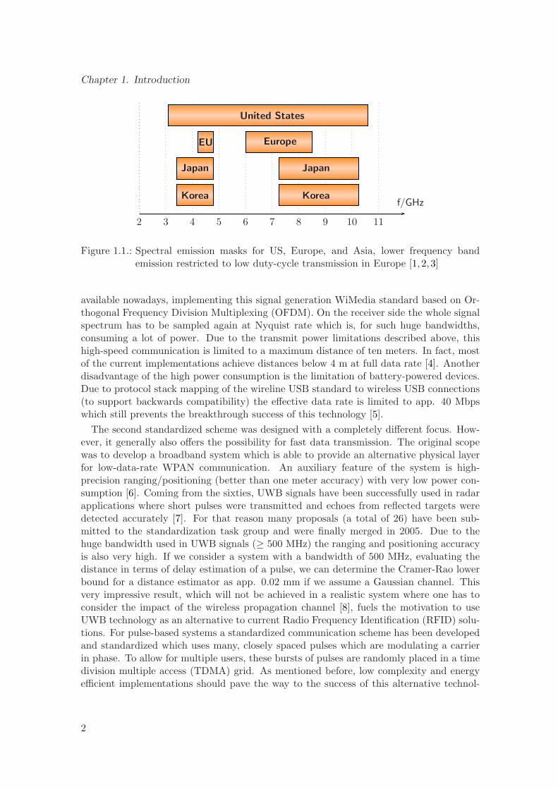
Figure 1.1.: Spectral emission masks for US, Europe, and Asia, lower frequency bandemission restricted to low duty-cycle transmission in Europe [1, 2, 3]
available nowadays, implementing this signal generation WiMedia standard based on Or-thogonal Frequency Division Multiplexing (OFDM). On the receiver side the whole signalspectrum has to be sampled again at Nyquist rate which is, for such huge bandwidths,consuming a lot of power. Due to the transmit power limitations described above, thishigh-speed communication is limited to a maximum distance of ten meters. In fact, mostof the current implementations achieve distances below 4 m at full data rate [4]. Anotherdisadvantage of the high power consumption is the limitation of battery-powered devices.Due to protocol stack mapping of the wireline USB standard to wireless USB connections(to support backwards compatibility) the effective data rate is limited to app. 40 Mbpswhich still prevents the breakthrough success of this technology [5].
The second standardized scheme was designed with a completely different focus. How-ever, it generally also offers the possibility for fast data transmission. The original scopewas to develop a broadband system which is able to provide an alternative physical layerfor low-data-rate WPAN communication. An auxiliary feature of the system is high-precision ranging/positioning (better than one meter accuracy) with very low power con-sumption [6]. Coming from the sixties, UWB signals have been successfully used in radarapplications where short pulses were transmitted and echoes from reflected targets weredetected accurately [7]. For that reason many proposals (a total of 26) have been sub-mitted to the standardization task group and were finally merged in 2005. Due to thehuge bandwidth used in UWB signals (≥ 500 MHz) the ranging and positioning accuracyis also very high. If we consider a system with a bandwidth of 500 MHz, evaluating thedistance in terms of delay estimation of a pulse, we can determine the Cramer-Rao lowerbound for a distance estimator as app. 0.02 mm if we assume a Gaussian channel. Thisvery impressive result, which will not be achieved in a realistic system where one has toconsider the impact of the wireless propagation channel [8], fuels the motivation to useUWB technology as an alternative to current Radio Frequency Identification (RFID) solu-tions. For pulse-based systems a standardized communication scheme has been developedand standardized which uses many, closely spaced pulses which are modulating a carrierin phase. To allow for multiple users, these bursts of pulses are randomly placed in a timedivision multiple access (TDMA) grid. As mentioned before, low complexity and energyefficient implementations should pave the way to the success of this alternative technol-
2
1.1. Motivation
ogy. This is possible because of the TDMA structure where transceivers can be switchedoff in long idle periods. On the other hand the receiver structures used to recover thetransmitted signals are very simple. They simply try to recover, i.e., determine and storethe energy present in a certain frequency band. According to the cumulated energy adecision is made on the transmitted data. However, the propagation channel can severelydistort the signals, which is a very challenging problem for a system designer. Even morechallenging is the nonlinear behavior of the front-end elements. Interference from servicesoperating in the same spectrum additionally limit the performance of these highly diversesystems.
Recently, the European Union also released a recommendation for the emitted powerspectral density (PSD) which has to be implemented individually by the member states [2].The European view on the unlicensed and free operation of wideband communicationsystems is more conservative than the one in the US. Potential victim services like WLANand GPS are explicitly bypassed and the available frequency range was split in two parts.Fig. 1.1 shows the regulation for the US, the proposed regulation masks for the EU, andthe regulations for important markets in Asia. It is clearly seen that a device operatingworldwide is very restricted in using the full spectral resources.
1.1. Motivation
As mentioned before, the novel Ultra Wide-Band technology also brings a lot of challengesacross all different disciplines of electrical engineering. First of all, the circuit design ofsuch systems touches the current limits of the technology for baseband signal processingand for RF circuitry used for carrier generation, mixing, etc. Furthermore, broadbandantennas and matching networks for flexible and reconfigurable front-ends have to bedesigned. Last but not least, many new/modified network protocols have to be foundand efficiently implemented to provide reliable and well performing devices for the specificscenarios. The main motivation for the industrial partner supporting this thesis was tofind implementation strategies for a realtime channel simulation environment built withstate of the art FPGA and DSP hardware. However, the UWB technology still requiresmore computational power than available on today’s hardware.
Keeping these hardware limitations in mind, it is not a trivial task to generate broadbandsignals in a UWB tranmitter because of their huge bandwidth to be processed. Restrictingour considerations not only to standardized UWB signals, the generation of pulse-basedwideband signals consists only of a few components which appears easy, but requires dif-ficult timing circuitry to generate pulses at the desired positions in time. However, sucha simple circuitry is also not the first choice when designing a universal hardware simu-lator which supports different waveforms. Furthermore, one standardized UWB systemfor high-speed wireless personal area networks (WPAN) is employing a broadband OFDMsignal to transmit data. Implementing this signal generation on FPGA hardware is in-deed not easy considering the bandwidth constraints inherently present on the simulationboards. If a parallelization or distribution of the computational complexity can be found,they can be implemented without major changes in the currently available hardware. Fur-thermore, if this parallelization can be realized on conventional digital signal processing(DSP) hardware, the same results can help chip designers to find more efficient chips with
3
Chapter 1. Introduction
relaxed conditions for the individual processing units.
Due to the huge bandwidth, the wireless propagation channel contains severe multipathwhich is complicating (and simplifying at the same time) the receiver design. Because theenergy of the transmitted signal is spread in time one can think of collecting this energyfrom each multipath component (MPC) and coherently combine this energy resulting inan optimal receiver. By doing this, the energy contained in the MPCs is collected like theleaves with a garden rake, providing the name for this receiver architectures, i.e., Rakereceivers. However, the implementation complexity of such a Rake receiver is very hugeconsidering that an UWB channel consists of hundreds of MPCs, each requiring a correla-tor for correct signal reception. Current implementations restrict the number of paths toapp. 10 which gives a tradeoff between implementation complexity and performance forthis suboptimal receiver. Furthermore, other sub-optimal receiver structures have beenproposed already during the years of research in the area. One main drawback of thesearchitectures is that they employ nonlinearities in their analog front-ends resulting in morecomplex processing in the back-end to recover the data symbols.
All these current implementation issues necessitate research in various areas of thefield of electrical engineering. Some of these are adressed in this thesis. However, thehardware limits due to the given architecture are considered as well which will becomeclear throughout the thesis.
1.2. Scope of the Work
Within this work, current implementation challenges in terms of signal processing withcurrently available DSP hardware used for UWB devices are investigated. This means thatstructures have been investigated to process the enormous bandwidth of UWB signals ontransmitter and receiver side. However, one main difference to conventional narrowbandsystems lies in the difference of the mobile radio channel which is not flat fading anymore.For that reason a more complex model for channel simulation has to be used which exceedsthe capabilities of currently available DSP hardware. Thus, ways of distributing thecomputational requirements and computational complexity on multiple systems have tobe investigated and are shown in this thesis.
Not only the implementation of the channel simulator is a complicated task when movingto higher bandwidths. Also the signal generation and receiver architectures are required toprocess the broadband signals. Thus, a transmitter and receiver architecture is presentedin this thesis which overcomes this bandwidth limitation. Furthermore, a technique forarbitrary signal generation of very wideband signals is presented in the thesis. However,in a first step, the computations for this system are studied for the error free case. After-wards hardware mismatches have been introduced and a compensation structure for thesemismatches is presented.
For the previously described nonlinear receiver front-ends, appropriate modeling anda theoretical bound, for the processing which is done in the back-end (digital domain)of the receiver is presented. A framework for nonlinear fading memory systems is pre-sented and one possible strategy to combat the nonlinear distortion effects caused by thenonlinearity inherently present in the analogue front-end. Furthermore, first steps of im-plementing UWB systems for demonstrating the algorithms and methods evaluated by
4
1.3. Outline of the Thesis and Main Contributions
means of simulations and measurements.
1.3. Outline of the Thesis and Main Contributions
This thesis is organized as follows: Several sections of this thesis have been publishedat international conferences and in international journals. In this short summary, theaccording publications are thus mentioned in the context of the respective chapters.In chapter 2 the parallelization of a UWB communication channel in the frequency do-main is presented. Furthermore, a novel signal generation approach is shown, whichdemonstrates the parallelization for the generation of one standardized OFDM symbol forthe WiMedia standard for WPAN applications. Furthermore, a subband receiver architec-ture is presented and the performance is compared to conventionally used receivers, i.e.,receivers able to process the whole bandwidth.
• Christoph Krall and Klaus Witrisal, Parallel OFDM Signal Generation for UWBSystems, in Proceedings of the IEEE International Conference on Ultra Wideband(ICUWB2006), Waltham, MA, September 2006, pp. 243-247. [9]
In chapter 3 methods for the implementation of a pulse-based UWB communication sys-tem are presented. For a flexible simulation environment a method for the generationof wideband pulses is presented. For that reason multiple Digital-to-Analog Converters(DACs) are used. Furthermore, a method for the compensation of mismatches in a con-verter array is presented in this chapter. Finally, a novel receiver architecture for thestandardized scheme is presented and compared to other possible receiver candidates forthe standardized scheme.
• Christoph Krall, Christian Vogel, and Klaus Witrisal, Time-Interleaved Digital-to-Analog Converters for UWB Signal Generation, in Proceedings of the IEEE Inter-national Conference on Ultra-Wideband 2007 (ICUWB2007), Singapore, Singapore,24-26 September 2007. [10]
• Christian Vogel and Christoph Krall, Compensation of Distortions Due to PeriodicNonuniform Holding Signals, submitted to IEEE 6th Symposium on CommunicationSystems, Networks and Digital Signal Processing (CSNDSP), Graz, Austria, July2008.
In chapter 4 a framework for modeling a sub-optimal nonlinear receiver front-end is pre-sented. However, the presented scheme is a non-standardized one. Anyhow, the perfor-mance in terms of Bit Error Ratio (BER) [11], robustness to Narrow-Band Interference(NBI) [12] and Multi-User Interference (MUI) [13], and robustness to the effects of thechannel (harsh environments) is promising and thus the system is invesitgated. It is shownthat the receiver output depends nonlinearly on the transmitted data symbols and non-linear techniques for an equalization of front-ends have to be used to combat the effectsof the nonlinear receiver.
• Christoph Krall, Klaus Witrisal, Heinz Koeppl, Geert Leus and Marco Pausini,Nonlinear Equalization for Frame-Differential IR-UWB Receivers, in Proceedings ofthe IEEE International Conference on Ultra-Wideband 2005 (ICU 2005), Zurich,Switzerland, 5-8 September 2005, pp. 576-581. [14]
5

Chapter 1. Introduction
• Christoph Krall, Klaus Witrisal, Geert Leus and Heinz Koeppl, Nonlinear Equaliza-tion for Second-Order Volterra Systems, submitted to IEEE Transactions on SignalProcessing.
In chapter 5 conclusions about the presented methods are summarized. The chapters aresupported with several appendices, which provide detailed equations, measurement resultsand supporting information to the topics covered in the thesis chapters.
6
Chapter2Subband Modeling of UWB Transceivers
In this chapter the standardized high-speed, WPAN UWB systems used as cable replace-ment is introduced. An implementation on a parallel architecture is proposed and ana-lyzed [15]. The application of this idea is two-fold. First of all, a new parallel transceiverarchitecture is found. Secondly, if the simulation of a broad range of environments isdesired to be computed on hardware for transceiver prototyping, the implementation ofa channel impulse response on digital signal processing (DSP) hardware is necessary. Forthat reason, efficient ways of mapping the broadband frequency response of a UWB chan-nel onto a parallel architecture of FPGA/DSP boards is discussed. Additionally, an analogsignal conditioning has to be done to not violate the sampling theorem. For the transceiverand the wireless propagation channel a hybrid filterbank approach is proposed to be ableto process parts of the huge signal bandwidth on a parallel DSP platform. If sufficientsignal separation for processing on multiple computing units can be achieved, each unitcan be optimized separately and computational costs can be saved for each unit. Further-more, to extend the system to be able to generate a standardized UWB signals, all thesignal generation units have to be used in parallel. This can be done in a very efficient wayconsidering a parallelization of the essential signal generation operation, the inverse fastFourier transform (IFFT). Additionally, a parallel receiver implementation is discussed inthe last section of this chapter1.
2.1. Standardized High-Speed UWB Signals
When the FCC authorized unlicensed transmission in the 3.1 - 10.6 GHz frequency bandin 2002, the IEEE was forming a task group to specify a standardized communicationsystem for wireless personal area networks (WPANs), capable of transmitting at speedsup to 480 Mbps data rate. This task group was assigned to the WPAN activities in theIEEE 802.15 standardization body and was called Task Group 3a (TG3a), looking foran alternative physical layer for WPANs. Conventionally, such a task group has severalsub-groups defining different items for the upcoming standard like a model for the wire-less broadband channel for different scenarios, signaling, etc. For the wireless channel,
1The section about the parallel signal generation for OFDM UWB signals and the respective simulationresults has been published by the author on an international conference [9].
7
Chapter 2. Subband Modeling of UWB Transceivers
measurements have been used to characterize a fully stochastic channel model which canbe used for the different specified scenarios. This channel model is summarized in Ap-pendix C. It is based on the measurement campaigns conducted in 2002 and 2003 (see [16]and references therein). Due to the problem that the industry was pushing the new tech-nology to get a standardized model as an input for the system design, the model is verygeneral and partly inaccurate. These channel models have been refined in another taskgroup (TG4a) where more physical effects have been considered and modeled [17].
For standardized signaling, many proposals have been submitted to the standardizationtask group. However, two major proposals have been selected to get a majority vote on,and to get one or both of them standardized. The first one was supported widely byindustry and has been submitted by a group of researchers from Texas Instruments [18]in 2004. This proposal describes a multiband orthogonal frequency division multiplexed(OFDM) signal with a bandwidth of 528 MHz, which is hopped very fast in frequency.The second proposal was a broadband direct sequence spread spectrum (DS-SS) signalwhich was also occupying a bandwidth larger than 500 MHz [19]. However, none ofthe two proposals could get the majority of the votes and finally, the task group failedin standardizing a signaling scheme. For that reason, the first proposal (which had alot of industrial supporters) was submitted to the European Computer ManufacturingAssociation (ECMA) to be standardized there. There it was standardized in Dec. 2005and a final standardization document was released [15]. Consecutively, a standardizationhas been done of the same scheme within the International Standards Organization (ISO)and was published under the number ISO 26907 [20]. By standardizing this scheme,industry had a worldwide standard for implementing high-speed UWB systems whichpushed many companies to have products on the market. Nowadays, the first solutions arearound from several manufacturers providing chipsets up to 480 Mbps realizing a wirelessUSB connection (see App. A). However, a breakthrough of this technology is still laggingbehind because of the backwards compatibility of the system to wireline USB connections,limiting the effective data rate [5]. All supporters and partners of this standardizationhave been gathered in the WiMedia Organization (www.wimedia.org) which also hoststhe current version of the standard and makes minor refinements [21].
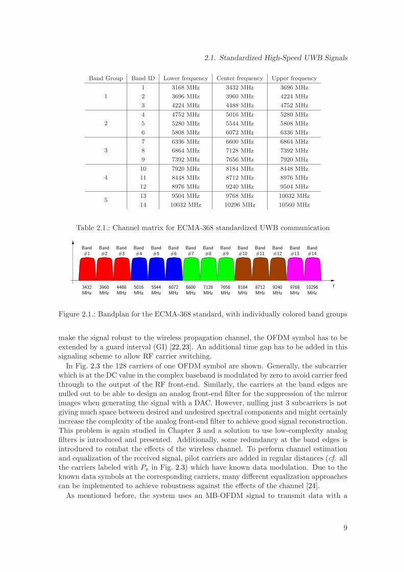
WiMedia Standard As already mentioned, finally the WiMedia standard for high-speeddata communication is used nowadays to implement high-speed UWB systems. For thatreason its general signal structure is discussed here and a proposal for a parallel systemimplementation is presented in later sections. For the 7.5 GHz bandwidth available in theUS, the standardized system uses 14 partitions for transmitting a fast frequency-hopped-signal. These frequency channels are summarized in Table 2.1 and visualized in Fig. 2.1,respectively. It is furthermore seen that the 14 channels are separated into 5 band groups,each occupying either 1 GHz or 1.5 GHz of bandwidth. So called “Mode 1” devices aresupposed to hop the first three channels, i.e., all channels in band group 1. If we reconsiderthe frequency ranges released by the regulation authorities in different parts of the world(cf. Fig. 1.1) not many of these channels remain if a worldwide device is required.
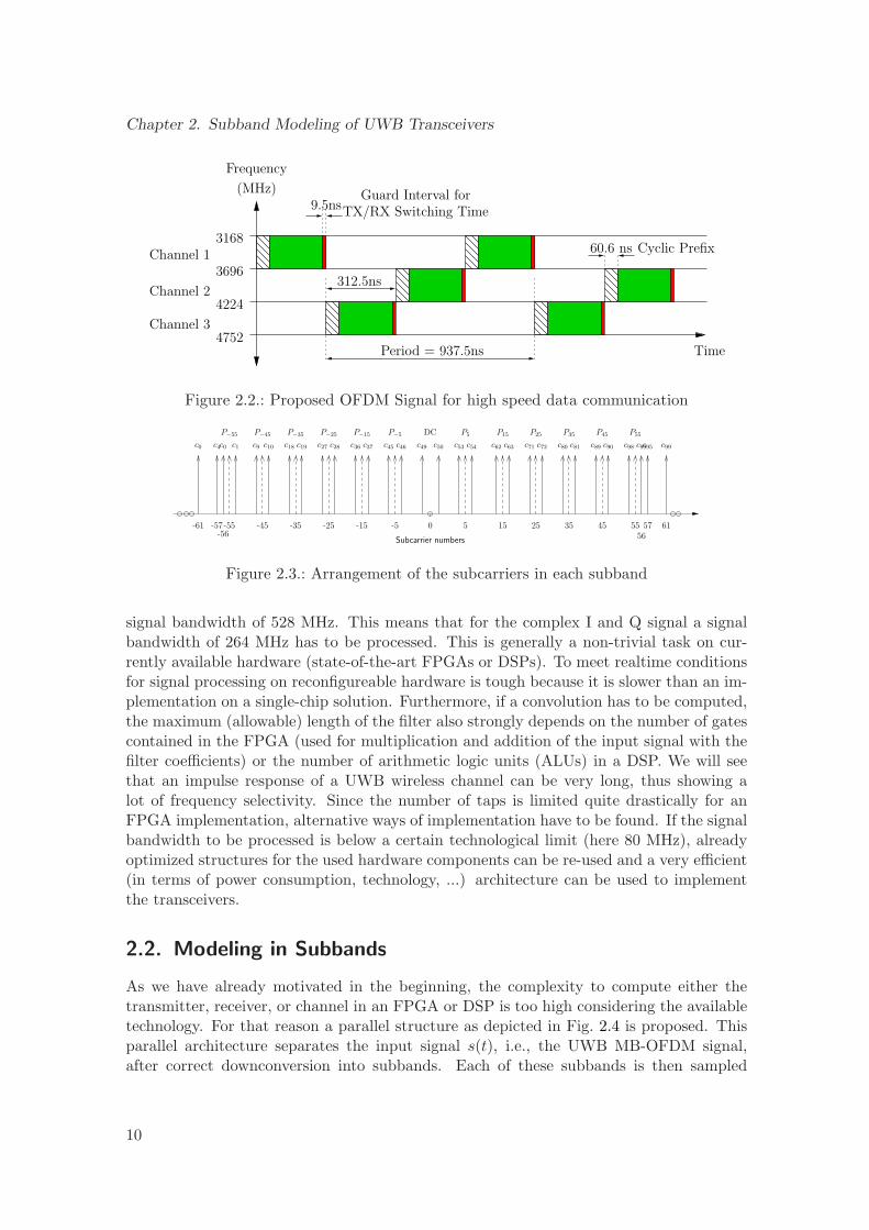
The currently standardized signal is, as already mentioned, a multiband OFDM (MB-OFDM) signal. The OFDM signal consists of 128 carriers which are modulated with QPSKdata symbols. The bandwidth of one OFDM symbol is specified as 528 MHz. A possiblehopping sequence and the timings for one UWB OFDM symbol are shown in Fig. 2.2. To
8
2.1. Standardized High-Speed UWB Signals
Band Group Band ID Lower frequency Center frequency Upper frequency
1
1 3168 MHz 3432 MHz 3696 MHz
2 3696 MHz 3960 MHz 4224 MHz
3 4224 MHz 4488 MHz 4752 MHz
2
4 4752 MHz 5016 MHz 5280 MHz
5 5280 MHz 5544 MHz 5808 MHz
6 5808 MHz 6072 MHz 6336 MHz
3
7 6336 MHz 6600 MHz 6864 MHz
8 6864 MHz 7128 MHz 7392 MHz
9 7392 MHz 7656 MHz 7920 MHz
4
10 7920 MHz 8184 MHz 8448 MHz
11 8448 MHz 8712 MHz 8976 MHz
12 8976 MHz 9240 MHz 9504 MHz
513 9504 MHz 9768 MHz 10032 MHz
14 10032 MHz 10296 MHz 10560 MHz
Table 2.1.: Channel matrix for ECMA-368 standardized UWB communication
f
#1
Band
3432
MHz
Band
#2
Band
#3
Band
#4
Band
#5 #6
Band Band
#7
Band
#8
Band
#9
Band
#10
Band
#11
Band
#12
Band
#13
Band
#14
MHz MHz MHzMHz MHzMHz MHz MHz MHz MHz MHz MHz MHz
3960 4488 5016 5544 6072 9768 102966600 7128 7656 8184 8712 9240
Figure 2.1.: Bandplan for the ECMA-368 standard, with individually colored band groups
make the signal robust to the wireless propagation channel, the OFDM symbol has to beextended by a guard interval (GI) [22,23]. An additional time gap has to be added in thissignaling scheme to allow RF carrier switching.
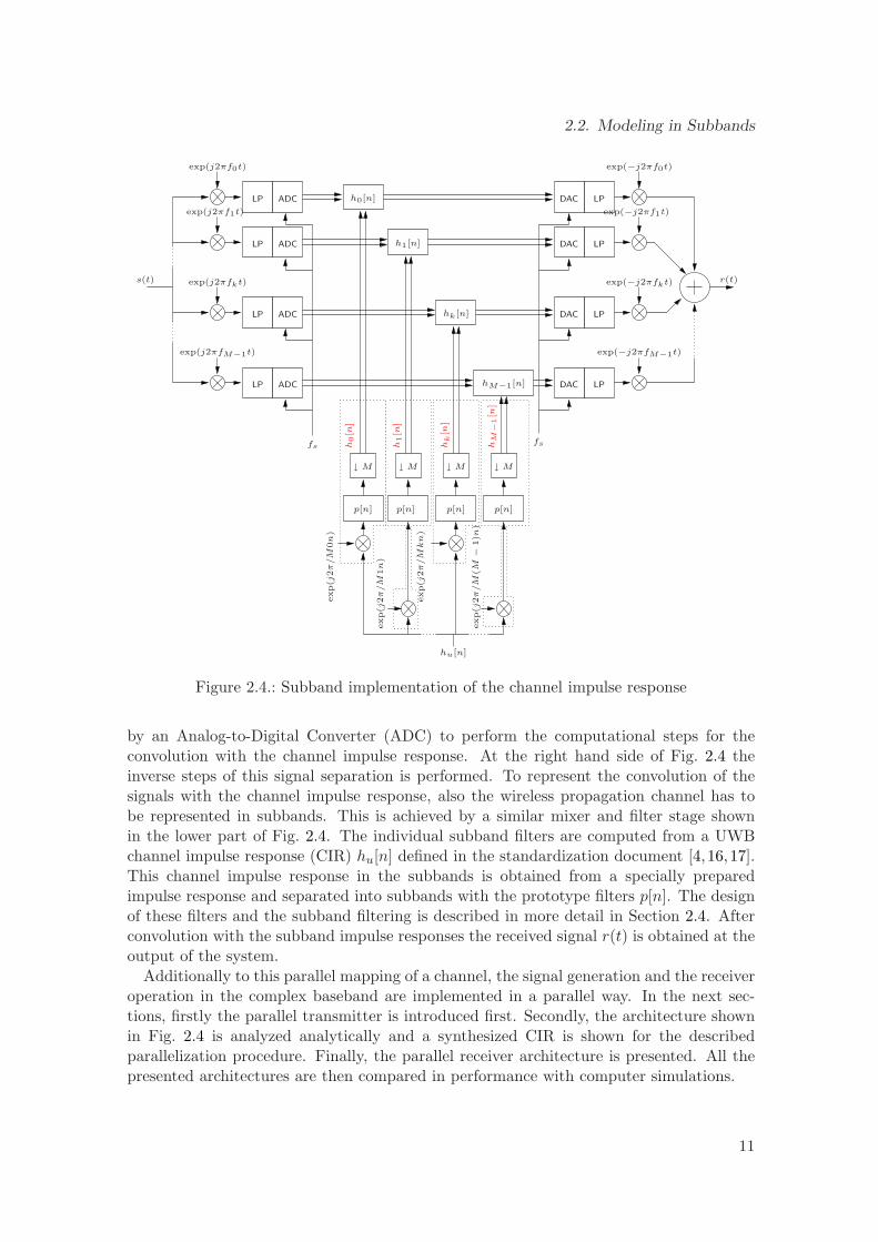
In Fig. 2.3 the 128 carriers of one OFDM symbol are shown. Generally, the subcarrierwhich is at the DC value in the complex baseband is modulated by zero to avoid carrier feedthrough to the output of the RF front-end. Similarly, the carriers at the band edges arenulled out to be able to design an analog front-end filter for the suppression of the mirrorimages when generating the signal with a DAC. However, nulling just 3 subcarriers is notgiving much space between desired and undesired spectral components and might certainlyincrease the complexity of the analog front-end filter to achieve good signal reconstruction.This problem is again studied in Chapter 3 and a solution to use low-complexity analogfilters is introduced and presented. Additionally, some redundancy at the band edges isintroduced to combat the effects of the wireless channel. To perform channel estimationand equalization of the received signal, pilot carriers are added in regular distances (cf. allthe carriers labeled with Px in Fig. 2.3) which have known data modulation. Due to theknown data symbols at the corresponding carriers, many different equalization approachescan be implemented to achieve robustness against the effects of the channel [24].
As mentioned before, the system uses an MB-OFDM signal to transmit data with a
9
Chapter 2. Subband Modeling of UWB Transceivers
Frequency
(MHz)
3168
3696Channel 1
4224
4752
Channel 2
Channel 3
9.5nsTX/RX Switching TimeGuard Interval for
Period = 937.5ns
312.5ns
60.6 ns Cyclic Prefix
Time
Figure 2.2.: Proposed OFDM Signal for high speed data communication
0
Subcarrier numbers
5 15 25 35 45 5556
57 61-5-15-25-35-45-55-56
-57-61
c0 c4 c1 c10 c19 c28 c37 c46 c49 c50 c54 c63 c72 c81 c90 c99c95 c99c0
P−55
c9
P−45
c18
P−35
c27
P−25
c36
P−15
c45
P−5
c53
P5
c62
P15
c71
P25
c80
P35
c89
P45
c98
P55DC
Figure 2.3.: Arrangement of the subcarriers in each subband
signal bandwidth of 528 MHz. This means that for the complex I and Q signal a signalbandwidth of 264 MHz has to be processed. This is generally a non-trivial task on cur-rently available hardware (state-of-the-art FPGAs or DSPs). To meet realtime conditionsfor signal processing on reconfigureable hardware is tough because it is slower than an im-plementation on a single-chip solution. Furthermore, if a convolution has to be computed,the maximum (allowable) length of the filter also strongly depends on the number of gatescontained in the FPGA (used for multiplication and addition of the input signal with thefilter coefficients) or the number of arithmetic logic units (ALUs) in a DSP. We will seethat an impulse response of a UWB wireless channel can be very long, thus showing alot of frequency selectivity. Since the number of taps is limited quite drastically for anFPGA implementation, alternative ways of implementation have to be found. If the signalbandwidth to be processed is below a certain technological limit (here 80 MHz), alreadyoptimized structures for the used hardware components can be re-used and a very efficient(in terms of power consumption, technology, ...) architecture can be used to implementthe transceivers.
2.2. Modeling in Subbands
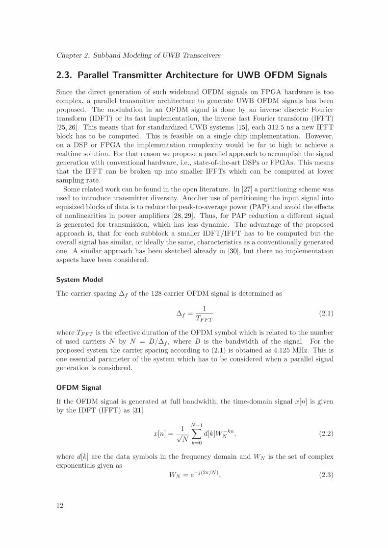
As we have already motivated in the beginning, the complexity to compute either thetransmitter, receiver, or channel in an FPGA or DSP is too high considering the availabletechnology. For that reason a parallel structure as depicted in Fig. 2.4 is proposed. Thisparallel architecture separates the input signal s(t), i.e., the UWB MB-OFDM signal,after correct downconversion into subbands. Each of these subbands is then sampled
10
2.2. Modeling in Subbands
↓ M ↓ M↓ M↓ M
p[n]p[n]p[n]p[n]
r(t)s(t)
h0[n]
h1[n]
hk[n]
hM−1[n]
LP
LP
LP
LP LP
LP
LP
LP
ADC
ADC
ADC
ADC
DAC
DAC
DAC
DAC
hu[n]
exp(j2πf0t)
exp(j2πf1t)
exp(j2πfkt)
exp(j2πfM−1t)
exp(−j2πf0t)
exp(−j2πf1t)
exp(−j2πfkt)
exp(−j2πfM−1t)
fsfs
exp(j
2π
/M
0n)
exp(j
2π
/M
1n)
exp(j
2π
/M
kn)
exp(j
2π
/M
(M−
1)n
)
h0[n
]
h1[n
]
hk[n
]
hM
−1[n
]
Figure 2.4.: Subband implementation of the channel impulse response
by an Analog-to-Digital Converter (ADC) to perform the computational steps for theconvolution with the channel impulse response. At the right hand side of Fig. 2.4 theinverse steps of this signal separation is performed. To represent the convolution of thesignals with the channel impulse response, also the wireless propagation channel has tobe represented in subbands. This is achieved by a similar mixer and filter stage shownin the lower part of Fig. 2.4. The individual subband filters are computed from a UWBchannel impulse response (CIR) hu[n] defined in the standardization document [4,16,17].This channel impulse response in the subbands is obtained from a specially preparedimpulse response and separated into subbands with the prototype filters p[n]. The designof these filters and the subband filtering is described in more detail in Section 2.4. Afterconvolution with the subband impulse responses the received signal r(t) is obtained at theoutput of the system.
Additionally to this parallel mapping of a channel, the signal generation and the receiveroperation in the complex baseband are implemented in a parallel way. In the next sec-tions, firstly the parallel transmitter is introduced first. Secondly, the architecture shownin Fig. 2.4 is analyzed analytically and a synthesized CIR is shown for the describedparallelization procedure. Finally, the parallel receiver architecture is presented. All thepresented architectures are then compared in performance with computer simulations.
11
Chapter 2. Subband Modeling of UWB Transceivers
2.3. Parallel Transmitter Architecture for UWB OFDM Signals
Since the direct generation of such wideband OFDM signals on FPGA hardware is toocomplex, a parallel transmitter architecture to generate UWB OFDM signals has beenproposed. The modulation in an OFDM signal is done by an inverse discrete Fouriertransform (IDFT) or its fast implementation, the inverse fast Fourier transform (IFFT)[25, 26]. This means that for standardized UWB systems [15], each 312.5 ns a new IFFTblock has to be computed. This is feasible on a single chip implementation. However,on a DSP or FPGA the implementation complexity would be far to high to achieve arealtime solution. For that reason we propose a parallel approach to accomplish the signalgeneration with conventional hardware, i.e., state-of-the-art DSPs or FPGAs. This meansthat the IFFT can be broken up into smaller IFFTs which can be computed at lowersampling rate.
Some related work can be found in the open literature. In [27] a partitioning scheme wasused to introduce transmitter diversity. Another use of partitioning the input signal intoequisized blocks of data is to reduce the peak-to-average power (PAP) and avoid the effectsof nonlinearities in power amplifiers [28, 29]. Thus, for PAP reduction a different signalis generated for transmission, which has less dynamic. The advantage of the proposedapproach is, that for each subblock a smaller IDFT/IFFT has to be computed but theoverall signal has similar, or ideally the same, characteristics as a conventionally generatedone. A similar approach has been sketched already in [30], but there no implementationaspects have been considered.
System Model
The carrier spacing ∆f of the 128-carrier OFDM signal is determined as
∆f =1
TFFT(2.1)
where TFFT is the effective duration of the OFDM symbol which is related to the numberof used carriers N by N = B/∆f , where B is the bandwidth of the signal. For theproposed system the carrier spacing according to (2.1) is obtained as 4.125 MHz. This isone essential parameter of the system which has to be considered when a parallel signalgeneration is considered.
OFDM Signal
If the OFDM signal is generated at full bandwidth, the time-domain signal x[n] is givenby the IDFT (IFFT) as [31]
x[n] =1√N
N−1∑
k=0
d[k]W−knN , (2.2)
where d[k] are the data symbols in the frequency domain and WN is the set of complexexponentials given as
WN = e−j(2π/N). (2.3)
12
2.3. Parallel Transmitter Architecture for UWB OFDM Signals
If we arrange the N samples of the data signal into a vector d, similarly, the N -pointFFT can be expressed as a matrix FN where the (n, k)th entry of the matrix is given asexpj2πnk/N/
√N . Thus, the N -point IFFT is determined as F−1
N = FHN , where (·)H
denotes conjugate transposition.With the introduced notation the time-domain signal is expressed as
x = FHNd. (2.4)
If the data is arranged in V disjoint subblocks dv where v = 1 . . . V , the IDFT can beexpressed as
x =V∑
v=1
FHNdv. (2.5)
The vector dv is an N × 1 element long vector of data symbols where only L = N/Vsymbols are non-zero, i.e.,
dv =
0(v−1)L×1
d[(v − 1)L]...
d[vL − 1]0(N−vL)×1
N×1
. (2.6)
Similarly, the data symbols in dv can be defined in the “baseband”. Then each signal has
to be multiplied with complex exponentials w(i)N , given by
w(i)N =
ej0
ej2πi/N
...
ej2(N−1)πi/N
N×1
(2.7)
where i = (2v − 1)L/2. This leads to new data vectors given as
dv =
d[(v − 1)L + L/2]...
d[vL − 1]0N−vL×1
d[(v − 1)L]...
d[(v − 1)L + L/2 − 1]
N×1
, (2.8)
and the IFFT on the data symbols can be expressed as
x =V∑
v=1
diagw(i)N FH
N dv. (2.9)
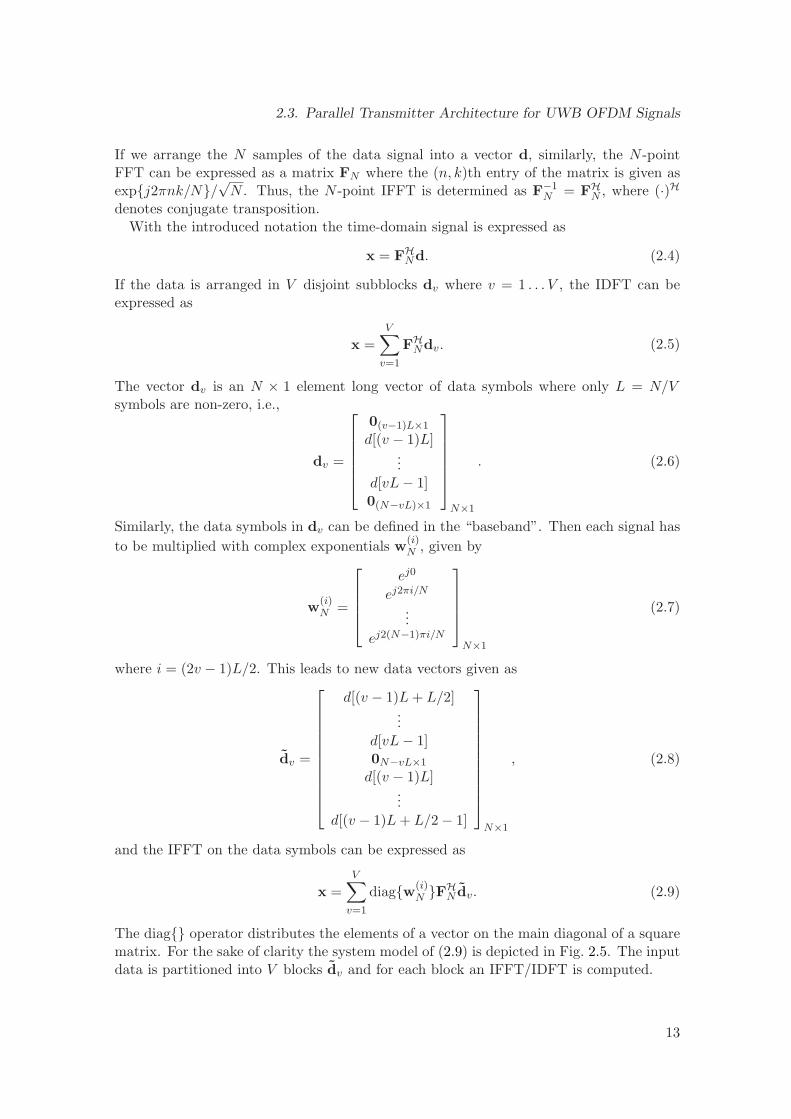
The diag operator distributes the elements of a vector on the main diagonal of a squarematrix. For the sake of clarity the system model of (2.9) is depicted in Fig. 2.5. The inputdata is partitioned into V blocks dv and for each block an IFFT/IDFT is computed.
13
Chapter 2. Subband Modeling of UWB Transceivers
Partitionedsubblocks
x[n]∑
d1
d2
dv IDFTL
IDFTL
IDFTLdV
IDFTL
w(L/2)N
w(3L/2)N
w((2v−1)L/2)N
w((2V −1)L/2)N
Figure 2.5.: Proposed parallel computation of an OFDM signal.
The goal is to achieve parallel generation of the OFDM signal which is obtained bycomputing V smaller IFFTs. Theoretically, the size of the IFFT in each subband can bejust L points but in this case we would need infinitely steep filters to achieve separationof the bands. To allow for practical filters, some oversampling is introduced, extendingthe IDFT blocksize to L′ > L. The additionally introduced carriers (L′ − L) are notmodulated, i.e. they are set to zero. With respect to (2.8) we define a new data vector
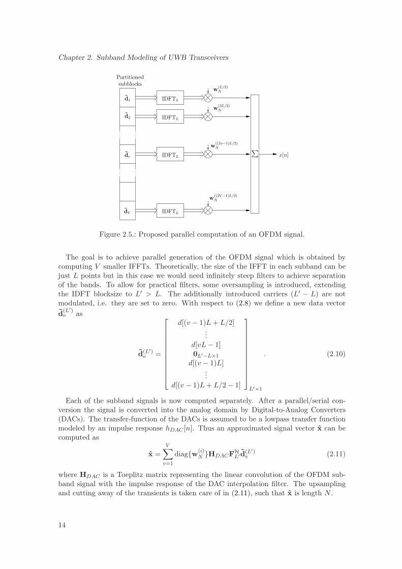
d(L′)v as
d(L′)v =
d[(v − 1)L + L/2]...
d[vL − 1]0L′−L×1
d[(v − 1)L]...
d[(v − 1)L + L/2 − 1]
L′×1
. (2.10)
Each of the subband signals is now computed separately. After a parallel/serial con-version the signal is converted into the analog domain by Digital-to-Analog Converters(DACs). The transfer-function of the DACs is assumed to be a lowpass transfer functionmodeled by an impulse response hDAC [n]. Thus an approximated signal vector x can becomputed as
x =V∑
v=1
diagw(i)N HDACFH
L′d(L′)v (2.11)
where HDAC is a Toeplitz matrix representing the linear convolution of the OFDM sub-band signal with the impulse response of the DAC interpolation filter. The upsamplingand cutting away of the transients is taken care of in (2.11), such that x is length N .
14
2.3. Parallel Transmitter Architecture for UWB OFDM Signals
In the following the quality loss due to subband signal generation is expressed analyt-ically. For that reason one has to figure out which effects are still visible after receivingand demodulating the signal in the receiver. Thus, an error vector e is defined for eachsubcarrier as
e = d − d (2.12)
where d is the used data vector and d is the demodulated data vector from the subband-generated signal, respectively. The receiver has to perform an FFT on the block of receiveddata symbols, i.e. d can be expressed as
d = FN x, (2.13)
where we have assumed an ideal channel. Similarly to the steps described for the subbanddecomposition, the signal x can be expressed as
x =V∑
v=1
diagw(i)N HDACFH
L′S(L′)v d, (2.14)
where S(L′)v is a selection and truncation matrix applied on the data vector d to perform
the steps described in (2.6), (2.8), and (2.10). Thus, the error equation can be simplifiedto
e =
(
I − FN
V∑
v=1
diagw(i)N HDACFH
L′S(L′)v
)
︸ ︷︷ ︸
Λ
d, (2.15)
where I represents an N ×N identity matrix and Λ is a matrix representing the determin-istic distortion errors and the Inter-Carrier Interference (ICI), respectively. The covarianceof the error is then given as
EeeH = EΛddHΛH = ΛΛH, (2.16)
where it is assumed that the autocorrelation matrix of the data symbols is an identitymatrix which holds for the current discussion because of i.i.d. unit-energy data symbols.The diagonal elements of EeeH represent the Mean Squared Error (MSE) due to thesubband decomposition and the reconstruction filters in the DACs, for each subcarrier.The main diagonal elements of Λ represent a deterministic error which potentially can becompensated in the receiver by a channel estimation algorithm. The off-diagonal elementsof Λ stand for the deterministic ICI from one carrier to another.
Cyclic Prefix - Zero Padded Prefix
Generally, an OFDM signal computed by the IFFT has to be extended to be resistantagainst the multipath propagation channel [16]. This is usually done by a cyclic extensionor cyclic prefix (CP) of the signal. The CP is realized by copying C ′ computed symbolsfrom the end of the time-domain signal to the beginning of the time-domain signal. Onerecently proposed approach considers substituting a cyclic repetition of the OFDM sig-nal with a sequence of zeros, i.e., zero-padding (ZP) [32]. It has similar computational
15
Chapter 2. Subband Modeling of UWB Transceivers
IDFTL′
Partitionedsubblocks
IDFTL′
IDFTL′
IDFTL′
PS
PS
PS
PS
DAC
DAC
DAC
DAC
∑x[n]
0
0
0
0
d(L′)2
d(L′)v
d(L′)V
w(i)N
w(i)N
w(i)N
w(i)N
d(L′)1
analogdigital
Figure 2.6.: Inserting cyclic prefix/zero-padded prefix for ODFM signal generation
complexity and spectral efficiency as the CP OFDM signal but requires a different algo-rithm for correct signal demodulation in the receiver. Due to the zeros at the beginningof each symbol, the receiver has to use an overlapp-add method (OLA) [31] to correctlydemodulate the data symbols. However, by the zero-padded extension the introducedInter-Symbol Interference (ISI) is eliminated. A resulting channel matrix is then alwaysguaranteed to be invertible, which enables perfect detectability in the absence of noise.
In the proposed scheme the insertion of the CP/ZP can be done very nicely for eachsubband separately. This is presented in Fig. 2.6. After partitioning the input datainto subblocks and computing an IDFT separately, the cyclic extension or zero paddingis inserted. The signal is then converted from its parallel set of samples into a serialsequence and is fed into a Digital-to-Analog Converter (DAC). To achieve shifting of thesubband to the correct position, complex modulators are used. The proposed transmitterarchitecture is compared to a conventional transmitter which can handle the huge signalbandwidth. The comparison has been done on a carrier-by-carrier basis by demonstratingthe additional error on each subcarrier in the signal spectrum. Furthermore, the signal hasbeen fed into a UWB OFDM receiver and the performance of the parallel architecture hasbeen compared to a conventional signal generator in terms of symbol-error ratio (SER).The simulation environment and the obtained results are discussed in Section 2.6.
2.4. Subband Modeling of the Channel
For the implementation of the response of a wideband propagation channel (cf. Fig. 2.4),it is very important to have a bandlimited channel response to be able to separate thewideband signal into subbands. Thus, this subsection’s focus is on general aspects of
16
2.4. Subband Modeling of the Channel
modeling a target transfer function with a filter bank consisting of M filters. Each of thefilters in the filter bank should model the transfer characteristics of the UWB channel for1/M -th of frequency range. Generally, such a filter bank is constructed by generating aprototype filter which has lowpass characteristics within the band of interest. Please notethat it would also be possible to design bandpass filters but this increases complexity. Thetransfer function can be arbitrarily specified according to the sampling frequency and thetransfer characteristics (passband attenuation, stopband attenuation, ripple in passband,ripple in stopband, ...). However, it is very important to keep the length of the filter ratherlow, i.e. to keep the implementation complexity low, which is in general proportional tothe filter length.
For the modeling of the wireless propagation channel many measurement campaignshave been used to get reliable results for the channel parameters (see [4] and referencestherein). Four different channel models have been selected and standardized with a set ofchannel parameters (see App. C for more information of the model). The channel modeldefines a channel impulse response in a statistical sense, i.e., the expected value of thechannel filter taps of the CIR for a specified scenario. Generally, a CIR hct(t) can bewritten as a sum of attenuated and time-shifted delta pulses [33,34,35], i.e.,
hct(t) =N−1∑
i=0
aiδ(t − τi), (2.17)
where ai is the set of path amplitudes and τi is the set of path delays, respectively.Similarly, the frequency response of the continuous-time impulse response is given by theFourier transform, i.e.,
Fhct(t) = Hct(f) =
∫ ∞
−∞hct(t) exp(−j2πft)dt. (2.18)
Consecutively, incorporating (2.17) into the frequency-domain representation in (2.18)gives a channel frequency response
Hw(f) =
N−1∑
i=0
ai exp(−j2πfτi). (2.19)
Usually this wideband channel is very frequency selective, and for a model of the channelmany coefficients of an equivalent filter response are needed. The bandwidth of the channelis limited to 528 MHz. Furthermore, in the proposed approach (cf. Fig. 2.4) the individualprocessing units are not capable to model the whole frequency range at once because thiswould need too many taps of an equivalent complex baseband filter [36].
To restrict the bandwidth of the one region related to the interesting band, it has to bewindowed from the overall frequency response. Thus the Fourier transform seen in (2.19)is restricted to frequencies in between a lower frequency fl and a higher frequency fh.
Hct(f) = W (f − fc)
N−1∑
i=0
ai exp(−j2πfτi). (2.20)
By applying this window funtion in the frequency domain, a bandlimitation of the broad-band frequency response to a certain bandwidth B = fh − fl is achieved because the
17
Chapter 2. Subband Modeling of UWB Transceivers
window function is zero outside this frequency range. The center frequency fc can bedirectly used from the standaridized channel definition seen in Table 2.1. For the windowfunctions W (f), one can use well known windows as Tukey or cosine roll-off windows toachieve smooth results in the time-domain. Furthermore, the window function has tobe flat within the interesting signal bandwidth, i.e., between fl and fh, and should sup-press all frequencies outside this band. For the detailed definition of the window W (f)and its exact properties the interested reader is refered to [37]. By restricting the signalbandwidth to the bandwidth of the window, an implicit down-conversion to a complexbaseband representation is achieved.
Until now, all processing steps are still in continuous-time domain. To apply DSP thefrequency response of the channel impulse response has to be sampled in the frequencydomain to obtain a discrete representation. The implicit shifting (modulation) down tocomplex baseband, denoted in (2.20), is also achieved with a shifting of the frequencyband with a complex exponential with frequency fc. Thus, an equivalent baseband repre-sentation is given as,
Hu(f) = Hct(f + fc) = W (f)N−1∑
i=0
ai exp(−j2πfτi) exp(−j2πfcτi). (2.21)
To obtain a discrete-frequency representation of the windowed, down-converted frequencyresponse, the continuous frequency-domain vector Hu(f) has to be sampled. The vectorof samples is given as
Hu[k] = Hu(kF ) (2.22)
where F denotes the spacing between points in the frequency domain, i.e., sampling in equi-distant frequency increments. A discrete-time representation of the frequency responseobtained from the standardized channel model is then obtained by performing the IDFTof the frequency-domain signal [31].
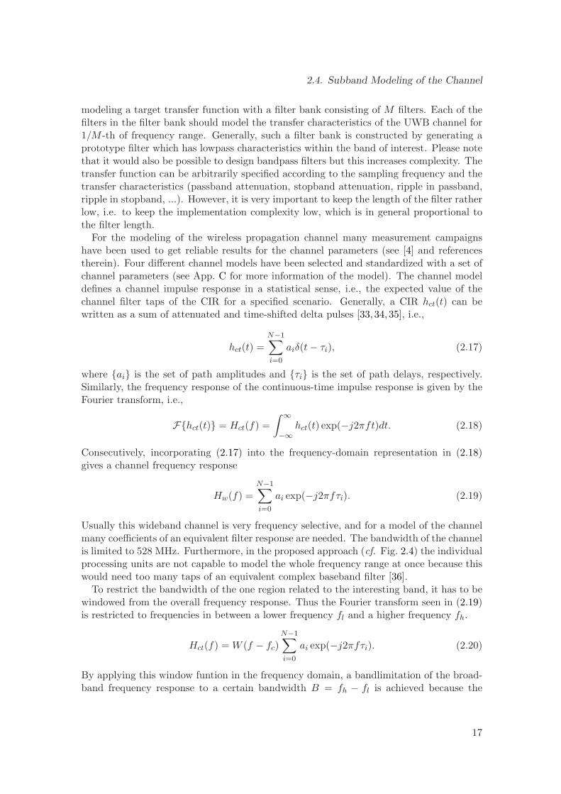
All the processing steps, which have to be done to obtain an impulse response of awireless broadband channel are summarized in Fig. 2.7. First of all, the continuous-timeimpulse response defined in the standardized model has to be transformed into the fre-quency domain. Then the interesting frequency range is masked by a windowing functionand shifted down to complex baseband. To obtain a complex time-domain representationof the channel, the IDFT has to be applied on the discrete-frequency sequence. Fromthese processing steps it is seen, that a straight-forward conversion for the channel modelis not possible. Such a direct model requires sampling of the channel with ¿ 1 GHz whichconsumes a lot of power and can not be directly implemented in the DSP hardware.
This well prepared, standardized impulse response has to be implemented with theparallel filter structure shown in Fig. 2.4 to be able to process the UWB signal bandwidthin real-time. The design of filters to achieve sufficient separation and a correct mappingis following in the next subsections
2.4.1. Design of the Filters for Subband Processing
For designing the filter bank it is required to have an overall frequency response whichis flat over the entire 528 MHz bandwith of interest. This is obvious since the UWBtransfer function has to be modeled by these subband filters. The filters used for the
18
2.4. Subband Modeling of the Channel
Cont.−time impulse response
Cont. frequency representation
Cut region of interest(window)
Disc.−time complex impulse response
Complex baseband equivalent system
Sampling
hct(t) FT
DFT −1
|Hct(f)| |Hw(f)||W (f)|
e−jwt
|Hu(f)|
n
n
t
f
ff
ℜ(hu[n])
ℑ(hu[n])
Figure 2.7.: Processing steps to obtain subband representation
filter bank are generally lowpass prototype filters. To obtain good separation betweenthe subbands, it is desired to have filters which have no attenuation in the passbandregion and infinite attenuation in the stopband regions. However, this leads to the wellknown rectangular filter (in the frequency-domain) which results in an infinitely long sincfunction in the time-domain. Thus realization of such a filter is not possible at all. Forrealizing the filter bank, some overlapping between the filters has to be allowed whichintroduces non-idealities in the subbands. For maximally decimated filter banks, whichconsist of just two filters, the cancellation of the introduced aliasing after downsampling ispossible [38]. An extension of the approach to M filters in a filter bank is shown in [39,40]but requires extra computational complexity. Generally, the filter length of a very sharpfinite impulse response (FIR) filter is inversely proportional to the transition width [41].As a consequence, very sharp FIR filters are also very long filters. On the other hand itis desired to use FIR due to their simplicity and properties like linear phase and stability.Thus, implementation complexity stays rather high. One approach to design very steepfilters and at the same time just slightly increasing the complexity is shown in [42]. Thetechnique to achieve the steep filters is called Frequency Response Masking and is describedin more detail in the following subsection.
2.4.2. Frequency Response Masking Filter Design
The Frequency Response Masking (FRM) approach tries to exploit the shrinking of thetransition band when interpolating an impulse response of a low complexity filter. Gener-ally, the steps used for creating a very steep transition band filter are depicted in Fig. 2.8.
First, it is assumed that the prototype filter ha[n] is given as depicted in Fig. 2.8(a)where the transition bandwidth is defined in the passband edge (θ) and the stopband edge(ϕ). When interpolating the filter with M − 1 zeros, M replicas in the frequency domainoccur, as depicted in Fig. 2.8(b). Additionally, this Figure shows the complementary filtertransfer function with the dashed line, |Hc(e
jMω)| = 1−|Ha(ejMω)|. This complementary
19
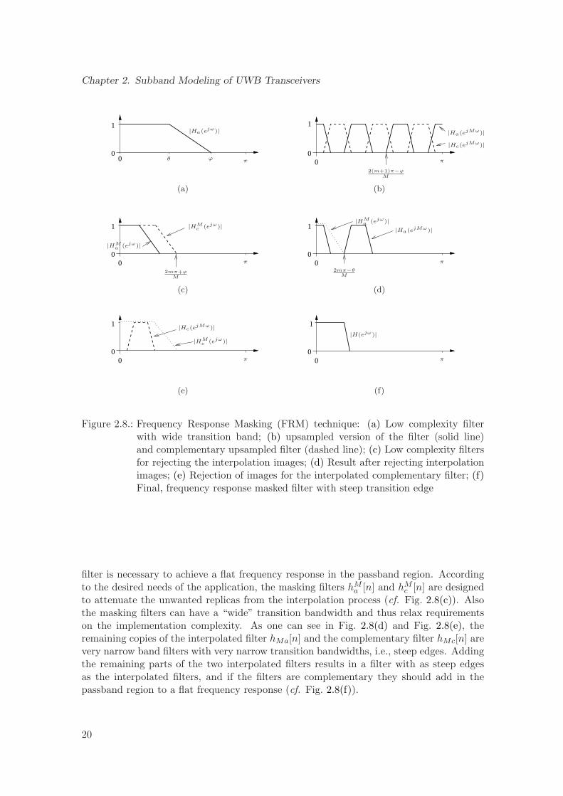
Chapter 2. Subband Modeling of UWB Transceivers
00
1
πθ ϕ
|Ha(ejω)|
(a)
00
1
π
2(m+1)π−ϕM
|Ha(ejMω)|
|Hc(ejMω)|
(b)
00
1
π
2mπ+ϕM
|HMc (ejω)|
|HMa (ejω)|
(c)
00
1
π
2mπ−θM
|HMa (ejω)|
|Ha(ejMω)|
(d)
00
1
π
|Hc(ejMω)|
|HMc (ejω)|
(e)
1
00
π
|H(ejω)|
(f)
Figure 2.8.: Frequency Response Masking (FRM) technique: (a) Low complexity filterwith wide transition band; (b) upsampled version of the filter (solid line)and complementary upsampled filter (dashed line); (c) Low complexity filtersfor rejecting the interpolation images; (d) Result after rejecting interpolationimages; (e) Rejection of images for the interpolated complementary filter; (f)Final, frequency response masked filter with steep transition edge
filter is necessary to achieve a flat frequency response in the passband region. Accordingto the desired needs of the application, the masking filters hM
a [n] and hMc [n] are designed
to attenuate the unwanted replicas from the interpolation process (cf. Fig. 2.8(c)). Alsothe masking filters can have a “wide” transition bandwidth and thus relax requirementson the implementation complexity. As one can see in Fig. 2.8(d) and Fig. 2.8(e), theremaining copies of the interpolated filter hMa[n] and the complementary filter hMc[n] arevery narrow band filters with very narrow transition bandwidths, i.e., steep edges. Addingthe remaining parts of the two interpolated filters results in a filter with as steep edgesas the interpolated filters, and if the filters are complementary they should add in thepassband region to a flat frequency response (cf. Fig. 2.8(f)).
20
2.4. Subband Modeling of the Channel
2.4.3. Mapping the Transfer Function on the Filterbank
For this specific problem a simplified frequency masking approach to design the prototypefilter was used. This is necessary to obtain a baseband equivalent description of the wirelesschannel in each subband. The use of a complementary filter for designing a flat frequencyresponse in the passband was avoided and a wideband lowpass filter was interpolated.Due to the interpolation very steep edges of the filter, as desired for the application, areobtained. Furthermore, the lowpass filter for the frequency masking approach was designedsuch that, after interpolation, the bandwidth of the filter is 80 MHz. The steep edge isalready achieved with one filter and another lowpass suppresses the periodic images fromthe interpolation to get a very nice filter with the desired frequency response. For theFRM filter 13 complex coefficients have been used which is reasonable to be computed inrealtime on the available technology.
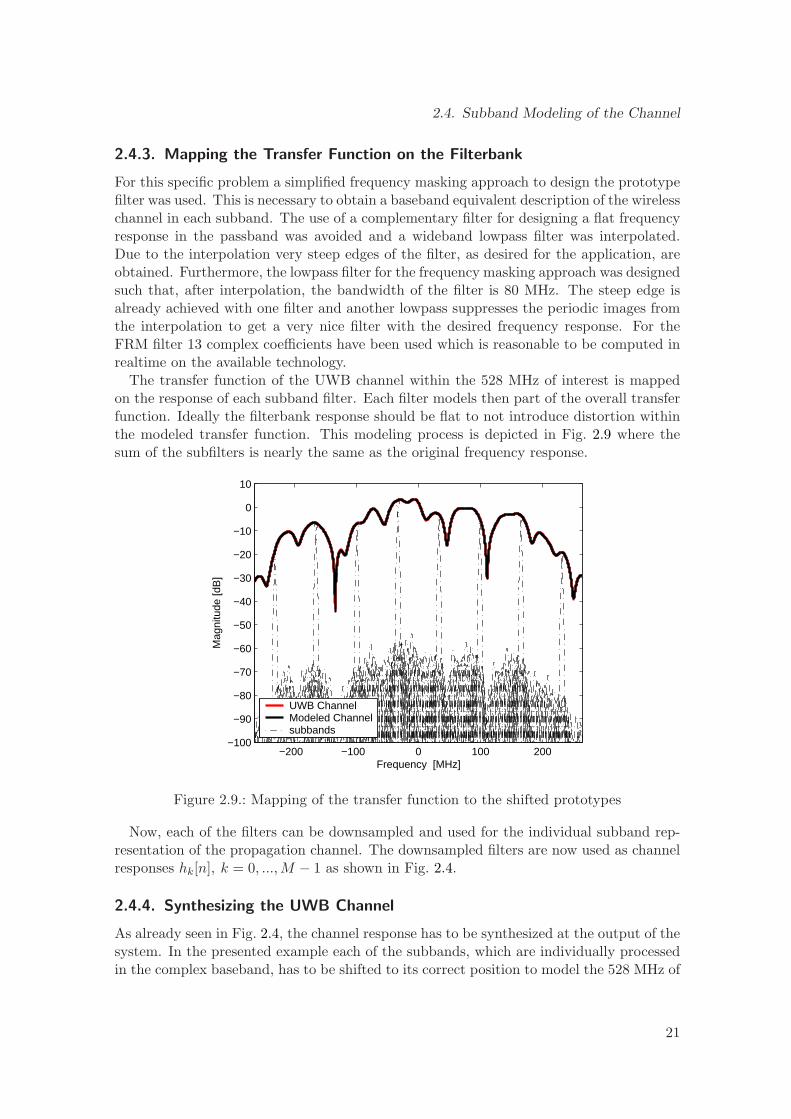
The transfer function of the UWB channel within the 528 MHz of interest is mappedon the response of each subband filter. Each filter models then part of the overall transferfunction. Ideally the filterbank response should be flat to not introduce distortion withinthe modeled transfer function. This modeling process is depicted in Fig. 2.9 where thesum of the subfilters is nearly the same as the original frequency response.
−200 −100 0 100 200−100
−90
−80
−70
−60
−50
−40
−30
−20
−10
0
10
Frequency [MHz]
Mag
nitu
de [d
B]
UWB ChannelModeled Channelsubbands
Figure 2.9.: Mapping of the transfer function to the shifted prototypes
Now, each of the filters can be downsampled and used for the individual subband rep-resentation of the propagation channel. The downsampled filters are now used as channelresponses hk[n], k = 0, ..., M − 1 as shown in Fig. 2.4.
2.4.4. Synthesizing the UWB Channel
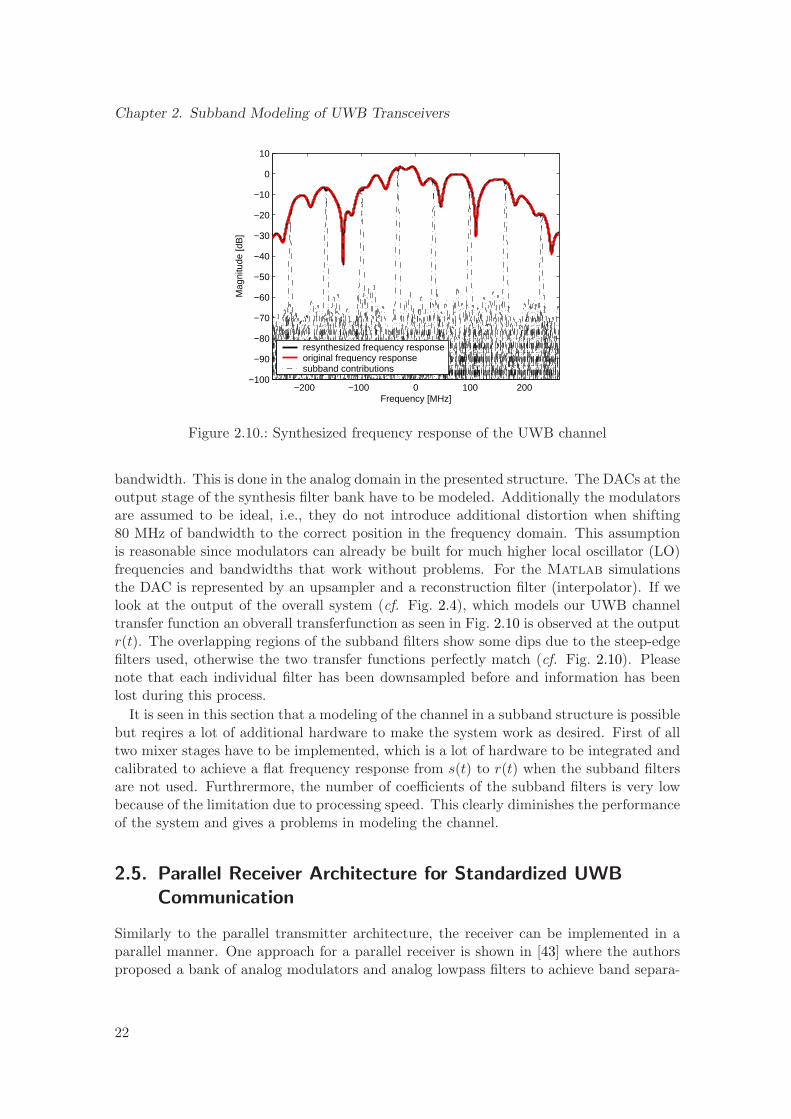
As already seen in Fig. 2.4, the channel response has to be synthesized at the output of thesystem. In the presented example each of the subbands, which are individually processedin the complex baseband, has to be shifted to its correct position to model the 528 MHz of
21
Chapter 2. Subband Modeling of UWB Transceivers
−200 −100 0 100 200−100
−90
−80
−70
−60
−50
−40
−30
−20
−10
0
10
Frequency [MHz]
Mag
nitu
de [d
B]
resynthesized frequency responseoriginal frequency responsesubband contributions
Figure 2.10.: Synthesized frequency response of the UWB channel
bandwidth. This is done in the analog domain in the presented structure. The DACs at theoutput stage of the synthesis filter bank have to be modeled. Additionally the modulatorsare assumed to be ideal, i.e., they do not introduce additional distortion when shifting80 MHz of bandwidth to the correct position in the frequency domain. This assumptionis reasonable since modulators can already be built for much higher local oscillator (LO)frequencies and bandwidths that work without problems. For the Matlab simulationsthe DAC is represented by an upsampler and a reconstruction filter (interpolator). If welook at the output of the overall system (cf. Fig. 2.4), which models our UWB channeltransfer function an obverall transferfunction as seen in Fig. 2.10 is observed at the outputr(t). The overlapping regions of the subband filters show some dips due to the steep-edgefilters used, otherwise the two transfer functions perfectly match (cf. Fig. 2.10). Pleasenote that each individual filter has been downsampled before and information has beenlost during this process.
It is seen in this section that a modeling of the channel in a subband structure is possiblebut reqires a lot of additional hardware to make the system work as desired. First of alltwo mixer stages have to be implemented, which is a lot of hardware to be integrated andcalibrated to achieve a flat frequency response from s(t) to r(t) when the subband filtersare not used. Furthrermore, the number of coefficients of the subband filters is very lowbecause of the limitation due to processing speed. This clearly diminishes the performanceof the system and gives a problems in modeling the channel.
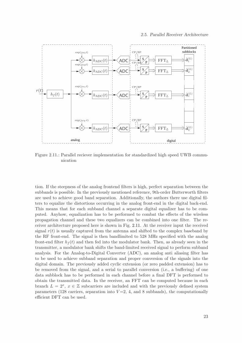
2.5. Parallel Receiver Architecture for Standardized UWB
Communication
Similarly to the parallel transmitter architecture, the receiver can be implemented in aparallel manner. One approach for a parallel receiver is shown in [43] where the authorsproposed a bank of analog modulators and analog lowpass filters to achieve band separa-
22
2.5. Parallel Receiver Architecture
Partitionedsubblocks
P
PS
S
PS
PS
analog digital
r(t)hf (t)
hADC(t)
hADC(t)
hADC(t)
hADC(t)
exp(jω1t)
exp(jω2t)
exp(jωvt)
exp(jωV t)
ADC
ADC
ADC
ADC
CP/ZP
CP/ZP
CP/ZP
CP/ZP
FFTL
FFTL
FFTL
FFTL d(L)1
d(L)2
d(L)v
d(L)V
Figure 2.11.: Parallel reciever implementation for standardized high speed UWB commu-nication
tion. If the steepness of the analog frontend filters is high, perfect separation between thesubbands is possible. In the previously mentioned reference, 9th-order Butterworth filtersare used to achieve good band separation. Additionally, the authors there use digital fil-ters to equalize the distortions occurring in the analog front-end in the digital back-end.This means that for each subband channel a separate digital equalizer has to be com-puted. Anyhow, equalization has to be performed to combat the effects of the wirelesspropagation channel and these two equalizers can be combined into one filter. The re-ceiver architecture proposed here is shown in Fig. 2.11. At the receiver input the receivedsignal r(t) is usually captured from the antenna and shifted to the complex baseband bythe RF front-end. The signal is then bandlimited to 528 MHz specified with the analogfront-end filter hf (t) and then fed into the modulator bank. Then, as already seen in thetransmitter, a modulator bank shifts the band-limited received signal to perform subbandanalysis. For the Analog-to-Digital Converter (ADC), an analog anti aliasing filter hasto be used to achieve subband separation and proper conversion of the signals into thedigital domain. The previously added cyclic extension (or zero padded extension) has tobe removed from the signal, and a serial to parallel conversion (i.e., a buffering) of onedata subblock has to be performed in each channel before a final DFT is performed toobtain the transmitted data. In the receiver, an FFT can be computed because in eachbranch L = 2x, x ∈ Z subcarriers are included and with the previously defined systemparameters (128 carriers, separation into V =2, 4, and 8 subbands), the computationallyefficient DFT can be used.
23
Chapter 2. Subband Modeling of UWB Transceivers
System Model
A system model for the receiver structure shown in Fig. 2.11 is derived. For the systemmodel, it is assumed that the received signal is an OFDM signal consisting of N carrierswhich are modulated by data symbols with known modulation format, i.e., BPSK, QPSK,or higher order QAM modulation. Furthermore, it is assumed, that the received signal isa bandlimited signal. With respect to Fig. 2.11, the first analog front-end filter hf (t) willprovide this feature for the receiver. Furthermore, we do not consider any synchronizationprocess of the receiver on the carrier and symbol start from the transmitter. For theprocessing steps described here, the two systems are assumed to be perfectly synchronized.This is reasonable, since the effect of the parallel structure on the overall performance ofthe receiver is investigated. Similarly to the transmitter the system is analyzed accordingto the overall performance and on a carrier-by-carrier basis.
By expressing the essential receiver operation, given by the FFT on a block of samplesof the received signal, with the cyclic extension removed, one obtains the data in thefrequency domain, i.e.,
d[k] =1√N
N−1∑
n=0
r[n]W knN , (2.23)
where d[k] is the data symbol at each carrier, r[n] is the sampled and sychronized OFDMtime-domain signal and W kn
N are the complex exponentials of the subcarriers. The set ofcomplex exponentials WN is defined in (2.3). Similarly to Section 2.3 the FFT can beexpressed in a matrix and vector notation as
d = FNr, (2.24)
where FN is an N point Fourier transform matrix where the (n, k)th entry is given asexp(j2πnk/N)/
√N , r is a vector of received samples, and d are the estimates of the
transmitted data symbols, respectively. Similarly to the generation process, if the signalwould be sampled at Nyquist rate, we could decompose the signal into disjunct blocks ofsamples from the received signal and compute the FFT on each subblock. In the previouslyintroduced matrix notation we then get,
dv =V∑
v=1
FNdiagw(i)N HADCr, (2.25)
where dv has similar structure as dv in (2.6) and each vector is N elements long andconsists of L = N/V data symbols and N − L zeros. The front-end filters hADC(t) arerepresented by the matrix HADC where the bandlimitation has implicitly been assumed.Otherwise the response of hf (t) can be inlcuded into HADC to get a combined response.
The vector w(i)N represents the shifting in the freqency domain and is similarly defined as in
(2.7). As already elaborated in the generation part, the size of the FFT computed in eachbranch can be reduced. Please note that each FFT computed in the receiver has length Land if proper filtering can be achieved in the continuous time domain, no oversampling isnecessary as for the signal generation where the DAC cannot be used up to its theoreticallimit.
24
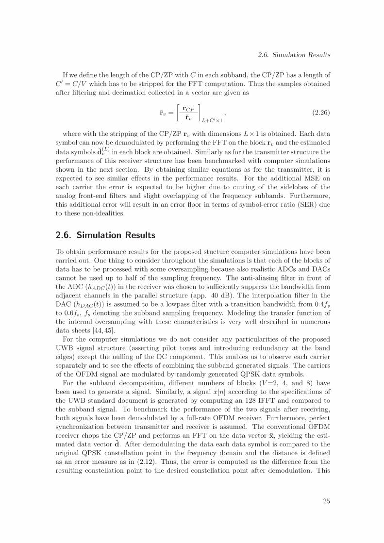
2.6. Simulation Results
If we define the length of the CP/ZP with C in each subband, the CP/ZP has a length ofC ′ = C/V which has to be stripped for the FFT computation. Thus the samples obtainedafter filtering and decimation collected in a vector are given as
rv =
[rCP
rv
]
L+C′×1
, (2.26)
where with the stripping of the CP/ZP rv with dimensions L×1 is obtained. Each datasymbol can now be demodulated by performing the FFT on the block rv and the estimated
data symbols d(L)v in each block are obtained. Similarly as for the transmitter structure the
performance of this receiver structure has been benchmarked with computer simulationsshown in the next section. By obtaining similar equations as for the transmitter, it isexpected to see similar effects in the performance results. For the additional MSE oneach carrier the error is expected to be higher due to cutting of the sidelobes of theanalog front-end filters and slight overlapping of the frequency subbands. Furthermore,this additional error will result in an error floor in terms of symbol-error ratio (SER) dueto these non-idealities.
2.6. Simulation Results
To obtain performance results for the proposed stucture computer simulations have beencarried out. One thing to consider throughout the simulations is that each of the blocks ofdata has to be processed with some oversampling because also realistic ADCs and DACscannot be used up to half of the sampling frequency. The anti-aliasing filter in front ofthe ADC (hADC(t)) in the receiver was chosen to sufficiently suppress the bandwidth fromadjacent channels in the parallel structure (app. 40 dB). The interpolation filter in theDAC (hDAC(t)) is assumed to be a lowpass filter with a transition bandwidth from 0.4fs
to 0.6fs, fs denoting the subband sampling frequency. Modeling the transfer function ofthe internal oversampling with these characteristics is very well described in numerousdata sheets [44,45].
For the computer simulations we do not consider any particularities of the proposedUWB signal structure (asserting pilot tones and introducing redundancy at the bandedges) except the nulling of the DC component. This enables us to observe each carrierseparately and to see the effects of combining the subband generated signals. The carriersof the OFDM signal are modulated by randomly generated QPSK data symbols.
For the subband decomposition, different numbers of blocks (V =2, 4, and 8) havebeen used to generate a signal. Similarly, a signal x[n] according to the specifications ofthe UWB standard document is generated by computing an 128 IFFT and compared tothe subband signal. To benchmark the performance of the two signals after receiving,both signals have been demodulated by a full-rate OFDM receiver. Furthermore, perfectsynchronization between transmitter and receiver is assumed. The conventional OFDMreceiver chops the CP/ZP and performs an FFT on the data vector x, yielding the esti-mated data vector d. After demodulating the data each data symbol is compared to theoriginal QPSK constellation point in the frequency domain and the distance is definedas an error measure as in (2.12). Thus, the error is computed as the difference from theresulting constellation point to the desired constellation point after demodulation. This
25
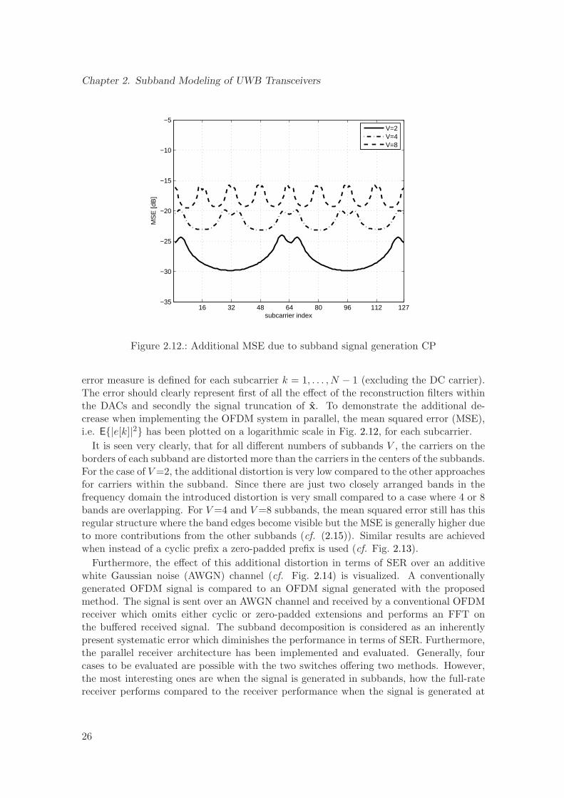
Chapter 2. Subband Modeling of UWB Transceivers
16 32 48 64 80 96 112 127−35
−30
−25
−20
−15
−10
−5
subcarrier index
MS
E [d
B]
V=2V=4V=8
Figure 2.12.: Additional MSE due to subband signal generation CP
error measure is defined for each subcarrier k = 1, . . . , N − 1 (excluding the DC carrier).The error should clearly represent first of all the effect of the reconstruction filters withinthe DACs and secondly the signal truncation of x. To demonstrate the additional de-crease when implementing the OFDM system in parallel, the mean squared error (MSE),i.e. E|e[k]|2 has been plotted on a logarithmic scale in Fig. 2.12, for each subcarrier.
It is seen very clearly, that for all different numbers of subbands V , the carriers on theborders of each subband are distorted more than the carriers in the centers of the subbands.For the case of V =2, the additional distortion is very low compared to the other approachesfor carriers within the subband. Since there are just two closely arranged bands in thefrequency domain the introduced distortion is very small compared to a case where 4 or 8bands are overlapping. For V =4 and V =8 subbands, the mean squared error still has thisregular structure where the band edges become visible but the MSE is generally higher dueto more contributions from the other subbands (cf. (2.15)). Similar results are achievedwhen instead of a cyclic prefix a zero-padded prefix is used (cf. Fig. 2.13).
Furthermore, the effect of this additional distortion in terms of SER over an additivewhite Gaussian noise (AWGN) channel (cf. Fig. 2.14) is visualized. A conventionallygenerated OFDM signal is compared to an OFDM signal generated with the proposedmethod. The signal is sent over an AWGN channel and received by a conventional OFDMreceiver which omits either cyclic or zero-padded extensions and performs an FFT onthe buffered received signal. The subband decomposition is considered as an inherentlypresent systematic error which diminishes the performance in terms of SER. Furthermore,the parallel receiver architecture has been implemented and evaluated. Generally, fourcases to be evaluated are possible with the two switches offering two methods. However,the most interesting ones are when the signal is generated in subbands, how the full-ratereceiver performs compared to the receiver performance when the signal is generated at
26
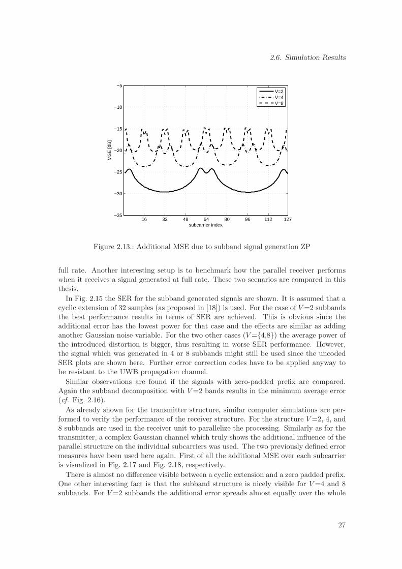
2.6. Simulation Results
16 32 48 64 80 96 112 127−35
−30
−25
−20
−15
−10
−5
subcarrier index
MS
E [d
B]
V=2V=4V=8
Figure 2.13.: Additional MSE due to subband signal generation ZP
full rate. Another interesting setup is to benchmark how the parallel receiver performswhen it receives a signal generated at full rate. These two scenarios are compared in thisthesis.
In Fig. 2.15 the SER for the subband generated signals are shown. It is assumed that acyclic extension of 32 samples (as proposed in [18]) is used. For the case of V =2 subbandsthe best performance results in terms of SER are achieved. This is obvious since theadditional error has the lowest power for that case and the effects are similar as addinganother Gaussian noise variable. For the two other cases (V =4,8) the average power ofthe introduced distortion is bigger, thus resulting in worse SER performance. However,the signal which was generated in 4 or 8 subbands might still be used since the uncodedSER plots are shown here. Further error correction codes have to be applied anyway tobe resistant to the UWB propagation channel.
Similar observations are found if the signals with zero-padded prefix are compared.Again the subband decomposition with V =2 bands results in the minimum average error(cf. Fig. 2.16).
As already shown for the transmitter structure, similar computer simulations are per-formed to verify the performance of the receiver structure. For the structure V =2, 4, and8 subbands are used in the receiver unit to parallelize the processing. Similarly as for thetransmitter, a complex Gaussian channel which truly shows the additional influence of theparallel structure on the individual subcarriers was used. The two previously defined errormeasures have been used here again. First of all the additional MSE over each subcarrieris visualized in Fig. 2.17 and Fig. 2.18, respectively.
There is almost no difference visible between a cyclic extension and a zero padded prefix.One other interesting fact is that the subband structure is nicely visible for V =4 and 8subbands. For V =2 subbands the additional error spreads almost equally over the whole
27
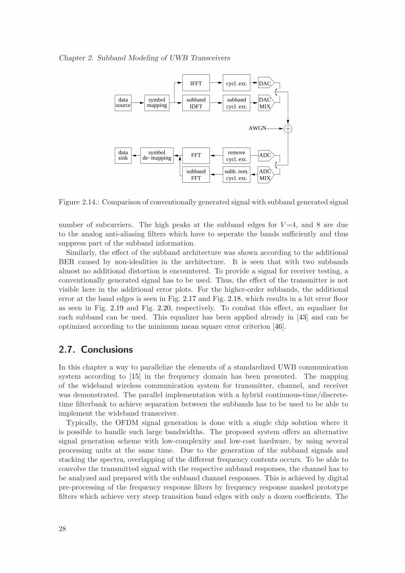
Chapter 2. Subband Modeling of UWB Transceivers
datasource
symbolmapping IDFT
subband subbandcycl. ext.
cycl. ext.IFFT DAC
AWGN
DACMIX
ADCMIX
ADCcycl. ext.removeFFTde−mapping
symbolsinkdata
subb. rem.cycl. ext.
subbandFFT
Figure 2.14.: Comparison of conventionally generated signal with subband generated signal
number of subcarriers. The high peaks at the subband edges for V =4, and 8 are dueto the analog anti-aliasing filters which have to seperate the bands sufficiently and thussuppress part of the subband information.
Similarly, the effect of the subband architecture was shown according to the additionalBER caused by non-idealities in the architecture. It is seen that with two subbandsalmost no additional distortion is encountered. To provide a signal for receiver testing, aconventionally generated signal has to be used. Thus, the effect of the transmitter is notvisible here in the additional error plots. For the higher-order subbands, the additionalerror at the band edges is seen in Fig. 2.17 and Fig. 2.18, which results in a bit error flooras seen in Fig. 2.19 and Fig. 2.20, respectively. To combat this effect, an equalizer foreach subband can be used. This equalizer has been applied already in [43] and can beoptimized according to the minimum mean square error criterion [46].
2.7. Conclusions
In this chapter a way to parallelize the elements of a standardized UWB communicationsystem according to [15] in the frequency domain has been presented. The mappingof the wideband wireless communication system for transmitter, channel, and receiverwas demonstrated. The parallel implementation with a hybrid continuous-time/discrete-time filterbank to achieve separation between the subbands has to be used to be able toimplement the wideband transceiver.
Typically, the OFDM signal generation is done with a single chip solution where itis possible to handle such large bandwidths. The proposed system offers an alternativesignal generation scheme with low-complexity and low-cost hardware, by using severalprocessing units at the same time. Due to the generation of the subband signals andstacking the spectra, overlapping of the different frequency contents occurs. To be able toconvolve the transmitted signal with the respective subband responses, the channel has tobe analyzed and prepared with the subband channel responses. This is achieved by digitalpre-processing of the frequency response filters by frequency response masked prototypefilters which achieve very steep transition band edges with only a dozen coefficients. The
28
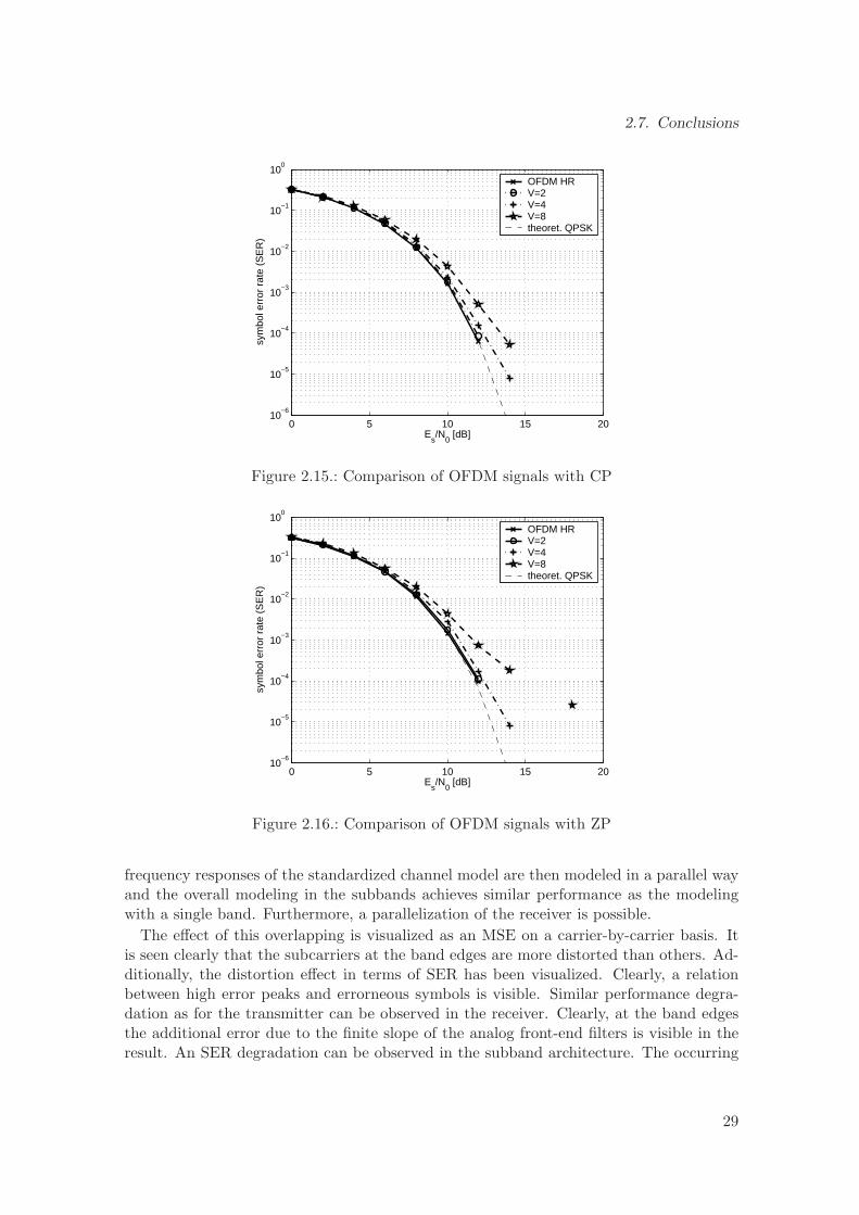
2.7. Conclusions
0 5 10 15 2010
−6
10−5
10−4
10−3
10−2
10−1
100
Es/N
0 [dB]
sym
bol e
rror
rat
e (S
ER
)
OFDM HRV=2V=4V=8theoret. QPSK
Figure 2.15.: Comparison of OFDM signals with CP
0 5 10 15 2010
−6
10−5
10−4
10−3
10−2
10−1
100
Es/N
0 [dB]
sym
bol e
rror
rat
e (S
ER
)
OFDM HRV=2V=4V=8theoret. QPSK
Figure 2.16.: Comparison of OFDM signals with ZP
frequency responses of the standardized channel model are then modeled in a parallel wayand the overall modeling in the subbands achieves similar performance as the modelingwith a single band. Furthermore, a parallelization of the receiver is possible.
The effect of this overlapping is visualized as an MSE on a carrier-by-carrier basis. Itis seen clearly that the subcarriers at the band edges are more distorted than others. Ad-ditionally, the distortion effect in terms of SER has been visualized. Clearly, a relationbetween high error peaks and errorneous symbols is visible. Similar performance degra-dation as for the transmitter can be observed in the receiver. Clearly, at the band edgesthe additional error due to the finite slope of the analog front-end filters is visible in theresult. An SER degradation can be observed in the subband architecture. The occurring
29
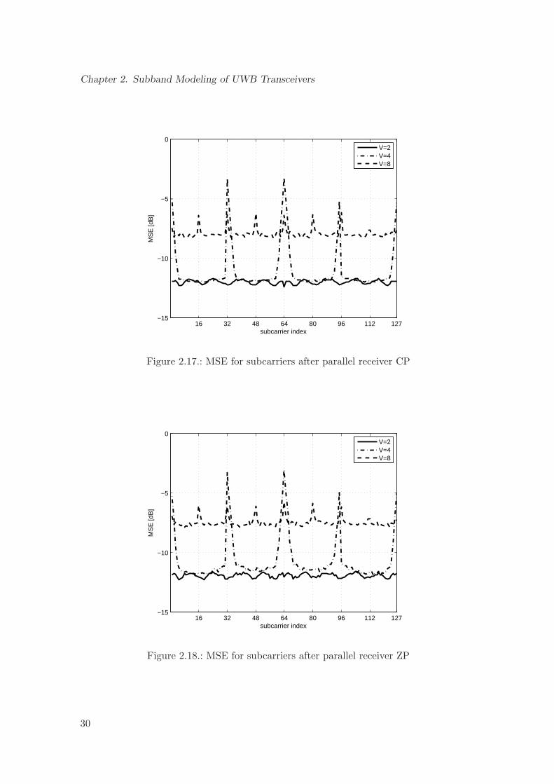
Chapter 2. Subband Modeling of UWB Transceivers
16 32 48 64 80 96 112 127−15
−10
−5
0
subcarrier index
MS
E [d
B]
V=2V=4V=8
Figure 2.17.: MSE for subcarriers after parallel receiver CP
16 32 48 64 80 96 112 127−15
−10
−5
0
subcarrier index
MS
E [d
B]
V=2V=4V=8
Figure 2.18.: MSE for subcarriers after parallel receiver ZP
30
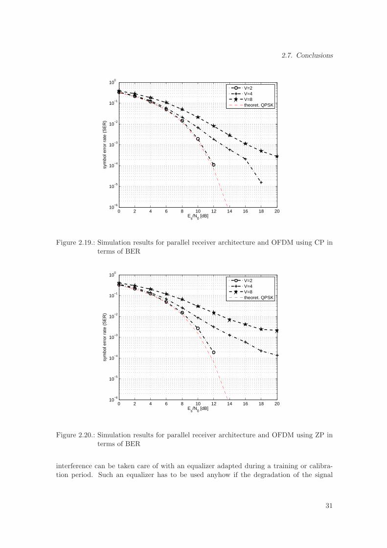
2.7. Conclusions
0 2 4 6 8 10 12 14 16 18 2010
−6
10−5
10−4
10−3
10−2
10−1
100
Es/N
0 [dB]
sym
bol e
rror
rat
e (S
ER
)
V=2V=4V=8theoret. QPSK
Figure 2.19.: Simulation results for parallel receiver architecture and OFDM using CP interms of BER
0 2 4 6 8 10 12 14 16 18 2010
−6
10−5
10−4
10−3
10−2
10−1
100
Es/N
0 [dB]
sym
bol e
rror
rat
e (S
ER
)
V=2V=4V=8theoret. QPSK
Figure 2.20.: Simulation results for parallel receiver architecture and OFDM using ZP interms of BER
interference can be taken care of with an equalizer adapted during a training or calibra-tion period. Such an equalizer has to be used anyhow if the degradation of the signal
31
Chapter 2. Subband Modeling of UWB Transceivers
due to a wireless propagation channel is considered to recover the transmitted data. Oneadvantage of OFDM is that each carrier can be equalized in amplitude and phase by asingle complex coefficient. However, this only works as long as the channel delay spreadis shorter than the guard interval. If the channel spread is longer than the guard interval,ISI occurs which has to be equalized with an equalizer filter response, i.e. employing morethan a single coefficient. Furthermore, OFDM is sensitive to carrier offsets where theorthogonality between the carriers gets lost. This inter-carrier interference (ICI) can becombated by the cyclic extension such that in one symbol all subcarriers have an integernumber of sine waves to preserve orthogonality.
32
Chapter3Pulse-Based UWB Communication
For high speed UWB communication systems a conventional OFDM signaling scheme hasbeen extended to current technological limits. This helped on the one hand in realizingdifferent implementations in a short, predictable time because experience in designingOFDM chips (like used in WLAN) is already available in many companies. This is, how-ever, completely contradictory to the original idea of UWB, i.e., using very widebandsignals (short pulses) and exploit the frequency diversity of the signals when they arereceived. It is also questionable whether the OFDM transceivers can be built in orderto fulfill low-power constraints. One second advantage of the UWB technology is that,due to its high bandwidth, a high positioning accuracy can be achieved. In a positioningsystem there are several possibilities to achieve accurate estimates of the current positionof simple tags or advanced stations in space which can be tracked due to the fine timeresolution of UWB signals. For details about positioning algorithms we want to refer theinterested reader to [47, 8] and the references therein. Combining these perspectives andrequirements and keeping current technological limits in mind, the IEEE has released astandardized communication scheme recently [6] which will be analyzed in this chapter.First an easy way to achieve broadband, universal signal generation, is presented. Fur-thermore, if mismatches in the presented structure occur, we can find a way to digitallypre-distort the signals so that a compensation of these effects is achieved in the analogdomain. In the end an analysis of receiver structures for the standardized scheme is pre-sented, and a comparison of different receiver architectures according to their performancein a single-user and in a multi-user scenario is shown1.
3.1. Introduction
An alternative to the extension of already existing communication systems to make them“Ultra” Wideband as presented in Chapter 2, is to use very narrow pulses, which alsooccupy a very broad spectrum. Unlicensed signal transmission is allowed according to theauthorities in the frequency range from 3.1 to 10.6 GHz. However, this very liberal opening
1The sections about Time-Interleaved Digital-to-Analog Converters and the proposed compensation ap-proach in the TIDAC structure have been published and submitted by the author to internationalconferences [10,48].
33
Chapter 3. Pulse-Based UWB Communication
of the “ether” is only available in the USA. Conversely, the European Commission followedmuch more conservative guidelines to propose a regulation directive for the EU memberstates [2] but it is up to national governments to implement the directive, where most ofthe member states are currently still belated. Only the UK and its respective regulationauthority OFCOM has implemented the directive in its current form. Generally the spec-tral emission limit already defined by the FCC in the US was set to the electromagneticcompatibility bound (EMC) of a power spectral density (PSD) of -41.25 dBm/MHz [1].
As already mentioned, as an alternative to a wideband extension of a conventionalwireless system, very short pulses can be transmitted. To comply with spectral regulationsmany different pulse shapes can be used, which by their shape can be made to fit thespectral emission mask [49]. What can be done additionally is to shift the pulses by mixingthem towards higher frequencies. However, the direct and easy baseband transmission isnot possible anymore when using a carrier to shift the signal spectrum. Also from a low-power perspective an additional RF mixer consumes a lot of power which is usually notdesired.
Also the IEEE recognized the great potential of pulse based Ultra Wide-Band signalingfor communication and positioning applications. Thus, it formed the IEEE 802.15 TaskGroup 4a to define an alternative PHY and MAC for wireless personal area networks(WPANs). The main task was to develop an alternative PHY providing simultaneouscommunication and high precision ranging with low power and system scalability. Theseendeavors in defining a new PHY for the new technology succeeded in Sept. 2007 inan addendum to the current standardization document [6]. Therein, standardized UWBpulses have been specified, which have a root raised cosine (RRC) pulse shape. The RRCpulse shape is mathematically defined as
x(t) =
1√T· sin(π(1−β)t/T )+(4βt/T ) cos(π(1+β)t/T )
(πt/T )(1−(4βt/T )2)t 6= 0, t 6= ±T/(4β)
1√T
(
1 − β + 4βπ
)
t = 0
β√2T
((1 + 2/π) sin(π/4β) + (1 − 2/π) cos(π/4β)) t = ±T/(4β)
, (3.1)
where β is a roll-off factor defined as 0.6, and T is the pulse width. Beside the pulse-basedsignaling employing wideband pulses, several different other signals have been standardizedin the current document. One method to generate wideband signals is to drive an activecircuitry into non-fading nonlinear behavior and let it generate chaotic waveforms whichare noise-like signals occupying a wide bandwidth [50]. Furthermore, the generation ofchirped signals is also possible to get wideband signals. There the frequency is continuouslyswept over a certain frequency range. Here chirping slopes of 500 MHz/2.5 ns are usedto generate the pulses. Furthermore, another optional waveform are continuous spectrum(CS) pulses which are reference pulses with adjusted group delay. Generally, the pulseshape used in the standard is a reference pulse shape meaning that actually any pulseshape can be used in a standardized IEEE 802.15.4a communication system which has acertain correlation with this reference pulse [6]. The bandwidths for these standardizedreference pulses are defined as 499.2 MHz and the whole frequency range from the FCCwas densly packed with neighboring channels. On top of these “narrow” channels thereare a few channels with app. 1.3 GHz which have intentionally overlapping frequencyranges, such that devices implementing different signal bandwidths can also communicatewith each other and can capture sufficient energy from each other.
34
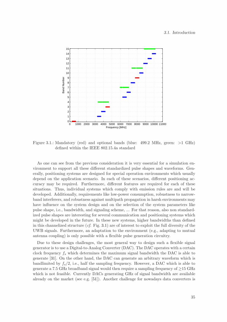
3.1. Introduction
0 1000 2000 3000 4000 5000 6000 7000 8000 9000 10000 110000
1
2
3
4
5
6
7
8
9
10
11
12
13
14
15
Frequency [MHz]
Ban
d N
umbe
r
Figure 3.1.: Mandatory (red) and optional bands (blue: 499.2 MHz, green: >1 GHz)defined within the IEEE 802.15.4a standard
As one can see from the previous consideration it is very essential for a simulation en-vironment to support all these different standardized pulse shapes and waveforms. Gen-erally, positioning systems are designed for special operation environments which usuallydepend on the application scenario. In each of these scenarios, different positioning ac-curacy may be required. Furthermore, different features are required for each of thesesituations. Thus, individual systems which comply with emission rules are and will bedeveloped. Additionally, requirements like low-power consumption, robustness to narrow-band interferers, and robustness against multipath propagation in harsh environments mayhave influence on the system design and on the selection of the system parameters likepulse shape, i.e., bandwidth, and signaling scheme, ... For that reason, also non standard-ized pulse shapes are interesting for several communication and positioning systems whichmight be developed in the future. In these new systems, higher bandwidths than definedin this channelized structure (cf. Fig. 3.1) are of interest to exploit the full diversity of theUWB signals. Furthermore, an adaptation to the environment (e.g., adapting to mutualantenna coupling) is only possible with a flexible pulse generation circuitry.
Due to these design challenges, the most general way to design such a flexible signalgenerator is to use a Digital-to-Analog Converter (DAC). The DAC operates with a certainclock frequency fs which determines the maximum signal bandwidth the DAC is able togenerate [31]. On the other hand, the DAC can generate an arbitrary waveform which isbandlimited by fs/2, i.e., half the sampling frequency. However, a DAC which is able togenerate a 7.5 GHz broadband signal would then require a sampling frequency of ≥15 GHzwhich is not feasible. Currently DACs generating GHz of signal bandwidth are availablealready on the market (see e.g. [51]). Another challenge for nowadays data converters is
35
Chapter 3. Pulse-Based UWB Communication
to provide sufficiently high resolution to provide high Signal to Noise Ratio (SNR) for thegenerated signals [52]. If we consider the integration of the converter on a System on Chip(SoC) we also have to take power consumption and area into consideration. Generally,a tradeoff between all these system parameters has to be found for the application. It isrecognized that the integration density of digital circuits grows much faster than the oneof analog circuits, which results in an increasing gap between analog and digital circuits interms of speed, area, and power consumption [53]. Fortunately, we can use digital signalprocessing to overcome the analog impairments of data converters [54]. One approachof extending the limitations of current DACs is shown in this thesis. By using multipleDACs one can extend the bandwidth of the analog signals generated by the architecture.To achieve this, some digital preprocessing has to be done in the digital domain and aclock phase shift has to be generated to achieve a time-interleaved generation of the DACsamples. Both components add complexity to the overall system but are relatively easyto realize. An equivalence of the proposed structure and a converter running at a highersampling rate is shown in Section 3.2. By using multiple converters, also mismatchesbetween these converters can be considered. One solution to compensate for timing offsetsin a such a multiple converter system is shown in Section 3.3. On the receiver side,the generated signals have to be decoded by a proper receiver architecture. To evaluatethe performance of the standardized IEEE 802.15.4a scheme, we propose three receiverarchitectures and compare them in Section 3.4.2
3.2. Flexible Generation of UWB Signals
In this work we focus on time-interleaved DACs (TIDACs) which consist of M DACsoperating at low sampling rate. Each of the DACs is used with a phase-shifted clock,which results in time-shifted contributions to the output signal. The main advantage ofthe TIDAC is that due to the phase-shifted signals, the output signal seems to be generatedat a higher sampling rate, given that the settling time of the individual DACs is high.
For the TIDAC, the clock generation adds more implementation complexity. However,this additional effort remains low because only a multiphase clock generator has to be usedto clock the different DACs. For the two-channel case, this can be easily done by usingdifferential signals. The additional complexity for the clock generation offers flexibility inpulse shape adaptation and generation which is needed in a demonstration environment.Using a TIDAC on a mobile device may consume more chip area than using a single DACat the M -times higher speed but offers relaxed conditions for the individual converterswhich can then be optimized.
The TIDAC proposed in this thesis distinguishes itself from previous works as follows.The authors in [55] consider a time-interleaved scheme that consists of two DACs that arealternately switched on, i.e., either the first or the second DAC contributes to the outputsignal. An improvement for the output signal is achieved by mapping the data wordswith a return to zero (RTZ) code which helps avoiding glitches in the output signal [56].However, this RTZ coding is not applicable to our structure because the output signalcombination in our scheme is always the sum of the contributions of the individual DACsin the TIDAC.
Another approach using TIDACs is shown in [57], where the DACs are operated in a
36
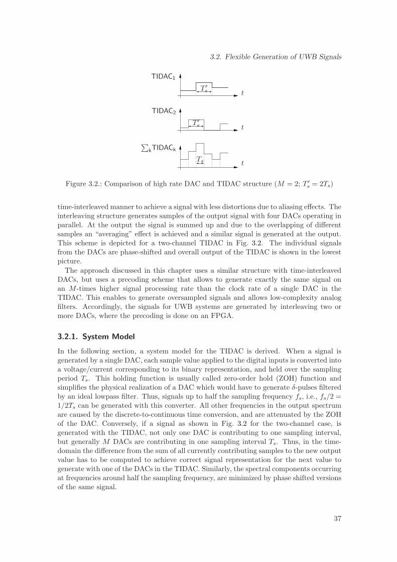
3.2. Flexible Generation of UWB Signals
t
t
t
TIDAC1
TIDAC2
∑
kTIDACk
T ′s
T ′s
Ts
Figure 3.2.: Comparison of high rate DAC and TIDAC structure (M = 2; T ′s = 2Ts)
time-interleaved manner to achieve a signal with less distortions due to aliasing effects. Theinterleaving structure generates samples of the output signal with four DACs operating inparallel. At the output the signal is summed up and due to the overlapping of differentsamples an “averaging” effect is achieved and a similar signal is generated at the output.This scheme is depicted for a two-channel TIDAC in Fig. 3.2. The individual signalsfrom the DACs are phase-shifted and overall output of the TIDAC is shown in the lowestpicture.
The approach discussed in this chapter uses a similar structure with time-interleavedDACs, but uses a precoding scheme that allows to generate exactly the same signal onan M -times higher signal processing rate than the clock rate of a single DAC in theTIDAC. This enables to generate oversampled signals and allows low-complexity analogfilters. Accordingly, the signals for UWB systems are generated by interleaving two ormore DACs, where the precoding is done on an FPGA.
3.2.1. System Model
In the following section, a system model for the TIDAC is derived. When a signal isgenerated by a single DAC, each sample value applied to the digital inputs is converted intoa voltage/current corresponding to its binary representation, and held over the samplingperiod Ts. This holding function is usually called zero-order hold (ZOH) function andsimplifies the physical realization of a DAC which would have to generate δ-pulses filteredby an ideal lowpass filter. Thus, signals up to half the sampling frequency fs, i.e., fs/2 =1/2Ts can be generated with this converter. All other frequencies in the output spectrumare caused by the discrete-to-continuous time conversion, and are attenuated by the ZOHof the DAC. Conversely, if a signal as shown in Fig. 3.2 for the two-channel case, isgenerated with the TIDAC, not only one DAC is contributing to one sampling interval,but generally M DACs are contributing in one sampling interval Ts. Thus, in the time-domain the difference from the sum of all currently contributing samples to the new outputvalue has to be computed to achieve correct signal representation for the next value togenerate with one of the DACs in the TIDAC. Similarly, the spectral components occurringat frequencies around half the sampling frequency, are minimized by phase shifted versionsof the same signal.
37
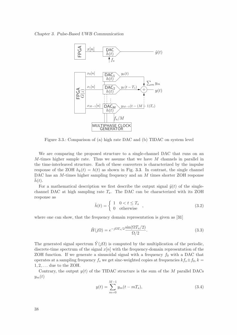
Chapter 3. Pulse-Based UWB Communication
h(t)
h(t)
h(t)
h(t)
y(t)
y0(t)
y1(t − Ts)
yM−1(t − (M − 1)Ts)
x[n]
x0[n]
x1[n]
xM−1[n]
∑
m ym
y(t)
FPG
AFPG
AG
(z)
fs
fs/M
DAC
DAC1
DAC2
DACM
...
MULTIPHASE CLOCKGENERATOR
Figure 3.3.: Comparison of (a) high rate DAC and (b) TIDAC on system level
We are comparing the proposed structure to a single-channel DAC that runs on anM -times higher sample rate. Thus we assume that we have M channels in parallel inthe time-interleaved structure. Each of these converters is characterized by the impulseresponse of the ZOH hk(t) = h(t) as shown in Fig. 3.3. In contrast, the single channelDAC has an M -times higher sampling frequency and an M times shorter ZOH responseh(t).
For a mathematical description we first describe the output signal y(t) of the single-channel DAC at high sampling rate Ts. The DAC can be characterized with its ZOHresponse as
h(t) =
1 0 < t ≤ Ts
0 otherwise, (3.2)
where one can show, that the frequency domain representation is given as [31]
H(jΩ) = e−jΩTs/2 sin(ΩTs/2)
Ω/2. (3.3)
The generated signal spectrum Y (jΩ) is computed by the multiplication of the periodic,discrete-time spectrum of the signal x[n] with the frequency-domain representation of theZOH function. If we generate a sinusoidal signal with a frequency f0 with a DAC thatoperates at a sampling frequency fs we get sinc-weighted copies at frequencies kfs±f0, k =1, 2, . . . due to the ZOH.
Contrary, the output y(t) of the TIDAC structure is the sum of the M parallel DACsym(t)
y(t) =
M−1∑
m=0
ym(t − mTs), (3.4)
38
3.2. Flexible Generation of UWB Signals
where ym(t − mTs) is the converted signal for each of the branches (cf. Fig. 3.3), i.e.,the time-shifted, overlapping outputs of the DACs. The overall response for the TIDACstructure with prefiltering is
y(t) =
∞∑
k=−∞
M−1∑
m=0
(
(x[kM + m] ∗ g[kM + m])×
δ(t − kMTs − mTs))
∗ h(t),
(3.5)
where x[kM + m] is the discrete-time signal, g[m] is the precoding filter, δ(t) is the Diracdelta function, h(t) is the reconstruction filter for each of the DACs (i.e., the ZOH), and ∗denotes convolution. For the sake of simplicity, the filter h(t) is assumed to be the same foreach DAC. For the precoding of the signal we generally need an IIR filter of M−1 taps sincewe have to account for all currently contributing M DACs and have to compute the newvalue to generate for the m-th DAC in the TIDAC. Thus only the additional difference toachieve the desired value in the converter array has to be computed. This filter operationcan be described by an input/output relation as y[n] = x[n]−y[n−1]− . . .−y[n−M +1],which is given in the frequency domain as the transfer function of a filter
G(z) =1
∑M−1m=0 z−m
. (3.6)
We see that this filter has M poles in its frequency domain representation. For a practicalimplementation of this filter, an FIR approximation can be used. The continuous-timerepresentation of the zero-order hold for one DAC is given by
h(t) =
1 0 < t ≤ MTs
0 otherwise, (3.7)
where MTs is the sampling time of one single DAC in the TIDAC. Thus the frequencydomain description of the output filter of one channel is
H(jΩ) =1
−jΩ
(e−jMΩTs − 1
), (3.8)
which is again a sinc function as in (3.3) but at the lower sampling rate.With these assumptions, the time-domain expression of (3.5) can be expressed in the
frequency domain as
Y (jΩ) =1
Ts
∞∑
k=−∞
M−1∑
m=0
Xm
(
j
(
Ω − k2π
Ts
))
×
G
(
j
(
Ω − k2π
Ts
))
H(jΩ),
(3.9)
where Xm(jΩ − 2 k π/Ts) is the spectrum in the m-th channel, and G(jΩ) = G(ejΩTs) isthe filter operation performed in the digital domain. The filter responses are equivalentas long as the frequency remains below half the sampling frequency of the DAC at highrate.
39
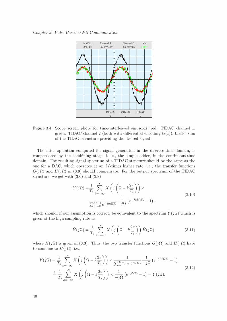
Chapter 3. Pulse-Based UWB Communication
timeDiv :
2ns/div
Channel A :
50 mV/div
Channel B :
50 mV/div
XY
OFF
OffsetB
0
OffsetC
0
OffsetA
0
Figure 3.4.: Scope screen photo for time-interleaved sinusoids, red: TIDAC channel 1,green: TIDAC channel 2 (both with differential encoding G(z)), black: sumof the TIDAC structure providing the desired signal
The filter operation computed for signal generation in the discrete-time domain, iscompensated by the combining stage, i. e., the simple adder, in the continuous-timedomain. The resulting signal spectrum of a TIDAC structure should be the same as theone for a DAC, which operates at an M -times higher rate, i.e., the transfer functionsG(jΩ) and H(jΩ) in (3.9) should compensate. For the output spectrum of the TIDACstructure, we get with (3.6) and (3.8)
Y (jΩ) =1
Ts
∞∑
k=−∞X
(
j
(
Ω − k2π
Ts
))
×
1∑M−1
m=0 e−jmΩTs
1
−jΩ
(e−jMΩTs − 1
),
(3.10)
which should, if our assumption is correct, be equivalent to the spectrum Y (jΩ) which isgiven at the high sampling rate as
Y (jΩ) =1
Ts
∞∑
k=−∞X
(
j
(
Ω − k2π
Ts
))
H(jΩ), (3.11)
where H(jΩ) is given in (3.3). Thus, the two transfer functions G(jΩ) and H(jΩ) haveto combine to H(jΩ), i.e.,
Y (jΩ) =1
Ts
∞∑
k=−∞X
(
j
(
Ω − k2π
Ts
))
× 1∑M−1
m=0 e−jmΩTs
1
−jΩ
(e−jMΩTs − 1
)
!=
1
Ts
∞∑
k=−∞X
(
j
(
Ω − k2π
Ts
))
× 1
−jΩ
(e−jΩTs − 1
)= Y (jΩ).
(3.12)
40
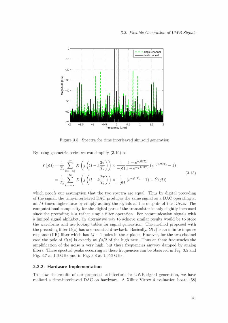
3.2. Flexible Generation of UWB Signals
−2 −1.5 −1 −0.5 0 0.5 1 1.5 2−70
−60
−50
−40
−30
−20
−10
0
Frequency [GHz]
Mag
nitu
de [d
Bc]
single channeldual channel
Figure 3.5.: Spectra for time interleaved sinusoid generation
By using geometric series we can simplify (3.10) to
Y (jΩ) =1
Ts
∞∑
k=−∞X
(
j
(
Ω − k2π
Ts
))
× 1
−jΩ
1 − e−jΩTs
1 − e−jMΩTs
(e−jMΩTs − 1
)
=1
Ts
∞∑
k=−∞X
(
j
(
Ω − k2π
Ts
))
× 1
−jΩ
(e−jΩTs − 1
)≡ Y (jΩ)
(3.13)
which proofs our assumption that the two spectra are equal. Thus by digital precodingof the signal, the time-interleaved DAC produces the same signal as a DAC operating atan M -times higher rate by simply adding the signals at the outputs of the DACs. Thecomputational complexity for the digital part of the transmitter is only slightly increasedsince the precoding is a rather simple filter operation. For communication signals witha limited signal alphabet, an alternative way to achieve similar results would be to storethe waveforms and use lookup tables for signal generation. The method proposed withthe precoding filter G(z) has one essential drawback. Basically, G(z) is an infinite impulseresponse (IIR) filter which has M − 1 poles in the z-plane. However, for the two-channelcase the pole of G(z) is exactly at fs/2 of the high rate. Thus at these frequencies theamplification of the noise is very high, but these frequencies anyway damped by analogfilters. These spectral peaks occurring at these frequencies can be observed in Fig. 3.5 andFig. 3.7 at 1.6 GHz and in Fig. 3.8 at 1.056 GHz.
3.2.2. Hardware Implementation
To show the results of our proposed architecture for UWB signal generation, we haverealized a time-interleaved DAC on hardware. A Xilinx Virtex 4 evaluation board [58]
41
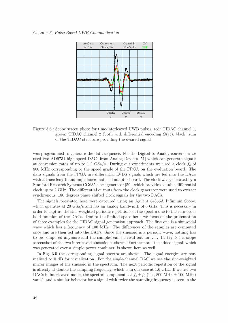
Chapter 3. Pulse-Based UWB Communication
timeDiv :
5ns/div
Channel A :
50 mV/div
Channel B :
50 mV/div
XY
OFF
OffsetB
0
OffsetC
0
OffsetA
0
Figure 3.6.: Scope screen photo for time-interleaved UWB pulses, red: TIDAC channel 1,green: TIDAC channel 2 (both with differential encoding G(z)), black: sumof the TIDAC structure providing the desired signal
was programmed to generate the data sequence. For the Digital-to-Analog conversion weused two AD9734 high-speed DACs from Analog Devices [51] which can generate signalsat conversion rates of up to 1.2 GSa/s. During our experiments we used a clock fs of800 MHz corresponding to the speed grade of the FPGA on the evaluation board. Thedata signals from the FPGA are differential LVDS signals which are fed into the DACswith a trace length and impedance-matched adapter board. The clock was generated by aStanford Research Systems CG635 clock generator [59], which provides a stable differentialclock up to 2 GHz. The differential outputs from the clock generator were used to extractsynchronous, 180 degrees phase shifted clock signals for the two DACs.
The signals presented here were captured using an Agilent 54855A Infiniium Scope,which operates at 20 GSa/s and has an analog bandwidth of 6 GHz. This is necessary inorder to capture the sinc-weighted periodic repetitions of the spectra due to the zero-orderhold function of the DACs. Due to the limited space here, we focus on the presentationof three examples for the TIDAC signal generation approach. The first one is a sinusoidalwave which has a frequency of 100 MHz. The differences of the samples are computedonce and are then fed into the DACs. Since the sinusoid is a periodic wave, nothing hasto be computed anymore and the samples can be read out forever. In Fig. 3.4 a scopescreenshot of the two interleaved sinusoids is shown. Furthermore, the added signal, whichwas generated over a simple power combiner, is shown here as well.
In Fig. 3.5 the corresponding signal spectra are shown. The signal energies are nor-malized to 0 dB for visualization. For the single-channel DAC we see the sinc-weightedmirror images of the sinusoid in the spectrum. The next periodic repetition of the signalis already at double the sampling frequency, which is in our case at 1.6 GHz. If we use twoDACs in interleaved mode, the spectral components at fs ±f0 (i.e., 800 MHz ± 100 MHz)vanish and a similar behavior for a signal with twice the sampling frequency is seen in the
42
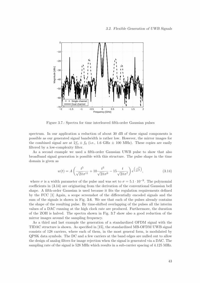
3.2. Flexible Generation of UWB Signals
−2 −1.5 −1 −0.5 0 0.5 1 1.5 2−70
−60
−50
−40
−30
−20
−10
0
Frequency [GHz]
Mag
nitu
de [d
Bc]
Single channelDual channel
Figure 3.7.: Spectra for time interleaved fifth-order Gaussian pulses
spectrum. In our application a reduction of about 30 dB of these signal components ispossible as our generated signal bandwidth is rather low. However, the mirror images forthe combined signal are at 2fs ± f0 (i.e., 1.6 GHz ± 100 MHz). These copies are easilyfiltered by a low-complexity filter.
As a second example we used a fifth-order Gaussian UWB pulse to show that alsobroadband signal generation is possible with this structure. The pulse shape in the timedomain is given as
w(t) = A
(t5√
2πσ11+ 10
t3√2πσ9
− 15t√
2πσ7
)
e
“
−t2
2σ2
”
, (3.14)
where σ is a width parameter of the pulse and was set to σ = 5.1 · 10−9. The polynomialcoefficients in (3.14) are originating from the derivation of the conventional Gaussian bellshape. A fifth-order Gaussian is used because it fits the regulation requirements definedby the FCC [1] Again, a scope screenshot of the differentially encoded signals and thesum of the signals is shown in Fig. 3.6. We see that each of the pulses already containsthe shape of the resulting pulse. By time-shifted overlapping of the pulses all the interimvalues of a DAC running at the high clock rate are produced. Furthermore, the durationof the ZOH is halved. The spectra shown in Fig. 3.7 show also a good reduction of themirror images around the sampling frequency.
As a third and last example the generation of a standardized OFDM signal with theTIDAC structure is shown. As specified in [15], the standardized MB-OFDM UWB signalconsists of 128 carriers, where each of them, in the most general form, is modulated byQPSK data symbols. The DC and a few carriers at the band edges are nulled out to allowthe design of analog filters for image rejection when the signal is generated via a DAC. Thesampling rate of the signal is 528 MHz which results in a sub-carrier spacing of 4.125 MHz.
43
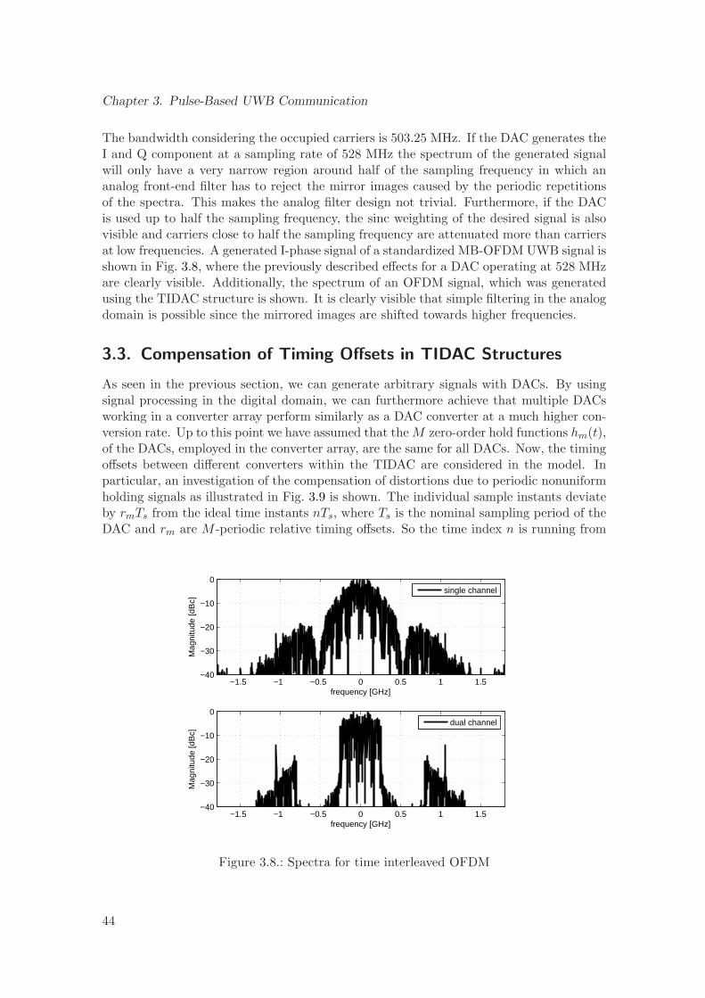
Chapter 3. Pulse-Based UWB Communication
The bandwidth considering the occupied carriers is 503.25 MHz. If the DAC generates theI and Q component at a sampling rate of 528 MHz the spectrum of the generated signalwill only have a very narrow region around half of the sampling frequency in which ananalog front-end filter has to reject the mirror images caused by the periodic repetitionsof the spectra. This makes the analog filter design not trivial. Furthermore, if the DACis used up to half the sampling frequency, the sinc weighting of the desired signal is alsovisible and carriers close to half the sampling frequency are attenuated more than carriersat low frequencies. A generated I-phase signal of a standardized MB-OFDM UWB signal isshown in Fig. 3.8, where the previously described effects for a DAC operating at 528 MHzare clearly visible. Additionally, the spectrum of an OFDM signal, which was generatedusing the TIDAC structure is shown. It is clearly visible that simple filtering in the analogdomain is possible since the mirrored images are shifted towards higher frequencies.
3.3. Compensation of Timing Offsets in TIDAC Structures
As seen in the previous section, we can generate arbitrary signals with DACs. By usingsignal processing in the digital domain, we can furthermore achieve that multiple DACsworking in a converter array perform similarly as a DAC converter at a much higher con-version rate. Up to this point we have assumed that the M zero-order hold functions hm(t),of the DACs, employed in the converter array, are the same for all DACs. Now, the timingoffsets between different converters within the TIDAC are considered in the model. Inparticular, an investigation of the compensation of distortions due to periodic nonuniformholding signals as illustrated in Fig. 3.9 is shown. The individual sample instants deviateby rmTs from the ideal time instants nTs, where Ts is the nominal sampling period of theDAC and rm are M -periodic relative timing offsets. So the time index n is running from
−1.5 −1 −0.5 0 0.5 1 1.5−40
−30
−20
−10
0
frequency [GHz]
Mag
nitu
de [d
Bc]
single channel
−1.5 −1 −0.5 0 0.5 1 1.5−40
−30
−20
−10
0
frequency [GHz]
Mag
nitu
de [d
Bc]
dual channel
Figure 3.8.: Spectra for time interleaved OFDM
44
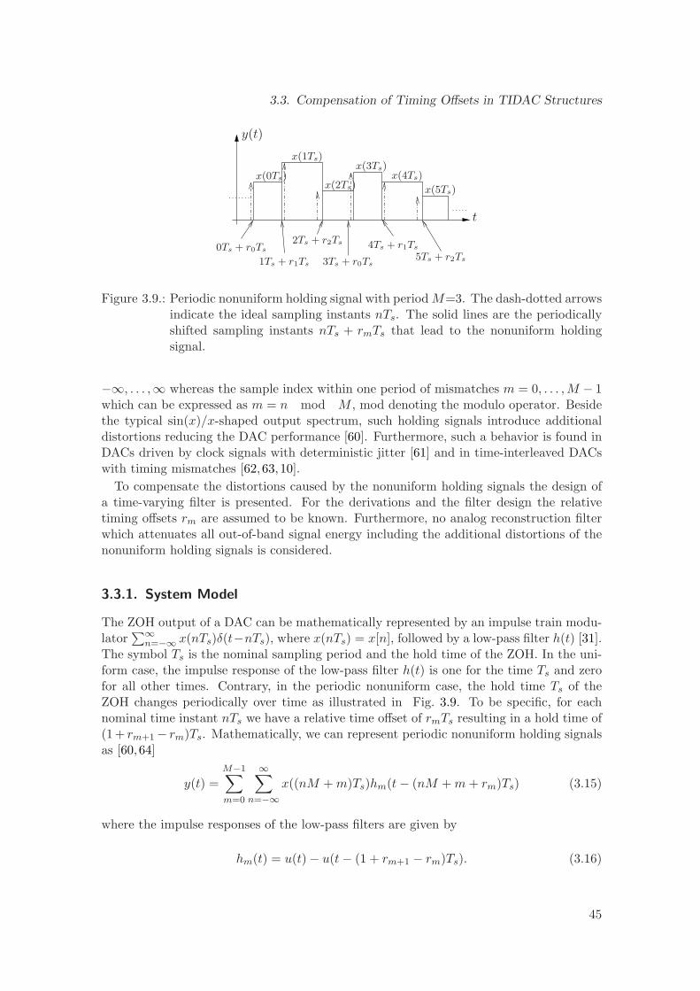
3.3. Compensation of Timing Offsets in TIDAC Structures
0Ts + r0Ts
1Ts + r1Ts
2Ts + r2Ts
3Ts + r0Ts
4Ts + r1Ts
5Ts + r2Ts
x(0Ts)
x(1Ts)
x(2Ts)
x(3Ts)x(4Ts)
x(5Ts)
t
y(t)
Figure 3.9.: Periodic nonuniform holding signal with period M=3. The dash-dotted arrowsindicate the ideal sampling instants nTs. The solid lines are the periodicallyshifted sampling instants nTs + rmTs that lead to the nonuniform holdingsignal.
−∞, . . . ,∞ whereas the sample index within one period of mismatches m = 0, . . . , M − 1which can be expressed as m = n mod M , mod denoting the modulo operator. Besidethe typical sin(x)/x-shaped output spectrum, such holding signals introduce additionaldistortions reducing the DAC performance [60]. Furthermore, such a behavior is found inDACs driven by clock signals with deterministic jitter [61] and in time-interleaved DACswith timing mismatches [62,63,10].
To compensate the distortions caused by the nonuniform holding signals the design ofa time-varying filter is presented. For the derivations and the filter design the relativetiming offsets rm are assumed to be known. Furthermore, no analog reconstruction filterwhich attenuates all out-of-band signal energy including the additional distortions of thenonuniform holding signals is considered.
3.3.1. System Model
The ZOH output of a DAC can be mathematically represented by an impulse train modu-lator
∑∞n=−∞ x(nTs)δ(t−nTs), where x(nTs) = x[n], followed by a low-pass filter h(t) [31].
The symbol Ts is the nominal sampling period and the hold time of the ZOH. In the uni-form case, the impulse response of the low-pass filter h(t) is one for the time Ts and zerofor all other times. Contrary, in the periodic nonuniform case, the hold time Ts of theZOH changes periodically over time as illustrated in Fig. 3.9. To be specific, for eachnominal time instant nTs we have a relative time offset of rmTs resulting in a hold time of(1+ rm+1 − rm)Ts. Mathematically, we can represent periodic nonuniform holding signalsas [60,64]
y(t) =M−1∑
m=0
∞∑
n=−∞x((nM + m)Ts)hm(t − (nM + m + rm)Ts) (3.15)
where the impulse responses of the low-pass filters are given by
hm(t) = u(t) − u(t − (1 + rm+1 − rm)Ts). (3.16)
45
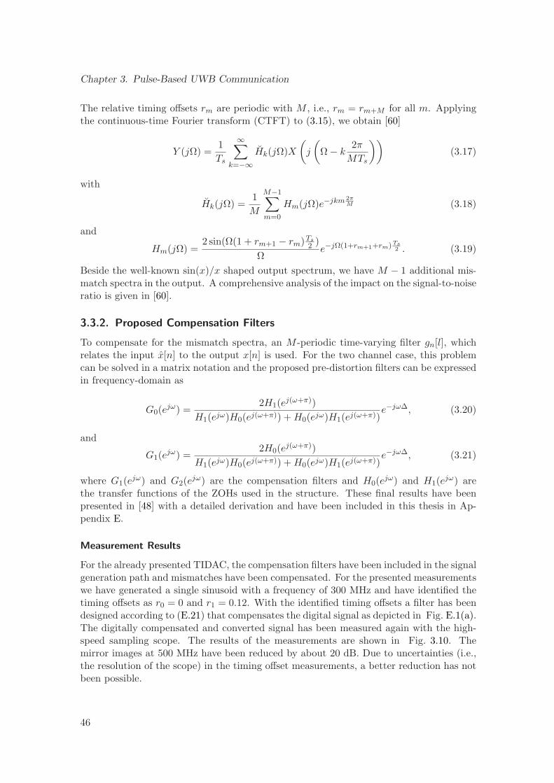
Chapter 3. Pulse-Based UWB Communication
The relative timing offsets rm are periodic with M , i.e., rm = rm+M for all m. Applyingthe continuous-time Fourier transform (CTFT) to (3.15), we obtain [60]
Y (jΩ) =1
Ts
∞∑
k=−∞Hk(jΩ)X
(
j
(
Ω − k2π
MTs
))
(3.17)
with
Hk(jΩ) =1
M
M−1∑
m=0
Hm(jΩ)e−jkm 2πM (3.18)
and
Hm(jΩ) =2 sin(Ω(1 + rm+1 − rm)Ts
2 )
Ωe−jΩ(1+rm+1+rm)Ts
2 . (3.19)
Beside the well-known sin(x)/x shaped output spectrum, we have M − 1 additional mis-match spectra in the output. A comprehensive analysis of the impact on the signal-to-noiseratio is given in [60].
3.3.2. Proposed Compensation Filters
To compensate for the mismatch spectra, an M -periodic time-varying filter gn[l], whichrelates the input x[n] to the output x[n] is used. For the two channel case, this problemcan be solved in a matrix notation and the proposed pre-distortion filters can be expressedin frequency-domain as
G0(ejω) =
2H1(ej(ω+π))
H1(ejω)H0(ej(ω+π)) + H0(ejω)H1(ej(ω+π))e−jω∆, (3.20)
and
G1(ejω) =
2H0(ej(ω+π))
H1(ejω)H0(ej(ω+π)) + H0(ejω)H1(ej(ω+π))e−jω∆, (3.21)
where G1(ejω) and G2(e
jω) are the compensation filters and H0(ejω) and H1(e
jω) arethe transfer functions of the ZOHs used in the structure. These final results have beenpresented in [48] with a detailed derivation and have been included in this thesis in Ap-pendix E.
Measurement Results
For the already presented TIDAC, the compensation filters have been included in the signalgeneration path and mismatches have been compensated. For the presented measurementswe have generated a single sinusoid with a frequency of 300 MHz and have identified thetiming offsets as r0 = 0 and r1 = 0.12. With the identified timing offsets a filter has beendesigned according to (E.21) that compensates the digital signal as depicted in Fig. E.1(a).The digitally compensated and converted signal has been measured again with the high-speed sampling scope. The results of the measurements are shown in Fig. 3.10. Themirror images at 500 MHz have been reduced by about 20 dB. Due to uncertainties (i.e.,the resolution of the scope) in the timing offset measurements, a better reduction has notbeen possible.
46
3.4. Standardized IEEE 802.15.4a Receiver Architectures
0 0.4 0.8 1.2 1.6 2 2.4−80
−60
−40
−20
0
Frequency [GHz]Ene
rgy
Den
sity
Spe
ctru
m [d
Bc]
uncompensated
0 0.4 0.8 1.2 1.6 2 2.4−80
−60
−40
−20
0
Ene
rgy
Den
sity
Spe
ctru
m [d
Bc]
Frequency [GHz]
compensated
Figure 3.10.: Measurements for the uncompensated and the precompensated sinusoid withf = 300 MHz and sampling rate fs = 1600 MS/s.
3.3.3. Timing Offset Identification
In the preceding discussion we have assumed that the timing offsets are known. In prac-tice, we have to determine them from measurements. Since the identification of timingoffsets will be a separate work of significant effort, we will only point out some principleapproaches. To determine the timing offset we need an additional analog-to-digital con-verter (ADC) to observe the output. By observing the output of the DAC for special inputsignals, one can use (3.17)-(3.19) to identify the timing offset similar as it has been donefor time-interleaved ADCs [65]. However, the accuracy requirements on the calibrationsignals seem to be challenging. For the case of two-periodic time-varying holding signalswe can exploit the Farrow structure [66] for the filter design of Gn(ejω). The impulse re-sponse of such filters can be changed by a single parameter, i.e., the timing offset, withoutredesigning the filter. This filter structure allows to adaptively find the timing offsets byminimizing the out-of-band energy without a calibration signal.
3.4. Standardized IEEE 802.15.4a Receiver Architectures
As we have seen in the two previous sections, the universal generation of UWB signals isa challenging task and can be achieved with a TIDAC to allow for low-complexity analogfront-end circuitry. As already mentioned, any pulse which complies with the spectralmasks specified by the regulation authorities (cf. Fig. 1.1) and has a certain similaritywith a reference pulse defined in the standard can be used for a standardized system.The requirements identified for this standardized system were to provide localization ofdevices with accuracies below 1 m and simultaneously allow low-rate data transmissionover the same physical link. In 2007, the IEEE 802.15 working group, and specifically thetask group 4a, finalized their standardization document about an alternative UWB PHYand MAC layer [6]. One of the signaling schemes defined in the IEEE802.15.4a standard
47
Chapter 3. Pulse-Based UWB Communication
considers transmitting data symbols by transmitting bursts of very short pulses. Thesepulses are combined in a burst consisting, for the mandatory data rates of a standardizeddevice, of 16 pulses. The 3 dB bandwidth of UWB pulses is 499.2 MHz. The inverse ofthis bandwidth defines the chip time Tc which is app. 2 ns. Pulses which can be used fora standardized scheme are defined with respect to their correlation properties to a well-defined reference pulse. This reference pulse is a root raised cosine pulse as defined alreadyin (3.1). In the beginning of this section we want to summarize the signaling schemedefined in the standardization document [6]. We will see that the standard employs atime division multiple access (TDMA) signaling scheme where the signals are modulatedin amplitude and position. This allows two different kinds of receivers, namely coherentand non-coherent receivers, where both types can detect the bit encoded in the positionbut the other bit encoded in the polarity is only a meaningful information for coherentreceivers. We will see three different types of receivers, one coherent and two non-coherentones, which have similar implementation complexity. We compare these receivers in singleand multi-user communication scenarios. The three receivers are compared according totheir bit error ratio (BER) performance in these environments.
3.4.1. Standardized Signaling Scheme
As already mentioned, the standardized IEEE802.15.4a signal consists of broadband pulseswith a bandwidth of 499.2 MHz. To be precise, for the mandatory data rate of 1 Mbps,16 pulses are combined to a burst of pulses which are sent consecutively. These pulsesare then pseudorandomly flipped in their sign to achieve spectral smoothing. For theoptional data rates defined in the standard, also other burst lengths are defined. We referthe interested reader to [6] and focus on the mandatory systems in this work. Further-more, these pulses are modulated with binary phase shift keying (BPSK) and with pulseposition (PPM). To be specific, the whole burst of pulses is modulated in position, thusthe modulation is called burst position modulation (BPM). For that reason, a signalingframe has been defined in the standard which is shown in Fig. 3.11. One can see quicklythat such a data symbol consists of two slots where data pulses can occur (labeled with“possible burst positions”). After one of these regions where a device is able to transmitdata, two guard intervals have been included into the frames. This keeps the interferenceof the UWB systems to other existing systems low and allows to design power efficientdevices which can switch off certain parts of the receiver during these idle times. In eachof these possible burst position frames, there are 8 (mandatory) subslots where one ofthese bursts can be placed in a pseudo-random manner. The hopping sequence is derivedfrom a linear feedback shift register (LFSR) which also determines the polarity code forthe pulses within a burst.
The transmitted signal xk(t) can be expressed for one symbol k by
xk(t) = (1 − 2g1(k))
Ncpb∑
n=1
(1 − 2bn(k))p(t − g0(k)TBPM − h(k)Tburst − nTc), (3.22)
where g0(k) and g1(k) are the two data bits, bn(k) is the pseudo random, time-varyingcode for pulse polarities, h(k) is the hopping sequence within the possible burst positions,and p(t) is the transmitted pulse shape, respectively. Ncpb is the number of chips per
48
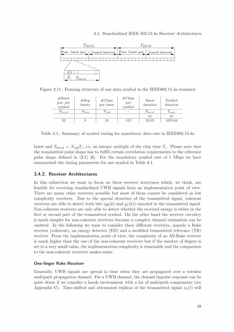
3.4. Standardized IEEE 802.15.4a Receiver Architectures
TBPMTBPM
Poss. burst pos.Poss. burst pos.
TburstTc
Guard intervalGuard interval
Figure 3.11.: Framing structure of one data symbol in the IEEE802.15.4a standard
#Burstpos. persymbol
#Hopbursts
#Chipsper burst
#Chipsper
symbol
Burstduration
Symbolduration
Nburst Nhop Ncpb - Tburst Tsym
ns ns
32 8 16 512 32.05 1025.64
Table 3.1.: Summary of symbol timing for mandatory data rate in IEEE802.15.4a
burst and Tburst = NcpbTc, i.e, an integer multiple of the chip time Tc. Please note thatthe transmitted pulse shape has to fulfill certain correlation requirements to the referencepulse shape defined in (3.1) [6]. For the mandatory symbol rate of 1 Mbps we havesummarized the timing parameters for one symbol in Table 3.1.
3.4.2. Receiver Architectures
In this subsection we want to focus on three receiver structures which, we think, arefeasible for receiving standardized UWB signals from an implementation point of view.There are many other receivers possible but most of them cannot be considered as lowcomplexity receivers. Due to the special structure of the transmitted signal, coherentreceivers are able to detect both bits (g0(k) and g1(k)) encoded in the transmitted signal.Non-coherent receivers are only able to detect whether the received energy is either in thefirst or second part of the transmitted symbol. On the other hand the receiver circuitryis much simpler for non-coherent receivers because a complex channel estimation can beomitted. In the following we want to consider three different receivers, namely a Rakereceiver (coherent), an energy detector (ED) and a modified transmitted reference (TR)receiver. From the implementation point of view, the complexity of an All-Rake receiveris much higher than the one of the non-coherent receivers but if the number of fingers isset to a very small value, the implementation complexity is reasonable and the comparisonto the non-coherent receivers makes sense.
One-finger Rake Receiver
Generally, UWB signals are spread in time when they are propagated over a wirelessmultipath propagation channel. For a UWB channel, the channel impulse response can bequite dense if we consider a harsh environment with a lot of multipath components (seeAppendix C). Time-shifted and attenuated replicas of the transmitted signal xk(t) will
49
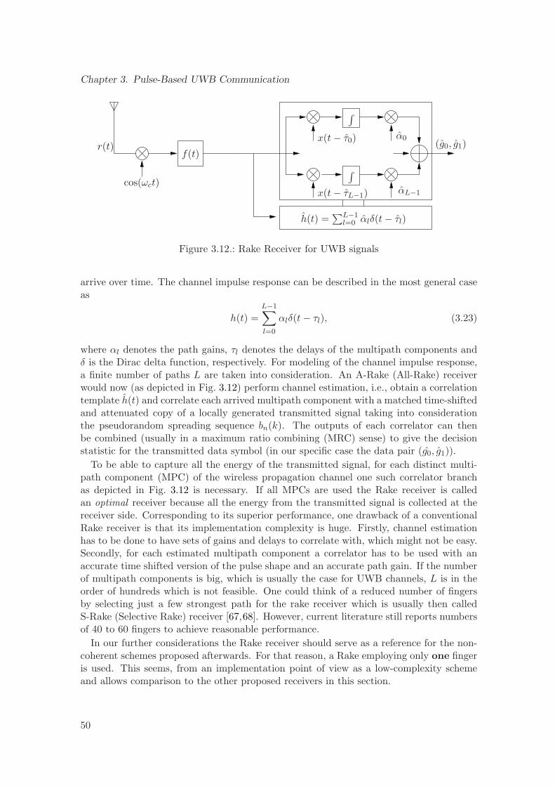
Chapter 3. Pulse-Based UWB Communication
r(t)x(t − τ0)
x(t − τL−1)cos(ωct)
f(t)
∫
∫
h(t) =∑L−1
l=0 αlδ(t − τl)
α0
αL−1
(g0, g1)
Figure 3.12.: Rake Receiver for UWB signals
arrive over time. The channel impulse response can be described in the most general caseas
h(t) =L−1∑
l=0
αlδ(t − τl), (3.23)
where αl denotes the path gains, τl denotes the delays of the multipath components andδ is the Dirac delta function, respectively. For modeling of the channel impulse response,a finite number of paths L are taken into consideration. An A-Rake (All-Rake) receiverwould now (as depicted in Fig. 3.12) perform channel estimation, i.e., obtain a correlationtemplate h(t) and correlate each arrived multipath component with a matched time-shiftedand attenuated copy of a locally generated transmitted signal taking into considerationthe pseudorandom spreading sequence bn(k). The outputs of each correlator can thenbe combined (usually in a maximum ratio combining (MRC) sense) to give the decisionstatistic for the transmitted data symbol (in our specific case the data pair (g0, g1)).
To be able to capture all the energy of the transmitted signal, for each distinct multi-path component (MPC) of the wireless propagation channel one such correlator branchas depicted in Fig. 3.12 is necessary. If all MPCs are used the Rake receiver is calledan optimal receiver because all the energy from the transmitted signal is collected at thereceiver side. Corresponding to its superior performance, one drawback of a conventionalRake receiver is that its implementation complexity is huge. Firstly, channel estimationhas to be done to have sets of gains and delays to correlate with, which might not be easy.Secondly, for each estimated multipath component a correlator has to be used with anaccurate time shifted version of the pulse shape and an accurate path gain. If the numberof multipath components is big, which is usually the case for UWB channels, L is in theorder of hundreds which is not feasible. One could think of a reduced number of fingersby selecting just a few strongest path for the rake receiver which is usually then calledS-Rake (Selective Rake) receiver [67,68]. However, current literature still reports numbersof 40 to 60 fingers to achieve reasonable performance.
In our further considerations the Rake receiver should serve as a reference for the non-coherent schemes proposed afterwards. For that reason, a Rake employing only one fingeris used. This seems, from an implementation point of view as a low-complexity schemeand allows comparison to the other proposed receivers in this section.
50
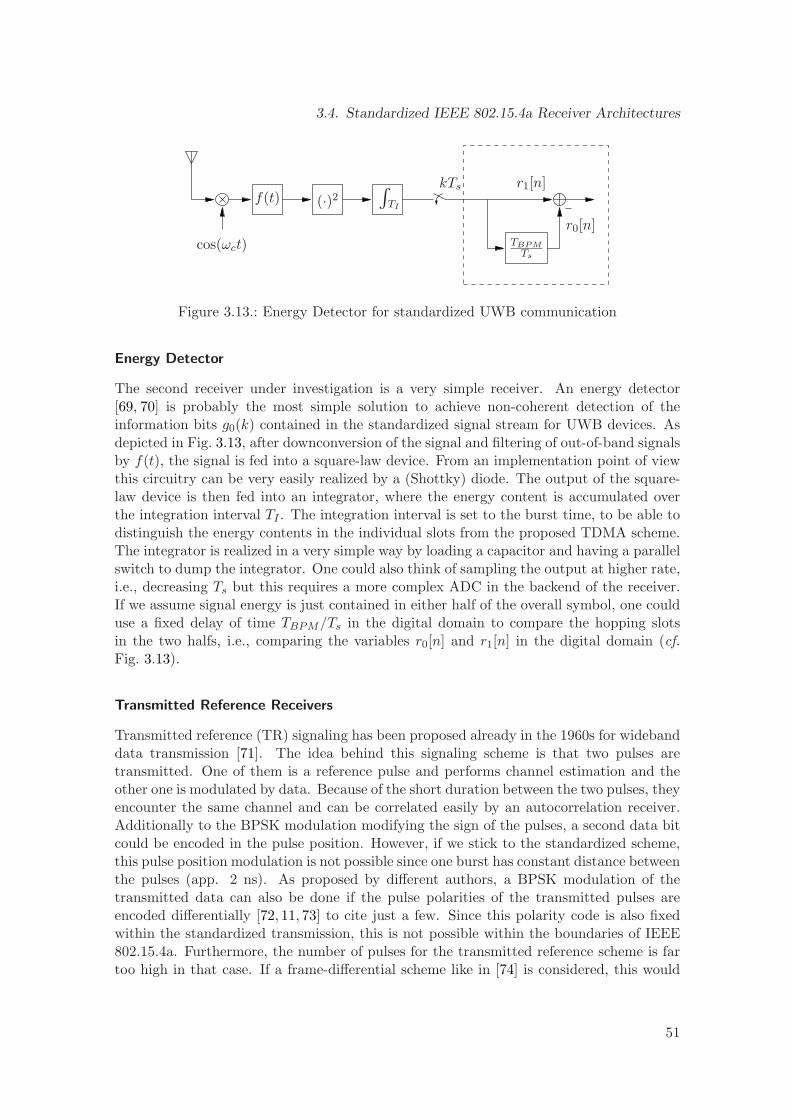
3.4. Standardized IEEE 802.15.4a Receiver Architectures
cos(ωct)
f(t) (·)2∫
TI
kTs
r0[n]
r1[n]
TBPMTs
Figure 3.13.: Energy Detector for standardized UWB communication
Energy Detector
The second receiver under investigation is a very simple receiver. An energy detector[69, 70] is probably the most simple solution to achieve non-coherent detection of theinformation bits g0(k) contained in the standardized signal stream for UWB devices. Asdepicted in Fig. 3.13, after downconversion of the signal and filtering of out-of-band signalsby f(t), the signal is fed into a square-law device. From an implementation point of viewthis circuitry can be very easily realized by a (Shottky) diode. The output of the square-law device is then fed into an integrator, where the energy content is accumulated overthe integration interval TI . The integration interval is set to the burst time, to be able todistinguish the energy contents in the individual slots from the proposed TDMA scheme.The integrator is realized in a very simple way by loading a capacitor and having a parallelswitch to dump the integrator. One could also think of sampling the output at higher rate,i.e., decreasing Ts but this requires a more complex ADC in the backend of the receiver.If we assume signal energy is just contained in either half of the overall symbol, one coulduse a fixed delay of time TBPM/Ts in the digital domain to compare the hopping slotsin the two halfs, i.e., comparing the variables r0[n] and r1[n] in the digital domain (cf.Fig. 3.13).
Transmitted Reference Receivers
Transmitted reference (TR) signaling has been proposed already in the 1960s for widebanddata transmission [71]. The idea behind this signaling scheme is that two pulses aretransmitted. One of them is a reference pulse and performs channel estimation and theother one is modulated by data. Because of the short duration between the two pulses, theyencounter the same channel and can be correlated easily by an autocorrelation receiver.Additionally to the BPSK modulation modifying the sign of the pulses, a second data bitcould be encoded in the pulse position. However, if we stick to the standardized scheme,this pulse position modulation is not possible since one burst has constant distance betweenthe pulses (app. 2 ns). As proposed by different authors, a BPSK modulation of thetransmitted data can also be done if the pulse polarities of the transmitted pulses areencoded differentially [72, 11, 73] to cite just a few. Since this polarity code is also fixedwithin the standardized transmission, this is not possible within the boundaries of IEEE802.15.4a. Furthermore, the number of pulses for the transmitted reference scheme is fartoo high in that case. If a frame-differential scheme like in [74] is considered, this would
51
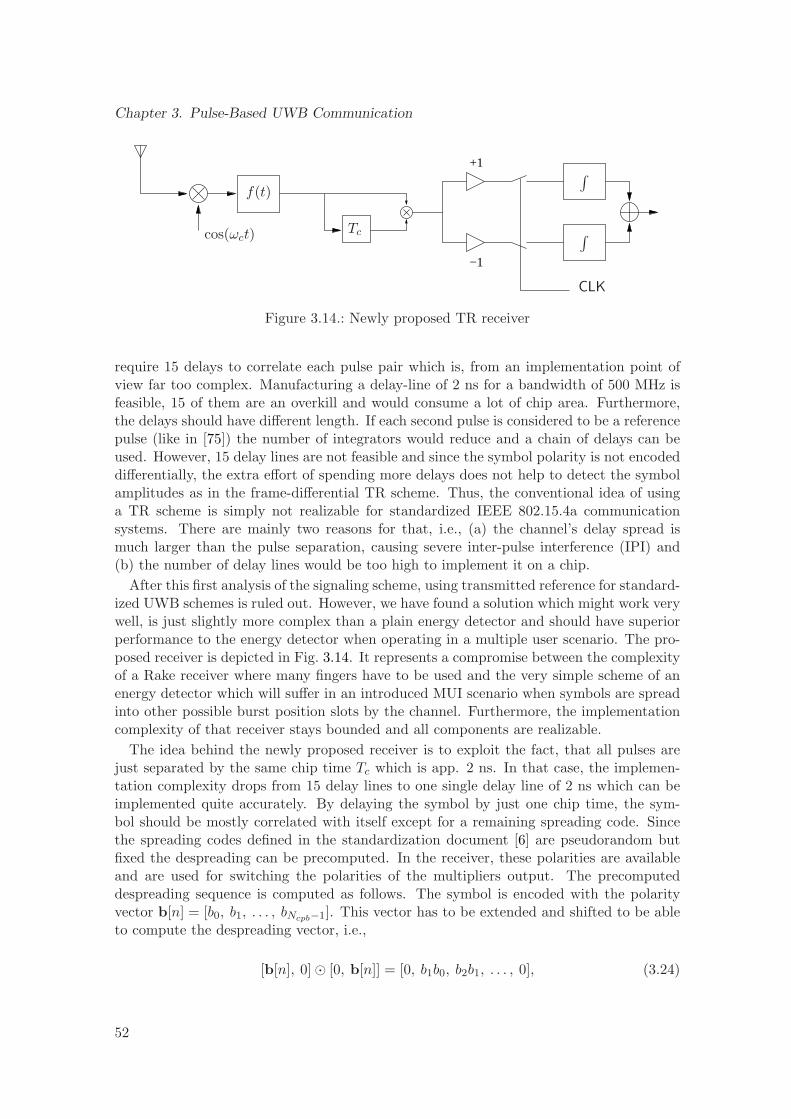
Chapter 3. Pulse-Based UWB Communication
+1
−1
cos(ωct)
f(t)
Tc ∫
∫
CLK
Figure 3.14.: Newly proposed TR receiver
require 15 delays to correlate each pulse pair which is, from an implementation point ofview far too complex. Manufacturing a delay-line of 2 ns for a bandwidth of 500 MHz isfeasible, 15 of them are an overkill and would consume a lot of chip area. Furthermore,the delays should have different length. If each second pulse is considered to be a referencepulse (like in [75]) the number of integrators would reduce and a chain of delays can beused. However, 15 delay lines are not feasible and since the symbol polarity is not encodeddifferentially, the extra effort of spending more delays does not help to detect the symbolamplitudes as in the frame-differential TR scheme. Thus, the conventional idea of usinga TR scheme is simply not realizable for standardized IEEE 802.15.4a communicationsystems. There are mainly two reasons for that, i.e., (a) the channel’s delay spread ismuch larger than the pulse separation, causing severe inter-pulse interference (IPI) and(b) the number of delay lines would be too high to implement it on a chip.
After this first analysis of the signaling scheme, using transmitted reference for standard-ized UWB schemes is ruled out. However, we have found a solution which might work verywell, is just slightly more complex than a plain energy detector and should have superiorperformance to the energy detector when operating in a multiple user scenario. The pro-posed receiver is depicted in Fig. 3.14. It represents a compromise between the complexityof a Rake receiver where many fingers have to be used and the very simple scheme of anenergy detector which will suffer in an introduced MUI scenario when symbols are spreadinto other possible burst position slots by the channel. Furthermore, the implementationcomplexity of that receiver stays bounded and all components are realizable.
The idea behind the newly proposed receiver is to exploit the fact, that all pulses arejust separated by the same chip time Tc which is app. 2 ns. In that case, the implemen-tation complexity drops from 15 delay lines to one single delay line of 2 ns which can beimplemented quite accurately. By delaying the symbol by just one chip time, the sym-bol should be mostly correlated with itself except for a remaining spreading code. Sincethe spreading codes defined in the standardization document [6] are pseudorandom butfixed the despreading can be precomputed. In the receiver, these polarities are availableand are used for switching the polarities of the multipliers output. The precomputeddespreading sequence is computed as follows. The symbol is encoded with the polarityvector b[n] = [b0, b1, . . . , bNcpb−1]. This vector has to be extended and shifted to be ableto compute the despreading vector, i.e.,
[b[n], 0] ⊙ [0, b[n]] = [0, b1b0, b2b1, . . . , 0], (3.24)
52
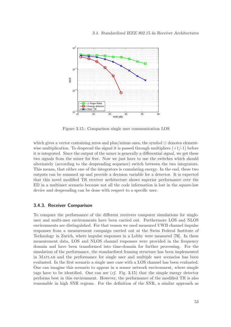
3.4. Standardized IEEE 802.15.4a Receiver Architectures
15 20 25 30 35 4010
−3
10−2
10−1
100
SNR [dB]
BE
R
1−finger RakeEnergy detectorMod. TR
Figure 3.15.: Comparison single user communication LOS
which gives a vector containing zeros and plus/minus ones, the symbol ⊙ denotes element-wise multiplication. To despread the signal it is passed through multipliers (+1/-1) beforeit is integrated. Since the output of the mixer is generally a differential signal, we get thesetwo signals from the mixer for free. Now we just have to use the switches which shouldalternately (according to the despreading sequence) switch between the two integrators.This means, that either one of the integrators is cumulating energy. In the end, these twooutputs can be summed up and provide a decision variable for a detector. It is expectedthat this novel modified TR receiver architecture shows superior performance over theED in a multiuser scenario because not all the code information is lost in the square-lawdevice and despreading can be done with respect to a specific user.
3.4.3. Receiver Comparison
To compare the performance of the different receivers computer simulations for single-user and multi-user environments have been carried out. Furthermore LOS and NLOSenvironments are distinguished. For that reason we used measured UWB channel impulseresponses from a measurement campaign carried out at the Swiss Federal Institute ofTechnology in Zurich, where impulse responses in a Lobby were measured [76]. In thesemeasurement data, LOS and NLOS channel responses were provided in the frequencydomain and have been transformed into time-domain for further processing. For thesimulation of the performance, the standardized framing structure has been implementedin Matlab and the performance for single user and multiple user scenarios has beenevaluated. In the first scenario a single user case with a LOS channel has been evaluated.One can imagine this scenario to appear in a sensor network environment, where simpletags have to be identified. One can see (cf. Fig. 3.15) that the simple energy detectorperforms best in this environment. However, the performance of the modified TR is alsoreasonable in high SNR regions. For the definition of the SNR, a similar approach as
53
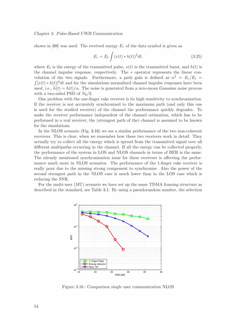
Chapter 3. Pulse-Based UWB Communication
shown in [69] was used. The received energy Er of the data symbol is given as
Er = Et
∫
(x(t) ∗ h(t))2dt, (3.25)
where Et is the energy of the transmitted pulse, x(t) is the transmitted burst, and h(t) isthe channel impulse response, respectively. The ∗ operator represents the linear con-volution of the two signals. Furthermore, a path gain is defined as α2 = Er/Et =∫
[x(t) ∗ h(t)]2dt and for the simulations normalized channel impulse responses have beenused, i.e., h(t) = h(t)/α. The noise is generated from a zero-mean Gaussian noise processwith a two-sided PSD of N0/2.
One problem with the one-finger rake receiver is its high sensitivity to synchronization.If the receiver is not accurately synchronized to the maximum path (and only this oneis used for the studied receiver) of the channel the performance quickly degrades. Tomake the receiver performance independent of the channel estimation, which has to beperformed in a real receiver, the (strongest path of the) channel is assumed to be knownfor the simulations.
In the NLOS scenario (Fig. 3.16) we see a similar performance of the two non-coherentreceivers. This is clear, when we remember how these two receivers work in detail. Theyactually try to collect all the energy which is spread from the transmitted signal over alldifferent multipaths occurring in the channel. If all the energy can be collected properly,the performance of the system in LOS and NLOS channels in terms of BER is the same.The already mentioned synchronization issue for these receivers is affecting the perfor-mance much more in NLOS scenarios. The performance of the 1-finger rake receiver isreally poor due to the missing strong component to synchronize. Also the power of thesecond strongest path in the NLOS case is much lower than in the LOS case which isreducing the SNR.
For the multi-user (MU) scenario we have set up the same TDMA framing structure asdescribed in the standard, see Table 3.1. By using a pseudorandom number, the selection
15 20 25 30 35 4010
−3
10−2
10−1
100
SNR [dB]
BE
R
1−finger RakeEnergy detectorMod. TR
Figure 3.16.: Comparison single user communication NLOS
54
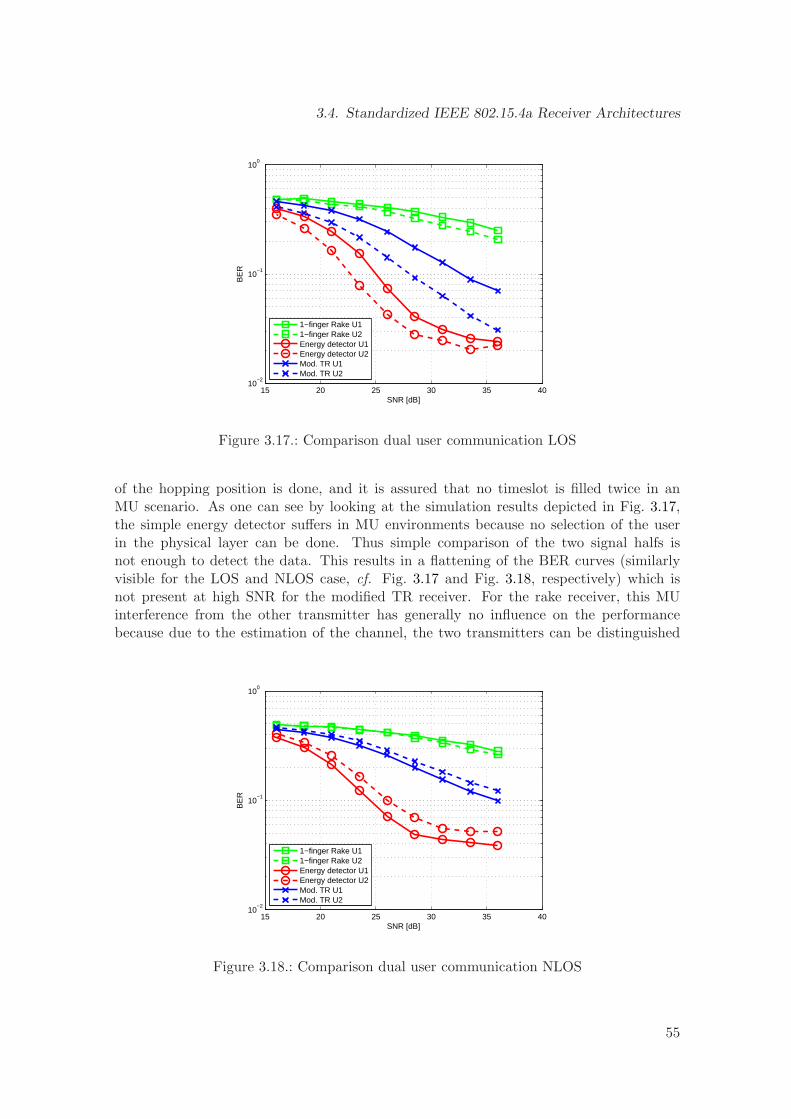
3.4. Standardized IEEE 802.15.4a Receiver Architectures
15 20 25 30 35 4010
−2
10−1
100
SNR [dB]
BE
R
1−finger Rake U11−finger Rake U2Energy detector U1Energy detector U2Mod. TR U1Mod. TR U2
Figure 3.17.: Comparison dual user communication LOS
of the hopping position is done, and it is assured that no timeslot is filled twice in anMU scenario. As one can see by looking at the simulation results depicted in Fig. 3.17,the simple energy detector suffers in MU environments because no selection of the userin the physical layer can be done. Thus simple comparison of the two signal halfs isnot enough to detect the data. This results in a flattening of the BER curves (similarlyvisible for the LOS and NLOS case, cf. Fig. 3.17 and Fig. 3.18, respectively) which isnot present at high SNR for the modified TR receiver. For the rake receiver, this MUinterference from the other transmitter has generally no influence on the performancebecause due to the estimation of the channel, the two transmitters can be distinguished
15 20 25 30 35 4010
−2
10−1
100
SNR [dB]
BE
R
1−finger Rake U11−finger Rake U2Energy detector U1Energy detector U2Mod. TR U1Mod. TR U2
Figure 3.18.: Comparison dual user communication NLOS
55
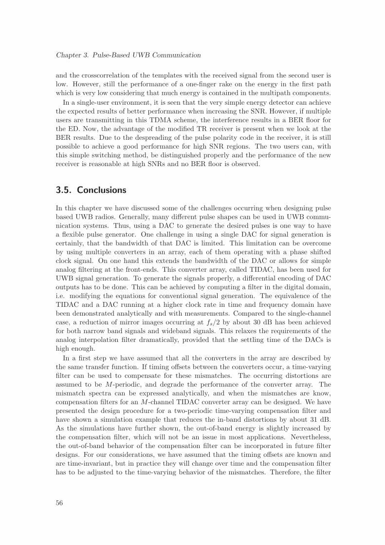
Chapter 3. Pulse-Based UWB Communication
and the crosscorrelation of the templates with the received signal from the second user islow. However, still the performance of a one-finger rake on the energy in the first pathwhich is very low considering that much energy is contained in the multipath components.
In a single-user environment, it is seen that the very simple energy detector can achievethe expected results of better performance when increasing the SNR. However, if multipleusers are transmitting in this TDMA scheme, the interference results in a BER floor forthe ED. Now, the advantage of the modified TR receiver is present when we look at theBER results. Due to the despreading of the pulse polarity code in the receiver, it is stillpossible to achieve a good performance for high SNR regions. The two users can, withthis simple switching method, be distinguished properly and the performance of the newreceiver is reasonable at high SNRs and no BER floor is observed.
3.5. Conclusions
In this chapter we have discussed some of the challenges occurring when designing pulsebased UWB radios. Generally, many different pulse shapes can be used in UWB commu-nication systems. Thus, using a DAC to generate the desired pulses is one way to havea flexible pulse generator. One challenge in using a single DAC for signal generation iscertainly, that the bandwidth of that DAC is limited. This limitation can be overcomeby using multiple converters in an array, each of them operating with a phase shiftedclock signal. On one hand this extends the bandwidth of the DAC or allows for simpleanalog filtering at the front-ends. This converter array, called TIDAC, has been used forUWB signal generation. To generate the signals properly, a differential encoding of DACoutputs has to be done. This can be achieved by computing a filter in the digital domain,i.e. modifying the equations for conventional signal generation. The equivalence of theTIDAC and a DAC running at a higher clock rate in time and frequency domain havebeen demonstrated analytically and with measurements. Compared to the single-channelcase, a reduction of mirror images occurring at fs/2 by about 30 dB has been achievedfor both narrow band signals and wideband signals. This relaxes the requirements of theanalog interpolation filter dramatically, provided that the settling time of the DACs ishigh enough.
In a first step we have assumed that all the converters in the array are described bythe same transfer function. If timing offsets between the converters occur, a time-varyingfilter can be used to compensate for these mismatches. The occurring distortions areassumed to be M -periodic, and degrade the performance of the converter array. Themismatch spectra can be expressed analytically, and when the mismatches are know,compensation filters for an M -channel TIDAC converter array can be designed. We havepresented the design procedure for a two-periodic time-varying compensation filter andhave shown a simulation example that reduces the in-band distortions by about 31 dB.As the simulations have further shown, the out-of-band energy is slightly increased bythe compensation filter, which will not be an issue in most applications. Nevertheless,the out-of-band behavior of the compensation filter can be incorporated in future filterdesigns. For our considerations, we have assumed that the timing offsets are known andare time-invariant, but in practice they will change over time and the compensation filterhas to be adjusted to the time-varying behavior of the mismatches. Therefore, the filter
56
3.5. Conclusions
design has to be extended to allow for time-varying timing offsets.Finally, also the receiver side has been investigated. Possible receiver structures for
standardized UWB low data rate communication and positioning systems [6] have beenpresented. It is seen that, from an implementation complexity point of view, an energydetector offers the most simple solution. On the other hand, the MU performance of the EDis not very good and a novel modified TR receiver has been proposed for the standardized,pulse based UWB communication scheme. With slightly increased complexity for themodified TR scheme, a superior MU performance can be achieved whereas the ED doesnot consider the additional information contained in the spreading code. A very simplerake receiver has been compared in this study too, but due to relying on a single path,reliable synchronization, and the loss of energy due to the multipath environment, therake receivers a bad choice for a low-complexity and low-cost implementation.
57

Chapter 3. Pulse-Based UWB Communication
58
Chapter4Equalization for Nonlinear Receiver Front-Ends
In this chapter we will review one very specific UWB communication system. It is basicallyan extension of the conventional pulse-based transmitted reference idea proposed already inthe 1960’s and generalized in 2002 [77] when UWB got the boost because of the regulationauthorities’ release of the spectrum in the US [1]. As already seen in Section 3.4, the simplereceivers which can be used for the standardized pulse based UWB scheme can also be usedfor TR signaling. One big advantage of correlation receivers is their easy implementation.Conversely, these receiver architectures have one main drawback, namely that they employnonlinear devices to be able to restore the original signal. This introduces new challengesfor the signal processing algorithms in the receivers and requires digital enhancement ofthe effects occurring in the continuous-time domain.
This digital enhancement of the analog front-end of the receiver will be the main sci-entific contribution of this chapter. In the beginning we will briefly review the resultsfrom [11], with respect to the used signaling scheme and the used receiver structure.Furthermore, a nonlinear equivalent system model can be derived from the studied com-munication system which will be briefly discussed in this section. The overall system canbe modeled as a second-order Volterra system when high data rates are used, i.e., a non-linear system with fading memory. The nonlinear distortion can be equalized by means ofdigital signal processing which will be elaborated in the following sections1.
4.1. Introduction
It was shown in Section 3.4 that receivers for pulse-based UWB communication can beimplemented with a few simple components. If we reconsider the ED, we have also seenthat this is achieved with a simple squaring device (i.e., a nonlinearity). Also if we con-sider the transmitted-reference signaling schemes as described in [77, 11, 72, 79] and thecorresponding autocorrelation receiver architectures, we see that the essential receiver op-eration is nonlinear. As discussed in Sect. 3.4, the idea of transmitted-reference signalingis to transmit pairs of pulses. The first pulse is an unmodulated reference pulse and servesas a template for the second transmitted pulse. The second pulse, i.e., the data pulse,is then modulated either in polarity or in delay. So for each transmitted bit, one such
1Main parts of this chapter are taken from a journal contribution submitted by the author [78].
59
Chapter 4. Equalization for Nonlinear Receiver Front-Ends
pulse doublet (frame) has to be transmitted. Since the separation between these pulses isusually small (∼ 2 - 30 ns) both pulses encounter the same distortion on the channel, andthe reference pulse is thus a perfect template to measure the similarity to the transmitteddata pulse (i.e., determining the correlation). Thus, the receiver operates directly in base-band and receives the signal with a broadband antenna. This received signal r(t) is thenfed into a pulse-pair correlator which consists of a delay line, matched to the distance ofthe pulses in the transmitted signal, and a multiplier performing the multiplication of thereceived signal with a time-shifted copy of itself. Afterwards, the signal of the multiplier iscumulated (integrated) over a certain time TI , to capture sufficient multipath energy fromthe transmitted pulses. This integration time is usually found by trading cumulation ofsignal energy and cumulation of noise [80]. The output of such a correlator is then sampledand digital post-processing can be done in a DSP or FPGA chip. The digital part of thereceiver can then also achieve synchronization of the receiver to the transmitter and withina feedback loop, the integrator delays are adjusted dynamically. One main advantage ofthis architecture is that in the receiver no channel estimation has to be performed.
One main drawback of the conventional transmitted-reference signaling scheme is, thatonly each second transmitted pulse contains new information. To support multi-userseparation and increase robustness to interference, generally one such data symbol doesnot consist of a single pulse pair, only. Multiple pulse-pairs normally comprise one datasymbol. This also means, that half of the transmitted symbol energy is already spentfor the reference pulses. One solution to this loss of energy is to use each pulse in adata symbol as a reference and as a data pulse [72]. Additionally, the information bitcan be differentially encoded into this pulse stream, meaning the current pulse polaritydepends on the polarity of the previous pulse and the current data symbol. One suchautocorrelation receiver for Ncr pulses composing one symbol is depicted in Fig. 4.1. Thereceived signal is fed into a bank of correlators where each correlator has a matched timedelay Dj , j = 0, . . . , Ncr which is matched to the pulse delays in the transmitted pulsestream. Each pulse pair thus requires one correlator and the outputs of these correlatorsare then sampled at Nyquist rate. The digital signal processing used in the back-end canthen get rid of nonlinear distortions in the received data symbols (one topic addressed inthis thesis), narrow band interference (NBI) [12], and multi-user interference (MUI) [81,13].Reduction of the nonlinear distortion can also be achieved by using oversampling in thereceiver front-end. This was extensively studied in [79].
When increasing the data rate, the distance between these pulses becomes smaller. Thisis on the one hand desired because then the correlation of the channel’s responses to thepulses is very high and requires short delay lines which can be implemented. On theother hand closely-spaced pulses, which are spread over the channel in delay, are alsointerfering with each other and are diminishing the performance of the system. Anyhow,there is high interest to find algorithms to reconstruct this information in a cheap way.Thus, the problems occurring with nonlinearities in the analog domain are compensatedfor by means of nonlinear digital signal processing which offers a cheap and flexible wayto combat these distortions.
60
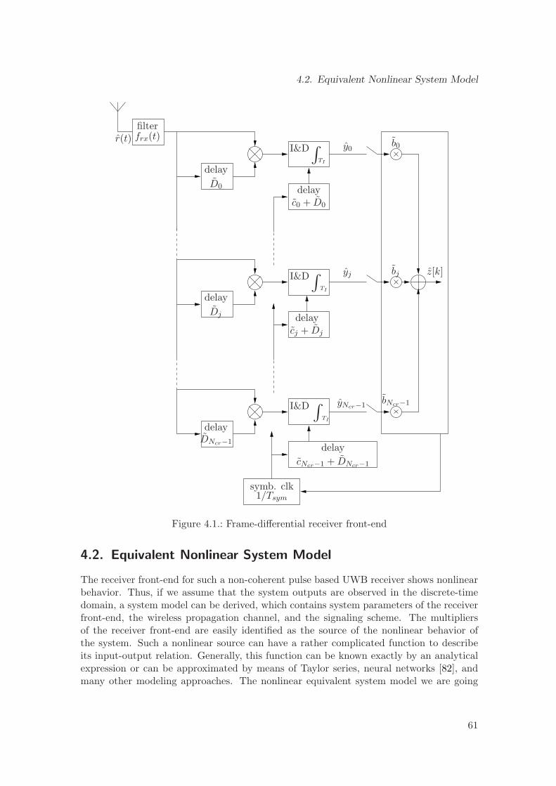
4.2. Equivalent Nonlinear System Model
delay
delay
delay
delay
delay
delay
I&D
I&D
I&D
∫
∫
∫
filter
symb. clk1/Tsym
frx(t)
D0
Dj
DNcr−1
c0 + D0
cj + Dj
cNcr−1 + DNcr−1
TI
TI
TI
y0
yj
yNcr−1
z[k]
r(t) b0
bj
bNcr−1
Figure 4.1.: Frame-differential receiver front-end
4.2. Equivalent Nonlinear System Model
The receiver front-end for such a non-coherent pulse based UWB receiver shows nonlinearbehavior. Thus, if we assume that the system outputs are observed in the discrete-timedomain, a system model can be derived, which contains system parameters of the receiverfront-end, the wireless propagation channel, and the signaling scheme. The multipliersof the receiver front-end are easily identified as the source of the nonlinear behavior ofthe system. Such a nonlinear source can have a rather complicated function to describeits input-output relation. Generally, this function can be known exactly by an analyticalexpression or can be approximated by means of Taylor series, neural networks [82], andmany other modeling approaches. The nonlinear equivalent system model we are going
61
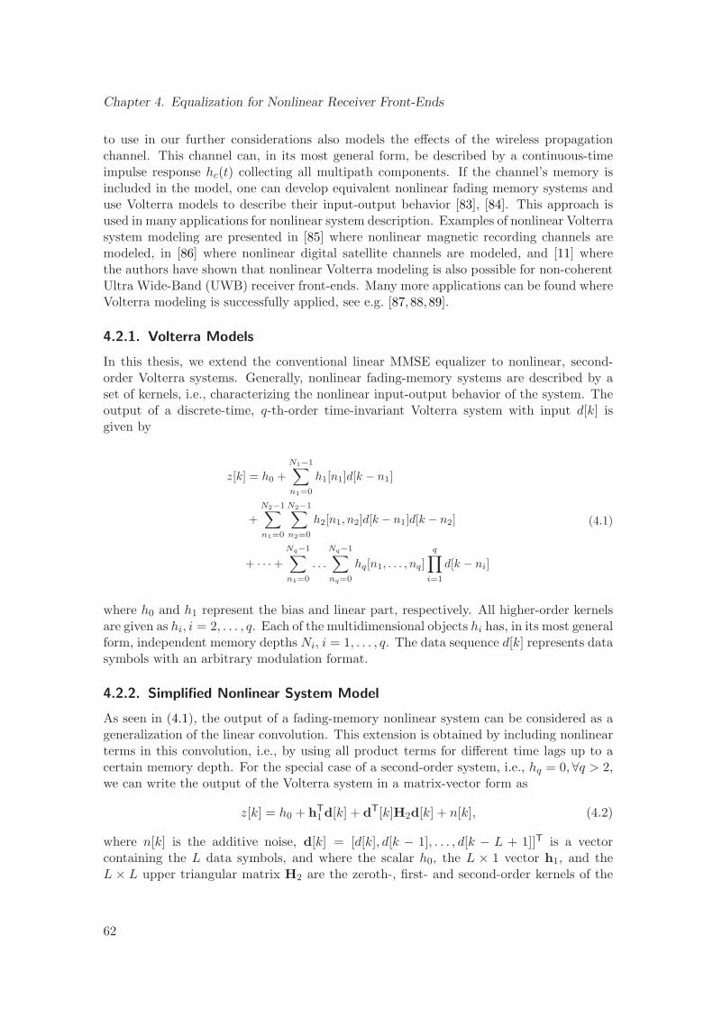
Chapter 4. Equalization for Nonlinear Receiver Front-Ends
to use in our further considerations also models the effects of the wireless propagationchannel. This channel can, in its most general form, be described by a continuous-timeimpulse response hc(t) collecting all multipath components. If the channel’s memory isincluded in the model, one can develop equivalent nonlinear fading memory systems anduse Volterra models to describe their input-output behavior [83], [84]. This approach isused in many applications for nonlinear system description. Examples of nonlinear Volterrasystem modeling are presented in [85] where nonlinear magnetic recording channels aremodeled, in [86] where nonlinear digital satellite channels are modeled, and [11] wherethe authors have shown that nonlinear Volterra modeling is also possible for non-coherentUltra Wide-Band (UWB) receiver front-ends. Many more applications can be found whereVolterra modeling is successfully applied, see e.g. [87, 88,89].
4.2.1. Volterra Models
In this thesis, we extend the conventional linear MMSE equalizer to nonlinear, second-order Volterra systems. Generally, nonlinear fading-memory systems are described by aset of kernels, i.e., characterizing the nonlinear input-output behavior of the system. Theoutput of a discrete-time, q-th-order time-invariant Volterra system with input d[k] isgiven by
z[k] = h0 +
N1−1∑
n1=0
h1[n1]d[k − n1]
+
N2−1∑
n1=0
N2−1∑
n2=0
h2[n1, n2]d[k − n1]d[k − n2]
+ · · · +Nq−1∑
n1=0
. . .
Nq−1∑
nq=0
hq[n1, . . . , nq]
q∏
i=1
d[k − ni]
(4.1)
where h0 and h1 represent the bias and linear part, respectively. All higher-order kernelsare given as hi, i = 2, . . . , q. Each of the multidimensional objects hi has, in its most generalform, independent memory depths Ni, i = 1, . . . , q. The data sequence d[k] represents datasymbols with an arbitrary modulation format.
4.2.2. Simplified Nonlinear System Model
As seen in (4.1), the output of a fading-memory nonlinear system can be considered as ageneralization of the linear convolution. This extension is obtained by including nonlinearterms in this convolution, i.e., by using all product terms for different time lags up to acertain memory depth. For the special case of a second-order system, i.e., hq = 0,∀q > 2,we can write the output of the Volterra system in a matrix-vector form as
z[k] = h0 + hT1 d[k] + dT[k]H2d[k] + n[k], (4.2)
where n[k] is the additive noise, d[k] = [d[k], d[k − 1], . . . , d[k − L + 1]]T is a vectorcontaining the L data symbols, and where the scalar h0, the L × 1 vector h1, and theL × L upper triangular matrix H2 are the zeroth-, first- and second-order kernels of the
62
4.3. Nonlinear Equalization for Second-Order Volterra Systems
channel, respectively. With respect to (4.1), the memory depth of the nonlinear system isdefined as L = max(N1, N2). We make the following assumptions in this work:
A1) The data symbols d[k] are binary antipodal, i.e., d[k] ∈ ±c, with c ∈ R and ±c isequiprobable such that Ed[k]=0.
A2) The noise is i.i.d. Gaussian with zero-mean and variance σ2n.
The derivations in this thesis can also be done without the i.i.d. assumption. However,the covariance matrices introduced later on will not be scaled identity matrices anymore.The squared elements of d[k] are given as d2[k] = c2, ∀k, and thus the main diagonal ofthe second-order kernel H2 can be included into the bias term h0 which simplifies (4.2).
For our further considerations, we assume that the bias term is not contained in thesystem and we define
y[k] = z[k] − h0 = hT1 d[k] + dT[k]H2d[k] + n[k], (4.3)
as the received sequence without the bias h0 which can easily be obtained by averaging.Since we want to write the second-order kernel as a linear function of the crossterms,
we introduce the operator ⊠, which is a modified Kronecker product that only takes theunique half of the crossterms into account. We can then rewrite y[k] as
y[k] = hT1 d[k] + hT
2 (d[k] ⊠ d[k]) + n[k], (4.4)
where h2 is an appropriate modification of H2, omitting also the main diagonal elementssince they have been collected in the bias term. For a vector b = [b1, b2, . . . , bK ]T, we definethe reduced Kronecker product b⊠b as b⊠b = [b1b2, b2b3, . . . , bK−1bK , b1b3, . . . , bK−2bK ,. . . , b1bK−1, b2bK , b1bK ]T.
4.3. Nonlinear Equalization for Second-Order Volterra Systems
To recover the originally transmitted information, an equalizer has to be used to combatthe distortion effects of the channel. For strictly linear systems, many different equalizationstrategies may be used. The most commonly known are Zero-Forcing (ZF) equalizers,Minimum Mean Squared Error (MMSE) equalizers, Maximum Likelihood (ML) equalizers,and Minimum Bit Error Rate (MBER) equalizers [90]. For linear Finite Impulse Response(FIR) channels the definition of an exact inverse is given by replacing all the zeros ofthe channel transfer function by poles, thus leading to Infinite Impulse Response (IIR)filters. A minimum-phase requirement on the channel is thus implicitly assumed to beable to create a stable and causal ZF equalizer [31]. Any occurring noise in the overallsystem is amplified by a possible gain of the ZF equalizer, making it less usefull for manyimplementations.
Another possibility to compute an equalizer is to minimize the mean squared error overa block of data symbols. Usually the error is then defined as the difference between theoriginally transmitted data symbols and the estimated data symbols, i.e., the receiveddata symbols processed by an equalizer. Thus, the formulation of the overall system isnecessary, i.e., the combined response of the channel and the equalizer. For purely linearsystems, the MMSE equalizer is easily derived and can be found in textbooks [91], [36].
63
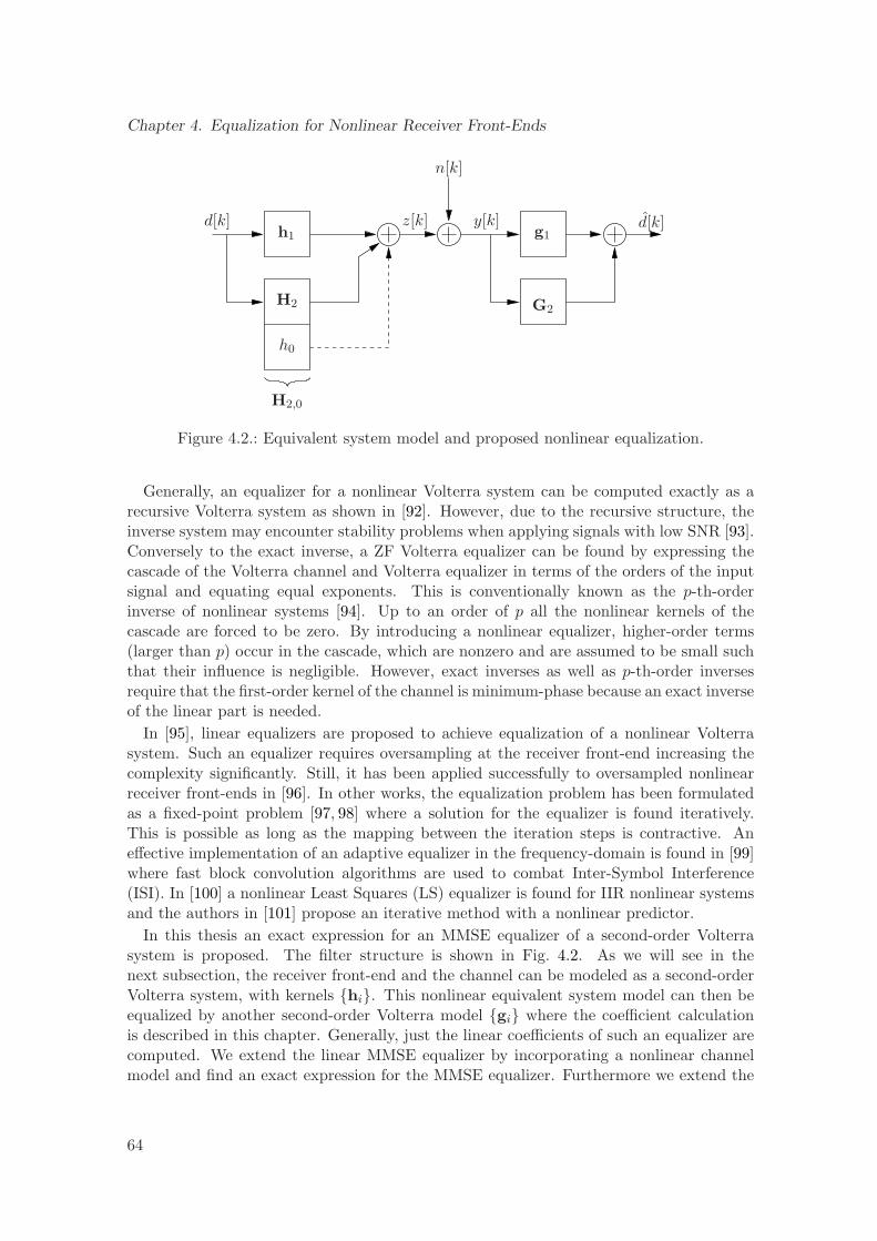
Chapter 4. Equalization for Nonlinear Receiver Front-Ends
d[k]h1
H2
h0
H2,0
z[k]
n[k]
y[k]g1
G2
d[k]
Figure 4.2.: Equivalent system model and proposed nonlinear equalization.
Generally, an equalizer for a nonlinear Volterra system can be computed exactly as arecursive Volterra system as shown in [92]. However, due to the recursive structure, theinverse system may encounter stability problems when applying signals with low SNR [93].Conversely to the exact inverse, a ZF Volterra equalizer can be found by expressing thecascade of the Volterra channel and Volterra equalizer in terms of the orders of the inputsignal and equating equal exponents. This is conventionally known as the p-th-orderinverse of nonlinear systems [94]. Up to an order of p all the nonlinear kernels of thecascade are forced to be zero. By introducing a nonlinear equalizer, higher-order terms(larger than p) occur in the cascade, which are nonzero and are assumed to be small suchthat their influence is negligible. However, exact inverses as well as p-th-order inversesrequire that the first-order kernel of the channel is minimum-phase because an exact inverseof the linear part is needed.
In [95], linear equalizers are proposed to achieve equalization of a nonlinear Volterrasystem. Such an equalizer requires oversampling at the receiver front-end increasing thecomplexity significantly. Still, it has been applied successfully to oversampled nonlinearreceiver front-ends in [96]. In other works, the equalization problem has been formulatedas a fixed-point problem [97, 98] where a solution for the equalizer is found iteratively.This is possible as long as the mapping between the iteration steps is contractive. Aneffective implementation of an adaptive equalizer in the frequency-domain is found in [99]where fast block convolution algorithms are used to combat Inter-Symbol Interference(ISI). In [100] a nonlinear Least Squares (LS) equalizer is found for IIR nonlinear systemsand the authors in [101] propose an iterative method with a nonlinear predictor.
In this thesis an exact expression for an MMSE equalizer of a second-order Volterrasystem is proposed. The filter structure is shown in Fig. 4.2. As we will see in thenext subsection, the receiver front-end and the channel can be modeled as a second-orderVolterra system, with kernels hi. This nonlinear equivalent system model can then beequalized by another second-order Volterra model gi where the coefficient calculationis described in this chapter. Generally, just the linear coefficients of such an equalizer arecomputed. We extend the linear MMSE equalizer by incorporating a nonlinear channelmodel and find an exact expression for the MMSE equalizer. Furthermore we extend the
64
4.4. MMSE Volterra Filters
MSE formulation to second-order Volterra cases and try to express a new second-orderVolterra equalizer, which is supposed to improve the performance further. Additionally,the obtained results are compared with their least mean squares (LMS) counterparts,which should ideally achieve similar results.
Equalizer Model
We can now define an equalizer that is applied to the received signal y[k]. For a first-orderVolterra or linear equalizer the estimated data sequence d[k] becomes
d[k] = gT1 y[k], (4.5)
where y[k] = [y[k], y[k − 1], . . . , y[k −Le + 1]]T, and where the Le × 1 vector g1 representsthe linear equalizer coefficients. Applying a second-order Volterra equalizer to y[k], weobtain
d[k] = gT1 y[k] + yT[k]G2y[k], (4.6)
where the Le ×Le matrix G2 represents the second-order kernel of the Volterra equalizer.Note that there is no zeroth-order kernel in both cases, since we already removed the biasfrom the channel model.
As we did for the channel, we can rewrite d[k] as
d[k] = gT1 y[k] + gT
2 (y[k] ⊠ y[k]), (4.7)
where g2 is an appropriate modification of G2.
4.4. MMSE Volterra Filters
In this section we derive linear and nonlinear equalizers for the nonlinear channel model.
4.4.1. First-Order Equalizer
First of all, let us assume that the second-order kernel g2 is zero and that we only focuson the first-order kernel g1. We then have to derive an expression for y[k] as a functionof h1 and h2. To this end, let us rewrite the Le elements of the input samples for theequalizer y[k − l] as
y[k − l] = hT1,ldx[k] + hT
2,l(dx[k] ⊠ dx[k]) + n[k − l], (4.8)
where the extended data vector is given by dx[k] = [d[k], d[k − 1], . . . , d[k − L − Le + 2]]T
and where the channel vectors h1,l and h2,l are appropriate extensions of h1 and h2 whichdepend on l = 0, 1, . . . , Le − 1, respectively.
In short, we can thus write
y[k − l] = fTl s[k] + n[k − l], (4.9)
where fl = [hT1,l,h
T2,l]
T and s[k] = [dTx [k], (dx[k] ⊠ dx[k])T]T. Both vectors, fl and s[k] are
having the dimension (ε + η) × 1, where ε = Le + L − 1 denotes the length of the linearterms, and η =
∑Lα=2 (Le + L − α) denotes the length of the nonlinear product terms.
65
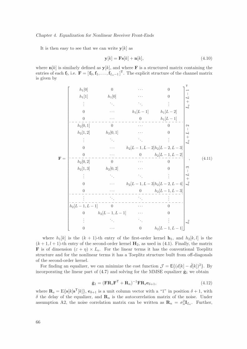
Chapter 4. Equalization for Nonlinear Receiver Front-Ends
It is then easy to see that we can write y[k] as
y[k] = Fs[k] + n[k], (4.10)
where n[k] is similarly defined as y[k], and where F is a structured matrix containing theentries of each fl, i.e. F = [ f0, f1, . . . , fLe−1 ]T. The explicit structure of the channel matrixis given by
F =
h1[0] 0 · · · 0
h1[1] h1[0] · · · 0...
. . .. . .
...
0 · · · h1[L − 1] h1[L − 2]
0 · · · 0 h1[L − 1]
h2[0, 1] 0 · · · 0
h2[1, 2] h2[0, 1] · · · 0...
. . .. . .
...
0 · · · h2[L − 1, L − 2]h2[L − 2, L − 3]
0 · · · 0 h2[L − 1, L − 2]
h2[0, 2] 0 · · · 0
h2[1, 3] h2[0, 2] · · · 0...
. . .. . .
...
0 · · · h2[L − 1, L − 3]h2[L − 2, L − 4]
0 · · · 0 h2[L − 1, L − 3]...
. . .. . .
...
h2[L − 1, L − 1] 0 · · · 0
0 h2[L − 1, L − 1] · · · 0...
. . .. . .
...
0 · · · 0 h2[L − 1, L − 1]
T
Le+
L−
1L
e+
L−
2L
e+
L−
3L
e
, (4.11)
where h1[k] is the (k + 1)-th entry of the first-order kernel h1, and h2[k, l] is the(k + 1, l + 1)-th entry of the second-order kernel H2, as used in (4.1). Finally, the matrixF is of dimension (ε + η) × Le. For the linear terms it has the conventional Toeplitzstructure and for the nonlinear terms it has a Toeplitz structure built from off-diagonalsof the second-order kernel.
For finding an equalizer, we can minimize the cost function J = E(d[k] − d[k])2. Byincorporating the linear part of (4.7) and solving for the MMSE equalizer g1 we obtain
g1 = (FRsFT + Rn)−1FRseδ+1, (4.12)
where Rs = Es[k]sT[k], eδ+1 is a unit column vector with a “1” in position δ + 1, withδ the delay of the equalizer, and Rn is the autocorrelation matrix of the noise. Underassumption A2, the noise correlation matrix can be written as Rn = σ2
nILe . Further,
66
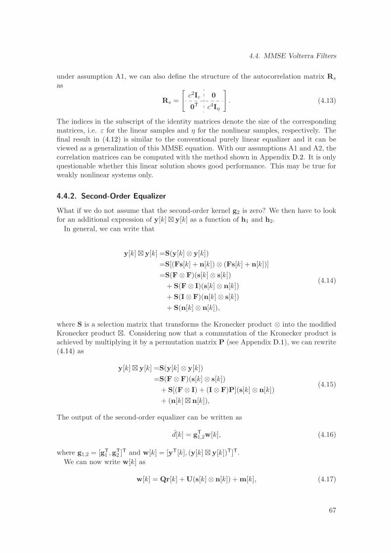
4.4. MMSE Volterra Filters
under assumption A1, we can also define the structure of the autocorrelation matrix Rs
as
Rs =
[
c2Iε 0
0T c4Iη
]
. (4.13)
The indices in the subscript of the identity matrices denote the size of the correspondingmatrices, i.e. ε for the linear samples and η for the nonlinear samples, respectively. Thefinal result in (4.12) is similar to the conventional purely linear equalizer and it can beviewed as a generalization of this MMSE equation. With our assumptions A1 and A2, thecorrelation matrices can be computed with the method shown in Appendix D.2. It is onlyquestionable whether this linear solution shows good performance. This may be true forweakly nonlinear systems only.
4.4.2. Second-Order Equalizer
What if we do not assume that the second-order kernel g2 is zero? We then have to lookfor an additional expression of y[k] ⊠ y[k] as a function of h1 and h2.
In general, we can write that
y[k] ⊠ y[k] =S(y[k] ⊗ y[k])
=S[(Fs[k] + n[k]) ⊗ (Fs[k] + n[k])]
=S(F ⊗ F)(s[k] ⊗ s[k])
+ S(F ⊗ I)(s[k] ⊗ n[k])
+ S(I ⊗ F)(n[k] ⊗ s[k])
+ S(n[k] ⊗ n[k]),
(4.14)
where S is a selection matrix that transforms the Kronecker product ⊗ into the modifiedKronecker product ⊠. Considering now that a commutation of the Kronecker product isachieved by multiplying it by a permutation matrix P (see Appendix D.1), we can rewrite(4.14) as
y[k] ⊠ y[k] =S(y[k] ⊗ y[k])
=S(F ⊗ F)(s[k] ⊗ s[k])
+ S[(F ⊗ I) + (I ⊗ F)P](s[k] ⊗ n[k])
+ (n[k] ⊠ n[k]),
(4.15)
The output of the second-order equalizer can be written as
d[k] = gT1,2w[k], (4.16)
where g1,2 = [gT1 ,gT
2 ]T and w[k] = [yT[k], (y[k] ⊠ y[k])T]T.
We can now write w[k] as
w[k] = Qr[k] + U(s[k] ⊗ n[k]) + m[k], (4.17)
67
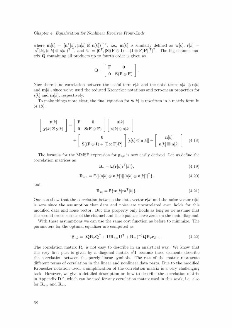
Chapter 4. Equalization for Nonlinear Receiver Front-Ends
where m[k] = [nT[k], (n[k] ⊠ n[k])T]T, i.e., m[k] is similarly defined as w[k], r[k] =[sT[k], (s[k] ⊗ s[k])T]T, and U = [0T, [S[(F ⊗ I) + (I ⊗ F)P]]T]T. The big channel ma-trix Q containing all products up to fourth order is given as
Q =
[
F 0
0 S(F ⊗ F)
]
.
Now there is no correlation between the useful term r[k] and the noise terms s[k] ⊗ n[k]and m[k], since we’ve used the reduced Kronecker notations and zero-mean properties fors[k] and m[k], respectively.
To make things more clear, the final equation for w[k] is rewritten in a matrix form in(4.18).
[
y[k]
y[k] ⊠ y[k]
]
=
[
F 0
0 S(F ⊗ F)
][
s[k]
s[k] ⊗ s[k]
]
+
[
0
S[(F ⊗ I) + (I ⊗ F)P]
]
[s[k] ⊗ n[k]] +
[
n[k]
n[k] ⊠ n[k]
]
(4.18)
The formula for the MMSE expression for g1,2 is now easily derived. Let us define thecorrelation matrices as
Rr = Er[k]rT[k], (4.19)
Rs,n = E[(s[k] ⊗ n[k])][(s[k] ⊗ n[k])]T, (4.20)
and
Rm = Em[k]mT[k]. (4.21)
One can show that the correlation between the data vector r[k] and the noise vector n[k]is zero since the assumption that data and noise are uncorrelated even holds for thismodified data and noise vector. But this property only holds as long as we assume thatthe second-order kernels of the channel and the equalizer have zeros on the main diagonal.
With these assumptions we can use the same cost function as before to minimize. Theparameters for the optimal equalizer are computed as
g1,2 = (QRrQT + URs,nU
T + Rm)−1QRreδ+1. (4.22)
The correlation matrix Rr is not easy to describe in an analytical way. We know thatthe very first part is given by a diagonal matrix c2I because these elements describethe correlation between the purely linear symbols. The rest of the matrix representsdifferent terms of correlation in the linear and nonlinear data parts. Due to the modifiedKronecker notation used, a simplification of the correlation matrix is a very challengingtask. However, we give a detailed description on how to describe the correlation matrixin Appendix D.2, which can be used for any correlation matrix used in this work, i.e. alsofor Rs,n and Rm.
68
4.4. MMSE Volterra Filters
4.4.3. Adaptive Volterra Filters
As a comparison the effects of the newly derived equalizers (4.12) and (4.22) w.r.t. anadaptive equalizer solution is shown. For that purpose an extension to the conventionallinear LMS adaptive algorithm [102] was used. These nonlinear extensions are needed toadapt the second-order kernel of the nonlinear LMS equalizer during training [103]. Themodified LMS updating equations are obtained as
g1[k] = g1[k − 1] + µ1y[k]e[k], (4.23)
for the first-order kernel and as
g2[k] = g2[k − 1] + µ2(y[k] ⊠ y[k])e[k], (4.24)
for the second-order kernel, with e[k] denoting the error signal which is given as e[k] =d[k − δ] − d[k] during the training phase.
4.4.4. Simulation Results
In this section we compare the linear (4.12) and nonlinear (4.22) equalizer. For thatpurpose we have used the nonlinear second-order equivalent system model derived in[11], which is a model for a frame-differential (FD) transmitted-reference (TR) UWBautocorrelation receiver (AcR) front-end. It describes the inter-symbol interference dueto a time-dispersive multipath channel for the nonlinear AcR. The authors also derivean exact expression for the noise variance at the output of the receiver, given a certaindouble-sided noise spectral density N0/2 at the receiver input. As a first approximation(which turned out to be a reasonable assumption for many scenarios), the noise is assumedto be a zero-mean i.i.d. Gaussian random process with a fixed variance σ2
n depending onthe receiver parameters. Furthermore, the FD-TR-UWB scheme uses BPSK signaling totransmit data and thus fits into our framework defined in (4.4).
To compute the equalizer coefficients according to (4.12) and (4.22) it is necessary todetermine the autocorrelation matrix of the data vectors s[k] and r[k]. The autocorrelationmatrix for s[k] is shown in (4.13) and is a scaled identity matrix with dimension 2L2 − Lif we assume that L is the number of channel taps and equalizer taps (i.e., Le = L). Theconstruction of r[k] is more complex and if we again take the same length for the channeland the equalizer, we get a huge autocorrelation matrix Rr, of dimension (4L4 − 4L3 +3L2−L)/2. We see that this size is mostly determined by the fourth-order term and bringsan enormous increase in the size of the autocorrelation matrix.
To achieve reasonable simulation times and matrix sizes, a simplification of the nonlinearequivalent system model coefficients has been investigated first. For an RMS delay spreadof the channel impulse response of τrms=10 ns the authors in [11] propose an equivalentnonlinear system model with 17 linear coefficients and (17×16)/2 second-order kernelcoefficients at a data rate of 125 Mbps (i.e., a symbol time of 8 ns) to achieve sufficientmodel accuracy. For estimating the huge correlation matrix Rr of the data when settingthe equalizer length equal to the channel length, this complexity has to be reduced. Forthat reason a comparison of the equivalent system model to a truncated version of itselfhas been done first. The quantity we have compared to achieve similar system behavioris the data averaged Bit Error Rate (BER). Moreover, the quantiles of the two results
69
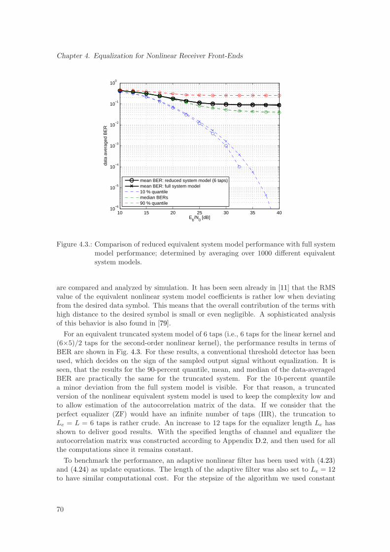
Chapter 4. Equalization for Nonlinear Receiver Front-Ends
10 15 20 25 30 35 4010
−6
10−5
10−4
10−3
10−2
10−1
100
data
ave
rage
d B
ER
Eb/N
0 [dB]
mean BER: reduced system model (6 taps)mean BER: full system model10 % quantilemedian BERs90 % quantile
Figure 4.3.: Comparison of reduced equivalent system model performance with full systemmodel performance; determined by averaging over 1000 different equivalentsystem models.
are compared and analyzed by simulation. It has been seen already in [11] that the RMSvalue of the equivalent nonlinear system model coefficients is rather low when deviatingfrom the desired data symbol. This means that the overall contribution of the terms withhigh distance to the desired symbol is small or even negligible. A sophisticated analysisof this behavior is also found in [79].
For an equivalent truncated system model of 6 taps (i.e., 6 taps for the linear kernel and(6×5)/2 taps for the second-order nonlinear kernel), the performance results in terms ofBER are shown in Fig. 4.3. For these results, a conventional threshold detector has beenused, which decides on the sign of the sampled output signal without equalization. It isseen, that the results for the 90-percent quantile, mean, and median of the data-averagedBER are practically the same for the truncated system. For the 10-percent quantilea minor deviation from the full system model is visible. For that reason, a truncatedversion of the nonlinear equivalent system model is used to keep the complexity low andto allow estimation of the autocorrelation matrix of the data. If we consider that theperfect equalizer (ZF) would have an infinite number of taps (IIR), the truncation toLe = L = 6 taps is rather crude. An increase to 12 taps for the equalizer length Le hasshown to deliver good results. With the specified lengths of channel and equalizer theautocorrelation matrix was constructed according to Appendix D.2, and then used for allthe computations since it remains constant.
To benchmark the performance, an adaptive nonlinear filter has been used with (4.23)and (4.24) as update equations. The length of the adaptive filter was also set to Le = 12to have similar computational cost. For the stepsize of the algorithm we used constant
70
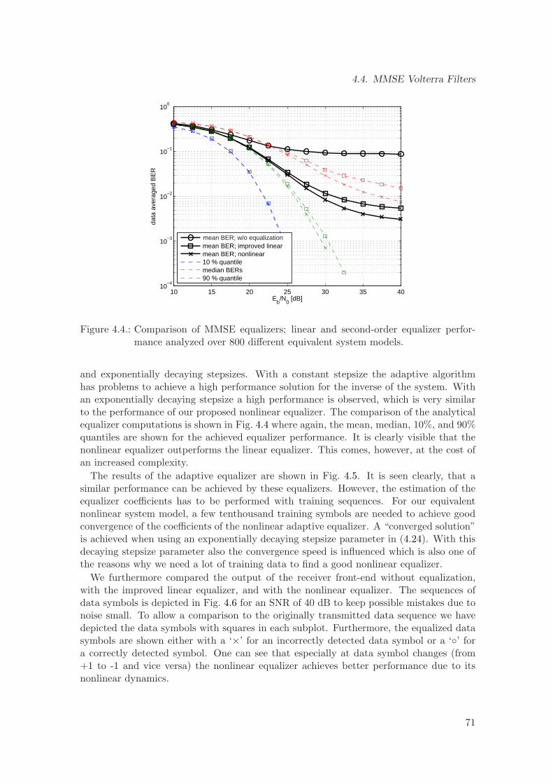
4.4. MMSE Volterra Filters
10 15 20 25 30 35 4010
−4
10−3
10−2
10−1
100
data
ave
rage
d B
ER
Eb/N
0 [dB]
mean BER; improved linearmean BER; nonlinear10 % quantilemedian BERs90 % quantile
mean BER; w/o equalization
Figure 4.4.: Comparison of MMSE equalizers; linear and second-order equalizer perfor-mance analyzed over 800 different equivalent system models.
and exponentially decaying stepsizes. With a constant stepsize the adaptive algorithmhas problems to achieve a high performance solution for the inverse of the system. Withan exponentially decaying stepsize a high performance is observed, which is very similarto the performance of our proposed nonlinear equalizer. The comparison of the analyticalequalizer computations is shown in Fig. 4.4 where again, the mean, median, 10%, and 90%quantiles are shown for the achieved equalizer performance. It is clearly visible that thenonlinear equalizer outperforms the linear equalizer. This comes, however, at the cost ofan increased complexity.
The results of the adaptive equalizer are shown in Fig. 4.5. It is seen clearly, that asimilar performance can be achieved by these equalizers. However, the estimation of theequalizer coefficients has to be performed with training sequences. For our equivalentnonlinear system model, a few tenthousand training symbols are needed to achieve goodconvergence of the coefficients of the nonlinear adaptive equalizer. A “converged solution”is achieved when using an exponentially decaying stepsize parameter in (4.24). With thisdecaying stepsize parameter also the convergence speed is influenced which is also one ofthe reasons why we need a lot of training data to find a good nonlinear equalizer.
We furthermore compared the output of the receiver front-end without equalization,with the improved linear equalizer, and with the nonlinear equalizer. The sequences ofdata symbols is depicted in Fig. 4.6 for an SNR of 40 dB to keep possible mistakes due tonoise small. To allow a comparison to the originally transmitted data sequence we havedepicted the data symbols with squares in each subplot. Furthermore, the equalized datasymbols are shown either with a ‘×’ for an incorrectly detected data symbol or a ‘’ fora correctly detected symbol. One can see that especially at data symbol changes (from+1 to -1 and vice versa) the nonlinear equalizer achieves better performance due to itsnonlinear dynamics.
71
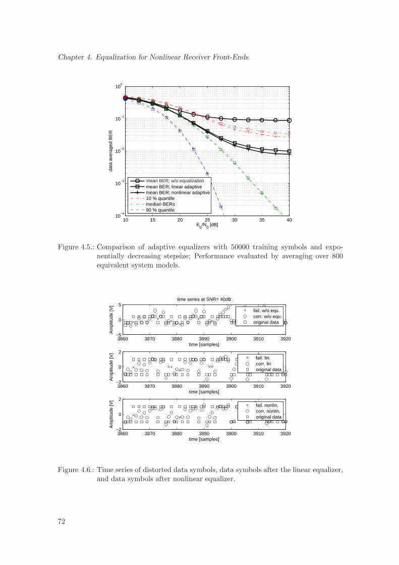
Chapter 4. Equalization for Nonlinear Receiver Front-Ends
10 15 20 25 30 35 4010
−4
10−3
10−2
10−1
100
data
ave
rage
d B
ER
Eb/N
0 [dB]
mean BER; linear adaptivemean BER; nonlinear adaptive10 % quantilemedian BERs90 % quantile
mean BER; w/o equalization
Figure 4.5.: Comparison of adaptive equalizers with 50000 training symbols and expo-nentially decreasing stepsize; Performance evaluated by averaging over 800equivalent system models.
3860 3870 3880 3890 3900 3910 3920−5
0
5
time [samples]
Am
plitu
de [V
]
time series at SNR= 40dB
fail. w/o equ.corr. w/o equ.original data
3860 3870 3880 3890 3900 3910 3920−2
0
2
time [samples]
Am
plitu
de [V
]
fail. lin.corr. linoriginal data
3860 3870 3880 3890 3900 3910 3920−2
0
2
time [samples]
Am
plitu
de [V
]
fail. nonlin.corr. nonlin.original data
Figure 4.6.: Time series of distorted data symbols, data symbols after the linear equalizer,and data symbols after nonlinear equalizer.
72
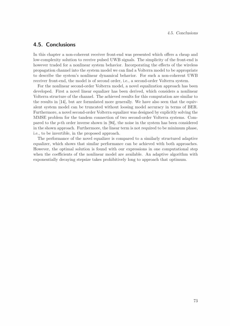
4.5. Conclusions
4.5. Conclusions
In this chapter a non-coherent receiver front-end was presented which offers a cheap andlow-complexity solution to receive pulsed UWB signals. The simplicity of the front-end ishowever traded for a nonlinear system behavior. Incorporating the effects of the wirelesspropagation channel into the system model we can find a Volterra model to be appropriateto describe the system’s nonlinear dynamical behavior. For such a non-coherent UWBreceiver front-end, the model is of second order, i.e., a second-order Volterra system.
For the nonlinear second-order Volterra model, a novel equalization approach has beendeveloped. First a novel linear equalizer has been derived, which considers a nonlinearVolterra structure of the channel. The achieved results for this computation are similar tothe results in [14], but are formulated more generally. We have also seen that the equiv-alent system model can be truncated without loosing model accuracy in terms of BER.Furthermore, a novel second-order Volterra equalizer was designed by explicitly solving theMMSE problem for the tandem connection of two second-order Volterra systems. Com-pared to the p-th order inverse shown in [94], the noise in the system has been consideredin the shown approach. Furthermore, the linear term is not required to be minimum phase,i.e., to be invertible, in the proposed approach.
The performance of the novel equalizer is compared to a similarly structured adaptiveequalizer, which shows that similar performance can be achieved with both approaches.However, the optimal solution is found with our expressions in one computational stepwhen the coefficients of the nonlinear model are available. An adaptive algorithm withexponentially decaying stepsize takes prohibitively long to approach that optimum.
73

Chapter 4. Equalization for Nonlinear Receiver Front-Ends
74
Chapter5Conclusion and Outlook
In this thesis novel implementation approaches for standardized and non-standardizedUWB systems have been presented. The discussed UWB systems offer the potentialfor high-speed communication systems and for providing exact positioning and trackingcapabilities.
From the discussions in Chapter 2, it is clear that the direct implementation of transceiverarchitectures on state-of-the-art DSP hardware is a very challenging task. Processing atNyquist sampling rate is simply not feasible and requires a technological breakthrough toachieve a direct implementation of the transceiver algorithms. Thus alternatives have tobe found for transceiver and channel model implementations. In this thesis the paralleliza-tion in frequency-domain of the transceiver algorithms for a wideband OFDM system isshown. This can be achieved by employing hybrid filterbanks for signal separation andsubband signal processing. Similarly, the channel response can be modeled on a paral-lel filter architecture which has several implementation challenges when steep filters areneeded.
A model with frequency-response masked filters has been achieved and demonstratedin this thesis. Still, a slight overlapping of the subbands has to be allowed to model theoverall behavior without gaps in the frequency-domain. The effect of this overlappingis visualized as an MSE on a carrier-by-carrier basis. It is seen that the subcarriers atthe band edges are more distorted than others. Additionally, the distortion effect hasbeen visualized in terms of SER. Clearly, a relation between high error peaks and thedegradation in SER is visible. Similar performance degradation as for the transmittercan be observed in the receiver. At the band edges the additional error due to the finiteslope of the analog front-end filters is visible. An SER degradation can be observed in thesubband architecture which limits the uncoded SER to flatten out at an error floor of 10−3
for 8 subbands and 10−4 for 4 subbands. The occurring interference can be taken careof with an equalizer adapted during a training or calibration period. Such an equalizerhas to be used anyhow if the degradation of the signal due to a wireless propagationchannel is considered to recover the transmitted data. Since the introduced distortionsin the front-ends are linear distortions, a linear equalizer should be used to enhance thesystem performance. The resulting subband models should be analyzed in more detail asfurther research. An optimization of such a structure with respect to system parameters
75
Chapter 5. Conclusion and Outlook
and certain propagation environments is another topic for further research.
Another possibility of generating wideband signals is to generate short pulses. Thesesignals are advantageous for short-range communication and positioning applications be-cause transmitters and receivers can be built with low power and low complexity. A flexiblesignal generator employing DACs has to be used when effects as flexible pulse shape gener-ation, equalization of destortions in the front-end, adaptation to environments, generationof impulse responses for simulation environments, generation of MB-OFDM signals, etc.are desired with one single structure. Current technological limits restrict the bandwidthto be generated with a single DAC to a few hundred MHz. Thus, a converter array, wheremultiple DACs operate in a time-interleaved structure is proposed in this thesis. Withthese converter arrays, signals of higher bandwidth can be generated. The architecturealso enables an oversampled generation of UWB signals, hence low-complexity analog fil-ters can be used due to the shifting of the spectral replicas to higher frequencies. Theconverters in this structure are assumed to be perfectly matched in time, such that noadditional mismatch spectra occur. The performance of the converter structure has beenverified with simulations and measurements and a reduction of the first spectral mirrorimage component by 30 dB has been possible for narrow and wideband signals.
If mismatches between the converters are considered, a compensation structure in thedigital back-end of the signal generator can be developed. This compensation strategyfor mismatches has been demonstrated and verified with measurements. It is possible toreduce the mismatch spectra by app. 20 dB with the proposed compensation approach.The compensation structure assumed that the timing offsets for the TIDAC structure areknown. However, in a practical application the offsets have to be identified continuouslyand an adaptive tuning of the parameters of the compensation filters has to be done. Thiscan be done very effectively with a Farrow filter, where the shape of the compensationfilter depends on one steering parameter, which can be directly related to the timing offset(assuming a two-channel case).
For the pulse-based signaling scheme standardized by the IEEE 802.15.4a task group,three low-complexity receiver architectures have been investigated and compared. Firstof all, a Rake receiver has been evaluated in its performance for the standardized signal.It has been demonstrated that the performance strongly depends on the synchronizationof the receiver. Furthermore it improves with the number of fingers used. However, anincrease of fingers also means an increase of complexity, which prohibits a high numberof fingers to be implemented. From an implementation complexity point of view, anenergy detector offers the most simple solution. On the other hand, the MU performanceof the ED is not very good. Therfore a novel modified TR receiver has been proposedfor the standardized, pulse-based UWB communication scheme considering the additionalinformation contained in the spreading code. With slightly increased complexity for themodified TR scheme, a superior MU performance can be achieved. The comparison hasbeen carried out with computer simulations. Strategies to combat the MUI or signalprocessing algorithms to have a robust receiver when NBI is present are topics for furtherresearch.
It has been observed that these simple non-coherent receivers can be modeled by fadingmemory nonlinear systems, i.e., Volterra systems. This means, for very high data rates,the inter-symbol interference for such receivers is fully described with a nonlinear systemmodel. It was shown in [104] that in a high data-rate system this nonlinear distortion is
76
considerably high. Thus, if such a receiver is used, a sophisticated equalizer has to be usedto recover the transmitted data symbols. An optimal MMSE nonlinear equalizer is derivedin this thesis. The novel equalizer perfectly demonstrates that an adaptive LMS filtersolution can achieve the same performance only asymptotically, i.e., after infinite time.The computation for the novel equalizer is done in one single step, but it assumes that thelinear and nonlinear system parameters of the equivalent system model are known. Theequalizer structure improves the uncoded BER floor by a factor of 20, if the output signalis sampled at symbol rate. An interesting question is how a similarly-optimized equalizerperforms on a multichannel Volterra system as described in [79], when the output of thefront-end is oversampled.
77

Chapter 5. Conclusion and Outlook
78
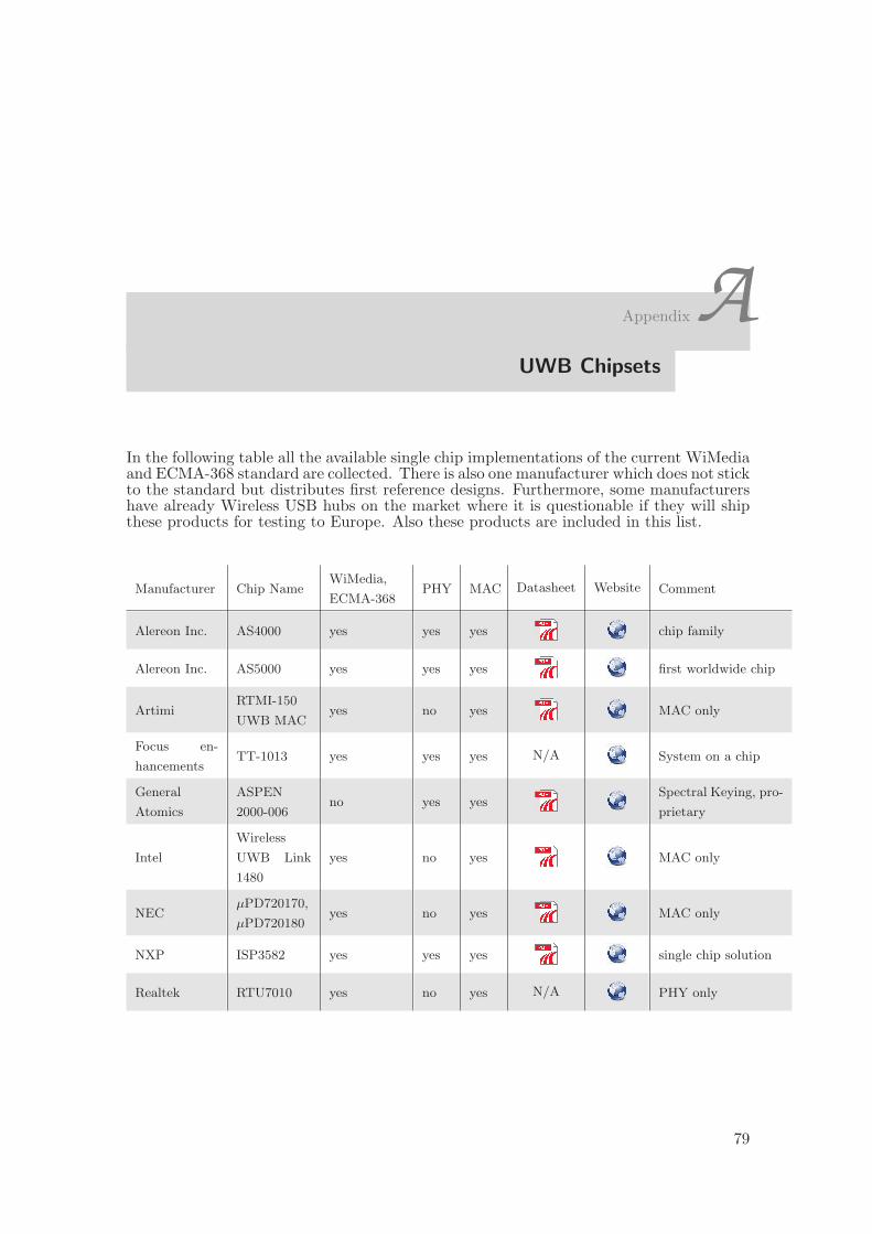
AppendixAUWB Chipsets
In the following table all the available single chip implementations of the current WiMediaand ECMA-368 standard are collected. There is also one manufacturer which does not stickto the standard but distributes first reference designs. Furthermore, some manufacturershave already Wireless USB hubs on the market where it is questionable if they will shipthese products for testing to Europe. Also these products are included in this list.
Manufacturer Chip NameWiMedia,
ECMA-368PHY MAC Datasheet Website Comment
Alereon Inc. AS4000 yes yes yes chip family
Alereon Inc. AS5000 yes yes yes first worldwide chip
ArtimiRTMI-150
UWB MACyes no yes MAC only
Focus en-
hancementsTT-1013 yes yes yes N/A System on a chip
General
Atomics
ASPEN
2000-006no yes yes
Spectral Keying, pro-
prietary
Intel
Wireless
UWB Link
1480
yes no yes MAC only
NECµPD720170,
µPD720180yes no yes MAC only
NXP ISP3582 yes yes yes single chip solution
Realtek RTU7010 yes no yes N/A PHY only
79
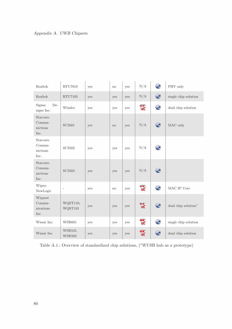
Appendix A. UWB Chipsets
Realtek RTU7010 yes no yes N/A PHY only
Realtek RTU7105 yes yes yes N/A single chip solution
Sigma De-
signs Inc.Windeo yes yes yes dual chip solution
Staccato
Commu-
nictions
Inc.
SC3501 yes no yes N/A MAC only
Staccato
Commu-
nictions
Inc.
SC3502 yes yes yes N/A
Staccato
Commu-
nictions
Inc.
SC3503 yes yes yes N/A
Wipro-
NewLogic- yes no yes MAC IP Core
Wiquest
Commu-
nications
Inc.
WQST110,
WQST101yes yes yes dual chip solution∗
Wisair Inc. WSR601 yes yes yes single chip solution
Wisair Inc.WSR531,
WSR502yes yes yes dual chip solution
Table A.1.: Overview of standardized chip solutions, (∗WUSB hub as a prototype)
80
AppendixBUWB Demonstrator
Within this thesis work, two UWB demonstrators have been built. Both of them consistmostly of off-the-shelf hardware which allows easy construction of the transmitting de-vices. In this appendix one of these demonstrators which enables to transmit widebandpulses over the wireless propagation channel is presented. The other demonstrator triesto simulate the effects of the channel on an FPGA board. The demonstration systemwas built to show the performance of pulse-based UWB systems surviving in a multi-path propagation environment. However, building a receiver is a quite complicated taskfor broadband systems with off-the-shelf components. Thus, the receiver was simulatedby sampling the received signals after the channel with a sampling scope, able to resolve6 GHz of bandwidth. To propagate the signals in free space, antennas are needed to matchthe impedance of the circuitry to the impedance of free space. Major contributions to thehardware development have been done by one diploma thesis student [105] and a projectstudent [106] which are fully acknowledged.
B.1. FPGA Hardware
As mentioned before, the demonstrator was used to generate a pulse-based UWB signal.According to the standard for the pulse based UWB PHY [6], pulses modulated in am-plitude have to be generated. Furthermore, long silence periods have to be generated. Tosmoothen the transmitted spectrum, the pulses transmitted with the demonstrator arehopped in time. The modulation scheme used for the pulses is a frame-differential schemeas described in [11]. The transmitted pulses have been generated with a Xilinx Virtex2 Pro FPGA programmed with VHDL. To generate short pulses, required for the broadsignal spectrum, high speed digital differential outputs of an FPGA have been used. Withthis technology (called Rocket I/O) it is possible to generate serial data streams with up to3.25 Gbps. The signal levels driven by these high speed outputs are standardized accord-ing to the Low Voltage Differential Signaling (LVDS) standard [107] which was developedto achieve high data rate transmission of signals at low power. To generate ternary sig-nals, two differential output signals were combined together as shown in Fig. B.1, using aresistive network. To match the output impedance of the differential signals, which is 100Ohms to the transmission line which connects the pulse generator to a mixer circuitry, a
81
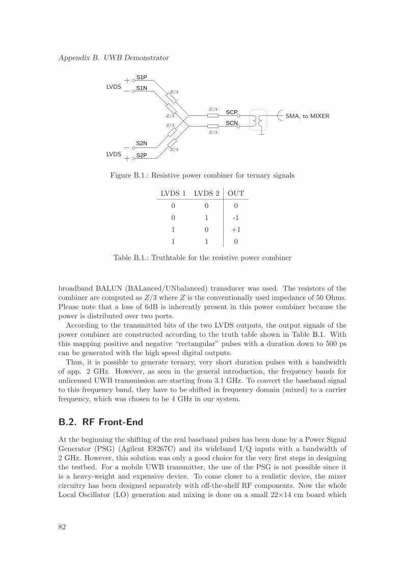
Appendix B. UWB Demonstrator
S2N
S2P
S1N
S1P
SCP
SCNZ/3
Z/3
Z/3
Z/3
Z/3
Z/3
LVDS
LVDS
SMA, to MIXER
Figure B.1.: Resistive power combiner for ternary signals
LVDS 1 LVDS 2 OUT
0 0 0
0 1 -1
1 0 +1
1 1 0
Table B.1.: Truthtable for the resistive power combiner
broadband BALUN (BALanced/UNbalanced) transducer was used. The resistors of thecombiner are computed as Z/3 where Z is the conventionally used impedance of 50 Ohms.Please note that a loss of 6dB is inherently present in this power combiner because thepower is distributed over two ports.
According to the transmitted bits of the two LVDS outputs, the output signals of thepower combiner are constructed according to the truth table shown in Table B.1. Withthis mapping positive and negative “rectangular” pulses with a duration down to 500 pscan be generated with the high speed digital outputs.
Thus, it is possible to generate ternary, very short duration pulses with a bandwidthof app. 2 GHz. However, as seen in the general introduction, the frequency bands forunlicensed UWB transmission are starting from 3.1 GHz. To convert the baseband signalto this frequency band, they have to be shifted in frequency domain (mixed) to a carrierfrequency, which was chosen to be 4 GHz in our system.
B.2. RF Front-End
At the beginning the shifting of the real baseband pulses has been done by a Power SignalGenerator (PSG) (Agilent E8267C) and its wideband I/Q inputs with a bandwidth of2 GHz. However, this solution was only a good choice for the very first steps in designingthe testbed. For a mobile UWB transmitter, the use of the PSG is not possible since itis a heavy-weight and expensive device. To come closer to a realistic device, the mixercircuitry has been designed separately with off-the-shelf RF components. Now the wholeLocal Oscillator (LO) generation and mixing is done on a small 22×14 cm board which
82
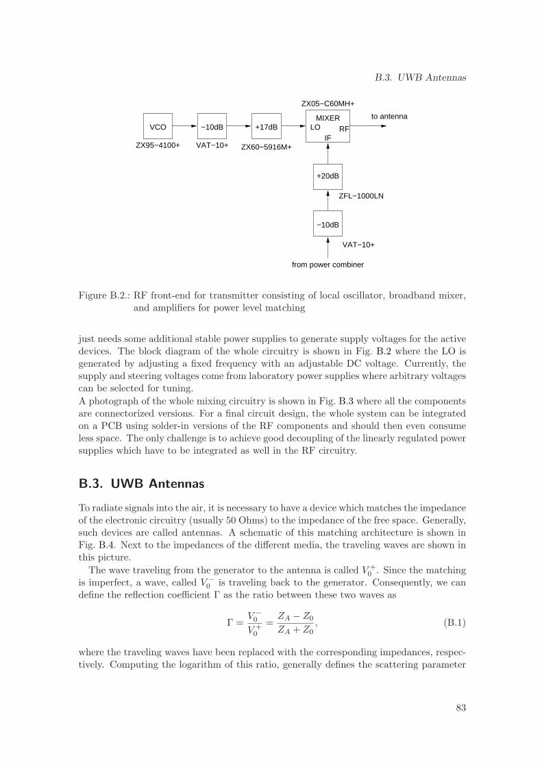
B.3. UWB Antennas
VCO −10dB +17dBMIXER
LOIF
RF
+20dB
−10dB
ZX95−4100+ VAT−10+ ZX60−5916M+
ZX05−C60MH+
ZFL−1000LN
VAT−10+
from power combiner
to antenna
Figure B.2.: RF front-end for transmitter consisting of local oscillator, broadband mixer,and amplifiers for power level matching
just needs some additional stable power supplies to generate supply voltages for the activedevices. The block diagram of the whole circuitry is shown in Fig. B.2 where the LO isgenerated by adjusting a fixed frequency with an adjustable DC voltage. Currently, thesupply and steering voltages come from laboratory power supplies where arbitrary voltagescan be selected for tuning.
A photograph of the whole mixing circuitry is shown in Fig. B.3 where all the componentsare connectorized versions. For a final circuit design, the whole system can be integratedon a PCB using solder-in versions of the RF components and should then even consumeless space. The only challenge is to achieve good decoupling of the linearly regulated powersupplies which have to be integrated as well in the RF circuitry.
B.3. UWB Antennas
To radiate signals into the air, it is necessary to have a device which matches the impedanceof the electronic circuitry (usually 50 Ohms) to the impedance of the free space. Generally,such devices are called antennas. A schematic of this matching architecture is shown inFig. B.4. Next to the impedances of the different media, the traveling waves are shown inthis picture.
The wave traveling from the generator to the antenna is called V +0 . Since the matching
is imperfect, a wave, called V −0 is traveling back to the generator. Consequently, we can
define the reflection coefficient Γ as the ratio between these two waves as
Γ =V −
0
V +0
=ZA − Z0
ZA + Z0, (B.1)
where the traveling waves have been replaced with the corresponding impedances, respec-tively. Computing the logarithm of this ratio, generally defines the scattering parameter
83
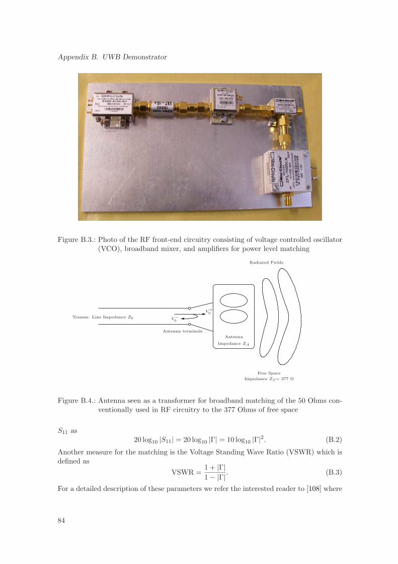
Appendix B. UWB Demonstrator
Figure B.3.: Photo of the RF front-end circuitry consisting of voltage controlled oscillator(VCO), broadband mixer, and amplifiers for power level matching
Antenna
Impedance ZA
Transm. Line Impedance Z0
Antenna terminals
Radiated Fields
Free Space
V +0
V −
0
Impedance ZS= 377 Ω
Figure B.4.: Antenna seen as a transformer for broadband matching of the 50 Ohms con-ventionally used in RF circuitry to the 377 Ohms of free space
S11 as20 log10 |S11| = 20 log10 |Γ| = 10 log10 |Γ|2. (B.2)
Another measure for the matching is the Voltage Standing Wave Ratio (VSWR) which isdefined as
VSWR =1 + |Γ|1 − |Γ| . (B.3)
For a detailed description of these parameters we refer the interested reader to [108] where
84
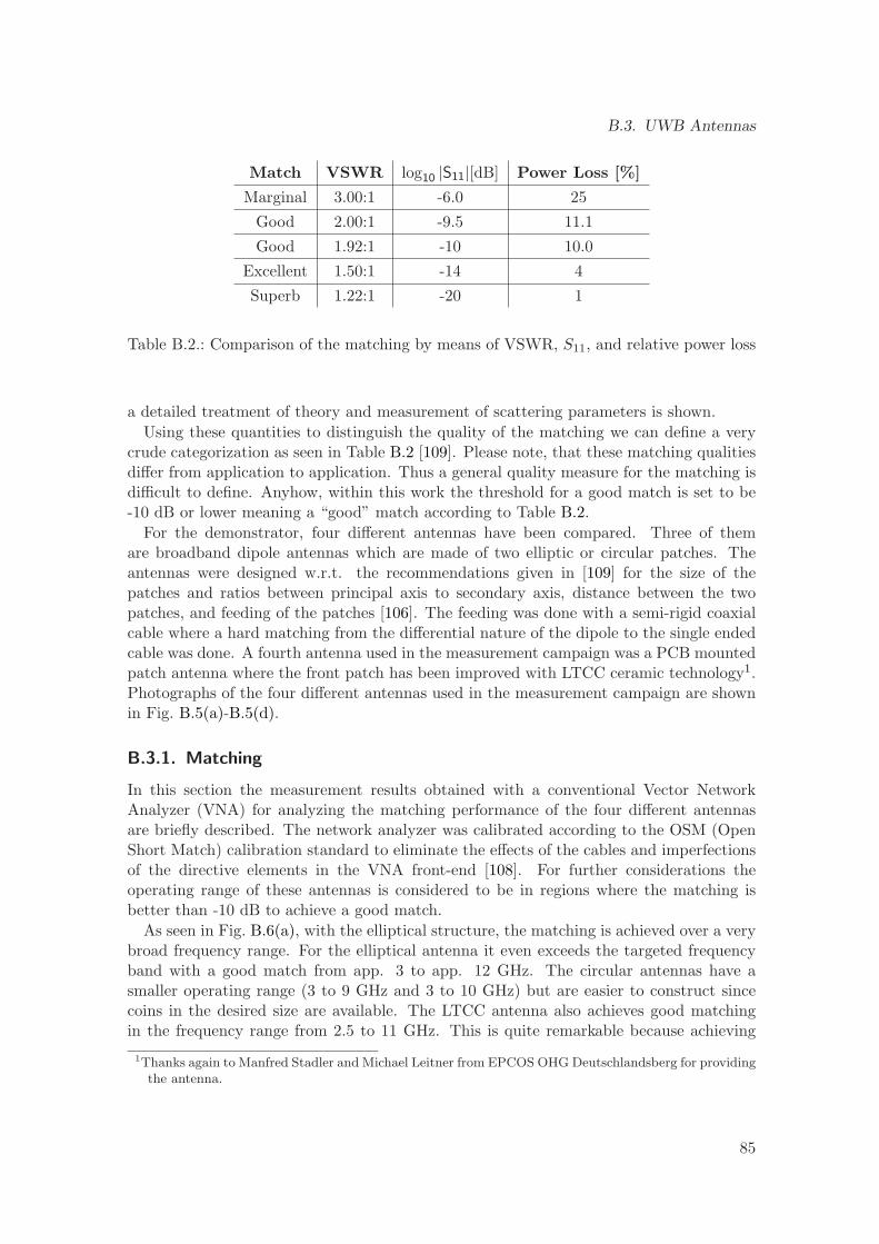
B.3. UWB Antennas
Match VSWR log10 |S11|[dB] Power Loss [%]
Marginal 3.00:1 -6.0 25
Good 2.00:1 -9.5 11.1
Good 1.92:1 -10 10.0
Excellent 1.50:1 -14 4
Superb 1.22:1 -20 1
Table B.2.: Comparison of the matching by means of VSWR, S11, and relative power loss
a detailed treatment of theory and measurement of scattering parameters is shown.
Using these quantities to distinguish the quality of the matching we can define a verycrude categorization as seen in Table B.2 [109]. Please note, that these matching qualitiesdiffer from application to application. Thus a general quality measure for the matching isdifficult to define. Anyhow, within this work the threshold for a good match is set to be-10 dB or lower meaning a “good” match according to Table B.2.
For the demonstrator, four different antennas have been compared. Three of themare broadband dipole antennas which are made of two elliptic or circular patches. Theantennas were designed w.r.t. the recommendations given in [109] for the size of thepatches and ratios between principal axis to secondary axis, distance between the twopatches, and feeding of the patches [106]. The feeding was done with a semi-rigid coaxialcable where a hard matching from the differential nature of the dipole to the single endedcable was done. A fourth antenna used in the measurement campaign was a PCB mountedpatch antenna where the front patch has been improved with LTCC ceramic technology1.Photographs of the four different antennas used in the measurement campaign are shownin Fig. B.5(a)-B.5(d).
B.3.1. Matching
In this section the measurement results obtained with a conventional Vector NetworkAnalyzer (VNA) for analyzing the matching performance of the four different antennasare briefly described. The network analyzer was calibrated according to the OSM (OpenShort Match) calibration standard to eliminate the effects of the cables and imperfectionsof the directive elements in the VNA front-end [108]. For further considerations theoperating range of these antennas is considered to be in regions where the matching isbetter than -10 dB to achieve a good match.
As seen in Fig. B.6(a), with the elliptical structure, the matching is achieved over a verybroad frequency range. For the elliptical antenna it even exceeds the targeted frequencyband with a good match from app. 3 to app. 12 GHz. The circular antennas have asmaller operating range (3 to 9 GHz and 3 to 10 GHz) but are easier to construct sincecoins in the desired size are available. The LTCC antenna also achieves good matchingin the frequency range from 2.5 to 11 GHz. This is quite remarkable because achieving
1Thanks again to Manfred Stadler and Michael Leitner from EPCOS OHG Deutschlandsberg for providingthe antenna.
85
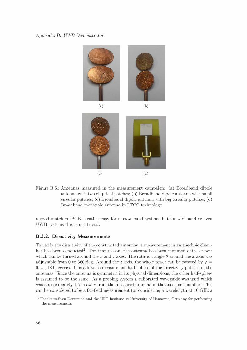
Appendix B. UWB Demonstrator
(a) (b)
(c) (d)
Figure B.5.: Antennas measured in the measurement campaign: (a) Broadband dipoleantenna with two elliptical patches; (b) Broadband dipole antenna with smallcircular patches; (c) Broadband dipole antenna with big circular patches; (d)Broadband monopole antenna in LTCC technology
a good match on PCB is rather easy for narrow band systems but for wideband or evenUWB systems this is not trivial.
B.3.2. Directivity Measurements
To verify the directivity of the constructed antennas, a measurement in an anechoic cham-ber has been conducted2. For that reason, the antenna has been mounted onto a towerwhich can be turned around the x and z axes. The rotation angle θ around the x axis wasadjustable from 0 to 360 deg. Around the z axis, the whole tower can be rotated by ϕ =0, ..., 180 degrees. This allows to measure one half-sphere of the directivity pattern of theantennas. Since the antenna is symmetric in its physical dimensions, the other half-sphereis assumed to be the same. As a probing system a calibrated waveguide was used whichwas approximately 1.5 m away from the measured antenna in the anechoic chamber. Thiscan be considered to be a far-field measurement (or considering a wavelength at 10 GHz a
2Thanks to Sven Dortmund and the HFT Institute at University of Hannover, Germany for performingthe measurements.
86
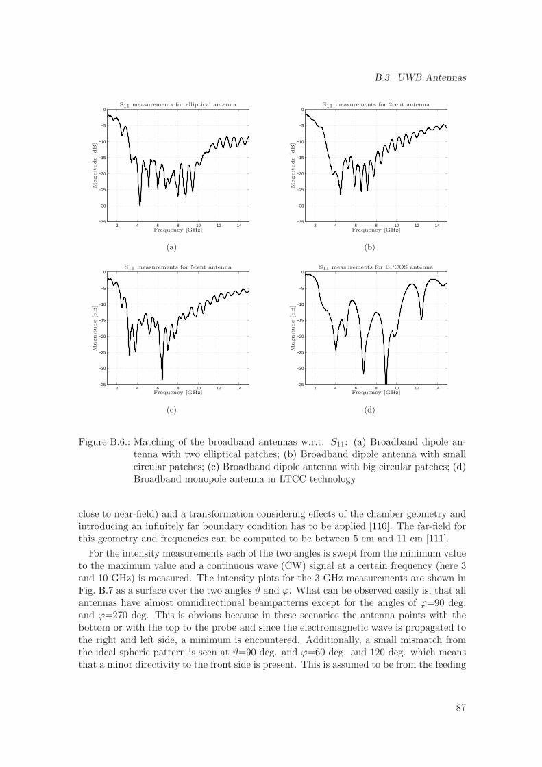
B.3. UWB Antennas
2 4 6 8 10 12 14−35
−30
−25
−20
−15
−10
−5
0
Frequency [GHz]
Magnit
ude
[dB
]
S11 measurements for elliptical antenna
(a)
2 4 6 8 10 12 14−35
−30
−25
−20
−15
−10
−5
0
Frequency [GHz]
Magnit
ude
[dB
]
S11 measurements for 2cent antenna
(b)
2 4 6 8 10 12 14−35
−30
−25
−20
−15
−10
−5
0
Frequency [GHz]
Magnit
ude
[dB
]
S11 measurements for 5cent antenna
(c)
2 4 6 8 10 12 14−35
−30
−25
−20
−15
−10
−5
0
Frequency [GHz]
Magnit
ude
[dB
]
S11 measurements for EPCOS antenna
(d)
Figure B.6.: Matching of the broadband antennas w.r.t. S11: (a) Broadband dipole an-tenna with two elliptical patches; (b) Broadband dipole antenna with smallcircular patches; (c) Broadband dipole antenna with big circular patches; (d)Broadband monopole antenna in LTCC technology
close to near-field) and a transformation considering effects of the chamber geometry andintroducing an infinitely far boundary condition has to be applied [110]. The far-field forthis geometry and frequencies can be computed to be between 5 cm and 11 cm [111].
For the intensity measurements each of the two angles is swept from the minimum valueto the maximum value and a continuous wave (CW) signal at a certain frequency (here 3and 10 GHz) is measured. The intensity plots for the 3 GHz measurements are shown inFig. B.7 as a surface over the two angles ϑ and ϕ. What can be observed easily is, that allantennas have almost omnidirectional beampatterns except for the angles of ϕ=90 deg.and ϕ=270 deg. This is obvious because in these scenarios the antenna points with thebottom or with the top to the probe and since the electromagnetic wave is propagated tothe right and left side, a minimum is encountered. Additionally, a small mismatch fromthe ideal spheric pattern is seen at ϑ=90 deg. and ϕ=60 deg. and 120 deg. which meansthat a minor directivity to the front side is present. This is assumed to be from the feeding
87
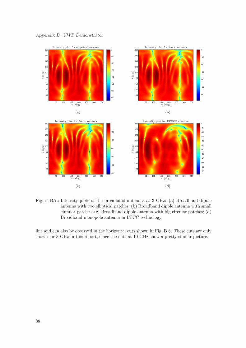
Appendix B. UWB Demonstrator
50 100 150 200 250 300 350
20
40
60
80
100
120
140
160
180
−70
−60
−50
−40
−30
−20
−10
0
θ[d
eg]
ϕ [deg]
Intensity plot for elliptical antenna
(a)
50 100 150 200 250 300 350
20
40
60
80
100
120
140
160
180
−60
−50
−40
−30
−20
−10
0
θ[d
eg]
ϕ [deg]
Intensity plot for 2cent antenna
(b)
50 100 150 200 250 300 350
20
40
60
80
100
120
140
160
180
−60
−50
−40
−30
−20
−10
0
θ[d
eg]
ϕ [deg]
Intensity plot for 5cent antenna
(c)
50 100 150 200 250 300 350
20
40
60
80
100
120
140
160
180
−55
−50
−45
−40
−35
−30
−25
−20
−15
−10
−5
0
θ[d
eg]
ϕ [deg]
Intensity plot for EPCOS antenna
(d)
Figure B.7.: Intensity plots of the broadband antennas at 3 GHz: (a) Broadband dipoleantenna with two elliptical patches; (b) Broadband dipole antenna with smallcircular patches; (c) Broadband dipole antenna with big circular patches; (d)Broadband monopole antenna in LTCC technology
line and can also be observed in the horizontal cuts shown in Fig. B.8. These cuts are onlyshown for 3 GHz in this report, since the cuts at 10 GHz show a pretty similar picture.
88
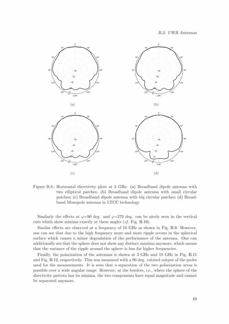
B.3. UWB Antennas
0°
30°
60°
90°
120°
150°
±180°
−150°
−120°
−90°
−60°
−30°
0−3
−10
−20
−30
−40
(a)
0°
30°
60°
90°
120°
150°
±180°
−150°
−120°
−90°
−60°
−30°
0−3
−10
−20
−30
−40
(b)
0°
30°
60°
90°
120°
150°
±180°
−150°
−120°
−90°
−60°
−30°
0−3
−10
−20
−30
−40
(c)
0°
30°
60°
90°
120°
150°
±180°
−150°
−120°
−90°
−60°
−30°
0−3
−10
−20
−30
−40
(d)
Figure B.8.: Horizontal directivity plots at 3 GHz: (a) Broadband dipole antenna withtwo elliptical patches; (b) Broadband dipole antenna with small circularpatches; (c) Broadband dipole antenna with big circular patches; (d) Broad-band Monopole antenna in LTCC technology
Similarly the effects at ϕ=90 deg. and ϕ=270 deg. can be nicely seen in the verticalcuts which show minima exactly at these angles (cf. Fig. B.10).
Similar effects are observed at a frequency of 10 GHz as shown in Fig. B.9. However,one can see that due to the high frequency more and more ripple occurs in the sphericalsurface which causes a minor degradation of the performance of the antenna. One canadditionally see that the sphere does not show any distinct maxima anymore, which meansthat the variance of the ripple around the sphere is less for higher frequencies.
Finally, the polarization of the antennas is shown at 3 GHz and 10 GHz in Fig. B.11and Fig. B.12, respectively. This was measured with a 90 deg. rotated output of the probeused for the measurements. It is seen that a separation of the two polarization areas ispossible over a wide angular range. However, at the borders, i.e., where the sphere of thedirectivity pattern has its minima, the two components have equal magnitude and cannotbe separated anymore.
89
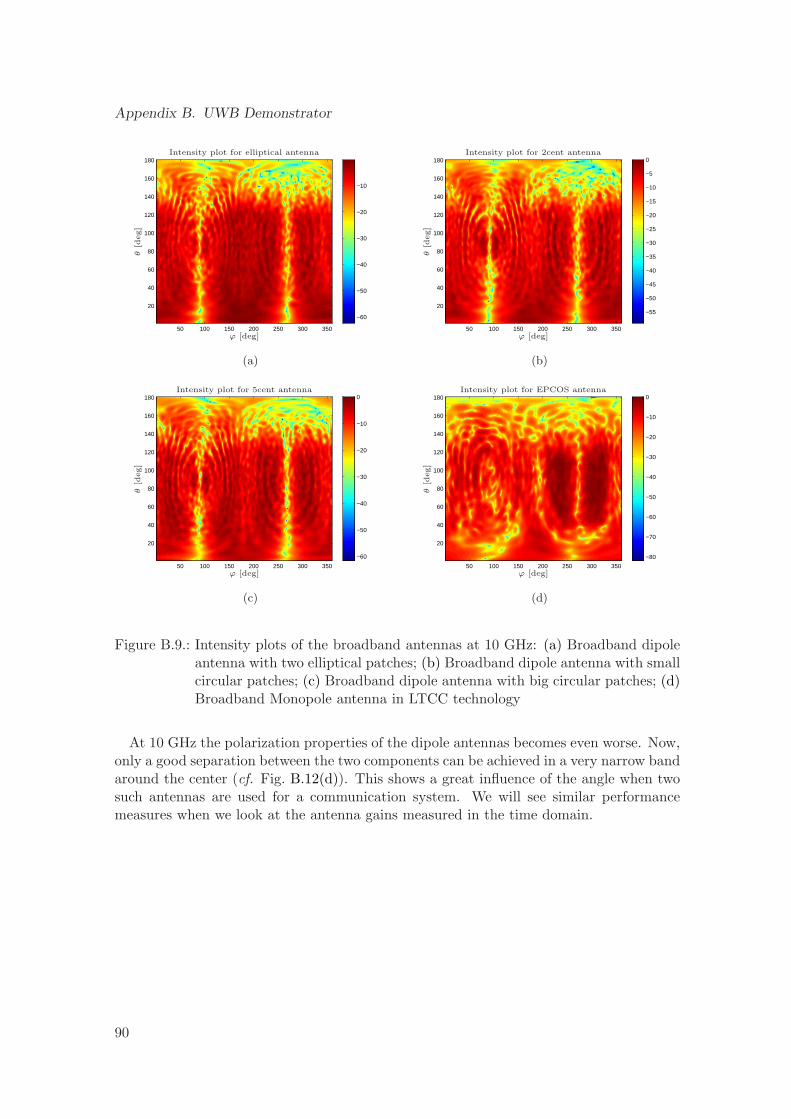
Appendix B. UWB Demonstrator
50 100 150 200 250 300 350
20
40
60
80
100
120
140
160
180
−60
−50
−40
−30
−20
−10
θ[d
eg]
ϕ [deg]
Intensity plot for elliptical antenna
(a)
50 100 150 200 250 300 350
20
40
60
80
100
120
140
160
180
−55
−50
−45
−40
−35
−30
−25
−20
−15
−10
−5
0
θ[d
eg]
ϕ [deg]
Intensity plot for 2cent antenna
(b)
50 100 150 200 250 300 350
20
40
60
80
100
120
140
160
180
−60
−50
−40
−30
−20
−10
0
θ[d
eg]
ϕ [deg]
Intensity plot for 5cent antenna
(c)
50 100 150 200 250 300 350
20
40
60
80
100
120
140
160
180
−80
−70
−60
−50
−40
−30
−20
−10
0
θ[d
eg]
ϕ [deg]
Intensity plot for EPCOS antenna
(d)
Figure B.9.: Intensity plots of the broadband antennas at 10 GHz: (a) Broadband dipoleantenna with two elliptical patches; (b) Broadband dipole antenna with smallcircular patches; (c) Broadband dipole antenna with big circular patches; (d)Broadband Monopole antenna in LTCC technology
At 10 GHz the polarization properties of the dipole antennas becomes even worse. Now,only a good separation between the two components can be achieved in a very narrow bandaround the center (cf. Fig. B.12(d)). This shows a great influence of the angle when twosuch antennas are used for a communication system. We will see similar performancemeasures when we look at the antenna gains measured in the time domain.
90
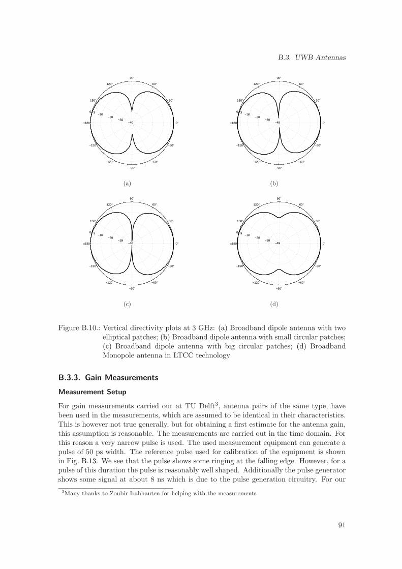
B.3. UWB Antennas
0°
30°
60°
90°
120°
150°
±180°
−150°
−120°
−90°
−60°
−30°
0 −3−10
−20−30
−40
(a)
0°
30°
60°
90°
120°
150°
±180°
−150°
−120°
−90°
−60°
−30°
0 −3−10
−20−30
−40
(b)
0°
30°
60°
90°
120°
150°
±180°
−150°
−120°
−90°
−60°
−30°
0 −3−10
−20−30
−40
(c)
0°
30°
60°
90°
120°
150°
±180°
−150°
−120°
−90°
−60°
−30°
0 −3−10
−20−30
−40
(d)
Figure B.10.: Vertical directivity plots at 3 GHz: (a) Broadband dipole antenna with twoelliptical patches; (b) Broadband dipole antenna with small circular patches;(c) Broadband dipole antenna with big circular patches; (d) BroadbandMonopole antenna in LTCC technology
B.3.3. Gain Measurements
Measurement Setup
For gain measurements carried out at TU Delft3, antenna pairs of the same type, havebeen used in the measurements, which are assumed to be identical in their characteristics.This is however not true generally, but for obtaining a first estimate for the antenna gain,this assumption is reasonable. The measurements are carried out in the time domain. Forthis reason a very narrow pulse is used. The used measurement equipment can generate apulse of 50 ps width. The reference pulse used for calibration of the equipment is shownin Fig. B.13. We see that the pulse shows some ringing at the falling edge. However, for apulse of this duration the pulse is reasonably well shaped. Additionally the pulse generatorshows some signal at about 8 ns which is due to the pulse generation circuitry. For our
3Many thanks to Zoubir Irahhauten for helping with the measurements
91
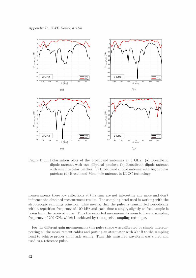
Appendix B. UWB Demonstrator
−150 −100 −50 0 50 100 150−50
−45
−40
−35
−30
−25
−20
−15
−10
−5
0
3 GHz
θ [deg]
DθDϕ
D(ϕ=
0
,θ)
[dB
]
(a)
−150 −100 −50 0 50 100 150−50
−45
−40
−35
−30
−25
−20
−15
−10
−5
0
3 GHz
θ [deg]
DθDϕ
D(ϕ=
0
,θ)
[dB
]
(b)
−150 −100 −50 0 50 100 150−50
−45
−40
−35
−30
−25
−20
−15
−10
−5
0
3 GHz
θ [deg]
DθDϕ
D(ϕ=
0
,θ)
[dB
]
(c)
−150 −100 −50 0 50 100 150−50
−45
−40
−35
−30
−25
−20
−15
−10
−5
0
3 GHz
θ [deg]
DθDϕ
D(ϕ=
0
,θ)
[dB
]
(d)
Figure B.11.: Polarization plots of the broadband antennas at 3 GHz: (a) Broadbanddipole antenna with two elliptical patches; (b) Broadband dipole antennawith small circular patches; (c) Broadband dipole antenna with big circularpatches; (d) Broadband Monopole antenna in LTCC technology
measurements these low reflections at this time are not interesting any more and don’tinfluence the obtained measurement results. The sampling head used is working with thestroboscopic sampling principle. This means, that the pulse is transmitted periodicallywith a repetition frequency of 100 kHz and each time a single, slightly shifted sample istaken from the received pulse. Thus the exported measurements seem to have a samplingfrequency of 200 GHz which is achieved by this special sampling technique.
For the different gain measurements this pulse shape was calibrated by simply intercon-necting all the measurement cables and putting an attenuator with 30 dB to the samplinghead to achieve proper amplitude scaling. Then this measured waveform was stored andused as a reference pulse.
92
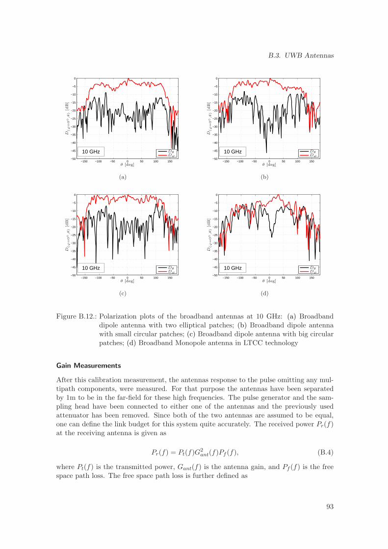
B.3. UWB Antennas
−150 −100 −50 0 50 100 150−50
−45
−40
−35
−30
−25
−20
−15
−10
−5
0
10 GHz
θ [deg]
DθDϕ
D(ϕ=
0
,θ)
[dB
]
(a)
−150 −100 −50 0 50 100 150−50
−45
−40
−35
−30
−25
−20
−15
−10
−5
0
10 GHz
θ [deg]
DθDϕ
D(ϕ=
0
,θ)
[dB
]
(b)
−150 −100 −50 0 50 100 150−50
−45
−40
−35
−30
−25
−20
−15
−10
−5
0
10 GHz
θ [deg]
DθDϕ
D(ϕ=
0
,θ)
[dB
]
(c)
−150 −100 −50 0 50 100 150−50
−45
−40
−35
−30
−25
−20
−15
−10
−5
0
10 GHz
θ [deg]
DθDϕ
D(ϕ=
0
,θ)
[dB
]
(d)
Figure B.12.: Polarization plots of the broadband antennas at 10 GHz: (a) Broadbanddipole antenna with two elliptical patches; (b) Broadband dipole antennawith small circular patches; (c) Broadband dipole antenna with big circularpatches; (d) Broadband Monopole antenna in LTCC technology
Gain Measurements
After this calibration measurement, the antennas response to the pulse omitting any mul-tipath components, were measured. For that purpose the antennas have been separatedby 1m to be in the far-field for these high frequencies. The pulse generator and the sam-pling head have been connected to either one of the antennas and the previously usedattenuator has been removed. Since both of the two antennas are assumed to be equal,one can define the link budget for this system quite accurately. The received power Pr(f)at the receiving antenna is given as
Pr(f) = Pt(f)G2ant(f)Pf (f), (B.4)
where Pt(f) is the transmitted power, Gant(f) is the antenna gain, and Pf (f) is the freespace path loss. The free space path loss is further defined as
93
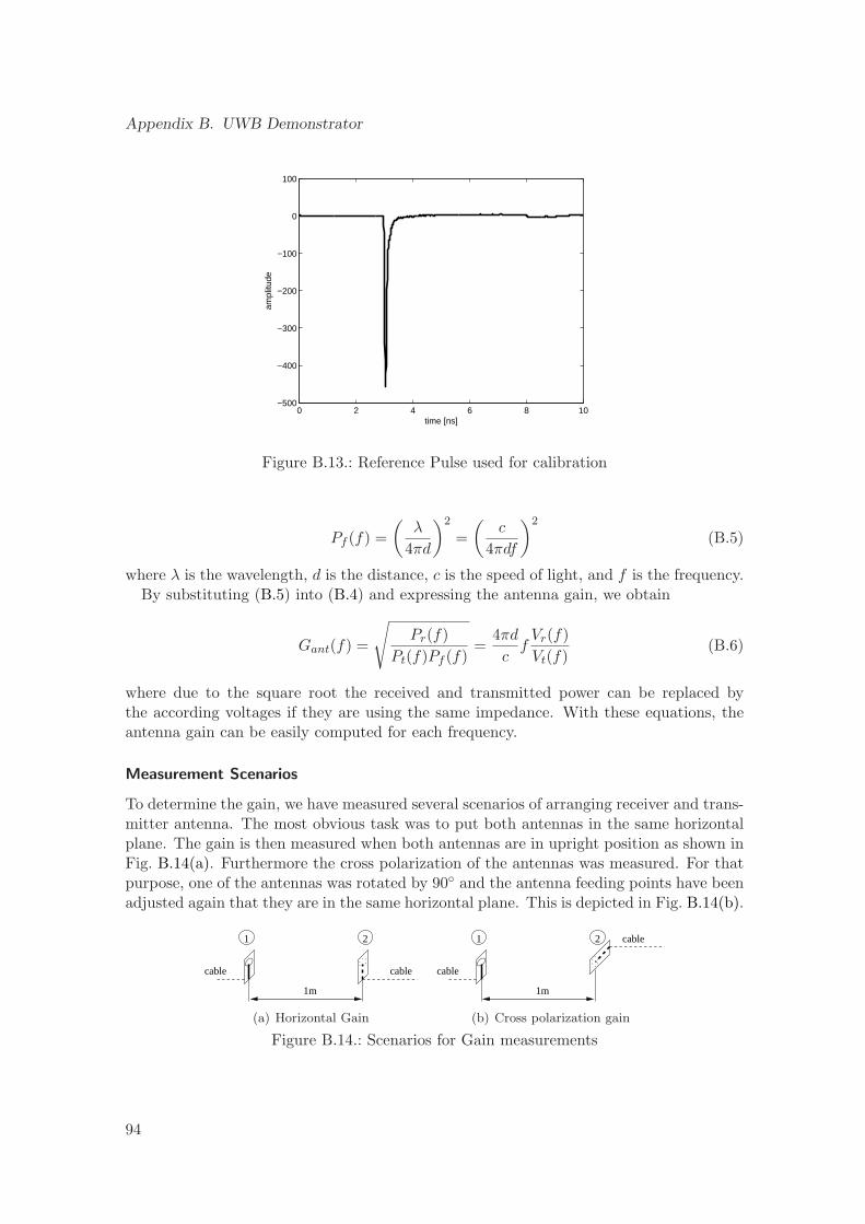
Appendix B. UWB Demonstrator
0 2 4 6 8 10−500
−400
−300
−200
−100
0
100
time [ns]
ampl
itude
Figure B.13.: Reference Pulse used for calibration
Pf (f) =
(λ
4πd
)2
=
(c
4πdf
)2
(B.5)
where λ is the wavelength, d is the distance, c is the speed of light, and f is the frequency.By substituting (B.5) into (B.4) and expressing the antenna gain, we obtain
Gant(f) =
√
Pr(f)
Pt(f)Pf (f)=
4πd
cf
Vr(f)
Vt(f)(B.6)
where due to the square root the received and transmitted power can be replaced bythe according voltages if they are using the same impedance. With these equations, theantenna gain can be easily computed for each frequency.
Measurement Scenarios
To determine the gain, we have measured several scenarios of arranging receiver and trans-mitter antenna. The most obvious task was to put both antennas in the same horizontalplane. The gain is then measured when both antennas are in upright position as shown inFig. B.14(a). Furthermore the cross polarization of the antennas was measured. For thatpurpose, one of the antennas was rotated by 90 and the antenna feeding points have beenadjusted again that they are in the same horizontal plane. This is depicted in Fig. B.14(b).
1m
cablecable
1 2
(a) Horizontal Gain
1m
cable
1 2 cable
(b) Cross polarization gain
Figure B.14.: Scenarios for Gain measurements
94
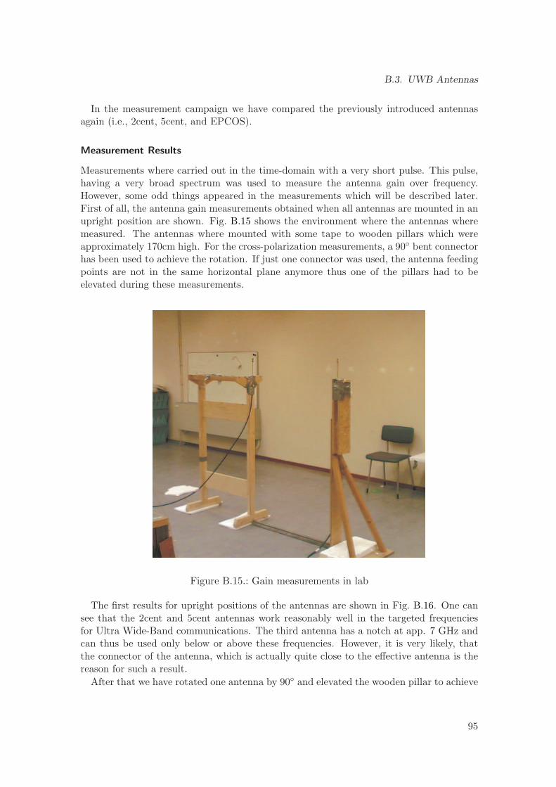
B.3. UWB Antennas
In the measurement campaign we have compared the previously introduced antennasagain (i.e., 2cent, 5cent, and EPCOS).
Measurement Results
Measurements where carried out in the time-domain with a very short pulse. This pulse,having a very broad spectrum was used to measure the antenna gain over frequency.However, some odd things appeared in the measurements which will be described later.First of all, the antenna gain measurements obtained when all antennas are mounted in anupright position are shown. Fig. B.15 shows the environment where the antennas wheremeasured. The antennas where mounted with some tape to wooden pillars which wereapproximately 170cm high. For the cross-polarization measurements, a 90 bent connectorhas been used to achieve the rotation. If just one connector was used, the antenna feedingpoints are not in the same horizontal plane anymore thus one of the pillars had to beelevated during these measurements.
Figure B.15.: Gain measurements in lab
The first results for upright positions of the antennas are shown in Fig. B.16. One cansee that the 2cent and 5cent antennas work reasonably well in the targeted frequenciesfor Ultra Wide-Band communications. The third antenna has a notch at app. 7 GHz andcan thus be used only below or above these frequencies. However, it is very likely, thatthe connector of the antenna, which is actually quite close to the effective antenna is thereason for such a result.
After that we have rotated one antenna by 90 and elevated the wooden pillar to achieve
95
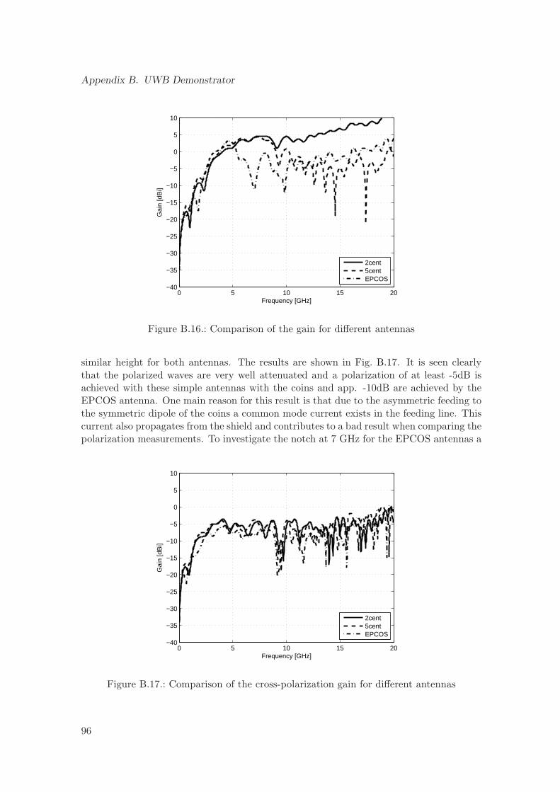
Appendix B. UWB Demonstrator
0 5 10 15 20−40
−35
−30
−25
−20
−15
−10
−5
0
5
10
Gai
n [d
Bi]
Frequency [GHz]
2cent5centEPCOS
Figure B.16.: Comparison of the gain for different antennas
similar height for both antennas. The results are shown in Fig. B.17. It is seen clearlythat the polarized waves are very well attenuated and a polarization of at least -5dB isachieved with these simple antennas with the coins and app. -10dB are achieved by theEPCOS antenna. One main reason for this result is that due to the asymmetric feeding tothe symmetric dipole of the coins a common mode current exists in the feeding line. Thiscurrent also propagates from the shield and contributes to a bad result when comparing thepolarization measurements. To investigate the notch at 7 GHz for the EPCOS antennas a
0 5 10 15 20−40
−35
−30
−25
−20
−15
−10
−5
0
5
10
Gai
n [d
Bi]
Frequency [GHz]
2cent5centEPCOS
Figure B.17.: Comparison of the cross-polarization gain for different antennas
96
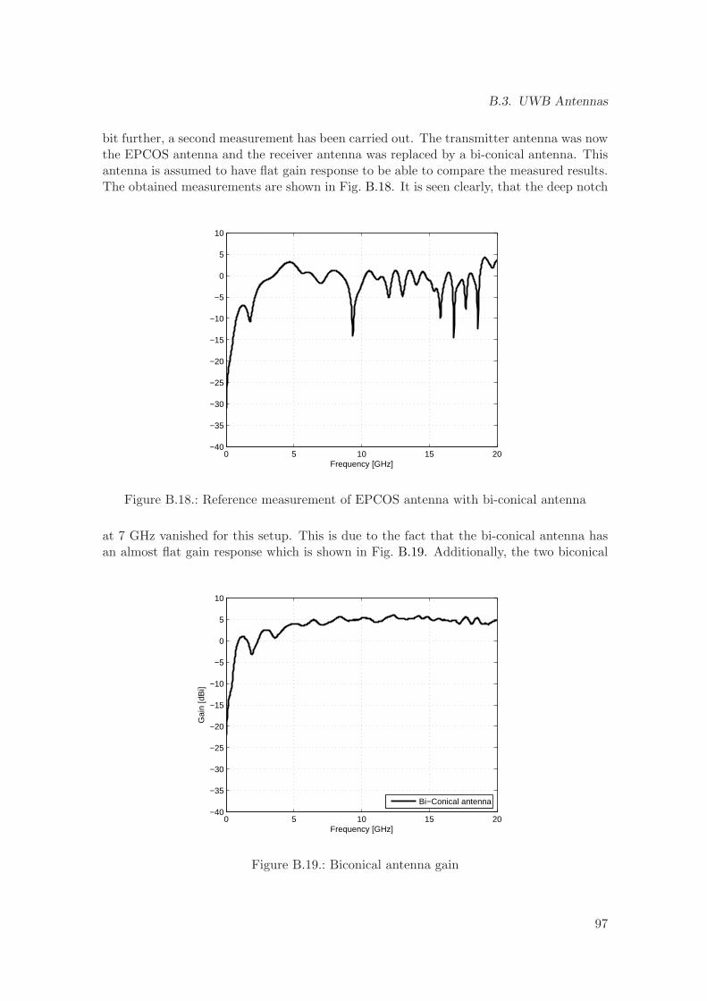
B.3. UWB Antennas
bit further, a second measurement has been carried out. The transmitter antenna was nowthe EPCOS antenna and the receiver antenna was replaced by a bi-conical antenna. Thisantenna is assumed to have flat gain response to be able to compare the measured results.The obtained measurements are shown in Fig. B.18. It is seen clearly, that the deep notch
0 5 10 15 20−40
−35
−30
−25
−20
−15
−10
−5
0
5
10
Frequency [GHz]
Figure B.18.: Reference measurement of EPCOS antenna with bi-conical antenna
at 7 GHz vanished for this setup. This is due to the fact that the bi-conical antenna hasan almost flat gain response which is shown in Fig. B.19. Additionally, the two biconical
0 5 10 15 20−40
−35
−30
−25
−20
−15
−10
−5
0
5
10
Frequency [GHz]
Gai
n [d
Bi]
Bi−Conical antenna
Figure B.19.: Biconical antenna gain
97
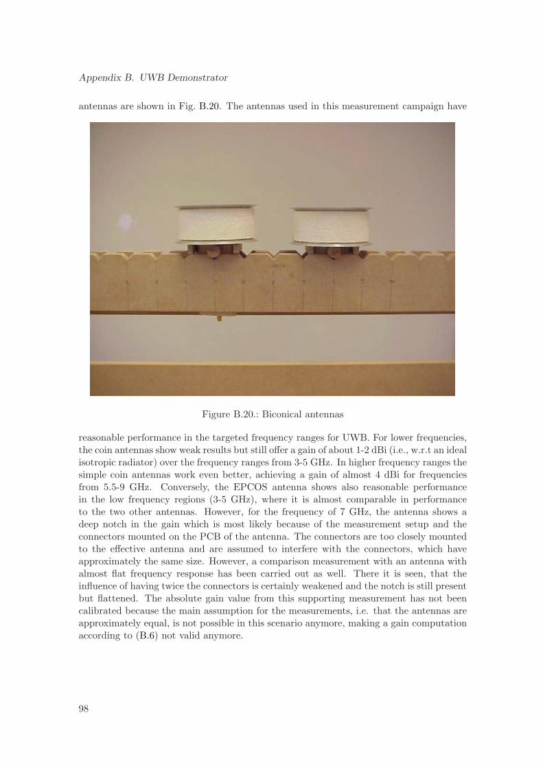
Appendix B. UWB Demonstrator
antennas are shown in Fig. B.20. The antennas used in this measurement campaign have
Figure B.20.: Biconical antennas
reasonable performance in the targeted frequency ranges for UWB. For lower frequencies,the coin antennas show weak results but still offer a gain of about 1-2 dBi (i.e., w.r.t an idealisotropic radiator) over the frequency ranges from 3-5 GHz. In higher frequency ranges thesimple coin antennas work even better, achieving a gain of almost 4 dBi for frequenciesfrom 5.5-9 GHz. Conversely, the EPCOS antenna shows also reasonable performancein the low frequency regions (3-5 GHz), where it is almost comparable in performanceto the two other antennas. However, for the frequency of 7 GHz, the antenna shows adeep notch in the gain which is most likely because of the measurement setup and theconnectors mounted on the PCB of the antenna. The connectors are too closely mountedto the effective antenna and are assumed to interfere with the connectors, which haveapproximately the same size. However, a comparison measurement with an antenna withalmost flat frequency response has been carried out as well. There it is seen, that theinfluence of having twice the connectors is certainly weakened and the notch is still presentbut flattened. The absolute gain value from this supporting measurement has not beencalibrated because the main assumption for the measurements, i.e. that the antennas areapproximately equal, is not possible in this scenario anymore, making a gain computationaccording to (B.6) not valid anymore.
98
AppendixCStandardized UWB Channels
C.1. Statistical Channel Models
Analysis and design of wireless communication systems are based on the knowledge ofthe propagation characteristics. Radio propagation mechanisms in the mobile and indoorenvironments are rather complex. Propagating radio signals undergo attenuation by ob-jects. Because of reflection, refraction and scattering, the transmitted wave arrives atthe receiver through different paths having different amplitudes and phases. These arethe three main effects which impact the description of a mobile radio channel. Reflectionoccurs when a propagating electromagnetic wave impinges on a smooth surface with largedimensions compared to the RF wavelength λ. Furthermore, diffraction occurs when theradio path between the transmitter and receiver is obstructed by a dense body with largedimensions compared to λ, causing secondary waves to be formed behind the obstructingbody. Diffraction and reflection are phenomena that account for RF energy travelling fromthe transmitter to the receiver without a line-of-sight path between the two. Diffractionis often termed “shadowing”. Scattering occurs when a radio wave impinges on either alarge rough surface or any surface whose dimensions are on the order of λ or less, causingthe reflected energy to spread out in all directions [33,34]. In wideband pulse transmissionthis causes delayed and attenuated echoes of each transmitted pulse, which in digital com-munication systems results in inter-symbol interference and fading of the received signalpower. This potentially limits the achievable data rate of the wireless transmission andstrategies to mitigate fading have to be investigated. If the knowledge of the propagationeffects could be incorporated and used in the receiver architecture, the performance of thecommunication system is improved. The characterization of the wireless radio propagationchannel is based on the mathematical model of the channel, which can be defined eitherin the time- or in the frequency-domain. A good overview about UWB channel modelingis presented in [16] and is further extended in this document.
C.1.1. Description of Different Propagation Effects
In wireless communication systems it is necessary to test the proposed transceiver archi-tectures with the occurring propagation channels. One approach to obtain these channelsis to model the physical effects of a wireless propagation channel with an impulse response.
99
Appendix C. Standardized UWB Channels
These channel models can be either deterministic, stochastic or hybrid channel models,with their according advantages and disadvantages. If a wireless channel is modeled de-terministically it is essential to know many parameters of the environment (i.e. positionsof reflectors, scatterers, etc.). Thus, it is a very complex task to account for all possiblereflections/scatterers which result in a multipath component at the receiver. One ideato simplify this approach is to generate a hybrid channel model which can be computedwith a low number of parameters of the geometry (reflectors/scatterers). These geometricmeasures determine a grid of dominant rays in the channel impulse response but to lowerthe complexity, the adjacent regions of the impulse response are modeled stochastically.Conversely, statistical channel models just represent the average behavior of a channel,which possibly occurs in a real world situation. The major advantage of the statisticalchannel models is that only a small amount of statistical parameters is needed to generateone realization of a channel impulse response.
C.1.2. Statistical Modeling of the Path Loss Exponent
In general, if a signal is transmitted through free space, it undergoes attenuation. Thereceived power Pr(d) is dependent on the distance d between transmitter and receiver,and is given by Friis equation [33] as
Pr(d) =PtGtGrλ
2
(4π)2d2(C.1)
where Pt denotes the power of the transmitter, and Gr, Gt are the gains of the receiverand transmitter antennas, respectively. It is seen clearly, that the path loss is dependenton the distance d and on the wavelength λ of the transmitted wave, which is given by
λ =c
f=
2πc
ωc(C.2)
where c is the propagation speed, i.e., the speed of light. In conventional narrowbandsystems the frequency-dependence is negligible because it remains approximately constantwithin the frequency range of interest. If a received signal shows fluctuations due tomultipath or shadowing, a narrowband model approach is to define the pathloss as
Gpr(d, fc) =EPRX(d, fc)
PTX(C.3)
where the expectation operator should cover an area which is large enough to allow aver-aging large-scale fading parameters (shadowing) and small-scale fading effects. Due to thehuge bandwith of UWB signals, the frequency dependence of the channel transfer functionhas to be considered. Thus it makes sense to define a frequency dependent path gain
Gpr(d, f) = E∫ f+∆f/2
f−∆f/2|H(f , d)|2df (C.4)
where H(f, d) is the channel transfer function. It greatly simplyfies the modeling of thepath loss if we assume that the path gain is a function of distance and frequency whichcan be written as a product of terms
Gpr(d, f) = Gpr(f)Gpr(d). (C.5)
100
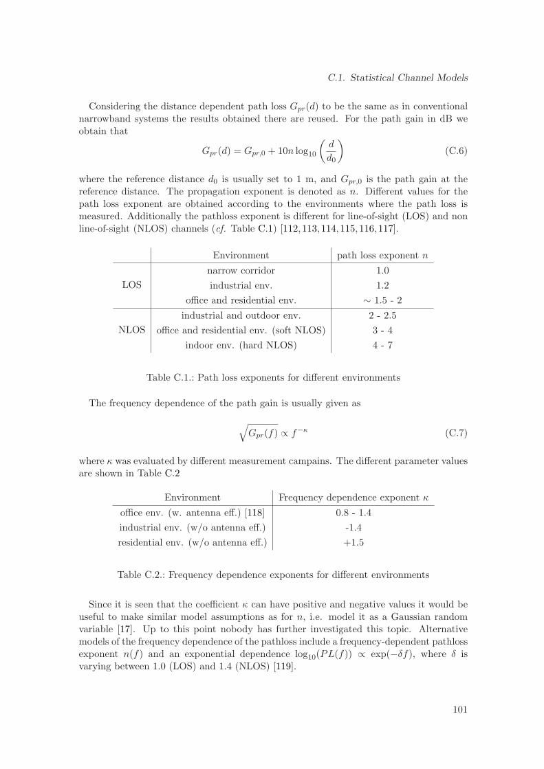
C.1. Statistical Channel Models
Considering the distance dependent path loss Gpr(d) to be the same as in conventionalnarrowband systems the results obtained there are reused. For the path gain in dB weobtain that
Gpr(d) = Gpr,0 + 10n log10
(d
d0
)
(C.6)
where the reference distance d0 is usually set to 1 m, and Gpr,0 is the path gain at thereference distance. The propagation exponent is denoted as n. Different values for thepath loss exponent are obtained according to the environments where the path loss ismeasured. Additionally the pathloss exponent is different for line-of-sight (LOS) and nonline-of-sight (NLOS) channels (cf. Table C.1) [112,113,114,115,116,117].
Environment path loss exponent n
LOS
narrow corridor 1.0
industrial env. 1.2
office and residential env. ∼ 1.5 - 2
NLOS
industrial and outdoor env. 2 - 2.5
office and residential env. (soft NLOS) 3 - 4
indoor env. (hard NLOS) 4 - 7
Table C.1.: Path loss exponents for different environments
The frequency dependence of the path gain is usually given as
√
Gpr(f) ∝ f−κ (C.7)
where κ was evaluated by different measurement campains. The different parameter valuesare shown in Table C.2
Environment Frequency dependence exponent κ
office env. (w. antenna eff.) [118] 0.8 - 1.4
industrial env. (w/o antenna eff.) -1.4
residential env. (w/o antenna eff.) +1.5
Table C.2.: Frequency dependence exponents for different environments
Since it is seen that the coefficient κ can have positive and negative values it would beuseful to make similar model assumptions as for n, i.e. model it as a Gaussian randomvariable [17]. Up to this point nobody has further investigated this topic. Alternativemodels of the frequency dependence of the pathloss include a frequency-dependent pathlossexponent n(f) and an exponential dependence log10(PL(f)) ∝ exp(−δf), where δ isvarying between 1.0 (LOS) and 1.4 (NLOS) [119].
101
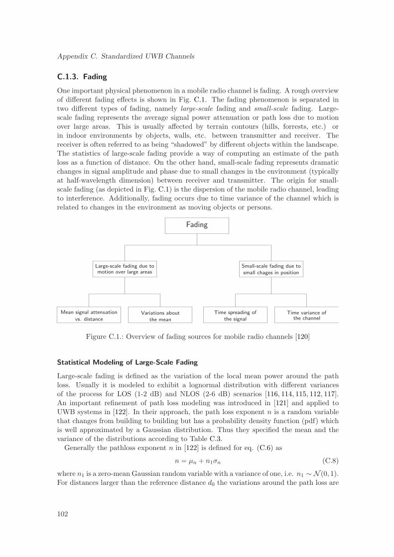
Appendix C. Standardized UWB Channels
C.1.3. Fading
One important physical phenomenon in a mobile radio channel is fading. A rough overviewof different fading effects is shown in Fig. C.1. The fading phenomenon is separated intwo different types of fading, namely large-scale fading and small-scale fading. Large-scale fading represents the average signal power attenuation or path loss due to motionover large areas. This is usually affected by terrain contours (hills, forrests, etc.) orin indoor environments by objects, walls, etc. between transmitter and receiver. Thereceiver is often referred to as being “shadowed” by different objects within the landscape.The statistics of large-scale fading provide a way of computing an estimate of the pathloss as a function of distance. On the other hand, small-scale fading represents dramaticchanges in signal amplitude and phase due to small changes in the environment (typicallyat half-wavelength dimension) between receiver and transmitter. The origin for small-scale fading (as depicted in Fig. C.1) is the dispersion of the mobile radio channel, leadingto interference. Additionally, fading occurs due to time variance of the channel which isrelated to changes in the environment as moving objects or persons.
Fading
Large-scale fading due tomotion over large areas
Mean signal attenuation
vs. distance
Variations about
the mean
Small-scale fading due to
small chages in position
Time spreading of
the signal
Time variance ofthe channel
Figure C.1.: Overview of fading sources for mobile radio channels [120]
Statistical Modeling of Large-Scale Fading
Large-scale fading is defined as the variation of the local mean power around the pathloss. Usually it is modeled to exhibit a lognormal distribution with different variancesof the process for LOS (1-2 dB) and NLOS (2-6 dB) scenarios [116, 114, 115, 112, 117].An important refinement of path loss modeling was introduced in [121] and applied toUWB systems in [122]. In their approach, the path loss exponent n is a random variablethat changes from building to building but has a probability density function (pdf) whichis well approximated by a Gaussian distribution. Thus they specified the mean and thevariance of the distributions according to Table C.3.
Generally the pathloss exponent n in [122] is defined for eq. (C.6) as
n = µn + n1σn (C.8)
where n1 is a zero-mean Gaussian random variable with a variance of one, i.e. n1 ∼ N (0, 1).For distances larger than the reference distance d0 the variations around the path loss are
102
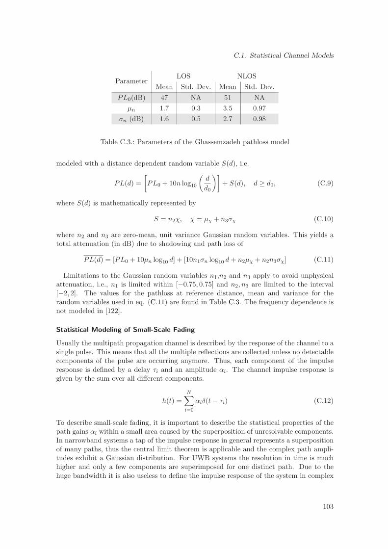
C.1. Statistical Channel Models
ParameterLOS NLOS
Mean Std. Dev. Mean Std. Dev.
PL0(dB) 47 NA 51 NA
µn 1.7 0.3 3.5 0.97
σn (dB) 1.6 0.5 2.7 0.98
Table C.3.: Parameters of the Ghassemzadeh pathloss model
modeled with a distance dependent random variable S(d), i.e.
PL(d) =
[
PL0 + 10n log10
(d
d0
)]
+ S(d), d ≥ d0, (C.9)
where S(d) is mathematically represented by
S = n2χ, χ = µχ + n3σχ (C.10)
where n2 and n3 are zero-mean, unit variance Gaussian random variables. This yields atotal attenuation (in dB) due to shadowing and path loss of
PL(d) = [PL0 + 10µn log10 d] + [10n1σn log10 d + n2µχ + n2n3σχ] (C.11)
Limitations to the Gaussian random variables n1,n2 and n3 apply to avoid unphysicalattenuation, i.e., n1 is limited within [−0.75, 0.75] and n2, n3 are limited to the interval[−2, 2]. The values for the pathloss at reference distance, mean and variance for therandom variables used in eq. (C.11) are found in Table C.3. The frequency dependence isnot modeled in [122].
Statistical Modeling of Small-Scale Fading
Usually the multipath propagation channel is described by the response of the channel to asingle pulse. This means that all the multiple reflections are collected unless no detectablecomponents of the pulse are occurring anymore. Thus, each component of the impulseresponse is defined by a delay τi and an amplitude αi. The channel impulse response isgiven by the sum over all different components.
h(t) =N∑
i=0
αiδ(t − τi) (C.12)
To describe small-scale fading, it is important to describe the statistical properties of thepath gains αi within a small area caused by the superposition of unresolvable components.In narrowband systems a tap of the impulse response in general represents a superpositionof many paths, thus the central limit theorem is applicable and the complex path ampli-tudes exhibit a Gaussian distribution. For UWB systems the resolution in time is muchhigher and only a few components are superimposed for one distinct path. Due to thehuge bandwidth it is also useless to define the impulse response of the system in complex
103
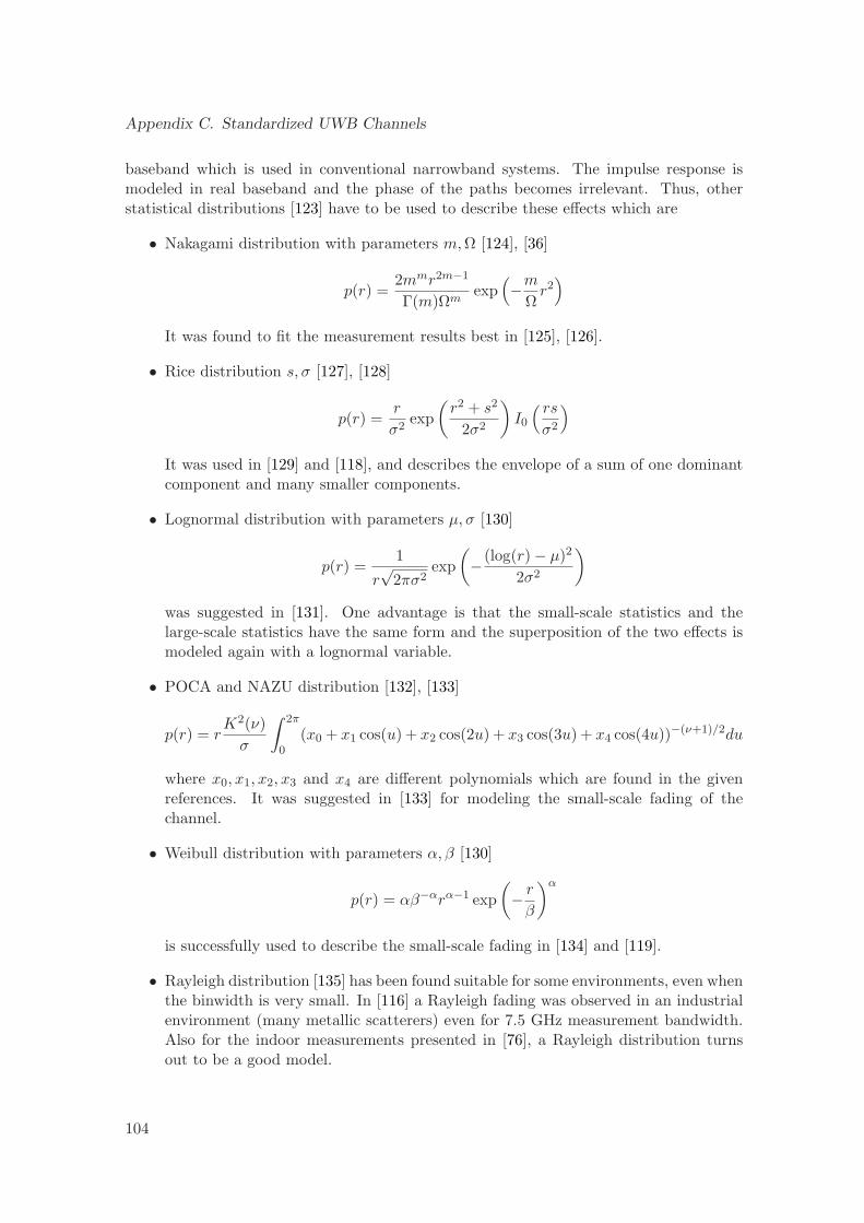
Appendix C. Standardized UWB Channels
baseband which is used in conventional narrowband systems. The impulse response ismodeled in real baseband and the phase of the paths becomes irrelevant. Thus, otherstatistical distributions [123] have to be used to describe these effects which are
• Nakagami distribution with parameters m, Ω [124], [36]
p(r) =2mmr2m−1
Γ(m)Ωmexp
(
−m
Ωr2)
It was found to fit the measurement results best in [125], [126].
• Rice distribution s, σ [127], [128]
p(r) =r
σ2exp
(r2 + s2
2σ2
)
I0
( rs
σ2
)
It was used in [129] and [118], and describes the envelope of a sum of one dominantcomponent and many smaller components.
• Lognormal distribution with parameters µ, σ [130]
p(r) =1
r√
2πσ2exp
(
−(log(r) − µ)2
2σ2
)
was suggested in [131]. One advantage is that the small-scale statistics and thelarge-scale statistics have the same form and the superposition of the two effects ismodeled again with a lognormal variable.
• POCA and NAZU distribution [132], [133]
p(r) = rK2(ν)
σ
∫ 2π
0(x0 + x1 cos(u) + x2 cos(2u) + x3 cos(3u) + x4 cos(4u))−(ν+1)/2du
where x0, x1, x2, x3 and x4 are different polynomials which are found in the givenreferences. It was suggested in [133] for modeling the small-scale fading of thechannel.
• Weibull distribution with parameters α, β [130]
p(r) = αβ−αrα−1 exp
(
− r
β
)α
is successfully used to describe the small-scale fading in [134] and [119].
• Rayleigh distribution [135] has been found suitable for some environments, even whenthe binwidth is very small. In [116] a Rayleigh fading was observed in an industrialenvironment (many metallic scatterers) even for 7.5 GHz measurement bandwidth.Also for the indoor measurements presented in [76], a Rayleigh distribution turnsout to be a good model.
104
C.1. Statistical Channel Models
Another important aspect is the correlation of fading between different delays. Such acorrelation can occur either if the wide-sense stationary uncorrelated scattering (WSSUS)model [136] is not valid anymore or per-pulse dispersion occurs. Per-pulse dispersionis a phenomenon which occurs if individual MPCs are distorted their and influence theadjacent bins, which results in correlated fading at these bins. This correlated fading couldnot be measured or observed in the channel measurements [125]. However, the authorsin [76] observed this phenomenon.
C.1.4. General Shape of the Impulse Response
It has been recognized in many wideband channel measurements, that the rays tend toarrive within clusters. A model which considers these effects was proposed by Saleh andValenzuela [137]. It allows the channel to consist of three different types of contributions.In their measurement campain they used a 1.5 GHz CW signal which was modulated bya train of 10 ns pulses with a repetition period of 600 ns. Due to this fine resolution intime domain, they obtained a very accurate model for a wideband channel (∼ 100MHz).Generally, the complex lowpass equivalent impulse response [36] of a channel is given by
h(t) =∑
k
βkejθkδ(t − τk) (C.13)
which means that the channel consists of path gains βk, phase shifts θk and delays τk.Saleh and Valenzuela defined a model which is also able to describe the clustering effectof the rays. Thus the impulse response of the SV model is given by
hsv(t) =L∑
l=0
K∑
k=0
ak,l exp(jθk,l)δ(t − Tl − τk,l) (C.14)
where ak,l denotes the weight of the kth component within the lth cluster, Tl is the delayof the lth cluster, τk,l is the delay of the kth multipath component (MPC) relative tothe lth cluster arrival time Tl. The phases θk,l are uniformly distributed within [0, 2π)for the bandpass system. K and L are the number of MPCs and the number of clusters,respectively. They can be fixed or modeled as a stochastic variable.
C.1.5. Path Interarrival Times
Several different models for interarrival times of the MPCs have been proposed.
• Regularly-spaced arrival times are useful for dense multipath profiles. Since thedifferent multipath components are not resolvable, a regular grid is defined on whichall resolvable MPCs have to lie, i.e. Tl + τk,l = i∆ with ∆ being the resolution ofthe grid and the variable i span cover the whole time axis which is spanned by theimpulse response [116].
• Poisson arrival times are probably the most popular model for the arrival timeswithin a cluster. The probability density function for the arrival of MPC path kat a certain time τk,l and conditioned on the arrival time of the previous MPC, i.e.τk−1,l, is given as [137]
p(τk,l|τk−1,l) = λl exp[−λ(τk,l − τk,l−1)], k > 0 (C.15)
105
Appendix C. Standardized UWB Channels
where the arrival time of the first ray in each cluster is by definition positive, i.e.,τ0,l > 0. The model proposed by Saleh and Valenzuela allows only a constant λfor all clusters which was also assumed for the 802.15.3a model (see Section C.2).However, measurements have shown that the arrival rate is larger for later clusters,thus λl for each cluster is used here.
• Mixed Poisson processes are used as a refinement for observations which occurredin the UWB channel measurements. The mixture of two Poisson processes fits theobservations better than using a single Poisson process [138]. Thus the pdf of theinterarrival times is given as
p(τk,l|τk−1,l) = βλ1 exp[−λ1(τk,l − τk−1,l] + (β − 1)λ2 exp[−λ2(τk,l − τk−1,l], k > 0(C.16)
where β is the mixture probability and λ1,λ2 are the ray arrival rates.
C.1.6. Cluster Powers and Cluster Shapes
The Power Delay Profile (PDP) is given (assuming ergodicity) as the expectation of thesquared value of the absolute taps of a channel impulse response, i.e.,
P (τ) = Et|h(t, τ)|2. (C.17)
where τ denotes the delays to describe a single impulse response of a channel, and tdenotes a possible variability of the channel over time [139]. The most common model forthe power delay profile is that each cluster exhibits an exponential decay, i.e.,
E|ak,l|2 ∝ Ωl exp(−τk,l/γl) (C.18)
where Ωl is the integrated energy of the lth cluster, and γl is the intra-cluster decayconstant. The cluster powers, averaged over the large-scale fading, follow an exponentialdecay
10 log(Ωl) = 10 log(exp(−Tl/Γ)) (C.19)
where Γ is the inter cluster decay time constant. Additionally the interarrival times of theclusters are also modeled by a Poisson process
p(Tl|Tl−1) = Λ exp[−Λ(Tl − Tl−1)], l > 0 (C.20)
where Λ is the cluster arrival rate.
With the shown model assumptions it is possible to model a huge range of widebandchannels, thus this model is widely used. A UWB channel is somewhat different in it’sbehavior. It is necessary to account for these special properties which were observed inthe measurement campains [129,140,141].
• The first component of a cluster can show stronger power than the one given by eq.(C.18). In conventional narrowband systems this is only true for the first path ofthe first cluster, i.e. the LOS component. In UWB systems this is also possible inmore than one cluster due to specular reflections in later clusters.
106
C.2. Parameters of the IEEE 802.15.3a Channel Model
• The cluster decay rates γl depend on the delay of the cluster. A possible solution toachieve this is with a linear increase of γl with the cluster delay [116]
γl ∝ kγTl + γ0 (C.21)
• The cluster powers show random variations around the value given by eq. (C.19)due to shadowing effects and are modeled with a lognormal distribution.
• The small scale averaged cluster shape is not strictly monotonous but shows a “finestructure”, i.e., deviations from the exponential decay. Thus a random variables(τk,l) for eq. (C.18) helps to model this observed effect [122].
• In some environments the cluster shape does not show a sharp onset but rather afirst gradual increase until a local maximum is reached and then a decrease. Thusan alternative PDP shape has been suggested for that case [17]
E|ak,l|2 ∝ (1 − ξ exp(−τk,l/γrise)) exp(−τk,l/γ1) (C.22)
C.2. Parameters of the IEEE 802.15.3a Channel Model
The IEEE has formed a standardization group, IEEE 802.15.3a, which has proposed astandardized channel model for UWB Personal Area Networks (PAN) communicationsystems [4]. The aim of the high data rate standardization group (TG3a) was to definechannel models which are representative for the typical behavior of a wireless UWB channelin different scenarios at short distance. The data rates for the 3a standard are up to 110Mbps at 10m distance, 200 Mbps at 4m distance and higher datarate at lower distance.It is very essential to have standardized stochastic channel models which represent thephysical effects to make a fair comparison between different transceiver structures.
C.2.1. The Model
The 802.15.3a standardization group has proposed the following channel model whichconsists of the following discrete time impulse response
h(t) = XL∑
l=0
K∑
k=0
αk,lδ(t − Tl − τk,l) (C.23)
where αk,l are the multipath coefficients, Tl is the delay of lth cluster, τk,l is the delayof the kth multipath component relative to the lth cluster. The variable X representsthe log-normal shadowing. Similarly to the Saleh/Valenzuela model the cluster arrivaltimes Tl and ray arrival times τk,l exhibit a Poisson distribution which are specified by thepdf
p(Tl|Tl−1) = Λ exp[−Λ(Tl − Tl−1)], l > 0 (C.24)
and
p(τk,l|τk−1,l) = λ exp[−λ(τk,l − τk−1,l], k > 0 (C.25)
107
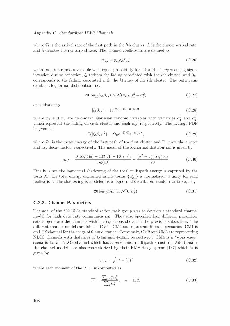
Appendix C. Standardized UWB Channels
where Tl is the arrival rate of the first path in the lth cluster, Λ is the cluster arrival rate,and λ denotes the ray arrival rate. The channel coefficients are defined as
αk,l = pk,lξlβk,l (C.26)
where pk,l is a random variable with equal probability for +1 and −1 representing signalinversion due to reflection, ξl reflects the fading associated with the lth cluster, and βk,l
corresponds to the fading associated with the kth ray of the lth cluster. The path gainsexhibit a lognormal distribution, i.e.,
20 log10(ξlβk,l) ∝ N (µk,l, σ21 + σ2
2) (C.27)
or equivalently
|ξlβk,l| = 10(µk,l+n1+n2)/20 (C.28)
where n1 and n2 are zero-mean Gaussian random variables with variances σ21 and σ2
2,which represent the fading on each cluster and each ray, respectively. The average PDPis given as
E|ξlβk,l|2 = Ω0e−Tl/Γe−τk,l/γ , (C.29)
where Ω0 is the mean energy of the first path of the first cluster and Γ, γ are the clusterand ray decay factor, respectively. The mean of the lognormal distribution is given by
µk,l =10 log(Ω0) − 10Tl/Γ − 10τk,l/γ
log(10)− (σ2
1 + σ22) log(10)
20(C.30)
Finally, since the lognormal shadowing of the total multipath energy is captured by theterm Xi, the total energy contained in the terms αi
k,l is normalized to unity for eachrealization. The shadowing is modeled as a lognormal distributed random variable, i.e.,
20 log10(Xi) ∝ N (0, σ2x) (C.31)
C.2.2. Channel Parameters
The goal of the 802.15.3a standardization task group was to develop a standard channelmodel for high data rate communication. They also specified four different parametersets to generate the channels with the equations shown in the previous subsection. Thedifferent channel models are labeled CM1 - CM4 and represent different scenarios. CM1 isan LOS channel for the range of 0-4m distance. Conversely, CM2 and CM3 are representingNLOS channels with distances of 0-4m and 4-10m, respectively. CM4 is a “worst-case”scenario for an NLOS channel which has a very dense multipath structure. Additionallythe channel models are also characterized by their RMS delay spread [137] which is isgiven by
τrms =
√
τ2 − (τ)2 (C.32)
where each moment of the PDP is computed as
τn =
∑
k τnk α2
k∑
k α2k
, n = 1, 2. (C.33)
108
C.3. The IEEE 802.15.4a Channel Model
Target Channel Characteristics CM1 CM2 CM3 CM4
τm[ns] (Mean excess delay) 5.05 10.38 14.18
τrms[ns] (rms delay spread) 5.28 8.03 14.28 25
NP10dB (number of paths within 10 dB of thestrongest path)
35
NP (85%) (number of paths that capture 85% ofthe channel energy)
24 36.1 61.54
Model Parameters
Λ[1/ns] (cluster arrival rate) 0.0233 0.4 0.0667 0.0667
λ[1/ns] (ray arrival rate) 2.5 0.5 2.1 2.1
Γ (cluster decay factor) 7.1 5.5 14 24
γ (ray decay factor) 4.3 6.7 7.9 12
σ1 [dB] (std. dev. of cluster lognormal fading) 3.4 3.4 3.4 3.4
σ2 [dB] (std. dev. of ray lognormal fading) 3.4 3.4 3.4 3.4
σx [dB] (std. dev. of lognormal fading term fortotal multipath realizations
3 3 3 3
Model Characteristics for 167ps sampling time
τm[ns] 5.0 9.9 15.9 30.1
τrms[ns] 5 8 15 25
NP10dB 12.5 15.3 24.9 41.2
NP (85%) 20.8 33.9 64.7 123.3
Channel energy mean [dB] -0.4 -0.5 0.0 0.3
Channel energy std. dev. [dB] 2.9 3.1 3.1 2.7
Table C.4.: Parameters for the different channel models in the 802.15.3a standard [4]
The moment is obtained from the general definition of the impulse response shown in(C.12). The different parameters of the channel models are shown in Table C.4.
We see from Table C.4 that for a measurement bandwidth of 6 GHz (167 ps timeresolution) the quantities like the RMS delay spread and other channel parameters arequite accurate compared to the target channel characteristics. For the target channelcharacteristics many values of representative quantities of the PDP are not even specified.Especially in CM4 where the definition of the model is said to be just a “worst case”scenario which should represent a very dense multipath channel.
C.3. The IEEE 802.15.4a Channel Model
The 802.15.4a standardization group has been developing a standard for UWB systemswith low data rates and geolocation capabilities. Since the 802.15.3a standard only coversindoor environments for wireless personal area networks (WPANs) a lot of effects whichare occurring in other scenarios are not covered in the 3a standard. Additionally, severaleffects are included in the model, which potentially increase the model accuracy, but onthe other hand also increase the model complexity. Apart from the model accuracy, threedifferent scenarios have been defined.
• 4a HF covers the same frequency range as the 802.15.3a channel, i.e., 3.1GHz to
109
Appendix C. Standardized UWB Channels
10.6GHz with several different scenarios.
• 4a LF covers the frequency range from 100MHz to 1000MHz.
• 4a Body Area Network (BAN) is a special case which tries to model the propagationchannel between two devices mounted on the human body.
Furthermore, a lot of different environments have been defined, i.e.,
• residential indoor
• office indoor
• industrial
• outdoor
• farm environments
In these different environments the specifications are done for an LOS and an NLOSscenario – the only exception is the farm environment which has only an NLOS scenariodefined. Generally all the models are based on measurement campains. The model consistsof a generalized Saleh/Valenzuela model [137]. Again the farm environment is excluded ofthe general model description because the model could not be fit into the measurementsproperly.
C.3.1. The Model
The path loss of the model is considered to be frequency and distance dependent. The dis-tance dependence and frequency dependence are given by eq. (C.6) and (C.7), respectively.Shadowing is not included in the model for reasons that are related to specific simulationrequirements in the 15.4a standardization. The generalizations of the Saleh/Valenzuelamodel include
• The number of clusters exhibits a Poisson distribution, where the mean L is a modelparameter.
• For some of the environments the cluster decay constant is linearly time dependent(C.21).
• For some NLOS environments (office and industrial), the PDP is not exponentiallydecaying but is given by (C.22)
• For indoor residential and office environments, the path arrival is given by a mixedPoisson distribution (cf. (C.16)).
• For industrial environments the channel model is a dense multipath channel. Thismeans that each path contains a significant amount of energy and the rather complexdescription with clusters is not feasible anymore. For that case a tapped delay linemodel is used.
110
C.3. The IEEE 802.15.4a Channel Model
The small-scale fading of the amplitudes is modeled with a Nakagami distribution, wherethe parameter m of the distribution is independent of the delay, with the exception of thefirst component. It can have a higher m-factor. The parameter sets for the differentenvironments are collected in Table C.5 and Table C.6.
111
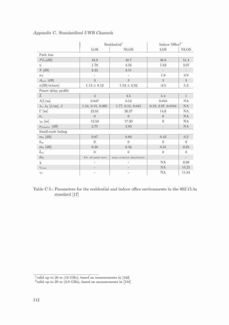
Appendix C. Standardized UWB Channels
Residential1 Indoor Office2
LOS NLOS LOS NLOS
Path loss
PL0[dB] 43.9 48.7 36.6 51.4
n 1.79 4.58 1.63 3.07
S [dB] 2.22 3.51 - -
σS - - 1.9 3.9
Aant [dB] 3 3 3 3
κ[dB/octave] 1.12 ± 0.12 1.53 ± 0.32 -3.5 5.3
Power delay profile
L 3 3.5 5.4 1
Λ[1/ns] 0.047 0.12 0.016 NA
λ1, λ2 [1/ns], β 1.54, 0.15, 0.095 1.77, 0.15, 0.045 0.19, 2.97, 0.0184 NA
Γ [ns] 22.61 26.27 14.6 NA
kγ 0 0 0 NA
γ0 [ns] 12.53 17.50 0 NA
σcluster [dB] 2.75 2.93 - NA
Small-scale fading
m0 [dB] 0.67 0.69 0.42 0.5
km 0 0 0 0
m0 [dB] 0.28 0.32 0.31 0.25
km 0 0 0 0
m0 NA: all paths have same m-factor distribution - -
χ - - NA 0.86
γrise - - NA 15.21
γ1 - - NA 11.84
Table C.5.: Parameters for the residential and indoor office environments in the 802.15.4astandard [17]
1valid up to 20 m (10 GHz), based on measurements in [142]2valid up to 28 m (2-8 GHz), based on measurements in [114]
112
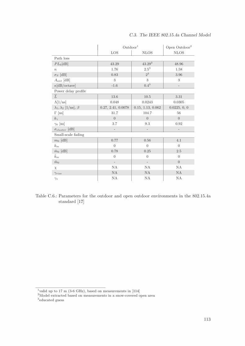
C.3. The IEEE 802.15.4a Channel Model
Outdoor1 Open Outdoor2
LOS NLOS NLOS
Path loss
PL0[dB] 43.29 43.293 48.96
n 1.76 2.53 1.58
σS [dB] 0.83 23 3.96
Aant [dB] 3 3 3
κ[dB/octave] -1.6 0.43 -
Power delay profile
L 13.6 10.5 3.31
Λ[1/ns] 0.048 0.0243 0.0305
λ1, λ2 [1/ns], β 0.27, 2.41, 0.0078 0.15, 1.13, 0.062 0.0225, 0, 0
Γ [ns] 31.7 104.7 56
kγ 0 0 0
γ0 [ns] 3.7 9.3 0.92
σcluster [dB] - - -
Small-scale fading
m0 [dB] 0.77 0.56 4.1
km 0 0 0
m0 [dB] 0.78 0.25 2.5
km 0 0 0
m0 - - 0
χ NA NA NA
γrise NA NA NA
γ1 NA NA NA
Table C.6.: Parameters for the outdoor and open outdoor environments in the 802.15.4astandard [17]
1valid up to 17 m (3-6 GHz), based on measurements in [114]2Model extracted based on measurements in a snow-covered open area3educated guess
113

Appendix C. Standardized UWB Channels
114
AppendixDKronecker Product and Correlation Matrix for the
Second-Order Equalizer
D.1. Commutation of the Kronecker Product
The Kronecker product of vectors is not commutative, which means that if the operandsare exchanged a different result is obtained. However, it is always possible to find apermutation matrix P that achieves
c = a ⊗ b ≡ P(b ⊗ a). (D.1)
If we assume that a is an m × 1 vector and b is an n × 1 vector, c is an mn × 1 vector.Thus, a valid permutation matrix has to be an mn × mn matrix.
If we assume that Exy is a matrix with dimensions m × n filled up with zeros, exceptfor a single 1 at the position (x, y) we can express the permutation matrix as
P = [vec(E11) , vec(E12) , . . . , vec(Emn)] , (D.2)
where vec(·) is denoting the vector operator, i.e., the operator that stacks a matrix into avector columnwise [143].
D.2. Correlation Matrix of the Data Terms
In this section we derive an analytical description for the correlation matrix Rr. Sinceit contains all different correlations between data terms up to eighth order we can give aset of rules how to create this matrix in a systematic way. First of all, we describe thecorrelation matrix a bit more explicitly. The correlation between the data terms is givenas Er[k]rT[k] where each of the data terms is given as r[k] = [sT[k], (s[k] ⊗ s[k])T]T ands[k] can be expressed as s[k] = [dT
x [k], (dx[k] ⊠ dx[k])T]T. Substituting this, we obtain
r[k] =[
dTx [k], (dx[k] ⊠ dx[k])T,
[dTx [k], (dx[k] ⊠ dx[k])T] ⊗ [dT
x [k], (dx[k] ⊠ dx[k])T]]T
.(D.3)
115
Appendix D. Correlation Matrix for the Second-Order Equalizer
To determine the autocorrelation matrix, the expectation operator of the outer product of(D.3) with itself has to be computed. If one studies the structure of the data products indetail, one can see that the matrix consists of sections with products of different orders.To analyze these products stepwise, we separate the correlation matrix in four parts, like
Rr =
R1 R2
RT2 R3
. .
(D.4)
where the separating line between the parts is drawn right after the fourth-order parts.Since the data vector up to the fourth-order products is defined with the reduced Kroneckernotation, R1 is exactly the same as Rs used for the linear equalizer. For the higher-orderterms, contained in R2 and R3, we can define conditions which have to be computed foreach element and then it can be decided whether there is correlation between the termsor not. For the following, we assume that all the processes are stationary. Thus we dropthe time index k of the data vectors. Furthermore, in each element of R2 and R3 weget a certain amount of data symbols contributing. Under assumption A1, we can say,that for each element in the correlation matrix where an odd number of data symbols iscontributing, the resulting correlation is zero. For an even number of contributing symbols,we can define conditions which have to be fulfilled such that there is correlation betweenthe data symbols, otherwise also these data symbols are uncorrelated.
Generally, the amount of different conditions which have to be checked is huge in thiscase. However, this problem is very similar with a set partitioning problem in combina-torics [144]. There, Bell has specified a number (i.e., the Bell number) which gives thenumber of partitioned sets of one dataset. For our problem not all different subsets are in-teresting. We just want to focus on the subsets which are contributing something differentfrom zero to the autocorrelation matrix of the data vector.
For the correlation of two data symbols, we have exactly one case where this conditionis fulfilled. There the contribution in the autocorrelation matrix is Edidj = c2 for i = j,where di is the i-th element of dx[k]. If we consider four symbols, we get already fourmatches which contribute a different value than zero to the correlation matrix. Thesefour cases are split in three sets of two data symbols and one set of four data symbols.Considering six data symbols, generally gives 31 different possible conditions. These 31split to 15 where we have three pairs of data symbols, 15 where we have one pair of datasymbols and one quad of data symbols, and one single six-element entry. For the eight-data-symbol case we have generally 374 subsets of the 4140 (the Bell number B8) thatcontribute. There we find 103 terms consisting of four pairs, 210 terms consisting of a groupof four and two pairs, 25 terms consisting of a pair and a group of six elements, 35 termsconsisting of two groups of four and one single entry which is consisting of a group of eight.This totally gives 374 different conditions and by superimposing the other contributionswith less than eight elements, we get a total number of 410 different possibilities to geta contribution in the autocorrelation matrix which is different from zero. To clarify thegrouping, we depict the conditions once again in (D.5) where the different permutationsare obtained when shifting indices.
Similar considerations are possible for the two other correlation matrices Rs,n and Rm
116
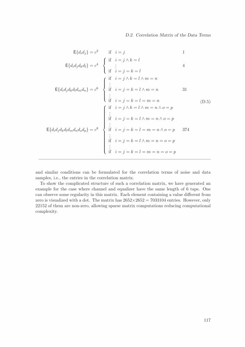
D.2. Correlation Matrix of the Data Terms
Edidj = c2 if i = j 1
Edidjdkdl = c4
if i = j ∧ k = l...
if i = j = k = l4
Edidjdkdldmdn = c6
if i = j ∧ k = l ∧ m = n...if i = j = k = l ∧ m = n...if i = j = k = l = m = n
31
Edidjdkdldmdndodp = c8
if i = j ∧ k = l ∧ m = n ∧ o = p...if i = j = k = l ∧ m = n ∧ o = p...if i = j = k = l = m = n ∧ o = p...if i = j = k = l ∧ m = n = o = p...if i = j = k = l = m = n = o = p
374
(D.5)
and similar conditions can be formulated for the correlation terms of noise and datasamples, i.e., the entries in the correlation matrix.
To show the complicated structure of such a correlation matrix, we have generated anexample for the case where channel and equalizer have the same length of 6 taps. Onecan observe some regularity in this matrix. Each element containing a value different fromzero is visualized with a dot. The matrix has 2652×2652 = 7033104 entries. However, only22152 of them are non-zero, allowing sparse matrix computations reducing computationalcomplexity.
117
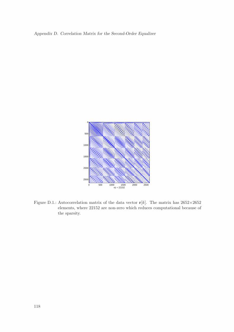
Appendix D. Correlation Matrix for the Second-Order Equalizer
0 500 1000 1500 2000 2500
0
500
1000
1500
2000
2500
nz = 22152
Figure D.1.: Autocorrelation matrix of the data vector r[k]. The matrix has 2652×2652elements, where 22152 are non-zero which reduces computational because ofthe sparsity.
118
AppendixEDerivation of the Compensation Filters
To compensate for the mismatch spectra, an M -periodic time-varying filter gn[l], whichrelates the input x[n] to the output x[n] is used. This filter is given as
x[n] =∞∑
l=−∞gn[l]x[n − l]. (E.1)
The filter digitally predistorts the digital output signal before digital-to-analog conversionand compensates therefore for the periodic nonuniform holding effects. Since gn[l] isperiodic with M , we can represent it as the inverse discrete Fourier transform (IDFT)
gn[l] =M−1∑
k=0
gk[l]ejkn 2π
M (E.2)
with the DFT
gk[l] =1
M
M−1∑
n=0
gn[l]e−jkn 2πM . (E.3)
In accordance with (3.18) and different from the common definition [31], we have thenormalization factor 1/M in the DFT. After substituting (E.2) in (E.1), we can write
x[n] =∑
l
M−1∑
k=0
gn[l]ejkn 2πM x[n − l]
=
M−1∑
k=0
( ∞∑
l=−∞gk[l]x[n − l]
)
ejk 2πM
n. (E.4)
The discrete-time Fourier transform (DTFT) of (E.4) gives
X(ejω) =M−1∑
k=0
Gk(ej(ω−k 2π
M))X(ej(ω−k 2π
M)) (E.5)
119
Appendix E. Derivation of the Compensation Filters
where
Gk(ejω) =
1
M
M−1∑
n=0
Gn(ejω)e−jkn 2πM (E.6)
is the DTFT of (E.3). Because the time-varying filter gn[l] precompensates the signal in thedigital domain, it can only affect the analog output signal of the DAC within a bandwidthof 2π/Ts. In practice, we will choose the fundamental band between −π/Ts and π/Ts,but theoretically we could compensate for any higher-order band. The continuous-timeoutput given by (3.17) can be represented within the fundamental band in discrete-timeas [31]
Y (ejω) =M−1∑
k=0
Hk(ejω)X
(
ej(ω−k 2πM ))
(E.7)
with
Hk(ejω) = Hk
(
jω
Ts
)
|ω| ≤ π, (E.8)
where it is assumed, without loss of generality, that T=1. Thus, after ideal digital-to-analog conversion the spectrum given in (E.7) is identical to the spectrum in (3.17) withinthe fundamental band. Substituting the output of the filter (E.5) in (E.7) results in theoutput
Y (ejω) =M−1∑
k1=0
M−1∑
k=0
Hk1(ejω)Gk(e
j(ω−(k1+k) 2πM
))
× X(
ej(ω−(k1+k) 2πM ))
. (E.9)
The precompensation filter and the discrete-time model of the holding signal is illustratedin Fig. E.1(a) for the two-periodic case. With l = k1 + k one can simplify (E.9) to
Y (ejω) =M−1∑
k=0
M−1+k∑
l=k
Hl−k(ejω)Gk(e
j(ω−l 2πM
))
× X(
ej(ω−l 2πM ))
=M−1∑
l=0
M−1∑
k=0
Hl−k(ejω)Gk(e
j(ω−l 2πM
))
× X(
ej(ω−l 2πM ))
(E.10)
where the periodicity of Hl−k(ejω) has been exploited. Thus, the overall transfer function
can be expressed as
Y (ejω) =M−1∑
l=0
Fl
(
ej(ω−l 2πM ))
X(
ej(ω−l 2πM ))
(E.11)
with
Fl(ejω) =
M−1∑
k=0
Hl−k(ej(ω+l 2π
M))Gk(e
jω), (E.12)
120
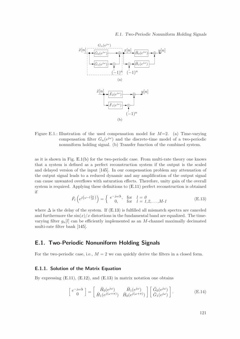
E.1. Two-Periodic Nonuniform Holding Signals
H0(ejω)
H1(ejω)
Gn(ejω)
G0(ejω)
G1(ejω)
x[n]x[n]
(−1)n (−1)n
y[n]
(a)
F0(ejω)
F1(ejω)
x[n]
(−1)n
y[n]
(b)
Figure E.1.: Illustration of the used compensation model for M=2. (a) Time-varyingcompensation filter Gn(ejω) and the discrete-time model of a two-periodicnonuniform holding signal. (b) Transfer function of the combined system.
as it is shown in Fig. E.1(b) for the two-periodic case. From multi-rate theory one knowsthat a system is defined as a perfect reconstruction system if the output is the scaledand delayed version of the input [145]. In our compensation problem any attenuation ofthe output signal leads to a reduced dynamic and any amplification of the output signalcan cause unwanted overflows with saturation effects. Therefore, unity gain of the overallsystem is required. Applying these definitions to (E.11) perfect reconstruction is obtainedif
Fl
(
ej(ω−l 2πM ))
=
e−jω∆, for l = 00, for l = 1,2,. . . ,M-1
(E.13)
where ∆ is the delay of the system. If (E.13) is fulfilled all mismatch spectra are canceledand furthermore the sin(x)/x distortions in the fundamental band are equalized. The time-varying filter gn[l] can be efficiently implemented as an M -channel maximally decimatedmulti-rate filter bank [145].
E.1. Two-Periodic Nonuniform Holding Signals
For the two-periodic case, i.e., M = 2 we can quickly derive the filters in a closed form.
E.1.1. Solution of the Matrix Equation
By expressing (E.11), (E.12), and (E.13) in matrix notation one obtains
[e−jω∆
0
]
=
[
H0(ejω) H1(e
jω)H1(e
j(ω+π)) H0(ej(ω+π))
] [
G0(ejω)
G1(ejω)
]
. (E.14)
121
Appendix E. Derivation of the Compensation Filters
Solving the matrix equation leads to
[
G0(ejω)
G1(ejω)
]
=
−H0(ej(ω+π))P (ejω)
H1(ej(ω+π))P (ejω)
e−jω∆ (E.15)
where
P (ejω) = H1(ejω)H1(e
j(ω+π)) − H0(ejω)H0(e
j(ω+π)). (E.16)
Applying the IDFT as defined in (E.2) to (E.15) the transfer functions of the time-varyingfilter gn[l] is obtained as
[
G0(ejω)
G1(ejω)
]
=
H1(ej(ω+π))−H0(ej(ω+π))P (ejω)
−(H1(ej(ω+π))+H0(ej(ω+π)))P (ejω)
e−jω∆. (E.17)
By using (E.16) with a discrete-time version of (3.18) a further simplification of (E.17)is possible and the two precompensation filters are given as
G0(ejω) =
2H1(ej(ω+π))
H1(ejω)H0(ej(ω+π)) + H0(ejω)H1(ej(ω+π))e−jω∆, (E.18)
and
G1(ejω) =
2H0(ej(ω+π))
H1(ejω)H0(ej(ω+π)) + H0(ejω)H1(ej(ω+π))e−jω∆. (E.19)
E.1.2. FIR Filter Design Example
For the design example two-periodic holding signals with relative timing offsets of r0 = 0and r1 = 0.0312 that are generated by a simulated 10-bit time-interleaved DAC are as-sumed. The digital signal has been a multi-tone signal with frequencies [0.0542, 0.1123,0.1704, 0.2285, 0.2866, 0.3447]fs. Without any compensation one obtains the energy den-sity spectrum shown in Fig. E.2. It is seen that the output spectrum has a sin(x)/xshape and that there are additional distortions due to nonuniform holding effects. Thelargest unwanted spur in the fundamental band, i.e., the band between 0 and 0.5, is about−31 dBc.
To approximate the ideal frequency responses given by (E.17) causal finite-impulse re-sponse (FIR) filters Ga
n(ejω) are used, which have transfer functions
Gan(ejω) =
N∑
l=0
gn[l]e−jωl (E.20)
and approximate the ideal frequency responses in the minimax (Chebychev) sense, i.e.,
min |Gn(ejω) − Gan(ejω)|, ω ∈ [0, ωc], ωc ≤ π (E.21)
where frequencies above ωc belong to the dont care band. The approximation problemhas been solved by using the Matlab software CVX1, where the designed filters are of orderN = 14 with ∆ = 7 and ωc = 0.8π.
122
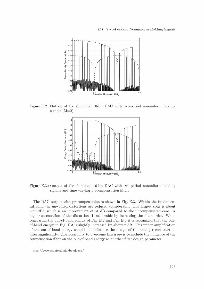
E.1. Two-Periodic Nonuniform Holding Signals
0 0.5 1 1.5−100
−90
−80
−70
−60
−50
−40
−30
−20
−10
0
Ene
rgy
Den
sity
Spe
ctru
m [d
Bc]
Normalized frequency Ω/Ωs
Figure E.2.: Output of the simulated 10-bit DAC with two-period nonuniform holdingsignals (M=2).
0 0.5 1 1.5−100
−90
−80
−70
−60
−50
−40
−30
−20
−10
0
Ene
rgy
Den
sity
Spe
ctru
m [d
Bc]
Normalized frequency Ω/Ωs
Figure E.3.: Output of the simulated 10-bit DAC with two-period nonuniform holdingsignals and time-varying precompensation filter.
The DAC output with precompensation is shown in Fig. E.3. Within the fundamen-tal band the unwanted distortions are reduced considerably. The largest spur is about−62 dBc, which is an improvement of 31 dB compared to the uncompensated case. Ahigher attenuation of the distortions is achievable by increasing the filter order. Whencomparing the out-of-band energy of Fig. E.2 and Fig. E.3 it is recognized that the out-of-band energy in Fig. E.3 is slightly increased by about 2 dB. This minor amplificationof the out-of-band energy should not influence the design of the analog reconstructionfilter significantly. One possibility to overcome this issue is to include the influence of thecompensation filter on the out-of-band energy as another filter design parameter.
1http://www.stanford.edu/boyd/cvx/
123

Appendix E. Derivation of the Compensation Filters
124
Curriculum Vitae
Christoph Krall was born in St. Veit an der Glan, Austria, on October 25, 1979. Afterprimary school he attended a technical college for telecommunication engineering, i.e.,HTBLA Mossingerstraße, Klagenfurt, Austria. In 1999 he started his studies in ElectricalEngineering at Graz University of Technology, Austria where he focused on communica-tions engineering, signal processing, and information technology. His diploma thesis waswritten at Delft University of Technology, The Netherlands (Prof. Gerard J.M. Janssen)where he investigated nonlinear equalizer structures for a broadband wireless communica-tion system. After finishing this project, he got the Dipl.-Ing. (MSc) degree in Jan. 2005from Graz University of Technology.
In Feb. 2005 he started with his PhD research project at the Christian Doppler Labo-ratory for Nonlinear Signal Processing at Graz University of Technology, Austria. Duringthis time he was again at Delft University of Technology, The Netherlands for a researchvisit of two months and worked with Prof. Alle-Jan van der Veen and Dr. Geert Leus.His research interests are wireless communication systems, nonlinear signal processing,and adaptive signal processing.
125

Appendix E. Derivation of the Compensation Filters
126
Bibliography
[1] Federal Communications Comission, “Part 15 Rules,” FCC,http://www.fcc.gov/oet/info/rules/part15/, Tech. Rep., April 2007.
[2] W. Hirt, “The European UWB Radio Regulatory and Standards Framework:Overview and Implications,” in IEEE International Conference on Ultra Wideband(ICUWB2007), Singapore, September 2007, .
[3] B. Hosler, “Passing FCC Regulations and RF Design Challenges,” Wireless USBDevelopers Conference, May 2006, .
[4] A. F. Molisch, J. R. Foerster, and M. Pendergrass, “Channel Models for Ultrawide-band Personal Area Networks,” IEEE Personal Communications Magazine, vol. 10,pp. 14 – 21, December 2003, .
[5] C. Ellison, “IOGEAR Wireless USB Hub and Adapter Review: Deja Vu all overagain,” http://www.smallnetbuilder.com/content/view/30175/85/1/3/, September2007, .
[6] IEEE P802.15.4a-2007 (Amendment 1), 802.15.4: Wireless Medium Access Con-trol (MAC) and Physical Layer (PHY) Specifications for Low-Rate Wireless PANs,IEEE Computer Society Std., 2007, .
[7] J. D. Taylor, Ultra-Wideband Radar Technology. CRC Press LLC, 2001.
[8] M.-G. Di Benedetto and G. Giancola, Understanding Ultra Wide Band Radio Fun-damentals. Upper Saddle River, New Jersey 07458: Prentice Hall PTR, 2004.
[9] C. Krall and K. Witrisal, “Parallel OFDM Signal Generation for UWB Systems,” in2006 IEEE Conference on Ultra Wideband (ICUWB 2006), Waltham, MA, Septem-ber 2006, pp. 243–247, .
[10] C. Krall, C. Vogel, and K. Witrisal, “Time-Interleaved Digital-to-Analog Convertersfor UWB Signal Generation,” in 2007 IEEE Conference on Ultra Wideband (ICUWB2007), Singapore, September 2007, .
127
Bibliography
[11] K. Witrisal, G. Leus, M. Pausini, and C. Krall, “Equivalent System Model andEqualization of Differential Impulse Radio UWB Systems,” IEEE Journal on Se-lected Areas in Communications, vol. 23, no. 9, pp. 1851–1862, September 2005,.
[12] Y. D. Alemseged, “Modeling and Mitigation of Narrowband Interference inTransmitted-Reference UWB Systems,” Ph.D. dissertation, Graz University of Tech-nology, Austria, March 2008, .
[13] C. Steiner and K. Witrisal, “Multiuser Interference Modeling and Suppression for aMultichannel Differential IR-UWB System,” in Proc. IEEE International Conferenceon Ultra-Wideband, ICU, Zurich, Switzerland, September 2005, pp. 667–672, .
[14] C. Krall, K. Witrisal, H. Koeppl, G. Leus, and M. Pausini, “Nonlinear Equaliza-tion for Frame-Differential IR-UWB Receivers,” in 2005 IEEE Conference on UltraWideband (ICU 2005), Zurich, Switzerland, September 2005, pp. 576–581, .
[15] ECMA, ECMA-368: High Rate Ultra Wideband PHY and MAC Standard.Geneva, Switzerland: ECMA (European Association for Standardizing In-formation and Communication Systems), Jun. 2005, . [Online]. Available:http://www.ecma.ch/ecma1/STAND/ecma-368.htm
[16] A. F. Molisch, “Ultrawideband Propagation Channels - Theory, Measurement, andModeling,” IEEE Trans. Veh. Technol., vol. 54, no. 5, pp. 1528 – 1545, September2005, .
[17] A. F. Molisch, K. Balakrishnan, C.-C. Chong, S. Emami, A. Fort, J. Karedal, J. Ku-nisch, H. Schantz, U. Schuster, and K. Siwiak, “IEEE 802.15.4a channel model -final report,” IEEE, Tech. Rep., November 2004, .
[18] A. Batra, J. Balakrishnan, G. Aiello, J. Foerster, and A. Dabak, “Design of a Multi-band OFDM System for Realistic UWB Channel Environments,” IEEE Trans. Mi-crow. Theory Tech., vol. 52, no. 9, pp. 2123–2138, 2004, .
[19] R. Fisher, R. Kohno, M. Mc Laughlin, and M. Welborn, “DS-UWB Physical LayerSubmission to 802.15 Task Group3a,” IEEE P802.15-04/0137r3, Tech. Rep., July2004, .
[20] ISO, ISO/IEC 26907:2007: High Rate Ultra Wideband PHY and MAC Standard.International Standardization Organization, Mar. 2007.
[21] W. Alliance, “WiMedia Logical Link Control Protocol,” The WiMedia Alliance,Tech. Rep., August 2007, .
[22] L. Hanzo, M. Munster, B. J. Choi, and T. Keller, ODFM MC-CDMA for BroadbandMulti-User Communications, WLANs and Broadcasting. John Wiley & Sons Ltd.,2003.
[23] H. Schulze and C. Luders, Theory and Applications of OFDM and CDMA WidebandWireless Communications. John Wiley & Sons Ltd., 2005.
128
Bibliography
[24] M. Ibnkahla, Signal Processing for Future Mobile Communications Systems: Chal-lenges and Perspectives. CRC Press, 2004.
[25] S. B. Weinstein and P. M. Ebert, “Data Transmission by Frequency-Division Mul-tiplexing Using the Discrete Fourier Transform,” IEEE Trans. Commun. Technol.,vol. 19, no. 5, pp. 628 – 634, October 1971, .
[26] P. Duhamel and M. Vetterli, “Fast Fourier Transforms: A Tutorial Review and aState of the Art,” Signal Processing, vol. 19, no. 4, pp. 259 – 299, 1990, .
[27] B. Daneshrad, L. J. Cimini, Jr., M. Carloni, and N. Sollenberger, “Performanceand Implementation of Clustered OFDM for Wireless Communications,” MobileNetworks and Applications, vol. 2, pp. 305 – 314, 1997, Baltzer Science PublishersBV, .
[28] S. H. Muller and J. B. Huber, “OFDM with Reduced Peak-to-mean Power Ratio byOptimum Combination of Partial Transmit Sequences,” Electronic Letters, vol. 33,pp. 368 – 369, February 1997, .
[29] L. J. Cimini, Jr. and N. R. Sollenberger, “Peak-to-Average Power Ratio Reduction ofan OFDM Signal Using Partial Transmit Sequences,” IEEE Commun. Lett., vol. 4,no. 3, pp. 86 – 88, March 2000, .
[30] T. Beth, W. Fumy, and R. Muhlfeld, “Zur Algebraischen Diskreten Fourier-Transformation,” Archiv der Mathematik, vol. 40, no. 1, pp. 238 – 244, December1983, .
[31] A. V. Oppenheim, R. W. Schafer, and J. R. Buck, Discrete-Time Signal Processing,2nd ed. Prentice Hall Inc., 1998.
[32] B. Muquet, Z. Wang, G. Giannakis, M. de Courville, and P. Duhamel, “CyclicPrefixing or Zero Padding for Wireless Multicarrier Transmissions?” IEEE Trans.Commun., vol. 50, no. 12, pp. 2136–2148, 2002, .
[33] T. S. Rappaport, Wireless Communications - Principles and Practice. PrenticeHall, Inc., 1999.
[34] M. Patzold, Mobile Fading Channels, 2nd ed. John Wiley & Sons Ltd., 2002.
[35] R. Steele and L. Hanzo, Eds., Mobile Radio Communications, 2nd ed. John Wiley& Sons, Ltd., 1999.
[36] J. G. Proakis, Digital Communications, 4th ed. McGraw-Hill International, 2001.
[37] F. J. Harris, “On the Use of Windows for Harmonic Analysis with the DiscreteFourier Transform,” Proc. IEEE, vol. 66, no. 1, pp. 51 – 83, January 1978, .
[38] R. E. Crochiere and L. R. Rabiner, Multirate Digital Signal Processing. PrencticeHall Inc., 1983.
129
Bibliography
[39] P. P. Vaidyanathan and K. Swaminathan, “Alias-Free, Real-Coefficient m-BandQMF Banks for Arbitrary m,” IEEE Trans. Circuits Syst., vol. CAS-34, no. 12, pp.1485 – 1496, December 1987, .
[40] P. P. Vaidyanathan, “Quadrature Mirror Filter Banks, M-Band Extensions andPerfect-Reconstruction Techniques,” IEEE ASSP Mag., pp. 4 – 20, July 1987, .
[41] Y. C. Lim, “Frequency-Response Masking Approach for the Synthesis of SharpLinear Phase Digital Filters,” IEEE Trans. Circuits Syst., vol. CAS-33, pp. 357 –364, April 1986, .
[42] Y. C. Lim and Y. Lian, “Frequency-Response Masking Approach for Digital Fil-ter Design: Complexity Reduction via Masking Filter Factorization,” IEEE Trans.Circuits Syst. II, vol. 41, no. 8, pp. 518 – 525, August 1994, .
[43] L. Feng and W. Namgoong, “An Adaptive Maximally Decimated Channelized UWBReceiver with Cyclic Prefix,” IEEE Trans. Circuits Syst. I, vol. 52, no. 10, pp. 2165–2172, 2005, .
[44] 16-Bit, 500MSps, 2x - 16x Interpolating Dual-Channel DAC, http://www.ti.com,Texas Instruments, .
[45] 16-Bit 160 MSPS 2x/4x/8x Interpolating Dual TxDAC R© + D/A Converter,http://www.analog.com, Analog Devices, .
[46] E. A. Lee and D. G. Messerschmitt, Digital Communication, 2nd ed. KluwerAcademic Publishers, 1994.
[47] S. Gezici, Z. Tian, G. Giannakis, H. Kobayashi, A. Molisch, H. Poor, andZ. Sahinoglu, “Localization via Ultra-Wideband Radios: A Look at PositioningAspects for Future Sensor Networks,” IEEE Signal Process. Mag., vol. 22, no. 4, pp.70–84, July 2005, .
[48] C. Vogel and C. Krall, “Compensation of Distortions Due to Periodic NonuniformHolding Signals,” in IEEE 6th Symposium on Communication Systems, Networksand Digital Signal Processing (CSNDSP), submitted, Graz, Austria, July 2008, .
[49] B. Hu and N. Beaulieu, “Pulse Shapes for Ultra Wideband Communication Sys-tems,” Wireless Communications, IEEE Transactions on, vol. 4, no. 4, pp. 1789–1797, 2005, .
[50] F. C. Moon, Chaotic and fractal dynamics. John Wiley & Sons, Inc., 1992.
[51] “Analog Devices AD9734 10-Bit, 1200 MSPS D/A Converter,” Sept. 2006. [Online].Available: http://www.analog.com
[52] F. Maloberti, “High-speed data converters for communication systems,” IEEE Cir-cuits Syst. Mag., vol. 1, no. 1, pp. 26–36, 2001, .
130
Bibliography
[53] G. Gielen, R. Rutenbar, S. Borkar, R. Brodersen, J.-H. Chern, E. Naviasky, D. Saias,and C. Sodini, “Tomorrow’s analog: just dead or just different?” in 2006 43rdACM/IEEE Design Automation Conference, San Francisco, CA, 2006, pp. 709–710,.
[54] B. Murmann, “Digitally Assisted Analog Circuits,” IEEE Micro, vol. 26, no. 2, pp.38–47, March-April 2006, .
[55] M. Clara, W. Klatzer, A. Wiesbauer, and D. Straeussnigg, “A 350MHz low-OSR∆Σ current-steering DAC with active termination in 0.13 µm CMOS,” in 2005IEEE International Solid-State Circuits Conference, 2005. Digest of Technical Pa-pers. ISSCC, San Francisco, CA, 2005, pp. 118–588 Vol. 1, .
[56] R. Adams, K. Nguyen, and K. Sweetland, “A 113-dB SNR Oversampling DAC withSegmented Noise-Shaped Scrambling,” IEEE J. Solid-State Circuits, vol. 33, no. 12,pp. 1871–1878, 1998, .
[57] A. G. Venes, K. L. Miller, and P. Vorenkamp, “Method and System for TimeInterleaved Digital to Analog Conversion for a Cable Modem,” U.S. PatentUS2 006 098 823, May, 2006, .
[58] Xilinx, “Virtex-4 ML403 Embedded Platform,” Xilinx Inc., Tech. Rep., May 2006.[Online]. Available: http://www.xilinx.com
[59] “Stanford Research Systems CG635 Synthesized Clock Generator,” 2006. [Online].Available: http://www.thinksrs.com/products/CG635.htm
[60] U. Seng-Pan, S. Sai-Weng, and R. Martins, “Exact spectra analysis of sampled sig-nals with jitter-induced nonuniformly holding effects,” IEEE Trans. Instrum. Meas.,vol. 53, no. 4, pp. 1279–1288, August 2004, .
[61] L. Angrisani, M. D’Apuzzo, and M. D’Arco, “Modeling timing jitter effects in digital-to-analog converters,” in 2005 IEEE International Workshop on Intelligent SignalProcessing, Faro, Protugal, September 2005, pp. 254–259, .
[62] D. Domanin, U. Gatti, P. Malcovati, and F. Maloberti, “A multipath polyphasedigital-to-analog converter for softwareradio transmission systems,” in The 2000IEEE International Symposium on Circuits and Systems, vol. 2, Geneva, Switzer-land, May 2000, pp. 361–364, .
[63] C.-K. Yang, V. Stojanovic, S. Modjtahedi, M. Horowitz, and W. Ellersick, “Aserial-link transceiver based on 8-GSamples/s A/D and D/A converters in 0.25-µm CMOS,” IEEE J. Solid-State Circuits, vol. 36, no. 11, pp. 1684–1692, November2001, .
[64] Y.-C. Jenq, “Digital-to-analog (D/A) converters with nonuniformly sampledsignals,”IEEE Trans. Instrum. Meas., vol. 45, no. 1, pp. 56–59, February 1996, .
[65] Y. C. Jenq, “Digital Spectra of Nonuniformly Sampled Signals: A Robust SamplingTime Offset Estimation Algorithm for Ultra High-Speed Waveform Digitizers Using
131
Bibliography
Interleaving,” IEEE Trans. Instrum. Meas., vol. 39, no. 1, pp. 71–75, February 1990,.
[66] C. Farrow, “A Continuously Variable Digital Delay Element,” in The 1988 IEEEInternational Symposium on Circuits and Systems, vol. 3, Helsinki, Finland, June1988, pp. 2641–2645, .
[67] M. Win, G. Chrisikos, and N. Sollenberger, “Performance of RAKE Reception inDense Multipath Channels: Implications of Spreading Bandwidth and Selection Di-versity Order,” IEEE J. Sel. Areas Commun., vol. 18, no. 8, pp. 1516–1525, August2000, .
[68] ——, “Effects of Chip Rate on Selective RAKE Combining,” IEEE Commun. Lett.,vol. 4, no. 7, pp. 233–235, July 2000, .
[69] M. Weisenhorn and W. Hirt, “Robust Noncoherent Receiver Exploiting UWB Chan-nel Properties,” in Ultra Wideband Systems, 2004. Joint with Conference on Ultra-wideband Systems and Technologies, Kyoto, Japan, 18-21 May 2004, pp. 156–160,.
[70] F. Troesch, F. Althaus, and A. Wittneben, “Modified Pulse Repetition CodingBoosting Energy Detector Performance in Low Data Rate Systems,” in Ultra-Wideband, 2005. ICU 2005. 2005 IEEE International Conference on, Zurich,Switzerland, 5-8 Sept. 2005, pp. 508–513, .
[71] C. Rushforth, “Transmitted-Reference Techniques for Random or Unknown Chan-nels,” IEEE Trans. Inf. Theory, vol. 10, no. 1, pp. 39–42, Jan. 1964, .
[72] M. Pausini, “Autocorrelation Receivers for Ultra Wideband Wireless Ccommunica-tions,” Ph.D. dissertation, Delft University of Technology, The Netherlands, Decem-ber 2007, .
[73] T. Q. S. Quek and M. Z. Win, “Analysis of UWB Transmitted-Reference Com-munication Systems in Dense Multipath Channels,” IEEE J. Sel. Areas Commun.,vol. 23, no. 9, pp. 1863 – 1874, September 2005, .
[74] Q. Dang, A. Trindade, A.-J. van der Veen, and G. Leus, “Signal Model and Re-ceiver Algorithms for a Transmit-Reference Ultra-Wideband Communication Sys-tem,” IEEE J. Sel. Areas Commun., vol. 24, no. 4, pp. 773–779, April 2006, .
[75] R. Hoctor and H. Tomlinson, “Delay-Hopped Transmitted-Reference RF Commu-nications,” in 2002 IEEE Conference on Ultra Wideband Systems and Technologies,2002. Digest of Papers., Baltimore, MD, 2002, pp. 265–269, .
[76] U. Schuster and H. Bolcskei, “Ultrawideband Channel Modeling on the Basis ofInformation-Theoretic Criteria,” IEEE Trans. Wireless Commun., vol. 6, no. 7, pp.2464 – 2475, July 2007, .
[77] R. Hoctor and H. Tomlinson, “Delay-Hopped Transmitted-Reference RF Commu-nications,” in 2002 IEEE Conference on Ultra Wideband Systems and Technologies,2002. Digest of Papers., Baltimore, MD, 2002, pp. 265–269, .
132
Bibliography
[78] C. Krall, K. Witrisal, G. Leus, and H. Koeppl, “Minimum Mean Squared ErrorEqualization for Second-Order Volterra Systems,” IEEE Trans. Signal Process.,2007, submitted.
[79] J. Romme, “UWB Channel Fading Statistics and Transmit-Reference Communi-cation,” Ph.D. dissertation, Graz University of Technology, Austria, March 2008,.
[80] S. Franz and U. Mitra, “Integration Interval Optimization and Performance Analysisfor UWB Transmitted Reference Systems,” in 2004 International Workshop on UltraWideband Systems, Kyoto, Japan, May 2004, pp. 26–30, .
[81] C. Steiner, “Multiuser Interference Modeling and Suppression for Differential IR-UWB Systems,” Master’s thesis, Graz University of Technology, Austria, 2005, .
[82] S. Haykin, Neural Networks: A Comprehensive Foundation. MacMillan PublishingCompany, 1994.
[83] M. Schetzen, The Volterra and Wiener Theories of Nonlinear Systems. New York:Krieger Publishing, 1980.
[84] V.J.Mathews and G. L. Sicuranza, Polynomial Signal Processing. Wiley-Interscience, 2000.
[85] R. Hermann, “Volterra modeling of digital magnetic saturation recording channels,”IEEE Trans. Magn., vol. 26, no. 5, pp. 2125–2127, Sep 1990, .
[86] S. Benedetto and E. Biglieri, “Nonlinear Equalization of Digital Satellite Channels,”IEEE J. Sel. Areas Commun., vol. 1, no. 1, pp. 57– 62, Jan. 1983, .
[87] H. Koeppl and P. Singerl, “An efficient scheme for nonlinear modeling and predis-tortion in mixed-signal systems,” IEEE Trans. Circuits Syst. II, vol. 53, no. 12, pp.1368–1372, Dec. 2006, .
[88] F. Gao and W. Snelgrove, “Adaptive Linearization of a Loudspeaker,” in 1991 In-ternational Conference on Acoustics, Speech, and Signal Processing, ICASSP, vol. 5,Toronto, Canada, April 1991, pp. 3589–3592, .
[89] E. Aschbacher and M. Rupp, “Modelling and identification of a nonlinear power-amplifier with memory for nonlinear digital adaptive pre-distortion,” in 4th IEEEWorkshop on Signal Processing Advances in Wireless Communications, 2003,SPAWC 2003, Rome, Italy, 15-18 June 2003, pp. 658–662, .
[90] E. A. Lee, D. G. Messerschmitt, and J. R. Barry, Digital Communication. SpringerNetherlands, 2004.
[91] M. Ibnkahla, Ed., Signal Processing for Mobile Communications Handbook. CRCPress, 2005.
133
Bibliography
[92] A. Carini, J. V. Mathews, and G. L. Sicuranza, “Exact and pth Order Equalizationand Linearization of Recursive Polynomial Systems,” in Thirty-Second AsilomarConference on Signals, Systems & Computers, Pacific Grove, CA, USA, Nov. 1998,pp. 688 – 692, .
[93] E. Mumolo and A. Carini, “On the Stability of Discrete Time Recursive VolterraFilters,” IEEE Signal Process. Lett., vol. 6, no. 9, pp. 230–232, Sept. 1999, .
[94] M. Schetzen, “Theory of pth-Order Inverses of Nonlinear Systems,” IEEE Trans.Circuits Syst., vol. CAS-23, no. 5, pp. 285–291, May 1976, .
[95] G. B. Giannakis and E. Serpedin, “Linear Multichannel Blind Equalizers of Nonlin-ear FIR Volterra Channels,” IEEE Trans. Signal Process., vol. 45, no. 1, pp. 67 –81, January 1997, .
[96] J. Romme and K. Witrisal, “Transmitted-Reference UWB Systems using WeightedAutocorrelation Receivers,” IEEE Trans. Microw. Theory Tech., vol. 54, no. 4, pp.1754–1761, April 2005, .
[97] A. Redfern and G. Zhou, “A Root Method for Volterra System Equalization,” IEEESignal Process. Lett., vol. 5, no. 11, pp. 285–288, Nov. 1998, .
[98] R. Nowak and B. Van Veen, “Volterra Filter Equalization: A Fixed Point Approach,”IEEE Trans. Signal Process., vol. 45, no. 2, pp. 377–388, Feb. 1997, .
[99] S. Im, “Adaptive Equalization of Nonlinear Digital Satellite Channels Using aFrequency-Domain Volterra Filter,” in Military Communications Conference, 1996.MILCOM ’96, Conference Proceedings, IEEE, vol. 3, McLean, VA, Oct. 1996, pp.843 – 848, .
[100] G. Raz and B. Van Veen, “Blind Equalization and Identification of Nonlinear andIIR Systems-A Least Squares Approach,” IEEE Trans. Signal Process., vol. 48, no. 1,pp. 192–200, Jan. 2000, .
[101] V. S. Kafka and U. Appelt, “Nonlinear Equalization by Recursive Polynomial Sys-tems with a Nonlinear Predictor,” in IEEE-EURASIP Workshop on Nonlinear Sig-nal and Image Processing, NSIP’01, Baltimore, MD, 2001, .
[102] S. Haykin, Adaptive Filter Theory, 4th ed. Prentice Hall, 2002.
[103] V. J. Mathews, “Adaptive Polynomial Filters,” IEEE Signal Process. Mag., vol. 8,pp. 10 – 26, July 1991, .
[104] C. Krall, “Nonlinear Equalization for a Frame-Differential IR-UWB Receiver,” Mas-ter’s thesis, Delft University of Technology, The Netherlands, August 2004, .
[105] S. Egger, “UWB Demonstrator with Scope on Synchronization,” Master’s thesis,Graz University of Technology, March 2007, .
[106] B. Schiffer, “Design of a UWB Antenna,” Graz University of Technology, Tech. Rep.,2007.
134
Bibliography
[107] The LVDS Owners Manual, 3rd ed., National Semiconductor, 2004, .
[108] M. Hiebel, Fundamentals of Vector Network Analysis. Munich, Germany: Rohdeand Schwarz Press, 2007.
[109] H. Schantz, The Art and Science of Ultra-Wideband Antennas. Artech House, 2005.
[110] J. E. Hansen, Spherical Near-Field Antenna Measurements. Stevenage. Herts, UK:The Institution of Engineering and Technology, IET, 1988.
[111] C. A. Balanis, Antenna Theory, 2nd ed. John Wiley & Sons Ltd., 1997.
[112] W. Ciccognani, A. Durantini, and D. Cassioli, “Time Domain Propagation Mea-surements of the UWB Indoor Channel Using PN-Sequence in the FCC-CompliantBand 3.6-6 GHz,” IEEE Trans. Antennas Propag., vol. 53, no. 4, pp. 1542–1549,2005, .
[113] J. Keignart, J.-B. Pierrot, N. Daniele, A. Alvarez, M. Lobeira, J. L. Garcia,G. Valera, and R. P. Torres, “U. C. A. N. Report on UWB Basic TransmissionLoss,” U.C.A.N., Tech. Rep. IST-2003-32710-U.C.A.N., March 2003, .
[114] B. Kannan et. al., “UWB Channel Characterization in Indoor Office Environments,”IEEE, Tech. Rep. 802.15-04-0439-00-004a, August 2004, .
[115] ——, “UWB Channel Characterization in Outdoor Environments,” IEEE, Tech.Rep. 802.15-04-0440-00-004a, August 2004, .
[116] J. Karedal, S. Wyne, P. Almers, F. Tufvesson, and A. Molisch, “Statistical analysisof the UWB channel in an industrial environment,” in 2004 IEEE 60th VehicularTechnology Conference, 2004. VTC2004-Fall., vol. 1, Los Angeles, CA, 2004, pp.81–85 Vol. 1, .
[117] D. Cassioli, W. Ciccognani, and A. Durantini, “UWB Channel Model Report,”Ultrawaves, Tech. Rep. IST-2001-35189, November 2003, .
[118] J. Kunisch and J. Pamp, “Measurement Results and Modeling Aspects for the UWBRadio Channel,” IEEE Conference on Ultra Wideband Systems and Technologies,pp. 19 – 23, 2002, .
[119] A. Alvarez, G. Valera, M. Lobeira, R. Torres, and J. L. Garcıa, “New ChannelImpulse Response Model for UWB Indoor System Simulations,” in Proceedings VTC2003 spring, Jeju, Korea, 2003, pp. 1 – 5, .
[120] B. Sklar, “Rayleigh Fading Channels in Mobile Digital Communication SystemsPart I: Characterization,” IEEE Commun. Mag., vol. 35, no. 7, pp. 90 – 100, July1997, .
[121] V. Erceg, L. J. Greenstein, S. Y. Tajandra, S. R. Parkoff, A. Gupta, B. Kulic,A. A. Julius, and R. Bianchi, “An Empirically Based Path Loss Model for WirelessChannel in Suburban Environments,” IEEE J. Sel. Areas Commun., pp. 1205 –1211, 1999, .
135
Bibliography
[122] S. S. Ghassemzadeh, R. Jana, C. W. Rice, W. Turin, and V. Tarokh, “Measurementand Modeling of an Ultra-Wide Bandwith Indoor Channel,” IEEE Trans. Commun.,pp. 1786 – 1796, 2004, .
[123] A. Papoulis and S. Unnikrishna Pillai, Probability, Random Variables and StochasticProcesses, 4th ed. Mc Graw Hill, 2002.
[124] M. Nakagami, “The m - distribution, a general formula of intensity distribution forrapid fading,” in Statistical Methods of Radio Wave Propagation: Proceedings of aSymposium held at the University of California, Pergamon Press, 1960, pp. 3 – 36.
[125] D. Cassioli, M. Z. Win, and A. F. Molisch, “The Ultra-Wide Bandwidth IndoorChannel: From Statistical Model to Simulations,” IEEE J. Sel. Areas Commun.,vol. 20, no. 6, pp. 1247 –1257, August 2002, .
[126] D. Cassioli and A. Durantini, “A time-domain propagation model of the uwb indoorchannel in the fcc-compliant band 3.6 - 6 ghz based on pn-sequence channel measure-ments,” in IEEE 59th Vehicular Technology Conference, 2004. VTC 2004-Spring.,vol. 1, Milan, Italy, 2004, pp. 213–217 Vol.1, .
[127] S. O. Rice, “Mathematical analysis of random noise,” Bell Systems Tech. Journal,vol. 23, pp. 282 – 332, 1954, .
[128] ——, “Mathematical analysis of random noise,” Bell Systems Tech. Journal, vol. 24,pp. 46 – 156, 1954, .
[129] V. Hovinen, M. Hamalainen, and T. Patsi, “Ultra Wideband Indoor Radio ChannelModels: Preliminary Results,” in 2002 IEEE Conference on Ultra Wideband Systemsand Technologies, 2002. Digest of Papers., Baltimore, MD, 2002, pp. 75–79, .
[130] H. Hashemi, “The Indoor Radio Propagation Channel,” Proc. IEEE, vol. 81, no. 7,pp. 943 – 968, 1993, .
[131] J. R. Foerster and Q. Li, “Uwb Channel Modeling Contribution from Intel,” IntelCorporation, Hillboro, OR, USA, Tech. Rep. P802.15 02/279SG3a, June 2002, .
[132] D. S. Polydorou and C. N. Capsalis, “A new theoretical model for the predictionof rapid fading variations in an indoor environment,” IEEE Trans. Veh. Technol.,vol. 46, no. 3, pp. 748 – 754, August 1997, .
[133] H. Zhang, T. Udagawa, T. Arita, and M. Nakagawa, “A statistical model for thesmall-scale multipath fading characteristics of ultra wideband indoor channel,” in2002 IEEE Conference on Ultra Wideband Systems and Technologies, vol. Digest ofPapers, Baltimore, MD, 2002, pp. 81 – 86, .
[134] P. Pagani and P. Pajusco, “Experimental assessment of the uwb channel variabil-ity in a dynamic indoor environment,” in 15th IEEE International Symposium onPersonal, Indoor and Mobile Radio Communications, 2004. PIMRC 2004., vol. 4,Barcelona, Spain, 2004, pp. 2973–2977 Vol.4, .
136
Bibliography
[135] G. L. Turin, F. D. Clapp, T. L. Johnston, S. B. Fine, and D. Lavry, “A StatisticalModel of Urban Multipath Propagation,” IEEE Trans. Veh. Technol., vol. VT-21,no. 1, pp. 1 – 9, 1972, .
[136] P. A. Bello, “Characterization of Randomly Time-Variant Linear Channels,” IEEETrans. Commun., vol. 11, pp. 360 – 393, December 1963, .
[137] A. A. M. Saleh and R. A. Valenzuela, “A Statistical Model for Indoor MultipathPropagation,” IEEE J. Sel. Areas Commun., vol. SAC-5, no. 2, pp. 128 – 137,February 1987, .
[138] C.-C. Chong, Y. Kim, and S.-S. Lee, “A Modified S-V Clustering Channel Modelfor the UWB Indoor Residential Environment,” in Proceedings IEEE VTC Spring05, Stockholm, Sweden, June 2005, .
[139] A. F. Molisch, Ed., Wideband Wireless Digital Communications. Prentice HallPTR, 2001.
[140] J. Keignart and N. Daniele, “Subnanosecond uwb channel sounding in frequencyand temporal domain,” in 2002 IEEE Conference on Ultra Wideband Systems andTechnologies, 2002. Digest of Papers., Baltimore, MD, 2002, pp. 25–30, .
[141] A. S. Y. Poon and M. Ho, “Indoor multiple-antenna channel characterization from2 to 8 ghz,” in IEEE International Conference on Communications, 2003. ICC ’03.,vol. 5, Anchorage, AK, 2003, pp. 3519–3523 vol.5, .
[142] C.-C. Chong, Y. Kim, and D.-S. Lee, “UWB Indoor Propagation Channel Measure-ments and Data Analysis in Various Types of High-Rise Apartments,” The 60thIEEE Semiannual Conference on Vehicular Technology, pp. 150 – 154, September2004, .
[143] A. Graham, Kronecker Products and Matrix Calculus With Applications. EllisHorwood Ltd., 1981.
[144] J. H. van Lint and R. M. Wilson, A Course in Combinatorics, 1st ed. CambridgeUniversity Press, 1993.
[145] P. P. Vaidyanathan, Multirate Systems and Filter Banks. Prentice Hall, 1993.
137
Related Documents