HAL Id: tel-01550015 https://tel.archives-ouvertes.fr/tel-01550015 Submitted on 29 Jun 2017 HAL is a multi-disciplinary open access archive for the deposit and dissemination of sci- entific research documents, whether they are pub- lished or not. The documents may come from teaching and research institutions in France or abroad, or from public or private research centers. L’archive ouverte pluridisciplinaire HAL, est destinée au dépôt et à la diffusion de documents scientifiques de niveau recherche, publiés ou non, émanant des établissements d’enseignement et de recherche français ou étrangers, des laboratoires publics ou privés. SiGe/Si Microwave Photonic devices and Interconnects towards Silicon-based full Optical Links Zerihun Tegegne To cite this version: Zerihun Tegegne. SiGe/Si Microwave Photonic devices and Interconnects towards Silicon-based full Optical Links. Electronics. Université Paris-Est, 2016. English. NNT : 2016PESC1070. tel- 01550015

Welcome message from author
This document is posted to help you gain knowledge. Please leave a comment to let me know what you think about it! Share it to your friends and learn new things together.
Transcript
HAL Id: tel-01550015https://tel.archives-ouvertes.fr/tel-01550015
Submitted on 29 Jun 2017
HAL is a multi-disciplinary open accessarchive for the deposit and dissemination of sci-entific research documents, whether they are pub-lished or not. The documents may come fromteaching and research institutions in France orabroad, or from public or private research centers.
L’archive ouverte pluridisciplinaire HAL, estdestinée au dépôt et à la diffusion de documentsscientifiques de niveau recherche, publiés ou non,émanant des établissements d’enseignement et derecherche français ou étrangers, des laboratoirespublics ou privés.
SiGe/Si Microwave Photonic devices and Interconnectstowards Silicon-based full Optical Links
Zerihun Tegegne
To cite this version:Zerihun Tegegne. SiGe/Si Microwave Photonic devices and Interconnects towards Silicon-based fullOptical Links. Electronics. Université Paris-Est, 2016. English. NNT : 2016PESC1070. tel-01550015

UNIVERSITÉ PARIS-EST École Doctorale MSTIC
Mathématiques, Sciences et Technologies de l’Information et de la Communication
Ph.D. THESIS
In order to obtain the title of Doctor of Science
Specialty: Electronics, optoelectronics and systems
Defended on May 11, 2016
Zerihun Gedeb TEGEGNE
SiGe/Si Microwave Photonic Phototransistors and
Interconnects toward Silicon-based full Optical Links
Final Version June 01, 2016
Thesis Director: Prof Elodie RICHALOT
Thesis Advisor: Dr. Jean-Luc POLLEUX
Dr. Marjorie GRZESKOWIAK
JURY:
Reviewers: Laurent VIVIEN, Pr. UPSUD, IEF (France)
Stavros IEZEKIEL, Pr. University of Cyprus (Cyprus)
Advisor: Elodie RICHALOT, Pr. ESYCOM-UPEM (France)
Jean-Luc POLLEUX, Dr. ESYCOM-ESIEE (France)
Marjorie GRZESKOWIAK, Dr. ESYCOM-UPEM (France)
Examiners: Catherine AlGANI, Pr. ESYCOM-Le Cnam (France)
Mehmet KAYNAK, Dr. IHP GmbH (Germany)
Pascal CHEVALIER, Dr. STMicroelectronics (France)


Abstract
With the recent explosive growth of connected objects, for example in Home Area Networks, the
wireless and optical communication technologies see more opportunity to merge with low cost
MicroWave Photonic (MWP) technologies. Millimeter frequency band from 57GHz to 67GHz is used
to accommodate the very high speed wireless data communication requirements. However, the
coverage distance of these wireless systems is limited to few meters (10m). The propagation is then
limiting to a single room mostly, due to both the high propagation attenuation of signals in this
frequency range and to the wall absorption and reflections. Therefore, an infrastructure is needed to
lead the signal to the distributed antennas configuration through MWP technology. Moreover, MWP
technology has recently extended to address a considerable number of novel applications including 5G
mobile communication, biomedical analysis, Datacom, optical signal processing and for
interconnection in vehicles and airplanes. Many of these application areas also demand high speed,
bandwidth and dynamic range at the same time they require devices that are small, light and low power
consuming. Furthermore, implementation cost is a key consideration for the deployment of such MWP
systems in home environment and various integrated MWP application.
This PhD deals with very cheap, Bipolar or BiCMOS integrated SiGe/Si MWP devices such as SiGe
HPTs, Si LEDs and SiGe LEDs, and focused on the combined integration of mm wave and
optoelectronic devices for various applications involving short wavelength links (750nm to 950nm).
This research focused on the study of the following points:
The better understanding of vertical and lateral illuminated SiGe phototransistors designed in a 80
GHz Telefunken GmbH SiGe HBT technology. We draw conclusions on the optimal performances
of the phototransistor. The light sensitive Si substrate and two-dimensional carrier flow effects on
SiGe phototransistor performance are investigated. This study helps to derive design rules to
improve frequency behavior of the HPT for the targeted applications.
For future intra /inter chip hybrid interconnections, we design polymer based low loss microwave
transmission lines and optical waveguides on low resistive silicon substrate. It is a step to envisage
further Silicon based platforms where SiGe HPT could be integrated at ultra-low cost and high
performances with other structures such high-speed VCSEL to build up a complete optical
transceiver on a Silicon optical interposer. The polymer is used as dielectric interface between the
line and the substrate for electrical interconnections and to design the core and cladding of the
optical waveguide.
The design, fabrication and characterization of the first on-chip microwave photonic links at mid
infrared wavelength (0.65-0.85μm) based on 80 GHz Telefunken GmbH SiGe HBT technological
processes. The full optical link combines Silicon Avalanche based Light Emitting Devices (Si Av
LEDs), silicon nitride based waveguides and SiGe HPT. Such device could permit hosting
microfluidic systems, on chip data communication and bio-chemical analysis applications.

i
Résumé
Avec la croissance forte de ces dernières années des objets connectés les technologies de
communication optique et radio voient davantage d’opportunités de s’associer et se combiner dans des
technologies bas-couts Photoniques-Microondes (MWP). Les réseaux domestiques en sont un exemple.
La bande millimétrique notamment, de 57GHz à 67GHz, est utilisé pour contenir les exigences des
communications sans fils très haut-débit, néanmoins, la couverture de ces systèmes wireless est limitée
en intérieur (indoor) essentiellement à une seule pièce, à la fois du fait de l’atténuation forte de
l’atmosphère dans cette bande de fréquence, mais aussi de fait de l’absorption et de la réflexion des
murs. Ainsi il nécessaire de déployer une infrastructure pour diffuser l’information au travers d’un
système d’antennes distribuées. Les technologiques optiques et photoniques-microondes sont une des
solutions envisagées. Les technologies MWP se sont également étendues et couvrent une gamme très
large d’applications incluant les communications mobiles 5G, les analyses biomédicales, les
communications courtes-distances (datacom), le traitement de signal par voie optique et les
interconnexions dans les véhicules et aéronefs. Beaucoup de ces applications requièrent de la rapidité,
de la bande-passante et une grande dynamique à la fois, en même temps de demander des dispositifs
compacts, légers et à faible consommation. Le cout d’implémentation est de plus un critère essentiel à
leur déploiement, en particulier dans l’environnement domestique ainsi que dans d’autres applications
variées des technologies MWP.
Ce travail de thèse vise ainsi le développement de composants photonique-microondes (MPW) intégrés
en technologie BiCMOS ou Bipolaire SiGe/Si, à très bas coût, incluant les phototransistors bipolaires à
hétérojonctions (HPT) SiGe/Si, les Diodes Electro-Luminescentes (LED) Si et SiGe, ainsi que
l’intégration combinées des composants optoélectroniques et microondes, pour l’ensemble des
applications impliquant des courtes longueurs d’ondes (de 750nm à 950nm typiquement).
Ces travaux se concentrent ainsi sur les points suivants :
La meilleure compréhension de phototransistors SiGe/Si latéraux et verticaux conçus dans une
technologie HBT SiGe 80GHz de Telefunken GmbH. Nous traçons des conclusions sur les
performances optimales du phototransistor. Les effets de photodétection du substrat et de la
dispersion spatiale des flux de porteurs sont analysés expérimentalement. Cette étude aide à
développer des règles de dessin pour améliorer les performances fréquentielles du phototransistor
HPT pour les applications visées.
Dans l’objectif de développer de futures interconnexions intra- et inter- puces, nous concevons des
lignes de transmissions faibles-pertes et des guides d’ondes optiques polymères sur Silicium faible
résistivité. Il s’agit d’une étape afin d’envisager des plateformes Silicium dans lesquelles les HPT
SiGe pourront potentiellement être intégrés de manière performante à très bas coût avec d’autres
structures telles que des lasers à émission par la surface (VCSEL), afin de construire un
transpondeur optique complet sur une interface Silicium. Le polymère est utilisé comme une
interface diélectrique entre les lignes de transmission et le substrat, pour les interconnexions
électriques, et pour définir le gain du guide d’onde optique dans les interconnexions optiques.
La conception, la fabrication et la caractérisation du premier lien photonique-microonde sur puce
Silicium sont menées en se basant sur la même technologie HBT SiGe 80GHz de Telefunken dans la
gamme de longueur d’onde 0,65µm-0,85µm. Ce lien optique complétement intégré combine des LEDS
Silicium en régime d’avalanche (Si Av LED), des guides d’ondes optiques Nitrure et Silice ainsi qu’un
phototransistor SiGe. Un tel dispositif pourrait permettre d’accueillir à l’avenir des communications
sur-puce, de systèmes micro-fluidiques et des applications d’analyse biochimiques.

i
Acknowledgments
I would like to express my special appreciation and thanks to my thesis director Prof. Elodie Richalot
and thesis advisors Dr. Jean Luc Polleux and Dr. M. Grzeskowiak, you have been a tremendous mentor
for me. I would like to thank you for encouraging my research and for allowing me to grow as a
research scientist. Your advice on both research as well as on my career have been priceless.
I would also like to thank the committee members of this thesis reviewer’s Prof. Laurent Vivien and
Prof. Stavros Iezekiel. My special thank also extended to the committee members of examiners Prof.
Catherine Algani, Dr. Mehmet Kaynak and Dr. Pascal Chevalier. I thank you all for your participation.
A special thanks to my friends Dr. C. Viana, Dr. M. Rosales and Dr. J. Schiellein for the valuable
supports and numerous stimulating discussions.
I also thank Prof. Laurent Vivien from CNRS and University of Paris-Sud for the technical helps for
the dicing processes of edge illuminated HPTs at the nano-center CTU-IEF-Minerve.
At the end I would like express appreciation to my beloved family. Words cannot express how grateful
I am to you for all of the sacrifices that you’ve made on my behalf. Your prayer for me was what
sustained me thus far.

ii
Table of contents
ABSTRACT ......................................................................................................................................... III
RESUME ................................................................................................................................................. I
ACKNOWLEDGMENTS ...................................................................................................................... I
TABLE OF CONTENTS ...................................................................................................................... II
LIST OF FIGURES ............................................................................................................................... V
LIST OF TABLES ............................................................................................................................ XIII
ACRONYM ......................................................................................................................................... XV
GENERAL INTRODUCTION ............................................................................................................. 1
CHAPTER 1 STATE OF THE ART ............................................................................................... 5
1.1 INTRODUCTION ........................................................................................................................... 6 1.2 MICROWAVE RADIO-NETWORKS ................................................................................................ 7 1.3 MICROWAVE PHOTONIC SYSTEMS AND ROF TECHNOLOGIES...................................................... 8
1.3.1 IF over Fiber Technology ................................................................................................. 9 1.3.2 RF over Fiber technology ............................................................................................... 10 1.3.3 Baseband over Fiber technology .................................................................................... 11
1.4 SILICON-BASED INTERCONNECTIONS ........................................................................................ 13 1.4.1 Electrical interconnections at 60 GHz on Si ................................................................... 13 1.4.2 Optical interconnections ................................................................................................. 16
1.5 OPTICAL SOURCES .................................................................................................................... 18 1.5.1 Light Emission device in III-V materials ........................................................................ 18 1.5.2 Light Emission device in Silicon ..................................................................................... 19
1.6 PHOTODETECTORS .................................................................................................................... 20 1.6.1 Introduction .................................................................................................................... 20 1.6.2 Photodetector Material Choices ..................................................................................... 20 1.6.3 Photodetector Structures and frequency limitations ....................................................... 21
1.7 HETEROJUNCTION BIPOLAR PHOTOTRANSISTOR (HPT) ............................................................ 36 1.7.1 HPT Principles ............................................................................................................... 36 1.7.2 HPT Technological Approach ........................................................................................ 38 1.7.3 Edge illuminated Phototransistor ................................................................................... 40 1.7.4 Travelling wave phototransistors ................................................................................... 40
1.8 SILICON-BASED OPTICAL MODULATORS ................................................................................... 43 1.9 CONCLUSION ............................................................................................................................. 45
CHAPTER 2 SIGE/SI HPT TECHNOLOGY, OPTO-MICROWAVE
CHARACTERIZATION AND DE-EMBEDDING TECHNIQUES ............................................... 46
2.1 INTRODUCTION ......................................................................................................................... 47 2.2 SIGE HPT TECHNOLOGY AND STRUCTURE UNDER STUDY ........................................................ 48

iii
2.2.1 SiGe HPT Technology .................................................................................................... 48 2.2.2 HPT structure, design variations and nomenclature ...................................................... 48
2.3 OPTO-MICROWAVE CHARACTERIZATION ................................................................................. 52 2.3.1 Optical Microwave characteristics of phototransistor ................................................... 52 2.3.2 Opto-Microwave Measurement Bench Setup .................................................................. 54 2.3.3 Calibration and De-embedding Techniques ................................................................... 56
2.4 THE COMPLETE AND INTRINSIC SIGE HPT BEHAVIOR ............................................................... 62 2.4.1 Introduction .................................................................................................................... 62 2.4.2 Intrinsic and Substrate photocurrent computation ......................................................... 62 2.4.3 Extraction of the coupling coefficient ............................................................................. 67 2.4.4 Substrate photodiode impact on the Opto-microwave behavior ..................................... 69 2.4.5 De-embedding the frequency response of the substrate photodiode ............................... 70
2.5 EXTRACTING TECHNIQUES OF OPTO-MICROWAVE CAPACITANCE AND TRANSIT TIME TERMS .... 74 2.5.1 Extracting electrical capacitances and transit time ....................................................... 74 2.5.2 Extracting opto-microwave capacitances and transit time ............................................. 77
2.6 CONCLUSION ............................................................................................................................. 80
CHAPTER 3 EXPERIMENTAL STUDY OF SIGE HPTS WITH TOP
ILLUMINATION 81
3.1 INTRODUCTION ......................................................................................................................... 82 3.2 HPT STATIC BEHAVIOR............................................................................................................. 83 3.3 HPT OPTIMUM BIASING ............................................................................................................. 88
3.3.1 Introduction .................................................................................................................... 88 3.3.2 Optimizing the low frequency opto-microwave behavior ............................................... 88 3.3.3 2T and 3T HPT configurations ....................................................................................... 93 3.3.4 Optimizing the dynamic opto-microwave behavior ........................................................ 95 3.3.5 Conclusion on dc bias ................................................................................................... 100
3.4 TWO DIMENSIONAL ELECTRICAL EXTENSION EFFECTS ........................................................... 101 3.4.1 Introduction .................................................................................................................. 101 3.4.2 Experimental hypothesis ............................................................................................... 102 3.4.3 Transit time extrapolation model .................................................................................. 103 3.4.4 Geometrical dependence of the capacitance ................................................................ 106 3.4.5 Transition frequency, fT, vs current density ................................................................. 108 3.4.6 Maximum Oscillation frequency-fmax and CBC.RB model ............................................... 110
3.5 LOCALIZATION OF THE PHOTOCURRENT SOURCES AND OM BEHAVIOR IN THE HPT STRUCTURE
114 3.5.1 Introduction .................................................................................................................. 114 3.5.2 Localization of the photocurrent source in the HPT structure ..................................... 115 3.5.3 Localization of the Opto-microwave behavior in the HPT structure ............................ 121
3.6 DEPENDENCY ON THE INJECTED OPTICAL POWER LEVEL ......................................................... 128 3.6.1 Introduction .................................................................................................................. 128 3.6.2 Injected optical power level impact on DC characteristics .......................................... 128 3.6.3 Injected optical power level impact on opto-microwave frequency response ............... 130
3.7 CURRENT DEPENDENCE OF FTOPT, AND TRANSIT TIME AND CAPACITANCE EVALUATION ........... 134 3.7.1 Introduction .................................................................................................................. 134 3.7.2 Current dependency of optical transition frequency fTopt .............................................. 134 3.7.3 Transit time and junction capacitance evaluation ........................................................ 135
3.8 SELECTION RULES FOR HPT SIZE AND GEOMETRY .................................................................. 139 3.9 CONCLUSION ........................................................................................................................... 143
CHAPTER 4 MILLIMETER WAVE AND OPTICAL INTERCONNECTIONS ON
SILICON 145
4.1 INTRODUCTION ....................................................................................................................... 146 4.2 PLANAR TRANSMISSION LINES ................................................................................................ 148
4.2.1 Introduction .................................................................................................................. 148

iv
4.2.2 Transmission lines modeling using HFSS ..................................................................... 148 4.2.3 Coplanar Line ............................................................................................................... 150 4.2.4 Micro-strip line ............................................................................................................. 155 4.2.5 Grounded Coplanar Line .............................................................................................. 161
4.3 OPTICAL WAVEGUIDE ............................................................................................................. 166 4.3.1 Polymer based optical waveguide ................................................................................ 166 4.3.2 SiN and SiO2 based optical waveguide for on-chip interconnections ........................... 168
4.4 COMBINATION OF OPTICAL AND ELECTRICAL WAVEGUIDES .................................................... 173 4.4.1 Grounded coplanar line with optical waveguide .......................................................... 173 4.4.2 Coplanar line with Optical waveguide ......................................................................... 175 4.4.3 Transmission line interconnections .............................................................................. 177
4.5 EXPERIMENTAL VALIDATION OF PLANAR TRANSMISSION LINE ............................................... 180 4.6 CONCLUSION ........................................................................................................................... 185
CHAPTER 5 EDGE ILLUMINATED SIGE HPT AND ON CHIP MICROWAVE
PHOTONIC LINKS ON SILICON .................................................................................................. 186
5.1 INTRODUCTION ....................................................................................................................... 187 5.2 EDGE ILLUMINATED SIGE HPT ............................................................................................... 188
5.2.1 Introduction .................................................................................................................. 188 5.2.2 Description of the structure .......................................................................................... 188 5.2.3 Light propagation behavior in SiGe/Si HPT structure ................................................. 189 5.2.4 On-probe characterization bench setup ........................................................................ 190 5.2.5 DC characteristics ........................................................................................................ 191 5.2.6 Opto-microwave characteristics ................................................................................... 193
5.3 CMOS COMPATIBLE SILICON AVALANCHE LIGHT EMITTING DIODE (SI AV LED) ................. 207 5.3.1 Introduction .................................................................................................................. 207 5.3.2 Light emission mechanisms in Silicon .......................................................................... 207 5.3.3 Proposed Si and SiGe Avalanche LEDs ....................................................................... 209
5.4 COMPLETE DESIGN OF ON-CHIP OPTICAL LINKS .................................................................... 212 a) Design Test Structure1 (TS1) ........................................................................................ 213 b) Design Test Structure 2 (TS2) ....................................................................................... 214 c) Design Test Structure 3 (TS3) ....................................................................................... 214
5.5 EXPERIMENTAL IMPLEMENTATION AND RESULTS OF THE OPTICAL LINK ................................ 215 5.5.1 Experimental Results of Test Structure 1 (TS1) ............................................................ 216 5.5.2 Experimental Results of Test Structure 2 (TS2) ............................................................ 217 5.5.3 Experimental Results of Test Structure 3 (TS3) ............................................................ 219 5.5.4 Synthesis on the full optical link experimental results .................................................. 221
5.6 CONCLUSION ........................................................................................................................... 223
THESIS CONCLUSION AND PROSPECTS .................................................................................. 224
PERSONAL SCIENTIFIC PUBLICATIONS ................................................................................. 229
REFERENCES ................................................................................................................................... 230

v
List of Figures Figure 1-1: Millimeter wave atmospheric absorption spectrum [16]........................................................ 7 Figure 1-2: Example of externally modulated MWP link. The direct modulation link can be done by
removing the external optical modulator and directly connecting the driver to the laser. .............. 8 Figure 1-3: Attenuation in a single mode silica optical fiber and functional zones of the principal
materials constituting the components of the link [46] ................................................................... 9 Figure 1-4: Simplified diagram of IF over fiber link. ............................................................................. 10 Figure 1-5: Simplified diagram of Radio over fiber. .............................................................................. 11 Figure 1-6: Simplified diagram of base band over fiber link. ................................................................. 11 Figure 1-7: Cross section of micro strip line with associated electric field lines.................................... 14 Figure 1-8: Cross section of the coplanar line with E-field lines associated to the odd mode ................ 15 Figure 1-9: Coplanar line on low resistive silicon with a polymer layer used to elevate the conductor
lines away from the substrate. ....................................................................................................... 15 Figure 1-10: Cross section of the Planar Goubau line with E-field lines shown. ................................... 16 Figure 1-11: Physical structure of VCSEL (a) and EEL (b). .................................................................. 18 Figure 1-12: The main trends in the progress of high speed photodetectors .......................................... 21 Figure 1-13: Schematic structure (right) and band diagram with structure (left) of a pin photodiode in
reverse bias. Jdr and Jd are drift and diffusion current densities, respectively ............................. 23 Figure 1-14: Simplified pin photodiode equivalent circuit ..................................................................... 25 Figure 1-15: High speed pin optimization: trade-off between speed and efficiency. ............................. 26 Figure 1-16: UTC photodiode energy diagram....................................................................................... 26 Figure 1-17: Resonate cavity enhanced Photodetector structure. ........................................................... 27 Figure 1-18: Physical schematic of MSM PD ........................................................................................ 28 Figure 1-19: Schematic structure of an InGaAs waveguide photodiode (left) and details of the epitaxial
structure (right) showing the guiding refractive index profile ...................................................... 29 Figure 1-20: Distributed effects in a travelling wave photodetector [30] [135]. .................................... 30 Figure 1-21: Velocity Matched PD structure .......................................................................................... 31 Figure 1-22: Parallel optical feed VMPD [30] [135]. ............................................................................. 32 Figure 1-23: 3dB bandwidth as a function of external efficiency ........................................................... 33 Figure 1-24: 3dB bandwidth as a function of active region thickness .................................................... 34 Figure 1-25: 3dB bandwidth as a function of surface area of the PD ..................................................... 34 Figure 1-26: Schematic diagram of an npn GaAs/AlGaAs phototransistor. ........................................... 36 Figure 1-27: Simplified diagram of an HPT .......................................................................................... 37 Figure 1-28: Schematic of a SiGe/Si MQW resonant cavity phototransistor using a double
heterojunction [173]. ..................................................................................................................... 39 Figure 1-29: Left: Photograph of the top view of a SiGe HPT with a 10x10μm² optical window in the
emitter; Right: Sketch of the vertical stack [183]. ......................................................................... 40 Figure 1-30: The three MZMs under test; from top to bottom the 1000-µm Push-Pull MZM, the 2000-
µm Push-Pull MZM, and the 1500-µm segmented TW electrode MZM with a built-in 50Ω
termination on the TWE. The TW device is self-terminated with an n+ resistor (far right of
device)[210]. ................................................................................................................................. 43 Figure 1-31: a) Modeled absorption coefficient vs applied electric field, b) Schematic of the EAM p-i-n
diode, c) Approximated optical flied distribution showing good confinement in Ge, d) Change in
electric field between ON and OFF state, e) Microscope image of the fabricated modulators
integrated with Si waveguides and grating couplers [214]. .......................................................... 43

vi
Figure 1-32: a) Schematic cross sectional diagram of ring modulator, b) Micrograph of the ring
modulator [209]. ........................................................................................................................... 44 Figure 2-1:– Schematic cross-section of SiGe2RF technology from Telefunken .................................. 48 Figure 2-2 : Simplified schematic cross section of an extended Base Collector HPT (xBC) ................. 49 Figure 2-3 : Simplified schematic cross section of an extended Emitter Base Collector HPT (xEBC) .. 50 Figure 2-4: Typical phototransistor characteristics and definition of opto-microwave parameters. ....... 52 Figure 2-5: a) Three ports schematic representation of the HPT; b) definition of the equivalent optical
input port [225] ............................................................................................................................. 53 Figure 2-6: Opto-Microwave characterization bench setup .................................................................... 54 Figure 2-7: Optical probe at the top of HPT structure ............................................................................ 55 Figure 2-8: Experimental bench setup of edge illuminated HPTs. a) photograph of the bench. b) Top
view microscopic picture of the device under test and the optical probe pointing on the edge side
of the HPT. c) Microscopic picture taken from 45o mirror. .......................................................... 55
Figure 2-9 : Defining the opto-microwave measurement planes. The device under test in the link
includes 850nm VCSEL, optical fiber, optical probe, the phototransistor and port 2 RF probe. .. 56 Figure 2-10 : Cascade network to represent the test fixture using four matrix blocks............................ 57 Figure 2-11 : a) K-SOLT calibration bench setup. b) Bench setup to measure microwave parasitic using
a substrate standard calibration kit. ............................................................................................... 58 Figure 2-12 : Bench setup to measure the optical power injected into the HPT using optical power
meter. ............................................................................................................................................ 58 Figure 2-13: Measured and data sheet microwave errors introduced by the GSG probe at port 2. The 1
st
figure is in terms of magnitude and the 2nd
one in terms of phase. ............................................... 59 Figure 2-14: Cascade network to represent the test fixture using four blocks where NFPD is used as
photodetector red block). .............................................................................................................. 60 Figure 2-15: The link response of the optical excitation stages (including laser) plus NFPD. ............... 60 Figure 2-16: Transmitter Optical Sub-Assembly (TOSA) integration and packaging. The laser is
packaged and integrated with the external DC and RF signal circuits .......................................... 60 Figure 2-17: Gummel plot of 10x10µm
2 HPT under 2.28mW illumination and dark condition ............ 62
Figure 2-18: The comparison of the experimental and physical modeling Gummel plots of 10x10µm2
optical window HPT under illumination condition. ...................................................................... 63 Figure 2-19 : The band gap of SiGe HPT along with distribution of photo-generated carriers,
photodiode mode (Vce>0, Vbe=0). ............................................................................................... 64 Figure 2-20: The band gap diagram of a common emitter HPT and the distribution of flows of photo-
generated carriers and electrical currents, in the phototransistor mode. ....................................... 66 Figure 2-21: Photocurrent computation flow chart ................................................................................. 67 Figure 2-22: Base current mapping over the structure of the HPT in a) HPT mode under Vce=3V and
Vbe=0.857V and b) PD mode under Vce=3V and Vbe=0V. ........................................................ 68 Figure 2-23: The slice of the base current at Z=0m a) HPT mode at Vce=3V and Vbe=0.857V and b)
PD mode at Vce=3V and Vbe=0V. The base current is not influenced by the substrate
photocurrent as the photogenerated carriers in the substrate are collected either by the substrate or
collector contact intentionally. ...................................................................................................... 69 Figure 2-24: Opto microwave gain of 10SQxEBC and 50SQxEBC. At Vce=2V and Vbe=0.857V for
HPT mode and Vbe=0V for PD mode .......................................................................................... 70 Figure 2-25: The phototransistor structure cross section along X and y plane. The intrinsic and the
substrate photodiode regions are indicated, and also the expected light penetration region are
shown in the intrinsic and substrate regions. ................................................................................. 71 Figure 2-26: Substrate frequency measurement and modeling. a) the transfer function model to fit with
the frequency response of the substrate photodiode, b) the topological map of 10x10µm2
HPT
low frequency responsivity in PD mode and the substrate frequency response is measured at
x=5µm, y=15µm under Vbe=0Vand Vce=3V dc bias. ................................................................. 71 Figure 2-27: The raw, substrate and net responsivities of 10x10µm
2 in PD mode operation (Vbe=0V).
...................................................................................................................................................... 72

vii
Figure 2-28 : Dynamic current gain h21 versus of frequency at two different biasing points. ............... 74 Figure 2-29 : fT versus of collector current for 10x10 HPT at Vce=3.5V. It also indicates the factors
that limit the speed of the HPTs in different regions of the curve. ............................................... 75 Figure 2-30: The simplified intrinsic vertical stack of the HPT. ............................................................ 76 Figure 2-31: Global time delay (electrical transition delay) versus of 1/Ic. From the slope of this curve
we can extract the built in capacitances and from the y-intercept we can extract the transit time.77 Figure 2-32 : Global opto-microwave and electrical time delays of 10x10(µm)
2 HPT ......................... 78
Figure 3-1: Ic-Vce curves of 50SQxEBC HPT for Ib between 10nA and 100μA: a) without optical
power illumination b) illuminated by 2.28mW optical power at 850nm ...................................... 83 Figure 3-2: The superposition of Ic-Vc curves with and without light illumination. Blue curves
(dashed) are in dark condition and red curves (plain) are with illumination. ................................ 84 Figure 3-3: The Gummel plot of the 10SQxEBC (10x10µm
2) and 50SQxEBC (50x50µm
2) HPTs with
2.28mW optical beam at 850nm and without (dark). .................................................................... 85 Figure 3-4: a) Common emitter current gain (β) extracted from the Gummel plot versus the base
emitter voltage for different size HPTs in dark condition; b) the optical current gain. ................. 86 Figure 3-5: DC responsivity extracted from the Gummel plot a) the complete and absolute responsivity,
b) the intrinsic responsivity. .......................................................................................................... 87 Figure 3-6: Low frequency complete opto microwave responsivity versus base voltage. of 10x10 and
50x50 HPTs at different collector voltages with injected optical power of 2.38mW. .................. 88 Figure 3-7: Low frequency complete and intrinsic opto microwave gain versus base voltage for
5x5µm2, 10x10µm
2 and 50x50µm
2 HPTs at 3V collector voltage................................................ 89
Figure 3-8: For various size optical window HPTs a) low frequency opto-microwave gain versus
collector current. b) Collector current versus base voltage at Vce=3V ......................................... 90 Figure 3-9: a) Low frequency complete opto-microwave gain versus base current. b) Base current
versus base voltage. For various sized optical window HPTs at Vce=3V .................................... 90 Figure 3-10: a) 50MHz low frequency microwave current gain (h21) of a 50SQxEBC HPT versus base
current for different values of collector voltage biasing. b) Low frequency (50MHz) microwave
current gain (h21) versus base current for different optical window size HPTs at Vce=3V. ........ 91 Figure 3-11 Low frequency intrinsic and complete Gopt at Vce=3V a) versus Ic; b) versus Vbe. ........ 92 Figure 3-12: 3T configuration ................................................................................................................ 93 Figure 3-13: Different 2T configurations ............................................................................................... 94 Figure 3-14: Opto-microwave gain versus frequency 10x10μm
2 SiGe HPT under 2-terminal and 3-
terminal configuration. .................................................................................................................. 95 Figure 3-15: Opto-microwave cutoff frequency of 10SQxEBC versus dc biasing. ................................ 96 Figure 3-16: Cutoff frequency of different optical window sized HPTs versus base voltage at Vce=2V.
...................................................................................................................................................... 97 Figure 3-17: Low frequency Gom to f-3dB product versus Vbe for different optical window size HPTs at
Vce=3V. ........................................................................................................................................ 97 Figure 3-18: Optical transition frequency at non-optimum position of the optical probe with different
Vce: a) versus collector current of 10x10µm2 and 50x50µm
2 HPTs b) versus Vbe of 10x10µm
2
HPT. .............................................................................................................................................. 98 Figure 3-19: The complete and intrinsic Gom versus frequency for 10x10µm2 HPT in PD and HPT
modes at Vce=2V. ......................................................................................................................... 99 Figure 3-20: The complete and intrinsic optical transition frequency versus collector current for
10x10µm2 and 50x50µm
2 HPTs at Vce=2V. .............................................................................. 100
Figure 3-21: A typical fT versus IC characteristic for SiGe HPT of different optical windows size at
Vce=3.5V. ................................................................................................................................... 101 Figure 3-22: The simplified schematic picture of the transistor under study along with the vertical and
lateral carrier flow. ...................................................................................................................... 102 Figure 3-23: Global time delay versus 1/Ic a) 5x5µm
2 HPT at different Vce to show how to extract the
junction capacitance and transit time, b) Different size HPTs (3x3µm2,5x5µm
2, 10x10µm
2 and
50x50µm2) at Vce=3.5V and c) The first derivative of global time delay with respect to 1/IC. .. 103

viii
Figure 3-24: The schematic of the total surface area and active surface area of the transistor. ............ 104 Figure 3-25: The potential distribution over the HPT structure [260] .................................................. 105 Figure 3-26: Experimental forward transit time versus the optical widow size at Vbe=0.823V and
Vce=3.5V .................................................................................................................................... 106 Figure 3-27: The junction capacitances versus the optical window size. ............................................. 106 Figure 3-28: The possible behavior of the transistor under dc bias. ..................................................... 107 Figure 3-29: C/W versus optical window size curve for the three models, and experimental data for
Vce=3.5V and Vbe=0.823V........................................................................................................ 108 Figure 3-30: Electrical transition frequency versus current density. .................................................... 110 Figure 3-31: Electrical extension region, ∆, versus w .......................................................................... 110 Figure 3-32: The maximum oscillation frequency versus collector current at Vce=3.5V for different
size HPTs. ................................................................................................................................... 111 Figure 3-33: CBCRB model extraction at Vce=3.5V a) versus Vbe and optical window size,w, b) versus
electrical extension region, ∆, at Vbe=0.823V. ........................................................................... 113 Figure 3-34: a) Top view of the 10x10μm
2 phototransistor. b) The layout of the HPT with optical
window at the center of the optical probe position coordinate system. X and Z are given in meter.
.................................................................................................................................................... 114 Figure 3-35: a) Primary photocurrent distribution over the 10x10µm² HPT structure; b) The
photocurrent measured at the base under Vce=3V and Vbe=0.857V. ........................................ 115 Figure 3-36: a) Transistor effect photocurrent map; b) Base efficiency map under Vce=3V and
Vbe=0.857V of the 10x10µm² HPT. ........................................................................................... 116 Figure 3-37: The 10x10µm² HPT slice curve of a) Primary, transistor effect and base photocurrent at
X=0m. b) Base efficiency at X=0m. c) Primary, transistor effect and base photocurrent at Z=0m.
d) Base efficiency ....................................................................................................................... 116 Figure 3-38: Collector current versus optical probe position of the 10x10µm² HPT in a) HPT mode
under Vce=3V and Vbe=0.857V, b) PD mode under Vce=3V and Vbe=0V ............................. 117 Figure 3-39: Substrate photocurrent of the 10x10µm² HPT under Vce=3V and Vbe=0.857V a)
topological map; b) slice curve at X=0µm. ................................................................................. 117 Figure 3-40: Phototransistor structure under study. .............................................................................. 118 Figure 3-41: Photocurrent measured at the collector of the 10x10µm² HPT in a) PD Mode, b) HPT
mode. The slice curves of the collector photocurrent c) PD mode, d) HPT mode. ..................... 119 Figure 3-42: a) The topological map of photocurrent amplification factor; b) The slice of the
photocurrent amplification factor at Z=0µm of the 10x10µm² HPT. .......................................... 119 Figure 3-43: DC responsivity of the 10x10µm² HPT in a) HPT mode and b) PD mode ...................... 120 Figure 3-44: The slice curve of the complete, intrinsic and substrate DC responsivities at X=0m in HPT
and PD mode of the 10x10µm² HPT. .......................................................................................... 120 Figure 3-45: Complete and intrinsic opto microwave gain in PD and HPT modes at X=0µm, Z=0µm
and the substrate frequency response model of the 10x10µm² HPT. .......................................... 121 Figure 3-46: Low frequency opto-microwave responsivity of the 10x10µm² HPT in a) HPT mode, b)
PD mode under Vce=3V and Vbe=0.857V/0V respectively and c) The HPT mode responsivity
slice plot at X=0m and its fitting with Erf model under Vce=2V or 3V and Vbe=0.857V. ........ 122 Figure 3-47: The slice curves of complete and intrinsic low frequency opto-microwave gain in PD and
HPT modes of the 10x10µm² HPT at X=0m. ............................................................................. 123 Figure 3-48: Optical gain (complete and intrinsic) and Electrical current gain at the peak position
(X=0µm and Z=0µm) of the 10x10µm² HPT. ............................................................................ 124 Figure 3-49: Optical gain (Gopt) a) The complete HPT topological mapping. b) The complete and
intrinsic slice curves at X=0m of the 10x10µm² HPT. ................................................................ 124 Figure 3-50: Opto microwave -3dB frequency a) The complete HPT topological map in HPT mode,
b)The complete HPT topological map in PD mode and c) the complete and intrinsic slice curves
at X=0 in PD and HPT modes, of the 10x10µm² HPT. ............................................................... 125

ix
Figure 3-51: a) Optical transition frequency (fTopt) versus optical probe position, b) The slice view of
the fTopt at X=0m and its fitting with Erf model under Vce=2V or 3V and Vbe=0.857V, of the
10x10µm² HPT. .......................................................................................................................... 126 Figure 3-52: The raw and extracted fTopt a) at z=0µm, b) at x=0µm of the 10x10µm² HPT. ............... 127 Figure 3-53: Base current in PD mode fitting with erf model (curves without marks) for different
injected optical power levels of the 10x10µm² HPT. a) The fitting targeting the model developed
in section 2.4.3 for Popt=2.38mW which has 32.3% coupling efficiency and 28µm diameter
beam width. b) The fitting made for each power level individually. .......................................... 128 Figure 3-54: a) Base current measured in HPT mode at Popt=1.14mW and 2.38mW. b) The intrinsic
photocurrent of the HPT measured in PD mode at different input optical powers of the 10x10µm²
HPT. ............................................................................................................................................ 129 Figure 3-55: a) Photocurrent amplification, βopt at different Popt. b) Base efficiency at different Popt. 130 Figure 3-56: Slice curves at x=0µm and different injected optical power levels a) DC intrinsic
responsivity. b) Low frequency (50MHz) substrate responsivity. .............................................. 130 Figure 3-57: Opto-microwave gain versus frequency in PD (Vce=2V, Vbe=0V) and HPT (Vce=2V,
Vbe=0.857V) modes at x=0µm and z=0µm by varying the injecting optical power level of the
10x10µm² HPT. .......................................................................................................................... 131 Figure 3-58: The slice figure of low frequency Gom in PD and HPT mode at x=0µm and different
injected optical power levels on the 10x10µm² HPT. ................................................................. 132 Figure 3-59: The influence of the injected optical power level on the optical transition frequency for the
10x10µm² HPT. .......................................................................................................................... 132 Figure 3-60: The slice curve of cutoff frequency at x=0µm and at different injected optical powers in
HPT mode of the 10x10µm² HPT. .............................................................................................. 133 Figure 3-61: Optical transition frequency of the 10x10µm² HPT versus collector current at various
injected optical power levels before and after the substrate photodiode effect is corrected........ 135 Figure 3-62: Global optical transition delay of the 10x10µm² HPT versus 1/IC at different optical
power levels before and after substrate effect corrected. ............................................................ 136 Figure 3-63: The complete and intrinsic a) opto-microwave capacitance b) opto-microwave transit time
of the 10x10µm² HPT. ................................................................................................................ 138 Figure 3-64: The slice curve of the low frequency opto-microwave gain of 50x50µm
2, 10x10µm
2 and
5x5µm2
optical window size HPTs at X=0m in HPT (Vbe=0.857V) and PD (Vbe=0V) modes of
operation for Vce=3V. ................................................................................................................ 139 Figure 3-65: Absolute opto-microwave gain of 5x5µm
2, 10x10µm
2, 50x50µm
2 HPTs in phototransistor
mode............................................................................................................................................ 140 Figure 3-66: Opto-microwave -3dB cutoff frequency of 10x10µm
2 and 5x5µm
2 optical window size
HPT at X=0m in a) HPT mode (Vbe=0.857V and Vce=3V), b) PD mode (Vbe=0V and Vce=3V).
.................................................................................................................................................... 141 Figure 4-1: The schematic of hybrid integrated microwave photonic circuit. ...................................... 146 Figure 4-2: coplanar line wave propagation modes. ............................................................................. 150 Figure 4-3: CPW transmission line structural schematic ...................................................................... 151 Figure 4-4: The characteristic impedance of coplanar line versus frequency when 16µm polymer layer
covers the silicon substrate. The metal strip width is of 114µm and air gap width of 13µm with
SU8 against 120µm metal strip width and 13µm slot width with BCB and parylene. ................ 153 Figure 4-5: The attenuation of coplanar line versus frequency with 16µm polymerlayers and line
dimensions for 50Ω characteristic impedance. ........................................................................... 154 Figure 4-6: The imaginary part of the propagation constant of coplanar line versus frequency with
16µm polymer layer and line dimensions for 50Ω characteristic impedance. ............................ 154 Figure 4-7: Electric field amplitude (V / m) and vector in the transverse and longitudinal planes of the
coplanar line on low resistive silicon substrate with a SU8 layer. The line dimensions are
s=100µm, w=13µm hSU8=16µm .................................................................................................. 155 Figure 4-8: Side view and top view of micro strip line structure. Metallic vias permit to connect the
ground of the measurement setup to the microstrip line ground plane is shown in b). ............... 156

x
Figure 4-9: Micro-strip line characteristic impedance versus frequency for variable SU8 thickness and
metal strip width s=51µm ........................................................................................................... 157 Figure 4-10: Micro-strip line attenuation versus frequency for variable SU8 thickness and metal strip
width s=51µm ............................................................................................................................. 158 Figure 4-11: The characteristic impedance of micro-strip line versus frequency for different dielectric
layers. The metal strip width is of 41µm for SU8 and 48 for BCB or Parylene layers; the slot
width is of 20µm. ........................................................................................................................ 159 Figure 4-12: The attenuation of micro strip-line versus frequency for different dielectric layers. The
metal strip width is of 41µm for SU8 and 48µm for BCB or Parylene and the slot width of 20µm.
.................................................................................................................................................... 159 Figure 4-13: The phase constant of micro-strip line versus frequency for different dielectric layers. The
metal strip width is of 41µm for SU8 and 48µm for BCB or Parylene and the slot width of 20µm.
.................................................................................................................................................... 160 Figure 4-14: Electric field amplitude (V / m) and vector in the transverse and longitudinal planes of the
micro-strip line with SU8 layer for strip width of 41µm. ........................................................... 160 Figure 4-15: Cross sectional view of grounded coplanar line structure ............................................... 161 Figure 4-16: Characteristic impedance vs frequency for different polymers ....................................... 162 Figure 4-17: The attenuation of grounded coplanar line versus frequency for different dielectric layers.
The metal strip width is of 80µm for SU8 and 88µm for BCB or Parylene, whereas the slot width
is of 30µm. .................................................................................................................................. 163 Figure 4-18: The phase constant versus frequency for different dielectric layers. The metal strip width
is of 80µm for SU8 and 88µm for BCB or Parylene, and the slot width is of 30µm. ................. 164 Figure 4-19: Electric field amplitude (V / m) in the transverse plane of the grounded coplanar line on
low resistive silicon substrate with SU8 layer and a strip width of 80µm. ................................. 164 Figure 4-20: Simulated structure of optical waveguide over low resistive silicon substrate. Due to
symmetry properties in regard to xOz plane, only the half of the structure is simulated ............ 166 Figure 4-21: The attenuation of optical signal over the 5µm length of optical waveguide versus
wavelength. ................................................................................................................................. 167 Figure 4-22: Transverse electric field profile at the excitation port and longitudinal electric field of
polymer base optical wave guide at 950nm wavelength. ............................................................ 168 Figure 4-23: Waveguide structure for design 1 (a) Side view section (b) Cross-sectional view. All
dimensions are in micro meters................................................................................................... 169 Figure 4-24: Waveguide simulation (a) Contour Map (XZ), (b) height-coded E-field amplitude ........ 169 Figure 4-25: Waveguide structure for design 2 (a) Side view section (b) Cross-sectional view. All
dimensions are in micrometers.................................................................................................... 170 Figure 4-26: Waveguide simulation for design 2 (a) Contour Map (XZ), (b) height-coded E-field
amplitude .................................................................................................................................... 170 Figure 4-27: Waveguide structure for design 3 (a) Side view section (b) Cross-sectional view. All
dimensions are in micrometers.................................................................................................... 171 Figure 4-28: Waveguide simulation for design 3 (a) Contour Map (XZ), (b) height-coded E-field
amplitude .................................................................................................................................... 171 Figure 4-29: Transverse field profile for a silicon nitride based waveguide with a silicon nitride core of
0.2 micron diameter embedded in a 1 micron diameter silicon oxide cladding. ......................... 172 Figure 4-30: Cross section view of grounded coplanar line with optical waveguide structure ............ 173 Figure 4-31: Attenuation versus frequency with and without optical waveguide over BCB polymer (the
optical waveguide is 2µm SU8) .................................................................................................. 174 Figure 4-32: Attenuation versus frequency with and without optical waveguide over Parylene polymer
(the optical waveguide is 2µm SU8) ........................................................................................... 174 Figure 4-33: Characteristic impedance vs frequency with and without optical waveguide over BCB
polymer (the optical waveguide is 2µm SU8) ............................................................................. 175 Figure 4-34: Characteristic impedance vs frequency with and without optical waveguide over parylene
polymer (the optical waveguide is 2µm SU8). ............................................................................ 175

xi
Figure 4-35: Cross section of coplanar line with optical waveguide .................................................... 176 Figure 4-36: Attenuation versus frequency with and without optical waveguide over Parylene polymer
(the optical waveguide is 2µm SU8) ........................................................................................... 176 Figure 4-37: Characteristic impedance vs frequency with and without optical waveguide over parylene
polymer (the optical waveguide is 2µm SU8) ............................................................................. 177 Figure 4-38: Top and cross sectional view of via interconnection of coplanar lines on Low silicon and
SU8. ............................................................................................................................................ 178 Figure 4-39: The forward transmission (S21) from x=0mm to x=3mm versus frequency when the line
is printed directly on low resistive silicone, fully on SU8 dielectric interface above the Si
substrate and a line partly directly on Silicon and partly on SU8 interconnected through Vias. 179 Figure 4-40: The characteristic impedance at various frequencies when the line is simulated directly on
low resistive silicon substrate and on SU8 dielectric interface above the substrate .................... 179 Figure 4-41: Schematic view of the mask used to fabricate the transmission lines .............................. 180 Figure 4-42: The designed five maskes to fabricate the whole patterns. .............................................. 182 Figure 4-43: The fabricated transmission lines on low resistive silicon and 16µm SU8 as a dielectric
interface between the substrate and the metallization. a) The photography of fabricated
transmission lines on full wafer. b) The microscopic picture of a coplanar line having a length of
1mm. ........................................................................................................................................... 183 Figure 4-44: The attenuation experimental result and simulation result of coplanar line fabricated on
low resistive silicon substrate by using 16µm SU8 as a dielectric interface. The line strip is of
108µm and the slot width of 19µm. ............................................................................................ 184 Figure 4-45: The measured and simulation phase constant of the fabricated coplanar line having a strip
width of 108µm a slot width of 19µm and with a SU8 thickness of 16µm. ................................ 184 Figure 5-1: a) Microscopic picture of the edge SiGe HPT, b) Layout of structure along with its
dimensions. ................................................................................................................................. 189 Figure 5-2: Basic simplified structure of SiGe/Si HPT used for simulation. ........................................ 189 Figure 5-3: The magnitude of the electric field evaluated by HFSS at 850nm. a) at the input port, b)
along the propagation axis. ......................................................................................................... 190 Figure 5-4: Ic-Vce curve of edge illuminated SiGe HPT with light (red curves with mark) and under
dark condition (blue curves) for different Ib values. ................................................................... 191 Figure 5-5: Gummel plot of edge illuminated SiGe HPTs with 1.14mW optical beam at 850nm and
without light illumination. ........................................................................................................... 192 Figure 5-6: Comparison of the DC current gain from the edge-HPT or top-HPTs of various optical
window sizes in dark conditions. ................................................................................................ 193 Figure 5-7: Opto-microwave gain a) versus Vbe at different Vce, b) versus Vce in PD mode and HPT
moed (Vbe=0.85V and 0.92V). ................................................................................................... 194 Figure 5-8: Cutoff frequency versus Vbe at different Vce. .................................................................. 195 Figure 5-9: a) Optical gain versus Vce, b) cutoff frequency versus Vce in PD and HPT mode
(Vbe=0.8V). ................................................................................................................................ 195 Figure 5-10: Opto-microwave gain versus frequency at low frequency Gom and cutoff frequency peak
biasing conditions. ...................................................................................................................... 196 Figure 5-11: Simplified cross section of an edge illuminated HPT; a) Along the length of the HPT with
the optical probe pointed to the structure, b) The front view of the edge side of the HPT where
the illumination and edge mapping scan are performed. ............................................................. 197 Figure 5-12:DC SNOM of edge illuminated SiGe HPT at Vce=1.5V with a) base current in PD mode,
b) Collector current in PD mode, c) base current in HPT mode (Vbe=0.8V), d) collector current
in HPT mode (Vbe=0.8V). .......................................................................................................... 198 Figure 5-13: The fitting between the base current cross section along y axis with the convolution
function resulted from the convolution of Gaussian beam having FWHF diameter of 34.2µm with
expected rectangular shape of the active region of the HPT. ...................................................... 199

xii
Figure 5-14: a) Intrinsic photocurrent measured at the collector contact in PD mode. b) Substrate
photocurrent, c) Slice curve of intrinsic photocurrent along y-axis, d) Slice curve of substrate
photocurrent along y-axis. ........................................................................................................... 200 Figure 5-15: Edge map of: a) primary photocurrent generated in the structure, b) Base efficiency. .... 201 Figure 5-16: OM SNOM of edge illuminated SiGe HPT at Vce=1.5V a) Low frequency opto-
microwave responsivity in PD mode (Vbe=0V), b) cutoff frequency in PD mode (Vbe=0V), c)
Low frequency opto-microwave responsivity in HPT mode (Vbe=0.8V) and d) cutoff frequency
in HPT mode (Vce=0.8V). .......................................................................................................... 203 Figure 5-17: The cross section curve of the cutoff frequency along y axis (for top into the substrate) at
Vce=1.5V in a) PD mode (Vbe=0.8V), b) HPT mode (Vbe=0V). .............................................. 203 Figure 5-18: Cutoff frequency extracted from physical simulation in the lateral illumination condition
versus the optical injection depth into the device when considering a theoretical beam width of
10nm [260]. ................................................................................................................................. 204 Figure 5-19: OM-SNOM of SiGe HPT with edge illumination at Vce=1.5V and Vbe=0.85V a) low
frequency responsivity and b) cutoff frequency. ......................................................................... 204 Figure 5-20: The cross section curve along y axis (with y>0 in substrate) of lateral illuminated HPTs at
Vce=1.5V and Vbe=0.85V a) Low frequency responsivity, b) Cutoff frequency ...................... 205 Figure 5-21: The edge map of optical transition frequency at Vce=1.5V and Vbe=0.85V. ................. 205 Figure 5-22: The Gom versus frequency of edge and top illuminated HPTs at their peak low frequency
gain and cutoff frequency. a) Un-normalized Gom, b) the normalized Gom to indicate the cutoff
frequency. ................................................................................................................................... 206 Figure 5-23: Energy band scheme for the impact ionization process for an electron in a reverse biased
pn silicon junction [114] ............................................................................................................. 207 Figure 5-24: Energy distribution of populations of electrons and holes in the conduction band and
valence band of silicon for various excitation conditions, momentum changes, and possible
subsequent photonic transitions [113]. ........................................................................................ 209 Figure 5-25: The schematic of three different Si based Av LEDs to be implemented in SiGe2RF
Telefunken GmbH technology for full on chip optical link system; a) Si Av N+NP
+ columnar, b)
SiGe-N+PN
- with collector contact and c) SiGe-N
+P without collector contact ......................... 210
Figure 5-26: The layout of the three different Si based Av LEDs implemented in SiGe2RF Telefunken
GmbH technology for full on chip optical link system; a) Si Av N+NP
+ columnar, b) SiGe-N
+PN
-
LED with collector contact and c) SiGe-N+P LED without collector contact............................. 210
Figure 5-27: The schematic of the detector used at the receiver side of the full optical link................ 212 Figure 5-28: Basic designs of the optical links using Si and SiGe Av LED, waveguides and SiGe-based
detectors with a) Design test structure 1 (TS1), b) Design test structure 2 (TS2) and c) Design test
structure 3 (TS3). ........................................................................................................................ 213 Figure 5-29: (a) Microscopic picture of the optical link device (b) Microscopic picture of G-S-G probe
connection on one of the devices during measurement ............................................................... 215 Figure 5-30: The schematic layout of the three test structures along with their appropriate GSG probe
connections during link characterization..................................................................................... 216 Figure 5-31: DC I-V Curves for TS1 (a) Reverse biased Optical source IV curve (b) Detector optical
link current versus source voltage. .............................................................................................. 217 Figure 5-32: RF coupling results for the fabricated on-chip micro-optical links in TS1. ..................... 217 Figure 5-33: DC IV Curves for TS2 (a) Forward biased Optical source IV curve (b) Detector optical
link response when source is activated. ...................................................................................... 218 Figure 5-34: RF coupling results for the fabricated on-chip micro-optical links in TS2. ..................... 219 Figure 5-35: DC IV curves for TS3 (a) Forward biased Optical source IV curve (b) Detector optical
link response when source was activated for TS3. ...................................................................... 220 Figure 5-36: RF coupling results for the fabricated on-chip micro-optical link of TS3 with the device
structure forward biased from the n+ side and the SiGe p region grounded ............................... 221

xiii
List of Tables Table 1-1: Summary of the state of the art of Microstrip lines for different technologies on silicon ..... 14 Table 1-2: Summary of the state of the art of coplanar lines on low resistive silicon substrate with a
polymer layer used to elevate the metal away from the substrate. ................................................ 16 Table 1-3: Summary of state of the art of HPTs ..................................................................................... 42 Table 2-1: Photodiode: NFPD 1414-50 Specifications .......................................................................... 59 Table 3-1: Summary of the dc responsivities in PD and HPT modes along with the optimum Vbe
values. ........................................................................................................................................... 87 Table 3-2: Summary of the peak performance of different size HPTs along with their optimum dc bias.
...................................................................................................................................................... 91 Table 3-3: Summary of the maximum low frequency (50MHz) electrical current gain of different size
HPTs along with the optimum dc bias for the gain. ...................................................................... 92 Table 3-4: The low frequency complete and intrinsic Gopt along with their optimum bias. ................. 93 Table 3-5: The low frequency Gom for different HPT configurations ................................................... 95 Table 3-6: Summary of the performance of different optical window size HPTs at their optimum dc
bias. ............................................................................................................................................... 98 Table 3-7 : The peak values of intrinsic and complete HPT optical transition frequencies along with
their optimum dc bias. ................................................................................................................. 100 Table 3-8: Capacitance and forward transit time extracted from figure 2.26 b) for different sized HPTs
(3x3µm2, 5x5µm
2, 10x10µm
2 and 50x50µm
2 HPTs) .................................................................. 103
Table 3-9: Current density computation for different models .............................................................. 108 Table 3-10: The capacitance and transit time terms at various injected optical power levels (P in) before
and after the substrate effect is corrected for 10x10µm2 HPT. ................................................... 137
Table 3-11: The electrical current gain and low frequency opto-microwave responsivity of the three
different size HPTs at x=0µm and y=0µm .................................................................................. 140 Table 4-1: Comparison of different methods of calculating losses by using HFSS for a microstrip line
on glass and high resistive silicon at 60 GHz. Glass thickness = thickness of silicon = 100µm,
metallization width = 100µm and t = 1µm [257] ........................................................................ 149 Table 4-2: The electrical properties of polymers (SU8, BCB and Parylene N) used in our model ...... 150 Table 4-3: Comparison of the attenuation at 60GHz of coplanar lines with 20µm thick SU8 interface
over LR Si substrate and coplanar lines directly on low resistive Si substrate; all these lines have
a 50Ω characteristics impedance ................................................................................................. 152 Table 4-4: Characteristic impedance for different SU8 thicknesses, for s=150µm w=22µm at 60GHz.
.................................................................................................................................................... 152 Table 4-5: Line dimensions to obtain coplanar lines of 45Ω, 50Ω,and 55Ω characteristic impedance at
60GHz frequency over 16µm polymer used to elevate the metal over the low resistive silicon
substrate. ..................................................................................................................................... 153 Table 4-6: Summary of the estimated dimensions of the coplanar line obtained using HFSS
simulations. Different polymer types are used and several targeted characteristic impedances at
60GHz are considered. The line losses are also evaluated at 60GHz using HFSS simulator...... 155 Table 4-7: Line dimensions computed through HFSS simulator to achieve 45, 50 and 55 characteristic
impedance at 60GHz for different polymers used to isolate the micro-strip line from silicon
substrate ...................................................................................................................................... 158 Table 4-8: Summary of dimension estimations using HFSS simulator of micro-strip line with different
polymers and for several targeted characteristic impedances at 60GHz. The propagation
attenuation is also evaluated using HFSS simulator at 60GHz. .................................................. 161 Table 4-9: Grounded coplanar line dimensions determined using HFSS simulations to get characteristic
impedances of 45Ω, 50Ω, 55Ω at 60GHz for different polymer layers. ..................................... 162 Table 4-10: Summary of dimensions of grounded coplanar line estimated using HFSS simulator for
different polymer layers and several targeted characteristic impedances at 60GHz. The losses in
the line also evaluated via HFSS simulator at 60GHz are presented. ......................................... 165

xiv
Table 4-11: Electrical properties of SU8 and Parylene at very high frequency. ................................... 167 Table 4-12: The line dimensions of the structure under simulation ..................................................... 177 Table 4-13: Cell numbering and their description. ............................................................................... 181 Table 4-14: The descriptions of each mask or layer along with their basic process and purpose......... 182 Table 5-1: Properties of the materials used in HFSS simulator. ........................................................... 190 Table 5-2: The possible combination of the on-chip full optical link. .................................................. 213 Table 5-3: The observations on full optical link experimental studies ................................................. 222

xv
Acronym BCB Bisbenzocyclobutene
BiCMOS Bipolar Complementary Metal Oxide Semiconductor
BS Base Station
CEB Common Emitter Base
CMOS Complementary Metal Oxide Semiconductor
CO Centeral Office
CPW Coplanar Waveguide
DC Direct Current
DFB Distributed Feedback and distributed Bragg Reflected
DSB Double Sideband
DUT Device under Test
EEL Edge Emitting Laser
EDA Electronic Design Automation
eO etched Oxide
FP Fabry Perot
GaAs Gallium arsenide
Ge Germanium
GCPW Grounded Coplanar Wavegide
GSG Ground Signal Ground
HAN Home Area Network
HBT Heterojunction Bipolar Transistor
HFSS High Frequency Structure Simulator
HPT Heterojunction Phototransistor
IC Integrated Circuit
IF Intermediate Frequency
InGaAs Indium Gallium Arsenide
InGaAsP Indium Gallium Arsenide Phosphide
LAN Local Area Network
LED Light Emitting Diode
MIC Microwave Integrated Circuit
MMF Multimode Fiber
MMIC Monolithic Microwave Integrated Circuit
MOEMS Micro Optical Electro-Mechanical Sensor
MSM Metal Semiconductor Metal
MQW Multiple Quantum Well
MWP Microwave Photonics
MZM Match Zehnder Modulator
NDA Non-Disclosure Agreement
O/E Electrical-to-Optical
OEIC Optoelectronic Integrated Circuits
OFDM Orthogonal Frequency Division Multiplex
OM Opto-Microwave
ORIGIN Optical Radio Infrastructure for Gbit/s Indoor Network
PD photodiode / photodetector

xvi
PGL Planar Goubau Line
QAM Quadrature Amplitude Modulation
QW Quantum Well
RCE Resonant-Cavity-Enhanced
RF Radio Frequency
RoF Radio over Fiber
Si Silicon
SIC Selectively Implanted Collector
SiGe Silicon Garmanium
SiN Silicon Nitride
SNOM Scanning Near-field Optical Microscopy
SQ Square
TE Transverse Electric
TEM Transverse Electromagnetic
TEOS Tetraethyl orthosilicate
TFM Thin Film Microstrip line
TIA Transimpedance Amplifier
TiSi Silicided Polysilicon (Titanium discilicite)
TWPD Traveling Wave Photodiode
VCSEL Vertical Cavity Surface Emitting Laser
VNA Vector Network Analyser
VMPD Velocity Matched Distributed Photodetector
UTC Uni Traveling Carrier
UWB Ultra-Wide Band
WPAN Wireless Personal Area Network
xBC Extended Base-Collector
xEBC Extended Emitter-Base-Collector
General introduction
1
General Introduction
Wireless technologies have been developed to replace wirelines installed in the Home Area Network
(HAN) in the context of the recent explosive growth of new services and wireless devices. The new
proposed services demand higher data rates reaching Giga bits per second. Home services using high
definition video signal transmission is one example that requires such high data rate.
The conventional and popular Wi-Fi, based on the standard IEEE 802.11 [9], uses centimeter wave
frequency band range and allows data rates up to 480Mbit/s. New solutions reaching higher data rates
are essential for future. For this purpose, new wireless network standards arise such as the
IEEE802.11.ad which is the extension of the Wi-Fi toward the millimeter wave ranges (mm wave),
from 57GHz to 67GHz. Here four channels with a large bandwidth of 2GHz are used getting data rates
up to 7Gbit/s. However, the coverage distance of these wireless systems is limited to few meters (10m)
with the propagation limited to a single room mostly due to both the high propagation attenuation of
signals at 60GHz and to the wall absorption and reflections. Therefore, an infrastructure is needed to
cover the whole home area so as to distribute the signal from one room to another through Microwave
photonic technology.
Microwave Photonics (MWP) is an interdisciplinary area that merges photonics and wireless
technologies for signal transmission. The advantage of MWP systems is that they can benefit from the
strengths of both optical and wireless technologies, such as the inherently large bandwidth of optical
fiber and unused bandwidth in the mm-wave wireless spectrum. For this reason, a hybrid system has
the potential to provide very high data transmission rates with minimal time delay. Cost is however an
extreme constraint in this system to permit the deployment of this network in each home; this pushes
pressure on the extremity devices such as the lasers and the photodetectors. Vertical Cavity Surface
Emitting Laser (VCSEL) is the solution on the emitting side, while the Silicon integration is a key
target for the detecting side. SiGe Microwave Photonics devices are developed for being integrated into
such 60GHz WiFi Radio-over-Fiber architecture as in the ORIGIN project [10]. The vision of ORIGIN
was to down-convert mm wave signal to intermediate frequency bands (5GHz) before transmitting
through the fiber channel, and then to up convert the signal at the end. The use of an intermediate
frequency is required to keep in the limit of the cutoff frequency of low cost optoelectronic devices.
These up and down conversions of signals however introduce high noise and make the system more
complex. Development of 60GHz direct-RoF system (millimeter wave over fiber) would avoid such
down- and up- conversions. Millimeter-Waves over Fiber systems are thus of tremendous interest for
such architecture. While this domain may still be limited to III-V or GeoSi technologies, it is an interest
in investigating the rise in frequency of SiGe based ultra-low-cost phototransistors.
Edge illuminated SiGe Heterojunction Photo-Transistors (HPTs) along with Si based external optical
modulator might be potential candidate to address this issue. Understanding the physics and physical
structure of SiGe/Si Microwave Photonics devices and improving its performance would be a clear
breakthrough, which could enable the combined integration of mm wave circuits and optoelectronic
devices on silicon at low cost.
Moreover, on chip optical and mm wave integration on Si CMOS or BiCMOS technology are key
issues for short range optical communication applications [11] such as intra/inter-chip interconnections,
biomedical analysis or Datacom, in addition to RoF systems. The most important constituents of such a
system is an effective BiCMOS compatible optical source, Bi/CMOS compatible optical waveguide,

General introduction
2
effective optical coupling to the waveguide, Bi/CMOS compatible electrical waveguide (transmission
lines) and Bi/CMOS compatible optical detector, which all seem to be highly viable in regard to the
present analyses and proposed technological process.
In this context, the important objectives of this thesis concern the understanding of physical behavior of
SiGe/Si Microwave photonic devices including SiGe HPTs, Si LEDs and SiGe LEDs, and the proposal
of mechanisms to improve their performances. We also work on the combination of optical and
electrical waveguides and transmission lines to interconnect mm wave circuits and optoelectronic
devices. Finally on-chip microwave photonics links have been fabricated and characterized using a
SiGe Bipolar technology.
The contributions of this PhD thesis concern three axes:
The better understanding of vertical and lateral illuminated SiGe phototransistors designed in a 80
GHz Telefunken GmbH SiGe HBT technology. We draw conclusions on the optimal performances
of the phototransistor. The light sensitive Si substrate and two-dimensional carrier flow effects on
SiGe phototransistor performance are investigated. This study helps to derive design rules to
improve frequency behavior of the HPT for the targeted applications.
For future intra /inter chip hybrid interconnections, we design polymer based low loss microwave
transmission lines and optical waveguides on low resistive silicon substrate. It is a step to envisage
further Silicon based platforms where SiGe HPT could be integrated at ultra-low cost and high
performances with other structures such high-speed VCSEL to build up a complete optical
transceiver on a Silicon optical interposer. The polymer is used as dielectric interface between the
line and the substrate for electrical interconnections and to design the core and cladding of the
optical waveguide.
The design, fabrication and characterization of the first on-chip microwave photonic links at mid
infrared wavelength (0.65-0.85μm) based on 80 GHz Telefunken GmbH SiGe HBT technological
processes. The full optical link combines Silicon Avalanche based Light Emitting Devices (Si Av
LEDs), silicon nitride based waveguides and SiGe HPT. Such device could permit hosting
microfluidic systems, on chip data communication and bio-chemical analysis applications.
This PhD document is divided in 5 chapters:
Chapter 1: State of The Art
This chapter presents an overview on the radio networks and their limitations. It mainly focuses on the
Wi-Fi technology and the arrival of the last standard for 60GHz systems. It introduces the Micro-Wave
Photonic (MWP) systems and technologies, which can complement the 60GHz wireless
communication to overcome its short range propagation distances.
Inter-chip and intra-chip interconnections for MWP applications are also detailed in this chapter.
Different types of transmission lines used for electrical interconnections as well as Silicon-based on-
chip optical interconnect techniques are presented.
We also briefly present the state-of-the-art of several types of opto-microwave transceivers. Light
emission devices of III-V materials and Silicon LEDs are presented along with their performances. The
trade-off between photodetector responsivity and bandwidth is discussed. Photodetector material
choices for a specific application at a specific wavelength are described. Different photodetector
structures are analyzed and their performances are compared. We also investigate the previous works
on heterojunction bipolar phototransistors (HPTs) and Silicon-based optical modulators that could be
used in the implementation of RoF systems.

General introduction
3
Chapter 2: SiGe/Si HPT technology, Opto-microwave characterization and de-embedding
techniques
This chapter is focused on preparing the further experimental analysis of opto-microwav devices,
including SiGe HPTs, SiGe and Si LEDs. We first describe the 80GHz SiGe bipolar technology from
Telefunken GmbH that we aim to use for all our SiGe-based optical structures. The fabrication of SiGe
HPT made within this technology is explained, with a special focus on being directly integrated in the
commercial process, without any adaptation of the required process flow. Opto-microwave parameters
of the phototransistor (such as opto-microwave gain, cutoff frequency, optical transition frequency and
optical gain) are defined and explained. The measurement bench setups for optical and opto-microwave
characterizations of top and edge illuminated HPTs are then detailed. Opto-microwave measurement
calibration and de-embedding techniques are also detailed to remove parasitic from the device under
test. A method to compute all photocurrents in each region of the phototransistor is proposed, based on
its physics, and explained. The de-embedding technique to isolate the substrate photodiode effect
(response) from the intrinsic phototransistor response is then demonstrated. At the end, the methods of
extracting the electrical intrinsic capacitance and transit time and their optical induced contribution
within the phototransistor are proposed and detailed.
Chapter 3: Experimental Study of SiGe HPT with Top Illumination
This chapter is focused on the experimental study of vertically illuminated (top illuminated) SiGe
HPTs developed using the 80 GHz Telefunken GmbH SiGe HBT technology.
We start this study with the static behavior of the phototransistor under dark and illuminated
conditions. The optimum dc bias points that maximize the low frequency gain and the dynamic
behavior (in terms of cutoff frequency and optical transition frequency) of the HPT are then pointed
out. Different types of base terminal interconnection that improves the low frequency gain of the HPT
are then studied.
The size dependency of the electrical dynamic behavior of SiGe HPTs, which shows an unusual
behavior as compared to HBTs, is investigated. We thus propose a “2D extension electrical effect” that
analyzes the two-dimensional and distributed nature of currents within SiGe HPT.
The variation of the DC current and of the opto-microwave frequency response versus the optical spot
illumination position over the surface of the structure is studied through an Opto-Microwave Scanning-
Near-field-Optical-Microscropy (OM-SNOM) technique under optimum dc bias conditions [1]. This
study led to the localization of the substrate photodiode within the structure as well as the analysis of
its impact under opto-microwave working condition [4] [8]. Once the behavior of the substrate
photodiode is understood, the intrinsic behavior of the HPT is then extracted by removing the influence
of the later.
The impact of the injected optical power level on the dc and opto-microwave performance of the SiGe
HPT is studied at three different injected optical power levels. The optical transition frequency
dependency on the photogenerated current is then demonstrated. The transit times and junction
capacitances of the HPT under opto-microwave condition are also extracted with the aim of inserting
them in an equivalent electrical circuit model in future phototransistor studies.
The impact of the optical window size on opto-microwave gain and cutoff frequency is analyzed. The
optical window size dependency of the substrate photodiode and 2D carrier distribution effects are also
investigated. Finally a conclusion is made regarding the design rules of SiGe/Si HPT structures.
Chapter 4: Microwave and Photonic interconnections on Silicon
In this chapter we investigate a novel method of fabricating different transmission lines and optical
waveguides on low resistivity silicon substrates using polymers (SU8 negative resist, BCB and
Parlyene) as a dielectric interface layer and as optical propagation medium. This topic is dealt with in
order to think the integration as in an overall multi-chip circuit in a Si-interposer like structure capable

General introduction
4
of handling both millimeter wave interconnects and optical interconnects in a polymer lithographic
process.
We use HFSS software to model the transmission lines in order to determine the modes of propagation
and the propagation characteristics of various types of lines (Coplanar, Micro-strip and Grounded
coplanar). We also investigate the inclusion techniques of RF lines and optical waveguides on a single
structure. This technique could also be explored for SiGe HPTs structures to obtain high speed
Traveling Wave HPT considering the active region (base-emitter-collector) as optical waveguide.
Based on the simulation results and line dimensions determined through HFSS, we developed the
schematic patterns/layouts of the lines and optical waveguides using CADENCE software. The validity
of the design is then demonstrated through the measurement of the fabricated lines.
We have also designed and studied optical waveguides by taking advantage of different oxide layers in
the SiGe HBT technology. This enables us to develop on-chip full optical links by using a technology
as presented in chapter 5.
Chapter 5: Edge illuminated SiGe HPT and on Chip microwave photonic links
This chapter has two main parts:
The first part focuses on edge illuminated SiGe HPT. We develop the first edge illuminated SiGe
phototransistor based on the available commercial SiGe/Si HBT technology [2] [5]. The structure of
the HPT under study is first described, and then experimentally characterized. The DC biasing values
are optimized to maximize its cut-off frequency and its low frequency responsivity. Then, we perform
an edge mapping / SNOM of the phototransistor by sweeping the optical fiber illumination spot in
order to observe the fastest and the more sensitive areas of the structure. We characterize this HPT by
using a multimode fiber (MMF) without the need of complex coupling techniques to fit with the MMF
context of Home-Area-Networks. However the performance of the HPT could be greatly improved by
using a single mode source at 850nm or by focusing the light with a tapered coupling structure. This
work is an ongoing perspective of this PhD thesis.
The second part of this chapter focuses on on-chip full optical link, obtained in co-operation between
the ESYCOM laboratory in France and both the Pr.Snymann team in the University of South-Africa
(UNISA) and Tshwane University of Technology (TUT) in South Africa. Such full optical links on
Silicon are directly integrated in the Telefunken GmbH SiGe HBT technological process without
process modifications. The general view of Si or SiGe LEDs design approach is first analyzed from the
literature and then the strategies to develop Si and SiGe LEDs from the existing bipolar technology are
presented. We design a full optical link in the operating wavelength range of about 650-850nm. The
involved optical link combines Silicon Avalanche based Light Emitting Devices (Si Av LEDs),
Silicon-Nitride based waveguides and SiGe HPT technology. Finally we validate the full optical link
design through experiment in terms of DC and RF behavior [6] [7].

Chapter 1 State of the art
5
Chapter 1 State of the artChapitre d'équation (Suivant) Section 1
1.1 INTRODUCTION ........................................................................................................................... 6 1.2 MICROWAVE RADIO-NETWORKS ................................................................................................ 7 1.3 MICROWAVE PHOTONIC SYSTEMS AND ROF TECHNOLOGIES ..................................................... 8
1.3.1 IF over Fiber Technology ................................................................................................. 9 1.3.2 RF over Fiber technology ............................................................................................... 10 1.3.3 Baseband over Fiber technology .................................................................................... 11
1.4 SILICON-BASED INTERCONNECTIONS ........................................................................................ 13 1.4.1 Electrical interconnections at 60 GHz on Si ................................................................... 13 1.4.2 Optical interconnections ................................................................................................. 16
1.5 OPTICAL SOURCES .................................................................................................................... 18 1.5.1 Light Emission device in III-V materials ........................................................................ 18 1.5.2 Light Emission device in Silicon ..................................................................................... 19
1.6 PHOTODETECTORS .................................................................................................................... 20 1.6.1 Introduction .................................................................................................................... 20 1.6.2 Photodetector Material Choices ..................................................................................... 20 1.6.3 Photodetector Structures and frequency limitations ....................................................... 21
1.7 HETEROJUNCTION BIPOLAR PHOTOTRANSISTOR (HPT) ............................................................ 36 1.7.1 HPT Principles ............................................................................................................... 36 1.7.2 HPT Technological Approach ........................................................................................ 38 1.7.3 Edge illuminated Phototransistor ................................................................................... 40 1.7.4 Travelling wave phototransistors ................................................................................... 40
1.8 SILICON-BASED OPTICAL MODULATORS................................................................................... 43 1.9 CONCLUSION............................................................................................................................. 45

Chapter 1 State of the art
6
1.1 Introduction
This chapter aims at giving the applicative context of the work and at providing the state-of-the-art in
the microwave-photonics devices, technologies and interconnects.
Following the introduction of this chapter, the second section presents a brief overview on the radio
networks, especially in the microwave range, and their limitations. It mainly focuses on the Wi-Fi
technology and the arrival of the last standard based on the 60 GHz.
The third section introduces the Micro-Wave Photonic (MWP) systems and technologies, which can
complement the 60 GHz wireless communication to overcome their short range propagation distances.
Inter-chip and intra-chip interconnects for MWP applications are detailed in the fourth section.
Different types of transmission lines used for electrical interconnections and silicon based on chip
optical interconnection techniques are discussed.
The fifth section briefly presents the state-of-the-art of different types of optical sources. In this section
light emission device from III-V materials and Silicon LEDs along with their performance is presented.
The sixth section covers the performance of different photodetectors. Different types of high-speed
PDs for microwave photonics application such as p-i-n photodiodes (p-i-n PD), uni-traveling- carrier
photodiodes (UTC PD), metal-semiconductor-metal photodetectors (MSM PD), resonant-cavity-
enhanced photodetectors (RCE PD), waveguide photodiodes (WGPD), traveling-wave photodetectors
(TWPD) and velocity-matched distributed photodetectors (VMDP) will be discussed. The trade of
between photodetector responsivity and bandwidth are covered in details with the state-of-the-art of
those PDs.
The seventh section of this chapter will focus on heterojunction bipolar phototransistors that can be
used in the implementation of MWP systems and applications. In the final section we revise few works
on silicon base optical modulators.

Chapter 1 State of the art
7
1.2 Microwave Radio-Networks
In the past, the benefits of unmetered connectivity and high mobility have driven the demand for
wireless services. However, with the proliferation of a variety of new data communication services, the
demand for broadband wireless networks is increasing rapidly. With the current generation of mobile
communications, the available spectral bandwidth is limited which prohibits the provision of
broadband services for a large customer number. To overcome this problem, the use of smaller radio
coverage areas in microcellular and picocellular wireless networks has attracted attention as a means to
increase capacity by enabling more efficient use of the limited available bandwidth. Wireless
communication systems operating at higher RF frequencies (>6GHz) provide larger bandwidths;
however, these are still limited to only few hundred MHz in bandwidth with Orthogonal Frequency
Division Multiplex (OFDM) modulation schemes [12].
As a result of the problem of spectral congestion limiting the provision of broadband services to users
in mobile and fixed wireless networks operating at lower microwave frequencies, radio networks
operating at higher frequencies are gaining more attention. 60 GHz wireless standards have been
developed with the dedicated ISM band for high data rate Wireless Personal Area Networks (WPANs)
like the ECMA-387 [13] in 2008, the 802.15.3c [14][15] and the IEEE802.11ad in 2013 [9] based on
the 60 GHz unlicensed spectrum. The internationally available unlicensed spectrum surrounding the 60
GHz carrier frequency got particular interest due to the propagation characteristics and the 9 GHz
available bandwidth. The standard IEEE 802.11ad presents a maximum throughput of up to 7 Gbit/s.
This new generation of 60 GHz Wi-Fi systems are intended to be massively introduced in the coming
years, keeping the compatibility with the current 2.4 and 5 GHz Wi-Fi solutions. Such radio networks
offer the ability to provide truly broadband services to users by utilizing the enormous bandwidth
available in these frequency bands. Due to the large atmospheric absorption that occurs at mm-wave
frequencies (around 60GHz) [16] as shown in Figure 1-1, such radio networks operate with
significantly smaller wireless coverage areas. This also enables efficient radio frequency re-use
schemes, and high security communication.
Figure 1-1: Millimeter wave atmospheric absorption spectrum [16]

Chapter 1 State of the art
8
1.3 Microwave photonic Systems and RoF Technologies
Signals can be transmitted in different form as analog electrical signal or in most of the cases they are
digitalized beforehand. The digital signals can be transmitted directly via metal line or cables, over
radio wave (high frequency carrier must be available), or via optic fibers (digital signals are transmitted
through one or several optical carriers). The advantages of optical fiber as transmission medium are its
low loss, large bandwidth characteristics, small size and low cable cost – it makes it the ideal solution
for efficiently transporting the combined millimeter wave signals. One however has to integrate the
O/E and E/O transverse that are required.
The distinctive feature of MWP links is to transmit analog or digital modulated microwave signals over
the fiber. This microwave signal modulates an optical carrier, which is then guided with minimum loss
over the optical fiber. The microwave signal is then detected by a photodetector.
The main applications of MWP are the distribution of microwave carrier in radar or radio astronomy
systems [17], in home area wireless network or ultra-wideband (UWB) interconnections [18]. In the
latter case the optical tunnels produced are capable of reaching all rooms of the house or buildings of
the company, university, or diverse institutions. In home area wireless network like new Wi-Fi
standard (IEEE802.11.ad), the signal distribution in each room is achieved by a 60GHz millimeter
wave, which stays confined in a room due to atmospheric absorption. The optical fiber is a mean to
interconnect each room through MWP access point per room. It extends the millimeter wave signal
throughout the whole home area.
A MWP link has three parts:
1. Light source: a laser that emits an optical carrier, whose intensity is directly modulated inside
the laser or externally by an optical modulator. The external modulator could be either Mach-
Zehnder or electro-absorption modulator.
2. Optical fiber: the modulated light is then transported by single or multi-mode optical fiber. It
may also include optical amplifiers.
3. Photodetector: the modulated and transmitted optical signal is then detected by a photodiode
or phototransistor at the receiver.
Figure 1-2 shows the case of a MWP system with an externally modulated laser.
Figure 1-2: Example of externally modulated MWP link. The direct modulation link can be done by
removing the external optical modulator and directly connecting the driver to the laser.
The light emitted from the laser is injected to a Mach-Zehnder or electro-absorption amplitude
modulator. The microwave modulation is also applied to the modulator through a driver circuit. After
passing through the optical fiber, the optical modulated signal is detected via a photodetector and then
amplified by a low noise amplifier.

Chapter 1 State of the art
9
There are also limitations associated to each device in the link and its constituting materials. For
example materials used for optical fibers, such as silica or plastic substances, are characterized by
losses presented in Figure 1-3 and chromatic dispersion. The losses present two minima at 1.3 and
1.5µm, and the chromatic dispersion is zero at 1.3µm.
Figure 1-3: Attenuation in a single mode silica optical fiber and functional zones of the principal
materials constituting the components of the link [17]
The devices used to generate, modulate, or detect optical waves are made up from semiconductors,
comprise one or more heterojunction, multiple quantum wells, or stacking of different layers. For the
generation of optical wave, it would be better to use InP and GaAs substrates where GaInAsP and
GaInAs respectively must be grown on the top by epitaxial [20]-[22]. Silicon based optical sources are
also interesting for low cost applications like on chip and inter chip systems. Photodetection at 850nm
is more feasible using Si [23][24][25] and GaAs [26]-[28] as substrate. Ge and InGaAs may be grown
by epitaxial in thin layer on these substrates respectively to achieve better performance at 1.55µm.
For very long links, 1.55µm wavelengths are preferred, as chromatic dispersion is low and losses are
the lowest. However, for short or very short links the attenuation of the optical signal per kilometer is
no longer a problem, so that it is possible to use optical wavelengths from 0.8µm to1.3µm. There are
three basic approaches of MWP technologies.
1.3.1 IF over Fiber Technology
Figure 1-4 shows a schematic diagram of the basic hardware required at the transmitter and receiver for
downstream signal transmission in a fiber radio system based on the distribution of the radio signal at a
lower intermediate frequency (IF), the so-called ‘IF-over-fiber’ signal transport scheme. Here IF refers
to microwave frequencies in the L and C band (such as 1– 8GHz). IF over fiber scheme requires
frequency up-conversion at the receiver and down-conversion at the transmitter. The IF-over-fiber
signal transport approach offers the advantage that readily available mature microwave hardware can
be utilized; it requires low bandwidth opto-electric device and the chromatic dispersion at IF frequency
is low. This scheme has the disadvantage that it requires frequency conversion to moves into the mm-
wave frequency regime at both the receiver and transmitter which complicates the architecture. The
complexity of the hardware increases since a high-frequency local oscillator (LO) and mixers for the
frequency conversion processes are required (as shown in Figure 1.4). This may also be a limitation
when considering the ability to upgrade or reconfigure the radio network with the provision of
additional radio channels or the implementation of required changes in RF frequency. Moreover, this
up and down conversions adds noise to the system.
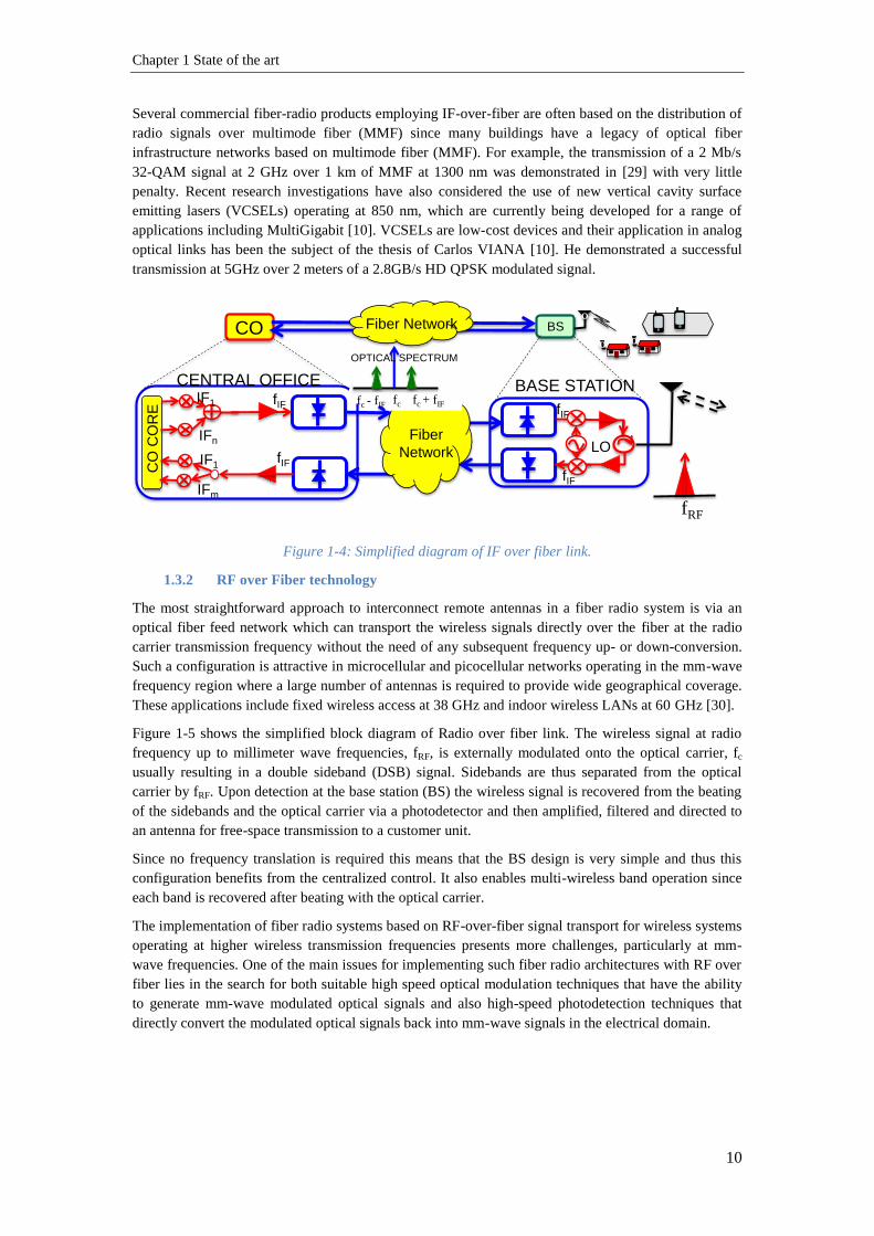
Chapter 1 State of the art
10
Several commercial fiber-radio products employing IF-over-fiber are often based on the distribution of
radio signals over multimode fiber (MMF) since many buildings have a legacy of optical fiber
infrastructure networks based on multimode fiber (MMF). For example, the transmission of a 2 Mb/s
32-QAM signal at 2 GHz over 1 km of MMF at 1300 nm was demonstrated in [29] with very little
penalty. Recent research investigations have also considered the use of new vertical cavity surface
emitting lasers (VCSELs) operating at 850 nm, which are currently being developed for a range of
applications including MultiGigabit [10]. VCSELs are low-cost devices and their application in analog
optical links has been the subject of the thesis of Carlos VIANA [10]. He demonstrated a successful
transmission at 5GHz over 2 meters of a 2.8GB/s HD QPSK modulated signal.
Figure 1-4: Simplified diagram of IF over fiber link.
1.3.2 RF over Fiber technology
The most straightforward approach to interconnect remote antennas in a fiber radio system is via an
optical fiber feed network which can transport the wireless signals directly over the fiber at the radio
carrier transmission frequency without the need of any subsequent frequency up- or down-conversion.
Such a configuration is attractive in microcellular and picocellular networks operating in the mm-wave
frequency region where a large number of antennas is required to provide wide geographical coverage.
These applications include fixed wireless access at 38 GHz and indoor wireless LANs at 60 GHz [30].
Figure 1-5 shows the simplified block diagram of Radio over fiber link. The wireless signal at radio
frequency up to millimeter wave frequencies, fRF, is externally modulated onto the optical carrier, fc
usually resulting in a double sideband (DSB) signal. Sidebands are thus separated from the optical
carrier by fRF. Upon detection at the base station (BS) the wireless signal is recovered from the beating
of the sidebands and the optical carrier via a photodetector and then amplified, filtered and directed to
an antenna for free-space transmission to a customer unit.
Since no frequency translation is required this means that the BS design is very simple and thus this
configuration benefits from the centralized control. It also enables multi-wireless band operation since
each band is recovered after beating with the optical carrier.
The implementation of fiber radio systems based on RF-over-fiber signal transport for wireless systems
operating at higher wireless transmission frequencies presents more challenges, particularly at mm-
wave frequencies. One of the main issues for implementing such fiber radio architectures with RF over
fiber lies in the search for both suitable high speed optical modulation techniques that have the ability
to generate mm-wave modulated optical signals and also high-speed photodetection techniques that
directly convert the modulated optical signals back into mm-wave signals in the electrical domain.
IF1
CO
CO
RE
IFm
IF1
IFn Fiber
Network
CENTRAL OFFICE BASE STATIONfc + fIFfc - fIF fc
fRF
LO
CO BS
º
º ºFiber Network
OPTICAL SPECTRUM
fIF
fIF
fIF
fIF

Chapter 1 State of the art
11
Figure 1-5: Simplified diagram of Radio over fiber.
1.3.3 Baseband over Fiber technology
The wireless signal is transported as baseband over the optical fiber link. Upon reaching the BS it is
detected and converted to RF before being radiated as shown in Figure 1-6: In the baseband-over-fiber
approach the radio information for the radio carriers is transported to the receiver as a time-division
multiplexed data stream. The individual data channels are then demultiplexed, up-converted to
intermediate frequencies and then undergo a further frequency up-conversion to the required radio
frequency band via a local oscillator located at the receiver.
As with IF-over-fiber signal distribution, the effect of fiber dispersion is small, and this technology
permits to use matured and reliable RF and digital hardware for signal processing. Furthermore low-
cost optoelectronic devices with low bandwidth can be employed [30]. However, the need for
frequency conversion at both transmitter and receiver complicates the system architecture design. The
additional LO source and extensive signal processing hardware (frequency conversion, multiplexing
and demultiplexing of signals) in the antenna station may also limit the upgradability of the overall
fiber radio system based on baseband-over-fiber signal transport.
Figure 1-6: Simplified diagram of base band over fiber link.
In general, to implement RoF techniques we need high speed photodetector, optical light source,
optical modulator in case of external modulated systems, as well as optical and microwave
interconnections. In this chapter we are going to study the state of the art of these very important
components of the RoF technology. In the first section we summarize the state of the art of optical and
LO
IF1
CO
CO
RE
IFm
IF1
IFn Fiber
Network
CENTRAL OFFICEBASE STATIONfc + fRFfc - fRF fc
fRF
CO BS
º
º ºFiber Network
OPTICAL SPECTRUM
fRF
fRF
fRF
fRF
CO
CO
RE
fc
Fiber
Network
CENTRAL OFFICE BASE STATION
fRF
LO
IFn
IF1
IFm
IF1
CO BS
º
º ºFiber
Network
fRF

Chapter 1 State of the art
12
electrical interconnections and then optical source, photodetector and optical modulator respectively
mainly based on Si technology.
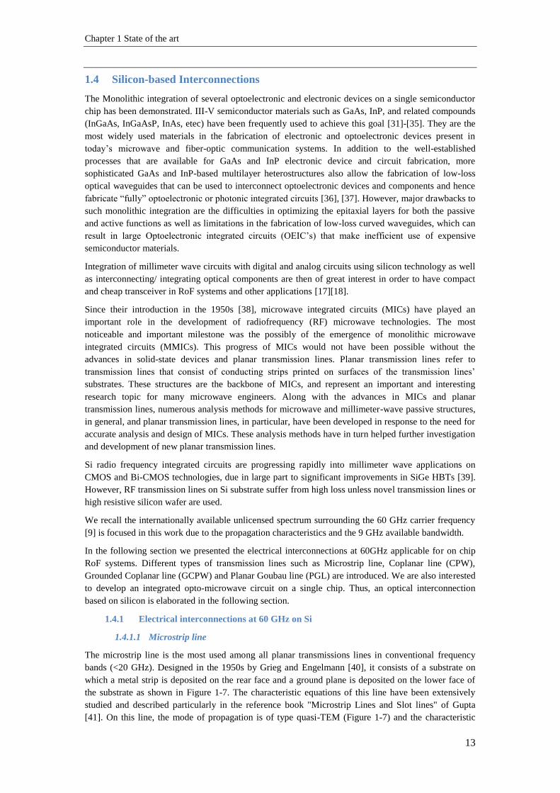
Chapter 1 State of the art
13
1.4 Silicon-based Interconnections
The Monolithic integration of several optoelectronic and electronic devices on a single semiconductor
chip has been demonstrated. III-V semiconductor materials such as GaAs, InP, and related compounds
(InGaAs, InGaAsP, InAs, etec) have been frequently used to achieve this goal [31]-[35]. They are the
most widely used materials in the fabrication of electronic and optoelectronic devices present in
today’s microwave and fiber-optic communication systems. In addition to the well-established
processes that are available for GaAs and InP electronic device and circuit fabrication, more
sophisticated GaAs and InP-based multilayer heterostructures also allow the fabrication of low-loss
optical waveguides that can be used to interconnect optoelectronic devices and components and hence
fabricate “fully” optoelectronic or photonic integrated circuits [36], [37]. However, major drawbacks to
such monolithic integration are the difficulties in optimizing the epitaxial layers for both the passive
and active functions as well as limitations in the fabrication of low-loss curved waveguides, which can
result in large Optoelectronic integrated circuits (OEIC’s) that make inefficient use of expensive
semiconductor materials.
Integration of millimeter wave circuits with digital and analog circuits using silicon technology as well
as interconnecting/ integrating optical components are then of great interest in order to have compact
and cheap transceiver in RoF systems and other applications [17][18].
Since their introduction in the 1950s [38], microwave integrated circuits (MICs) have played an
important role in the development of radiofrequency (RF) microwave technologies. The most
noticeable and important milestone was the possibly of the emergence of monolithic microwave
integrated circuits (MMICs). This progress of MICs would not have been possible without the
advances in solid-state devices and planar transmission lines. Planar transmission lines refer to
transmission lines that consist of conducting strips printed on surfaces of the transmission lines’
substrates. These structures are the backbone of MICs, and represent an important and interesting
research topic for many microwave engineers. Along with the advances in MICs and planar
transmission lines, numerous analysis methods for microwave and millimeter-wave passive structures,
in general, and planar transmission lines, in particular, have been developed in response to the need for
accurate analysis and design of MICs. These analysis methods have in turn helped further investigation
and development of new planar transmission lines.
Si radio frequency integrated circuits are progressing rapidly into millimeter wave applications on
CMOS and Bi-CMOS technologies, due in large part to significant improvements in SiGe HBTs [39].
However, RF transmission lines on Si substrate suffer from high loss unless novel transmission lines or
high resistive silicon wafer are used.
We recall the internationally available unlicensed spectrum surrounding the 60 GHz carrier frequency
[9] is focused in this work due to the propagation characteristics and the 9 GHz available bandwidth.
In the following section we presented the electrical interconnections at 60GHz applicable for on chip
RoF systems. Different types of transmission lines such as Microstrip line, Coplanar line (CPW),
Grounded Coplanar line (GCPW) and Planar Goubau line (PGL) are introduced. We are also interested
to develop an integrated opto-microwave circuit on a single chip. Thus, an optical interconnection
based on silicon is elaborated in the following section.
1.4.1 Electrical interconnections at 60 GHz on Si
1.4.1.1 Microstrip line
The microstrip line is the most used among all planar transmissions lines in conventional frequency
bands (<20 GHz). Designed in the 1950s by Grieg and Engelmann [40], it consists of a substrate on
which a metal strip is deposited on the rear face and a ground plane is deposited on the lower face of
the substrate as shown in Figure 1-7. The characteristic equations of this line have been extensively
studied and described particularly in the reference book "Microstrip Lines and Slot lines" of Gupta
[41]. On this line, the mode of propagation is of type quasi-TEM (Figure 1-7) and the characteristic

Chapter 1 State of the art
14
impedance for a given permittivity, is determined mainly by the w / h ratio, where w is the line width
and h is the height of the dielectric substrate.
Figure 1-7: Cross section of micro strip line with associated electric field lines
Microstrip line technology offers both simplicity and ease of implementation and integration in
microwave devices. They are used at frequencies ranging from a few MHz to a few tens of gigahertz.
At higher frequencies, in the millimeter band, the losses in the dielectric and in the metal as well as
radiation losses become important. Higher order modes also appear and cause problems. At high
frequency, the manufacturing tolerances become also very difficult to meet because of the small size
and the technology used. However, this type of line makes it easy to insert series elements, even though
it is necessary to penetrate the substrate for the inclusion of discrete components in parallel. Of course
it is not easy to do so. "Via hole" in the circuits are technologically difficult to realize at high frequency
due to their small dimensions.
Several types of novel microstrip transmission lines exist to minimize losses on silicon substrate at
high frequency, such as inverted micro-strip line as presented in [42] [43], Thin Film Microstrip line
(TFMs) [44] [45] and Microshield line or Shielded membrane microstrip [46]. TFMs lines are created
by depositing a metallic ground plane, and thin insulating layers on silicon wafer, before printing the
microstrip line (Figure 1-7).
In [44], TFMs lines are characterized for strip widths of 23µm and 52µm, polyimide thickness of
11.05µm on low resistive (2Ω.cm) silicon wafer. These TFMS transmission lines have characteristic
impedances of 53Ω and 31Ω respectively and a minimum attenuation of 0.3dB/mm at 20 GHz.
Another TFMs work is presented in [45] on low resistive silicon wafer for a metal strip widths of 3µm
and 9.2µm which leads to the characteristic impedances of 68Ω and 44Ω, and attenuations of 1.2
dB/mm and 1 dB/mm respectively.
Table 1-1: Summary of the state of the art of Microstrip lines for different technologies on silicon
Material Thickness
(µm)
α(dB/mm) ρ of Si
(Ω.cm)
F(GHz) reference comment
Polyimide 20 0.14 10 60 [47] suspended
polyimide 7.4 0.4 No
effect
60 [48]
air 10 1.4 5 8 [49] inverted
air 100 0.02 4000
(HR Si)
8 [49] inverted
1.4.1.2 . Coplanar line (CPW)
The coplanar line (Figure 1-8) consists of a central metal strip and a pair of ground planes separated by
two identical slots located on the same face of the substrate. W represents the width of the signal line,
while s is the distance between the signal line and the ground conductors. This architecture has been
used extensively in MMICs due to its easy fabrication and flexibility of design [50].
Substrate
h
w

Chapter 1 State of the art
15
Figure 1-8: Cross section of the coplanar line with E-field lines associated to the odd mode
This structure shows two possible modes of propagation:
An even mode, quasi-TE and dispersive.
An odd mode, quasi-TEM and dispersive (Figure 1-8).
The odd mode is used in most of the devices. To prevent the even mode propagation, the ground planes
of the coplanar line are connected by a metallic structure so that they are at the same potential, which
has the effect of cancelling the even mode. The connecting devices used between ground planes are
ribbons (air bridge). The coplanar line radiates weakly at high frequencies due to the uneven structure
of the electric field. As indicated in Figure 1-8, there are a little field lines penetrating into the
dielectric thereby line losses are reduced and it makes coplanar lines interesting at high frequencies.
Another characteristic of the coplanar lines is that they are less sensitive to the thickness of the
dielectric substrate than microstrip lines. Besides, the topology of this line permits an easily integration
of discrete components either in series or parallel.
Coplanar transmission lines have been extensively studied in many research groups both at low and
high frequencies by using different types of technologies [50]. A few works have also been done for
CPW on low resistive silicon substrate [39] [51]-[53]. In CMOS and BiCMOS technologies, the quality
factor of the transmission lines implemented on low resistive silicon substrate is much lower than on a
semi-insulating GaAs, InP and high resistive silicon substrates. Improving the performance of such a
CPW line through elevating them away from the lossy substrate, using additional layers of low loss
dielectric materials, has been recently investigated [39] [51]-[53] as shown in Figure 1-9. To minimize
the loss in these technologies a photolithographic process is performed by using polymers on low
resistive silicon to obtain CPW line elevated with respect to the substrate.
Figure 1-9: Coplanar line on low resistive silicon with a polymer layer used to elevate the conductor
lines away from the substrate.
A summary of the performances of coplanar line fabricated on low resistive silicon substrate with
different types of polymer interface is presented in Table 1-2. A coplanar line fabricated on 75Ω.cm
resistivity silicon and elevated away from the substrate by 26µm SU8 reaches a minimum loss of
0.1mm/dB at 10GHz [53]. In [39], a coplanar line on 2Ω.cm silicon substrate with 25µm or 125µm
SU8 polymer interface is presented. The minimum attenuation achieved at 60GHz frequency is
4mm/dB and 0.7mm/dB respectively. On 10Ω.cm silicon substrate with 10µm BCB dielectric interface
an attenuation of 0.6dB/mm is measured at 50GHz [51].
hSubstrate s
Ground contact Metal strip (w) Ground contact
LR Silicon
polymer polymer
metal Strip, s w
slot w

Chapter 1 State of the art
16
Table 1-2: Summary of the state of the art of coplanar lines on low resistive silicon substrate with a
polymer layer used to elevate the metal away from the substrate.
Polymer
type
Thickness
(μm)
α(dB/m
m)
f(GHz) ρ of Si (Ω.cm) reference comment
SU8 25 4 60 2 [39]
125 0.7 60 2 [39]
26 0.1 10 75 [53]
BCB 10 0.6 50 10 [51]
Parylene 15 0.56 40 10 [52] 5μm oxide
on Si &
then
parylene
oxide 5 1.85 40 10 [52]
1.4.1.3 Planar Goubau line (PGL)
Research efforts are continuously devoted to transmission line studies, and new types of transmission
line are proposed and investigated. The original Goubau line (a single circular conductor surrounded by
a uniform dielectric coating in free space) was analyzed in the 1950s [54] [55]. The dielectrics
surrounding the conductor help to confine the field around the wire. Standard circular Goubau line and
planar Goubau line have been studied for mm-waves (below 100GHz) and sub-millimeter waves
(above 100GHz) applications [56]-[57]. They are mainly used in the field of THz (100 GHz to 10 THz)
[59].[60]. Planar Goubau line [61] consists of a metallic ribbon on a dielectric, the propagation medium
of the field contains several materials (substrate and air see Figure 1-10). The parameters influencing
the line properties are the dielectric thickness, the substrate resistivity or tangent loss and the
permittivity [62].
Figure 1-10: Cross section of the Planar Goubau line with E-field lines shown.
Planar Goubau lines are simple to fabricate, low cost and have wide bandwidth. PGL on an alumina
ceramic substrate (relative dielectric constant 9.9 and 0.254mm thick) is used in [63] at frequencies
between 40GHz and 60GHz. Low loss (0.064dB/mm @ 60GHz) Goubau line on high resistive silicone
in the 57-64 GHz band was investigated in [64].
1.4.2 Optical interconnections
Optical interconnection is the technology of interconnecting various optical devices and components
for the generation, focusing, splitting, combining, isolating, polarization, coupling, switching,
modulation and detection of light, all on a single chip, or chip to chip, or between boards. Optical
waveguides can be used to provide the connections between these components. An optical waveguide
is a light conduit consisting of a slab, strip or cylinder of dielectric material surrounded by another
dielectric material of lower refractive index. The light is transported through the inner medium without
Substrate
h
Chapter 1 State of the art
17
radiating into the surrounding medium. The most widely used of these waveguides is the optical fiber,
which is made of two concentric circular cylinders of low loss dielectric materials such as glass.
In the last two to three decades, the optical interconnections have been widely employed in high-speed
transmission because of their characteristics of high information capacity, no noise emissivity,
transmission security, low loss, and low weight [65]-[68]. Optical interconnections are replacing the
electrical interconnections not only for long distance communication but optical interconnections are
also being developed for chip to chip[69]-[71], or on chip [72]-[74] communications as well.
Progress in computer technology is becoming increasingly dependent on faster data transfer between
and within microchips [75]. Optical interconnections may provide a way forward, and silicon photonics
has been proven to be particularly useful, once integrated on the standard silicon chips [76]-[78]. Thus,
silicon based optical waveguides are hot research issues for low cost and high data transfer
interconnections. The high index contrast in Si core and SiO2 coating makes Si/SiO2 waveguide one of
the most popular components. An attempt to lower propagation loss, on a SiO2 core waveguide was
discussed in [72] at wavelength spectra of 650-1300nm.
From the viewpoint of the signal transmission rate, silicon is however not the best waveguide material.
Its high refractive index (n=3.4–3.5) reduces the light speed. A polymer waveguide has a lower
refractive index (n= 1.3) and produces a shorter delay than Si waveguides [74]. The use of polymer
waveguides for on-chip optical interconnection also allows a multistep fabrication process whereby it
is possible to first optimize the processing of the semiconductor devices and then fabricate the polymer
waveguide structures for the optical signal distribution system [79]. Polymers offer high thermal,
chemical and environmental stability, low optical losses, good dielectric properties, low cost, ease of
processing and compatibility with semiconductor processing technology, and represent an interesting
alternative to semiconductor materials as light distribution systems [80].
In 2012, IBM announced that it had achieved optical components, based on silicon photonics
technology, at the 90 nanometer scale that can be manufactured using standard techniques and
incorporated into conventional chips [81] [82]. It has already demonstrated optical transceivers
exceeding 25 Gbit/s per channel [82]. In September 2013, Intel announced a completely integrated
module that includes silicon modulators, detectors, waveguides, hybrid silicon laser and circuitry that
transmits data at speeds of 100 Gigabits per second [83].
Chapter 1 State of the art
18
1.5 Optical Sources
We can categorize laser diodes according to device structure in three main types being Fabry Perot
(FP), distributed feedback and distributed Bragg reflected laser (DFB) and vertical cavity surface
emitting lasers (VCSELs). The first two are Edge Emitting lasers (EEL), whereas VCSELs are surface
emitting lasers. Differences between VCSELs and the Edge Emitting lasers (EEL) are shown in figure
1.9. The main difference is the optical aperture which is on the top for a VCSEL and on the side for an
EEL. As an EEL has a longer active layer it generates higher optical power. Nevertheless, the reduced
active layer of the VCSELs induces a lower threshold current and higher operation speed. The small
lasing cavity of the VCSEL, shown in Figure 1-11 a), requires mirrors with very high reflectivity.
Figure 1-11: Physical structure of VCSEL (a) and EEL (b).
It is clear that VCSELs are more efficient regarding their low power consumption, single mode
operation (SM), and high optical efficiency. The main advantage of the EELs is their high optical
power.
VCSELs have numerous advantages. As a vertical emission laser, it gives the capability of on wafer
level testability and 2-D array production which reduce the cost. Their circular and low divergent
optical beam facilitates the alignment and packaging into the optical fiber. The low volume of the
optical cavity allows a single mode operation and high speed operation. The low cost crops up in the
development of VCSELs and Si LEDs, in particular for their implementation in short range optical
interconnections (within a building and on a chip).
Many industrial companies, universities and research laboratories have focused their activities on high
speed VCSELs emitting at different wavelengths and low cost Si LEDs. Moving from shorter
wavelengths (650, 750, 850, 980, 1100 nm) to longer ones (1300 and 1550 nm) the VCSEL technology
complexity increases as well as the cost. Thereby, in the recent years, the shorter wavelength optical
sources and low cost Si LEDs with a potential to be integrated into CMOS based optical interconnect
on a single chip become of a big interest [84]-[86]. Thus we will focus our discussion on low
wavelengths with a special interest in 850 nm VCSEL and Si LED.
1.5.1 Light Emission device in III-V materials
850 nm is the most interesting wavelength for LAN applications and 850nm VCSEL will surely keep
playing an important role in the further future of optical communications. Different materials for active
region can be used and have been reported, including GaAs [87] [89]-[94], InGaAs [20]-[22] and
InGaAlAs [95]. New concepts in order to increase the VCSEL performances, like the bandwidth
modulation, have been applied, including optical/electrical confinement techniques: oxide aperture [93]
[94], proton implantation [20] [89], Photonic Crystals (PhC) [96] [94] and a few years ago back double
oxide aperture [97]-[100]. Bit rates up to 40 Gbit/s have been reached recently [97] [95] [101] using
double oxide aperture and InGaAs quantum wells (QW), with an aperture diameter of 6 µm - 9µm.
Light
Quantum Well layer
Top DBR Mirror
Bottom DBR Mirror
substratecontact
contact ring
polyimide
active area
Heat sink
light-guiding layers
contact
contact
Light
substrate
a) b)

Chapter 1 State of the art
19
In the case of 980 nm VCSELs, active region materials can be GaAs [94] [101] or InGaAs [102] [103]
[104] [105]. Bit rates up to 35 Gbit/s have been achieved recently [227] using tapered-deep-oxide
aperture with an aperture diameter of 3 µm and using InGaAs QW.
The most recent 1100 nm VCSEL devices make use of InGaAs [106] [107]. Bit rates up to 40 Gbit/s
have been achieved [108] using tapered-deep-oxide aperture with an aperture diameter of 5µm.
1.5.2 Light Emission device in Silicon
Unfortunately, silicon is an indirect bandgap semiconductor, and, therefore, fabricating integrated
lasers is a challenge. The most successful approaches to fabricate lasers on silicon are based on hybrid
or heterogeneous integration of III-V materials [246].
However, various researchers have highlighted the need for small-dimension light emitters which are
compatible with mainstream silicon CMOS integrated circuit technology [84]-[86]. Light emission
from silicon devices has previously been performed in reverse-biased silicon p-n avalanche structures
[109]-[112]. It has been postulated that light emission occurs from these structures through phonon
assisted intra-band and inter-band recombination phenomena [109] [110].
In particular, Kramer et al [111] and Snyman et al [112] realized the first Si LED light emitting devices
utilizing current density and surface engineering technology. Snyman et al have succeeded in obtaining
practical and usable light emitting devices (Si LED’s) using standard CMOS design and processing
technology [111] [112]. Recently, models have been presented which postulate that enhanced light
emission can be obtained in these devices through carrier energy and carrier momentum engineering
[113] [114].
In [242], an optical emission intensities of about 100nW μm-2
were subsequently measured on silicon
avalanche LED when the total active emission areas are considered at the device surface. About 1nW
μm-2
and 0.5nW μm-2
optical emission intensity on silicon LEDs were measured in [243] and in [114]
respectively.
Because of the easy integration in CMOS technology, these type of devices show great potential to be
integrated into CMOS based optical interconnects, optical RF connection systems and lab-on chip
micro-photonic systems. Although present emission levels are sufficient in order to sustain diverse
applications, a higher emission power is desirable.

Chapter 1 State of the art
20
1.6 Photodetectors
1.6.1 Introduction
A photodetector is the device that detects the optical power and then converts it into electrical power.
Photodetector devices perform photodetection. The performance of an optical detector can be
determined by its ability to detect the smallest possible optical power and to generate a maximum
electric power at the output with an absolute minimum degree of distortion. Optical detection must also
exhibit a wide Bandwidth and sharp response to accommodate high bit rate criteria. Besides its ability
to interface with optical cables, a long operating life, cost, fast response, low noise, high reliability are
desirable criteria.
In the last decade there has been a considerable interest for photodetectors bandwidth increment. This
results in arrival of new types of high speed photodiodes based on InP/InGaAs for long distance
communication systems. However, nowadays the bandwidth requirement of the last mile (home area
networks) is increasing and thereby high cost efficiency of integrated transceivers is of great interest.
As a result some researchers on this area are working on SiGe/Si technologies, which are cheap and
easy to integrate [23] [115]-[119].
1.6.2 Photodetector Material Choices
High speed photodetectors are used in the implementation of the different Radio over Fiber systems as
discussed in the previous section. These devices are required in telecommunication systems and in high
capacity optical based networks. There are different materials that are used in the implementation of
these photodetector structures. The use of the materials that are matched to a specific wavelength and
optimized for high speed operation is a key activity in the research for very high speed discrete
photodetectors. This is specially the case in telecoms applications where the performance is the major
criterion.
Based on the operating wavelength, Semiconductor materials can be categorized into:
1. Detector materials for long-haul communication systems
InGaAs (slightly tunable gap) direct bandgap, ternary alloy. Excellent material for long-haul
communications (λ = 1.55 μm), grown (lattice-matched) on InP substrates
InGaAsP (slightly tunable gap), direct bandgap, quaternary alloy. Material for long-haul
communications (λ = 1.55 μm), grown (lattice-matched) on InP substrates
AlGaSb (tunable gap) [122], direct bandgap, ternary alloy. Material for long-haul
communications (λ = 1.55 μm). Poor substrate choice (GaSb), not competitive with InP at
present. Interesting material for low-bandgap (high mobility) electronics, less developed than
InGaAsP
2. Detector materials for LANs communication
GaAs (AlGaAs), direct bandgap, somewhat tunable gap, ternary alloy. Cannot be used for
long-haul communications, only suited for LAN applications (λ = 0.85μm). Excellent
substrate availability (GaAs), mature technology, low-cost; compatible with AlGaAs lasers.
Si, indirect bandgap. Cannot be used for long-haul communications since it cannot absorb
light at at related high wavelengths. Well suited for LANs, OK for avalanche photodiodes.
Excellent substrate availability (Si), mature technology, low-cost.
3. Detector materials for LAN and long-haul
Ge, indirect bandgap, bulk material. Can be used for long-haul communications but also for
LANs (high secondary absorption edge due to direct processes). Excellent possibilities for
avalanche photodiodes. Good substrate availability (Ge), mature technology, medium cost.
Recently revived by the emergence of high-speed SiGe technologies integration with Si-based

Chapter 1 State of the art
21
ICs.
Silicon based photodetectors are commonly used for wavelengths from 400nm up to1000nm.
Germanium is used for photodetectors at long wavelengths up to 1800nm. Due to the indirect
bandgap of Silicon and Germanium at these wavelengths, they have relatively small bandwidth
efficiency products.
As Silicon is abundant and has relatively low processing cost, there have been a lot of research
activities to develop high speed photodetectors that are based on Silicon. This permits to monolithically
integrate detectors with high speed electronic circuits that are needed for the processing of the detected
optical signals [120]. One aspect of these researches aims to extend the spectral response of Silicon
based detectors so that they can be used in the telecoms at wavelength such as 1310nm. This involves
the use of Germanium [118] [121] and SiGe based photodetectors [116].
1.6.3 Photodetector Structures and frequency limitations
The bandwidth of a photodetector is mainly limited by carrier transit time and RC time constant.
Carrier transit time is the time taken by the photo-generated carriers to travel across the high-field
region. It is usually dominated by holes transit time as holes typically have lower drift velocity than
electrons in common photodetector materials. The RC time constant is determined by the equivalent
circuit parameters of the photodiode and the load circuit. Diode series resistance (due to ohmic contacts
and bulk resistances), load impedance and the junction and parasitic capacitances contribute to the RC
time constant. Diffusion time becomes important when the photocurrent due to carriers absorbed in the
p and n contact regions within about one diffusion length at the edge of the depletion region becomes
comparable to the current arising from the photo-generated carriers within the depletion region.
Generally factors that affect photodetector speed can be categorized into three mechanisms depending
on the device structure.
1. Intrinsic cut-off mechanisms
Device capacitance (due to junction and /or parasitic)
Minority carrier life time ( in the case of photoconductor)
Active region transit time (PIN, APD)
Avalanche build up time (APD)
Internal gain cut-off frequency (in phototransistors)
2. External mechanisms: external parasitic or load capacitance
3. Light and RF signal velocity mismatch: in distributed photodetectors
Based on the way of the optical signal injected into the photodetector (PD) structure, the high speed
PDs may be classified in three classes: surface-illuminated, resonant-cavity-enhanced and edge coupled
PDs (Figure 1-12). Besides, in regard to their microwave properties they can be divided in lumped and
distributed PDs.
Figure 1-12: The main trends in the progress of high speed photodetectors[130]
PIN
MSM
UTC PD WGPD
Surface illuminated
RCEPDLumped
TWPD
VMPD
distributed
Improve BW & saturationImprove η
Edge coupled
Improve BW & saturation

Chapter 1 State of the art
22
Usually the quality of the different types of high-speed PDs is characterized by the bandwidth-
efficiency product. For surface-illuminated PDs this parameter usually does not exceed 20-30 GHz
(BW*efficiency) [122] due to trade-off between quantum efficiency and bandwidth. The increase of
the quantum efficiency requires increasing the PD absorption layer thickness, whereas to increase the
bandwidth requires reducing it. This trade-off can be overcome by means of resonant-cavity-enhanced
PDs, in which PD is placed in a Fabry-Perot resonator. Optical radiation passes through the thin
absorption layer many times and quantum efficiency increases at the resonant wavelength. In the edge-
coupled PDs, optical wave propagates in perpendicular direction to the charge carrier transport. In this
case, it is necessary to increase the device length instead of the absorption layer thickness, in order to
increase the quantum efficiency.
For some novel microwave optoelectronic systems it is necessary to have high-speed PDs with large
saturation current, for example, in systems using optical amplifier as a preamplifier in the photo-
receiver. PDs with high saturation current are needed also for such applications as photonic generation
of millimeter waves and photonic measurements of the high-speed electronic devices [216]. The
saturation of a photocurrent under high optical power is connected to screening of an internal electrical
field of the PD by photo-carriers (space-charge effect). To increase the PD bandwidth, in general, it is
necessary to decrease the absorption layers volume. In this case the optical power density incident into
the PD is increased. So there is a trade-off between bandwidth and high saturation current. This general
trade-off is overcome in distributed photodetectors such as TWPD and VMDP (Figure 1-12). The
bandwidth of the distributed PDs is limited by the difference between propagation velocities of light
wave and microwave as well as by the microwave losses. So the length and width of the absorption
layer can be made rather large compared with the lumped PDs [123] [124] [125]. On the other hand,
improving the saturation current can be achieved by optimizing carrier dynamics, which has been done
in UTC PDs [126]. Thus, there are two main trends in the development of high-speed PDs. The first is
suited for the development of PDs with high bandwidth-efficiency product and the second is related to
the development of high-speed PDs with high saturation current [127] [122] [128].
1.6.3.1 PIN Photodetector
A p-i-n photodiode consists of p and n regions separated by a very lightly doped intrinsic (i) region as
indicated in Figure 1-13. The intrinsic layer contains only a very small amount of dopants and acts as a
wide depletion layer. In normal operation, a sufficiently large reverse bias voltage is applied across the
device so that the intrinsic region is fully depleted of carriers. At longer wavelengths, light penetrates
more deeply into the semiconductor material.
Light is incident on depletion region so photo-generated carriers are generated in the depletion region.
Due to the high electric field induced across the depletion region, the carriers separate and are collected
by the reverse biased voltage. This causes a current flow in the external circuit which is referred as
photocurrent.
The performance of p-i-n photodiodes can be improved by using a double heterostructure design. The
intrinsic layer is sandwiched between p-type and n-type layers of a different semiconductor whose
band gap is chosen such that light is absorbed only in the middle i-layer. As an example Figure 1-13
shows a p-i-n photodiode made of InGaAs for the intrinsic layer and InP for the p-type and n-type
access layers.

Chapter 1 State of the art
23
Figure 1-13: Schematic structure (right) and band diagram with structure (left) of a pin photodiode in
reverse bias. Jdr and Jd are drift and diffusion current densities, respectively
Compound semiconductor pin structures are today probably among the best components available for
10 Gbps and 40 Gbps systems. Cut-off frequencies higher than 67 GHz have been demonstrated [129].
Usually, a compromise must be reached between speed and responsivity (efficiency); the device speed
is dominated by transit time and the parasitic capacitance. Such limitations can be overcome in more
advanced structures such as traveling-wave waveguide photodiodes.
a) The pin PD photocurrent, responsivity and efficiency
The main contribution to the photocurrent is given by the drift current associated with carriers
generated inside the intrinsic depleted region; secondary contributions (which disappear in
heterojunction devices) come from the diffusion regions. Due to the large width of the depletion region
W, the optical generation rate will be non-uniform, according to the law:
1
0in x x
opt i opt
P RG x e G e
Ahf
(1.1)
Where ηi is the intrinsic quantum efficiency, Pin the total incident power on the lateral (upper)
photodiode detection facet, A is the detector area, hf is the photon energy, α is the material absorption,
Gopt is the optical generation and R is the power reflectivity of the detection surface.
The total photocurrent is the contribution of both the drift (from the intrinsic layer) and diffusion (from
the surface and substrate layers) carriers’ movement: Iph + Idr + Idff.
By ignoring the dark current the photocurrent can be expressed as:
1 11
p
ww
ph i in
hn
q eI P R e
hf L
(1.2)
Where Lhn is the length of diffusion region, wp is the width of p doped region and w is the width of the
depletion region.
Thus the responsivity is:
1 11
p
wwph
i
in hn
I q eR R e
P hf L
(1.3)
And external efficiency is:
1 11
p
phw
w
ext iin hn
Ieq
R eP L
hf
(1.4)
n+ InP substrate
i InGaAs absorption layer
p+ InP top layer
n-contact
p-contact
hf
W
Wp

Chapter 1 State of the art
24
The diffusion contributions to currents are much smaller than the drift contributions in dynamic
operation, and should be reduced to optimize the high-speed response. This can be immediately
achieved in heterojunction devices, where the substrate layer below the absorption region is of wide
gap and therefore does not appreciably absorb light. The maximization of ηext requires that the
thickness of the top layer is small, or that the top layer is of wide gap, (i.e. transparent to the incoming
light). For high-speed, high-efficiency photodiodes αwp → 0 and αLhn → 0, the external device
quantum efficiency and responsivity are:
1 1 w
ext i R e (1.5)
1 1 w
i
qR R e
hf
(1.6)
b) The pin PD Frequency Response
There are four main mechanisms that limit the speed of pin photodiodes under dynamic excitation
[122]:
1. The effect of the total diode capacitance, including the depleted region diode capacitance
and any other external parasitic capacitance.
2. The transit time of the carriers drifting across the depletion layer.
3. The diffusion time of carriers generated outside the undepleted regions (mainly in
homojunction devices).
4. The charge trapping at heterojunctions (in heterojunction devices).
Transit time effects are negligible in pn junction photodiodes owing to the small depletion region
width, but become a dominant mechanism in pin devices. Transit time and RC cutoff are thus the main
limitations in technology-optimized pin photodiodes.
There are two extreme frequency behaviors of a transit limited bandwidth Photodiode:
Thick diode (αW >>1): the frequency response is mainly limited by the velocity of minority
carriers generated at the illuminated side. For p+ side illuminated pin, the 3dB electrical
bandwidth is limited by electrons saturation velocity (Vn,sat) [17] [122] [130]:
,
3 , 0.443n sat
dB tr
vf
w (1.7)
For n+ side illuminated pin, the 3dB electrical bandwidth is limited by holes saturation
velocity (Vh,sat) [17] [122] [130]:
,
3 , 0.443h sat
dB tr
vf
w (1.8)
Since the holes are slower than electrons, illumination should come from the p+ side to
maximize the device speed.
Assuming, on the other hand, that both carriers have the same transit time we can have the
approximate expression [17] [122] [130]:
𝑓3𝑑𝐵,𝑡𝑟 =1
2.2𝜏𝑡 𝑤ℎ𝑒𝑟𝑒 𝜏𝑡 𝑖𝑠 𝑡ℎ𝑒 𝑒𝑙𝑒𝑐𝑡𝑟𝑜𝑛 𝑜𝑟 ℎ𝑜𝑙𝑒 𝑡𝑟𝑎𝑛𝑠𝑖𝑡 𝑡𝑖𝑚𝑒
The diode is thin (αW << 1); in this case, the generation of pairs along the i layer is almost
uniform and the frequency response is limited by both carriers; an approximation of the cut-off
frequency is given by[17] [122] [130]:

Chapter 1 State of the art
25
3 , 4 4 4
, ,
3.5 1 1 1 1,
2 2dB tr
n sat h sat
vf where
w v v v
(1.9)
From these computations it is clear that transit time limited cut-off frequency increases with decreasing
the absorption region thickness w.
The cut-off frequency of pin photodiode is also highly limited by the total diode capacitance that can
be deduced from the PD equivalent circuit. In Figure 1-14, Cp is the external diode parasitic
capacitance and Rs the series parasitic diode resistance, RD the parallel diode resistance, Cj the intrinsic
capacitance (dominated by the intrinsic layer capacitance). Usually it is considered that RD >> Rs, RL.
Figure 1-14: Simplified pin photodiode equivalent circuit
From the equivalent circuit we can also estimate the RC-limited cut-off frequency. Thus the 3 dB RC-
limited photodiode bandwidth is given by [17][122] [130]:
3 ,
1, ,
2
sdB RC s s j p j
Af where R R R and C C C C
RC w (1.10)
The total cutoff frequency resulting from the transit time and RC effect can be evaluated at a circuit
level. An approximate expression is:
32 2
3 , 3 ,
1dB
dB RC dB tr
ff f
(1.11)
In general in PIN PD the external efficiency (ηx) and the RC limited band width (f3dB,RC )increase with
the thickness of the active region (W). However, the transit limited bandwidth (f3dB,tr) decreases when
the active area thickness increases. When the surface area (A) of the PD increases the external
efficiency increases whereas RC limited bandwidth decreases. Thus, there is a tradeoff between
external efficiency and bandwidth in PIN photodetector structure.
c) Bandwidth efficiency trade-off
In a vertically illuminated photodiode, optimization of the external quantum efficiency suggests W >>
Lα = 1/α (absorption length); moreover, the detection area A should be large in order to improve the
coupling with the external source (e.g.an optical fiber). However, increasing the active area thickness
increases the RC-limited bandwidth (since it decreases the junction capacitance) but decreases the
transit time-limited bandwidth. Increasing the device area has no influence on the transit time-limited
bandwidth but makes the capacitance larger and therefore decreases the RC-limited bandwidth (Figure
1-15 b)). Keeping the device area A constant, we therefore have 𝑓3𝑑𝐵,𝑅𝐶 ∝ 𝑊 but 𝑓3𝑑𝐵,𝑡𝑟 ∝ 1/W. Since
𝑓3𝑑𝐵 < min (𝑓3𝑑𝐵,𝑅𝐶 ,𝑓3𝑑𝐵,𝑡𝑟), the total bandwidth is dominated by 𝑓3𝑑𝐵,𝑅𝐶 ∝ W (low W) or 𝑓3𝑑𝐵,𝑡𝑟∝
1/W (large W). The total bandwidth then first increases as a function of W, then decreases (Figure 1-15
a)). f3dB therefore has a maximum, which shifts toward smaller values of W and larger cut-off
frequencies with decreasing A. At the same time, the efficiency always increases with W. As a
consequence, high-frequency operation (high f3dB) requires small-area diodes, with small W and
consequently poor efficiency (Figure 1-15 c).

Chapter 1 State of the art
26
Figure 1-15: High speed pin optimization: trade-off between speed and efficiency.
1.6.3.2 Uni Travelling Carrier Photodiode-UTC PD
In PIN diode, under the effect of the applied reverse voltage electric field appears in the intrinsic region
i, electrons are thus directed to the N doped zone and holes are directed to the P doped zone. These
charges create a space charge region, generating an electric field .This new electric field can interfere
with the internal electric field due to reverse voltage, thus carriers are delayed. Hence the carrier delay
is the principal cause of non-linearity.
Figure 1-16: UTC photodiode energy diagram
Another way to enhance both the bandwidth and the saturation current of the traditional p-i-n PD is to
use only fast electrons for charge carrier transport, that is achieved in the UTC PDs [17] [130] [134]
[217] [218]. The principle of this PD is based on the fact that absorption occurs in p doped zones
followed by large gap i zones. Holes generated in zone p are absorbed in the same zone with a very
short relaxation time. However, electrons move via diffusion from zone p towards zone i where they
are captured and drift under the effect of the electric field present in the zone. Hence the space charge
in this zone is only due to electrons. Additionally, as long as the layer thickness is less than 0.2μm, a
velocity overshoot phenomena in InGaAs/InP UTC PD occurs meaning that electrons can move five
0 20 40 60 800
10
20
30
40
50
60
External Efficiency (%)
3dB
Ba
nd
wid
th (
GH
z)
[117]
[115]
[119]
[131]
[28]
[26]
[119]
[132]
[118]
0 0.5 1 1.5 2 2.5 30
10
20
30
40
50
60
70
Active region thickness (um)
3 d
B B
and
wid
th (
GH
z)
InGaAs PDs
SiGe PDs
[117][119]
[119]
[118]
[28]
[28]
[129]
[131]
0 1000 2000 3000 4000 5000 60000
10
20
30
40
50
60
70
surface Area of the PD (um squar)
3dB
Ba
nd
wid
th (
GH
z)
SiGe PDs
InGaAs PDs
[119][118]
[129]
[132]
[133]
[117]
[119]
[28]
[131]
[26] [115]
a b
c
Transit time limit RC constant limit
RC constant limit
Transit time limit
RC constant limit
Valence band

Chapter 1 State of the art
27
times the saturation velocity [17]. Therefore the transit-time limited bandwidth of the UTC PD with
thin absorption layer can be as high as 200 GHz and above [130]. Moreover, usage of a graded band
gap in the absorption p-layer creates an internal electric field and drift mechanism becomes dominant
in the absorption p-layer that results in even greater decrease of the transit time. The saturation current
of the UTC PD is determined by the space charge effect in the collector layer [17][130]. Since only
photoelectrons induce space charge effect the saturation current of the UTC PD is higher than for the
traditional p-i-n PD, in which both photo generated holes and electrons destroy the internal electrical
field of the p-n junction.
1.6.3.3 Resonant Cavity Enhanced Photodetector –RCE PD
One technique to overcome the bandwidth–efficiency limitations of the vertically illuminated PIN is to
try to increase the distance over which photons travel through the absorption region in order to
maximize optical absorption, while keeping the distance that the electron-hole pairs travel as small as
possible to minimize the transit time. This may be achieved through creating a resonant optical cavity
in order to set up multiple passes of the optical signal through the active region [17] [27] [119] [122]
[130] [137]-[139] as shown Figure 1-17, but the resonance leads to wavelength selectivity thus making
these devices of more interest for use in wavelength division multiplexed (WDM) systems. Due to
multiple propagation of optical radiation at the resonant wavelength through the absorbing layer, its
thickness can be reduced for receiving necessary bandwidth without any efficiency penalty. In this case
bandwidth-efficiency product can reach hundreds of GigaHertz [130].
Figure 1-17: Resonate cavity enhanced Photodetector structure.
This potodetector has high speed and high quantum efficiency. It was demonstrated in [137] 36GHz
3dB bandwidth and 70% external quantum efficiency can be achieved in a GaAs photodiode.
The RCE PD quantum efficiency can be expressed by the following formula [17][130]:
1 1 2 2 1 2
1 2
2[4 ( )/ ]
1 2
1 11
1
d
d
d j n d n d nd
R R ee
R R e e
(1.12)
where R1, φ1and R2, φ2 are the reflection coefficients and phase shifts of the forward and reverse
reflectors, n, α, d are the refractive index, absorption coefficient and thickness of the absorption
layer, 𝑛1, 𝑑1 𝑎𝑛𝑑 𝑛2, 𝑑2 are the refractive index and thickness of layers above and below the absorption
layer. The quantum efficiency is maximum at wavelength
𝜆0 when 4𝜋(𝑛1𝑑1 + 𝑛2𝑑2 + 𝑛𝑑) 𝜆0 + 𝜑1(𝜆0) + 𝜑2(𝜆0) = 2𝜋⁄ . The maximum efficiency and the
related spectral width at half maximum can be expressed by the following formulae [17] [130]:
1 2
2
1 2
1 11
1
d
d
maxd
R R ee
R R e
(1.13)
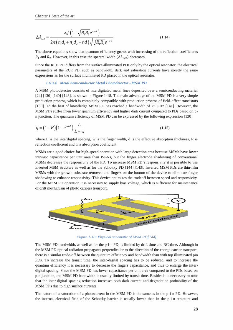
Chapter 1 State of the art
28
2
0 1 2
1/2
1 1 2 2 1 2
1
2
d
d
R R e
n d n d nd R R e
(1.14)
The above equations show that quantum efficiency grows with increasing of the reflection coefficients
𝑅1 and 𝑅2. However, in this case the spectral width (∆𝜆1/2) decreases.
Since the RCE PD differs from the surface-illuminated PDs only by the optical resonator, the electrical
parameters of the RCE PD, such as bandwidth, dark and saturation currents have mostly the same
expressions as for the surface illuminated PD placed in the optical resonator.
1.6.3.4 Metal Semiconductor Metal Photodetector –MSM PD
A MSM photodetector consists of interdigitated metal lines deposited over a semiconducting material
[24] [130] [140]-[143], as shown in Figure 1-18. The main advantage of the MSM PD is a very simple
production process, which is completely compatible with production process of field-effect transistors
[130]. To the best of knowledge MSM PD has reached a bandwidth of 75 GHz [141]. However, the
MSM PDs suffer from lower quantum efficiency and higher dark current compared to PDs based on p-
n junction. The quantum efficiency of MSM PD can be expressed by the following expression [130]:
1 1 d LR e
L w
(1.15)
where L is the interdigital spacing, w is the finger width, d is the effective absorption thickness, R is
reflection coefficient and α is absorption coefficient.
MSMs are a good choice for high-speed operation with large detection area because MSMs have lower
intrinsic capacitance per unit area than P-i-Ns, but the finger electrode shadowing of conventional
MSMs decreases the responsivity of the PD. To increase MSM PD’s responsivity it is possible to use
inverted MSM structure as well as for the Schottky PD [144] [143]. Inverted MSM PDs are thin-film
MSMs with the growth substrate removed and fingers on the bottom of the device to eliminate finger
shadowing to enhance responsivity. This device optimizes the tradeoff between speed and responsivity.
For the MSM PD operation it is necessary to supply bias voltage, which is sufficient for maintenance
of drift mechanism of photo carriers transport.
Figure 1-18: Physical schematic of MSM PD[144]
The MSM PD bandwidth, as well as for the p-i-n PD, is limited by drift time and RC-time. Although in
the MSM PD optical radiation propagates perpendicular to the direction of the charge carrier transport,
there is a similar trade-off between the quantum efficiency and bandwidth than with top illuminated pin
PDs. To increase the transit time, the inter-digital spacing has to be reduced, and to increase the
quantum efficiency it is necessary to decrease the fingers capacitance, and thus to enlarge the inter-
digital spacing. Since the MSM PD has lower capacitance per unit area compared to the PDs based on
p-n junction, the MSM PD bandwidth is usually limited by transit time. Besides it is necessary to note
that the inter-digital spacing reduction increases both dark current and degradation probability of the
MSM PDs due to high surface currents.
The nature of a saturation of a photocurrent in the MSM PD is the same as in the p-i-n PD. However,
the internal electrical field of the Schottky barrier is usually lower than in the p-i-n structure and

Chapter 1 State of the art
29
moreover there is a large barrier for holes at the metal-semiconductor interface. This result in lower
saturation current of the PD based on Schottky barrier compared with the p-i-n PDs [144].
1.6.3.5 Waveguide Photodetector -WGPD
An alternative structure for increasing optical absorption and reducing the transit time impact is to use
edge-coupling, thus allowing the optical input to enter directly the intrinsic region and to propagate
orthogonally to the electric field. Thus the photon flux and the carrier motion are orthogonal. In this
case, the structure becomes an optical waveguide, allowing the design of long but narrow absorption
regions which ensure that a large fraction of the input power is absorbed while maintaining low transit
times [122] [130] [146] [147][148]. Waveguide photodiodes with bandwidths larger than 100 GHz
have been demonstrated [149], and typical bandwidth–efficiency products for these devices are about
55 GHz.
Light is guided by an optical waveguide made of an intrinsic narrow gap semiconductor layer,
sandwiched between two highly doped wide-gap layers (see Figure 1-19).
Figure 1-19: Schematic structure of an InGaAs waveguide photodiode (left) and details of the epitaxial
structure (right) showing the guiding refractive index profile [122]
Applying a reverse bias voltage, photo carriers are collected by the doped layers after a very short
transit time since the waveguide active region is typically thin. As the waveguide length can be
designed long enough (W >> Lα), the majority of photons are absorbed, without affecting the transit
time. The photodiode external efficiency and responsibivity can be expressed as: [122] [130]:
1 1 ovГ W
x i r e
(1.16)
1 1 ovГ W
i
qR r e
hf
(1.17)
Where ᴦov is the overlap integral or confinement factor, α is the core absorption, d is the active
absorption region thickness W is the optical waveguide length and r is the input reflection coefficient.
The RC constant limited 3dB bandwidth is:
3 ,
1 , ,
2
sdB RC s D j p j
awf where R R R C C C C
RC d (1.18)
Where Cp is the external diode parasitic capacitance, Rs is the series parasitic diode resistance, RD is the
parallel diode resistance, Cj is the intrinsic capacitance, w is the length of the active area, a is the width
of the active area and d is the thickness active area.
Finally, the transit time limited cut-off frequency will be
3 , 4 4 4
, ,
3.5 1 1 1 1
2 2dB tr
n sat h sat
vf where
d v v v
(1.19)

Chapter 1 State of the art
30
Where v is mean velocity, vn and vp are the electron and hole velocities in the intrinsic region
respectively.
The waveguide photodiode has the following disadvantages:
First, the thickness of the active layer is often less than 1 mm, leading to a significant reduction
in coupling efficiency between the photodiode and single-mode fibre. This can be improved to
some extent by using tapered fiber or by fabricating devices that have doped optical guiding
layers around the absorption region.
Second, the ‘long and narrow’ topology creates a capacitive region with a large area-to-
thickness ratio, resulting in increased capacitance which causes an RC time limitation.
Third, such structures suffer from earlier power saturation with respect to conventional
photodiodes, due to the very small cross section.
1.6.3.6 Travelling Wave Photodetector -TWPD
The photodiode structures discussed above results of lumped element approaches. In order to eliminate
the limitation of the RC time constant and to improve impedance matching, distributed designs were
proposed. These are commonly known as travelling-wave photodetectors [30] [122] [127] [130] [135]
[136] [150] and they are a natural evolution of the edge coupled waveguide PIN structure discussed
above. In this case, in addition to the optical wave guiding mechanism, the device contacts are
engineered to support microwave travelling waves; the approach is similar to Mach–Zehnder travelling
wave modulators, and it is another example of transmission line effects in microwave photonics.
Coplanar waveguide is typically chosen which supports a quasi-TEM mode; the transmission line
parameters are determined by the device capacitance and the contact strip inductance. Absorption of
optical power occurs in a distributed manner along the length of the device, through a travelling wave
(Figure 1-20). Such a device is no longer limited by RC effects but by the velocity mismatch between
the optical group velocity and electrical phase velocity. When velocity matching is achieved, then long
device lengths compared to waveguide photodiodes are possible in principle. The fact that the
absorption volume is increased also means that these devices will saturate at a higher power level [30]
[135].
Figure 1-20: Distributed effects in a travelling wave photodetector [30] [135].
The TWPD is a device with distributed parameters. Its bandwidth is not limited by RC-time; therefore
the TWPD length can be made much longer. The TWPD bandwidth is limited by the difference in the
propagation velocities of light and microwave, and by parasitic RC-time and microwave losses in the
transmission line. It is necessary to note that the propagation velocity of the microwave in the TWPD is
2 or 3 times smaller than the velocity of the light wave [30] [135] [144] [151]; because the velocity of
the microwave signal is significantly slowed down by the capacitance of the photodiode (slow wave
effect). Therefore major factor limits the bandwidth in correctly designed TWPD.
Optical radiation is absorbed in the TWPD and the photocurrent generates two microwaves
propagating in opposite directions. The backward travelling microwave (in regard to the light direction
of propagation) is reflected from the TWPD input edge and thus introduces additional mismatching
between the light wave and microwave propagation velocities. This effect can be eliminated by means
of matched load at the input edge of the TWPD microwave transmission line. However, in this case,

Chapter 1 State of the art
31
half of the photocurrent will be absorbed by the matched load and the TWPD quantum efficiency
divided by two. The TWPD bandwidth limited by the mismatch between the light wave and microwave
propagation velocities can be expressed using the following expressions [122] [130] while considering
two cases:
1. If the absorption region is short (ГαW<<1) one has
3
0.44 o m
dB
m o
v vf
W v v
(1.20)
Where vo is the light wave propagation velocity and vm the microwave propagation velocity in
the TWPD.
In this case the cutoff frequency is inversely proportional to the device length W.
2. In a more realistic case the absorption region is long (ГαW>>1)
3
0
Г
2
o mdB
m
v vf for matched laod TWPD
v v
(1.21)
2
03
2 2
0
ГГ
32 5
m mdB
m
v v vf for unmached load TWPD
v v
(1.22)
In this case 𝑓3𝑑𝐵 is independent on W
Where, v0 and vm are the light wave and microwave propagation velocities in TWPD. The above two
formula show that the bandwidth of matched TWPD is 2 or 3 times larger than for the unmatched
TWPD. To increase the TWPD bandwidth, it is necessary to increase the Гα product. However, this
results in the saturation current decrease due to non-uniformity of optical radiation absorption. Since
the TWPD length is longer than for WGPD, the TWPD still has in general a larger saturation current. A
large variety of travelling-wave photodiodes have been demonstrated and exhibit excellent
performance such as 3dB bandwidths higher than of 210 GHz, for PIN based devices [123].
1.6.3.7 Velocity Matched Distributed Photodetector -VMPD
VMDP consists of a microwave transmission line periodically loaded by separated PDs (p-i-n PD
[152], UTC PD [126], or MSM PD [153] [154]), to which optical radiation is provided by means of a
passive waveguide (Figure 1-21). The key feature of the VMDP is that the microwave transmission
line, the passive optical waveguide and the PDs can be designed separately with the purpose of
achievement of the required characteristics. The microwave propagation velocity in a customary
microwave transmission line is higher than light wave propagation velocity in semiconductor
waveguide. The microwave propagation velocity can be reduced by periodical loading the microwave
transmission line with capacitances, which can be p-n junction capacitances of the separated PDs.
VMDP is designed so that the photocurrents from each separated PD sum in phase (matching of the
microwave and light wave propagation velocities).
Figure 1-21: Velocity Matched PD structure

Chapter 1 State of the art
32
The VMDP quantum efficiency with matched loads at the ends of the transmission line can he
expressed by the following formula [53]:
2
00 002
0
1 11 1
2 1 1 2
N
N
e
k
k
(1.23)
Where 𝜂0 = 1 − 𝑒−Г𝛼𝑑 is the quantum efficiency of the separated PD, k is the coupling efficiency
between passive waveguide and separated PDs (it is possible to achieve k value almost equals to 1), N
is the number of separated PDs in the VMDP and 𝜂𝑒 is the coupling efficiency.
1/22
03 2 2
0 0
1 12 1 m
dB
p m
v vf N l
f v v f
(1.24)
Where ∆l is the spacing interval between the separated PDs in the VMDP, ∆fp is the parasitic RC-time
limited bandwidth. The separated PD bandwidth ∆f0 can be very large (about hundreds of GigaHertz),
since it is not required to have simultaneously a high quantum efficiency. Since the VMDP is designed
so that v0 ≈ vm, the slight mismatching between the light wave and microwave propagation velocities
bandwidth influences on the VMDP bandwidth only under large number of separated PDs. Thus, in a
correctly designed VMDP, the bandwidth is mostly determined by microwave losses in the
transmission line and by parasitic RC-time.
For perfectly matched PDs (v0 ≈ vm) and when neglecting parasitic RC time, the 3dB bandwidth is
limited by the transit time of discrete PDs. Thus it can be expressed [155] [30] [144] as:
3 0.55 0.55ehdB
v Ef
d d
The VMDP
bandwidth is limited by microwave losses, parasitic RC-time, mismatching of the microwave and light
wave propagation velocities, and separated PD bandwidth. It can be expressed as [151]:
(1.25)
Where veh is the velocity of electon hole, d is the absorption thickness of each PD, μ is the carrier
mobility and E is the electric field in the active region.
The global photocurrent of the VMDP is the sum of the photocurrents of the discrete PDs. Therefore to
obtain a high saturation current it is necessary that each separated PDs only absorbs a small part of the
incident optical power. This is easily reached by decreasing the confinement factor of each separated
PD. It is necessary to notice, that on the first photodiode the maximum optical power drops. To avoid
this, it is necessary to use the VMDP with parallel optical feeding of (Figure 1-22) [30] [135]. In this
case, each separated PD absorbs the same optical power and the VMDP saturation current is increased.
However, in this case the lengths of optical waveguides should be selected so that the photocurrents of
the separated PDs sum in phase.
Figure 1-22: Parallel optical feed VMPD [30] [135].

Chapter 1 State of the art
33
1.6.3.8 Summary
To conclude, we summarize in this section the state of the art of PDs by comparing results of different
publications in the previous years. The 3dB bandwidth of different types of photodetector with respect
to the technology used (InP/InGaAs or SiGe/Si), active region thickness, surface area and external
efficiency are plotted in Figure 1-23, Figure 1-24 and Figure 1-25. The related references are also
indicated in the figures.
PDs made from InGaAs have higher efficiency and bandwidth than SiGe/Si PDs, see Figure 1-23 and
Figure 1-24. This is due to the indirect bands of SiGe/Si material.
Figure 1-23 shows that waveguide PDs have better external efficiency than PIN because of large
absorption length and they have poor bandwidth because of RC limitation. RCE also has good
responsivity with values as high as 90% [138] (long absorption due to repeated reflection). TWPDs
have the highest bandwidth with f3dbB as high as 210GHz but low efficiency due to poor optical
coupling. PIN photodiodes have the lowest performances because of the trade-off between efficiency
and bandwidth.
Figure 1-23: 3dB bandwidth as a function of external efficiency
From Figure 1-24, it can be observed that at an equivalent active area thickness, SiGe photodiodes are
less high speed with bandwidth however as high as 15GHz [117]. Maximum active area thickness
achieved with this material is less than 1µm [118] due to the mechanical instability of the layer induced
by the mismatch between Si and SiGe lattice constant. This explains why achieved external efficiencies
are below 46.67% [23].
0 20 40 60 80 10010
-1
100
101
102
103
External efficiency (%)
3d
B B
an
dw
idth
(GH
z)
pin
RCE
TWPD
WGPD
MSM
[123]
[117]
[142] [119]
[124]
[28][27]
[137]
[26][131]
[23]
[25]
[140]
[138]
[118]
[115]
[141][125][132]
[120]
[24]
[119]
[156]
SiGe and
few InGaAs
InGaAs
only
[116]
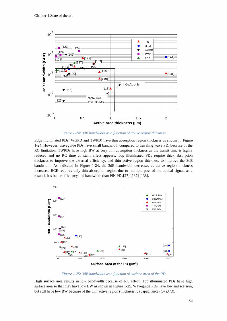
Chapter 1 State of the art
34
Figure 1-24: 3dB bandwidth as a function of active region thickness
Edge illuminated PDs (WGPD and TWPD) have thin absorption region thickness as shown in Figure
1-24. However, waveguide PDs have small bandwidth compared to traveling wave PD, because of the
RC limitation. TWPDs have high BW at very thin absorption thickness as the transit time is highly
reduced and no RC time constant effect appears. Top illuminated PDs require thick absorption
thickness to improve the external efficiency, and thin active region thickness to improve the 3dB
bandwidth. As indicated in Figure 1-24, the 3dB bandwidth decreases as active region thickness
increases. RCE requires only thin absorption region due to multiple pass of the optical signal, as a
result it has better efficiency and bandwidth than PiN PDs[27] [137] [138].
Figure 1-25: 3dB bandwidth as a function of surface area of the PD
High surface area results in low bandwidth because of RC effect. Top illuminated PDs have high
surface area so that they have low BW as shown in Figure 1-25. Waveguide PDs have low surface area,
but still have low BW because of the thin active region (thickness, d) capacitance (C=𝜀𝐴/𝑑).
0 0.5 1 1.5 210
-1
100
101
102
103
Active area thickness (µm)
3d
B B
an
dw
idth
(GH
z)
PIN
MSM
WGPD
TWPD
RCE
[149]
[129]
[119]
[118]
[131]
[141]
[124][123]
[133]
[156]
[119]
[137]
[138][27]
[142][117]
[120][25]
[116]
[23]
[125]
[126]
[28]
InGaAs only
SiGe and
few InGaAs
0 500 1000 1500 2000 25000
50
100
150
200
250
3d
B B
an
dw
idth
(GH
z)
RCE PDs
MSM PDs
PIN PDs
TW PDs
WG PDs
[129]
[132]
[133]
[117] [1119][119]
[118]
[28]
[131][26]
[123]
[124]
[125]
[149]
[126]
[156]
[25]
[27] [138]
[137]
[141]
[140]
[142]
Surface Area of the PD (µm2)

Chapter 1 State of the art
35
Finally we conclude that advanced high-speed PDs based on compounds materials have recently been
proposed for microwave photonics application. For frequencies below 50 GHz surface-lumped PDs
such as p-i-n PDs, WGPDs, MSM PDs or RCEP PDs are successfully developed. For higher
frequencies it is necessary to work with lumped UTC PDs and to go above 100 GHz it is more suitable
to use distributed devices such as TWPDs and VMDPs [123] [124] [126]. In the applications where
high-output power is required, one should use the UTC PDs, WGPDS and/or distributed absorption,
TWPDs, or VMDPs.

Chapter 1 State of the art
36
1.7 Heterojunction Bipolar Phototransistor (HPT)
In this section we present the overview of Heterojunction bipolar Photo-Transistors (HPT) which are
implemented as high-speed light detector. The principle of HPTs, the motivation to use
phototransistors instead of photodiodes and light illumination techniques of HPTs are first introduced.
In the second sub-section, HPTs are presented according to their technological approach, while
considering both III-V material and Si-based phototransistors. Edge illuminated and traveling wave
phototransistors are also pointed out.
1.7.1 HPT Principles
Heterojunction bipolar phototransistors (HPT) are based on Heterojunction Bipolar Transistors (HBTs)
with the design of an optical window to enable the light path into the device and with some of its layers
made of optical absorbing material, especially in the base-collector region. HPTs are good candidate as
microwave photo-receivers, and could be called as microwave phototransistors, as opposed to low
speed homojunction phototransistors used in sensor or opto-coupler applications.
The performance of HPTs, as any phototransistor, is supported by their internal current gain; not
present in p-i-n and schottky photodiodes. In addition, unlike avalanche photodiodes, HPTs do not
suffer from extensive noise due to avalanche effect. This advantage, and their process and layer
compatibility to heterojunction bipolar transistor, makes them highly attractive in manufacturing single
chip optical receiver [157].
Figure 1-26 shows a representative cross section of an AlGaAs phototransistor [17]. The structure of
the HPT is similar to a bipolar transistor except for enlarged base and collector regions, to enable the
presence of an optical window that receives the illumination spot, as given in Figure 1-26. The
phototransistor structure can be illuminated vertically or laterally. Vertical illumination of the
phototransistor can be achieved in different ways. A simple way is to illuminate the phototransistor
between base-emitter contacts. This is simply illuminating a transistor structure [158]. The optical
beam can also be injected via the emitter through an opening in the emitter contact [159] or by utilizing
a transparent emitter contact [160]. Finally, one of the base contacts could be removed or omitted to
allow the direct illumination of the base-collector junction [161] [162]. Another way of vertical
illumination is through the backside of the phototransistor. Lateral illumination of the HPT is one
method to improve the coupling efficiency to bandwidth trade-off. This allows the propagation distance
before a complete optical absorption to be long enough while the absorption layer remains thin enough
to ensure short transit times. Lateral illumination of phototransistors can be done by injecting the light
through the cleaved side of the device. It can also be achieved by using an optical waveguide integrated
in the device structure [163].
Figure 1-26: Schematic diagram of an npn GaAs/AlGaAs phototransistor.
Generally, in phototransistor, the base-collector region behaves as a p-i-n photodiode and injects the
photo-generated current into the base (holes) and collector (electrons). The hole photo-generated
current goes through the base and is then amplified. The phototransistor is hence usually represented by
the simplified diagram given in Figure 1-27:

Chapter 1 State of the art
37
Figure 1-27: Simplified diagram of an HPT
IC in such transistor can be written as:
IC = Iph + βIph where β is the current gain and Iph is the photogenerated current.
As the current gain of a transistor can be very high, this relation shows the benefit of using a
phototransistor instead of a photodiode, which only generates Iph.
This diagram is however a rough approximation and can lead to wrong interpretation results if one
consider that in a voltage biasing mode, for example, all the photogenerated current should leak into
the voltage source, which is only partially the case. Chapter 3 will better analyze the real HPT
behavior.
Microwave bipolar transistors are mostly all n-p-n types and all have an emitter base heterojunction. In
this transistor, the emitter base heterojunction has either the emitter made of a large gap semiconductor
or the base made of a small band gap semiconductor. The semiconductor must be chosen in such a way
that the band gap difference is in the valence band side as much as possible. This results in blocking the
holes that could come from the base towards the emitter and thus increasing the emitter injection
efficiency. Thus, the base can be doped more than that of homojunction transistor base and its
thickness can be reduced, leading to increase the transistor operational speed, without increasing the
transistor base resistance RB [17] [157] [164].
The npn phototransistor is basically operated in the common emitter configuration where Vbe and Vce
voltages are greater than 0. In this case the phototransistor is in the forward active mode. The BC
junction is reverse biased and the BE junction is forward biased. The BE junction biasing could come
from either the optical illumination of the HPT or by providing an external electrical base bias. The
biasing of BE junction from the optical illumination is called a two terminal phototransistor operation
(2T-HPT), as the base contact does not exist [165]. The base contact may however exist but is left
floating [166] [168]. Providing an external bias for the base is called a three terminal HPT operation
(3T-HPT) which is reported to provide enhanced HPT performances [175] [169]-[171]. For simplicity,
it is assumed that no absorption occurs in the sub-collector and the collector is free of mobile charges.
The photoelectric effects generate an electron-hole pair for every photon that is absorbed. The electron
hole pairs generated in BC depletion region and within the diffusion lengths of the minority carriers in
the base and collector will be separated and collected by the field of BC junction leading to a current
flow in the external circuit. This is known as the primary photocurrent. The holes are swept into the
base, thereby increasing the base potential. This in turn increases the base emitter forward bias. To
maintain the charge-neutrality condition in the base, a large injection of electrons occurs from the
emitter into the thin base resulting in a large electron-current flow from the emitter to the collector.
This is the traditional behavior of a bipolar transistor. The amplification of the photocurrent is a purely
electrical phenomenon due to the transistor action.
VBE
VCE
Light
Iph
IC
E
C
B
Chapter 1 State of the art
38
Finally the advantage of using a phototransistor instead of a photodiode comes from the possibility to
have an internal gain into the HPT, providing a PiN + HBT like structure, but also in providing novel
functionality due to the three-terminal structure, such as optical mixing and injected oscillators [172].
1.7.2 HPT Technological Approach
Based on the energy gap and lattice constant we can select the appropriate semiconductor materials to
construct the HPT stacks. Heterojunction phototransistors using III-V compound have been extensively
studied in the past two decades [174]-[179]. Heterojunction phototransistor using IV-IV also emerges
nowadays since SiGe phototransistor proposed in 1997 with the multiple walls [173] [181], and since
2003 with SiGe HPTs integrated with the existing SiGe bipolar and BiCMOS technologies emerging
for RoF applications [159] [161] [182]-[187].
1.7.2.1 GaAlAs/GaAs, InGaP/GaAs and InGaAs/InP phototransistors
Various HPTs fabricated using AlGaAs/GaAs [174] [175] [178] and InGaP/GaAs [176] [177] [179]
technologies have been reported and applied to high performance optical receivers.
The first HPTs were fabricated on GaAs substrate because AlGaAs/GaAs heterojunction has lattice
matching regardless of the proportion of Al and Ga. Furthermore the GaAs substrate was available
elsewhere in the form of wafer with good mechanical and electrical properties. The GaAs
semiconductor shows a correct absorption only for wavelength inferior to 0.85µm.
InGaP/GaAs heterojunction bipolar phototransistors (HPTs) are attractive photodetectors for optical
communication and sensor applications. Those HPTs have large optical gain at low voltage bias and
are compatible with heterojunction bipolar transistors (HBTs) concerning their epitaxial structures and
fabrication process [188] [166]. Moreover, InGaP/GaAs HPTs have an advantage over GaAlAs/GaAs,
because InGaP/GaAs HPTs have superior electrical and optical performances due to their larger
valence and smaller conduction band discontinuities and a high etching selectivity between InGaP and
GaAs [180]. An InGaP/GaAs HPT with a responsivity of 0.6A/W and optical gain of 45dB has been
demonstrated in [179].
Another material used to realize a phototransistor is InGaAs/InP [172] [189] [190]. In this
phototransistor light absorption takes place at optical wavelengths equal or inferior to 1.5µm. The
proportions of Ga and In in the arrangement of InGaAs materials has to be well chosen to get good
lattice matching between InP and InGaAs. The material used is actually In0.53Ga0.47As. For such
phototransistor an optical transition frequency of 62GHz and responsivity of 0.4A/W has been reported
in [191]
1.7.2.2 Pure Silicon Phototransistors
Pure silicon bipolar phototransistors have been studied for a long time as sensors or opto-couplers and
only few as high speed detectors. High speed Si phototransistors were however fabricated in a 0.35μm
commercial AMS BiCMOS technology without process modifications [187]. They have studied
extended base collector phototransistors with different optical window sizes. In their work, NPN
transistors are directly implemented in a 0.35µm BiCMOS technology. This technology has no silicide
layers. The transistors are designed with an enlarged base collector junction area which serves as a
photodiode in which the photocurrent is amplified by the intrinsic transistor part of the device. It has a
base node, which is used for base biasing to help speeding up the detectors response and to slightly
raise responsivity. The emitter capacitance is maintained as small as possible to avoid slowing the
device by making the emitter area as small as possible. The transistors are characterized over a wide
optical spectral range at 410nm, 675nm, 785nm, and 850nm, providing -3dB bandwidths up to
390MHz at 410nm and responsivities of 1.76A/W at 675nm corresponding to quantum efficiencies of
359% normalized in terms of the quantum efficiency of a silicon photodiode. Another pure silicon
phototransistor obtained from a standard 180 nm CMOS process technology is presented in [192]. A
responsivity of 2.89 A/W at 630 kHz and DC responsivity of 6.44 A/W is achieved. Furthermore this

Chapter 1 State of the art
39
phototransistor reaches bandwidths up to 50.7 MHz at 850 nm, 76.9 MHz at 675 nm and 60.5 MHz at
410 nm at VCE = 10 V and floating base conditions.
1.7.2.3 SiGe/Si Phototransistors
The last type of phototransistor is the SiGe heterojunction phototransistor. In 1997 SiGe/Si multiple
quantum well (MQW) HPT was proposed on SOI substrate according to SIMOX process [173]. Its
base is composed of several SiGe/Si multiple quantum wells that are inserted in a vertical resonant
cavity which operates at 1.3um wavelength. The SiGe/Si MQW both forces the base and the absorption
layer as shown in Figure 1-28. The cavity is defined by the lower SIMOX substrate and the upper
Si02/Si mirror. For a SIMOX substrate based resonant cavity photodetector with 1µm absorption layer,
a calculated quantum efficiency of 18% was obtained and a cutoff frequency as high as 1GHz was
calculated at input optical power of 10µW.
Figure 1-28: Schematic of a SiGe/Si MQW resonant cavity phototransistor using a double
heterojunction [173].
In 2002, a SiGe/Si phototransistor was fabricated by placing 𝑆𝑖0.5𝐺𝑒0.5/Si multiple quantum wells
(MQWs) in the base-collector region [181]. A responsivity of 1.47A/W and bandwidth of 1.25GHz at
850nm are demonstrated. In [193], the same group has been demonstrating MQW SiGe phototransistor
with fT and fmax of 25 GHz and an external quantum efficiency of 194%, thus a responsivity of
1.33A/W, at 850nm.
The use of MQW SiGe/Si has demonstrated a promising responsivity and high bandwidth detection at
850nm wavelength. However, this approach is not straight forward to implement in commercial SiGe-
based processes and at 850nm wavelength detection, a single SiGe layer could be used as done in 2003,
[182]. In that case SiGe HPTs are fully compatible with the SiGe HBT structure from commercial
SiGe-based technologies. This allows monolithic integration with electronic signal processing circuits,
and thus extends the existing application list of SiGe-based technologies to include opto-electric (O/E)
functionalities without the addition of masks and processing steps. These microwave SiGe
phototransistors provide an innovative solution for the integration of optoelectronic functions in
commercial bipolar or BiCMOS process technologies, contrary to SiGe multi quantum wells structures.
These devices have since been fabricated using several industrial SiGe bipolar and BiCMOS process
technologies: Atmel/Telefunken [159] [161] [182] [183], TSMC [185], IBM [184] and AMS [187].
The first SiGe bipolar heterojunction phototransistor developed in a commercial available SiGe/Si
technology (Atmel technologies) was presented in 2003 [182] [183]. Figure 1-29 illustrates the
configuration of such a phototransistor and a photograph. This structure has a 10x10µm2 optical
window opening in the emitter through which the light penetrates. The phototransistor structure is
made without any additional absorption structure and is purely based on the SiGe bipolar technology.
The base profile was abrupt in shape with Ge content in range of 20 to 25%. The base doping was
significantly high compared to Si HBT and typically around 1019
cm-3
. This HPT structure has a
measured fT of approximately 20 GHz. It has a lower fT as compared to the 30GHz fT of standard HBT

Chapter 1 State of the art
40
devices in this process due to the enlargement of the structure to open the optical window. However it
is still considerably high due to thin base and high base doping. A dc responsivity of 1.47A/W and a -
3dB bandwidth of 0.4GHz were achieved at 0.94μm.
Figure 1-29: Left: Photograph of the top view of a SiGe HPT with a 10x10μm² optical window in the
emitter; Right: Sketch of the vertical stack [183].
A second SiGe HPT was proposed almost simultaneously with Pie et al in [185]. It is implemented in a
BiCMOS process from TSMC and exhibits a responsivity of 0.43A/W with a pass band of 3GHz. In
2004, Apsel et al [194] from Cornell University demonstrated a 0.25µm IBM BiCMOS process SiGe
HPT with responsivities of 2.4A/W and 0.12A/W that were achieved under 850nm and 1060nm
respectively under 2T Phototransistor operation and a bandwidth of above 500MHz for a 10x16µm2
HPT. By modifying the commercial SiGe HBT structure in IBM 0.25µm SiGe BiCMOS process,
Apsel at el [194] also implement a smaller sized 6x10µm2 HPT. The photo detecting window was
incorporated by removing silicide layers that block the optical absorption and the existing layers were
manipulated. Smaller sized HPTs using the IBM BiCMOS process show that a responsivity of 2.7A/W
and a cut off of 2.3GHz were measured. The optical cutoff frequencies of these devices measured from
pulsed laser measurement are 2.0GHz, 2.1GHZ and 5GHz for the HPT sizes of 6x10µm2, 5x5µm
2 and
2x2µm2 respectively at 850nm.
Most recently at the end of 2015, a SiGe HPT fabricated by adapting the available design kit provided
by CMC Microsystems with very high DC responsivity of 232A/W at 1.55µm wavelength is reported
in [19].
1.7.3 Edge illuminated Phototransistor
Vertically illuminated photodetectors or HPTs are known for their ease of coupling but suffer from a
trade-off between conversion efficiency and transit time limited frequency performance [195] [189]
[196].
Edge-coupled devices overcome this problem by allowing the optical signal to enter through the side of
the device, orthogonal to the bias field. This gives the freedom to design longer devices to ensure that a
high proportion of the optical signal to be absorbed while maintaining a narrow absorption region to
keep transit times low. The drawback, however, is that the device capacitance becomes significant due
to the increased device area and reduced depletion layer thickness [195]. This increased capacitance
gives rise to a response limited by the increased RC time constant once the device contact and load
resistances are taken into account [196] [197].
1.7.4 Travelling wave phototransistors
In order to improve both the bandwidth and the conversion efficiency in a single device, topologies
must move away from lumped element configurations to distributed traveling-wave structures. In 1998,
it was proposed that using the transistor structure in the traveling- wave geometry would eliminate the
RC limitations of the lumped devices, replacing them instead with a velocity mismatch limited
response [198]. The literature is generally sparse on high-frequency characterization of traveling-wave

Chapter 1 State of the art
41
heterojunction phototransistors (TW-HPTs); however, measured results from [198] seemed very
promising, indicating a dc gain of more than 35 times that of a similar length traveling wave
photodiode. While frequency response results were not presented, devices showed no saturation up to a
dc photocurrent of 50 mA at 60 GHz, indicating the potential for the use of such devices in high-power
applications.
In [199] the set of classical drift-diffusion device equations has been applied to fully distributed
travelling-wave heterojunction phototransistor structures (TW-HPTs). In this publication a full physical
model has been shown for the first time indicating that the potential RC limitations still exist for
transistor in the traveling-wave regime.
Table 1-3 presents the summary of the performances of HPTs fabricated from different material type.
Their performance in terms of responsivity, optical transition frequency, optical gain and external
efficiency are presented. The operating wavelength, base thickness, doping level, optical window size
and HPT structure are also summarized in the same table.

Chapter 1 State of the art
42
Table 1-3: Summary of state of the art of HPTs
Reference year type material Wb[A] doping base Wc[A] optical window λ[μm] illumination β current gain ft [GHz] fmax[GHz] R[A/W] Gopt[dB] ft_opt[GHz] ηext
[200] 2004 InP-InGaAS 1,55 x x x x 7,5 x x
[191] 1999 InP-InGaAS 600 3,00E+19 5000 5x6 1,55 42 71 x 0,4 35 62 x
[182] 2003 Si-SiGe x 1,10E+19 x 10x10 0,94 x [email protected] and [email protected] x 1.49 [HPT] 3,46 x x
[201] Si-SiGe 300 x x 10x10 1,17 latteral 5 x x x 30 x x
[161] 2011 Si-SiGe 10x10 0,85 x 39 x 1.8 [HPT] x
[179] 2005 InGaP-GaAs 1400 4,00E+19 6000 x 0,85 x x x 0,64 45 x Assumed 100%
[180] 2010 InGaP-GaAs 800 4,00E+19 8000 50x50 0,635 0,34 120,5
[185] 2004 Si-SiGe 0,85 100 0,43
[202] 2009 UTC-HPT InP-InGaAS 2200 2e+18 , 1e+18 , 5e+18 4600 5x5 1,55 0,2 37 52
[202] 2009 UTC-HPT InP-InGaAS 2200 2e+18 , 1e+18 , 5e+18 4600 10x10 1,55 0,2 29 36
[177] 2005 2T-HPT InGaP-GaAs 1400 4,00E+19 6000 0,85 33 28,4
[162] 2005 3T-HPT InGaP-GaAs 1400 4,00E+19 6000 0,85 34
[189] 1999 edge coupled HPT InP-InGaAS 500 1,00E+19 4000 1,55 edge 43 100 [HPT] 400 @length=1μm
[190] 2011 UTC-HPT InP-InGaAS 52x52 1,55
[203] 2005 2T-HPT InP-InGaAS 500 3,50E+19 8000 1,55 25 0,2 20
[204] 2008 APD-HPT InP-InGaAS-(InAlAs charge layer 700 5,00E+17 25000 1,55 460000 [HPT+APD] 5,50E+05 66%
[159] 2012 Si-SiGe 20x20 0,85 451,8 3.53 [HPT]
[181] 2003 MQW-HPT Si-SiGe 600 5,00E+18 14,4 0,85 200 25 25 0.026 (1.3 in HPT) 194%
[205] Si-SiGe 10x10 0,94 0.014 (1.5 HPT) 94 x
[205] Si-SiGe 10x10 1,17 latteral 0.04[HPT] 134 x
[𝑐𝑚−3] [ 𝑚2]
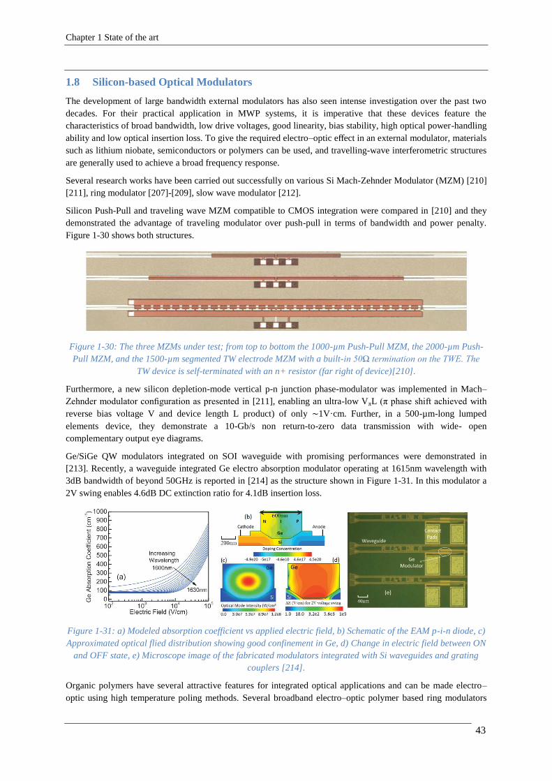
Chapter 1 State of the art
43
1.8 Silicon-based Optical Modulators
The development of large bandwidth external modulators has also seen intense investigation over the past two
decades. For their practical application in MWP systems, it is imperative that these devices feature the
characteristics of broad bandwidth, low drive voltages, good linearity, bias stability, high optical power-handling
ability and low optical insertion loss. To give the required electro–optic effect in an external modulator, materials
such as lithium niobate, semiconductors or polymers can be used, and travelling-wave interferometric structures
are generally used to achieve a broad frequency response.
Several research works have been carried out successfully on various Si Mach-Zehnder Modulator (MZM) [210]
[211], ring modulator [207]-[209], slow wave modulator [212].
Silicon Push-Pull and traveling wave MZM compatible to CMOS integration were compared in [210] and they
demonstrated the advantage of traveling modulator over push-pull in terms of bandwidth and power penalty.
Figure 1-30 shows both structures.
Figure 1-30: The three MZMs under test; from top to bottom the 1000-µm Push-Pull MZM, the 2000-µm Push-
Pull MZM, and the 1500-µm segmented TW electrode MZM with a built-in 50Ω termination on the TWE. The
TW device is self-terminated with an n+ resistor (far right of device)[210].
Furthermore, a new silicon depletion-mode vertical p-n junction phase-modulator was implemented in Mach–
Zehnder modulator configuration as presented in [211], enabling an ultra-low VπL (π phase shift achieved with
reverse bias voltage V and device length L product) of only ∼1V·cm. Further, in a 500-µm-long lumped
elements device, they demonstrate a 10-Gb/s non return-to-zero data transmission with wide- open
complementary output eye diagrams.
Ge/SiGe QW modulators integrated on SOI waveguide with promising performances were demonstrated in
[213]. Recently, a waveguide integrated Ge electro absorption modulator operating at 1615nm wavelength with
3dB bandwidth of beyond 50GHz is reported in [214] as the structure shown in Figure 1-31. In this modulator a
2V swing enables 4.6dB DC extinction ratio for 4.1dB insertion loss.
Figure 1-31: a) Modeled absorption coefficient vs applied electric field, b) Schematic of the EAM p-i-n diode, c)
Approximated optical flied distribution showing good confinement in Ge, d) Change in electric field between ON
and OFF state, e) Microscope image of the fabricated modulators integrated with Si waveguides and grating
couplers [214].
Organic polymers have several attractive features for integrated optical applications and can be made electro–
optic using high temperature poling methods. Several broadband electro–optic polymer based ring modulators

Chapter 1 State of the art
44
have been developed [206] [207]. For ring modulators, an error free modulated signal transmission with a
bandwidth of 25 Gbps has been reported with 1-V peak-to peak drive voltage [208]. Low efficiency, and low-
power handling performance, and the linearity of ring modulators were reported in [209]. As demonstrated, for
low-dynamic-range applications, silicon ring modulators offer a compact solution. Figure 1-32 shows an
example of CMOS compatible ring modulator where a) illustrates the cross section of the pn junction and b)
illustrates the schematic of the ring modulator design with n-doping at the center and surrounded by p-doping.
Figure 1-32: a) Schematic cross sectional diagram of ring modulator, b) Micrograph of the ring modulator
[209].
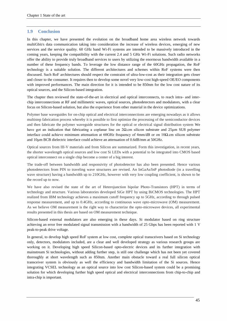
Chapter 1 State of the art
45
1.9 Conclusion
In this chapter, we have presented the evolution on the broadband home area wireless network towards
multiGbit/s data communication taking into consideration the increase of wireless devices, emerging of new
services and the service quality. 60 GHz band Wi-Fi systems are intended to be massively introduced in the
coming years, keeping the compatibility with the current 2.4 and 5 GHz Wi-Fi solutions. Such radio networks
offer the ability to provide truly broadband services to users by utilizing the enormous bandwidth available in a
number of these frequency bands. To leverage the low distance range of the 60GHz propagation, the RoF
technology is a suitable solution. The different architectures and schemes within RoF systems were then
discussed. Such RoF architectures should respect the constraint of ultra-low-cost as their integration gets closer
and closer to the consumer. It requires then to develop some novel very low-cost high-speed OE/EO components
with improved performances. The main direction for it is intended to be 850nm for the low cost nature of its
optical sources, and the Silicon-based integration.
The chapter then reviewed the state-of-the-art in electrical and optical interconnects, to reach intra- and inter-
chip interconnections at RF and millimetric waves, optical sources, photodetectors and modulators, with a clear
focus on Silicon-based solution, but also the experience from other material in the device optimizations.
Polymer base waveguides for on-chip optical and electrical interconnections are emerging nowadays as it allows
multistep fabrication process whereby it is possible to first optimize the processing of the semiconductor devices
and then fabricate the polymer waveguide structures for the optical or electrical signal distribution system We
have got an indication that fabricating a coplanar line on 2Ω.cm silicon substrate and 25µm SU8 polymer
interface could achieve minimum attenuation at 60GHz frequency of 4mm/dB or on 10Ω.cm silicon substrate
and 10µm BCB dielectric interface could achieve an attenuation of 0.6dB/mm at 50GHz.
Optical sources from III-V materials and from Silicon are summarized. Form this investigation, in recent years,
the shorter wavelength optical sources and low cost Si LEDs with a potential to be integrated into CMOS based
optical interconnect on a single chip become a center of a big interest.
The trade-off between bandwidth and responsivity of photodetector has also been presented. Hence various
photodetectors from PIN to traveling wave structures are revised. An InGaAs/InP photodiode (in a travelling
wave structure) having a bandwidth up to 210GHz, however with very low coupling coefficient, is shown to be
the record up to now.
We have also revised the state of the art of Heterojunction bipolar Photo-Transistors (HPT) in terms of
technology and structure. Various laboratories developed SiGe HPT by using BiCMOS technologies. The HPT
realized from IBM technology achieves a maximum cutoff frequency up to 5GHz, according to through pulsed
response measurement, and up to 0.4GHz, according to continuous wave opto-microwave (OM) measurement.
As we believe OM measurement is the right way to characterize the opto-microwave devices, all experimental
results presented in this thesis are based on OM measurement technique.
Silicon-based external modulators are also emerging in these days. Si modulator based on ring structure
achieving an error free modulated signal transmission with a bandwidth of 25 Gbps has been reported with 1 V
peak-to-peak drive voltage.
In general, to develop high speed RoF system at low cost, complete optical transceivers based on Si technology
only, detectors, modulators included, are a clear and well developed strategy as various research groups are
working on it. Developing high speed Silicon-based opto-electric devices and its further integration with
mainstream Si technologies, without adding further step, is still one challenge which has not been yet covered
thoroughly at short wavelength such as 850nm. Another main obstacle toward a real full silicon optical
transceiver system is obviously as well the efficiency and bandwidth limitation of the Si sources. Hence
integrating VCSEL technology as an optical source into low cost Silicon-based system could be a promising
solution for which developing further high speed optical and electrical interconnections from chip-to-chip and
intra-chip is important.
Chapter 2 SiGe/Si HPT Technology, Opto-microwave characterization and de-embedding techniques
46
Chapter 2 SiGe/Si HPT Technology, Opto-
microwave characterization and de-embedding
techniquesChapitre d'équation (Suivant) Section 1
2.1 INTRODUCTION ......................................................................................................................... 47 2.2 SIGE HPT TECHNOLOGY AND STRUCTURE UNDER STUDY ........................................................ 48
2.2.1 SiGe HPT Technology .................................................................................................... 48 2.2.2 HPT structure, design variations and nomenclature ...................................................... 48
2.3 OPTO-MICROWAVE CHARACTERIZATION ................................................................................. 52 2.3.1 Optical Microwave characteristics of phototransistor ................................................... 52 2.3.2 Opto-Microwave Measurement Bench Setup ................................................................. 54 2.3.3 Calibration and De-embedding Techniques ................................................................... 56
2.4 THE COMPLETE AND INTRINSIC SIGE HPT BEHAVIOR .............................................................. 62 2.4.1 Introduction .................................................................................................................... 62 2.4.2 Intrinsic and Substrate photocurrent computation ......................................................... 62 2.4.3 Extraction of the coupling coefficient ............................................................................. 67 2.4.4 Substrate photodiode impact on the Opto-microwave behavior .................................... 69 2.4.5 De-embedding the frequency response of the substrate photodiode .............................. 70
2.5 EXTRACTING TECHNIQUES OF OPTO-MICROWAVE CAPACITANCE AND TRANSIT TIME TERMS .... 74 2.5.1 Extracting electrical capacitances and transit time ....................................................... 74 2.5.2 Extracting opto-microwave capacitances and transit time ............................................ 77
2.6 CONCLUSION ............................................................................................................................ 80
Chapter 2 SiGe/Si HPT Technology, Opto-microwave characterization and de-embedding techniques
47
2.1 Introduction
This chapter aims at preparing the steps of characterization and analysis of SiGe HPTs, opto-microwave (OM)
devices in general. Before describing the specific OM measurement techniques that are employed, this chapter
introduces the SiGe HPT samples under study and their technology.
The second section, then, gives an overview of the 80GHz SiGe bipolar technology (SiGe HBT) from
Telefunken GmbH. The phototransistors we studied are essentially modified versions of SiGe HBT. The HPT
structure and its various design methods are presented.
The third section starts by defining the OM characterization parameters of the HPT (such as opto-microwave
gain, cutoff frequency, optical transition frequency and optical gain). Then the opto-microwave measurement
bench setups for top and edge illuminated HPTs are presented. Information about the OM calibration and de-
embedding techniques are also provided in this section
The fourth section focuses on the isolation of the intrinsic behavior of SiGe HPT. We observe the existence of
the substrate photodiode photocurrent in SiGe HPT experimentally and then we validate this observation through
physical model. The method of photocurrent computation in each region of the phototransistor is then presented.
The impact of the frequency response of the substrate photodiode on intrinsic behavior of SiGe HPT is shown.
The technique to de-embed the frequency response of the substrate and the model to extract the coupling
coefficient is also demonstrated in this section.
In the last section, the method of extracting the intrinsic capacitance and transit time of the phototransistor is
presented.
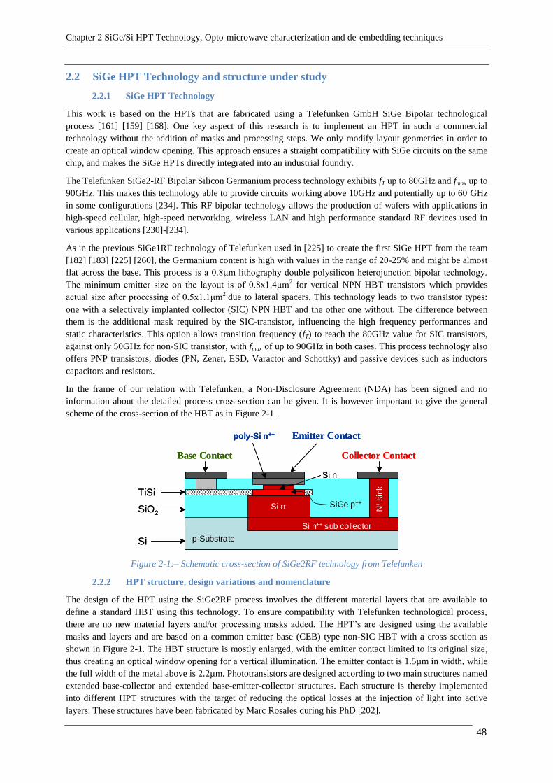
Chapter 2 SiGe/Si HPT Technology, Opto-microwave characterization and de-embedding techniques
48
2.2 SiGe HPT Technology and structure under study
2.2.1 SiGe HPT Technology
This work is based on the HPTs that are fabricated using a Telefunken GmbH SiGe Bipolar technological
process [161] [159] [168]. One key aspect of this research is to implement an HPT in such a commercial
technology without the addition of masks and processing steps. We only modify layout geometries in order to
create an optical window opening. This approach ensures a straight compatibility with SiGe circuits on the same
chip, and makes the SiGe HPTs directly integrated into an industrial foundry.
The Telefunken SiGe2-RF Bipolar Silicon Germanium process technology exhibits fT up to 80GHz and fmax up to
90GHz. This makes this technology able to provide circuits working above 10GHz and potentially up to 60 GHz
in some configurations [234]. This RF bipolar technology allows the production of wafers with applications in
high-speed cellular, high-speed networking, wireless LAN and high performance standard RF devices used in
various applications [230]-[234].
As in the previous SiGe1RF technology of Telefunken used in [225] to create the first SiGe HPT from the team
[182] [183] [225] [260], the Germanium content is high with values in the range of 20-25% and might be almost
flat across the base. This process is a 0.8μm lithography double polysilicon heterojunction bipolar technology.
The minimum emitter size on the layout is of 0.8x1.4μm2 for vertical NPN HBT transistors which provides
actual size after processing of 0.5x1.1μm2
due to lateral spacers. This technology leads to two transistor types:
one with a selectively implanted collector (SIC) NPN HBT and the other one without. The difference between
them is the additional mask required by the SIC-transistor, influencing the high frequency performances and
static characteristics. This option allows transition frequency (fT) to reach the 80GHz value for SIC transistors,
against only 50GHz for non-SIC transistor, with fmax of up to 90GHz in both cases. This process technology also
offers PNP transistors, diodes (PN, Zener, ESD, Varactor and Schottky) and passive devices such as inductors
capacitors and resistors.
In the frame of our relation with Telefunken, a Non-Disclosure Agreement (NDA) has been signed and no
information about the detailed process cross-section can be given. It is however important to give the general
scheme of the cross-section of the HBT as in Figure 2-1.
Figure 2-1:– Schematic cross-section of SiGe2RF technology from Telefunken
2.2.2 HPT structure, design variations and nomenclature
The design of the HPT using the SiGe2RF process involves the different material layers that are available to
define a standard HBT using this technology. To ensure compatibility with Telefunken technological process,
there are no new material layers and/or processing masks added. The HPT’s are designed using the available
masks and layers and are based on a common emitter base (CEB) type non-SIC HBT with a cross section as
shown in Figure 2-1. The HBT structure is mostly enlarged, with the emitter contact limited to its original size,
thus creating an optical window opening for a vertical illumination. The emitter contact is 1.5µm in width, while
the full width of the metal above is 2.2µm. Phototransistors are designed according to two main structures named
extended base-collector and extended base-emitter-collector structures. Each structure is thereby implemented
into different HPT structures with the target of reducing the optical losses at the injection of light into active
layers. These structures have been fabricated by Marc Rosales during his PhD [202].
Collector Contact
Si n-
Si n++ sub collector
N+
sin
k
Base Contact
Emitter Contact
TiSi
SiO2
Si p-Substrate
SiGe p++
Si n
poly-Si n++
Collector Contact
Si n-
Si n++ sub collector
N+
sin
k
Base Contact
Emitter Contact
TiSi
SiO2
Si p-Substrate
SiGe p++
Si n
poly-Si n++
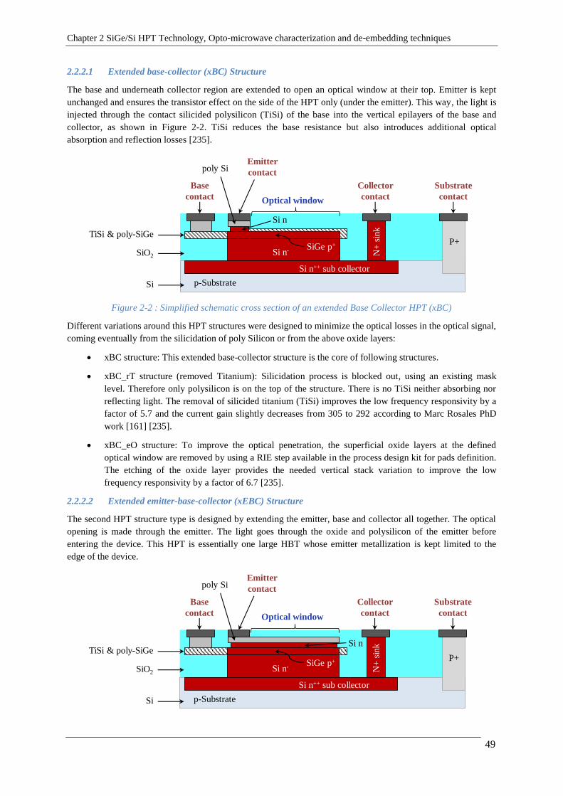
Chapter 2 SiGe/Si HPT Technology, Opto-microwave characterization and de-embedding techniques
49
2.2.2.1 Extended base-collector (xBC) Structure
The base and underneath collector region are extended to open an optical window at their top. Emitter is kept
unchanged and ensures the transistor effect on the side of the HPT only (under the emitter). This way, the light is
injected through the contact silicided polysilicon (TiSi) of the base into the vertical epilayers of the base and
collector, as shown in Figure 2-2. TiSi reduces the base resistance but also introduces additional optical
absorption and reflection losses [235].
Figure 2-2 : Simplified schematic cross section of an extended Base Collector HPT (xBC)
Different variations around this HPT structures were designed to minimize the optical losses in the optical signal,
coming eventually from the silicidation of poly Silicon or from the above oxide layers:
xBC structure: This extended base-collector structure is the core of following structures.
xBC_rT structure (removed Titanium): Silicidation process is blocked out, using an existing mask
level. Therefore only polysilicon is on the top of the structure. There is no TiSi neither absorbing nor
reflecting light. The removal of silicided titanium (TiSi) improves the low frequency responsivity by a
factor of 5.7 and the current gain slightly decreases from 305 to 292 according to Marc Rosales PhD
work [161] [235].
xBC_eO structure: To improve the optical penetration, the superficial oxide layers at the defined
optical window are removed by using a RIE step available in the process design kit for pads definition.
The etching of the oxide layer provides the needed vertical stack variation to improve the low
frequency responsivity by a factor of 6.7 [235].
2.2.2.2 Extended emitter-base-collector (xEBC) Structure
The second HPT structure type is designed by extending the emitter, base and collector all together. The optical
opening is made through the emitter. The light goes through the oxide and polysilicon of the emitter before
entering the device. This HPT is essentially one large HBT whose emitter metallization is kept limited to the
edge of the device.
Optical window
Substrate
contact
Collector
contact
Base
contact
Emitter
contact
Si
TiSi & poly-SiGe
SiGe p+
SiO2
Si n
poly Si
p-Substrate
Si n++ sub collector
Si n- N+
sin
k
P+
Optical window
Substrate
contact
Collector
contact
Base
contact
Emitter
contact
Si
TiSi & poly-SiGe
SiGe p+
SiO2
Si n
poly Si
p-Substrate
Si n++ sub collector
Si n- N+
sin
k
P+

Chapter 2 SiGe/Si HPT Technology, Opto-microwave characterization and de-embedding techniques
50
Figure 2-3 : Simplified schematic cross section of an extended Emitter Base Collector HPT (xEBC)
One variant with a reduced thickness of oxide layers on the top was fabricated to evaluate optical losses:
1. xEBC structure.
2. xEBC_eO structure: oxide layers above at the defined optical window are etched out. The oxide etching
improves the optical response by 2dB [235].
Different structures were implemented in the three prototyping runs during the work of Marc Rosales. To keep
the reference of the wafer lot and the design variations, we use and remind his HPT name labelling [235]:
<Prototype Run Number>-<Optical Window Size><optical window type><xBC or xEBC><extras><extras>
Reference code for HPT description is built as follows:
R1, R2, R3 code can be added before, to specify the run number of HPT devices.
Prototype Run Number R1, R2, R3
Optical Window Size 03 = 3 µm x 3 µm
05 = 5 µm x 5 µm
10 = 10 µm x 10 µm
20 = 20 µm x 20 µm
30 = 30 µm x 30 µm
40 = 40 µm x 40 µm
50 = 50 µm x 50 µm
Optical Window Type xBC = extended Base Collector
xEBC = extended Emitter Base Collector
Optical Window Shape SQ = Square
CR = circular, applicable to xEBC type only
Extras rT = removed Titanium, applicable only to xBC type
eO = etched oxide
sic = if the collector uses SIC.
For example, R1_10SQxBCrTeO corresponds to Prototype Run 1, with square optical window size of
10x10µm2, extended base and collector, removed titanium and etched oxide. R2_50SQxEBC_eO corresponds to
Prototype Run 2, with square optical window size of 50x50µm2, extended emitter, base and collector, and etched
oxide.
In his thesis [235], Marc Rosales focused on the validation and identification of the best structure in terms of dc
biasing and opto-microwave responses. He validated that extended emitter-base-collector (xEBC) HPT structures
on prototype run 2 shows better performance by 11dB in terms of opto-microwave gain and the cutoff frequency
is improved by a 30% ratio (for both oxide etched and non-etched) when compared to extended base collector
(xBC) structure. Therefore, in this thesis, we will focus on xEBC structures only for further experimental studies.
It will correspond to the samples R2_03SQxEBC (3x3µm2), R2_05SQxEBC (5x5µm
2), R2_10SQxEBC
(10x10µm2) and R2_50SQxEBC (50x50µm
2). The test results are reported in chapter 3. We have also designed
an edge illuminated structure based on the same technology. The experimental results of such structure are
presented in chapter 5. In the present chapter we deal with tools that are used for opto-microwave
03SQxEB C_sic_rT_eO_swit ch
Window size(eg 3µm)
ShapeCR:circularSQ: square
TopologyxEBCxBC
if SIC if rT if eO Switch optioncommon base

Chapter 2 SiGe/Si HPT Technology, Opto-microwave characterization and de-embedding techniques
51
characterization of the HPTs and different approaches (physical and technical approaches) to deeply understand
the behavior of SiGe/Si HPTs.

Chapter 2 SiGe/Si HPT Technology, Opto-microwave characterization and de-embedding techniques
52
2.3 Opto-Microwave Characterization
2.3.1 Optical Microwave characteristics of phototransistor
This section is focused on the definition of parameters that characterize the phototransistor behavior as shown in
Figure 2-4. This curve is extracted from S-parameter measurement of the opto-microwave link. From this figure
we can extract the opto-microwave gain both in photodiode (GOM,PD mode) and in phototransistor mode (GOM,HPT
mode), the cutoff frequency (f-3dB,OM) and the optical transition frequency (fT,opt). The photodiode mode is obtained
by setting the base-emitter biasing dc voltage to zero, whereas the phototransistor mode is obtained by setting
appropriate voltage biasing at the base-emitter contact (typically above 0.6V to activate the transistor effect).
First of all let’s define the opto-microwave gain (GOM). The opto-microwave gain represents the ratio of the HPT
output signal power (Pout-hpt) to the output power of a photodiode with a 1A/W responsivity and loaded by 50Ω
(P1A/W-photodiode-over-50Ω) [182] [200] [225] as presented in equation(2.1). This is of particular use as it is equal to the
square of the responsivity (i.e., same value in dB) under a 50Ω loading condition. This provides an effective
means of evaluating the efficiency of matching networks compared to a 50Ω loading network as reference case.
1 / 50
out hpt
OM
A W photodiode over
PG
P
(2.1)
If loaded with 50 Ohms, then it comes:
2
0 c2
OM hpt2
0 opt
1.R I
2G f R1
.R P2
.
.
(2.2)
| |OM dB hpt dBG R (2.3)
Where Rhpt is the responsivity of the phototransistor, Popt is the illumination optical power considered as
equivalent to a current and IC is the collector current.
Figure 2-4: Typical phototransistor characteristics and definition of opto-microwave parameters.
The opto-microwave S-parameters are an extension into the opto-microwave domain of the scattering parameters
as defined in the microwave domain [200] [225]. We can consider a phototransistor as a 3-ports device, whose
accesses are labelled 1, 2 and 3, where 1 represents the base access, 2 is the optical access and 3 is the collector
access as shown in Figure 2-5 a). The extension relies on the modeling of the optical port as an electrical port
GO
M(d
B)
Frequency (Hz)
GOM,HPT mode
fT,opt
Gopt
GOM,PD mode
f-3dB,OM

Chapter 2 SiGe/Si HPT Technology, Opto-microwave characterization and de-embedding techniques
53
whose input impedance is 50Ω as shown in Figure 2-5 b). A current of the same amplitude as the modulated
optical power models the optical signal. It can be considered as if the signal were detected by a virtual 1 A/W
photodiode before entering the internal phototransistor. Both the amplitude and phase information and power
waves theory can be transposed [200] [225]. This approach is the origin of the opto-microwave power gain
definition [225] and the opto-microwave noise figure definition [10].
a) b)
Figure 2-5: a) Three ports schematic representation of the HPT; b) definition of the equivalent optical input port
[225]
According to [200] [225], the opto-microwave gain of such a three-ports HPT can then be written as:
2 2
2 311 0 2 32 2
11 1 3 3
. . . ..
1 Γ1 .Γ
Γ 1 Γ.1OM
MG G G G S
S sp
(2.4)
Where 1 and 3 are respectively the base and collector load reflection coefficients, and where M and sp3 are
given below:
1211 31
32
. S
M S SS
(2.5)
1311 31 1
33
3 33
11 1
.
..
1 .Γ
1 Γ
SS S
Ssp S
S
(2.6)
G0 is the main transfer characteristic while G1 is a pure Γ1 function that describes the influence of the base load
impedance on the GOM. G2 shows the influence of the collector load impedance. It is lightly influenced by Γ1 but
this dependency could be neglected.
All S-parameters are measured by using the bench setup described in section 2.3.2. The opto-microwave gain of
the HPTs of various optical window sizes as a function of the frequency could then be plotted as shown in Figure
2-4 for both photodiode and phototransistor modes. From such experimental results another characteristic of
phototransistors called optical gain Gopt can also be extracted. It is defined as the difference between the HPT
GOM (in dB) as a function of the frequency and the PD mode GOM (in dB) at low frequency, all measured under
50Ohms load conditions. It is the current gain enhancement between the HPT and PD modes of operation (the
internal gain of the phototransistor due to its amplification effect).
From this opto-microwave characteristic curve we can also extract the opto-microwave dynamic behavior of the
phototransistor through the cutoff frequency in PD and HPT modes and through the optical transition frequency.
The opto-microwave cutoff frequency (f-3dB,OM) is the frequency at which the opto-microwave gain drops by 3dB
from its dc response.
The optical transition frequency fT opt is the frequency at which the optical gain is unity or zero in dB. This sets
the limit for the use of phototransistor as a photocurrent amplifier. It can also be seen as the frequency for which
the responsivity of the phototransistor in phototransistor mode is equal to the low frequency responsivity in
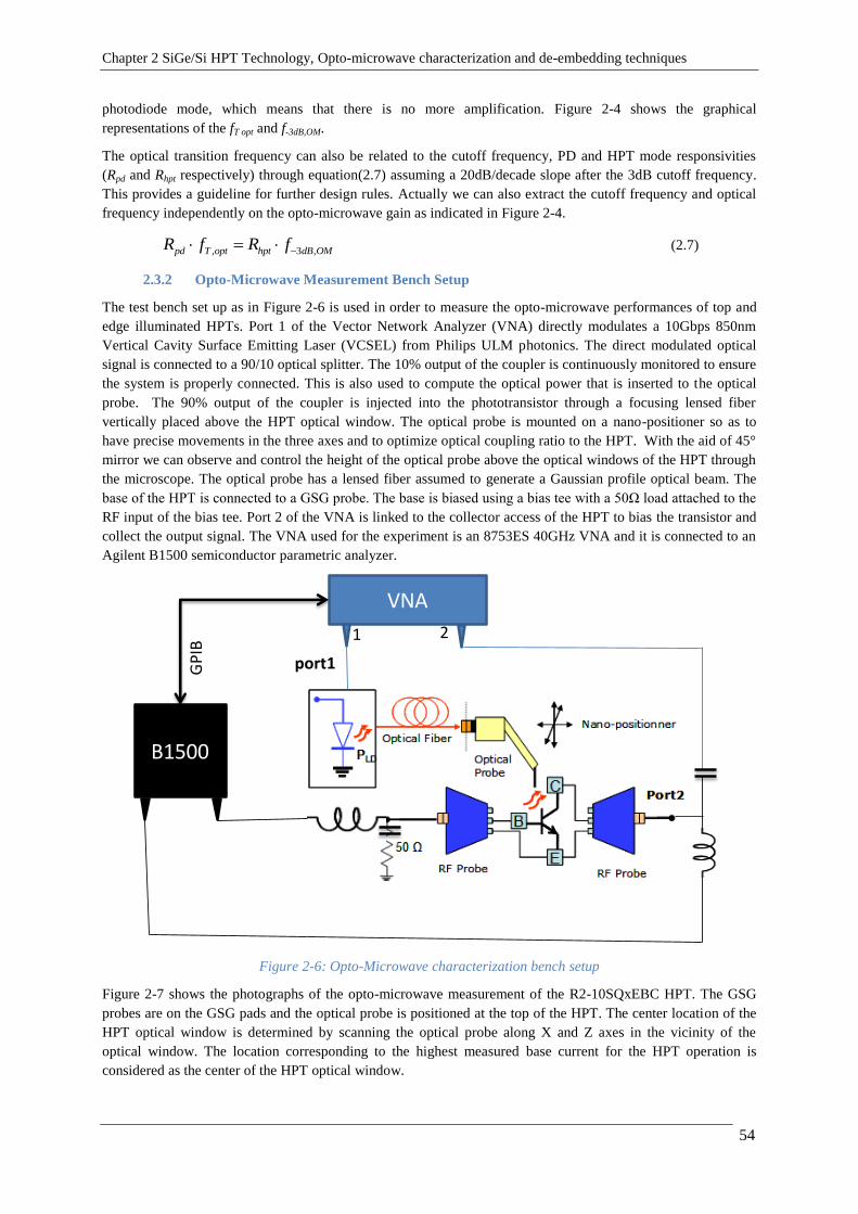
Chapter 2 SiGe/Si HPT Technology, Opto-microwave characterization and de-embedding techniques
54
photodiode mode, which means that there is no more amplification. Figure 2-4 shows the graphical
representations of the fT opt and f-3dB,OM.
The optical transition frequency can also be related to the cutoff frequency, PD and HPT mode responsivities
(Rpd and Rhpt respectively) through equation(2.7) assuming a 20dB/decade slope after the 3dB cutoff frequency.
This provides a guideline for further design rules. Actually we can also extract the cutoff frequency and optical
frequency independently on the opto-microwave gain as indicated in Figure 2-4.
, 3 ,pd T opt hpt dB OMR f R f (2.7)
2.3.2 Opto-Microwave Measurement Bench Setup
The test bench set up as in Figure 2-6 is used in order to measure the opto-microwave performances of top and
edge illuminated HPTs. Port 1 of the Vector Network Analyzer (VNA) directly modulates a 10Gbps 850nm
Vertical Cavity Surface Emitting Laser (VCSEL) from Philips ULM photonics. The direct modulated optical
signal is connected to a 90/10 optical splitter. The 10% output of the coupler is continuously monitored to ensure
the system is properly connected. This is also used to compute the optical power that is inserted to the optical
probe. The 90% output of the coupler is injected into the phototransistor through a focusing lensed fiber
vertically placed above the HPT optical window. The optical probe is mounted on a nano-positioner so as to
have precise movements in the three axes and to optimize optical coupling ratio to the HPT. With the aid of 45°
mirror we can observe and control the height of the optical probe above the optical windows of the HPT through
the microscope. The optical probe has a lensed fiber assumed to generate a Gaussian profile optical beam. The
base of the HPT is connected to a GSG probe. The base is biased using a bias tee with a 50Ω load attached to the
RF input of the bias tee. Port 2 of the VNA is linked to the collector access of the HPT to bias the transistor and
collect the output signal. The VNA used for the experiment is an 8753ES 40GHz VNA and it is connected to an
Agilent B1500 semiconductor parametric analyzer.
Figure 2-6: Opto-Microwave characterization bench setup
Figure 2-7 shows the photographs of the opto-microwave measurement of the R2-10SQxEBC HPT. The GSG
probes are on the GSG pads and the optical probe is positioned at the top of the HPT. The center location of the
HPT optical window is determined by scanning the optical probe along X and Z axes in the vicinity of the
optical window. The location corresponding to the highest measured base current for the HPT operation is
considered as the center of the HPT optical window.
VNA
B1500
GP
IB
port1
1 2

Chapter 2 SiGe/Si HPT Technology, Opto-microwave characterization and de-embedding techniques
55
Figure 2-7: Optical probe at the top of HPT structure
Figure 2-8 shows the photographs of the bench setup with the required fiber mounting modifications to
characterize edge illuminated HPTs. All the connections, except the axis of light injection, are similar to the
bench setup described above. To inject light on the side, we use a horizontal optical probe supporter to point the
optical probe on the side as shown in Figure 2-8 a). To control the position of illumination we attach the optical
probe with the nano-positioner, so that we can move the fiber in a well-controlled way. Figure 2-8 b) shows the
microscopic picture of the device under test along with the optical fiber on the side. From this view we can
control the movement of the fiber along x and z axes. In the same picture we can clearly observe the base and
collector contacts through RF probe. Figure 2-8 c) is a microscopic picture taken through a 45 degree mirror. By
using this view we can control the movement of the optical probe along y axis.
Figure 2-8: Experimental bench setup of edge illuminated HPTs. a) photograph of the bench. b) Top view
microscopic picture of the device under test and the optical probe pointing on the edge side of the HPT. c)
Microscopic picture taken from 45o mirror.
It is then important to note that the measurement of the HPT is actually the measurement of the link composed of
the laser, the injection fiber, the electrical connectors and the phototransistor. To characterize only the HPT, it is
necessary to overcome the losses and phase shifts introduced by the test link. It is therefore necessary to correct
mathematically the errors from the actual behavior of devices under test. Thus, the measurement is carried out in
two steps, firstly with a reference photodetector, then with the phototransistor under test.
Optical probe support
Optical probe attached tothe nano-positioner
fiber
a)
b) c)

Chapter 2 SiGe/Si HPT Technology, Opto-microwave characterization and de-embedding techniques
56
2.3.3 Calibration and De-embedding Techniques
The purpose of this part is to demonstrate how to extract the HPT characteristics from the test link, through
hybrid calibration techniques. The implementation of one of the extraction techniques known as “T matrix”
[172] will be detailed for the electrical error correction. Then the opto-microwave calibration itself will be
described. Finally the test fixture de-embedding technique will be presented.
When an optical signal is introduced, we can define the opto-microwave S-parameters, and calibrations then
become hybrid, using opto-microwave quantities described in section 2.3.1. It is therefore necessary to develop
new calibration procedures. The problem with this kind of calibration is that the chain of elements at the input
port is compatible with a coaxial cable of Type K, while the output port is in the form of a coplanar line access
only compatible with a GSG probe. It is thus not possible to use a conventional SOLT calibration since the loads
used for calibration (Open, short, load and Thru) cannot be connected to both ports simultaneously. Thus a
proper calibration technique with a precise de-embedding technique has to be implemented.
At this point, it is necessary to define the measurement planes as shown in Figure 2-9. This shows the
measurement plane where we can connect the input and the output ports simultaneously through the K-connector
for microwave calibration. The device under test is then made of the laser, the optical channel offset (optical
fiber, splitter and optical probe), the phototransistor and port 2 GSG RF probe.
Figure 2-9 : Defining the opto-microwave measurement planes. The device under test in the link includes 850nm
VCSEL, optical fiber, optical probe, the phototransistor and port 2 RF probe.
Thus, to perform this type of calibration, there are several techniques:
The adapter removal calibration technique is described in the reference [236]. This technique is applied
to study the DUT composed of the laser, fiber and HPT, which is an insertable device with K connector
at the input and GSG pads at the output.
The ghost removal technique [190] also sets the DUT to consist of the laser, fiber and HPT. The HPT
under study has GSG pads as connectors for its base and another set of GSG pads for its collector. The
first step for this technique involves setting up the measurement bench for full two-port on-wafer
calibration and performing this calibration. This moves the measurement plane up to the tips of the
GSG probe. Step two involves physically disconnecting the port 1 of the VNA that was connected to
one of the GSG probes and keeping the port 2 of the VNA connected to the other GSG probe. In the
third step, one connects the port 1 of the VNA to the laser and land the GSG probe on the GSG pad
which is connected to the collector of the HPT. Measurements of the DUT are done on this step. These
measurements include the effects of ghost parameters due to the change of measurement setup
immediately after a calibration procedure. In the last step the connector is physically disconnected from
VNA
port1
Legends: Measurement plane
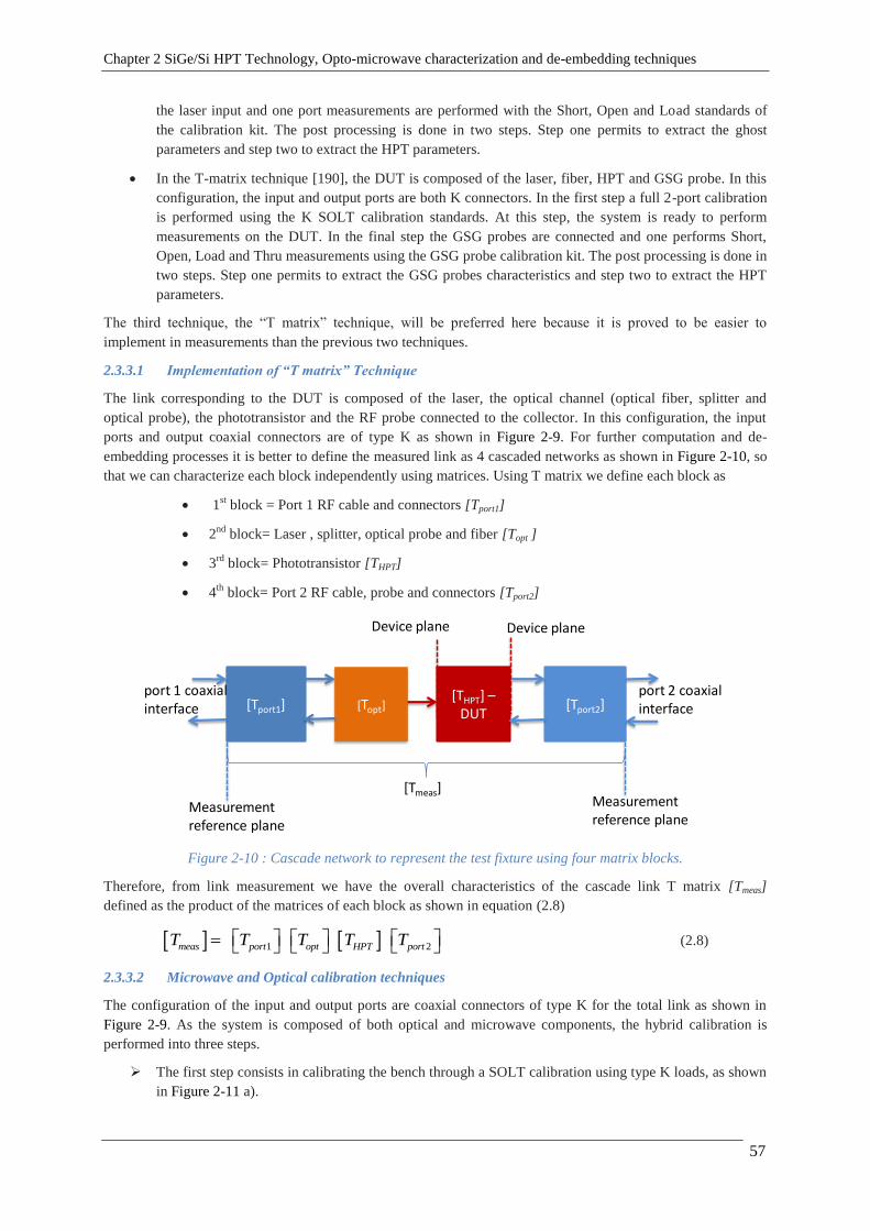
Chapter 2 SiGe/Si HPT Technology, Opto-microwave characterization and de-embedding techniques
57
the laser input and one port measurements are performed with the Short, Open and Load standards of
the calibration kit. The post processing is done in two steps. Step one permits to extract the ghost
parameters and step two to extract the HPT parameters.
In the T-matrix technique [190], the DUT is composed of the laser, fiber, HPT and GSG probe. In this
configuration, the input and output ports are both K connectors. In the first step a full 2-port calibration
is performed using the K SOLT calibration standards. At this step, the system is ready to perform
measurements on the DUT. In the final step the GSG probes are connected and one performs Short,
Open, Load and Thru measurements using the GSG probe calibration kit. The post processing is done in
two steps. Step one permits to extract the GSG probes characteristics and step two to extract the HPT
parameters.
The third technique, the “T matrix” technique, will be preferred here because it is proved to be easier to
implement in measurements than the previous two techniques.
2.3.3.1 Implementation of “T matrix” Technique
The link corresponding to the DUT is composed of the laser, the optical channel (optical fiber, splitter and
optical probe), the phototransistor and the RF probe connected to the collector. In this configuration, the input
ports and output coaxial connectors are of type K as shown in Figure 2-9. For further computation and de-
embedding processes it is better to define the measured link as 4 cascaded networks as shown in Figure 2-10, so
that we can characterize each block independently using matrices. Using T matrix we define each block as
1st block = Port 1 RF cable and connectors [Tport1]
2nd
block= Laser , splitter, optical probe and fiber [Topt ]
3rd
block= Phototransistor [THPT]
4th
block= Port 2 RF cable, probe and connectors [Tport2]
Figure 2-10 : Cascade network to represent the test fixture using four matrix blocks.
Therefore, from link measurement we have the overall characteristics of the cascade link T matrix [Tmeas]
defined as the product of the matrices of each block as shown in equation (2.8)
1 2 meas port opt HPT portT T T T T (2.8)
2.3.3.2 Microwave and Optical calibration techniques
The configuration of the input and output ports are coaxial connectors of type K for the total link as shown in
Figure 2-9. As the system is composed of both optical and microwave components, the hybrid calibration is
performed into three steps.
The first step consists in calibrating the bench through a SOLT calibration using type K loads, as shown
in Figure 2-11 a).
[Tport1] [Topt][THPT] –
DUT[Tport2]
Measurement reference plane
Measurement reference plane
port 2 coaxial interface
port 1 coaxial interface
Device planeDevice plane
[Tmeas]
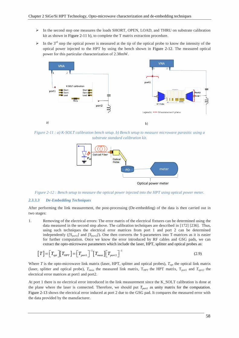
Chapter 2 SiGe/Si HPT Technology, Opto-microwave characterization and de-embedding techniques
58
In the second step one measures the loads SHORT, OPEN, LOAD, and THRU on substrate calibration
kit as shown in Figure 2-11 b), to complete the T matrix extraction procedure.
In the 3rd
step the optical power is measured at the tip of the optical probe to know the intensity of the
optical power injected to the HPT by using the bench shown in Figure 2-12. The measured optical
power for this particular characterization of 2.38mW.
Figure 2-11 : a) K-SOLT calibration bench setup. b) Bench setup to measure microwave parasitic using a
substrate standard calibration kit.
Figure 2-12 : Bench setup to measure the optical power injected into the HPT using optical power meter.
2.3.3.3 De-Embedding Techniques
After performing the link measurement, the post-processing (De-embedding) of the data is then carried out in
two stages:
1. Removing of the electrical errors: The error matrix of the electrical fixtures can be determined using the
data measured in the second step above. The calibration techniques are described in [172] [236]. Thus,
using such techniques the electrical error matrices from port 1 and port 2 can be determined
independently ([Sport1] and [Sport2]). One then converts the S-parameters into T-matrices as it is easier
for further computation. Once we know the error introduced by RF cables and GSG pads, we can
extract the opto-microwave parameters which include the laser, HPT, splitter and optical probes as:
1 1
1 2opt HPT port meas portT T T T T T
(2.9)
Where T is the opto-microwave link matrix (laser, HPT, splitter and optical probes), Topt the optical link matrix
(laser, splitter and optical probe), Tmeas the measured link matrix, THPT the HPT matrix, Tport1 and Toprt2 the
electrical error matrices at port1 and port2.
At port 1 there is no electrical error introduced in the link measurement since the K_SOLT calibration is done at
the plane where the laser is connected. Therefore, we should put Tport1 as unity matrix for the computation.
Figure 2-13 shows the electrical error induced at port 2 due to the GSG pad. It compares the measured error with
the data provided by the manufacturer.
PD meter
Optical power meter
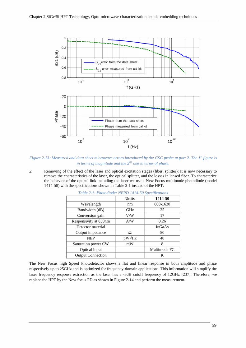
Chapter 2 SiGe/Si HPT Technology, Opto-microwave characterization and de-embedding techniques
59
Figure 2-13: Measured and data sheet microwave errors introduced by the GSG probe at port 2. The 1st figure is
in terms of magnitude and the 2nd
one in terms of phase.
2. Removing of the effect of the laser and optical excitation stages (fiber, splitter): It is now necessary to
remove the characteristics of the laser, the optical splitter, and the losses in lensed fiber. To characterize
the behavior of the optical link including the laser we use a New Focus multimode photodiode (model
1414-50) with the specifications shown in Table 2-1 instead of the HPT.
Table 2-1: Photodiode: NFPD 1414-50 Specifications
Units 1414-50
Wavelength nm 800-1630
Bandwidth (dB) GHz 25
Conversion gain V/W 17
Responsivity at 850nm A/W 0.26
Detector material InGaAs
Output impedance Ω 50
NEP pW√Hz 40
Saturation power CW mW 8
Optical Input Multimode FC
Output Connection K
The New Focus high Speed Photodetector shows a flat and linear response in both amplitude and phase
respectively up to 25GHz and is optimized for frequency-domain applications. This information will simplify the
laser frequency response extraction as the laser has a -3dB cutoff frequency of 12GHz [237]. Therefore, we
replace the HPT by the New focus PD as shown in Figure 2-14 and perform the measurement.
10-1
100
101
-0.8
-0.6
-0.4
-0.2
0
S21 (
dB
)
f (GHz)
S21
error from the data sheet
S21
error measured from cal kit
108
109
1010
-60
-40
-20
0
20
f (Hz)
Phase
Phase from the data sheet
Phase measured from cal kit
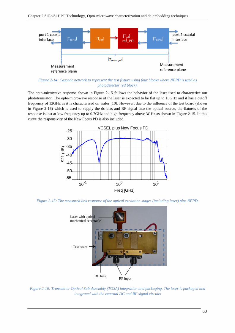
Chapter 2 SiGe/Si HPT Technology, Opto-microwave characterization and de-embedding techniques
60
Figure 2-14: Cascade network to represent the test fixture using four blocks where NFPD is used as
photodetector red block).
The opto-microwave response shown in Figure 2-15 follows the behavior of the laser used to characterize our
phototransistor. The opto-microwave response of the laser is expected to be flat up to 10GHz and it has a cutoff
frequency of 12GHz as it is characterized on wafer [10]. However, due to the influence of the test board (shown
in Figure 2-16) which is used to supply the dc bias and RF signal into the optical source, the flatness of the
response is lost at low frequency up to 0.7GHz and high frequency above 3GHz as shown in Figure 2-15. In this
curve the responsivity of the New Focus PD is also included.
Figure 2-15: The measured link response of the optical excitation stages (including laser) plus NFPD.
Figure 2-16: Transmitter Optical Sub-Assembly (TOSA) integration and packaging. The laser is packaged and
integrated with the external DC and RF signal circuits
[Tport1] [Topt][Tpd] –ref_PD
[Tport2]
Measurement reference plane
Measurement reference plane
port 2 coaxial interface
port 1 coaxial interface
10-1
100
101
-55
-50
-45
-40
-35
-30
-25
S2
1 (
dB
)
Freq [GHz]
VCSEL plus New Focus PD
Laser with optical
mechanical receptacle
Test board
RF inputDC bias

Chapter 2 SiGe/Si HPT Technology, Opto-microwave characterization and de-embedding techniques
61
Thus, from this measurement we should extract the behavior of the laser along with the optical excitation stages
[Topt] by removing the New Focus PD response as follows.
Similarly to the 1st stage related to the electrical errors coming from the electrical test fixture, we remove the
optical excitation stages using equation(2.10).
1 1
1 2pdopt pd opt pd port meas portT T T T T T
(2.10)
Where [Tpd] is the responsivity of the NFPD used instead of HPT, [Topt+pd] is the link response of optical
excitation stages (including laser) plus NFPD, [Topt] the optical link matrix (laser, splitter and optical probe) and
[Tmeas_pd] the measured link matrix with NFPD.
According to Table 2-1, the reference photodiode has a responsivity of 0.26 A/W. This value can also be
measured directly through an LIV measurement, providing the dc curve of the photogenerated current as a
function of the injected optical power. The extracted slope then provides the real effective responsivity of the
photodiode, which is then measured to be 0.222A/W. The opto microwave gain of the New focus Photodiode
can be obtained from the responsivity by using equation (2.11) as explained in [236].
21
0.22220log 20log( ) 19.093
2pd PDS R (2.11)
Since we know the link response of optical excitation stages (laser, optical interconnection) plus NFPD [Topt+pd],
it is now easy to remove the NFPD response and extract such optical excitation stages response as:
1
opt opt pd pdT T T
(2.12)
It leads to the response of the optical interconnection. By using equation(2.9), we can extract the pure opto
microwave response of the HPT as:
1
HPT optT T T
(2.13)
Where T is the opto-microwave link matrix (laser, HPT, splitter and optical probes)
All opto-microwave responses of HPTs presented in this thesis are extracted by using the above processes.
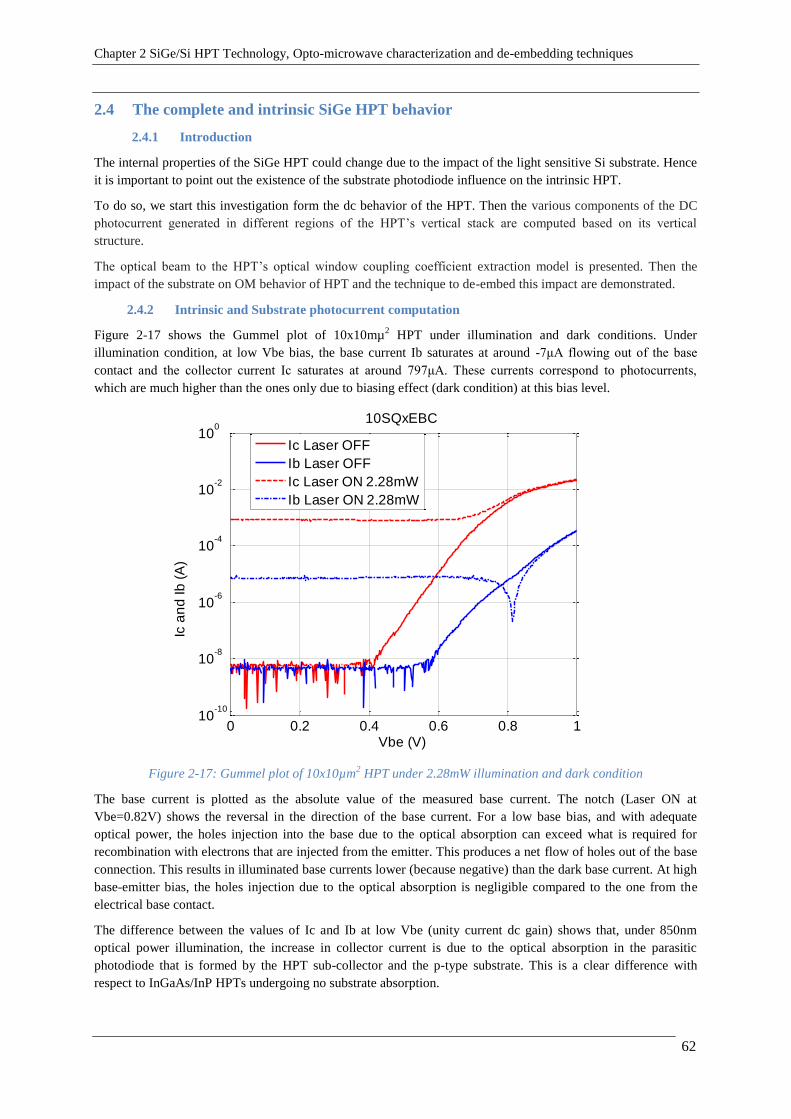
Chapter 2 SiGe/Si HPT Technology, Opto-microwave characterization and de-embedding techniques
62
2.4 The complete and intrinsic SiGe HPT behavior
2.4.1 Introduction
The internal properties of the SiGe HPT could change due to the impact of the light sensitive Si substrate. Hence
it is important to point out the existence of the substrate photodiode influence on the intrinsic HPT.
To do so, we start this investigation form the dc behavior of the HPT. Then the various components of the DC
photocurrent generated in different regions of the HPT’s vertical stack are computed based on its vertical
structure.
The optical beam to the HPT’s optical window coupling coefficient extraction model is presented. Then the
impact of the substrate on OM behavior of HPT and the technique to de-embed this impact are demonstrated.
2.4.2 Intrinsic and Substrate photocurrent computation
Figure 2-17 shows the Gummel plot of 10x10mµ2 HPT under illumination and dark conditions. Under
illumination condition, at low Vbe bias, the base current Ib saturates at around -7μA flowing out of the base
contact and the collector current Ic saturates at around 797μA. These currents correspond to photocurrents,
which are much higher than the ones only due to biasing effect (dark condition) at this bias level.
Figure 2-17: Gummel plot of 10x10µm2 HPT under 2.28mW illumination and dark condition
The base current is plotted as the absolute value of the measured base current. The notch (Laser ON at
Vbe=0.82V) shows the reversal in the direction of the base current. For a low base bias, and with adequate
optical power, the holes injection into the base due to the optical absorption can exceed what is required for
recombination with electrons that are injected from the emitter. This produces a net flow of holes out of the base
connection. This results in illuminated base currents lower (because negative) than the dark base current. At high
base-emitter bias, the holes injection due to the optical absorption is negligible compared to the one from the
electrical base contact.
The difference between the values of Ic and Ib at low Vbe (unity current dc gain) shows that, under 850nm
optical power illumination, the increase in collector current is due to the optical absorption in the parasitic
photodiode that is formed by the HPT sub-collector and the p-type substrate. This is a clear difference with
respect to InGaAs/InP HPTs undergoing no substrate absorption.
0 0.2 0.4 0.6 0.8 110
-10
10-8
10-6
10-4
10-2
100
10SQxEBC
Vbe (V)
Ic a
nd
Ib
(A
)
Ic Laser OFF
Ib Laser OFF
Ic Laser ON 2.28mW
Ib Laser ON 2.28mW
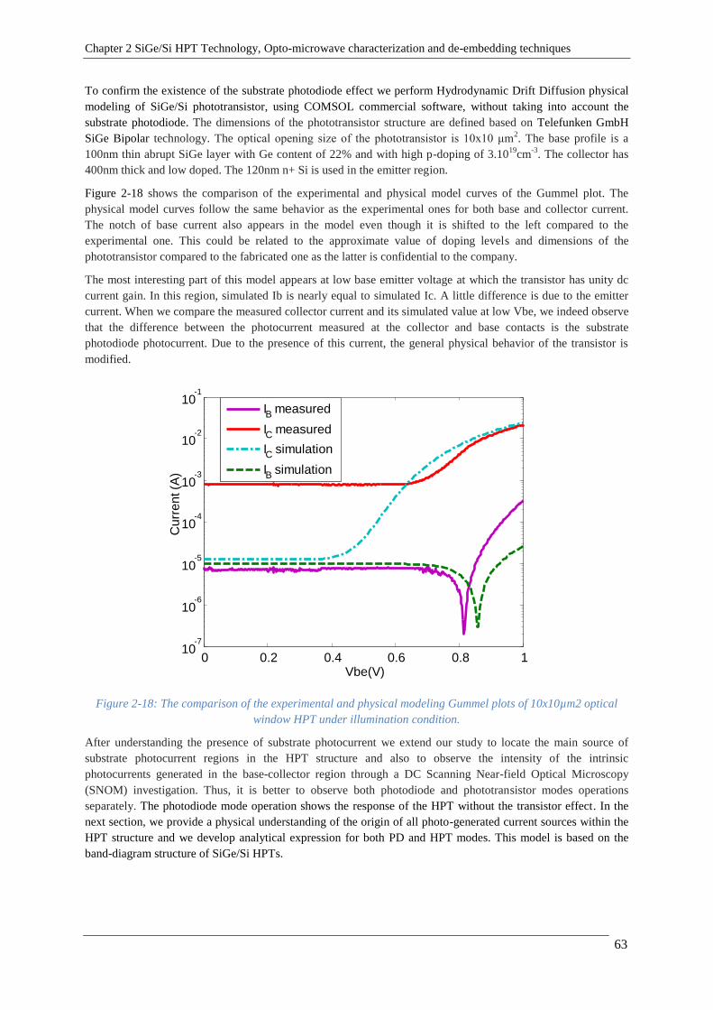
Chapter 2 SiGe/Si HPT Technology, Opto-microwave characterization and de-embedding techniques
63
To confirm the existence of the substrate photodiode effect we perform Hydrodynamic Drift Diffusion physical
modeling of SiGe/Si phototransistor, using COMSOL commercial software, without taking into account the
substrate photodiode. The dimensions of the phototransistor structure are defined based on Telefunken GmbH
SiGe Bipolar technology. The optical opening size of the phototransistor is 10x10 μm2. The base profile is a
100nm thin abrupt SiGe layer with Ge content of 22% and with high p-doping of 3.1019
cm-3
. The collector has
400nm thick and low doped. The 120nm n+ Si is used in the emitter region.
Figure 2-18 shows the comparison of the experimental and physical model curves of the Gummel plot. The
physical model curves follow the same behavior as the experimental ones for both base and collector current.
The notch of base current also appears in the model even though it is shifted to the left compared to the
experimental one. This could be related to the approximate value of doping levels and dimensions of the
phototransistor compared to the fabricated one as the latter is confidential to the company.
The most interesting part of this model appears at low base emitter voltage at which the transistor has unity dc
current gain. In this region, simulated Ib is nearly equal to simulated Ic. A little difference is due to the emitter
current. When we compare the measured collector current and its simulated value at low Vbe, we indeed observe
that the difference between the photocurrent measured at the collector and base contacts is the substrate
photodiode photocurrent. Due to the presence of this current, the general physical behavior of the transistor is
modified.
Figure 2-18: The comparison of the experimental and physical modeling Gummel plots of 10x10µm2 optical
window HPT under illumination condition.
After understanding the presence of substrate photocurrent we extend our study to locate the main source of
substrate photocurrent regions in the HPT structure and also to observe the intensity of the intrinsic
photocurrents generated in the base-collector region through a DC Scanning Near-field Optical Microscopy
(SNOM) investigation. Thus, it is better to observe both photodiode and phototransistor modes operations
separately. The photodiode mode operation shows the response of the HPT without the transistor effect. In the
next section, we provide a physical understanding of the origin of all photo-generated current sources within the
HPT structure and we develop analytical expression for both PD and HPT modes. This model is based on the
band-diagram structure of SiGe/Si HPTs.
0 0.2 0.4 0.6 0.8 110
-7
10-6
10-5
10-4
10-3
10-2
10-1
Vbe(V)
Cu
rre
nt (A
)
IB measured
IC measured
IC simulation
IB simulation

Chapter 2 SiGe/Si HPT Technology, Opto-microwave characterization and de-embedding techniques
64
A. In Photodiode mode
Primary photocurrent (Iprim_ph):
The primary photocurrent generated in the active area of the HPT, which is the total flux of carriers created by
the incident optical power, is expressed as
_
_
.. 1 . . .(1 )
.bSi Si i sS aGe e
opt i W W
prim ph int
PI q R e Г e
h c
(2.14)
Where Popt_i is the input optical power, R is the input reflection coefficient, ηint is internal quantum efficiency, Γ
is the confinement factor, αSi, αSiGe are the absorption coefficients of Si (in the emitter and collector) and SiGe (in
the base) respectively, WSi, WSiGe are the thickness of the Si region (emitter plus collector) and SiGe one (base)
respectively.
The primary photocurrent includes all the possible photocurrents generated by light in emitter, base and collector
regions and collected at the base contact.
When base-emitter junction is not biased, the generated primary photocurrent is distributed throughout the
structure as shown in Figure 2-19.
Figure 2-19 : The band gap of SiGe HPT along with distribution of photo-generated carriers, photodiode mode
(Vce>0, Vbe=0).
The electrons, generated in the base and collector, are divided into two streams: a few go to the emitter, and most
of them towards the collector, because of the electric potential introduced by Vce. The majority of holes in the
base are discharged by the base contact. Some holes can stay in the base or may go over the potential barrier to
reach the collector or emitter but this effect is very small and is neglected.
Electrons generated in the emitter are flowing to the emitter contact. Holes generated in the space charge region
are moving towards the base and the base contact. Thus, holes generated in the emitter and mostly in the
collector are contributing to the primary photocurrent and hence to the base current flowing out to the base
contact. Moreover, photo-generated electrons in the Si substrate at the proximity of the sub-collector within the
induced substrate space charge region are injected into the collector and reach the collector contact (hence
contribute to the collector current) and substrate holes are flowing away by the substrate contact (not added to
the primary photocurrent). Hence the current measured at the base contact are free from the substrate current.
The primary photocurrent is the photocurrent generated in the emitter, base and collector of the device due to the
optical light illumination. It can thus be rewritten from Figure 2-19 as:
_ _ _ _prim ph prim b prim c prim eI I I I (2.15)
position
I phe _
_ _b PD phI
Base SiGe (p+)Emitter Si (n+) Collector Si (n)
Photo-generated hole and electrons
En
erg
y ga
p
_ _C ph C subI I
I phprim_
Sub-collector Si (n++) Substrate Si (P)
_prim eI
_prim bI
_prim cI
_C phI
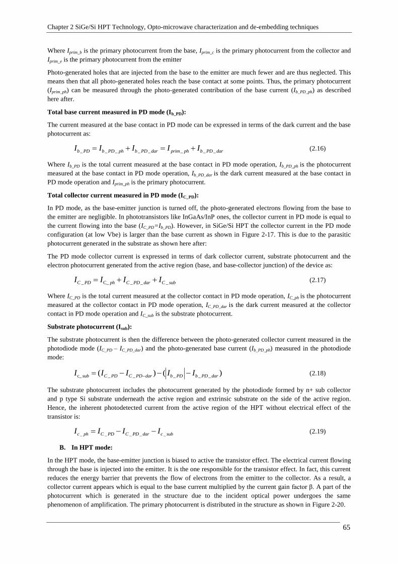
Chapter 2 SiGe/Si HPT Technology, Opto-microwave characterization and de-embedding techniques
65
Where Iprim_b is the primary photocurrent from the base, Iprim_c is the primary photocurrent from the collector and
Iprim_e is the primary photocurrent from the emitter
Photo-generated holes that are injected from the base to the emitter are much fewer and are thus neglected. This
means then that all photo-generated holes reach the base contact at some points. Thus, the primary photocurrent
(Iprim_ph) can be measured through the photo-generated contribution of the base current (Ib_PD_ph) as described
here after.
Total base current measured in PD mode (Ib_PD):
The current measured at the base contact in PD mode can be expressed in terms of the dark current and the base
photocurrent as:
_ _ _ _ _ _ _ _b PD b PD ph b PD dar prim ph b PD darI I I I I (2.16)
Where Ib_PD is the total current measured at the base contact in PD mode operation, Ib_PD_ph is the photocurrent
measured at the base contact in PD mode operation, Ib_PD_dar is the dark current measured at the base contact in
PD mode operation and Iprim_ph is the primary photocurrent.
Total collector current measured in PD mode (IC_PD):
In PD mode, as the base-emitter junction is turned off, the photo-generated electrons flowing from the base to
the emitter are negligible. In phototransistors like InGaAs/InP ones, the collector current in PD mode is equal to
the current flowing into the base (IC_PD=Ib_PD). However, in SiGe/Si HPT the collector current in the PD mode
configuration (at low Vbe) is larger than the base current as shown in Figure 2-17. This is due to the parasitic
photocurrent generated in the substrate as shown here after:
The PD mode collector current is expressed in terms of dark collector current, substrate photocurrent and the
electron photocurrent generated from the active region (base, and base-collector junction) of the device as:
_ C_ _ _ _C PD ph C PD dar C subI I I I (2.17)
Where IC_PD is the total current measured at the collector contact in PD mode operation, IC_ph is the photocurrent
measured at the collector contact in PD mode operation, IC_PD_dar is the dark current measured at the collector
contact in PD mode operation and IC_sub is the substrate photocurrent.
Substrate photocurrent (Isub):
The substrate photocurrent is then the difference between the photo-generated collector current measured in the
photodiode mode (IC_PD – IC_PD_dar) and the photo-generated base current (Ib_PD_ph) measured in the photodiode
mode:
c_ _ _ _ _ _( ) ( )sub C PD C PD dar b PD b PD darI I I I I (2.18)
The substrate photocurrent includes the photocurrent generated by the photodiode formed by n+ sub collector
and p type Si substrate underneath the active region and extrinsic substrate on the side of the active region.
Hence, the inherent photodetected current from the active region of the HPT without electrical effect of the
transistor is:
_ _ _ _ _c ph C PD C PD dar c subI I I I (2.19)
B. In HPT mode:
In the HPT mode, the base-emitter junction is biased to active the transistor effect. The electrical current flowing
through the base is injected into the emitter. It is the one responsible for the transistor effect. In fact, this current
reduces the energy barrier that prevents the flow of electrons from the emitter to the collector. As a result, a
collector current appears which is equal to the base current multiplied by the current gain factor β. A part of the
photocurrent which is generated in the structure due to the incident optical power undergoes the same
phenomenon of amplification. The primary photocurrent is distributed in the structure as shown in Figure 2-20.

Chapter 2 SiGe/Si HPT Technology, Opto-microwave characterization and de-embedding techniques
66
Figure 2-20: The band gap diagram of a common emitter HPT and the distribution of flows of photo-generated
carriers and electrical currents, in the phototransistor mode.
In the phototransistor mode, the holes that are photo-generated in the emitter are separated into two parts. One
part diffuses toward the emitter contact, and another part is injected into the base region due to both diffusion
and proximity of electrical field of the base-emitter space-charge-region. Photo-generated electrons are divided
into the emitter contact and the base region. As in the photodiode mode, some of the photo-generated holes in the
emitter, base and collector are thus collected by the base contact. This creates the current Ib_HPT_ph. However,
there are photo-generated holes which are injected into the emitter which creates the current called transistor
effect photocurrent (Ibe_HPT_ph). Moreover, in the case when the base-emitter diode is forward biased, the energy
barrier gets reduced so that the path mostly selected by photo-generated holes is towards the emitter. In terms of
equation, this means:
Primary photocurrent in HPT mode (Iprim_ph): As defined in equation(2.14), the primary photocurrent is the
photocurrent generated in the active region of the HPT which is exactly the same as the primary
photocurrent in the PD mode. In HPT mode it is expressed as:
_ _ _ _ _prim ph be HPT ph b HPT phI I I (2.20)
Where Ibe_HPT_ph is a fraction of photo-generated photocurrent flowing from the base to the emitter (activating the
transistor effect), Ib_HPT_ph is the photocurrent measured at the base contact in HPT mode.
There is the contribution of the primary photocurrent to the total base, emitter and collector currents of the
phototransistor. Theoretically these currents have electrical and optical origins as follows:
For the base: Total current measured at the base contact:
_ _ _ _ _b HPT b HPT ph b HPT darI I I (2.21)
Where Ib_HPT is the total current measured at the base contact in HPT mode and Ib_HPT_dar is the dark
current measured at the base contact in HPT mode.
For the collector: The total current measured at the collector contact is:
_ _ _ _ _ _ _ _ _ .c HPT c opt c HPT dar C sub c opt be HPT ph c phoptI I I I with I I I (2.22)
Where Ic_HPT is the total current measured at the collector contact in HPT mode, Ic_opt is the photo-
generated contribution and Ic_HPT_dar is the dark current, all measured at the collector contact in HPT
mode, βphoto is the common emitter photocurrent gain, Ibe_HPT_ph is the transistor effect activating
photocurrent and Ic_ph is the photocurrent measured at the collector contact in PD mode operation.
For the emitter: The total current measured at the emitter contact is:
position
_ _ _ _C HPT dar b HPT darI I
_ _
_
be HPT phphoto
C ph
I
I
_ _C opt C subI I
I phe _
I opte _
_ _b HPT darI_ _be HPT phI
_ _b HPT phI
_ _e HPT darI
Base SiGe (p+)Emitter Si (n+) Collector Si (n)E
ne
rgy
gap
I phprim_
Sub-Collector Si (n++) Substrate Si (P)
_C HPTI
_prim cI
_prim bI_prim eI

Chapter 2 SiGe/Si HPT Technology, Opto-microwave characterization and de-embedding techniques
67
_ _ _ _ _ _ _ _ ( 1).e HPT e opt e HPT dar e op optt be HPT ph e phI I I with I I I (2.23)
Where Ie_HPT is the total current measured at the emitter contact in HPT mode, Ie_opt is the photocurrent
contribution and Ie_HPT_dar is the dark current, all measured at the emitter contact in HPT mode, and Ie_ph
is the photocurrent measured at the collector contact in PD mode operation.
Finally Ie_opt is evaluated from equation (2.22) and (2.23) as:
_ _ _ _ _ _ _ _( )e opt c opt prim ph be HPT ph c opt b HPT phI I I I I I (2.24)
Photocurrent gain (βopt): the photocurrent gain of transistor is defined as the ratio between the amplified
photocurrent (difference between Ic_opt and Ic_ph) and the photocurrent flowing from the base to the emitter
(Ibe_HPT_ph), responsible of activating the transistor effect:
_ _
__ _
c opt c ph
be
op
HPT h
t
p
I I
I
(2.25)
Where Ibe_HPT_ph can be computed from equation 2.20. Ib_HPT_ph and Ic_opt can be computed from equation (2.21)
and (2.22) respectively as all terms in these equations are already known.
Base efficiency (𝜸): is the ratio of the photocurrent at the base to the primary photocurrent generated in the HPT.
__ _
_
b HPT ph
prim ph
I
I
(2.26)
Photocurrents computing flow-chart: Figure 2-21 shows the summary of computing photocurrents in different
regions of the phototransistor. This flow chart helps computing the previously defined currents.
Figure 2-21: Photocurrent computation flow chart
2.4.3 Extraction of the coupling coefficient
In this section we present how to extract the coupling coefficient of the optical beam and the device under test.
Among all photocurrents measured into the phototransistor, the base photocurrent is easily accessible and, as
opposed to the collector one, is only due to the intrinsic structure of the HPT and does not depend on other
contributions, such as the substrate photocurrent or amplification position dependent mechanisms. It is then
Lighted measuresIc_PD Ib_PD
Dark measuresIc_PD_dark Ib_PD_dark
- -
Isub+Ic_phIb_PD_ph Iprim_ph
-
Isub-
Ic_ph Ie_ph
-
PD mode
Lighted measuresIc_HPT Ib_HPT
Dark measuresIc_HPT_dark Ib_HPT_dark
--
Ic_opt
Ib_HPT_ph
-
-
Ie_opt
HPT mode
Ibe_HPT_ph
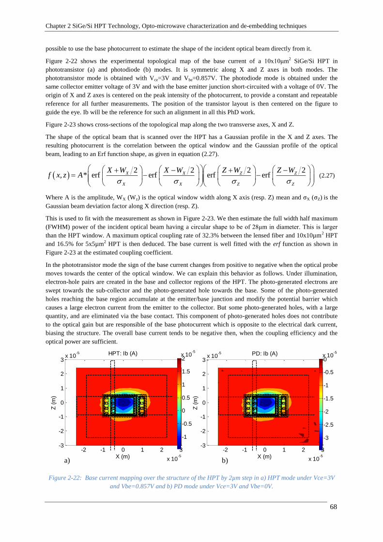
Chapter 2 SiGe/Si HPT Technology, Opto-microwave characterization and de-embedding techniques
68
possible to use the base photocurrent to estimate the shape of the incident optical beam directly from it.
Figure 2-22 shows the experimental topological map of the base current of a 10x10μm2 SiGe/Si HPT in
phototransistor (a) and photodiode (b) modes. It is symmetric along X and Z axes in both modes. The
phototransistor mode is obtained with Vce=3V and Vbe=0.857V. The photodiode mode is obtained under the
same collector emitter voltage of 3V and with the base emitter junction short-circuited with a voltage of 0V. The
origin of X and Z axes is centered on the peak intensity of the photocurrent, to provide a constant and repeatable
reference for all further measurements. The position of the transistor layout is then centered on the figure to
guide the eye. Ib will be the reference for such an alignment in all this PhD work.
Figure 2-23 shows cross-sections of the topological map along the two transverse axes, X and Z.
The shape of the optical beam that is scanned over the HPT has a Gaussian profile in the X and Z axes. The
resulting photocurrent is the correlation between the optical window and the Gaussian profile of the optical
beam, leading to an Erf function shape, as given in equation (2.27).
2 2 2 2
, * erf erf erf erfX X Z Z
X X Z Z
X W X W Z W Z Wf x z A
(2.27)
Where A is the amplitude, WX (Wz) is the optical window width along X axis (resp. Z) mean and σX (σZ) is the
Gaussian beam deviation factor along X direction (resp. Z).
This is used to fit with the measurement as shown in Figure 2-23. We then estimate the full width half maximum
(FWHM) power of the incident optical beam having a circular shape to be of 28μm in diameter. This is larger
than the HPT window. A maximum optical coupling rate of 32.3% between the lensed fiber and 10x10µm2 HPT
and 16.5% for 5x5µm2 HPT is then deduced. The base current is well fitted with the erf function as shown in
Figure 2-23 at the estimated coupling coefficient.
In the phototransistor mode the sign of the base current changes from positive to negative when the optical probe
moves towards the center of the optical window. We can explain this behavior as follows. Under illumination,
electron-hole pairs are created in the base and collector regions of the HPT. The photo-generated electrons are
swept towards the sub-collector and the photo-generated hole towards the base. Some of the photo-generated
holes reaching the base region accumulate at the emitter/base junction and modify the potential barrier which
causes a large electron current from the emitter to the collector. But some photo-generated holes, with a large
quantity, and are eliminated via the base contact. This component of photo-generated holes does not contribute
to the optical gain but are responsible of the base photocurrent which is opposite to the electrical dark current,
biasing the structure. The overall base current tends to be negative then, when the coupling efficiency and the
optical power are sufficient.
Figure 2-22: Base current mapping over the structure of the HPT by 2µm step in a) HPT mode under Vce=3V
and Vbe=0.857V and b) PD mode under Vce=3V and Vbe=0V.
X (m)
Z (
m)
PD: Ib (A)
-2 -1 0 1 2 3
x 10-5
-3
-2
-1
0
1
2
3x 10
-5
-3
-2.5
-2
-1.5
-1
-0.5
0x 10
-5
X (m)
Z (
m)
HPT: Ib (A)
-2 -1 0 1 2 3
x 10-5
-3
-2
-1
0
1
2
3x 10
-5
-1
-0.5
0
0.5
1
1.5
2x 10
-5
a) b)

Chapter 2 SiGe/Si HPT Technology, Opto-microwave characterization and de-embedding techniques
69
Figure 2-23: The slice of the base current at Z=0m a) HPT mode at Vce=3V and Vbe=0.857V and b) PD mode
at Vce=3V and Vbe=0V. The base current is not influenced by the substrate photocurrent as the photogenerated
carriers in the substrate are collected either by the substrate or collector contact intentionally.
2.4.4 Substrate photodiode impact on the Opto-microwave behavior
S-parameters and thus the opto-microwave gain are measured by using the bench setup described in section
2.3.2. Figure 2-24 shows the opto-microwave gain (GOM) of the HPTs having 10µmx10µm and 50µmx50µm
optical window size as a function of the frequency. In the same figure the PD and HPT modes of both devices
are presented. All the parasitic effects are removed by the de-embedding procedure described in section 2.3.3.
The measurements are made from 50MHz up to 20GHz.
The result shows that for a 0V Vbe biasing and 2V Collector voltage (PD mode), we observe a GOM of -32 dB at
50 MHz against a peak GOM value of -17 dB at 50 MHz for a base voltage of 0.857 V and 2 V collector voltage
(HPT mode) for an optical window size of 10SQxEBC (10x10µm2) HPT. For 50SQxEBC (50x50µm
2) HPT we
observe a PD mode GOM of -31 dB and HPT mode GOM of -5 dB at 50 MHz with the same biasing as the former
one. From the same figure we can also extract the optical gain, Gopt. For 10SQxEBC HPT we observe a Gopt at
50 MHz of 15 dB and for 50SQxEBC a Gopt at 50 MHz of 26 dB.
The PD mode Gom at low frequency of the 50x50µm2 HPT was expected to be much higher than for the
10x10µm2 HPT due to the higher optical coupling efficiency. However, they have nearly equal value. It is
obvious that there is a coupling loss for 10x10µm2 HPT, whereas for 50x50 a 100% coupling efficiency is
attended. This expectation is violated here; it is due to substrate photodiode effect which is more visible into the
10x10µm² HPT and increase the overall responsivity and thus the GOM.
Another observation is for frequencies less than 3GHz the slope of the Gom curve in PD mode for 10x10µm2
HPT versus frequency is steeper than the slope of Gom curve for 50x50µm2. The 10x10µm² do any exhibit any
plateau and has an almost 10dB/decade slope which is characteristics from substrate photocurrents. The cutoff
frequency of the smaller device then is smaller than the one of the 50x50µm² HPT in PD mode. Normally the
bigger one should have smaller cutoff frequency. This shows that there is a great impact of the slow substrate
photocurrent in PD mode on smaller HPTs. This will be investigated in detail in chapter 3.
-4 -2 0 2 4
x 10-5
-4
-3
-2
-1
0x 10
-5
X (m)
Ib (
A)
Ib measured
Erf model
a) b)
-4 -2 0 2 4
x 10-5
-2
-1
0
1
2x 10
-5
x (m)
Ib (
A)
Erf model,
Ib measured

Chapter 2 SiGe/Si HPT Technology, Opto-microwave characterization and de-embedding techniques
70
Figure 2-24: Opto microwave gain of 10SQxEBC and 50SQxEBC. At Vce=2V and Vbe=0.857V for HPT mode
and Vbe=0V for PD mode
2.4.5 De-embedding the frequency response of the substrate photodiode
Figure 2-26 b) shows the topological mapping experimental result of the low-frequency responsivity of the HPT
in the photodiode mode. The responsivity forms a donut shape with response higher in the substrate than in the
active area. This helps us to select a position of the fiber where we can isolate the substrate response from the
HPT one for further analysis. Figure 2-26 a) then shows the opto-microwave response of the substrate obtained
at X=5µm and X=15µm (where the peak of the substrate response appears).
The intrinsic characteristics of the HPT are related to the behavior of the excess carriers into the emitter, base
and collector regions as described previously. They may however be hidden by the substrate photodiode created
by the n++ sub-collector and p type substrate at some given positions. It is then important to separate the two
contributions, as well in term of frequency response.
The frequency response of these various contributions is influenced by the intensity of light reaching each layer
of the structure and the distance covered by the photo-generated carriers to reach the metal contacts. Similarly
the frequency response of the substrate photodiode is also dependent on the depth of the light penetration into the
structure and the lateral position of the optical probe to illuminate the device:
The substrate photocurrents can thus be considered as the sum of individual photocurrents contribution each
given at a specific penetration depth into the structure as shown in Figure 2-25. The magnitude and the speed of
the photocurrent generated at the top surface for example (at A) is different from the ones obtained underneath
(for example at B and C). This difference is related to the number of photons reaching the specific depth and also
the distance to be traveled by the carriers to reach the metal contacts. Hence each of these individual
contributions get smaller in amplitude and slower as the depth is increased. This effect is a distributed one along
all the depth of the structure. Their related responsivity can be plotted as in Figure 2-26 a). Each of them is a
typical 20dB/decade slope in theory. The combination of them all however provides a slope which depends on
the variation law of the absorption and cutoff frequency as a function of the depth. In the case of a linear
variation, a theoretical slope of 10dB/decade is then expected according to [263]. In our case, we can extract a
slope of 8dB/decade. Such a slope is very close to the theory and is thus considered as a proof of the substrate
contribution on the HPT performances. It is also considered to be related only to the distance of penetration to
108
109
1010
-80
-70
-60
-50
-40
-30
-20
-10
0
Freq (Hz)
Go
m(d
B)
HPT mode 50SQxRBC
HPT mode 10SQxRBC
PD mode 10SQxRBC
PD mode 50SQxRBC
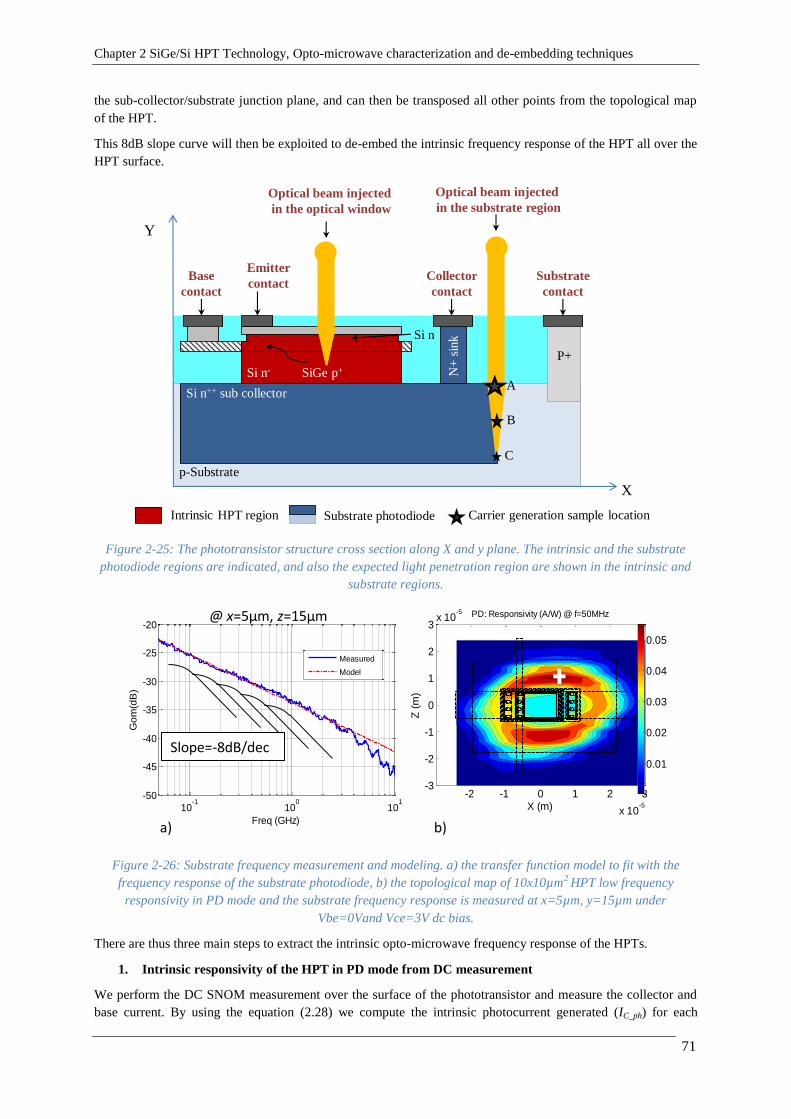
Chapter 2 SiGe/Si HPT Technology, Opto-microwave characterization and de-embedding techniques
71
the sub-collector/substrate junction plane, and can then be transposed all other points from the topological map
of the HPT.
This 8dB slope curve will then be exploited to de-embed the intrinsic frequency response of the HPT all over the
HPT surface.
Figure 2-25: The phototransistor structure cross section along X and y plane. The intrinsic and the substrate
photodiode regions are indicated, and also the expected light penetration region are shown in the intrinsic and
substrate regions.
Figure 2-26: Substrate frequency measurement and modeling. a) the transfer function model to fit with the
frequency response of the substrate photodiode, b) the topological map of 10x10µm2 HPT low frequency
responsivity in PD mode and the substrate frequency response is measured at x=5µm, y=15µm under
Vbe=0Vand Vce=3V dc bias.
There are thus three main steps to extract the intrinsic opto-microwave frequency response of the HPTs.
1. Intrinsic responsivity of the HPT in PD mode from DC measurement
We perform the DC SNOM measurement over the surface of the phototransistor and measure the collector and
base current. By using the equation (2.28) we compute the intrinsic photocurrent generated (IC_ph) for each
Substrate
contact
Collector
contact
Optical beam injected
in the substrate regionOptical beam injected
in the optical window
Base
contact
Emitter
contact
p-Substrate
Si n++ sub collector
Si n- N+
sin
k
P+
A
B
Intrinsic HPT region Substrate photodiode Carrier generation sample location
Y
X
C
SiGe p+
Si n
10-1
100
101
-50
-45
-40
-35
-30
-25
-20
Freq (GHz)
Go
m(d
B)
Measured
Model
Slope=-8dB/dec
@ x=5µm, z=15µm
X (m)
Z (
m)
PD: Responsivity (A/W) @ f=50MHz
-2 -1 0 1 2 3
x 10-5
-3
-2
-1
0
1
2
3x 10
-5
0.01
0.02
0.03
0.04
0.05
a) b)

Chapter 2 SiGe/Si HPT Technology, Opto-microwave characterization and de-embedding techniques
72
position of the optical probe. Then we use the definition of opto-microwave power gain defined in section 2.3 as
shown in equation (2.29) to extract the intrinsic dc responsivity, RPD,i,DC.
_PD _ _PD_darkC C ph C subI I I I (2.28)
2 2
22 _ _PD _PD_dark
,, ,
, ,
C ph C C sub
PD DC subPD i DC
opt RF opt RF
R RI I I I
RI I
(2.29)
With Iopt,RF=αcalPopt,RF
_PD _PD_dark
, , ,
, ,
C C sub
PD i DC PD DC sub
opt RF opt RF
I I IR R R
I I
(2.30)
Where IC,PD is the total current measured at the collector contact in PD mode operation, IC_ph is the photocurrent
generated in the active area of the HPT in PD mode, IC_PD_dark is the dark current measured at the collector
contact in PD mode, Isub is the substrate photocurrent, RPD,DC is the complete DC responsivity of the HPT in PD
mode, αcal is the coupling factor of the reference diode and Popt,RF is the illuminating optical power expressed in
terms of the equivalent current Iopt,RF.
2. Extract the low frequency (at 50MHz) responsivity of the substrate
To extract the substrate responsivity (Rsub) at low frequency we assume that the intrinsic dc responsivity
(RPD,i,DC) is equal to the intrinsic responsivity at low frequency (RPD,i,LF) which is true (valid) under voltage bias
condition. Hence:
, ,
, ,LF , ,
, ,DC
C ph C ph
PD i PD i DC
opt RF opt
I IR R
I I (2.31)
Thus the substrate responsivity (Rsub) at low frequency is deduced from the PD mode intrinsic (RPD,i,LF) and low
frequency complete (Rom,PD ) responsivity.
, , ,sub om PD PD i LFR R R (2.32)
The photodiode mode intrinsic (RPD,i,DC), substrate (Rsub) and complete (Rom,PD) responsivities of 10x10µm2 HPT
are presented in Figure 2-27. The Rom,PD curve is the slice figure of the PD mode responsivity measured at
50MHz. We observe that the intrinsic responsivity follows the Erf function with its peak at x=y=0µm and the
responsivity of the substrate photodiode is stronger than the intrinsic photodiode. The substrate responsivity is
very low in the active region of the HPT, but it is not null due to the penetration of optical light through the
substrate.
Figure 2-27: The raw, substrate and net responsivities of 10x10µm2 in PD mode operation (Vbe=0V).
-2 -1 0 1 2
x 10-5
0
0.01
0.02
0.03
0.04
0.05
0.06
Z (m)
Re
sp
on
siv
ity (
A/W
)
Rom,PD
RPD,i,DC
Rsub

Chapter 2 SiGe/Si HPT Technology, Opto-microwave characterization and de-embedding techniques
73
3. Measuring and modeling the substrate frequency response (in substrate regions)
We measure the frequency response of the substrate by pointing the optical probe on the substrate to illuminate
the substrate photodiode at x=5µm and z=15µm as shown in Figure 2-26 b). Then the substrate response at low
frequency computed by equation (2.32) at the given point is extrapolated to all frequencies by using the transfer
function presented in equation(2.33) to fit with the measured substrate frequency response. Thus from this model
we can extract the slope of the substrate response. The slope evaluated is then used to extrapolate the low
frequency responsivity of the substrate photodiode to all frequencies for each illuminated positions.
0
0
(f )( )
1f
subsub
RR f
fj
(2.33)
Where f0 =50MHz, ∝ is the order of the transfer function. Figure 2-26 a) shows the fitting of our model with the
opto-microwave gain of the substrate photodiode. Our model is well fitted with the measurement result for
∝=0.4 which is equivalent to -8dB/decay slope.
To deduce the intrinsic frequency response of the HPT we de-embed the local frequency response of substrate
photodiode from the frequency response of the complete HPT which is measured directly at each position of the
optical probe in all frequencies ranges by using the following equations for HPT and PD mode respectivly.
,HPT,i ,HPT, ,( ) ( ) ( )OM OM com OM subR f R f R f (2.34)
,PD,i ,PD, ,( ) ( ) ( )OM OM com OM subR f R f R f (2.35)
Where ROM,HPT,i and ROM,PD,i are the intrinsic responsivities in HPT and PD momde, and ROM,HPT,com and
ROM,PD,com are the complete responsivities in HPT and PD mode respectively.
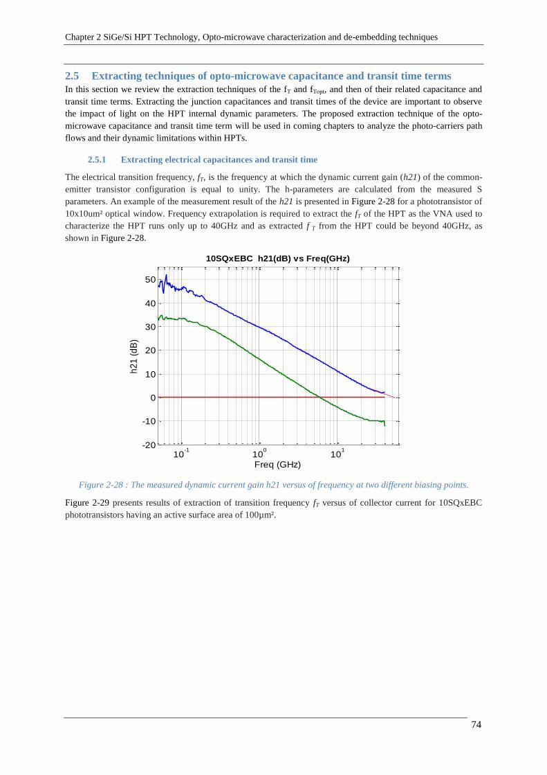
Chapter 2 SiGe/Si HPT Technology, Opto-microwave characterization and de-embedding techniques
74
2.5 Extracting techniques of opto-microwave capacitance and transit time terms
In this section we review the extraction techniques of the fT and fTopt, and then of their related capacitance and
transit time terms. Extracting the junction capacitances and transit times of the device are important to observe
the impact of light on the HPT internal dynamic parameters. The proposed extraction technique of the opto-
microwave capacitance and transit time term will be used in coming chapters to analyze the photo-carriers path
flows and their dynamic limitations within HPTs.
2.5.1 Extracting electrical capacitances and transit time
The electrical transition frequency, fT, is the frequency at which the dynamic current gain (h21) of the common-
emitter transistor configuration is equal to unity. The h-parameters are calculated from the measured S
parameters. An example of the measurement result of the h21 is presented in Figure 2-28 for a phototransistor of
10x10um² optical window. Frequency extrapolation is required to extract the fT of the HPT as the VNA used to
characterize the HPT runs only up to 40GHz and as extracted f T from the HPT could be beyond 40GHz, as
shown in Figure 2-28.
Figure 2-28 : The measured dynamic current gain h21 versus of frequency at two different biasing points.
Figure 2-29 presents results of extraction of transition frequency fT versus of collector current for 10SQxEBC
phototransistors having an active surface area of 100µm².
10-1
100
101
-20
-10
0
10
20
30
40
50
10SQxEBC h21(dB) vs Freq(GHz)
h2
1 (
dB
)
Freq (GHz)

Chapter 2 SiGe/Si HPT Technology, Opto-microwave characterization and de-embedding techniques
75
Figure 2-29 : The measured fT versus of collector current for 10x10 HPT at Vce=3.5V. It also indicates the
factors that limit the speed of the HPTs in different regions of the curve.
The transition frequency fT is fundamentally determined by the collector current IC. For very low IC the speed of
the transistor is limited by the junction capacitances. With increasing IC, the intrinsic conductance decreases, and
makes eventually the capacitance charging time smaller than the forward transit time. This is the region where fT
reaches its peak and is constant as shown in Figure 2-29. The device speed is then mainly limited by the forward
transit time. At high IC, however, base push-out occurs (Kirk effect) due to the high current injection, and
forward transit time itself increases with IC, leading to fT roll-off.
Mathematically, the electrical transition frequency (fT) in bipolar phototransistor can be written in general as
[172]:
1 1
22
T
EC
BE BC BC E C b e bc
C
fk T
C C C R Rq I
(2.36)
Where τF=CBC.(RE+RC)+ τb+ τe+ τbc is the forward transit time, m
C
kTg
qI
is the intrinsic trans-conductance at
low injection, CBE and CBC are emitter-base and collector-base depletion capacitances, RE and RC are the dynamic
emitter and collector resistances, τb, τe and τbc are base transit time, emitter transit time and base-collector
depletion time delay respectively.
To improve fT in a SiGe HPT, the forward transit time must be decreased by using a combination of vertical
profile scaling as well as Ge grading across the base. At the same time, the operating current IC must be
increased in proportion in order to make the intrinsic trans-conductance negligible compared to the forward
transit time. That is, the high fT potential of small forward transit time transistors can only be obtained by using
sufficiently high operating current. Figure 2-30 shows the active area vertical stack of the HPTs used to compute
the parameters which strongly affect the transition frequency.
0 0.005 0.01 0.015 0.02 0.0250
10
20
30
40
50
60
Ic (A)
f T (
GH
z)
Cap
acit
ance
Tran
sit
tim
e li
mit
Hig
h in
ject
ion

Chapter 2 SiGe/Si HPT Technology, Opto-microwave characterization and de-embedding techniques
76
Figure 2-30: The simplified intrinsic vertical stack of the HPT.
In this study, the base is p+ doped with a constant Ge profile. The emitter and collector are n+ and n doped
respectively. Thus, having this in mind we drive equations to evaluate the transit time and junction capacitances
in the base, emitter and collector as follows.
Base transit time, b : is the time associated with the excess minority carrier charge in the neutral base. It can be
expressed by the simplified equation as:
2
2
bb
nb
w
D (2.37)
Where, Dnb is the diffusivity of electron in the base, wb is neutral base width.
Emitter transit time, τe: is the time associated with the excess minority carrier charge in the neutral emitter. The
emitter charge storage time can be written as[172] [262]:
21
( )2
e ee
ac pe pe
w w
s D
(2.38)
Where Dpe is the hole diffusivity in the emitter, Spe is the hole surface recombination velocity at emitter contact
and βac is the ac current gain of the transistor.
Base-collector depletion time delay τbc: is the time required for electrons to traverse the base-collector depletion
region [172] [262]. Electrons travel across the collector-base depletion region by drift, and hence it can be
written as
2
BCbc
sat
w
V (2.39)
Where wBC is the base-collector depletion thickness, and Vsat is the carrier saturation velocity.
Base-emitter depletion capacitance CBE:
,
. BEBE
EB d
AC
W
(2.40)
Where ℰ is dielectric constant of the material, ABE is base emitter depletion region surface area and WEB,d is
depletion area thickness.
Base-collector depletion
base
emitter
SiG
e H
PT v
erti
cal s
tack
L
W
BCt
bt
etwe
wb
wBC

Chapter 2 SiGe/Si HPT Technology, Opto-microwave characterization and de-embedding techniques
77
Base-collector depletion capacitance CBC:
,
. BCBC
BC d
AC
W
(2.41)
Where, ABC is base emitter depletion region surface area and WBC,d is the depletion thickness.
The values of forward transit time and junction capacitances can be easily extracted from a plot of global time
delay (τtot=1/2πfT) versus 1/IC, as shown in Figure 2-31. Near the peak of fT, the global time delay versus 1/IC
curve is nearly linear, indicating that the junction capacitance is close to constant for this biasing range at high fT.
Thus, the CEC junction capacitance can be obtained from the slope:
EC BE BCC C C (2.42)
As we can see in Figure 2-31 the global time delay versus 1/Ic has a constant slop after the high injection region.
As at infinite collector current the global time delay is equal to the forward transit time, this latter can be
extracted. The forward transit time τF can be determined from the y-axis intercept at infinite collector current as
shown in Figure 2-31.
F BC E C b e bcC R R (2.43)
Figure 2-31: Global time delay (electrical transition delay) versus of 1/Ic. From the slope of this curve we can
extract the built in capacitances and from the y-intercept we can extract the transit time.
2.5.2 Extracting opto-microwave capacitances and transit time
The optical transition frequency, fTopt, is the frequency for which the responsivity of the HPT in phototransistor
mode is equal to the low frequency responsivity in photodiode mode as it is defined in section 2.3.1. Unlike fT,
fTopt is influenced by additional terms related to the photodetection mechanism.
The optical transition frequency, fTopt, is much lower than the electrical transition frequency, fT. It is explained by
the addition of capacitive and transit time terms related to the photodetection mechanism. Other electrical terms
remain unchanged. Thus, it is possible to develop an expression for the optical transition frequency fTopt as:
0 200 400 600 800 10000
0.005
0.01
0.015
0.02
0.025
1/Ic (1/A)
Ele
ctr
ica
l tr
an
sitio
n d
ela
y (
ns)
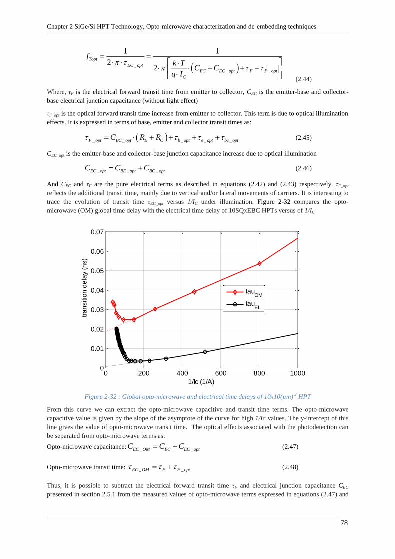
Chapter 2 SiGe/Si HPT Technology, Opto-microwave characterization and de-embedding techniques
78
_
_ _
1 1
22
Topt
EC opt
EC EC opt F F opt
C
fk T
C Cq I
(2.44)
Where, τF is the electrical forward transit time from emitter to collector, CEC is the emitter-base and collector-
base electrical junction capacitance (without light effect)
τF_opt is the optical forward transit time increase from emitter to collector. This term is due to optical illumination
effects. It is expressed in terms of base, emitter and collector transit times as:
_ _ _ _ _F opt BC opt E C b opt e opt bc optC R R (2.45)
CEC_opt is the emitter-base and collector-base junction capacitance increase due to optical illumination
_ _ _EC opt BE opt BC optC C C (2.46)
And CEC and τF are the pure electrical terms as described in equations (2.42) and (2.43) respectively. τF_opt
reflects the additional transit time, mainly due to vertical and/or lateral movements of carriers. It is interesting to
trace the evolution of transit time τEC_opt versus 1/IC under illumination. Figure 2-32 compares the opto-
microwave (OM) global time delay with the electrical time delay of 10SQxEBC HPTs versus of 1/IC
Figure 2-32 : Global opto-microwave and electrical time delays of 10x10(µm) 2 HPT
From this curve we can extract the opto-microwave capacitive and transit time terms. The opto-microwave
capacitive value is given by the slope of the asymptote of the curve for high 1/Ic values. The y-intercept of this
line gives the value of opto-microwave transit time. The optical effects associated with the photodetection can
be separated from opto-microwave terms as:
Opto-microwave capacitance: _ _EC OM EC EC optC C C (2.47)
Opto-microwave transit time: _ _EC OM F F opt (2.48)
Thus, it is possible to subtract the electrical forward transit time τF and electrical junction capacitance CEC
presented in section 2.5.1 from the measured values of opto-microwave terms expressed in equations (2.47) and
0 200 400 600 800 10000
0.01
0.02
0.03
0.04
0.05
0.06
0.07
1/Ic (1/A)
Op
tica
l tr
an
sitio
n d
ela
y (
ns)
tauOM
tauEL

Chapter 2 SiGe/Si HPT Technology, Opto-microwave characterization and de-embedding techniques
79
(2.48) respectively and thus, to obtain the optical forward transit time τF_opt and optical junction capacitance
CEC_opt terms.
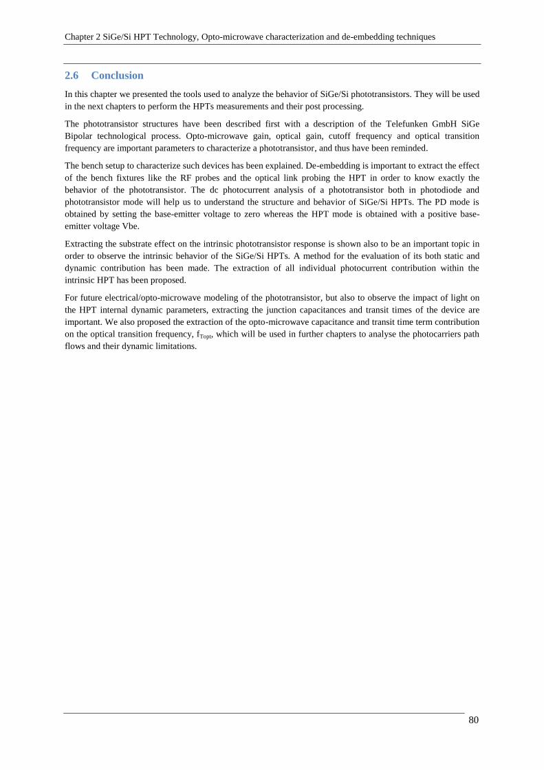
Chapter 2 SiGe/Si HPT Technology, Opto-microwave characterization and de-embedding techniques
80
2.6 Conclusion
In this chapter we presented the tools used to analyze the behavior of SiGe/Si phototransistors. They will be used
in the next chapters to perform the HPTs measurements and their post processing.
The phototransistor structures have been described first with a description of the Telefunken GmbH SiGe
Bipolar technological process. Opto-microwave gain, optical gain, cutoff frequency and optical transition
frequency are important parameters to characterize a phototransistor, and thus have been reminded.
The bench setup to characterize such devices has been explained. De-embedding is important to extract the effect
of the bench fixtures like the RF probes and the optical link probing the HPT in order to know exactly the
behavior of the phototransistor. The dc photocurrent analysis of a phototransistor both in photodiode and
phototransistor mode will help us to understand the structure and behavior of SiGe/Si HPTs. The PD mode is
obtained by setting the base-emitter voltage to zero whereas the HPT mode is obtained with a positive base-
emitter voltage Vbe.
Extracting the substrate effect on the intrinsic phototransistor response is shown also to be an important topic in
order to observe the intrinsic behavior of the SiGe/Si HPTs. A method for the evaluation of its both static and
dynamic contribution has been made. The extraction of all individual photocurrent contribution within the
intrinsic HPT has been proposed.
For future electrical/opto-microwave modeling of the phototransistor, but also to observe the impact of light on
the HPT internal dynamic parameters, extracting the junction capacitances and transit times of the device are
important. We also proposed the extraction of the opto-microwave capacitance and transit time term contribution
on the optical transition frequency, fTopt, which will be used in further chapters to analyse the photocarriers path
flows and their dynamic limitations.

Chapter 3 Experimental study of SiGe HPTs with top illumination
81
Chapter 3 Experimental study of SiGe HPTs
with top illuminationChapitre d'équation (Suivant) Section 1
3.1 INTRODUCTION ......................................................................................................................... 82 3.2 HPT STATIC BEHAVIOR............................................................................................................. 83 3.3 HPT OPTIMUM BIASING ............................................................................................................. 88
3.3.1 Introduction .................................................................................................................... 88 3.3.2 Optimizing the low frequency opto-microwave behavior ............................................... 88 3.3.3 2T and 3T HPT configurations ....................................................................................... 93 3.3.4 Optimizing the dynamic opto-microwave behavior ........................................................ 95 3.3.5 Conclusion on dc bias ................................................................................................... 100
3.4 TWO DIMENSIONAL ELECTRICAL EXTENSION EFFECTS ........................................................... 101 3.4.1 Introduction .................................................................................................................. 101 3.4.2 Experimental hypothesis ............................................................................................... 102 3.4.3 Transit time extrapolation model .................................................................................. 103 3.4.4 Geometrical dependence of the capacitance ................................................................ 106 3.4.5 Transition frequency, fT, vs current density ................................................................. 108 3.4.6 Maximum Oscillation frequency-fmax and CBC.RB model ............................................... 110
3.5 LOCALIZATION OF THE PHOTOCURRENT SOURCES AND OM BEHAVIOR IN THE HPT STRUCTURE
114 3.5.1 Introduction .................................................................................................................. 114 3.5.2 Localization of the photocurrent source in the HPT structure ..................................... 115 3.5.3 Localization of the Opto-microwave behavior in the HPT structure ............................ 121
3.6 DEPENDENCY ON THE INJECTED OPTICAL POWER LEVEL ......................................................... 128 3.6.1 Introduction .................................................................................................................. 128 3.6.2 Injected optical power level impact on DC characteristics .......................................... 128 3.6.3 Injected optical power level impact on opto-microwave frequency response ............... 130
3.7 CURRENT DEPENDENCE OF FTOPT, AND TRANSIT TIME AND CAPACITANCE EVALUATION ........... 134 3.7.1 Introduction .................................................................................................................. 134 3.7.2 Current dependency of optical transition frequency fTopt .............................................. 134 3.7.3 Transit time and junction capacitance evaluation ........................................................ 135
3.8 SELECTION RULES FOR HPT SIZE AND GEOMETRY .................................................................. 139 3.9 CONCLUSION ........................................................................................................................... 143

Chapter 3 Experimental study of SiGe HPTs with top illumination
82
3.1 Introduction
There is a continuous need to verify the ability of integrating phototransistors in newer commercial
SiGe process technologies offering faster operating frequencies but also to improve the performances
of the HPT without a modification of the technology in terms of vertical stacks of layers. To optimize
the speed of the phototransistor, [205] identified the fastest and slowest regions of the structure based
on physical simulations. References [249] investigated the performances of phototransistor through
opto electric compact circuit modeling. M. D. Rosales et al [245] verified that the proximity of the
base, emitter and collector contacts to the optical window has an influence on the dynamic response
characteristic of the phototransistor. The existence of substrate photocurrent was demonstrated through
modified MEXTRAM model in [250] and they also show that the impulse response is wider when the
substrate contact is open. Reference [251] suggests and demonstrates that using the substrate contact
we can remove the photo-generated holes in the substrate so that the speed performance of the
phototransistor can be enhanced. However, the photo-generated electrons in the substrate still have a
great impact on the speed performance of the SiGe HPTs. Reference [250] has demonstrated the impact
of the injected optical power on the dc response behavior of the phototransistor. But the impact on
opto-microwave behavior of injected optical level and its frequency limitation were still not
investigated.
This chapter intends to study further the HPT dynamic behavior. We characterize the HPT technology
presented in chapter two in the configuration of top-side illumination.
After this section of introduction, in the second section of this chapter, the electrical static behavior of
the phototransistor under dark and illumination conditions is observed through the Ic-Vce
characteristics, electrical current gain (β) and the Gummel curve. The dc responsivity of the different
optical window size phototransistor is also presented and compared.
The third section deals with the optimization of the dc bias conditions that maximize the opto-
microwave behavior of the HPT, with the consideration on the low frequency gain and dynamic
behavior of the phototransistor. It starts with the low-frequency opto-microwave gain, and then deals
with the comparison on two-terminal (2T-HPT) and three-terminal (3T-HPT) configurations. Finally
discuss the opto-microwave 3dB cutoff frequency and optical transition frequency (fTopt) as a function
of the biasing.
In the fourth section, we focus on the size dependency of the electrical dynamic behavior of SiGe
HPTs, which shows an unusual behavior as compared to HBTs. We thus propose a “2D extension
electrical effect” that analyses the two-dimensional and distributed nature of currents within SiGe HPT.
While in second and third sections, the point of illumination was chosen to be fixed, at the center of the
optical window, where the optical response is maximized, the fifth section analyses further the spatial
dependency on the opto-microwave behavior. The DC current and opto-microwave frequency response
are analyzed over the surface of the structure through SNOM investigation under the optimum dc bias
conditions.
In sixth section, the impact of the injected optical power level on the dc and opto-microwave
performance of the SiGe HPT is presented.
The seventh section focuses on the opto-microwave transit time and junction capacitances of the HPT,
deduced from the fTopt current dependency. This analysis is extended as well as a function of the
position of the optical beam over the HPT surface to provide further information on the distributed
nature of the HPT.
Finally, in section eight, the impact of the optical window size on opto-microwave gain and cutoff
frequency is analyzed. The optical window size dependency of the substrate photodiode and 2D carrier
distribution effects are also investigated. The conclusion is then provided in the last section.

Chapter 3 Experimental study of SiGe HPTs with top illumination
83
3.2 HPT Static behavior
The static behavior of the HPT can be observed through the measurement of the output Ic-Vce
characteristics, electrical current gain (β) and the Gummel curve under dark and illumination
conditions. Under illumination condition, we inject 2.28mW dc optical power which is measured at the
tip of the lensed fiber probe.
Output characteristics (Ic-Vce) of a transistor show the collector current (Ic) versus of the collector
voltage (Vce) and the base current (Ib). This indicates AC signals can be superimposed on DC bias
levels. The typical Ic-Vce output characteristics of the 50SQxEBC HPT are as shown in Figure 3-1. It
illustrates how an input base current and collector voltage influence the output collector current. Dark
condition is represented in Figure 3-1 a). The output characteristics of the HPT were measured by
sweeping the collector voltage Vce from 0V to 4.5V whereas the base current Ib is swept from 10nA-
1μA by steps of 0.1μA, from 3μA -20μA by steps of 2.3μA and from 25μA -100μA by steps of 3μA.
With 2.5V Vce, the collector current Ic is equal to 950μA with an Ib of 1μA or Ic is equal to 40.5mA
with an Ib of 100μA. From the plotted curves we observe that there is a rapid increase of the collector
current for the collector voltage greater than 3.5V. This is due to the fact that the phototransistor is
operating in the breakdown/avalanche mode.
The effect of illumination with a 2.28mW dc optical beam at 850nm is shown on the Ic-Vce curves in
Figure 3-1 b). The high value of Ic is attributed to the generated photocurrent that adds to the initial
base current and that is amplified by the transistor action of the HPT. Without illumination, the
supplied bias current in the base Ibbias sets the bias point of the HPT. The illumination pushes the bias
point of the HPT to Ib = (Ibbias + Iph) and thus modifies the value of the current gain (β). As a result, the
measured collector current Icillum for the HPT will be given by:
( )* illum ph bias phIc I Ib I (3.1)
1illum ph biasIc I Ib (3.2)
Under constant base current biasing, illumination of the HPT causes an increase in the Vbe voltage.
This is primarily due to the addition of the photocurrent in the base to the initial base bias Ib [235].
Figure 3-1: Ic-Vce curves of 50SQxEBC HPT for Ib between 10nA and 100μA: a) without optical
power illumination b) illuminated by 2.28mW optical power at 850nm
Figure 3-2 shows the superposition of Ic-Vc curves with and without light illumination. In the active
region, at Ib=10nA and Vce=2V, Ic is equal to 53µA in dark condition and against Icillum=31.6mA
when light is ON. Thus, the transistor collector current due to the light illumination is around 31mA.
This gives a dc responsivity of 50x50µm2 HPT that reaches up to 13.6A/W at Ib=10nA.

Chapter 3 Experimental study of SiGe HPTs with top illumination
84
Figure 3-2: The superposition of Ic-Vc curves with and without light illumination. Blue curves (dashed)
are in dark condition and red curves (plain) are with illumination.
Figure 3-3 shows the Gummel plot of the 10SQxEBC and 50SQxEBC HPTs with 2.28mW optical
beam at 850nm and without (dark). The base voltage is initially provided with 0V, which puts the HPT
in a reverse active mode. It is then increased up to 1V where the HPT goes to a forward active mode up
to saturation. The collector and base currents are measured as a function of the supplied voltage in the
base. In the non-illuminated condition, the measured Ic and Ib clearly show the different regions in the
HPT operation: the low current region, the linear region and the high current region. In the low Vbe
bias range, the measured dark Ic and Ib saturate in the range of 10-9
A. In the high current region, the
change in the slope of Ic and Ib is evident.
Without illumination, the 50SQxEBC shows an increase in collector current by a factor of 3.2
compared to the 10SQxEBC as shown in Figure 3-3, it is due to the increase in size of the intrinsic
transistor with the optical window size.
At low Vbe bias and under 2.28mW illumination, the base current Ib (flowing out of the base contact)
saturates at around 50μA for 10SQxEBC HPT and 91µA for 50SQxEBC HPT. The collector current Ic
saturates respectively at around 5mA and 7mA. These currents correspond to the photocurrent
generated by the optical absorption, which are far greater than the HPT’s transistor dark currents at low
base bias level. Under illuminated condition, it is observed that at high base bias (> 0.87V), the effects
of the optical absorption are negligible on the biasing level as compared to the dark currents.
The base current is plotted as the absolute value of the measured illuminated base current. The notch
shows the reversal in the direction of the base current. The notch moves to higher base emitter voltage
for 50SQxEBC HPT, which has higher intrinsic transistor area, indicating that larger size HPT requires
higher base emitter voltage to reach its transistor mode operation.
For given HPT size, the difference in the value of Ic and Ib at low Vbe is due to the substrate
photocurrent as explained in chapter 2 section 2.4.2.
0 0.5 1 1.5 2 2.5 3 3.5 4 4.5-10
0
10
20
30
40
50
60
7050SQxEBC Ic vs Vce Opt Pin=2.28mW
Ic (
mA
)
Vce (V)
Light ON Ib=25uA
Light OFF Ib=10nA
Light OFF Ib=25uA
Light ON Ib=100uA
Light OFF Ib=100uA
Light ON Ib=10nA

Chapter 3 Experimental study of SiGe HPTs with top illumination
85
Figure 3-3: The Gummel plot of the 10SQxEBC (10x10µm2) and 50SQxEBC (50x50µm
2) HPTs with
2.28mW optical beam at 850nm and without (dark).
In summary, at low base-emitter junction bias and high enough optical power, the photocurrent
generated in the emitter, base or collector regions swamps the devices transistor action. That is, the
effect of electrons injection into the base from the emitter is negligible. By contrast, at high base-
emitter bias the transistor action is noticeable and the photocurrent constitutes a small base current
injected into the device which is amplified by the transistor operation to provide the device optical
gain. The substrate parasitic photodiode proves however to have a deep impact on Ic, especially visible
at low Vbe.
Another very important characteristic of a phototransistor that makes it different from a photodiode is
its internal current gain (β). Figure 3-4 a) shows the common emitter electrical dc current gain (β)
extracted from the Gummel plot in dark conditions versus of the base emitter voltage for different size
HPTs respectively. The highest beta is seen in the 50x50µm2 HPT with a peak value of 1200 at
Vbe=0.68V. This is followed by the 10x10µm2 with a maximal β of 450 at Vbe=0.7V, 5x5µm
2 having
β peak of 400 at Vbe=0.75V and finally 3x3µm2 which has a peak current gain (β) of 260 at Vbe=0.8V.
Figure 3-4 b) shows the common emitter optical dc current gain (βopt) only due to the injection of
optical light as versus of the base emitter voltage for 10x10µm2 and 50x50µm
2 HPTs. The larger
optical window size HPT has higher βopt (102 at Vbe=0.898V) than the smaller size HPT (73.1 at
Vbe=0.890V).

Chapter 3 Experimental study of SiGe HPTs with top illumination
86
Figure 3-4: a) Common emitter current gain (β) extracted from the Gummel plot versus the base
emitter voltage for different size HPTs in dark condition; b) the optical current gain.
The measured collector currents from the illuminated and dark Gummel curves and Ic-Vce
measurements are used to extract the DC responsivity of the HPT. For our understanding we were able
to extract the complete responsivity, absolute responsivity and intrinsic responsivity of HPT as
expressed in equations (3.3) to (3.5) respectively.
Complete responsivity:
illum dark
in opt
Ic IcAR
W P
(3.3)
Absolute responsivity:
illum darkabs
in opt
Ic IcAR
W P
(3.4)
Intrinsic responsivity:
int
opt su
in opt
bIc IAR
W P
(3.5)
Where Pin,opt is the injected optical power, Icopt is photocurrent measured at the collector contact, Isub is
substrate photocurrent and Γ is the coupling efficiency of the optical beam to the optical window.
Figure 3-5 shows the resulting DC responsivity for the 10x10µm2 and 50x50µm
2 HPT configuration
under 2.28mW optical power illumination versus of the supplied Vbe. The illumination of the HPT
under low base emitter voltage bias causes an initial significant increase in the measured dc
responsivity due to the photocurrent from the parasitic substrate photodiode. As the base-emitter region
becomes forward biased the dc responsivity starts to increase until it reaches a peak value where it
starts to descend to lower values as Vbe is increased.
The complete DC responsivity difference between 50x50µm2 and 10x10µm
2 HPTs under PD mode
operation (as shown in Figure 3-5 a) comes mainly from the optical beam coupling efficiency. As it is
presented in chapter 2 section 2.4.3, the coupling efficiency of 10x10µm2 HPT is 32.3% whereas
50x50µm2 HPT is 100%. Considering these values, we extract the absolute responsivity of both HPTs
by using equation(3.4). Thus, as it is shown in Figure 3-5 a), the absolute dc responsivity at low Vbe
(PD mode) is the same for 10x10µm2 and 50x50µm
2 HPTs.
In HPT mode (for Vbe >0.6V), the absolute dc responsivity difference between the two HPTs (ratio of
1.47 at Vbe=0.83V) is mostly due to the electrical dc current gain 1.3 times higher (at Vbe=0.83V) in
a) b)
0 0.2 0.4 0.6 0.8 10
200
400
600
800
1000
1200
1400
Be
ta
Vbe (V)
3x3µm2
5x5µm2
10x10µm2
50x50µm2
0 0.2 0.4 0.6 0.8 10
20
40
60
80
100
120
Be
tao
pt
Vbe (V)
10x10µm2
50x50µm2
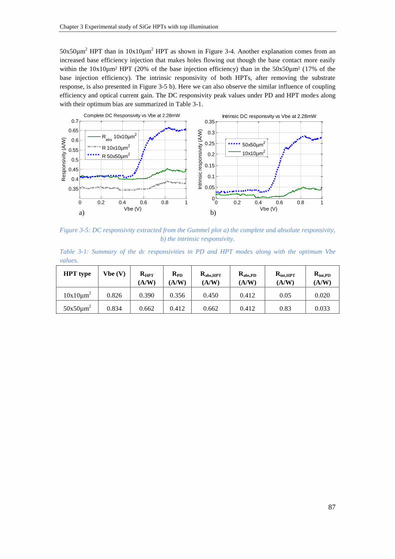
Chapter 3 Experimental study of SiGe HPTs with top illumination
87
50x50µm2 HPT than in 10x10µm
2 HPT as shown in Figure 3-4. Another explanation comes from an
increased base efficiency injection that makes holes flowing out though the base contact more easily
within the 10x10µm² HPT (20% of the base injection efficiency) than in the 50x50µm² (17% of the
base injection efficiency). The intrinsic responsivity of both HPTs, after removing the substrate
response, is also presented in Figure 3-5 b). Here we can also observe the similar influence of coupling
efficiency and optical current gain. The DC responsivity peak values under PD and HPT modes along
with their optimum bias are summarized in Table 3-1.
Figure 3-5: DC responsivity extracted from the Gummel plot a) the complete and absolute responsivity,
b) the intrinsic responsivity.
Table 3-1: Summary of the dc responsivities in PD and HPT modes along with the optimum Vbe
values.
HPT type Vbe (V) RHPT
(A/W)
RPD
(A/W)
Rabs,HPT
(A/W)
Rabs,PD
(A/W)
Rint,HPT
(A/W)
Rint,PD
(A/W)
10x10µm2 0.826 0.390 0.356 0.450 0.412 0.05 0.020
50x50µm2 0.834 0.662 0.412 0.662 0.412 0.83 0.033
0 0.2 0.4 0.6 0.8 10
0.05
0.1
0.15
0.2
0.25
0.3
0.35 Intrinsic DC responsvity vs Vbe at 2.28mW
Intr
insic
re
sp
on
siv
ity (
A/W
)
Vbe (V)
50x50µm2
10x10µm2
0 0.2 0.4 0.6 0.8 1
0.35
0.4
0.45
0.5
0.55
0.6
0.65
0.7 Complete DC Responsivity vs Vbe at 2.28mW
Re
sp
on
siv
ity (
A/W
)
Vbe (V)
Rabs
10x10µm2
R 10x10µm2
R 50x50µm2
a) b)

Chapter 3 Experimental study of SiGe HPTs with top illumination
88
3.3 HPT optimum biasing
3.3.1 Introduction
Our phototransistor operates under common emitter configuration. However, depending on the level of
the dc bias and the base terminal connection, its performance varies. In this section we deal with
optimizing the dc biasing conditions and the different connections to the base to maximize alternatively
the low frequency gain and dynamic behavior of the phototransistor. We sweep the dc bias at the
collector and base and measure the S parameters of the link under opto-microwave and pure electrical
conditions. In this study we focus on voltage control biasing condition. Thus, in this section we present
the optimum dc biasing conditions on both the collector and base terminal sides that maximize the low
frequency gain (such as h21, Gopt, Gom) and the dynamic behavior (such as f-3dB and fTopt) of the
phototransistor.
3.3.2 Optimizing the low frequency opto-microwave behavior
This part focuses on the dc biasing conditions to maximize the low-frequency behavior of the HPT.
3.3.2.1 Low frequency opto-microwave gain vs biasing
Here we optimize low frequency opto-microwave gain (Gom) in terms of dc bias. The S-parameters of
the link are measured versus of Vbe at different constant voltages Vce. From the link measurement all
the setup features are removed using the de-embedding techniques presented in chapter 2 section 2.3.3.
Figure 3-6) shows the opto-microwave responsivity at 50 MHz versus of the base bias voltage Vbe at a
fixed Vce of 3V and 1V for 10x10µm2 and 50x50µm
2 optical window sized HPTs. The responsivity
measurements at Vbe=0V-0.55V could be considered as the PD mode biasing of the HPT. In this
biasing region, the base-collector junction is reversed biased and the base-emitter junction is not yet
forward biased. The responsivity starts increasing fromVbe= 0.6V and reaches its peak at around
Vbe=0.857V, it then starts to fall off as the HPTs are in the high injection region. It is also observed
that the responsivity enhances as Vce increases from 1V to 3V.
Figure 3-6: Low frequency complete opto microwave responsivity versus base voltage. of 10x10 and
50x50 HPTs at different collector voltages with injected optical power of 2.38mW.
0 0.2 0.4 0.6 0.8 10
0.1
0.2
0.3
0.4
0.5
0.6
Vbe (V)
Go
m (
A/W
)
3V Vce 10x10µm2
3V Vce 50x50µm2
1V Vce 50x50µm2
1V Vce 10x10µm2
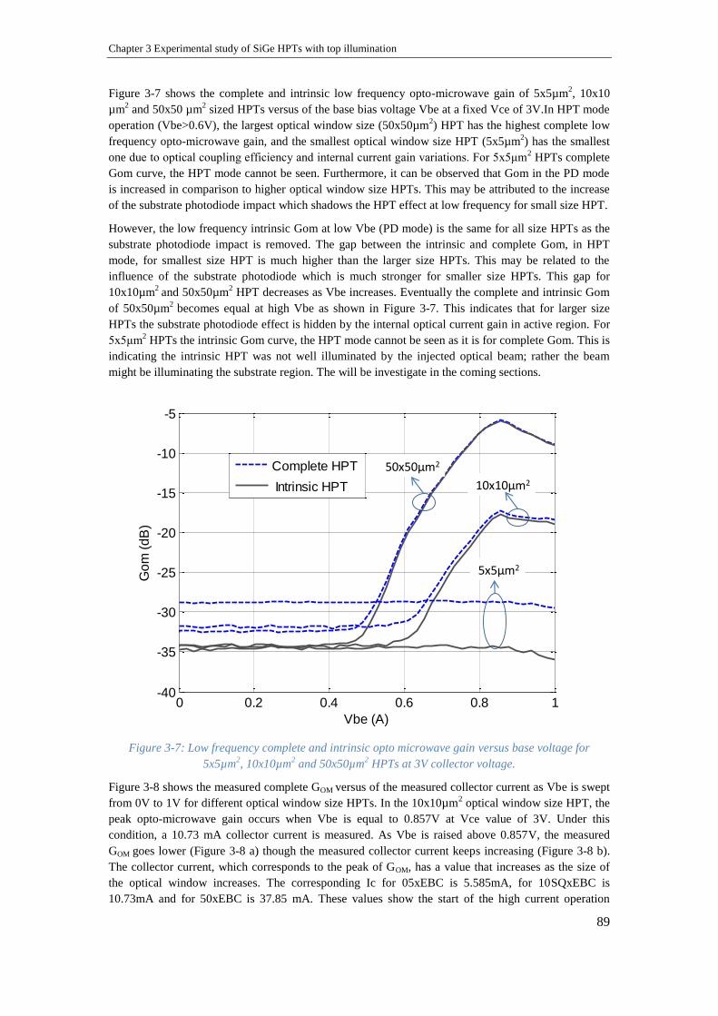
Chapter 3 Experimental study of SiGe HPTs with top illumination
89
Figure 3-7 shows the complete and intrinsic low frequency opto-microwave gain of 5x5µm2, 10x10
µm2 and 50x50 µm
2 sized HPTs versus of the base bias voltage Vbe at a fixed Vce of 3V.In HPT mode
operation (Vbe>0.6V), the largest optical window size (50x50µm2) HPT has the highest complete low
frequency opto-microwave gain, and the smallest optical window size HPT (5x5µm2) has the smallest
one due to optical coupling efficiency and internal current gain variations. For 5x5μm2 HPTs complete
Gom curve, the HPT mode cannot be seen. Furthermore, it can be observed that Gom in the PD mode
is increased in comparison to higher optical window size HPTs. This may be attributed to the increase
of the substrate photodiode impact which shadows the HPT effect at low frequency for small size HPT.
However, the low frequency intrinsic Gom at low Vbe (PD mode) is the same for all size HPTs as the
substrate photodiode impact is removed. The gap between the intrinsic and complete Gom, in HPT
mode, for smallest size HPT is much higher than the larger size HPTs. This may be related to the
influence of the substrate photodiode which is much stronger for smaller size HPTs. This gap for
10x10µm2
and 50x50µm2 HPT decreases as Vbe increases. Eventually the complete and intrinsic Gom
of 50x50µm2
becomes equal at high Vbe as shown in Figure 3-7. This indicates that for larger size
HPTs the substrate photodiode effect is hidden by the internal optical current gain in active region. For
5x5μm2 HPTs the intrinsic Gom curve, the HPT mode cannot be seen as it is for complete Gom. This is
indicating the intrinsic HPT was not well illuminated by the injected optical beam; rather the beam
might be illuminating the substrate region. The will be investigate in the coming sections.
Figure 3-7: Low frequency complete and intrinsic opto microwave gain versus base voltage for
5x5µm2, 10x10µm
2 and 50x50µm
2 HPTs at 3V collector voltage.
Figure 3-8 shows the measured complete GOM versus of the measured collector current as Vbe is swept
from 0V to 1V for different optical window size HPTs. In the 10x10µm2 optical window size HPT, the
peak opto-microwave gain occurs when Vbe is equal to 0.857V at Vce value of 3V. Under this
condition, a 10.73 mA collector current is measured. As Vbe is raised above 0.857V, the measured
GOM goes lower (Figure 3-8 a) though the measured collector current keeps increasing (Figure 3-8 b).
The collector current, which corresponds to the peak of GOM, has a value that increases as the size of
the optical window increases. The corresponding Ic for 05xEBC is 5.585mA, for 10SQxEBC is
10.73mA and for 50xEBC is 37.85 mA. These values show the start of the high current operation
0 0.2 0.4 0.6 0.8 1-40
-35
-30
-25
-20
-15
-10
-5
Vbe (A)
Go
m (
dB
)
Complete HPT
Intrinsic HPT
50x50µm2
10x10µm2
5x5µm2

Chapter 3 Experimental study of SiGe HPTs with top illumination
90
region of the HPT. If the collector current is above optimal values, then the low frequency gain of the
transistor starts the roll off.
Figure 3-8: For various size optical window HPTs a) low frequency opto-microwave gain versus
collector current. b) Collector current versus base voltage at Vce=3V
In Figure 3-9 a) the complete GOM is plotted versus of the measured base current Ib as Vb is swept
from 0V to 1V for fixed Vce=3V. This shows that the peak GOM could generally be achieved at very
small values of Ib under the illuminated condition. It is the lowest possible base current that allows the
forward-active mode operation of the HPT. The highest GOM could be achieved in the region of
negative Ib as well. The HPT GOM declines as the base current increases further. The optimum Ib to
maximize GOM is 9.9μA and it is nearly the same for the three HPTs at Vce=3V and Vbe=0.857V.
Figure 3-9 b) shows the base current versus of base voltage for Vce=3V.
Figure 3-9: a) Low frequency complete opto-microwave gain versus base current. b) Base current
versus base voltage. For various sized optical window HPTs at Vce=3V
The peak value of the intrinsic and complete low frequency Gom in PD and HPT modes along with
their optimum dc bias are presented in Table 3-2. The intrinsic Gom in PD mode has the same value of
-34.8dB for all optical window size HPTs. The complete and intrinsic Gom of 50x50µm2 HPT, in HPT
mode, have about the same value around of -5.9dB.
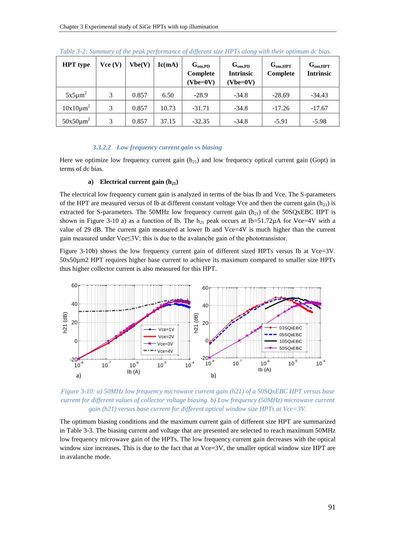
Chapter 3 Experimental study of SiGe HPTs with top illumination
91
Table 3-2: Summary of the peak performance of different size HPTs along with their optimum dc bias.
HPT type Vce (V) Vbe(V) Ic(mA) Gom,PD
Complete
(Vbe=0V)
Gom,PD
Intrinsic
(Vbe=0V)
Gom,HPT
Complete
Gom,HPT
Intrinsic
5x5µm2 3 0.857 6.50 -28.9 -34.8 -28.69 -34.43
10x10µm2 3 0.857 10.73 -31.71 -34.8 -17.26 -17.67
50x50µm2 3 0.857 37.15 -32.35 -34.8 -5.91 -5.98
3.3.2.2 Low frequency current gain vs biasing
Here we optimize low frequency current gain (h21) and low frequency optical current gain (Gopt) in
terms of dc bias.
a) Electrical current gain (h21)
The electrical low frequency current gain is analyzed in terms of the bias Ib and Vce. The S-parameters
of the HPT are measured versus of Ib at different constant voltage Vce and then the current gain (h21) is
extracted for S-parameters. The 50MHz low frequency current gain (h21) of the 50SQxEBC HPT is
shown in Figure 3-10 a) as a function of Ib. The h21 peak occurs at Ib=51.72µA for Vce=4V with a
value of 29 dB. The current gain measured at lower Ib and Vce=4V is much higher than the current
gain measured under Vce≤3V; this is due to the avalanche gain of the phototransistor.
Figure 3-10b) shows the low frequency current gain of different sized HPTs versus Ib at Vce=3V.
50x50µm2 HPT requires higher base current to achieve its maximum compared to smaller size HPTs
thus higher collector current is also measured for this HPT.
Figure 3-10: a) 50MHz low frequency microwave current gain (h21) of a 50SQxEBC HPT versus base
current for different values of collector voltage biasing. b) Low frequency (50MHz) microwave current
gain (h21) versus base current for different optical window size HPTs at Vce=3V.
The optimum biasing conditions and the maximum current gain of different size HPT are summarized
in Table 3-3. The biasing current and voltage that are presented are selected to reach maximum 50MHz
low frequency microwave gain of the HPTs. The low frequency current gain decreases with the optical
window size increases. This is due to the fact that at Vce=3V, the smaller optical window size HPT are
in avalanche mode.
a) b)
10-8
10-7
10-6
10-5
10-4
-20
0
20
40
60
Ib (A)
h2
1 (
dB
)
Vce=1V
Vce=2V
Vce=3V
Vce=4V
10-8
10-7
10-6
10-5
10-4
-20
0
20
40
60
Ib (A)
h2
1 (
dB
)
03SQxEBC
05SQxEBC
10SQxEBC
50SQxEBC

Chapter 3 Experimental study of SiGe HPTs with top illumination
92
Table 3-3: Summary of the maximum low frequency (50MHz) electrical current gain of different size
HPTs along with the optimum dc bias for the gain.
HPT type Vce (V) Ib (µA) Ic(mA) RF max h21 at 50MHz
(dB)
03SQxEBC 3 2.42 1.27 48.8
05SQxEBC 3 5.42 3.02 47.7
10SQxEBC 3 9.44 5.50 47.8
50SQxEBC 3 51.72 28.49 43.6
b) Optical current gain (Gopt)
The optical gain is the internal gain of a phototransistor comparing to its photodiode. In other words,
Gopt is the difference between the phototransistor opto-microwave gains in HPT mode and in PD
mode. Figure 3-11 a) shows the intrinsic and complete low frequency Gopt versus of collector current
and base emitter voltage for 10x10µm2 and 50x50µm
2 HPT at Vce=3V. In terms of Ic, the Gopt
reaches its peak for 10x10µm2 HPT at low collector current compared to 50x50µm
2 HPT (its peak
appears at higher collector current) as shown in Figure 3-11 a). At high Ic the Gopt is compressed as
the HPT reaches its maximum current injection point.
The optical gain is zero dB until Vbe=0.55V (in PD mode region) and starts increasing for Vbe=0.6V
(in HPT mode region) and eventually reaches its peak at Vbe=0.857V in both structures as shown in
Figure 3-11 b). The Gopt starts collapses as the Vbe keeps increasing beyond 0.857V due to high
current injection again.
Figure 3-11 Low frequency intrinsic and complete Gopt at Vce=3V a) versus Ic; b) versus Vbe.
The maximum complete and intrinsic optical gain of 10x10µm2 and 50x50µm2 HPT are presented in
Table 3-4. The peak Gopt appears at Vbe=0.857V for both HPTs. However, as the measured Gopt
value is different for the two HPTs, the maximum collector current measured for 10x10µm2 HPT is
smaller than the maximum collector current of 50x50µm2. This is due to the fact that larger device has
a capacity to handle larger power (current) than small size device.
0 0.2 0.4 0.6 0.8 10
5
10
15
20
25
30
Vbe (V)
Go
pt (d
B)
Intrinsic HPT
Complete HPT
10-3
10-2
10-1
0
5
10
15
20
25
30
Ic (A)
Go
pt (d
B)
Intrinsic HPT
Complete HPT
a) b)
50x50µm2
10x10µm2
10x10µm2
50x50µm2

Chapter 3 Experimental study of SiGe HPTs with top illumination
93
Table 3-4: The low frequency complete and intrinsic Gopt along with their optimum bias.
HPT type Vce (V) Vbe(V) Ic(mA) Gopt Complete HPT
at 50MHz (dB)
Gopt Intrinsic HPT
at 50MHz (dB)
10x10µm2 3 0.857 10.73 15.36 17.93
50x50µm2 3 0.857 37.15 25.15 27.03
3.3.3 2T and 3T HPT configurations
We show the impact of the base terminal connection (2T and 3T configuration) on the opto-microwave
behavior under top illumination condition.
As it is defined in [174] and [203], phototransistors have 3 terminals (these are the base, collector and
emitter) in addition to the optical access terminal call the optical window. Based on how we inject the
dc polarization; we can operate a phototransistor into 2 main configurations as three terminal (3T) and
two terminal (2T) configurations.
3T configuration
In this configuration the RF modulated signal is injected through the optical window, the output of the
opto-microwave signal is captured and Vce is supplied through the collector-emitter contact. On the
base-emitter contact a dc bias is supplied through T-bias as shown in Figure 3-12 where the RF input of
the T-bias is locked by 50Ω. The experimental result of such configuration is shown in Figure 3-14
both in HPT (3T-Vbe=0.857V) and PD (3T-Vbe=0V) modes.
Figure 3-12: 3T configuration
2T configuration
Similarly to the 3T configuration the RF modulated optical signal is injected on the optical window
and the output is measured on the collector-emitter contact. Vce is also injected through the collector-
emitter contact. The difference with the pervious configuration is on the base-emitter contact where
three different connections are possible as shown in Figure 3-13.
a) Case one (2T-50Ω on RF and DC): Figure 3-13 a) shows a 2T configuration where both the dc
and RF terminals of the T- bias are locked by 50Ω. It has similar configuration as 3T in PD mode
configuration, as B1500 on the dc bias provides 50Ω load.
b) Case two (2T-50Ω on RF only): The second type of connection in 2T configuration is shown in
Figure 3-13 b), where the dc input of the T-bias is left open and the RF port is loaded by 50Ω.
c) Case three (2T-DC contact UP from the base): In 3rd
connection of 2T configuration, no T-bias
is connected on the base emitter pad, rather the base-emitter terminal left open as shown in
Figure 3-13 c). The base terminal is unprobed either DC or RF probes.

Chapter 3 Experimental study of SiGe HPTs with top illumination
94
Figure 3-13: Different 2T configurations
Figure 3-14 shows the opto-microwave gain versus of frequency for different configuration and
connection of 10x10μm2 HPT. Form this curve we draw the following observations:
The 2T configuration when the DC contact is left UP from the base contact (2T-DC contact
UP from the base or case three) has very high responsivity at low frequency. For this
configuration we can achieve a positive opto-microwave gain of more than +12dB at 50MHz.
However, its cutoff frequency is quite small compared to other configurations. This high opto-
microwave gain compared to 3T configuration could be due to high current gain under this
configuration as the photo-generated holes are blocked on the base-emitter junction (as there is
no way to flow out through the base contact) so that they can collect more electrons from the
emitter region through the transistor action.
The 3T configuration in HPT mode (3T-Vbe=0.857V) and 2T configuration when the DC port
of the T-bias is left open (2T-50Ω FR Only or case two) have the same frequency response
behavior. This could be explaining from the physical nature of the phototransistor: when we
operate our transistor in 3T under CV condition, there is a possibility of the flow of holes out
of the base contact rather than collecting more electrons from the emitter region, whereas in
2T configuration when the dc connection on the base contact is left open, all the photo-
generated holes are kept near to base-emitter junction and then they collect electrons from the
emitter region due to transistor action.
The 3T PD mode (3T-Vbe=0V) configuration and 2T configuration when both T bias ports are
loaded by 50Ω (2T-50Ω RF and DC) have the same frequency response behavior.
For high frequency application, such as greater than 2GHz, 3T under HPT mode, 2T when the
base contact is floating and 2T when the DC connection on T bias is floating (2T-50Ω FR
Only) have equal frequency responses.

Chapter 3 Experimental study of SiGe HPTs with top illumination
95
Figure 3-14: Opto-microwave gain versus frequency 10x10μm2 SiGe HPT under 2-terminal and 3-
terminal configuration.
The low frequency opto-microwave gain of the phototransistor in different configuration is
summarized in Table 3-5. From this we conclude that the 2T-DC contact up from the base
configuration has maximum (+12dB) low frequency Gom.
Table 3-5: The low frequency Gom for different HPT configurations
Terminal configuration Vce (V) Vbe(V) Low frequency Gom
(dB)
3T-Vbe=0.857V (HPT mode) 2 0.857 -8.28
2T-50Ω RF only 2 - -8.43
2T-DC contact up from the base 2 - +12.00
2T-50Ω RF and DC 2 - -16.79
3T-Vbe=0V (PD mode) 2 0 -16.79
3.3.4 Optimizing the dynamic opto-microwave behavior
The dynamic behavior of the phototransistor is analyzed through the optical transition frequency fTopt,
opto-microwave cutoff frequency f-3dB, and cutoff frequency–responsivity product. This part will focus
on the optimization of the dc biasing conditions to maximize the dynamic behavior of the HPT.
3.3.4.1 Optical cutoff frequency
The opto-microwave cutoff frequency is the -3dB cutoff frequency of the opto-microwave gain, GOM. It
is measured in using the 50 MHz gain value as a reference, which is the lowest possible frequency of
our VNA. This means that the f3dB values are significant above typically 150MHz, and limited by the
VNA below. The f3dB curve of 10SQxEBC HPT is shown in Figure 3-15as a function of the DC biasing
10-1
100
101
-50
-40
-30
-20
-10
0
10
20
Go
m(d
B)
Freq (GHz)
2T-50Ω RF only
3T-Vbe=0.857V (HPT mode)
2T-50Ω RF and DCand
3T-Vbe=0V (PD mode)
2T-DC contact up from the base
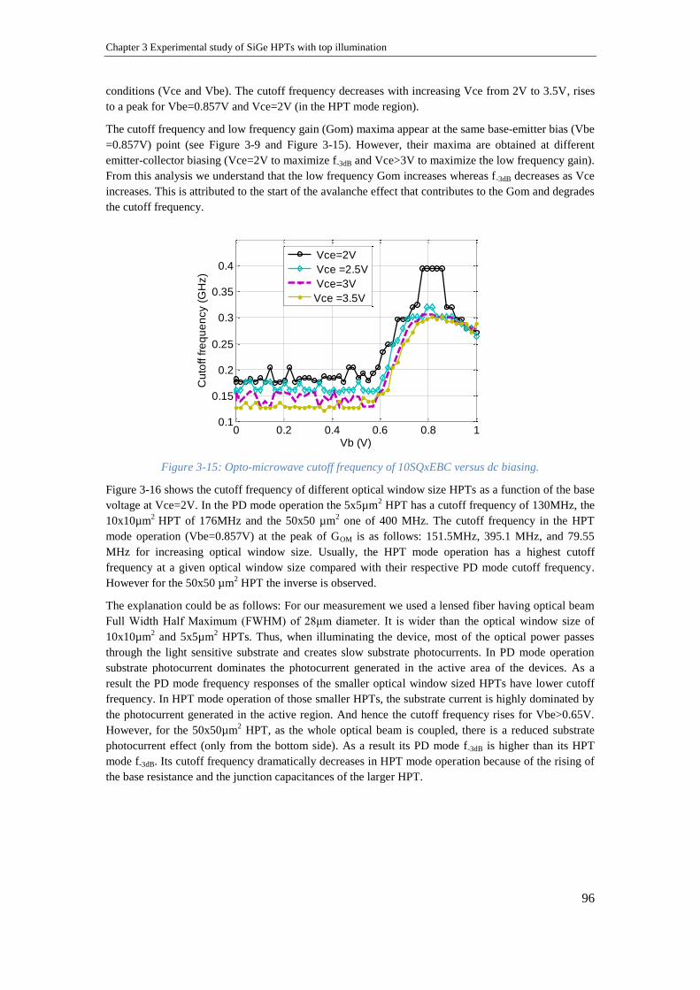
Chapter 3 Experimental study of SiGe HPTs with top illumination
96
conditions (Vce and Vbe). The cutoff frequency decreases with increasing Vce from 2V to 3.5V, rises
to a peak for Vbe=0.857V and Vce=2V (in the HPT mode region).
The cutoff frequency and low frequency gain (Gom) maxima appear at the same base-emitter bias (Vbe
=0.857V) point (see Figure 3-9 and Figure 3-15). However, their maxima are obtained at different
emitter-collector biasing (Vce=2V to maximize f-3dB and Vce>3V to maximize the low frequency gain).
From this analysis we understand that the low frequency Gom increases whereas f-3dB decreases as Vce
increases. This is attributed to the start of the avalanche effect that contributes to the Gom and degrades
the cutoff frequency.
Figure 3-15: Opto-microwave cutoff frequency of 10SQxEBC versus dc biasing.
Figure 3-16 shows the cutoff frequency of different optical window size HPTs as a function of the base
voltage at Vce=2V. In the PD mode operation the 5x5µm2 HPT has a cutoff frequency of 130MHz, the
10x10µm2
HPT of 176MHz and the 50x50 µm2 one of 400 MHz. The cutoff frequency in the HPT
mode operation (Vbe=0.857V) at the peak of GOM is as follows: 151.5MHz, 395.1 MHz, and 79.55
MHz for increasing optical window size. Usually, the HPT mode operation has a highest cutoff
frequency at a given optical window size compared with their respective PD mode cutoff frequency.
However for the 50x50 µm2 HPT the inverse is observed.
The explanation could be as follows: For our measurement we used a lensed fiber having optical beam
Full Width Half Maximum (FWHM) of 28μm diameter. It is wider than the optical window size of
10x10µm2 and 5x5µm
2 HPTs. Thus, when illuminating the device, most of the optical power passes
through the light sensitive substrate and creates slow substrate photocurrents. In PD mode operation
substrate photocurrent dominates the photocurrent generated in the active area of the devices. As a
result the PD mode frequency responses of the smaller optical window sized HPTs have lower cutoff
frequency. In HPT mode operation of those smaller HPTs, the substrate current is highly dominated by
the photocurrent generated in the active region. And hence the cutoff frequency rises for Vbe>0.65V.
However, for the 50x50µm2 HPT, as the whole optical beam is coupled, there is a reduced substrate
photocurrent effect (only from the bottom side). As a result its PD mode f-3dB is higher than its HPT
mode f-3dB. Its cutoff frequency dramatically decreases in HPT mode operation because of the rising of
the base resistance and the junction capacitances of the larger HPT.
0 0.2 0.4 0.6 0.8 10.1
0.15
0.2
0.25
0.3
0.35
0.4
Vb (V)
Cu
toff fre
qu
en
cy (
GH
z)
Vce=2V
Vce =2.5V
Vce=3V
Vce =3.5V
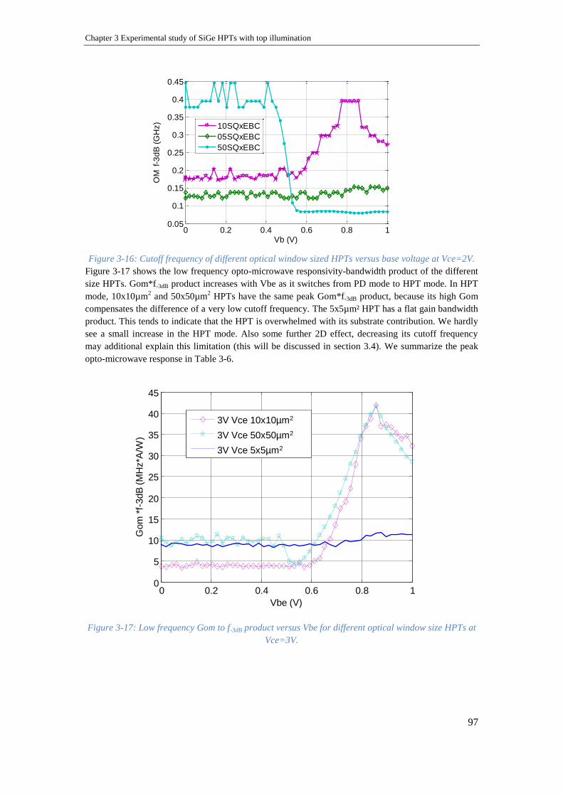
Chapter 3 Experimental study of SiGe HPTs with top illumination
97
Figure 3-16: Cutoff frequency of different optical window sized HPTs versus base voltage at Vce=2V.
Figure 3-17 shows the low frequency opto-microwave responsivity-bandwidth product of the different
size HPTs. Gom*f-3dB product increases with Vbe as it switches from PD mode to HPT mode. In HPT
mode, 10x10µm2 and 50x50µm
2 HPTs have the same peak Gom*f-3dB product, because its high Gom
compensates the difference of a very low cutoff frequency. The 5x5µm² HPT has a flat gain bandwidth
product. This tends to indicate that the HPT is overwhelmed with its substrate contribution. We hardly
see a small increase in the HPT mode. Also some further 2D effect, decreasing its cutoff frequency
may additional explain this limitation (this will be discussed in section 3.4). We summarize the peak
opto-microwave response in Table 3-6.
Figure 3-17: Low frequency Gom to f-3dB product versus Vbe for different optical window size HPTs at
Vce=3V.
0 0.2 0.4 0.6 0.8 10.05
0.1
0.15
0.2
0.25
0.3
0.35
0.4
0.45
Vb (V)
OM
f-3
dB
(G
Hz)
10SQxEBC
05SQxEBC
50SQxEBC
0 0.2 0.4 0.6 0.8 10
5
10
15
20
25
30
35
40
45
Vbe (V)
Gom
*f-
3dB
(M
Hz*A
/W)
3V Vce 10x10µm2
3V Vce 50x50µm2
3V Vce 5x5µm2

Chapter 3 Experimental study of SiGe HPTs with top illumination
98
Table 3-6: Summary of the performance of different optical window size HPTs at their optimum dc
bias.
HPT type f-3dB,HPT(MHz)
at Vce=2V and
Vbe=0.857V
f-3dB,PD(MHz) at
Vce=2V and Vbe=0V
Gom,HPT*f-3dB,HPT
(MHz*A/W) at Vce=3V
and Vce=3V
05SQxEBC 153.8 136 11.5
10SQxEBC 400 181 41.9
50SQxEBC 79.6 400 41.7
3.3.4.2 Optical transition frequency (fTopt) vs dc bias
As it is defined in chapter 2 section 2.3.1, the optical transition frequency, fTopt, is a frequency at which
the optical gain of the phototransistor is equal to one (where the transistor stops amplifying). In this
section we optimize the dc biasing points of the HPT that maximizes the fTopt. We also present and
compare the intrinsic and complete HPT optical transition frequencies.
a) Complete optical transition frequency (fTopt,comp)
Figure 3-18 a) shows the extraction results of optical transition frequencies fTopt for phototransistors
having 10x10 and 50x50µm2 optical window size versus of the collector current. From these curves
and electrical transition frequency (fT) vs IC curve presented in Figure 3-21, we can directly compare
the evolution of fT and fTopt under the same biasing condition (let say Vce=3.5V). That means we can
compare the transition frequency measured when the RF power is injected through the base (fT) and
when the RF power is injected through the optical window by modulating the optical power (fTopt).
Compared to the electrical transition frequency, for non-optimum position of the optical probe, the
optical transition frequency is dramatically reduces to 2.2GHz from 50GHz for 10x10µm2 under the
same biasing condition (see Figure 3-21 and Figure 3-18 a). This is due to the presences of additional
capacitance and transit time related to the injected optical power.
Figure 3-18: Optical transition frequency at non-optimum position of the optical probe with different
Vce: a) versus collector current of 10x10µm2 and 50x50µm
2 HPTs b) versus Vbe of 10x10µm
2 HPT.
For the HPT having 10x10µm2 active surface area, the optical transition frequency is getting smaller as
Vce increases. It can be explained as when Vce increases, the base collector depletion area increases,
which in turn increases the junction capacitance of the phototransistor. It is not the case for 50SQxEBC
under the same biasing condition as it can handle high power. The maximum value of fTopt of
50x50µm2 HPT is 1.56GHz at Vce=2.5V and Ic =0.036A as presented in Figure 3-18 a).
a) b)
0.5 0.6 0.7 0.8 0.9 10
0.5
1
1.5
2
2.5
Vb (V)
fTo
pt (G
Hz)
Vce=1V
Vce=2V
Vce=2.5V
Vce=3V
0 0.02 0.04 0.06 0.080
0.5
1
1.5
2
2.5
Ic opt (A)
fTo
pt (G
Hz)
2V Vce 10SQxEBC
2.5V Vce 10SQxEBC
3.5V Vce 10SQxEBC
2V Vce 50SQxEBC
2.5V Vce 50SQxEBC
3.5V Vce 50SQxEBC

Chapter 3 Experimental study of SiGe HPTs with top illumination
99
We also optimize the optical transition frequency, fTopt, in terms of Vbe and Vce. The preliminary
results of fTopt of 10x10µm2 HPT versus of the base voltage at various Vce are extracted and shown in
Figure 3-18 b). For this optical probe position, a maximum fTopt of 2.2GHz is obtained at Vbe=0.857V
and Vce=2V.
b) Intrinsic optical transition frequency (fTopt,int)
The complete and intrinsic opto-microwave gains versus frequency at non optimum optical probe
position are plotted in Figure 3-19 for both photodiode (Vbe=0V) and phototransistor (Vbe=0.857V)
modes at Vce=2V. The frequency response of the substrate photodiode at the same location of the
optical probe is modeled and plotted in the same figure. From this we can extract the complete and
intrinsic optical transition frequencies as it is indicated in the figure.
As we can observe in Figure 3-19, the impact of the substrate photodiode is observed at low frequency
in HPT mode of operation and this impact is not visible at high frequency (f>200MHz) as the substrate
response is dominated by the internal transistor action. However, in PD mode, the influence of the
substrate photodiode is observed at all frequencies up to 10GHz. Hence, we conclude that the substrate
effect is more visible for SiGe/Si photodiode than for SiGe/Si phototransistor.
Figure 3-19: The complete and intrinsic Gom versus frequency for 10x10µm2 HPT in PD and HPT
modes at Vce=2V.
As we observe in Figure 3-19, the substrate photodiode contributes to the low frequency gain and thus
lower the 3dB cutoff frequency. However it contributes to the overall detection and is still contributing
even up to 10GHz. Figure 3-20 shows the complete and intrinsic optical transition frequency curve
versus the collector current Ic of 10x10µm2
and 50x50µm2
HPTs at Vce=2V. After removing the
substrate response, the optical transition frequency is improved from 2.17GHz to 3.5GHz for
10x10µm2 and from 1.8GHz to 3GHz for 50x50µm
2 HPT. The intrinsic optical transition frequency of
50x50µm2 HPT is smaller than the intrinsic optical frequency of 10x10µm
2 HPT. This is due to the
higher junction capacitances and base resistances in 50x50µm2 HPT as the surface area is larger. Table
3-7 provides the peak values of the intrinsic and complete optical transition frequencies of 10x10µm2
and 50x50µm2 HPTs with their corresponding dc bias points.
10-1
100
101
-80
-70
-60
-50
-40
-30
-20
-10
Freq (GHz)
Go
m(d
B)
Model
Complete HPT
Intrinsic HPT
fTopt,comp fTopt,int
HPT mode
PD mode

Chapter 3 Experimental study of SiGe HPTs with top illumination
100
Figure 3-20: The complete and intrinsic optical transition frequency versus collector current for
10x10µm2 and 50x50µm
2 HPTs at Vce=2V.
Table 3-7 : The peak values of intrinsic and complete HPT optical transition frequencies along with
their optimum dc bias.
3.3.5 Conclusion on dc bias
According to this study we conclude that at Vbe=0.857V and Vce=3V the low frequency behaviors
(Gopt, Gom and h21) are maximized. However, the dynamic behaviors (fTopt, f-3dB) are optimized at the
same Vbe and Vce=2V for smaller size HPTs. Thus we will use Vbe=0.857V (under HPT mode) and
Vce=3V or 2V for further opto-microwave experimental studies such as the localization of
photocurrent sources in the structure and 2D dependence of dynamic behavior in the following section.
We have observed the impact of the base terminal contact on the low frequency behaviors. We
understand that the substrate photodiode degrades the dynamic behavior and contributes to the low
frequency behavior in SiGe/Si HPTs with a great impact in the PD mode operation. In this 1st study we
also understand that 10x10µm2 HPT have better performance in terms of frequency, even though it has
lower responsivity compared to 50x50µm2.
0 0.02 0.04 0.06 0.080
0.5
1
1.5
2
2.5
3
3.5
Ic (A)
fTo
pt (G
Hz)
Intrinsic HPT
Complete HPT
50x50µm2
10x10µm2
HPT type Vce (V) Vbe(V) Ic(mA) fTopt Complete HPT
(GHz)
fTopt Intrinsic HPT
(GHz)
10x10µm2 2 0.857 7.5 2.17 3.5
50x10µm2 3 0.857 36.0 1.8 3.0
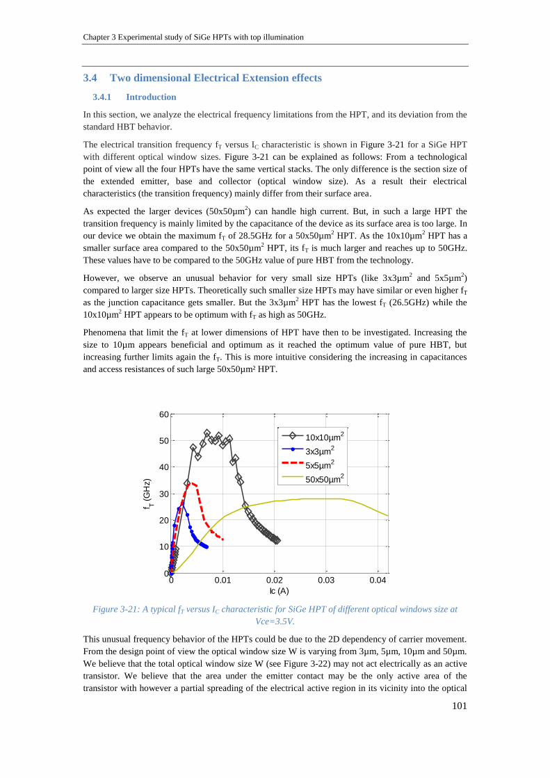
Chapter 3 Experimental study of SiGe HPTs with top illumination
101
3.4 Two dimensional Electrical Extension effects
3.4.1 Introduction
In this section, we analyze the electrical frequency limitations from the HPT, and its deviation from the
standard HBT behavior.
The electrical transition frequency fT versus IC characteristic is shown in Figure 3-21 for a SiGe HPT
with different optical window sizes. Figure 3-21 can be explained as follows: From a technological
point of view all the four HPTs have the same vertical stacks. The only difference is the section size of
the extended emitter, base and collector (optical window size). As a result their electrical
characteristics (the transition frequency) mainly differ from their surface area.
As expected the larger devices (50x50µm2) can handle high current. But, in such a large HPT the
transition frequency is mainly limited by the capacitance of the device as its surface area is too large. In
our device we obtain the maximum fT of 28.5GHz for a 50x50µm2 HPT. As the 10x10µm
2 HPT has a
smaller surface area compared to the 50x50µm2 HPT, its fT is much larger and reaches up to 50GHz.
These values have to be compared to the 50GHz value of pure HBT from the technology.
However, we observe an unusual behavior for very small size HPTs (like 3x3µm2 and 5x5µm
2)
compared to larger size HPTs. Theoretically such smaller size HPTs may have similar or even higher fT
as the junction capacitance gets smaller. But the 3x3µm2 HPT has the lowest fT (26.5GHz) while the
10x10µm2 HPT appears to be optimum with fT as high as 50GHz.
Phenomena that limit the fT at lower dimensions of HPT have then to be investigated. Increasing the
size to 10µm appears beneficial and optimum as it reached the optimum value of pure HBT, but
increasing further limits again the fT. This is more intuitive considering the increasing in capacitances
and access resistances of such large 50x50µm² HPT.
Figure 3-21: A typical fT versus IC characteristic for SiGe HPT of different optical windows size at
Vce=3.5V.
This unusual frequency behavior of the HPTs could be due to the 2D dependency of carrier movement.
From the design point of view the optical window size W is varying from 3µm, 5µm, 10µm and 50µm.
We believe that the total optical window size W (see Figure 3-22) may not act electrically as an active
transistor. We believe that the area under the emitter contact may be the only active area of the
transistor with however a partial spreading of the electrical active region in its vicinity into the optical
0 0.01 0.02 0.03 0.040
10
20
30
40
50
60
Ic (A)
f T (
GH
z)
10x10µm2
3x3µm2
5x5µm2
50x50µm2
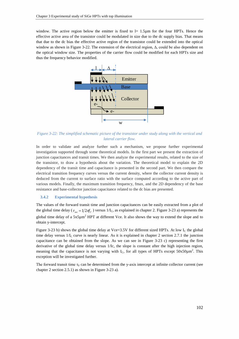
Chapter 3 Experimental study of SiGe HPTs with top illumination
102
window. The active region below the emitter is fixed to l= 1.5µm for the four HPTs. Hence the
effective active area of the transistor could be modulated in size due to the dc supply bias. That means
that due to the dc bias the effective active region of the transistor could be extended into the optical
window as shown in Figure 3-22. The extension of the electrical region, ∆, could be also dependent on
the optical window size. The properties of the carrier flow could be modified for each HPTs size and
thus the frequency behavior modified.
Figure 3-22: The simplified schematic picture of the transistor under study along with the vertical and
lateral carrier flow.
In order to validate and analyze further such a mechanism, we propose further experimental
investigation supported through some theoretical models. In the first part we present the extraction of
junction capacitances and transit times. We then analyze the experimental results, related to the size of
the transistor, to draw a hypothesis about the variation. The theoretical model to explain the 2D
dependency of the transit time and capacitance is presented in the second part. We then compare the
electrical transition frequency curves versus the current density, where the collector current density is
deduced from the current to surface ratio with the surface computed according to the active part of
various models. Finally, the maximum transition frequency, fmax, and the 2D dependency of the base
resistance and base-collector junction capacitance related to the dc bias are presented.
3.4.2 Experimental hypothesis
The values of the forward transit time and junction capacitances can be easily extracted from a plot of
the global time delay (Ttot f 21 ) versus 1/IC, as explained in chapter 2. Figure 3-23 a) represents the
global time delay of a 5x5µm2 HPT at different Vce. It also shows the way to extend the slope and to
obtain y-intercept.
Figure 3-23 b) shows the global time delay at Vce=3.5V for different sized HPTs. At low IC the global
time delay versus 1/IC curve is nearly linear. As it is explained in chapter 2 section 2.7.1 the junction
capacitance can be obtained from the slope. As we can see in Figure 3-23 c) representing the first
derivative of the global time delay versus 1/Ic, the slope is constant after the high injection region,
meaning that the capacitance is not varying with IC, for all types of HPTs except 50x50µm2. This
exception will be investigated further.
The forward transit time τF can be determined from the y-axis intercept at infinite collector current (see
chapter 2 section 2.5.1) as shown in Figure 3-23 a).
l ∆
w
e-
e-
Emitter
Base
Collector

Chapter 3 Experimental study of SiGe HPTs with top illumination
103
Figure 3-23: Global time delay versus 1/Ic a) 5x5µm2 HPT at different Vce to show how to extract the
junction capacitance and transit time, b) Different size HPTs (3x3µm2,5x5µm
2, 10x10µm
2 and
50x50µm2) at Vce=3.5V and c) The first derivative of global time delay with respect to 1/IC.
The extracted values of the junction capacitance and transit time of 3x3µm2, 5x5µm
2, and 10x10µm
2
and 50x50µm2 optical window sized HPTs are presented in Table 3-8. As expected the transit time and
the junction capacitance of 50x50µm2 HPT are larger than for the three other structures as its base-
emitter and base-collector junction surface areas are larger. The transit time of 3x3µm2 was expected to
be the smallest, mostly due to its capacitance and resistance contributions as τF=CBC (RE+RC)+ τb+ τe+
τbc. But it has a higher transit time than the 10x10µm2 and 5x5µm
2 HPTs. This could be due to the
variation of the electrical field in each transistor that modifies the electrical extension region, ∆, of the
active area of the transistor, and may create either larger capacitances or may increase the path length
of carriers, mostly increasing the base-collector transit time. This fact is analyzed in the following
section with the help of theoretical models.
Table 3-8: Capacitance and forward transit time extracted from figure 2.26 b) for different sized HPTs
(3x3µm2, 5x5µm
2, 10x10µm
2 and 50x50µm
2 HPTs)
Device size (µm2) Transit time (ps) Slope (A.s) Capacitance (pF)
50x50 5.5 1.95E-13 7.5540
10x10 1.5 2.06E-14 0.7979
5x5 3 7.25E-15 0.2805
3x3 5.4 2.80E-15 0.1083
3.4.3 Transit time extrapolation model
In this sub section the impact of the optical window size on the transit time is investigated and
explained with the help of theoretical models. We focus our analysis on how the size of the optical
window modifies the electrical extension region.
500 1000 1500 2000 2500 3000-1
0
1
2
3
4
5x 10
-4
1/Ic (A-1
)
d(t
au
)/d
(Ic)
[A.n
s]
3x3µm2
5x5µm2
10x10µm2
50x50µm2
0 500 1000 1500 20000
0.005
0.01
0.015
0.02
1/Ic (A-1
)
Glo
ba
l tim
e d
ela
y (
ns)
5µmx5µm t_EC vs 1/ Ic
Vce=1V
Vce=2V
Vce=3.5V
0 500 1000 1500 2000 25000
0.01
0.02
0.03
0.04
0.05
1/Ic (A-1
)
Glo
ba
l tim
e d
ela
y (
ns)
t_EC vs Ic Extrapolation
a) b)
c)
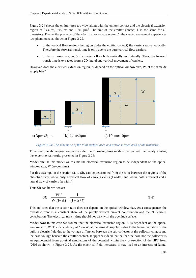
Chapter 3 Experimental study of SiGe HPTs with top illumination
104
Figure 3-24 shows the emitter area top view along with the emitter contact and the electrical extension
region of 3x3µm2, 5x5µm
2 and 10x10µm
2. The size of the emitter contact, l, is the same for all
transistors. Due to the presence of the electrical extension region ∆, the carrier movement experiences
two phenomena as shown in Figure 3-22.
In the vertical flow region (the region under the emitter contact) the carriers move vertically.
Therefore the forward transit time is only due to the pure vertical flow carriers.
In the extension region, ∆, the carriers flow both vertically and laterally. Thus, the forward
transit time is extracted from a 2D lateral and vertical movement of carriers.
However, does the electrical extension region, ∆, depend on the optical window size, W, at the same dc
supply bias?
Figure 3-24: The schematic of the total surface area and active surface area of the transistor.
To answer the above question we consider the following three models that we will then analyze using
the experimental results presented in Figure 3-26:
Model one: In this model we assume the electrical extension region to be independent on the optical
window size, W (∆=constant).
For this assumption the section ratio, SR, can be determined from the ratio between the regions of the
phototransistor where only a vertical flow of carriers exists (l width) and where both a vertical and a
lateral flow of carriers (∆ width).
Thus SR can be written as:
W. 1
W.(l ) (1 / )
lSR
l
(3.6)
This indicates that the section ratio does not depend on the optical window size. As a consequence, the
overall current is a constant share of the purely vertical current contribution and the 2D current
contribution. The electrical transit time should not vary with the opening surface.
Model two: In this case we assume that the electrical extension region, ∆, is dependent on the optical
window size, W. The dependency of ∆ on W, at the same dc supply, is due to the lateral variation of the
built in electric field due to the voltage difference between the sub-collector at the collector contact and
the base voltage beneath the emitter contact. It appears indeed that neither the base nor the collector is
an equipotential from physical simulations of the potential within the cross-section of the HPT from
[260] as shown in Figure 3-25. As the electrical field increases, it may lead to an increase of lateral
∆
l
∆
l
∆
l
w
w
a) 3µmx3µm b) 5µmx5µm c) 10µmx10µm

Chapter 3 Experimental study of SiGe HPTs with top illumination
105
path and thus of the transit time when W reduces. In this case the transit time is expected to vary with
the optical window.
It has to be noted that our SiGe HPT has actually only one emitter contact, as opposed to [260], which
lies on the left hand side of the HPT, at the opposite of the collector contact. This may then exacerbate
further the lateral electrical field and voltage inhomogeneity in the base and collector regions.
Figure 3-25: The potential distribution over the HPT structure simulation result [260]
Model three: In the last case we assume that the lateral flow of carriers occurs in all regions of the
transistor (i.e ∆=W) under the same dc bias condition. Under this assumption the transit time increases
directly with the optical window size as the lateral distance increases.
Experimental observation: In order to observe in which one of the above three situations is our
transistor working, we experimentally extract the transit time of various size HPT (3µm, 5µm, 10µm
and 50µm). The result is presented in Figure 3-26. It shows that the transit time decreases as the optical
window size increases from 3µm, 5µm to 10µm. This proves that the electrical extension region, ∆,
depends on the optical window size, W. This is because the lateral electrical field is higher with lower
dimension under the same dc biasing condition. Thus the lateral flow of carriers may dominate over the
vertical one when the optical window size is smaller. This finally increases the forward transit time of
the smaller transistor as shown in Figure 3-26. This fits with the assumption of model two.
The transit time of W=50µm optical window size transistor is however much larger. This may be due
to the fact that the collector surface and sub-collector dimension gets so large that the RC.CBC term of
the transit time becomes predominant. The capacitance increases with the width of the window and is
proportional to l.(l+∆). On the other side the resistance is controlled by the length from the collector
contact to the vertical point below the emitter active region. This length is then approximately the
optical window size. The width of this resistance is also defined by the width of this optical window.
Thus, as the length and width are almost equal (when considering ∆ small or negligible for the
50x50µm² HPT), the resistance keeps constant. In overall, the RC.CBC product then increases.
This then keeps consistent with model 2 and consolidates this approach.

Chapter 3 Experimental study of SiGe HPTs with top illumination
106
Figure 3-26: Experimentally measured forward transit time versus the optical widow size at
Vbe=0.823V and Vce=3.5V
3.4.4 Geometrical dependence of the capacitance
In this section we present the geometrical dependence of the capacitance related to the electrical
extension region ∆. The capacitance is extracted from the fT curve versus IC at low collector currents.
The result is given in Figure 3-27 which shows that the device capacitance increases with the optical
window size W, as expected.
The junction capacitance increases with the size of the HPT by assuming that the total surface area of
(l+W).W determines the capacitance of the HPT. However, as the emitter contact is smaller than the
total emitter size, the definition of the capacitance might be far different from this. Thus, we are
interested in observing closely this phenomenon by comparing experimental results with a number of
mathematical models. Here we define three models as shown in Figure 3-28 (Model 1, Model 2 and
Model 3) that have the purpose to consider either a 2D electrical extension effect (∆) or not, according
to extreme cases.
Figure 3-27: Experimentally measured junction capacitances versus the optical window size.
0
1
2
3
4
5
6
0 10 20 30 40 50
Forw
ard
tran
sit
tim
e (
ps)
w (µm)
0
1
2
3
4
5
6
7
8
0 10 20 30 40 50
Cap
acit
ance
(pF)
w (µm)

Chapter 3 Experimental study of SiGe HPTs with top illumination
107
Figure 3-28: The possible behavior of the transistor under dc bias.
Model 1: In this model we assume that the flow of carriers is only vertically under the emitter contact.
Hence the capacitance of the transistor can be determined by the surface area under the emitter contact.
This represents a case where there is no electrical extension ∆. Mathematically this can be modelled as
shown in equation(3.7):
. .
SCR
l wC
w
(3.7)
Where wSCR is the junction space charge region width and ℰ is the dielectric permittivity.
Model 2: In this model we assume that the flow of carriers is vertical under the emitter contact, l, and
both vertical and lateral under electrical extension region, ∆. Hence the surface area of the active region
of the transistor is increased by ∆. As a result the capacitance can be determined by the surface area
under the emitter contact and electrical extension region. In this model the electrical extension region,
∆, depends on the optical window size. Mathematically the capacitance can be expressed as:
.( ).W
SCR
lC
w
(3.8)
Where SCRw is an average value of the space charge width of the base-emitter and base-collector all
over the transistor.
Model 3: In third model we assume that the flow of carriers is distributed through all regions of the
transistor, l+W. This represents a case where there is no restriction of the carrier path beneath the
emitter metal contact only, and thus no concept of electrical extension ∆. In other words it would be a
case where the high doping of the polysilicon of the emitter and the high doping of the base are
providing sufficiently low resistances to create a homogenous voltage and current distribution across
the HPT. Hence the capacitance of the transistor can be determined through the whole surface area of
the transistor. Mathematically this can be model as:
.( ).W
SCR
l WC
w
(3.9)
We consider l=1.5µm from the design, and we assume that ℰr= 11.7, this is to say that silicon is the
dominant component of the HPT. We assume the smallest envisageable space charge region width is of
wSCR=10nm thus providing the maximum boundary to the capacitance. Figure 3-29 shows the curves of
the three models expressed in terms of ratio of the capacitance to the optical window size (C/W) versus
the optical window size, W. Model 1 and Model 3 show the two extremes of the possible operation of
the transistor. That means for model l, the C/W ratio is constant whereas for model 3 it linearly
increases with W. Model 2 is an intermediate model, which lies between model 3 and model 1.
Comparing measurements data in Figure 3-29 and the model trends, it appears that the HPT is rather
l ∆
e-
e-
Model 2
l
e-
e-
wl
e-
Model 1 Model 3

Chapter 3 Experimental study of SiGe HPTs with top illumination
108
following a model 2 shape. This is then an additional verification of the validity of this model proving
that ∆ varies with W. From this we understand that the junction capacitance is modified by the
electrical extension region ∆.
Figure 3-29: C/W versus optical window size curve for the three models, and experimental data for
Vce=3.5V and Vbe=0.823V.
3.4.5 Transition frequency, fT, vs current density
To validate the above models we plot the electrical transition frequency versus the collector current
density as shown in Figure 3-30. The current density is computed by considering the effective active
area of the intrinsic transistor from the above three models. Hence we compute the current density for
each model as shown in Table 3-9
Table 3-9: Current density computation for different models
Model Collector current density (Jc)
Model 1
W.CI
l
Model 2
W.( )CI
l , thus
(W).
C
C
If l
w J
Model 3
W.( )CI
l W
From this result we can observe that the peak of fT appears at a different collector current density for
models 1 and 3 as shown in Figure 3-30 a) and b) respectively depending on the transistor size. This
comes from the fact that the high injection degradation starts appearing at some threshold current
density which varies with the size of the transistor. However, one may consider that the injection level
is mostly controlled by the doping levels (which are the same for all HPTs) and hence the fT curve in
high injection region should follow the same decreasing for all HPTs; so having a convergence of the fT
curve at high current density. We therefore define the ∆ dimension in model 2 to be adjusted so that all
HPTs have their fT curves following the same decrease in high injection as presented in Figure 3-30 c).
According to model 2, the electrical extension region (∆) is expected to decrease while the optical
0
0,02
0,04
0,06
0,08
0,1
0,12
0,14
0 2 4 6 8 10
C/W
(µ
F/m
)
W (µm)
Model 1
Model 3
Model 2= Experimental

Chapter 3 Experimental study of SiGe HPTs with top illumination
109
window size (W) increases. According to the result from the Figure 3-26, we can even assume that the
electrical extension region (∆) of 50µm HPT is negligible, which means ∆=0. This is our reference
point to be able to define values for ∆ as a function of the HPTs size. The values of ∆ that are then
extracted are plotted as a function of W in Figure 3-31.
As a result of this optimization, we can observe that the peaks of the fT are then well aligned for the
four HPTs as shown in Figure 3-30 c). We can also observe that while the slope of fT at low Jc are not
equal for models 1 and 3, they have nearly similar slopes for model 2. This means the capacitance per
unit of active surface are similar for all phototransistor, which is consistent in the fact they have exactly
the same vertical stack.
From this analysis we then confirm the validity of our proposed model of 2D electrical extension
effect. By extracting such an average and effective ∆ width of such an extension, we can unify the
behavior of all HPTs as a function of their size.
The active region of the transistor is neither only under the emitter contact nor the whole emitter (l+w),
it is rather determined by the emitter contact size and the electrical extension region, ∆. This electrical
extension region depends on the electric field distribution in the transistor and the size of the optical
window, and is increased when the voltage gradient gets higher between the base contact and the
collector, thus, at a given Vcb value, when the size of the HPT decreases, which is a confirmed trend as
observed by the result of Figure 3-31.
According to this extraction of the ∆ value, we observe that for HPT of 3µm in size of optical window,
and then 1.5µm of emitter contact and 0.7µm of regions around the emitter contact which are shadowed
by the metal layer above, thus 5.2µm in width in total, the electrical extension comes to be as high as
3µm.
This explains that the electrical field in such a structure is highly transverse and justify then why this
structure comes to be the slowest test structure as compared to the 5x5µm² and 10x10µm² optical
window sizes HPTs. A clear design rules could then be deduced to improve their speed: perspective
would be: - to get a symmetric contact of the collector, or even circular shape, that will make the
electrical field more vertical; - to get simultaneously a symmetrical contact of the base and emitters; -
eventually to fragment the HPT in smaller individual HPTs, as the electrical extension may reach a
limit in its increase. This limits is however not visible from the curve yet.
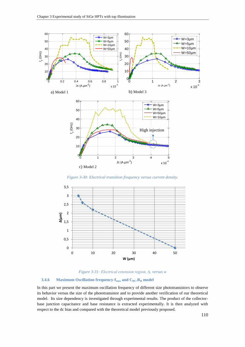
Chapter 3 Experimental study of SiGe HPTs with top illumination
110
Figure 3-30: Electrical transition frequency versus current density.
Figure 3-31: Electrical extension region, ∆, versus w
3.4.6 Maximum Oscillation frequency-fmax and CBC.RB model
In this part we present the maximum oscillation frequency of different size phototransistors to observe
its behavior versus the size of the phototransistor and to provide another verification of our theoretical
model. Its size dependency is investigated through experimental results. The product of the collector-
base junction capacitance and base resistance is extracted experimentally. It is then analyzed with
respect to the dc bias and compared with the theoretical model previously proposed.
a) Model 1 b) Model 3
c) Model 2
0 1 2 3 4 5
x 10-4
0
10
20
30
40
50
60
Jc (A.µm-2
)
f T (
GH
z)
W=3µm
W=5µm
W=50µm
W=10µm
High injection
0 1 2 3
x 10-4
0
10
20
30
40
50
60
Jc (A.µm-2)
f T (
GH
z)
W=3µm
W=5µm
W=10µm
W=50µm
0 0.2 0.4 0.6 0.8 1
x 10-3
0
10
20
30
40
50
60
Jc (A.µm-2
)
f T (
GH
z)
W=3µm
W=5µm
W=10µm
W=50µm
0
0,5
1
1,5
2
2,5
3
3,5
0 10 20 30 40 50
∆(µm)
W (µm)
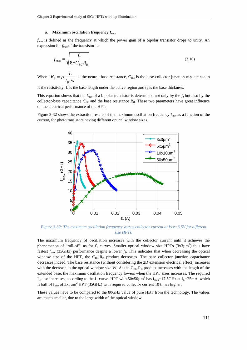
Chapter 3 Experimental study of SiGe HPTs with top illumination
111
a. Maximum oscillation frequency fmax
fmax is defined as the frequency at which the power gain of a bipolar transistor drops to unity. An
expression for fmax of the transistor is:
max8
T
BC B
ff
C R (3.10)
Where .w
B
B
LR
t is the neutral base resistance, CBC is the base-collector junction capacitance, ρ
is the resistivity, L is the base length under the active region and tB is the base thickness.
This equation shows that the fmax of a bipolar transistor is determined not only by the fT but also by the
collector-base capacitance CBC and the base resistance RB. These two parameters have great influence
on the electrical performance of the HPT.
Figure 3-32 shows the extraction results of the maximum oscillation frequency fmax as a function of the
current, for phototransistors having different optical window sizes.
Figure 3-32: The maximum oscillation frequency versus collector current at Vce=3.5V for different
size HPTs.
The maximum frequency of oscillation increases with the collector current until it achieves the
phenomenon of “roll-off” as for fT curves. Smaller optical window size HPTs (3x3µm2) thus have
fastest fmax (35GHz) performance despite a lower fT. This indicates that when decreasing the optical
window size of the HPT, the CBC.RB product decreases. The base collector junction capacitance
decreases indeed. The base resistance (without considering the 2D extension electrical effect) increases
with the decrease in the optical window size W. As the CBC.RB product increases with the length of the
extended base, the maximum oscillation frequency lowers when the HPT sizes increases. The required
IC also increases, according to the fT curve. HPT with 50x50µm2 has fmax=17.5GHz at IC=25mA, which
is half of fmax of 3x3µm2 HPT (35GHz) with required collector current 10 times higher.
These values have to be compared to the 80GHz value of pure HBT from the technology. The values
are much smaller, due to the large width of the optical window.
0 0.01 0.02 0.03 0.04 0.050
5
10
15
20
25
30
35
40
Ic (A)
f ma
x (G
Hz)
3x3µm2
5x5µm2
10x10µm2
50x50µm2
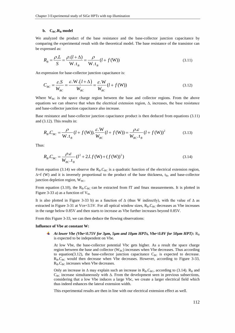
Chapter 3 Experimental study of SiGe HPTs with top illumination
112
b. CBC.RB model
We analyzed the product of the base resistance and the base-collector junction capacitance by
comparing the experimental result with the theoretical model. The base resistance of the transistor can
be expressed as:
. .( )( (W))
W.t W.tB
B B
L lR l f
S
(3.11)
An expression for base-collector junction capacitance is:
.W.. .W( (W))
BC
BC BC BC
lSC l f
W W W (3.12)
Where WBC is the space charge region between the base and collector regions. From the above
equations we can observe that when the electrical extension region, ∆, increases, the base resistance
and base-collector junction capacitance also increase.
Base resistance and base-collector junction capacitance product is then deduced from equations (3.11)
and (3.12). This results in:
2.W .. ( (W)). ( (W)) ( (W))
W.t .tB BC
B BC BC B
R C l f l f l fW W
(3.13)
Thus:
2 2.. ( 2. . (W) ( (W)) )
.tB BC
BC B
R C l l f fW
(3.14)
From equation (3.14) we observe the RB.CBC is a quadratic function of the electrical extension region,
∆=f (W) and it is inversely proportional to the product of the base thickness, tB, and base-collector
junction depletion region, WBC.
From equation (3.10), the RB.CBC can be extracted from fT and fmax measurements. It is plotted in
Figure 3-33 a) as a function of Vbe.
It is also plotted in Figure 3-33 b) as a function of ∆ (thus W indirectly), with the value of ∆ as
extracted in Figure 3-31 at Vce=3.5V. For all optical window sizes, RB.CBC decreases as Vbe increases
in the range below 0.85V and then starts to increase as Vbe further increases beyond 0.85V.
From this Figure 3-33, we can then deduce the flowing observations:
Influence of Vbe at constant W:
At lower Vbe (Vbe<0.75V for 3µm, 5µm and 10µm HPTs, Vbe<0.8V for 50µm HPT): RB
is expected to be independent on Vbe.
At low Vbe, the base-collector potential Vbc gets higher. As a result the space charge
region between the base and collector (WBC) increases when Vbe decreases. Thus according
to equation(3.12), the base-collector junction capacitance CBC is expected to decrease.
RB.CBC would then decrease when Vbe decreases. However, according to Figure 3-33,
RB.CBC increases when Vbe decreases.
Only an increase in ∆ may explain such an increase in RB.CBC, according to (3.14). RB and
CBC increase simultaneously with ∆. From the development seen in previous subsections,
considering that a low Vbe induces a large Vbc, we create a larger electrical field which
thus indeed enhances the lateral extension width.
This experimental results are then in line with our electrical extension effect as well.
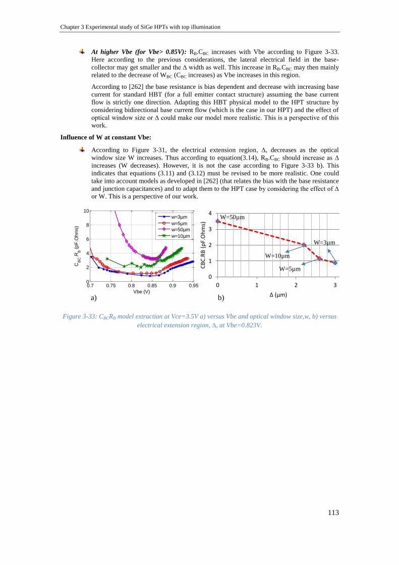
Chapter 3 Experimental study of SiGe HPTs with top illumination
113
At higher Vbe (for Vbe> 0.85V): RB.CBC increases with Vbe according to Figure 3-33.
Here according to the previous considerations, the lateral electrical field in the base-
collector may get smaller and the ∆ width as well. This increase in RB.CBC may then mainly
related to the decrease of WBC (CBC increases) as Vbe increases in this region.
According to [262] the base resistance is bias dependent and decrease with increasing base
current for standard HBT (for a full emitter contact structure) assuming the base current
flow is strictly one direction. Adapting this HBT physical model to the HPT structure by
considering bidirectional base current flow (which is the case in our HPT) and the effect of
optical window size or ∆ could make our model more realistic. This is a perspective of this
work.
Influence of W at constant Vbe:
According to Figure 3-31, the electrical extension region, ∆, decreases as the optical
window size W increases. Thus according to equation(3.14), RB.CBC should increase as ∆
increases (W decreases). However, it is not the case according to Figure 3-33 b). This
indicates that equations (3.11) and (3.12) must be revised to be more realistic. One could
take into account models as developed in [262] (that relates the bias with the base resistance
and junction capacitances) and to adapt them to the HPT case by considering the effect of ∆
or W. This is a perspective of our work.
Figure 3-33: CBCRB model extraction at Vce=3.5V a) versus Vbe and optical window size,w, b) versus
electrical extension region, ∆, at Vbe=0.823V.
0
1
2
3
4
0 1 2 3
CB
C.R
B (
pF.
Oh
ms)
∆ (µm)
0.7 0.75 0.8 0.85 0.9 0.950
2
4
6
8
10
Vbe (V)
CB
C.R
B (
pF
.Oh
ms)
w=3µm
w=5µm
w=50µm
w=10µm
W=50µm
W=10µm
W=5µm
W=3µm
a) b)
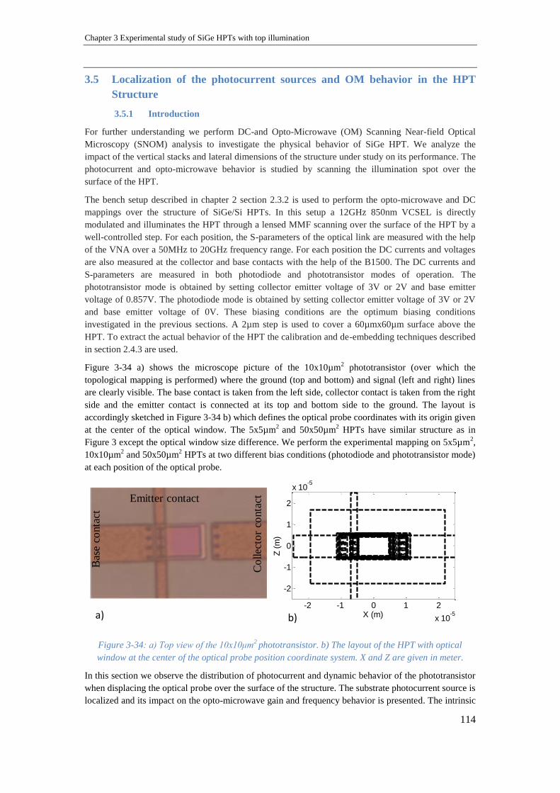
Chapter 3 Experimental study of SiGe HPTs with top illumination
114
3.5 Localization of the photocurrent sources and OM behavior in the HPT
Structure
3.5.1 Introduction
For further understanding we perform DC-and Opto-Microwave (OM) Scanning Near-field Optical
Microscopy (SNOM) analysis to investigate the physical behavior of SiGe HPT. We analyze the
impact of the vertical stacks and lateral dimensions of the structure under study on its performance. The
photocurrent and opto-microwave behavior is studied by scanning the illumination spot over the
surface of the HPT.
The bench setup described in chapter 2 section 2.3.2 is used to perform the opto-microwave and DC
mappings over the structure of SiGe/Si HPTs. In this setup a 12GHz 850nm VCSEL is directly
modulated and illuminates the HPT through a lensed MMF scanning over the surface of the HPT by a
well-controlled step. For each position, the S-parameters of the optical link are measured with the help
of the VNA over a 50MHz to 20GHz frequency range. For each position the DC currents and voltages
are also measured at the collector and base contacts with the help of the B1500. The DC currents and
S-parameters are measured in both photodiode and phototransistor modes of operation. The
phototransistor mode is obtained by setting collector emitter voltage of 3V or 2V and base emitter
voltage of 0.857V. The photodiode mode is obtained by setting collector emitter voltage of 3V or 2V
and base emitter voltage of 0V. These biasing conditions are the optimum biasing conditions
investigated in the previous sections. A 2µm step is used to cover a 60µmx60µm surface above the
HPT. To extract the actual behavior of the HPT the calibration and de-embedding techniques described
in section 2.4.3 are used.
Figure 3-34 a) shows the microscope picture of the 10x10µm2 phototransistor (over which the
topological mapping is performed) where the ground (top and bottom) and signal (left and right) lines
are clearly visible. The base contact is taken from the left side, collector contact is taken from the right
side and the emitter contact is connected at its top and bottom side to the ground. The layout is
accordingly sketched in Figure 3-34 b) which defines the optical probe coordinates with its origin given
at the center of the optical window. The 5x5µm2
and 50x50µm2 HPTs have similar structure as in
Figure 3 except the optical window size difference. We perform the experimental mapping on 5x5µm2,
10x10µm2 and 50x50µm
2 HPTs at two different bias conditions (photodiode and phototransistor mode)
at each position of the optical probe.
Figure 3-34: a) Top view of the 10x10μm2 phototransistor. b) The layout of the HPT with optical
window at the center of the optical probe position coordinate system. X and Z are given in meter.
In this section we observe the distribution of photocurrent and dynamic behavior of the phototransistor
when displacing the optical probe over the surface of the structure. The substrate photocurrent source is
localized and its impact on the opto-microwave gain and frequency behavior is presented. The intrinsic
X (m)
Z (
m)
-2 -1 0 1 2
x 10-5
-2
-1
0
1
2
x 10-5
a) b)
Bas
e co
nta
ct
Co
llec
tor
conta
ctEmitter contact

Chapter 3 Experimental study of SiGe HPTs with top illumination
115
behavior of the phototransistor is analyzed by de-embedding the dc and local frequency response of the
substrate photodiode.
3.5.2 Localization of the photocurrent source in the HPT structure
The mathematical equations presented in chapter 2 section 2.5 based on the physics of SiGe HPT allow
to compute the different photocurrents at each position of the optical probe. This part will focus on the
localization of the dc photocurrent sources over the structure of the HPT. The substrate photodiode is
located in the structure by computing the substrate photocurrent. The complete and intrinsic dc
responsivity are also deduced and presented. For such study we focus on 10x10μm2 HPT.
The primary photocurrent generated, defined in chapter 2, in the HPT is computed using equation
(2.16) in section 2.4.2 from the PD mode base current. Its map versus the optical probe position is
shown in Figure 3-35 a). It is really symmetrical with respect to X and Z axes. From this result we
observe that the maximum photocurrent generated in the HPT is -30μA when the optical probe is
pointed at the center of the active area (X=0μm and Z=0μm). In this photocurrent there is no transistor
effect as it is measured in the PD mode operation. The photocurrent measured at the base in HPT mode
operation is shown in Figure 3-35 b). It is also well centered to the active area. The maximum
photocurrent measured on the base is -11μA at X=0μm and Z=0μm.
Figure 3-35: a) Primary photocurrent distribution over the 10x10µm² HPT structure; b) The
photocurrent measured at the base under Vce=3V and Vbe=0.857V.
Most part of the primary photo-generated holes is flowing towards the emitter contact. Figure 3-36 a)
shows parts of primary photo-generated carriers (holes) flowing from the base to the emitter (Ibe-ph) that
enables the phototransistor effect. Figure 3-37 shows the slice figures of the primary photocurrent
(Iprim), the photocurrent activating the transistor effect (Ibe-ph), the base photocurrent (Ib-ph) and the base
photo-detection efficiency () of the transistor. Due to the transistor effect, electrons are injected from
the emitter to the base to compensate or neutralize accumulated holes at the base-emitter junction. A
maximum of 25μA photocurrent is flowing to the emitter for amplification. The efficiency of the base
is plotted in Figure 3-36 b) which is the ratio of the photocurrent measured at the base contact to the
primary photocurrent. At z=x=0, 20% of the primary photocurrent reaches the base contact, thus 80%
of it is used for the phototransistor action. Base efficiency is getting larger when the optical beam
moves closer to the edge of the optical window, reaching up to near 100%. This means that on a design
point of view, a phototransistor with a good proximity of base contacts will have less phototransistor
action, but will have a higher photocurrent injected toward the base contact. Then matching the base
terminal to reinject the photo-detected signal into the structure (HPT base matching, see [235], [200])
will be important.
X (m)
Z (
m)
Primary photocurrent
-2 -1 0 1 2
x 10-5
-2
-1
0
1
2
x 10-5
-3
-2.5
-2
-1.5
-1
-0.5
0x 10
-5
X (m)
Z (
m)
HPT_IbPh
-2 -1 0 1 2
x 10-5
-2
-1
0
1
2
x 10-5
-10
-8
-6
-4
-2
0
x 10-6
a) b)
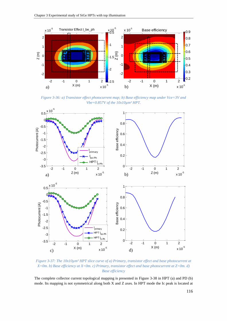
Chapter 3 Experimental study of SiGe HPTs with top illumination
116
Figure 3-36: a) Transistor effect photocurrent map; b) Base efficiency map under Vce=3V and
Vbe=0.857V of the 10x10µm² HPT.
Figure 3-37: The 10x10µm² HPT slice curve of a) Primary, transistor effect and base photocurrent at
X=0m. b) Base efficiency at X=0m. c) Primary, transistor effect and base photocurrent at Z=0m. d)
Base efficiency
The complete collector current topological mapping is presented in Figure 3-38 in HPT (a) and PD (b)
mode. Its mapping is not symmetrical along both X and Z axes. In HPT mode the Ic peak is located at
X (m)
Z (
m)
Transistor Effect I_be_ph
-2 -1 0 1 2
x 10-5
-2
-1
0
1
2
x 10-5
-2.5
-2
-1.5
-1
-0.5x 10
-5
a) b) X (m)
Z (
m)
Base efficiency
-2 -1 0 1 2
x 10-5
-2
-1
0
1
2
x 10-5
0.2
0.3
0.4
0.5
0.6
0.7
0.8
0.9
-2 -1 0 1 2
x 10-5
0
0.2
0.4
0.6
0.8
1
X (m)
Ba
se
effic
ien
cy
-2 -1 0 1 2
x 10-5
0
0.2
0.4
0.6
0.8
1
Z (m)
Ba
se
effic
ien
cy
-2 -1 0 1 2
x 10-5
-3.5
-3
-2.5
-2
-1.5
-1
-0.5
0
0.5x 10
-5
Z (m)
Ph
oto
cu
rre
nt (A
)
Iprimary
Ibe-Ph
HPT Ib-Ph
-2 -1 0 1 2
x 10-5
-3.5
-3
-2.5
-2
-1.5
-1
-0.5
0
0.5x 10
-5
X (m)
Ph
oto
cu
rre
nt (A
)
Iprimary
HPT Ibe-Ph
HPT Ib-Ph
a) b)
c) d)
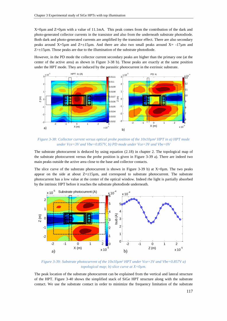
Chapter 3 Experimental study of SiGe HPTs with top illumination
117
X=0µm and Z=0µm with a value of 11.1mA. This peak comes from the contribution of the dark and
photo-generated collector currents in the transistor and also from the underneath substrate photodiode.
Both dark and photo-generated currents are amplified by the transistor effect. There are also secondary
peaks around X=5µm and Z=±15µm. And there are also two small peaks around X= -17µm and
Z=±15µm. Those peaks are due to the illumination of the substrate photodiode.
However, in the PD mode the collector current secondary peaks are higher than the primary one (at the
center of the active area) as shown in Figure 3-38 b). Those peaks are exactly at the same position
under the HPT mode. They are induced by the parasitic photocurrent in the extrinsic substrate.
Figure 3-38: Collector current versus optical probe position of the 10x10µm² HPT in a) HPT mode
under Vce=3V and Vbe=0.857V, b) PD mode under Vce=3V and Vbe=0V
The substrate photocurrent is deduced by using equation (2.18) in chapter 2. The topological map of
the substrate photocurrent versus the probe position is given in Figure 3-39 a). There are indeed two
main peaks outside the active area close to the base and collector contacts.
The slice curve of the substrate photocurrent is shown in Figure 3-39 b) at X=0µm. The two peaks
appear on the side at about Z=±15µm, and correspond to substrate photocurrent. The substrate
photocurrent has a low value at the center of the optical window. Indeed rhe light is partially absorbed
by the intrinsic HPT before it reaches the substrate photodiode underneath.
Figure 3-39: Substrate photocurrent of the 10x10µm² HPT under Vce=3V and Vbe=0.857V a)
topological map; b) slice curve at X=0µm.
The peak location of the substrate photocurrent can be explained from the vertical and lateral structure
of the HPT. Figure 3-40 shows the simplified stack of SiGe HPT structure along with the substrate
contact. We use the substrate contact in order to minimize the frequency limitation of the substrate
X (m)
Z (
m)
HPT: Ic (A)
-2 -1 0 1 2 3
x 10-5
-3
-2
-1
0
1
2
3x 10
-5
0.0102
0.0103
0.0104
0.0105
0.0106
0.0107
0.0108
0.0109
0.011
0.0111
X (m)
Z (
m)
PD: Ic
-2 -1 0 1 2 3
x 10-5
-3
-2
-1
0
1
2
3x 10
-5
6
7
8
9
10
11
12
13x 10
-4
a) b)
X (m)
Z (
m)
Substrate photocurrent (A)
-2 -1 0 1 2
x 10-5
-2
-1
0
1
2
x 10-5
0
1
2
3
4
5
6x 10
-4
-2 -1 0 1 2
x 10-5
0
1
2
3
4
5
x 10-4
Z (m)
Isu
b (
A)
a) b)
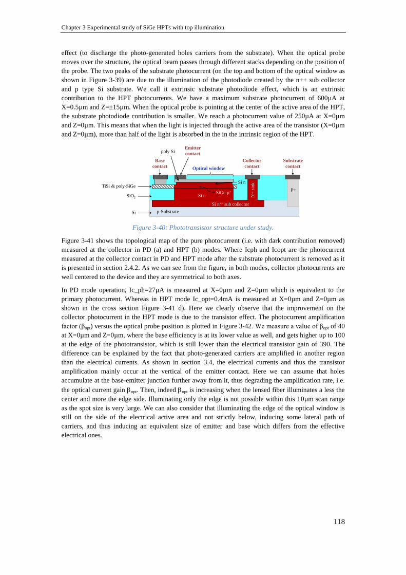
Chapter 3 Experimental study of SiGe HPTs with top illumination
118
effect (to discharge the photo-generated holes carriers from the substrate). When the optical probe
moves over the structure, the optical beam passes through different stacks depending on the position of
the probe. The two peaks of the substrate photocurrent (on the top and bottom of the optical window as
shown in Figure 3-39) are due to the illumination of the photodiode created by the n++ sub collector
and p type Si substrate. We call it extrinsic substrate photodiode effect, which is an extrinsic
contribution to the HPT photocurrents. We have a maximum substrate photocurrent of 600µA at
X=0.5µm and Z=±15µm. When the optical probe is pointing at the center of the active area of the HPT,
the substrate photodiode contribution is smaller. We reach a photocurrent value of 250µA at X=0µm
and Z=0µm. This means that when the light is injected through the active area of the transistor (X=0µm
and Z=0µm), more than half of the light is absorbed in the in the intrinsic region of the HPT.
Figure 3-40: Phototransistor structure under study.
Figure 3-41 shows the topological map of the pure photocurrent (i.e. with dark contribution removed)
measured at the collector in PD (a) and HPT (b) modes. Where Icph and Icopt are the photocurrent
measured at the collector contact in PD and HPT mode after the substrate photocurrent is removed as it
is presented in section 2.4.2. As we can see from the figure, in both modes, collector photocurrents are
well centered to the device and they are symmetrical to both axes.
In PD mode operation, Ic_ph=27µA is measured at X=0µm and Z=0µm which is equivalent to the
primary photocurrent. Whereas in HPT mode Ic_opt=0.4mA is measured at X=0µm and Z=0µm as
shown in the cross section Figure 3-41 d). Here we clearly observe that the improvement on the
collector photocurrent in the HPT mode is due to the transistor effect. The photocurrent amplification
factor (βopt) versus the optical probe position is plotted in Figure 3-42. We measure a value of βopt of 40
at X=0µm and Z=0µm, where the base efficiency is at its lower value as well, and gets higher up to 100
at the edge of the phototransistor, which is still lower than the electrical transistor gain of 390. The
difference can be explained by the fact that photo-generated carriers are amplified in another region
than the electrical currents. As shown in section 3.4, the electrical currents and thus the transistor
amplification mainly occur at the vertical of the emitter contact. Here we can assume that holes
accumulate at the base-emitter junction further away from it, thus degrading the amplification rate, i.e.
the optical current gain opt. Then, indeed opt is increasing when the lensed fiber illuminates a less the
center and more the edge side. Illuminating only the edge is not possible within this 10µm scan range
as the spot size is very large. We can also consider that illuminating the edge of the optical window is
still on the side of the electrical active area and not strictly below, inducing some lateral path of
carriers, and thus inducing an equivalent size of emitter and base which differs from the effective
electrical ones.
Optical window
Substrate
contact
Collector
contact
Base
contact
Emitter
contact
Si
TiSi & poly-SiGe
SiGe p+
SiO2
Si n
poly Si
p-Substrate
Si n++ sub collector
Si n- N+
sin
k
P+

Chapter 3 Experimental study of SiGe HPTs with top illumination
119
Figure 3-41: Photocurrent measured at the collector of the 10x10µm² HPT in a) PD Mode, b) HPT
mode. The slice curves of the collector photocurrent c) PD mode, d) HPT mode.
Figure 3-42: a) The topological map of photocurrent amplification factor; b) The slice of the
photocurrent amplification factor at Z=0µm of the 10x10µm² HPT.
Figure 3-43 shows the topological map of the complete DC responsivity of the 10x10µm2 HPT in
phototransistor (a) and photodiode (b) modes respectively. We clearly observe the influence of the
substrate photocurrent at the peaks of the responsivity in PD mode operation. It has the same shape as
the substrate photocurrent shown in Figure 3-43 a). In the PD mode operation a maximum responsivity
of 0.3A/W at X=5µm and Z=±15µm is measured whereas when we illuminate the active area of the
HPT (X=0µm, Z=0µm), the responsivity is 0.2A/W. This difference is due to the presence of high
sensitivity photodiode formed by the sub collector and p type silicon substrate. In the phototransistor
X (m)
Z (
m)
PD_IcPh
-2 -1 0 1 2
x 10-5
-2
-1
0
1
2
x 10-5
0
0.5
1
1.5
2
2.5x 10
-5
X (m)
Z (
m)
IcOpt (A)
-2 -1 0 1 2
x 10-5
-2
-1
0
1
2
x 10-5
0
1
2
3
4
x 10-4
-2 -1 0 1 2
x 10-5
0
0.5
1
1.5
2
2.5
3x 10
-5
Z (m)
IcP
h (
A)
-3 -2 -1 0 1 2
x 10-5
0
1
2
3
x 10-4
x (m)
Ph
oto
cu
rre
nt (A
)
Icopt
Ieopt
a) b)
c) d)
-3 -2 -1 0 1 2
x 10-5
0
100
200
300
400
X (m)
DC
cu
rre
nt a
ga
in
X(m)
Z (
m)
Optical DC current gain
-2 -1 0 1 2
x 10-5
-2
-1
0
1
2
x 10-5
40
50
60
70
80
90
100
βopt≈40
βelec≈390
a) b)
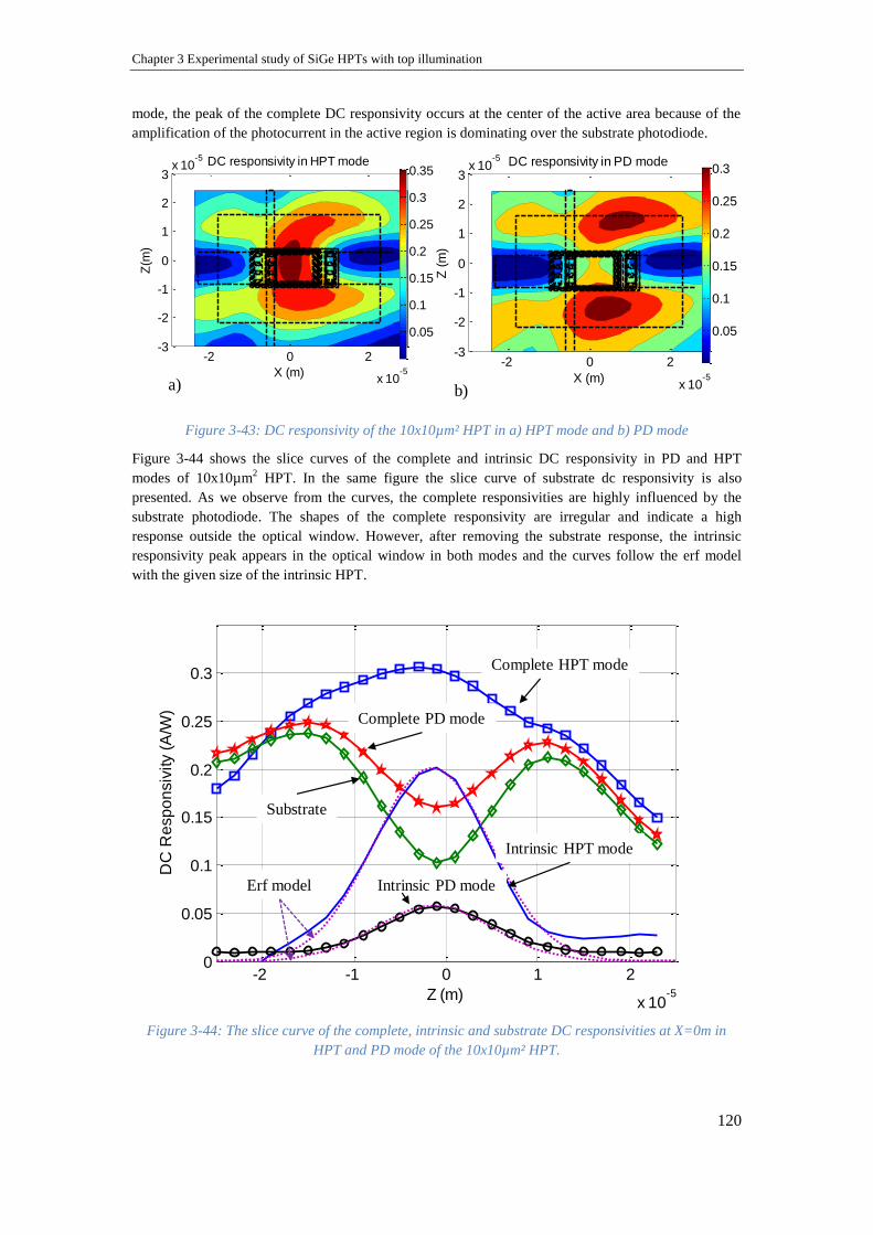
Chapter 3 Experimental study of SiGe HPTs with top illumination
120
mode, the peak of the complete DC responsivity occurs at the center of the active area because of the
amplification of the photocurrent in the active region is dominating over the substrate photodiode.
Figure 3-43: DC responsivity of the 10x10µm² HPT in a) HPT mode and b) PD mode
Figure 3-44 shows the slice curves of the complete and intrinsic DC responsivity in PD and HPT
modes of 10x10µm2 HPT. In the same figure the slice curve of substrate dc responsivity is also
presented. As we observe from the curves, the complete responsivities are highly influenced by the
substrate photodiode. The shapes of the complete responsivity are irregular and indicate a high
response outside the optical window. However, after removing the substrate response, the intrinsic
responsivity peak appears in the optical window in both modes and the curves follow the erf model
with the given size of the intrinsic HPT.
Figure 3-44: The slice curve of the complete, intrinsic and substrate DC responsivities at X=0m in
HPT and PD mode of the 10x10µm² HPT.
X (m)
Z(m
)
DC responsivity in HPT mode
-2 0 2
x 10-5
-3
-2
-1
0
1
2
3x 10
-5
0.05
0.1
0.15
0.2
0.25
0.3
0.35
X (m)
Z (
m)
DC responsivity in PD mode
-2 0 2
x 10-5
-3
-2
-1
0
1
2
3x 10
-5
0.05
0.1
0.15
0.2
0.25
0.3
a) b)
-2 -1 0 1 2
x 10-5
0
0.05
0.1
0.15
0.2
0.25
0.3
Z (m)
DC
Re
sp
on
siv
ity (
A/W
)
Intrinsic HPT mode
Intrinsic PD mode
Complete PD mode
Complete HPT mode
Substrate
Erf model

Chapter 3 Experimental study of SiGe HPTs with top illumination
121
3.5.3 Localization of the Opto-microwave behavior in the HPT structure
Figure 3-45 shows the complete and intrinsic opto-microwave gain versus frequency in PD and HPT
modes at center of the optical window (X=0um, Z=0um). The model of substrate photodiode frequency
response at X=Z=0µm is also presented in the same figure. The complete and intrinsic Gom are equal
in the whole frequency range in HPT mode operation. This indicates that the frequency response of the
substrate photodiode is hidden by the internal transistor amplification effect. However, in PD mode, the
substrate photodiode contributes to its opto-microwave gain and reduces its dynamic behavior.
In general, from such a curve, we can extract both complete and intrinsic cutoff frequencies optical
transition frequency, optical gain and low frequency Gom. Thus, in this section we focus on the
localization of the frequency behavior of the HPT over the surface of the structure through OM SNOM
investigation. The effect of the substrate photodiode on the OM gain and dynamic behavior of the HPT
is studied.
Figure 3-45: Complete and intrinsic opto microwave gain in PD and HPT modes at X=0µm, Z=0µm
and the substrate frequency response model of the 10x10µm² HPT.
3.5.3.1 Low frequency behavior
In this part we are going to present the low frequency Gom and optical gain topological map of the
HPT. The contribution of the substrate photodiode is also detailed.
a) Low frequency Opto-microwave gain (Gom)
The complete opto-microwave responsivity at 50MHz (low frequency of the VNA) of the HPT in
transistor and photodiode modes versus optical probe position is presented in Figure 3-46 a) and b)
respectively. A similar behavior as DC responsivity is observed on the opto-microwave response. A
low frequency complete responsivity of 0.26A/W (resp. 0.241A/W) is measured when Vce=3V (resp.
2V) at the center of the optical window as shown in Figure 3-46 c). Taking into account the 32.3%
fiber to HPT coupling efficiency, this corresponds to a 0.805A/W absolute responsivity. In PD mode,
high responsivity value is observed in the substrate at x=10µm and z=14µm, at x=2µm and z=-16µm.
The measured opto-microwave gain in HPT mode at 50MHz under 50Ω (i.e. responsivity) is well fitted
with an Erf function for -5µm < x < 5μm as shown in the cross-section presented in Figure 3-46 c). The
responsivity is not well fitted with the model outside the optical window. As we observe in Figure 3-46
10-1
100
101
-70
-60
-50
-40
-30
-20
-10
Freq (GHz)
Go
m(d
B)
Sub response model
PD complete
PD intrinsic
HPT complete
HPT intrinsicfTopt,comp fTopt,int
HPT mode
PD mode
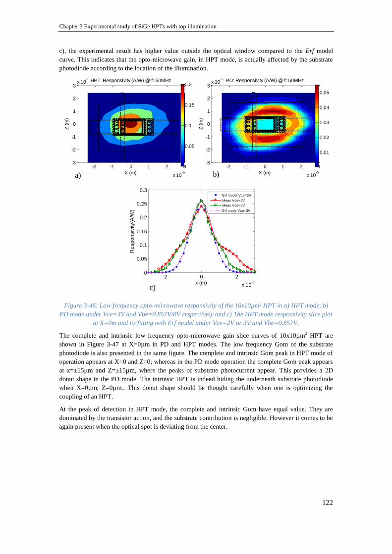
Chapter 3 Experimental study of SiGe HPTs with top illumination
122
c), the experimental result has higher value outside the optical window compared to the Erf model
curve. This indicates that the opto-microwave gain, in HPT mode, is actually affected by the substrate
photodiode according to the location of the illumination.
Figure 3-46: Low frequency opto-microwave responsivity of the 10x10µm² HPT in a) HPT mode, b)
PD mode under Vce=3V and Vbe=0.857V/0V respectively and c) The HPT mode responsivity slice plot
at X=0m and its fitting with Erf model under Vce=2V or 3V and Vbe=0.857V.
The complete and intrinsic low frequency opto-microwave gain slice curves of 10x10µm2 HPT are
shown in Figure 3-47 at X=0µm in PD and HPT modes. The low frequency Gom of the substrate
photodiode is also presented in the same figure. The complete and intrinsic Gom peak in HPT mode of
operation appears at X=0 and Z=0; whereas in the PD mode operation the complete Gom peak appears
at x=±15µm and Z=±15µm, where the peaks of substrate photocurrent appear. This provides a 2D
donut shape in the PD mode. The intrinsic HPT is indeed hiding the underneath substrate photodiode
when X=0µm; Z=0µm.. This donut shape should be thought carefully when one is optimizing the
coupling of an HPT.
At the peak of detection in HPT mode, the complete and intrinsic Gom have equal value. They are
dominated by the transistor action, and the substrate contribution is negligible. However it comes to be
again present when the optical spot is deviating from the center.
-2 0 2
x 10-5
0
0.05
0.1
0.15
0.2
0.25
0.3
x (m)
Re
sp
on
siv
ity(A
/W)
Erf model Vce=2V
Meas Vce=2V
Meas Vce=3V
Erf mode Vce=3V
X (m)
Z (
m)
HPT: Responsivity (A/W) @ f=50MHz
-2 -1 0 1 2 3
x 10-5
-3
-2
-1
0
1
2
3x 10
-5
0.05
0.1
0.15
0.2
X (m)
Z (
m)
PD: Responsivity (A/W) @ f=50MHz
-2 -1 0 1 2 3
x 10-5
-3
-2
-1
0
1
2
3x 10
-5
0.01
0.02
0.03
0.04
0.05
a) b)
c)

Chapter 3 Experimental study of SiGe HPTs with top illumination
123
Figure 3-47: The slice curves of complete and intrinsic low frequency opto-microwave gain in PD and
HPT modes of the 10x10µm² HPT at X=0m.
b) Optical gain (Gopt)
As defined in chapter 2 section 2.3.1 another way to characterize the phototransistor is the optical gain,
Gopt. It is the difference between the HPT mode GOM versus frequency and the PD mode GOM at low
frequency. The opto-microwave gain at the peak position (X=0, Z=0) is plotted in Figure 3-45 for both
photodiode and phototransistor modes. We reach up to a 20dB complete optical gain at 50MHz at the
peak of detection.
Figure 3-48 shows the comparison between the complete and intrinsic optical gain (Gopt) as well as the
electrical current gain (h21) of the 10x10µm2 HPT at Vce=3V and Vbe=0.857V. At these biasing
conditions the electrical current gain appears to be the upper limit of the optical gain at all frequencies.
At 50MHz, the electrical current gain is 36dB and the complete and intrinsic optical gain is 20dB and
24.5dB respectively. The low frequency intrinsic optical gain is 11.5dB lower than the electrical
current gain. The gap between Gopt and h21 for the intrinsic HPT however reduces at the frequency of
400-800MHz. This may be due to an internal matching effect of the base of the phototransistor. The
photocurrents flowing in direction of the base contact are reflected back internally to the base-emitter
junction so as to fully amplify the primary photocurrent.
-3 -2 -1 0 1 2
x 10-5
-80
-70
-60
-50
-40
-30
-20
-10
Z (µm)
Go
m (
dB
)
Intrinsic HPT mode
Complete HPT mode
Substrate
Complete PD mode
Intrinsic PD mode

Chapter 3 Experimental study of SiGe HPTs with top illumination
124
Figure 3-48: Optical gain (complete and intrinsic) and Electrical current gain at the peak position
(X=0µm and Z=0µm) of the 10x10µm² HPT.
The optical gain over the surface of the HPT is shown in Figure 3-49. The complete Gopt has a
symmetrical topological shape on both X and Z axes and is well centered to the optical window.
Optical gain is highly modified by the substrate photodiode and optical coupling ratio. Figure 3-49 b)
shows the complete and intrinsic optical gain slice curve along Z axis. The optical gain increases from
about 19dB to 24.5dB when the substrate influence is removed. Compared to the complete Gopt, the
intrinsic Gopt is almost flat in the optical window (Z=±5µm).
Figure 3-49: Optical gain (Gopt) a) The complete HPT topological mapping. b) The complete and
intrinsic slice curves at X=0m of the 10x10µm² HPT.
3.5.3.2 Dynamic Behavior
The dynamic behavior of the phototransistor over the surface of the structure is analyzed through the
measurement of the optical transition frequency (fTopt) and the cutoff frequency (f-3dB,OM) of the
phototransistor in PD and HPT modes.
a) Cutoff frequency (f-3dB)
Figure 3-50 presents the topological and slice plots of the -3dB cutoff frequency of 10x10µm2 optical
window HPT in PD mode and HPT mode of operation. The cutoff frequency is usually small in
10-1
100
101
-30
-20
-10
0
10
20
30
40
Freq (GHz)
Ga
in(d
B)
h21
Complete Gopt
Intrinsic Gopt
X (m)
Z (
m)
-2 -1 0 1 2
x 10-5
-2
-1
0
1
2
x 10-5
0
5
10
15
-2 -1 0 1 2
x 10-5
0
5
10
15
20
25
Z (m)
Gopt (
dB
)
Gopt
complete
Gopt
Intrinsic
a) b)
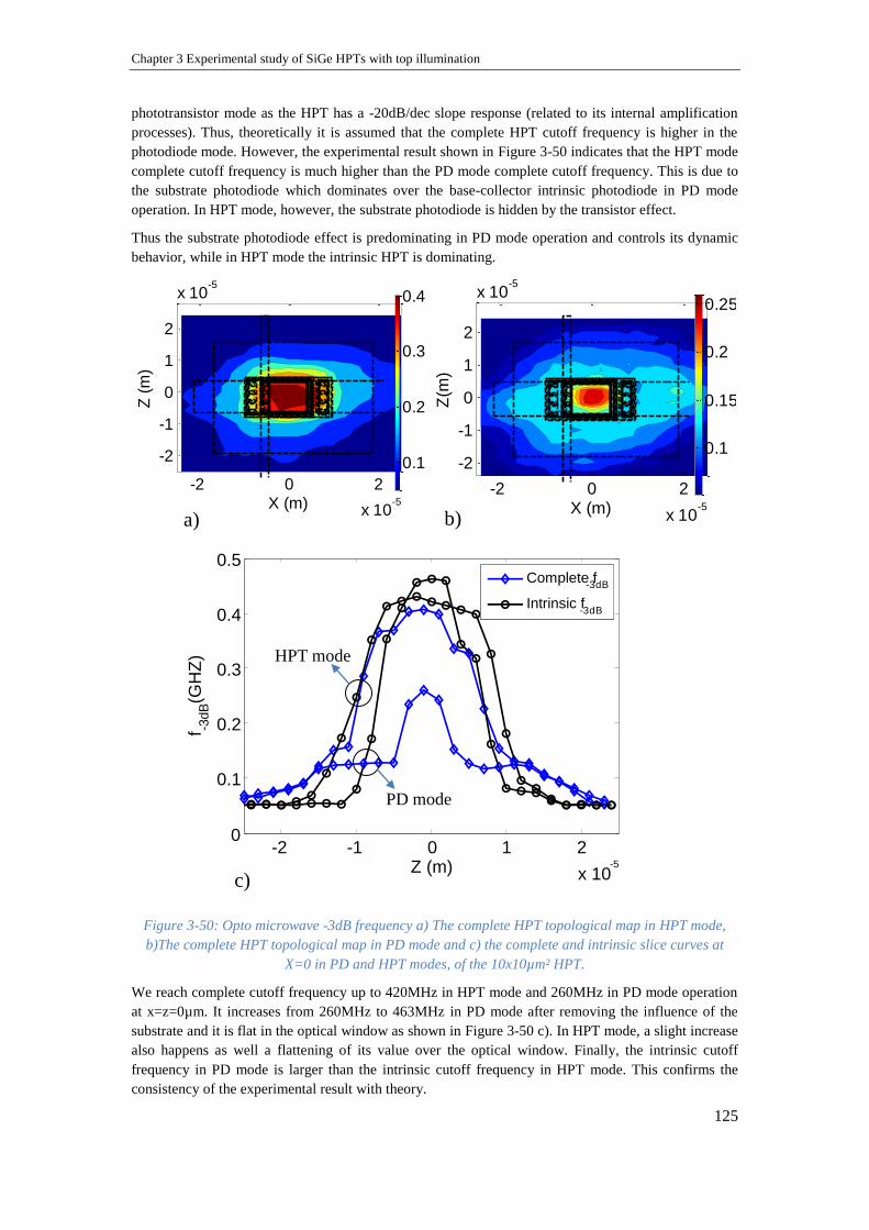
Chapter 3 Experimental study of SiGe HPTs with top illumination
125
phototransistor mode as the HPT has a -20dB/dec slope response (related to its internal amplification
processes). Thus, theoretically it is assumed that the complete HPT cutoff frequency is higher in the
photodiode mode. However, the experimental result shown in Figure 3-50 indicates that the HPT mode
complete cutoff frequency is much higher than the PD mode complete cutoff frequency. This is due to
the substrate photodiode which dominates over the base-collector intrinsic photodiode in PD mode
operation. In HPT mode, however, the substrate photodiode is hidden by the transistor effect.
Thus the substrate photodiode effect is predominating in PD mode operation and controls its dynamic
behavior, while in HPT mode the intrinsic HPT is dominating.
Figure 3-50: Opto microwave -3dB frequency a) The complete HPT topological map in HPT mode,
b)The complete HPT topological map in PD mode and c) the complete and intrinsic slice curves at
X=0 in PD and HPT modes, of the 10x10µm² HPT.
We reach complete cutoff frequency up to 420MHz in HPT mode and 260MHz in PD mode operation
at x=z=0µm. It increases from 260MHz to 463MHz in PD mode after removing the influence of the
substrate and it is flat in the optical window as shown in Figure 3-50 c). In HPT mode, a slight increase
also happens as well a flattening of its value over the optical window. Finally, the intrinsic cutoff
frequency in PD mode is larger than the intrinsic cutoff frequency in HPT mode. This confirms the
consistency of the experimental result with theory.
-2 -1 0 1 2
x 10-5
0
0.1
0.2
0.3
0.4
0.5
Z (m)
f - 3dB(G
HZ
)
Complete f-3dB
Intrinsic f-3dB
X (m)
Z(m
)
-2 0 2
x 10-5
-2
-1
0
1
2
x 10-5
0.1
0.15
0.2
0.25
X (m)
Z (
m)
-2 0 2
x 10-5
-2
-1
0
1
2
x 10-5
0.1
0.2
0.3
0.4
PD mode
HPT mode
a) b)
c)

Chapter 3 Experimental study of SiGe HPTs with top illumination
126
The cutoff frequency outside the optical window is mainly due to the substrate effect. It has very small
value which is equal in both modes. When we measure the cutoff frequency far from the optical
window (metal contact), the distance traveled by the photo-generated carriers into the substrate is
longer than the one close to the optical window.
After removing the substrate response in both modes the cutoff frequency outside the optical window
becomes null as it goes below the limit of the measurement bench of the VNA (≈50MHz).
b. Optical transition frequency (fTopt)
Figure 3-51 presents the optical transition frequency versus the fiber position. The fTopt curve is
symmetrical with respect to the X and Z axes and has a peak at the center of the optical window.
A maximum complete fTopt of 4.12GHz is measured at the peak position under Vce=2V and
Vbe=0.857V. According to Figure 3-51 b), the fTopt curve versus the fiber position follows the Erf
function variation. At both extremities, its value is very low and could be attributed mostly to substrate
detection noise. It is also not flat across the active window of the HPT. This indicates that fTopt is
affected by the coupling efficiency into the HPT and the substrate photodiode. If there wouldn’t be a
substrate photodiode effect, the fTopt would be flat over the optical window.
Figure 3-51: a) Optical transition frequency (fTopt) versus optical probe position, b) The slice view of
the fTopt at X=0m and its fitting with Erf model under Vce=2V or 3V and Vbe=0.857V, of the 10x10µm²
HPT.
The slice figure of the fTopt for 10x10µm2 HPT at x=0µm and z=0µm before and after removing the
substrate photodiode effect is shown in Figure 3-52 a) and b) respectively for Vce=2V and
Vbe=0.857V. The intrinsic fTopt has a flat shape in the optical window along Z axis (Figure 3-52 b) as it
mostly depends on the vertical stack parameters, and it drops faster to zero outside the optical window.
Along the x axis, the intrinsic fTopt is not flat and its peak is shifted from the center of the optical
window to the edge of the optical window as shown in figure Figure 3-52 a). This may be explained by
the tilted angle of the lensed fiber along this direction, which may affect the distribution of photo-
carriers within this direction, and then the related transit times. The fTopt then improves from 3.41GHz
to 6GHz when the intrinsic response is de-embedded. This gives access to the intrinsic HPT
performance and physics.
-2 0 2
x 10-5
0
1
2
3
4
5x 10
9
Z (m)
f Topt (
Hz)
Meas Vce=2V
Erf Model Vce=2V
Meas Vce=3V
Erf model Vce=3
X (m)
Z (
m)
fTopt
(Hz)
-2 -1 0 1 2 3
x 10-5
-3
-2
-1
0
1
2
3x 10
-5
0
1
2
3
4x 10
9
a) b)

Chapter 3 Experimental study of SiGe HPTs with top illumination
127
Figure 3-52: The raw and extracted fTopt a) at z=0µm, b) at x=0µm of the 10x10µm² HPT.
-2 -1 0 1 2
x 10-5
0
1
2
3
4
5
6
7x 10
9
X (m)
f To
pt (
Hz)
fTopt
Intrinsic
fTopt
Complete
-2 -1 0 1 2
x 10-5
0
1
2
3
4
5
6
7x 10
9
Z (m)
f To
pt(H
z)
fTopt
Complete
fTopt
Intrinsic
a) b)

Chapter 3 Experimental study of SiGe HPTs with top illumination
128
3.6 Dependency on the injected optical power level
3.6.1 Introduction
The opto-microwave performance of the phototransistor could be changed related to the injected
optical power intensity. This could be due to many factors such as self-biasing effect and variation of
modes of the injected optical power versus current biasing of the multimode VCSEL source (this could
change the beam width).
Thus, in this section we observe the effect of the injected optical power level on the performance of
SiGe HPTs. For this study we focus on 10x10µm2 SiGe/Si HPT and we choose three optical power
levels (Popt=0.83mW, 1.14mW and 2.38mW measured at the peak of the optical probe). DC and OM
SNOM are performed in PD and HPT modes for the three power levels. To observe this effect we start
from the dc characters by fitting Ib with the erf model and go through the injected power level
dependency of opto-microwave responsivity and frequency behavior.
3.6.2 Injected optical power level impact on DC characteristics
We start this study by analyzing the behavior of the optical beam through the fitting of Ib in PD mode
with the erf model as shown Figure 3-53. Figure 3-53 a) shows the erf fitting with the experimentally
measured base current in PD mode. According to the development in section 2.4.3, the beam is
evaluated to get a beam width of 28μm. This model fits well with our measurements for Popt=2.38mW
and we can extract a 32.3% coupling rate, but it doesn’t fit when we reduce the optical power to
Popt=0.83mW and 1.14mW as shown in Figure 3-53 a). Thus, we need to adjust the Erf fit with Ib
measured at Popt=0.83mW and 1.14mW. As a result for these two optical power levels we extract a
coupling efficiency of 26.1% and an optical beam width of 34.8µm as shown in Figure 3-53 b).
This variation of beam width indicates that there is change in the modes of the VCSEL source at
different dc biasings.
In Figure 3-53 we can also observe that the photocurrent flowing out to the base contact increases
along with the injected optical power (it is higher for high optical power). This could be explained by
self-biasing effect of the injected optical power. That means at high optical power level a large number
of electron hole pairs could be generated in the base-collector region and then the holes are collected at
the base contact.
Figure 3-53: Base current in PD mode fitting with erf model (curves without marks) for different
injected optical power levels of the 10x10µm² HPT. a) The fitting targeting the model developed in
section 2.4.3 for Popt=2.38mW which has 32.3% coupling efficiency and 28µm diameter beam width.
b) The fitting made for each power level individually.
-3 -2 -1 0 1 2 3
x 10-5
-4
-3.5
-3
-2.5
-2
-1.5
-1
-0.5
0
0.5x 10
-5
X (µm)
Ib (
A)
2.38mW
1.14mW
0.83mW
-3 -2 -1 0 1 2 3
x 10-5
-4
-3.5
-3
-2.5
-2
-1.5
-1
-0.5
0
0.5x 10
-5
X (µm)
Ib (
A)
2.38mW fit @32.3% and28µm
1.14mW [email protected]% and 34.8µm
0.83mW [email protected]% and 34.8µm
X (m) X (m)a) b)

Chapter 3 Experimental study of SiGe HPTs with top illumination
129
Figure 3-54 a) shows the base current in HPT mode for the three injected optical power. At high
injected optical power, larger amount of electrons and holes are generated and hence we measure more
base current for an injected optical power of 2.38mW than other.
Figure 3-54 b) shows the intrinsic photocurrent measured at the collector contact in PD mode operation
at different optical power levels. When the optical probe is pointing at the center of the optical window,
Icph increases from 27.5µA to 32.5µm as the injected optical power increases from 0.83mW to
1.14mW and then it decreases to 28µA for Popt=2.38mW. Icph decrease at 2.38mW could be related to
the current saturation at high optical power.
Figure 3-54: a) Base current measured in HPT mode at Popt=1.14mW and 2.38mW. b) The intrinsic
photocurrent of the HPT measured in PD mode at different input optical powers of the 10x10µm² HPT.
We present the slice figure of the photocurrent amplification gain, βopt, and of the base efficiency at
z=0µm in Figure 3-55 a) and b) respectively. βopt increases from 36 to 48 and then to 55 when the
injected optical power level decreases from 2.38mW to 1.14mW and then to 0.83mW respectively.
The base efficiency also increases as the injected optical power level decreases: At the center of the
optical window about 20%, 26% and 46% of the photo-generated holes are moving out from the base
region to the base contact for an injected optical power of 2.38mW, 1.14mW and 0.83mW respectively.
Somehow the phototransistor effect (opt) is even less activated when the power is higher in the middle
of the optical window, and in parallel fewer holes contribute to this effect, escaping through the base
contact.
The optical dc current gain (βopt) and base efficiency variation with the injected optical power level can
be explained by the following reasons:
a) Self-biasing effect that is mostly believed to be the case. At high optical power, the hole
density in the base increases and reduces further the resistance. Then holes resistance to reach
the base contact lowers and the base efficiency increases. In parallel, the current gain
decreases because the voltage induced self-biasing across this resistance inside the optical
window gets lower: the transistor effect is less activated.
b) High injection phenomenons due to a high optical power within the HPT, eventually.
Absorption rate are in the range of 103cm
-1. Thus the generation rate is in the range of 10
19cm
-
3.s
-1. Accumulated into the base, this may create some equivalent modification of the base
doping. This effect would be more pregnant at the center of the optical window where the time
for accumulation is large (less base efficiency).
c) Due to injected optical beam width variation, that could explain a less concentrated effect of
the self-biasing effect for example.
-3 -2 -1 0 1 2 3
x 10-5
-0.5
0
0.5
1
1.5
2
2.5
3
3.5x 10
-5
Z (m)
IcP
h (
A)
Popt=0.83mW
Popt=1.14mW
Popt=2.38mW
a) b)-3 -2 -1 0 1 2
x 10-5
-2
-1
0
1
2
3x 10
-5
X (m)
Ib (
A)
Ib HPT mode
Popt=0.83mW
Popt=1.14mW
Popt=2.38mW

Chapter 3 Experimental study of SiGe HPTs with top illumination
130
Figure 3-55: a) Photocurrent amplification, βopt at different Popt. b) Base efficiency at different Popt.
The intrinsic responsivity (RPD,i) of the phototransistor in PD mode operation and the responsivity of
the substrate photodiode at different optical power levels are presented in Figure 3-56 a) and b)
respectively. The intrinsic responsivity is much less when Popt is high at 2.38mW. A small decrease is
also observed but with similar values for the lower values of Popt.
The substrate responsivity has peaks outside the optical window which are related to the illumination of
the substrate photodiode. The substrate response at the center of the optical window has nearly equal
value for all injected optical level. However, outside the active area, the substrate responsivity is also
less for the power of 2.38mW. This is meanly related to the increase of the optical beam width when
the optical power is lower. As we presented in Figure 3-53 the beam width for smaller optical power
injection is larger than for higher optical power and thus, the coupling efficiency is less for smaller
Popt. This reduced coupling efficiency results in large portion of optical power injected into the
substrate and thus the effective substrate responsivity increases.
Figure 3-56: Slice curves at x=0µm and different injected optical power levels a) DC intrinsic
responsivity. b) Low frequency (50MHz) substrate responsivity.
3.6.3 Injected optical power level impact on opto-microwave frequency response
We measure the S-parameters in PD mode (Vce=2V, Vbe=0V) and HPT mode (Vce=2V,
Vbe=0.857V) by varying the injected optical power level (0.83mW, 1.14mW and 2.38mW). Then, we
extract the opto-microwave responsivity and the frequency response behavior of the phototransistor
after removing the test bench effect through the de-embedding techniques presented in section 2.3.3.
-3 -2 -1 0 1 2
x 10-5
30
40
50
60
70
80
90
100
110
X (m)
Be
taO
pt
Popt=0.83mW
Popt= 1.14mW
Popt= 2.38mW
-3 -2 -1 0 1 2
x 10-5
0
0.2
0.4
0.6
0.8
1
X (m)
Ba
se
effic
ien
cy
Popt=0.83mW
Popt=1.14mW
Popt=2.38mW
a) b)
-3 -2 -1 0 1 2 3
x 10-5
0
0.02
0.04
0.06
0.08
0.1
0.12
Z (m)
Rs
ub (
A/W
)
Popt=2.38mW
Popt=1.14mW
Popt=0.83mW
-3 -2 -1 0 1 2 3
x 10-5
0
0.005
0.01
0.015
0.02
0.025
0.03
0.035
Z (m)
RP
D,i (
A/W
)
Popt=0.83mW
Popt=1.14mW
Popt=2.38mW
a) b)

Chapter 3 Experimental study of SiGe HPTs with top illumination
131
Figure 3-57 shows the opto-microwave gain versus frequency of 10x10µm2 optical window size HPTs
for different injected optical power levels at x=0µm and z=0µm both in PD and HPT mode operation.
The opto-microwave gain increases as the injected optical power decreases for both modes. We could
explain this variation accordingly:
1. The Gom difference in PD mode is due to the influence of the substrate photodiode response
which depends on the level of injected optical power as presented above. The Gom has a
lower cutoff frequency for 0.83mW and 1.14mW optical powers than 2.38mW, which verifies
the influence of the slow substrate photodiode on the frequency response.
2. The Gom has nearly equal relative frequency response in HPT mode. This indicates that the
impact of the substrate photodiode is less visible. However, the Gom is higher for small
optical powers. This is due to the fact that the optical gain at low injected optical power level
is higher than at 2.38mW as shown in Figure 3-55 a).
Figure 3-57: Opto-microwave gain versus frequency in PD (Vce=2V, Vbe=0V) and HPT (Vce=2V,
Vbe=0.857V) modes at x=0µm and z=0µm by varying the injecting optical power level of the
10x10µm² HPT.
We present the slice figure of the low frequency (at 50MHz) opto-microwave gain at x=0µm both in
HPT and PD modes at different optical power levels in Figure 3-58. The Gom decreases from -10dB
to -14dB as the injected optical power increases from 0.83mW to 2.38mW in HPT mode.
10-1
100
101
-55
-50
-45
-40
-35
-30
-25
-20
-15
-10
-5
Freq (GHz)
Go
m(d
B)
1.14mW
0.83mW
2.38mW
HPT mode
PD mode

Chapter 3 Experimental study of SiGe HPTs with top illumination
132
Figure 3-58: The slice figure of low frequency Gom in PD and HPT mode at x=0µm and different
injected optical power levels on the 10x10µm² HPT.
The complete and intrinsic optical transition frequencies are presented in Figure 3-59 at different
optical power levels and z=0µm. The complete fTopt is directly extracted from the measured S-
parameters, whereas the intrinsic fTopt is obtained after the substrate response removal. The complete
fTopt increases as the injected optical power increases from 0.83mW to 2.38mW. It is mainly due to the
substrate effect. Indeed, after correcting the substrate photodiode response fTopt has nearly the same
value for all injected powers. The fTopt for Popt=2.38mW is a bit smaller than others and has a tilted
shape along the X axis over the optical window as shown in previous sections. This may be due to the
tilted optical beam with a more focused beam spot which makes the angle getting more impact. The
peak value reduction is also explained by a reduced optical gain at 2.38mW. We are able to extract an
intrinsic optical transition frequency of 6.5GHz for an injected optical power of 0.83mW and 1.14mW.
Figure 3-59: The influence of the injected optical power level on the optical transition frequency for
the 10x10µm² HPT.
-3 -2 -1 0 1 2 3
x 10-5
-60
-55
-50
-45
-40
-35
-30
-25
-20
-15
-10
Z (m)
Go
m (
dB
)
Popt=3.38mW
Popt=1.14mW
Popt=0.83mW
PD mode
HPT mode
-3 -2 -1 0 1 2 3
x 10-5
0
1
2
3
4
5
6
7x 10
9
X (m)
fTo
pt (H
z)
Popt=1.14mW
Popt=0.83mW
Popt=2.38mW
Intrinsic fTopt
Complete fTopt

Chapter 3 Experimental study of SiGe HPTs with top illumination
133
Another very important parameter to characterize the dynamic behavior of a phototransistor is the
cutoff frequency. Figure 3-60 shows the slice figure at x=0µm of the cutoff frequency for injected
optical power of 0.83mW, 1.14mW and 2.38mW in HPT mode. We observe 400MHz, 395MHz and
390MHz cutoff frequency at the peak detection for 2.38mW, 1.14mW and 0.83mW respectively. In
HPT mode the cutoff frequencies for the three optical power levels are nearly equal when the optical
probe is pointing at the center of the optical window (there is only 5MHz difference between the power
levels). This small difference is due to the substrate photodiode effect at different optical power levels.
The slope of Gom versus frequency as shown in Figure 3-57 is nearly equal in HPT mode operation as
well.
Figure 3-60: The slice curve of cutoff frequency at x=0µm and at different injected optical powers in
HPT mode of the 10x10µm² HPT.
From this section we conclude that the level of the injected optical power affects the dc and opto-
microwave behaviors of SiGe/Si HPTs. The effect could be related mostly to self-biasing effect and to
the modification of the VCSEL optical power beam shape injected into the structure, improving
diffusion current into the base and modifying the substrate contribution rate..
-2 0 2
x 10-5
0.05
0.1
0.15
0.2
0.25
0.3
0.35
0.4
0.45
Z (m)
f -3d
B(G
Hz)
2.38mW
0.83mW
1.14mW

Chapter 3 Experimental study of SiGe HPTs with top illumination
134
3.7 Current dependence of fTopt, and transit time and capacitance evaluation
3.7.1 Introduction
Observing the current dependency of the optical transition frequency is quite important to understand
the behavior of a phototransistor. In section 3.30 we have presented the current dependency of fTopt in
order to optimize the dc biasing conditions at non optimum position of the optical probe. In this section
we present the fTopt vs collector current at the peak detection of the HPT (X=Z=0µm). The opto-
microwave capacitance and transition time delay induced contributions to fTopt are extracted and then
compared with the equivalent electrical junction capacitance and transit time terms presented in section
3.4.
To do so, we perform opto-microwave experiment by sweeping Vbe from 0V to 1V and fixing Vce=2V
at the peak detection of the phototransistor (X=0µm and Z=0µm). Actually to perform such experiment
we did a scan over the surface of the HPT to cover 12µmx4µm surface area with 2µm step by sweeping
Vbe at each location of the optical probe (It took a day to characterize a single HPT at a single injected
optical power). We performed this experiment over a single HPT three times at three injected optical
power level and then we extract from the Ib curve the peak response, which then defines the X=Z=0µm
reference position.
3.7.2 Current dependency of optical transition frequency fTopt
Figure 3-61 shows the complete and intrinsic optical transition frequencies versus collector current (IC)
at different injected optical power levels. To validate this result we can compare with the fTopt
topological map result presented in Figure 3-59, section 3.6.3 (they have the same peak fTopt). As we
can observe, the intrinsic fTopt has the same maximum values for injected optical power of 0.83mW,
1.14mW and 2.38mW and their maximum appears at IC ≈9mA. However, the complete fTopt has
different maximum values.
In fTopt versus Ic curve we have three mean regions (at low IC, medium IC and high IC).
Capacitance limiting region: for IC lower than 6mA, fTopt increases with the collector current as the
base emitter junction depletion region increase and thus the junction capacitance reduces by the dc
supply.
The intrinsic fTopt curves have almost the same slope at low Ic for different injected optical power level.
The complete fTopt curves have different slopes at low Ic for various injected optical power levels. This
is due to the existence of additional capacitance in the substrate photodiode which depends on the level
of injected optical power. For an injected optical power of 2.38mW the complete fTopt slope is steeper
than the slope at lower optical power level. The first reason could be the better coupling efficiency of
the optical beam at 2.38mW (it has 32.3% coupling, whereas others have 26.5% coupling efficiency).
The second reason could be the fact that its high level optical power could help the substrate
photodiode depletion region to increase locally and thus reduces the capacitance value (self-biasing
effect). Even though the optical beams at 0.83mW and 1.14mW have the same coupling coefficient, the
fTopt slope at 1.14mW is steeper than at 0.83mW. This can prove the second reason has great impact on
fTopt behavior at low Ic.
Transit time limit region: This is the region where the peak of fTopt is reached that is between
IC=6mA and 12mA as shown in Figure 3-61. The frequency behavior in this region is mainly limited
by the carrier time to reach the metal contacts. The complete fTopt peak increases as the injected optical
power increases. This can be explained by the presence of numerous slow carriers from the substrate
when we illuminate by 0.83mW and 1.14mW as they have lower coupling coefficient than with
2.38mW injected optical power beam. As the substrate effect is removed the intrinsic fTopt peaks have
the same level at all injected optical powers.
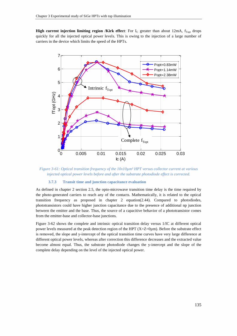
Chapter 3 Experimental study of SiGe HPTs with top illumination
135
High current injection limiting region /Kirk effect: For IC greater than about 12mA, fTopt drops
quickly for all the injected optical power levels. This is owing to the injection of a large number of
carriers in the device which limits the speed of the HPTs.
Figure 3-61: Optical transition frequency of the 10x10µm² HPT versus collector current at various
injected optical power levels before and after the substrate photodiode effect is corrected.
3.7.3 Transit time and junction capacitance evaluation
As defined in chapter 2 section 2.5, the opto-microwave transition time delay is the time required by
the photo-generated carriers to reach any of the contacts. Mathematically, it is related to the optical
transition frequency as proposed in chapter 2 equation(2.44). Compared to photodiodes,
phototransistors could have higher junction capacitance due to the presence of additional np junction
between the emitter and the base. Thus, the source of a capacitive behavior of a phototransistor comes
from the emitter-base and collector-base junctions.
Figure 3-62 shows the complete and intrinsic optical transition delay versus 1/IC at different optical
power levels measured at the peak detection region of the HPT (X=Z=0µm). Before the substrate effect
is removed, the slope and y-intercept of the optical transition time curves have very large difference at
different optical power levels, whereas after correction this difference decreases and the extracted value
become almost equal. Thus, the substrate photodiode changes the y-intercept and the slope of the
complete delay depending on the level of the injected optical power.
0 0.005 0.01 0.015 0.02 0.025 0.030
1
2
3
4
5
6
7
Ic (A)
fTo
pt (G
Hz)
Popt=0.83mW
Popt=1.14mW
Popt=2.38mW
Intrinsic fTopt
Complete fTopt

Chapter 3 Experimental study of SiGe HPTs with top illumination
136
Figure 3-62: Global optical transition delay of the 10x10µm² HPT versus 1/IC at different optical
power levels before and after substrate effect corrected.
As it is explained in details in section 2.5, the capacitance and the transit terms of the phototransistor
can be extracted from the slope and y-intercept of the transition delay curve.
These values are given in Table 3-10 for a 10x10µm2 HPT at different injected optical power levels.
We compare the intrinsic and complete capacitances and transit times. We have also compared these
values with the electrical capacitance and transit time presented in section 3.4.
In general, the complete junction capacitance and transit time terms are higher than the intrinsic ones.
The opto-microwave capacitances and transit times are much larger than the electrical equivalent
values due to the increase of junction capacitance and transit time experienced by the photo-generated
carriers.
A larger value of capacitance and transit time means that photo-generated carriers experience a longer
path along the phototransistor than in the electrical transistor. Indeed the electrical transistor lies only
in the vertical region of the emitter plus a given electrical extension as seen in section 3.4, while the
phototransistor effect is distributed along the whole device with additional lateral path of photo-carriers
which are imposed in order to reach the electrical contacts.
As well capacitance terms are larger, related to the given surface of the optical window and variation of
the space-charge-region width along the lateral position.
Thus, we deduce the complete and intrinsic “optical” capacitance and transit time by removing the
electrical parameters from the opto-microwave extracted ones as described in chapter 2 section 2.5.2.
These values give us the additional junction capacitances and transit time that describes the added path
length and added equivalent surface supported by photo-generated carriers compared to the electrical
ones.
The complete HPT opto-microwave capacitance and transit time increase with the injected optical
power decrease.
0 500 1000 1500
0.05
0.1
0.15
0.2
0.25
1/Ic (1/A)
Op
tica
l tr
an
sitio
n d
ela
y (
ns)
Popt=0.83mW
Popt=1.14mW
Popt=2.38mW
Intrinsic
complete
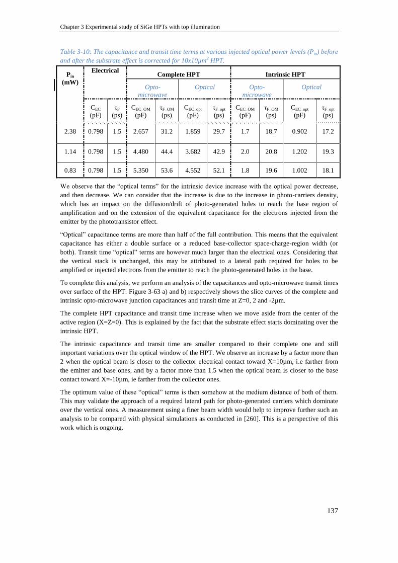
Chapter 3 Experimental study of SiGe HPTs with top illumination
137
Table 3-10: The capacitance and transit time terms at various injected optical power levels (Pin) before
and after the substrate effect is corrected for 10x10µm2 HPT.
Pin
(mW)
Electrical Complete HPT Intrinsic HPT
Opto-
microwave
Optical Opto-
microwave
Optical
CEC
(pF)
τF
(ps)
CEC_OM
(pF)
τF_OM
(ps)
CEC_opt
(pF)
τF_opt
(ps)
CEC_OM
(pF)
τF_OM
(ps)
CEC_opt
(pF)
τF_opt
(ps)
2.38 0.798 1.5 2.657 31.2 1.859 29.7 1.7 18.7 0.902 17.2
1.14 0.798 1.5 4.480 44.4 3.682 42.9 2.0 20.8 1.202 19.3
0.83 0.798 1.5 5.350 53.6 4.552 52.1 1.8 19.6 1.002 18.1
We observe that the “optical terms” for the intrinsic device increase with the optical power decrease,
and then decrease. We can consider that the increase is due to the increase in photo-carriers density,
which has an impact on the diffusion/drift of photo-generated holes to reach the base region of
amplification and on the extension of the equivalent capacitance for the electrons injected from the
emitter by the phototransistor effect.
“Optical” capacitance terms are more than half of the full contribution. This means that the equivalent
capacitance has either a double surface or a reduced base-collector space-charge-region width (or
both). Transit time “optical” terms are however much larger than the electrical ones. Considering that
the vertical stack is unchanged, this may be attributed to a lateral path required for holes to be
amplified or injected electrons from the emitter to reach the photo-generated holes in the base.
To complete this analysis, we perform an analysis of the capacitances and opto-microwave transit times
over surface of the HPT. Figure 3-63 a) and b) respectively shows the slice curves of the complete and
intrinsic opto-microwave junction capacitances and transit time at Z=0, 2 and -2µm.
The complete HPT capacitance and transit time increase when we move aside from the center of the
active region (X=Z=0). This is explained by the fact that the substrate effect starts dominating over the
intrinsic HPT.
The intrinsic capacitance and transit time are smaller compared to their complete one and still
important variations over the optical window of the HPT. We observe an increase by a factor more than
2 when the optical beam is closer to the collector electrical contact toward X=10µm, i.e farther from
the emitter and base ones, and by a factor more than 1.5 when the optical beam is closer to the base
contact toward X=-10µm, ie farther from the collector ones.
The optimum value of these “optical” terms is then somehow at the medium distance of both of them.
This may validate the approach of a required lateral path for photo-generated carriers which dominate
over the vertical ones. A measurement using a finer beam width would help to improve further such an
analysis to be compared with physical simulations as conducted in [260]. This is a perspective of this
work which is ongoing.

Chapter 3 Experimental study of SiGe HPTs with top illumination
138
Figure 3-63: The complete and intrinsic a) opto-microwave capacitance b) opto-microwave transit
time of the 10x10µm² HPT.
-5 0 5 100
50
100
150
200
250
300
350
X(µm)
Op
tom
icro
wa
ve
tra
nsit tim
e (
ps)
Z=-2µm
Z=2µm
Z=0µm
Intrinsic
Complete
-5 0 5 100
2
4
6
8
10
12
14
X(µm)
Op
tom
icro
wa
ve
ca
pa
cita
nce
(p
F)
Z=-2µm
Z=2µm
Z=0µm
Intrinsic
Complete
a) b)

Chapter 3 Experimental study of SiGe HPTs with top illumination
139
3.8 Selection rules for HPT size and geometry
In this section we demonstrate the size dependency of SiGe/Si HPTs through the complete opto-
microwave behavior at 2.38mW injected optical power. The impact of the optical window size on opto-
microwave gain and cutoff frequency in both photodiode and phototransistor mode operation is
analyzed. The optical window size dependency of the substrate photodiode impact is also investigated.
Figure 3-64 shows the opto-microwave gain slice curve of the three HPTs, having the optical window
size of 5x5µm2, 10x10µm
2 and 50x50µm
2, at 50MHz in HPT and PD modes. In HPT mode
configuration the Gom of 50x50µm2 is higher by 8.3dB than the Gom of 10x10µm
2 HPT and by
15.2dB than the Gom of 5x5µm2. This is mostly due to higher electrical current gain (β) of 50x50µm
2
HPT as presented in Table 3-11 and its 100% coupling efficiency.
However, in PD mode operation the Gom of the 50x50µm2 and 10x10µm
2 HPTs is lower than for the
Gom of 5x5µm2
at the center of the optical window. This is demonstrated to be due to the fact that
when 28µm diameter optical beam is pointing at the center (x=0µm and y=0µm) to illuminate over the
5x5µm2
HPT, a larger portion of the light is illuminating the substrate photodiode. In PD mode
operation, the substrate photodiode is more sensitive than the base-collector diode as shown in Figure
3-46 b). Thus, in PD mode, because of the substrate photodiode and coupling efficiency, the opto-
microwave gain of 5x5µm2
HPT is higher than the Gom of 10x10µm2 and 50x50µm
2 HPTs; Gom of
10x10µm2 HPT is higher than of 50x50µm
2 HPT.
Figure 3-64: The slice curve of the low frequency opto-microwave gain of 50x50µm2, 10x10µm
2 and
5x5µm2 optical window size HPTs at X=0m in HPT (Vbe=0.857V) and PD (Vbe=0V) modes of
operation for Vce=3V.
-2 -1 0 1 2
x 10-5
-70
-60
-50
-40
-30
-20
-10
0
Z (m)
Go
m(d
B)
10x10m2 PD mode
10x10m2 HPT mode
50x50m2 PD mode
50x50m2 HPT mode
5x5m2 PD mode
5x5m2 HPT mode

Chapter 3 Experimental study of SiGe HPTs with top illumination
140
Table 3-11: The electrical current gain and low frequency opto-microwave responsivity of the three
different size HPTs at x=0µm and y=0µm
HPT window (µm2) β at Vbe=0.857V Gom HPT mode at
50MHz (dB)
Gom PD mode at
50MHz (dB)
50x50 438 -4.8 -33.8
10x10 390 -13.1 -33.8
5x5 332 -20.0 -30.3
The low frequency opto-microwave gain slice curve by considering the coupling efficiency of 16.5%,
32.3% and 100% for 5x5µm2, 10x10µm
2 and 50x50µm
2 HPTs respectively, is presented in Figure
3-65. At the peak detection all sized HPTs have nearly -4dB opto-microwave gain, which is equivalent
to the responsivity of 0.67A/W.
Figure 3-65: Absolute opto-microwave gain of 5x5µm2, 10x10µm
2, 50x50µm
2 HPTs in phototransistor
mode.
Figure 3-66 shows the slice plots of cutoff frequency for 10x10µm2, 5x5µm
2 and 50x50µm
2optical
window size HPTs at x=0 both in PD and HPT modes. The cutoff frequency curves can be decomposed
into three different regions (A, B and C) as shown in Figure 3-66 a). Region A represents an extracted
cutoff frequency close to the low frequency limitation of the Vector Network Analyzer (VNA) we used
(namely 50MHz). Thus, the cutoff frequencies presented in this region are not reliable. The cutoff
frequency in region B is mainly related to the substrate response. In this region the cutoff frequency
gets smaller and becomes equal in both modes which indicate that the cutoff frequency in this region is
extracted from the substrate photodiode. In region C we have high cutoff frequency corresponding to
the frequency response of the phototransistor.
Theoretically, the cutoff frequency of smaller surface area transistors is higher than the one of larger
surface area transistors due to the RC limit. This theory is consistent if we compare 50x50µm2 HPT
with the other two in HPT mode. The cutoff frequency of 50x50µm2 is less than 80MHz which is much
closer to the VNA’s low frequency limitation; this cutoff frequency is much smaller than with 5x5µm2
and 10x10µm2 HPTs. However, when we compare the -3dB cutoff frequency of 5x5µm
2 and
10x10µm2, the theory is no more valid (the cutoff frequency of 5x5µm
2 HPT is smaller than of
-2 -1 0 1 2
x 10-5
-45
-40
-35
-30
-25
-20
-15
-10
-5
0
Z (m)
Go
m (
dB
)
5x5m2
10x10m2
50x50m2
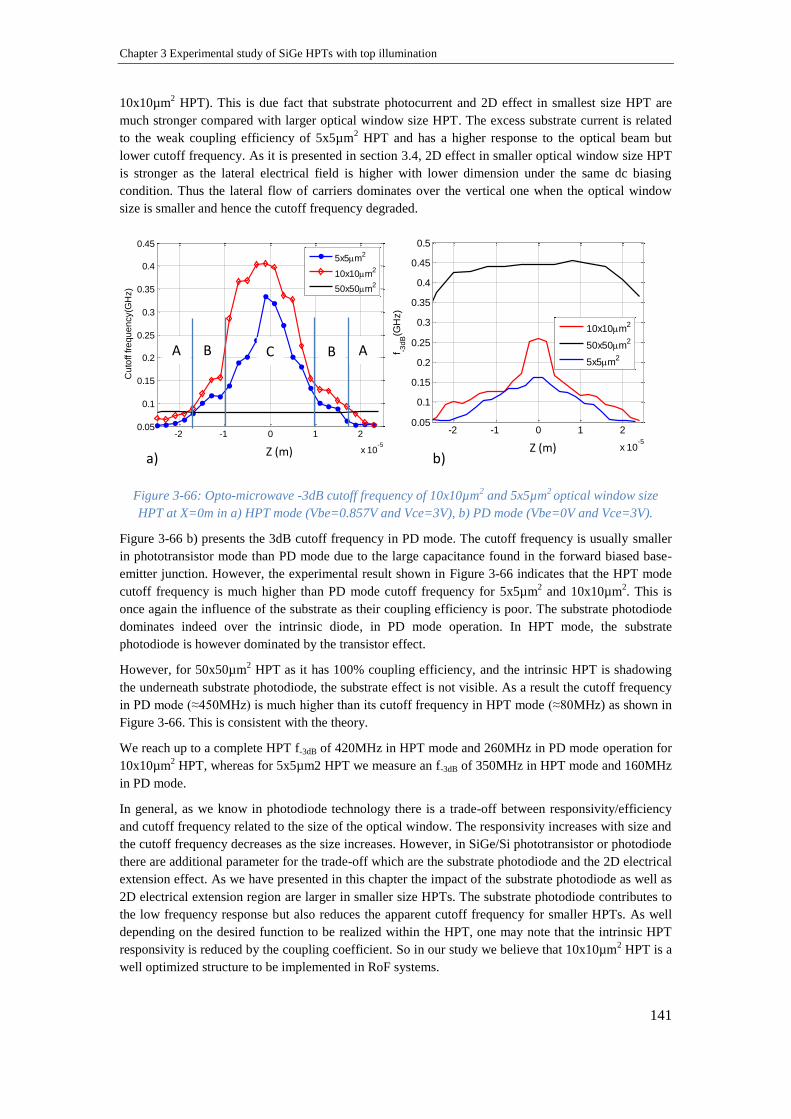
Chapter 3 Experimental study of SiGe HPTs with top illumination
141
10x10µm2 HPT). This is due fact that substrate photocurrent and 2D effect in smallest size HPT are
much stronger compared with larger optical window size HPT. The excess substrate current is related
to the weak coupling efficiency of 5x5µm2 HPT and has a higher response to the optical beam but
lower cutoff frequency. As it is presented in section 3.4, 2D effect in smaller optical window size HPT
is stronger as the lateral electrical field is higher with lower dimension under the same dc biasing
condition. Thus the lateral flow of carriers dominates over the vertical one when the optical window
size is smaller and hence the cutoff frequency degraded.
Figure 3-66: Opto-microwave -3dB cutoff frequency of 10x10µm2 and 5x5µm
2 optical window size
HPT at X=0m in a) HPT mode (Vbe=0.857V and Vce=3V), b) PD mode (Vbe=0V and Vce=3V).
Figure 3-66 b) presents the 3dB cutoff frequency in PD mode. The cutoff frequency is usually smaller
in phototransistor mode than PD mode due to the large capacitance found in the forward biased base-
emitter junction. However, the experimental result shown in Figure 3-66 indicates that the HPT mode
cutoff frequency is much higher than PD mode cutoff frequency for 5x5µm2 and 10x10µm
2. This is
once again the influence of the substrate as their coupling efficiency is poor. The substrate photodiode
dominates indeed over the intrinsic diode, in PD mode operation. In HPT mode, the substrate
photodiode is however dominated by the transistor effect.
However, for 50x50µm2 HPT as it has 100% coupling efficiency, and the intrinsic HPT is shadowing
the underneath substrate photodiode, the substrate effect is not visible. As a result the cutoff frequency
in PD mode (≈450MHz) is much higher than its cutoff frequency in HPT mode (≈80MHz) as shown in
Figure 3-66. This is consistent with the theory.
We reach up to a complete HPT f-3dB of 420MHz in HPT mode and 260MHz in PD mode operation for
10x10µm2 HPT, whereas for 5x5µm2 HPT we measure an f-3dB of 350MHz in HPT mode and 160MHz
in PD mode.
In general, as we know in photodiode technology there is a trade-off between responsivity/efficiency
and cutoff frequency related to the size of the optical window. The responsivity increases with size and
the cutoff frequency decreases as the size increases. However, in SiGe/Si phototransistor or photodiode
there are additional parameter for the trade-off which are the substrate photodiode and the 2D electrical
extension effect. As we have presented in this chapter the impact of the substrate photodiode as well as
2D electrical extension region are larger in smaller size HPTs. The substrate photodiode contributes to
the low frequency response but also reduces the apparent cutoff frequency for smaller HPTs. As well
depending on the desired function to be realized within the HPT, one may note that the intrinsic HPT
responsivity is reduced by the coupling coefficient. So in our study we believe that 10x10µm2 HPT is a
well optimized structure to be implemented in RoF systems.
-2 -1 0 1 2
x 10-5
0.05
0.1
0.15
0.2
0.25
0.3
0.35
0.4
0.45
Y (m)
Cu
toff fre
qu
en
cy(G
Hz)
5x5m2
10x10m2
50x50m2
-2 -1 0 1 2
x 10-5
0.05
0.1
0.15
0.2
0.25
0.3
0.35
0.4
0.45
0.5
Y (m)
f -3d
B(G
Hz)
10x10m2
50x50m2
5x5m2
Z (m) Z (m)
A B C B A
a) b)
Chapter 3 Experimental study of SiGe HPTs with top illumination
142
Due to the presence of the substrate photodiode, the physical behavior of the phototransistor or
photodiode deviates from its intrinsic behavior. Hence, we suggest redesigning the HPT structures in
order to avoid or minimize the impact of the substrate. This could be achieved:
Through lateral illuminated structure or
By properly designing the optical window with a proper metallization.
By using either smaller optical beam optical source with SMF at 850nm or use MMF with a
proper optical coupling structure to characterize the HPTs.
One could also take the advantage of the substrate photodiode to enhance the low frequency
responsivity at low frequency applications.
The 2D electrical effect is also modifies the internal dynamic behavior of the HPT. Hence a proper
design rules could then be deduced:
To get a symmetric contact of the collector, base and emitters that will make the electrical
field more vertical.
To fragment the HPT in smaller individual HPTs, as the electrical extension may reach a
limit in its increase.
Chapter 3 Experimental study of SiGe HPTs with top illumination
143
3.9 Conclusion
This chapter presented the different experimental results in the study, optimization and operation of top
illuminated SiGe HPTs. We have shown the performance of an HPT both in static and opto-microwave
measurements. We have also studied the influence of the HPT physical structure through the
localization of the DC and OM behavior over the surface of the device. The substrate photocurrent
distribution over the surface of the HPT is deduced from the experimental results and its effect on
responsivity and speed of the HPT is extensively studied. An extraction method was then developed to
isolate the substrate effect and then measure the intrinsic behavior of the HPT. The influences of
various optical window sizes on the performance of the HPT both electrically and for the opto-
microwave response are studied. The injected optical power level effect on the performance of SiGe
HPT is also presented.
DC characterization of the HPT involves measuring the output Ic-Vce characteristics of the HPT,
electrical current gain (β) and the Gummel measurements. The effect of illumination with optical beam
at 850nm on the Ic-Vce curves of the HPT is presented. The dc optical current gain is isolated and
compared with the electrical behavior.
From the microwave behavioral study we observe that the speed of 3x3µm2 HPT (26.5GHz) is smaller
than of 10x10µm2 HPT (50GHz). This is due to the 2D electrical extension effect as it is demonstrated
through various mathematical models. A proper design rules is then proposed to get a symmetric
contacts on the collector, base and emitters so that the electrical field will be more vertical; and also to
fragment the HPT in smaller individual HPTs as the electrical extension may reach a limit in its
increase.
The opto-microwave gain, the optical transition frequency and opto-microwave cutoff frequency of
different size SiGe HPT structures are studied and analyzed at different biasing points. This allows
finding an optimum bias point that maximizes the frequency responsivity (Vbe=0.857V, Vce=3V) and
speed (Vbe=0.857V, Vce=2V) of the HPT.
We have carried out OM SNOM and DC SNOM analyses as they are crucial to understand the
behavior and physical structure of SiGe HPTs. OM SNOM analysis allowed the extraction of an opto-
microwave response and the dynamic behavior over the surface of the device at each position of the
optical illumination. DC SNOM analysis allowed the extraction of the photocurrent distribution over
the structure of the HPTs. This also allowed the extraction of substrate photocurrent over each optical
probe position and hence the substrate source is isolated.
From SNOM analysis we have studied the effects of the substrate photocurrent on the responsivity and
speed of the SiGe HPT. Both DC and opto-microwave responsivities of the HPT are highly affected by
the substrate photodiode. The extrinsic substrate photodiode is much stronger than the intrinsic one.
The substrate effect is much visible in PD mode operation than in HPT mode as it is hidden by the
transistor effect.
We reach complete cutoff frequency of 420MHz in HPT mode, 260MHz in PD mode and complete
optical transition frequency of 4.2GHz for 10x10µm2 HPT. An extraction method was then applied to
isolate the substrate effect and then measure the intrinsic behavior of the HPT. An intrinsic cutoff
frequency of 463MHz in PD mode and an intrinsic optical transition frequency of 6.5GHz are then
deduced. The intrinsic cutoff frequency is also slight increases in HPT mode.
An alternative to get rid of the substrate contribution could be through a proper design of the optical
window with proper metal diaphragms around it. Indeed, the substrate photodiode would be hidden
either by metal contacts or by upper layers of the intrinsic HPT, or through the use of a lateral
illumination of the HPT. Alternatively taking advantage of the substrate could be envisaged leading to
combined HPT+PD structure.

Chapter 3 Experimental study of SiGe HPTs with top illumination
144
We have also demonstrated the performance of SiGe/Si HPT is highly affected by the level of the
injected optical power. This could be related to self-biasing or to variation in the optical source modes
at different biasing levels that changes the beam width. The latter effect modifies the coupling
efficiency so that the influence of the substrate photodiode is changed for each optical power level.
The optical transition frequency (fTopt=6.5GHz for 10x10µm2 HPT) is much lower than the electrical
transition frequency (fT=50GHz for 10x10µm2 HPT). It is explained by the addition of capacitive and
transit time terms related to the photodetection mechanism. The transit time and junction capacitances
of the SiGe HPT are extracted experimentally (in electrical, opto-microwave and optical point of view).
The opto-microwave capacitance and transit time terms are increased by more than a factor of 3.5 and
21 respectively when compared with their electrical equivalent values. This is due to the increase of
junction capacitance and transit time experienced by the photogenerated carriers. We also observed that
the complete HPT opto-microwave capacitance and transit time increases with decreasing the injected
optical power level. These parameters could be used for further modeling of the SiGe HPT.

Chapter 4 Millimeter wave and optical Interconnections on Silicon
145
Chapter 4 Millimeter Wave and optical
Interconnections on Silicon
4.1 INTRODUCTION ....................................................................................................................... 146 4.2 PLANAR TRANSMISSION LINES ................................................................................................ 148
4.2.1 Introduction .................................................................................................................. 148 4.2.2 Transmission lines modeling using HFSS .................................................................... 148 4.2.3 Coplanar Line .............................................................................................................. 150 4.2.4 Micro-strip line ............................................................................................................ 155 4.2.5 Grounded Coplanar Line ............................................................................................. 161
4.3 OPTICAL WAVEGUIDE ............................................................................................................ 166 4.3.1 Polymer based optical waveguide ................................................................................ 166 4.3.2 SiN and SiO2 based optical waveguide for on-chip interconnections .......................... 168
4.4 COMBINATION OF OPTICAL AND ELECTRICAL WAVEGUIDES ................................................... 173 4.4.1 Grounded coplanar line with optical waveguide ......................................................... 173 4.4.2 Coplanar line with Optical waveguide ......................................................................... 175 4.4.3 Transmission line interconnections .............................................................................. 177
4.5 EXPERIMENTAL VALIDATION OF PLANAR TRANSMISSION LINE .............................................. 180 4.6 CONCLUSION .......................................................................................................................... 185

Chapter 4 Millimeter wave and optical Interconnections on Silicon
146
4.1 Introduction
High speed communication and remote sensing are moving at a rapid pace toward millimeter-wave and optical
frequencies in order to achieve extremely high data-rates, enhanced detection capabilities or superior image
resolution. The integration of millimeter wave circuits with digital and baseband frequency analog circuits as
well as interconnecting optical components using silicon technology is of great interest. Although complete
monolithic integration strongly facilitates packaging and offers compactness, the integration of several
functionalities into a single chip is not straight-forward and is strongly driven by the system requirements and the
aimed costs. There are two approaches to develop integrated microwave-photonics (IMWP) circuits on Silicon
platform that could vary based on the technological availabilities and the targeted applications.
Hybrid IMWP circuits:
This approach targets the realization of IMWP circuits by combining VCSELs, high speed detectors and
antenna units together with Silicon-based optical and electrical interconnections for RoF applications. In
this approach each optical element is developed separately using its optimal substrate, the various
elements are then combined on a common Silicon substrate. This Silicon substrate is designed to
include passive optical waveguides and electrical interconnections where the active components will be
placed in etched cavity such as in Figure 4-1 is the approach that we propose to follow.
Figure 4-1: The schematic of hybrid integrated microwave photonic circuit.
Since the emission spectrum of the VCSEL lies mainly within the absorption band of silicon (450- 850
nm), it implies that optical waveguide cannot be Silicon based. Standard low resistivity Silicon substrate
is also lossy and provides high signal attenuation in the millimeter frequency band. Thus, technologies
for circuit interconnections and passive elements on low resistivity CMOS grade silicon still need to be
further developed in order to overcome the high signal losses at millimeter and optical frequencies.
High resistivity silicon (HRS) substrates (>1000Ω.cm) are available, but at higher cost and their use
deviates from the standard CMOS fabrication process. Micro-machined microstrip waveguide using
polyimide as a dielectric interface layer has been investigated [47] [48]. However it has limitations due
to the difficulty to achieve a large layer thickness, poor aspect ratio between the layer width and
thickness, high curing temperature, and low transparency making subsequent optical alignment difficult.
Polymer based electrical interconnections overcome these limitations and are also used for optical
interconnections at the board level. The use of polymers such as SU-8, Parylene and BCB is expected to
be very efficient to achieve inter-chip interconnections through micro-meter size waveguide, and to be
furthermore compatible with the use of lithographic process to design electrical interconnections.
Monolithic IMWP circuits:
The second approach combines on a single chip monolithic optical sources, waveguides and detectors.
It is therefore required to have CMOS-compatible Si light emitting sources, detectors, optical
waveguides and electrical interconnections. This integration will have the benefit of low cost multi
functionality and reduced size of opto- microwave integrated circuits. The targeted applications can be
biomedical analysis, microfluidic or Datacom. Detectors and LEDs based on SiGe BiCMOS technology
are demonstrated in chapter 3 and 5 respectively. A major stumbling block, however, is the
VCSEL Detector
Thermal heat sink Thermal heat sinkantenna antenna
Microwave lineOptical waveguide Microwave line
Silicon Substrate

Chapter 4 Millimeter wave and optical Interconnections on Silicon
147
development of low loss and low cost opto-electric interconnections (millimeter wave transmission
lines and optical waveguides) in CMOS technology.
In general, this thesis aims at improving the integration of opto-electronic circuits by providing information on
the design aspect of individual components that could be implemented into either one or both approaches
described above.
Thus, this chapter focuses on the development of interconnecting devices such as: millimeter transmission lines
and optical waveguides that are compatible with those approaches.
For the first approach, we investigate a novel method of fabricating transmission line structures in the millimeter
frequency range (60GHz) on low resistivity CMOS grade silicon substrates using polymers (SU8 negative resist,
BCB and Parylene) as a dielectric interface layer and as optical waveguide (optical interconnections). We
investigate the mixed integration of millimeter-waves transmission lines and of optical waveguides
simultaneously.
Based on the simulation results through HFSS, we develop the schematic patterns/layout of the transmission
lines and optical waveguides using CADENCE software. The validity of the design is then demonstrated through
experiment results as presented in the last section.
For the second approach, we design optical waveguides by taking advantage of different oxide layers in SiGe
BiCMOS technology. This enables us to develop a full optical link which will then be validated experimentally
in chapter 5.
Chapter 4 Millimeter wave and optical Interconnections on Silicon
148
4.2 Planar transmission lines
4.2.1 Introduction
Connections between components are necessary in a circuit design. Typically a metal interconnect is used for
these connections. Planar transmission lines, as opposed to waveguides, are commonly used in RF circuits due to
the ease of manufacturing, their low cost, their well understood electrical behavior, the availability of Electronic
design automation (EDA) tools for design and their small space requirements, among other design benefits. The
chief characteristic of planar transmission lines is that the lines are generally routed in two dimensions.
Typically, planar transmission lines are metal lines routed on a substrate material such as a printed circuit board,
a microwave monolithic integrated circuit (MMIC), etc. A ground plane (continuous metal sheet used as a circuit
reference) is commonly located close to transmission lines, either on the opposite side of the substrate (i.e.
microstrip), on both sides of the line, or above the substrate.
The performance of transmission lines is highly affected by the losses along the line (attenuation) and circuit
matching impedance (characteristics impedance). Planar circuit transmission lines suffer from losses that reduce
the signal energy passed through the line. The line losses have various origins that can be ranked in three
categories: losses in the conductor (metal), losses in the dielectric, radiation losses. These losses are dependent
on the type of line used.
Metal/conductor losses: In RF lines the resistance of the conductors is never equal to zero. Whenever current
flows through one of these conductors, some energy is dissipated in the form of heat. This heat loss is a power
loss. Another type of conductor loss is due to skin effect. When DC current flows through a conductor, the
movement of electrons through the conductor cross section is uniform; the situation is somewhat different when
AC is applied. At high frequency AC current tends to avoid travel through the center of a solid conductor,
limiting itself to conduction near the surface. This limits the cross-sectional conductor area available to carry
alternating current flow. Since resistance is inversely proportional to the cross-sectional area, it increases as the
frequency is increased. Also, since power loss increases as resistance increases, power losses increase with
frequency because of skin effect.
Dielectric Losses: Result from the heating effect in the dielectric material between the conductors. The heat
produced is dissipated into the surrounding medium. When there is no potential difference between two
conductors, the atoms in the dielectric material between them are normal and the orbits of the electrons are
circular. When there is a potential difference between two conductors, the orbits of the electrons change. The
excessive negative charge on one conductor repels electrons on the dielectric toward the positive conductor and
thus distorts the orbits of the electrons. A change in the path of electrons requires more energy, introducing a
power loss.
Radiation or Induction Losses: Radiation or induction losses are similar as both are caused by the fields
surrounding the conductors. Induction losses occur when the electromagnetic field around a conductor cuts any
nearby metallic object and a current is induced in that object. As a result, power is dissipated in the object and is
lost. Radiation losses occur because some magnetic lines of force about a conductor do not return to the
conductor when the cycle alternates. These lines of force are projected into space as radiation, resulting in power
losses.
In our model we consider all types of losses and the targeted characteristic impedance is 50Ω. To model our
transmission lines we use the commercial electromagnetic simulation software HFSS (High Frequency Structure
Simulator). The propagation characteristics of Coplanar, Micro strip and Grounded coplanar lines on low
resistive silicon (20Ω.cm) substrate and polymers (SU8, BCB, and Parylene) in 50GHz to 70GHz frequency
range are studied. From this model the appropriate dimensions of the lines are determined in order to achieve
minimum attenuation and 50Ω characteristic impedance.
4.2.2 Transmission lines modeling using HFSS
High Frequency Structure Simulator (HFSS) is a three-dimensional electromagnetic simulation software based
on the finite elements method. This software allows the calculation of the electromagnetic behavior of a

Chapter 4 Millimeter wave and optical Interconnections on Silicon
149
structure, and it has post-processing tools for a more detailed analysis of attenuation, propagation constant,
characteristic impedance, and the S-parameters of the line.
This work is devoted to model transmission lines of low loss in the millimeter frequency range (60GHz). There
are three different methods of extracting the propagation attenuation of lines using HFSS [257].
The first method (denoted gamma-HFSS) considers the real part of the propagation constant obtained by
taking into account only the port surface excitation, irrespective of the actual line length. This is a 2D
calculation and it is very fast.
The second method (rated power) uses the difference between the Poynting vector flows through two
surfaces (of identical dimensions) perpendicular to the propagation direction of the traveling wave.
The third method (denoted extraction) consists of extracting losses from the Sij parameters of two identical
lines of different lengths by de-embedding method. The Sij parameters are calculated by HFSS.
Table 4-1 from [257] compares the three methods of losses extraction using HFSS for a microstrip line on glass
and on high resistive silicon substrate at 60 GHz. The presented results permit to conclude that the three methods
give similar results. Thus, we prefer to use the 1st method to extract the attenuation due to its simplicity.
Table 4-1: Comparison of different methods of calculating losses by using HFSS for a microstrip line on glass
and high resistive silicon at 60 GHz. Glass thickness = thickness of silicon = 100µm, metallization width =
100µm and t = 1µm [257]
Method Microstrip line on
Glass substrate at 60GHz Silicon substrate at 60GHz
Poynting vector 0.0534 dB/mm 0.0899 dB/mm
Extraction 0.0539 dB/mm 0.0899 dB/mm
Gamma-HFSS 0.0538 dB/mm 0.0894 dB/mm
In this section we study the Coplanar, Microstrip and Grounded coplanar lines from 50 to 70GHz. Low resistive
silicon is used as substrate and the metallization is deposited over polymer (SU8, Parlyne or BCB). These lines
are in vacuum.
In our simulations we consider materials with the following specifications. The thickness of the substrate is
550µm and the polymer thickness and the line dimensions will be precisely modeled through HFSS simulator.
The silicon substrate thickness = 550 µm, of resistivity 20Ω.cm, of permittivity r =11.7.
Gold for metallization having thickness of 1.2µm.
Different types of polymers ( SU8, BCB and Parylene ); their properties as specified in table 3.2
Glass thickness 500µm, tanδ=0.0005, r=4. The glass wafer is put below the silicon one in order to
minimize the chuck effect during the measurements using the probe station; it is also considered in
simulations for a better match with measurement conditions.
Stainless steel used as metal chuck with thickness 10μm.

Chapter 4 Millimeter wave and optical Interconnections on Silicon
150
Table 4-2: The electrical properties of polymers (SU8, BCB and Parylene N) used in our model
Polymer r tanσ or ρ Frequency(GHz) optical above
650nm
Reference
SU8 3.25 0.027 30 Transparent [52]
BCB 2.5 0.002 60 Transparent [252]
Parylene-N 2.35 0.0006 60 Transparent [253] [254]
LR Silicon 11.7 20Ω.cm absorb Substrate what we have
The target line dimension and polymer thickness should provide the minimum losses and 50Ω characteristics
impedance. We have also taken into consideration the pitch width of GSG probe as an additional constraint to be
able to do on wafer measurement. In our laboratory we have 150µm pitch RF probes for 60GHz characterization.
In the following sections we present the simulation results of Coplanar, Microstrip and Grounded Coplanar lines
by using SU8, BCB and Parylene-N as dielectric layer over low resistive silicon substrate.
4.2.3 Coplanar Line
a. Structure presentation
We study here the coplanar line on low resistive silicon substrate with the metallization deposited on polymer
layer (as shown in Figure 4-3). The optimal metal strip width (s) and slot width (W) will be determined through
HFSS simulations. We also fix the polymer thickness based on the possibilities of our technological fabrication
process; we will see this thickness has a great impact on the line characteristics. Our main target is to minimize
the line loss and to achieve 50Ω characteristics impedance at 60GHz. In our model we have taken into
consideration the metal chuck effect during on wafer measurement and also the mechanism to minimize this
effect by adding a glass wafer as shown in Figure 4-3 . We put 500µm thick glass wafer under LR silicon wafer
during on wafer measurement to avoid the chuck effect on the measurement results.
To characterize the coplanar line, we made several simulations in the frequency band 50 to 70 GHz; we focused
on the band 57 - 64 GHz allocated for radio services.
Several modes can propagate in a coplanar line, whose excitation depends on the line excitation system. We
meanly distinguish the coplanar and the coupled slot line propagation modes as shown in Figure 4-2. In the
following we always consider the coplanar mode corresponding to the classical use of coplanar waveguides: the
signal propagates along the metal strip whereas the two metallic planes besides are connected to the ground as
shown on Figure 4-3.
Figure 4-2: coplanar line wave propagation modes.
Substrate Substrate
a) Coplanar mode a) Coupled slotline mode

Chapter 4 Millimeter wave and optical Interconnections on Silicon
151
Figure 4-3: CPW transmission line structural schematic
b. Study of the characteristics of the line
The target is to model and design low loss coplanar lines on low resistive silicon substrate having characteristic
impedance of 50 Ohm at 60GHz. In this sub-section we present the simulation results of coplanar lines with and
without a polymer layer between the metal and the substrate. The influences of the polymer thickness, the metal
strip width and the slot width on the characteristic impedance and on the attenuation of the line are presented.
We then present the final simulation results for the optimal line dimensions and polymer thickness.
i. Coplanar line with/without polymer layer and metal strip width effect
A 4mm long coplanar line with a central conductor (s) width varying from 114µm to 250µm and a slot gap (w)
varying from 13µm to 58µm over 550µm thick low resistive silicon substrate has been simulated at 60GHz. The
simulation results are presented in Table 4-3 with 20µm thick SU8 and without SU8 layer between the metal and
substrate. As the substrate is low resistive silicon, the lines fabricated without polymer layer have very high
losses. In this case, one obtains losses of 2.15dB/mm at 60GHz with line dimensions leading to 50Ω
characteristic impedance (metal strip width of 114µm and slot width of 10µm). These losses are strongly reduced
just by introducing 20µm SU8 layer between the metal and the silicon substrate: losses of 0.77dB/mm are
obtained at the same frequency and for the same characteristic impedance. Table 4-3 also shows how the
attenuation of the line varies with metal strip (s) and slot width (w). Large strip width and air gap imply high
loss. To achieve 50Ω characteristics impedance we need to play with the metal strip and air gap widths. The
characteristics impedance decreases as the metal strip width (s) increases and it increases as the slot width (w)
increases. Thus, to get 50Ω line both or one of these parameters could be manipulated depending on our design
requirements (such as the characterization GSG probe pitch width).
LRSilicon
polymer polymer
glass
metal
Strip, s wslot w
Metal chuck
a) Vertical stack of the line along with measurementbench setup effect and protection
b) Picture taken from HFSS simulator
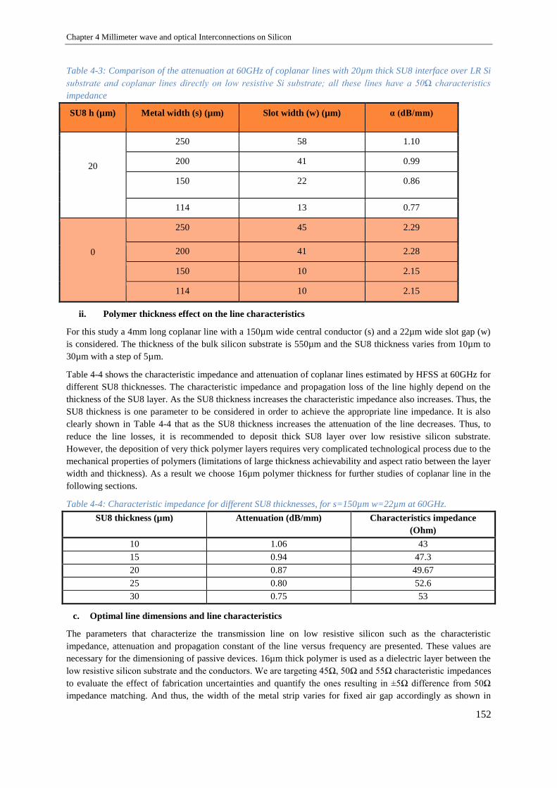
Chapter 4 Millimeter wave and optical Interconnections on Silicon
152
Table 4-3: Comparison of the attenuation at 60GHz of coplanar lines with 20µm thick SU8 interface over LR Si
substrate and coplanar lines directly on low resistive Si substrate; all these lines have a 50Ω characteristics
impedance
SU8 h (µm) Metal width (s) (µm) Slot width (w) (µm) α (dB/mm)
20
250 58 1.10
200 41 0.99
150 22 0.86
114 13 0.77
0
250 45 2.29
200 41 2.28
150 10 2.15
114 10 2.15
ii. Polymer thickness effect on the line characteristics
For this study a 4mm long coplanar line with a 150µm wide central conductor (s) and a 22µm wide slot gap (w)
is considered. The thickness of the bulk silicon substrate is 550µm and the SU8 thickness varies from 10µm to
30µm with a step of 5µm.
Table 4-4 shows the characteristic impedance and attenuation of coplanar lines estimated by HFSS at 60GHz for
different SU8 thicknesses. The characteristic impedance and propagation loss of the line highly depend on the
thickness of the SU8 layer. As the SU8 thickness increases the characteristic impedance also increases. Thus, the
SU8 thickness is one parameter to be considered in order to achieve the appropriate line impedance. It is also
clearly shown in Table 4-4 that as the SU8 thickness increases the attenuation of the line decreases. Thus, to
reduce the line losses, it is recommended to deposit thick SU8 layer over low resistive silicon substrate.
However, the deposition of very thick polymer layers requires very complicated technological process due to the
mechanical properties of polymers (limitations of large thickness achievability and aspect ratio between the layer
width and thickness). As a result we choose 16µm polymer thickness for further studies of coplanar line in the
following sections.
Table 4-4: Characteristic impedance for different SU8 thicknesses, for s=150µm w=22µm at 60GHz.
SU8 thickness (µm) Attenuation (dB/mm) Characteristics impedance
(Ohm)
10 1.06 43
15 0.94 47.3
20 0.87 49.67
25 0.80 52.6
30 0.75 53
c. Optimal line dimensions and line characteristics
The parameters that characterize the transmission line on low resistive silicon such as the characteristic
impedance, attenuation and propagation constant of the line versus frequency are presented. These values are
necessary for the dimensioning of passive devices. 16µm thick polymer is used as a dielectric layer between the
low resistive silicon substrate and the conductors. We are targeting 45Ω, 50Ω and 55Ω characteristic impedances
to evaluate the effect of fabrication uncertainties and quantify the ones resulting in ±5Ω difference from 50Ω
impedance matching. And thus, the width of the metal strip varies for fixed air gap accordingly as shown in

Chapter 4 Millimeter wave and optical Interconnections on Silicon
153
Table 4-5. When we use BCB or Parylene as a dielectric layer, the dimensions of the line (metal strip and slot
width) leading to one fixed impedance are the same.
Table 4-5: Line dimensions to obtain coplanar lines of 45Ω, 50Ω,and 55Ω characteristic impedance at 60GHz
frequency over 16µm polymer used to elevate the metal over the low resistive silicon substrate.
Polymer type Metal strip width, s
(µm)
Probing slot width, w
(µm)
Target characteristics
impedance (Ω)
SU8 140 13 45
114 13 50
80 13 55
BCB or
Parylene
162 13 45
120 13 50
90 13 55
We studied the behavior of the lines in the frequency range from 50GHz to 70 GHz for the three different
polymer layers; we only present here the results for the lines of characteristic impedance 50Ω at 60 GHz. Thus,
the strip width is fixed at 114µm withSU8 or 120µm with BCB/Parylene for the same slot width of 13µm as
shown in Table 4-5. Then we perform a simulation in the required frequency range.
Figure 4-4 shows the characteristic impedance versus frequency for SU8, BCB and Parylene layers. The
characteristic impedance is almost equal in the three configurations and it slightly decreases with frequency.
Figure 4-4: The simulated result of the characteristic impedance of coplanar line versus frequency when 16µm
polymer layer covers the silicon substrate. The metal strip width is of 114µm and air gap width of 13µm with
SU8 against 120µm metal strip width and 13µm slot width with BCB and parylene.
Figure 4-5 and Figure 4-6 show the real and imaginary parts of the propagation constant indeed the attenuation
constant α (dB/mm) and the phase constant β (rad/m), for a coplanar line with a central conductor width of
114µm for SU8 and 120µm for BCB or Parylene layers, a thickness of metallization of 1.2µm and a substrate
thickness of 550µm. Figure 4-5 details the magnitude of losses in the line related to each polymer layer. Using
SU8 as dielectric interface results in the highest losses compared to BCB and Parylene as SU8 has a higher
tangent loss for the frequency range of 52GHz to 70GHz. We obtain 0.64dB/mm, 0.66dB/mm and 0.724dB/mm
52 54 56 58 60 62 64 66 6840
42
44
46
48
50
52
54
56
58
60
Frequency (GHz)
Zo
(Oh
m)
BCB
Parylene
SU8

Chapter 4 Millimeter wave and optical Interconnections on Silicon
154
attenuation for Parylene, BCB and SU8 respectively at 60GHz. Figure 4-6 shows the imaginary part of the
propagation constant versus frequency; it varies linearly up to 67 GHz.
Figure 4-5: The simulated result of the attenuation of coplanar line versus frequency with 16µm polymerlayers
and line dimensions for 50Ω characteristic impedance.
Figure 4-6: The imaginary part of the propagation constant of coplanar line versus frequency with 16µm
polymer layer and line dimensions for 50Ω characteristic impedance extracted from the HFSS simulator.
Both transverse and longitudinal electric field distributions of a coplanar line are shown in Figure 4-7 when SU8
is used as dielectric layer between metal and low resistive silicon substrate. The electric field is presented by its
magnitude and as a vector. The electric field is confined in the slots between the strip line and the two ground
52 54 56 58 60 62 64 66 68 700
0.2
0.4
0.6
0.8
1
1.2
1.4
1.6
1.8
2
Frequency (GHz)
Att
en
ua
tion (
dB
/mm
)
BCB
Parylene
SU8
52 54 56 58 60 62 64 66 68 701700
1800
1900
2000
2100
2200
2300
2400
2500
2600
Frequency (GHz)
Ph
ase
co
nsta
nt (r
ad
/m)
BCB
Parylene
SU8

Chapter 4 Millimeter wave and optical Interconnections on Silicon
155
metallic planes situated on both sides of the strip (See Figure 4-2). Since the polymer layer is thin, we can
observe in Figure 4-7 a) and b) that at 60GHz a part of the RF signal propagates through the silicon substrate. As
a consequence, the losses in coplanar line are high compared to micro strip and grounded coplanar lines on
polymer layer. At 50GHz (Figure 4-7 c) and d)) the field confinement in SU8 is better: it is coherent with the
lower losses (see Figure 4-5).
Figure 4-7: Electric field amplitude (V / m) and vector in the transverse and longitudinal planes of the coplanar
line on low resistive silicon substrate with a SU8 layer. The line dimensions are s=114µm, w=13µm hSU8=16µm
The simulation results of coplanar line over 16µm thick polymer layer at 60GHz and to achieve characteristic
impedances of 45Ω, 50Ω and 55Ω are summarized in Table 4-6. To reach this goal we fix the slot width at 13µm
and vary the metal strip width. To get higher characteristic impedance the metal strip width has to be smaller.
Eventually, the line loss decreases from 0.81dB/mm to 0.70dB/mm while the metal strip width decreases from
140µm to 80µm.
Table 4-6: Summary of the estimated dimensions of the coplanar line obtained using HFSS simulations.
Different polymer types are used and several targeted characteristic impedances at 60GHz are considered. The
line losses are also evaluated at 60GHz using HFSS simulator.
Polymer type Metal strip width, s
(µm)
Probing slot width, w
(µm)
Target
characteristics
impedance (Ω)
Attenuation
(dB/mm)
SU8 140 13 45.5 0.81
100 13 49.5 0.72
80 13 54.8 0.70
BCB 162 13 45.5 0.74
120 13 49.8 0.65
90 13 55.2 0.62
Parylene 162 13 45.6 0.70
120 13 50.5 0.63
90 13 55.3 0.60
4.2.4 Micro-strip line
a) Structure explanation
e) Transversal E-field vector at f=60GHz coplanar mode f) LongitudinalE-field vector at f=60GHz coplanar mode
c) Transversal E-fieldat f=50GHz coplanar mode
a) Transversal E-fieldat f=60GHz coplanar mode
d) LongitudinalE-field at f=50GHz coplanar mode
d) LongitudinalE-field at f=60GHz coplanar mode
glassSi
SU8
glassSi
SU8
glass
Si
SU8
Metal
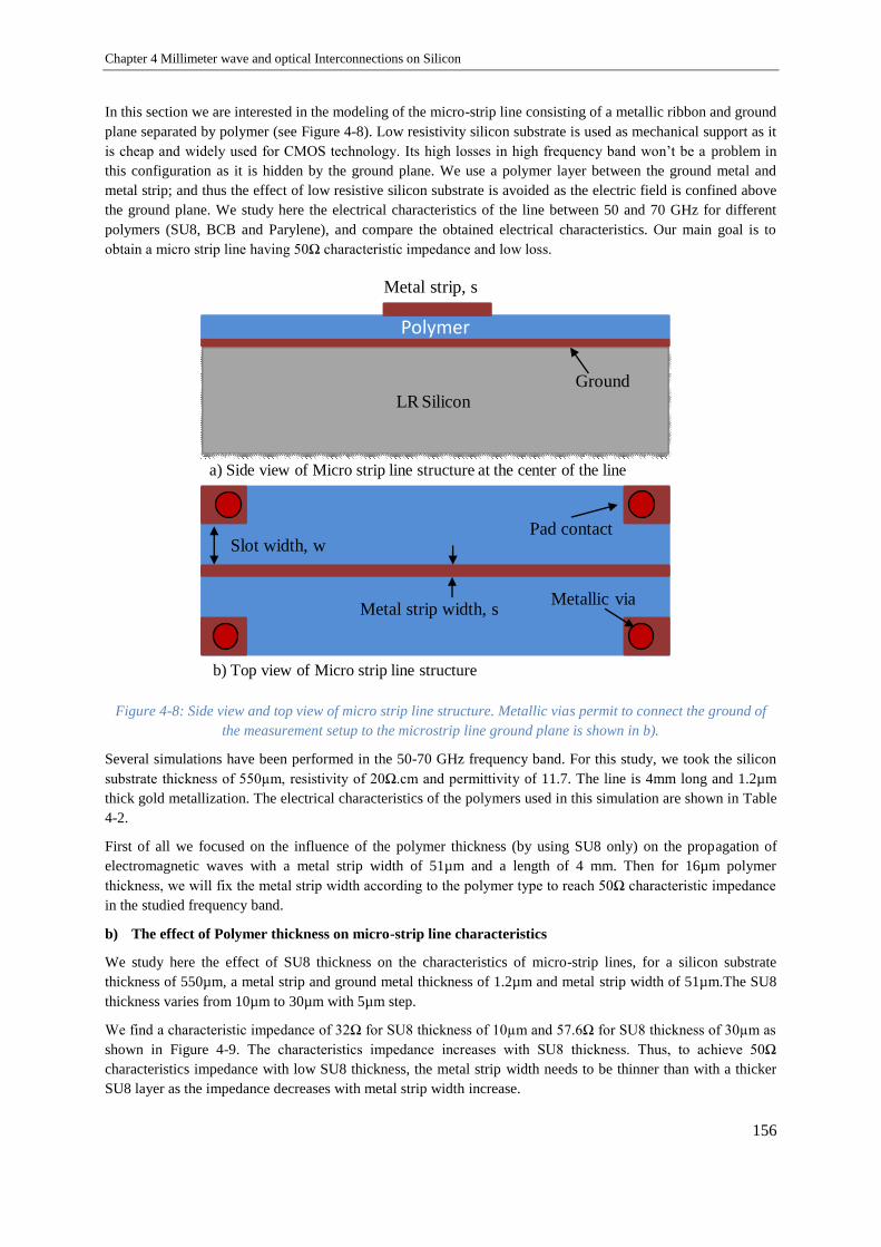
Chapter 4 Millimeter wave and optical Interconnections on Silicon
156
In this section we are interested in the modeling of the micro-strip line consisting of a metallic ribbon and ground
plane separated by polymer (see Figure 4-8). Low resistivity silicon substrate is used as mechanical support as it
is cheap and widely used for CMOS technology. Its high losses in high frequency band won’t be a problem in
this configuration as it is hidden by the ground plane. We use a polymer layer between the ground metal and
metal strip; and thus the effect of low resistive silicon substrate is avoided as the electric field is confined above
the ground plane. We study here the electrical characteristics of the line between 50 and 70 GHz for different
polymers (SU8, BCB and Parylene), and compare the obtained electrical characteristics. Our main goal is to
obtain a micro strip line having 50Ω characteristic impedance and low loss.
Figure 4-8: Side view and top view of micro strip line structure. Metallic vias permit to connect the ground of
the measurement setup to the microstrip line ground plane is shown in b).
Several simulations have been performed in the 50-70 GHz frequency band. For this study, we took the silicon
substrate thickness of 550µm, resistivity of 20Ω.cm and permittivity of 11.7. The line is 4mm long and 1.2µm
thick gold metallization. The electrical characteristics of the polymers used in this simulation are shown in Table
4-2.
First of all we focused on the influence of the polymer thickness (by using SU8 only) on the propagation of
electromagnetic waves with a metal strip width of 51µm and a length of 4 mm. Then for 16µm polymer
thickness, we will fix the metal strip width according to the polymer type to reach 50Ω characteristic impedance
in the studied frequency band.
b) The effect of Polymer thickness on micro-strip line characteristics
We study here the effect of SU8 thickness on the characteristics of micro-strip lines, for a silicon substrate
thickness of 550µm, a metal strip and ground metal thickness of 1.2µm and metal strip width of 51µm.The SU8
thickness varies from 10µm to 30µm with 5µm step.
We find a characteristic impedance of 32Ω for SU8 thickness of 10µm and 57.6Ω for SU8 thickness of 30µm as
shown in Figure 4-9. The characteristics impedance increases with SU8 thickness. Thus, to achieve 50Ω
characteristics impedance with low SU8 thickness, the metal strip width needs to be thinner than with a thicker
SU8 layer as the impedance decreases with metal strip width increase.
LR Silicon
Polymer
Metal strip, s
Ground
Slot width, w
Metal strip width, s
Pad contact
a) Side view of Micro strip line structure at the center of the line
b) Top view of Micro strip line structure
Metallic via

Chapter 4 Millimeter wave and optical Interconnections on Silicon
157
Figure 4-9: Micro-strip line characteristic impedance versus frequency for variable SU8 thickness and metal
strip width s=51µm as it is deduced from the simulation
As it is shown in Figure 4-10 the attenuation decreases as the polymer thickness increases from 10µm to 30µm.
It was expected as, when the polymer thickness is high enough, the micro-strip mode electric field is confined
properly between the two metals, and the radiation in the air is reduced (reduced radiation loss). Besides, the
attenuation slightly increases with frequency.
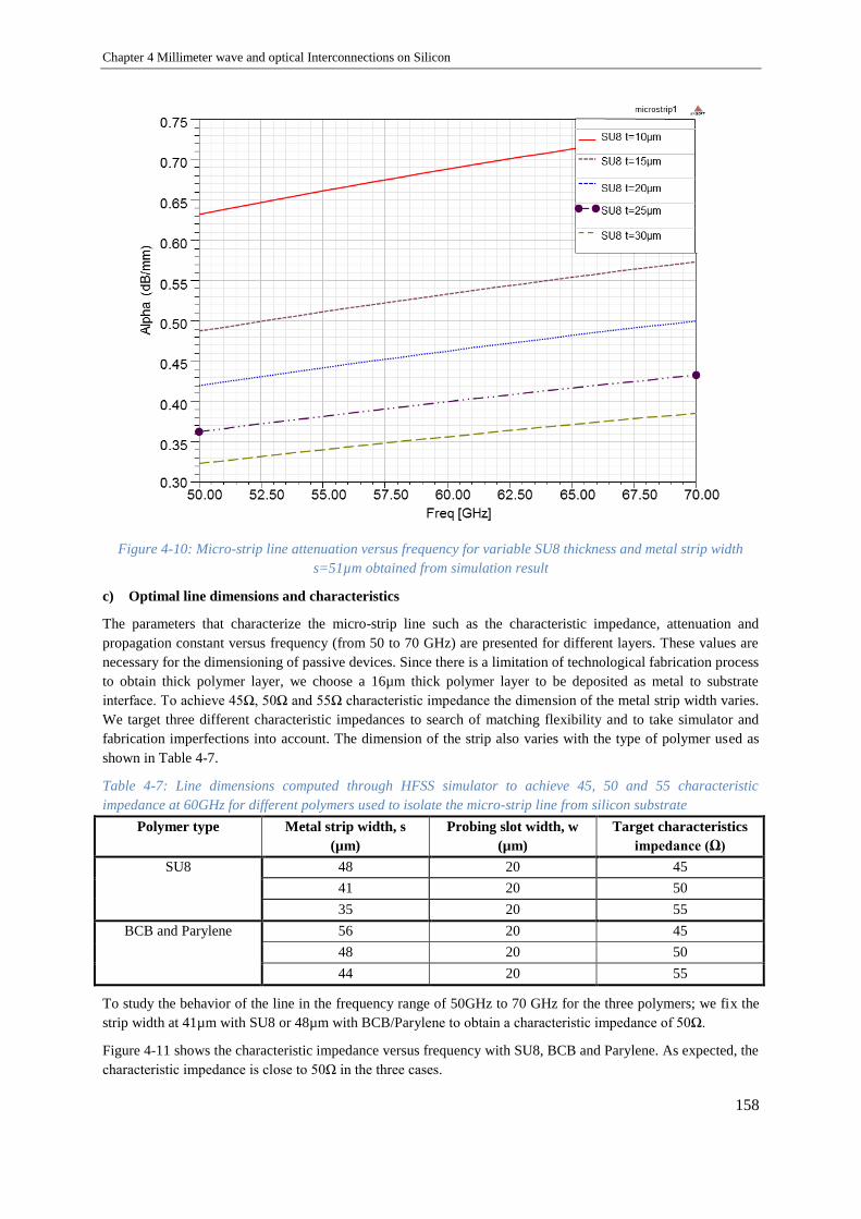
Chapter 4 Millimeter wave and optical Interconnections on Silicon
158
Figure 4-10: Micro-strip line attenuation versus frequency for variable SU8 thickness and metal strip width
s=51µm obtained from simulation result
c) Optimal line dimensions and characteristics
The parameters that characterize the micro-strip line such as the characteristic impedance, attenuation and
propagation constant versus frequency (from 50 to 70 GHz) are presented for different layers. These values are
necessary for the dimensioning of passive devices. Since there is a limitation of technological fabrication process
to obtain thick polymer layer, we choose a 16µm thick polymer layer to be deposited as metal to substrate
interface. To achieve 45Ω, 50Ω and 55Ω characteristic impedance the dimension of the metal strip width varies.
We target three different characteristic impedances to search of matching flexibility and to take simulator and
fabrication imperfections into account. The dimension of the strip also varies with the type of polymer used as
shown in Table 4-7.
Table 4-7: Line dimensions computed through HFSS simulator to achieve 45, 50 and 55 characteristic
impedance at 60GHz for different polymers used to isolate the micro-strip line from silicon substrate
Polymer type Metal strip width, s
(µm)
Probing slot width, w
(µm)
Target characteristics
impedance (Ω)
SU8 48 20 45
41 20 50
35 20 55
BCB and Parylene 56 20 45
48 20 50
44 20 55
To study the behavior of the line in the frequency range of 50GHz to 70 GHz for the three polymers; we fix the
strip width at 41µm with SU8 or 48µm with BCB/Parylene to obtain a characteristic impedance of 50Ω.
Figure 4-11 shows the characteristic impedance versus frequency with SU8, BCB and Parylene. As expected, the
characteristic impedance is close to 50Ω in the three cases.
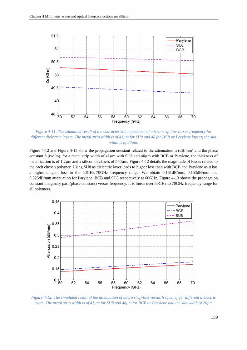
Chapter 4 Millimeter wave and optical Interconnections on Silicon
159
Figure 4-11: The simulated result of the characteristic impedance of micro-strip line versus frequency for
different dielectric layers. The metal strip width is of 41µm for SU8 and 48 for BCB or Parylene layers; the slot
width is of 20µm.
Figure 4-12 and Figure 4-13 show the propagation constant related to the attenuation α (dB/mm) and the phase
constant β (rad/m), for a metal strip width of 41µm with SU8 and 48µm with BCB or Parylene, the thickness of
metallization is of 1.2µm and a silicon thickness of 550µm. Figure 4-12 details the magnitude of losses related to
the each chosen polymer. Using SU8 as dielectric layer leads to higher loss than with BCB and Parylene as it has
a higher tangent loss in the 50GHz-70GHz frequency range. We obtain 0.151dB/mm, 0.153dB/mm and
0.325dB/mm attenuation for Parylene, BCB and SU8 respectively at 60GHz. Figure 4-13 shows the propagation
constant imaginary part (phase constant) versus frequency. It is linear over 50GHz to 70GHz frequency range for
all polymers.
Figure 4-12: The simulated result of the attenuation of micro strip-line versus frequency for different dielectric
layers. The metal strip width is of 41µm for SU8 and 48µm for BCB or Parylene and the slot width of 20µm.

Chapter 4 Millimeter wave and optical Interconnections on Silicon
160
Figure 4-13: The simulated result of the phase constant of micro-strip line versus frequency for different
dielectric layers. The metal strip width is of 41µm for SU8 and 48µm for BCB or Parylene and the slot width of
20µm.
Both transverse and longitudinal electric field distribution of microstrip line are shown in Figure 4-14 when SU8
is used as dielectric layer. We observe that the electric field is well confined between the strip line and the
ground metal. As there is no energy propagating through the low resistive silicon, the attenuation is kept small.
The good field propagation is noticed for example at 60GHz and 70GHz in Figure 4-14 a) and c) respectively as
the electric field distribution remains quite similar along the line.
Figure 4-14: Electric field amplitude (V / m) and vector in the transverse and longitudinal planes of the micro-
strip line with SU8 layer for strip width of 41µm.
In Table 4-8 we summarize the simulation results at 60GHz for 16µm thick polymer and micro-strip lines of
characteristics impedance 45Ω, 50Ω and 55Ω. To achieve these different characteristic impedances we modify
the metal strip width from 48µm to 41µm as shown in Table 4-8. The corresponding attenuations are also
presented in the same table. We observe higher attenuations and smaller strip widths are obtained with SU8,
whereas similar results are obtained with BCB and Parylene
50 52 54 56 58 60 62 64 66 68 701400
1500
1600
1700
1800
1900
2000
2100
2200
2300
Frequency (GHz)
Pro
pagation c
onsta
nt
Parlyene
SU8
BCB
F=70GHz
F=60GHz
a) Electric field amplitude in the transverse plane at 60GHz
F=60GHz
F=60GHz
b) Electric field vector in the transverse plane at 60GHz
c) Electric field amplitude in the transverse plane at 70GHz d) Electric field amplitude in the longitudinal plane at 60GHz

Chapter 4 Millimeter wave and optical Interconnections on Silicon
161
Table 4-8: Summary of dimension estimations using HFSS simulator of micro-strip line with different polymers
and for several targeted characteristic impedances at 60GHz. The propagation attenuation is also evaluated
using HFSS simulator at 60GHz.
Polymer type Metal strip width, s
(µm)
Probing slot width, w
(µm)
Target
characteristics
impedance (Ω)
Attenuation
(dB/mm)
SU8 48 20 45.5 0.31
41 20 50.7 0.33
35 20 55.5 0.37
BCB 56 20 45.1 0.15
48 20 49.8 0.153
44 20 55.8 0.16
Parylene 56 20 45.5 0.15
48 20 50.2 0.15
44 20 55.2 0.155
4.2.5 Grounded Coplanar Line
a) Structure explanation
In this section we study the grounded coplanar line. As the coplanar waveguide, it consists of a metal strip along
which the signal propagates and the two metallic planes besides connected to the ground. The difference with the
coplanar waveguide leads in the presence of a ground plane hiding the low resistive silicon substrate, so that the
signal can propagate within the polymer deposited above this inferior ground plane as shown in Figure 4-15. We
aim to use this line for high frequency applications. In this case, the propagation takes place in the polymer and
in the air, so the propagation medium can be considered as inhomogeneous. We will use low resistivity silicon
substrate as mechanical support as it is cheap and widely used for CMOS technology. We use a polymer layer
between the ground metal and metal strip; and thus the effect of low resistive silicon substrate is avoid as the
electric field is confined within the two slots around the metal strip. The polymer is removed in the slot in order
to minimize the propagation attenuation. We study here the electrical characteristics of the line between 50 and
70 GHz for different polymers (SU8, BCB and Parylene), and compare the electrical characteristics in each
configuration. Our main goal is to obtain a grounded coplanar line having 50Ω characteristics impedance and
low loss.
Figure 4-15: Cross sectional view of grounded coplanar line structure
To characterize such transmission line, we performed several simulations in the 50-70 GHz frequency band,
looking more specifically at its behavior around 60 GHz. In this study, we consider a silicon substrate thickness
of 550µm, resistivity of 20Ω.cm and permittivity of 11.7. The line is 4mm long and gold thickness is of 1.2µm.
Metal dimensions will be chosen according to the polymer layer and the target characteristic impedance. The
electrical characteristics of the polymers used in simulations are shown in Table 4-2.
LR Silicon
Polymer
metal strip width, s
ground metal
Polymer Polymer
slot widthw

Chapter 4 Millimeter wave and optical Interconnections on Silicon
162
We saw that the thickness of the polymer deposited between the upper and the lower metallic layers has similar
effect as already observed with the micro-strip line.
b) Optimal line dimensions and characteristics of grounded coplanar lines
The characteristic impedance, attenuation and phase constant of grounded coplanar line versus frequency (from
50 to 70 GHz) are presented when SU8, BCB and Parylene are used as dielectric layers. These values are
necessary for the line dimensioning. Due to the technological fabrication process limitations, we choose 16µm
thick polymer rather than a thicker polymer layer. For matching flexibility with different circuit interconnections
and taking fabrication errors into account; we targeted 45Ω, 50Ω and 55Ω characteristic impedances. Thus, the
dimensions of the metal strip and air gap widths vary accordingly. These dimensions also vary with the polymer
used as shown in Table 4-9.
Table 4-9: Grounded coplanar line dimensions determined using HFSS simulations to get characteristic
impedances of 45Ω, 50Ω, 55Ω at 60GHz for different polymer layers.
Polymer type Metal strip width, s
(µm)
Probing slot width, w
(µm)
Target characteristics
impedance (Ω)
SU8 90 30 45
80 30 50
72 30 55
BCB and Parylene 100 30 45
88 30 50
79 30 55
To study the behavior of the line between 50GHz and 70 GHz, we fix the strip width at 80µm with SU8 or 88µm
with BCB/Parylene. We take a slot width of 30µm. For these specifications the characteristics impedance is of
50Ω.
Figure 4-16 shows the characteristics impedance versus frequency for SU8, BCB and Parylene. The
characteristic impedance is almost constant from 50GHz to 70GHz and it is a slightly higher with Parylene layer.
Figure 4-16: Characteristic impedance vs frequency for different polymers as it is extracted from HFSS
simulator
Figure 4-17 and Figure 4-18 show the propagation constant real and imaginary parts, namely the attenuation α
(dB/mm) and the phase constant β (rad/m), for a metal strip width of 80µm with SU8 and 88µm with BCB or

Chapter 4 Millimeter wave and optical Interconnections on Silicon
163
Parylene, a metallization thickness of 1.2µm and a substrate thickness of 550µm. Figure 4-16 details the
magnitude of losses for each chosen polymer. With SU8 the grounded coplanar line has higher losses than with
BCB and Parylene due to the higher tangent loss of BCB in the studied frequency range. We obtain attenuation
of 0.135dB/mm, 0.15dB/mm and 0.31dB/mm for Parylene, BCB and SU8 respectively at 60GHz. The signal loss
slightly increases with frequency regardless of the polymer type. The slop of the attenuation curve with BCB and
Parylene are equal and it is smaller than with SU8. This indicates that the use of BCB and Parylene as a
dielectric layer in Grounded coplanar line highly minimizes the losses in the 50-70GHz frequency band
compared to SU8.
Figure 4-17: The simulated result of the attenuation of grounded coplanar line versus frequency for different
dielectric layers. The metal strip width is of 80µm for SU8 and 88µm for BCB or Parylene, whereas the slot
width is of 30µm.
Figure 4-17 shows the imaginary part of the propagation constant versus frequency. It is linear over 50GHz to
70GHz frequency range.
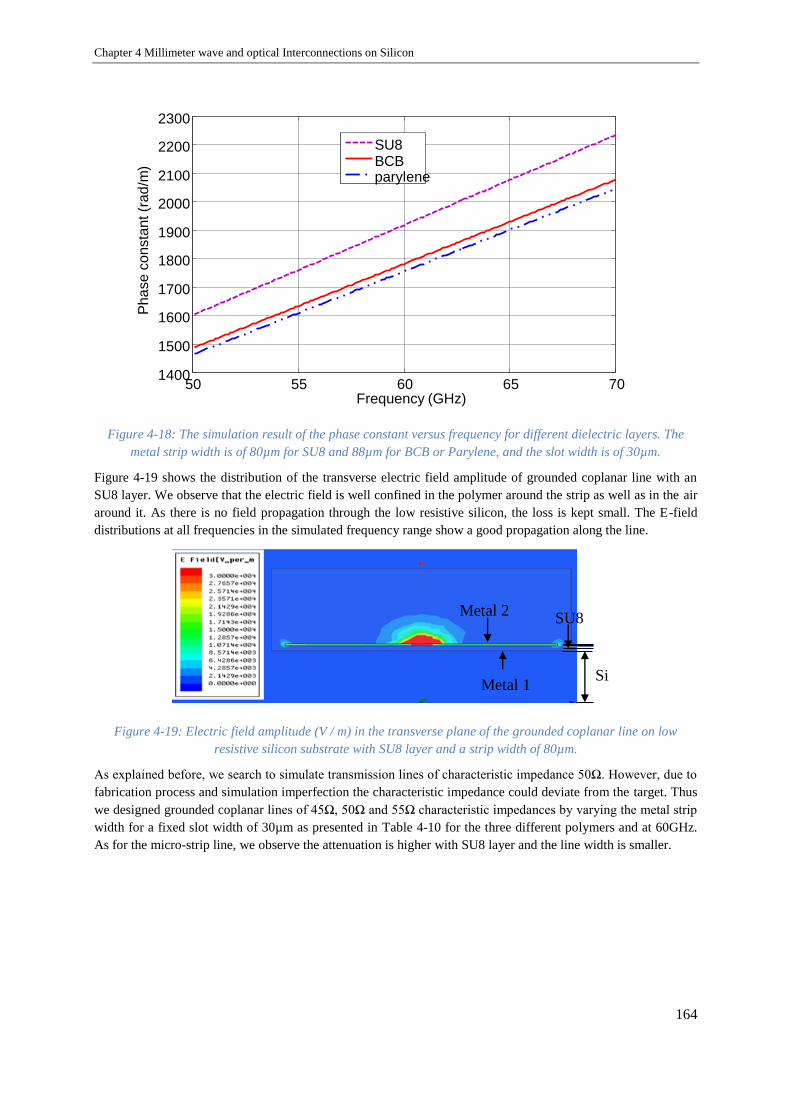
Chapter 4 Millimeter wave and optical Interconnections on Silicon
164
Figure 4-18: The simulation result of the phase constant versus frequency for different dielectric layers. The
metal strip width is of 80µm for SU8 and 88µm for BCB or Parylene, and the slot width is of 30µm.
Figure 4-19 shows the distribution of the transverse electric field amplitude of grounded coplanar line with an
SU8 layer. We observe that the electric field is well confined in the polymer around the strip as well as in the air
around it. As there is no field propagation through the low resistive silicon, the loss is kept small. The E-field
distributions at all frequencies in the simulated frequency range show a good propagation along the line.
Figure 4-19: Electric field amplitude (V / m) in the transverse plane of the grounded coplanar line on low
resistive silicon substrate with SU8 layer and a strip width of 80µm.
As explained before, we search to simulate transmission lines of characteristic impedance 50Ω. However, due to
fabrication process and simulation imperfection the characteristic impedance could deviate from the target. Thus
we designed grounded coplanar lines of 45Ω, 50Ω and 55Ω characteristic impedances by varying the metal strip
width for a fixed slot width of 30µm as presented in Table 4-10 for the three different polymers and at 60GHz.
As for the micro-strip line, we observe the attenuation is higher with SU8 layer and the line width is smaller.
50 55 60 65 701400
1500
1600
1700
1800
1900
2000
2100
2200
2300
Frequency (GHz)
Ph
ase
co
nsta
nt (r
ad
/m)
SU8BCBparylene
SiMetal 1
Metal 2SU8

Chapter 4 Millimeter wave and optical Interconnections on Silicon
165
Table 4-10: Summary of dimensions of grounded coplanar line estimated using HFSS simulator for different
polymer layers and several targeted characteristic impedances at 60GHz. The losses in the line also evaluated
via HFSS simulator at 60GHz are presented.
Polymer type Metal strip width, s
(µm)
Slot width, w (µm) Target
characteristics
impedance (Ω)
Attenuation
(dB/mm)
SU8 90 30 45.1 0.31
80 30 50.2 0.31
72 30 55.2 0.31
BCB 100 30 44.5 0.15
88 30 50.2 0.15
79 30 54.6 0.15
Parylene 100 30 45.4 0.14
88 30 50.6 0.14
79 30 55.5 0.15

Chapter 4 Millimeter wave and optical Interconnections on Silicon
166
4.3 Optical Waveguide
The optical waveguide is the fundamental element that interconnects various devices of an optical integrated
circuit, just as the previously presented lines do in an electrical integrated circuit. However, whereas in these
lines one single propagation mode appears in the considered use conditions, several distinct optical modes can
propagate in an optical waveguide. A mode, in this sense, is a spatial distribution of optical energy associated to
propagation characteristics. In this section, simulation results of optical waveguides are presented. First we
present the simulation results of polymer based optical waveguides and then of optical waveguides based on
different oxide layers of SiGe BiCMOS technology.
4.3.1 Polymer based optical waveguide
Polymer materials are used for optical interconnections at the board level. Using polymers such as SU-8 and
BCB is foreseen to be very efficient for inter-chip interconnections with micro-meter size waveguides, while
being furthermore compatible with lithographic interconnections for electrical interfaces. SU8 and BCB exhibit
optical attenuation in 1dB/cm range in the near-IR region [79] [80]. Proven to be good candidates for optical
waveguides within a chip, they offer the promise of an excellent convergence with the lithographic
interconnections for electronics. The processing properties of photoresists enable the design of 3D shapes.
Combined with wafer-level packaging, these waveguides demonstrate very good passive coupling capabilities.
Polymer waveguides could couple to on-chip embedded waveguides that could be based on III-V, Si3N4, Si02
or SOI.
Thus, in this thesis we model an optical waveguide based on SU8 and parylene. We simulate optical waveguide
of 5µm long with a rectangular SU8 core of 2µmx3µm as sketched in Figure 4-20. SU8 is associated with
Parylene or BCB to design the clad of the waveguide, SU8 having the higher optical index. The core of SU8 has
the higher optical index (1.5843) and is taken away from silicon substrate of high refractive index by using a
layer of parylene that has a lower refractive index (of 1.5); the structure is laterally surrounded by air. Optical
propagation is guided within the core of higher refractive index due to Snell’s law of refraction and total internal
reflection.
Figure 4-20: Simulated structure of optical waveguide over low resistive silicon substrate. Due to symmetry
properties in regard to xOz plane, only the half of the structure is simulated
1.5µm
5µm2.5µm
3µm
5µm
2µm
parylene
SU8
Si
xy
z
x
zz
y
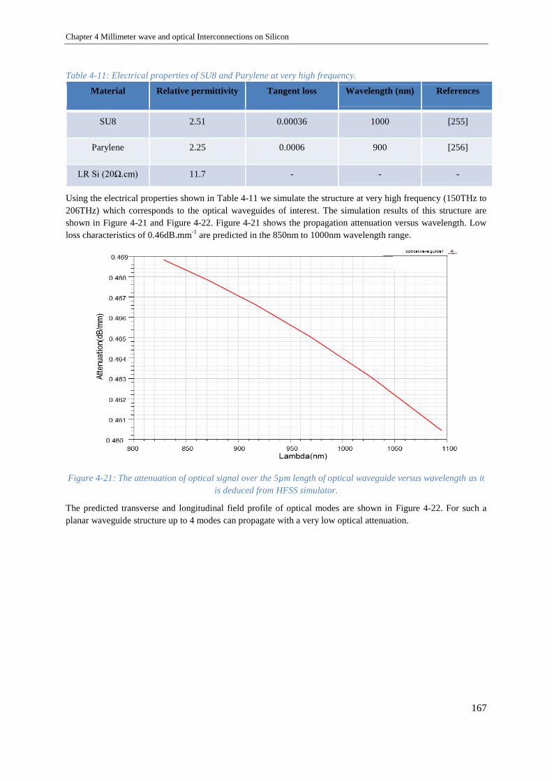
Chapter 4 Millimeter wave and optical Interconnections on Silicon
167
Table 4-11: Electrical properties of SU8 and Parylene at very high frequency.
Material Relative permittivity Tangent loss Wavelength (nm) References
SU8 2.51 0.00036 1000 [255]
Parylene 2.25 0.0006 900 [256]
LR Si (20Ω.cm) 11.7 - - -
Using the electrical properties shown in Table 4-11 we simulate the structure at very high frequency (150THz to
206THz) which corresponds to the optical waveguides of interest. The simulation results of this structure are
shown in Figure 4-21 and Figure 4-22. Figure 4-21 shows the propagation attenuation versus wavelength. Low
loss characteristics of 0.46dB.mm-1
are predicted in the 850nm to 1000nm wavelength range.
Figure 4-21: The attenuation of optical signal over the 5µm length of optical waveguide versus wavelength as it
is deduced from HFSS simulator.
The predicted transverse and longitudinal field profile of optical modes are shown in Figure 4-22. For such a
planar waveguide structure up to 4 modes can propagate with a very low optical attenuation.

Chapter 4 Millimeter wave and optical Interconnections on Silicon
168
Figure 4-22: Transverse electric field profile at the excitation port and longitudinal electric field of polymer
base optical wave guide at 950nm wavelength.
4.3.2 SiN and SiO2 based optical waveguide for on-chip interconnections
We established a partnership with the team of Pr. Snyman in the University of South-Africa (UNISA) and
formerly in the Tshwane University of Technology (TUT). We present here the results of this collaboration in
designing optical waveguides directly integrated in the Telefunken SiGe Technology.
We have taken advantage of different oxide layers of the technology to develop the waveguides. The designed
waveguide will be implemented in a full on-chip optical links presented in chapter 5. The development of an
efficient Silicon based waveguide at submicron wavelengths presents major challenges, particularly due to
higher absorption and scattering effects at short wavelengths. We have hence extensively studied three different
waveguide structures. Kingsley Ogudo made the simulations, while Pr. Snyman and Dr. Polleux made the
layouts. My contribution was on the characterization.
1. Simulations of the optical waveguide Design 1 (OWGD1)
The first design test structure is shown in Figure 4-23a) and b). The waveguide structure is placed in a
TetraEthylOrthosilicate (TEOS1) plasma deposited layer. A channel crevice is etched in the TEOS1 layer (n =
1.46) and then filled with a second TEOS layer (TEOS2). This layer is then densified by a thermal process,
increasing its refractive index to about 1.48. A V-shaped cross-section (shown Figure 4-23 b) as defined by built-
in processing procedures was chosen in order to ensure the highest radiation coupling of the optical source,
which is of submicron dimension and presents a spherical radiation shape, and which is positioned slightly
subsurface of the surface of the optical source columnar structure. This technology is well suited to obtain single
mode waveguides which are transparent from 450nm to 850nm wavelengths and Figure 4-23 shows such a
design. The typical layers thickness as offered by Telefunken process procedures was used during our design.
The side delimitation of the waveguide is facilitated by reactive ion etching or by plasma etching of all the
oxides down to the silicon substrate interface. This minimizes the lateral parasitic capacitive couplings with the
surrounding oxide layers which might arise due to the RF modulation at the optical source.
1st mode 2nd mode 3rd mode 4th mode 5th mode
1st mode 2nd mode 3rd mode 4th mode 5th mode
a) Transversal view of electric field distribution
b) Longitudinal view of electric field distribution

Chapter 4 Millimeter wave and optical Interconnections on Silicon
169
Figure 4-23: Waveguide structure for design 1 (a) Side view section (b) Cross-sectional view. All dimensions are
in micro meters
For the first design test structure (OWGD1) shown in Figure 4-23, we simulated the optical waveguide structure
designed with the TEOS1 and TEOS2 areas, where TEOS2 has a higher optical index due to densification
strategy used to increase the optical index from 1.46 to 1.48. The core of high refractive index (1.48) is
surrounded by silicon oxide of refractive index 1.46, thus optical waves are guided within the core of higher
refractive index due to Snell’s law of refraction and total internal reflection.
R-Soft simulation results of this structure are shown in Figure 4-24 at 750nm wavelength. Figure 4-24 shows
very low loss propagation and weak influence of higher order modes as the field distribution is very closed to the
one of the first optical mode. Figure 4-24 a) displays E-field amplitude versus x and z as a 2D color-coded
contour map, and Figure 4-24 b) is a 3D contour graph that displays electric field amplitude versus x and z in 3D
contour graph with color coding to indicate amplitude value.
Figure 4-24: Waveguide simulation (a) Contour Map (XZ), (b) height-coded E-field amplitude
2. Simulations of optical waveguide Design 2 (OWGD2)
Figure 4-25 shows a schematic of the second design, where vertical slots are predefined by a poly silicon
window obtained using Telefunken technological process. This leads to a 45 degree hollow in the Tetraethyl
orthosilicate1 (TEOS1) oxide before positioning the silicon nitride layer. The etched crevice of 0.4 micron in the
first TEOS layer is filled up with a silicon nitride layer, followed by further CVD deposited TEOS oxide over-
layer. Hence a high refractive index core of n = 2.4 is formed by silicon nitride with a surrounding index of n =
1.46.
By tailor made designing the dimensions of the various layers in the waveguide, a V-shaped waveguide profile is
achieved. This enables vertical lowering of the higher index core of the waveguide into the silicon layers, which
facilitates a good vertical alignment of the core of the waveguide with the light emission spot of the optical
source.
0.4 0.4
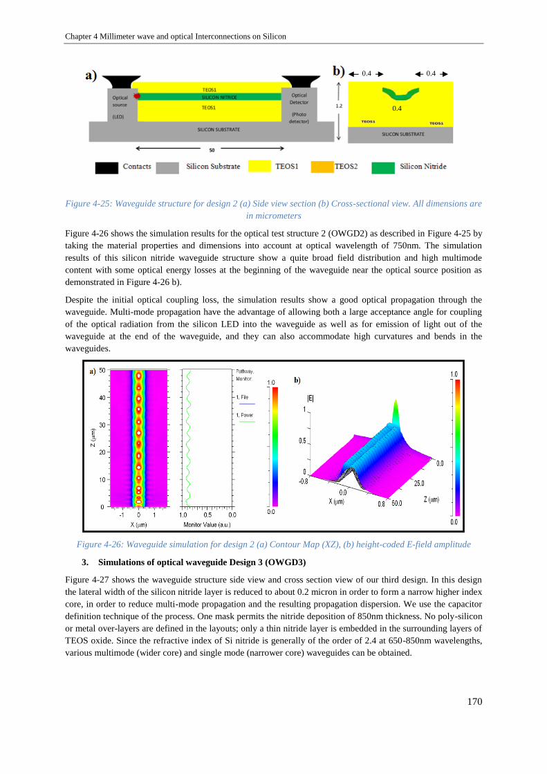
Chapter 4 Millimeter wave and optical Interconnections on Silicon
170
Figure 4-25: Waveguide structure for design 2 (a) Side view section (b) Cross-sectional view. All dimensions are
in micrometers
Figure 4-26 shows the simulation results for the optical test structure 2 (OWGD2) as described in Figure 4-25 by
taking the material properties and dimensions into account at optical wavelength of 750nm. The simulation
results of this silicon nitride waveguide structure show a quite broad field distribution and high multimode
content with some optical energy losses at the beginning of the waveguide near the optical source position as
demonstrated in Figure 4-26 b).
Despite the initial optical coupling loss, the simulation results show a good optical propagation through the
waveguide. Multi-mode propagation have the advantage of allowing both a large acceptance angle for coupling
of the optical radiation from the silicon LED into the waveguide as well as for emission of light out of the
waveguide at the end of the waveguide, and they can also accommodate high curvatures and bends in the
waveguides.
Figure 4-26: Waveguide simulation for design 2 (a) Contour Map (XZ), (b) height-coded E-field amplitude
3. Simulations of optical waveguide Design 3 (OWGD3)
Figure 4-27 shows the waveguide structure side view and cross section view of our third design. In this design
the lateral width of the silicon nitride layer is reduced to about 0.2 micron in order to form a narrow higher index
core, in order to reduce multi-mode propagation and the resulting propagation dispersion. We use the capacitor
definition technique of the process. One mask permits the nitride deposition of 850nm thickness. No poly-silicon
or metal over-layers are defined in the layouts; only a thin nitride layer is embedded in the surrounding layers of
TEOS oxide. Since the refractive index of Si nitride is generally of the order of 2.4 at 650-850nm wavelengths,
various multimode (wider core) and single mode (narrower core) waveguides can be obtained.
0.4 0.4
0.4

Chapter 4 Millimeter wave and optical Interconnections on Silicon
171
Figure 4-27: Waveguide structure for design 3 (a) Side view section (b) Cross-sectional view. All dimensions are
in micrometers
We simulated the narrower silicon nitride core waveguide design 3 (OWGD3) as in Figure 4-27 at optical
wavelength of 750nm. From the simulation results presented in Figure 4-28, OWGD3 yields narrower single
mode propagation, with low losses and very low multimode content. Although it is more difficult to couple light
into the waveguide in single mode operation, we see the loss along the waveguide is lower in single mode
propagation. This will enable high modulation bandwidth to be achieved in this kind of narrower core
waveguide.
Figure 4-28: Waveguide simulation for design 3 (a) Contour Map (XZ), (b) height-coded E-field amplitude
Figure 4-29 shows the predicted distribution of transverse field amplitude for a 0.2 micron diameter nitride core
waveguide embedded in a silicon oxide surrounding matrix. Low loss characteristics of 0.65dBcm-1
are
predicted, taking the material properties into account.
0.4 0.4
0.2

Chapter 4 Millimeter wave and optical Interconnections on Silicon
172
Figure 4-29: Transverse field profile for a silicon nitride based waveguide with a silicon nitride core of 0.2
micron diameter embedded in a 1 micron diameter silicon oxide cladding.
These analyses show that both silicon nitride and TEOS offer good possibilities for low loss light transmission in
the wavelength range of 650nm to 850nm. The experimental results by A. Gorin [258] on thin film planar silicon
nitride waveguide show the variation of the attenuation versus wavelengths; with high losses of 4.3dB.cm-1
at
530nm against losses of only about 1dB.cm-1
at 650nm and 0.1dB.cm-1
at 750nm. This suggest that compromises
could be made with respect to the choice of operating wavelength, anticipated waveguide losses and detection
efficiency while using CMOS technology. At shorter wavelengths both silicon nitride and TEOS reveal higher
absorption coefficients with good efficiency of silicon detectors for small detection volumes, while longer
wavelengths reveal lower transmission losses but with lower detection efficiency of silicon detectors per unit
silicon volume.
Especially the transparency of silicon-nitride based waveguides on 750nm-850nm range, offers remarkable
possibilities with regard to the integration of optical communication, data transfer and photonic systems directly
into CMOS integrated circuitry. In particular, this technology is very attractive for the anticipated low levels of
technological complexity compared to the incorporation of III-V or hybrid III-V with silicon technologies.
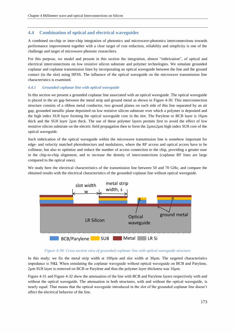
Chapter 4 Millimeter wave and optical Interconnections on Silicon
173
4.4 Combination of optical and electrical waveguides
A combined on-chip or inter-chip integration of photonics and microwave-photonics interconnections towards
performance improvement together with a clear target of cost reduction, reliability and simplicity is one of the
challenge and target of microwave photonic researchers.
For this purpose, we model and present in this section the integration, almost “imbrication”, of optical and
electrical interconnections on low resistive silicon substrate and polymer technologies. We simulate grounded
coplanar and coplanar transmission lines by incorporating an optical waveguide between the line and the ground
contact (in the slot) using HFSS. The influence of the optical waveguide on the microwave transmission line
characteristics is examined.
4.4.1 Grounded coplanar line with optical waveguide
In this section we present a grounded coplanar line associated with an optical waveguide. The optical waveguide
is placed in the air gap between the metal strip and ground metal as shown in Figure 4-30. This interconnection
structure consists of a ribbon metal conductor, two ground planes on each side of this line separated by an air
gap, grounded metallic plane deposited on low resistive silicon substrate over which a polymer is deposited and
the high index SU8 layer forming the optical waveguide core in the slot. The Parylene or BCB layer is 16µm
thick and the SU8 layer 2µm thick. The use of these polymer layers permits first to avoid the effect of low
resistive silicon substrate on the electric field propagation then to form the 2µmx2µm high index SU8 core of the
optical waveguide.
Such imbrication of the optical waveguide within the microwave transmission line is somehow important for
edge- and velocity matched photodetectors and modulators, where the RF access and optical access have to be
collinear, but also to optimize and reduce the number of access connection to the chip, providing a greater ease
in the chip-to-chip alignment, and to increase the density of interconnections (coplanar RF lines are large
compared to the optical ones).
We study here the electrical characteristics of the transmission line between 50 and 70 GHz, and compare the
obtained results with the electrical characteristics of the grounded coplanar line without optical waveguide.
Figure 4-30: Cross section view of grounded coplanar line with optical waveguide structure
In this study; we fix the metal strip width at 100µm and slot width at 30µm. The targeted characteristics
impedance is 50Ω. When simulating the coplanar waveguide without optical waveguide on BCB and Parylene,
2µm SU8 layer is removed on BCB or Parylene and thus the polymer layer thickness was 16µm.
Figure 4-31 and Figure 4-32 show the attenuation of the line with BCB and Parylene layers respectively with and
without the optical waveguide. The attenuation in both structures, with and without the optical waveguide, is
nearly equal. That means that the optical waveguide introduced in the slot of the grounded coplanar line doesn’t
affect the electrical behavior of the line.
LR Silicon
metal strip width, s
ground metal Optical waveguide
BCB/Parylene SU8 Metal LR Si
slot widthw

Chapter 4 Millimeter wave and optical Interconnections on Silicon
174
Figure 4-31: The simulation result of grounded coplanar line with and without optical waveguide over BCB
polymer (the optical waveguide is 2µm SU8) attenuation versus frequency
Figure 4-32: The simulation result of grounded coplanar line with and without optical waveguide over Parylene
polymer (the optical waveguide is 2µm SU8) attenuation versus frequency
Figure 4-33 and Figure 4-34 show the characteristic impedance versus frequency for BCB and Parylene layers.
The characteristic impedance in both cases is the same. There is a small difference; this could be attributed to the
deposition of 2µm thick SU8 over 16µm BCB or Parylene.
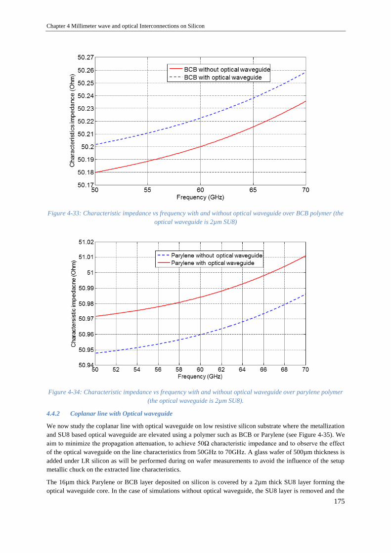
Chapter 4 Millimeter wave and optical Interconnections on Silicon
175
Figure 4-33: Characteristic impedance vs frequency with and without optical waveguide over BCB polymer (the
optical waveguide is 2µm SU8)
Figure 4-34: Characteristic impedance vs frequency with and without optical waveguide over parylene polymer
(the optical waveguide is 2µm SU8).
4.4.2 Coplanar line with Optical waveguide
We now study the coplanar line with optical waveguide on low resistive silicon substrate where the metallization
and SU8 based optical waveguide are elevated using a polymer such as BCB or Parylene (see Figure 4-35). We
aim to minimize the propagation attenuation, to achieve 50Ω characteristic impedance and to observe the effect
of the optical waveguide on the line characteristics from 50GHz to 70GHz. A glass wafer of 500µm thickness is
added under LR silicon as will be performed during on wafer measurements to avoid the influence of the setup
metallic chuck on the extracted line characteristics.
The 16µm thick Parylene or BCB layer deposited on silicon is covered by a 2µm thick SU8 layer forming the
optical waveguide core. In the case of simulations without optical waveguide, the SU8 layer is removed and the

Chapter 4 Millimeter wave and optical Interconnections on Silicon
176
thickness of Parylene or BCB layer becomes 16µm. Parylene or BCB layer permits to minimize the effect of low
resistive silicon on the attenuation of the coplanar waveguide as well as of the optical waveguide. The main
focus is to study the electrical behavior of the coplanar line between 50 and 70 GHz, and compare the result with
the electrical behavior of the coplanar line without optical waveguide. Optical propagation is guided within the
core of higher refractive index SU8.
Figure 4-35: Cross section of coplanar line with optical waveguide
The study of the optical waveguide influence on the line electrical behavior is only performed with Parylene
layer; with a strip width fixed at 200µm and slot width of 30µm. The targeted characteristic impedance is 50Ω in
50GHz-70GHz frequency range.
Figure 4-36 shows the resulting attenuation over the required frequency band as computed using HFSS with and
without optical waveguide. The attenuation in both structures is nearly equal. That means the optical waveguide
introduced in the slot of the coplanar line doesn’t affect the electrical behavior of the line.
Figure 4-36: The simulation result of coplanar line with and without optical waveguide over Parylene polymer
(the optical waveguide is 2µm SU8) attenuation versus frequency
glass
metal Strips
slot air gapw
Metal chuck
BCB/Parylene SU8 Metal LR Si
52 54 56 58 60 62 64 66 68 700
0.2
0.4
0.6
0.8
1
1.2
1.4
1.6
1.8
2
Frequency (GHz)
Att
enu
ati
on
(d
B/m
m)
Parylene without optical waveguide
Parylene with optical waveguide
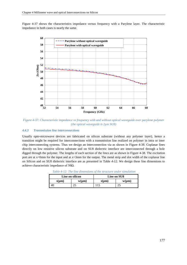
Chapter 4 Millimeter wave and optical Interconnections on Silicon
177
Figure 4-37 shows the characteristics impedance versus frequency with a Parylene layer. The characteristic
impedance in both cases is nearly the same.
Figure 4-37: Characteristic impedance vs frequency with and without optical waveguide over parylene polymer
(the optical waveguide is 2µm SU8)
4.4.3 Transmission line interconnections
Usually opto-microwave devices are fabricated on silicon substrate (without any polymer layer), hence a
transition might be required for interconnections with a transmission line realized on polymer in intra or inter
chip interconnecting systems. Thus we design an interconnection via as shown in Figure 4-38. Coplanar lines
directly on low resistive silicon substrate and on SU8 dielectric interface are interconnected through a hole
digged through the polymer. The lengths of each section of the lines are as shown in Figure 4-38. The excitation
port are at x=0mm for the input and at x=3mm for the output. The metal strip and slot width of the coplanar line
on Silicon and on SU8 dielectric interface are as presented in Table 4-12. We design these line dimensions to
achieve characteristic impedance of 50Ω.
Table 4-12: The line dimensions of the structure under simulation
52 54 56 58 60 62 64 66 6840
42
44
46
48
50
52
54
56
58
60
Frequency (GHz)
Zo
(Oh
m)
Parylene without optical waveguide
Parylene with optical waveguide
Line on silicon Line on SU8
s(µm) w(µm) s(µm) w(µm)
40 25 115 25
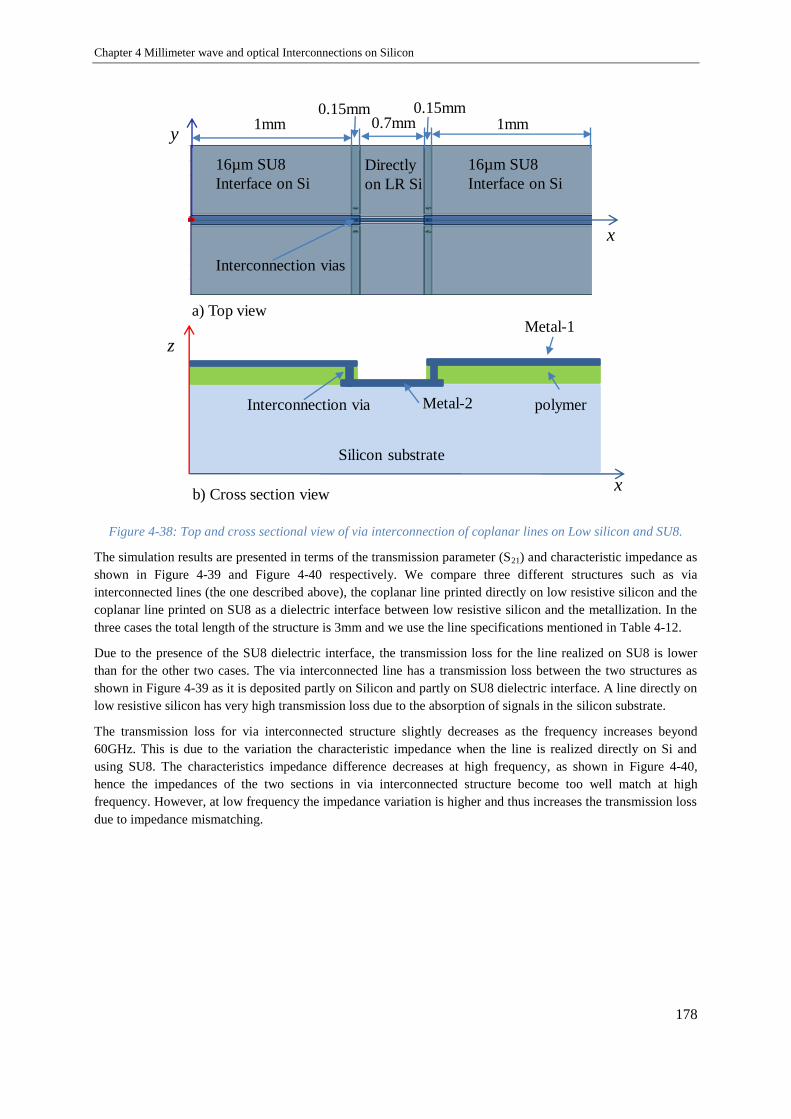
Chapter 4 Millimeter wave and optical Interconnections on Silicon
178
Figure 4-38: Top and cross sectional view of via interconnection of coplanar lines on Low silicon and SU8.
The simulation results are presented in terms of the transmission parameter (S21) and characteristic impedance as
shown in Figure 4-39 and Figure 4-40 respectively. We compare three different structures such as via
interconnected lines (the one described above), the coplanar line printed directly on low resistive silicon and the
coplanar line printed on SU8 as a dielectric interface between low resistive silicon and the metallization. In the
three cases the total length of the structure is 3mm and we use the line specifications mentioned in Table 4-12.
Due to the presence of the SU8 dielectric interface, the transmission loss for the line realized on SU8 is lower
than for the other two cases. The via interconnected line has a transmission loss between the two structures as
shown in Figure 4-39 as it is deposited partly on Silicon and partly on SU8 dielectric interface. A line directly on
low resistive silicon has very high transmission loss due to the absorption of signals in the silicon substrate.
The transmission loss for via interconnected structure slightly decreases as the frequency increases beyond
60GHz. This is due to the variation the characteristic impedance when the line is realized directly on Si and
using SU8. The characteristics impedance difference decreases at high frequency, as shown in Figure 4-40,
hence the impedances of the two sections in via interconnected structure become too well match at high
frequency. However, at low frequency the impedance variation is higher and thus increases the transmission loss
due to impedance mismatching.
x
y
a) Top view
b) Cross section viewx
Silicon substrate
Interconnection via Metal-2 polymer
Metal-1
z
16µm SU8
Interface on Si
16µm SU8
Interface on Si
Directly
on LR Si
Interconnection vias
1mm 1mm0.7mm0.15mm0.15mm

Chapter 4 Millimeter wave and optical Interconnections on Silicon
179
Figure 4-39: The simulation result of the forward transmission (S21) from x=0mm to x=3mm versus frequency
when the line is printed directly on low resistive silicone, fully on SU8 dielectric interface above the Si substrate
and a line partly directly on Silicon and partly on SU8 interconnected through Vias.
Figure 4-40: The simulation result of the characteristic impedance at various frequencies when the line is
simulated directly on low resistive silicon substrate and on SU8 dielectric interface above the substrate
56 58 60 62 64 66-10
-8
-6
-4
-2
0
Frequency (GHz)
S21 (
dB
)
Via interconnection
On SU8
Direct on LR Silicon
56 58 60 62 64 6645
50
55
Freqeuncy (GHz)
Z0 (
Oh
ms)
On SU8
DIrectly on LR Silicon

Chapter 4 Millimeter wave and optical Interconnections on Silicon
180
4.5 Experimental validation of Planar Transmission line
Based on transmission line dimensions optimized through electromagnetic simulations using HFSS software and
polymer optical waveguide dimensions determined through optical simulations using CADENCE software, we
have drawn the schematic patterns/layout of Coplanar, Microstrip and Grounded coplanar transmission lines
along with polymer based optical waveguides. Each type of line is designed with several different lengths so that
the line characteristics can easily be extracted from the measurement results.
The mask is divided into several cells as shown in Figure 4-41 where in each cell all the structures are based on a
same type of transmission line (either coplanar waveguide, microstrip line or grounded coplanar waveguide). For
example C-1 stands for cell one and only comprises coplanar lines on SU8; C-4 stands cell four and contains
coplanar lines on BCB, and C-5 stands for cell five and is reserved for grounded coplanar lines on BCB or
Parylene and so on as detailed in Table 4-13. The same area is used for lines on BCB and Parylene as
simulations have led to the same estimated dimensions associated to the same characteristic impedance; so BCB
and parylene can be deposited alternatively. We have also designed the patterns of grounded coplanar lines and
coplanar lines with an optical waveguide; these structures are located in cells from C-8 to C-12. We have also
inserted patterns with via transitions (C-VT) to test the interconnection/transition between transmission lines on
polymer and transmission lines directly on low resistive silicon. Table 4-13 details for each cell the technology
used. Cells C-9, C-10 and C-11 aim to test the optical waveguide by providing an optical fiber alignment at the
two ends of the optical guide by deep reactive ion etching (DRIE). These cells are also important to study the
coupling between optical and microwave signals (to observe experimentally the effect of optical signal on the
microwave one). Optical waveguides of different sizes, namely (5µm width, 2µm thick) and (10µm width, 2µm
thick), and having different lengths are designed.
Figure 4-41: Schematic view of the mask used to fabricate the transmission lines
C-1
C-2
C-3
C-4
C-6
C-5
C-7
C-8
C-1
0C
-9
C-1
2C
-11
C-Alg C-Alg
C-V
TC
-VT

Chapter 4 Millimeter wave and optical Interconnections on Silicon
181
Table 4-13: Cell numbering and their description.
Cell number Cell name
C-VT Via transition test structure
C-Alg alignment mask
C-1 Coplanar line over SU8
C-2 Grounded coplanar line over SU8
C-3 Coplanar line with 10µm wide optical waveguide
C-4 Coplanar line on BCB or Parylene N
C-5 Grounded coplanar line on BCB or Parylene N
C-6 Microstrip line on BCB or Parylene N
C-7 Microstrip line on SU8
C-8 Grounded coplanar line with 10µm wide optical waveguide
C-9
Coplanar line with 10µm wide optical waveguide plus optical fiber alignment
(need mask 5, see Table 4-14)
C-10
Grounded coplanar line with 5µm and 10µm wide optical waveguides plus
optical fiber alignment (needs mask 5, see Table 4-14)
C-11
Coplanar line with 5µm wide optical waveguide plus optical fiber alignment
(need mask 5, see Table 4-14)
C-12 Coplanar line with 5µm wide optical waveguide
Where: -C stands for Cell: in each cell we have the same type of transmission line
VT stands for via transition
Alg stands for alignment
Figure 4-42 shows the mask with patterns of various types of transmission lines and different layers of the mask
to be used during fabrication. Depending on the technology and the structure that we want to fabricate, we need
up to five masks as it is shown in Figure 4-42 and Table 4-14. Mask1 (L3) is used to print the ground metal that
is deposited on the substrate. Where the patterns are available (dark), the ground metal will be printed. Mask 2
(L6) is used to create via through the polymer in order to have an interconnection between the top layer ground
contact (Metal 2) of microstrip and grounded coplanar line with underneath ground metal (Metal 1) deposited on
substrate. Mask 3 (L2) is used during metal 2 depositions to print the signal line and the top ground layer
contacts. We use Mask 4 (L4) to fabricate the optical waveguides and Mask 5 (L5) is used to etch silicon
substrate so that we can create a cavity to align the optical fiber during on wafer characterization. Table 4-14
shows each mask along with the design layers and their purpose, basic processes and tells about the geometry
and mask relationships.

Chapter 4 Millimeter wave and optical Interconnections on Silicon
182
Figure 4-42: The designed five maskes to fabricate the whole patterns.
Table 4-14: The descriptions of each mask or layer along with their basic process and purpose.
Mask
Number Layer
Mask
Name Purpose Basic process
Metal and
polymer
remove
where mask
is
Geometry
dark where
pattern is
(polarity)
mask 1 L3 Metal_1 to print the
ground metal
photolithography
(+) etch and
protect
clear dark
mask 2 L6 Via via opening photolithography
(-) dark dark
mask 3 L2 Metal_2 Metallization etch and
protected clear dark
mask 4 L4 OPT-
WG
optical
waveguide
SiO2 deposition
and PFR
photolithography,
etching and
protection
clear dark
mask 5 L5 DRIE u-groove
opening etch and protect dark clear
Even though it is possible to fabricate transmission lines on low resistive silicon substrate using polymer as a
dielectric interface between the substrate and the metal as it is presented in [39], we weren’t able to fabricate our
lines with a polymer layer using the proposed fabrication processes in ESIEE clean room. We encountered
difficulties to etch the polymer. RIE would be necessary to perform this process but it is difficult as it is very
long in time and heat up the whole structure a lot. The process development was then stopped here.
Therefore, we only targeted to fabricate a coplanar line on 16µm thick SU8 as a first test, and kept our masks for
a future fabrication using an optimized fabrication process. We keep the SU8 in the air gap (it is not removed as
Mask 1 Mask 2 Mask 3
Mask 4
Mask 5
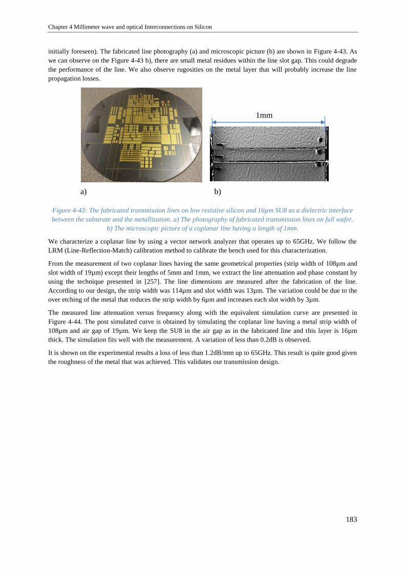
Chapter 4 Millimeter wave and optical Interconnections on Silicon
183
initially foreseen). The fabricated line photography (a) and microscopic picture (b) are shown in Figure 4-43. As
we can observe on the Figure 4-43 b), there are small metal residues within the line slot gap. This could degrade
the performance of the line. We also observe rugosities on the metal layer that will probably increase the line
propagation losses.
Figure 4-43: The fabricated transmission lines on low resistive silicon and 16µm SU8 as a dielectric interface
between the substrate and the metallization. a) The photography of fabricated transmission lines on full wafer.
b) The microscopic picture of a coplanar line having a length of 1mm.
We characterize a coplanar line by using a vector network analyzer that operates up to 65GHz. We follow the
LRM (Line-Reflection-Match) calibration method to calibrate the bench used for this characterization.
From the measurement of two coplanar lines having the same geometrical properties (strip width of 108µm and
slot width of 19µm) except their lengths of 5mm and 1mm, we extract the line attenuation and phase constant by
using the technique presented in [257]. The line dimensions are measured after the fabrication of the line.
According to our design, the strip width was 114µm and slot width was 13µm. The variation could be due to the
over etching of the metal that reduces the strip width by 6µm and increases each slot width by 3µm.
The measured line attenuation versus frequency along with the equivalent simulation curve are presented in
Figure 4-44. The post simulated curve is obtained by simulating the coplanar line having a metal strip width of
108µm and air gap of 19µm. We keep the SU8 in the air gap as in the fabricated line and this layer is 16µm
thick. The simulation fits well with the measurement. A variation of less than 0.2dB is observed.
It is shown on the experimental results a loss of less than 1.2dB/mm up to 65GHz. This result is quite good given
the roughness of the metal that was achieved. This validates our transmission design.
a) b)
1mm
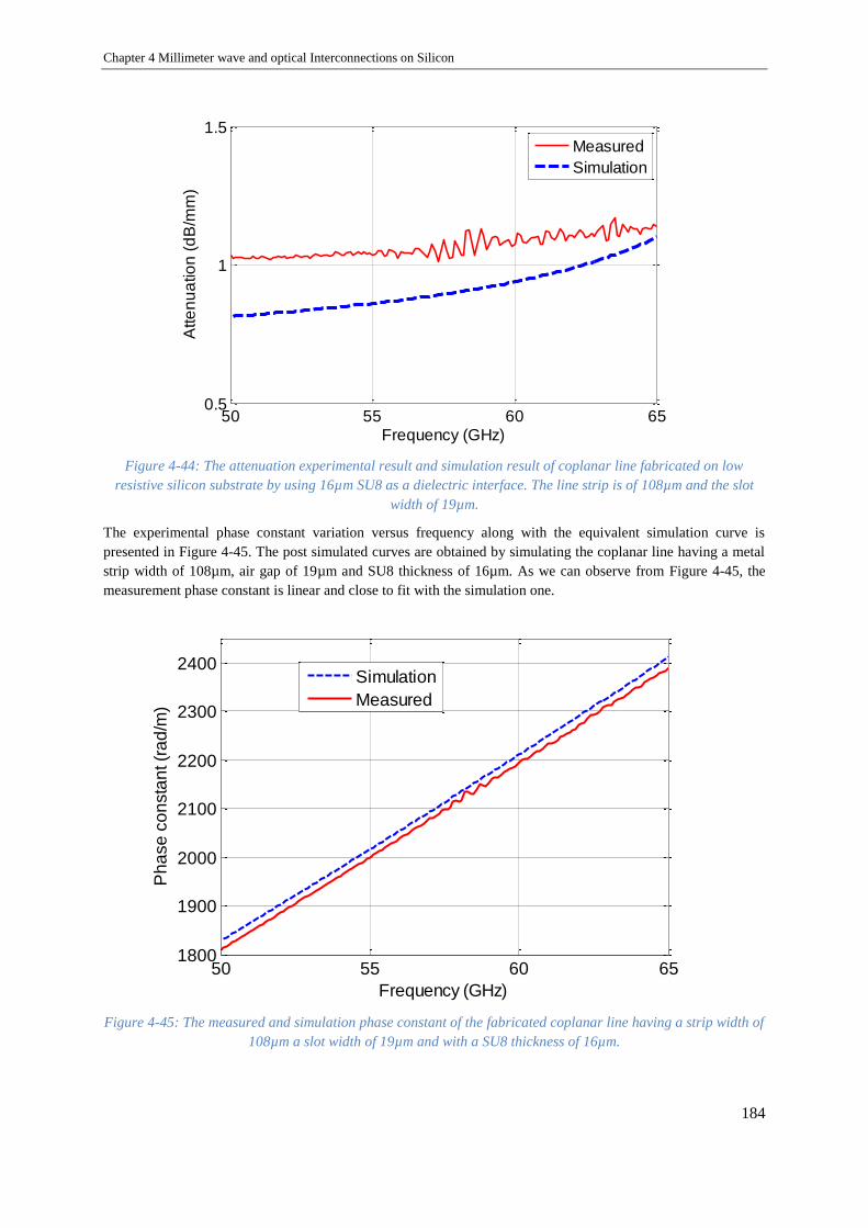
Chapter 4 Millimeter wave and optical Interconnections on Silicon
184
Figure 4-44: The attenuation experimental result and simulation result of coplanar line fabricated on low
resistive silicon substrate by using 16µm SU8 as a dielectric interface. The line strip is of 108µm and the slot
width of 19µm.
The experimental phase constant variation versus frequency along with the equivalent simulation curve is
presented in Figure 4-45. The post simulated curves are obtained by simulating the coplanar line having a metal
strip width of 108µm, air gap of 19µm and SU8 thickness of 16µm. As we can observe from Figure 4-45, the
measurement phase constant is linear and close to fit with the simulation one.
Figure 4-45: The measured and simulation phase constant of the fabricated coplanar line having a strip width of
108µm a slot width of 19µm and with a SU8 thickness of 16µm.
50 55 60 650.5
1
1.5
Frequency (GHz)
Atte
nu
atio
n (
dB
/mm
)
Measured
Simulation
50 55 60 651800
1900
2000
2100
2200
2300
2400
Frequency (GHz)
Ph
ase
co
nsta
nt (r
ad
/m)
Simulation
Measured
Chapter 4 Millimeter wave and optical Interconnections on Silicon
185
4.6 Conclusion
The following major conclusions can be derived from the work presented in this chapter:
We have successfully designed low loss microwave transmission lines on low resistive silicon substrate by using
polymer layers between the line and the substrate. Coplanar, microstrip and grounded coplanar lines based on
SU8, BCB and Parylene in the mm wave frequency range are investigated and designed. Grounded coplanar and
microstrip lines have less attenuation compared to coplanar line as the grounded metal avoids the propagation of
electric field within the silicon substrate. The targeted characteristic impedance for all types of line is 50Ω. The
first experimental result indeed indicates that our design using HFSS is suited. Less than 1.2dB/mm attenuation
in the millimeter-wave frequency range is measured for a coplanar waveguide structure.
We have also successfully designed polymer based optical waveguides that have been included with mm
microwave transmission lines. The interconnection of mm-wave lines on silicon and polymer are demonstrated
through HFSS simulation. They provide an input for the future integration of mm and optical signals in a single
chip or through interconnections between chips.
Silicon based optical waveguide are also designed to be directly integrated into the SiGe Telefunken
Technology. Their design takes advantage on the oxide layers existing in this SiGe technology. The major
advantages of using such optical waveguides associated to the choice of 0.75μm-0.85µm operating wavelength
range are the ease of integrating the optical source, waveguides and optical detectors in a same chip, this
integration implying ease of design and processing procedures.
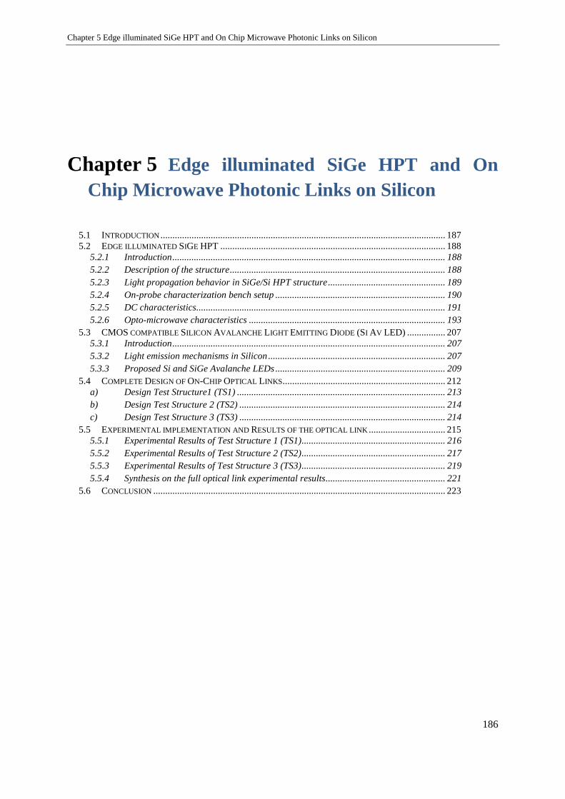
Chapter 5 Edge illuminated SiGe HPT and On Chip Microwave Photonic Links on Silicon
186
Chapter 5 Edge illuminated SiGe HPT and On
Chip Microwave Photonic Links on Silicon
5.1 INTRODUCTION ....................................................................................................................... 187 5.2 EDGE ILLUMINATED SIGE HPT .............................................................................................. 188
5.2.1 Introduction .................................................................................................................. 188 5.2.2 Description of the structure .......................................................................................... 188 5.2.3 Light propagation behavior in SiGe/Si HPT structure ................................................. 189 5.2.4 On-probe characterization bench setup ....................................................................... 190 5.2.5 DC characteristics........................................................................................................ 191 5.2.6 Opto-microwave characteristics .................................................................................. 193
5.3 CMOS COMPATIBLE SILICON AVALANCHE LIGHT EMITTING DIODE (SI AV LED) ................ 207 5.3.1 Introduction .................................................................................................................. 207 5.3.2 Light emission mechanisms in Silicon .......................................................................... 207 5.3.3 Proposed Si and SiGe Avalanche LEDs ....................................................................... 209
5.4 COMPLETE DESIGN OF ON-CHIP OPTICAL LINKS .................................................................... 212 a) Design Test Structure1 (TS1) ....................................................................................... 213 b) Design Test Structure 2 (TS2) ...................................................................................... 214 c) Design Test Structure 3 (TS3) ...................................................................................... 214
5.5 EXPERIMENTAL IMPLEMENTATION AND RESULTS OF THE OPTICAL LINK ................................ 215 5.5.1 Experimental Results of Test Structure 1 (TS1) ............................................................ 216 5.5.2 Experimental Results of Test Structure 2 (TS2) ............................................................ 217 5.5.3 Experimental Results of Test Structure 3 (TS3) ............................................................ 219 5.5.4 Synthesis on the full optical link experimental results.................................................. 221
5.6 CONCLUSION .......................................................................................................................... 223
Chapter 5 Edge illuminated SiGe HPT and On Chip Microwave Photonic Links on Silicon
187
5.1 Introduction
For next generation Micro Optical Electro-Mechanical sensors (MOEMS), lab on chip technologies, optical
communications and data transfers as well bio sensor applications, BiCMOS based Integrated Microwave
Photonic (IMWP) systems are the most viable solution [11]. IMWP also offers new functionalities that would
not be possible using electronic based approach [11] [261]: microwave photonics systems deal with the
generation, processing and distribution of microwave and millimeter signals by optical beams by benefiting from
low loss, large bandwidth and immunity from electromagnetic interference. Other functionalities are tunable and
reconfigurable filter, optoelectronic oscillators, arbitrary waveform generation and so on [261]. Furthermore, the
use of IMWP greatly reduces the system complexity and offers major advantage of integrating all the
technological processes into mainstream silicon fabrication technology. With little adaptation, it could be made
compatible with standard silicon BiCMOS fabrication technology, the most promising of the current silicon
technology.
While in the literature such IMWP circuits are realized at 1.55µm (using III-V lasers on Silicon and Ge detectors
for example), we investigate in this chapter the possibility to use pure Si and SiGe materials to provide both the
optical detector and emitter, through the use of shorter wavelength. While the previous approach is considered to
be BiCMOS compatible, our approach is expected to be fully BiCMOS integrated. For instance the
demonstration is made on bipolar Telefunken Technology.
The applications of our approach are not only related to the communication field, but could embrace much larger
field such as the optical sensing domain for biochemical applications or others.
Key constituents of such a system are an effective BiCMOS compatible optical source, optical waveguide and an
effective optical coupling from the source to the waveguide and to the optical photodetectors such as our SiGe
HPT. These all seem to be highly viable in regard to the present analyses and proposed technology process.
In the previous chapter, in addition to polymer based optical waveguides, we proposed and analyzed the
transmission characteristics of the Si3N4 and TEOS optical waveguides which can be implemented directly in the
Telefunken GmbH SiGe HBT technological process. The simulation results of such optical waveguide were
showing losses less than 0.65dB/cm at 750nm.
This chapter starts with section two where we demonstrate the first edge illuminated SiGe HPTs. It has been
fabricated using the 80 GHz SiGe2RF Telefunken GmbH SiGe Bipolar technological processes which is crucial
to be implemented for ultra-low-cost silicon based IMWP systems. Its performance in terms of DC, opto-
microwave cutoff frequency and gain are presented. In order to avoid complex optical packaging systems, we
focus to the potential, yet lossy, use of a direct coupling via a simple lensed multimode 850nm fiber.
The third section focuses on the development of Si or SiGe LEDs within our SiGe technology. Design
approaches are presented as well as an understanding of the emission process and experimental validation of
their optical emission.
Finally, we present on-chip full optical link developed in co-operation between ESYCOM and the team of Pr.
Snyman in South-Africa. Such a full optical link utilizes a BiCMOS Si Avalanche LEDs [112] [238] [239] as the
optical source, the Si3N4 /TEOS optical waveguides which were discussed in Chapter 4 and our SiGe edge HPT,
used in photodiode mode.
The designed full optical link operates in the 650-850nm wavelength range. The experimental results of the link
performance in terms of DC and RF behavior are presented.

Chapter 5 Edge illuminated SiGe HPT and On Chip Microwave Photonic Links on Silicon
188
5.2 Edge illuminated SiGe HPT
5.2.1 Introduction
Vertically illuminated photodetectors or HPTs are known for their ease of light coupling but suffer from a
tradeoff between conversion efficiency and frequency performance, the latter being limited by the transit time
[196] [199]. Edge-coupled devices overcome this problem as the optical signal enters through the side of the
device and propagates orthogonally to the bias field. This gives the freedom to design longer devices to ensure a
high proportion of the optical signal to be absorbed while maintaining a narrow absorption region to keep transit
times low [196] [197] [199]. Edge coupled HPTs based on InP-InGaAs technology have been intensively
studied since 1993 [196] [199].
In this section we present the first edge illuminated SiGe phototransistor based on the available commercial
SiGe/Si technology for low cost detector or mixer in Radio-over-Fiber applications and/or on-chip or inter chip
optical packaging applications. Its technology and structure are described. Its DC behavior based on Ic-Vce
curve, Gummel plot and DC current gain is presented. The DC biasing values are optimized to maximize either
its cutoff frequency and or its low frequency responsivity. Then, we perform an opto-microwave SNOM (edge
mapping) measurement of the edge-phototransistor in order to observe the fastest and the highest sensitive areas
of the structure.
5.2.2 Description of the structure
The SiGe/Si HPT structure was implemented according to the geometry presented in Chapter 2. The basic HPT
structure is designed by extending the emitter, base and collector layers of the reference HBT. In the case of our
edge SiGe HPT, it is increased from 0.8x1.4μm2 to 4.5x5µm
2 for better coupling with the optical fiber as shown
in Figure 5-1 b).
The final HPT is then 4.5µm wide (corresponding to the width through which light is horizontally coupled) and
5µm long (maximum absorption length of light) as shown in Figure 5-1 b). The Si1-xGe base layer sandwiched
between the collector and emitter, both made of Silicon, is expected to play the role of an evanescent optical
waveguide that detects light, at least partly given the optical beam size that will be injected in our multimode
fiber injection. The base profile is a 40-80nm thin abrupt SiGe layer with Ge content in the range of 20-25% and
high p doping in the range of 1019
cm-3
. The collector is typically 300-400nm thick with low doping.
The emitter metal contact is designed on a reduced surface of the emitter to avoid additional optical losses by
metal absorption of the light throughout the longitudinal direction, and to reduce the electrical parasitic
capacitances. The optical access at the edge requires the HPT to be diced using a smooth shallow dicing blade
close to the active area of the devices as shown in Figure 5-1 a), giving a slickly polished surface state. We dice
80µm down to the substrate to have a smooth surface at the optical beam input and then dice fully in depth and
farther from the surface using a microscopic saw. The full and smooth dicing was processed at the Universté
Paris Sud – IEF laboratory with the help of Pr. Vivien.

Chapter 5 Edge illuminated SiGe HPT and On Chip Microwave Photonic Links on Silicon
189
Figure 5-1: a) Microscopic picture of the edge SiGe HPT, b) Layout of structure along with its dimensions.
5.2.3 Light propagation behavior in SiGe/Si HPT structure
In this sub section we demonstrate on a theoretical basis the behavior of light propagation into a SiGe/Si
phototransistor by using HFSS simulator. Figure 5-2 shows the vertical stacks of the SiGe/Si HPT structure
under study. We simulate a 5µm long edge illuminated phototransistor under an 850nm wavelength illumination.
The SiGe base of the HPT is modeled with a high refractive index of 3.57. The surrounding Si layers are
modeled with a lower refractive index of 3.42. We define a 1x1μm square excitation port at the input and output
of the structure aligned to the SiGe base. We use the material properties as given in Table 5-1 to perform the
simulations.
Figure 5-2: Basic simplified structure of SiGe/Si HPT used for simulation.
emitter
base collector
a)
base
emitter
colle
cto
r
5µ
m
4.5µm
2µm
b)
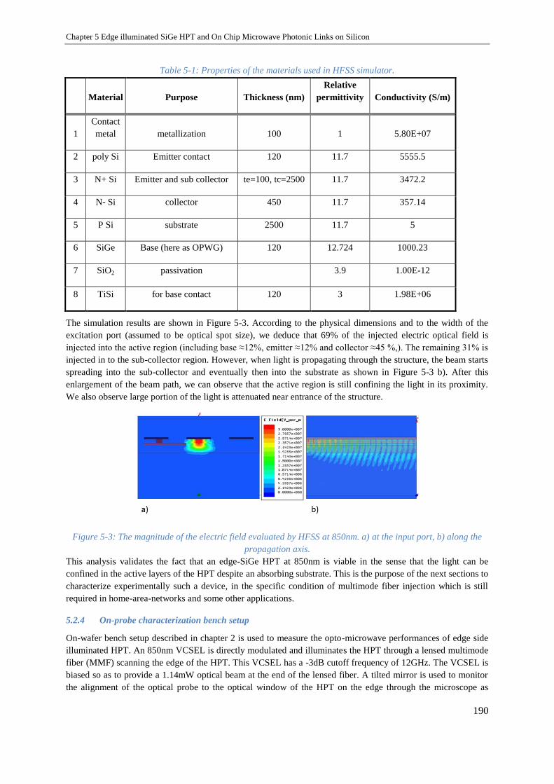
Chapter 5 Edge illuminated SiGe HPT and On Chip Microwave Photonic Links on Silicon
190
Table 5-1: Properties of the materials used in HFSS simulator.
Material Purpose Thickness (nm)
Relative
permittivity Conductivity (S/m)
1
Contact
metal metallization 100 1 5.80E+07
2 poly Si Emitter contact 120 11.7 5555.5
3 N+ Si Emitter and sub collector te=100, tc=2500 11.7 3472.2
4 N- Si collector 450 11.7 357.14
5 P Si substrate 2500 11.7 5
6 SiGe Base (here as OPWG) 120 12.724 1000.23
7 SiO2 passivation
3.9 1.00E-12
8 TiSi for base contact 120 3 1.98E+06
The simulation results are shown in Figure 5-3. According to the physical dimensions and to the width of the
excitation port (assumed to be optical spot size), we deduce that 69% of the injected electric optical field is
injected into the active region (including base ≈12%, emitter ≈12% and collector ≈45 %,). The remaining 31% is
injected in to the sub-collector region. However, when light is propagating through the structure, the beam starts
spreading into the sub-collector and eventually then into the substrate as shown in Figure 5-3 b). After this
enlargement of the beam path, we can observe that the active region is still confining the light in its proximity.
We also observe large portion of the light is attenuated near entrance of the structure.
Figure 5-3: The magnitude of the electric field evaluated by HFSS at 850nm. a) at the input port, b) along the
propagation axis.
This analysis validates the fact that an edge-SiGe HPT at 850nm is viable in the sense that the light can be
confined in the active layers of the HPT despite an absorbing substrate. This is the purpose of the next sections to
characterize experimentally such a device, in the specific condition of multimode fiber injection which is still
required in home-area-networks and some other applications.
5.2.4 On-probe characterization bench setup
On-wafer bench setup described in chapter 2 is used to measure the opto-microwave performances of edge side
illuminated HPT. An 850nm VCSEL is directly modulated and illuminates the HPT through a lensed multimode
fiber (MMF) scanning the edge of the HPT. This VCSEL has a -3dB cutoff frequency of 12GHz. The VCSEL is
biased so as to provide a 1.14mW optical beam at the end of the lensed fiber. A tilted mirror is used to monitor
the alignment of the optical probe to the optical window of the HPT on the edge through the microscope as
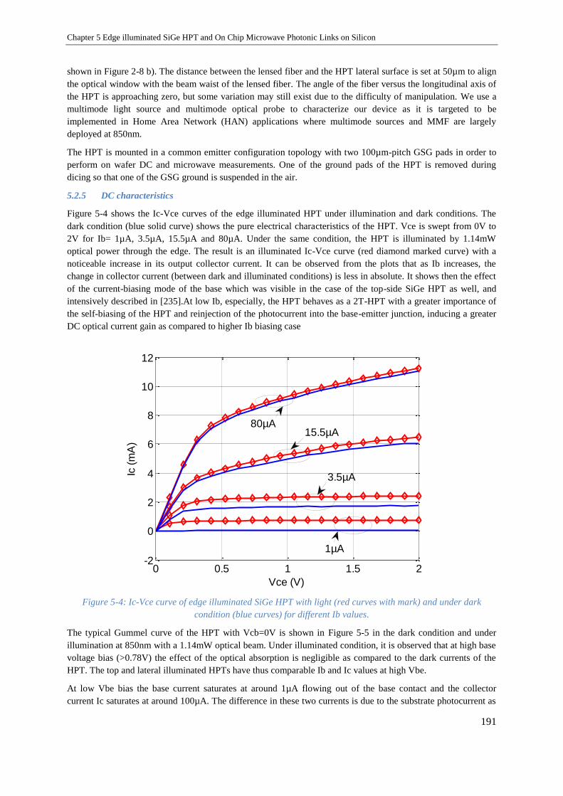
Chapter 5 Edge illuminated SiGe HPT and On Chip Microwave Photonic Links on Silicon
191
shown in Figure 2-8 b). The distance between the lensed fiber and the HPT lateral surface is set at 50µm to align
the optical window with the beam waist of the lensed fiber. The angle of the fiber versus the longitudinal axis of
the HPT is approaching zero, but some variation may still exist due to the difficulty of manipulation. We use a
multimode light source and multimode optical probe to characterize our device as it is targeted to be
implemented in Home Area Network (HAN) applications where multimode sources and MMF are largely
deployed at 850nm.
The HPT is mounted in a common emitter configuration topology with two 100µm-pitch GSG pads in order to
perform on wafer DC and microwave measurements. One of the ground pads of the HPT is removed during
dicing so that one of the GSG ground is suspended in the air.
5.2.5 DC characteristics
Figure 5-4 shows the Ic-Vce curves of the edge illuminated HPT under illumination and dark conditions. The
dark condition (blue solid curve) shows the pure electrical characteristics of the HPT. Vce is swept from 0V to
2V for Ib= 1µA, 3.5µA, 15.5µA and 80µA. Under the same condition, the HPT is illuminated by 1.14mW
optical power through the edge. The result is an illuminated Ic-Vce curve (red diamond marked curve) with a
noticeable increase in its output collector current. It can be observed from the plots that as Ib increases, the
change in collector current (between dark and illuminated conditions) is less in absolute. It shows then the effect
of the current-biasing mode of the base which was visible in the case of the top-side SiGe HPT as well, and
intensively described in [235].At low Ib, especially, the HPT behaves as a 2T-HPT with a greater importance of
the self-biasing of the HPT and reinjection of the photocurrent into the base-emitter junction, inducing a greater
DC optical current gain as compared to higher Ib biasing case
Figure 5-4: Ic-Vce curve of edge illuminated SiGe HPT with light (red curves with mark) and under dark
condition (blue curves) for different Ib values.
The typical Gummel curve of the HPT with Vcb=0V is shown in Figure 5-5 in the dark condition and under
illumination at 850nm with a 1.14mW optical beam. Under illuminated condition, it is observed that at high base
voltage bias (>0.78V) the effect of the optical absorption is negligible as compared to the dark currents of the
HPT. The top and lateral illuminated HPTs have thus comparable Ib and Ic values at high Vbe.
At low Vbe bias the base current saturates at around 1µA flowing out of the base contact and the collector
current Ic saturates at around 100µA. The difference in these two currents is due to the substrate photocurrent as
0 0.5 1 1.5 2-2
0
2
4
6
8
10
12
Ic (
mA
)
Vce (V)
1µA
80µA15.5µA
3.5µA
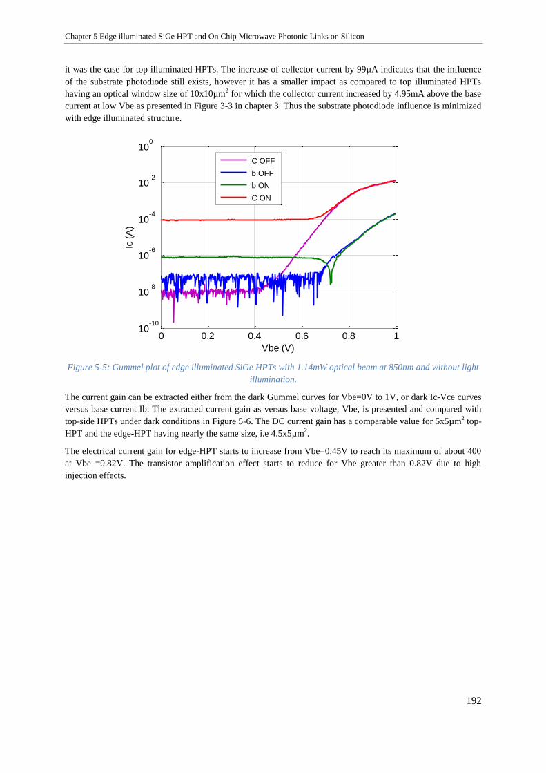
Chapter 5 Edge illuminated SiGe HPT and On Chip Microwave Photonic Links on Silicon
192
it was the case for top illuminated HPTs. The increase of collector current by 99µA indicates that the influence
of the substrate photodiode still exists, however it has a smaller impact as compared to top illuminated HPTs
having an optical window size of 10x10µm2 for which the collector current increased by 4.95mA above the base
current at low Vbe as presented in Figure 3-3 in chapter 3. Thus the substrate photodiode influence is minimized
with edge illuminated structure.
Figure 5-5: Gummel plot of edge illuminated SiGe HPTs with 1.14mW optical beam at 850nm and without light
illumination.
The current gain can be extracted either from the dark Gummel curves for Vbe=0V to 1V, or dark Ic-Vce curves
versus base current Ib. The extracted current gain as versus base voltage, Vbe, is presented and compared with
top-side HPTs under dark conditions in Figure 5-6. The DC current gain has a comparable value for 5x5µm2 top-
HPT and the edge-HPT having nearly the same size, i.e 4.5x5µm2.
The electrical current gain for edge-HPT starts to increase from Vbe=0.45V to reach its maximum of about 400
at Vbe =0.82V. The transistor amplification effect starts to reduce for Vbe greater than 0.82V due to high
injection effects.
0 0.2 0.4 0.6 0.8 110
-10
10-8
10-6
10-4
10-2
100
Ic (
A)
Vbe (V)
IC OFF
Ib OFF
Ib ON
IC ON

Chapter 5 Edge illuminated SiGe HPT and On Chip Microwave Photonic Links on Silicon
193
Figure 5-6: Comparison of the DC current gain from the edge-HPT or top-HPTs of various optical window sizes
in dark conditions.
5.2.6 Opto-microwave characteristics
This section shows the opto-microwave behavior of the edge illuminated SiGe HPT in terms of opto-microwave
cutoff frequency and responsivity in PD and HPT modes of operation. The DC biasing conditions will then be
optimized according to these results before performing edge mapping. The distributions of the photocurrent and
opto-microwave response across the edge section of the HPT structure are then investigated at the optimum dc
biasing condition that maximizes either the low frequency responsivity or the cutoff frequency.
5.2.6.1 Optimizing the DC bias for the opto-microwave behavior
Before we perform edge SNOM investigation to look for the fastest and highest sensitive areas of the HPT as
well as to see the distribution of photocurrent across the edge section of the HPT, we optimize the dc biasing
conditions of the phototransistor with respect to the low frequency responsivity and the opto-microwave cutoff
frequency at a given arbitrarily fixed position of the optical probe. This then provides two sets of optimum
biasing conditions, depending on the selected criterion.
For this study, the opto-microwave measurements are realized using constant voltage biasing of the base. The
phototransistor is operated in the forward active mode with collector-emitter voltage (Vce) values at 1V, 1.5V,
2V, 2.5V and 3V and with the base-emitter voltage (Vbe) swept from 0V to 1V.
Figure 5-7 a) shows the low frequency opto-microwave gain of the edge illuminated SiGe HPT versus Vbe at
different Vce. The position of the fiber is arbitrarily chosen in the detection range of the HPT, thus at a non-
optimum position. From Vbe= 0V to 0.7V, the HPT is operated in its PD mode as it is the case for top
illuminated HPTs. In this region the base emitter junction is not yet efficiently biased and hence the base-
collector junction pin photodiode is detecting light without any transistor amplification. Gom increases above
Vbe=0.7V and eventually reaches its peak at Vbe=0.85V when Vce=1.5V, 2V, 2.5V or 3V; and at Vbe=0.92V
when Vce=1V. At larger Vbe values, the fall-off of the gain is observed as the HPT is operated in a high
injection regime.
The Gom is also shown as a function of Vce in Figure 5-7 b) in PD mode (Vbe=0V) and HPT mode at
Vbe=0.85V and 0.92V. In PD mode, the Gom slightly increases as the collector-emitter voltage increases from
1V to 3V. However, in the HPT mode, it decreases as Vce increases either above 1V or 1.5V depending on Vbe
value. We can deduce an optimum Gom when Vce is in the vicinity of 1V or eventually between 1 and 2V. More
precise measurements would be needed. However, for 10x10μm2 top illuminated HPTs the maximum Gom
0 0.2 0.4 0.6 0.8 10
100
200
300
400
500
600
Be
ta
Vbe (V)
3x3µm2
5x5µm2
10x10µm2
EDGE HPT

Chapter 5 Edge illuminated SiGe HPT and On Chip Microwave Photonic Links on Silicon
194
appears at Vce=3.5V as it is presented in chapter 3. The difference could be explained by the overall size of the
phototransistor and the existence of lateral electrical field contribution in the base-collector regions, leading in a
2D electrical extended region as described in Chapter 3. As the lateral illuminated HPT is smaller and more
vertical, it can be optimum at lower Vce. As well, it appears that the optimum Vbe is varying with Vce. This was
not the case with top-illuminated HPT. Further investigations would be required there.
The optical gain (Gopt) enhancement between the HPT mode and PD mode of operation is presented in Figure
5-9 a) versus Vce. We reach a maximum Gopt of 12dB at Vce =1V which then falls down for higher Vce.
Compared with top illuminated structure (optical window size 10x10µm2) which has Gopt =18dB, laterally
illuminated structure has smaller Gopt which is due to the smaller size of edge illuminated HPT (smaller size has
lower current gain).
Figure 5-7: Opto-microwave gain a) versus Vbe at different Vce, b) versus Vce in PD mode and HPT moed
(Vbe=0.85V and 0.92V).
The opto-microwave cutoff frequency (f-3dB) versus Vbe, using 50MHz as a reference for the low frequency
response, is shown in Figure 5-8. The cutoff frequency is low and constant in the PD mode (up to Vbe=0.7V)
and it increases to a peak around 0.8V. We observe a maximum cutoff frequency of 480MHz at Vbe=0.8V and
Vce=1.5V. The 2nd
highest value is obtained at Vbe=0.85V and Vce=1V. This indicates that an optimum Vce
value different from 1.5V may exist between 1V and 2V, similar to the optimization of the low-frequency gain
as seen before.
1 1.5 2 2.5 3-30
-25
-20
-15
-10
Vce (V)
Gom
(dB
)
PD mode
HPT mode Vbe=0.85V
HPT mode Vbe=0.92V
0 0.2 0.4 0.6 0.8 1-26
-24
-22
-20
-18
-16
-14
-12
Vbe (A)
Go
m (
dB
)
Vce=1V
Vce=1.5V
Vce=2V
Vce=2.5V
Vce=3V
a) b)
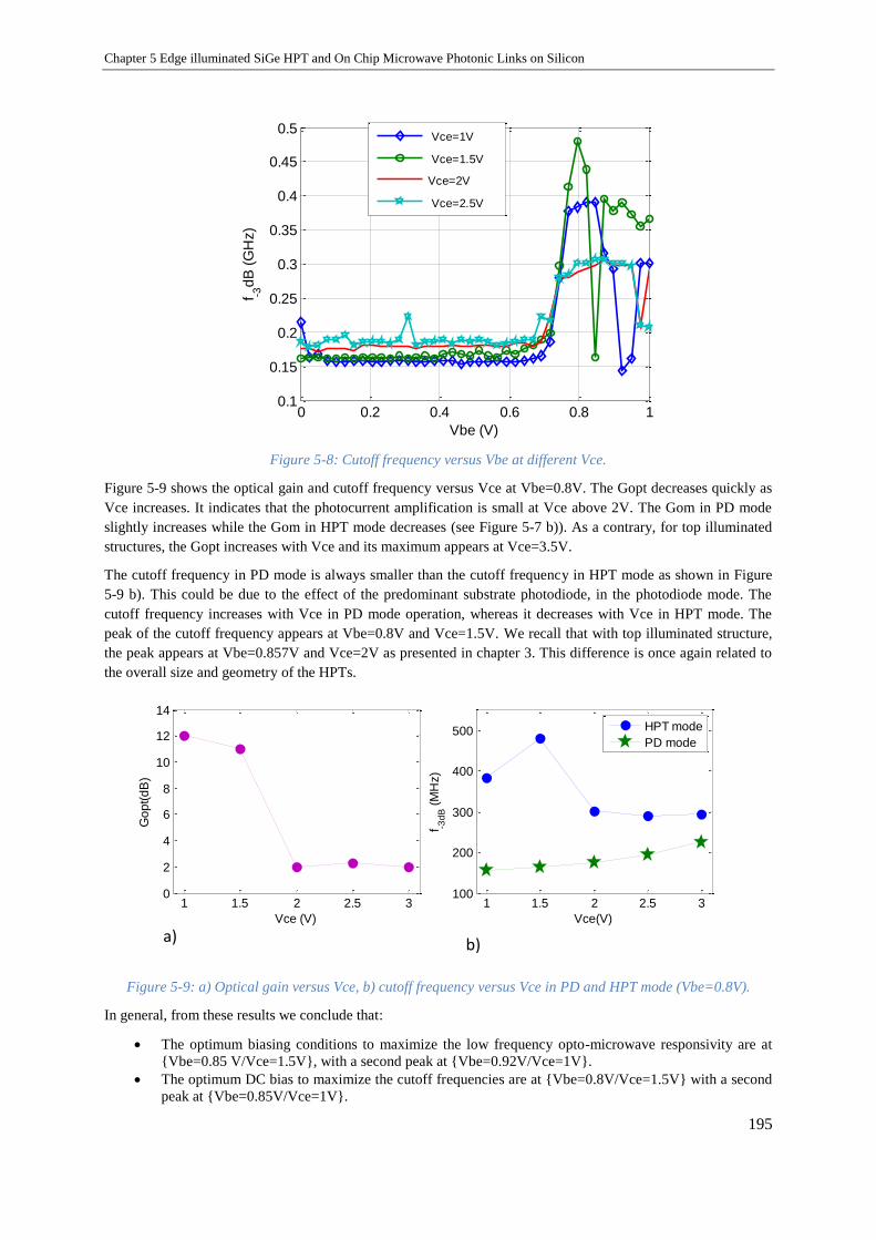
Chapter 5 Edge illuminated SiGe HPT and On Chip Microwave Photonic Links on Silicon
195
Figure 5-8: Cutoff frequency versus Vbe at different Vce.
Figure 5-9 shows the optical gain and cutoff frequency versus Vce at Vbe=0.8V. The Gopt decreases quickly as
Vce increases. It indicates that the photocurrent amplification is small at Vce above 2V. The Gom in PD mode
slightly increases while the Gom in HPT mode decreases (see Figure 5-7 b)). As a contrary, for top illuminated
structures, the Gopt increases with Vce and its maximum appears at Vce=3.5V.
The cutoff frequency in PD mode is always smaller than the cutoff frequency in HPT mode as shown in Figure
5-9 b). This could be due to the effect of the predominant substrate photodiode, in the photodiode mode. The
cutoff frequency increases with Vce in PD mode operation, whereas it decreases with Vce in HPT mode. The
peak of the cutoff frequency appears at Vbe=0.8V and Vce=1.5V. We recall that with top illuminated structure,
the peak appears at Vbe=0.857V and Vce=2V as presented in chapter 3. This difference is once again related to
the overall size and geometry of the HPTs.
Figure 5-9: a) Optical gain versus Vce, b) cutoff frequency versus Vce in PD and HPT mode (Vbe=0.8V).
In general, from these results we conclude that:
The optimum biasing conditions to maximize the low frequency opto-microwave responsivity are at
Vbe=0.85 V/Vce=1.5V, with a second peak at Vbe=0.92V/Vce=1V.
The optimum DC bias to maximize the cutoff frequencies are at Vbe=0.8V/Vce=1.5V with a second
peak at Vbe=0.85V/Vce=1V.
0 0.2 0.4 0.6 0.8 10.1
0.15
0.2
0.25
0.3
0.35
0.4
0.45
0.5
Vbe (V)
f -3d
B (
GH
z)
Vce=1V
Vce=1.5V
Vce=2V
Vce=2.5V
a) b)
1 1.5 2 2.5 30
2
4
6
8
10
12
14
Vce (V)
Go
pt(
dB
)
1 1.5 2 2.5 3100
200
300
400
500
Vce(V)
f -3d
B (
MH
z)
HPT mode
PD mode

Chapter 5 Edge illuminated SiGe HPT and On Chip Microwave Photonic Links on Silicon
196
Figure 5-10 shows the behavior of the opto-microwave gain versus frequency at these various optimum biasing
conditions. From these curves, we understand that despite the cutoff frequency and the low frequency gain are
found at different biasing conditions in a HPT mode, the high frequency part of the Gom curves become equal
and have nearly the same slope at all biasing conditions.
Figure 5-10: Opto-microwave gain versus frequency at low frequency Gom and cutoff frequency peak biasing
conditions.
In summary, we found the optimum biasing conditions to maximize the low frequency Gom are 0.85V at the
base-emitter junction and 1.5V at the collector-emitter junction; and to maximize the cutoff frequency, they are
0.8V and 1.5V at the base and collector contact respectively. We will use these dc biasing conditions for further
experimental studies to perform edge OM and DC SNOM as presented in the following sections.
5.2.6.2 Edge Mapping
Figure 5-11 a) shows the simplified cross section of the edge coupled phototransistor with the optical probe
aligned with the active area. The front view of the optical window is detailed in Figure 5-11 b) that shows the
surface over which the edge SNOM is performed. On these figures the axes are given accordingly to the
experimental results shown in the following section.
10-1
100
101
-55
-50
-45
-40
-35
-30
-25
-20
-15
-10G
om
(d
B)
Freq (GHz)
Vce=1V, Vb=0.92V
Vce=1.5V, Vb=0.8V
Vce=1V, Vb=0.85V
Vce=1.5V, Vb=0.85V
@f-3dB max
@Gom max
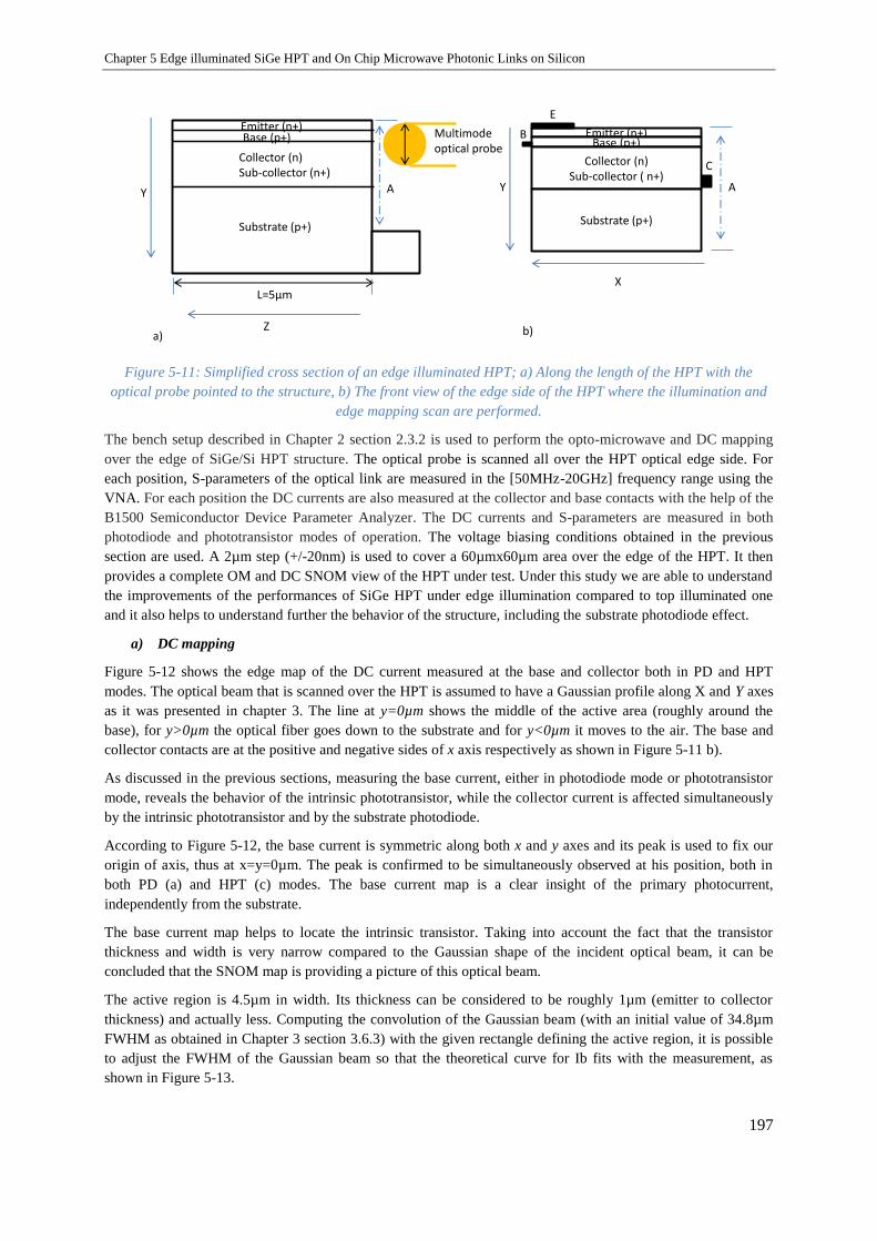
Chapter 5 Edge illuminated SiGe HPT and On Chip Microwave Photonic Links on Silicon
197
Figure 5-11: Simplified cross section of an edge illuminated HPT; a) Along the length of the HPT with the
optical probe pointed to the structure, b) The front view of the edge side of the HPT where the illumination and
edge mapping scan are performed.
The bench setup described in Chapter 2 section 2.3.2 is used to perform the opto-microwave and DC mapping
over the edge of SiGe/Si HPT structure. The optical probe is scanned all over the HPT optical edge side. For
each position, S-parameters of the optical link are measured in the [50MHz-20GHz] frequency range using the
VNA. For each position the DC currents are also measured at the collector and base contacts with the help of the
B1500 Semiconductor Device Parameter Analyzer. The DC currents and S-parameters are measured in both
photodiode and phototransistor modes of operation. The voltage biasing conditions obtained in the previous
section are used. A 2µm step (+/-20nm) is used to cover a 60µmx60µm area over the edge of the HPT. It then
provides a complete OM and DC SNOM view of the HPT under test. Under this study we are able to understand
the improvements of the performances of SiGe HPT under edge illumination compared to top illuminated one
and it also helps to understand further the behavior of the structure, including the substrate photodiode effect.
a) DC mapping
Figure 5-12 shows the edge map of the DC current measured at the base and collector both in PD and HPT
modes. The optical beam that is scanned over the HPT is assumed to have a Gaussian profile along X and Y axes
as it was presented in chapter 3. The line at y=0µm shows the middle of the active area (roughly around the
base), for y>0µm the optical fiber goes down to the substrate and for y<0µm it moves to the air. The base and
collector contacts are at the positive and negative sides of x axis respectively as shown in Figure 5-11 b).
As discussed in the previous sections, measuring the base current, either in photodiode mode or phototransistor
mode, reveals the behavior of the intrinsic phototransistor, while the collector current is affected simultaneously
by the intrinsic phototransistor and by the substrate photodiode.
According to Figure 5-12, the base current is symmetric along both x and y axes and its peak is used to fix our
origin of axis, thus at x=y=0µm. The peak is confirmed to be simultaneously observed at his position, both in
both PD (a) and HPT (c) modes. The base current map is a clear insight of the primary photocurrent,
independently from the substrate.
The base current map helps to locate the intrinsic transistor. Taking into account the fact that the transistor
thickness and width is very narrow compared to the Gaussian shape of the incident optical beam, it can be
concluded that the SNOM map is providing a picture of this optical beam.
The active region is 4.5µm in width. Its thickness can be considered to be roughly 1µm (emitter to collector
thickness) and actually less. Computing the convolution of the Gaussian beam (with an initial value of 34.8µm
FWHM as obtained in Chapter 3 section 3.6.3) with the given rectangle defining the active region, it is possible
to adjust the FWHM of the Gaussian beam so that the theoretical curve for Ib fits with the measurement, as
shown in Figure 5-13.
Emitter (n+)Base (p+)
Collector (n)Sub-collector ( n+)
X
Y
Substrate (p+)
B
E
C
AA A
Multimode optical probe
Y
L=5µm
Z
Substrate (p+)
Collector (n) Sub-collector (n+)
Base (p+)Emitter (n+)
a) b)

Chapter 5 Edge illuminated SiGe HPT and On Chip Microwave Photonic Links on Silicon
198
It is then shown that the optimum FWHM for the optical beam is 32.2µm. This dimension is slightly different
from the one obtained with the top illumination cases. This is due to eventually slight modification in the
VCSEL source and to some difference in distance and angle of the lensed fiber from the scanned surface.
It is also observed that tuning the active region dimension doesn’t influence much the final results, as it is much
lower than the beam size.
It is then possible to sketch on the SNOM curves the rectangle related to the active region. This is done in Figure
5-12. A rectangle indicating the region of influence of the substrate is also shown in this figure. The extraction of
its dimensions will be computed on a similar procedure in the following part.
The collector current has a peak centered at x=0µm and y=10µm, down into the substrate with a values 0.15mA
and 1.5mA in PD and HPT mode respectively. The peak deviation from the center of the intrinsic transistor is
clearly related to the substrate photodiode photocurrent which is then predominant compared to Ic from the
intrinsic HPT. The peak of Ic is still in the vertical axis of the intrinsic HPT (x=0), but it is indeed shifted 10µm
below where the coupling of the optical beam to the sub-collector / substrate photodiode is optimum.
Below that depth, the coupling to the substrate photodiode is stable in amplitude near to its maximum value, but
the recombination losses of the photo-generated carriers are becoming predominant. It then explains the
reduction of Ic below.
Figure 5-12:DC SNOM of edge illuminated SiGe HPT at Vce=1.5V with a) base current in PD mode, b)
Collector current in PD mode, c) base current in HPT mode (Vbe=0.8V), d) collector current in HPT mode
(Vbe=0.8V).
X (m)
Y (
m)
PD: Ib
-2-1012
x 10-5
-2
-1
0
1
2
3
x 10-5
-1.2
-1
-0.8
-0.6
-0.4
-0.2
0x 10
-6
X (m)
Y (
m)
PD: Ic
-2-1012
x 10-5
-2
-1
0
1
2
3
x 10-5
2
4
6
8
10
12
14x 10
-5
a) b)
X (m)
Y (
m)
HPT: Ic
-2-1012
x 10-5
-2
-1
0
1
2
3
x 10-5
1.15
1.2
1.25
1.3
1.35
1.4
1.45x 10
-3
X (m)
Y (
m)
HPT: Ib
-2-1012
x 10-5
-2
-1
0
1
2
3
x 10-5
1.4
1.6
1.8
2
2.2
2.4
2.6
2.8x 10
-6
c) d)
Substrate region Substrate region
Substrate regionSubstrate region

Chapter 5 Edge illuminated SiGe HPT and On Chip Microwave Photonic Links on Silicon
199
Figure 5-13: The fitting between the base current cross section along y axis with the convolution function
resulted from the convolution of Gaussian beam having FWHF diameter of 32.2µm with expected rectangular
shape of the active region of the HPT.
The edge map of the intrinsic photocurrent measured at the collector in PD mode is presented in Figure 5-14 a).
As we can see from the figure, the peak of the collector photo-generated current is well centered to the intrinsic
device and the map symmetrical to both axes. In PD mode operation, an intrinsic photocurrent of 2.2µA is
measured at the collector contact at peak detection position (X=0µm and Y=0µm).
The computed intrinsic photocurrent Icph indeed confirms that the active region is very small compared to the
injected optical beam and well fits with the function resulting from the convolution between the Gaussian beam
and the active region rectangle of 4.5µm x1µm.
Computing the substrate current map helps to locate the substrate photodiode. It is given in Figure 5-14 b). The
peaks appears around x=0µm and y=10µm, indeed outside the intrinsic area. We extract a substrate photocurrent
of 110µA at the peak. It is 2.5 times less than the substrate photocurrent of top illuminated structure, i.e. 280µA.
From the measurement of the base current, the substrate photocurrent peak appears 10µm below the center of the
active region, so it is estimated to be approximately 9µm below the sub-collector and substrate junction if we
consider a few hundred nanometer thick sub-collector.
Considering the Gaussian beam parameters as the one taken from the top illumination case described in chapter 3
section 3.6.3, it is interesting to know how thick the effective substrate absorption layer is. We assume that the
effective absorption section of the substrate photodiode region has a rectangular shape. Then we perform the
correlation between the Gaussian function and the rectangle function. The resulting curve is used to fit with the
measured substrate photocurrent by tuning the dimensions of the rectangle. The resulting fit is achieved in Figure
5-14 d) along Y axis (at X=0µm), when the expected rectangle width dimension becomes 17µm along. This
provides the effective thickness of the substrate photodiode. The fit along the X axis is also performed and hence
it fits with the experimental result when the length of the rectangle becomes 32µm. This indicates that the
effective substrate photodiode region has a rectangular shape with a surface area of 17µmx32µm as sketched in
Figure 5-14 a) and b).
-3 -2 -1 0 1 2 3
x 10-5
-1.4
-1.2
-1
-0.8
-0.6
-0.4
-0.2
0x 10
-6
Y (m)
Ib (
A)
measured
Model

Chapter 5 Edge illuminated SiGe HPT and On Chip Microwave Photonic Links on Silicon
200
Figure 5-14: a) Intrinsic photocurrent measured at the collector contact in PD mode. b) Substrate photocurrent,
c) Slice curve of intrinsic photocurrent along y-axis, d) Slice curve of substrate photocurrent along y-axis.
The edge map as a function of optical probe position of the primary photocurrent and base efficiency are shown
in Figure 5-15 a) and b) respectively. Both are symmetric along the x and y axes, as Ib is. Peak values appear at
the center of the active area (x=y=0µm). The maximum generated photocurrent in the edge illuminated SiGe
HPT is then evaluated to be 2.6µA. This primary photocurrent is the combination of all photocurrent sources in
the intrinsic photodiode mode.
Figure 5-15 b) shows the fraction of this holes photocurrent which leaks through the base contact. The rest of
holes photocurrent is effectively injected into the emitter when operating in the HPT mode (in this case under
Vbe=0.8V and Vce=1.5V). This part will activate the phototransistor amplification effect, while the other one
will simply leak to the base contact.
When the 1.14mW optical power is injected in the active region of edge illuminated HPT, only 10% of the
photo-generated holes are leaking through the base contact and 90% are used to active the transistors
amplification effect. Whereas when the injection depth moves far from the active region the fraction of leakage
photo-generated current increases.
The base efficiency is smaller compared with top illuminated HPTs having an optical window of 10x10µm2, i.e
26%, at the peak detection (in the active region) at injected power level of 1.14mW as presented in chapter 3
section 3.6.3. This indicates a better amplification within edge-HPTs. This is attributed to be two aspects: the
better localization of the optical beam all along the length of the device; a better design for the emitter contact
enabling a greater proximity between the region of amplification and the region of generation of electron/hole
pairs.
X (m)
Y (
m)
Isub
-2-1012
x 10-5
-2
-1
0
1
2
3
x 10-5
0
2
4
6
8
10
x 10-5
X (m)
Y (
m)
PD_IcPh
-2-1012
x 10-5
-2
-1
0
1
2
3
x 10-5
1.2
1.4
1.6
1.8
2
2.2x 10
-6
a) b)
c) d)
-2 0 2
x 10-5
-2
0
2
4
6
8
10
12x 10
-5
Y (m)
Isu
b (
A)
Measured
Model
-2 0 2
x 10-5
1
1.2
1.4
1.6
1.8
2
2.2
2.4x 10
-6
Y (m)
IcP
h (
A)
Measured
Model
Substrate regionSubstrate region

Chapter 5 Edge illuminated SiGe HPT and On Chip Microwave Photonic Links on Silicon
201
Figure 5-15: Edge map of: a) primary photocurrent generated in the structure, b) Base efficiency.
In general, at the peak detection (x=y=0µm) a complete DC responsivity of 0.48A/W in HPT mode (Vbe=0.85V
and Vce=1.5V) and 0.105A/W in PD mode are observed. The DC responsivity in HPT mode for laterally
illuminated device is 1.33 times larger than the top illuminated HPT of 10x10µm2 optical window size (i.e
0.36AW). We also observe maximum DC substrate responsivity of 0.09A/W for edge illuminated structures and
0.234A/W for top illuminate case.
Thus we conclude that the substrate influence on the intrinsic HPT performance is indeed minimized in edge
illuminated structures.
b) Opto-microwave mapping
Figure 5-16 a) and c) shows the OM-SNOM view of the low frequency opto-microwave responsivity and opto-
microwave cutoff frequency of the edge illuminated HPT under 50Ω condition at 50MHz in HPT and PD modes,
respectively. The PD modes are obtained by setting Vbe=0V and Vce=1.5V and HPT modes is obtained by
setting Vbe=0.8V and Vce= 1.5V. These biasing conditions are chosen in the section 5.2.6.1 to maximize the
cutoff frequency.
Thus the following observations are made from Figure 5-16:
Figure 5-16 a): in PD mode, the highest gain at 50MHz is still located into the substrate as in the case of top
illuminated HPTs but it is however closer to the intrinsic HPT with a maximum position at x=0µm and
Y=5µm. This is due to the fact that the sub-collector/substrate photodiode speed is directly dependent on the
distance between the points of optical injection to the sub-collector. The cutoff frequency can be lower than
50MHz and thus the signal is filtered; the amplitude at 50MHz gets lower when the light is injected far from
the sub-collector.
Figure 5-16 c): The same phenomenon is observed in the phototransistor mode. The low frequency behavior
is still mostly affected by the substrate photodiode indeed. We extract a peak responsivity of 0.11A/W in
HPT mode at X=0µm and Y=5µm
One could take advantage of the substrate photodiode to boost the overall responsivity of the device
combined with the intrinsic HPT.
Figure 5-16 b): The cutoff frequency of the photodiode mode shows two peaks. The first peak is almost
centered in x, and is located at y=-9µm. This first peak is associated to the illumination of the upper part
intrinsic HPT region only. This is consistent to the maximization of the f-3dB when the beam is centered into
the top part of the base-emitter junction. At this position, the transit time for the holes to reach the emitter is
reduced, as foreseen by physical simulations conducted as simulated in [260], whose results are re-plotted in
Figure 5-18. This figure shows the f-3dB frequency in the lateral illumination condition versus the optical
injection depth into the device when considering a theoretical beam width of 10nm injected on the edge of
the device.
X (µm)
Y (
µm
)
Primary Photocurrent
-202
x 10-5
-3
-2
-1
0
1
2
3
x 10-5
-2.6
-2.4
-2.2
-2
-1.8
-1.6
x 10-6
X (µm)
Y (
µm
)
Base efficiency
-202
x 10-5
-3
-2
-1
0
1
2
3
x 10-5
0.1
0.2
0.3
0.4
0.5
0.6
0.7
0.8
a) b)
Chapter 5 Edge illuminated SiGe HPT and On Chip Microwave Photonic Links on Silicon
202
The second peak of the f-3dB is located at x=3µm and y=0µm; for this peak it might be the base-collector
junction which maximizes the speed, which then linearly decreases with y when the optical beam moves
down to the substrate as shown in the cross section curve along y axis in Figure 5-17 a). The two peaks have
the same f-3dB value i.e. 260MHz.
Figure 5-16 d): The f-3dB of the phototransistor mode is quite different. It is mostly associated to the intrinsic
HPT region with a peak value of 520MHz. Its position is located beneath the emitter metal contact around
x=6µm and y close to -10µm. This shows the importance of this metal contact on the dynamic of the HPT.
This emitter metal contact was initially designed only on the left hand side of the emitter to prevent from the
absorption losses into the metal. These losses appear not being visible in our observation. On the
counterpart, it shows to have an important effect on the f-3dB. The speed decreases when the optical probe
moves away from the emitter contact along x axis. From this we observe that the high doping of the emitter
is not sufficient to prevent from lateral paths of the photo-carriers as observed in the top-illuminated HPT.
We also observe that the peak is at y around -8µm. In this position the optical beam is illuminating above (in
the air) however, the Gaussian tail excites the emitter-base region only, and thus minimizes the illumination
of the substrate photodiode. We observe that when the beam is illuminating further these lower regions, the
influence of the emitter metal contact is less and the f-3dB is more uniform along the x axis within the volume
of the intrinsic HPT. This is supporting indeed that this is due to the regions below the base, and that the
toppest peak is indeed related to the emitter-base region. Figure 5-17 b) shows the f-3dB frequency as the
function of the optical injection location as it is moved down to the substrate. The cross section curve indeed
linearly decreases as the optical injection depth moves into the active device and then down to the substrate.
A perspective of optimization of the edge-SiGe HPT would then be to fully cover the emitter with a metal
contact, in order to increase the area dimension where the peak f-3dB is met. In conclusion cutoff frequencies of
up to520MHz and 260MHz are obtained in HPT (Vce=1.5V and Vbe=0.8V) and PD (Vce=1.5V and Vbe=0V)
mode respectively.

Chapter 5 Edge illuminated SiGe HPT and On Chip Microwave Photonic Links on Silicon
203
Figure 5-16: OM SNOM of edge illuminated SiGe HPT at Vce=1.5V a) Low frequency opto-microwave
responsivity in PD mode (Vbe=0V), b) cutoff frequency in PD mode (Vbe=0V), c) Low frequency opto-
microwave responsivity in HPT mode (Vbe=0.8V) and d) cutoff frequency in HPT mode (Vce=0.8V).
Figure 5-17: The cross section curve of the cutoff frequency along y axis (for top into the substrate) at Vce=1.5V
in a) PD mode (Vbe=0.8V), b) HPT mode (Vbe=0V).
X (m)
Y (
m)
HPT: f-3dB
(GHz)
-2-1012
x 10-5
-2
-1
0
1
2
x 10-5
0.1
0.2
0.3
0.4
0.5
X (m)
Y (
m)
PD: f-3dB
(GHz)
-2-1012
x 10-5
-2
-1
0
1
2
x 10-5
0.05
0.1
0.15
0.2
0.25
X (m)
Y (
m)
PD: R (A/W) @ f=0.05GHz
-2-1012
x 10-5
-2
-1
0
1
2
x 10-5
0.01
0.02
0.03
0.04
0.05
0.06
X (m)
Y (
m)
HPT: R (A/W) @ f=0.05GHz
-2-1012
x 10-5
-2
-1
0
1
2
x 10-5
0.01
0.02
0.03
0.04
0.05
0.06
0.07
0.08
0.09
0.1
a) b)
c) d)
-30 -20 -10 0 10 20 300.05
0.1
0.15
0.2
0.25
0.3
Y (µm)
f - 3d
B(G
Hz)
@X=3µm
@X=0µm
-30 -20 -10 0 10 20 30
0.1
0.2
0.3
0.4
0.5
Y (µm)
f -3d
B(G
Hz)
@X=6µm
@X=0µm
a) b)

Chapter 5 Edge illuminated SiGe HPT and On Chip Microwave Photonic Links on Silicon
204
Figure 5-18: Cutoff frequency extracted from physical simulation in the lateral illumination condition versus the
optical injection depth into the device when considering a theoretical beam width of 10nm [260].
Figure 5-19 shows the map of the low frequency opto-microwave responsivity and f-3dB of an edge illuminated
HPT under 50Ω condition at 50MHz in HPT mode obtained by setting Vbe=0.85V and Vce= 1.5V which
maximizes the low frequency responsivity as studied in section 5.2.6.1. At this biasing condition the low
frequency responsivity increases to 0.26A/W in HPT mode and the cutoff frequency to around 800MHz as it is
also shown in the cross section curve in Figure 5-20. The peak of the cutoff frequency is shifted to the base
contact due to metal contact proximity effect as described above. The peak responsivity is more than for the
previous biasing points as expected (this biasing condition maximizes the low frequency responsivity). The
maximum f-3dB in the HPT mode is even more than for the previous biasing point. This was not expected. It
indicates that the biasing optimization may be different depending on the optical injection point. We still observe
two peaks. The topper one (at y~-8µm) reaches the value of 306MHz which is lower than with the previous
biasing conditions as shown in Figure 5-16, i.e. 520MHz, while the peak at the bottom position (at y=0µm) is
indeed increased. The top one was related to the proximity of the emitter contact and is closer to the base-emitter
region whereas the bottom one is probably due to the base-collector junction within the intrinsic HPT. Both are
indeed impacted by Vbe. This assumption, initiated above, is then here reinforced.
Figure 5-19: OM-SNOM of SiGe HPT with edge illumination at Vce=1.5V and Vbe=0.85V a) low frequency
responsivity and b) cutoff frequency.
a) b)X (m)
Y (
m)
HPT: R (A/W) @ f=0.05GHz
-2-1012
x 10-5
-2
-1
0
1
2
x 10-5
0.05
0.1
0.15
0.2
0.25
X (m)
Y (
m)
HPT: f-3dB
(GHz)
-2-1012
x 10-5
-2
-1
0
1
2
x 10-5
0.1
0.2
0.3
0.4
0.5
0.6
0.7
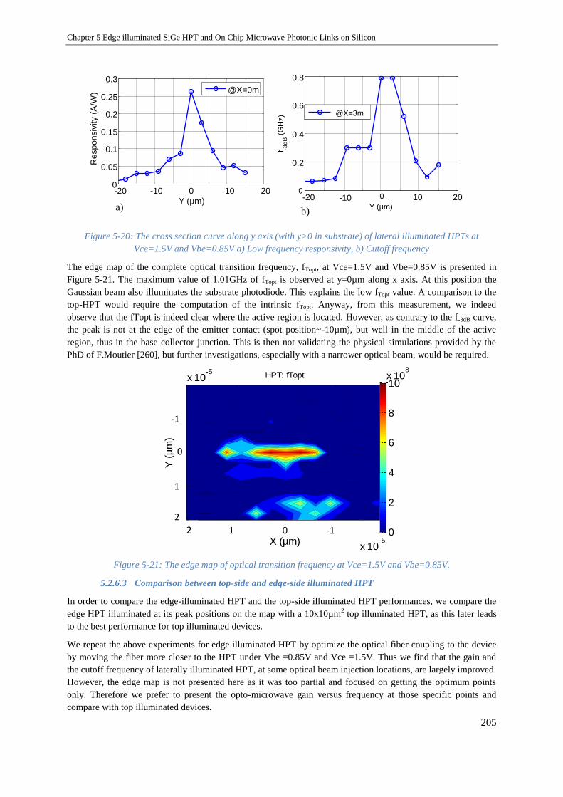
Chapter 5 Edge illuminated SiGe HPT and On Chip Microwave Photonic Links on Silicon
205
Figure 5-20: The cross section curve along y axis (with y>0 in substrate) of lateral illuminated HPTs at
Vce=1.5V and Vbe=0.85V a) Low frequency responsivity, b) Cutoff frequency
The edge map of the complete optical transition frequency, fTopt, at Vce=1.5V and Vbe=0.85V is presented in
Figure 5-21. The maximum value of 1.01GHz of fTopt is observed at y=0µm along x axis. At this position the
Gaussian beam also illuminates the substrate photodiode. This explains the low fTopt value. A comparison to the
top-HPT would require the computation of the intrinsic fTopt. Anyway, from this measurement, we indeed
observe that the fTopt is indeed clear where the active region is located. However, as contrary to the f-3dB curve,
the peak is not at the edge of the emitter contact (spot position~-10µm), but well in the middle of the active
region, thus in the base-collector junction. This is then not validating the physical simulations provided by the
PhD of F.Moutier [260], but further investigations, especially with a narrower optical beam, would be required.
Figure 5-21: The edge map of optical transition frequency at Vce=1.5V and Vbe=0.85V.
5.2.6.3 Comparison between top-side and edge-side illuminated HPT
In order to compare the edge-illuminated HPT and the top-side illuminated HPT performances, we compare the
edge HPT illuminated at its peak positions on the map with a 10x10µm2 top illuminated HPT, as this later leads
to the best performance for top illuminated devices.
We repeat the above experiments for edge illuminated HPT by optimize the optical fiber coupling to the device
by moving the fiber more closer to the HPT under Vbe =0.85V and Vce =1.5V. Thus we find that the gain and
the cutoff frequency of laterally illuminated HPT, at some optical beam injection locations, are largely improved.
However, the edge map is not presented here as it was too partial and focused on getting the optimum points
only. Therefore we prefer to present the opto-microwave gain versus frequency at those specific points and
compare with top illuminated devices.
-20 -10 0 10 200
0.05
0.1
0.15
0.2
0.25
0.3
Y (µm)
Re
sp
on
siv
ity
(A/W
) @X=0m
10 200
0.2
0.4
0.6
0.8
Y (µm)
f -3d
B(G
Hz) @X=3m
0-10-20
a) b)
X (µm)
Y (
µm
)
HPT: fTopt
2345
x 10-5
2
3
4
5
x 10-5
0
2
4
6
8
10x 10
8
2 1 0 -1
2
1
0
-1

Chapter 5 Edge illuminated SiGe HPT and On Chip Microwave Photonic Links on Silicon
206
Figure 5-22 shows the Gom versus frequency of edge and top illuminated HPTs. For the edge illuminated HPT,
we present two Gom curves one extracted at the peak of the low frequency responsivity (with the substrate
influence) and the other extracted where the peak of the cutoff frequency appears ( the intrinsic HPT response).
The intrinsic Gom is extracted close to the emitter contact at the peak is due to the illumination of the emitter
base region as presented above, whereas the Gom with substrate influence is extracted when the optical beam
illuminates the base-collector region and its tail illuminates the substrate photodiode.
As shown in Figure 5-22 a), we observe a low frequency (50MHz) complete opto-microwave gain of -7dB
(opto-microwave responsivity of 0.45A/W) and -10dB (opto-microwave responsivity of 0.32A/W) for edge and
top side illuminated HPTs respectively. The improvement in the responsivity for edge side illumination is related
to the increase of the absorption length. It can be up to 5µm long whereas for top illuminated HPT the absorption
length is less than 1µm (which is the total thickness of the active area including emitter, base and collector). We
also note down that this increase in length could benefit both to the intrinsic HPT and to the substrate
photodiode. However, at the selected beam position to optimize the f-3dB, it is shown that the substrate effect is
much less visible (no 10dB/dec slope). Thus the light is well confined in the intrinsic HPT all along this 5µm
penetration length.
Figure 5-22 b) shows the normalized Gom versus frequency for the top and edge HPTs. We observe that the
edge illuminated HPT can reach up to 890MHz cutoff frequency whereas the top illuminated one is limited to
420MHz. The cutoff frequency at the position that maximizes the HPT mode low frequency Gom (with substrate
influence) is only 150MHz.
In total, it is shown that even when using a MMF, the edge-SiGe HPT is similar in performances to the top-
illuminated one especially at high frequency above 1GHz (a). At frequency below 1GHz, depending on the
position of injection, the substrate or the intrinsic HPT can be predominant in the case of the edge-HPT, giving
thus a higher f-3dB frequency when the intrinsic HPT is preferably illuminated. This may be useful to enable
larger bandwidth circuits for applications below 1GHz, but doesn’t limit the operation of the HPT above 1GHz
in its usual 20dB/dec slope.
It is a very important result that this edge-SiGe HPT can be used without complex coupling structures and tapers.
However an important perspective comes from the very high improvement potential that could bring the use of
single-mode fiber (SMF) at 850nm or even reduced modes fibers such as 9µm core optical fiber operating at
850nm [259]. Indeed the previous results gives indications that the intrinsic region is capable of keeping its
fraction of light confined and not getting systematically into the substrate. This is consistent with optical
waveguides simulations from section 5.2.3.
Figure 5-22: The Gom versus frequency of edge and top illuminated HPTs at their peak low frequency gain and
cutoff frequency. a) Un-normalized Gom, b) the normalized Gom to indicate the cutoff frequency.
10-1
100
101
-50
-40
-30
-20
-10
0
Freq , GHz
Go
m (
dB
)
EDGE at peak Gom
EDGE at peak f-3dB
TOP 10x102 HPT
10-1
100
101
-40
-30
-20
-10
0
Freq (GHz)
Go
m N
orm
alize
d (
dB
)
TOP 10x102 HPT
EDGE at peak f-3dB
EDGE at peak Gom
f-3dB
f-3dB
f-3dB
a) b)

Chapter 5 Edge illuminated SiGe HPT and On Chip Microwave Photonic Links on Silicon
207
5.3 CMOS compatible Silicon Avalanche Light Emitting Diode (Si Av LED)
5.3.1 Introduction
Due to the potential for low cost and high volume production, Si has emerged as an integrated platform in recent
years. However, silicon is an indirect band gap semiconductor, and, therefore, fabricating silicon based lasers is a
challenge. Nevertheless, Si Avalanche Light Emitting Diodes (Si Av LED) devices which emit in the 450-750nm
range are known since quite early years [112] [238] [239]. Viable CMOS compatible and avalanche based Si
LEDs have however only emerged since the 1990’s [111][240]. Kramer et al [111] are the first to propose the
used of Si Av LEDs into CMOS technology and thoroughly illustrate some potentials of this technology.
Snyman et al [112] [239] [240] have subsequently realized a series of practical first iteration to use light emitting
devices in standard CMOS technology using CMOS compatible operating voltage and current levels. This was
mainly achieved by using novel surface engineering, current density modeling and dynamic carrier density
engineering techniques. The developed devices showed an optical output about three times higher compared to
previous similar works. In particular, promising results have recently been obtained by further increasing the
efficiency through depletion layer profile and carrier and momentum engineering [185] [241]. The technology is
appropriately nomenclature Silicon Avalanche based Light Emitting Diode (Si Av LED) technology, as light-
emission in the device occurs in reverse-biased silicon diode under avalanche breakdown.
In this section, we report an overview on the mechanisms of light emission in Silicon. We also summarize the
previous works of top emitting Si AV LEDs in ESYCOM laboratory together with the Pr.Snyman team in TUT
and then in UNISA. Furthermore, from the conclusion drawn from these works we design and present three
different LEDs that are compatible with the existing SiGe HPT technology and we use them together to fabricate
a full on chip optical link. This is presented in section 5.4.
5.3.2 Light emission mechanisms in Silicon
The avalanche light emitting diode in Figure 5-23 gives a simple but basic synopsis for the light emission
process in silicon. Electrons are accelerated in the strong field of a reverse biased silicon pn junction, the energy
gained by the carriers is transferred to the lattice, and electron-hole pairs are formed during the subsequent host
atom ionization processes.
Figure 5-23: Energy band scheme for the impact ionization process for an electron in a reverse biased pn silicon
junction [114]
Chapter 5 Edge illuminated SiGe HPT and On Chip Microwave Photonic Links on Silicon
208
Many perturbations are possible in the electron hole excitation process:
1. Defects such as dislocations, vacancy and interstitial complexes are responsible for electron-hole pairs
generation at the sites of the defects particularly in prevailing strong E –field conditions.
2. Interstitials and dopant impurities assist with radiative recombination phenomena of electron-hole pairs.
Thus several theories have subsequently been presented for explaining light emission phenomena such as:
Excited carriers are retarded in the crystal lattice, and according to a classical Maxwell approach, through
scattering interaction with the lattice, a part of the energy may be directly converted to photons [114]
Further theories have also been proposed that especially intra-band transitions may be responsible for the
light emission processes. Such transitions may occur between the first and second conduction band for
electrons as well as for the first and second bands of the valence band for holes in silicon [113]. The energy
band diagram showing the various transitions in silicon was investigated [113]. At various excitation
conditions specific photon transition can be enhanced as shown in Figure 5-24:
If electrons gain enough energies and momentums to high up in both the first and second
conduction bands to 1.8 eV, direct intra-band relaxation transitions of Type A could be favored,
corresponding to about 750 nm in wavelength. Similarly, intra-band transitions can also occur in
the valence band, between second and first valence bands leading to transitions of about 1.5 eV
(transitions of Type B), in Figure 5-24. This would lead to emissions of about 850 nm wavelength.
If hole energy values are sufficiently raised such that their momentum values correspond with the
near momentum values of electrons excited in the conduction band, various indirect inter-band
transitions of Type C, as in Figure 5-24 and with photonic emissions of approximately 2.3 eV or
650nm wavelength can occur, mainly through a process of phonon assisted carrier recombination.
When electron and hole momentum values correspond more precisely in the respective bands,
direct type transitions of about 2.8 eV can be promoted between the conduction band and the
valence band (Transitions of Type D in Figure 5-24).

Chapter 5 Edge illuminated SiGe HPT and On Chip Microwave Photonic Links on Silicon
209
Figure 5-24: Energy distribution of populations of electrons and holes in the conduction band and valence band
of silicon for various excitation conditions, momentum changes, and possible subsequent photonic transitions
[113].
A series of theoretical simulations of carrier energies and momentums in the silicon band structure has been
performed in [242] when a volume of crystal is subjected to high electric fields as experienced in these devices
during strong reverse bias conditions. It was observed that the energy distribution of the electrons in the
conduction band for this excitation field range from 1.1 to 1.7 eV, while quite a wide momentum scattering is
observed for electrons. Similar tendencies were observed for holes, but the spread in both energy and momentum
is less due to the heavier effective mass of holes in silicon.
During previous work and experimental analyses [228] [240] [242], some important phenomena have been
observed that can provide important clues for further optimized device design.
1. Light emission was only observed on the n-side of pn junctions, indicating that electrons are primarily
responsible for light emission phenomena in silicon.
2. High doping and n-type doping enhance the light emission. Strong light streaking is observed in n-
material when high electron densities are injected into the avalanche junctions.
3. The emission intensity seems to be clearly related to the density of the carriers that traverse or are
injected into specific crystal regions.
5.3.3 Proposed Si and SiGe Avalanche LEDs
Using our experimental and theoretical results on top emitted Si LED, we designed three different LED
implemented using the SiGe2RF Telefunken GmbH technology to be used in a full on-chip optical link as shown
in Figure 5-25. These structures are of course not investigated through simulation, but we use our previous work
experiences on the SiGe HPT technology to implement them in a full on chip optical link for a first test.
The layouts of the three Silicon-based LEDs designed from SiGe2RF Telefunken technology are shown in
Figure 5-26. The RF and DC probing contacts and the designed optical waveguides are also shown in the layout.
EPS
A
C
D
B
HPS
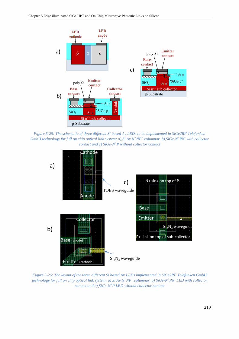
Chapter 5 Edge illuminated SiGe HPT and On Chip Microwave Photonic Links on Silicon
210
Figure 5-25: The schematic of three different Si based Av LEDs to be implemented in SiGe2RF Telefunken
GmbH technology for full on chip optical link system; a) Si Av N+NP
+ columnar, b) SiGe-N
+PN
- with collector
contact and c) SiGe-N+P without collector contact
Figure 5-26: The layout of the three different Si based Av LEDs implemented in SiGe2RF Telefunken GmbH
technology for full on chip optical link system; a) Si Av N+NP
+ columnar, b) SiGe-N
+PN
- LED with collector
contact and c) SiGe-N+P LED without collector contact
a)
b)
c)
Collector
contact
Base
contact
Emitter
contact
SiGe p+SiO2
Si n
poly Si
p-Substrate
Si n++ sub collector
Si n- N+
sin
k
Base
contact
Emitter
contact
SiGe p+SiO2
Si n
poly Si
p-Substrate
Si n++ sub collector
Si n-
a)
b)
c)
Cathode
Anode
Emitter (cathode)
Base (anode)
Collector Emitter
N+ sink on top of P-
Base
P+ sink on top of sub-collector
Si3N4 waveguide
Si3N4 waveguide
TOES waveguide
Chapter 5 Edge illuminated SiGe HPT and On Chip Microwave Photonic Links on Silicon
211
The structures of these optical sources can be described as follows:
a) Si Av N+NP
+ columnar: An n
+n-p
+ columnar structure is placed laterally on the semi-insulating
substrate. The regions are doped as indicated in Figure 5-25 a). The regions are appropriately
electrically contacted during experimental measurements in order to apply a forward bias at the first p+
n junction. Upon forward biasing, the depletion region penetrates through the n+ region in order to
strengthen and confine the electric field in the lowly doped n region. According to our previous
experience gained from the previously designed devices, we know that the light emission would occur
near the surface region of the middle N region and extend more or less laterally across the whole region.
b) SiGe-N+PN
-LED with collector contact: The basic vertical structure of a SiGe/Si HBT is used. The
emitter and collector contacts are grounded as required by the RF probe bias during the measurement
process and a forward biasing together with the modulation signal are applied on the base (P anode)
contact. Positive voltage bias places the anode contact in forward bias mode. The depletion region lies
toward the n side of either the collector or the base, as the base is highly doped. Thus light emission will
be in the n regions. As it will be describe in the following section, a V-shaped groove silicon nitride
waveguide with wider core is used along with this LED to realize the full optical link.
c) SiGe-N+P LED without collector contact: A vertical cubical columnar SiGe/Si HBT like structure is
used. It has four metallic contacts as shown in Figure 5-26 c) as it is designed from the HBT structure.
The first two on the side are emitter and base, and the last two on top and bottom are additional N+/P-
diode and P+/N+ diode sink as shown in Figure 5-26 c) which were designed for other purposes (which
will not be discussed here). The base-emitter SiGe pn junction is submitted to a forward bias in
avalanche regime as a positive voltage is applied through the base and thus light is emitted in the
depletion region of the pn junction. As it will be describe in the following section, a silicon nitride
waveguide with narrow core is used along with this LED to realize the full optical link as light emission
region is expected to be very narrow (only the depletion region of the base-emitter pn junction).
Since the SiGe/Si HBT of this nature has a transition frequency of up to 80GHz, it can be assumed that
this will benefit to the speed of the optical source with the base-emitter junction placed in avalanche
forward bias mode. With 20%-25% Germanium doping, the emitted wavelength for this design is
predicted to be about 850 nm. However the emission will be distributed among Si and SiGe regions
depending on the voltage bias applied across the junction.
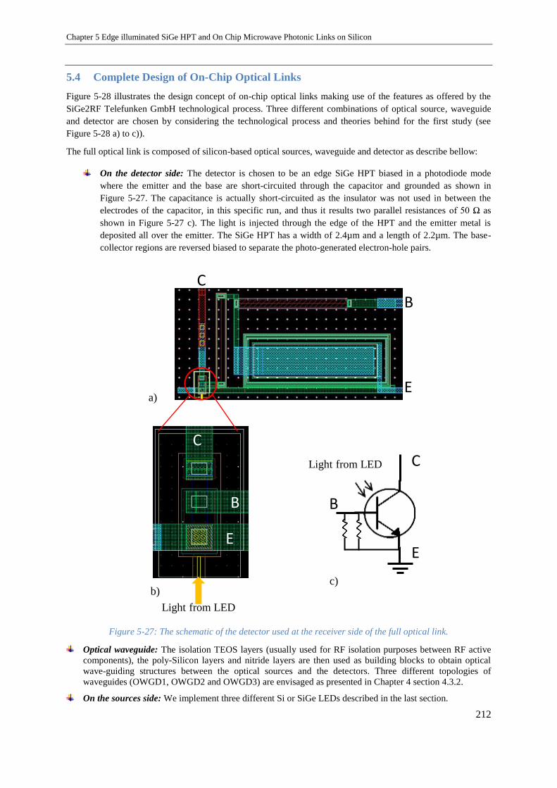
Chapter 5 Edge illuminated SiGe HPT and On Chip Microwave Photonic Links on Silicon
212
5.4 Complete Design of On-Chip Optical Links
Figure 5-28 illustrates the design concept of on-chip optical links making use of the features as offered by the
SiGe2RF Telefunken GmbH technological process. Three different combinations of optical source, waveguide
and detector are chosen by considering the technological process and theories behind for the first study (see
Figure 5-28 a) to c)).
The full optical link is composed of silicon-based optical sources, waveguide and detector as describe bellow:
On the detector side: The detector is chosen to be an edge SiGe HPT biased in a photodiode mode
where the emitter and the base are short-circuited through the capacitor and grounded as shown in
Figure 5-27. The capacitance is actually short-circuited as the insulator was not used in between the
electrodes of the capacitor, in this specific run, and thus it results two parallel resistances of 50 Ω as
shown in Figure 5-27 c). The light is injected through the edge of the HPT and the emitter metal is
deposited all over the emitter. The SiGe HPT has a width of 2.4µm and a length of 2.2µm. The base-
collector regions are reversed biased to separate the photo-generated electron-hole pairs.
Figure 5-27: The schematic of the detector used at the receiver side of the full optical link.
Optical waveguide: The isolation TEOS layers (usually used for RF isolation purposes between RF active
components), the poly-Silicon layers and nitride layers are then used as building blocks to obtain optical
wave-guiding structures between the optical sources and the detectors. Three different topologies of
waveguides (OWGD1, OWGD2 and OWGD3) are envisaged as presented in Chapter 4 section 4.3.2.
On the sources side: We implement three different Si or SiGe LEDs described in the last section.
B
E
C
C
B
Light from LED
C
E
B
Light from LED
a)
b)c)
E

Chapter 5 Edge illuminated SiGe HPT and On Chip Microwave Photonic Links on Silicon
213
Overall there are 3 different possible sources and 3 different waveguides, which make 9 possible combinations.
According to the following table and Figure 5-28, only 3 combinations were fabricated to respect our chip
surface limitations (area available for the run). Additional combinations could have been possible to vary the
alignment position of the waveguide to the optical source.
Table 5-2: The possible combination of the on-chip full optical link.
LEDs Optical waveguide
OWGD1 OWGD2 OWGD3
Si Av N+NP
+ columnar Test structure 1(TS1) x x
SiGe-N+PN LED with
collector contact
x Test structure 2 (TS2) x
SiGe-N+P LED without
collector contact
x x Test structure 3 (TS3)
Figure 5-28: Basic designs of the optical links using Si and SiGe Av LED, waveguides and SiGe-based detectors
with a) Design test structure 1 (TS1), b) Design test structure 2 (TS2) and c) Design test structure 3 (TS3).
a) Design Test Structure1 (TS1)
The first design Test Structure 1 (TS1) is shown in Figure 5-28 a). On the source side, Si Av n+np+ columnar
presented in section 5.3.3 is located laterally on the semi-insulating substrate.
Base
contact
Emitter
contact
SiGe p+
poly Si
Si n++ sub collector
Si n-
Si nSi3N4
Base
contact
Emitter
contact
SiGe p+SiO2
Si n
poly Si
p-SubstrateSi n++ sub collector
Si n-
Base
contact
Emitter
contact
SiGe p+
poly Si
Si n++ sub collector
Si n-
Si n
Si3N4
LED
cathode
N+
P+N
Base
contact
Emitter
contact
SiGe p+
poly Si
Si n++ sub collector
Si n-
LED
anode
Si n
TOES2
TOES1
a) TS1
b) TS2
c) TS3
TOES1
TOES1
Collector
contact
Base
contact
Emitter
contact
SiGe p+SiO2
Si n
poly Si
p-Substrate
Si n++ sub collector
Si n- N+
sin
k
p-Substrate

Chapter 5 Edge illuminated SiGe HPT and On Chip Microwave Photonic Links on Silicon
214
The region between the Si Av LED source and SiGe detector are filled with TEOS plasma deposited oxide
waveguide as presented in Chapter 4 section 4.3.2 by Optical Waveguide Design 1(OWGD1).
b) Design Test Structure 2 (TS2)
In our second test structure 2 (TS2) (Figure 5-28 b)), a vertical cubical columnar HPT like structure is used to
excite both the base-emitter and base-collector diode in forward avalanche regime (SiGe-N+PN LED with
collector contact). A V-shaped groove silicon nitride waveguide design is used in this design, as presented in
Chapter 4 section 4.3.2 (Optical Waveguide Design 2, OWGD2), in order to optimize coupling of light with the
Si Av LED. The same detector structure design as in TS1 is used in this optical link.
c) Design Test Structure 3 (TS3)
In a third design test structure (TS3) (Figure 5-28 c), a SiGe-N+P LED with an open collector is used as the
source. The silicon nitride optical waveguide similar to the one of TS2 but of smaller silicon nitride layer lateral
thickness, as presented in Chapter 4 section 4.3.2 (Optical Waveguide Design 3, OWGD3), is used. The
waveguide core size reduction enables less modal dispersion in the waveguide.

Chapter 5 Edge illuminated SiGe HPT and On Chip Microwave Photonic Links on Silicon
215
5.5 Experimental implementation and Results of the optical link
The fabricated on-chip integrated optical link is shown in Figure 5-29a). The device under test is a 750nm-
850nm Silicon base avalanche LED die (Wafer) where the light is coupled from the LED optical source through
the designed optical TEOS or Silicon Nitride optical waveguide to the SiGe detector.
Figure 5-29: (a) Microscopic picture of the optical link device (b) Microscopic picture of G-S-G probe
connection on one of the devices during measurement
The RF coupling between the source and the detector in the on-chip optical micro-links are tested and analyzed
using a vector network analyzer (VNA) (50 MHz-40 GHz). The experimental setup described in Chapter 2
section 2.3.2 is used to characterize the link (from source via the designed waveguides to the detector). 200µm
pitch GSG probes (shown in Figure 5-29 b)) are used to connect the DC and RF input signals to the devices on
the die. RF signal and DC biasing are applied on the source and detector sides through GSG probes via VNA
internal tee bias. RF signal on the source modulates the optical power emitted from the source.
The optical probing of the three test structures (TS1, TS2 and TS3) of the optical link are as shown below in
Figure 5-30.
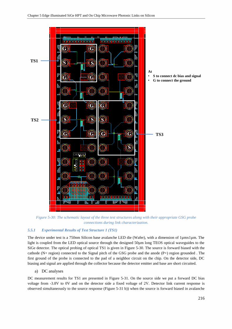
Chapter 5 Edge illuminated SiGe HPT and On Chip Microwave Photonic Links on Silicon
216
Figure 5-30: The schematic layout of the three test structures along with their appropriate GSG probe
connections during link characterization.
5.5.1 Experimental Results of Test Structure 1 (TS1)
The device under test is a 750nm Silicon base avalanche LED die (Wafer), with a dimension of 1µmx1µm. The
light is coupled from the LED optical source through the designed 50µm long TEOS optical waveguides to the
SiGe detector. The optical probing of optical TS1 is given in Figure 5-30. The source is forward biased with the
cathode (N+ region) connected to the Signal pitch of the GSG probe and the anode (P+) region grounded . The
first ground of the probe is connected to the pad of a neighbor circuit on the chip. On the detector side, DC
biasing and signal are applied through the collector because the detector emitter and base are short circuited.
a) DC analyses
DC measurement results for TS1 are presented in Figure 5-31. On the source side we put a forward DC bias
voltage from -3.8V to 0V and on the detector side a fixed voltage of 2V. Detector link current response is
observed simultaneously to the source response (Figure 5-31 b)) when the source is forward biased in avalanche
TS1
TS2
TS3
At
• S to connect dc bias and signal
• G to connect the ground

Chapter 5 Edge illuminated SiGe HPT and On Chip Microwave Photonic Links on Silicon
217
mode as in Figure 5-31 a). The observed detector current is of the order of 10 to 100 nA when the Si Av LED
source is activated.
Figure 5-31: DC I-V Curves for TS1 (a) Reverse biased Optical source IV curve (b) Detector optical link current
versus source voltage.
In the I-V curves monitored on the detector side, a detector current IC of about 90nA is detected for a voltage at
the source Vs =3V (Figure 5-31). This observation may suggest that the optical transmission through the
designed waveguides indeed occurs from the optical source to the optical detector through the Silicon-oxide
waveguide.
b) RF analyses
The experimental RF response of test structure 1 when optical source and detector are activated (biasing with
Vs=-2.6V on the source and 2V on the detector) is shown in Figure 5-32. Only S21 and S12 (S-Parameters) of
the two port network analyzer measurements are presented here versus frequency. It shows low and about equal
values for both S21 and S12. This implies that the optical coupling is low and dominated by the substrate
parasitic coupling in RF. This indicates that our design philosophy of TEOS 2 yielding higher refractive index (n
= 1.48) with thermal annealing process is not successful enough or that the waveguide is misaligned with the
optical source. The DC measurements show positive results, however the overall efficiency is not high enough to
compete with the RF substrate coupling. However, this area of investigation could be further exploited
Figure 5-32: RF coupling results for the fabricated on-chip micro-optical links in TS1.
5.5.2 Experimental Results of Test Structure 2 (TS2)
In this test structure the optical source uses an 850nm SiGe-based avalanche LED die (Wafer), with a size of
1µmx1µm. It is mostly an HBT structure biased in a specific regime. The waveguide in this device is a V-shape
Frequency in Hz
Po
we
r in
dB

Chapter 5 Edge illuminated SiGe HPT and On Chip Microwave Photonic Links on Silicon
218
groove silicon nitride core surrounded by a TEOS oxide of lower refractive index. The light is coupled from the
LED optical source through the designed 50µm long silicon nitride optical waveguides to the SiGe detector.
The RF probing of TS2 optical link is as shown in Figure 5-30. On the source side, the emitter and collector
contacts are connected to ground while the base is connected to the Signal pitch of the GSG probe. Both the
base-emitter and base-collector diode are thus forward biased. On the detector side, the SiGe HPT is biased in
the same condition as TS1.
a) DC analysis
To activate the devices under test, we swept on the source side the bias voltage from 0V to 1.4V on the anode
(forward biasing) whereas on the detector side a fixed DC voltage of 2V is applied. In the IV curves monitored
on the detector side, a detector current IC of about 90nA is detected for the voltage Vs of 1.3V at the source
(Figure 5-33). The measured curves are obtained at both source and detector sides when the optical source is
forward biased. It can be seen that, when forward basing the source diode junction, current flows through the
device up to about 9mA under 1.4V. The forward bias knee voltage is about 1.2V as shown in Figure 5-33 a). It
can be observed that the level of current observed into the collector is similar to TS1, except that the knee
voltage is shifted to lower values. This may be attributed to either the coupling substrate as in TS1, or the optical
coupling.
Figure 5-33: DC IV Curves for TS2 (a) Forward biased Optical source IV curve (b) Detector optical link
response when source is activated.
b) RF analyses
Figure 5-34 shows the experimental results on test structure TS2 when the optical source is forward biased by
1.2V and reversed biased at the detector by 2V. Again, only S21 and S12 S-parameters are considered here. Our
measurement results show a S21 somehow higher than S12 while the two ports have the same output power.
This is an indication that an optical coupling is then probably present along the silicon nitride V-groove
waveguide in TS2. The higher S12 value observed frequency increase is attributed to parasitic conduction along
the semi-insulating substrate. The possibility of electrical coupling through the oxide layers is rejected as it
would be several orders lower. Despite the fact that S21 is higher than S12, the difference is too small and as the
trends of the curves is the same, it is still uncertain to attribute this to the clear demonstration of the presence of
an optical coupling. However, certain design aspects of these structures (TS2) could still be improved.

Chapter 5 Edge illuminated SiGe HPT and On Chip Microwave Photonic Links on Silicon
219
Figure 5-34: RF coupling results for the fabricated on-chip micro-optical links in TS2.
5.5.3 Experimental Results of Test Structure 3 (TS3)
The device under test is SiGe-based avalanche LED die (Wafer), with a size of 1µmx1µm. It is mostly a pn
photodiode from HBT structure. The light is coupled from the LED optical source through the silicon nitride
optical waveguides to the SiGe detector. The waveguide in this device is a silicon nitride with narrow core of
refractive index of (n=2.4) surrounded by a TEOS1 oxide layer with lower refractive index of (n=1.46) and of
50µm length.
The RF probing of TS3 of the optical link is as shown in Figure 5-30. The source has 4 connections in order to
have flexible connections. The signal and DC biasing are applied through the base, the emitter is grounded, and
the n+ and p+ sink contacts are left open. The first ground of the probe is connected to the pad of a neighbor
circuit on the chip. On the detector side, DC biasing and signal are applied through the base, itself short circuited
to the emitter (thus emitter contact is left open). The collector is grounded as indicated in Figure 5-30. This
situation is different from the previous case. It is expected to reduce the substrate coupling by ensuring a ground
voltage of the N+ sub collector region.
a) DC analysis
We swept the source DC bias voltage from 0V to 1.3V (it forward-biases the base-collector junction) and fix the
detector voltage at -1V though the base (it is thus +1V Vce). IV curves are shown in Figure 5-35 a) and b). A
current of about +0.8mA (Ib=-0.8mA) is detected on the SiGe HPT collector side (in PD mode) at the voltage Vs
of 1.3V at the source.
These DC I-V curves are obtained at both source and the detector for this test structure device when the LED
source is forward biased. It can be seen that, when the device is placed in a forward bias condition, current flows
through the device up to about 7mA. The forward bias knee voltage is about 1.2V as shown in Figure 5-35 a).
Such currents are much higher than the 90nA measured in the previous sections. This may indeed be a clear
demonstration of an optical coupling from the source to the detector, demonstrating then a good efficiency of the
optical waveguides. This observation hence confirms that optical transmission through the designed nitride
waveguides indeed occurs from the optical source to the optical detector through the V-groove nitride core
waveguide surrounded by TEOS1 layer.
Frequency in Hz
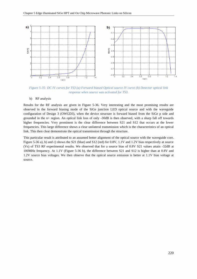
Chapter 5 Edge illuminated SiGe HPT and On Chip Microwave Photonic Links on Silicon
220
Figure 5-35: DC IV curves for TS3 (a) Forward biased Optical source IV curve (b) Detector optical link
response when source was activated for TS3.
b) RF analysis
Results for the RF analysis are given in Figure 5-36. Very interesting and the most promising results are
observed in the forward biasing mode of the SiGe junction LED optical source and with the waveguide
configuration of Design 3 (OWGD3), when the device structure is forward biased from the SiGe p side and
grounded in the n+ region. An optical link loss of only -30dB is then observed, with a sharp fall off towards
higher frequencies. Very prominent is the clear difference between S21 and S12 that occurs at the lower
frequencies. This large difference shows a clear unilateral transmission which is the characteristics of an optical
link. This then clear demonstrate the optical transmission through the structure.
This particular result is attributed to an assumed better alignment of the optical source with the waveguide core.
Figure 5-36 a), b) and c) shows the S21 (blue) and S12 (red) for 0.8V, 1.1V and 1.2V bias respectively at source
(Vs) of TS3 RF experimental results. We observed that for a source bias of 0.8V S21 values attain -32dB at
100MHz frequency. At 1.1V (Figure 5-36 b), the difference between S21 and S12 is higher than at 0.8V and
1.2V source bias voltages. We then observe that the optical source emission is better at 1.1V bias voltage at
source.
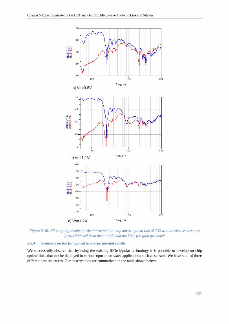
Chapter 5 Edge illuminated SiGe HPT and On Chip Microwave Photonic Links on Silicon
221
Figure 5-36: RF coupling results for the fabricated on-chip micro-optical link of TS3 with the device structure
forward biased from the n+ side and the SiGe p region grounded
5.5.4 Synthesis on the full optical link experimental results
We successfully observe that by using the existing SiGe bipolar technology it is possible to develop on-chip
optical links that can be deployed in various opto-microwave applications such as sensors. We have studied three
different test structures. Our observations are summarized in the table shown below.
a) Vs=0.8V
b) Vs=1.1V
c) Vs=1.2V

Chapter 5 Edge illuminated SiGe HPT and On Chip Microwave Photonic Links on Silicon
222
Table 5-3: The observations on full optical link experimental studies
Test
structure
Performance Observations
IC RF
TS1 90nA at Vs=3V Not successful DC observation: there is a dc coupling,
however in the nA range only. This may be
attributed to either substrate coupling or
optical coupling. From the RF measurements
and from the similitude to TS2 measurements,
it seems to be only the substrate coupling.
RF observation: The RF transmission is
clearly dominated by the substrate coupling.
No optical transmission can be demonstrated.
TS2 90nA at
Vs=1.2V
Not successful DC observation: the dc coupling is also
present. A shift in the voltage knee of the
diode curve is observed, potentially due to a
change in the biasing influence of the source to
the substrate. The amplitude in the detected
current is very similar to the TS1. This
indicates that indeed only the substrate
coupling is observed.
RF observation: The RF transmission is
clearly dominated by the substrate coupling.
Still a slight variation is visible, which may
indicate an eventual presence of an optical
transmission. But no clear evidence of it can
be given.
TS3 0.8mA at
Vs=1.3V
successful DC observation: there is a clear dc optical
emission, transmission and detection.
Photocurrents up to 0.8mA are detected at the
output of the link.
RF observation: There is a clear and strong
Opto-RF transmission through the optical link.
A gain of about -30dB up to 100MHz is
measured.

Chapter 5 Edge illuminated SiGe HPT and On Chip Microwave Photonic Links on Silicon
223
5.6 Conclusion
The following major conclusions can be derived from the work presented in this chapter:
The first edge illuminated SiGe/Si HPT was designed and fabricated by using the existing SiGe BiCMOS
technology. A two-step post fabrication process was used to create an optical access on the edge through
successive smooth and full dicing techniques. A low frequency opto-microwave responsivity of 0.45A/W and an
opto-microwave cutoff frequency of 890MHz were measured. Compared to top illuminated HPT, edge
illuminated HPT improves the cutoff frequency by more than a factor two and also improves the responsivity
from 0.32A/W (for 10x10µm2 HPT) to 0.45A/W. Compared to the top illuminated HPT of the same size
(5x5µm2 HPT), the edge illuminated HPT improves the f-3dB by a factor of more than two and it also improves
the low frequency responsivity by a factor of more than four, while using a simple lensed MMF fiber for the
coupling. This phototransistor could be used in further microwave photonic applications whose operating
frequency could lie in the 1-10GHz range where integration to Si Integrated Circuits (ICs) and costs are the main
issues. Further optical coupling structures could improve the performances. However, these results already
demonstrate that a simple etched HPT is still enough to achieve improvements compared to the top illuminated
HPT without the need of complex coupling structure, even when using MMF. We have also observed the impact
of the substrate photodiode and metal proximity effect on the performances of edge illuminated SiGe HPTs.
These results will have a clear adding value to some further design optimization of the device. Finally, the
substrate photodiode influence is minimized in laterally illuminated structure when compared with top illumined
one.
The chapter then conducted some investigation toward a full integration of an optical link on the same chip. The
major advantages of using 750nm wavelength are the ease of integration of optical source, waveguide and
optical detector all in Silicon, thus all on the same chip.
We have demonstrated a full optical link integrated in the SiGe bipolar technology of study. Different structures
were tested. A successful demonstration was obtained with a forward biased SiGe/Si avalanche LED source
coupled to a SiGe HPT in photodiode mode through a Si3N4/SiO2 optical waveguide., leading to total link budget
to about -30dB, at even low power consumption rates, since only 1V and few mAs are required to operate these
devices. However substantial further development works still need to be performed. Quite good first iteration
optical coupling from source to detector has been demonstrated from this work at both DC and AC levels.
This SiGe/Si fully integrated optical link technology offers wide application possibilities for diverse micro-
sensing and microwave photonic system development.
Thesis conclusion and Perspectives
224
Thesis conclusion and Prospects
I. Conclusion
With the recent explosive growth of connected objects, for example in Home Area Networks (HAN), the
wireless and optical communication technologies start to merge further, through the interdisciplinary domain
called Microwave photonic technology (MWP). The advantage of MWP systems is that they can benefit from
the strengths of both optical and wireless technologies, such as the inherently large bandwidth of optical fiber
and unused bandwidth in the mm-wave wireless spectrum. For this reason, a hybrid system has the potential to
provide very high data transmission rates with minimal time delay. Moreover, MWP technology has recently
extended to address a considerable number of applications [11] including 5G mobile communication, biomedical
analysis, Datacom, optical signal processing and for interconnection in vehicles and airplanes. Many of these
novel application areas also demand high speed, bandwidth and dynamic range at the same time they require
devices that are small, light and low power consuming. Furthermore, implementation cost is a key for the
deployment of such MWP systems in home environment and various integrated MWP applications, becoming
more and more sensitive when the application is closer to the end user. This is especially the case for Home-
Area-Networks using an optical infrastructure, but also sensing applications where sensors could be widely
deployed in large numbers.
This PhD work focused on the development of very cheap, Bipolar and BiCMOS integrated SiGe/Si MWP
devices such as SiGe HPTs, Si LEDs and SiGe LEDs, and focused on the combined integration of mm wave and
optoelectronic devices for various applications involving short wavelength links (750nm to 950nm).
Compared to bulk CMOS, the BiCMOS SiGe HBT presents a much higher cut-off frequency at a given
technology node. To reach similar cut-off frequencies, bulk CMOS designs have to use much smaller process
nodes, forcing compromises on the design and leading most of the time to overall lower performances and higher
cost. It is also possible to develop some efficient detectors in the wavelength range from 750nm to 900nm, as
high speed SiGe phototransistors were demonstrated since 2003 in bipolar and BiCMOS industrial process.
Silicon is also a material of choice to integrate optical waveguides, electrical transmission lines and active
devices simultaneously up to the millimetric waves. Therefore SiGe Bipolar or BiCMOS technologies are good
candidates to implement MWP systems. The improvement of the SiGe HPTs, the further development and
convergence of electrical transmission lines and optical waveguides for intra- and inter- chips interconnects, are
steps to create complete RoF transceiver on a Silicon platform including a high speed VCSEL for the sources,
ultimately targeting an monolithic integrated optoelectronic receiver and strongly integrated transmitter. A last
step covered by the PhD is then the investigation of more futuristic Silicon-based optical sources directly
integrated in the bipolar process. It is also important to note that, despite single mode fiber would be highly
suitable to improve performances, this work kept focused on the compatibility to multimode optical fibers as this
one is still yet the required standard for Home-Area-Networks.
In this research, we have chosen the SiGe2RF Telefunken GmbH SiGe Bipolar technology to implement SiGe/Si
MWP devices (SiGe HPT, Si and SiGe LEDs and optical waveguide) demonstrating as well a complete on-chip
optical link. The fabrication of MWP devices using this technology does modify neither the vertical stack of
layers nor the masks set that is used. Only combination of existing layers and masks is done using the standard
SiGe2RF HBT mask set. This ensures the direct integration with the technological process and the potential
integration of complete opto-electronic radio frequency (OE-RF) circuits

Thesis conclusion and Perspectives
225
SiGe HPTs have also the advantage to combine a PIN photodiode with an HBT, thus lowering the output
impedance and making easier the match to the other components of the electronic circuits. Indeed, it avoids the
need of a Trans-impedance Amplifier (TIA). The other advantages of HPT is the presence of three terminals
(optical access, base, collector) which permits original function such as mixers and self-oscillators that are not
described in this PhD, but are perspective for OE-EO circuit designers.
The basic HPT structure is designed by extending the emitter, base and collector layers of the reference HBT.
The optical injection is made through the emitter for top illuminated HPT structure. The light path goes through
the oxide and polysilicon layers of the emitter before entering the Si emitter, SiGe base and Si collector regions.
To obtain edge illuminated SiGe HPT structure we perform a post fabrication process through smooth dicing and
subsequent full dicing. Those HPT are essentially large HBTs whose emitter metallization only partially covers
the emitter region. The substrate is grounded through a p+ guard ring region to control the substrate photocurrent
(mainly holes) influence on the HPTs dynamic behavior.
On the source side, we implement Si and SiGe LED optical sources using the same technology with appropriate
electrical contacts in order to apply a forward bias at the p+ n junction so that the light emission occur near the
surface region of n region and extend more or less laterally across the whole region. We use the presence of
several oxide and nitride layers in the technological process to design the Si3N4 or TOES optical waveguides.
The full optical link was designed by interconnecting a SiGe LED and edge-SiGe HPT using an nitride optical
waveguide.
Main conclusions drawn in the chapters of this PhD are synthesized as given below:
Different methods of characterizing top and edge illuminated HPTs were presented in Chapter 2. De-embedding
is crucial to extract the effect of the bench fixtures like the RF probes and the optical probing link in order to
know the exact opto-microwave behavior of the phototransistor. The dc photocurrent analysis of a
phototransistor both in photodiode and phototransistor modes helped us to understand the physical behavior of
SiGe/Si HPTs and the impact of the chosen geometrical parameters. Extracting the substrate effect from the
intrinsic phototransistor response and determining the different photocurrents contribution (primary
photocurrent, optical amplification, base efficiency) was also an important topic in order to observe the intrinsic
behavior of the SiGe/Si HPTs. Extracting the junction capacitances and transit times was an additional important
part of this work as they will be used in the future electrical/opto-microwave modeling of the SiGe
phototransistors and as it provides further physical information on the behavior of photogenerated carriers for
further HPT design optimizations.
In Chapter 3 top illuminated SiGe HPTs of different optical window sizes were designed and characterized in
terms of DC, electrical and opto-microwave behavior at different biasing points. This analysis allowed us finding
an optimum bias point that maximizes the frequency response of the HPT including opto-microwave gain, cutoff
frequency and optical transition frequency. From the microwave behavioral study we measure an electrical
transition frequency fT value of 50GHz for 10x10µm2 HPT which is the same value as pure non SIC HBT
technology. However, we measure an electrical transition frequency of only 26.5GHz for 3x3µm2 HPT. This
unusual behavior is due to the 2D electrical extension effect which is directly related to the built in potential.
This effect has been demonstrated through various mathematical models. A proper design rules is then proposed
to get a symmetric contacts on the collector, base and emitters so that the electrical field will be more vertical;
and also to fragment the HPT in smaller individual HPTs as the electrical extension may reach a limit in its
increase. We have also carried out OM SNOM and DC SNOM analysis at their optimum biasing conditions as
they are crucial to understand the impact of SiGe HPTs structure. OM SNOM analysis allowed the extraction of
an opto-microwave response at each position of the optical illumination over the device. DC SNOM analysis
allowed the extraction of substrate photocurrent at each optical probe position. It has a great impact on the
responsivity and speed of the SiGe HPT. The substrate effect is more visible in the PD mode operation than in
the HPT mode where it is hidden by the transistor effect. We observe that the intrinsic optical transition
frequency fTopt is much lower than the electrical transition frequency fT. It is explained by the addition of
capacitive and transit time terms related to the photodetection mechanism in the intrinsic transistor and substrate
region of the structure. The opto-microwave capacitance and transit time terms are increased by more than a

Thesis conclusion and Perspectives
226
factor of 3.5 and 21 respectively when compared with their electrical equivalent values. We have also observed
that the performance of SiGe/Si HPT is highly affected by the level of the injected optical power. This could be
related to self-biasing of the HPT with the optical power and also related to the variation of the modes of the
optical source under use (and thus the illumination pattern). The complete HPT opto-microwave capacitance and
transit time terms are increased with decreasing the injected optical power level. We were able to demonstrate an
intrinsic optical transition frequency of 6.5GHz and absolute responsivity of up to 0.8A/W for 10x10µm2 HPT
which has the best performance compared to other optical window size HPTs.
Then in Chapter 4, for future intra /inter chip hybrid interconnections, we have successfully designed polymer
based low loss microwave transmission lines and optical waveguides on low resistive silicon substrate. It is a
step to envisage further silicon-based platforms where SiGe HPT could be integrated at ultra-low cost and high
performances with other structures such high-speed VCSEL to build up a complete optical transceiver on a
silicon optical interposer. The polymer is used as dielectric interface between the line and the substrate for
electrical interconnections and to design the core and cladding of the optical waveguide. Coplanar, microstrip
and grounded coplanar lines based on SU8, BCB and Parlyene have been investigated and designed in the mm
wave frequency range. Grounded coplanar and microstrip lines have less attenuation than coplanar line as the
metallic ground prevents the propagation of electric field into the lossy silicon substrate. The targeted
characteristic impedance for all types of line was 50Ω. The inclusion techniques of optical waveguide with mm
microwave transmission lines are also presented. The interconnections of mm wave lines on silicon and polymer
are analyzed through HFSS simulation. This study provides an input for the future integration of mm and optical
waves within a single chip or for interconnections between several chips. About 1dB/mm attenuation in the
millimeter wave frequency range was experimentally measured for a coplanar waveguide structure. This of
course indicates that our design optimized using HFSS software is well suited even though the fabricated
structure was not good enough.
In Chapter 5, the first BiCMOS compatible edge illuminated SiGe/Si HPT was then successfully designed and
fabricated by using the standard SiGe Telefunken bipolar technology coupled to a multimode fiber. A two-step
post fabrication process was used to create an optical access on the edge through polishing and dicing
techniques. A low frequency opto-microwave responsivity of 0.45A/W and opto-microwave cutoff frequency of
890MHz was measured. Compared to top illuminated HPT, edge illuminated HPT improves the cutoff frequency
by more than a factor two and also improves the complete responsivity from 0.32A/W (for 10x10µm2 HPT) to
0.45A/W. The impact of the substrate photodiode is minimized in lateral illuminated case by a factor of 2.4
times. Compared to the top illuminated HPT of about the same size (5x5µm2 HPT), the edge illuminated HPT
improves the f-3dB by a factor of more than 2.5 and also improves the low frequency responsivity by a factor of
more than four while using a simple lensed multi-mode fiber (MMF) for the coupling. This phototransistor could
be used in further microwave photonic applications whose operating frequency could lie in the 1-10GHz range
where integration in Si Integrated Circuits (ICs) and costs are the main issues. Further optical coupling structures
could improve the performances. However, these results demonstrate that a simple etched HPT is still enough to
achieve improvements compared to the top illuminated HPT without requiring a complex coupling structure,
even when using MMF. We have also observed the impact of the substrate photodiode and of the metal
proximity on the performances of edge illuminated SiGe HPTs.
The design and fabrication of the first full optical link based on SiGe BiCMOS technological process was
presented in Chapter 5 as well. It was a collaboration work between ESYCOM-ESIEE Paris and the team of
Pr.Snyman in South Africa, in the University of South-Africa (UNISA) and formerly in the Tshwane University
of Technology (TUT). We have designed three different optical links comprising Si or SiGe AvLED on the
source side, Si3N4 or TSOE optical waveguide and SiGe HPT on the detector side. In particular, the use of Si-Ge
technology detector in association with Si AvLEDs demonstrates potential incorporation of these devices in
standard CMOS technological process. Our proposed use of TEOS and silicon nitride based waveguides which
were fabricated thanks to the advanced capabilities offered by the SiGe bipolar BiCMOS process technologies,
permits to design a wide variety of optimized waveguide structures between the optical source and the detector
on the chip.

Thesis conclusion and Perspectives
227
The designed silicon based optical waveguides use the advantage of the oxide layers existing in SiGe BiCMOS
technology. The optical waveguide associated to the choice of 0.75μm to 0.85µm operating wavelength may
show new routes of both developments and applications in silicon photonics technology, or at least permit an
important spin-off of this technology towards low cost ease of fabrication. The major advantage of using 750nm
wavelength is the integration ease of optical source, waveguide and optical detector all in a same chip; this
implies a simplification of design and processing procedures.
We have shown the forward biased micro-dimensioned SiGe/Si light sources have achieved high optical
emissions, leading to reduced total link budgets to about -30dB, at even low power consumption rates, since only
1V and few mA are required to operate these devices. However substantial further development works still need
to be performed. Quite good first iteration optical coupling from source to detector has been demonstrated from
this work at both DC and AC levels. This full optical link technology offers wide application possibilities for
diverse micro-sensing and microwave photonic systems in which optical communication and data transfer play
an important role.
II. Perspectives
The perspectives of this thesis are presented as follows:
Concerning the SiGe HPT:
For the detection of optical signals in MWP systems, photodetector technologies with high responsivities,
large bandwidths and high optical power handling capabilities are required. The raw SiGe phototransistor
optical transition frequency (fTopt) is ultimately shadowed by its substrate photodiode carriers’ transient
time and other intrinsic factors, such as the junction capacitances. Thus, a solution to get rid of the
substrate contribution in the top illuminated HPTs could be through a proper design of the optical window
with a metallic diaphragm avoiding the illumination of the substrate photodiode. Indeed, the substrate
photodiode would be hidden either by metallic contacts or by upper layers of the intrinsic HPT. One could
also consider in the future design that edge illuminated structures minimizes the influence of substrate
diode, but still it needs extra techniques to avoid completely. Alternatively taking advantage of the
substrate could be envisaged leading to combined HPT+PD structure.
To improve the optical transition frequency (fTopt) and the opto-microwave cutoff frequency (f-3dB) of SiGe
HPT, it would be important to reduce the electrical transit times and the optical induced terms. One
direction is to consider higher fT/fmax technologies like STMicroelectronics (230GHz/280GHz) or IHP
(300GHz/500GHz). The second direction is to optimize the design of the HPT, and especially engineering
the 2D configuration of the electrical field distribution within the HPT. A proper position of the base and
collector contacts is a key direction, together with the size optimization.
Low noise HPTs are very useful in certain MWP applications such as optoelectronic oscillators, tunable
and reconfigurable filters and photonic beamforming. Further characterization of the SiGe HPT in terms of
noise would be then important as well.
These phototransistors could also be implemented in applications where a single mode fiber is used at
850nm. Characterizing the device through single mode with a smaller spot optical probe could be
important for such applications. This activity is ongoing.
Compact circuit modelling could bring clear information for future design aspects of the HPTs.
Increasing the operating frequency of SiGe photodetectors into the millimeter wave range (60GHz) would
be very useful in certain MWP applications. While being an ambitious goal, a potential direction would be
to develop a phototransistor structure overcoming the frequency limitation of traveling wave HPT. For this
purpose the interaction between optical and electrical waves have to be analyzed in further detail through
physical and EM simulations.

Thesis conclusion and Perspectives
228
Concerning the optical source and full optical link:
We demonstrated in this thesis that the SiGe Av LEDs, the waveguide and the detector technology
provides a cutoff frequency of more than 200MHz. However, this still needs to be improved through the
proper design of the overall link.
The physical behavior of Si Av LEDs and SiGe Av LEDs needs to be studied using commercial software
simulators. Performing the equivalent circuit or physical modelling of the individual devices of the link
will provide important information for future design. Improve the coupling efficiency to the optical
waveguide is also an important issue.
Concerning the polymer based interconnections:
We found a promising experimental result for coplanar waveguide structure even though the fabricated
line was not good enough due to technical limitations. Further process developments are still needed.
Thus, fabricating the waveguides (optical and electrical waveguides) with appropriate technological
process using the designed layout proposed in this thesis and characterization it for its validation is crucial.
Moreover, further work is still required for the hybrid integration of VCSELs, HPTs, antenna units, and
electrical and optical interconnections on silicon wafer for low cost MWP applications.

Thesis conclusion and Perspectives
229
Personal scientific Publications
Journals and Articles
[1] Z. G. Tegegne, C. Viana, M. Rosales, J. Scheillein, J.-L. Polleux, C. Algani, M. Grzeskowiak and E.
Richalot, “An 850nm SiGe/Si HPT with a 4.1GHz maximum Optical Transition Frequency and
0.805A/W Responsivity”, in International journal of microwave and wireless technologies, 2015, dio:
10.1017/S17907875001531.
[2] Z. G. Tegegne, C. Viana, J.-L. Polleux, M. Grzeskowiak, E. Richalot “Edge illuminated SiGe
Heterojunction Phototransistor for RoF applications” in IEEE/IET Electronics Letters, Vol.51, Iss.8, p.
1906-1908, 2015.
[3] C. Viana, Z.G. Tegegne, M. Rosales, J.L Polleux, C. Algani, V. Lecocq, C. Lyszyk, S. Denet, “A hybrid
photo-receiver based on SiGe Heterojunction Photo-Transistor for low cost 60GHz Intermediate-
Frequency Radio-over-Fiber Applications” in Electronics, Vol.51, No.8, pp.640-642, 2014.
International Conferences with proceedings
[4] Z. G. Tegegne, C. Viana, M. Rosales, J.-L. Polleux, C. Algani, M. Grzeskowiak, E. Richalot, "Substrate
diode effect on the performance of Silicon Germanium phototransistors",in IEEE International topic
meeting on microwave photonic, Cyprus, 2015. [5] Z. G. Tegegne, C. Viana, J.-L. Polleux, M. Grzeskowiak, E. Richalot “Improving the opto-microwave
performance of SiGe/Si Phototransistor through edge illuminated structure” in PhotonicsWest 2016
conference, Paper 9752-44, San Francisco, 13-18 Feb 2016. [6] K. Ogudo, L. W. Snyman, J.L Polleux, C. Viana, Z.G .Tegegne, D. Schmieder, “Towards 10 – 40 GHz
on-chip micro-optical links with all integrated Si Av LED optical sources, Si N based waveguides and
Si-Ge detector technology“ in PhotonicsWest 2014 conference, Paper 8991-7, San Francisco, 1-6 Feb
2014. [7] K. Ogudo. A, L.W. Snyman, J.L. Polleux, C. Viana, Z.G Tegegne, “Realization of 10 GHz minus 30dB
on-chip micro-optical links with Si-Ge RF Bi-Polar technology”, in Proceeding of SIPEE, Vol.9257, Republic of South Africa; May 2014
National conferences with proceedings
[8] Z.G. Tegegne, C. Viana, M. Rosales, J.L. Polleux, M. Grzeskowiak, E. Richalot, C.Algani “Impact du
substrat sur les performances de phototransistors microondes SiGe/Si” 19emes Journees Nationales
Microondes, Bordeaux, May 2015.

References
230
References [9] IEEE 802.11 standards Tutorial http://www.radio-electronics.com/info/wireless/wi-fi/ieee- 802-11-
standards-tutorial.php
[10] Carlos Viana “Technological development and system integration of VCSELs and SiGe HPT receivers for
60GHz low cost Radio-over-Fiber applications” Universite Paris-Est, Ecole Doctorale MSTIC, PhD
Thesis 2014.
[11] Stavros Iezekiel and Maurizio Burla “RF Engineering Meets Optoelectronics Progress in Integrated
Microwave Photonics” IEEE Microwave Magazine, 1527-3342, September 2015.
[12] http://www.radio-electronics.com/info/wireless/wi-fi/ieee-802-11n.php
[13] High Rate 60 GHz PHY, Mac and HDMI PAL, Standard ECMA-387, ECMA international December
2010.
[14] Part 15.3: Wireless MAC and PHY Layer Specifications for High Rate Wireless Personal Area Networks
(WPANs): Amendment 2: Millimeterwave based Alternative Physical Layer Extension, IEEE
P802.15.3c/D13 July 2009.
[15] Wireless Gigabit Alliance (WiGig), http://wirelessgigabitalliance.org
[16] NAVAIR Electronic Warfare/Combat Systems “Electronic Warfare and Radar Systems Engineering
Handbook” NAWCWD TP 8347, April 1997.
[17] Christian Rumelhard, Catherine Algani, Anne Laure Billabert “Microwave Photonic Links components
and circuits” Book first published 2011 in Great Britain and the United states.
[18] J. Guillory et al., “60GHz Intermediate Frequency over Fiber using a passive Multipoint-to-Multipoint
architecture”, 16th European conference on Networks and Optical Communications, July 2011.
[19] V. Sorianello, G. De Angelis, A. De Iacovo, L. Colace, S. Faralli, and M. Romagnoli “High responsivity
SiGe heterojunction phototransistor on silicon photonics platform” Optics Express, Vol. 23, No. 22, Nov
2015.
[20] B. J. Thibeault, K. Bertilsson, E. R. Hegblom, E. Strzelecka, P. D. Floyd, R. Naone, and L. A. Coldren,
‘High speed characteristics of low optical loss oxide apertured vertical cavity lasers”, IEEE Photonics
Technology Letters, Volume 9, pp.11–13, 1997.
[21] Y. Satuby, and M. Orenstein, “Limits of the modulation response of a single-mode proton implanted
VCSEL”, IEEE Photonics Technology Letters, Volume 10, pp.760–762, 1998.
[22] K. L. Lear, V. M. Hietala, H. Q. Hou, M. Ochiai, J. J. Banas, B.E. Hammons, J. C. Zopler, and S. P.
Kilcoyne, “Small and large signal modulation of 850 nm oxide-confined Vertical-Cavity Surface-Emitting
Lasers”, Summaries of Papers Presented at the Conference on Lasers and Electro-Optics ( CLEO '97),
Volume 15, pp.69–74, 1997.
[23] Dyan Ali et al “High Speed SiGe pin W-Structure Photodetectors at Telecommunication Wavelengths
Grown Directly on Si” Conference on Quantum Electronics and Laser Science, IET, pp.1-2, 2008 San
Jose, CA.
[24] Henry C. Lee et al “A Novel High Speed Silecon MSM Photodetector oprating at 830nm wavelengh”
IEEE Electronic Device Letters, Vol.16, No.5 May 1995.
[25] Papichaya Chaisakul et al “10 GB/s Ge/SiGe Multiple Quantum Well Waveguide Photodetector” IEEE
Photonics Technology Letters, Vol.23, No.20, October 15, 2011.
[26] Yoshihiro Yoneda, Ryuji Yamabi, Sosaku Sawada, and Hiroshi Yano “Large-area Top-Illuminated InP-
Passivated Mesa-type InGaAs pin Photodiodes for High-bit-rate Multi-mode Fiber Applications” IEEE
OFC/NFOEC, pp. 1-3, San Diego, CA 2008.

References
231
[27] Lingzi Zhang et al “Wavelength Tunable Si Based InGaAs Resonant cavity enhanced photodetectors using
Sol-Gel Wafer bonding technology” IEEE Photonic Technoloy Letters, Vol.23, No.13, July 1, 2011.
[28] Xiaofeng Duan, Yongqing Huang, Xiaomin Ren, Yufeng Shang, Xinye Fan, and Fuquan Hu “High-
Efficiency InGaAs/InP Photodetector Incorporating SOI-Based Concentric Circular Subwavelength
Gratings” IEEE Photonics Technology Letters, Vol. 24, No. 10, May 15, 2012.
[29] D.Wake, S. Dupont, C. Lethien, J.-P. Vilcot and D. Decoster, ‘‘Radiofrequency transmission of 32-QAM
signals over multimode fibre for distributed antenna system applications’’, Electron. Lett., vol. 37, 1087–
1089, 2001.
[30] Stavro Iezekiel “Microwave Photonics Devices and Applications” Department of Electrical and Computer
Engineering, University of Cyprus, Cyp. Published 2009.
[31] R. J. Deri, “Monolithic integration of optical waveguide circuitry with 111-V photodetectors for advanced
lightwave receivers,” J. Lightwave Technol., vol. 11, pp. 1296-1313, 1993.
[32] J. G. Bauer, C. Lauterbach, D. Romer, N. Emeis, L. Hoffman, and G. Ebbinghaus, “Monolithic integration
of a waveguide InGaAsflnP pin photodiode with a locally ion implanted JFET for receiver OEIC
applications,” Proc. Inst. Elect. Eng., vol. 140, pp. 66-70, 1993.
[33] P. R. Berger, N. K. Dutta, J. Lopata, S . N. G. Chu, and N. Chand, “Monolithic integration of GaAs and
Ino.zGao.8As lasers by molecular beam epitaxy on GaAs,” Appl. Phys. Lett., vol. 58, pp. 2698-2700,
1991.
[34] J. F. Vincbant, J. P. Vilcot, J. L. Lorriaux, and D. Decoster, “Monolithic integration of a thin and short
metal-semiconductor-metal photodetector with a GaAlAs optical inverted rib waveguide on a GaAs semi-
insulating substrate,” Appl. Phys. L.ett., vol. 55, pp. 1966-1968, 1989.
[35] W. P. Hong, G. K. Chang, R. Bhat, C. Nguyen, and M. Koza, “Monolithically integrated waveguide-MSM
detector-HEMT amplifier receiver for long-wavelength lightwave systems,” IEEE Photon. Technol. Lett.,
vol. 3, pp. 156-158, 1991.
[36] F. J. Leonberger and J. P. Donnelly, “Semiconductor integrated optic devices,” in Guided- Wave
Optoelectronics, T. Tamir, Ed. New York Springer-Verlag, vol. 26, pp. 3 17-395, 1990.
[37] H. Nishihara, M. Haruna, and T. Suhara, “Passive waveguide devices,” in Optical Integrated Circuits, R.
E. Fischer and W. J. Smith, Eds. New York: McGraw-Hill, 19139, pp. 245-281.
[38] R.M. Barrett and M. H. Barnes “Microwave Printed Circuits” Radio and TV News (Radio-electronic
Engineering section), Vo.46, pp.16-31, September 1951.
[39] Khaled Elgaid, David L. Edgar, David A. McCloy, Iain G. Thayne “CPW Interconnects for MMIC
Applications on Low Resistivity CMOS Grade Silicon Using Micromachined SU8 Negative Resist” IEEE
EuMA, pp.1-4, Milan, Sept 2002.
[40] D.D.Grieg and H.F. Engelmann “Microstrip –A New Transmission Technique for the Kilomegacycle
Range” Proc, IRE, V.40, December 1952, pp.1644-50.
[41] K.C. GUPTA, R. GANG, J.J. BAHL. “Microstrip Lines and Slotlines”. Norwood (USA): Artech House
Publishers, 1996, 2nde edition, 560 pages.
[42] Laurent Martoglio, Elodie Richalot, Gaelle Lissorgues Bazin, Odile Picon “Low Cost Invertied Line in
Silicon/Glass Technology for Filter in the Ka-Band” IEEE Microwave Theory and Techniques, Vol.54,
No.7, pp.3084-3089, July 2006.
[43] L. Martoglio, E. Richalot, G. Lissorgues, and O. Picon “A wideband 3D-transition between coplanar and
inverted microstrip on silicon to characterize a line in MEMS technology”, in Microwave and Optical
Technology Letters, Vol.46 (4): Pp.378 – 381, Aug 2005.
[44] George E. Ponchak, Alexandros Margomenos, and Linda P. B. Kalehi “Low Loss, Finite Width Ground
Plane, Thin Film Microstrip Lines on Si Wafers” IEEE Topic meeting on Silicon Monolithic Integrated
circuits in RF Systems, pp.43-47, Garmisch, Germany, April 2000.
[45] T. Quémerais, L. Moquillon, J.-M. Fournier, P. Benech, N. Corrao “TFMS Microstrip line modeling and
characterization up to 110 GHz on 45 nm node silicon technology: application for CAD” IEEE Topic
meeting on Silicon Monolithic Integrated circuits in RF Systems, pp.4-7, New Orleans, LA, Jan 2010.
[46] Jin Li, Xiaochuan Zhang and Jun Xu “Modeling and simulation of Silicon based Planar transimishn lines
for Micromachined Filter Application” IEEE Integrated Nonlinear Microwave and Millimetre-Wave
Circuits (INMMIC) workshope, pp.1-3, Dublin, 3-4 Sept. 2012.
References
232
[47] Manish Prasad, Arun Singh Gaur, Vivek Kr. Sharma and Nagendra P. Pathak “Dispersion and Attenuation
Characteristics of Suspended Microstrip Line on Multilayer Lossy Silicon Substrate at 60 GHz” IEEE
International conference on IRMMW-THz, pp.1-2, Pasadena, CA, Sept 2008.
[48] George E. Ponchak, Senior Member, IEEE, and Alan N. Downey “Characterization of Thin Film
Microstrip Lines on Polyimide” IEEE, VOL. 21, NO. 2, MAY 1998.
[49] Om Prakash Parida and Navakant Bhat “Characterization of optical properties of SU-8 and fabrication of
Optical Componenets” International Conference on Optics and Photonics CSIO, Chandigarh, India, 30
Oct.-1 Nov. 2009.
[50] L. Lalehparvar, D. Budimir, “Electromagnetic modeling of 3D multilayer CPW transmission lines on
GaAs/Si substrates for MMICs”, IEEE Proc. Of MTT-S, Microwave and Optoelectronics Conference,
Vol.1, pp. 253-255, August 2001.
[51] G. Six, M. Vanmackelberg, H. Happy and G. Dambrine, S. Boret, D. Gloria “Transmission Lines on Low
Resistivity Silicon Substrate for MMICs Applications” IEEE EuMA, pp.1-4, London, Sept 2001.
[52] R. R. Lahiji, H. Sharifi, S. Mohammadi, and L.P. B. Katehi “Low-Loss Coplanar Waveguide
Transmission Lines and Vertical Interconnects on Multi-Layer Parylene-N” IEEE SMIC, pp.1-4, San
Diego, CA, Jan 2009.
[53] Roimolo Mlarcelli, Simione Catotii, Luciano Frciigtielli “Low Loss Coplanar Lines on low resistivity
Silicon by SU8 thick negative Photoresist“ IEEE Microelectronics & Microsystems, Vol.1, Rome, Italy
November2005.
[54] Goubau, G. “Surface waves and their application to transmission line” J. Appl. Phys, 21, pp. 1119 -1128,
1950.
[55] Goubau, G. “Single-conductor surface-wave transmission lines”, Proc. IRE, 39, pp. 619–624, 1951.
[56] Alonso, K., Hagmann, M.J. “Simulations of tapered Goubau line for coupling of microwave signals
generated by resonant laser-assisted field emission”, J. Vac. Sci. Technol. B, 18, pp. 1009–1013, 2000.
[57] Xu, Y., Bosisio, R.G. “Application of Goubau lines for millimeter and sub-millimeter wave gas sensors”,
IEE Proc. Microw. Antennas Propag, 2005, 152, pp. 400–405.
[58] Treizebre, A., Bocquet, B., Xu, Y., Bosisio, R.G. “New THz excitation of planar Goubau line” Microw.
Opt. Technol. Lett., 2008, 50, (11), pp. 2998–3001.
[59] G. Sherman, C. Hennessy “Complex TM Modes in a Generalized Goubau Line with Arbitrary
Conductivities” IEEE Trans. Ant. And Prop, 1983, Vol.31, No 4, pp. 553-562.
[60] Y. Xu, R.G. Bosisio “Study of Goubau lines for submillimetre wave and terahertz frequency applications”
IEE Proceedings, Microwaves, Antennas and Propagation, IEE Proceedings, 2004, Vol.151, No. 5, pp.
460- 464.
[61] Y. Xu, R.G. Bosisio “A comprehensive study on the planar type of goubau line for millimetre and
submillimetre wave integrated circuits” IET Microwaves, Antennas and Propagation, 2007, Vol. 1, No. 3,
pp 681-687.
[62] Treizebre, B. Bocquet, Y. Xu, R. Bosisio “New THz excitation of planar Goubau line” Microwave and
Optical Tech. Lett, Vol. 50, No°11, pp 2998-3001, 2008.
[63] Y.Xu, C. Nerguizian and R .G Bosisio “Wideband planar Goubau line integrated circut components at
millimeter wave” IET Microw 2011, Vol.5, No.8, pp.882-885.
[64] J.Emond, M.Greskowiak, G.Lissorgues, S.protat, F.Deshours, E. Richalot and O.Picon “A Low loss Planar
Goubau Line and a Coplanar PLG Transition on high Resistivity Silicon Substrate in the 57-64 GHz band”
Microwave and optical technology letters, Vol. 54,No. 1 January 2012.
[65] Mederer, F. et al, “3-Gb/s Data transmission With GaAs VCSELs over PCB Integrated Polymer
Waveguides,” IEEE Photonics Technology Letters, Vol. 12, No. 9, pp. 1032-1034, 2001.
[66] Mohammed, E. et al, “Optical interconnection system integration for ultra-short-reach applications,” Intel
Technology Journal, Vol. 87, No. 2, pp. 115-128, 2004.
[67] Mohammed, E. et al, “Optical I/O technology for digital VLSI,” Proc of the SPIE, San Jose, CA, Vol.
5358, pp. 60-70, June, 2004.
[68] Jaemin Shin, et. al., “Comparision of Electrical and Optical Interconnect”, Proc 53th Electronic
Components and Technology Conf, New Orleans, LA, pp.1067-1072, May, 2003.

References
233
[69] G. Kirk, D. V. Plant, M. H. Ayliffe, M. Chateauneuf, and F. Lacroix, “Design rules for highly parallel
free-space optical interconnect,” IEEE J. Select. Topics Quantum Electron. vol. 9, pp. 531–547, Mar./Apr.
2003.
[70] Debaes, M. Vervaeke, V. Baukens, H. Ottevaere, P. Vynck, P. Tuteleers, B. Volckaerts, W. Meeus, M.
Brunfaut, J. Van Campenhout, A. Hermanne, and H. Thienpont, “Low-cost microoptical modules for
MCM level optical interconnections,” IEEE J. Select. Topics Quantum Electron., vol. 9, pp. 518–530,
Mar./Apr. 2003.
[71] M. P. Christensen, P. Milojkovic, C. Kuznia, and M.W. Haney, “Design of a 160 Gbps free-space optical
interconnection fabric for fully connected multi-chip applications,” in Proc. Annu. Meeting LEOS, 2002,
pp. 61–62.
[72] Keishi Ohashi. et al “On-Chip Optical Interconnect” IEEE Vol. 97, No. 7, July 2009.
[73] Keren Bergman “Silicon Photonic On-Chip Optical Interconnection Networks” 20th IEEE Annual
meeting on Laser and Electro-optics, pp.470-471, Lake Buena Vista, FL, Oct 2007.
[74] M. Haurylau, G. Chen, H. Chen, J. Zhang, N. A. Nelson, D. H. Albonesi, E. G. Friedman, and P. M.
Fauchet, B “On-chip optical interconnect roadmap: Challenges and critical directions”, IEEE, J. Sel.
Topics Quantum Electron., vol. 12, pp. 1699–1705, Jun. 2006.
[75] J. D. Meindl "Beyond Moore's Law: the interconnect era" Computing in Science & Engineering 5 (1): 20–
24. doi:10.1109/MCISE.2003.1166548, 2003.
[76] T. Barwicz, H. Byun, F. Gan, C. W. Holzwarth, M. A. Popovic, P. T. Rakich, M. R. Watts, E. P. Ippen, F.
X. Kärtner, H. I. Smith, J. S. Orcutt, R. J. Ram, V. Stojanovic, O. O. Olubuyide, J. L. Hoyt, S. Spector, M.
Geis, M. Grein, T. Lyszczarz and J. U. Yoon "Silicon photonics for compact, energy-efficient
interconnects". Journal of Optical Networking 6 (1): 63–73, 2006.
[77] J. S. Orcutt, A. Khilo, M. A. Popovic, C. W. Holzwarth, B. Moss, H. Li, M. S. Dahlem, T. D. Bonifield, F.
X. Kaertner, E. P. Ippen, J. L. Hoyt, R. J. Ram, and V. Stojanovic "Demonstration of an Electronic
Photonic Integrated Circuit in a Commercial Scaled Bulk CMOS Process". Conference on Lasers and
Electro-Optics/Quantum Electronics and Laser Science Conference and Photonic Applications Systems
Technologies, 2008.
[78] Michal Lipson "Guiding, Modulating, and Emitting Light on Silicon Challenges and
Opportunities". Journal of Lightwave Technology 23 (12): 4222–4238, 2005.
[79] Lucie Robitaille, Claire L. Callender, and Julian P. Noad “Design and Fabrication of Low-Loss Polymer
Waveguide Components for On-Chip Optical Interconnection” IEEE Photonics Technology Letters, Vol.
8, No. 12, December 1996.
[80] T. C. Kowalczyk, T. Kosc, K. D. Singer, P. A. Chill, C. H. Seager, M. B. Meinhardt, A. J. Beuhler, and D.
A. Wargowski, “Loss mechanisms in polyimide waveguides,’’ J. Appl. Phys., vol. 76, pp. 2505-2508,
1994.
[81] IBM research “Silicon integrated Nonophotonics”
http://researcher.watson.ibm.com/researcher/view_group.php?id=2757
[82] IBM “IBM integrates optics and electronics on a single chip” http://www.gizmag.com/ibm-silicon-
nanophotonics/25446/?utm_source=Gizmag+Subscribers&utm_campaign=59593484e3-UA-2235360-
4&utm_medium=email
[83] Intel “Intel® Silicon Photonics Technology” http://www.intel.com/content/www/us/en/research/intel-labs-
silicon-photonics-research.html
[84] Fitzgerald, E.A, Kimerling, L.C., “Silicon-Based Technology for Integrated Opto electronics”, MRS,
pp.39-47, Bulletin 1998.
[85] Wada, K., “Electronics and Photonics convergence on Silicon CMOS Platforms” Proc. SPIE. 5357, 16,
2004.
[86] Soref, R., “Silicon photonics technology: past, present and future “Optoelectronic Integration on Silicon”
Proc SPIE 5730, 2008.
[87] G. Dang, W.S. Hobson, L.M.F. Chirovsky, J. Lopata, M. Tayahi, S.N.G. Chu, F. Ren, and S.J. Pearton,
“High-speed modulation of 850-nm intracavity contacted shallow implant-apertured Vertical-Cavity
Surface-Emitting lasers”, IEEE Photonics Technology Letters, Volume 13, pp.924–926, 2001.
References
234
[88] T. Tanigawa, T. Onishi, T. Nagaix, and T. Ueda, “High-speed 850 nm AlGaAs/GaAs vertical cavity
surface emitting lasers with low parasitic capacitance fabricated using BCB planarization technique”,
Lasers and Electro-Optics Conference, Volume 2, pp.1381–1383, 2005.
[89] N. Al-Omari, and K.L. Lear, “Polyimide-planarized Vertical-Cavity Surface Emitting Lasers with 17.0
GHz bandwidth”, IEEE Photonics Technology Letters, Volume 16, pp.969–971, 2004.
[90] N. Al-Omari, and K.L. Lear, ‘VCSELs with a self-aligned contact and copper-plated heatsink’, IEEE
Photonics Technology Letters, Volume 17, pp.1767–1769, 2005.
[91] Al-Omari and K.L. Lear, “Low current density, inverted polarity, high speed, top emitting 850 nm
VCSELs”, IET Optoelectronics, Volume 1, pp.221-225, 2007.
[92] Chen Chen, Zhaobing Tian, K.D. Choquette, and D.V. Plant, “25-Gb/s direct modulation of implant
confined holey Vertical-Cavity Surface-Emitting Lasers”, IEEE Photonics Technology Letters, Volume
22, Issue 7, pp.465–467, 2010.
[93] Chen Ji, Jingyi Wang, D. Soderstrom, and L. Giovane, “20-Gb/s 850-nm oxide VCSEL operating at 25°c -
70°c”, IEEE Photonics Technology Letters, Volume 22, Issue 10, pp.670 –672, 2010.
[94] M. S. Alias, S. Shaari, P. O. Leisher, K. D. Choquette, “Highly confined and continuous single-mode
operation of self-align photonic crystal oxide VCSEL”, Applied Physics B: Lasers and Optics, Volume
100, Number 3, pp.453-459, 2010.
[95] S.A. Blokhin, J.A. Lott, A. Mutig, G. Fiol, N.N. Ledentsov, M.V. Maximov, A.M. Nadtochiy, V.A.
Shchukin, and D. Bimberg, “Oxide-confined 850 nm VCSELs operating at bit rates up to 40 Gbit/s”,
Electronics Letters, Volume 45, Issue 10, pp.501–503, 2009.
[96] T. S. Kim, A. J. Danner, D. M. Grasso, E. W. Young, and K. D. Choquette, “Single fundamental mode
photonic crystal vertical cavity surface emitting laser with 9 GHz bandwidth”, Electronics Letters, Volume
40, pp.1340–1341, 2004.
[97] P. Westbergh, J.S. Gustavsson, B. K. andgel, A. Haglund, A. Larsson, A. Mutig, A. Nadtochiy, D.
Bimberg, and A. Joel, “40 Gbit/s error-free operation of oxide-confined 850 nm VCSEL”, Electronics
Letters, Volume 46, pp.1014–1016, 2010.
[98] P. Westbergh, J.S. Gustavsson, A. Haglund, M. Skold, A. Joel, and A. Larsson, “High-speed, low-current-
density 850 nm VCSELs”, IEEE Journal of Selected Topics in Quantum Electronics, Volume 15, Issue 3,
pp.694–703, 2009.
[99] P. Westbergh, J.S. Gustavsson, A. Haglund, A. Larsson, F. Hopfer, G. Fiol, D. Bimberg, and A. Joel, “32
Gbit/s multimode fiber transmission using high-speed, low current density 850 nm VCSEL”, Electronics
Letters, Volume 45, Issue 7, pp.366–368, 2009.
[100] P. Westbergh, J.S. Gustavsson, A. Haglund, H. Sunnerud, and A. Larsson, “Large aperture 850 nm
VCSELs operating at bit rates up to 25 Gbit/s”, Electronics Letters, Volume 44, Issue 15, pp.907 –908,
2008.
[101] J. A. Lott, N. N. Ledentsov, V. A. Shchukin, A. Mutig, S. A. Blokhin, A. M. Nadtochiy, G. Fiol, and D.
Bimberg, “850 nm VCSELs for up to 40 Gbit/s short reach data links”, Conference on Lasers and Electro-
Optics (CLEO) and Quantum Electronics and Laser Science Conference (QELS), pp 1–2, 2010.
[102] K.L. Lear, A. Mar, K.D. Choquette, S.P. Kilcoyne, R.P. Jr. Schneider, and K.M Geib, “High-frequency
modulation of oxide-confined vertical cavity surface emitting lasers”, Electronics Letters, 32, pp.457–457,
1996.
[103] G. Shtengel, H. Temkin, P. Brusenbach, T. Uchida, M. Kim, C. Parsons, W. E. Quinn, and S. E.
Swirhun, “High-speed vertical-cavity surface emitting lasers”, IEEE Photonics Technology Letters,
Volume 5, pp.1359–1362, 1993.
[104] K. Dutta, K. Kosaka, K. Kurihara, Y. Sugimasa and K. Kasahara, “High-speed VCSEL of modulation
bandwidth over 7.0 GHz and its application to 100 m PCF datalink”, IEEE Journal Lightwave
Technology, Volume 16, pp.870–875, 1998.
[105] N. Al-Omari, G. P. Carey, S. Hallstein, J. P. Watson, G. Dang and K. L. Lear, “Low thermal resistance,
high speed, top emitting 980 nm VCSELs”, IEEE Photonics. Technology Letters, Volume 18, pp.1225–
1227, 2006.
[106] N. Suzuki, H. Hatakeyama, K. Yashiki, K. Fukatsu, K. Tokutome, T. Akagawa, T. Anan, and M. Tsuji,
“High-speed InGaAs VCSELs”, Lasers and Electro-Optics 19th Annual Meeting, 2006.

References
235
[107] H. Hatakeyama, T. Akagawa, K. Fukatsu, N. Suzuki, K. Tokutome, K. Yashiki, T. Anan and M. Tsuji,
“25 Gbit/s 100 °C operation of highly reliable InGaAs/GaAsP-VCSELs”, Electronics Letters, Volume 45,
Issue 1, pp.45–46, 2009.
[108] T. Anan, N. Suzuki, K. Yashiki, K. Fukatsu, H. Hatakeyama, T. Akagawa, K. Tokutome, and M. Tsuji,
“High-speed 1.1- µm range InGaAs VCSELs” presented at the OFC, San Diego, CA, 2008.
[109] Bude, J., Sano, N, and Yoshii,A, “Hot carrier luminescence in silicon,” Phys. Rev. B 45 (11), pp5848–
5856, 1992.
[110] Akil, N. , Houstma, V.E., LeMinth, P., Holleman, J., Zieren, V., DeMooij, D., Woerlee, P.H., van den
Berg, A., and Wallinga, H., “Modelling of light-emission spectra measured on silicon nanometer-scale
diode antifuses”, J. Apl. Phys. 88 (4), 1916-1922, 2000.
[111] Kramer J., Seitz. P., Steigmeier, E. F., Auderset H., and Delley B., “Light-emitting devices in Industrial
CMOS technology” Sensors and Actuators (A37-38), 527-533 (1993).
[112] Snyman, L.W. , Aharoni, H , du Plessis, M., Marais, J.F.K , van Niekerk, D. and Biber, A., "Planar light
emitting electro-optical interfaces in standard silicon complementary metal oxide semiconductor
integrated circuitry" Optical Engineering (SPIE-USA) (41), Issue 12, 3230 – 3240 (2002).
[113] Snyman , L. W. , du Plessis, M., and Bellotti, E., “Photonic transitions (1.4 eV- 2.8 eV) in Silicon
p+np+ injection-avalanche CMOS LEDs as function of depletion layer profiling and defect engineering”,
IEEE Journal of Quantum Electronics 46 (6), 906-919 (2010).
[114] Xu, K., and Li, G.P, “A three terminal silicon PMOSFET light emitting device (LED) for optical
intensity modulation” IEEE Photonic J (4) 6, 2159 – 2168 (2013).
[115] Massimo Ghioni. et al “A VLSI-Cimpatible High Speed Silicon Photodetector for optical Data Link
Applications” IEEE Transaction on Electron Devices, Vol.43,No.7, July 1996.
[116] Dyan Ali et al “High Speed SiGe pin W-Structure Photodetectors at Telecommunication Wavelengths
Grown Directly on Si” Conference on Quantum Electronics and Laser Science, IET, pp. 1-2, 2008 San
Jose, CA.
[117] Sebastian M. Csutak et al “CMOS Compatible High Speed Planar Silicon Photodiodes Fabricaled on
SOI Substrates” IEEE Journal of Quantum Electronics, Vol, 38, No.2, February 2002.
[118] Johann Osmond et al “High speed Ge Photodetector Integrated on SOI operating at very low bias
voltage” 5th IEEE international conference on Group IV Photonics, Sept 2008, pp.164-166, Cardiff.
[119] Buwen Cheng et al “Silicon based long wavelength photodetectors” IEEE communication and photonic
conference, pp.1-9, Shanghai, Nov 2011.
[120] S.S.Agashe et al “Integrated High Linearity and High Bandwidth Compact Tapered Photodetector”
IEEE Photonics Technology Letters, Vol.18, No.24, December 15, 2006.
[121] L. Vivien, L. Virot, D. Marris-Morini, J-M. Hartmann, P. Crozat1, E. Cassan, C. Baudot, F. Boeuf, J-M.
Fédéli “40Gbit/s Germanium Waveguide Photodiode” OFC/NFOEC Technical Digest, 2013 OSA.
[122] Giovanni Ghione “Semiconductor Devices for High-Speed Optoelectronics” Politecnico di Torino,
Torino, Italy, published 2009 (book).
[123] Jeong Woo Park et al “Traveling wave type photomixer with a high responsibility and a high 3dB
bandwidth” IEEE, 37th International conference on Infrared, Millimeter, and Terahertz Waves, Sept 2012,
pp.1-2, Wollongong, NSW.
[124] Andreas Beling et al “High speed Miniatured Photodiode and parallel Fed Traveling wave
Photodetectors based on InP” IEEE Journal of Selected Topics in Quantum Electronics, Vol.13, No.1,
Januwary/February 2007.
[125] Andrean Beling et al “Parallel Fed Traveling wave photodetector for >100GHz Application” Journal of
Lightwave Technology, Vol.26, No.1. January1, 2008.
[126] Asher Mardjar et al “ A Novel Analytical Model as a Design Tool for Uni Traveling Carrier Traveling
Wave Photo Detector Approaching 1 THz” IEEE Transation on Microwave Theory and Techniques, Vol.
57,No.1, January2009.
[127] Kirk Steven Giboney “Travelling-Wave Photodetectors” A dissertation submitted in partial satisfaction
of the requirements for the degree of Doctor of Philosophy in Electrical and Computer Engineering.
University of California, Santa Barbara.
References
236
[128] Kato K. “Ultrawide-bandhigh-frequency photodetectors”, IEEE Trans. on Microwave Theory Tech.,
1999, Vo1.47,no.7, Part 2, pp.1265-1281.
[129] R. S. Tucker, A. J. Taylor, C. A. Burms, G. Eisenstein, and J. M. Wiesenfeld, “Coaxially mounted 67
GHz bandwidth InGaAs PIN photodiode,” Electron Lett., vol. 22, pp. 917-918, Aug. 1986.
[130] Sergei Malyshev and Alexander Chizh “STATE OF THE ART HIGH-SPEED PHOTODETECTORS
FOR MICROWAVE PHOTONICS APPLICATION” 15th International Conference on Microwaves,
Radar and Wireless Communications, Vol.3, pp765-775, 2004.
[131] Y. S. Wang, S. J. Chang, Member, IEEE, C. L. Tsai, M. C. Wu, Y. Z. Chiou, Y. H. Huang, and W. Lin
“High-Speed InGaAs P-I-N Photodetector With Planar Buried Heterostructure” IEEE Transactions on
Electron Devices, Vol. 56, No. 6, June 2009.
[132] C. S. Whelm, P. F. Marsh, R. E. Leoni 111, J. Hunt, M. Grigas,W. E. Hoke, KC Hwang and T. E.
Kazior “Metamorphic PIN Photodiodes for the 40 Gb/s Fiber Market” IEEE 23rd Annual Technical
Digest, pp. 251-254, Baltimore, MD, SUA Oct 2001.
[133] D. WAKE, L. C. BLANK, R. H. WALLING, AND I. D. HENNING” Top- Illuminated InGaAs/InP p-i-
n Photodiodes with a 3-dB Bandwidth in Excess of 26 GHz” IEEE Electron Device Letters, Vol. 9, No. 5,
May 1988.
[134] Tuo Shi, Bing Xiong, Changzheng Sun, and Yi Lu “Novel Back-to-Back Uni-Traveling-Carrier
Photodiodes with High Responsivity, High Saturation Current and Wide Bandwidth” IEEE OFC/NFOEC,
pp. 1-3, Anaheim, CA, March 2013.
[135] Sanjeev Murthy, Seong-Jin Kim, Thomas Jung, Zhi-Zhi Wang, Wei Hsin and Ming C. Wu “Backward-
Wave Cancellation in Distributed Traveling-Wave Photodetectors”, Journal of Light wave technology,
Vol. 21, No. 12, December 2003.
[136] Asher Madjar, Navya Koka, Jeffry Bloch, Paul K. L. Yu, Andreas Stoehr and Dieter Stefan Jaeger “A
Novel Analytical Model as a Design Tool for Uni-Traveling-Carrier Traveling Wave Photo Detectors
Approaching 1 THz”, IEEE Transactions on Microwave Theory And Techniques, Vol. 57, No. 1, January
2009.
[137] Xiaofeng Duan et al “Long Wavelength Multiple Resonant Cavities RCE Photodetectors on GaAs
substrates” IEEE Transactions on Electron Devices, Vol.58, No.11, November 2011.
[138] Ding Li et al “Analysis and optimization of a dual absorption RCE photodetector for high speed
applications” IEEE communication and photonic conference, pp.1-7, Shanghai, Nov 2011.
[139] Lingzi Zhang, Yuhua Zuo, Quan Cao, Chunlai Xue, Buwen Chen, Jinzhong Yu, and Qiming Wang
“High performance of silicon-based resonant-cavity-enhanced (RCE) photodetectors using sol-gel
bonding” 7th IEEE international conference on Group IV photonics, pp.272-274, Beijing, Sept 2010.
[140] D. Kuhl, F. Hieronyme “High speed Metal Semiconductor Metal Photodetector on InP:Fe” IEEE
Photonocs Technology Letters, Vol.2, No.8, August 1990.
[141] R. A. Norwood, G. Khanarian “Very High-Speed Metal-Semicondaactor-Metal InGaAs Photodetectors
with InP barrier enhancement layer grown by Low Pressure Metalorganic Chemical Vapour Deposition”
Ellectronic letters, Vol. 26 No. 25, December 1990.
[142] W. A. Wohlmuth, P. Fay, K. Vaccaro, E. A. Martin, and I. Adesida “High speed InGaAs Metal-
Semiconductorotodetectors Metal Photodetector with thin absorption Layers” IEEE Photonics Technology
Letters, Vol. 9, No 5, May 1997.
[143] Zefram Marks, Bart Van Zeghbroeck “High-Speed Nanoscale Metal-Semiconductor-Metal
Photodetectors with Terahertz Bandwidth” 10th IEEE international conference on NUSOD, pg.11-12,
Atlanta, GA, Sept 2010.
[144] Ven dier O. Jokerst N. Leavitt R.. “Thin-film inverted MSM photodetectors”, IEEE Photon. Technol.
Lett.. 1996, Vo1.8, no.2, pp.266-268.
[145] Sang-Woo Seo, Sang-Yeon Cho, Sa Huang, Jeng Jung Shin, Nan Marie Jokerst, April S. Brown, and
Martin A. Brooke “High-Speed Large-Area Inverted InGaAs Thin-Film Metal–Semiconductor–Metal
Photodetectors” IEEE Journal of Selected Topics in Quantum Electronics, Vol. 10, No. 4, July/August
2004.

References
237
[146] L. Ding, T.-Y. Liow, A. E.-J. Lim, N. Duan, M.-B. Yu, and G.-Q. Lo “Ge Waveguide Photodetectors
with Responsivity Roll-off beyond 1620 nm Using Localized Stressor” IEEE OFC/NFOEC, p p.1-3,
Los Angeles, March 2012.
[147] Dyan Ali1, Phillip Thompson, Julius Goldhar, Joseph DiPasquale Christopher J.K. Richardson “High-
Speed SiGe p-i-n W-Structure Photodetectors at Telecommunication Wavelengths Grown Directly on Si”
IET Confrence on Quantum Electronics and Laser Science, pp.1-2, San Jose, CA, May 2008.
[148] Shiyang Zhu1, G. Q. Lo1, D. L. Kwong1, H. S. Chu2, P. Bai2, and E. P. Li2 “Silicon Waveguide
Infrared Photodiodes Based on Embedded Nickel Silicide Particles” IEEE OFC/NFOEC, p p.1-3, Los
Angeles, March 2012.
[149] K. Kato, A. Kozen, Y. Muramoto, Y. Itaya, T. Nagatsuma, and M. Yaita1 “10-GHz, 50%-Efficiency
Mushroom-Mesa Waveguide p-i-n Photodiode for a 1.55-pm Wavelength” IEEE Photonics Technology
Lelters, Vol. 6, No. 6, June 1994.
[150] Guido Torrese, Isabelle Huynen, Marc Serres, Dominic Gallagher,Matthew Banham, and André Vander
Vorst, “An Analytical Small-Signal Bias-Dependent Nonuniform Model for p-i-n Traveling-Wave
Photodetectors”, IEEE Transactions on Microwave Theory and Techniques, Vol. 50, NN. 11, November
2002.
[151] Kuhl D., Hieronymi F., Bottcher E.H., Wolf T., Bimberg D., Kuhl I., Klingenstein M. “Influence of
space charges on the impulse response of IuGaAs metal-semiconductor-metal photodetectors”, J.
Lightwave Technol., 1992, Vol.10, 110.6, 1’992, pp.753-759.
[152] Guido Torrese, Cailin Wei, Matthew J. Frank, Isabelle Huynen, André Vander Vorst, and Patrice
Mégret “Embedded Grating n+-i-n+ Traveling-Wave Photodetectors” IEEE Transactions On Microwave
Theory and Techniques, Vol. 57, No. 5, May 2009.
[153] Jin-Wei Shi, Gan-Giap Gan, Yi-Jen Chiu, Yen-Hung Chen’ Chi-Kuang Sun, Ying-Jay Yang, and John
E. Bowers “Ultra-high bandwidth (570GHz) Metal-Semiconductor-Metal Traveling-Wave-
Photodetectors” IEEE Microwave conference, Vol.1, pp.358-361, Taipei, 2001.
[154] Jin-Wei Shi, Yen-Hung Chen, Tzu-Ming Lid, Ming-Che Chan’, Kian-Giap Can’, Yi-Jen Chid, John. E.
Bowers’, and Chi-Kuang Sun “Metal-Semiconductors-Metal Traveling Wave Photodetetcors” IEEE
Photonics Technology Letters, Vol.13, No.6, pp.623-625, June 2001.
[155] Ebrahim Mortazy and Ke Wu CREER and Poly-Grames Research Center Ecole Polytechnique de
Montreal Montreal, Canada” Integration of Traveling-Wave Photodetector and Coplanar-Fed Log-Periodic
Antenna for Terahertz Source Generation”, IEEE MWP, pp.107-110, Montreal, QC, Oct 2010.
[156] P. R. A. Binetti, X. J. M. Leijtens, T. de Vries, Y. S. Oei, L. Di Cioccio, J.-M. Fedeli, C. Lagahe, J. Van
Campenhout, D. Van Thourhout, P. J. van Veldhoven, R. Notzel, and M. K. Smit “InP/InGaAs
Photodetector on SOI Photonic Circuitry” Photonic journal, IEEE, Vol 2, No 3, pp.299-305, June 2010.
[157] John Wiley and Sons “Physics of semiconductor Devices” 2nd edition, New York, 1981
[158] L. E. M, J. DeBarros, A. Paolella, P. R. Herczfeld, and A. A. A. De Salles, “Noise Performance of HBT
as photodetector in analog fiber optic communication link,” Proceedings, 1997 SBMO/IEEE MTT-S
International, 1997, vol. 1, pp.338–343.
[159] Marc D. Rosales, Jean-Luc Polleux,Julien Schiellein, Carlos Viana Catherine Algani “Full area Emiter
SiGe Phototransistor for Opto-Microwave circuit applications” 9th IEEE international conference on
Group IV Photonic, pp. 294-296, San Diego, CA, Aug 2012.
[160] S. A. Bashar and A. A. Rezazadeh, “Optically transparent ITO emitter contacts in the fabrication of
InP/InGaAs HPT's,” Microwave Theory and Techniques, IEEE Transactions on, vol. 43, no. 9, pp.2299–
2303, 1995.
[161] Marc D. Rosales, Jean-Luc Polleux, Catherine Algani “Design and Implementation of SiGe HPTs using
an 80GHz SiGe Bipolar Process Technology” 8th IEEE international conference on Group IV Photonic,
pp. 243-245, London, Sept 2011.
[162] C. Gonzalez, M. Muller, J. L. Benchimol, M. Riet, P. Jaffre, and P. Legaud, “A 28 GHz HPT/HBT
monolithically integrated photoreceiver for hybrid fibre radio distribution systems,” High Performance
Electron Devices for Microwave and Optoelectronic Applications, 2000 8th IEEE International
Symposiumon, Jan. 2000.
References
238
[163] P. Freeman, Xiangkun Zhang, I. Vurgaftman, J. Singh, and P. Bhattacharya, “Optical control of 14 GHz
MMIC oscillators based on InAlAs/InGaAs HBTs with monolithically integrated optical waveguides,”
IEEE Trans. Electron Devices, vol.43, no.3, pp.373–379, Mar. 1996.
[164] Peter Ashburn “SiGe Heterojunction Bipolar Transistors” University of Southampton, Southampton,
UK 2003.
[165] T. Mitsuyu, S. Fujita, and A. Sasaki, “InGaAsP/InP wavelength selective Heterojunction
phototransistors,” IEEE Trans. Electron Devices, vol. 31, no. 6, pp. 812–817, 1984.
[166] K. H. Ha, Y. H. Lee, J. I. Song, C. Caneau, C. Y. Park, and K. H. Park, “High-speed Ga In P/GaAs
heterojunction phototransistors,” Electron. Lett., vol. 31, no. 16, pp. 1386–1387, Aug. 1995.
[167] Z.Pei, L. Lai, H. Hwang, Y.Tseng, C. Liang, and M. J. Tsai, “Si1− x Ge x/Si Multiquantum well
phototransistor for near infrared operation,” Physica E: Low dimensional Systems and Nanostructures,
vol. 16, no. 3, pp. 554–557, 2003.
[168] T. Yin, A. Apsel, A.M. Pappu, C. Reungsinpinya, and A. Khimani, “Optical interconnects in
commercial BiCMOS,” Proceedings of SPIE, vol. 5357, p.1, 2004.
[169] D. Fritzsche, E. Kuphal, and R. Aulbach, “Fast response InP/InGaAsP Heterojunction phototransistors,”
Electron. Let. vol.17, no.5, pp.178–180, 1981.
[170] S. Chandrasekhar, M. K. Hoppe, Dentai, “Demonstration of enhanced Performance of an InP/InGaAs
heterojunction phototransistor with a base terminal,” Electron Device Letters, IEEE, vol. 12, no.10,
pp.550–552, 1991.
[171] S.W.Tan, H.R.Chen, W.T.Chen, M.K.Hsu, A.H.Lin, and W.S.Lour, “Characterization and Modeling of
Three Terminal Heterojunction Phototransistors Using an InGaP Layer for Passivation”, vol.52, no. 2,
pp.204–210, Feb. 2005.
[172] Julien Schiellein “Etude de Phototransistors bipolaires à hétérojonction InP/InGaAs pour applications
d’oscillateurs photoinjectés très faible bruit de phase” Thèse de doctorat de l’université Paris-Est.
[173] Yuqing Zhu, Qinqing Yang, Qiming Wang “Resonant Cavity SiGe/Si MQW Heterojunction
Phototransistor Grown on the SIMOX Substrate for 1.3pm Operation” IEEE Electronic Components and
Technology Conference, pp.1199-1204, San Jose, CA, May 1997.
[174] N.B.Lukyanchikova, N.P.Garbar and M.V.Petrichuk “Noise Properties of AlGaAs/GaAs HPTs with
transparent ITO emitter contact “IEEE EDMO, pp50-55, Leeds, Nov 1996.
[175] H. R. Chen, S. W. Tan, W. T. Chen, T. S. Lin, and W. S. Lour, “The Effect on Base Bias for
InGaP/GaAs Heterojunction Phototransistors,” IEEE Optoelectronic and Microelectronic Materials and
Devices, pp241-244, Brisbane, Qld, Dec 2004.
[176] S.W.Tan, W.T. Chen, M.Y. Chu and W.S.Lour “A new model for the phototransistor” 4th IEEE IWJT,
pp.232-235, March 2004.
[177] H.R. Chen, S.W. Tan, W.T. Chen, T.S. Lin and W.S.Lour “The effect on base biase for InGaP/GaAs
Heterojunction Phototransistor” IEEE CSIC’08, pg.1-4, Monterey, CA, Oct 2008.
[178] Hassan A. Khan and Ali A. Rezazadeh “Analytical Modeling of the Spectral Response of
Heterojunction Phototransistors” IEEE Electronic Device Letters, Vol.30, No.11, pp.1158-1160, Oct 2009.
[179] Shih-Wei Tan, Hon-Rung Chen,Wei-Tien Chen, Meng-Kai Hsu, An-Hung Lin, andWen-Shiung Lour,
Member, “Characterization and Modeling of Three-Terminal Heterojunction Phototransistors Using an
InGaP Layer for Passivation” IEEE Electronic Device Letters, Vol.52, No.2, pp.204-210, Feb 2005.
[180] Min Su Park and Jae Hyung Jang “Enhancement of Optical Gain in Floating-Base InGaP–GaAs
Heterojunction Phototransistors” IEEE Photonics Technology Letters, Vol. 22, No. 16, August 15, 2010.
[181] Zingway Pei, C. S. Liang, L. S. Lai, Y. T. Tseng, Y. M. Hsu, P. S. Chen, S. C. Lu, M.-J. Tsai, and C.
W. Liu, “A High-Performance SiGe–Si Multiple-Quantum-Well Heterojunction Phototransistor” IEEE
Electron Device letters, Vol.24, No.10, pp.643-645, Oct 2003.
[182] J.L. Polleux, F. Moutier, A.L. Billabert, C. Rumelhard1, E. Sönmez, H. Schumacher “A Strained SiGe
layer Heterojunction Bipolar Phototransistor for Short-Range Opto-Microwave Applications” IEEE
international Topical Meeting on MWP, pp.113-116, Sept 2003.
[183] J.L. Polleux, F. Moutier, A.L. Billabert, C. Rumelhard, E. Sönmez, H. Schumacher “An SiGe/Si
Heterojunction Phototransistor for Opto-Microwave Applications: Modeling and first Experimental
Results” 11th GAAS symposium-Munich 2003.

References
239
[184] Yin T, Pappua.M, Apel A.B “Low cost high effieciency, and high speed SiGe phototransistors in
commercial BICMOS” IEEE photonics Technology latters, vol.18,no 1,pp55-57, 2006.
[185] Z.Pie, J.W. Shi, Y-M.Hsu, F.Yuan. C.S.Lu “Bandwidth Enhancement in an Integrated SiGe
Phototransistor by Removal of Excess carriers” IEEE Electronics Device Letter Vol.25 No. 5 May 2004.
[186] M.Egels and B. Delacressonniere, “Design of an optically frequency or Phase controlled oscillator for
hybrid fiber radio LAN at 5.2 GHz,” Microwave and Optical Technology Letters, Vo.45 (2), pp.104-107,
Wiley, 2005.
[187] Marchlewski and H. Zimmermann, “BiCMOS phototransistors,” Proceedings of SPIE, vol. 7003,
pp.70030J, 2008.
[188] S. Chandrasekhar, L. M. Lunardi, A. H. Gnauck, R. A. Hamm, and G. J. Qua, “High-speed monolithic
p-i-n/HBT and HPT/HBT photoreceiver implemented with simple phototransistor structure,” IEEE
Photon. Technol. Lett., vol. 5, no. 11, pp. 1316–1318, Nov. 1993.
[189] D. W. E. Allsopp, M. S. Stern, and E. Strobel “Analysis of Edge-Coupled Heterojunction
Phototransistors” IEEE Transactions on Microwave Theory and techniques, Vol. 47, No. 7, July 1999.
[190] Julein Schiellein, Marc Rosales, Jean Luc Polleux, Catherine Algani, Thomas Merlet “ Analysis of Opto
Micro wave path in to an InP/InGaAs UTC-HPT” Proceeding of the 41st European Microwave
conference, 2011.
[191] J. Thuret, C. Gonzalez, J.L. Benchimol, M. Riet and P. Berdaguer “High-speed InP/InGaAs
Heterojunction Phototransistor for Millimetre- Wave Fibre Radio Communications” 11th IEEE
International Conference on Indium Phosphide and Related Materials, pp.389-392, Davos, Switzerland,
May 1999.
[192] P. Kostov, W. Gaberl, M. Hofbauer, H. Zimmermann “PNP PIN bipolar phototransistors for high-
speed applications built in a 180 nm CMOS process” An International journal of Solid-State Electronics
Vol.74, pp.49–57, 2012.
[193] Z. Pei, C.S. Liang, L.S. Lai, Y.T. Tseng, Y.M. Hsu, P.S. Chen, S.C. Lu, C.M. Liu, M.-J. Tsai and C.W.
Liu “High efficient 850 nm and 1,310 nm multiple quantum well SiGe/Si heterojunction phototransistors
with 1.25 plus GHz bandwidth (850nm)” Electron Devices Meeting, 2002. IEDM '02. Digest.
International, pp.297–300, 2002.
[194] A.B. Apsel, T. Yin, and A.M.Pappu, “Photonic VLSI for on chip computing architectures,” Society of
Photo Optical Instrumentation Engineers (SPIE) Conference Series, vol.5597, pp. 1–12, 2004.
[195] K. Kato, “Ultrawide-band/high-frequency photodetectors,” IEEE Trans. Microwave Theory Tech., vol.
47, no. 7, pp. 1265–1281, 1999.
[196] W.K. Ng, C.H. Tan, P.A. Houston and A. Krysa “High current InP/InGaAs evanescently coupled
waveguide phototransistor” IEE Proc.-Optoelectron., paper 152 (2), 140-144 (2005).
[197] Wake, D., Newson, D.J., Harlow, M.J., and Henning, I.D: ‘Optically biased, edge coupled InP/InGaAs
heterojunction phototransistor’, Electron. Lett, paper 29, 2217–2219 (1993).
[198] D. C. Scott, D. P. Prakash, H. Erlig, M. A. Bhattacharya, and H. R. Fetterman, “High power, high
frequency traveling wave heterojunction phototransistors with integrated polyimide waveguide,” in Proc.
IEEE Int. Microw. Symp., 1998, pp. 1237–1240.
[199] G. Rangel-Sharp, R. E. Miles, and S. Iezekiel, “Physical Modeling of Traveling-Wave Heterojunction
Phototransistors” Journal of lightwave technology, Vol. 26, No. 13, July 1, 2008.
[200] Jean-Luc Polleux, Laurent Paszkiewicz, Anne-Laure Billabert, Jacques Salset, and Christian
Rumelhard, “Optimization of InP–InGaAs HPT Gain: Design of an Opto-Microwave Monolithic
Amplifier” IEEE Transactions on Microwave Theory and Techniques, Vol. 52, No. 3, March 2004.
[201] F. Moutier, J.L. Polleux and C. Rumelhard “Numerical Results Of The Uni-Traveling-Carrier Effect Of
A SiGe/Si Heterojunction Bipolar Phototransistor” ESYCOM.
[202] J. Kim, S. Kanakaraju, W.B. Johnson and C.-H. Lee” InP/InGaAs uni-travelling carrier heterojunction
phototransistors” Electronics Letters, Vol. 45, No. 12, June 2009.
[203] Tae Woung Jeong, Koichi Iiyama and Sabro Takamiya “Two Terminal InP/InGaAs Heterojunction
Phototransistor with Lateral Photodiode as Sensing Section” IEEE International Conference on Indium
Phosphide and Related Materials, pp.250-253, May 2005.

References
240
[204] J.-W. Shi, Y.-S. Wu, F.-C. Hong, and W.-Y. Chiu “Separate Absorption-Charge Multiplication
Heterojunction Phototransistors with the Bandwidth-Enhancement Effect and Ultrahigh Gain-Bandwidth
Product under Near Avalanche Operation” IEEE Electronic device Letters, Vol. 29, No. 7, JULY 2008.
[205] F. Moutier, J.L. Polleux, C. Rumelhard, H. Schumacher” Frequency Response Enhancement of a Single
Strained Layer SiGe Phototransistor Based on Physical Simulations” IEEE EGAAS, pp.113-116, Oct
2005.
[206] Payam Rabiei, William H.Steier, Cheng Zhang, and Larry R.Dalton “Polymer Micro-Ring Filters and
Modulators” Journal of Lightwave Technology, Vol. 20, No. 11, November 2002.
[207] Hidehisa Tazawa and William H. Steier “Linearity and Ultra-Linearization ofRing Resonator Based
Modulators for Sub-Octave Bandpass Analog Optical Links” IEEE OFC, dio. 10.1109/OFC.2006.215804,
March 2006.
[208] Guoliang Li, Xuezhe Zheng, Jin Yao, Hiren Thacker, Ivan Shubin, Ying Luo, Kannan Raj, John E.
Cunningham, and Ashok V. Krishnamoorthy “High-efficiency 25Gb/s CMOS ring modulator with
integrated thermal tuning” IEEE 18th
international conference on Group IV Photonics, pp8-10, London,
Sept.2011.
[209] Yangjin Ma, Zhe Xuan, Yang Liu, Ran Ding, Yunchu Li, Andy Eu-Jin Lim, Guo-Qiang Lo, Tom
Baehr-Jones, and Michael Hochberg “Silicon Microring Based Modulator and Filter for High Speed
Transmitters at 1310 nm” IEEE optical interconnects conference , pp.23-24, San Diego, CA, May 2014.
[210] T. Latchu, M. Pochet , N. G. Usechak , C. D e Ro se , A . Len t in e , D. C. Trotter , and W. Zo rtman
“Power-Penalty Comparison of Push-Pull and Traveling-Wave Electrode Silicon Mach–Zehnder
Modulators” IEEE optical interconnects conference , pp.25-26, San Diego, CA, May 2014.
[211] Michael R. Watts, William A. Zortman, Douglas C. Trotter, Ralph W. Young,and Anthony L. Lentine
“Low-Voltage, Compact, Depletion-Mode,Silicon Mach–Zehnder Modulator” IEEE Journal Of Selected
Topics In Quantum Electronics, Vol. 16, No. 1, January/February 2010.
[212] A. Brimont, D.J. Thomson, P. Sanchis, J. Herrera, F.Y. Gardes, J.M. Fedeli, G.T. Reed, J. Martí
“Enhancing the Performance of Carrier Depletion Based Silicon Electro-optical Modulators via Slow
Light Propagation” IEEE 18th
international conference on Group IV Photonics, pp1-3, London, Sept.2011.
[213] Mohamed Saïd Rouifed, Delphine Marris-Morini, Xavier Le Roux, Papichaya Chaisakul,1 Jacopo
Frigerio, Daniel Chrastina, Giovanni Isella, and Laurent Vivien “Advances towards the demonstration of
a Ge/SiGe modulator integrated on SOI” IEEE 11th
international conference on Group IV Photonics, pp75-
76, Paris, Sept.2014.
[214] S.Gupta al et “50GHz Ge Waveguide Electro-Absorption Modulator Integrated in a 220nm SOI
Photonic Platform” IEEE OFC, pp1-3, Los Angeles, CA, March 2015.
[215] Papichaya Chaisakul, Delphine Marris-Morini, Giovanni Isella, Daniel Chrastina, Mohamed-Saïd
Rouifed,Xavier Le Roux, Samson Edmond, Eric Cassan, Jean-René Coudevylle, and Laurent Vivien “10-
Gb/s Ge/SiGe Multiple Quantum-Well Waveguide Photodetector” IEEE Photonics Technology Letters,
Vol.23, No.20, pp.1430-1135, July 2011.
[216] Nagatsuma T. “Photonic measurement technologies for high-speed electronics”, Meas. Sci. Technol.,
2002, Vo1.13, pp.1655-1663.
[217] Mourad Chtioui, Francois Lelarge, Alain Enard, Frederic Pommereau, Daniele Carpentier, Alexandre
Marceaux, Frédéric van Dijk, and Mohand Achouche” High Responsivity and High Power UTC and
MUTC GaInAs-InP Photodiodes” IEEE Photonics Technology Letters, Vol.24, No.4, pp.318-320, Dec
2011.
[218] Ho-Jin Song, Member, IEEE, Katsuhiro Ajito, Member, IEEE, Yoshifumi Muramoto, Atsushi
Wakatsuki, Tadao Nagatsuma, Senior Member, IEEE, and Naoya Kukutsu, Member, IEEE” Uni-
Travelling-Carrier Photodiode Module Generating 300 GHz Power Greater Than 1 mW” IEEE Microwave
And Wireless Components Letters, Vol. 22, No. 7, July 2012.
[219] Guido Torrese, , Isabelle Huynen, Marc Serres, Dominic Gallagher, Matthew Banham, and André
Vander Vorst, “An Analytical Small-Signal Bias-Dependent Nonuniform Model for p-i-n Traveling-Wave
Photodetectors” IEEE Transactions On Microwave Theory and Techniques, Vol. 50, No. 11, November
2002.

References
241
[220] Abdolber Mallah Livani, Hassan Kaatuzian “Improving Bandwidth of Parallel-Fed Travelling Wave
Photo Detectors” 20th IEEE Iranian Conference on Electrical Engineering, pp.267-269, Tehran, May
2012.
[221] R. People, “Physics and Applications of GexSi1-x/Si Strained-Layer Heterostructures”, in IEEE Journal
of Quantum Electronics, Vol. QE-22, N°9, September 1986.
[222] Z. Matutinovic-Krstelj, V. Venkataraman, E. J. Prinz, J. C. Sturm and C. W. Magee, “Base Resistance
and Effective Bandgap Reduction in n-p-n Si/Si1-xGex/Si HBT's with Heavy Base Doping”, in IEEE
Transactions on Electron Devices, Vol. 43, N°3, pp. 457-466, March 1996.
[223] J.L. Polleux and C. Rumelhard “Optical Absorption Coefficient Determination and Physical Modelling
Of Strained Sige/Si Photodetectors” 8th IEEE international symposium, pp167-172, Glasgow, 2000.
[224] R. Braunstein, A. R. Moore and Frank Herman, “Intinsic Optical Absorption in Germanium Silicon
Alloys”, in Physical Review,, Vol. 109, N°3, pp. 695-710, February 1958.
[225] Jean-Luc Polleux “Contribution à l'étude et à la modélisation de phototransistors bipolaires à
hétérojonction SiGe/Si pour les applications opto-microondes” These Docteur du Conservatoire National
des Arts et Métiers, oct 2001.
[226] Y. Ding, W. J. Fan, D. W. Xu, C. Z. Tong, Y. Liu, L. J. Zhao, "Low threshold current density, low
resistance oxide-confined VCSEL fabricated by a dielectric-free approach", Applied Physics B: Lasers and
Optics, Volume 98, Issue 4, pp.773-778, 2010.
[227] Y.-C. Chang, C.S. Wang, and L.A. Coldren, “High-efficiency, high-speed VCSELs with 35 Gbit/s
error-free operation”, Electronics Letters, Volume 43, Issue 19, pp.1022 –1023, 2007.
[228] Snyman, L. W. , Aharoni , H., and du Plessis, M ., “Two order increase in the quantum efficiency of
silicon CMOS n+pn avalanche-based light emitting devices as a function of current density” IEEE
Photonic Technology Letters . 17 (10), 2041 – 2043 (2005).
[229] Jin Li, Xiaochuan Zhang, and Jun Xu “Modeling and Simulation of Silicon-Based Planar Transmission
Lines for Micromachined Filter Applications” IEEE Work shop on INMMIC, pp1-3, Dublin, Sept 2012.
[230] D. Lin, B. Schleicher, A. Trasser, and H. U.-W. I. 2. I. I. C. O. Schumacher, “A highly compact SiGe
HBT differential LNA for 3.1–10.6 GHz ultra-wideband applications,” IEEE International Conference
ICUWB, vol. 1, pp1-4, Nanjing, Sept 2010.
[231] H. Kamitsuna, “Direct Optical Injection Locking of InP/InGaAs HPT Oscillator Circuits for Millimeter
Wave Photonics and Optoelectronic Clock Recovery,” pp.1–4, Jun. 2003.
[232] G. Liu, A. Trasser, and H. M. T. A. T. I. T. O. Schumacher, “A 64–84-GHz PLL with Low Phase Noise
in an 80-GHz SiGe HBT Technology,” IEEE Microwave Theory and Techniques, IEEE Transactions on,
vol. 60, no. 12, pp.3739-3748, Sept 2012.
[233] Ç. Ulusoy, G. Liu, A. Trasser, and H. Schumacher, “Hardware efficient receiver for low-cost ultra-high
rate 60 GHz wireless communications,” Int. J. Microw. Wireless Technol., vol. 3, no. 2, pp. 121–129,
Mar. 2011.
[234] G. Liu, A. Trasser, and H. Schumacher, “33–43 GHz and 66–86 GHz VCO With High Output Power in
an 80 GHz SiGe HBT Technology”, in IEEE Microwave And Wireless Components Letters, Vol. 20, No.
10, pp.557-559, Oct. 2010.
[235] Marc ROSALES “Study of SiGe HPT for Radio over Fiber Applications” Ph.D THESIS, UNIVESITÉ
PARIS-EST, June 16, 2014.
[236] Agilent, “Measuring noninsertable devices, agilent 8510-13 product note,” Agilent Technologies, Tech.
Rep., 1999.
[237] Carlos VIANA, Jean-Luc POLLEUX, Catherine Algani “VCSEL characterizations at the circuit- and
system-levels for low-cost RoF applications” IEEE MMS 13th Mediterranean, pp1-4, Sept 2013.
[238] Snyman, L.W. , Aharoni, H ., du Plessis, M. , and Gouws, R.B.J., “Increased efficiency of silicon light
emitting diodes in a standard 1.2 micron complementary metal oxide semiconductor technology” SPIEE
Optical Engineering Vol.37, Isu.7, 2133 – 2141, February 1998.
[239] Snyman, L.W. , du Plessis, M., Seevinck, E. , and Aharoni, H. , “An efficient, low voltage, high
frequency silicon CMOS light emitting device and electro-optical interface”, IEEE Electron Device
Letters, Vol.20, No.12, pp.614-617, Dec 1999.
References
242
[240] Snyman, L.W. , Auderset, H., Derendinger, M. , Patterson, B.D. , and Von Lanthen, A “Efficient
electroluminescence from 2- and 3-junction silicon structures” Applied physics, Annual Report
1996/Annex.111B of the Paul Scherrer Institute, Switzerland, Vol.28, 1996.
[241] K.A. Ogudo, D. Schmieder, D. Foty and L. W. Snyman. “Optical propagation and refraction in silicon
complementary metal-oxidesemiconductor structures at 750nm: toward on chip optical links and
microphotonic systems” Journal of Micro and Nano Lithography, MEMS, MOEMS, 12 (1) 013015, 1 -13
(2013).
[242] Lukas W. Snyman , Jean-Luc Polleux , Kingsley A. Ogudo , Carlos Viana and Sebastian Wahl “High
Intensity 100 nW 5 GHz Silicon Avalanche LED utilizing carrier energy and momentum engineering”
Proc. of SPIE Vol. 8990 89900L-1, SPIE 2014; doi: 10.1117/12.2038195.
[243] P.J. Venter, M. du Plessis, A.W. Bogalecki and C.J. van Rensburg, “ Nanoscale SOI silicon light source
design for improved efficiency, Proc. SPIE 8628, Optoelectronic Integrated Circuits XV, 86280A (2013);
doi:10.1117/12.2004235.
[244] L. Y. Lin, M. C. Wu, T. Itoh, T. A. Vang, R. E. Muller, D. L. Sivco, and A. Y. Cho “High-Power High-
Speed Photodetectors—Design, Analysis, and Experimental Demonstration” IEEE Microwave Theory and
techniques, Vol. 45, No.8. pp. 1320-1331, Aug 1997.
[245] M. D. Rosales, F. Duport, J. Schiellein, J.-L. Polleux, C. Algani, C. Rumelhard, “Opto-microwave
experimental mapping of SiGe/Si phototransistors at 850nm”, International Journal of Microwave and
Wireless Technologies, Volume 1, Issue 06, pp 469-473, 2009.
[246] A. W. Fang, H. Park, O. Cohen, R. Jones, M. J. Paniccia, and J. E. Bowers, “Electrically pumped hybrid
AlGaInAs-Silicon evanescent laser,” Opt. Express, vol. 14, no. 20, pp.9203–9210, 2006.
[247] W.Shockley, M. Sparks, and G. Teal, “p--‐n Junction Transistors,” Physical Review, vol.83, no.1,
pp.151–162, Jul. 1951.
[248] J. N. Shive, “The Properties of Germanium Phototransistors,” J. Opt. Soc. Am., vol. 43, no.4, p.239,
1953.
[249] Helme.J.P, Houstron.P.A,”Analytical modeling of speed response of heterojunction bipolar
phototransistors”. Lightwave Technology. 25(5) (20007), 1247-1255.
[250] Feng Yuan, Jin-Wei Shi, Zingway pei, and Chee Wee Liu “MEXTRAM Modeling of Si-SiGe HPTs”
IEEE Transactions On Electronics Devices, Vol.51, No.6, June 2004.
[251] J.-W. Shi, Z. Pei, F. Yuan, Y.-M. Hsu, C.-W. Liu, S. C. Lu, and M.-J. Tsai, “Performance enhancement
of high-speed SiGe based heterojunction phototransistor with substrate terminal,” Appl. Phys. Lett.,
VOL.85, NO.14, Oct. 2004.
[252] Mohammed El-Gibari, Yann Mahe, Dominique Averty, Cyril Lupi and Hongwu Li “Ultra-Wideband
Coplanar Microstrip Transitions for Connectorizing Microwave Photonic Components Based on Thin
Polymer and Driven by Microstrip Electrode” Proceedings of the 6th German Microwave Conference, 14–
16 March 2011, Darmstadt, Germany.
[253] Hasan Sharifi, Rosa R. Lahiji, Han-Chung Lin, Peide D. Ye, Linda P. B. Katehi, and Saeed
Mohammadi, “Characterization of Parylene-N as Flexible Substrate and Passivation Layer for Microwave
and Millimeter-Wave Integrated Circuits” IEEE Transactions On Advanced Packaging, Vol. 32, No. 1,
February 2009.
[254] Felix D. Mbairi & Hjalmar Hesselbom “High Frequency Design and Characterization of SU-8 based
Conductor Backed Coplanar Waveguide Transmission Lines” IEEE International Symposium on
Advanced Packaging Materials, pp.243 – 248, 16-18 March 2005.
[255] http://memscyclopedia.org/su8.html
[256] Roberto Machorro, Luis E. Regalado, and Jesus M. Siqueiros “Optical properties of parylene and its use
as substrate in beam splitters” APPLIED OPTICS , Vol. 30, No. 19, 1 July 1991.
[257] Julien ÉMOND “Contribution a L’etude des Structures Passives Verre-Silicium dans le Domaine
Millimetrique” Ph.D Thesis, Univesité Paris-Est, Jully 02, 2010.
[258] Gorin, A., Jaouad, A., Grondin, E., Aimez, V. and Charette, P “Fabrication of silicon nitride
waveguides for visible-light using PECVD: a study of the effect of plasma frequency on optical
properties” Optics Express, Vol.16, No.18, pp.13509-13516, September 2008.

References
243
[259] Jacopo Nanni, Giovanni Tartarini, Simone Rusticelli, Federico Perini, Carlos Viana, Jean-Luc Polleux,
Catherine Algani, "Modal noise in 850nm VCSEL-based Radio over Fiber systems for manifold
applications", FOTONICA 2015, Turin, Italy, May 6-8 2015.
[260] Frederic Moutier “Modélisation et ´Evaluation des Performances des Phototransistors Bipolaires à
Hétérojonction SiGe/Si pour les Applications Optique-microondes Courtes Distances” Ph.D THESIS,
Université de Marne-La-Vallée, December 2006.
[261] José Capmany al et“Innovative Concepts in Microwave Photonics” Waves - 2012 - year 4/ISSN 1889-
8297.
[262] M. Reisch “High-Frequency Bipolar Transistors” Springer edition, ISBN 978-3-642-63205-1, 2003.
[263] Sasa Radovanovic “High-speed Photodiodes in Standard CMOS Technologies” Published 2004,
Netherlands, ISBN 90-365-2115-7.
Related Documents