Shot Noise of a Quantum Dot Measured with Gigahertz Impedance Matching T. Hasler, 1 M. Jung, 1 V. Ranjan, 1 G. Puebla-Hellmann, 1, 2 A. Wallraff, 2 and C. Sch¨ onenberger 1 1 Department of Physics, University of Basel, Klingelbergstrasse 82, CH-4056 Basel, Switzerland 2 Department of Physics, ETH Z¨ urich, Otto-Stern-Weg 1, CH-8093 Z¨ urich, Switzerland (Dated: November 5, 2015) The demand for a fast high-frequency read-out of high-impedance devices, such as quantum dots, necessitates impedance matching. Here we use a resonant impedance-matching circuit (a stub tuner) realized by on-chip superconducting transmission lines to measure the electronic shot noise of a carbon-nanotube quantum dot at a frequency close to 3GHz in an efficient way. As compared to wideband detection without impedance matching, the signal-to-noise ratio can be enhanced by as much as a factor of 800 for a device with an impedance of 100kΩ. The advantage of the stub resonator concept is the ease with which the response of the circuit can be predicted, designed and fabricated. We further demonstrate that all relevant matching circuit parameters can reliably be deduced from power-reflectance measurements and then used to predict the power-transmission function from the device through the circuit. The shot noise of the carbon-nanotube quantum dot in the Coulomb blockade regime shows an oscillating suppression below the Schottky value of 2eI , as well as an enhancement in specific regions. INTRODUCTION Noise studies are shown to be a powerful tool to char- acterize electron transport in quantum systems [1]. They reveal information which is not accessible via the conduc- tance alone. In particular, correlations due to e.g. quan- tum statistics or Coulomb repulsion lead to a suppression or enhancement of the nonequilibrium shot noise relative to the classical value given by Schottky, S I =2e|I |. Here, S I is the current-noise spectral density and I denotes the time-averaged dc current. Correlations can be observed notably in low-dimensional nanoscale devices due to co- herent charge transport and reduced screening by the environment. Quantum dots (QDs), representing one of the smallest systems possible, are currently of particular interest for instance as building blocks for spintronics- based quantum computation [2]. The trend in modern experiments is toward a fast read- out of QD states using high frequencies. However, the combination of high-frequency measurements with QD impedances on the order of R = 100 kΩ or larger suf- fers from the large impedance mismatch to the standard line and instrument impedance of Z 0 = 50Ω, leading to a strong suppression of the detected signal power on the order of (Z 0 /R) 2 . In order to measure noise of a QD, the noise signal should be efficiently transmitted into the 50 Ω line that connects to the amplifier. This can be achieved with an impedance-matching circuit[3– 6]. Here, we use a stub impedance-matching circuit con- sisting of two low-loss superconducting transmission lines connected in parallel, with a resonance frequency close to 3 GHz. For the presented QD sample, the signal-to- noise ratio (SNR) enhancement at a resistance of 100 kΩ is deduced to be up to a factor of 200 as compared to a wide-band detection without impedance matching. The upper bound for the improvement in SNR at this resis- tance is as large as a factor of 800, assuming a lossless impedance-matching circuit at full matching. The de- vice and matching circuit are placed on the same chip to minimize parasitic capacitances and inductances. In this work, we use a carbon-nanotube (CNT) QD as a model system to demonstrate the application of the stub impedance-matching circuit for sensitive gigahertz- frequency noise measurements of high-resistance samples. QDs defined in CNTs are shown to produce well-resolved and stable results [7–9]. Several studies investigate shot noise of CNT QDs in various regimes. There are mea- surements reported in the cotunneling regime [10], in the Kondo regime [11, 12], in the transparent case showing Fabry-Perot interferences [13–15] and at very high bias [16], where electron-phonon coupling becomes evident. These measurements are performed with broadband de- tection methods. SAMPLE FABRICATION The challenge on the fabrication side is to combine a low-disorder CNT with a high-quality microwave cir- cuit. CNT growth is done by chemical vapor deposition (CVD) in a CH 4 and H 2 atmosphere at 950 ◦ C [17]. This process turns out to be harmful to silicon nitride and ox- ide substrates. Resonators fabricated on these substrates after CVD growth exhibit quality factors below 100 at 4.2 K. That is why we apply a CNT stamping technique adapted from Viennot, Palomo, and Kontos [18], which is sketched in Fig. 1(a). In contrast to single-CNT stamp- ing with a fork [6, 19], we transfer many CNTs from a growth substrate to an area on the target substrate where bottom gates have been fabricated. Selected CNTs are then contacted. In more detail, the fabrication steps are as follows: We use a silicon substrate with a thermal oxide for the stamps. It is patterned within a 2 × 2 mm 2 area into an arXiv:1507.04884v2 [cond-mat.mes-hall] 4 Nov 2015

Welcome message from author
This document is posted to help you gain knowledge. Please leave a comment to let me know what you think about it! Share it to your friends and learn new things together.
Transcript

Shot Noise of a Quantum Dot Measured with Gigahertz Impedance Matching
T. Hasler,1 M. Jung,1 V. Ranjan,1 G. Puebla-Hellmann,1, 2 A. Wallraff,2 and C. Schonenberger1
1Department of Physics, University of Basel, Klingelbergstrasse 82, CH-4056 Basel, Switzerland2Department of Physics, ETH Zurich, Otto-Stern-Weg 1, CH-8093 Zurich, Switzerland
(Dated: November 5, 2015)
The demand for a fast high-frequency read-out of high-impedance devices, such as quantumdots, necessitates impedance matching. Here we use a resonant impedance-matching circuit (a stubtuner) realized by on-chip superconducting transmission lines to measure the electronic shot noiseof a carbon-nanotube quantum dot at a frequency close to 3 GHz in an efficient way. As comparedto wideband detection without impedance matching, the signal-to-noise ratio can be enhanced byas much as a factor of 800 for a device with an impedance of 100 kΩ. The advantage of the stubresonator concept is the ease with which the response of the circuit can be predicted, designedand fabricated. We further demonstrate that all relevant matching circuit parameters can reliablybe deduced from power-reflectance measurements and then used to predict the power-transmissionfunction from the device through the circuit. The shot noise of the carbon-nanotube quantum dotin the Coulomb blockade regime shows an oscillating suppression below the Schottky value of 2eI,as well as an enhancement in specific regions.
INTRODUCTION
Noise studies are shown to be a powerful tool to char-acterize electron transport in quantum systems [1]. Theyreveal information which is not accessible via the conduc-tance alone. In particular, correlations due to e.g. quan-tum statistics or Coulomb repulsion lead to a suppressionor enhancement of the nonequilibrium shot noise relativeto the classical value given by Schottky, SI = 2e|I|. Here,SI is the current-noise spectral density and I denotes thetime-averaged dc current. Correlations can be observednotably in low-dimensional nanoscale devices due to co-herent charge transport and reduced screening by theenvironment. Quantum dots (QDs), representing one ofthe smallest systems possible, are currently of particularinterest for instance as building blocks for spintronics-based quantum computation [2].
The trend in modern experiments is toward a fast read-out of QD states using high frequencies. However, thecombination of high-frequency measurements with QDimpedances on the order of R = 100 kΩ or larger suf-fers from the large impedance mismatch to the standardline and instrument impedance of Z0 = 50Ω, leadingto a strong suppression of the detected signal power onthe order of (Z0/R)2. In order to measure noise of aQD, the noise signal should be efficiently transmittedinto the 50 Ω line that connects to the amplifier. Thiscan be achieved with an impedance-matching circuit[3–6]. Here, we use a stub impedance-matching circuit con-sisting of two low-loss superconducting transmission linesconnected in parallel, with a resonance frequency closeto 3 GHz. For the presented QD sample, the signal-to-noise ratio (SNR) enhancement at a resistance of 100 kΩis deduced to be up to a factor of 200 as compared to awide-band detection without impedance matching. Theupper bound for the improvement in SNR at this resis-tance is as large as a factor of 800, assuming a lossless
impedance-matching circuit at full matching. The de-vice and matching circuit are placed on the same chip tominimize parasitic capacitances and inductances.
In this work, we use a carbon-nanotube (CNT) QDas a model system to demonstrate the application of thestub impedance-matching circuit for sensitive gigahertz-frequency noise measurements of high-resistance samples.QDs defined in CNTs are shown to produce well-resolvedand stable results [7–9]. Several studies investigate shotnoise of CNT QDs in various regimes. There are mea-surements reported in the cotunneling regime [10], in theKondo regime [11, 12], in the transparent case showingFabry-Perot interferences [13–15] and at very high bias[16], where electron-phonon coupling becomes evident.These measurements are performed with broadband de-tection methods.
SAMPLE FABRICATION
The challenge on the fabrication side is to combinea low-disorder CNT with a high-quality microwave cir-cuit. CNT growth is done by chemical vapor deposition(CVD) in a CH4 and H2 atmosphere at 950 C [17]. Thisprocess turns out to be harmful to silicon nitride and ox-ide substrates. Resonators fabricated on these substratesafter CVD growth exhibit quality factors below 100 at4.2 K. That is why we apply a CNT stamping techniqueadapted from Viennot, Palomo, and Kontos [18], which issketched in Fig. 1(a). In contrast to single-CNT stamp-ing with a fork [6, 19], we transfer many CNTs from agrowth substrate to an area on the target substrate wherebottom gates have been fabricated. Selected CNTs arethen contacted.
In more detail, the fabrication steps are as follows:We use a silicon substrate with a thermal oxide for thestamps. It is patterned within a 2× 2 mm2 area into an
arX
iv:1
507.
0488
4v2
[co
nd-m
at.m
es-h
all]
4 N
ov 2
015
2
50 µm(a)
800 nmCNT
SG DGLG RG
SiSiO2
Si3N4
(c)
500 μm
Niobium
(d)(b)
4 µm
14 µm
FIG. 1. (a) Illustration of the carbon nanotube stampingprocess. CVD growth is done on the top silicon substrate(blue), which contains an area of square mesas. On the bot-tom substrate (gray), bottom gates are fabricated and cov-ered with silicon nitride. (b) False-color image of the CNTconnected to Ti/Au leads (orange) and bottom gates under-neath (yellow), which are covered with silicon nitride. (c)Sketch of the cross section. The gates called source gate(SG), drain gate (DG), left gate (LG) and right gate (RG)are covered with silicon nitride. The CNT is stamped on topand contacted with Ti/Au leads. (d) SEM image of the stubimpedance-matching circuit made out of two niobium copla-nar transmission lines in parallel. The 50 Ω side is at thelauncher on the right, and the high-resistance sample is lo-cated at the bottom left. The two bond wires are air bridgesto connect the ground planes.
array of square mesas. The squares with a lateral sizeof 50 µm and a height of 4 µm [top right of Fig. 1(a)]are separated by 50 µm. After spinning Fe/Mo cata-lyst particles onto the SiO2, we do CVD growth. On atarget Si/SiO2 substrate, an array of Au bottom gatesis deposited and covered with a 50-nm layer of plasma-enhanced CVD silicon nitride. With the help of a maskaligner, the stamp and the bottom-gate area of the targetsubstrate are roughly aligned on top of each other andthen pressed together. Then we locate CNTs that arecrossing bottom gates, as in the bottom right of Fig. 1(a),using a scanning electron microscope (SEM). Next, thesilicon nitride layer covering the gates is etched with aCHF3/O2 plasma some distance away from the corre-sponding CNT. In the following, we contact the CNTand its gates with 5/40 nm-thick Ti/Au leads. The re-sulting device is shown in Fig. 1(b), and a cross section issketched in Fig. 1(c). The next fabrication step is to pro-tect the CNT and the gates with a PMMA/HSQ bilayerresist before a 150-nm-thick layer of niobium is sput-tered. Subsequently, the niobium on the protected area islifted off, and the impedance-matching circuit, as shown
in Fig. 1(d), is patterned by electron beam lithographyusing a PMMA resist layer and reactive-ion etching withan Ar/Cl2 plasma. The final device is glued into the cen-ter of a printed circuit board with rf and dc connectors,which is our sample holder. The ground planes on thesample holder and on the chip are connected with manybond wires located at the edge of the chip (not visible).In order to suppress any spurious electromagnetic modesarising from different potentials on the ground planes,Al bond wires connect the ground planes close to the Tjunction near the 50 Ω launcher, seen in Fig. 1(d) on theright side.
HIGH-FREQUENCY SETUP
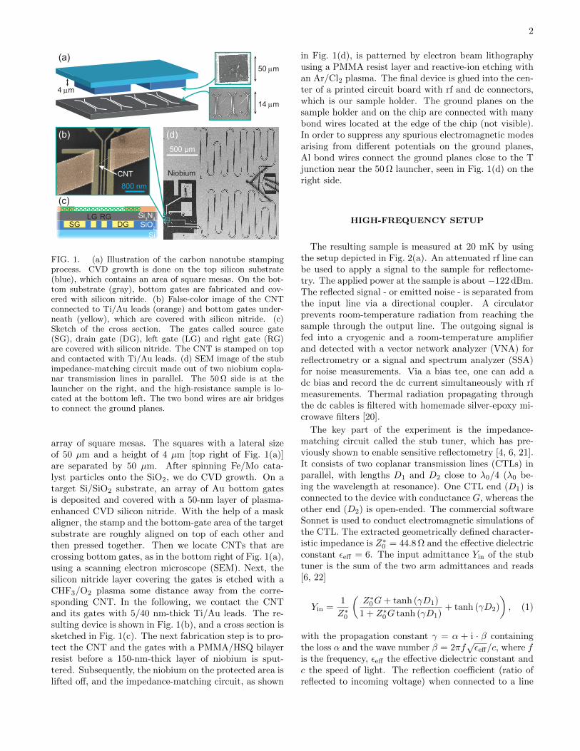
The resulting sample is measured at 20 mK by usingthe setup depicted in Fig. 2(a). An attenuated rf line canbe used to apply a signal to the sample for reflectome-try. The applied power at the sample is about −122 dBm.The reflected signal - or emitted noise - is separated fromthe input line via a directional coupler. A circulatorprevents room-temperature radiation from reaching thesample through the output line. The outgoing signal isfed into a cryogenic and a room-temperature amplifierand detected with a vector network analyzer (VNA) forreflectrometry or a signal and spectrum analyzer (SSA)for noise measurements. Via a bias tee, one can add adc bias and record the dc current simultaneously with rfmeasurements. Thermal radiation propagating throughthe dc cables is filtered with homemade silver-epoxy mi-crowave filters [20].
The key part of the experiment is the impedance-matching circuit called the stub tuner, which has pre-viously shown to enable sensitive reflectometry [4, 6, 21].It consists of two coplanar transmission lines (CTLs) inparallel, with lengths D1 and D2 close to λ0/4 (λ0 be-ing the wavelength at resonance). One CTL end (D1) isconnected to the device with conductance G, whereas theother end (D2) is open-ended. The commercial softwareSonnet is used to conduct electromagnetic simulations ofthe CTL. The extracted geometrically defined character-istic impedance is Z∗
0 = 44.8 Ω and the effective dielectricconstant εeff = 6. The input admittance Yin of the stubtuner is the sum of the two arm admittances and reads[6, 22]
Yin =1
Z∗0
(Z∗
0G+ tanh (γD1)
1 + Z∗0G tanh (γD1)
+ tanh (γD2)
), (1)
with the propagation constant γ = α + i · β containingthe loss α and the wave number β = 2πf
√εeff/c, where f
is the frequency, εeff the effective dielectric constant andc the speed of light. The reflection coefficient (ratio ofreflected to incoming voltage) when connected to a line
3
Bias-tee
Am
plifi
ers
20 mKA
ttenu
ator
s
VNA / SSA
Circulator
Filter-box
Directional coupler-20 dB
DeviceStub tuner
D1
D2
DC bias+-
I/V converter V
Gate+-
4 K
0.7 K
rf
DC
−5
−3
−1
1
2.915 2.92 2.925 2.93f (GHz)
|Γ|2 (
dB)
G(e2/h) = 0.2 00 0.2 0.4
−5−4−3
G (e2/h)
f = f0
2.915 2.92 2.925 2.93
0
1
2
3
4
f (GHz)
|t V|2
G(e2/h) =0.40.20.1
x 10-5
(a)
(b) (c)
FIG. 2. (a) Schematic of the setup with an input and anoutput rf line plus one dc line. Everything on a blue back-ground is inside a dilution refrigerator with a base tempera-ture of 20 mK. (b) Amplitude squared of the reflection coeffi-cient Γ = Vout/Vin around the resonance frequency. Symbolsare measured and lines fitted or calculated. The stub tunerloss α = 0.046 m−1 as well as the two lengths D1 = 10.355 mmand D2 = 10.589 mm are extracted by fitting (solid red line)to the spectrum in the Coulomb blockade regime of the QD,where G = 0 (blue triangles). The upper spectrum for a finitedc conductance of G = 0.2 e2/h is plotted with a shift of 1dB for clarity (green circles). It matches well the calculatedreflection coefficient (dashed red line) using the previous fitparameters. The conductance dependence of the reflectanceat the resonance frequency is plotted in the inset. (c) Calcu-lated voltage-transmission function of the stub tuner for threetypical device conductances using the fit parameters gainedfrom (b).
with characteristic impedance Z0 is then given by
Γ =eiφ − Z0Yin
eiφ + Z0Yin, (2)
where the phase factor eiφ is a fit parameter that accountsfor the asymmetry in the resonance caused by standingwaves in the setup.
The strategy is now as follows: One first deducesthe stub tuner parameters from a frequency-dependentpower-reflectance measurement for a known conductancevalue G of the CNT device. Once all the parameters inthe matching circuit are fixed, one can use them to de-termine G for an arbitrary gate setting. We use a gatesetting deep in the Coulomb blockade (CB) regime, whereG = 0, as a reference to deduce the stub tuner parame-ters D1, D2, and α by fitting the measured |Γ(f)|2 withEq. (2) as shown in Fig. 2(b). To demonstrate that thisextraction works reliably, the measured spectrum at a dc
conductance G = 0.2 e2/h is compared in the figure tothe spectrum calculated with the previously determinedfitting parameters. An excellent agreement is evident.This demonstrates that one can now use this procedureto determine the differential high-frequency G for anygate-voltage setting by reflectometry, i.e. by fitting tothe measured reflected power. The inset in Fig. 2(b)shows the dependence of the reflectance on G at the res-onance frequency. Full matching is not reached in thissample. The reflection dip is deepest for G = 0 and de-creases with increasing conductance. Hence, it is evenpossible to infer the conductance G just by measuringthe resonance amplitude.
For noise measurements, we need to know the voltagetransmission through the stub tuner from the sample tothe 50 Ω side. It can be calculated with the stub parame-ters obtained from reflection. Solving the wave equationof a stub tuner with the appropriate boundary conditionsat the two ends and at the T junction between the twoarms and the launcher (derivation in Supplemental Ma-terial [23]), one obtains a voltage-transmission function
tV =Z0
R+ Z0· 2eγD1 coth (γD2)
ΓL + e2γD1 [1 + 2 coth (γD2)], (3)
with the differential device resistance R = 1/G, ΓL =(R− Z0) / (R+ Z0) and assuming that Z∗
0 ≈ Z0. Theresulting power transmission with the previously deter-mined stub parameters is plotted in Fig. 2(c). The stubtuner has a bandpass effect around the resonance fre-quency f0. The bandwidth, defined as full width at halfmaximum, can be inferred to be BWstub = f0 · 4Z0G/πat matching in the limit where the loss α 1. In ourcase, we obtain a bandwidth of 1.5 MHz for G = 0.2 e2/h(corresponding to R = 130 kΩ).
We measure the amplified noise power over Z0 = 50 Ωintegrated over a bandwidth (BW) of 20 MHz aroundthe resonance frequency, defined as 〈δP 〉. For each gatevoltage, the corresponding background noise 〈δP0〉 atVSD = 0, containing amplifier and thermal noise, is sub-tracted. By dividing the setup amplification g as well asthe stub tuner transmission tV [Eq. (3)] integrated overthe bandwidth and converting power to current, the re-sulting shot-noise spectral density is (see SupplementalMaterial for details [23])
SI = G2Z0〈δP 〉 − 〈δP0〉g∫
BW|tV |2 df
. (4)
The setup power gain g appearing in Eq. (4), whichincludes the gain of the amplifiers and cable loss, is de-termined by replacing the sample with a metal-wire resis-tor in the hot-electron regime. In this regime, the Fanofactor F = SI/2eI is
√3/4 [24, 25]. The wire length of
L = 50µm is longer than the inelastic electron scatteringlength but shorter than the electron-phonon scatteringlength. Its width of 680 nm and thickness of 30 nm lead
4
1250 1300 1350 1400
VRG (mV)
0.1 0.2G (e2/h)0(b)(a)
1250 1300 1350 1400
−20
−10
0
10
20
30
VRG (mV)
VS
D (m
V)
0.1 0.2dI/dV (e2/h)0
−30
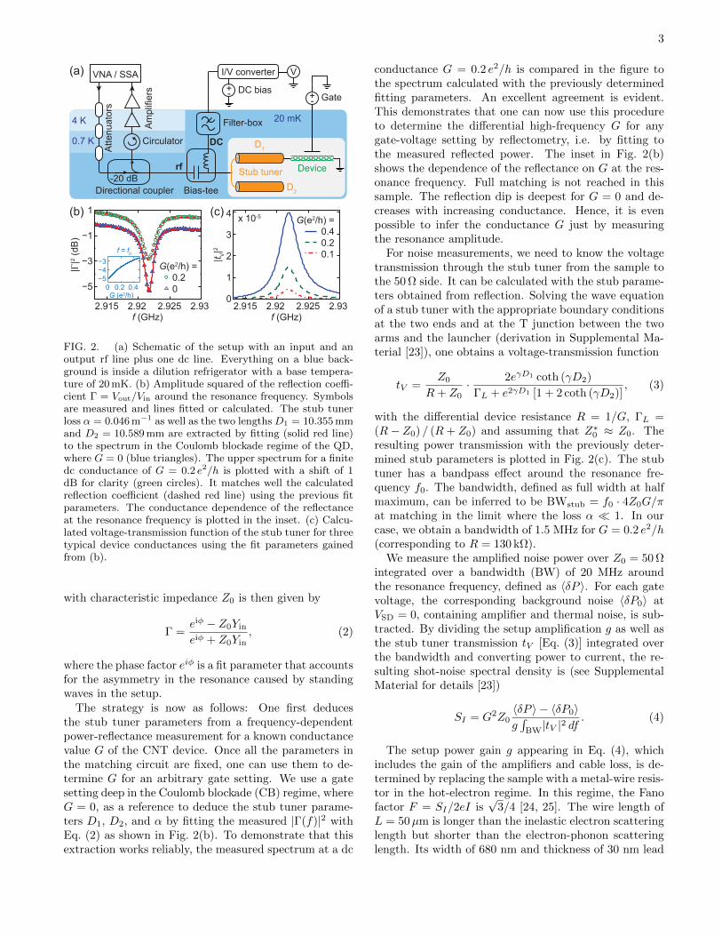
FIG. 3. (a) Derivative of the dc current (dI/dVSD) as afunction of the voltage on the right gate and of the source-drain bias. The contour of the CB diamonds is highlighted bythe dashed line. (b) Differential conductance deduced fromthe reflection amplitude.
to a residual resistance of 39 Ω, which is close enoughto 50 Ω to have a high signal output without impedancematching. The wire is attached to two copper pads ofsize 300 × 300 µm2 and height 500 nm, acting as heatsinks. Comparing the shot-noise dependence on currentin the linear regime with the Fano factor
√3/4, we can
infer a power gain g = 97.9 dB of the amplification chain(see Supplemental Material [23]).
EXPERIMENT
With the help of the bottom gates beneath the CNT,we conduct measurements in the single-QD regime (moreinformation on the QD formation can be found in Sup-plemental Material [23]). Its energy levels are controlledby the plunger gate voltage VRG [26]. The differen-tial conductance derived by numerically differentiatingthe measured dc current (dI/dVSD) and by transform-ing the reflection amplitude to G using Eq. (2) is shownin Figs. 3(a) and 3(b), respectively. The comparisonshows that the rf conductance is in good agreement withdI/dVSD, which confirms the validity of our way to ex-tract the stub tuner parameters. The fourfold degeneracyof the CNT QD states becomes evident by looking at thedashed contour lines. We stress that the rf-deduced con-ductance is in fact less noisy and can be measured muchfaster.
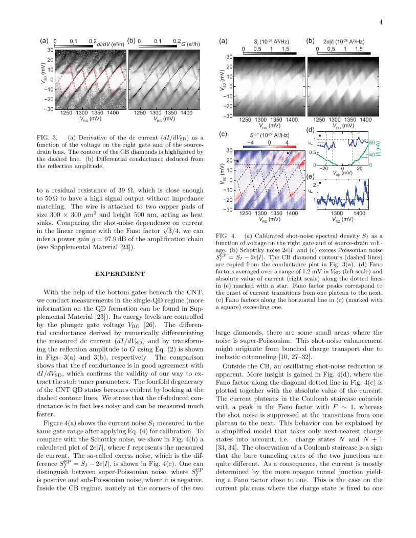
Figure 4(a) shows the current noise SI measured in thesame gate range after applying Eq. (4) for calibration. Tocompare with the Schottky noise, we show in Fig. 4(b) acalculated plot of 2e|I|, where I represents the measureddc current. The so-called excess noise, which is the dif-ference SEP
I = SI − 2e|I|, is shown in Fig. 4(c). One candistinguish between super-Poissonian noise, where SEP
I
is positive and sub-Poissonian noise, where it is negative.Inside the CB regime, namely at the corners of the two
VRG (mV)
1250 1300 1350 1400
10 0.5 1.52e|I| (10-26 A2/Hz)(b)(a)
−20
−10
0
10
20
30
VRG (mV)
VS
D (m
V)
−30 1250 1300 1350 1400
SI (10-26 A2/Hz)0 0.5 1 1.5
1250 1300 1350 1400
−20
−10
0
10
20
30
VRG (mV)V
SD (m
V)
SIEP (10-27 A2/Hz)
−4 0 4
−30
(c) (d)
0
0.5
1
F
0
40
80
|I| (n
A)
−20 0 20VSD (mV)(e)
1300 1400
1
2
F
VRG (mV)
FIG. 4. (a) Calibrated shot-noise spectral density SI as afunction of voltage on the right gate and of source-drain volt-age. (b) Schottky noise 2e|I| and (c) excess Poissonian noiseSEPI = SI − 2e|I|. The CB diamond contours (dashed lines)
are copied from the conductance plot in Fig. 3(a). (d) Fanofactors averaged over a range of 1.2 mV in VSD (left scale) andabsolute value of current (right scale) along the dotted linesin (c) marked with a star. Fano factor peaks correspond tothe onset of current transitions from one plateau to the next.(e) Fano factors along the horizontal line in (c) (marked witha square) exceeding one.
large diamonds, there are some small areas where thenoise is super-Poissonian. This shot-noise enhancementmight originate from bunched charge transport due toinelastic cotunneling [10, 27–32].
Outside the CB, an oscillating shot-noise reduction isapparent. More insight is gained in Fig. 4(d), where theFano factor along the diagonal dotted line in Fig. 4(c) isplotted together with the absolute value of the current.The current plateaus in the Coulomb staircase coincidewith a peak in the Fano factor with F ∼ 1, whereasthe shot noise is suppressed at the transitions from oneplateau to the next. This behavior can be explained bya simplified model that takes only next-nearest chargestates into account, i.e. charge states N and N + 1[33, 34]. The observation of a Coulomb staircase is a signthat the bare tunneling rates of the two junctions arequite different. As a consequence, the current is mostlydetermined by the more opaque tunnel junction yield-ing a Fano factor close to one. This is the case on thecurrent plateaus where the charge state is fixed to one
5
charge value for most of the time. In contrast, at thetransition between two current plateaus, the two corre-sponding charge states N and N + 1 are equally proba-ble. This is caused by a subtle energy dependence of theeffective tunneling rates that takes the charging energyof the island into account [33]. Hence, in this case thewhole device behaves as if it was composed of two identi-cal junctions in series with similar tunneling rates. Thisyields a suppression of the Fano factor by 2 to F = 0.5 inthe ideal case. However, at finite temperature and/or forlarger bias voltages, more than two charge states are in-volved, yielding F > 0.5. The periodic noise suppressiontherefore tends to decay away at large bias voltages andapproaches F = 1 for eV Ec. This is exactly what wesee in the data.
But it can be seen in Fig. 4(d) and more pronouncedlyin Fig. 4(e) that the Fano factor peak values can exceedone. This indicates that the assumption of the two-statemodel used above is too much simplified and there is morethan one channel involved. If, for example, two differentorbital states are accessible within the bias window, it isvery likely that their lead couplings are different. Sequen-tial tunneling may then be rapid through the stronglycoupled orbital until this process is interrupted when anelectron is trapped in the weakly coupled state. This re-sults in a random sequence of electron bunches with anoise that exceeds the classical Schottky value [29, 35].
CONCLUSION AND DISCUSSION
In summary, we demonstrate the versatility of a match-ing circuit realized by a stub tuner for quantitative noisemeasurements of high-impedance quantum devices at gi-gahertz frequencies. Our model system for a quantumdevice is a single CNT QD. The CNT is transferred froma growth chip to the device chip by stamping. The sim-ple planar structure of a stub tuner built from coplanartransmission lines makes it easy to design and to fabricatewith standard lithography. We show that all relevant cir-cuit parameters can be deduced from the reflection spec-trum. These parameters can then be used to calculatethe transmission function needed to quantify the noisespectral density of the device.
In order to quantify the advantage in noise measure-ment due to the matching circuit, one has to comparewith a wideband noise detection without any impedancematching. The later case offers significantly more BW,but the noise signal is strongly reduced due to impedancemismatch. But, in practice, the BW is not infinite butlimited by the circulator and amplifier to values in therange of about 500 MHz. The total power 〈δP2〉 in thedetection line before amplification is given by 1/2·SIZ0f0
and SIZ0BW for the case with and without matching cir-cuit, respectively (see Supplemental Material [23]). Here,f0 denotes the resonance frequency of the matching cir-
cuit. It is evident that the matching circuit provides animprovement in detected power, since f0 > BW.
However, the real strength of the stub tuner is evidentonly if one also considers the background noise. Narrow-band detection greatly reduces the collected backgroundnoise added by the setup, for example, by the ampli-fier. This is captured by the SNR, which is defined asthe desired noise signal divided by the background noise,where the background noise is due to the amplifier chain.Here, the main results of the SNR analysis are given;the derivations can be found in Supplemental Material[23]. In order to compare the efficiency of a matchingcircuit for different matching conditions and even differ-ent impedance-matching circuits, we introduce the figureof merit gSNR = SNRmatching/SNRno matching, which isgiven by
gSNR =
(R
Z0
)2
·∫
BW|tV |2 dfBW
. (5)
The figure of merit depends on the device resistance R,the circuit bandwidth BW and the transmission functiontV . The upper bound in the lossless case at full matchingis derived to be
gmaxSNR =
π
8
R
Z0≈ 800 for R = 100 kΩ. (6)
Despite being quite far from full matching and havingsome loss in the circuit, the figure of merit for the devicepresented here is still as high as gSNR ≈ 200 at a deviceresistance of R = 100 kΩ. It is interesting to note thatthe figure of merit for an LC-matching circuit [3, 30, 32]is exactly the same, although the bandwidth is larger.The bandwidth scales with
√Z0/R compared to Z0/R
for a stub tuner.In conclusion, a matching circuit can provide a tremen-
dous increase in performance for noise measurements andother experiments in which a high signal transmissionis crucial. The increase in SNR is the same for a stubtuner and an LC circuit. However, the stub tuner cir-cuit can be designed in a much easier manner, but itis of narrower bandwidth. This may be an advantageor disadvantage depending on the application. If spu-rious resonances appear in the same frequency window,for example, so-called box modes generated by the sam-ple enclosure box, it might be beneficial not to have atoo-large bandwidth. If, on the other hand, fast read-outis the key, an LC circuit could perform better.
ACKNOWLEDGEMENTS
The authors thank T. Kontos, J. J. Viennot and L.Bruhat for their kind help with CNT stamping. For thesilicon nitride deposition, we thank D. Marty, C. D. Wild,and J. Gobrecht from the PSI. We acknowledge financial
6
support by the ERC project QUEST and the Swiss Na-tional Science Foundation (SNF) through various grants,including NCCR-QSIT.
[1] Ya.M. Blanter and M. Buttiker, “Shot noise in meso-scopic conductors,” Physics Reports 336, 1 – 166 (2000).
[2] Jeremy Levy, “Universal quantum computation withspin-1/2 pairs and heisenberg exchange,” Phys. Rev.Lett. 89, 147902 (2002).
[3] W. W. Xue, B. Davis, Feng Pan, J. Stettenheim, T. J.Gilheart, A. J. Rimberg, and Z. Ji, “On-chip matchingnetworks for radio-frequency single-electron transistors,”Applied Physics Letters 91, 093511 (2007).
[4] Gabriel Puebla-Hellmann and Andreas Wallraff, “Real-ization of gigahertz-frequency impedance matching cir-cuits for nano-scale devices,” Applied Physics Letters101, 053108 (2012).
[5] Carles Altimiras, Olivier Parlavecchio, Philippe Joyez,Denis Vion, Patrice Roche, Daniel Esteve, and FabienPortier, “Dynamical coulomb blockade of shot noise,”Phys. Rev. Lett. 112, 236803 (2014).
[6] V. Ranjan, G. Puebla-Hellmann, M. Jung, T. Hasler,A. Nunnenkamp, M. Muoth, C. Hierold, A. Wallraff,and C. Schonenberger, “Clean carbon nanotubes coupledto superconducting impedance-matching circuits,” Nat.Commun. 6, 7165 (2015).
[7] G. A. Steele, G. Gotz, and L. P. Kouwenhoven, “Tunablefew-electron double quantum dots and klein tunnelling inultraclean carbon nanotubes,” Nat. Nanotechnol. 4, 363–367 (2009).
[8] J. Waissman, M. Honig, S. Pecker, A. Benyamini,A. Hamo, and S. Ilani, “Realization of pristine and lo-cally tunable one-dimensional electron systems in carbonnanotubes,” Nat. Nanotechnol. 8, 569–574 (2013).
[9] Minkyung Jung, Jens Schindele, Stefan Nau, MarkusWeiss, Andreas Baumgartner, and ChristianSchonenberger, “Ultraclean single, double, and triplecarbon nanotube quantum dots with recessed re bottomgates,” Nano Letters 13, 4522–4526 (2013).
[10] E. Onac, F. Balestro, B. Trauzettel, C. F. J. Lodewijk,and L. P. Kouwenhoven, “Shot-noise detection in a car-bon nanotube quantum dot,” Phys. Rev. Lett. 96, 026803(2006).
[11] T. Delattre, C. Feuillet-Palma, L. G. Herrmann,P. Morfin, J.-M. Berroir, G. Feve, B. Placais, D. C. Glat-tli, M.-S. Choi, C. Mora, and T. Kontos, “Noisy kondoimpurities,” Nat. Phys. 5, 208–212 (2009).
[12] J. Basset, A. Yu. Kasumov, C. P. Moca, G. Zarand, P. Si-mon, H. Bouchiat, and R. Deblock, “Measurement ofquantum noise in a carbon nanotube quantum dot in thekondo regime,” Phys. Rev. Lett. 108, 046802 (2012).
[13] F. Wu, P. Queipo, A. Nasibulin, T. Tsuneta, T. H. Wang,E. Kauppinen, and P. J. Hakonen, “Shot noise with inter-action effects in single-walled carbon nanotubes,” Phys.Rev. Lett. 99, 156803 (2007).
[14] L. G. Herrmann, T. Delattre, P. Morfin, J.-M. Berroir,B. Placais, D. C. Glattli, and T. Kontos, “Shot noise infabry-perot interferometers based on carbon nanotubes,”Phys. Rev. Lett. 99, 156804 (2007).
[15] Na Young Kim, Patrik Recher, William D. Oliver,Yoshihisa Yamamoto, Jing Kong, and Hongjie Dai,“Tomonaga-luttinger liquid features in ballistic single-walled carbon nanotubes: Conductance and shot noise,”Phys. Rev. Lett. 99, 036802 (2007).
[16] F. Wu, P. Virtanen, S. Andresen, B. Plaais, andP. J. Hakonen, “Electron-phonon coupling in single-walled carbon nanotubes determined by shot noise,” Ap-plied Physics Letters 97, 262115 (2010).
[17] B. Babic, J. Furer, M. Iqbal, and C. Schonenberger,“Suitability of carbon nanotubes grown by chemical va-por deposition for electrical devices,” AIP ConferenceProceedings 723, 574–582 (2004).
[18] J. J. Viennot, J. Palomo, and T. Kontos, “Stamping sin-gle wall nanotubes for circuit quantum electrodynamics,”Applied Physics Letters 104, 113108 (2014).
[19] M. Muoth, K. Chikkadi, Yu Liu, and C. Hierold, “Sus-pended cnt-fet piezoresistive strain gauges: Chirality as-signment and quantitative analysis,” in 2013 IEEE 26thInternational Conference on Micro Electro MechanicalSystems (MEMS) (2013) pp. 496–499.
[20] Christian P. Scheller, Sarah Heizmann, Kristine Bed-ner, Dominic Giss, Matthias Meschke, Dominik M.Zumbuhl, Jeramy D. Zimmerman, and Arthur C. Gos-sard, “Silver-epoxy microwave filters and thermalizers formillikelvin experiments,” Applied Physics Letters 104,211106 (2014).
[21] S. Hellmuller, M. Pikulski, T. Muller, B. Kung,G. Puebla-Hellmann, A. Wallraff, M. Beck, K. Ensslin,and T. Ihn, “Optimization of sample-chip design for stub-matched radio-frequency reflectometry measurements,”Applied Physics Letters 101, 042112 (2012).
[22] D.M. Pozar, “Microwave engineering,” (John Wiley &Sons Inc., Hoboken, 2005) Chap. 5, p. 232, 3rd ed.
[23] See Supplemental Material at http://link.aps.org/supp-lemental/10.1103/PhysRevApplied.4.054002 for detailson the quantum dot formation, the setup calibration andderivations of the stub tuner transmission function andsignal to noise ratios.
[24] Andrew H. Steinbach, John M. Martinis, and Michel H.Devoret, “Observation of hot-electron shot noise in ametallic resistor,” Phys. Rev. Lett. 76, 3806–3809 (1996).
[25] M. Henny, Ph.D. thesis, University of Basel (1998), p. 57.[26] J. Nygard, D.H. Cobden, M. Bockrath, P.L. McEuen,
and P.E. Lindelof, “Electrical transport measurementson single-walled carbon nanotubes,” Applied Physics A69, 297–304 (1999).
[27] Eugene V. Sukhorukov, Guido Burkard, and DanielLoss, “Noise of a quantum dot system in the cotunnelingregime,” Phys. Rev. B 63, 125315 (2001).
[28] A. Cottet, W. Belzig, and C. Bruder, “Positive cross-correlations due to dynamical channel blockade in athree-terminal quantum dot,” Phys. Rev. B 70, 115315(2004).
[29] W. Belzig, “Full counting statistics of super-poissonianshot noise in multilevel quantum dots,” Phys. Rev. B71, 161301 (2005).
[30] Yiming Zhang, L. DiCarlo, D. T. McClure, M. Ya-mamoto, S. Tarucha, C. M. Marcus, M. P. Hanson,and A. C. Gossard, “Noise correlations in a coulomb-blockaded quantum dot,” Phys. Rev. Lett. 99, 036603(2007).
[31] S. Gustavsson, M. Studer, R. Leturcq, T. Ihn, K. En-sslin, D. C. Driscoll, and A. C. Gossard, “Detecting
7
single-electron tunneling involving virtual processes inreal time,” Phys. Rev. B 78, 155309 (2008).
[32] Yuma Okazaki, Satoshi Sasaki, and Koji Muraki, “Shotnoise spectroscopy on a semiconductor quantum dot inthe elastic and inelastic cotunneling regimes,” Phys. Rev.B 87, 041302 (2013).
[33] Selman Hershfield, John H. Davies, Per Hyldgaard,Christopher J. Stanton, and John W. Wilkins, “Zero-frequency current noise for the double-tunnel-junctioncoulomb blockade,” Phys. Rev. B 47, 1967–1979 (1993).
[34] H. Birk, M. J. M. de Jong, and C. Schonenberger,“Shot-noise suppression in the single-electron tunnelingregime,” Phys. Rev. Lett. 75, 1610–1613 (1995).
[35] S. Gustavsson, R. Leturcq, B. Simovic, R. Schleser,P. Studerus, T. Ihn, K. Ensslin, D. C. Driscoll, and A. C.Gossard, “Counting statistics and super-poissonian noisein a quantum dot: Time-resolved measurements of elec-tron transport,” Phys. Rev. B 74, 195305 (2006).
Supplemental Material for ”Shot Noise of a Quantum Dot Measured with GigahertzImpedance Matching”
T. Hasler,1 M. Jung,1 V. Ranjan,1 G. Puebla-Hellmann,1, 2 A. Wallraff,2 and C. Schonenberger1
1Department of Physics, University of Basel, Klingelbergstrasse 82, CH-4056 Basel, Switzerland2Department of Physics, ETH Zurich, Otto-Stern-Weg 1, CH-8093 Zurich, Switzerland
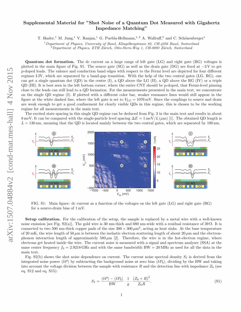
Quantum dot formation. The dc current on a large range of left gate (LG) and right gate (RG) voltages isplotted in the main figure of Fig. S1. The source gate (SG) as well as the drain gate (DG) are fixed at −3 V to getp-doped leads. The valence and conduction band edges with respect to the Fermi level are depicted for four differentregimes I-IV, which are separated by a band-gap transition. With the help of the two central gates (LG, RG), onecan get a single quantum dot (QD) in the centre (I), a QD above the LG (II), a QD above the RG (IV) or a tripleQD (III). It is best seen in the left bottom corner, where the entire CNT should be p-doped, that Fermi-level pinningclose to the leads can still lead to a QD formation. For the measurements presented in the main text, we concentrateon the single QD regime (I). If plotted with a different color bar, weaker resonance lines would still appear in thefigure at the white dashed line, where the left gate is set to VLG = 1076 mV. Since the couplings to source and drainare weak enough to get a good confinement for clearly visible QDs in this regime, this is chosen to be the workingregime for all measurements in the main text.
The excited state spacing in this single QD regime can be deduced from Fig. 3 in the main text and results in about8 meV. It can be compared with the single-particle level spacing ∆E = 1 meV/L (µm) [1]. The obtained QD length isL = 130 nm, meaning that the QD is located mainly between the two central gates, which are separated by 100 nm.
VRG (mV)
VLG
(mV
)
−1000 −500 0 500 1000 1500−500
0
500
1000
1500
2000
I (nA
)
5
10
15
20
25
III
III IV
SG DGLG RG
E
EF
ECEV
III
SG DGLG RG
E
EF
ECEV
II
SG DGLG RG
E
EF
ECEV
I
SG DGLG RG
E
EF
ECEV
IV
FIG. S1: Main figure: dc current as a function of the voltages on the left gate (LG) and right gate (RG)for a source-drain bias of 1 mV.
Setup calibration. For the calibration of the setup, the sample is replaced by a metal wire with a well-knownnoise emission [see Fig. S2(a)]. The gold wire is 30 nm-thick and 680 nm-wide with a residual resistance of 39 Ω. It isconnected to two 500 nm-thick copper pads of the size 300× 300µm2, acting as heat sinks. At the base temperatureof 20 mK, the wire length of 50µm is between the inelastic electron scattering length of about 20µm and the electron-phonon interaction length of approximately 580µm [2]. Therefore, the wire is in the hot-electron regime, whereelectrons get heated inside the wire. The current noise is measured with a signal and spectrum analyser (SSA) at thesame center frequency f0 = 2.9218 GHz and with the same bandwidth BW = 20 MHz as used for all the data in themain text.
Fig. S2(b) shows the shot noise dependence on current. The current noise spectral density SI is derived from theintegrated noise power 〈δP 〉 by subtracting the background noise at zero bias 〈δP0〉, dividing by the BW and takinginto account the voltage division between the sample with resistance R and the detection line with impedance Z0 (seeeq. S12 and eq. S15):
SI =〈δP 〉 − 〈δP0〉
BW· 1
g· (Z0 +R)
2
Z0R. (S1)
1
arX
iv:1
507.
0488
4v2
[co
nd-m
at.m
es-h
all]
4 N
ov 2
015
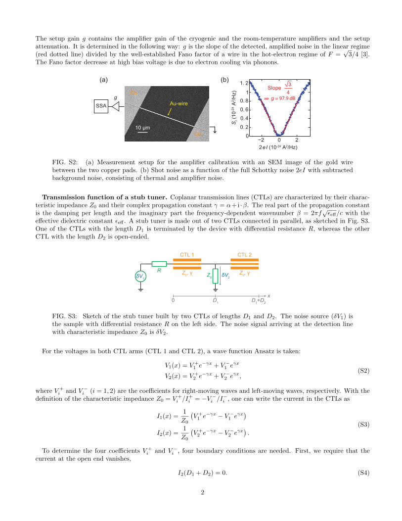
The setup gain g contains the amplifier gain of the cryogenic and the room-temperature amplifiers and the setupattenuation. It is determined in the following way: g is the slope of the detected, amplified noise in the linear regime(red dotted line) divided by the well-established Fano factor of a wire in the hot-electron regime of F =
√3/4 [3].
The Fano factor decrease at high bias voltage is due to electron cooling via phonons.
Cu
Cu10 μm
Au-wireSSAg
−2 0 20
0. 2
0.4
0. 6
0. 81
1. 2
2 e I (10-24 A2/Hz)
SI (
10-24 A
2 /Hz)
Slope43
g = 97.9 dB
(a) (b)
FIG. S2: (a) Measurement setup for the amplifier calibration with an SEM image of the gold wirebetween the two copper pads. (b) Shot noise as a function of the full Schottky noise 2eI with subtractedbackground noise, consisting of thermal and amplifier noise.
Transmission function of a stub tuner. Coplanar transmission lines (CTLs) are characterized by their charac-teristic impedance Z0 and their complex propagation constant γ = α+i ·β. The real part of the propagation constantis the damping per length and the imaginary part the frequency-dependent wavenumber β = 2πf
√εeff/c with the
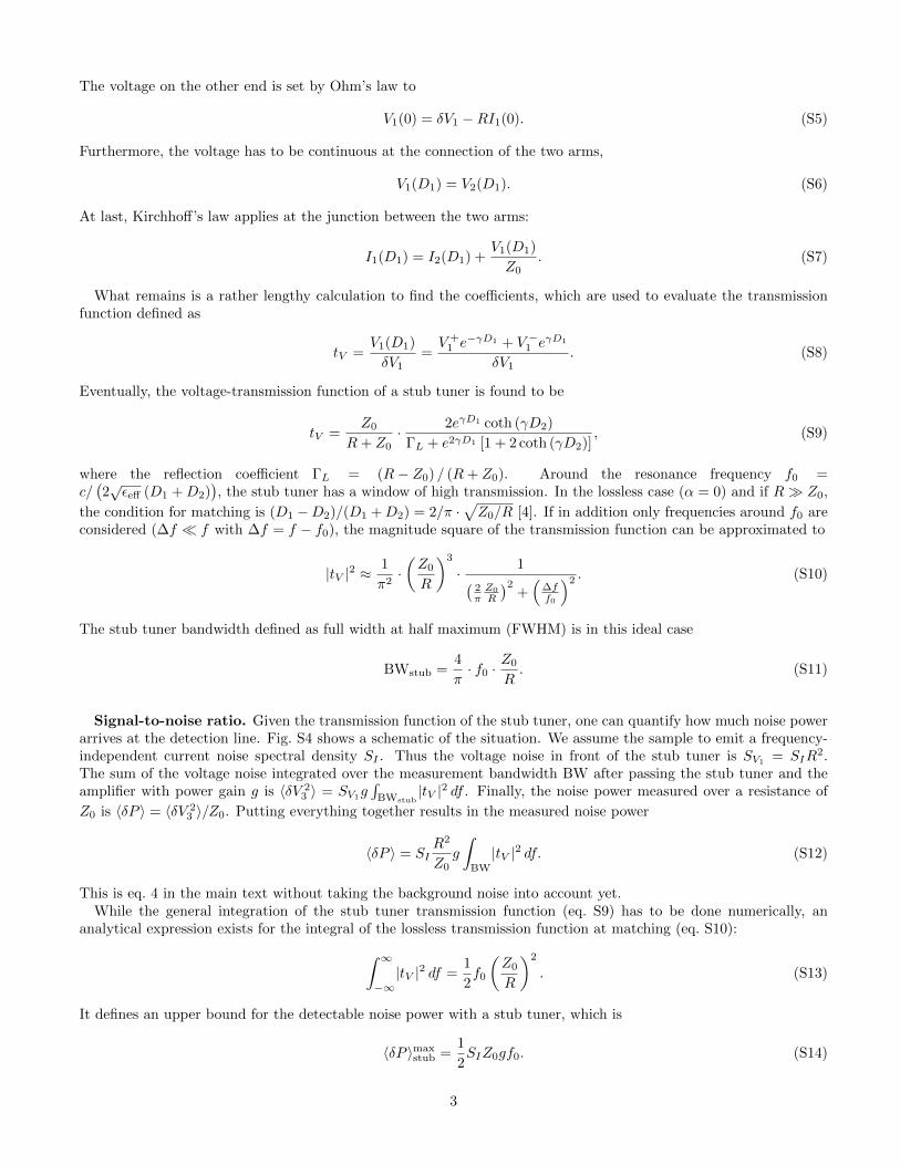
effective dielectric constant εeff . A stub tuner is made out of two CTLs connected in parallel, as sketched in Fig. S3.One of the CTLs with the length D1 is terminated by the device with differential resistance R, whereas the otherCTL with the length D2 is open-ended.
CTL 1
RZ0δV1
δV2
x0 D1 D1+D2
Z0, γ Z0, γ
CTL 2
FIG. S3: Sketch of the stub tuner built by two CTLs of lengths D1 and D2. The noise source (δV1) isthe sample with differential resistance R on the left side. The noise signal arriving at the detection linewith characteristic impedance Z0 is δV2.
For the voltages in both CTL arms (CTL 1 and CTL 2), a wave function Ansatz is taken:
V1(x) = V +1 e−γx + V −1 eγx
V2(x) = V +2 e−γx + V −2 eγx,
(S2)
where V +i and V −i (i = 1, 2) are the coefficients for right-moving waves and left-moving waves, respectively. With the
definition of the characteristic impedance Z0 = V +i /I
+i = −V −i /I−i , one can write the current in the CTLs as
I1(x) =1
Z0
(V +
1 e−γx − V −1 eγx)
I2(x) =1
Z0
(V +
2 e−γx − V −2 eγx).
(S3)
To determine the four coefficients V +i and V −i , four boundary conditions are needed. First, we require that the
current at the open end vanishes,
I2(D1 +D2) = 0. (S4)
2
The voltage on the other end is set by Ohm’s law to
V1(0) = δV1 −RI1(0). (S5)
Furthermore, the voltage has to be continuous at the connection of the two arms,
V1(D1) = V2(D1). (S6)
At last, Kirchhoff’s law applies at the junction between the two arms:
I1(D1) = I2(D1) +V1(D1)
Z0. (S7)
What remains is a rather lengthy calculation to find the coefficients, which are used to evaluate the transmissionfunction defined as
tV =V1(D1)
δV1=V +
1 e−γD1 + V −1 eγD1
δV1. (S8)
Eventually, the voltage-transmission function of a stub tuner is found to be
tV =Z0
R+ Z0· 2eγD1 coth (γD2)
ΓL + e2γD1 [1 + 2 coth (γD2)], (S9)
where the reflection coefficient ΓL = (R− Z0) / (R+ Z0). Around the resonance frequency f0 =c/(2√εeff (D1 +D2)
), the stub tuner has a window of high transmission. In the lossless case (α = 0) and if R Z0,
the condition for matching is (D1 −D2)/(D1 +D2) = 2/π ·√Z0/R [4]. If in addition only frequencies around f0 are
considered (∆f f with ∆f = f − f0), the magnitude square of the transmission function can be approximated to
|tV |2 ≈1
π2·(Z0
R
)3
· 1(
2πZ0
R
)2+(
∆ff0
)2 . (S10)
The stub tuner bandwidth defined as full width at half maximum (FWHM) is in this ideal case
BWstub =4
π· f0 ·
Z0
R. (S11)
Signal-to-noise ratio. Given the transmission function of the stub tuner, one can quantify how much noise powerarrives at the detection line. Fig. S4 shows a schematic of the situation. We assume the sample to emit a frequency-independent current noise spectral density SI . Thus the voltage noise in front of the stub tuner is SV1
= SIR2.
The sum of the voltage noise integrated over the measurement bandwidth BW after passing the stub tuner and theamplifier with power gain g is 〈δV 2
3 〉 = SV1g∫
BWstub|tV |2 df . Finally, the noise power measured over a resistance of
Z0 is 〈δP 〉 = 〈δV 23 〉/Z0. Putting everything together results in the measured noise power
〈δP 〉 = SIR2
Z0g
∫
BW
|tV |2 df. (S12)
This is eq. 4 in the main text without taking the background noise into account yet.While the general integration of the stub tuner transmission function (eq. S9) has to be done numerically, an
analytical expression exists for the integral of the lossless transmission function at matching (eq. S10):
∫ ∞
−∞|tV |2 df =
1
2f0
(Z0
R
)2
. (S13)
It defines an upper bound for the detectable noise power with a stub tuner, which is
〈δP 〉maxstub =
1
2SIZ0gf0. (S14)
3

Stub-tunerR
Z0
g〈δP〉tVSV1 Sback
FIG. S4: Schematic of the measurement setup. The noise generated by the sample with differentialresistance R is drawn as a voltage source SV1 in series. The noise signal is transmitted through the stubtuner and amplified by a factor g. The instrument measures the integrated noise power 〈δP 〉 over Z0.The background noise (Sbg) is assumed to be added between the stub tuner and the amplifier.
This transmitted noise power has to be compared with the signal measured in the absence of impedance matching.The noise spectral density is small in this case, but one can integrate over a large bandwidth. On the other hand,the bandwidth is always restricted by other components. In our setup, the circulator has the smallest bandwidthof BW0 = 500 MHz. Eq. S12 can be generally used to get the signal power for this kind of setup by taking theappropriate transmission function tV . If there is no impedance-matching circuit at all, the stub tuner is replaced byan element with a constant transmission function tV = Z0/(Z0 +R) obtained via eq. S9 by setting D1 = D2 = 0. Itleads to the same result as if voltage division of the emitted noise voltage is considered in the circuit drawn in Fig. S4.By means of eq. S12, the resulting noise power measured without impedance matching is then
〈δP 〉0 = SIZ0gBW0. (S15)
Therefore, the maximum enhancement in detectable noise power obtained with a lossless stub tuner at full matchingat a resonance frequency f0 = 3 GHz is 〈δP 〉max
stub/〈δP 〉0 = 1/2 · f0/BW0 ≈ 3.So far the discussion was about the noise signal only. But the main advantage of a matching circuit is revealed by
considering the signal-to-noise ratio (SNR). Noise is in this context the background noise, as for instance the amplifiernoise. Its power spectral density Sbg is assumed to be frequency independent. If one assumes the background noisesource to be introduced between the impedance-matching circuit and the amplifier (see Fig. S4), the background noisepower picked up over the measurement bandwidth (BW) is 〈δP 〉bg = SbgBWg. This leads to the general expressionfor the SNR
SNR =〈δP 〉〈δP 〉bg
=SIR
2
SbgZ0·∫
BW|tV |2 dfBW
, (S16)
where eq. S12 is used to get the last expression. Without impedance matching, one can use eq. S15 and gets
SNR0 =〈δP0〉〈δP 〉bg
=SIZ0
Sbg. (S17)
Eventually, we want to compare the SNRs with and without impedance matching. To do so, we introduce the figureof merit for impedance matching as
gSNR =SNR
SNR0=
(R
Z0
)2
·∫
BW|tV |2 dfBW
. (S18)
This means that gSNR depends on the transmission function tV of the resonant circuit and the chosen integrationbandwidth BW, which is optimally the FWHM given in eq. S11. An upper bound for gSNR considering a lossless stubtuner at full matching can then be given with the help of eq. S13:
gmaxSNR =
π
8
R
Z0, (S19)
which amounts to a factor as high as gSNR ≈ 800 for R = 100 kΩ. For realistic matching circuits, the integration ofthe general transmission function (eq. S9) can be done numerically. Using the stub-parameters from the main textderived by reflectometry, the resulting improvement in the SNR is still gSNR ≈ 200 at this resistance if the bandwidthis the FWHM, although the circuit is not fully matched to R = 100 kΩ.
Comparison with LC-circuit In the last part, we compare this result with an LC matching circuit. To this end,an expression for the voltage-transmission function tV appearing in eq. S18 has to be derived. Using the circuit drawn
4
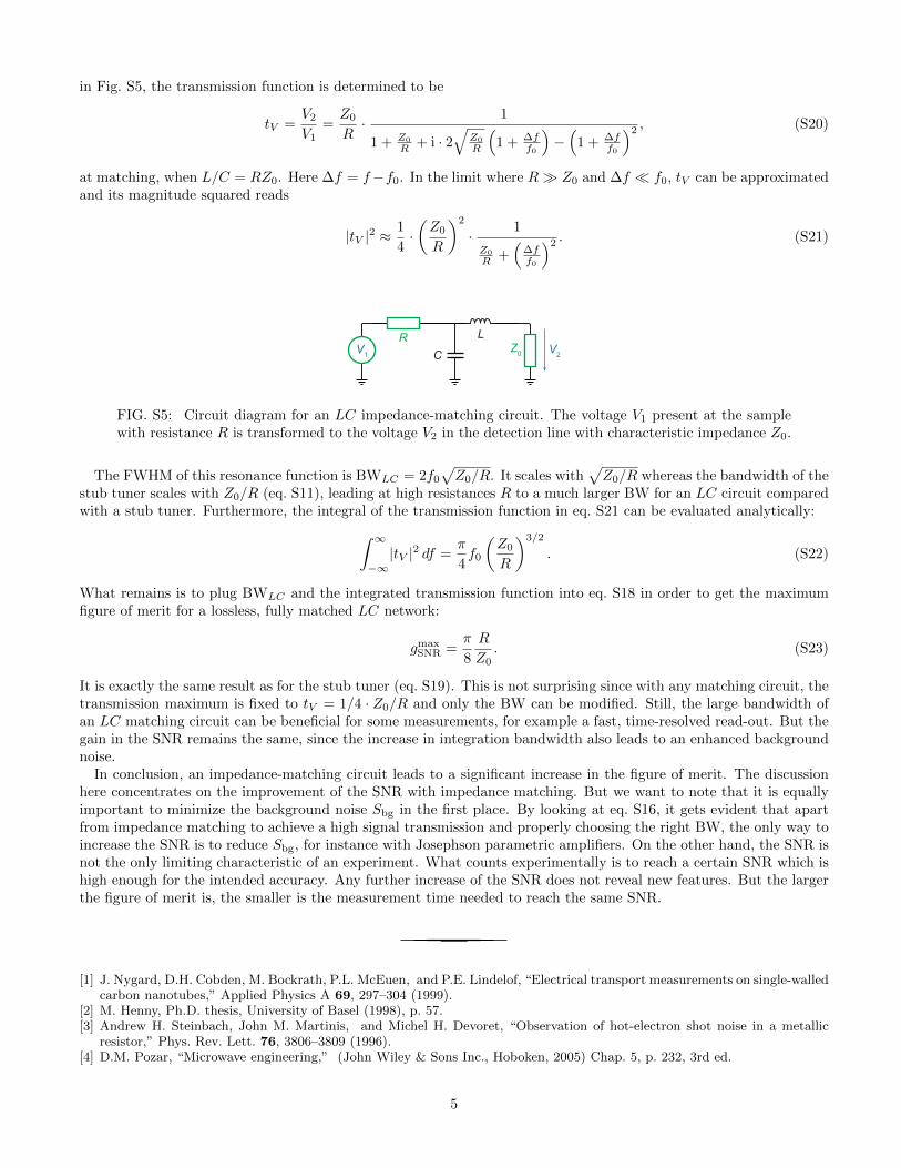
in Fig. S5, the transmission function is determined to be
tV =V2
V1=Z0
R· 1
1 + Z0
R + i · 2√
Z0
R
(1 + ∆f
f0
)−(
1 + ∆ff0
)2 , (S20)
at matching, when L/C = RZ0. Here ∆f = f−f0. In the limit where R Z0 and ∆f f0, tV can be approximatedand its magnitude squared reads
|tV |2 ≈1
4·(Z0
R
)2
· 1
Z0
R +(
∆ff0
)2 . (S21)
RZ0V1 V2C
L
FIG. S5: Circuit diagram for an LC impedance-matching circuit. The voltage V1 present at the samplewith resistance R is transformed to the voltage V2 in the detection line with characteristic impedance Z0.
The FWHM of this resonance function is BWLC = 2f0
√Z0/R. It scales with
√Z0/R whereas the bandwidth of the
stub tuner scales with Z0/R (eq. S11), leading at high resistances R to a much larger BW for an LC circuit comparedwith a stub tuner. Furthermore, the integral of the transmission function in eq. S21 can be evaluated analytically:
∫ ∞
−∞|tV |2 df =
π
4f0
(Z0
R
)3/2
. (S22)
What remains is to plug BWLC and the integrated transmission function into eq. S18 in order to get the maximumfigure of merit for a lossless, fully matched LC network:
gmaxSNR =
π
8
R
Z0. (S23)
It is exactly the same result as for the stub tuner (eq. S19). This is not surprising since with any matching circuit, thetransmission maximum is fixed to tV = 1/4 · Z0/R and only the BW can be modified. Still, the large bandwidth ofan LC matching circuit can be beneficial for some measurements, for example a fast, time-resolved read-out. But thegain in the SNR remains the same, since the increase in integration bandwidth also leads to an enhanced backgroundnoise.
In conclusion, an impedance-matching circuit leads to a significant increase in the figure of merit. The discussionhere concentrates on the improvement of the SNR with impedance matching. But we want to note that it is equallyimportant to minimize the background noise Sbg in the first place. By looking at eq. S16, it gets evident that apartfrom impedance matching to achieve a high signal transmission and properly choosing the right BW, the only way toincrease the SNR is to reduce Sbg, for instance with Josephson parametric amplifiers. On the other hand, the SNR isnot the only limiting characteristic of an experiment. What counts experimentally is to reach a certain SNR which ishigh enough for the intended accuracy. Any further increase of the SNR does not reveal new features. But the largerthe figure of merit is, the smaller is the measurement time needed to reach the same SNR.
[1] J. Nygard, D.H. Cobden, M. Bockrath, P.L. McEuen, and P.E. Lindelof, “Electrical transport measurements on single-walledcarbon nanotubes,” Applied Physics A 69, 297–304 (1999).
[2] M. Henny, Ph.D. thesis, University of Basel (1998), p. 57.[3] Andrew H. Steinbach, John M. Martinis, and Michel H. Devoret, “Observation of hot-electron shot noise in a metallic
resistor,” Phys. Rev. Lett. 76, 3806–3809 (1996).[4] D.M. Pozar, “Microwave engineering,” (John Wiley & Sons Inc., Hoboken, 2005) Chap. 5, p. 232, 3rd ed.
5
Related Documents