Welcome message from author
This document is posted to help you gain knowledge. Please leave a comment to let me know what you think about it! Share it to your friends and learn new things together.
Transcript

SHORT FORM
2019
Contents ______________________________________________________________________________________________
Contents-1
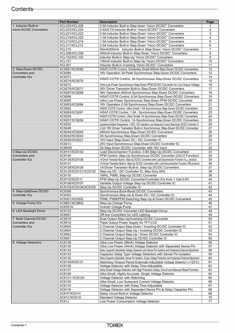
Part Number Description Page 1. Inductor Built-in XCL225/XCL226 0.5A Inductor Built-in Step-down “micro DC/DC” Converters 1 micro DC/DC Converters XCL223/XCL224 0.4A/0.7A Inductor Built-in "micro DC/DC" Converters 2 XCL221/XCL222 0.5A Inductor Built-in Step-Down “micro DC/DC” Converters 3 XCL219/XCL220 1.0A Inductor Built-in Step-Down “micro DC/DC” Converters 4 XCL213/XCL214 1.5A Inductor Built-in Step-Down "micro DC/DC" Converters 5 XCL211/XCL212 2.0A Inductor Built-in Step-Down "micro DC/DC" Converters 6 XCL210 50mA/200mA Inductor Built-in Step-Down “micro DC/DC” Converters 7 XCL208/XCL209 400mA Inductor Built-in Step-Down “micro DC/DC” Converters 8 XCL102/XCL103 Inductor Built-in Step-Up "micro DC/DC" Converters 9 XCL101 100mA Inductor Built-in Step-Up "micro DC/DC" Converters 10 XCL301 Inductor Built-in Inverting “micro DC/DC” Converters 11 2. Step-Down DC/DC XC9281/XC9282 HiSAT-COT® Control, Extremely Small 600mA Step-Down DC/DC Converters 12 Converters and XC9280 18V Operation 3A Peak Synchronous Step-Down DC/DC Converters 13 Controller ICs XC9273 HiSAT-COT® Control, 3A Synchronous Step-Down DC/DC Converters 14 XC9274/XC9275 15 XC9272 Ultra Low Power Synchronous Step-Down PFM DC/DC Converter for Low Output Voltage 16 XC9270/XC9271 30V Driver Transistor Built-in Step-Down DC/DC Converters 17 XC9267/XC9268 36V Operation 600mA Synchronous Step-Down DC/DC Converters 18 XC9266 HiSAT-COT® Control, 6.0A Synchronous Step-Down DC/DC Converters 19 XC9265 Ultra Low Power Synchronous Step-Down PFM DC/DC Converter 20 XC9263/XC9264 18V Operation 0.5A Synchronous Step-Down DC/DC Converters 21 XC9262 HiSAT-COT® Control, Ultra Small 1.5A Synchronous Step-Down DC/DC Converters 22 XC9260/XC9261 HiSAT-COT® Control, 1.5A , Synchronous Step-Down DC/DC Converters 23 XC9259 HiSAT-COT® Control, Ultra Small 1A Synchronous Step-Down DC/DC Converters 24 XC9257/XC9258 HiSAT-COT® Control, 1A Synchronous Step-Down DC/DC Converters 25 XC9252 Operating Ambient Temperature: +105, 30V Operation Low Quiescent Current Step-Down DC/DC Controller IC 26 XC9248 2.2A 18V Driver Transistor Built-in Synchronous Step-Down DC/DC Converter 27 XC9244/XC9245 400mA Synchronous Step-Down DC/DC Converters 28 XC9242/XC9243 2A Synchronous Step-Down DC/DC Converters 29 XC9220/XC9221 16V Input Step-Down DC / DC Controller IC 30 XC9213 25V Input Synchronous Step-Down DC/DC Controller IC 31 XCM526 3A Step-Down DC/DC Converter with 16V Input 32 3.Step-Up DC/DC XC9141/XC9142 Load Disconnection Function, 0.8A Step-Up DC/DC Converters 33 Converters and XC9140 PFM Control, Step-Up Synchronous DC/DC Converter (UVLO Function) 34 Controller ICs XC9135/XC9136 1A Driver Transistor Built-in, Step-Up DC/DC Converters with Load Disconnection Function (VOUT product) 35 XC9131 1A Driver Transistor Built-in, Step-Up DC/DC Converters with Load Disconnection Function (FB product) 36 XC9128/XC9129 1A Driver Transistor Built-in, Step-Up DC/DC Converters 37 XC9120/XC9121/XC9122 Step-Up DC / DC Controller IC, Max Duty 93% 38 XC9119 1MHz, PWM, Step-Up DC/DC Converter 39 XC9110/XC9111 PFM Step-Up DC/DC Converter/Controller ICs from 1 Cell 0.8V 40 XC9106/XC9107 Variable Output Voltage Step-Up DC/DC Controller IC 41 XC9103/XC9104/XC9105 Step-Up DC/DC Controller IC 42 4. Step-Up&Down DC/DC XC9306 Synchronous Buck-Boost DC/DC Converters 43 Controller ICs XC9303 Synchronous Step-Up & Down DC / DC Controller IC 44 XC9301/XC9302 PWM, PWM/PFM Switching Step-Up & Down DC/DC Converters 45 5. Charge Pump ICs XC9801/XC9802 Step-Up Charge Pump 46 XC6351A Inverter Charge Pump 47 6. LED Backlight Driver XC9133 Step-Up DC/DC Converter-LED Backlight Driver 48 XC9401 Off-line Controllers for LED Lighting 49 7. Multi Channel DC/DC XC9519 Dual Output Step-Up/Inverting DC/DC Converter 50 Converters and XC9516 Triple Output Power Supply for TFT-LCD 51 Controller ICs XC9505 2 Channel Output Step-Down / Inverting DC/DC Controller IC 52 XC9504 2 Channel Output Step-Up / Inverting DC/DC Controller IC 53 XC9502 2 Channel Output Step-Up / Down DC/DC Controller IC 54 XC9501 2 Channel Output Step-Up DC/DC Controller IC 55 8. Voltage Detectors XC6136 Ultra Low Power (88nA) Voltage Detector 56 XC6135 Ultra Low Power (44nA) Voltage Detector with Separated Sense Pin 57 XC6134 Delay Capacitor Adjustable Voltage Detectors with Sense Pin Isolation and Hysteresis External Adjustment 58 XC6133 Capacitor Delay Type Voltage Detectors with Sense Pin Isolation 59 XC6132 Delay Capacitor Adjustable, Sense Pin Isolation, Surge Voltage Protection and Hysteresis Rxternal Adjustment 60 XC6130/XC6131 Watchdog Timeout Period Externally Adjustable Voltage Detector (+125) 61 XC6129 Voltage Detector with Delay Time Adjustable 62 XC6127 Ultra Small Voltage Detector with High Precision Delay Circuit and Manual Reset Function 63 XC6126 Ultra Small, Highly Accurate, Single Voltage Detector 64 XC6121~XC6124 Voltage Detector with Watchdog 65 XC6120 Ultra Small, Low Quiescent Current Voltage Detector 66 XC6119 Voltage Detector with Delay Time Adjustable 67 XC6118 Voltage Detector with Separated Sense Pin & Delay Capacitor Pin 68 XC61F/XC61H Delay Circuit Built-in Voltage Detector 69 XC61C/XC61G Standard Voltage Detector 70 XC61J Low Power Consumption Voltage Detector 71
_______________________________________________________________________________________________________
Contents-2
9. Voltage Regulators XC6238 300mA High Speed LDO Regulator with ON/OFF Switch 72 Single Type XC6237 Ultra Low Power Consumption 0.6μA High Speed LDO Regulator 73 XC6233 200mA High Speed LDO Voltage Regulator with Built-in Inrush Current Protection 74 XC6231 10V Input 500mA High Speed LDO Regulators 75 XC6230 Adjustable Voltage Output Multifunction 2A High Speed LDO Regulator 76 XC6229 300mA Ultra Small High Speed LDO Regulator with Built-in Inrush Current Protection 77 XC6227 700mA High Speed LDO Regulator with Reverse Current Protection 78 XC6225 30mA High Speed LDO Regulator 79 XC6224 1.2V Low Voltage Operation,150mA High Speed LDO Voltage Regulator 80 XC6223 300mA High Speed LDO Voltage Regulator with Built-in Inrush Current Protection 81 XC6222 700mA High Speed LDO Regulator 82 XC6221 200mA High Speed LDO Voltage Regulator 83 XC6220 1A High Speed LDO Voltage Regulator with “GreenOperation” 84 XC6219 300mA High Speed LDO Regulators 85 XC6218 200mA Low Power Consumption LDO Regulator 86 XC6217 200mA High Speed "Green Operation" LDO Voltage Regulator 87 XC6216 28V Input Voltage Regulators with CE Pin 88 XC6215 0.8μA Low Quiescent Current Voltage Regulator with CE Pin 89 XC6214 500mA High Speed 3 Terminal Regulator, Thermal Shutdown 90 XC6209 300mA High Speed LDO Regulators 91 XC6206 1μA Low Power 3Terminal Voltage Regulator 92 XC6206J Low Consumption Current Regulators 93 XC6204/XC6205 300mA/150mA High Speed LDO Regulators with CE Pin 94 XC6201 10V Input 3 Terminal, Low Power Voltage Regulator 95 XC62FJ 10V Input, 200mA Low Consumption Current Regulator 96 XC6604 1A, 0.5V Low Input Voltage, High Speed LDO Regulator (Adjustable Current Limit) 97 XC6603 1A, 0.5V Low Input Voltage, High Speed LDO Regulator (Adjustable Soft-start) 98 XC6602 1A, 0.5V Input Voltage, High Speed LDO Regulator 99 XC6601 400mA Low Voltage Input LDO Voltage Regulator 100 XC6505 Low Quiescent Current, 200mA High Speed LDO Regulator - 10.5V Input 101 XC6504 0.6μA Ultra Low Quiescent Current Small Voltage Regulator (CL Capacitor-less) 102 XC6503 CL Capacitor-less, 500mA Low Quiescent Current High Speed LDO Regulator 103 XC6501 CL Capacitor-less, 200mA High Speed LDO Regulator 104 XC6702 36V Input, 300mA Low Quiescent Current High Speed LDO Regulator 105 XC6701 28V Operation High Speed Voltage Regulators with Stand-by Function 106 XC6902 -16V Input Three Terminal Negative High Speed Voltage Regulator 107 XC6901 200mA Negative Voltage Regulator with ON/OFF Control 108 XB1085 3.0A Positive Voltage Regulator 109 10. Voltage Regulators XC6413/XC6414 10V, 300mA/500mA High Speed LDO Regulators with Voltage Detector 110 Voltage Detect Type XC6408 28V Operation Voltage Regulator with Voltage Detector 111 XC6405 500mA High Speed LDO Regulator with Voltage Detector 112 XC6403/XC6404 300mA/500mA High Speed LDO Regulators with Voltage Detector 113 XC6402 700mA High Speed LDO Regulator with Voltage Detector 114 11. Multi Chip Module XCM414 Voltage Regulator with Bridge Diode for Wireless Power Receiver 115 12. Load Switch XC8109 85mΩ High Function Power Switch with Current Limit Adjustable Pin (0.075A~1.3A Current Limit Adjustable) 116 XC8108 85mΩ High Function Power Switch with Current Limit Adjustable Pin (0.9A~2.4A Current Limit Adjustable) 117 XC8107 85mΩ High Function Power Switch (Fixed Current Limit) 118 XC8102 400mA Small Load Switch with CL Discharge 119 XC8101 Low Quiescent Current Load Switch 120 13. Push Button Controllers XC6192 Push Button Load Switch 121
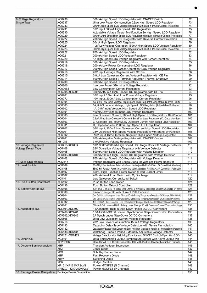
XC6190 Push Button Reboot Controller 122 14. Battery Charge ICs XC6808 4.35V 1 Cell Li-ion and Li-Po Battery Linear Charger IC with Battery Temperature Detection (CC Charge: 5~40mA) 125 XC6806 Linear Charger IC with Current Path Function 126 XC6804 One Cell Li-ion / Li-polymer Linear Charger IC with Battery Temperature Detection (CC Charge:200~800mA) 127 XC6803 One Cell Li-ion / Li-polymer Linear Charger IC with Battery Temperature Detection (CC Charge:40~280mA) 128 XC6802 100~800mA 1 Cell Li-ion and Li-Po Battery Linear Charger IC with Constant-Current/Constant-Voltage 129 XC6801 500mA 1 Cell Li-ion and Li-Po Battery Linear Charger IC with Constant-Current/Constant-Voltage 130 15. Automotive ICs XDL601/XDL602 1.5A Inductor Built-in Step-Down “micro DC/DC” Converters 135 XD9260/XD9261 1.5A HiSAT-COT® Control, Synchronous Step-Down DC/DC Converters 136 XD9242/XD9243 2A Synchronous Step-Down DC/DC Converters 137 XD6506 Ultra-Low Quiescent Current Voltage Regulator 138 XD6216 28V Low Power Consumption 150mA Voltage Regulators 139 XD6133 Capacitor Delay Type Voltage Detectors with Sense Pin Isolation 140 XD6132 Delay capacitor adjustable voltage detectors with sense pin isolation, surge voltage protection and hysteresis external adjustment 141 XD6130/XD6131 Watchdog Timeout Period Externally Adjustable Voltage Detector 142 XD6121~XD6124 Voltage Detector with Watchdog Function and ON/OFF Control (VDF=1.6V~5.0V) 143 16. Other ICs XC3101 Ultra Small Analog Output Temperature Sensor with Alarm Output Pin 144 XC25BS8 Ultra Small PLL Clock Generator ICs with Built-in Divider/Multiplier Circuits 145 17. Discrete Semiconductors XBP Transient Voltage Suppressor 146 XBZ Zener Diode 147 XBS Schottky Barrier Diode 147 XBF Fast Recovery Diode 148 XBW Switching Diode 148 XBR Bridge Rectifier 148 XP151/XP161/XP2xxN Power MOSFET (N Channel) 149 XP152/XP162/XP202/XP2xxP Power MOSFET (P Channel) 149 18. Package Power Dissipation Package Power Dissipation 150
Contents ______________________________________________________________________________________________
Contents-1
Part Number Description Page 1. Inductor Built-in XCL225/XCL226 0.5A Inductor Built-in Step-down “micro DC/DC” Converters 1 micro DC/DC Converters XCL223/XCL224 0.4A/0.7A Inductor Built-in "micro DC/DC" Converters 2 XCL221/XCL222 0.5A Inductor Built-in Step-Down “micro DC/DC” Converters 3 XCL219/XCL220 1.0A Inductor Built-in Step-Down “micro DC/DC” Converters 4 XCL213/XCL214 1.5A Inductor Built-in Step-Down "micro DC/DC" Converters 5 XCL211/XCL212 2.0A Inductor Built-in Step-Down "micro DC/DC" Converters 6 XCL210 50mA/200mA Inductor Built-in Step-Down “micro DC/DC” Converters 7 XCL208/XCL209 400mA Inductor Built-in Step-Down “micro DC/DC” Converters 8 XCL102/XCL103 Inductor Built-in Step-Up "micro DC/DC" Converters 9 XCL101 100mA Inductor Built-in Step-Up "micro DC/DC" Converters 10 XCL301 Inductor Built-in Inverting “micro DC/DC” Converters 11 2. Step-Down DC/DC XC9281/XC9282 HiSAT-COT® Control, Extremely Small 600mA Step-Down DC/DC Converters 12 Converters and XC9280 18V Operation 3A Peak Synchronous Step-Down DC/DC Converters 13 Controller ICs XC9273 HiSAT-COT® Control, 3A Synchronous Step-Down DC/DC Converters 14 XC9274/XC9275 15 XC9272 Ultra Low Power Synchronous Step-Down PFM DC/DC Converter for Low Output Voltage 16 XC9270/XC9271 30V Driver Transistor Built-in Step-Down DC/DC Converters 17 XC9267/XC9268 36V Operation 600mA Synchronous Step-Down DC/DC Converters 18 XC9266 HiSAT-COT® Control, 6.0A Synchronous Step-Down DC/DC Converters 19 XC9265 Ultra Low Power Synchronous Step-Down PFM DC/DC Converter 20 XC9263/XC9264 18V Operation 0.5A Synchronous Step-Down DC/DC Converters 21 XC9262 HiSAT-COT® Control, Ultra Small 1.5A Synchronous Step-Down DC/DC Converters 22 XC9260/XC9261 HiSAT-COT® Control, 1.5A , Synchronous Step-Down DC/DC Converters 23 XC9259 HiSAT-COT® Control, Ultra Small 1A Synchronous Step-Down DC/DC Converters 24 XC9257/XC9258 HiSAT-COT® Control, 1A Synchronous Step-Down DC/DC Converters 25 XC9252 Operating Ambient Temperature: +105, 30V Operation Low Quiescent Current Step-Down DC/DC Controller IC 26 XC9248 2.2A 18V Driver Transistor Built-in Synchronous Step-Down DC/DC Converter 27 XC9244/XC9245 400mA Synchronous Step-Down DC/DC Converters 28 XC9242/XC9243 2A Synchronous Step-Down DC/DC Converters 29 XC9220/XC9221 16V Input Step-Down DC / DC Controller IC 30 XC9213 25V Input Synchronous Step-Down DC/DC Controller IC 31 XCM526 3A Step-Down DC/DC Converter with 16V Input 32 3.Step-Up DC/DC XC9141/XC9142 Load Disconnection Function, 0.8A Step-Up DC/DC Converters 33 Converters and XC9140 PFM Control, Step-Up Synchronous DC/DC Converter (UVLO Function) 34 Controller ICs XC9135/XC9136 1A Driver Transistor Built-in, Step-Up DC/DC Converters with Load Disconnection Function (VOUT product) 35 XC9131 1A Driver Transistor Built-in, Step-Up DC/DC Converters with Load Disconnection Function (FB product) 36 XC9128/XC9129 1A Driver Transistor Built-in, Step-Up DC/DC Converters 37 XC9120/XC9121/XC9122 Step-Up DC / DC Controller IC, Max Duty 93% 38 XC9119 1MHz, PWM, Step-Up DC/DC Converter 39 XC9110/XC9111 PFM Step-Up DC/DC Converter/Controller ICs from 1 Cell 0.8V 40 XC9106/XC9107 Variable Output Voltage Step-Up DC/DC Controller IC 41 XC9103/XC9104/XC9105 Step-Up DC/DC Controller IC 42 4. Step-Up&Down DC/DC XC9306 Synchronous Buck-Boost DC/DC Converters 43 Controller ICs XC9303 Synchronous Step-Up & Down DC / DC Controller IC 44 XC9301/XC9302 PWM, PWM/PFM Switching Step-Up & Down DC/DC Converters 45 5. Charge Pump ICs XC9801/XC9802 Step-Up Charge Pump 46 XC6351A Inverter Charge Pump 47 6. LED Backlight Driver XC9133 Step-Up DC/DC Converter-LED Backlight Driver 48 XC9401 Off-line Controllers for LED Lighting 49 7. Multi Channel DC/DC XC9519 Dual Output Step-Up/Inverting DC/DC Converter 50 Converters and XC9516 Triple Output Power Supply for TFT-LCD 51 Controller ICs XC9505 2 Channel Output Step-Down / Inverting DC/DC Controller IC 52 XC9504 2 Channel Output Step-Up / Inverting DC/DC Controller IC 53 XC9502 2 Channel Output Step-Up / Down DC/DC Controller IC 54 XC9501 2 Channel Output Step-Up DC/DC Controller IC 55 8. Voltage Detectors XC6136 Ultra Low Power (88nA) Voltage Detector 56 XC6135 Ultra Low Power (44nA) Voltage Detector with Separated Sense Pin 57 XC6134 Delay Capacitor Adjustable Voltage Detectors with Sense Pin Isolation and Hysteresis External Adjustment 58 XC6133 Capacitor Delay Type Voltage Detectors with Sense Pin Isolation 59 XC6132 Delay Capacitor Adjustable, Sense Pin Isolation, Surge Voltage Protection and Hysteresis Rxternal Adjustment 60 XC6130/XC6131 Watchdog Timeout Period Externally Adjustable Voltage Detector (+125) 61 XC6129 Voltage Detector with Delay Time Adjustable 62 XC6127 Ultra Small Voltage Detector with High Precision Delay Circuit and Manual Reset Function 63 XC6126 Ultra Small, Highly Accurate, Single Voltage Detector 64 XC6121~XC6124 Voltage Detector with Watchdog 65 XC6120 Ultra Small, Low Quiescent Current Voltage Detector 66 XC6119 Voltage Detector with Delay Time Adjustable 67 XC6118 Voltage Detector with Separated Sense Pin & Delay Capacitor Pin 68 XC61F/XC61H Delay Circuit Built-in Voltage Detector 69 XC61C/XC61G Standard Voltage Detector 70 XC61J Low Power Consumption Voltage Detector 71
_______________________________________________________________________________________________________
Contents-2
9. Voltage Regulators XC6238 300mA High Speed LDO Regulator with ON/OFF Switch 72 Single Type XC6237 Ultra Low Power Consumption 0.6μA High Speed LDO Regulator 73 XC6233 200mA High Speed LDO Voltage Regulator with Built-in Inrush Current Protection 74 XC6231 10V Input 500mA High Speed LDO Regulators 75 XC6230 Adjustable Voltage Output Multifunction 2A High Speed LDO Regulator 76 XC6229 300mA Ultra Small High Speed LDO Regulator with Built-in Inrush Current Protection 77 XC6227 700mA High Speed LDO Regulator with Reverse Current Protection 78 XC6225 30mA High Speed LDO Regulator 79 XC6224 1.2V Low Voltage Operation,150mA High Speed LDO Voltage Regulator 80 XC6223 300mA High Speed LDO Voltage Regulator with Built-in Inrush Current Protection 81 XC6222 700mA High Speed LDO Regulator 82 XC6221 200mA High Speed LDO Voltage Regulator 83 XC6220 1A High Speed LDO Voltage Regulator with “GreenOperation” 84 XC6219 300mA High Speed LDO Regulators 85 XC6218 200mA Low Power Consumption LDO Regulator 86 XC6217 200mA High Speed "Green Operation" LDO Voltage Regulator 87 XC6216 28V Input Voltage Regulators with CE Pin 88 XC6215 0.8μA Low Quiescent Current Voltage Regulator with CE Pin 89 XC6214 500mA High Speed 3 Terminal Regulator, Thermal Shutdown 90 XC6209 300mA High Speed LDO Regulators 91 XC6206 1μA Low Power 3Terminal Voltage Regulator 92 XC6206J Low Consumption Current Regulators 93 XC6204/XC6205 300mA/150mA High Speed LDO Regulators with CE Pin 94 XC6201 10V Input 3 Terminal, Low Power Voltage Regulator 95 XC62FJ 10V Input, 200mA Low Consumption Current Regulator 96 XC6604 1A, 0.5V Low Input Voltage, High Speed LDO Regulator (Adjustable Current Limit) 97 XC6603 1A, 0.5V Low Input Voltage, High Speed LDO Regulator (Adjustable Soft-start) 98 XC6602 1A, 0.5V Input Voltage, High Speed LDO Regulator 99 XC6601 400mA Low Voltage Input LDO Voltage Regulator 100 XC6505 Low Quiescent Current, 200mA High Speed LDO Regulator - 10.5V Input 101 XC6504 0.6μA Ultra Low Quiescent Current Small Voltage Regulator (CL Capacitor-less) 102 XC6503 CL Capacitor-less, 500mA Low Quiescent Current High Speed LDO Regulator 103 XC6501 CL Capacitor-less, 200mA High Speed LDO Regulator 104 XC6702 36V Input, 300mA Low Quiescent Current High Speed LDO Regulator 105 XC6701 28V Operation High Speed Voltage Regulators with Stand-by Function 106 XC6902 -16V Input Three Terminal Negative High Speed Voltage Regulator 107 XC6901 200mA Negative Voltage Regulator with ON/OFF Control 108 XB1085 3.0A Positive Voltage Regulator 109 10. Voltage Regulators XC6413/XC6414 10V, 300mA/500mA High Speed LDO Regulators with Voltage Detector 110 Voltage Detect Type XC6408 28V Operation Voltage Regulator with Voltage Detector 111 XC6405 500mA High Speed LDO Regulator with Voltage Detector 112 XC6403/XC6404 300mA/500mA High Speed LDO Regulators with Voltage Detector 113 XC6402 700mA High Speed LDO Regulator with Voltage Detector 114 11. Multi Chip Module XCM414 Voltage Regulator with Bridge Diode for Wireless Power Receiver 115 12. Load Switch XC8109 85mΩ High Function Power Switch with Current Limit Adjustable Pin (0.075A~1.3A Current Limit Adjustable) 116 XC8108 85mΩ High Function Power Switch with Current Limit Adjustable Pin (0.9A~2.4A Current Limit Adjustable) 117 XC8107 85mΩ High Function Power Switch (Fixed Current Limit) 118 XC8102 400mA Small Load Switch with CL Discharge 119 XC8101 Low Quiescent Current Load Switch 120 13. Push Button Controllers XC6192 Push Button Load Switch 121
XC6190 Push Button Reboot Controller 122 14. Battery Charge ICs XC6808 4.35V 1 Cell Li-ion and Li-Po Battery Linear Charger IC with Battery Temperature Detection (CC Charge: 5~40mA) 125 XC6806 Linear Charger IC with Current Path Function 126 XC6804 One Cell Li-ion / Li-polymer Linear Charger IC with Battery Temperature Detection (CC Charge:200~800mA) 127 XC6803 One Cell Li-ion / Li-polymer Linear Charger IC with Battery Temperature Detection (CC Charge:40~280mA) 128 XC6802 100~800mA 1 Cell Li-ion and Li-Po Battery Linear Charger IC with Constant-Current/Constant-Voltage 129 XC6801 500mA 1 Cell Li-ion and Li-Po Battery Linear Charger IC with Constant-Current/Constant-Voltage 130 15. Automotive ICs XDL601/XDL602 1.5A Inductor Built-in Step-Down “micro DC/DC” Converters 135 XD9260/XD9261 1.5A HiSAT-COT® Control, Synchronous Step-Down DC/DC Converters 136 XD9242/XD9243 2A Synchronous Step-Down DC/DC Converters 137 XD6506 Ultra-Low Quiescent Current Voltage Regulator 138 XD6216 28V Low Power Consumption 150mA Voltage Regulators 139 XD6133 Capacitor Delay Type Voltage Detectors with Sense Pin Isolation 140 XD6132 Delay Capacitor Adjustable Voltage Detectors with Sense Pin Isolation, Surge Voltage Protection and Hysteresis External Adjustment 141 XD6130/XD6131 Watchdog Timeout Period Externally Adjustable Voltage Detector 142 XD6121~XD6124 Voltage Detector with Watchdog Function and ON/OFF Control (VDF=1.6V~5.0V) 143 16. Other ICs XC3101 Ultra Small Analog Output Temperature Sensor with Alarm Output Pin 144 XC25BS8 Ultra Small PLL Clock Generator ICs with Built-in Divider/Multiplier Circuits 145 17. Discrete Semiconductors XBP Transient Voltage Suppressor 146 XBZ Zener Diode 147 XBS Schottky Barrier Diode 147 XBF Fast Recovery Diode 148 XBW Switching Diode 148 XBR Bridge Rectifier 148 XP151/XP161/XP2xxN Power MOSFET (N Channel) 149 XP152/XP162/XP202/XP2xxP Power MOSFET (P Channel) 149 18. Package Power Dissipation Package Power Dissipation 150
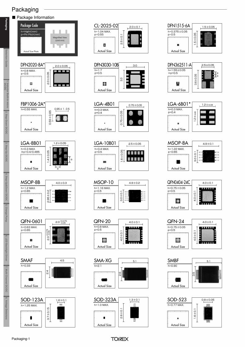
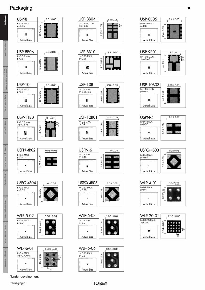
h=Hight(mm)p=Pin Pitch(mm)
Package Code
Actual Size Photo
Magnified View(Unit:mm)
Actual Size
MSOP-8A 4.9±0.1
3.0
±0
.1
h=1.22 MAX.p=0.65
Actual Size
MSOP-8B 4.0±0.3
2.9
5±
0.2
h=1.2 MAX.p=0.65
Actual Size
MSOP-10 4.9±0.2
3.0
±0
.1
h=1.16 MAX.p=0.5
QFN-20 4.0±0.1
4.0
±0
.1
h=0.8 MAX.p=0.5
Actual Size
QFN-0601 2.0
h=0.63 MAX.p=0.65
Actual Size
+0.075-0.05
2.0
+0
.07
5-
0.0
5
Actual Size
SOD-123A 1.6±0.1
3.7
±0
.15
h=1.25 MAX.
QFN-24 4.0±0.1
4.0
±0
.1
Actual Size
h=0.75±0.05p=0.5
Actual Size
SOD-523 0.8±0.05
1.6
±0
.1
h=0.77 MAX.
Actual Size
SOD-323A 1.3±0.1
2.6
±0
.1
h=1.0 MAX.
LGA-4B01
0.7
5±
0.0
5
h=0.3 MAX.p=0.4
Actual Size
0.75±0.05
1.2±0.05
1.4
±0
.05
Actual Size
LGA-8B01h=0.3 MAX.※p=0.4/0.485
Actual Size
CL-2025-02 2.0±0.1
2.5
±0
.1
h=1.04 MAX.p=0.55
Actual Size
DFN1515-6A 1.5±0.05
1.5
±0
.05
h=0.375±0.05 p=0.5
Actual Size
DFN2020-8A* 2.0±0.05
2.0
±0
.05
h=0.8 MAX. p=0.5
Actual Size
LGA-10B01 2.5±0.05
1.6
±0
.05h=0.4 MAX.
p=0.5
Actual Size
QFN0404-24C 4.0±0.1
4.0
±0
.1
h=0.75±0.05p=0.5
※
※
DFN3030-10Bh=1.7p=0.5
3.0
3.0
FBP1006-2A*h=0.55 MAX.
LGA-6B01*h=0.3 MAX.p=0.4
1.2±x.xx
1.2
±x.
xx
SMAF 4.5
2.4
h=0.33
SMA-XGh=2.1
5.1
2.6
SMBFh=0.90
5.1
3.5
0.95± 1 . 0 5
0.5
5±
0.6
5
DFN362511-Ah=1.55±0.05※p=0.5
2.5±0.05
3.6±
0.05
※※
Actual SizeActual SizeActual Size
Actual Size
Actual Size Actual Size
Actual Size
Packaging-1
Packaging Package Information
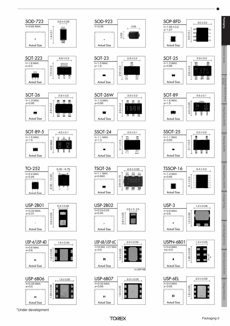
Actual Size
SOT-89-5 4.5±0.1
4.6
MA
X
h=1.5 MAX.p=1.5
Actual Size
SOT-89 4.5±0.1
4.0
±0
.25
h=1.6 MAX.p=1.5
Actual Size
SSOT-24 2.0±0.1
2.1
±0
.3
h=1.1 MAX.p=1.3
Actual Size
USP-6B/USP-6C 2.0±0.05
1.8
±0
.05
h=0.6 MAX. ※(0.7 MAX)p=0.5
※USP-6B
USP-2B01 0.3±0.05
0.6
±0
.05
h=0.33 MAX.p=0.31
Actual Size
USP-3 1.2±0.08
1.2
±0
.08
h=0.6 MAX.p=0.6
Actual Size
Actual Size
TSSOP-16 6.4±0.2
5.1
±0
.2
h=1.4 MAX.p=0.65
USP-4/USP-4D 1.6±0.05
1.2
±0
.05
h=0.6 MAX.p=0.6
Actual Size
SSOT-25 2.0±0.2
2.1
±0
.3
h=1.1 MAX.p=0.65
Actual Size
TO-252 6.35-6.75
9.3
5-
10
.45h=2.4 MAX.
p=2.29
Actual Size
Actual Size
USPN-6B01 1.0±0.05
1.4
5±
0.0
5
h=0.4 MAX.※p=0.5
USP-6B06h=0.33 MAX.p=0.5
Actual Size
1.8±0.05
1.5
0±
0.0
5
※
TSOT-26h=1.1 MAX.p=0.950
Actual Size
2.9±0.05
2.8
±0
.15
USP-6B07h=0.33 MAX.p=0.55
Actual Size
2.0±0.05
1.8
±0.
05
USP-2B02h=0.3±0.03p=0.45
0.5± 0 . 0 5
0.8
±0
.05
Actual Size
SOT-26 2.9±0.2
2.8
±0
.2
h=1.3 MAX.p=0.95
Actual Size
SOT-26W 2.9±0.2
2.8
±0
.2
h=1.3 MAX.p=0.95
Actual Size
SOT-25 2.9±0.2
2.8
±0
.2
h=1.3 MAX.p=0.95
Actual Size
SOT-23 2.9±0.2
2.8
±0
.2
h=1.3 MAX.p=1.9
Actual SizeActual Size
SOT-223 6.6±0.3
7.0
±0
.3
h=1.8 MAX.p=2.3
SOP-8FDh=1.55±0.2p=1.27
Actual Size
6.0±0.2
4.9
±0
.1
Actual Size
SOD-723 0.6±0.05
1.4
±0
.1
h=0.65 MAX.
SOD-923h=0.35 0.95
0.5
5
Actual Size
Actual Size
USP-6EL 2.0±0.05
1.8
±0
.05
h=0.4 MAX.p=0.55
Packaging-2
*Under development
USPN-4B02 0.95±0.05
0.7
5±
0.0
5
Actual Size
h=0.4 MAX.p=0.4
USPQ-4B03 1.0±0.05
1.0
±0
.05
h=0.4 MAX.p=0.65
Actual Size
USPN-6 1.3±0.05
1.3
±0
.05
h=0.4 MAX.p=0.45
Actual Size
WLP-5-02 0.88±0.04
1.2
5±
0.0
4
h=0.4 MAX.p=0.5
Actual Size
USPQ-4B04 1.0±0.05
1.0
±0
.05
h=0.6 MAX.p=0.65
Actual Size
WLP-20-01 2.15±0.05
1.9
4±
0.0
5
h=0.625 MAX.※p=0.4
Actual Size
※
※
WLP-4-01 0.70
h=0.2 MAX.p=0.4
Actual Size
+0.02-0.03
0.7
0+
0.0
2-
0.0
3
WLP-5-03 1.06±0.04
1.2
6±
0.0
4
h=0.4 MAX.p=0.5
Actual Size
WLP-6-01 1.08±0.03
1.2
8±
0.0
3h=0.4 MAX.※p=0.4/0.5
Actual Size
※
※
USP-12B01 2.3±0.05
2.8
±0
.05
h=0.6 MAX.p=0.4
Actual Size
USPN-4 1.2±0.05
0.9
±0
.05
h=0.4 MAX.p=0.55
Actual Size
USPQ-4B05 1.0±0.05
1.0
±0
.05
h=0.33 MAX.p=0.65
Actual Size
USP-10B03h=1.0±0.05p=0.65
Actual Size
2.15±0.05
2.5
±0
.05
Actual Size
USP-11B01 3.1±0.1
4.7
±0
.1
h=1.35 MAX.※p=0.675 ※
※
Actual Size
USP-10B 2.6±0.05
2.9
±0
.05
h=0.6 MAX.p=0.65/0.5
Actual Size
USP-10 2.5±0.05
2.7
±0
.05
h=0.6 MAX.p=0.5
USP-9B01 2.5±0.1
3.2
±0
.1
h=1.0±0.05※p=0.45
Actual Size
※※
USP-8B06 2.0±0.05
2.0
±0
.05
h=0.33 MAX.p=0.5
USP-8B10h=0.33 MAX.p=0.65
2.9±0.05
2.6
±0.
05
Actual SizeActual Size
Actual Size
USP-8B05 2.4±0.05
2.4
±0
.05
h=0.33±0.3p=0.6
Actual Size
USP-8 2.5±0.05
2.7
±0
.05
h=0.6 MAX.p=0.65
USP-8B04h=0.70±0.05※p=0.43
Actual Size
1.5±0.05
2.2
5±
0.0
5 ※
WLP-5-06 0.88±0.33
0.9
6±
0.3
3
h=0.33 MAX.p=0.5
Actual Size
Packaging-3
Packaging
*Under development

Selection Guide
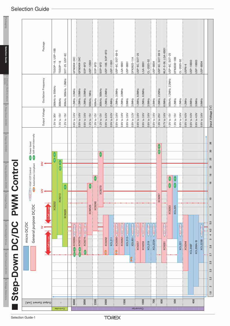
Selection Guide-1
St
ep-D
own
DC
/DC
PW
M C
ontr
ol
Outp
ut
Voltag
eO
scill
atio
n F
requency
Pac
kage
XC
9252
1.5
V t
o 3
0V
280kH
z to
550kH
zTSSO
P-16, U
SP
-10B
-XC
9213
1.5
V t
o 1
5V
300kH
zTSSO
P-16
XC
9220
1.2
V t
o 1
5V
300kH
z, 5
00kH
z, 1
.0M
Hz
SO
T-25, U
SP
-6C
6000
XC
9266
0.8
V t
o 3
.6V
1.2
MH
z, 3
.0M
Hz
QFN
0404-24C
XC
9273
0.8
V t
o 3
.6V
1.2
MH
z, 3
.0M
Hz
QFN
0404-24C
XC
9274
0.8
V t
o 3
.6V
1.2
MH
z, 3
.0M
Hz
SO
P-8FD
XC
M526
1.2
V t
o 1
5V
500kH
z, 1
MH
zU
SP
-12B
01
2200
XC
9248
1.0
V t
o 1
2V
500kH
zSO
P-8FD
XC
9270
1.2
V t
o 1
2V
300kH
z, 5
00kH
zSO
P-8FD
XC
9242
0.9
V t
o 6
.0V
1.2
MH
z, 2
.4M
Hz
USP
-10B
, SO
P-8FD
XC
L211
0.9
V t
o 6
.0V
2.4
MH
zU
SP
-11B
01
XC
9260
0.8
V t
o 3
.6V
1.2
MH
z, 3
.0M
Hz
USP
-6C
, SO
T-89-5
XC
9262
0.8
V t
o 3
.6V
1.2
MH
z, 3
.0M
Hz
LG
A-8B
01
XC
L213
0.8
V t
o 3
.6V
3.0
MH
zU
SP
-9B
01
XD
L601
0.8
V t
o 3
.3V
3.0
MH
zD
FN
3625-11A
XC
9257
0.8
V t
o 3
.6V
1.2
MH
z, 6
.0M
Hz
USP
-6C
, SO
T-25
XC
9259
0.8
V t
o 3
.6V
1.2
MH
z, 6
.0M
Hz
LG
A-8B
01
XC
L219
0.8
V t
o 3
.6V
3.0
MH
zC
L-2025-02
700
XC
L223A
0.8
V t
o 3
.6V
3.0
MH
zU
SP
-8B
04
XC
9267
1.0
V t
o 2
5V
1.2
MH
z, 2
.2M
Hz
USP
-6C
, SO
T-89-5
XC
9281
0.7
V t
o 3
.6V
6.0
MH
zW
LP
-5-06, LG
A-6B
01
XC
9263
1.0
V t
o 1
5V
500kH
z, 1
.2M
Hz,
2.2
MH
zU
SP
-6C
, SO
T-25
XC
L225
1.0
V t
o 1
5V
1.2
MH
zD
FN
3030-10B
XC
L221
0.8
V t
o 3
.6V
1.2
MH
zC
L-2025-02
XC
9244
0.8
V t
o 4
.0V
1.2
MH
zU
SP
N-6
XC
L208F
0.8
V t
o 4
.0V
3.0
MH
zU
SP
-10B
03
XC
L208A
/B
0.8
V t
o 4
.0V
3.0
MH
zU
SP
-10B
03
XC
L223B
0.8
V t
o 3
.6V
3.0
MH
zU
SP
-8B
04
Input
Voltag
e [
V]
5.5
630
36
10
16
18
20
25
2.2
2.3
2.5
2.7
2.8
3
4
4.5
Controller
Output Current [mA]
500
400
Converter
3000
2000
1500
1000
600
71.8
2
mic
ro D
C/DC
Gene
ral p
urpo
seDC
/DC
HiSA
T-CO
T
HiSA
T-CO
T
HiSA
T-CO
T
HiSA
T-CO
T
HiSA
T-CO
T
HiSA
T-CO
T
HiSA
T-CO
T
HiSA
T-CO
T
HiSA
T-CO
T
HiSA
T-CO
T
HiSA
T-CO
T
HiSA
T-CO
T
HiSA
T-CO
T
PG
PG PG
PG
PG
HiSA
T-CO
T
SSSS
SS SS
SS
SS
PGSS
Auto
mot
ive
Com
plia
ntPG
Pow
er G
ood
SSSo
ft-st
art E
xter
nally
HiSA
T-CO
THi
SAT-
COT
Cont
rol
1 C
ell
Li-
ion
2 C
ell
Li-
ion
12V
24V
5V
PG
PG
SS
SS
SS SS
Selection Guide-2
St
ep-D
own
DC
/DC
PW
M C
ontr
olH
iSA
T-C
OT
Ext
ern
alFET/SB
DV
out
Sett
ing
Pro
tection
Oth
er
Low
Voltag
e D
C/D
C :
Inpu
t V
oltag
e 6
V o
r lo
wer
XC
L223A
PW
M2.5
~5.5
0.8
~3.6
700
3.0
MYes
-V
out
105
USP
-8B
04
TSD
/Lim
/Short
SS/U
VLO
/D
ischar
ge2
XC
L223B
PW
M2.5
~5.5
0.8
~3.6
400
3.0
MYes
-V
out
105
USP
-8B
04
TSD
/Lim
/Short
SS/U
VLO
/D
ischar
ge2
XC
L221
PW
M2.5
~5.5
0.8
~3.6
500
1.2
MYes
-V
out
105
CL-2025-02
TSD
/Lim
/Short
SS/U
VLO
/D
ischar
ge3
XC
L219
PW
M2.5
~5.5
0.8
~3.6
1000
3.0
MYes
-V
out
105
CL-2025-02
TSD
/Lim
/Short
SS/U
VLO
/D
ischar
ge4
XC
L213
PW
M2.7
~5.5
0.8
~3.6
1500
3.0
MYes
-V
out
105
USP
-9B
01
TSD
/Lim
/Short
SS/U
VLO
/D
ischar
ge5
XC
L211
PW
M2.7
~6.0
0.9
~6.0
2000
2.4
M-
-FB
85
USP
-11B
01
TSD
/Lim
SS/U
VLO
/D
ischar
ge6
XC
L208A
/B
PW
M2.0
~6.0
0.8
~4.0
400
3.0
M-
-V
out
85
USP
-10B
03
Lim
/Short
SS/U
VLO
/D
ischar
ge8
XC
L208F
PW
M1.8
~6.0
0.8
~4.0
400
3.0
M-
-FB
85
USP
-10B
03
Lim
/Short
SS/U
VLO
/D
ischar
ge8
XC
9281
PW
M2.5
~5.5
0.7
~3.6
600
6.0
MYes
-V
out
105
LG
A-6B
01
WLP
-5-06
Lim
UV
LO
/SS/D
ischar
ge12
XC
9274
PW
M2.7
~5.5
0.8
~3.6
3000
1.2
M3.0
MYes
-FB
105
SO
P-8FD
TSD
/Lim
/Short
or
Hic
cup
UV
LO
/SS/Soft
off/P
G/D
ischar
ge15
XC
9273
PW
M o
r P
WM
/P
FM
2.7
~5.5
0.8
~3.6
3000
1.2
M3.0
MYes
-FB
105
QFN
0404-24C
TSD
/Lim
/Short
or
Hic
cup
UV
LO
/SS a
dj./
Soft
off/P
G/D
ischar
ge14
XC
9266
PW
M o
r P
WM
/P
FM
2.7
~5.5
0.8
~3.6
6000
1.2
M3.0
MYes
-FB
105
QFN
0404-24C
TSD
/Lim
/Short
or
Hic
cup
UV
LO
/SS a
dj./
Soft
off/P
G/D
ischar
ge19
XC
9262
PW
M o
r P
WM
/P
FM
2.7
~5.5
0.8
~3.6
1500
1.2
M3.0
MYes
-V
out
105
LG
A-8B
01
TSD
/Lim
/Short
SS/U
VLO
/D
ischar
ge22
XC
9260
PW
M2.7
~5.5
0.8
~3.6
1500
1.2
M3.0
MYes
-V
out
105
SO
T-89-5
USP
-6C
TSD
/Lim
/Short
SS/U
VLO
/D
ischar
ge23
XC
9259
PW
M o
r P
WM
/P
FM
2.5
~5.5
0.8
~3.6
1000
1.2
M6.0
MYes
-V
out
105
LG
A-8B
01
TSD
/Lim
/Short
SS/U
VLO
/D
ischar
ge24
XC
9257
PW
M2.5
~5.5
0.8
~3.6
1000
1.2
M6.0
MYes
-V
out
105
SO
T-25
USP
-6C
TSD
/Lim
/Short
SS/U
VLO
/D
ischar
ge25
XC
9244
PW
M2.3
~6.0
0.8
~4.0
400
1.2
M-
-V
out
85
USP
N-6
Lim
SS/U
VLO
/D
ischar
ge28
XC
9242
PW
M2.7
~6.0
0.9
~6.0
2000
1.2
M2.4
M-
-FB
85
USP
-10B
SO
P-8FD
TSD
/Lim
SS/U
VLO
/D
ischar
ge29
XDL6
01(A
EC-Q
100)
PW
M2.5
~5.5
0.8
~3.3
1500
3.0
MYes
-V
out
105
DFN
3625-11A
TSD
/Lim
/Short
SS/U
VLO
/D
ischar
ge135
XD
9260
(AEC
-Q
100)
PW
M2.7
~5.5
0.8
~3.6
1500
1.2
M3.0
MYes
-V
out
105
USP
-6C
TSD
/Lim
/Short
SS/U
VLO
/D
ischar
ge136
XD
9242
(AEC
-Q
100)
PW
M2.7
~6.0
0.9
~6.0
2000
1.2
M2.4
M-
-FB
85
USP
-10B
TSD
/Lim
SS/U
VLO
/D
ischar
ge137
XC
L225
PW
M3.0
~18.0
1.0
~15.0
500
1.2
M-
-FB
105
DFN
3030-10B
TSD
/Lim
SS a
dj./
UV
LO
/P
G1
XC
9263
PW
M3.0
~18.0
1.0
~15.0
500
500k
1.2
M2.2
M-
-FB
105
SO
T-25
USP
-6C
TSD
/Lim
SS a
dj./
UV
LO
/P
G21
XC
9248
PW
M4.5
~18.0
1.0
~12.0
2200
500k
--
FB
105
SO
P-8FD
Lim
/Short
/TSD
/Short
SS a
dj./
UV
LO
/D
ischar
ge27
XC
9220
PW
M2.8
~16.0
1.2
~15.0
3000
300k
500k
1.0
M-
Pch+SB
DFB
85
SO
T-25
USP
-6C
Lim
/Short
SS a
dj./
UV
LO
30
XC
M526
PW
M o
r P
WM
/P
FM
4.0
~16.0
1.2
~15.0
3000
500k
1.0
M-
SB
DFB
85
USP
-12B
01
Short
SS a
dj./
UV
LO
32
Hig
h V
oltag
e D
C/D
C :
Inpu
t V
oltag
e 3
6V
or
low
er
XC
9270
PW
M7.0
~30.0
1.2
~12.0
2000
300k
500k
Ext
CLK
-SB
DFB
105
SO
P-8FD
TSD
/Lim
/Short
SS a
dj./
UV
LO
/SYN
C17
XC
9267
PW
M3.0
~36.0
1.0
~25.0
600
1.2
M2.2
M-
-FB
105
SO
T-89-5
USP
-6C
TSD
/Lim
SS a
dj./
UV
LO
/P
G18
XC
9252
PW
M o
r P
WM
/P
FM
3.0
~30.0
1.5
~30.0
10000
Adj.(
280k~
550k)
Ext
CLK
-P
ch+SB
DFB
105
TSSO
P-16
USP
-10B
TSD
/Lim
/Short
SS a
dj./
UV
LO
/P
G/SYN
C26
XC
9213
PW
M o
r P
WM
/P
FM
4.0
~25.0
1.5
~15.0
5000
300k
-N
ch+N
ch
FB
85
TSSO
P-16
Lim
/Short
SS a
dj./
UV
LO
31
Mid
dle V
oltag
e D
C/D
C :
Inpu
t V
oltag
e 1
8V
or
low
er
Pag
eIo
ut
[mA
]fo
sc[H
z]
Function
Ta
max
.P
acka
ge
Function
Series
Contr
ol
Meth
od
Vin
[V
]V
out
[V]
Selection Guide
Selection Guide-3
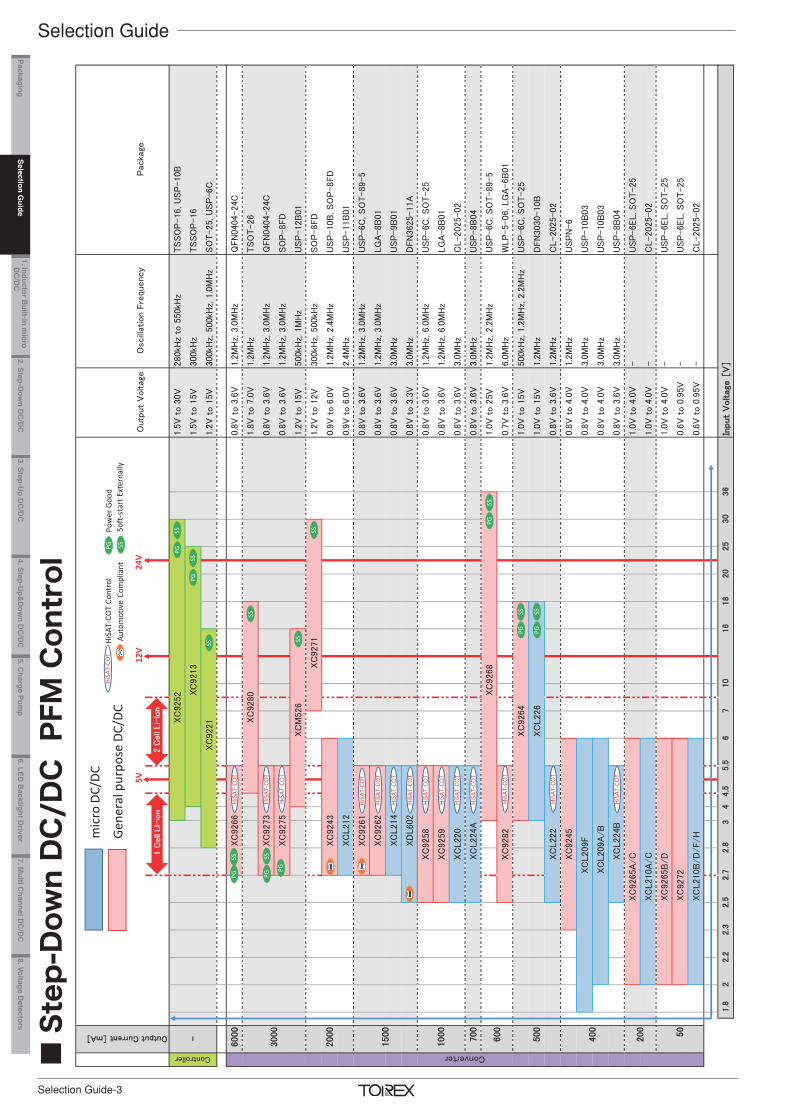
St
ep-D
own
DC
/DC
PFM
Con
trol
Outp
ut
Voltag
eO
scill
atio
n F
requency
Pac
kage
XC
9252
1.5
V t
o 3
0V
280kH
z to
550kH
zTSSO
P-16, U
SP
-10B
XC
9213
1.5
V t
o 1
5V
300kH
zTSSO
P-16
XC
9221
1.2
V t
o 1
5V
300kH
z, 5
00kH
z, 1
.0M
Hz
SO
T-25, U
SP
-6C
6000
XC
9266
0.8
V t
o 3
.6V
1.2
MH
z, 3
.0M
Hz
QFN
0404-24C
XC
9280
1.8
V t
o 7
.0V
1.2
MH
zTSO
T-26
XC
9273
0.8
V t
o 3
.6V
1.2
MH
z, 3
.0M
Hz
QFN
0404-24C
XC
9275
0.8
V t
o 3
.6V
1.2
MH
z, 3
.0M
Hz
SO
P-8FD
XC
M526
1.2
V t
o 1
5V
500kH
z, 1
MH
zU
SP
-12B
01
XC
9271
1.2
V t
o 1
2V
300kH
z, 5
00kH
zSO
P-8FD
XC
9243
0.9
V t
o 6
.0V
1.2
MH
z, 2
.4M
Hz
USP
-10B
, SO
P-8FD
XC
L212
0.9
V t
o 6
.0V
2.4
MH
zU
SP
-11B
01
XC
9261
0.8
V t
o 3
.6V
1.2
MH
z, 3
.0M
Hz
USP
-6C
, SO
T-89-5
XC
9262
0.8
V t
o 3
.6V
1.2
MH
z, 3
.0M
Hz
LG
A-8B
01
XC
L214
0.8
V t
o 3
.6V
3.0
MH
zU
SP
-9B
01
XD
L602
0.8
V t
o 3
.3V
3.0
MH
zD
FN
3625-11A
XC
9258
0.8
V t
o 3
.6V
1.2
MH
z, 6
.0M
Hz
USP
-6C
, SO
T-25
XC
9259
0.8
V t
o 3
.6V
1.2
MH
z, 6
.0M
Hz
LG
A-8B
01
XC
L220
0.8
V t
o 3
.6V
3.0
MH
zC
L-2025-02
700
XC
L224A
0.8
V t
o 3
.6V
3.0
MH
zU
SP
-8B
04
XC
9268
1.0
V t
o 2
5V
1.2
MH
z, 2
.2M
Hz
USP
-6C
, SO
T-89-5
XC
9282
0.7
V t
o 3
.6V
6.0
MH
zW
LP
-5-06, LG
A-6B
01
XC
9264
1.0
V t
o 1
5V
500kH
z, 1
.2M
Hz,
2.2
MH
zU
SP
-6C
, SO
T-25
XC
L226
1.0
V t
o 1
5V
1.2
MH
zD
FN
3030-10B
XC
L222
0.8
V t
o 3
.6V
1.2
MH
zC
L-2025-02
XC
9245
0.8
V t
o 4
.0V
1.2
MH
zU
SP
N-6
XC
L209F
0.8
V t
o 4
.0V
3.0
MH
zU
SP
-10B
03
XC
L209A
/B
0.8
V t
o 4
.0V
3.0
MH
zU
SP
-10B
03
XC
L224B
0.8
V t
o 3
.6V
3.0
MH
zU
SP
-8B
04
XC
9265A
/C
1.0
V t
o 4
.0V
-U
SP
-6EL, SO
T-25
XC
L210A
/C
1.0
V t
o 4
.0V
-C
L-2025-02
XC
9265B
/D
1.0
V t
o 4
.0V
-U
SP
-6EL, SO
T-25
XC
9272
0.6
V t
o 0
.95V
-U
SP
-6EL, SO
T-25
XC
L210B
/D
/F/H
0.6
V t
o 0
.95V
-C
L-2025-02
Input
Voltag
e [
V]
30
2.8
5.5
618
20
25
3
4
4.5
Converter
10
16
Output Current [mA]
22.2
Controller
-
1000
1500
2000
3000
50
200
400
500
600
71.8
2.3
2.5
2.7
36
mic
ro D
C/DC
Gene
ral p
urpo
se D
C/DC
HiSA
T-CO
T
HiSA
T-CO
T
HiSA
T-CO
T
HiSA
T-CO
T
HiSA
T-CO
T
HiSA
T-CO
T
HiSA
T-CO
T
HiSA
T-CO
T
HiSA
T-CO
T
HiSA
T-CO
T
HiSA
T-CO
T
HiSA
T-CO
T
HiSA
T-CO
T
PG
PG PG
PG
PG
HiSA
T-CO
T
SS
SS
SS
SS
PGSS
Auto
mot
ive
Com
plia
ntPG
Pow
er G
ood
SSSo
ft-st
art E
xter
nally
HiSA
T-CO
THi
SAT-
COT
Cont
rol
12V
24V
5V
1 C
ell
Li-
ion
2 C
ell
Li-
ion
PG
PG
SS
SS
SS
SS SS
SS
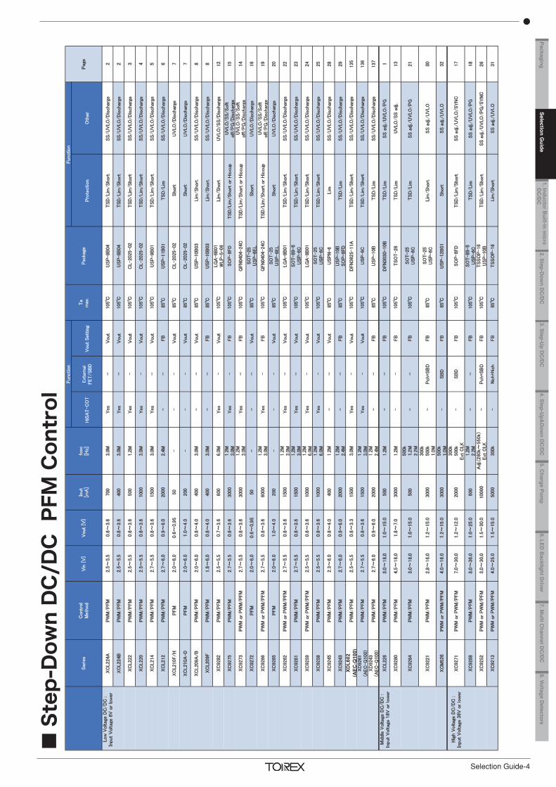
Selection Guide-4
St
ep-D
own
DC
/DC
PFM
Con
trol
HiS
AT-C
OT
Ext
ern
alFET/SB
DV
out
Sett
ing
Pro
tection
Oth
er
Low
Voltag
e D
C/D
C :
Inpu
t V
oltag
e 6
V o
r lo
wer
XC
L224A
PW
M/P
FM
2.5
~5.5
0.8
~3.6
700
3.0
MYes
-V
out
105
USP
-8B
04
TSD
/Lim
/Short
SS/U
VLO
/D
ischar
ge2
XC
L224B
PW
M/P
FM
2.5
~5.5
0.8
~3.6
400
3.0
MYes
-V
out
105
USP
-8B
04
TSD
/Lim
/Short
SS/U
VLO
/D
ischar
ge2
XC
L222
PW
M/P
FM
2.5
~5.5
0.8
~3.6
500
1.2
MYes
-V
out
105
CL-2025-02
TSD
/Lim
/Short
SS/U
VLO
/D
ischar
ge3
XC
L220
PW
M/P
FM
2.5
~5.5
0.8
~3.6
1000
3.0
MYes
-V
out
105
CL-2025-02
TSD
/Lim
/Short
SS/U
VLO
/D
ischar
ge4
XC
L214
PW
M/P
FM
2.7
~5.5
0.8
~3.6
1500
3.0
MYes
-V
out
105
USP
-9B
01
TSD
/Lim
/Short
SS/U
VLO
/D
ischar
ge5
XC
L212
PW
M/P
FM
2.7
~6.0
0.9
~6.0
2000
2.4
M-
-FB
85
USP
-11B
01
TSD
/Lim
SS/U
VLO
/D
ischar
ge6
XC
L210F/H
PFM
2.0
~6.0
0.6
~0.9
550
--
-V
out
85
CL-2025-02
Short
UV
LO
/D
ischar
ge7
XC
L210A
-D
PFM
2.0
~6.0
1.0
~4.0
200
--
-V
out
85
CL-2025-02
Short
UV
LO
/D
ischar
ge7
XC
L209A
/B
PW
M/P
FM
2.0
~6.0
0.8
~4.0
400
3.0
M-
-V
out
85
USP
-10B
03
Lim
/Short
SS/U
VLO
/D
ischar
ge8
XC
L209F
PW
M/P
FM
1.8
~6.0
0.8
~4.0
400
3.0
M-
-FB
85
USP
-10B
03
Lim
/Short
SS/U
VLO
/D
ischar
ge8
XC
9282
PW
M/P
FM
2.5
~5.5
0.7
~3.6
600
6.0
MYes
-V
out
105
LG
A-6B
01
WLP
-5-06
Lim
/Short
UV
LO
/SS/D
ischar
ge12
XC
9275
PW
M/P
FM
2.7
~5.5
0.8
~3.6
3000
1.2
M3.0
MYes
-FB
105
SO
P-8FD
TSD
/Lim
/Short
or
Hic
cup
UV
LO
/SS/Soft
off/P
G/D
ischar
ge15
XC
9273
PW
M o
r P
WM
/P
FM
2.7
~5.5
0.8
~3.6
3000
1.2
M3.0
MYes
-FB
105
QFN
0404-24C
TSD
/Lim
/Short
or
Hic
cup
UV
LO
/SS/Soft
off/P
G/D
ischar
ge14
XC
9272
PFM
2.0
~6.0
0.6
~0.9
550
--
-V
out
85
SO
T-25
USP
-6EL
Short
UV
LO
/D
ischar
ge16
XC
9266
PW
M o
r P
WM
/P
FM
2.7
~5.5
0.8
~3.6
6000
1.2
M3.0
MYes
-FB
105
QFN
0404-24C
TSD
/Lim
/Short
or
Hic
cup
UV
LO
/SS/Soft
off/P
G/D
ischar
ge19
XC
9265
PFM
2.0
~6.0
1.0
~4.0
200
--
-V
out
85
SO
T-25
USP
-6EL
Short
UV
LO
/D
ischar
ge20
XC
9262
PW
M o
r P
WM
/P
FM
2.7
~5.5
0.8
~3.6
1500
1.2
M3.0
MYes
-V
out
105
LG
A-8B
01
TSD
/Lim
/Short
SS/U
VLO
/D
ischar
ge22
XC
9261
PW
M/P
FM
2.7
~5.5
0.8
~3.6
1500
1.2
M3.0
MYes
-V
out
105
SO
T-89-5
USP
-6C
TSD
/Lim
/Short
SS/U
VLO
/D
ischar
ge23
XC
9259
PW
M o
r P
WM
/P
FM
2.5
~5.5
0.8
~3.6
1000
1.2
M6.0
MYes
-V
out
105
LG
A-8B
01
TSD
/Lim
/Short
SS/U
VLO
/D
ischar
ge24
XC
9258
PW
M/P
FM
2.5
~5.5
0.8
~3.6
1000
1.2
M6.0
MYes
-V
out
105
SO
T-25
USP
-6C
TSD
/Lim
/Short
SS/U
VLO
/D
ischar
ge25
XC
9245
PW
M/P
FM
2.3
~6.0
0.8
~4.0
400
1.2
M-
-V
out
85
USP
N-6
Lim
SS/U
VLO
/D
ischar
ge28
XC
9243
PW
M/P
FM
2.7
~6.0
0.9
~6.0
2000
1.2
M2.4
M-
-FB
85
USP
-10B
SO
P-8FD
TSD
/Lim
SS/U
VLO
/D
ischar
ge29
XDL6
02(A
EC-Q
100)
PW
M/P
FM
2.5
~5.5
0.8
~3.3
1500
3.0
MYes
-V
out
105
DFN
3625-11A
TSD
/Lim
/Short
SS/U
VLO
/D
ischar
ge135
XD
9261
(AEC
-Q
100)
PW
M/P
FM
2.7
~5.5
0.8
~3.6
1500
1.2
M3.0
MYes
-V
out
105
USP
-6C
TSD
/Lim
/Short
SS/U
VLO
/D
ischar
ge136
XD
9243
(AEC
-Q
100)
PW
M/P
FM
2.7
~6.0
0.9
~6.0
2000
1.2
M2.4
M-
-FB
85
USP
-10B
TSD
/Lim
SS/U
VLO
/D
ischar
ge137
XC
L226
PW
M/P
FM
3.0
~18.0
1.0
~15.0
500
1.2
M-
-FB
105
DFN
3030-10B
TSD
/Lim
SS a
dj./
UV
LO
/P
G1
XC
9280
PW
M/P
FM
4.5
~18.0
1.8
~7.0
3000
1.2
M-
-FB
105
TSO
T-26
TSD
/Lim
UV
LO
/SS a
dj.
13
XC
9264
PW
M/P
FM
3.0
~18.0
1.0
~15.0
500
500k
1.2
M2.2
M-
-FB
105
SO
T-25
USP
-6C
TSD
/Lim
SS a
dj./
UV
LO
/P
G21
XC
9221
PW
M/P
FM
2.8
~16.0
1.2
~15.0
3000
300k
500k
1.0
M-
Pch+SB
DFB
85
SO
T-25
USP
-6C
Lim
/Short
SS a
dj./
UV
LO
30
XC
M526
PW
M o
r P
WM
/P
FM
4.0
~16.0
1.2
~15.0
3000
500k
1.0
M-
SB
DFB
85
USP
-12B
01
Short
SS a
dj./
UV
LO
32
Hig
h V
oltag
e D
C/D
C :
Inpu
t V
oltag
e 3
6V
or
low
er
XC
9271
PW
M o
r P
WM
/P
FM
7.0
~30.0
1.2
~12.0
2000
300k
500k
Ext
CLK
-SB
DFB
105
SO
P-8FD
TSD
/Lim
/Short
SS a
dj./
UV
LO
/SYN
C17
XC
9268
PW
M/P
FM
3.0
~36.0
1.0
~25.0
600
1.2
M2.2
M-
-FB
105
SO
T-89-5
USP
-6C
TSD
/Lim
SS a
dj./
UV
LO
/P
G18
XC
9252
PW
M o
r P
WM
/P
FM
3.0
~30.0
1.5
~30.0
10000
Adj.(
280k~
550k)
Ext
CLK
-P
ch+SB
DFB
105
TSSO
P-16
USP
-10B
TSD
/Lim
/Short
SS a
dj./
UV
LO
/P
G/SYN
C26
XC
9213
PW
M o
r P
WM
/P
FM
4.0
~25.0
1.5
~15.0
5000
300k
-N
ch+N
ch
FB
85
TSSO
P-16
Lim
/Short
SS a
dj./
UV
LO
31
Mid
dle V
oltag
e D
C/D
C :
Inpu
t V
oltag
e 1
8V
or
low
er
Pag
eIo
ut
[mA
]fo
sc[H
z]
Function
Ta
max
.P
acka
ge
Function
Series
Contr
ol
Meth
od
Vin
[V
]V
out
[V]
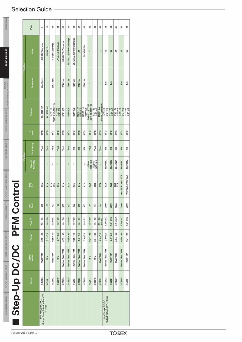
Selection Guide
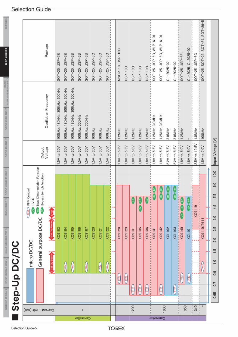
Selection Guide-5
St
ep-U
p D
C/D
C
XC
9103
1.5
V t
o 3
0V
100kH
z, 1
80kH
z, 3
00kH
z, 5
00kH
zSO
T-25, U
SP
-6B
XC
9104
1.5
V t
o 3
0V
100kH
z, 1
80kH
z, 3
00kH
z, 5
00kH
zSO
T-25, U
SP
-6B
XC
9105
1.5
V t
o 3
0V
100kH
z, 1
80kH
z, 3
00kH
z, 5
00kH
zSO
T-25, U
SP
-6B
XC
9106
1.5
V t
o 3
0V
100kH
z, 3
00kH
zSO
T-25, U
SP
-6B
XC
9107
1.5
V t
o 3
0V
100kH
z, 3
00kH
zSO
T-25, U
SP
-6B
XC
9120
1.5
V t
o 3
0V
100kH
zSO
T-25, U
SP
-6C
XC
9121
1.5
V t
o 3
0V
100kH
zSO
T-25, U
SP
-6C
XC
9122
1.5
V t
o 3
0V
100kH
zSO
T-25, U
SP
-6C
XC
9128
1.8
V t
o 5
.3V
1.2
MH
zM
SO
P-10, U
SP
-10B
XC
9129
1.8
V t
o 5
.3V
1.2
MH
zU
SP
-10B
XC
9131
1.8
V t
o 5
.0V
1.2
MH
zU
SP
-10B
XC
9135
1.8
V t
o 5
.0V
1.2
MH
zU
SP
-10B
XC
9136
1.8
V t
o 5
.0V
1.2
MH
zU
SP
-10B
XC
9141
1.8
V t
o 5
.5V
1.2
MH
z, 3
.0M
Hz
SO
T-25, U
SP
-6C
, W
LP
-6-01
XC
9142
1.8
V t
o 5
.5V
1.2
MH
z, 3
.0M
Hz
SO
T-25, U
SP
-6C
, W
LP
-6-01
XC
L102
2.2
V t
o 5
.5V
3.0
MH
zC
L-2025-02
XC
L103
2.2
V t
o 5
.5V
3.0
MH
zC
L-2025-02
XC
9140
1.8
V t
o 5
.0V
1.2
MH
zSO
T-25, U
SP
-6EL
XC
L101
1.8
V t
o 5
.0V
-C
L-2025, C
L2025-02
3 10
XC
9119
2.5
V t
o 1
9.5
V1.0
MH
zSO
T-25, U
SP
-6C
-XC
9110/9111
1.5
V t
o 7
.0V
100kH
zSO
T-25, SO
T-23, SO
T-89, SO
T-89-5
Inpu
t V
oltag
e [
V]
Outp
ut
Voltag
eO
scill
atio
n F
requ
ency
Pac
kage
10.0
2.5
3.0
4.5
5.5
6.0
350
Converter
2.0
0.6
50.7
0.9
1.0
1.5
Current Limit [mA]
Controller
-
1200
1000
mic
ro D
C/DC
Gene
ral p
urpo
se D
C/DC
Load
Disc
onne
ctio
n Fu
nctio
nBP
Bypa
ss S
witc
h Fu
nctio
n
PFM
PFM
Con
trol
LD
LD
BPLD
BPLD
LDLD BPLD
BPLD
BPLD
BPLD
PFM
PFM
PFM
PFM
PFM
PFM
PFM
PFM
PFM
UV
UVL
O
UV
UV
PFM
PFM
PFM
PFM
PFM
Li-
ion
2 C
ell
Dry
Bat
tery
1 C
ell
Dry
Bat
tery
PFM
Selection Guide-6
St
ep-U
p D
C/D
C P
WM
Con
trol
Ext
ern
alFET/SB
DV
out
Sett
ing
Pro
tection
Oth
er
XC
L102
PW
M0.6
5~
6.0
2.2
~5.5
500
3.0
M-
Vout
85
CL-2025-02
Lim
/Short
SS/LD
/D
ischar
ge9
XC
9141
PW
M0.6
5~
6.0
1.8
~5.5
500
1.2
M3.0
M-
Vout
85
SO
T-25
WLP
-6-01, U
SP
-6C
Lim
/Short
SS/LD
/D
ischar
ge33
XC
9136
PW
M o
r P
WM
/P
FM
0.6
5~
5.5
1.8
~5.0
600
1.2
M-
Vout
85
USP
-10B
TSD
/Lim
SS/LD
/FO
/D
ischar
ge35
XC
9135
PW
M o
r P
WM
/P
FM
0.6
5~
5.5
1.8
~5.0
600
1.2
M-
Vout
85
USP
-10B
TSD
/Lim
SS/U
VLO
/LD
/FO
/D
ischar
ge35
XC
9131
PW
M o
r P
WM
/P
FM
0.6
5~
5.5
1.8
~5.0
600
1.2
M-
FB
85
USP
-10B
TSD
/Lim
SS/LD
/FO
/D
ischar
ge36
XC
9129
PW
M o
r P
WM
/P
FM
0.8
~6.0
1.8
~5.3
600
1.2
M-
FB
85
MSO
P-10
USP
-10B
TSD
/Lim
SS
37
XC
9128
PW
M o
r P
WM
/P
FM
0.8
~6.0
1.8
~5.3
600
1.2
M-
FB
85
MSO
P-10
USP
-10B
TSD
/Lim
SS/A
EN
/FO
37
XC
9801
PW
M1.8
~5.5
2.5
~6.0
or
Vin
x230
300k
-V
out
85
MSO
P-8A
USP
-8, U
SP
-8B
05
--
46
Hig
h V
oltag
e D
C/D
C :
Outp
ut
Voltag
e 3
6V
or
low
er
XC
9122
PW
M o
r P
WM
/P
FM
0.9
~6.0
1.5
~30.0
3000
100k
Nch+SB
DFB
85
SO
T-25
USP
-6C
Lim
SS
38
XC
9120
PW
M0.9
~6.0
1.5
~30.0
3000
100k
Nch+SB
DFB
85
SO
T-25
USP
-6C
Lim
SS
38
XC
9119
PW
M2.5
~6.0
2.5
~19.5
100
1.0
MSB
DFB
85
SO
T-25
USP
-6C
-SS a
dj.
39
XC
9106
PW
M0.9
~10.0
1.5
~30.0
3000
100k
300k
Nch+SB
DFB
85
SO
T-25
USP
-6B
-SS
41
XC
9105
PW
M o
r P
WM
/P
FM
0.9
~10.0
1.5
~30.0
3000
100k/
180k/
300k/
500k
Nch+SB
DFB
85
SO
T-25
USP
-6B
Lim
SS
42
XC
9103
PW
M0.9
~10.0
1.5
~30.0
3000
100k/
180k/
300k/
500k
Nch+SB
DFB
85
SO
T-25
USP
-6B
Lim
SS
42
LED
Bac
k lig
ht
driv
er
XC
9133
PW
M2.5
~6.0
2.5
~17.5
100
1.0
MSB
DFB
85
SO
T-25
Lim
/O
VP
-48
Low
Voltag
e D
C/D
C,
Char
ge P
um
p O
utp
ut
Voltag
e 7
Vor
low
er
Pag
eIo
ut
[mA
]fo
sc[H
z]Ta
max
.P
acka
ge
Function
Function
Series
Contr
ol
Meth
od
Vin
[V
]V
out
[V]
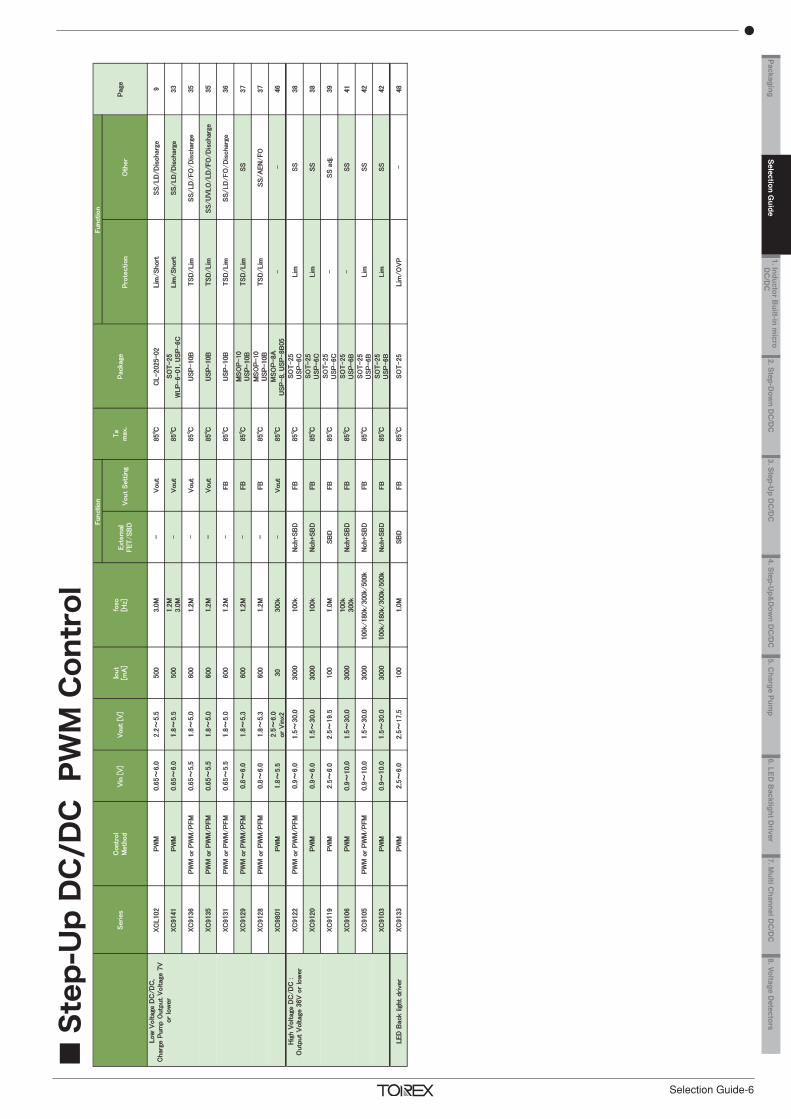
Selection Guide
Selection Guide-7
St
ep-U
p D
C/D
C
PFM
Con
trol
Ext
ern
alFET/SB
DV
out
Sett
ing
Pro
tection
Oth
er
XC
L103
PW
M/P
FM
0.6
5~
6.0
2.2
~5.5
500
3.0
M-
Vout
85
CL-2025-02
Lim
/Short
SS/LD
/D
ischar
ge9
XC
L101
PFM
0.7
~5.5
1.8
~5.0
100
1.2
M-
Vout
85
CL-2025-02
-U
VLO
/LD
10
XC
9142
PW
M/P
FM
0.6
5~
6.0
1.8
~5.5
500
1.2
M3.0
M-
Vout
85
SO
T-25
WLP
-6-01, U
SP
-6C
Lim
/Short
SS/LD
/D
ischar
ge33
XC
9140
PFM
0.7
~5.5
1.8
~5.0
100
1.2
M-
Vout
85
SO
T-25
USP
-6EL
-U
VLO
/LD
/D
ischar
ge34
XC
9136
PW
M o
r P
WM
/P
FM
0.6
5~
5.5
1.8
~5.0
600
1.2
M-
Vout
85
USP
-10B
TSD
/Lim
SS/LD
/FO
/D
ischar
ge35
XC
9135
PW
M o
r P
WM
/P
FM
0.6
5~
5.5
1.8
~5.0
600
1.2
M-
Vout
85
USP
-10B
TSD
/Lim
SS/U
VLO
/LD
/FO
/D
ischar
ge35
XC
9131
PW
M o
r P
WM
/P
FM
0.6
5~
5.5
1.8
~5.0
600
1.2
M-
FB
85
USP
-10B
TSD
/Lim
SS/U
VLO
/LD
/FO
/D
ischar
ge36
XC
9129
PW
M o
r P
WM
/P
FM
0.8
~6.0
1.8
~5.3
600
1.2
M-
FB
85
MSO
P-10
USP
-10B
TSD
/Lim
SS
37
XC
9128
PW
M o
r P
WM
/P
FM
0.8
~6.0
1.8
~5.3
600
1.2
M-
FB
85
MSO
P-10
USP
-10B
TSD
/Lim
SS/A
EN
/FO
37
XC
9111
PFM
0.8
~10.0
1.5
~7.0
70
100k
SB
D o
rSB
D+N
ch
Vout
85
SO
T-23, SO
T-25
SO
T-89, U
SP
-6C
--
40
XC
9110
PFM
0.8
~10.0
1.5
~7.0
70
100k
SB
D o
rSB
D+N
ch
Vout
85
SO
T-25
USP
-6C
--
40
XC
9802
PW
M/P
FM
1.8
~5.5
2.5
~6.0
or
Vin
x230
300k
-V
out
85
MSO
P-8A
USP
-8, U
SP
-8B
05
--
46
Hig
h V
oltag
e D
C/D
C :
Outp
ut
Voltag
e 3
6V
or
low
er
XC
9122
PW
M o
r P
WM
/P
FM
0.9
~6.0
1.5
~30.0
3000
100k
Nch+SB
DFB
85
SO
T-25
USP
-6C
Lim
SS
38
XC
9121
PW
M/P
FM
0.9
~6.0
1.5
~30.0
3000
100k
Nch+SB
DFB
85
SO
T-25
USP
-6C
Lim
SS
38
XC
9107
PW
M/P
FM
0.9
~10.0
1.5
~30.0
3000
100k
300k
Nch+SB
DFB
85
SO
T-25
USP
-6B
-SS
41
XC
9105
PW
M o
r P
WM
/P
FM
0.9
~10.0
1.5
~30.0
3000
100k/
180k/
300k/
500k
Nch+SB
DFB
85
SO
T-25
USP
-6B
Lim
SS
42
XC
9104
PW
M/P
FM
0.9
~10.0
1.5
~30.0
3000
100k/
180k/
300k/
500k
Nch+SB
DFB
85
SO
T-25
USP
-6B
Lim
SS
42
Low
Voltag
e D
C/D
C,
Char
ge P
um
p O
utp
ut
Voltag
e 7
Vor
low
er
Function
Pag
eIo
ut
[mA
]fo
sc[H
z]Ta
max
.P
acka
ge
Function
Series
Contr
ol
Meth
od
Vin
[V
]V
out
[V]
Selection Guide-8
St
ep-U
p/D
own
DC
/DC
N
egat
ive
Volta
ge D
C/D
C
Ext
ern
alFET/SB
DV
out
Sett
ing
Pro
tection
Oth
er
Low
Voltag
e D
C/D
C :
Inpu
t V
oltag
e 6
V o
r lo
wer
XC
9306
PW
M o
r P
FM
2.5
~5.5
0.8
~5.0
800
6.0
M-
FB
85
WLP
-20-01
TSD
/Lim
SS/U
VLO
43
Mid
dle V
oltag
e D
C/D
C :
Inpu
t V
oltag
e 1
8V
or
low
er
XC
9303
PW
M o
r P
WM
/P
FM
2.0
~10.0
2.0
~6.0
800
300k
Pch+N
ch*2+S
BD
FB
85
MSO
P-8A
-SS
44
XC
9302
PW
M/P
FM
2.0
~10.0
2.4
~6.0
250
180k
300k
Pch+SB
D*2
Vout
85
SO
T-25
-SS
45
XC
9301
PW
M2.0
~10.0
2.4
~6.0
250
180k
300k
Pch+SB
D*2
Vout
85
SO
T-25
-SS
45
Function
Series
Contr
ol
Meth
od
Vin
[V
]V
out
[V]
Pag
eIo
ut
[mA
]fo
sc[H
z]Ta
max
.P
acka
ge
Function
Ext
ern
alFET/SB
DV
out
Sett
ing
Pro
tection
Oth
er
Nega
tive
Voltag
e D
C/D
C,
Inve
ter
Char
ge P
um
pXC
L301
PFM
/P
WM
2.7
~5.5
-3.3
50
-SB
DV
out
85
CL-2025-02
Lim
SS/U
VLO
/D
ischar
ge11
XC
6351A
-1.2
~5.0
-V
IN10
35k
120k
--
80
SO
T-25
USP
-6B
--
47
Function
Series
Contr
ol
Meth
od
Vin
[V
]V
out
[V]
Pag
eIo
ut
[mA
]fo
sc[H
z]Ta
max
.P
acka
ge
Function
Selection Guide
Selection Guide-9
Vo
ltage
Reg
ulat
or (L
ow Q
uies
cent
)
Vo
ltage
Reg
ulat
or (L
ow Q
uies
cent
)
Output Current [mA]
Outp
ut
Voltag
eP
acka
ge
1000
XC
6220
0.8
V t
o 5
.0V
USP
-6C
, SO
T-25, SO
T-89-5, SO
P-8FD
500
XC
6214
1.2
V t
o 5
.0V
SO
T-89, TO
-252
XC
62FJ
1.7
V t
o 6
.0V
SO
T-89
XC
6206
1.2
V t
o 5
.0V
SO
T-23, SO
T-89, U
SP
-6B
XC
6215
0.9
V t
o 5
.0V
USP
N-4, U
SP
-3, U
SP
-4, U
SP
-6B
06, SSO
T-24, SO
T-2
5XC
6217
0.8
V t
o 4
.0V
USP
N-4, U
SP
-4D
, SSO
T-24, SO
T-25
XC
6218
0.9
V t
o 4
.0V
USP
-3, SSO
T-24
XC
6501
1.2
V t
o 5
.0V
WLP
-4-01, U
SP
N-4, U
SP
-3, U
SP
-4, SSO
T-24, SO
T-2
5XC
6505
1.5
V t
o 8
.0V
USP
-6C
, SO
T-25, SO
T-89-5
XC
6201
1.3
V t
o 6
.0V
USP
-6B
, SO
T-25, SO
T-89-5
XC
6237
1.2
V t
o 5
.0V
SSO
T-24, SO
T-23, U
SP
Q-4B
05
XC
6216
1.8
V t
o 1
2V
USP
-6B
06, U
SP
-6C
, SO
T-25, SO
T-89, SO
T-89-5, SO
T-223, SO
T-23, TO
-252
XC
6504
1.1
V t
o 5
.0V
USP
N-4B
02, U
SP
Q-4B
04, SSO
T-24, SO
T-25
10
10.5
28
36
Input
Voltage
[V
]8.0
1.5
1.6
1.7
1.8
2.0
2.5
3.0
3.6
4.5
5.5
6.0
200
1.4
0.5
1.0
1.2
150
CL H
igh
Spee
d Di
scha
rge
SSSo
ft-s
tart
CL L
ess
CL C
apac
itor-
less
CDRCRe
vers
e Cu
rren
t Pro
tect
ion
Low
Qui
esce
nt
With
Gre
en O
pera
tion
Auto
mot
ive
Com
plia
nt
CD
CDCDCL
Les
s
CL L
ess
CD
CE
Curr
ent
Lim
itO
ther
Low
Voltag
e R
egu
lato
rs :
Inpu
t V
oltag
e 6
V o
r lo
wer
XC
6237A
,B1.6
~6.0
1.2
~5.0
1.0
%150
0.6
1.1
60
Yes
FB
+Lim
GO
/D
ischar
ge105
SSO
T-24
USP
Q-4B
05
73
XC
6237C
1.6
~6.0
1.2
~5.0
1.0
%150
0.6
1.1
60
-FB
+Lim
GO
105
SO
T-23
73
XC
6220
1.6
~6.0
0.8
~5.0
1.0
%1000
80.2
50
Yes
FB
+Lim
GO
/In
rush
/TSD
/D
ischar
ge85
USP
-6C
. SO
T-25
SO
T-89-5. SO
P-8FD
84
XC
6218
1.5
~6.0
0.9
~4.0
2.0
%200
12.0
40
-FB
+Lim
-85
USP
-3
SSO
T-24
86
XC
6217
1.6
~6.0
0.8
~4.0
2.0
%200
4.5
0.8
70
Yes
FB
+Lim
GO
/D
ischar
ge85
SO
T-25, SSO
T-24
USP
-4D
, U
SP
N-4
87
XC
6215P
1.5
~6.0
0.9
~5.0
2.0
%200
0.8
2.3
35
-FB
+Lim
-85
USP
-3
89
XC
6215B
1.5
~6.0
0.9
~5.0
2.0
%200
0.8
2.3
35
Yes
FB
+Lim
-85
SO
T-25. SSO
T-24
USP
-4. U
SP
N-4, U
SP
-6B
06
89
XC
6214
1.8
~6.0
1.2
~5.0
2.0
%500
81.0
40
-FB
+Lim
TSD
85
TO
-252
SO
T-89
90
XC
6206
1.8
~6.0
1.2
~5.0
1.0
%2.0
%250
11.8
35
-FB
+Lim
-85
USP
-6B
SO
T-89 ,SO
T-23
92
XC
6504
1.4
~6.0
1.1
~5.0
1.0
%150
0.6
2.1
30
Yes
FB
+Lim
CL less
/D
ischar
ge85
SO
T-25. SSO
T-24
USP
N-4B
02. U
SP
Q-4B
04
102
Mid
dle V
oltag
e R
egu
lato
rs :
Inpu
t V
oltag
e 1
8V
or
low
er
XC
6201
1.8
~10.0
1.3
~6.0
1.0
%2.0
%200
22.0
35
-Lim
-85
USP
-6B
SO
T-89 ,SO
T-25
95
XC
62FJ
1.8
~10.0
1.7
~6.0
2.0
%200
22.0
35
-Lim
-85
SO
T-89
96
Hig
h V
oltag
e R
egu
lato
rs :
Inpu
t V
oltag
e 3
6V
or
low
er
XC
6216B
2.0
~28.0
2.0
~12.0
1.0
%2.0
%150
56.5
30
Yes
FB
+Lim
TSD
85
SO
T-25, SO
T-89-5
USP
-6B
06, U
SP
-6C
88
XC
6216C
1.8
~28.0
2.0
~23.0
1.0
%2.0
%150
56.5
30
Yes
FB
+Lim
TSD
85
USP
-6C
SO
T-25 ,SO
T-89-5
88
XC
6216D
2.0
~28.0
1.8
~12.0
1.0
%2.0
%150
56.5
30
-FB
+Lim
TSD
85
TO
-252
SO
T-89 ,SO
T-223, SO
T-23
88
XC
6408
2.0
~28.0
2.0
~18.0
2.0
%150
9.6
8.0
40
No
FB
+Lim
TSD
/V
D85
SO
T-25
SO
T-89-5 ,U
SP
-6C
111
Series
Vin
[V
]V
out
[V]
Pag
eR
on
[Ω]
Iout
[mA
]V
out
Accura
cy
Iss
[μA
]
Function
Ta
max
.P
acka
geP
SR
R@
1kH
z [d
B]
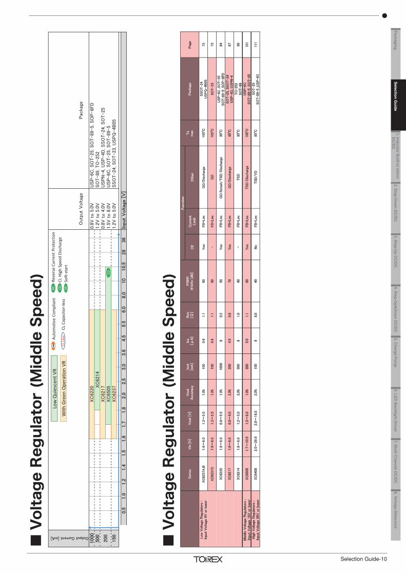
Selection Guide-10
Vo
ltage
Reg
ulat
or (M
iddl
e Sp
eed)
Vo
ltage
Reg
ulat
or (M
iddl
e Sp
eed)
Output Current [mA]
Outp
ut
Voltag
eP
acka
ge
1000
XC
6220
0.8
V t
o 5
.0V
US
P-6C
, S
OT-25, S
OT-89-5, S
OP
-8FD
500
XC
6214
1.2
V t
o 5
.0V
SO
T-89, TO
-252
XC
6217
0.8
V t
o 4
.0V
US
PN
-4, U
SP
-4D
, S
SO
T-24, S
OT-25
XC
6505
1.5
V t
o 8
.0V
US
P-6C
, S
OT-25, S
OT-89-5
150
XC
6237
1.2
V t
o 5
.0V
SS
OT-24, S
OT-23, U
SP
Q-4B
05
I nput
Voltage
[V
]8.0
1.5
1.6
1.7
1.8
2.0
2.5
3.0
3.6
4.5
5.5
6.0
200
10
10.5
28
36
0.5
1.0
1.2
1.4
CL H
igh
Spee
d Di
scha
rge
SSSo
ft-s
tart
CL L
ess
CL C
apac
itor-
less
CDRCRe
vers
e Cu
rren
t Pro
tect
ion
Low
Qui
esce
ntVR
With
Gre
en O
pera
tion
VR
Auto
mot
ive
Com
plia
nt
CD
CE
Curr
ent
Lim
itO
ther
Low
Voltag
e R
egu
lato
rs :
Inpu
t V
oltag
e 6
V o
r lo
wer
XC
6237A
,B1.6
~6.0
1.2
~5.0
1.0
%150
0.6
1.1
60
Yes
FB
+Lim
GO
/D
ischar
ge105
SSO
T-24
USP
Q-4B
05
73
XC
6237C
1.6
~6.0
1.2
~5.0
1.0
%150
0.6
1.1
60
-FB
+Lim
GO
105
SO
T-23
73
XC
6220
1.6
~6.0
0.8
~5.0
1.0
%1000
80.2
50
Yes
FB
+Lim
GO
/In
rush
/TSD
/D
ischar
ge85
USP
-6C
,SO
T-25
SO
T-89-5 ,SO
P-8FD
84
XC
6217
1.6
~6.0
0.8
~4.0
2.0
%200
4.5
0.8
70
Yes
FB
+Lim
GO
/D
ischar
ge85
SO
T-25, SSO
T-24
USP
-4D
, U
SP
N-4
87
XC
6214
1.8
~6.0
1.2
~5.0
2.0
%500
81.0
40
-FB
+Lim
TSD
85
TO
-252
SO
T-89
90
Mid
dle V
oltag
e R
egu
lato
rs :
Inpu
t V
oltag
e 1
8V
or
low
er
XC
6505
1.7
~10.5
1.5
~8.0
1.0
%200
5.5
1.1
60
Yes
FB
+Lim
TSD
/D
ischar
ge105
USP
-6C
SO
T-89-5 ,SO
T-25
101
Hig
h V
oltag
e R
egu
lato
rs :
Inpu
t V
oltag
e 3
6V
or
low
er
XC
6408
2.0
~28.0
2.0
~18.0
2.0
%150
88.0
40
No
FB
+Lim
TSD
/V
D85
SO
T-25
SO
T-89-5 ,U
SP
-6C
111
Pac
kage
Pag
eIo
ut
[mA
]Is
s[μ
A]
Ron
[Ω]
PSR
R@
1kH
z [d
B]
Function
Ta
max
.V
out
Accura
cy
Series
Vin
[V
]V
out
[V]
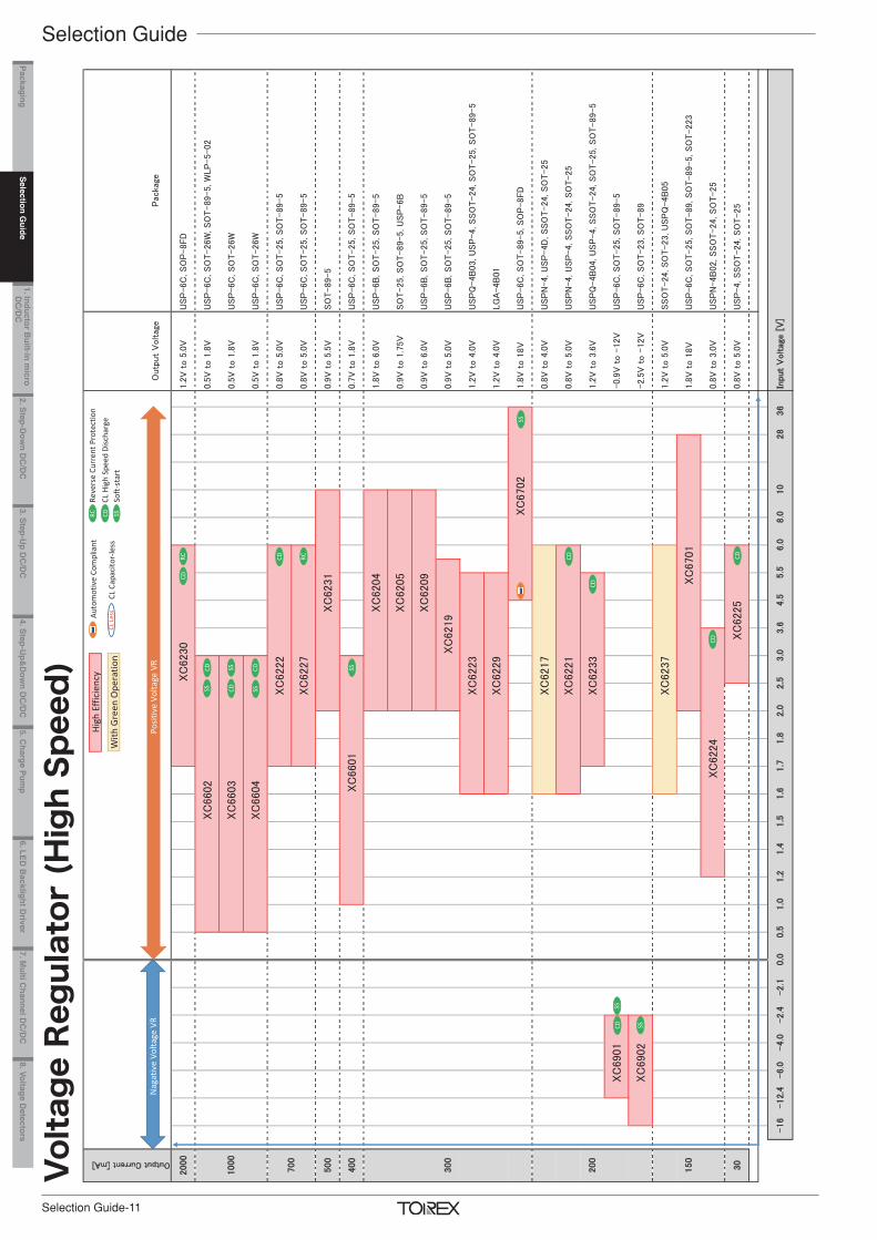
Selection Guide
Selection Guide-11
Volta
ge R
egul
ator
(Hig
h Sp
eed)
Output Current [mA]
Outp
ut
Voltag
eP
acka
ge
2000
XC
6230
1.2
V t
o 5
.0V
USP
-6C
, SO
P-8FD
XC
6602
0.5
V t
o 1
.8V
USP
-6C
, SO
T-26W
, SO
T-89-5, W
LP
-5-02
XC
6603
0.5
V t
o 1
.8V
USP
-6C
, SO
T-26W
XC
6604
0.5
V t
o 1
.8V
USP
-6C
, SO
T-26W
XC
6222
0.8
V t
o 5
.0V
USP
-6C
, SO
T-25, SO
T-89-5
XC
6227
0.8
V t
o 5
.0V
USP
-6C
, SO
T-25, SO
T-89-5
500
XC
6231
0.9
V t
o 5
.5V
SO
T-89-5
400
XC
6601
0.7
V t
o 1
.8V
USP
-6C
, SO
T-25, SO
T-89-5
XC
6204
1.8
V t
o 6
.0V
USP
-6B
, SO
T-25, SO
T-89-5
XC
6205
0.9
V t
o 1
.75V
SO
T-25, SO
T-89-5, U
SP
-6B
XC
6209
0.9
V t
o 6
.0V
USP
-6B
, SO
T-25, SO
T-89-5
XC
6219
0.9
V t
o 5
.0V
USP
-6B
, SO
T-25, SO
T-89-5
XC
6223
1.2
V t
o 4
.0V
USP
Q-4B
03, U
SP
-4, SSO
T-24, SO
T-25, SO
T-89-5
XC
6229
1.2
V t
o 4
.0V
LG
A-4B
01
XC
6702
1.8
V t
o 1
8V
USP
-6C
, SO
T-89-5, SO
P-8FD
XC
6217
0.8
V t
o 4
.0V
USP
N-4, U
SP
-4D
, SSO
T-24, SO
T-25
XC
6221
0.8
V t
o 5
.0V
USP
N-4, U
SP
-4, SSO
T-24, SO
T-25
XC
6233
1.2
V t
o 3
.6V
USP
Q-4B
04, U
SP
-4, SSO
T-24, SO
T-25, SO
T-89-5
XC
6901
-0.9
V t
o -
12V
USP
-6C
, SO
T-25, SO
T-89-5
XC
6902
-2.5
V t
o -
12V
USP
-6C
, SO
T-23, SO
T-89
XC
6237
1.2
V t
o 5
.0V
SSO
T-24, SO
T-23, U
SP
Q-4B
05
XC
6701
1.8
V t
o 1
8V
USP
-6C
, SO
T-25, SO
T-89, SO
T-89-5, SO
T-223
XC
6224
0.8
V t
o 3
.0V
USP
N-4B
02, SSO
T-24, SO
T-25
30
XC
6225
0.8
V t
o 5
.0V
USP
-4, SSO
T-24, SO
T-25
-2.4
-2.1
0.0
0.5
1.0
1.2
1000
200
150
36
6.0
10
28
700
300
1.4
-16
-12.4
-6.0
-4.0
Input
Voltag
e [
V]
8.0
1.5
1.6
1.7
1.8
2.0
2.5
3.0
3.6
4.5
5.5
SS
High
Effi
cien
cyCL
Hig
h Sp
eed
Disc
harg
eSS
Soft
-sta
rtCL
Les
sCL
Cap
acito
r-le
ssCDRC
Reve
rse
Curr
ent P
rote
ctio
n
With
Gre
en O
pera
tion
Nag
ativ
e Vo
ltage
VRPo
sitiv
eVo
ltage
VR
Auto
mot
ive
Com
plia
nt
RC RC CDCD
CD
CD
CD
CD
CD
CD
CD
SS
SS
CDSS
SS
SS SS
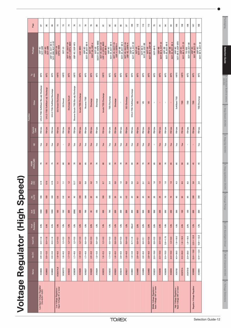
Selection Guide-12
Volta
ge R
egul
ator
(Hig
h Sp
eed)
CE
Curr
ent
Lim
itO
ther
Low
Inpu
t V
oltag
e R
egu
lato
r(V
in=0.5
V~
3.0
V)
XC
6604
0.5
~3.0
0.5
~1.8
0.5
%1000
100
0.1
575
Yes
FB
+Lim
UV
LO
/TSD
/Soft
Sta
rt/Ili
m a
dj./
Dis
char
ge85
USP
-6C
SO
T-26W
97
XC
6603
0.5
~3.0
0.5
~1.8
0.5
%1000
100
0.1
575
Yes
FB
+Lim
UV
LO
/TSD
/Soft
Sta
rt a
dj./
Dis
char
ge85
USP
-6C
SO
T-26W
98
XC
6602
0.5
~3.0
0.5
~1.8
0.5
%1000
100
0.1
575
Yes
FB
+Lim
UV
LO
/TSD
/Soft
Sta
rt/D
ischar
ge85
USP
-6C
, SO
T-89-5
SO
T-26W
, W
LP
-5-02
99
Low
Voltag
e R
egu
lato
rs :
Inpu
t V
oltag
e 6
V o
r lo
wer
XC
6237A
,B1.6
~6.0
1.2
~5.0
1.0
%150
0.6
1.1
75
Yes
FB
+Lim
GO
/In
rush
/D
ischar
ge105
SSO
T-24
USP
Q-4B
05
73
XC
6237C
1.6
~6.0
1.2
~5.0
1.0
%150
0.6
1.1
60
-FB
+Lim
GO
/In
rush
105
SO
T-23
73
XC
6233
1.7
~5.5
1.2
~3.6
1.0
%200
45
1.2
60
Yes
FB
+Lim
Dis
char
ge/In
rush
85
SO
T-25 ,SSO
T-24
USP
-4 ,U
SP
Q-4B
04
74
XC
6230
1.7
~6.0
1.2
~5.0
1.0
%2000
45
0.1
770
Yes
FB
+Lim
Reve
rse/In
rush
/TSD
/Ili
m a
dj./
Dis
char
ge105
USP
-6C
, SO
P-8FD
76
XC
6229
1.6
~5.5
1.2
~4.0
1.0
%300
100
0.5
80
Yes
FB
+Lim
Inru
sh/TSD
/D
ischar
ge85
LG
A-4B
01
77
XC
6227
1.7
~6.0
0.8
~5.0
1.0
%700
100
0.4
65
Yes
FB
+Lim
Reve
rse/TSD
85
USP
-6C
SO
T-25 ,SO
T-89-5
78
XC
6225
2.5
~6.0
0.8
~5.0
2.0
%30
25
3.2
70
Yes
FB
+Lim
Dis
char
ge85
SO
T-25
SSO
T-24, U
SP
-4
79
XC
6224
1.2
~3.6
0.8
~3.0
1.5
%150
33
1.4
70
Yes
FB
+Lim
Dis
char
ge85
SO
T-25
SSO
T-24, U
SP
N-4B
02
80
XC
6223
1.6
~5.5
1.2
~4.0
1.0
%300
100
0.7
80
Yes
FB
+Lim
Inru
sh/TSD
/D
ischar
ge105
SO
T-25. SSO
T-24
USP
-4. U
SP
Q-4B
03
SO
T-89-5
81
XC
6222
1.7
~6.0
0.8
~5.0
1.0
%700
100
0.4
65
Yes
FB
+Lim
TSD
/D
ischar
ge85
USP
-6C
SO
T-25 ,SO
T-89-5
82
XC
6221
1.6
~6.0
0.8
~5.0
1.0
%200
25
0.8
70
Yes
FB
+Lim
Dis
char
ge85
SO
T-25. SSO
T-24
USP
-4. U
SP
N-4
83
XC
6219
2.0
~6.0
0.9
~5.0
1.0
%300
25
1.6
70
Yes
FB
+Lim
-85
USP
-6B
SO
T-25 ,SO
T-89-5
85
XC
6217
1.6
~6.0
0.8
~4.0
1.0
%200
4.5
0.8
70
Yes
FB
+Lim
GO
/D
ischar
ge85
SO
T-25, SSO
T-24
USP
-4D
, U
SP
N-4
87
XC
6601
1.0
~3.0
0.7
~1.8
20m
V400
25
0.3
60
Yes
FB
+Lim
UV
LO
/TSD
/Soft
Sta
rt/D
ischar
ge85
USP
-6C
SO
T-89-5 ,SO
T-25
100
XC
6405
2.0
~6.0
0.9
~5.1
2.0
%500
90
3.1
70
Yes
FB
+Lim
VD
85
SO
T-25
SO
T-89-5
112
XC
6404
2.0
~6.0
0.9
~5.1
2.0
%500
35
2.1
75
Yes
FB
+Lim
VD
85
SO
T-89-5
SO
T-25, U
SP
-6B
113
XC
6403
2.0
~6.0
0.9
~5.6
2.0
%300
35
2.1
75
Yes
FB
+Lim
VD
85
SO
T-25
SO
T-89-5 ,U
SP
-6B
113
Mid
dle V
oltag
e R
egu
lato
rs :
Inpu
t V
oltag
e 1
8V
or
low
er
XC
6231
2.0
~10.0
0.9
~5.5
2.0
%500
35
1.6
65
-FB
+Lim
-85
SO
T-89-5
75
XC
6209
2.0
~10.0
0.9
~6.0
2.0
%300
25
1.6
80
Yes
FB
+Lim
-85
USP
-6B
SO
T-89-5, SO
T-23
91
XC
6205
2.0
~10.0
0.9
~1.7
51.0
%300
70
1.6
70
Yes
FB
+Lim
-85
USP
-6B
SO
T-25, SO
T-89-5
94
XC
6204
2.0
~10.0
1.8
~6.0
1.0
%300
70
1.6
65
Yes
FB
+Lim
-85
USP
-6B
SO
T-25, SO
T-89-5
94
Hig
h V
oltag
e R
egu
lato
rs :
Inpu
t V
oltag
e 3
6V
or
low
er
XC
6702
4.5
~36.0
1.8
~18.0
1.0
%300
40
4.3
65
Yes
FB
+Lim
Soft
Sta
rt/TSD
105
USP
-6C
SO
T-89-5 ,SO
P-8FD
105
XC
6701A
2.0
~28.0
1.8
~18.0
2.0
%150
50
6.5
50
Yes
FB
+Lim
TSD
105
USP
-6C
SO
T-89-5 ,SO
T-25
106
XC
6701D
2.0
~28.0
1.8
~18.0
2.0
%150
50
6.5
50
-FB
+Lim
TSD
85
TO
-252
SO
T-223 ,SO
T-89
106
Nega
tive
Voltag
e R
egu
lato
rXC
6902
-2.4
~-16.0
-2.5
~-12.0
1.5
%200
100
3.9
45
-FB
+Lim
TSD
85
USP
-6C
SO
T-89 ,SO
T-23
107
XC
6901
-2.4
~-12.4
-0.9
~-12.0
1.5
%200
100
2.5
45
Yes
FB
+Lim
TSD
/D
ischar
ge85
USP
-6C
SO
T-89-5 ,SO
T-25
108
Pag
eV
out
Accura
cy
PSR
R@
1kH
z [d
B]
Iout
[mA
]Is
s[μ
A]
Ron
[Ω]
Function
Series
Vin
[V
]V
out
[V]
Ta
max
.P
acka
ge
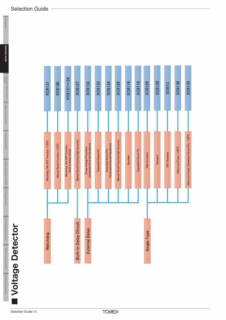
Selection Guide
Selection Guide-13
Vo
ltage
Det
ecto
r
XC
6130
XC
6131
Wat
chdo
gW
atchdo
g, O
N/O
FF F
unction, +
125
Man
ual
Rese
t Function,
+125
Wat
chdo
g, O
N/O
FF F
unction,
Built
-in
Dela
y C
ircuit
Built
-in
Dela
y C
ircuit
Ext
ern
al D
ela
y
Sin
gle T
ype
Man
ual
Rese
t Function,
Hig
h A
ccura
cy
Surg
e V
oltag
e P
rote
ction,
Hys
tere
sis
Ext
ern
al A
dju
stm
ent
Separ
ated
Sense
Pin
Separ
ated
Sense
Pin
,
Hys
tere
sis
Ext
ern
al A
dju
stm
ent
Sta
ndar
d
XC
6121~
24
XC
6127
XC
6132
XC
6133
XC
6134
XC
6120
10V
, Sta
nda
rdX
C61C
XC
6136
XC
6135
Ultra
Low
Pow
er, +
105
Ultra
Low
Pow
er, S
epar
ated
Sense
Pin
, +105
Man
ual
Rese
t Function,
Hig
h A
ccura
cy
Sta
ndar
d
XC
6129
XC
6119
Separ
ated
Sense
Pin
XC
6118
Hig
h A
ccura
cy
XC
6126
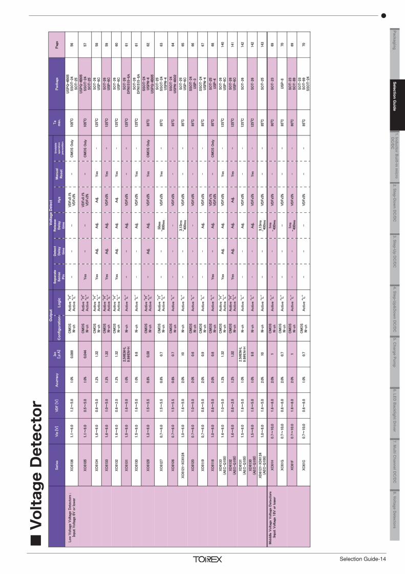
Selection Guide-14
Vo
ltage
Det
ecto
rC
onfig
urat
ion
Logi
cSe
para
teSe
nse
Pin
Det
ect
Del
aytim
e
Rel
ease
Del
aytim
eH
ysM
anua
lR
eset
Uns
tabl
eop
erat
ion
prev
entio
n
Low
Voltag
e V
oltag
e D
ete
cto
rs :
Inpu
t V
oltag
e 6
V o
r lo
wer
XC
6136
1.1
~6.0
1.2
~5.0
1.0
%0.0
88
CM
OS
N-ch
Active
"H
"A
ctive
"L"
--
-V
DFx0
.1%
VD
Fx5
%-
CM
OS O
nly
105
USP
Q-4B
05
SSO
T-24
SO
T-25
56
XC
6135
1.1
~6.0
0.5
~5.0
1.0
%0.0
44
CM
OS
N-ch
Active
"H
"A
ctive
"L"
Yes
--
VD
Fx0
.1%
VD
Fx5
%-
CM
OS O
nly
105
USP
Q-4B
05
SSO
T-24
SO
T-25
57
XC
6134
1.6
~6.0
0.8
~5.0
1.2
%1.3
2C
MO
SN
-ch
Active
"H
"A
ctive
"L"
Yes
Adj
.A
dj.
Adj
.Yes
-125
SO
T-26
USP
-6C
58
XC
6133
1.6
~6.0
1.0
~5.0
1.2
%1.3
2C
MO
SN
-ch
Active
"H
"A
ctive
"L"
Yes
Adj
.A
dj.
VD
Fx5
%Yes
-125
SO
T-26
USP
-6C
59
XC
6132
1.6
~6.0
0.8
~2.0
1.2
%1.3
2C
MO
SN
-ch
Active
"H
"A
ctive
"L"
Yes
Adj
.A
dj.
Adj
.Yes
-125
SO
T-26
USP
-6C
60
XC
6131
1.5
~6.0
1.6
~5.0
1.0
%2.5
@EN
=L
9.8
@EN
=H
N-ch
Active
"L"
--
Adj
.V
DFx5
%-
-125
SO
T-26
DFN
1515-6A
61
XC
6130
1.5
~6.0
1.6
~5.0
1.0
%9.8
N-ch
Active
"L"
--
Adj
.V
DFx5
%Yes
-125
SO
T-26
DFN
1515-6A
61
XC
6129
1.3
~6.0
1.5
~5.5
0.8
%0.5
8C
MO
SN
-ch
Active
"H
"A
ctive
"L"
-A
dj.
Adj
.V
DFx5
%Yes
CM
OS O
nly
85
SSO
T-24
USP
N-4
USP
Q-4B
05
62
XC
6127
0.7
~6.0
1.5
~5.5
0.8
%0.7
CM
OS
N-ch
Active
"H
"A
ctive
"L"
--
50m
s~8
00m
sV
DFx5
%Yes
-85
SO
T-25
SSO
T-24
USP
N-4
63
XC
6126
0.7
~6.0
1.5
~5.5
0.8
%0.7
CM
OS
N-ch
Active
"L"
--
-V
DFx5
%-
-85
SSO
T-24
USP
N-4B
02
64
XC
6121-XC
6124
1.0
~6.0
1.6
~5.0
2.0
%10
N-ch
Active
"L"
--
3.1
3m
s~4
00m
sV
DFx5
%-
-85
SO
T-25
USP
-6C
65
XC
6120
0.7
~6.0
1.0
~5.0
2.0
%0.6
CM
OS
N-ch
Active
"L"
--
-V
DFx5
%-
-85
SSO
T-24
USP
-3
66
XC
6119
0.7
~6.0
0.8
~5.0
2.0
%0.9
CM
OS
N-ch
Active
"L"
--
Adj
.V
DFx5
%-
-85
SSO
T-24
USP
N-4
67
XC
6118
1.0
~6.0
0.8
~5.0
2.0
%0.8
CM
OS
N-ch
Active
"L"
Yes
-A
dj.
VD
Fx1
%V
DFx5
%-
CM
OS O
nly
85
SO
T-25
USP
-4
68
XD
6133
(AEC
-Q
100)
1.6
~6.0
1.0
~5.0
1.2
%1.3
2C
MO
SN
-ch
Active
"H
"A
ctive
"L"
Yes
Adj
.A
dj.
VD
Fx5
%Yes
-125
SO
T-26
USP
-6C
140
XD
6132
(AEC
-Q
100)
1.6
~6.0
0.8
~2.0
1.2
%1.3
2C
MO
SN
-ch
Active
"H
"A
ctive
"L"
Yes
Adj
.A
dj.
Adj
.Yes
-125
SO
T-26
USP
-6C
141
XD
6131
(AEC
-Q
100)
1.5
~6.0
1.6
~5.0
1.0
%2.5
@EN
=L
9.8
@EN
=H
N-ch
Active
"L"
--
Adj
.V
DFx5
%-
-125
SO
T-26
142
XD
6130
(AEC
-Q
100)
1.5
~6.0
1.6
~5.0
1.0
%9.8
N-ch
Active
"L"
--
Adj
.V
DFx5
%Yes
-125
SO
T-26
142
XD
6121-XD
6124
(AEC
-Q
100)
1.0
~6.0
1.6
~5.0
2.0
%10
N-ch
Active
"L"
--
3.1
3m
s~4
00m
sV
DFx5
%-
-85
SO
T-25
143
Mid
ddle
Voltag
e V
oltag
e D
ete
cto
rs:In
put
Voltag
e 1
8V
or
low
er
XC
61H
0.7
~10.0
1.6
~6.0
2.0
%1
CM
OS
N-ch
Active
"L"
--
1m
s~4
00m
sV
DFx5
%-
-80
SO
T-23
69
XC
61G
0.7
~10.0
0.8
~6.0
2.0
%0.7
CM
OS
N-ch
Active
"L"
--
-V
DFx5
%-
-85
USP
-3
70
XC
61F
0.7
~10.0
1.6
~6.0
2.0
%1
CM
OS
N-ch
Active
"L"
--
1m
s~4
00m
sV
DFx5
%-
-80
SO
T-23
SO
T-89
69
XC
61C
0.7
~10.0
0.8
~6.0
1.0
%0.7
CM
OS
N-ch
Active
"L"
--
-V
DFx5
%-
-85
SO
T-23
SO
T-89
SSO
T-24
70
Pac
kage
Pag
eIs
s[μ
A]
Ta
max
.
Out
put
Volta
ge D
etec
tA
curr
acy
Series
Vin
[V
]V
DF [
V]
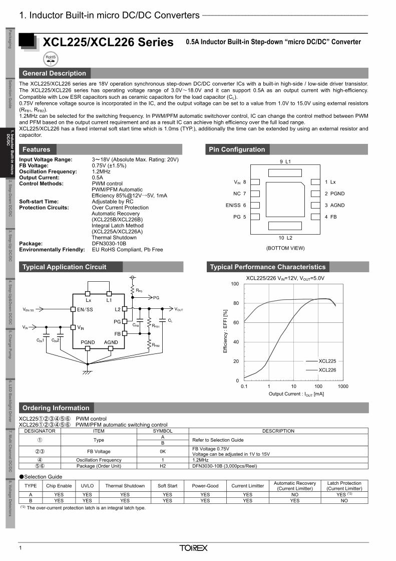
1. Inductor Built-in micro DC/DC Converters __________________________________________________
1
XCL225/XCL226 Series 0.5A Inductor Built-in Step-down “micro DC/DC” Converter
General Description
The XCL225/XCL226 series are 18V operation synchronous step-down DC/DC converter ICs with a built-in high-side / low-side driver transistor. The XCL225/XCL226 series has operating voltage range of 3.0V~18.0V and it can support 0.5A as an output current with high-efficiency. Compatible with Low ESR capacitors such as ceramic capacitors for the load capacitor (CL). 0.75V reference voltage source is incorporated in the IC, and the output voltage can be set to a value from 1.0V to 15.0V using external resistors (RFB1, RFB2). 1.2MHz can be selected for the switching frequency. In PWM/PFM automatic switchover control, IC can change the control method between PWMand PFM based on the output current requirement and as a result IC can achieve high efficiency over the full load range. XCL225/XCL226 has a fixed internal soft start time which is 1.0ms (TYP.), additionally the time can be extended by using an external resistor and capacitor.
Features Pin Configuration Input Voltage Range: 3~18V (Absolute Max. Rating: 20V) FB Voltage: 0.75V (±1.5%) Oscillation Frequency: 1.2MHz Output Current: 0.5A Control Methods: PWM control PWM/PFM Automatic Efficiency 85%@12V→5V, 1mA Soft-start Time: Adjustable by RC Protection Circuits: Over Current Protection Automatic Recovery (XCL225B/XCL226B) Integral Latch Method (XCL225A/XCL226A) Thermal Shutdown Package: DFN3030-10B Environmentally Friendly: EU RoHS Compliant, Pb Free
Typical Application Circuit Typical Performance Characteristics
Ordering Information
XCL225①②③④⑤⑥ PWM control XCL226①②③④⑤⑥ PWM/PFM automatic switching control
DESIGNATOR ITEM SYMBOL DESCRIPTION
① Type A Refer to Selection Guide B
②③ FB Voltage 0K FB Voltage 0.75V Voltage can be adjusted in 1V to 15V
④ Oscillation Frequency 1 1.2MHz ⑤⑥ Package (Order Unit) H2 DFN3030-10B (3,000pcs/Reel)
Selection Guide
TYPE Chip Enable UVLO Thermal Shutdown Soft Start Power-Good Current Limitter Automatic Recovery (Current Limitter)
Latch Protection (Current Limitter)
A YES YES YES YES YES YES NO YES (*2) B YES YES YES YES YES YES YES NO
(*2) The over-current protection latch is an integral latch type.
L1Lx
PGND
EN/SS
VIN
CIN2CIN1
L2
FB
RFB1CFB
CL
VOUT
AGND
PG
RFB2
PG
VIN
VEN/SS
RPG
1 Lx
2 PGND
3 AGND
4 FB
VIN 8
NC 7
EN/SS 6
PG 5
9 L1
10 L2
(BOTTOM VIEW)
0
20
40
60
80
100
0.1 1 10 100 1000
Effi
cien
cy :
EFF
I [%
]
Output Current : IOUT [mA]
XCL225
XCL226
XCL225/226 VIN=12V, VOUT=5.0V
_______________________________________________________________________________________________________
*GreenOperation-compatible
2
XCL223/XCL224 Series 0.4A/0.7A Inductor Built-in Step-Down “micro DC/DC” Converters
General Description Features
The XCL223/XCL224 series is a synchronous step-down micro DC/DCconverter which integrates an inductor and a control IC in one tiny package(2.25mm×1.5mm, H=0.75mmMAX). A stable power supply is configured using only two capacitors connectedexternally. An internal coil simplifies the circuit and enables minimization of noise andother operational trouble due to the circuit wiring. A wide operating voltage range of from 2.5V to 5.5V enables support forapplications that require an internally fixed output voltage (0.8V to 3.6V). Theaccuracy of the output voltage is ± 2.0% and the voltage is adjustable internallywith 0.05V step. The XCL223/XCL224 series uses synchronous rectification and the operatingfrequency is 3.0MHz. The XCL223/XCL224 series uses HiSAT-COT(*)
synchronous rectification. HiSAT-COT+PWM control (XCL223) orHiSAT-COT+automatic PWM/PFM switching control (XCL224) can beselected. The maximum load current can be selected either 400mA or 700mA. The series have a high speed soft-start (0.3ms TYP.) for quick turn-on. Withthe built-in UVLO (Under Voltage Lock Out) function, the internal P-channeldriver transistor is forced OFF when the input voltage becomes 2.0V or lower.When CE is “Low”, the integrated CL discharge function discharges the electriccharge at the output capacitor CL via the internal discharge switch locatedbetween the LX and PGND pins. The power consumption will be less than1.0μA. (*) HiSAT-COT is an original Torex term for High Speed Transient Response.
Input Voltage: 2.5V~5.5V (Absolute Max. Rating: 6.2V) Output Voltage: 0.8V~3.6V (±2.0%) Output Current: 700mA (XCL223A/XCL224A) 400mA (XCL223B/XCL224B) Quiescent Current: 25μA (fOSC=3.0MHz) Oscillation Frequency: 3.0MHz Control Methods: HiSAT-COT Control 100% Duty Cycle PWM Control (XCL223) PWM/PFM Automatic Switching Control (XCL224) Circuit Protection: Thermal Shutdown Current Limit Circuit (Drop) Short Circuit Protection Functions: Soft-start UVLO CL Discharge Output Capacitor: Ceramic Capacitor Operating Ambient Temperature: -40~+105 Package: USP-8B04 Environmentally Friendly: EU RoHS Compliant, Pb Free
Pin Configuration
Typical Application Circuit Typical Performance Characteristics
XCL224B213DR(VOUT=2.1V)
Ordering Information
XCL223①②③④⑤⑥-⑦ PWM control XCL224①②③④⑤⑥-⑦ PWM/PFM automatic switching control
DESIGNATOR ITEM SYMBOL DESCRIPTION
① Type A Output Current : 700mA B Output Current : 400mA
②③ Output Voltage 08~36
Output Voltage options e.g.)1.2V → ②=1, ③=2 1.25V → ②=1, ③=C 0.05V Increments: 0.05=A, 0.15=B, 0.25=C, 0.35=D, 0.45=E, 0.55=F, 0.65=H, 0.75=K, 0.85=L,0.95=M
④ Oscillation Frequency 3 3.0MHz ⑤⑥-⑦(*1) Package (Order Unit) D2-G USP-8B04 (3,000pcs/Reel)
(*1) The “-G” suffix denotes Halogen and Antimony free as well as being fully EU RoHS compliant. Selection Guide
TYPE OUTPUT VOLTAGE
CL AUTO- DISCHARGE
LATCH or SHORT PROTECTION UVLO CHIP ENABLE CURRENT LIMIT SOFT-START THERMAL
SHUTDOWN B (400mA) Fixed Yes Yes Yes Yes Yes Fixed Yes A (700mA) Fixed Yes Yes Yes Yes Yes Fixed Yes
1 PGND
2 AGND
3 VOUTCE 4
LX 5
VIN 6
7 L1L2 8
0
20
40
60
80
100
0.1 1 10 100 1000
Effi
cien
cy :
EFF
I [%
]
Output Current : IOUT [mA]
VIN=3.6VVIN=4.2V
USP-8B04 (BOTTOM VIEW)
VIN
PGND
CE
AGND
VOUT
LXL1
L2
CINCL
VIN VOUT
1. Inductor Built-in m
icro D
C/D
C
2. Step-Dow
n DC
/DC
3. Step-Up D
C/D
C4. Step-U
p&D
own D
C/D
C
5.Charge Pum
p6.LED
Backlight D
river8.Voltage D
etectorsSelection G
uidePackaging
7. Multi C
hannel DC
/DC
1. Inductor B
uilt-in micro
DC
/DC
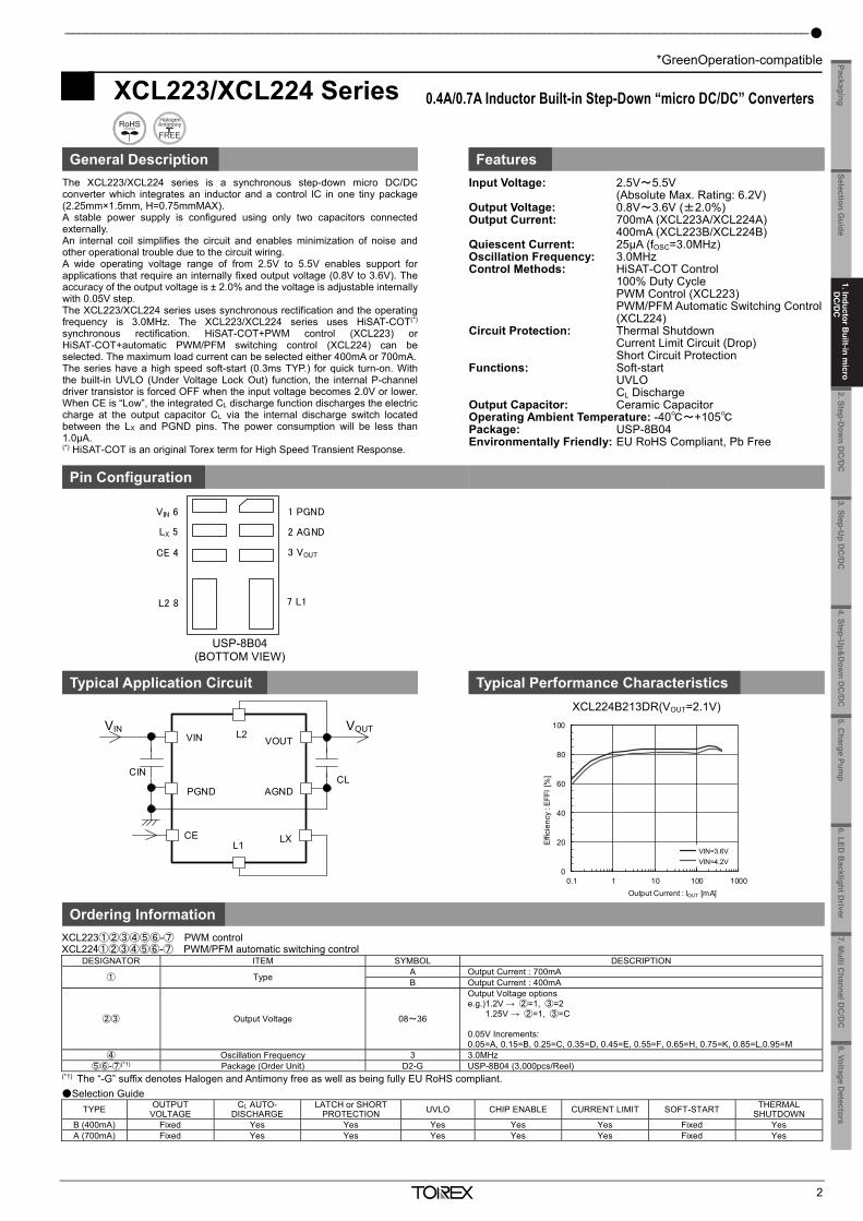
1. Inductor Built-in micro DC/DC Converters __________________________________________________
1
XCL225/XCL226 Series 0.5A Inductor Built-in Step-down “micro DC/DC” Converter
General Description
The XCL225/XCL226 series are 18V operation synchronous step-down DC/DC converter ICs with a built-in high-side / low-side driver transistor. The XCL225/XCL226 series has operating voltage range of 3.0V~18.0V and it can support 0.5A as an output current with high-efficiency. Compatible with Low ESR capacitors such as ceramic capacitors for the load capacitor (CL). 0.75V reference voltage source is incorporated in the IC, and the output voltage can be set to a value from 1.0V to 15.0V using external resistors (RFB1, RFB2). 1.2MHz can be selected for the switching frequency. In PWM/PFM automatic switchover control, IC can change the control method between PWMand PFM based on the output current requirement and as a result IC can achieve high efficiency over the full load range. XCL225/XCL226 has a fixed internal soft start time which is 1.0ms (TYP.), additionally the time can be extended by using an external resistor and capacitor.
Features Pin Configuration Input Voltage Range: 3~18V (Absolute Max. Rating: 20V) FB Voltage: 0.75V (±1.5%) Oscillation Frequency: 1.2MHz Output Current: 0.5A Control Methods: PWM control PWM/PFM Automatic Efficiency 85%@12V→5V, 1mA Soft-start Time: Adjustable by RC Protection Circuits: Over Current Protection Automatic Recovery (XCL225B/XCL226B) Integral Latch Method (XCL225A/XCL226A) Thermal Shutdown Package: DFN3030-10B Environmentally Friendly: EU RoHS Compliant, Pb Free
Typical Application Circuit Typical Performance Characteristics
Ordering Information
XCL225①②③④⑤⑥ PWM control XCL226①②③④⑤⑥ PWM/PFM automatic switching control
DESIGNATOR ITEM SYMBOL DESCRIPTION
① Type A Refer to Selection Guide B
②③ FB Voltage 0K FB Voltage 0.75V Voltage can be adjusted in 1V to 15V
④ Oscillation Frequency 1 1.2MHz ⑤⑥ Package (Order Unit) H2 DFN3030-10B (3,000pcs/Reel)
Selection Guide
TYPE Chip Enable UVLO Thermal Shutdown Soft Start Power-Good Current Limitter Automatic Recovery (Current Limitter)
Latch Protection (Current Limitter)
A YES YES YES YES YES YES NO YES (*2) B YES YES YES YES YES YES YES NO
(*2) The over-current protection latch is an integral latch type.
L1Lx
PGND
EN/SS
VIN
CIN2CIN1
L2
FB
RFB1CFB
CL
VOUT
AGND
PG
RFB2
PG
VIN
VEN/SS
RPG
1 Lx
2 PGND
3 AGND
4 FB
VIN 8
NC 7
EN/SS 6
PG 5
9 L1
10 L2
(BOTTOM VIEW)
0
20
40
60
80
100
0.1 1 10 100 1000
Effi
cien
cy :
EFF
I [%
]
Output Current : IOUT [mA]
XCL225
XCL226
XCL225/226 VIN=12V, VOUT=5.0V
_______________________________________________________________________________________________________
*GreenOperation-compatible
2
XCL223/XCL224 Series 0.4A/0.7A Inductor Built-in Step-Down “micro DC/DC” Converters
General Description Features
The XCL223/XCL224 series is a synchronous step-down micro DC/DCconverter which integrates an inductor and a control IC in one tiny package(2.25mm×1.5mm, H=0.75mmMAX). A stable power supply is configured using only two capacitors connectedexternally. An internal coil simplifies the circuit and enables minimization of noise andother operational trouble due to the circuit wiring. A wide operating voltage range of from 2.5V to 5.5V enables support forapplications that require an internally fixed output voltage (0.8V to 3.6V). Theaccuracy of the output voltage is ± 2.0% and the voltage is adjustable internallywith 0.05V step. The XCL223/XCL224 series uses synchronous rectification and the operatingfrequency is 3.0MHz. The XCL223/XCL224 series uses HiSAT-COT(*)
synchronous rectification. HiSAT-COT+PWM control (XCL223) orHiSAT-COT+automatic PWM/PFM switching control (XCL224) can beselected. The maximum load current can be selected either 400mA or 700mA. The series have a high speed soft-start (0.3ms TYP.) for quick turn-on. Withthe built-in UVLO (Under Voltage Lock Out) function, the internal P-channeldriver transistor is forced OFF when the input voltage becomes 2.0V or lower.When CE is “Low”, the integrated CL discharge function discharges the electriccharge at the output capacitor CL via the internal discharge switch locatedbetween the LX and PGND pins. The power consumption will be less than1.0μA. (*) HiSAT-COT is an original Torex term for High Speed Transient Response.
Input Voltage: 2.5V~5.5V (Absolute Max. Rating: 6.2V) Output Voltage: 0.8V~3.6V (±2.0%) Output Current: 700mA (XCL223A/XCL224A) 400mA (XCL223B/XCL224B) Quiescent Current: 25μA (fOSC=3.0MHz) Oscillation Frequency: 3.0MHz Control Methods: HiSAT-COT Control 100% Duty Cycle PWM Control (XCL223) PWM/PFM Automatic Switching Control (XCL224) Circuit Protection: Thermal Shutdown Current Limit Circuit (Drop) Short Circuit Protection Functions: Soft-start UVLO CL Discharge Output Capacitor: Ceramic Capacitor Operating Ambient Temperature: -40~+105 Package: USP-8B04 Environmentally Friendly: EU RoHS Compliant, Pb Free
Pin Configuration
Typical Application Circuit Typical Performance Characteristics
XCL224B213DR(VOUT=2.1V)
Ordering Information
XCL223①②③④⑤⑥-⑦ PWM control XCL224①②③④⑤⑥-⑦ PWM/PFM automatic switching control
DESIGNATOR ITEM SYMBOL DESCRIPTION
① Type A Output Current : 700mA B Output Current : 400mA
②③ Output Voltage 08~36
Output Voltage options e.g.)1.2V → ②=1, ③=2 1.25V → ②=1, ③=C 0.05V Increments: 0.05=A, 0.15=B, 0.25=C, 0.35=D, 0.45=E, 0.55=F, 0.65=H, 0.75=K, 0.85=L,0.95=M
④ Oscillation Frequency 3 3.0MHz ⑤⑥-⑦(*1) Package (Order Unit) D2-G USP-8B04 (3,000pcs/Reel)
(*1) The “-G” suffix denotes Halogen and Antimony free as well as being fully EU RoHS compliant. Selection Guide
TYPE OUTPUT VOLTAGE
CL AUTO- DISCHARGE
LATCH or SHORT PROTECTION UVLO CHIP ENABLE CURRENT LIMIT SOFT-START THERMAL
SHUTDOWN B (400mA) Fixed Yes Yes Yes Yes Yes Fixed Yes A (700mA) Fixed Yes Yes Yes Yes Yes Fixed Yes
1 PGND
2 AGND
3 VOUTCE 4
LX 5
VIN 6
7 L1L2 8
0
20
40
60
80
100
0.1 1 10 100 1000
Effi
cien
cy :
EFF
I [%
]
Output Current : IOUT [mA]
VIN=3.6VVIN=4.2V
USP-8B04 (BOTTOM VIEW)
VIN
PGND
CE
AGND
VOUT
LXL1
L2
CINCL
VIN VOUT
2. Step-Dow
n DC
/DC
3. Step-Up D
C/D
C4. Step-U
p&D
own D
C/D
C
5.Charge Pum
p6.LED
Backlight D
river8.Voltage D
etectorsSelection G
uidePackaging
7. Multi C
hannel DC
/DC
1. Inductor B
uilt-in micro
DC
/DC
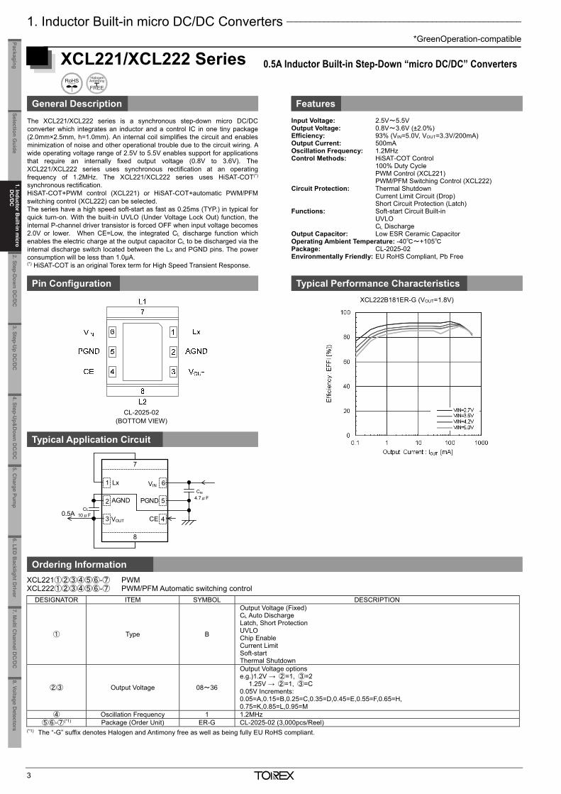
1. Inductor Built-in micro DC/DC Converters __________________________________________________
*GreenOperation-compatible
3
XCL221/XCL222 Series 0.5A Inductor Built-in Step-Down “micro DC/DC” Converters
General Description Features
The XCL221/XCL222 series is a synchronous step-down micro DC/DC converter which integrates an inductor and a control IC in one tiny package (2.0mm×2.5mm, h=1.0mm). An internal coil simplifies the circuit and enables minimization of noise and other operational trouble due to the circuit wiring. A wide operating voltage range of 2.5V to 5.5V enables support for applications that require an internally fixed output voltage (0.8V to 3.6V). The XCL221/XCL222 series uses synchronous rectification at an operating frequency of 1.2MHz. The XCL221/XCL222 series uses HiSAT-COT(*) synchronous rectification. HiSAT-COT+PWM control (XCL221) or HiSAT-COT+automatic PWM/PFM switching control (XCL222) can be selected. The series have a high speed soft-start as fast as 0.25ms (TYP.) in typical for quick turn-on. With the built-in UVLO (Under Voltage Lock Out) function, the internal P-channel driver transistor is forced OFF when input voltage becomes 2.0V or lower. When CE=Low, the integrated CL discharge function which enables the electric charge at the output capacitor CL to be discharged via the internal discharge switch located between the LX and PGND pins. The power consumption will be less than 1.0μA. (*) HiSAT-COT is an original Torex term for High Speed Transient Response.
Input Voltage: 2.5V~5.5V Output Voltage: 0.8V~3.6V (±2.0%) Efficiency: 93% (VIN=5.0V, VOUT=3.3V/200mA) Output Current: 500mA Oscillation Frequency: 1.2MHz Control Methods: HiSAT-COT Control 100% Duty Cycle PWM Control (XCL221) PWM/PFM Switching Control (XCL222) Circuit Protection: Thermal Shutdown Current Limit Circuit (Drop) Short Circuit Protection (Latch) Functions: Soft-start Circuit Built-in UVLO CL Discharge Output Capacitor: Low ESR Ceramic Capacitor Operating Ambient Temperature: -40~+105 Package: CL-2025-02 Environmentally Friendly: EU RoHS Compliant, Pb Free
Pin Configuration Typical Performance Characteristics
XCL222B181ER-G (VOUT=1.8V)
Typical Application Circuit Ty
Ordering Information
XCL221①②③④⑤⑥-⑦ PWM XCL222①②③④⑤⑥-⑦ PWM/PFM Automatic switching control
DESIGNATOR ITEM SYMBOL DESCRIPTION
① Type B
Output Voltage (Fixed) CL Auto Discharge Latch, Short Protection UVLO Chip Enable Current Limit Soft-start Thermal Shutdown
②③ Output Voltage 08~36
Output Voltage options e.g.)1.2V → ②=1, ③=2 1.25V → ②=1, ③=C 0.05V Increments: 0.05=A,0.15=B,0.25=C,0.35=D,0.45=E,0.55=F,0.65=H, 0.75=K,0.85=L,0.95=M
④ Oscillation Frequency 1 1.2MHz ⑤⑥-⑦(*1) Package (Order Unit) ER-G CL-2025-02 (3,000pcs/Reel)
(*1) The “-G” suffix denotes Halogen and Antimony free as well as being fully EU RoHS compliant.
CL-2025-02 (BOTTOM VIEW)
0.5A
CIN
4.7μF
CL10μF
7
8
1
2
3 4
5
6
PGND
VINLx
CEVOUT
AGND
_______________________________________________________________________________________________________
*GreenOperation-compatible
4
XCL219/XCL220 Series 1.0A Inductor Built-in Step-Down “micro DC/DC” Converters
General Description Features
The XCL219/XCL220 series is a synchronous step-down micro DC/DCconverter which integrates an inductor and a control IC in one tiny package(2.0mm×2.5mm, h=1.0mm). An internal coil simplifies the circuit and enablesminimization of noise and other operational trouble due to the circuit wiring. Awide operating voltage range of 2.5V to 5.5V enables support for applicationsthat require an internally fixed output voltage (0.8V to 3.6V). TheXCL219/XCL220 series uses synchronous rectification at an operatingfrequency of 3.0MHz. The XCL219/XCL220 series uses HiSAT-COT(*)
synchronous rectification. HiSAT-COT+PWM control (XCL219) or HiSAT-COT+automatic PWM/PFMswitching control (XCL220) can be selected. The series have a high speed soft-start as fast as 0.3ms in typical for quickturn-on. With the built-in UVLO (Under Voltage Lock Out) function, the internalP-channel driver transistor is forced OFF when input voltage becomes 2.0V orlower. When CE=Low, the integrated CL discharge function which enablesthe electric charge at the output capacitor CL to be discharged via the internaldischarge switch located between the LX and VSS pins. The powerconsumption will be less than 1.0μA. (*) HiSAT-COT is an original Torex term for High Speed Transient Response.
Input Voltage: 2.5V~5.5V (Absolute Max. Rating: 6.2V) Output Voltage: 0.8V~3.6V Oscillation Frequency: 3MHz Output Current: 1.0A Efficiency: 93% (VIN=5.0V, VOUT=3.3V/300mA) Control Methods: HiSAT-COT 100% Duty Cycle PWM (XCL219) PWM/PFM (XCL220) Circuit Protection: Thermal Shutdown Current Limit Circuit (Drop) Short Circuit Protection Functions: Soft-start Circuit Built-in UVLO CL Discharge Output Capacitor: Ceramic Capacitor Operating Ambient Temperature: -40~+105 Package: CL-2025-02 Environmentally Friendly: EU RoHS Compliant, Pb Free
Pin Configuration Typical Performance Characteristics
XCL219/XCL220 (VOUT=3.3V)
Typical Application Circuit Ty
Ordering Information
XCL219①②③④⑤⑥-⑦ PWM control XCL220①②③④⑤⑥-⑦ PWM/PFM automatic switching control
DESIGNATOR ITEM SYMBOL DESCRIPTION
① Type B
Output Voltage (Fixed) CL Auto Discharge Latch or Short Protection UVLO Chip Enable Current Limit Soft-start (Fixed) Thernal Shutdown
②③ Output Voltage 08~36
Output Voltage options e.g.)1.2V → ②=1, ③=2
1.25V → ②=1, ③=C 0.05V Increments: 0.05=A,0.15=B,0.25=C,0.35=D,0.45=E,0.55=F,0.65=H, 0.75=K,0.85=L,0.95=M
④ Oscillation Frequency 3 3.0MHz ⑤⑥-⑦(*1) Package (Order Unit) FR-G CL-2025-02 (3,000pcs/Reel)
(*1) The “-G” suffix denotes Halogen and Antimony free as well as being fully EU RoHS compliant.
CL-2025-02 (BOTTOM VIEW)
0
20
40
60
80
100
0.1 1 10 100 1000
Effic
ienc
y : E
FFI
(%)
Output Current : IOUT (mA)
XCL219
XCL220
VIN=5.0V
1.0A
CIN
4.7μF
CL10μF
7
8
1
2
3 4
5
6
PGND
VINLx
CEVOUT
AGND
1. Inductor Built-in m
icro D
C/D
C
2. Step-Dow
n DC
/DC
3. Step-Up D
C/D
C4. Step-U
p&D
own D
C/D
C
5.Charge Pum
p6.LED
Backlight D
river8.Voltage D
etectorsSelection G
uidePackaging
7. Multi C
hannel DC
/DC
1. Inductor B
uilt-in micro
DC
/DC
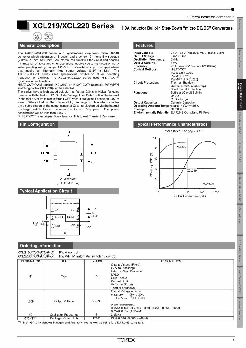
1. Inductor Built-in micro DC/DC Converters __________________________________________________
*GreenOperation-compatible
3
XCL221/XCL222 Series 0.5A Inductor Built-in Step-Down “micro DC/DC” Converters
General Description Features
The XCL221/XCL222 series is a synchronous step-down micro DC/DC converter which integrates an inductor and a control IC in one tiny package (2.0mm×2.5mm, h=1.0mm). An internal coil simplifies the circuit and enables minimization of noise and other operational trouble due to the circuit wiring. A wide operating voltage range of 2.5V to 5.5V enables support for applications that require an internally fixed output voltage (0.8V to 3.6V). The XCL221/XCL222 series uses synchronous rectification at an operating frequency of 1.2MHz. The XCL221/XCL222 series uses HiSAT-COT(*) synchronous rectification. HiSAT-COT+PWM control (XCL221) or HiSAT-COT+automatic PWM/PFM switching control (XCL222) can be selected. The series have a high speed soft-start as fast as 0.25ms (TYP.) in typical for quick turn-on. With the built-in UVLO (Under Voltage Lock Out) function, the internal P-channel driver transistor is forced OFF when input voltage becomes 2.0V or lower. When CE=Low, the integrated CL discharge function which enables the electric charge at the output capacitor CL to be discharged via the internal discharge switch located between the LX and PGND pins. The power consumption will be less than 1.0μA. (*) HiSAT-COT is an original Torex term for High Speed Transient Response.
Input Voltage: 2.5V~5.5V Output Voltage: 0.8V~3.6V (±2.0%) Efficiency: 93% (VIN=5.0V, VOUT=3.3V/200mA) Output Current: 500mA Oscillation Frequency: 1.2MHz Control Methods: HiSAT-COT Control 100% Duty Cycle PWM Control (XCL221) PWM/PFM Switching Control (XCL222) Circuit Protection: Thermal Shutdown Current Limit Circuit (Drop) Short Circuit Protection (Latch) Functions: Soft-start Circuit Built-in UVLO CL Discharge Output Capacitor: Low ESR Ceramic Capacitor Operating Ambient Temperature: -40~+105 Package: CL-2025-02 Environmentally Friendly: EU RoHS Compliant, Pb Free
Pin Configuration Typical Performance Characteristics
XCL222B181ER-G (VOUT=1.8V)
Typical Application Circuit Ty
Ordering Information
XCL221①②③④⑤⑥-⑦ PWM XCL222①②③④⑤⑥-⑦ PWM/PFM Automatic switching control
DESIGNATOR ITEM SYMBOL DESCRIPTION
① Type B
Output Voltage (Fixed) CL Auto Discharge Latch, Short Protection UVLO Chip Enable Current Limit Soft-start Thermal Shutdown
②③ Output Voltage 08~36
Output Voltage options e.g.)1.2V → ②=1, ③=2 1.25V → ②=1, ③=C 0.05V Increments: 0.05=A,0.15=B,0.25=C,0.35=D,0.45=E,0.55=F,0.65=H, 0.75=K,0.85=L,0.95=M
④ Oscillation Frequency 1 1.2MHz ⑤⑥-⑦(*1) Package (Order Unit) ER-G CL-2025-02 (3,000pcs/Reel)
(*1) The “-G” suffix denotes Halogen and Antimony free as well as being fully EU RoHS compliant.
CL-2025-02 (BOTTOM VIEW)
0.5A
CIN
4.7μF
CL10μF
7
8
1
2
3 4
5
6
PGND
VINLx
CEVOUT
AGND
_______________________________________________________________________________________________________
*GreenOperation-compatible
4
XCL219/XCL220 Series 1.0A Inductor Built-in Step-Down “micro DC/DC” Converters
General Description Features
The XCL219/XCL220 series is a synchronous step-down micro DC/DCconverter which integrates an inductor and a control IC in one tiny package(2.0mm×2.5mm, h=1.0mm). An internal coil simplifies the circuit and enablesminimization of noise and other operational trouble due to the circuit wiring. Awide operating voltage range of 2.5V to 5.5V enables support for applicationsthat require an internally fixed output voltage (0.8V to 3.6V). TheXCL219/XCL220 series uses synchronous rectification at an operatingfrequency of 3.0MHz. The XCL219/XCL220 series uses HiSAT-COT(*)
synchronous rectification. HiSAT-COT+PWM control (XCL219) or HiSAT-COT+automatic PWM/PFMswitching control (XCL220) can be selected. The series have a high speed soft-start as fast as 0.3ms in typical for quickturn-on. With the built-in UVLO (Under Voltage Lock Out) function, the internalP-channel driver transistor is forced OFF when input voltage becomes 2.0V orlower. When CE=Low, the integrated CL discharge function which enablesthe electric charge at the output capacitor CL to be discharged via the internaldischarge switch located between the LX and VSS pins. The powerconsumption will be less than 1.0μA. (*) HiSAT-COT is an original Torex term for High Speed Transient Response.
Input Voltage: 2.5V~5.5V (Absolute Max. Rating: 6.2V) Output Voltage: 0.8V~3.6V Oscillation Frequency: 3MHz Output Current: 1.0A Efficiency: 93% (VIN=5.0V, VOUT=3.3V/300mA) Control Methods: HiSAT-COT 100% Duty Cycle PWM (XCL219) PWM/PFM (XCL220) Circuit Protection: Thermal Shutdown Current Limit Circuit (Drop) Short Circuit Protection Functions: Soft-start Circuit Built-in UVLO CL Discharge Output Capacitor: Ceramic Capacitor Operating Ambient Temperature: -40~+105 Package: CL-2025-02 Environmentally Friendly: EU RoHS Compliant, Pb Free
Pin Configuration Typical Performance Characteristics
XCL219/XCL220 (VOUT=3.3V)
Typical Application Circuit Ty
Ordering Information
XCL219①②③④⑤⑥-⑦ PWM control XCL220①②③④⑤⑥-⑦ PWM/PFM automatic switching control
DESIGNATOR ITEM SYMBOL DESCRIPTION
① Type B
Output Voltage (Fixed) CL Auto Discharge Latch or Short Protection UVLO Chip Enable Current Limit Soft-start (Fixed) Thernal Shutdown
②③ Output Voltage 08~36
Output Voltage options e.g.)1.2V → ②=1, ③=2
1.25V → ②=1, ③=C 0.05V Increments: 0.05=A,0.15=B,0.25=C,0.35=D,0.45=E,0.55=F,0.65=H, 0.75=K,0.85=L,0.95=M
④ Oscillation Frequency 3 3.0MHz ⑤⑥-⑦(*1) Package (Order Unit) FR-G CL-2025-02 (3,000pcs/Reel)
(*1) The “-G” suffix denotes Halogen and Antimony free as well as being fully EU RoHS compliant.
CL-2025-02 (BOTTOM VIEW)
0
20
40
60
80
100
0.1 1 10 100 1000
Effic
ienc
y : E
FFI
(%)
Output Current : IOUT (mA)
XCL219
XCL220
VIN=5.0V
1.0A
CIN
4.7μF
CL10μF
7
8
1
2
3 4
5
6
PGND
VINLx
CEVOUT
AGND
2. Step-Dow
n DC
/DC
3. Step-Up D
C/D
C4. Step-U
p&D
own D
C/D
C
5.Charge Pum
p6.LED
Backlight D
river8.Voltage D
etectorsSelection G
uidePackaging
7. Multi C
hannel DC
/DC
1. Inductor B
uilt-in micro
DC
/DC
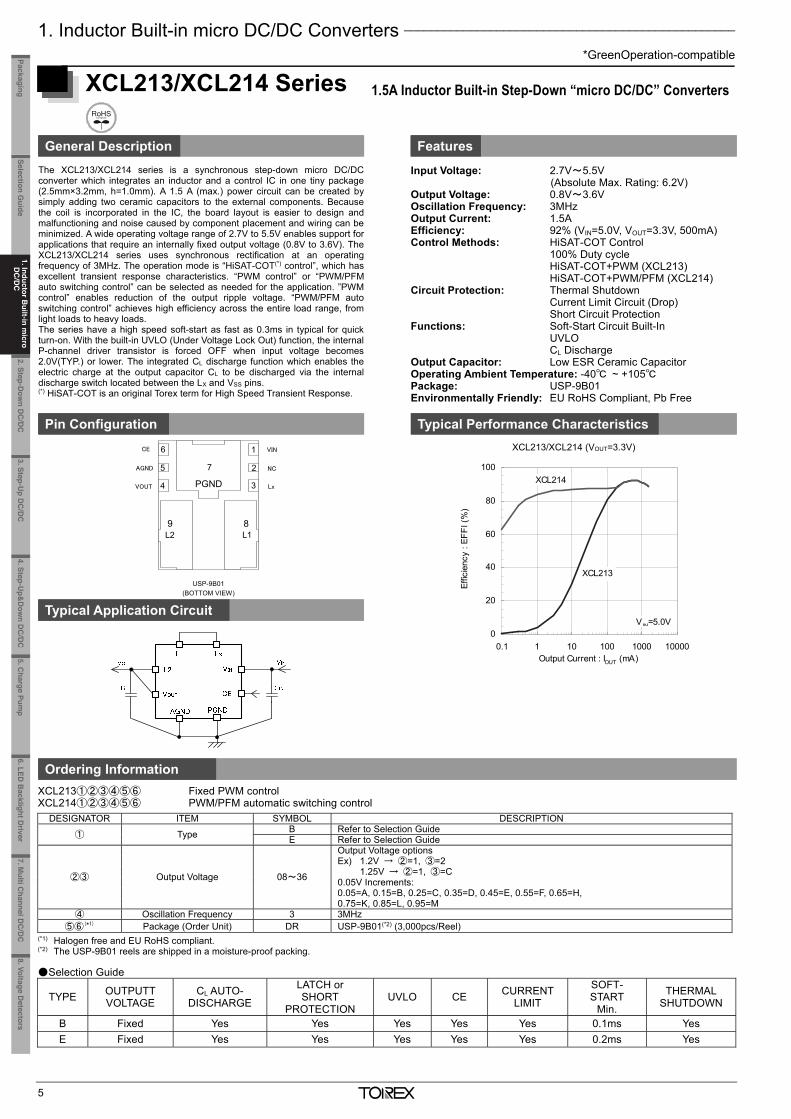
1. Inductor Built-in micro DC/DC Converters __________________________________________________
*GreenOperation-compatible
5
XCL213/XCL214 Series 1.5A Inductor Built-in Step-Down “micro DC/DC” Converters
General Description Features
The XCL213/XCL214 series is a synchronous step-down micro DC/DC converter which integrates an inductor and a control IC in one tiny package (2.5mm×3.2mm, h=1.0mm). A 1.5 A (max.) power circuit can be created by simply adding two ceramic capacitors to the external components. Because the coil is incorporated in the IC, the board layout is easier to design and malfunctioning and noise caused by component placement and wiring can be minimized. A wide operating voltage range of 2.7V to 5.5V enables support for applications that require an internally fixed output voltage (0.8V to 3.6V). The XCL213/XCL214 series uses synchronous rectification at an operating frequency of 3MHz. The operation mode is “HiSAT-COT(*) control”, which has excellent transient response characteristics. “PWM control” or “PWM/PFM auto switching control” can be selected as needed for the application. ”PWM control” enables reduction of the output ripple voltage. “PWM/PFM auto switching control” achieves high efficiency across the entire load range, from light loads to heavy loads. The series have a high speed soft-start as fast as 0.3ms in typical for quick turn-on. With the built-in UVLO (Under Voltage Lock Out) function, the internal P-channel driver transistor is forced OFF when input voltage becomes 2.0V(TYP.) or lower. The integrated CL discharge function which enables the electric charge at the output capacitor CL to be discharged via the internal discharge switch located between the LX and VSS pins. (*) HiSAT-COT is an original Torex term for High Speed Transient Response.
Input Voltage: 2.7V~5.5V (Absolute Max. Rating: 6.2V)
Output Voltage: 0.8V~3.6V Oscillation Frequency: 3MHz Output Current: 1.5A Efficiency: 92% (VIN=5.0V, VOUT=3.3V, 500mA) Control Methods: HiSAT-COT Control 100% Duty cycle HiSAT-COT+PWM (XCL213) HiSAT-COT+PWM/PFM (XCL214) Circuit Protection: Thermal Shutdown Current Limit Circuit (Drop) Short Circuit Protection Functions: Soft-Start Circuit Built-In UVLO CL Discharge Output Capacitor: Low ESR Ceramic Capacitor Operating Ambient Temperature: -40 ~ +105 Package: USP-9B01 Environmentally Friendly: EU RoHS Compliant, Pb Free
Pin Configuration Typical Performance Characteristics
XCL213/XCL214 (VOUT=3.3V)
Typical Application Circuit Ty
Ordering Information
XCL213①②③④⑤⑥ Fixed PWM control XCL214①②③④⑤⑥ PWM/PFM automatic switching control
DESIGNATOR ITEM SYMBOL DESCRIPTION
① Type B Refer to Selection Guide E Refer to Selection Guide
②③ Output Voltage 08~36
Output Voltage options Ex) 1.2V → ②=1, ③=2 1.25V → ②=1, ③=C 0.05V Increments: 0.05=A, 0.15=B, 0.25=C, 0.35=D, 0.45=E, 0.55=F, 0.65=H, 0.75=K, 0.85=L, 0.95=M
④ Oscillation Frequency 3 3MHz ⑤⑥(*1) Package (Order Unit) DR USP-9B01(*2) (3,000pcs/Reel)
(*1) Halogen free and EU RoHS compliant. (*2) The USP-9B01 reels are shipped in a moisture-proof packing. Selection Guide
TYPE OUTPUTT VOLTAGE
CL AUTO- DISCHARGE
LATCH or SHORT
PROTECTION UVLO CE CURRENT
LIMIT
SOFT- START
Min.
THERMAL SHUTDOWN
B Fixed Yes Yes Yes Yes Yes 0.1ms Yes E Fixed Yes Yes Yes Yes Yes 0.2ms Yes
VOUT
AGND
CE
PG
1
2
34
5
6
7
L2 L1
PGND
VIN
NC
Lx
USP-9B01 (BOTTOM VIEW)
8 9
0
20
40
60
80
100
0.1 1 10 100 1000 10000Output Current : IOUT (mA)
Effic
ienc
y : E
FFI (
%)
XCL213
XCL214
VIN=5.0V
_______________________________________________________________________________________________________
*GreenOperation-compatible
6
XCL211/XCL212 Series 2.0A Inductor Built-in Step-Down “micro DC/DC” Converters
General Description Features
The XCL211/XCL212series is a synchronous step-down micro DC/DCconverter which integrates an inductor and a control IC in one tiny package(3.1mm×4.7mm, h=1.3mm). An internal coil simplifies the circuit and enables minimization of noise andother operational trouble due to the circuit wiring. A wide operating voltage range of 2.7V to 6.0V enables support forapplications that require an externally set output voltage can be selected. TheXCL211/XCL212 series uses synchronous rectification at an operatingfrequency of 2.4MHz. PWM control (XCL211) or automatic PWM/PFMswitching control (XCL212) can be selected. The XCL211 series has a fixedfrequency, enabling the suppression of output ripple. The XCL212 seriesachieves high efficiency while holding down output ripple across the full rangeof loads, from light to heavy, enabling the extension of battery operation time. The series have a high speed soft-start as fast as 1ms in typical for quickturn-on. With the built-in UVLO (Under Voltage Lock Out) function, the internalP-channel driver transistor is forced OFF when input voltage becomes 2.4V orlower. It’s suitable for large-current application due to limit current is configured4.0A in typical. The integrated CL discharge function which enables the electriccharge at the output capacitor CL to be discharged via the internal dischargeswitch located between the LX and VSS pins. Due to CL discharge function,malfunction on LX is prevented when Stand-by mode.
Package Size: 3.1mm×4.7mm, h=1.3mm Input Voltage: 2.7V~6.0V (Absolute Max. Ratings: 7.0V) Output Voltage: 0.9V~VIN (FB Voltage=0.8V±2%) High Efficiency: 94% (VIN=5.0V, VOUT=3.3V) Output Current: 2.0A Oscillation Frequency: 2.4MHz (±15%) Max. Duty Cycle: 100% Control Methods: PWM (XCL211) PWM/PFM (XCL212) Functions: Current Limit Circuit (automatic return) Soft-start Circuit Built-in CL Discharge UVLO Output Capacitor: Low ESR Ceramic Capacitor Operating Ambient Temperature: -40~ +85 Package: USP-11B01 Environmentally Friendly: EU RoHS Compliant, Pb Free
Pin Configuration Typical Performance Characteristics
XCL211B082DR/XCL212B082DR
Typical Application Circuit
Ordering Information
XCL211①②③④⑤⑥ Fixed PWM XCL212①②③④⑤⑥ PWM/PFM Auto Switching
DESIGNATOR ITEM SYMBOL DESCRIPTION
① Type B
Fixed Soft-start Chip Enable Current Limiter Tharmal Shutdown UVLO CL Auto Discharge
②③ Reference Voltage 08 Reference Voltage is fixed at 0.8V ④ Oscillation Frequency 2 2.4MHz
⑤⑥(*1) Package (Order Unit) DR USP-11B01 (1,000pcs/Reel) (*1) Halogen free and EU RoHS compliant.
0
20
40
60
80
100
0.1 1 10 100 1000 10000
Effi
cien
cy :
EFF
I (%
)
Output Current : IOUT (mA)
XCL211
XCL212
VIN=5.0V
VOUT=3.3V
1. Inductor Built-in m
icro D
C/D
C
2. Step-Dow
n DC
/DC
3. Step-Up D
C/D
C4. Step-U
p&D
own D
C/D
C
5.Charge Pum
p6.LED
Backlight D
river8.Voltage D
etectorsSelection G
uidePackaging
7. Multi C
hannel DC
/DC
1. Inductor B
uilt-in micro
DC
/DC
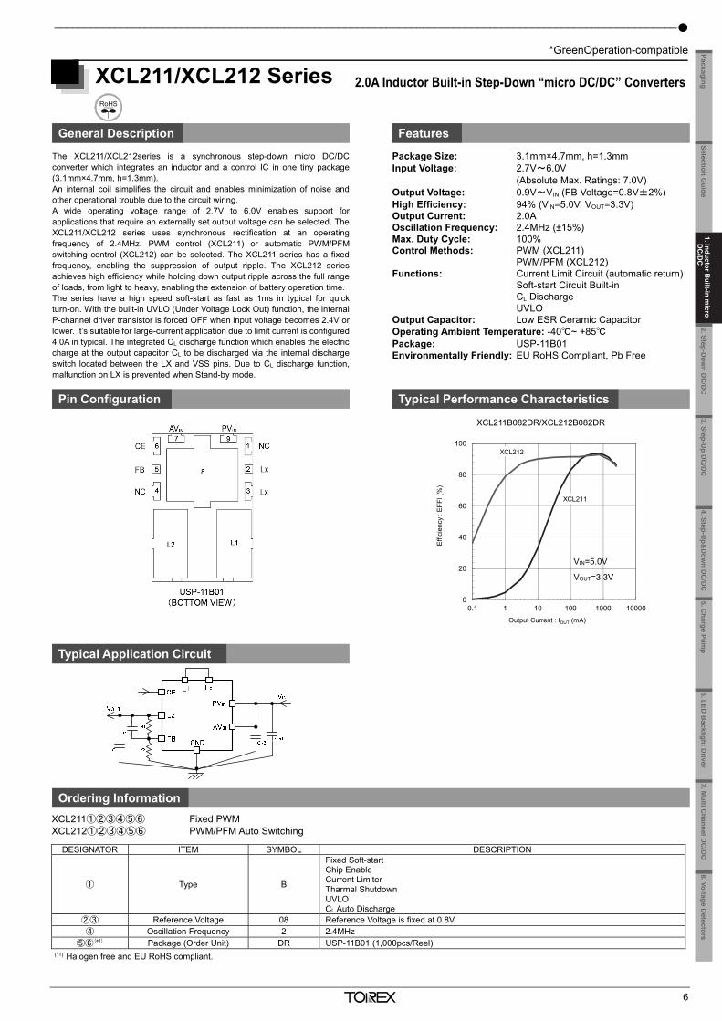
1. Inductor Built-in micro DC/DC Converters __________________________________________________
*GreenOperation-compatible
5
XCL213/XCL214 Series 1.5A Inductor Built-in Step-Down “micro DC/DC” Converters
General Description Features
The XCL213/XCL214 series is a synchronous step-down micro DC/DC converter which integrates an inductor and a control IC in one tiny package (2.5mm×3.2mm, h=1.0mm). A 1.5 A (max.) power circuit can be created by simply adding two ceramic capacitors to the external components. Because the coil is incorporated in the IC, the board layout is easier to design and malfunctioning and noise caused by component placement and wiring can be minimized. A wide operating voltage range of 2.7V to 5.5V enables support for applications that require an internally fixed output voltage (0.8V to 3.6V). The XCL213/XCL214 series uses synchronous rectification at an operating frequency of 3MHz. The operation mode is “HiSAT-COT(*) control”, which has excellent transient response characteristics. “PWM control” or “PWM/PFM auto switching control” can be selected as needed for the application. ”PWM control” enables reduction of the output ripple voltage. “PWM/PFM auto switching control” achieves high efficiency across the entire load range, from light loads to heavy loads. The series have a high speed soft-start as fast as 0.3ms in typical for quick turn-on. With the built-in UVLO (Under Voltage Lock Out) function, the internal P-channel driver transistor is forced OFF when input voltage becomes 2.0V(TYP.) or lower. The integrated CL discharge function which enables the electric charge at the output capacitor CL to be discharged via the internal discharge switch located between the LX and VSS pins. (*) HiSAT-COT is an original Torex term for High Speed Transient Response.
Input Voltage: 2.7V~5.5V (Absolute Max. Rating: 6.2V)
Output Voltage: 0.8V~3.6V Oscillation Frequency: 3MHz Output Current: 1.5A Efficiency: 92% (VIN=5.0V, VOUT=3.3V, 500mA) Control Methods: HiSAT-COT Control 100% Duty cycle HiSAT-COT+PWM (XCL213) HiSAT-COT+PWM/PFM (XCL214) Circuit Protection: Thermal Shutdown Current Limit Circuit (Drop) Short Circuit Protection Functions: Soft-Start Circuit Built-In UVLO CL Discharge Output Capacitor: Low ESR Ceramic Capacitor Operating Ambient Temperature: -40 ~ +105 Package: USP-9B01 Environmentally Friendly: EU RoHS Compliant, Pb Free
Pin Configuration Typical Performance Characteristics
XCL213/XCL214 (VOUT=3.3V)
Typical Application Circuit Ty
Ordering Information
XCL213①②③④⑤⑥ Fixed PWM control XCL214①②③④⑤⑥ PWM/PFM automatic switching control
DESIGNATOR ITEM SYMBOL DESCRIPTION
① Type B Refer to Selection Guide E Refer to Selection Guide
②③ Output Voltage 08~36
Output Voltage options Ex) 1.2V → ②=1, ③=2 1.25V → ②=1, ③=C 0.05V Increments: 0.05=A, 0.15=B, 0.25=C, 0.35=D, 0.45=E, 0.55=F, 0.65=H, 0.75=K, 0.85=L, 0.95=M
④ Oscillation Frequency 3 3MHz ⑤⑥(*1) Package (Order Unit) DR USP-9B01(*2) (3,000pcs/Reel)
(*1) Halogen free and EU RoHS compliant. (*2) The USP-9B01 reels are shipped in a moisture-proof packing. Selection Guide
TYPE OUTPUTT VOLTAGE
CL AUTO- DISCHARGE
LATCH or SHORT
PROTECTION UVLO CE CURRENT
LIMIT
SOFT- START
Min.
THERMAL SHUTDOWN
B Fixed Yes Yes Yes Yes Yes 0.1ms Yes E Fixed Yes Yes Yes Yes Yes 0.2ms Yes
VOUT
AGND
CE
PG
1
2
34
5
6
7
L2 L1
PGND
VIN
NC
Lx
USP-9B01 (BOTTOM VIEW)
8 9
0
20
40
60
80
100
0.1 1 10 100 1000 10000Output Current : IOUT (mA)
Effic
ienc
y : E
FFI (
%)
XCL213
XCL214
VIN=5.0V
_______________________________________________________________________________________________________
*GreenOperation-compatible
6
XCL211/XCL212 Series 2.0A Inductor Built-in Step-Down “micro DC/DC” Converters
General Description Features
The XCL211/XCL212series is a synchronous step-down micro DC/DCconverter which integrates an inductor and a control IC in one tiny package(3.1mm×4.7mm, h=1.3mm). An internal coil simplifies the circuit and enables minimization of noise andother operational trouble due to the circuit wiring. A wide operating voltage range of 2.7V to 6.0V enables support forapplications that require an externally set output voltage can be selected. TheXCL211/XCL212 series uses synchronous rectification at an operatingfrequency of 2.4MHz. PWM control (XCL211) or automatic PWM/PFMswitching control (XCL212) can be selected. The XCL211 series has a fixedfrequency, enabling the suppression of output ripple. The XCL212 seriesachieves high efficiency while holding down output ripple across the full rangeof loads, from light to heavy, enabling the extension of battery operation time. The series have a high speed soft-start as fast as 1ms in typical for quickturn-on. With the built-in UVLO (Under Voltage Lock Out) function, the internalP-channel driver transistor is forced OFF when input voltage becomes 2.4V orlower. It’s suitable for large-current application due to limit current is configured4.0A in typical. The integrated CL discharge function which enables the electriccharge at the output capacitor CL to be discharged via the internal dischargeswitch located between the LX and VSS pins. Due to CL discharge function,malfunction on LX is prevented when Stand-by mode.
Package Size: 3.1mm×4.7mm, h=1.3mm Input Voltage: 2.7V~6.0V (Absolute Max. Ratings: 7.0V) Output Voltage: 0.9V~VIN (FB Voltage=0.8V±2%) High Efficiency: 94% (VIN=5.0V, VOUT=3.3V) Output Current: 2.0A Oscillation Frequency: 2.4MHz (±15%) Max. Duty Cycle: 100% Control Methods: PWM (XCL211) PWM/PFM (XCL212) Functions: Current Limit Circuit (automatic return) Soft-start Circuit Built-in CL Discharge UVLO Output Capacitor: Low ESR Ceramic Capacitor Operating Ambient Temperature: -40~ +85 Package: USP-11B01 Environmentally Friendly: EU RoHS Compliant, Pb Free
Pin Configuration Typical Performance Characteristics
XCL211B082DR/XCL212B082DR
Typical Application Circuit
Ordering Information
XCL211①②③④⑤⑥ Fixed PWM XCL212①②③④⑤⑥ PWM/PFM Auto Switching
DESIGNATOR ITEM SYMBOL DESCRIPTION
① Type B
Fixed Soft-start Chip Enable Current Limiter Tharmal Shutdown UVLO CL Auto Discharge
②③ Reference Voltage 08 Reference Voltage is fixed at 0.8V ④ Oscillation Frequency 2 2.4MHz
⑤⑥(*1) Package (Order Unit) DR USP-11B01 (1,000pcs/Reel) (*1) Halogen free and EU RoHS compliant.
0
20
40
60
80
100
0.1 1 10 100 1000 10000
Effi
cien
cy :
EFF
I (%
)
Output Current : IOUT (mA)
XCL211
XCL212
VIN=5.0V
VOUT=3.3V
2. Step-Dow
n DC
/DC
3. Step-Up D
C/D
C4. Step-U
p&D
own D
C/D
C
5.Charge Pum
p6.LED
Backlight D
river8.Voltage D
etectorsSelection G
uidePackaging
7. Multi C
hannel DC
/DC
1. Inductor B
uilt-in micro
DC
/DC
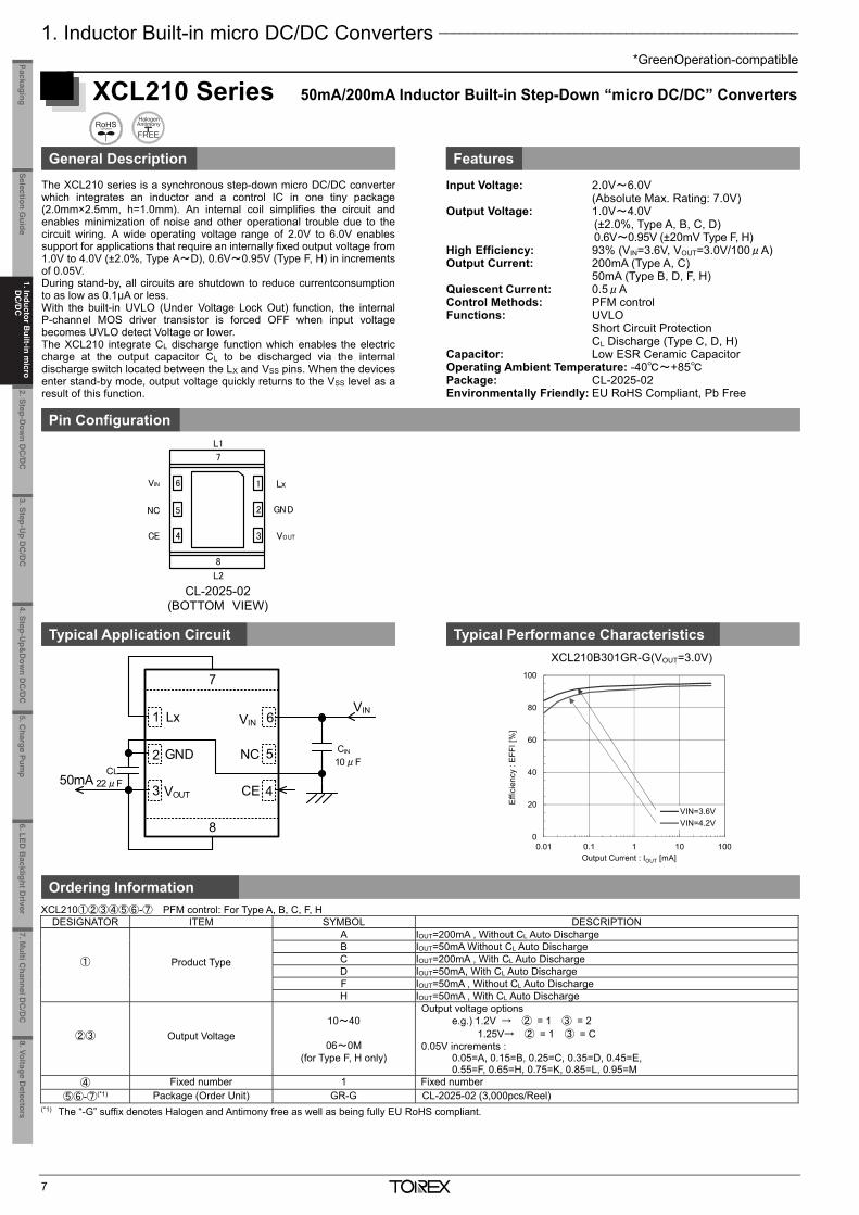
1. Inductor Built-in micro DC/DC Converters __________________________________________________
*GreenOperation-compatible
7
XCL210 Series 50mA/200mA Inductor Built-in Step-Down “micro DC/DC” Converters
General Description Features
The XCL210 series is a synchronous step-down micro DC/DC converter which integrates an inductor and a control IC in one tiny package (2.0mm×2.5mm, h=1.0mm). An internal coil simplifies the circuit and enables minimization of noise and other operational trouble due to the circuit wiring. A wide operating voltage range of 2.0V to 6.0V enables support for applications that require an internally fixed output voltage from 1.0V to 4.0V (±2.0%, Type A~D), 0.6V~0.95V (Type F, H) in increments of 0.05V. During stand-by, all circuits are shutdown to reduce currentconsumption to as low as 0.1μA or less. With the built-in UVLO (Under Voltage Lock Out) function, the internal P-channel MOS driver transistor is forced OFF when input voltage becomes UVLO detect Voltage or lower. The XCL210 integrate CL discharge function which enables the electric charge at the output capacitor CL to be discharged via the internal discharge switch located between the LX and VSS pins. When the devices enter stand-by mode, output voltage quickly returns to the VSS level as a result of this function.
Input Voltage: 2.0V~6.0V (Absolute Max. Rating: 7.0V) Output Voltage: 1.0V~4.0V
(±2.0%, Type A, B, C, D) 0.6V~0.95V (±20mV Type F, H)
High Efficiency: 93% (VIN=3.6V, VOUT=3.0V/100μA) Output Current: 200mA (Type A, C) 50mA (Type B, D, F, H) Quiescent Current: 0.5μA Control Methods: PFM control Functions: UVLO Short Circuit Protection CL Discharge (Type C, D, H) Capacitor: Low ESR Ceramic Capacitor Operating Ambient Temperature: -40~+85 Package: CL-2025-02 Environmentally Friendly: EU RoHS Compliant, Pb Free
Pin Configuration
Typical Application Circuit Typical Performance Characteristics
Ordering Information
XCL210①②③④⑤⑥-⑦ PFM control: For Type A, B, C, F, H DESIGNATOR ITEM SYMBOL DESCRIPTION
① Product Type
A IOUT=200mA , Without CL Auto Discharge B IOUT=50mA Without CL Auto Discharge C IOUT=200mA , With CL Auto Discharge D IOUT=50mA, With CL Auto Discharge F IOUT=50mA , Without CL Auto Discharge H IOUT=50mA , With CL Auto Discharge
②③ Output Voltage 10~40
06~0M
(for Type F, H only)
Output voltage options e.g.) 1.2V → ② = 1 ③ = 2 1.25V→ ② = 1 ③ = C 0.05V increments : 0.05=A, 0.15=B, 0.25=C, 0.35=D, 0.45=E, 0.55=F, 0.65=H, 0.75=K, 0.85=L, 0.95=M
④ Fixed number 1 Fixed number ⑤⑥-⑦(*1) Package (Order Unit) GR-G CL-2025-02 (3,000pcs/Reel)
(*1) The “-G” suffix denotes Halogen and Antimony free as well as being fully EU RoHS compliant.
0
20
40
60
80
100
0.01 0.1 1 10 100
Effi
cien
cy :
EFF
I [%
]
Output Current : IOUT [mA]
VIN=3.6VVIN=4.2V
XCL210B301GR-G(VOUT=3.0V)
CL-2025-02 (BOTTOM VIEW)
L1
L2
7
8
VIN 6
NC 5
CE 4
1 Lx
2 GND
3 VOUT
50mA
CIN
10μFCL
22μF
7
8
1
2
3 4
5
6
GND
VINLx
CEVOUT
NC
VIN
_______________________________________________________________________________________________________
*GreenOperation-compatible
8
XCL208/XCL209 Series 400mA Inductor Built-in Step-Down “micro DC/DC” Converters
General Description Features
The XCL208/XCL209 series is a synchronous step-down micro DC/DCconverter which integrates an inductor and a control IC in one tinypackage (2.5mm×2.15mm, h=1.05mm). A stable power supply with anoutput current of 400mA is configured using only two capacitorsconnected externally. An internal coil simplifies the circuit and enables minimization of noiseand other operational trouble due to the circuit wiring. A wide operating voltage range of 1.8V (2.0V) to 6.0V enables support forapplications that require an alkaline battery (2-cell) or AC adapter (5V)power supply. An internally fixed output voltage (0.8V to 4.0V) or anexternally set output voltage can be selected. The XCL208/XCL209 series uses synchronous rectification at anoperating frequency of 3MHz. PWM control (XCL208) or automaticPWM/PFM switching control (XCL209) can be selected. The XCL208series has a fixed frequency, enabling the suppression of output ripple.The XCL209 series achieves high efficiency while holding down outputripple across the full range of loads, from light to heavy, enabling theextension of battery operation time. Soft start and on/off functions with CL discharge are provided, and the IC can be put in the standby state by inputting a Low level signal into the CEpin.
Input Voltage: 1.8V~6.0V (Type F) (Absolute Max. Rating: 6.5V) 2.0V~6.0V (Types A/B) (Absolute Max. Rating: 6.5V) Output Voltage: 0.8V~4.0V (±2.0%) (Fixed) High Efficiency : 90% (VIN=4.2V, VOUT=3.3V) Output Current: 400mA Oscillation Frequency: 3MHz (±15%) CE Functions: Active High Soft-start CL Auto Discharge Protection Circuits: Current Limiter Built-in (Constant Current & Latching) Control Methods: PWM (XCL208) PWM/PFM Auto (XCL209) Operating Ambient Temperature: -40~+85 Package: USP-10B03 Environmentally Friendly: EU RoHS Compliant, Pb Free
Pin Configuration
Typical Application Circuit Typical Performance Characteristics
Ordering Information
XCL208①②③④⑤⑥: Fixed PWM control XCL209①②③④⑤⑥: PWM / PFM automatic switching control
DESIGNATOR ITEM SYMBOL DESCRIPTION
① Functions selection Fixed Output Voltage A VIN≧2.0V, No CL auto discharge, Standard soft-start
B VIN≧2.0V, CL auto discharge, High speed soft-start Output Voltage External Setting F VIN≧1.8V, CL auto discharge, High speed soft-start
②③ Fixed Output Voltage 0~9 A~M
Output voltage options e.g. 2.8V → ②=2 ③=8 0.05V increments : e.g. 2.85V→ ②=2 ③=L 0.05=A, 0.15=B, 0.25=C, 0.35=D, 0.45=E, 0.55=F, 0.65=H, 0.75=K, 0.85=L, 0.95=M
Output Voltage External Setting 08 FB=0.8V ④ Oscillation Frequency 3 3MHz
⑤⑥ (*1) Package (Order Unit) DR USP-10B03 (3,000pcs/Reel) (*1) Halogen free and EU RoHS compliant. (*2) When other output voltages (semi-custom) are needed, please contact your local Torex sales office for more information. Output voltage range is 0.8~4.0V.
(BOTTOM VIEW)
AVSS
VIN
CE
LX
PVSS
VOUT
NC
NC
L1
L2
1
2
3
45
6
7
8
9
10
XCL208x333DR/XCL209x333DR
0
20
40
60
80
100
0.01 0.1 1 10 100 1000
Output Current:IOUT (mA)
Effic
ency
:EFF
I(%)
VIN= 4.2V5.0V
VOUT=3.3V
XCL209(PWM/PFM)
XCL208(PWM)
XCL208A / XCL208B / XCL209A / XCL209B Type
XCL208F / XCL209F Type
USP-10B03 (BOTTOM VIEW)
1. Inductor Built-in m
icro D
C/D
C
2. Step-Dow
n DC
/DC
3. Step-Up D
C/D
C4. Step-U
p&D
own D
C/D
C
5.Charge Pum
p6.LED
Backlight D
river8.Voltage D
etectorsSelection G
uidePackaging
7. Multi C
hannel DC
/DC
1. Inductor B
uilt-in micro
DC
/DC
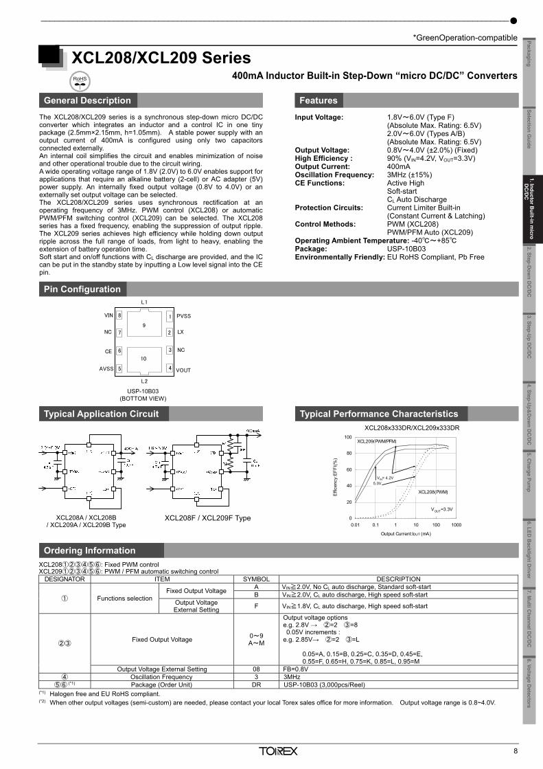
1. Inductor Built-in micro DC/DC Converters __________________________________________________
*GreenOperation-compatible
7
XCL210 Series 50mA/200mA Inductor Built-in Step-Down “micro DC/DC” Converters
General Description Features
The XCL210 series is a synchronous step-down micro DC/DC converter which integrates an inductor and a control IC in one tiny package (2.0mm×2.5mm, h=1.0mm). An internal coil simplifies the circuit and enables minimization of noise and other operational trouble due to the circuit wiring. A wide operating voltage range of 2.0V to 6.0V enables support for applications that require an internally fixed output voltage from 1.0V to 4.0V (±2.0%, Type A~D), 0.6V~0.95V (Type F, H) in increments of 0.05V. During stand-by, all circuits are shutdown to reduce currentconsumption to as low as 0.1μA or less. With the built-in UVLO (Under Voltage Lock Out) function, the internal P-channel MOS driver transistor is forced OFF when input voltage becomes UVLO detect Voltage or lower. The XCL210 integrate CL discharge function which enables the electric charge at the output capacitor CL to be discharged via the internal discharge switch located between the LX and VSS pins. When the devices enter stand-by mode, output voltage quickly returns to the VSS level as a result of this function.
Input Voltage: 2.0V~6.0V (Absolute Max. Rating: 7.0V) Output Voltage: 1.0V~4.0V
(±2.0%, Type A, B, C, D) 0.6V~0.95V (±20mV Type F, H)
High Efficiency: 93% (VIN=3.6V, VOUT=3.0V/100μA) Output Current: 200mA (Type A, C) 50mA (Type B, D, F, H) Quiescent Current: 0.5μA Control Methods: PFM control Functions: UVLO Short Circuit Protection CL Discharge (Type C, D, H) Capacitor: Low ESR Ceramic Capacitor Operating Ambient Temperature: -40~+85 Package: CL-2025-02 Environmentally Friendly: EU RoHS Compliant, Pb Free
Pin Configuration
Typical Application Circuit Typical Performance Characteristics
Ordering Information
XCL210①②③④⑤⑥-⑦ PFM control: For Type A, B, C, F, H DESIGNATOR ITEM SYMBOL DESCRIPTION
① Product Type
A IOUT=200mA , Without CL Auto Discharge B IOUT=50mA Without CL Auto Discharge C IOUT=200mA , With CL Auto Discharge D IOUT=50mA, With CL Auto Discharge F IOUT=50mA , Without CL Auto Discharge H IOUT=50mA , With CL Auto Discharge
②③ Output Voltage 10~40
06~0M
(for Type F, H only)
Output voltage options e.g.) 1.2V → ② = 1 ③ = 2 1.25V→ ② = 1 ③ = C 0.05V increments : 0.05=A, 0.15=B, 0.25=C, 0.35=D, 0.45=E, 0.55=F, 0.65=H, 0.75=K, 0.85=L, 0.95=M
④ Fixed number 1 Fixed number ⑤⑥-⑦(*1) Package (Order Unit) GR-G CL-2025-02 (3,000pcs/Reel)
(*1) The “-G” suffix denotes Halogen and Antimony free as well as being fully EU RoHS compliant.
0
20
40
60
80
100
0.01 0.1 1 10 100
Effi
cien
cy :
EFF
I [%
]
Output Current : IOUT [mA]
VIN=3.6VVIN=4.2V
XCL210B301GR-G(VOUT=3.0V)
CL-2025-02 (BOTTOM VIEW)
L1
L2
7
8
VIN 6
NC 5
CE 4
1 Lx
2 GND
3 VOUT
50mA
CIN
10μFCL
22μF
7
8
1
2
3 4
5
6
GND
VINLx
CEVOUT
NC
VIN
_______________________________________________________________________________________________________
*GreenOperation-compatible
8
XCL208/XCL209 Series 400mA Inductor Built-in Step-Down “micro DC/DC” Converters
General Description Features
The XCL208/XCL209 series is a synchronous step-down micro DC/DCconverter which integrates an inductor and a control IC in one tinypackage (2.5mm×2.15mm, h=1.05mm). A stable power supply with anoutput current of 400mA is configured using only two capacitorsconnected externally. An internal coil simplifies the circuit and enables minimization of noiseand other operational trouble due to the circuit wiring. A wide operating voltage range of 1.8V (2.0V) to 6.0V enables support forapplications that require an alkaline battery (2-cell) or AC adapter (5V)power supply. An internally fixed output voltage (0.8V to 4.0V) or anexternally set output voltage can be selected. The XCL208/XCL209 series uses synchronous rectification at anoperating frequency of 3MHz. PWM control (XCL208) or automaticPWM/PFM switching control (XCL209) can be selected. The XCL208series has a fixed frequency, enabling the suppression of output ripple.The XCL209 series achieves high efficiency while holding down outputripple across the full range of loads, from light to heavy, enabling theextension of battery operation time. Soft start and on/off functions with CL discharge are provided, and the IC can be put in the standby state by inputting a Low level signal into the CEpin.
Input Voltage: 1.8V~6.0V (Type F) (Absolute Max. Rating: 6.5V) 2.0V~6.0V (Types A/B) (Absolute Max. Rating: 6.5V) Output Voltage: 0.8V~4.0V (±2.0%) (Fixed) High Efficiency : 90% (VIN=4.2V, VOUT=3.3V) Output Current: 400mA Oscillation Frequency: 3MHz (±15%) CE Functions: Active High Soft-start CL Auto Discharge Protection Circuits: Current Limiter Built-in (Constant Current & Latching) Control Methods: PWM (XCL208) PWM/PFM Auto (XCL209) Operating Ambient Temperature: -40~+85 Package: USP-10B03 Environmentally Friendly: EU RoHS Compliant, Pb Free
Pin Configuration
Typical Application Circuit Typical Performance Characteristics
Ordering Information
XCL208①②③④⑤⑥: Fixed PWM control XCL209①②③④⑤⑥: PWM / PFM automatic switching control
DESIGNATOR ITEM SYMBOL DESCRIPTION
① Functions selection Fixed Output Voltage A VIN≧2.0V, No CL auto discharge, Standard soft-start
B VIN≧2.0V, CL auto discharge, High speed soft-start Output Voltage External Setting F VIN≧1.8V, CL auto discharge, High speed soft-start
②③ Fixed Output Voltage 0~9 A~M
Output voltage options e.g. 2.8V → ②=2 ③=8 0.05V increments : e.g. 2.85V→ ②=2 ③=L 0.05=A, 0.15=B, 0.25=C, 0.35=D, 0.45=E, 0.55=F, 0.65=H, 0.75=K, 0.85=L, 0.95=M
Output Voltage External Setting 08 FB=0.8V ④ Oscillation Frequency 3 3MHz
⑤⑥ (*1) Package (Order Unit) DR USP-10B03 (3,000pcs/Reel) (*1) Halogen free and EU RoHS compliant. (*2) When other output voltages (semi-custom) are needed, please contact your local Torex sales office for more information. Output voltage range is 0.8~4.0V.
(BOTTOM VIEW)
AVSS
VIN
CE
LX
PVSS
VOUT
NC
NC
L1
L2
1
2
3
45
6
7
8
9
10
XCL208x333DR/XCL209x333DR
0
20
40
60
80
100
0.01 0.1 1 10 100 1000
Output Current:IOUT (mA)
Effic
ency
:EFF
I(%)
VIN= 4.2V5.0V
VOUT=3.3V
XCL209(PWM/PFM)
XCL208(PWM)
XCL208A / XCL208B / XCL209A / XCL209B Type
XCL208F / XCL209F Type
USP-10B03 (BOTTOM VIEW)
2. Step-Dow
n DC
/DC
3. Step-Up D
C/D
C4. Step-U
p&D
own D
C/D
C
5.Charge Pum
p6.LED
Backlight D
river8.Voltage D
etectorsSelection G
uidePackaging
7. Multi C
hannel DC
/DC
1. Inductor B
uilt-in micro
DC
/DC
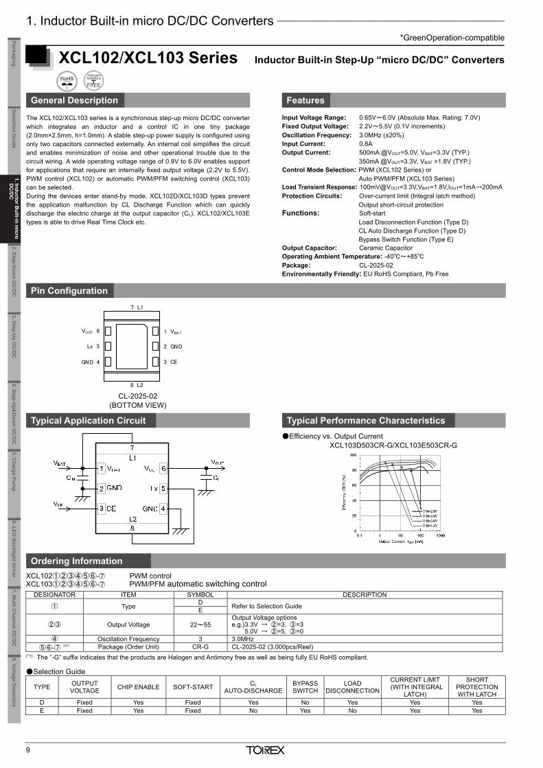
1. Inductor Built-in micro DC/DC Converters __________________________________________________
*GreenOperation-compatible
9
7 L1
8 L2
VOUT 6
Lx 5
GND 4
1 VBA T
2 GND
3 CE
XCL102/XCL103 Series Inductor Built-in Step-Up “micro DC/DC” Converters
General Description Features
The XCL102/XCL103 series is a synchronous step-up micro DC/DC converter which integrates an inductor and a control IC in one tiny package (2.0mm×2.5mm, h=1.0mm). A stable step-up power supply is configured using only two capacitors connected externally. An internal coil simplifies the circuit and enables minimization of noise and other operational trouble due to the circuit wiring. A wide operating voltage range of 0.9V to 6.0V enables support for applications that require an internally fixed output voltage (2.2V to 5.5V). PWM control (XCL102) or automatic PWM/PFM switching control (XCL103) can be selected. During the devices enter stand-by mode, XCL102D/XCL103D types prevent the application malfunction by CL Discharge Function which can quickly discharge the electric charge at the output capacitor (CL). XCL102/XCL103E types is able to drive Real Time Clock etc.
Input Voltage Range: 0.65V~6.0V (Absolute Max. Rating: 7.0V) Fixed Output Voltage: 2.2V~5.5V (0.1V increments) Oscillation Frequency: 3.0MHz (±20%) Input Current: 0.8A Output Current: 500mA @VOUT=5.0V, VBAT=3.3V (TYP.) 350mA @VOUT=3.3V, VBAT =1.8V (TYP.) Control Mode Selection: PWM (XCL102 Series) or Auto PWM/PFM (XCL103 Series) Load Transient Response: 100mV@VOUT=3.3V,VBAT=1.8V,IOUT=1mA→200mA Protection Circuits: Over-current limit (Integral latch method) Output short-circuit protection Functions: Soft-start Load Disconnection Function (Type D) CL Auto Discharge Function (Type D) Bypass Switch Function (Type E) Output Capacitor: Ceramic Capacitor Operating Ambient Temperature: -40~+85 Package: CL-2025-02 Environmentally Friendly: EU RoHS Compliant, Pb Free
Pin Configuration
Typical Application Circuit Typical Performance Characteristics
Efficiency vs. Output Current XCL103D503CR-G/XCL103E503CR-G
Ordering Information
XCL102①②③④⑤⑥-⑦ PWM control XCL103①②③④⑤⑥-⑦ PWM/PFM automatic switching control
DESIGNATOR ITEM SYMBOL DESCRIPTION
① Type D Refer to Selection Guide E
②③ Output Voltage 22~55 Output Voltage options e.g.)3.3V → ②=3, ③=3 5.0V → ②=5, ③=0
④ Oscillation Frequency 3 3.0MHz ⑤⑥-⑦ (*1) Package (Order Unit) CR-G CL-2025-02 (3,000pcs/Reel)
(*1) The ”-G” suffix indicates that the products are Halogen and Antimony free as well as being fully EU RoHS compliant. Selection Guide
TYPE OUTPUT VOLTAGE CHIP ENABLE SOFT-START CL
AUTO-DISCHARGE BYPASS SWITCH
LOAD DISCONNECTION
CURRENT LIMIT (WITH INTEGRAL
LATCH)
SHORT PROTECTION WITH LATCH
D Fixed Yes Fixed Yes No Yes Yes Yes E Fixed Yes Fixed No Yes No Yes Yes
CL-2025-02 (BOTTOM VIEW)
_______________________________________________________________________________________________________
*GreenOperation-compatible
10
XCL101 Series 100mA Inductor Built-in Step-Up “micro DC/DC” Converters
General Description Features
The XCL101 series is a synchronous step-up micro DC/DC converterwhich integrates an inductor and a control IC in one tiny package(2.5mm×2.0mm, h=1.00mm). A stable power supply with a configuredusing only two capacitors connected externally. An internal coil simplifiesthe circuit and enables minimization of noise and other operationaltrouble due to the circuit wiring. A wide operating voltage range of 0.9V to5.5V enables support for applications that require an alkaline battery(1-cell) or Ni-HM (1-cell) power supply. The output voltage can be setfrom 1.8V to 5.0V (±2.0%) in steps of 0.1V (semi custom). PFMsynchronous control enables a low quiescent current, making theseproducts ideal for portable devices that require high efficiency. TheXCL101 features a load disconnect function to break continuity betweenthe input and output at shutdown (XCL101A), and also a bypass modefunction to maintain continuity between the input and output (XCL101C).
Input Voltage: 0.7V ~ 5.5V (Absolute Max. Rating: 7.0V) Fixed Output Voltage: 1.8V~5.0V (±2.0%) (Standard Voltage) Output Current: 100mA@VOUT=3.3V, VBAT=1.8V (TYP.) Quiescent Current: 6.3μA (VBAT=VOUT+0.5V) Control Method: PFM Control PFM Switching Current: 350mA Functions: Load Disconnection Function or Bypass Mode Function Output Capacitor: Ceramic Capacitor Compatible Operating Ambient Temperature: -40 ~ +85 Package: CL-2025-02 Environmentally Friendly: EU RoHS Compliant, Pb Free
Pin Configuration
Typical Application Circuit Typical Performance Characteristics
XCL101C Series
XCL101C501ER-G
Ordering Information
XCL101①②③④⑤⑥-⑦ DESIGNATOR ITEM SYMBOL DESCRIPTION
① Product Type A Load Disconnection C VBAT Bypass
②③ Output Voltage 18~50 Output Voltage e.g. VOUT=1.8V ⇒ ②=1, ③=8
④ Oscillation Frequency 1 1.2MHz ⑤⑥-⑦ (*1) Package (Order Unit) ER-G CL-2025-02 (3,000pcs/Reel)
(*1) The “-G” suffix denotes Halogen and Antimony free as well as being fully EU RoHS compliant.
0
20
40
60
80
100
0.01 0.1 1 10 100 1000
Output Current:IOUT (mA)
Effic
ienc
y:EF
FI(%
)
3.6V
VOUT=5.0V
4.2V
VIN= 3.0V
(TOP VIEW) (Note)『L1 and Lx』are connecting on PCB
CL-2025-02 (BOTTOM VIEW)
1. Inductor Built-in m
icro D
C/D
C
2. Step-Dow
n DC
/DC
3. Step-Up D
C/D
C4. Step-U
p&D
own D
C/D
C
5.Charge Pum
p6.LED
Backlight D
river8.Voltage D
etectorsSelection G
uidePackaging
7. Multi C
hannel DC
/DC
1. Inductor B
uilt-in micro
DC
/DC
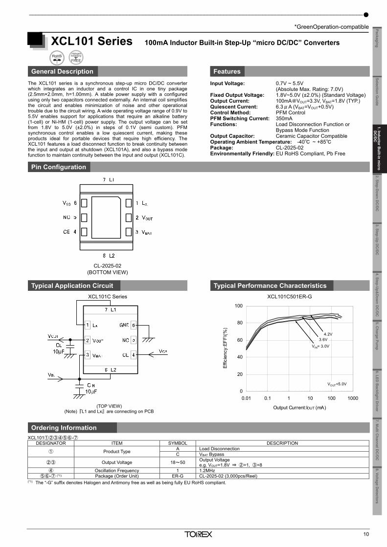
1. Inductor Built-in micro DC/DC Converters __________________________________________________
*GreenOperation-compatible
9
7 L1
8 L2
VOUT 6
Lx 5
GND 4
1 VBA T
2 GND
3 CE
XCL102/XCL103 Series Inductor Built-in Step-Up “micro DC/DC” Converters
General Description Features
The XCL102/XCL103 series is a synchronous step-up micro DC/DC converter which integrates an inductor and a control IC in one tiny package (2.0mm×2.5mm, h=1.0mm). A stable step-up power supply is configured using only two capacitors connected externally. An internal coil simplifies the circuit and enables minimization of noise and other operational trouble due to the circuit wiring. A wide operating voltage range of 0.9V to 6.0V enables support for applications that require an internally fixed output voltage (2.2V to 5.5V). PWM control (XCL102) or automatic PWM/PFM switching control (XCL103) can be selected. During the devices enter stand-by mode, XCL102D/XCL103D types prevent the application malfunction by CL Discharge Function which can quickly discharge the electric charge at the output capacitor (CL). XCL102/XCL103E types is able to drive Real Time Clock etc.
Input Voltage Range: 0.65V~6.0V (Absolute Max. Rating: 7.0V) Fixed Output Voltage: 2.2V~5.5V (0.1V increments) Oscillation Frequency: 3.0MHz (±20%) Input Current: 0.8A Output Current: 500mA @VOUT=5.0V, VBAT=3.3V (TYP.) 350mA @VOUT=3.3V, VBAT =1.8V (TYP.) Control Mode Selection: PWM (XCL102 Series) or Auto PWM/PFM (XCL103 Series) Load Transient Response: 100mV@VOUT=3.3V,VBAT=1.8V,IOUT=1mA→200mA Protection Circuits: Over-current limit (Integral latch method) Output short-circuit protection Functions: Soft-start Load Disconnection Function (Type D) CL Auto Discharge Function (Type D) Bypass Switch Function (Type E) Output Capacitor: Ceramic Capacitor Operating Ambient Temperature: -40~+85 Package: CL-2025-02 Environmentally Friendly: EU RoHS Compliant, Pb Free
Pin Configuration
Typical Application Circuit Typical Performance Characteristics
Efficiency vs. Output Current XCL103D503CR-G/XCL103E503CR-G
Ordering Information
XCL102①②③④⑤⑥-⑦ PWM control XCL103①②③④⑤⑥-⑦ PWM/PFM automatic switching control
DESIGNATOR ITEM SYMBOL DESCRIPTION
① Type D Refer to Selection Guide E
②③ Output Voltage 22~55 Output Voltage options e.g.)3.3V → ②=3, ③=3 5.0V → ②=5, ③=0
④ Oscillation Frequency 3 3.0MHz ⑤⑥-⑦ (*1) Package (Order Unit) CR-G CL-2025-02 (3,000pcs/Reel)
(*1) The ”-G” suffix indicates that the products are Halogen and Antimony free as well as being fully EU RoHS compliant. Selection Guide
TYPE OUTPUT VOLTAGE CHIP ENABLE SOFT-START CL
AUTO-DISCHARGE BYPASS SWITCH
LOAD DISCONNECTION
CURRENT LIMIT (WITH INTEGRAL
LATCH)
SHORT PROTECTION WITH LATCH
D Fixed Yes Fixed Yes No Yes Yes Yes E Fixed Yes Fixed No Yes No Yes Yes
CL-2025-02 (BOTTOM VIEW)
_______________________________________________________________________________________________________
*GreenOperation-compatible
10
XCL101 Series 100mA Inductor Built-in Step-Up “micro DC/DC” Converters
General Description Features
The XCL101 series is a synchronous step-up micro DC/DC converterwhich integrates an inductor and a control IC in one tiny package(2.5mm×2.0mm, h=1.00mm). A stable power supply with a configuredusing only two capacitors connected externally. An internal coil simplifiesthe circuit and enables minimization of noise and other operationaltrouble due to the circuit wiring. A wide operating voltage range of 0.9V to5.5V enables support for applications that require an alkaline battery(1-cell) or Ni-HM (1-cell) power supply. The output voltage can be setfrom 1.8V to 5.0V (±2.0%) in steps of 0.1V (semi custom). PFMsynchronous control enables a low quiescent current, making theseproducts ideal for portable devices that require high efficiency. TheXCL101 features a load disconnect function to break continuity betweenthe input and output at shutdown (XCL101A), and also a bypass modefunction to maintain continuity between the input and output (XCL101C).
Input Voltage: 0.7V ~ 5.5V (Absolute Max. Rating: 7.0V) Fixed Output Voltage: 1.8V~5.0V (±2.0%) (Standard Voltage) Output Current: 100mA@VOUT=3.3V, VBAT=1.8V (TYP.) Quiescent Current: 6.3μA (VBAT=VOUT+0.5V) Control Method: PFM Control PFM Switching Current: 350mA Functions: Load Disconnection Function or Bypass Mode Function Output Capacitor: Ceramic Capacitor Compatible Operating Ambient Temperature: -40 ~ +85 Package: CL-2025-02 Environmentally Friendly: EU RoHS Compliant, Pb Free
Pin Configuration
Typical Application Circuit Typical Performance Characteristics
XCL101C Series
XCL101C501ER-G
Ordering Information
XCL101①②③④⑤⑥-⑦ DESIGNATOR ITEM SYMBOL DESCRIPTION
① Product Type A Load Disconnection C VBAT Bypass
②③ Output Voltage 18~50 Output Voltage e.g. VOUT=1.8V ⇒ ②=1, ③=8
④ Oscillation Frequency 1 1.2MHz ⑤⑥-⑦ (*1) Package (Order Unit) ER-G CL-2025-02 (3,000pcs/Reel)
(*1) The “-G” suffix denotes Halogen and Antimony free as well as being fully EU RoHS compliant.
0
20
40
60
80
100
0.01 0.1 1 10 100 1000
Output Current:IOUT (mA)
Effic
ienc
y:EF
FI(%
)
3.6V
VOUT=5.0V
4.2V
VIN= 3.0V
(TOP VIEW) (Note)『L1 and Lx』are connecting on PCB
CL-2025-02 (BOTTOM VIEW)
2. Step-Dow
n DC
/DC
3. Step-Up D
C/D
C4. Step-U
p&D
own D
C/D
C
5.Charge Pum
p6.LED
Backlight D
river8.Voltage D
etectorsSelection G
uidePackaging
7. Multi C
hannel DC
/DC
1. Inductor B
uilt-in micro
DC
/DC
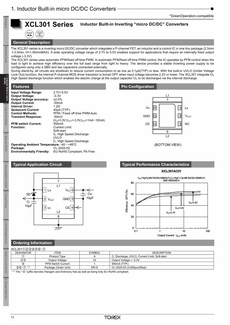
1. Inductor Built-in micro DC/DC Converters ________________________________________________
*GreenOperation-compatible
11
XCL301 Series Inductor Built-in Inverting “micro DC/DC” Converters
General Description
The XCL301 series is a inverting micro DC/DC converter which integrates a P-channel FET, an inductor and a control IC in one tiny package (2.5mm×2.0mm, H=1.00mmMAX). A wide operating voltage range of 2.7V to 5.5V enables support for applications that require an internally fixed outputvoltage (-3.3V). The XCL301 series uses automatic PFM/fixed off time PWM. In automatic PFM/fixed off time PWM control, the IC operates by PFM control when the load is light to achieve high efficiency over the full load range from light to heavy. The device provides a stable inverting power supply to beconfigured using only a SBD and two capacitors connected externally. During stand-by, all circuits are shutdown to reduce current consumption to as low as 0.1μA(TYP) or less. With the built-in UVLO (Under Voltage Lock Out) function, the internal P-channel MOS driver transistor is forced OFF when input voltage becomes 2.2V or lower. The XCL301 integrate CL High Speed discharge function which enables the electric charge at the output capacitor CL to be discharged via the internal discharge.
Features Pin Configuration Input Voltage Range: 2.7V~5.5V Output Voltage: -3.3V Output Voltage accuracy: ±2.0% Output Current: -50mA Internal Driver: 1.2Ω Quiescent Current: 40μA (TYP.) Control Methods: PFM / Fixed off time PWM Auto Transient Response: -50mV (VIN=3.3V,VOUT=-3.3V,IOUT=1mA→50mA) PFM switch Current: 550mA Function: Current Limit Soft-start CL High Speed Discharge UVLO CL High Speed Discharge Operating Ambient Temperature: -40~+85 Package: CL-2025-02 Environmentally Friendly: EU RoHS Compliant, Pb Free
Typical Application Circuit Typical Performance Characteristics
Ordering Information
XCL301①②③④⑤⑥-⑦ DESIGNATOR ITEM SYMBOL DESCRIPTION
① Product Type A CL Discharge, UVLO, Current Limit, Soft-start ②③ Output Voltage 33 Output Voltage = -3.3V ④ PFM Switch Current 1 550mA (TYP.)
⑤⑥-⑦ (*1) Package (Order Unit) ER-G CL-2025-02 (3,000pcs/Reel) (*1) The “-G” suffix denotes Halogen and Antimony free as well as being fully EU RoHS compliant.
(BOTTOM VIEW)
L1
L2
7
8
VIN 6
GND 5
CE 4
1 Lx
2 VOUT
3 NC
L1
L2
1
2
3 4
5
6Lx
VOUT
NC CE
GND
VIN
CIN
10μFCL
10μF
8
7
SD
___________________________________________ 2. Step-Down DC/DC Converters and Controller ICs
12
XC9281/XC9282 Series HiSAT-COTControl, Extremely Small 600mA Synchronous Step-Down DC/DC Converters
General Description Features
The XC9281/XC9282 series are 600mA synchronous rectification DC/DCconverters adopting HiSAT-COT (*) control. Due to increasing the oscilla-tion frequency to high frequency, 0.47uH coil with a size of 1.0 x 0.5 mmcan be used. A 0.6 x 0.3 mm ceramic capacitor can be used for the inputcapacitance (CIN) and the output capacitance (CL), realizing that themounting area including peripheral components can be reduced to 6.6mm2. Due to increasing the oscillation frequency to a high frequency, themounting area is reduced. Additionally, an efficiency equal to or higherthan that of conventional products can realize by improving on-resistanceand current consumption. Because of these features, XC9281/XC9282series are ideal for equipment requiring miniaturization and low profilemounting area, and battery-powered equipment such as mobile equip-ment. Moreover, the high-speed transient response technology of theHiSAT-COT control makes it possible to minimize the fluctuation of theoutput voltage for a load transient condition. This feature is optimal for applications requiring a fast response and output voltage stability for aninstantaneous load fluctuation like FPGA. (*) HiSAT-COT is a proprietary high-speed transient response technology
which Torex developed and the DC/DC converters with HiSAT-COTtechnology are ideal for LSI's that require high precision and high sta-bility power supply voltage.
Input Voltage Range : 2.5V~5.5V Output Voltage Range : 0.7V~1.15V(±2.0%) 1.2V~3.6V(±1.5%) Output Current : 600mA Quiescent Current : 11μA(XC9282 PWM/PFM Auto) Oscillation Frequency : 6MHz Efficiency : 89%(VIN=3.7V,VOUT=1.8V,IOUT=300mA) Control Methods : HiSAT-COT Control PWM Control (XC9281) PWM/PFM Auto (XC9282) Protection Functions : Current Limit Functions : Soft-Start, UVLO CL Discharge (Type B) Input / Output Capacitor : Ceramic Capacitor Operating Ambient Temperature : - 40 ~ + 105 Package : LGA-6B01(1.2 x 1.2 x 0.3mm) WLP-5-06(0.88 x 0.96 x 0.33mm) Environmentally : EU RoHS Compliant, Pb Free
Pin Configuration Typical Application Circuit
Typical Performance Chracteriarics XC9281B18E / XC9282B18E (VOUT=1.8V)
L = 0.47μH (DFE18SANR47MG0L)
CIN = 4.7μF (GRM035R60J475ME15) CL = 4.7μF (GRM035R60J475ME15)
Ordering Information
XC9281①②③④⑤⑥-⑦ PWM control XC9282①②③④⑤⑥-⑦ PWM/PFM automatic switching control
DESIGNATOR ITEM SYMBOL DESCRIPTION
① Type A Without CL Discharge B With CL Discharge
②③ Output Voltage 07~36
Output voltage options e.g. 1.2V → ②=1, ③=2 1.25V → ②=1, ③=C 0.05V increments : 0.05=A, 0.15=B, 0.25=C, 0.35=D, 0.45=E, 0.55=F, 0.65=H, 0.75=K, 0.85=L, 0.95=M
④ Oscillation Frequency E 6MHz
⑤⑥-⑦ (*1) Packages (Order Unit)
1R-G LGA-6B01 (5,000pcs / Reel) 0R-G WLP-5-06 (5,000pcs / Reel)
(*1) The “-G” suffix denotes Halogen and Antimony free as well as being fully EU RoHS compliant.
WLP-5-06
(BOTTOM VIEW)
GND 6
Lx 5
VIN 4
1 Vout
2 NC
3 CE
2 VIN
3 GND
CE 1
Vout 4
5 Lx
VIN
2.5 ~ 5.5V
CIN : 4.7uF(0.6x0.3x0.5mm)
VIN LX
GND
VOUT
L : 0.47uH(1.0x0.5x0.75mm)
CECE
XC9281/XC9282
CL : 4.7uF(0.6x0.3x0.5mm)
VOUT
1.8V / 600mA
1. Inductor Built-in m
icro D
C/D
C
2. Step-Dow
n DC
/DC
3. Step-Up D
C/D
C4. Step-U
p&D
own D
C/D
C
5.Charge Pum
p6.LED
Backlight D
river8.Voltage D
etectorsSelection G
uidePackaging
7. Multi C
hannel DC
/DC
1. Inductor B
uilt-in micro
DC
/DC
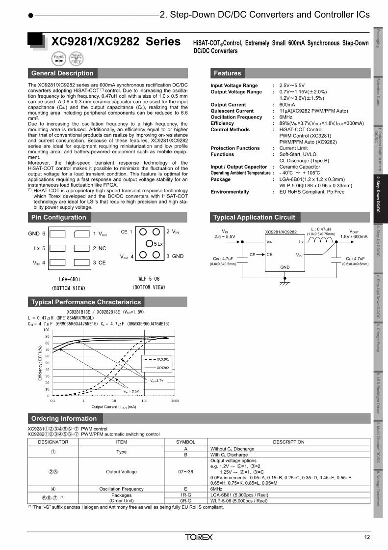
1. Inductor Built-in micro DC/DC Converters ________________________________________________
*GreenOperation-compatible
11
XCL301 Series Inductor Built-in Inverting “micro DC/DC” Converters
General Description
The XCL301 series is a inverting micro DC/DC converter which integrates a P-channel FET, an inductor and a control IC in one tiny package (2.5mm×2.0mm, H=1.00mmMAX). A wide operating voltage range of 2.7V to 5.5V enables support for applications that require an internally fixed outputvoltage (-3.3V). The XCL301 series uses automatic PFM/fixed off time PWM. In automatic PFM/fixed off time PWM control, the IC operates by PFM control when the load is light to achieve high efficiency over the full load range from light to heavy. The device provides a stable inverting power supply to beconfigured using only a SBD and two capacitors connected externally. During stand-by, all circuits are shutdown to reduce current consumption to as low as 0.1μA(TYP) or less. With the built-in UVLO (Under Voltage Lock Out) function, the internal P-channel MOS driver transistor is forced OFF when input voltage becomes 2.2V or lower. The XCL301 integrate CL High Speed discharge function which enables the electric charge at the output capacitor CL to be discharged via the internal discharge.
Features Pin Configuration Input Voltage Range: 2.7V~5.5V Output Voltage: -3.3V Output Voltage accuracy: ±2.0% Output Current: -50mA Internal Driver: 1.2Ω Quiescent Current: 40μA (TYP.) Control Methods: PFM / Fixed off time PWM Auto Transient Response: -50mV (VIN=3.3V,VOUT=-3.3V,IOUT=1mA→50mA) PFM switch Current: 550mA Function: Current Limit Soft-start CL High Speed Discharge UVLO CL High Speed Discharge Operating Ambient Temperature: -40~+85 Package: CL-2025-02 Environmentally Friendly: EU RoHS Compliant, Pb Free
Typical Application Circuit Typical Performance Characteristics
Ordering Information
XCL301①②③④⑤⑥-⑦ DESIGNATOR ITEM SYMBOL DESCRIPTION
① Product Type A CL Discharge, UVLO, Current Limit, Soft-start ②③ Output Voltage 33 Output Voltage = -3.3V ④ PFM Switch Current 1 550mA (TYP.)
⑤⑥-⑦ (*1) Package (Order Unit) ER-G CL-2025-02 (3,000pcs/Reel) (*1) The “-G” suffix denotes Halogen and Antimony free as well as being fully EU RoHS compliant.
(BOTTOM VIEW)
L1
L2
7
8
VIN 6
GND 5
CE 4
1 Lx
2 VOUT
3 NC
L1
L2
1
2
3 4
5
6Lx
VOUT
NC CE
GND
VIN
CIN
10μFCL
10μF
8
7
SD
___________________________________________ 2. Step-Down DC/DC Converters and Controller ICs
12
XC9281/XC9282 Series HiSAT-COTControl, Extremely Small 600mA Synchronous Step-Down DC/DC Converters
General Description Features
The XC9281/XC9282 series are 600mA synchronous rectification DC/DCconverters adopting HiSAT-COT (*) control. Due to increasing the oscilla-tion frequency to high frequency, 0.47uH coil with a size of 1.0 x 0.5 mmcan be used. A 0.6 x 0.3 mm ceramic capacitor can be used for the inputcapacitance (CIN) and the output capacitance (CL), realizing that themounting area including peripheral components can be reduced to 6.6mm2. Due to increasing the oscillation frequency to a high frequency, themounting area is reduced. Additionally, an efficiency equal to or higherthan that of conventional products can realize by improving on-resistanceand current consumption. Because of these features, XC9281/XC9282series are ideal for equipment requiring miniaturization and low profilemounting area, and battery-powered equipment such as mobile equip-ment. Moreover, the high-speed transient response technology of theHiSAT-COT control makes it possible to minimize the fluctuation of theoutput voltage for a load transient condition. This feature is optimal for applications requiring a fast response and output voltage stability for aninstantaneous load fluctuation like FPGA. (*) HiSAT-COT is a proprietary high-speed transient response technology
which Torex developed and the DC/DC converters with HiSAT-COTtechnology are ideal for LSI's that require high precision and high sta-bility power supply voltage.
Input Voltage Range : 2.5V~5.5V Output Voltage Range : 0.7V~1.15V(±2.0%) 1.2V~3.6V(±1.5%) Output Current : 600mA Quiescent Current : 11μA(XC9282 PWM/PFM Auto) Oscillation Frequency : 6MHz Efficiency : 89%(VIN=3.7V,VOUT=1.8V,IOUT=300mA) Control Methods : HiSAT-COT Control PWM Control (XC9281) PWM/PFM Auto (XC9282) Protection Functions : Current Limit Functions : Soft-Start, UVLO CL Discharge (Type B) Input / Output Capacitor : Ceramic Capacitor Operating Ambient Temperature : - 40 ~ + 105 Package : LGA-6B01(1.2 x 1.2 x 0.3mm) WLP-5-06(0.88 x 0.96 x 0.33mm) Environmentally : EU RoHS Compliant, Pb Free
Pin Configuration Typical Application Circuit
Typical Performance Chracteriarics XC9281B18E / XC9282B18E (VOUT=1.8V)
L = 0.47μH (DFE18SANR47MG0L)
CIN = 4.7μF (GRM035R60J475ME15) CL = 4.7μF (GRM035R60J475ME15)
Ordering Information
XC9281①②③④⑤⑥-⑦ PWM control XC9282①②③④⑤⑥-⑦ PWM/PFM automatic switching control
DESIGNATOR ITEM SYMBOL DESCRIPTION
① Type A Without CL Discharge B With CL Discharge
②③ Output Voltage 07~36
Output voltage options e.g. 1.2V → ②=1, ③=2 1.25V → ②=1, ③=C 0.05V increments : 0.05=A, 0.15=B, 0.25=C, 0.35=D, 0.45=E, 0.55=F, 0.65=H, 0.75=K, 0.85=L, 0.95=M
④ Oscillation Frequency E 6MHz
⑤⑥-⑦ (*1) Packages (Order Unit)
1R-G LGA-6B01 (5,000pcs / Reel) 0R-G WLP-5-06 (5,000pcs / Reel)
(*1) The “-G” suffix denotes Halogen and Antimony free as well as being fully EU RoHS compliant.
WLP-5-06
(BOTTOM VIEW)
GND 6
Lx 5
VIN 4
1 Vout
2 NC
3 CE
2 VIN
3 GND
CE 1
Vout 4
5 Lx
VIN
2.5 ~ 5.5V
CIN : 4.7uF(0.6x0.3x0.5mm)
VIN LX
GND
VOUT
L : 0.47uH(1.0x0.5x0.75mm)
CECE
XC9281/XC9282
CL : 4.7uF(0.6x0.3x0.5mm)
VOUT
1.8V / 600mA
1. Inductor Built-in m
icro D
C/D
C
3. Step-Up D
C/D
C4. Step-U
p&D
own D
C/D
C
5.Charge Pum
p6.LED
Backlight D
river8.Voltage D
etectorsSelection G
uidePackaging
7. Multi C
hannel DC
/DC
2. Step-D
own D
C/D
C
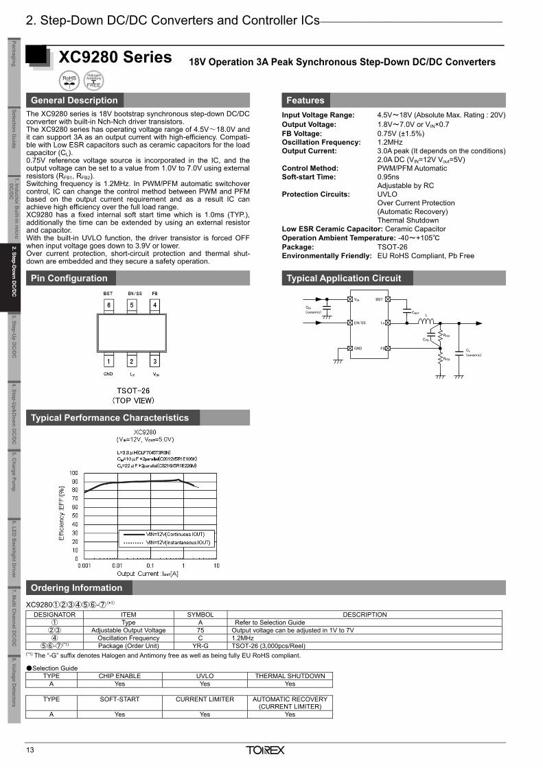
2. Step-Down DC/DC Converters and Controller ICs _____________________________________________
13
XC9280 Series 18V Operation 3A Peak Synchronous Step-Down DC/DC Converters
General Description Features
The XC9280 series is 18V bootstrap synchronous step-down DC/DC converter with built-in Nch-Nch driver transistors. The XC9280 series has operating voltage range of 4.5V~18.0V and it can support 3A as an output current with high-efficiency. Compati-ble with Low ESR capacitors such as ceramic capacitors for the load capacitor (CL). 0.75V reference voltage source is incorporated in the IC, and the output voltage can be set to a value from 1.0V to 7.0V using external resistors (RFB1, RFB2). Switching frequency is 1.2MHz. In PWM/PFM automatic switchover control, IC can change the control method between PWM and PFM based on the output current requirement and as a result IC can achieve high efficiency over the full load range. XC9280 has a fixed internal soft start time which is 1.0ms (TYP.), additionally the time can be extended by using an external resistor and capacitor. With the built-in UVLO function, the driver transistor is forced OFF when input voltage goes down to 3.9V or lower. Over current protection, short-circuit protection and thermal shut-down are embedded and they secure a safety operation.
Input Voltage Range: 4.5V~18V (Absolute Max. Rating : 20V) Output Voltage: 1.8V~7.0V or VIN×0.7 FB Voltage: 0.75V (±1.5%) Oscillation Frequency: 1.2MHz Output Current: 3.0A peak (It depends on the conditions) 2.0A DC (VIN=12V Vout=5V) Control Method: PWM/PFM Automatic Soft-start Time: 0.95ns Adjustable by RC Protection Circuits: UVLO Over Current Protection (Automatic Recovery) Thermal Shutdown Low ESR Ceramic Capacitor: Ceramic Capacitor Operation Ambient Temperature: -40~+105 Package: TSOT-26 Environmentally Friendly: EU RoHS Compliant, Pb Free
Pin Configuration Typical Application Circuit
Typical Performance Characteristics
Ordering Information
XC9280①②③④⑤⑥-⑦(*1) DESIGNATOR ITEM SYMBOL DESCRIPTION
① Type A Refer to Selection Guide ②③ Adjustable Output Voltage 75 Output voltage can be adjusted in 1V to 7V ④ Oscillation Frequency C 1.2MHz
⑤⑥-⑦(*1) Package (Order Unit) YR-G TSOT-26 (3,000pcs/Reel) (*1) The “-G” suffix denotes Halogen and Antimony free as well as being fully EU RoHS compliant. Selection Guide
TYPE CHIP ENABLE UVLO THERMAL SHUTDOWN A Yes Yes Yes
TYPE SOFT-START CURRENT LIMITER AUTOMATIC RECOVERY
(CURRENT LIMITER) A Yes Yes Yes
Lx
BST
FBGND
VIN
EN/SS
CL
(ceramic)
L
RFB1
RFB2
CFB
CIN
(ceramic) CBST
_______________________________________________________________________________________________________
*GreenOperation-compatible
14
XC9273 Series HiSAT-COT® Control, 3A Synchronous Step-Down DC/DC Converters
General Description Features
The XC9273 series is a group of synchronous-rectification type DC/DC con-verters with a built-in P-channel MOS driver transistor and N-channel MOSswitching transistor, designed to allow the use of ceramic capacitors. The smallon-resistance of these two internal driver transistors enable a high efficiency,stable power supply with an output current up to 3.0A. 0.6V reference voltagesource is incorporated, and the output voltage can be set freely by external re-sistors. Oscillation frequency is set to 1.2MHz or 3.0MHz can be selected forsuiting to your particular application. The operation mode is HISAT-COT(*)
control, which has an excellent transient response. PWM control or PWM/PFMauto switching control can be selected at the MODE1 pin, and a high-speedresponse, low ripple, and high efficiency are achieved across the entire loadrange (from light loads to heavy loads). During stand-by, all circuits are shut-down to reduce current consumption to as low as 1.0μA or less. As for thesoft-start function as fast as 0.25ms in typical for quick turn-on. The soft starttime can be set as desired by adding an external capacitance to the SS pin.Internal protection circuits include over current protection, short-circuit protec-tion, and thermal shutdown circuits to enable safe use. Short circuit protectionor Hiccup mode can be selected at the MODE2 pin. Soft-off function can beselected at the MODE3 pin. The package is the QFN0404-24C(4mm X 4mm)(*) HiSAT-COT is a proprietary high-speed transient response technology which
Torex developed and the DC/DC converters with HiSAT-COT technology areideal for LSI's that require high precision and high stability power supplyvoltage.
Input Voltage Range: 2.7V~5.5V (Absolute Max. rating: 6.2V) Output Voltage Range: 0.8V~3.6V FB Voltage: 0.6V (±1.0%) Output Current: 3.0A Oscillation Frequency: 1.2MHz, 3.0MHz Efficiency: 93% (VIN=5.0V, VOUT=1.8V, IOUT=1.0A) Control Methods: HiSAT-COT Control 100% Duty Cycle Mode select between Fixed PWM and PWM/PFM Auto Protection Circuits: Thermal Shutdown Current Limit (Pendent character) HICCUP or Short Circuit Protection Functions: UVLO , Soft-Start, Soft-off CL High Speed Discharge Capacitor: Ceramic Capacitor Operating Ambient Temperature: -40~+105 Package: QFN0404-24C Environmentally Friendly: EU RoHS Compliant, Pb Free
Pin Configuration
Typical Application Circuit Typical Performance Characteristics
Ordering Information
XC9273①②③④⑤⑥-⑦ PWM control PWM/PFM automatic switching control
DESIGNATOR ITEM SYMBOL DESCRIPTION ① Type B Refer to Selection Guide
②③ FB Voltage 06 FB Voltage 0.6V
④ Oscillation Frequency C 1.2MHz D 3.0MHz
⑤⑥-⑦(*1) Package (Order Unit) ZR-G QFN0404-24C (1,000pcs/Reel) (*1) The “-G” suffix denotes Halogen and Antimony free as well as being fully EU RoHS compliant. Selection Guide
TYPE CL AUTO-DISCHARGE WITH SOFT-OFF
SHORT PROTECTION WITH LATCH OR
HICCUP MODE B Yes Yes
TYPE UVLO CHIP ENABLE CURRENT LIMIT SOFT START TIME THERMAL SHUTDOWN B Yes Yes Yes Adjustable Yes
PVIN
AVIN
CE
MODE1
PG
SS
AGND
VOUT
Lx
FB
PGND
MODE2
MODE3
VIN
CIN
CSS
CDD
RDD
RPG
L
CFBRFB1
RFB2
CL
VOUT
XC9273B06C
VOUT=1.8V, fosc=1.2MHz L=0.56μH(MWSA0603),CIN=47μF(GRM31CR61A476ME15L)
CL=47μF(GRM31CR60J476ME19L),RFB1=36kΩ,RFB2=18kΩ,CFB=1500pF
020406080
100
1 10 100 1000 10000
Effi
cien
cy :
EFF
I (%
)
Output Current : IOUT (mA)
PWM/PFM
PWM
VIN =5.0V
1. Inductor Built-in m
icro D
C/D
C
2. Step-Dow
n DC
/DC
3. Step-Up D
C/D
C4. Step-U
p&D
own D
C/D
C
5.Charge Pum
p6.LED
Backlight D
river8.Voltage D
etectorsSelection G
uidePackaging
7. Multi C
hannel DC
/DC
2. Step-D
own D
C/D
C
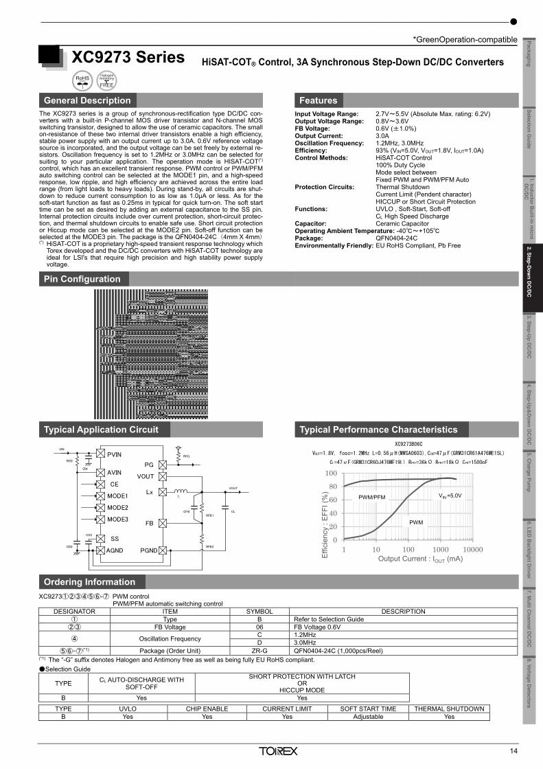
2. Step-Down DC/DC Converters and Controller ICs _____________________________________________
13
XC9280 Series 18V Operation 3A Peak Synchronous Step-Down DC/DC Converters
General Description Features
The XC9280 series is 18V bootstrap synchronous step-down DC/DC converter with built-in Nch-Nch driver transistors. The XC9280 series has operating voltage range of 4.5V~18.0V and it can support 3A as an output current with high-efficiency. Compati-ble with Low ESR capacitors such as ceramic capacitors for the load capacitor (CL). 0.75V reference voltage source is incorporated in the IC, and the output voltage can be set to a value from 1.0V to 7.0V using external resistors (RFB1, RFB2). Switching frequency is 1.2MHz. In PWM/PFM automatic switchover control, IC can change the control method between PWM and PFM based on the output current requirement and as a result IC can achieve high efficiency over the full load range. XC9280 has a fixed internal soft start time which is 1.0ms (TYP.), additionally the time can be extended by using an external resistor and capacitor. With the built-in UVLO function, the driver transistor is forced OFF when input voltage goes down to 3.9V or lower. Over current protection, short-circuit protection and thermal shut-down are embedded and they secure a safety operation.
Input Voltage Range: 4.5V~18V (Absolute Max. Rating : 20V) Output Voltage: 1.8V~7.0V or VIN×0.7 FB Voltage: 0.75V (±1.5%) Oscillation Frequency: 1.2MHz Output Current: 3.0A peak (It depends on the conditions) 2.0A DC (VIN=12V Vout=5V) Control Method: PWM/PFM Automatic Soft-start Time: 0.95ns Adjustable by RC Protection Circuits: UVLO Over Current Protection (Automatic Recovery) Thermal Shutdown Low ESR Ceramic Capacitor: Ceramic Capacitor Operation Ambient Temperature: -40~+105 Package: TSOT-26 Environmentally Friendly: EU RoHS Compliant, Pb Free
Pin Configuration Typical Application Circuit
Typical Performance Characteristics
Ordering Information
XC9280①②③④⑤⑥-⑦(*1) DESIGNATOR ITEM SYMBOL DESCRIPTION
① Type A Refer to Selection Guide ②③ Adjustable Output Voltage 75 Output voltage can be adjusted in 1V to 7V ④ Oscillation Frequency C 1.2MHz
⑤⑥-⑦(*1) Package (Order Unit) YR-G TSOT-26 (3,000pcs/Reel) (*1) The “-G” suffix denotes Halogen and Antimony free as well as being fully EU RoHS compliant. Selection Guide
TYPE CHIP ENABLE UVLO THERMAL SHUTDOWN A Yes Yes Yes
TYPE SOFT-START CURRENT LIMITER AUTOMATIC RECOVERY
(CURRENT LIMITER) A Yes Yes Yes
Lx
BST
FBGND
VIN
EN/SS
CL
(ceramic)
L
RFB1
RFB2
CFB
CIN
(ceramic) CBST
_______________________________________________________________________________________________________
*GreenOperation-compatible
14
XC9273 Series HiSAT-COT® Control, 3A Synchronous Step-Down DC/DC Converters
General Description Features
The XC9273 series is a group of synchronous-rectification type DC/DC con-verters with a built-in P-channel MOS driver transistor and N-channel MOSswitching transistor, designed to allow the use of ceramic capacitors. The smallon-resistance of these two internal driver transistors enable a high efficiency,stable power supply with an output current up to 3.0A. 0.6V reference voltagesource is incorporated, and the output voltage can be set freely by external re-sistors. Oscillation frequency is set to 1.2MHz or 3.0MHz can be selected forsuiting to your particular application. The operation mode is HISAT-COT(*)
control, which has an excellent transient response. PWM control or PWM/PFMauto switching control can be selected at the MODE1 pin, and a high-speedresponse, low ripple, and high efficiency are achieved across the entire loadrange (from light loads to heavy loads). During stand-by, all circuits are shut-down to reduce current consumption to as low as 1.0μA or less. As for thesoft-start function as fast as 0.25ms in typical for quick turn-on. The soft starttime can be set as desired by adding an external capacitance to the SS pin.Internal protection circuits include over current protection, short-circuit protec-tion, and thermal shutdown circuits to enable safe use. Short circuit protectionor Hiccup mode can be selected at the MODE2 pin. Soft-off function can beselected at the MODE3 pin. The package is the QFN0404-24C(4mm X 4mm)(*) HiSAT-COT is a proprietary high-speed transient response technology which
Torex developed and the DC/DC converters with HiSAT-COT technology areideal for LSI's that require high precision and high stability power supplyvoltage.
Input Voltage Range: 2.7V~5.5V (Absolute Max. rating: 6.2V) Output Voltage Range: 0.8V~3.6V FB Voltage: 0.6V (±1.0%) Output Current: 3.0A Oscillation Frequency: 1.2MHz, 3.0MHz Efficiency: 93% (VIN=5.0V, VOUT=1.8V, IOUT=1.0A) Control Methods: HiSAT-COT Control 100% Duty Cycle Mode select between Fixed PWM and PWM/PFM Auto Protection Circuits: Thermal Shutdown Current Limit (Pendent character) HICCUP or Short Circuit Protection Functions: UVLO , Soft-Start, Soft-off CL High Speed Discharge Capacitor: Ceramic Capacitor Operating Ambient Temperature: -40~+105 Package: QFN0404-24C Environmentally Friendly: EU RoHS Compliant, Pb Free
Pin Configuration
Typical Application Circuit Typical Performance Characteristics
Ordering Information
XC9273①②③④⑤⑥-⑦ PWM control PWM/PFM automatic switching control
DESIGNATOR ITEM SYMBOL DESCRIPTION ① Type B Refer to Selection Guide
②③ FB Voltage 06 FB Voltage 0.6V
④ Oscillation Frequency C 1.2MHz D 3.0MHz
⑤⑥-⑦(*1) Package (Order Unit) ZR-G QFN0404-24C (1,000pcs/Reel) (*1) The “-G” suffix denotes Halogen and Antimony free as well as being fully EU RoHS compliant. Selection Guide
TYPE CL AUTO-DISCHARGE WITH SOFT-OFF
SHORT PROTECTION WITH LATCH OR
HICCUP MODE B Yes Yes
TYPE UVLO CHIP ENABLE CURRENT LIMIT SOFT START TIME THERMAL SHUTDOWN B Yes Yes Yes Adjustable Yes
PVIN
AVIN
CE
MODE1
PG
SS
AGND
VOUT
Lx
FB
PGND
MODE2
MODE3
VIN
CIN
CSS
CDD
RDD
RPG
L
CFBRFB1
RFB2
CL
VOUT
XC9273B06C
VOUT=1.8V, fosc=1.2MHz L=0.56μH(MWSA0603),CIN=47μF(GRM31CR61A476ME15L)
CL=47μF(GRM31CR60J476ME19L),RFB1=36kΩ,RFB2=18kΩ,CFB=1500pF
020406080
100
1 10 100 1000 10000
Effi
cien
cy :
EFF
I (%
)
Output Current : IOUT (mA)
PWM/PFM
PWM
VIN =5.0V
1. Inductor Built-in m
icro D
C/D
C
3. Step-Up D
C/D
C4. Step-U
p&D
own D
C/D
C
5.Charge Pum
p6.LED
Backlight D
river8.Voltage D
etectorsSelection G
uidePackaging
7. Multi C
hannel DC
/DC
2. Step-D
own D
C/D
C
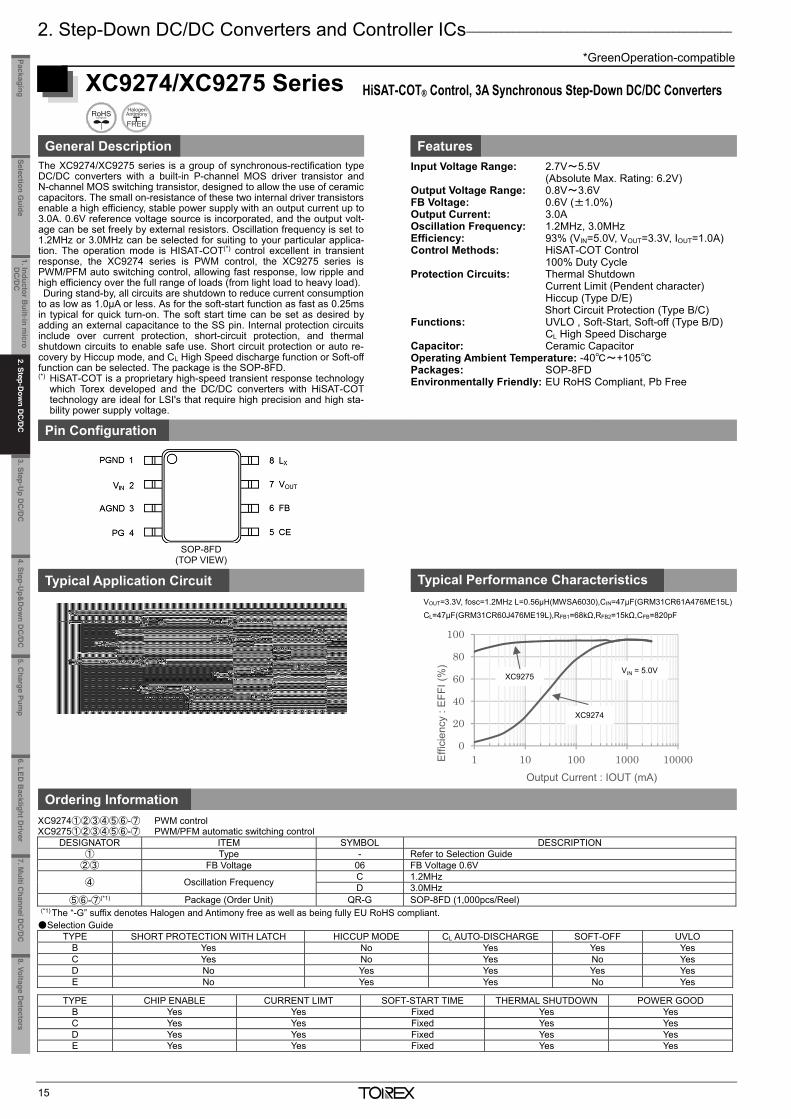
2. Step-Down DC/DC Converters and Controller ICs _____________________________________________
*GreenOperation-compatible
15
XC9274/XC9275 Series HiSAT-COT® Control, 3A Synchronous Step-Down DC/DC Converters
General Description Features
The XC9274/XC9275 series is a group of synchronous-rectification type DC/DC converters with a built-in P-channel MOS driver transistor and N-channel MOS switching transistor, designed to allow the use of ceramic capacitors. The small on-resistance of these two internal driver transistors enable a high efficiency, stable power supply with an output current up to 3.0A. 0.6V reference voltage source is incorporated, and the output volt-age can be set freely by external resistors. Oscillation frequency is set to 1.2MHz or 3.0MHz can be selected for suiting to your particular applica-tion. The operation mode is HISAT-COT(*) control excellent in transient response, the XC9274 series is PWM control, the XC9275 series is PWM/PFM auto switching control, allowing fast response, low ripple and high efficiency over the full range of loads (from light load to heavy load). During stand-by, all circuits are shutdown to reduce current consumption to as low as 1.0μA or less. As for the soft-start function as fast as 0.25ms in typical for quick turn-on. The soft start time can be set as desired by adding an external capacitance to the SS pin. Internal protection circuits include over current protection, short-circuit protection, and thermal shutdown circuits to enable safe use. Short circuit protection or auto re-covery by Hiccup mode, and CL High Speed discharge function or Soft-off function can be selected. The package is the SOP-8FD. (*) HiSAT-COT is a proprietary high-speed transient response technology
which Torex developed and the DC/DC converters with HiSAT-COT technology are ideal for LSI's that require high precision and high sta-bility power supply voltage.
Input Voltage Range: 2.7V~5.5V (Absolute Max. Rating: 6.2V)
Output Voltage Range: 0.8V~3.6V FB Voltage: 0.6V (±1.0%) Output Current: 3.0A Oscillation Frequency: 1.2MHz, 3.0MHz Efficiency: 93% (VIN=5.0V, VOUT=3.3V, IOUT=1.0A) Control Methods: HiSAT-COT Control 100% Duty Cycle Protection Circuits: Thermal Shutdown Current Limit (Pendent character) Hiccup (Type D/E) Short Circuit Protection (Type B/C) Functions: UVLO , Soft-Start, Soft-off (Type B/D) CL High Speed Discharge Capacitor: Ceramic Capacitor Operating Ambient Temperature: -40~+105 Packages: SOP-8FD Environmentally Friendly: EU RoHS Compliant, Pb Free
Pin Configuration
Typical Application Circuit Typical Performance Characteristics
Ordering Information
XC9274①②③④⑤⑥-⑦ PWM control XC9275①②③④⑤⑥-⑦ PWM/PFM automatic switching control
DESIGNATOR ITEM SYMBOL DESCRIPTION ① Type - Refer to Selection Guide
②③ FB Voltage 06 FB Voltage 0.6V
④ Oscillation Frequency C 1.2MHz D 3.0MHz
⑤⑥-⑦(*1) Package (Order Unit) QR-G SOP-8FD (1,000pcs/Reel) (*1) The “-G” suffix denotes Halogen and Antimony free as well as being fully EU RoHS compliant. Selection Guide
TYPE SHORT PROTECTION WITH LATCH HICCUP MODE CL AUTO-DISCHARGE SOFT-OFF UVLO B Yes No Yes Yes Yes C Yes No Yes No Yes D No Yes Yes Yes Yes E No Yes Yes No Yes
TYPE CHIP ENABLE CURRENT LIMT SOFT-START TIME THERMAL SHUTDOWN POWER GOOD
B Yes Yes Fixed Yes Yes C Yes Yes Fixed Yes Yes D Yes Yes Fixed Yes Yes E Yes Yes Fixed Yes Yes
0
20
40
60
80
100
1 10 100 1000 10000Effi
cien
cy :
EFF
I (%
)
Output Current : IOUT (mA)
XC9275
XC9274
VIN = 5.0V
SOP-8FD (TOP VIEW)
VOUT=3.3V, fosc=1.2MHz L=0.56μH(MWSA6030),CIN=47μF(GRM31CR61A476ME15L)
CL=47μF(GRM31CR60J476ME19L),RFB1=68kΩ,RFB2=15kΩ,CFB=820pF
_______________________________________________________________________________________________________
*GreenOperation-compatible
16
XC9272 Series Ultra Low Power Synchronous Step-Down PFM DC/DC Converter for Low Output Voltage
General Description Features
XC9272 series are Ultra Low Power synchronous-rectification typePFM step down DC/DC converters with a built-in 0.4Ω (TYP.) Pchdriver and 0.4Ω (TYP.) Nch synchronous switching transistor, de-signed to allow the use of ceramic capacitor. PFM control enables a low quiescent current, making these productsideal for battery operated devices that require high efficiency andlong battery life. Only inductor, CIN and CL capacitors are needed as external parts tomake a step down DC/DC circuit. Operation voltage range is from 2.0V to 6.0V. This product has fixedoutput voltage from 0.6V to 0.95V(accuracy: ±20mV) in increments of0.05V. During stand-by, all circuits are shutdown to reduce consumption toas low as 0.1μA(TYP.) or less. With the built-in UVLO (Under Voltage Lock Out) function, the inter-nal P-channel MOS driver transistor is forced OFF when input volt-age gets lower than UVLO detection voltage. Besides, XC9272 se-ries has UVLO release voltage of 1.8V (TYP.). The product with CL discharge function, XC9272B type, can dis-charge CL capacitor during stand-by mode due to the internal re-sistance by turning on the internal switch between VOUT -GND. Thisenables output voltage restored to GND level fast.
Input Voltage Range: 2.0V~6.0V (Absolute Max. Rating: 7.0V) Output Voltage Setting: 0.6V~0.95V
(±20mV, 0.05V step increments) Output Current: 50mA Driver Transistor: 0.4Ω (Pch Driver Tr) 0.4Ω (Nch Synchronous rectifier Switch Tr) Supply Current: 0.50μA @ VOUT(T)=0.7V (TYP.) Control Method: PFM control High Speed Transient: 50mV (VIN=3.6V, VOUT=0.7V, IOUT=10μA
→50mA) PFM Switching Current: 180mA Function: Short Protection CL Discharge(XC9272B) UVLO Ceramic Capacitor Compatible Operation Ambient Temperature: -40~+85 Packages: SOT-25, USP-6EL Environmentally Friendly: EU RoHS compliant, Pb Free
Pin Configuration
Typical Application Circuit Typical Performance Characteristics
Efficiency vs. Output Current
Ordering Information
XC9272①②③④⑤⑥-⑦ DESIGNATOR ITEM SYMBOL DESCRIPTION
① Product Type A Without CL Discharge B With CL Discharge
②③ Output Voltage 06~09 Output Voltage : e.g. VOUT=0.7V⇒②=0, ③=7 Output Voltage Range: 0.6V~0.95V (0.05V step)
④ Output Voltage Type 1 Output Voltage x.x0V (the 2nd decimal place is “0”)
B Output Voltage x.x5V (the 2nd decimal place is “5”)
⑤⑥-⑦(*1) Packages (Order Unit) 4R-G USP-6EL (3,000pcs/Reel) MR-G SOT-25 (3,000pcs/Reel)
(*1) The “-G” suffix denotes Halogen and Antimony free as well as being fully EU RoHS compliant.
LXVIN
VOUT
GND
CE
VIN
CIN(Ceramic) CL
(Ceramic)
VOUTL
0
20
40
60
80
100
0.01 0.1 1 10 100
Effic
ienc
y : E
FFI (
%)
Output Current : IOUT (mA)
VIN=2.0V
XC9272A071xR-G(VOUT=0.7V)L=10μH(VLF302512M-100M),CIN=10μF(LMK107BJ106MA),
CL=22μF(JMK107BJ226MA)
VIN=3.6V
1 32
5 4
VIN
VOUT
SOT-25(TOP VIEW)
LX
CEGNDUSP-6EL
(BOTTOM VIEW)
34
2
1
5
6VIN
CE
LX
GND
VOUT
NC
1. Inductor Built-in m
icro D
C/D
C
2. Step-Dow
n DC
/DC
3. Step-Up D
C/D
C4. Step-U
p&D
own D
C/D
C
5.Charge Pum
p6.LED
Backlight D
river8.Voltage D
etectorsSelection G
uidePackaging
7. Multi C
hannel DC
/DC
2. Step-D
own D
C/D
C
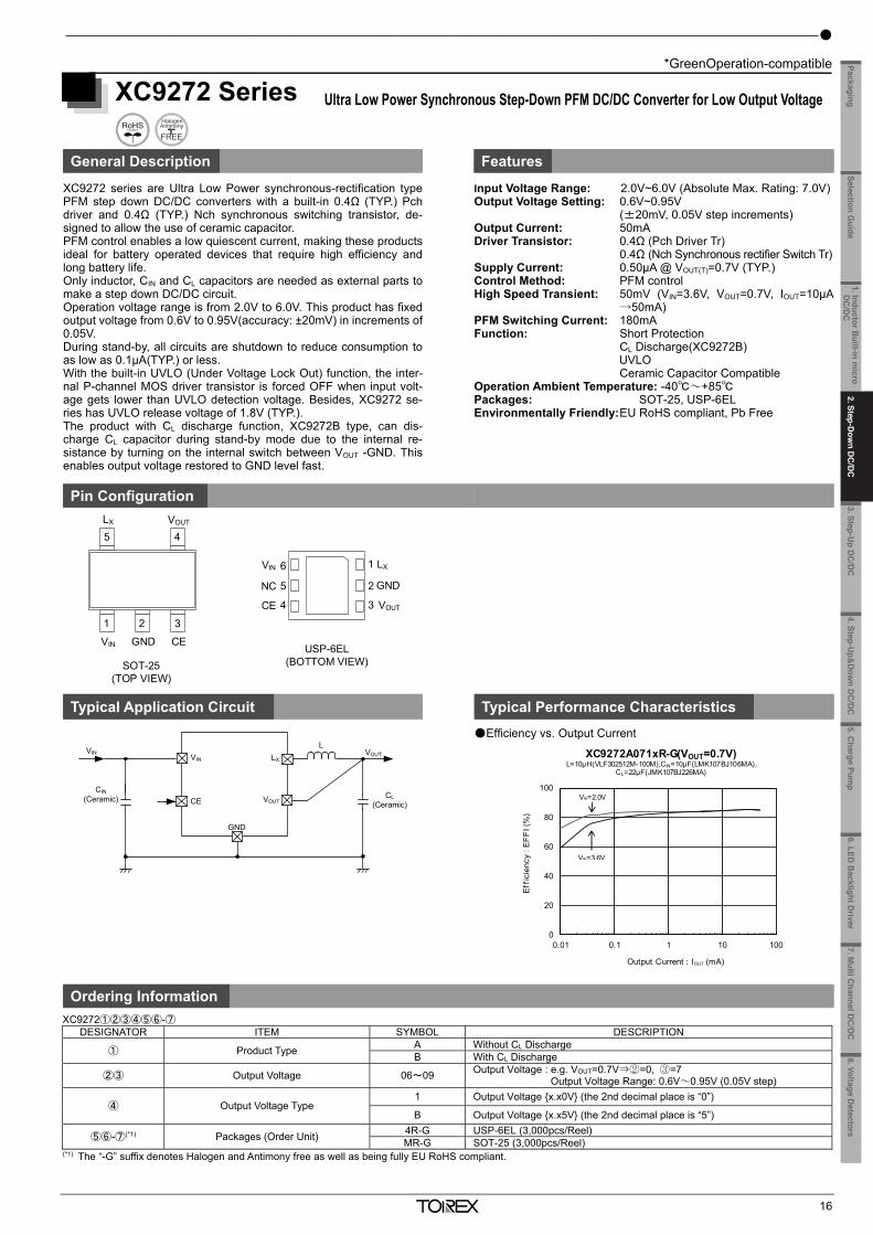
2. Step-Down DC/DC Converters and Controller ICs _____________________________________________
*GreenOperation-compatible
15
XC9274/XC9275 Series HiSAT-COT® Control, 3A Synchronous Step-Down DC/DC Converters
General Description Features
The XC9274/XC9275 series is a group of synchronous-rectification type DC/DC converters with a built-in P-channel MOS driver transistor and N-channel MOS switching transistor, designed to allow the use of ceramic capacitors. The small on-resistance of these two internal driver transistors enable a high efficiency, stable power supply with an output current up to 3.0A. 0.6V reference voltage source is incorporated, and the output volt-age can be set freely by external resistors. Oscillation frequency is set to 1.2MHz or 3.0MHz can be selected for suiting to your particular applica-tion. The operation mode is HISAT-COT(*) control excellent in transient response, the XC9274 series is PWM control, the XC9275 series is PWM/PFM auto switching control, allowing fast response, low ripple and high efficiency over the full range of loads (from light load to heavy load). During stand-by, all circuits are shutdown to reduce current consumption to as low as 1.0μA or less. As for the soft-start function as fast as 0.25ms in typical for quick turn-on. The soft start time can be set as desired by adding an external capacitance to the SS pin. Internal protection circuits include over current protection, short-circuit protection, and thermal shutdown circuits to enable safe use. Short circuit protection or auto re-covery by Hiccup mode, and CL High Speed discharge function or Soft-off function can be selected. The package is the SOP-8FD. (*) HiSAT-COT is a proprietary high-speed transient response technology
which Torex developed and the DC/DC converters with HiSAT-COT technology are ideal for LSI's that require high precision and high sta-bility power supply voltage.
Input Voltage Range: 2.7V~5.5V (Absolute Max. Rating: 6.2V)
Output Voltage Range: 0.8V~3.6V FB Voltage: 0.6V (±1.0%) Output Current: 3.0A Oscillation Frequency: 1.2MHz, 3.0MHz Efficiency: 93% (VIN=5.0V, VOUT=3.3V, IOUT=1.0A) Control Methods: HiSAT-COT Control 100% Duty Cycle Protection Circuits: Thermal Shutdown Current Limit (Pendent character) Hiccup (Type D/E) Short Circuit Protection (Type B/C) Functions: UVLO , Soft-Start, Soft-off (Type B/D) CL High Speed Discharge Capacitor: Ceramic Capacitor Operating Ambient Temperature: -40~+105 Packages: SOP-8FD Environmentally Friendly: EU RoHS Compliant, Pb Free
Pin Configuration
Typical Application Circuit Typical Performance Characteristics
Ordering Information
XC9274①②③④⑤⑥-⑦ PWM control XC9275①②③④⑤⑥-⑦ PWM/PFM automatic switching control
DESIGNATOR ITEM SYMBOL DESCRIPTION ① Type - Refer to Selection Guide
②③ FB Voltage 06 FB Voltage 0.6V
④ Oscillation Frequency C 1.2MHz D 3.0MHz
⑤⑥-⑦(*1) Package (Order Unit) QR-G SOP-8FD (1,000pcs/Reel) (*1) The “-G” suffix denotes Halogen and Antimony free as well as being fully EU RoHS compliant. Selection Guide
TYPE SHORT PROTECTION WITH LATCH HICCUP MODE CL AUTO-DISCHARGE SOFT-OFF UVLO B Yes No Yes Yes Yes C Yes No Yes No Yes D No Yes Yes Yes Yes E No Yes Yes No Yes
TYPE CHIP ENABLE CURRENT LIMT SOFT-START TIME THERMAL SHUTDOWN POWER GOOD
B Yes Yes Fixed Yes Yes C Yes Yes Fixed Yes Yes D Yes Yes Fixed Yes Yes E Yes Yes Fixed Yes Yes
0
20
40
60
80
100
1 10 100 1000 10000Effi
cien
cy :
EFF
I (%
)
Output Current : IOUT (mA)
XC9275
XC9274
VIN = 5.0V
SOP-8FD (TOP VIEW)
VOUT=3.3V, fosc=1.2MHz L=0.56μH(MWSA6030),CIN=47μF(GRM31CR61A476ME15L)
CL=47μF(GRM31CR60J476ME19L),RFB1=68kΩ,RFB2=15kΩ,CFB=820pF
_______________________________________________________________________________________________________
*GreenOperation-compatible
16
XC9272 Series Ultra Low Power Synchronous Step-Down PFM DC/DC Converter for Low Output Voltage
General Description Features
XC9272 series are Ultra Low Power synchronous-rectification typePFM step down DC/DC converters with a built-in 0.4Ω (TYP.) Pchdriver and 0.4Ω (TYP.) Nch synchronous switching transistor, de-signed to allow the use of ceramic capacitor. PFM control enables a low quiescent current, making these productsideal for battery operated devices that require high efficiency andlong battery life. Only inductor, CIN and CL capacitors are needed as external parts tomake a step down DC/DC circuit. Operation voltage range is from 2.0V to 6.0V. This product has fixedoutput voltage from 0.6V to 0.95V(accuracy: ±20mV) in increments of0.05V. During stand-by, all circuits are shutdown to reduce consumption toas low as 0.1μA(TYP.) or less. With the built-in UVLO (Under Voltage Lock Out) function, the inter-nal P-channel MOS driver transistor is forced OFF when input volt-age gets lower than UVLO detection voltage. Besides, XC9272 se-ries has UVLO release voltage of 1.8V (TYP.). The product with CL discharge function, XC9272B type, can dis-charge CL capacitor during stand-by mode due to the internal re-sistance by turning on the internal switch between VOUT -GND. Thisenables output voltage restored to GND level fast.
Input Voltage Range: 2.0V~6.0V (Absolute Max. Rating: 7.0V) Output Voltage Setting: 0.6V~0.95V
(±20mV, 0.05V step increments) Output Current: 50mA Driver Transistor: 0.4Ω (Pch Driver Tr) 0.4Ω (Nch Synchronous rectifier Switch Tr) Supply Current: 0.50μA @ VOUT(T)=0.7V (TYP.) Control Method: PFM control High Speed Transient: 50mV (VIN=3.6V, VOUT=0.7V, IOUT=10μA
→50mA) PFM Switching Current: 180mA Function: Short Protection CL Discharge(XC9272B) UVLO Ceramic Capacitor Compatible Operation Ambient Temperature: -40~+85 Packages: SOT-25, USP-6EL Environmentally Friendly: EU RoHS compliant, Pb Free
Pin Configuration
Typical Application Circuit Typical Performance Characteristics
Efficiency vs. Output Current
Ordering Information
XC9272①②③④⑤⑥-⑦ DESIGNATOR ITEM SYMBOL DESCRIPTION
① Product Type A Without CL Discharge B With CL Discharge
②③ Output Voltage 06~09 Output Voltage : e.g. VOUT=0.7V⇒②=0, ③=7 Output Voltage Range: 0.6V~0.95V (0.05V step)
④ Output Voltage Type 1 Output Voltage x.x0V (the 2nd decimal place is “0”)
B Output Voltage x.x5V (the 2nd decimal place is “5”)
⑤⑥-⑦(*1) Packages (Order Unit) 4R-G USP-6EL (3,000pcs/Reel) MR-G SOT-25 (3,000pcs/Reel)
(*1) The “-G” suffix denotes Halogen and Antimony free as well as being fully EU RoHS compliant.
LXVIN
VOUT
GND
CE
VIN
CIN(Ceramic) CL
(Ceramic)
VOUTL
0
20
40
60
80
100
0.01 0.1 1 10 100
Effic
ienc
y : E
FFI (
%)
Output Current : IOUT (mA)
VIN=2.0V
XC9272A071xR-G(VOUT=0.7V)L=10μH(VLF302512M-100M),CIN=10μF(LMK107BJ106MA),
CL=22μF(JMK107BJ226MA)
VIN=3.6V
1 32
5 4
VIN
VOUT
SOT-25(TOP VIEW)
LX
CEGNDUSP-6EL
(BOTTOM VIEW)
34
2
1
5
6VIN
CE
LX
GND
VOUT
NC
1. Inductor Built-in m
icro D
C/D
C
3. Step-Up D
C/D
C4. Step-U
p&D
own D
C/D
C
5.Charge Pum
p6.LED
Backlight D
river8.Voltage D
etectorsSelection G
uidePackaging
7. Multi C
hannel DC
/DC
2. Step-D
own D
C/D
C
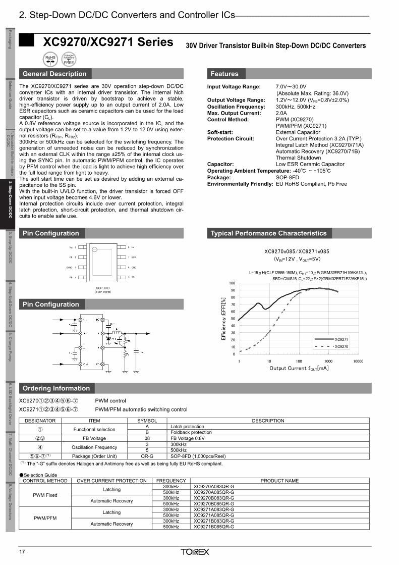
2. Step-Down DC/DC Converters and Controller ICs _____________________________________________
17
XC9270/XC9271 Series 30V Driver Transistor Built-in Step-Down DC/DC Converters
General Description Features
The XC9270/XC9271 series are 30V operation step-down DC/DC converter ICs with an internal driver transistor. The internal Nch driver transistor is driven by bootstrap to achieve a stable, high-efficiency power supply up to an output current of 2.0A. Low ESR capacitors such as ceramic capacitors can be used for the load capacitor (CL). A 0.8V reference voltage source is incorporated in the IC, and the output voltage can be set to a value from 1.2V to 12.0V using exter-nal resistors (RFB1, RFB2). 300kHz or 500kHz can be selected for the switching frequency. The generation of unneeded noise can be reduced by synchronization with an external CLK within the range ±25% of the internal clock us-ing the SYNC pin. In automatic PWM/PFM control, the IC operates by PFM control when the load is light to achieve high efficiency over the full load range from light to heavy. The soft start time can be set as desired by adding an external ca-pacitance to the SS pin. With the built-in UVLO function, the driver transistor is forced OFF when input voltage becomes 4.6V or lower. Internal protection circuits include over current protection, integral latch protection, short-circuit protection, and thermal shutdown cir-cuits to enable safe use.
Input Voltage Range: 7.0V~30.0V (Absolute Max. Rating: 36.0V)
Output Voltage Range: 1.2V~12.0V (VFB=0.8V±2.0%) Oscillation Frequency: 300kHz, 500kHz Max. Output Current: 2.0A Control Method: PWM (XC9270) PWM/PFM (XC9271) Soft-start: External Capacitor Protection Circuit: Over Current Protection 3.2A (TYP.) Integral Latch Method (XC9270/71A) Automatic Recovery (XC9270/71B) Thermal Shutdown Capacitor: Low ESR Ceramic Capacitor Operating Ambient Temperature: -40 ~ +105 Package: SOP-8FD Environmentally Friendly: EU RoHS Compliant, Pb Free
Pin Configuration Typical Performance Characteristics
Pin Configuration
Ordering Information
XC9270①②③④⑤⑥-⑦ PWM control XC9271①②③④⑤⑥-⑦ PWM/PFM automatic switching control
DESIGNATOR ITEM SYMBOL DESCRIPTION
① Functional selection A Latch protection B Foldback protection
②③ FB Voltage 08 FB Voltage 0.8V
④ Oscillation Frequency 3 300kHz 5 500kHz
⑤⑥-⑦(*1) Package (Order Unit) QR-G SOP-8FD (1,000pcs/Reel) (*1) The “-G” suffix denotes Halogen and Antimony free as well as being fully EU RoHS compliant. Selection Guide
CONTROL METHOD OVER CURRENT PROTECTION FREQUENCY PRODUCT NAME
PWM Fixed Latching 300kHz XC9270A083QR-G
500kHz XC9270A085QR-G
Automatic Recovery 300kHz XC9270B083QR-G 500kHz XC9270B085QR-G
PWM/PFM Latching 300kHz XC9271A083QR-G
500kHz XC9271A085QR-G
Automatic Recovery 300kHz XC9271B083QR-G 500kHz XC9271B085QR-G
VIN
SOP-8FD(TOP VIEW)
1
2
3
4
8
7
6
5
CE
SYNC
FB
Lx
BST
GND
SS
XC9270x085/XC9271x085
(VIN=12V , VOUT=5V)
0
10
20
30
40
50
60
70
80
90
100
1 10 100 1000 10000
Output Current :IOUT[mA]
Effic
iency
:EFFI[
%]
XC9271
XC9270
L=15μH(CLF12555-150M), CIN1=10μF(GRM32ER71H106KA12L),SBD=CMS15, CL=22μF×2(GRM32ER71E226KE15L)
_______________________________________________________________________________________________________
*GreenOperation-compatible
18
XC9267/XC9268 Series 36V Operation 600mA Synchronous Step-Down DC/DC Converters
General Description Features
The XC9267/XC9268 series are 36V operation synchronous step-downDC/DC converter ICs with a built-in P-channel MOS driver transistor andN-channel MOS switching transistor. The XC9267/XC9268 series hasoperating voltage range of 3.0V~36.0V and high-efficiency power supplyup to an output current of 600mA. Low ESR capacitors such as ceramiccapacitors can be used for the load capacitor (CL). A 0.75V reference voltage source is incorporated in the IC, and the outputvoltage can be set to a value from 1.0V to 25.0V using external resistors(RFB1, RFB2). 1.2MHz or 2.2MHz can be selected for the switching frequency. In auto-matic PWM/PFM control, the IC operates by PFM control when the load islight to achieve high efficiency over the full load range from light to heavy. The soft-start time is internally set to 2.0ms (TYP.), but can be adjusted toset a longer time using an external resistor and capacitor. With the built-in UVLO function, the driver transistor is forced OFF wheninput voltage becomes 2.7V or lower. The output state can be monitored using the power good function. Internal protection circuits include over current protection, short-circuitprotection, and thermal shutdown circuits to enable safe use.
Input Voltage Range: 3~36V (Absolute Max. Rating: 40V) Output Voltage Range: 1.0V~25V FB Voltage: 0.75V (±1.5%) Oscillation Frequency: 1.2MHz, 2.2MHz Output Current: 600mA Control Methods: PWM Control (XC9267) PWM/PFM Auto (XC9268) Efficiency 85%@12V→5V, 1mA Soft-start Time: Adjustable by RC Protection Circuits: Over Current Protection Thermal Shutdown Short-circuit Protection Low ESR Ceramic Capacitor: Ceramic Capacitor Operating Ambient Temperature: -40~+105 Packages: SOT-89-5 (Without Power Good) : USP-6C (With Power Good) Environmentally Friendly EU RoHS Compliant, Pb Free
Pin Configuration
Typical Application Circuit Typical Performance Characteristics
Ordering Information
XC9267①②③④⑤⑥-⑦(*1) PWM control XC9268①②③④⑤⑥-⑦(*1) PWM/PFM Auto
DESIGNATOR ITEM SYMBOL DESCRIPTION ① Type B Refer to Selection Guide
②③ FB Voltage 75 FB Voltage 0.75V
④ Oscillation Frequency C 1.2MHz D 2.2MHz
⑤⑥-⑦(*1) Packages (Order Unit) PR-G SOT-89-5 (1,000pcs/Reel) ER-G USP-6C (3,000pcs/Reel)
(*1) The “-G” suffix denotes Halogen and Antimony free as well as being fully RoHS compliant. Selection Guide
TYPE Packages Current Limiter Automatic Recovery (Current Limiter) Chip Enable B PR-G YES YES YES
TYPE Packages UVLO Thermal Shutdown Soft Start POWER GOOD
B PR-G YES YES YES NO
TYPE Packages Current Limiter Automatic Recovery (Current Limiter) Chip Enable B ER-G YES YES YES
TYPE Packages UVLO Thermal Shutdown Soft Start POWER GOOD
B ER-G YES YES YES YES
0102030405060708090
100
0.1 1 10 100 1000
Effi
cien
cy :E
FFI[%
]
Output Current :IOUT[mA]
XC9268B75C (PWM/PFM Auto)(VIN=12V, VOUT=5V)
L=6.8μH, CIN=2.2μF, CL=10μF
1. Inductor Built-in m
icro D
C/D
C
2. Step-Dow
n DC
/DC
3. Step-Up D
C/D
C4. Step-U
p&D
own D
C/D
C
5.Charge Pum
p6.LED
Backlight D
river8.Voltage D
etectorsSelection G
uidePackaging
7. Multi C
hannel DC
/DC
2. Step-D
own D
C/D
C
2. Step-Down DC/DC Converters and Controller ICs _____________________________________________
17
XC9270/XC9271 Series 30V Driver Transistor Built-in Step-Down DC/DC Converters
General Description Features
The XC9270/XC9271 series are 30V operation step-down DC/DC converter ICs with an internal driver transistor. The internal Nch driver transistor is driven by bootstrap to achieve a stable, high-efficiency power supply up to an output current of 2.0A. Low ESR capacitors such as ceramic capacitors can be used for the load capacitor (CL). A 0.8V reference voltage source is incorporated in the IC, and the output voltage can be set to a value from 1.2V to 12.0V using exter-nal resistors (RFB1, RFB2). 300kHz or 500kHz can be selected for the switching frequency. The generation of unneeded noise can be reduced by synchronization with an external CLK within the range ±25% of the internal clock us-ing the SYNC pin. In automatic PWM/PFM control, the IC operates by PFM control when the load is light to achieve high efficiency over the full load range from light to heavy. The soft start time can be set as desired by adding an external ca-pacitance to the SS pin. With the built-in UVLO function, the driver transistor is forced OFF when input voltage becomes 4.6V or lower. Internal protection circuits include over current protection, integral latch protection, short-circuit protection, and thermal shutdown cir-cuits to enable safe use.
Input Voltage Range: 7.0V~30.0V (Absolute Max. Rating: 36.0V)
Output Voltage Range: 1.2V~12.0V (VFB=0.8V±2.0%) Oscillation Frequency: 300kHz, 500kHz Max. Output Current: 2.0A Control Method: PWM (XC9270) PWM/PFM (XC9271) Soft-start: External Capacitor Protection Circuit: Over Current Protection 3.2A (TYP.) Integral Latch Method (XC9270/71A) Automatic Recovery (XC9270/71B) Thermal Shutdown Capacitor: Low ESR Ceramic Capacitor Operating Ambient Temperature: -40 ~ +105 Package: SOP-8FD Environmentally Friendly: EU RoHS Compliant, Pb Free
Pin Configuration Typical Performance Characteristics
Pin Configuration
Ordering Information
XC9270①②③④⑤⑥-⑦ PWM control XC9271①②③④⑤⑥-⑦ PWM/PFM automatic switching control
DESIGNATOR ITEM SYMBOL DESCRIPTION
① Functional selection A Latch protection B Foldback protection
②③ FB Voltage 08 FB Voltage 0.8V
④ Oscillation Frequency 3 300kHz 5 500kHz
⑤⑥-⑦(*1) Package (Order Unit) QR-G SOP-8FD (1,000pcs/Reel) (*1) The “-G” suffix denotes Halogen and Antimony free as well as being fully EU RoHS compliant. Selection Guide
CONTROL METHOD OVER CURRENT PROTECTION FREQUENCY PRODUCT NAME
PWM Fixed Latching 300kHz XC9270A083QR-G
500kHz XC9270A085QR-G
Automatic Recovery 300kHz XC9270B083QR-G 500kHz XC9270B085QR-G
PWM/PFM Latching 300kHz XC9271A083QR-G
500kHz XC9271A085QR-G
Automatic Recovery 300kHz XC9271B083QR-G 500kHz XC9271B085QR-G
VIN
SOP-8FD(TOP VIEW)
1
2
3
4
8
7
6
5
CE
SYNC
FB
Lx
BST
GND
SS
XC9270x085/XC9271x085
(VIN=12V , VOUT=5V)
0
10
20
30
40
50
60
70
80
90
100
1 10 100 1000 10000
Output Current :IOUT[mA]
Effic
iency
:EFFI[
%]
XC9271
XC9270
L=15μH(CLF12555-150M), CIN1=10μF(GRM32ER71H106KA12L),SBD=CMS15, CL=22μF×2(GRM32ER71E226KE15L)
_______________________________________________________________________________________________________
*GreenOperation-compatible
18
XC9267/XC9268 Series 36V Operation 600mA Synchronous Step-Down DC/DC Converters
General Description Features
The XC9267/XC9268 series are 36V operation synchronous step-downDC/DC converter ICs with a built-in P-channel MOS driver transistor andN-channel MOS switching transistor. The XC9267/XC9268 series hasoperating voltage range of 3.0V~36.0V and high-efficiency power supplyup to an output current of 600mA. Low ESR capacitors such as ceramiccapacitors can be used for the load capacitor (CL). A 0.75V reference voltage source is incorporated in the IC, and the outputvoltage can be set to a value from 1.0V to 25.0V using external resistors(RFB1, RFB2). 1.2MHz or 2.2MHz can be selected for the switching frequency. In auto-matic PWM/PFM control, the IC operates by PFM control when the load islight to achieve high efficiency over the full load range from light to heavy. The soft-start time is internally set to 2.0ms (TYP.), but can be adjusted toset a longer time using an external resistor and capacitor. With the built-in UVLO function, the driver transistor is forced OFF wheninput voltage becomes 2.7V or lower. The output state can be monitored using the power good function. Internal protection circuits include over current protection, short-circuitprotection, and thermal shutdown circuits to enable safe use.
Input Voltage Range: 3~36V (Absolute Max. Rating: 40V) Output Voltage Range: 1.0V~25V FB Voltage: 0.75V (±1.5%) Oscillation Frequency: 1.2MHz, 2.2MHz Output Current: 600mA Control Methods: PWM Control (XC9267) PWM/PFM Auto (XC9268) Efficiency 85%@12V→5V, 1mA Soft-start Time: Adjustable by RC Protection Circuits: Over Current Protection Thermal Shutdown Short-circuit Protection Low ESR Ceramic Capacitor: Ceramic Capacitor Operating Ambient Temperature: -40~+105 Packages: SOT-89-5 (Without Power Good) : USP-6C (With Power Good) Environmentally Friendly EU RoHS Compliant, Pb Free
Pin Configuration
Typical Application Circuit Typical Performance Characteristics
Ordering Information
XC9267①②③④⑤⑥-⑦(*1) PWM control XC9268①②③④⑤⑥-⑦(*1) PWM/PFM Auto
DESIGNATOR ITEM SYMBOL DESCRIPTION ① Type B Refer to Selection Guide
②③ FB Voltage 75 FB Voltage 0.75V
④ Oscillation Frequency C 1.2MHz D 2.2MHz
⑤⑥-⑦(*1) Packages (Order Unit) PR-G SOT-89-5 (1,000pcs/Reel) ER-G USP-6C (3,000pcs/Reel)
(*1) The “-G” suffix denotes Halogen and Antimony free as well as being fully RoHS compliant. Selection Guide
TYPE Packages Current Limiter Automatic Recovery (Current Limiter) Chip Enable B PR-G YES YES YES
TYPE Packages UVLO Thermal Shutdown Soft Start POWER GOOD
B PR-G YES YES YES NO
TYPE Packages Current Limiter Automatic Recovery (Current Limiter) Chip Enable B ER-G YES YES YES
TYPE Packages UVLO Thermal Shutdown Soft Start POWER GOOD
B ER-G YES YES YES YES
0102030405060708090
100
0.1 1 10 100 1000
Effi
cien
cy :E
FFI[%
]
Output Current :IOUT[mA]
XC9268B75C (PWM/PFM Auto)(VIN=12V, VOUT=5V)
L=6.8μH, CIN=2.2μF, CL=10μF
1. Inductor Built-in m
icro D
C/D
C
3. Step-Up D
C/D
C4. Step-U
p&D
own D
C/D
C
5.Charge Pum
p6.LED
Backlight D
river8.Voltage D
etectorsSelection G
uidePackaging
7. Multi C
hannel DC
/DC
2. Step-D
own D
C/D
C
2. Step-Down DC/DC Converters and Controller ICs _____________________________________________
*GreenOperation-compatible
19
XC9266 Series HiSAT-COT® Control, 6.0A Synchronous Step-Down DC/DC Converters
General Description Features
The XC9266 series is a group of synchronous-rectification type DC/DC con-verters with a built-in P-channel MOS driver transistor and N-channel MOS switching transistor, designed to allow the use of ceramic capacitors. The small on-resistances of these two internal driver transistors enable a high efficiency, stable power supply with an output current up to 6.0A. A 0.6V reference voltage source is incorporated, and the output voltage can be set freely by external re-sistors. Oscillation frequency is set to 1.2MHz or 3.0MHz can be selected for suiting to your particular application. The operation mode is HiSAT-COT(*) con-trol, which has an excellent transient response. PWM control or PWM/PFM auto switching control can be selected at the MODE1 pin, and a high-speed response, low ripple, and high efficiency are achieved across the entire load range (from light loads to heavy loads). During stand-by, all circuits are shut-down to reduce current consumption to as low as 1.0μA or less. As for the soft-start function as fast as 0.25ms in typical for quick turn-on. The soft start time can be set as desired by adding an external capacitance to the SS pin. Internal protection circuits include over current protection, short-circuit protec-tion, and thermal shutdown circuits to enable safe use. Short circuit protection or Hiccup mode can be selected at the MODE2 pin. Soft-off function can be selected at the MODE3 pin. The package is the QFN0404-24C (4mm X 4mm). (*) HiSAT-COT is a proprietary high-speed transient response technology which
Torex developed and the DC/DC converters with HiSAT-COT technology are ideal for LSI's that require high precision and high stability power supply voltage.
IInput Voltage Range: 2.7V~5.5V (Absolute Maxi Rating: 6.2V) Output Voltage Range: 0.8V~3.6V FB Voltage 0.6V (±1.0%) Output Current: 6.0A Oscillation Frequency: 1.2MHz, 3.0MHz Efficiency: 93% (VIN=5.0V, VOUT=1.8V, IOUT=1.0A) Control Methods: HiSAT-COT Control 100% Duty Cycle Mode select between Fixed PWM and PWM/PFM Auto Protection Circuits: Thermal Shutdown Current Limit Hiccup or Short Circuit Protection Functions: UVLO, Soft-start, Soft-off CL High Speed Discharge Capacitor: Ceramic Capacitor Operating Ambient Temperature: -40~+105 Package: QFN0404-24C Environmentally Friendly: EU RoHS Compliant, Pb Free
Pin Configuration
Typical Application Circuit Typical Performance Characteristics
Ordering Information
XC9266①②③④⑤⑥-⑦ PWM control ⇔ PWM/PFM automatic switching control DESIGNATOR ITEM SYMBOL DESCRIPTION
① Type B
Output Voltage (Adjustable) CL Auto-Discharge with Soft-off Short Protection with Latch or Hiccup Mode UVLO Chip Enable Current Limit Soft-start (Fixed) Thermal Shutdown Power Good
②③ Adjustable Output Voltage 06 FB Voltage 0.6V
④ Oscillation Frequency C 1.2MHz D 3.0MHz
⑤⑥-⑦(*1) Package (Order Unit) ZR-G QFN0404-24C (1,000pcs/Reel) (*1) The “-G” suffix denotes Halogen and Antimony free as well as being fully EU RoHS compliant
0.0
20.0
40.0
60.0
80.0
100.0
1 10 100 1000 10000
Effi
cien
cy :
EFF
I (%
)
Output Current : IOUT (mA)
PWM/PFM
PWM
VIN = 5.0V
XC9266B06C VOUT=1.8V, fosc=1.2MHz L=0.47μH(XFL7015-471M),CIN=47μF(GRM31CR61A476ME15L),CL=47μF(GRM31CR60J476ME19L),
RFB1=36kΩ,RFB2=18kΩ,CFB=1500pFPVIN
AVIN
CE
MODE1
PG
SS
AGND
VOUT
Lx
FB
PGND
MODE2
MODE3
VIN
CIN
CSS
CDD
RDD
RPG
L
CFBRFB1
RFB2
CL
VOUT
_______________________________________________________________________________________________________
*GreenOperation-compatible
20
XC9265 Series Ultra Low Power Synchronous Step-Down PFM DC/DC Converter
General Description Features
XC9265 series are Ultra Low Power synchronous-rectification type PFM stepdown DC/DC converters with a built-in 0.4Ω (TYP.) Pch driver and 0.4Ω (TYP.)Nch synchronous switching transistor, designed to allow the use of ceramiccapacitor. PFM control enables a low quiescent current, making these products ideal forbattery operated devices that require high efficiency and long battery life. Only inductor, CIN and CL capacitors are needed as external parts to make astep down DC/DC circuit. Operation voltage range is from 2.0V to 6.0V. This product has fixed outputvoltage from 1.0V to 4.0V (±2.0%) in increments of 0.05V. During stand-by, all circuits are shutdown to reduce consumption to as low as0.1μA (TYP.) or less. With the built-in UVLO (Under Voltage Lock Out) function, the internalP-channel MOS driver transistor is forced OFF when input voltage gets lowerthan UVLO detection voltage. Besides, XC9265 series has UVLO releasevoltage of 1.8V (TYP.). The product with CL discharge function can discharge CL capacitor duringstand-by mode due to the internal resistance by turning on the internal switchbetween VOUT -GND. This enables output voltage restored to GND level fast.
Input Voltage Range: 2.0V~6.0V Output Voltage Setting: 1.0V~4.0V (±2.0%, 0.05V increments) Output Current: 200mA (XC9265A/C) 50mA(XC9265B/D) Driver Transistor: 0.4Ω (P-ch Driver Tr.) 0.4Ω (N-ch Synchronous rectifier switch Tr.) Quiescent Current: 0.5μA (VOUT=1.8V (TYP.)) Control Method: PFM control High Speed Transient: 50mV
(VIN=3.6V,VOUT=1.8V,IOUT=10μA→50mA) Function: Short Protection CL Discharge (XC9265C/ D) UVLO Operation Ambient Temperature: -40~+85 Packages: SOT-25, USP-6EL Environmentally Friendly: EU RoHS compliant, Pb Free
Pin Configuration
Typical Application Circuit Typical Performance Characteristics
Ordering Information
XC9265①②③④⑤⑥-⑦ DESIGNATOR ITEM SYMBOL DESCRIPTION
① Product Type
A IOUT=200mA Without CL Auto Discharge B IOUT=50mA Without CL Auto Discharge C IOUT=200mA With CL Auto Discharge D IOUT=50mA With CL Auto Discharge
②③ Output Voltage 10~40 Output Voltage : e.g. VOUT=1.80V⇒②=1, ③=8 Output Voltage Range: 1.0V~4.0V (0.05V step)
④ Output Voltage Type 1 Output Voltage x.x0V (the 2nd decimal place is “0”) B Output Voltage x.x5V (the 2nd decimal place is “5”)
⑤⑥-⑦(*1) Packages (Order Unit)
4R-G USP-6EL (3,000pcs/Reel) MR-G SOT-25 (3,000pcs/Reel)
(*1) The “-G” suffix denotes Halogen and Antimony free as well as being fully EU RoHS compliant.
0
20
40
60
80
100
0.01 0.1 1 10 100 1000
Effi
cien
cy :
EFF
I (%
)
Output Current : IOUT (mA)
3.6V
VIN=3.0V
4.2V
XC9265A1814R-G(VOUT=1.8V)L=10μH(VLF302512MT-100M),CIN=10μF(LMK107BJ106MA),
CL=22μF(JMK107BJ226MA)
Efficiency vs. Output Current
1 32
5 4
VIN
VOUT
SOT-25(TOP VIEW)
LX
CEGNDUSP-6EL
(BOTTOM VIEW)
34
2
1
5
6VIN
CE
LX
GND
VOUT
NC
LXVIN
VOUT
GND
CE
VIN
CIN(Ceramic)
CL(Ceramic)
VOUTL
1. Inductor Built-in m
icro D
C/D
C
2. Step-Dow
n DC
/DC
3. Step-Up D
C/D
C4. Step-U
p&D
own D
C/D
C
5.Charge Pum
p6.LED
Backlight D
river8.Voltage D
etectorsSelection G
uidePackaging
7. Multi C
hannel DC
/DC
2. Step-D
own D
C/D
C
2. Step-Down DC/DC Converters and Controller ICs _____________________________________________
*GreenOperation-compatible
19
XC9266 Series HiSAT-COT® Control, 6.0A Synchronous Step-Down DC/DC Converters
General Description Features
The XC9266 series is a group of synchronous-rectification type DC/DC con-verters with a built-in P-channel MOS driver transistor and N-channel MOS switching transistor, designed to allow the use of ceramic capacitors. The small on-resistances of these two internal driver transistors enable a high efficiency, stable power supply with an output current up to 6.0A. A 0.6V reference voltage source is incorporated, and the output voltage can be set freely by external re-sistors. Oscillation frequency is set to 1.2MHz or 3.0MHz can be selected for suiting to your particular application. The operation mode is HiSAT-COT(*) con-trol, which has an excellent transient response. PWM control or PWM/PFM auto switching control can be selected at the MODE1 pin, and a high-speed response, low ripple, and high efficiency are achieved across the entire load range (from light loads to heavy loads). During stand-by, all circuits are shut-down to reduce current consumption to as low as 1.0μA or less. As for the soft-start function as fast as 0.25ms in typical for quick turn-on. The soft start time can be set as desired by adding an external capacitance to the SS pin. Internal protection circuits include over current protection, short-circuit protec-tion, and thermal shutdown circuits to enable safe use. Short circuit protection or Hiccup mode can be selected at the MODE2 pin. Soft-off function can be selected at the MODE3 pin. The package is the QFN0404-24C (4mm X 4mm). (*) HiSAT-COT is a proprietary high-speed transient response technology which
Torex developed and the DC/DC converters with HiSAT-COT technology are ideal for LSI's that require high precision and high stability power supply voltage.
IInput Voltage Range: 2.7V~5.5V (Absolute Maxi Rating: 6.2V) Output Voltage Range: 0.8V~3.6V FB Voltage 0.6V (±1.0%) Output Current: 6.0A Oscillation Frequency: 1.2MHz, 3.0MHz Efficiency: 93% (VIN=5.0V, VOUT=1.8V, IOUT=1.0A) Control Methods: HiSAT-COT Control 100% Duty Cycle Mode select between Fixed PWM and PWM/PFM Auto Protection Circuits: Thermal Shutdown Current Limit Hiccup or Short Circuit Protection Functions: UVLO, Soft-start, Soft-off CL High Speed Discharge Capacitor: Ceramic Capacitor Operating Ambient Temperature: -40~+105 Package: QFN0404-24C Environmentally Friendly: EU RoHS Compliant, Pb Free
Pin Configuration
Typical Application Circuit Typical Performance Characteristics
Ordering Information
XC9266①②③④⑤⑥-⑦ PWM control ⇔ PWM/PFM automatic switching control DESIGNATOR ITEM SYMBOL DESCRIPTION
① Type B
Output Voltage (Adjustable) CL Auto-Discharge with Soft-off Short Protection with Latch or Hiccup Mode UVLO Chip Enable Current Limit Soft-start (Fixed) Thermal Shutdown Power Good
②③ Adjustable Output Voltage 06 FB Voltage 0.6V
④ Oscillation Frequency C 1.2MHz D 3.0MHz
⑤⑥-⑦(*1) Package (Order Unit) ZR-G QFN0404-24C (1,000pcs/Reel) (*1) The “-G” suffix denotes Halogen and Antimony free as well as being fully EU RoHS compliant
0.0
20.0
40.0
60.0
80.0
100.0
1 10 100 1000 10000
Effi
cien
cy :
EFF
I (%
)
Output Current : IOUT (mA)
PWM/PFM
PWM
VIN = 5.0V
XC9266B06C VOUT=1.8V, fosc=1.2MHz L=0.47μH(XFL7015-471M),CIN=47μF(GRM31CR61A476ME15L),CL=47μF(GRM31CR60J476ME19L),
RFB1=36kΩ,RFB2=18kΩ,CFB=1500pFPVIN
AVIN
CE
MODE1
PG
SS
AGND
VOUT
Lx
FB
PGND
MODE2
MODE3
VIN
CIN
CSS
CDD
RDD
RPG
L
CFBRFB1
RFB2
CL
VOUT
_______________________________________________________________________________________________________
*GreenOperation-compatible
20
XC9265 Series Ultra Low Power Synchronous Step-Down PFM DC/DC Converter
General Description Features
XC9265 series are Ultra Low Power synchronous-rectification type PFM stepdown DC/DC converters with a built-in 0.4Ω (TYP.) Pch driver and 0.4Ω (TYP.)Nch synchronous switching transistor, designed to allow the use of ceramiccapacitor. PFM control enables a low quiescent current, making these products ideal forbattery operated devices that require high efficiency and long battery life. Only inductor, CIN and CL capacitors are needed as external parts to make astep down DC/DC circuit. Operation voltage range is from 2.0V to 6.0V. This product has fixed outputvoltage from 1.0V to 4.0V (±2.0%) in increments of 0.05V. During stand-by, all circuits are shutdown to reduce consumption to as low as0.1μA (TYP.) or less. With the built-in UVLO (Under Voltage Lock Out) function, the internalP-channel MOS driver transistor is forced OFF when input voltage gets lowerthan UVLO detection voltage. Besides, XC9265 series has UVLO releasevoltage of 1.8V (TYP.). The product with CL discharge function can discharge CL capacitor duringstand-by mode due to the internal resistance by turning on the internal switchbetween VOUT -GND. This enables output voltage restored to GND level fast.
Input Voltage Range: 2.0V~6.0V Output Voltage Setting: 1.0V~4.0V (±2.0%, 0.05V increments) Output Current: 200mA (XC9265A/C) 50mA(XC9265B/D) Driver Transistor: 0.4Ω (P-ch Driver Tr.) 0.4Ω (N-ch Synchronous rectifier switch Tr.) Quiescent Current: 0.5μA (VOUT=1.8V (TYP.)) Control Method: PFM control High Speed Transient: 50mV
(VIN=3.6V,VOUT=1.8V,IOUT=10μA→50mA) Function: Short Protection CL Discharge (XC9265C/ D) UVLO Operation Ambient Temperature: -40~+85 Packages: SOT-25, USP-6EL Environmentally Friendly: EU RoHS compliant, Pb Free
Pin Configuration
Typical Application Circuit Typical Performance Characteristics
Ordering Information
XC9265①②③④⑤⑥-⑦ DESIGNATOR ITEM SYMBOL DESCRIPTION
① Product Type
A IOUT=200mA Without CL Auto Discharge B IOUT=50mA Without CL Auto Discharge C IOUT=200mA With CL Auto Discharge D IOUT=50mA With CL Auto Discharge
②③ Output Voltage 10~40 Output Voltage : e.g. VOUT=1.80V⇒②=1, ③=8 Output Voltage Range: 1.0V~4.0V (0.05V step)
④ Output Voltage Type 1 Output Voltage x.x0V (the 2nd decimal place is “0”) B Output Voltage x.x5V (the 2nd decimal place is “5”)
⑤⑥-⑦(*1) Packages (Order Unit)
4R-G USP-6EL (3,000pcs/Reel) MR-G SOT-25 (3,000pcs/Reel)
(*1) The “-G” suffix denotes Halogen and Antimony free as well as being fully EU RoHS compliant.
0
20
40
60
80
100
0.01 0.1 1 10 100 1000
Effi
cien
cy :
EFF
I (%
)
Output Current : IOUT (mA)
3.6V
VIN=3.0V
4.2V
XC9265A1814R-G(VOUT=1.8V)L=10μH(VLF302512MT-100M),CIN=10μF(LMK107BJ106MA),
CL=22μF(JMK107BJ226MA)
Efficiency vs. Output Current
1 32
5 4
VIN
VOUT
SOT-25(TOP VIEW)
LX
CEGNDUSP-6EL
(BOTTOM VIEW)
34
2
1
5
6VIN
CE
LX
GND
VOUT
NC
LXVIN
VOUT
GND
CE
VIN
CIN(Ceramic)
CL(Ceramic)
VOUTL
1. Inductor Built-in m
icro D
C/D
C
3. Step-Up D
C/D
C4. Step-U
p&D
own D
C/D
C
5.Charge Pum
p6.LED
Backlight D
river8.Voltage D
etectorsSelection G
uidePackaging
7. Multi C
hannel DC
/DC
2. Step-D
own D
C/D
C
2. Step-Down DC/DC Converters and Controller ICs _____________________________________________
*GreenOperation-compatible
21
XC9263/XC9264 Series 18V Operation 0.5A Synchronous Step-Down DC/DC Converters
General Description Features
The XC9263/XC9264 series are 18V operation synchronous step-down DC/DC converter ICs with a built-in P-channel MOS driver transistor and N-channel MOS switching transistor. The XC9263/XC9264 series has operating voltage range of 3.0V~18.0V and high-efficiency power supply up to an output current of 0.5A. Low ESR capacitors such as ceramic capacitors can be used for the load capacitor (CL). A 0.75V reference voltage source is incorporated in the IC, and the output voltage can be set to a value from 1.0V to 15.0V using external resistors (RFB1, RFB2). 500kHz or 1.2MHz or 2.2MHz can be selected for the switching frequency. In automatic PWM/PFM control, the IC operates by PFM control when the load is light to achieve high efficiency over the full load range from light to heavy. The soft-start time is internally set to 1ms (TYP.), but can be adjusted to set a longer time using an external resistor and capacitor. With the built-in UVLO function, the driver transistor is forced OFF when input voltage becomes 2.7V or lower. The output state can be monitored using the power good function. Internal protection circuits include over current protection, short-circuit protec-tion, and thermal shutdown circuits to enable safe use.
Input Voltage Range: 3.0V~18.0V (Absolute Max. Rating: 20.0V) Output Voltage Range: 1.0V~15V FB Voltage: 0.75V (±1.5%) Oscillation Frequency: 500kHz, 1.2MHz, 2.2MHz Output Current: 0.5A Control Methods: PWM/PFM Auto Efficiency 85%@12V→5V, 1mA PWM control Soft-start Time: Adjustable by RC Protection Circuits: Over Current Protection Automatic Recovery (Type B) Integral Latch Method (Type A) Thermal Shutdown Low ESR Ceramic Capacitor: Ceramic Capacitor Packages: SOT-25 (without Power Good function) USP-6C Environmentally Friendly: EU RoHS Compliant, Pb Free
Pin Configuration
Typical Application Circuit Typical Performance Characteristics
Ordering Information
XC9263①②③④⑤⑥-⑦(*1) PWM control XC9264①②③④⑤⑥-⑦(*1) PWM/PFM automatic switching control
DESIGNATOR ITEM SYMBOL DESCRIPTION
① Type A Refer to Selection Guide B ②③ FB Voltage 75 FB Voltage 0.75V
④ Oscillation Frequency 5 500kHz C 1.2MHz D 2.2MHz
⑤⑥-⑦ Packages (Order Unit) MR-G(*1) SOT-25 (3,000pcs/Reel) ER-G(*1) USP-6C (3,000pcs/Reel)
(*1) The “-G” suffix denotes Halogen and Antimony free as well as being fully EU RoHS compliant. Selection Guide
TYPE PACKAGE CURRENT LIMITTER
AUTOMATIC RECOVERY (CURRENT LIMITTER)
LATCH PROTECTION (CURRENT LIMITTER) CHIP ENABLE
TYPE PACKAGE CURRENT
LIMITTER AUTOMATIC RECOVERY
(CURRENT LIMITTER) LATCH PROTECTION (CURRENT LIMITTER) CHIP ENABLE
A MR-G
YES NO YES (*1) YES A ER-G
YES NO YES (*1) YES B YES YES NO YES B YES YES NO YES
TYPE PACKAGE UVLO THERMAL
SHUTDOWN SOFT START POWER GOOD
TYPE PACKAGE UVLO THERMAL SHUTDOWN SOFT START POWER GOOD
A MR-G
YES YES YES NO A ER-G
YES YES YES YES B YES YES YES NO B YES YES YES YES
(*1) The over-current protection latch is an integral latch type.
0
10
20
30
40
50
60
70
80
90
100
0.1 1 10 100 1000
Effic
ienc
y :E
FFI[%]
Output Current :IOUT[mA]
XC9264x755(VIN=12V, VOUT=5V, fOSC=500kHz)
XC9264x755
L=10μH, CIN=2.2μF, CL=10μF×2
×2
_______________________________________________________________________________________________________
*GreenOperation-compatible
22
XC9262 Series HiSAT-COT® Control, Ultra Small 1.5A Synchronous Step-Down DC/DC Converters
General Description Features
The XC9262 series is a group of synchronous-rectification type DC/DC con-verters with a built-in P-channel MOS driver transistor and N-channel MOSswitching transistor, designed to allow the use of ceramic capacitors. Outputvoltage is internally set in a range from 0.8V to 3.6V (±2.0%) increments of0.05V. The device provides a high efficiency, stable power supply with an out-put current of 1.5A to be configured using only a coil and two capacitors con-nected externally. Oscillation frequency is set to 1.2MHz or 3MHz can be se-lected for suiting to your particular application. The operation mode is HISAT-COT(*) control, which has an excellent transientresponse. PWM control or PWM/PFM auto switching control can be selected atthe MODE pin, and a high-speed response, low ripple, and high efficiency areachieved across the entire load range, from light loads to heavy loads. During stand-by, all circuits are shutdown to reduce current consumption to aslow as 1.0μA or less. As for the soft-start function as fast as 0.30ms in typicalfor quick turn-on. With the built-in UVLO (Under Voltage Lock Out) function, theinternal P-channel MOS driver transistor is forced OFF when input voltagebecomes 2.0V or lower. The B types integrate CL High Speed discharge func-tion which enables the electric charge at the output capacitor CL to be dis-charged via the internal discharge. The package is the ultra-small 1.2mm × 1.4mm × h0.3mm LGA-8B01. (*) HiSAT-COT is a proprietary high-speed transient response technology which
Torex developed and the DC/DC converters with HiSAT-COT technology areideal for LSI's that require high precision and high stability power supplyvoltage.
Input Voltage Range: 2.7V~5.5V (Absolute Max. Rating: 6.2V) Output Voltage Range: 0.8V~3.6V (±2.0%) Quiescent Current: 25μA (fOSC=3MHz) Output Current: 1.5A Oscillation Frequency: 1.2MHz, 3MHz Efficiency: 90% (VIN=3.7V, VOUT=1.8V, IOUT=200mA) Control Methods: HiSAT-COT Control 100% Duty Cycle PWM Control PWM/PFM Auto Protection Circuits: Thermal Shutdown Current Limit (Pendent character) Short Circuit Protection (Type B) Functions: Soft-start UVLO CL High Speed Discharge (Type B) Capacitor: Ceramic Capacitor Operating Ambient Temperature: - 40 ~ + 105 Package: LGA-8B01 Environmentally Friendly: EU RoHS Compliant, Pb Free
Pin Configuration
Typical Application Circuit Typical Performance Characteristics
Ordering Information
XC9262①②③④⑤⑥-⑦ PWM control ⇔PWM/PFM automatic switching control DESIGNATOR ITEM SYMBOL DESCRIPTION
① Type A Refer to [Selection Guide] B
②③ Output Voltage 08~36
Output voltage options e.g. 1.2V → ②=1, ③=2 1.25V → ②=1, ③=C 0.05V increments : 0.05=A, 0.15=B, 0.25=C, 0.35=D, 0.45=E, 0.55=F,
0.65=H, 0.75=K, 0.85=L, 0.95=M
④ Oscillation Frequency C 1.2MHz D 3MHz
⑤⑥-⑦(*1) Package (Order Unit) 1R-G LGA-8B01 (5,000pcs/Reel) (*1) The “-G” suffix denotes Halogen and Antimony free as well as being fully EU RoHS compliant. Selection Guide
TYPE OUTPUT VOLTAGE CL AUTO-DISCHARGE SHORT PROTECTION (LATCH) UVLO A Fixed No No Yes B Fixed Yes Yes Yes
TYPE CHIP ENABLE CURRENT LIMIT SOFT-START TIME THERMAL SHUTDOWN
A Yes Yes Fixed Yes B Yes Yes Fixed Yes
1.5ALx
VOUT
VIN
CE
VOUT
VIN
CE
L
MODEAGND
PGND
MODECIN CL
NC
CIN (ceramic)
CL (ceramic)
XC9262A18D
0102030405060708090
100
0.1 1 10 100 1000 10000
Output Current: IOUT (mA)
Effic
ienc
y: E
FFI (
%)
PFM/PWM
PWM
L = LQM2MPN1R0MGH(1.0μH)CIN = 10μF(GRM155R61A106M) CL = 10μF(GRM155R61A106M)
VIN = 5.0V
VIN = 3.7V
VIN = 5.0V
VIN = 3.7V
1. Inductor Built-in m
icro D
C/D
C
2. Step-Dow
n DC
/DC
3. Step-Up D
C/D
C4. Step-U
p&D
own D
C/D
C
5.Charge Pum
p6.LED
Backlight D
river8.Voltage D
etectorsSelection G
uidePackaging
7. Multi C
hannel DC
/DC
2. Step-D
own D
C/D
C
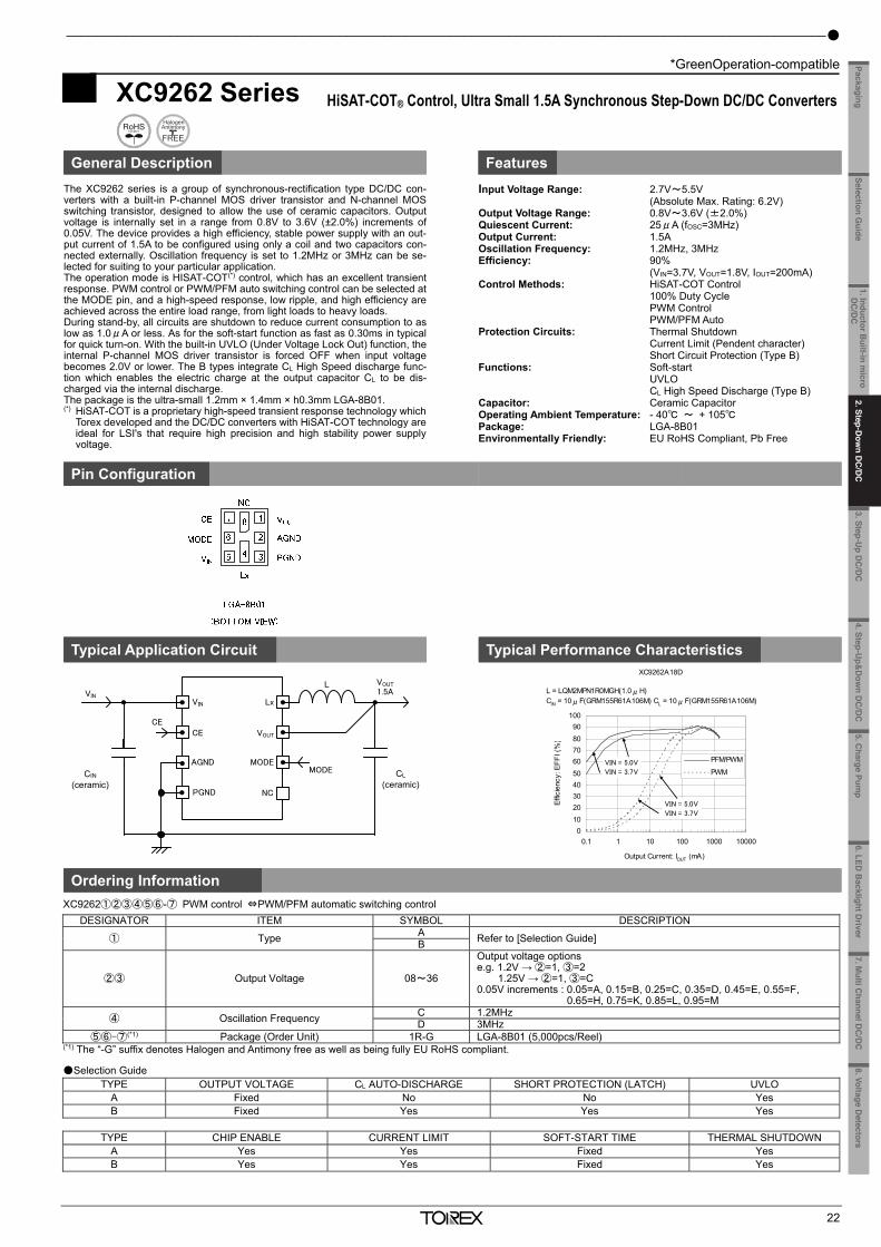
2. Step-Down DC/DC Converters and Controller ICs _____________________________________________
*GreenOperation-compatible
21
XC9263/XC9264 Series 18V Operation 0.5A Synchronous Step-Down DC/DC Converters
General Description Features
The XC9263/XC9264 series are 18V operation synchronous step-down DC/DC converter ICs with a built-in P-channel MOS driver transistor and N-channel MOS switching transistor. The XC9263/XC9264 series has operating voltage range of 3.0V~18.0V and high-efficiency power supply up to an output current of 0.5A. Low ESR capacitors such as ceramic capacitors can be used for the load capacitor (CL). A 0.75V reference voltage source is incorporated in the IC, and the output voltage can be set to a value from 1.0V to 15.0V using external resistors (RFB1, RFB2). 500kHz or 1.2MHz or 2.2MHz can be selected for the switching frequency. In automatic PWM/PFM control, the IC operates by PFM control when the load is light to achieve high efficiency over the full load range from light to heavy. The soft-start time is internally set to 1ms (TYP.), but can be adjusted to set a longer time using an external resistor and capacitor. With the built-in UVLO function, the driver transistor is forced OFF when input voltage becomes 2.7V or lower. The output state can be monitored using the power good function. Internal protection circuits include over current protection, short-circuit protec-tion, and thermal shutdown circuits to enable safe use.
Input Voltage Range: 3.0V~18.0V (Absolute Max. Rating: 20.0V) Output Voltage Range: 1.0V~15V FB Voltage: 0.75V (±1.5%) Oscillation Frequency: 500kHz, 1.2MHz, 2.2MHz Output Current: 0.5A Control Methods: PWM/PFM Auto Efficiency 85%@12V→5V, 1mA PWM control Soft-start Time: Adjustable by RC Protection Circuits: Over Current Protection Automatic Recovery (Type B) Integral Latch Method (Type A) Thermal Shutdown Low ESR Ceramic Capacitor: Ceramic Capacitor Packages: SOT-25 (without Power Good function) USP-6C Environmentally Friendly: EU RoHS Compliant, Pb Free
Pin Configuration
Typical Application Circuit Typical Performance Characteristics
Ordering Information
XC9263①②③④⑤⑥-⑦(*1) PWM control XC9264①②③④⑤⑥-⑦(*1) PWM/PFM automatic switching control
DESIGNATOR ITEM SYMBOL DESCRIPTION
① Type A Refer to Selection Guide B ②③ FB Voltage 75 FB Voltage 0.75V
④ Oscillation Frequency 5 500kHz C 1.2MHz D 2.2MHz
⑤⑥-⑦ Packages (Order Unit) MR-G(*1) SOT-25 (3,000pcs/Reel) ER-G(*1) USP-6C (3,000pcs/Reel)
(*1) The “-G” suffix denotes Halogen and Antimony free as well as being fully EU RoHS compliant. Selection Guide
TYPE PACKAGE CURRENT LIMITTER
AUTOMATIC RECOVERY (CURRENT LIMITTER)
LATCH PROTECTION (CURRENT LIMITTER) CHIP ENABLE
TYPE PACKAGE CURRENT
LIMITTER AUTOMATIC RECOVERY
(CURRENT LIMITTER) LATCH PROTECTION (CURRENT LIMITTER) CHIP ENABLE
A MR-G
YES NO YES (*1) YES A ER-G
YES NO YES (*1) YES B YES YES NO YES B YES YES NO YES
TYPE PACKAGE UVLO THERMAL
SHUTDOWN SOFT START POWER GOOD
TYPE PACKAGE UVLO THERMAL SHUTDOWN SOFT START POWER GOOD
A MR-G
YES YES YES NO A ER-G
YES YES YES YES B YES YES YES NO B YES YES YES YES
(*1) The over-current protection latch is an integral latch type.
0
10
20
30
40
50
60
70
80
90
100
0.1 1 10 100 1000
Effic
ienc
y :E
FFI[%]
Output Current :IOUT[mA]
XC9264x755(VIN=12V, VOUT=5V, fOSC=500kHz)
XC9264x755
L=10μH, CIN=2.2μF, CL=10μF×2
×2
_______________________________________________________________________________________________________
*GreenOperation-compatible
22
XC9262 Series HiSAT-COT® Control, Ultra Small 1.5A Synchronous Step-Down DC/DC Converters
General Description Features
The XC9262 series is a group of synchronous-rectification type DC/DC con-verters with a built-in P-channel MOS driver transistor and N-channel MOSswitching transistor, designed to allow the use of ceramic capacitors. Outputvoltage is internally set in a range from 0.8V to 3.6V (±2.0%) increments of0.05V. The device provides a high efficiency, stable power supply with an out-put current of 1.5A to be configured using only a coil and two capacitors con-nected externally. Oscillation frequency is set to 1.2MHz or 3MHz can be se-lected for suiting to your particular application. The operation mode is HISAT-COT(*) control, which has an excellent transientresponse. PWM control or PWM/PFM auto switching control can be selected atthe MODE pin, and a high-speed response, low ripple, and high efficiency areachieved across the entire load range, from light loads to heavy loads. During stand-by, all circuits are shutdown to reduce current consumption to aslow as 1.0μA or less. As for the soft-start function as fast as 0.30ms in typicalfor quick turn-on. With the built-in UVLO (Under Voltage Lock Out) function, theinternal P-channel MOS driver transistor is forced OFF when input voltagebecomes 2.0V or lower. The B types integrate CL High Speed discharge func-tion which enables the electric charge at the output capacitor CL to be dis-charged via the internal discharge. The package is the ultra-small 1.2mm × 1.4mm × h0.3mm LGA-8B01. (*) HiSAT-COT is a proprietary high-speed transient response technology which
Torex developed and the DC/DC converters with HiSAT-COT technology areideal for LSI's that require high precision and high stability power supplyvoltage.
Input Voltage Range: 2.7V~5.5V (Absolute Max. Rating: 6.2V) Output Voltage Range: 0.8V~3.6V (±2.0%) Quiescent Current: 25μA (fOSC=3MHz) Output Current: 1.5A Oscillation Frequency: 1.2MHz, 3MHz Efficiency: 90% (VIN=3.7V, VOUT=1.8V, IOUT=200mA) Control Methods: HiSAT-COT Control 100% Duty Cycle PWM Control PWM/PFM Auto Protection Circuits: Thermal Shutdown Current Limit (Pendent character) Short Circuit Protection (Type B) Functions: Soft-start UVLO CL High Speed Discharge (Type B) Capacitor: Ceramic Capacitor Operating Ambient Temperature: - 40 ~ + 105 Package: LGA-8B01 Environmentally Friendly: EU RoHS Compliant, Pb Free
Pin Configuration
Typical Application Circuit Typical Performance Characteristics
Ordering Information
XC9262①②③④⑤⑥-⑦ PWM control ⇔PWM/PFM automatic switching control DESIGNATOR ITEM SYMBOL DESCRIPTION
① Type A Refer to [Selection Guide] B
②③ Output Voltage 08~36
Output voltage options e.g. 1.2V → ②=1, ③=2 1.25V → ②=1, ③=C 0.05V increments : 0.05=A, 0.15=B, 0.25=C, 0.35=D, 0.45=E, 0.55=F,
0.65=H, 0.75=K, 0.85=L, 0.95=M
④ Oscillation Frequency C 1.2MHz D 3MHz
⑤⑥-⑦(*1) Package (Order Unit) 1R-G LGA-8B01 (5,000pcs/Reel) (*1) The “-G” suffix denotes Halogen and Antimony free as well as being fully EU RoHS compliant. Selection Guide
TYPE OUTPUT VOLTAGE CL AUTO-DISCHARGE SHORT PROTECTION (LATCH) UVLO A Fixed No No Yes B Fixed Yes Yes Yes
TYPE CHIP ENABLE CURRENT LIMIT SOFT-START TIME THERMAL SHUTDOWN
A Yes Yes Fixed Yes B Yes Yes Fixed Yes
1.5ALx
VOUT
VIN
CE
VOUT
VIN
CE
L
MODEAGND
PGND
MODECIN CL
NC
CIN (ceramic)
CL (ceramic)
XC9262A18D
0102030405060708090
100
0.1 1 10 100 1000 10000
Output Current: IOUT (mA)
Effic
ienc
y: E
FFI (
%)
PFM/PWM
PWM
L = LQM2MPN1R0MGH(1.0μH)CIN = 10μF(GRM155R61A106M) CL = 10μF(GRM155R61A106M)
VIN = 5.0V
VIN = 3.7V
VIN = 5.0V
VIN = 3.7V
1. Inductor Built-in m
icro D
C/D
C
3. Step-Up D
C/D
C4. Step-U
p&D
own D
C/D
C
5.Charge Pum
p6.LED
Backlight D
river8.Voltage D
etectorsSelection G
uidePackaging
7. Multi C
hannel DC
/DC
2. Step-D
own D
C/D
C
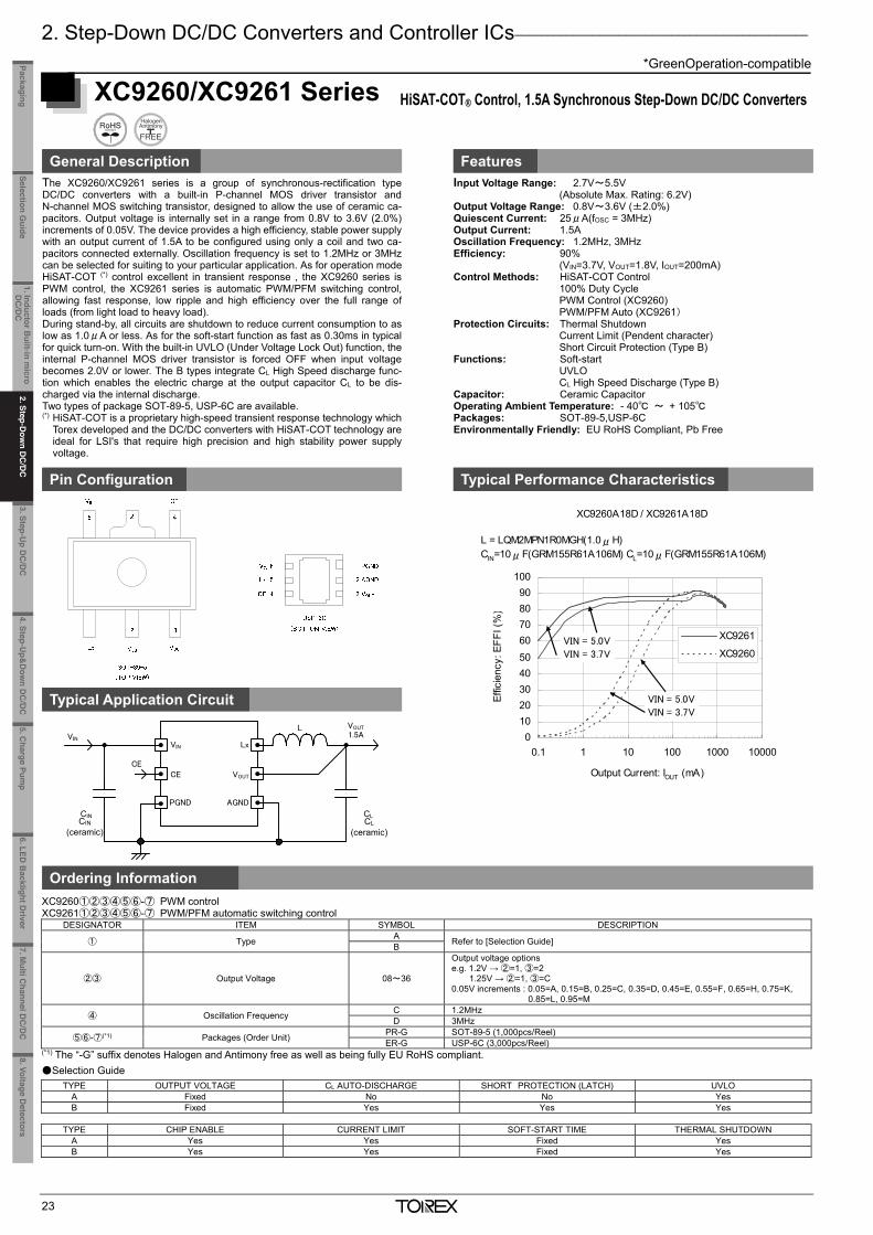
2. Step-Down DC/DC Converters and Controller ICs _____________________________________________
*GreenOperation-compatible
23
XC9260/XC9261 Series HiSAT-COT® Control, 1.5A Synchronous Step-Down DC/DC Converters
General Description Features
The XC9260/XC9261 series is a group of synchronous-rectification type DC/DC converters with a built-in P-channel MOS driver transistor and N-channel MOS switching transistor, designed to allow the use of ceramic ca-pacitors. Output voltage is internally set in a range from 0.8V to 3.6V (2.0%) increments of 0.05V. The device provides a high efficiency, stable power supply with an output current of 1.5A to be configured using only a coil and two ca-pacitors connected externally. Oscillation frequency is set to 1.2MHz or 3MHz can be selected for suiting to your particular application. As for operation mode HiSAT-COT (*) control excellent in transient response , the XC9260 series is PWM control, the XC9261 series is automatic PWM/PFM switching control, allowing fast response, low ripple and high efficiency over the full range of loads (from light load to heavy load). During stand-by, all circuits are shutdown to reduce current consumption to as low as 1.0μA or less. As for the soft-start function as fast as 0.30ms in typical for quick turn-on. With the built-in UVLO (Under Voltage Lock Out) function, the internal P-channel MOS driver transistor is forced OFF when input voltage becomes 2.0V or lower. The B types integrate CL High Speed discharge func-tion which enables the electric charge at the output capacitor CL to be dis-charged via the internal discharge. Two types of package SOT-89-5, USP-6C are available. (*) HiSAT-COT is a proprietary high-speed transient response technology which
Torex developed and the DC/DC converters with HiSAT-COT technology are ideal for LSI's that require high precision and high stability power supply voltage.
Input Voltage Range: 2.7V~5.5V (Absolute Max. Rating: 6.2V) Output Voltage Range: 0.8V~3.6V (±2.0%) Quiescent Current: 25μA(fOSC = 3MHz) Output Current: 1.5A Oscillation Frequency: 1.2MHz, 3MHz Efficiency: 90% (VIN=3.7V, VOUT=1.8V, IOUT=200mA) Control Methods: HiSAT-COT Control 100% Duty Cycle PWM Control (XC9260) PWM/PFM Auto (XC9261) Protection Circuits: Thermal Shutdown Current Limit (Pendent character) Short Circuit Protection (Type B) Functions: Soft-start UVLO CL High Speed Discharge (Type B) Capacitor: Ceramic Capacitor Operating Ambient Temperature: - 40 ~ + 105 Packages: SOT-89-5,USP-6C Environmentally Friendly: EU RoHS Compliant, Pb Free
Pin Configuration Typical Performance Characteristics
Typical Application Circuit
Ordering Information
XC9260①②③④⑤⑥-⑦ PWM control XC9261①②③④⑤⑥-⑦ PWM/PFM automatic switching control
DESIGNATOR ITEM SYMBOL DESCRIPTION
① Type A Refer to [Selection Guide] B
②③ Output Voltage 08~36
Output voltage options e.g. 1.2V → ②=1, ③=2 1.25V → ②=1, ③=C 0.05V increments : 0.05=A, 0.15=B, 0.25=C, 0.35=D, 0.45=E, 0.55=F, 0.65=H, 0.75=K,
0.85=L, 0.95=M
④ Oscillation Frequency C 1.2MHz D 3MHz
⑤⑥-⑦(*1) Packages (Order Unit) PR-G SOT-89-5 (1,000pcs/Reel) ER-G USP-6C (3,000pcs/Reel)
(*1) The “-G” suffix denotes Halogen and Antimony free as well as being fully EU RoHS compliant. Selection Guide
TYPE OUTPUT VOLTAGE CL AUTO-DISCHARGE SHORT PROTECTION (LATCH) UVLO A Fixed No No Yes B Fixed Yes Yes Yes
TYPE CHIP ENABLE CURRENT LIMIT SOFT-START TIME THERMAL SHUTDOWN
A Yes Yes Fixed Yes B Yes Yes Fixed Yes
CIN (ceramic)
CL (ceramic)
XC9260A18D / XC9261A18D
0102030405060708090
100
0.1 1 10 100 1000 10000
Output Current: IOUT (mA)
Effic
ienc
y: E
FFI (
%)
XC9261
XC9260
L = LQM2MPN1R0MGH(1.0μH)CIN=10μF(GRM155R61A106M) CL=10μF(GRM155R61A106M)
VIN = 5.0V
VIN = 3.7V
VIN = 5.0V
VIN = 3.7V
1.5ALx
VOUT
VIN
CE
VOUT
VIN
CE
L
AGNDPGND
CIN CL
_______________________________________________________________________________________________________
24
XC9259 Series HiSAT-COT® Control, Ultra Small 1A Synchronous Step-Down DC/DC Converters
General Description Features
The XC9259 series is a group of synchronous-rectification type DC/DC con-verters with a built-in P-channel MOS driver transistor and N-channel MOSswitching transistor, designed to allow the use of ceramic capacitors. Outputvoltage is internally set in a range from 0.8V to 3.6V (±2.0%) increments of0.05V. The device provides a high efficiency, stable power supply with anoutput current of 600mA to be configured using only a coil and two capacitorsconnected externally. Oscillation frequency is set to 1.2MHz or 6MHz can beselected for suiting to your particular application. As for operation modeHiSAT-COT(*) control excellent in transient response, the XC9259 has PWMcontrol and automatic PWM/PFM switching control, allowing fast response, lowripple and high efficiency over the full range of loads (from light load to heavyload). During stand-by, all circuits are shutdown to reduce current consumption to aslow as 1.0μA or less. As for the soft-start function as fast as 0.30ms in typicalfor quick turn-on. With the built-in UVLO (Under Voltage Lock Out) function,the internal P-channel MOS driver transistor is forced OFF when input voltagebecomes 1.6V or lower. The B types integrate CL discharge function whichenables the electric charge at the output capacitor CL to be discharged via theinternal discharge. Package is available in LGA-8B01 (1.2mm x 1.4mm x h0.3mm). (*) HiSAT-COT is a proprietary high-speed transient response technology which
Torex developed and the DC/DC converters with HiSAT-COT technology areideal for LSI's that require high precision and high stability power supplyvoltage.
Input Voltage Range: 2.5V~5.5V Output Voltage Range: 0.8V~3.6V Oscillation Frequency: 1.2MHz, 6MHz Output Current: 1A Control Methods: HiSAT-COT Control 100% Duty Cycle PWM Control PWM/PFM Auto Protection Circuits: Thermal Shutdown Current Limit (Pendent character) Short Circuit Protection (Type B) Functions: Soft-start UVLO CL Discharge (Type B) Output Capacitor: Ceramic Capacitor Operating Ambient Temperature: -40~ +105 Package: LGA-8B01 Environmentally Friendly: EU RoHS Compliant, Pb Free
Pin Configuration Typical Performance Characteristics
Typical Application Circuit Typical Performance Characteristics
Ordering Information
XC9259①②③④⑤⑥-⑦ PWM control ⇔PWM/PFM automatic switching control DESIGNATOR ITEM SYMBOL DESCRIPTION
① Type A Refer to [Selection Guide] B
②③ Output Voltage 08~36
Output voltage options e.g. 1.2V → ②=1, ③=2 1.25V → ②=1, ③=C 0.05V increments : 0.05=A, 0.15=B, 0.25=C, 0.35=D, 0.45=E, 0.55=F,
0.65=H, 0.75=K, 0.85=L, 0.95=M
④ Oscillation Frequency C 1.2MHz E 6MHz
⑤⑥-⑦(*1) Package (Order Unit) 1R-G LGA-8B01 (5,000pcs/Reel) (*1) The “-G” suffix denotes Halogen and Antimony free as well as being fully EU RoHS compliant. Selection Guide
TYPE OUTPUT VOLTAGE CL AUTO-DISCHARGE SHORT PROTECTION (LATCH) UVLO
A Fixed No No Yes B Fixed Yes Yes Yes
TYPE CHIP ENABLE CURRENT LIMIT SOFT-START TIME THERMAL SHUTDOWN
A Yes Yes Fixed Yes B Yes Yes Fixed Yes
0
10
20
30
40
50
60
70
80
90
100
0.1 1 10 100 1000
Effic
ienc
y: E
FFI (
%)
Output Current: IOUT (mA)
XC9259x18E
PWM
PFM/PWM
VIN=5.0V
VIN=5.0V
VIN=3.7V
VIN=3.7V
L = GLCLKR4701A(0.47μH)CIN = 10μF(GRM155R61A106M) CL = 10μF×2(GRM155R61A106M)
1. Inductor Built-in m
icro D
C/D
C
2. Step-Dow
n DC
/DC
3. Step-Up D
C/D
C4. Step-U
p&D
own D
C/D
C
5.Charge Pum
p6.LED
Backlight D
river8.Voltage D
etectorsSelection G
uidePackaging
7. Multi C
hannel DC
/DC
2. Step-D
own D
C/D
C
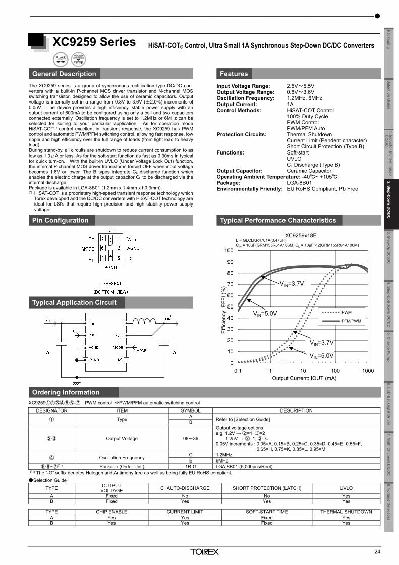
2. Step-Down DC/DC Converters and Controller ICs _____________________________________________
*GreenOperation-compatible
23
XC9260/XC9261 Series HiSAT-COT® Control, 1.5A Synchronous Step-Down DC/DC Converters
General Description Features
The XC9260/XC9261 series is a group of synchronous-rectification type DC/DC converters with a built-in P-channel MOS driver transistor and N-channel MOS switching transistor, designed to allow the use of ceramic ca-pacitors. Output voltage is internally set in a range from 0.8V to 3.6V (2.0%) increments of 0.05V. The device provides a high efficiency, stable power supply with an output current of 1.5A to be configured using only a coil and two ca-pacitors connected externally. Oscillation frequency is set to 1.2MHz or 3MHz can be selected for suiting to your particular application. As for operation mode HiSAT-COT (*) control excellent in transient response , the XC9260 series is PWM control, the XC9261 series is automatic PWM/PFM switching control, allowing fast response, low ripple and high efficiency over the full range of loads (from light load to heavy load). During stand-by, all circuits are shutdown to reduce current consumption to as low as 1.0μA or less. As for the soft-start function as fast as 0.30ms in typical for quick turn-on. With the built-in UVLO (Under Voltage Lock Out) function, the internal P-channel MOS driver transistor is forced OFF when input voltage becomes 2.0V or lower. The B types integrate CL High Speed discharge func-tion which enables the electric charge at the output capacitor CL to be dis-charged via the internal discharge. Two types of package SOT-89-5, USP-6C are available. (*) HiSAT-COT is a proprietary high-speed transient response technology which
Torex developed and the DC/DC converters with HiSAT-COT technology are ideal for LSI's that require high precision and high stability power supply voltage.
Input Voltage Range: 2.7V~5.5V (Absolute Max. Rating: 6.2V) Output Voltage Range: 0.8V~3.6V (±2.0%) Quiescent Current: 25μA(fOSC = 3MHz) Output Current: 1.5A Oscillation Frequency: 1.2MHz, 3MHz Efficiency: 90% (VIN=3.7V, VOUT=1.8V, IOUT=200mA) Control Methods: HiSAT-COT Control 100% Duty Cycle PWM Control (XC9260) PWM/PFM Auto (XC9261) Protection Circuits: Thermal Shutdown Current Limit (Pendent character) Short Circuit Protection (Type B) Functions: Soft-start UVLO CL High Speed Discharge (Type B) Capacitor: Ceramic Capacitor Operating Ambient Temperature: - 40 ~ + 105 Packages: SOT-89-5,USP-6C Environmentally Friendly: EU RoHS Compliant, Pb Free
Pin Configuration Typical Performance Characteristics
Typical Application Circuit
Ordering Information
XC9260①②③④⑤⑥-⑦ PWM control XC9261①②③④⑤⑥-⑦ PWM/PFM automatic switching control
DESIGNATOR ITEM SYMBOL DESCRIPTION
① Type A Refer to [Selection Guide] B
②③ Output Voltage 08~36
Output voltage options e.g. 1.2V → ②=1, ③=2 1.25V → ②=1, ③=C 0.05V increments : 0.05=A, 0.15=B, 0.25=C, 0.35=D, 0.45=E, 0.55=F, 0.65=H, 0.75=K,
0.85=L, 0.95=M
④ Oscillation Frequency C 1.2MHz D 3MHz
⑤⑥-⑦(*1) Packages (Order Unit) PR-G SOT-89-5 (1,000pcs/Reel) ER-G USP-6C (3,000pcs/Reel)
(*1) The “-G” suffix denotes Halogen and Antimony free as well as being fully EU RoHS compliant. Selection Guide
TYPE OUTPUT VOLTAGE CL AUTO-DISCHARGE SHORT PROTECTION (LATCH) UVLO A Fixed No No Yes B Fixed Yes Yes Yes
TYPE CHIP ENABLE CURRENT LIMIT SOFT-START TIME THERMAL SHUTDOWN
A Yes Yes Fixed Yes B Yes Yes Fixed Yes
CIN (ceramic)
CL (ceramic)
XC9260A18D / XC9261A18D
0102030405060708090
100
0.1 1 10 100 1000 10000
Output Current: IOUT (mA)
Effic
ienc
y: E
FFI (
%)
XC9261
XC9260
L = LQM2MPN1R0MGH(1.0μH)CIN=10μF(GRM155R61A106M) CL=10μF(GRM155R61A106M)
VIN = 5.0V
VIN = 3.7V
VIN = 5.0V
VIN = 3.7V
1.5ALx
VOUT
VIN
CE
VOUT
VIN
CE
L
AGNDPGND
CIN CL
_______________________________________________________________________________________________________
24
XC9259 Series HiSAT-COT® Control, Ultra Small 1A Synchronous Step-Down DC/DC Converters
General Description Features
The XC9259 series is a group of synchronous-rectification type DC/DC con-verters with a built-in P-channel MOS driver transistor and N-channel MOSswitching transistor, designed to allow the use of ceramic capacitors. Outputvoltage is internally set in a range from 0.8V to 3.6V (±2.0%) increments of0.05V. The device provides a high efficiency, stable power supply with anoutput current of 600mA to be configured using only a coil and two capacitorsconnected externally. Oscillation frequency is set to 1.2MHz or 6MHz can beselected for suiting to your particular application. As for operation modeHiSAT-COT(*) control excellent in transient response, the XC9259 has PWMcontrol and automatic PWM/PFM switching control, allowing fast response, lowripple and high efficiency over the full range of loads (from light load to heavyload). During stand-by, all circuits are shutdown to reduce current consumption to aslow as 1.0μA or less. As for the soft-start function as fast as 0.30ms in typicalfor quick turn-on. With the built-in UVLO (Under Voltage Lock Out) function,the internal P-channel MOS driver transistor is forced OFF when input voltagebecomes 1.6V or lower. The B types integrate CL discharge function whichenables the electric charge at the output capacitor CL to be discharged via theinternal discharge. Package is available in LGA-8B01 (1.2mm x 1.4mm x h0.3mm). (*) HiSAT-COT is a proprietary high-speed transient response technology which
Torex developed and the DC/DC converters with HiSAT-COT technology areideal for LSI's that require high precision and high stability power supplyvoltage.
Input Voltage Range: 2.5V~5.5V Output Voltage Range: 0.8V~3.6V Oscillation Frequency: 1.2MHz, 6MHz Output Current: 1A Control Methods: HiSAT-COT Control 100% Duty Cycle PWM Control PWM/PFM Auto Protection Circuits: Thermal Shutdown Current Limit (Pendent character) Short Circuit Protection (Type B) Functions: Soft-start UVLO CL Discharge (Type B) Output Capacitor: Ceramic Capacitor Operating Ambient Temperature: -40~ +105 Package: LGA-8B01 Environmentally Friendly: EU RoHS Compliant, Pb Free
Pin Configuration Typical Performance Characteristics
Typical Application Circuit Typical Performance Characteristics
Ordering Information
XC9259①②③④⑤⑥-⑦ PWM control ⇔PWM/PFM automatic switching control DESIGNATOR ITEM SYMBOL DESCRIPTION
① Type A Refer to [Selection Guide] B
②③ Output Voltage 08~36
Output voltage options e.g. 1.2V → ②=1, ③=2 1.25V → ②=1, ③=C 0.05V increments : 0.05=A, 0.15=B, 0.25=C, 0.35=D, 0.45=E, 0.55=F,
0.65=H, 0.75=K, 0.85=L, 0.95=M
④ Oscillation Frequency C 1.2MHz E 6MHz
⑤⑥-⑦(*1) Package (Order Unit) 1R-G LGA-8B01 (5,000pcs/Reel) (*1) The “-G” suffix denotes Halogen and Antimony free as well as being fully EU RoHS compliant. Selection Guide
TYPE OUTPUT VOLTAGE CL AUTO-DISCHARGE SHORT PROTECTION (LATCH) UVLO
A Fixed No No Yes B Fixed Yes Yes Yes
TYPE CHIP ENABLE CURRENT LIMIT SOFT-START TIME THERMAL SHUTDOWN
A Yes Yes Fixed Yes B Yes Yes Fixed Yes
0
10
20
30
40
50
60
70
80
90
100
0.1 1 10 100 1000
Effic
ienc
y: E
FFI (
%)
Output Current: IOUT (mA)
XC9259x18E
PWM
PFM/PWM
VIN=5.0V
VIN=5.0V
VIN=3.7V
VIN=3.7V
L = GLCLKR4701A(0.47μH)CIN = 10μF(GRM155R61A106M) CL = 10μF×2(GRM155R61A106M)
1. Inductor Built-in m
icro D
C/D
C
3. Step-Up D
C/D
C4. Step-U
p&D
own D
C/D
C
5.Charge Pum
p6.LED
Backlight D
river8.Voltage D
etectorsSelection G
uidePackaging
7. Multi C
hannel DC
/DC
2. Step-D
own D
C/D
C
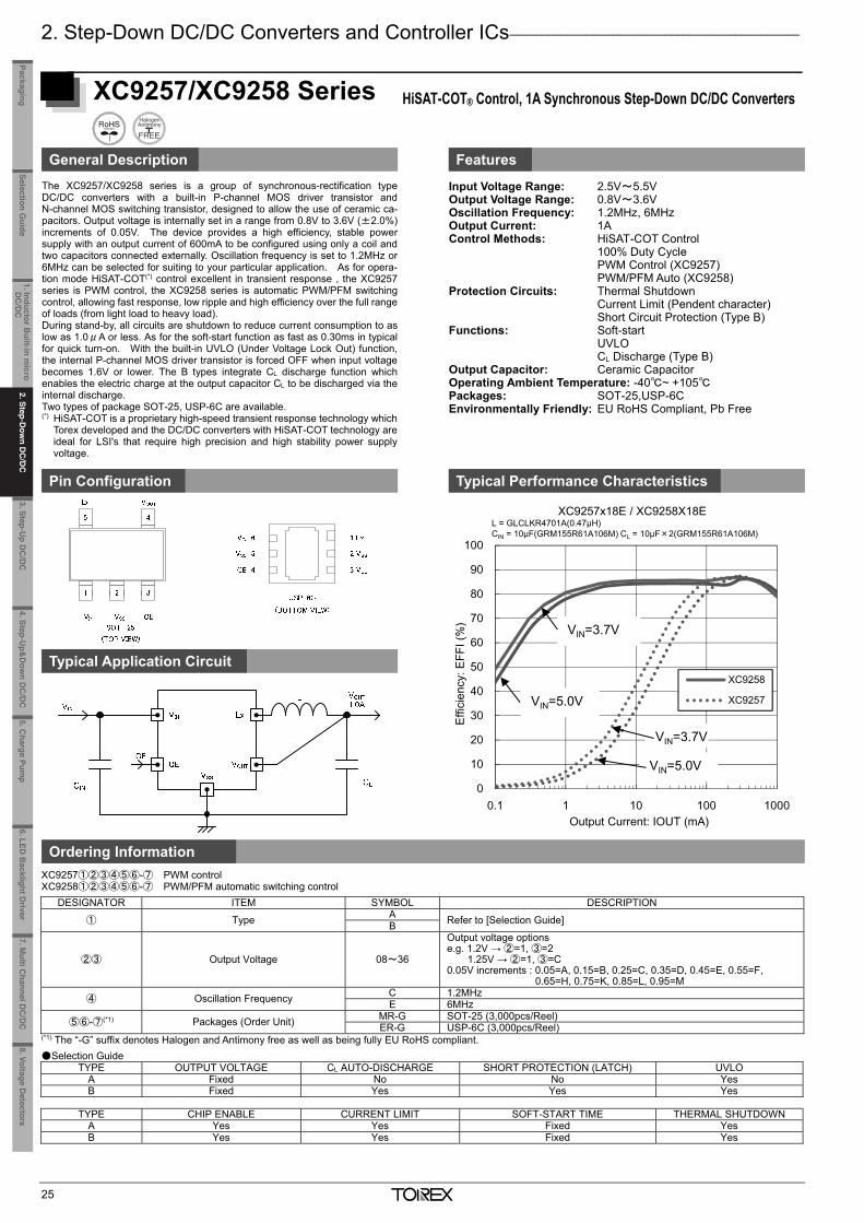
2. Step-Down DC/DC Converters and Controller ICs _____________________________________________
25
XC9257/XC9258 Series HiSAT-COT® Control, 1A Synchronous Step-Down DC/DC Converters
General Description Features
The XC9257/XC9258 series is a group of synchronous-rectification type DC/DC converters with a built-in P-channel MOS driver transistor and N-channel MOS switching transistor, designed to allow the use of ceramic ca-pacitors. Output voltage is internally set in a range from 0.8V to 3.6V (±2.0%) increments of 0.05V. The device provides a high efficiency, stable power supply with an output current of 600mA to be configured using only a coil and two capacitors connected externally. Oscillation frequency is set to 1.2MHz or 6MHz can be selected for suiting to your particular application. As for opera-tion mode HiSAT-COT(*) control excellent in transient response , the XC9257 series is PWM control, the XC9258 series is automatic PWM/PFM switching control, allowing fast response, low ripple and high efficiency over the full range of loads (from light load to heavy load). During stand-by, all circuits are shutdown to reduce current consumption to as low as 1.0μA or less. As for the soft-start function as fast as 0.30ms in typical for quick turn-on. With the built-in UVLO (Under Voltage Lock Out) function, the internal P-channel MOS driver transistor is forced OFF when input voltage becomes 1.6V or lower. The B types integrate CL discharge function which enables the electric charge at the output capacitor CL to be discharged via the internal discharge. Two types of package SOT-25, USP-6C are available. (*) HiSAT-COT is a proprietary high-speed transient response technology which
Torex developed and the DC/DC converters with HiSAT-COT technology are ideal for LSI's that require high precision and high stability power supply voltage.
Input Voltage Range: 2.5V~5.5V Output Voltage Range: 0.8V~3.6V Oscillation Frequency: 1.2MHz, 6MHz Output Current: 1A Control Methods: HiSAT-COT Control 100% Duty Cycle PWM Control (XC9257) PWM/PFM Auto (XC9258) Protection Circuits: Thermal Shutdown Current Limit (Pendent character) Short Circuit Protection (Type B) Functions: Soft-start UVLO CL Discharge (Type B) Output Capacitor: Ceramic Capacitor Operating Ambient Temperature: -40~ +105 Packages: SOT-25,USP-6C Environmentally Friendly: EU RoHS Compliant, Pb Free
Pin Configuration Typical Performance Characteristics
Typical Application Circuit
Ordering Information
XC9257①②③④⑤⑥-⑦ PWM control XC9258①②③④⑤⑥-⑦ PWM/PFM automatic switching control
DESIGNATOR ITEM SYMBOL DESCRIPTION
① Type A Refer to [Selection Guide] B
②③ Output Voltage 08~36
Output voltage options e.g. 1.2V → ②=1, ③=2 1.25V → ②=1, ③=C 0.05V increments : 0.05=A, 0.15=B, 0.25=C, 0.35=D, 0.45=E, 0.55=F,
0.65=H, 0.75=K, 0.85=L, 0.95=M
④ Oscillation Frequency C 1.2MHz E 6MHz
⑤⑥-⑦(*1) Packages (Order Unit) MR-G SOT-25 (3,000pcs/Reel) ER-G USP-6C (3,000pcs/Reel)
(*1) The “-G” suffix denotes Halogen and Antimony free as well as being fully EU RoHS compliant. Selection Guide
TYPE OUTPUT VOLTAGE CL AUTO-DISCHARGE SHORT PROTECTION (LATCH) UVLO A Fixed No No Yes B Fixed Yes Yes Yes
TYPE CHIP ENABLE CURRENT LIMIT SOFT-START TIME THERMAL SHUTDOWN
A Yes Yes Fixed Yes B Yes Yes Fixed Yes
0
10
20
30
40
50
60
70
80
90
100
0.1 1 10 100 1000
Effic
ienc
y: E
FFI (
%)
Output Current: IOUT (mA)
XC9257x18E / XC9258X18E
XC9258
XC9257
VIN=3.7V
VIN=5.0V
VIN=3.7V
VIN=5.0V
L = GLCLKR4701A(0.47μH)CIN = 10μF(GRM155R61A106M) CL = 10μF×2(GRM155R61A106M)
_______________________________________________________________________________________________________
26
XC9252 Series Operating Ambient Temperature: +105, 30V Operation
General Description Features
The XC9252 series is a 30V operation step-down DC/DC controllerIC. The external P-ch driver transistor is used to achieve a stableoperation under low input voltage. Low ESR capacitors such asceramic capacitors can be used for the load capacitor (CL). A 0.8V reference voltage source is incorporated, and the outputvoltage can be set freely from 1.0V using external resistors (RFB1, RFB2). 300kHz to 600kHz can be selected for the switching frequency byconnecting an external resistor to the ROSC pin. The generation ofunneeded noise can be reduced by this synchronization with an ex-ternal CLK within ±25% of the internal clock using the MODE/SYNCpin. In automatic PWM/PFM control, the IC operates by PFM con-trol when the load is light to achieve high efficiency over the full loadrange from light to heavy. The soft start time can be set as desired by adding an external ca-pacitance to the SS pin. With the built-in UVLO function, the driver transistor is forced OFFwhen input voltage becomes 2.5V or lower. Internal protection circuits include over current protection,short-circuit protection, and thermal shutdown circuits to enable safeuse.
Input Voltage Range: 3.0V~30.0V (Absolute Max. Rating: 36.0V) Output Voltage Range: 1.5V~Externally Set
(VFB=0.8V±2.0%) Quiescent Current: 30μA (@300kHz) Oscillation Frequency: 280kHz~550kHz (External Resistor) Synchronous External Clocking: ±25% of the internal clock Control Method: PWM control (MODE:H) PWM/PFM (MODE:L) Soft-start: External set (External C) Protection Circuits: Over current limit (External Resistor) Automatic Return (XC9252A/B) Integral latch protection (XC9252C) Thermal shutdown Output Capacitor: Low ESR Capacitor Operating Ambient Temperature: -40~+105 Packages: TSSOP-16 (XC9252A/C) USP-10B (XC9252B) Environmentally Friendly: EU RoHS Compliant, Pb Free
Pin Configuration
Typical Application Circuit Typical Performance Characteristics
Ordering Information
XC9252①②③④⑤⑥-⑦
DESIGNATOR ITEM SYMBOL DESCRIPTION
① Type A Standard Type (TSSOP-16) B Without Chip Enable, Power-Good (USP-10B) C Standard Type with Latch Protection (TSSOP-16)
②③ FB Voltage 08 FB Voltage 0.8V ④ Oscillation Frequency A Adjustable
⑤⑥-⑦ (*1) Packages (Order Unit) VR-G TSSOP-16 (3,000pcs/Reel) * Only Type A, C DR-G USP-10B (3,000pcs/Reel) (*2)* Only Type B
(*1) The “-G” suffix denotes Halogen and Antimony free as well as being fully EU RoHS compliant. (*2) The USP-10B reels are shipped in a moisture-proof packing.
XC9252
EXTB
ISENSE
CLAMPVL
VIN
CE
ROSC
FB
CIN
CL
CVL SBD
L
RFB1
RFB2
CFB
SS
CSS
MODE/SYNC
GND
ROSC
PG
RSENSE
PchMOSFET
RPG
CCLAMP
XC9252x08A(VIN=12V, VOUT=5.7V, fOSC=280kHz)
0
10
20
30
40
50
60
70
80
90
100
1 10 100 1000 10000
Output Current :IOUT[mA]
Effic
iency
:EFFI[
%]
PFM(MODE=L)
PWM(MODE=H)
L=22μH(CLF12555-220M), CIN=10μF(GRM32ER71H106KA12L),ROSC=300kΩ, CL=22μF×2 (GRM32ER71E226KE15L),
RSENSE=50mΩ, PchMOSFET:2SJ668, SBD:CMS15
Low Quiescent Current Step-down DC/DC Controller IC
1. Inductor Built-in m
icro D
C/D
C
2. Step-Dow
n DC
/DC
3. Step-Up D
C/D
C4. Step-U
p&D
own D
C/D
C
5.Charge Pum
p6.LED
Backlight D
river8.Voltage D
etectorsSelection G
uidePackaging
7. Multi C
hannel DC
/DC
2. Step-D
own D
C/D
C
2. Step-Down DC/DC Converters and Controller ICs _____________________________________________
25
XC9257/XC9258 Series HiSAT-COT® Control, 1A Synchronous Step-Down DC/DC Converters
General Description Features
The XC9257/XC9258 series is a group of synchronous-rectification type DC/DC converters with a built-in P-channel MOS driver transistor and N-channel MOS switching transistor, designed to allow the use of ceramic ca-pacitors. Output voltage is internally set in a range from 0.8V to 3.6V (±2.0%) increments of 0.05V. The device provides a high efficiency, stable power supply with an output current of 600mA to be configured using only a coil and two capacitors connected externally. Oscillation frequency is set to 1.2MHz or 6MHz can be selected for suiting to your particular application. As for opera-tion mode HiSAT-COT(*) control excellent in transient response , the XC9257 series is PWM control, the XC9258 series is automatic PWM/PFM switching control, allowing fast response, low ripple and high efficiency over the full range of loads (from light load to heavy load). During stand-by, all circuits are shutdown to reduce current consumption to as low as 1.0μA or less. As for the soft-start function as fast as 0.30ms in typical for quick turn-on. With the built-in UVLO (Under Voltage Lock Out) function, the internal P-channel MOS driver transistor is forced OFF when input voltage becomes 1.6V or lower. The B types integrate CL discharge function which enables the electric charge at the output capacitor CL to be discharged via the internal discharge. Two types of package SOT-25, USP-6C are available. (*) HiSAT-COT is a proprietary high-speed transient response technology which
Torex developed and the DC/DC converters with HiSAT-COT technology are ideal for LSI's that require high precision and high stability power supply voltage.
Input Voltage Range: 2.5V~5.5V Output Voltage Range: 0.8V~3.6V Oscillation Frequency: 1.2MHz, 6MHz Output Current: 1A Control Methods: HiSAT-COT Control 100% Duty Cycle PWM Control (XC9257) PWM/PFM Auto (XC9258) Protection Circuits: Thermal Shutdown Current Limit (Pendent character) Short Circuit Protection (Type B) Functions: Soft-start UVLO CL Discharge (Type B) Output Capacitor: Ceramic Capacitor Operating Ambient Temperature: -40~ +105 Packages: SOT-25,USP-6C Environmentally Friendly: EU RoHS Compliant, Pb Free
Pin Configuration Typical Performance Characteristics
Typical Application Circuit
Ordering Information
XC9257①②③④⑤⑥-⑦ PWM control XC9258①②③④⑤⑥-⑦ PWM/PFM automatic switching control
DESIGNATOR ITEM SYMBOL DESCRIPTION
① Type A Refer to [Selection Guide] B
②③ Output Voltage 08~36
Output voltage options e.g. 1.2V → ②=1, ③=2 1.25V → ②=1, ③=C 0.05V increments : 0.05=A, 0.15=B, 0.25=C, 0.35=D, 0.45=E, 0.55=F,
0.65=H, 0.75=K, 0.85=L, 0.95=M
④ Oscillation Frequency C 1.2MHz E 6MHz
⑤⑥-⑦(*1) Packages (Order Unit) MR-G SOT-25 (3,000pcs/Reel) ER-G USP-6C (3,000pcs/Reel)
(*1) The “-G” suffix denotes Halogen and Antimony free as well as being fully EU RoHS compliant. Selection Guide
TYPE OUTPUT VOLTAGE CL AUTO-DISCHARGE SHORT PROTECTION (LATCH) UVLO A Fixed No No Yes B Fixed Yes Yes Yes
TYPE CHIP ENABLE CURRENT LIMIT SOFT-START TIME THERMAL SHUTDOWN
A Yes Yes Fixed Yes B Yes Yes Fixed Yes
0
10
20
30
40
50
60
70
80
90
100
0.1 1 10 100 1000
Effic
ienc
y: E
FFI (
%)
Output Current: IOUT (mA)
XC9257x18E / XC9258X18E
XC9258
XC9257
VIN=3.7V
VIN=5.0V
VIN=3.7V
VIN=5.0V
L = GLCLKR4701A(0.47μH)CIN = 10μF(GRM155R61A106M) CL = 10μF×2(GRM155R61A106M)
_______________________________________________________________________________________________________
26
XC9252 Series Operating Ambient Temperature: +105, 30V Operation
General Description Features
The XC9252 series is a 30V operation step-down DC/DC controllerIC. The external P-ch driver transistor is used to achieve a stableoperation under low input voltage. Low ESR capacitors such asceramic capacitors can be used for the load capacitor (CL). A 0.8V reference voltage source is incorporated, and the outputvoltage can be set freely from 1.0V using external resistors (RFB1, RFB2). 300kHz to 600kHz can be selected for the switching frequency byconnecting an external resistor to the ROSC pin. The generation ofunneeded noise can be reduced by this synchronization with an ex-ternal CLK within ±25% of the internal clock using the MODE/SYNCpin. In automatic PWM/PFM control, the IC operates by PFM con-trol when the load is light to achieve high efficiency over the full loadrange from light to heavy. The soft start time can be set as desired by adding an external ca-pacitance to the SS pin. With the built-in UVLO function, the driver transistor is forced OFFwhen input voltage becomes 2.5V or lower. Internal protection circuits include over current protection,short-circuit protection, and thermal shutdown circuits to enable safeuse.
Input Voltage Range: 3.0V~30.0V (Absolute Max. Rating: 36.0V) Output Voltage Range: 1.5V~Externally Set
(VFB=0.8V±2.0%) Quiescent Current: 30μA (@300kHz) Oscillation Frequency: 280kHz~550kHz (External Resistor) Synchronous External Clocking: ±25% of the internal clock Control Method: PWM control (MODE:H) PWM/PFM (MODE:L) Soft-start: External set (External C) Protection Circuits: Over current limit (External Resistor) Automatic Return (XC9252A/B) Integral latch protection (XC9252C) Thermal shutdown Output Capacitor: Low ESR Capacitor Operating Ambient Temperature: -40~+105 Packages: TSSOP-16 (XC9252A/C) USP-10B (XC9252B) Environmentally Friendly: EU RoHS Compliant, Pb Free
Pin Configuration
Typical Application Circuit Typical Performance Characteristics
Ordering Information
XC9252①②③④⑤⑥-⑦
DESIGNATOR ITEM SYMBOL DESCRIPTION
① Type A Standard Type (TSSOP-16) B Without Chip Enable, Power-Good (USP-10B) C Standard Type with Latch Protection (TSSOP-16)
②③ FB Voltage 08 FB Voltage 0.8V ④ Oscillation Frequency A Adjustable
⑤⑥-⑦ (*1) Packages (Order Unit) VR-G TSSOP-16 (3,000pcs/Reel) * Only Type A, C DR-G USP-10B (3,000pcs/Reel) (*2)* Only Type B
(*1) The “-G” suffix denotes Halogen and Antimony free as well as being fully EU RoHS compliant. (*2) The USP-10B reels are shipped in a moisture-proof packing.
XC9252
EXTB
ISENSE
CLAMPVL
VIN
CE
ROSC
FB
CIN
CL
CVL SBD
L
RFB1
RFB2
CFB
SS
CSS
MODE/SYNC
GND
ROSC
PG
RSENSE
PchMOSFET
RPG
CCLAMP
XC9252x08A(VIN=12V, VOUT=5.7V, fOSC=280kHz)
0
10
20
30
40
50
60
70
80
90
100
1 10 100 1000 10000
Output Current :IOUT[mA]
Effic
iency
:EFFI[
%]
PFM(MODE=L)
PWM(MODE=H)
L=22μH(CLF12555-220M), CIN=10μF(GRM32ER71H106KA12L),ROSC=300kΩ, CL=22μF×2 (GRM32ER71E226KE15L),
RSENSE=50mΩ, PchMOSFET:2SJ668, SBD:CMS15
Low Quiescent Current Step-down DC/DC Controller IC
1. Inductor Built-in m
icro D
C/D
C
3. Step-Up D
C/D
C4. Step-U
p&D
own D
C/D
C
5.Charge Pum
p6.LED
Backlight D
river8.Voltage D
etectorsSelection G
uidePackaging
7. Multi C
hannel DC
/DC
2. Step-D
own D
C/D
C
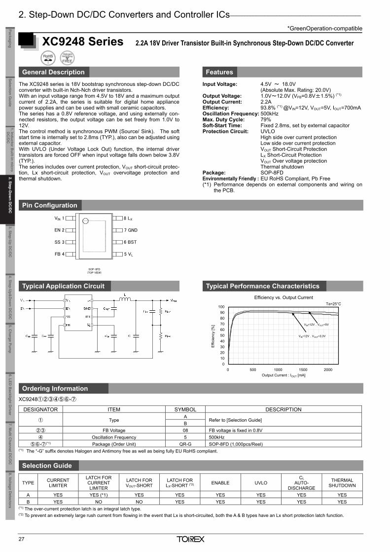
2. Step-Down DC/DC Converters and Controller ICs _____________________________________________
*GreenOperation-compatible
27
XC9248 Series 2.2A 18V Driver Transistor Built-in Synchronous Step-Down DC/DC Converter
General Description Features
The XC9248 series is 18V bootstrap synchronous step-down DC/DC converter with built-in Nch-Nch driver transistors. With an input voltage range from 4.5V to 18V and a maximum output current of 2.2A, the series is suitable for digital home appliance power supplies and can be used with small ceramic capacitors. The series has a 0.8V reference voltage, and using externally con-nected resistors, the output voltage can be set freely from 1.0V to 12V. The control method is synchronous PWM (Source/ Sink). The soft start time is internally set to 2.8ms (TYP.), also can be adjusted using external capacitor. With UVLO (Under Voltage Lock Out) function, the internal driver transistors are forced OFF when input voltage falls down below 3.8V (TYP.). The series includes over current protection, VOUT short-circuit protec-tion, Lx short-circuit protection, VOUT overvoltage protection and thermal shutdown.
Input Voltage: 4.5V ~ 18.0V (Absolute Max. Rating: 20.0V) Output Voltage: 1.0V~12.0V (VFB=0.8V±1.5%) (*1) Output Current: 2.2A Efficiency: 93.8% (*1) @VIN=12V, VOUT=5V, IOUT=700mA Oscillation Frequency: 500kHz Max. Duty Cycle: 79% Soft-Start Time: Fixed 2.8ms, set by external capacitor Protection Circuit: UVLO High side over current protection Low side over current protection VOUT Short-Circuit Protection LX Short-Circuit Protection VOUT Over voltage protection Thermal shutdown Package: SOP-8FD Environmentally Friendly : EU RoHS Compliant, Pb Free (*1) Performance depends on external components and wiring on
the PCB.
Pin Configuration
Typical Application Circuit Typical Performance Characteristics Efficiency vs. Output Current
Ordering Information XC9248①②③④⑤⑥-⑦
DESIGNATOR ITEM SYMBOL DESCRIPTION
① Type A
Refer to [Selection Guide] B
②③ FB Voltage 08 FB voltage is fixed in 0.8V ④ Oscillation Frequency 5 500kHz
⑤⑥-⑦(*1) Package (Order Unit) QR-G SOP-8FD (1,000pcs/Reel) (*1) The “-G” suffix denotes Halogen and Antimony free as well as being fully EU RoHS compliant.
Selection Guide
TYPE CURRENT LIMITER
LATCH FOR CURRENT LIMITER
LATCH FOR VOUT-SHORT
LATCH FOR LX-SHORT (*2) ENABLE UVLO
CL AUTO-
DISCHARGE
THERMAL SHUTDOWN
A YES YES (*1) YES YES YES YES YES YES B YES NO NO YES YES YES YES YES
(*1) The over-current protection latch is an integral latch type. (*2) To prevent an extremely large rush current from flowing in the event that Lx is short-circuited, both the A & B types have an Lx short protection latch function.
SOP-8FD(TOP VIEW)
VIN 1
EN 2
SS 3
FB 4
8 LX
7 GND
6 BST
5 VL
Ta=25°C
0102030405060708090
100
0 500 1000 1500 2000Output Current : IOUT [mA]
Effic
ienc
y [%
]
VIN=12V , VOUT=3.3V
VIN=12V , VOUT=5V
_______________________________________________________________________________________________________
*GreenOperation-compatible
28
XC9244/XC9245 Series 400mA Synchronous Step-Down DC/DC Converters
General Description Features
The XC9244/XC9245 series is a group of synchronous-rectificationtype step-down DC/DC converters with a built-in 0.65ΩP-ch MOSdriver transistor and 0.45Ω N-ch MOS switching transistor, designedto allow the use of ceramic capacitors. Output current of 400mA(MAX.) to be configured using only a coil and capacitor connected ex-ternally. The output voltage can be set from 0.8V to 4.0V in increments of0.05V (±2.0%). With an internal switching frequency of 1.2MHz,small external components can be used. USPN-6 package is suit-able for the application which requires low profile and small-footprint. The XC9244 series is PWM fixed frequency control, and the XC9245series is PWM/PFM, which automatically switches from PWM to PFMduring light loads, high efficiency can be achieved over a wide rangeof load conditions. When stand-by mode, due to stop all operation,quiescent current is reduced to 1μA or less. The integrated CLdischarge function which enables the electric charge at the outputcapacitor CL to be discharged via the internal discharge switch lo-cated between the VOUT and VSS pins. The CL discharge functionprevents malfunction on VOUT connecting application during stand-bymode. The XC9244/XC9245 series has a high speed soft-start as fast as0.25ms in typical for quick turn-on. Current limiter circuit (ConstantCurrent & Latching) is built-in for preventing from thermal destruction.With UVLO (Under Voltage Lock Out) function, the internal P channeldriver transistor is forced OFF when input voltage becomes 2.25V orlower.
Driver Transistor: 0.65Ω P-ch Driver Transistor 0.45Ω N-ch Synchronous Switch
Transistor Input Voltage: 2.3V ~ 6.0V
(Absolute Max. Rating: 6.5V) Output Voltage Selectable: 0.8V ~ 4.0V (0.05V increments) High Efficiency: 90% (VIN=4.2V, VOUT=1.8V) Output Current: 400mA Oscillation Frequency: 1.2MHz (±15%) Max. Duty Cycle: 100% Functions: Current Limiter Circuit (Constant Current & Latching) CL High Speed Discharge Soft Start Circuit Output Capacitor: Low ESR Ceramic Capacitor Control Methods: PWM (XC9244) PWM/PFM Auto (XC9245) Operating Ambient Temperature: -40C ~ +85C Package: USPN-6 Environmentally Friendly: EU RoHS Compliant, Pb Free
Pin Configuration Typical Performance Characteristics
Typical Application Circuit
Ordering Information
XC9244①②③④⑤⑥-⑦: Fixed PWM control XC9245①②③④⑤⑥-⑦: PWM / PFM automatic switching control
DESIGNATOR ITEM SYMBOL DESCRIPTION ① Type A With CL Auto Discharge
②③ Output Voltage 08~40
Output voltage options e.g. 1.2V → ②=1, ③=2 1.25V → ②=1, ③=C 0.05V increments: 0.05=A, 0.15=B, 0.25=C, 0.35=D, 0.45=E,
0.55=F, 0.65=H, 0.75=K, 0.85=L, 0.95=M Refer to “Stadard Voltage” Table
④ Oscillation Frequency C 1.2MHz
⑤⑥-⑦(*1) Package (Order Unit) 7R-G USPN-6 (5,000pcs/Reel)
(*1) The “-G” suffix denotes Halogen and Antimony free as well as being fully EU RoHS compliant.
400mALx
VOUT
VIN
CE
VSS
VOUT
CL
(ceramic)
CIN
(ceramic)
VIN
CE
L
CIN=4.7μF(LMK212BJ475)
L=4.7μH(SPM3012),CL=10μF(LMK212BJ106)
XC9244/XC9245A33C
0
20
40
60
80
100
0.1 1 10 100 1000
Output Current : IOUT (mA)
Effi
cien
cy :
EFF
I (%
)
VIN=4.2V
PWM Control VIN=4.2V5.0V
VIN=5.0V
USPN-6(BOTTOM VIEW)
1 VOUT
2 VSS
3 CE
VSS 6
Lx 5
VIN 4
Standard Voltage
VOUT(V) PRODUCT NAME
Fixed PWM PWM/PFM Auto 1.0V XC9244A10C7R-G XC9245A10C7R-G 1.2V XC9244A12C7R-G XC9245A12C7R-G 1.5V XC9244A15C7R-G XC9245A15C7R-G 1.8V XC9244A18C7R-G XC9245A18C7R-G 2.5V XC9244A25C7R-G XC9245A25C7R-G 2.8V XC9244A28C7R-G XC9245A28C7R-G 3.3V XC9244A33C7R-G XC9245A33C7R-G
* For other voltages, please contact your local Torex sales office or representative.
1. Inductor Built-in m
icro D
C/D
C
2. Step-Dow
n DC
/DC
3. Step-Up D
C/D
C4. Step-U
p&D
own D
C/D
C
5.Charge Pum
p6.LED
Backlight D
river8.Voltage D
etectorsSelection G
uidePackaging
7. Multi C
hannel DC
/DC
2. Step-D
own D
C/D
C
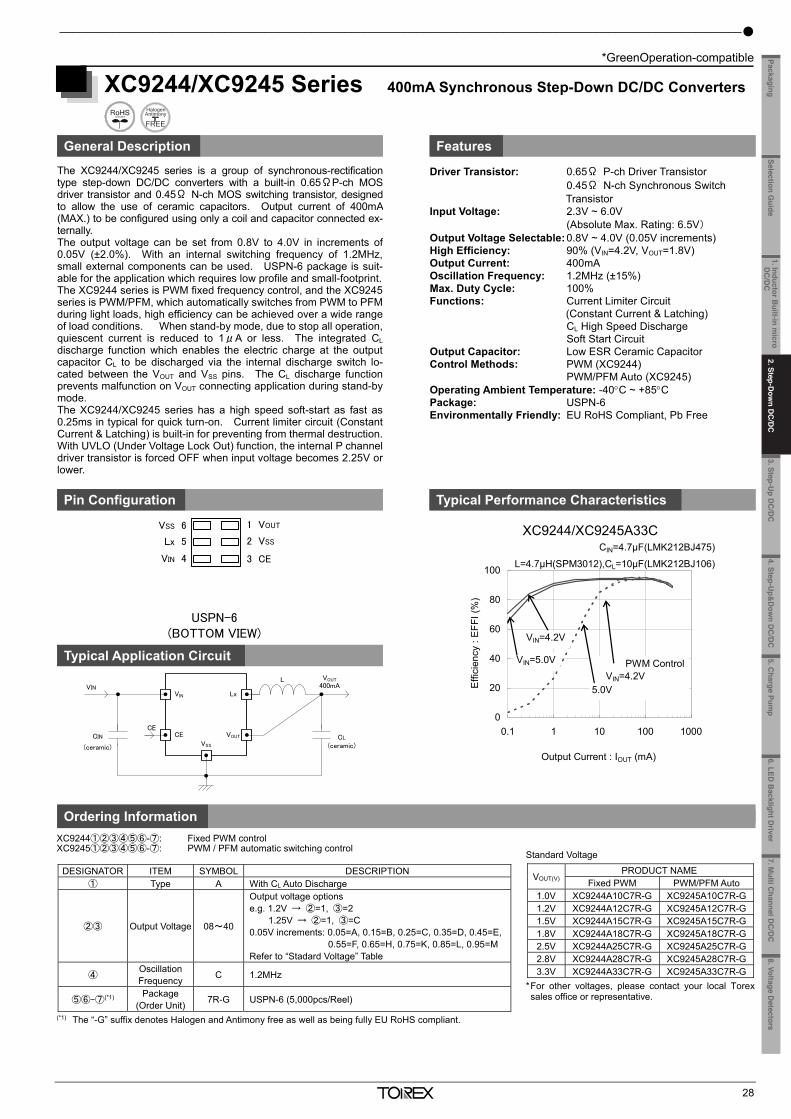
2. Step-Down DC/DC Converters and Controller ICs _____________________________________________
*GreenOperation-compatible
27
XC9248 Series 2.2A 18V Driver Transistor Built-in Synchronous Step-Down DC/DC Converter
General Description Features
The XC9248 series is 18V bootstrap synchronous step-down DC/DC converter with built-in Nch-Nch driver transistors. With an input voltage range from 4.5V to 18V and a maximum output current of 2.2A, the series is suitable for digital home appliance power supplies and can be used with small ceramic capacitors. The series has a 0.8V reference voltage, and using externally con-nected resistors, the output voltage can be set freely from 1.0V to 12V. The control method is synchronous PWM (Source/ Sink). The soft start time is internally set to 2.8ms (TYP.), also can be adjusted using external capacitor. With UVLO (Under Voltage Lock Out) function, the internal driver transistors are forced OFF when input voltage falls down below 3.8V (TYP.). The series includes over current protection, VOUT short-circuit protec-tion, Lx short-circuit protection, VOUT overvoltage protection and thermal shutdown.
Input Voltage: 4.5V ~ 18.0V (Absolute Max. Rating: 20.0V) Output Voltage: 1.0V~12.0V (VFB=0.8V±1.5%) (*1) Output Current: 2.2A Efficiency: 93.8% (*1) @VIN=12V, VOUT=5V, IOUT=700mA Oscillation Frequency: 500kHz Max. Duty Cycle: 79% Soft-Start Time: Fixed 2.8ms, set by external capacitor Protection Circuit: UVLO High side over current protection Low side over current protection VOUT Short-Circuit Protection LX Short-Circuit Protection VOUT Over voltage protection Thermal shutdown Package: SOP-8FD Environmentally Friendly : EU RoHS Compliant, Pb Free (*1) Performance depends on external components and wiring on
the PCB.
Pin Configuration
Typical Application Circuit Typical Performance Characteristics Efficiency vs. Output Current
Ordering Information XC9248①②③④⑤⑥-⑦
DESIGNATOR ITEM SYMBOL DESCRIPTION
① Type A
Refer to [Selection Guide] B
②③ FB Voltage 08 FB voltage is fixed in 0.8V ④ Oscillation Frequency 5 500kHz
⑤⑥-⑦(*1) Package (Order Unit) QR-G SOP-8FD (1,000pcs/Reel) (*1) The “-G” suffix denotes Halogen and Antimony free as well as being fully EU RoHS compliant.
Selection Guide
TYPE CURRENT LIMITER
LATCH FOR CURRENT LIMITER
LATCH FOR VOUT-SHORT
LATCH FOR LX-SHORT (*2) ENABLE UVLO
CL AUTO-
DISCHARGE
THERMAL SHUTDOWN
A YES YES (*1) YES YES YES YES YES YES B YES NO NO YES YES YES YES YES
(*1) The over-current protection latch is an integral latch type. (*2) To prevent an extremely large rush current from flowing in the event that Lx is short-circuited, both the A & B types have an Lx short protection latch function.
SOP-8FD(TOP VIEW)
VIN 1
EN 2
SS 3
FB 4
8 LX
7 GND
6 BST
5 VL
Ta=25°C
0102030405060708090
100
0 500 1000 1500 2000Output Current : IOUT [mA]
Effic
ienc
y [%
]
VIN=12V , VOUT=3.3V
VIN=12V , VOUT=5V
_______________________________________________________________________________________________________
*GreenOperation-compatible
28
XC9244/XC9245 Series 400mA Synchronous Step-Down DC/DC Converters
General Description Features
The XC9244/XC9245 series is a group of synchronous-rectificationtype step-down DC/DC converters with a built-in 0.65ΩP-ch MOSdriver transistor and 0.45Ω N-ch MOS switching transistor, designedto allow the use of ceramic capacitors. Output current of 400mA(MAX.) to be configured using only a coil and capacitor connected ex-ternally. The output voltage can be set from 0.8V to 4.0V in increments of0.05V (±2.0%). With an internal switching frequency of 1.2MHz,small external components can be used. USPN-6 package is suit-able for the application which requires low profile and small-footprint. The XC9244 series is PWM fixed frequency control, and the XC9245series is PWM/PFM, which automatically switches from PWM to PFMduring light loads, high efficiency can be achieved over a wide rangeof load conditions. When stand-by mode, due to stop all operation,quiescent current is reduced to 1μA or less. The integrated CLdischarge function which enables the electric charge at the outputcapacitor CL to be discharged via the internal discharge switch lo-cated between the VOUT and VSS pins. The CL discharge functionprevents malfunction on VOUT connecting application during stand-bymode. The XC9244/XC9245 series has a high speed soft-start as fast as0.25ms in typical for quick turn-on. Current limiter circuit (ConstantCurrent & Latching) is built-in for preventing from thermal destruction.With UVLO (Under Voltage Lock Out) function, the internal P channeldriver transistor is forced OFF when input voltage becomes 2.25V orlower.
Driver Transistor: 0.65Ω P-ch Driver Transistor 0.45Ω N-ch Synchronous Switch
Transistor Input Voltage: 2.3V ~ 6.0V
(Absolute Max. Rating: 6.5V) Output Voltage Selectable: 0.8V ~ 4.0V (0.05V increments) High Efficiency: 90% (VIN=4.2V, VOUT=1.8V) Output Current: 400mA Oscillation Frequency: 1.2MHz (±15%) Max. Duty Cycle: 100% Functions: Current Limiter Circuit (Constant Current & Latching) CL High Speed Discharge Soft Start Circuit Output Capacitor: Low ESR Ceramic Capacitor Control Methods: PWM (XC9244) PWM/PFM Auto (XC9245) Operating Ambient Temperature: -40C ~ +85C Package: USPN-6 Environmentally Friendly: EU RoHS Compliant, Pb Free
Pin Configuration Typical Performance Characteristics
Typical Application Circuit
Ordering Information
XC9244①②③④⑤⑥-⑦: Fixed PWM control XC9245①②③④⑤⑥-⑦: PWM / PFM automatic switching control
DESIGNATOR ITEM SYMBOL DESCRIPTION ① Type A With CL Auto Discharge
②③ Output Voltage 08~40
Output voltage options e.g. 1.2V → ②=1, ③=2 1.25V → ②=1, ③=C 0.05V increments: 0.05=A, 0.15=B, 0.25=C, 0.35=D, 0.45=E,
0.55=F, 0.65=H, 0.75=K, 0.85=L, 0.95=M Refer to “Stadard Voltage” Table
④ Oscillation Frequency C 1.2MHz
⑤⑥-⑦(*1) Package (Order Unit) 7R-G USPN-6 (5,000pcs/Reel)
(*1) The “-G” suffix denotes Halogen and Antimony free as well as being fully EU RoHS compliant.
400mALx
VOUT
VIN
CE
VSS
VOUT
CL
(ceramic)
CIN
(ceramic)
VIN
CE
L
CIN=4.7μF(LMK212BJ475)
L=4.7μH(SPM3012),CL=10μF(LMK212BJ106)
XC9244/XC9245A33C
0
20
40
60
80
100
0.1 1 10 100 1000
Output Current : IOUT (mA)
Effi
cien
cy :
EFF
I (%
)
VIN=4.2V
PWM Control VIN=4.2V5.0V
VIN=5.0V
USPN-6(BOTTOM VIEW)
1 VOUT
2 VSS
3 CE
VSS 6
Lx 5
VIN 4
Standard Voltage
VOUT(V) PRODUCT NAME
Fixed PWM PWM/PFM Auto 1.0V XC9244A10C7R-G XC9245A10C7R-G 1.2V XC9244A12C7R-G XC9245A12C7R-G 1.5V XC9244A15C7R-G XC9245A15C7R-G 1.8V XC9244A18C7R-G XC9245A18C7R-G 2.5V XC9244A25C7R-G XC9245A25C7R-G 2.8V XC9244A28C7R-G XC9245A28C7R-G 3.3V XC9244A33C7R-G XC9245A33C7R-G
* For other voltages, please contact your local Torex sales office or representative.
1. Inductor Built-in m
icro D
C/D
C
3. Step-Up D
C/D
C4. Step-U
p&D
own D
C/D
C
5.Charge Pum
p6.LED
Backlight D
river8.Voltage D
etectorsSelection G
uidePackaging
7. Multi C
hannel DC
/DC
2. Step-D
own D
C/D
C
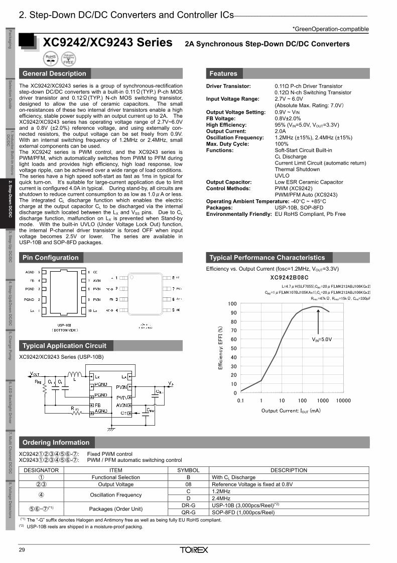
2. Step-Down DC/DC Converters and Controller ICs _____________________________________________
*GreenOperation-compatible
29
XC9242/XC9243 Series 2A Synchronous Step-Down DC/DC Converters
General Description Features
The XC9242/XC9243 series is a group of synchronous-rectification step-down DC/DC converters with a built-in 0.11Ω(TYP.) P-ch MOS driver transistor and 0.12Ω(TYP.) N-ch MOS switching transistor, designed to allow the use of ceramic capacitors. The small on-resistances of these two internal driver transistors enable a high efficiency, stable power supply with an output current up to 2A. The XC9242/XC9243 series has operating voltage range of 2.7V~6.0V and a 0.8V (±2.0%) reference voltage, and using externally con-nected resistors, the output voltage can be set freely from 0.9V. With an internal switching frequency of 1.2MHz or 2.4MHz, small external components can be used. The XC9242 series is PWM control, and the XC9243 series is PWM/PFM, which automatically switches from PWM to PFM during light loads and provides high efficiency, high load response, low voltage ripple, can be achieved over a wide range of load conditions. The series have a high speed soft-start as fast as 1ms in typical for quick turn-on. It’s suitable for large-current application due to limit current is configured 4.0A in typical. During stand-by, all circuits are shutdown to reduce current consumption to as low as 1.0μA or less. The integrated CL discharge function which enables the electric charge at the output capacitor CL to be discharged via the internal discharge switch located between the LX and VSS pins. Due to CL discharge function, malfunction on LX is prevented when Stand-by mode. With the built-in UVLO (Under Voltage Lock Out) function, the internal P-channel driver transistor is forced OFF when input voltage becomes 2.5V or lower. The series are available in USP-10B and SOP-8FD packages.
Driver Transistor: 0.11Ω P-ch Driver Transistor 0.12Ω N-ch Switching Transistor Input Voltage Range: 2.7V ~ 6.0V
(Absolute Max. Rating: 7.0V) Output Voltage Setting: 0.9V ~ VIN FB Voltage: 0.8V±2.0% High Efficiency: 95% (VIN=5.0V, VOUT=3.3V) Output Current: 2.0A Oscillation Frequency: 1.2MHz (±15%), 2.4MHz (±15%) Max. Duty Cycle: 100% Functions: Soft-Start Circuit Built-in CL Discharge Current Limit Circuit (automatic return) Thermal Shutdown UVLO Output Capacitor: Low ESR Ceramic Capacitor Control Methods: PWM (XC9242) PWM/PFM Auto (XC9243) Operating Ambient Temperature: -40C ~ +85C Packages: USP-10B, SOP-8FD Environmentally Friendly: EU RoHS Compliant, Pb Free
Pin Configuration Typical Performance Characteristics
Efficiency vs. Output Current (fosc=1.2MHz, VOUT=3.3V)
Typical Application Circuit
XC9242/XC9243 Series (USP-10B)
Ordering Information
XC9242①②③④⑤⑥-⑦: Fixed PWM control XC9243①②③④⑤⑥-⑦: PWM / PFM automatic switching control
DESIGNATOR ITEM SYMBOL DESCRIPTION ① Functional Selection B With CL Discharge
②③ Output Voltage 08 Reference Voltage is fixed at 0.8V
④ Oscillation Frequency C 1.2MHz D 2.4MHz
⑤⑥-⑦(*1) Packages (Order Unit) DR-G USP-10B (3,000pcs/Reel)(*2) QR-G SOP-8FD (1,000pcs/Reel)
(*1) The “-G” suffix denotes Halogen and Antimony free as well as being fully EU RoHS compliant. (*2) USP-10B reels are shipped in a moisture-proof packing.
XC9242B08C
0
10
20
30
40
50
60
70
80
90
100
0.1 1 10 100 1000 10000
Output Current: IOUT (mA)
Effic
iency:
EFFI (%
)
L=4.7μH(SLF7055),CIN1=20μF(LMK212ABJ106KGx2)
CIN2=1μF(LMK107BJ105KAx1),CL=20μF(LMK212ABJ106KGx2)
RFB1=47kΩ, RFB2=15kΩ, CFB=330pF
VIN=5.0V
_______________________________________________________________________________________________________
30
XC9220/XC9221 Series 16V Input Voltage, Step-Down DC/DC Controller IC
General Description Features
The XC9220/XC9221 series is a group of multi-purpose step-downDC/DC controller ICs. The ICs enable a high efficiency, stablepower supply with an output current up to 3A to be configured usingonly a transistor, a coil, a diode, and two capacitors connected ex-ternally. Low ESR capacitors such as a ceramic capacitor can beused as an output capacitor. The XC9220/XC9221 series has a 0.9V (±1.5%) reference voltage,and using externally connected resistors, the output voltage can beset freely. With an internal switching frequency of 300kHz and500kHz 1MHz, small external components can also be used. TheXC9220 series is PWM control, and the XC9221 series is PWM/PFMmode, which automatically switches from PWM to PFM during lightloads and high efficiencies can be achieved over a wide range of loadconditions. As for the soft-start time, the XC9220/9221A and C se-ries is internally set to 4msec and the XC9220/9221B and D seriescan be externally set-up. With the built-in UVLO (Under VoltageLock Out) function, the external P-channel driver transistor is forcedOFF when input voltage becomes 2.3V or lower. Two types ofpackage, SOT-25 and USP-6, are available.
Operating Voltage Range: 2.8V ~ 16.0V (Absolute Max. Rating: 18.0V) FB Voltage: 1.2V or more, Externally Set (VFB=0.9V ±1.5%) Oscillation Frequency: 300kHz, 500kHz, and 1.0MHz Control Methods: PWM control (XC9220) PWM/PFM (XC9221) Soft-start: 4ms, (Types A, C) Externally set (Types B, D) Protection Circuits: Integral protection (1.0 ms) (Types A, B) Short Circuit Protection Output Capacitor: Low ESR Ceramic Operating Ambient Temperature: -40C ~ +85C Packages: SOT-25, USP-6C Environmentally Friendly: EU RoHS Compliant, Pb Free
Pin Configuration
Typical Application Circuit Typical Performance Characteristics
Ordering Information XC9220①②③④⑤⑥-⑦ : Fixed PWM control XC9221①②③④⑤⑥-⑦ : PWM/PFM automatic switching control
DESIGNATOR ITEM SYMBOL DESCRIPTION
① Type of DC/DC Controller ICs
A Soft-start internally set with integral protection function B Soft-start externally set with integral protection function C Soft-start internally set without integral protection function D
(The Recommended Type) Soft-start externally set without integral protection function
②③ Output Voltage 09 FB Voltage (Fixed)
④ Oscillation Frequency 3 300kHz 5 500kHz A 1MHz
⑤⑥-⑦(*1) Packages (Order Unit) MR-G SOT-25 (3,000pcs/Reel) ER-G USP-6C (3,000pcs/Reel)
(*1) The “-G” suffix denotes Halogen and Antimony free as well as being fully EU RoHS compliant.
SOT-25 (TOP VIEW)
1 2 3
5 4
CE/CSS VSS FB
EXT/VIN
12
3
54
CE
GND
FB
VIN
EXT
CIN
VIN
CL
RFB1
RFB2
CFB
L
SBD
PchMOSFET
VOUT
C E
RSENSE( for ceramic CL )
* RSENSE : Tantalum and electrolytic capacitors can be used, in w hich case, RSENSE becomes unnecessary.
XC9221A095MR (VOUT=3.3V, FOSC=500kHz) CIN=47uF (OS-Con), CL=47uF (OS-Con),
L=10uH (CDRH8D43, SUMIDA) PchMOSFET: CPH3308 (SANYO), CDD=1.0uF (ceramic),
RIN=10Ω
Efficiency vs. Output Current
USP-6C (BOTTOM VIEW)
1 VIN
2 NC
3 EXT/
CE/C SS 6
VSS 5
FB 4
1. Inductor Built-in m
icro D
C/D
C
2. Step-Dow
n DC
/DC
3. Step-Up D
C/D
C4. Step-U
p&D
own D
C/D
C
5.Charge Pum
p6.LED
Backlight D
river8.Voltage D
etectorsSelection G
uidePackaging
7. Multi C
hannel DC
/DC
2. Step-D
own D
C/D
C
2. Step-Down DC/DC Converters and Controller ICs _____________________________________________
*GreenOperation-compatible
29
XC9242/XC9243 Series 2A Synchronous Step-Down DC/DC Converters
General Description Features
The XC9242/XC9243 series is a group of synchronous-rectification step-down DC/DC converters with a built-in 0.11Ω(TYP.) P-ch MOS driver transistor and 0.12Ω(TYP.) N-ch MOS switching transistor, designed to allow the use of ceramic capacitors. The small on-resistances of these two internal driver transistors enable a high efficiency, stable power supply with an output current up to 2A. The XC9242/XC9243 series has operating voltage range of 2.7V~6.0V and a 0.8V (±2.0%) reference voltage, and using externally con-nected resistors, the output voltage can be set freely from 0.9V. With an internal switching frequency of 1.2MHz or 2.4MHz, small external components can be used. The XC9242 series is PWM control, and the XC9243 series is PWM/PFM, which automatically switches from PWM to PFM during light loads and provides high efficiency, high load response, low voltage ripple, can be achieved over a wide range of load conditions. The series have a high speed soft-start as fast as 1ms in typical for quick turn-on. It’s suitable for large-current application due to limit current is configured 4.0A in typical. During stand-by, all circuits are shutdown to reduce current consumption to as low as 1.0μA or less. The integrated CL discharge function which enables the electric charge at the output capacitor CL to be discharged via the internal discharge switch located between the LX and VSS pins. Due to CL discharge function, malfunction on LX is prevented when Stand-by mode. With the built-in UVLO (Under Voltage Lock Out) function, the internal P-channel driver transistor is forced OFF when input voltage becomes 2.5V or lower. The series are available in USP-10B and SOP-8FD packages.
Driver Transistor: 0.11Ω P-ch Driver Transistor 0.12Ω N-ch Switching Transistor Input Voltage Range: 2.7V ~ 6.0V
(Absolute Max. Rating: 7.0V) Output Voltage Setting: 0.9V ~ VIN FB Voltage: 0.8V±2.0% High Efficiency: 95% (VIN=5.0V, VOUT=3.3V) Output Current: 2.0A Oscillation Frequency: 1.2MHz (±15%), 2.4MHz (±15%) Max. Duty Cycle: 100% Functions: Soft-Start Circuit Built-in CL Discharge Current Limit Circuit (automatic return) Thermal Shutdown UVLO Output Capacitor: Low ESR Ceramic Capacitor Control Methods: PWM (XC9242) PWM/PFM Auto (XC9243) Operating Ambient Temperature: -40C ~ +85C Packages: USP-10B, SOP-8FD Environmentally Friendly: EU RoHS Compliant, Pb Free
Pin Configuration Typical Performance Characteristics
Efficiency vs. Output Current (fosc=1.2MHz, VOUT=3.3V)
Typical Application Circuit
XC9242/XC9243 Series (USP-10B)
Ordering Information
XC9242①②③④⑤⑥-⑦: Fixed PWM control XC9243①②③④⑤⑥-⑦: PWM / PFM automatic switching control
DESIGNATOR ITEM SYMBOL DESCRIPTION ① Functional Selection B With CL Discharge
②③ Output Voltage 08 Reference Voltage is fixed at 0.8V
④ Oscillation Frequency C 1.2MHz D 2.4MHz
⑤⑥-⑦(*1) Packages (Order Unit) DR-G USP-10B (3,000pcs/Reel)(*2) QR-G SOP-8FD (1,000pcs/Reel)
(*1) The “-G” suffix denotes Halogen and Antimony free as well as being fully EU RoHS compliant. (*2) USP-10B reels are shipped in a moisture-proof packing.
XC9242B08C
0
10
20
30
40
50
60
70
80
90
100
0.1 1 10 100 1000 10000
Output Current: IOUT (mA)
Effic
iency:
EFFI (%
)
L=4.7μH(SLF7055),CIN1=20μF(LMK212ABJ106KGx2)
CIN2=1μF(LMK107BJ105KAx1),CL=20μF(LMK212ABJ106KGx2)
RFB1=47kΩ, RFB2=15kΩ, CFB=330pF
VIN=5.0V
_______________________________________________________________________________________________________
30
XC9220/XC9221 Series 16V Input Voltage, Step-Down DC/DC Controller IC
General Description Features
The XC9220/XC9221 series is a group of multi-purpose step-downDC/DC controller ICs. The ICs enable a high efficiency, stablepower supply with an output current up to 3A to be configured usingonly a transistor, a coil, a diode, and two capacitors connected ex-ternally. Low ESR capacitors such as a ceramic capacitor can beused as an output capacitor. The XC9220/XC9221 series has a 0.9V (±1.5%) reference voltage,and using externally connected resistors, the output voltage can beset freely. With an internal switching frequency of 300kHz and500kHz 1MHz, small external components can also be used. TheXC9220 series is PWM control, and the XC9221 series is PWM/PFMmode, which automatically switches from PWM to PFM during lightloads and high efficiencies can be achieved over a wide range of loadconditions. As for the soft-start time, the XC9220/9221A and C se-ries is internally set to 4msec and the XC9220/9221B and D seriescan be externally set-up. With the built-in UVLO (Under VoltageLock Out) function, the external P-channel driver transistor is forcedOFF when input voltage becomes 2.3V or lower. Two types ofpackage, SOT-25 and USP-6, are available.
Operating Voltage Range: 2.8V ~ 16.0V (Absolute Max. Rating: 18.0V) FB Voltage: 1.2V or more, Externally Set (VFB=0.9V ±1.5%) Oscillation Frequency: 300kHz, 500kHz, and 1.0MHz Control Methods: PWM control (XC9220) PWM/PFM (XC9221) Soft-start: 4ms, (Types A, C) Externally set (Types B, D) Protection Circuits: Integral protection (1.0 ms) (Types A, B) Short Circuit Protection Output Capacitor: Low ESR Ceramic Operating Ambient Temperature: -40C ~ +85C Packages: SOT-25, USP-6C Environmentally Friendly: EU RoHS Compliant, Pb Free
Pin Configuration
Typical Application Circuit Typical Performance Characteristics
Ordering Information XC9220①②③④⑤⑥-⑦ : Fixed PWM control XC9221①②③④⑤⑥-⑦ : PWM/PFM automatic switching control
DESIGNATOR ITEM SYMBOL DESCRIPTION
① Type of DC/DC Controller ICs
A Soft-start internally set with integral protection function B Soft-start externally set with integral protection function C Soft-start internally set without integral protection function D
(The Recommended Type) Soft-start externally set without integral protection function
②③ Output Voltage 09 FB Voltage (Fixed)
④ Oscillation Frequency 3 300kHz 5 500kHz A 1MHz
⑤⑥-⑦(*1) Packages (Order Unit) MR-G SOT-25 (3,000pcs/Reel) ER-G USP-6C (3,000pcs/Reel)
(*1) The “-G” suffix denotes Halogen and Antimony free as well as being fully EU RoHS compliant.
SOT-25 (TOP VIEW)
1 2 3
5 4
CE/CSS VSS FB
EXT/VIN
12
3
54
CE
GND
FB
VIN
EXT
CIN
VIN
CL
RFB1
RFB2
CFB
L
SBD
PchMOSFET
VOUT
C E
RSENSE( for ceramic CL )
* RSENSE : Tantalum and electrolytic capacitors can be used, in w hich case, RSENSE becomes unnecessary.
XC9221A095MR (VOUT=3.3V, FOSC=500kHz) CIN=47uF (OS-Con), CL=47uF (OS-Con),
L=10uH (CDRH8D43, SUMIDA) PchMOSFET: CPH3308 (SANYO), CDD=1.0uF (ceramic),
RIN=10Ω
Efficiency vs. Output Current
USP-6C (BOTTOM VIEW)
1 VIN
2 NC
3 EXT/
CE/C SS 6
VSS 5
FB 4
1. Inductor Built-in m
icro D
C/D
C
3. Step-Up D
C/D
C4. Step-U
p&D
own D
C/D
C
5.Charge Pum
p6.LED
Backlight D
river8.Voltage D
etectorsSelection G
uidePackaging
7. Multi C
hannel DC
/DC
2. Step-D
own D
C/D
C
2. Step-Down DC/DC Converters and Controller ICs _____________________________________________
*GreenOperation-compatible
31
XC9213 Series 25V Input Synchronous Step-Down DC/DC Controller IC
General Description Features
XC9213 series is N-ch & N-ch drive, synchronous, step-down DC/DC controller IC with a built-in bootstrap driver circuit. Output will be stable no matter which load capacitors, including a low ESR capaci-tor, are used. Resistance (RSENSE) of about several 10m will be required as a current sense. The phase compensation is also run when a low ESR capacitor is used. In addition, the circuit is double protected by the ways of limiting the current while detecting overshoot current and making output shutdown at any given timing by a protection time set-ting capacitor (CPRO). The output voltage can be set freely within a range of 1.5V ~ 15V with 1.0V (±2.0%) of internal reference voltage by using externally con-nected resistors (RFB1, 2). Synchronous rectification PWM control can be switched to non-synchronous 30mV current limit PFM/PWM automatic switchable control (=voltage between RSENSE pins) by using the MODE pin. The series has a built-in voltage detector for monitoring a selected voltage by external resistors. During stand-by (CE pin = low), all circuits are shutdown to reduce current consumption to as low as 4.0μA or less.
Input Voltage Range: 4.0V ~ 25.0V (Absolute Max. Rating: 30.0V)
Output Voltage Range: 1.5V ~ 15V externally set Reference voltage 1.0V ±2.0%
Output Current: More than 5.0A (VIN=5.0V, VOUT=3.3V) Oscillation Frequency: 300kHz ±15% Control: PWM / PFM manual-switching control Current Limiter, protection:
Current limit operates at voltage sense 170mV Shutdown time can be adjustable by CPRO.
High Efficiency: 93% (TYP. PWM mode @ VIN=5.0V, VOUT=3.3V, 1A)
Detect Voltage Function: Detects 0.9V / Open-drain output Stand-by Current: 4.0μA (MAX.) Output Capacitor: Low ESR Ceramic Operating Ambient Temperature: -40C ~ +85C Package: TSSOP-16 Environmentally Friendly: EU RoHS Compliant, Pb Free
Pin Configuration Typical Application Circuit
Typical Performance Characteristics Ordering Information XC9213B①②③④⑤-⑥
DESIGNATOR ITEM SYMBOL DESCRIPTION
①② Reference Voltage 10 1.0V (±2.0%)
③ Oscillation Frequency 3 300kHz
④⑤-⑥(*1) Package (Order Unit) VR-G TSSOP-16
(3,000pcs/Reel) (*1) The “-G” suffix denotes Halogen and Antimony free as well as being fully
EU RoHS compliant.
_______________________________________________________________________________________________________
32
XCM526 Series 3A Step-Down DC/DC Converter with 16V Input
General Description Features The XCM526 series is a multi-module IC which includes a step-down DC/DCcontroller IC and P-channel power MOSFET. The IC enables a high efficien-cy, stable power supply with an output current up to 3A. Low ESR electrolyticcapacitors such as an OS-CON aluminum solid capacitor, a tantalum Neocapacitor can be used as an output capacitor. In case of using a ceramiccapacitor, RSENSE is needed to be placed on. The XCM526 series has a 0.9V (±1.5%) reference voltage, and using exter-nally connected resistors, the output voltage can be set freely. With an in-ternal switching frequency of 500kHz and 1.0MHz, small external componentscan also be used. The XCM526A has a fixed PWM control for low outputvoltage ripple, and the XCM526B has a PWM/PFM control, which automati-cally switches from PWM to PFM during light loads and high efficiencies canbe achieved over a wide range of load conditions. As for the soft-start time,there are two types, one is internally set to 4ms and the other can be externallyset-up. With the built-in UVLO (Under Voltage Lock Out) function, the internalP-channel driver transistor is forced OFF when input voltage becomes 2.3V(TYP.) or lower.
<DC/DC Block> Input Voltage Range: 4.0V ~ 16.0V (Absolute Max. Rating: 18.0V) Output Voltage Externally Set Range: 1.2V ~ (0.9V±1.5%) Max. Output Current: 3.0A Oscillation Frequency: 500kHz、1MHz Control: PWM control (XCM526A) PWM/PFM automatic switching (XCM526B) Soft-Start: 4ms internally fixed and externally set Protection Circuits: Short Circuit Protection <Power MOSFET Block> ON Resistance: 70mΩ (VGS=-4.5V), 47mΩ (VGS=-10.0V) Operating Ambient Temperature: -40C ~ +85C Package: USP-12B01 (2.3mm x 2.8mm) Environmentally Friendly: EU RoHS Compliant, Pb Free
Pin Configuration
Typical Application Circuit Typical Performance Characteristics
Ordering Information
XCM526A①②③④⑤-⑥…PWM control XCM526B①②③④⑤-⑥…PWM/PFM automatic switching control
DESIGNATOR ITEM SYMBOL DESCRIPTION
① Type C Soft-start internally fixed D Soft-start externally set
② Output Voltage 9 FB Standard Voltage 0.9V±1.5%
③ Oscillation Frequency (*2) 5 500kHz A 1.0MHz
④⑤-⑥(*1) Package (Order Unit) DR-G USP-12B01 (3,000pcs/Reel) (*1) The “-G” suffix denotes Halogen and Antimony free as well as being fully EU RoHS compliant. (*2) For the 300kHz type is semi-custom product. Please contact your local Torex sales office or representative.
USP-12B01 (TOP VIEW)
USP-12B01 (BOTTOM VIEW)
(TOP VIEW)
XCM526Ax/Bx9Axx
0
10
20
30
40
50
60
70
80
90
100
0.1 1 10 100 1000 10000
Output Current : IOUT (mA)
Effic
iency
: EFFI (%
)
VIN=5.0V
PWM(XCM526A)
PFM(XCM526B)
VIN=12V
SBD:CLS01, L=SLF10165T-4.7μH
CIN=22uF(ceramic), CL=47uF(ceramic), RSENSE=50mohm
VOUT=3.3V
1. Inductor Built-in m
icro D
C/D
C
2. Step-Dow
n DC
/DC
3. Step-Up D
C/D
C4. Step-U
p&D
own D
C/D
C
5.Charge Pum
p6.LED
Backlight D
river8.Voltage D
etectorsSelection G
uidePackaging
7. Multi C
hannel DC
/DC
2. Step-D
own D
C/D
C
2. Step-Down DC/DC Converters and Controller ICs _____________________________________________
*GreenOperation-compatible
31
XC9213 Series 25V Input Synchronous Step-Down DC/DC Controller IC
General Description Features
XC9213 series is N-ch & N-ch drive, synchronous, step-down DC/DC controller IC with a built-in bootstrap driver circuit. Output will be stable no matter which load capacitors, including a low ESR capaci-tor, are used. Resistance (RSENSE) of about several 10m will be required as a current sense. The phase compensation is also run when a low ESR capacitor is used. In addition, the circuit is double protected by the ways of limiting the current while detecting overshoot current and making output shutdown at any given timing by a protection time set-ting capacitor (CPRO). The output voltage can be set freely within a range of 1.5V ~ 15V with 1.0V (±2.0%) of internal reference voltage by using externally con-nected resistors (RFB1, 2). Synchronous rectification PWM control can be switched to non-synchronous 30mV current limit PFM/PWM automatic switchable control (=voltage between RSENSE pins) by using the MODE pin. The series has a built-in voltage detector for monitoring a selected voltage by external resistors. During stand-by (CE pin = low), all circuits are shutdown to reduce current consumption to as low as 4.0μA or less.
Input Voltage Range: 4.0V ~ 25.0V (Absolute Max. Rating: 30.0V)
Output Voltage Range: 1.5V ~ 15V externally set Reference voltage 1.0V ±2.0%
Output Current: More than 5.0A (VIN=5.0V, VOUT=3.3V) Oscillation Frequency: 300kHz ±15% Control: PWM / PFM manual-switching control Current Limiter, protection:
Current limit operates at voltage sense 170mV Shutdown time can be adjustable by CPRO.
High Efficiency: 93% (TYP. PWM mode @ VIN=5.0V, VOUT=3.3V, 1A)
Detect Voltage Function: Detects 0.9V / Open-drain output Stand-by Current: 4.0μA (MAX.) Output Capacitor: Low ESR Ceramic Operating Ambient Temperature: -40C ~ +85C Package: TSSOP-16 Environmentally Friendly: EU RoHS Compliant, Pb Free
Pin Configuration Typical Application Circuit
Typical Performance Characteristics Ordering Information XC9213B①②③④⑤-⑥
DESIGNATOR ITEM SYMBOL DESCRIPTION
①② Reference Voltage 10 1.0V (±2.0%)
③ Oscillation Frequency 3 300kHz
④⑤-⑥(*1) Package (Order Unit) VR-G TSSOP-16
(3,000pcs/Reel) (*1) The “-G” suffix denotes Halogen and Antimony free as well as being fully
EU RoHS compliant.
_______________________________________________________________________________________________________
32
XCM526 Series 3A Step-Down DC/DC Converter with 16V Input
General Description Features The XCM526 series is a multi-module IC which includes a step-down DC/DCcontroller IC and P-channel power MOSFET. The IC enables a high efficien-cy, stable power supply with an output current up to 3A. Low ESR electrolyticcapacitors such as an OS-CON aluminum solid capacitor, a tantalum Neocapacitor can be used as an output capacitor. In case of using a ceramiccapacitor, RSENSE is needed to be placed on. The XCM526 series has a 0.9V (±1.5%) reference voltage, and using exter-nally connected resistors, the output voltage can be set freely. With an in-ternal switching frequency of 500kHz and 1.0MHz, small external componentscan also be used. The XCM526A has a fixed PWM control for low outputvoltage ripple, and the XCM526B has a PWM/PFM control, which automati-cally switches from PWM to PFM during light loads and high efficiencies canbe achieved over a wide range of load conditions. As for the soft-start time,there are two types, one is internally set to 4ms and the other can be externallyset-up. With the built-in UVLO (Under Voltage Lock Out) function, the internalP-channel driver transistor is forced OFF when input voltage becomes 2.3V(TYP.) or lower.
<DC/DC Block> Input Voltage Range: 4.0V ~ 16.0V (Absolute Max. Rating: 18.0V) Output Voltage Externally Set Range: 1.2V ~ (0.9V±1.5%) Max. Output Current: 3.0A Oscillation Frequency: 500kHz、1MHz Control: PWM control (XCM526A) PWM/PFM automatic switching (XCM526B) Soft-Start: 4ms internally fixed and externally set Protection Circuits: Short Circuit Protection <Power MOSFET Block> ON Resistance: 70mΩ (VGS=-4.5V), 47mΩ (VGS=-10.0V) Operating Ambient Temperature: -40C ~ +85C Package: USP-12B01 (2.3mm x 2.8mm) Environmentally Friendly: EU RoHS Compliant, Pb Free
Pin Configuration
Typical Application Circuit Typical Performance Characteristics
Ordering Information
XCM526A①②③④⑤-⑥…PWM control XCM526B①②③④⑤-⑥…PWM/PFM automatic switching control
DESIGNATOR ITEM SYMBOL DESCRIPTION
① Type C Soft-start internally fixed D Soft-start externally set
② Output Voltage 9 FB Standard Voltage 0.9V±1.5%
③ Oscillation Frequency (*2) 5 500kHz A 1.0MHz
④⑤-⑥(*1) Package (Order Unit) DR-G USP-12B01 (3,000pcs/Reel) (*1) The “-G” suffix denotes Halogen and Antimony free as well as being fully EU RoHS compliant. (*2) For the 300kHz type is semi-custom product. Please contact your local Torex sales office or representative.
USP-12B01 (TOP VIEW)
USP-12B01 (BOTTOM VIEW)
(TOP VIEW)
XCM526Ax/Bx9Axx
0
10
20
30
40
50
60
70
80
90
100
0.1 1 10 100 1000 10000
Output Current : IOUT (mA)
Effic
iency
: EFFI (%
)
VIN=5.0V
PWM(XCM526A)
PFM(XCM526B)
VIN=12V
SBD:CLS01, L=SLF10165T-4.7μH
CIN=22uF(ceramic), CL=47uF(ceramic), RSENSE=50mohm
VOUT=3.3V
1. Inductor Built-in m
icro D
C/D
C
3. Step-Up D
C/D
C4. Step-U
p&D
own D
C/D
C
5.Charge Pum
p6.LED
Backlight D
river8.Voltage D
etectorsSelection G
uidePackaging
7. Multi C
hannel DC
/DC
2. Step-D
own D
C/D
C
3. Step-Up DC/DC Converters and Controller ICs _________________________________________________
*GreenOperation-compatible
33
XC9141/XC9142 Series Load Disconnection Function, 0.8A Step-Up DC/DC Converters
General Description Features
XC9141/XC9142 series are synchronous step-up DC/DC converters with a 0.3Ω(TYP.) N-channel driver transistor and a 0.4Ω(TYP.) syn-chronous P-channel switching transistor built-in. A highly efficient and stable current can be supplied up to 0.8A by reducing ON re-sistance of the built-in transistors. The series are able to start operation under the condition which has 0.9V input voltage (VBAT) to generate 3.3V output voltage with a 100Ωload resistor, suitable for mobile equipment using only one Al-kaline battery or one Nickel metal hydride battery. The output voltage can be set from 1.8V to 5.5V (±2.0%) in steps of 0.1V.With the built-in oscillator, either 1.2MHz or 3.0MHz can be se-lected for suiting to your particular application. During the devices enter stand-by mode, A, D type prevent the ap-plication malfunction by CL Discharge Function which can quickly discharge the electric charge at the output capacitor (CL). B, E type is able to drive RTC etc. by Bypass Switch Function to maintain conti-nuity between the input and output. C, F type is able to connect in parallel with other power supplies by Load Disconnection Function which breaks continuity between the input and output. * Type D, E, and F are under development.
Input Voltage Range: 0.65V~6.0V (Absolute Max. Rating: 7.0V) Fixed Output Voltages: 1.8V~5.5V (0.1V increments Type A, B, C) 2.2V~2.5V (Type D, E, F) Oscillation Frequency: 1.2MHz (±15%),3MHz (±20%) Input Current: 0.8A Output Current: 500mA @VOUT=5.0V, VBAT=3.3V (TYP.) 350mA @VOUT=3.3V, VBAT=1.8V (TYP.) Control Mode Selection: PWM (XC9141 Series) or Auto PWM/PFM (XC9142 Series) Load Transient Response: 100mV @VOUT=3.3V,VBAT=1.8V,VOUT=1mA→200mA (tr=5μs) Protection Circuits: Over-current limit Integral latch method (Type D,E,F) Output short-circuit protection (Type D,E,F) Functions: Soft-start Load Disconnection Function (Type A,C,D,F) CL Auto Discharge Function (Type A,D) Bypass Switch Function (Type B,E) Output Capacitor: Ceramic Capacitor Operating Ambient Temperature: -40~+85 Packages: SOT-25, USP-6C, WLP-6-01 Environmentally Friendly: EU RoHS Compliant, Pb Free * Type D, E and F are under development.
Pin Configuration Typical Performance Characteristics
Efficiency vs. Output Current
Typical Application Circuit T
4D)
Ordering Information
XC9141①②③④⑤⑥-⑦ PWM control XC9142①②③④⑤⑥-⑦ PWM/PFM automatic switching control DESIGNATOR ITEM SYMBOL DESCRIPTION
① Type
A
Refer to Selection Guide B D(*2) E(*2)
②③
Output Voltage (XC9141A,B Type) 18~55 Output voltage options e.g. 1.8V
→ ②=1, ③=8 Output Voltage
(XC9141D,E Type) 22~55 Output voltage options e.g. 2.2V → ②=2, ③=2
④ Oscillation Frequency
C 1.2MHz D 3.0MHz
⑤⑥-⑦(*1) Packages (Order Unit)
MR-G SOT-25 (3,000pcs/Reel) ER-G USP-6C (3,000pcs/Reel) 0R-G WLP-6-01 (5,000pcs/Reel)
(*1) The “-G” suffix denotes Halogen and Antimony free as well as being fully EU RoHs compliant. (*2) Type D and E are under development. Selection Guide
TYPE OUTPUT VOLTAGE CHIP ENABLE SOFT-START CURRENT LIMIT SHORT PROTECTION WITH LATCH CL AUTO-DISCHARGE SHUTDOWN OPTIONS
AT CE=L A Fixed Yes Fixed Yes (without latch ) No Yes Complete Output Disconnect(*2) B Fixed Yes Fixed Yes (without latch ) No No Input-to-Output Bypass(*2)
C(*1) Fixed Yes Fixed Yes (without latch ) No No Complete Output Disconnect(*3) D(*4) Fixed Yes Fixed Yes (with integral latch) Yes Yes Complete Output Disconnect(*2) E(*4) Fixed Yes Fixed Yes (with integral latch) Yes No Input-to-Output Bypass(*2)
F(*1) (*4) Fixed Yes Fixed Yes (with integral latch) Yes No Complete Output Disconnect(*3) (*1) Type C, F is available for the XC9142 series only. (*2) VOUT pin can not be connected to the different output pin such as another supply (AC adaptor). (*3) VOUT pin can be connected to the different output pin such as another supply (AC adaptor). (*4) Type D, E, and F are under development.
1 32
5 4VOUTLx
CE GND BAT USP-6C(BOTTOM VIEW)
2 GND
1 BAT
3 CE
VOUT 6
Lx 5
GND 4
SOT-25(TOP VIEW)
2 GND
1 BAT
3 CE
VOUT 6
Lx 5
GND 4
WLP-6-01(BOTTOM VIEW)
DESIGNATOR ITEM SYMBOL DESCRIPTION
① Type
A
Refer to Selection Guide
B C
D(*2) E(*2) F(*2)
②③
Output Voltage (XC9142A,B,C Type) 18~55 Output voltage options e.g. 1.8V
→ ②=1, ③=8 Output Voltage
(XC9142D,E,F Type) 22~55 Output voltage options e.g. 2.2V → ②=2, ③=2
④ Oscillation Frequency
C 1.2MHz D 3.0MHz
⑤⑥-⑦(*1) Packages (Order Unit)
MR-G SOT-25 (3,000pcs/Reel) ER-G USP-6C (3,000pcs/Reel) 0R-G WLP-6-01 (5,000pcs/Reel)
(*1) The “-G” suffix denotes Halogen and Antimony free as well as being fully EU RoHs compliant. (*2) Type D, E, and F are under development.
L=4.7μH(LQH5BPN4R7NT0L)CIN=10μF(GRM188R60J106M),CL=10μF(GRM188R60J106M)
XC9141A33C / XC9142A33C
0
10
20
30
40
50
60
70
80
90
100
0.1 1 10 100 1000
Effic
ienc
y : E
FFI
[%]
Output Current : IOUT [mA]
VBAT=0.9VVBAT=1.2VVBAT=1.8VVBAT=2.5V
solid line : XC9141dotted line : XC9142
CIN=10μF
CL=10μF
L=4.7μH
VOUT
GNDBAT
CE
Lx
VIN
CE
VOUT
_______________________________________________________________________________________________________
*GreenOperation-compatible
34
XC9140 Series PFM Control, Step-Up Synchronous DC/DC Converter
General Description Features
The XC9140 series are step-up synchronous DC/DC converters thatsupport ceramic capacitors and have an internal 0.6Ω (TYP.) Nchdriver transistor and an internal 0.65Ω (TYP.) Pch synchronous recti-fier switch transistor. PFM control enables a low quiescent current,making these products ideal for portable devices that require high ef-ficiency. When the output voltage is 3.3V and the output current is 1mA,startup from an input voltage of VBAT=0.9V is possible which meansthat the XC9140 can be used in applications that start from a singlealkaline or nickel-metal hydride battery. The output voltage can be setfrom 1.8V to 5.0V (±2.0%) in steps of 0.1V. The XC9140 features a load disconnect function to break continuitybetween the input and output at shutdown (XC9140A), and also abypass mode function to maintain continuity between the input andoutput (XC9140C). A version with a UVLO (Under Voltage Lock Out) function will also beavailable (currently under development) which enables the preven-tion of battery leakage by stopping the IC’s operation when the inputvoltage is low. The standard product will have a UVLO release volt-age of 2.15V (±3.0%) and a custom version with a UVLO releasevoltage selectable from between 1.65V to 2.2V, in steps of 0.05V, willalso be made available.
High Efficiency Step-up DC/DC Converter at light load Efficiency 80% @VOUT=3.3V, VBAT=1.8V, IOUT=100μA
Input Voltage Range: 0.9V~5.5V (Absolute Max. Rating: 7.0V) Output Voltage Setting: 1.8V~5.0V (±2.0%) 0.1V increments Output Current: 100mA@VOUT=3.3V, VBAT=1.8V (TYP.) Driver Transistor: 0.6Ω Nch driver transistor 0.65Ω Pch synchronous rectifier switch
transistor Quiescent Current: 6.3μA (VBAT=VOUT+0.5V) Control Method: PFM Control High Speed Transient Response: 50mV@VOUT=3.3V, VBAT=1.8V,
IOUT=1→50mA PFM Switching Current: 350mA Functions: Load Disconnection Function or Bypass Mode Function UVLO Inrush Current Protection Ceramic Capacitor Operating Ambient Temperature: -40~+85 Packages: SOT-25, USP-6EL Environmentally Friendly: EU RoHS Compliant, Pb Free
Pin Configuration
Typical Application Circuit Typical Performance Characteristics
Ordering Information XC9140①②③④⑤⑥-⑦ PFM contrtol
DESIGNATOR ITEM SYMBOL DESCRIPTION
① (*1) Product Type A Load Disconnection Without CL Auto Discharge C VBAT Bypass Without CL Auto Discharge
②③ (*2) Output Voltage 18~50 Output Voltage e.g. VOUT=3.3V⇒②=3, ③=3
④ UVLO Function 1 No UVLO 2 UVLO Function, VUVLO_R=2.15V
⑤⑥-⑦ (*3) Packages (Order Unit) 4R-G USP-6EL (3,000pcs/Reel) MR-G SOT-25 (3,000pcs/Reel)
(*1) The product with the CL discharge function is a semi-custom product. (*2) VOUT=3.3V is standard. (*3) The “-G” suffix denotes Halogen and Antimony free as well as being fully EU RoHs compliant.
1 32
5 4
SOT-25(TOP VIEW)
VOUTLX
CE GND VBAT
LX
VBAT
VOUT
GND
CE
L=4.7μH
CL=10μF
CIN=10μF
VIN=0.9~5.5V
CIN=4.7μF
VBAT=0.9~5.5V
0
20
40
60
80
100
0.01 0.1 1 10 100 1000
Output Current : IOUT (mA)
Eff
icie
ncy
: E
FF
I (%
)
3.0V VBAT=1.8V
2.5V
XC9140A331MR-G(VOUT=3.3V)L=4.7μH(VLF302512M-4R7M),CIN=4.7μF(LMK107BJ475MA),
CL=10μF(LMK107BJ106MA)
1. Inductor Built-in m
icro D
C/D
C
2. Step-Dow
n DC
/DC
3. Step-Up D
C/D
C4. Step-U
p&D
own D
C/D
C
5.Charge Pum
p6.LED
Backlight D
river8.Voltage D
etectorsSelection G
uidePackaging
7. Multi C
hannel DC
/DC
3. Step-U
p DC
/DC
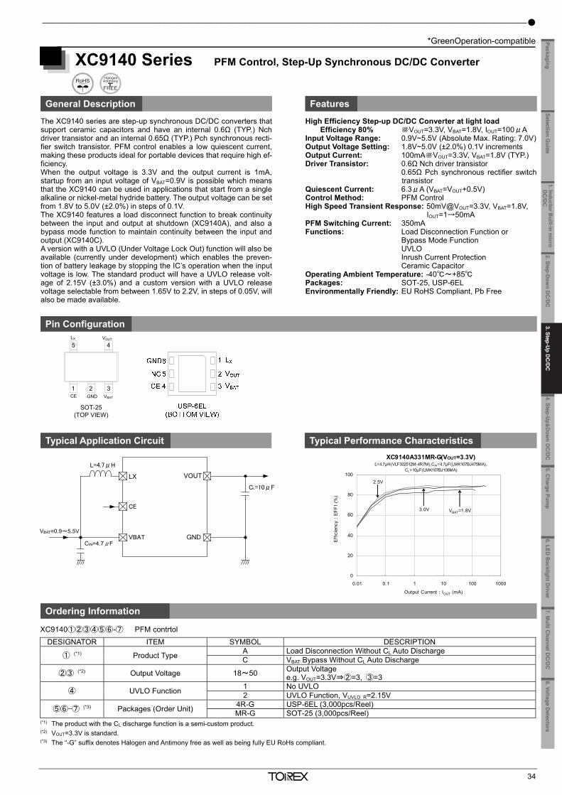
3. Step-Up DC/DC Converters and Controller ICs _________________________________________________
*GreenOperation-compatible
33
XC9141/XC9142 Series Load Disconnection Function, 0.8A Step-Up DC/DC Converters
General Description Features
XC9141/XC9142 series are synchronous step-up DC/DC converters with a 0.3Ω(TYP.) N-channel driver transistor and a 0.4Ω(TYP.) syn-chronous P-channel switching transistor built-in. A highly efficient and stable current can be supplied up to 0.8A by reducing ON re-sistance of the built-in transistors. The series are able to start operation under the condition which has 0.9V input voltage (VBAT) to generate 3.3V output voltage with a 100Ωload resistor, suitable for mobile equipment using only one Al-kaline battery or one Nickel metal hydride battery. The output voltage can be set from 1.8V to 5.5V (±2.0%) in steps of 0.1V.With the built-in oscillator, either 1.2MHz or 3.0MHz can be se-lected for suiting to your particular application. During the devices enter stand-by mode, A, D type prevent the ap-plication malfunction by CL Discharge Function which can quickly discharge the electric charge at the output capacitor (CL). B, E type is able to drive RTC etc. by Bypass Switch Function to maintain conti-nuity between the input and output. C, F type is able to connect in parallel with other power supplies by Load Disconnection Function which breaks continuity between the input and output. * Type D, E, and F are under development.
Input Voltage Range: 0.65V~6.0V (Absolute Max. Rating: 7.0V) Fixed Output Voltages: 1.8V~5.5V (0.1V increments Type A, B, C) 2.2V~2.5V (Type D, E, F) Oscillation Frequency: 1.2MHz (±15%),3MHz (±20%) Input Current: 0.8A Output Current: 500mA @VOUT=5.0V, VBAT=3.3V (TYP.) 350mA @VOUT=3.3V, VBAT=1.8V (TYP.) Control Mode Selection: PWM (XC9141 Series) or Auto PWM/PFM (XC9142 Series) Load Transient Response: 100mV @VOUT=3.3V,VBAT=1.8V,VOUT=1mA→200mA (tr=5μs) Protection Circuits: Over-current limit Integral latch method (Type D,E,F) Output short-circuit protection (Type D,E,F) Functions: Soft-start Load Disconnection Function (Type A,C,D,F) CL Auto Discharge Function (Type A,D) Bypass Switch Function (Type B,E) Output Capacitor: Ceramic Capacitor Operating Ambient Temperature: -40~+85 Packages: SOT-25, USP-6C, WLP-6-01 Environmentally Friendly: EU RoHS Compliant, Pb Free * Type D, E and F are under development.
Pin Configuration Typical Performance Characteristics
Efficiency vs. Output Current
Typical Application Circuit T
4D)
Ordering Information
XC9141①②③④⑤⑥-⑦ PWM control XC9142①②③④⑤⑥-⑦ PWM/PFM automatic switching control DESIGNATOR ITEM SYMBOL DESCRIPTION
① Type
A
Refer to Selection Guide B D(*2) E(*2)
②③
Output Voltage (XC9141A,B Type) 18~55 Output voltage options e.g. 1.8V
→ ②=1, ③=8 Output Voltage
(XC9141D,E Type) 22~55 Output voltage options e.g. 2.2V → ②=2, ③=2
④ Oscillation Frequency
C 1.2MHz D 3.0MHz
⑤⑥-⑦(*1) Packages (Order Unit)
MR-G SOT-25 (3,000pcs/Reel) ER-G USP-6C (3,000pcs/Reel) 0R-G WLP-6-01 (5,000pcs/Reel)
(*1) The “-G” suffix denotes Halogen and Antimony free as well as being fully EU RoHs compliant. (*2) Type D and E are under development. Selection Guide
TYPE OUTPUT VOLTAGE CHIP ENABLE SOFT-START CURRENT LIMIT SHORT PROTECTION WITH LATCH CL AUTO-DISCHARGE SHUTDOWN OPTIONS
AT CE=L A Fixed Yes Fixed Yes (without latch ) No Yes Complete Output Disconnect(*2) B Fixed Yes Fixed Yes (without latch ) No No Input-to-Output Bypass(*2)
C(*1) Fixed Yes Fixed Yes (without latch ) No No Complete Output Disconnect(*3) D(*4) Fixed Yes Fixed Yes (with integral latch) Yes Yes Complete Output Disconnect(*2) E(*4) Fixed Yes Fixed Yes (with integral latch) Yes No Input-to-Output Bypass(*2)
F(*1) (*4) Fixed Yes Fixed Yes (with integral latch) Yes No Complete Output Disconnect(*3) (*1) Type C, F is available for the XC9142 series only. (*2) VOUT pin can not be connected to the different output pin such as another supply (AC adaptor). (*3) VOUT pin can be connected to the different output pin such as another supply (AC adaptor). (*4) Type D, E, and F are under development.
1 32
5 4VOUTLx
CE GND BAT USP-6C(BOTTOM VIEW)
2 GND
1 BAT
3 CE
VOUT 6
Lx 5
GND 4
SOT-25(TOP VIEW)
2 GND
1 BAT
3 CE
VOUT 6
Lx 5
GND 4
WLP-6-01(BOTTOM VIEW)
DESIGNATOR ITEM SYMBOL DESCRIPTION
① Type
A
Refer to Selection Guide
B C
D(*2) E(*2) F(*2)
②③
Output Voltage (XC9142A,B,C Type) 18~55 Output voltage options e.g. 1.8V
→ ②=1, ③=8 Output Voltage
(XC9142D,E,F Type) 22~55 Output voltage options e.g. 2.2V → ②=2, ③=2
④ Oscillation Frequency
C 1.2MHz D 3.0MHz
⑤⑥-⑦(*1) Packages (Order Unit)
MR-G SOT-25 (3,000pcs/Reel) ER-G USP-6C (3,000pcs/Reel) 0R-G WLP-6-01 (5,000pcs/Reel)
(*1) The “-G” suffix denotes Halogen and Antimony free as well as being fully EU RoHs compliant. (*2) Type D, E, and F are under development.
L=4.7μH(LQH5BPN4R7NT0L)CIN=10μF(GRM188R60J106M),CL=10μF(GRM188R60J106M)
XC9141A33C / XC9142A33C
0
10
20
30
40
50
60
70
80
90
100
0.1 1 10 100 1000
Effic
ienc
y : E
FFI
[%]
Output Current : IOUT [mA]
VBAT=0.9VVBAT=1.2VVBAT=1.8VVBAT=2.5V
solid line : XC9141dotted line : XC9142
CIN=10μF
CL=10μF
L=4.7μH
VOUT
GNDBAT
CE
Lx
VIN
CE
VOUT
_______________________________________________________________________________________________________
*GreenOperation-compatible
34
XC9140 Series PFM Control, Step-Up Synchronous DC/DC Converter
General Description Features
The XC9140 series are step-up synchronous DC/DC converters thatsupport ceramic capacitors and have an internal 0.6Ω (TYP.) Nchdriver transistor and an internal 0.65Ω (TYP.) Pch synchronous recti-fier switch transistor. PFM control enables a low quiescent current,making these products ideal for portable devices that require high ef-ficiency. When the output voltage is 3.3V and the output current is 1mA,startup from an input voltage of VBAT=0.9V is possible which meansthat the XC9140 can be used in applications that start from a singlealkaline or nickel-metal hydride battery. The output voltage can be setfrom 1.8V to 5.0V (±2.0%) in steps of 0.1V. The XC9140 features a load disconnect function to break continuitybetween the input and output at shutdown (XC9140A), and also abypass mode function to maintain continuity between the input andoutput (XC9140C). A version with a UVLO (Under Voltage Lock Out) function will also beavailable (currently under development) which enables the preven-tion of battery leakage by stopping the IC’s operation when the inputvoltage is low. The standard product will have a UVLO release volt-age of 2.15V (±3.0%) and a custom version with a UVLO releasevoltage selectable from between 1.65V to 2.2V, in steps of 0.05V, willalso be made available.
High Efficiency Step-up DC/DC Converter at light load Efficiency 80% @VOUT=3.3V, VBAT=1.8V, IOUT=100μA
Input Voltage Range: 0.9V~5.5V (Absolute Max. Rating: 7.0V) Output Voltage Setting: 1.8V~5.0V (±2.0%) 0.1V increments Output Current: 100mA@VOUT=3.3V, VBAT=1.8V (TYP.) Driver Transistor: 0.6Ω Nch driver transistor 0.65Ω Pch synchronous rectifier switch
transistor Quiescent Current: 6.3μA (VBAT=VOUT+0.5V) Control Method: PFM Control High Speed Transient Response: 50mV@VOUT=3.3V, VBAT=1.8V,
IOUT=1→50mA PFM Switching Current: 350mA Functions: Load Disconnection Function or Bypass Mode Function UVLO Inrush Current Protection Ceramic Capacitor Operating Ambient Temperature: -40~+85 Packages: SOT-25, USP-6EL Environmentally Friendly: EU RoHS Compliant, Pb Free
Pin Configuration
Typical Application Circuit Typical Performance Characteristics
Ordering Information XC9140①②③④⑤⑥-⑦ PFM contrtol
DESIGNATOR ITEM SYMBOL DESCRIPTION
① (*1) Product Type A Load Disconnection Without CL Auto Discharge C VBAT Bypass Without CL Auto Discharge
②③ (*2) Output Voltage 18~50 Output Voltage e.g. VOUT=3.3V⇒②=3, ③=3
④ UVLO Function 1 No UVLO 2 UVLO Function, VUVLO_R=2.15V
⑤⑥-⑦ (*3) Packages (Order Unit) 4R-G USP-6EL (3,000pcs/Reel) MR-G SOT-25 (3,000pcs/Reel)
(*1) The product with the CL discharge function is a semi-custom product. (*2) VOUT=3.3V is standard. (*3) The “-G” suffix denotes Halogen and Antimony free as well as being fully EU RoHs compliant.
1 32
5 4
SOT-25(TOP VIEW)
VOUTLX
CE GND VBAT
LX
VBAT
VOUT
GND
CE
L=4.7μH
CL=10μF
CIN=10μF
VIN=0.9~5.5V
CIN=4.7μF
VBAT=0.9~5.5V
0
20
40
60
80
100
0.01 0.1 1 10 100 1000
Output Current : IOUT (mA)
Eff
icie
ncy
: E
FF
I (%
)
3.0V VBAT=1.8V
2.5V
XC9140A331MR-G(VOUT=3.3V)L=4.7μH(VLF302512M-4R7M),CIN=4.7μF(LMK107BJ475MA),
CL=10μF(LMK107BJ106MA)
1. Inductor Built-in m
icro D
C/D
C
2. Step-Dow
n DC
/DC
4. Step-Up&
Dow
n DC
/DC
5.C
harge Pump
6.LED B
acklight Driver
8.Voltage Detectors
Selection Guide
Packaging7. M
ulti Channel D
C/D
C
3. Step-Up D
C/D
C
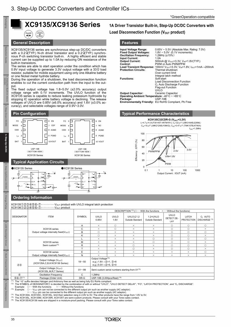
3. Step-Up DC/DC Converters and Controller ICs _________________________________________________
*GreenOperation-compatible
35
XC9136 Series XC9135 Series
XC9135/XC9136 Series 1A Driver Transistor Built-in, Step-Up DC/DC Converters with Load Disconnection Function (VOUT product)
General Description Features
XC9135/XC9136 series are synchronous step-up DC/DC converters with a 0.2Ω(TYP.) N-ch driver transistor and a 0.2Ω(TYP.) synchro-nous P-ch switching transistor built-in. A highly efficient and stable current can be supplied up to 1.0A by reducing ON resistance of the built-in transistors. The series are able to start operation under the condition which has 0.9V input voltage to generate 3.3V output voltage with a 33Ω load resistor, suitable for mobile equipment using only one Alkaline battery or one Nickel metal hydride battery. During the operation of a shutdown, the load disconnection function enables to cut the current conduction path from the input to the out-put. The fixed output voltage has 1.8~5.0V (±2.0% accuracy) output voltage range with 0.1V increments. The UVLO function of the XC9135 series is capable to reduce leaking potassium hydroxide by stopping IC operation while battery voltage is declining. The release voltages of UVLO are 0.85V (±6.0% accuracy) and 1.6V (±3.0% ac-curacy), and selectable voltages range of 0.9V~3.0V.
Input Voltage Range: 0.65V ~ 5.5V (Absolute Max. Rating: 7.0V) Fixed Output Voltages: 1.8V ~ 5.0V (0.1V increments) Oscillation Frequency: 1.2MHz (±15%) Input Current: 1.0A Output Current: 500mA @ VOUT=3.3V, VIN=1.8V(TYP.) Control: PWM or Auto PWM/PFM Load Transient Response: 100mV VOUT=3.3V, VIN=1.8V, IOUT=1mA→200mA Protection Circuits: Thermal shutdown Over-current limit Integral latch method Functions: Soft-start Load Disconnection Function CL Auto Discharge Function Flag-out Function UVLO Output Capacitor: Ceramic Capacitor Operating Ambient Temperature: -40C ~ +85C Package: USP-10B Environmentally Friendly: EU RoHS Compliant, Pb Free
Pin Configuration Typical Performance Characteristics
Typical Application Circuits
XC9135 Series XC9136 Series
Ordering Information XC9135①②③④⑤⑥-⑦・・・・・・・・・・VOUT product with UVLO integral latch protection
XC9136①②③④⑤⑥-⑦・・・・・・・・・・VOUT product
DESIGNATOR ITEM SYMBOL
DESCRIPTION (*2) (・・・With the functions ・・・Without the functions)
UVLO 0.85V
UVLO 1.6V
UVLO≦1.2 Outside Standard
1.2<UVLO Outside Standard
UVLO DETECT DE-
LAY
LATCH PROTECTION
CL AUTO DISCHARGE (*3)
①
XC9135 series Output voltage internally fixed(VOUT)
A C B K
XC9135 series Semi custom(*5)
L M R T
XC9136 series Output voltage internally fixed(VOUT)
E N
②③
Output Voltage (VOUT) (XC9135A,C,B,K/XC9136 Series) 18~50
Output Voltage(*4) e.g.) 1.8V→②=1, ③=8 e.g.) 5.0V→②=5, ③=0
Output Voltage (VOUT) (XC9135L,M,R,T Series) 01~99 Semi custom serial numbers starting from 01(*5)
④ Oscillation Frequency C 1.2MHz ⑤⑥-⑦(*1) Package (Order Unit) DR-G USP-10B (3,000pcs/Reel) (*6)
(*1) The “-G” suffix denotes Halogen and Antimony free as well as being fully EU RoHs compliant. (*2) The SYMBOL of DESIGNATOR① is decided by the combination of with or without “UVLO”, “UVLO DETECT DELAY”, “FO”, “LATCH PROTECTION”, and “CL DISCHARGE”.
Example: ・・・With the functions ・・・Without the functions (*3) Example: ・・・VOUT pin can not be connected to the different output pin such as another supply (AC adaptor).
・・・VOUT pin can be connected to the different output pin such as another supply (AC adaptor). (*4) The XC9135A, XC9135C, XC9135L, limit their selection rang in 2.8V to 5V. The other products have the range from 1.8V to 5V. (*5) The XC9135L, XC9135M, XC9135R, XC9135T are semi-custom products. Please consult with your Torex sales contact. (*6) The XC9135/XC9136 reels are shipped in a moisture-proof packing. Please consult with your Torex sales contact.
PGND
AGND
MODE
VOUT 10
9
8
1
2
3
74
65FO
BAT
EN
Lx PGND
AGND
NCMODE
VOUT
USP-10B
( BOTTOM VIEW )
CDD
USP-10B
( BOTTOM VIEW )
10
9
8
1
2
3
74
65FO
BAT
EN
Lx
CDF
CDD
0
20
40
60
80
100
0.1 1 10 100 1000Output Current : IOUT (mA)
Effi
cien
cy :
EFF
I (%
)
VIN=1.8V
2.5V 3.0V
PWM
PWM/PFM
L=4.7μH (VLF3014ST-4R7M1R1), CL=22μF (LMK316ABJ226ML)
CIN=10μF (JMK212ABJ106KG), CDD=0.47μF (TMK107BJ474KA)fOSC=1.2MHz
XC9135C32CDR-G (VOUT=3.2V)
_______________________________________________________________________________________________________
*GreenOperation-compatible
36
XC9131x05C (VO UT=3.3V )
0
10
20
30
40
50
60
70
80
90
100
0.1 1 10 100 1000
Output Current: IOUT (mA)
Effic
iency:
EFFI (%
)
L=4.7μH(LTF5022-LC), CL=20μF(LMK212BJ106KG*2)
CIN=10μF(LMK212BJ106KG), CDD=0.47μF(EMK107BJ474KA)
RFB1=560kΩ, RFB2=100kΩ, CFB=10pF, FO=OPEN
VIN=1.8V
2.4V
PWM/PFM
PWM
XC9131 Series 1A Driver Transistor Built-in, Step-Up DC/DC Converters with
Load Disconnection Function (FB product)
General Description Features
XC9131 series are synchronous step-up DC/DC converters with a0.2Ω(TYP.) N-ch driver transistor and a 0.2Ω(TYP.) synchronousP-ch switching transistor built-in. A highly efficient and stable cur-rent can be supplied up to 1.0A by reducing ON resistance of thebuilt-in transistors. The series are able to start operation under the condition which has0.9V input voltage to generate 3.3V output voltage with a 33Ωloadresistor, suitable for mobile equipment using only one Alkaline batteryor one Nickel metal hydride battery. During the operation of a shutdown, the load disconnection functionenables to cut the current conduction path from the input to the out-put. The XC9131 series has 0.5V±0.01V reference voltage integrated andbeing able to set an output voltage with external components.
Input Voltage Range: 0.65V~5.5V (Absolute Max. Rating: 7.0V)
Voltage Adjustable Type: VFB=0.50V±0.01V Set up with externalcomponents
Oscillation Frequency: 1.2MHz (±15%) Input Current: 1.0A Output Current: 500mA @ VOUT=3.3V, VIN=1.8V(TYP.) Control Mode Selection: PWM or Auto PWM/PFM Load Transient Response: 100mV @ VOUT=3.3V,
VIN=1.8V, IOUT=1mA→200mA Protection Circuits: Thermal shutdown
Over-current limit Integral latch method
Functions: Soft-start Load Disconnection Function CL Discharge Function Flag-out Function Output Capacitor: Ceramic Capacitor Operating Ambient Temperature: -40C ~ +85C Package: USP-10B Environmentally Friendly: EU RoHS Compliant, Pb Free
Pin Configuration
Typical Application Circuit Typical Performance Characteristics
Ordering Information XC9131①②③④⑤⑥-⑦
DESIGNATOR ITEM SYMBOL DESCRIPTION
① CL Discharge F Available H Not Available
②③ Reference Voltage (FB) 05 0.5V (Fixed) ④ Oscillation Frequency C 1.2MHz
⑤⑥-⑦(*1) Package
(Order Unit) DR-G USP-10B (3,000pcs/Reel) (*1) The “-G” suffix denotes Halogen and Antimony free as well as being fully EU RoHs compliant.
1. Inductor Built-in m
icro D
C/D
C
2. Step-Dow
n DC
/DC
3. Step-Up D
C/D
C4. Step-U
p&D
own D
C/D
C
5.Charge Pum
p6.LED
Backlight D
river8.Voltage D
etectorsSelection G
uidePackaging
7. Multi C
hannel DC
/DC
3. Step-U
p DC
/DC
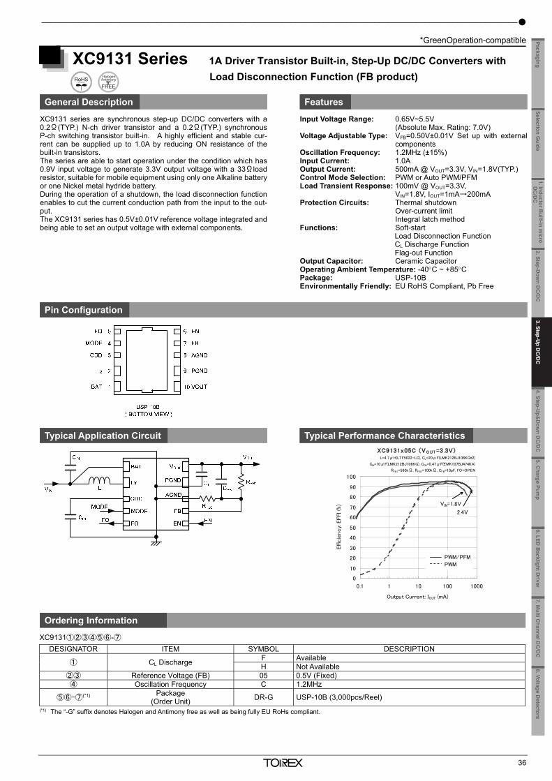
3. Step-Up DC/DC Converters and Controller ICs _________________________________________________
*GreenOperation-compatible
35
XC9136 Series XC9135 Series
XC9135/XC9136 Series 1A Driver Transistor Built-in, Step-Up DC/DC Converters with Load Disconnection Function (VOUT product)
General Description Features
XC9135/XC9136 series are synchronous step-up DC/DC converters with a 0.2Ω(TYP.) N-ch driver transistor and a 0.2Ω(TYP.) synchro-nous P-ch switching transistor built-in. A highly efficient and stable current can be supplied up to 1.0A by reducing ON resistance of the built-in transistors. The series are able to start operation under the condition which has 0.9V input voltage to generate 3.3V output voltage with a 33Ω load resistor, suitable for mobile equipment using only one Alkaline battery or one Nickel metal hydride battery. During the operation of a shutdown, the load disconnection function enables to cut the current conduction path from the input to the out-put. The fixed output voltage has 1.8~5.0V (±2.0% accuracy) output voltage range with 0.1V increments. The UVLO function of the XC9135 series is capable to reduce leaking potassium hydroxide by stopping IC operation while battery voltage is declining. The release voltages of UVLO are 0.85V (±6.0% accuracy) and 1.6V (±3.0% ac-curacy), and selectable voltages range of 0.9V~3.0V.
Input Voltage Range: 0.65V ~ 5.5V (Absolute Max. Rating: 7.0V) Fixed Output Voltages: 1.8V ~ 5.0V (0.1V increments) Oscillation Frequency: 1.2MHz (±15%) Input Current: 1.0A Output Current: 500mA @ VOUT=3.3V, VIN=1.8V(TYP.) Control: PWM or Auto PWM/PFM Load Transient Response: 100mV VOUT=3.3V, VIN=1.8V, IOUT=1mA→200mA Protection Circuits: Thermal shutdown Over-current limit Integral latch method Functions: Soft-start Load Disconnection Function CL Auto Discharge Function Flag-out Function UVLO Output Capacitor: Ceramic Capacitor Operating Ambient Temperature: -40C ~ +85C Package: USP-10B Environmentally Friendly: EU RoHS Compliant, Pb Free
Pin Configuration Typical Performance Characteristics
Typical Application Circuits
XC9135 Series XC9136 Series
Ordering Information XC9135①②③④⑤⑥-⑦・・・・・・・・・・VOUT product with UVLO integral latch protection
XC9136①②③④⑤⑥-⑦・・・・・・・・・・VOUT product
DESIGNATOR ITEM SYMBOL
DESCRIPTION (*2) (・・・With the functions ・・・Without the functions)
UVLO 0.85V
UVLO 1.6V
UVLO≦1.2 Outside Standard
1.2<UVLO Outside Standard
UVLO DETECT DE-
LAY
LATCH PROTECTION
CL AUTO DISCHARGE (*3)
①
XC9135 series Output voltage internally fixed(VOUT)
A C B K
XC9135 series Semi custom(*5)
L M R T
XC9136 series Output voltage internally fixed(VOUT)
E N
②③
Output Voltage (VOUT) (XC9135A,C,B,K/XC9136 Series) 18~50
Output Voltage(*4) e.g.) 1.8V→②=1, ③=8 e.g.) 5.0V→②=5, ③=0
Output Voltage (VOUT) (XC9135L,M,R,T Series) 01~99 Semi custom serial numbers starting from 01(*5)
④ Oscillation Frequency C 1.2MHz ⑤⑥-⑦(*1) Package (Order Unit) DR-G USP-10B (3,000pcs/Reel) (*6)
(*1) The “-G” suffix denotes Halogen and Antimony free as well as being fully EU RoHs compliant. (*2) The SYMBOL of DESIGNATOR① is decided by the combination of with or without “UVLO”, “UVLO DETECT DELAY”, “FO”, “LATCH PROTECTION”, and “CL DISCHARGE”.
Example: ・・・With the functions ・・・Without the functions (*3) Example: ・・・VOUT pin can not be connected to the different output pin such as another supply (AC adaptor).
・・・VOUT pin can be connected to the different output pin such as another supply (AC adaptor). (*4) The XC9135A, XC9135C, XC9135L, limit their selection rang in 2.8V to 5V. The other products have the range from 1.8V to 5V. (*5) The XC9135L, XC9135M, XC9135R, XC9135T are semi-custom products. Please consult with your Torex sales contact. (*6) The XC9135/XC9136 reels are shipped in a moisture-proof packing. Please consult with your Torex sales contact.
PGND
AGND
MODE
VOUT 10
9
8
1
2
3
74
65FO
BAT
EN
Lx PGND
AGND
NCMODE
VOUT
USP-10B
( BOTTOM VIEW )
CDD
USP-10B
( BOTTOM VIEW )
10
9
8
1
2
3
74
65FO
BAT
EN
Lx
CDF
CDD
0
20
40
60
80
100
0.1 1 10 100 1000Output Current : IOUT (mA)
Effi
cien
cy :
EFF
I (%
)
VIN=1.8V
2.5V 3.0V
PWM
PWM/PFM
L=4.7μH (VLF3014ST-4R7M1R1), CL=22μF (LMK316ABJ226ML)
CIN=10μF (JMK212ABJ106KG), CDD=0.47μF (TMK107BJ474KA)fOSC=1.2MHz
XC9135C32CDR-G (VOUT=3.2V)
_______________________________________________________________________________________________________
*GreenOperation-compatible
36
XC9131x05C (VO UT=3.3V)
0
10
20
30
40
50
60
70
80
90
100
0.1 1 10 100 1000
Output Current: IOUT (mA)
Effic
iency:
EFFI (%
)
L=4.7μH(LTF5022-LC), CL=20μF(LMK212BJ106KG*2)
CIN=10μF(LMK212BJ106KG), CDD=0.47μF(EMK107BJ474KA)
RFB1=560kΩ, RFB2=100kΩ, CFB=10pF, FO=OPEN
VIN=1.8V
2.4V
PWM/PFM
PWM
XC9131 Series 1A Driver Transistor Built-in, Step-Up DC/DC Converters with
Load Disconnection Function (FB product)
General Description Features
XC9131 series are synchronous step-up DC/DC converters with a0.2Ω(TYP.) N-ch driver transistor and a 0.2Ω(TYP.) synchronousP-ch switching transistor built-in. A highly efficient and stable cur-rent can be supplied up to 1.0A by reducing ON resistance of thebuilt-in transistors. The series are able to start operation under the condition which has0.9V input voltage to generate 3.3V output voltage with a 33Ωloadresistor, suitable for mobile equipment using only one Alkaline batteryor one Nickel metal hydride battery. During the operation of a shutdown, the load disconnection functionenables to cut the current conduction path from the input to the out-put. The XC9131 series has 0.5V±0.01V reference voltage integrated andbeing able to set an output voltage with external components.
Input Voltage Range: 0.65V~5.5V (Absolute Max. Rating: 7.0V)
Voltage Adjustable Type: VFB=0.50V±0.01V Set up with externalcomponents
Oscillation Frequency: 1.2MHz (±15%) Input Current: 1.0A Output Current: 500mA @ VOUT=3.3V, VIN=1.8V(TYP.) Control Mode Selection: PWM or Auto PWM/PFM Load Transient Response: 100mV @ VOUT=3.3V,
VIN=1.8V, IOUT=1mA→200mA Protection Circuits: Thermal shutdown
Over-current limit Integral latch method
Functions: Soft-start Load Disconnection Function CL Discharge Function Flag-out Function Output Capacitor: Ceramic Capacitor Operating Ambient Temperature: -40C ~ +85C Package: USP-10B Environmentally Friendly: EU RoHS Compliant, Pb Free
Pin Configuration
Typical Application Circuit Typical Performance Characteristics
Ordering Information XC9131①②③④⑤⑥-⑦
DESIGNATOR ITEM SYMBOL DESCRIPTION
① CL Discharge F Available H Not Available
②③ Reference Voltage (FB) 05 0.5V (Fixed) ④ Oscillation Frequency C 1.2MHz
⑤⑥-⑦(*1) Package
(Order Unit) DR-G USP-10B (3,000pcs/Reel) (*1) The “-G” suffix denotes Halogen and Antimony free as well as being fully EU RoHs compliant.
1. Inductor Built-in m
icro D
C/D
C
2. Step-Dow
n DC
/DC
4. Step-Up&
Dow
n DC
/DC
5.C
harge Pump
6.LED B
acklight Driver
8.Voltage Detectors
Selection Guide
Packaging7. M
ulti Channel D
C/D
C
3. Step-Up D
C/D
C
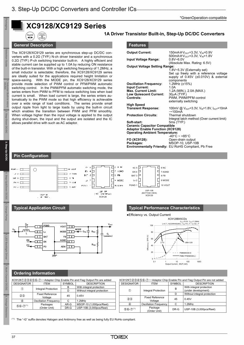
3. Step-Up DC/DC Converters and Controller ICs _________________________________________________
*GreenOperation-compatible
37
XC9128/XC9129 Series 1A Driver Transistor Built-in, Step-Up DC/DC Converters
General Description Features
The XC9128/XC9129 series are synchronous step-up DC/DC con-verters with a 0.2Ω (TYP.) N-ch driver transistor and a synchronous 0.2Ω (TYP.) P-ch switching transistor built-in. A highly efficient and stable current can be supplied up to 1.0A by reducing ON resistance of the built-in transistor. With a high switching frequency of 1.2MHz, a small inductor is selectable; therefore, the XC9128/XC9129 series are ideally suited for the applications required height limitation or space-saving. With the MODE pin, the XC9128/XC9129 series provide mode selection of PWM control or PFM/PWM automatic switching control. In the PWM/PFM automatic switching mode, the series enters from PWM to PFM to reduce switching loss when load current is small. When load current is large, the series enters au-tomatically to the PWM mode so that high efficiency is achievable over a wide range of load conditions. The series provide small output ripple from light to large loads by using the built-in circuit which enables the transition between PWM and PFM smoothly. When voltage higher than the input voltage is applied to the output during shut-down, the input and the output are isolated and the IC allows parallel drive with such as AC adaptor.
Output Current: 150mA@VOUT=3.3V, VIN=0.9V 500mA@VOUT=3.3V, VIN=1.8V
Input Voltage Range: 0.8V~6.0V (Absolute Max. Rating: 6.5V)
Output Voltage Setting Range: 1.8V~5.3V (Externally set) Set up freely with a reference voltagesupply of 0.45V (±0.010V) & external components
Oscillation Frequency: 1.2MHz (±15%) Input Current: 1.0A Max. Current Limit: 1.2A (MIN.), 2.0A (MAX.) Low Quiescent Current: 30A (TYP.) Controls: PWM, PWM/PFM control
externally switching High Speed Transient Response: 100mV @ VOUT=3.3V, VIN=1.8V, IOUT=10mA
→100mA Protection Circuits: Thermal shutdown
Integral latch method (Over current limit) Soft-start: 5ms (TYP.) Ceramic Capacitor Compatible Adaptor Enable Function (XC9128) Operating Ambient Temperature:
-40C ~ +85C FO (XC9128): Open-drain output Packages: MSOP-10, USP-10B Environmentally Friendly: EU RoHS Compliant, Pb Free
Pin Configuration
Typical Application Circuit Typical Performance Characteristics Efficiency vs. Output Current
Ordering Information XC9128①②③④⑤⑥-⑦・・・Adaptor Chip Enable Pin and Flag Output Pin are added
DESIGNATOR ITEM SYMBOL DESCRIPTION
① Integral Protection B With integral protection D Without integral protection
②③ Fixed Reference
Voltage 45 0.45V
④ Oscillation Frequency C 1.2MHz
⑤⑥-⑦(*1) Packages
(Order Unit) AR-G MSOP-10 (1,000pcs/Reel) DR-G USP-10B (3,000pcs/Reel)
XC9129①②③④⑤⑥-⑦・・・Adaptor Chip Enable Pin and Flag Output Pin are not added DESIGNATOR ITEM SYMBOL DESCRIPTION
① Integral Protection B With integral protection (under development)
D Without integral protection
②③ Fixed Reference
Voltage 45 0.45V
④ Oscillation Frequency C 1.2MHz
⑤⑥-⑦(*1) Package
(Order Unit) DR-G USP-10B (3,000pcs/Reel)
(*1) The “-G” suffix denotes Halogen and Antimony free as well as being fully EU RoHs compliant.
5
4
3
6
7
8
2 9
1 10
FO
BAT
EN
Lx
PGND
AEN/
AGND
FB
MODE
VOUT
USP-10B( BOTTOM VIEW )
NC 5
EN 4
BAT 3
Lx 2
6 NC 7 AGND
8 FB
9 MODE
10 VOUT
USP-10B (BOTTOM VIEW)
XC9129 XC9128
6 NC
7 AGND
8 FB
9 MODE
10 VOUT
NC 5
EN 4
BAT 3
Lx 2
PGND 1
USP-10B (BOTTOM VIEW)
XC9129
Lx
VOUT
BAT FB
FO AEN/
MODE
PGND
ENAGND
LRFB1
RFB2
CL
1
3
5
2
4
10
8
6
9
7
CIN
CFB
MODE
EN
VIN
(ceramic)
VOUT
FO
0
20
40
60
80
100
0.1 1 10 100 1000Output Current : IOUT (mA)
Effic
iency
: EFFI (%
)
PWM(MODE:H)
PWM/PFM(MODE:L)
VIN=1.8V3.7V
XC9128B45CDx VOUT=5.0V, fOSC=1.2MHz
L=4.7μH(CDRH4D28C), CIN=10μF, CL=32μF
_______________________________________________________________________________________________________
*GreenOperation-compatible
38
XC9120/XC9121/XC9122 Series Step-Up DC/DC Controller IC, Max Duty: 93%
General Description Features
XC9120/XC9121/XC9122 Series are PWM control step-up DC/DCconverter controller ICs. Since maximum duty ratio is as large as93%, the series is the best for the applications used as high step-upratios, such as the LCD panels and OELD. In this series, even if it is a high step-up ratio, the output voltage stabilized at high efficiency canbe obtained. With 0.9V (±2.0%) of reference voltage supply inter-nal, and using external resistors, RFB1 and 2, output voltage can beset up freely within a range of 1.5V to 30V. For a current sense, with the use of RSENSE, ceramic capacitorscan be used as load capacitors and allows for lower output ripple andreduced PCB area requirements. During stand-by (when the CE pin is low), all circuits are shutdown toreduce current consumption to as low as 1.0μA or less. The overcurrent limit circuit of this IC is designed to monitor the ripplevoltage of the FB pin and operates the IC to stop when the ripplevoltage runs over 250mV. The IC resumes its operation with a tog-gle of the CE pin or by turning the power supply back on.
Input Voltage Range: 0.9V~6.0V (Absolute Max. Rating: 12.0V) Operating Voltage Range: 1.8V~6.0V FB Voltage: 0.9V (±2.0%) Oscillation Frequency: 100kHz (±15%) Output Current: More than 80mA (VIN=3.6V, VOUT=15V) Control: XC9120 (PWM Control)
XC9121 (PWM/PFM Automatic Switching Control), XC9122 (PWM/PFM Externally Switching Control)
High Efficiency: 85% (TYP.) (VIN=3.6V, VOUT=15V, IOUT=10mA)
Low Quiescent Current: 13μA (TYP.) Stand-by Current: 1.0μA (MAX.) Output Capacitor: Low ESR Ceramic Current Limiter Function: Operates when ripple voltage=250mV Operating Ambient Temperature: -40C ~ +85C Packages: SOT-25, USP-6C Environmentally Friendly: EU RoHS Compliant, Pb Free
Pin Configuration
Typical Application Circuit Typical Performance Characteristics
Ordering Information XC9120①②③④⑤⑥-⑦: Fixed PWM control XC9121①②③④⑤⑥-⑦: PWM / PFM automatic switching control XC9122①②③④⑤⑥-⑦: PWM / PFM externally switching control
DESIGNATOR ITEM SYMBOL DESCRIPTION
① Type of DC/DC Controller B With current limiter D No current limiter
②③ Output Voltage 09 FB Voltage 0.9V (±2.0%) ④ Oscillation Frequency 1 100kHz
⑤⑥-⑦(*1) Packages (Order Unit) MR-G SOT-25 (3,000pcs/Reel) ER-G USP-6C (3,000pcs/Reel)
(*1) The “-G” suffix denotes Halogen and Antimony free as well as being fully EU RoHs compliant.
SOT-25 (TOP VIEW)
USP-6C (BOTTOM VIEW)
VOUT=15V
Nch PowerMOS FET
XP161A1355
RSENSE: 50mΩfor Ceramic CL
SD:XB01SB04A2
RFB1:470kΩ
CFB: 33pF
CE
1 5
43
2Ceramic CL:10uF x 4
RFB2: 30kΩ
CIN VIN=2.7V~4.2V
L: 47uH
(CE( / PWM))*
XBS104S14R-G
1. Inductor Built-in m
icro D
C/D
C
2. Step-Dow
n DC
/DC
3. Step-Up D
C/D
C4. Step-U
p&D
own D
C/D
C
5.Charge Pum
p6.LED
Backlight D
river8.Voltage D
etectorsSelection G
uidePackaging
7. Multi C
hannel DC
/DC
3. Step-U
p DC
/DC
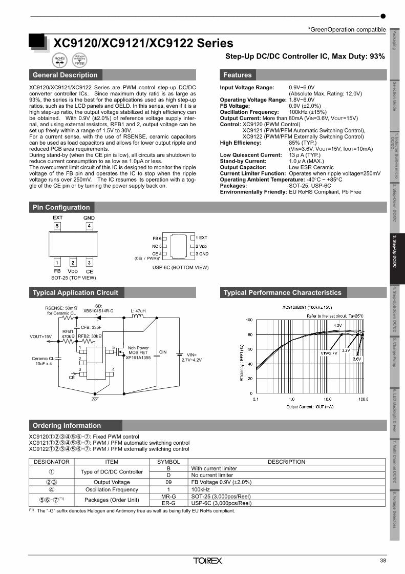
3. Step-Up DC/DC Converters and Controller ICs _________________________________________________
*GreenOperation-compatible
37
XC9128/XC9129 Series 1A Driver Transistor Built-in, Step-Up DC/DC Converters
General Description Features
The XC9128/XC9129 series are synchronous step-up DC/DC con-verters with a 0.2Ω (TYP.) N-ch driver transistor and a synchronous 0.2Ω (TYP.) P-ch switching transistor built-in. A highly efficient and stable current can be supplied up to 1.0A by reducing ON resistance of the built-in transistor. With a high switching frequency of 1.2MHz, a small inductor is selectable; therefore, the XC9128/XC9129 series are ideally suited for the applications required height limitation or space-saving. With the MODE pin, the XC9128/XC9129 series provide mode selection of PWM control or PFM/PWM automatic switching control. In the PWM/PFM automatic switching mode, the series enters from PWM to PFM to reduce switching loss when load current is small. When load current is large, the series enters au-tomatically to the PWM mode so that high efficiency is achievable over a wide range of load conditions. The series provide small output ripple from light to large loads by using the built-in circuit which enables the transition between PWM and PFM smoothly. When voltage higher than the input voltage is applied to the output during shut-down, the input and the output are isolated and the IC allows parallel drive with such as AC adaptor.
Output Current: 150mA@VOUT=3.3V, VIN=0.9V 500mA@VOUT=3.3V, VIN=1.8V
Input Voltage Range: 0.8V~6.0V (Absolute Max. Rating: 6.5V)
Output Voltage Setting Range: 1.8V~5.3V (Externally set) Set up freely with a reference voltagesupply of 0.45V (±0.010V) & external components
Oscillation Frequency: 1.2MHz (±15%) Input Current: 1.0A Max. Current Limit: 1.2A (MIN.), 2.0A (MAX.) Low Quiescent Current: 30A (TYP.) Controls: PWM, PWM/PFM control
externally switching High Speed Transient Response: 100mV @ VOUT=3.3V, VIN=1.8V, IOUT=10mA
→100mA Protection Circuits: Thermal shutdown
Integral latch method (Over current limit) Soft-start: 5ms (TYP.) Ceramic Capacitor Compatible Adaptor Enable Function (XC9128) Operating Ambient Temperature:
-40C ~ +85C FO (XC9128): Open-drain output Packages: MSOP-10, USP-10B Environmentally Friendly: EU RoHS Compliant, Pb Free
Pin Configuration
Typical Application Circuit Typical Performance Characteristics Efficiency vs. Output Current
Ordering Information XC9128①②③④⑤⑥-⑦・・・Adaptor Chip Enable Pin and Flag Output Pin are added
DESIGNATOR ITEM SYMBOL DESCRIPTION
① Integral Protection B With integral protection D Without integral protection
②③ Fixed Reference
Voltage 45 0.45V
④ Oscillation Frequency C 1.2MHz
⑤⑥-⑦(*1) Packages
(Order Unit) AR-G MSOP-10 (1,000pcs/Reel) DR-G USP-10B (3,000pcs/Reel)
XC9129①②③④⑤⑥-⑦・・・Adaptor Chip Enable Pin and Flag Output Pin are not added DESIGNATOR ITEM SYMBOL DESCRIPTION
① Integral Protection B With integral protection (under development)
D Without integral protection
②③ Fixed Reference
Voltage 45 0.45V
④ Oscillation Frequency C 1.2MHz
⑤⑥-⑦(*1) Package
(Order Unit) DR-G USP-10B (3,000pcs/Reel)
(*1) The “-G” suffix denotes Halogen and Antimony free as well as being fully EU RoHs compliant.
5
4
3
6
7
8
2 9
1 10
FO
BAT
EN
Lx
PGND
AEN/
AGND
FB
MODE
VOUT
USP-10B( BOTTOM VIEW )
NC 5
EN 4
BAT 3
Lx 2
6 NC 7 AGND
8 FB
9 MODE
10 VOUT
USP-10B (BOTTOM VIEW)
XC9129 XC9128
6 NC
7 AGND
8 FB
9 MODE
10 VOUT
NC 5
EN 4
BAT 3
Lx 2
PGND 1
USP-10B (BOTTOM VIEW)
XC9129
Lx
VOUT
BAT FB
FO AEN/
MODE
PGND
ENAGND
LRFB1
RFB2
CL
1
3
5
2
4
10
8
6
9
7
CIN
CFB
MODE
EN
VIN
(ceramic)
VOUT
FO
0
20
40
60
80
100
0.1 1 10 100 1000Output Current : IOUT (mA)
Effic
iency
: EFFI (%
)
PWM(MODE:H)
PWM/PFM(MODE:L)
VIN=1.8V3.7V
XC9128B45CDx VOUT=5.0V, fOSC=1.2MHz
L=4.7μH(CDRH4D28C), CIN=10μF, CL=32μF
_______________________________________________________________________________________________________
*GreenOperation-compatible
38
XC9120/XC9121/XC9122 Series Step-Up DC/DC Controller IC, Max Duty: 93%
General Description Features
XC9120/XC9121/XC9122 Series are PWM control step-up DC/DCconverter controller ICs. Since maximum duty ratio is as large as93%, the series is the best for the applications used as high step-upratios, such as the LCD panels and OELD. In this series, even if it is a high step-up ratio, the output voltage stabilized at high efficiency canbe obtained. With 0.9V (±2.0%) of reference voltage supply inter-nal, and using external resistors, RFB1 and 2, output voltage can beset up freely within a range of 1.5V to 30V. For a current sense, with the use of RSENSE, ceramic capacitorscan be used as load capacitors and allows for lower output ripple andreduced PCB area requirements. During stand-by (when the CE pin is low), all circuits are shutdown toreduce current consumption to as low as 1.0μA or less. The overcurrent limit circuit of this IC is designed to monitor the ripplevoltage of the FB pin and operates the IC to stop when the ripplevoltage runs over 250mV. The IC resumes its operation with a tog-gle of the CE pin or by turning the power supply back on.
Input Voltage Range: 0.9V~6.0V (Absolute Max. Rating: 12.0V) Operating Voltage Range: 1.8V~6.0V FB Voltage: 0.9V (±2.0%) Oscillation Frequency: 100kHz (±15%) Output Current: More than 80mA (VIN=3.6V, VOUT=15V) Control: XC9120 (PWM Control)
XC9121 (PWM/PFM Automatic Switching Control), XC9122 (PWM/PFM Externally Switching Control)
High Efficiency: 85% (TYP.) (VIN=3.6V, VOUT=15V, IOUT=10mA)
Low Quiescent Current: 13μA (TYP.) Stand-by Current: 1.0μA (MAX.) Output Capacitor: Low ESR Ceramic Current Limiter Function: Operates when ripple voltage=250mV Operating Ambient Temperature: -40C ~ +85C Packages: SOT-25, USP-6C Environmentally Friendly: EU RoHS Compliant, Pb Free
Pin Configuration
Typical Application Circuit Typical Performance Characteristics
Ordering Information XC9120①②③④⑤⑥-⑦: Fixed PWM control XC9121①②③④⑤⑥-⑦: PWM / PFM automatic switching control XC9122①②③④⑤⑥-⑦: PWM / PFM externally switching control
DESIGNATOR ITEM SYMBOL DESCRIPTION
① Type of DC/DC Controller B With current limiter D No current limiter
②③ Output Voltage 09 FB Voltage 0.9V (±2.0%) ④ Oscillation Frequency 1 100kHz
⑤⑥-⑦(*1) Packages (Order Unit) MR-G SOT-25 (3,000pcs/Reel) ER-G USP-6C (3,000pcs/Reel)
(*1) The “-G” suffix denotes Halogen and Antimony free as well as being fully EU RoHs compliant.
SOT-25 (TOP VIEW)
USP-6C (BOTTOM VIEW)
VOUT=15V
Nch PowerMOS FET
XP161A1355
RSENSE: 50mΩfor Ceramic CL
SD:XB01SB04A2
RFB1:470kΩ
CFB: 33pF
CE
1 5
43
2Ceramic CL:10uF x 4
RFB2: 30kΩ
CIN VIN=2.7V~4.2V
L: 47uH
(CE( / PWM))*
XBS104S14R-G
1. Inductor Built-in m
icro D
C/D
C
2. Step-Dow
n DC
/DC
4. Step-Up&
Dow
n DC
/DC
5.C
harge Pump
6.LED B
acklight Driver
8.Voltage Detectors
Selection Guide
Packaging7. M
ulti Channel D
C/D
C
3. Step-Up D
C/D
C
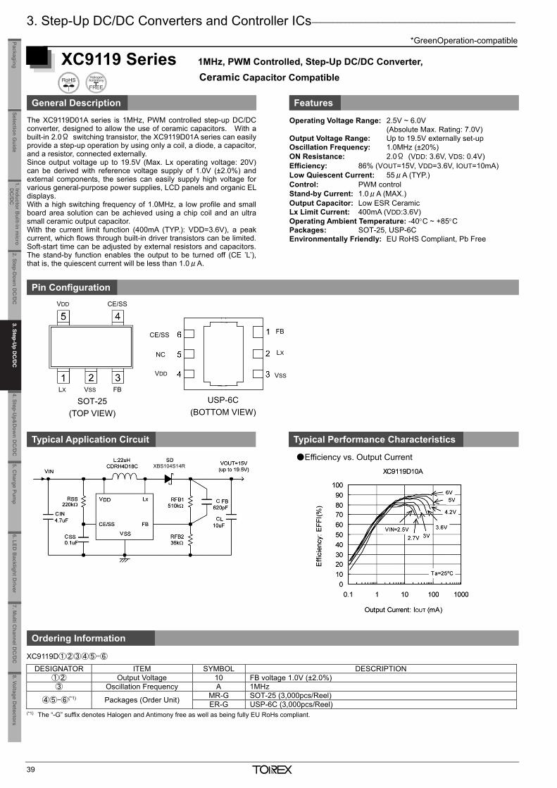
3. Step-Up DC/DC Converters and Controller ICs _________________________________________________
*GreenOperation-compatible
39
XC9119 Series 1MHz, PWM Controlled, Step-Up DC/DC Converter, Ceramic Capacitor Compatible
General Description Features
The XC9119D01A series is 1MHz, PWM controlled step-up DC/DC converter, designed to allow the use of ceramic capacitors. With a built-in 2.0Ω switching transistor, the XC9119D01A series can easily provide a step-up operation by using only a coil, a diode, a capacitor, and a resistor, connected externally. Since output voltage up to 19.5V (Max. Lx operating voltage: 20V) can be derived with reference voltage supply of 1.0V (±2.0%) and external components, the series can easily supply high voltage for various general-purpose power supplies, LCD panels and organic EL displays. With a high switching frequency of 1.0MHz, a low profile and small board area solution can be achieved using a chip coil and an ultra small ceramic output capacitor. With the current limit function (400mA (TYP.): VDD=3.6V), a peak current, which flows through built-in driver transistors can be limited. Soft-start time can be adjusted by external resistors and capacitors. The stand-by function enables the output to be turned off (CE ’L’), that is, the quiescent current will be less than 1.0μA.
Operating Voltage Range: 2.5V ~ 6.0V (Absolute Max. Rating: 7.0V) Output Voltage Range: Up to 19.5V externally set-up Oscillation Frequency: 1.0MHz (±20%) ON Resistance: 2.0Ω (VDD: 3.6V, VDS: 0.4V) Efficiency: 86% (VOUT=15V, VDD=3.6V, IOUT=10mA) Low Quiescent Current: 55μA (TYP.) Control: PWM control Stand-by Current: 1.0μA (MAX.) Output Capacitor: Low ESR Ceramic Lx Limit Current: 400mA (VDD:3.6V) Operating Ambient Temperature: -40C ~ +85C Packages: SOT-25, USP-6C Environmentally Friendly: EU RoHS Compliant, Pb Free
Pin Configuration
Typical Application Circuit Typical Performance Characteristics
Ordering Information XC9119D①②③④⑤-⑥
DESIGNATOR ITEM SYMBOL DESCRIPTION ①② Output Voltage 10 FB voltage 1.0V (±2.0%) ③ Oscillation Frequency A 1MHz
④⑤-⑥(*1) Packages (Order Unit) MR-G SOT-25 (3,000pcs/Reel) ER-G USP-6C (3,000pcs/Reel)
(*1) The “-G” suffix denotes Halogen and Antimony free as well as being fully EU RoHs compliant.
SOT-25 (TOP VIEW)
Efficiency vs. Output Current
VDD CE/SS
LX VSS FB
USP-6C (BOTTOM VIEW)
VDD
CE/SS FB
LX
VSS
NC
XBS104S14R
_______________________________________________________________________________________________________
40
XC9110/XC9111 Series PFM Step-Up DC/DC Converter / Controller ICs 1 Cell 0.8V
General Description Features
The XC9110/XC9111 series is a group of PFM controlled step-up DC/DC con-verter/controller ICs designed to generate low supply voltage by the combina-tion of PFM control and CMOS structure. The series is ideal for applicationswhere a longer battery life is needed such as in portable communicationequipment. With a built-in 2.5ΩN-channel driver transistor, the XC9110C/E andXC9111C/E types provide a step-up operation by using only a coil, a capacitor,and a diode connected externally. The XC9110/XC9111B, D and F versions can be used with an external tran-sistor for applications requiring larger currents. Output voltage is internally programmable in a range from 1.5V to 7.0V in in-crements of 0.1V (±2.5%). Maximum oscillation frequency is set to 100kHz for XC9110/XC9111 series. (Atlight loads, it is set to 180kHz for the XC9111 series.) Options include prod-ucts equipped with a CE pin (C and D versions) that allows the IC to be shutdown thereby reducing quiescent current and with separated VDD/VOUT pins (Eand F versions) to separate the power supply block and the output voltagedetect block. With the XC9110 series, maximum duty cycle is set to 75%(VDD=3.3V) making it suitable for use with large current operations. TheXC9111 series automatically switches duty ratio between 56% & 75%(VDD=3.3V) when it senses changes in load to drop output ripple voltage andcan support both large and small currents. The external transistor types(B/D/F types) can be provided for applications, which require larger currents.
Operating Voltage Range: Operating Hold Voltage 0.8V ~ 10.0V Operating Voltage 0.9V ~ 10.0V
Output Voltage Range: 1.5V ~ 7.0V (0.1V increments) Accuracy: ±2.5% Max. Oscillation Frequency: 100kHz (±15%)
180kHz (for the XC9111 series, duty ratio:56% at light loads)
Built-in Switching N-ch Transistor: Types A/C/E, ON Resistance 2.5Ω(VDD=3.0V)
External Transistor Types: Types B/D/F Lx Limit Voltage: Type E : More than VDD=2.0V
Types A/C : More than VOUT=2.0V Low Quiescent Current: 20μA (when operating VOUT=3V) Operating Ambient Temperature: -40C ~ +85C Packages: SOT-23 & SOT-89
(for XC9111 series) SOT-25, USP-6C
Environmentally Friendly: EU RoHS Compliant, Pb Free
Pin Configuration
Typical Application Circuit Typical Performance Characteristics Type C circuit
Ordering Information XC9110①②③④⑤⑥-⑦: Fixed PFM control, 75% duty XC9111①②③④⑤⑥-⑦: Fixed PFM control, 56% / 75% duty variable DESIGNATOR ITEM SYMBOL DESCRIPTION
① CE Function
A VDD / VOUT common type (for XC9111) Built-in Transistor B VDD / VOUT common type (for XC9111) External Transistor C CE pin Built-in Transistor D CE pin External Transistor E VDD / VOUT separated type Built-in Transistor F VDD / VOUT separated type External Transistor
②③ Output Voltage 15 ~ 70 ex. 3.5V output →②= 3,③= 5 ④ Max. Oscillation Frequency 1 100kHz
⑤⑥-⑦(*1) Packages (Order Unit) MR-G ①=A~B SOT-23 (3,000pcs/Reel)
①=C~F SOT-25 (3,000pcs/Reel) PR-G ①=A~B SOT-89 (1,000pcs/Reel) ER-G ①=C~F USP-6C (3,000pcs/Reel)
(*1) The “-G” suffix denotes Halogen and Antimony free as well as being fully EU RoHs compliant.
SOT-25 (TOP VIEW)
1
2
3
6
5
4
VOUT/VDD
CE/VOUT
NC
VSS
Lx/EXT
NC
USP-6C (BOTTOM VIEW)
1 2 3
5 4L
CIN
CL(Tantalum)
(TOP VIEW)SOT-25
GND
VOUT
CE
SD
VIN +
+
XC9111E331MR
0
20
40
60
80
100
0 5 0 100 150 200 250 300Output Current:IOUT(mA)
Effi
cien
cy:E
FFI(%
)
VIN=0.9V1.2V
1.5V
2.4V3.0V
L=100H(CR54),CL47F(Tantalum)SD:XB01SB04A2BR
XC9111E331MR L=100μH(CR54), CL47μF(Tantalum)
SD: XB01SB04A2BR
CE/VOUT1 2 3
5 4VSS
VOUT/VDD
Lx/EXT
NC
SOT-23 (TOP VIEW) SOT-89 (TOP VIEW)
VOUT
1. Inductor Built-in m
icro D
C/D
C
2. Step-Dow
n DC
/DC
3. Step-Up D
C/D
C4. Step-U
p&D
own D
C/D
C
5.Charge Pum
p6.LED
Backlight D
river8.Voltage D
etectorsSelection G
uidePackaging
7. Multi C
hannel DC
/DC
3. Step-U
p DC
/DC
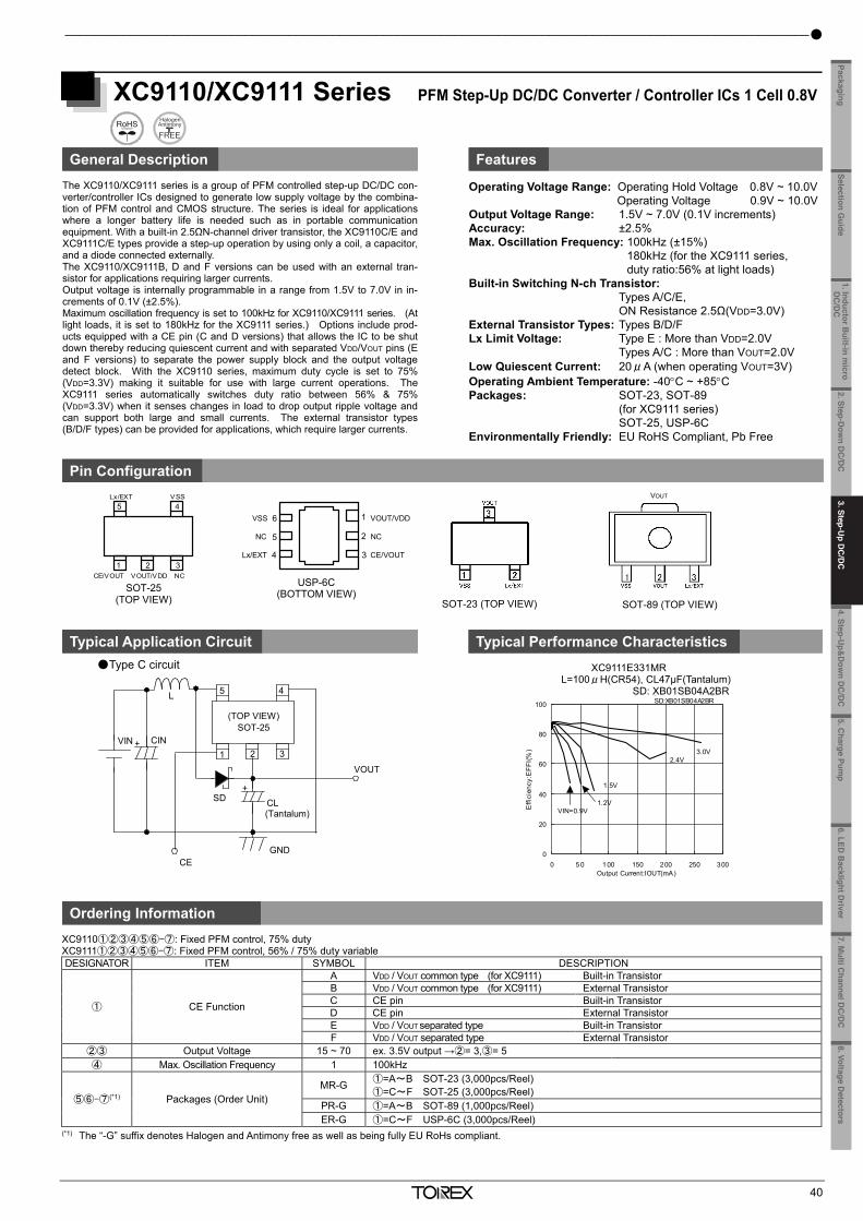
3. Step-Up DC/DC Converters and Controller ICs _________________________________________________
*GreenOperation-compatible
39
XC9119 Series 1MHz, PWM Controlled, Step-Up DC/DC Converter, Ceramic Capacitor Compatible
General Description Features
The XC9119D01A series is 1MHz, PWM controlled step-up DC/DC converter, designed to allow the use of ceramic capacitors. With a built-in 2.0Ω switching transistor, the XC9119D01A series can easily provide a step-up operation by using only a coil, a diode, a capacitor, and a resistor, connected externally. Since output voltage up to 19.5V (Max. Lx operating voltage: 20V) can be derived with reference voltage supply of 1.0V (±2.0%) and external components, the series can easily supply high voltage for various general-purpose power supplies, LCD panels and organic EL displays. With a high switching frequency of 1.0MHz, a low profile and small board area solution can be achieved using a chip coil and an ultra small ceramic output capacitor. With the current limit function (400mA (TYP.): VDD=3.6V), a peak current, which flows through built-in driver transistors can be limited. Soft-start time can be adjusted by external resistors and capacitors. The stand-by function enables the output to be turned off (CE ’L’), that is, the quiescent current will be less than 1.0μA.
Operating Voltage Range: 2.5V ~ 6.0V (Absolute Max. Rating: 7.0V) Output Voltage Range: Up to 19.5V externally set-up Oscillation Frequency: 1.0MHz (±20%) ON Resistance: 2.0Ω (VDD: 3.6V, VDS: 0.4V) Efficiency: 86% (VOUT=15V, VDD=3.6V, IOUT=10mA) Low Quiescent Current: 55μA (TYP.) Control: PWM control Stand-by Current: 1.0μA (MAX.) Output Capacitor: Low ESR Ceramic Lx Limit Current: 400mA (VDD:3.6V) Operating Ambient Temperature: -40C ~ +85C Packages: SOT-25, USP-6C Environmentally Friendly: EU RoHS Compliant, Pb Free
Pin Configuration
Typical Application Circuit Typical Performance Characteristics
Ordering Information XC9119D①②③④⑤-⑥
DESIGNATOR ITEM SYMBOL DESCRIPTION ①② Output Voltage 10 FB voltage 1.0V (±2.0%) ③ Oscillation Frequency A 1MHz
④⑤-⑥(*1) Packages (Order Unit) MR-G SOT-25 (3,000pcs/Reel) ER-G USP-6C (3,000pcs/Reel)
(*1) The “-G” suffix denotes Halogen and Antimony free as well as being fully EU RoHs compliant.
SOT-25 (TOP VIEW)
Efficiency vs. Output Current
VDD CE/SS
LX VSS FB
USP-6C (BOTTOM VIEW)
VDD
CE/SS FB
LX
VSS
NC
XBS104S14R
_______________________________________________________________________________________________________
40
XC9110/XC9111 Series PFM Step-Up DC/DC Converter / Controller ICs 1 Cell 0.8V
General Description Features
The XC9110/XC9111 series is a group of PFM controlled step-up DC/DC con-verter/controller ICs designed to generate low supply voltage by the combina-tion of PFM control and CMOS structure. The series is ideal for applicationswhere a longer battery life is needed such as in portable communicationequipment. With a built-in 2.5ΩN-channel driver transistor, the XC9110C/E andXC9111C/E types provide a step-up operation by using only a coil, a capacitor,and a diode connected externally. The XC9110/XC9111B, D and F versions can be used with an external tran-sistor for applications requiring larger currents. Output voltage is internally programmable in a range from 1.5V to 7.0V in in-crements of 0.1V (±2.5%). Maximum oscillation frequency is set to 100kHz for XC9110/XC9111 series. (Atlight loads, it is set to 180kHz for the XC9111 series.) Options include prod-ucts equipped with a CE pin (C and D versions) that allows the IC to be shutdown thereby reducing quiescent current and with separated VDD/VOUT pins (Eand F versions) to separate the power supply block and the output voltagedetect block. With the XC9110 series, maximum duty cycle is set to 75%(VDD=3.3V) making it suitable for use with large current operations. TheXC9111 series automatically switches duty ratio between 56% & 75%(VDD=3.3V) when it senses changes in load to drop output ripple voltage andcan support both large and small currents. The external transistor types(B/D/F types) can be provided for applications, which require larger currents.
Operating Voltage Range: Operating Hold Voltage 0.8V ~ 10.0V Operating Voltage 0.9V ~ 10.0V
Output Voltage Range: 1.5V ~ 7.0V (0.1V increments) Accuracy: ±2.5% Max. Oscillation Frequency: 100kHz (±15%)
180kHz (for the XC9111 series, duty ratio:56% at light loads)
Built-in Switching N-ch Transistor: Types A/C/E, ON Resistance 2.5Ω(VDD=3.0V)
External Transistor Types: Types B/D/F Lx Limit Voltage: Type E : More than VDD=2.0V
Types A/C : More than VOUT=2.0V Low Quiescent Current: 20μA (when operating VOUT=3V) Operating Ambient Temperature: -40C ~ +85C Packages: SOT-23, SOT-89
(for XC9111 series) SOT-25, USP-6C
Environmentally Friendly: EU RoHS Compliant, Pb Free
Pin Configuration
Typical Application Circuit Typical Performance Characteristics Type C circuit
Ordering Information XC9110①②③④⑤⑥-⑦: Fixed PFM control, 75% duty XC9111①②③④⑤⑥-⑦: Fixed PFM control, 56% / 75% duty variable DESIGNATOR ITEM SYMBOL DESCRIPTION
① CE Function
A VDD / VOUT common type (for XC9111) Built-in Transistor B VDD / VOUT common type (for XC9111) External Transistor C CE pin Built-in Transistor D CE pin External Transistor E VDD / VOUT separated type Built-in Transistor F VDD / VOUT separated type External Transistor
②③ Output Voltage 15 ~ 70 ex. 3.5V output →②= 3,③= 5 ④ Max. Oscillation Frequency 1 100kHz
⑤⑥-⑦(*1) Packages (Order Unit) MR-G ①=A~B SOT-23 (3,000pcs/Reel)
①=C~F SOT-25 (3,000pcs/Reel) PR-G ①=A~B SOT-89 (1,000pcs/Reel) ER-G ①=C~F USP-6C (3,000pcs/Reel)
(*1) The “-G” suffix denotes Halogen and Antimony free as well as being fully EU RoHs compliant.
SOT-25 (TOP VIEW)
1
2
3
6
5
4
VOUT/VDD
CE/VOUT
NC
VSS
Lx/EXT
NC
USP-6C (BOTTOM VIEW)
1 2 3
5 4L
CIN
CL(Tantalum)
(TOP VIEW)SOT-25
GND
VOUT
CE
SD
VIN +
+
XC9111E331MR
0
20
40
60
80
100
0 5 0 100 150 200 250 300Output Current:IOUT(mA)
Effi
cien
cy:E
FFI(%
)
VIN=0.9V1.2V
1.5V
2.4V3.0V
L=100H(CR54),CL47F(Tantalum)SD:XB01SB04A2BR
XC9111E331MR L=100μH(CR54), CL47μF(Tantalum)
SD: XB01SB04A2BR
CE/VOUT1 2 3
5 4VSS
VOUT/VDD
Lx/EXT
NC
SOT-23 (TOP VIEW) SOT-89 (TOP VIEW)
VOUT
1. Inductor Built-in m
icro D
C/D
C
2. Step-Dow
n DC
/DC
4. Step-Up&
Dow
n DC
/DC
5.C
harge Pump
6.LED B
acklight Driver
8.Voltage Detectors
Selection Guide
Packaging7. M
ulti Channel D
C/D
C
3. Step-Up D
C/D
C
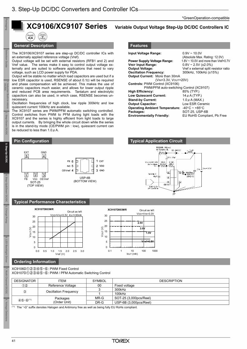
3. Step-Up DC/DC Converters and Controller ICs _________________________________________________
*GreenOperation-compatible
41
XC9106/XC9107 Series Variable Output Voltage Step-Up DC/DC Controllers IC
General Description Features
The XC9106/XC9107 series are step-up DC/DC controller ICs with an externally applied reference voltage (Vref). Output voltage will be set with external resistors (RFB1 and 2) and Vref value. The series make it easy to control output voltage ex-ternally and are suited to software applications that need to vary voltage, such as LCD power supply for PDA. Output will be stable no matter which load capacitors are used but if a low ESR capacitor is used, RSENSE of about 0.1 will be required and phase compensation will be achieved. This makes the use of ceramic capacitors much easier, and allows for lower output ripple and reduced PCB area requirements. Tantalum and electrolytic capacitors can also be used, in which case, RSENSE becomes un-necessary. Oscillation frequencies of high clock, low ripple 300kHz and low quiescent current 100kHz are available. The XC9107 series are PWM/PFM automatic switching controlled. Control switches from PWM to PFM during light loads with the XC9107 and the series is highly efficient from light loads to large output currents. By bringing the whole circuit down while the series is in the stand-by mode (CE/PWM pin : low), quiescent current can be reduced to less than 1.0μA.
Input Voltage Range: 0.9V ~ 10.0V (Absolute Max. Rating: 12.0V) Power Supply Voltage Range: 1.8V ~ 10.0V and more than Vref+0.7VVREF Input Range: 0.8V ~ 2.5V (±2.0%) Output Voltage: Vref x external split resistor ratio Oscillation Frequency: 300kHz, 100kHz (±15%) Output Current: More than 30mA (VIN=3.3V, VOUT=20V) Controls: PWM Control (XC9106)
PWM/PFM auto-switching Control (XC9107) High Efficiency: 85% (TYP.) Low Quiescent Current: 14μA (TYP.) Stand-by Current: 1.0μA (MAX.) Output Capacitor: Low ESR Ceramic Operating Ambient Temperature: -40C ~ +85C Packages: SOT-25, USP-6B Environmentally Friendly: EU RoHS Compliant, Pb Free
Pin Configuration Typical Application Circuit
Typical Performance Characteristics
Ordering Information XC9106D①②③④⑤-⑥: PWM Fixed Control XC9107D①②③④⑤-⑥: PWM / PFM Automatic Switching Control
DESIGNATOR ITEM SYMBOL DESCRIPTION ①② Reference Voltage 00 Fixed voltage
③ Oscillation Frequency 3 300kHz 1 100kHz
④⑤-⑥(*1)Packages
(Order Unit) MR-G SOT-25 (3,000pcs/Reel) DR-G USP-6B (3,000pcs/Reel)
(*1) The “-G” suffix denotes Halogen and Antimony free as well as being fully EU RoHs compliant.
SOT-25 (TOP VIEW)
USP-6B (BOTTOM VIEW)
EXT GND
FB VDD CE/Vref
0
5
10
15
20
25
30
0.0 0.5 1.0 1.5 2.0 2.5 3.0Vref (V)
VO
UT
(V)
Circuit as leftVDD=VIN=3.3V, IOUT=30mA
XC9107D003MR
0
5
10
15
20
25
30
0.1 1 10 100 1000IOUT (mA)
VO
UT
(V)
2.0V
Vref=0.8V
1.5V
2.5V
XC9107D003MR Circuit as leftVDD=VIN=3.3V
_______________________________________________________________________________________________________
*GreenOperation-compatible
42
XC9103/XC9104/XC9105 Series Ceramic Cap. Compatible Step-Up DC/DC Controllers
General Description Features
The XC9103/XC9104/XC9105 series are PWM, PWM/PFM autoswitching /manual switching controlled multi-functional step-upDC/DC controllers. Output will be stable no matter which load capacitors are used butshould a low ESR capacitor be used, RSENSE of about 0.1 will berequired and phase compensation will be achieved. This makes theuse of ceramic capacitors much easier and allows for lower outputripple and reduced PCB area requirements. Tantalum and electrolyticcapacitors can also be used, in which case, RSENSE becomes un-necessary. With 0.9V of standard voltage supply internal, and using externallyconnected components, output voltage can be set up freely within arange of 1.5V to 30V. With 300kHz or 180kHz frequencies, the size of the external components can be reduced. Oscillation frequencies of 100kHz and 500kHz are also available as custom-designed products.The XC9103 offers PWM operation. The XC9104 offers PWM/PFMautomatic switching operation. The PWM operation is shifted to thePFM operation automatically at light load so that it maintain high ef-ficiency over a wide range of load currents. The XC9105 offers bothPWM and PWM/PFM auto switching operations and it can be se-lected by external signal. A current limiter circuit is built in to the IC (except with the 500kHzversion) and monitors the ripple voltage on the FB pin. Operation isshut down when the ripple voltage is more than 250mV. The oper-ations of the IC can be returned to normal with a toggle of the CE pinor by turning the power supply back on.
Input Voltage Range: 0.8V ~ 10.0V (Absolute Max. Rating: 12.0V) Power Supply Voltage Range: 1.8V ~ 10.0V FB Voltage: 0.9V (±2.0%) Oscillation Frequency: 100, 180, 300, 500kHz (±15%)
180, 300kHz only for XC9103/04/05B type (with current limiter)
Output Current: more than 400mA (VIN=1.8V, VOUT=3.3V) Controls: PWM controlled (XC9103)
PWM/PFM auto-switching Control (XC9104) PWM/PFM manual-switching Control (XC9105)
High Efficiency: 85% (TYP.) Low Quiescent Current: 16μA (TYP.) Stand-by Current: 1.0μA (MAX.) Current Limiter Function: Operates when ripple voltage =250mV
(180kHz version) Also available without current limiter (100kHz and 500kHz types are available only without current limiter)
Soft-start: 10ms Operating Ambient Temperature: -40C ~ +85C Packages: SOT-25, USP-6B Environmentally Friendly: EU RoHS Compliant, Pb Free
Pin Configuration Typical Application Circuit
Typical Performance Characteristics Ordering Information
XC9103①②③④⑤⑥-⑦: Fixed PWM control XC9104①②③④⑤⑥-⑦: PWM / PFM automatic switching control XC9105①②③④⑤⑥-⑦: PWM / PFM manual switching control DESIGNATOR ITEM SYMBOL DESCRIPTION
① Type of DC/DC Controller
B With current limiter (180kHz, 300kHz only)
D Without current limiter ②③ Output Voltage 09 FB voltage 0.9V (±2.0%)
④ Oscillation Frequency
3 300kHz 1 100kHz 2 180kHz 5 500kHz
⑤⑥-⑦(*1) Packages (Order Unit)
MR-G SOT-25 (3,000pcs/Reel) DR-G USP-6B (3,000pcs/Reel)
(*1) The “-G” suffix denotes Halogen and Antimony free as well as being fullyEU RoHs compliant.
USP-6B (BOTTOM VIEW)
SOT-25 (TOP VIEW)
1 2 3
4 5 EXT GND
FB VDD CE
1. Inductor Built-in m
icro D
C/D
C
2. Step-Dow
n DC
/DC
3. Step-Up D
C/D
C4. Step-U
p&D
own D
C/D
C
5.Charge Pum
p6.LED
Backlight D
river8.Voltage D
etectorsSelection G
uidePackaging
7. Multi C
hannel DC
/DC
3. Step-U
p DC
/DC
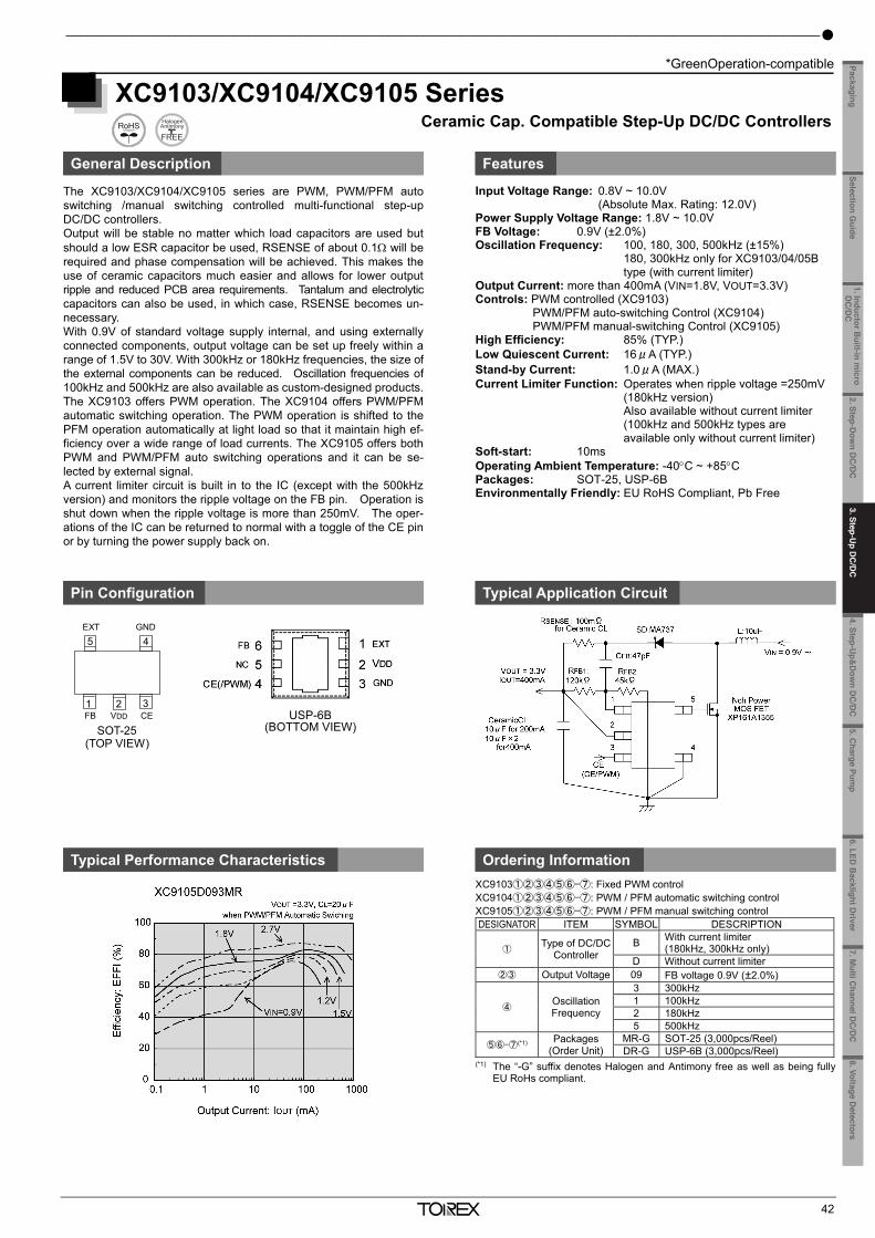
3. Step-Up DC/DC Converters and Controller ICs _________________________________________________
*GreenOperation-compatible
41
XC9106/XC9107 Series Variable Output Voltage Step-Up DC/DC Controllers IC
General Description Features
The XC9106/XC9107 series are step-up DC/DC controller ICs with an externally applied reference voltage (Vref). Output voltage will be set with external resistors (RFB1 and 2) and Vref value. The series make it easy to control output voltage ex-ternally and are suited to software applications that need to vary voltage, such as LCD power supply for PDA. Output will be stable no matter which load capacitors are used but if a low ESR capacitor is used, RSENSE of about 0.1 will be required and phase compensation will be achieved. This makes the use of ceramic capacitors much easier, and allows for lower output ripple and reduced PCB area requirements. Tantalum and electrolytic capacitors can also be used, in which case, RSENSE becomes un-necessary. Oscillation frequencies of high clock, low ripple 300kHz and low quiescent current 100kHz are available. The XC9107 series are PWM/PFM automatic switching controlled. Control switches from PWM to PFM during light loads with the XC9107 and the series is highly efficient from light loads to large output currents. By bringing the whole circuit down while the series is in the stand-by mode (CE/PWM pin : low), quiescent current can be reduced to less than 1.0μA.
Input Voltage Range: 0.9V ~ 10.0V (Absolute Max. Rating: 12.0V) Power Supply Voltage Range: 1.8V ~ 10.0V and more than Vref+0.7VVREF Input Range: 0.8V ~ 2.5V (±2.0%) Output Voltage: Vref x external split resistor ratio Oscillation Frequency: 300kHz, 100kHz (±15%) Output Current: More than 30mA (VIN=3.3V, VOUT=20V) Controls: PWM Control (XC9106)
PWM/PFM auto-switching Control (XC9107) High Efficiency: 85% (TYP.) Low Quiescent Current: 14μA (TYP.) Stand-by Current: 1.0μA (MAX.) Output Capacitor: Low ESR Ceramic Operating Ambient Temperature: -40C ~ +85C Packages: SOT-25, USP-6B Environmentally Friendly: EU RoHS Compliant, Pb Free
Pin Configuration Typical Application Circuit
Typical Performance Characteristics
Ordering Information XC9106D①②③④⑤-⑥: PWM Fixed Control XC9107D①②③④⑤-⑥: PWM / PFM Automatic Switching Control
DESIGNATOR ITEM SYMBOL DESCRIPTION ①② Reference Voltage 00 Fixed voltage
③ Oscillation Frequency 3 300kHz 1 100kHz
④⑤-⑥(*1)Packages
(Order Unit) MR-G SOT-25 (3,000pcs/Reel) DR-G USP-6B (3,000pcs/Reel)
(*1) The “-G” suffix denotes Halogen and Antimony free as well as being fully EU RoHs compliant.
SOT-25 (TOP VIEW)
USP-6B (BOTTOM VIEW)
EXT GND
FB VDD CE/Vref
0
5
10
15
20
25
30
0.0 0.5 1.0 1.5 2.0 2.5 3.0Vref (V)
VO
UT
(V)
Circuit as leftVDD=VIN=3.3V, IOUT=30mA
XC9107D003MR
0
5
10
15
20
25
30
0.1 1 10 100 1000IOUT (mA)
VO
UT
(V)
2.0V
Vref=0.8V
1.5V
2.5V
XC9107D003MR Circuit as leftVDD=VIN=3.3V
_______________________________________________________________________________________________________
*GreenOperation-compatible
42
XC9103/XC9104/XC9105 Series Ceramic Cap. Compatible Step-Up DC/DC Controllers
General Description Features
The XC9103/XC9104/XC9105 series are PWM, PWM/PFM autoswitching /manual switching controlled multi-functional step-upDC/DC controllers. Output will be stable no matter which load capacitors are used butshould a low ESR capacitor be used, RSENSE of about 0.1 will berequired and phase compensation will be achieved. This makes theuse of ceramic capacitors much easier and allows for lower outputripple and reduced PCB area requirements. Tantalum and electrolyticcapacitors can also be used, in which case, RSENSE becomes un-necessary. With 0.9V of standard voltage supply internal, and using externallyconnected components, output voltage can be set up freely within arange of 1.5V to 30V. With 300kHz or 180kHz frequencies, the size of the external components can be reduced. Oscillation frequencies of 100kHz and 500kHz are also available as custom-designed products.The XC9103 offers PWM operation. The XC9104 offers PWM/PFMautomatic switching operation. The PWM operation is shifted to thePFM operation automatically at light load so that it maintain high ef-ficiency over a wide range of load currents. The XC9105 offers bothPWM and PWM/PFM auto switching operations and it can be se-lected by external signal. A current limiter circuit is built in to the IC (except with the 500kHzversion) and monitors the ripple voltage on the FB pin. Operation isshut down when the ripple voltage is more than 250mV. The oper-ations of the IC can be returned to normal with a toggle of the CE pinor by turning the power supply back on.
Input Voltage Range: 0.8V ~ 10.0V (Absolute Max. Rating: 12.0V) Power Supply Voltage Range: 1.8V ~ 10.0V FB Voltage: 0.9V (±2.0%) Oscillation Frequency: 100, 180, 300, 500kHz (±15%)
180, 300kHz only for XC9103/04/05B type (with current limiter)
Output Current: more than 400mA (VIN=1.8V, VOUT=3.3V) Controls: PWM controlled (XC9103)
PWM/PFM auto-switching Control (XC9104) PWM/PFM manual-switching Control (XC9105)
High Efficiency: 85% (TYP.) Low Quiescent Current: 16μA (TYP.) Stand-by Current: 1.0μA (MAX.) Current Limiter Function: Operates when ripple voltage =250mV
(180kHz version) Also available without current limiter (100kHz and 500kHz types are available only without current limiter)
Soft-start: 10ms Operating Ambient Temperature: -40C ~ +85C Packages: SOT-25, USP-6B Environmentally Friendly: EU RoHS Compliant, Pb Free
Pin Configuration Typical Application Circuit
Typical Performance Characteristics Ordering Information
XC9103①②③④⑤⑥-⑦: Fixed PWM control XC9104①②③④⑤⑥-⑦: PWM / PFM automatic switching control XC9105①②③④⑤⑥-⑦: PWM / PFM manual switching control DESIGNATOR ITEM SYMBOL DESCRIPTION
① Type of DC/DC Controller
B With current limiter (180kHz, 300kHz only)
D Without current limiter ②③ Output Voltage 09 FB voltage 0.9V (±2.0%)
④ Oscillation Frequency
3 300kHz 1 100kHz 2 180kHz 5 500kHz
⑤⑥-⑦(*1) Packages (Order Unit)
MR-G SOT-25 (3,000pcs/Reel) DR-G USP-6B (3,000pcs/Reel)
(*1) The “-G” suffix denotes Halogen and Antimony free as well as being fullyEU RoHs compliant.
USP-6B (BOTTOM VIEW)
SOT-25 (TOP VIEW)
1 2 3
4 5 EXT GND
FB VDD CE
1. Inductor Built-in m
icro D
C/D
C
2. Step-Dow
n DC
/DC
4. Step-Up&
Dow
n DC
/DC
5.C
harge Pump
6.LED B
acklight Driver
8.Voltage Detectors
Selection Guide
Packaging7. M
ulti Channel D
C/D
C
3. Step-Up D
C/D
C
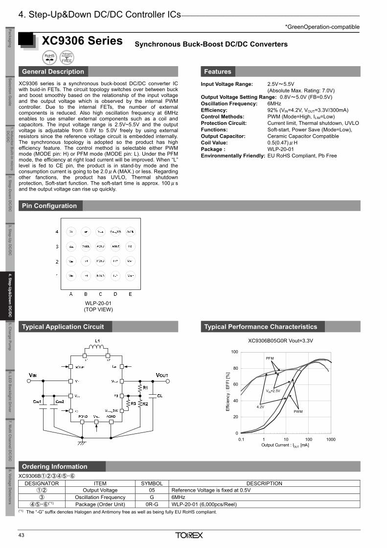
4. Step-Up&Down DC/DC Controller ICs _______________________________________________________
*GreenOperation-compatible
43
XC9306 Series Synchronous Buck-Boost DC/DC Converters
General Description Features
XC9306 series is a synchronous buck-boost DC/DC converter IC with buid-in FETs. The circuit topology switches over between buck and boost smoothly based on the relationship of the input voltage and the output voltage which is observed by the internal PWM controller. Due to the internal FETs, the number of external components is reduced. Also high oscillation frequency at 6MHz enables to use smaller external components such as a coil and capacitors. The input voltage range is 2.5V~5.5V and the output voltage is adjustable from 0.8V to 5.0V freely by using external resistors since the reference voltage circuit is embedded internally. The synchronous topology is adopted so the product has high efficiency feature. The control method is selectable either PWM mode (MODE pin: H) or PFM mode (MODE pin: L). Under the PFM mode, the efficiency at right load current will be improved. When “L” level is fed to CE pin, the product is in stand-by mode and the consumption current is going to be 2.0μA (MAX.) or less. Regarding other fanctions, the product has UVLO, Thermal shutdown protection, Soft-start function. The soft-start time is approx. 100μs and the output voltage can rise up quickly.
Input Voltage Range: 2.5V~5.5V (Absolute Max. Rating: 7.0V) Output Voltage Setting Range: 0.8V~5.0V (FB=0.5V) Oscillation Frequency: 6MHz Efficiency: 92% (VIN=4.2V, VOUT=3.3V/300mA) Control Methods: PWM (Mode=High, ILIM=Low) Protection Circuit: Current limit, Thermal shutdown, UVLO Functions: Soft-start, Power Save (Mode=Low), Output Capacitor: Ceramic Capacitor Compatible Coil Value: 0.5(0.47)μH Package : WLP-20-01 Environmentally Friendly: EU RoHS Compliant, Pb Free
Pin Configuration
WLP-20-01 (TOP VIEW)
Typical Application Circuit Typical Performance Characteristics
XC9306B05G0R Vout=3.3V
Ordering Information XC9306B①②③④⑤-⑥
DESIGNATOR ITEM SYMBOL DESCRIPTION ①② Output Voltage 05 Reference Voltage is fixed at 0.5V ③ Oscillation Frequency G 6MHz
④⑤-⑥(*1) Package (Order Unit) 0R-G WLP-20-01 (6,000pcs/Reel) (*1) The “-G” suffix denotes Halogen and Antimony free as well as being fully EU RoHS compliant.
0
20
40
60
80
100
0.1 1 10 100 1000Output Current : IOUT [mA]
Effic
ienc
y : E
FFI [
%]
VIN=2.5V
4.2V
PFM
PWM
_______________________________________________________________________________________________________
*Green Operation-compatible
44
XC9303 Series High Efficiency, Synchronous Step-Up & Down DC/DC Controller ICs
General Description Features
The XC9303 series is highly efficient, synchronous PWM, PWM/PFMswitchable step-up / down DC/DC controller ICs. A versatile, largeoutput current and high efficiency, step-up/down DC/DC controllercan be realized using only basic external components - transistors,coil, diode, capacitors, and resistors for detecting voltages. Highefficiency is obtained through the use of a synchronous rectificationtopology. The operation of the XC9303 series can be switchedbetween PWM and PWM/PFM (automatic switching control) externallyusing the PWM pin. In PWM/PFM mode, the XC9303 automaticallyswitches from PWM to PFM during light loads and high efficienciescan be achieved over a wide range of output loads conditions.Output noise can be easily reduced with PWM control since thefrequency is fixed. The XC9303 has a 0.9V (±2.0%) internal voltage supply and usingexternally connected components, output voltage can be set freelybetween 2.0V to 6.0V. With an internal 300kHz switching frequencysmaller external components can be used. Soft-start time isinternally set to 10ms and offers protection against in-rush currentswhen the power is switched on and prevents voltage overshoot.
Input Voltage Range: 2.0V ~ 10.0V (Absolute Max. Rating: 12.0V) Output Voltage Range: 2.0V ~ 6.0V Externally Set (VFB=0.9V±2.0%) Oscillation Frequency: 300kHz ±15% Output Current: 800mA (VIN = 4.2V, VOUT=3.3V) Low Quiescent Current: 55μA (TYP.) Stand-by Current: 3.0μA (MAX.) Soft-start: 10ms Operating Ambient Temperature: -40C ~ +85C Package: MSOP-8 Environmentally Friendly: EU RoHS Compliant, Pb Free
Pin Configuration
VDD
EXT1
PWM
CE
GND
EXT2
FB
NC
8
7
6
54
3
2
1
MSOP-8A(TOP VIEW)
Typical Application Circuit Typical Performance Characteristics
Ordering Information
XC9303①②③④⑤⑥-⑦
DESIGNATOR ITEM SYMBOL DESCRIPTION ① Type of DC/DC Controller B Standard type (10 pin)
②③ Output Voltage 09 FB voltage: 0.9V (±2.0%) ④ Oscillation Frequency 3 300kHz
⑤⑥-⑦(*1) Package (Order Unit) KR-G MSOP-8A (1,000pcs/Reel) (*1) The “-G” suffix denotes Halogen and Antimony free as well as being fully EU RoHS compliant.
MSOP-8A (TOP VIEW)
<XC9303B093K OUTPUT= 3.3V> Efficiency vs. Output Current
1. Inductor Built-in m
icro D
C/D
C
2. Step-Dow
n DC
/DC
3. Step-Up D
C/D
C4. Step-U
p&D
own D
C/D
C
5.Charge Pum
p6.LED
Backlight D
river8.Voltage D
etectorsSelection G
uidePackaging
7. Multi C
hannel DC
/DC
4. Step-U
p&D
own D
C/D
C
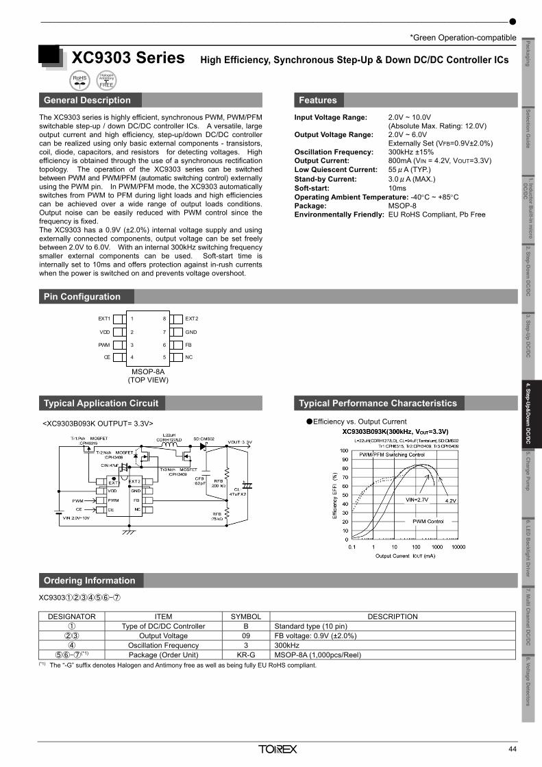
4. Step-Up&Down DC/DC Controller ICs _______________________________________________________
*GreenOperation-compatible
43
XC9306 Series Synchronous Buck-Boost DC/DC Converters
General Description Features
XC9306 series is a synchronous buck-boost DC/DC converter IC with buid-in FETs. The circuit topology switches over between buck and boost smoothly based on the relationship of the input voltage and the output voltage which is observed by the internal PWM controller. Due to the internal FETs, the number of external components is reduced. Also high oscillation frequency at 6MHz enables to use smaller external components such as a coil and capacitors. The input voltage range is 2.5V~5.5V and the output voltage is adjustable from 0.8V to 5.0V freely by using external resistors since the reference voltage circuit is embedded internally. The synchronous topology is adopted so the product has high efficiency feature. The control method is selectable either PWM mode (MODE pin: H) or PFM mode (MODE pin: L). Under the PFM mode, the efficiency at right load current will be improved. When “L” level is fed to CE pin, the product is in stand-by mode and the consumption current is going to be 2.0μA (MAX.) or less. Regarding other fanctions, the product has UVLO, Thermal shutdown protection, Soft-start function. The soft-start time is approx. 100μs and the output voltage can rise up quickly.
Input Voltage Range: 2.5V~5.5V (Absolute Max. Rating: 7.0V) Output Voltage Setting Range: 0.8V~5.0V (FB=0.5V) Oscillation Frequency: 6MHz Efficiency: 92% (VIN=4.2V, VOUT=3.3V/300mA) Control Methods: PWM (Mode=High, ILIM=Low) Protection Circuit: Current limit, Thermal shutdown, UVLO Functions: Soft-start, Power Save (Mode=Low), Output Capacitor: Ceramic Capacitor Compatible Coil Value: 0.5(0.47)μH Package : WLP-20-01 Environmentally Friendly: EU RoHS Compliant, Pb Free
Pin Configuration
WLP-20-01 (TOP VIEW)
Typical Application Circuit Typical Performance Characteristics
XC9306B05G0R Vout=3.3V
Ordering Information XC9306B①②③④⑤-⑥
DESIGNATOR ITEM SYMBOL DESCRIPTION ①② Output Voltage 05 Reference Voltage is fixed at 0.5V ③ Oscillation Frequency G 6MHz
④⑤-⑥(*1) Package (Order Unit) 0R-G WLP-20-01 (6,000pcs/Reel) (*1) The “-G” suffix denotes Halogen and Antimony free as well as being fully EU RoHS compliant.
0
20
40
60
80
100
0.1 1 10 100 1000Output Current : IOUT [mA]
Effic
ienc
y : E
FFI [
%]
VIN=2.5V
4.2V
PFM
PWM
_______________________________________________________________________________________________________
*Green Operation-compatible
44
XC9303 Series High Efficiency, Synchronous Step-Up & Down DC/DC Controller ICs
General Description Features
The XC9303 series is highly efficient, synchronous PWM, PWM/PFMswitchable step-up / down DC/DC controller ICs. A versatile, largeoutput current and high efficiency, step-up/down DC/DC controllercan be realized using only basic external components - transistors,coil, diode, capacitors, and resistors for detecting voltages. Highefficiency is obtained through the use of a synchronous rectificationtopology. The operation of the XC9303 series can be switchedbetween PWM and PWM/PFM (automatic switching control) externallyusing the PWM pin. In PWM/PFM mode, the XC9303 automaticallyswitches from PWM to PFM during light loads and high efficienciescan be achieved over a wide range of output loads conditions.Output noise can be easily reduced with PWM control since thefrequency is fixed. The XC9303 has a 0.9V (±2.0%) internal voltage supply and usingexternally connected components, output voltage can be set freelybetween 2.0V to 6.0V. With an internal 300kHz switching frequencysmaller external components can be used. Soft-start time isinternally set to 10ms and offers protection against in-rush currentswhen the power is switched on and prevents voltage overshoot.
Input Voltage Range: 2.0V ~ 10.0V (Absolute Max. Rating: 12.0V) Output Voltage Range: 2.0V ~ 6.0V Externally Set (VFB=0.9V±2.0%) Oscillation Frequency: 300kHz ±15% Output Current: 800mA (VIN = 4.2V, VOUT=3.3V) Low Quiescent Current: 55μA (TYP.) Stand-by Current: 3.0μA (MAX.) Soft-start: 10ms Operating Ambient Temperature: -40C ~ +85C Package: MSOP-8 Environmentally Friendly: EU RoHS Compliant, Pb Free
Pin Configuration
VDD
EXT1
PWM
CE
GND
EXT2
FB
NC
8
7
6
54
3
2
1
MSOP-8A(TOP VIEW)
Typical Application Circuit Typical Performance Characteristics
Ordering Information
XC9303①②③④⑤⑥-⑦
DESIGNATOR ITEM SYMBOL DESCRIPTION ① Type of DC/DC Controller B Standard type (10 pin)
②③ Output Voltage 09 FB voltage: 0.9V (±2.0%) ④ Oscillation Frequency 3 300kHz
⑤⑥-⑦(*1) Package (Order Unit) KR-G MSOP-8A (1,000pcs/Reel) (*1) The “-G” suffix denotes Halogen and Antimony free as well as being fully EU RoHS compliant.
MSOP-8A (TOP VIEW)
<XC9303B093K OUTPUT= 3.3V> Efficiency vs. Output Current
1. Inductor Built-in m
icro D
C/D
C
2. Step-Dow
n DC
/DC
3. Step-Up D
C/D
C5.C
harge Pump
6.LED B
acklight Driver
8.Voltage Detectors
Selection Guide
Packaging7. M
ulti Channel D
C/D
C
4. Step-Up&
Dow
n DC
/DC
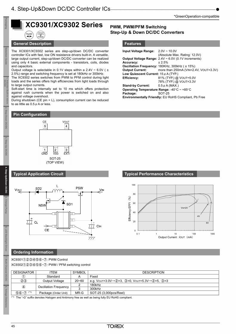
4. Step-Up&Down DC/DC Controller ICs _____________________________________________________
*GreenOperation-compatible
45
XC9301/XC9302 Series PWM, PWM/PFM Switching Step-Up & Down DC/DC Converters
General Description Features
The XC9301/XC9302 series are step-up/down DC/DC converter controller ICs with fast, low ON resistance drivers built-in. A versatile, large output current, step-up/down DC/DC converter can be realized using only 4 basic external components - transistors, coils, diodes and capacitors. Output voltage is selectable in 0.1V steps within a 2.4V ~ 6.0V ( ± 2.5%) range and switching frequency is set at 180kHz or 300kHz. The XC9302 series switches from PWM to PFM control during light loads and the series offers high efficiencies from light loads through to large output currents. Soft-start time is internally set to 10 ms which offers protection against rush currents when the power is switched on and also against voltage overshoot. During shutdown (CE pin = L), consumption current can be reduced to as little as 0.5μA or less.
Input Voltage Range: 2.0V ~ 10.0V (Absolute Max. Rating: 12.0V) Output Voltage Range: 2.4V ~ 6.0V (0.1V increments) Accuracy: ± 2.5% Oscillation Frequency: 180KHz, 300kHz ( ± 15%) Output Current: more than 250mA (VIN=2.4V, VOUT=3.3V) Low Quiescent Current: 15μA (TYP.) Efficiency: 81% (TYP.) @ VOUT=5.0V
78% (TYP.) @ VOUT=3.3V Stand-by Current: 0.5μA (MAX.) Operating Temperature Range: -40C ~ +85C Package: SOT-25 Environmentally Friendly: EU RoHS Compliant, Pb Free
Pin Configuration
Typical Application Circuit Typical Performance Characteristics
Ordering Information
XC9301①②③④⑤⑥-⑦: PWM Control XC9302①②③④⑤⑥-⑦: PWM / PFM switching control
DESIGNATOR ITEM SYMBOL DESCRIPTION ① Standard A Fixed
②③ Output Voltage 20~60 e.g. VOUT=3.0V→②=3, ③=0, VOUT=5.3V→②=5, ③=3
④ Oscillation Frequency 2 180kHz 3 300kHz
⑤⑥-⑦ (*1) Package (Order Unit) MR-G SOT-25 (3,000pcs/Reel) (*1) The “-G” suffix denotes Halogen and Antimony free as well as being fully EU RoHS compliant.
0
20
40
60
80
100
0.1 1 10 100 1000
VIN=2V
6V
4V
Effic
ienc
y:E
FFI(
%)
Output Current:IOUT(mA)
CE VOUT
GND VDD EXT/
SOT-25 (TOP VIEW)
Output Current : lOUT(mA)
_______________________________________________________________________________________ 5. Charge Pump ICs
46
XC9801/XC9802 Series Step-Up Charge Pump General Description Features
The XC9801/XC9802 series are fixed regulated voltage step-upcharge pump ICs which provide stable, highly efficient, positivevoltages with the only external components required being 2 capac-itors. Since regulating is done via the control of the charge pump's gatevoltage waveform, ripple is minimal. Output voltage is selectable in100mV steps within a 2.5V ~ 6.0V range. Control of XC9802 switches to PFM (pulse skip) during light loadswithout affecting output impedance or ripple so that the IC is pro-tected against drops in efficiency. Connecting the SENSE pin to theGND pin allows the IC to be used as a voltage doubler. As well as the ultra small MSOP-8A, USP-8 and USP-8B05 pack-ages, the small consumption current and high efficiencies of the se-ries make the XC9801 suitable for use with all types of battery oper-ated applications.
Input Voltage Range: 1.8V ~ 5.5V (Absolute Max. Rating: 6.0V)
Output Voltage Range: 2.5V ~ 6.0V Small Input Current: 80μA (no load : XC9802 ) Output Current: 80mA (3.6V → 5V step-up) Low Quiescent Current: 3mA (TYP.) Oscillation Frequency: 300kHz Stand-By Current (CE 'L'): 2.0μA (TYP.) Can be used as a Step-Up Doubler (sense = 0V) Operating Ambient Temperature: -40C ~ +85C Packages: MSOP-8A
USP-8 USP-8B05
Environmentally Friendly: EU RoHS Compliant, Pb Free
Pin Configuration
Typical Application Circuit Typical Performance Characteristics
Ordering Information
XC9801①②③④⑤⑥-⑦: Without Pulse Skip XC9802①②③④⑤⑥-⑦: With Pulse Skip
DESIGNATOR ITEM SYMBOL DESCRIPTION ① True Logic Level at CE Pin B Positive
②③ Output Voltage 50 Standard Voltage
VOUT=5.0V→②=5, ③=0
25 ~ 60 Semi-custom Voltage e.g. VOUT=2.5V→②=2, ③=5
④ Oscillation Frequency 3 300kHz
⑤⑥-⑦(*1) Packages (Order Unit) KR-G MSOP-8A (1,000pcs/Reel) DR-G USP-8 (3,000pcs/Reel) ER-G USP-8B05 (5,000pcs/Reel)
(*1) The “-G” suffix denotes Halogen and Antimony free as well as being fully EU RoHS compliant.
MSOP-8A (TOP VIEW)
USP-8(BOTTOM VIEW)
VOUT 1
2
3
45
6
7
8
C1+
C1-
PGND
SENSE
CE
VIN
GND
1. Inductor Built-in m
icro D
C/D
C
2. Step-Dow
n DC
/DC
3. Step-Up D
C/D
C4. Step-U
p&D
own D
C/D
C
5.Charge Pum
p6.LED
Backlight D
river8.Voltage D
etectorsSelection G
uidePackaging
7. Multi C
hannel DC
/DC
4. Step-U
p&D
own D
C/D
C
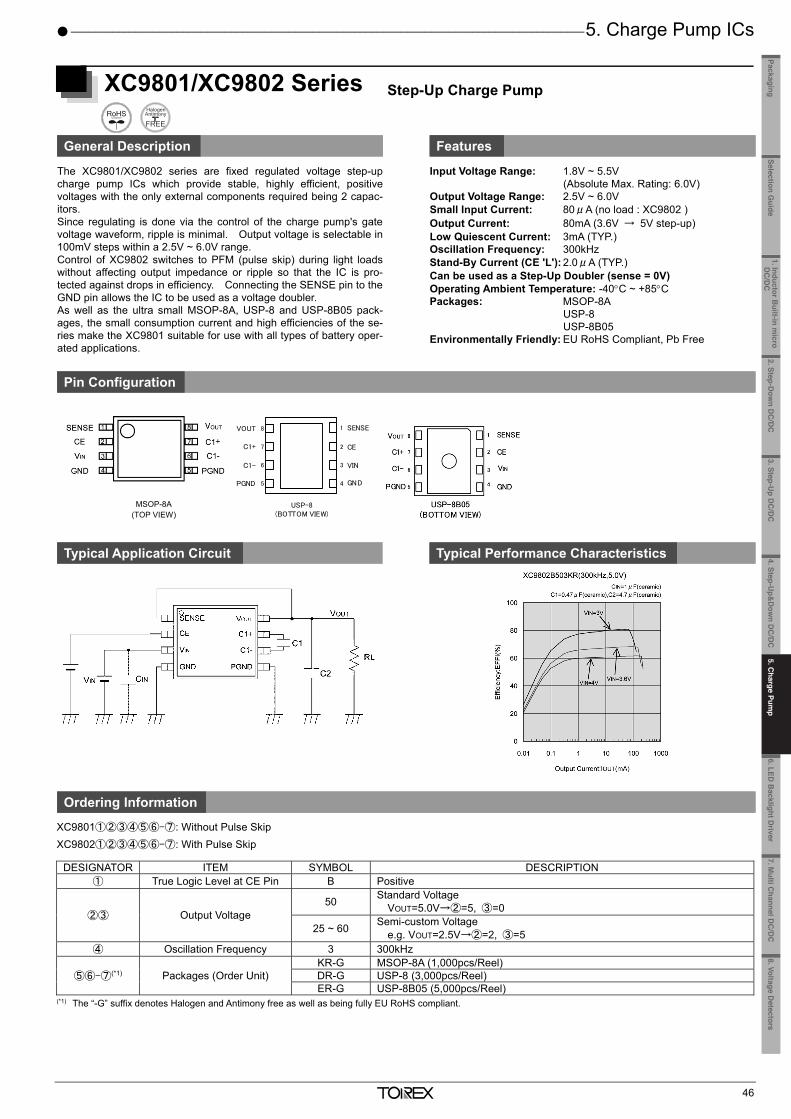
4. Step-Up&Down DC/DC Controller ICs _____________________________________________________
*GreenOperation-compatible
45
XC9301/XC9302 Series PWM, PWM/PFM Switching Step-Up & Down DC/DC Converters
General Description Features
The XC9301/XC9302 series are step-up/down DC/DC converter controller ICs with fast, low ON resistance drivers built-in. A versatile, large output current, step-up/down DC/DC converter can be realized using only 4 basic external components - transistors, coils, diodes and capacitors. Output voltage is selectable in 0.1V steps within a 2.4V ~ 6.0V ( ± 2.5%) range and switching frequency is set at 180kHz or 300kHz. The XC9302 series switches from PWM to PFM control during light loads and the series offers high efficiencies from light loads through to large output currents. Soft-start time is internally set to 10 ms which offers protection against rush currents when the power is switched on and also against voltage overshoot. During shutdown (CE pin = L), consumption current can be reduced to as little as 0.5μA or less.
Input Voltage Range: 2.0V ~ 10.0V (Absolute Max. Rating: 12.0V) Output Voltage Range: 2.4V ~ 6.0V (0.1V increments) Accuracy: ± 2.5% Oscillation Frequency: 180KHz, 300kHz ( ± 15%) Output Current: more than 250mA (VIN=2.4V, VOUT=3.3V) Low Quiescent Current: 15μA (TYP.) Efficiency: 81% (TYP.) @ VOUT=5.0V
78% (TYP.) @ VOUT=3.3V Stand-by Current: 0.5μA (MAX.) Operating Temperature Range: -40C ~ +85C Package: SOT-25 Environmentally Friendly: EU RoHS Compliant, Pb Free
Pin Configuration
Typical Application Circuit Typical Performance Characteristics
Ordering Information
XC9301①②③④⑤⑥-⑦: PWM Control XC9302①②③④⑤⑥-⑦: PWM / PFM switching control
DESIGNATOR ITEM SYMBOL DESCRIPTION ① Standard A Fixed
②③ Output Voltage 20~60 e.g. VOUT=3.0V→②=3, ③=0, VOUT=5.3V→②=5, ③=3
④ Oscillation Frequency 2 180kHz 3 300kHz
⑤⑥-⑦ (*1) Package (Order Unit) MR-G SOT-25 (3,000pcs/Reel) (*1) The “-G” suffix denotes Halogen and Antimony free as well as being fully EU RoHS compliant.
0
20
40
60
80
100
0.1 1 10 100 1000
VIN=2V
6V
4V
Effic
ienc
y:E
FFI(
%)
Output Current:IOUT(mA)
CE VOUT
GND VDD EXT/
SOT-25 (TOP VIEW)
Output Current : lOUT(mA)
_______________________________________________________________________________________ 5. Charge Pump ICs
46
XC9801/XC9802 Series Step-Up Charge Pump General Description Features
The XC9801/XC9802 series are fixed regulated voltage step-upcharge pump ICs which provide stable, highly efficient, positivevoltages with the only external components required being 2 capac-itors. Since regulating is done via the control of the charge pump's gatevoltage waveform, ripple is minimal. Output voltage is selectable in100mV steps within a 2.5V ~ 6.0V range. Control of XC9802 switches to PFM (pulse skip) during light loadswithout affecting output impedance or ripple so that the IC is pro-tected against drops in efficiency. Connecting the SENSE pin to theGND pin allows the IC to be used as a voltage doubler. As well as the ultra small MSOP-8A, USP-8 and USP-8B05 pack-ages, the small consumption current and high efficiencies of the se-ries make the XC9801 suitable for use with all types of battery oper-ated applications.
Input Voltage Range: 1.8V ~ 5.5V (Absolute Max. Rating: 6.0V)
Output Voltage Range: 2.5V ~ 6.0V Small Input Current: 80μA (no load : XC9802 ) Output Current: 80mA (3.6V → 5V step-up) Low Quiescent Current: 3mA (TYP.) Oscillation Frequency: 300kHz Stand-By Current (CE 'L'): 2.0μA (TYP.) Can be used as a Step-Up Doubler (sense = 0V) Operating Ambient Temperature: -40C ~ +85C Packages: MSOP-8A
USP-8 USP-8B05
Environmentally Friendly: EU RoHS Compliant, Pb Free
Pin Configuration
Typical Application Circuit Typical Performance Characteristics
Ordering Information
XC9801①②③④⑤⑥-⑦: Without Pulse Skip XC9802①②③④⑤⑥-⑦: With Pulse Skip
DESIGNATOR ITEM SYMBOL DESCRIPTION ① True Logic Level at CE Pin B Positive
②③ Output Voltage 50 Standard Voltage
VOUT=5.0V→②=5, ③=0
25 ~ 60 Semi-custom Voltage e.g. VOUT=2.5V→②=2, ③=5
④ Oscillation Frequency 3 300kHz
⑤⑥-⑦(*1) Packages (Order Unit) KR-G MSOP-8A (1,000pcs/Reel) DR-G USP-8 (3,000pcs/Reel) ER-G USP-8B05 (5,000pcs/Reel)
(*1) The “-G” suffix denotes Halogen and Antimony free as well as being fully EU RoHS compliant.
MSOP-8A (TOP VIEW)
USP-8(BOTTOM VIEW)
VOUT 1
2
3
45
6
7
8
C1+
C1-
PGND
SENSE
CE
VIN
GND
1. Inductor Built-in m
icro D
C/D
C
2. Step-Dow
n DC
/DC
3. Step-Up D
C/D
C4. Step-U
p&D
own D
C/D
C
6.LED B
acklight Driver
8.Voltage Detectors
Selection Guide
Packaging7. M
ulti Channel D
C/D
C
5.Charge Pum
p
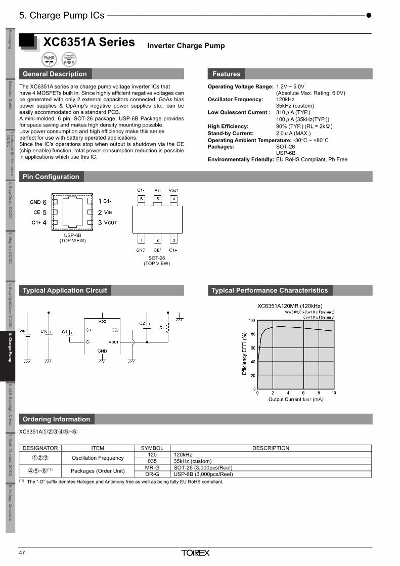
5. Charge Pump ICs _____________________________________________________________________________
47
XC6351A Series Inverter Charge Pump
General Description Features
The XC6351A series are charge pump voltage inverter ICs that have 4 MOSFETs built in. Since highly efficient negative voltages can be generated with only 2 external capacitors connected, GaAs bias power supplies & OpAmp's negative power supplies etc., can be easily accommodated on a standard PCB. A mini-molded, 6 pin, SOT-26 package, USP-6B Package provides for space saving and makes high density mounting possible. Low power consumption and high efficiency make this series perfect for use with battery operated applications. Since the IC's operations stop when output is shutdown via the CE (chip enable) function, total power consumption reduction is possible in applications which use this IC.
Operating Voltage Range: 1.2V ~ 5.0V (Absolute Max. Rating: 6.0V) Oscillator Frequency: 120kHz
35kHz (custom) Low Quiescent Current : 310μA (TYP.)
100μA (35kHz(TYP.)) High Efficiency: 90% (TYP.) (RL = 2kΩ) Stand-by Current: 2.0μA (MAX.) Operating Ambient Temperature: -30C ~ +80C Packages: SOT-26
USP-6B Environmentally Friendly: EU RoHS Compliant, Pb Free
Pin Configuration
Typical Application Circuit Typical Performance Characteristics
Ordering Information
XC6351A①②③④⑤-⑥
DESIGNATOR ITEM SYMBOL DESCRIPTION
①②③ Oscillation Frequency 120 120kHz 035 35kHz (custom)
④⑤-⑥(*1) Packages (Order Unit) MR-G SOT-26 (3,000pcs/Reel) DR-G USP-6B (3,000pcs/Reel)
(*1) The “-G” suffix denotes Halogen and Antimony free as well as being fully EU RoHS compliant.
USP-6B (TOP VIEW)
SOT-26 <SOT-23-6> (TOP VIEW)
SOT-26 (TOP VIEW)
___________________________________________________________________________________ 6. LED Backlight Driver
48
XC9133 Series Step-Up DC/DC Converter-LED Backlight Driver
General Description Features
The XC9133 series is a fixed frequency, constant current step-upDC/DC converter which is optimized for LED backlight applications inmobile phones, PDAs and digital cameras. Output voltage of up to17.5V is possible so that four white LEDs can be driven in series.Since the LED current is set by only one external resistor, all whiteLEDs placed in series can be turned on at the same time. The newDC/DC Converter is also able to drive a network of two parallel banksof three LEDs. LED dimming is controlled by adjusting the duty cycle of a PWMsignal (10kHz Max.) applied to the CE pin. Efficiency is high with a 0.2V low feedback reference voltage ensur-ing the RLED losses are minimal. In addition, an internal MOSFETwith a low RDSON of 2.4Ω is used. A low profile and small boardarea solution can be achieved using a chip inductor and a small ce-ramic output capacitor CL=0.22μF as a result of the high 1MHzswitching frequency. If white LEDs are opened or damaged, the detector built in the Lx pincauses the IC to stop oscillating, preventing excessive increase ofthe output voltage.
Input Voltage Range: 2.5V ~ 6.0V (Absolute Max. Rating: 7.0V) Output Voltage Range: Up to 17.5V externally set-up Reference voltage 0.2V ±5.0% Output Current: 30mA (3 white LEDs, VIN=3.6V) Oscillation Frequency: 1.0MHz (±20%) ON Resistance: 2.4Ω High Efficiency: 85% 3 white LEDs in series VIN=3.6V, ILED=20mA Control: PWM control Stand-by Current: ISTB=1.0μA (MAX.) Output Capacitor: 0.22μF, ceramic Lx Limit Current: 360mA(TYP.) Lx Overvoltage Limit: 19V (TYP.) Operating Ambient Temperature: -40C ~ +85C Package: SOT-25 Environmentally Friendly: EU RoHS Compliant, Pb Free
Pin Configuration
Typical Application Circuit Typical Performance Characteristics
Ordering Information XC9133①②③④⑤⑥-⑦
DESIGNATOR ITEM SYMBOL DESCRIPTION ① Lx Overvoltage Limit B 19V (TYP.)
②③ FB Voltage 02 0.2V (±5.0%) ④ Oscillation Frequency A 1MHz
⑤⑥-⑦(*1) Package (Order Unit) MR-G SOT-25 (3,000pcs/Reel) (*1) The “-G” suffix denotes Halogen and Antimony free as well as being fully EU RoHS compliant.
SOT-25 (TOP VIEW)
0102030405060708090
100
0 5 10 15 20 25 30
LED Currrent : ILED (mA)
Effi
cien
cy :
EFF
I (%
)
L:VLF3010S
NR3015
VIN=3.0V
LED:NSCW100 x 3SBD:XBS053V15R,CL:TMK316J224KF
XC9133B02A Series
1. Inductor Built-in m
icro D
C/D
C
2. Step-Dow
n DC
/DC
3. Step-Up D
C/D
C4. Step-U
p&D
own D
C/D
C
5.Charge Pum
p6.LED
Backlight D
river8.Voltage D
etectorsSelection G
uidePackaging
7. Multi C
hannel DC
/DC
5.C
harge Pump
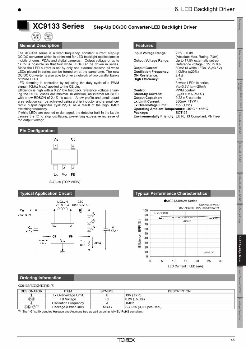
5. Charge Pump ICs _____________________________________________________________________________
47
XC6351A Series Inverter Charge Pump
General Description Features
The XC6351A series are charge pump voltage inverter ICs that have 4 MOSFETs built in. Since highly efficient negative voltages can be generated with only 2 external capacitors connected, GaAs bias power supplies & OpAmp's negative power supplies etc., can be easily accommodated on a standard PCB. A mini-molded, 6 pin, SOT-26 package, USP-6B Package provides for space saving and makes high density mounting possible. Low power consumption and high efficiency make this series perfect for use with battery operated applications. Since the IC's operations stop when output is shutdown via the CE (chip enable) function, total power consumption reduction is possible in applications which use this IC.
Operating Voltage Range: 1.2V ~ 5.0V (Absolute Max. Rating: 6.0V) Oscillator Frequency: 120kHz
35kHz (custom) Low Quiescent Current : 310μA (TYP.)
100μA (35kHz(TYP.)) High Efficiency: 90% (TYP.) (RL = 2kΩ) Stand-by Current: 2.0μA (MAX.) Operating Ambient Temperature: -30C ~ +80C Packages: SOT-26
USP-6B Environmentally Friendly: EU RoHS Compliant, Pb Free
Pin Configuration
Typical Application Circuit Typical Performance Characteristics
Ordering Information
XC6351A①②③④⑤-⑥
DESIGNATOR ITEM SYMBOL DESCRIPTION
①②③ Oscillation Frequency 120 120kHz 035 35kHz (custom)
④⑤-⑥(*1) Packages (Order Unit) MR-G SOT-26 (3,000pcs/Reel) DR-G USP-6B (3,000pcs/Reel)
(*1) The “-G” suffix denotes Halogen and Antimony free as well as being fully EU RoHS compliant.
USP-6B (TOP VIEW)
SOT-26 <SOT-23-6> (TOP VIEW)
SOT-26 (TOP VIEW)
___________________________________________________________________________________ 6. LED Backlight Driver
48
XC9133 Series Step-Up DC/DC Converter-LED Backlight Driver
General Description Features
The XC9133 series is a fixed frequency, constant current step-upDC/DC converter which is optimized for LED backlight applications inmobile phones, PDAs and digital cameras. Output voltage of up to17.5V is possible so that four white LEDs can be driven in series.Since the LED current is set by only one external resistor, all whiteLEDs placed in series can be turned on at the same time. The newDC/DC Converter is also able to drive a network of two parallel banksof three LEDs. LED dimming is controlled by adjusting the duty cycle of a PWMsignal (10kHz Max.) applied to the CE pin. Efficiency is high with a 0.2V low feedback reference voltage ensur-ing the RLED losses are minimal. In addition, an internal MOSFETwith a low RDSON of 2.4Ω is used. A low profile and small boardarea solution can be achieved using a chip inductor and a small ce-ramic output capacitor CL=0.22μF as a result of the high 1MHzswitching frequency. If white LEDs are opened or damaged, the detector built in the Lx pincauses the IC to stop oscillating, preventing excessive increase ofthe output voltage.
Input Voltage Range: 2.5V ~ 6.0V (Absolute Max. Rating: 7.0V) Output Voltage Range: Up to 17.5V externally set-up Reference voltage 0.2V ±5.0% Output Current: 30mA (3 white LEDs, VIN=3.6V) Oscillation Frequency: 1.0MHz (±20%) ON Resistance: 2.4Ω High Efficiency: 85% 3 white LEDs in series VIN=3.6V, ILED=20mA Control: PWM control Stand-by Current: ISTB=1.0μA (MAX.) Output Capacitor: 0.22μF, ceramic Lx Limit Current: 360mA(TYP.) Lx Overvoltage Limit: 19V (TYP.) Operating Ambient Temperature: -40C ~ +85C Package: SOT-25 Environmentally Friendly: EU RoHS Compliant, Pb Free
Pin Configuration
Typical Application Circuit Typical Performance Characteristics
Ordering Information XC9133①②③④⑤⑥-⑦
DESIGNATOR ITEM SYMBOL DESCRIPTION ① Lx Overvoltage Limit B 19V (TYP.)
②③ FB Voltage 02 0.2V (±5.0%) ④ Oscillation Frequency A 1MHz
⑤⑥-⑦(*1) Package (Order Unit) MR-G SOT-25 (3,000pcs/Reel) (*1) The “-G” suffix denotes Halogen and Antimony free as well as being fully EU RoHS compliant.
SOT-25 (TOP VIEW)
0102030405060708090
100
0 5 10 15 20 25 30
LED Currrent : ILED (mA)
Effi
cien
cy :
EFF
I (%
)
L:VLF3010S
NR3015
VIN=3.0V
LED:NSCW100 x 3SBD:XBS053V15R,CL:TMK316J224KF
XC9133B02A Series
1. Inductor Built-in m
icro D
C/D
C
2. Step-Dow
n DC
/DC
3. Step-Up D
C/D
C4. Step-U
p&D
own D
C/D
C
5.Charge Pum
p8.Voltage D
etectorsSelection G
uidePackaging
7. Multi C
hannel DC
/DC
6.LED
Backlight D
river
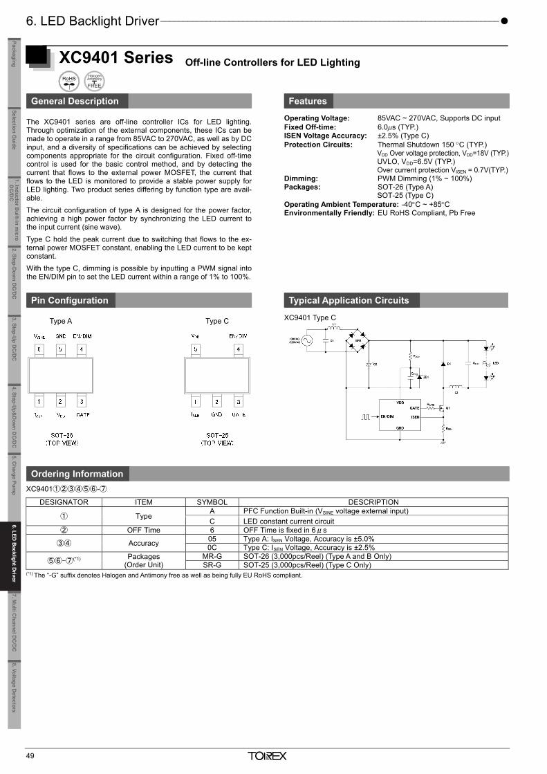
6. LED Backlight Driver __________________________________________________________________________
49
XC9401 Series Off-line Controllers for LED Lighting
General Description Features
The XC9401 series are off-line controller ICs for LED lighting. Through optimization of the external components, these ICs can be made to operate in a range from 85VAC to 270VAC, as well as by DC input, and a diversity of specifications can be achieved by selecting components appropriate for the circuit configuration. Fixed off-time control is used for the basic control method, and by detecting the current that flows to the external power MOSFET, the current that flows to the LED is monitored to provide a stable power supply for LED lighting. Two product series differing by function type are avail-able. The circuit configuration of type A is designed for the power factor, achieving a high power factor by synchronizing the LED current to the input current (sine wave). Type C hold the peak current due to switching that flows to the ex-ternal power MOSFET constant, enabling the LED current to be kept constant. With the type C, dimming is possible by inputting a PWM signal into the EN/DIM pin to set the LED current within a range of 1% to 100%.
Operating Voltage: 85VAC ~ 270VAC, Supports DC input Fixed Off-time: 6.0s (TYP.) ISEN Voltage Accuracy: ±2.5% (Type C) Protection Circuits: Thermal Shutdown 150 C (TYP.) VDD Over voltage protection, VDD=18V (TYP.) UVLO, VDD=6.5V (TYP.) Over current protection VISEN = 0.7V(TYP.) Dimming: PWM Dimming (1% ~ 100%) Packages: SOT-26 (Type A) SOT-25 (Type C) Operating Ambient Temperature: -40C ~ +85C Environmentally Friendly: EU RoHS Compliant, Pb Free
Pin Configuration Typical Application Circuits
Type A Type C
XC9401 Type C
Ordering Information XC9401①②③④⑤⑥-⑦
DESIGNATOR ITEM SYMBOL DESCRIPTION
① Type A PFC Function Built-in (VSINE voltage external input) C LED constant current circuit
② OFF Time 6 OFF Time is fixed in 6μs
③④ Accuracy 05 Type A: ISEN Voltage, Accuracy is ±5.0% 0C Type C: ISEN Voltage, Accuracy is ±2.5%
⑤⑥-⑦(*1) Packages
(Order Unit) MR-G SOT-26 (3,000pcs/Reel) (Type A and B Only) SR-G SOT-25 (3,000pcs/Reel) (Type C Only)
(*1) The “-G” suffix denotes Halogen and Antimony free as well as being fully EU RoHS compliant.
_______________________________________ 7. Multi Channel DC/DC Converters and Controller ICs
50
XC9519 Series Dual Output Step-Up/Inverting DC/DC Converter
General Description Features
The XC9519 series is a 2 channel (step-up and inverting) DC/DCconverter IC. One DC/DC converter is a step-up DC/DC and theother is an inverting DC/DC converter. The step-up convertercompares a built-in reference voltage 1.0V to the FBP voltage(±1.5%) and a positive output voltage can be set freely with theexternal components up to 18V. The inverting DC/DC convertercompares a difference between a reference voltage and the FBNvoltage (±1.5%) to the GND, then a negative output voltage can beset until -15V with the external components. With a 1.2MHz frequency, the size of the external components canbe reduced. As for operation mode, the device can be selected touse PWM control or automatic PWM/PFM switching control by theMODE pin. In the automatic PWM/PFM switching control mode,control switches from PWM to PFM during light loads. The series ishighly efficient from light loads through to large output currents. Inthe PWM control mode, noise is easily reduced since the frequencyis fixed. The control mode can be selected for each application. Thesoft start and current control functions are internally optimized.During stand-by, all circuits in the IC are shutdown to reduce currentconsumption to as low as 1.0μA or less. The device includes a gatecontrol pin for the P-channel MOSFET which is used for a loaddisconnection at the stand-by mode. The GAINP and GAINN pinsare used for loop compensation in order to optimize load transientresponse. With the built-in UVLO (Under Voltage Lock Out) function,the internal driver transistor is forced OFF when input voltagebecomes 2.2V or lower.
Input Voltage: 2.7V ~ 5.5V (Absolute Max. Rating: 6.0V) Output Current: 500mA @VIN=3.7V, VOUTP=5.0V, VOUTN=-5.0V Positive Output Voltage: 4.0V(*1) ~ 18.0V (±1.5% @25C) Negative Output Voltage: -15.0V(*2) ~ -4.0V (±1.5% @25C) Oscillation Frequency: 1.2MHz Soft-Start Circuit Built-In: Step-Up DC/DC converter 2.5ms (TYP.) Inverting DC/DC converter 2.2ms (TYP.) Protection Circuits: Over Current Limit (Integral Latching) Short Protection Latching UVLO Thermal Shutdown Over Voltage Protection Functions: Control Pin Load Disconnect Pin Phase Compensation Pin Ceramic Capacitor Compatible Operating Ambient Temperature: -40 ~ +85C Package: QFN-24 Environmentally Friendly: EU RoHS Compliant, Pb Free (*1) VOUTPSET≧VIN+0.2V (VOUTPSET: Positive output voltage range) (*2) VIN -VOUTNSET+VFN≦21.0V
(VFN : Forward voltage of SBDN, VOUTNSET : Nagative output voltage range)
Pin Configuration Typical Application Circuit
Typical Performance Characteristics Ordering Information VOUTP=5.0V, VOUTN=-5.0V, IOUTP=IOUTN
CLP, CLN=4×4.7μF, LP, LN=3.3μH (VLF5014S-3R3M2R0), SBDP, SBDN: CMS03 P-ch MOS: EMH1303, RZP=7.5kΩ, CZP=4.7nF, RZN=130kΩ, CZN=0.47nF
XC9519①②③④⑤⑥-⑦
DESIGNATOR ITEM SYMBOL DESCRIPTION
① UVLO Detect Voltage A UVLO Detect Voltage 2.2 V
UVLO Hysteresis width 0.2 V
②③ Oscillation Frequency 12 1.2 MHz
④ Max. Current Limit A 2.0A
⑤⑥-⑦(*1) Package (Order Unit) ZR-G QFN-24 (1,000pcs/Reel)(*2)
(*1) The “-G” suffix denotes Halogen and Antimony free as well as being fullyEU RoHS compliant.
(*2) The XC9519 reels are shipped in a moisture-proof packing.
ENP FBN
PGND
RFBP1
LP
VIN
XC9519
FBP
LXP
ENN
BSW
VREF
LXN
PVIN
AVIN
AGND
SBDP
CIN_A
RFBP2
LN
RFBN2
RFBN1
CLP
CLN
SBDN
VOUTP
CL_VR
GAINP
RZN
CZP CZN
RZP
GAINN
VOUTP
CIN_P
VOUTN
MODE
VOUTN
SWPP-ch MOS
CFBP
RSP
CIN_SW
0
20
40
60
80
100
0.1 1 10 100 1000
Output Current:IOUTP, IOUTN (mA)
Effic
ienc
y:EF
FI(%
)
3.6V
2.7V
VIN= 4.4V
VENP="H",VENN="H"
PWM/PFM (VMODE="H")PWM (VMODE="L")
1. Inductor Built-in m
icro D
C/D
C
2. Step-Dow
n DC
/DC
3. Step-Up D
C/D
C4. Step-U
p&D
own D
C/D
C
5.Charge Pum
p6.LED
Backlight D
river8.Voltage D
etectorsSelection G
uidePackaging
7. Multi C
hannel DC
/DC
6.LED
Backlight D
river
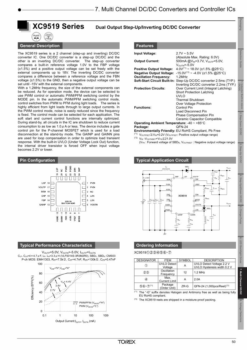
6. LED Backlight Driver __________________________________________________________________________
49
XC9401 Series Off-line Controllers for LED Lighting
General Description Features
The XC9401 series are off-line controller ICs for LED lighting. Through optimization of the external components, these ICs can be made to operate in a range from 85VAC to 270VAC, as well as by DC input, and a diversity of specifications can be achieved by selecting components appropriate for the circuit configuration. Fixed off-time control is used for the basic control method, and by detecting the current that flows to the external power MOSFET, the current that flows to the LED is monitored to provide a stable power supply for LED lighting. Two product series differing by function type are avail-able. The circuit configuration of type A is designed for the power factor, achieving a high power factor by synchronizing the LED current to the input current (sine wave). Type C hold the peak current due to switching that flows to the ex-ternal power MOSFET constant, enabling the LED current to be kept constant. With the type C, dimming is possible by inputting a PWM signal into the EN/DIM pin to set the LED current within a range of 1% to 100%.
Operating Voltage: 85VAC ~ 270VAC, Supports DC input Fixed Off-time: 6.0s (TYP.) ISEN Voltage Accuracy: ±2.5% (Type C) Protection Circuits: Thermal Shutdown 150 C (TYP.) VDD Over voltage protection, VDD=18V (TYP.) UVLO, VDD=6.5V (TYP.) Over current protection VISEN = 0.7V(TYP.) Dimming: PWM Dimming (1% ~ 100%) Packages: SOT-26 (Type A) SOT-25 (Type C) Operating Ambient Temperature: -40C ~ +85C Environmentally Friendly: EU RoHS Compliant, Pb Free
Pin Configuration Typical Application Circuits
Type A Type C
XC9401 Type C
Ordering Information XC9401①②③④⑤⑥-⑦
DESIGNATOR ITEM SYMBOL DESCRIPTION
① Type A PFC Function Built-in (VSINE voltage external input) C LED constant current circuit
② OFF Time 6 OFF Time is fixed in 6μs
③④ Accuracy 05 Type A: ISEN Voltage, Accuracy is ±5.0% 0C Type C: ISEN Voltage, Accuracy is ±2.5%
⑤⑥-⑦(*1) Packages
(Order Unit) MR-G SOT-26 (3,000pcs/Reel) (Type A and B Only) SR-G SOT-25 (3,000pcs/Reel) (Type C Only)
(*1) The “-G” suffix denotes Halogen and Antimony free as well as being fully EU RoHS compliant.
_______________________________________ 7. Multi Channel DC/DC Converters and Controller ICs
50
XC9519 Series Dual Output Step-Up/Inverting DC/DC Converter
General Description Features
The XC9519 series is a 2 channel (step-up and inverting) DC/DCconverter IC. One DC/DC converter is a step-up DC/DC and theother is an inverting DC/DC converter. The step-up convertercompares a built-in reference voltage 1.0V to the FBP voltage(±1.5%) and a positive output voltage can be set freely with theexternal components up to 18V. The inverting DC/DC convertercompares a difference between a reference voltage and the FBNvoltage (±1.5%) to the GND, then a negative output voltage can beset until -15V with the external components. With a 1.2MHz frequency, the size of the external components canbe reduced. As for operation mode, the device can be selected touse PWM control or automatic PWM/PFM switching control by theMODE pin. In the automatic PWM/PFM switching control mode,control switches from PWM to PFM during light loads. The series ishighly efficient from light loads through to large output currents. Inthe PWM control mode, noise is easily reduced since the frequencyis fixed. The control mode can be selected for each application. Thesoft start and current control functions are internally optimized.During stand-by, all circuits in the IC are shutdown to reduce currentconsumption to as low as 1.0μA or less. The device includes a gatecontrol pin for the P-channel MOSFET which is used for a loaddisconnection at the stand-by mode. The GAINP and GAINN pinsare used for loop compensation in order to optimize load transientresponse. With the built-in UVLO (Under Voltage Lock Out) function,the internal driver transistor is forced OFF when input voltagebecomes 2.2V or lower.
Input Voltage: 2.7V ~ 5.5V (Absolute Max. Rating: 6.0V) Output Current: 500mA @VIN=3.7V, VOUTP=5.0V, VOUTN=-5.0V Positive Output Voltage: 4.0V(*1) ~ 18.0V (±1.5% @25C) Negative Output Voltage: -15.0V(*2) ~ -4.0V (±1.5% @25C) Oscillation Frequency: 1.2MHz Soft-Start Circuit Built-In: Step-Up DC/DC converter 2.5ms (TYP.) Inverting DC/DC converter 2.2ms (TYP.) Protection Circuits: Over Current Limit (Integral Latching) Short Protection Latching UVLO Thermal Shutdown Over Voltage Protection Functions: Control Pin Load Disconnect Pin Phase Compensation Pin Ceramic Capacitor Compatible Operating Ambient Temperature: -40 ~ +85C Package: QFN-24 Environmentally Friendly: EU RoHS Compliant, Pb Free (*1) VOUTPSET≧VIN+0.2V (VOUTPSET: Positive output voltage range) (*2) VIN -VOUTNSET+VFN≦21.0V
(VFN : Forward voltage of SBDN, VOUTNSET : Nagative output voltage range)
Pin Configuration Typical Application Circuit
Typical Performance Characteristics Ordering Information VOUTP=5.0V, VOUTN=-5.0V, IOUTP=IOUTN
CLP, CLN=4×4.7μF, LP, LN=3.3μH (VLF5014S-3R3M2R0), SBDP, SBDN: CMS03 P-ch MOS: EMH1303, RZP=7.5kΩ, CZP=4.7nF, RZN=130kΩ, CZN=0.47nF
XC9519①②③④⑤⑥-⑦
DESIGNATOR ITEM SYMBOL DESCRIPTION
① UVLO Detect Voltage A UVLO Detect Voltage 2.2 V
UVLO Hysteresis width 0.2 V
②③ Oscillation Frequency 12 1.2 MHz
④ Max. Current Limit A 2.0A
⑤⑥-⑦(*1) Package (Order Unit) ZR-G QFN-24 (1,000pcs/Reel)(*2)
(*1) The “-G” suffix denotes Halogen and Antimony free as well as being fullyEU RoHS compliant.
(*2) The XC9519 reels are shipped in a moisture-proof packing.
ENP FBN
PGND
RFBP1
LP
VIN
XC9519
FBP
LXP
ENN
BSW
VREF
LXN
PVIN
AVIN
AGND
SBDP
CIN_A
RFBP2
LN
RFBN2
RFBN1
CLP
CLN
SBDN
VOUTP
CL_VR
GAINP
RZN
CZP CZN
RZP
GAINN
VOUTP
CIN_P
VOUTN
MODE
VOUTN
SWPP-ch MOS
CFBP
RSP
CIN_SW
0
20
40
60
80
100
0.1 1 10 100 1000
Output Current:IOUTP, IOUTN (mA)
Effic
ienc
y:EF
FI(%
)
3.6V
2.7V
VIN= 4.4V
VENP="H",VENN="H"
PWM/PFM (VMODE="H")PWM (VMODE="L")
1. Inductor Built-in m
icro D
C/D
C
2. Step-Dow
n DC
/DC
3. Step-Up D
C/D
C4. Step-U
p&D
own D
C/D
C
5.Charge Pum
p6.LED
Backlight D
river8.Voltage D
etectorsSelection G
uidePackaging
7. Multi C
hannel DC
/DC
7. M
ulti Channel D
C/D
C
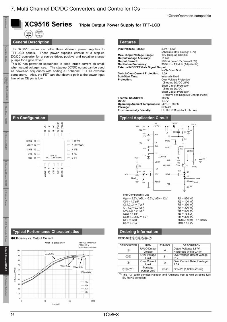
7. Multi Channel DC/DC Converters and Controller ICs _____________________________________
*GreenOperation-compatible
51
R5
R6
CLcp2
VGH
C2
DRV2D4
D5
VOUT
R3
R4
CLcp1
VGL
VIN
AGND
PGND
LX
CVL
CD
VOUTSWB
CP2SWB
FB
CE
FB1
DRV1
VIN
L1
CIN
CDD
CE
CFB R1
R2
D1(SD)VOUT
ROSC ROSC(R9)
CL1
R8
C5(R7)
Tr1
VSRCTr2
R10
CL2
FB2
CVL
CD
D2
D3
C1
XC9516 Series Triple Output Power Supply for TFT-LCD
General Description Features
The XC9516 series can offer three different power supplies to TFT-LCD panels. These power supplies consist of a step-up DC/DC converter for a source driver, positive and negative charge pumps for a gate driver. This IC has power-on sequences to keep inrush current as small when output voltage rises. The step-up DC/DC output can be used as power-on sequences with adding a P-channel FET as external component. Also, the FET can shut down a path to the power input line when CE pin is low.
Input Voltage Range: 2.5V ~ 5.5V (Absolute Max. Rating: 6.0V) Max. Output Voltage Range: 19V (Step-up DC/DC) Output Voltage Accuracy: ±1.5% Output Current: 500mA (VIN=5.0V, VOUT=9.0V) Oscillation Frequency: 300kHz ~ 1.2MHz (Adjustable) External MOSFET Gate Signal Output: N-Ch Open Drain Switch Over-Current Protection: 1.3A Soft-Start Time: Internally fixed Protection: Over Voltage Protection (Step-up DC/DC 21V) Short Circuit Protection (Step-up DC/DC) Short Circuit Protection (Positive and Negative Charge Pump) Thermal Shutdown: 150C UVLO: 1.87V Operating Ambient Temperature: -40C ~ +85C Package: QFN-20 Environmentally Friendly: EU RoHS Compliant, Pb Free
Pin Configuration Typical Application Circuit
Typical Performance Characteristics Ordering Information
Efficiency vs. Output Current
XC9516①②③④⑤⑥-⑦
DESIGNATOR ITEM SYMBOL DESCRIPTON
① UVLO Detect
Voltage A Detect Voltage: 1.87V, Hysteresis Width 0.44V
②③ Over Voltage
Limit 21 Over Voltage Detect Voltage: 21V
④ Over Current
Limit A Over Current Detect Voltage: 1.3A
⑤⑥-⑦(*1) Package (Order unit) ZR-G QFN-20 (1,000pcs/Reel)
(*1) The “-G” suffix denotes Halogen and Antimony free as well as being fullyEU RoHS compliant.
DRV1
CP2SWB
FB1
FB
RO
SC
NC
VINCD
AG
ND
PG
ND
NC
LX
LX
VOUT
CVLQFN-20
(BOTTOM VIEW)
1
2
3
4
5
6
CE
78910
15
14
13
12
11
2019181716
FB2
SWB
DRV2
PG
ND
※1
VIN=2.5V
VIN=4.0V VIN=5.5V
VIN=3.3V
XC9516 Efficiency
0
10
20
30
40
50
60
70
80
90
100
1 10 100 1000
Iout[mA]
Eff
icie
ncy:E
FFI(%)
2.5V
3.3V
4.0V
5.5V
VIN=VCE, VOUT=9.0VFOSC=1MHzIcp1=-1mA, Icp2=1mA
VIN=2.5V
VIN=4.0V
VIN=5.5V
VIN=3.3V
e.g) Components List VOUT = 9.2V, VGL = -5.3V, VGH= 12V R1 = 820 kΩ CIN = 4.7μF R2 = 100 kΩ CL1,CL2 =4.7μF R3 = 390 kΩ C1, C2 = 0.01μF R4 = 300 kΩ CVL,CD = 0.1μF R5 = 820 kΩ CDD = 1μF R6 = 75 kΩ CLcp1,CLcp2 = 1μF R8 = 300 kΩ CFB = 22pF ROSC(R9) = 130 kΩ C5 = 0.01μF R10 = 51 kΩ
_______________________________________________________________________________________________________
*GreenOperation-compatible
52
XC9505 Series 2 Channel Output Step-Down / Inverting DC/DC Controller IC
General Description Features
XC9505 series are PWM controled, PWM/PFM automatic switching,2 channel (step-down and inverting) DC/DC controller ICs. With0.9V of standard voltage supply internal, and using externallyconnected components, the output 1 voltage (step-down DC/DCcontroller) can be set freely within a range of 0.9V to 6.0V. Sincethe output 2 (inverting DC/DC controller) has a built-in 0.9Vreference voltage (±2.0%), negative voltage can be set with theexternal components. With a 180kHz frequency, the size of the external components canbe reduced. Switching frequencies of 300kHz and 500kHzfrequency are also available as custom designed products. The control of the XC9505 series can be switched between PWMcontrol and PWM/PFM automatic switching control using externalsignals. Control switches from PWM to PFM during light loadswhen automatic switching is selected and the series is highly efficientfrom light loads through to large output currents. Noise is easilyreduced with PWM control since the frequency is fixed. The series gives freedom of control selection so that control suited tothe application can be selected. Soft-start time is internally set to10ms (output1) which offers protection against rush currents andvoltage overshoot when the power is switched on.
2 ch. DC/DC Controller Output 1: Step-Down DC/DC Controller
Output Voltage Range : 0.9V ~ 6.0V : Externally Set (VFB=0.9V±2.0%) Output Current : ≧1000mA (VIN=5.0V, VOUT=3.3V) Soft-Start Internally Set-Up
Output 2: Inverting DC/DC Controller Output Voltage Range : -30.0V ~ 0.0V Externally Set (VFB=0.9V±2.0%) Output Current : ≧- 100mA (VIN=5.0V, VOUT= - 3.3V)
Common Operating Voltage Range : 2.0V ~ 10.0V (Absolute Max. Rating: 12.0V) Oscillation Frequency : 180kHz, 300kHz, 500kHz Low Quiescent Current: 50μA (TYP.) Stand-by Current : 3.0μA (MAX.)
Operating Ambient Temperature: -40C ~ +85C Packages : MSOP-10, USP-10 Environmentally Friendly: EU RoHS Compliant, Pb Free
Pin Configuration Typical Application Circuit
Typical Performance Characteristics Ordering Information
XC9505①②③④⑤⑥-⑦ DESIGNATOR ITEM SYMBOL DESCRIPTION
① Type of DC/DC Controller B Standard type (10 pin)
②③ Output Voltage 09 FB voltage 0.9V (±2.0%)
④ Oscillation Frequency
2 180kHz 3 300kHz (custom) 5 500kHz (custom)
⑤⑥-⑦(*1) Packages (Order Unit)
AR-G MSOP-10 (1,000pcs/Reel)
DR-G USP-10 (3,000pcs/Reel)
(*1) The “-G” suffix denotes Halogen and Antimony free as well as being fullyEU RoHS compliant.
1
2
3
4
56
7
8
9
10 EXT1
VDD
FB1
PWM1
EN1EN2
PWM2
FB2
GND
EXT2
USP-10 (BOTTOM VIEW)
1 EXT1
2 VDD
3 FB1 FB2 8
GND 9
EXT2 10
4 PWM1 PWM2 7
5 EN1 EN2 6
MSOP-10(TOP VIEW)
<XC9505B092A Input: 2 cell, VOUT: 3.3V, VOUT: - 5.0V
Efficiency vs. Output Current
1. Inductor Built-in m
icro D
C/D
C
2. Step-Dow
n DC
/DC
3. Step-Up D
C/D
C4. Step-U
p&D
own D
C/D
C
5.Charge Pum
p6.LED
Backlight D
river8.Voltage D
etectorsSelection G
uidePackaging
7. Multi C
hannel DC
/DC
7. M
ulti Channel D
C/D
C
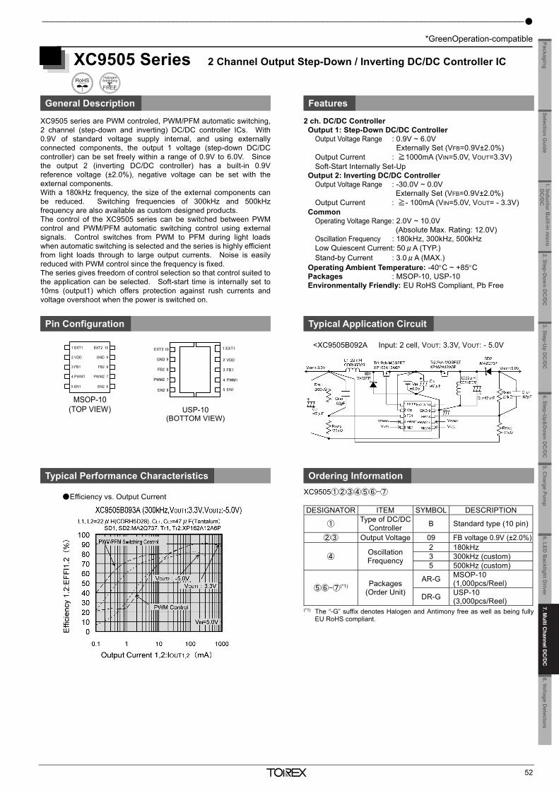
7. Multi Channel DC/DC Converters and Controller ICs _____________________________________
*GreenOperation-compatible
51
R5
R6
CLcp2
VGH
C2
DRV2D4
D5
VOUT
R3
R4
CLcp1
VGL
VIN
AGND
PGND
LX
CVL
CD
VOUTSWB
CP2SWB
FB
CE
FB1
DRV1
VIN
L1
CIN
CDD
CE
CFB R1
R2
D1(SD)VOUT
ROSC ROSC(R9)
CL1
R8
C5(R7)
Tr1
VSRCTr2
R10
CL2
FB2
CVL
CD
D2
D3
C1
XC9516 Series Triple Output Power Supply for TFT-LCD
General Description Features
The XC9516 series can offer three different power supplies to TFT-LCD panels. These power supplies consist of a step-up DC/DC converter for a source driver, positive and negative charge pumps for a gate driver. This IC has power-on sequences to keep inrush current as small when output voltage rises. The step-up DC/DC output can be used as power-on sequences with adding a P-channel FET as external component. Also, the FET can shut down a path to the power input line when CE pin is low.
Input Voltage Range: 2.5V ~ 5.5V (Absolute Max. Rating: 6.0V) Max. Output Voltage Range: 19V (Step-up DC/DC) Output Voltage Accuracy: ±1.5% Output Current: 500mA (VIN=5.0V, VOUT=9.0V) Oscillation Frequency: 300kHz ~ 1.2MHz (Adjustable) External MOSFET Gate Signal Output: N-Ch Open Drain Switch Over-Current Protection: 1.3A Soft-Start Time: Internally fixed Protection: Over Voltage Protection (Step-up DC/DC 21V) Short Circuit Protection (Step-up DC/DC) Short Circuit Protection (Positive and Negative Charge Pump) Thermal Shutdown: 150C UVLO: 1.87V Operating Ambient Temperature: -40C ~ +85C Package: QFN-20 Environmentally Friendly: EU RoHS Compliant, Pb Free
Pin Configuration Typical Application Circuit
Typical Performance Characteristics Ordering Information
Efficiency vs. Output Current
XC9516①②③④⑤⑥-⑦
DESIGNATOR ITEM SYMBOL DESCRIPTON
① UVLO Detect
Voltage A Detect Voltage: 1.87V, Hysteresis Width 0.44V
②③ Over Voltage
Limit 21 Over Voltage Detect Voltage: 21V
④ Over Current
Limit A Over Current Detect Voltage: 1.3A
⑤⑥-⑦(*1) Package (Order unit) ZR-G QFN-20 (1,000pcs/Reel)
(*1) The “-G” suffix denotes Halogen and Antimony free as well as being fullyEU RoHS compliant.
DRV1
CP2SWB
FB1
FB
RO
SC
NC
VINCD
AG
ND
PG
ND
NC
LX
LX
VOUT
CVLQFN-20
(BOTTOM VIEW)
1
2
3
4
5
6
CE
78910
15
14
13
12
11
2019181716
FB2
SWB
DRV2
PG
ND
※1
VIN=2.5V
VIN=4.0V VIN=5.5V
VIN=3.3V
XC9516 Efficiency
0
10
20
30
40
50
60
70
80
90
100
1 10 100 1000
Iout[mA]
Eff
icie
ncy:E
FFI(%)
2.5V
3.3V
4.0V
5.5V
VIN=VCE, VOUT=9.0VFOSC=1MHzIcp1=-1mA, Icp2=1mA
VIN=2.5V
VIN=4.0V
VIN=5.5V
VIN=3.3V
e.g) Components List VOUT = 9.2V, VGL = -5.3V, VGH= 12V R1 = 820 kΩ CIN = 4.7μF R2 = 100 kΩ CL1,CL2 =4.7μF R3 = 390 kΩ C1, C2 = 0.01μF R4 = 300 kΩ CVL,CD = 0.1μF R5 = 820 kΩ CDD = 1μF R6 = 75 kΩ CLcp1,CLcp2 = 1μF R8 = 300 kΩ CFB = 22pF ROSC(R9) = 130 kΩ C5 = 0.01μF R10 = 51 kΩ
_______________________________________________________________________________________________________
*GreenOperation-compatible
52
XC9505 Series 2 Channel Output Step-Down / Inverting DC/DC Controller IC
General Description Features
XC9505 series are PWM controled, PWM/PFM automatic switching,2 channel (step-down and inverting) DC/DC controller ICs. With0.9V of standard voltage supply internal, and using externallyconnected components, the output 1 voltage (step-down DC/DCcontroller) can be set freely within a range of 0.9V to 6.0V. Sincethe output 2 (inverting DC/DC controller) has a built-in 0.9Vreference voltage (±2.0%), negative voltage can be set with theexternal components. With a 180kHz frequency, the size of the external components canbe reduced. Switching frequencies of 300kHz and 500kHzfrequency are also available as custom designed products. The control of the XC9505 series can be switched between PWMcontrol and PWM/PFM automatic switching control using externalsignals. Control switches from PWM to PFM during light loadswhen automatic switching is selected and the series is highly efficientfrom light loads through to large output currents. Noise is easilyreduced with PWM control since the frequency is fixed. The series gives freedom of control selection so that control suited tothe application can be selected. Soft-start time is internally set to10ms (output1) which offers protection against rush currents andvoltage overshoot when the power is switched on.
2 ch. DC/DC Controller Output 1: Step-Down DC/DC Controller
Output Voltage Range : 0.9V ~ 6.0V : Externally Set (VFB=0.9V±2.0%) Output Current : ≧1000mA (VIN=5.0V, VOUT=3.3V) Soft-Start Internally Set-Up
Output 2: Inverting DC/DC Controller Output Voltage Range : -30.0V ~ 0.0V Externally Set (VFB=0.9V±2.0%) Output Current : ≧- 100mA (VIN=5.0V, VOUT= - 3.3V)
Common Operating Voltage Range : 2.0V ~ 10.0V (Absolute Max. Rating: 12.0V) Oscillation Frequency : 180kHz, 300kHz, 500kHz Low Quiescent Current: 50μA (TYP.) Stand-by Current : 3.0μA (MAX.)
Operating Ambient Temperature: -40C ~ +85C Packages : MSOP-10, USP-10 Environmentally Friendly: EU RoHS Compliant, Pb Free
Pin Configuration Typical Application Circuit
Typical Performance Characteristics Ordering Information
XC9505①②③④⑤⑥-⑦ DESIGNATOR ITEM SYMBOL DESCRIPTION
① Type of DC/DC Controller B Standard type (10 pin)
②③ Output Voltage 09 FB voltage 0.9V (±2.0%)
④ Oscillation Frequency
2 180kHz 3 300kHz (custom) 5 500kHz (custom)
⑤⑥-⑦(*1) Packages (Order Unit)
AR-G MSOP-10 (1,000pcs/Reel)
DR-G USP-10 (3,000pcs/Reel)
(*1) The “-G” suffix denotes Halogen and Antimony free as well as being fullyEU RoHS compliant.
1
2
3
4
56
7
8
9
10 EXT1
VDD
FB1
PWM1
EN1EN2
PWM2
FB2
GND
EXT2
USP-10 (BOTTOM VIEW)
1 EXT1
2 VDD
3 FB1 FB2 8
GND 9
EXT2 10
4 PWM1 PWM2 7
5 EN1 EN2 6
MSOP-10(TOP VIEW)
<XC9505B092A Input: 2 cell, VOUT: 3.3V, VOUT: - 5.0V
Efficiency vs. Output Current
1. Inductor Built-in m
icro D
C/D
C
2. Step-Dow
n DC
/DC
3. Step-Up D
C/D
C4. Step-U
p&D
own D
C/D
C
5.Charge Pum
p6.LED
Backlight D
river8.Voltage D
etectorsSelection G
uidePackaging
7. Multi C
hannel DC
/DC
7. M
ulti Channel D
C/D
C
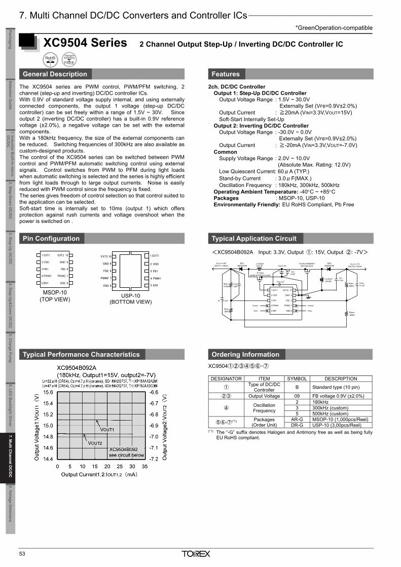
7. Multi Channel DC/DC Converters and Controller ICs _____________________________________
*GreenOperation-compatible
53
XC9504 Series 2 Channel Output Step-Up / Inverting DC/DC Controller IC
General Description Features
The XC9504 series are PWM control, PWM/PFM switching, 2 channel (step-up and inverting) DC/DC controller ICs. With 0.9V of standard voltage supply internal, and using externally connected components, the output 1 voltage (step-up DC/DC controller) can be set freely within a range of 1.5V ~ 30V. Since output 2 (inverting DC/DC controller) has a built-in 0.9V reference voltage (±2.0%), a negative voltage can be set with the external components. With a 180kHz frequency, the size of the external components can be reduced. Switching frequencies of 300kHz are also available as custom-designed products. The control of the XC9504 series can be switched between PWM control and PWM/PFM automatic switching control using external signals. Control switches from PWM to PFM during light loads when automatic switching is selected and the series is highly efficient from light loads through to large output currents. Noise is easily reduced with PWM control since the frequency is fixed. The series gives freedom of control selection so that control suited to the application can be selected. Soft-start time is internally set to 10ms (output 1) which offers protection against rush currents and voltage overshoot when the power is switched on .
2ch. DC/DC Controller Output 1: Step-Up DC/DC Controller
Output Voltage Range : 1.5V ~ 30.0V Externally Set (VFB=0.9V±2.0%)
Output Current : ≧20mA (VIN=3.3V,VOUT=15V) Soft-Start Internally Set-Up
Output 2: Inverting DC/DC Controller Output Voltage Range : -30.0V ~ 0.0V
Externally Set (VFB=0.9V±2.0%) Output Current : ≧-20mA (VIN=3.3V,VOUT=-7.0V)
Common Supply Voltage Range : 2.0V ~ 10.0V
(Absolute Max. Rating: 12.0V) Low Quiescent Current: 60μA (TYP.) Stand-by Current : 3.0μF(MAX.) Oscillation Frequency : 180kHz, 300kHz, 500kHz
Operating Ambient Temperature: -40C ~ +85C Packages : MSOP-10, USP-10 Environmentally Friendly: EU RoHS Compliant, Pb Free
Pin Configuration Typical Application Circuit
Typical Performance Characteristics Ordering Information
XC9504①②③④⑤⑥-⑦ DESIGNATOR ITEM SYMBOL DESCRIPTION
① Type of DC/DC Controller B Standard type (10 pin)
②③ Output Voltage 09 FB voltage 0.9V (±2.0%)
④ Oscillation Frequency
2 180kHz 3 300kHz (custom) 5 500kHz (custom)
⑤⑥-⑦(*1) Packages (Order Unit)
AR-G MSOP-10 (1,000pcs/Reel) DR-G USP-10 (3,00pcs/Reel)
(*1) The “-G” suffix denotes Halogen and Antimony free as well as being fullyEU RoHS compliant.
1
2
3
4
56
7
8
9
10 EXT1
VDD
FB1
PWM1
EN1EN2
PWM2
FB2
GND
EXT2
USP-10 (BOTTOM VIEW)
1 EXT1
2 VDD
3 FB1 FB2 8
GND 9
EXT2 10
4 PWM1 PWM2 7
5 EN1 EN2 6
MSOP-10(TOP VIEW)
<XC9504B092A Input: 3.3V, Output ①: 15V, Output ②: -7V>
L1:22uHD412F
Tr2:Pch MOSFETXP152A12C0
CIN:47uFTr1:Nch
MOSFETXP151A12A2
L2:47HD412F
VPWM1 VPWM2
1 EXT1
2 VDD
3 FB1 FB2 8
GND 9
EXT2/ 10
4 PWM1 PWM2 7
5 NE1 NE2 6 VNE2VNE1
CDD:1F
SD2:MA2Q735
RRB11:470k
RFB12:30k
CFB1:5pF
4.7F
VOUT1=15VIOUT1=~20mA
SD1:MA2Q735
CL1
RRB21:56k
CFB21:0.1F
VOUT2=-7VIOUT2=~20mA
CL2:4.7F
RRB22
:100k
VIN=3.3V
_______________________________________________________________________________________________________
*GreenOperation-compatible
54
XC9502 Series 2 Channel Output Step-Up / Down DC/DC Controller IC
General Description Features
The XC9502 series are PWM controlled, PWM/PFM automaticswitching controlled, multi-functional, 2 channel step-up and downDC/DC controller ICs. With 0.9V of standard voltage supplyinternal, and using externally connected components, the output 1voltage (step-up DC/DC controller) can be set freely within a range of1.5V to 30V. Since the output 2 (step-down DC/DC controller) has abuilt-in 0.9V reference voltage (±2.0%), 0.9V to 6.0V can be setusing external components. With a 180kHz frequency, the size of the external components canbe reduced. Switching frequencies of 300kHz & 500kHz are alsoavailable as custom-designed products. The control of the XC9502 series can be switched between PWMcontrol and PWM/PFM automatic switching control using externalsignals. Control switches from PWM to PFM during light loadswhen automatic switching is selected and the series is highly efficientfrom light loads through to large output currents. Noise is easily reduced with PWM control since the frequency isfixed. The series gives freedom of control selection so that controlsuited to the application can be selected. Soft-start time is internallyset to 10ms (Output 1) and offers protection against in-rush currentswhen the power is switched. This also prevents voltage overshoot.
2ch DC/DC Controller <Output 1: Step-Up DC/DC Controller>
Output Voltage Range: 1.5V ~ 30.0V Externally Set (VFB=0.9V±2.0%)
Output Current: ≦300mA (VIN=1.8V,VOUT=3.3V) <Output 2: Step-Down DC/DC Controller>
Output Voltage Range: 0.9V ~ 6.0V Externally Set (VFB=0.9V±2.0%)
Output Current : ≦1000mA (VIN=3.3V, VOUT=1.8V) <Common>
Supply Voltage Range: 2.0V ~ 10.0V (Absolute Max. Rating: 12.0V)
Oscillation Frequency: 180kHz (±15%) * 300kHz, 500kHz custom
Low Quiescent Current: 50μA (TYP.) Stand-by Current: 3.0μA (MAX.) Soft-Start: 10ms Operating Ambient Temperature: -40C ~ +85C Packages: MSOP-10, USP-10 Environmentally Friendly: EU RoHS Compliant, Pb Free
Pin Configuration Typical Application Circuit
Typical Performance Characteristics Ordering Information
XC9502①②③④⑤⑥-⑦ DESIGNATOR ITEM SYMBOL DESCRIPTION
① Type of DC/DC Controller B Standard type (10 pin)
②③ Output Voltage 09 FB voltage: 0.9V (±2.0%)
④ Oscillation Frequency
2 180kHz 3 300kHz (custom) 5 500kHz (custom)
⑤⑥-⑦(*1) Packages (Order Unit)
AR-G MSOP-10 (1,000pcs/Reel)
DR-G USP-10 (3,000pcs/Reel)
(*1) The “-G” suffix denotes Halogen and Antimony free as well as being fullyEU RoHS compliant.
1
2
3
4
56
7
8
9
10 EXT1
VDD
FB1
PWM1
EN1EN2
PWM2
FB2
GND
EXT2
USP-10 (BOTTOM VIEW)
1 EXT1
2 VDD
3 FB1 FB2 8
GND 9
EXT2 10
4 PWM1 PWM2 7
5 EN1 EN2 6
MSOP-10(TOP VIEW)
<XC9502B092A Input : 2 cell, VOUT①: 3.3V, VOUT②: 1.8V >
1. Inductor Built-in m
icro D
C/D
C
2. Step-Dow
n DC
/DC
3. Step-Up D
C/D
C4. Step-U
p&D
own D
C/D
C
5.Charge Pum
p6.LED
Backlight D
river8.Voltage D
etectorsSelection G
uidePackaging
7. Multi C
hannel DC
/DC
7. M
ulti Channel D
C/D
C
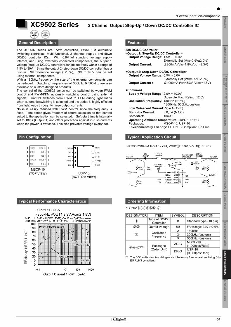
7. Multi Channel DC/DC Converters and Controller ICs _____________________________________
*GreenOperation-compatible
53
XC9504 Series 2 Channel Output Step-Up / Inverting DC/DC Controller IC
General Description Features
The XC9504 series are PWM control, PWM/PFM switching, 2 channel (step-up and inverting) DC/DC controller ICs. With 0.9V of standard voltage supply internal, and using externally connected components, the output 1 voltage (step-up DC/DC controller) can be set freely within a range of 1.5V ~ 30V. Since output 2 (inverting DC/DC controller) has a built-in 0.9V reference voltage (±2.0%), a negative voltage can be set with the external components. With a 180kHz frequency, the size of the external components can be reduced. Switching frequencies of 300kHz are also available as custom-designed products. The control of the XC9504 series can be switched between PWM control and PWM/PFM automatic switching control using external signals. Control switches from PWM to PFM during light loads when automatic switching is selected and the series is highly efficient from light loads through to large output currents. Noise is easily reduced with PWM control since the frequency is fixed. The series gives freedom of control selection so that control suited to the application can be selected. Soft-start time is internally set to 10ms (output 1) which offers protection against rush currents and voltage overshoot when the power is switched on .
2ch. DC/DC Controller Output 1: Step-Up DC/DC Controller
Output Voltage Range : 1.5V ~ 30.0V Externally Set (VFB=0.9V±2.0%)
Output Current : ≧20mA (VIN=3.3V,VOUT=15V) Soft-Start Internally Set-Up
Output 2: Inverting DC/DC Controller Output Voltage Range : -30.0V ~ 0.0V
Externally Set (VFB=0.9V±2.0%) Output Current : ≧-20mA (VIN=3.3V,VOUT=-7.0V)
Common Supply Voltage Range : 2.0V ~ 10.0V
(Absolute Max. Rating: 12.0V) Low Quiescent Current: 60μA (TYP.) Stand-by Current : 3.0μF(MAX.) Oscillation Frequency : 180kHz, 300kHz, 500kHz
Operating Ambient Temperature: -40C ~ +85C Packages : MSOP-10, USP-10 Environmentally Friendly: EU RoHS Compliant, Pb Free
Pin Configuration Typical Application Circuit
Typical Performance Characteristics Ordering Information
XC9504①②③④⑤⑥-⑦ DESIGNATOR ITEM SYMBOL DESCRIPTION
① Type of DC/DC Controller B Standard type (10 pin)
②③ Output Voltage 09 FB voltage 0.9V (±2.0%)
④ Oscillation Frequency
2 180kHz 3 300kHz (custom) 5 500kHz (custom)
⑤⑥-⑦(*1) Packages (Order Unit)
AR-G MSOP-10 (1,000pcs/Reel) DR-G USP-10 (3,00pcs/Reel)
(*1) The “-G” suffix denotes Halogen and Antimony free as well as being fullyEU RoHS compliant.
1
2
3
4
56
7
8
9
10 EXT1
VDD
FB1
PWM1
EN1EN2
PWM2
FB2
GND
EXT2
USP-10 (BOTTOM VIEW)
1 EXT1
2 VDD
3 FB1 FB2 8
GND 9
EXT2 10
4 PWM1 PWM2 7
5 EN1 EN2 6
MSOP-10(TOP VIEW)
<XC9504B092A Input: 3.3V, Output ①: 15V, Output ②: -7V>
L1:22uHD412F
Tr2:Pch MOSFETXP152A12C0
CIN:47uFTr1:Nch
MOSFETXP151A12A2
L2:47HD412F
VPWM1 VPWM2
1 EXT1
2 VDD
3 FB1 FB2 8
GND 9
EXT2/ 10
4 PWM1 PWM2 7
5 NE1 NE2 6 VNE2VNE1
CDD:1F
SD2:MA2Q735
RRB11:470k
RFB12:30k
CFB1:5pF
4.7F
VOUT1=15VIOUT1=~20mA
SD1:MA2Q735
CL1
RRB21:56k
CFB21:0.1F
VOUT2=-7VIOUT2=~20mA
CL2:4.7F
RRB22
:100k
VIN=3.3V
_______________________________________________________________________________________________________
*GreenOperation-compatible
54
XC9502 Series 2 Channel Output Step-Up / Down DC/DC Controller IC
General Description Features
The XC9502 series are PWM controlled, PWM/PFM automaticswitching controlled, multi-functional, 2 channel step-up and downDC/DC controller ICs. With 0.9V of standard voltage supplyinternal, and using externally connected components, the output 1voltage (step-up DC/DC controller) can be set freely within a range of1.5V to 30V. Since the output 2 (step-down DC/DC controller) has abuilt-in 0.9V reference voltage (±2.0%), 0.9V to 6.0V can be setusing external components. With a 180kHz frequency, the size of the external components canbe reduced. Switching frequencies of 300kHz & 500kHz are alsoavailable as custom-designed products. The control of the XC9502 series can be switched between PWMcontrol and PWM/PFM automatic switching control using externalsignals. Control switches from PWM to PFM during light loadswhen automatic switching is selected and the series is highly efficientfrom light loads through to large output currents. Noise is easily reduced with PWM control since the frequency isfixed. The series gives freedom of control selection so that controlsuited to the application can be selected. Soft-start time is internallyset to 10ms (Output 1) and offers protection against in-rush currentswhen the power is switched. This also prevents voltage overshoot.
2ch DC/DC Controller <Output 1: Step-Up DC/DC Controller>
Output Voltage Range: 1.5V ~ 30.0V Externally Set (VFB=0.9V±2.0%)
Output Current: ≦300mA (VIN=1.8V,VOUT=3.3V) <Output 2: Step-Down DC/DC Controller>
Output Voltage Range: 0.9V ~ 6.0V Externally Set (VFB=0.9V±2.0%)
Output Current : ≦1000mA (VIN=3.3V, VOUT=1.8V) <Common>
Supply Voltage Range: 2.0V ~ 10.0V (Absolute Max. Rating: 12.0V)
Oscillation Frequency: 180kHz (±15%) * 300kHz, 500kHz custom
Low Quiescent Current: 50μA (TYP.) Stand-by Current: 3.0μA (MAX.) Soft-Start: 10ms Operating Ambient Temperature: -40C ~ +85C Packages: MSOP-10, USP-10 Environmentally Friendly: EU RoHS Compliant, Pb Free
Pin Configuration Typical Application Circuit
Typical Performance Characteristics Ordering Information
XC9502①②③④⑤⑥-⑦ DESIGNATOR ITEM SYMBOL DESCRIPTION
① Type of DC/DC Controller B Standard type (10 pin)
②③ Output Voltage 09 FB voltage: 0.9V (±2.0%)
④ Oscillation Frequency
2 180kHz 3 300kHz (custom) 5 500kHz (custom)
⑤⑥-⑦(*1) Packages (Order Unit)
AR-G MSOP-10 (1,000pcs/Reel)
DR-G USP-10 (3,000pcs/Reel)
(*1) The “-G” suffix denotes Halogen and Antimony free as well as being fullyEU RoHS compliant.
1
2
3
4
56
7
8
9
10 EXT1
VDD
FB1
PWM1
EN1EN2
PWM2
FB2
GND
EXT2
USP-10 (BOTTOM VIEW)
1 EXT1
2 VDD
3 FB1 FB2 8
GND 9
EXT2 10
4 PWM1 PWM2 7
5 EN1 EN2 6
MSOP-10(TOP VIEW)
<XC9502B092A Input : 2 cell, VOUT①: 3.3V, VOUT②: 1.8V >
1. Inductor Built-in m
icro D
C/D
C
2. Step-Dow
n DC
/DC
3. Step-Up D
C/D
C4. Step-U
p&D
own D
C/D
C
5.Charge Pum
p6.LED
Backlight D
river8.Voltage D
etectorsSelection G
uidePackaging
7. Multi C
hannel DC
/DC
7. M
ulti Channel D
C/D
C
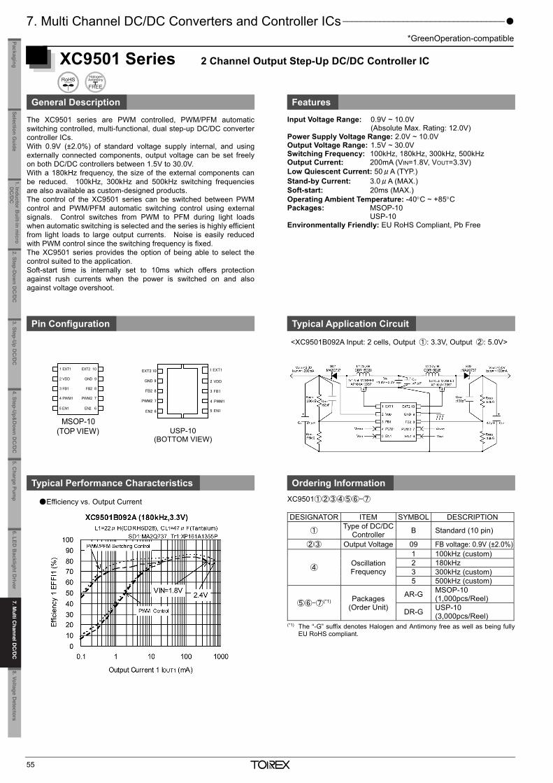
7. Multi Channel DC/DC Converters and Controller ICs ___________________________________
*GreenOperation-compatible
55
XC9501 Series 2 Channel Output Step-Up DC/DC Controller IC
General Description Features
The XC9501 series are PWM controlled, PWM/PFM automatic switching controlled, multi-functional, dual step-up DC/DC converter controller ICs. With 0.9V (±2.0%) of standard voltage supply internal, and using externally connected components, output voltage can be set freely on both DC/DC controllers between 1.5V to 30.0V. With a 180kHz frequency, the size of the external components can be reduced. 100kHz, 300kHz and 500kHz switching frequencies are also available as custom-designed products. The control of the XC9501 series can be switched between PWM control and PWM/PFM automatic switching control using external signals. Control switches from PWM to PFM during light loads when automatic switching is selected and the series is highly efficient from light loads to large output currents. Noise is easily reduced with PWM control since the switching frequency is fixed. The XC9501 series provides the option of being able to select the control suited to the application. Soft-start time is internally set to 10ms which offers protection against rush currents when the power is switched on and also against voltage overshoot.
Input Voltage Range: 0.9V ~ 10.0V (Absolute Max. Rating: 12.0V) Power Supply Voltage Range: 2.0V ~ 10.0V Output Voltage Range: 1.5V ~ 30.0V Switching Frequency: 100kHz, 180kHz, 300kHz, 500kHz Output Current: 200mA (VIN=1.8V, VOUT=3.3V) Low Quiescent Current: 50μA (TYP.) Stand-by Current: 3.0μA (MAX.) Soft-start: 20ms (MAX.) Operating Ambient Temperature: -40C ~ +85C Packages: MSOP-10 USP-10 Environmentally Friendly: EU RoHS Compliant, Pb Free
Pin Configuration Typical Application Circuit
Typical Performance Characteristics Ordering Information XC9501①②③④⑤⑥-⑦
DESIGNATOR ITEM SYMBOL DESCRIPTION
① Type of DC/DC Controller B Standard (10 pin)
②③ Output Voltage 09 FB voltage: 0.9V (±2.0%)
④ Oscillation Frequency
1 100kHz (custom) 2 180kHz 3 300kHz (custom) 5 500kHz (custom)
⑤⑥-⑦(*1) Packages (Order Unit)
AR-G MSOP-10 (1,000pcs/Reel)
DR-G USP-10 (3,000pcs/Reel)
(*1) The “-G” suffix denotes Halogen and Antimony free as well as being fullyEU RoHS compliant.
1
2
3
4
56
7
8
9
10 EXT1
VDD
FB1
PWM1
EN1EN2
PWM2
FB2
GND
EXT2
USP-10 (BOTTOM VIEW)
1 EXT1
2 VDD
3 FB1 FB2 8
GND 9
EXT2 10
4 PWM1 PWM2 7
5 EN1 EN2 6
MSOP-10(TOP VIEW)
<XC9501B092A Input: 2 cells, Output ①: 3.3V, Output ②: 5.0V>
Efficiency vs. Output Current
_______________________________________________________________________________________ 8. Voltage Detectors
56
XC6136 Series Ultra Low Power (88nA) Voltage Detector
Preliminary General Description
The XC6136 series is ultra-low power voltage detector with high accuracy detection, manufactured using CMOS process and laser trimming tech-nologies. The device is available in both CMOS and N-channel open drain output configurations. Also detect logic is available in both RESETB (Active Low)and RESET (Active High). Ultra-small low height package USPQ-4B05 and standard packages SSOT-24 and SOT-25 which are ideally suited for small design of portable de-vices and high densely mounting applications. UVLO circuit is implemented in order to suppress the floating of RESETB pin (undefined operation) when VIN voltage is lower than the minimumoperating voltage.
Features Pin Configuration Ultra-Low Power :91nA TYP.(@detect, VDF=1.2V, VIN=1.1V) :88nA TYP.(@release, VDF=1.2V, VIN=1.32V) High Accuracy :±0.8% (VDF≦3.0V, Ta=25) ±1.0% (3.1V≦VDF, Ta=25) :±2.5% (VDF≦3.0V, Ta=-40~105) ±2.7% (3.1V≦VDF, Ta=-40~105) Temperature Characteristics :±50ppm/ (TYP.) Hysteresis Width :TYPE:A/C VDF×5.0% (TYP.) TYPE:B/D 2mV~28mV (TYP.) Detect Voltage Range :1.2V~5.0V (0.1Vstep) Operating Voltage Range :1.1V~6.0V Output Type :CMOS Nch open drain Output Logic :RESETB(Active Low) RESET(Active High) Undefined Operation Protection :Output Pin Voltage 0.38V (CMOS Output only) (MAX:Ta=-40~+105) @Power supply Input pin Voltage<
operating voltage(MIN.) Packages :USPQ-4B05,SSOT-24,SOT-25 Environment Friendly :EU RoHS Compliant, Pb Free
Typical Application Circuit Typical Performance Characteristics
Ordering Information
XC6136①②③④⑤⑥-⑦ DESIGNATOR ITEM SYMBOL DESCRIPTION
① Output Configuration C CMOS output N Nch open drain output
②③ Detect Voltage 12~50 e.g. 1.2V → ②=1, ③=2
④ Type
A Reset Active Low / Hysteresis 5.0%(TYP.) B Reset Active Low / Hysteresis 0.1%(TYP.) C Reset Active High / Hysteresis 5.0%(TYP.) D Reset Active High / Hysteresis 0.1%(TYP.)
⑤⑥-⑦(*1) Packages (Order Unit) 9R-G USPQ-4B05 (5,000pcs/Reel) NR-G SSOT-24 (3,000pcs/Reel) MR-G SOT-25 (3,000pcs/Reel) Cu Wire
(*1) The “-G” suffix denotes Halogen and Antimony free as well as being fully RoHS compliant.
USPQ-4B05 (BOTTOM VIEW)
SOT-25 (TOP VIEW)
SSOT-24 (TOP VIEW)
VIN
VSS
VIN1 μprocessor
RPull(*1)
VIN2RESETB /RESET
RESETB /RESETINPUT
VIN
VSS
XC6136 Series
1 3
45
2
VSSRESETB/RESET
VIN
NCNC
1. Inductor Built-in m
icro D
C/D
C
2. Step-Dow
n DC
/DC
3. Step-Up D
C/D
C4. Step-U
p&D
own D
C/D
C
5.Charge Pum
p6.LED
Backlight D
river8.Voltage D
etectorsSelection G
uidePackaging
7. Multi C
hannel DC
/DC
7. M
ulti Channel D
C/D
C
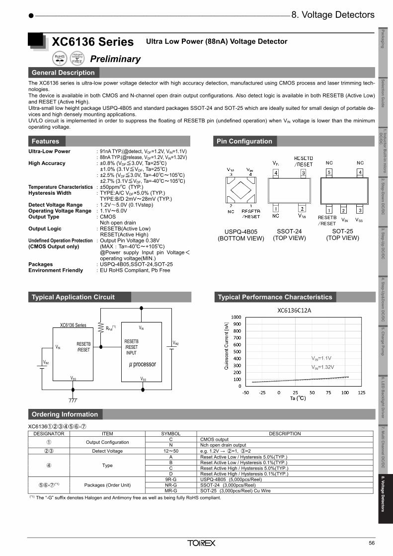
7. Multi Channel DC/DC Converters and Controller ICs ___________________________________
*GreenOperation-compatible
55
XC9501 Series 2 Channel Output Step-Up DC/DC Controller IC
General Description Features
The XC9501 series are PWM controlled, PWM/PFM automatic switching controlled, multi-functional, dual step-up DC/DC converter controller ICs. With 0.9V (±2.0%) of standard voltage supply internal, and using externally connected components, output voltage can be set freely on both DC/DC controllers between 1.5V to 30.0V. With a 180kHz frequency, the size of the external components can be reduced. 100kHz, 300kHz and 500kHz switching frequencies are also available as custom-designed products. The control of the XC9501 series can be switched between PWM control and PWM/PFM automatic switching control using external signals. Control switches from PWM to PFM during light loads when automatic switching is selected and the series is highly efficient from light loads to large output currents. Noise is easily reduced with PWM control since the switching frequency is fixed. The XC9501 series provides the option of being able to select the control suited to the application. Soft-start time is internally set to 10ms which offers protection against rush currents when the power is switched on and also against voltage overshoot.
Input Voltage Range: 0.9V ~ 10.0V (Absolute Max. Rating: 12.0V) Power Supply Voltage Range: 2.0V ~ 10.0V Output Voltage Range: 1.5V ~ 30.0V Switching Frequency: 100kHz, 180kHz, 300kHz, 500kHz Output Current: 200mA (VIN=1.8V, VOUT=3.3V) Low Quiescent Current: 50μA (TYP.) Stand-by Current: 3.0μA (MAX.) Soft-start: 20ms (MAX.) Operating Ambient Temperature: -40C ~ +85C Packages: MSOP-10 USP-10 Environmentally Friendly: EU RoHS Compliant, Pb Free
Pin Configuration Typical Application Circuit
Typical Performance Characteristics Ordering Information XC9501①②③④⑤⑥-⑦
DESIGNATOR ITEM SYMBOL DESCRIPTION
① Type of DC/DC Controller B Standard (10 pin)
②③ Output Voltage 09 FB voltage: 0.9V (±2.0%)
④ Oscillation Frequency
1 100kHz (custom) 2 180kHz 3 300kHz (custom) 5 500kHz (custom)
⑤⑥-⑦(*1) Packages (Order Unit)
AR-G MSOP-10 (1,000pcs/Reel)
DR-G USP-10 (3,000pcs/Reel)
(*1) The “-G” suffix denotes Halogen and Antimony free as well as being fullyEU RoHS compliant.
1
2
3
4
56
7
8
9
10 EXT1
VDD
FB1
PWM1
EN1EN2
PWM2
FB2
GND
EXT2
USP-10 (BOTTOM VIEW)
1 EXT1
2 VDD
3 FB1 FB2 8
GND 9
EXT2 10
4 PWM1 PWM2 7
5 EN1 EN2 6
MSOP-10(TOP VIEW)
<XC9501B092A Input: 2 cells, Output ①: 3.3V, Output ②: 5.0V>
Efficiency vs. Output Current
_______________________________________________________________________________________ 8. Voltage Detectors
56
XC6136 Series Ultra Low Power (88nA) Voltage Detector
Preliminary General Description
The XC6136 series is ultra-low power voltage detector with high accuracy detection, manufactured using CMOS process and laser trimming tech-nologies. The device is available in both CMOS and N-channel open drain output configurations. Also detect logic is available in both RESETB (Active Low)and RESET (Active High). Ultra-small low height package USPQ-4B05 and standard packages SSOT-24 and SOT-25 which are ideally suited for small design of portable de-vices and high densely mounting applications. UVLO circuit is implemented in order to suppress the floating of RESETB pin (undefined operation) when VIN voltage is lower than the minimumoperating voltage.
Features Pin Configuration Ultra-Low Power :91nA TYP.(@detect, VDF=1.2V, VIN=1.1V) :88nA TYP.(@release, VDF=1.2V, VIN=1.32V) High Accuracy :±0.8% (VDF≦3.0V, Ta=25) ±1.0% (3.1V≦VDF, Ta=25) :±2.5% (VDF≦3.0V, Ta=-40~105) ±2.7% (3.1V≦VDF, Ta=-40~105) Temperature Characteristics :±50ppm/ (TYP.) Hysteresis Width :TYPE:A/C VDF×5.0% (TYP.) TYPE:B/D 2mV~28mV (TYP.) Detect Voltage Range :1.2V~5.0V (0.1Vstep) Operating Voltage Range :1.1V~6.0V Output Type :CMOS Nch open drain Output Logic :RESETB(Active Low) RESET(Active High) Undefined Operation Protection :Output Pin Voltage 0.38V (CMOS Output only) (MAX:Ta=-40~+105) @Power supply Input pin Voltage<
operating voltage(MIN.) Packages :USPQ-4B05,SSOT-24,SOT-25 Environment Friendly :EU RoHS Compliant, Pb Free
Typical Application Circuit Typical Performance Characteristics
Ordering Information
XC6136①②③④⑤⑥-⑦ DESIGNATOR ITEM SYMBOL DESCRIPTION
① Output Configuration C CMOS output N Nch open drain output
②③ Detect Voltage 12~50 e.g. 1.2V → ②=1, ③=2
④ Type
A Reset Active Low / Hysteresis 5.0%(TYP.) B Reset Active Low / Hysteresis 0.1%(TYP.) C Reset Active High / Hysteresis 5.0%(TYP.) D Reset Active High / Hysteresis 0.1%(TYP.)
⑤⑥-⑦(*1) Packages (Order Unit) 9R-G USPQ-4B05 (5,000pcs/Reel) NR-G SSOT-24 (3,000pcs/Reel) MR-G SOT-25 (3,000pcs/Reel) Cu Wire
(*1) The “-G” suffix denotes Halogen and Antimony free as well as being fully RoHS compliant.
USPQ-4B05 (BOTTOM VIEW)
SOT-25 (TOP VIEW)
SSOT-24 (TOP VIEW)
VIN
VSS
VIN1 μprocessor
RPull(*1)
VIN2RESETB /RESET
RESETB /RESETINPUT
VIN
VSS
XC6136 Series
1 3
45
2
VSSRESETB/RESET
VIN
NCNC
1. Inductor Built-in m
icro D
C/D
C
2. Step-Dow
n DC
/DC
3. Step-Up D
C/D
C4. Step-U
p&D
own D
C/D
C
5.Charge Pum
p6.LED
Backlight D
riverSelection G
uidePackaging
7. Multi C
hannel DC
/DC
8.Voltage D
etectors
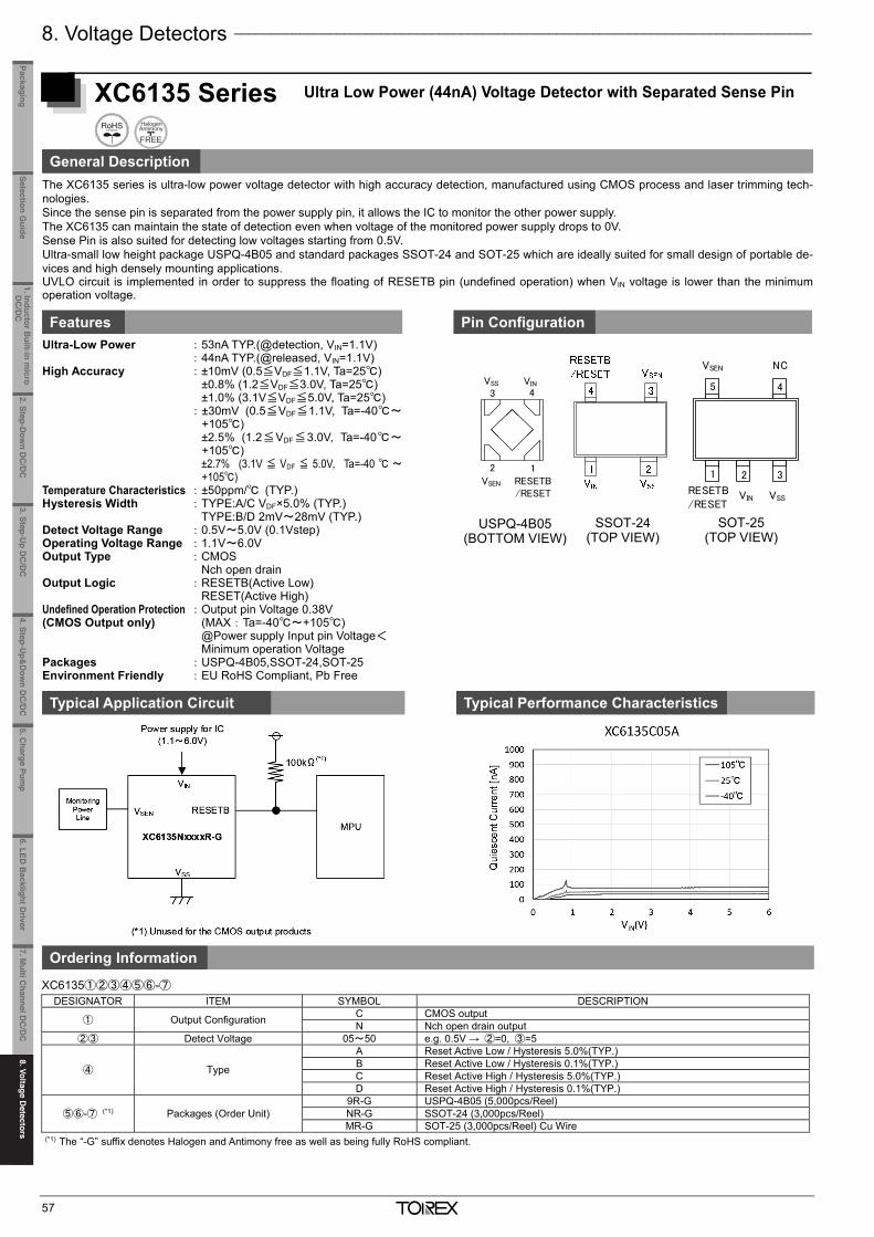
8. Voltage Detectors _______________________________________________________________________________
57
XC6135 Series Ultra Low Power (44nA) Voltage Detector with Separated Sense Pin
General Description
The XC6135 series is ultra-low power voltage detector with high accuracy detection, manufactured using CMOS process and laser trimming tech-nologies. Since the sense pin is separated from the power supply pin, it allows the IC to monitor the other power supply. The XC6135 can maintain the state of detection even when voltage of the monitored power supply drops to 0V. Sense Pin is also suited for detecting low voltages starting from 0.5V. Ultra-small low height package USPQ-4B05 and standard packages SSOT-24 and SOT-25 which are ideally suited for small design of portable de-vices and high densely mounting applications. UVLO circuit is implemented in order to suppress the floating of RESETB pin (undefined operation) when VIN voltage is lower than the minimum operation voltage. Features Pin Configuration
Ultra-Low Power :53nA TYP.(@detection, VIN=1.1V) :44nA TYP.(@released, VIN=1.1V) High Accuracy :±10mV (0.5≦VDF≦1.1V, Ta=25) ±0.8% (1.2≦VDF≦3.0V, Ta=25) ±1.0% (3.1V≦VDF≦5.0V, Ta=25) :±30mV (0.5≦VDF≦1.1V, Ta=-40~
+105) ±2.5% (1.2≦VDF≦3.0V, Ta=-40~
+105) ±2.7% (3.1V ≦ VDF ≦ 5.0V, Ta=-40 ~
+105) Temperature Characteristics :±50ppm/ (TYP.) Hysteresis Width :TYPE:A/C VDF×5.0% (TYP.) TYPE:B/D 2mV~28mV (TYP.) Detect Voltage Range :0.5V~5.0V (0.1Vstep) Operating Voltage Range :1.1V~6.0V Output Type :CMOS Nch open drain Output Logic :RESETB(Active Low) RESET(Active High) Undefined Operation Protection :Output pin Voltage 0.38V (CMOS Output only) (MAX:Ta=-40~+105) @Power supply Input pin Voltage< Minimum operation Voltage Packages :USPQ-4B05,SSOT-24,SOT-25 Environment Friendly :EU RoHS Compliant, Pb Free
Typical Application Circuit Typical Performance Characteristics
––
Ordering Information
XC6135①②③④⑤⑥-⑦ DESIGNATOR ITEM SYMBOL DESCRIPTION
① Output Configuration C CMOS output N Nch open drain output
②③ Detect Voltage 05~50 e.g. 0.5V → ②=0, ③=5
④ Type
A Reset Active Low / Hysteresis 5.0%(TYP.) B Reset Active Low / Hysteresis 0.1%(TYP.) C Reset Active High / Hysteresis 5.0%(TYP.) D Reset Active High / Hysteresis 0.1%(TYP.)
⑤⑥-⑦ (*1) Packages (Order Unit) 9R-G USPQ-4B05 (5,000pcs/Reel) NR-G SSOT-24 (3,000pcs/Reel) MR-G SOT-25 (3,000pcs/Reel) Cu Wire
(*1) The “-G” suffix denotes Halogen and Antimony free as well as being fully RoHS compliant.
USPQ-4B05 (BOTTOM VIEW)
SOT-25 (TOP VIEW)
SSOT-24 (TOP VIEW)
VINVSS
2
3
1
4
VSEN RESETB /RESET
1 3
45
2
VSSRESETB/RESET
VIN
NCVSEN
_______________________________________________________________________________________________________
58
XC6134 Series Delay Capacitor Adjustable Voltage Detectors with Sense Pin Isolation
General Description Features
The XC6134 series are ultra-small delay capacitor adjustable typevoltage detectors that have high accuracy and sense pin isolation.High accuracy and a low supply current are achieved by means of aCMOS process, a highly accurate reference power supply, and lasertrimming technology. The sense pin is isolated from the power input pin to enable moni-toring of the voltage of another power supply. Output can be main-tained in the detection state even if the voltage of the power supplythat is monitored drops to 0V. The sense pin is also suitable for de-tecting high voltages, and the detection and release voltage can beset as desired using external resistors. An internal delay circuit isalso provided. By connecting a capacitor to the Cd/MRB pin, any re-lease delay time and detect delay time can be set, and the pin canalso be used as a manual reset pin. The HYS external adjustment pincan be used to establish a sufficient hysteresis width.
Operating Ambient Temperature: -40~+125 Operating Voltage Rang: 1.6V~6.0V
(Absolute Max. Rating: 7.0V) Detect Voltage Range: 0.8V~5.0V Detect Voltage Accuracy: ±18mV (VDF<1.5V) (Ta=25) ±1.2% (1.5V≦VDF≦3.0V) ±1.5% (3.1V≦VDF≦5.0V) Detect Voltage Accuracy: ±36mV (VDF<1.5V) (Ta=-40~125) ±2.7% (1.5V≦VDF≦3.0V) ±3.0% (3.1V≦VDF≦5.0V) Temperature Characteristics: ±50ppm/ (TYP.) Hysteresis Width: VDF×0.1% (TYP.) Adjustable Pin for Hysteresis Width: Yes Low Supply Current: 1.28μA (TYP.) VIN=1.6V (At detection) 1.65μA (TYP.) VIN=6.0V(At release) Manual Reset Function: Yes Output Type: CMOS or Nch open drain Output Logic: H level or L level at detection Delay Capacitance Pin: Release delay / detection delay can
be set in 5 time ratio options Packages: USP-6C,SOT-26 Environmentally Friendly: EU RoHS compliant, Pb free
Pin Configuration Type A/B/C/D/L
Type E/F/H/K/M
Typical Application Circuit Typical Performance Characteristics
Battery (+B) voltage monitoring: Detects high voltage by R1/R2 resistance dividing. A hysteresis width can be added as desired by connecting R3 between the VSEN and HYS pins
Ordering Information
XC6134①②③④⑤⑥-⑦ DESIGNATOR ITEM SYMBOL DESCRIPTION
① Output Configuration C CMOS output N Nch open drain output
②③ Detect Voltage 08~50 e.g. 1.0V → ②=1, ③=0 ④ Type A~M Refer to [Selection Guide]
⑤⑥-⑦(*1) Packages (Order Unit) MR-G SOT-26 (3,000pcs/Reel) ER-G USP-6C (3,000pcs/Reel)
(*1) The “-G” suffix denotes Halogen and Antimony free as well as being fully EU RoHS compliant. Selection Guide
TYPE RESET/RESETB OUTPUT DELAY (Rp:Rn) HYSTERESIS A Active High(*2) 1:0 144kΩ:0Ω 0.1%(TYP.) B ↑ 1:0.125 144kΩ:18kΩ ↑ C ↑ 1:1 144kΩ:144kΩ ↑ D ↑ 2:1 288kΩ:144kΩ ↑ L ↑ 0.076:1 11kΩ:144kΩ ↑ E Active Low(*2) 1:0 144kΩ:0Ω ↑ F ↑ 1:0.125 144kΩ:18kΩ ↑ H ↑ 1:1 144kΩ:144kΩ ↑ K ↑ 2:1 288kΩ:144kΩ ↑ M ↑ 0.076:1 11kΩ:144kΩ ↑
(*2) ”Active High” is H level when detection occurs, and “Active Low” is L level when detection occurs.
5
1 32
6 4
SOT-26(TOP VIEW)
VSEN
VIN
Cd/MRB
RESET HYS
VSS
USP-6C(BOTTOM VIEW)
34
2
1
5
6 HYS
RESET
VINCd/MRB
VSS
VSEN5
1 32
6 4
SOT-26(TOP VIEW)
VSEN
VIN
Cd/MRB
RESETB HYS
VSS
USP-6C(BOTTOM VIEW)
34
2
1
5
6 HYS
RESETB
VINCd/MRB
VSS
VSEN
Cd/MRB
RESETRESETB
VIN
VSS
HYS
VSEN
VDD
GND
+B
R1
R2
R3
Rpull(*1)
RESETSW
Cd
and Hysteresis External Adjustment
0.0
0.5
1.0
1.5
2.0
2.5
3.0
3.5
4.0
0.0 0.5 1.0 1.5 2.0 2.5 3.0 3.5 4.0 4.5 5.0 5.5 6.0
Outp
ut V
oltag
e : V
RESET(V
)
VSEN pin Voltage : VSEN(V)
XC6134C10B
R3=0Ω
R3=330kΩ
R3=110kΩ
VIN=3.3V、VSEN=0V→6V→0V
R1=330kΩ
1. Inductor Built-in m
icro D
C/D
C
2. Step-Dow
n DC
/DC
3. Step-Up D
C/D
C4. Step-U
p&D
own D
C/D
C
5.Charge Pum
p6.LED
Backlight D
river8.Voltage D
etectorsSelection G
uidePackaging
7. Multi C
hannel DC
/DC
8.Voltage D
etectors
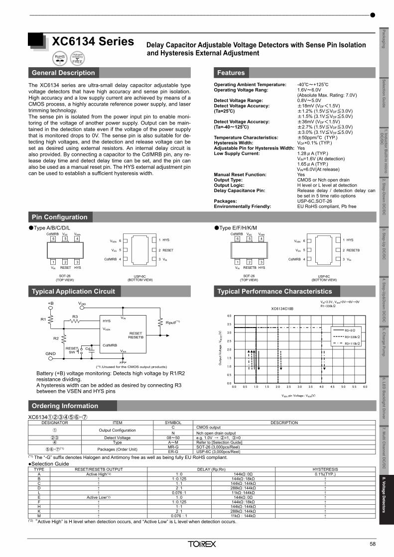
8. Voltage Detectors _______________________________________________________________________________
57
XC6135 Series Ultra Low Power (44nA) Voltage Detector with Separated Sense Pin
General Description
The XC6135 series is ultra-low power voltage detector with high accuracy detection, manufactured using CMOS process and laser trimming tech-nologies. Since the sense pin is separated from the power supply pin, it allows the IC to monitor the other power supply. The XC6135 can maintain the state of detection even when voltage of the monitored power supply drops to 0V. Sense Pin is also suited for detecting low voltages starting from 0.5V. Ultra-small low height package USPQ-4B05 and standard packages SSOT-24 and SOT-25 which are ideally suited for small design of portable de-vices and high densely mounting applications. UVLO circuit is implemented in order to suppress the floating of RESETB pin (undefined operation) when VIN voltage is lower than the minimum operation voltage. Features Pin Configuration
Ultra-Low Power :53nA TYP.(@detection, VIN=1.1V) :44nA TYP.(@released, VIN=1.1V) High Accuracy :±10mV (0.5≦VDF≦1.1V, Ta=25) ±0.8% (1.2≦VDF≦3.0V, Ta=25) ±1.0% (3.1V≦VDF≦5.0V, Ta=25) :±30mV (0.5≦VDF≦1.1V, Ta=-40~
+105) ±2.5% (1.2≦VDF≦3.0V, Ta=-40~
+105) ±2.7% (3.1V ≦ VDF ≦ 5.0V, Ta=-40 ~
+105) Temperature Characteristics :±50ppm/ (TYP.) Hysteresis Width :TYPE:A/C VDF×5.0% (TYP.) TYPE:B/D 2mV~28mV (TYP.) Detect Voltage Range :0.5V~5.0V (0.1Vstep) Operating Voltage Range :1.1V~6.0V Output Type :CMOS Nch open drain Output Logic :RESETB(Active Low) RESET(Active High) Undefined Operation Protection :Output pin Voltage 0.38V (CMOS Output only) (MAX:Ta=-40~+105) @Power supply Input pin Voltage< Minimum operation Voltage Packages :USPQ-4B05,SSOT-24,SOT-25 Environment Friendly :EU RoHS Compliant, Pb Free
Typical Application Circuit Typical Performance Characteristics
––
Ordering Information
XC6135①②③④⑤⑥-⑦ DESIGNATOR ITEM SYMBOL DESCRIPTION
① Output Configuration C CMOS output N Nch open drain output
②③ Detect Voltage 05~50 e.g. 0.5V → ②=0, ③=5
④ Type
A Reset Active Low / Hysteresis 5.0%(TYP.) B Reset Active Low / Hysteresis 0.1%(TYP.) C Reset Active High / Hysteresis 5.0%(TYP.) D Reset Active High / Hysteresis 0.1%(TYP.)
⑤⑥-⑦ (*1) Packages (Order Unit) 9R-G USPQ-4B05 (5,000pcs/Reel) NR-G SSOT-24 (3,000pcs/Reel) MR-G SOT-25 (3,000pcs/Reel) Cu Wire
(*1) The “-G” suffix denotes Halogen and Antimony free as well as being fully RoHS compliant.
USPQ-4B05 (BOTTOM VIEW)
SOT-25 (TOP VIEW)
SSOT-24 (TOP VIEW)
VINVSS
2
3
1
4
VSEN RESETB /RESET
1 3
45
2
VSSRESETB/RESET
VIN
NCVSEN
_______________________________________________________________________________________________________
58
XC6134 Series Delay Capacitor Adjustable Voltage Detectors with Sense Pin Isolation
General Description Features
The XC6134 series are ultra-small delay capacitor adjustable typevoltage detectors that have high accuracy and sense pin isolation.High accuracy and a low supply current are achieved by means of aCMOS process, a highly accurate reference power supply, and lasertrimming technology. The sense pin is isolated from the power input pin to enable moni-toring of the voltage of another power supply. Output can be main-tained in the detection state even if the voltage of the power supplythat is monitored drops to 0V. The sense pin is also suitable for de-tecting high voltages, and the detection and release voltage can beset as desired using external resistors. An internal delay circuit isalso provided. By connecting a capacitor to the Cd/MRB pin, any re-lease delay time and detect delay time can be set, and the pin canalso be used as a manual reset pin. The HYS external adjustment pincan be used to establish a sufficient hysteresis width.
Operating Ambient Temperature: -40~+125 Operating Voltage Rang: 1.6V~6.0V
(Absolute Max. Rating: 7.0V) Detect Voltage Range: 0.8V~5.0V Detect Voltage Accuracy: ±18mV (VDF<1.5V) (Ta=25) ±1.2% (1.5V≦VDF≦3.0V) ±1.5% (3.1V≦VDF≦5.0V) Detect Voltage Accuracy: ±36mV (VDF<1.5V) (Ta=-40~125) ±2.7% (1.5V≦VDF≦3.0V) ±3.0% (3.1V≦VDF≦5.0V) Temperature Characteristics: ±50ppm/ (TYP.) Hysteresis Width: VDF×0.1% (TYP.) Adjustable Pin for Hysteresis Width: Yes Low Supply Current: 1.28μA (TYP.) VIN=1.6V (At detection) 1.65μA (TYP.) VIN=6.0V(At release) Manual Reset Function: Yes Output Type: CMOS or Nch open drain Output Logic: H level or L level at detection Delay Capacitance Pin: Release delay / detection delay can
be set in 5 time ratio options Packages: USP-6C,SOT-26 Environmentally Friendly: EU RoHS compliant, Pb free
Pin Configuration Type A/B/C/D/L
Type E/F/H/K/M
Typical Application Circuit Typical Performance Characteristics
Battery (+B) voltage monitoring: Detects high voltage by R1/R2 resistance dividing. A hysteresis width can be added as desired by connecting R3 between the VSEN and HYS pins
Ordering Information
XC6134①②③④⑤⑥-⑦ DESIGNATOR ITEM SYMBOL DESCRIPTION
① Output Configuration C CMOS output N Nch open drain output
②③ Detect Voltage 08~50 e.g. 1.0V → ②=1, ③=0 ④ Type A~M Refer to [Selection Guide]
⑤⑥-⑦(*1) Packages (Order Unit) MR-G SOT-26 (3,000pcs/Reel) ER-G USP-6C (3,000pcs/Reel)
(*1) The “-G” suffix denotes Halogen and Antimony free as well as being fully EU RoHS compliant. Selection Guide
TYPE RESET/RESETB OUTPUT DELAY (Rp:Rn) HYSTERESIS A Active High(*2) 1:0 144kΩ:0Ω 0.1%(TYP.) B ↑ 1:0.125 144kΩ:18kΩ ↑ C ↑ 1:1 144kΩ:144kΩ ↑ D ↑ 2:1 288kΩ:144kΩ ↑ L ↑ 0.076:1 11kΩ:144kΩ ↑ E Active Low(*2) 1:0 144kΩ:0Ω ↑ F ↑ 1:0.125 144kΩ:18kΩ ↑ H ↑ 1:1 144kΩ:144kΩ ↑ K ↑ 2:1 288kΩ:144kΩ ↑ M ↑ 0.076:1 11kΩ:144kΩ ↑
(*2) ”Active High” is H level when detection occurs, and “Active Low” is L level when detection occurs.
5
1 32
6 4
SOT-26(TOP VIEW)
VSEN
VIN
Cd/MRB
RESET HYS
VSS
USP-6C(BOTTOM VIEW)
34
2
1
5
6 HYS
RESET
VINCd/MRB
VSS
VSEN5
1 32
6 4
SOT-26(TOP VIEW)
VSEN
VIN
Cd/MRB
RESETB HYS
VSS
USP-6C(BOTTOM VIEW)
34
2
1
5
6 HYS
RESETB
VINCd/MRB
VSS
VSEN
Cd/MRB
RESETRESETB
VIN
VSS
HYS
VSEN
VDD
GND
+B
R1
R2
R3
Rpull(*1)
RESETSW
Cd
and Hysteresis External Adjustment
0.0
0.5
1.0
1.5
2.0
2.5
3.0
3.5
4.0
0.0 0.5 1.0 1.5 2.0 2.5 3.0 3.5 4.0 4.5 5.0 5.5 6.0
Outp
ut V
oltag
e : V
RESET(V
)
VSEN pin Voltage : VSEN(V)
XC6134C10B
R3=0Ω
R3=330kΩ
R3=110kΩ
VIN=3.3V、VSEN=0V→6V→0V
R1=330kΩ
1. Inductor Built-in m
icro D
C/D
C
2. Step-Dow
n DC
/DC
3. Step-Up D
C/D
C4. Step-U
p&D
own D
C/D
C
5.Charge Pum
p6.LED
Backlight D
riverSelection G
uidePackaging
7. Multi C
hannel DC
/DC
8.Voltage D
etectors
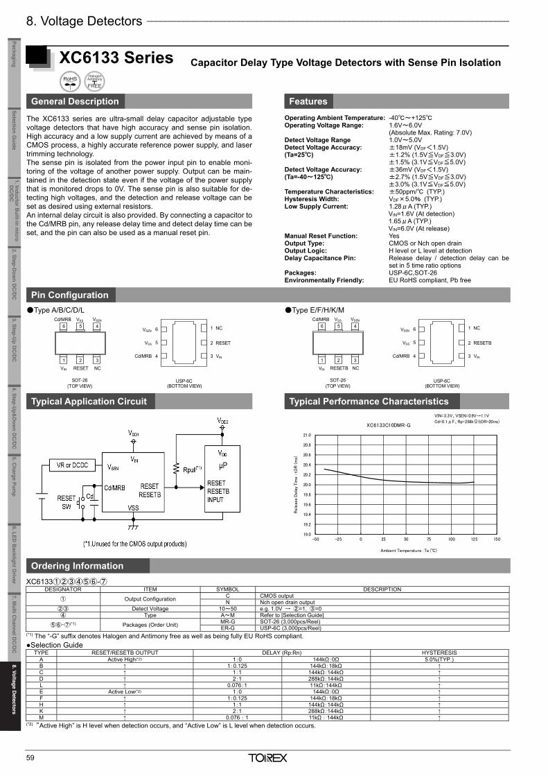
8. Voltage Detectors _______________________________________________________________________________
59
XC6133 Series Capacitor Delay Type Voltage Detectors with Sense Pin Isolation
General Description Features
The XC6133 series are ultra-small delay capacitor adjustable type voltage detectors that have high accuracy and sense pin isolation. High accuracy and a low supply current are achieved by means of a CMOS process, a highly accurate reference power supply, and laser trimming technology. The sense pin is isolated from the power input pin to enable moni-toring of the voltage of another power supply. Output can be main-tained in the detection state even if the voltage of the power supply that is monitored drops to 0V. The sense pin is also suitable for de-tecting high voltages, and the detection and release voltage can be set as desired using external resistors. An internal delay circuit is also provided. By connecting a capacitor to the Cd/MRB pin, any release delay time and detect delay time can be set, and the pin can also be used as a manual reset pin.
Operating Ambient Temperature: -40~+125 Operating Voltage Range: 1.6V~6.0V
(Absolute Max. Rating: 7.0V) Detect Voltage Range 1.0V~5.0V Detect Voltage Accuracy: ±18mV (VDF<1.5V) (Ta=25) ±1.2% (1.5V≦VDF≦3.0V) ±1.5% (3.1V≦VDF≦5.0V) Detect Voltage Accuracy: ±36mV (VDF<1.5V) (Ta=-40~125) ±2.7% (1.5V≦VDF≦3.0V) ±3.0% (3.1V≦VDF≦5.0V) Temperature Characteristics: ±50ppm/ (TYP.) Hysteresis Width: VDF×5.0% (TYP.) Low Supply Current: 1.28μA (TYP.) VIN=1.6V (At detection) 1.65μA (TYP.) VIN=6.0V (At release) Manual Reset Function: Yes Output Type: CMOS or Nch open drain Output Logic: H level or L level at detection Delay Capacitance Pin: Release delay / detection delay can be
set in 5 time ratio options Packages: USP-6C,SOT-26 Environmentally Friendly: EU RoHS compliant, Pb free
Pin Configuration Type A/B/C/D/L
Type E/F/H/K/M
Typical Application Circuit Typical Performance Characteristics
Ordering Information
XC6133①②③④⑤⑥-⑦ DESIGNATOR ITEM SYMBOL DESCRIPTION
① Output Configuration C CMOS output N Nch open drain output
②③ Detect Voltage 10~50 e.g. 1.0V → ②=1, ③=0 ④ Type A~M Refer to [Selection Guide]
⑤⑥-⑦(*1) Packages (Order Unit) MR-G SOT-26 (3,000pcs/Reel) ER-G USP-6C (3,000pcs/Reel)
(*1) The “-G” suffix denotes Halogen and Antimony free as well as being fully EU RoHS compliant. Selection Guide
TYPE RESET/RESETB OUTPUT DELAY (Rp:Rn) HYSTERESIS A Active High(*2) 1:0 144kΩ:0Ω 5.0%(TYP.) B ↑ 1:0.125 144kΩ:18kΩ ↑ C ↑ 1:1 144kΩ:144kΩ ↑ D ↑ 2:1 288kΩ:144kΩ ↑ L ↑ 0.076:1 11kΩ:144kΩ ↑ E Active Low(*2) 1:0 144kΩ:0Ω ↑ F ↑ 1:0.125 144kΩ:18kΩ ↑ H ↑ 1:1 144kΩ:144kΩ ↑ K ↑ 2:1 288kΩ:144kΩ ↑ M ↑ 0.076:1 11kΩ:144kΩ ↑
(*2) ”Active High” is H level when detection occurs, and “Active Low” is L level when detection occurs.
19.0
19.2
19.4
19.6
19.8
20.0
20.2
20.4
20.6
20.8
21.0
-50 -25 0 25 50 75 100 125 150
Rele
ase D
ela
y Tim
e :
tDR
(m
s)
Ambient Temperature : Ta ()
XC6133C10DMR-G
VIN=3.3V、VSEN=0.9V→1.1V
Cd=0.1μF、Rp=288kΩ(tDR=20ms)
5
1 32
6 4
SOT-26(TOP VIEW)
VSEN
VIN
Cd/MRB
RESET NC
VSS
USP-6C(BOTTOM VIEW)
34
2
1
5
6 NC
RESET
VINCd/MRB
VSS
VSEN5
1 32
6 4
SOT-26(TOP VIEW)
VSEN
VIN
Cd/MRB
RESETB NC
VSS
USP-6C(BOTTOM VIEW)
34
2
1
5
6 NC
RESETB
VINCd/MRB
VSS
VSEN
_______________________________________________________________________________________________________
60
XC6132 Series Delay Capacitor Adjustable, Sense Pin Isolation, Surge Voltage
General Description Features
The XC6132 series are ultra-small delay capacitor adjustable typevoltage detectors that have high accuracy and sense pin isolation.High accuracy and a low supply current are achieved by means of aCMOS process, a highly accurate reference power supply, and lasertrimming technology. The sense pin is isolated from the power input pin to enable moni-toring of the voltage of another power supply. Output can be main-tained in the detection state even if the voltage of the power supplythat is monitored drops to 0V. The sense pin is also suitable for de-tecting high voltages, and the detection and release voltage can beset as desired using external resistors. An internal surge voltageprotection circuit and an internal delay circuit are also provided. By connecting a capacitor to the Cd/MRB pin, any release delay timeand detect delay time can be set and the pin can also be used as amanual reset pin. The HYS external adjustment pin can be used to establish a suffi-cient hysteresis width.
Operating Ambient Temperature: -40~+125 Operating voltage range: 1.6V~6.0V
(Absolute Max. Rating: 7.0V) Detect voltage range: 0.8V~2.0V Detect voltage accuracy: ±18mV(VDF<1.5V) (Ta=25) ±1.2%(1.5V≦VDF≦2.0V) Detect voltage accuracy: ±36mV(VDF<1.5V) (Ta=-40~125) ±2.7%(1.5V≦VDF≦2.0V) Temperature Characteristics: ±50ppm/(TYP.) Hysteresis width: VDF×0.1%(TYP.) Adjustable Pin for Hysteresis Width: Yes Low supply current: 1.28μA(TYP.) VIN=1.6V(At detection) 1.65μA(TYP.) VIN=6.0V(At release) Manual reset function: Yes Output type: CMOS or N-ch open drain Output logic: H level or L level at detection Delay capacitance pin: Release delay / detection delay can be set
in 5 time ratio options Sense pin: Includes a surge voltage protection function Packages: USP-6C,SOT-26 Environmentally Friendly: EU RoHS compliant, Pb free
Pin Configuration A/B/C/D/L type
E/F/H/K/M type
Typical Application Circuit Typical Performance Characteristics
Battery (+B) voltage monitoring: Detects high voltage via R1/R2 resistance division. A hysteresis width can be added as desired by connecting R3 between the VSEN and HYS pins
Ordering Information
XC6132①②③④⑤⑥-⑦ DESIGNATOR ITEM SYMBOL DESCRIPTION
① Output Configuration C CMOS output N N-ch open drain output
②③ Detect Voltage 08~20 e.g. 1.0V → ②=1, ③=0 ④ Type A~M Refer to Selection Guide
⑤⑥-⑦(*1) Packages (Order Unit) MR-G SOT-26 (3,000pcs/Reel) ER-G USP-6C (3,000pcs/Reel)
(*1) The “-G” suffix denotes Halogen and Antimony free as well as being fully EU RoHS compliant. Selection Guide
TYPE RESET/RESETB OUTPUT DELAY(Rp:Rn) HYSTERESIS A Active High(*2) 1:0 144kΩ:0Ω 0.1%(TYP.) B ↑ 1:0.125 144kΩ:18kΩ ↑ C ↑ 1:1 144kΩ:144kΩ ↑ D ↑ 2:1 288kΩ:144kΩ ↑ L ↑ 0.076:1 11kΩ:144kΩ ↑ E Active Low(*2) 1:0 144kΩ:0Ω ↑ F ↑ 1:0.125 144kΩ:18kΩ ↑ H ↑ 1:1 144kΩ:144kΩ ↑ K ↑ 2:1 288kΩ:144kΩ ↑ M ↑ 0.076:1 11kΩ:144kΩ ↑
(*2) ”Active High” is H level when detection occurs, and “Active Low” is L level when detection occurs.
5
1 32
6 4
SOT-26(TOP VIEW)
VSEN
VIN
Cd/MRB
RESET HYS
VSS
USP-6C(BOTTOM VIEW)
34
2
1
5
6 HYS
RESET
VINCd/MRB
VSS
VSEN5
1 32
6 4
SOT-26(TOP VIEW)
VSEN
VIN
Cd/MRB
RESETB HYS
VSS
USP-6C(BOTTOM VIEW)
34
2
1
5
6 HYS
RESETB
VINCd/MRB
VSS
VSEN
Protection and Hysteresis Rxternal Adjustment
Cd/MRB
RESETRESETB
VIN
VSS
HYS
VSEN
VDD
GND
+B
R1
R2
R3
Rpull(*1)
RESETSW
Cd
0.0
0.5
1.0
1.5
2.0
2.5
3.0
3.5
4.0
0 1 2 3 4 5 6 7 8 9 10
Outp
ut
Voltag
e :
VR
ESET(V
)
Voltage Sense : VSEN(V)
XC6132C10E
OPEN R1=330kΩ R1=560kΩ
VIN=3.3VVSEN=0V→10V→0V
R2=100kΩ、R3=330kΩ
1. Inductor Built-in m
icro D
C/D
C
2. Step-Dow
n DC
/DC
3. Step-Up D
C/D
C4. Step-U
p&D
own D
C/D
C
5.Charge Pum
p6.LED
Backlight D
river8.Voltage D
etectorsSelection G
uidePackaging
7. Multi C
hannel DC
/DC
8.Voltage D
etectors
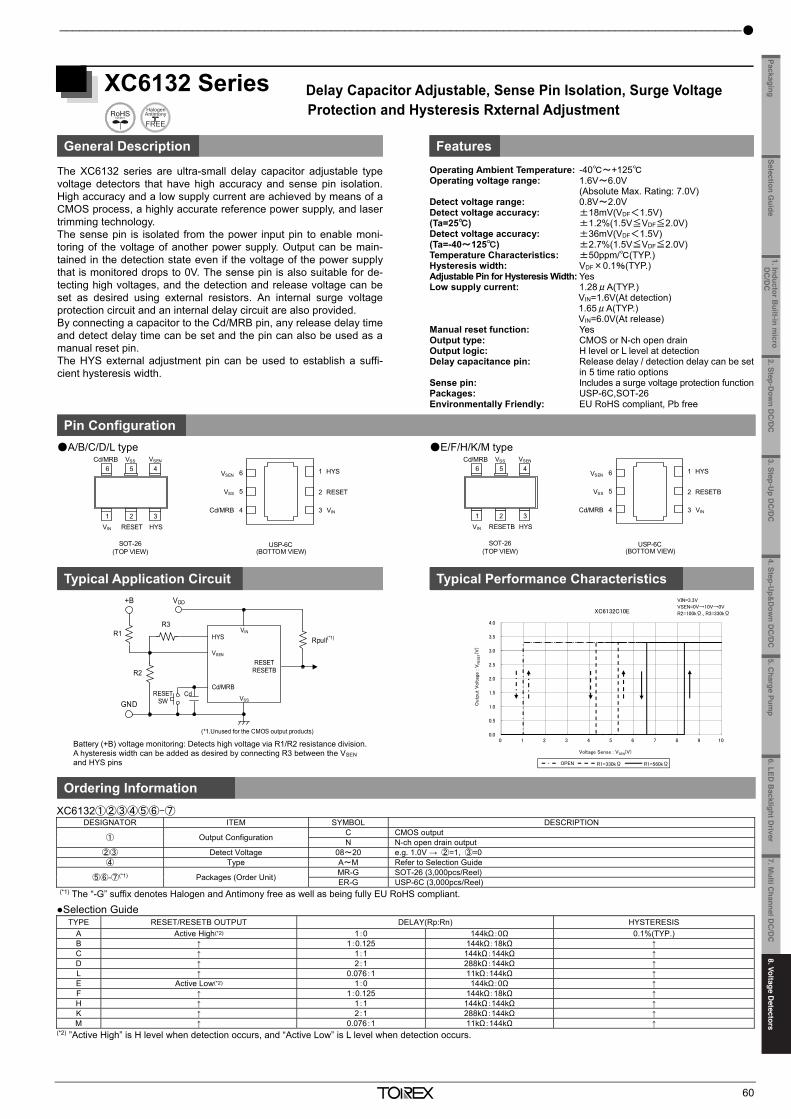
8. Voltage Detectors _______________________________________________________________________________
59
XC6133 Series Capacitor Delay Type Voltage Detectors with Sense Pin Isolation
General Description Features
The XC6133 series are ultra-small delay capacitor adjustable type voltage detectors that have high accuracy and sense pin isolation. High accuracy and a low supply current are achieved by means of a CMOS process, a highly accurate reference power supply, and laser trimming technology. The sense pin is isolated from the power input pin to enable moni-toring of the voltage of another power supply. Output can be main-tained in the detection state even if the voltage of the power supply that is monitored drops to 0V. The sense pin is also suitable for de-tecting high voltages, and the detection and release voltage can be set as desired using external resistors. An internal delay circuit is also provided. By connecting a capacitor to the Cd/MRB pin, any release delay time and detect delay time can be set, and the pin can also be used as a manual reset pin.
Operating Ambient Temperature: -40~+125 Operating Voltage Range: 1.6V~6.0V
(Absolute Max. Rating: 7.0V) Detect Voltage Range 1.0V~5.0V Detect Voltage Accuracy: ±18mV (VDF<1.5V) (Ta=25) ±1.2% (1.5V≦VDF≦3.0V) ±1.5% (3.1V≦VDF≦5.0V) Detect Voltage Accuracy: ±36mV (VDF<1.5V) (Ta=-40~125) ±2.7% (1.5V≦VDF≦3.0V) ±3.0% (3.1V≦VDF≦5.0V) Temperature Characteristics: ±50ppm/ (TYP.) Hysteresis Width: VDF×5.0% (TYP.) Low Supply Current: 1.28μA (TYP.) VIN=1.6V (At detection) 1.65μA (TYP.) VIN=6.0V (At release) Manual Reset Function: Yes Output Type: CMOS or Nch open drain Output Logic: H level or L level at detection Delay Capacitance Pin: Release delay / detection delay can be
set in 5 time ratio options Packages: USP-6C,SOT-26 Environmentally Friendly: EU RoHS compliant, Pb free
Pin Configuration Type A/B/C/D/L
Type E/F/H/K/M
Typical Application Circuit Typical Performance Characteristics
Ordering Information
XC6133①②③④⑤⑥-⑦ DESIGNATOR ITEM SYMBOL DESCRIPTION
① Output Configuration C CMOS output N Nch open drain output
②③ Detect Voltage 10~50 e.g. 1.0V → ②=1, ③=0 ④ Type A~M Refer to [Selection Guide]
⑤⑥-⑦(*1) Packages (Order Unit) MR-G SOT-26 (3,000pcs/Reel) ER-G USP-6C (3,000pcs/Reel)
(*1) The “-G” suffix denotes Halogen and Antimony free as well as being fully EU RoHS compliant. Selection Guide
TYPE RESET/RESETB OUTPUT DELAY (Rp:Rn) HYSTERESIS A Active High(*2) 1:0 144kΩ:0Ω 5.0%(TYP.) B ↑ 1:0.125 144kΩ:18kΩ ↑ C ↑ 1:1 144kΩ:144kΩ ↑ D ↑ 2:1 288kΩ:144kΩ ↑ L ↑ 0.076:1 11kΩ:144kΩ ↑ E Active Low(*2) 1:0 144kΩ:0Ω ↑ F ↑ 1:0.125 144kΩ:18kΩ ↑ H ↑ 1:1 144kΩ:144kΩ ↑ K ↑ 2:1 288kΩ:144kΩ ↑ M ↑ 0.076:1 11kΩ:144kΩ ↑
(*2) ”Active High” is H level when detection occurs, and “Active Low” is L level when detection occurs.
19.0
19.2
19.4
19.6
19.8
20.0
20.2
20.4
20.6
20.8
21.0
-50 -25 0 25 50 75 100 125 150
Rele
ase D
ela
y Tim
e :
tDR
(m
s)
Ambient Temperature : Ta ()
XC6133C10DMR-G
VIN=3.3V、VSEN=0.9V→1.1V
Cd=0.1μF、Rp=288kΩ(tDR=20ms)
5
1 32
6 4
SOT-26(TOP VIEW)
VSEN
VIN
Cd/MRB
RESET NC
VSS
USP-6C(BOTTOM VIEW)
34
2
1
5
6 NC
RESET
VINCd/MRB
VSS
VSEN5
1 32
6 4
SOT-26(TOP VIEW)
VSEN
VIN
Cd/MRB
RESETB NC
VSS
USP-6C(BOTTOM VIEW)
34
2
1
5
6 NC
RESETB
VINCd/MRB
VSS
VSEN
_______________________________________________________________________________________________________
60
XC6132 Series Delay Capacitor Adjustable, Sense Pin Isolation, Surge Voltage
General Description Features
The XC6132 series are ultra-small delay capacitor adjustable typevoltage detectors that have high accuracy and sense pin isolation.High accuracy and a low supply current are achieved by means of aCMOS process, a highly accurate reference power supply, and lasertrimming technology. The sense pin is isolated from the power input pin to enable moni-toring of the voltage of another power supply. Output can be main-tained in the detection state even if the voltage of the power supplythat is monitored drops to 0V. The sense pin is also suitable for de-tecting high voltages, and the detection and release voltage can beset as desired using external resistors. An internal surge voltageprotection circuit and an internal delay circuit are also provided. By connecting a capacitor to the Cd/MRB pin, any release delay timeand detect delay time can be set and the pin can also be used as amanual reset pin. The HYS external adjustment pin can be used to establish a suffi-cient hysteresis width.
Operating Ambient Temperature: -40~+125 Operating voltage range: 1.6V~6.0V
(Absolute Max. Rating: 7.0V) Detect voltage range: 0.8V~2.0V Detect voltage accuracy: ±18mV(VDF<1.5V) (Ta=25) ±1.2%(1.5V≦VDF≦2.0V) Detect voltage accuracy: ±36mV(VDF<1.5V) (Ta=-40~125) ±2.7%(1.5V≦VDF≦2.0V) Temperature Characteristics: ±50ppm/(TYP.) Hysteresis width: VDF×0.1%(TYP.) Adjustable Pin for Hysteresis Width: Yes Low supply current: 1.28μA(TYP.) VIN=1.6V(At detection) 1.65μA(TYP.) VIN=6.0V(At release) Manual reset function: Yes Output type: CMOS or N-ch open drain Output logic: H level or L level at detection Delay capacitance pin: Release delay / detection delay can be set
in 5 time ratio options Sense pin: Includes a surge voltage protection function Packages: USP-6C,SOT-26 Environmentally Friendly: EU RoHS compliant, Pb free
Pin Configuration A/B/C/D/L type
E/F/H/K/M type
Typical Application Circuit Typical Performance Characteristics
Battery (+B) voltage monitoring: Detects high voltage via R1/R2 resistance division. A hysteresis width can be added as desired by connecting R3 between the VSEN and HYS pins
Ordering Information
XC6132①②③④⑤⑥-⑦ DESIGNATOR ITEM SYMBOL DESCRIPTION
① Output Configuration C CMOS output N N-ch open drain output
②③ Detect Voltage 08~20 e.g. 1.0V → ②=1, ③=0 ④ Type A~M Refer to Selection Guide
⑤⑥-⑦(*1) Packages (Order Unit) MR-G SOT-26 (3,000pcs/Reel) ER-G USP-6C (3,000pcs/Reel)
(*1) The “-G” suffix denotes Halogen and Antimony free as well as being fully EU RoHS compliant. Selection Guide
TYPE RESET/RESETB OUTPUT DELAY(Rp:Rn) HYSTERESIS A Active High(*2) 1:0 144kΩ:0Ω 0.1%(TYP.) B ↑ 1:0.125 144kΩ:18kΩ ↑ C ↑ 1:1 144kΩ:144kΩ ↑ D ↑ 2:1 288kΩ:144kΩ ↑ L ↑ 0.076:1 11kΩ:144kΩ ↑ E Active Low(*2) 1:0 144kΩ:0Ω ↑ F ↑ 1:0.125 144kΩ:18kΩ ↑ H ↑ 1:1 144kΩ:144kΩ ↑ K ↑ 2:1 288kΩ:144kΩ ↑ M ↑ 0.076:1 11kΩ:144kΩ ↑
(*2) ”Active High” is H level when detection occurs, and “Active Low” is L level when detection occurs.
5
1 32
6 4
SOT-26(TOP VIEW)
VSEN
VIN
Cd/MRB
RESET HYS
VSS
USP-6C(BOTTOM VIEW)
34
2
1
5
6 HYS
RESET
VINCd/MRB
VSS
VSEN5
1 32
6 4
SOT-26(TOP VIEW)
VSEN
VIN
Cd/MRB
RESETB HYS
VSS
USP-6C(BOTTOM VIEW)
34
2
1
5
6 HYS
RESETB
VINCd/MRB
VSS
VSEN
Protection and Hysteresis Rxternal Adjustment
Cd/MRB
RESETRESETB
VIN
VSS
HYS
VSEN
VDD
GND
+B
R1
R2
R3
Rpull(*1)
RESETSW
Cd
0.0
0.5
1.0
1.5
2.0
2.5
3.0
3.5
4.0
0 1 2 3 4 5 6 7 8 9 10
Outp
ut
Voltag
e :
VR
ESET(V
)
Voltage Sense : VSEN(V)
XC6132C10E
OPEN R1=330kΩ R1=560kΩ
VIN=3.3VVSEN=0V→10V→0V
R2=100kΩ、R3=330kΩ
1. Inductor Built-in m
icro D
C/D
C
2. Step-Dow
n DC
/DC
3. Step-Up D
C/D
C4. Step-U
p&D
own D
C/D
C
5.Charge Pum
p6.LED
Backlight D
riverSelection G
uidePackaging
7. Multi C
hannel DC
/DC
8.Voltage D
etectors
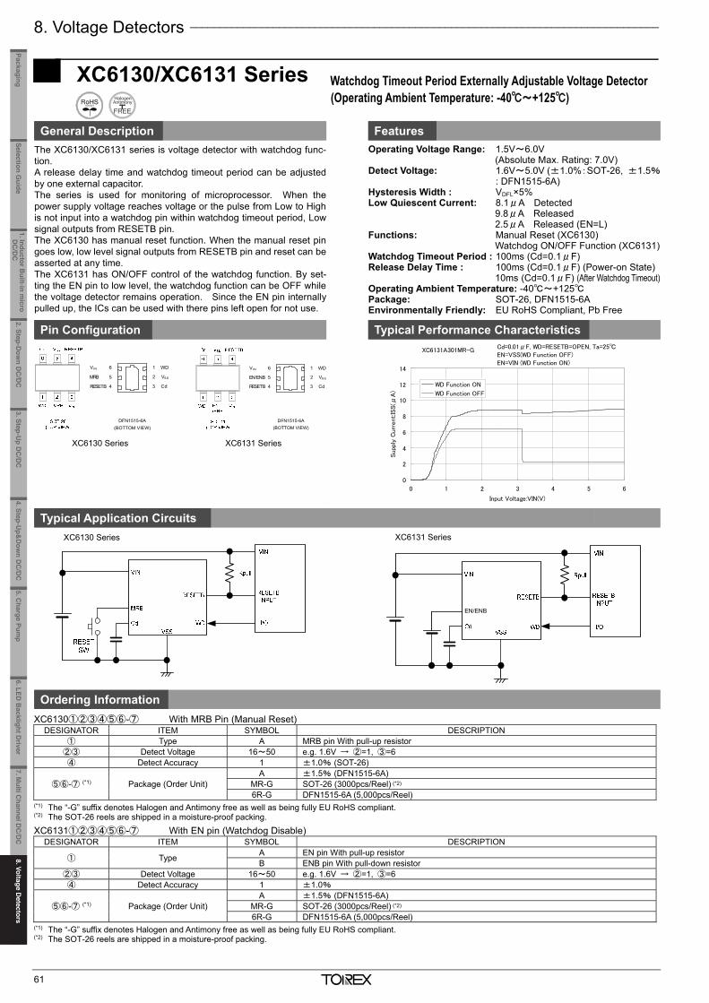
8. Voltage Detectors _______________________________________________________________________________
61
XC6130/XC6131 Series Watchdog Timeout Period Externally Adjustable Voltage Detector
General Description Features
The XC6130/XC6131 series is voltage detector with watchdog func-tion. A release delay time and watchdog timeout period can be adjusted by one external capacitor. The series is used for monitoring of microprocessor. When the power supply voltage reaches voltage or the pulse from Low to High is not input into a watchdog pin within watchdog timeout period, Low signal outputs from RESETB pin. The XC6130 has manual reset function. When the manual reset pin goes low, low level signal outputs from RESETB pin and reset can be asserted at any time. The XC6131 has ON/OFF control of the watchdog function. By set-ting the EN pin to low level, the watchdog function can be OFF while the voltage detector remains operation. Since the EN pin internally pulled up, the ICs can be used with there pins left open for not use.
Operating Voltage Range: 1.5V~6.0V (Absolute Max. Rating: 7.0V) Detect Voltage: 1.6V~5.0V (±1.0%:SOT-26, ±1.5%
: DFN1515-6A) Hysteresis Width : VDFL×5% Low Quiescent Current: 8.1μA Detected 9.8μA Released 2.5μA Released (EN=L) Functions: Manual Reset (XC6130) Watchdog ON/OFF Function (XC6131) Watchdog Timeout Period : 100ms (Cd=0.1μF) Release Delay Time : 100ms (Cd=0.1μF) (Power-on State) 10ms (Cd=0.1μF) (After Watchdog Timeout) Operating Ambient Temperature: -40~+125 Package: SOT-26, DFN1515-6A Environmentally Friendly: EU RoHS Compliant, Pb Free
Pin Configuration Typical Performance Characteristics
Typical Application Circuits
Ordering Information
XC6130①②③④⑤⑥-⑦ With MRB Pin (Manual Reset) DESIGNATOR ITEM SYMBOL DESCRIPTION
① Type A MRB pin With pull-up resistor ②③ Detect Voltage 16~50 e.g. 1.6V → ②=1, ③=6 ④ Detect Accuracy 1 ±1.0% (SOT-26)
⑤⑥-⑦ (*1) Package (Order Unit) A ±1.5% (DFN1515-6A)
MR-G SOT-26 (3000pcs/Reel) (*2) 6R-G DFN1515-6A (5,000pcs/Reel)
(*1) The “-G” suffix denotes Halogen and Antimony free as well as being fully EU RoHS compliant. (*2) The SOT-26 reels are shipped in a moisture-proof packing. XC6131①②③④⑤⑥-⑦ With EN pin (Watchdog Disable)
DESIGNATOR ITEM SYMBOL DESCRIPTION
① Type A EN pin With pull-up resistor B ENB pin With pull-down resistor
②③ Detect Voltage 16~50 e.g. 1.6V → ②=1, ③=6 ④ Detect Accuracy 1 ±1.0%
⑤⑥-⑦ (*1) Package (Order Unit) A ±1.5% (DFN1515-6A)
MR-G SOT-26 (3000pcs/Reel) (*2) 6R-G DFN1515-6A (5,000pcs/Reel)
(*1) The “-G” suffix denotes Halogen and Antimony free as well as being fully EU RoHS compliant. (*2) The SOT-26 reels are shipped in a moisture-proof packing.
XC6131A301MR-G
0
2
4
6
8
10
12
14
0 1 2 3 4 5 6
Input Voltage:VIN(V)
Supply
Curr
ent:IS
S(μ
A)
WD Function ON
WD Function OFF
Cd=0.01μF, WD=RESETB=OPEN, Ta=25EN=VSS(WD Function OFF)EN=VIN (WD Function ON)
XC6130 Series XC6131 Series
(Operating Ambient Temperature: -40~+125)
EN/ENB
XC6130 Series XC6131 Series
1
2
4
5
6VIN
MRB
RESETB
WD
VSS
DFN1515-6A(BOTTOM VIEW)
1
2
4
5
6VIN
/EN
RESETB
WD
VSSENB
DFN1515-6A(BOTTOM VIEW)
_______________________________________________________________________________________________________
62
XC6129 Series Voltage Detector with Delay Time Adjustable
General Description Features
XC6129 series is an ultra small highly accurate voltage detector with externalcapacitor type delay function. The device includes a highly accurate reference voltage source, manufacturedusing CMOS process and laser trimming technology, it maintains low powerconsumption and high accuracy. The device includes the built-in delay circuit.A release delay time or detect delay time can be set freely by connecting anexternal delay capacitor to Cd pin. There are two kinds of the output configuration for the XC6129 such as CMOSor N-channel open drain. The series has a function to prevent an indefiniteoperation. Therefore, when the input pin voltage is under minimum operatingvoltage, the function controls an output pin voltage in the indefinite operation less than0.4V (MAX.). Also, the series allows a choice of an output logic when detec-tion; therefore, it is suitable for various electric devices using Microcontrollers. Ultra small package USPN-4, SSOT-24 (standard) and USPQ-4B05 are ideallysuited for small design of portable devices and high densely mounting applica-tions.
High Accuracy: ±0.8% Temperature Characteristic: ±50ppm/ (TYP.) Hysteresis Width: VDF×5% (TYP.) Quiescent Current : 0.42μA TYP. (at Detect VIN=2.7V) 0.58μA TYP. (at Release VIN=2.7V) Detect Voltage Range: 1.5V~5.5V (0.1V increments) Input Voltage Range: 1.3V~6.0V
(Absolute Max. Rating: 6.5V) Output Configuration: CMOS or N-channel Open Drain Output Logic: Active High or Active Low (at Detect) Release Delay Time: 13.9ms (Cd=0.01μF, RP=2MΩ) Detect Delay Time: 17.9ms (Cd=0.01μF, Rn=2MΩ) Manual Reset Function: Cd Pin “Low” makes VOUT “Low” Operating Ambient Temperature: -40~+85 Packages: USPN-4, SSOT-24, USPQ-4B05 Environmentally Friendly: EU RoHS Compliant, Pb Free
Pin Configuration Typical Performance Characteristics
Typical Application Circuit
Ordering Information
XC6129①②③④⑤⑥-⑦ DESIGNATOR ITEM SYMBOL DESCRIPTION
① Output Configuration C CMOS output N Nch open drain output
②③ Detect Voltage 15~55 e.g. 1.8V → ②=1, ③=8
④ Type
A
Refer to [Selection Guide]
B C D E F G J L
⑤⑥-⑦(*1) Packages (Order Unit) NR-G SSOT-24 (3,000pcs/Reel) 9R-G USPQ-4B05 (5,000pcs/Reel) 7R-G USPN-4 (5,000pcs/Reel)
(*1) The “-G” suffix denotes Halogen and Antimony free as well as being fully EU RoHS compliant. Selection Guide
TYPE OUTPUT LOGIC RELEASE DELAY DETECT DELAY HYSTERESIS WIDTH INDEFINITENESS PREVENTION A
Reset Active Low
Yes No 5% (TYP.) Not Available B 5% (TYP.) Available C No Yes 5% (TYP.) Not Available D 5% (TYP.) Available E Yes Yes 5% (TYP.) Not Available F 5% (TYP.) Available G
Reset Active High Yes No 5% (TYP.)
Not Available J No Yes 5% (TYP.) L Yes Yes 5% (TYP.)
SSOT-24
(TOP VIEW)
VIN
RESETBRESET
VSS
1 2
34
Cd/MRB
USPN-4
(BOTTOM VIEW)
1
10
100
1000
10000
0.01 0.1 1
検出
・解
除遅
延時
間(m
S)
Cd (μF)
解除遅延時間
検出遅延時間
Release Delay Time Detect Delay Time
Det
ect・
Rel
ease
Del
ay T
ime
(ms)
USPQ-4B05(BOTTOM VIEW)
2
3
1
4
VINVSS
RESETBRESET
Cd/MRB
1. Inductor Built-in m
icro D
C/D
C
2. Step-Dow
n DC
/DC
3. Step-Up D
C/D
C4. Step-U
p&D
own D
C/D
C
5.Charge Pum
p6.LED
Backlight D
river8.Voltage D
etectorsSelection G
uidePackaging
7. Multi C
hannel DC
/DC
8.Voltage D
etectors
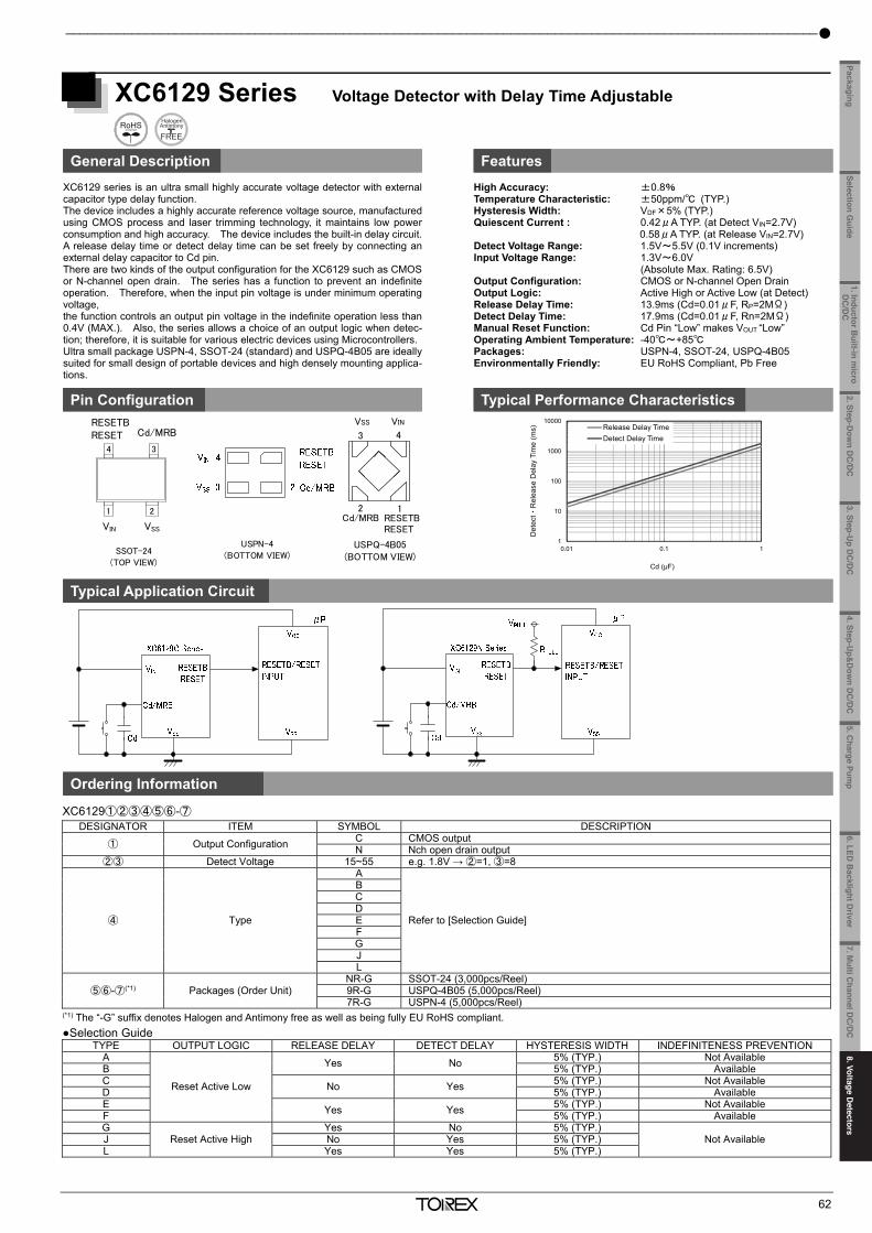
8. Voltage Detectors _______________________________________________________________________________
61
XC6130/XC6131 Series Watchdog Timeout Period Externally Adjustable Voltage Detector
General Description Features
The XC6130/XC6131 series is voltage detector with watchdog func-tion. A release delay time and watchdog timeout period can be adjusted by one external capacitor. The series is used for monitoring of microprocessor. When the power supply voltage reaches voltage or the pulse from Low to High is not input into a watchdog pin within watchdog timeout period, Low signal outputs from RESETB pin. The XC6130 has manual reset function. When the manual reset pin goes low, low level signal outputs from RESETB pin and reset can be asserted at any time. The XC6131 has ON/OFF control of the watchdog function. By set-ting the EN pin to low level, the watchdog function can be OFF while the voltage detector remains operation. Since the EN pin internally pulled up, the ICs can be used with there pins left open for not use.
Operating Voltage Range: 1.5V~6.0V (Absolute Max. Rating: 7.0V) Detect Voltage: 1.6V~5.0V (±1.0%:SOT-26, ±1.5%
: DFN1515-6A) Hysteresis Width : VDFL×5% Low Quiescent Current: 8.1μA Detected 9.8μA Released 2.5μA Released (EN=L) Functions: Manual Reset (XC6130) Watchdog ON/OFF Function (XC6131) Watchdog Timeout Period : 100ms (Cd=0.1μF) Release Delay Time : 100ms (Cd=0.1μF) (Power-on State) 10ms (Cd=0.1μF) (After Watchdog Timeout) Operating Ambient Temperature: -40~+125 Package: SOT-26, DFN1515-6A Environmentally Friendly: EU RoHS Compliant, Pb Free
Pin Configuration Typical Performance Characteristics
Typical Application Circuits
Ordering Information
XC6130①②③④⑤⑥-⑦ With MRB Pin (Manual Reset) DESIGNATOR ITEM SYMBOL DESCRIPTION
① Type A MRB pin With pull-up resistor ②③ Detect Voltage 16~50 e.g. 1.6V → ②=1, ③=6 ④ Detect Accuracy 1 ±1.0% (SOT-26)
⑤⑥-⑦ (*1) Package (Order Unit) A ±1.5% (DFN1515-6A)
MR-G SOT-26 (3000pcs/Reel) (*2) 6R-G DFN1515-6A (5,000pcs/Reel)
(*1) The “-G” suffix denotes Halogen and Antimony free as well as being fully EU RoHS compliant. (*2) The SOT-26 reels are shipped in a moisture-proof packing. XC6131①②③④⑤⑥-⑦ With EN pin (Watchdog Disable)
DESIGNATOR ITEM SYMBOL DESCRIPTION
① Type A EN pin With pull-up resistor B ENB pin With pull-down resistor
②③ Detect Voltage 16~50 e.g. 1.6V → ②=1, ③=6 ④ Detect Accuracy 1 ±1.0%
⑤⑥-⑦ (*1) Package (Order Unit) A ±1.5% (DFN1515-6A)
MR-G SOT-26 (3000pcs/Reel) (*2) 6R-G DFN1515-6A (5,000pcs/Reel)
(*1) The “-G” suffix denotes Halogen and Antimony free as well as being fully EU RoHS compliant. (*2) The SOT-26 reels are shipped in a moisture-proof packing.
XC6131A301MR-G
0
2
4
6
8
10
12
14
0 1 2 3 4 5 6
Input Voltage:VIN(V)
Supply
Curr
ent:IS
S(μ
A)
WD Function ON
WD Function OFF
Cd=0.01μF, WD=RESETB=OPEN, Ta=25EN=VSS(WD Function OFF)EN=VIN (WD Function ON)
XC6130 Series XC6131 Series
(Operating Ambient Temperature: -40~+125)
EN/ENB
XC6130 Series XC6131 Series
1
2
4
5
6VIN
MRB
RESETB
WD
VSS
DFN1515-6A(BOTTOM VIEW)
1
2
4
5
6VIN
/EN
RESETB
WD
VSSENB
DFN1515-6A(BOTTOM VIEW)
_______________________________________________________________________________________________________
62
XC6129 Series Voltage Detector with Delay Time Adjustable
General Description Features
XC6129 series is an ultra small highly accurate voltage detector with externalcapacitor type delay function. The device includes a highly accurate reference voltage source, manufacturedusing CMOS process and laser trimming technology, it maintains low powerconsumption and high accuracy. The device includes the built-in delay circuit.A release delay time or detect delay time can be set freely by connecting anexternal delay capacitor to Cd pin. There are two kinds of the output configuration for the XC6129 such as CMOSor N-channel open drain. The series has a function to prevent an indefiniteoperation. Therefore, when the input pin voltage is under minimum operatingvoltage, the function controls an output pin voltage in the indefinite operation less than0.4V (MAX.). Also, the series allows a choice of an output logic when detec-tion; therefore, it is suitable for various electric devices using Microcontrollers. Ultra small package USPN-4, SSOT-24 (standard) and USPQ-4B05 are ideallysuited for small design of portable devices and high densely mounting applica-tions.
High Accuracy: ±0.8% Temperature Characteristic: ±50ppm/ (TYP.) Hysteresis Width: VDF×5% (TYP.) Quiescent Current : 0.42μA TYP. (at Detect VIN=2.7V) 0.58μA TYP. (at Release VIN=2.7V) Detect Voltage Range: 1.5V~5.5V (0.1V increments) Input Voltage Range: 1.3V~6.0V
(Absolute Max. Rating: 6.5V) Output Configuration: CMOS or N-channel Open Drain Output Logic: Active High or Active Low (at Detect) Release Delay Time: 13.9ms (Cd=0.01μF, RP=2MΩ) Detect Delay Time: 17.9ms (Cd=0.01μF, Rn=2MΩ) Manual Reset Function: Cd Pin “Low” makes VOUT “Low” Operating Ambient Temperature: -40~+85 Packages: USPN-4, SSOT-24, USPQ-4B05 Environmentally Friendly: EU RoHS Compliant, Pb Free
Pin Configuration Typical Performance Characteristics
Typical Application Circuit
Ordering Information
XC6129①②③④⑤⑥-⑦ DESIGNATOR ITEM SYMBOL DESCRIPTION
① Output Configuration C CMOS output N Nch open drain output
②③ Detect Voltage 15~55 e.g. 1.8V → ②=1, ③=8
④ Type
A
Refer to [Selection Guide]
B C D E F G J L
⑤⑥-⑦(*1) Packages (Order Unit) NR-G SSOT-24 (3,000pcs/Reel) 9R-G USPQ-4B05 (5,000pcs/Reel) 7R-G USPN-4 (5,000pcs/Reel)
(*1) The “-G” suffix denotes Halogen and Antimony free as well as being fully EU RoHS compliant. Selection Guide
TYPE OUTPUT LOGIC RELEASE DELAY DETECT DELAY HYSTERESIS WIDTH INDEFINITENESS PREVENTION A
Reset Active Low
Yes No 5% (TYP.) Not Available B 5% (TYP.) Available C No Yes 5% (TYP.) Not Available D 5% (TYP.) Available E Yes Yes 5% (TYP.) Not Available F 5% (TYP.) Available G
Reset Active High Yes No 5% (TYP.)
Not Available J No Yes 5% (TYP.) L Yes Yes 5% (TYP.)
SSOT-24
(TOP VIEW)
VIN
RESETBRESET
VSS
1 2
34
Cd/MRB
USPN-4
(BOTTOM VIEW)
1
10
100
1000
10000
0.01 0.1 1
検出
・解
除遅
延時
間(m
S)
Cd (μF)
解除遅延時間
検出遅延時間
Release Delay Time Detect Delay Time
Det
ect・
Rel
ease
Del
ay T
ime
(ms)
USPQ-4B05(BOTTOM VIEW)
2
3
1
4
VINVSS
RESETBRESET
Cd/MRB
1. Inductor Built-in m
icro D
C/D
C
2. Step-Dow
n DC
/DC
3. Step-Up D
C/D
C4. Step-U
p&D
own D
C/D
C
5.Charge Pum
p6.LED
Backlight D
riverSelection G
uidePackaging
7. Multi C
hannel DC
/DC
8.Voltage D
etectors
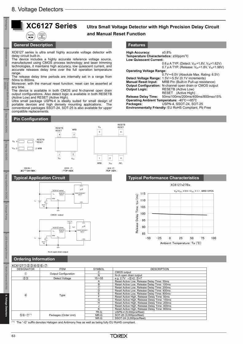
8. Voltage Detectors _______________________________________________________________________________
63
RESETBRESETVIN
1 2
34
MRB
23
14
MRBVSS
1 32
5 4
VIN VSS
RESETBRESET
VIN
VSS
RESETBRESET
MRB NC
XC6127 Series Ultra Small Voltage Detector with High Precision Delay Circuit and Manual Reset Function
General Description Features
XC6127 series is ultra small highly accurate voltage detector with delay circuit built-in. The device includes a highly accurate reference voltage source, manufactured using CMOS process technology and laser trimming technologies, it maintains high accuracy, low quiescent current, and accurate releases delay time over the full operation temperature range. The release delay time periods are internally set in a range from 50ms to 800ms. Moreover, with the manual reset function, reset can be asserted at any time. The device is available in both CMOS and N-channel open drain output configurations. Also detect logic is available in both RESETB (Active Low) and RESET (Active High). Ultra small package USPN-4 is ideally suited for small design of portable devices and high densely mounting applications. The conventional packages SSOT-24, SOT-25 is also available for upper compatible replacements.
High Accuracy: ±0.8% Temperature Characteristics: ±50ppm/ Low Quiescent Current: 0.6μA TYP. (Detect: VDF=1.8V, VIN=1.62V) 0.7μA TYP. (Release: VDF=1.8V, VIN=1.98V) Operating Voltage Range: 0.7V~6.0V (Absolute Max. Rating: 6.5V) Detect Voltage Range: 1.5V~5.5V (0.1V increments) Manual Reset Input: MRB Pin (Built-in Pull-up resistance) Output Configuration: N-channel open drain or CMOS output Output Logic: RESETB (Active Low) RESET (Active High) Release Delay Time: 50ms/100ms/200ms/400ms/800ms±15% Operating Ambient Temperature: -40~+85 Packages: USPN-4, SSOT-24, SOT-25 Environmentally Friendly: EU RoHS Compliant, Pb Free
Pin Configuration
Typical Application Circuit Typical Performance Characteristics
Ordering Information
XC6127①②③④⑤⑥-⑦ DESIGNATOR ITEM SYMBOL DESCRIPTION
① Output Configuration C CMOS output N N-ch open drain output
②③ Detect Voltage 15~55 e.g. 2.7V →②=2, ③=7
④ Type
A Reset Active Low, Release Delay Time: 50ms B Reset Active Low, Release Delay Time: 100ms C Reset Active Low, Release Delay Time: 200ms D Reset Active Low, Release Delay Time: 400ms E Reset Active Low, Release Delay Time: 800ms F Reset Active High, Release Delay Time: 50ms G Reset Active High, Release Delay Time: 100ms H Reset Active High, Release Delay Time: 200ms J Reset Active High, Release Delay Time: 400ms K Reset Active High, Release Delay Time: 800ms
⑤⑥-⑦(*1) Packages (Order Unit) 7R-G USPN-4 (5,000pcs/Reel) MR-G SOT-25 (3,000pcs/Reel) NR-G SSOT-24 (3,000pcs/Reel)
(*1) The “-G” suffix denotes Halogen and Antimony free as well as being fully EU RoHS compliant.
VIN
VIN
MRB
RESETBRESET
RESETSW
VIN
MRB
RESETBRESET
RESETSW
Rpull
Vpull-Up
CMOS output
N-ch open drain output
XC6127 series
XC6127 series
RESETB/RESETINPUT
VCC
μP
VSS
RESETB/RESETINPUT
VCC
μP
VSSVIN
VSS
VSS
XC6127x27Bx
85
90
95
100
105
110
115
-50 -25 0 25 50 75 100
Ambient Temperature: Ta ()
Rele
ase D
ela
y Tim
e: t D
R (
ms)
VIN=VDFL×0.9→VDFL×1.1 , MRB=OPEN
_______________________________________________________________________________________________________
64
XC6126 Series Ultra Small, Highly Accurate, Single Voltage Detector
General Description Features
The XC6126 series is an ultra small, highly accurate CMOS singlevoltage detector with very low quiescent current. The device in-cludes a highly accurate reference voltage source and uses lasertrimming technologies, it maintains high accuracy over the full opera-tion temperature range. The device is available in both CMOS and N-channel open drainoutput configurations. Ultra small package USPN-4B02 is ideally suited for small design ofportable devices and high densely mounting applications. Theconventional package SSOT-24 is also available for upper compati-ble replacements.
High Accuracy: ±0.8% Temperature Characteristics: ±50ppm/(TYP) Low Quiescent Current: 0.6μA (Detect: VDF=1.8V, VIN=1.62V)(TYP.) 0.7μA (Release: VDF=1.8V, VIN=1.98V)(TYP.) Operating Voltage Range: 0.7V~6.0V (Absolute Max. Rating: 6.5V) Detect Voltage Range: 1.5V~5.5V (0.1V increments) Output Configuration: N-ch open drain output CMOS output Detect Logic: Active Low Reset Operating Ambient Temperature: -40~+85 Packages: USPN-4B02, SSOT-24 Environmentally Friendly: EU RoHS Compliant, Pb Free
Pin Configuration
Typical Application Circuit Typical Performance Characteristics Detect Voltage vs. Ambient Temperature
Ordering Information
XC6126①②③④⑤⑥-⑦ DESIGNATOR ITEM SYMBOL DESCRIPTION
① Output Configuration C CMOS Output N N-ch Open Drain Output
②③ Detect Voltage 15~55 e.g. 2.7V →②=2, ③=7 ④ Detect Accuracy A ±0.8%
⑤⑥-⑦(*1) Packages (Order Unit) 7R-G USPN-4B02 (5,000pcs/Reel) NR-G SSOT-24 (3,000pcs/Reel)
(*1) The “-G” suffix denotes Halogen and Antimony free as well as being fully EU RoHS compliant.
NC
USPN-4B02(BOTTOM VIEW)
VINVSS
23
14
1 2
34
SSOT-24(TOP VIEW)
NC VSS
VIN VOUT
VOUT
XC6126x27Ax
2.64
2.66
2.68
2.70
2.72
2.74
2.76
-50 -25 0 25 50 75 100
Ambient Temperature: Ta ()
Dete
ct
Voltag
e: V
DFL (V
)
1. Inductor Built-in m
icro D
C/D
C
2. Step-Dow
n DC
/DC
3. Step-Up D
C/D
C4. Step-U
p&D
own D
C/D
C
5.Charge Pum
p6.LED
Backlight D
river8.Voltage D
etectorsSelection G
uidePackaging
7. Multi C
hannel DC
/DC
8.Voltage D
etectors
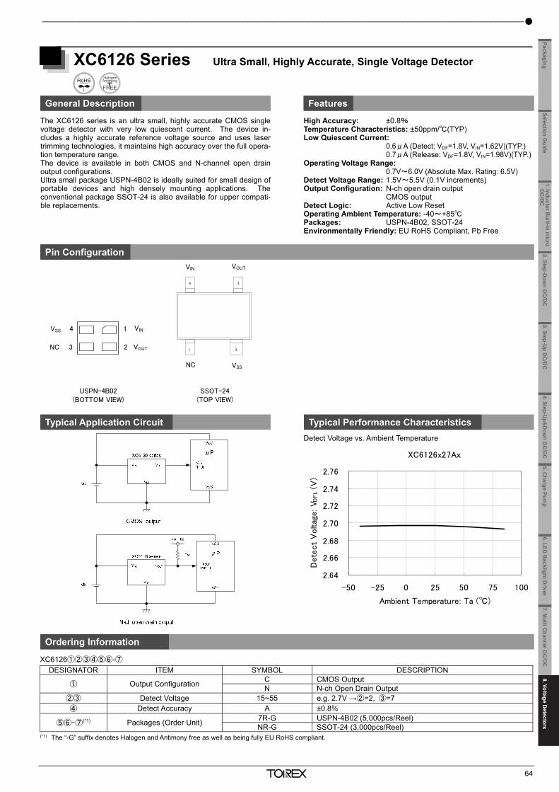
8. Voltage Detectors _______________________________________________________________________________
63
RESETBRESETVIN
1 2
34
MRB
23
14
MRBVSS
1 32
5 4
VIN VSS
RESETBRESET
VIN
VSS
RESETBRESET
MRB NC
XC6127 Series Ultra Small Voltage Detector with High Precision Delay Circuit and Manual Reset Function
General Description Features
XC6127 series is ultra small highly accurate voltage detector with delay circuit built-in. The device includes a highly accurate reference voltage source, manufactured using CMOS process technology and laser trimming technologies, it maintains high accuracy, low quiescent current, and accurate releases delay time over the full operation temperature range. The release delay time periods are internally set in a range from 50ms to 800ms. Moreover, with the manual reset function, reset can be asserted at any time. The device is available in both CMOS and N-channel open drain output configurations. Also detect logic is available in both RESETB (Active Low) and RESET (Active High). Ultra small package USPN-4 is ideally suited for small design of portable devices and high densely mounting applications. The conventional packages SSOT-24, SOT-25 is also available for upper compatible replacements.
High Accuracy: ±0.8% Temperature Characteristics: ±50ppm/ Low Quiescent Current: 0.6μA TYP. (Detect: VDF=1.8V, VIN=1.62V) 0.7μA TYP. (Release: VDF=1.8V, VIN=1.98V) Operating Voltage Range: 0.7V~6.0V (Absolute Max. Rating: 6.5V) Detect Voltage Range: 1.5V~5.5V (0.1V increments) Manual Reset Input: MRB Pin (Built-in Pull-up resistance) Output Configuration: N-channel open drain or CMOS output Output Logic: RESETB (Active Low) RESET (Active High) Release Delay Time: 50ms/100ms/200ms/400ms/800ms±15% Operating Ambient Temperature: -40~+85 Packages: USPN-4, SSOT-24, SOT-25 Environmentally Friendly: EU RoHS Compliant, Pb Free
Pin Configuration
Typical Application Circuit Typical Performance Characteristics
Ordering Information
XC6127①②③④⑤⑥-⑦ DESIGNATOR ITEM SYMBOL DESCRIPTION
① Output Configuration C CMOS output N N-ch open drain output
②③ Detect Voltage 15~55 e.g. 2.7V →②=2, ③=7
④ Type
A Reset Active Low, Release Delay Time: 50ms B Reset Active Low, Release Delay Time: 100ms C Reset Active Low, Release Delay Time: 200ms D Reset Active Low, Release Delay Time: 400ms E Reset Active Low, Release Delay Time: 800ms F Reset Active High, Release Delay Time: 50ms G Reset Active High, Release Delay Time: 100ms H Reset Active High, Release Delay Time: 200ms J Reset Active High, Release Delay Time: 400ms K Reset Active High, Release Delay Time: 800ms
⑤⑥-⑦(*1) Packages (Order Unit) 7R-G USPN-4 (5,000pcs/Reel) MR-G SOT-25 (3,000pcs/Reel) NR-G SSOT-24 (3,000pcs/Reel)
(*1) The “-G” suffix denotes Halogen and Antimony free as well as being fully EU RoHS compliant.
VIN
VIN
MRB
RESETBRESET
RESETSW
VIN
MRB
RESETBRESET
RESETSW
Rpull
Vpull-Up
CMOS output
N-ch open drain output
XC6127 series
XC6127 series
RESETB/RESETINPUT
VCC
μP
VSS
RESETB/RESETINPUT
VCC
μP
VSSVIN
VSS
VSS
XC6127x27Bx
85
90
95
100
105
110
115
-50 -25 0 25 50 75 100
Ambient Temperature: Ta ()
Rele
ase D
ela
y Tim
e: t D
R (
ms)
VIN=VDFL×0.9→VDFL×1.1 , MRB=OPEN
_______________________________________________________________________________________________________
64
XC6126 Series Ultra Small, Highly Accurate, Single Voltage Detector
General Description Features
The XC6126 series is an ultra small, highly accurate CMOS singlevoltage detector with very low quiescent current. The device in-cludes a highly accurate reference voltage source and uses lasertrimming technologies, it maintains high accuracy over the full opera-tion temperature range. The device is available in both CMOS and N-channel open drainoutput configurations. Ultra small package USPN-4B02 is ideally suited for small design ofportable devices and high densely mounting applications. Theconventional package SSOT-24 is also available for upper compati-ble replacements.
High Accuracy: ±0.8% Temperature Characteristics: ±50ppm/(TYP) Low Quiescent Current: 0.6μA (Detect: VDF=1.8V, VIN=1.62V)(TYP.) 0.7μA (Release: VDF=1.8V, VIN=1.98V)(TYP.) Operating Voltage Range: 0.7V~6.0V (Absolute Max. Rating: 6.5V) Detect Voltage Range: 1.5V~5.5V (0.1V increments) Output Configuration: N-ch open drain output CMOS output Detect Logic: Active Low Reset Operating Ambient Temperature: -40~+85 Packages: USPN-4B02, SSOT-24 Environmentally Friendly: EU RoHS Compliant, Pb Free
Pin Configuration
Typical Application Circuit Typical Performance Characteristics Detect Voltage vs. Ambient Temperature
Ordering Information
XC6126①②③④⑤⑥-⑦ DESIGNATOR ITEM SYMBOL DESCRIPTION
① Output Configuration C CMOS Output N N-ch Open Drain Output
②③ Detect Voltage 15~55 e.g. 2.7V →②=2, ③=7 ④ Detect Accuracy A ±0.8%
⑤⑥-⑦(*1) Packages (Order Unit) 7R-G USPN-4B02 (5,000pcs/Reel) NR-G SSOT-24 (3,000pcs/Reel)
(*1) The “-G” suffix denotes Halogen and Antimony free as well as being fully EU RoHS compliant.
NC
USPN-4B02(BOTTOM VIEW)
VINVSS
23
14
1 2
34
SSOT-24(TOP VIEW)
NC VSS
VIN VOUT
VOUT
XC6126x27Ax
2.64
2.66
2.68
2.70
2.72
2.74
2.76
-50 -25 0 25 50 75 100
Ambient Temperature: Ta ()
Dete
ct
Voltag
e: V
DFL (V
)
1. Inductor Built-in m
icro D
C/D
C
2. Step-Dow
n DC
/DC
3. Step-Up D
C/D
C4. Step-U
p&D
own D
C/D
C
5.Charge Pum
p6.LED
Backlight D
riverSelection G
uidePackaging
7. Multi C
hannel DC
/DC
8.Voltage D
etectors
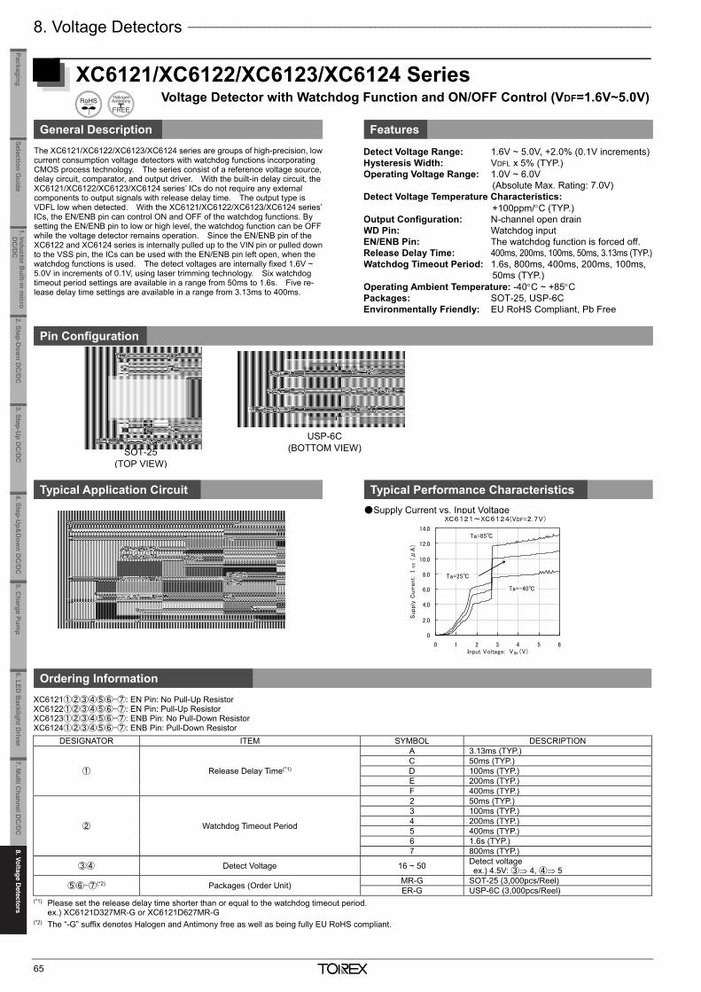
8. Voltage Detectors _______________________________________________________________________________
65
XC6121/XC6122/XC6123/XC6124 Series Voltage Detector with Watchdog Function and ON/OFF Control (VDF=1.6V~5.0V)
General Description Features
The XC6121/XC6122/XC6123/XC6124 series are groups of high-precision, low current consumption voltage detectors with watchdog functions incorporating CMOS process technology. The series consist of a reference voltage source, delay circuit, comparator, and output driver. With the built-in delay circuit, the XC6121/XC6122/XC6123/XC6124 series’ ICs do not require any external components to output signals with release delay time. The output type is VDFL low when detected. With the XC6121/XC6122/XC6123/XC6124 series’ ICs, the EN/ENB pin can control ON and OFF of the watchdog functions. By setting the EN/ENB pin to low or high level, the watchdog function can be OFF while the voltage detector remains operation. Since the EN/ENB pin of the XC6122 and XC6124 series is internally pulled up to the VIN pin or pulled down to the VSS pin, the ICs can be used with the EN/ENB pin left open, when the watchdog functions is used. The detect voltages are internally fixed 1.6V ~ 5.0V in increments of 0.1V, using laser trimming technology. Six watchdog timeout period settings are available in a range from 50ms to 1.6s. Five re-lease delay time settings are available in a range from 3.13ms to 400ms.
Detect Voltage Range: 1.6V ~ 5.0V, +2.0% (0.1V increments) Hysteresis Width: VDFL x 5% (TYP.) Operating Voltage Range: 1.0V ~ 6.0V
(Absolute Max. Rating: 7.0V) Detect Voltage Temperature Characteristics:
+100ppm/C (TYP.) Output Configuration: N-channel open drain WD Pin: Watchdog input EN/ENB Pin: The watchdog function is forced off. Release Delay Time: 400ms, 200ms, 100ms, 50ms, 3.13ms (TYP.) Watchdog Timeout Period: 1.6s, 800ms, 400ms, 200ms, 100ms,
50ms (TYP.) Operating Ambient Temperature: -40C ~ +85C Packages: SOT-25, USP-6C Environmentally Friendly: EU RoHS Compliant, Pb Free
Pin Configuration
Typical Application Circuit Typical Performance Characteristics Supply Current vs. Input Voltage
Ordering Information
XC6121①②③④⑤⑥-⑦: EN Pin: No Pull-Up Resistor XC6122①②③④⑤⑥-⑦: EN Pin: Pull-Up Resistor XC6123①②③④⑤⑥-⑦: ENB Pin: No Pull-Down Resistor XC6124①②③④⑤⑥-⑦: ENB Pin: Pull-Down Resistor
DESIGNATOR ITEM SYMBOL DESCRIPTION
① Release Delay Time(*1)
A 3.13ms (TYP.) C 50ms (TYP.) D 100ms (TYP.) E 200ms (TYP.) F 400ms (TYP.)
② Watchdog Timeout Period
2 50ms (TYP.) 3 100ms (TYP.) 4 200ms (TYP.) 5 400ms (TYP.) 6 1.6s (TYP.) 7 800ms (TYP.)
③④ Detect Voltage 16 ~ 50 Detect voltage ex.) 4.5V: ③ 4, ④ 5
⑤⑥-⑦(*2) Packages (Order Unit) MR-G SOT-25 (3,000pcs/Reel) ER-G USP-6C (3,000pcs/Reel)
(*1) Please set the release delay time shorter than or equal to the watchdog timeout period. ex.) XC6121D327MR-G or XC6121D627MR-G (*2) The “-G” suffix denotes Halogen and Antimony free as well as being fully EU RoHS compliant.
0
2.0
4.0
6.0
8.0
10.0
12.0
14.0
0 1 2 3 4 5 6Input Voltage: VIN (V)
Sup
ply C
urr
ent:
IS
S (
μA
)
XC6121~XC6124(VDF=2.7V)
Ta=85
Ta=-40
Ta=25
SOT-25 (TOP VIEW)
USP-6C (BOTTOM VIEW)
_______________________________________________________________________________________________________
66
XC6120 Series Ultra Small, Low Quiescent Current Voltage Detector
General Description Features The XC6120 series are highly precise, low quiescent current voltagedetectors, manufactured using CMOS and laser trimming technolo-gies. With low quiescent current and high accuracy, the series issuitable for precision mobile equipment. The series’ ultra small packages are best suited for high-densitymounting. Both CMOS and N-channel open drain output configura-tions are available.
Accuracy: ± 2.0% (VDF≧1.5V) ± 30mV (VDF<1.5V)
Low Quiescent Current: 0.6μA (TYP.) [VDF=2.7V, VIN2.97V] Detect Voltage Range: 1.0V ~ 5.0V (0.1V increments) Operating Voltage Range: 0.7V ~ 6.0V (Absolute Max. Rating: 7.0V) Detect Voltage Temperature Characteristics: ±100ppm/ (TYP.) Output Configuration: N-channel open drain or CMOS Operating Ambient Temperature: -40~+85 Packages: USP-3, SOT-25, SSOT-24 Environmentally Friendly: EU RoHS Compliant, Pb Free
Pin Configuration
Typical Application Circuit Typical Performance Characteristics
Supply Current vs. Input Voltage
Ordering Information
XC6120①②③④⑤⑥-⑦ DESIGNATOR ITEM SYMBOL DESCRIPTION
① Output Configuration C CMOS output N N-ch open drain output
②③ Detect Voltage (VDF) 10~50 e.g.1.0V → ②1, ③0 ④ Detect Accuracy 2 ±2.0%
⑤⑥-⑦(*1) Packages (Order Unit)
HR-G USP-3 (3,000pcs/Reel) SR-G SOT-25 (3,000pcs/Reel) Standard feed(*2) NR-G SSOT-24 (3,000pcs/Reel) SL-G SOT-25 (3,000pcs/Reel) Reverse feed(*2)
(*1) The “-G” suffix denotes Halogen and Antimony free as well as being fully EU RoHS compliant. (*2) SOT-25 uses Cu wires. Taping Specification ・SR-G ・SL-G
VIN
NC VSS
VOUT
SSOT-24 (TOP VIEW)
SOT-25 (TOP VIEW)
VSS
VIN VOUT USP-3
(BOTTOM VIEW)
direction of feed direction of feed
XC6120N272xx
1. Inductor Built-in m
icro D
C/D
C
2. Step-Dow
n DC
/DC
3. Step-Up D
C/D
C4. Step-U
p&D
own D
C/D
C
5.Charge Pum
p6.LED
Backlight D
river8.Voltage D
etectorsSelection G
uidePackaging
7. Multi C
hannel DC
/DC
8.Voltage D
etectors
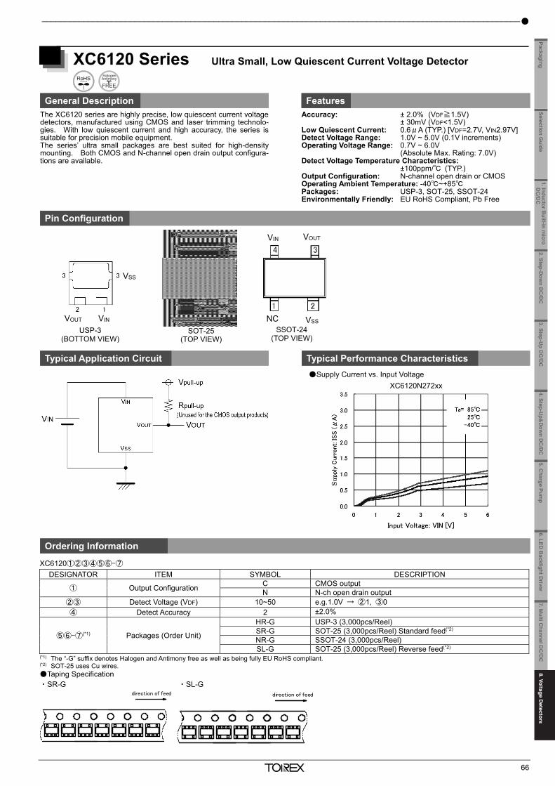
8. Voltage Detectors _______________________________________________________________________________
65
XC6121/XC6122/XC6123/XC6124 Series Voltage Detector with Watchdog Function and ON/OFF Control (VDF=1.6V~5.0V)
General Description Features
The XC6121/XC6122/XC6123/XC6124 series are groups of high-precision, low current consumption voltage detectors with watchdog functions incorporating CMOS process technology. The series consist of a reference voltage source, delay circuit, comparator, and output driver. With the built-in delay circuit, the XC6121/XC6122/XC6123/XC6124 series’ ICs do not require any external components to output signals with release delay time. The output type is VDFL low when detected. With the XC6121/XC6122/XC6123/XC6124 series’ ICs, the EN/ENB pin can control ON and OFF of the watchdog functions. By setting the EN/ENB pin to low or high level, the watchdog function can be OFF while the voltage detector remains operation. Since the EN/ENB pin of the XC6122 and XC6124 series is internally pulled up to the VIN pin or pulled down to the VSS pin, the ICs can be used with the EN/ENB pin left open, when the watchdog functions is used. The detect voltages are internally fixed 1.6V ~ 5.0V in increments of 0.1V, using laser trimming technology. Six watchdog timeout period settings are available in a range from 50ms to 1.6s. Five re-lease delay time settings are available in a range from 3.13ms to 400ms.
Detect Voltage Range: 1.6V ~ 5.0V, +2.0% (0.1V increments) Hysteresis Width: VDFL x 5% (TYP.) Operating Voltage Range: 1.0V ~ 6.0V
(Absolute Max. Rating: 7.0V) Detect Voltage Temperature Characteristics:
+100ppm/C (TYP.) Output Configuration: N-channel open drain WD Pin: Watchdog input EN/ENB Pin: The watchdog function is forced off. Release Delay Time: 400ms, 200ms, 100ms, 50ms, 3.13ms (TYP.) Watchdog Timeout Period: 1.6s, 800ms, 400ms, 200ms, 100ms,
50ms (TYP.) Operating Ambient Temperature: -40C ~ +85C Packages: SOT-25, USP-6C Environmentally Friendly: EU RoHS Compliant, Pb Free
Pin Configuration
Typical Application Circuit Typical Performance Characteristics Supply Current vs. Input Voltage
Ordering Information
XC6121①②③④⑤⑥-⑦: EN Pin: No Pull-Up Resistor XC6122①②③④⑤⑥-⑦: EN Pin: Pull-Up Resistor XC6123①②③④⑤⑥-⑦: ENB Pin: No Pull-Down Resistor XC6124①②③④⑤⑥-⑦: ENB Pin: Pull-Down Resistor
DESIGNATOR ITEM SYMBOL DESCRIPTION
① Release Delay Time(*1)
A 3.13ms (TYP.) C 50ms (TYP.) D 100ms (TYP.) E 200ms (TYP.) F 400ms (TYP.)
② Watchdog Timeout Period
2 50ms (TYP.) 3 100ms (TYP.) 4 200ms (TYP.) 5 400ms (TYP.) 6 1.6s (TYP.) 7 800ms (TYP.)
③④ Detect Voltage 16 ~ 50 Detect voltage ex.) 4.5V: ③ 4, ④ 5
⑤⑥-⑦(*2) Packages (Order Unit) MR-G SOT-25 (3,000pcs/Reel) ER-G USP-6C (3,000pcs/Reel)
(*1) Please set the release delay time shorter than or equal to the watchdog timeout period. ex.) XC6121D327MR-G or XC6121D627MR-G (*2) The “-G” suffix denotes Halogen and Antimony free as well as being fully EU RoHS compliant.
0
2.0
4.0
6.0
8.0
10.0
12.0
14.0
0 1 2 3 4 5 6Input Voltage: VIN (V)
Sup
ply C
urr
ent:
IS
S (
μA
)
XC6121~XC6124(VDF=2.7V)
Ta=85
Ta=-40
Ta=25
SOT-25 (TOP VIEW)
USP-6C (BOTTOM VIEW)
_______________________________________________________________________________________________________
66
XC6120 Series Ultra Small, Low Quiescent Current Voltage Detector
General Description Features The XC6120 series are highly precise, low quiescent current voltagedetectors, manufactured using CMOS and laser trimming technolo-gies. With low quiescent current and high accuracy, the series issuitable for precision mobile equipment. The series’ ultra small packages are best suited for high-densitymounting. Both CMOS and N-channel open drain output configura-tions are available.
Accuracy: ± 2.0% (VDF≧1.5V) ± 30mV (VDF<1.5V)
Low Quiescent Current: 0.6μA (TYP.) [VDF=2.7V, VIN2.97V] Detect Voltage Range: 1.0V ~ 5.0V (0.1V increments) Operating Voltage Range: 0.7V ~ 6.0V (Absolute Max. Rating: 7.0V) Detect Voltage Temperature Characteristics: ±100ppm/ (TYP.) Output Configuration: N-channel open drain or CMOS Operating Ambient Temperature: -40~+85 Packages: USP-3, SOT-25, SSOT-24 Environmentally Friendly: EU RoHS Compliant, Pb Free
Pin Configuration
Typical Application Circuit Typical Performance Characteristics
Supply Current vs. Input Voltage
Ordering Information
XC6120①②③④⑤⑥-⑦ DESIGNATOR ITEM SYMBOL DESCRIPTION
① Output Configuration C CMOS output N N-ch open drain output
②③ Detect Voltage (VDF) 10~50 e.g.1.0V → ②1, ③0 ④ Detect Accuracy 2 ±2.0%
⑤⑥-⑦(*1) Packages (Order Unit)
HR-G USP-3 (3,000pcs/Reel) SR-G SOT-25 (3,000pcs/Reel) Standard feed(*2) NR-G SSOT-24 (3,000pcs/Reel) SL-G SOT-25 (3,000pcs/Reel) Reverse feed(*2)
(*1) The “-G” suffix denotes Halogen and Antimony free as well as being fully EU RoHS compliant. (*2) SOT-25 uses Cu wires. Taping Specification ・SR-G ・SL-G
VIN
NC VSS
VOUT
SSOT-24 (TOP VIEW)
SOT-25 (TOP VIEW)
VSS
VIN VOUT USP-3
(BOTTOM VIEW)
direction of feed direction of feed
XC6120N272xx
1. Inductor Built-in m
icro D
C/D
C
2. Step-Dow
n DC
/DC
3. Step-Up D
C/D
C4. Step-U
p&D
own D
C/D
C
5.Charge Pum
p6.LED
Backlight D
riverSelection G
uidePackaging
7. Multi C
hannel DC
/DC
8.Voltage D
etectors
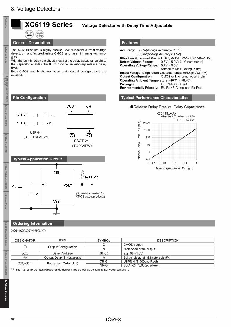
8. Voltage Detectors _______________________________________________________________________________
67
XC6119xxxAx
0.1
1
10
100
1000
10000
0.0001 0.001 0.01 0.1 1
Delay Capacitance: Cd (μF)
Rel
ease
Del
ay T
ime:
t D
R (m
s)
VIN(min)=0.7V VIN(max)=6.0Vtr=5μs Ta=25
XC6119 Series Voltage Detector with Delay Time Adjustable
General Description Features
The XC6119 series is highly precise, low quiescent current voltage detector, manufactured using CMOS and laser trimming technolo-gies. With the built-in delay circuit, connecting the delay capacitance pin to the capacitor enables the IC to provide an arbitrary release delay time. Both CMOS and N-channel open drain output configurations are available.
Accuracy: ±2.0%(Voltage Accuracy≧1.5V) ±30mV(Voltage Acuracy<1.5V)
Ultra Low Quiescent Current : 0.9A(TYP. VDF=1.0V, VIN=1.1V) Detect Voltage Range: 0.8V ~ 5.0V (0.1V increments) Operating Voltage Range: 0.7V ~ 6.0V (Absolute Max. Rating: 7.0V) Detect Voltage Temperature Characteristics: ±100ppm/(TYP.) Output Configuration: CMOS or N-channel open drain Operating Ambient Temperature: -40 ~ +85 Packages: USPN-4, SSOT-24 Environmentally Friendly: EU RoHS Compliant, Pb Free
Pin Configuration Typical Performance Characteristics
Typical Application Circuit
Ordering Information
XC6119①②③④⑤⑥-⑦
DESIGNATOR ITEM SYMBOL DESCRIPTION
① Output Configuration C CMOS output N N-ch open drain output
②③ Detect Voltage 08~50 e.g. 18→1.8V ④ Output Delay & Hysteresis A Built-in delay pin & hysteresis 5%
⑤⑥-⑦(*1) Packages (Order Unit) 7R-G USPN-4 (5,000pcs/Reel) NR-G SSOT-24 (3,000pcs/Reel)
(*1) The “-G” suffix denotes Halogen and Antimony free as well as being fully EU RoHS compliant.
Release Delay Time vs. Delay Capacitance
(No resistor needed for CMOS output products)
USPN-4 (BOTTOM VIEW)
Cd
SSOT-24 (TOP VIEW)
_______________________________________________________________________________________________________
68
XC6118 Series Voltage Detector with Separated Sense Pin & Delay Capacitor
General Description Features
The XC6118 series is highly precise, low quiescent current voltagedetector, manufactured with CMOS process and laser trimmingtechnologies. Since the sense pin is separated from power supply, it allows the ICto monitor added power supply. Moreover, with the built-in delay circuit, connecting the delay capac-itance pin to the capacitor enables the IC to provide an arbitrary re-lease delay time. Both CMOS and N-channel open drain output configurations areavailable.
Accuracy: ±2.0%(Detect Voltage≧1.5V) ±30mV(Detect Voltage<1.5V)
Ultra Low Quiescent Current: 0.8A(TYP.)(VIN=2.0V) Detect Voltage Range: 0.8V ~ 5.0V(0.1V increments) Operating Voltage Range: 1.0V ~ 6.0V
(Absolute Max. Rating: 7.0V) Detect Voltage Temperature Characteristics : ±100ppm/(TYP.) Output Configuration: CMOS or N-channel open drain Operating Ambient Temperature: -40 ~ +85 Packages: USP-4, SOT-25 Environmentally Friendly: EU RoHS Compliant, Pb Free
Pin Configuration High Voltage Detect Circuit
Typical Application Circuit
Ordering Information
XC6118①②③④⑤⑥-⑦
DESIGNATOR ITEM SYMBOL DESCRIPTION
① Output Configuration C CMOS output N N-ch open drain output
②③ Detect Voltage 08~50 e.g. 18→1.8V
④ Output Delay & Hysteresis (Options)
A Built-in delay pin, hysteresis 5% (TYP.) B Built-in delay pin, hysteresis less than 1% C No built-in delay pin, hysteresis 5% (TYP.) (Semi-Custom) D No built-in delay pin, hysteresis less than 1% (Semi-Custom)
⑤⑥-⑦(*1) Packages (Order Unit) GR-G USP-4 (3,000pcs/Reel) MR-G SOT-25 (3,000pcs/Reel)
(*1) The “-G” suffix denotes Halogen and Antimony free as well as being fully EU RoHS compliant.
SOT-25 (TOP VIEW)
USP-4 (BOTTOM VIEW)
No resistor needed for CMOS output product
Added Power Supply
Cd/NC
Use with R2 < RSEN. *RSEN is an internal sensor resistor in the IC. The operating voltage of the VSEN pin is 6V, so set to 6V or less.
Example: When 12V (+B: battery voltage) is detected, detection is possible with detectionvoltage (VSEN) = 1.0V, R1 = 220kΩ, and R2 = 20kΩ. VIN = 1V to 6V: This is the IC power supply, so turn on the power at the same time orbefore VSEN. It is acceptable if the voltage applied to the VSEN pin is higher than VIN.
1. Inductor Built-in m
icro D
C/D
C
2. Step-Dow
n DC
/DC
3. Step-Up D
C/D
C4. Step-U
p&D
own D
C/D
C
5.Charge Pum
p6.LED
Backlight D
river8.Voltage D
etectorsSelection G
uidePackaging
7. Multi C
hannel DC
/DC
8.Voltage D
etectors
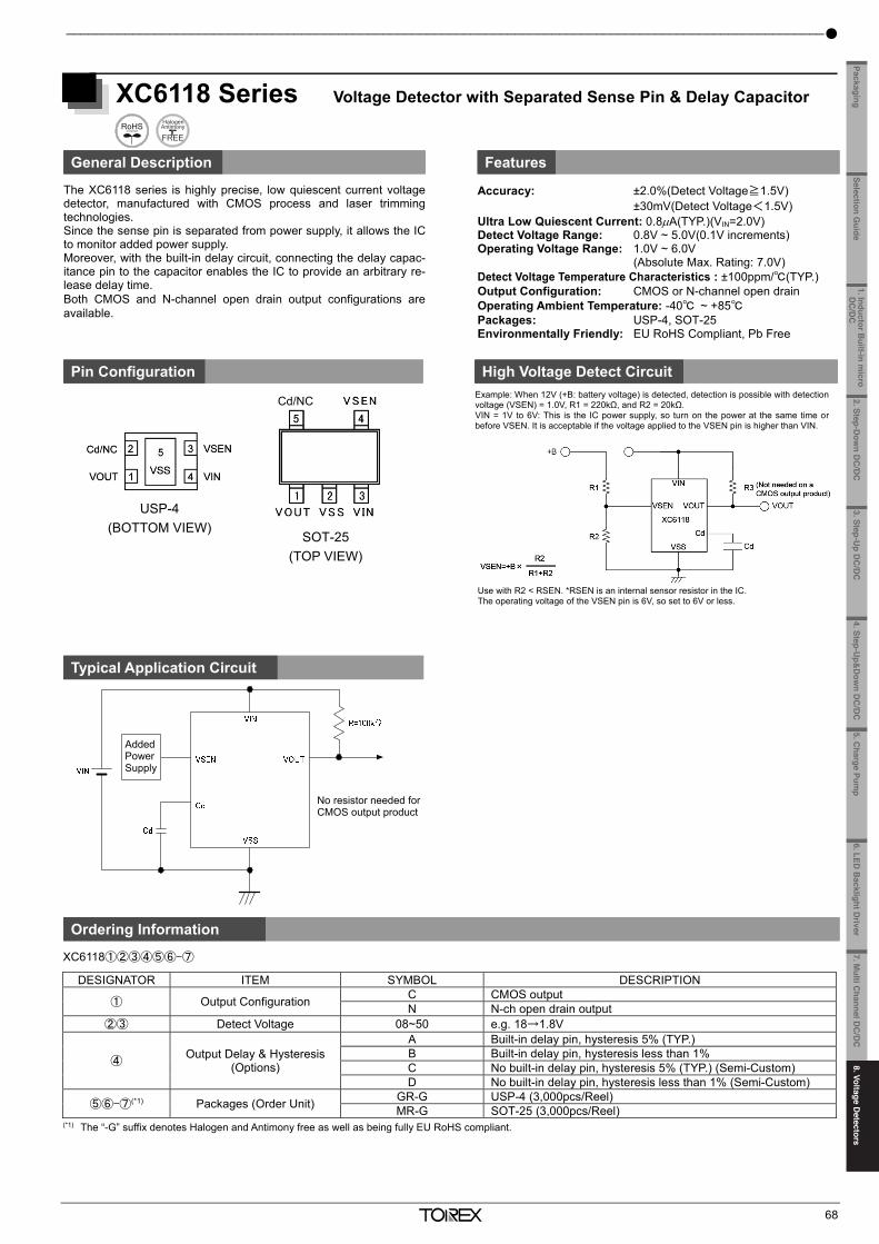
8. Voltage Detectors _______________________________________________________________________________
67
XC6119xxxAx
0.1
1
10
100
1000
10000
0.0001 0.001 0.01 0.1 1
Delay Capacitance: Cd (μF)
Rel
ease
Del
ay T
ime:
t D
R (m
s)
VIN(min)=0.7V VIN(max)=6.0Vtr=5μs Ta=25
XC6119 Series Voltage Detector with Delay Time Adjustable
General Description Features
The XC6119 series is highly precise, low quiescent current voltage detector, manufactured using CMOS and laser trimming technolo-gies. With the built-in delay circuit, connecting the delay capacitance pin to the capacitor enables the IC to provide an arbitrary release delay time. Both CMOS and N-channel open drain output configurations are available.
Accuracy: ±2.0%(Voltage Accuracy≧1.5V) ±30mV(Voltage Acuracy<1.5V)
Ultra Low Quiescent Current : 0.9A(TYP. VDF=1.0V, VIN=1.1V) Detect Voltage Range: 0.8V ~ 5.0V (0.1V increments) Operating Voltage Range: 0.7V ~ 6.0V (Absolute Max. Rating: 7.0V) Detect Voltage Temperature Characteristics: ±100ppm/(TYP.) Output Configuration: CMOS or N-channel open drain Operating Ambient Temperature: -40 ~ +85 Packages: USPN-4, SSOT-24 Environmentally Friendly: EU RoHS Compliant, Pb Free
Pin Configuration Typical Performance Characteristics
Typical Application Circuit
Ordering Information
XC6119①②③④⑤⑥-⑦
DESIGNATOR ITEM SYMBOL DESCRIPTION
① Output Configuration C CMOS output N N-ch open drain output
②③ Detect Voltage 08~50 e.g. 18→1.8V ④ Output Delay & Hysteresis A Built-in delay pin & hysteresis 5%
⑤⑥-⑦(*1) Packages (Order Unit) 7R-G USPN-4 (5,000pcs/Reel) NR-G SSOT-24 (3,000pcs/Reel)
(*1) The “-G” suffix denotes Halogen and Antimony free as well as being fully EU RoHS compliant.
Release Delay Time vs. Delay Capacitance
(No resistor needed for CMOS output products)
USPN-4 (BOTTOM VIEW)
Cd
SSOT-24 (TOP VIEW)
_______________________________________________________________________________________________________
68
XC6118 Series Voltage Detector with Separated Sense Pin & Delay Capacitor
General Description Features
The XC6118 series is highly precise, low quiescent current voltagedetector, manufactured with CMOS process and laser trimmingtechnologies. Since the sense pin is separated from power supply, it allows the ICto monitor added power supply. Moreover, with the built-in delay circuit, connecting the delay capac-itance pin to the capacitor enables the IC to provide an arbitrary re-lease delay time. Both CMOS and N-channel open drain output configurations areavailable.
Accuracy: ±2.0%(Detect Voltage≧1.5V) ±30mV(Detect Voltage<1.5V)
Ultra Low Quiescent Current: 0.8A(TYP.)(VIN=2.0V) Detect Voltage Range: 0.8V ~ 5.0V(0.1V increments) Operating Voltage Range: 1.0V ~ 6.0V
(Absolute Max. Rating: 7.0V) Detect Voltage Temperature Characteristics : ±100ppm/(TYP.) Output Configuration: CMOS or N-channel open drain Operating Ambient Temperature: -40 ~ +85 Packages: USP-4, SOT-25 Environmentally Friendly: EU RoHS Compliant, Pb Free
Pin Configuration High Voltage Detect Circuit
Typical Application Circuit
Ordering Information
XC6118①②③④⑤⑥-⑦
DESIGNATOR ITEM SYMBOL DESCRIPTION
① Output Configuration C CMOS output N N-ch open drain output
②③ Detect Voltage 08~50 e.g. 18→1.8V
④ Output Delay & Hysteresis (Options)
A Built-in delay pin, hysteresis 5% (TYP.) B Built-in delay pin, hysteresis less than 1% C No built-in delay pin, hysteresis 5% (TYP.) (Semi-Custom) D No built-in delay pin, hysteresis less than 1% (Semi-Custom)
⑤⑥-⑦(*1) Packages (Order Unit) GR-G USP-4 (3,000pcs/Reel) MR-G SOT-25 (3,000pcs/Reel)
(*1) The “-G” suffix denotes Halogen and Antimony free as well as being fully EU RoHS compliant.
SOT-25 (TOP VIEW)
USP-4 (BOTTOM VIEW)
No resistor needed for CMOS output product
Added Power Supply
Cd/NC
Use with R2 < RSEN. *RSEN is an internal sensor resistor in the IC. The operating voltage of the VSEN pin is 6V, so set to 6V or less.
Example: When 12V (+B: battery voltage) is detected, detection is possible with detectionvoltage (VSEN) = 1.0V, R1 = 220kΩ, and R2 = 20kΩ. VIN = 1V to 6V: This is the IC power supply, so turn on the power at the same time orbefore VSEN. It is acceptable if the voltage applied to the VSEN pin is higher than VIN.
1. Inductor Built-in m
icro D
C/D
C
2. Step-Dow
n DC
/DC
3. Step-Up D
C/D
C4. Step-U
p&D
own D
C/D
C
5.Charge Pum
p6.LED
Backlight D
riverSelection G
uidePackaging
7. Multi C
hannel DC
/DC
8.Voltage D
etectors
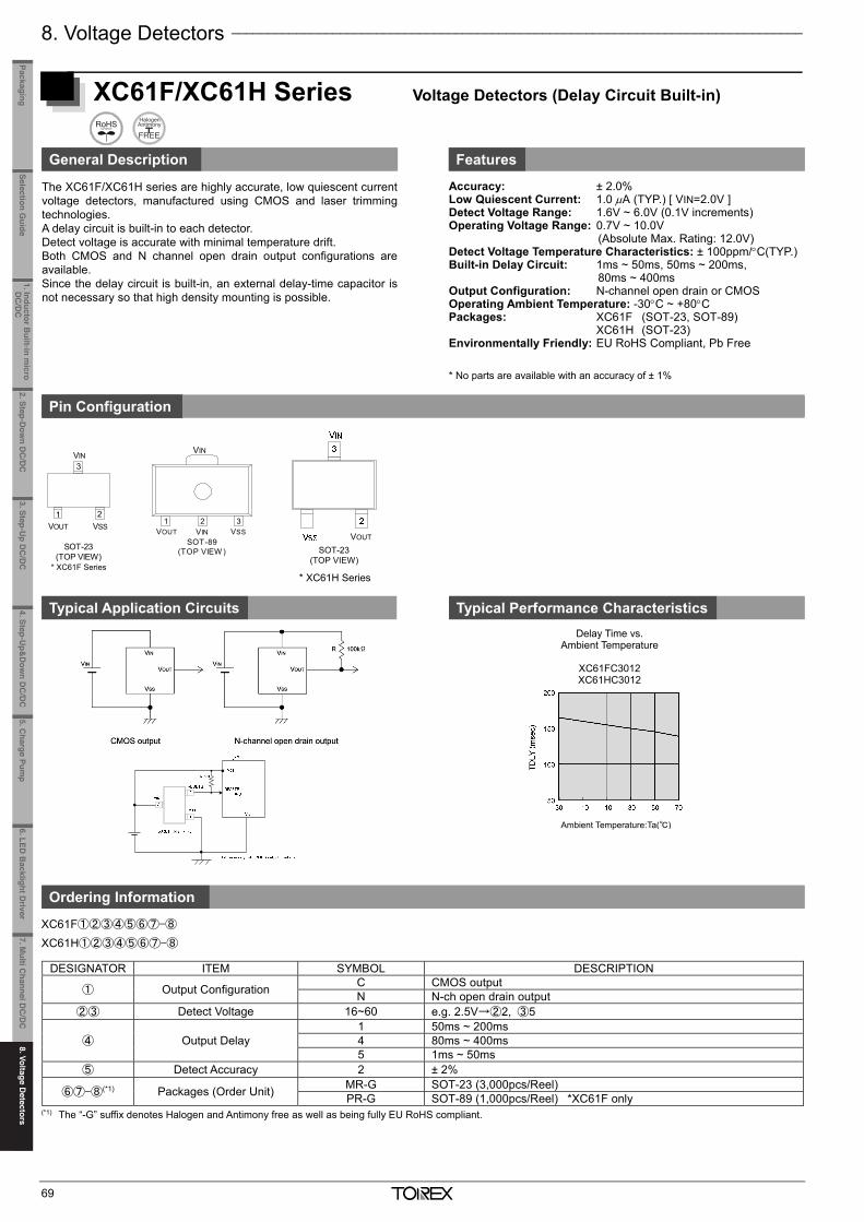
8. Voltage Detectors _______________________________________________________________________________
69
XC61F/XC61H Series Voltage Detectors (Delay Circuit Built-in)
General Description Features
The XC61F/XC61H series are highly accurate, low quiescent current voltage detectors, manufactured using CMOS and laser trimming technologies. A delay circuit is built-in to each detector. Detect voltage is accurate with minimal temperature drift. Both CMOS and N channel open drain output configurations are available. Since the delay circuit is built-in, an external delay-time capacitor is not necessary so that high density mounting is possible.
Accuracy: ± 2.0% Low Quiescent Current: 1.0 A (TYP.) [ VIN=2.0V ] Detect Voltage Range: 1.6V ~ 6.0V (0.1V increments) Operating Voltage Range: 0.7V ~ 10.0V
(Absolute Max. Rating: 12.0V) Detect Voltage Temperature Characteristics: ± 100ppm/C(TYP.) Built-in Delay Circuit: 1ms ~ 50ms, 50ms ~ 200ms,
80ms ~ 400ms Output Configuration: N-channel open drain or CMOS Operating Ambient Temperature: -30C ~ +80C Packages: XC61F (SOT-23, SOT-89) XC61H (SOT-23) Environmentally Friendly: EU RoHS Compliant, Pb Free
* No parts are available with an accuracy of ± 1%
Pin Configuration
1 2
SOT-23(TOP VIEW)
3VIN
VSSVOUT
SOT-89(TOP VIEW )
2 3VIN
1VSSVOUT
Typical Application Circuits Typical Performance Characteristics
Ordering Information
XC61F①②③④⑤⑥⑦-⑧ XC61H①②③④⑤⑥⑦-⑧
DESIGNATOR ITEM SYMBOL DESCRIPTION
① Output Configuration C CMOS output N N-ch open drain output
②③ Detect Voltage 16~60 e.g. 2.5V→②2, ③5
④ Output Delay 1 50ms ~ 200ms 4 80ms ~ 400ms 5 1ms ~ 50ms
⑤ Detect Accuracy 2 ± 2%
⑥⑦-⑧(*1) Packages (Order Unit) MR-G SOT-23 (3,000pcs/Reel) PR-G SOT-89 (1,000pcs/Reel) *XC61F only
(*1) The “-G” suffix denotes Halogen and Antimony free as well as being fully EU RoHS compliant.
SOT-23 (TOP VIEW)
* XC61H Series
Ambient Temperature:Ta()
Delay Time vs. Ambient Temperature
XC61FC3012 XC61HC3012
VIN
* XC61F Series
VOUT
_______________________________________________________________________________________________________
70
XC61C/XC61G Series Standard Voltage Detectors
General Description Features
The XC61C/XC61G series are highly precise, low quiescent currentvoltage detectors, manufactured using CMOS and laser trimmingtechnologies. Detect voltage is accurate with minimal temperaturedrift. Both CMOS and N channel open drain output configurations areavailable.
Accuracy: ±2.0% ±1.0% (Standard Voltage 2.6~5.1V) Low Quiescent Current: 0.7 A(TYP.) [ VIN=1.5V ] Detect Voltage Range: 0.8V ~ 6.0V (0.1V increments) Operating Voltage Range: 0.7V ~ 6.0V (Low Voltage) 0.7V ~ 10.0V (Standard Voltage) Detect Voltage Temperature Characteristics: ± 100ppm/C(TYP.) Output Configuration: N-channel open drain or CMOS Operating Ambient Temperature: -40C ~ +85C Packages: XC61C (SSOT-24, SOT-23, SOT-89) XC61G (USP-3) Environmentally Friendly: EU RoHS Compliant, Pb Free
Pin Configuration
Typical Application Circuits
Typical Performance Characteristics
Ordering Information
XC61C①②③④⑤⑥⑦-⑧
XC61G①②③④⑤⑥⑦-⑧
DESIGNATOR ITEM SYMBOL DESCRIPTION
① Output Configuration C CMOS output N N-ch open drain output
②③ Detect Voltage 08~60 e.g. 0.9V→②0, ③9 e.g. 1.5V→②1, ③5
④ Output Delay 0 No delay
⑤ Detect Accuracy 1 ± 1.0% *XC61C only 2 ± 2.0%
⑥⑦-⑧(*1) Packages (Order Unit)
NR-G SSOT-24 (SC-82) (3,000pcs/Reel) *XC61C only MR-G SOT-23 (3,000pcs/Reel) *XC61C only PR-G SOT-89 (1,000pcs/Reel) *XC61C only HR-G USP-3 (3,000pcs/Reel) *XC61G only
(*1) The “-G” suffix denotes Halogen and Antimony free as well as being fully EU RoHS compliant.
CMOS Output Nch Open Drain Output
* XC61G only Supply Current vs. Input Voltage
XC61CC0902 (0.9V) XC61GC0902 (0.9V)
Supply Current vs. Input Voltage XC61CC4502 (4.5V) XC61GC4502 (4.5V)
1 2
SOT-23(TOP VIEW)
3VIN
VSSVOUT1 2
4 3
VIN
NCVSS
VOUT
SSOT-24(SC-82)(TOP VIEW)
SOT-89(TOP VIEW)
2 3VIN
1VSSVOUT
VIN
(BOTTOM VIEW)
2 VOUT
1 VSS
1. Inductor Built-in m
icro D
C/D
C
2. Step-Dow
n DC
/DC
3. Step-Up D
C/D
C4. Step-U
p&D
own D
C/D
C
5.Charge Pum
p6.LED
Backlight D
river8.Voltage D
etectorsSelection G
uidePackaging
7. Multi C
hannel DC
/DC
8.Voltage D
etectors
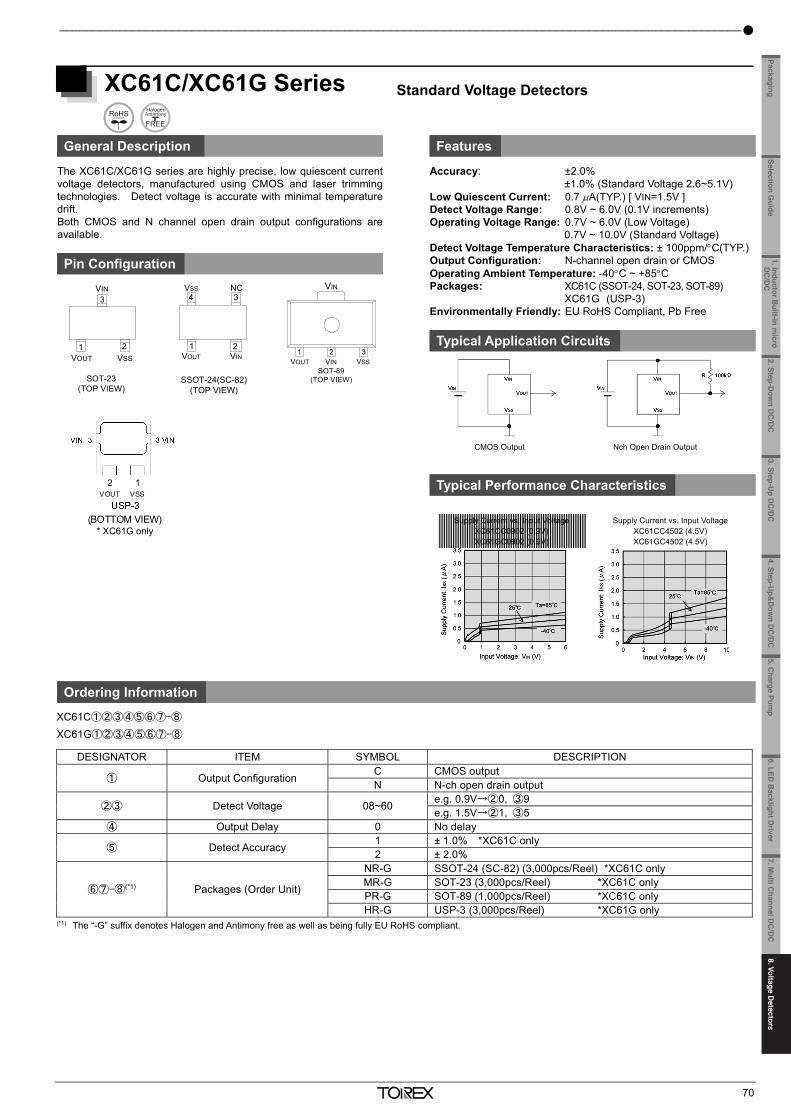
8. Voltage Detectors _______________________________________________________________________________
69
XC61F/XC61H Series Voltage Detectors (Delay Circuit Built-in)
General Description Features
The XC61F/XC61H series are highly accurate, low quiescent current voltage detectors, manufactured using CMOS and laser trimming technologies. A delay circuit is built-in to each detector. Detect voltage is accurate with minimal temperature drift. Both CMOS and N channel open drain output configurations are available. Since the delay circuit is built-in, an external delay-time capacitor is not necessary so that high density mounting is possible.
Accuracy: ± 2.0% Low Quiescent Current: 1.0 A (TYP.) [ VIN=2.0V ] Detect Voltage Range: 1.6V ~ 6.0V (0.1V increments) Operating Voltage Range: 0.7V ~ 10.0V
(Absolute Max. Rating: 12.0V) Detect Voltage Temperature Characteristics: ± 100ppm/C(TYP.) Built-in Delay Circuit: 1ms ~ 50ms, 50ms ~ 200ms,
80ms ~ 400ms Output Configuration: N-channel open drain or CMOS Operating Ambient Temperature: -30C ~ +80C Packages: XC61F (SOT-23, SOT-89) XC61H (SOT-23) Environmentally Friendly: EU RoHS Compliant, Pb Free
* No parts are available with an accuracy of ± 1%
Pin Configuration
1 2
SOT-23(TOP VIEW)
3VIN
VSSVOUT
SOT-89(TOP VIEW )
2 3VIN
1VSSVOUT
Typical Application Circuits Typical Performance Characteristics
Ordering Information
XC61F①②③④⑤⑥⑦-⑧ XC61H①②③④⑤⑥⑦-⑧
DESIGNATOR ITEM SYMBOL DESCRIPTION
① Output Configuration C CMOS output N N-ch open drain output
②③ Detect Voltage 16~60 e.g. 2.5V→②2, ③5
④ Output Delay 1 50ms ~ 200ms 4 80ms ~ 400ms 5 1ms ~ 50ms
⑤ Detect Accuracy 2 ± 2%
⑥⑦-⑧(*1) Packages (Order Unit) MR-G SOT-23 (3,000pcs/Reel) PR-G SOT-89 (1,000pcs/Reel) *XC61F only
(*1) The “-G” suffix denotes Halogen and Antimony free as well as being fully EU RoHS compliant.
SOT-23 (TOP VIEW)
* XC61H Series
Ambient Temperature:Ta()
Delay Time vs. Ambient Temperature
XC61FC3012 XC61HC3012
VIN
* XC61F Series
VOUT
_______________________________________________________________________________________________________
70
XC61C/XC61G Series Standard Voltage Detectors
General Description Features
The XC61C/XC61G series are highly precise, low quiescent currentvoltage detectors, manufactured using CMOS and laser trimmingtechnologies. Detect voltage is accurate with minimal temperaturedrift. Both CMOS and N channel open drain output configurations areavailable.
Accuracy: ±2.0% ±1.0% (Standard Voltage 2.6~5.1V) Low Quiescent Current: 0.7 A(TYP.) [ VIN=1.5V ] Detect Voltage Range: 0.8V ~ 6.0V (0.1V increments) Operating Voltage Range: 0.7V ~ 6.0V (Low Voltage) 0.7V ~ 10.0V (Standard Voltage) Detect Voltage Temperature Characteristics: ± 100ppm/C(TYP.) Output Configuration: N-channel open drain or CMOS Operating Ambient Temperature: -40C ~ +85C Packages: XC61C (SSOT-24, SOT-23, SOT-89) XC61G (USP-3) Environmentally Friendly: EU RoHS Compliant, Pb Free
Pin Configuration
Typical Application Circuits
Typical Performance Characteristics
Ordering Information
XC61C①②③④⑤⑥⑦-⑧
XC61G①②③④⑤⑥⑦-⑧
DESIGNATOR ITEM SYMBOL DESCRIPTION
① Output Configuration C CMOS output N N-ch open drain output
②③ Detect Voltage 08~60 e.g. 0.9V→②0, ③9 e.g. 1.5V→②1, ③5
④ Output Delay 0 No delay
⑤ Detect Accuracy 1 ± 1.0% *XC61C only 2 ± 2.0%
⑥⑦-⑧(*1) Packages (Order Unit)
NR-G SSOT-24 (SC-82) (3,000pcs/Reel) *XC61C only MR-G SOT-23 (3,000pcs/Reel) *XC61C only PR-G SOT-89 (1,000pcs/Reel) *XC61C only HR-G USP-3 (3,000pcs/Reel) *XC61G only
(*1) The “-G” suffix denotes Halogen and Antimony free as well as being fully EU RoHS compliant.
CMOS Output Nch Open Drain Output
* XC61G only Supply Current vs. Input Voltage
XC61CC0902 (0.9V) XC61GC0902 (0.9V)
Supply Current vs. Input Voltage XC61CC4502 (4.5V) XC61GC4502 (4.5V)
1 2
SOT-23(TOP VIEW)
3VIN
VSSVOUT1 2
4 3
VIN
NCVSS
VOUT
SSOT-24(SC-82)(TOP VIEW)
SOT-89(TOP VIEW)
2 3VIN
1VSSVOUT
VIN
(BOTTOM VIEW)
2 VOUT
1 VSS
1. Inductor Built-in m
icro D
C/D
C
2. Step-Dow
n DC
/DC
3. Step-Up D
C/D
C4. Step-U
p&D
own D
C/D
C
5.Charge Pum
p6.LED
Backlight D
riverSelection G
uidePackaging
7. Multi C
hannel DC
/DC
8.Voltage D
etectors
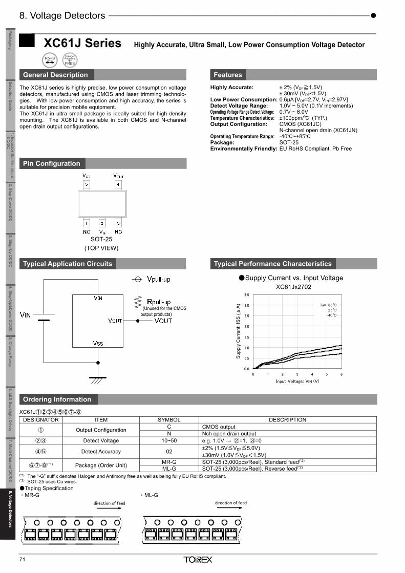
8. Voltage Detectors _____________________________________________________________________________
71
XC61J Series Highly Accurate, Ultra Small, Low Power Consumption Voltage Detector
General Description Features
The XC61J series is highly precise, low power consumption voltagedetectors, manufactured using CMOS and laser trimming technolo-gies. With low power consumption and high accuracy, the series issuitable for precision mobile equipment. The XC61J in ultra small package is ideally suited for high-densitymounting. The XC61J is available in both CMOS and N-channelopen drain output configurations.
Highly Accurate: ± 2% (VDF≧1.5V) ± 30mV (VDF<1.5V) Low Power Consumption: 0.6μA [VDF=2.7V, VIN=2.97V] Detect Voltage Range: 1.0V ~ 5.0V (0.1V increments) Operating Voltage Range Detect Voltage: 0.7V ~ 6.0V Temperature Characteristics: ±100ppm/ (TYP.) Output Configuration: CMOS (XC61JC) N-channel open drain (XC61JN) Operating Temperature Range: -40~+85 Package: SOT-25 Environmentally Friendly: EU RoHS Compliant, Pb Free
Pin Configuration
Typical Application Circuits Typical Performance Characteristics
Ordering Information
XC61J①②③④⑤⑥⑦-⑧
(*1) The “-G” suffix denotes Halogen and Antimony free as well as being fully EU RoHS compliant. (*2) SOT-25 uses Cu wires. Taping Specification ・MR-G ・ML-G
DESIGNATOR ITEM SYMBOL DESCRIPTION
① Output Configuration C CMOS output N Nch open drain output
②③ Detect Voltage 10~50 e.g. 1.0V → ②=1, ③=0
④⑤ Detect Accuracy 02 ±2% (1.5V≦VDF≦5.0V) ±30mV (1.0V≦VDF<1.5V)
⑥⑦-⑧(*1) Package (Order Unit) MR-G SOT-25 (3,000pcs/Reel), Standard feed(*2) ML-G SOT-25 (3,000pcs/Reel), Reverse feed(*2)
SOT-25 (TOP VIEW)
direction of feed
Supply Current vs. Input Voltage
0.0
0.5
1.0
1.5
2.0
2.5
3.0
3.5
0 1 2 3 4 5 6
Input Voltage: VIN (V)
Ta= 85
25
-40
XC61Jx2702
Sup
ply
Cur
rent
: IS
S (μ
A)
direction of feed
____________________________________________________________________ 9. Voltage Regulators Single Type
72
XC6238 Series 300mA High Speed LDO Regulator with ON/OFF Switch
General Description Features
The XC6238 series is a high speed LDO regulator that features highaccurate, low noise, high ripple rejection, low dropout and low powerconsumption. The series consists of a voltage reference, an erroramplifier, a driver transistor, a current limiter, a phase compensationcircuit. The CE function enables the circuit to be in stand-by mode byinputting low level signal. In the stand-by mode, the series enablesthe electric charge at the output capacitor CL to be discharged viathe internal switch, and as a result the VOUT pin quickly returns to theVSS level. The output stabilization capacitor CL is also compatiblewith low ESR ceramic capacitors. The output voltage is selectable in 0.05V increments within the rangeof 1.2V to 4.0V which fixed by laser trimming technologies. The overcurrent protection circuit is built-in. This protection circuit will operatewhen the output current reaches current limit level.
Maximum Output Current: 300mA Input Voltage Range: 1.6~5.5V Output Voltages: 2.0~4.0V (Accuracy ±1%) 1.2~1.95V (Accuracy ±20mV) 0.05V increments Dropout Voltage: 200mV@IOUT=300mA (VOUT=3.0V) Low Power Consumption: 100μA Stand-by Current: 0.1μA High Ripple Rejection: 80dB@f=1kHz Protection Circuits: Current Limit (400mA) Short Circuit Protection Inrush Current Protection (Type H) Low ESR Capacitors: CIN=1μF, CL=1μF CE Function: Active High, CL High Speed Discharge
Typical Application Circuit Typical Performance Characteristics
Ordering Information
XC6238①②③④⑤⑥-⑦ (*1)
DESIGNATOR ITEM SYMBOL DESCRIPTION
① Regulator Type D No Inrush Current Control H Inrush Current Prevention Circuit Built-in
②③ Output Voltage 12~40 ex.) 2.80V → ②=2, ③=8, ④=please see down below.
④ Output Voltage Accuracy
1 ±1% (VOUT≧2.0V) ±0.02V (VOUT<2.0V) In case of 2nd decimal place 0 (ex.2.80V → ④=1)
B ±1% (VOUT≧2.0V) ±0.02V (VOUT<2.0V) In case of 2nd decimal place 5 (ex.2.85V → ④=B)
⑤⑥-⑦ (*1) Packages (Order Unit) 6R-G UFN-4A01 (3,000pcs/Reel) (*1) The “-G” suffix denotes Halogen and Antimony free as well as being fully EU RoHS compliant.
0
50
100
150
200
250
300
350
400
-4.0
-3.0
-2.0
-1.0
0.0
1.0
2.0
3.0
4.0
Rus
h C
urre
n: IR
US
H [m
A]
Inpu
t Vol
tage
: VC
E [V
]
Time [20μs/div]
Rush Current
XC6238H12
1. Inductor Built-in m
icro D
C/D
C
2. Step-Dow
n DC
/DC
3. Step-Up D
C/D
C4. Step-U
p&D
own D
C/D
C
5.Charge Pum
p6.LED
Backlight D
river8.Voltage D
etectorsSelection G
uidePackaging
7. Multi C
hannel DC
/DC
8.Voltage D
etectors
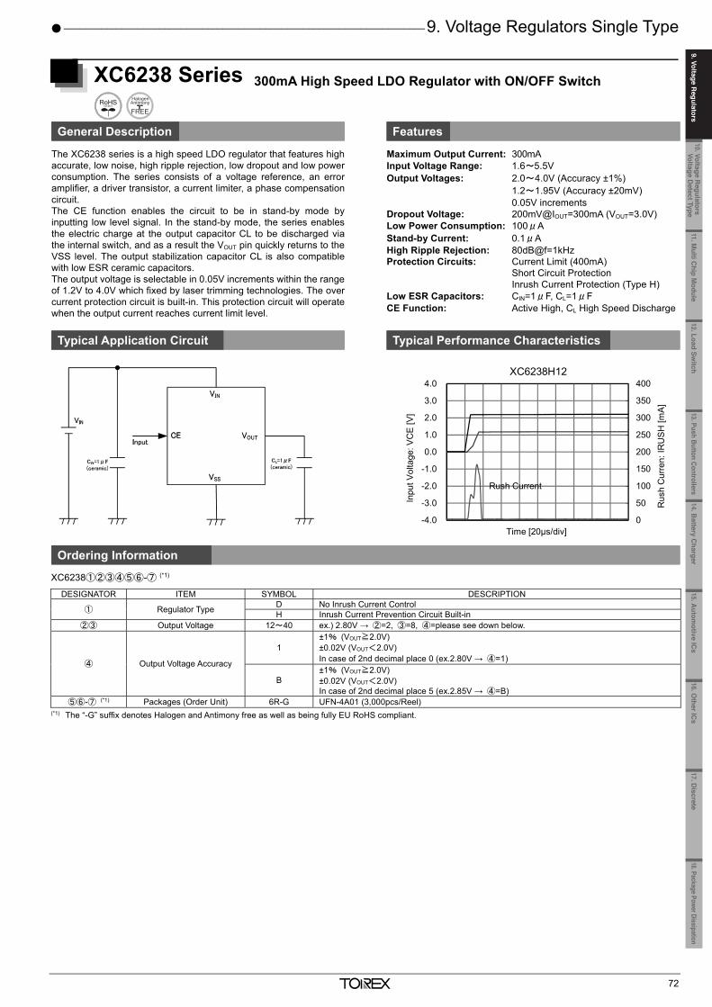
8. Voltage Detectors _____________________________________________________________________________
71
XC61J Series Highly Accurate, Ultra Small, Low Power Consumption Voltage Detector
General Description Features
The XC61J series is highly precise, low power consumption voltagedetectors, manufactured using CMOS and laser trimming technolo-gies. With low power consumption and high accuracy, the series issuitable for precision mobile equipment. The XC61J in ultra small package is ideally suited for high-densitymounting. The XC61J is available in both CMOS and N-channelopen drain output configurations.
Highly Accurate: ± 2% (VDF≧1.5V) ± 30mV (VDF<1.5V) Low Power Consumption: 0.6μA [VDF=2.7V, VIN=2.97V] Detect Voltage Range: 1.0V ~ 5.0V (0.1V increments) Operating Voltage Range Detect Voltage: 0.7V ~ 6.0V Temperature Characteristics: ±100ppm/ (TYP.) Output Configuration: CMOS (XC61JC) N-channel open drain (XC61JN) Operating Temperature Range: -40~+85 Package: SOT-25 Environmentally Friendly: EU RoHS Compliant, Pb Free
Pin Configuration
Typical Application Circuits Typical Performance Characteristics
Ordering Information
XC61J①②③④⑤⑥⑦-⑧
(*1) The “-G” suffix denotes Halogen and Antimony free as well as being fully EU RoHS compliant. (*2) SOT-25 uses Cu wires. Taping Specification ・MR-G ・ML-G
DESIGNATOR ITEM SYMBOL DESCRIPTION
① Output Configuration C CMOS output N Nch open drain output
②③ Detect Voltage 10~50 e.g. 1.0V → ②=1, ③=0
④⑤ Detect Accuracy 02 ±2% (1.5V≦VDF≦5.0V) ±30mV (1.0V≦VDF<1.5V)
⑥⑦-⑧(*1) Package (Order Unit) MR-G SOT-25 (3,000pcs/Reel), Standard feed(*2) ML-G SOT-25 (3,000pcs/Reel), Reverse feed(*2)
SOT-25 (TOP VIEW)
direction of feed
Supply Current vs. Input Voltage
0.0
0.5
1.0
1.5
2.0
2.5
3.0
3.5
0 1 2 3 4 5 6
Input Voltage: VIN (V)
Ta= 85
25
-40
XC61Jx2702
Sup
ply
Cur
rent
: IS
S (μ
A)
direction of feed
____________________________________________________________________ 9. Voltage Regulators Single Type
72
XC6238 Series 300mA High Speed LDO Regulator with ON/OFF Switch
General Description Features
The XC6238 series is a high speed LDO regulator that features highaccurate, low noise, high ripple rejection, low dropout and low powerconsumption. The series consists of a voltage reference, an erroramplifier, a driver transistor, a current limiter, a phase compensationcircuit. The CE function enables the circuit to be in stand-by mode byinputting low level signal. In the stand-by mode, the series enablesthe electric charge at the output capacitor CL to be discharged viathe internal switch, and as a result the VOUT pin quickly returns to theVSS level. The output stabilization capacitor CL is also compatiblewith low ESR ceramic capacitors. The output voltage is selectable in 0.05V increments within the rangeof 1.2V to 4.0V which fixed by laser trimming technologies. The overcurrent protection circuit is built-in. This protection circuit will operatewhen the output current reaches current limit level.
Maximum Output Current: 300mA Input Voltage Range: 1.6~5.5V Output Voltages: 2.0~4.0V (Accuracy ±1%) 1.2~1.95V (Accuracy ±20mV) 0.05V increments Dropout Voltage: 200mV@IOUT=300mA (VOUT=3.0V) Low Power Consumption: 100μA Stand-by Current: 0.1μA High Ripple Rejection: 80dB@f=1kHz Protection Circuits: Current Limit (400mA) Short Circuit Protection Inrush Current Protection (Type H) Low ESR Capacitors: CIN=1μF, CL=1μF CE Function: Active High, CL High Speed Discharge
Typical Application Circuit Typical Performance Characteristics
Ordering Information
XC6238①②③④⑤⑥-⑦ (*1)
DESIGNATOR ITEM SYMBOL DESCRIPTION
① Regulator Type D No Inrush Current Control H Inrush Current Prevention Circuit Built-in
②③ Output Voltage 12~40 ex.) 2.80V → ②=2, ③=8, ④=please see down below.
④ Output Voltage Accuracy
1 ±1% (VOUT≧2.0V) ±0.02V (VOUT<2.0V) In case of 2nd decimal place 0 (ex.2.80V → ④=1)
B ±1% (VOUT≧2.0V) ±0.02V (VOUT<2.0V) In case of 2nd decimal place 5 (ex.2.85V → ④=B)
⑤⑥-⑦ (*1) Packages (Order Unit) 6R-G UFN-4A01 (3,000pcs/Reel) (*1) The “-G” suffix denotes Halogen and Antimony free as well as being fully EU RoHS compliant.
0
50
100
150
200
250
300
350
400
-4.0
-3.0
-2.0
-1.0
0.0
1.0
2.0
3.0
4.0
Rus
h C
urre
n: IR
US
H [m
A]
Inpu
t Vol
tage
: VC
E [V
]
Time [20μs/div]
Rush Current
XC6238H12
11.Multi C
hip Module
10. Voltage Regulators
Voltage Detect Type
12.Load Switch
13. Push Button Controllers14.B
attery Charger
15.Autom
otive ICs
16.Other IC
s17. D
iscrete18.Package Power Dissipation
9. Voltage Regulators
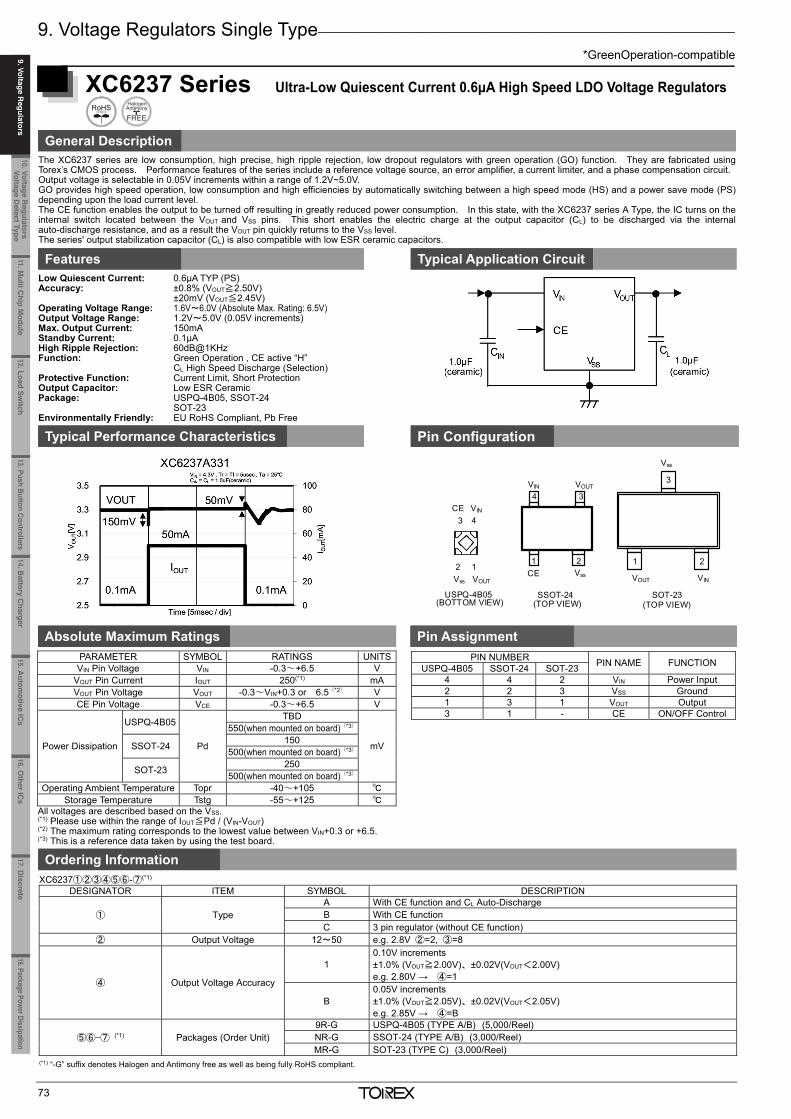
9. Voltage Regulators Single Type_______________________________________________________________
*GreenOperation-compatible
73
XC6237 Series Ultra-Low Quiescent Current 0.6μA High Speed LDO Voltage Regulators
General Description
The XC6237 series are low consumption, high precise, high ripple rejection, low dropout regulators with green operation (GO) function. They are fabricated usingTorex’s CMOS process. Performance features of the series include a reference voltage source, an error amplifier, a current limiter, and a phase compensation circuit. Output voltage is selectable in 0.05V increments within a range of 1.2V~5.0V. GO provides high speed operation, low consumption and high efficiencies by automatically switching between a high speed mode (HS) and a power save mode (PS) depending upon the load current level. The CE function enables the output to be turned off resulting in greatly reduced power consumption. In this state, with the XC6237 series A Type, the IC turns on the internal switch located between the VOUT and VSS pins. This short enables the electric charge at the output capacitor (CL) to be discharged via the internal auto-discharge resistance, and as a result the VOUT pin quickly returns to the VSS level. The series' output stabilization capacitor (CL) is also compatible with low ESR ceramic capacitors. Features Typical Application Circuit
Low Quiescent Current: 0.6μA TYP (PS) Accuracy: ±0.8% (VOUT≧2.50V) ±20mV (VOUT≦2.45V) Operating Voltage Range: 1.6V~6.0V (Absolute Max. Rating: 6.5V) Output Voltage Range: 1.2V~5.0V (0.05V increments) Max. Output Current: 150mA Standby Current: 0.1μA High Ripple Rejection: 60dB@1KHz Function: Green Operation , CE active “H” CL High Speed Discharge (Selection) Protective Function: Current Limit, Short Protection Output Capacitor: Low ESR Ceramic Package: USPQ-4B05, SSOT-24 SOT-23 Environmentally Friendly: EU RoHS Compliant, Pb Free
Typical Performance Characteristics Pin Configuration
Absolute Maximum Ratings Pin Assignment
PARAMETER SYMBOL RATINGS UNITS VIN Pin Voltage VIN -0.3~+6.5 V
VOUT Pin Current IOUT 250(*1) mA VOUT Pin Voltage VOUT -0.3~VIN+0.3 or 6.5(*2) V CE Pin Voltage VCE -0.3~+6.5 V
Power Dissipation
USPQ-4B05
Pd
TBD
mV
550(when mounted on board)(*3)
SSOT-24 150 500(when mounted on board)(*3)
SOT-23 250 500(when mounted on board)(*3)
Operating Ambient Temperature Topr -40~+105
Storage Temperature Tstg -55~+125 All voltages are described based on the VSS.
(*1) Please use within the range of IOUT≦Pd / (VIN-VOUT) (*2) The maximum rating corresponds to the lowest value between VIN+0.3 or +6.5. (*3) This is a reference data taken by using the test board.
Ordering Information
SOT-23(TOP VIEW)
VINVOUT
Vss
3
1 2
SSOT-24(TOP VIEW)
1 2
34
CE
USPQ-4B05(BOTTOM VIEW)
2
3
1
4CE
VOUT
Vss
VIN
VOUTVss
VIN
XC6237①②③④⑤⑥-⑦(*1) DESIGNATOR ITEM SYMBOL DESCRIPTION
① Type A With CE function and CL Auto-Discharge B With CE function C 3 pin regulator (without CE function)
② Output Voltage 12~50 e.g. 2.8V ②=2, ③=8
④ Output Voltage Accuracy
1 0.10V increments ±1.0% (VOUT≧2.00V)、±0.02V(VOUT<2.00V) e.g. 2.80V → ④=1
B 0.05V increments ±1.0% (VOUT≧2.05V)、±0.02V(VOUT<2.05V) e.g. 2.85V → ④=B
⑤⑥-⑦ (*1) Packages (Order Unit) 9R-G USPQ-4B05 (TYPE A/B) (5,000/Reel) NR-G SSOT-24 (TYPE A/B) (3,000/Reel) MR-G SOT-23 (TYPE C) (3,000/Reel)
(*1) “-G” suffix denotes Halogen and Antimony free as well as being fully RoHS compliant.
PIN NUMBER PIN NAME FUNCTION USPQ-4B05 SSOT-24 SOT-23 4 4 2 VIN Power Input 2 2 3 VSS Ground 1 3 1 VOUT Output 3 1 - CE ON/OFF Control
_______________________________________________________________________________________________________
74
XC6233 Series 200mA High Speed LDO Voltage Regulator with Built-in Inrush Current Protection
General Description Features
The XC6233 series is a 200mA high speed LDO regulator thatfeatures high accurate, high ripple rejection and low dropout. Theseries consists of a voltage reference, an error amplifier, a drivertransistor, a current limiter, a phase compensation circuit and aninrush current protection circuit. The output voltage is selectable in 0.05V increments (±1.0%) within the range of 1.2V to 3.6V using laser trimming technologies. The CE function enables the circuit to be in stand-by mode byinputting low level signal. In the stand-by mode, the series enablesthe electric charge at the output capacitor CL to be discharged viathe internal switch, and as a result the VOUT pin quickly returns tothe Low level. The series is also compatible with low ESR ceramic capacitors,which provides stable output voltage. This stability can bemaintained even during load fluctuations due to the excellenttransient response. The over current protection circuit is built-in. The protectioncircuit will operate when the output current reaches current limitlevel.
Max. Output Current: 200mA Input Voltage Range: 1.7V~5.5V (Absolute Max. Rating : 6.0V) Output Voltage Range: 1.2V~3.6V (±1.0%) 0.05V increments Dropout Voltage: 240mV @IOUT=200mA (VOUT=3.0V) Low Quiescent Current: 45μA (TYP.) Stand-by Current: 0.1μA High Ripple Rejection: 75dB@1kHz CE Pin Function: Active High CL Discharge Inrush Current Protection Protection Circuit: Current Limit 255mA (TYP.) Short Circuit Protection 60mA (TYP.) External Capacitor: 1.0μF Operating Ambient Temperature: -40~+85 Packages: USPQ-4B04 USP-4 SSOT-24 SOT-25 Environmentally Friendly: EU RoHS Compliant, Pb Free
Pin Configuration
Typical Application Circuit Typical Performance Characteristics
Ordering Information
XC6233①②③④⑤⑥-⑦ DESIGNATOR ITEM SYMBOL DESCRIPTION
① Type of Regulator
CE Active High H With Inrush Current Protection, With CE Pull-down, With CL discharge
②③ Output Voltage 12~36 ex.)2.80V → ②=2, ③=8 ④= please see down below
④ Output Voltage
Accuracy
1 0.10V increments ±1.0% (VOUT≧2.00V), ±0.02V (VOUT<2.00V) e.g. 2.80V → ④=1
B 0.05V increments ±1.0% (VOUT≧2.05V), ±0.02V (VOUT<2.05V) e.g. 2.85V → ④=B
⑤⑥-⑦(*1) Packages (Order Unit)
9R-G USPQ-4B04 (3,000pcs/Reel) GR-G USP-4 (3,000pcs/Reel) NR-G SSOT-24 (3,000pcs/Reel) MR-G SOT-25 (3,000pcs/Reel)
(*1) The “-G” suffix denotes Halogen and Antimony free as well as being fully EU RoHS compliant. For another type of regulators, please contact your local Torex sales office or representative.
XC6233(VOUT=1.8V)
-3.0
-2.0
-1.0
0.0
1.0
2.0
3.0
Time (40μs/div)
Voltag
e :
(V)
-50
0
50
100
150
200
250
Rush
Curr
ent
: IRU
SH (m
A)
CE Input Voltage
VCE=0V→2.8V, tr=5μs, Ta=25
VIN=2.8V, CIN=CL=1.0μF(ceramic)
Output Voltage
Rush Current
11.Multi C
hip Module
10. Voltage Regulators
Voltage Detect Type
9. Voltage Regulators
12.Load Switch
13. Push Button Controllers14.B
attery Charger
15.Autom
otive ICs
16.Other IC
s17. D
iscrete18.Package Power Dissipation
9. Voltage Regulators
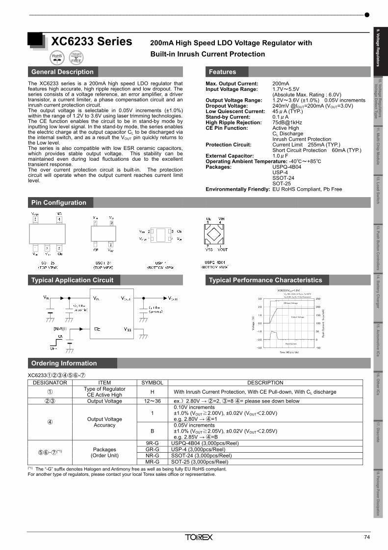
9. Voltage Regulators Single Type_______________________________________________________________
*GreenOperation-compatible
73
XC6237 Series Ultra-Low Quiescent Current 0.6μA High Speed LDO Voltage Regulators
General Description
The XC6237 series are low consumption, high precise, high ripple rejection, low dropout regulators with green operation (GO) function. They are fabricated usingTorex’s CMOS process. Performance features of the series include a reference voltage source, an error amplifier, a current limiter, and a phase compensation circuit. Output voltage is selectable in 0.05V increments within a range of 1.2V~5.0V. GO provides high speed operation, low consumption and high efficiencies by automatically switching between a high speed mode (HS) and a power save mode (PS) depending upon the load current level. The CE function enables the output to be turned off resulting in greatly reduced power consumption. In this state, with the XC6237 series A Type, the IC turns on the internal switch located between the VOUT and VSS pins. This short enables the electric charge at the output capacitor (CL) to be discharged via the internal auto-discharge resistance, and as a result the VOUT pin quickly returns to the VSS level. The series' output stabilization capacitor (CL) is also compatible with low ESR ceramic capacitors. Features Typical Application Circuit
Low Quiescent Current: 0.6μA TYP (PS) Accuracy: +0.8% (VOUT≧2.50V) +20mV (VOUT≦2.45V) Operating Voltage Range: 1.6V~6.0V (Absolute Max. Rating: 6.5V) Output Voltage Range: 1.2V~5.0V (0.05V increments) Max. Output Current: 150mA Standby Current: 0.1μA High Ripple Rejection: 60dB@1KHz Function: Green Operation , CE active “H” CL High Speed Discharge (Selection) Protective Function: Current Limit, Short Protection Output Capacitor: Low ESR Ceramic Package: USPQ-4B05, SSOT-24 SOT-23 Environmentally Friendly: EU RoHS Compliant, Pb Free
Typical Performance Characteristics Pin Configuration
Absolute Maximum Ratings Pin Assignment
PARAMETER SYMBOL RATINGS UNITS VIN Pin Voltage VIN -0.3~+6.5 V
VOUT Pin Current IOUT 250(*1) mA VOUT Pin Voltage VOUT -0.3~VIN+0.3 or 6.5(*2) V CE Pin Voltage VCE -0.3~+6.5 V
Power Dissipation
USPQ-4B05
Pd
TBD
mV
550(when mounted on board)(*3)
SSOT-24 150 500(when mounted on board)(*3)
SOT-23 250 500(when mounted on board)(*3)
Operating Ambient Temperature Topr -40~+105
Storage Temperature Tstg -55~+125 All voltages are described based on the VSS.
(*1) Please use within the range of IOUT≦Pd / (VIN-VOUT) (*2) The maximum rating corresponds to the lowest value between VIN+0.3 or +6.5. (*3) This is a reference data taken by using the test board.
Ordering Information
SOT-23(TOP VIEW)
VINVOUT
Vss
3
1 2
SSOT-24(TOP VIEW)
1 2
34
CE
USPQ-4B05(BOTTOM VIEW)
2
3
1
4CE
VOUT
Vss
VIN
VOUTVss
VIN
XC6237①②③④⑤⑥-⑦(*1) DESIGNATOR ITEM SYMBOL DESCRIPTION
① Type A With CE function and CL Auto-Discharge B With CE function C 3 pin regulator (without CE function)
② Output Voltage 12~50 e.g. 2.8V ②=2, ③=8
④ Output Voltage Accuracy
1 0.10V increments ±1.0% (VOUT≧2.00V)、±0.02V(VOUT<2.00V) e.g. 2.80V → ④=1
B 0.05V increments ±1.0% (VOUT≧2.05V)、±0.02V(VOUT<2.05V) e.g. 2.85V → ④=B
⑤⑥-⑦ (*1) Packages (Order Unit) 9R-G USPQ-4B05 (TYPE A/B) (5,000/Reel) NR-G SSOT-24 (TYPE A/B) (3,000/Reel) MR-G SOT-23 (TYPE C) (3,000/Reel)
(*1) “-G” suffix denotes Halogen and Antimony free as well as being fully RoHS compliant.
PIN NUMBER PIN NAME FUNCTION USPQ-4B05 SSOT-24 SOT-23 4 4 2 VIN Power Input 2 2 3 VSS Ground 1 3 1 VOUT Output 3 1 - CE ON/OFF Control
_______________________________________________________________________________________________________
74
XC6233 Series 200mA High Speed LDO Voltage Regulator with Built-in Inrush Current Protection
General Description Features
The XC6233 series is a 200mA high speed LDO regulator thatfeatures high accurate, high ripple rejection and low dropout. Theseries consists of a voltage reference, an error amplifier, a drivertransistor, a current limiter, a phase compensation circuit and aninrush current protection circuit. The output voltage is selectable in 0.05V increments (±1.0%) within the range of 1.2V to 3.6V using laser trimming technologies. The CE function enables the circuit to be in stand-by mode byinputting low level signal. In the stand-by mode, the series enablesthe electric charge at the output capacitor CL to be discharged viathe internal switch, and as a result the VOUT pin quickly returns tothe Low level. The series is also compatible with low ESR ceramic capacitors,which provides stable output voltage. This stability can bemaintained even during load fluctuations due to the excellenttransient response. The over current protection circuit is built-in. The protectioncircuit will operate when the output current reaches current limitlevel.
Max. Output Current: 200mA Input Voltage Range: 1.7V~5.5V (Absolute Max. Rating : 6.0V) Output Voltage Range: 1.2V~3.6V (±1.0%) 0.05V increments Dropout Voltage: 240mV @IOUT=200mA (VOUT=3.0V) Low Quiescent Current: 45μA (TYP.) Stand-by Current: 0.1μA High Ripple Rejection: 75dB@1kHz CE Pin Function: Active High CL Discharge Inrush Current Protection Protection Circuit: Current Limit 255mA (TYP.) Short Circuit Protection 60mA (TYP.) External Capacitor: 1.0μF Operating Ambient Temperature: -40~+85 Packages: USPQ-4B04 USP-4 SSOT-24 SOT-25 Environmentally Friendly: EU RoHS Compliant, Pb Free
Pin Configuration
Typical Application Circuit Typical Performance Characteristics
Ordering Information
XC6233①②③④⑤⑥-⑦ DESIGNATOR ITEM SYMBOL DESCRIPTION
① Type of Regulator
CE Active High H With Inrush Current Protection, With CE Pull-down, With CL discharge
②③ Output Voltage 12~36 ex.)2.80V → ②=2, ③=8 ④= please see down below
④ Output Voltage
Accuracy
1 0.10V increments ±1.0% (VOUT≧2.00V), ±0.02V (VOUT<2.00V) e.g. 2.80V → ④=1
B 0.05V increments ±1.0% (VOUT≧2.05V), ±0.02V (VOUT<2.05V) e.g. 2.85V → ④=B
⑤⑥-⑦(*1) Packages (Order Unit)
9R-G USPQ-4B04 (3,000pcs/Reel) GR-G USP-4 (3,000pcs/Reel) NR-G SSOT-24 (3,000pcs/Reel) MR-G SOT-25 (3,000pcs/Reel)
(*1) The “-G” suffix denotes Halogen and Antimony free as well as being fully EU RoHS compliant. For another type of regulators, please contact your local Torex sales office or representative.
XC6233(VOUT=1.8V)
-3.0
-2.0
-1.0
0.0
1.0
2.0
3.0
Time (40μs/div)
Voltag
e :
(V)
-50
0
50
100
150
200
250
Rush
Curr
ent
: IRU
SH (m
A)
CE Input Voltage
VCE=0V→2.8V, tr=5μs, Ta=25
VIN=2.8V, CIN=CL=1.0μF(ceramic)
Output Voltage
Rush Current
11.Multi C
hip Module
10. Voltage Regulators
Voltage Detect Type
12.Load Switch
13. Push Button Controllers14.B
attery Charger
15.Autom
otive ICs
16.Other IC
s17. D
iscrete18.Package Power Dissipation
9. Voltage Regulators
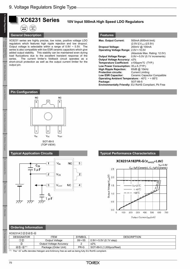
9. Voltage Regulators Single Type_______________________________________________________________
75
XC6231 Series 10V Input 500mA High Speed LDO Regulators
General Description Features XC6231 series are highly precise, low noise, positive voltage LDO regulators which features high ripple rejection and low dropout. Output voltage is selectable within a range of 0.9V ~ 5.5V. The series is also compatible with low ESR ceramic capacitors which give added output stability. This stability can be maintained even during load fluctuations due to the excellent transient response of the series. The current limiter’s foldback circuit operates as a short-circuit protection as well as the output current limiter for the output pin.
Max. Output Current: 500mA (600mA limit) (2.5V≦VOUT≦5.5V) Dropout Voltage: 200mV @ 100mA Operating Voltage Range: 2.0V~10.0V (Absolute Max. Rating: 12.0V) Output Voltage Range: 0.9V~5.5V (0.1V increments) Output Voltage Accuracy: ±2% Temperature Coefficient: ±100ppm/ (TYP.) Low Power Consumption: 35μA (TYP.) High Ripple Rejection: 65dB @ 10kHz Protection circuits: Current Limiting Low ESR Capacitor: Ceramic Capacitor Compatible Operating Ambient Temperature: - 40 ~ + 85 Package: SOT-89-5 Environmentally Friendly: EU RoHS Compliant, Pb Free
XC6231A①②③④⑤-⑥ DESIGNATOR ITEM SYMBOL DESCRIPTION
①② Output Voltage 09~55 0.9V~5.5V (0.1V step) ③ Output Voltage Accuracy 2 ±2%
④⑤-⑥(*1) Package (Order Unit) PR-G SOT-89-5 (1,000pcs/Reel) (*1) The “-G” suffix denotes Halogen and Antimony free as well as being fully EU RoHS compliant.
Pin Configuration
Typical Application Circuits Typical Performance Characteristics
Ordering Information
SOT-89-5 (TOP VIEW)
_______________________________________________________________________________________________________
76
XC6230 Series Adjustable Voltage Output Multifunction 2A High Speed LDO Regulator
General Description Features
The XC6230 series are low on-resistance / low dropout voltage, highly precise,low noise, high PSRR, and large current High Speed LDO regulator IC. Internal circuitry includes a reference voltage supply, error amplifier, drivertransistor, over-current protection circuit, in-rush current prevention circuit,reverse current protection circuit, thermal shutdown circuit, and phasecompensation circuit. A built-in 0.17Ω low ON-resistance Pch driver transistor which can output up toa maximum output current 2.0A are also enclosed in a small surface-mountPKG, even in applications that input and output voltage difference is you use avery small state, it is possible to use in the space-saving. A low ESR ceramic capacitor can be used for the output capacitor (CL). Then, the output voltage is possible to set the output voltage value to 1.2V ~5.0V by connecting the external resistors to VOFB terminal. The over current protection circuit will operate when the output current reachesits current limit. The thermal shutdown circuit will operate when the junctiontemperature reaches its limit temperature. The current limit is possible toarbitrarily set in a range of external resistor in 0.3 ~ 2.5A to ILIM terminal. Theinrush current prevention circuit perform the function of suppressing thevariation of the VIN line and It is possible to suppress the current (inrushcurrent), which is charged in the output capacitor (CL) during IC start rising(when the IC control in CE). In addition, the CE function enables the output tobe turned off and the IC becomes a stand-by mode resulting in greatly reducedpower consumption. When in standby mode, the output capacitor (CL) to bedischarged at high speed it can be returned to the VSS level. The IC has further built-in reverse current prevention circuit, to preventbackflow current when the voltage state of more than input terminal (VIN) to theoutput terminal (VOUT).
Max. Output Current: 2A Current Limit Setting Range: 0.3A~2.5A Dropout Voltage: 0.17V@IOUT=1.0A/VOUT(T)=3.3V Input Voltage Range: 1.7V~6.0V
(Absolute Max. Rating: 7.0V) VOFB Accuracy: 1.2V (±1.0%) Output Voltage Setting Range: 1.2V~5.0V Quiescent Current: 45μA Functions: Reverse Current Protection (Option) Inrush Current Prevention Output Voltage Adjustable CL High Speed Discharge Current Limit Adjustable Protection Functions: Thermal Shutdown (Detect: 150C, Release: 125C (TYP.)) Current Limit Short Protection Output Capacitor: Ceramic Capacitor (4.7μF) Operating Ambient Temperature: -40C~+105C Packages: SOP-8FD, USP-6C Environmentally Friendly: EU RoHS Compliant, Pb Free
Pin Configuration
Typical Application Circuit Typical Performance Characteristics
Output Voltage vs. Output Current (Output current externally adjusted.)
Ordering Information
XC6230①②③④⑤⑥-⑦ DESIGNATOR ITEM SYMBOL DESCRIPTION
① Type H
Thermal shutdown Reverse current protection Adjustable current limiter Adjustable output voltage Inrush current protection CE Pull-down resistor CL Auto discharge
②③ Output Voltage 00 Adjustable Output Voltage (VOFB=1.20V)
④ Adjustable
Output Voltage Accuracy
1 ±1%
⑤⑥-⑦(*1) Packages (Order Unit) ER-G USP-6C (3,000pcs/Reel) QR-G SOP-8FD (1,000pcs/Reel)
(*1) The “-G” suffix denotes Halogen and Antimony free as well as being fully EU RoHS compliant.
0.0
0.2
0.4
0.6
0.8
1.0
1.2
1.4
1.6
0 500 1000 1500 2000 2500 3000
Outp
ut V
oltag
e : V
OUT
(V)
Output Current : IOUT (mA)
XC6230(VOUT_SET=1.2V)
RLIM_SET=0ΩRLIM_SET=13.5kΩRLIM_SET=36kΩRLIM_SET=100kΩRLIM_SET=200kΩ
VOUT_SET =1.2V, Ta=25,
VIN=2.2V, CIN=2.2μF(ceramic), CL=4.7μF(ceramic)
11.Multi C
hip Module
10. Voltage Regulators
Voltage Detect Type
9. Voltage Regulators
12.Load Switch
13. Push Button Controllers14.B
attery Charger
15.Autom
otive ICs
16.Other IC
s17. D
iscrete18.Package Power Dissipation
9. Voltage Regulators
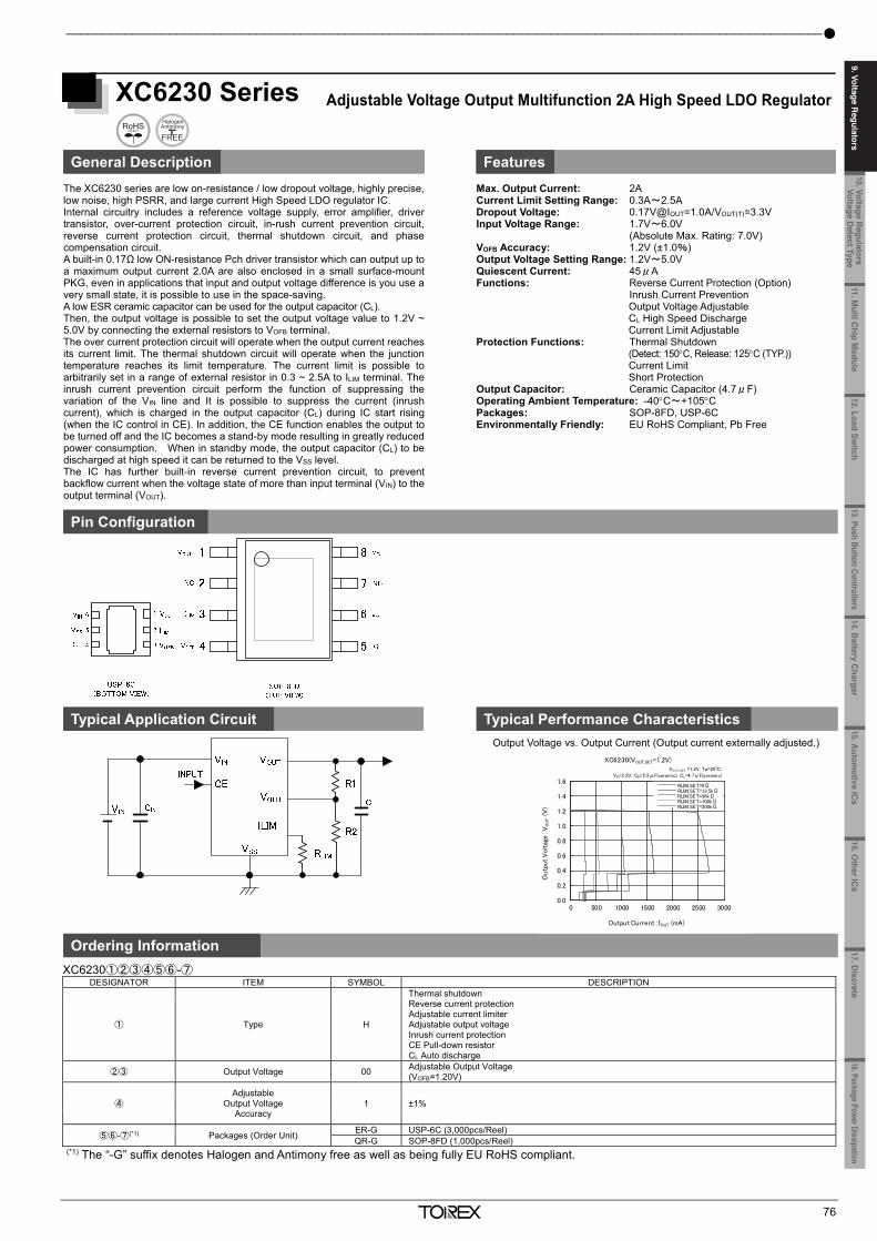
9. Voltage Regulators Single Type_______________________________________________________________
75
XC6231 Series 10V Input 500mA High Speed LDO Regulators
General Description Features XC6231 series are highly precise, low noise, positive voltage LDO regulators which features high ripple rejection and low dropout. Output voltage is selectable within a range of 0.9V ~ 5.5V. The series is also compatible with low ESR ceramic capacitors which give added output stability. This stability can be maintained even during load fluctuations due to the excellent transient response of the series. The current limiter’s foldback circuit operates as a short-circuit protection as well as the output current limiter for the output pin.
Max. Output Current: 500mA (600mA limit) (2.5V≦VOUT≦5.5V) Dropout Voltage: 200mV @ 100mA Operating Voltage Range: 2.0V~10.0V (Absolute Max. Rating: 12.0V) Output Voltage Range: 0.9V~5.5V (0.1V increments) Output Voltage Accuracy: ±2% Temperature Coefficient: ±100ppm/ (TYP.) Low Power Consumption: 35μA (TYP.) High Ripple Rejection: 65dB @ 10kHz Protection circuits: Current Limiting Low ESR Capacitor: Ceramic Capacitor Compatible Operating Ambient Temperature: - 40 ~ + 85 Package: SOT-89-5 Environmentally Friendly: EU RoHS Compliant, Pb Free
XC6231A①②③④⑤-⑥ DESIGNATOR ITEM SYMBOL DESCRIPTION
①② Output Voltage 09~55 0.9V~5.5V (0.1V step) ③ Output Voltage Accuracy 2 ±2%
④⑤-⑥(*1) Package (Order Unit) PR-G SOT-89-5 (1,000pcs/Reel) (*1) The “-G” suffix denotes Halogen and Antimony free as well as being fully EU RoHS compliant.
Pin Configuration
Typical Application Circuits Typical Performance Characteristics
Ordering Information
SOT-89-5 (TOP VIEW)
_______________________________________________________________________________________________________
76
XC6230 Series Adjustable Voltage Output Multifunction 2A High Speed LDO Regulator
General Description Features
The XC6230 series are low on-resistance / low dropout voltage, highly precise,low noise, high PSRR, and large current High Speed LDO regulator IC. Internal circuitry includes a reference voltage supply, error amplifier, drivertransistor, over-current protection circuit, in-rush current prevention circuit,reverse current protection circuit, thermal shutdown circuit, and phasecompensation circuit. A built-in 0.17Ω low ON-resistance Pch driver transistor which can output up toa maximum output current 2.0A are also enclosed in a small surface-mountPKG, even in applications that input and output voltage difference is you use avery small state, it is possible to use in the space-saving. A low ESR ceramic capacitor can be used for the output capacitor (CL). Then, the output voltage is possible to set the output voltage value to 1.2V ~5.0V by connecting the external resistors to VOFB terminal. The over current protection circuit will operate when the output current reachesits current limit. The thermal shutdown circuit will operate when the junctiontemperature reaches its limit temperature. The current limit is possible toarbitrarily set in a range of external resistor in 0.3 ~ 2.5A to ILIM terminal. Theinrush current prevention circuit perform the function of suppressing thevariation of the VIN line and It is possible to suppress the current (inrushcurrent), which is charged in the output capacitor (CL) during IC start rising(when the IC control in CE). In addition, the CE function enables the output tobe turned off and the IC becomes a stand-by mode resulting in greatly reducedpower consumption. When in standby mode, the output capacitor (CL) to bedischarged at high speed it can be returned to the VSS level. The IC has further built-in reverse current prevention circuit, to preventbackflow current when the voltage state of more than input terminal (VIN) to theoutput terminal (VOUT).
Max. Output Current: 2A Current Limit Setting Range: 0.3A~2.5A Dropout Voltage: 0.17V@IOUT=1.0A/VOUT(T)=3.3V Input Voltage Range: 1.7V~6.0V
(Absolute Max. Rating: 7.0V) VOFB Accuracy: 1.2V (±1.0%) Output Voltage Setting Range: 1.2V~5.0V Quiescent Current: 45μA Functions: Reverse Current Protection (Option) Inrush Current Prevention Output Voltage Adjustable CL High Speed Discharge Current Limit Adjustable Protection Functions: Thermal Shutdown (Detect: 150C, Release: 125C (TYP.)) Current Limit Short Protection Output Capacitor: Ceramic Capacitor (4.7μF) Operating Ambient Temperature: -40C~+105C Packages: SOP-8FD, USP-6C Environmentally Friendly: EU RoHS Compliant, Pb Free
Pin Configuration
Typical Application Circuit Typical Performance Characteristics
Output Voltage vs. Output Current (Output current externally adjusted.)
Ordering Information
XC6230①②③④⑤⑥-⑦ DESIGNATOR ITEM SYMBOL DESCRIPTION
① Type H
Thermal shutdown Reverse current protection Adjustable current limiter Adjustable output voltage Inrush current protection CE Pull-down resistor CL Auto discharge
②③ Output Voltage 00 Adjustable Output Voltage (VOFB=1.20V)
④ Adjustable
Output Voltage Accuracy
1 ±1%
⑤⑥-⑦(*1) Packages (Order Unit) ER-G USP-6C (3,000pcs/Reel) QR-G SOP-8FD (1,000pcs/Reel)
(*1) The “-G” suffix denotes Halogen and Antimony free as well as being fully EU RoHS compliant.
0.0
0.2
0.4
0.6
0.8
1.0
1.2
1.4
1.6
0 500 1000 1500 2000 2500 3000
Outp
ut V
oltag
e : V
OUT
(V)
Output Current : IOUT (mA)
XC6230(VOUT_SET=1.2V)
RLIM_SET=0ΩRLIM_SET=13.5kΩRLIM_SET=36kΩRLIM_SET=100kΩRLIM_SET=200kΩ
VOUT_SET =1.2V, Ta=25,
VIN=2.2V, CIN=2.2μF(ceramic), CL=4.7μF(ceramic)
11.Multi C
hip Module
10. Voltage Regulators
Voltage Detect Type
12.Load Switch
13. Push Button Controllers14.B
attery Charger
15.Autom
otive ICs
16.Other IC
s17. D
iscrete18.Package Power Dissipation
9. Voltage Regulators
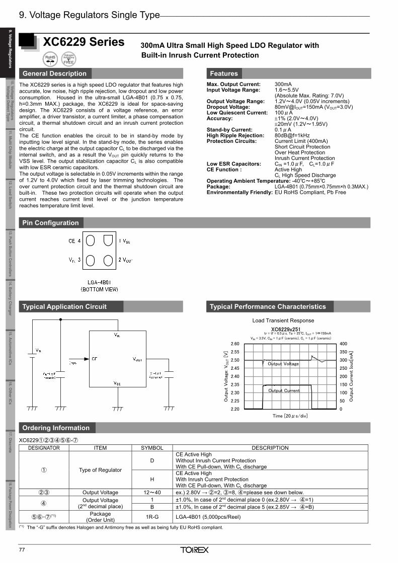
9. Voltage Regulators Single Type_______________________________________________________________
77
XC6229 Series 300mA Ultra Small High Speed LDO Regulator with Built-in Inrush Current Protection
General Description Features The XC6229 series is a high speed LDO regulator that features high accurate, low noise, high ripple rejection, low dropout and low power consumption. Housed in the ultra-small LGA-4B01 (0.75 x 0.75, h=0.3mm MAX.) package, the XC6229 is ideal for space-saving design. The XC6229 consists of a voltage reference, an error amplifier, a driver transistor, a current limiter, a phase compensation circuit, a thermal shutdown circuit and an inrush current protection circuit. The CE function enables the circuit to be in stand-by mode by inputting low level signal. In the stand-by mode, the series enables the electric charge at the output capacitor CL to be discharged via the internal switch, and as a result the VOUT pin quickly returns to the VSS level. The output stabilization capacitor CL is also compatible with low ESR ceramic capacitors. The output voltage is selectable in 0.05V increments within the range of 1.2V to 4.0V which fixed by laser trimming technologies. The over current protection circuit and the thermal shutdown circuit are built-in. These two protection circuits will operate when the output current reaches current limit level or the junction temperature reaches temperature limit level.
Max. Output Current: 300mA Input Voltage Range: 1.6~5.5V (Absolute Max. Rating: 7.0V) Output Voltage Range: 1.2V~4.0V (0.05V increments) Dropout Voltage: 80mV@IOUT=150mA (VOUT=3.0V) Low Quiescent Current: 100μA Accuracy: 1% (2.0V~4.0V) 20mV (1.2V~1.95V) Stand-by Current: 0.1μA High Ripple Rejection: 80dB@f=1kHz Protection Circuits: Current Limit (400mA) Short Circuit Protection Over Heat Protection Inrush Current Protection Low ESR Capacitors: CIN =1.0μF, CL=1.0μF CE Function : Active High CL High Speed Discharge Operating Ambient Temperature: -40~+85 Package: LGA-4B01 (0.75mm×0.75mm×h 0.3MAX.) Environmentally Friendly: EU RoHS Compliant, Pb Free
XC6229①②③④⑤⑥-⑦ DESIGNATOR ITEM SYMBOL DESCRIPTION
① Type of Regulator
D CE Active High Without Inrush Current Protection With CE Pull-down, With CL discharge
H CE Active High With Inrush Current Protection With CE Pull-down, With CL discharge
②③ Output Voltage 12~40 ex.) 2.80V → ②=2, ③=8, ④=please see down below.
④ Output Voltage
(2nd decimal place) 1 ±1.0%, In case of 2nd decimal place 0 (ex.2.80V → ④=1) B ±1.0%, In case of 2nd decimal place 5 (ex.2.85V → ④=B)
⑤⑥-⑦(*1) Package
(Order Unit) 1R-G LGA-4B01 (5,000pcs/Reel) (*1) The “-G” suffix denotes Halogen and Antimony free as well as being fully EU RoHS compliant.
Pin Configuration
Typical Application Circuit
Typical Performance Characteristics
Ordering Information
tr = tf = 0.5μs, Ta = 25, IOUT = 1⇔150mA
VIN = 3.5V, CIN = 1μF (ceramic), CL = 1μF (ceramic)
XC6229x251
2.20
2.25
2.30
2.35
2.40
2.45
2.50
2.55
2.60
Time [20μs/div]
Outp
ut
Voltag
e: V
OU
T [
V]
0
50
100
150
200
250
300
350
400
Outp
ut
Curr
ent
Iout[
mA
]
Output Voltage
Output Current
Load Transient Response
_______________________________________________________________________________________________________
78
XC6227 Series 700mA High Speed LDO Regulator with Reverse Current Protection
General Description Features
The XC6227 series is a highly accurate, low noise, high ripplerejection, low dropout, and low power consumption high speedvoltage regulator. The series consists of a voltage reference, an error amplifier, adriver transistor, a current limiter, a thermal protection circuit, areverse current protection circuit and a phase compensationcircuit. The CE function enables the entire circuit to be placed in astand-by state by inputting a low level signal to the CE pin.Over-current protection and thermal protection circuits areintegrated. The protection circuit starts to operate when eitheroutput current reaches the current limit level or junctiontemperature reaches the temperature limit. With the reversecurrent protection function of a driver transistor, the reverse currentflow is prohibited when VOUT voltage is higher than VIN voltage.For an example, when a battery is connected to the VOUT pin, battery current will not flow back to the XC6227.
Max. Output Current: 700mA Operating Voltage Range: 1.7V ~ 6.0V (Absolute Max. Rating: 6.5V) Output Voltage Range: 0.8V ~ 5.0V (0.05V increments) Dropout Voltage: 120mV@IOUT=300mA (VOUT=3.0V) Low Quiescent Current: 100μA Accuracy: ±1.0% (VOUT>2.0V) ±0.02V (VOUT≦2.0V) High Ripple Rejection: 65dB@1kHz ON/OFF Control: Active High 0.1μA (Stand-by) Output Capacitor: Ceramic capacitor Operating Ambient Temperature: -40C ~ +85C Packages: USP-6C, SOT-25, SOT-89-5 Environmentally Friendly: EU RoHS Compliant, Pb Free
Pin Configuration
Typical Application Circuit Typical Performance Characteristics VOUT Sink Current VS. Input Voltage
Ordering Information
XC6227①②③④⑤⑥-⑦ DESIGNATOR ITEM SYMBOL DESCRIPTION
① Type of CE (*2) C with CE Active High, with CE Pull-down resistor ②③ Output Voltage 08~50 e.g.) 2.8V ②=2 ③=8
④ Output Voltage (the 2nd decimal place)
1 Output voltage x.x0V e.g. 2.80V →②=2, ③=8, ④=1 B Output voltage x.x5V e.g. 2.85V →②=2, ③=8, ④=B
⑤⑥-⑦(*1) Packages (Order Unit) MR-G SOT-25 (3,000pcs/Reel) PR-G SOT-89-5 (1,000pcs/Reel) ER-G USP-6C (3,000pcs/Reel)
(*1) The “-G” suffix denotes Halogen and Antimony free as well as being fully EU RoHS compliant. (*2) For without CE Pull-down, please contact your local Torex sales office or representative.
VOUT=3.3V
IOUT=0mA
XC6227C331
-2
0
2
4
6
8
10
0 0.5 1 1.5 2 2.5 3 3.5 4 4.5 5 5.5 6
Input Voltage:VIN(V)
VO
UT S
ink
Curr
ent:
I REV
S(μ
A) -40
25
85
11.Multi C
hip Module
10. Voltage Regulators
Voltage Detect Type
9. Voltage Regulators
12.Load Switch
13. Push Button Controllers14.B
attery Charger
15.Autom
otive ICs
16.Other IC
s17. D
iscrete18.Package Power Dissipation
9. Voltage Regulators
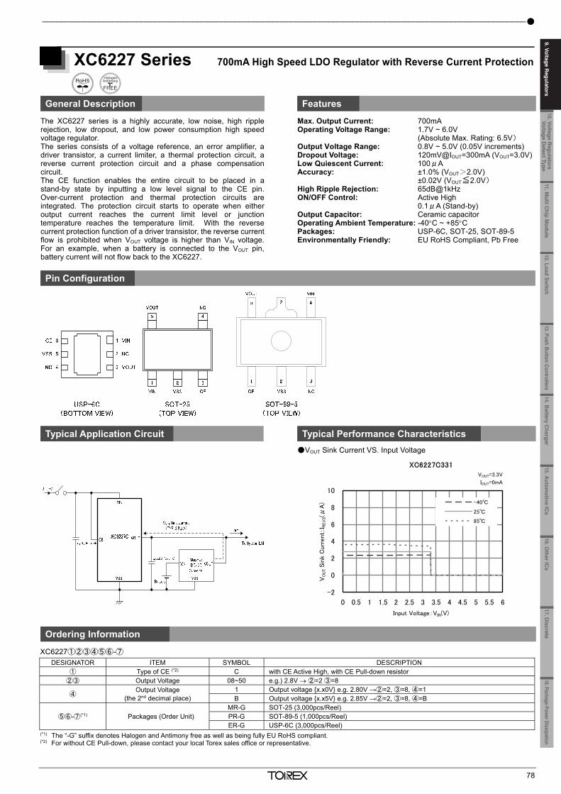
9. Voltage Regulators Single Type_______________________________________________________________
77
XC6229 Series 300mA Ultra Small High Speed LDO Regulator with Built-in Inrush Current Protection
General Description Features The XC6229 series is a high speed LDO regulator that features high accurate, low noise, high ripple rejection, low dropout and low power consumption. Housed in the ultra-small LGA-4B01 (0.75 x 0.75, h=0.3mm MAX.) package, the XC6229 is ideal for space-saving design. The XC6229 consists of a voltage reference, an error amplifier, a driver transistor, a current limiter, a phase compensation circuit, a thermal shutdown circuit and an inrush current protection circuit. The CE function enables the circuit to be in stand-by mode by inputting low level signal. In the stand-by mode, the series enables the electric charge at the output capacitor CL to be discharged via the internal switch, and as a result the VOUT pin quickly returns to the VSS level. The output stabilization capacitor CL is also compatible with low ESR ceramic capacitors. The output voltage is selectable in 0.05V increments within the range of 1.2V to 4.0V which fixed by laser trimming technologies. The over current protection circuit and the thermal shutdown circuit are built-in. These two protection circuits will operate when the output current reaches current limit level or the junction temperature reaches temperature limit level.
Max. Output Current: 300mA Input Voltage Range: 1.6~5.5V (Absolute Max. Rating: 7.0V) Output Voltage Range: 1.2V~4.0V (0.05V increments) Dropout Voltage: 80mV@IOUT=150mA (VOUT=3.0V) Low Quiescent Current: 100μA Accuracy: 1% (2.0V~4.0V) 20mV (1.2V~1.95V) Stand-by Current: 0.1μA High Ripple Rejection: 80dB@f=1kHz Protection Circuits: Current Limit (400mA) Short Circuit Protection Over Heat Protection Inrush Current Protection Low ESR Capacitors: CIN =1.0μF, CL=1.0μF CE Function : Active High CL High Speed Discharge Operating Ambient Temperature: -40~+85 Package: LGA-4B01 (0.75mm×0.75mm×h 0.3MAX.) Environmentally Friendly: EU RoHS Compliant, Pb Free
XC6229①②③④⑤⑥-⑦ DESIGNATOR ITEM SYMBOL DESCRIPTION
① Type of Regulator
D CE Active High Without Inrush Current Protection With CE Pull-down, With CL discharge
H CE Active High With Inrush Current Protection With CE Pull-down, With CL discharge
②③ Output Voltage 12~40 ex.) 2.80V → ②=2, ③=8, ④=please see down below.
④ Output Voltage
(2nd decimal place) 1 ±1.0%, In case of 2nd decimal place 0 (ex.2.80V → ④=1) B ±1.0%, In case of 2nd decimal place 5 (ex.2.85V → ④=B)
⑤⑥-⑦(*1) Package
(Order Unit) 1R-G LGA-4B01 (5,000pcs/Reel) (*1) The “-G” suffix denotes Halogen and Antimony free as well as being fully EU RoHS compliant.
Pin Configuration
Typical Application Circuit
Typical Performance Characteristics
Ordering Information
tr = tf = 0.5μs, Ta = 25, IOUT = 1⇔150mA
VIN = 3.5V, CIN = 1μF (ceramic), CL = 1μF (ceramic)
XC6229x251
2.20
2.25
2.30
2.35
2.40
2.45
2.50
2.55
2.60
Time [20μs/div]
Outp
ut
Voltag
e: V
OU
T [
V]
0
50
100
150
200
250
300
350
400
Outp
ut
Curr
ent
Iout[
mA
]
Output Voltage
Output Current
Load Transient Response
_______________________________________________________________________________________________________
78
XC6227 Series 700mA High Speed LDO Regulator with Reverse Current Protection
General Description Features
The XC6227 series is a highly accurate, low noise, high ripplerejection, low dropout, and low power consumption high speedvoltage regulator. The series consists of a voltage reference, an error amplifier, adriver transistor, a current limiter, a thermal protection circuit, areverse current protection circuit and a phase compensationcircuit. The CE function enables the entire circuit to be placed in astand-by state by inputting a low level signal to the CE pin.Over-current protection and thermal protection circuits areintegrated. The protection circuit starts to operate when eitheroutput current reaches the current limit level or junctiontemperature reaches the temperature limit. With the reversecurrent protection function of a driver transistor, the reverse currentflow is prohibited when VOUT voltage is higher than VIN voltage.For an example, when a battery is connected to the VOUT pin, battery current will not flow back to the XC6227.
Max. Output Current: 700mA Operating Voltage Range: 1.7V ~ 6.0V (Absolute Max. Rating: 6.5V) Output Voltage Range: 0.8V ~ 5.0V (0.05V increments) Dropout Voltage: 120mV@IOUT=300mA (VOUT=3.0V) Low Quiescent Current: 100μA Accuracy: ±1.0% (VOUT>2.0V) ±0.02V (VOUT≦2.0V) High Ripple Rejection: 65dB@1kHz ON/OFF Control: Active High 0.1μA (Stand-by) Output Capacitor: Ceramic capacitor Operating Ambient Temperature: -40C ~ +85C Packages: USP-6C, SOT-25, SOT-89-5 Environmentally Friendly: EU RoHS Compliant, Pb Free
Pin Configuration
Typical Application Circuit Typical Performance Characteristics VOUT Sink Current VS. Input Voltage
Ordering Information
XC6227①②③④⑤⑥-⑦ DESIGNATOR ITEM SYMBOL DESCRIPTION
① Type of CE (*2) C with CE Active High, with CE Pull-down resistor ②③ Output Voltage 08~50 e.g.) 2.8V ②=2 ③=8
④ Output Voltage (the 2nd decimal place)
1 Output voltage x.x0V e.g. 2.80V →②=2, ③=8, ④=1 B Output voltage x.x5V e.g. 2.85V →②=2, ③=8, ④=B
⑤⑥-⑦(*1) Packages (Order Unit) MR-G SOT-25 (3,000pcs/Reel) PR-G SOT-89-5 (1,000pcs/Reel) ER-G USP-6C (3,000pcs/Reel)
(*1) The “-G” suffix denotes Halogen and Antimony free as well as being fully EU RoHS compliant. (*2) For without CE Pull-down, please contact your local Torex sales office or representative.
VOUT=3.3V
IOUT=0mA
XC6227C331
-2
0
2
4
6
8
10
0 0.5 1 1.5 2 2.5 3 3.5 4 4.5 5 5.5 6
Input Voltage:VIN(V)
VO
UT S
ink
Curr
ent:
I REV
S(μ
A) -40
25
85
11.Multi C
hip Module
10. Voltage Regulators
Voltage Detect Type
12.Load Switch
13. Push Button Controllers14.B
attery Charger
15.Autom
otive ICs
16.Other IC
s17. D
iscrete18.Package Power Dissipation
9. Voltage Regulators
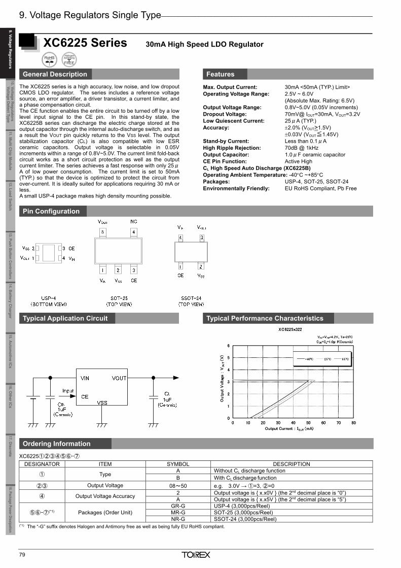
9. Voltage Regulators Single Type_______________________________________________________________
79
XC6225 Series 30mA High Speed LDO Regulator
General Description Features
The XC6225 series is a high accuracy, low noise, and low dropoutCMOS LDO regulator. The series includes a reference voltagesource, an error amplifier, a driver transistor, a current limiter, anda phase compensation circuit. The CE function enables the entire circuit to be turned off by a lowlevel input signal to the CE pin. In this stand-by state, theXC6225B series can discharge the electric charge stored at theoutput capacitor through the internal auto-discharge switch, and asa result the VOUT pin quickly returns to the VSS level. The outputstabilization capacitor (CL) is also compatible with low ESRceramic capacitors. Output voltage is selectable in 0.05Vincrements within a range of 0.8V~5.0V. The current limit fold-back circuit works as a short circuit protection as well as the outputcurrent limiter. The series achieves a fast response with only 25μA of low power consumption. The current limit is set to 50mA(TYP.) so that the device is optimized to protect the circuit fromover-current. It is ideally suited for applications requiring 30 mA orless. A small USP-4 package makes high density mounting possible.
Max. Output Current: 30mA <50mA (TYP.) Limit> Operating Voltage Range: 2.5V ~ 6.0V (Absolute Max. Rating: 6.5V) Output Voltage Range: 0.8V~5.0V (0.05V increments) Dropout Voltage: 70mV@ IOUT=30mA, VOUT=3.2V Low Quiescent Current: 25μA (TYP.) Accuracy: 2.0% (VOUT>1.5V) 0.03V (VOUT≦1.45V) Stand-by Current: Less than 0.1μA High Ripple Rejection: 70dB @ 1kHz Output Capacitor: 1.0μF ceramic capacitor CE Pin Function: Active High CL High Speed Auto Discharge (XC6225B) Operating Ambient Temperature: -40C ~+85C Packages: USP-4, SOT-25, SSOT-24 Environmentally Friendly: EU RoHS Compliant, Pb Free
Pin Configuration
Typical Application Circuit Typical Performance Characteristics
Ordering Information
XC6225①②③④⑤⑥-⑦ DESIGNATOR ITEM SYMBOL DESCRIPTION
① Type A Without CL discharge function B With CL discharge function
②③ Output Voltage 08~50 e.g. 3.0V → ①=3, ②=0
④ Output Voltage Accuracy 2 Output voltage is x.x0V (the 2nd decimal place is “0”) A Output voltage is x.x5V (the 2nd decimal place is “5”)
⑤⑥-⑦(*1) Packages (Order Unit) GR-G USP-4 (3,000pcs/Reel) MR-G SOT-25 (3,000pcs/Reel) NR-G SSOT-24 (3,000pcs/Reel)
(*1) The “-G” suffix denotes Halogen and Antimony free as well as being fully EU RoHS compliant.
_______________________________________________________________________________________________________
80
XC6224 Series 1.2V Low Voltage Operation, 150mA High Speed LDO Voltage Regulator
General Description Features
The XC6224 series is a high speed LDO regulator that featureshigh accurate, low noise, high ripple rejection, low dropout and lowpower consumption. The series consists of a voltage reference, anerror amplifier, a driver transistor, a current limiter, and a phasecompensation circuit. This IC is suitable for a local power supply placed in adjacent tothe system logic LSI or others, because of low input voltageoperation, using an ultra small package USPN-4B02 (0.75mm x0.95mm) and stable operation with a small phase compensationcapacitor (CL) 0.47μF. Also, this IC has fast transient response and high ripple rejection(70dB @ 1kHz). The CE function enables the circuit to be in stand-by mode byinputting low level signal. In the stand-by mode, the series enablesthe electric charge at the output capacitor CL to be discharged viathe internal switch, and as a result the VOUT pin quickly returns tothe VSS level. The over current protection circuit is integrated and operates whenthe output current reaches current limit level.
Max. Output Current: 150mA Operating Voltage Range: 1.2V ~ 3.6V (Absolute Max. Rating: 4.6V) Output Voltage Range: 0.8V ~ 3.0V (0.05V increments) Dropout Voltage: 210mV@150mA (VOUT=2.8V) Low Quiescent Current: 33μA (TYP.) High Accuracy: ±1.5% (Output Voltage 1.25V ~ 3.0V)
±20mV (Output Voltage 0.8V ~ 1.20V) High Ripple Rejection: 70dB (1kHz) Protection Circuits: Current Limiter, Short Circuit Protection ON/OFF Control: Active High CL Auto Discharge Function 0.1μA (Stand-by) Output Capacitor: Low ESR Capacitor Operating Ambient Temperature: -40C ~ +85C Packages: USPN-4B02, SSOT-24, SOT-25 Environmentally Friendly: EU RoHS Compliant, Pb Free
Pin Configuration
Typical Application Circuit Typical Performance Characteristics
Ordering Information
XC6224①②③④⑤⑥-⑦ CE Active High, with CL Discharge, ±1% Accuracy DESIGNATOR ITEM SYMBOL DESCRIPTION
① Type of Regulator A
(The Recommended Type) Without CE pull-down
B With CE pull-down ②③ Output Voltage 08~30 e.g.) 2.5V ②=2 ③=5
④ Output Voltage Type (The 2nd Decimal Place)
1 x.x0V (the 2nd decimal place is “0”) B x.x5V (the 2nd decimal place is “5”)
⑤⑥-⑦(*1) Packages (Order Unit) 7R-G USPN-4B02 (5,000pcs/Reel) MR-G SOT-25 (3,000pcs/Reel) NR-G SSOT-24 (3,000pcs/Reel)
(*1) The “-G” suffix denotes Halogen and Antimony free as well as being fully EU RoHS compliant.
XC6224A121 Ta=25、 IOUT =50mA⇔100mA、 tr= tf=0.5µ sVIN =2.25V、 CIN =CL =0.47µF
Outp
ut C
urre
nt:
IOUT[ m
A]
Time [10µs/div]
500
Output Voltage
450
400
350
300
250
200
150
100
50
0
Output Current Outp
ut V
olta
ge:
VOUT[ V]
1.40
1.35
1.30
1.25
1.20
1.15
1.10
1.05
1.00
0.95
0.90
11.Multi C
hip Module
10. Voltage Regulators
Voltage Detect Type
9. Voltage Regulators
12.Load Switch
13. Push Button Controllers14.B
attery Charger
15.Autom
otive ICs
16.Other IC
s17. D
iscrete18.Package Power Dissipation
9. Voltage Regulators
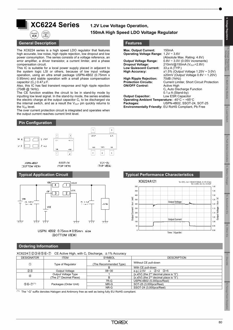
9. Voltage Regulators Single Type_______________________________________________________________
79
XC6225 Series 30mA High Speed LDO Regulator
General Description Features
The XC6225 series is a high accuracy, low noise, and low dropoutCMOS LDO regulator. The series includes a reference voltagesource, an error amplifier, a driver transistor, a current limiter, anda phase compensation circuit. The CE function enables the entire circuit to be turned off by a lowlevel input signal to the CE pin. In this stand-by state, theXC6225B series can discharge the electric charge stored at theoutput capacitor through the internal auto-discharge switch, and asa result the VOUT pin quickly returns to the VSS level. The outputstabilization capacitor (CL) is also compatible with low ESRceramic capacitors. Output voltage is selectable in 0.05Vincrements within a range of 0.8V~5.0V. The current limit fold-back circuit works as a short circuit protection as well as the outputcurrent limiter. The series achieves a fast response with only 25μA of low power consumption. The current limit is set to 50mA(TYP.) so that the device is optimized to protect the circuit fromover-current. It is ideally suited for applications requiring 30 mA orless. A small USP-4 package makes high density mounting possible.
Max. Output Current: 30mA <50mA (TYP.) Limit> Operating Voltage Range: 2.5V ~ 6.0V (Absolute Max. Rating: 6.5V) Output Voltage Range: 0.8V~5.0V (0.05V increments) Dropout Voltage: 70mV@ IOUT=30mA, VOUT=3.2V Low Quiescent Current: 25μA (TYP.) Accuracy: 2.0% (VOUT>1.5V) 0.03V (VOUT≦1.45V) Stand-by Current: Less than 0.1μA High Ripple Rejection: 70dB @ 1kHz Output Capacitor: 1.0μF ceramic capacitor CE Pin Function: Active High CL High Speed Auto Discharge (XC6225B) Operating Ambient Temperature: -40C ~+85C Packages: USP-4, SOT-25, SSOT-24 Environmentally Friendly: EU RoHS Compliant, Pb Free
Pin Configuration
Typical Application Circuit Typical Performance Characteristics
Ordering Information
XC6225①②③④⑤⑥-⑦ DESIGNATOR ITEM SYMBOL DESCRIPTION
① Type A Without CL discharge function B With CL discharge function
②③ Output Voltage 08~50 e.g. 3.0V → ①=3, ②=0
④ Output Voltage Accuracy 2 Output voltage is x.x0V (the 2nd decimal place is “0”) A Output voltage is x.x5V (the 2nd decimal place is “5”)
⑤⑥-⑦(*1) Packages (Order Unit) GR-G USP-4 (3,000pcs/Reel) MR-G SOT-25 (3,000pcs/Reel) NR-G SSOT-24 (3,000pcs/Reel)
(*1) The “-G” suffix denotes Halogen and Antimony free as well as being fully EU RoHS compliant.
_______________________________________________________________________________________________________
80
XC6224 Series 1.2V Low Voltage Operation, 150mA High Speed LDO Voltage Regulator
General Description Features
The XC6224 series is a high speed LDO regulator that featureshigh accurate, low noise, high ripple rejection, low dropout and lowpower consumption. The series consists of a voltage reference, anerror amplifier, a driver transistor, a current limiter, and a phasecompensation circuit. This IC is suitable for a local power supply placed in adjacent tothe system logic LSI or others, because of low input voltageoperation, using an ultra small package USPN-4B02 (0.75mm x0.95mm) and stable operation with a small phase compensationcapacitor (CL) 0.47μF. Also, this IC has fast transient response and high ripple rejection(70dB @ 1kHz). The CE function enables the circuit to be in stand-by mode byinputting low level signal. In the stand-by mode, the series enablesthe electric charge at the output capacitor CL to be discharged viathe internal switch, and as a result the VOUT pin quickly returns tothe VSS level. The over current protection circuit is integrated and operates whenthe output current reaches current limit level.
Max. Output Current: 150mA Operating Voltage Range: 1.2V ~ 3.6V (Absolute Max. Rating: 4.6V) Output Voltage Range: 0.8V ~ 3.0V (0.05V increments) Dropout Voltage: 210mV@150mA (VOUT=2.8V) Low Quiescent Current: 33μA (TYP.) High Accuracy: ±1.5% (Output Voltage 1.25V ~ 3.0V)
±20mV (Output Voltage 0.8V ~ 1.20V) High Ripple Rejection: 70dB (1kHz) Protection Circuits: Current Limiter, Short Circuit Protection ON/OFF Control: Active High CL Auto Discharge Function 0.1μA (Stand-by) Output Capacitor: Low ESR Capacitor Operating Ambient Temperature: -40C ~ +85C Packages: USPN-4B02, SSOT-24, SOT-25 Environmentally Friendly: EU RoHS Compliant, Pb Free
Pin Configuration
Typical Application Circuit Typical Performance Characteristics
Ordering Information
XC6224①②③④⑤⑥-⑦ CE Active High, with CL Discharge, ±1% Accuracy DESIGNATOR ITEM SYMBOL DESCRIPTION
① Type of Regulator A
(The Recommended Type) Without CE pull-down
B With CE pull-down ②③ Output Voltage 08~30 e.g.) 2.5V ②=2 ③=5
④ Output Voltage Type (The 2nd Decimal Place)
1 x.x0V (the 2nd decimal place is “0”) B x.x5V (the 2nd decimal place is “5”)
⑤⑥-⑦(*1) Packages (Order Unit) 7R-G USPN-4B02 (5,000pcs/Reel) MR-G SOT-25 (3,000pcs/Reel) NR-G SSOT-24 (3,000pcs/Reel)
(*1) The “-G” suffix denotes Halogen and Antimony free as well as being fully EU RoHS compliant.
XC6224A121 Ta=25、 IOUT =50mA⇔100mA、 tr= tf=0.5µ sVIN =2.25V、 CIN =CL =0.47µF
Outp
ut C
urre
nt:
IOUT[ m
A]
Time [10µs/div]
500
Output Voltage
450
400
350
300
250
200
150
100
50
0
Output Current Outp
ut V
olta
ge:
VOUT[ V]
1.40
1.35
1.30
1.25
1.20
1.15
1.10
1.05
1.00
0.95
0.90
11.Multi C
hip Module
10. Voltage Regulators
Voltage Detect Type
12.Load Switch
13. Push Button Controllers14.B
attery Charger
15.Autom
otive ICs
16.Other IC
s17. D
iscrete18.Package Power Dissipation
9. Voltage Regulators
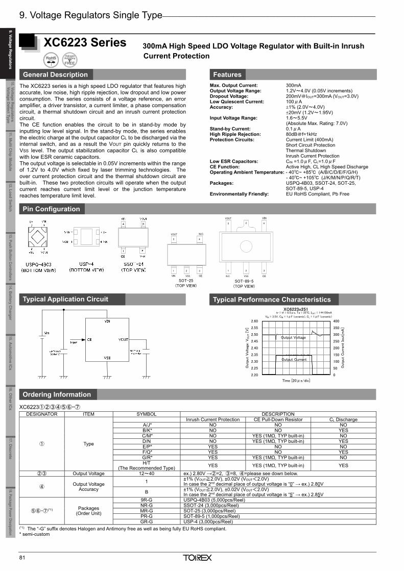
9. Voltage Regulators Single Type_______________________________________________________________
81
XC6223 Series 300mA High Speed LDO Voltage Regulator with Built-in Inrush Current Protection
General Description Features The XC6223 series is a high speed LDO regulator that features high accurate, low noise, high ripple rejection, low dropout and low power consumption. The series consists of a voltage reference, an error amplifier, a driver transistor, a current limiter, a phase compensation circuit, a thermal shutdown circuit and an inrush current protection circuit. The CE function enables the circuit to be in stand-by mode by inputting low level signal. In the stand-by mode, the series enables the electric charge at the output capacitor CL to be discharged via the internal switch, and as a result the VOUT pin quickly returns to the VSS level. The output stabilization capacitor CL is also compatible with low ESR ceramic capacitors. The output voltage is selectable in 0.05V increments within the range of 1.2V to 4.0V which fixed by laser trimming technologies. The over current protection circuit and the thermal shutdown circuit are built-in. These two protection circuits will operate when the output current reaches current limit level or the junction temperature reaches temperature limit level.
Max. Output Current: 300mA Output Voltage Range: 1.2V~4.0V (0.05V increments) Dropout Voltage: 200mV@IOUT=300mA (VOUT=3.0V) Low Quiescent Current: 100μA Accuracy: 1% (2.0V~4.0V) 20mV (1.2V~1.95V) Input Voltage Range: 1.6~5.5V
(Absolute Max. Rating: 7.0V) Stand-by Current: 0.1μA High Ripple Rejection: 80dB@f=1kHz Protection Circuits: Current Limit (400mA) Short Circuit Protection Thermal Shutdown Inrush Current Protection Low ESR Capacitors: CIN =1.0μF, CL=1.0μF CE Function: Active High, CL High Speed Discharge Operating Ambient Temperature: - 40~ +85 (A/B/C/D/E/F/G/H)
- 40~ +105 (J/K/M/N/P/Q/R/T) Packages: USPQ-4B03, SSOT-24, SOT-25, SOT-89-5, USP-4 Environmentally Friendly: EU RoHS Compliant, Pb Free
XC6223①②③④⑤⑥-⑦ DESIGNATOR ITEM SYMBOL DESCRIPTION
① Type
Inrush Current Protection CE Pull-Down Resistor CL Discharge A/J* NO NO NO B/K* NO NO YES C/M* NO YES (1MΩ, TYP built-in) NO D/N NO YES (1MΩ, TYP built-in) YES E/P* YES NO NO F/Q* YES NO YES G/R* YES YES (1MΩ, TYP built-in) NO H/T
(The Recommended Type) YES YES (1MΩ, TYP built-in) YES
②③ Output Voltage 12~40 ex.) 2.80V →②=2, ③=8, ④=please see down below.
④ Output Voltage Accuracy
1 ±1% (VOUT≧2.0V), ±0.02V (VOUT<2.0V) In case the 2nd decimal place of output voltage is “0” → ex.) 2.80V
B ±1% (VOUT≧2.0V), ±0.02V (VOUT<2.0V) In case the 2nd decimal place of output voltage is “5” → ex.) 2.85V
⑤⑥-⑦(*1) Packages (Order Unit)
9R-G USPQ-4B03 (5,000pcs/Reel) NR-G SSOT-24 (3,000pcs/Reel) MR-G SOT-25 (3,000pcs/Reel) PR-G SOT-89-5 (1,000pcs/Reel) GR-G USP-4 (3,000pcs/Reel)
(*1) The “-G” suffix denotes Halogen and Antimony free as well as being fully EU RoHS compliant. * semi-custom
Pin Configuration
Typical Application Circuit
Typical Performance Characteristics
Ordering Information
tr = tf = 0.5μs, Ta = 25, IOUT = 1⇔150mA
VIN = 3.5V, CIN = 1μF (ceramic), CL = 1μF (ceramic)
XC6223x251
2.20
2.25
2.30
2.35
2.40
2.45
2.50
2.55
2.60
Time [20μs/div]
Outp
ut
Voltag
e: V
OU
T [
V]
0
50
100
150
200
250
300
350
400
Outp
ut
Curr
ent
Iout[
mA
]Output Voltage
Output Current
1 32
5 4
VIN
VOUT
VSS
SOT-25(TOP VIEW)
CE
N.C.
1 2 3
45 2
N.C. VSS CE
VOUT VIN
SOT-89-5(TOP VIEW)
_______________________________________________________________________________________________________
82
XC6222 Series 700mA High Speed LDO Regulator
General Description Features
The XC6222 series is a highly accurate, low noise, high ripplerejection, low dropout, and low power consumption high speedCMOS voltage regulator. The series consists of a voltagereference, an error amplifier, a driver transistor, a current limiter, athermal protection circuit, and a phase compensation circuit. The CE function enables the entire circuit to be placed in astand-by state by inputting a low level signal to the CE pin. In thisstand-by mode, the electric charge at the output capacitor (CL) will be discharged by the internal auto-discharge switch, and as aresult the VOUT pin will quickly return to the VSS level. Over-current protection and thermal protection circuits areintegrated. The protection circuit starts to operate when eitheroutput current reaches the current limit level or junctiontemperature reaches the temperature limit.
Max. Output Current: 700mA Operating Voltage Range: 1.7V ~ 6.0V
(Absolute Max. Rating: 6.5V) Output Voltage Range: 0.8V~5.0V (0.05V increments) Dropout Voltage: 120mV @IOUT=300mA(VOUT=3.0V) Low Quiescent Current: 100μA (VOUT=3.0V) Accuracy: 1.0% (VOUT>2.0V) 0.02V (VOUT≦2.0V) Stand-by Current: Less than 0.1μA (CE Active High) High Ripple Rejection: 65dB @ 1kHz CE Pin Function: Active High Low ESR Capacitor: Ceramic capacitor Operating Ambient Temperature: -40~+85 Packages: USP-6C, SOT-25, SOT-89-5 Environmentally Friendly: EU RoHS Compliant, Pb Free
Pin Configuration Typical Application Circuits
Typical Performance Characteristics
Load Transient Response
Ordering Information
XC6222①②③④⑤⑥-⑦
DESIGNATOR ITEM SYMBOL DESCRIPTION
① Type
A without CE Pull-down resistor, without CL discharge (semi-custom) B without CE Pull-down resistor , with CL discharge (semi-custom) C with CE Pull-down resistor, without CL discharge (semi-custom) D with CE Pull-down resistor, with CL discharge (standard)
②③ Output Voltage 08~50 e.g. 2.8V → ②=2, ③=8 Output Voltage Range : 0.8~5.0 V (0.05V increments)
④ Output Voltage Type (The 2nd Decimal Place)
1 Output voltage x.x0v (the 2nd decimal place is “0”) ±1.0% (VOUT>2.0V), ±0.02V(VOUT≦2.0V)
B Output voltage x.x5v (the 2nd decimal place is “5”) ±1.0% (VOUT>2.0V), ±0.02V(VOUT≦2.0V)
⑤⑥-⑦(*1) Packages (Order Unit) MR-G SOT-25 (3,000pcs/Reel) PR-G SOT-89-5 (1,000pcs/Reel) ER-G USP-6C (3,000pcs/Reel)
(*1) The “-G” suffix denotes Halogen and Antimony free as well as being fully EU RoHS compliant.
5 4
1 32
VIN VSS CE
VOUT NC
SOT-25(TOP VIEW)
1 VIN
2 NC
3 VOUT
CE 6
VSS 5
NC 4
USP-6C(BOTTOM VIEW)
SOT-89-5(TOP VIEW)
1 2 3
45 2
VOUT VIN
VSSCE NC
*CL: 2.2μF or higher (VOUT=2.5~5.0V) 4.7μF or higher (VOUT=2.1~2.45V) 6.8μF or higher (VOUT=0.8~2.05V)
XC6222x151
1.1
1.2
1.3
1.4
1.5
1.6
Time:100μs/div
Outp
ut
Voltag
e:V
OU
T(V
)
0
200
400
600
800
1000
Outp
ut
Curr
ent:
I OU
T(m
A)
tr=tf=5μs,VIN=2.5V, Ta=25
VOUT=10→300mA, CIN=1.0μF(ceramic), CL=6.8μF(ceramic)
Output Current
Output Voltage
11.Multi C
hip Module
10. Voltage Regulators
Voltage Detect Type
9. Voltage Regulators
12.Load Switch
13. Push Button Controllers14.B
attery Charger
15.Autom
otive ICs
16.Other IC
s17. D
iscrete18.Package Power Dissipation
9. Voltage Regulators
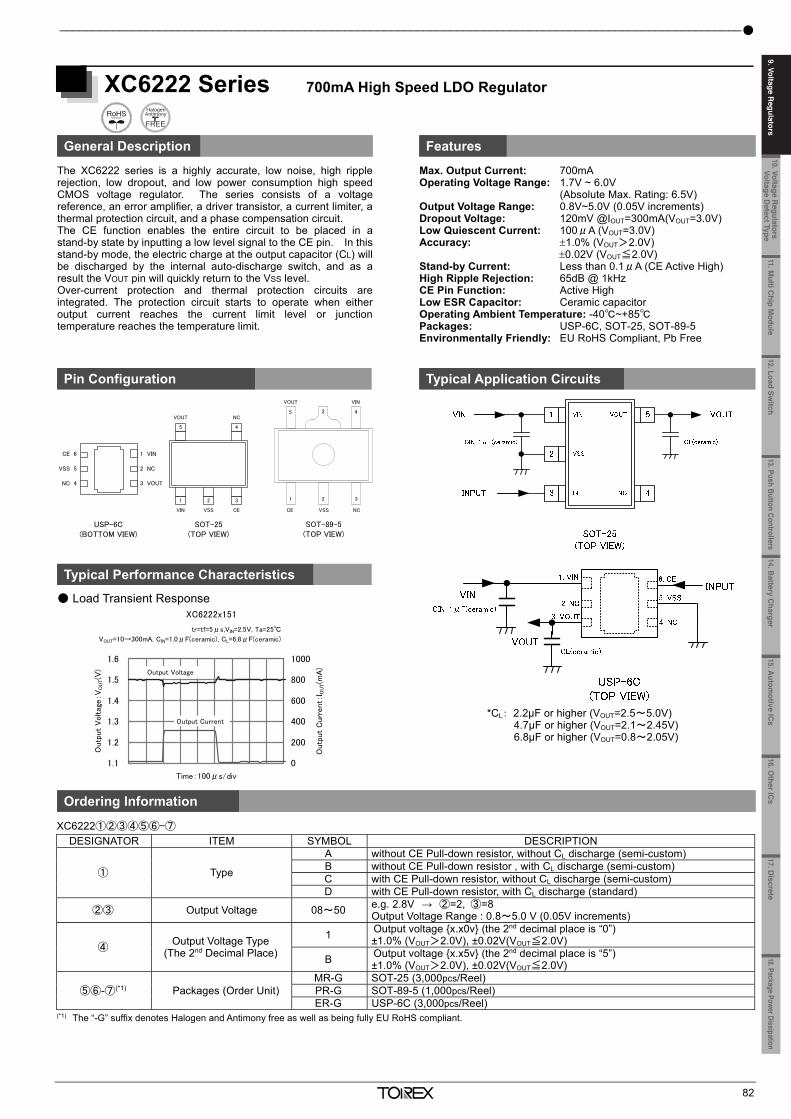
9. Voltage Regulators Single Type_______________________________________________________________
81
XC6223 Series 300mA High Speed LDO Voltage Regulator with Built-in Inrush Current Protection
General Description Features The XC6223 series is a high speed LDO regulator that features high accurate, low noise, high ripple rejection, low dropout and low power consumption. The series consists of a voltage reference, an error amplifier, a driver transistor, a current limiter, a phase compensation circuit, a thermal shutdown circuit and an inrush current protection circuit. The CE function enables the circuit to be in stand-by mode by inputting low level signal. In the stand-by mode, the series enables the electric charge at the output capacitor CL to be discharged via the internal switch, and as a result the VOUT pin quickly returns to the VSS level. The output stabilization capacitor CL is also compatible with low ESR ceramic capacitors. The output voltage is selectable in 0.05V increments within the range of 1.2V to 4.0V which fixed by laser trimming technologies. The over current protection circuit and the thermal shutdown circuit are built-in. These two protection circuits will operate when the output current reaches current limit level or the junction temperature reaches temperature limit level.
Max. Output Current: 300mA Output Voltage Range: 1.2V~4.0V (0.05V increments) Dropout Voltage: 200mV@IOUT=300mA (VOUT=3.0V) Low Quiescent Current: 100μA Accuracy: 1% (2.0V~4.0V) 20mV (1.2V~1.95V) Input Voltage Range: 1.6~5.5V
(Absolute Max. Rating: 7.0V) Stand-by Current: 0.1μA High Ripple Rejection: 80dB@f=1kHz Protection Circuits: Current Limit (400mA) Short Circuit Protection Thermal Shutdown Inrush Current Protection Low ESR Capacitors: CIN =1.0μF, CL=1.0μF CE Function: Active High, CL High Speed Discharge Operating Ambient Temperature: - 40~ +85 (A/B/C/D/E/F/G/H)
- 40~ +105 (J/K/M/N/P/Q/R/T) Packages: USPQ-4B03, SSOT-24, SOT-25, SOT-89-5, USP-4 Environmentally Friendly: EU RoHS Compliant, Pb Free
XC6223①②③④⑤⑥-⑦ DESIGNATOR ITEM SYMBOL DESCRIPTION
① Type
Inrush Current Protection CE Pull-Down Resistor CL Discharge A/J* NO NO NO B/K* NO NO YES C/M* NO YES (1MΩ, TYP built-in) NO D/N NO YES (1MΩ, TYP built-in) YES E/P* YES NO NO F/Q* YES NO YES G/R* YES YES (1MΩ, TYP built-in) NO H/T
(The Recommended Type) YES YES (1MΩ, TYP built-in) YES
②③ Output Voltage 12~40 ex.) 2.80V →②=2, ③=8, ④=please see down below.
④ Output Voltage Accuracy
1 ±1% (VOUT≧2.0V), ±0.02V (VOUT<2.0V) In case the 2nd decimal place of output voltage is “0” → ex.) 2.80V
B ±1% (VOUT≧2.0V), ±0.02V (VOUT<2.0V) In case the 2nd decimal place of output voltage is “5” → ex.) 2.85V
⑤⑥-⑦(*1) Packages (Order Unit)
9R-G USPQ-4B03 (5,000pcs/Reel) NR-G SSOT-24 (3,000pcs/Reel) MR-G SOT-25 (3,000pcs/Reel) PR-G SOT-89-5 (1,000pcs/Reel) GR-G USP-4 (3,000pcs/Reel)
(*1) The “-G” suffix denotes Halogen and Antimony free as well as being fully EU RoHS compliant. * semi-custom
Pin Configuration
Typical Application Circuit
Typical Performance Characteristics
Ordering Information
tr = tf = 0.5μs, Ta = 25, IOUT = 1⇔150mA
VIN = 3.5V, CIN = 1μF (ceramic), CL = 1μF (ceramic)
XC6223x251
2.20
2.25
2.30
2.35
2.40
2.45
2.50
2.55
2.60
Time [20μs/div]
Outp
ut
Voltag
e: V
OU
T [
V]
0
50
100
150
200
250
300
350
400
Outp
ut
Curr
ent
Iout[
mA
]
Output Voltage
Output Current
1 32
5 4
VIN
VOUT
VSS
SOT-25(TOP VIEW)
CE
N.C.
1 2 3
45 2
N.C. VSS CE
VOUT VIN
SOT-89-5(TOP VIEW)
_______________________________________________________________________________________________________
82
XC6222 Series 700mA High Speed LDO Regulator
General Description Features
The XC6222 series is a highly accurate, low noise, high ripplerejection, low dropout, and low power consumption high speedCMOS voltage regulator. The series consists of a voltagereference, an error amplifier, a driver transistor, a current limiter, athermal protection circuit, and a phase compensation circuit. The CE function enables the entire circuit to be placed in astand-by state by inputting a low level signal to the CE pin. In thisstand-by mode, the electric charge at the output capacitor (CL) will be discharged by the internal auto-discharge switch, and as aresult the VOUT pin will quickly return to the VSS level. Over-current protection and thermal protection circuits areintegrated. The protection circuit starts to operate when eitheroutput current reaches the current limit level or junctiontemperature reaches the temperature limit.
Max. Output Current: 700mA Operating Voltage Range: 1.7V ~ 6.0V
(Absolute Max. Rating: 6.5V) Output Voltage Range: 0.8V~5.0V (0.05V increments) Dropout Voltage: 120mV @IOUT=300mA(VOUT=3.0V) Low Quiescent Current: 100μA (VOUT=3.0V) Accuracy: 1.0% (VOUT>2.0V) 0.02V (VOUT≦2.0V) Stand-by Current: Less than 0.1μA (CE Active High) High Ripple Rejection: 65dB @ 1kHz CE Pin Function: Active High Low ESR Capacitor: Ceramic capacitor Operating Ambient Temperature: -40~+85 Packages: USP-6C, SOT-25, SOT-89-5 Environmentally Friendly: EU RoHS Compliant, Pb Free
Pin Configuration Typical Application Circuits
Typical Performance Characteristics
Load Transient Response
Ordering Information
XC6222①②③④⑤⑥-⑦
DESIGNATOR ITEM SYMBOL DESCRIPTION
① Type
A without CE Pull-down resistor, without CL discharge (semi-custom) B without CE Pull-down resistor , with CL discharge (semi-custom) C with CE Pull-down resistor, without CL discharge (semi-custom) D with CE Pull-down resistor, with CL discharge (standard)
②③ Output Voltage 08~50 e.g. 2.8V → ②=2, ③=8 Output Voltage Range : 0.8~5.0 V (0.05V increments)
④ Output Voltage Type (The 2nd Decimal Place)
1 Output voltage x.x0v (the 2nd decimal place is “0”) ±1.0% (VOUT>2.0V), ±0.02V(VOUT≦2.0V)
B Output voltage x.x5v (the 2nd decimal place is “5”) ±1.0% (VOUT>2.0V), ±0.02V(VOUT≦2.0V)
⑤⑥-⑦(*1) Packages (Order Unit) MR-G SOT-25 (3,000pcs/Reel) PR-G SOT-89-5 (1,000pcs/Reel) ER-G USP-6C (3,000pcs/Reel)
(*1) The “-G” suffix denotes Halogen and Antimony free as well as being fully EU RoHS compliant.
5 4
1 32
VIN VSS CE
VOUT NC
SOT-25(TOP VIEW)
1 VIN
2 NC
3 VOUT
CE 6
VSS 5
NC 4
USP-6C(BOTTOM VIEW)
SOT-89-5(TOP VIEW)
1 2 3
45 2
VOUT VIN
VSSCE NC
*CL: 2.2μF or higher (VOUT=2.5~5.0V) 4.7μF or higher (VOUT=2.1~2.45V) 6.8μF or higher (VOUT=0.8~2.05V)
XC6222x151
1.1
1.2
1.3
1.4
1.5
1.6
Time:100μs/div
Outp
ut
Voltag
e:V
OU
T(V
)
0
200
400
600
800
1000
Outp
ut
Curr
ent:
I OU
T(m
A)
tr=tf=5μs,VIN=2.5V, Ta=25
VOUT=10→300mA, CIN=1.0μF(ceramic), CL=6.8μF(ceramic)
Output Current
Output Voltage
11.Multi C
hip Module
10. Voltage Regulators
Voltage Detect Type
12.Load Switch
13. Push Button Controllers14.B
attery Charger
15.Autom
otive ICs
16.Other IC
s17. D
iscrete18.Package Power Dissipation
9. Voltage Regulators
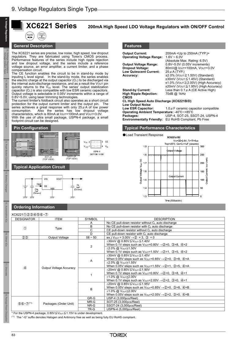
9. Voltage Regulators Single Type_______________________________________________________________
83
XC6221 Series 200mA High Speed LDO Voltage Regulators with ON/OFF Control
General Description Features
The XC6221 series are precise, low noise, high speed, low dropoutregulators. They are fabricated using Torex’s CMOS process.Performance features of the series include high ripple rejectionand low dropout voltage, and the series include a referencevoltage source, an error amplifier, a current limiter, and a phasecompensation circuit. The CE function enables the circuit to be in stand-by mode byinputing L level signal. In the stand-by mode, the series enablesthe electric charge at the output capacitor (CL) to be discharged viathe internal auto-discharge resistance, and as a result the VOUT pin quickly returns to the VSS level. The series' output stabilizationcapacitor (CL) is also compatible with low ESR ceramic capacitors.Output voltage is selectable in 0.05V increments within a range of0.8V~5.0V, using laser trimming technologies. The current limiter's foldback circuit also operates as a short circuitprotection for the output current limiter and the output pin. Theseries achieves a great response with only 25μA of low powerconsumption. Also the series has low dropout voltagecharacteristics, which is 80mA at IOUT=100mA and VOUT=3.0V. With the use of ultra small package, USPN-4 package, a smallfootprint circuit can be designed.
Output Current: 200mA <Up to 250mA (TYP.)> Operating Voltage Range: 1.6V ~ 6.0V (Absolute Max. Rating: 6.5V) Output Voltage Range: 0.8V~5.0V (0.05V increments) Dropout Voltage: 80mV@ IOUT=100mA, VOUT=3.0V Low Quiescent Current: 25μA (TYP.) Accuracy: ±2.0% (VOUT≧1.50V) (Standard) ±30mV (VOUT≦1.45V) (Standard) ±1.0% (VOUT≧2.00V) (High Accuracy) ±20mV (VOUT≦1.95V) (High Accuracy) Stand-by Current: Less than 0.1μA (CE Active High) High Ripple Rejection: 70dB @ 1kHz CMOS CL High Speed Auto Discharge (XC6221B/D) Low Output Noise Low ESR Capacitor: 1.0μF ceramic capacitor compatible Operating Ambient Temperature: -40~+85 Packages: USP-4, SOT-25, SSOT-24, USPN-4 Environmentally Friendly: EU RoHS Compliant, Pb Free
Pin Configuration Typical Performance Characteristics
Load Transient Response
Typical Application Circuit
Ordering Information
XC6221①②③④⑤⑥-⑦ DESIGNATOR ITEM SYMBOL DESCRIPTION
① Type
A No CE pull-down resistor without CL auto discharge B No CE pull-down resistor with CL auto discharge C CE pull-down resistor without CL auto discharge D CE pull-down resistor with CL auto discharge
②③ Output Voltage 08 ~ 50 ex.) VOUT = 3.00V →② = 3, ③ = 0
④ Output Voltage Accuracy
2
30mV @ 0.80V≦VOUT≦1.40V When 0.1V steps such as VOUT=0.80V →②=0, ③=8, ④=2 2.0% @ VOUT>1.50V When 0.1V steps such as VOUT=1.50V →②=1, ③=5, ④=2
A
30mV @ 0.85V≦VOUT≦1.45V When 0.05V steps such as VOUT=0.85V →②=0, ③=8, ④=A 2.0% @ VOUT>1.55V When 0.05V steps such as VOUT=1.55V →②=1, ③=5, ④=A
1
20mV @ 0.80V≦VOUT≦1.90V When 0.1V steps such as VOUT=0.80V →②=0, ③=8, ④=1 1.0% @ VOUT>2.00V When 0.1V steps such as VOUT=2.00V →②=2, ③=0, ④=1
B
20mV @ 0.85V≦VOUT≦1.95V When 0.05V steps such as VOUT=0.85V →②=0, ③=8, ④=B 1.0% @ VOUT>2.00V When 0.05V steps such as VOUT=2.05V →②=2, ③=0, ④=B
⑤⑥-⑦(*1) Packages (Order Unit)
GR-G USP-4 (3,000pcs/Reel) MR-G SOT-25 (3,000pcs/Reel) NR-G SSOT-24 (3,000pcs/Reel) 7R-G USPN-4 (5,000pcs/Reel)
* For the USPN-4 package, 0.80V≦VOUT≦1.15V is under development. (*1) The “-G” suffix denotes Halogen and Antimony free as well as being fully EU RoHS compliant.
SOT-25 (TOP VIEW)
SSOT-24 (TOP VIEW)
USP-4 (BOTTOM VIEW)
2VSS
VOUT1
3 CE
4 VIN
USPN-4 (BOTTOM VIEW)
_______________________________________________________________________________________________________
84
XC6220 Series 1A High Speed LDO Voltage Regulator with “GreenOperation”
General Description Features
The XC6220 series is a highly accurate, low noise, high speed, low dropout,and large current CMOS voltage regulator with GreenOperation function.The series consists of a voltage reference, an error amplifier, a currentlimiter, an inrush current prevention circuit and a phase compensation circuitplus a driver transistor. With a 0.2Ω on-resistance driver transistor integrated and with outputcurrents up to 1A, the ultra low dropout voltage performance greatly extendsbattery life as does the GreenOperation function which can switch betweenhigh speed and power save modes automatically. Low ESR ceramiccapacitors can be used for the output stabilization capacitor (CL). Output voltage is selectable in 0.05V increments within the range of0.8V~5.0V, using laser trimming technologies. An over current protection circuit and a thermal shutdown circuit are built in.The over current protection circuit will operate when the output currentreaches its limit current. The thermal shutdown circuit will operate when thejunction temperature reaches its limit temperature. The inrush protectioncircuit works by controlling the inrush current which is charged to CL whenthe IC starts up. In this way, any fluctuations to VIN caused by inrush currentduring system start up can be minimized. The CE function enables the output to be turned off and the IC becomes astand-by mode resulting in greatly reduced power consumption.
Max. Output Current: 1000mA (1.2V≦VOUT≦5.0V) Operating Voltage Range: 1.6V ~ 6.0V
(Absolute Max. Rating: 6.5V) Output Voltage Range: 0.8V ~ 5.0V (0.05V increments) Dropout Voltage: 20mV @ 100mA (VOUT=3.0V) 60mV@ 300mA (VOUT=3.0V) Low Quiescent Current: 8μA (TYP.) in PS mode 50μA (TYP.) in HS mode Accuracy: ±1.0% (VOUT≧2.0V) ±20mV (VOUT<2.0V) Thermal Shutdown: Detect 150, Release 135(TYP.) Inrush Current Protection: 700mA (MAX.) CL Auto Discharge: XC6220B/D Series CE Pull-down Resistor: XC6220C/D Series Output Capacitor: Ceramic Capacitor Compatible Operating Ambient Temperature: - 40~ +85 Packages: USP-6C, SOT-25, SOT-89-5, SOP-8FD Environmentally Friendly: EU RoHS Compliant, Pb Free
Pin Configuration
Typical Application Circuit Typical Performance Characteristics
Ordering Information
XC6220①②③④⑤⑥-⑦
DESIGNATOR ITEM SYMBOL DESCRIPTION
① Type
A without CE Pull-down resistor, without CL discharge (Semi-custom) B without CE Pull-down resistor, with CL discharge (Standard) C with CE Pull-down resistor, without CL discharge (Semi-custom) D with CE Pull-down resistor, with CL discharge (Semi-custom)
②③ Output Voltage 08~50 e.g. 3.0V → ①=3, ②=0
④ Output Voltage Type (The 2nd Decimal Place)
1 Output voltage .0v (the 2nd decimal place is “0”) B Output voltage .5v (the 2nd decimal place is “5”)
⑤⑥-⑦(*1) Packages (Order Unit)
MR-G SOT-25 (3,000pcs/Reel) PR-G SOT-89-5 (1,000pcs/Reel) ER-G USP-6C (3,000pcs/Reel) QR-G SOP-8FD(1,000pcs/Reel)
(*1) The “-G” suffix denotes Halogen and Antimony free as well as being fully EU RoHS compliant.
XC6220x181
0
100
200
300
400
500
0 200 400 600 800 1000
Output Current: IOUT (mA)
Dro
pout
Voltag
e: V
dif (m
V) Topr=25
Topr=-40
Topr=85
CE=VIN, CIN=CL=10μF (ceramic)
SOP-8FD
(TOP VIEW)
11.Multi C
hip Module
10. Voltage Regulators
Voltage Detect Type
9. Voltage Regulators
12.Load Switch
13. Push Button Controllers14.B
attery Charger
15.Autom
otive ICs
16.Other IC
s17. D
iscrete18.Package Power Dissipation
9. Voltage Regulators
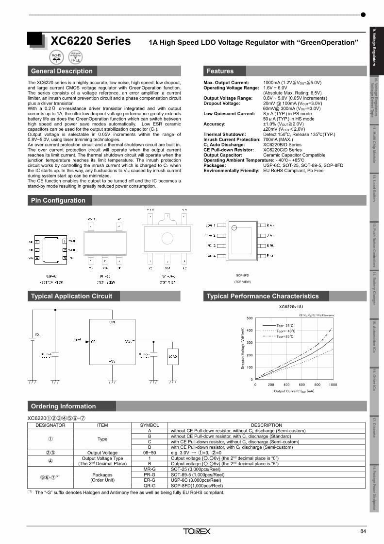
9. Voltage Regulators Single Type_______________________________________________________________
83
XC6221 Series 200mA High Speed LDO Voltage Regulators with ON/OFF Control
General Description Features
The XC6221 series are precise, low noise, high speed, low dropoutregulators. They are fabricated using Torex’s CMOS process.Performance features of the series include high ripple rejectionand low dropout voltage, and the series include a referencevoltage source, an error amplifier, a current limiter, and a phasecompensation circuit. The CE function enables the circuit to be in stand-by mode byinputing L level signal. In the stand-by mode, the series enablesthe electric charge at the output capacitor (CL) to be discharged viathe internal auto-discharge resistance, and as a result the VOUT pin quickly returns to the VSS level. The series' output stabilizationcapacitor (CL) is also compatible with low ESR ceramic capacitors.Output voltage is selectable in 0.05V increments within a range of0.8V~5.0V, using laser trimming technologies. The current limiter's foldback circuit also operates as a short circuitprotection for the output current limiter and the output pin. Theseries achieves a great response with only 25μA of low powerconsumption. Also the series has low dropout voltagecharacteristics, which is 80mA at IOUT=100mA and VOUT=3.0V. With the use of ultra small package, USPN-4 package, a smallfootprint circuit can be designed.
Output Current: 200mA <Up to 250mA (TYP.)> Operating Voltage Range: 1.6V ~ 6.0V (Absolute Max. Rating: 6.5V) Output Voltage Range: 0.8V~5.0V (0.05V increments) Dropout Voltage: 80mV@ IOUT=100mA, VOUT=3.0V Low Quiescent Current: 25μA (TYP.) Accuracy: ±2.0% (VOUT≧1.50V) (Standard) ±30mV (VOUT≦1.45V) (Standard) ±1.0% (VOUT≧2.00V) (High Accuracy) ±20mV (VOUT≦1.95V) (High Accuracy) Stand-by Current: Less than 0.1μA (CE Active High) High Ripple Rejection: 70dB @ 1kHz CMOS CL High Speed Auto Discharge (XC6221B/D) Low Output Noise Low ESR Capacitor: 1.0μF ceramic capacitor compatible Operating Ambient Temperature: -40~+85 Packages: USP-4, SOT-25, SSOT-24, USPN-4 Environmentally Friendly: EU RoHS Compliant, Pb Free
Pin Configuration Typical Performance Characteristics
Load Transient Response
Typical Application Circuit
Ordering Information
XC6221①②③④⑤⑥-⑦ DESIGNATOR ITEM SYMBOL DESCRIPTION
① Type
A No CE pull-down resistor without CL auto discharge B No CE pull-down resistor with CL auto discharge C CE pull-down resistor without CL auto discharge D CE pull-down resistor with CL auto discharge
②③ Output Voltage 08 ~ 50 ex.) VOUT = 3.00V →② = 3, ③ = 0
④ Output Voltage Accuracy
2
30mV @ 0.80V≦VOUT≦1.40V When 0.1V steps such as VOUT=0.80V →②=0, ③=8, ④=2 2.0% @ VOUT>1.50V When 0.1V steps such as VOUT=1.50V →②=1, ③=5, ④=2
A
30mV @ 0.85V≦VOUT≦1.45V When 0.05V steps such as VOUT=0.85V →②=0, ③=8, ④=A 2.0% @ VOUT>1.55V When 0.05V steps such as VOUT=1.55V →②=1, ③=5, ④=A
1
20mV @ 0.80V≦VOUT≦1.90V When 0.1V steps such as VOUT=0.80V →②=0, ③=8, ④=1 1.0% @ VOUT>2.00V When 0.1V steps such as VOUT=2.00V →②=2, ③=0, ④=1
B
20mV @ 0.85V≦VOUT≦1.95V When 0.05V steps such as VOUT=0.85V →②=0, ③=8, ④=B 1.0% @ VOUT>2.00V When 0.05V steps such as VOUT=2.05V →②=2, ③=0, ④=B
⑤⑥-⑦(*1) Packages (Order Unit)
GR-G USP-4 (3,000pcs/Reel) MR-G SOT-25 (3,000pcs/Reel) NR-G SSOT-24 (3,000pcs/Reel) 7R-G USPN-4 (5,000pcs/Reel)
* For the USPN-4 package, 0.80V≦VOUT≦1.15V is under development. (*1) The “-G” suffix denotes Halogen and Antimony free as well as being fully EU RoHS compliant.
SOT-25 (TOP VIEW)
SSOT-24 (TOP VIEW)
USP-4 (BOTTOM VIEW)
2VSS
VOUT1
3 CE
4 VIN
USPN-4 (BOTTOM VIEW)
_______________________________________________________________________________________________________
84
XC6220 Series 1A High Speed LDO Voltage Regulator with “GreenOperation”
General Description Features
The XC6220 series is a highly accurate, low noise, high speed, low dropout,and large current CMOS voltage regulator with GreenOperation function.The series consists of a voltage reference, an error amplifier, a currentlimiter, an inrush current prevention circuit and a phase compensation circuitplus a driver transistor. With a 0.2Ω on-resistance driver transistor integrated and with outputcurrents up to 1A, the ultra low dropout voltage performance greatly extendsbattery life as does the GreenOperation function which can switch betweenhigh speed and power save modes automatically. Low ESR ceramiccapacitors can be used for the output stabilization capacitor (CL). Output voltage is selectable in 0.05V increments within the range of0.8V~5.0V, using laser trimming technologies. An over current protection circuit and a thermal shutdown circuit are built in.The over current protection circuit will operate when the output currentreaches its limit current. The thermal shutdown circuit will operate when thejunction temperature reaches its limit temperature. The inrush protectioncircuit works by controlling the inrush current which is charged to CL whenthe IC starts up. In this way, any fluctuations to VIN caused by inrush currentduring system start up can be minimized. The CE function enables the output to be turned off and the IC becomes astand-by mode resulting in greatly reduced power consumption.
Max. Output Current: 1000mA (1.2V≦VOUT≦5.0V) Operating Voltage Range: 1.6V ~ 6.0V
(Absolute Max. Rating: 6.5V) Output Voltage Range: 0.8V ~ 5.0V (0.05V increments) Dropout Voltage: 20mV @ 100mA (VOUT=3.0V) 60mV@ 300mA (VOUT=3.0V) Low Quiescent Current: 8μA (TYP.) in PS mode 50μA (TYP.) in HS mode Accuracy: ±1.0% (VOUT≧2.0V) ±20mV (VOUT<2.0V) Thermal Shutdown: Detect 150, Release 135(TYP.) Inrush Current Protection: 700mA (MAX.) CL Auto Discharge: XC6220B/D Series CE Pull-down Resistor: XC6220C/D Series Output Capacitor: Ceramic Capacitor Compatible Operating Ambient Temperature: - 40~ +85 Packages: USP-6C, SOT-25, SOT-89-5, SOP-8FD Environmentally Friendly: EU RoHS Compliant, Pb Free
Pin Configuration
Typical Application Circuit Typical Performance Characteristics
Ordering Information
XC6220①②③④⑤⑥-⑦
DESIGNATOR ITEM SYMBOL DESCRIPTION
① Type
A without CE Pull-down resistor, without CL discharge (Semi-custom) B without CE Pull-down resistor, with CL discharge (Standard) C with CE Pull-down resistor, without CL discharge (Semi-custom) D with CE Pull-down resistor, with CL discharge (Semi-custom)
②③ Output Voltage 08~50 e.g. 3.0V → ①=3, ②=0
④ Output Voltage Type (The 2nd Decimal Place)
1 Output voltage .0v (the 2nd decimal place is “0”) B Output voltage .5v (the 2nd decimal place is “5”)
⑤⑥-⑦(*1) Packages (Order Unit)
MR-G SOT-25 (3,000pcs/Reel) PR-G SOT-89-5 (1,000pcs/Reel) ER-G USP-6C (3,000pcs/Reel) QR-G SOP-8FD(1,000pcs/Reel)
(*1) The “-G” suffix denotes Halogen and Antimony free as well as being fully EU RoHS compliant.
XC6220x181
0
100
200
300
400
500
0 200 400 600 800 1000
Output Current: IOUT (mA)
Dro
pout
Voltag
e: V
dif (m
V) Topr=25
Topr=-40
Topr=85
CE=VIN, CIN=CL=10μF (ceramic)
SOP-8FD
(TOP VIEW)
11.Multi C
hip Module
10. Voltage Regulators
Voltage Detect Type
12.Load Switch
13. Push Button Controllers14.B
attery Charger
15.Autom
otive ICs
16.Other IC
s17. D
iscrete18.Package Power Dissipation
9. Voltage Regulators
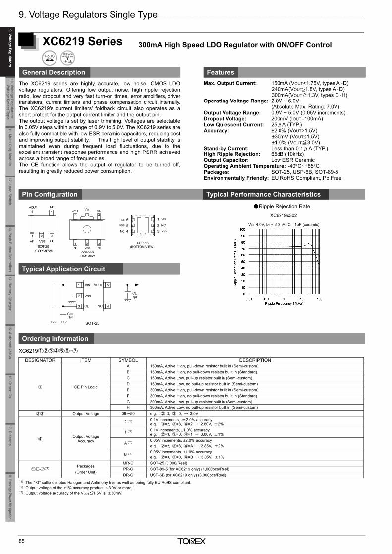
9. Voltage Regulators Single Type_______________________________________________________________
85
5 4
1 2 3
VOUT
CEVSSNC
VIN
SOT-89-5 (TOP VIEW)
SOT-25 (TOP VIEW)
45
1 2 3
VSS
NC
CEVIN
VOUT
XC6219 Series 300mA High Speed LDO Regulator with ON/OFF Control
General Description Features The XC6219 series are highly accurate, low noise, CMOS LDO voltage regulators. Offering low output noise, high ripple rejection ratio, low dropout and very fast turn-on times, error amplifiers, driver transistors, current limiters and phase compensation circuit internally. The XC6219's current limiters' foldback circuit also operates as a short protect for the output current limiter and the output pin. The output voltage is set by laser trimming. Voltages are selectable in 0.05V steps within a range of 0.9V to 5.0V. The XC6219 series are also fully compatible with low ESR ceramic capacitors, reducing cost and improving output stability. This high level of output stability is maintained even during frequent load fluctuations, due to the excellent transient response performance and high PSRR achieved across a broad range of frequencies. The CE function allows the output of regulator to be turned off, resulting in greatly reduced power consumption.
Max. Output Current: 150mA (VOUT<1.75V, types A~D) 240mA(VOUT1.8V, types A~D) 300mA(VOUT≧1.3V, types E~H)
Operating Voltage Range: 2.0V ~ 6.0V (Absolute Max. Rating: 7.0V) Output Voltage Range: 0.9V ~ 5.0V (0.05V increments) Dropout Voltage: 200mV (IOUT=100mA) Low Quiescent Current: 25μA (TYP.) Accuracy: ±2.0% (VOUT>1.5V)
±30mV (VOUT1.5V) ±1.0% (VOUT≦3.0V)
Stand-by Current: Less than 0.1μA (TYP.) High Ripple Rejection: 65dB (10kHz) Output Capacitor: Low ESR Ceramic Operating Ambient Temperature: -40C~+85C Packages: SOT-25, USP-6B, SOT-89-5 Environmentally Friendly: EU RoHS Compliant, Pb Free
XC6219①②③④⑤⑥-⑦
DESIGNATOR ITEM SYMBOL DESCRIPTION
① CE Pin Logic
A 150mA, Active High, pull-down resistor built in (Semi-custom) B 150mA, Active High, no pull-down resistor built in (Standard) C 150mA, Active Low, pull-up resistor built in (Semi-custom) D 150mA, Active Low, no pull-up resistor built in (Semi-custom) E 300mA, Active High, pull-down resistor built in (Semi-custom) F 300mA, Active High, no pull-down resistor built in (Standard) G 300mA, Active Low, pull-up resistor built in (Semi-custom) H 300mA, Active Low, no pull-up resistor built in (Semi-custom)
②③ Output Voltage 09~50 e.g. ②=3, ③=0, → 3.0V
④ Output Voltage Accuracy
2 (*3) 0.1V increments, ±2.0% accuracy e.g. ③=2, ③=8, ④=2 → 2.80V, ±2%
1 (*2) 0.1V increments, ±1.0% accuracy e.g. ②=3, ③=0, ④=1 → 3.00V, ±1%
A (*3) 0.05V increments, ±2.0% accuracy e.g. ②=2, ③=8, ④=A → 2.85V, ±2%
B (*2) 0.05V increments, ±1.0% accuracy e.g. ②=3, ③=0, ④=B → 3.05V, ±1%
⑤⑥-⑦(*1) Packages
(Order Unit)
MR-G SOT-25 (3,000/Reel) PR-G SOT-89-5 (for XC6219 only) (1,000pcs/Reel) DR-G USP-6B (for XC6219 only) (3,000pcs/Reel)
(*1) The “-G” suffix denotes Halogen and Antimony free as well as being fully EU RoHS compliant. (*2) Output voltage of the ±1% accuracy product is 3.0V or more. (*3) Output voltage accuracy of the VOUT≦1.5V is ±30mV.
Pin Configuration Typical Performance Characteristics
Typical Application Circuit
Ordering Information
1
234
56
VOUT
VSS
CE VIN
NC
NC
USP-6B(BOTTOM VIEW)
VSS
1
2
3 4
5VIN VOUT
CE NC
CIN1F
CL1F
XC6219x302
Ripple Rejection Rate
SOT-25
VSS
VIN=4.0V, IOUT=50mA, CL=1μF (ceramic)
_______________________________________________________________________________________________________
86
XC6218 Series 200mA Low Power Consumption LDO Regulators
General Description Features
XC6218 series are highly precise, low noise, positive voltage LDOregulators manufactured using CMOS processes. The seriesachieves very low quiescent current, 1.0μA (TYP.) and consists ofa reference voltage source, an error amplifier, current limit circuit,and a phase compensation circuit plus a driver transistor. Small USP-3 and SSOT-24 packages make high density mountingpossible. Therefore, the series is ideal for applications wherehigh density mounting is required such as in mobile phones. Output voltage is selectable in 0.1V increments within a range of0.9V~4.0V by laser trimming. The series is also compatible withlow ESR ceramic capacitors (CL), which give added outputstability. The current limiter’s fold-back circuit also operates as a shortprotect for the output current limiter and the output pin.
Max. Output Current: 200mA (300mA Limit: TYP.) (@VOUT=3.0V, VIN=4.0V)
Operating Voltage Range: 1.5V ~ 6.0V (Absolute Max. Rating: 7.0V) Output Voltage: 0.9 ~ 4.0V (0.1V increments) Dropout Voltage: 200mV@IOUT=100mA
(@VOUT=3.0V) Low Quiescent Current: 1.0μA (TYP.) Accuracy: ±2.0%
(1.5<VOUT≦4.0V) ±30mV (0.9≦VOUT≦1.5V)
External Capacitor: 0.1μF~1.0μF Current Limit Circuit Built-in Output Capacitor: Low ESR Ceramic Operating Ambient Temperature: -40~85 Packages: USP-3, SSOT-24 Environmentally Friendly: EU RoHS Compliant, Pb Free
Pin Configuration
Typical Application Circuit Typical Performance Characteristics Supply Current vs. Input Voltage
Ordering Information
XC6218P①②③④⑤-⑥ DESIGNATOR ITEM SYMBOL DESCRIPTION
①② Output Voltage 09~40
Output voltage “②” represents value after the decimal point. Ex.) 15 ⇒ ①:1, ②: 5 = 1.5V 33 ⇒ ①:3, ②: 3 = 3.3V
③ Output Voltage Accuracy 2 ±2.0%
④⑤-⑥(*1) Packages (Order Unit) HR-G USP-3 (3,000pcs/Reel) NR-G SSOT-24 (3,000pcs/Reel)
(*1) The “-G” suffix denotes Halogen and Antimony free as well as being fully EU RoHS compliant.
11.Multi C
hip Module
10. Voltage Regulators
Voltage Detect Type
9. Voltage Regulators
12.Load Switch
13. Push Button Controllers14.B
attery Charger
15.Autom
otive ICs
16.Other IC
s17. D
iscrete18.Package Power Dissipation
9. Voltage Regulators
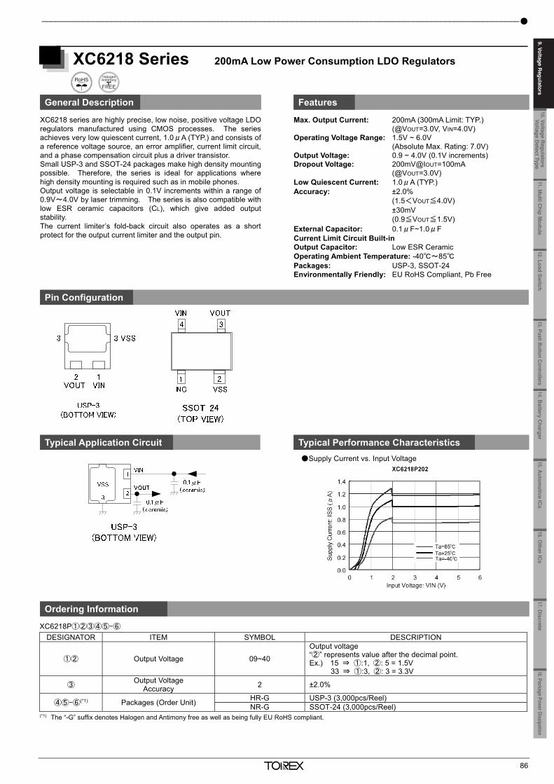
9. Voltage Regulators Single Type_______________________________________________________________
85
5 4
1 2 3
VOUT
CEVSSNC
VIN
SOT-89-5 (TOP VIEW)
SOT-25 (TOP VIEW)
45
1 2 3
VSS
NC
CEVIN
VOUT
XC6219 Series 300mA High Speed LDO Regulator with ON/OFF Control
General Description Features The XC6219 series are highly accurate, low noise, CMOS LDO voltage regulators. Offering low output noise, high ripple rejection ratio, low dropout and very fast turn-on times, error amplifiers, driver transistors, current limiters and phase compensation circuit internally. The XC6219's current limiters' foldback circuit also operates as a short protect for the output current limiter and the output pin. The output voltage is set by laser trimming. Voltages are selectable in 0.05V steps within a range of 0.9V to 5.0V. The XC6219 series are also fully compatible with low ESR ceramic capacitors, reducing cost and improving output stability. This high level of output stability is maintained even during frequent load fluctuations, due to the excellent transient response performance and high PSRR achieved across a broad range of frequencies. The CE function allows the output of regulator to be turned off, resulting in greatly reduced power consumption.
Max. Output Current: 150mA (VOUT<1.75V, types A~D) 240mA(VOUT1.8V, types A~D) 300mA(VOUT≧1.3V, types E~H)
Operating Voltage Range: 2.0V ~ 6.0V (Absolute Max. Rating: 7.0V) Output Voltage Range: 0.9V ~ 5.0V (0.05V increments) Dropout Voltage: 200mV (IOUT=100mA) Low Quiescent Current: 25μA (TYP.) Accuracy: ±2.0% (VOUT>1.5V)
±30mV (VOUT1.5V) ±1.0% (VOUT≦3.0V)
Stand-by Current: Less than 0.1μA (TYP.) High Ripple Rejection: 65dB (10kHz) Output Capacitor: Low ESR Ceramic Operating Ambient Temperature: -40C~+85C Packages: SOT-25, USP-6B, SOT-89-5 Environmentally Friendly: EU RoHS Compliant, Pb Free
XC6219①②③④⑤⑥-⑦
DESIGNATOR ITEM SYMBOL DESCRIPTION
① CE Pin Logic
A 150mA, Active High, pull-down resistor built in (Semi-custom) B 150mA, Active High, no pull-down resistor built in (Standard) C 150mA, Active Low, pull-up resistor built in (Semi-custom) D 150mA, Active Low, no pull-up resistor built in (Semi-custom) E 300mA, Active High, pull-down resistor built in (Semi-custom) F 300mA, Active High, no pull-down resistor built in (Standard) G 300mA, Active Low, pull-up resistor built in (Semi-custom) H 300mA, Active Low, no pull-up resistor built in (Semi-custom)
②③ Output Voltage 09~50 e.g. ②=3, ③=0, → 3.0V
④ Output Voltage Accuracy
2 (*3) 0.1V increments, ±2.0% accuracy e.g. ③=2, ③=8, ④=2 → 2.80V, ±2%
1 (*2) 0.1V increments, ±1.0% accuracy e.g. ②=3, ③=0, ④=1 → 3.00V, ±1%
A (*3) 0.05V increments, ±2.0% accuracy e.g. ②=2, ③=8, ④=A → 2.85V, ±2%
B (*2) 0.05V increments, ±1.0% accuracy e.g. ②=3, ③=0, ④=B → 3.05V, ±1%
⑤⑥-⑦(*1) Packages
(Order Unit)
MR-G SOT-25 (3,000/Reel) PR-G SOT-89-5 (for XC6219 only) (1,000pcs/Reel) DR-G USP-6B (for XC6219 only) (3,000pcs/Reel)
(*1) The “-G” suffix denotes Halogen and Antimony free as well as being fully EU RoHS compliant. (*2) Output voltage of the ±1% accuracy product is 3.0V or more. (*3) Output voltage accuracy of the VOUT≦1.5V is ±30mV.
Pin Configuration Typical Performance Characteristics
Typical Application Circuit
Ordering Information
1
234
56
VOUT
VSS
CE VIN
NC
NC
USP-6B(BOTTOM VIEW)
VSS
1
2
3 4
5VIN VOUT
CE NC
CIN1F
CL1F
XC6219x302
Ripple Rejection Rate
SOT-25
VSS
VIN=4.0V, IOUT=50mA, CL=1μF (ceramic)
_______________________________________________________________________________________________________
86
XC6218 Series 200mA Low Power Consumption LDO Regulators
General Description Features
XC6218 series are highly precise, low noise, positive voltage LDOregulators manufactured using CMOS processes. The seriesachieves very low quiescent current, 1.0μA (TYP.) and consists ofa reference voltage source, an error amplifier, current limit circuit,and a phase compensation circuit plus a driver transistor. Small USP-3 and SSOT-24 packages make high density mountingpossible. Therefore, the series is ideal for applications wherehigh density mounting is required such as in mobile phones. Output voltage is selectable in 0.1V increments within a range of0.9V~4.0V by laser trimming. The series is also compatible withlow ESR ceramic capacitors (CL), which give added outputstability. The current limiter’s fold-back circuit also operates as a shortprotect for the output current limiter and the output pin.
Max. Output Current: 200mA (300mA Limit: TYP.) (@VOUT=3.0V, VIN=4.0V)
Operating Voltage Range: 1.5V ~ 6.0V (Absolute Max. Rating: 7.0V) Output Voltage: 0.9 ~ 4.0V (0.1V increments) Dropout Voltage: 200mV@IOUT=100mA
(@VOUT=3.0V) Low Quiescent Current: 1.0μA (TYP.) Accuracy: ±2.0%
(1.5<VOUT≦4.0V) ±30mV (0.9≦VOUT≦1.5V)
External Capacitor: 0.1μF~1.0μF Current Limit Circuit Built-in Output Capacitor: Low ESR Ceramic Operating Ambient Temperature: -40~85 Packages: USP-3, SSOT-24 Environmentally Friendly: EU RoHS Compliant, Pb Free
Pin Configuration
Typical Application Circuit Typical Performance Characteristics Supply Current vs. Input Voltage
Ordering Information
XC6218P①②③④⑤-⑥ DESIGNATOR ITEM SYMBOL DESCRIPTION
①② Output Voltage 09~40
Output voltage “②” represents value after the decimal point. Ex.) 15 ⇒ ①:1, ②: 5 = 1.5V 33 ⇒ ①:3, ②: 3 = 3.3V
③ Output Voltage Accuracy 2 ±2.0%
④⑤-⑥(*1) Packages (Order Unit) HR-G USP-3 (3,000pcs/Reel) NR-G SSOT-24 (3,000pcs/Reel)
(*1) The “-G” suffix denotes Halogen and Antimony free as well as being fully EU RoHS compliant.
11.Multi C
hip Module
10. Voltage Regulators
Voltage Detect Type
12.Load Switch
13. Push Button Controllers14.B
attery Charger
15.Autom
otive ICs
16.Other IC
s17. D
iscrete18.Package Power Dissipation
9. Voltage Regulators
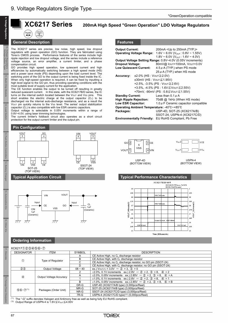
9. Voltage Regulators Single Type_______________________________________________________________
*GreenOperation-compatible
87
XC6217 Series 200mA High Speed "Green Operation" LDO Voltage Regulators
General Description Features
The XC6217 series are precise, low noise, high speed, low dropout regulators with green operation (GO) function. They are fabricated usingTorex’s CMOS process. Performance features of the series include highripple rejection and low dropout voltage, and the series include a referencevoltage source, an error amplifier, a current limiter, and a phasecompensation circuit. GO provides high speed operation, low quiescent current and high efficiencies by automatically switching between a high speed mode (HS)and a power save mode (PS) depending upon the load current level. Theswitching point of the GO to the output current is being fixed inside the IC.When only high-speed operation is required, it can be fixed by inputting ahigh level signal to the GO pin, thus providing operating conditions with themost suitable level of supply current for the application. The CE function enables the output to be turned off resulting in greatly reduced quiescent current. In this state, with the XC6217B/D series, the ICturns on the internal switch located between the VOUT and VSS pins. Thisshort enables the electric charge at the output capacitor (CL) to be discharged via the internal auto-discharge resistance, and as a result theVOUT pin quickly returns to the VSS level. The series' output stabilizationcapacitor (CL) is also compatible with low ESR ceramic capacitors. Output voltage is selectable in 0.05V increments within a range of0.8V~4.0V, using laser trimming technologies. The current limiter's foldback circuit also operates as a short circuitprotection for the output current limiter and the output pin.
Output Current: 200mA <Up to 250mA (TYP.)> Operating Voltage Range: 1.6V ~ 6.0V (VOUT : 0.8V ~ 1.55V) 1.8V ~ 6.0V (VOUT : 1.6V ~ 4.0V) Output Voltage Setting Range: 0.8V~4.0V (0.05V increments) Dropout Voltage: 80mV@ IOUT=100mA, VOUT=3.0V Low Quiescent Current: 4.5μA (TYP.) when PS mode 25μA (TYP.) when HS mode Accuracy: ±2.0% (HS : VOUT≧2.0V) ±30mV (HS : VOUT≦1.95V) +2.5%, -3.5% (PS : VOUT≧2.6V) +3.5%, -4.5% (PS : 1.6V≦VOUT≦2.55V) +70mV, -90mV (PS : 0.8≦VOUT≦1.55V) Standby Current: Less than 0.1μA High Ripple Rejection: 70dB @ 1kHz (When HS mode) Low ESR Capacitor: 1.0μF Ceramic capacitor compatible Operating Ambient Temperature: -40~+85 Packages: USP-4D, SOT-25 (XC6217A/B) SSOT-24, USPN-4 (XC6217C/D) Environmentally Friendly: EU RoHS Compliant, Pb Free
Pin Configuration
Typical Application Circuit Typical Performance Characteristics
Ordering Information
XC6217①②③④⑤⑥-⑦ DESIGNATOR ITEM SYMBOL DESCRIPTION
① Type of Regulator
A CE Active High, no CL discharge resistor B CE Active High, with CL discharge resistor C CE Active High, no CL discharge resistor, no GO pin (SSOT-24) D CE Active High, with CL discharge resistor, no GO pin (SSOT-24)
②③ Output Voltage 08 ~ 40 ex.) VOUT(T) = 3.0V → ② = 3, ③ = 0
④ Output Voltage Accuracy
2 2.0%, 0.1V increments ex.) 2.8V → ② = 2, ③ = 8, ④ = 2 A 2.0%, 0.05V increments ex.) 2.85V → ② = 2, ③ = 8, ④ = A 1 1.0%, 0.1V increments ex.) 2.8V → ② = 2, ③ = 8, ④ = 1 B 1.0%, 0.05V increments ex.) 2.85V → ② = 2, ③ = 8, ④ = B
⑤⑥-⑦(*1) Packages (Order Unit)
GR-G USP-4D (XC6217A/B type) (3,000pcs/Reel) MR-G SOT-25 (XC6217A/B type) (3,000pcs/Reel) NR-G SSOT-24 (XC6217C/D type) (3,000pcs/Reel) 7R-G USPN-4 (XC6217C/D type)(*2) (5,000pcs/Reel)
(*1) The “-G” suffix denotes Halogen and Antimony free as well as being fully EU RoHS compliant. (*2) Output Range of USPN-4 is 1.6V≦VOUT≦4.00V
1 2 3
45VOUT GO
VIN VSS CE
CIN1uF
(Ceramic)
Input InputCL1uF
(Ceramic)
VOUTVIN
CE GOVSS
SOT-25 (TOP VIEW)
SSOT-24 (TOP VIEW)
USP-4D (BOTTOM VIEW)
1
2 3
4
CE
VINVOUT
GO5
VSS
1 2
34VIN VOUT
CE VSSUSPN-4
(BOTTOM VIEW)
2 3
1 4
CEVSS
VOUT VIN
_______________________________________________________________________________________________________
88
XC6216 Series 28V Input Voltage Regulators with CE Pin
General Description Features XC6216 series are highly precise, low noise, positive regulator ICs.The series consists of a voltage reference, an error amplifier, acurrent limiter, a thermal shutdown circuit and a phase compensationcircuit plus a driver transistor. The output voltage is selectable in 0.1V increments within the rangeof 1.8V to 12V using laser trimming technologies (XC6216B series).Furthermore, with external resistors, the output voltage can be setfrom 2.0V to 23V (XC6216C series). The series’ output stabilizationcapacitor (CL) is also compatible with low ESR ceramic capacitors. The over current protection circuit and the thermal shutdown circuitare built-in. These two protection circuits will operate when theoutput current reaches current limit level or the junction temperaturereaches temperature limit level. The CE function enables the output to be turned off and the ICbecomes a stand-by mode resulting in greatly reduced quiescentcurrent.
Max. Output Current: 150mA (Up to 200mA)(VIN=VOUT+3.0V) Input Voltage Range: 2.0V~28.0V (Absolute Max. Rating: 30.0V) Output Voltage: 1.8V~12.0V (0.1V increments) Setting Range: (With external resistors: 2.0V~23.0V) Dropout Voltage: 300mV@IOUT=20mA Low Quiescent Current: 5μA Accuracy: ±2.0% (±1.0% Possible) Stand-by Current: Less than 0.1μA High Ripple Rejection: 40dB@1kHz Operating Ambient Temperature: -40~+85 Packages: SOT-25, SOT-89, SOT-89-5, USP-6C, SOT-223, TO-252,SOT-23, USP-6B06 Environmentally Friendly: EU RoHS Compliant, Pb Free
Pin Configuration
Typical Application Circuits
Ordering Information
XC6216①②③④⑤⑥-⑦: CE function (Active High) Fixed output voltage 1.8V~12.0V (0.1V increments) DESIGNATOR ITEM SYMBOL DESCRIPTION
① Type and Options of Regulators B Fixed output voltage C Output voltage externally set (VOFB=2.0V)(*3)
②③ Output Voltage 18 ~ C0
For the voltage within 1.8V ~9.9V (0.1V increments); e.g. 2.5V ⇒ 25, 5.0V ⇒ 50 For the voltage within 10.0V~12.0V (0.1V increments); e.g. 10.6V ⇒ A6, 11.2V ⇒ B2, 12.0V ⇒ C0
20 For C type (output voltage externally set), VOFB=2.0V only
④ Output Voltage Accuracy (*2) 2 ±2.0% 1 ±1.0%(*3)
⑤⑥-⑦(*1) Packages (Order Unit)
MR-G SOT-25 (3,000pcs/Reel) PR-G SOT-89-5 (1,000pcs/Reel) ER-G USP-6C (3,000pcs/Reel) 8R-G USP-6B06 (5,000pcs/Reel)
(*1) The “-G” suffix denotes Halogen and Antimony free as well as being fully EU RoHS compliant. (*2) For the C type, the accuracy is based on VOFB voltage. The actual output voltage accuracy is depended on the external resistances. (*3) USP-6B06 package is available for the A/B types and Output Voltage Accuracy ±2%. XC6216D①②③④⑤-⑥: 3 pin regulator (No CE function), Fixed output voltage 1.8V~12.0V (0.1V increments)
DESIGNATOR ITEM SYMBOL DESCRIPTION
①② Output Voltage 18 ~ C0
For the voltage within 1.8V~9.9V (0.1V increments); e.g. 2.5V ⇒ 25, 5.0V ⇒ 50 For the voltage within10.0V~12.0V (0.1V increments); e.g. 10.6V ⇒ A6, 11.2V ⇒ B2, 12.0V ⇒ C0
③ Output Voltage Accuracy 2 ±2.0% 1 ±1.0%
④⑤-⑥(*1) Packages (Order Unit)
MR-G SOT-23 (3,000pcs/Reel) PR-G SOT-89 (1,000pcs/Reel) FR-G SOT-223 (1,000pcs/Reel) JR-G TO-252 (2,500pcs/Reel)
(*1) The “-G” suffix denotes Halogen and Antimony free as well as being fully EU RoHS compliant.
VIN VOUT
VSSC E
1uFCIN CL
1uF
XC6216B/XE6216B Series (Fixed Output Voltage)
TO-252 (TOP VIEW)
VIN
USP-6B06(BOTTOM VIEW)
3
2
16
5
4
VOUT
NCVSS
CENC
USP-6B06 (BOTTOM VIEW)
XC6216C Series (Output Voltage Externally Set)
11.Multi C
hip Module
10. Voltage Regulators
Voltage Detect Type
9. Voltage Regulators
12.Load Switch
13. Push Button Controllers14.B
attery Charger
15.Autom
otive ICs
16.Other IC
s17. D
iscrete18.Package Power Dissipation
9. Voltage Regulators
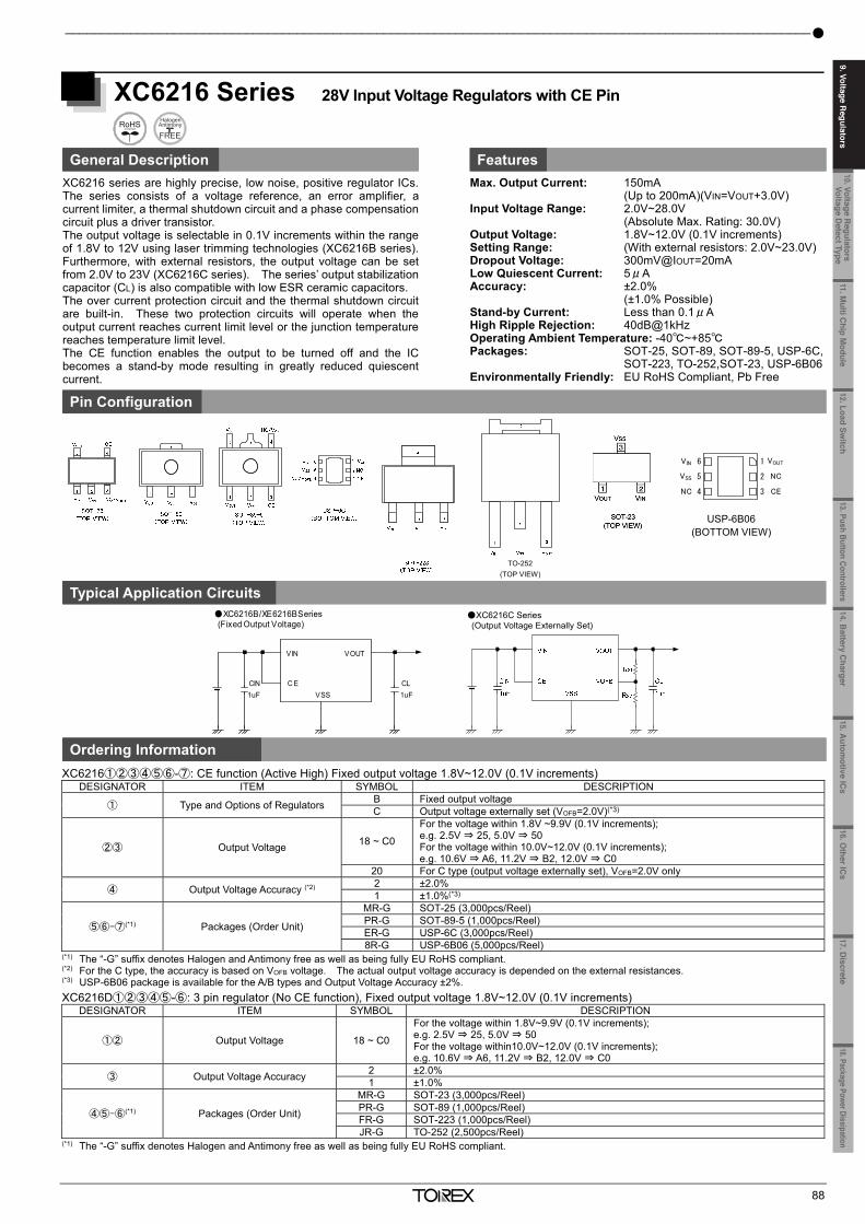
9. Voltage Regulators Single Type_______________________________________________________________
*GreenOperation-compatible
87
XC6217 Series 200mA High Speed "Green Operation" LDO Voltage Regulators
General Description Features
The XC6217 series are precise, low noise, high speed, low dropout regulators with green operation (GO) function. They are fabricated usingTorex’s CMOS process. Performance features of the series include highripple rejection and low dropout voltage, and the series include a referencevoltage source, an error amplifier, a current limiter, and a phasecompensation circuit. GO provides high speed operation, low quiescent current and high efficiencies by automatically switching between a high speed mode (HS)and a power save mode (PS) depending upon the load current level. Theswitching point of the GO to the output current is being fixed inside the IC.When only high-speed operation is required, it can be fixed by inputting ahigh level signal to the GO pin, thus providing operating conditions with themost suitable level of supply current for the application. The CE function enables the output to be turned off resulting in greatly reduced quiescent current. In this state, with the XC6217B/D series, the ICturns on the internal switch located between the VOUT and VSS pins. Thisshort enables the electric charge at the output capacitor (CL) to be discharged via the internal auto-discharge resistance, and as a result theVOUT pin quickly returns to the VSS level. The series' output stabilizationcapacitor (CL) is also compatible with low ESR ceramic capacitors. Output voltage is selectable in 0.05V increments within a range of0.8V~4.0V, using laser trimming technologies. The current limiter's foldback circuit also operates as a short circuitprotection for the output current limiter and the output pin.
Output Current: 200mA <Up to 250mA (TYP.)> Operating Voltage Range: 1.6V ~ 6.0V (VOUT : 0.8V ~ 1.55V) 1.8V ~ 6.0V (VOUT : 1.6V ~ 4.0V) Output Voltage Setting Range: 0.8V~4.0V (0.05V increments) Dropout Voltage: 80mV@ IOUT=100mA, VOUT=3.0V Low Quiescent Current: 4.5μA (TYP.) when PS mode 25μA (TYP.) when HS mode Accuracy: ±2.0% (HS : VOUT≧2.0V) ±30mV (HS : VOUT≦1.95V) +2.5%, -3.5% (PS : VOUT≧2.6V) +3.5%, -4.5% (PS : 1.6V≦VOUT≦2.55V) +70mV, -90mV (PS : 0.8≦VOUT≦1.55V) Standby Current: Less than 0.1μA High Ripple Rejection: 70dB @ 1kHz (When HS mode) Low ESR Capacitor: 1.0μF Ceramic capacitor compatible Operating Ambient Temperature: -40~+85 Packages: USP-4D, SOT-25 (XC6217A/B) SSOT-24, USPN-4 (XC6217C/D) Environmentally Friendly: EU RoHS Compliant, Pb Free
Pin Configuration
Typical Application Circuit Typical Performance Characteristics
Ordering Information
XC6217①②③④⑤⑥-⑦ DESIGNATOR ITEM SYMBOL DESCRIPTION
① Type of Regulator
A CE Active High, no CL discharge resistor B CE Active High, with CL discharge resistor C CE Active High, no CL discharge resistor, no GO pin (SSOT-24) D CE Active High, with CL discharge resistor, no GO pin (SSOT-24)
②③ Output Voltage 08 ~ 40 ex.) VOUT(T) = 3.0V → ② = 3, ③ = 0
④ Output Voltage Accuracy
2 2.0%, 0.1V increments ex.) 2.8V → ② = 2, ③ = 8, ④ = 2 A 2.0%, 0.05V increments ex.) 2.85V → ② = 2, ③ = 8, ④ = A 1 1.0%, 0.1V increments ex.) 2.8V → ② = 2, ③ = 8, ④ = 1 B 1.0%, 0.05V increments ex.) 2.85V → ② = 2, ③ = 8, ④ = B
⑤⑥-⑦(*1) Packages (Order Unit)
GR-G USP-4D (XC6217A/B type) (3,000pcs/Reel) MR-G SOT-25 (XC6217A/B type) (3,000pcs/Reel) NR-G SSOT-24 (XC6217C/D type) (3,000pcs/Reel) 7R-G USPN-4 (XC6217C/D type)(*2) (5,000pcs/Reel)
(*1) The “-G” suffix denotes Halogen and Antimony free as well as being fully EU RoHS compliant. (*2) Output Range of USPN-4 is 1.6V≦VOUT≦4.00V
1 2 3
45VOUT GO
VIN VSS CE
CIN1uF
(Ceramic)
Input InputCL1uF
(Ceramic)
VOUTVIN
CE GOVSS
SOT-25 (TOP VIEW)
SSOT-24 (TOP VIEW)
USP-4D (BOTTOM VIEW)
1
2 3
4
CE
VINVOUT
GO5
VSS
1 2
34VIN VOUT
CE VSSUSPN-4
(BOTTOM VIEW)
2 3
1 4
CEVSS
VOUT VIN
_______________________________________________________________________________________________________
88
XC6216 Series 28V Input Voltage Regulators with CE Pin
General Description Features XC6216 series are highly precise, low noise, positive regulator ICs.The series consists of a voltage reference, an error amplifier, acurrent limiter, a thermal shutdown circuit and a phase compensationcircuit plus a driver transistor. The output voltage is selectable in 0.1V increments within the rangeof 1.8V to 12V using laser trimming technologies (XC6216B series).Furthermore, with external resistors, the output voltage can be setfrom 2.0V to 23V (XC6216C series). The series’ output stabilizationcapacitor (CL) is also compatible with low ESR ceramic capacitors. The over current protection circuit and the thermal shutdown circuitare built-in. These two protection circuits will operate when theoutput current reaches current limit level or the junction temperaturereaches temperature limit level. The CE function enables the output to be turned off and the ICbecomes a stand-by mode resulting in greatly reduced quiescentcurrent.
Max. Output Current: 150mA (Up to 200mA)(VIN=VOUT+3.0V) Input Voltage Range: 2.0V~28.0V (Absolute Max. Rating: 30.0V) Output Voltage: 1.8V~12.0V (0.1V increments) Setting Range: (With external resistors: 2.0V~23.0V) Dropout Voltage: 300mV@IOUT=20mA Low Quiescent Current: 5μA Accuracy: ±2.0% (±1.0% Possible) Stand-by Current: Less than 0.1μA High Ripple Rejection: 40dB@1kHz Operating Ambient Temperature: -40~+85 Packages: SOT-25, SOT-89, SOT-89-5, USP-6C, SOT-223, TO-252,SOT-23, USP-6B06 Environmentally Friendly: EU RoHS Compliant, Pb Free
Pin Configuration
Typical Application Circuits
Ordering Information
XC6216①②③④⑤⑥-⑦: CE function (Active High) Fixed output voltage 1.8V~12.0V (0.1V increments) DESIGNATOR ITEM SYMBOL DESCRIPTION
① Type and Options of Regulators B Fixed output voltage C Output voltage externally set (VOFB=2.0V)(*3)
②③ Output Voltage 18 ~ C0
For the voltage within 1.8V ~9.9V (0.1V increments); e.g. 2.5V ⇒ 25, 5.0V ⇒ 50 For the voltage within 10.0V~12.0V (0.1V increments); e.g. 10.6V ⇒ A6, 11.2V ⇒ B2, 12.0V ⇒ C0
20 For C type (output voltage externally set), VOFB=2.0V only
④ Output Voltage Accuracy (*2) 2 ±2.0% 1 ±1.0%(*3)
⑤⑥-⑦(*1) Packages (Order Unit)
MR-G SOT-25 (3,000pcs/Reel) PR-G SOT-89-5 (1,000pcs/Reel) ER-G USP-6C (3,000pcs/Reel) 8R-G USP-6B06 (5,000pcs/Reel)
(*1) The “-G” suffix denotes Halogen and Antimony free as well as being fully EU RoHS compliant. (*2) For the C type, the accuracy is based on VOFB voltage. The actual output voltage accuracy is depended on the external resistances. (*3) USP-6B06 package is available for the A/B types and Output Voltage Accuracy ±2%. XC6216D①②③④⑤-⑥: 3 pin regulator (No CE function), Fixed output voltage 1.8V~12.0V (0.1V increments)
DESIGNATOR ITEM SYMBOL DESCRIPTION
①② Output Voltage 18 ~ C0
For the voltage within 1.8V~9.9V (0.1V increments); e.g. 2.5V ⇒ 25, 5.0V ⇒ 50 For the voltage within10.0V~12.0V (0.1V increments); e.g. 10.6V ⇒ A6, 11.2V ⇒ B2, 12.0V ⇒ C0
③ Output Voltage Accuracy 2 ±2.0% 1 ±1.0%
④⑤-⑥(*1) Packages (Order Unit)
MR-G SOT-23 (3,000pcs/Reel) PR-G SOT-89 (1,000pcs/Reel) FR-G SOT-223 (1,000pcs/Reel) JR-G TO-252 (2,500pcs/Reel)
(*1) The “-G” suffix denotes Halogen and Antimony free as well as being fully EU RoHS compliant.
VIN VOUT
VSSC E
1uFCIN CL
1uF
XC6216B/XE6216B Series (Fixed Output Voltage)
TO-252 (TOP VIEW)
VIN
USP-6B06(BOTTOM VIEW)
3
2
16
5
4
VOUT
NCVSS
CENC
USP-6B06 (BOTTOM VIEW)
XC6216C Series (Output Voltage Externally Set)
11.Multi C
hip Module
10. Voltage Regulators
Voltage Detect Type
12.Load Switch
13. Push Button Controllers14.B
attery Charger
15.Autom
otive ICs
16.Other IC
s17. D
iscrete18.Package Power Dissipation
9. Voltage Regulators
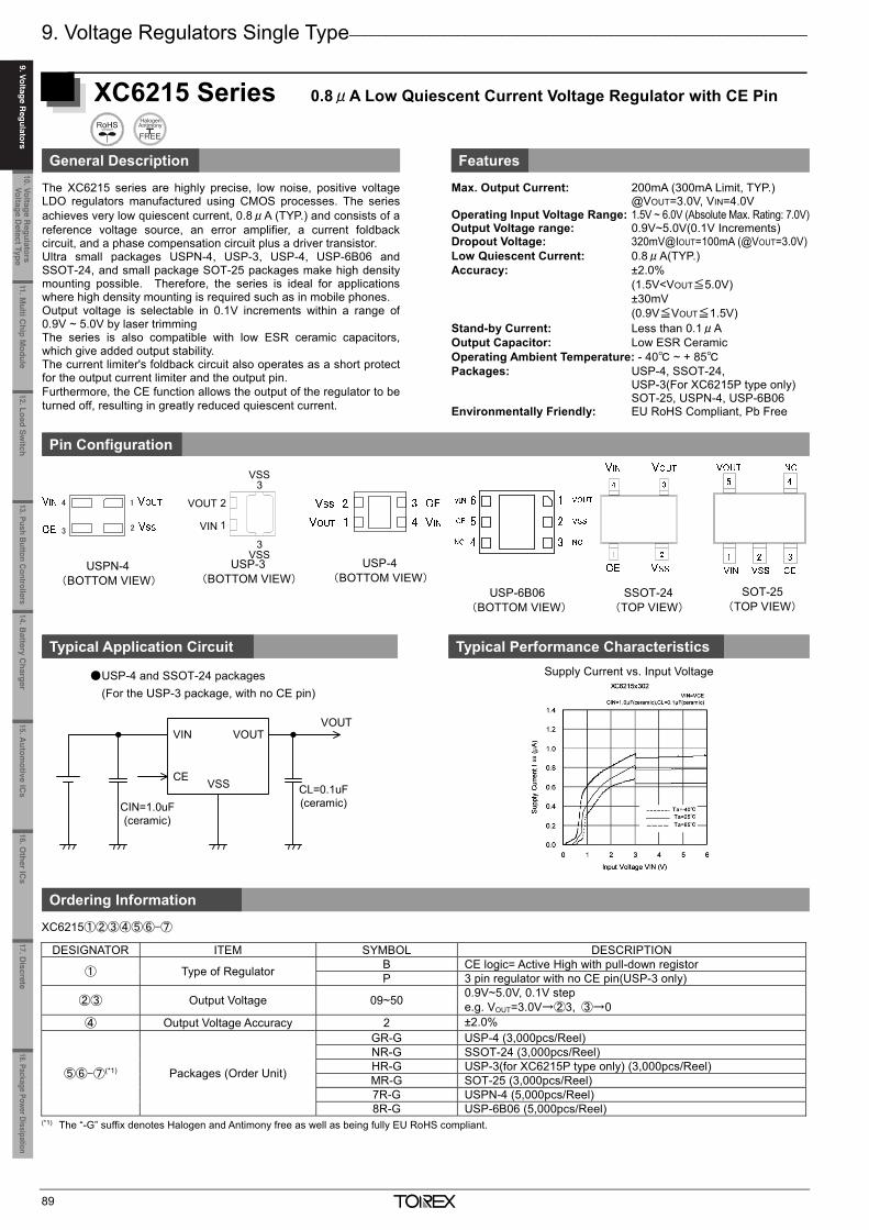
9. Voltage Regulators Single Type_______________________________________________________________
89
XC6215 Series 0.8μA Low Quiescent Current Voltage Regulator with CE Pin
General Description Features
The XC6215 series are highly precise, low noise, positive voltage LDO regulators manufactured using CMOS processes. The series achieves very low quiescent current, 0.8μA (TYP.) and consists of a reference voltage source, an error amplifier, a current foldback circuit, and a phase compensation circuit plus a driver transistor. Ultra small packages USPN-4, USP-3, USP-4, USP-6B06 and SSOT-24, and small package SOT-25 packages make high density mounting possible. Therefore, the series is ideal for applications where high density mounting is required such as in mobile phones. Output voltage is selectable in 0.1V increments within a range of 0.9V ~ 5.0V by laser trimming The series is also compatible with low ESR ceramic capacitors, which give added output stability. The current limiter's foldback circuit also operates as a short protect for the output current limiter and the output pin. Furthermore, the CE function allows the output of the regulator to be turned off, resulting in greatly reduced quiescent current.
Max. Output Current: 200mA (300mA Limit, TYP.) @VOUT=3.0V, VIN=4.0V
Operating Input Voltage Range: 1.5V ~ 6.0V (Absolute Max. Rating: 7.0V)Output Voltage range: 0.9V~5.0V(0.1V Increments) Dropout Voltage: 320mV@IOUT=100mA (@VOUT=3.0V) Low Quiescent Current: 0.8μA(TYP.) Accuracy: ±2.0%
(1.5V<VOUT≦5.0V) ±30mV (0.9V≦VOUT≦1.5V)
Stand-by Current: Less than 0.1μA Output Capacitor: Low ESR Ceramic Operating Ambient Temperature: - 40 ~ + 85 Packages: USP-4, SSOT-24,
USP-3(For XC6215P type only) SOT-25, USPN-4, USP-6B06
Environmentally Friendly: EU RoHS Compliant, Pb Free
Pin Configuration
Typical Application Circuit Typical Performance Characteristics
Supply Current vs. Input Voltage
Ordering Information
XC6215①②③④⑤⑥-⑦
DESIGNATOR ITEM SYMBOL DESCRIPTION
① Type of Regulator B CE logic= Active High with pull-down registor P 3 pin regulator with no CE pin(USP-3 only)
②③ Output Voltage 09~50 0.9V~5.0V, 0.1V step e.g. VOUT=3.0V→②3, ③→0
④ Output Voltage Accuracy 2 ±2.0%
⑤⑥-⑦(*1) Packages (Order Unit)
GR-G USP-4 (3,000pcs/Reel) NR-G SSOT-24 (3,000pcs/Reel) HR-G USP-3(for XC6215P type only) (3,000pcs/Reel) MR-G SOT-25 (3,000pcs/Reel) 7R-G USPN-4 (5,000pcs/Reel) 8R-G USP-6B06 (5,000pcs/Reel)
(*1) The “-G” suffix denotes Halogen and Antimony free as well as being fully EU RoHS compliant.
VIN VOUT
VSSCE
VOUT
CL=0.1uF(ceramic)CIN=1.0uF
(ceramic)
USP-4 and SSOT-24 packages (For the USP-3 package, with no CE pin)
USP-3 (BOTTOM VIEW)
2
1
3
3
VSS
VSS
VOUT
VIN
USP-4 (BOTTOM VIEW)
3 2
14
USPN-4 (BOTTOM VIEW)
SOT-25 (TOP VIEW)
SSOT-24 (TOP VIEW)
USP-6B06 (BOTTOM VIEW)
_______________________________________________________________________________________________________
90
XC6214 Series 500mA High Speed LDO Regulators, Thermal Shutdown
General Description Features
The XC6214 series are highly precise, low noise, high current,positive voltage low dropout regulators. They are fabricated usingTorex's CMOS process. The series features a voltage reference, anerror amplifier, a current limiter, a thermal protection circuit, and aphase compensation circuit plus a driver transistor. The output voltage is selectable in 0.1V increments within the rangeof 1.2V to 5.0V. (Output voltage 1.2V, 1.5V, 1.8V, 2.5V, 3.0V, and3.3V, are standard products. Other than these voltages areavailable as semi-custom products.) The series is also compatible with low ESR ceramic capacitors,which give added output stability. This stability can be maintainedeven during load fluctuations due to the excellent transient responseof the series. The over current protection circuit and the thermal shutdown circuitare built in. The over current protection circuit will operate when theoutput current reaches current limit level. The thermal shutdowncircuit will operate when the junction temperature reachestemperature limit level.
Max. Output Current: 500mA (800mA limit) Operating Voltage Range: 1.8V ~ 6.0V (Absolute Max. Rating: 6.5V) Output Voltage: 1.2V, 1.5V, 1.8V, 2.5V, 3.0V, 3.3V (standard) Other voltages between 1.2V ~ 5.0V (semi-custom) Dropout Voltage: 500mV @ IOUT = 500mA (VOUT=3.3V) Low Quiescent Current: 8μA (TYP.) Accuracy: ±2.0% Ripple Rejection Rate: 40dB @ 1k Hz Operating Ambient Temperature: - 40 ~ + 85 Packages: SOT-89, TO-252 Environmentally Friendly: EU RoHS Compliant, Pb Free
Pin Configuration
Typical Application Circuit Typical Performance Characteristics
Ordering Information
XC6214P①②③④⑤-⑥ DESIGNATOR ITEM SYMBOL DESCRIPTION
①② Output Voltage
12 1.2V 15 1.5V 18 1.8V 25 2.5V 30 3.0V 33 3.3V
③ Output Voltage Accuracy 2 ±2.0%
④⑤-⑥(*1) Packages (Order Unit) JR-G TO-252 (2,500pcs/Reel) PR-G SOT-89 (1,000pcs/Reel)
(*1) The “-G” suffix denotes Halogen and Antimony free as well as being fully EU RoHS compliant.
SOT-89 (TOP VIEW)
VSS VIN VOUT
VOUT
VSS
VIN
CIN1.0uF
CL1.0uF
RLVIN
Dropout Voltage vs. Output Current
VOUT VIN VSS
TO-252 (TOP VIEW)
VIN VSS
11.Multi C
hip Module
10. Voltage Regulators
Voltage Detect Type
9. Voltage Regulators
12.Load Switch
13. Push Button Controllers14.B
attery Charger
15.Autom
otive ICs
16.Other IC
s17. D
iscrete18.Package Power Dissipation
9. Voltage Regulators
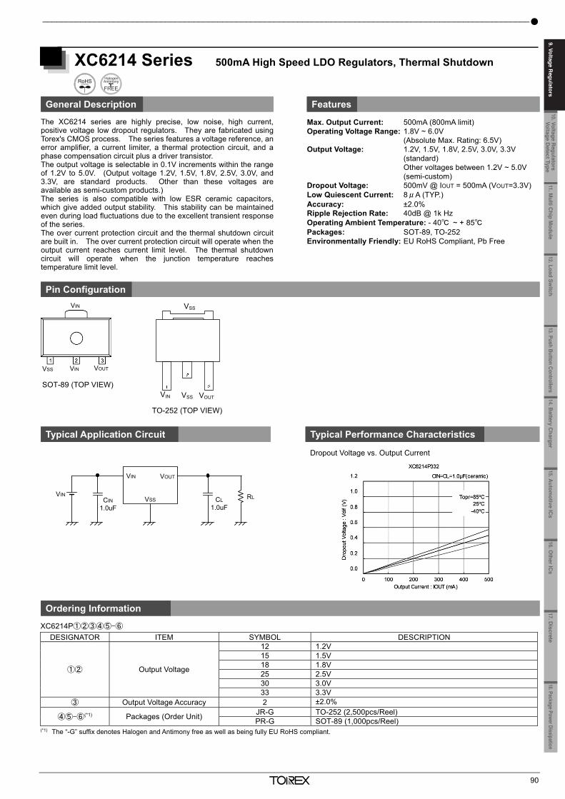
9. Voltage Regulators Single Type_______________________________________________________________
89
XC6215 Series 0.8μA Low Quiescent Current Voltage Regulator with CE Pin
General Description Features
The XC6215 series are highly precise, low noise, positive voltage LDO regulators manufactured using CMOS processes. The series achieves very low quiescent current, 0.8μA (TYP.) and consists of a reference voltage source, an error amplifier, a current foldback circuit, and a phase compensation circuit plus a driver transistor. Ultra small packages USPN-4, USP-3, USP-4, USP-6B06 and SSOT-24, and small package SOT-25 packages make high density mounting possible. Therefore, the series is ideal for applications where high density mounting is required such as in mobile phones. Output voltage is selectable in 0.1V increments within a range of 0.9V ~ 5.0V by laser trimming The series is also compatible with low ESR ceramic capacitors, which give added output stability. The current limiter's foldback circuit also operates as a short protect for the output current limiter and the output pin. Furthermore, the CE function allows the output of the regulator to be turned off, resulting in greatly reduced quiescent current.
Max. Output Current: 200mA (300mA Limit, TYP.) @VOUT=3.0V, VIN=4.0V
Operating Input Voltage Range: 1.5V ~ 6.0V (Absolute Max. Rating: 7.0V)Output Voltage range: 0.9V~5.0V(0.1V Increments) Dropout Voltage: 320mV@IOUT=100mA (@VOUT=3.0V) Low Quiescent Current: 0.8μA(TYP.) Accuracy: ±2.0%
(1.5V<VOUT≦5.0V) ±30mV (0.9V≦VOUT≦1.5V)
Stand-by Current: Less than 0.1μA Output Capacitor: Low ESR Ceramic Operating Ambient Temperature: - 40 ~ + 85 Packages: USP-4, SSOT-24,
USP-3(For XC6215P type only) SOT-25, USPN-4, USP-6B06
Environmentally Friendly: EU RoHS Compliant, Pb Free
Pin Configuration
Typical Application Circuit Typical Performance Characteristics
Supply Current vs. Input Voltage
Ordering Information
XC6215①②③④⑤⑥-⑦
DESIGNATOR ITEM SYMBOL DESCRIPTION
① Type of Regulator B CE logic= Active High with pull-down registor P 3 pin regulator with no CE pin(USP-3 only)
②③ Output Voltage 09~50 0.9V~5.0V, 0.1V step e.g. VOUT=3.0V→②3, ③→0
④ Output Voltage Accuracy 2 ±2.0%
⑤⑥-⑦(*1) Packages (Order Unit)
GR-G USP-4 (3,000pcs/Reel) NR-G SSOT-24 (3,000pcs/Reel) HR-G USP-3(for XC6215P type only) (3,000pcs/Reel) MR-G SOT-25 (3,000pcs/Reel) 7R-G USPN-4 (5,000pcs/Reel) 8R-G USP-6B06 (5,000pcs/Reel)
(*1) The “-G” suffix denotes Halogen and Antimony free as well as being fully EU RoHS compliant.
VIN VOUT
VSSCE
VOUT
CL=0.1uF(ceramic)CIN=1.0uF
(ceramic)
USP-4 and SSOT-24 packages (For the USP-3 package, with no CE pin)
USP-3 (BOTTOM VIEW)
2
1
3
3
VSS
VSS
VOUT
VIN
USP-4 (BOTTOM VIEW)
3 2
14
USPN-4 (BOTTOM VIEW)
SOT-25 (TOP VIEW)
SSOT-24 (TOP VIEW)
USP-6B06 (BOTTOM VIEW)
_______________________________________________________________________________________________________
90
XC6214 Series 500mA High Speed LDO Regulators, Thermal Shutdown
General Description Features
The XC6214 series are highly precise, low noise, high current,positive voltage low dropout regulators. They are fabricated usingTorex's CMOS process. The series features a voltage reference, anerror amplifier, a current limiter, a thermal protection circuit, and aphase compensation circuit plus a driver transistor. The output voltage is selectable in 0.1V increments within the rangeof 1.2V to 5.0V. (Output voltage 1.2V, 1.5V, 1.8V, 2.5V, 3.0V, and3.3V, are standard products. Other than these voltages areavailable as semi-custom products.) The series is also compatible with low ESR ceramic capacitors,which give added output stability. This stability can be maintainedeven during load fluctuations due to the excellent transient responseof the series. The over current protection circuit and the thermal shutdown circuitare built in. The over current protection circuit will operate when theoutput current reaches current limit level. The thermal shutdowncircuit will operate when the junction temperature reachestemperature limit level.
Max. Output Current: 500mA (800mA limit) Operating Voltage Range: 1.8V ~ 6.0V (Absolute Max. Rating: 6.5V) Output Voltage: 1.2V, 1.5V, 1.8V, 2.5V, 3.0V, 3.3V (standard) Other voltages between 1.2V ~ 5.0V (semi-custom) Dropout Voltage: 500mV @ IOUT = 500mA (VOUT=3.3V) Low Quiescent Current: 8μA (TYP.) Accuracy: ±2.0% Ripple Rejection Rate: 40dB @ 1k Hz Operating Ambient Temperature: - 40 ~ + 85 Packages: SOT-89, TO-252 Environmentally Friendly: EU RoHS Compliant, Pb Free
Pin Configuration
Typical Application Circuit Typical Performance Characteristics
Ordering Information
XC6214P①②③④⑤-⑥ DESIGNATOR ITEM SYMBOL DESCRIPTION
①② Output Voltage
12 1.2V 15 1.5V 18 1.8V 25 2.5V 30 3.0V 33 3.3V
③ Output Voltage Accuracy 2 ±2.0%
④⑤-⑥(*1) Packages (Order Unit) JR-G TO-252 (2,500pcs/Reel) PR-G SOT-89 (1,000pcs/Reel)
(*1) The “-G” suffix denotes Halogen and Antimony free as well as being fully EU RoHS compliant.
SOT-89 (TOP VIEW)
VSS VIN VOUT
VOUT
VSS
VIN
CIN1.0uF
CL1.0uF
RLVIN
Dropout Voltage vs. Output Current
VOUT VIN VSS
TO-252 (TOP VIEW)
VIN VSS
11.Multi C
hip Module
10. Voltage Regulators
Voltage Detect Type
12.Load Switch
13. Push Button Controllers14.B
attery Charger
15.Autom
otive ICs
16.Other IC
s17. D
iscrete18.Package Power Dissipation
9. Voltage Regulators
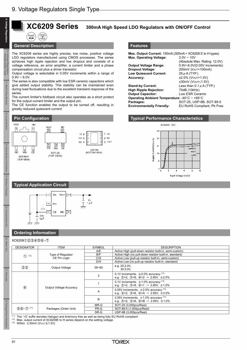
9. Voltage Regulators Single Type_______________________________________________________________
91
XC6209 Series 300mA High Speed LDO Regulators with ON/OFF Control
General Description Features
The XC6209 series are highly precise, low noise, positive voltage LDO regulators manufactured using CMOS processes. The series achieves high ripple rejection and low dropout and consists of a voltage reference, an error amplifier, a current limiter and a phase compensation circuit plus a driver transistor. Output voltage is selectable in 0.05V increments within a range of 0.9V ~ 6.0V. The series is also compatible with low ESR ceramic capacitors which give added output stability. This stability can be maintained even during load fluctuations due to the excellent transient response of the series. The current limiter's foldback circuit also operates as a short protect for the output current limiter and the output pin. The CE function enables the output to be turned off, resulting in greatly reduced quiescent current.
Max. Output Current: 150mA (300mA = XC6209 E to H types) Max. Operating Voltage: 2.0V ~ 10V (Absolute Max. Rating: 12.0V) Output Voltage Range: 0.9V~6.0V(0.05V increments) Dropout Voltage: 200mV (IOUT=100mA) Low Quiescent Current: 25μA (TYP.) Accuracy: ±2.0% (VOUT>1.5V)
±30mV (VOUT1.5V) Stand-by Current: Less than 0.1μA (TYP.) High Ripple Rejection: 70dB (10kHz) Output Capacitor: Low ESR Ceramic Operating Ambient Temperature: -40C ~ +85C Packages: SOT-25, USP-6B, SOT-89-5 Environmentally Friendly: EU RoHS Compliant, Pb Free
Pin Configuration Typical Performance Characteristics
Typical Application Circuit
Ordering Information
XC6209①②③④⑤⑥-⑦
DESIGNATOR ITEM SYMBOL DESCRIPTION
① (*2) Type of Regulator CE Pin Logic
A/E Active High (pull-down resistor built-in, semi-custom) B/F Active High (no pull-down resistor built-in, standard) C/G Active Low (pull-up resistor built-in, semi-custom) D/H Active Low (no pull-up resistor built-in, standard)
②③ Output Voltage 09~60 e.g. 20:2.0V, 30:3.0V,
④ Output Voltage Accuracy
2 0.1V increments, ±2.0% accuracy (*3) e.g. ②=2, ③=8, ④=2 → 2.80V, ±2.0%
1 0.1V increments, ±1.0% accuracy (*3) e.g. ②=2, ③=8, ④=1 → 2.80V, ±1.0%
A 0.05V increments, ±2.0% accuracy (*3) e.g. ②=2, ③=8, ④=A → 2.85V, ±2.0%
B 0.05V increments, ±1.0% accuracy (*3) e.g. ②=2, ③=8, ④=B → 2.85V, ±1.0%
⑤⑥-⑦ (*1) Packages (Order Unit) MR-G SOT-25 (3,000pcs/Reel) PR-G SOT-89-5 (1,000pcs/Reel) DR-G USP-6B (3,000pcs/Reel)
(*1) The “-G” suffix denotes Halogen and Antimony free as well as being fully EU RoHS compliant. (*2) Max. output current of XC6209E to H series depend on the setting voltage. (*3) Within ±30mV (VOUT≦1.5V)
5 4
1 2 3
SOT-89-5(TOP VIEW)
VSS
VOUT VIN
NC CE
1
234
56
VOUT
VSS
CE VIN
NC
NC
USP-6B(BOTTOM VIEW)SOT-25
(TOP VIEW)
_______________________________________________________________________________________________________
92
XC6206 Series 1μA Low Power 3 Terminal Voltage Regulator General Description Features
The XC6206 series are highly precise, low quiescent current, highvoltage, positive voltage regulators manufactured using CMOS andlaser trimming technologies. The series provide high currents witha significantly low dropout voltage. The XC6206 series consists of a current limiter circuit, a drivertransistor, a precision reference voltage and an error correctioncircuit. The series are compatible with low ESR ceramic capacitors. Thecurrent limiter's foldback circuit also operates as a short protect forthe output current limiter and the output pin. Output voltage can be set internally by laser trimming technologies.It is selectable in 0.1V increments within a range of 1.2V to 5.0V.
Max. Output Current: 200mA (3.0V type) Max. Operating Voltage: 6.0V (Absolute Max. Rating: 7.0V) Output Voltage Range: 1.2V ~ 5.0V (0.1V increments) Dropout Voltage: 250mV @ IOUT=100mA (3.0V type) Low Quiescent Current: 1.0 μA(TYP.) Accuracy: ±2.0% (±30mV@VOUT<1.5V)(±1.0%@VOUT≧2.0V) Output Capacitor: Low ESR Ceramic Operating Ambient Temperature: -40C ~ +85C Packages: SOT-23, SOT-89, USP-6B Environmentally Friendly: EU RoHS Compliant, Pb Free
Pin Configuration
Typical Application Circuit Typical Performance Characteristics
Ordering Information
XC6206P①②③④⑤-⑥
DESIGNATOR ITEM SYMBOL DESCRIPTION ①② Output Voltage 12 ~ 50 e.g. VOUT:3.0V→①=3, ②=0
③ Output Voltage Accuracy 2 ± 2.0% @ VOUT≧1.5V, ± 30mV @ VOUT<1.5V 1 ± 1.0% @ VOUT≧2.0V
④⑤-⑥(*1) Packages (Order Unit) MR-G SOT-23 (3,000pcs/Reel) PR-G SOT-89 (1,000pcs/Reel) DR-G USP-6B (3,000pcs/Reel)
(*1) The “-G” suffix denotes Halogen and Antimony free as well as being fully EU RoHS compliant.
SOT-23 (TOP VIEW)
VOUT 1234
56
NC VSS
USP-6B(BOTTOM VIEW)
NCVIN
NC
1 2 3 VSS VOUT VIN
SOT-89 (TOP VIEW)
VIN
11.Multi C
hip Module
10. Voltage Regulators
Voltage Detect Type
9. Voltage Regulators
12.Load Switch
13. Push Button Controllers14.B
attery Charger
15.Autom
otive ICs
16.Other IC
s17. D
iscrete18.Package Power Dissipation
9. Voltage Regulators
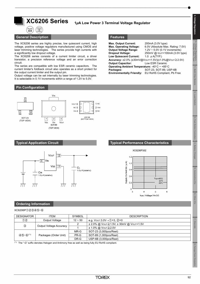
9. Voltage Regulators Single Type_______________________________________________________________
91
XC6209 Series 300mA High Speed LDO Regulators with ON/OFF Control
General Description Features
The XC6209 series are highly precise, low noise, positive voltage LDO regulators manufactured using CMOS processes. The series achieves high ripple rejection and low dropout and consists of a voltage reference, an error amplifier, a current limiter and a phase compensation circuit plus a driver transistor. Output voltage is selectable in 0.05V increments within a range of 0.9V ~ 6.0V. The series is also compatible with low ESR ceramic capacitors which give added output stability. This stability can be maintained even during load fluctuations due to the excellent transient response of the series. The current limiter's foldback circuit also operates as a short protect for the output current limiter and the output pin. The CE function enables the output to be turned off, resulting in greatly reduced quiescent current.
Max. Output Current: 150mA (300mA = XC6209 E to H types) Max. Operating Voltage: 2.0V ~ 10V (Absolute Max. Rating: 12.0V) Output Voltage Range: 0.9V~6.0V(0.05V increments) Dropout Voltage: 200mV (IOUT=100mA) Low Quiescent Current: 25μA (TYP.) Accuracy: ±2.0% (VOUT>1.5V)
±30mV (VOUT1.5V) Stand-by Current: Less than 0.1μA (TYP.) High Ripple Rejection: 70dB (10kHz) Output Capacitor: Low ESR Ceramic Operating Ambient Temperature: -40C ~ +85C Packages: SOT-25, USP-6B, SOT-89-5 Environmentally Friendly: EU RoHS Compliant, Pb Free
Pin Configuration Typical Performance Characteristics
Typical Application Circuit
Ordering Information
XC6209①②③④⑤⑥-⑦
DESIGNATOR ITEM SYMBOL DESCRIPTION
① (*2) Type of Regulator CE Pin Logic
A/E Active High (pull-down resistor built-in, semi-custom) B/F Active High (no pull-down resistor built-in, standard) C/G Active Low (pull-up resistor built-in, semi-custom) D/H Active Low (no pull-up resistor built-in, standard)
②③ Output Voltage 09~60 e.g. 20:2.0V, 30:3.0V,
④ Output Voltage Accuracy
2 0.1V increments, ±2.0% accuracy (*3) e.g. ②=2, ③=8, ④=2 → 2.80V, ±2.0%
1 0.1V increments, ±1.0% accuracy (*3) e.g. ②=2, ③=8, ④=1 → 2.80V, ±1.0%
A 0.05V increments, ±2.0% accuracy (*3) e.g. ②=2, ③=8, ④=A → 2.85V, ±2.0%
B 0.05V increments, ±1.0% accuracy (*3) e.g. ②=2, ③=8, ④=B → 2.85V, ±1.0%
⑤⑥-⑦ (*1) Packages (Order Unit) MR-G SOT-25 (3,000pcs/Reel) PR-G SOT-89-5 (1,000pcs/Reel) DR-G USP-6B (3,000pcs/Reel)
(*1) The “-G” suffix denotes Halogen and Antimony free as well as being fully EU RoHS compliant. (*2) Max. output current of XC6209E to H series depend on the setting voltage. (*3) Within ±30mV (VOUT≦1.5V)
5 4
1 2 3
SOT-89-5(TOP VIEW)
VSS
VOUT VIN
NC CE
1
234
56
VOUT
VSS
CE VIN
NC
NC
USP-6B(BOTTOM VIEW)SOT-25
(TOP VIEW)
_______________________________________________________________________________________________________
92
XC6206 Series 1μA Low Power 3 Terminal Voltage Regulator General Description Features
The XC6206 series are highly precise, low quiescent current, highvoltage, positive voltage regulators manufactured using CMOS andlaser trimming technologies. The series provide high currents witha significantly low dropout voltage. The XC6206 series consists of a current limiter circuit, a drivertransistor, a precision reference voltage and an error correctioncircuit. The series are compatible with low ESR ceramic capacitors. Thecurrent limiter's foldback circuit also operates as a short protect forthe output current limiter and the output pin. Output voltage can be set internally by laser trimming technologies.It is selectable in 0.1V increments within a range of 1.2V to 5.0V.
Max. Output Current: 200mA (3.0V type) Max. Operating Voltage: 6.0V (Absolute Max. Rating: 7.0V) Output Voltage Range: 1.2V ~ 5.0V (0.1V increments) Dropout Voltage: 250mV @ IOUT=100mA (3.0V type) Low Quiescent Current: 1.0 μA(TYP.) Accuracy: ±2.0% (±30mV@VOUT<1.5V)(±1.0%@VOUT≧2.0V) Output Capacitor: Low ESR Ceramic Operating Ambient Temperature: -40C ~ +85C Packages: SOT-23, SOT-89, USP-6B Environmentally Friendly: EU RoHS Compliant, Pb Free
Pin Configuration
Typical Application Circuit Typical Performance Characteristics
Ordering Information
XC6206P①②③④⑤-⑥
DESIGNATOR ITEM SYMBOL DESCRIPTION ①② Output Voltage 12 ~ 50 e.g. VOUT:3.0V→①=3, ②=0
③ Output Voltage Accuracy 2 ± 2.0% @ VOUT≧1.5V, ± 30mV @ VOUT<1.5V 1 ± 1.0% @ VOUT≧2.0V
④⑤-⑥(*1) Packages (Order Unit) MR-G SOT-23 (3,000pcs/Reel) PR-G SOT-89 (1,000pcs/Reel) DR-G USP-6B (3,000pcs/Reel)
(*1) The “-G” suffix denotes Halogen and Antimony free as well as being fully EU RoHS compliant.
SOT-23 (TOP VIEW)
VOUT 1234
56
NC VSS
USP-6B(BOTTOM VIEW)
NCVIN
NC
1 2 3 VSS VOUT VIN
SOT-89 (TOP VIEW)
VIN
11.Multi C
hip Module
10. Voltage Regulators
Voltage Detect Type
12.Load Switch
13. Push Button Controllers14.B
attery Charger
15.Autom
otive ICs
16.Other IC
s17. D
iscrete18.Package Power Dissipation
9. Voltage Regulators
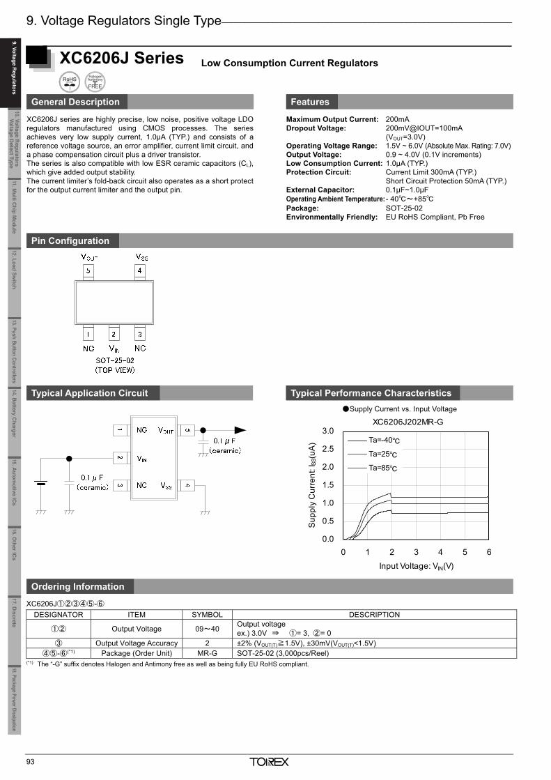
9. Voltage Regulators Single Type_______________________________________________________________
93
XC6206J Series Low Consumption Current Regulators General Description Features
XC6206J series are highly precise, low noise, positive voltage LDO regulators manufactured using CMOS processes. The series achieves very low supply current, 1.0μA (TYP.) and consists of a reference voltage source, an error amplifier, current limit circuit, and a phase compensation circuit plus a driver transistor. The series is also compatible with low ESR ceramic capacitors (CL), which give added output stability. The current limiter’s fold-back circuit also operates as a short protect for the output current limiter and the output pin.
Maximum Output Current: 200mA Dropout Voltage: 200mV@IOUT=100mA (VOUT=3.0V) Operating Voltage Range: 1.5V ~ 6.0V (Absolute Max. Rating: 7.0V) Output Voltage: 0.9 ~ 4.0V (0.1V increments) Low Consumption Current: 1.0μA (TYP.) Protection Circuit: Current Limit 300mA (TYP.) Short Circuit Protection 50mA (TYP.) External Capacitor: 0.1μF~1.0μF Operating Ambient Temperature: - 40~+85 Package: SOT-25-02 Environmentally Friendly: EU RoHS Compliant, Pb Free
Pin Configuration
Typical Application Circuit Typical Performance Characteristics
Supply Current vs. Input Voltage
Ordering Information
XC6206J①②③④⑤-⑥ DESIGNATOR ITEM SYMBOL DESCRIPTION
①② Output Voltage 09~40 Output voltage ex.) 3.0V ⇒ ①= 3, ②= 0
③ Output Voltage Accuracy 2 ±2% (VOUT(T)≧1.5V), ±30mV(VOUT(T)<1.5V) ④⑤-⑥(*1) Package (Order Unit) MR-G SOT-25-02 (3,000pcs/Reel)
(*1) The “-G” suffix denotes Halogen and Antimony free as well as being fully EU RoHS compliant.
0.0
0.5
1.0
1.5
2.0
2.5
3.0
0 1 2 3 4 5 6
Input Voltage: VIN(V)
Sup
ply
Cur
rent
: ISS
(uA
) Ta=-40
Ta=25
Ta=85
XC6206J202MR-G
_______________________________________________________________________________________________________
94
XC6204/XC6205 Series 300mA/150mA High Speed LDO Regulators with CE Pin
General Description Features
The XC6204/XC6205 series are highly precise, low noise, positivevoltage LDO regulators manufactured using CMOS processes. Theseries achieves high ripple rejection and low dropout and consists ofa voltage reference, an error amplifier, a current limiter, and phasecompensation circuit plus a driver transistor. Output voltage is selectable in 0.05V increments within a range of0.9V ~ 6.0V. The series is also compatible with low ESR ceramic capacitors whichgive added output stability. This stability can be maintained evenduring load fluctuations due to the excellent transient response of theseries. The current limiter's foldback circuit also operates as a short protectfor the output current limiter and the output pin. The CE function enables the output to be turned off, resulting ingreatly reduced quiescent current.
Max. Output Current: 150mA 300mA (XC6204E~H Series)
Operating Voltage: 2.0V ~ 10V (Absolute Max. Rating: 12.0V) Output Voltage Range: 0.9V ~ 1.75V [XC6205] (0.05V increments)
1.8V ~ 6.0V [XC6204] (0.05V increments) Dropout Voltage: 200mV @ 100mA Low Quiescent Current: 70μA (TYP.) Accuracy: ± 2.0%, ± 1.0%, Stand-by Current: Less than 0.1μA (TYP.) High Ripple Rejection: 70dB (10 kHz) (XC6204) 60dB (10 kHz) (XC6205) Output Capacitor: Low ESR Ceramic Operating Ambient Temperature: -40C ~ +85C Packages: SOT-23, SOT-89-5, USP-6B Environmentally Friendly: EU RoHS Compliant, Pb Free
Pin Configuration
5 4
1 2 3
SOT-89-5 (TOP VIEW)
5 2 1 3 VSS CE
VOUT NC
VIN
SOT-25 (TOP VIEW)
4 5
Typical Application Circuit Typical Performance Characteristics
Ordering Information
XC6204/6205①②③④⑤⑥-⑦
DESIGNATOR ITEM SYMBOL DESCRIPTION
① (*2) Type of Regulator (CE pin Logic)
A / E Active High, pull-down resistor built-in (Semi-Custom) B / F Active High, no pull-down resistor built-in C / G Active Low, pull-up resistor built-in (Semi-Custom) D / H Active Low, no pull-up resistor built-in (Semi-Custom)
②③ Output Voltage 09~60, e.g. VOUT=2.0V→②=2, ③=0
④ Output Voltage Accuracy
2 0.1V increments, ±2.0% accuracy e.g. VOUT=3.8V, ±2.0%→②=3, ③=8, ④=2
1 (*3) 0.1V increments, ±1.0% accuracy e.g. VOUT=3.0V, ±1.0%→②=3, ③=0, ④=1
A 0.05V increments, ±2.0% accuracy e.g. VOUT=3.85V, ±2.0%→②=3, ③=8, ④=A
B (*3) 0.05V increments, ±1.0% accuracy e.g. VOUT=3.05V, ±1.0%→②=3, ③=0, ④=B
⑤⑥-⑦(*1) Packages (Order Unit) MR-G SOT-25 (3,000pcs/Reel) DR-G USP-6B (3,000pcs/Reel) PR-G SOT-89-5 (1,000pcs/Reel)
(*1) The “-G” suffix denotes Halogen and Antimony free as well as being fully EU RoHS compliant. (*2) E to H types are compatible to 300mA of XC6204 series. (*3) Output voltage range of the +1% accuracy product is 2.95V to 6.0V.
1234
56
VOUT
VSS
CE VIN
NC
NC
USP-6B(BOTTOM VIEW)
USP-6B
(BOTTOM VIEW)
VOUT VIN
VSS CE NC
VSS
Rip
ple
Rej
ectio
n R
atio
: P
SR
R (d
B)
XC6204x302
11.Multi C
hip Module
10. Voltage Regulators
Voltage Detect Type
9. Voltage Regulators
12.Load Switch
13. Push Button Controllers14.B
attery Charger
15.Autom
otive ICs
16.Other IC
s17. D
iscrete18.Package Power Dissipation
9. Voltage Regulators
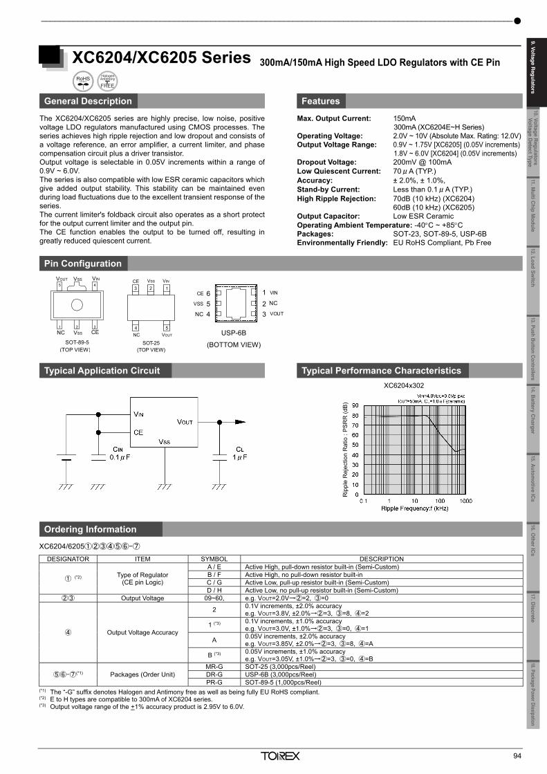
9. Voltage Regulators Single Type_______________________________________________________________
93
XC6206J Series Low Consumption Current Regulators General Description Features
XC6206J series are highly precise, low noise, positive voltage LDO regulators manufactured using CMOS processes. The series achieves very low supply current, 1.0μA (TYP.) and consists of a reference voltage source, an error amplifier, current limit circuit, and a phase compensation circuit plus a driver transistor. The series is also compatible with low ESR ceramic capacitors (CL), which give added output stability. The current limiter’s fold-back circuit also operates as a short protect for the output current limiter and the output pin.
Maximum Output Current: 200mA Dropout Voltage: 200mV@IOUT=100mA (VOUT=3.0V) Operating Voltage Range: 1.5V ~ 6.0V (Absolute Max. Rating: 7.0V) Output Voltage: 0.9 ~ 4.0V (0.1V increments) Low Consumption Current: 1.0μA (TYP.) Protection Circuit: Current Limit 300mA (TYP.) Short Circuit Protection 50mA (TYP.) External Capacitor: 0.1μF~1.0μF Operating Ambient Temperature: - 40~+85 Package: SOT-25-02 Environmentally Friendly: EU RoHS Compliant, Pb Free
Pin Configuration
Typical Application Circuit Typical Performance Characteristics
Supply Current vs. Input Voltage
Ordering Information
XC6206J①②③④⑤-⑥ DESIGNATOR ITEM SYMBOL DESCRIPTION
①② Output Voltage 09~40 Output voltage ex.) 3.0V ⇒ ①= 3, ②= 0
③ Output Voltage Accuracy 2 ±2% (VOUT(T)≧1.5V), ±30mV(VOUT(T)<1.5V) ④⑤-⑥(*1) Package (Order Unit) MR-G SOT-25-02 (3,000pcs/Reel)
(*1) The “-G” suffix denotes Halogen and Antimony free as well as being fully EU RoHS compliant.
0.0
0.5
1.0
1.5
2.0
2.5
3.0
0 1 2 3 4 5 6
Input Voltage: VIN(V)
Sup
ply
Cur
rent
: ISS
(uA
) Ta=-40
Ta=25
Ta=85
XC6206J202MR-G
_______________________________________________________________________________________________________
94
XC6204/XC6205 Series 300mA/150mA High Speed LDO Regulators with CE Pin
General Description Features
The XC6204/XC6205 series are highly precise, low noise, positivevoltage LDO regulators manufactured using CMOS processes. Theseries achieves high ripple rejection and low dropout and consists ofa voltage reference, an error amplifier, a current limiter, and phasecompensation circuit plus a driver transistor. Output voltage is selectable in 0.05V increments within a range of0.9V ~ 6.0V. The series is also compatible with low ESR ceramic capacitors whichgive added output stability. This stability can be maintained evenduring load fluctuations due to the excellent transient response of theseries. The current limiter's foldback circuit also operates as a short protectfor the output current limiter and the output pin. The CE function enables the output to be turned off, resulting ingreatly reduced quiescent current.
Max. Output Current: 150mA 300mA (XC6204E~H Series)
Operating Voltage: 2.0V ~ 10V (Absolute Max. Rating: 12.0V) Output Voltage Range: 0.9V ~ 1.75V [XC6205] (0.05V increments)
1.8V ~ 6.0V [XC6204] (0.05V increments) Dropout Voltage: 200mV @ 100mA Low Quiescent Current: 70μA (TYP.) Accuracy: ± 2.0%, ± 1.0%, Stand-by Current: Less than 0.1μA (TYP.) High Ripple Rejection: 70dB (10 kHz) (XC6204) 60dB (10 kHz) (XC6205) Output Capacitor: Low ESR Ceramic Operating Ambient Temperature: -40C ~ +85C Packages: SOT-23, SOT-89-5, USP-6B Environmentally Friendly: EU RoHS Compliant, Pb Free
Pin Configuration
5 4
1 2 3
SOT-89-5 (TOP VIEW)
5 2 1 3 VSS CE
VOUT NC
VIN
SOT-25 (TOP VIEW)
4 5
Typical Application Circuit Typical Performance Characteristics
Ordering Information
XC6204/6205①②③④⑤⑥-⑦
DESIGNATOR ITEM SYMBOL DESCRIPTION
① (*2) Type of Regulator (CE pin Logic)
A / E Active High, pull-down resistor built-in (Semi-Custom) B / F Active High, no pull-down resistor built-in C / G Active Low, pull-up resistor built-in (Semi-Custom) D / H Active Low, no pull-up resistor built-in (Semi-Custom)
②③ Output Voltage 09~60, e.g. VOUT=2.0V→②=2, ③=0
④ Output Voltage Accuracy
2 0.1V increments, ±2.0% accuracy e.g. VOUT=3.8V, ±2.0%→②=3, ③=8, ④=2
1 (*3) 0.1V increments, ±1.0% accuracy e.g. VOUT=3.0V, ±1.0%→②=3, ③=0, ④=1
A 0.05V increments, ±2.0% accuracy e.g. VOUT=3.85V, ±2.0%→②=3, ③=8, ④=A
B (*3) 0.05V increments, ±1.0% accuracy e.g. VOUT=3.05V, ±1.0%→②=3, ③=0, ④=B
⑤⑥-⑦(*1) Packages (Order Unit) MR-G SOT-25 (3,000pcs/Reel) DR-G USP-6B (3,000pcs/Reel) PR-G SOT-89-5 (1,000pcs/Reel)
(*1) The “-G” suffix denotes Halogen and Antimony free as well as being fully EU RoHS compliant. (*2) E to H types are compatible to 300mA of XC6204 series. (*3) Output voltage range of the +1% accuracy product is 2.95V to 6.0V.
1234
56
VOUT
VSS
CE VIN
NC
NC
USP-6B(BOTTOM VIEW)
USP-6B
(BOTTOM VIEW)
VOUT VIN
VSS CE NC
VSS
Rip
ple
Rej
ectio
n R
atio
: P
SR
R (d
B)
XC6204x302
11.Multi C
hip Module
10. Voltage Regulators
Voltage Detect Type
12.Load Switch
13. Push Button Controllers14.B
attery Charger
15.Autom
otive ICs
16.Other IC
s17. D
iscrete18.Package Power Dissipation
9. Voltage Regulators
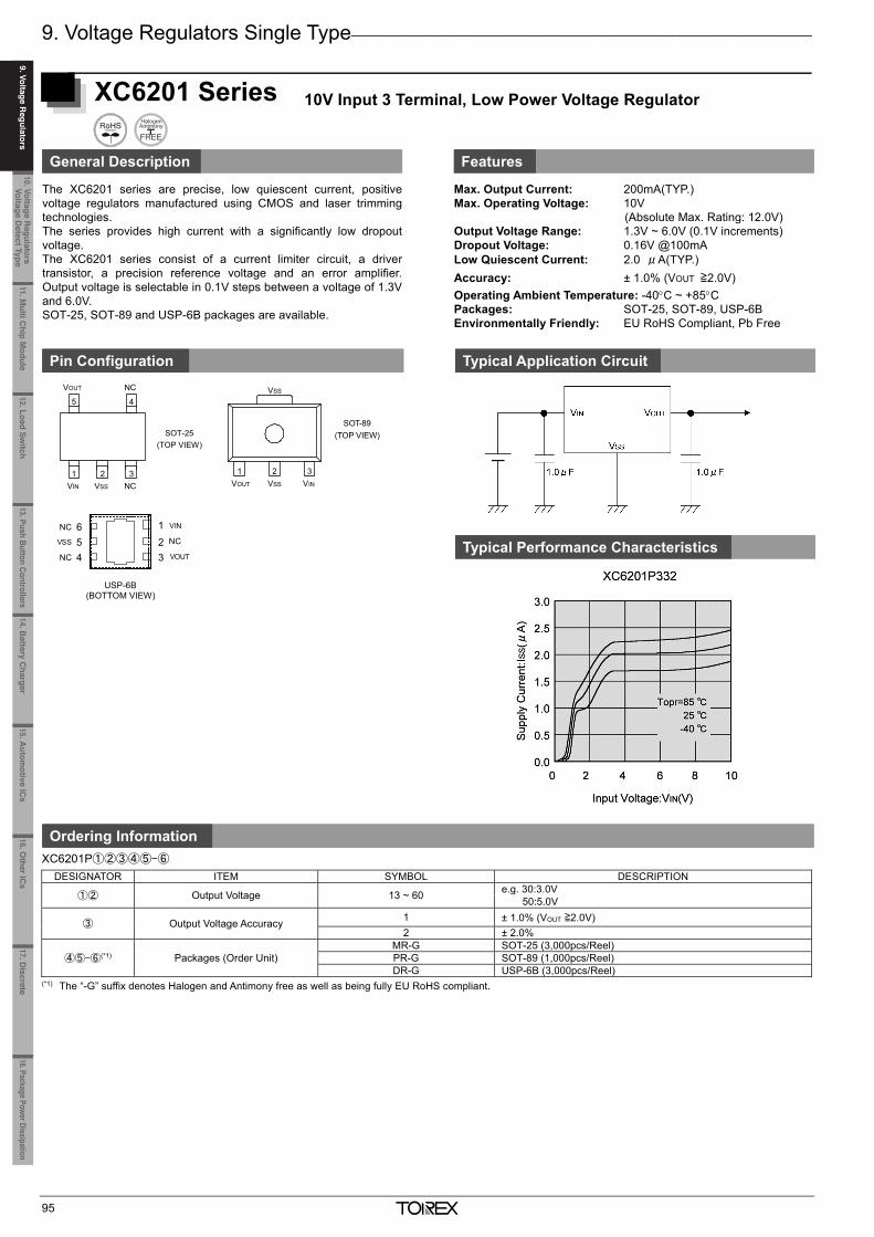
9. Voltage Regulators Single Type_______________________________________________________________
95
XC6201 Series 10V Input 3 Terminal, Low Power Voltage Regulator General Description Features
The XC6201 series are precise, low quiescent current, positive voltage regulators manufactured using CMOS and laser trimming technologies. The series provides high current with a significantly low dropout voltage. The XC6201 series consist of a current limiter circuit, a driver transistor, a precision reference voltage and an error amplifier. Output voltage is selectable in 0.1V steps between a voltage of 1.3V and 6.0V. SOT-25, SOT-89 and USP-6B packages are available.
Max. Output Current: 200mA(TYP.) Max. Operating Voltage: 10V
(Absolute Max. Rating: 12.0V) Output Voltage Range: 1.3V ~ 6.0V (0.1V increments) Dropout Voltage: 0.16V @100mA Low Quiescent Current: 2.0 μA(TYP.) Accuracy: ± 1.0% (VOUT ≧2.0V) Operating Ambient Temperature: -40C ~ +85C Packages: SOT-25, SOT-89, USP-6B Environmentally Friendly: EU RoHS Compliant, Pb Free
Pin Configuration Typical Application Circuit
SOT-25 <SOT-23-5> (TOP VIEW)
VSS VIN
VOUT
3 2 1
5
NC
NC 4
SOT-89 (TOP VIEW)
VSS VIN VOUT 3 2 1
VSS
Block Diagram
Typical Performance Characteristics
Ordering Information XC6201P①②③④⑤-⑥
DESIGNATOR ITEM SYMBOL DESCRIPTION
①② Output Voltage 13 ~ 60 e.g. 30:3.0V 50:5.0V
③ Output Voltage Accuracy 1 ± 1.0% (VOUT ≧2.0V) 2 ± 2.0%
④⑤-⑥(*1) Packages (Order Unit) MR-G SOT-25 (3,000pcs/Reel) PR-G SOT-89 (1,000pcs/Reel) DR-G USP-6B (3,000pcs/Reel)
(*1) The “-G” suffix denotes Halogen and Antimony free as well as being fully EU RoHS compliant.
VOUT
VSS
1
234
56
USP-6B(BOTTOM VIEW)
VINNC
NC
NC
USP-6B (BOTTOM VIEW)
SOT-25 (TOP VIEW)
_______________________________________________________________________________________________________
96
XC62FJ Series 10V Input, 200mA Low Consumption Current Regulator General Description Features
The XC62FJ series is a highly precise, low power consumption,positive voltage regulator manufactured with CMOS and lasertrimming technologies. The series provides large currents with a significantly smalldropout voltage. The XC62FJ consists of a current limiter circuit, a driver transistor,a precision reference voltage and an error amplifier. The output voltage is selectable in 0.1V steps between 1.7V ~6.0V.
Max. Output Current: 200mA Dropout Voltage: 160mV@IOUT=100mA (VOUT=5.0V) Operating Voltage Range: 1.8V~10V (Absolute Max. Rating: 12.0V) Output Voltage Range: 1.7V~6.0V (±2.0%) 0.1V increments Consumption Current: 2.0μA (TYP.) External Capacitor: Ceramic Capacitor Operating Ambient Temperature: -40~+85 Package: SOT-89 Environmentally Friendly: EU RoHS Compliant, Pb Free
Pin Configuration
Typical Application Circuit Typical Performance Characteristics
Ordering Information
XC62FJ①②③④⑤⑥-⑦ DESIGNATOR DESCRIPTION SYMBOL DESCRIPTION
①② Output Voltage 17~60 e.g. 30: 3.0V, 50: 5.0V ③④ Output Voltage Accuracy 02 ±2.0%
⑤⑥-⑦(*1) Package (Order Unit) PR-G SOT-89 (1,000pcs/Reel) (*1) The “-G” suffix denotes Halogen and Antimony free as well as being fully EU RoHS compliant.
1 2 3
VIN VOUT
SOT-89(TOP VIEW)
VSS
Consumption Current vs. Input Voltage
0.0
0.5
1.0
1.5
2.0
2.5
3.0
0 2 4 6 8 10
Con
sum
ptio
n C
urre
nt: I
SS(u
A)
Input Voltage: VIN(V)
XC62FJ3302PR-G
Ta=-40
Ta=25
Ta=85
11.Multi C
hip Module
10. Voltage Regulators
Voltage Detect Type
9. Voltage Regulators
12.Load Switch
13. Push Button Controllers14.B
attery Charger
15.Autom
otive ICs
16.Other IC
s17. D
iscrete18.Package Power Dissipation
9. Voltage Regulators
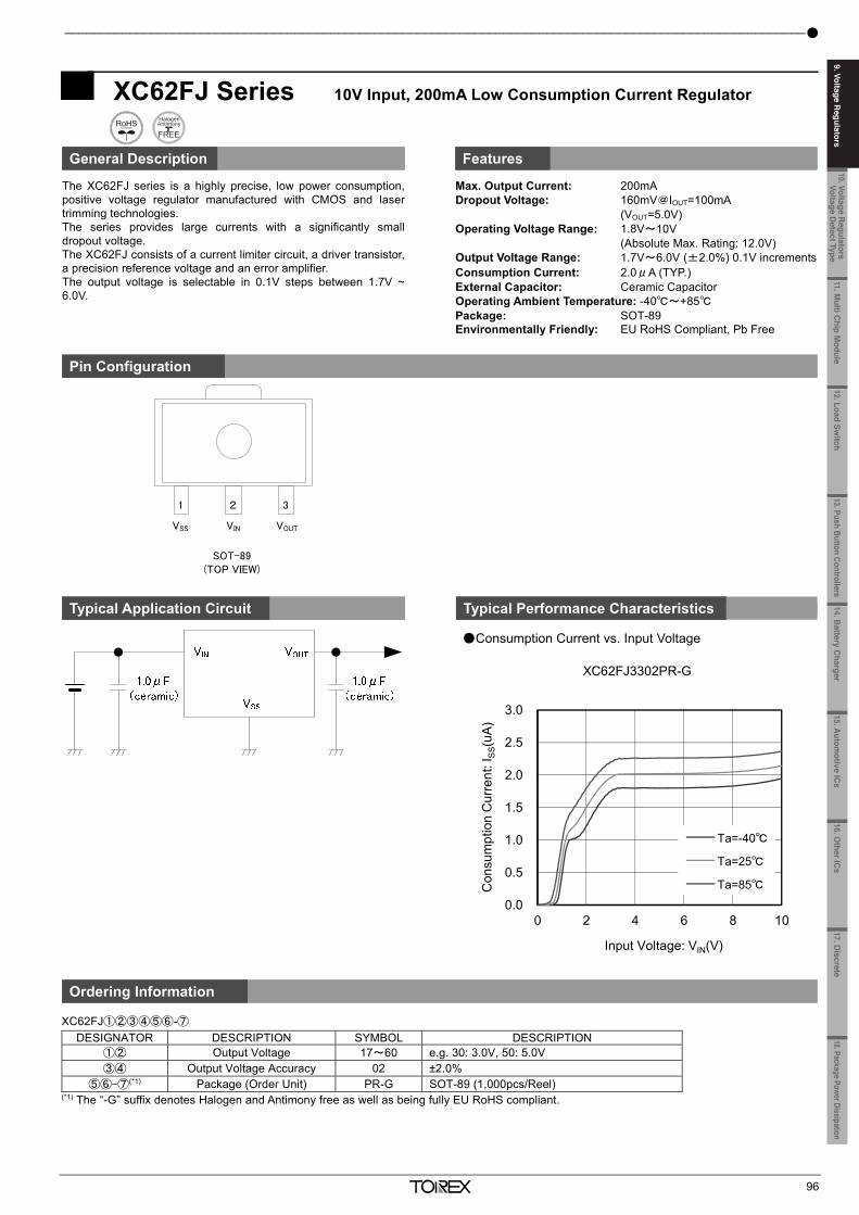
9. Voltage Regulators Single Type_______________________________________________________________
95
XC6201 Series 10V Input 3 Terminal, Low Power Voltage Regulator General Description Features
The XC6201 series are precise, low quiescent current, positive voltage regulators manufactured using CMOS and laser trimming technologies. The series provides high current with a significantly low dropout voltage. The XC6201 series consist of a current limiter circuit, a driver transistor, a precision reference voltage and an error amplifier. Output voltage is selectable in 0.1V steps between a voltage of 1.3V and 6.0V. SOT-25, SOT-89 and USP-6B packages are available.
Max. Output Current: 200mA(TYP.) Max. Operating Voltage: 10V
(Absolute Max. Rating: 12.0V) Output Voltage Range: 1.3V ~ 6.0V (0.1V increments) Dropout Voltage: 0.16V @100mA Low Quiescent Current: 2.0 μA(TYP.) Accuracy: ± 1.0% (VOUT ≧2.0V) Operating Ambient Temperature: -40C ~ +85C Packages: SOT-25, SOT-89, USP-6B Environmentally Friendly: EU RoHS Compliant, Pb Free
Pin Configuration Typical Application Circuit
SOT-25 <SOT-23-5> (TOP VIEW)
VSS VIN
VOUT
3 2 1
5
NC
NC 4
SOT-89 (TOP VIEW)
VSS VIN VOUT 3 2 1
VSS
Block Diagram
Typical Performance Characteristics
Ordering Information XC6201P①②③④⑤-⑥
DESIGNATOR ITEM SYMBOL DESCRIPTION
①② Output Voltage 13 ~ 60 e.g. 30:3.0V 50:5.0V
③ Output Voltage Accuracy 1 ± 1.0% (VOUT ≧2.0V) 2 ± 2.0%
④⑤-⑥(*1) Packages (Order Unit) MR-G SOT-25 (3,000pcs/Reel) PR-G SOT-89 (1,000pcs/Reel) DR-G USP-6B (3,000pcs/Reel)
(*1) The “-G” suffix denotes Halogen and Antimony free as well as being fully EU RoHS compliant.
VOUT
VSS
1
234
56
USP-6B(BOTTOM VIEW)
VINNC
NC
NC
USP-6B (BOTTOM VIEW)
SOT-25 (TOP VIEW)
_______________________________________________________________________________________________________
96
XC62FJ Series 10V Input, 200mA Low Consumption Current Regulator General Description Features
The XC62FJ series is a highly precise, low power consumption,positive voltage regulator manufactured with CMOS and lasertrimming technologies. The series provides large currents with a significantly smalldropout voltage. The XC62FJ consists of a current limiter circuit, a driver transistor,a precision reference voltage and an error amplifier. The output voltage is selectable in 0.1V steps between 1.7V ~6.0V.
Max. Output Current: 200mA Dropout Voltage: 160mV@IOUT=100mA (VOUT=5.0V) Operating Voltage Range: 1.8V~10V (Absolute Max. Rating: 12.0V) Output Voltage Range: 1.7V~6.0V (±2.0%) 0.1V increments Consumption Current: 2.0μA (TYP.) External Capacitor: Ceramic Capacitor Operating Ambient Temperature: -40~+85 Package: SOT-89 Environmentally Friendly: EU RoHS Compliant, Pb Free
Pin Configuration
Typical Application Circuit Typical Performance Characteristics
Ordering Information
XC62FJ①②③④⑤⑥-⑦ DESIGNATOR DESCRIPTION SYMBOL DESCRIPTION
①② Output Voltage 17~60 e.g. 30: 3.0V, 50: 5.0V ③④ Output Voltage Accuracy 02 ±2.0%
⑤⑥-⑦(*1) Package (Order Unit) PR-G SOT-89 (1,000pcs/Reel) (*1) The “-G” suffix denotes Halogen and Antimony free as well as being fully EU RoHS compliant.
1 2 3
VIN VOUT
SOT-89(TOP VIEW)
VSS
Consumption Current vs. Input Voltage
0.0
0.5
1.0
1.5
2.0
2.5
3.0
0 2 4 6 8 10
Con
sum
ptio
n C
urre
nt: I
SS(u
A)
Input Voltage: VIN(V)
XC62FJ3302PR-G
Ta=-40
Ta=25
Ta=85
11.Multi C
hip Module
10. Voltage Regulators
Voltage Detect Type
12.Load Switch
13. Push Button Controllers14.B
attery Charger
15.Autom
otive ICs
16.Other IC
s17. D
iscrete18.Package Power Dissipation
9. Voltage Regulators
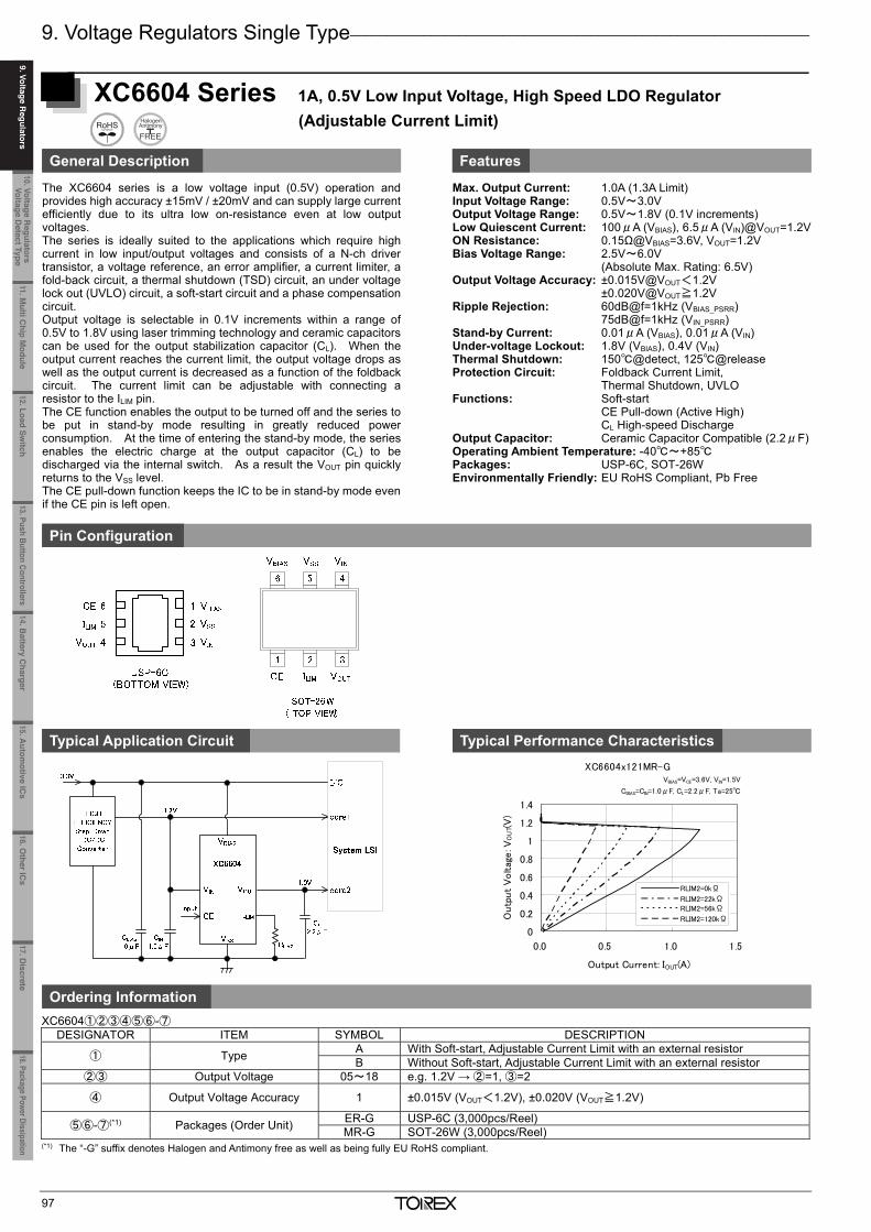
9. Voltage Regulators Single Type_______________________________________________________________
97
XC6604 Series 1A, 0.5V Low Input Voltage, High Speed LDO Regulator (Adjustable Current Limit)
General Description Features
The XC6604 series is a low voltage input (0.5V) operation and provides high accuracy ±15mV / ±20mV and can supply large current efficiently due to its ultra low on-resistance even at low output voltages. The series is ideally suited to the applications which require high current in low input/output voltages and consists of a N-ch driver transistor, a voltage reference, an error amplifier, a current limiter, a fold-back circuit, a thermal shutdown (TSD) circuit, an under voltage lock out (UVLO) circuit, a soft-start circuit and a phase compensation circuit. Output voltage is selectable in 0.1V increments within a range of 0.5V to 1.8V using laser trimming technology and ceramic capacitors can be used for the output stabilization capacitor (CL). When the output current reaches the current limit, the output voltage drops as well as the output current is decreased as a function of the foldback circuit. The current limit can be adjustable with connecting a resistor to the ILIM pin. The CE function enables the output to be turned off and the series to be put in stand-by mode resulting in greatly reduced power consumption. At the time of entering the stand-by mode, the series enables the electric charge at the output capacitor (CL) to be discharged via the internal switch. As a result the VOUT pin quickly returns to the VSS level. The CE pull-down function keeps the IC to be in stand-by mode even if the CE pin is left open.
Max. Output Current: 1.0A (1.3A Limit) Input Voltage Range: 0.5V~3.0V Output Voltage Range: 0.5V~1.8V (0.1V increments) Low Quiescent Current: 100μA (VBIAS), 6.5μA (VIN)@VOUT=1.2V ON Resistance: 0.15Ω@VBIAS=3.6V, VOUT=1.2V Bias Voltage Range: 2.5V~6.0V (Absolute Max. Rating: 6.5V) Output Voltage Accuracy: ±0.015V@VOUT<1.2V ±0.020V@VOUT≧1.2V Ripple Rejection: 60dB@f=1kHz (VBIAS_PSRR) 75dB@f=1kHz (VIN_PSRR) Stand-by Current: 0.01μA (VBIAS), 0.01μA (VIN) Under-voltage Lockout: 1.8V (VBIAS), 0.4V (VIN) Thermal Shutdown: 150@detect, 125@release Protection Circuit: Foldback Current Limit, Thermal Shutdown, UVLO Functions: Soft-start CE Pull-down (Active High) CL High-speed Discharge Output Capacitor: Ceramic Capacitor Compatible (2.2μF) Operating Ambient Temperature: -40~+85 Packages: USP-6C, SOT-26W Environmentally Friendly: EU RoHS Compliant, Pb Free
Pin Configuration
Typical Application Circuit Typical Performance Characteristics
Ordering Information XC6604①②③④⑤⑥-⑦
DESIGNATOR ITEM SYMBOL DESCRIPTION
① Type A With Soft-start, Adjustable Current Limit with an external resistor B Without Soft-start, Adjustable Current Limit with an external resistor
②③ Output Voltage 05~18 e.g. 1.2V → ②=1, ③=2
④ Output Voltage Accuracy 1 ±0.015V (VOUT<1.2V), ±0.020V (VOUT≧1.2V)
⑤⑥-⑦(*1) Packages (Order Unit) ER-G USP-6C (3,000pcs/Reel) MR-G SOT-26W (3,000pcs/Reel)
(*1) The “-G” suffix denotes Halogen and Antimony free as well as being fully EU RoHS compliant.
XC6604x121MR-G
0
0.2
0.4
0.6
0.8
1
1.2
1.4
0.0 0.5 1.0 1.5
Output Current: IOUT(A)
Outp
ut
Voltag
e: V
OU
T(V
)
RLIM2=0kΩ
RLIM2=22kΩRLIM2=56kΩ
RLIM2=120kΩ
VBIAS=VCE=3.6V, VIN=1.5V
CBIAS=CIN=1.0μF, CL=2.2μF, Ta=25
_______________________________________________________________________________________________________
98
XC6603 Series 1A, 0.5V Low Input Voltage, High Speed LDO Regulator (Adjustable Soft-start)
General Description Features
The XC6603 series is a low voltage input (0.5V) operation andprovides high accuracy ±15mV / ±20mV and can supply large currentefficiently due to its ultra low on-resistance even at low outputvoltages. The series is ideally suited to the applications which require highcurrent in low input/output voltages and consists of a N-ch drivertransistor, a voltage reference, an error amplifier, a current limiter, afoldback circuit, a thermal shutdown (TSD) circuit, an under voltagelock out (UVLO) circuit, a soft-start circuit and a phase compensationcircuit. Output voltage is selectable in 0.1V increments within a range of0.5V to 1.8V using laser trimming technology and ceramic capacitorscan be used for the output stabilization capacitor (CL). The inrushcurrent (IRUSH) from VIN to VOUT for charging CL at start-up can bereduced and makes the VIN stable. Soft-start time can be adjustablewith connecting a capacitor to the SS pin. The inrush currentconflicts with the soft-start time, therefore if soft-start is set longer,the inrush current is decreased. The CE function enables the output to be turned off and the series tobe put in stand-by mode resulting in greatly reduced powerconsumption. At the time of entering the stand-by mode, the seriesenables the electric charge at the output capacitor (CL) to bedischarged via the internal switch. As a result the VOUT pin quicklyreturns to the VSS level. The CE pull-down function keeps the IC to be in stand-by mode evenif the CE pin is left open.
Max. Output Current: 1.0A (1.3A Limit) Input Voltage Range: 0.5V~3.0V Output Voltage Range: 0.5V~1.8V (0.1V increments) Low Quiescent Current: 100μA (VBIAS), 6.5μA (VIN)@VOUT=1.2V ON Resistance: 0.15Ω@VBIAS=3.6V, VOUT=1.2V Bias Voltage Range: 2.5V~6.0V (Absolute Max. Rating: 6.5V) Output Voltage Accuracy: ±0.015V@VOUT<1.2V ±0.020V@VOUT≧1.2V Ripple Rejection: 60dB@f=1kHz (VBIAS_PSRR) 75dB@f=1kHz (VIN_PSRR) Stand-by Current: 0.01μA (VBIAS), 0.01μA (VIN) Under-voltage Lockout: 1.8V (VBIAS), 0.4V (VIN) Thermal Shutdown: 150@detect, 125@release Protection Circuit: Foldback Current Limit,
Thermal Shutdown, UVLO Functions: Adjustable Soft-start time with an
external capacitor CE Pull-down (Active High) CL Auto Discharge Output Capacitor: Ceramic Capacitor Compatible (2.2μF) Operating Ambient Temperature: -40~+85 Packages: USP-6C, SOT-26W Environmentally Friendly: EU RoHS Compliant, Pb Free
Pin Configuration
Typical Application Circuit Typical Performance Characteristics
Ordering Information XC6603①②③④⑤⑥-⑦
DESIGNATOR ITEM SYMBOL DESCRIPTION ① Type A Adjustable Soft-start time with an external capacitor
②③ Output Voltage 05~18 e.g. 1.2V → ②=1, ③=2
④ Output Voltage Accuracy 1 ±0.015V (VOUT<1.2V), ±0.020V (VOUT≧1.2V)
⑤⑥-⑦(*1) Packages (Order Unit) ER-G USP-6C (3,000pcs/Reel) MR-G SOT-26W (3,000pcs/Reel)
(*1) The “-G” suffix denotes Halogen and Antimony free as well as being fully EU RoHS compliant.
XC6603A121xR-G
-6
-4
-2
0
2
4
Time (1ms/div)
CE Inpu
t V
oltag
e: V
CE(V
)
-1
0
1
2
3
4
Outp
ut
Voltag
e: V
OU
T(V
)
VBIAS=3.6V, VCE=0V→3.6V(tr=5μs), VIN=1.5V
IOUT=100mA, CBIAS=CIN=1.0μF, CL=2.2μF, Ta=25
CE Input Voltage
Output Voltage
11.Multi C
hip Module
10. Voltage Regulators
Voltage Detect Type
9. Voltage Regulators
12.Load Switch
13. Push Button Controllers14.B
attery Charger
15.Autom
otive ICs
16.Other IC
s17. D
iscrete18.Package Power Dissipation
9. Voltage Regulators
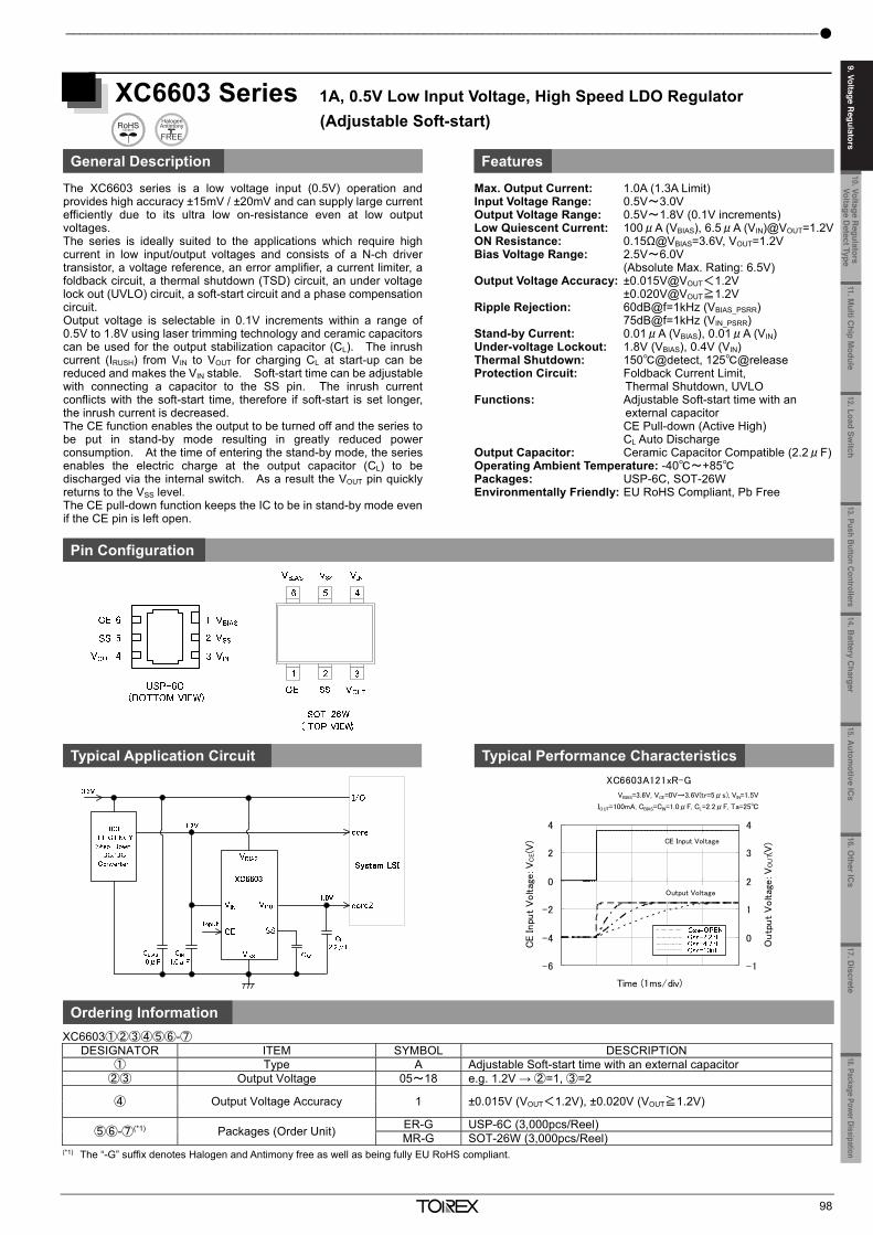
9. Voltage Regulators Single Type_______________________________________________________________
97
XC6604 Series 1A, 0.5V Low Input Voltage, High Speed LDO Regulator (Adjustable Current Limit)
General Description Features
The XC6604 series is a low voltage input (0.5V) operation and provides high accuracy ±15mV / ±20mV and can supply large current efficiently due to its ultra low on-resistance even at low output voltages. The series is ideally suited to the applications which require high current in low input/output voltages and consists of a N-ch driver transistor, a voltage reference, an error amplifier, a current limiter, a fold-back circuit, a thermal shutdown (TSD) circuit, an under voltage lock out (UVLO) circuit, a soft-start circuit and a phase compensation circuit. Output voltage is selectable in 0.1V increments within a range of 0.5V to 1.8V using laser trimming technology and ceramic capacitors can be used for the output stabilization capacitor (CL). When the output current reaches the current limit, the output voltage drops as well as the output current is decreased as a function of the foldback circuit. The current limit can be adjustable with connecting a resistor to the ILIM pin. The CE function enables the output to be turned off and the series to be put in stand-by mode resulting in greatly reduced power consumption. At the time of entering the stand-by mode, the series enables the electric charge at the output capacitor (CL) to be discharged via the internal switch. As a result the VOUT pin quickly returns to the VSS level. The CE pull-down function keeps the IC to be in stand-by mode even if the CE pin is left open.
Max. Output Current: 1.0A (1.3A Limit) Input Voltage Range: 0.5V~3.0V Output Voltage Range: 0.5V~1.8V (0.1V increments) Low Quiescent Current: 100μA (VBIAS), 6.5μA (VIN)@VOUT=1.2V ON Resistance: 0.15Ω@VBIAS=3.6V, VOUT=1.2V Bias Voltage Range: 2.5V~6.0V (Absolute Max. Rating: 6.5V) Output Voltage Accuracy: ±0.015V@VOUT<1.2V ±0.020V@VOUT≧1.2V Ripple Rejection: 60dB@f=1kHz (VBIAS_PSRR) 75dB@f=1kHz (VIN_PSRR) Stand-by Current: 0.01μA (VBIAS), 0.01μA (VIN) Under-voltage Lockout: 1.8V (VBIAS), 0.4V (VIN) Thermal Shutdown: 150@detect, 125@release Protection Circuit: Foldback Current Limit, Thermal Shutdown, UVLO Functions: Soft-start CE Pull-down (Active High) CL High-speed Discharge Output Capacitor: Ceramic Capacitor Compatible (2.2μF) Operating Ambient Temperature: -40~+85 Packages: USP-6C, SOT-26W Environmentally Friendly: EU RoHS Compliant, Pb Free
Pin Configuration
Typical Application Circuit Typical Performance Characteristics
Ordering Information XC6604①②③④⑤⑥-⑦
DESIGNATOR ITEM SYMBOL DESCRIPTION
① Type A With Soft-start, Adjustable Current Limit with an external resistor B Without Soft-start, Adjustable Current Limit with an external resistor
②③ Output Voltage 05~18 e.g. 1.2V → ②=1, ③=2
④ Output Voltage Accuracy 1 ±0.015V (VOUT<1.2V), ±0.020V (VOUT≧1.2V)
⑤⑥-⑦(*1) Packages (Order Unit) ER-G USP-6C (3,000pcs/Reel) MR-G SOT-26W (3,000pcs/Reel)
(*1) The “-G” suffix denotes Halogen and Antimony free as well as being fully EU RoHS compliant.
XC6604x121MR-G
0
0.2
0.4
0.6
0.8
1
1.2
1.4
0.0 0.5 1.0 1.5
Output Current: IOUT(A)
Outp
ut
Voltag
e: V
OU
T(V
)
RLIM2=0kΩ
RLIM2=22kΩRLIM2=56kΩ
RLIM2=120kΩ
VBIAS=VCE=3.6V, VIN=1.5V
CBIAS=CIN=1.0μF, CL=2.2μF, Ta=25
_______________________________________________________________________________________________________
98
XC6603 Series 1A, 0.5V Low Input Voltage, High Speed LDO Regulator (Adjustable Soft-start)
General Description Features
The XC6603 series is a low voltage input (0.5V) operation andprovides high accuracy ±15mV / ±20mV and can supply large currentefficiently due to its ultra low on-resistance even at low outputvoltages. The series is ideally suited to the applications which require highcurrent in low input/output voltages and consists of a N-ch drivertransistor, a voltage reference, an error amplifier, a current limiter, afoldback circuit, a thermal shutdown (TSD) circuit, an under voltagelock out (UVLO) circuit, a soft-start circuit and a phase compensationcircuit. Output voltage is selectable in 0.1V increments within a range of0.5V to 1.8V using laser trimming technology and ceramic capacitorscan be used for the output stabilization capacitor (CL). The inrushcurrent (IRUSH) from VIN to VOUT for charging CL at start-up can bereduced and makes the VIN stable. Soft-start time can be adjustablewith connecting a capacitor to the SS pin. The inrush currentconflicts with the soft-start time, therefore if soft-start is set longer,the inrush current is decreased. The CE function enables the output to be turned off and the series tobe put in stand-by mode resulting in greatly reduced powerconsumption. At the time of entering the stand-by mode, the seriesenables the electric charge at the output capacitor (CL) to bedischarged via the internal switch. As a result the VOUT pin quicklyreturns to the VSS level. The CE pull-down function keeps the IC to be in stand-by mode evenif the CE pin is left open.
Max. Output Current: 1.0A (1.3A Limit) Input Voltage Range: 0.5V~3.0V Output Voltage Range: 0.5V~1.8V (0.1V increments) Low Quiescent Current: 100μA (VBIAS), 6.5μA (VIN)@VOUT=1.2V ON Resistance: 0.15Ω@VBIAS=3.6V, VOUT=1.2V Bias Voltage Range: 2.5V~6.0V (Absolute Max. Rating: 6.5V) Output Voltage Accuracy: ±0.015V@VOUT<1.2V ±0.020V@VOUT≧1.2V Ripple Rejection: 60dB@f=1kHz (VBIAS_PSRR) 75dB@f=1kHz (VIN_PSRR) Stand-by Current: 0.01μA (VBIAS), 0.01μA (VIN) Under-voltage Lockout: 1.8V (VBIAS), 0.4V (VIN) Thermal Shutdown: 150@detect, 125@release Protection Circuit: Foldback Current Limit,
Thermal Shutdown, UVLO Functions: Adjustable Soft-start time with an
external capacitor CE Pull-down (Active High) CL Auto Discharge Output Capacitor: Ceramic Capacitor Compatible (2.2μF) Operating Ambient Temperature: -40~+85 Packages: USP-6C, SOT-26W Environmentally Friendly: EU RoHS Compliant, Pb Free
Pin Configuration
Typical Application Circuit Typical Performance Characteristics
Ordering Information XC6603①②③④⑤⑥-⑦
DESIGNATOR ITEM SYMBOL DESCRIPTION ① Type A Adjustable Soft-start time with an external capacitor
②③ Output Voltage 05~18 e.g. 1.2V → ②=1, ③=2
④ Output Voltage Accuracy 1 ±0.015V (VOUT<1.2V), ±0.020V (VOUT≧1.2V)
⑤⑥-⑦(*1) Packages (Order Unit) ER-G USP-6C (3,000pcs/Reel) MR-G SOT-26W (3,000pcs/Reel)
(*1) The “-G” suffix denotes Halogen and Antimony free as well as being fully EU RoHS compliant.
XC6603A121xR-G
-6
-4
-2
0
2
4
Time (1ms/div)
CE Inpu
t V
oltag
e: V
CE(V
)
-1
0
1
2
3
4
Outp
ut
Voltag
e: V
OU
T(V
)
VBIAS=3.6V, VCE=0V→3.6V(tr=5μs), VIN=1.5V
IOUT=100mA, CBIAS=CIN=1.0μF, CL=2.2μF, Ta=25
CE Input Voltage
Output Voltage
11.Multi C
hip Module
10. Voltage Regulators
Voltage Detect Type
12.Load Switch
13. Push Button Controllers14.B
attery Charger
15.Autom
otive ICs
16.Other IC
s17. D
iscrete18.Package Power Dissipation
9. Voltage Regulators
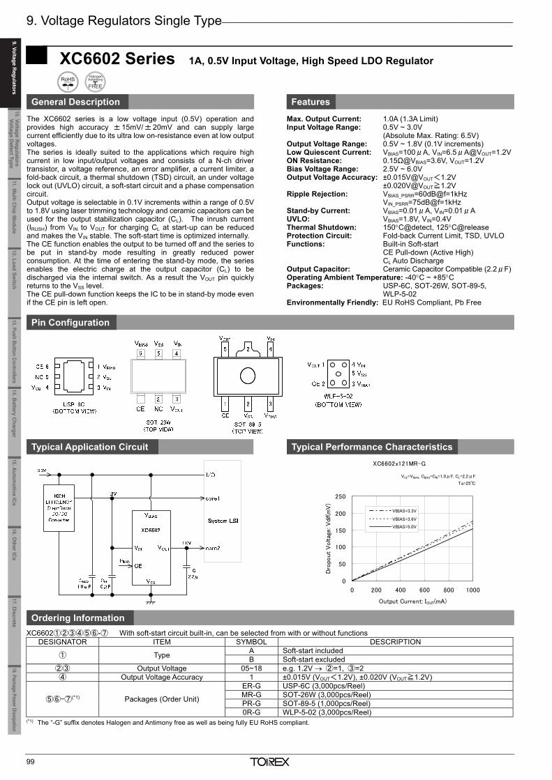
9. Voltage Regulators Single Type_______________________________________________________________
99
XC6602 Series 1A, 0.5V Input Voltage, High Speed LDO Regulator
General Description Features
The XC6602 series is a low voltage input (0.5V) operation and provides high accuracy ±15mV/±20mV and can supply large current efficiently due to its ultra low on-resistance even at low output voltages. The series is ideally suited to the applications which require high current in low input/output voltages and consists of a N-ch driver transistor, a voltage reference, an error amplifier, a current limiter, a fold-back circuit, a thermal shutdown (TSD) circuit, an under voltage lock out (UVLO) circuit, a soft-start circuit and a phase compensation circuit. Output voltage is selectable in 0.1V increments within a range of 0.5V to 1.8V using laser trimming technology and ceramic capacitors can be used for the output stabilization capacitor (CL). The inrush current (IRUSH) from VIN to VOUT for charging CL at start-up can be reduced and makes the VIN stable. The soft-start time is optimized internally. The CE function enables the output to be turned off and the series to be put in stand-by mode resulting in greatly reduced power consumption. At the time of entering the stand-by mode, the series enables the electric charge at the output capacitor (CL) to be discharged via the internal switch. As a result the VOUT pin quickly returns to the VSS level. The CE pull-down function keeps the IC to be in stand-by mode even if the CE pin is left open.
Max. Output Current: 1.0A (1.3A Limit) Input Voltage Range: 0.5V ~ 3.0V (Absolute Max. Rating: 6.5V) Output Voltage Range: 0.5V ~ 1.8V (0.1V increments) Low Quiescent Current: VBIAS=100μA, VIN=6.5μA@VOUT=1.2V ON Resistance: 0.15Ω@VBIAS=3.6V, VOUT=1.2V Bias Voltage Range: 2.5V ~ 6.0V Output Voltage Accuracy: ±0.015V@VOUT<1.2V ±0.020V@VOUT≧1.2V Ripple Rejection: VBIAS_PSRR=60dB@f=1kHz VIN_PSRR=75dB@f=1kHz Stand-by Current: VBIAS=0.01μA, VIN=0.01μA UVLO: VBIAS=1.8V, VIN=0.4V Thermal Shutdown: 150C@detect, 125C@release Protection Circuit: Fold-back Current Limit, TSD, UVLO Functions: Built-in Soft-start CE Pull-down (Active High) CL Auto Discharge Output Capacitor: Ceramic Capacitor Compatible (2.2μF) Operating Ambient Temperature: -40C ~ +85C Packages: USP-6C, SOT-26W, SOT-89-5, WLP-5-02 Environmentally Friendly: EU RoHS Compliant, Pb Free
Pin Configuration
Typical Application Circuit Typical Performance Characteristics
Ordering Information
XC6602①②③④⑤⑥-⑦ With soft-start circuit built-in, can be selected from with or without functions DESIGNATOR ITEM SYMBOL DESCRIPTION
① Type A Soft-start included B Soft-start excluded
②③ Output Voltage 05~18 e.g. 1.2V ②=1, ③=2 ④ Output Voltage Accuracy 1 ±0.015V (VOUT<1.2V), ±0.020V (VOUT≧1.2V)
⑤⑥-⑦(*1) Packages (Order Unit)
ER-G USP-6C (3,000pcs/Reel) MR-G SOT-26W (3,000pcs/Reel) PR-G SOT-89-5 (1,000pcs/Reel) 0R-G WLP-5-02 (3,000pcs/Reel)
(*1) The “-G” suffix denotes Halogen and Antimony free as well as being fully EU RoHS compliant.
XC6602x121MR-G
0
50
100
150
200
250
0 200 400 600 800 1000
Output Current: IOUT(mA)
Dro
pout
Voltag
e: V
dif(m
V)
VBIAS=3.3V
VBIAS=3.6V
VBIAS=5.0V
VCE=VBIAS, CBIAS=CIN=1.0μF, CL=2.2μF
Ta=25
_______________________________________________________________________________________________________
100
XC6601 Series 400mA Low Voltage Input LDO Voltage Regulators with Soft-start Function
General Description Features
The XC6601 series is a CMOS LDO voltage regulator with precise (±20mV) outputs which enables the operation in ultra low On resistanceeven where low output voltages to achieve high efficiency of the outputcurrent. The series is suited for the application which requires low dropoutvoltage operation. The series consists of a voltage reference, an erroramplifier, a driver transistor, a current limiter, a fold back circuit, a thermalshutdown (TSD) circuit, a Under Voltage Lock Out (UVLO) and a phasecompensation circuit. The output voltage is selectable in 0.05V increments within the range of0.7V to 1.8V using laser trimming technologies. The output stabilizationcapacitor (CL) is also compatible with low ESR ceramic capacitors. The over current protection circuit (the current limiter and the fold backcircuit) and the thermal shutdown circuit (the TSD circuit) are built-in.These two protection circuits will operate when the output current reacheslimit level or the junction temperature reaches temperature limit level. With the built-in UVLO function, the regulator output is forced OFF whenthe VBIAS pin or the VIN pin becomes the UVLO voltage or lower. The CE function enables the output to be turned off and the seriesbecomes a stand-by mode resulting in greatly reduced powerconsumption. At the time of entering the stand-by mode, the seriesenables the electric charge at the output capacitor (CL) to be dischargedvia the internal auto-discharge switch placed between the VOUT pin andthe VSS pin, as a result the VOUT pin quickly returns to the VSS level.
Max. Output Current: 400mA (Limiter 500mA TYP.) Input Voltage Range: 1.0V ~ 3.0V
(Absolute Max. Rating: 7.0V) (VIN≦VBIAS)
Output Voltage Range: 0.7V ~ 1.8V (0.05V increments) Dropout Voltage: 35mV@IOUT=100mA (TYP.)
(at VBIAS - VOUT=2.4V) Low Quiescent Current: IBIAS=25μA , IIN=1.0μA (TYP.)
IBIAS=0.01μA , IIN=0.01μA (TYP.) Bias Voltage Range: 2.5V ~ 6.0V
(VBIAS - VOUT≧0.9V) Output Voltage Accuracy: ±20mV UVLO: VBIAS=2.0V, VIN=0.4V (TYP.) Thermal Shutdown (Detect/Release): 150/125 (TYP.) CL High Speed Auto-Discharge Output Capacitor: Low ESR Ceramic Operating Ambient Temperature: -40 ~ +85 Packages: USP-6C, SOT-25, SOT-89-5 Environmentally Friendly: EU RoHS Compliant, Pb Free
Pin Configuration
Typical Application Circuit Typical Performance Characteristics
VBIAS =3.6V , VIN =1.5V , VOUT =1.2V
Dropout Voltage vs. Output Current
Ordering Information
XC6601①②③④⑤⑥-⑦
DESIGNATOR ITEM SYMBOL DESCRIPTION
① Type of Regulators A Pull-down Resistor Built-in B No Pull-down Resistor Built-in
②③ Output Voltage 07 ~ 18 e.g.) VOUT(T)=1.2V⇒②=1,③=2
④ Output Voltage 1 0.1V increments
e.g.) 1.2V⇒②=1,③=2,④=1
B 0.05V increments e.g.) 1.25V⇒=1,③=2,④=B
⑤⑥-⑦(*1) Packages (Order Unit)
MR-G SOT-25 (3,000pcs/Reel) ER-G USP-6C (3,000pcs/Reel) PR-G SOT-89-5 (1,000pcs/Reel)
(*1) The “-G” suffix denotes Halogen and Antimony free as well as being fully EU RoHS compliant.
VBIAS VOUT CE
VIN VSS VBIAS
XC6 6 0 1 B1 2 1 MR
0
50
100
150
200
250
300
0 100 200 300 400
Output Current: IOUT(mA)
Dro
pout
Volt
age: V
dif(m
V)
VBIAS=3.0V
VBIAS=3.3V
VBIAS=3.6V
VBIAS=4.2V
VBIAS=5.0V
Ta=25 []
11.Multi C
hip Module
10. Voltage Regulators
Voltage Detect Type
9. Voltage Regulators
12.Load Switch
13. Push Button Controllers14.B
attery Charger
15.Autom
otive ICs
16.Other IC
s17. D
iscrete18.Package Power Dissipation
9. Voltage Regulators
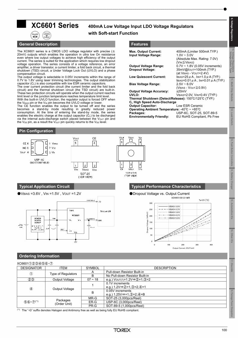
9. Voltage Regulators Single Type_______________________________________________________________
99
XC6602 Series 1A, 0.5V Input Voltage, High Speed LDO Regulator
General Description Features
The XC6602 series is a low voltage input (0.5V) operation and provides high accuracy ±15mV/±20mV and can supply large current efficiently due to its ultra low on-resistance even at low output voltages. The series is ideally suited to the applications which require high current in low input/output voltages and consists of a N-ch driver transistor, a voltage reference, an error amplifier, a current limiter, a fold-back circuit, a thermal shutdown (TSD) circuit, an under voltage lock out (UVLO) circuit, a soft-start circuit and a phase compensation circuit. Output voltage is selectable in 0.1V increments within a range of 0.5V to 1.8V using laser trimming technology and ceramic capacitors can be used for the output stabilization capacitor (CL). The inrush current (IRUSH) from VIN to VOUT for charging CL at start-up can be reduced and makes the VIN stable. The soft-start time is optimized internally. The CE function enables the output to be turned off and the series to be put in stand-by mode resulting in greatly reduced power consumption. At the time of entering the stand-by mode, the series enables the electric charge at the output capacitor (CL) to be discharged via the internal switch. As a result the VOUT pin quickly returns to the VSS level. The CE pull-down function keeps the IC to be in stand-by mode even if the CE pin is left open.
Max. Output Current: 1.0A (1.3A Limit) Input Voltage Range: 0.5V ~ 3.0V (Absolute Max. Rating: 6.5V) Output Voltage Range: 0.5V ~ 1.8V (0.1V increments) Low Quiescent Current: VBIAS=100μA, VIN=6.5μA@VOUT=1.2V ON Resistance: 0.15Ω@VBIAS=3.6V, VOUT=1.2V Bias Voltage Range: 2.5V ~ 6.0V Output Voltage Accuracy: ±0.015V@VOUT<1.2V ±0.020V@VOUT≧1.2V Ripple Rejection: VBIAS_PSRR=60dB@f=1kHz VIN_PSRR=75dB@f=1kHz Stand-by Current: VBIAS=0.01μA, VIN=0.01μA UVLO: VBIAS=1.8V, VIN=0.4V Thermal Shutdown: 150C@detect, 125C@release Protection Circuit: Fold-back Current Limit, TSD, UVLO Functions: Built-in Soft-start CE Pull-down (Active High) CL Auto Discharge Output Capacitor: Ceramic Capacitor Compatible (2.2μF) Operating Ambient Temperature: -40C ~ +85C Packages: USP-6C, SOT-26W, SOT-89-5, WLP-5-02 Environmentally Friendly: EU RoHS Compliant, Pb Free
Pin Configuration
Typical Application Circuit Typical Performance Characteristics
Ordering Information
XC6602①②③④⑤⑥-⑦ With soft-start circuit built-in, can be selected from with or without functions DESIGNATOR ITEM SYMBOL DESCRIPTION
① Type A Soft-start included B Soft-start excluded
②③ Output Voltage 05~18 e.g. 1.2V ②=1, ③=2 ④ Output Voltage Accuracy 1 ±0.015V (VOUT<1.2V), ±0.020V (VOUT≧1.2V)
⑤⑥-⑦(*1) Packages (Order Unit)
ER-G USP-6C (3,000pcs/Reel) MR-G SOT-26W (3,000pcs/Reel) PR-G SOT-89-5 (1,000pcs/Reel) 0R-G WLP-5-02 (3,000pcs/Reel)
(*1) The “-G” suffix denotes Halogen and Antimony free as well as being fully EU RoHS compliant.
XC6602x121MR-G
0
50
100
150
200
250
0 200 400 600 800 1000
Output Current: IOUT(mA)
Dro
pout
Voltag
e: V
dif(m
V)
VBIAS=3.3V
VBIAS=3.6V
VBIAS=5.0V
VCE=VBIAS, CBIAS=CIN=1.0μF, CL=2.2μF
Ta=25
_______________________________________________________________________________________________________
100
XC6601 Series 400mA Low Voltage Input LDO Voltage Regulators with Soft-start Function
General Description Features
The XC6601 series is a CMOS LDO voltage regulator with precise (±20mV) outputs which enables the operation in ultra low On resistanceeven where low output voltages to achieve high efficiency of the outputcurrent. The series is suited for the application which requires low dropoutvoltage operation. The series consists of a voltage reference, an erroramplifier, a driver transistor, a current limiter, a fold back circuit, a thermalshutdown (TSD) circuit, a Under Voltage Lock Out (UVLO) and a phasecompensation circuit. The output voltage is selectable in 0.05V increments within the range of0.7V to 1.8V using laser trimming technologies. The output stabilizationcapacitor (CL) is also compatible with low ESR ceramic capacitors. The over current protection circuit (the current limiter and the fold backcircuit) and the thermal shutdown circuit (the TSD circuit) are built-in.These two protection circuits will operate when the output current reacheslimit level or the junction temperature reaches temperature limit level. With the built-in UVLO function, the regulator output is forced OFF whenthe VBIAS pin or the VIN pin becomes the UVLO voltage or lower. The CE function enables the output to be turned off and the seriesbecomes a stand-by mode resulting in greatly reduced powerconsumption. At the time of entering the stand-by mode, the seriesenables the electric charge at the output capacitor (CL) to be dischargedvia the internal auto-discharge switch placed between the VOUT pin andthe VSS pin, as a result the VOUT pin quickly returns to the VSS level.
Max. Output Current: 400mA (Limiter 500mA TYP.) Input Voltage Range: 1.0V ~ 3.0V
(Absolute Max. Rating: 7.0V) (VIN≦VBIAS)
Output Voltage Range: 0.7V ~ 1.8V (0.05V increments) Dropout Voltage: 35mV@IOUT=100mA (TYP.)
(at VBIAS - VOUT=2.4V) Low Quiescent Current: IBIAS=25μA , IIN=1.0μA (TYP.)
IBIAS=0.01μA , IIN=0.01μA (TYP.) Bias Voltage Range: 2.5V ~ 6.0V
(VBIAS - VOUT≧0.9V) Output Voltage Accuracy: ±20mV UVLO: VBIAS=2.0V, VIN=0.4V (TYP.) Thermal Shutdown (Detect/Release): 150/125 (TYP.) CL High Speed Auto-Discharge Output Capacitor: Low ESR Ceramic Operating Ambient Temperature: -40 ~ +85 Packages: USP-6C, SOT-25, SOT-89-5 Environmentally Friendly: EU RoHS Compliant, Pb Free
Pin Configuration
Typical Application Circuit Typical Performance Characteristics
VBIAS =3.6V , VIN =1.5V , VOUT =1.2V
Dropout Voltage vs. Output Current
Ordering Information
XC6601①②③④⑤⑥-⑦
DESIGNATOR ITEM SYMBOL DESCRIPTION
① Type of Regulators A Pull-down Resistor Built-in B No Pull-down Resistor Built-in
②③ Output Voltage 07 ~ 18 e.g.) VOUT(T)=1.2V⇒②=1,③=2
④ Output Voltage 1 0.1V increments
e.g.) 1.2V⇒②=1,③=2,④=1
B 0.05V increments e.g.) 1.25V⇒=1,③=2,④=B
⑤⑥-⑦(*1) Packages (Order Unit)
MR-G SOT-25 (3,000pcs/Reel) ER-G USP-6C (3,000pcs/Reel) PR-G SOT-89-5 (1,000pcs/Reel)
(*1) The “-G” suffix denotes Halogen and Antimony free as well as being fully EU RoHS compliant.
VBIAS VOUT CE
VIN VSS VBIAS
XC6 6 0 1 B1 2 1 MR
0
50
100
150
200
250
300
0 100 200 300 400
Output Current: IOUT(mA)
Dro
pout
Volt
age: V
dif(m
V)
VBIAS=3.0V
VBIAS=3.3V
VBIAS=3.6V
VBIAS=4.2V
VBIAS=5.0V
Ta=25 []
11.Multi C
hip Module
10. Voltage Regulators
Voltage Detect Type
12.Load Switch
13. Push Button Controllers14.B
attery Charger
15.Autom
otive ICs
16.Other IC
s17. D
iscrete18.Package Power Dissipation
9. Voltage Regulators
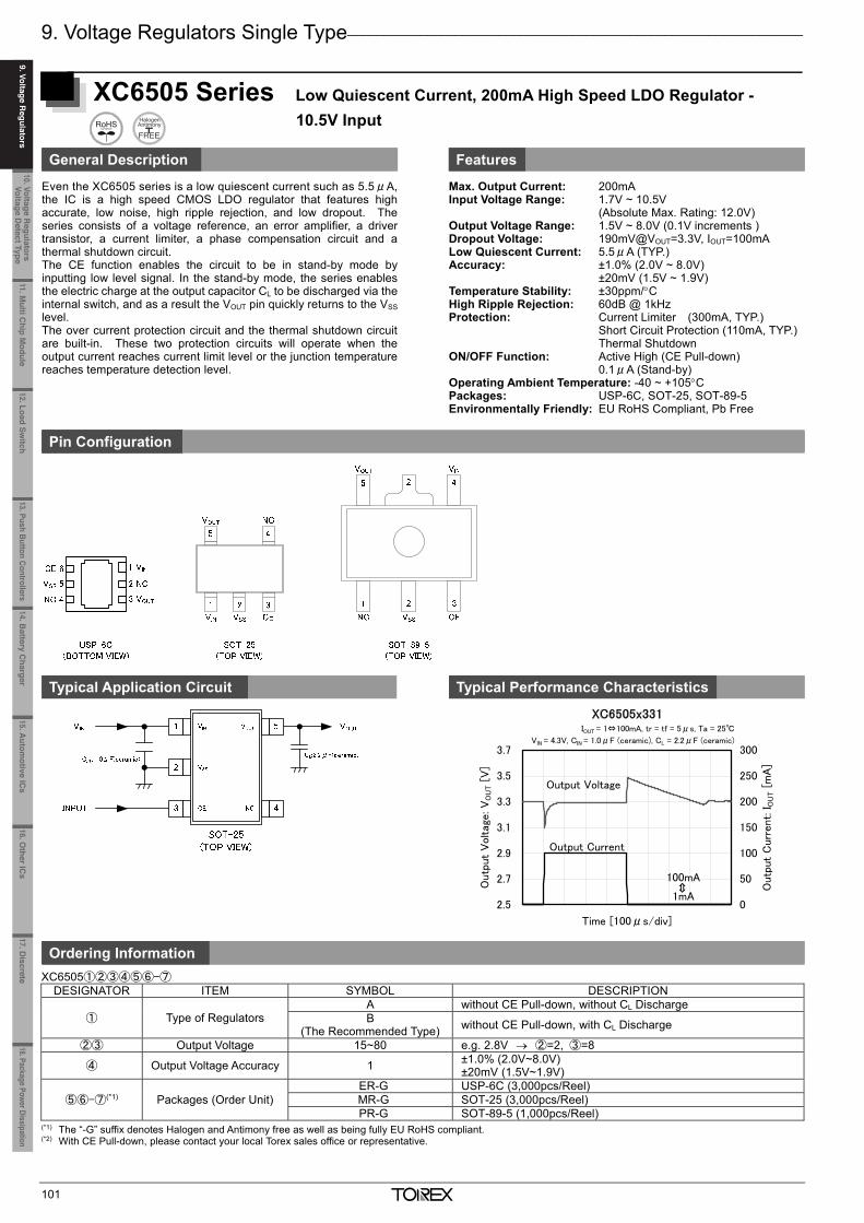
9. Voltage Regulators Single Type_______________________________________________________________
101
XC6505 Series Low Quiescent Current, 200mA High Speed LDO Regulator - 10.5V Input
General Description Features
Even the XC6505 series is a low quiescent current such as 5.5μA, the IC is a high speed CMOS LDO regulator that features high accurate, low noise, high ripple rejection, and low dropout. The series consists of a voltage reference, an error amplifier, a driver transistor, a current limiter, a phase compensation circuit and a thermal shutdown circuit. The CE function enables the circuit to be in stand-by mode by inputting low level signal. In the stand-by mode, the series enables the electric charge at the output capacitor CL to be discharged via the internal switch, and as a result the VOUT pin quickly returns to the VSS level. The over current protection circuit and the thermal shutdown circuit are built-in. These two protection circuits will operate when the output current reaches current limit level or the junction temperature reaches temperature detection level.
Max. Output Current: 200mA Input Voltage Range: 1.7V ~ 10.5V (Absolute Max. Rating: 12.0V) Output Voltage Range: 1.5V ~ 8.0V (0.1V increments ) Dropout Voltage: 190mV@VOUT=3.3V, IOUT=100mA Low Quiescent Current: 5.5μA (TYP.) Accuracy: ±1.0% (2.0V ~ 8.0V) ±20mV (1.5V ~ 1.9V) Temperature Stability: ±30ppm/C High Ripple Rejection: 60dB @ 1kHz Protection: Current Limiter (300mA, TYP.) Short Circuit Protection (110mA, TYP.) Thermal Shutdown ON/OFF Function: Active High (CE Pull-down) 0.1μA (Stand-by) Operating Ambient Temperature: -40 ~ +105C Packages: USP-6C, SOT-25, SOT-89-5 Environmentally Friendly: EU RoHS Compliant, Pb Free
Pin Configuration
Typical Application Circuit Typical Performance Characteristics
Ordering Information XC6505①②③④⑤⑥-⑦
DESIGNATOR ITEM SYMBOL DESCRIPTION
① Type of Regulators A without CE Pull-down, without CL Discharge B
(The Recommended Type) without CE Pull-down, with CL Discharge
②③ Output Voltage 15~80 e.g. 2.8V ②=2, ③=8
④ Output Voltage Accuracy 1 ±1.0% (2.0V~8.0V) ±20mV (1.5V~1.9V)
⑤⑥-⑦(*1) Packages (Order Unit) ER-G USP-6C (3,000pcs/Reel) MR-G SOT-25 (3,000pcs/Reel) PR-G SOT-89-5 (1,000pcs/Reel)
(*1) The “-G” suffix denotes Halogen and Antimony free as well as being fully EU RoHS compliant. (*2) With CE Pull-down, please contact your local Torex sales office or representative.
IOUT = 1⇔100mA, tr = tf = 5μs, Ta = 25
VIN = 4.3V, CIN = 1.0μF (ceramic), CL = 2.2μF (ceramic)
XC6505x331
2.5
2.7
2.9
3.1
3.3
3.5
3.7
Time [100μs/div]
Outp
ut
Voltag
e: V
OU
T [
V]
0
50
100
150
200
250
300
Outp
ut
Curr
ent: I
OU
T [
mA
]
⇔
Output Voltage
100mA
1mA
Output Current
_______________________________________________________________________________________________________
102
XC6504 Series 0.6μA Ultra Low Quiescent Current Small Voltage Regulator (CL Capacitor-less)
General Description Features
The XC6504 series is a highly accurate CMOS voltage regulatorthat achieves very low quiescent current operation of 0.6μA.Even output current is 1μA (when light load), the XC6504 canprovide high accurate outputs, which is ideally suited for theapplications to draw less output current. The usage of supersmall package USPN-4B02 (0.75 x 0.95mm) and the advantage ofcapacitor-less stable operation can contribute the board spacesaving outstandingly. The IC consists of a reference voltagesource, an error amplifier, a driver transistor, over-currentprotection circuit, and a phase compensation circuit. The device is compatible with a low ESR ceramic output capacitorCL. Moreover, the device can provide stable output even without aCL output capacitor because of the excellent internal phasecompensation. Output voltage is fixed internally by laser trimming technology andcan be selectable in 0.1V increments within the range of 1.1V to5.0V. The CE function enables the device to be put into standbymode by inputting a low level signal to the CE pin thereby reducingcurrent consumption to less than 0.1μA. In the standby mode, if aCL output capacitor is used, the electric charge stored at CL can bedischarged via the internal switch and as a result, the VOUT pinquickly returns to the VSS level.
Max. Output Current: 150mA Input Voltage Range: 1.4V~6.0V (Absolute Max. Rating: 6.5V) Output Voltage Range: 1.1V~5.0V (0.1V increments) Quiescent Current: 0.6μA (VOUT<1.9V) Output Accuracy: ±0.02V@VOUT<2.0V ±1.0%@VOUT≧2.0V Temperature Stability: ±50ppm/ Low On Resistance: 3.3Ω@VOUT=3.0V Standby Current: 0.01μA Protection Current: Current Limiter Shot Circuit Protection CE Function: CL Auto Discharge ON/OFF Logic=Enable High Output Capacitor: Low ESR Ceramic Capacitor (CL Capacitor-Less Compatible) Operating Ambient Temperature: -40~+85 Packages: USPQ-4B04 USPN-4B02 SSOT-24 SOT-25 Environmentally Friendly: EU RoHS Compliant, Pb Free
Pin Configuration
Typical Application Circuit Typical Performance Characteristics
Ordering Information XC6504①②③④⑤⑥-⑦
DESIGNATOR ITEM SYMBOL DESCRIPTION ① Type A With Current limiter, CE pull-down resistor, CL Auto discharge
②③ Output Voltage 11~50 e.g. 1.8V → ②=1, ③=8 ④ Output Voltage Accuracy 1 ±0.02V (VOUT<2.0V), ±1.0% (VOUT≧2.0V)
⑤⑥-⑦(*1) Packages (Order Unit)
9R-G USPQ-4B04 (3,000pcs/Reel) 7R-G USPN-4B02 (5,000pcs/Reel) NR-G SSOT-24 (3,000pcs/Reel) MR-G SOT-25 (3,000pcs/Reel)
(*1) The “-G” suffix denotes Halogen and Antimony free as well as being fully EU RoHS compliant.
XC6504x181xR
0.0
0.2
0.4
0.6
0.8
1.0
1.2
1.4
0 1 2 3 4 5 6
Input Voltage: VIN [V]
Supp
ly C
urr
ent: I
SS [
μA
]
Ta=-40
Ta=25
Ta=85
VCE=VINIOUT=0mA
CIN=CL=open
11.Multi C
hip Module
10. Voltage Regulators
Voltage Detect Type
9. Voltage Regulators
12.Load Switch
13. Push Button Controllers14.B
attery Charger
15.Autom
otive ICs
16.Other IC
s17. D
iscrete18.Package Power Dissipation
9. Voltage Regulators
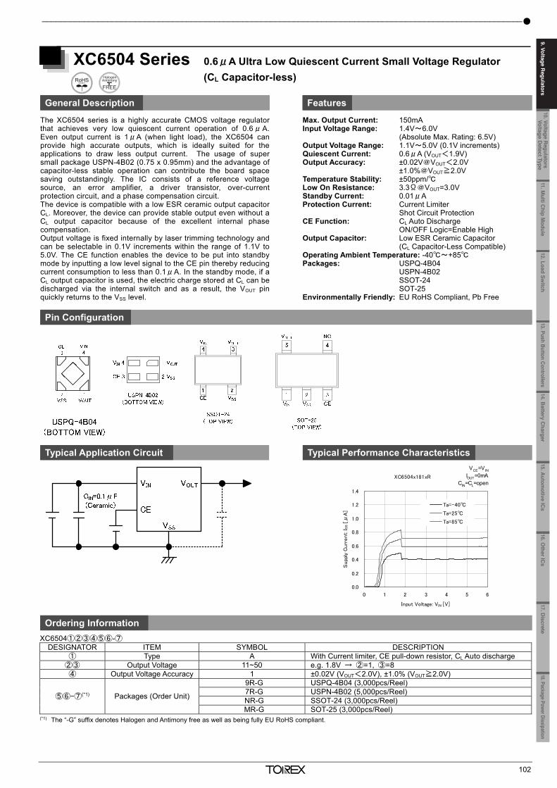
9. Voltage Regulators Single Type_______________________________________________________________
101
XC6505 Series Low Quiescent Current, 200mA High Speed LDO Regulator - 10.5V Input
General Description Features
Even the XC6505 series is a low quiescent current such as 5.5μA, the IC is a high speed CMOS LDO regulator that features high accurate, low noise, high ripple rejection, and low dropout. The series consists of a voltage reference, an error amplifier, a driver transistor, a current limiter, a phase compensation circuit and a thermal shutdown circuit. The CE function enables the circuit to be in stand-by mode by inputting low level signal. In the stand-by mode, the series enables the electric charge at the output capacitor CL to be discharged via the internal switch, and as a result the VOUT pin quickly returns to the VSS level. The over current protection circuit and the thermal shutdown circuit are built-in. These two protection circuits will operate when the output current reaches current limit level or the junction temperature reaches temperature detection level.
Max. Output Current: 200mA Input Voltage Range: 1.7V ~ 10.5V (Absolute Max. Rating: 12.0V) Output Voltage Range: 1.5V ~ 8.0V (0.1V increments ) Dropout Voltage: 190mV@VOUT=3.3V, IOUT=100mA Low Quiescent Current: 5.5μA (TYP.) Accuracy: ±1.0% (2.0V ~ 8.0V) ±20mV (1.5V ~ 1.9V) Temperature Stability: ±30ppm/C High Ripple Rejection: 60dB @ 1kHz Protection: Current Limiter (300mA, TYP.) Short Circuit Protection (110mA, TYP.) Thermal Shutdown ON/OFF Function: Active High (CE Pull-down) 0.1μA (Stand-by) Operating Ambient Temperature: -40 ~ +105C Packages: USP-6C, SOT-25, SOT-89-5 Environmentally Friendly: EU RoHS Compliant, Pb Free
Pin Configuration
Typical Application Circuit Typical Performance Characteristics
Ordering Information XC6505①②③④⑤⑥-⑦
DESIGNATOR ITEM SYMBOL DESCRIPTION
① Type of Regulators A without CE Pull-down, without CL Discharge B
(The Recommended Type) without CE Pull-down, with CL Discharge
②③ Output Voltage 15~80 e.g. 2.8V ②=2, ③=8
④ Output Voltage Accuracy 1 ±1.0% (2.0V~8.0V) ±20mV (1.5V~1.9V)
⑤⑥-⑦(*1) Packages (Order Unit) ER-G USP-6C (3,000pcs/Reel) MR-G SOT-25 (3,000pcs/Reel) PR-G SOT-89-5 (1,000pcs/Reel)
(*1) The “-G” suffix denotes Halogen and Antimony free as well as being fully EU RoHS compliant. (*2) With CE Pull-down, please contact your local Torex sales office or representative.
IOUT = 1⇔100mA, tr = tf = 5μs, Ta = 25
VIN = 4.3V, CIN = 1.0μF (ceramic), CL = 2.2μF (ceramic)
XC6505x331
2.5
2.7
2.9
3.1
3.3
3.5
3.7
Time [100μs/div]
Outp
ut
Voltag
e: V
OU
T [
V]
0
50
100
150
200
250
300
Outp
ut
Curr
ent: I
OU
T [
mA
]
⇔
Output Voltage
100mA
1mA
Output Current
_______________________________________________________________________________________________________
102
XC6504 Series 0.6μA Ultra Low Quiescent Current Small Voltage Regulator (CL Capacitor-less)
General Description Features
The XC6504 series is a highly accurate CMOS voltage regulatorthat achieves very low quiescent current operation of 0.6μA.Even output current is 1μA (when light load), the XC6504 canprovide high accurate outputs, which is ideally suited for theapplications to draw less output current. The usage of supersmall package USPN-4B02 (0.75 x 0.95mm) and the advantage ofcapacitor-less stable operation can contribute the board spacesaving outstandingly. The IC consists of a reference voltagesource, an error amplifier, a driver transistor, over-currentprotection circuit, and a phase compensation circuit. The device is compatible with a low ESR ceramic output capacitorCL. Moreover, the device can provide stable output even without aCL output capacitor because of the excellent internal phasecompensation. Output voltage is fixed internally by laser trimming technology andcan be selectable in 0.1V increments within the range of 1.1V to5.0V. The CE function enables the device to be put into standbymode by inputting a low level signal to the CE pin thereby reducingcurrent consumption to less than 0.1μA. In the standby mode, if aCL output capacitor is used, the electric charge stored at CL can bedischarged via the internal switch and as a result, the VOUT pinquickly returns to the VSS level.
Max. Output Current: 150mA Input Voltage Range: 1.4V~6.0V (Absolute Max. Rating: 6.5V) Output Voltage Range: 1.1V~5.0V (0.1V increments) Quiescent Current: 0.6μA (VOUT<1.9V) Output Accuracy: ±0.02V@VOUT<2.0V ±1.0%@VOUT≧2.0V Temperature Stability: ±50ppm/ Low On Resistance: 3.3Ω@VOUT=3.0V Standby Current: 0.01μA Protection Current: Current Limiter Shot Circuit Protection CE Function: CL Auto Discharge ON/OFF Logic=Enable High Output Capacitor: Low ESR Ceramic Capacitor (CL Capacitor-Less Compatible) Operating Ambient Temperature: -40~+85 Packages: USPQ-4B04 USPN-4B02 SSOT-24 SOT-25 Environmentally Friendly: EU RoHS Compliant, Pb Free
Pin Configuration
Typical Application Circuit Typical Performance Characteristics
Ordering Information XC6504①②③④⑤⑥-⑦
DESIGNATOR ITEM SYMBOL DESCRIPTION ① Type A With Current limiter, CE pull-down resistor, CL Auto discharge
②③ Output Voltage 11~50 e.g. 1.8V → ②=1, ③=8 ④ Output Voltage Accuracy 1 ±0.02V (VOUT<2.0V), ±1.0% (VOUT≧2.0V)
⑤⑥-⑦(*1) Packages (Order Unit)
9R-G USPQ-4B04 (3,000pcs/Reel) 7R-G USPN-4B02 (5,000pcs/Reel) NR-G SSOT-24 (3,000pcs/Reel) MR-G SOT-25 (3,000pcs/Reel)
(*1) The “-G” suffix denotes Halogen and Antimony free as well as being fully EU RoHS compliant.
XC6504x181xR
0.0
0.2
0.4
0.6
0.8
1.0
1.2
1.4
0 1 2 3 4 5 6
Input Voltage: VIN [V]
Supp
ly C
urr
ent: I
SS [
μA
]
Ta=-40
Ta=25
Ta=85
VCE=VINIOUT=0mA
CIN=CL=open
11.Multi C
hip Module
10. Voltage Regulators
Voltage Detect Type
12.Load Switch
13. Push Button Controllers14.B
attery Charger
15.Autom
otive ICs
16.Other IC
s17. D
iscrete18.Package Power Dissipation
9. Voltage Regulators
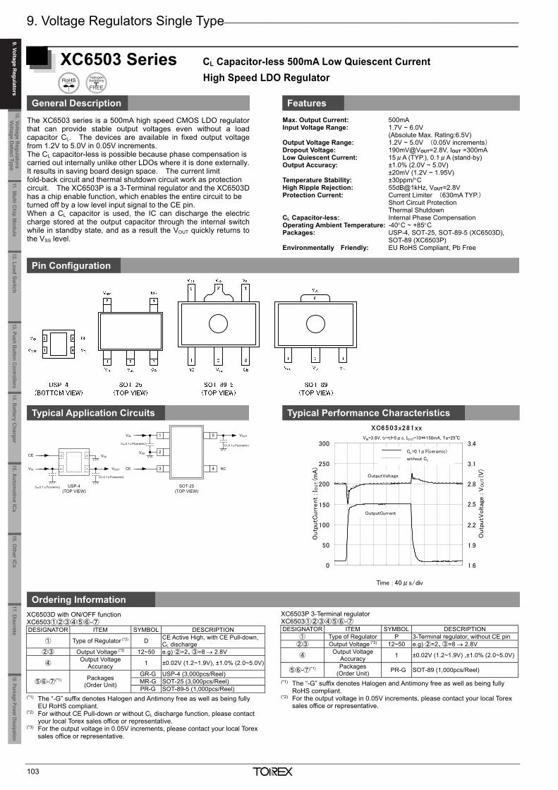
9. Voltage Regulators Single Type_______________________________________________________________
103
XC6503 Series CL Capacitor-less 500mA Low Quiescent Current High Speed LDO Regulator
General Description Features
The XC6503 series is a 500mA high speed CMOS LDO regulatorthat can provide stable output voltages even without a loadcapacitor CL. The devices are available in fixed output voltagefrom 1.2V to 5.0V in 0.05V increments. The CL capacitor-less is possible because phase compensation is carried out internally unlike other LDOs where it is done externally.It results in saving board design space. The current limit fold-back circuit and thermal shutdown circuit work as protection circuit. The XC6503P is a 3-Terminal regulator and the XC6503Dhas a chip enable function, which enables the entire circuit to be turned off by a low level input signal to the CE pin. When a CL capacitor is used, the IC can discharge the electriccharge stored at the output capacitor through the internal switchwhile in standby state, and as a result the VOUT quickly returns tothe VSS level.
Max. Output Current: 500mA Input Voltage Range: 1.7V ~ 6.0V (Absolute Max. Rating:6.5V) Output Voltage Range: 1.2V ~ 5.0V (0.05V increments) Dropout Voltage: 190mV@VOUT=2.8V, IOUT =300mA Low Quiescent Current: 15μA (TYP.), 0.1μA (stand-by) Output Accuracy: ±1.0% (2.0V ~ 5.0V) ±20mV (1.2V ~ 1.95V) Temperature Stability: ±30ppm/C High Ripple Rejection: 55dB@1kHz, VOUT=2.8V Protection Current: Current Limiter (630mA TYP.) Short Circuit Protection Thermal Shutdown CL Capacitor-less: Internal Phase Compensation Operating Ambient Temperature: -40C ~ +85C Packages: USP-4, SOT-25, SOT-89-5 (XC6503D), SOT-89 (XC6503P) Environmentally Friendly: EU RoHS Compliant, Pb Free
Pin Configuration
Typical Application Circuits Typical Performance Characteristics
Ordering Information
XC6503D with ON/OFF function XC6503①②③④⑤⑥-⑦
DESIGNATOR ITEM SYMBOL DESCRIPTION
① Type of Regulator (*2) D CE Active High, with CE Pull-down, CL discharge
②③ Output Voltage (*3) 12~50 e.g) ②=2、③=8 2.8V
④ Output Voltage Accuracy 1 ±0.02V (1.2~1.9V), ±1.0% (2.0~5.0V)
⑤⑥-⑦(*1) Packages (Order Unit)
GR-G USP-4 (3,000pcs/Reel) MR-G SOT-25 (3,000pcs/Reel) PR-G SOT-89-5 (1,000pcs/Reel)
(*1) The “-G” suffix denotes Halogen and Antimony free as well as being fully EU RoHS compliant.
(*2) For without CE Pull-down or without CL discharge function, please contact your local Torex sales office or representative.
(*3) For the output voltage in 0.05V increments, please contact your local Torex sales office or representative.
CL:0.1μF(ceramic)
CIN:0.1μF(ceramic)
VIN
CE
USP-4(TOP VIEW)
VOUT4
VSS3 2
1
SOT-25(TOP VIEW)
NC
5
4
1
3
2VSS
CE
VIN VOUT
CIN:0.1μF(ceramic) CL:0.1μF(ceramic)
XC6503x281xx
0
50
100
150
200
250
300
Time : 40μs/div
Outp
utC
urr
ent
: IO
UT (m
A)
1.6
1.9
2.2
2.5
2.8
3.1
3.4
Outp
utV
oltag
e :
VO
UT (V
)
OutputCurrent
VIN=3.8V, tr=tf=5μs, IOUT=10⇔150mA, Ta=25
CL=0.1μF(ceramic)
without CL
OutputVoltage
XC6503P 3-Terminal regulator XC6503①②③④⑤⑥-⑦
DESIGNATOR ITEM SYMBOL DESCRIPTION ① Type of Regulator P 3-Terminal regulator, without CE pin
②③ Output Voltage (*2) 12~50 e.g) ②=2、③=8 2.8V
④ Output Voltage Accuracy 1 ±0.02V (1.2~1.9V) ,±1.0% (2.0~5.0V)
⑤⑥-⑦(*1) Packages (Order Unit) PR-G SOT-89 (1,000pcs/Reel)
(*1) The “-G” suffix denotes Halogen and Antimony free as well as being fully RoHS compliant.
(*2) For the output voltage in 0.05V increments, please contact your local Torex sales office or representative.
_______________________________________________________________________________________________________
104
XC6501 Series CL Capacitor-less, Low Quiescent Current, 200mA High Speed LDO Regulator
General Description Features
The XC6501 series is a 6.0V high speed, low noise CMOS LDOregulator that can provide stable output voltages within a range of1.2V to 5.0V (0.05V increments) even without a load capacitor CL. This is possible because phase compensation is carried outinternally unlike other LDOs where it is done externally. The seriesconsists of a reference voltage source, driver transistor, erroramplifier, current limit circuit, and phase compensation circuit. The CE function enables the circuit to be put into stand-by mode byinputting a low level signal to the CE pin thereby reducing currentconsumption from an already low 13A (in operation) to less than0.1A. In the stand-by mode, if a CL cap is used, the electric chargestored at CL can be discharged via the internal auto-discharge switchand as a result, the VOUT pin quickly returns to the VSS level. The current limit fold-back circuit operates as a short circuitprotection and a current limiter function for the output pin.
Max. Output Current: 200mA Operating Voltage Range: 1.4V ~ 6.0V
(Absolute Max. Rating: 6.5V) Output Voltage Range: 2.0V~5.0V (±1%) (*1) 1.2V~1.95V (±0.02V) (*1)
Dropout Voltage: 150mV@IOUT=100mA, VOUT=2.8V Low Quiescent Current: 13A@VOUT=2.8V Accuracy: 1% (2.0V ~ 5.0V) 20mV (1.2V ~ 1.95V) Stand-by Current: Less than 0.1A (CE Active High) High Ripple Rejection: 50dB@f=1kHz,VOUT=2.8V Protection Circuits: Current limit (300mA, TYP.),
Short Circuit Protection Output capacitor is not required: Internal phase compensation CL High Speed Auto Discharge Operating Ambient Temperature: -40C ~ +85C Packages: SOT-25, SSOT-24, USP-4, USPN-4, USP-3,
WLP-4-01 Environmentally Friendly: EU RoHS Compliant, Pb Free (*1) WLP-4-01 : 2.0V~5.0V (±2%), 1.2V~1.95V (±0.03V)
Pin Configuration
Typical Application Circuits Typical Performance Characteristics
Ordering Information
XC6501①②③④⑤⑥-⑦ DESIGNATOR ITEM SYMBOL DESCRIPTION
① Regulator Type
A Without CE Pull-down, Without CL discharge B Without CE Pull-down, With CL discharge C With CE Pull-down, Without CL discharge D With CE Pull-down, With CL discharge P 3 pin, without CE pin (USP-3)
②③ Output Voltage 12 ~ 50 ex.)28V → ②=2, ③=8
④ Output Voltage Type [Accuracy]
1(*3) 0.1V increments ex.)1.80V → ②=1, ③=8, ④=1 [±0.02V @ 1.2V~1.9V, ±1% @ 2.0V~5.0V]
A(*3) 0.05V increments ex.)1.85V → ②=1, ③=8, ④=A [±0.02V @ 1.25V~1.95V, ±1% @ 1.5V~4.95V]
2(*4) 0.1V increments ex.)1.80V → ②=1, ③=8, ④=2 [±0.03V @ 1.2V~1.4V, ±2% @ 2.0V~5.0V]
B(*4) 0.05V increments ex.)1.85V → ②=1, ③=8, ④=B [±0.03V @ 1.25V~1.45V, ±2% @ 1.55V~4.95V]
⑤⑥-⑦(*1) Packages (Order Unit)
HR-G USP-3 (Only XC6501P) (3,000pcs/Reel)(*2) GR-G USP-4 (3,000pcs/Reel) NR-G SSOT-24 (3,000pcs/Reel) MR-G SOT-25 (3,000pcs/Reel) 7R-G USPN-4 (5,000pcs/Reel) 0R-G WLP-4-01 (5,000pcs/Reel)
(*1) The “-G” suffix denotes Halogen and Antimony free as well as being fully EU RoHS compliant. (*2) USP-3 is available only for XC6501P series. (*3) WLP-4-01 is excluded. (*4) WLP-4-01 only.
SSOT-24 (TOP VIEW)
SOT-25 (TOP VIEW)
VOUT
VIN
3V SS
2
1
CE
VIN
2
1 4
3 VSS
VOU
TUSP-3 (BOTTOM VIEW)
USP-4 (BOTTOM VIEW)
4 3
1 2 CE VSS
VIN VOUT 5 4
1 32CE
NC VOU
VSVIN
WLP-4-01 (BOTTOM VIEW)
2 VIN
3 CE
VOUT 1
VSS 4
11.Multi C
hip Module
10. Voltage Regulators
Voltage Detect Type
9. Voltage Regulators
12.Load Switch
13. Push Button Controllers14.B
attery Charger
15.Autom
otive ICs
16.Other IC
s17. D
iscrete18.Package Power Dissipation
9. Voltage Regulators
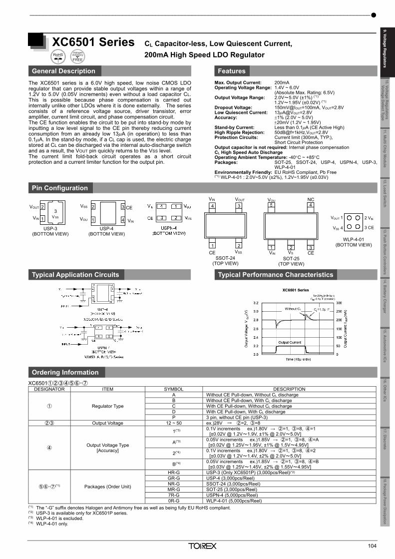
9. Voltage Regulators Single Type_______________________________________________________________
103
XC6503 Series CL Capacitor-less 500mA Low Quiescent Current High Speed LDO Regulator
General Description Features
The XC6503 series is a 500mA high speed CMOS LDO regulatorthat can provide stable output voltages even without a loadcapacitor CL. The devices are available in fixed output voltagefrom 1.2V to 5.0V in 0.05V increments. The CL capacitor-less is possible because phase compensation is carried out internally unlike other LDOs where it is done externally.It results in saving board design space. The current limit fold-back circuit and thermal shutdown circuit work as protection circuit. The XC6503P is a 3-Terminal regulator and the XC6503Dhas a chip enable function, which enables the entire circuit to be turned off by a low level input signal to the CE pin. When a CL capacitor is used, the IC can discharge the electriccharge stored at the output capacitor through the internal switchwhile in standby state, and as a result the VOUT quickly returns tothe VSS level.
Max. Output Current: 500mA Input Voltage Range: 1.7V ~ 6.0V (Absolute Max. Rating:6.5V) Output Voltage Range: 1.2V ~ 5.0V (0.05V increments) Dropout Voltage: 190mV@VOUT=2.8V, IOUT =300mA Low Quiescent Current: 15μA (TYP.), 0.1μA (stand-by) Output Accuracy: ±1.0% (2.0V ~ 5.0V) ±20mV (1.2V ~ 1.95V) Temperature Stability: ±30ppm/C High Ripple Rejection: 55dB@1kHz, VOUT=2.8V Protection Current: Current Limiter (630mA TYP.) Short Circuit Protection Thermal Shutdown CL Capacitor-less: Internal Phase Compensation Operating Ambient Temperature: -40C ~ +85C Packages: USP-4, SOT-25, SOT-89-5 (XC6503D), SOT-89 (XC6503P) Environmentally Friendly: EU RoHS Compliant, Pb Free
Pin Configuration
Typical Application Circuits Typical Performance Characteristics
Ordering Information
XC6503D with ON/OFF function XC6503①②③④⑤⑥-⑦
DESIGNATOR ITEM SYMBOL DESCRIPTION
① Type of Regulator (*2) D CE Active High, with CE Pull-down, CL discharge
②③ Output Voltage (*3) 12~50 e.g) ②=2、③=8 2.8V
④ Output Voltage Accuracy 1 ±0.02V (1.2~1.9V), ±1.0% (2.0~5.0V)
⑤⑥-⑦(*1) Packages (Order Unit)
GR-G USP-4 (3,000pcs/Reel) MR-G SOT-25 (3,000pcs/Reel) PR-G SOT-89-5 (1,000pcs/Reel)
(*1) The “-G” suffix denotes Halogen and Antimony free as well as being fully EU RoHS compliant.
(*2) For without CE Pull-down or without CL discharge function, please contact your local Torex sales office or representative.
(*3) For the output voltage in 0.05V increments, please contact your local Torex sales office or representative.
CL:0.1μF(ceramic)
CIN:0.1μF(ceramic)
VIN
CE
USP-4(TOP VIEW)
VOUT4
VSS3 2
1
SOT-25(TOP VIEW)
NC
5
4
1
3
2VSS
CE
VIN VOUT
CIN:0.1μF(ceramic) CL:0.1μF(ceramic)
XC6503x281xx
0
50
100
150
200
250
300
Time : 40μs/div
Outp
utC
urr
ent
: IO
UT (m
A)
1.6
1.9
2.2
2.5
2.8
3.1
3.4
Outp
utV
oltag
e :
VO
UT (V
)
OutputCurrent
VIN=3.8V, tr=tf=5μs, IOUT=10⇔150mA, Ta=25
CL=0.1μF(ceramic)
without CL
OutputVoltage
XC6503P 3-Terminal regulator XC6503①②③④⑤⑥-⑦
DESIGNATOR ITEM SYMBOL DESCRIPTION ① Type of Regulator P 3-Terminal regulator, without CE pin
②③ Output Voltage (*2) 12~50 e.g) ②=2、③=8 2.8V
④ Output Voltage Accuracy 1 ±0.02V (1.2~1.9V) ,±1.0% (2.0~5.0V)
⑤⑥-⑦(*1) Packages (Order Unit) PR-G SOT-89 (1,000pcs/Reel)
(*1) The “-G” suffix denotes Halogen and Antimony free as well as being fully RoHS compliant.
(*2) For the output voltage in 0.05V increments, please contact your local Torex sales office or representative.
_______________________________________________________________________________________________________
104
XC6501 Series CL Capacitor-less, Low Quiescent Current, 200mA High Speed LDO Regulator
General Description Features
The XC6501 series is a 6.0V high speed, low noise CMOS LDOregulator that can provide stable output voltages within a range of1.2V to 5.0V (0.05V increments) even without a load capacitor CL. This is possible because phase compensation is carried outinternally unlike other LDOs where it is done externally. The seriesconsists of a reference voltage source, driver transistor, erroramplifier, current limit circuit, and phase compensation circuit. The CE function enables the circuit to be put into stand-by mode byinputting a low level signal to the CE pin thereby reducing currentconsumption from an already low 13A (in operation) to less than0.1A. In the stand-by mode, if a CL cap is used, the electric chargestored at CL can be discharged via the internal auto-discharge switchand as a result, the VOUT pin quickly returns to the VSS level. The current limit fold-back circuit operates as a short circuitprotection and a current limiter function for the output pin.
Max. Output Current: 200mA Operating Voltage Range: 1.4V ~ 6.0V
(Absolute Max. Rating: 6.5V) Output Voltage Range: 2.0V~5.0V (±1%) (*1) 1.2V~1.95V (±0.02V) (*1)
Dropout Voltage: 150mV@IOUT=100mA, VOUT=2.8V Low Quiescent Current: 13A@VOUT=2.8V Accuracy: 1% (2.0V ~ 5.0V) 20mV (1.2V ~ 1.95V) Stand-by Current: Less than 0.1A (CE Active High) High Ripple Rejection: 50dB@f=1kHz,VOUT=2.8V Protection Circuits: Current limit (300mA, TYP.),
Short Circuit Protection Output capacitor is not required: Internal phase compensation CL High Speed Auto Discharge Operating Ambient Temperature: -40C ~ +85C Packages: SOT-25, SSOT-24, USP-4, USPN-4, USP-3,
WLP-4-01 Environmentally Friendly: EU RoHS Compliant, Pb Free (*1) WLP-4-01 : 2.0V~5.0V (±2%), 1.2V~1.95V (±0.03V)
Pin Configuration
Typical Application Circuits Typical Performance Characteristics
Ordering Information
XC6501①②③④⑤⑥-⑦ DESIGNATOR ITEM SYMBOL DESCRIPTION
① Regulator Type
A Without CE Pull-down, Without CL discharge B Without CE Pull-down, With CL discharge C With CE Pull-down, Without CL discharge D With CE Pull-down, With CL discharge P 3 pin, without CE pin (USP-3)
②③ Output Voltage 12 ~ 50 ex.)28V → ②=2, ③=8
④ Output Voltage Type [Accuracy]
1(*3) 0.1V increments ex.)1.80V → ②=1, ③=8, ④=1 [±0.02V @ 1.2V~1.9V, ±1% @ 2.0V~5.0V]
A(*3) 0.05V increments ex.)1.85V → ②=1, ③=8, ④=A [±0.02V @ 1.25V~1.95V, ±1% @ 1.5V~4.95V]
2(*4) 0.1V increments ex.)1.80V → ②=1, ③=8, ④=2 [±0.03V @ 1.2V~1.4V, ±2% @ 2.0V~5.0V]
B(*4) 0.05V increments ex.)1.85V → ②=1, ③=8, ④=B [±0.03V @ 1.25V~1.45V, ±2% @ 1.55V~4.95V]
⑤⑥-⑦(*1) Packages (Order Unit)
HR-G USP-3 (Only XC6501P) (3,000pcs/Reel)(*2) GR-G USP-4 (3,000pcs/Reel) NR-G SSOT-24 (3,000pcs/Reel) MR-G SOT-25 (3,000pcs/Reel) 7R-G USPN-4 (5,000pcs/Reel) 0R-G WLP-4-01 (5,000pcs/Reel)
(*1) The “-G” suffix denotes Halogen and Antimony free as well as being fully EU RoHS compliant. (*2) USP-3 is available only for XC6501P series. (*3) WLP-4-01 is excluded. (*4) WLP-4-01 only.
SSOT-24 (TOP VIEW)
SOT-25 (TOP VIEW)
VOUT
VIN
3V SS
2
1
CE
VIN
2
1 4
3 VSS
VOU
TUSP-3 (BOTTOM VIEW)
USP-4 (BOTTOM VIEW)
4 3
1 2 CE VSS
VIN VOUT 5 4
1 32CE
NC VOU
VSVIN
WLP-4-01 (BOTTOM VIEW)
2 VIN
3 CE
VOUT 1
VSS 4
11.Multi C
hip Module
10. Voltage Regulators
Voltage Detect Type
12.Load Switch
13. Push Button Controllers14.B
attery Charger
15.Autom
otive ICs
16.Other IC
s17. D
iscrete18.Package Power Dissipation
9. Voltage Regulators
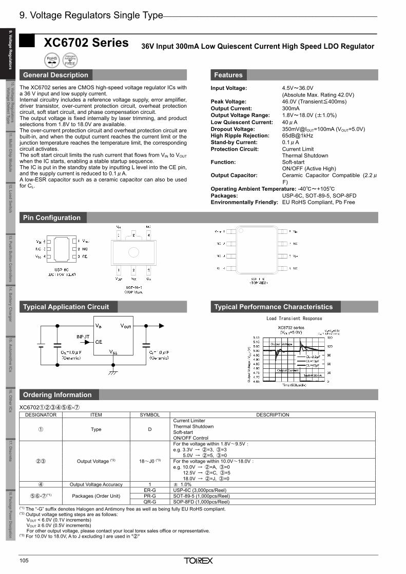
9. Voltage Regulators Single Type_______________________________________________________________
105
XC6702 Series 36V Input 300mA Low Quiescent Current High Speed LDO Regulator
General Description Features
The XC6702 series are CMOS high-speed voltage regulator ICs with a 36 V input and low supply current. Internal circuitry includes a reference voltage supply, error amplifier, driver transistor, over-current protection circuit, overheat protection circuit, soft start circuit, and phase compensation circuit. The output voltage is fixed internally by laser trimming, and product selections from 1.8V to 18.0V are available. The over-current protection circuit and overheat protection circuit are built-in, and when the output current reaches the current limit or the junction temperature reaches the temperature limit, the corresponding circuit activates. The soft start circuit limits the rush current that flows from VIN to VOUT when the IC starts, enabling a stable startup sequence. The IC is put in the standby state by inputting L level into the CE pin, and the supply current is reduced to 0.1μA. A low-ESR capacitor such as a ceramic capacitor can also be used for CL.
Input Voltage: 4.5V~36.0V (Absolute Max. Rating 42.0V) Peak Voltage: 46.0V (Transient≦400ms) Output Current: 300mA Output Voltage Range: 1.8V~18.0V (±1.0%) Low Quiescent Current: 40μA Dropout Voltage: 350mV@IOUT=100mA (VOUT=5.0V) High Ripple Rejection: 65dB@1kHz Stand-by Current: 0.1μA Protection Circuit: Current Limit Thermal Shutdown Function: Soft-start ON/OFF (Active High) Output Capacitor: Ceramic Capacitor Compatible (2.2μ
F) Operating Ambient Temperature: -40~+105
Packages: USP-6C, SOT-89-5, SOP-8FD Environmentally Friendly: EU RoHS Compliant, Pb Free
Pin Configuration
Typical Application Circuit Typical Performance Characteristics
Load Transient Response
Ordering Information
XC6702①②③④⑤⑥-⑦ DESIGNATOR ITEM SYMBOL DESCRIPTION
① Type D
Current Limiter Thermal Shutdown Soft-start ON/OFF Control
②③ Output Voltage (*2) 18~J0 (*3)
For the voltage within 1.8V~9.5V: e.g. 3.3V → ②=3, ③=3 5.0V → ②=5, ③=0 For the voltage within 10.0V~18.0V: e.g. 10.0V → ②=A, ③=0 12.5V → ②=C, ③=5 18.0V → ②=J, ③=0
④ Output Voltage Accuracy 1 ± 1.0%
⑤⑥-⑦(*1) Packages (Order Unit) ER-G USP-6C (3,000pcs/Reel) PR-G SOT-89-5 (1,000pcs/Reel) QR-G SOP-8FD (1,000pcs/Reel)
(*1) The “-G” suffix denotes Halogen and Antimony free as well as being fully EU RoHS compliant. (*2) Output voltage setting steps are as follows: VOUT < 6.0V (0.1V increments) VOUT ≥ 6.0V (0.5V increments) For other output voltage, please contact your local torex sales office or representative. (*3) For 10.0V to 18.0V, A to J excluding I are used in "②"
_______________________________________________________________________________________________________
106
XC6701 Series 28V Operation High Speed Voltage Regulators with Stand-by Function
General Description Features
The XC6701 series are positive voltage regulator ICs manufactured usingCMOS process with 28V of operation voltage. The series consists of avoltage reference, an error amplifier, a current limiter, a thermal shutdowncircuit and a phase compensation circuit plus a driver transistor. The output voltage is selectable in 0.1V increments within the range of 1.8V to18V which fixed by laser trimming technologies. The output stabilizationcapacitor (CL) is also compatible with low ESR ceramic capacitors. The over current protection circuit and the thermal shutdown circuit are built-in. These two protection circuits will operate when the output current reachescurrent limit level or the junction temperature reaches temperature limit level. The CE function can disable the output to be turned off and the IC becomes astand-by mode resulting in greatly reduced power consumption. Packagesare selectable depending on the applications from SOT-25, SOT-89,SOT-89-5, USP-6C, SOT-223, and TO-252.
Max. Output Current: 150mA (200mA limit) (VIN=VOUT+3.0V)
Dropout Voltage: 300mV@IOUT=20mA Input Voltage Range: 2.0V ~ 28.0V (Absolute Max. Rating: 30.0V) Output Voltage Range: 1.8V ~ 18.0V (0.1V increments) Accuracy: ±2.0% Low Quiescent Current: 50μA (VOUT=5.0V) Stand-by Current: Less than 0.1μA High Ripple Rejection: 50dB@1kHz Output Capacitor: Low ESR Ceramic Operating Ambient Temperature: -40C ~+105C (XC6701A) -40C ~+85C (XC6701B,D) Packages: SOT-25, SOT-89, SOT-89-5, USP-6C,
SOT-223, TO-252 Environmentally Friendly: EU RoHS Compliant, Pb Free
Pin Configuration Typical Application Circuit
Typical Performance Characteristics
Ordering Information
XC6701①②③④⑤⑥-⑦
DESIGNATOR ITEM SYMBOL DESCRIPTION
① Type
A Fixed output voltage, Active H (Operating Ambient Temperature: -40≦Topr≦105)
B Fixed output voltage, Active H (Operating Ambient Temperature: -40≦Topr≦85)
D Fixed output voltage, with no CE function (Operating Ambient Temperature: -40≦Topr≦85)
②③ Output Voltage 18~J0
For the voltage within 1.8V~9.9V, that voltage. For 10V,11V,12V,13V,14V,15V,16V,17V, and 18Vblocks, A, B, C, D, E, F, G, H, and J are respectively used for “②”. “②” and “③”are decimal voltage values. e.g.) 25 : 2.5V 50 : 5.0V B6 :11.6V F2 :15.2V J0 :18.0V
④ Output Voltage
Accuracy 2 ±2.0%
⑤⑥-⑦(*1) Packages (Order Unit)
MR-G SOT-25 (3,000pcs/Reel) (Type A/B Only) PR-G SOT-89-5 (1,000pcs/Reel) (Type A/B Only) ER-G USP-6C (3,000pcs/Reel) (Type A/B Only) FR-G SOT-223 (1,000pcs/Reel) (Type D Only) JR-G TO-252 (2,500pcs/Reel) (Type D Only) PR-G SOT-89 (1,000pcs/Reel) (Type D Only)
(*1) The “-G” suffix denotes Halogen and Antimony free as well as being fully EU RoHS compliant.
SOT-89-5(TOP VIEW)
SOT-89(TOP VIEW)
1 2 3
VINVOUT VSS
1 2 3
45 2
VOUT VSS CE
VIN NC
TO252(TOP VIEW)
1
2
3
VIN VSS VOUT
USP-6C(BOTTOM VIEW)
3
2
16
5
4
VIN
VSS
NC CE
VOUT
NC
1 32
5 4
VOUT CE
VIN VSS NC
SOT-25(TOP VIEW)
1 2 3
VINVSSVOUT
SOT-223(TOP VIEW)
2
2
2
TO-252 (TOP VIEW)
11.Multi C
hip Module
10. Voltage Regulators
Voltage Detect Type
9. Voltage Regulators
12.Load Switch
13. Push Button Controllers14.B
attery Charger
15.Autom
otive ICs
16.Other IC
s17. D
iscrete18.Package Power Dissipation
9. Voltage Regulators
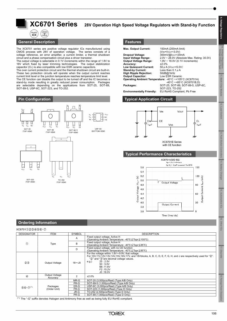
9. Voltage Regulators Single Type_______________________________________________________________
105
XC6702 Series 36V Input 300mA Low Quiescent Current High Speed LDO Regulator
General Description Features
The XC6702 series are CMOS high-speed voltage regulator ICs with a 36 V input and low supply current. Internal circuitry includes a reference voltage supply, error amplifier, driver transistor, over-current protection circuit, overheat protection circuit, soft start circuit, and phase compensation circuit. The output voltage is fixed internally by laser trimming, and product selections from 1.8V to 18.0V are available. The over-current protection circuit and overheat protection circuit are built-in, and when the output current reaches the current limit or the junction temperature reaches the temperature limit, the corresponding circuit activates. The soft start circuit limits the rush current that flows from VIN to VOUT when the IC starts, enabling a stable startup sequence. The IC is put in the standby state by inputting L level into the CE pin, and the supply current is reduced to 0.1μA. A low-ESR capacitor such as a ceramic capacitor can also be used for CL.
Input Voltage: 4.5V~36.0V (Absolute Max. Rating 42.0V) Peak Voltage: 46.0V (Transient≦400ms) Output Current: 300mA Output Voltage Range: 1.8V~18.0V (±1.0%) Low Quiescent Current: 40μA Dropout Voltage: 350mV@IOUT=100mA (VOUT=5.0V) High Ripple Rejection: 65dB@1kHz Stand-by Current: 0.1μA Protection Circuit: Current Limit Thermal Shutdown Function: Soft-start ON/OFF (Active High) Output Capacitor: Ceramic Capacitor Compatible (2.2μ
F) Operating Ambient Temperature: -40~+105
Packages: USP-6C, SOT-89-5, SOP-8FD Environmentally Friendly: EU RoHS Compliant, Pb Free
Pin Configuration
Typical Application Circuit Typical Performance Characteristics
Load Transient Response
Ordering Information
XC6702①②③④⑤⑥-⑦ DESIGNATOR ITEM SYMBOL DESCRIPTION
① Type D
Current Limiter Thermal Shutdown Soft-start ON/OFF Control
②③ Output Voltage (*2) 18~J0 (*3)
For the voltage within 1.8V~9.5V: e.g. 3.3V → ②=3, ③=3 5.0V → ②=5, ③=0 For the voltage within 10.0V~18.0V: e.g. 10.0V → ②=A, ③=0 12.5V → ②=C, ③=5 18.0V → ②=J, ③=0
④ Output Voltage Accuracy 1 ± 1.0%
⑤⑥-⑦(*1) Packages (Order Unit) ER-G USP-6C (3,000pcs/Reel) PR-G SOT-89-5 (1,000pcs/Reel) QR-G SOP-8FD (1,000pcs/Reel)
(*1) The “-G” suffix denotes Halogen and Antimony free as well as being fully EU RoHS compliant. (*2) Output voltage setting steps are as follows: VOUT < 6.0V (0.1V increments) VOUT ≥ 6.0V (0.5V increments) For other output voltage, please contact your local torex sales office or representative. (*3) For 10.0V to 18.0V, A to J excluding I are used in "②"
_______________________________________________________________________________________________________
106
XC6701 Series 28V Operation High Speed Voltage Regulators with Stand-by Function
General Description Features
The XC6701 series are positive voltage regulator ICs manufactured usingCMOS process with 28V of operation voltage. The series consists of avoltage reference, an error amplifier, a current limiter, a thermal shutdowncircuit and a phase compensation circuit plus a driver transistor. The output voltage is selectable in 0.1V increments within the range of 1.8V to18V which fixed by laser trimming technologies. The output stabilizationcapacitor (CL) is also compatible with low ESR ceramic capacitors. The over current protection circuit and the thermal shutdown circuit are built-in. These two protection circuits will operate when the output current reachescurrent limit level or the junction temperature reaches temperature limit level. The CE function can disable the output to be turned off and the IC becomes astand-by mode resulting in greatly reduced power consumption. Packagesare selectable depending on the applications from SOT-25, SOT-89,SOT-89-5, USP-6C, SOT-223, and TO-252.
Max. Output Current: 150mA (200mA limit) (VIN=VOUT+3.0V)
Dropout Voltage: 300mV@IOUT=20mA Input Voltage Range: 2.0V ~ 28.0V (Absolute Max. Rating: 30.0V) Output Voltage Range: 1.8V ~ 18.0V (0.1V increments) Accuracy: ±2.0% Low Quiescent Current: 50μA (VOUT=5.0V) Stand-by Current: Less than 0.1μA High Ripple Rejection: 50dB@1kHz Output Capacitor: Low ESR Ceramic Operating Ambient Temperature: -40C ~+105C (XC6701A) -40C ~+85C (XC6701B,D) Packages: SOT-25, SOT-89, SOT-89-5, USP-6C,
SOT-223, TO-252 Environmentally Friendly: EU RoHS Compliant, Pb Free
Pin Configuration Typical Application Circuit
Typical Performance Characteristics
Ordering Information
XC6701①②③④⑤⑥-⑦
DESIGNATOR ITEM SYMBOL DESCRIPTION
① Type
A Fixed output voltage, Active H (Operating Ambient Temperature: -40≦Topr≦105)
B Fixed output voltage, Active H (Operating Ambient Temperature: -40≦Topr≦85)
D Fixed output voltage, with no CE function (Operating Ambient Temperature: -40≦Topr≦85)
②③ Output Voltage 18~J0
For the voltage within 1.8V~9.9V, that voltage. For 10V,11V,12V,13V,14V,15V,16V,17V, and 18Vblocks, A, B, C, D, E, F, G, H, and J are respectively used for “②”. “②” and “③”are decimal voltage values. e.g.) 25 : 2.5V 50 : 5.0V B6 :11.6V F2 :15.2V J0 :18.0V
④ Output Voltage
Accuracy 2 ±2.0%
⑤⑥-⑦(*1) Packages (Order Unit)
MR-G SOT-25 (3,000pcs/Reel) (Type A/B Only) PR-G SOT-89-5 (1,000pcs/Reel) (Type A/B Only) ER-G USP-6C (3,000pcs/Reel) (Type A/B Only) FR-G SOT-223 (1,000pcs/Reel) (Type D Only) JR-G TO-252 (2,500pcs/Reel) (Type D Only) PR-G SOT-89 (1,000pcs/Reel) (Type D Only)
(*1) The “-G” suffix denotes Halogen and Antimony free as well as being fully EU RoHS compliant.
SOT-89-5(TOP VIEW)
SOT-89(TOP VIEW)
1 2 3
VINVOUT VSS
1 2 3
45 2
VOUT VSS CE
VIN NC
TO252(TOP VIEW)
1
2
3
VIN VSS VOUT
USP-6C(BOTTOM VIEW)
3
2
16
5
4
VIN
VSS
NC CE
VOUT
NC
1 32
5 4
VOUT CE
VIN VSS NC
SOT-25(TOP VIEW)
1 2 3
VINVSSVOUT
SOT-223(TOP VIEW)
2
2
2
TO-252 (TOP VIEW)
11.Multi C
hip Module
10. Voltage Regulators
Voltage Detect Type
12.Load Switch
13. Push Button Controllers14.B
attery Charger
15.Autom
otive ICs
16.Other IC
s17. D
iscrete18.Package Power Dissipation
9. Voltage Regulators
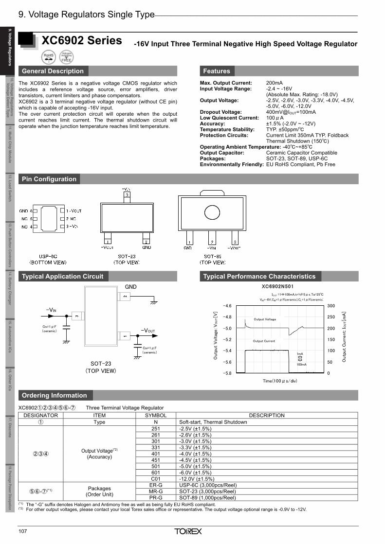
9. Voltage Regulators Single Type_______________________________________________________________
107
XC6902 Series -16V Input Three Terminal Negative High Speed Voltage Regulator
General Description Features
The XC6902 Series is a negative voltage CMOS regulator which includes a reference voltage source, error amplifiers, driver transistors, current limiters and phase compensators. XC6902 is a 3 terminal negative voltage regulator (without CE pin) which is capable of accepting -16V input. The over current protection circuit will operate when the output current reaches limit current. The thermal shutdown circuit will operate when the junction temperature reaches limit temperature.
Max. Output Current: 200mA Input Voltage Range: -2.4 ~ -16V (Absolute Max. Rating: -18.0V) Output Voltage: -2.5V, -2.6V, -3.0V, -3.3V, -4.0V, -4.5V, -5.0V, -6.0V, -12.0V Dropout Voltage: 400mV@IOUT=100mA Low Quiescent Current: 100μA Accuracy: ±1.5% (-2.0V ~ -12V) Temperature Stability: TYP. ±50ppm/ Protection Circuits: Current Limit 350mA TYP. Foldback Thermal Shutdown (150) Operating Ambient Temperature: -40~+85 Output Capacitor: Ceramic Capacitor Compatible Packages: SOT-23, SOT-89, USP-6C Environmentally Friendly: EU RoHS Compliant, Pb Free
Pin Configuration
Typical Application Circuit Typical Performance Characteristics
Ordering Information
XC6902①②③④⑤⑥-⑦ Three Terminal Voltage Regulator DESIGNATOR ITEM SYMBOL DESCRIPTION
① Type N Soft-start, Thermal Shutdown
②③④ Output Voltage(*2)
(Accuracy)
251 -2.5V (±1.5%) 261 -2.6V (±1.5%) 301 -3.0V (±1.5%) 331 -3.3V (±1.5%) 401 -4.0V (±1.5%) 451 -4.5V (±1.5%) 501 -5.0V (±1.5%) 601 -6.0V (±1.5%) C01 -12.0V (±1.5%)
⑤⑥-⑦(*1) Packages (Order Unit)
ER-G USP-6C (3,000pcs/Reel) MR-G SOT-23 (3,000pcs/Reel) PR-G SOT-89 (1,000pcs/Reel)
(*1) The “-G” suffix denotes Halogen and Antimony free as well as being fully EU RoHS compliant. (*2) For other output voltages, please contact your local Torex sales office or representative. The output voltage optional range is -0.9V to -12V.
SOT-23(TOP VIEW)
GND
-VIN
-VOUT
CIN=1μF(ceramic)
CIN=1μF(ceramic)
XC6902N501
-5.8
-5.6
-5.4
-5.2
-5.0
-4.8
-4.6
Time(100μs/div)
Outp
ut
Voltag
e: V
OU
T [V
]
0
50
100
150
200
250
300
Outp
ut
Curr
ent: I
OU
T [m
A]
Output Current
Output Voltage
1mA
100mA
IOUT =1⇔100mA,tr=tf=5μs,Ta=25
VIN=-6V,CIN=1μF(ceramic),CL=1μF(ceramic)
_______________________________________________________________________________________________________
108
XC6901 Series 200mA Negative Voltage High Speed Regulator with ON/OFF Control
General Description Features
The XC6901 Series is a negative voltage CMOS regulator whichincludes a reference voltage source, error amplifier, driver transistor,current limiter and phase compensator. The CE function enables the circuit to be in stand-by mode byinputting low level signal. In the stand-by mode, the electric charge atthe output capacitor (CL) will be discharged via the internalauto-discharge switch and as a result the -VOUT pin quickly returns tothe VSS level. The over current protection circuit will operate when the outputcurrent reaches limit current. The thermal shutdown circuit willoperate when the junction temperature reaches limit temperature.
Max. Output Current: 200mA Input Voltage Range: -2.4V~-12.4V(VCE=3.6V) (Absolute Max. Rating: -18V+VCE) Output Voltage Range: -0.9V~-12.0V Dropout Voltage: 400mV@IOUT=100mA Low Quiescent Current: 100μA Output Voltage Accuracy: ±1.5% (VOUT<-2.0V) ±0.03V (-VOUT≧-2.0V) Temperature Stability: TYP.±50ppm/ CE High Level Voltage: +1.2V, Active High Stand-by Current: 0.1μA Protection Circuits: Current Limit 350mA TYP, Foldback Overheat Protection TTSB=150 Function: CL High-speed Discharge Output Capacitor: Ceramic Capacitor Compatible Operating Ambient Temperature: -40~+85 Packages: SOT-25, SOT-89-5, USP-6C Environmentally Friendly: EU RoHS Compliant, Pb Free
Pin Configuration
Typical Application Circuits Typical Performance Characteristics
Ordering Information
XC6901①②③④⑤⑥-⑦ ON/OFF Control Voltage Regulator (CE Active High) DESIGNATOR ITEM SYMBOL DESCRIPTION
① Type (*2) D CE Pull-down resistor CL Auto-discharge
②③ Output Voltage 09~C0 -0.9V~-12V e.g. -0.9V→②=0, ③=9, -12V→②=C, ③=0 A:10, B:11, C:12
④ Output Type 1 0.10V Increments
e.g. -1.2V→②=1, ③=2, ④=1
B 0.05V Increments for -0.95V~-4.95V e.g. -1.25V→②=1, ③=2, ④=B
⑤⑥-⑦(*1) Packages (Order Unit)
ER-G USP-6C (3,000pcs/Reel) MR-G SOT-25 (3,000pcs/Reel) PR-G SOT-89-5 (1,000pcs/Reel)
(*1) The “-G” suffix denotes Halogen and Antimony free as well as being fully EU RoHS compliant. (*2 For the type without CL auto-discharge, please contact your local Torex sales office or
representative.
SOT-25
(TOP VIEW)
GND
-VIN
CE
-VOUT
NC
CL:1.0μF
(ceramic)
CIN:1.0μF
(ceramic)
XC6901x501
-5.8
-5.6
-5.4
-5.2
-5.0
-4.8
-4.6
Time(100μs/div)
Outp
ut
Voltag
e: V
OU
T [V
]
0
50
100
150
200
250
300
Outp
ut
Curr
ent: I
OU
T [m
A]
Output Current
Output Voltage
1mA
100mA
IOUT =1⇔100mA,tr=tf=5μs,Ta=25,VCE=1.5V
VIN=-6V,CIN=1μF(ceramic),CL=1μF(ceramic)
STANDARD VOLTAGE Examples for standard voltage
VOUT (V)
PACKAGES USP-6C SOT-25 SOT-89-5
-1.2V XC6901D121ER-G XC6901D121MR-G XC6901D121PR-G -2.5V XC6901D251ER-G XC6901D251MR-G XC6901D251PR-G -2.6V XC6901D261ER-G XC6901D261MR-G XC6901D261PR-G -3.0V XC6901D301ER-G XC6901D301MR-G XC6901D301PR-G -3.3V XC6901D331ER-G XC6901D331MR-G XC6901D331PR-G -4.0V XC6901D401ER-G XC6901D401MR-G XC6901D401PR-G -4.5V XC6901D451ER-G XC6901D451MR-G XC6901D451PR-G -5.0V XC6901D501ER-G XC6901D501MR-G XC6901D501PR-G -6.0V XC6901D601ER-G XC6901D601MR-G XC6901D601PR-G
-12.0V XC6901DC01ER-G XC6901DC01MR-G XC6901DC01PR-G
11.Multi C
hip Module
10. Voltage Regulators
Voltage Detect Type
9. Voltage Regulators
12.Load Switch
13. Push Button Controllers14.B
attery Charger
15.Autom
otive ICs
16.Other IC
s17. D
iscrete18.Package Power Dissipation
9. Voltage Regulators
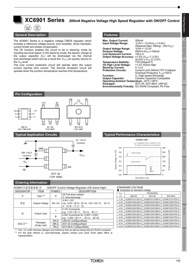
9. Voltage Regulators Single Type_______________________________________________________________
107
XC6902 Series -16V Input Three Terminal Negative High Speed Voltage Regulator
General Description Features
The XC6902 Series is a negative voltage CMOS regulator which includes a reference voltage source, error amplifiers, driver transistors, current limiters and phase compensators. XC6902 is a 3 terminal negative voltage regulator (without CE pin) which is capable of accepting -16V input. The over current protection circuit will operate when the output current reaches limit current. The thermal shutdown circuit will operate when the junction temperature reaches limit temperature.
Max. Output Current: 200mA Input Voltage Range: -2.4 ~ -16V (Absolute Max. Rating: -18.0V) Output Voltage: -2.5V, -2.6V, -3.0V, -3.3V, -4.0V, -4.5V, -5.0V, -6.0V, -12.0V Dropout Voltage: 400mV@IOUT=100mA Low Quiescent Current: 100μA Accuracy: ±1.5% (-2.0V ~ -12V) Temperature Stability: TYP. ±50ppm/ Protection Circuits: Current Limit 350mA TYP. Foldback Thermal Shutdown (150) Operating Ambient Temperature: -40~+85 Output Capacitor: Ceramic Capacitor Compatible Packages: SOT-23, SOT-89, USP-6C Environmentally Friendly: EU RoHS Compliant, Pb Free
Pin Configuration
Typical Application Circuit Typical Performance Characteristics
Ordering Information
XC6902①②③④⑤⑥-⑦ Three Terminal Voltage Regulator DESIGNATOR ITEM SYMBOL DESCRIPTION
① Type N Soft-start, Thermal Shutdown
②③④ Output Voltage(*2)
(Accuracy)
251 -2.5V (±1.5%) 261 -2.6V (±1.5%) 301 -3.0V (±1.5%) 331 -3.3V (±1.5%) 401 -4.0V (±1.5%) 451 -4.5V (±1.5%) 501 -5.0V (±1.5%) 601 -6.0V (±1.5%) C01 -12.0V (±1.5%)
⑤⑥-⑦(*1) Packages (Order Unit)
ER-G USP-6C (3,000pcs/Reel) MR-G SOT-23 (3,000pcs/Reel) PR-G SOT-89 (1,000pcs/Reel)
(*1) The “-G” suffix denotes Halogen and Antimony free as well as being fully EU RoHS compliant. (*2) For other output voltages, please contact your local Torex sales office or representative. The output voltage optional range is -0.9V to -12V.
SOT-23(TOP VIEW)
GND
-VIN
-VOUT
CIN=1μF(ceramic)
CIN=1μF(ceramic)
XC6902N501
-5.8
-5.6
-5.4
-5.2
-5.0
-4.8
-4.6
Time(100μs/div)
Outp
ut
Voltag
e: V
OU
T [V
]
0
50
100
150
200
250
300
Outp
ut
Curr
ent: I
OU
T [m
A]
Output Current
Output Voltage
1mA
100mA
IOUT =1⇔100mA,tr=tf=5μs,Ta=25
VIN=-6V,CIN=1μF(ceramic),CL=1μF(ceramic)
_______________________________________________________________________________________________________
108
XC6901 Series 200mA Negative Voltage High Speed Regulator with ON/OFF Control
General Description Features
The XC6901 Series is a negative voltage CMOS regulator whichincludes a reference voltage source, error amplifier, driver transistor,current limiter and phase compensator. The CE function enables the circuit to be in stand-by mode byinputting low level signal. In the stand-by mode, the electric charge atthe output capacitor (CL) will be discharged via the internalauto-discharge switch and as a result the -VOUT pin quickly returns tothe VSS level. The over current protection circuit will operate when the outputcurrent reaches limit current. The thermal shutdown circuit willoperate when the junction temperature reaches limit temperature.
Max. Output Current: 200mA Input Voltage Range: -2.4V~-12.4V(VCE=3.6V) (Absolute Max. Rating: -18V+VCE) Output Voltage Range: -0.9V~-12.0V Dropout Voltage: 400mV@IOUT=100mA Low Quiescent Current: 100μA Output Voltage Accuracy: ±1.5% (VOUT<-2.0V) ±0.03V (-VOUT≧-2.0V) Temperature Stability: TYP.±50ppm/ CE High Level Voltage: +1.2V, Active High Stand-by Current: 0.1μA Protection Circuits: Current Limit 350mA TYP, Foldback Overheat Protection TTSB=150 Function: CL High-speed Discharge Output Capacitor: Ceramic Capacitor Compatible Operating Ambient Temperature: -40~+85 Packages: SOT-25, SOT-89-5, USP-6C Environmentally Friendly: EU RoHS Compliant, Pb Free
Pin Configuration
Typical Application Circuits Typical Performance Characteristics
Ordering Information
XC6901①②③④⑤⑥-⑦ ON/OFF Control Voltage Regulator (CE Active High) DESIGNATOR ITEM SYMBOL DESCRIPTION
① Type (*2) D CE Pull-down resistor CL Auto-discharge
②③ Output Voltage 09~C0 -0.9V~-12V e.g. -0.9V→②=0, ③=9, -12V→②=C, ③=0 A:10, B:11, C:12
④ Output Type 1 0.10V Increments
e.g. -1.2V→②=1, ③=2, ④=1
B 0.05V Increments for -0.95V~-4.95V e.g. -1.25V→②=1, ③=2, ④=B
⑤⑥-⑦(*1) Packages (Order Unit)
ER-G USP-6C (3,000pcs/Reel) MR-G SOT-25 (3,000pcs/Reel) PR-G SOT-89-5 (1,000pcs/Reel)
(*1) The “-G” suffix denotes Halogen and Antimony free as well as being fully EU RoHS compliant. (*2 For the type without CL auto-discharge, please contact your local Torex sales office or
representative.
SOT-25
(TOP VIEW)
GND
-VIN
CE
-VOUT
NC
CL:1.0μF
(ceramic)
CIN:1.0μF
(ceramic)
XC6901x501
-5.8
-5.6
-5.4
-5.2
-5.0
-4.8
-4.6
Time(100μs/div)
Outp
ut
Voltag
e: V
OU
T [V
]
0
50
100
150
200
250
300
Outp
ut
Curr
ent: I
OU
T [m
A]
Output Current
Output Voltage
1mA
100mA
IOUT =1⇔100mA,tr=tf=5μs,Ta=25,VCE=1.5V
VIN=-6V,CIN=1μF(ceramic),CL=1μF(ceramic)
STANDARD VOLTAGE Examples for standard voltage
VOUT (V)
PACKAGES USP-6C SOT-25 SOT-89-5
-1.2V XC6901D121ER-G XC6901D121MR-G XC6901D121PR-G -2.5V XC6901D251ER-G XC6901D251MR-G XC6901D251PR-G -2.6V XC6901D261ER-G XC6901D261MR-G XC6901D261PR-G -3.0V XC6901D301ER-G XC6901D301MR-G XC6901D301PR-G -3.3V XC6901D331ER-G XC6901D331MR-G XC6901D331PR-G -4.0V XC6901D401ER-G XC6901D401MR-G XC6901D401PR-G -4.5V XC6901D451ER-G XC6901D451MR-G XC6901D451PR-G -5.0V XC6901D501ER-G XC6901D501MR-G XC6901D501PR-G -6.0V XC6901D601ER-G XC6901D601MR-G XC6901D601PR-G
-12.0V XC6901DC01ER-G XC6901DC01MR-G XC6901DC01PR-G
11.Multi C
hip Module
10. Voltage Regulators
Voltage Detect Type
12.Load Switch
13. Push Button Controllers14.B
attery Charger
15.Autom
otive ICs
16.Other IC
s17. D
iscrete18.Package Power Dissipation
9. Voltage Regulators
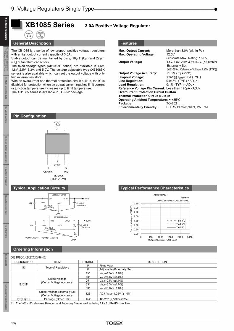
9. Voltage Regulators Single Type_____________________________________________________________
109
XB1085 Series 3.0A Positive Voltage Regulator General Description Features
The XB1085 is a series of low dropout positive voltage regulatorswith a high output current capacity of 3.0A . Stable output can be maintained by using 10μF (CIN) and 22μF (CL) of tantalum capacitors. The fixed voltage types (XB1085P series) are available in 1.5V,1.8V, 2.5V, 3.3V, and 5.0V. The voltage adjustable type (XB1085Kseries) is also available which can set the output voltage with onlytwo external resistors. With an overcurrent and thermal protection circuit built-in, the IC is disabled for protection when an output current reaches limit currentor junction temperature increases up to limit temperature. The XB1085 series is available in TO-252 package.
Max. Output Current: More than 3.0A (within Pd) Max. Operating Voltage: 12.0V (Absolute Max. Rating: 18.0V) Output Voltage: 1.5V, 1.8V, 2.5V, 3.3V, 5.0V, (XB1085P)
Externally Set (XB1085K/ Reference Voltage 1.25V (TYP.))
Output Voltage Accuracy: ±1.0% ( Tj =25) Dropout Voltage: 1.3V @ IOUT=3.0A (TYP.) Line Regulation: 0.015% (TYP.) <ADJ> Load Regulation: 0.1% (TYP.) <ADJ> Reference Voltage Pin Current: Less than 120μA <ADJ> Overcurrent Protection Circuit Built-in Thermal Protection Circuit Built-in Operating Ambient Temperature: ~ +85C Package: TO-252 Environmentally Friendly: EU RoHS Compliant, Pb Free
Pin Configuration
Typical Application Circuits Typical Performance Characteristics
Ordering Information
XB1085①②③④⑤⑥-⑦ DESIGNATOR ITEM SYNBOL DESCRIPTION
① Type of Regulators P Fixed VOUT K Adjustable (Externally Set)
②③④
Output Voltage (Output Voltage Accuracy)
151 VOUT=1.5V (±1.0%) 181 VOUT=1.8V (±1.0%) 251 VOUT=2.5V (±1.0%) 331 VOUT=3.3V (±1.0%) 501 VOUT=5.0V (±1.0%)
Output Voltage Externally Set (Output Voltage Accuracy) 12B ADJ, VOUT=1.25V (±1.0%)
⑤⑥-⑦(*1) Package (Order Unit) JR-G TO-252 (2,500pcs/Reel) (*1) The “-G” suffix denotes Halogen and Antimony free as well as being fully EU RoHS compliant.
TO-252 (TOP VIEW)
XB1085P Series
VIN VOUT
VSS
IOUT
VINCIN=10uF(Tantalum)
CL=22uF(Tantalum)
XB1085K Series
VIN VOUT
ADJ
IOUT
VINCIN=10uF
(Tantalum)
CL=22uF(Tantalum)R1
R2
VOUT=VREF×(1+R2/R1) + IADJ×R2
XB1085P331
0.00
0.50
1.00
1.50
2.00
2.50
3.00
3.50
0 600 1200 1800 2400 3000Output Current: IOUT (mA)
Outp
ut
Voltag
e: V
OU
T(V
)
Ta=85
Ta=25
Ta=0
VIN=4.9V
CIN=10μF(Tantal),CL=22μF(Tantal)
1 3
2
2
VSS/ADJ
VOUT
(Tab)
VIN
VOUT
______________________________________________________ 10. Voltage Regulators Voltage Detect Type
110
XC6413/XC6414 Series 10V, 300mA/500mA High Speed LDO Regulators with Voltage Detector
General Description Features The XC6413/XC6414 series are highly precise, low noise, positivevoltage LDO regulators with voltage detector manufactured usingCMOS processes. Performance features of the series includes highripple rejection and low dropout and the series features a voltagereference, an error amplifier, a current limiter and a phasecompensation circuit plus a driver transistor. Detect voltage isselectable in 0.1V increments within a range of 0.9V ~ 6.0V and VRoutput voltage is selectable within a range of 0.9V~5.5V. The series is also compatible with low ESR ceramic capacitors whichgive added output stability. This stability can be maintained evenduring load fluctuations due to the excellent transient response of theseries. The current limiter's foldback circuit operates as a short-circuitprotection as well as the output current limiter for the output pin. Theseries provides optional user selection from a variety of circuitapplications, such as detector monitoring, detector output logic andinternal pull-up / down resistance. The XC6413/XC6414FY types can delay the detector output. Delaytime can be controlled by the use of an external capacitor(semi-custom).
Max. Output Current: 300mA (380mA limit) (1.8V≤VROUT≤5.5V)[XC6413] 500mA (600mA limit) (2.5V≤VROUT≤5.5V)[XC6414]
Operating Voltage Range: 2.0V ~ 10.0V (Absolute Max. Rating: 12.0V) VR Setting Output Voltage: 0.9V ~ 5.5V (0.1V increments) Dropout Voltage: 200mV (IROUT=100mA) Low Quiescent Current: 35μA (TYP.) VD Detect Voltage Setting: 0.9V ~ 6.0V (0.1V increments) When Monitoring VIN: more than 2.0V VR Setting Voltage Accuracy: ± 2.0% VD Detect Voltage Accuracy: ± 2.0% VR.VD Temperature Coefficient: ± 100ppm/ (TYP.) High Ripple Rejection: 65dB (10kHz) Output Capacitor: Low ESR Ceramic Operating Ambient Temperature: - 40 ~ + 85 Packages: SOT-25, USP-6B, SOT-89-5 Environmentally Friendly: EU RoHS Compliant, Pb Free
Pin Configuration Typical Application Circuits
Ordering Information XC6413 / XC6414①②③④⑤⑥-⑦ DESIGNATOR ITEM SYMBOL DESCRIPTION
① Operational Function F Cd pin
② Type of Regulator Y VD Sense pin : VROUT, VD Output Logic :
Detect L
③④
Output Voltage &
Detect Voltage
-
Internally set sequential number relating to output voltage and detect voltage (refer to the chart PIN NUMBER: ③④ Table) VR setting output voltage range: 0.9V ~ 5.5V Detect voltage setting range: 0.9V ~ 6.0V 100mV increments are available
⑤⑥-⑦(*1) Packages (Order Unit)
MR-G SOT-25 (3,000pcs/Reel) PR-G SOT-89-5 (1,000pcs/Reel) DR-G USP-6B (3,000pcs/Reel))
(*1) The “-G” suffix denotes Halogen and Antimony free as well as being fully EURoHS compliant.
PIN NUMBER: ③,④ Types (80 ~ 99 : Standard voltage products) ③④ VROUT VDOUT ③④ VROUT VDOUT ③④ VROUT VDOUT ③④ VROUT VDOUT 01 11 80 1.8 1.6 90 1.3 2.0 02 12 81 2.8 3.1 91 1.5 2.0 03 13 82 1.8 2.0 92 04 14 83 2.5 2.8 93 05 15 84 2.85 3.2 94 06 16 85 3.0 3.3 95 07 17 86 3.5 3.8 96 08 18 87 3.0 4.2 97 09 19 88 3.3 4.0 98 10 20 89 99
For other voltage, please contact your local Torex sales office or representative.
VSS
Cd
Cd
Cd
11.Multi C
hip Module
10. Voltage Regulators
Voltage Detect Type
9. Voltage Regulators
12.Load Switch
13. Push Button Controllers14.B
attery Charger
15.Autom
otive ICs
16.Other IC
s17. D
iscrete18.Package Power Dissipation
9. Voltage Regulators
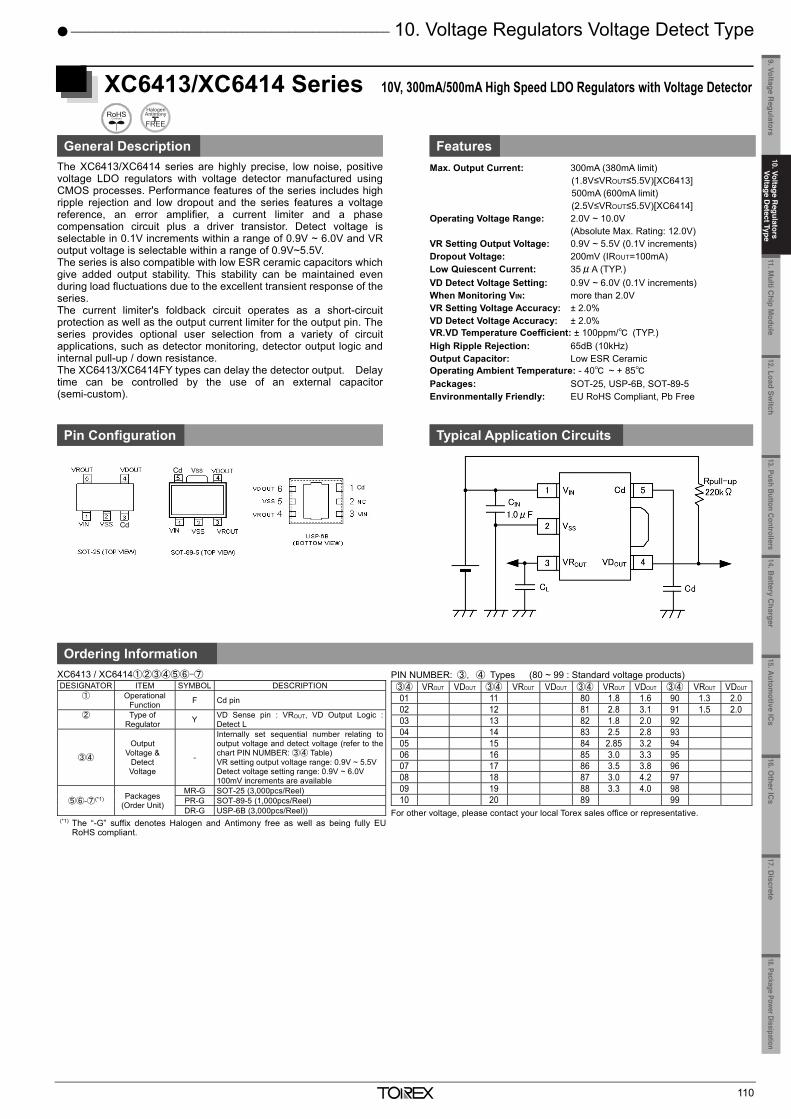
9. Voltage Regulators Single Type_____________________________________________________________
109
XB1085 Series 3.0A Positive Voltage Regulator General Description Features
The XB1085 is a series of low dropout positive voltage regulatorswith a high output current capacity of 3.0A . Stable output can be maintained by using 10μF (CIN) and 22μF (CL) of tantalum capacitors. The fixed voltage types (XB1085P series) are available in 1.5V,1.8V, 2.5V, 3.3V, and 5.0V. The voltage adjustable type (XB1085Kseries) is also available which can set the output voltage with onlytwo external resistors. With an overcurrent and thermal protection circuit built-in, the IC is disabled for protection when an output current reaches limit currentor junction temperature increases up to limit temperature. The XB1085 series is available in TO-252 package.
Max. Output Current: More than 3.0A (within Pd) Max. Operating Voltage: 12.0V (Absolute Max. Rating: 18.0V) Output Voltage: 1.5V, 1.8V, 2.5V, 3.3V, 5.0V, (XB1085P)
Externally Set (XB1085K/ Reference Voltage 1.25V (TYP.))
Output Voltage Accuracy: ±1.0% ( Tj =25) Dropout Voltage: 1.3V @ IOUT=3.0A (TYP.) Line Regulation: 0.015% (TYP.) <ADJ> Load Regulation: 0.1% (TYP.) <ADJ> Reference Voltage Pin Current: Less than 120μA <ADJ> Overcurrent Protection Circuit Built-in Thermal Protection Circuit Built-in Operating Ambient Temperature: ~ +85C Package: TO-252 Environmentally Friendly: EU RoHS Compliant, Pb Free
Pin Configuration
Typical Application Circuits Typical Performance Characteristics
Ordering Information
XB1085①②③④⑤⑥-⑦ DESIGNATOR ITEM SYNBOL DESCRIPTION
① Type of Regulators P Fixed VOUT K Adjustable (Externally Set)
②③④
Output Voltage (Output Voltage Accuracy)
151 VOUT=1.5V (±1.0%) 181 VOUT=1.8V (±1.0%) 251 VOUT=2.5V (±1.0%) 331 VOUT=3.3V (±1.0%) 501 VOUT=5.0V (±1.0%)
Output Voltage Externally Set (Output Voltage Accuracy) 12B ADJ, VOUT=1.25V (±1.0%)
⑤⑥-⑦(*1) Package (Order Unit) JR-G TO-252 (2,500pcs/Reel) (*1) The “-G” suffix denotes Halogen and Antimony free as well as being fully EU RoHS compliant.
TO-252 (TOP VIEW)
XB1085P Series
VIN VOUT
VSS
IOUT
VINCIN=10uF(Tantalum)
CL=22uF(Tantalum)
XB1085K Series
VIN VOUT
ADJ
IOUT
VINCIN=10uF
(Tantalum)
CL=22uF(Tantalum)R1
R2
VOUT=VREF×(1+R2/R1) + IADJ×R2
XB1085P331
0.00
0.50
1.00
1.50
2.00
2.50
3.00
3.50
0 600 1200 1800 2400 3000Output Current: IOUT (mA)
Outp
ut
Voltag
e: V
OU
T(V
)
Ta=85
Ta=25
Ta=0
VIN=4.9V
CIN=10μF(Tantal),CL=22μF(Tantal)
1 3
2
2
VSS/ADJ
VOUT
(Tab)
VIN
VOUT
______________________________________________________ 10. Voltage Regulators Voltage Detect Type
110
XC6413/XC6414 Series 10V, 300mA/500mA High Speed LDO Regulators with Voltage Detector
General Description Features The XC6413/XC6414 series are highly precise, low noise, positivevoltage LDO regulators with voltage detector manufactured usingCMOS processes. Performance features of the series includes highripple rejection and low dropout and the series features a voltagereference, an error amplifier, a current limiter and a phasecompensation circuit plus a driver transistor. Detect voltage isselectable in 0.1V increments within a range of 0.9V ~ 6.0V and VRoutput voltage is selectable within a range of 0.9V~5.5V. The series is also compatible with low ESR ceramic capacitors whichgive added output stability. This stability can be maintained evenduring load fluctuations due to the excellent transient response of theseries. The current limiter's foldback circuit operates as a short-circuitprotection as well as the output current limiter for the output pin. Theseries provides optional user selection from a variety of circuitapplications, such as detector monitoring, detector output logic andinternal pull-up / down resistance. The XC6413/XC6414FY types can delay the detector output. Delaytime can be controlled by the use of an external capacitor(semi-custom).
Max. Output Current: 300mA (380mA limit) (1.8V≤VROUT≤5.5V)[XC6413] 500mA (600mA limit) (2.5V≤VROUT≤5.5V)[XC6414]
Operating Voltage Range: 2.0V ~ 10.0V (Absolute Max. Rating: 12.0V) VR Setting Output Voltage: 0.9V ~ 5.5V (0.1V increments) Dropout Voltage: 200mV (IROUT=100mA) Low Quiescent Current: 35μA (TYP.) VD Detect Voltage Setting: 0.9V ~ 6.0V (0.1V increments) When Monitoring VIN: more than 2.0V VR Setting Voltage Accuracy: ± 2.0% VD Detect Voltage Accuracy: ± 2.0% VR.VD Temperature Coefficient: ± 100ppm/ (TYP.) High Ripple Rejection: 65dB (10kHz) Output Capacitor: Low ESR Ceramic Operating Ambient Temperature: - 40 ~ + 85 Packages: SOT-25, USP-6B, SOT-89-5 Environmentally Friendly: EU RoHS Compliant, Pb Free
Pin Configuration Typical Application Circuits
Ordering Information XC6413 / XC6414①②③④⑤⑥-⑦ DESIGNATOR ITEM SYMBOL DESCRIPTION
① Operational Function F Cd pin
② Type of Regulator Y VD Sense pin : VROUT, VD Output Logic :
Detect L
③④
Output Voltage &
Detect Voltage
-
Internally set sequential number relating to output voltage and detect voltage (refer to the chart PIN NUMBER: ③④ Table) VR setting output voltage range: 0.9V ~ 5.5V Detect voltage setting range: 0.9V ~ 6.0V 100mV increments are available
⑤⑥-⑦(*1) Packages (Order Unit)
MR-G SOT-25 (3,000pcs/Reel) PR-G SOT-89-5 (1,000pcs/Reel) DR-G USP-6B (3,000pcs/Reel))
(*1) The “-G” suffix denotes Halogen and Antimony free as well as being fully EURoHS compliant.
PIN NUMBER: ③,④ Types (80 ~ 99 : Standard voltage products) ③④ VROUT VDOUT ③④ VROUT VDOUT ③④ VROUT VDOUT ③④ VROUT VDOUT 01 11 80 1.8 1.6 90 1.3 2.0 02 12 81 2.8 3.1 91 1.5 2.0 03 13 82 1.8 2.0 92 04 14 83 2.5 2.8 93 05 15 84 2.85 3.2 94 06 16 85 3.0 3.3 95 07 17 86 3.5 3.8 96 08 18 87 3.0 4.2 97 09 19 88 3.3 4.0 98 10 20 89 99
For other voltage, please contact your local Torex sales office or representative.
VSS
Cd
Cd
Cd
11.Multi C
hip Module
9. Voltage Regulators
12.Load Switch
13. Push Button Controllers14.B
attery Charger
15.Autom
otive ICs
16.Other IC
s17. D
iscrete18.Package Power Dissipation
10. Voltage Regulators
Voltage Detect Type
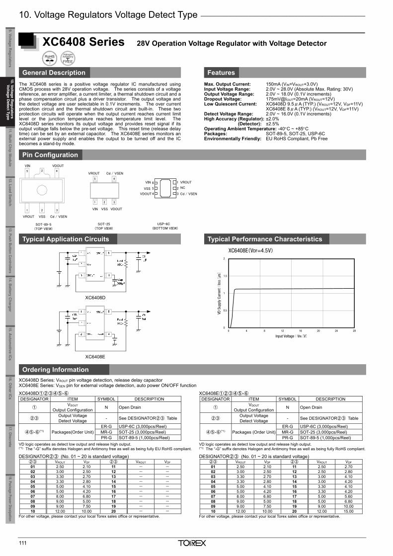
10. Voltage Regulators Voltage Detect Type __________________________________________________
111
XC6408 Series 28V Operation Voltage Regulator with Voltage Detector
General Description Features The XC6408 series is a positive voltage regulator IC manufactured using CMOS process with 28V operation voltage. The series consists of a voltage reference, an error amplifier, a current limiter, a thermal shutdown circuit and a phase compensation circuit plus a driver transistor. The output voltage and the detect voltage are user selectable in 0.1V increments. The over current protection circuit and the thermal shutdown circuit are built-in. These two protection circuits will operate when the output current reaches current limit level or the junction temperature reaches temperature limit level. The XC6408D series monitors its output voltage and provides reset signal if its output voltage falls below the pre-set voltage. This reset time (release delay time) can be set by an external capacitor. The XC6408E series monitors an external power supply and enables the output to be turned off and the IC becomes a stand-by mode.
Max. Output Current: 150mA (VIN=VROUT+3.0V) Input Voltage Range: 2.0V ~ 28.0V (Absolute Max. Rating: 30V) Output Voltage Range: 2.0V ~ 18.0V (0.1V increments) Dropout Voltage: 175mV@IOUT=20mA (VROUT=12V) Low Quiescent Current: XC6408D 9.5μA (TYP.) (VROUT=12V, VDF=11V) XC6408E 8μA (TYP.) (VROUT=12V, VDF=11V) Detect Voltage Range: 2.0V ~ 16.0V (0.1V increments) High Accuracy (Regulator): ±2.0% (Detector): ±2.5% Operating Ambient Temperature: -40C ~ +85C Packages: SOT-89-5, SOT-25, USP-6C Environmentally Friendly: EU RoHS Compliant, Pb Free
Pin Configuration
Typical Application Circuits Typical Performance Characteristics
Ordering Information
XC6408D Series: VROUT pin voltage detection, release delay capacitor XC6408E Series: VSEN pin for external voltage detection, auto power ON/OFF function XC6408D①②③④⑤-⑥ DESIGNATOR ITEM SYMBOL DESCRIPTION
① VDOUT Output Configuration N Open Drain
②③ Output Voltage Detect Voltage - See DESIGNATOR②③ Table
④⑤-⑥(*1) Packages(Order Unit) ER-G USP-6C (3,000pcs/Reel) MR-G SOT-25 (3,000pcs/Reel) PR-G SOT-89-5 (1,000pcs/Reel)
VD logic operates as detect low output and release high output. (*1) The “-G” suffix denotes Halogen and Antimony free as well as being fully EU RoHS compliant. DESIGNATOR②③ (No. 01 ~ 20 is standard voltage)
②③ VROUT VDF ②③ VROUT VDF 01 2.50 2.10 11 - - 02 3.00 2.50 12 - - 03 3.30 2.70 13 - - 04 3.30 2.80 14 - - 05 5.00 4.10 15 - - 06 5.00 4.20 16 - - 07 8.00 6.80 17 - - 08 9.00 5.00 18 - - 09 9.00 7.50 19 - - 10 12.00 10.00 20 - -
For other voltage, please contact your local Torex sales office or representative.
XC6408E①②③④⑤-⑥
DESIGNATOR ITEM SYMBOL DESCRIPTION
① VDOUT Output Configuration N Open Drain
②③ Output Voltage Detect Voltage - See DESIGNATOR②③ Table
④⑤-⑥(*1) Packages (Order Unit) ER-G USP-6C (3,000pcs/Reel) MR-G SOT-25 (3,000pcs/Reel) PR-G SOT-89-5 (1,000pcs/Reel)
VD logic operates as detect low output and release high output. (*1) The “-G” suffix denotes Halogen and Antimony free as well as being fully RoHS compliant. DESIGNATOR②③ (No. 01 ~ 20 is standard voltage)
②③ VROUT VDF ②③ VROUT VDF 01 2.50 2.10 11 2.50 2.70 02 3.00 2.50 12 2.50 2.80 03 3.30 2.70 13 3.00 4.10 04 3.30 2.80 14 3.00 4.20 05 5.00 4.10 15 3.30 4.10 06 5.00 4.20 16 3.30 4.20 07 8.00 6.80 17 5.00 5.60 08 9.00 5.00 18 5.00 6.80 09 9.00 7.50 19 9.00 10.00 10 12.00 10.00 20 12.00 15.00
For other voltage, please contact your local Torex sales office or representative.
1 32
5 4
SOT-25(TOP VIEW)
1 2 3
45 2
SOT-89-5(TOP VIEW)
VIN
VROUT VSS
USP-6C *(BOTTOM VIEW)
34
2
1
5
6
VDOUT
Cd / VSEN
VROUT
VSS
Cd / VSEN
VIN VDOUT
VIN
VDOUT
VSS
VROUT
Cd / VSEN
N.C.NC
XC6408E
XC6408D
2
1.5
1
0.5
08 12 2816 20 240 4
VD S
uppl
y Cu
rren
t:ID
SS[µ
s]
Input Voltage:VIN [V]
XC6408E(VDF=4.5V)
_______________________________________________________________________________________________________
112
XC6405 Series 500mA High Speed LDO Regulators, Voltage Detector Function
General Description Features
The XC6405 series are precise, low noise, high speed, high current, positivevoltage low dropout regulators with built-in voltage detector. They are fabricatedusing Torex’s CMOS process. Performance features of the series includes highripple rejection and low dropout voltage, and the series features a voltagereference, an error amplifier, a current limiter and a phase compensation circuitplus a driver transistor. Detect voltage is selectable in 100mV increments within the range of 0.9V to5.5V and the LDO output voltage is selectable within a range of 0.9V to 5.1V, alsoin 0.1V increments. The series is also compatible with low ESR ceramic capacitors which give addedoutput stability. This stability can be maintained even during load fluctuations dueto the excellent transient response of the series. The current limiter's foldback circuit also operates as a short circuit protection forthe output current limiter and the output pin. The series provides options to the user to select from a variety of circuit features,such as detector monitoring, detector output logic, CE and EN pin input logic,internal pull-up / down resistance, and power ready. The IC's internal regulator circuit can be placed in stand-by mode via the ENfunction (XC6405 A to C series). The whole IC can be put in to stand-by modevia the CE function with the XC6405D series (semi-custom). In the stand-by mode, power consumption is greatly reduced. The XC6405 A and B series features the toggle operation function. Theregulator output can be OFF when the XC6405B series detects voltage(semi-custom). The XC6405E series can monitor another power source by using the VSEN pin(semi-custom). The XC6405F series can delay the detector output the delay time can becontrolled by the use of an external capacitor (semi-custom).
Max. Output Current: More than 500mA (600mA limit) (2.5V≦VROUT≦4.9V)
Operating Voltage Range: 2.0V ~ 6.0V VR Setting Output Voltage Range: 0.9V~5.1V
(0.1V increments ± 2.0%) Dropout Voltage: 200mV (IROUT=100mA) Low Quiescent Current: 90μA (TYP.) Detect Voltage Setting Range: 0.9V ~ 5.5V
(0.1V increments ± 2.0%) VR. VD Temperature Coefficient: ±100ppm/ C (TYP.) High Ripple Rejection: 65dB (10kHz) Output Capacitor: Low ESR Ceramic Operating Ambient Temperature: - 40 ~ + 85 Packages: SOT-25, SOT-89-5 Environmentally Friendly: EU RoHS Compliant, Pb Free
Pin Configuration Ordering Information
XC6405①②③④⑤⑥-⑦ DESIGNATOR ITEM SYMBOL DESCRIPTION
① Operational Function
A Toggle and EN function(*2) B Toggle, EN function, VD signal/VR OFF function(*2) C EN function(*2) D CE function(*2) E VSEN Pin(*2) F Cd pin
② Type of Regulator A~Z As in the chart below.
③④ Output Voltage &
Detect Voltage
01~
Internally set sequential number relating to output voltage and detect voltage (refer to the chart below) VR setting output voltage range: 0.9V~5.1V Detect voltage setting range: 0.9V ~5.5V 0.1V increments are available
⑤⑥-⑦(*1) Packages (Order Unit)
MR-G SOT-25 (3,000pcs/Reel) PR-G SOT-89-5 (1,000pcs/Reel) DR-G Embossed tape, Standard feed
(*1) The “-G” suffix denotes Halogen and Antimony free as well as being fully EU RoHScompliant.
(*2) For A ~ E series, please contact your local Torex sales office or representative. PIN NUMBER : ②Types
② EN / CE
FUNCTION EN / CE LOGIC PULL UP/DOWN RESISTANCE
VD SENSE PIN
VD OUTPUT LOGIC
PIN NUMBER ①
A Functional Active High Pull-down Function VIN Detect L
A ~ D Series
B Functional Active High Pull-down Function VIN Detect H
C Functional Active High Pull-down Function VOUT Detect L
D Functional Active High Pull-down Function VOUT Detect H
E Functional Active High Nonfunctional VIN Detect L F Functional Active High Nonfunctional VIN Detect H H Functional Active High Nonfunctional VOUT Detect L K Functional Active High Nonfunctional VOUT Detect H L Functional Active Low Pull-up Function VIN Detect L M Functional Active Low Pull-up Function VIN Detect H N Functional Active Low Pull-up Function VOUT Detect L P Functional Active Low Pull-up Function VOUT Detect H R Functional Active Low Nonfunctional VIN Detect L S Functional Active Low Nonfunctional VIN Detect H T Functional Active Low Nonfunctional VOUT Detect L U Functional Active Low Nonfunctional VOUT Detect H V Nonfunctional - - VIN / VSEN Detect L E & F
Series X Nonfunctional - - VIN / VSEN Detect H Y Nonfunctional - - VOUT Detect L F
Series Z Nonfunctional - - VOUT Detect H
Typical Application Circuits
dVIN VSS VROUT
VDOUTEN / CE
VSEN / Cd
1 2
45
3
SOT-89-5
VROUT VDOUT
VIN VSS EN /CE VSEN / Cd
EN /CE VSEN / Cd VDOUT
VIN VSS VROUT
SOT-89-5 SOT-25 (TOP VIEW)
XC6405A ~ D Series
XC6405E Series
XC6405F Series
Rpull-up 200k
Rpull-up 200k
Rpull-up 200k
VSS
11.Multi C
hip Module
10. Voltage Regulators
Voltage Detect Type
9. Voltage Regulators
12.Load Switch
13. Push Button Controllers14.B
attery Charger
15.Autom
otive ICs
16.Other IC
s17. D
iscrete18.Package Power Dissipation
10. Voltage Regulators
Voltage Detect Type
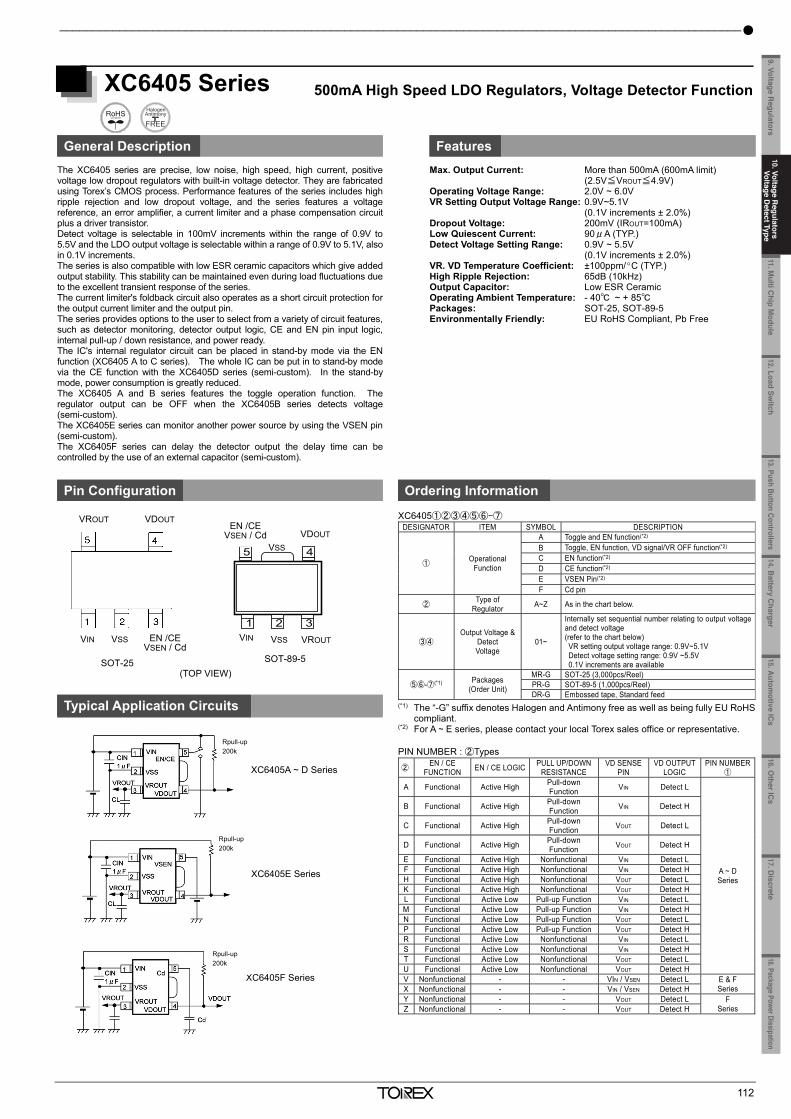
10. Voltage Regulators Voltage Detect Type __________________________________________________
111
XC6408 Series 28V Operation Voltage Regulator with Voltage Detector
General Description Features The XC6408 series is a positive voltage regulator IC manufactured using CMOS process with 28V operation voltage. The series consists of a voltage reference, an error amplifier, a current limiter, a thermal shutdown circuit and a phase compensation circuit plus a driver transistor. The output voltage and the detect voltage are user selectable in 0.1V increments. The over current protection circuit and the thermal shutdown circuit are built-in. These two protection circuits will operate when the output current reaches current limit level or the junction temperature reaches temperature limit level. The XC6408D series monitors its output voltage and provides reset signal if its output voltage falls below the pre-set voltage. This reset time (release delay time) can be set by an external capacitor. The XC6408E series monitors an external power supply and enables the output to be turned off and the IC becomes a stand-by mode.
Max. Output Current: 150mA (VIN=VROUT+3.0V) Input Voltage Range: 2.0V ~ 28.0V (Absolute Max. Rating: 30V) Output Voltage Range: 2.0V ~ 18.0V (0.1V increments) Dropout Voltage: 175mV@IOUT=20mA (VROUT=12V) Low Quiescent Current: XC6408D 9.5μA (TYP.) (VROUT=12V, VDF=11V) XC6408E 8μA (TYP.) (VROUT=12V, VDF=11V) Detect Voltage Range: 2.0V ~ 16.0V (0.1V increments) High Accuracy (Regulator): ±2.0% (Detector): ±2.5% Operating Ambient Temperature: -40C ~ +85C Packages: SOT-89-5, SOT-25, USP-6C Environmentally Friendly: EU RoHS Compliant, Pb Free
Pin Configuration
Typical Application Circuits Typical Performance Characteristics
Ordering Information
XC6408D Series: VROUT pin voltage detection, release delay capacitor XC6408E Series: VSEN pin for external voltage detection, auto power ON/OFF function XC6408D①②③④⑤-⑥ DESIGNATOR ITEM SYMBOL DESCRIPTION
① VDOUT Output Configuration N Open Drain
②③ Output Voltage Detect Voltage - See DESIGNATOR②③ Table
④⑤-⑥(*1) Packages(Order Unit) ER-G USP-6C (3,000pcs/Reel) MR-G SOT-25 (3,000pcs/Reel) PR-G SOT-89-5 (1,000pcs/Reel)
VD logic operates as detect low output and release high output. (*1) The “-G” suffix denotes Halogen and Antimony free as well as being fully EU RoHS compliant. DESIGNATOR②③ (No. 01 ~ 20 is standard voltage)
②③ VROUT VDF ②③ VROUT VDF 01 2.50 2.10 11 - - 02 3.00 2.50 12 - - 03 3.30 2.70 13 - - 04 3.30 2.80 14 - - 05 5.00 4.10 15 - - 06 5.00 4.20 16 - - 07 8.00 6.80 17 - - 08 9.00 5.00 18 - - 09 9.00 7.50 19 - - 10 12.00 10.00 20 - -
For other voltage, please contact your local Torex sales office or representative.
XC6408E①②③④⑤-⑥
DESIGNATOR ITEM SYMBOL DESCRIPTION
① VDOUT Output Configuration N Open Drain
②③ Output Voltage Detect Voltage - See DESIGNATOR②③ Table
④⑤-⑥(*1) Packages (Order Unit) ER-G USP-6C (3,000pcs/Reel) MR-G SOT-25 (3,000pcs/Reel) PR-G SOT-89-5 (1,000pcs/Reel)
VD logic operates as detect low output and release high output. (*1) The “-G” suffix denotes Halogen and Antimony free as well as being fully RoHS compliant. DESIGNATOR②③ (No. 01 ~ 20 is standard voltage)
②③ VROUT VDF ②③ VROUT VDF 01 2.50 2.10 11 2.50 2.70 02 3.00 2.50 12 2.50 2.80 03 3.30 2.70 13 3.00 4.10 04 3.30 2.80 14 3.00 4.20 05 5.00 4.10 15 3.30 4.10 06 5.00 4.20 16 3.30 4.20 07 8.00 6.80 17 5.00 5.60 08 9.00 5.00 18 5.00 6.80 09 9.00 7.50 19 9.00 10.00 10 12.00 10.00 20 12.00 15.00
For other voltage, please contact your local Torex sales office or representative.
1 32
5 4
SOT-25(TOP VIEW)
1 2 3
45 2
SOT-89-5(TOP VIEW)
VIN
VROUT VSS
USP-6C *(BOTTOM VIEW)
34
2
1
5
6
VDOUT
Cd / VSEN
VROUT
VSS
Cd / VSEN
VIN VDOUT
VIN
VDOUT
VSS
VROUT
Cd / VSEN
N.C.NC
XC6408E
XC6408D
2
1.5
1
0.5
08 12 2816 20 240 4
VD S
uppl
y Cu
rren
t:ID
SS[µ
s]
Input Voltage:VIN [V]
XC6408E(VDF=4.5V)
_______________________________________________________________________________________________________
112
XC6405 Series 500mA High Speed LDO Regulators, Voltage Detector Function
General Description Features
The XC6405 series are precise, low noise, high speed, high current, positivevoltage low dropout regulators with built-in voltage detector. They are fabricatedusing Torex’s CMOS process. Performance features of the series includes highripple rejection and low dropout voltage, and the series features a voltagereference, an error amplifier, a current limiter and a phase compensation circuitplus a driver transistor. Detect voltage is selectable in 100mV increments within the range of 0.9V to5.5V and the LDO output voltage is selectable within a range of 0.9V to 5.1V, alsoin 0.1V increments. The series is also compatible with low ESR ceramic capacitors which give addedoutput stability. This stability can be maintained even during load fluctuations dueto the excellent transient response of the series. The current limiter's foldback circuit also operates as a short circuit protection forthe output current limiter and the output pin. The series provides options to the user to select from a variety of circuit features,such as detector monitoring, detector output logic, CE and EN pin input logic,internal pull-up / down resistance, and power ready. The IC's internal regulator circuit can be placed in stand-by mode via the ENfunction (XC6405 A to C series). The whole IC can be put in to stand-by modevia the CE function with the XC6405D series (semi-custom). In the stand-by mode, power consumption is greatly reduced. The XC6405 A and B series features the toggle operation function. Theregulator output can be OFF when the XC6405B series detects voltage(semi-custom). The XC6405E series can monitor another power source by using the VSEN pin(semi-custom). The XC6405F series can delay the detector output the delay time can becontrolled by the use of an external capacitor (semi-custom).
Max. Output Current: More than 500mA (600mA limit) (2.5V≦VROUT≦4.9V)
Operating Voltage Range: 2.0V ~ 6.0V VR Setting Output Voltage Range: 0.9V~5.1V
(0.1V increments ± 2.0%) Dropout Voltage: 200mV (IROUT=100mA) Low Quiescent Current: 90μA (TYP.) Detect Voltage Setting Range: 0.9V ~ 5.5V
(0.1V increments ± 2.0%) VR. VD Temperature Coefficient: ±100ppm/ C (TYP.) High Ripple Rejection: 65dB (10kHz) Output Capacitor: Low ESR Ceramic Operating Ambient Temperature: - 40 ~ + 85 Packages: SOT-25, SOT-89-5 Environmentally Friendly: EU RoHS Compliant, Pb Free
Pin Configuration Ordering Information
XC6405①②③④⑤⑥-⑦ DESIGNATOR ITEM SYMBOL DESCRIPTION
① Operational Function
A Toggle and EN function(*2) B Toggle, EN function, VD signal/VR OFF function(*2) C EN function(*2) D CE function(*2) E VSEN Pin(*2) F Cd pin
② Type of Regulator A~Z As in the chart below.
③④ Output Voltage &
Detect Voltage
01~
Internally set sequential number relating to output voltage and detect voltage (refer to the chart below) VR setting output voltage range: 0.9V~5.1V Detect voltage setting range: 0.9V ~5.5V 0.1V increments are available
⑤⑥-⑦(*1) Packages (Order Unit)
MR-G SOT-25 (3,000pcs/Reel) PR-G SOT-89-5 (1,000pcs/Reel) DR-G Embossed tape, Standard feed
(*1) The “-G” suffix denotes Halogen and Antimony free as well as being fully EU RoHScompliant.
(*2) For A ~ E series, please contact your local Torex sales office or representative. PIN NUMBER : ②Types
② EN / CE
FUNCTION EN / CE LOGIC PULL UP/DOWN RESISTANCE
VD SENSE PIN
VD OUTPUT LOGIC
PIN NUMBER ①
A Functional Active High Pull-down Function VIN Detect L
A ~ D Series
B Functional Active High Pull-down Function VIN Detect H
C Functional Active High Pull-down Function VOUT Detect L
D Functional Active High Pull-down Function VOUT Detect H
E Functional Active High Nonfunctional VIN Detect L F Functional Active High Nonfunctional VIN Detect H H Functional Active High Nonfunctional VOUT Detect L K Functional Active High Nonfunctional VOUT Detect H L Functional Active Low Pull-up Function VIN Detect L M Functional Active Low Pull-up Function VIN Detect H N Functional Active Low Pull-up Function VOUT Detect L P Functional Active Low Pull-up Function VOUT Detect H R Functional Active Low Nonfunctional VIN Detect L S Functional Active Low Nonfunctional VIN Detect H T Functional Active Low Nonfunctional VOUT Detect L U Functional Active Low Nonfunctional VOUT Detect H V Nonfunctional - - VIN / VSEN Detect L E & F
Series X Nonfunctional - - VIN / VSEN Detect H Y Nonfunctional - - VOUT Detect L F
Series Z Nonfunctional - - VOUT Detect H
Typical Application Circuits
dVIN VSS VROUT
VDOUTEN / CE
VSEN / Cd
1 2
45
3
SOT-89-5
VROUT VDOUT
VIN VSS EN /CE VSEN / Cd
EN /CE VSEN / Cd VDOUT
VIN VSS VROUT
SOT-89-5 SOT-25 (TOP VIEW)
XC6405A ~ D Series
XC6405E Series
XC6405F Series
Rpull-up 200k
Rpull-up 200k
Rpull-up 200k
VSS
11.Multi C
hip Module
9. Voltage Regulators
12.Load Switch
13. Push Button Controllers14.B
attery Charger
15.Autom
otive ICs
16.Other IC
s17. D
iscrete18.Package Power Dissipation
10. Voltage Regulators
Voltage Detect Type
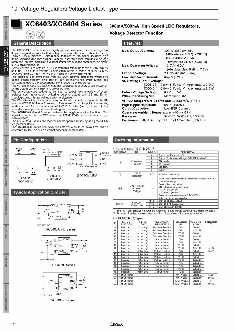
10. Voltage Regulators Voltage Detect Type __________________________________________________
113
XC6403/XC6404 Series 300mA/500mA High Speed LDO Regulators, Voltage Detector Function
General Description Features
The XC6403/XC6404 series are highly precise, low noise, positive voltage low dropout regulators with built-in voltage detector. They are fabricated using Torex’s CMOS process. Performance features of the series includes high ripple rejection and low dropout voltage, and the series features a voltage reference, an error amplifier, a current limiter and a phase compensation circuit plus a driver transistor. Detect voltage is selectable in 0.1V increments within the range of 0.9V to 5.5V and the LDO output voltage is selectable within a range of 0.9V to 5.6V (XC6403) and 0.9V to 5.1V (XC6404), also in 100mV increments. The series is also compatible with low ESR ceramic capacitors which give added output stability. This stability can be maintained even during load fluctuations due to the excellent transient response of the series. The current limiter's foldback circuit also operates as a short circuit protection for the output current limiter and the output pin. The series provides options to the user to select from a variety of circuit features, such as detector monitoring, detector output logic, CE and EN pin input logic, and internal pull-up / down resistance. The IC's internal regulator circuit can be placed in stand-by mode via the EN function (XC6403/04 A to C series). The whole IC can be put in to stand-by mode via the CE function with the XC6403/04D series (semi-custom). In the stand-by mode, power consumption is greatly reduced. The XC6403/04 A and B series features the toggle operation function. The regulator output can be OFF when the XC6403/04B series detects voltage (semi-custom). The XC6403/04E series can monitor another power source by using the VSEN pin (semi-custom). The XC6403/04F series can delay the detector output: the delay time can be controlled by the use of an external capacitor (semi-custom).
Max. Output Current: 300mA (380mA limit) (1.8V<VROUT<5.3V) [XC6403] 500mA (600mA limit) (2.5V<VROUT<4.9V) [XC6404]
Max. Operating Voltage: 2.0V ~ 6.0V (Absolute Max. Rating: 7.0V) Dropout Voltage: 200mV (IOUT=100mA) Low Quiescent Current: 35μA (TYP.) VR Setting Output Voltage:
[XC6403] 0.9V~ 5.6V (0.1V increments, ± 2.0%) [XC6404] 0.9V~ 5.1V (0.1V increments, ± 2.0%)
Detect Voltage Setting: 0.9V ~ 5.5V When monitoring VIN: More than 2.0V VR. VD Temperature Coefficient: ±100ppm/ (TYP.) High Ripple Rejection: 65dB (10kHz) Output Capacitor: Low ESR Ceramic Operating Ambient Temperature: - 40 ~ + 85 Packages: SOT-25, SOT-89-5, USP-6B Environmentally Friendly: EU RoHS Compliant, Pb Free
Pin Configuration Ordering Information
XC6403/XC6404①②③④⑤⑥-⑦ DESINATOR ITEM SYMBOL DESCRIPTION
① Operational Function
A Toggle and EN function(*2) B Toggle, EN function, VD signal/VR OFF function(*2) C EN function D CE function E VSEN Pin F Cd pin
② Type of Regulator A~Z As in the chart below.
③④ Output Voltage
& Detect Voltage
01~
Internally set sequential number relating to output voltage and detect voltage (refer to the chart below) VR setting output voltage range: 0.9V~5.6V[XC6403] 0.9V~5.1V[XC6404] Detect voltage setting range: 0.9V ~5.5V 0.1V increments are available
⑤⑥-⑦(*1) Packages (Order Unit)
MR-G SOT-25 (3,000pcs/Reel) PR-G SOT-89-5 (1,000pcs/Reel) DR-G USP-6B (3,000pcs/Reel)
(*1) The “-G” suffix denotes Halogen and Antimony free as well as being fully EU RoHS compliant. (*2) For A and B series, please contact your local Torex sales office or representative.
PIN NUMBER : ②Types
② EN / CE
FUNCTION EN / CE LOGIC
PULL UP/DOWN RESISTANCE
VD SENSE PIN
VD OUTPUT LOGIC
PIN NUBER ①
A Functional Active High Pull-down Function VIN Detect L
A ~ D Series
B Functional Active High Pull-down Function VIN Detect H C Functional Active High Pull-down Function VOUT Detect L D Functional Active High Pull-down Function VOUT Detect H E Functional Active High Nonfunctional VIN Detect L F Functional Active High Nonfunctional VIN Detect H H Functional Active High Nonfunctional VOUT Detect L K Functional Active High Nonfunctional VOUT Detect H L Functional Active Low Pull-up Function VIN Detect L M Functional Active Low Pull-up Function VIN Detect H N Functional Active Low Pull-up Function VOUT Detect L P Functional Active Low Pull-up Function VOUT Detect H R Functional Active Low Nonfunctional VIN Detect L S Functional Active Low Nonfunctional VIN Detect H T Functional Active Low Nonfunctional VOUT Detect L U Functional Active Low Nonfunctional VOUT Detect H V Nonfunctional - - VIN / VSEN Detect L E & F
Series X Nonfunctional - - VIN / VSEN Detect H Y Nonfunctional - - VOUT / VSEN Detect L F
Series Z Nonfunctional - - VOUT / VSEN Detect H
Typical Application Circuits
VIN VSS VROUT
VDOUT
1 2
45
3
SOT-89-5
EN/CEVSEN/CdVDOUT 1
234
56
VINVROUT
VSS NC
USP-6B(BOTTOM VIEW)
SOT-25 (TOP VIEW)
EN / CE VSEN / Cd
SOT-89-5 (TOP VIEW)
USP-6B (BOTTOM VIEW)
XC6403A ~ D Series
XC6403E Series
XC6403F Series
VSS
_______________________________________________________________________________________________________
114
XC6402 Series 700mA High Speed LDO Regulators, Voltage Detector Function
General Description Features
The XC6402 series are precise, low noise, high current, positivevoltage low dropout regulators with built-in voltage detector. They arefabricated using Torex’s CMOS process. The series features avoltage reference, an error amplifier, a current limiter, a voltagedetector and a phase compensation circuit plus a driver transistor. The output voltage of the LDO and detect voltage of the detector isselectable in 0.05V increments with in the range of 0.8V to 5.0V. With a low ON resistance driver transistor built-in, batteries can beused until input-output voltage differential is minimal and canaccordingly be used for a longer time. The series is also compatible with low ESR ceramic capacitors whichgive added output stability. The series provides options to the user to select from a variety ofcircuit features, such as detector monitoring, detector output logic,EN pin input logic, and internal pull-up / down resistance(semi-custom). The IC's internal regulator circuit can be placed in stand-by mode viathe EN function (XC6402C series). In the stand-by mode, powerconsumption is greatly reduced. The XC6402F series can delay the detector output: the delay timecan be controlled by the use of an external capacitor.
Max. Output Current: 700mA (800mA limit) (1.6V≦VROUT≦5.0V)
Max. Operating Voltage: 1.5V ~ 6.0V (Absolute Max. Rating: 6.5V)
VR Output Voltage Range: 0.8V ~ 5.0V (0.05V increments) VD Output Voltage Range: 0.8V ~ 5.0V (0.05V increments) Dropout Voltage: 50mV (IOUT=100mA) Low Quiescent Current: 35μA(TYP) When monitoring VIN: More than 1.5V Accuracy: ±2.0% High Ripple Rejection: 60dB (@1kHz) Operating Ambient Temperature: - 40 ~ +85 Output Capacitor: Low ESR Ceramic Packages: SOT-25, SOT-89-5, USP-6B Environmentally Friendly: EU RoHS Compliant, Pb Free Typical Performance Characteristics
Dropout Voltage vs. VR Output Current
Pin Configuration
Typical Application Circuits Ordering Information XC6402C Series XC6402F Series
XC6402①②③④⑤⑥-⑦ DESIGNATOR ITEM SYMBOL DESCRIPTION
① Operational Function C EN function F Cd pin
② Type of Regulator A~Z As in the chart below
③④ Output Voltage & Detect Voltage 01~
Internally set sequential number relating to output voltage and detect voltage VR setting output voltage range: 0.8V~5.0V Detect voltage setting range: 0.8V ~5.0V 0.05V increments are available
⑤⑥-⑦(*1) Packages (Order Unit)
MR-G SOT-25 (3,000pcs/Reel) PR-G SOT-89-5 (1,000pcs/Reel) DR-G USP-6B (3,000pcs/Reel)
PIN NUMBER : ②Types ② EN FUNCTION EN LOGIC PULL UP/DOWN
RESISTANCE VD SENSE
PIN VD OUTPUT
LOGIC PIN NUMBER
① A Functional Active High Pull-down Function VIN Detect L
C Series
B Functional Active High Pull-down Function VIN Detect H C Functional Active High Pull-down Function VROUT Detect L D Functional Active High Pull-down Function VROUT Detect H E Functional Active High Nonfunctional VIN Detect L F Functional Active High Nonfunctional VIN Detect H H Functional Active High Nonfunctional VROUT Detect L K Functional Active High Nonfunctional VROUT Detect H L Functional Active Low Pull-up Function VIN Detect L M Functional Active Low Pull-up Function VIN Detect H N Functional Active Low Pull-up Function VROUT Detect L P Functional Active Low Pull-up Function VROUT Detect H R Functional Active Low Nonfunctional VIN Detect L S Functional Active Low Nonfunctional VIN Detect H T Functional Active Low Nonfunctional VROUT Detect L U Functional Active Low Nonfunctional VROUT Detect H V Nonfunctional - - VIN Detect L
F Series X Nonfunctional - - VIN Detect H Y Nonfunctional - - VROUT Detect L Z Nonfunctional - - VROUT Detect H
(*1) The “-G” suffix denotes Halogen and Antimony free as well as being fully EU RoHS compliant.
EN / Cd
VIN VSS VROUT
VDOUT
1 2
45
3
SOT-89-5(TOP VIEW)
VDOUT 1234
56
VROUT NC
USP-6B(BOTTOM VIEW)
VINVSS
EN/Cd
SOT-25
(TOP VIEW)
Rpull-up 220kΩ
Rpull-up 220kΩ
XC6402 Series (VR : 3.0V)
0.0
0.1
0.2
0.3
0.4
0.5
0.6
0.7
0.8
0.9
1.0
0 100 200 300 400 500 600 700
VR Outpu Current IROUT (mA)
Drop
ouVo
ltage
Vdi
(V)
CIN=1uF(ceramic) CL=1.0uF(ceramic)
- 40- 25- 85
VR Output Current IROUT (mA)
Dro
pout
Vol
tage
Vdi
f(V) VSS
11.Multi C
hip Module
10. Voltage Regulators
Voltage Detect Type
9. Voltage Regulators
12.Load Switch
13. Push Button Controllers14.B
attery Charger
15.Autom
otive ICs
16.Other IC
s17. D
iscrete18.Package Power Dissipation
10. Voltage Regulators
Voltage Detect Type
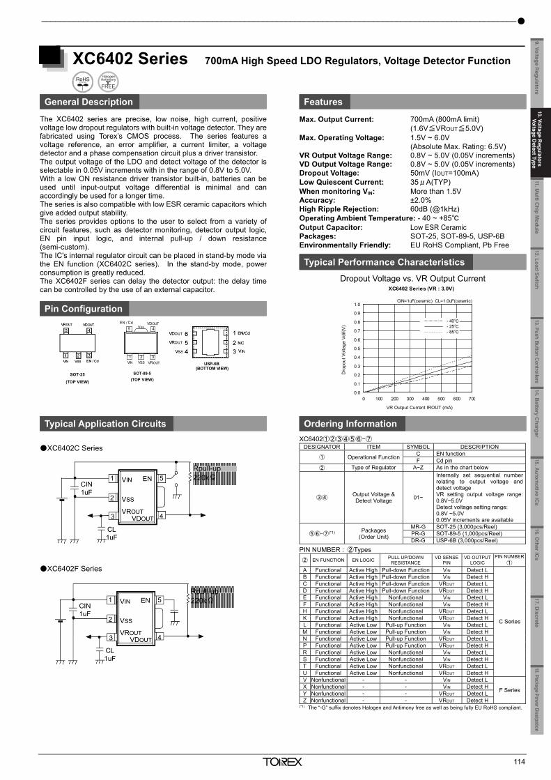
10. Voltage Regulators Voltage Detect Type __________________________________________________
113
XC6403/XC6404 Series 300mA/500mA High Speed LDO Regulators, Voltage Detector Function
General Description Features
The XC6403/XC6404 series are highly precise, low noise, positive voltage low dropout regulators with built-in voltage detector. They are fabricated using Torex’s CMOS process. Performance features of the series includes high ripple rejection and low dropout voltage, and the series features a voltage reference, an error amplifier, a current limiter and a phase compensation circuit plus a driver transistor. Detect voltage is selectable in 0.1V increments within the range of 0.9V to 5.5V and the LDO output voltage is selectable within a range of 0.9V to 5.6V (XC6403) and 0.9V to 5.1V (XC6404), also in 100mV increments. The series is also compatible with low ESR ceramic capacitors which give added output stability. This stability can be maintained even during load fluctuations due to the excellent transient response of the series. The current limiter's foldback circuit also operates as a short circuit protection for the output current limiter and the output pin. The series provides options to the user to select from a variety of circuit features, such as detector monitoring, detector output logic, CE and EN pin input logic, and internal pull-up / down resistance. The IC's internal regulator circuit can be placed in stand-by mode via the EN function (XC6403/04 A to C series). The whole IC can be put in to stand-by mode via the CE function with the XC6403/04D series (semi-custom). In the stand-by mode, power consumption is greatly reduced. The XC6403/04 A and B series features the toggle operation function. The regulator output can be OFF when the XC6403/04B series detects voltage (semi-custom). The XC6403/04E series can monitor another power source by using the VSEN pin (semi-custom). The XC6403/04F series can delay the detector output: the delay time can be controlled by the use of an external capacitor (semi-custom).
Max. Output Current: 300mA (380mA limit) (1.8V<VROUT<5.3V) [XC6403] 500mA (600mA limit) (2.5V<VROUT<4.9V) [XC6404]
Max. Operating Voltage: 2.0V ~ 6.0V (Absolute Max. Rating: 7.0V) Dropout Voltage: 200mV (IOUT=100mA) Low Quiescent Current: 35μA (TYP.) VR Setting Output Voltage:
[XC6403] 0.9V~ 5.6V (0.1V increments, ± 2.0%) [XC6404] 0.9V~ 5.1V (0.1V increments, ± 2.0%)
Detect Voltage Setting: 0.9V ~ 5.5V When monitoring VIN: More than 2.0V VR. VD Temperature Coefficient: ±100ppm/ (TYP.) High Ripple Rejection: 65dB (10kHz) Output Capacitor: Low ESR Ceramic Operating Ambient Temperature: - 40 ~ + 85 Packages: SOT-25, SOT-89-5, USP-6B Environmentally Friendly: EU RoHS Compliant, Pb Free
Pin Configuration Ordering Information
XC6403/XC6404①②③④⑤⑥-⑦ DESINATOR ITEM SYMBOL DESCRIPTION
① Operational Function
A Toggle and EN function(*2) B Toggle, EN function, VD signal/VR OFF function(*2) C EN function D CE function E VSEN Pin F Cd pin
② Type of Regulator A~Z As in the chart below.
③④ Output Voltage
& Detect Voltage
01~
Internally set sequential number relating to output voltage and detect voltage (refer to the chart below) VR setting output voltage range: 0.9V~5.6V[XC6403] 0.9V~5.1V[XC6404] Detect voltage setting range: 0.9V ~5.5V 0.1V increments are available
⑤⑥-⑦(*1) Packages (Order Unit)
MR-G SOT-25 (3,000pcs/Reel) PR-G SOT-89-5 (1,000pcs/Reel) DR-G USP-6B (3,000pcs/Reel)
(*1) The “-G” suffix denotes Halogen and Antimony free as well as being fully EU RoHS compliant. (*2) For A and B series, please contact your local Torex sales office or representative.
PIN NUMBER : ②Types
② EN / CE
FUNCTION EN / CE LOGIC
PULL UP/DOWN RESISTANCE
VD SENSE PIN
VD OUTPUT LOGIC
PIN NUBER ①
A Functional Active High Pull-down Function VIN Detect L
A ~ D Series
B Functional Active High Pull-down Function VIN Detect H C Functional Active High Pull-down Function VOUT Detect L D Functional Active High Pull-down Function VOUT Detect H E Functional Active High Nonfunctional VIN Detect L F Functional Active High Nonfunctional VIN Detect H H Functional Active High Nonfunctional VOUT Detect L K Functional Active High Nonfunctional VOUT Detect H L Functional Active Low Pull-up Function VIN Detect L M Functional Active Low Pull-up Function VIN Detect H N Functional Active Low Pull-up Function VOUT Detect L P Functional Active Low Pull-up Function VOUT Detect H R Functional Active Low Nonfunctional VIN Detect L S Functional Active Low Nonfunctional VIN Detect H T Functional Active Low Nonfunctional VOUT Detect L U Functional Active Low Nonfunctional VOUT Detect H V Nonfunctional - - VIN / VSEN Detect L E & F
Series X Nonfunctional - - VIN / VSEN Detect H Y Nonfunctional - - VOUT / VSEN Detect L F
Series Z Nonfunctional - - VOUT / VSEN Detect H
Typical Application Circuits
VIN VSS VROUT
VDOUT
1 2
45
3
SOT-89-5
EN/CEVSEN/CdVDOUT 1
234
56
VINVROUT
VSS NC
USP-6B(BOTTOM VIEW)
SOT-25 (TOP VIEW)
EN / CE VSEN / Cd
SOT-89-5 (TOP VIEW)
USP-6B (BOTTOM VIEW)
XC6403A ~ D Series
XC6403E Series
XC6403F Series
VSS
_______________________________________________________________________________________________________
114
XC6402 Series 700mA High Speed LDO Regulators, Voltage Detector Function
General Description Features
The XC6402 series are precise, low noise, high current, positivevoltage low dropout regulators with built-in voltage detector. They arefabricated using Torex’s CMOS process. The series features avoltage reference, an error amplifier, a current limiter, a voltagedetector and a phase compensation circuit plus a driver transistor. The output voltage of the LDO and detect voltage of the detector isselectable in 0.05V increments with in the range of 0.8V to 5.0V. With a low ON resistance driver transistor built-in, batteries can beused until input-output voltage differential is minimal and canaccordingly be used for a longer time. The series is also compatible with low ESR ceramic capacitors whichgive added output stability. The series provides options to the user to select from a variety ofcircuit features, such as detector monitoring, detector output logic,EN pin input logic, and internal pull-up / down resistance(semi-custom). The IC's internal regulator circuit can be placed in stand-by mode viathe EN function (XC6402C series). In the stand-by mode, powerconsumption is greatly reduced. The XC6402F series can delay the detector output: the delay timecan be controlled by the use of an external capacitor.
Max. Output Current: 700mA (800mA limit) (1.6V≦VROUT≦5.0V)
Max. Operating Voltage: 1.5V ~ 6.0V (Absolute Max. Rating: 6.5V)
VR Output Voltage Range: 0.8V ~ 5.0V (0.05V increments) VD Output Voltage Range: 0.8V ~ 5.0V (0.05V increments) Dropout Voltage: 50mV (IOUT=100mA) Low Quiescent Current: 35μA(TYP) When monitoring VIN: More than 1.5V Accuracy: ±2.0% High Ripple Rejection: 60dB (@1kHz) Operating Ambient Temperature: - 40 ~ +85 Output Capacitor: Low ESR Ceramic Packages: SOT-25, SOT-89-5, USP-6B Environmentally Friendly: EU RoHS Compliant, Pb Free Typical Performance Characteristics
Dropout Voltage vs. VR Output Current
Pin Configuration
Typical Application Circuits Ordering Information XC6402C Series XC6402F Series
XC6402①②③④⑤⑥-⑦ DESIGNATOR ITEM SYMBOL DESCRIPTION
① Operational Function C EN function F Cd pin
② Type of Regulator A~Z As in the chart below
③④ Output Voltage & Detect Voltage 01~
Internally set sequential number relating to output voltage and detect voltage VR setting output voltage range: 0.8V~5.0V Detect voltage setting range: 0.8V ~5.0V 0.05V increments are available
⑤⑥-⑦(*1) Packages (Order Unit)
MR-G SOT-25 (3,000pcs/Reel) PR-G SOT-89-5 (1,000pcs/Reel) DR-G USP-6B (3,000pcs/Reel)
PIN NUMBER : ②Types ② EN FUNCTION EN LOGIC PULL UP/DOWN
RESISTANCE VD SENSE
PIN VD OUTPUT
LOGIC PIN NUMBER
① A Functional Active High Pull-down Function VIN Detect L
C Series
B Functional Active High Pull-down Function VIN Detect H C Functional Active High Pull-down Function VROUT Detect L D Functional Active High Pull-down Function VROUT Detect H E Functional Active High Nonfunctional VIN Detect L F Functional Active High Nonfunctional VIN Detect H H Functional Active High Nonfunctional VROUT Detect L K Functional Active High Nonfunctional VROUT Detect H L Functional Active Low Pull-up Function VIN Detect L M Functional Active Low Pull-up Function VIN Detect H N Functional Active Low Pull-up Function VROUT Detect L P Functional Active Low Pull-up Function VROUT Detect H R Functional Active Low Nonfunctional VIN Detect L S Functional Active Low Nonfunctional VIN Detect H T Functional Active Low Nonfunctional VROUT Detect L U Functional Active Low Nonfunctional VROUT Detect H V Nonfunctional - - VIN Detect L
F Series X Nonfunctional - - VIN Detect H Y Nonfunctional - - VROUT Detect L Z Nonfunctional - - VROUT Detect H
(*1) The “-G” suffix denotes Halogen and Antimony free as well as being fully EU RoHS compliant.
EN / Cd
VIN VSS VROUT
VDOUT
1 2
45
3
SOT-89-5(TOP VIEW)
VDOUT 1234
56
VROUT NC
USP-6B(BOTTOM VIEW)
VINVSS
EN/Cd
SOT-25
(TOP VIEW)
Rpull-up 220kΩ
Rpull-up 220kΩ
XC6402 Series (VR : 3.0V)
0.0
0.1
0.2
0.3
0.4
0.5
0.6
0.7
0.8
0.9
1.0
0 100 200 300 400 500 600 700
VR Outpu Current IROUT (mA)
Drop
ouVo
ltage
Vdi
(V)
CIN=1uF(ceramic) CL=1.0uF(ceramic)
- 40- 25- 85
VR Output Current IROUT (mA)
Dro
pout
Vol
tage
Vdi
f(V) VSS
11.Multi C
hip Module
9. Voltage Regulators
12.Load Switch
13. Push Button Controllers14.B
attery Charger
15.Autom
otive ICs
16.Other IC
s17. D
iscrete18.Package Power Dissipation
10. Voltage Regulators
Voltage Detect Type
11. Multi Chip Module ____________________________________________________________________________
115
XCM414 Series Voltage Regulator with Bridge Diode for Wireless Power Receiver
General Description Features
The XCM414 series consist of four Schottky Barrier Diodes (SBD) and a positive voltage regulator (VR). These four SBDs configure a bridge circuit and it performs the full-wave rectification of an AC input so that the positive voltage regulator can generate DC output. The VR consists of a voltage reference, an error amplifier, a current limiter, a thermal shutdown circuit and a phase compensation circuit plus a driver transistor. The output voltage is preset at 3.3V in the IC as a standard value, and it is selectable in 0.1V increments within the range of 2.0V to 12V using laser trimming technologies. The output stabilization capacitor (CL) is also compatible with low ESR ceramic capacitors. The over current protection circuit and the thermal shutdown circuit are built-in. These two protection circuits will operate when the output current reaches current limit level or the junction temperature reaches temperature limit level. The CE function enables the output to be turned off and the IC becomes a stand-by mode resulting in greatly reduced power consumption.
【Schottky Barrier Diode (SBD)】 Forward Voltage: 0.33V (IF=10mA) Reverse Current: 2μA (VR=40V) 【Voltage Regulator (VR)】 Input Voltage Range: 2.0V~26.0V Output Voltage (nominal): 3.3V Output Voltage Range (option): 2.0V~12.0V(0.1V increments) Fixed Output Accuracy: ±2% Low Power Consumption: 5μA Stand-by Current: less than 0.1μA High Ripple Rejection: 30dB@1kHz Low ESR Capacitor: Ceramic Capacitor Compatible Built–in Protection: Current Limit Circuit : Thermal Shutdown Circuit Operating Temperature: -40~+85 Package: USP-8B10 Environmentally Friendly: EU RoHS Compliant, Pb Free
Pin Configuration Typical Application Circuit
Ordering Information
XCM414①②③④⑤⑥-⑦ DESIGNATOR DESCRIPTION SYMBOL DESCRIPTION
① TYPE B Fixed
②③④ Output Voltage 020~120 For the voltage within 2.0V ~9.9V (0.1V increments) (*2) e.g. 033 ⇒ 3.3V、 105 ⇒ 10.5V
⑤⑥-⑦(*1) Package (Order Unit) D2-G USP-8B10 (5,000pcs/Reel) (*1) The “-G” suffix denotes Halogen and Antimony free as well as being fully EU RoHS compliant. (*2) Standard: XCM414B033D2-G.
_____________________________________________________________________________________________ 12. Load Switch
116
XC8109 Series 85mΩ High Function Power Switch with Current Limit Adjustable Pin (0.075A~1.3A Current Limit Adjustable)
General Description Features
The XC8109 series is a P-channel MOSFET power switch IC with alow ON resistance. A current limit, reverse current protection(prevents reverse current from VOUT to VIN), soft start, thermalshutdown, and an under voltage lockout (UVLO) are incorporated as protective functions. A flag function monitors the power switch status.The flag output has N-channel open drain structure, and outputs Lowlevel signal while over-current or overheating is detected, or whilethe reverse current protection is operated. A variable current limiting function is integrated, allowing the currentlimit value to be set, using an external resistor. The voltage level which is fed to CE pin determines the status ofXC8109. The logic level of CE pin is selectable between either one of active high or active low.
Input Voltage Range: 2.5V~5.5V (Absolute Max. Rating: 6.0V) Max. Output Current: 0.9A ON Resistance: 85mΩ@VIN=5.0V (TYP.) Quiescent Current: 40μA@ VIN=5.0V Stand-by Current: 0.1μA (TYP.) Flag Delay Time: 7.5ms (TYP.) * At over-current detection 4ms (TYP.) * At reverse voltage detection Protection Circuit: Reverse Current Protection 0.075A~1.3A(TYP.) Thermal Shutdown Under Voltage Lockout (UVLO) Soft-start Functions: Flag Output CE Pin Input Logic Selectable Current Limit Response Time: 2μs (TYP.) * Reference value Operating Ambient Temperature: -40~+105 Package: USP-6C Environmentally Friendly: EU RoHS Compliant, Pb Free
Pin Configuration Typical Performance Characteristics
Typical Application Circuit Ty
* The Typical circuit is base on USB high side switch.
The XC8109 series can accommodate 1μF output capacitor (CL).
Ordering Information
XC8109①②③④⑤⑥-⑦ DESIGNATOR ITEM SYMBOL DESCRIPTION
① CE Logic A Active H B Active L
② Protection Circuits Type C Auto-recovery(*1) D Lanch-off(*2)
③④ Max. Output Current 10 0.9A (* Adjustable current limit range:0.075A~1300mA)
⑤⑥-⑦(*3) Package (Order Unit) ER-G USP-6C (3,000pcs/Reel) (*1) Over Current Protection, Reverse Current Prevention, and Thermal Protection are Auto-recovery. (*2) Over Current Protection and Reverse Current Prevention are Latching, Thermal Protection is Auto-recovery. (*3) The “-G” suffix denotes Halogen and Antimony free as well as being fully EU RoHS compliant.
XC8109xC10ER
0.0
1.0
2.0
3.0
4.0
5.0
6.0
0.0 0.2 0.4 0.6 0.8 1.0 1.2 1.4 1.6 1.8 2.0 2.2 2.4
Output Current : IOUT [A]
Outp
ut
Voltag
e :
VO
UT [V
]
RILIM=515kΩ
RILIM=18.4kΩ
RILIM=0kΩ
CIN=1.0μF(ceramic), CL=1.0μF(ceramic)
11.Multi C
hip Module
10. Voltage Regulators
Voltage Detect Type
9. Voltage Regulators
12.Load Switch
13. Push Button Controllers14.B
attery Charger
15.Autom
otive ICs
16.Other IC
s17. D
iscrete18.Package Power Dissipation
11.Multi C
hip Module
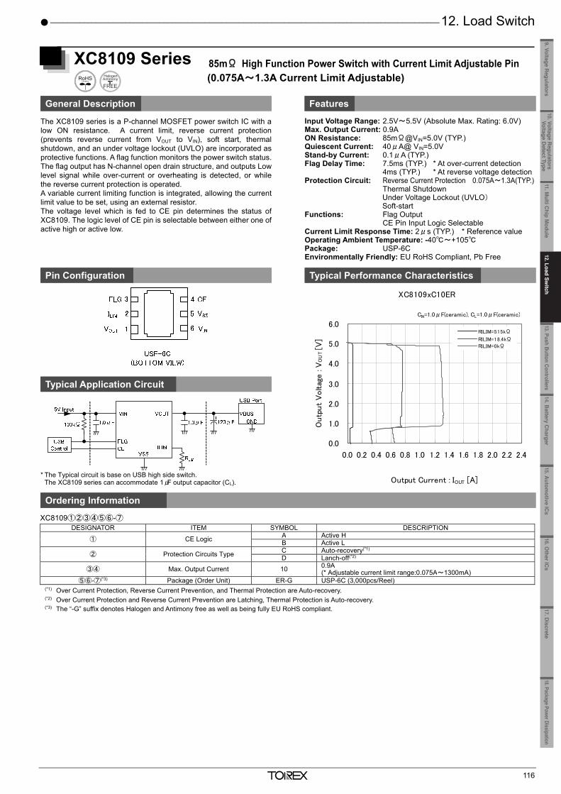
11. Multi Chip Module ____________________________________________________________________________
115
XCM414 Series Voltage Regulator with Bridge Diode for Wireless Power Receiver
General Description Features
The XCM414 series consist of four Schottky Barrier Diodes (SBD) and a positive voltage regulator (VR). These four SBDs configure a bridge circuit and it performs the full-wave rectification of an AC input so that the positive voltage regulator can generate DC output. The VR consists of a voltage reference, an error amplifier, a current limiter, a thermal shutdown circuit and a phase compensation circuit plus a driver transistor. The output voltage is preset at 3.3V in the IC as a standard value, and it is selectable in 0.1V increments within the range of 2.0V to 12V using laser trimming technologies. The output stabilization capacitor (CL) is also compatible with low ESR ceramic capacitors. The over current protection circuit and the thermal shutdown circuit are built-in. These two protection circuits will operate when the output current reaches current limit level or the junction temperature reaches temperature limit level. The CE function enables the output to be turned off and the IC becomes a stand-by mode resulting in greatly reduced power consumption.
【Schottky Barrier Diode (SBD)】 Forward Voltage: 0.33V (IF=10mA) Reverse Current: 2μA (VR=40V) 【Voltage Regulator (VR)】 Input Voltage Range: 2.0V~26.0V Output Voltage (nominal): 3.3V Output Voltage Range (option): 2.0V~12.0V(0.1V increments) Fixed Output Accuracy: ±2% Low Power Consumption: 5μA Stand-by Current: less than 0.1μA High Ripple Rejection: 30dB@1kHz Low ESR Capacitor: Ceramic Capacitor Compatible Built–in Protection: Current Limit Circuit : Thermal Shutdown Circuit Operating Temperature: -40~+85 Package: USP-8B10 Environmentally Friendly: EU RoHS Compliant, Pb Free
Pin Configuration Typical Application Circuit
Ordering Information
XCM414①②③④⑤⑥-⑦ DESIGNATOR DESCRIPTION SYMBOL DESCRIPTION
① TYPE B Fixed
②③④ Output Voltage 020~120 For the voltage within 2.0V ~9.9V (0.1V increments) (*2) e.g. 033 ⇒ 3.3V、 105 ⇒ 10.5V
⑤⑥-⑦(*1) Package (Order Unit) D2-G USP-8B10 (5,000pcs/Reel) (*1) The “-G” suffix denotes Halogen and Antimony free as well as being fully EU RoHS compliant. (*2) Standard: XCM414B033D2-G.
_____________________________________________________________________________________________ 12. Load Switch
116
XC8109 Series 85mΩ High Function Power Switch with Current Limit Adjustable Pin (0.075A~1.3A Current Limit Adjustable)
General Description Features
The XC8109 series is a P-channel MOSFET power switch IC with alow ON resistance. A current limit, reverse current protection(prevents reverse current from VOUT to VIN), soft start, thermalshutdown, and an under voltage lockout (UVLO) are incorporated as protective functions. A flag function monitors the power switch status.The flag output has N-channel open drain structure, and outputs Lowlevel signal while over-current or overheating is detected, or whilethe reverse current protection is operated. A variable current limiting function is integrated, allowing the currentlimit value to be set, using an external resistor. The voltage level which is fed to CE pin determines the status ofXC8109. The logic level of CE pin is selectable between either one of active high or active low.
Input Voltage Range: 2.5V~5.5V (Absolute Max. Rating: 6.0V) Max. Output Current: 0.9A ON Resistance: 85mΩ@VIN=5.0V (TYP.) Quiescent Current: 40μA@ VIN=5.0V Stand-by Current: 0.1μA (TYP.) Flag Delay Time: 7.5ms (TYP.) * At over-current detection 4ms (TYP.) * At reverse voltage detection Protection Circuit: Reverse Current Protection 0.075A~1.3A(TYP.) Thermal Shutdown Under Voltage Lockout (UVLO) Soft-start Functions: Flag Output CE Pin Input Logic Selectable Current Limit Response Time: 2μs (TYP.) * Reference value Operating Ambient Temperature: -40~+105 Package: USP-6C Environmentally Friendly: EU RoHS Compliant, Pb Free
Pin Configuration Typical Performance Characteristics
Typical Application Circuit Ty
* The Typical circuit is base on USB high side switch.
The XC8109 series can accommodate 1μF output capacitor (CL).
Ordering Information
XC8109①②③④⑤⑥-⑦ DESIGNATOR ITEM SYMBOL DESCRIPTION
① CE Logic A Active H B Active L
② Protection Circuits Type C Auto-recovery(*1) D Lanch-off(*2)
③④ Max. Output Current 10 0.9A (* Adjustable current limit range:0.075A~1300mA)
⑤⑥-⑦(*3) Package (Order Unit) ER-G USP-6C (3,000pcs/Reel) (*1) Over Current Protection, Reverse Current Prevention, and Thermal Protection are Auto-recovery. (*2) Over Current Protection and Reverse Current Prevention are Latching, Thermal Protection is Auto-recovery. (*3) The “-G” suffix denotes Halogen and Antimony free as well as being fully EU RoHS compliant.
XC8109xC10ER
0.0
1.0
2.0
3.0
4.0
5.0
6.0
0.0 0.2 0.4 0.6 0.8 1.0 1.2 1.4 1.6 1.8 2.0 2.2 2.4
Output Current : IOUT [A]
Outp
ut
Voltag
e :
VO
UT [V
]
RILIM=515kΩ
RILIM=18.4kΩ
RILIM=0kΩ
CIN=1.0μF(ceramic), CL=1.0μF(ceramic)
11.Multi C
hip Module
10. Voltage Regulators
Voltage Detect Type
9. Voltage Regulators
13. Push Button Controllers14.B
attery Charger
15.Autom
otive ICs
16.Other IC
s17. D
iscrete18.Package Power Dissipation
12.Load Switch
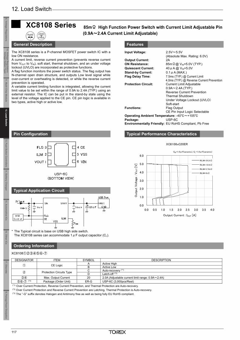
12. Load Switch _____________________________________________________________________________________
117
XC8108 Series 85mΩ High Function Power Switch with Current Limit Adjustable Pin (0.9A~2.4A Current Limit Adjustable)
General Description Features
The XC8108 series is a P-channel MOSFET power switch IC with a low ON resistance. A current limit, reverse current prevention (prevents reverse current from VOUT to VIN), soft start, thermal shutdown, and an under voltage lockout (UVLO) are incorporated as protective functions. A flag function monitors the power switch status. The flag output has N-channel open drain structure, and outputs Low level signal while over-current or overheating is detected, or while the reverse current prevention is operated. A variable current limiting function is integrated, allowing the current limit value to be set within the range of 0.9A to 2.4A (TYP.) using an external resistor. The IC can be put in the stand-by state using the level of the voltage applied to the CE pin. CE pin logic is available in two types, active high or active low.
Input Voltage: 2.5V~5.5V (Absolute Max. Rating: 6.0V) Output Current: 2A ON Resistance: 85mΩ@ VIN=5.0V (TYP.) Quiescent Current: 40μA @ VIN=5.0V Stand-by Current: 0.1μA (MAX.) Flag Delay Time: 7.5ms (TYP.) @ Current Limit 4.0ms (TYP.) @ Reverse Current Prevention Protection Circuit: Current Limit Adjustable 0.9A~2.4A (TYP.) Reverse Current Prevention Thermal Shutdown Under Voltage Lockout (UVLO) Soft-start Functions: Flag Output CE Pin Input Logic Selectable Operating Ambient Temperature: -40~+105 Package: USP-6C Environmentally Friendly: EU RoHS Compliant, Pb Free
Pin Configuration Typical Performance Characteristics
Typical Application Circuit
* The Typical circuit is base on USB high side switch.
The XC8108 series can accommodate 1μF output capacitor (CL).
Ordering Information
XC8108①②③④⑤⑥-⑦
DESIGNATOR ITEM SYMBOL DESCRIPTION
① CE Logic A Active High B Active Low
② Protection Circuits Type C Auto-recovery (*1) D Latch-off (*2)
③④ Max. Output Current 20 2.0A (Adjustable current limit range: 0.9A~2.4A) ⑤⑥-⑦ (*3) Package (Order Unit) ER-G USP-6C (3,000pcs/Reel)
(*1) Over Current Protection, Reverse Current Prevention, and Thermal Protection are Auto-recovery. (*2) Over Current Protection and Reverse Current Prevention are Latching, Thermal Protection is Auto-recovery. (*3) The “-G” suffix denotes Halogen and Antimony free as well as being fully EU RoHS compliant.
XC8108xC20ER
0.0
1.0
2.0
3.0
4.0
5.0
6.0
0.0 0.5 1.0 1.5 2.0 2.5 3.0 3.5 4.0
Output Current : IOUT [A]
Outp
ut
Voltag
e :
VO
UT [V
]
RILIM=39.2kΩ
RILIM=18.4kΩ
RILIM=5.76kΩ
RILIM=0kΩ
CIN=1.0μF(ceramic), CL=1.0μF(ceramic)
_______________________________________________________________________________________________________
118
XC8107 Series 85mΩ High Function Power Switch (Fixed Current Limit)
General Description Features
The XC8107 series is a P-channel MOSFET power switch IC with alow ON resistance. A current limit, reverse current prevention (prevents reverse currentfrom VOUT to VIN), soft start, thermal shutdown, and an under voltagelockout (UVLO) are incorporated as protective functions. A flagfunction monitors the power switch status. The flag output hasN-channel open drain structure, and outputs Low level signal whileover-current or overheating is detected, or while the reverse currentprevention is operated. The IC can be put in the stand-by state using the level of the voltageapplied to the CE pin. High active or Low active can be selected forthe CE pin input logic.
Input Voltage: 2.5V~5.5V (Absolute Max. Rating: 6.0V) Output Current: 2A ON Resistance: 85mΩ @ VIN=5.0V (TYP.) *USP-6C 100mΩ @ VIN=5.0V (TYP.) *SOT-25 (XC8107A, B) 95mΩ@VIN=5.0V (TYP.) (XC8107X, Y) Quiescent Current: 40μA @ VIN=5.0V Stand-by Current: 0.1μA (MAX.) Flag Delay Time: 7.5ms (TYP.) @ Current Limit 4.0ms (TYP.) @ Reverse Current Prevention Protection Circuit: Reverse Current Prevention Thermal Shutdown Under Voltage Lockout (UVLO) Soft-start Functions: Flag Output CE Pin Input Logic Selectable Operating Ambient Temperature: -40~+105 Packages: SOT-25 (Au wire or Cu wire), USP-6C Environmentally Friendly: EU RoHS Compliant, Pb Free
Pin Configuration Typical Performance Characteristics
Typical Application Circuit Ty
* The Typical circuit is base on USB high side switch.
The XC8107 series can accommodate 1μF output capacitor (CL).
Ordering Information
XC8107①②③④⑤⑥-⑦
DESIGNATOR ITEM Au wire Cu wire DESCRIPTION
① CE Logic A X Active High B Y Active Low
② Protection Circuits Type C Auto-recovery D Latch-off
③④ Max. Output Current
05 0.5A (0.9A) 10 1.0A (1.4A) 15 1.5A (1.9A) 20 2.0A (2.4A)
⑤⑥-⑦(*1) Packages (Order Unit) ER-G USP-6C (3,000pcs/Reel)(*2) MR-G SOT-25 (3,000pcs/Reel)
(*1) The “-G” suffix denotes Halogen and Antimony free as well as being fully EU RoHS compliant. (*2) UPS-6C package is available for the A/B type.
XC8107xCxxxR
0.0
1.0
2.0
3.0
4.0
5.0
6.0
0.0 0.5 1.0 1.5 2.0 2.5 3.0 3.5 4.0
Output Current : IOUT [A]
Outp
ut
Voltag
e :
VO
UT [V
]
0 .5A type
1.0A type
1.5A type
2.0A type
CIN=1.0μF(ceramic), CL=1.0μF(ceramic)
11.Multi C
hip Module
10. Voltage Regulators
Voltage Detect Type
9. Voltage Regulators
12.Load Switch
13. Push Button Controllers14.B
attery Charger
15.Autom
otive ICs
16.Other IC
s17. D
iscrete18.Package Power Dissipation
12.Load Switch
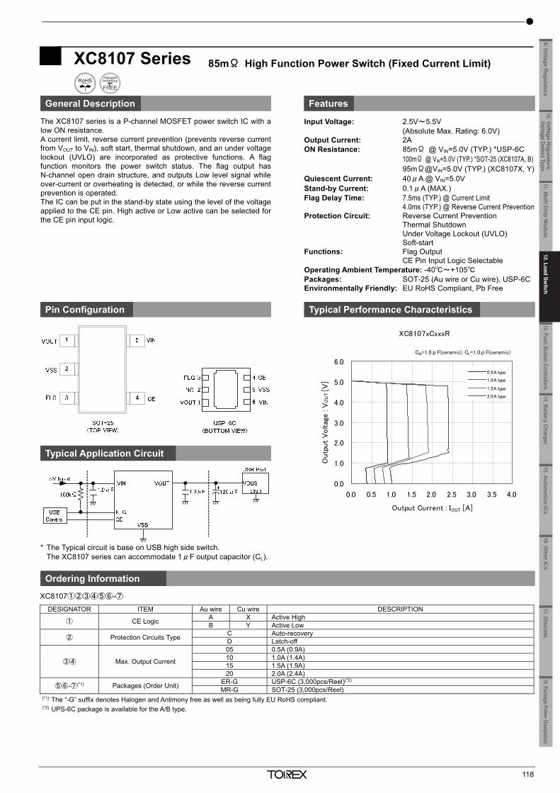
12. Load Switch _____________________________________________________________________________________
117
XC8108 Series 85mΩ High Function Power Switch with Current Limit Adjustable Pin (0.9A~2.4A Current Limit Adjustable)
General Description Features
The XC8108 series is a P-channel MOSFET power switch IC with a low ON resistance. A current limit, reverse current prevention (prevents reverse current from VOUT to VIN), soft start, thermal shutdown, and an under voltage lockout (UVLO) are incorporated as protective functions. A flag function monitors the power switch status. The flag output has N-channel open drain structure, and outputs Low level signal while over-current or overheating is detected, or while the reverse current prevention is operated. A variable current limiting function is integrated, allowing the current limit value to be set within the range of 0.9A to 2.4A (TYP.) using an external resistor. The IC can be put in the stand-by state using the level of the voltage applied to the CE pin. CE pin logic is available in two types, active high or active low.
Input Voltage: 2.5V~5.5V (Absolute Max. Rating: 6.0V) Output Current: 2A ON Resistance: 85mΩ@ VIN=5.0V (TYP.) Quiescent Current: 40μA @ VIN=5.0V Stand-by Current: 0.1μA (MAX.) Flag Delay Time: 7.5ms (TYP.) @ Current Limit 4.0ms (TYP.) @ Reverse Current Prevention Protection Circuit: Current Limit Adjustable 0.9A~2.4A (TYP.) Reverse Current Prevention Thermal Shutdown Under Voltage Lockout (UVLO) Soft-start Functions: Flag Output CE Pin Input Logic Selectable Operating Ambient Temperature: -40~+105 Package: USP-6C Environmentally Friendly: EU RoHS Compliant, Pb Free
Pin Configuration Typical Performance Characteristics
Typical Application Circuit
* The Typical circuit is base on USB high side switch.
The XC8108 series can accommodate 1μF output capacitor (CL).
Ordering Information
XC8108①②③④⑤⑥-⑦
DESIGNATOR ITEM SYMBOL DESCRIPTION
① CE Logic A Active High B Active Low
② Protection Circuits Type C Auto-recovery (*1) D Latch-off (*2)
③④ Max. Output Current 20 2.0A (Adjustable current limit range: 0.9A~2.4A) ⑤⑥-⑦ (*3) Package (Order Unit) ER-G USP-6C (3,000pcs/Reel)
(*1) Over Current Protection, Reverse Current Prevention, and Thermal Protection are Auto-recovery. (*2) Over Current Protection and Reverse Current Prevention are Latching, Thermal Protection is Auto-recovery. (*3) The “-G” suffix denotes Halogen and Antimony free as well as being fully EU RoHS compliant.
XC8108xC20ER
0.0
1.0
2.0
3.0
4.0
5.0
6.0
0.0 0.5 1.0 1.5 2.0 2.5 3.0 3.5 4.0
Output Current : IOUT [A]
Outp
ut
Voltag
e :
VO
UT [V
]
RILIM=39.2kΩ
RILIM=18.4kΩ
RILIM=5.76kΩ
RILIM=0kΩ
CIN=1.0μF(ceramic), CL=1.0μF(ceramic)
_______________________________________________________________________________________________________
118
XC8107 Series 85mΩ High Function Power Switch (Fixed Current Limit)
General Description Features
The XC8107 series is a P-channel MOSFET power switch IC with alow ON resistance. A current limit, reverse current prevention (prevents reverse currentfrom VOUT to VIN), soft start, thermal shutdown, and an under voltagelockout (UVLO) are incorporated as protective functions. A flagfunction monitors the power switch status. The flag output hasN-channel open drain structure, and outputs Low level signal whileover-current or overheating is detected, or while the reverse currentprevention is operated. The IC can be put in the stand-by state using the level of the voltageapplied to the CE pin. High active or Low active can be selected forthe CE pin input logic.
Input Voltage: 2.5V~5.5V (Absolute Max. Rating: 6.0V) Output Current: 2A ON Resistance: 85mΩ @ VIN=5.0V (TYP.) *USP-6C 100mΩ @ VIN=5.0V (TYP.) *SOT-25 (XC8107A, B) 95mΩ@VIN=5.0V (TYP.) (XC8107X, Y) Quiescent Current: 40μA @ VIN=5.0V Stand-by Current: 0.1μA (MAX.) Flag Delay Time: 7.5ms (TYP.) @ Current Limit 4.0ms (TYP.) @ Reverse Current Prevention Protection Circuit: Reverse Current Prevention Thermal Shutdown Under Voltage Lockout (UVLO) Soft-start Functions: Flag Output CE Pin Input Logic Selectable Operating Ambient Temperature: -40~+105 Packages: SOT-25 (Au wire or Cu wire), USP-6C Environmentally Friendly: EU RoHS Compliant, Pb Free
Pin Configuration Typical Performance Characteristics
Typical Application Circuit Ty
* The Typical circuit is base on USB high side switch.
The XC8107 series can accommodate 1μF output capacitor (CL).
Ordering Information
XC8107①②③④⑤⑥-⑦
DESIGNATOR ITEM Au wire Cu wire DESCRIPTION
① CE Logic A X Active High B Y Active Low
② Protection Circuits Type C Auto-recovery D Latch-off
③④ Max. Output Current
05 0.5A (0.9A) 10 1.0A (1.4A) 15 1.5A (1.9A) 20 2.0A (2.4A)
⑤⑥-⑦(*1) Packages (Order Unit) ER-G USP-6C (3,000pcs/Reel)(*2) MR-G SOT-25 (3,000pcs/Reel)
(*1) The “-G” suffix denotes Halogen and Antimony free as well as being fully EU RoHS compliant. (*2) UPS-6C package is available for the A/B type.
XC8107xCxxxR
0.0
1.0
2.0
3.0
4.0
5.0
6.0
0.0 0.5 1.0 1.5 2.0 2.5 3.0 3.5 4.0
Output Current : IOUT [A]
Outp
ut
Voltag
e :
VO
UT [V
]
0 .5A type
1.0A type
1.5A type
2.0A type
CIN=1.0μF(ceramic), CL=1.0μF(ceramic)
11.Multi C
hip Module
10. Voltage Regulators
Voltage Detect Type
9. Voltage Regulators
13. Push Button Controllers14.B
attery Charger
15.Autom
otive ICs
16.Other IC
s17. D
iscrete18.Package Power Dissipation
12.Load Switch
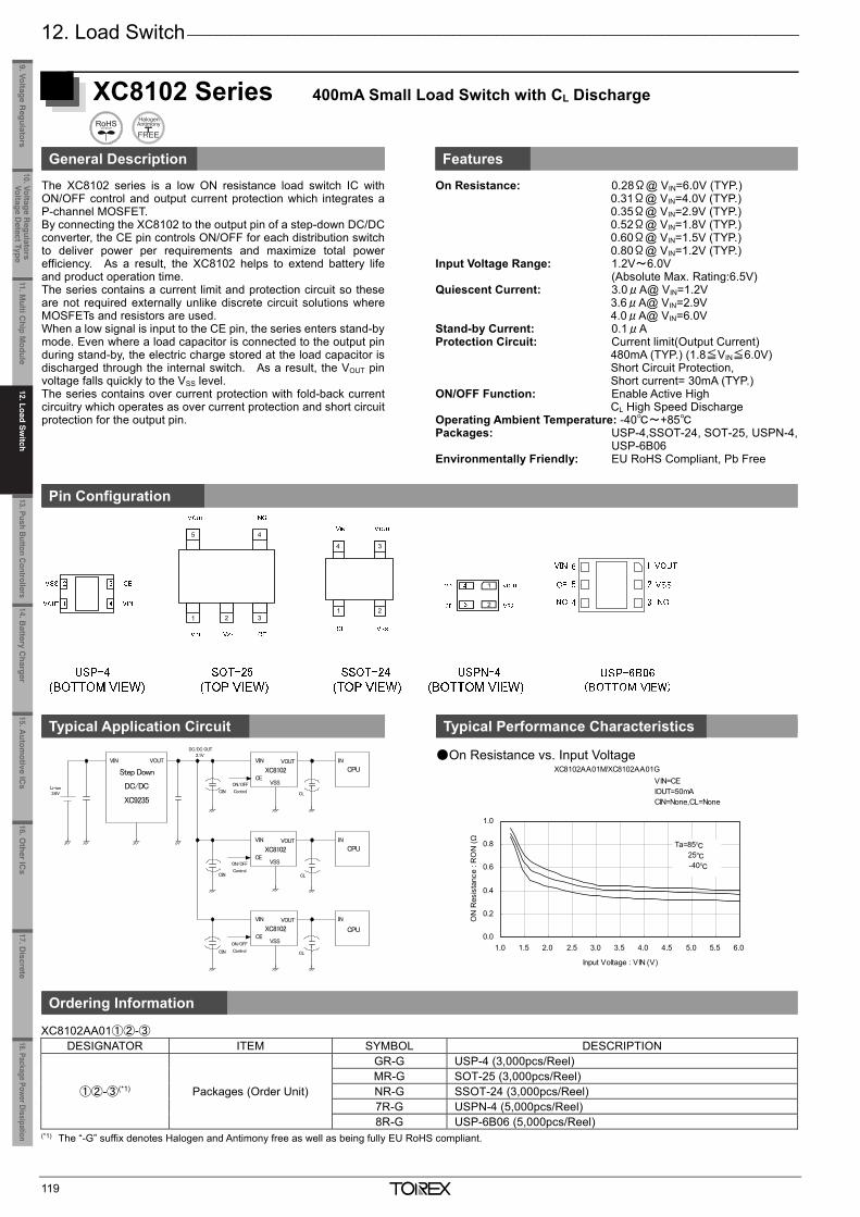
12. Load Switch _____________________________________________________________________________________
119
XC8102 Series 400mA Small Load Switch with CL Discharge
General Description Features
The XC8102 series is a low ON resistance load switch IC withON/OFF control and output current protection which integrates aP-channel MOSFET. By connecting the XC8102 to the output pin of a step-down DC/DCconverter, the CE pin controls ON/OFF for each distribution switchto deliver power per requirements and maximize total powerefficiency. As a result, the XC8102 helps to extend battery lifeand product operation time. The series contains a current limit and protection circuit so theseare not required externally unlike discrete circuit solutions whereMOSFETs and resistors are used. When a low signal is input to the CE pin, the series enters stand-by mode. Even where a load capacitor is connected to the output pinduring stand-by, the electric charge stored at the load capacitor isdischarged through the internal switch. As a result, the VOUT pin voltage falls quickly to the VSS level. The series contains over current protection with fold-back currentcircuitry which operates as over current protection and short circuitprotection for the output pin.
On Resistance: 0.28Ω@ VIN=6.0V (TYP.) 0.31Ω@ VIN=4.0V (TYP.) 0.35Ω@ VIN=2.9V (TYP.) 0.52Ω@ VIN=1.8V (TYP.) 0.60Ω@ VIN=1.5V (TYP.) 0.80Ω@ VIN=1.2V (TYP.) Input Voltage Range: 1.2V~6.0V (Absolute Max. Rating:6.5V) Quiescent Current: 3.0μA@ VIN=1.2V 3.6μA@ VIN=2.9V 4.0μA@ VIN=6.0V Stand-by Current: 0.1μA Protection Circuit: Current limit(Output Current) 480mA (TYP.) (1.8≦VIN≦6.0V) Short Circuit Protection, Short current= 30mA (TYP.) ON/OFF Function: Enable Active High CL High Speed Discharge Operating Ambient Temperature: -40~+85 Packages: USP-4,SSOT-24, SOT-25, USPN-4,
USP-6B06 Environmentally Friendly: EU RoHS Compliant, Pb Free
Pin Configuration
Typical Application Circuit Typical Performance Characteristics
On Resistance vs. Input Voltage
Ordering Information
XC8102AA01①②-③ DESIGNATOR ITEM SYMBOL DESCRIPTION
①②-③(*1) Packages (Order Unit)
GR-G USP-4 (3,000pcs/Reel) MR-G SOT-25 (3,000pcs/Reel) NR-G SSOT-24 (3,000pcs/Reel) 7R-G USPN-4 (5,000pcs/Reel) 8R-G USP-6B06 (5,000pcs/Reel)
(*1) The “-G” suffix denotes Halogen and Antimony free as well as being fully EU RoHS compliant.
XC8102AA01M/XC8102AA01G
0.0
0.2
0.4
0.6
0.8
1.0
1.0 1.5 2.0 2.5 3.0 3.5 4.0 4.5 5.0 5.5 6.0
Input Voltage : VIN (V)
ON
Res
ista
nce
: RO
N (Ω
VIN=CEIOUT=50mACIN=None,CL=None
Ta=85
25
-40
Step Down
DC/DC
XC9235
Li-ion
DC/DC OUT
3.6V
2.1V
XC8102
VIN
CEVSS
VOUT
XC8102
VIN
CEVSS
VOUT
XC8102
VIN
CEVSS
VOUT
ON/OFF
Control
ON/OFF
Control
CL
CL
CL
ON/OFF
ControlCIN
CIN
CIN
CPU
CPU
CPU
IN
IN
IN
VIN VOUT
3 4
2 1
5 4
3 2 1
1
2
_______________________________________________________________________________________________________
120
XC8101AA01
0
1
2
3
4
5
6
0.0 0.5 1.0 1.5 2.0 2.5 3.0 3.5 4.0 4.5 5.0 5.5 6.0
Input Voltage: V IN (V)
Supp
ly C
urre
nt: I
SS (μ
A)
Ta=-40
Ta=25
Ta=85
VIN=CECIN=None , CL=None
XC8101 Series Low Quiescent Current Load Switch
General Description Features
The XC8101 series is a low On resistance line switch IC withON/OFF control which integrates P-channel MOSFET. TheXC8101 is suited for power distribution switch. With connecting tothe output pin of step-down DC/DC converters, the CE pin controlsON/OF for each distribution switch to deliver power perrequirements and maximize total power efficiency. As result, theXC8101 helps extend battery life and product operation time.The XC8101 is available in an ultra small package USP-4 anddoes not require any external capacitors so that it can providesmall power unit design and board space saving. When low signalis input to the CE pin, the XC8101 enters stand-by mode. Evenwhere a load capacitor is connected to the output pin during in thestand-by mode, the internal switch between the VOUT and VSS of theXC8101 enables the electric charge in the load capacitor to bedischarged. Because of this discharge function, the VOUT pin voltage falls quickly to VSS level. The XC8101 contains an over current protection with foldbackcurrent circuitry which operates as over current protection andshort circuit protection for the output pin.
On Resistance: 0.75Ω@ VIN=2.9V 1.15Ω@ VIN=1.8V
Output Current: 200mA <Current Limit =300mA (TYP.)> Input Voltage Range: 1.8V ~ 6.0V
(Absolute Max. Rating: 6.5V) Quiescent Current: 3.0μA@ VIN=1.8V Stand-by Current: 0.1μA Protection Circuit: Current limit, 300mA (TYP.)
Short-circuit Protection, Short current= 30mA (TYP.)
ON/OFF Function: High Active Enable High-Speed Discharge Function Operating Ambient Temperature: -40 ~ +85 Packages: USP-4, SSOT-24, SOT-25 Environmentally Friendly: EU RoHS Compliant, Pb Free
Pin Configuration
Typical Application Circuit Typical Performance Characteristics
Supply Current vs. Input Voltage
Ordering Information
XC8101①②③④⑤⑥-⑦
DESIGNATOR DESCRIPTION SYMBOL DESCRIPTION ① CE pin logic A High active enable ② CL Discharge Function A Output capacitor (CL) auto-discharge function integrated
③④ Internal Standard Number 01 Fixed
⑤⑥-⑦ (*1) Packages (Order Unit) GR-G USP-4 (3,000pcs/Reel) MR-G SOT-25 (3,000pcs/Reel) NR-G SSOT-24 (3,000pcs/Reel)
(*1) The “-G” suffix denotes Halogen and Antimony free as well as being fully EU RoHS compliant.
USP-4 (BOTTOM VIEW) SOT-25
(TOP VIEW) SSOT-24
(TOP VIEW)
Step Down
DC/DC
XC9235
Li-ion
DC/DC OUT
3.6V
2.1V
XC8101
VIN
CEVSS
VOUT
XC8101
VIN
CEVSS
VOUT
XC8101
VIN
CEVSS
VOUT
ON/OFF
Control
ON/OFF
Control
CL
CL
CL
ON/OFF
ControlCIN
CIN
CIN
CPU
CPU
CPU
IN
IN
IN
VIN VOUT
11.Multi C
hip Module
10. Voltage Regulators
Voltage Detect Type
9. Voltage Regulators
12.Load Switch
13. Push Button Controllers14.B
attery Charger
15.Autom
otive ICs
16.Other IC
s17. D
iscrete18.Package Power Dissipation
12.Load Switch
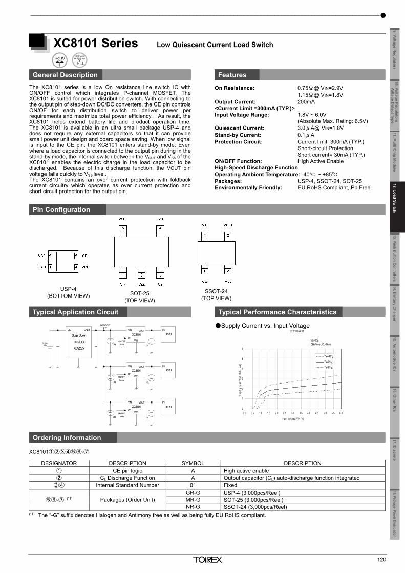
12. Load Switch _____________________________________________________________________________________
119
XC8102 Series 400mA Small Load Switch with CL Discharge
General Description Features
The XC8102 series is a low ON resistance load switch IC withON/OFF control and output current protection which integrates aP-channel MOSFET. By connecting the XC8102 to the output pin of a step-down DC/DCconverter, the CE pin controls ON/OFF for each distribution switchto deliver power per requirements and maximize total powerefficiency. As a result, the XC8102 helps to extend battery lifeand product operation time. The series contains a current limit and protection circuit so theseare not required externally unlike discrete circuit solutions whereMOSFETs and resistors are used. When a low signal is input to the CE pin, the series enters stand-by mode. Even where a load capacitor is connected to the output pinduring stand-by, the electric charge stored at the load capacitor isdischarged through the internal switch. As a result, the VOUT pin voltage falls quickly to the VSS level. The series contains over current protection with fold-back currentcircuitry which operates as over current protection and short circuitprotection for the output pin.
On Resistance: 0.28Ω@ VIN=6.0V (TYP.) 0.31Ω@ VIN=4.0V (TYP.) 0.35Ω@ VIN=2.9V (TYP.) 0.52Ω@ VIN=1.8V (TYP.) 0.60Ω@ VIN=1.5V (TYP.) 0.80Ω@ VIN=1.2V (TYP.) Input Voltage Range: 1.2V~6.0V (Absolute Max. Rating:6.5V) Quiescent Current: 3.0μA@ VIN=1.2V 3.6μA@ VIN=2.9V 4.0μA@ VIN=6.0V Stand-by Current: 0.1μA Protection Circuit: Current limit(Output Current) 480mA (TYP.) (1.8≦VIN≦6.0V) Short Circuit Protection, Short current= 30mA (TYP.) ON/OFF Function: Enable Active High CL High Speed Discharge Operating Ambient Temperature: -40~+85 Packages: USP-4,SSOT-24, SOT-25, USPN-4,
USP-6B06 Environmentally Friendly: EU RoHS Compliant, Pb Free
Pin Configuration
Typical Application Circuit Typical Performance Characteristics
On Resistance vs. Input Voltage
Ordering Information
XC8102AA01①②-③ DESIGNATOR ITEM SYMBOL DESCRIPTION
①②-③(*1) Packages (Order Unit)
GR-G USP-4 (3,000pcs/Reel) MR-G SOT-25 (3,000pcs/Reel) NR-G SSOT-24 (3,000pcs/Reel) 7R-G USPN-4 (5,000pcs/Reel) 8R-G USP-6B06 (5,000pcs/Reel)
(*1) The “-G” suffix denotes Halogen and Antimony free as well as being fully EU RoHS compliant.
XC8102AA01M/XC8102AA01G
0.0
0.2
0.4
0.6
0.8
1.0
1.0 1.5 2.0 2.5 3.0 3.5 4.0 4.5 5.0 5.5 6.0
Input Voltage : VIN (V)
ON
Res
ista
nce
: RO
N (Ω
VIN=CEIOUT=50mACIN=None,CL=None
Ta=85
25
-40
Step Down
DC/DC
XC9235
Li-ion
DC/DC OUT
3.6V
2.1V
XC8102
VIN
CEVSS
VOUT
XC8102
VIN
CEVSS
VOUT
XC8102
VIN
CEVSS
VOUT
ON/OFF
Control
ON/OFF
Control
CL
CL
CL
ON/OFF
ControlCIN
CIN
CIN
CPU
CPU
CPU
IN
IN
IN
VIN VOUT
3 4
2 1
5 4
3 2 1
1
2
_______________________________________________________________________________________________________
120
XC8101AA01
0
1
2
3
4
5
6
0.0 0.5 1.0 1.5 2.0 2.5 3.0 3.5 4.0 4.5 5.0 5.5 6.0
Input Voltage: V IN (V)
Supp
ly C
urre
nt: I
SS (μ
A)
Ta=-40
Ta=25
Ta=85
VIN=CECIN=None , CL=None
XC8101 Series Low Quiescent Current Load Switch
General Description Features
The XC8101 series is a low On resistance line switch IC withON/OFF control which integrates P-channel MOSFET. TheXC8101 is suited for power distribution switch. With connecting tothe output pin of step-down DC/DC converters, the CE pin controlsON/OF for each distribution switch to deliver power perrequirements and maximize total power efficiency. As result, theXC8101 helps extend battery life and product operation time.The XC8101 is available in an ultra small package USP-4 anddoes not require any external capacitors so that it can providesmall power unit design and board space saving. When low signalis input to the CE pin, the XC8101 enters stand-by mode. Evenwhere a load capacitor is connected to the output pin during in thestand-by mode, the internal switch between the VOUT and VSS of theXC8101 enables the electric charge in the load capacitor to bedischarged. Because of this discharge function, the VOUT pin voltage falls quickly to VSS level. The XC8101 contains an over current protection with foldbackcurrent circuitry which operates as over current protection andshort circuit protection for the output pin.
On Resistance: 0.75Ω@ VIN=2.9V 1.15Ω@ VIN=1.8V
Output Current: 200mA <Current Limit =300mA (TYP.)> Input Voltage Range: 1.8V ~ 6.0V
(Absolute Max. Rating: 6.5V) Quiescent Current: 3.0μA@ VIN=1.8V Stand-by Current: 0.1μA Protection Circuit: Current limit, 300mA (TYP.)
Short-circuit Protection, Short current= 30mA (TYP.)
ON/OFF Function: High Active Enable High-Speed Discharge Function Operating Ambient Temperature: -40 ~ +85 Packages: USP-4, SSOT-24, SOT-25 Environmentally Friendly: EU RoHS Compliant, Pb Free
Pin Configuration
Typical Application Circuit Typical Performance Characteristics
Supply Current vs. Input Voltage
Ordering Information
XC8101①②③④⑤⑥-⑦
DESIGNATOR DESCRIPTION SYMBOL DESCRIPTION ① CE pin logic A High active enable ② CL Discharge Function A Output capacitor (CL) auto-discharge function integrated
③④ Internal Standard Number 01 Fixed
⑤⑥-⑦ (*1) Packages (Order Unit) GR-G USP-4 (3,000pcs/Reel) MR-G SOT-25 (3,000pcs/Reel) NR-G SSOT-24 (3,000pcs/Reel)
(*1) The “-G” suffix denotes Halogen and Antimony free as well as being fully EU RoHS compliant.
USP-4 (BOTTOM VIEW) SOT-25
(TOP VIEW) SSOT-24
(TOP VIEW)
Step Down
DC/DC
XC9235
Li-ion
DC/DC OUT
3.6V
2.1V
XC8101
VIN
CEVSS
VOUT
XC8101
VIN
CEVSS
VOUT
XC8101
VIN
CEVSS
VOUT
ON/OFF
Control
ON/OFF
Control
CL
CL
CL
ON/OFF
ControlCIN
CIN
CIN
CPU
CPU
CPU
IN
IN
IN
VIN VOUT
11.Multi C
hip Module
10. Voltage Regulators
Voltage Detect Type
9. Voltage Regulators
13. Push Button Controllers14.B
attery Charger
15.Autom
otive ICs
16.Other IC
s17. D
iscrete18.Package Power Dissipation
12.Load Switch
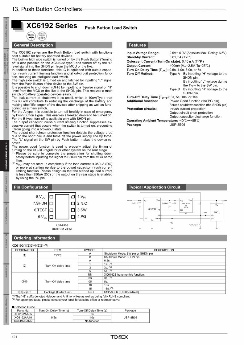
13. Push Button Controllers _______________________________________________________________________________
121
XC6192 Series Push Button Load Switch
General Description Features
The XC6192 series are the Push Button load switch with functions best suitable for battery operated devices. The built-in high side switch is turned on by the Push Button (Turning off is also possible on the XC6192A type.) and turned off by the "L" level signal into the SHDN pin from the MCU or the like. In addition to these functions, this IC is equipped with output capac-itor inrush current limiting function and short-circuit protection func-tion, realizing an intelligent load switch. The high side switch is turned on and latched by inputting "L" signal from the Push Button of the device to the SW pin. It is possible to shut down (OFF) by inputting a 1-pulse signal of "H" level from the MCU or the like to the SHDN pin. This realizes a main switch of battery operated devices easily. (*1) The leak current at shutdown is so small, which is 10nA(Typ.), that this IC will contribute to reducing the discharge of the battery and making shelf life longer of the devices after shipping as well as func-tioning as a main switch. For the A type, it is possible to turn off forcibly in case of emergency by Push Button signal. This enables a freezed device to be turned off. For the B type, turn-off is available only with SHDN pin. The output capacitor inrush current limiting function suppresses ex-cessive current that occurs when the switch is turned on, preventing it from going into a brownout state. The output short-circuit protection function detects the voltage drop due to the short circuit and turns off the power supply line by force. The "L" signal on the SW pin by Push button makes the device re-cover. The power good function is used to properly adjust the timing of turning on the DC-DC regulator or other system on the rear stage. (*1) Please be sure to complete the preparation for shutting down
safely before inputting the signal to SHDN pin from the MCU or the likes.
(*2) VOUT may not start up completely if the load current is 350uA (DC) or more at starting up due to the output capacitor inrush current limiting function. Please design so that the started up load current is less than 350uA (DC) or the output on the rear stage is enabled by using the PG pin.
Input Voltage Range: 2.5V~6.0V (Absolute Max. Rating: 6.5V) Stand-by Current: 0.01μA (TYP.) Quiescent Current (Turn-On state): 0.45μA (TYP.) Output Current: 400mA (VIN=2.5V, Ta=25) Turn-On Delay Time (TOND): 0.5s, 1.0s, 3.0s, or 5s Turn-Off Method: Type A By inputting “H” voltage to the
SHDN pin. By inputting “L” voltage during the TOFFD to the SW pin.
Type B By inputting “H” voltage to the SHDN pin.
Turn-Off Delay Time (TOFFD): 3s, 5s, 10s, or 15s Additional function: Power Good function (the PG pin) Forced shutdown function (the SHDN pin)Protection circuits: Inrush current protection Output circuit short protection Output capacitor discharge function Operating Ambient Temperature: -40~+85 Package: USP-8B06
Pin Configuration Typical Application Circuit
Ordering Information
XC6192①②③④⑤⑥-⑦ DESIGNATOR ITEM SYMBOL DESCRIPTION
① TYPE A Shutdown Mode: SW pin or SHDN pin B Shutdown Mode: SHDN pin
② Turn-On delay time
A 0.5s. 1 1s. (*2) 3 3s. (*2) 5 5s. (*2)
③④ Turn-Off delay time
NN XC6192B have no this function. 03 3s. (*2) 05 5s. 10 10s. 15 15s. (*2)
⑤⑥-⑦(*1) Package (Order Unit) ER-G USP-8B06 (5,000pcs/Reel) (*1) The “-G” suffix denotes Halogen and Antimony free as well as being fully RoHS compliant. (*2) For option products, please contact your local Torex sales office or representative: Selection Guide
Parts No. Turn-On Delay Time (s) Turn-Off Delay Time (s) Package XC6192AA05
0.5s 5s
USP-8B06 XC6192AA10 10s XC6192BANN No function
1.VIN
2.N.C
3.SW
4.PG
8.VOUT
7.SHDN
6.TEST
5.VSS
USP-8B06(BOTTOM VIEW)
VIN
SW
VSS
PG
SHDN
PMIC or LDOor
DC/DC
EN
VDD
XC6192
VOUT
VIN
MCU
OtherBattery
CL=0.1μF
VOUT
I/OTEST
R2CIN=0.1μF
R3Push Button
R1
I/OSBD
_______________________________________________________________________________________________________
122
XC6190 Series Push Button Reboot Controller
General Description Features The XC6190 series are timer reset ICs that supply a reboot signal tothe system when “L” voltage is input into the SW1, SW2 pins for a settime (reboot delay time) using two switches (physical buttons). On type A, the reboot delay time (TDL) can be set as desired bychanging the external resistance RT within the range 1s to 20s. On type B, TDL is fixed internally. When the TS pin is set to “H” level,the delay time is 12.5s. When the TS pin is set to “L” level, the delaytime is 7.5s. After the reboot signal (TRSTB) is output for 0.4s (TYP), the IC auto-matically returns to the steady state. Quiescent current in standby mode is a very small 0.01μA (TYP.),and this contributes to a longer battery drive time. The small USPN-6 and USPN-6B01 packages enable reduction of mounting space. The UVLO function is equipped as a protective function to preventmalfunctioning of the IC.
Input Voltage Range: 1.75V~6.0V Low power Consumption: 0.01μA (Stand-by,TYP.) Output Configuration: Nch Open Drain (XC6190AN/BN) CMOS (XC6190AC/BC) RSTB Pin SINK Current: 30mA (VRSTB=0.3V) Reboot Delay Time (Type A): 1s~20s (Adjustable by the external resistor) *12.5s±5% (RT=200kΩ) Reboot Delay Time (Type B): 7.5s±5% (TS=GND), 12.5s±5% (TS=VIN) Reboot Time: 0.4s±5% Operating Ambient Temperature: -40~+85 Packages: USPN-6, USPN-6B01 Environmentally Friendly: RoHS Compliant, Pb Free
Pin Configuration
XC6190AN15xx / XC6190AC15xx
Typical Application Circuit
Type A One-Button Solution
Type B Two-Button Solution
Ordering Information
XC6190①②③④⑤⑥-⑦ DESIGNATOR DESCRIPTION SYMBOL DESCRIPTION
① Type A Reboot delay time set by the external resistance B Reboot delay time internal fix.
② Output Configuration N Nch open drain output C CMOS output
③ Reboot delay time 1 Type A : 12.5s (RT=200kΩ) 2 Type B : 7.5s(VTS=”L”), 12.5s(VTS=”H”)
④ Reboot delay time accuracy 5 ±5%
⑤⑥-⑦(*1) Packages (Order Unit) 7R-G USPN-6 (5,000pcs/Reel) 8R-G USPN-6B01 (5,000pcs/Reel)
(*1) The “-G” suffix denotes Halogen and Antimony free as well as being fully EU RoHS compliant. (*2) XC6190AC158R-G is under development.
Button2RT
Button1
SW1
VIN
RT
SW2
VSS
RSTB
RPUL
LSW1
XC6190AN15xxBattery RESETB
MPU/CPU
Other
Button2
Button1
SW1
VIN
TS
SW2
VSS
RSTB
RPUL
LSW1
XC6190BN15xxBattery RESETB
MPU/CPU
Other
USPN-6B01(BOTTOM VIEW)
RSTB1
2
34
5
6
VSS
SW1
SW2
RT
VIN
USPN-6(BOTTOM VIEW)
VIN
RSTB
VSS
6
25
1
34 SW1
SW2
RT
11.Multi C
hip Module
10. Voltage Regulators
Voltage Detect Type
9. Voltage Regulators
12.Load Switch
13. Push Button Controllers14.B
attery Charger
15.Autom
otive ICs
16.Other IC
s17. D
iscrete18.Package Power Dissipation
13. Push Button Controllers
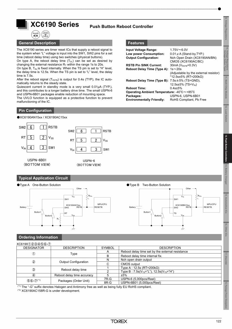
13. Push Button Controllers _______________________________________________________________________________
121
XC6192 Series Push Button Load Switch
General Description Features
The XC6192 series are the Push Button load switch with functions best suitable for battery operated devices. The built-in high side switch is turned on by the Push Button (Turning off is also possible on the XC6192A type.) and turned off by the "L" level signal into the SHDN pin from the MCU or the like. In addition to these functions, this IC is equipped with output capac-itor inrush current limiting function and short-circuit protection func-tion, realizing an intelligent load switch. The high side switch is turned on and latched by inputting "L" signal from the Push Button of the device to the SW pin. It is possible to shut down (OFF) by inputting a 1-pulse signal of "H" level from the MCU or the like to the SHDN pin. This realizes a main switch of battery operated devices easily. (*1) The leak current at shutdown is so small, which is 10nA(Typ.), that this IC will contribute to reducing the discharge of the battery and making shelf life longer of the devices after shipping as well as func-tioning as a main switch. For the A type, it is possible to turn off forcibly in case of emergency by Push Button signal. This enables a freezed device to be turned off. For the B type, turn-off is available only with SHDN pin. The output capacitor inrush current limiting function suppresses ex-cessive current that occurs when the switch is turned on, preventing it from going into a brownout state. The output short-circuit protection function detects the voltage drop due to the short circuit and turns off the power supply line by force. The "L" signal on the SW pin by Push button makes the device re-cover. The power good function is used to properly adjust the timing of turning on the DC-DC regulator or other system on the rear stage. (*1) Please be sure to complete the preparation for shutting down
safely before inputting the signal to SHDN pin from the MCU or the likes.
(*2) VOUT may not start up completely if the load current is 350uA (DC) or more at starting up due to the output capacitor inrush current limiting function. Please design so that the started up load current is less than 350uA (DC) or the output on the rear stage is enabled by using the PG pin.
Input Voltage Range: 2.5V~6.0V (Absolute Max. Rating: 6.5V) Stand-by Current: 0.01μA (TYP.) Quiescent Current (Turn-On state): 0.45μA (TYP.) Output Current: 400mA (VIN=2.5V, Ta=25) Turn-On Delay Time (TOND): 0.5s, 1.0s, 3.0s, or 5s Turn-Off Method: Type A By inputting “H” voltage to the
SHDN pin. By inputting “L” voltage during the TOFFD to the SW pin.
Type B By inputting “H” voltage to the SHDN pin.
Turn-Off Delay Time (TOFFD): 3s, 5s, 10s, or 15s Additional function: Power Good function (the PG pin) Forced shutdown function (the SHDN pin)Protection circuits: Inrush current protection Output circuit short protection Output capacitor discharge function Operating Ambient Temperature: -40~+85 Package: USP-8B06
Pin Configuration Typical Application Circuit
Ordering Information
XC6192①②③④⑤⑥-⑦ DESIGNATOR ITEM SYMBOL DESCRIPTION
① TYPE A Shutdown Mode: SW pin or SHDN pin B Shutdown Mode: SHDN pin
② Turn-On delay time
A 0.5s. 1 1s. (*2) 3 3s. (*2) 5 5s. (*2)
③④ Turn-Off delay time
NN XC6192B have no this function. 03 3s. (*2) 05 5s. 10 10s. 15 15s. (*2)
⑤⑥-⑦(*1) Package (Order Unit) ER-G USP-8B06 (5,000pcs/Reel) (*1) The “-G” suffix denotes Halogen and Antimony free as well as being fully RoHS compliant. (*2) For option products, please contact your local Torex sales office or representative: Selection Guide
Parts No. Turn-On Delay Time (s) Turn-Off Delay Time (s) Package XC6192AA05
0.5s 5s
USP-8B06 XC6192AA10 10s XC6192BANN No function
1.VIN
2.N.C
3.SW
4.PG
8.VOUT
7.SHDN
6.TEST
5.VSS
USP-8B06(BOTTOM VIEW)
VIN
SW
VSS
PG
SHDN
PMIC or LDOor
DC/DC
EN
VDD
XC6192
VOUT
VIN
MCU
OtherBattery
CL=0.1μF
VOUT
I/OTEST
R2CIN=0.1μF
R3Push Button
R1
I/OSBD
_______________________________________________________________________________________________________
122
XC6190 Series Push Button Reboot Controller
General Description Features The XC6190 series are timer reset ICs that supply a reboot signal tothe system when “L” voltage is input into the SW1, SW2 pins for a settime (reboot delay time) using two switches (physical buttons). On type A, the reboot delay time (TDL) can be set as desired bychanging the external resistance RT within the range 1s to 20s. On type B, TDL is fixed internally. When the TS pin is set to “H” level,the delay time is 12.5s. When the TS pin is set to “L” level, the delaytime is 7.5s. After the reboot signal (TRSTB) is output for 0.4s (TYP), the IC auto-matically returns to the steady state. Quiescent current in standby mode is a very small 0.01μA (TYP.),and this contributes to a longer battery drive time. The small USPN-6 and USPN-6B01 packages enable reduction of mounting space. The UVLO function is equipped as a protective function to preventmalfunctioning of the IC.
Input Voltage Range: 1.75V~6.0V Low power Consumption: 0.01μA (Stand-by,TYP.) Output Configuration: Nch Open Drain (XC6190AN/BN) CMOS (XC6190AC/BC) RSTB Pin SINK Current: 30mA (VRSTB=0.3V) Reboot Delay Time (Type A): 1s~20s (Adjustable by the external resistor) *12.5s±5% (RT=200kΩ) Reboot Delay Time (Type B): 7.5s±5% (TS=GND), 12.5s±5% (TS=VIN) Reboot Time: 0.4s±5% Operating Ambient Temperature: -40~+85 Packages: USPN-6, USPN-6B01 Environmentally Friendly: RoHS Compliant, Pb Free
Pin Configuration
XC6190AN15xx / XC6190AC15xx
Typical Application Circuit
Type A One-Button Solution
Type B Two-Button Solution
Ordering Information
XC6190①②③④⑤⑥-⑦ DESIGNATOR DESCRIPTION SYMBOL DESCRIPTION
① Type A Reboot delay time set by the external resistance B Reboot delay time internal fix.
② Output Configuration N Nch open drain output C CMOS output
③ Reboot delay time 1 Type A : 12.5s (RT=200kΩ) 2 Type B : 7.5s(VTS=”L”), 12.5s(VTS=”H”)
④ Reboot delay time accuracy 5 ±5%
⑤⑥-⑦(*1) Packages (Order Unit) 7R-G USPN-6 (5,000pcs/Reel) 8R-G USPN-6B01 (5,000pcs/Reel)
(*1) The “-G” suffix denotes Halogen and Antimony free as well as being fully EU RoHS compliant. (*2) XC6190AC158R-G is under development.
Button2RT
Button1
SW1
VIN
RT
SW2
VSS
RSTB
RPUL
LSW1
XC6190AN15xxBattery RESETB
MPU/CPU
Other
Button2
Button1
SW1
VIN
TS
SW2
VSS
RSTB
RPUL
LSW1
XC6190BN15xxBattery RESETB
MPU/CPU
Other
USPN-6B01(BOTTOM VIEW)
RSTB1
2
34
5
6
VSS
SW1
SW2
RT
VIN
USPN-6(BOTTOM VIEW)
VIN
RSTB
VSS
6
25
1
34 SW1
SW2
RT
11.Multi C
hip Module
10. Voltage Regulators
Voltage Detect Type
9. Voltage Regulators
12.Load Switch
14.Battery C
harger15.A
utomotive IC
s16.O
ther ICs
17. Discrete
18.Package Power Dissipation13. Push Button Controllers
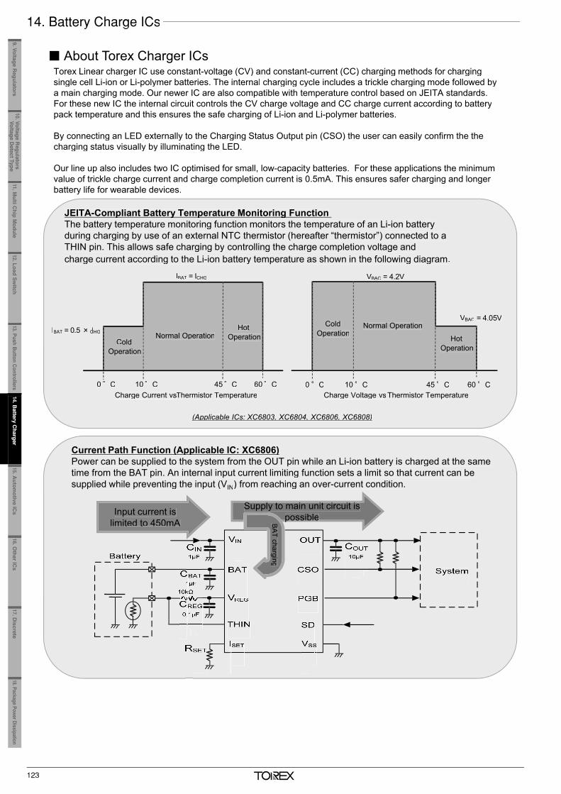
123
About Torex Charger ICsTorex Linear charger IC use constant-voltage (CV) and constant-current (CC) charging methods for charging single cell Li-ion or Li-polymer batteries. The internal charging cycle includes a trickle charging mode followed bya main charging mode. Our newer IC are also compatible with temperature control based on JEITA standards. For these new IC the internal circuit controls the CV charge voltage and CC charge current according to battery pack temperature and this ensures the safe charging of Li-ion and Li-polymer batteries.
By connecting an LED externally to the Charging Status Output pin (CSO) the user can easily confirm the the charging status visually by illuminating the LED.
Our line up also includes two IC optimised for small, low-capacity batteries. For these applications the minimumvalue of trickle charge current and charge completion current is 0.5mA. This ensures safer charging and longer battery life for wearable devices.
IBAT = 0.5 ICHGIICold
Operation
Normal Operation
Charge Current vsThermistor Temperaturevsvs10 C0 C 45 C 60 C
HotOperation
IBAT = ICHG
JEITA-Compliant Battery Temperature Monitoring Function The battery temperature monitoring function monitors the temperature of an Li-ion batteryduring charging by use of an external NTC thermistor (hereafter “thermistor”) connected to a THIN pin. This allows safe charging by controlling the charge completion voltage and charge current according to the Li-ion battery temperature as shown in the following diagram.
VBAC = 4.2V
Charge Voltage vs Thermistor Temperaturess
VBAC = 4.05VCold
OperationNormal Operation
HotOperation
10 C0 C 45 C 60 C
Current Path Function (Applicable IC: XC6806) Power can be supplied to the system from the OUT pin while an Li-ion battery is charged at the sametime from the BAT pin. An internal input current limiting function sets a limit so that current can besupplied while preventing the input (VIN) from reaching an over-current condition.
Input current islimited to 450mA
Supply to main unit circuit isS l t i it i it ippossiblepossibleBAT charging
(Applicable ICs: XC6803, XC6804, XC6806, XC6808)
y g14. Battery Charge ICs
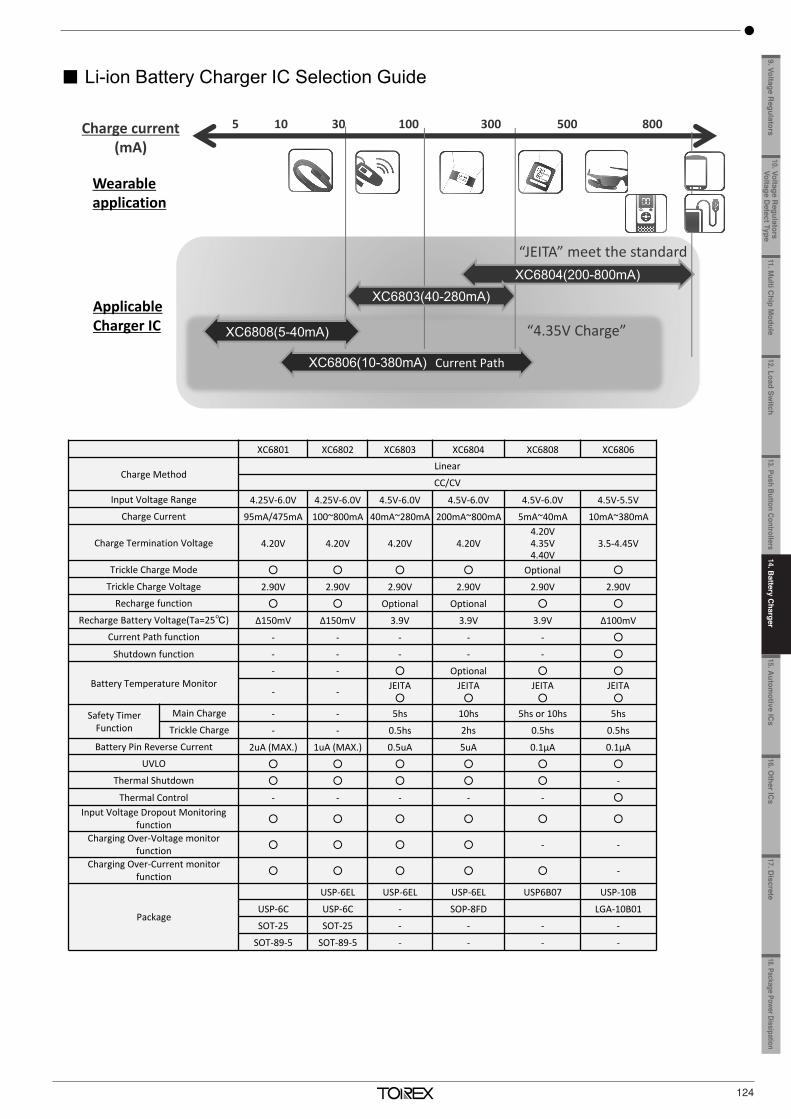
124
Li-ion Battery Charger IC Selection Guide
Charge current (mA)
Wearableapplication
ApplicableCharger IC
XC6804(200-800mA)
5 10 30 100 300 500 800
XC6806(10-380mA) Current Path
XC6803(40-280mA)
“JEITA” meet the standard
XC6808(5-40mA) “4.35V Charge”
XC6801 XC6802 XC6803 XC6804 XC6808 XC6806
Charge MethodLinear
CC/CV
Input Voltage Range 4.25V-6.0V 4.25V-6.0V 4.5V-6.0V 4.5V-6.0V 4.5V-6.0V 4.5V-5.5VCharge Current 95mA/475mA 100~800mA 40mA~280mA 200mA~800mA 5mA~40mA 10mA~380mA
Charge Termination Voltage 4.20V 4.20V 4.20V 4.20V4.20V4.35V4.40V
3.5-4.45V
Trickle Charge Mode OptionalTrickle Charge Voltage 2.90V 2.90V 2.90V 2.90V 2.90V 2.90V
Recharge function Optional OptionalRecharge Battery Voltage(Ta=25 ) 150mV 150mV 3.9V 3.9V 3.9V 100mV
Current Path function - - - - -
Shutdown function - - - - -
Battery Temperature Monitor- - Optional
- - JEITA JEITA JEITA JEITA
Safety TimerFunction
Main Charge - - 5hs 10hs 5hs or 10hs 5hsTrickle Charge - - 0.5hs 2hs 0.5hs 0.5hs
Battery Pin Reverse Current 2uA (MAX.) 1uA (MAX.) 0.5uA 5uA 0.1 A 0.1 AUVLO
Thermal Shutdown -
Thermal Control - - - - -Input Voltage Dropout Monitoring
functionCharging Over-Voltage monitor
function - -
Charging Over-Current monitor function -
Package
USP-6EL USP-6EL USP-6EL USP6B07 USP-10B
USP-6C USP-6C - SOP-8FD LGA-10B01
SOT-25 SOT-25 - - - -
SOT-89-5 SOT-89-5 - - - -
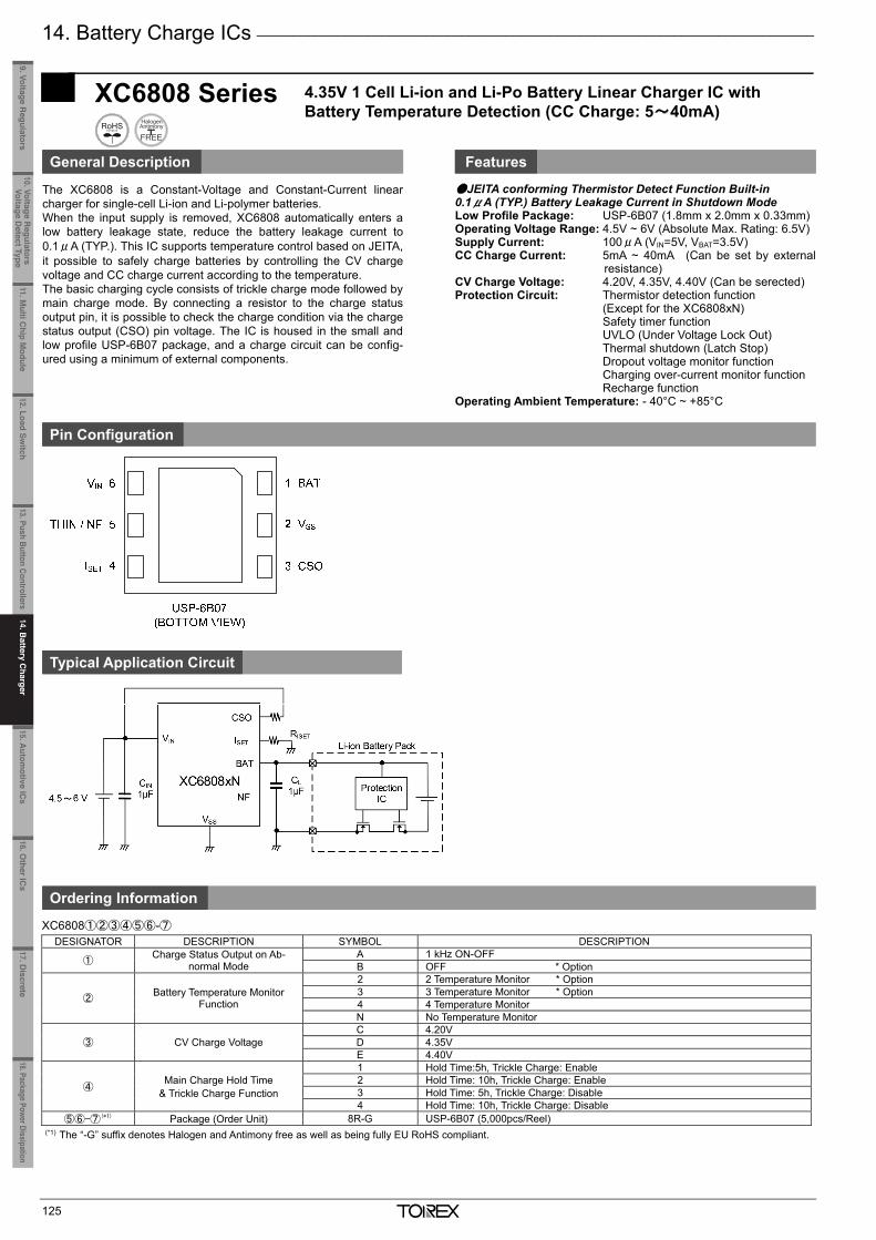
14. Battery Charge ICs ____________________________________________________________________________
125
XC6808 Series 4.35V 1 Cell Li-ion and Li-Po Battery Linear Charger IC with
General Description Features
The XC6808 is a Constant-Voltage and Constant-Current linear charger for single-cell Li-ion and Li-polymer batteries. When the input supply is removed, XC6808 automatically enters a low battery leakage state, reduce the battery leakage current to 0.1μA (TYP.). This IC supports temperature control based on JEITA, it possible to safely charge batteries by controlling the CV charge voltage and CC charge current according to the temperature. The basic charging cycle consists of trickle charge mode followed by main charge mode. By connecting a resistor to the charge status output pin, it is possible to check the charge condition via the charge status output (CSO) pin voltage. The IC is housed in the small and low profile USP-6B07 package, and a charge circuit can be config-ured using a minimum of external components.
JEITA conforming Thermistor Detect Function Built-in 0.1μA (TYP.) Battery Leakage Current in Shutdown Mode Low Profile Package: USP-6B07 (1.8mm x 2.0mm x 0.33mm) Operating Voltage Range: 4.5V ~ 6V (Absolute Max. Rating: 6.5V) Supply Current: 100μA (VIN=5V, VBAT=3.5V) CC Charge Current: 5mA ~ 40mA (Can be set by external
resistance) CV Charge Voltage: 4.20V, 4.35V, 4.40V (Can be serected) Protection Circuit: Thermistor detection function (Except for the XC6808xN) Safety timer function UVLO (Under Voltage Lock Out) Thermal shutdown (Latch Stop) Dropout voltage monitor function Charging over-current monitor function Recharge function Operating Ambient Temperature: - 40°C ~ +85°C
Pin Configuration
Typical Application Circuit
Ordering Information
XC6808①②③④⑤⑥-⑦ DESIGNATOR DESCRIPTION SYMBOL DESCRIPTION
① Charge Status Output on Ab-
normal Mode A 1 kHz ON-OFF B OFF * Option
② Battery Temperature Monitor
Function
2 2 Temperature Monitor * Option 3 3 Temperature Monitor * Option 4 4 Temperature Monitor N No Temperature Monitor
③ CV Charge Voltage C 4.20V D 4.35V E 4.40V
④ Main Charge Hold Time
& Trickle Charge Function
1 Hold Time:5h, Trickle Charge: Enable 2 Hold Time: 10h, Trickle Charge: Enable 3 Hold Time: 5h, Trickle Charge: Disable 4 Hold Time: 10h, Trickle Charge: Disable
⑤⑥-⑦(*1) Package (Order Unit) 8R-G USP-6B07 (5,000pcs/Reel) (*1) The “-G” suffix denotes Halogen and Antimony free as well as being fully EU RoHS compliant.
Battery Temperature Detection (CC Charge: 5~40mA)
_______________________________________________________________________________________________________
126
XC6806 Series Linear Charger IC with Current Path Function (CC Charge:10~380mA)
General Description Features
Equipped with a system power supply function, the XC6806 is a lin-ear charger IC for single-cell lithium ion batteries and lithium polymerbatteries. IC control gives system power supply priority over chargingthe lithium ion battery. The charge current can be adjusted with anexternal resistance, and an internal limit circuit with an input currentof 450mA automatically reduces the charging current based on theload current that flows to the system. The lithium ion battery temperature is monitored in conformance withJEITA, and by controlling the charge voltage and charge current asappropriate for the temperature, the battery can be charged safely.Internal protective functions include a safety timer function, UVLOfunction, thermal control function, and reverse current protectionfunction. In addition, a shutdown function completely shuts off power supplyfrom the battery to the system to prevent battery leakage currentwhile the device is not in use, and this enables longer use of lowsupply current devices that operate using a small battery. The IC is mounted in the small, high heat dissipation USP-10B orLGA-10B01 package, and a charging circuit can be designed withminimal external components.
Current Path Function JEITA conforming Thermistor Detect Function Built-in Operating Voltage Range: 4.5V~5.5V CC Charge: 10mA~380mA Can be set by external
resistance CV Charge: 3.5V~4.45V Input current limit: 450mA, fixed internally Protection Circuit: Safety timer function UVLO (Under Voltage Lockout) Thermal shutdown Dropout Voltage Monitor Function Operating Ambient Temperature: -40~+85 Packages: USP-10B, LGA-10B01 Environmentally Friendly: EU RoHS Compliant, Pb Free
Pin Configuration
Typical Application Circuit
Ordering Information
XC6806①②③④⑤⑥-⑦ DESIGNATOR ITEM SYMBOL DESCRIPTION
① TYPE A 4 Temperature Monitor (JEITA Compliant) B 3 Temperature Monitor (Semi-custom) C 2 Temperature Monitor (Semi-custom)
②③④ Charge Voltage 350~445 3.50V~4.45V
⑤⑥-⑦(*1) Packages (Order Unit) DR-G USP-10B (3,000pcs/Reel)(*2) 11-G LGA-10B01 (5,000pcs/Reel)
(*1) The “-G” suffix denotes Halogen and Antimony free as well as being fully RoHS compliant. (*2) The reels are shipped in a moisture-proof packing. Please consult with your Torex sales contact.
VIN OUT
VSS
BAT
STB
CSOPGB
VREG
THIN
ISET
USP-10B(BOTTOM VIEW)
1
2
3
4
5
10
9
8
7
6
OUT
VSS
BAT
STB
CSO
VIN
PGB
VREG
THIN
ISET
SD SD
VIN
VSS
BAT
THIN
1μF
OUT
ISETRSET
VREG
Battery
0.1μF
1μF10kΩ
10μFCIN
CBAT
CREG
COUT
CSO
PGB
SD
System
11.Multi C
hip Module
10. Voltage Regulators
Voltage Detect Type
9. Voltage Regulators
12.Load Switch
13. Push Button Controllers14.B
attery Charger
15.Autom
otive ICs
16.Other IC
s17. D
iscrete18.Package Power Dissipation
14.Battery C
harger
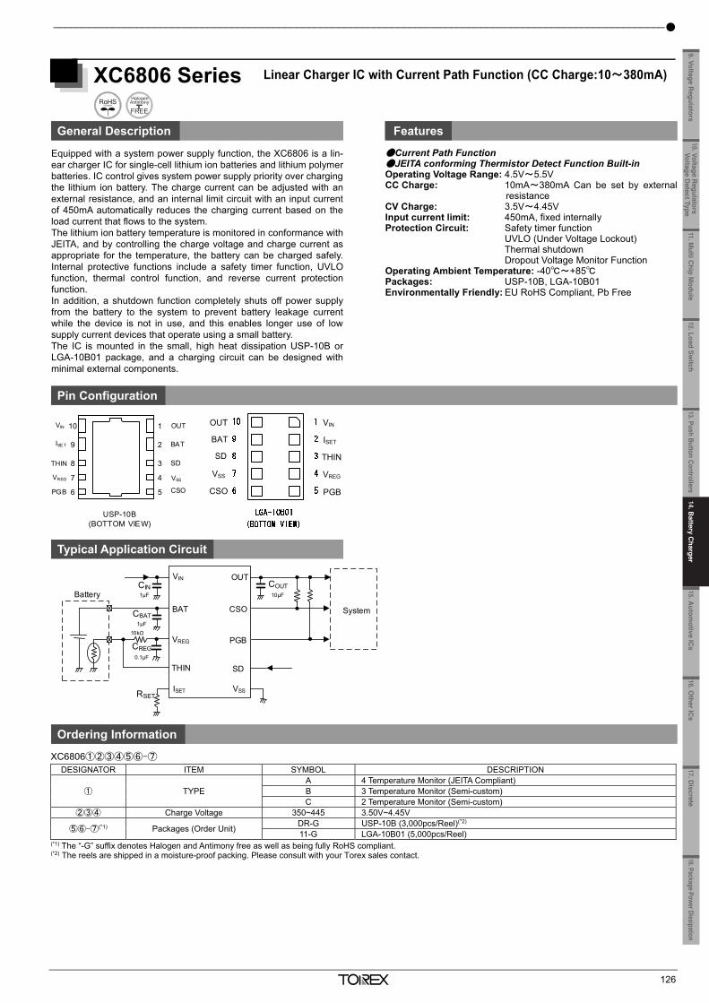
14. Battery Charge ICs ____________________________________________________________________________
125
XC6808 Series 4.35V 1 Cell Li-ion and Li-Po Battery Linear Charger IC with
General Description Features
The XC6808 is a Constant-Voltage and Constant-Current linear charger for single-cell Li-ion and Li-polymer batteries. When the input supply is removed, XC6808 automatically enters a low battery leakage state, reduce the battery leakage current to 0.1μA (TYP.). This IC supports temperature control based on JEITA, it possible to safely charge batteries by controlling the CV charge voltage and CC charge current according to the temperature. The basic charging cycle consists of trickle charge mode followed by main charge mode. By connecting a resistor to the charge status output pin, it is possible to check the charge condition via the charge status output (CSO) pin voltage. The IC is housed in the small and low profile USP-6B07 package, and a charge circuit can be config-ured using a minimum of external components.
JEITA conforming Thermistor Detect Function Built-in 0.1μA (TYP.) Battery Leakage Current in Shutdown Mode Low Profile Package: USP-6B07 (1.8mm x 2.0mm x 0.33mm) Operating Voltage Range: 4.5V ~ 6V (Absolute Max. Rating: 6.5V) Supply Current: 100μA (VIN=5V, VBAT=3.5V) CC Charge Current: 5mA ~ 40mA (Can be set by external
resistance) CV Charge Voltage: 4.20V, 4.35V, 4.40V (Can be serected) Protection Circuit: Thermistor detection function (Except for the XC6808xN) Safety timer function UVLO (Under Voltage Lock Out) Thermal shutdown (Latch Stop) Dropout voltage monitor function Charging over-current monitor function Recharge function Operating Ambient Temperature: - 40°C ~ +85°C
Pin Configuration
Typical Application Circuit
Ordering Information
XC6808①②③④⑤⑥-⑦ DESIGNATOR DESCRIPTION SYMBOL DESCRIPTION
① Charge Status Output on Ab-
normal Mode A 1 kHz ON-OFF B OFF * Option
② Battery Temperature Monitor
Function
2 2 Temperature Monitor * Option 3 3 Temperature Monitor * Option 4 4 Temperature Monitor N No Temperature Monitor
③ CV Charge Voltage C 4.20V D 4.35V E 4.40V
④ Main Charge Hold Time
& Trickle Charge Function
1 Hold Time:5h, Trickle Charge: Enable 2 Hold Time: 10h, Trickle Charge: Enable 3 Hold Time: 5h, Trickle Charge: Disable 4 Hold Time: 10h, Trickle Charge: Disable
⑤⑥-⑦(*1) Package (Order Unit) 8R-G USP-6B07 (5,000pcs/Reel) (*1) The “-G” suffix denotes Halogen and Antimony free as well as being fully EU RoHS compliant.
Battery Temperature Detection (CC Charge: 5~40mA)
_______________________________________________________________________________________________________
126
XC6806 Series Linear Charger IC with Current Path Function (CC Charge:10~380mA)
General Description Features
Equipped with a system power supply function, the XC6806 is a lin-ear charger IC for single-cell lithium ion batteries and lithium polymerbatteries. IC control gives system power supply priority over chargingthe lithium ion battery. The charge current can be adjusted with anexternal resistance, and an internal limit circuit with an input currentof 450mA automatically reduces the charging current based on theload current that flows to the system. The lithium ion battery temperature is monitored in conformance withJEITA, and by controlling the charge voltage and charge current asappropriate for the temperature, the battery can be charged safely.Internal protective functions include a safety timer function, UVLOfunction, thermal control function, and reverse current protectionfunction. In addition, a shutdown function completely shuts off power supplyfrom the battery to the system to prevent battery leakage currentwhile the device is not in use, and this enables longer use of lowsupply current devices that operate using a small battery. The IC is mounted in the small, high heat dissipation USP-10B orLGA-10B01 package, and a charging circuit can be designed withminimal external components.
Current Path Function JEITA conforming Thermistor Detect Function Built-in Operating Voltage Range: 4.5V~5.5V CC Charge: 10mA~380mA Can be set by external
resistance CV Charge: 3.5V~4.45V Input current limit: 450mA, fixed internally Protection Circuit: Safety timer function UVLO (Under Voltage Lockout) Thermal shutdown Dropout Voltage Monitor Function Operating Ambient Temperature: -40~+85 Packages: USP-10B, LGA-10B01 Environmentally Friendly: EU RoHS Compliant, Pb Free
Pin Configuration
Typical Application Circuit
Ordering Information
XC6806①②③④⑤⑥-⑦ DESIGNATOR ITEM SYMBOL DESCRIPTION
① TYPE A 4 Temperature Monitor (JEITA Compliant) B 3 Temperature Monitor (Semi-custom) C 2 Temperature Monitor (Semi-custom)
②③④ Charge Voltage 350~445 3.50V~4.45V
⑤⑥-⑦(*1) Packages (Order Unit) DR-G USP-10B (3,000pcs/Reel)(*2) 11-G LGA-10B01 (5,000pcs/Reel)
(*1) The “-G” suffix denotes Halogen and Antimony free as well as being fully RoHS compliant. (*2) The reels are shipped in a moisture-proof packing. Please consult with your Torex sales contact.
VIN OUT
VSS
BAT
STB
CSOPGB
VREG
THIN
ISET
USP-10B(BOTTOM VIEW)
1
2
3
4
5
10
9
8
7
6
OUT
VSS
BAT
STB
CSO
VIN
PGB
VREG
THIN
ISET
SD SD
VIN
VSS
BAT
THIN
1μF
OUT
ISETRSET
VREG
Battery
0.1μF
1μF10kΩ
10μFCIN
CBAT
CREG
COUT
CSO
PGB
SD
System
11.Multi C
hip Module
10. Voltage Regulators
Voltage Detect Type
9. Voltage Regulators
12.Load Switch
13. Push Button Controllers15.A
utomotive IC
s16.O
ther ICs
17. Discrete
18.Package Power Dissipation14.B
attery Charger
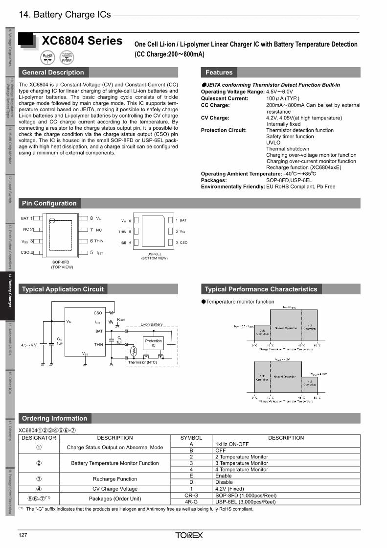
14. Battery Charge ICs ____________________________________________________________________________
127
XC6804 Series One Cell Li-ion / Li-polymer Linear Charger IC with Battery Temperature Detection (CC Charge:200~800mA)
General Description Features
The XC6804 is a Constant-Voltage (CV) and Constant-Current (CC) type charging IC for linear charging of single-cell Li-ion batteries and Li-polymer batteries. The basic charging cycle consists of trickle charge mode followed by main charge mode. This IC supports tem-perature control based on JEITA, making it possible to safely charge Li-ion batteries and Li-polymer batteries by controlling the CV charge voltage and CC charge current according to the temperature. By connecting a resistor to the charge status output pin, it is possible to check the charge condition via the charge status output (CSO) pin voltage. The IC is housed in the small SOP-8FD or USP-6EL pack-age with high heat dissipation, and a charge circuit can be configured using a minimum of external components.
JEITA conforming Thermistor Detect Function Built-in Operating Voltage Range: 4.5V~6.0V Quiescent Current: 100μA (TYP.) CC Charge: 200mA~800mA Can be set by external
resistance CV Charge: 4.2V, 4.05V(at high temperature)
Internally fixed Protection Circuit: Thermistor detection function Safety timer function UVLO Thermal shutdown Charging over-voltage monitor function
Charging over-current monitor function Recharge function (XC6804xxE) Operating Ambient Temperature: -40~+85 Packages: SOP-8FD,USP-6EL Environmentally Friendly: EU RoHS Compliant, Pb Free
Pin Configuration
Typical Application Circuit Typical Performance Characteristics
Temperature monitor function
Ordering Information
XC6804①②③④⑤⑥-⑦ DESIGNATOR DESCRIPTION SYMBOL DESCRIPTION
① Charge Status Output on Abnormal Mode A 1kHz ON-OFF B OFF
② Battery Temperature Monitor Function 2 2 Temperature Monitor 3 3 Temperature Monitor 4 4 Temperature Monitor
③ Recharge Function E Enable D Disable
④ CV Charge Voltage 1 4.2V (Fixed)
⑤⑥-⑦(*1) Packages (Order Unit) QR-G SOP-8FD (1,000pcs/Reel) 4R-G USP-6EL (3,000pcs/Reel)
(*1) The “-G” suffix indicates that the products are Halogen and Antimony free as well as being fully RoHS compliant.
VIN
VSS
BAT
THIN4.5~ V
Li-ion Battery
Protection IC
CL 1µF
Thermistor (NTC)
CIN 1µF
CSO
ISETRISET
6
VINBAT
NC
1
2
3
4
8
7
6
5
NC
VSS THIN
CSO ISET
SOP-8FD(TOP VIEW)
ISET
USP-6EL(BOTTOM VIEW)
34
2
1
5
6VIN
CE
BAT
VSS
CSO
THIN
_______________________________________________________________________________________________________
128
XC6803 Series One Cell Li-ion / Li-polymer Linear Charger IC with Battery Temperature Detection (CC Charge:40~280mA)
General Description Features
The XC6803 is a Constant-Voltage (CV) and Constant-Current (CC)type charging IC for linear charging of single-cell Li-ion batteries andLi-polymer batteries. The basic charging cycle consists of tricklecharge mode followed by main charge mode. This IC supports tem-perature control based on JEITA, making it possible to safely chargeLi-ion batteries and Li-polymer batteries by controlling the CV chargevoltage and CC charge current according to the temperature. Byconnecting a resistor to the charge status output pin, it is possible tocheck the charge condition via the charge status output (CSO) pinvoltage. The IC is housed in the small USP-6EL package with highheat dissipation, and a charge circuit can be configured using aminimum of external components.
JEITA conforming Thermistor Detect Function Built-in Operating Voltage Range: 4.5V~6.0V Quiescent: 100μA (TYP.) CC Charge: 40mA~280mA Can be set by external
resistance CV Charge Voltage: 4.2V, 4.05V (at high temperature)
Internally fixed Protection Circuit: Thermistor detection function Safety timer function UVLO Thermal shutdown Dropout voltage monitor function Charging over-voltage monitor function
Charging over-current monitor function Recharge function (XC6803xxE) Operating Ambient Temperature: -40~+85 Package: USP-6EL Environmentally Friendly: EU RoHS Compliant, Pb Free
Pin Configuration
Typical Application Circuit Typical Performance Characteristics
Temperature monitor function
Ordering Information
XC6803①②③④⑤⑥-⑦ DESIGNATOR DESCRIPTION SYMBOL DESCRIPTION
① Charge Status Output on Abnormal Mode A 1kHz ON-OFF B OFF
② Battery Temperature Monitor Function 2 2 Temperature Monitor 3 3 Temperature Monitor 4 4 Temperature Monitor
③ Recharge Function E Enable D Disable
④ CV Charge Voltage 1 4.2V (Fixed) ⑤⑥-⑦(*1) Package (Order Unit) 4R-G USP-6EL (3,000pcs/Reel)
(*1) The “-G” suffix indicates that the products are Halogen and Antimony free as well as being fully RoHS compliant.
VIN
VSS
BAT
THIN4.5~ V
Li-ion Battery
Protection IC
CL 1µF
Thermistor (NTC)
CIN 1µF
CSO
ISETRISET
6
11.Multi C
hip Module
10. Voltage Regulators
Voltage Detect Type
9. Voltage Regulators
12.Load Switch
13. Push Button Controllers14.B
attery Charger
15.Autom
otive ICs
16.Other IC
s17. D
iscrete18.Package Power Dissipation
14.Battery C
harger
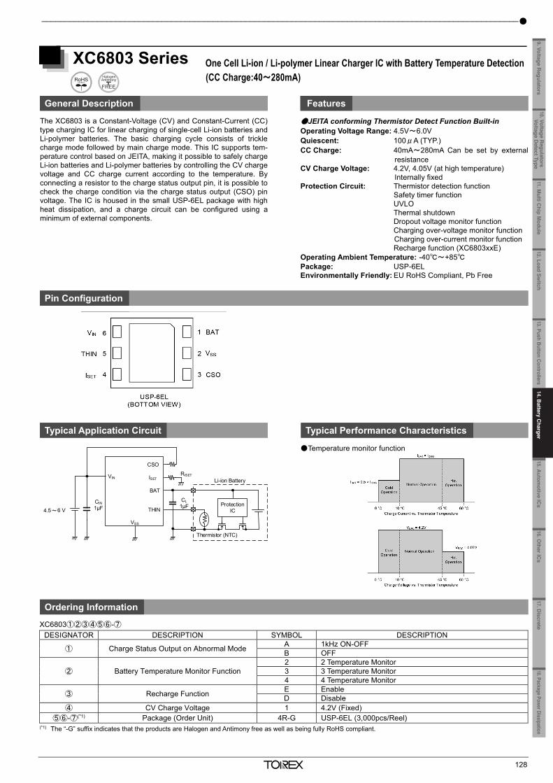
14. Battery Charge ICs ____________________________________________________________________________
127
XC6804 Series One Cell Li-ion / Li-polymer Linear Charger IC with Battery Temperature Detection (CC Charge:200~800mA)
General Description Features
The XC6804 is a Constant-Voltage (CV) and Constant-Current (CC) type charging IC for linear charging of single-cell Li-ion batteries and Li-polymer batteries. The basic charging cycle consists of trickle charge mode followed by main charge mode. This IC supports tem-perature control based on JEITA, making it possible to safely charge Li-ion batteries and Li-polymer batteries by controlling the CV charge voltage and CC charge current according to the temperature. By connecting a resistor to the charge status output pin, it is possible to check the charge condition via the charge status output (CSO) pin voltage. The IC is housed in the small SOP-8FD or USP-6EL pack-age with high heat dissipation, and a charge circuit can be configured using a minimum of external components.
JEITA conforming Thermistor Detect Function Built-in Operating Voltage Range: 4.5V~6.0V Quiescent Current: 100μA (TYP.) CC Charge: 200mA~800mA Can be set by external
resistance CV Charge: 4.2V, 4.05V(at high temperature)
Internally fixed Protection Circuit: Thermistor detection function Safety timer function UVLO Thermal shutdown Charging over-voltage monitor function
Charging over-current monitor function Recharge function (XC6804xxE) Operating Ambient Temperature: -40~+85 Packages: SOP-8FD,USP-6EL Environmentally Friendly: EU RoHS Compliant, Pb Free
Pin Configuration
Typical Application Circuit Typical Performance Characteristics
Temperature monitor function
Ordering Information
XC6804①②③④⑤⑥-⑦ DESIGNATOR DESCRIPTION SYMBOL DESCRIPTION
① Charge Status Output on Abnormal Mode A 1kHz ON-OFF B OFF
② Battery Temperature Monitor Function 2 2 Temperature Monitor 3 3 Temperature Monitor 4 4 Temperature Monitor
③ Recharge Function E Enable D Disable
④ CV Charge Voltage 1 4.2V (Fixed)
⑤⑥-⑦(*1) Packages (Order Unit) QR-G SOP-8FD (1,000pcs/Reel) 4R-G USP-6EL (3,000pcs/Reel)
(*1) The “-G” suffix indicates that the products are Halogen and Antimony free as well as being fully RoHS compliant.
VIN
VSS
BAT
THIN4.5~ V
Li-ion Battery
Protection IC
CL 1µF
Thermistor (NTC)
CIN 1µF
CSO
ISETRISET
6
VINBAT
NC
1
2
3
4
8
7
6
5
NC
VSS THIN
CSO ISET
SOP-8FD(TOP VIEW)
ISET
USP-6EL(BOTTOM VIEW)
34
2
1
5
6VIN
CE
BAT
VSS
CSO
THIN
_______________________________________________________________________________________________________
128
XC6803 Series One Cell Li-ion / Li-polymer Linear Charger IC with Battery Temperature Detection (CC Charge:40~280mA)
General Description Features
The XC6803 is a Constant-Voltage (CV) and Constant-Current (CC)type charging IC for linear charging of single-cell Li-ion batteries andLi-polymer batteries. The basic charging cycle consists of tricklecharge mode followed by main charge mode. This IC supports tem-perature control based on JEITA, making it possible to safely chargeLi-ion batteries and Li-polymer batteries by controlling the CV chargevoltage and CC charge current according to the temperature. Byconnecting a resistor to the charge status output pin, it is possible tocheck the charge condition via the charge status output (CSO) pinvoltage. The IC is housed in the small USP-6EL package with highheat dissipation, and a charge circuit can be configured using aminimum of external components.
JEITA conforming Thermistor Detect Function Built-in Operating Voltage Range: 4.5V~6.0V Quiescent: 100μA (TYP.) CC Charge: 40mA~280mA Can be set by external
resistance CV Charge Voltage: 4.2V, 4.05V (at high temperature)
Internally fixed Protection Circuit: Thermistor detection function Safety timer function UVLO Thermal shutdown Dropout voltage monitor function Charging over-voltage monitor function
Charging over-current monitor function Recharge function (XC6803xxE) Operating Ambient Temperature: -40~+85 Package: USP-6EL Environmentally Friendly: EU RoHS Compliant, Pb Free
Pin Configuration
Typical Application Circuit Typical Performance Characteristics
Temperature monitor function
Ordering Information
XC6803①②③④⑤⑥-⑦ DESIGNATOR DESCRIPTION SYMBOL DESCRIPTION
① Charge Status Output on Abnormal Mode A 1kHz ON-OFF B OFF
② Battery Temperature Monitor Function 2 2 Temperature Monitor 3 3 Temperature Monitor 4 4 Temperature Monitor
③ Recharge Function E Enable D Disable
④ CV Charge Voltage 1 4.2V (Fixed) ⑤⑥-⑦(*1) Package (Order Unit) 4R-G USP-6EL (3,000pcs/Reel)
(*1) The “-G” suffix indicates that the products are Halogen and Antimony free as well as being fully RoHS compliant.
VIN
VSS
BAT
THIN4.5~ V
Li-ion Battery
Protection IC
CL 1µF
Thermistor (NTC)
CIN 1µF
CSO
ISETRISET
6
11.Multi C
hip Module
10. Voltage Regulators
Voltage Detect Type
9. Voltage Regulators
12.Load Switch
13. Push Button Controllers15.A
utomotive IC
s16.O
ther ICs
17. Discrete
18.Package Power Dissipation14.B
attery Charger
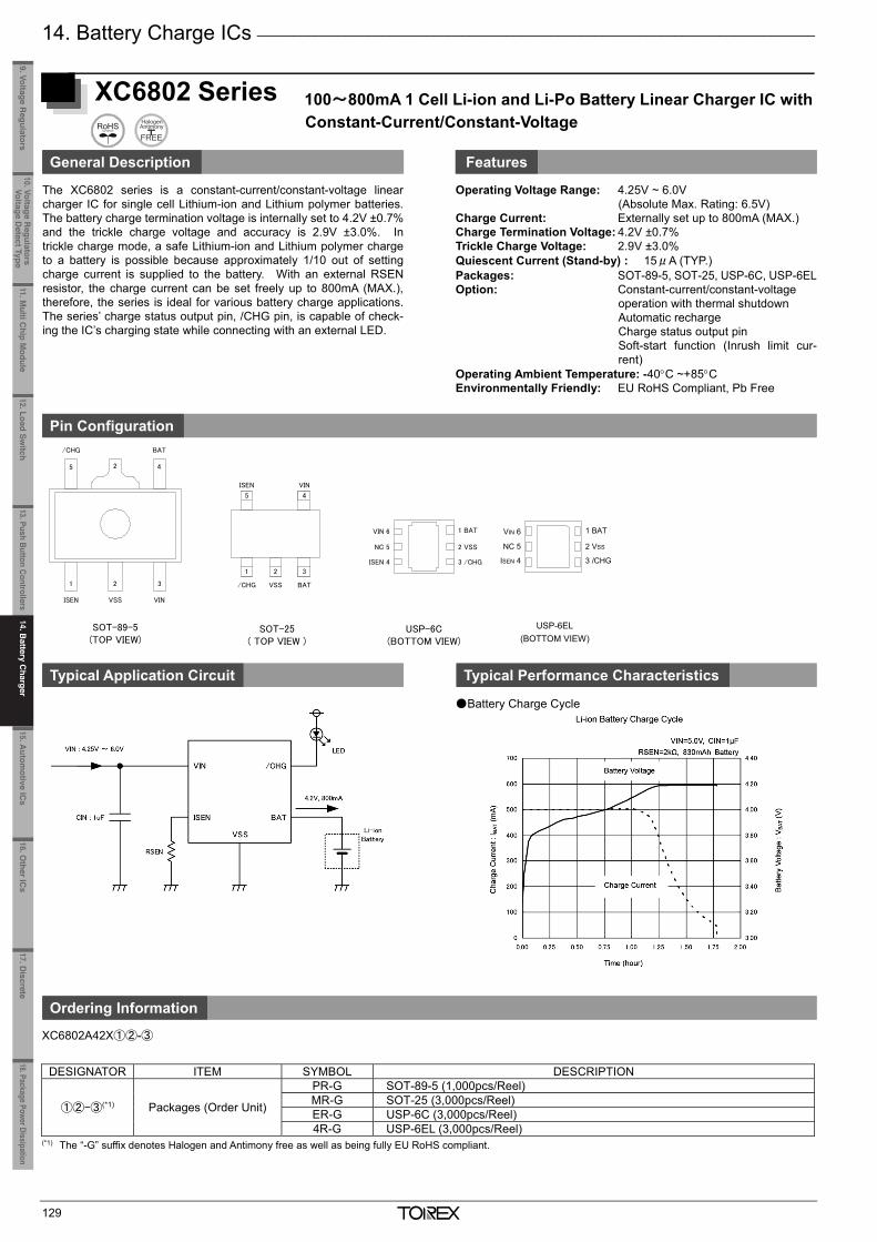
14. Battery Charge ICs ____________________________________________________________________________
129
XC6802 Series 100~800mA 1 Cell Li-ion and Li-Po Battery Linear Charger IC with Constant-Current/Constant-Voltage
General Description Features
The XC6802 series is a constant-current/constant-voltage linear charger IC for single cell Lithium-ion and Lithium polymer batteries. The battery charge termination voltage is internally set to 4.2V ±0.7% and the trickle charge voltage and accuracy is 2.9V ±3.0%. In trickle charge mode, a safe Lithium-ion and Lithium polymer charge to a battery is possible because approximately 1/10 out of setting charge current is supplied to the battery. With an external RSEN resistor, the charge current can be set freely up to 800mA (MAX.), therefore, the series is ideal for various battery charge applications. The series’ charge status output pin, /CHG pin, is capable of check-ing the IC’s charging state while connecting with an external LED.
Operating Voltage Range: 4.25V ~ 6.0V (Absolute Max. Rating: 6.5V)
Charge Current: Externally set up to 800mA (MAX.) Charge Termination Voltage: 4.2V ±0.7% Trickle Charge Voltage: 2.9V ±3.0% Quiescent Current (Stand-by) : 15μA (TYP.) Packages: SOT-89-5, SOT-25, USP-6C, USP-6ELOption: Constant-current/constant-voltage
operation with thermal shutdown Automatic recharge Charge status output pin Soft-start function (Inrush limit cur-rent)
Operating Ambient Temperature: -40C ~+85C Environmentally Friendly: EU RoHS Compliant, Pb Free
Pin Configuration
Typical Application Circuit Typical Performance Characteristics
Battery Charge Cycle
Ordering Information
XC6802A42X①②-③
DESIGNATOR ITEM SYMBOL DESCRIPTION
①②-③(*1) Packages (Order Unit)
PR-G SOT-89-5 (1,000pcs/Reel) MR-G SOT-25 (3,000pcs/Reel) ER-G USP-6C (3,000pcs/Reel) 4R-G USP-6EL (3,000pcs/Reel)
(*1) The “-G” suffix denotes Halogen and Antimony free as well as being fully EU RoHS compliant.
SOT-25( TOP VIEW )
1 2 3
5 4
/CHG VSS BAT
VINISEN
SOT-89-5(TOP VIEW)
1 2 3
45 2
BAT
ISEN VSS VIN
/CHG
USP-6C(BOTTOM VIEW)
3 /CHGISEN 4
2 VSS
1 BAT
NC 5
VIN 6
3 /CHGISEN 4
2 VSS
1 BAT
NC 5
VIN 6
USP-6EL (BOTTOM VIEW)
_______________________________________________________________________________________________________
130
XC6801 Series 500mA 1 Cell Li-ion and Li-Po Battery Linear Charger IC with Constant-Current/Constant-Voltage
General Description Features
The XC6801 series is a constant-current/constant-voltage linearcharger IC for single cell Lithium-ion and Lithium polymer batteries.The battery charge termination voltage is internally set to 4.2V ±0.7%and the trickle charge voltage and accuracy is 2.9V ±3.0%. Intrickle charge mode, a safe Lithium-ion and Lithium polymer batterycharge is possible because approximately only 1/10 of the full chargecurrent is supplied to the battery. As it is possible to select a USBcharge current of either 100mA (MAX.) or 500mA (MAX.) by using theLim pin, the series is ideal for applications where the charge is fromUSB power. The series’ charge status output pin, /CHG pin, is ca-pable of checking the IC’s charging state via connection to an ex-ternal LED.
Operating Voltage Range: 4.25V ~ 6.0V (Absolute Max. Rating: 6.5V)
USB Charge Current: 100mA or 500mA Pin-Selectable Charge Termination Voltage: 4.2V ±0.7% Trickle Charge Voltage: 2.9V ±3.0% Quiescent Current (Stand-by) : 12μA (TYP.) Packages: SOT-89-5, SOT-25, USP-6C Option: Constant-current/constant-voltage
operation with thermal shutdown Automatic recharge Charge status output pin Soft-start function (Inrush limit cur-
rent) Operating Ambient Temperature: -40C ~+85C Environmentally Friendly: EU RoHS Compliant, Pb Free
Pin Configuration
Typical Application Circuit Typical Performance Characteristics
Battery Charge Cycle
Ordering Information
XC6801A42①②③-④
DESIGNATOR ITEM SYMBOL DESCRIPTION ① Setting Charge Current 1 LIM“L”=95mA, LIM“H”=475mA
②③-④(*1) Packages (Order Unit) PR-G SOT-89-5 (1,000pcs/Reel) MR-G SOT-25 (3,000pcs/Reel) ER-G USP-6C (3,000pcs/Reel)
(*1) The “-G” suffix denotes Halogen and Antimony free as well as being fully EU RoHS compliant.
XC6801A421
0
100
200
300
400
500
600
700
800
900
1000
0 0.3 0.6 0.9 1.2 1.5
Time (hour)
Char
ge C
urr
ent
I BAT (m
A)
3.0
3.3
3.6
3.9
4.2
4.5
Bat
tery
Voltag
e
VBAT (V
)
Battery Voltage
Charge Current(Lim:H)
VIN=VLim=5V, CIN=1.0μF
420mAh Battery
11.Multi C
hip Module
10. Voltage Regulators
Voltage Detect Type
9. Voltage Regulators
12.Load Switch
13. Push Button Controllers14.B
attery Charger
15.Autom
otive ICs
16.Other IC
s17. D
iscrete18.Package Power Dissipation
14.Battery C
harger
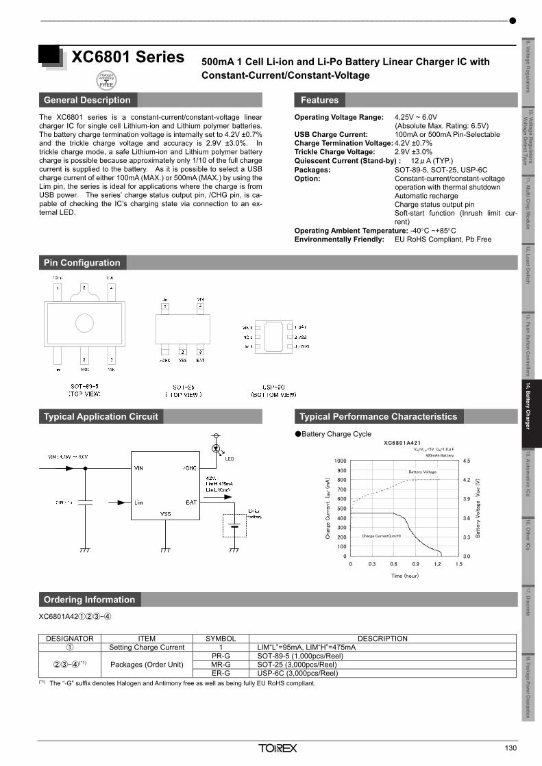
14. Battery Charge ICs ____________________________________________________________________________
129
XC6802 Series 100~800mA 1 Cell Li-ion and Li-Po Battery Linear Charger IC with Constant-Current/Constant-Voltage
General Description Features
The XC6802 series is a constant-current/constant-voltage linear charger IC for single cell Lithium-ion and Lithium polymer batteries. The battery charge termination voltage is internally set to 4.2V ±0.7% and the trickle charge voltage and accuracy is 2.9V ±3.0%. In trickle charge mode, a safe Lithium-ion and Lithium polymer charge to a battery is possible because approximately 1/10 out of setting charge current is supplied to the battery. With an external RSEN resistor, the charge current can be set freely up to 800mA (MAX.), therefore, the series is ideal for various battery charge applications. The series’ charge status output pin, /CHG pin, is capable of check-ing the IC’s charging state while connecting with an external LED.
Operating Voltage Range: 4.25V ~ 6.0V (Absolute Max. Rating: 6.5V)
Charge Current: Externally set up to 800mA (MAX.) Charge Termination Voltage: 4.2V ±0.7% Trickle Charge Voltage: 2.9V ±3.0% Quiescent Current (Stand-by) : 15μA (TYP.) Packages: SOT-89-5, SOT-25, USP-6C, USP-6ELOption: Constant-current/constant-voltage
operation with thermal shutdown Automatic recharge Charge status output pin Soft-start function (Inrush limit cur-rent)
Operating Ambient Temperature: -40C ~+85C Environmentally Friendly: EU RoHS Compliant, Pb Free
Pin Configuration
Typical Application Circuit Typical Performance Characteristics
Battery Charge Cycle
Ordering Information
XC6802A42X①②-③
DESIGNATOR ITEM SYMBOL DESCRIPTION
①②-③(*1) Packages (Order Unit)
PR-G SOT-89-5 (1,000pcs/Reel) MR-G SOT-25 (3,000pcs/Reel) ER-G USP-6C (3,000pcs/Reel) 4R-G USP-6EL (3,000pcs/Reel)
(*1) The “-G” suffix denotes Halogen and Antimony free as well as being fully EU RoHS compliant.
SOT-25( TOP VIEW )
1 2 3
5 4
/CHG VSS BAT
VINISEN
SOT-89-5(TOP VIEW)
1 2 3
45 2
BAT
ISEN VSS VIN
/CHG
USP-6C(BOTTOM VIEW)
3 /CHGISEN 4
2 VSS
1 BAT
NC 5
VIN 6
3 /CHGISEN 4
2 VSS
1 BAT
NC 5
VIN 6
USP-6EL (BOTTOM VIEW)
_______________________________________________________________________________________________________
130
XC6801 Series 500mA 1 Cell Li-ion and Li-Po Battery Linear Charger IC with Constant-Current/Constant-Voltage
General Description Features
The XC6801 series is a constant-current/constant-voltage linearcharger IC for single cell Lithium-ion and Lithium polymer batteries.The battery charge termination voltage is internally set to 4.2V ±0.7%and the trickle charge voltage and accuracy is 2.9V ±3.0%. Intrickle charge mode, a safe Lithium-ion and Lithium polymer batterycharge is possible because approximately only 1/10 of the full chargecurrent is supplied to the battery. As it is possible to select a USBcharge current of either 100mA (MAX.) or 500mA (MAX.) by using theLim pin, the series is ideal for applications where the charge is fromUSB power. The series’ charge status output pin, /CHG pin, is ca-pable of checking the IC’s charging state via connection to an ex-ternal LED.
Operating Voltage Range: 4.25V ~ 6.0V (Absolute Max. Rating: 6.5V)
USB Charge Current: 100mA or 500mA Pin-Selectable Charge Termination Voltage: 4.2V ±0.7% Trickle Charge Voltage: 2.9V ±3.0% Quiescent Current (Stand-by) : 12μA (TYP.) Packages: SOT-89-5, SOT-25, USP-6C Option: Constant-current/constant-voltage
operation with thermal shutdown Automatic recharge Charge status output pin Soft-start function (Inrush limit cur-
rent) Operating Ambient Temperature: -40C ~+85C Environmentally Friendly: EU RoHS Compliant, Pb Free
Pin Configuration
Typical Application Circuit Typical Performance Characteristics
Battery Charge Cycle
Ordering Information
XC6801A42①②③-④
DESIGNATOR ITEM SYMBOL DESCRIPTION ① Setting Charge Current 1 LIM“L”=95mA, LIM“H”=475mA
②③-④(*1) Packages (Order Unit) PR-G SOT-89-5 (1,000pcs/Reel) MR-G SOT-25 (3,000pcs/Reel) ER-G USP-6C (3,000pcs/Reel)
(*1) The “-G” suffix denotes Halogen and Antimony free as well as being fully EU RoHS compliant.
XC6801A421
0
100
200
300
400
500
600
700
800
900
1000
0 0.3 0.6 0.9 1.2 1.5
Time (hour)
Char
ge C
urr
ent
I BAT (m
A)
3.0
3.3
3.6
3.9
4.2
4.5
Bat
tery
Voltag
e
VBAT (V
)Battery Voltage
Charge Current(Lim:H)
VIN=VLim=5V, CIN=1.0μF
420mAh Battery
11.Multi C
hip Module
10. Voltage Regulators
Voltage Detect Type
9. Voltage Regulators
12.Load Switch
13. Push Button Controllers15.A
utomotive IC
s16.O
ther ICs
17. Discrete
18.Package Power Dissipation14.B
attery Charger
Torex’s Automotive ICs
Compliant with AEC-Q100Torex automotive ICs conform with AEC-Q100 (reliability and quality testing standard for integrated circuits), which was established by the AEC (Automotive Electronics Council: a standardization organization for automotive electronic component reliability).A characteristic of AEC-Q100 reliability testing that distinguishes it from commercial electronics is a higher number of tested samples and tested lots. Automotive evaluation based on this standard ensures that automotive products have high quality.
Quality ManagementTorex is a “Fab-less manufacturer”, meaning we do not have our own wafer production. However, Torex implements process control using SPC (Statistical Process Control) and MSA (Measurement System Analysis). Control standards for manufacturing conform to AEC-Q001, 002, and other guidelines. We will also provide PPAP (Production Part Approval Process) documentation upon customer request.
Design SupportIn addition to detailed information on each product, we can also provide evaluation boards for many products.
The use of electronics began with stereos and air conditioners. It then spread to information devices such as automotive meters, car navigation, and ETC. As we move into the future, the incorporation of electronic devices will accelerate to provide greater peace of mind, safety, and comfort. The advance of electronics will further increase the amount of power consumed by devices and elevate the importance of power ICs.
As Japan’s only exclusive manufacturer of power ICs, Torex has been supplying power ICs to a wide range of customers since its inception. By applying our unique small-size and low-consumption technologies, we are ableto provide highly integrated solutions, optimized for automotive electronic devices. Our benefits include:
Enhanced TraceabilityIf a problem occurs, Torex will take immediate action and has implemented strengthened traceability to minimize adverse effects.Sales traceability: Tracking of delivery destinations and counts by lot controlManufacturing traceability: Tracking of manufacturing logs by lot control
Small package sizes, giving engineers more freedom with design layouts.
High-efficiency power supplies with small overall circuit size.
High-efficiency power supplies to minimize heat and improve power dissipation
Longevity of supply, so you can use the product with peace of mind.
131
15. Automotive ICs
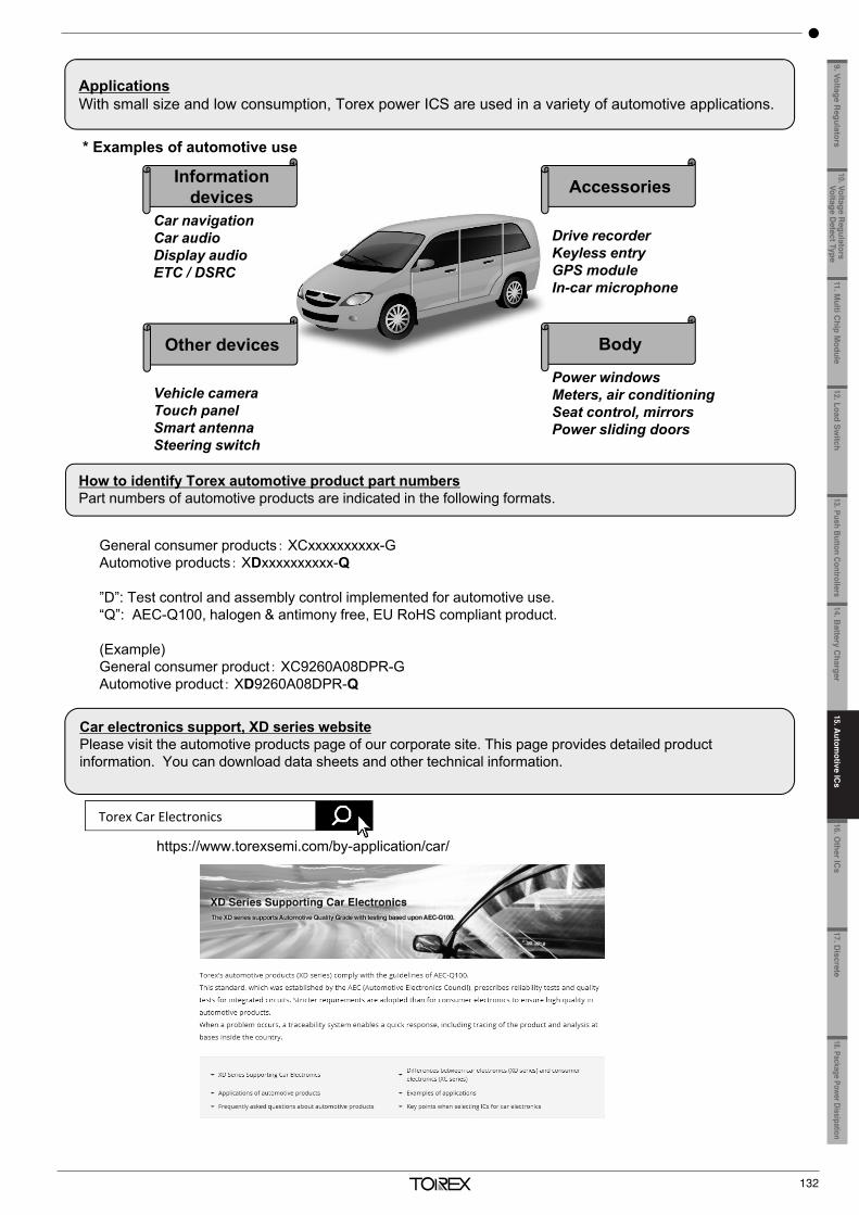
Applications With small size and low consumption, Torex power ICS are used in a variety of automotive applications.
Information devices Accessories
BodyOther devices
General consumer products XCxxxxxxxxxx-GAutomotive products XDxxxxxxxxxx-Q
”D”: Test control and assembly control implemented for automotive use.“Q”: AEC-Q100, halogen & antimony free, EU RoHS compliant product.
(Example)General consumer product XC9260A08DPR-GAutomotive product XD9260A08DPR-Q
How to identify Torex automotive product part numbersPart numbers of automotive products are indicated in the following formats.
Car electronics support, XD series websitePlease visit the automotive products page of our corporate site. This page provides detailed product information. You can download data sheets and other technical information.
* Examples of automotive use
https://www.torexsemi.com/by-application/car/
Torex Car Electronics
132
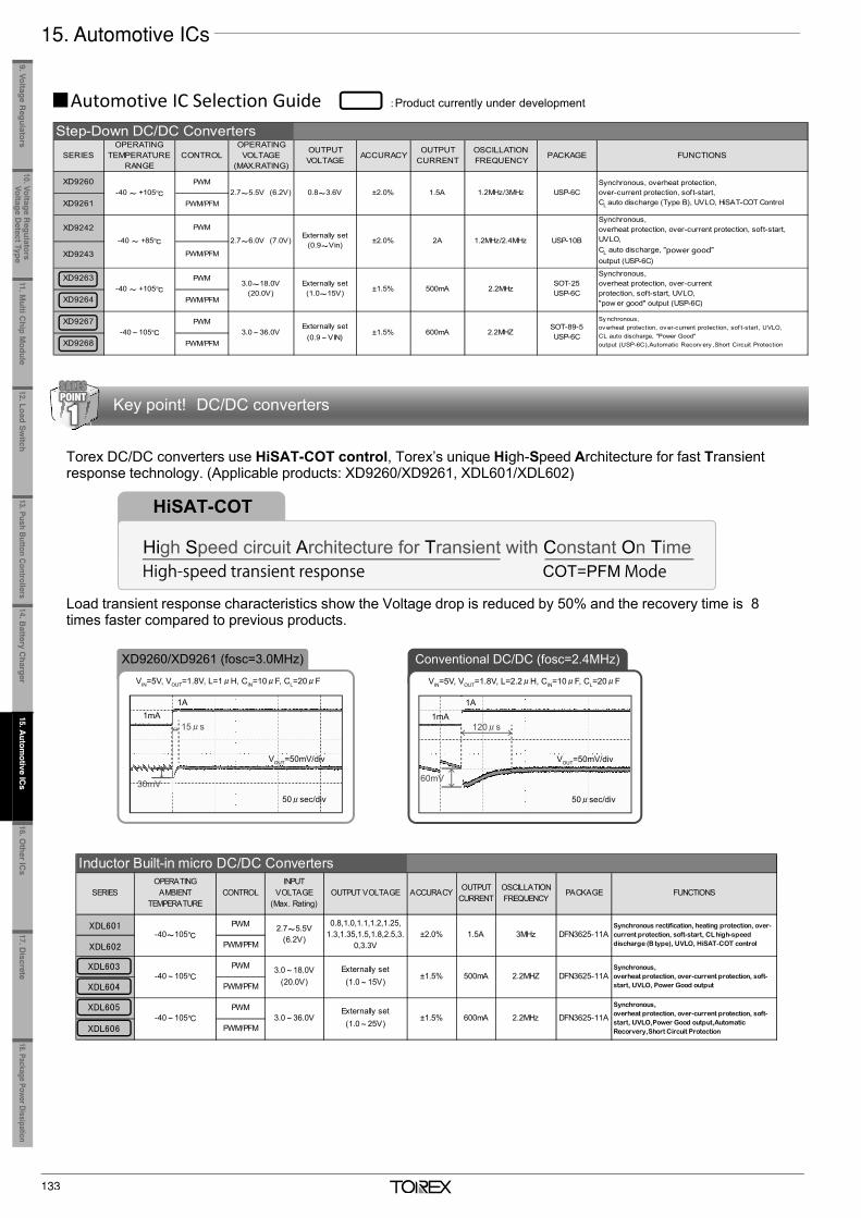
Automotive IC Selection Guide Product currently under development
Torex DC/DC converters use HiSAT-COT control, Torex’s unique High-Speed Architecture for fast Transient response technology. (Applicable products: XD9260/XD9261, XDL601/XDL602)
Load transient response characteristics show the Voltage drop is reduced by 50% and the recovery time is 8 times faster compared to previous products.
Key point! DC/DC converters
SERIESOPERATING
TEMPERATURERANGE
CONTROLOPERATING
VOLTAGE(MAX.RATING)
OUTPUTVOLTAGE
ACCURACYOUTPUT
CURRENTOSCILLATIONFREQUENCY
PACKAGE FUNCTIONS
XD9260 PWM
XD9261 PWM/PFM
XD9242 PWM
XD9243 PWM/PFM
XD9263 PWM
XD9264 PWM/PFM
XD9267 PWM
XD9268 PWM/PFM
Step-Down DC/DC Converters
USP-10B
Synchronous,overheat protection, over-current protection, soft-start,UVLO,CL auto discharge, " "output (USP-6C)
-40 +85 2.7 6.0V (7.0V)Externally set
(0.9 Vin) ±2.0% 2A 1.2MHz/2.4MHz
1.2MHz/3MHz USP-6CSynchronous, overheat protection,over-current protection, soft-start,CL auto discharge (Type B), UVLO, HiSAT-COT Control
-40 +105 2.7 5.5V (6.2V) 0.8 3.6V ±2.0% 1.5A
2.2MHzSOT-25USP-6C
Synchronous,overheat protection, over-currentprotection, soft-start, UVLO,"pow er good" output (USP-6C)
-40 +1053.0 18.0V
(20.0V)Externally set(1.0 15V) ±1.5% 500mA
2.2MHZSOT-89-5USP-6C
Sy nchronous,ov erheat protection, ov er-current protection, sof t-start, UVLO,CL auto discharge, "Power Good"output (USP-6C),Automatic Recorv ery ,Short Circuit Protection
-40 105 3.0 36.0VExternally set
(0.9 VIN)±1.5% 600mA
Inductor Built-in micro DC/DC Converters
SERIESOPERATING
AMBIENTTEMPERATURE
CONTROLINPUT
VOLTAGE(Max. Rating)
OUTPUT VOLTAGE ACCURACY OUTPUTCURRENT
OSCILLATIONFREQUENCY
PACKAGE FUNCTIONS
PWM
PWM/PFM
PWM
PWM/PFM
PWM
PWM/PFM
3MHz DFN3625-11ASynchronous rectification, heating protection, over-current protection, soft-start, CL high-speeddischarge (B type), UVLO, HiSAT-COT control
±1.5% 500mA
-40 1052.7 5.5V
(6.2V)
0.8,1.0,1.1,1.2,1.25,1.3,1.35,1.5,1.8,2.5,3.
0,3.3V±2.0% 1.5A
2.2MHZ DFN3625-11ASynchronous,overheat protection, over-current protection, soft-start, UVLO, Power Good output
-40 105 3.0 36.0VExternally set(1.0 25V)
±1.5% 600mA 2.2MHz DFN3625-11ASynchronous,overheat protection, over-current protection, soft-start, UVLO,Power Good output,AutomaticRecorvery,Short Circuit Protection
-40 1053.0 18.0V
(20.0V)Externally set(1.0 15V)
Key point! DC/DC converters11SALES
High Speed circuit Architecture for Transient with Constant On TimeHigh-speed transient response COT=PFM Mode
HiSAT-COT
Conventional DC/DC (fosc=2.4MHz)VIN=5V, VOUT=1.8V, L=2.2 H, CIN=10 F, CL=20 F
1mA
1A
VOUT=50mV/div
50 sec/div
120 s
60mV
XD9260/XD9261 (fosc=3.0MHz)VIN=5V, VOUT=1.8V, L=1 H, CIN=10 F, CL=20 F
1mA1A
VOUT=50mV/div
50 sec/div
15 s
30mV
133
15. Automotive ICs
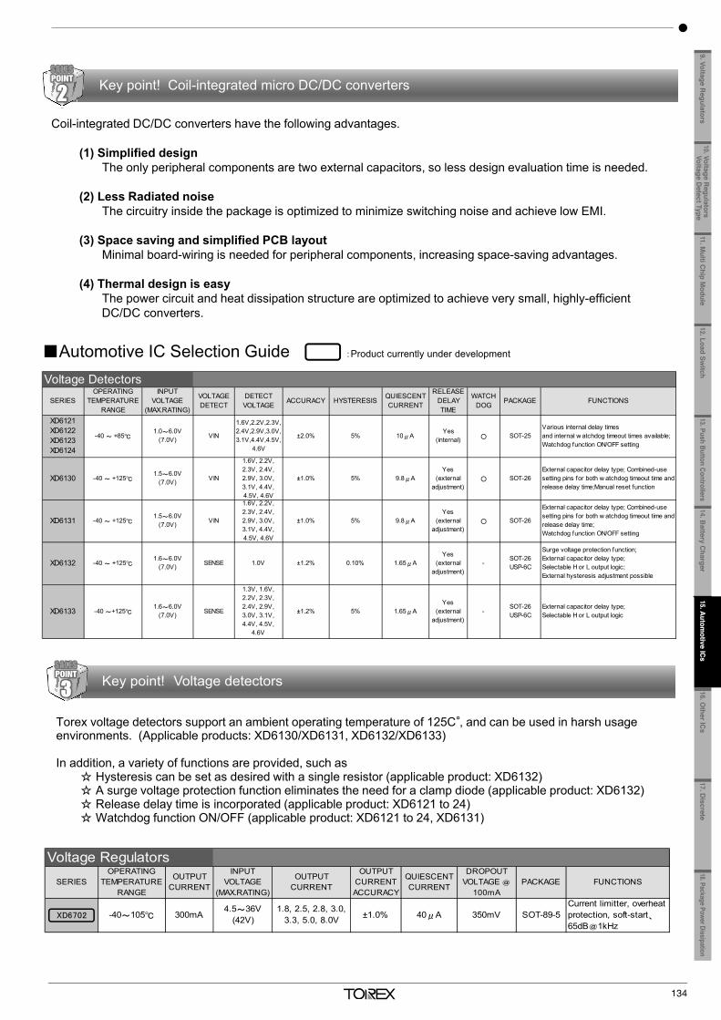
Automotive IC Selection Guide Product currently under development
Torex voltage detectors support an ambient operating temperature of 125C , and can be used in harsh usage environments. (Applicable products: XD6130/XD6131, XD6132/XD6133)
In addition, a variety of functions are provided, such asHysteresis can be set as desired with a single resistor (applicable product: XD6132)A surge voltage protection function eliminates the need for a clamp diode (applicable product: XD6132)Release delay time is incorporated (applicable product: XD6121 to 24)Watchdog function ON/OFF (applicable product: XD6121 to 24, XD6131)
Key point! Voltage detectors
SERIESOPERATING
TEMPERATURERANGE
INPUTVOLTAGE
(MAX.RATING)
VOLTAGEDETECT
DETECTVOLTAGE
ACCURACY HYSTERESISQUIESCENTCURRENT
RELEASEDELAYTIME
WATCHDOG
PACKAGE FUNCTIONS
XD6121XD6122XD6123XD6124
-40 +851.0 6.0V
(7.0V) VIN
1.6V,2.2V,2.3V,2.4V,2.9V,3.0V,3.1V,4.4V,4.5V,
4.6V
±2.0% 5% 10 AYes
(internal) SOT-25Various internal delay timesand internal w atchdog timeout times available;Watchdog function ON/OFF setting
XD6130 -40 +1251.5 6.0V
(7.0V) VIN
1.6V, 2.2V,2.3V, 2.4V,2.9V, 3.0V,3.1V, 4.4V,4.5V, 4.6V
±1.0% 5% 9.8 AYes
(externaladjustment)
SOT-26External capacitor delay type; Combined-usesetting pins for both w atchdog timeout time andrelease delay time;Manual reset function
XD6131 -40 +1251.5 6.0V
(7.0V) VIN
1.6V, 2.2V,2.3V, 2.4V,2.9V, 3.0V,3.1V, 4.4V,4.5V, 4.6V
±1.0% 5% 9.8 AYes
(externaladjustment)
SOT-26
External capacitor delay type; Combined-usesetting pins for both w atchdog timeout time andrelease delay time;Watchdog function ON/OFF setting
XD6132 -40 +1251.6 6.0V
(7.0V) SENSE 1.0V ±1.2% 0.10% 1.65 AYes
(externaladjustment)
-SOT-26USP-6C
Surge voltage protection function;External capacitor delay type;Selectable H or L output logic;External hysteresis adjustment possible
XD6133 -40 +1251.6 6.0V
(7.0V) SENSE
1.3V, 1.6V,2.2V, 2.3V,2.4V, 2.9V,3.0V, 3.1V,4.4V, 4.5V,
4.6V
±1.2% 5% 1.65 AYes
(externaladjustment)
-SOT-26USP-6C
External capacitor delay type;Selectable H or L output logic
Voltage Detectors
SERIESOPERATING
TEMPERATURERANGE
OUTPUTCURRENT
INPUTVOLTAGE
(MAX.RATING)
OUTPUTCURRENT
OUTPUTCURRENTACCURACY
QUIESCENTCURRENT
DROPOUTVOLTAGE
100mAPACKAGE FUNCTIONS
-40 105 300mA4.5 36V
(42V)1.8, 2.5, 2.8, 3.0,
3.3, 5.0, 8.0V ±1.0% 40 A 350mV SOT-89-5Current limitter, overheatprotection, soft-start65dB 1kHz
Voltage Regulators
Coil-integrated DC/DC converters have the following advantages.
(1) Simplified designThe only peripheral components are two external capacitors, so less design evaluation time is needed.
(2) Less Radiated noiseThe circuitry inside the package is optimized to minimize switching noise and achieve low EMI.
(3) Space saving and simplified PCB layoutMinimal board-wiring is needed for peripheral components, increasing space-saving advantages.
(4) Thermal design is easyThe power circuit and heat dissipation structure are optimized to achieve very small, highly-efficient DC/DC converters.
Key point! Coil-integrated micro DC/DC converters
Key point! Voltage detectors33SALES
Key point! Coil-integrated micro DC/DC converters22SALES
134
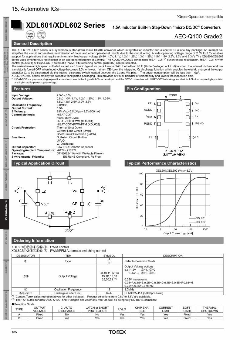
15. Automotive ICs ___________________________________________________________________________________________
*GreenOperation-compatible
135
XDL601/XDL602 Series 1.5A Inductor Built-in Step-Down “micro DC/DC” Converters
AEC-Q100 Grade2 General Description
The XDL601/XDL602 series is a synchronous step-down micro DC/DC converter which integrates an inductor and a control IC in one tiny package. An internal coil simplifies the circuit and enables minimization of noise and other operational trouble due to the circuit wiring. A wide operating voltage range of 2.5V to 5.5V enables support for applications that require an internally fixed output voltage (0.8V, 1.0V, 1.1V, 1.2V, 1.25V, 1.3V, 1.35V, 1.5V, 1.8V, 2.5V, 3.0V and 3.3V). The XDL601/XDL602series uses synchronous rectification at an operating frequency of 3.0MHz. The XDL601/XDL602 series uses HiSAT-COT (*) synchronous rectification. HiSAT-COT+PWM control (XDL601) or HiSAT-COT+automatic PWM/PFM switching control (XDL602) can be selected. The series have a high speed soft-start as fast as 0.3ms in typical for quick turn-on. With the built-in UVLO (Under Voltage Lock Out) function, the internal P-channel driver transistor is forced OFF when input voltage becomes 2.0V or lower. When CE=Low, the integrated CL discharge function which enables the electric charge at the output capacitor CL to be discharged via the internal discharge switch located between the LX and VSS pins. The power consumption will be less than 1.0μA. XDL601/XD602 series employ the wettable flank plated packaging. This provides a visual indicator of solderability and lowers the inspection time. (*) HiSAT-COT is a proprietary high-speed transient response technology which Torex developed and the DC/DC converters with HiSAT-COT technology are ideal for LSI's that require high precision
and high stability power supply voltage. Features Pin Configuration
Input Voltage: 2.5V~5.5V Output Voltage: 0.8V, 1.0V, 1.1V, 1.2V, 1.25V, 1.3V, 1.35V,
1.5V, 1.8V, 2.5V, 3.0V, 3.3V Oscillation Frequency: 3.0MHz Output Current: 1.5A Efficiency: 93% (VIN=5.0V,VOUT=3.3V/500mA) Control Methods: HiSAT-COT 100% Duty Cycle HiSAT-COT+PWM (XDL601) HiSAT-COT+PWM/PFM (XDL602) Circuit Protection: Thermal Shut Down Current Limit Circuit (Drop) Short Circuit Protection (Latch) Functions: Soft-start Circuit Built-in UVLO CL Discharge Output Capacitor: Low ESR Ceramic Capacitor OperatingAmbient Temperature: -40~+105 Package: DFN3625-11A (with Wettable Flanks) Environmental Friendly: EU RoHS Compliant, Pb Free
Typical Application Circuit Typical Performance Characteristics
Ordering Information
XDL601①②③④⑤⑥-⑦ PWM control XDL602①②③④⑤⑥-⑦ PWM/PFM Automatic switching control
DESIGNATOR ITEM SYMBOL DESCRIPTION
① Type A Refer to Selection Guide B
②③ Output Voltage 08,10,11,12,1C
13,1D,15,18 25,30,33 (*1)
Output Voltage options e.g.)1.2V → ②=1, ③=2 1.25V → ②=1, ③=C 0.05V Increments: 0.05=A,0.15=B,0.25=C,0.35=D,0.45=E,0.55=F,0.65=H, 0.75=K,0.85=L,0.95=M
④ Oscillation Frequency 3 3.0MHz ⑤⑥-⑦(*2) Package (Order Unit) 62-Q DFN3625-11A (3,000pcs/Reel)
(*1) Contact Torex sales representatives for other voltages. Product selections from 0.8V to 3.6V are available. (*2) The “-Q” suffix denotes “AEC-Q100” and “Halogen and Antimony free” as well as being fully EU RoHS compliant. Selection Guide
TYPE OUTPUT VOLTAGE
CL AUTO- DISCHARGE
LATCH or SHORT PROTECTION UVLO CHIP ENA-
BLE CURRENT
LIMIT SOFT- START
THERMAL SHUTDOWN
A Fixed No No Yes Yes Yes Fixed Yes B Fixed Yes Yes Yes Yes Yes Fixed Yes
L1 L2
VIN
NC
Lx
PGND
PGND
CE
AGND
VOUT
PGND
9 9
XDL601/XDL602 (VOUT=3.3V)
_______________________________________________________________________________________________________
*GreenOperation-compatible
136
XD9260/XD9261 Series 1.5A HiSAT-COT® Control, Synchronous Step-Down DC/DC Converters
AEC-Q100 Grade2 General Description Features
The XD9260/XD9261 series is a group of synchronous-rectification type DC/DCconverters with a built-in P-channel MOS driver transistor and N-channel MOSswitching transistor, designed to allow the use of ceramic capacitors. Outputvoltage is internally set in a range from 0.8V to 3.6V (2.0%) increments of 0.05V.The device provides a high efficiency, stable power supply with an output cur-rent of 1.5A to be configured using only a coil and two capacitors connectedexternally. Oscillation frequency is set to 1.2MHz or 3MHz can be selected forsuiting to your particular application. As for operation mode HiSAT-COT (*) con-trol excellent in transient response , the XD9260 series is PWM control, theXD9261 series is automatic PWM/PFM switching control, allowing fast re-sponse, low ripple and high efficiency over the full range of loads (from light loadto heavy load). During stand-by, all circuits are shutdown to reduce current consumption to aslow as 1.0μA or less. As for the soft-start function as fast as 0.30ms in typicalfor quick turn-on. With the built-in UVLO (Under Voltage Lock Out) function, theinternal P-channel MOS driver transistor is forced OFF when input voltage be-comes 2.0V or lower. The B types integrate CL High Speed discharge functionwhich enables the electric charge at the output capacitor CL to be dischargedvia the internal discharge. Package USP-6C is available. (*) HiSAT-COT is a proprietary high-speed transient response technology which Torex devel-
oped and the DC/DC converters with HiSAT-COT technology are ideal for LSI's that requirehigh precision and high stability power supply voltage.
Input Voltage Range: 2.7V~5.5V (Absolute Max. Rating: 6.2V) Output Voltage Range: 0.8V~3.6V (±2.0%) Quiescent Current: 25μA(fOSC = 3MHz) Output Current: 1.5A Oscillation Frequency: 1.2MHz, 3MHz Efficiency: 90% (VIN=3.7V, VOUT=1.8V, IOUT=200mA) Control Methods: HiSAT-COT Control 100% Duty Cycle PWM Control (XD9260) PWM/PFM Auto (XD9261) Protection Circuits: Thermal Shutdown
Current Limit (Pendent character) Short Circuit Protection (Type B) Functions: Soft-start UVLO CL High Speed Discharge (Type B) Capacitor: Ceramic Capacitor Operating Ambient Temperature: - 40 ~ + 105 Packages: USP-6C Environmentally Friendly: EU RoHS Compliant, Pb Free
Pin Configuration Typical Performance Characteristics
Typical Application Circuit
Ordering Information
XD9260①②③④⑤⑥-⑦ PWM control XD9261①②③④⑤⑥-⑦ PWM/PFM automatic switching control
DESIGNATOR ITEM SYMBOL DESCRIPTION
① Type A Refer to [Selection Guide] B
②③ Output Voltage 08~36
Output voltage options e.g. 1.2V → ②=1, ③=2 1.25V → ②=1, ③=C 0.05V increments : 0.05=A, 0.15=B, 0.25=C, 0.35=D, 0.45=E, 0.55=F, 0.65=H, 0.75=K,
0.85=L, 0.95=M
④ Oscillation Frequency C 1.2MHz D 3MHz
⑤⑥-⑦(*1) Package (Order Unit) ER-Q USP-6C (3,000pcs/Reel) (*1) The “-Q” suffix denotes “AEC-Q100” and “Halogen and Antimony free” as well as being fully EU RoHS compliant. Selection Guide
TYPE OUTPUT VOLTAGE CL AUTO-DISCHARGE SHORT PROTECTION (LATCH) UVLO A Fixed No No Yes B Fixed Yes Yes Yes
TYPE CHIP ENABLE CURRENT LIMIT SOFT-START TIME THERMAL SHUTDOWN
A Yes Yes Fixed Yes B Yes Yes Fixed Yes
1.5ALx
VOUT
VIN
CE
VOUT
VIN
CE
L
AGNDPGND
CIN CLCIN (ceramic)
CL (ceramic)
0102030405060708090
100
0.1 1 10 100 1000 10000
Output Current: IOUT (mA)
Effic
ienc
y: E
FFI (
%)
XC9261
XC9260
L = LQM2MPN1R0MGH(1.0μH)CIN=10μF(GRM155R61A106M) CL=10μF(GRM155R61A106M)
VIN = 5.0V
VIN = 3.7V
VIN = 5.0V
VIN = 3.7V
XD9260A18D / XD9261A18D
11.Multi C
hip Module
10. Voltage Regulators
Voltage Detect Type
9. Voltage Regulators
12.Load Switch
13. Push Button Controllers14.B
attery Charger
15.Autom
otive ICs
16.Other IC
s17. D
iscrete18.Package Power Dissipation
15.Autom
otive ICs
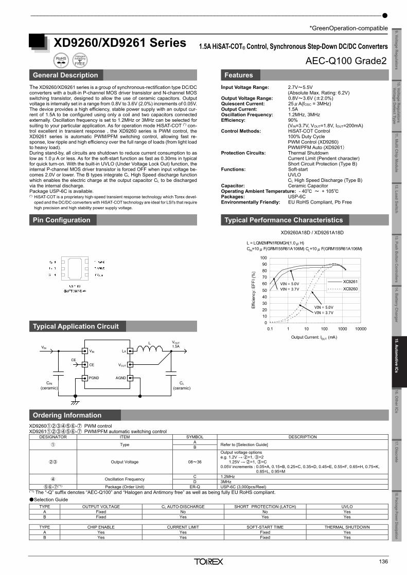
15. Automotive ICs ___________________________________________________________________________________________
*GreenOperation-compatible
135
XDL601/XDL602 Series 1.5A Inductor Built-in Step-Down “micro DC/DC” Converters
AEC-Q100 Grade2 General Description
The XDL601/XDL602 series is a synchronous step-down micro DC/DC converter which integrates an inductor and a control IC in one tiny package. An internal coil simplifies the circuit and enables minimization of noise and other operational trouble due to the circuit wiring. A wide operating voltage range of 2.5V to 5.5V enables support for applications that require an internally fixed output voltage (0.8V, 1.0V, 1.1V, 1.2V, 1.25V, 1.3V, 1.35V, 1.5V, 1.8V, 2.5V, 3.0V and 3.3V). The XDL601/XDL602series uses synchronous rectification at an operating frequency of 3.0MHz. The XDL601/XDL602 series uses HiSAT-COT (*) synchronous rectification. HiSAT-COT+PWM control (XDL601) or HiSAT-COT+automatic PWM/PFM switching control (XDL602) can be selected. The series have a high speed soft-start as fast as 0.3ms in typical for quick turn-on. With the built-in UVLO (Under Voltage Lock Out) function, the internal P-channel driver transistor is forced OFF when input voltage becomes 2.0V or lower. When CE=Low, the integrated CL discharge function which enables the electric charge at the output capacitor CL to be discharged via the internal discharge switch located between the LX and VSS pins. The power consumption will be less than 1.0μA. XDL601/XD602 series employ the wettable flank plated packaging. This provides a visual indicator of solderability and lowers the inspection time. (*) HiSAT-COT is a proprietary high-speed transient response technology which Torex developed and the DC/DC converters with HiSAT-COT technology are ideal for LSI's that require high precision
and high stability power supply voltage. Features Pin Configuration
Input Voltage: 2.5V~5.5V Output Voltage: 0.8V, 1.0V, 1.1V, 1.2V, 1.25V, 1.3V, 1.35V,
1.5V, 1.8V, 2.5V, 3.0V, 3.3V Oscillation Frequency: 3.0MHz Output Current: 1.5A Efficiency: 93% (VIN=5.0V,VOUT=3.3V/500mA) Control Methods: HiSAT-COT 100% Duty Cycle HiSAT-COT+PWM (XDL601) HiSAT-COT+PWM/PFM (XDL602) Circuit Protection: Thermal Shut Down Current Limit Circuit (Drop) Short Circuit Protection (Latch) Functions: Soft-start Circuit Built-in UVLO CL Discharge Output Capacitor: Low ESR Ceramic Capacitor OperatingAmbient Temperature: -40~+105 Package: DFN3625-11A (with Wettable Flanks) Environmental Friendly: EU RoHS Compliant, Pb Free
Typical Application Circuit Typical Performance Characteristics
Ordering Information
XDL601①②③④⑤⑥-⑦ PWM control XDL602①②③④⑤⑥-⑦ PWM/PFM Automatic switching control
DESIGNATOR ITEM SYMBOL DESCRIPTION
① Type A Refer to Selection Guide B
②③ Output Voltage 08,10,11,12,1C
13,1D,15,18 25,30,33 (*1)
Output Voltage options e.g.)1.2V → ②=1, ③=2 1.25V → ②=1, ③=C 0.05V Increments: 0.05=A,0.15=B,0.25=C,0.35=D,0.45=E,0.55=F,0.65=H, 0.75=K,0.85=L,0.95=M
④ Oscillation Frequency 3 3.0MHz ⑤⑥-⑦(*2) Package (Order Unit) 62-Q DFN3625-11A (3,000pcs/Reel)
(*1) Contact Torex sales representatives for other voltages. Product selections from 0.8V to 3.6V are available. (*2) The “-Q” suffix denotes “AEC-Q100” and “Halogen and Antimony free” as well as being fully EU RoHS compliant. Selection Guide
TYPE OUTPUT VOLTAGE
CL AUTO- DISCHARGE
LATCH or SHORT PROTECTION UVLO CHIP ENA-
BLE CURRENT
LIMIT SOFT- START
THERMAL SHUTDOWN
A Fixed No No Yes Yes Yes Fixed Yes B Fixed Yes Yes Yes Yes Yes Fixed Yes
L1 L2
VIN
NC
Lx
PGND
PGND
CE
AGND
VOUT
PGND
9 9
XDL601/XDL602 (VOUT=3.3V)
_______________________________________________________________________________________________________
*GreenOperation-compatible
136
XD9260/XD9261 Series 1.5A HiSAT-COT® Control, Synchronous Step-Down DC/DC Converters
AEC-Q100 Grade2 General Description Features
The XD9260/XD9261 series is a group of synchronous-rectification type DC/DCconverters with a built-in P-channel MOS driver transistor and N-channel MOSswitching transistor, designed to allow the use of ceramic capacitors. Outputvoltage is internally set in a range from 0.8V to 3.6V (2.0%) increments of 0.05V.The device provides a high efficiency, stable power supply with an output cur-rent of 1.5A to be configured using only a coil and two capacitors connectedexternally. Oscillation frequency is set to 1.2MHz or 3MHz can be selected forsuiting to your particular application. As for operation mode HiSAT-COT (*) con-trol excellent in transient response , the XD9260 series is PWM control, theXD9261 series is automatic PWM/PFM switching control, allowing fast re-sponse, low ripple and high efficiency over the full range of loads (from light loadto heavy load). During stand-by, all circuits are shutdown to reduce current consumption to aslow as 1.0μA or less. As for the soft-start function as fast as 0.30ms in typicalfor quick turn-on. With the built-in UVLO (Under Voltage Lock Out) function, theinternal P-channel MOS driver transistor is forced OFF when input voltage be-comes 2.0V or lower. The B types integrate CL High Speed discharge functionwhich enables the electric charge at the output capacitor CL to be dischargedvia the internal discharge. Package USP-6C is available. (*) HiSAT-COT is a proprietary high-speed transient response technology which Torex devel-
oped and the DC/DC converters with HiSAT-COT technology are ideal for LSI's that requirehigh precision and high stability power supply voltage.
Input Voltage Range: 2.7V~5.5V (Absolute Max. Rating: 6.2V) Output Voltage Range: 0.8V~3.6V (±2.0%) Quiescent Current: 25μA(fOSC = 3MHz) Output Current: 1.5A Oscillation Frequency: 1.2MHz, 3MHz Efficiency: 90% (VIN=3.7V, VOUT=1.8V, IOUT=200mA) Control Methods: HiSAT-COT Control 100% Duty Cycle PWM Control (XD9260) PWM/PFM Auto (XD9261) Protection Circuits: Thermal Shutdown
Current Limit (Pendent character) Short Circuit Protection (Type B) Functions: Soft-start UVLO CL High Speed Discharge (Type B) Capacitor: Ceramic Capacitor Operating Ambient Temperature: - 40 ~ + 105 Packages: USP-6C Environmentally Friendly: EU RoHS Compliant, Pb Free
Pin Configuration Typical Performance Characteristics
Typical Application Circuit
Ordering Information
XD9260①②③④⑤⑥-⑦ PWM control XD9261①②③④⑤⑥-⑦ PWM/PFM automatic switching control
DESIGNATOR ITEM SYMBOL DESCRIPTION
① Type A Refer to [Selection Guide] B
②③ Output Voltage 08~36
Output voltage options e.g. 1.2V → ②=1, ③=2 1.25V → ②=1, ③=C 0.05V increments : 0.05=A, 0.15=B, 0.25=C, 0.35=D, 0.45=E, 0.55=F, 0.65=H, 0.75=K,
0.85=L, 0.95=M
④ Oscillation Frequency C 1.2MHz D 3MHz
⑤⑥-⑦(*1) Package (Order Unit) ER-Q USP-6C (3,000pcs/Reel) (*1) The “-Q” suffix denotes “AEC-Q100” and “Halogen and Antimony free” as well as being fully EU RoHS compliant. Selection Guide
TYPE OUTPUT VOLTAGE CL AUTO-DISCHARGE SHORT PROTECTION (LATCH) UVLO A Fixed No No Yes B Fixed Yes Yes Yes
TYPE CHIP ENABLE CURRENT LIMIT SOFT-START TIME THERMAL SHUTDOWN
A Yes Yes Fixed Yes B Yes Yes Fixed Yes
1.5ALx
VOUT
VIN
CE
VOUT
VIN
CE
L
AGNDPGND
CIN CLCIN (ceramic)
CL (ceramic)
0102030405060708090
100
0.1 1 10 100 1000 10000
Output Current: IOUT (mA)
Effic
ienc
y: E
FFI (
%)
XC9261
XC9260
L = LQM2MPN1R0MGH(1.0μH)CIN=10μF(GRM155R61A106M) CL=10μF(GRM155R61A106M)
VIN = 5.0V
VIN = 3.7V
VIN = 5.0V
VIN = 3.7V
XD9260A18D / XD9261A18D
11.Multi C
hip Module
10. Voltage Regulators
Voltage Detect Type
9. Voltage Regulators
12.Load Switch
13. Push Button Controllers14.B
attery Charger
16.Other IC
s17. D
iscrete18.Package Power Dissipation
15.Autom
otive ICs
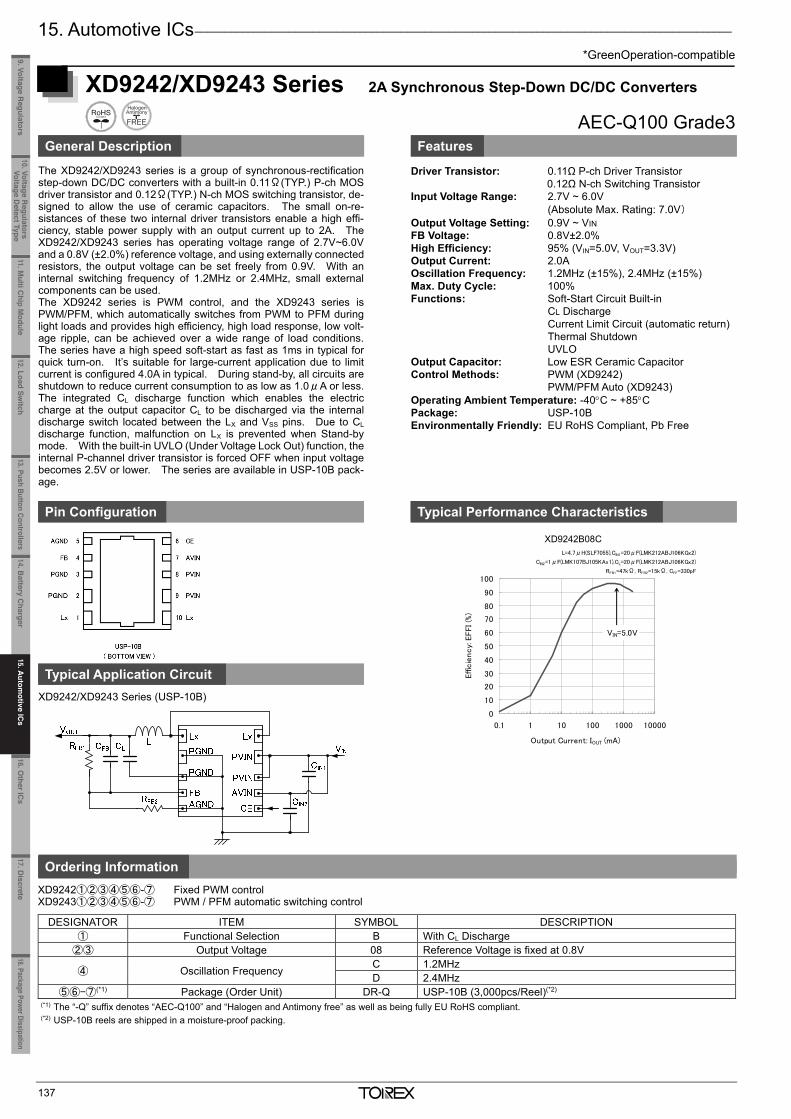
15. Automotive ICs ___________________________________________________________________________________________
*GreenOperation-compatible
137
XD9242/XD9243 Series 2A Synchronous Step-Down DC/DC Converters
General Description Features
The XD9242/XD9243 series is a group of synchronous-rectification step-down DC/DC converters with a built-in 0.11Ω(TYP.) P-ch MOS driver transistor and 0.12Ω(TYP.) N-ch MOS switching transistor, de-signed to allow the use of ceramic capacitors. The small on-re-sistances of these two internal driver transistors enable a high effi-ciency, stable power supply with an output current up to 2A. The XD9242/XD9243 series has operating voltage range of 2.7V~6.0V and a 0.8V (±2.0%) reference voltage, and using externally connected resistors, the output voltage can be set freely from 0.9V. With an internal switching frequency of 1.2MHz or 2.4MHz, small external components can be used. The XD9242 series is PWM control, and the XD9243 series is PWM/PFM, which automatically switches from PWM to PFM during light loads and provides high efficiency, high load response, low volt-age ripple, can be achieved over a wide range of load conditions. The series have a high speed soft-start as fast as 1ms in typical for quick turn-on. It’s suitable for large-current application due to limit current is configured 4.0A in typical. During stand-by, all circuits are shutdown to reduce current consumption to as low as 1.0μA or less. The integrated CL discharge function which enables the electric charge at the output capacitor CL to be discharged via the internal discharge switch located between the LX and VSS pins. Due to CL discharge function, malfunction on LX is prevented when Stand-by mode. With the built-in UVLO (Under Voltage Lock Out) function, the internal P-channel driver transistor is forced OFF when input voltage becomes 2.5V or lower. The series are available in USP-10B pack-age.
Driver Transistor: 0.11Ω P-ch Driver Transistor 0.12Ω N-ch Switching Transistor Input Voltage Range: 2.7V ~ 6.0V
(Absolute Max. Rating: 7.0V) Output Voltage Setting: 0.9V ~ VIN FB Voltage: 0.8V±2.0% High Efficiency: 95% (VIN=5.0V, VOUT=3.3V) Output Current: 2.0A Oscillation Frequency: 1.2MHz (±15%), 2.4MHz (±15%) Max. Duty Cycle: 100% Functions: Soft-Start Circuit Built-in CL Discharge Current Limit Circuit (automatic return) Thermal Shutdown UVLO Output Capacitor: Low ESR Ceramic Capacitor Control Methods: PWM (XD9242) PWM/PFM Auto (XD9243) Operating Ambient Temperature: -40C ~ +85C Package: USP-10B Environmentally Friendly: EU RoHS Compliant, Pb Free
Pin Configuration Typical Performance Characteristics
Typical Application Circuit
XD9242/XD9243 Series (USP-10B)
Ordering Information
XD9242①②③④⑤⑥-⑦ Fixed PWM control XD9243①②③④⑤⑥-⑦ PWM / PFM automatic switching control
DESIGNATOR ITEM SYMBOL DESCRIPTION ① Functional Selection B With CL Discharge
②③ Output Voltage 08 Reference Voltage is fixed at 0.8V
④ Oscillation Frequency C 1.2MHz D 2.4MHz
⑤⑥-⑦(*1) Package (Order Unit) DR-Q USP-10B (3,000pcs/Reel)(*2) (*1) The “-Q” suffix denotes “AEC-Q100” and “Halogen and Antimony free” as well as being fully EU RoHS compliant. (*2) USP-10B reels are shipped in a moisture-proof packing.
XC9242B08C
0
10
20
30
40
50
60
70
80
90
100
0.1 1 10 100 1000 10000
Output Current: IOUT (mA)
Effic
iency:
EFFI (%
)
L=4.7μH(SLF7055),CIN1=20μF(LMK212ABJ106KGx2)
CIN2=1μF(LMK107BJ105KAx1),CL=20μF(LMK212ABJ106KGx2)
RFB1=47kΩ, RFB2=15kΩ, CFB=330pF
VIN=5.0V
XD9242B08C
AEC-Q100 Grade3
_______________________________________________________________________________________________________
138
XD6506 Series Ultra-Low Quiescent Current Voltage Regulator (with Stand-by Function)
AEC-Q100 Grade2 General Description Features
The XD6506 series are positive voltage LDO regulators manufacturedusing CMOS processes. The series achieves Ultra low supply current,0.8μA (TYP.) and consists of a reference voltage source, an erroramplifier, a current fold-back circuit, and a phase compensation circuitplus a driver transistor. The output voltage is selectable in 0.1V increments within the rangeof 1.2V to 5V using laser trimming technologies. The series is also compatible with low ESR ceramic capacitors, whichgive added output stability. The current limiter's fold-back circuit also operates as a short protectfor the output current limiter and the output pin. Furthermore, the CE function allows the output of the regulator to beturned off, resulting in greatly reduced power consumption.
Maximum Output Current: 150mA Low Power Consumption: 0.8μA Stand-by Current: Less than 0.1μA Dropout Voltage: 360mV@IOUT=100mA (VOUT=3.3V) Operating Input Voltage: 1.5V ~ 6.0V Output Voltage Range: 1.2V~5.0V(0.1V Step) Output Accuracy: ±2.0%(1.5V<VOUT≦5.0V) ±30mA(1.2≦VOUT≦1.5V) Protection function: Current limit Circuit Low ESR Capacitor Compatible: Ceramic Capacitor Compatible Operating Temperature Range: -40~+105 Packages: SOT-25 Environmentally Friendly: EU RoHS Compliant, Pb Free
Typical Application Circuit Typical Performance Characteristics
Ordering Information
XD6506①②③④⑤⑥-⑦(*1) DESIGNATOR ITEM SYMBOL DESCRIPTION
① TYPE B Refer to Selection Guide ②③ Output Voltage 12~50 e.g. 3.3V ⇒ 33, 5.0V ⇒ 50
④ Output Voltage Accuracy 2 ±2% (VOUT≧1.5V) ±0.03V (VOUT<1.5V)
⑤⑥-⑦(*1) Package (Order Unit) MR-Q SOT-25 (3,000pcs/Reel) (*1) The “-Q” suffix denotes “AEC-Q100” and “Halogen and Antimony free” as well as being fully EU RoHS compliant.
CIN=0.1μF(ceramic)
VIN
VIN
VSS
CE VOUT
CIN=0.1μF(ceramic)
Input
0.0
0.2
0.4
0.6
0.8
1.0
1.2
1.4
1.6
1.8
0 1 2 3 4 5 6
Supp
ly C
urre
ntISS
(μA
)
Input Voltage VIN (V)
XD6506B332Ta=25 VIN=VCE
CIN=0.1μF(ceramic),CL=0.1μF(ceramic)
11.Multi C
hip Module
10. Voltage Regulators
Voltage Detect Type
9. Voltage Regulators
12.Load Switch
13. Push Button Controllers14.B
attery Charger
15.Autom
otive ICs
16.Other IC
s17. D
iscrete18.Package Power Dissipation
15.Autom
otive ICs
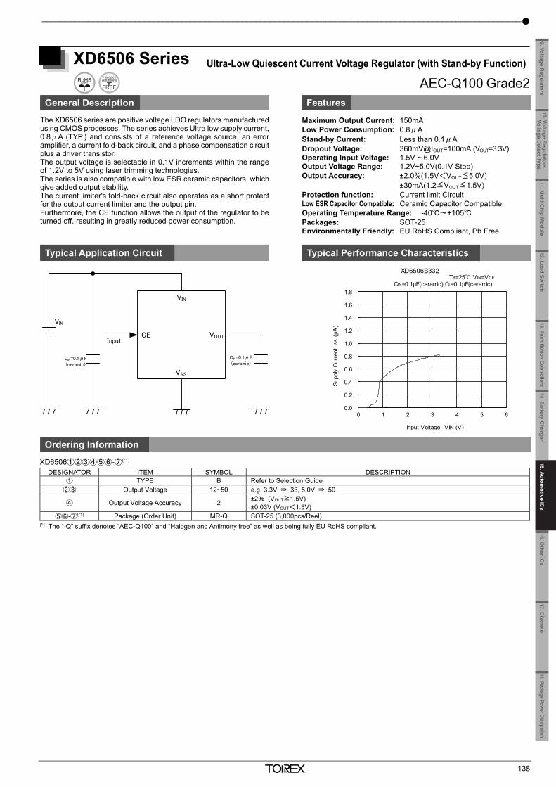
15. Automotive ICs ___________________________________________________________________________________________
*GreenOperation-compatible
137
XD9242/XD9243 Series 2A Synchronous Step-Down DC/DC Converters
General Description Features
The XD9242/XD9243 series is a group of synchronous-rectification step-down DC/DC converters with a built-in 0.11Ω(TYP.) P-ch MOS driver transistor and 0.12Ω(TYP.) N-ch MOS switching transistor, de-signed to allow the use of ceramic capacitors. The small on-re-sistances of these two internal driver transistors enable a high effi-ciency, stable power supply with an output current up to 2A. The XD9242/XD9243 series has operating voltage range of 2.7V~6.0V and a 0.8V (±2.0%) reference voltage, and using externally connected resistors, the output voltage can be set freely from 0.9V. With an internal switching frequency of 1.2MHz or 2.4MHz, small external components can be used. The XD9242 series is PWM control, and the XD9243 series is PWM/PFM, which automatically switches from PWM to PFM during light loads and provides high efficiency, high load response, low volt-age ripple, can be achieved over a wide range of load conditions. The series have a high speed soft-start as fast as 1ms in typical for quick turn-on. It’s suitable for large-current application due to limit current is configured 4.0A in typical. During stand-by, all circuits are shutdown to reduce current consumption to as low as 1.0μA or less. The integrated CL discharge function which enables the electric charge at the output capacitor CL to be discharged via the internal discharge switch located between the LX and VSS pins. Due to CL discharge function, malfunction on LX is prevented when Stand-by mode. With the built-in UVLO (Under Voltage Lock Out) function, the internal P-channel driver transistor is forced OFF when input voltage becomes 2.5V or lower. The series are available in USP-10B pack-age.
Driver Transistor: 0.11Ω P-ch Driver Transistor 0.12Ω N-ch Switching Transistor Input Voltage Range: 2.7V ~ 6.0V
(Absolute Max. Rating: 7.0V) Output Voltage Setting: 0.9V ~ VIN FB Voltage: 0.8V±2.0% High Efficiency: 95% (VIN=5.0V, VOUT=3.3V) Output Current: 2.0A Oscillation Frequency: 1.2MHz (±15%), 2.4MHz (±15%) Max. Duty Cycle: 100% Functions: Soft-Start Circuit Built-in CL Discharge Current Limit Circuit (automatic return) Thermal Shutdown UVLO Output Capacitor: Low ESR Ceramic Capacitor Control Methods: PWM (XD9242) PWM/PFM Auto (XD9243) Operating Ambient Temperature: -40C ~ +85C Package: USP-10B Environmentally Friendly: EU RoHS Compliant, Pb Free
Pin Configuration Typical Performance Characteristics
Typical Application Circuit
XD9242/XD9243 Series (USP-10B)
Ordering Information
XD9242①②③④⑤⑥-⑦ Fixed PWM control XD9243①②③④⑤⑥-⑦ PWM / PFM automatic switching control
DESIGNATOR ITEM SYMBOL DESCRIPTION ① Functional Selection B With CL Discharge
②③ Output Voltage 08 Reference Voltage is fixed at 0.8V
④ Oscillation Frequency C 1.2MHz D 2.4MHz
⑤⑥-⑦(*1) Package (Order Unit) DR-Q USP-10B (3,000pcs/Reel)(*2) (*1) The “-Q” suffix denotes “AEC-Q100” and “Halogen and Antimony free” as well as being fully EU RoHS compliant. (*2) USP-10B reels are shipped in a moisture-proof packing.
XC9242B08C
0
10
20
30
40
50
60
70
80
90
100
0.1 1 10 100 1000 10000
Output Current: IOUT (mA)
Effic
iency:
EFFI (%
)
L=4.7μH(SLF7055),CIN1=20μF(LMK212ABJ106KGx2)
CIN2=1μF(LMK107BJ105KAx1),CL=20μF(LMK212ABJ106KGx2)
RFB1=47kΩ, RFB2=15kΩ, CFB=330pF
VIN=5.0V
XD9242B08C
AEC-Q100 Grade3
_______________________________________________________________________________________________________
138
XD6506 Series Ultra-Low Quiescent Current Voltage Regulator (with Stand-by Function)
AEC-Q100 Grade2 General Description Features
The XD6506 series are positive voltage LDO regulators manufacturedusing CMOS processes. The series achieves Ultra low supply current,0.8μA (TYP.) and consists of a reference voltage source, an erroramplifier, a current fold-back circuit, and a phase compensation circuitplus a driver transistor. The output voltage is selectable in 0.1V increments within the rangeof 1.2V to 5V using laser trimming technologies. The series is also compatible with low ESR ceramic capacitors, whichgive added output stability. The current limiter's fold-back circuit also operates as a short protectfor the output current limiter and the output pin. Furthermore, the CE function allows the output of the regulator to beturned off, resulting in greatly reduced power consumption.
Maximum Output Current: 150mA Low Power Consumption: 0.8μA Stand-by Current: Less than 0.1μA Dropout Voltage: 360mV@IOUT=100mA (VOUT=3.3V) Operating Input Voltage: 1.5V ~ 6.0V Output Voltage Range: 1.2V~5.0V(0.1V Step) Output Accuracy: ±2.0%(1.5V<VOUT≦5.0V) ±30mA(1.2≦VOUT≦1.5V) Protection function: Current limit Circuit Low ESR Capacitor Compatible: Ceramic Capacitor Compatible Operating Temperature Range: -40~+105 Packages: SOT-25 Environmentally Friendly: EU RoHS Compliant, Pb Free
Typical Application Circuit Typical Performance Characteristics
Ordering Information
XD6506①②③④⑤⑥-⑦(*1) DESIGNATOR ITEM SYMBOL DESCRIPTION
① TYPE B Refer to Selection Guide ②③ Output Voltage 12~50 e.g. 3.3V ⇒ 33, 5.0V ⇒ 50
④ Output Voltage Accuracy 2 ±2% (VOUT≧1.5V) ±0.03V (VOUT<1.5V)
⑤⑥-⑦(*1) Package (Order Unit) MR-Q SOT-25 (3,000pcs/Reel) (*1) The “-Q” suffix denotes “AEC-Q100” and “Halogen and Antimony free” as well as being fully EU RoHS compliant.
CIN=0.1μF(ceramic)
VIN
VIN
VSS
CE VOUT
CIN=0.1μF(ceramic)
Input
0.0
0.2
0.4
0.6
0.8
1.0
1.2
1.4
1.6
1.8
0 1 2 3 4 5 6
Supp
ly C
urre
ntISS
(μA
)
Input Voltage VIN (V)
XD6506B332Ta=25 VIN=VCE
CIN=0.1μF(ceramic),CL=0.1μF(ceramic)
11.Multi C
hip Module
10. Voltage Regulators
Voltage Detect Type
9. Voltage Regulators
12.Load Switch
13. Push Button Controllers14.B
attery Charger
16.Other IC
s17. D
iscrete18.Package Power Dissipation
15.Autom
otive ICs
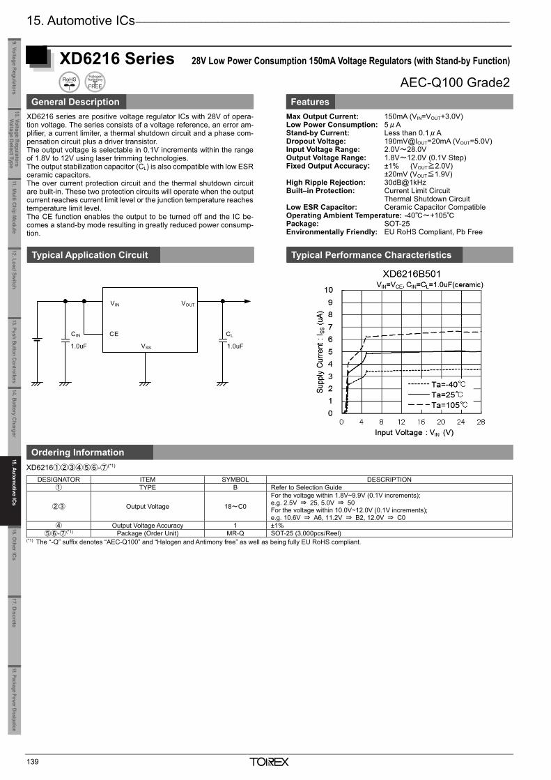
15. Automotive ICs ___________________________________________________________________________________________
139
XD6216 Series 28V Low Power Consumption 150mA Voltage Regulators (with Stand-by Function)
AEC-Q100 Grade2
General Description Features XD6216 series are positive voltage regulator ICs with 28V of opera-tion voltage. The series consists of a voltage reference, an error am-plifier, a current limiter, a thermal shutdown circuit and a phase com-pensation circuit plus a driver transistor. The output voltage is selectable in 0.1V increments within the range of 1.8V to 12V using laser trimming technologies. The output stabilization capacitor (CL) is also compatible with low ESR ceramic capacitors. The over current protection circuit and the thermal shutdown circuit are built-in. These two protection circuits will operate when the output current reaches current limit level or the junction temperature reaches temperature limit level. The CE function enables the output to be turned off and the IC be-comes a stand-by mode resulting in greatly reduced power consump-tion.
Max Output Current: 150mA (VIN=VOUT+3.0V) Low Power Consumption: 5μA Stand-by Current: Less than 0.1μA Dropout Voltage: 190mV@IOUT=20mA (VOUT=5.0V) Input Voltage Range: 2.0V~28.0V Output Voltage Range: 1.8V~12.0V (0.1V Step) Fixed Output Accuracy: ±1% (VOUT≧2.0V) ±20mV (VOUT≦1.9V) High Ripple Rejection: 30dB@1kHz Built–in Protection: Current Limit Circuit Thermal Shutdown Circuit Low ESR Capacitor: Ceramic Capacitor Compatible Operating Ambient Temperature: -40~+105 Package: SOT-25 Environmentally Friendly: EU RoHS Compliant, Pb Free
Typical Application Circuit Typical Performance Characteristics
Ordering Information
XD6216①②③④⑤⑥-⑦(*1)
DESIGNATOR ITEM SYMBOL DESCRIPTION
① TYPE B Refer to Selection Guide
②③ Output Voltage 18~C0
For the voltage within 1.8V~9.9V (0.1V increments); e.g. 2.5V ⇒ 25, 5.0V ⇒ 50 For the voltage within 10.0V~12.0V (0.1V increments); e.g. 10.6V ⇒ A6, 11.2V ⇒ B2, 12.0V ⇒ C0
④ Output Voltage Accuracy 1 ±1% ⑤⑥-⑦(*1) Package (Order Unit) MR-Q SOT-25 (3,000pcs/Reel)
(*1) The “-Q” suffix denotes “AEC-Q100” and “Halogen and Antimony free” as well as being fully EU RoHS compliant.
VIN VOUT
VSS
CE
1.0uF
CIN CL
1.0uF
_______________________________________________________________________________________________________
140
XD6133 Series Capacitor Delay Type Voltage Detectors with Sense Pin Isolation
General Description Features
The XD6133 series are ultra-small delay capacitor adjustable typevoltage detectors that have high accuracy and sense pin isolation.High accuracy and a low supply current are achieved by means of aCMOS process, a highly accurate reference power supply, and lasertrimming technology. The sense pin is isolated from the power input pin to enable monitor-ing of the voltage of another power supply. Output can be maintainedin the detection state even if the voltage of the power supply that ismonitored drops to 0V. The sense pin is also suitable for detectinghigh voltages, and the detection and release voltage can be set asdesired using external resistors. An internal delay circuit is also provided. By connecting a capacitor tothe Cd/MRB pin, any release delay time and detect delay time can beset, and the pin can also be used as a manual reset pin.
Operating Ambient Temperature: -40~+125 Operating Voltage Range: 1.6V~6.0V
(Absolute Max. Rating: 7.0V) Detect Voltage Range (standard): 1.3V, 1.6V, 2.2V, 2.3V, 2.4V, 2.9V, 3.0V,
3.1V, 4.4V, 4.5V, 4.6V Detect Voltage Range (option): 1.0V~5.0V Detect Voltage Accuracy: ±18mV (VDF<1.5V) (Ta=25) ±1.2% (1.5V≦VDF≦3.0V) ±1.5% (3.1V≦VDF≦5.0V) Detect Voltage Accuracy: ±36mV (VDF<1.5V) (Ta=-40~125) ±2.7% (1.5V≦VDF≦3.0V) ±3.0% (3.1V≦VDF≦5.0V) Temperature Characteristics: ±50ppm/ (TYP.) Hysteresis Width: VDF×5.0% (TYP.) Low Supply Current: 1.28μA (TYP.) VIN=1.6V (At detection) 1.65μA (TYP.) VIN=6.0V (At release) Manual Reset Function: Yes Output Type: CMOS or Nch open drain Output Logic: H level or L level at detection Delay Capacitance Pin: Release delay / detection delay can be set
in 5 time ratio options Packages: USP-6C,SOT-26 Environmentally Friendly: EU RoHS compliant, Pb free
Pin Configuration Type A/B/C/D/L
Type E/F/H/K/M
Typical Application Circuit Typical Performance Characteristics
Ordering Information
XC6133①②③④⑤⑥-⑦ DESIGNATOR ITEM SYMBOL DESCRIPTION
① Output Configuration C CMOS output N Nch open drain output
②③ Detect Voltage 13, 16, 22, 23, 24, 29, 30, 31, 44, 45, 46
e.g. 1.3V → ②=1, ③=3
④ Type A~K Refer to [Selection Guide]
⑤⑥-⑦(*1) Packages (Order Unit) MR-Q SOT-26 (3,000pcs/Reel) ER-Q USP-6C (3,000pcs/Reel)
(*1) The “-Q” suffix denotes “AEC-Q100” and “Halogen and Antimony free” as well as being fully EU RoHS compliant. Selection Guide
TYPE RESET/RESETB OUTPUT DELAY (Rp:Rn) HYSTERESIS A Active High(*2) 1:0 144kΩ:0Ω 5.0%(TYP.) B ↑ 1:0.125 144kΩ:18kΩ ↑ C ↑ 1:1 144kΩ:144kΩ ↑ D ↑ 2:1 288kΩ:144kΩ ↑ L ↑ 0.076:1 11kΩ:144kΩ ↑ E Active Low(*2) 1:0 144kΩ:0Ω ↑ F ↑ 1:0.125 144kΩ:18kΩ ↑ H ↑ 1:1 144kΩ:144kΩ ↑ K ↑ 2:1 288kΩ:144kΩ ↑
(*2) ”Active High” is H level when detection occurs, and “Active Low” is L level when detection occurs.
19.0
19.2
19.4
19.6
19.8
20.0
20.2
20.4
20.6
20.8
21.0
-50 -25 0 25 50 75 100 125 150
Rele
ase D
ela
y Tim
e :
tDR
(m
s)
Ambient Temperature : Ta ()
XC6133C08DMR-G
VIN=3.3V、VSEN=0.72V→0.88V
Cd=0.1μF、Rp=288kΩ(tDR=20ms)XD6133C08DMR-Q
5
1 32
6 4
SOT-26(TOP VIEW)
VSEN
VIN
Cd/MRB
RESET NC
VSS
USP-6C(BOTTOM VIEW)
34
2
1
5
6 NC
RESET
VINCd/MRB
VSS
VSEN5
1 32
6 4
SOT-26(TOP VIEW)
VSEN
VIN
Cd/MRB
RESETB NC
VSS
USP-6C(BOTTOM VIEW)
34
2
1
5
6 NC
RESETB
VINCd/MRB
VSS
VSEN
AEC-Q100 Grade1
11.Multi C
hip Module
10. Voltage Regulators
Voltage Detect Type
9. Voltage Regulators
12.Load Switch
13. Push Button Controllers14.B
attery Charger
15.Autom
otive ICs
16.Other IC
s17. D
iscrete18.Package Power Dissipation
15.Autom
otive ICs
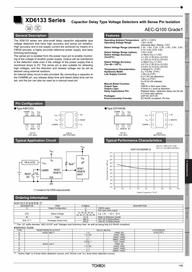
15. Automotive ICs ___________________________________________________________________________________________
139
XD6216 Series 28V Low Power Consumption 150mA Voltage Regulators (with Stand-by Function)
AEC-Q100 Grade2
General Description Features XD6216 series are positive voltage regulator ICs with 28V of opera-tion voltage. The series consists of a voltage reference, an error am-plifier, a current limiter, a thermal shutdown circuit and a phase com-pensation circuit plus a driver transistor. The output voltage is selectable in 0.1V increments within the range of 1.8V to 12V using laser trimming technologies. The output stabilization capacitor (CL) is also compatible with low ESR ceramic capacitors. The over current protection circuit and the thermal shutdown circuit are built-in. These two protection circuits will operate when the output current reaches current limit level or the junction temperature reaches temperature limit level. The CE function enables the output to be turned off and the IC be-comes a stand-by mode resulting in greatly reduced power consump-tion.
Max Output Current: 150mA (VIN=VOUT+3.0V) Low Power Consumption: 5μA Stand-by Current: Less than 0.1μA Dropout Voltage: 190mV@IOUT=20mA (VOUT=5.0V) Input Voltage Range: 2.0V~28.0V Output Voltage Range: 1.8V~12.0V (0.1V Step) Fixed Output Accuracy: ±1% (VOUT≧2.0V) ±20mV (VOUT≦1.9V) High Ripple Rejection: 30dB@1kHz Built–in Protection: Current Limit Circuit Thermal Shutdown Circuit Low ESR Capacitor: Ceramic Capacitor Compatible Operating Ambient Temperature: -40~+105 Package: SOT-25 Environmentally Friendly: EU RoHS Compliant, Pb Free
Typical Application Circuit Typical Performance Characteristics
Ordering Information
XD6216①②③④⑤⑥-⑦(*1)
DESIGNATOR ITEM SYMBOL DESCRIPTION
① TYPE B Refer to Selection Guide
②③ Output Voltage 18~C0
For the voltage within 1.8V~9.9V (0.1V increments); e.g. 2.5V ⇒ 25, 5.0V ⇒ 50 For the voltage within 10.0V~12.0V (0.1V increments); e.g. 10.6V ⇒ A6, 11.2V ⇒ B2, 12.0V ⇒ C0
④ Output Voltage Accuracy 1 ±1% ⑤⑥-⑦(*1) Package (Order Unit) MR-Q SOT-25 (3,000pcs/Reel)
(*1) The “-Q” suffix denotes “AEC-Q100” and “Halogen and Antimony free” as well as being fully EU RoHS compliant.
VIN VOUT
VSS
CE
1.0uF
CIN CL
1.0uF
_______________________________________________________________________________________________________
140
XD6133 Series Capacitor Delay Type Voltage Detectors with Sense Pin Isolation
General Description Features
The XD6133 series are ultra-small delay capacitor adjustable typevoltage detectors that have high accuracy and sense pin isolation.High accuracy and a low supply current are achieved by means of aCMOS process, a highly accurate reference power supply, and lasertrimming technology. The sense pin is isolated from the power input pin to enable monitor-ing of the voltage of another power supply. Output can be maintainedin the detection state even if the voltage of the power supply that ismonitored drops to 0V. The sense pin is also suitable for detectinghigh voltages, and the detection and release voltage can be set asdesired using external resistors. An internal delay circuit is also provided. By connecting a capacitor tothe Cd/MRB pin, any release delay time and detect delay time can beset, and the pin can also be used as a manual reset pin.
Operating Ambient Temperature: -40~+125 Operating Voltage Range: 1.6V~6.0V
(Absolute Max. Rating: 7.0V) Detect Voltage Range (standard): 1.3V, 1.6V, 2.2V, 2.3V, 2.4V, 2.9V, 3.0V,
3.1V, 4.4V, 4.5V, 4.6V Detect Voltage Range (option): 1.0V~5.0V Detect Voltage Accuracy: ±18mV (VDF<1.5V) (Ta=25) ±1.2% (1.5V≦VDF≦3.0V) ±1.5% (3.1V≦VDF≦5.0V) Detect Voltage Accuracy: ±36mV (VDF<1.5V) (Ta=-40~125) ±2.7% (1.5V≦VDF≦3.0V) ±3.0% (3.1V≦VDF≦5.0V) Temperature Characteristics: ±50ppm/ (TYP.) Hysteresis Width: VDF×5.0% (TYP.) Low Supply Current: 1.28μA (TYP.) VIN=1.6V (At detection) 1.65μA (TYP.) VIN=6.0V (At release) Manual Reset Function: Yes Output Type: CMOS or Nch open drain Output Logic: H level or L level at detection Delay Capacitance Pin: Release delay / detection delay can be set
in 5 time ratio options Packages: USP-6C,SOT-26 Environmentally Friendly: EU RoHS compliant, Pb free
Pin Configuration Type A/B/C/D/L
Type E/F/H/K/M
Typical Application Circuit Typical Performance Characteristics
Ordering Information
XC6133①②③④⑤⑥-⑦ DESIGNATOR ITEM SYMBOL DESCRIPTION
① Output Configuration C CMOS output N Nch open drain output
②③ Detect Voltage 13, 16, 22, 23, 24, 29, 30, 31, 44, 45, 46
e.g. 1.3V → ②=1, ③=3
④ Type A~K Refer to [Selection Guide]
⑤⑥-⑦(*1) Packages (Order Unit) MR-Q SOT-26 (3,000pcs/Reel) ER-Q USP-6C (3,000pcs/Reel)
(*1) The “-Q” suffix denotes “AEC-Q100” and “Halogen and Antimony free” as well as being fully EU RoHS compliant. Selection Guide
TYPE RESET/RESETB OUTPUT DELAY (Rp:Rn) HYSTERESIS A Active High(*2) 1:0 144kΩ:0Ω 5.0%(TYP.) B ↑ 1:0.125 144kΩ:18kΩ ↑ C ↑ 1:1 144kΩ:144kΩ ↑ D ↑ 2:1 288kΩ:144kΩ ↑ L ↑ 0.076:1 11kΩ:144kΩ ↑ E Active Low(*2) 1:0 144kΩ:0Ω ↑ F ↑ 1:0.125 144kΩ:18kΩ ↑ H ↑ 1:1 144kΩ:144kΩ ↑ K ↑ 2:1 288kΩ:144kΩ ↑
(*2) ”Active High” is H level when detection occurs, and “Active Low” is L level when detection occurs.
19.0
19.2
19.4
19.6
19.8
20.0
20.2
20.4
20.6
20.8
21.0
-50 -25 0 25 50 75 100 125 150
Rele
ase D
ela
y Tim
e :
tDR
(m
s)
Ambient Temperature : Ta ()
XC6133C08DMR-G
VIN=3.3V、VSEN=0.72V→0.88V
Cd=0.1μF、Rp=288kΩ(tDR=20ms)XD6133C08DMR-Q
5
1 32
6 4
SOT-26(TOP VIEW)
VSEN
VIN
Cd/MRB
RESET NC
VSS
USP-6C(BOTTOM VIEW)
34
2
1
5
6 NC
RESET
VINCd/MRB
VSS
VSEN5
1 32
6 4
SOT-26(TOP VIEW)
VSEN
VIN
Cd/MRB
RESETB NC
VSS
USP-6C(BOTTOM VIEW)
34
2
1
5
6 NC
RESETB
VINCd/MRB
VSS
VSEN
AEC-Q100 Grade1
11.Multi C
hip Module
10. Voltage Regulators
Voltage Detect Type
9. Voltage Regulators
12.Load Switch
13. Push Button Controllers14.B
attery Charger
16.Other IC
s17. D
iscrete18.Package Power Dissipation
15.Autom
otive ICs
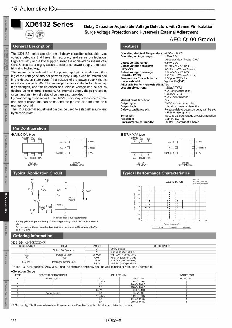
15. Automotive ICs ___________________________________________________________________________________________
141
XD6132 Series Delay Capacitor Adjustable Voltage Detectors with Sense Pin Isolation,
General Description Features
The XD6132 series are ultra-small delay capacitor adjustable type voltage detectors that have high accuracy and sense pin isolation. High accuracy and a low supply current are achieved by means of a CMOS process, a highly accurate reference power supply, and laser trimming technology. The sense pin is isolated from the power input pin to enable monitor-ing of the voltage of another power supply. Output can be maintained in the detection state even if the voltage of the power supply that is monitored drops to 0V. The sense pin is also suitable for detecting high voltages, and the detection and release voltage can be set as desired using external resistors. An internal surge voltage protection circuit and an internal delay circuit are also provided. By connecting a capacitor to the Cd/MRB pin, any release delay time and detect delay time can be set and the pin can also be used as a manual reset pin. The HYS external adjustment pin can be used to establish a sufficient hysteresis width.
Operating Ambient Temperature: -40~+125 Operating voltage range: 1.6V~6.0V
(Absolute Max. Rating: 7.0V) Detect voltage range: 0.8V~2.0V Detect voltage accuracy: ±18mV(VDF<1.5V) (Ta=25) ±1.2%(1.5V≦VDF≦2.0V) Detect voltage accuracy: ±36mV(VDF<1.5V) (Ta=-40~125) ±2.7%(1.5V≦VDF≦2.0V) Temperature Characteristics: ±50ppm/(TYP.) Hysteresis width: VDF×0.1%(TYP.) Adjustable Pin for Hysteresis Width: Yes Low supply current: 1.28μA(TYP.) VIN=1.6V(At detection) 1.65μA(TYP.) VIN=6.0V(At release) Manual reset function: Yes Output type: CMOS or N-ch open drain Output logic: H level or L level at detection Delay capacitance pin: Release delay / detection delay can be set
in 5 time ratio options Sense pin: Includes a surge voltage protection functionPackages: USP-6C,SOT-26 Environmentally Friendly: EU RoHS compliant, Pb free
Pin Configuration A/B/C/D/L type
E/F/H/K/M type
Typical Application Circuit Typical Performance Characteristics
Battery (+B) voltage monitoring: Detects high voltage via R1/R2 resistance divi-sion. A hysteresis width can be added as desired by connecting R3 between the VSEN and HYS pins
Ordering Information
XD6132①②③④⑤⑥-⑦ DESIGNATOR ITEM SYMBOL DESCRIPTION
① Output Configuration C CMOS output N N-ch open drain output
②③ Detect Voltage 08~20 e.g. 1.0V → ②=1, ③=0 ④ Type A~K Refer to Selection Guide
⑤⑥-⑦(*1) Packages (Order Unit) MR-Q SOT-26 (3,000pcs/Reel) ER-Q USP-6C (3,000pcs/Reel)
(*1) The “-Q” suffix denotes “AEC-Q100” and “Halogen and Antimony free” as well as being fully EU RoHS compliant. Selection Guide
TYPE RESET/RESETB OUTPUT DELAY(Rp:Rn) HYSTERESIS A Active High(*2) 1:0 144kΩ:0Ω 0.1%(TYP.) B ↑ 1:0.125 144kΩ:18kΩ ↑ C ↑ 1:1 144kΩ:144kΩ ↑ D ↑ 2:1 288kΩ:144kΩ ↑ L ↑ 0.076:1 11kΩ:144kΩ ↑ E Active Low(*2) 1:0 144kΩ:0Ω ↑ F ↑ 1:0.125 144kΩ:18kΩ ↑ H ↑ 1:1 144kΩ:144kΩ ↑ K ↑ 2:1 288kΩ:144kΩ ↑
(*2) ”Active High” is H level when detection occurs, and “Active Low” is L level when detection occurs.
5
1 32
6 4
SOT-26(TOP VIEW)
VSEN
VIN
Cd/MRB
RESET HYS
VSS
USP-6C(BOTTOM VIEW)
34
2
1
5
6 HYS
RESET
VINCd/MRB
VSS
VSEN5
1 32
6 4
SOT-26(TOP VIEW)
VSEN
VIN
Cd/MRB
RESETB HYS
VSS
USP-6C(BOTTOM VIEW)
34
2
1
5
6 HYS
RESETB
VINCd/MRB
VSS
VSEN
Surge Voltage Protection and Hysteresis External Adjustment
Cd/MRB
RESETRESETB
VIN
VSS
HYS
VSEN
VDD
GND
+B
R1
R2
R3
Rpull(*1)
RESETSW
Cd
0.0
0.5
1.0
1.5
2.0
2.5
3.0
3.5
4.0
0 1 2 3 4 5 6 7 8 9 10
Outp
ut
Voltag
e :
VR
ESET(V
)
Voltage Sense : VSEN(V)
XC6132C10E
OPEN R1=330kΩ R1=560kΩ
VIN=3.3VVSEN=0V→10V→0V
R2=100kΩ、R3=330kΩXD6132C10E
AEC-Q100 Grade1
_______________________________________________________________________________________________________
142
XD6130/XD6131 Series Watchdog Timeout Period Externally Adjustable Voltage Detector
General Description Features
The XD6130/XD6131 series is voltage detector with watchdog func-tion. A release delay time and watchdog timeout period can be adjusted byone external capacitor. The series is used for monitoring of microprocessor. When thepower supply voltage reaches voltage or the pulse from Low to Highis not input into a watchdog pin within watchdog timeout period, Lowsignal outputs from RESETB pin. The XD6130 has manual reset function. When the manual reset pingoes low, low level signal outputs from RESETB pin and reset can beasserted at any time. The XD6131 has ON/OFF control of the watchdog function. By settingthe EN pin to low level, the watchdog function can be OFF while thevoltage detector remains operation. Since the EN pin internallypulled up, the ICs can be used with there pins left open for not use.
Operating Voltage Range: 1.5V~6.0V (Absolute Max. Rating: 7.0V) Detect Voltage: 1.6V, 2.2V, 2.3V, 2.4V, 2.9V, 3.0V, 3.1V,
4.4V, 4.5V, 4.6V (±1.0%) Hysteresis Width : VDFL×5% Low Quiescent Current: 8.1μA Detected 9.8μA Released 2.5μA Released (EN=L) Functions: Manual Reset (XC6130) Watchdog ON/OFF Function (XC6131) Watchdog Timeout Period : 100ms (Cd=0.1μF) Release Delay Time : 100ms (Cd=0.1μF) (Power-on State) 10ms (Cd=0.1μF) (After Watchdog Timeout) Operating Ambient Temperature: -40~+125 Package: SOT-26 Environmentally Friendly: EU RoHS Compliant, Pb Free
Pin Configuration Typical Performance Characteristics
Typical Application Circuits
Ordering Information
XD6130①②③④⑤⑥-⑦ With MRB Pin (Manual Reset) DESIGNATOR ITEM SYMBOL DESCRIPTION
① Type A MRB pin With pull-up resistor ②③ Detect Voltage 16~50 e.g. 1.6V → ②=1, ③=6 ④ Detect Accuracy 1 ±1.0%
⑤⑥-⑦ (*1) Package (Order Unit) MR-Q SOT-26 (3000pcs/Reel) (*2) (*1) The “-Q” suffix denotes “AEC-Q100” and “Halogen and Antimony free” as well as being fully EU RoHS compliant. (*2) The SOT-26 reels are shipped in a moisture-proof packing. XD6131①②③④⑤⑥-⑦ With EN pin (Watchdog Disable)
DESIGNATOR ITEM SYMBOL DESCRIPTION ① Type A EN pin With pull-up resistor
②③ Detect Voltage 16~50 e.g. 1.6V → ②=1, ③=6 ④ Detect Accuracy 1 ±1.0%
⑤⑥-⑦ (*1) Package (Order Unit) MR-Q SOT-26 (3000pcs/Reel) (*2) (*1) The “-Q” suffix denotes “AEC-Q100” and “Halogen and Antimony free” as well as being fully EU RoHS compliant. (*2) The SOT-26 reels are shipped in a moisture-proof packing.
XD6130 Series XD6131 Series
XC6131A301MR-G
0
2
4
6
8
10
12
14
0 1 2 3 4 5 6
Input Voltage:VIN(V)
Supply
Curr
ent:IS
S(μ
A)
WD Function ON
WD Function OFF
Cd=0.01μF, WD=RESETB=OPEN, Ta=25EN=VSS(WD Function OFF)EN=VIN (WD Function ON)
XD6131A301MR-Q
XD6130 Series XD6131 Series
EN/ENB
AEC-Q100 Grade1
11.Multi C
hip Module
10. Voltage Regulators
Voltage Detect Type
9. Voltage Regulators
12.Load Switch
13. Push Button Controllers14.B
attery Charger
15.Autom
otive ICs
16.Other IC
s17. D
iscrete18.Package Power Dissipation
15.Autom
otive ICs
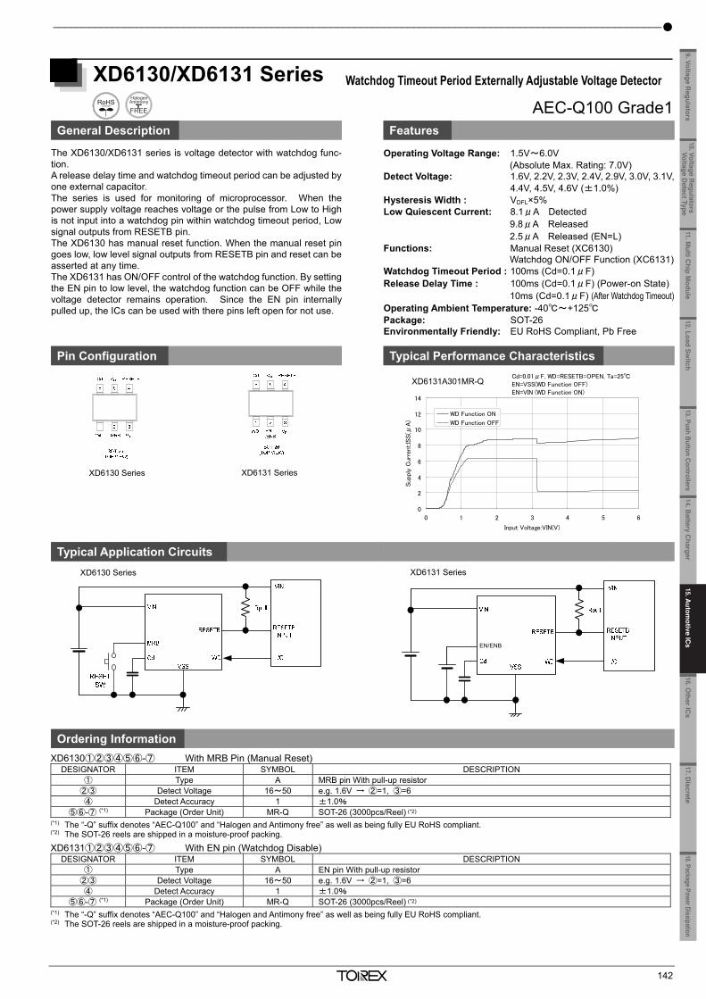
15. Automotive ICs ___________________________________________________________________________________________
141
XD6132 Series Delay Capacitor Adjustable Voltage Detectors with Sense Pin Isolation,
General Description Features
The XD6132 series are ultra-small delay capacitor adjustable type voltage detectors that have high accuracy and sense pin isolation. High accuracy and a low supply current are achieved by means of a CMOS process, a highly accurate reference power supply, and laser trimming technology. The sense pin is isolated from the power input pin to enable monitor-ing of the voltage of another power supply. Output can be maintained in the detection state even if the voltage of the power supply that is monitored drops to 0V. The sense pin is also suitable for detecting high voltages, and the detection and release voltage can be set as desired using external resistors. An internal surge voltage protection circuit and an internal delay circuit are also provided. By connecting a capacitor to the Cd/MRB pin, any release delay time and detect delay time can be set and the pin can also be used as a manual reset pin. The HYS external adjustment pin can be used to establish a sufficient hysteresis width.
Operating Ambient Temperature: -40~+125 Operating voltage range: 1.6V~6.0V
(Absolute Max. Rating: 7.0V) Detect voltage range: 0.8V~2.0V Detect voltage accuracy: ±18mV(VDF<1.5V) (Ta=25) ±1.2%(1.5V≦VDF≦2.0V) Detect voltage accuracy: ±36mV(VDF<1.5V) (Ta=-40~125) ±2.7%(1.5V≦VDF≦2.0V) Temperature Characteristics: ±50ppm/(TYP.) Hysteresis width: VDF×0.1%(TYP.) Adjustable Pin for Hysteresis Width: Yes Low supply current: 1.28μA(TYP.) VIN=1.6V(At detection) 1.65μA(TYP.) VIN=6.0V(At release) Manual reset function: Yes Output type: CMOS or N-ch open drain Output logic: H level or L level at detection Delay capacitance pin: Release delay / detection delay can be set
in 5 time ratio options Sense pin: Includes a surge voltage protection functionPackages: USP-6C,SOT-26 Environmentally Friendly: EU RoHS compliant, Pb free
Pin Configuration A/B/C/D/L type
E/F/H/K/M type
Typical Application Circuit Typical Performance Characteristics
Battery (+B) voltage monitoring: Detects high voltage via R1/R2 resistance divi-sion. A hysteresis width can be added as desired by connecting R3 between the VSEN and HYS pins
Ordering Information
XD6132①②③④⑤⑥-⑦ DESIGNATOR ITEM SYMBOL DESCRIPTION
① Output Configuration C CMOS output N N-ch open drain output
②③ Detect Voltage 08~20 e.g. 1.0V → ②=1, ③=0 ④ Type A~K Refer to Selection Guide
⑤⑥-⑦(*1) Packages (Order Unit) MR-Q SOT-26 (3,000pcs/Reel) ER-Q USP-6C (3,000pcs/Reel)
(*1) The “-Q” suffix denotes “AEC-Q100” and “Halogen and Antimony free” as well as being fully EU RoHS compliant. Selection Guide
TYPE RESET/RESETB OUTPUT DELAY(Rp:Rn) HYSTERESIS A Active High(*2) 1:0 144kΩ:0Ω 0.1%(TYP.) B ↑ 1:0.125 144kΩ:18kΩ ↑ C ↑ 1:1 144kΩ:144kΩ ↑ D ↑ 2:1 288kΩ:144kΩ ↑ L ↑ 0.076:1 11kΩ:144kΩ ↑ E Active Low(*2) 1:0 144kΩ:0Ω ↑ F ↑ 1:0.125 144kΩ:18kΩ ↑ H ↑ 1:1 144kΩ:144kΩ ↑ K ↑ 2:1 288kΩ:144kΩ ↑
(*2) ”Active High” is H level when detection occurs, and “Active Low” is L level when detection occurs.
5
1 32
6 4
SOT-26(TOP VIEW)
VSEN
VIN
Cd/MRB
RESET HYS
VSS
USP-6C(BOTTOM VIEW)
34
2
1
5
6 HYS
RESET
VINCd/MRB
VSS
VSEN5
1 32
6 4
SOT-26(TOP VIEW)
VSEN
VIN
Cd/MRB
RESETB HYS
VSS
USP-6C(BOTTOM VIEW)
34
2
1
5
6 HYS
RESETB
VINCd/MRB
VSS
VSEN
Surge Voltage Protection and Hysteresis External Adjustment
Cd/MRB
RESETRESETB
VIN
VSS
HYS
VSEN
VDD
GND
+B
R1
R2
R3
Rpull(*1)
RESETSW
Cd
0.0
0.5
1.0
1.5
2.0
2.5
3.0
3.5
4.0
0 1 2 3 4 5 6 7 8 9 10
Outp
ut
Voltag
e :
VR
ESET(V
)
Voltage Sense : VSEN(V)
XC6132C10E
OPEN R1=330kΩ R1=560kΩ
VIN=3.3VVSEN=0V→10V→0V
R2=100kΩ、R3=330kΩXD6132C10E
AEC-Q100 Grade1
_______________________________________________________________________________________________________
142
XD6130/XD6131 Series Watchdog Timeout Period Externally Adjustable Voltage Detector
General Description Features
The XD6130/XD6131 series is voltage detector with watchdog func-tion. A release delay time and watchdog timeout period can be adjusted byone external capacitor. The series is used for monitoring of microprocessor. When thepower supply voltage reaches voltage or the pulse from Low to Highis not input into a watchdog pin within watchdog timeout period, Lowsignal outputs from RESETB pin. The XD6130 has manual reset function. When the manual reset pingoes low, low level signal outputs from RESETB pin and reset can beasserted at any time. The XD6131 has ON/OFF control of the watchdog function. By settingthe EN pin to low level, the watchdog function can be OFF while thevoltage detector remains operation. Since the EN pin internallypulled up, the ICs can be used with there pins left open for not use.
Operating Voltage Range: 1.5V~6.0V (Absolute Max. Rating: 7.0V) Detect Voltage: 1.6V, 2.2V, 2.3V, 2.4V, 2.9V, 3.0V, 3.1V,
4.4V, 4.5V, 4.6V (±1.0%) Hysteresis Width : VDFL×5% Low Quiescent Current: 8.1μA Detected 9.8μA Released 2.5μA Released (EN=L) Functions: Manual Reset (XC6130) Watchdog ON/OFF Function (XC6131) Watchdog Timeout Period : 100ms (Cd=0.1μF) Release Delay Time : 100ms (Cd=0.1μF) (Power-on State) 10ms (Cd=0.1μF) (After Watchdog Timeout) Operating Ambient Temperature: -40~+125 Package: SOT-26 Environmentally Friendly: EU RoHS Compliant, Pb Free
Pin Configuration Typical Performance Characteristics
Typical Application Circuits
Ordering Information
XD6130①②③④⑤⑥-⑦ With MRB Pin (Manual Reset) DESIGNATOR ITEM SYMBOL DESCRIPTION
① Type A MRB pin With pull-up resistor ②③ Detect Voltage 16~50 e.g. 1.6V → ②=1, ③=6 ④ Detect Accuracy 1 ±1.0%
⑤⑥-⑦ (*1) Package (Order Unit) MR-Q SOT-26 (3000pcs/Reel) (*2) (*1) The “-Q” suffix denotes “AEC-Q100” and “Halogen and Antimony free” as well as being fully EU RoHS compliant. (*2) The SOT-26 reels are shipped in a moisture-proof packing. XD6131①②③④⑤⑥-⑦ With EN pin (Watchdog Disable)
DESIGNATOR ITEM SYMBOL DESCRIPTION ① Type A EN pin With pull-up resistor
②③ Detect Voltage 16~50 e.g. 1.6V → ②=1, ③=6 ④ Detect Accuracy 1 ±1.0%
⑤⑥-⑦ (*1) Package (Order Unit) MR-Q SOT-26 (3000pcs/Reel) (*2) (*1) The “-Q” suffix denotes “AEC-Q100” and “Halogen and Antimony free” as well as being fully EU RoHS compliant. (*2) The SOT-26 reels are shipped in a moisture-proof packing.
XD6130 Series XD6131 Series
XC6131A301MR-G
0
2
4
6
8
10
12
14
0 1 2 3 4 5 6
Input Voltage:VIN(V)
Supply
Curr
ent:IS
S(μ
A)
WD Function ON
WD Function OFF
Cd=0.01μF, WD=RESETB=OPEN, Ta=25EN=VSS(WD Function OFF)EN=VIN (WD Function ON)
XD6131A301MR-Q
XD6130 Series XD6131 Series
EN/ENB
AEC-Q100 Grade1
11.Multi C
hip Module
10. Voltage Regulators
Voltage Detect Type
9. Voltage Regulators
12.Load Switch
13. Push Button Controllers14.B
attery Charger
16.Other IC
s17. D
iscrete18.Package Power Dissipation
15.Autom
otive ICs
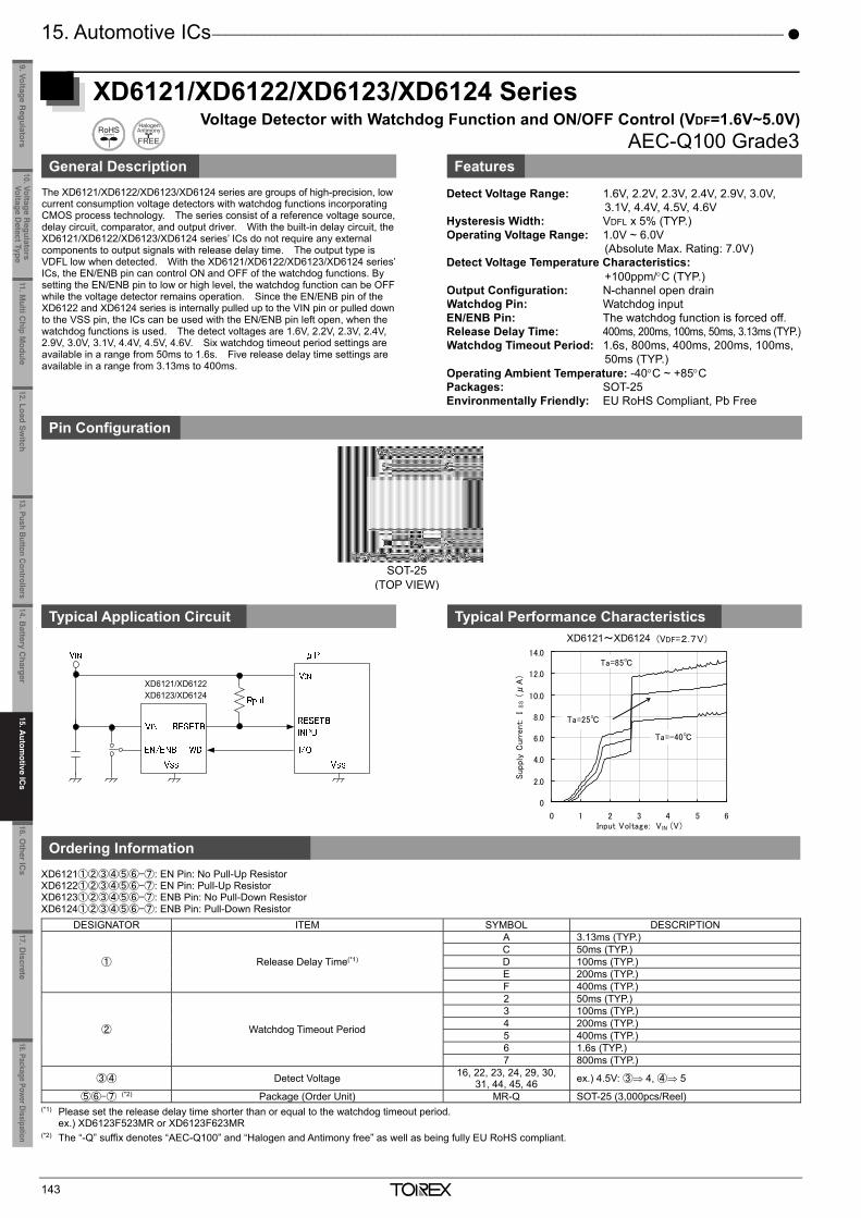
15. Automotive ICs _________________________________________________________________________________________
143
XD6121/XD6122/XD6123/XD6124 Series Voltage Detector with Watchdog Function and ON/OFF Control (VDF=1.6V~5.0V)
General Description Features
The XD6121/XD6122/XD6123/XD6124 series are groups of high-precision, low current consumption voltage detectors with watchdog functions incorporating CMOS process technology. The series consist of a reference voltage source, delay circuit, comparator, and output driver. With the built-in delay circuit, the XD6121/XD6122/XD6123/XD6124 series’ ICs do not require any external components to output signals with release delay time. The output type is VDFL low when detected. With the XD6121/XD6122/XD6123/XD6124 series’ ICs, the EN/ENB pin can control ON and OFF of the watchdog functions. By setting the EN/ENB pin to low or high level, the watchdog function can be OFF while the voltage detector remains operation. Since the EN/ENB pin of the XD6122 and XD6124 series is internally pulled up to the VIN pin or pulled down to the VSS pin, the ICs can be used with the EN/ENB pin left open, when the watchdog functions is used. The detect voltages are 1.6V, 2.2V, 2.3V, 2.4V, 2.9V, 3.0V, 3.1V, 4.4V, 4.5V, 4.6V. Six watchdog timeout period settings are available in a range from 50ms to 1.6s. Five release delay time settings are available in a range from 3.13ms to 400ms.
Detect Voltage Range: 1.6V, 2.2V, 2.3V, 2.4V, 2.9V, 3.0V, 3.1V, 4.4V, 4.5V, 4.6V
Hysteresis Width: VDFL x 5% (TYP.) Operating Voltage Range: 1.0V ~ 6.0V
(Absolute Max. Rating: 7.0V) Detect Voltage Temperature Characteristics:
+100ppm/C (TYP.) Output Configuration: N-channel open drain Watchdog Pin: Watchdog input EN/ENB Pin: The watchdog function is forced off. Release Delay Time: 400ms, 200ms, 100ms, 50ms, 3.13ms (TYP.) Watchdog Timeout Period: 1.6s, 800ms, 400ms, 200ms, 100ms,
50ms (TYP.) Operating Ambient Temperature: -40C ~ +85C Packages: SOT-25 Environmentally Friendly: EU RoHS Compliant, Pb Free
Pin Configuration
Typical Application Circuit Typical Performance Characteristics
Ordering Information
XD6121①②③④⑤⑥-⑦: EN Pin: No Pull-Up Resistor XD6122①②③④⑤⑥-⑦: EN Pin: Pull-Up Resistor XD6123①②③④⑤⑥-⑦: ENB Pin: No Pull-Down Resistor XD6124①②③④⑤⑥-⑦: ENB Pin: Pull-Down Resistor
DESIGNATOR ITEM SYMBOL DESCRIPTION
① Release Delay Time(*1)
A 3.13ms (TYP.) C 50ms (TYP.) D 100ms (TYP.) E 200ms (TYP.) F 400ms (TYP.)
② Watchdog Timeout Period
2 50ms (TYP.) 3 100ms (TYP.) 4 200ms (TYP.) 5 400ms (TYP.) 6 1.6s (TYP.) 7 800ms (TYP.)
③④ Detect Voltage 16, 22, 23, 24, 29, 30, 31, 44, 45, 46 ex.) 4.5V: ③ 4, ④ 5
⑤⑥-⑦ (*2) Package (Order Unit) MR-Q SOT-25 (3,000pcs/Reel) (*1) Please set the release delay time shorter than or equal to the watchdog timeout period. ex.) XD6123F523MR or XD6123F623MR (*2) The “-Q” suffix denotes “AEC-Q100” and “Halogen and Antimony free” as well as being fully EU RoHS compliant.
SOT-25 (TOP VIEW)
0
2.0
4.0
6.0
8.0
10.0
12.0
14.0
0 1 2 3 4 5 6Input Voltage: VIN (V)
Sup
ply C
urr
ent:
IS
S (
μA
)
XC6121~XC6124(VDF=2.7V)
Ta=85
Ta=-40
Ta=25
XD6121~XD6124
AEC-Q100 Grade3
________________________________________________________________________________________________ 16. Other ICs
144
XC3101 Series Ultra Small Analog Output Temperature Sensor with Alarm Output Pin
General Description Features
The XC3101 series is a temperature sensor IC which features ultrasmall, low current consumption, and high-accurate detection. It canprovide both analog and alarm outputs. The alarm output configuresN-channel open-drain. The device consists of a band-gap type tem-perature sensor, a voltage reference, a temperature setting tilt ampli-fier, a comparator, and various set resistors. Alarm temperature is internally set at 70C. When the temperatureexceeds a set point, the alarm output is maintained as "Low". When the temperature drops a pre-set hysteresis width from the setpoint, the alarm output is released to "High". The hysteresis width is5C. An analog voltage output is provided in a high-accuracy which isguaranteed in the operating temperature range of -40C to 100C. An external A/D can monitor the sensing temperature. The operating input voltage range is 2.7 to 5.5V. The small con-sumption current of 3.5μA (TYP.) is ideally suited for temperaturedetection for battery devices. The ultra small USPN-4 (1.2 x 0.9 x0.4) package is available for the high-density board mounting in mo-bile device applications as well as an industry standard packageSSOT-24.
Input Voltage Range: 2.7V ~ 5.5V Analog Output Voltage: 1.600V (TYP.) @25C 2.365V (TYP.) @-40C 0.717V (TYP.) @100C Analog Output Temp. Coefficient: -11.77mV/C (TYP.) Analog Output Temp. Range: -40C ~ +100C Temperature Accuracy: ±3.5C@Ta= -40C ~ +100C Alarm Temperature: 70C ±4.5C Alarm Hysteresis: 5C (TYP.) Alarm Output Configuration: N-channel Open-Drain Alarm Output Logic: Active Low Alarm Low Quiescent Current: 3.5μA (TYP.) @25C Operating Ambient Temperature: -40C ~ +100C Packages: USPN-4, SSOT-24 Environmentally Friendly: EU RoHS Compliant, Pb Free
Pin Configuration Typical Performance Characteristics
Typical Application Circuit
Ordering Information PRODUCT NAME ALARM TEMPERATURE (*2) HYSTERESIS WIDTH (*3) PACKAGE ORDER UNIT
XC3101AC70NR-G(*1) 70C 5C SSOT-24 3,000pcs/Reel XC3101AC707R-G(*1) 70C 5C USPN-4 5,000pcs/Reel
(*1) The “-G” suffix denotes Halogen and Antimony free as well as being fully EU RoHS compliant. (*2) For other alarm temperature besides 70C, please contact your local Torex sales office or representative.
Optional setting range is 50C ~ 95C. (*3) The hysteresis width selections are available in 5C and 2 other optional for alarm temperature.
PRODUCT NAME HYSTERESIS WIDTH DESCRIPTION XC3101AA 0C (TYP.) Semi-custom XC3101AB 2.4C (TYP.) Semi-custom XC3101AC 5C (TYP.) Standard
CL
Alarm Output
CIN
VDOUT
VAOUT
RPULL
VPull-up
Analog Output VBAT
VDD
VSS
XC3101AC70
500
1000
1500
2000
2500
-50 -25 0 25 50 75 100 125Ambient Temperature: Ta []
Ana
log
Out
put
Voltag
e:
VA
OU
T [
mV
]
VDD=2.7V,IAOUT=1uA
CIN=0.1F(ceramic),CL=0.1uF(ceramic)VDD=2.7V, IAOUT=1μA
CIN=0.1μF(ceramic), CL=0.1μF(ceramic)
11.Multi C
hip Module
10. Voltage Regulators
Voltage Detect Type
9. Voltage Regulators
12.Load Switch
13. Push Button Controllers14.B
attery Charger
15.Autom
otive ICs
16.Other IC
s17. D
iscrete18.Package Power Dissipation
15.Autom
otive ICs
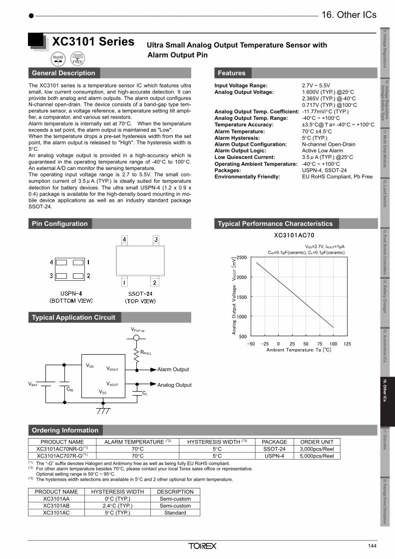
15. Automotive ICs _________________________________________________________________________________________
143
XD6121/XD6122/XD6123/XD6124 Series Voltage Detector with Watchdog Function and ON/OFF Control (VDF=1.6V~5.0V)
General Description Features
The XD6121/XD6122/XD6123/XD6124 series are groups of high-precision, low current consumption voltage detectors with watchdog functions incorporating CMOS process technology. The series consist of a reference voltage source, delay circuit, comparator, and output driver. With the built-in delay circuit, the XD6121/XD6122/XD6123/XD6124 series’ ICs do not require any external components to output signals with release delay time. The output type is VDFL low when detected. With the XD6121/XD6122/XD6123/XD6124 series’ ICs, the EN/ENB pin can control ON and OFF of the watchdog functions. By setting the EN/ENB pin to low or high level, the watchdog function can be OFF while the voltage detector remains operation. Since the EN/ENB pin of the XD6122 and XD6124 series is internally pulled up to the VIN pin or pulled down to the VSS pin, the ICs can be used with the EN/ENB pin left open, when the watchdog functions is used. The detect voltages are 1.6V, 2.2V, 2.3V, 2.4V, 2.9V, 3.0V, 3.1V, 4.4V, 4.5V, 4.6V. Six watchdog timeout period settings are available in a range from 50ms to 1.6s. Five release delay time settings are available in a range from 3.13ms to 400ms.
Detect Voltage Range: 1.6V, 2.2V, 2.3V, 2.4V, 2.9V, 3.0V, 3.1V, 4.4V, 4.5V, 4.6V
Hysteresis Width: VDFL x 5% (TYP.) Operating Voltage Range: 1.0V ~ 6.0V
(Absolute Max. Rating: 7.0V) Detect Voltage Temperature Characteristics:
+100ppm/C (TYP.) Output Configuration: N-channel open drain Watchdog Pin: Watchdog input EN/ENB Pin: The watchdog function is forced off. Release Delay Time: 400ms, 200ms, 100ms, 50ms, 3.13ms (TYP.) Watchdog Timeout Period: 1.6s, 800ms, 400ms, 200ms, 100ms,
50ms (TYP.) Operating Ambient Temperature: -40C ~ +85C Packages: SOT-25 Environmentally Friendly: EU RoHS Compliant, Pb Free
Pin Configuration
Typical Application Circuit Typical Performance Characteristics
Ordering Information
XD6121①②③④⑤⑥-⑦: EN Pin: No Pull-Up Resistor XD6122①②③④⑤⑥-⑦: EN Pin: Pull-Up Resistor XD6123①②③④⑤⑥-⑦: ENB Pin: No Pull-Down Resistor XD6124①②③④⑤⑥-⑦: ENB Pin: Pull-Down Resistor
DESIGNATOR ITEM SYMBOL DESCRIPTION
① Release Delay Time(*1)
A 3.13ms (TYP.) C 50ms (TYP.) D 100ms (TYP.) E 200ms (TYP.) F 400ms (TYP.)
② Watchdog Timeout Period
2 50ms (TYP.) 3 100ms (TYP.) 4 200ms (TYP.) 5 400ms (TYP.) 6 1.6s (TYP.) 7 800ms (TYP.)
③④ Detect Voltage 16, 22, 23, 24, 29, 30, 31, 44, 45, 46 ex.) 4.5V: ③ 4, ④ 5
⑤⑥-⑦ (*2) Package (Order Unit) MR-Q SOT-25 (3,000pcs/Reel) (*1) Please set the release delay time shorter than or equal to the watchdog timeout period. ex.) XD6123F523MR or XD6123F623MR (*2) The “-Q” suffix denotes “AEC-Q100” and “Halogen and Antimony free” as well as being fully EU RoHS compliant.
SOT-25 (TOP VIEW)
0
2.0
4.0
6.0
8.0
10.0
12.0
14.0
0 1 2 3 4 5 6Input Voltage: VIN (V)
Sup
ply C
urr
ent:
IS
S (
μA
)
XC6121~XC6124(VDF=2.7V)
Ta=85
Ta=-40
Ta=25
XD6121~XD6124
AEC-Q100 Grade3
________________________________________________________________________________________________ 16. Other ICs
144
XC3101 Series Ultra Small Analog Output Temperature Sensor with Alarm Output Pin
General Description Features
The XC3101 series is a temperature sensor IC which features ultrasmall, low current consumption, and high-accurate detection. It canprovide both analog and alarm outputs. The alarm output configuresN-channel open-drain. The device consists of a band-gap type tem-perature sensor, a voltage reference, a temperature setting tilt ampli-fier, a comparator, and various set resistors. Alarm temperature is internally set at 70C. When the temperatureexceeds a set point, the alarm output is maintained as "Low". When the temperature drops a pre-set hysteresis width from the setpoint, the alarm output is released to "High". The hysteresis width is5C. An analog voltage output is provided in a high-accuracy which isguaranteed in the operating temperature range of -40C to 100C. An external A/D can monitor the sensing temperature. The operating input voltage range is 2.7 to 5.5V. The small con-sumption current of 3.5μA (TYP.) is ideally suited for temperaturedetection for battery devices. The ultra small USPN-4 (1.2 x 0.9 x0.4) package is available for the high-density board mounting in mo-bile device applications as well as an industry standard packageSSOT-24.
Input Voltage Range: 2.7V ~ 5.5V Analog Output Voltage: 1.600V (TYP.) @25C 2.365V (TYP.) @-40C 0.717V (TYP.) @100C Analog Output Temp. Coefficient: -11.77mV/C (TYP.) Analog Output Temp. Range: -40C ~ +100C Temperature Accuracy: ±3.5C@Ta= -40C ~ +100C Alarm Temperature: 70C ±4.5C Alarm Hysteresis: 5C (TYP.) Alarm Output Configuration: N-channel Open-Drain Alarm Output Logic: Active Low Alarm Low Quiescent Current: 3.5μA (TYP.) @25C Operating Ambient Temperature: -40C ~ +100C Packages: USPN-4, SSOT-24 Environmentally Friendly: EU RoHS Compliant, Pb Free
Pin Configuration Typical Performance Characteristics
Typical Application Circuit
Ordering Information PRODUCT NAME ALARM TEMPERATURE (*2) HYSTERESIS WIDTH (*3) PACKAGE ORDER UNIT
XC3101AC70NR-G(*1) 70C 5C SSOT-24 3,000pcs/Reel XC3101AC707R-G(*1) 70C 5C USPN-4 5,000pcs/Reel
(*1) The “-G” suffix denotes Halogen and Antimony free as well as being fully EU RoHS compliant. (*2) For other alarm temperature besides 70C, please contact your local Torex sales office or representative.
Optional setting range is 50C ~ 95C. (*3) The hysteresis width selections are available in 5C and 2 other optional for alarm temperature.
PRODUCT NAME HYSTERESIS WIDTH DESCRIPTION XC3101AA 0C (TYP.) Semi-custom XC3101AB 2.4C (TYP.) Semi-custom XC3101AC 5C (TYP.) Standard
CL
Alarm Output
CIN
VDOUT
VAOUT
RPULL
VPull-up
Analog Output VBAT
VDD
VSS
XC3101AC70
500
1000
1500
2000
2500
-50 -25 0 25 50 75 100 125Ambient Temperature: Ta []
Ana
log
Out
put
Voltag
e:
VA
OU
T [
mV
]
VDD=2.7V,IAOUT=1uA
CIN=0.1F(ceramic),CL=0.1uF(ceramic)VDD=2.7V, IAOUT=1μA
CIN=0.1μF(ceramic), CL=0.1μF(ceramic)
11.Multi C
hip Module
10. Voltage Regulators
Voltage Detect Type
9. Voltage Regulators
12.Load Switch
13. Push Button Controllers14.B
attery Charger
15.Autom
otive ICs
17. Discrete
18.Package Power Dissipation16.O
ther ICs
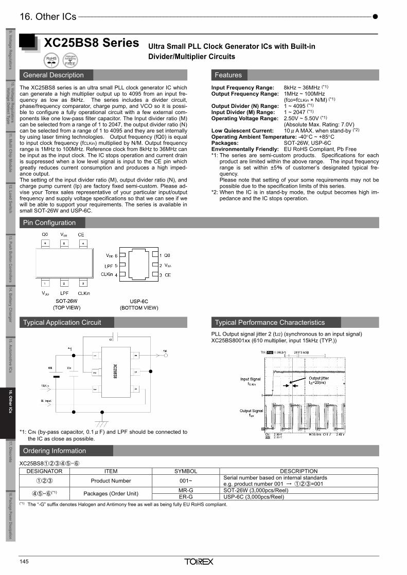
16. Other ICs ______________________________________________________________________________________
145
XC25BS8 Series Ultra Small PLL Clock Generator ICs with Built-in Divider/Multiplier Circuits
General Description Features
The XC25BS8 series is an ultra small PLL clock generator IC which can generate a high multiplier output up to 4095 from an input fre-quency as low as 8kHz. The series includes a divider circuit, phase/frequency comparator, charge pump, and VCO so it is possi-ble to configure a fully operational circuit with a few external com-ponents like one low-pass filter capacitor. The Input divider ratio (M) can be selected from a range of 1 to 2047, the output divider ratio (N) can be selected from a range of 1 to 4095 and they are set internally by using laser timing technologies. Output frequency (fQ0) is equal to input clock frequency (fCLKin) multiplied by N/M. Output frequency range is 1MHz to 100MHz. Reference clock from 8kHz to 36MHz can be input as the input clock. The IC stops operation and current drain is suppressed when a low level signal is input to the CE pin which greatly reduces current consumption and produces a high imped-ance output. The setting of the input divider ratio (M), output divider ratio (N), and charge pump current (Ip) are factory fixed semi-custom. Please ad-vise your Torex sales representative of your particular input/output frequency and supply voltage specifications so that we can see if we will be able to support your requirements. The series is available in small SOT-26W and USP-6C.
Input Frequency Range: 8kHz ~ 36MHz (*1) Output Frequency Range: 1MHz ~ 100MHz
(fQ0=fCLKin × N/M) (*1) Output Divider (N) Range: 1 ~ 4095 (*1) Input Divider (M) Range: 1 ~ 2047 (*1) Operating Voltage Range: 2.50V ~ 5.50V (*1)
(Absolute Max. Rating: 7.0V) Low Quiescent Current: 10μA MAX. when stand-by (*2) Operating Ambient Temperature: -40C ~ +85C Packages: SOT-26W, USP-6C Environmentally Friendly: EU RoHS Compliant, Pb Free *1: The series are semi-custom products. Specifications for each
product are limited within the above range. The input frequencyrange is set within ±5% of customer’s designated typical fre-quency. Please note that setting of your some requirements may not bepossible due to the specification limits of this series.
*2: When the IC is in stand-by mode, the output becomes high im-pedance and the IC stops operation.
Pin Configuration
Typical Application Circuit Typical Performance Characteristics
*1: CIN (by-pass capacitor, 0.1μF) and LPF should be connected to
the IC as close as possible.
PLL Output signal jitter 2 (tJ2) (synchronous to an input signal) XC25BS8001xx (610 multiplier, input 15kHz (TYP.))
Ordering Information
XC25BS8①②③④⑤-⑥ DESIGNATOR ITEM SYMBOL DESCRIPTION
①②③ Product Number 001~ Serial number based on internal standards e.g. product number 001 → ①②③=001
④⑤-⑥(*1) Packages (Order Unit) MR-G SOT-26W (3,000pcs/Reel) ER-G USP-6C (3,000pcs/Reel)
(*1) The “-G” suffix denotes Halogen and Antimony free as well as being fully EU RoHS compliant.
11.Multi C
hip Module
10. Voltage Regulators
Voltage Detect Type
9. Voltage Regulators
12.Load Switch
13. Push Button Controllers14.B
attery Charger
15.Autom
otive ICs
16.Other IC
s17. D
iscrete18.Package Power Dissipation
16.Other IC
s
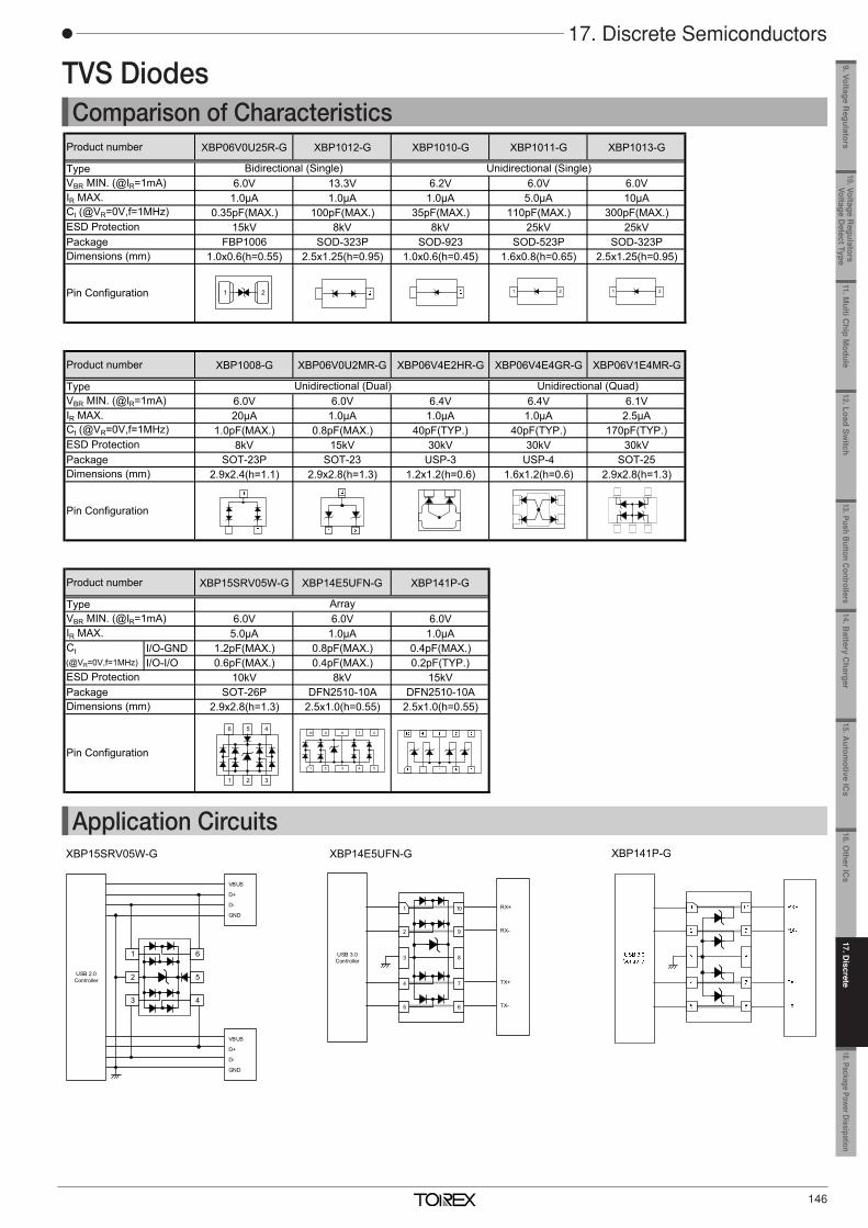
TVS DiodesComparison of Characteristics
Application Circuits
特性比較
XBP06V0U25R-G XBP1012-G XBP1010-G XBP1011-G XBP1013-G
TypeVBR MIN. (@IR=1mA) 6.0V 13.3V 6.2V 6.0V 6.0VIR MAX. 1.0μA 1.0μA 1.0μA 5.0μA 10μA
0.35pF(MAX.) 100pF(MAX.) 35pF(MAX.) 110pF(MAX.) 300pF(MAX.)15kV 8kV 8kV 25kV 25kV
Package FBP1006 SOD-323P SOD-923 SOD-523P SOD-323P1.0x0.6(h=0.55) 2.5x1.25(h=0.95) 1.0x0.6(h=0.45) 1.6x0.8(h=0.65) 2.5x1.25(h=0.95)
XBP1008-G XBP06V0U2MR-G XBP06V4E2HR-G XBP06V4E4GR-G XBP06V1E4MR-G
TypeVBR MIN. (@IR=1mA) 6.0V 6.0V 6.4V 6.4V 6.1VIR MAX. 20μA 1.0μA 1.0μA 1.0μA 2.5μA
1.0pF(MAX.) 0.8pF(MAX.) 40pF(TYP.) 40pF(TYP.) 170pF(TYP.)8kV 15kV 30kV 30kV 30kV
Package SOT-23P SOT-23 USP-3 USP-4 SOT-252.9x2.4(h=1.1) 2.9x2.8(h=1.3) 1.2x1.2(h=0.6) 1.6x1.2(h=0.6) 2.9x2.8(h=1.3)
XBP15SRV05W-G XBP14E5UFN-G XBP141P-G
TypeVBR MIN. (@IR=1mA) 6.0V 6.0V 6.0VIR MAX. 5.0μA 1.0μA 1.0μACt I/O-GND 1.2pF(MAX.) 0.8pF(MAX.) 0.4pF(MAX.)(@VR=0V,f=1MHz) I/O-I/O 0.6pF(MAX.) 0.4pF(MAX.) 0.2pF(TYP.)
10kV 8kV 15kVPackage SOT-26P DFN2510-10A DFN2510-10A
2.9x2.8(h=1.3) 2.5x1.0(h=0.55) 2.5x1.0(h=0.55)
使用例
XBP15SRV05W-G使用例 XBP14E5UFN-G使用例
ESD Protection
ESD Protection
XBP141P-G使用例
Pin Configuration
Unidirectional (Dual) Unidirectional (Quad)
Pin Configuration
Product number
Ct (@VR=0V,f=1MHz)
Dimensions (mm)
Pin Configuration
Product number
Dimensions (mm)
Array
Bidirectional (Single) Unidirectional (Single)
Product number
Ct (@VR=0V,f=1MHz)
Dimensions (mm)
ESD Protection
2121
1 3
6 4
2
5
USB 2.0Controller
VBUS
D+
D-
GND
VBUS
D+
D-
GND
1
3
6
4
2 5
3 4 52
8 7 6910
1
1 21
3
4
5
2
8
7
6
9
101
USB 3.0Controller
RX+
RX-
TX+
TX-
146
17. Discrete Semiconductors
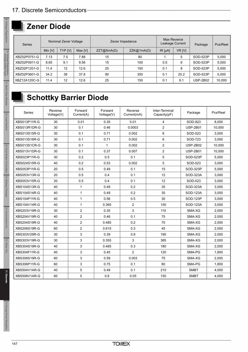
17. Discrete Semiconductors _____________________________________________________________________
147
Zener Diode
Series Nominal Zener Voltage Zener Impedance Max Reverce
Leakage Current Package Pcs/Reel
Min [V] TYP [V] Max [V] ZZT@5mA(Ω) ZZK@1mA(Ω) IR [μA] VR [V]
XBZ02P0751-G 7.13 7.5 7.88 15 80 1 5 SOD-523P 5,000
XBZ02P0911-G 8.65 9.1 9.56 15 100 0.5 6 SOD-523P 5,000
XBZ02P1201-G 11.4 12 12.6 25 150 0.1 8 SOD-523P 5,000
XBZ02P3601-G 34.2 36 37.8 90 350 0.1 25.2 SOD-523P 5,000
XBZ12A120C-G 11.4 12 12.6 25 150 0.1 9.1 USP-2B02 10,000
Schottky Barrier Diode
Series Reverse Voltage(V)
Forward Current(A)
Forward Voltage(V)
Reverse Current(mA)
Inter-Terminal Capacity(pF) Package Pcs/Reel
XBS013P11R-G 30 0.01 0.35 0.01 4 SOD-923 8,000
XBS013R1DR-G 30 0.1 0.46 0.0003 2 USP-2B01 10,000
XBS013S15R-G 30 0.1 0.71 0.002 6 SOD-523 3,000
XBS013S16R-G 30 0.1 0.71 0.002 6 SOD-723 3,000
XBS013S1CR-G 30 0.1 1 0.002 2 USP-2B02 10,000
XBS013V1DR-G 30 0.1 0.37 0.007 2 USP-2B01 10,000
XBS023P11R-G 30 0.2 0.5 0.1 5 SOD-523P 5,000
XBS024S15R-G 40 0.2 0.53 0.002 5 SOD-523 3,000
XBS053P11R-G 20 0.5 0.49 0.1 15 SOD-323P 5,000
XBS053V13R-G 20 0.5 0.4 0.1 12 SOD-323A 3,000
XBS053V15R-G 20 0.5 0.4 0.1 12 SOD-523 3,000
XBS104S13R-G 40 1 0.49 0.2 35 SOD-323A 3,000
XBS104S14R-G 40 1 0.49 0.2 35 SOD-123A 3,000
XBS104P11R-G 40 1 0.56 0.5 30 SOD-123P 3,000
XBS104V14R-G 40 1 0.365 2 150 SOD-123A 3,000
XBS203V19R-G 30 2 0.35 3 110 SMA-XG 2,000
XBS204V19R-G 40 2 0.46 0.1 75 SMA-XG 2,000
XBS204S19R-G 40 2 0.485 0.2 70 SMA-XG 2,000
XBS206S19R-G 60 2 0.615 0.3 45 SMA-XG 2,000
XBS303V29R-G 30 3 0.39 0.9 190 SMA-XG 2,000
XBS303V19R-G 30 3 0.355 3 385 SMA-XG 2,000
XBS304S19R-G 40 3 0.465 0.3 180 SMA-XG 2,000
XBS304F11R-G 40 3 0.45 2 120 SMA-PG 1,800
XBS306S19R-G 60 3 0.59 0.003 75 SMA-XG 2,000
XBS306P11R-G 60 3 0.75 0.1 80 SMA-PG 1,800
XBS504V1AR-G 40 5 0.49 0.1 210 SMBT 4,000
XBS506V1AR-G 60 5 0.6 0.05 150 SMBT 4,000
_______________________________________________________________________________________________________
148
Fast Recovery Diode
Product Reverse Voltage
RMS Voltage
Forward Current
(Average)
Forward Voltage
Reverse Current
Reverse Recovery
Time Package Pcs/Reel
VRM [V] VRMS [V] IF(AV) [A] VF@ (V) IR@ (μA) Trr [nS]
XBF10A20S-G 200 140 1 0.95 1 35 SMAF 3,000
XBF10A40S-G 400 280 1 1.25 1 35 SMAF 3,000
XBF10A60S-G 600 420 1 1.7 1 35 SMAF 3,000
XBF20A20S-G 200 140 2 0.95 1 35 SMBF 10,000
XBF20A40S-G 400 280 2 1.25 1 35 SMBF 10,000
XBF20A60S-G 600 420 2 1.7 1 35 SMBF 10,000
Switching Diode
Product Reverse Voltage
Forward Voltage
Forward Current
Reverce Current
Recovery time Capacitance
Package Pcs/Reel
VRRM [V] VF [V] IF [mA] IR [μA] VR [V] trr [ns] CT [pF]
XBW1SS400-G 80 1.2 100 0.1 80 4 0.5 SOD-523P 5,000
XBW21P0204-G 75 1.25 150 0.03 25 4 1.5 SOT-323 3,000
Bridge Diode
Product
Repetitive Peak
Reverse Voltage
Forward Current
Non Continuous
Forward Surge Current
Forward Voltage
Reverse Current Package Pcs/Reel
VRM [V] IF(AV) [A] IFSM [A] VF [V] IR [μA]
XBR12A6-G 600 1.5 50 1.1 5 SDIP 3,000
XBR12A8-G 800 1.5 50 1.1 5 SDIP 3,000
XBR12A10-G 1000 1.5 50 1.1 5 SDIP 3,000
11.Multi C
hip Module
10. Voltage Regulators
Voltage Detect Type
9. Voltage Regulators
12.Load Switch
13. Push Button Controllers14.B
attery Charger
15.Autom
otive ICs
16.Other IC
s17. D
iscrete18.Package Power Dissipation
17. Discrete
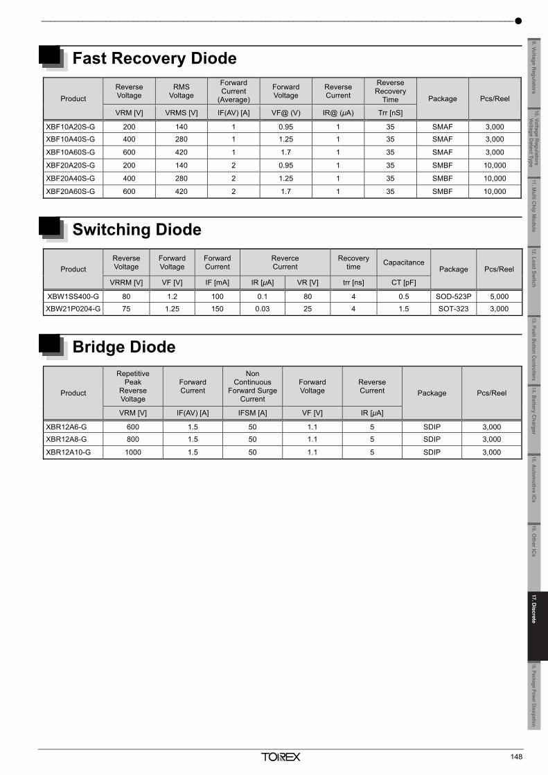
17. Discrete Semiconductors _____________________________________________________________________
147
Zener Diode
Series Nominal Zener Voltage Zener Impedance Max Reverce
Leakage Current Package Pcs/Reel
Min [V] TYP [V] Max [V] ZZT@5mA(Ω) ZZK@1mA(Ω) IR [μA] VR [V]
XBZ02P0751-G 7.13 7.5 7.88 15 80 1 5 SOD-523P 5,000
XBZ02P0911-G 8.65 9.1 9.56 15 100 0.5 6 SOD-523P 5,000
XBZ02P1201-G 11.4 12 12.6 25 150 0.1 8 SOD-523P 5,000
XBZ02P3601-G 34.2 36 37.8 90 350 0.1 25.2 SOD-523P 5,000
XBZ12A120C-G 11.4 12 12.6 25 150 0.1 9.1 USP-2B02 10,000
Schottky Barrier Diode
Series Reverse Voltage(V)
Forward Current(A)
Forward Voltage(V)
Reverse Current(mA)
Inter-Terminal Capacity(pF) Package Pcs/Reel
XBS013P11R-G 30 0.01 0.35 0.01 4 SOD-923 8,000
XBS013R1DR-G 30 0.1 0.46 0.0003 2 USP-2B01 10,000
XBS013S15R-G 30 0.1 0.71 0.002 6 SOD-523 3,000
XBS013S16R-G 30 0.1 0.71 0.002 6 SOD-723 3,000
XBS013S1CR-G 30 0.1 1 0.002 2 USP-2B02 10,000
XBS013V1DR-G 30 0.1 0.37 0.007 2 USP-2B01 10,000
XBS023P11R-G 30 0.2 0.5 0.1 5 SOD-523P 5,000
XBS024S15R-G 40 0.2 0.53 0.002 5 SOD-523 3,000
XBS053P11R-G 20 0.5 0.49 0.1 15 SOD-323P 5,000
XBS053V13R-G 20 0.5 0.4 0.1 12 SOD-323A 3,000
XBS053V15R-G 20 0.5 0.4 0.1 12 SOD-523 3,000
XBS104S13R-G 40 1 0.49 0.2 35 SOD-323A 3,000
XBS104S14R-G 40 1 0.49 0.2 35 SOD-123A 3,000
XBS104P11R-G 40 1 0.56 0.5 30 SOD-123P 3,000
XBS104V14R-G 40 1 0.365 2 150 SOD-123A 3,000
XBS203V19R-G 30 2 0.35 3 110 SMA-XG 2,000
XBS204V19R-G 40 2 0.46 0.1 75 SMA-XG 2,000
XBS204S19R-G 40 2 0.485 0.2 70 SMA-XG 2,000
XBS206S19R-G 60 2 0.615 0.3 45 SMA-XG 2,000
XBS303V29R-G 30 3 0.39 0.9 190 SMA-XG 2,000
XBS303V19R-G 30 3 0.355 3 385 SMA-XG 2,000
XBS304S19R-G 40 3 0.465 0.3 180 SMA-XG 2,000
XBS304F11R-G 40 3 0.45 2 120 SMA-PG 1,800
XBS306S19R-G 60 3 0.59 0.003 75 SMA-XG 2,000
XBS306P11R-G 60 3 0.75 0.1 80 SMA-PG 1,800
XBS504V1AR-G 40 5 0.49 0.1 210 SMBT 4,000
XBS506V1AR-G 60 5 0.6 0.05 150 SMBT 4,000
_______________________________________________________________________________________________________
148
Fast Recovery Diode
Product Reverse Voltage
RMS Voltage
Forward Current
(Average)
Forward Voltage
Reverse Current
Reverse Recovery
Time Package Pcs/Reel
VRM [V] VRMS [V] IF(AV) [A] VF@ (V) IR@ (μA) Trr [nS]
XBF10A20S-G 200 140 1 0.95 1 35 SMAF 3,000
XBF10A40S-G 400 280 1 1.25 1 35 SMAF 3,000
XBF10A60S-G 600 420 1 1.7 1 35 SMAF 3,000
XBF20A20S-G 200 140 2 0.95 1 35 SMBF 10,000
XBF20A40S-G 400 280 2 1.25 1 35 SMBF 10,000
XBF20A60S-G 600 420 2 1.7 1 35 SMBF 10,000
Switching Diode
Product Reverse Voltage
Forward Voltage
Forward Current
Reverce Current
Recovery time Capacitance
Package Pcs/Reel
VRRM [V] VF [V] IF [mA] IR [μA] VR [V] trr [ns] CT [pF]
XBW1SS400-G 80 1.2 100 0.1 80 4 0.5 SOD-523P 5,000
XBW21P0204-G 75 1.25 150 0.03 25 4 1.5 SOT-323 3,000
Bridge Diode
Product
Repetitive Peak
Reverse Voltage
Forward Current
Non Continuous
Forward Surge Current
Forward Voltage
Reverse Current Package Pcs/Reel
VRM [V] IF(AV) [A] IFSM [A] VF [V] IR [μA]
XBR12A6-G 600 1.5 50 1.1 5 SDIP 3,000
XBR12A8-G 800 1.5 50 1.1 5 SDIP 3,000
XBR12A10-G 1000 1.5 50 1.1 5 SDIP 3,000
11.Multi C
hip Module
10. Voltage Regulators
Voltage Detect Type
9. Voltage Regulators
12.Load Switch
13. Push Button Controllers14.B
attery Charger
15.Autom
otive ICs
16.Other IC
s18.Package Power Dissipation
17. Discrete
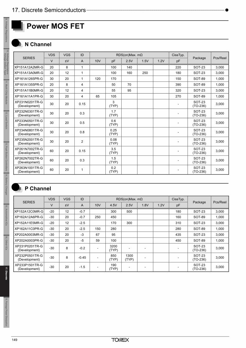
17. Discrete Semiconductors ___________________________________________________________________
149
Power MOS FET
N Channel
SERIES VDS VGS ID RDS(on)Max. mΩ CissTyp.
Package Pcs/Reel V ±V A 10V pF 2.5V 1.5V 1.2V pF
XP151A12A2MR-G 20 8 1 100 140 220 SOT-23 3,000
XP151A13A0MR-G 20 12 1 100 160 250 180 SOT-23 3,000
XP161A1265PR-G 30 20 1 120 170 150 SOT-89 1,000
XP161A1355PR-G 20 8 4 50 70 390 SOT-89 1,000
XP151A11B0MR-G 20 12 4 55 95 320 SOT-23 3,000
XP161A11A1PR-G 30 20 4 65 105 270 SOT-89 1,000
XP231N0201TR-G (Development) 30 20 0.15 3
(TYP) - SOT-23 (TO-236) 3,000
XP232N0301TR-G (Development) 30 20 0.3 1.7
(TYP) - SOT-23 (TO-236) 3,000
XP233N0501TR-G (Development) 30 20 0.5 0.6
(TYP) - SOT-23 (TO-236) 3,000
XP234N0801TR-G (Development) 30 20 0.8 0.25
(TYP) - SOT-23 (TO-236) 3,000
XP235N2001TR-G (Development) 30 20 2 0.08
(TYP) - SOT-23 (TO-236) 3,000
XP261N7002TR-G (Development) 60 20 0.15 3.5
(TYP) - SOT-23 (TO-236) 3,000
XP262N7002TR-G (Development) 60 20 0.3 1.5
(TYP) - SOT-23 (TO-236) 3,000
XP263N1001TR-G (Development) 60 20 1 0.2
(TYP) - SOT-23 (TO-236) 3,000
P Channel
SERIES VDS VGS ID RDS(on)Max. mΩ CissTyp.
Package Pcs/Reel V ±V A 10V 4.5V 2.5V 1.8V 1.2V pF
XP152A12C0MR-G -20 12 -0.7 300 500 180 SOT-23 3,000
XP162A12A6PR-G -30 20 -0.7 250 450 160 SOT-89 1,000
XP152A11E5MR-G -20 12 -2.5 170 300 310 SOT-23 3,000
XP162A11C0PR-G -30 20 -2.5 150 280 280 SOT-89 1,000
XP202A0003MR-G -30 20 -3 67 95 435 SOT-23 3,000
XP202A0003PR-G -30 20 -5 59 100 450 SOT-89 1,000
XP231P0201TR-G (Development) -30 8 -0.2 - 3200
(TYP) - - - SOT-23 (TO-236) 3,000
XP232P0501TR-G (Development) -30 8 -0.45 - 850
(TYP) 1300 (TYP) - - SOT-23
(TO-236) 3,000
XP233P1501TR-G (Development) -30 20 -1.5 - 190
(TYP) - - - SOT-23 (TO-236) 3,000
_____________________________________________________________________ 18. Package Power Dissipation
150
Package Power Dissipation CL-2025-02 Power Dissipation Power dissipation data for the CL-2025-02 is shown in this page. The value of power dissipation varies with the mount board conditions. Please use this data as the reference data taken in the following condition. 1. Measurement Condition Condition: Mount on a board Ambient: Natural convection Soldering: Lead (Pb) free Board: Dimensions 40 x 40 mm (1600 mm2 in one side) Copper (Cu) traces occupy 50% of the board area in top and back faces. Package heat-sink is tied to the copper traces. Material: Glass Epoxy (FR-4) Thickness: 1.6 mm Through-hole: 4 x 0.8 Diameter
Evaluation Board (Unit: mm) 2. Power Dissipation vs. Ambient Temperature Board Mount (Tj max = 125)
Ambient Temperature ()
Power Dissipation Pd (mW)
Thermal Resistance (/W)
25 1000 100.00 85 250
LGA-4B01 Power Dissipation Power dissipation data for the LGA-4B01 is shown in this page. The value of power dissipation varies with the mount board conditions. Please use this data as the reference data taken in the following condition. 1. Measurement Condition Condition : Mount on a board Ambient : Natural convection Soldering : Lead (Pb) free Board : Dimensions 40 x 40 mm (1600 mm2 in one side) Copper (Cu) traces occupy 50% of the front
and 50% of the back. The copper area is divided into four block, one
block is 12.5% of total. Each terminal connects one copper block in
the front and one in the back. Material : Glass Epoxy(FR-4) Thickness : 1.6mm Through-hole : 4 x 0.8 Diameter
Evaluation Board (Unit: mm)
2. Power Dissipation vs. Ambient temperature Board Mount (Tjmax=125)
Ambient Temperature ()
Power Dissipation Pd (mW)
Thermal Resistance (/W)
25 600 166.67 85 240
40.0
40.0
1.4
2.54
2.5
28.9
28.9
40.0
2.54 1.4
2.5
28.9
28.9
40.0
11.Multi C
hip Module
10. Voltage Regulators
Voltage Detect Type
9. Voltage Regulators
12.Load Switch
13. Push Button Controllers14.B
attery Charger
15.Autom
otive ICs
16.Other IC
s17. D
iscrete18.Package Power Dissipation
17. Discrete
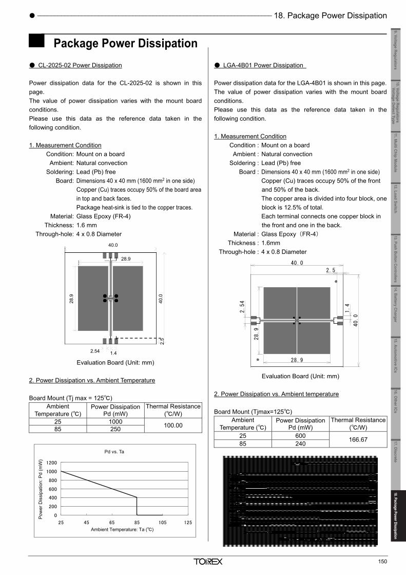
17. Discrete Semiconductors ___________________________________________________________________
149
Power MOS FET
N Channel
SERIES VDS VGS ID RDS(on)Max. mΩ CissTyp.
Package Pcs/Reel V ±V A 10V pF 2.5V 1.5V 1.2V pF
XP151A12A2MR-G 20 8 1 100 140 220 SOT-23 3,000
XP151A13A0MR-G 20 12 1 100 160 250 180 SOT-23 3,000
XP161A1265PR-G 30 20 1 120 170 150 SOT-89 1,000
XP161A1355PR-G 20 8 4 50 70 390 SOT-89 1,000
XP151A11B0MR-G 20 12 4 55 95 320 SOT-23 3,000
XP161A11A1PR-G 30 20 4 65 105 270 SOT-89 1,000
XP231N0201TR-G (Development) 30 20 0.15 3
(TYP) - SOT-23 (TO-236) 3,000
XP232N0301TR-G (Development) 30 20 0.3 1.7
(TYP) - SOT-23 (TO-236) 3,000
XP233N0501TR-G (Development) 30 20 0.5 0.6
(TYP) - SOT-23 (TO-236) 3,000
XP234N0801TR-G (Development) 30 20 0.8 0.25
(TYP) - SOT-23 (TO-236) 3,000
XP235N2001TR-G (Development) 30 20 2 0.08
(TYP) - SOT-23 (TO-236) 3,000
XP261N7002TR-G (Development) 60 20 0.15 3.5
(TYP) - SOT-23 (TO-236) 3,000
XP262N7002TR-G (Development) 60 20 0.3 1.5
(TYP) - SOT-23 (TO-236) 3,000
XP263N1001TR-G (Development) 60 20 1 0.2
(TYP) - SOT-23 (TO-236) 3,000
P Channel
SERIES VDS VGS ID RDS(on)Max. mΩ CissTyp.
Package Pcs/Reel V ±V A 10V 4.5V 2.5V 1.8V 1.2V pF
XP152A12C0MR-G -20 12 -0.7 300 500 180 SOT-23 3,000
XP162A12A6PR-G -30 20 -0.7 250 450 160 SOT-89 1,000
XP152A11E5MR-G -20 12 -2.5 170 300 310 SOT-23 3,000
XP162A11C0PR-G -30 20 -2.5 150 280 280 SOT-89 1,000
XP202A0003MR-G -30 20 -3 67 95 435 SOT-23 3,000
XP202A0003PR-G -30 20 -5 59 100 450 SOT-89 1,000
XP231P0201TR-G (Development) -30 8 -0.2 - 3200
(TYP) - - - SOT-23 (TO-236) 3,000
XP232P0501TR-G (Development) -30 8 -0.45 - 850
(TYP) 1300 (TYP) - - SOT-23
(TO-236) 3,000
XP233P1501TR-G (Development) -30 20 -1.5 - 190
(TYP) - - - SOT-23 (TO-236) 3,000
_____________________________________________________________________ 18. Package Power Dissipation
150
Package Power Dissipation CL-2025-02 Power Dissipation Power dissipation data for the CL-2025-02 is shown in this page. The value of power dissipation varies with the mount board conditions. Please use this data as the reference data taken in the following condition. 1. Measurement Condition Condition: Mount on a board Ambient: Natural convection Soldering: Lead (Pb) free Board: Dimensions 40 x 40 mm (1600 mm2 in one side) Copper (Cu) traces occupy 50% of the board area in top and back faces. Package heat-sink is tied to the copper traces. Material: Glass Epoxy (FR-4) Thickness: 1.6 mm Through-hole: 4 x 0.8 Diameter
Evaluation Board (Unit: mm) 2. Power Dissipation vs. Ambient Temperature Board Mount (Tj max = 125)
Ambient Temperature ()
Power Dissipation Pd (mW)
Thermal Resistance (/W)
25 1000 100.00 85 250
LGA-4B01 Power Dissipation Power dissipation data for the LGA-4B01 is shown in this page. The value of power dissipation varies with the mount board conditions. Please use this data as the reference data taken in the following condition. 1. Measurement Condition Condition : Mount on a board Ambient : Natural convection Soldering : Lead (Pb) free Board : Dimensions 40 x 40 mm (1600 mm2 in one side) Copper (Cu) traces occupy 50% of the front
and 50% of the back. The copper area is divided into four block, one
block is 12.5% of total. Each terminal connects one copper block in
the front and one in the back. Material : Glass Epoxy(FR-4) Thickness : 1.6mm Through-hole : 4 x 0.8 Diameter
Evaluation Board (Unit: mm)
2. Power Dissipation vs. Ambient temperature Board Mount (Tjmax=125)
Ambient Temperature ()
Power Dissipation Pd (mW)
Thermal Resistance (/W)
25 600 166.67 85 240
40.0
40.0
1.4
2.54
2.5
28.9
28.9
40.0
2.54 1.4
2.5
28.9
28.9
40.0
11.Multi C
hip Module
10. Voltage Regulators
Voltage Detect Type
9. Voltage Regulators
12.Load Switch
13. Push Button Controllers14.B
attery Charger
15.Autom
otive ICs
16.Other IC
s17. D
iscrete18.Package Power Dissipation
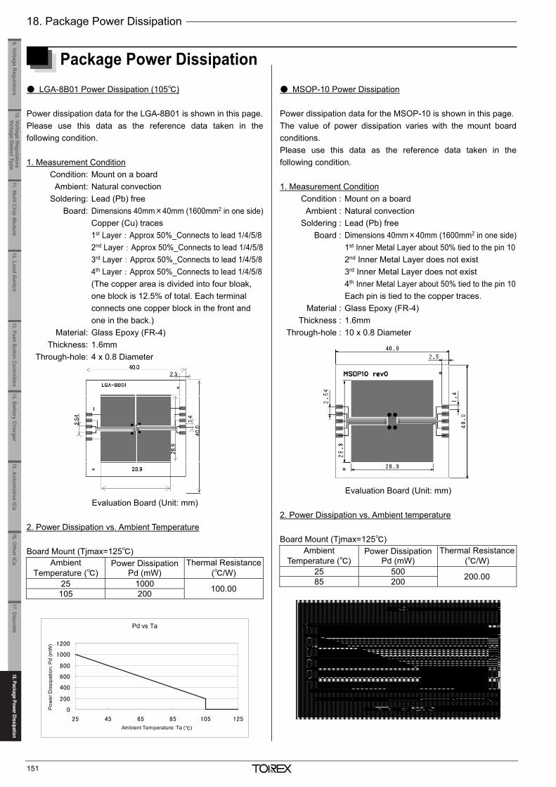
18. Package Power Dissipation _______________________________________________________________________
151
Package Power Dissipation LGA-8B01 Power Dissipation (105) Power dissipation data for the LGA-8B01 is shown in this page. Please use this data as the reference data taken in the following condition. 1. Measurement Condition Condition: Mount on a board Ambient: Natural convection Soldering: Lead (Pb) free Board: Dimensions 40mm×40mm (1600mm2 in one side) Copper (Cu) traces 1st Layer:Approx 50%_Connects to lead 1/4/5/8 2nd Layer:Approx 50%_Connects to lead 1/4/5/8 3rd Layer:Approx 50%_Connects to lead 1/4/5/8 4th Layer:Approx 50%_Connects to lead 1/4/5/8 (The copper area is divided into four bloak, one block is 12.5% of total. Each terminal connects one copper block in the front and one in the back.) Material: Glass Epoxy (FR-4) Thickness: 1.6mm Through-hole: 4 x 0.8 Diameter
Evaluation Board (Unit: mm) 2. Power Dissipation vs. Ambient Temperature Board Mount (Tjmax=125)
Ambient Temperature ()
Power Dissipation Pd (mW)
Thermal Resistance (/W)
25 1000 100.00 105 200
MSOP-10 Power Dissipation Power dissipation data for the MSOP-10 is shown in this page. The value of power dissipation varies with the mount board conditions. Please use this data as the reference data taken in the following condition. 1. Measurement Condition Condition : Mount on a board Ambient : Natural convection Soldering : Lead (Pb) free Board : Dimensions 40mm×40mm (1600mm2 in one side) 1st Inner Metal Layer about 50% tied to the pin 10 2nd Inner Metal Layer does not exist 3rd Inner Metal Layer does not exist 4th Inner Metal Layer about 50% tied to the pin 10 Each pin is tied to the copper traces. Material : Glass Epoxy (FR-4) Thickness : 1.6mm Through-hole : 10 x 0.8 Diameter
Evaluation Board (Unit: mm) 2. Power Dissipation vs. Ambient temperature Board Mount (Tjmax=125)
Ambient Temperature ()
Power Dissipation Pd (mW)
Thermal Resistance (/W)
25 500 200.00 85 200
Pd vs Ta
0
200
400
600
800
1000
1200
25 45 65 85 105 125
Ambient Temperature: Ta ()
Pow
er D
issi
patio
n: P
d (m
W)
_______________________________________________________________________________________________________
152
Package Power Dissipation
QFN-20 Power Dissipation Power dissipation data for the QFN-20 is shown in this page. The value of power dissipation varies with the mount board conditions. Please use this data as the reference data taken in the following condition. 1. Measurement Condition Condition : Mount on a board Ambien t: Natural convection Soldering : Lead (Pb) free Board : Dimensions 40 x 40 mm (1600 mm2 in one side) Copper (Cu) traces occupy 50% of the board area in top and back faces. Package heat-sink is tied to the copper traces. Material : Glass Epoxy (FR-4) Thickness : 1.6 mm Through-hole : 5 x 0.8 Diameter
Evaluation Board (Unit: mm) 2. Power Dissipation vs. Ambient Temperature Board Mount (Tjmax=125)
Ambient Temperature ()
Power Dissipation Pd (mW)
Thermal Resistance (/W)
25 1000 100.00 85 400
QFN-24 Power Dissipation Power dissipation data for the QFN-24 is shown in this page. The value of power dissipation varies with the mount board conditions. Please use this data as the reference data taken in the following condition. 1. Measurement Condition Condition: Mount on a board Ambient: Natural convection Soldering: Lead (Pb) free Board: Dimensions:40 x 40 mm (1600mm2 in one side) 4Copper Layers 1st Inner metal layer about 50% is not
connected to the heatsink back metal. 2nd, 3rd and 4th Inner metal layer about 50%
connects to the heatsink back metal. Material: Glass Epoxy (FR-4) Thickness: 1.0 mm Through-hole: 4 x 0.4 Diameter
Evaluation Board (Unit: mm) 2. Power Dissipation vs. Ambient Temperature Board Mount (Tjmax=125)
Ambient Temperature ()
Power Dissipation Pd (mW)
Thermal Resistance (/W)
25 1500 66.67 85 600
Pd vs Ta
0
200
400
600
800
1000
1200
25 45 65 85 105 125
Ambient Temperature Ta ()
Pow
er D
issi
patio
n P
d (m
W)
Pd-Ta特性グラフ
0200400600800
1000120014001600
25 45 65 85 105 125
周囲温度Ta()
許容
損失Pd(mW)
Pd vs. Ta
Ambient Temperature: Ta ()
Pow
er D
issi
patio
n: P
d (
W)
40
40
2.54
1.4
28.9
28.9
2.5
Ambient Temperature: Ta ()
Pow
er D
issi
patio
n: P
d (m
W)
11.Multi C
hip Module
10. Voltage Regulators
Voltage Detect Type
9. Voltage Regulators
12.Load Switch
13. Push Button Controllers14.B
attery Charger
15.Autom
otive ICs
16.Other IC
s17. D
iscrete18.Package Power Dissipation18.Package Power Dissipation
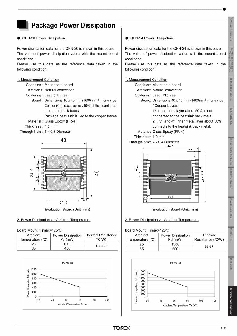
18. Package Power Dissipation _______________________________________________________________________
151
Package Power Dissipation LGA-8B01 Power Dissipation (105) Power dissipation data for the LGA-8B01 is shown in this page. Please use this data as the reference data taken in the following condition. 1. Measurement Condition Condition: Mount on a board Ambient: Natural convection Soldering: Lead (Pb) free Board: Dimensions 40mm×40mm (1600mm2 in one side) Copper (Cu) traces 1st Layer:Approx 50%_Connects to lead 1/4/5/8 2nd Layer:Approx 50%_Connects to lead 1/4/5/8 3rd Layer:Approx 50%_Connects to lead 1/4/5/8 4th Layer:Approx 50%_Connects to lead 1/4/5/8 (The copper area is divided into four bloak, one block is 12.5% of total. Each terminal connects one copper block in the front and one in the back.) Material: Glass Epoxy (FR-4) Thickness: 1.6mm Through-hole: 4 x 0.8 Diameter
Evaluation Board (Unit: mm) 2. Power Dissipation vs. Ambient Temperature Board Mount (Tjmax=125)
Ambient Temperature ()
Power Dissipation Pd (mW)
Thermal Resistance (/W)
25 1000 100.00 105 200
MSOP-10 Power Dissipation Power dissipation data for the MSOP-10 is shown in this page. The value of power dissipation varies with the mount board conditions. Please use this data as the reference data taken in the following condition. 1. Measurement Condition Condition : Mount on a board Ambient : Natural convection Soldering : Lead (Pb) free Board : Dimensions 40mm×40mm (1600mm2 in one side) 1st Inner Metal Layer about 50% tied to the pin 10 2nd Inner Metal Layer does not exist 3rd Inner Metal Layer does not exist 4th Inner Metal Layer about 50% tied to the pin 10 Each pin is tied to the copper traces. Material : Glass Epoxy (FR-4) Thickness : 1.6mm Through-hole : 10 x 0.8 Diameter
Evaluation Board (Unit: mm) 2. Power Dissipation vs. Ambient temperature Board Mount (Tjmax=125)
Ambient Temperature ()
Power Dissipation Pd (mW)
Thermal Resistance (/W)
25 500 200.00 85 200
Pd vs Ta
0
200
400
600
800
1000
1200
25 45 65 85 105 125
Ambient Temperature: Ta ()
Pow
er D
issi
patio
n: P
d (m
W)
_______________________________________________________________________________________________________
152
Package Power Dissipation
QFN-20 Power Dissipation Power dissipation data for the QFN-20 is shown in this page. The value of power dissipation varies with the mount board conditions. Please use this data as the reference data taken in the following condition. 1. Measurement Condition Condition : Mount on a board Ambien t: Natural convection Soldering : Lead (Pb) free Board : Dimensions 40 x 40 mm (1600 mm2 in one side) Copper (Cu) traces occupy 50% of the board area in top and back faces. Package heat-sink is tied to the copper traces. Material : Glass Epoxy (FR-4) Thickness : 1.6 mm Through-hole : 5 x 0.8 Diameter
Evaluation Board (Unit: mm) 2. Power Dissipation vs. Ambient Temperature Board Mount (Tjmax=125)
Ambient Temperature ()
Power Dissipation Pd (mW)
Thermal Resistance (/W)
25 1000 100.00 85 400
QFN-24 Power Dissipation Power dissipation data for the QFN-24 is shown in this page. The value of power dissipation varies with the mount board conditions. Please use this data as the reference data taken in the following condition. 1. Measurement Condition Condition: Mount on a board Ambient: Natural convection Soldering: Lead (Pb) free Board: Dimensions:40 x 40 mm (1600mm2 in one side) 4Copper Layers 1st Inner metal layer about 50% is not
connected to the heatsink back metal. 2nd, 3rd and 4th Inner metal layer about 50%
connects to the heatsink back metal. Material: Glass Epoxy (FR-4) Thickness: 1.0 mm Through-hole: 4 x 0.4 Diameter
Evaluation Board (Unit: mm) 2. Power Dissipation vs. Ambient Temperature Board Mount (Tjmax=125)
Ambient Temperature ()
Power Dissipation Pd (mW)
Thermal Resistance (/W)
25 1500 66.67 85 600
Pd vs Ta
0
200
400
600
800
1000
1200
25 45 65 85 105 125
Ambient Temperature Ta ()
Pow
er D
issi
patio
n P
d (m
W)
Pd-Ta特性グラフ
0200400600800
1000120014001600
25 45 65 85 105 125
周囲温度Ta()
許容
損失Pd(mW)
Pd vs. Ta
Ambient Temperature: Ta ()
Pow
er D
issi
patio
n: P
d (
W)
40
40
2.54
1.4
28.9
28.9
2.5
Ambient Temperature: Ta ()
Pow
er D
issi
patio
n: P
d (m
W)
11.Multi C
hip Module
10. Voltage Regulators
Voltage Detect Type
9. Voltage Regulators
12.Load Switch
13. Push Button Controllers14.B
attery Charger
15.Autom
otive ICs
16.Other IC
s17. D
iscrete18.Package Power Dissipation
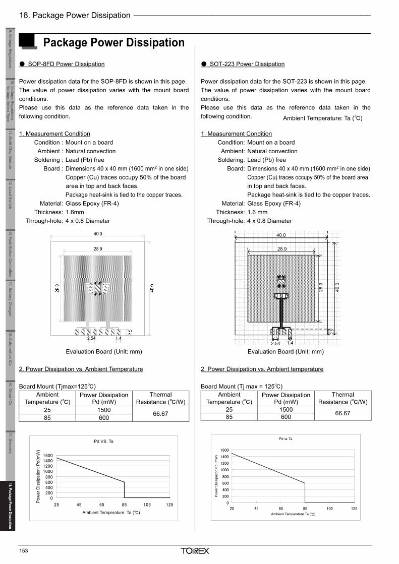
18. Package Power Dissipation _______________________________________________________________________
153
Package Power Dissipation
SOP-8FD Power Dissipation Power dissipation data for the SOP-8FD is shown in this page. The value of power dissipation varies with the mount board conditions. Please use this data as the reference data taken in the following condition. 1. Measurement Condition Condition : Mount on a board Ambient : Natural convection Soldering : Lead (Pb) free Board : Dimensions 40 x 40 mm (1600 mm2 in one side) Copper (Cu) traces occupy 50% of the board
area in top and back faces. Package heat-sink is tied to the copper traces. Material: Glass Epoxy (FR-4) Thickness: 1.6mm Through-hole: 4 x 0.8 Diameter
Evaluation Board (Unit: mm) 2. Power Dissipation vs. Ambient Temperature Board Mount (Tjmax=125)
Ambient Temperature ()
Power Dissipation Pd (mW)
Thermal Resistance (/W)
25 1500 66.67 85 600
SOT-223 Power Dissipation Power dissipation data for the SOT-223 is shown in this page. The value of power dissipation varies with the mount board conditions. Please use this data as the reference data taken in the following condition. 1. Measurement Condition Condition: Mount on a board Ambient: Natural convection Soldering: Lead (Pb) free Board: Dimensions 40 x 40 mm (1600 mm2 in one side) Copper (Cu) traces occupy 50% of the board area in top and back faces. Package heat-sink is tied to the copper traces. Material: Glass Epoxy (FR-4) Thickness: 1.6 mm Through-hole: 4 x 0.8 Diameter
Evaluation Board (Unit: mm) 2. Power Dissipation vs. Ambient temperature Board Mount (Tj max = 125)
Ambient Temperature ()
Power Dissipation Pd (mW)
Thermal Resistance (/W)
25 1500 66.67 85 600
Pd-Ta特性グラフ
0200400600800
1000120014001600
25 45 65 85 105 125
周囲温度Ta()
許容損
失Pd(
mW)
Pd VS. Ta
Pow
er D
issi
patio
n: P
d(m
W)
Ambient Temperature: Ta ()
Pd vs Ta
0
200
400
600
800
1000
1200
1400
1600
25 45 65 85 105 125
Ambient Temperature Ta ()
Pow
er D
issi
patio
n P
d (m
W)
40.0
2.54 1.4
28.9
Ambient Temperature: Ta ()
Ambient Temperature: Ta ()
40.0
28.9
2.54 1.4 40
.0
28.9
2.5
_______________________________________________________________________________________________________
154
Package Power Dissipation
SOT-23 Power Dissipation Power dissipation data for the SOT-23 is shown in this page. The value of power dissipation varies with the mount board conditions. Please use this data as the reference data taken in the following condition. 1. Measurement Condition Condition: Mount on a board Ambient: Natural convection Soldering: Lead (Pb) free Board: Dimensions 40 x 40 mm (1600 mm2 in one side) Copper (Cu) traces occupy 50% of the board area in top and back faces. Package heat-sink is tied to the copper traces. (Board of SOT-26 is used) Material: Glass Epoxy (FR-4) Thickness: 1.6 mm Through-hole: 4 x 0.8 Diameter
Evaluation Board (Unit: mm) 2. Power Dissipation vs. Ambient temperature Board Mount (Tj max = 125)
Ambient Temperature ()
Power Dissipation Pd (mW)
Thermal Resistance (/W)
25 500 200.00 85 200
SOT-25 Power Dissipation Power dissipation data for the SOT-25 is shown in this page. The value of power dissipation varies with the mount board conditions. Please use this data as the reference data taken in the following condition. 1. Measurement Condition Condition: Mount on a board Ambient: Natural convection Soldering: Lead (Pb) free Board: Dimensions 40 x 40 mm (1600 mm2 in one side) Copper (Cu) traces occupy 50% of the board area in top and back faces. Package heat-sink is tied to the copper traces.
(Board of SOT-26 is used) Material: Glass Epoxy (FR-4) Thickness: 1.6 mm Through-hole: 4 x 0.8 Diameter
Evaluation Board (Unit: mm) 2. Power Dissipation vs. Ambient temperature Board Mount (Tj max = 125)
Ambient Temperature ()
Power Dissipation Pd (mW)
Thermal Resistance (/W)
25 600 166.67 85 240
3. Power Dissipation vs. Ambient temperature (105) Board Mount (Tj max = 125)
Ambient Temperature ()
Power Dissipation Pd (mW)
Thermal Resistance (/W)
25 600 166.67 105 120
Pd vs Ta
0
100
200
300
400
500
600
25 45 65 85 105 125
Ambient Temperature Ta ()
Pow
er D
issi
patio
n P
d (m
W)
Pd vs Ta
0
100
200
300
400
500
600
700
25 45 65 85 105 125
Ambient Temperature Ta ()
Pow
er D
issi
patio
n P
d (m
W)
Pd vs Ta
0
100
200
300
400
500
600
700
25 45 65 85 105 125Ambient Temperature Ta ()
Pow
er D
issi
patio
n P
d (m
W)
40.0
2.54 1.4
28.9
40.0
2.54 1.4
28.9
11.Multi C
hip Module
10. Voltage Regulators
Voltage Detect Type
9. Voltage Regulators
12.Load Switch
13. Push Button Controllers14.B
attery Charger
15.Autom
otive ICs
16.Other IC
s17. D
iscrete18.Package Power Dissipation18.Package Power Dissipation
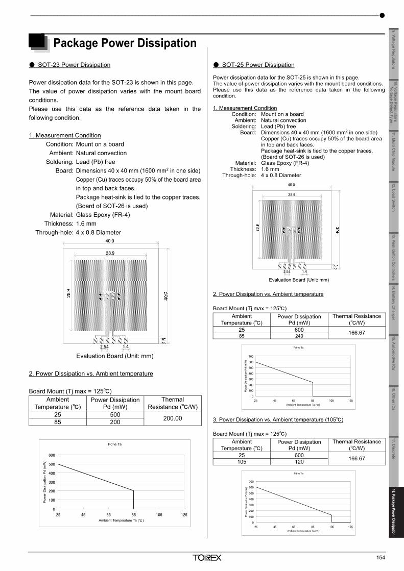
18. Package Power Dissipation _______________________________________________________________________
153
Package Power Dissipation
SOP-8FD Power Dissipation Power dissipation data for the SOP-8FD is shown in this page. The value of power dissipation varies with the mount board conditions. Please use this data as the reference data taken in the following condition. 1. Measurement Condition Condition : Mount on a board Ambient : Natural convection Soldering : Lead (Pb) free Board : Dimensions 40 x 40 mm (1600 mm2 in one side) Copper (Cu) traces occupy 50% of the board
area in top and back faces. Package heat-sink is tied to the copper traces. Material: Glass Epoxy (FR-4) Thickness: 1.6mm Through-hole: 4 x 0.8 Diameter
Evaluation Board (Unit: mm) 2. Power Dissipation vs. Ambient Temperature Board Mount (Tjmax=125)
Ambient Temperature ()
Power Dissipation Pd (mW)
Thermal Resistance (/W)
25 1500 66.67 85 600
SOT-223 Power Dissipation Power dissipation data for the SOT-223 is shown in this page. The value of power dissipation varies with the mount board conditions. Please use this data as the reference data taken in the following condition. 1. Measurement Condition Condition: Mount on a board Ambient: Natural convection Soldering: Lead (Pb) free Board: Dimensions 40 x 40 mm (1600 mm2 in one side) Copper (Cu) traces occupy 50% of the board area in top and back faces. Package heat-sink is tied to the copper traces. Material: Glass Epoxy (FR-4) Thickness: 1.6 mm Through-hole: 4 x 0.8 Diameter
Evaluation Board (Unit: mm) 2. Power Dissipation vs. Ambient temperature Board Mount (Tj max = 125)
Ambient Temperature ()
Power Dissipation Pd (mW)
Thermal Resistance (/W)
25 1500 66.67 85 600
Pd-Ta特性グラフ
0200400600800
1000120014001600
25 45 65 85 105 125
周囲温度Ta()
許容損
失Pd(
mW)
Pd VS. Ta
Pow
er D
issi
patio
n: P
d(m
W)
Ambient Temperature: Ta ()
Pd vs Ta
0
200
400
600
800
1000
1200
1400
1600
25 45 65 85 105 125
Ambient Temperature Ta ()
Pow
er D
issi
patio
n P
d (m
W)
40.0
2.54 1.4
28.9
Ambient Temperature: Ta ()
Ambient Temperature: Ta ()
40.0
28.9
2.54 1.4
40.0
28.9
2.5
_______________________________________________________________________________________________________
154
Package Power Dissipation
SOT-23 Power Dissipation Power dissipation data for the SOT-23 is shown in this page. The value of power dissipation varies with the mount board conditions. Please use this data as the reference data taken in the following condition. 1. Measurement Condition Condition: Mount on a board Ambient: Natural convection Soldering: Lead (Pb) free Board: Dimensions 40 x 40 mm (1600 mm2 in one side) Copper (Cu) traces occupy 50% of the board area in top and back faces. Package heat-sink is tied to the copper traces. (Board of SOT-26 is used) Material: Glass Epoxy (FR-4) Thickness: 1.6 mm Through-hole: 4 x 0.8 Diameter
Evaluation Board (Unit: mm) 2. Power Dissipation vs. Ambient temperature Board Mount (Tj max = 125)
Ambient Temperature ()
Power Dissipation Pd (mW)
Thermal Resistance (/W)
25 500 200.00 85 200
SOT-25 Power Dissipation Power dissipation data for the SOT-25 is shown in this page. The value of power dissipation varies with the mount board conditions. Please use this data as the reference data taken in the following condition. 1. Measurement Condition Condition: Mount on a board Ambient: Natural convection Soldering: Lead (Pb) free Board: Dimensions 40 x 40 mm (1600 mm2 in one side) Copper (Cu) traces occupy 50% of the board area in top and back faces. Package heat-sink is tied to the copper traces.
(Board of SOT-26 is used) Material: Glass Epoxy (FR-4) Thickness: 1.6 mm Through-hole: 4 x 0.8 Diameter
Evaluation Board (Unit: mm) 2. Power Dissipation vs. Ambient temperature Board Mount (Tj max = 125)
Ambient Temperature ()
Power Dissipation Pd (mW)
Thermal Resistance (/W)
25 600 166.67 85 240
3. Power Dissipation vs. Ambient temperature (105) Board Mount (Tj max = 125)
Ambient Temperature ()
Power Dissipation Pd (mW)
Thermal Resistance (/W)
25 600 166.67 105 120
Pd vs Ta
0
100
200
300
400
500
600
25 45 65 85 105 125
Ambient Temperature Ta ()
Pow
er D
issi
patio
n P
d (m
W)
Pd vs Ta
0
100
200
300
400
500
600
700
25 45 65 85 105 125
Ambient Temperature Ta ()
Pow
er D
issi
patio
n P
d (m
W)
Pd vs Ta
0
100
200
300
400
500
600
700
25 45 65 85 105 125Ambient Temperature Ta ()
Pow
er D
issi
patio
n P
d (m
W)
40.0
2.54 1.4
28.9
40.0
2.54 1.4
28.9
11.Multi C
hip Module
10. Voltage Regulators
Voltage Detect Type
9. Voltage Regulators
12.Load Switch
13. Push Button Controllers14.B
attery Charger
15.Autom
otive ICs
16.Other IC
s17. D
iscrete18.Package Power Dissipation
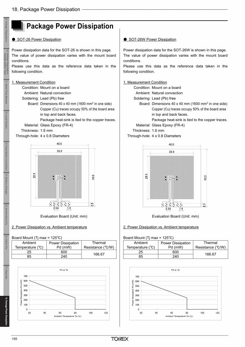
18. Package Power Dissipation _______________________________________________________________________
155
Package Power Dissipation
SOT-26 Power Dissipation Power dissipation data for the SOT-26 is shown in this page. The value of power dissipation varies with the mount board conditions. Please use this data as the reference data taken in the following condition. 1. Measurement Condition Condition: Mount on a board Ambient: Natural convection Soldering: Lead (Pb) free Board: Dimensions 40 x 40 mm (1600 mm2 in one side) Copper (Cu) traces occupy 50% of the board area in top and back faces. Package heat-sink is tied to the copper traces. Material: Glass Epoxy (FR-4) Thickness: 1.6 mm Through-hole: 4 x 0.8 Diameters
Evaluation Board (Unit: mm) 2. Power Dissipation vs. Ambient temperature Board Mount (Tj max = 125)
Ambient Temperature ()
Power Dissipation Pd (mW)
Thermal Resistance (/W)
25 600 166.67 85 240
SOT-26W Power Dissipation Power dissipation data for the SOT-26W is shown in this page. The value of power dissipation varies with the mount board conditions. Please use this data as the reference data taken in the following condition. 1. Measurement Condition Condition: Mount on a board Ambient: Natural convection Soldering: Lead (Pb) free Board: Dimensions 40 x 40 mm (1600 mm2 in one side) Copper (Cu) traces occupy 50% of the board area in top and back faces. Package heat-sink is tied to the copper traces. Material: Glass Epoxy (FR-4) Thickness: 1.6 mm Through-hole: 4 x 0.8 Diameters
Evaluation Board (Unit: mm) 2. Power Dissipation vs. Ambient temperature Board Mount (Tj max = 125)
Ambient Temperature ()
Power Dissipation Pd (mW)
Thermal Resistance (/W)
25 600 166.67 85 240
Pd vs Ta
0
100
200
300
400
500
600
700
25 45 65 85 105 125
Ambient Temperature Ta ()
Pow
er D
issi
patio
n P
d (m
W)
Pd vs Ta
0
100
200
300
400
500
600
700
25 45 65 85 105 125
Ambient Temperature Ta ()
Pow
er D
issi
patio
n P
d (m
W)
40.0
2.54 1.4
28.9
40.0
2.54 1.4
28.9
_______________________________________________________________________________________________________
156
Package Power Dissipation SOT-89 Power Dissipation Power dissipation data for the SOT-89 is shown in this page. The value of power dissipation varies with the mount board conditions. Please use this data as the reference data taken in the following condition. 1. Measurement Condition Condition: Mount on a board Ambient: Natural convection Soldering: Lead (Pb) free Board: Dimensions 40 x 40 mm (1600 mm2 in one side) Copper (Cu) traces occupy 50% of the board area in top and back faces. Package heat-sink is tied to the copper traces. Material: Glass Epoxy (FR-4) Thickness: 1.6 mm Through-hole: 5 x 0.8 Diameter
Evaluation Board (Unit: mm) 2. Power Dissipation vs. Ambient temperature Board Mount (Tj max = 125)
Ambient Temperature ()
Power Dissipation Pd (mW)
Thermal Resistance (/W)
25 1000 100.00 85 400
SOT-89-5 Power Dissipation Power dissipation data for the SOT-89-5 is shown in this page. The value of power dissipation varies with the mount board conditions. Please use this data as the reference data taken in the following condition. 1. Measurement Condition Condition: Mount on a board Ambient: Natural convection Soldering: Lead (Pb) free Board: Dimensions 40 x 40 mm (1600 mm2 in one side) Copper (Cu) traces occupy 50% of the board area in top and back faces. Package heat-sink is tied to the copper traces. Material: Glass Epoxy (FR-4) Thickness: 1.6 mm Through-hole: 5 x 0.8 Diameter
Evaluation Board (Unit: mm) 2. Power Dissipation vs. Ambient temperature Board Mount (Tj max = 125)
Ambient Temperature ()
Power Dissipation Pd (mW)
Thermal Resistance (/W)
25 1300 76.92 85 520
3. Power Dissipation vs. Ambient temperature (105) Board Mount (Tj max = 125)
Ambient Temperature ()
Power Dissipation Pd (mW)
Thermal Resistance (/W)
25 1300 76.92 105 260
Pd vs Ta
0
200
400
600
800
1000
1200
25 45 65 85 105 125Ambient Temperature Ta ()
Pow
er D
issi
patio
n P
d (m
W)
Pd vs Ta
0
200
400
600
800
1000
1200
1400
25 45 65 85 105 125
Ambient Temperature Ta ()
Pow
er D
issi
patio
n P
d (m
W)
Pd vs Ta
0
200
400
600
800
1000
1200
1400
25 45 65 85 105 125
Ambient Temperature Ta ()
Pow
er D
issi
patio
n P
d (m
W)
28.9
40.0
2.5
28.9
40.0
2.5
11.Multi C
hip Module
10. Voltage Regulators
Voltage Detect Type
9. Voltage Regulators
12.Load Switch
13. Push Button Controllers14.B
attery Charger
15.Autom
otive ICs
16.Other IC
s17. D
iscrete18.Package Power Dissipation18.Package Power Dissipation
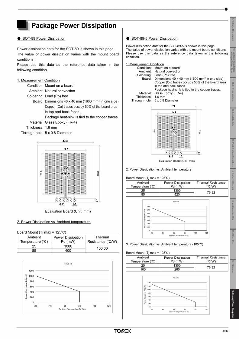
18. Package Power Dissipation _______________________________________________________________________
155
Package Power Dissipation
SOT-26 Power Dissipation Power dissipation data for the SOT-26 is shown in this page. The value of power dissipation varies with the mount board conditions. Please use this data as the reference data taken in the following condition. 1. Measurement Condition Condition: Mount on a board Ambient: Natural convection Soldering: Lead (Pb) free Board: Dimensions 40 x 40 mm (1600 mm2 in one side) Copper (Cu) traces occupy 50% of the board area in top and back faces. Package heat-sink is tied to the copper traces. Material: Glass Epoxy (FR-4) Thickness: 1.6 mm Through-hole: 4 x 0.8 Diameters
Evaluation Board (Unit: mm) 2. Power Dissipation vs. Ambient temperature Board Mount (Tj max = 125)
Ambient Temperature ()
Power Dissipation Pd (mW)
Thermal Resistance (/W)
25 600 166.67 85 240
SOT-26W Power Dissipation Power dissipation data for the SOT-26W is shown in this page. The value of power dissipation varies with the mount board conditions. Please use this data as the reference data taken in the following condition. 1. Measurement Condition Condition: Mount on a board Ambient: Natural convection Soldering: Lead (Pb) free Board: Dimensions 40 x 40 mm (1600 mm2 in one side) Copper (Cu) traces occupy 50% of the board area in top and back faces. Package heat-sink is tied to the copper traces. Material: Glass Epoxy (FR-4) Thickness: 1.6 mm Through-hole: 4 x 0.8 Diameters
Evaluation Board (Unit: mm) 2. Power Dissipation vs. Ambient temperature Board Mount (Tj max = 125)
Ambient Temperature ()
Power Dissipation Pd (mW)
Thermal Resistance (/W)
25 600 166.67 85 240
Pd vs Ta
0
100
200
300
400
500
600
700
25 45 65 85 105 125
Ambient Temperature Ta ()
Pow
er D
issi
patio
n P
d (m
W)
Pd vs Ta
0
100
200
300
400
500
600
700
25 45 65 85 105 125
Ambient Temperature Ta ()
Pow
er D
issi
patio
n P
d (m
W)
40.0
2.54 1.4
28.9
40.0
2.54 1.4
28.9
_______________________________________________________________________________________________________
156
Package Power Dissipation SOT-89 Power Dissipation Power dissipation data for the SOT-89 is shown in this page. The value of power dissipation varies with the mount board conditions. Please use this data as the reference data taken in the following condition. 1. Measurement Condition Condition: Mount on a board Ambient: Natural convection Soldering: Lead (Pb) free Board: Dimensions 40 x 40 mm (1600 mm2 in one side) Copper (Cu) traces occupy 50% of the board area in top and back faces. Package heat-sink is tied to the copper traces. Material: Glass Epoxy (FR-4) Thickness: 1.6 mm Through-hole: 5 x 0.8 Diameter
Evaluation Board (Unit: mm) 2. Power Dissipation vs. Ambient temperature Board Mount (Tj max = 125)
Ambient Temperature ()
Power Dissipation Pd (mW)
Thermal Resistance (/W)
25 1000 100.00 85 400
SOT-89-5 Power Dissipation Power dissipation data for the SOT-89-5 is shown in this page. The value of power dissipation varies with the mount board conditions. Please use this data as the reference data taken in the following condition. 1. Measurement Condition Condition: Mount on a board Ambient: Natural convection Soldering: Lead (Pb) free Board: Dimensions 40 x 40 mm (1600 mm2 in one side) Copper (Cu) traces occupy 50% of the board area in top and back faces. Package heat-sink is tied to the copper traces. Material: Glass Epoxy (FR-4) Thickness: 1.6 mm Through-hole: 5 x 0.8 Diameter
Evaluation Board (Unit: mm) 2. Power Dissipation vs. Ambient temperature Board Mount (Tj max = 125)
Ambient Temperature ()
Power Dissipation Pd (mW)
Thermal Resistance (/W)
25 1300 76.92 85 520
3. Power Dissipation vs. Ambient temperature (105) Board Mount (Tj max = 125)
Ambient Temperature ()
Power Dissipation Pd (mW)
Thermal Resistance (/W)
25 1300 76.92 105 260
Pd vs Ta
0
200
400
600
800
1000
1200
25 45 65 85 105 125Ambient Temperature Ta ()
Pow
er D
issi
patio
n P
d (m
W)
Pd vs Ta
0
200
400
600
800
1000
1200
1400
25 45 65 85 105 125
Ambient Temperature Ta ()
Pow
er D
issi
patio
n P
d (m
W)
Pd vs Ta
0
200
400
600
800
1000
1200
1400
25 45 65 85 105 125
Ambient Temperature Ta ()
Pow
er D
issi
patio
n P
d (m
W)
28.9
40.0
2.5
28.9
40.0
2.5
11.Multi C
hip Module
10. Voltage Regulators
Voltage Detect Type
9. Voltage Regulators
12.Load Switch
13. Push Button Controllers14.B
attery Charger
15.Autom
otive ICs
16.Other IC
s17. D
iscrete18.Package Power Dissipation
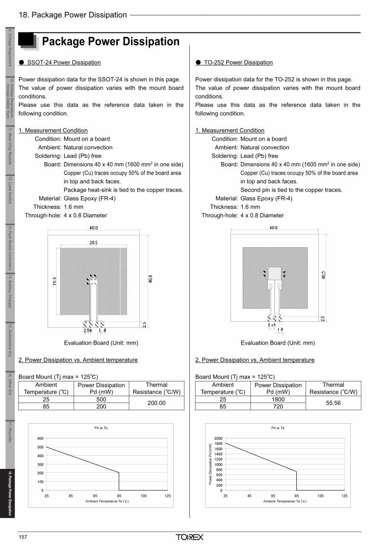
18. Package Power Dissipation _______________________________________________________________________
157
Package Power Dissipation SSOT-24 Power Dissipation Power dissipation data for the SSOT-24 is shown in this page. The value of power dissipation varies with the mount board conditions. Please use this data as the reference data taken in the following condition. 1. Measurement Condition Condition: Mount on a board Ambient: Natural convection Soldering: Lead (Pb) free Board: Dimensions 40 x 40 mm (1600 mm2 in one side) Copper (Cu) traces occupy 50% of the board area in top and back faces. Package heat-sink is tied to the copper traces. Material: Glass Epoxy (FR-4) Thickness: 1.6 mm Through-hole: 4 x 0.8 Diameter
Evaluation Board (Unit: mm) 2. Power Dissipation vs. Ambient temperature Board Mount (Tj max = 125)
Ambient Temperature ()
Power Dissipation Pd (mW)
Thermal Resistance (/W)
25 500 200.00 85 200
TO-252 Power Dissipation Power dissipation data for the TO-252 is shown in this page. The value of power dissipation varies with the mount board conditions. Please use this data as the reference data taken in the following condition. 1. Measurement Condition Condition: Mount on a board Ambient: Natural convection Soldering: Lead (Pb) free Board: Dimensions 40 x 40 mm (1600 mm2 in one side) Copper (Cu) traces occupy 50% of the board area in top and back faces. Second pin is tied to the copper traces. Material: Glass Epoxy (FR-4) Thickness: 1.6 mm Through-hole: 4 x 0.8 Diameter
Evaluation Board (Unit: mm) 2. Power Dissipation vs. Ambient temperature Board Mount (Tj max = 125)
Ambient Temperature ()
Power Dissipation Pd (mW)
Thermal Resistance (/W)
25 1800 55.56 85 720
Pd vs Ta
0
100
200
300
400
500
600
25 45 65 85 105 125
Ambient Temperature Ta ()
Pd vs Ta
0
200
400
600800
1000
1200
1400
1600
1800
2000
25 45 65 85 105 125
Ambient Temperature Ta ()
Pow
er D
issi
patio
n P
d (m
W)
_______________________________________________________________________________________________________
158
Package Power Dissipation USP-2B01 Power Dissipation Power dissipation data for the USP-2B01 is shown in this page. The value of power dissipation varies with the mount board conditions. Please use this data as the reference data taken in the following condition. 1. Measurement Condition Condition : Mount on a board Ambient : Natural convection Soldering : Lead (Pb) free Board : Dimensions 114.3mm×76.2mm Copper (Cu) traces occupy 74.2mm x 74.2mm
of the board area in back faces. Material : Glass Epoxy (FR-4) Thickness : 1.6mm 2. Power Dissipation vs. Ambient temperature Board Mount (Tj max = 125)
Ambient Temperature ()
Power Dissipation Pd (mW)
Thermal Resistance (/W)
25 100 1000.00 85 40
Board Mount (Tj max = 150)
Ambient Temperature ()
Power Dissipation Pd (mW)
Thermal Resistance (/W)
25 125 1000.00 85 65
150 0
USP-2B02 Power Dissipation Power dissipation data for the USP-2B02 is shown in this page. The value of power dissipation varies with the mount board conditions. Please use this data as the reference data taken in the following condition. 1. Measurement Condition Condition : Mount on a board Ambient : Natural convection Soldering : Lead (Pb) free Board : Dimensions 114.3mm×76.2mm Copper (Cu) traces occupy 74.2mm x 74.2mm
of the board area in back faces. Material : Glass Epoxy (FR-4) Thickness : 1.6mm 2. Power Dissipation vs. Ambient temperature Board Mount (Tj max = 125)
Ambient Temperature ()
Power Dissipation Pd (mW)
Thermal Resistance (/W)
25 110 909.09 85 44 Board Mount (Tj max = 150)
Ambient Temperature ()
Power Dissipation Pd (mW)
Thermal Resistance (/W)
25 137.5 862.07 85 71.5
150 0
11.Multi C
hip Module
10. Voltage Regulators
Voltage Detect Type
9. Voltage Regulators
12.Load Switch
13. Push Button Controllers14.B
attery Charger
15.Autom
otive ICs
16.Other IC
s17. D
iscrete18.Package Power Dissipation18.Package Power Dissipation
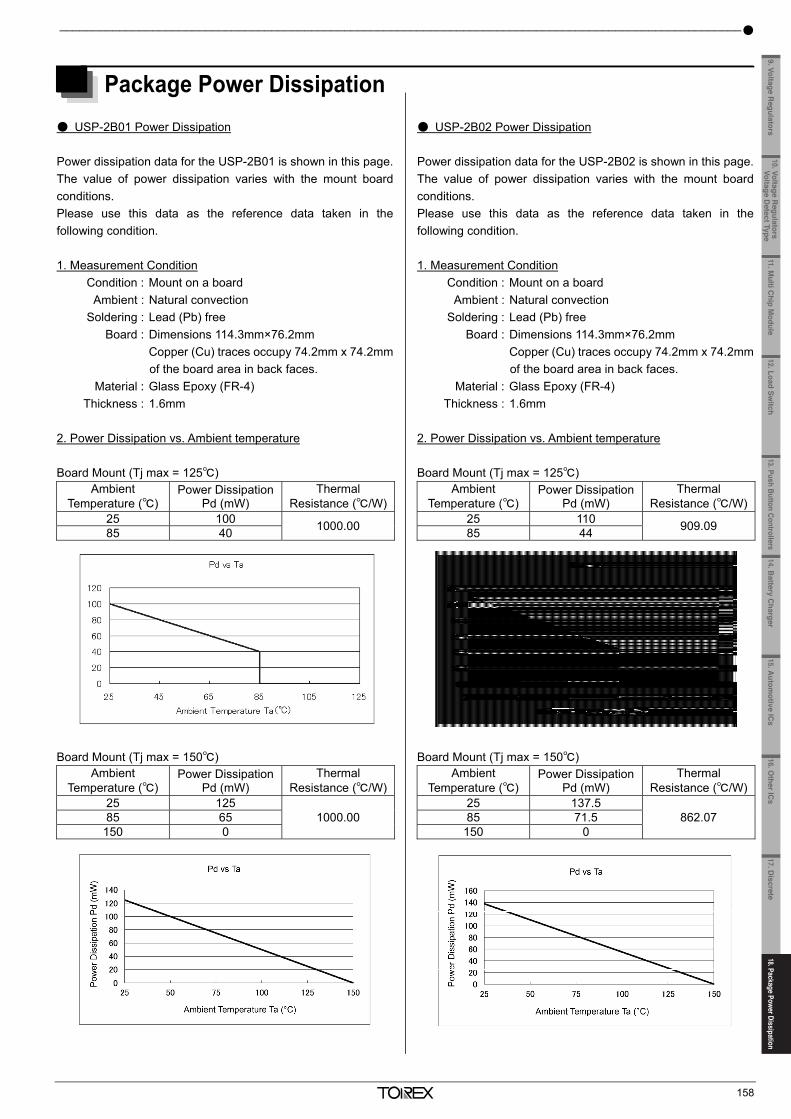
18. Package Power Dissipation _______________________________________________________________________
157
Package Power Dissipation SSOT-24 Power Dissipation Power dissipation data for the SSOT-24 is shown in this page. The value of power dissipation varies with the mount board conditions. Please use this data as the reference data taken in the following condition. 1. Measurement Condition Condition: Mount on a board Ambient: Natural convection Soldering: Lead (Pb) free Board: Dimensions 40 x 40 mm (1600 mm2 in one side) Copper (Cu) traces occupy 50% of the board area in top and back faces. Package heat-sink is tied to the copper traces. Material: Glass Epoxy (FR-4) Thickness: 1.6 mm Through-hole: 4 x 0.8 Diameter
Evaluation Board (Unit: mm) 2. Power Dissipation vs. Ambient temperature Board Mount (Tj max = 125)
Ambient Temperature ()
Power Dissipation Pd (mW)
Thermal Resistance (/W)
25 500 200.00 85 200
TO-252 Power Dissipation Power dissipation data for the TO-252 is shown in this page. The value of power dissipation varies with the mount board conditions. Please use this data as the reference data taken in the following condition. 1. Measurement Condition Condition: Mount on a board Ambient: Natural convection Soldering: Lead (Pb) free Board: Dimensions 40 x 40 mm (1600 mm2 in one side) Copper (Cu) traces occupy 50% of the board area in top and back faces. Second pin is tied to the copper traces. Material: Glass Epoxy (FR-4) Thickness: 1.6 mm Through-hole: 4 x 0.8 Diameter
Evaluation Board (Unit: mm) 2. Power Dissipation vs. Ambient temperature Board Mount (Tj max = 125)
Ambient Temperature ()
Power Dissipation Pd (mW)
Thermal Resistance (/W)
25 1800 55.56 85 720
Pd vs Ta
0
100
200
300
400
500
600
25 45 65 85 105 125
Ambient Temperature Ta ()
Pd vs Ta
0
200
400
600800
1000
1200
1400
1600
1800
2000
25 45 65 85 105 125
Ambient Temperature Ta ()
Pow
er D
issi
patio
n P
d (m
W)
_______________________________________________________________________________________________________
158
Package Power Dissipation USP-2B01 Power Dissipation Power dissipation data for the USP-2B01 is shown in this page. The value of power dissipation varies with the mount board conditions. Please use this data as the reference data taken in the following condition. 1. Measurement Condition Condition : Mount on a board Ambient : Natural convection Soldering : Lead (Pb) free Board : Dimensions 114.3mm×76.2mm Copper (Cu) traces occupy 74.2mm x 74.2mm
of the board area in back faces. Material : Glass Epoxy (FR-4) Thickness : 1.6mm 2. Power Dissipation vs. Ambient temperature Board Mount (Tj max = 125)
Ambient Temperature ()
Power Dissipation Pd (mW)
Thermal Resistance (/W)
25 100 1000.00 85 40
Board Mount (Tj max = 150)
Ambient Temperature ()
Power Dissipation Pd (mW)
Thermal Resistance (/W)
25 125 1000.00 85 65
150 0
USP-2B02 Power Dissipation Power dissipation data for the USP-2B02 is shown in this page. The value of power dissipation varies with the mount board conditions. Please use this data as the reference data taken in the following condition. 1. Measurement Condition Condition : Mount on a board Ambient : Natural convection Soldering : Lead (Pb) free Board : Dimensions 114.3mm×76.2mm Copper (Cu) traces occupy 74.2mm x 74.2mm
of the board area in back faces. Material : Glass Epoxy (FR-4) Thickness : 1.6mm 2. Power Dissipation vs. Ambient temperature Board Mount (Tj max = 125)
Ambient Temperature ()
Power Dissipation Pd (mW)
Thermal Resistance (/W)
25 110 909.09 85 44 Board Mount (Tj max = 150)
Ambient Temperature ()
Power Dissipation Pd (mW)
Thermal Resistance (/W)
25 137.5 862.07 85 71.5
150 0
11.Multi C
hip Module
10. Voltage Regulators
Voltage Detect Type
9. Voltage Regulators
12.Load Switch
13. Push Button Controllers14.B
attery Charger
15.Autom
otive ICs
16.Other IC
s17. D
iscrete18.Package Power Dissipation
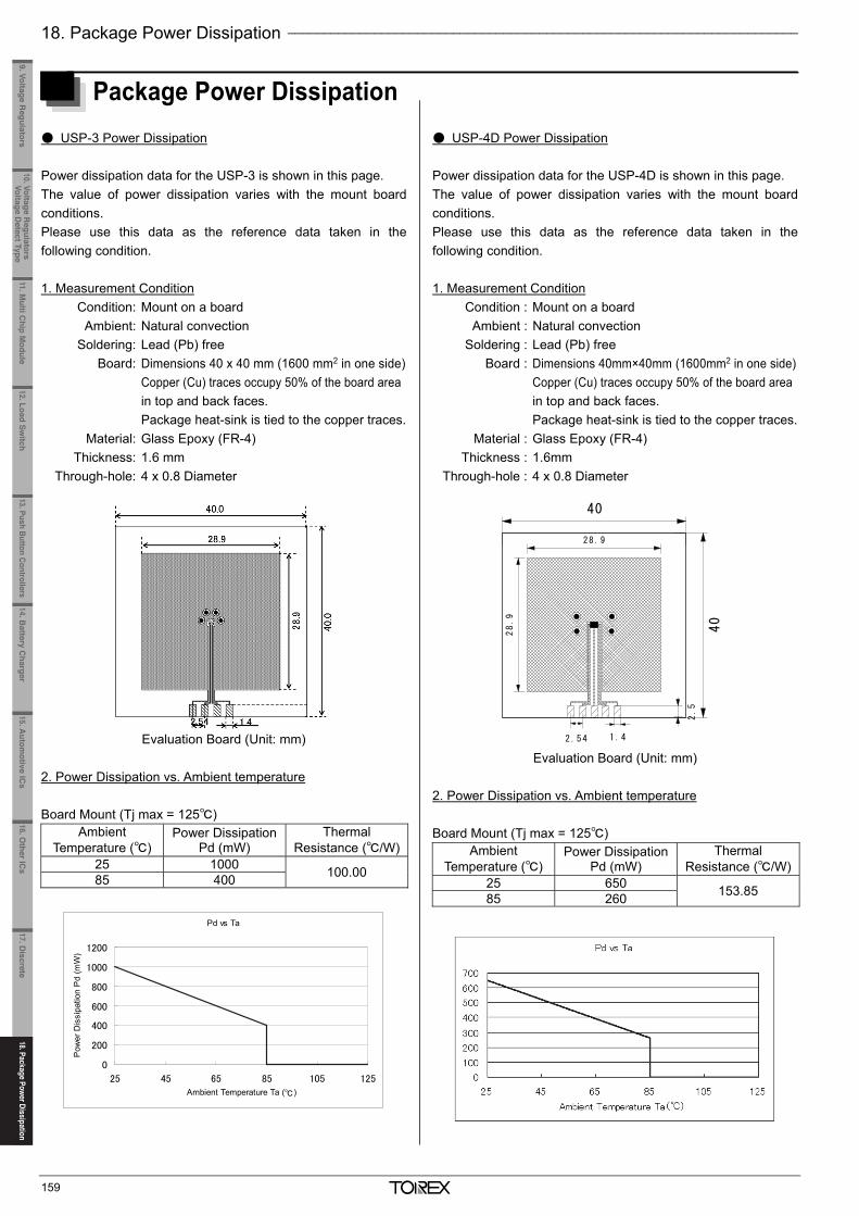
18. Package Power Dissipation _______________________________________________________________________
159
Package Power Dissipation USP-3 Power Dissipation Power dissipation data for the USP-3 is shown in this page. The value of power dissipation varies with the mount board conditions. Please use this data as the reference data taken in the following condition. 1. Measurement Condition Condition: Mount on a board Ambient: Natural convection Soldering: Lead (Pb) free Board: Dimensions 40 x 40 mm (1600 mm2 in one side) Copper (Cu) traces occupy 50% of the board area in top and back faces. Package heat-sink is tied to the copper traces. Material: Glass Epoxy (FR-4) Thickness: 1.6 mm Through-hole: 4 x 0.8 Diameter
Evaluation Board (Unit: mm) 2. Power Dissipation vs. Ambient temperature Board Mount (Tj max = 125)
Ambient Temperature ()
Power Dissipation Pd (mW)
Thermal Resistance (/W)
25 1000 100.00 85 400
USP-4D Power Dissipation Power dissipation data for the USP-4D is shown in this page. The value of power dissipation varies with the mount board conditions. Please use this data as the reference data taken in the following condition. 1. Measurement Condition Condition : Mount on a board Ambient : Natural convection Soldering : Lead (Pb) free Board : Dimensions 40mm×40mm (1600mm2 in one side) Copper (Cu) traces occupy 50% of the board area in top and back faces. Package heat-sink is tied to the copper traces. Material : Glass Epoxy (FR-4) Thickness : 1.6mm Through-hole : 4 x 0.8 Diameter
Evaluation Board (Unit: mm) 2. Power Dissipation vs. Ambient temperature Board Mount (Tj max = 125)
Ambient Temperature ()
Power Dissipation Pd (mW)
Thermal Resistance (/W)
25 650 153.85 85 260
Pd vs Ta
0
200
400
600
800
1000
1200
25 45 65 85 105 125Ambient Temperature Ta ()
Pow
er D
issi
patio
n P
d (m
W)
2.54 1.4
28.9
28.9
2.5
40
40
_______________________________________________________________________________________________________
160
Package Power Dissipation USP-6B06 Power Dissipation Power dissipation data for the USP-6B06 is shown in this page. The value of power dissipation varies with the mount board conditions. Please use this data as the reference data taken in the following condition. 1. Measurement Condition Condition: Mount on a board Ambient: Natural convection Soldering: Lead (Pb) free Board: Dimensions 40 x 40 mm (1600 mm2 in one
side) Copper (Cu) traces occupy 50% of the board
area in top and back faces Package heat-sink is tied to the copper traces Material: Glass Epoxy (FR-4) Thickness: 1.6 mm Through-hole: 4 x 0.8 Diameter
Evaluation Board (Unit: mm) 2. Power Dissipation vs. Ambient temperature Board Mount (Tj max = 125)
Ambient Temperature ()
Power Dissipation Pd (mW)
Thermal Resistance (/W)
25 900 111.11 85 360
USP-6C, USP-6B, USP-6EL, and USP-4 Power Dissipation Power dissipation data for the USP-6C, USP-6B, USP-6EL, and USP-4 is shown in this page. The value of power dissipation varies with the mount board conditions. Please use this data as the reference data taken in the following condition. 1. Measurement Condition Condition: Mount on a board Ambient: Natural convection Soldering: Lead (Pb) free Board: Dimensions 40 x 40 mm (1600 mm2 in one side) Copper (Cu) traces occupy 50% of the board area in top and back faces. Package heat-sink is tied to the copper traces. Material: Glass Epoxy (FR-4) Thickness: 1.6mm Through-hole: 4 x 0.8 Diameter
Evaluation Board (Unit: mm) 2. Power Dissipation vs. Ambient temperature Board Mount (Tj max = 125)
Ambient Temperature ()
Power Dissipation Pd (mW)
Thermal Resistance (/W)
25 1000 100.00 85 400
3. USP-6C Power Dissipation vs. Ambient temperature (105) Board Mount (Tj max = 125)
Ambient Temperature ()
Power Dissipation Pd (mW)
Thermal Resistance (/W)
25 1000 100.00 105 200
Pd vs. Ta
0
200
400
600
800
1000
1200
25 45 65 85 105 125
Ambient Temperature: Ta()
Pow
er D
issp
atio
n: P
d(m
W)
Pow
er D
issi
patio
n: P
d (m
W)
Pd vs Ta
0
200
400
600
800
1000
1200
25 45 65 85 105 125
Ambient Temperature Ta ()
Pow
er
Dis
sipa
tion P
d (m
W)
Ambient Temperature Ta (°C)
Pow
er D
issi
patio
n P
d (m
W)
Pd vs Ta
40.0
28.9
1.42.54
11.Multi C
hip Module
10. Voltage Regulators
Voltage Detect Type
9. Voltage Regulators
12.Load Switch
13. Push Button Controllers14.B
attery Charger
15.Autom
otive ICs
16.Other IC
s17. D
iscrete18.Package Power Dissipation18.Package Power Dissipation
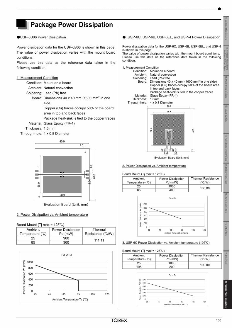
18. Package Power Dissipation _______________________________________________________________________
159
Package Power Dissipation USP-3 Power Dissipation Power dissipation data for the USP-3 is shown in this page. The value of power dissipation varies with the mount board conditions. Please use this data as the reference data taken in the following condition. 1. Measurement Condition Condition: Mount on a board Ambient: Natural convection Soldering: Lead (Pb) free Board: Dimensions 40 x 40 mm (1600 mm2 in one side) Copper (Cu) traces occupy 50% of the board area in top and back faces. Package heat-sink is tied to the copper traces. Material: Glass Epoxy (FR-4) Thickness: 1.6 mm Through-hole: 4 x 0.8 Diameter
Evaluation Board (Unit: mm) 2. Power Dissipation vs. Ambient temperature Board Mount (Tj max = 125)
Ambient Temperature ()
Power Dissipation Pd (mW)
Thermal Resistance (/W)
25 1000 100.00 85 400
USP-4D Power Dissipation Power dissipation data for the USP-4D is shown in this page. The value of power dissipation varies with the mount board conditions. Please use this data as the reference data taken in the following condition. 1. Measurement Condition Condition : Mount on a board Ambient : Natural convection Soldering : Lead (Pb) free Board : Dimensions 40mm×40mm (1600mm2 in one side) Copper (Cu) traces occupy 50% of the board area in top and back faces. Package heat-sink is tied to the copper traces. Material : Glass Epoxy (FR-4) Thickness : 1.6mm Through-hole : 4 x 0.8 Diameter
Evaluation Board (Unit: mm) 2. Power Dissipation vs. Ambient temperature Board Mount (Tj max = 125)
Ambient Temperature ()
Power Dissipation Pd (mW)
Thermal Resistance (/W)
25 650 153.85 85 260
Pd vs Ta
0
200
400
600
800
1000
1200
25 45 65 85 105 125Ambient Temperature Ta ()
Pow
er D
issi
patio
n P
d (m
W)
2.54 1.4
28.9
28.9
2.5
40
40
_______________________________________________________________________________________________________
160
Package Power Dissipation USP-6B06 Power Dissipation Power dissipation data for the USP-6B06 is shown in this page. The value of power dissipation varies with the mount board conditions. Please use this data as the reference data taken in the following condition. 1. Measurement Condition Condition: Mount on a board Ambient: Natural convection Soldering: Lead (Pb) free Board: Dimensions 40 x 40 mm (1600 mm2 in one
side) Copper (Cu) traces occupy 50% of the board
area in top and back faces Package heat-sink is tied to the copper traces Material: Glass Epoxy (FR-4) Thickness: 1.6 mm Through-hole: 4 x 0.8 Diameter
Evaluation Board (Unit: mm) 2. Power Dissipation vs. Ambient temperature Board Mount (Tj max = 125)
Ambient Temperature ()
Power Dissipation Pd (mW)
Thermal Resistance (/W)
25 900 111.11 85 360
USP-6C, USP-6B, USP-6EL, and USP-4 Power Dissipation Power dissipation data for the USP-6C, USP-6B, USP-6EL, and USP-4 is shown in this page. The value of power dissipation varies with the mount board conditions. Please use this data as the reference data taken in the following condition. 1. Measurement Condition Condition: Mount on a board Ambient: Natural convection Soldering: Lead (Pb) free Board: Dimensions 40 x 40 mm (1600 mm2 in one side) Copper (Cu) traces occupy 50% of the board area in top and back faces. Package heat-sink is tied to the copper traces. Material: Glass Epoxy (FR-4) Thickness: 1.6mm Through-hole: 4 x 0.8 Diameter
Evaluation Board (Unit: mm) 2. Power Dissipation vs. Ambient temperature Board Mount (Tj max = 125)
Ambient Temperature ()
Power Dissipation Pd (mW)
Thermal Resistance (/W)
25 1000 100.00 85 400
3. USP-6C Power Dissipation vs. Ambient temperature (105) Board Mount (Tj max = 125)
Ambient Temperature ()
Power Dissipation Pd (mW)
Thermal Resistance (/W)
25 1000 100.00 105 200
Pd vs. Ta
0
200
400
600
800
1000
1200
25 45 65 85 105 125
Ambient Temperature: Ta()
Pow
er D
issp
atio
n: P
d(m
W)
Pow
er D
issi
patio
n: P
d (m
W)
Pd vs Ta
0
200
400
600
800
1000
1200
25 45 65 85 105 125
Ambient Temperature Ta ()
Pow
er
Dis
sipa
tion P
d (m
W)
Ambient Temperature Ta (°C)
Pow
er D
issi
patio
n P
d (m
W)
Pd vs Ta
40.0
28.9
1.42.54
11.Multi C
hip Module
10. Voltage Regulators
Voltage Detect Type
9. Voltage Regulators
12.Load Switch
13. Push Button Controllers14.B
attery Charger
15.Autom
otive ICs
16.Other IC
s17. D
iscrete18.Package Power Dissipation
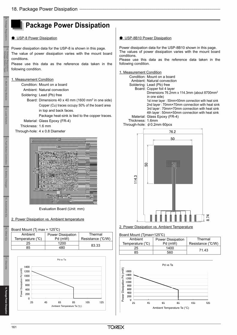
18. Package Power Dissipation _______________________________________________________________________
161
Package Power Dissipation USP-8 Power Dissipation Power dissipation data for the USP-8 is shown in this page. The value of power dissipation varies with the mount board conditions. Please use this data as the reference data taken in the following condition. 1. Measurement Condition Condition: Mount on a board Ambient: Natural convection Soldering: Lead (Pb) free Board: Dimensions 40 x 40 mm (1600 mm2 in one side) Copper (Cu) traces occupy 50% of the board area in top and back faces. Package heat-sink is tied to the copper traces. Material: Glass Epoxy (FR-4) Thickness: 1.6 mm Through-hole: 4 x 0.8 Diameter
Evaluation Board (Unit: mm) 2. Power Dissipation vs. Ambient temperature Board Mount (Tj max = 125)
Ambient Temperature ()
Power Dissipation Pd (mW)
Thermal Resistance (/W)
25 1200 83.33 85 480
USP-8B10 Power Dissipation Power dissipation data for the USP-8B10 shown in this page. The values of power dissipation varies with the mount board conditions. Please use this data as the reference data taken in the following condition. 1. Measurement Condition Condition: Mount on a board Ambient: Natural convection Soldering: Lead (Pb) free Board: Copper foil 4 layer Dimensions 76.2mm x 114.3mm (about 8700mm2
in one side) 1st inner layer : 50mm×50mm connection with heat sink 2nd layer : 70mm×70mm connection with heat sink 3rd layer : 70mm×70mm connection with heat sink 4th layer : 50mm×50mm connection with heat sink Material: Glass Epoxy (FR-4) Thickness: 1.6mm Through-hole: φ0.2mm 60pcs 2. Power Dissipation vs. Ambient Temperature Board Mount (Tjmax=125)
Ambient Temperature ()
Power Dissipation Pd (mW)
Thermal Resistance (/W)
25 1400 71.43 85 560
Pd vs Ta
0
200
400
600
800
1000
1200
1400
25 45 65 85 105 125Ambient Temperature Ta ()
Pow
er D
issi
patio
n P
d (m
W)
76.2 114.3
50
50
8.7
4
Ambient Temperature Ta (°C)
Pow
er D
issi
patio
n P
d (m
W)
Pd vs Ta
_______________________________________________________________________________________________________
162
Package Power Dissipation USP-9B01 Power Dissipation Power dissipation data for the USP-9B01 is shown in this page. Please use this data as the reference data taken in the following condition. 1. Measurement Condition Condition: Mount on a board Ambient: Natural convection Soldering: Lead (Pb) free Board: Dimensions 40mm×40mm (1600mm2 in one side) Copper (Cu) traces occupy 50% of the board area in top and back faces. Package hear-sink is tied to the copper traces. Material: Glass Epoxy (FR-4) Thickness: 1.6mm Through-hole: 4 x 0.8 Diameter
Evaluation Board (Unit: mm) 2. Power Dissipation vs. Ambient Temperature Board Mount (Tjmax=125)
Ambient Temperature ()
Power Dissipation Pd (mW)
Thermal Resistance (/W)
25 1200 83.33 85 480
USP-10B Power Dissipation Power dissipation data for the USP-10B is shown in this page. The value of power dissipation varies with the mount board conditions. Please use this data as the reference data taken in the following condition. 1. Measurement Condition Condition: Mount on a board Ambient: Natural convection Soldering: Lead (Pb) free Board: 40 x 40 mm (1600 mm2 in one side) Inner two metal layers, no large metal area in
the front and back. Copper Area: 1st Inner metal layer about 50% 4th Inner metal layer about 50% Each Heatsink back metal is connected to the
inner layers respectively. 2nd and 3rd Inner metal layer does not exist. Material: Glass Epoxy (FR-4) Thickness: 1.6mm Through-hole: 4 x 0.8 Diameter
Evaluation Board (Unit: mm) 2. Power Dissipation vs. Ambient temperature Board Mount (Tj max = 125)
Ambient Temperature ()
Power Dissipation Pd (mW)
Thermal Resistance (/W)
25 1000 100.00 85 400
Pd vs Ta
0
200
400
600
800
1000
1200
1400
25 45 65 85 105 125
Ambient Temperature: Ta ()
Pow
er D
issi
patio
n: P
d (m
W)
Pd-Ta特性グラフ
0
200
400
600
800
1000
1200
25 45 65 85 105 125
周囲温度Ta()
許容
損失
Pd(
mW
)
2.5
1.4
40.0
28.9
28.9
40.0
2.54
Pd vs. Ta
Ambient Temperature: Ta ()
Pow
er D
issi
patio
n: P
d (m
W)
11.Multi C
hip Module
10. Voltage Regulators
Voltage Detect Type
9. Voltage Regulators
12.Load Switch
13. Push Button Controllers14.B
attery Charger
15.Autom
otive ICs
16.Other IC
s17. D
iscrete18.Package Power Dissipation18.Package Power Dissipation
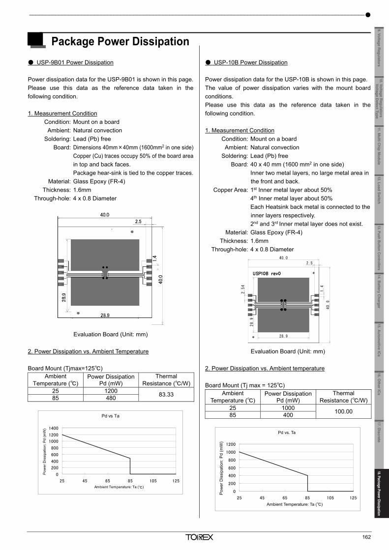
18. Package Power Dissipation _______________________________________________________________________
161
Package Power Dissipation USP-8 Power Dissipation Power dissipation data for the USP-8 is shown in this page. The value of power dissipation varies with the mount board conditions. Please use this data as the reference data taken in the following condition. 1. Measurement Condition Condition: Mount on a board Ambient: Natural convection Soldering: Lead (Pb) free Board: Dimensions 40 x 40 mm (1600 mm2 in one side) Copper (Cu) traces occupy 50% of the board area in top and back faces. Package heat-sink is tied to the copper traces. Material: Glass Epoxy (FR-4) Thickness: 1.6 mm Through-hole: 4 x 0.8 Diameter
Evaluation Board (Unit: mm) 2. Power Dissipation vs. Ambient temperature Board Mount (Tj max = 125)
Ambient Temperature ()
Power Dissipation Pd (mW)
Thermal Resistance (/W)
25 1200 83.33 85 480
USP-8B10 Power Dissipation Power dissipation data for the USP-8B10 shown in this page. The values of power dissipation varies with the mount board conditions. Please use this data as the reference data taken in the following condition. 1. Measurement Condition Condition: Mount on a board Ambient: Natural convection Soldering: Lead (Pb) free Board: Copper foil 4 layer Dimensions 76.2mm x 114.3mm (about 8700mm2
in one side) 1st inner layer : 50mm×50mm connection with heat sink 2nd layer : 70mm×70mm connection with heat sink 3rd layer : 70mm×70mm connection with heat sink 4th layer : 50mm×50mm connection with heat sink Material: Glass Epoxy (FR-4) Thickness: 1.6mm Through-hole: φ0.2mm 60pcs 2. Power Dissipation vs. Ambient Temperature Board Mount (Tjmax=125)
Ambient Temperature ()
Power Dissipation Pd (mW)
Thermal Resistance (/W)
25 1400 71.43 85 560
Pd vs Ta
0
200
400
600
800
1000
1200
1400
25 45 65 85 105 125Ambient Temperature Ta ()
Pow
er D
issi
patio
n P
d (m
W)
76.2
114.3
50
50
8.7
4
Ambient Temperature Ta (°C)
Pow
er D
issi
patio
n P
d (m
W)
Pd vs Ta
_______________________________________________________________________________________________________
162
Package Power Dissipation USP-9B01 Power Dissipation Power dissipation data for the USP-9B01 is shown in this page. Please use this data as the reference data taken in the following condition. 1. Measurement Condition Condition: Mount on a board Ambient: Natural convection Soldering: Lead (Pb) free Board: Dimensions 40mm×40mm (1600mm2 in one side) Copper (Cu) traces occupy 50% of the board area in top and back faces. Package hear-sink is tied to the copper traces. Material: Glass Epoxy (FR-4) Thickness: 1.6mm Through-hole: 4 x 0.8 Diameter
Evaluation Board (Unit: mm) 2. Power Dissipation vs. Ambient Temperature Board Mount (Tjmax=125)
Ambient Temperature ()
Power Dissipation Pd (mW)
Thermal Resistance (/W)
25 1200 83.33 85 480
USP-10B Power Dissipation Power dissipation data for the USP-10B is shown in this page. The value of power dissipation varies with the mount board conditions. Please use this data as the reference data taken in the following condition. 1. Measurement Condition Condition: Mount on a board Ambient: Natural convection Soldering: Lead (Pb) free Board: 40 x 40 mm (1600 mm2 in one side) Inner two metal layers, no large metal area in
the front and back. Copper Area: 1st Inner metal layer about 50% 4th Inner metal layer about 50% Each Heatsink back metal is connected to the
inner layers respectively. 2nd and 3rd Inner metal layer does not exist. Material: Glass Epoxy (FR-4) Thickness: 1.6mm Through-hole: 4 x 0.8 Diameter
Evaluation Board (Unit: mm) 2. Power Dissipation vs. Ambient temperature Board Mount (Tj max = 125)
Ambient Temperature ()
Power Dissipation Pd (mW)
Thermal Resistance (/W)
25 1000 100.00 85 400
Pd vs Ta
0
200
400
600
800
1000
1200
1400
25 45 65 85 105 125
Ambient Temperature: Ta ()
Pow
er D
issi
patio
n: P
d (m
W)
Pd-Ta特性グラフ
0
200
400
600
800
1000
1200
25 45 65 85 105 125
周囲温度Ta()
許容
損失
Pd(
mW
)
2.5
1.4
40.0
28.9
28.9
40.0
2.54
Pd vs. Ta
Ambient Temperature: Ta ()
Pow
er D
issi
patio
n: P
d (m
W)
11.Multi C
hip Module
10. Voltage Regulators
Voltage Detect Type
9. Voltage Regulators
12.Load Switch
13. Push Button Controllers14.B
attery Charger
15.Autom
otive ICs
16.Other IC
s17. D
iscrete18.Package Power Dissipation
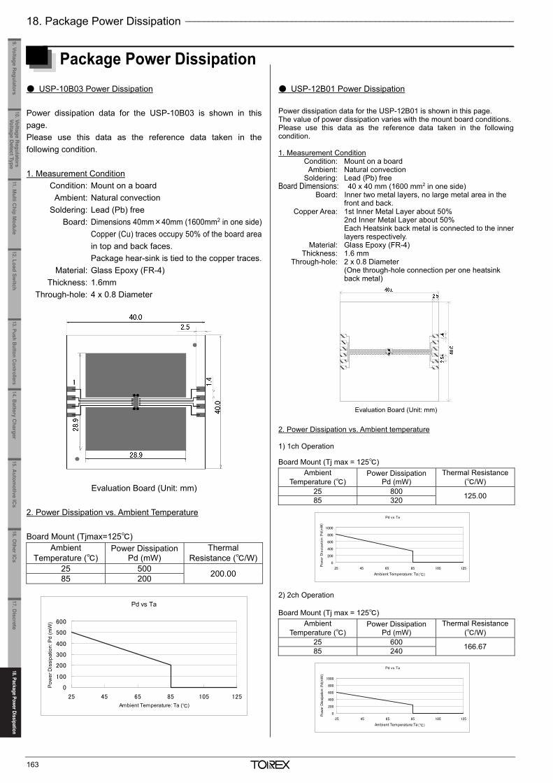
18. Package Power Dissipation _______________________________________________________________________
163
Package Power Dissipation USP-10B03 Power Dissipation Power dissipation data for the USP-10B03 is shown in this page. Please use this data as the reference data taken in the following condition. 1. Measurement Condition Condition: Mount on a board Ambient: Natural convection Soldering: Lead (Pb) free Board: Dimensions 40mm×40mm (1600mm2 in one side) Copper (Cu) traces occupy 50% of the board area in top and back faces. Package hear-sink is tied to the copper traces. Material: Glass Epoxy (FR-4) Thickness: 1.6mm Through-hole: 4 x 0.8 Diameter
Evaluation Board (Unit: mm) 2. Power Dissipation vs. Ambient Temperature Board Mount (Tjmax=125)
Ambient Temperature ()
Power Dissipation Pd (mW)
Thermal Resistance (/W)
25 500 200.00 85 200
USP-12B01 Power Dissipation Power dissipation data for the USP-12B01 is shown in this page. The value of power dissipation varies with the mount board conditions. Please use this data as the reference data taken in the following condition. 1. Measurement Condition Condition: Mount on a board Ambient: Natural convection Soldering: Lead (Pb) free Board Dimensions: 40 x 40 mm (1600 mm2 in one side) Board: Inner two metal layers, no large metal area in the
front and back. Copper Area: 1st Inner Metal Layer about 50% 2nd Inner Metal Layer about 50% Each Heatsink back metal is connected to the inner
layers respectively. Material: Glass Epoxy (FR-4) Thickness: 1.6 mm Through-hole: 2 x 0.8 Diameter (One through-hole connection per one heatsink
back metal)
Evaluation Board (Unit: mm) 2. Power Dissipation vs. Ambient temperature 1) 1ch Operation Board Mount (Tj max = 125)
Ambient Temperature ()
Power Dissipation Pd (mW)
Thermal Resistance (/W)
25 800 125.00 85 320
2) 2ch Operation Board Mount (Tj max = 125)
Ambient Temperature ()
Power Dissipation Pd (mW)
Thermal Resistance (/W)
25 600 166.67 85 240
Pd vs Ta
0
100
200
300
400
500
600
25 45 65 85 105 125
Ambient Temperature: Ta ()
Pow
er D
issi
patio
n: P
d (m
W)
Pd vs Ta
0
200
400
600
800
1000
25 45 65 85 105 125
Ambient Temperature: Ta()
Pow
er
Dis
sip
ation: Pd(m
W)
Pd vs Ta
0
200
400
600
800
1000
25 45 65 85 105 125
Ambient Temperature:Ta()
Pow
er D
issi
patio
n: P
d(m
W)
_______________________________________________________________________________________________________
164
Package Power Dissipation USPN-4 Power Dissipation Power dissipation data for the USPN-4 is shown in this page. The value of power dissipation varies with the mount board conditions. Please use this data as the reference data taken in the following condition. 1. Measurement Condition Condition: Mount on a board Ambient: Natural convection Soldering: Lead (Pb) free Board: Dimensions 40 x 40 mm (1600 mm2 in one side) Copper (Cu) traces occupy 50% of the front
and 50% of the back. The copper area is divided into four block, one
block is 12.5% of total. The USPN-4 package has for terminals. Each terminal connects one copper block in
the front and one in the back. Material: Glass Epoxy (FR-4) Thickness: 1.6 mm Through-hole: 4 x 0.8 Diameter
Evaluation Board (Unit: mm) 2. Power Dissipation vs. Ambient temperature Board Mount (Tj max = 125)
Ambient Temperature ()
Power Dissipation Pd (mW)
Thermal Resistance (/W)
25 600 166.67 85 240
USPN-4B02 Power Dissipation Power dissipation data for the USPN-4B02 is shown in this page. The value of power dissipation varies with the mount board conditions. Please use this data as the reference data taken in the following condition. 1. Measurement Condition Condition: Mount on a board Ambient: Natural convection Soldering: Lead (Pb) free Board: Dimensions 40 x 40 mm (1600 mm2 in one side) Copper (Cu) traces occupy 50% of the front
and 50% of the back. The copper area is divided into four block, one
block is 12.5% of total. The USPN-4 package has for terminals. Each terminal connects one copper block in
the front and one in the back. Material: Glass Epoxy (FR-4) Thickness: 1.6 mm Through-hole: 4 x 0.8 Diameter
Evaluation Board (Unit: mm) 2. Power Dissipation vs. Ambient temperature Board Mount (Tj max = 125)
Ambient Temperature ()
Power Dissipation Pd (mW)
Thermal Resistance (/W)
25 550 181.82 85 220
Pd vs Ta
0
100
200
300
400
500
600
700
25 45 65 85 105 125
Ambient Temperature: Ta()
Pow
er D
issi
patio
n: P
d(m
W)
Pd vs Ta
0
100
200
300
400
500
600
25 45 65 85 105 125
Ambient Temperature Ta ()
Pow
er D
issi
patio
n P
d (m
W)
40.0
2.5
41.4
28.9
11.Multi C
hip Module
10. Voltage Regulators
Voltage Detect Type
9. Voltage Regulators
12.Load Switch
13. Push Button Controllers14.B
attery Charger
15.Autom
otive ICs
16.Other IC
s17. D
iscrete18.Package Power Dissipation18.Package Power Dissipation
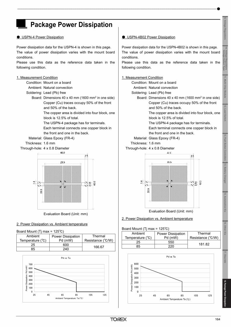
18. Package Power Dissipation _______________________________________________________________________
163
Package Power Dissipation USP-10B03 Power Dissipation Power dissipation data for the USP-10B03 is shown in this page. Please use this data as the reference data taken in the following condition. 1. Measurement Condition Condition: Mount on a board Ambient: Natural convection Soldering: Lead (Pb) free Board: Dimensions 40mm×40mm (1600mm2 in one side) Copper (Cu) traces occupy 50% of the board area in top and back faces. Package hear-sink is tied to the copper traces. Material: Glass Epoxy (FR-4) Thickness: 1.6mm Through-hole: 4 x 0.8 Diameter
Evaluation Board (Unit: mm) 2. Power Dissipation vs. Ambient Temperature Board Mount (Tjmax=125)
Ambient Temperature ()
Power Dissipation Pd (mW)
Thermal Resistance (/W)
25 500 200.00 85 200
USP-12B01 Power Dissipation Power dissipation data for the USP-12B01 is shown in this page. The value of power dissipation varies with the mount board conditions. Please use this data as the reference data taken in the following condition. 1. Measurement Condition Condition: Mount on a board Ambient: Natural convection Soldering: Lead (Pb) free Board Dimensions: 40 x 40 mm (1600 mm2 in one side) Board: Inner two metal layers, no large metal area in the
front and back. Copper Area: 1st Inner Metal Layer about 50% 2nd Inner Metal Layer about 50% Each Heatsink back metal is connected to the inner
layers respectively. Material: Glass Epoxy (FR-4) Thickness: 1.6 mm Through-hole: 2 x 0.8 Diameter (One through-hole connection per one heatsink
back metal)
Evaluation Board (Unit: mm) 2. Power Dissipation vs. Ambient temperature 1) 1ch Operation Board Mount (Tj max = 125)
Ambient Temperature ()
Power Dissipation Pd (mW)
Thermal Resistance (/W)
25 800 125.00 85 320
2) 2ch Operation Board Mount (Tj max = 125)
Ambient Temperature ()
Power Dissipation Pd (mW)
Thermal Resistance (/W)
25 600 166.67 85 240
Pd vs Ta
0
100
200
300
400
500
600
25 45 65 85 105 125
Ambient Temperature: Ta ()
Pow
er D
issi
patio
n: P
d (m
W)
Pd vs Ta
0
200
400
600
800
1000
25 45 65 85 105 125
Ambient Temperature: Ta()
Pow
er
Dis
sip
ation: Pd(m
W)
Pd vs Ta
0
200
400
600
800
1000
25 45 65 85 105 125
Ambient Temperature:Ta()
Pow
er D
issi
patio
n: P
d(m
W)
_______________________________________________________________________________________________________
164
Package Power Dissipation USPN-4 Power Dissipation Power dissipation data for the USPN-4 is shown in this page. The value of power dissipation varies with the mount board conditions. Please use this data as the reference data taken in the following condition. 1. Measurement Condition Condition: Mount on a board Ambient: Natural convection Soldering: Lead (Pb) free Board: Dimensions 40 x 40 mm (1600 mm2 in one side) Copper (Cu) traces occupy 50% of the front
and 50% of the back. The copper area is divided into four block, one
block is 12.5% of total. The USPN-4 package has for terminals. Each terminal connects one copper block in
the front and one in the back. Material: Glass Epoxy (FR-4) Thickness: 1.6 mm Through-hole: 4 x 0.8 Diameter
Evaluation Board (Unit: mm) 2. Power Dissipation vs. Ambient temperature Board Mount (Tj max = 125)
Ambient Temperature ()
Power Dissipation Pd (mW)
Thermal Resistance (/W)
25 600 166.67 85 240
USPN-4B02 Power Dissipation Power dissipation data for the USPN-4B02 is shown in this page. The value of power dissipation varies with the mount board conditions. Please use this data as the reference data taken in the following condition. 1. Measurement Condition Condition: Mount on a board Ambient: Natural convection Soldering: Lead (Pb) free Board: Dimensions 40 x 40 mm (1600 mm2 in one side) Copper (Cu) traces occupy 50% of the front
and 50% of the back. The copper area is divided into four block, one
block is 12.5% of total. The USPN-4 package has for terminals. Each terminal connects one copper block in
the front and one in the back. Material: Glass Epoxy (FR-4) Thickness: 1.6 mm Through-hole: 4 x 0.8 Diameter
Evaluation Board (Unit: mm) 2. Power Dissipation vs. Ambient temperature Board Mount (Tj max = 125)
Ambient Temperature ()
Power Dissipation Pd (mW)
Thermal Resistance (/W)
25 550 181.82 85 220
Pd vs Ta
0
100
200
300
400
500
600
700
25 45 65 85 105 125
Ambient Temperature: Ta()
Pow
er D
issi
patio
n: P
d(m
W)
Pd vs Ta
0
100
200
300
400
500
600
25 45 65 85 105 125
Ambient Temperature Ta ()
Pow
er D
issi
patio
n P
d (m
W)
40.0
2.5
41.4
28.9
11.Multi C
hip Module
10. Voltage Regulators
Voltage Detect Type
9. Voltage Regulators
12.Load Switch
13. Push Button Controllers14.B
attery Charger
15.Autom
otive ICs
16.Other IC
s17. D
iscrete18.Package Power Dissipation
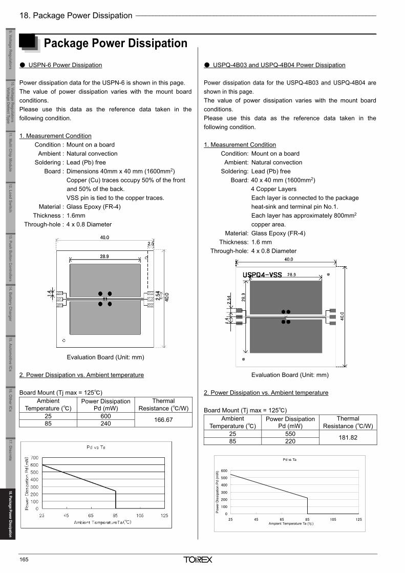
18. Package Power Dissipation _______________________________________________________________________
165
Package Power Dissipation USPN-6 Power Dissipation Power dissipation data for the USPN-6 is shown in this page. The value of power dissipation varies with the mount board conditions. Please use this data as the reference data taken in the following condition. 1. Measurement Condition Condition : Mount on a board Ambient : Natural convection Soldering : Lead (Pb) free Board : Dimensions 40mm x 40 mm (1600mm2) Copper (Cu) traces occupy 50% of the front
and 50% of the back. VSS pin is tied to the copper traces. Material : Glass Epoxy (FR-4) Thickness : 1.6mm Through-hole : 4 x 0.8 Diameter
Evaluation Board (Unit: mm) 2. Power Dissipation vs. Ambient temperature Board Mount (Tj max = 125)
Ambient Temperature ()
Power Dissipation Pd (mW)
Thermal Resistance (/W)
25 600 166.67 85 240
USPQ-4B03 and USPQ-4B04 Power Dissipation Power dissipation data for the USPQ-4B03 and USPQ-4B04 are shown in this page. The value of power dissipation varies with the mount board conditions. Please use this data as the reference data taken in the following condition. 1. Measurement Condition Condition: Mount on a board Ambient: Natural convection Soldering: Lead (Pb) free Board: 40 x 40 mm (1600mm2) 4 Copper Layers Each layer is connected to the package
heat-sink and terminal pin No.1. Each layer has approximately 800mm2
copper area. Material: Glass Epoxy (FR-4) Thickness: 1.6 mm Through-hole: 4 x 0.8 Diameter
Evaluation Board (Unit: mm) 2. Power Dissipation vs. Ambient temperature Board Mount (Tj max = 125)
Ambient Temperature ()
Power Dissipation Pd (mW)
Thermal Resistance (/W)
25 550 181.82 85 220
Pd vs Ta
0
100
200
300
400
500
600
25 45 65 85 105 125Ampient Temperature Ta ()
Pow
er D
issi
patio
n P
d (m
W)
_______________________________________________________________________________________________________
166
Package Power Dissipation WLP Power Dissipation Power dissipation data for the WLP is shown in this page. The value of power dissipation varies with the mount board conditions. Please use this data as the reference data taken in the following condition. 1. Measurement Condition Condition: Mount on a board Ambient: Natural convection Soldering: Lead (Pb) free Board: 40mm×40mm(1600mm2 in one side) Metal Area: 1st Metal Layer about 50% 2nd Inner Metal Layer about 50% 3rd Inner Metal Layer about 50% 4th Metal Layer about 50% 4 separations is each layer connected to each pin Material: Glass Epoxy(FR-4) Thickness: 1.6mm Through-hole: 4 x 0.8 Diameter
Evaluation Board (Unit: mm) 2. Power Dissipation vs. Ambient temperature Board Mount (Tj max = 125)
Ambient Temperature ()
Power Dissipation Pd (mW)
Thermal Resistance (/W)
25 750 133.33 85 300
2.54
1.4
40.0
40.0
2.5
28.9
28.9
Pd vs. Ta P
ower
Dis
sipa
tion:
Pd
(mW
)
Ambient Temperature: Ta ()
11.Multi C
hip Module
10. Voltage Regulators
Voltage Detect Type
9. Voltage Regulators
12.Load Switch
13. Push Button Controllers14.B
attery Charger
15.Autom
otive ICs
16.Other IC
s17. D
iscrete18.Package Power Dissipation18.Package Power Dissipation
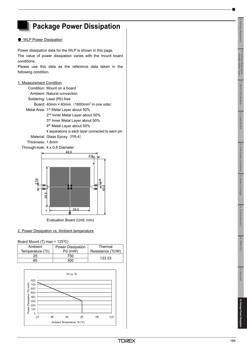
18. Package Power Dissipation _______________________________________________________________________
165
Package Power Dissipation USPN-6 Power Dissipation Power dissipation data for the USPN-6 is shown in this page. The value of power dissipation varies with the mount board conditions. Please use this data as the reference data taken in the following condition. 1. Measurement Condition Condition : Mount on a board Ambient : Natural convection Soldering : Lead (Pb) free Board : Dimensions 40mm x 40 mm (1600mm2) Copper (Cu) traces occupy 50% of the front
and 50% of the back. VSS pin is tied to the copper traces. Material : Glass Epoxy (FR-4) Thickness : 1.6mm Through-hole : 4 x 0.8 Diameter
Evaluation Board (Unit: mm) 2. Power Dissipation vs. Ambient temperature Board Mount (Tj max = 125)
Ambient Temperature ()
Power Dissipation Pd (mW)
Thermal Resistance (/W)
25 600 166.67 85 240
USPQ-4B03 and USPQ-4B04 Power Dissipation Power dissipation data for the USPQ-4B03 and USPQ-4B04 are shown in this page. The value of power dissipation varies with the mount board conditions. Please use this data as the reference data taken in the following condition. 1. Measurement Condition Condition: Mount on a board Ambient: Natural convection Soldering: Lead (Pb) free Board: 40 x 40 mm (1600mm2) 4 Copper Layers Each layer is connected to the package
heat-sink and terminal pin No.1. Each layer has approximately 800mm2
copper area. Material: Glass Epoxy (FR-4) Thickness: 1.6 mm Through-hole: 4 x 0.8 Diameter
Evaluation Board (Unit: mm) 2. Power Dissipation vs. Ambient temperature Board Mount (Tj max = 125)
Ambient Temperature ()
Power Dissipation Pd (mW)
Thermal Resistance (/W)
25 550 181.82 85 220
Pd vs Ta
0
100
200
300
400
500
600
25 45 65 85 105 125Ampient Temperature Ta ()
Pow
er D
issi
patio
n P
d (m
W)
_______________________________________________________________________________________________________
166
Package Power Dissipation WLP Power Dissipation Power dissipation data for the WLP is shown in this page. The value of power dissipation varies with the mount board conditions. Please use this data as the reference data taken in the following condition. 1. Measurement Condition Condition: Mount on a board Ambient: Natural convection Soldering: Lead (Pb) free Board: 40mm×40mm(1600mm2 in one side) Metal Area: 1st Metal Layer about 50% 2nd Inner Metal Layer about 50% 3rd Inner Metal Layer about 50% 4th Metal Layer about 50% 4 separations is each layer connected to each pin Material: Glass Epoxy(FR-4) Thickness: 1.6mm Through-hole: 4 x 0.8 Diameter
Evaluation Board (Unit: mm) 2. Power Dissipation vs. Ambient temperature Board Mount (Tj max = 125)
Ambient Temperature ()
Power Dissipation Pd (mW)
Thermal Resistance (/W)
25 750 133.33 85 300
2.54
1.4
40.0
40.0
2.5
28.9
28.9
Pd vs. Ta
Pow
er D
issi
patio
n: P
d (m
W)
Ambient Temperature: Ta ()
11.Multi C
hip Module
10. Voltage Regulators
Voltage Detect Type
9. Voltage Regulators
12.Load Switch
13. Push Button Controllers14.B
attery Charger
15.Autom
otive ICs
16.Other IC
s17. D
iscrete18.Package Power Dissipation


Related Documents