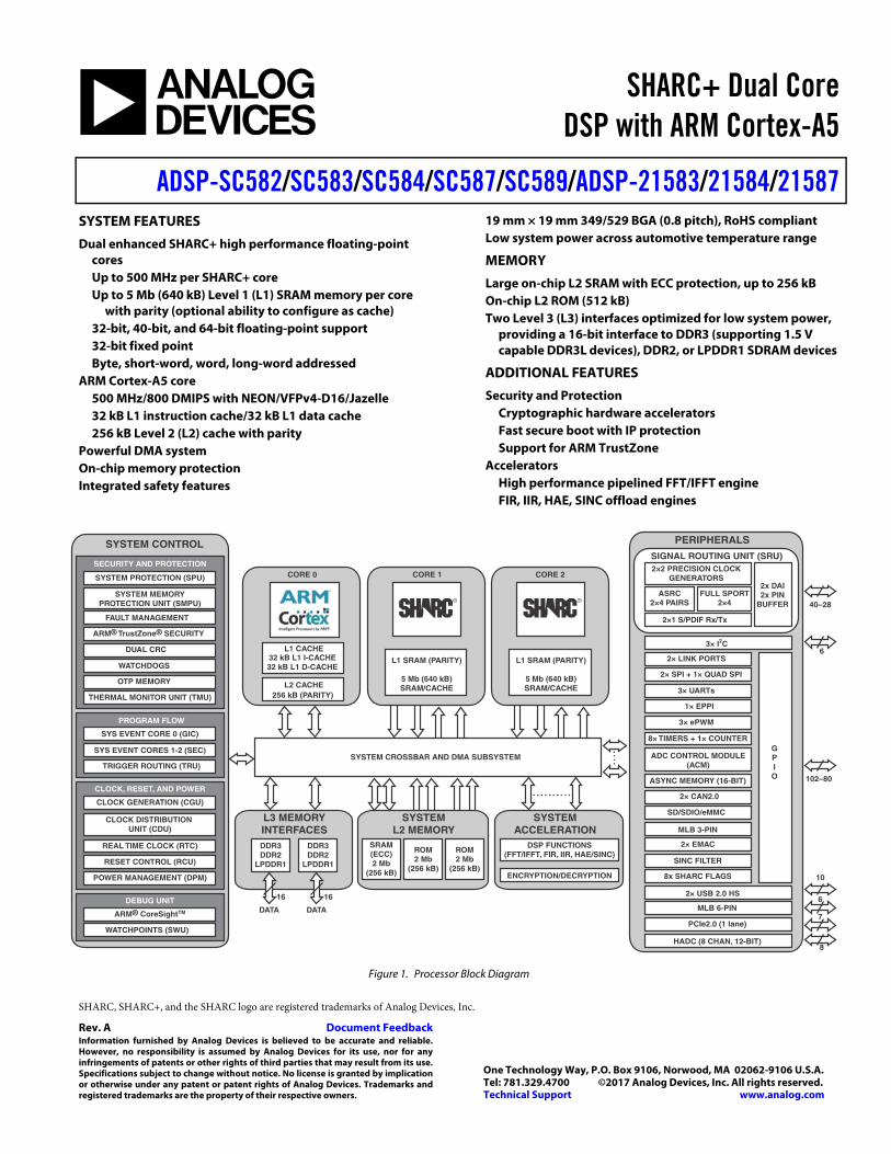
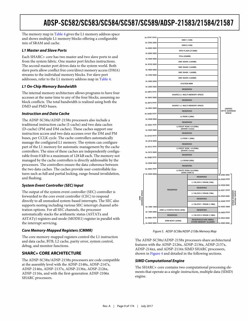
SHARC, SHARC+, and the SHARC logo are registered trademarks of Analog Devices, Inc. SHARC+ Dual Core DSP with ARM Cortex-A5 ADSP-SC582/SC583/SC584/SC587/SC589/ADSP-21583/21584/21587 Rev. A Document Feedback Information furnished by Analog Devices is believed to be accurate and reliable. However, no responsibility is assumed by Analog Devices for its use, nor for any infringements of patents or other rights of third parties that may result from its use. Specifications subject to change without notice. No license is granted by implication or otherwise under any patent or patent rights of Analog Devices. Trademarks and registered trademarks are the property of their respective owners. One Technology Way, P.O. Box 9106, Norwood, MA 02062-9106 U.S.A. Tel: 781.329.4700 ©2017 Analog Devices, Inc. All rights reserved. Technical Support www.analog.com SYSTEM FEATURES Dual enhanced SHARC+ high performance floating-point cores Up to 500 MHz per SHARC+ core Up to 5 Mb (640 kB) Level 1 (L1) SRAM memory per core with parity (optional ability to configure as cache) 32-bit, 40-bit, and 64-bit floating-point support 32-bit fixed point Byte, short-word, word, long-word addressed ARM Cortex-A5 core 500 MHz/800 DMIPS with NEON/VFPv4-D16/Jazelle 32 kB L1 instruction cache/32 kB L1 data cache 256 kB Level 2 (L2) cache with parity Powerful DMA system On-chip memory protection Integrated safety features 19 mm × 19 mm 349/529 BGA (0.8 pitch), RoHS compliant Low system power across automotive temperature range MEMORY Large on-chip L2 SRAM with ECC protection, up to 256 kB On-chip L2 ROM (512 kB) Two Level 3 (L3) interfaces optimized for low system power, providing a 16-bit interface to DDR3 (supporting 1.5 V capable DDR3L devices), DDR2, or LPDDR1 SDRAM devices ADDITIONAL FEATURES Security and Protection Cryptographic hardware accelerators Fast secure boot with IP protection Support for ARM TrustZone Accelerators High performance pipelined FFT/IFFT engine FIR, IIR, HAE, SINC offload engines Figure 1. Processor Block Diagram SYSTEM CONTROL FAULT MANAGEMENT SYSTEM PROTECTION (SPU) SECURITY AND PROTECTION ARM® TrustZone® SECURITY DUAL CRC WATCHDOGS THERMAL MONITOR UNIT (TMU) OTP MEMORY TRIGGER ROUTING (TRU) SYS EVENT CORE 0 (GIC) PROGRAM FLOW REAL TIME CLOCK (RTC) CLOCK GENERATION (CGU) CLOCK, RESET, AND POWER POWER MANAGEMENT (DPM) RESET CONTROL (RCU) WATCHPOINTS (SWU) ARM® CoreSight TM DEBUG UNIT SYSTEM MEMORY PROTECTION UNIT (SMPU) CLOCK DISTRIBUTION UNIT (CDU) DATA 16 S L1 SRAM (PARITY) 5 Mb (640 kB) SRAM/CACHE 32 kB L1 I-CACHE 32 kB L1 D-CACHE SYSTEM L2 MEMORY SYSTEM ACCELERATION L3 MEMORY INTERFACES DDR3 DDR2 LPDDR1 DDR3 DDR2 LPDDR1 DSP FUNCTIONS (FFT/IFFT, FIR, IIR, HAE/SINC) L1 SRAM (PARITY) 5 Mb (640 kB) SRAM/CACHE ENCRYPTION/DECRYPTION L1 CACHE L2 CACHE 256 kB (PARITY) DATA 16 SYSTEM CROSSBAR AND DMA SUBSYSTEM CORE 1 CORE 2 CORE 0 S PERIPHERALS 3× I 2 C 2× LINK PORTS 2× SPI + 1× QUAD SPI 3× UARTs 3× ePWM 8× TIMERS + 1× COUNTER 1× EPPI ADC CONTROL MODULE (ACM) ASYNC MEMORY (16-BIT) SD/SDIO/eMMC MLB 3-PIN 2× CAN2.0 2× USB 2.0 HS MLB 6-PIN PCIe2.0 (1 lane) HADC (8 CHAN, 12-BIT) 2× EMAC SINC FILTER 8x SHARC FLAGS ASRC 2×4 PAIRS 2×1 S/PDIF Rx/Tx 2×2 PRECISION CLOCK GENERATORS FULL SPORT 2×4 2x DAI 2x PIN BUFFER SIGNAL ROUTING UNIT (SRU) G P I O SRAM (ECC) 2 Mb (256 kB) 40–28 6 102–80 10 6 7 8 SYS EVENT CORES 1-2 (SEC) ROM 2 Mb (256 kB) ROM 2 Mb (256 kB)

Welcome message from author
This document is posted to help you gain knowledge. Please leave a comment to let me know what you think about it! Share it to your friends and learn new things together.
Transcript
SHARC, SHARC+, and the SHARC logo are registered trademarks of Analog Devices, Inc.
SHARC+ Dual CoreDSP with ARM Cortex-A5
ADSP-SC582/SC583/SC584/SC587/SC589/ADSP-21583/21584/21587
Rev. A Document FeedbackInformation furnished by Analog Devices is believed to be accurate and reliable.However, no responsibility is assumed by Analog Devices for its use, nor for anyinfringements of patents or other rights of third parties that may result from its use.Specifications subject to change without notice. No license is granted by implicationor otherwise under any patent or patent rights of Analog Devices. Trademarks andregistered trademarks are the property of their respective owners.
One Technology Way, P.O. Box 9106, Norwood, MA 02062-9106 U.S.A.Tel: 781.329.4700 ©2017 Analog Devices, Inc. All rights reserved.Technical Support www.analog.com
SYSTEM FEATURESDual enhanced SHARC+ high performance floating-point
coresUp to 500 MHz per SHARC+ coreUp to 5 Mb (640 kB) Level 1 (L1) SRAM memory per core
with parity (optional ability to configure as cache)32-bit, 40-bit, and 64-bit floating-point support 32-bit fixed point Byte, short-word, word, long-word addressed
ARM Cortex-A5 core500 MHz/800 DMIPS with NEON/VFPv4-D16/Jazelle32 kB L1 instruction cache/32 kB L1 data cache256 kB Level 2 (L2) cache with parity
Powerful DMA systemOn-chip memory protectionIntegrated safety features
19 mm × 19 mm 349/529 BGA (0.8 pitch), RoHS compliantLow system power across automotive temperature range
MEMORYLarge on-chip L2 SRAM with ECC protection, up to 256 kBOn-chip L2 ROM (512 kB)Two Level 3 (L3) interfaces optimized for low system power,
providing a 16-bit interface to DDR3 (supporting 1.5 V capable DDR3L devices), DDR2, or LPDDR1 SDRAM devices
ADDITIONAL FEATURES Security and Protection
Cryptographic hardware acceleratorsFast secure boot with IP protectionSupport for ARM TrustZone
AcceleratorsHigh performance pipelined FFT/IFFT engineFIR, IIR, HAE, SINC offload engines
Figure 1. Processor Block Diagram
SYSTEM CONTROL
FAULT MANAGEMENT
SYSTEM PROTECTION (SPU)
SECURITY AND PROTECTION
ARM® TrustZone® SECURITY
DUAL CRC
WATCHDOGS
THERMAL MONITOR UNIT (TMU)
OTP MEMORY
TRIGGER ROUTING (TRU)
SYS EVENT CORE 0 (GIC)
PROGRAM FLOW
REAL TIME CLOCK (RTC)
CLOCK GENERATION (CGU)
CLOCK, RESET, AND POWER
POWER MANAGEMENT (DPM)
RESET CONTROL (RCU)
WATCHPOINTS (SWU)
ARM® CoreSightTM
DEBUG UNIT
SYSTEM MEMORYPROTECTION UNIT (SMPU)
CLOCK DISTRIBUTION UNIT (CDU)
DATA
16
S
L1 SRAM (PARITY)
5 Mb (640 kB)SRAM/CACHE
32 kB L1 I-CACHE32 kB L1 D-CACHE
SYSTEML2 MEMORY
SYSTEMACCELERATION
L3 MEMORYINTERFACESDDR3DDR2
LPDDR1
DDR3DDR2
LPDDR1
DSP FUNCTIONS(FFT/IFFT, FIR, IIR, HAE/SINC)
L1 SRAM (PARITY)
5 Mb (640 kB)SRAM/CACHE
ENCRYPTION/DECRYPTION
L1 CACHE
L2 CACHE256 kB (PARITY)
DATA
16
SYSTEM CROSSBAR AND DMA SUBSYSTEM
CORE 1 CORE 2CORE 0
S
PERIPHERALS
3× I2C
2× LINK PORTS
2× SPI + 1× QUAD SPI
3× UARTs
3× ePWM
8× TIMERS + 1× COUNTER
1× EPPI
ADC CONTROL MODULE(ACM)
ASYNC MEMORY (16-BIT)
SD/SDIO/eMMC
MLB 3-PIN
2× CAN2.0
2× USB 2.0 HS
MLB 6-PIN
PCIe2.0 (1 lane)
HADC (8 CHAN, 12-BIT)
2× EMAC
SINC FILTER
8x SHARC FLAGS
ASRC2×4 PAIRS
2×1 S/PDIF Rx/Tx
2×2 PRECISION CLOCKGENERATORS
FULL SPORT2×4
2x DAI2x PIN
BUFFER
SIGNAL ROUTING UNIT (SRU)
GPIO
SRAM(ECC)2 Mb
(256 kB)
40–28
6
102–80
10
6
7
8
SYS EVENT CORES 1-2 (SEC)
ROM2 Mb
(256 kB)
ROM2 Mb
(256 kB)
Rev. A | Page 2 of 174 | July 2017
ADSP-SC582/SC583/SC584/SC587/SC589/ADSP-21583/21584/21587
TABLE OF CONTENTSSystem Features . . . . . . . . . . . . . . . . . . . . . . . . . . . . . . . . . . . . . . . . . . . . . . . . . . . . . . . 1Memory . . . . . . . . . . . . . . . . . . . . . . . . . . . . . . . . . . . . . . . . . . . . . . . . . . . . . . . . . . . . . . . . 1Additional Features . . . . . . . . . . . . . . . . . . . . . . . . . . . . . . . . . . . . . . . . . . . . . . . . . . 1Table Of Contents . . . . . . . . . . . . . . . . . . . . . . . . . . . . . . . . . . . . . . . . . . . . . . . . . . . . 2Revision History . . . . . . . . . . . . . . . . . . . . . . . . . . . . . . . . . . . . . . . . . . . . . . . . . . . . . . 3General Description . . . . . . . . . . . . . . . . . . . . . . . . . . . . . . . . . . . . . . . . . . . . . . . . . 4
ARM Cortex-A5 Processor . . . . . . . . . . . . . . . . . . . . . . . . . . . . . . . . . . . . . . 6SHARC Processor . . . . . . . . . . . . . . . . . . . . . . . . . . . . . . . . . . . . . . . . . . . . . . . . . 7SHARC+ Core Architecture . . . . . . . . . . . . . . . . . . . . . . . . . . . . . . . . . . . . 9System Infrastructure . . . . . . . . . . . . . . . . . . . . . . . . . . . . . . . . . . . . . . . . . . . 11System Memory Map . . . . . . . . . . . . . . . . . . . . . . . . . . . . . . . . . . . . . . . . . . . 12Security Features . . . . . . . . . . . . . . . . . . . . . . . . . . . . . . . . . . . . . . . . . . . . . . . . 15Safety Features . . . . . . . . . . . . . . . . . . . . . . . . . . . . . . . . . . . . . . . . . . . . . . . . . . . 15Processor Peripherals . . . . . . . . . . . . . . . . . . . . . . . . . . . . . . . . . . . . . . . . . . . 16System Acceleration . . . . . . . . . . . . . . . . . . . . . . . . . . . . . . . . . . . . . . . . . . . . 21System Design . . . . . . . . . . . . . . . . . . . . . . . . . . . . . . . . . . . . . . . . . . . . . . . . . . . . 21System Debug . . . . . . . . . . . . . . . . . . . . . . . . . . . . . . . . . . . . . . . . . . . . . . . . . . . . 24Development Tools . . . . . . . . . . . . . . . . . . . . . . . . . . . . . . . . . . . . . . . . . . . . . 24Additional Information . . . . . . . . . . . . . . . . . . . . . . . . . . . . . . . . . . . . . . . . 25Related Signal Chains . . . . . . . . . . . . . . . . . . . . . . . . . . . . . . . . . . . . . . . . . . 25Security Features Disclaimer . . . . . . . . . . . . . . . . . . . . . . . . . . . . . . . . . . 25
ADSP-SC58x/ADSP-2158x Detailed Signal Descriptions . . . . . . . . . . . . . . . . . . . . . . . . . . . . . . . . . . . . . . . . . . . . . . . . . . . . . . 26
349-Ball CSP_BGA Signal Descriptions . . . . . . . . . . . . . . . . . . . . . . . 31GPIO Multiplexing for the 349-Ball CSP_BGA Package . . 40529-Ball CSP_BGA Signal Descriptions . . . . . . . . . . . . . . . . . . . . . . . 43GPIO Multiplexing for the 529-Ball CSP_BGA Package . . 55
ADSP-SC58x/ADSP-2158x Designer Quick Reference . . . . 58Specifications . . . . . . . . . . . . . . . . . . . . . . . . . . . . . . . . . . . . . . . . . . . . . . . . . . . . . . . . 80
Operating Conditions . . . . . . . . . . . . . . . . . . . . . . . . . . . . . . . . . . . . . . . . . . . 80Electrical Characteristics . . . . . . . . . . . . . . . . . . . . . . . . . . . . . . . . . . . . . . . 84HADC . . . . . . . . . . . . . . . . . . . . . . . . . . . . . . . . . . . . . . . . . . . . . . . . . . . . . . . . . . . . . . 88TMU .. . . . . . . . . . . . . . . . . . . . . . . . . . . . . . . . . . . . . . . . . . . . . . . . . . . . . . . . . . . . . . . 88Absolute Maximum Ratings . . . . . . . . . . . . . . . . . . . . . . . . . . . . . . . . . . . 89ESD Caution . . . . . . . . . . . . . . . . . . . . . . . . . . . . . . . . . . . . . . . . . . . . . . . . . . . . . . 89Package Information . . . . . . . . . . . . . . . . . . . . . . . . . . . . . . . . . . . . . . . . . . . . 89Timing Specifications . . . . . . . . . . . . . . . . . . . . . . . . . . . . . . . . . . . . . . . . . . . 90Output Drive Currents . . . . . . . . . . . . . . . . . . . . . . . . . . . . . . . . . . . . . . . 154Test Conditions . . . . . . . . . . . . . . . . . . . . . . . . . . . . . . . . . . . . . . . . . . . . . . . . 156Environmental Conditions . . . . . . . . . . . . . . . . . . . . . . . . . . . . . . . . . . 158
ADSP-SC58x/ADSP-2158x 349-Ball BGA Ball Assignments . . . . . . . . . . . . . . . . . . . . . . . . . . . . . . . . . . . . . . . . . . . . . . . . . . . . 159Numerical by Ball Number . . . . . . . . . . . . . . . . . . . . . . . . . . . . . . . . . . 159Alphabetical by Pin Name . . . . . . . . . . . . . . . . . . . . . . . . . . . . . . . . . . . 161Configuration of the 349-Ball CSP_BGA .. . . . . . . . . . . . . . . . 163
ADSP-SC58x/ADSP-2158x 529-Ball BGA Ball Assignments . . . . . . . . . . . . . . . . . . . . . . . . . . . . . . . . . . . . . . . . . . . . . . . . . . . . 164Numerical by Ball Number . . . . . . . . . . . . . . . . . . . . . . . . . . . . . . . . . . 164Alphabetical by Pin Name . . . . . . . . . . . . . . . . . . . . . . . . . . . . . . . . . . . 167Configuration of the 529-Ball CSP_BGA .. . . . . . . . . . . . . . . . 170
Outline Dimensions . . . . . . . . . . . . . . . . . . . . . . . . . . . . . . . . . . . . . . . . . . . . . . 171Surface-Mount Design . . . . . . . . . . . . . . . . . . . . . . . . . . . . . . . . . . . . . . . . 172Planned Automotive Production Products . . . . . . . . . . . . . . 173Ordering Guide . . . . . . . . . . . . . . . . . . . . . . . . . . . . . . . . . . . . . . . . . . . . . . . . 174
Rev. A | Page 3 of 174 | July 2017
ADSP-SC582/SC583/SC584/SC587/SC589/ADSP-21583/21584/21587REVISION HISTORY7/2017—Rev. 0 to Rev. AChanges to Processor Block Diagram .. . . . . . . . . . . . . . . . . . . . . . . . . . . 1Changes to Table 2 and Table 3 in General Description . . . . . 4Changes to ARM Cortex-A5 Processor Block Diagram . . . . . 6Changes to ADSP-SC58x/ADSP-2158x Memory Map . . . . . . . 9Change to Power Supplies . . . . . . . . . . . . . . . . . . . . . . . . . . . . . . . . . . . . . . . . . 23Change to Table 10 in Power Management . . . . . . . . . . . . . . . . . . . 24Change to DMC_VREF Description, Table 11 in ADSP-SC58x/ADSP-2158x Detailed Signal Descriptions . . . . . . . . . . . 26Change to VDD_HADC Signal Description, Table 12 in 349-Ball CSP_BGA Signal Descriptions . . . . . . . . . . . . . . . . . . . . . . . . 31Change to VDD_HADC Signal Description, Table 19 in 529-Ball CSP_BGA Signal Descriptions . . . . . . . . . . . . . . . . . . . . . . . . 43Changes to HADC0_VREFN, HADC0_VREFP, and VDD_HADC Signal Description and Notes, Table 27 in ADSP-SC58x/ADSP-2158x Designer Quick Reference . . . . . 58Change to PC_10 Driver Type, Table 27 in ADSP-SC58x/ADSP-2158x Designer Quick Reference . . . . . 58Changes to Operating Conditions . . . . . . . . . . . . . . . . . . . . . . . . . . . . . . . 80Changes to Table 29 and Table 30 in Clock Related Operating Conditions . . . . . . . . . . . . . . . . . . . . . . . . . . . . . . . . . . . . . . . . . . . . . . . . . . . . . . . . . . . . 82Changes to Electrical Characteristics . . . . . . . . . . . . . . . . . . . . . . . . . . . 84
Changes to Table 31, Table 34, and Table 35 in Total Internal Power Dissipation . . . . . . . . . . . . . . . . . . . . . . . . . . . . . . . . . . . . . . . . . . . . . . . . . . 86Added Table 41 in TMU . . . . . . . . . . . . . . . . . . . . . . . . . . . . . . . . . . . . . . . . . . 88Changes to Table 42 in Absolute Maximum Ratings . . . . . . . 89Added Table 47 and Figure 13 in SMC Read Cycle Timing With Reference to SYS_CLKOUT .. . . . . . . . . . . . . . . . . . . . . . . . . . . . . . . . . . . . . 93Added Table 51 and Figure 17 in SMC Write Cycle Timing With Reference to SYS_CLKOUT .. . . . . . . . . . . . . . . . . . . . . . . . . . . . . 97Change to tQH Parameter, Table 55 in DDR2 SDRAM Read Cycle Timing . . . . . . . . . . . . . . . . . . . . . . . . . . . . . . . . . . . . . . . . . . . . . . . . . . . . . . . 100Change to tDQSQ Parameter, Table 61 in DDR3 SDRAM Read Cycle Timing . . . . . . . . . . . . . . . . . . . . . . . . . . . . . . . . . . . . . . . . . . . . . . . . . . . . . . . 106Changed Timing Requirement Parameter Heading to Switching Characteristics Heading, Table 84 in DAIx Pin to DAIx Pin Direct Routing (DAI0 Block and DAI1 Block) . . . . . . . . . . . . . . 134Added Table 87 and Figure 58 in PWM — Medium Precision (MP) Mode Timing . . . . . . . . . . . . . . . . . . . . . . . . . . . . . . . . . . . . . . . . . . . . . . . 136Changes to Table 88, Table 89, Figure 59, and Figure 62 in PWM — Heightened Precision (HP) Mode Timing . . . . . . . 136Added Figure 60 and Figure 61 in PWM — Heightened Preci-sion (HP) Mode Timing . . . . . . . . . . . . . . . . . . . . . . . . . . . . . . . . . . . . . . . . . . 136Changes to Planned Automotive Production Products . . . 173Changes to Ordering Guide . . . . . . . . . . . . . . . . . . . . . . . . . . . . . . . . . . . . . 174
Rev. A | Page 4 of 174 | July 2017
ADSP-SC582/SC583/SC584/SC587/SC589/ADSP-21583/21584/21587
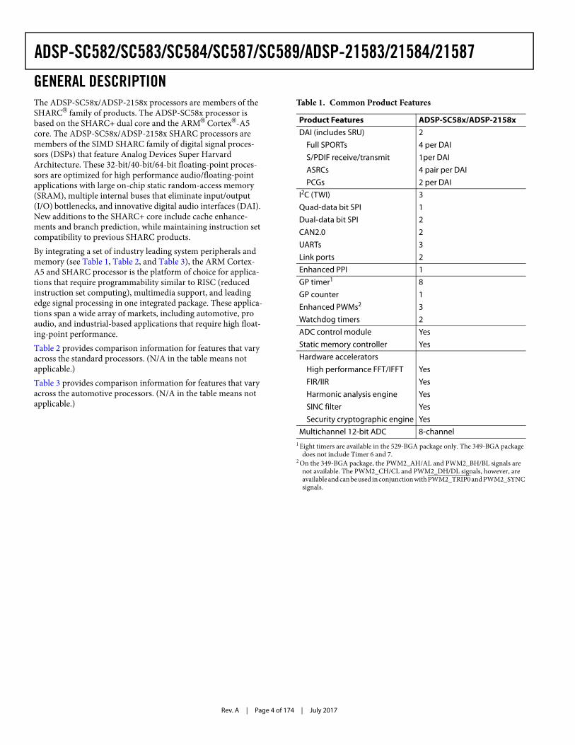
GENERAL DESCRIPTIONThe ADSP-SC58x/ADSP-2158x processors are members of the SHARC® family of products. The ADSP-SC58x processor is based on the SHARC+ dual core and the ARM® Cortex®-A5 core. The ADSP-SC58x/ADSP-2158x SHARC processors are members of the SIMD SHARC family of digital signal proces-sors (DSPs) that feature Analog Devices Super Harvard Architecture. These 32-bit/40-bit/64-bit floating-point proces-sors are optimized for high performance audio/floating-point applications with large on-chip static random-access memory (SRAM), multiple internal buses that eliminate input/output (I/O) bottlenecks, and innovative digital audio interfaces (DAI). New additions to the SHARC+ core include cache enhance-ments and branch prediction, while maintaining instruction set compatibility to previous SHARC products.By integrating a set of industry leading system peripherals and memory (see Table 1, Table 2, and Table 3), the ARM Cortex-A5 and SHARC processor is the platform of choice for applica-tions that require programmability similar to RISC (reduced instruction set computing), multimedia support, and leading edge signal processing in one integrated package. These applica-tions span a wide array of markets, including automotive, pro audio, and industrial-based applications that require high float-ing-point performance.Table 2 provides comparison information for features that vary across the standard processors. (N/A in the table means not applicable.)Table 3 provides comparison information for features that vary across the automotive processors. (N/A in the table means not applicable.)
Table 1. Common Product Features
Product Features ADSP-SC58x/ADSP-2158x DAI (includes SRU) 2
Full SPORTs 4 per DAI
S/PDIF receive/transmit 1per DAI
ASRCs 4 pair per DAI
PCGs 2 per DAI
I2C (TWI) 3
Quad-data bit SPI 1
Dual-data bit SPI 2
CAN2.0 2
UARTs 3
Link ports 2
Enhanced PPI 1
GP timer1 8
GP counter 1
Enhanced PWMs2 3
Watchdog timers 2
ADC control module Yes
Static memory controller Yes
Hardware accelerators
High performance FFT/IFFT Yes
FIR/IIR Yes
Harmonic analysis engine Yes
SINC filter Yes
Security cryptographic engine Yes
Multichannel 12-bit ADC 8-channel1 Eight timers are available in the 529-BGA package only. The 349-BGA package
does not include Timer 6 and 7.2 On the 349-BGA package, the PWM2_AH/AL and PWM2_BH/BL signals are
not available. The PWM2_CH/CL and PWM2_DH/DL signals, however, are available and can be used in conjunction with PWM2_TRIP0 and PWM2_SYNC signals.
Rev. A | Page 5 of 174 | July 2017
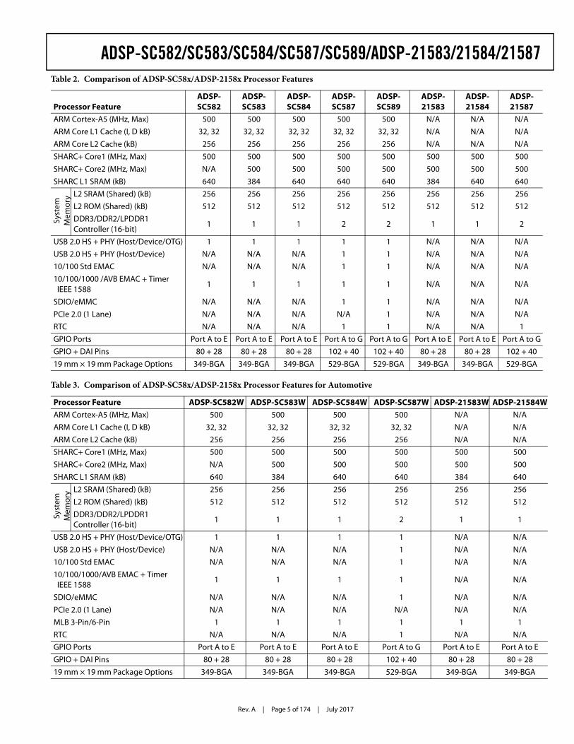
ADSP-SC582/SC583/SC584/SC587/SC589/ADSP-21583/21584/21587Table 2. Comparison of ADSP-SC58x/ADSP-2158x Processor Features
Processor Feature ADSP-SC582
ADSP-SC583
ADSP-SC584
ADSP-SC587
ADSP-SC589
ADSP-21583
ADSP-21584
ADSP-21587
ARM Cortex-A5 (MHz, Max) 500 500 500 500 500 N/A N/A N/A
ARM Core L1 Cache (I, D kB) 32, 32 32, 32 32, 32 32, 32 32, 32 N/A N/A N/A
ARM Core L2 Cache (kB) 256 256 256 256 256 N/A N/A N/A
SHARC+ Core1 (MHz, Max) 500 500 500 500 500 500 500 500
SHARC+ Core2 (MHz, Max) N/A 500 500 500 500 500 500 500
SHARC L1 SRAM (kB) 640 384 640 640 640 384 640 640
Syst
em
Mem
ory L2 SRAM (Shared) (kB) 256 256 256 256 256 256 256 256
L2 ROM (Shared) (kB) 512 512 512 512 512 512 512 512
DDR3/DDR2/LPDDR1 Controller (16-bit)
1 1 1 2 2 1 1 2
USB 2.0 HS + PHY (Host/Device/OTG) 1 1 1 1 1 N/A N/A N/A
USB 2.0 HS + PHY (Host/Device) N/A N/A N/A 1 1 N/A N/A N/A
10/100 Std EMAC N/A N/A N/A 1 1 N/A N/A N/A
10/100/1000 /AVB EMAC + Timer IEEE 1588
1 1 1 1 1 N/A N/A N/A
SDIO/eMMC N/A N/A N/A 1 1 N/A N/A N/A
PCIe 2.0 (1 Lane) N/A N/A N/A N/A 1 N/A N/A N/A
RTC N/A N/A N/A 1 1 N/A N/A 1
GPIO Ports Port A to E Port A to E Port A to E Port A to G Port A to G Port A to E Port A to E Port A to G
GPIO + DAI Pins 80 + 28 80 + 28 80 + 28 102 + 40 102 + 40 80 + 28 80 + 28 102 + 40
19 mm × 19 mm Package Options 349-BGA 349-BGA 349-BGA 529-BGA 529-BGA 349-BGA 349-BGA 529-BGA
Table 3. Comparison of ADSP-SC58x/ADSP-2158x Processor Features for Automotive
Processor Feature ADSP-SC582W ADSP-SC583W ADSP-SC584W ADSP-SC587W ADSP-21583W ADSP-21584WARM Cortex-A5 (MHz, Max) 500 500 500 500 N/A N/A
ARM Core L1 Cache (I, D kB) 32, 32 32, 32 32, 32 32, 32 N/A N/A
ARM Core L2 Cache (kB) 256 256 256 256 N/A N/A
SHARC+ Core1 (MHz, Max) 500 500 500 500 500 500
SHARC+ Core2 (MHz, Max) N/A 500 500 500 500 500
SHARC L1 SRAM (kB) 640 384 640 640 384 640
Syst
emM
emor
y L2 SRAM (Shared) (kB) 256 256 256 256 256 256
L2 ROM (Shared) (kB) 512 512 512 512 512 512
DDR3/DDR2/LPDDR1 Controller (16-bit)
1 1 1 2 1 1
USB 2.0 HS + PHY (Host/Device/OTG) 1 1 1 1 N/A N/A
USB 2.0 HS + PHY (Host/Device) N/A N/A N/A 1 N/A N/A
10/100 Std EMAC N/A N/A N/A 1 N/A N/A
10/100/1000/AVB EMAC + Timer IEEE 1588
1 1 1 1 N/A N/A
SDIO/eMMC N/A N/A N/A 1 N/A N/A
PCIe 2.0 (1 Lane) N/A N/A N/A N/A N/A N/A
MLB 3-Pin/6-Pin 1 1 1 1 1 1
RTC N/A N/A N/A 1 N/A N/A
GPIO Ports Port A to E Port A to E Port A to E Port A to G Port A to E Port A to E
GPIO + DAI Pins 80 + 28 80 + 28 80 + 28 102 + 40 80 + 28 80 + 28
19 mm × 19 mm Package Options 349-BGA 349-BGA 349-BGA 529-BGA 349-BGA 349-BGA
Rev. A | Page 6 of 174 | July 2017
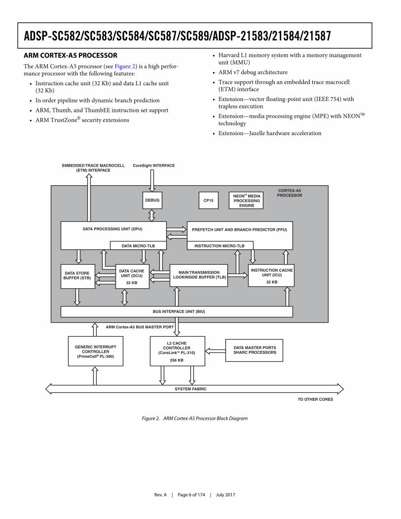
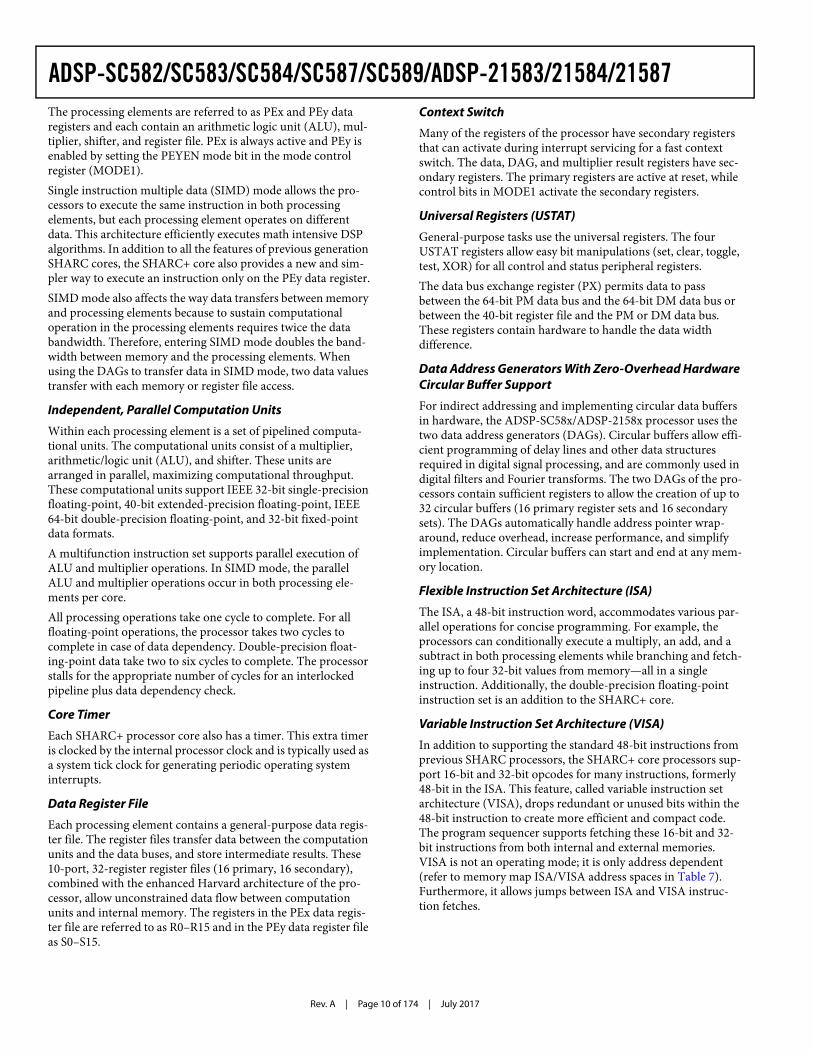
ADSP-SC582/SC583/SC584/SC587/SC589/ADSP-21583/21584/21587ARM CORTEX-A5 PROCESSORThe ARM Cortex-A5 processor (see Figure 2) is a high perfor-mance processor with the following features:
• Instruction cache unit (32 Kb) and data L1 cache unit (32 Kb)
• In order pipeline with dynamic branch prediction• ARM, Thumb, and ThumbEE instruction set support• ARM TrustZone® security extensions
• Harvard L1 memory system with a memory management unit (MMU)
• ARM v7 debug architecture• Trace support through an embedded trace macrocell
(ETM) interface• Extension—vector floating-point unit (IEEE 754) with
trapless execution• Extension—media processing engine (MPE) with NEONTM
technology• Extension—Jazelle hardware acceleration
Figure 2. ARM Cortex-A5 Processor Block Diagram
DATA STOREBUFFER (STB)
BUS INTERFACE UNIT (BIU)
PREFETCH UNIT AND BRANCH PREDICTOR (PFU)DATA PROCESSING UNIT (DPU)
DATA MICRO-TLB INSTRUCTION MICRO-TLB
DEBUG
DATA CACHEUNIT (DCU)
MAIN TRANSMISSION LOOKINSIDE BUFFER (TLB)
INSTRUCTION CACHEUNIT (ICU)
CORTEX-A5PROCESSOR
EMBEDDED TRACE MACROCELL(ETM) INTERFACE
L2 CACHECONTROLLER
(CoreLinkTM PL-310)
256 KB
SYSTEM FABRIC
TO OTHER CORES
ARM Cortex-A5 BUS MASTER PORT
CoreSight INTERFACE
CP15NEON MEDIAPROCESSING
ENGINE
32 KB 32 KB
GENERIC INTERRUPTCONTROLLER
(PrimeCell® PL-390)
TM
DATA MASTER PORTSSHARC PROCESSORS
Rev. A | Page 7 of 174 | July 2017
ADSP-SC582/SC583/SC584/SC587/SC589/ADSP-21583/21584/21587Generic Interrupt Controller (GIC), PL390 (ADSP-SC58x Only)
The generic interrupt controller (GIC) is a centralized resource for supporting and managing interrupts. The GIC splits into the distributor block (GICPORT0) and the CPU interface block (GICPORT1).
Generic Interrupt Controller Port0 (GICPORT0)The GICPORT0 distributor block performs interrupt prioritiza-tion and distribution to the GICPORT1 blocks that connect to the processors in the system. It centralizes all interrupt sources, determines the priority of each interrupt, and forwards the interrupt with the highest priority to the interface, for priority masking and preemption handling.
Generic Interrupt Controller Port1 (GICPORT1)The GICPORT1 CPU interface block performs priority masking and preemption handling for a connected processor in the sys-tem. GICPORT1 supports 8 software generated interrupts (SGIs) and 254 shared peripheral interrupts (SPIs).
L2 Cache Controller, PL310 (ADSP-SC58x Only)
The L2 cache controller, PL310 (see Figure 2), works efficiently with the ARM Cortex-A5 processors that implement system fabric. The cache controller directly interfaces on the data and instruction interface. The internal pipelining of the cache con-troller is optimized to enable the processors to operate at the same clock frequency. The cache controller supports the following:
• Two read/write 64-bit slave ports, one connected to the ARM Cortex-A5 instruction and data interfaces, and one connecting the ARM Cortex-A5 and SHARC+ cores for data coherency.
• Two read/write 64-bit master ports for interfacing with the system fabric.
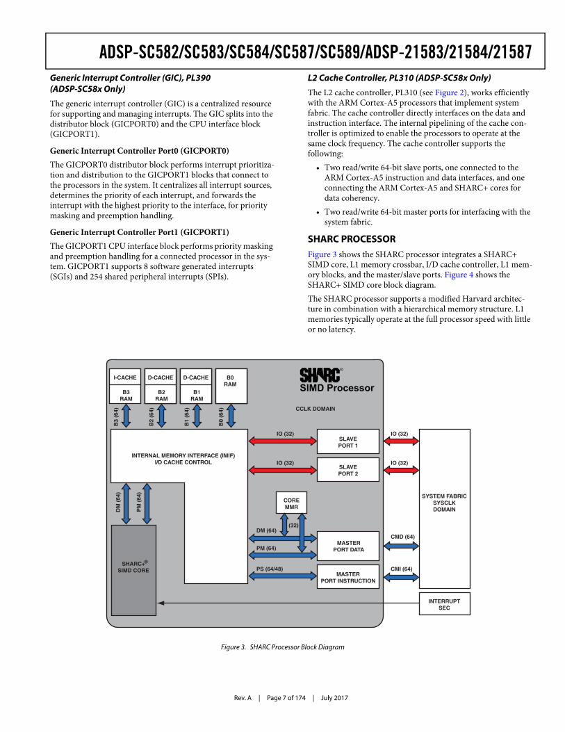
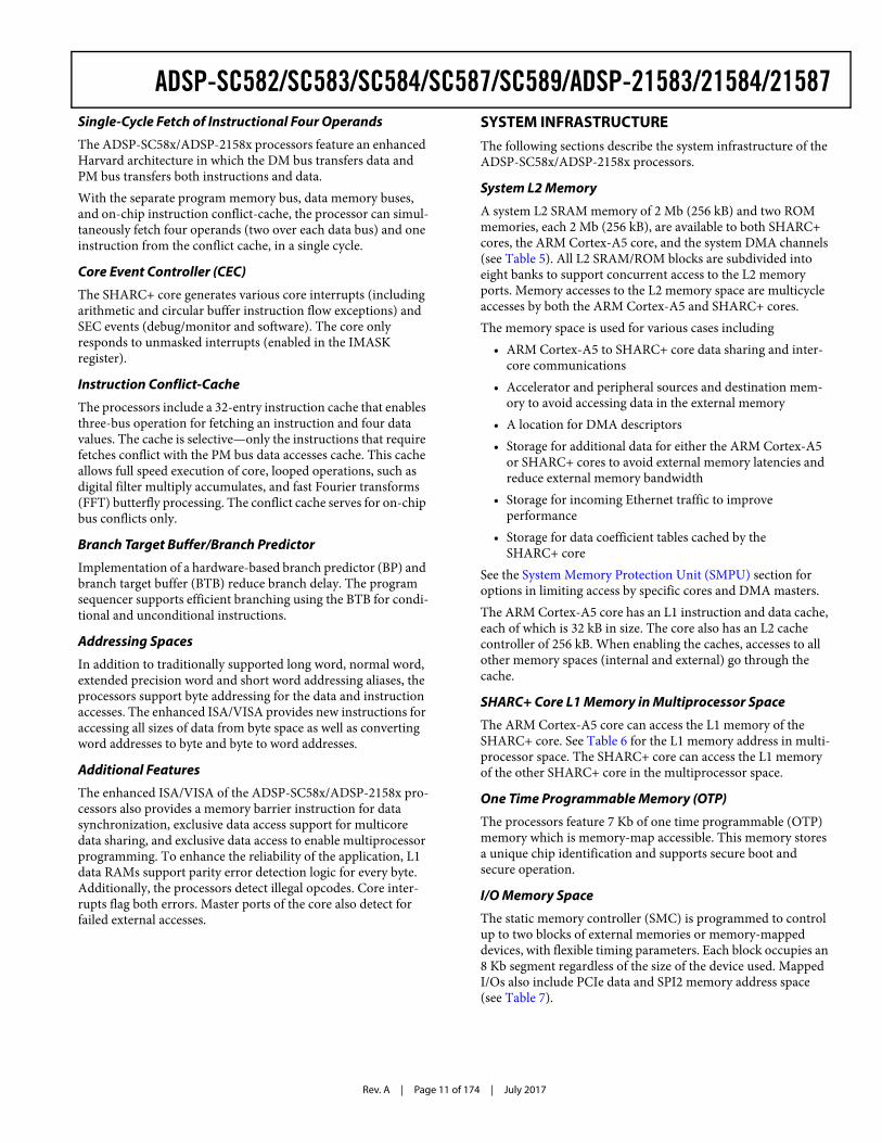
SHARC PROCESSOR Figure 3 shows the SHARC processor integrates a SHARC+ SIMD core, L1 memory crossbar, I/D cache controller, L1 mem-ory blocks, and the master/slave ports. Figure 4 shows the SHARC+ SIMD core block diagram.The SHARC processor supports a modified Harvard architec-ture in combination with a hierarchical memory structure. L1 memories typically operate at the full processor speed with little or no latency.
Figure 3. SHARC Processor Block Diagram
B3RAM
I-CACHE
B2RAM
P-CACHE
B2RAM
P-CACHE
B1RAM
D-CACHE
B2RAM
P-CACHE
B2RAM
P-CACHE
B2RAM
D-CACHE
B2RAM
P-CACHE
B2RAM
P-CACHEB0RAM
B3
(64)
B2
(64)
B1
(64)
B0
(64)
IO (32)
INTERNAL MEMORY INTERFACE (IMIF)I/D CACHE CONTROL
SHARC+SIMD CORE
DM
(64
)
PM
(64
)
SLAVEPORT 1
SLAVEPORT 2
IO (32)
COREMMR
DM (64)
PM (64)
PS (64/48)
(32)
MASTERPORT INSTRUCTION
MASTERPORT DATA
IO (32)
IO (32)
CMD (64)
CMI (64)
SYSTEM FABRICSYSCLKDOMAIN
INTERRUPTSEC
S SIMD Processor
CCLK DOMAIN
®
Rev. A | Page 8 of 174 | July 2017
ADSP-SC582/SC583/SC584/SC587/SC589/ADSP-21583/21584/21587
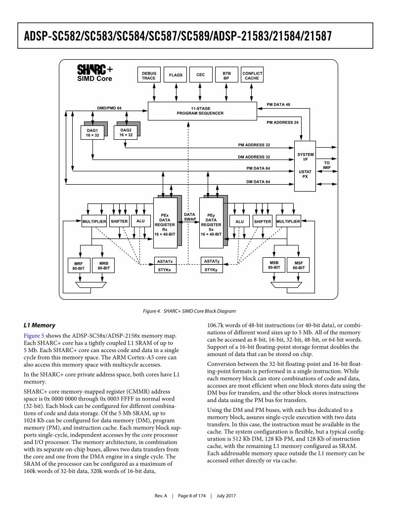
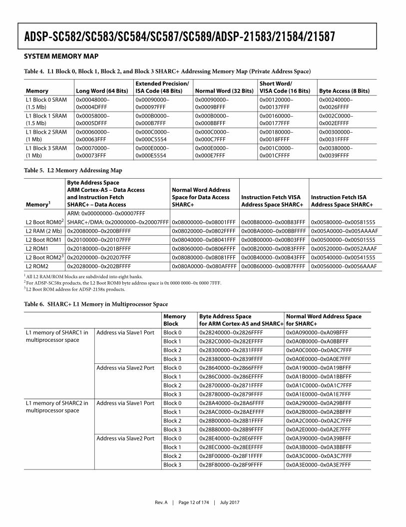
L1 Memory
Figure 5 shows the ADSP-SC58x/ADSP-2158x memory map. Each SHARC+ core has a tightly coupled L1 SRAM of up to 5 Mb. Each SHARC+ core can access code and data in a single cycle from this memory space. The ARM Cortex-A5 core can also access this memory space with multicycle accesses.In the SHARC+ core private address space, both cores have L1 memory. SHARC+ core memory-mapped register (CMMR) address space is 0x 0000 0000 through 0x 0003 FFFF in normal word (32-bit). Each block can be configured for different combina-tions of code and data storage. Of the 5 Mb SRAM, up to 1024 Kb can be configured for data memory (DM), program memory (PM), and instruction cache. Each memory block sup-ports single-cycle, independent accesses by the core processor and I/O processor. The memory architecture, in combination with its separate on-chip buses, allows two data transfers from the core and one from the DMA engine in a single cycle. The SRAM of the processor can be configured as a maximum of 160k words of 32-bit data, 320k words of 16-bit data,
106.7k words of 48-bit instructions (or 40-bit data), or combi-nations of different word sizes up to 5 Mb. All of the memory can be accessed as 8-bit, 16-bit, 32-bit, 48-bit, or 64-bit words. Support of a 16-bit floating-point storage format doubles the amount of data that can be stored on chip.Conversion between the 32-bit floating-point and 16-bit float-ing-point formats is performed in a single instruction. While each memory block can store combinations of code and data, accesses are most efficient when one block stores data using the DM bus for transfers, and the other block stores instructions and data using the PM bus for transfers.Using the DM and PM buses, with each bus dedicated to a memory block, assures single-cycle execution with two data transfers. In this case, the instruction must be available in the cache. The system configuration is flexible, but a typical config-uration is 512 Kb DM, 128 Kb PM, and 128 Kb of instruction cache, with the remaining L1 memory configured as SRAM. Each addressable memory space outside the L1 memory can be accessed either directly or via cache.
Figure 4. SHARC+ SIMD Core Block Diagram
+
11-STAGEPROGRAM SEQUENCER
PM ADDRESS 32
PM DATA 64
DM DATA 64
DM ADDRESS 32
DAG116 × 32
MRF80-BIT
ALUMULTIPLIER SHIFTERPEx
DATAREGISTER
Rx16 × 40-BIT
DMD/PMD 64
ASTATx
STYKx
ASTATy
STYKy
PEyDATA
REGISTERSx
16 × 40-BIT
MRB80-BIT
MSB80-BIT
MSF80-BIT
DAG216 × 32
ALU MULTIPLIERSHIFTER
DATA SWAP
SYSTEMI/F
USTATPX
PM ADDRESS 24
PM DATA 48
DEBUGTRACE
FLAGS CEC BTBBP
CONFLICTCACHE
TOIMIF
S SIMD Core
Rev. A | Page 9 of 174 | July 2017
ADSP-SC582/SC583/SC584/SC587/SC589/ADSP-21583/21584/21587The memory map in Table 4 gives the L1 memory address space and shows multiple L1 memory blocks offering a configurable mix of SRAM and cache.
L1 Master and Slave Ports
Each SHARC+ core has two master and two slave ports to and from the system fabric. One master port fetches instructions. The second master port drives data to the system world. Both slave ports allow conflict free core/direct memory access (DMA) streams to the individual memory blocks. For slave port addresses, refer to the L1 memory address map in Table 4.
L1 On-Chip Memory Bandwidth
The internal memory architecture allows programs to have four accesses at the same time to any of the four blocks, assuming no block conflicts. The total bandwidth is realized using both the DMD and PMD buses.
Instruction and Data Cache
The ADSP-SC58x/ADSP-2158x processors also include a traditional instruction cache (I-cache) and two data caches (D-cache) (PM and DM caches). These caches support one instruction access and two data accesses over the DM and PM buses, per CCLK cycle. The cache controllers automatically manage the configured L1 memory. The system can configure part of the L1 memory for automatic management by the cache controllers. The sizes of these caches are independently configu-rable from 0 kB to a maximum of 128 kB each. The memory not managed by the cache controllers is directly addressable by the processors. The controllers ensure the data coherence between the two data caches. The caches provide user-controllable fea-tures such as full and partial locking, range-bound invalidation, and flushing.
System Event Controller (SEC) Input
The output of the system event controller (SEC) controller is forwarded to the core event controller (CEC) to respond directly to all unmasked system-based interrupts. The SEC also supports nesting including various SEC interrupt channel arbi-tration options. For all SEC channels, the processor automatically stacks the arithmetic status (ASTATx and ASTATy) registers and mode (MODE1) register in parallel with the interrupt servicing.
Core Memory-Mapped Registers (CMMR)
The core memory-mapped registers control the L1 instruction and data cache, BTB, L2 cache, parity error, system control, debug, and monitor functions.
SHARC+ CORE ARCHITECTUREThe ADSP-SC58x/ADSP-2158x processors are code compatible at the assembly level with the ADSP-2148x, ADSP-2147x, ADSP-2146x, ADSP-2137x, ADSP-2136x, ADSP-2126x, ADSP-2116x, and with the first-generation ADSP-2106x SHARC processors.
The ADSP-SC58x/ADSP-2158x processors share architectural features with the ADSP-2126x, ADSP-2136x, ADSP-2137x, ADSP-214xx, and ADSP-2116x SIMD SHARC processors, shown in Figure 4 and detailed in the following sections.
SIMD Computational Engine
The SHARC+ core contains two computational processing ele-ments that operate as a single-instruction, multiple data (SIMD) engine.
Figure 5. ADSP-SC58x/ADSP-2158x Memory Map
0x FFFF FFFF
0x C000 0000
0x 8000 0000
0x 6000 0000
0x 5000 0000
0x 4C00 0000
0x 4800 0000
0x 4400 0000
0x 4000 0000
0x 3000 0000
0x 28F9 FFFF
0x 28A4 0000
0x 2879 FFFF
0x 2824 0000
0x 202B FFFF
0x 201B FFFF
0x 2028 0000
0x 2020 7FFF
0x 2020 0000
0x 2018 0000
0x 2010 7FFF
0x 2010 0000
0x 200B FFFF
0x 2008 0000
0x 2000 7FFF
DMC1 (1GB)
DMC0 (1GB)
SPI2 FLASH (512MB)
PCIe (256MB)
SMC BANK 3 (64MB)
SMC BANK 2 (64MB)
SMC BANK 1 (64MB)
SMC BANK 0 (64MB)
SYSTEM MMR
RESERVED
SHARC2 L1 MULTI-MEMORY SPACE
RESERVED
SHARC1 L1 MULTI-MEMORY SPACE
RESERVED
L2 ROM 2 (2Mb)
RESERVED
L2 BOOT ROM 2 (0.25Mb)(SHARC Cores)
RESERVED
L2 ROM 1 (2Mb)
RESERVED
RESERVED
L2 SRAM (2Mb)
RESERVED
L2 BOOT ROM 0 (0.25Mb)(ARM CORE 0)
L2 BOOT ROM 1 (0.25Mb)(SHARC Cores)
0x 2000 0000
0x 0039 FFFF
0x 0038 0000
0x 0031 FFFF
0x 0030 0000
0x 002E FFFF
0x 002C 0000
0x 0026 FFFF
0x 0024 0000
0x 0000 0000
RESERVED
L1 BLOCK 3 SRAM (1Mb)
RESERVED
RESERVED
RESERVED
L1 BLOCK 2 SRAM (1Mb)
L1 BLOCK 1 SRAM (1.5Mb)
L1 BLOCK 0 SRAM (1.5Mb)
RESERVED/CORE MMRs/OTHER MEMORY ALIASES
RESERVED
ARM L2 CONFIG REGS (4KB)
RESERVED
ARM BOOT (32KB)
0x 2000 0000
0x 1000 1000
0x 1000 0000
0x 0000 7FFF
0x 0000 0000
AR
M
AD
DR
ES
S S
PAC
E
UNIFIEDBYTE ADDRESS
SPACE
SH
AR
C P
RIVA
TE
AD
DR
ES
S S
PAC
E
Rev. A | Page 10 of 174 | July 2017
ADSP-SC582/SC583/SC584/SC587/SC589/ADSP-21583/21584/21587The processing elements are referred to as PEx and PEy data registers and each contain an arithmetic logic unit (ALU), mul-tiplier, shifter, and register file. PEx is always active and PEy is enabled by setting the PEYEN mode bit in the mode control register (MODE1). Single instruction multiple data (SIMD) mode allows the pro-cessors to execute the same instruction in both processing elements, but each processing element operates on different data. This architecture efficiently executes math intensive DSP algorithms. In addition to all the features of previous generation SHARC cores, the SHARC+ core also provides a new and sim-pler way to execute an instruction only on the PEy data register.SIMD mode also affects the way data transfers between memory and processing elements because to sustain computational operation in the processing elements requires twice the data bandwidth. Therefore, entering SIMD mode doubles the band-width between memory and the processing elements. When using the DAGs to transfer data in SIMD mode, two data values transfer with each memory or register file access.
Independent, Parallel Computation Units
Within each processing element is a set of pipelined computa-tional units. The computational units consist of a multiplier, arithmetic/logic unit (ALU), and shifter. These units are arranged in parallel, maximizing computational throughput. These computational units support IEEE 32-bit single-precision floating-point, 40-bit extended-precision floating-point, IEEE 64-bit double-precision floating-point, and 32-bit fixed-point data formats. A multifunction instruction set supports parallel execution of ALU and multiplier operations. In SIMD mode, the parallel ALU and multiplier operations occur in both processing ele-ments per core.All processing operations take one cycle to complete. For all floating-point operations, the processor takes two cycles to complete in case of data dependency. Double-precision float-ing-point data take two to six cycles to complete. The processor stalls for the appropriate number of cycles for an interlocked pipeline plus data dependency check.
Core Timer
Each SHARC+ processor core also has a timer. This extra timer is clocked by the internal processor clock and is typically used as a system tick clock for generating periodic operating system interrupts.
Data Register File
Each processing element contains a general-purpose data regis-ter file. The register files transfer data between the computation units and the data buses, and store intermediate results. These 10-port, 32-register register files (16 primary, 16 secondary), combined with the enhanced Harvard architecture of the pro-cessor, allow unconstrained data flow between computation units and internal memory. The registers in the PEx data regis-ter file are referred to as R0–R15 and in the PEy data register file as S0–S15.
Context Switch
Many of the registers of the processor have secondary registers that can activate during interrupt servicing for a fast context switch. The data, DAG, and multiplier result registers have sec-ondary registers. The primary registers are active at reset, while control bits in MODE1 activate the secondary registers.
Universal Registers (USTAT)
General-purpose tasks use the universal registers. The four USTAT registers allow easy bit manipulations (set, clear, toggle, test, XOR) for all control and status peripheral registers.The data bus exchange register (PX) permits data to pass between the 64-bit PM data bus and the 64-bit DM data bus or between the 40-bit register file and the PM or DM data bus. These registers contain hardware to handle the data width difference.
Data Address Generators With Zero-Overhead Hardware Circular Buffer Support
For indirect addressing and implementing circular data buffers in hardware, the ADSP-SC58x/ADSP-2158x processor uses the two data address generators (DAGs). Circular buffers allow effi-cient programming of delay lines and other data structures required in digital signal processing, and are commonly used in digital filters and Fourier transforms. The two DAGs of the pro-cessors contain sufficient registers to allow the creation of up to 32 circular buffers (16 primary register sets and 16 secondary sets). The DAGs automatically handle address pointer wrap-around, reduce overhead, increase performance, and simplify implementation. Circular buffers can start and end at any mem-ory location.
Flexible Instruction Set Architecture (ISA)
The ISA, a 48-bit instruction word, accommodates various par-allel operations for concise programming. For example, the processors can conditionally execute a multiply, an add, and a subtract in both processing elements while branching and fetch-ing up to four 32-bit values from memory—all in a single instruction. Additionally, the double-precision floating-point instruction set is an addition to the SHARC+ core.
Variable Instruction Set Architecture (VISA)
In addition to supporting the standard 48-bit instructions from previous SHARC processors, the SHARC+ core processors sup-port 16-bit and 32-bit opcodes for many instructions, formerly 48-bit in the ISA. This feature, called variable instruction set architecture (VISA), drops redundant or unused bits within the 48-bit instruction to create more efficient and compact code. The program sequencer supports fetching these 16-bit and 32-bit instructions from both internal and external memories. VISA is not an operating mode; it is only address dependent (refer to memory map ISA/VISA address spaces in Table 7). Furthermore, it allows jumps between ISA and VISA instruc-tion fetches.
Rev. A | Page 11 of 174 | July 2017
ADSP-SC582/SC583/SC584/SC587/SC589/ADSP-21583/21584/21587Single-Cycle Fetch of Instructional Four Operands
The ADSP-SC58x/ADSP-2158x processors feature an enhanced Harvard architecture in which the DM bus transfers data and PM bus transfers both instructions and data.With the separate program memory bus, data memory buses, and on-chip instruction conflict-cache, the processor can simul-taneously fetch four operands (two over each data bus) and one instruction from the conflict cache, in a single cycle.
Core Event Controller (CEC)
The SHARC+ core generates various core interrupts (including arithmetic and circular buffer instruction flow exceptions) and SEC events (debug/monitor and software). The core only responds to unmasked interrupts (enabled in the IMASK register).
Instruction Conflict-Cache
The processors include a 32-entry instruction cache that enables three-bus operation for fetching an instruction and four data values. The cache is selective—only the instructions that require fetches conflict with the PM bus data accesses cache. This cache allows full speed execution of core, looped operations, such as digital filter multiply accumulates, and fast Fourier transforms (FFT) butterfly processing. The conflict cache serves for on-chip bus conflicts only.
Branch Target Buffer/Branch Predictor
Implementation of a hardware-based branch predictor (BP) and branch target buffer (BTB) reduce branch delay. The program sequencer supports efficient branching using the BTB for condi-tional and unconditional instructions.
Addressing Spaces
In addition to traditionally supported long word, normal word, extended precision word and short word addressing aliases, the processors support byte addressing for the data and instruction accesses. The enhanced ISA/VISA provides new instructions for accessing all sizes of data from byte space as well as converting word addresses to byte and byte to word addresses.
Additional Features
The enhanced ISA/VISA of the ADSP-SC58x/ADSP-2158x pro-cessors also provides a memory barrier instruction for data synchronization, exclusive data access support for multicore data sharing, and exclusive data access to enable multiprocessor programming. To enhance the reliability of the application, L1 data RAMs support parity error detection logic for every byte. Additionally, the processors detect illegal opcodes. Core inter-rupts flag both errors. Master ports of the core also detect for failed external accesses.
SYSTEM INFRASTRUCTUREThe following sections describe the system infrastructure of the ADSP-SC58x/ADSP-2158x processors.
System L2 Memory
A system L2 SRAM memory of 2 Mb (256 kB) and two ROM memories, each 2 Mb (256 kB), are available to both SHARC+ cores, the ARM Cortex-A5 core, and the system DMA channels (see Table 5). All L2 SRAM/ROM blocks are subdivided into eight banks to support concurrent access to the L2 memory ports. Memory accesses to the L2 memory space are multicycle accesses by both the ARM Cortex-A5 and SHARC+ cores. The memory space is used for various cases including
• ARM Cortex-A5 to SHARC+ core data sharing and inter-core communications
• Accelerator and peripheral sources and destination mem-ory to avoid accessing data in the external memory
• A location for DMA descriptors• Storage for additional data for either the ARM Cortex-A5
or SHARC+ cores to avoid external memory latencies and reduce external memory bandwidth
• Storage for incoming Ethernet traffic to improve performance
• Storage for data coefficient tables cached by the SHARC+ core
See the System Memory Protection Unit (SMPU) section for options in limiting access by specific cores and DMA masters.The ARM Cortex-A5 core has an L1 instruction and data cache, each of which is 32 kB in size. The core also has an L2 cache controller of 256 kB. When enabling the caches, accesses to all other memory spaces (internal and external) go through the cache.
SHARC+ Core L1 Memory in Multiprocessor Space
The ARM Cortex-A5 core can access the L1 memory of the SHARC+ core. See Table 6 for the L1 memory address in multi-processor space. The SHARC+ core can access the L1 memory of the other SHARC+ core in the multiprocessor space.
One Time Programmable Memory (OTP)
The processors feature 7 Kb of one time programmable (OTP) memory which is memory-map accessible. This memory stores a unique chip identification and supports secure boot and secure operation.
I/O Memory Space
The static memory controller (SMC) is programmed to control up to two blocks of external memories or memory-mapped devices, with flexible timing parameters. Each block occupies an 8 Kb segment regardless of the size of the device used. Mapped I/Os also include PCIe data and SPI2 memory address space (see Table 7).
Rev. A | Page 12 of 174 | July 2017
ADSP-SC582/SC583/SC584/SC587/SC589/ADSP-21583/21584/21587SYSTEM MEMORY MAP
Table 4. L1 Block 0, Block 1, Block 2, and Block 3 SHARC+ Addressing Memory Map (Private Address Space)
Memory Long Word (64 Bits)Extended Precision/ ISA Code (48 Bits) Normal Word (32 Bits)
Short Word/VISA Code (16 Bits) Byte Access (8 Bits)
L1 Block 0 SRAM (1.5 Mb)
0x00048000–0x0004DFFF
0x00090000–0x00097FFF
0x00090000–0x0009BFFF
0x00120000–0x00137FFF
0x00240000–0x0026FFFF
L1 Block 1 SRAM (1.5 Mb)
0x00058000–0x0005DFFF
0x000B0000–0x000B7FFF
0x000B0000–0x000BBFFF
0x00160000–0x00177FFF
0x002C0000–0x002EFFFF
L1 Block 2 SRAM (1 Mb)
0x00060000–0x00063FFF
0x000C0000–0x000C5554
0x000C0000–0x000C7FFF
0x00180000–0x0018FFFF
0x00300000–0x0031FFFF
L1 Block 3 SRAM (1 Mb)
0x00070000–0x00073FFF
0x000E0000–0x000E5554
0x000E0000–0x000E7FFF
0x001C0000–0x001CFFFF
0x00380000–0x0039FFFF
Table 5. L2 Memory Addressing Map
Memory1
1 All L2 RAM/ROM blocks are subdivided into eight banks.
Byte Address SpaceARM Cortex-A5 – Data Access and Instruction FetchSHARC+ – Data Access
Normal Word AddressSpace for Data AccessSHARC+
Instruction Fetch VISA Address Space SHARC+
Instruction Fetch ISA Address Space SHARC+
L2 Boot ROM02
2 For ADSP-SC58x products, the L2 Boot ROM0 byte address space is 0x 0000 0000–0x 0000 7FFF.
ARM: 0x00000000–0x00007FFF
0x08000000–0x08001FFF 0x00B80000–0x00B83FFF 0x00580000–0x00581555SHARC+/DMA: 0x20000000–0x20007FFF
L2 RAM (2 Mb) 0x20080000–0x200BFFFF 0x08020000–0x0802FFFF 0x00BA0000–0x00BBFFFF 0x005A0000–0x005AAAAF
L2 Boot ROM1 0x20100000–0x20107FFF 0x08040000–0x08041FFF 0x00B00000–0x00B03FFF 0x00500000–0x00501555
L2 ROM1 0x20180000–0x201BFFFF 0x08060000–0x0806FFFF 0x00B20000–0x00B3FFFF 0x00520000–0x0052AAAF
L2 Boot ROM23
3 L2 Boot ROM address for ADSP-2158x products.
0x20200000–0x20207FFF 0x08080000–0x08081FFF 0x00B40000–0x00B43FFF 0x00540000–0x00541555
L2 ROM2 0x20280000–0x202BFFFF 0x080A0000–0x080AFFFF 0x00B60000–0x00B7FFFF 0x00560000–0x0056AAAF
Table 6. SHARC+ L1 Memory in Multiprocessor Space
Memory Block
Byte Address Space for ARM Cortex-A5 and SHARC+
Normal Word Address Space for SHARC+
L1 memory of SHARC1 in multiprocessor space
Address via Slave1 Port Block 0 0x28240000–0x2826FFFF 0x0A090000–0xA09BFFF
Block 1 0x282C0000–0x282EFFFF 0x0A0B0000–0xA0BBFFF
Block 2 0x28300000–0x2831FFFF 0x0A0C0000–0x0A0C7FFF
Block 3 0x28380000–0x2839FFFF 0x0A0E0000–0x0A0E7FFF
Address via Slave2 Port Block 0 0x28640000–0x2866FFFF 0x0A190000–0x0A19BFFF
Block 1 0x286C0000–0x286EFFFF 0x0A1B0000–0x0A1BBFFF
Block 2 0x28700000–0x2871FFFF 0x0A1C0000–0x0A1C7FFF
Block 3 0x28780000–0x2879FFFF 0x0A1E0000–0x0A1E7FFF
L1 memory of SHARC2 in multiprocessor space
Address via Slave1 Port Block 0 0x28A40000–0x28A6FFFF 0x0A290000–0x0A29BFFF
Block 1 0x28AC0000–0x28AEFFFF 0x0A2B0000–0x0A2BBFFF
Block 2 0x28B00000–0x28B1FFFF 0x0A2C0000–0x0A2C7FFF
Block 3 0x28B80000–0x28B9FFFF 0x0A2E0000–0x0A2E7FFF
Address via Slave2 Port Block 0 0x28E40000–0x28E6FFFF 0x0A390000–0x0A39BFFF
Block 1 0x28EC0000–0x28EEFFFF 0x0A3B0000–0x0A3BBFFF
Block 2 0x28F00000–0x28F1FFFF 0x0A3C0000–0x0A3C7FFF
Block 3 0x28F80000–0x28F9FFFF 0x0A3E0000–0x0A3E7FFF
Rev. A | Page 13 of 174 | July 2017
ADSP-SC582/SC583/SC584/SC587/SC589/ADSP-21583/21584/21587
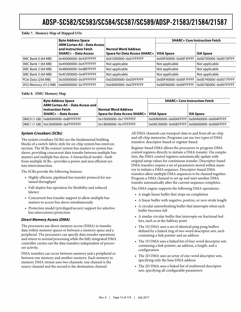
System Crossbars (SCBs)
The system crossbars (SCBs) are the fundamental building blocks of a switch-fabric style for on-chip system bus intercon-nection. The SCBs connect system bus masters to system bus slaves, providing concurrent data transfer between multiple bus masters and multiple bus slaves. A hierarchical model—built from multiple SCBs—provides a power and area efficient sys-tem interconnection.The SCBs provide the following features:
• Highly efficient, pipelined bus transfer protocol for sus-tained throughput
• Full-duplex bus operation for flexibility and reduced latency
• Concurrent bus transfer support to allow multiple bus masters to access bus slaves simultaneously
• Protection model (privileged/secure) support for selective bus interconnect protection
Direct Memory Access (DMA)
The processors use direct memory access (DMA) to transfer data within memory spaces or between a memory space and a peripheral. The processors can specify data transfer operations and return to normal processing while the fully integrated DMA controller carries out the data transfers independent of proces-sor activity. DMA transfers can occur between memory and a peripheral or between one memory and another memory. Each memory to memory DMA stream uses two channels: one channel is the source channel and the second is the destination channel.
All DMA channels can transport data to and from all on-chip and off-chip memories. Programs can use two types of DMA transfers: descriptor-based or register-based. Register-based DMA allows the processors to program DMA control registers directly to initiate a DMA transfer. On comple-tion, the DMA control registers automatically update with original setup values for continuous transfer. Descriptor-based DMA transfers require a set of parameters stored within mem-ory to initiate a DMA sequence. Descriptor-based DMA transfers allow multiple DMA sequences to be chained together. Program a DMA channel to set up and start another DMA transfer automatically after the current sequence completes.The DMA engine supports the following DMA operations:
• A single linear buffer that stops on completion• A linear buffer with negative, positive, or zero stride length• A circular autorefreshing buffer that interrupts when each
buffer becomes full• A similar circular buffer that interrupts on fractional buf-
fers, such as at the halfway point• The 1D DMA uses a set of identical ping pong buffers
defined by a linked ring of two-word descriptor sets, each containing a link pointer and an address
• The 1D DMA uses a linked list of four-word descriptor sets containing a link pointer, an address, a length, and a configuration
• The 2D DMA uses an array of one-word descriptor sets, specifying only the base DMA address
• The 2D DMA uses a linked list of multiword descriptor sets, specifying all configurable parameters
Table 7. Memory Map of Mapped I/Os
Byte Address SpaceARM Cortex-A5 – Data Access and Instruction FetchSHARC+ – Data Access
Normal Word AddressSpace for Data Access SHARC+
SHARC+ Core Instruction Fetch
VISA Space ISA SpaceSMC Bank 0 (64 MB) 0x40000000–0x43FFFFFF 0x01000000–0x01FFFFFF 0x00F00000–0x00F3FFFF 0x00700000–0x0073FFFF
SMC Bank 1 (64 MB) 0x44000000–0x47FFFFFF Not applicable Not applicable Not applicable
SMC Bank 2 (64 MB) 0x48000000–0x4BFFFFFF Not applicable Not applicable Not applicable
SMC Bank 3 (64 MB) 0x4C000000–0x4FFFFFFF Not applicable Not applicable Not applicable
PCIe Data (256 MB) 0x50000000–0x5FFFFFFF 0x02000000–0x03FFFFFF 0x00F40000–0x00F7FFFF 0x00740000–0x0077FFFF
SPI2 Memory (512 MB) 0x60000000–0x7FFFFFFF 0x04000000–0x07FFFFFF 0x00F80000–0x00FFFFFF 0x00780000–0x007FFFFF
Table 8. DMC Memory Map
Byte Address SpaceARM Cortex-A5 – Data Access and Instruction FetchSHARC+ – Data Access
Normal Word AddressSpace for Data Access SHARC+
SHARC+ Core Instruction Fetch
VISA Space ISA SpaceDMC0 (1 GB) 0x80000000–0xBFFFFFFF 0x10000000–0x17FFFFFF 0x00800000–0x00AFFFFF 0x00400000–0x004FFFFF
DMC1 (1 GB) 0xC0000000–0xFFFFFFFF 0x18000000–0x1FFFFFFF 0x00C00000–0x00EFFFFF 0x00600000–0x006FFFFF
Rev. A | Page 14 of 174 | July 2017
ADSP-SC582/SC583/SC584/SC587/SC589/ADSP-21583/21584/21587Memory Direct Memory Access (MDMA)The processor supports various MDMA operations, including,
• Standard bandwidth MDMA channels with CRC protec-tion (32-bit bus width, runs on SCLK0)
• Enhanced bandwidth MDMA channel (32-bit bus width, runs on SYSCLK)
• Maximum bandwidth MDMA channels (64-bit bus width, run on SYCLK, one channel can be assigned to the FFT accelerator)
Extended Memory DMAExtended memory DMA supports various operating modes such as delay line (which allows processor reads and writes to external delay line buffers and to the external memory) with limited core interaction and scatter/gather DMA (writes to and from noncontiguous memory blocks).
Cyclic Redundant C ode (CRC) Protection
The cyclic redundant codes (CRC) protection modules allow system software to calculate the signature of code, data, or both in memory, the content of memory-mapped registers, or peri-odic communication message objects. Dedicated hardware circuitry compares the signature with precalculated values and triggers appropriate fault events. For example, every 100 ms the system software initiates the sig-nature calculation of the entire memory contents and compares these contents with expected, precalculated values. If a mis-match occurs, a fault condition is generated through the processor core or the trigger routing unit.The CRC is a hardware module based on a CRC32 engine that computes the CRC value of the 32-bit data-words presented to it. The source channel of the memory to memory DMA (in memory scan mode) provides data. The data can be optionally forwarded to the destination channel (memory transfer mode). The main features of the CRC peripheral are as follows:
• Memory scan mode• Memory transfer mode• Data verify mode• Data fill mode• User-programmable CRC32 polynomial• Bit/byte mirroring option (endianness)• Fault/error interrupt mechanisms• 1D and 2D fill block to initialize an array with constants• 32-bit CRC signature of a block of a memory or an MMR
block
Event Handling
The processors provide event handling that supports both nest-ing and prioritization. Nesting allows multiple event service routines to be active simultaneously. Prioritization ensures that servicing a higher priority event takes precedence over servicing a lower priority event.
The processors provide support for five different types of events:
• An emulation event causes the processors to enter emula-tion mode, allowing command and control of the processors through the JTAG interface.
• A reset event resets the processors.• An exceptions event occur synchronously to program flow
(in other words, the exception is taken before the instruc-tion is allowed to complete). Conditions triggered on the one side by the SHARC+ core, such as data alignment (SIMD/long word) or compute violations (fixed or floating point), and illegal instructions cause core exceptions. Con-ditions triggered on the other side by the SEC, such as error correcting codes (ECC)/parity/watchdog/system clock, cause system exceptions.
• An interrupts event occurs asynchronously to program flow. They are caused by input signals, timers, and other peripherals, as well as by an explicit software instruction.
System Event Controller (SEC)Both SHARC+ cores feature a system event controller. The SEC features include the following:
• Comprehensive system event source management includ-ing interrupt enable, fault enable, priority, core mapping, and source grouping
• A distributed programming model where each system event source control and all status fields are independent of each other
• Determinism where all system events have the same propa-gation delay and provide unique identification of a specific system event source
• A slave control port that provides access to all SEC registers for configuration, status, and interrupt/fault services
• Global locking that supports a register level protection model to prevent writes to locked registers
• Fault management including fault action configuration, time out, external indication, and system reset
Trigger Routing Unit (TRU)
The trigger routing unit (TRU) provides system-level sequence control without core intervention. The TRU maps trigger masters (generators of triggers) to trigger slaves (receivers of triggers). Slave endpoints can be configured to respond to trig-gers in various ways. Common applications enabled by the TRU include,
• Automatically triggering the start of a DMA sequence after a sequence from another DMA channel completes
• Software triggering• Synchronization of concurrent activities
Rev. A | Page 15 of 174 | July 2017
ADSP-SC582/SC583/SC584/SC587/SC589/ADSP-21583/21584/21587SECURITY FEATURESThe following sections describe the security features of the ADSP-SC58x/ADSP-2158x processors.
ARM TrustZone
The ADSP-SC58x processors provide TrustZone technology that is integrated into the ARM Cortex-A5 processors. The TrustZone technology enables a secure state that is extended throughout the system fabric.
Cryptographic Hardware Accelerators
The ADSP-SC58x/ADSP-2158x processors support standards-based hardware accelerated encryption, decryption, authentica-tion, and true random number generation.Support for the hardware-accelerated cryptographic ciphers includes the following:
• AES in ECB, CBC, ICM, and CTR modes with 128-bit, 192-bit, and 256-bit keys
• DES in ECB and CBC mode with 56-bit key• 3DES in ECB and CBC mode with 3x 56-bit key• ARC4 in stateful, stateless mode, up to 128-bit key
Support for the hardware accelerated hash functions includes the following:
• SHA-1• SHA-2 with 224-bit and 256-bit digests• HMAC transforms for SHA-1 and SHA-2• MD5
Public key accelerator (PKA) is available to offload computation intensive public key cryptography operations.Both a hardware-based nondeterministic random number gen-erator and pseudorandom number generator are available.Secure boot is also available with 224-bit elliptic curve digital signatures ensuring integrity and authenticity of the boot stream. Optionally, ensuring confidentiality through AES-128 encryption is available.Employ secure debug to allow only trusted users to access the system with debug tools.
System Protection Unit (SPU)
The system protection unit (SPU) guards against accidental or unwanted access to an MMR space of the peripheral by provid-ing a write protection mechanism. The user can choose and configure the protected peripherals as well as configure which of the four system MMR masters (two SHARC+ cores, memory DMA, and CoreSight debug) the peripherals are guarded against. The SPU is also part of the security infrastructure. Along with providing write protection functionality, the SPU is employed to define which resources in the system are secure or nonsecure and to block access to secure resources from nonsecure masters.
System Memory Protection Unit (SMPU)
Synonymously, the system memory protection unit (SMPU) provides memory protection against read and/or write transac-tions to defined regions of memory. There are SMPU units in the ADSP-SC58x/ADSP-2158x processors for each memory space, except for SHARC L1 and SPI direct memory slave.The SMPU is also part of the security infrastructure. It allows the user to protect against arbitrary read and/or write transac-tions and allows regions of memory to be defined as secure and prevent nonsecure masters from accessing those memory regions.
SAFETY FEATURESThe ADSP-SC58x/ADSP-2158x processors are designed to sup-port functional safety applications. While the level of safety is mainly dominated by the system concept, the following primi-tives are provided by the processors to build a robust safety concept.
Multiparity Bit Protected SHARC+ Core L1 Memories
In the SHARC+ core L1 memory space, whether SRAM or cache, multiple parity bits protect each word to detect the single event upsets that occur in all RAMs. Parity does not protect the cache tags.
Error Correcting Codes (ECC) Protected L2 Memories
Error correcting codes (ECC) correct single event upsets. A sin-gle error correct-double error detect (SEC-DED) code protects the L2 memory. By default, ECC is enabled, but it can be dis-abled on a per bank basis. Single-bit errors correct transparently. If enabled, dual-bit errors can issue a system event or fault. ECC protection is fully transparent to the user, even if L2 memory is read or written by 8-bit or 16-bit entities.
Cyclic Redundant Code (CRC) Protected Memories
While parity bit and ECC protection mainly protect against ran-dom soft errors in L1 and L2 memory cells, the cyclic redundant code (CRC) engines can protect against systematic errors (pointer errors) and static content (instruction code) of L1, L2, and even L3 memories (DDR2, LPDDR). The processors feature two CRC engines that are embedded in the memory to memory DMA controllers.
CAUTIONThis product includes security features that can be used to protect embedded nonvolatile memory contents and prevent execution of unauthorized code. When security is enabled on this device (either by the ordering party or the subsequent receiving parties), the ability of Analog Devices to conduct failure analysis on returned devices is limited. Contact Analog Devices for details on the failure analysis limitations for this device.
Rev. A | Page 16 of 174 | July 2017
ADSP-SC582/SC583/SC584/SC587/SC589/ADSP-21583/21584/21587CRC checksums can be calculated or compared automatically during memory transfers, or one or multiple memory regions can be continuously scrubbed by a single DMA work unit as per DMA descriptor chain instructions. The CRC engine also pro-tects data loaded during the boot process.
Signal Watchdogs
The eight general-purpose timers feature modes to monitor off-chip signals. The watchdog period mode monitors whether external signals toggle with a period within an expected range. The watchdog width mode monitors whether the pulse widths of external signals are within an expected range. Both modes help to detect undesired toggling or lack of toggling of system level signals.
System Event Controller (SEC)
Besides system events, the system event controller (SEC) further supports fault management including fault action configuration as timeout, internal indication by system interrupt, or external indication through the SYS_FAULT pin and system reset.
PROCESSOR PERIPHERALSThe following sections describe the peripherals of the ADSP-SC58x/ADSP-2158x processors.
Dynamic Memory Controller (DMC)
The 16-bit dynamic memory controller (DMC) interfaces to:• LPDDR1 (JESD209A) maximum frequency 200 MHz,
DDRCLK (64 Mb to 2 Gb)• DDR2 (JESD79-2E) maximum frequency 400 MHz,
DDRCLK (256 Mb to 4 Gb)• DDR3 (JESD79-3E) maximum frequency 450 MHz,
DDRCLK (512 Mb to 8 Gb)• DDR3L (1.5 V compatible only) maximum frequency
450 MHz, DDRCLK (512 Mb to 8 Gb)See Table 8 for the DMC memory map.
Digital Audio Interface (DAI)
The processors support two mirrored digital audio interface (DAI) units. Each DAI can connect various peripherals to any of the DAI pins (DAI_PIN20–DAI_PIN01).The application code makes these connections using the signal routing unit (SRU), shown in Figure 1.The SRU is a matrix routing unit (or group of multiplexers) that enables the peripherals provided by the DAI to interconnect under software control. This functionality allows easy use of the DAI associated peripherals for a wider variety of applications by using a larger set of algorithms than is possible with nonconfig-urable signal paths.The DAI includes the peripherals described in the following sec-tions (SPORTs, ASRC, S/PDIF, and PCG). DAI Pin Buffers 20 and 19 can change the polarity of the input signals. Most signals of the peripherals belonging to different DAIs cannot be inter-connected, with few exceptions.
The DAI_PINx pin buffers may also be used as GPIO pins. DAI input signals allow the triggering of interrupts on the rising edge, the falling edge, or both edges.See the Digital Audio Interface (DAI) chapter of the ADSP-SC58x/ADSP-2158x SHARC+ Processor Hardware Reference for complete information on the use of the DAIs and SRUs.
Serial Ports (SPORTs)
The processors feature eight synchronous full serial ports. These ports provide an inexpensive interface to a wide variety of digi-tal and mixed-signal peripheral devices. These devices include Analog Devices AD19xx and ADAU19xx family of audio codecs, analog-to-digital converters (ADCs) and digital-to-ana-log converters (DACs). Two data lines, a clock, and frame sync make up the serial ports. The data lines can be programmed to either transmit or receive data and each data line has a dedicated DMA channel.An individual full SPORT module consists of two inde-pendently configurable SPORT halves with identical functionality. Two bidirectional data lines—primary (0) and secondary (1)—are available per SPORT half and are configu-rable as either transmitters or receivers. Therefore, each SPORT half permits two unidirectional streams into or out of the same SPORT. This bidirectional functionality provides greater flexibility for serial communications. For full-duplex configura-tion, one half SPORT provides two transmit signals, while the other half SPORT provides the two receive signals. The frame sync and clock are shared. Serial ports operate in the following six modes:
• Standard DSP serial mode• Multichannel time division multiplexing (TDM) mode• I2S mode• Packed I2S mode• Left justified mode• Right justified mode
Asynchronous Sample Rate Converter (ASRC)
The asynchronous sample rate converter (ASRC) contains eight ASRC blocks. It is the same core in the AD1896 192 kHz stereo asynchronous sample rate converter. The ASRC provides up to 140 dB signal-to-noise ratio (SNR). The ASRC block performs synchronous or asynchronous sample rate conversion across independent stereo channels, without using internal processor resources. The ASRC blocks can also be configured to operate together to convert multichannel audio data without phase mis-matches. Finally, the ASRC can clean up audio data from jittery clock sources such as the S/PDIF receiver.
S/PDIF-Compatible Digital Audio Receiver/Transmitter
The Sony/Philips Digital Interface Format (S/PDIF) is a stan-dard audio data transfer format that allows the transfer of digital audio signals from one device to another without converting them to an analog signal. There are two S/PDIF transmit/receive
Rev. A | Page 17 of 174 | July 2017
ADSP-SC582/SC583/SC584/SC587/SC589/ADSP-21583/21584/21587blocks on the processor. The digital audio interface carries three types of information: audio data, nonaudio data (compressed data), and timing information.The S/PDIF interface supports one stereo channel or com-pressed audio streams. The S/PDIF transmitter and receiver are AES3 compliant and support the sample rate from 24 KHz to 192 KHz. The S/PDIF receiver supports professional jitter standards.The S/PDIF receiver/transmitter has no separate DMA chan-nels. It receives audio data in serial format and converts it into a biphase encoded signal. The serial data input to the receiver/transmitter can be formatted as left justified, I2S, or right justified with word widths of 16, 18, 20, or 24 bits. The serial data, clock, and frame sync inputs to the S/PDIF receiver/transmitter are routed through the signal routing unit (SRU). They can come from various sources, such as the SPORTs, external pins, and the precision clock generators (PCGs), and are controlled by the SRU control registers.
Precision Clock Generators (PCG)
The precision clock generators (PCG) consist of four units: units A/B located in the DAI0 block, and units C/D located in the DAI1 block. The PCG can generate a pair of signals (clock and frame sync) derived from a clock input signal (CLKIN1-0, SCLK0, or DAI pin buffer). Each unit can also access the oppo-site DAI unit. All units are identical in functionality and operate independently of each other. The two signals generated by each unit are normally used as a serial bit clock/frame sync pair.
Enhanced Parallel Peripheral Interface (EPPI)
The processors provide an enhanced parallel peripheral inter-face (EPPI) that supports data widths up to 24 bits. The EPPI supports direct connection to TFT LCD panels, parallel ADCs and DACs, video encoders and decoders, image sensor mod-ules, and other general-purpose peripherals.The features supported in the EPPI module include the following:
• Programmable data length of 8 bits, 10 bits, 12 bits, 14 bits, 16 bits, 18 bits, and 24 bits per clock.
• Various framed, nonframed, and general-purpose operat-ing modes. Frame syncs can be generated internally or can be supplied by an external device.
• ITU-656 status word error detection and correction for ITU-656 receive modes and ITU-656 preamble and status word decoding.
• Optional packing and unpacking of data to/from 32 bits from/to 8 bits, 16 bits, and 24 bits. If packing/unpacking is enabled, configure endianness to change the order of pack-ing/unpacking of the bytes/words.
• RGB888 can be converted to RGB666 or RGB565 for trans-mit modes.
• Various deinterleaving/interleaving modes for receiv-ing/transmitting 4:2:2 YCrCb data.
• Configurable LCD data enable output available on Frame Sync 3.
Universal Asynchronous Receiver/Transmitter (UART) Ports
The processors provide three full-duplex universal asynchro-nous receiver/transmitter (UART) ports, fully compatible with PC standard UARTs. Each UART port provides a simplified UART interface to other peripherals or hosts, supporting full-duplex, DMA supported, asynchronous transfers of serial data. A UART port includes support for five to eight data bits as well as no parity, even parity, or odd parity. Optionally, an additional address bit can be transferred to inter-rupt only addressed nodes in multidrop bus (MDB) systems. A frame is terminated by a configurable number of stop bits.The UART ports support automatic hardware flow control through the clear to send (CTS) input and request to send (RTS) output with programmable assertion first in, first out (FIFO) levels.To help support the Local Interconnect Network (LIN) proto-cols, a special command causes the transmitter to queue a break command of programmable bit length into the transmit buffer. Similarly, the number of stop bits can be extended by a pro-grammable interframe space.
Serial Peripheral Interface (SPI) Ports
The processors have three industry-standard SPI-compatible ports that allow the processors to communicate with multiple SPI-compatible devices. The baseline SPI peripheral is a synchronous, four-wire inter-face consisting of two data pins, one device select pin, and a gated clock pin. The two data pins allow full-duplex operation to other SPI-compatible devices. An extra two (optional) data pins are provided to support quad SPI operation. Enhanced modes of operation, such as flow control, fast mode, and dual-I/O mode (DIOM), are also supported. A direct memory access (DMA) mode allows for transferring several words with mini-mal central processing unit (CPU) interaction.With a range of configurable options, the SPI ports provide a glueless hardware interface with other SPI-compatible devices in master mode, slave mode, and multimaster environments. The SPI peripheral includes programmable baud rates, clock phase, and clock polarity. The peripheral can operate in a multi-master environment by interfacing with several other devices, acting as either a master device or a slave device. In a multimas-ter environment, the SPI peripheral uses open-drain outputs to avoid data bus contention. The flow control features enable slow slave devices to interface with fast master devices by providing an SPI ready pin (SPI_RDY) which flexibly controls the transfers.The baud rate and clock phase/polarities of the SPI port are pro-grammable. The port has integrated DMA channels for both transmit and receive data streams.
Link Ports (LP)
Two 8-bit wide link ports (LP) can connect to the link ports of other DSPs or peripherals. LP are bidirectional ports that have eight data lines, an acknowledge line, and a clock line.
Rev. A | Page 18 of 174 | July 2017
ADSP-SC582/SC583/SC584/SC587/SC589/ADSP-21583/21584/21587ADC Control Module (ACM) Interface
The ADC control module (ACM) provides an interface that synchronizes the controls between the processors and an ADC. The analog-to-digital conversions are initiated by the proces-sors, based on external or internal events.The ACM allows for flexible scheduling of sampling instants and provides precise sampling signals to the ADC. The ACM synchronizes the ADC conversion process, generat-ing the ADC controls, the ADC conversion start signal, and other signals. The actual data acquisition from the ADC is done by an internal DAI routing of the ACM with the SPORT0 block.The processors interface directly to many ADCs without any glue logic required.
3-Phase Pulse Width Modulator (PWM) Units
The pulse width modulator (PWM) module is a flexible and programmable waveform generator. With minimal CPU inter-vention, the PWM generates complex waveforms for motor control, pulse coded modulation (PCM), DAC conversions, power switching, and power conversion. The PWM module has four PWM pairs capable of 3-phase PWM generation for source inverters for ac induction and dc brushless motors.Each of the three 3-phase PWM generation units features the following:
• 16-bit center-based PWM generation unit• Programmable PWM pulse width• Single update mode with an option for asymmetric duty• Programmable dead time and switching frequency• Programmable dead time per channel• Twos complement implementation which permits smooth
transition to full on and full off states• Dedicated asynchronous PWM shutdown signal
Ethernet Media Access Controller (EMAC)
The processor features two ethernet media access controllers (EMACs): 10/100 Ethernet and 10/100/1000/AVB Ethernet with precision time protocol IEEE 1588.The processors can directly connect to a network through embedded fast EMAC that supports 10-BaseT (10 Mb/sec), 100-BaseT (100 Mb/sec) and 1000-BaseT (1 Gb/sec) operations. The 10/100 EMAC peripheral on the processors is fully compli-ant to the IEEE 802.3-2002 standard. The peripheral provides programmable features designed to minimize supervision, bus use, or message processing by the rest of the processor system. Some standard features of the EMAC are as follows:
• Support and RMII/RGMII protocols for external PHYs• Full-duplex and half-duplex modes• Media access management (in half-duplex operation)• Flow control • Station management, including the generation of
MDC/MDIO frames for read/write access to PHY registers
Some advanced features of the EMAC are as follows:• Automatic checksum computation of IP header and IP
payload fields of receive frames• Independent 32-bit descriptor driven receive and transmit
DMA channels• Frame status delivery to memory through DMA, including
frame completion semaphores for efficient buffer queue management in software
• Transmit DMA support for separate descriptors for MAC header and payload fields to eliminate buffer copy operations
• Convenient frame alignment modes• 47 MAC management statistics counters with selectable
clear on read behavior and programmable interrupts on half maximum value
• Advanced power management• Magic packet detection and wakeup frame filtering• Support for 802.3Q tagged VLAN frames• Programmable MDC clock rate and preamble suppression
Audio Video Bridging (AVB) Support(10/100/1000 EMAC Only)The 10/100/1000 EMAC supports the following audio video (AVB) features:
• Separate channels or queues for AV data transfer in 100 Mbps and 1000 Mbps modes
• IEEE 802.1-Qav specified credit-based shaper (CBS) algo-rithm for the additional transmit channels
• Configuring up to two additional channels (Channel 1 and Channel 2) on the transmit and receive paths for AV traffic. Channel 0 is available by default and carries the legacy best effort Ethernet traffic on the transmit side.
• Separate DMA, transmit and receive FIFO for AVB latency class
• Programmable control to route received VLAN tagged non AV packets to channels or queues
Precision Time Protocol (PTP) IEEE 1588 SupportThe IEEE 1588 standard is a precision clock synchronization protocol for networked measurement and control systems. The processors include hardware support for IEEE 1588 with an integrated precision time protocol synchronization engine (PTP_TSYNC). This engine provides hardware assisted time stamping to improve the accuracy of clock synchronization between PTP nodes. The main features of the engine are as follows:
• Support for both IEEE 1588-2002 and IEEE 1588-2008 pro-tocol standards
• Hardware assisted time stamping capable of up to 12.5 ns resolution
• Lock adjustment
Rev. A | Page 19 of 174 | July 2017
ADSP-SC582/SC583/SC584/SC587/SC589/ADSP-21583/21584/21587• Automatic detection of IPv4 and IPv6 packets, as well as
PTP messages• Multiple input clock sources (SCLK0, RGMII, RMII, RMII
clock, and external clock)• Programmable pulse per second (PPS) output• Auxiliary snapshot to time stamp external events
Controller Area Network (CAN)
There are two controller area network (CAN) modules. A CAN controller implements the CAN 2.0B (active) protocol. This protocol is an asynchronous communications protocol used in both industrial and automotive control systems. The CAN pro-tocol is well suited for control applications due to the capability to communicate reliably over a network. This is because the protocol incorporates CRC checking, message error tracking, and fault node confinement. The CAN controller offers the following features:
• 32 mailboxes (8 receive only, 8 transmit only, 16 configu-rable for receive or transmit)
• Dedicated acceptance masks for each mailbox• Additional data filtering on the first two bytes• Support for both the standard (11-bit) and extended (29-
bit) identifier (ID) message formats• Support for remote frames• Active or passive network support• Interrupts, including transmit and receive complete, error,
and globalAn additional crystal is not required to supply the CAN clock because it is derived from a system clock through a programma-ble divider.
Timers
The processors include several timers that are described in the following sections.
General-Purpose (GP) Timers (TIMER)There is one general-purpose (GP) timer unit, providing eight general-purpose programmable timers. Each timer has an exter-nal pin that can be configured either as PWM or timer output, as an input to clock the timer, or as a mechanism for measuring pulse widths and periods of external events. These timers can be synchronized to an external clock input on the TM_TMR[n] pins, an external TM_CLK input pin, or to the internal SCLK0.These timer units can be used in conjunction with the UARTs and the CAN controller to measure the width of the pulses in the data stream to provide a software autobaud detect function for the respective serial channels. The GP timers can generate interrupts to the processor core, providing periodic events for synchronization to either the sys-tem clock or to external signals. Timer events can also trigger other peripherals via the TRU (for instance, to signal a fault). Each timer can also be started and/or stopped by any TRU mas-ter without core intervention.
Watchdog Timer (WDT)Two on-chip software watchdog timers (WDT) can be used by the ARM Cortex-A5 and/or SHARC+ cores. A software watch-dog can improve system availability by forcing the processors to a known state, via a general-purpose interrupt, or a fault, if the timer expires before being reset by software. The programmer initializes the count value of the timer, enables the appropriate interrupt, then enables the timer. Thereafter, the software must reload the counter before it counts down to zero from the programmed value, protecting the system from remaining in an unknown state where software that normally resets the timer stops running due to an external noise condi-tion or software error.
General-Purpose Counters (CNT)
A 32-bit counter (CNT) is provided that can operate in general-purpose up/down count modes and can sense 2-bit quadrature or binary codes as typically emitted by industrial drives or man-ual thumbwheels. Count direction is either controlled by a level-sensitive input pin or by two edge detectors.A third counter input can provide flexible zero marker support and can input the push button signal of thumbwheel devices. All three CNT0 pins have a programmable debouncing circuit.Internal signals forwarded to a GP timer enable this timer to measure the intervals between count events. Boundary registers enable auto-zero operation or simple system warning by inter-rupts when programmed count values are exceeded.
PCI Express (PCIe)
A PCI express interface (PCIe) is available on some product variants (see Table 2 and Table 3). This single, bidirectional lane can be configured to be either a root complex (RC) or end point (EP) system. The PCIe interface has the following features:
• Designed to be compliant with the PCI Express Base Specification 3.0
• Support for transfers at either 2.5 Gbps (Gen 1) or 5.0 Gbps (Gen 2) in each direction
• Support for 8b/10b encode and decode• Lane reversal and lane polarity inversion• Flow control of data in both the transmit and receive
directions• Support for removal of corrupted packets for error detec-
tion and recovery• Maximum transaction payload of 256 bytes
Housekeeping Analog-to-Digital Converter (HADC)
The housekeeping analog-to-digital converter (HADC) pro-vides a general-purpose, multichannel successive approximation ADC. It supports the following set of features:
• 12-bit ADC core (10-bit accuracy) with built in sample and hold.
• Eight single-ended input channels that can be extended to 15 channels by adding an external channel multiplexer.
Rev. A | Page 20 of 174 | July 2017
ADSP-SC582/SC583/SC584/SC587/SC589/ADSP-21583/21584/21587• Throughput rates up to 1 MSPS.• Single external reference with analog inputs between
0 V and 3.3 V.• Selectable ADC clock frequency including the ability to
program a prescaler.• Adaptable conversion type; allows single or continuous
conversion with option of autoscan.• Auto sequencing capability with up to 15 autoconversions
in a single session. Each conversion can be programmed to select 1 to 15 input channels.
• 16 data registers (individually addressable) to store conver-sion values.
USB 2.0 On the Go (OTG) Dual-Role Device Controller
There are two USB modules + PHY. USB0 supports HS/FS/LS USB 2.0 on the go (OTG) and USB1 supports HS/FS USB 2.0 only and can be programmed to be a host or device. The USB 2.0 OTG dual-role device controller provides a low cost connectivity solution in industrial applications, as well as consumer mobile devices such as cell phones, digital still cam-eras, and MP3 players. The USB 2.0 controller allows these devices to transfer data using a point to point USB connection without the need for a PC host. The module can operate in a tra-ditional USB peripheral only mode as well as the host mode presented in the OTG supplement to the USB 2.0 specification. The USB clock is provided through a dedicated external crystal or crystal oscillator. The USB OTG dual-role device controller includes a PLL with programmable multipliers to generate the necessary internal clocking frequency for the USB.
Media Local Bus (MediaLB)
The automotive model has a MediaLB (MLB) slave interface that allows the processors to function as a media local bus device. It includes support for both 3-pin and 6-pin media local bus protocols. The MLB 3-pin configuration supports speeds up to 1024 × FS. The MLB 6-pin configuration supports speed of 4096 × FS. The MLB also supports up to 63 logical channels with up to 468 bytes of data per MLB frame.The MLB interface supports MOST25, MOST50, and MOST150 data rates and operates in slave mode only.
2-Wire Controller Interface (TWI)
The processors include three 2-wire interface (TWI) modules that provide a simple exchange method of control data between multiple devices. The TWI module is compatible with the widely used I2C bus standard. The TWI module offers the capabilities of simultaneous master and slave operation and support for both 7-bit addressing and multimedia data arbitra-tion. The TWI interface utilizes two pins for transferring clock (TWI_SCL) and data (TWI_SDA) and supports the protocol at speeds up to 400 kb/sec. The TWI interface pins are compatible with 5 V logic levels.
Additionally, the TWI module is fully compatible with serial camera control bus (SCCB) functionality for easier control of various CMOS camera sensor devices.
General-Purpose I/O (GPIO)
Each general-purpose port pin can be individually controlled by manipulating the port control, status, and interrupt registers:
• GPIO direction control register specifies the direction of each individual GPIO pin as input or output.
• GPIO control and status registers have a write one to mod-ify mechanism that allows any combination of individual GPIO pins to be modified in a single instruction, without affecting the level of any other GPIO pins.
• GPIO interrupt mask registers allow each individual GPIO pin to function as an interrupt to the processors. GPIO pins defined as inputs can be configured to generate hardware interrupts, while output pins can be triggered by software interrupts.
• GPIO interrupt sensitivity registers specify whether indi-vidual pins are level or edge sensitive and specify, if edge sensitive, whether the rising edge or both the rising and falling edges of the signal are significant.
Pin Interrupts
Every port pin on the processors can request interrupts in either an edge sensitive or a level sensitive manner with programmable polarity. Interrupt functionality is decoupled from GPIO opera-tion. Six system-level interrupt channels (PINT0–PINT5) are reserved for this purpose. Each of these interrupt channels can manage up to 32 interrupt pins. The assignment from pin to interrupt is not performed on a pin by pin basis. Rather, groups of eight pins (half ports) can be flexibly assigned to interrupt channels. Every pin interrupt channel features a special set of 32-bit mem-ory-mapped registers that enable half-port assignment and interrupt management. This includes masking, identification, and clearing of requests. These registers also enable access to the respective pin states and use of the interrupt latches, regardless of whether the interrupt is masked or not. Most control registers feature multiple MMR address entries to write-one-to-set or write-one-to-clear them individually.
Mobile Storage Interface (MSI)
The mobile storage interface (MSI) controller acts as the host interface for multimedia cards (MMC), secure digital memory cards (SD), and secure digital input/output cards (SDIO). The MSI controller has the following features:
• Support for a single MMC, SD memory, and SDIO card • Support for 1-bit and 4-bit SD modes • Support for 1-bit, 4-bit, and 8-bit MMC modes • Support for eMMC 4.3 embedded NAND flash devices • An eleven-signal external interface with clock, command,
optional interrupt, and up to eight data lines• Integrated DMA controller
Rev. A | Page 21 of 174 | July 2017
ADSP-SC582/SC583/SC584/SC587/SC589/ADSP-21583/21584/21587• Card interface clock generation in the clock distribution
unit (CDU) • SDIO interrupt and read wait features
SYSTEM ACCELERATIONThe following sections describe the system acceleration blocks of the ADSP-SC58x/ADSP-2158x processors.
FFT/IFFT Accelerator
A high performance FFT/IFFT accelerator is available to improve the overall floating-point computation power of the ADSP-SC58x/ADSP-2158x processors.The following features are available to improve the overall per-formance of the FFT/IFFT accelerator:
• Support for the IEEE-754/854 single-precision floating-point data format.
• Automatic twiddle factor generation to reduce system bandwidth.
• Support for a vector complex multiply for windowing and frequency domain filtering.
• Ability to pipeline the data flow. This allows the accelerator to bring in a new data set while the current data set is pro-cessed and the previous data set is sent out to memory. This can provide a significant system level performance improvement.
• Ability to output the result as the magnitude squared of the complex samples.
• Dedicated, high speed DMA controller with 64-bit buses that can read and write data from any memory space.
The FFT/IFFT accelerator can run concurrently with the other accelerators on the processor.
Finite Impulse Response (FIR) Accelerator
The finite impulse response (FIR) accelerator consists of a 1024 word coefficient memory, a 1024 word deep delay line for the data, and four MAC units. A controller manages the acceler-ator. The FIR accelerator runs at the peripheral clock frequency. The FIR accelerator can access all memory spaces and can run concurrently with the other accelerators on the processor.
Infinite Impulse Response (IIR) Accelerator
The infinite impulse response (IIR) accelerator consists of a 1440 word coefficient memory for storage of biquad coeffi-cients, a data memory for storing the intermediate data, and one MAC unit. A controller manages the accelerator. The IIR accel-erator runs at the peripheral clock frequency. The IIR accelerator can access all memory spaces and run concurrently with the other accelerators on the processor.
Harmonic Analysis Engine (HAE)
The harmonic analysis engine (HAE) block receives 8 kHz input samples from two source signals whose frequencies are between 45 Hz and 65 Hz. The HAE processes the input samples and
produces output results. The output results consist of power quality measurements of the fundamental and up to 12 addi-tional harmonics.
Sinus Cardinalis (SINC) Filter
The sinus cardinalis (SINC) filter module processes four bit streams using a pair of configurable SINC filters for each bit stream. The purpose of the primary SINC filter of each pair is to produce the filtered and decimated output for the pair. The out-put can decimate any integer rate between 8 and 256 times lower than the input rate. Greater decimation allows greater removal of noise, and, therefore, greater effective number of bits (ENOB).Optional additional filtering outside the SINC module can fur-ther increase ENOB. The primary SINC filter output is accessible through transfer to processor memory, or to another peripheral, via DMA.Each of the four channels is also provided with a low latency secondary filter with programmable positive and negative over-range detection comparators. These limit detection events can interrupt the core, generate a trigger, or signal a system fault.
Digital Transmission Content Protection (DTCP)
Contact Analog Devices for more information on DTCP.
SYSTEM DESIGNThe following sections provide an introduction to system design features and power supply issues.
Clock Management
The processors provide three operating modes, each with a dif-ferent performance and power profile. Control of clocking to each of the processor peripherals reduces power consumption. The processors do not support any low power operation modes. Control of clocking to each of the processor peripherals can reduce the power consumption.
Reset Control Unit (RCU)
Reset is the initial state of the whole processor, or the core, and is the result of a hardware or software triggered event. In this state, all control registers are set to default values and functional units are idle. Exiting a full system reset starts with the core ready to boot. The reset control unit (RCU) controls how all the functional units enter and exit reset. Differences in functional require-ments and clocking constraints define how reset signals are generated. Programs must guarantee that none of the reset functions put the system into an undefined state or causes resources to stall. This is particularly important when the core resets (programs must ensure that there is no pending system activity involving the core when it is reset). From a system perspective, reset is defined by both the reset tar-get and the reset source.
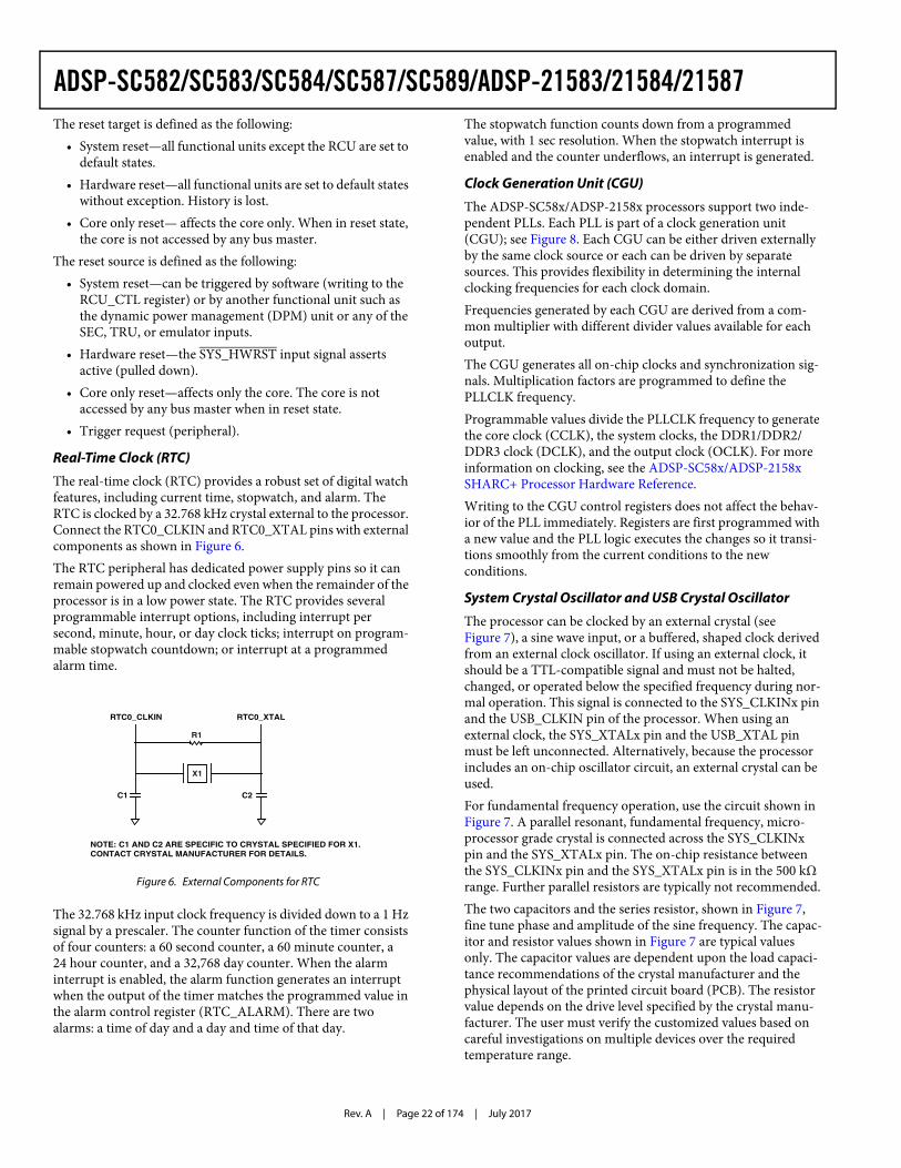
Rev. A | Page 22 of 174 | July 2017
ADSP-SC582/SC583/SC584/SC587/SC589/ADSP-21583/21584/21587The reset target is defined as the following:
• System reset—all functional units except the RCU are set to default states.
• Hardware reset—all functional units are set to default states without exception. History is lost.
• Core only reset— affects the core only. When in reset state, the core is not accessed by any bus master.
The reset source is defined as the following:• System reset—can be triggered by software (writing to the
RCU_CTL register) or by another functional unit such as the dynamic power management (DPM) unit or any of the SEC, TRU, or emulator inputs.
• Hardware reset—the SYS_HWRST input signal asserts active (pulled down).
• Core only reset—affects only the core. The core is not accessed by any bus master when in reset state.
• Trigger request (peripheral).
Real-Time Clock (RTC)
The real-time clock (RTC) provides a robust set of digital watch features, including current time, stopwatch, and alarm. The RTC is clocked by a 32.768 kHz crystal external to the processor. Connect the RTC0_CLKIN and RTC0_XTAL pins with external components as shown in Figure 6.The RTC peripheral has dedicated power supply pins so it can remain powered up and clocked even when the remainder of the processor is in a low power state. The RTC provides several programmable interrupt options, including interrupt per second, minute, hour, or day clock ticks; interrupt on program-mable stopwatch countdown; or interrupt at a programmed alarm time.
The 32.768 kHz input clock frequency is divided down to a 1 Hz signal by a prescaler. The counter function of the timer consists of four counters: a 60 second counter, a 60 minute counter, a 24 hour counter, and a 32,768 day counter. When the alarm interrupt is enabled, the alarm function generates an interrupt when the output of the timer matches the programmed value in the alarm control register (RTC_ALARM). There are two alarms: a time of day and a day and time of that day.
The stopwatch function counts down from a programmed value, with 1 sec resolution. When the stopwatch interrupt is enabled and the counter underflows, an interrupt is generated.
Clock Generation Unit (CGU)
The ADSP-SC58x/ADSP-2158x processors support two inde-pendent PLLs. Each PLL is part of a clock generation unit (CGU); see Figure 8. Each CGU can be either driven externally by the same clock source or each can be driven by separate sources. This provides flexibility in determining the internal clocking frequencies for each clock domain.Frequencies generated by each CGU are derived from a com-mon multiplier with different divider values available for each output. The CGU generates all on-chip clocks and synchronization sig-nals. Multiplication factors are programmed to define the PLLCLK frequency. Programmable values divide the PLLCLK frequency to generate the core clock (CCLK), the system clocks, the DDR1/DDR2/ DDR3 clock (DCLK), and the output clock (OCLK). For more information on clocking, see the ADSP-SC58x/ADSP-2158x SHARC+ Processor Hardware Reference. Writing to the CGU control registers does not affect the behav-ior of the PLL immediately. Registers are first programmed with a new value and the PLL logic executes the changes so it transi-tions smoothly from the current conditions to the new conditions.
System Crystal Oscillator and USB Crystal Oscillator
The processor can be clocked by an external crystal (see Figure 7), a sine wave input, or a buffered, shaped clock derived from an external clock oscillator. If using an external clock, it should be a TTL-compatible signal and must not be halted, changed, or operated below the specified frequency during nor-mal operation. This signal is connected to the SYS_CLKINx pin and the USB_CLKIN pin of the processor. When using an external clock, the SYS_XTALx pin and the USB_XTAL pin must be left unconnected. Alternatively, because the processor includes an on-chip oscillator circuit, an external crystal can be used.For fundamental frequency operation, use the circuit shown in Figure 7. A parallel resonant, fundamental frequency, micro-processor grade crystal is connected across the SYS_CLKINx pin and the SYS_XTALx pin. The on-chip resistance between the SYS_CLKINx pin and the SYS_XTALx pin is in the 500 kΩ range. Further parallel resistors are typically not recommended.The two capacitors and the series resistor, shown in Figure 7, fine tune phase and amplitude of the sine frequency. The capac-itor and resistor values shown in Figure 7 are typical values only. The capacitor values are dependent upon the load capaci-tance recommendations of the crystal manufacturer and the physical layout of the printed circuit board (PCB). The resistor value depends on the drive level specified by the crystal manu-facturer. The user must verify the customized values based on careful investigations on multiple devices over the required temperature range.
Figure 6. External Components for RTC
C1 C2
X1
RTC0_CLKIN
R1
RTC0_XTAL
NOTE: C1 AND C2 ARE SPECIFIC TO CRYSTAL SPECIFIED FOR X1.CONTACT CRYSTAL MANUFACTURER FOR DETAILS.
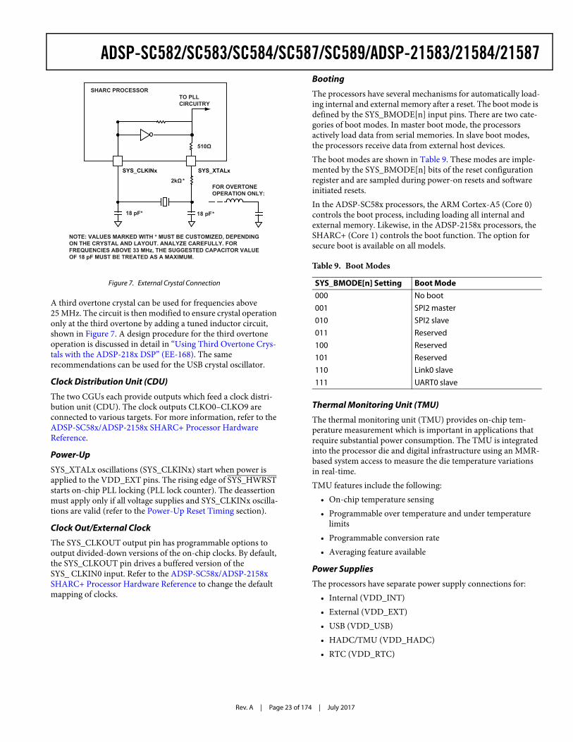
Rev. A | Page 23 of 174 | July 2017
ADSP-SC582/SC583/SC584/SC587/SC589/ADSP-21583/21584/21587
A third overtone crystal can be used for frequencies above 25 MHz. The circuit is then modified to ensure crystal operation only at the third overtone by adding a tuned inductor circuit, shown in Figure 7. A design procedure for the third overtone operation is discussed in detail in “Using Third Overtone Crys-tals with the ADSP-218x DSP” (EE-168). The same recommendations can be used for the USB crystal oscillator.
Clock Distribution Unit (CDU)
The two CGUs each provide outputs which feed a clock distri-bution unit (CDU). The clock outputs CLKO0–CLKO9 are connected to various targets. For more information, refer to the ADSP-SC58x/ADSP-2158x SHARC+ Processor Hardware Reference.
Power-Up
SYS_XTALx oscillations (SYS_CLKINx) start when power is applied to the VDD_EXT pins. The rising edge of SYS_HWRST starts on-chip PLL locking (PLL lock counter). The deassertion must apply only if all voltage supplies and SYS_CLKINx oscilla-tions are valid (refer to the Power-Up Reset Timing section).
Clock Out/External Clock
The SYS_CLKOUT output pin has programmable options to output divided-down versions of the on-chip clocks. By default, the SYS_CLKOUT pin drives a buffered version of the SYS_ CLKIN0 input. Refer to the ADSP-SC58x/ADSP-2158x SHARC+ Processor Hardware Reference to change the default mapping of clocks.
Booting
The processors have several mechanisms for automatically load-ing internal and external memory after a reset. The boot mode is defined by the SYS_BMODE[n] input pins. There are two cate-gories of boot modes. In master boot mode, the processors actively load data from serial memories. In slave boot modes, the processors receive data from external host devices. The boot modes are shown in Table 9. These modes are imple-mented by the SYS_BMODE[n] bits of the reset configuration register and are sampled during power-on resets and software initiated resets.In the ADSP-SC58x processors, the ARM Cortex-A5 (Core 0) controls the boot process, including loading all internal and external memory. Likewise, in the ADSP-2158x processors, the SHARC+ (Core 1) controls the boot function. The option for secure boot is available on all models.
Thermal Monitoring Unit (TMU)
The thermal monitoring unit (TMU) provides on-chip tem-perature measurement which is important in applications that require substantial power consumption. The TMU is integrated into the processor die and digital infrastructure using an MMR-based system access to measure the die temperature variations in real-time.TMU features include the following:
• On-chip temperature sensing• Programmable over temperature and under temperature
limits• Programmable conversion rate• Averaging feature available
Power Supplies
The processors have separate power supply connections for:• Internal (VDD_INT)• External (VDD_EXT)• USB (VDD_USB)• HADC/TMU (VDD_HADC)• RTC (VDD_RTC)
Figure 7. External Crystal Connection
SYS_CLKINx
TO PLL CIRCUITRY
FOR OVERTONEOPERATION ONLY:
NOTE: VALUES MARKED WITH * MUST BE CUSTOMIZED, DEPENDINGON THE CRYSTAL AND LAYOUT. ANALYZE CAREFULLY. FORFREQUENCIES ABOVE 33 MHz, THE SUGGESTED CAPACITOR VALUEOF 18 pF MUST BE TREATED AS A MAXIMUM.
18 pF* 18 pF*
*
SHARC PROCESSOR
SYS_XTALx
Table 9. Boot Modes
SYS_BMODE[n] Setting Boot Mode000 No boot
001 SPI2 master
010 SPI2 slave
011 Reserved
100 Reserved
101 Reserved
110 Link0 slave
111 UART0 slave
Rev. A | Page 24 of 174 | July 2017
ADSP-SC582/SC583/SC584/SC587/SC589/ADSP-21583/21584/21587• DMC (VDD_DMC)• PCIe (VDD_PCIE, VDD_PCIE_TX and VDD_PCIE_RX)
All power supplies must meet the specifications provided in the Operating Conditions section. All external supply pins must be connected to the same power supply.
Power Management
As shown in Table 10, the processors support four different power domains, which maximizes flexibility while maintaining compliance with industry standards and conventions. There are no sequencing requirements for the various power domains, but all domains must be powered according to the appropriate spec-ifications (see the Specifications section for processor operating conditions). If the feature or the peripheral is not used, refer to Table 27.)
The power dissipated by the processors is largely a function of the clock frequency and the square of the operating voltage. For example, reducing the clock frequency by 25% results in a 25% reduction in dynamic power dissipation.
Target Board JTAG Emulator Connector
The Analog Devices DSP tools product line of JTAG emulators uses the IEEE 1149.1 JTAG test access port of the processors to monitor and control the target board processor during emula-tion. The Analog Devices DSP tools product line of JTAG emulators provides emulation at full processor speed, allowing inspection and modification of memory, registers, and proces-sor stacks. The processor JTAG interface ensures the emulator does not affect target system loading or timing.For information on JTAG emulator operation, see the appropri-ate emulator hardware user’s guide at SHARC Processors Software and Tools.
SYSTEM DEBUGThe processors include various features that allow easy system debug. These are described in the following sections.
System Watchpoint Unit (SWU)
The system watchpoint unit (SWU) is a single module that con-nects to a single system bus and provides transaction monitoring. One SWU is attached to the bus going to each system slave. The SWU provides ports for all system bus address channel signals. Each SWU contains four match groups of registers with associated hardware. These four SWU match groups operate independently but share common event (for example, interrupt and trigger) outputs.
Debug Access Port (DAP)
Debug access port (DAP) provides IEEE 1149.1 JTAG interface support through the JTAG debug. The DAP provides an optional instrumentation trace for both the core and system. It provides a trace stream that conforms to MIPI System Trace Protocol version 2 (STPv2).
DEVELOPMENT TOOLSAnalog Devices supports its processors with a complete line of software and hardware development tools, including an inte-grated development environment (CrossCore® Embedded Studio), evaluation products, emulators, and a variety of soft-ware add-ins.
Integrated Development Environments (IDEs)
For C/C++ software writing and editing, code generation, and debug support, Analog Devices offers the CrossCore Embedded Studio integrated development environment (IDE). CrossCore Embedded Studio is based on the Eclipse framework. Supporting most Analog Devices processor families, it is the IDE of choice for processors, including multicore devices. CrossCore Embedded Studio seamlessly integrates available software add-ins to support real-time operating systems, file systems, TCP/IP stacks, USB stacks, algorithmic software mod-ules, and evaluation hardware board support packages. For more information, visit www.analog.com/cces.
EZ-KIT Lite Evaluation Board
For processor evaluation, Analog Devices provides a wide range of EZ-KIT Lite® evaluation boards. Including the processor and key peripherals, the evaluation board also supports on-chip emulation capabilities and other evaluation and development features. Various EZ-Extenders® are also available, which are daughter cards that deliver additional specialized functionality, including audio and video processing. For more information visit www.analog.com.
EZ-KIT Lite Evaluation Kits
For a cost-effective way to learn more about developing with Analog Devices processors, Analog Devices offer a range of EZ-KIT Lite evaluation kits. Each evaluation kit includes an EZ-KIT Lite evaluation board, directions for downloading an evaluation version of the available IDE(s), a USB cable, and a power supply. The USB controller on the EZ-KIT Lite board connects to the USB port of the user PC, enabling the chosen IDE evaluation suite to emulate the on-board processor in-circuit.
Table 10. Power Domains
Power Domain VDD RangeAll internal logic VDD_INT
DDR3/DDR2/LPDDR VDD_DMC
USB VDD_USB
HADC/TMU VDD_HADC
RTC VDD_RTC
PCIe_TX VDD_PCIE_TX
PCIe_RX VDD_PCIE_RX
PCIe VDD_PCIE
All other I/O (includes SYS, JTAG, and port pins)
VDD_EXT
Rev. A | Page 25 of 174 | July 2017
ADSP-SC582/SC583/SC584/SC587/SC589/ADSP-21583/21584/21587This permits the customer to download, execute, and debug programs for the EZ-KIT Lite system. It also supports in circuit programming of the on-board Flash device to store user specific boot code, enabling standalone operation. With the full version of CrossCore Embedded Studio installed (sold separately), engi-neers can develop software for supported EZ-KITs or any custom system utilizing supported Analog Devices processors.
Software Add-Ins for CrossCore Embedded Studio
Analog Devices offers software add-ins which seamlessly inte-grate with CrossCore Embedded Studio to extend the capabilities and reduce development time. Add-ins include board support packages for evaluation hardware, various mid-dleware packages, and algorithmic modules. Documentation, help, configuration dialogs, and coding examples present in these add-ins are viewable through the CrossCore Embedded Studio IDE once the add-in is installed.
Board Support Packages for Evaluation Hardware
Software support for the EZ-KIT Lite evaluation boards and EZ-Extender daughter cards is provided by software add-ins called board support packages (BSPs). The BSPs contain the required drivers, pertinent release notes, and select example code for the given evaluation hardware. A download link for a specific BSP is located on the web page for the associated EZ-KIT or EZ-Extender product.
Middleware Packages
Analog Devices offers middleware add-ins such as real-time operating systems, file systems, USB stacks, and TCP/IP stacks. For more information, see the following web pages:
• www.analog.com/ucos2• www.analog.com/ucos3• www.analog.com/ucfs• www.analog.com/ucusbd• www.analog.com/ucusbh• www.analog.com/lwip
Algorithmic Modules
To speed development, Analog Devices offers add-ins that per-form popular audio and video processing algorithms. These are available for use with CrossCore Embedded Studio. For more information visit www.analog.com.
Designing an Emulator-Compatible DSP Board (Target)
For embedded system test and debug, Analog Devices provides a family of emulators. On each JTAG DSP, Analog Devices sup-plies an IEEE 1149.1 JTAG test access port (TAP). In-circuit emulation is facilitated by use of this JTAG interface. The emulator accesses the internal features of the processor via the TAP, allowing the developer to load code, set breakpoints, and view variables, memory, and registers.
The processor must be halted to send data and commands, but once an operation is completed by the emulator, the DSP system is set to run at full speed with no impact on system timing. The emulators require the target board to include a header that sup-ports connection of the JTAG port of the DSP to the emulator.For details on target board design issues including mechanical layout, single processor connections, signal buffering, signal ter-mination, and emulator pod logic, see “Analog Devices JTAG Emulation Technical Reference” (EE-68).
ADDITIONAL INFORMATIONThis data sheet provides a general overview of the ADSP-SC58x/ADSP-2158x architecture and functionality. For detailed information on the core architecture and instruction set, refer to the SHARC+ Core Programming Reference.
RELATED SIGNAL CHAINSA signal chain is a series of signal-conditioning electronic com-ponents that receive input (data acquired from sampling either real-time phenomena or from stored data) in tandem, with the output of one portion of the chain supplying input to the next. Signal chains are often used in signal processing applications to gather and process data or to apply system controls based on analysis of real-time phenomena.Analog Devices eases signal processing system development by providing signal processing components that are designed to work together well. A tool for viewing relationships between specific applications and related components is available on the www.analog.com website.The application signal chains page in the Circuits from the Lab® site (www.analog.com\circuits) provides the following:
• Graphical circuit block diagram presentation of signal chains for a variety of circuit types and applications
• Drill down links for components in each chain to selection guides and application information
• Reference designs applying best practice design techniques
SECURITY FEATURES DISCLAIMERTo our knowledge, the Security Features, when used in accor-dance with the data sheet and hardware reference manual specifications, provide a secure method of implementing code and data safeguards. However, Analog Devices does not guaran-tee that this technology provides absolute security. ACCORDINGLY, ANALOG DEVICES HEREBY DISCLAIMS ANY AND ALL EXPRESS AND IMPLIED WARRANTIES THAT THE SECURITY FEATURES CANNOT BE BREACHED, COMPROMISED, OR OTHERWISE CIRCUM-VENTED AND IN NO EVENT SHALL ANALOG DEVICES BE LIABLE FOR ANY LOSS, DAMAGE, DESTRUCTION, OR RELEASE OF DATA, INFORMATION, PHYSICAL PROP-ERTY, OR INTELLECTUAL PROPERTY.
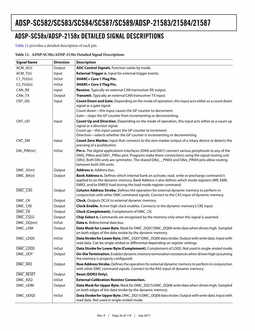
Rev. A | Page 26 of 174 | July 2017
ADSP-SC582/SC583/SC584/SC587/SC589/ADSP-21583/21584/21587
ADSP-SC58x/ADSP-2158x DETAILED SIGNAL DESCRIPTIONSTable 11 provides a detailed description of each pin.
Table 11. ADSP-SC58x/ADSP-2158x Detailed Signal Descriptions
Signal Name Direction DescriptionACM_A[n] Output ADC Control Signals. Function varies by mode.
ACM_T[n] Input External Trigger n. Input for external trigger events.
C1_FLG[n] InOut SHARC+ Core 1 Flag Pin. C2_FLG[n] InOut SHARC+ Core 2 Flag Pin.CAN_RX Input Receive. Typically an external CAN transceiver RX output.
CAN_TX Output Transmit. Typically an external CAN transceiver TX input.
CNT_DG Input Count Down and Gate. Depending on the mode of operation, this input acts either as a count down signal or a gate signal.Count down—this input causes the GP counter to decrement.Gate—stops the GP counter from incrementing or decrementing.
CNT_UD Input Count Up and Direction. Depending on the mode of operation, this input acts either as a count up signal or a direction signal.Count up—this input causes the GP counter to increment.Direction—selects whether the GP counter is incrementing or decrementing.
CNT_ZM Input Count Zero Marker. Input that connects to the zero marker output of a rotary device or detects the pressing of a pushbutton.
DAI_PIN[nn] InOut Pin n. The digital applications interfaces (DAI0 and DAI1) connect various peripherals to any of the DAI0_PINxx and DAI1_PINxx pins. Programs make these connections using the signal routing unit (SRU). Both DAI units are symmetric. The shared DAIx__PIN03 and DAIx_PIN04 pins allow routing between both DAI units.
DMC_A[nn] Output Address n. Address bus.
DMC_BA[n] Output Bank Address n. Defines which internal bank an activate, read, write or precharge command is applied to on the dynamic memory. Bank Address n also defines which mode registers (MR, EMR, EMR2, and/or EMR3) load during the load mode register command.
DMC_CAS Output Column Address Strobe. Defines the operation for external dynamic memory to perform in conjunction with other DMC command signals. Connect to the CAS input of dynamic memory.
DMC_CK Output Clock. Outputs DCLK to external dynamic memory.
DMC_CKE Output Clock Enable. Active high clock enables. Connects to the dynamic memory’s CKE input.
DMC_CK Output Clock (Complement). Complement of DMC_CK.
DMC_CS[n] Output Chip Select n. Commands are recognized by the memory only when this signal is asserted.
DMC_DQ[nn] InOut Data n. Bidirectional data bus.
DMC_LDM Output Data Mask for Lower Byte. Mask for DMC_DQ07:DMC_DQ00 write data when driven high. Sampled on both edges of the data strobe by the dynamic memory.
DMC_LDQS InOut Data Strobe for Lower Byte. DMC_DQ07:DMC_DQ00 data strobe. Output with write data. Input with read data. Can be single-ended or differential depending on register settings.
DMC_LDQS InOut Data Strobe for Lower Byte (Complement). Complement of LDQS. Not used in single-ended mode.
DMC_ODT Output On-Die Termination. Enables dynamic memory termination resistances when driven high (assuming the memory is properly configured).
DMC_RAS Output Row Address Strobe. Defines the operation for external dynamic memory to perform in conjunction with other DMC command signals. Connect to the RAS input of dynamic memory.
DMC_RESET Output Reset (DDR3 Only).DMC_RZQ InOut External Calibration Resistor Connection.DMC_UDM Output Data Mask for Upper Byte. Mask for DMC_DQ15:DMC_DQ08 write data when driven high. Sampled
on both edges of the data strobe by the dynamic memory.
DMC_UDQS InOut Data Strobe for Upper Byte. DMC_DQ15:DMC_DQ08 data strobe. Output with write data. Input with read data. Not used in single-ended mode.
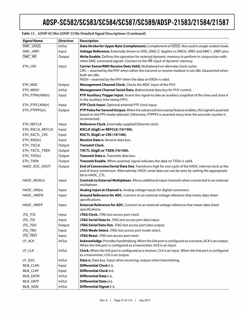
Rev. A | Page 27 of 174 | July 2017
ADSP-SC582/SC583/SC584/SC587/SC589/ADSP-21583/21584/21587
DMC_UDQS InOut Data Strobe for Upper Byte (Complement). Complement of UDQS. Not used in single-ended mode.
DMC_VREF Input Voltage Reference. Externally driven to VDD_DMC/2. Applies to DMC0_VREF and DMC1_VREF pins.
DMC_WE Output Write Enable. Defines the operation for external dynamic memory to perform in conjunction with other DMC command signals. Connect to the WE input of dynamic memory.
ETH_CRS Input Carrier Sense/RMII Receive Data Valid. Multiplexed on alternate clock cycles. CRS— asserted by the PHY when either the transmit or receive medium is not idle. Deasserted when both are idle. RXDV—asserted by the PHY when the data on RXDn is valid.
ETH_MDC Output Management Channel Clock. Clocks the MDC input of the PHY.
ETH_MDIO InOut Management Channel Serial Data. Bidirectional data bus for PHY control.
ETH_PTPAUXIN[n] Input PTP Auxiliary Trigger Input. Assert this signal to take an auxiliary snapshot of the time and store it in the auxiliary time stamp FIFO.
ETH_PTPCLKIN[n] Input PTP Clock Input. Optional external PTP clock input.
ETH_PTPPPS[n] Output PTP Pulse Per Second Output. When the advanced time stamp feature enables, this signal is asserted based on the PPS mode selected. Otherwise, PTPPPS is asserted every time the seconds counter is incremented.
ETH_REFCLK Input Reference Clock. Externally supplied Ethernet clock.
ETH_RXCLK_REFCLK Input RXCLK (GigE) or REFCLK (10/100).ETH_RXCTL_CRS Input RXCTL (GigE) or CRS (10/100). ETH_RXD[n] Input Receive Data n. Receive data bus.
ETH_TXCLK Output Transmit Clock.ETH_TXCTL_TXEN Output TXCTL (GigE) or TXEN (10/100).ETH_TXD[n] Output Transmit Data n. Transmits data bus.
ETH_TXEN Output Transmit Enable. When asserted, signal indicates the data on TXDn is valid.
HADC_EOC_DOUT Output End of Conversion/Serial Data Out. Transitions high for one cycle of the HADC internal clock at the end of every conversion. Alternatively, HADC serial data out can be seen by setting the appropriate bit in HADC_CTL.
HADC_MUX[n] Input Controls to External Multiplexer. Allows additional input channels when connected to an external multiplexer.
HADC_VIN[n] Input Analog Input at Channel n. Analog voltage inputs for digital conversion.
HADC_VREFN Input Ground Reference for ADC. Connect to an external voltage reference that meets data sheet specifications.
HADC_VREFP Input External Reference for ADC. Connect to an external voltage reference that meets data sheet specifications.
JTG_TCK Input JTAG Clock. JTAG test access port clock.
JTG_TDI Input JTAG Serial Data In. JTAG test access port data input.
JTG_TDO Output JTAG Serial Data Out. JTAG test access port data output.
JTG_TMS Input JTAG Mode Select. JTAG test access port mode select.
JTG_TRST Input JTAG Reset. JTAG test access port reset.
LP_ACK InOut Acknowledge. Provides handshaking. When the link port is configured as a receiver, ACK is an output. When the link port is configured as a transmitter, ACK is an input.
LP_CLK InOut Clock. When the link port is configured as a receiver, CLK is an input. When the link port is configured as a transmitter, CLK is an output.
LP_D[n] InOut Data n. Data bus. Input when receiving, output when transmitting.
MLB_CLKN Input Differential Clock (–).MLB_CLKP Input Differential Clock (+).MLB_DATN InOut Differential Data (–).MLB_DATP InOut Differential Data (+).MLB_SIGN InOut Differential Signal (–).
Table 11. ADSP-SC58x/ADSP-2158x Detailed Signal Descriptions (Continued)
Signal Name Direction Description
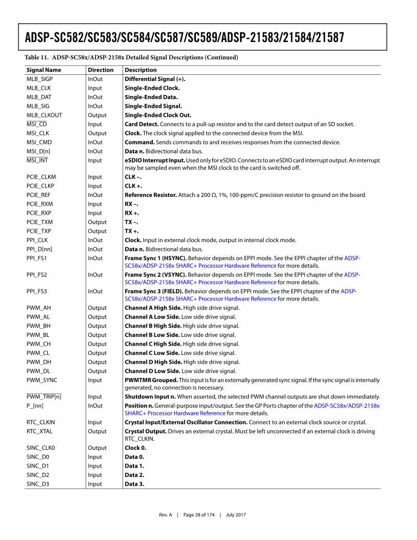
Rev. A | Page 28 of 174 | July 2017
ADSP-SC582/SC583/SC584/SC587/SC589/ADSP-21583/21584/21587
MLB_SIGP InOut Differential Signal (+). MLB_CLK Input Single-Ended Clock.MLB_DAT InOut Single-Ended Data.MLB_SIG InOut Single-Ended Signal.MLB_CLKOUT Output Single-Ended Clock Out.MSI_CD Input Card Detect. Connects to a pull-up resistor and to the card detect output of an SD socket.
MSI_CLK Output Clock. The clock signal applied to the connected device from the MSI.
MSI_CMD InOut Command. Sends commands to and receives responses from the connected device.
MSI_D[n] InOut Data n. Bidirectional data bus.
MSI_INT Input eSDIO Interrupt Input. Used only for eSDIO. Connects to an eSDIO card interrupt output. An interrupt may be sampled even when the MSI clock to the card is switched off.
PCIE_CLKM Input CLK –. PCIE_CLKP Input CLK +.PCIE_REF InOut Reference Resistor. Attach a 200 Ω, 1%, 100-ppm/C precision resistor to ground on the board.
PCIE_RXM Input RX –.PCIE_RXP Input RX +. PCIE_TXM Output TX –. PCIE_TXP Output TX +. PPI_CLK InOut Clock. Input in external clock mode, output in internal clock mode.
PPI_D[nn] InOut Data n. Bidirectional data bus.
PPI_FS1 InOut Frame Sync 1 (HSYNC). Behavior depends on EPPI mode. See the EPPI chapter of the ADSP-SC58x/ADSP-2158x SHARC+ Processor Hardware Reference for more details.
PPI_FS2 InOut Frame Sync 2 (VSYNC). Behavior depends on EPPI mode. See the EPPI chapter of the ADSP-SC58x/ADSP-2158x SHARC+ Processor Hardware Reference for more details.
PPI_FS3 InOut Frame Sync 3 (FIELD). Behavior depends on EPPI mode. See the EPPI chapter of the ADSP-SC58x/ADSP-2158x SHARC+ Processor Hardware Reference for more details.
PWM_AH Output Channel A High Side. High side drive signal.
PWM_AL Output Channel A Low Side. Low side drive signal.
PWM_BH Output Channel B High Side. High side drive signal.
PWM_BL Output Channel B Low Side. Low side drive signal.
PWM_CH Output Channel C High Side. High side drive signal.
PWM_CL Output Channel C Low Side. Low side drive signal.
PWM_DH Output Channel D High Side. High side drive signal.
PWM_DL Output Channel D Low Side. Low side drive signal.
PWM_SYNC Input PWMTMR Grouped. This input is for an externally generated sync signal. If the sync signal is internally generated, no connection is necessary.
PWM_TRIP[n] Input Shutdown Input n. When asserted, the selected PWM channel outputs are shut down immediately.
P_[nn] InOut Position n. General-purpose input/output. See the GP Ports chapter of the ADSP-SC58x/ADSP-2158x SHARC+ Processor Hardware Reference for more details.
RTC_CLKIN Input Crystal Input/External Oscillator Connection. Connect to an external clock source or crystal.
RTC_XTAL Output Crystal Output. Drives an external crystal. Must be left unconnected if an external clock is driving RTC_CLKIN.
SINC_CLK0 Output Clock 0. SINC_D0 Input Data 0. SINC_D1 Input Data 1. SINC_D2 Input Data 2. SINC_D3 Input Data 3.
Table 11. ADSP-SC58x/ADSP-2158x Detailed Signal Descriptions (Continued)
Signal Name Direction Description
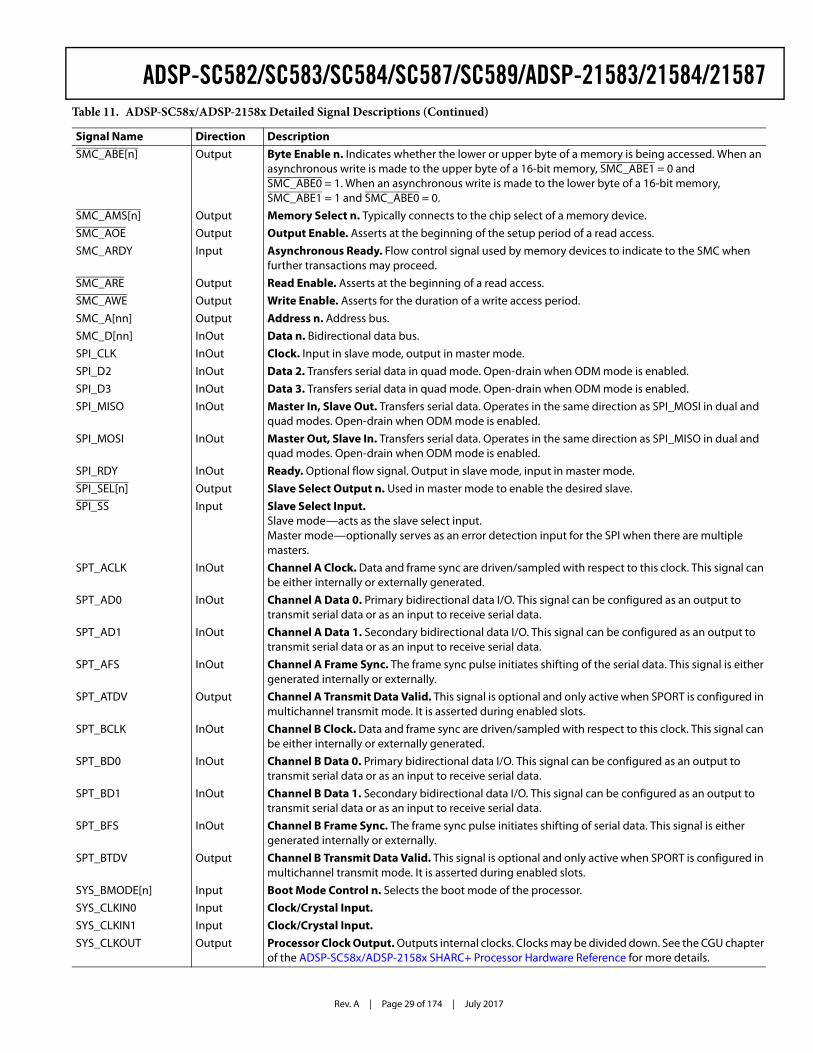
Rev. A | Page 29 of 174 | July 2017
ADSP-SC582/SC583/SC584/SC587/SC589/ADSP-21583/21584/21587
SMC_ABE[n] Output Byte Enable n. Indicates whether the lower or upper byte of a memory is being accessed. When an asynchronous write is made to the upper byte of a 16-bit memory, SMC_ABE1 = 0 and SMC_ABE0 = 1. When an asynchronous write is made to the lower byte of a 16-bit memory, SMC_ABE1 = 1 and SMC_ABE0 = 0.
SMC_AMS[n] Output Memory Select n. Typically connects to the chip select of a memory device.
SMC_AOE Output Output Enable. Asserts at the beginning of the setup period of a read access.
SMC_ARDY Input Asynchronous Ready. Flow control signal used by memory devices to indicate to the SMC when further transactions may proceed.
SMC_ARE Output Read Enable. Asserts at the beginning of a read access.
SMC_AWE Output Write Enable. Asserts for the duration of a write access period.
SMC_A[nn] Output Address n. Address bus.
SMC_D[nn] InOut Data n. Bidirectional data bus.
SPI_CLK InOut Clock. Input in slave mode, output in master mode.
SPI_D2 InOut Data 2. Transfers serial data in quad mode. Open-drain when ODM mode is enabled.
SPI_D3 InOut Data 3. Transfers serial data in quad mode. Open-drain when ODM mode is enabled.
SPI_MISO InOut Master In, Slave Out. Transfers serial data. Operates in the same direction as SPI_MOSI in dual and quad modes. Open-drain when ODM mode is enabled.
SPI_MOSI InOut Master Out, Slave In. Transfers serial data. Operates in the same direction as SPI_MISO in dual and quad modes. Open-drain when ODM mode is enabled.
SPI_RDY InOut Ready. Optional flow signal. Output in slave mode, input in master mode.
SPI_SEL[n] Output Slave Select Output n. Used in master mode to enable the desired slave.
SPI_SS Input Slave Select Input. Slave mode—acts as the slave select input. Master mode—optionally serves as an error detection input for the SPI when there are multiple masters.
SPT_ACLK InOut Channel A Clock. Data and frame sync are driven/sampled with respect to this clock. This signal can be either internally or externally generated.
SPT_AD0 InOut Channel A Data 0. Primary bidirectional data I/O. This signal can be configured as an output to transmit serial data or as an input to receive serial data.
SPT_AD1 InOut Channel A Data 1. Secondary bidirectional data I/O. This signal can be configured as an output to transmit serial data or as an input to receive serial data.
SPT_AFS InOut Channel A Frame Sync. The frame sync pulse initiates shifting of the serial data. This signal is either generated internally or externally.
SPT_ATDV Output Channel A Transmit Data Valid. This signal is optional and only active when SPORT is configured in multichannel transmit mode. It is asserted during enabled slots.
SPT_BCLK InOut Channel B Clock. Data and frame sync are driven/sampled with respect to this clock. This signal can be either internally or externally generated.
SPT_BD0 InOut Channel B Data 0. Primary bidirectional data I/O. This signal can be configured as an output to transmit serial data or as an input to receive serial data.
SPT_BD1 InOut Channel B Data 1. Secondary bidirectional data I/O. This signal can be configured as an output to transmit serial data or as an input to receive serial data.
SPT_BFS InOut Channel B Frame Sync. The frame sync pulse initiates shifting of serial data. This signal is either generated internally or externally.
SPT_BTDV Output Channel B Transmit Data Valid. This signal is optional and only active when SPORT is configured in multichannel transmit mode. It is asserted during enabled slots.
SYS_BMODE[n] Input Boot Mode Control n. Selects the boot mode of the processor.
SYS_CLKIN0 Input Clock/Crystal Input. SYS_CLKIN1 Input Clock/Crystal Input. SYS_CLKOUT Output Processor Clock Output. Outputs internal clocks. Clocks may be divided down. See the CGU chapter
of the ADSP-SC58x/ADSP-2158x SHARC+ Processor Hardware Reference for more details.
Table 11. ADSP-SC58x/ADSP-2158x Detailed Signal Descriptions (Continued)
Signal Name Direction Description
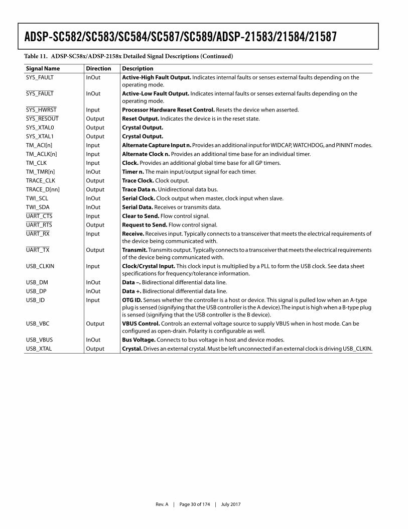
Rev. A | Page 30 of 174 | July 2017
ADSP-SC582/SC583/SC584/SC587/SC589/ADSP-21583/21584/21587
SYS_FAULT InOut Active-High Fault Output. Indicates internal faults or senses external faults depending on the operating mode.
SYS_FAULT InOut Active-Low Fault Output. Indicates internal faults or senses external faults depending on the operating mode.
SYS_HWRST Input Processor Hardware Reset Control. Resets the device when asserted.
SYS_RESOUT Output Reset Output. Indicates the device is in the reset state.
SYS_XTAL0 Output Crystal Output. SYS_XTAL1 Output Crystal Output. TM_ACI[n] Input Alternate Capture Input n. Provides an additional input for WIDCAP, WATCHDOG, and PININT modes.
TM_ACLK[n] Input Alternate Clock n. Provides an additional time base for an individual timer.
TM_CLK Input Clock. Provides an additional global time base for all GP timers.
TM_TMR[n] InOut Timer n. The main input/output signal for each timer.
TRACE_CLK Output Trace Clock. Clock output.
TRACE_D[nn] Output Trace Data n. Unidirectional data bus.
TWI_SCL InOut Serial Clock. Clock output when master, clock input when slave.
TWI_SDA InOut Serial Data. Receives or transmits data.
UART_CTS Input Clear to Send. Flow control signal.
UART_RTS Output Request to Send. Flow control signal.
UART_RX Input Receive. Receives input. Typically connects to a transceiver that meets the electrical requirements of the device being communicated with.
UART_TX Output Transmit. Transmits output. Typically connects to a transceiver that meets the electrical requirements of the device being communicated with.
USB_CLKIN Input Clock/Crystal Input. This clock input is multiplied by a PLL to form the USB clock. See data sheet specifications for frequency/tolerance information.
USB_DM InOut Data –. Bidirectional differential data line.
USB_DP InOut Data +. Bidirectional differential data line.
USB_ID Input OTG ID. Senses whether the controller is a host or device. This signal is pulled low when an A-type plug is sensed (signifying that the USB controller is the A device).The input is high when a B-type plug is sensed (signifying that the USB controller is the B device).
USB_VBC Output VBUS Control. Controls an external voltage source to supply VBUS when in host mode. Can be configured as open-drain. Polarity is configurable as well.
USB_VBUS InOut Bus Voltage. Connects to bus voltage in host and device modes.
USB_XTAL Output Crystal. Drives an external crystal. Must be left unconnected if an external clock is driving USB_CLKIN.
Table 11. ADSP-SC58x/ADSP-2158x Detailed Signal Descriptions (Continued)
Signal Name Direction Description
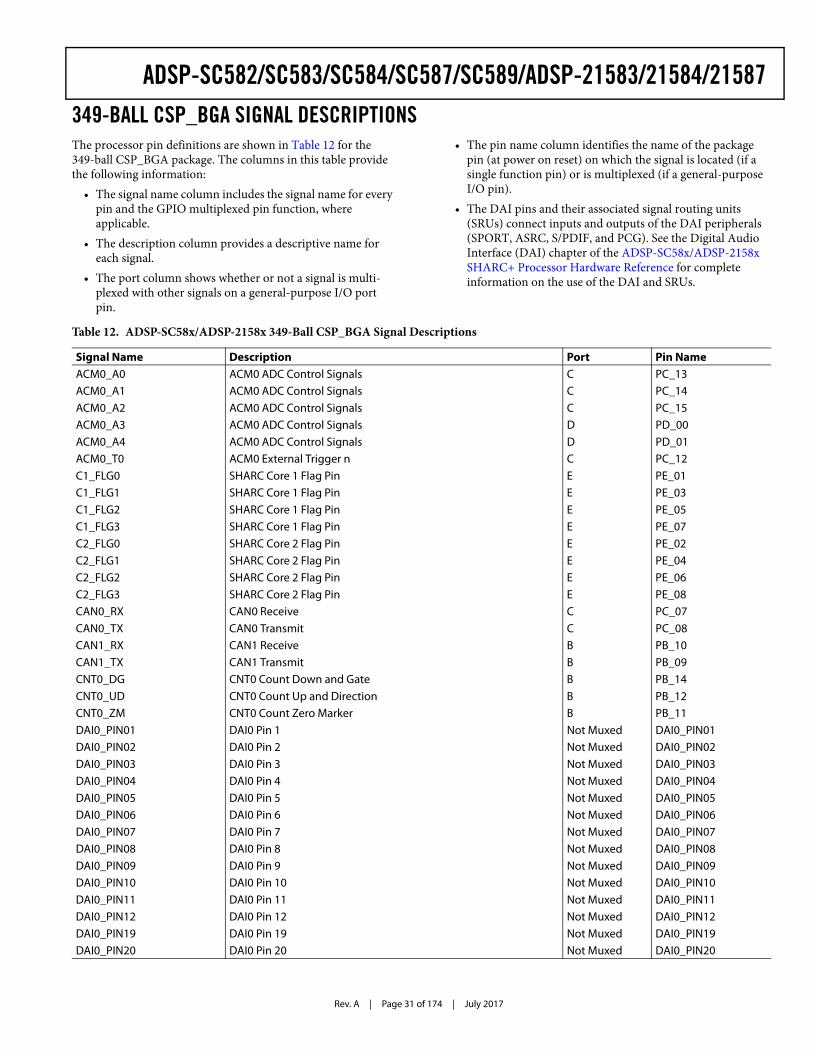
Rev. A | Page 31 of 174 | July 2017
ADSP-SC582/SC583/SC584/SC587/SC589/ADSP-21583/21584/21587349-BALL CSP_BGA SIGNAL DESCRIPTIONSThe processor pin definitions are shown in Table 12 for the 349-ball CSP_BGA package. The columns in this table provide the following information:
• The signal name column includes the signal name for every pin and the GPIO multiplexed pin function, where applicable.
• The description column provides a descriptive name for each signal.
• The port column shows whether or not a signal is multi-plexed with other signals on a general-purpose I/O port pin.
• The pin name column identifies the name of the package pin (at power on reset) on which the signal is located (if a single function pin) or is multiplexed (if a general-purpose I/O pin).
• The DAI pins and their associated signal routing units (SRUs) connect inputs and outputs of the DAI peripherals (SPORT, ASRC, S/PDIF, and PCG). See the Digital Audio Interface (DAI) chapter of the ADSP-SC58x/ADSP-2158x SHARC+ Processor Hardware Reference for complete information on the use of the DAI and SRUs.
Table 12. ADSP-SC58x/ADSP-2158x 349-Ball CSP_BGA Signal Descriptions
Signal Name Description Port Pin NameACM0_A0 ACM0 ADC Control Signals C PC_13ACM0_A1 ACM0 ADC Control Signals C PC_14
ACM0_A2 ACM0 ADC Control Signals C PC_15ACM0_A3 ACM0 ADC Control Signals D PD_00
ACM0_A4 ACM0 ADC Control Signals D PD_01ACM0_T0 ACM0 External Trigger n C PC_12
C1_FLG0 SHARC Core 1 Flag Pin E PE_01C1_FLG1 SHARC Core 1 Flag Pin E PE_03
C1_FLG2 SHARC Core 1 Flag Pin E PE_05C1_FLG3 SHARC Core 1 Flag Pin E PE_07
C2_FLG0 SHARC Core 2 Flag Pin E PE_02
C2_FLG1 SHARC Core 2 Flag Pin E PE_04C2_FLG2 SHARC Core 2 Flag Pin E PE_06
C2_FLG3 SHARC Core 2 Flag Pin E PE_08CAN0_RX CAN0 Receive C PC_07
CAN0_TX CAN0 Transmit C PC_08CAN1_RX CAN1 Receive B PB_10
CAN1_TX CAN1 Transmit B PB_09CNT0_DG CNT0 Count Down and Gate B PB_14
CNT0_UD CNT0 Count Up and Direction B PB_12CNT0_ZM CNT0 Count Zero Marker B PB_11
DAI0_PIN01 DAI0 Pin 1 Not Muxed DAI0_PIN01DAI0_PIN02 DAI0 Pin 2 Not Muxed DAI0_PIN02
DAI0_PIN03 DAI0 Pin 3 Not Muxed DAI0_PIN03DAI0_PIN04 DAI0 Pin 4 Not Muxed DAI0_PIN04
DAI0_PIN05 DAI0 Pin 5 Not Muxed DAI0_PIN05DAI0_PIN06 DAI0 Pin 6 Not Muxed DAI0_PIN06
DAI0_PIN07 DAI0 Pin 7 Not Muxed DAI0_PIN07DAI0_PIN08 DAI0 Pin 8 Not Muxed DAI0_PIN08
DAI0_PIN09 DAI0 Pin 9 Not Muxed DAI0_PIN09DAI0_PIN10 DAI0 Pin 10 Not Muxed DAI0_PIN10
DAI0_PIN11 DAI0 Pin 11 Not Muxed DAI0_PIN11DAI0_PIN12 DAI0 Pin 12 Not Muxed DAI0_PIN12
DAI0_PIN19 DAI0 Pin 19 Not Muxed DAI0_PIN19DAI0_PIN20 DAI0 Pin 20 Not Muxed DAI0_PIN20
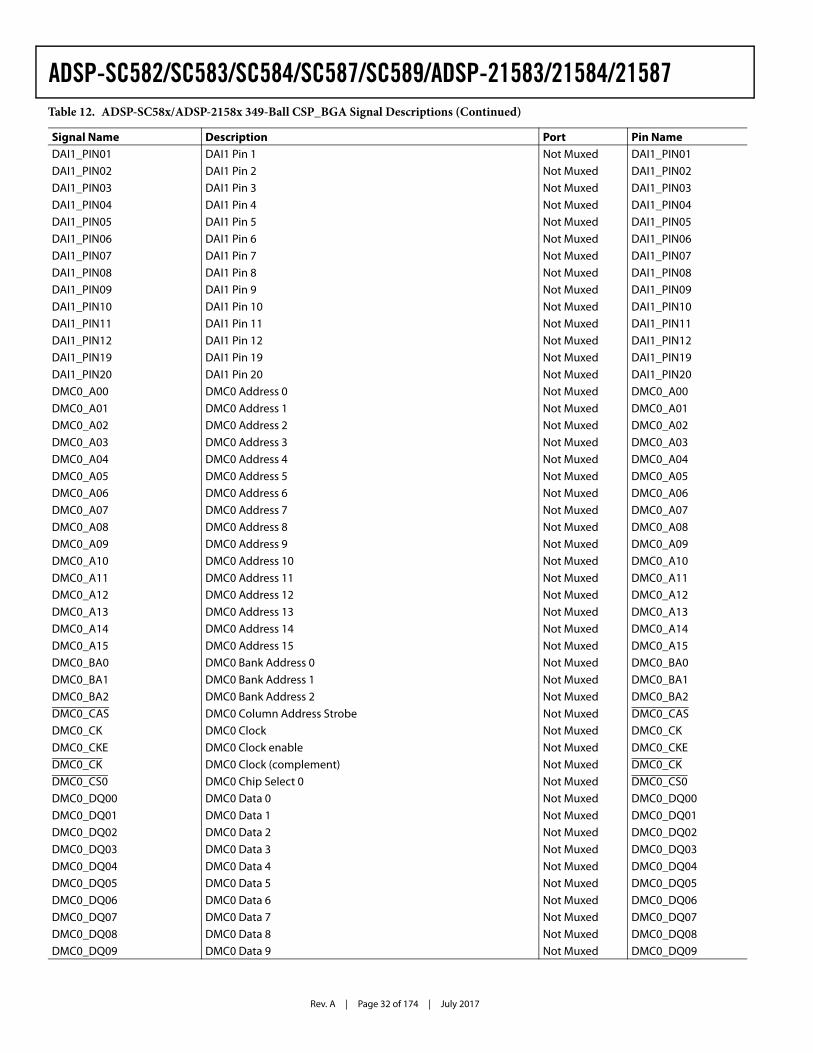
Rev. A | Page 32 of 174 | July 2017
ADSP-SC582/SC583/SC584/SC587/SC589/ADSP-21583/21584/21587
DAI1_PIN01 DAI1 Pin 1 Not Muxed DAI1_PIN01
DAI1_PIN02 DAI1 Pin 2 Not Muxed DAI1_PIN02DAI1_PIN03 DAI1 Pin 3 Not Muxed DAI1_PIN03
DAI1_PIN04 DAI1 Pin 4 Not Muxed DAI1_PIN04DAI1_PIN05 DAI1 Pin 5 Not Muxed DAI1_PIN05
DAI1_PIN06 DAI1 Pin 6 Not Muxed DAI1_PIN06DAI1_PIN07 DAI1 Pin 7 Not Muxed DAI1_PIN07
DAI1_PIN08 DAI1 Pin 8 Not Muxed DAI1_PIN08DAI1_PIN09 DAI1 Pin 9 Not Muxed DAI1_PIN09
DAI1_PIN10 DAI1 Pin 10 Not Muxed DAI1_PIN10DAI1_PIN11 DAI1 Pin 11 Not Muxed DAI1_PIN11
DAI1_PIN12 DAI1 Pin 12 Not Muxed DAI1_PIN12DAI1_PIN19 DAI1 Pin 19 Not Muxed DAI1_PIN19
DAI1_PIN20 DAI1 Pin 20 Not Muxed DAI1_PIN20DMC0_A00 DMC0 Address 0 Not Muxed DMC0_A00
DMC0_A01 DMC0 Address 1 Not Muxed DMC0_A01DMC0_A02 DMC0 Address 2 Not Muxed DMC0_A02
DMC0_A03 DMC0 Address 3 Not Muxed DMC0_A03DMC0_A04 DMC0 Address 4 Not Muxed DMC0_A04
DMC0_A05 DMC0 Address 5 Not Muxed DMC0_A05DMC0_A06 DMC0 Address 6 Not Muxed DMC0_A06
DMC0_A07 DMC0 Address 7 Not Muxed DMC0_A07DMC0_A08 DMC0 Address 8 Not Muxed DMC0_A08
DMC0_A09 DMC0 Address 9 Not Muxed DMC0_A09DMC0_A10 DMC0 Address 10 Not Muxed DMC0_A10
DMC0_A11 DMC0 Address 11 Not Muxed DMC0_A11DMC0_A12 DMC0 Address 12 Not Muxed DMC0_A12
DMC0_A13 DMC0 Address 13 Not Muxed DMC0_A13DMC0_A14 DMC0 Address 14 Not Muxed DMC0_A14
DMC0_A15 DMC0 Address 15 Not Muxed DMC0_A15DMC0_BA0 DMC0 Bank Address 0 Not Muxed DMC0_BA0
DMC0_BA1 DMC0 Bank Address 1 Not Muxed DMC0_BA1DMC0_BA2 DMC0 Bank Address 2 Not Muxed DMC0_BA2
DMC0_CAS DMC0 Column Address Strobe Not Muxed DMC0_CASDMC0_CK DMC0 Clock Not Muxed DMC0_CK
DMC0_CKE DMC0 Clock enable Not Muxed DMC0_CKEDMC0_CK DMC0 Clock (complement) Not Muxed DMC0_CK
DMC0_CS0 DMC0 Chip Select 0 Not Muxed DMC0_CS0DMC0_DQ00 DMC0 Data 0 Not Muxed DMC0_DQ00
DMC0_DQ01 DMC0 Data 1 Not Muxed DMC0_DQ01DMC0_DQ02 DMC0 Data 2 Not Muxed DMC0_DQ02
DMC0_DQ03 DMC0 Data 3 Not Muxed DMC0_DQ03
DMC0_DQ04 DMC0 Data 4 Not Muxed DMC0_DQ04DMC0_DQ05 DMC0 Data 5 Not Muxed DMC0_DQ05
DMC0_DQ06 DMC0 Data 6 Not Muxed DMC0_DQ06DMC0_DQ07 DMC0 Data 7 Not Muxed DMC0_DQ07
DMC0_DQ08 DMC0 Data 8 Not Muxed DMC0_DQ08DMC0_DQ09 DMC0 Data 9 Not Muxed DMC0_DQ09
Table 12. ADSP-SC58x/ADSP-2158x 349-Ball CSP_BGA Signal Descriptions (Continued)
Signal Name Description Port Pin Name
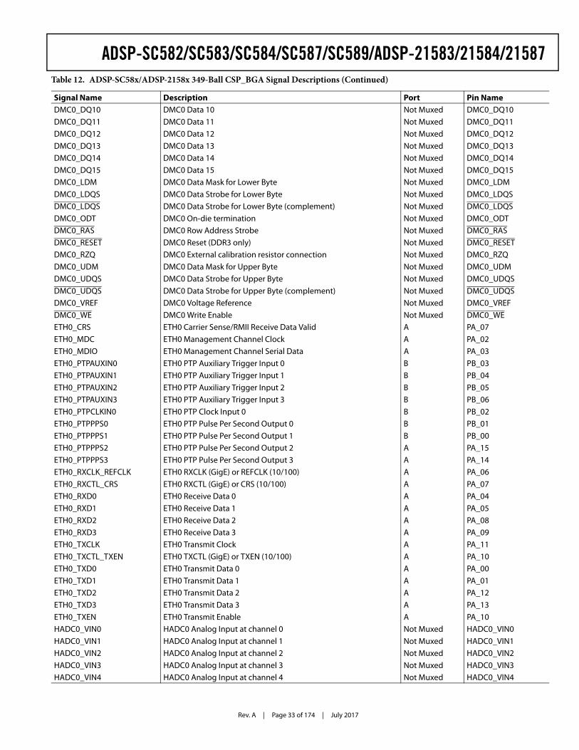
Rev. A | Page 33 of 174 | July 2017
ADSP-SC582/SC583/SC584/SC587/SC589/ADSP-21583/21584/21587
DMC0_DQ10 DMC0 Data 10 Not Muxed DMC0_DQ10
DMC0_DQ11 DMC0 Data 11 Not Muxed DMC0_DQ11DMC0_DQ12 DMC0 Data 12 Not Muxed DMC0_DQ12
DMC0_DQ13 DMC0 Data 13 Not Muxed DMC0_DQ13DMC0_DQ14 DMC0 Data 14 Not Muxed DMC0_DQ14
DMC0_DQ15 DMC0 Data 15 Not Muxed DMC0_DQ15DMC0_LDM DMC0 Data Mask for Lower Byte Not Muxed DMC0_LDM
DMC0_LDQS DMC0 Data Strobe for Lower Byte Not Muxed DMC0_LDQSDMC0_LDQS DMC0 Data Strobe for Lower Byte (complement) Not Muxed DMC0_LDQS
DMC0_ODT DMC0 On-die termination Not Muxed DMC0_ODTDMC0_RAS DMC0 Row Address Strobe Not Muxed DMC0_RAS
DMC0_RESET DMC0 Reset (DDR3 only) Not Muxed DMC0_RESETDMC0_RZQ DMC0 External calibration resistor connection Not Muxed DMC0_RZQ
DMC0_UDM DMC0 Data Mask for Upper Byte Not Muxed DMC0_UDMDMC0_UDQS DMC0 Data Strobe for Upper Byte Not Muxed DMC0_UDQS
DMC0_UDQS DMC0 Data Strobe for Upper Byte (complement) Not Muxed DMC0_UDQSDMC0_VREF DMC0 Voltage Reference Not Muxed DMC0_VREF
DMC0_WE DMC0 Write Enable Not Muxed DMC0_WEETH0_CRS ETH0 Carrier Sense/RMII Receive Data Valid A PA_07
ETH0_MDC ETH0 Management Channel Clock A PA_02ETH0_MDIO ETH0 Management Channel Serial Data A PA_03
ETH0_PTPAUXIN0 ETH0 PTP Auxiliary Trigger Input 0 B PB_03ETH0_PTPAUXIN1 ETH0 PTP Auxiliary Trigger Input 1 B PB_04
ETH0_PTPAUXIN2 ETH0 PTP Auxiliary Trigger Input 2 B PB_05ETH0_PTPAUXIN3 ETH0 PTP Auxiliary Trigger Input 3 B PB_06
ETH0_PTPCLKIN0 ETH0 PTP Clock Input 0 B PB_02ETH0_PTPPPS0 ETH0 PTP Pulse Per Second Output 0 B PB_01
ETH0_PTPPPS1 ETH0 PTP Pulse Per Second Output 1 B PB_00ETH0_PTPPPS2 ETH0 PTP Pulse Per Second Output 2 A PA_15
ETH0_PTPPPS3 ETH0 PTP Pulse Per Second Output 3 A PA_14ETH0_RXCLK_REFCLK ETH0 RXCLK (GigE) or REFCLK (10/100) A PA_06
ETH0_RXCTL_CRS ETH0 RXCTL (GigE) or CRS (10/100) A PA_07ETH0_RXD0 ETH0 Receive Data 0 A PA_04
ETH0_RXD1 ETH0 Receive Data 1 A PA_05ETH0_RXD2 ETH0 Receive Data 2 A PA_08
ETH0_RXD3 ETH0 Receive Data 3 A PA_09ETH0_TXCLK ETH0 Transmit Clock A PA_11
ETH0_TXCTL_TXEN ETH0 TXCTL (GigE) or TXEN (10/100) A PA_10ETH0_TXD0 ETH0 Transmit Data 0 A PA_00
ETH0_TXD1 ETH0 Transmit Data 1 A PA_01ETH0_TXD2 ETH0 Transmit Data 2 A PA_12
ETH0_TXD3 ETH0 Transmit Data 3 A PA_13
ETH0_TXEN ETH0 Transmit Enable A PA_10HADC0_VIN0 HADC0 Analog Input at channel 0 Not Muxed HADC0_VIN0
HADC0_VIN1 HADC0 Analog Input at channel 1 Not Muxed HADC0_VIN1HADC0_VIN2 HADC0 Analog Input at channel 2 Not Muxed HADC0_VIN2
HADC0_VIN3 HADC0 Analog Input at channel 3 Not Muxed HADC0_VIN3HADC0_VIN4 HADC0 Analog Input at channel 4 Not Muxed HADC0_VIN4
Table 12. ADSP-SC58x/ADSP-2158x 349-Ball CSP_BGA Signal Descriptions (Continued)
Signal Name Description Port Pin Name
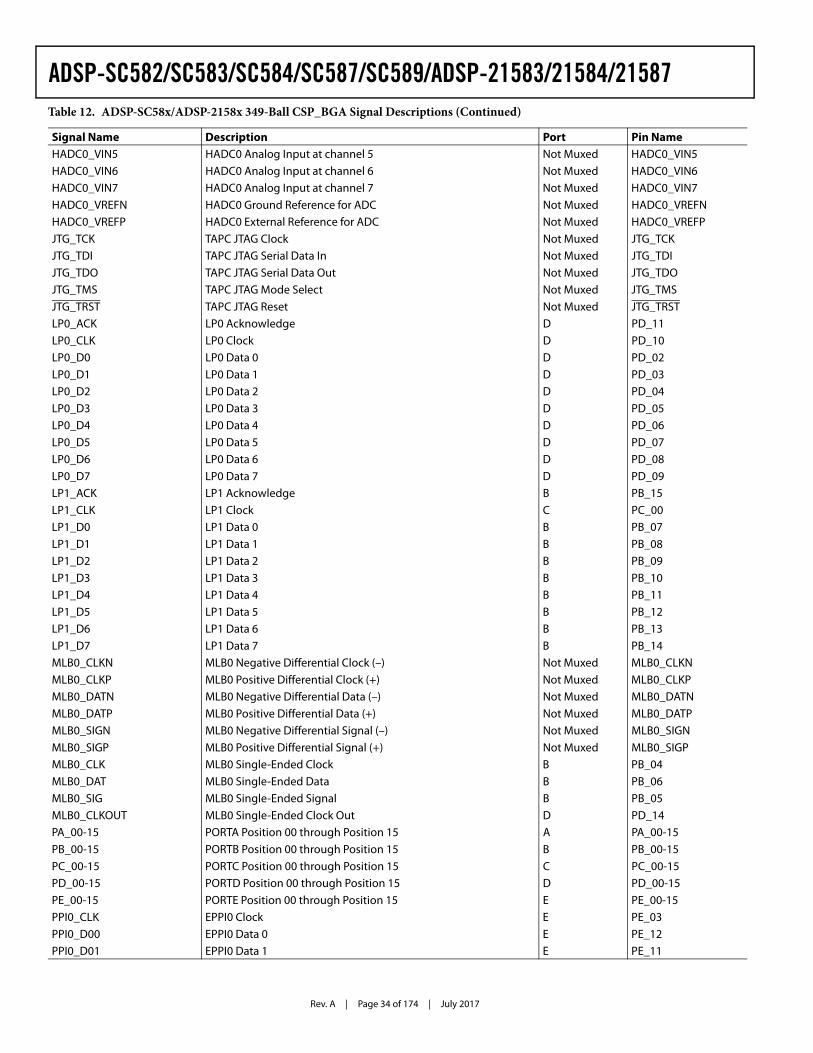
Rev. A | Page 34 of 174 | July 2017
ADSP-SC582/SC583/SC584/SC587/SC589/ADSP-21583/21584/21587
HADC0_VIN5 HADC0 Analog Input at channel 5 Not Muxed HADC0_VIN5
HADC0_VIN6 HADC0 Analog Input at channel 6 Not Muxed HADC0_VIN6HADC0_VIN7 HADC0 Analog Input at channel 7 Not Muxed HADC0_VIN7
HADC0_VREFN HADC0 Ground Reference for ADC Not Muxed HADC0_VREFNHADC0_VREFP HADC0 External Reference for ADC Not Muxed HADC0_VREFP
JTG_TCK TAPC JTAG Clock Not Muxed JTG_TCKJTG_TDI TAPC JTAG Serial Data In Not Muxed JTG_TDI
JTG_TDO TAPC JTAG Serial Data Out Not Muxed JTG_TDOJTG_TMS TAPC JTAG Mode Select Not Muxed JTG_TMS
JTG_TRST TAPC JTAG Reset Not Muxed JTG_TRSTLP0_ACK LP0 Acknowledge D PD_11
LP0_CLK LP0 Clock D PD_10LP0_D0 LP0 Data 0 D PD_02
LP0_D1 LP0 Data 1 D PD_03LP0_D2 LP0 Data 2 D PD_04
LP0_D3 LP0 Data 3 D PD_05LP0_D4 LP0 Data 4 D PD_06
LP0_D5 LP0 Data 5 D PD_07LP0_D6 LP0 Data 6 D PD_08
LP0_D7 LP0 Data 7 D PD_09LP1_ACK LP1 Acknowledge B PB_15
LP1_CLK LP1 Clock C PC_00LP1_D0 LP1 Data 0 B PB_07
LP1_D1 LP1 Data 1 B PB_08LP1_D2 LP1 Data 2 B PB_09
LP1_D3 LP1 Data 3 B PB_10LP1_D4 LP1 Data 4 B PB_11
LP1_D5 LP1 Data 5 B PB_12LP1_D6 LP1 Data 6 B PB_13
LP1_D7 LP1 Data 7 B PB_14MLB0_CLKN MLB0 Negative Differential Clock (–) Not Muxed MLB0_CLKN
MLB0_CLKP MLB0 Positive Differential Clock (+) Not Muxed MLB0_CLKPMLB0_DATN MLB0 Negative Differential Data (–) Not Muxed MLB0_DATN
MLB0_DATP MLB0 Positive Differential Data (+) Not Muxed MLB0_DATPMLB0_SIGN MLB0 Negative Differential Signal (–) Not Muxed MLB0_SIGN
MLB0_SIGP MLB0 Positive Differential Signal (+) Not Muxed MLB0_SIGPMLB0_CLK MLB0 Single-Ended Clock B PB_04
MLB0_DAT MLB0 Single-Ended Data B PB_06MLB0_SIG MLB0 Single-Ended Signal B PB_05
MLB0_CLKOUT MLB0 Single-Ended Clock Out D PD_14PA_00-15 PORTA Position 00 through Position 15 A PA_00-15
PB_00-15 PORTB Position 00 through Position 15 B PB_00-15
PC_00-15 PORTC Position 00 through Position 15 C PC_00-15PD_00-15 PORTD Position 00 through Position 15 D PD_00-15
PE_00-15 PORTE Position 00 through Position 15 E PE_00-15PPI0_CLK EPPI0 Clock E PE_03
PPI0_D00 EPPI0 Data 0 E PE_12PPI0_D01 EPPI0 Data 1 E PE_11
Table 12. ADSP-SC58x/ADSP-2158x 349-Ball CSP_BGA Signal Descriptions (Continued)
Signal Name Description Port Pin Name
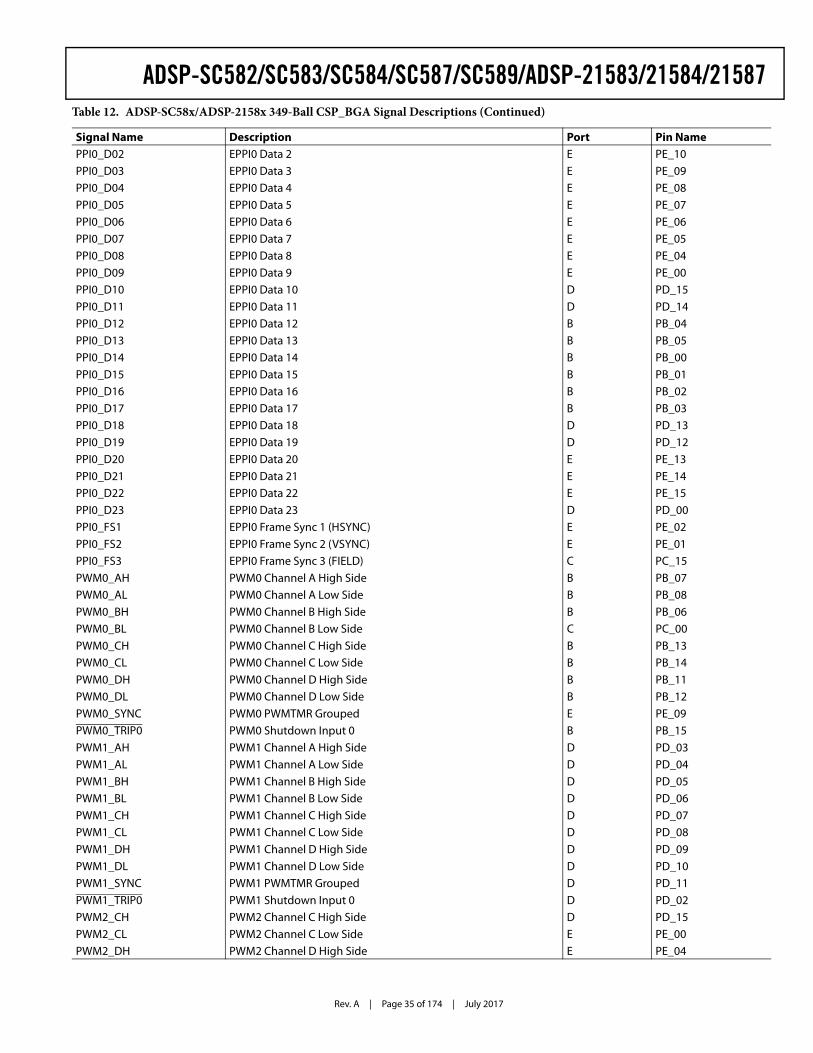
Rev. A | Page 35 of 174 | July 2017
ADSP-SC582/SC583/SC584/SC587/SC589/ADSP-21583/21584/21587
PPI0_D02 EPPI0 Data 2 E PE_10
PPI0_D03 EPPI0 Data 3 E PE_09PPI0_D04 EPPI0 Data 4 E PE_08
PPI0_D05 EPPI0 Data 5 E PE_07PPI0_D06 EPPI0 Data 6 E PE_06
PPI0_D07 EPPI0 Data 7 E PE_05PPI0_D08 EPPI0 Data 8 E PE_04
PPI0_D09 EPPI0 Data 9 E PE_00PPI0_D10 EPPI0 Data 10 D PD_15
PPI0_D11 EPPI0 Data 11 D PD_14PPI0_D12 EPPI0 Data 12 B PB_04
PPI0_D13 EPPI0 Data 13 B PB_05PPI0_D14 EPPI0 Data 14 B PB_00
PPI0_D15 EPPI0 Data 15 B PB_01PPI0_D16 EPPI0 Data 16 B PB_02
PPI0_D17 EPPI0 Data 17 B PB_03PPI0_D18 EPPI0 Data 18 D PD_13
PPI0_D19 EPPI0 Data 19 D PD_12PPI0_D20 EPPI0 Data 20 E PE_13
PPI0_D21 EPPI0 Data 21 E PE_14PPI0_D22 EPPI0 Data 22 E PE_15
PPI0_D23 EPPI0 Data 23 D PD_00PPI0_FS1 EPPI0 Frame Sync 1 (HSYNC) E PE_02
PPI0_FS2 EPPI0 Frame Sync 2 (VSYNC) E PE_01PPI0_FS3 EPPI0 Frame Sync 3 (FIELD) C PC_15
PWM0_AH PWM0 Channel A High Side B PB_07PWM0_AL PWM0 Channel A Low Side B PB_08
PWM0_BH PWM0 Channel B High Side B PB_06PWM0_BL PWM0 Channel B Low Side C PC_00
PWM0_CH PWM0 Channel C High Side B PB_13PWM0_CL PWM0 Channel C Low Side B PB_14
PWM0_DH PWM0 Channel D High Side B PB_11PWM0_DL PWM0 Channel D Low Side B PB_12
PWM0_SYNC PWM0 PWMTMR Grouped E PE_09PWM0_TRIP0 PWM0 Shutdown Input 0 B PB_15
PWM1_AH PWM1 Channel A High Side D PD_03PWM1_AL PWM1 Channel A Low Side D PD_04
PWM1_BH PWM1 Channel B High Side D PD_05PWM1_BL PWM1 Channel B Low Side D PD_06
PWM1_CH PWM1 Channel C High Side D PD_07PWM1_CL PWM1 Channel C Low Side D PD_08
PWM1_DH PWM1 Channel D High Side D PD_09
PWM1_DL PWM1 Channel D Low Side D PD_10PWM1_SYNC PWM1 PWMTMR Grouped D PD_11
PWM1_TRIP0 PWM1 Shutdown Input 0 D PD_02PWM2_CH PWM2 Channel C High Side D PD_15
PWM2_CL PWM2 Channel C Low Side E PE_00PWM2_DH PWM2 Channel D High Side E PE_04
Table 12. ADSP-SC58x/ADSP-2158x 349-Ball CSP_BGA Signal Descriptions (Continued)
Signal Name Description Port Pin Name
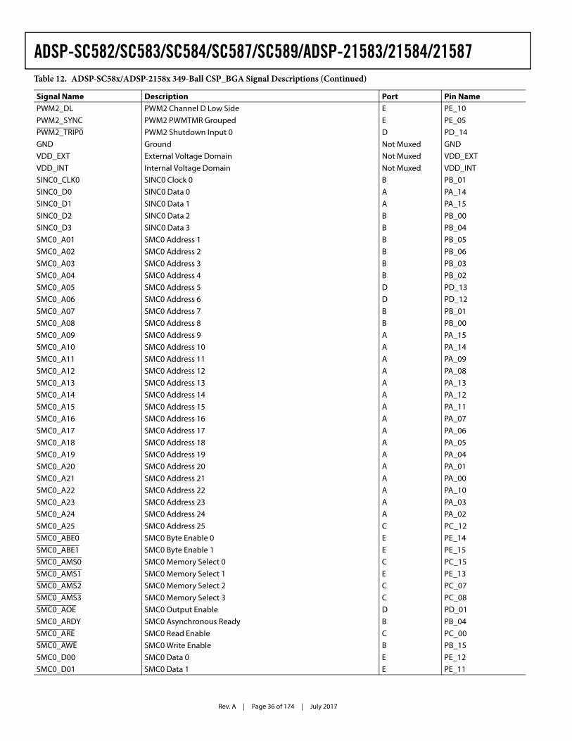
Rev. A | Page 36 of 174 | July 2017
ADSP-SC582/SC583/SC584/SC587/SC589/ADSP-21583/21584/21587
PWM2_DL PWM2 Channel D Low Side E PE_10
PWM2_SYNC PWM2 PWMTMR Grouped E PE_05PWM2_TRIP0 PWM2 Shutdown Input 0 D PD_14
GND Ground Not Muxed GNDVDD_EXT External Voltage Domain Not Muxed VDD_EXT
VDD_INT Internal Voltage Domain Not Muxed VDD_INTSINC0_CLK0 SINC0 Clock 0 B PB_01
SINC0_D0 SINC0 Data 0 A PA_14SINC0_D1 SINC0 Data 1 A PA_15
SINC0_D2 SINC0 Data 2 B PB_00SINC0_D3 SINC0 Data 3 B PB_04
SMC0_A01 SMC0 Address 1 B PB_05SMC0_A02 SMC0 Address 2 B PB_06
SMC0_A03 SMC0 Address 3 B PB_03SMC0_A04 SMC0 Address 4 B PB_02
SMC0_A05 SMC0 Address 5 D PD_13SMC0_A06 SMC0 Address 6 D PD_12
SMC0_A07 SMC0 Address 7 B PB_01SMC0_A08 SMC0 Address 8 B PB_00
SMC0_A09 SMC0 Address 9 A PA_15SMC0_A10 SMC0 Address 10 A PA_14
SMC0_A11 SMC0 Address 11 A PA_09SMC0_A12 SMC0 Address 12 A PA_08
SMC0_A13 SMC0 Address 13 A PA_13SMC0_A14 SMC0 Address 14 A PA_12
SMC0_A15 SMC0 Address 15 A PA_11SMC0_A16 SMC0 Address 16 A PA_07
SMC0_A17 SMC0 Address 17 A PA_06SMC0_A18 SMC0 Address 18 A PA_05
SMC0_A19 SMC0 Address 19 A PA_04SMC0_A20 SMC0 Address 20 A PA_01
SMC0_A21 SMC0 Address 21 A PA_00SMC0_A22 SMC0 Address 22 A PA_10
SMC0_A23 SMC0 Address 23 A PA_03SMC0_A24 SMC0 Address 24 A PA_02
SMC0_A25 SMC0 Address 25 C PC_12SMC0_ABE0 SMC0 Byte Enable 0 E PE_14
SMC0_ABE1 SMC0 Byte Enable 1 E PE_15SMC0_AMS0 SMC0 Memory Select 0 C PC_15
SMC0_AMS1 SMC0 Memory Select 1 E PE_13SMC0_AMS2 SMC0 Memory Select 2 C PC_07
SMC0_AMS3 SMC0 Memory Select 3 C PC_08
SMC0_AOE SMC0 Output Enable D PD_01SMC0_ARDY SMC0 Asynchronous Ready B PB_04
SMC0_ARE SMC0 Read Enable C PC_00SMC0_AWE SMC0 Write Enable B PB_15
SMC0_D00 SMC0 Data 0 E PE_12SMC0_D01 SMC0 Data 1 E PE_11
Table 12. ADSP-SC58x/ADSP-2158x 349-Ball CSP_BGA Signal Descriptions (Continued)
Signal Name Description Port Pin Name
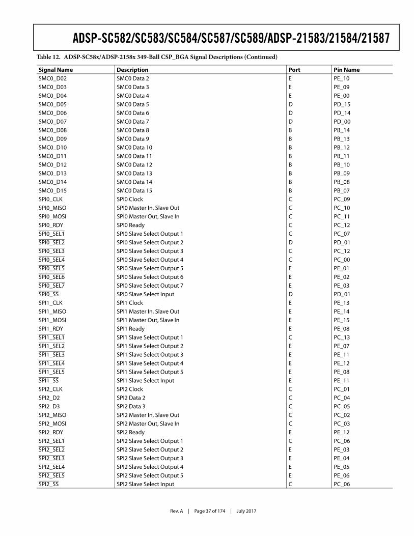
Rev. A | Page 37 of 174 | July 2017
ADSP-SC582/SC583/SC584/SC587/SC589/ADSP-21583/21584/21587
SMC0_D02 SMC0 Data 2 E PE_10
SMC0_D03 SMC0 Data 3 E PE_09SMC0_D04 SMC0 Data 4 E PE_00
SMC0_D05 SMC0 Data 5 D PD_15SMC0_D06 SMC0 Data 6 D PD_14
SMC0_D07 SMC0 Data 7 D PD_00SMC0_D08 SMC0 Data 8 B PB_14
SMC0_D09 SMC0 Data 9 B PB_13SMC0_D10 SMC0 Data 10 B PB_12
SMC0_D11 SMC0 Data 11 B PB_11SMC0_D12 SMC0 Data 12 B PB_10
SMC0_D13 SMC0 Data 13 B PB_09SMC0_D14 SMC0 Data 14 B PB_08
SMC0_D15 SMC0 Data 15 B PB_07SPI0_CLK SPI0 Clock C PC_09
SPI0_MISO SPI0 Master In, Slave Out C PC_10SPI0_MOSI SPI0 Master Out, Slave In C PC_11
SPI0_RDY SPI0 Ready C PC_12SPI0_SEL1 SPI0 Slave Select Output 1 C PC_07
SPI0_SEL2 SPI0 Slave Select Output 2 D PD_01SPI0_SEL3 SPI0 Slave Select Output 3 C PC_12
SPI0_SEL4 SPI0 Slave Select Output 4 C PC_00SPI0_SEL5 SPI0 Slave Select Output 5 E PE_01
SPI0_SEL6 SPI0 Slave Select Output 6 E PE_02SPI0_SEL7 SPI0 Slave Select Output 7 E PE_03
SPI0_SS SPI0 Slave Select Input D PD_01SPI1_CLK SPI1 Clock E PE_13
SPI1_MISO SPI1 Master In, Slave Out E PE_14SPI1_MOSI SPI1 Master Out, Slave In E PE_15
SPI1_RDY SPI1 Ready E PE_08SPI1_SEL1 SPI1 Slave Select Output 1 C PC_13
SPI1_SEL2 SPI1 Slave Select Output 2 E PE_07SPI1_SEL3 SPI1 Slave Select Output 3 E PE_11
SPI1_SEL4 SPI1 Slave Select Output 4 E PE_12SPI1_SEL5 SPI1 Slave Select Output 5 E PE_08
SPI1_SS SPI1 Slave Select Input E PE_11SPI2_CLK SPI2 Clock C PC_01
SPI2_D2 SPI2 Data 2 C PC_04SPI2_D3 SPI2 Data 3 C PC_05
SPI2_MISO SPI2 Master In, Slave Out C PC_02SPI2_MOSI SPI2 Master Out, Slave In C PC_03
SPI2_RDY SPI2 Ready E PE_12
SPI2_SEL1 SPI2 Slave Select Output 1 C PC_06SPI2_SEL2 SPI2 Slave Select Output 2 E PE_03
SPI2_SEL3 SPI2 Slave Select Output 3 E PE_04SPI2_SEL4 SPI2 Slave Select Output 4 E PE_05
SPI2_SEL5 SPI2 Slave Select Output 5 E PE_06SPI2_SS SPI2 Slave Select Input C PC_06
Table 12. ADSP-SC58x/ADSP-2158x 349-Ball CSP_BGA Signal Descriptions (Continued)
Signal Name Description Port Pin Name
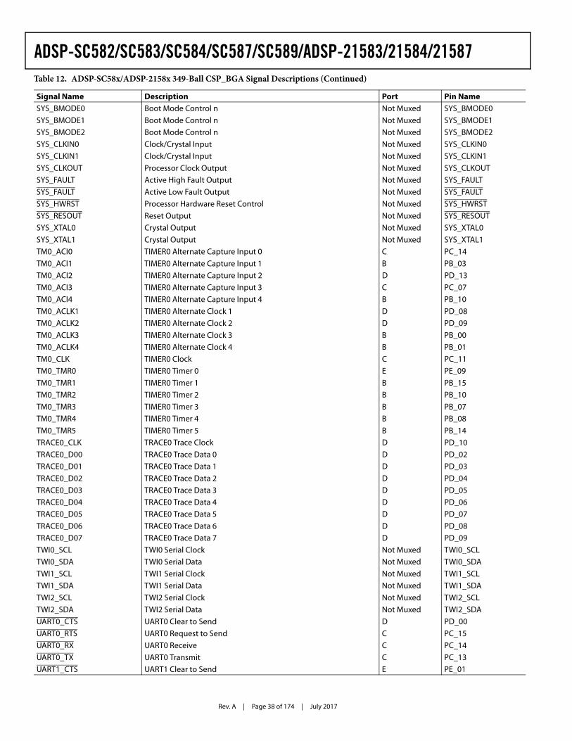
Rev. A | Page 38 of 174 | July 2017
ADSP-SC582/SC583/SC584/SC587/SC589/ADSP-21583/21584/21587
SYS_BMODE0 Boot Mode Control n Not Muxed SYS_BMODE0
SYS_BMODE1 Boot Mode Control n Not Muxed SYS_BMODE1SYS_BMODE2 Boot Mode Control n Not Muxed SYS_BMODE2
SYS_CLKIN0 Clock/Crystal Input Not Muxed SYS_CLKIN0SYS_CLKIN1 Clock/Crystal Input Not Muxed SYS_CLKIN1
SYS_CLKOUT Processor Clock Output Not Muxed SYS_CLKOUTSYS_FAULT Active High Fault Output Not Muxed SYS_FAULT
SYS_FAULT Active Low Fault Output Not Muxed SYS_FAULTSYS_HWRST Processor Hardware Reset Control Not Muxed SYS_HWRST
SYS_RESOUT Reset Output Not Muxed SYS_RESOUTSYS_XTAL0 Crystal Output Not Muxed SYS_XTAL0
SYS_XTAL1 Crystal Output Not Muxed SYS_XTAL1TM0_ACI0 TIMER0 Alternate Capture Input 0 C PC_14
TM0_ACI1 TIMER0 Alternate Capture Input 1 B PB_03TM0_ACI2 TIMER0 Alternate Capture Input 2 D PD_13
TM0_ACI3 TIMER0 Alternate Capture Input 3 C PC_07TM0_ACI4 TIMER0 Alternate Capture Input 4 B PB_10
TM0_ACLK1 TIMER0 Alternate Clock 1 D PD_08TM0_ACLK2 TIMER0 Alternate Clock 2 D PD_09
TM0_ACLK3 TIMER0 Alternate Clock 3 B PB_00TM0_ACLK4 TIMER0 Alternate Clock 4 B PB_01
TM0_CLK TIMER0 Clock C PC_11TM0_TMR0 TIMER0 Timer 0 E PE_09
TM0_TMR1 TIMER0 Timer 1 B PB_15TM0_TMR2 TIMER0 Timer 2 B PB_10
TM0_TMR3 TIMER0 Timer 3 B PB_07TM0_TMR4 TIMER0 Timer 4 B PB_08
TM0_TMR5 TIMER0 Timer 5 B PB_14TRACE0_CLK TRACE0 Trace Clock D PD_10
TRACE0_D00 TRACE0 Trace Data 0 D PD_02TRACE0_D01 TRACE0 Trace Data 1 D PD_03
TRACE0_D02 TRACE0 Trace Data 2 D PD_04TRACE0_D03 TRACE0 Trace Data 3 D PD_05
TRACE0_D04 TRACE0 Trace Data 4 D PD_06TRACE0_D05 TRACE0 Trace Data 5 D PD_07
TRACE0_D06 TRACE0 Trace Data 6 D PD_08TRACE0_D07 TRACE0 Trace Data 7 D PD_09
TWI0_SCL TWI0 Serial Clock Not Muxed TWI0_SCLTWI0_SDA TWI0 Serial Data Not Muxed TWI0_SDA
TWI1_SCL TWI1 Serial Clock Not Muxed TWI1_SCLTWI1_SDA TWI1 Serial Data Not Muxed TWI1_SDA
TWI2_SCL TWI2 Serial Clock Not Muxed TWI2_SCL
TWI2_SDA TWI2 Serial Data Not Muxed TWI2_SDAUART0_CTS UART0 Clear to Send D PD_00
UART0_RTS UART0 Request to Send C PC_15UART0_RX UART0 Receive C PC_14
UART0_TX UART0 Transmit C PC_13UART1_CTS UART1 Clear to Send E PE_01
Table 12. ADSP-SC58x/ADSP-2158x 349-Ball CSP_BGA Signal Descriptions (Continued)
Signal Name Description Port Pin Name
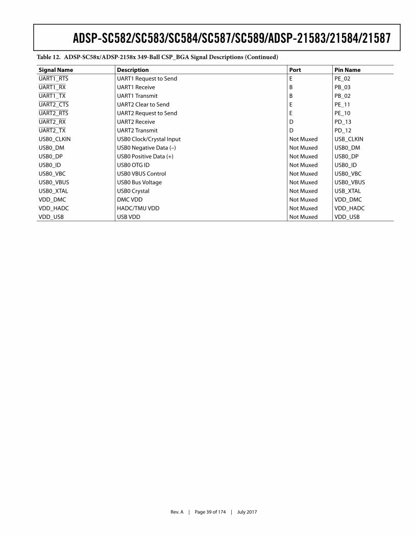
Rev. A | Page 39 of 174 | July 2017
ADSP-SC582/SC583/SC584/SC587/SC589/ADSP-21583/21584/21587
UART1_RTS UART1 Request to Send E PE_02
UART1_RX UART1 Receive B PB_03UART1_TX UART1 Transmit B PB_02
UART2_CTS UART2 Clear to Send E PE_11UART2_RTS UART2 Request to Send E PE_10
UART2_RX UART2 Receive D PD_13UART2_TX UART2 Transmit D PD_12
USB0_CLKIN USB0 Clock/Crystal Input Not Muxed USB_CLKINUSB0_DM USB0 Negative Data (–) Not Muxed USB0_DM
USB0_DP USB0 Positive Data (+) Not Muxed USB0_DPUSB0_ID USB0 OTG ID Not Muxed USB0_ID
USB0_VBC USB0 VBUS Control Not Muxed USB0_VBCUSB0_VBUS USB0 Bus Voltage Not Muxed USB0_VBUS
USB0_XTAL USB0 Crystal Not Muxed USB_XTALVDD_DMC DMC VDD Not Muxed VDD_DMC
VDD_HADC HADC/TMU VDD Not Muxed VDD_HADCVDD_USB USB VDD Not Muxed VDD_USB
Table 12. ADSP-SC58x/ADSP-2158x 349-Ball CSP_BGA Signal Descriptions (Continued)
Signal Name Description Port Pin Name
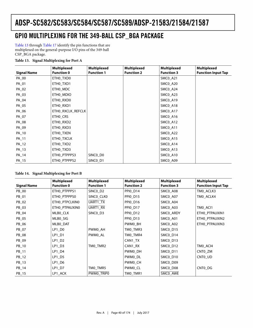
Rev. A | Page 40 of 174 | July 2017
ADSP-SC582/SC583/SC584/SC587/SC589/ADSP-21583/21584/21587
GPIO MULTIPLEXING FOR THE 349-BALL CSP_BGA PACKAGETable 13 through Table 17 identify the pin functions that are multiplexed on the general-purpose I/O pins of the 349-ball CSP_BGA package.Table 13. Signal Multiplexing for Port A
Signal NameMultiplexed Function 0
Multiplexed Function 1
Multiplexed Function 2
Multiplexed Function 3
Multiplexed Function Input Tap
PA_00 ETH0_TXD0 SMC0_A21
PA_01 ETH0_TXD1 SMC0_A20
PA_02 ETH0_MDC SMC0_A24
PA_03 ETH0_MDIO SMC0_A23
PA_04 ETH0_RXD0 SMC0_A19
PA_05 ETH0_RXD1 SMC0_A18
PA_06 ETH0_RXCLK_REFCLK SMC0_A17
PA_07 ETH0_CRS SMC0_A16
PA_08 ETH0_RXD2 SMC0_A12
PA_09 ETH0_RXD3 SMC0_A11
PA_10 ETH0_TXEN SMC0_A22
PA_11 ETH0_TXCLK SMC0_A15
PA_12 ETH0_TXD2 SMC0_A14
PA_13 ETH0_TXD3 SMC0_A13
PA_14 ETH0_PTPPPS3 SINC0_D0 SMC0_A10
PA_15 ETH0_PTPPPS2 SINC0_D1 SMC0_A09
Table 14. Signal Multiplexing for Port B
Signal NameMultiplexed Function 0
Multiplexed Function 1
Multiplexed Function 2
Multiplexed Function 3
Multiplexed Function Input Tap
PB_00 ETH0_PTPPPS1 SINC0_D2 PPI0_D14 SMC0_A08 TM0_ACLK3
PB_01 ETH0_PTPPPS0 SINC0_CLK0 PPI0_D15 SMC0_A07 TM0_ACLK4
PB_02 ETH0_PTPCLKIN0 UART1_TX PPI0_D16 SMC0_A04
PB_03 ETH0_PTPAUXIN0 UART1_RX PPI0_D17 SMC0_A03 TM0_ACI1
PB_04 MLB0_CLK SINC0_D3 PPI0_D12 SMC0_ARDY ETH0_PTPAUXIN1
PB_05 MLB0_SIG PPI0_D13 SMC0_A01 ETH0_PTPAUXIN2
PB_06 MLB0_DAT PWM0_BH SMC0_A02 ETH0_PTPAUXIN3
PB_07 LP1_D0 PWM0_AH TM0_TMR3 SMC0_D15
PB_08 LP1_D1 PWM0_AL TM0_TMR4 SMC0_D14
PB_09 LP1_D2 CAN1_TX SMC0_D13
PB_10 LP1_D3 TM0_TMR2 CAN1_RX SMC0_D12 TM0_ACI4
PB_11 LP1_D4 PWM0_DH SMC0_D11 CNT0_ZM
PB_12 LP1_D5 PWM0_DL SMC0_D10 CNT0_UD
PB_13 LP1_D6 PWM0_CH SMC0_D09
PB_14 LP1_D7 TM0_TMR5 PWM0_CL SMC0_D08 CNT0_DG
PB_15 LP1_ACK PWM0_TRIP0 TM0_TMR1 SMC0_AWE
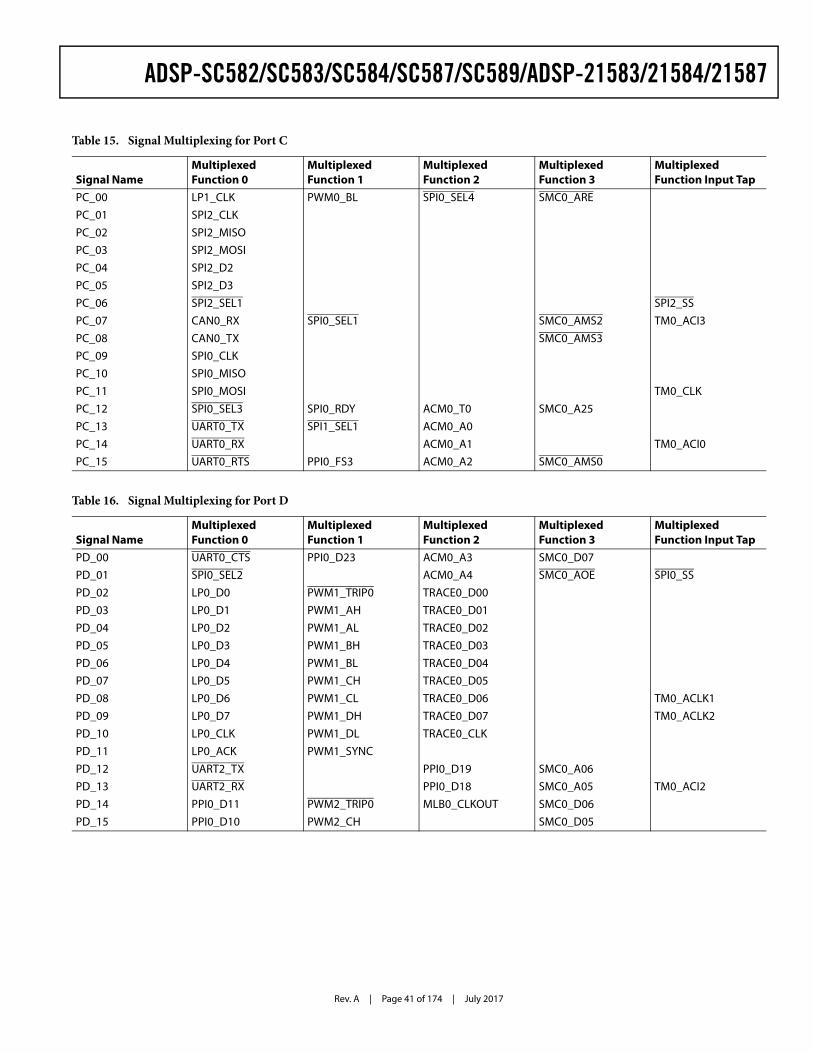
Rev. A | Page 41 of 174 | July 2017
ADSP-SC582/SC583/SC584/SC587/SC589/ADSP-21583/21584/21587
Table 15. Signal Multiplexing for Port C
Signal NameMultiplexed Function 0
Multiplexed Function 1
Multiplexed Function 2
Multiplexed Function 3
Multiplexed Function Input Tap
PC_00 LP1_CLK PWM0_BL SPI0_SEL4 SMC0_ARE
PC_01 SPI2_CLK
PC_02 SPI2_MISO
PC_03 SPI2_MOSI
PC_04 SPI2_D2
PC_05 SPI2_D3
PC_06 SPI2_SEL1 SPI2_SS
PC_07 CAN0_RX SPI0_SEL1 SMC0_AMS2 TM0_ACI3
PC_08 CAN0_TX SMC0_AMS3
PC_09 SPI0_CLK
PC_10 SPI0_MISO
PC_11 SPI0_MOSI TM0_CLK
PC_12 SPI0_SEL3 SPI0_RDY ACM0_T0 SMC0_A25
PC_13 UART0_TX SPI1_SEL1 ACM0_A0
PC_14 UART0_RX ACM0_A1 TM0_ACI0
PC_15 UART0_RTS PPI0_FS3 ACM0_A2 SMC0_AMS0
Table 16. Signal Multiplexing for Port D
Signal NameMultiplexed Function 0
Multiplexed Function 1
Multiplexed Function 2
Multiplexed Function 3
Multiplexed Function Input Tap
PD_00 UART0_CTS PPI0_D23 ACM0_A3 SMC0_D07
PD_01 SPI0_SEL2 ACM0_A4 SMC0_AOE SPI0_SS
PD_02 LP0_D0 PWM1_TRIP0 TRACE0_D00
PD_03 LP0_D1 PWM1_AH TRACE0_D01
PD_04 LP0_D2 PWM1_AL TRACE0_D02
PD_05 LP0_D3 PWM1_BH TRACE0_D03
PD_06 LP0_D4 PWM1_BL TRACE0_D04
PD_07 LP0_D5 PWM1_CH TRACE0_D05
PD_08 LP0_D6 PWM1_CL TRACE0_D06 TM0_ACLK1
PD_09 LP0_D7 PWM1_DH TRACE0_D07 TM0_ACLK2
PD_10 LP0_CLK PWM1_DL TRACE0_CLK
PD_11 LP0_ACK PWM1_SYNC
PD_12 UART2_TX PPI0_D19 SMC0_A06
PD_13 UART2_RX PPI0_D18 SMC0_A05 TM0_ACI2
PD_14 PPI0_D11 PWM2_TRIP0 MLB0_CLKOUT SMC0_D06
PD_15 PPI0_D10 PWM2_CH SMC0_D05
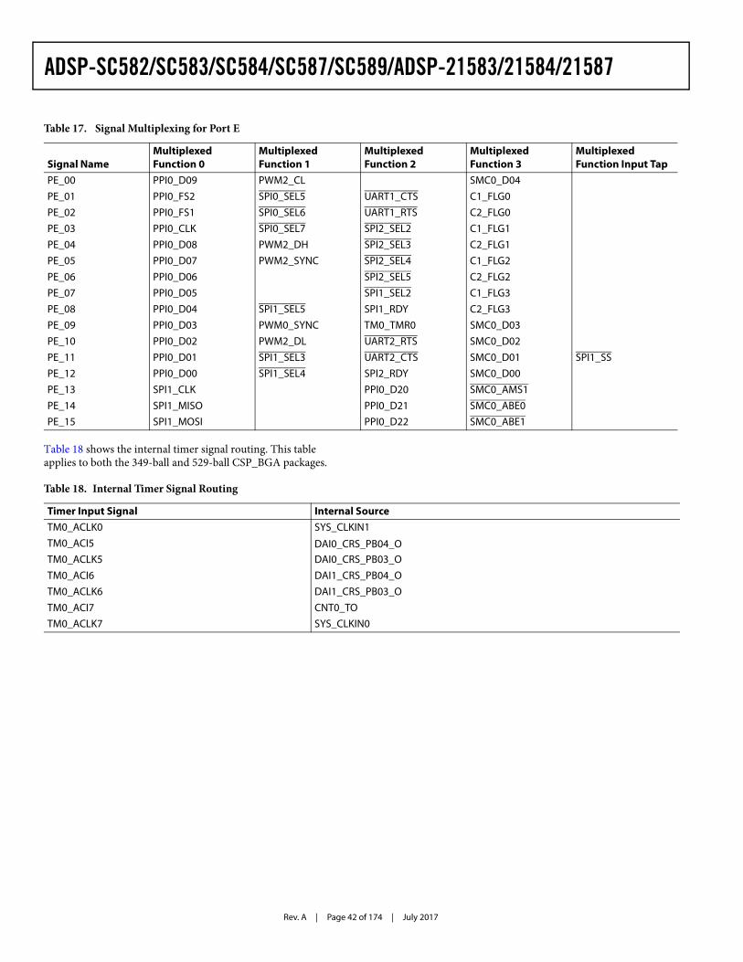
Rev. A | Page 42 of 174 | July 2017
ADSP-SC582/SC583/SC584/SC587/SC589/ADSP-21583/21584/21587
Table 18 shows the internal timer signal routing. This table applies to both the 349-ball and 529-ball CSP_BGA packages.
Table 17. Signal Multiplexing for Port E
Signal NameMultiplexed Function 0
Multiplexed Function 1
Multiplexed Function 2
Multiplexed Function 3
Multiplexed Function Input Tap
PE_00 PPI0_D09 PWM2_CL SMC0_D04
PE_01 PPI0_FS2 SPI0_SEL5 UART1_CTS C1_FLG0
PE_02 PPI0_FS1 SPI0_SEL6 UART1_RTS C2_FLG0
PE_03 PPI0_CLK SPI0_SEL7 SPI2_SEL2 C1_FLG1
PE_04 PPI0_D08 PWM2_DH SPI2_SEL3 C2_FLG1
PE_05 PPI0_D07 PWM2_SYNC SPI2_SEL4 C1_FLG2
PE_06 PPI0_D06 SPI2_SEL5 C2_FLG2
PE_07 PPI0_D05 SPI1_SEL2 C1_FLG3
PE_08 PPI0_D04 SPI1_SEL5 SPI1_RDY C2_FLG3
PE_09 PPI0_D03 PWM0_SYNC TM0_TMR0 SMC0_D03
PE_10 PPI0_D02 PWM2_DL UART2_RTS SMC0_D02
PE_11 PPI0_D01 SPI1_SEL3 UART2_CTS SMC0_D01 SPI1_SS
PE_12 PPI0_D00 SPI1_SEL4 SPI2_RDY SMC0_D00
PE_13 SPI1_CLK PPI0_D20 SMC0_AMS1
PE_14 SPI1_MISO PPI0_D21 SMC0_ABE0
PE_15 SPI1_MOSI PPI0_D22 SMC0_ABE1
Table 18. Internal Timer Signal Routing
Timer Input Signal Internal SourceTM0_ACLK0 SYS_CLKIN1
TM0_ACI5 DAI0_CRS_PB04_OTM0_ACLK5 DAI0_CRS_PB03_O
TM0_ACI6 DAI1_CRS_PB04_O
TM0_ACLK6 DAI1_CRS_PB03_O
TM0_ACI7 CNT0_TO
TM0_ACLK7 SYS_CLKIN0
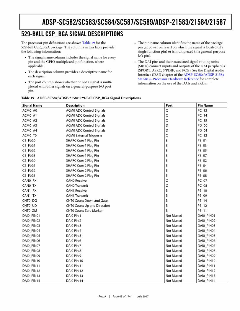
Rev. A | Page 43 of 174 | July 2017
ADSP-SC582/SC583/SC584/SC587/SC589/ADSP-21583/21584/21587529-BALL CSP_BGA SIGNAL DESCRIPTIONSThe processor pin definitions are shown Table 19 for the 529-ball CSP_BGA package. The columns in this table provide the following information:
• The signal name column includes the signal name for every pin and the GPIO multiplexed pin function, where applicable.
• The description column provides a descriptive name for each signal.
• The port column shows whether or not a signal is multi-plexed with other signals on a general-purpose I/O port pin.
• The pin name column identifies the name of the package pin (at power on reset) on which the signal is located (if a single function pin) or is multiplexed (if a general-purpose I/O pin).
• The DAI pins and their associated signal routing units (SRUs) connect inputs and outputs of the DAI peripherals (SPORT, ASRC, S/PDIF, and PCG). See the Digital Audio Interface (DAI) chapter of the ADSP-SC58x/ADSP-2158x SHARC+ Processor Hardware Reference for complete information on the use of the DAIs and SRUs.
Table 19. ADSP-SC58x/ADSP-2158x 529-Ball CSP_BGA Signal Descriptions
Signal Name Description Port Pin NameACM0_A0 ACM0 ADC Control Signals C PC_13ACM0_A1 ACM0 ADC Control Signals C PC_14
ACM0_A2 ACM0 ADC Control Signals C PC_15ACM0_A3 ACM0 ADC Control Signals D PD_00
ACM0_A4 ACM0 ADC Control Signals D PD_01ACM0_T0 ACM0 External Trigger n C PC_12
C1_FLG0 SHARC Core 1 Flag Pin E PE_01C1_FLG1 SHARC Core 1 Flag Pin E PE_03
C1_FLG2 SHARC Core 1 Flag Pin E PE_05C1_FLG3 SHARC Core 1 Flag Pin E PE_07
C2_FLG0 SHARC Core 2 Flag Pin E PE_02
C2_FLG1 SHARC Core 2 Flag Pin E PE_04C2_FLG2 SHARC Core 2 Flag Pin E PE_06
C2_FLG3 SHARC Core 2 Flag Pin E PE_08CAN0_RX CAN0 Receive C PC_07
CAN0_TX CAN0 Transmit C PC_08CAN1_RX CAN1 Receive B PB_10
CAN1_TX CAN1 Transmit B PB_09CNT0_DG CNT0 Count Down and Gate B PB_14
CNT0_UD CNT0 Count Up and Direction B PB_12CNT0_ZM CNT0 Count Zero Marker B PB_11
DAI0_PIN01 DAI0 Pin 1 Not Muxed DAI0_PIN01DAI0_PIN02 DAI0 Pin 2 Not Muxed DAI0_PIN02
DAI0_PIN03 DAI0 Pin 3 Not Muxed DAI0_PIN03DAI0_PIN04 DAI0 Pin 4 Not Muxed DAI0_PIN04
DAI0_PIN05 DAI0 Pin 5 Not Muxed DAI0_PIN05DAI0_PIN06 DAI0 Pin 6 Not Muxed DAI0_PIN06
DAI0_PIN07 DAI0 Pin 7 Not Muxed DAI0_PIN07DAI0_PIN08 DAI0 Pin 8 Not Muxed DAI0_PIN08
DAI0_PIN09 DAI0 Pin 9 Not Muxed DAI0_PIN09DAI0_PIN10 DAI0 Pin 10 Not Muxed DAI0_PIN10
DAI0_PIN11 DAI0 Pin 11 Not Muxed DAI0_PIN11DAI0_PIN12 DAI0 Pin 12 Not Muxed DAI0_PIN12
DAI0_PIN13 DAI0 Pin 13 Not Muxed DAI0_PIN13DAI0_PIN14 DAI0 Pin 14 Not Muxed DAI0_PIN14
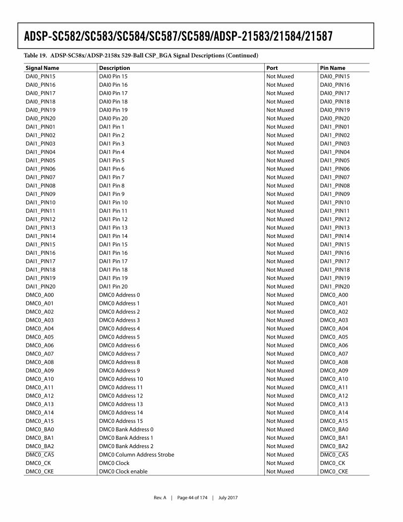
Rev. A | Page 44 of 174 | July 2017
ADSP-SC582/SC583/SC584/SC587/SC589/ADSP-21583/21584/21587
DAI0_PIN15 DAI0 Pin 15 Not Muxed DAI0_PIN15
DAI0_PIN16 DAI0 Pin 16 Not Muxed DAI0_PIN16DAI0_PIN17 DAI0 Pin 17 Not Muxed DAI0_PIN17
DAI0_PIN18 DAI0 Pin 18 Not Muxed DAI0_PIN18DAI0_PIN19 DAI0 Pin 19 Not Muxed DAI0_PIN19
DAI0_PIN20 DAI0 Pin 20 Not Muxed DAI0_PIN20DAI1_PIN01 DAI1 Pin 1 Not Muxed DAI1_PIN01
DAI1_PIN02 DAI1 Pin 2 Not Muxed DAI1_PIN02DAI1_PIN03 DAI1 Pin 3 Not Muxed DAI1_PIN03
DAI1_PIN04 DAI1 Pin 4 Not Muxed DAI1_PIN04DAI1_PIN05 DAI1 Pin 5 Not Muxed DAI1_PIN05
DAI1_PIN06 DAI1 Pin 6 Not Muxed DAI1_PIN06DAI1_PIN07 DAI1 Pin 7 Not Muxed DAI1_PIN07
DAI1_PIN08 DAI1 Pin 8 Not Muxed DAI1_PIN08DAI1_PIN09 DAI1 Pin 9 Not Muxed DAI1_PIN09
DAI1_PIN10 DAI1 Pin 10 Not Muxed DAI1_PIN10DAI1_PIN11 DAI1 Pin 11 Not Muxed DAI1_PIN11
DAI1_PIN12 DAI1 Pin 12 Not Muxed DAI1_PIN12DAI1_PIN13 DAI1 Pin 13 Not Muxed DAI1_PIN13
DAI1_PIN14 DAI1 Pin 14 Not Muxed DAI1_PIN14DAI1_PIN15 DAI1 Pin 15 Not Muxed DAI1_PIN15
DAI1_PIN16 DAI1 Pin 16 Not Muxed DAI1_PIN16DAI1_PIN17 DAI1 Pin 17 Not Muxed DAI1_PIN17
DAI1_PIN18 DAI1 Pin 18 Not Muxed DAI1_PIN18DAI1_PIN19 DAI1 Pin 19 Not Muxed DAI1_PIN19
DAI1_PIN20 DAI1 Pin 20 Not Muxed DAI1_PIN20DMC0_A00 DMC0 Address 0 Not Muxed DMC0_A00
DMC0_A01 DMC0 Address 1 Not Muxed DMC0_A01DMC0_A02 DMC0 Address 2 Not Muxed DMC0_A02
DMC0_A03 DMC0 Address 3 Not Muxed DMC0_A03DMC0_A04 DMC0 Address 4 Not Muxed DMC0_A04
DMC0_A05 DMC0 Address 5 Not Muxed DMC0_A05DMC0_A06 DMC0 Address 6 Not Muxed DMC0_A06
DMC0_A07 DMC0 Address 7 Not Muxed DMC0_A07DMC0_A08 DMC0 Address 8 Not Muxed DMC0_A08
DMC0_A09 DMC0 Address 9 Not Muxed DMC0_A09DMC0_A10 DMC0 Address 10 Not Muxed DMC0_A10
DMC0_A11 DMC0 Address 11 Not Muxed DMC0_A11DMC0_A12 DMC0 Address 12 Not Muxed DMC0_A12
DMC0_A13 DMC0 Address 13 Not Muxed DMC0_A13DMC0_A14 DMC0 Address 14 Not Muxed DMC0_A14
DMC0_A15 DMC0 Address 15 Not Muxed DMC0_A15
DMC0_BA0 DMC0 Bank Address 0 Not Muxed DMC0_BA0DMC0_BA1 DMC0 Bank Address 1 Not Muxed DMC0_BA1
DMC0_BA2 DMC0 Bank Address 2 Not Muxed DMC0_BA2DMC0_CAS DMC0 Column Address Strobe Not Muxed DMC0_CAS
DMC0_CK DMC0 Clock Not Muxed DMC0_CKDMC0_CKE DMC0 Clock enable Not Muxed DMC0_CKE
Table 19. ADSP-SC58x/ADSP-2158x 529-Ball CSP_BGA Signal Descriptions (Continued)
Signal Name Description Port Pin Name
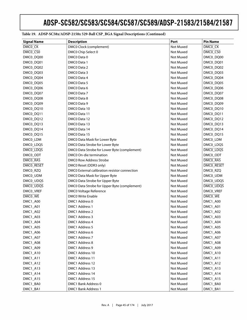
Rev. A | Page 45 of 174 | July 2017
ADSP-SC582/SC583/SC584/SC587/SC589/ADSP-21583/21584/21587
DMC0_CK DMC0 Clock (complement) Not Muxed DMC0_CK
DMC0_CS0 DMC0 Chip Select 0 Not Muxed DMC0_CS0DMC0_DQ00 DMC0 Data 0 Not Muxed DMC0_DQ00
DMC0_DQ01 DMC0 Data 1 Not Muxed DMC0_DQ01DMC0_DQ02 DMC0 Data 2 Not Muxed DMC0_DQ02
DMC0_DQ03 DMC0 Data 3 Not Muxed DMC0_DQ03DMC0_DQ04 DMC0 Data 4 Not Muxed DMC0_DQ04
DMC0_DQ05 DMC0 Data 5 Not Muxed DMC0_DQ05DMC0_DQ06 DMC0 Data 6 Not Muxed DMC0_DQ06
DMC0_DQ07 DMC0 Data 7 Not Muxed DMC0_DQ07DMC0_DQ08 DMC0 Data 8 Not Muxed DMC0_DQ08
DMC0_DQ09 DMC0 Data 9 Not Muxed DMC0_DQ09DMC0_DQ10 DMC0 Data 10 Not Muxed DMC0_DQ10
DMC0_DQ11 DMC0 Data 11 Not Muxed DMC0_DQ11DMC0_DQ12 DMC0 Data 12 Not Muxed DMC0_DQ12
DMC0_DQ13 DMC0 Data 13 Not Muxed DMC0_DQ13DMC0_DQ14 DMC0 Data 14 Not Muxed DMC0_DQ14
DMC0_DQ15 DMC0 Data 15 Not Muxed DMC0_DQ15DMC0_LDM DMC0 Data Mask for Lower Byte Not Muxed DMC0_LDM
DMC0_LDQS DMC0 Data Strobe for Lower Byte Not Muxed DMC0_LDQSDMC0_LDQS DMC0 Data Strobe for Lower Byte (complement) Not Muxed DMC0_LDQS
DMC0_ODT DMC0 On-die termination Not Muxed DMC0_ODTDMC0_RAS DMC0 Row Address Strobe Not Muxed DMC0_RAS
DMC0_RESET DMC0 Reset (DDR3 only) Not Muxed DMC0_RESETDMC0_RZQ DMC0 External calibration resistor connection Not Muxed DMC0_RZQ
DMC0_UDM DMC0 Data Mask for Upper Byte Not Muxed DMC0_UDMDMC0_UDQS DMC0 Data Strobe for Upper Byte Not Muxed DMC0_UDQS
DMC0_UDQS DMC0 Data Strobe for Upper Byte (complement) Not Muxed DMC0_UDQSDMC0_VREF DMC0 Voltage Reference Not Muxed DMC0_VREF
DMC0_WE DMC0 Write Enable Not Muxed DMC0_WEDMC1_A00 DMC1 Address 0 Not Muxed DMC1_A00
DMC1_A01 DMC1 Address 1 Not Muxed DMC1_A01DMC1_A02 DMC1 Address 2 Not Muxed DMC1_A02
DMC1_A03 DMC1 Address 3 Not Muxed DMC1_A03DMC1_A04 DMC1 Address 4 Not Muxed DMC1_A04
DMC1_A05 DMC1 Address 5 Not Muxed DMC1_A05DMC1_A06 DMC1 Address 6 Not Muxed DMC1_A06
DMC1_A07 DMC1 Address 7 Not Muxed DMC1_A07DMC1_A08 DMC1 Address 8 Not Muxed DMC1_A08
DMC1_A09 DMC1 Address 9 Not Muxed DMC1_A09DMC1_A10 DMC1 Address 10 Not Muxed DMC1_A10
DMC1_A11 DMC1 Address 11 Not Muxed DMC1_A11
DMC1_A12 DMC1 Address 12 Not Muxed DMC1_A12DMC1_A13 DMC1 Address 13 Not Muxed DMC1_A13
DMC1_A14 DMC1 Address 14 Not Muxed DMC1_A14DMC1_A15 DMC1 Address 15 Not Muxed DMC1_A15
DMC1_BA0 DMC1 Bank Address 0 Not Muxed DMC1_BA0DMC1_BA1 DMC1 Bank Address 1 Not Muxed DMC1_BA1
Table 19. ADSP-SC58x/ADSP-2158x 529-Ball CSP_BGA Signal Descriptions (Continued)
Signal Name Description Port Pin Name
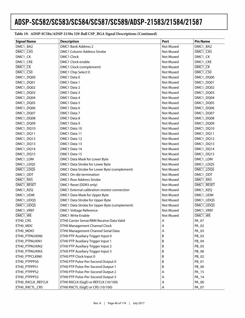
Rev. A | Page 46 of 174 | July 2017
ADSP-SC582/SC583/SC584/SC587/SC589/ADSP-21583/21584/21587
DMC1_BA2 DMC1 Bank Address 2 Not Muxed DMC1_BA2
DMC1_CAS DMC1 Column Address Strobe Not Muxed DMC1_CASDMC1_CK DMC1 Clock Not Muxed DMC1_CK
DMC1_CKE DMC1 Clock enable Not Muxed DMC1_CKEDMC1_CK DMC1 Clock (complement) Not Muxed DMC1_CK
DMC1_CS0 DMC1 Chip Select 0 Not Muxed DMC1_CS0DMC1_DQ00 DMC1 Data 0 Not Muxed DMC1_DQ00
DMC1_DQ01 DMC1 Data 1 Not Muxed DMC1_DQ01DMC1_DQ02 DMC1 Data 2 Not Muxed DMC1_DQ02
DMC1_DQ03 DMC1 Data 3 Not Muxed DMC1_DQ03DMC1_DQ04 DMC1 Data 4 Not Muxed DMC1_DQ04
DMC1_DQ05 DMC1 Data 5 Not Muxed DMC1_DQ05DMC1_DQ06 DMC1 Data 6 Not Muxed DMC1_DQ06
DMC1_DQ07 DMC1 Data 7 Not Muxed DMC1_DQ07DMC1_DQ08 DMC1 Data 8 Not Muxed DMC1_DQ08
DMC1_DQ09 DMC1 Data 9 Not Muxed DMC1_DQ09DMC1_DQ10 DMC1 Data 10 Not Muxed DMC1_DQ10
DMC1_DQ11 DMC1 Data 11 Not Muxed DMC1_DQ11DMC1_DQ12 DMC1 Data 12 Not Muxed DMC1_DQ12
DMC1_DQ13 DMC1 Data 13 Not Muxed DMC1_DQ13DMC1_DQ14 DMC1 Data 14 Not Muxed DMC1_DQ14
DMC1_DQ15 DMC1 Data 15 Not Muxed DMC1_DQ15DMC1_LDM DMC1 Data Mask for Lower Byte Not Muxed DMC1_LDM
DMC1_LDQS DMC1 Data Strobe for Lower Byte Not Muxed DMC1_LDQSDMC1_LDQS DMC1 Data Strobe for Lower Byte (complement) Not Muxed DMC1_LDQS
DMC1_ODT DMC1 On-die termination Not Muxed DMC1_ODTDMC1_RAS DMC1 Row Address Strobe Not Muxed DMC1_RAS
DMC1_RESET DMC1 Reset (DDR3 only) Not Muxed DMC1_RESETDMC1_RZQ DMC1 External calibration resistor connection Not Muxed DMC1_RZQ
DMC1_UDM DMC1 Data Mask for Upper Byte Not Muxed DMC1_UDMDMC1_UDQS DMC1 Data Strobe for Upper Byte Not Muxed DMC1_UDQS
DMC1_UDQS DMC1 Data Strobe for Upper Byte (complement) Not Muxed DMC1_UDQSDMC1_VREF DMC1 Voltage Reference Not Muxed DMC1_VREF
DMC1_WE DMC1 Write Enable Not Muxed DMC1_WEETH0_CRS ETH0 Carrier Sense/RMII Receive Data Valid A PA_07
ETH0_MDC ETH0 Management Channel Clock A PA_02ETH0_MDIO ETH0 Management Channel Serial Data A PA_03
ETH0_PTPAUXIN0 ETH0 PTP Auxiliary Trigger Input 0 B PB_03ETH0_PTPAUXIN1 ETH0 PTP Auxiliary Trigger Input 1 B PB_04
ETH0_PTPAUXIN2 ETH0 PTP Auxiliary Trigger Input 2 B PB_05ETH0_PTPAUXIN3 ETH0 PTP Auxiliary Trigger Input 3 B PB_06
ETH0_PTPCLKIN0 ETH0 PTP Clock Input 0 B PB_02
ETH0_PTPPPS0 ETH0 PTP Pulse-Per-Second Output 0 B PB_01ETH0_PTPPPS1 ETH0 PTP Pulse-Per-Second Output 1 B PB_00
ETH0_PTPPPS2 ETH0 PTP Pulse-Per-Second Output 2 A PA_15ETH0_PTPPPS3 ETH0 PTP Pulse-Per-Second Output 3 A PA_14
ETH0_RXCLK_REFCLK ETH0 RXCLK (GigE) or REFCLK (10/100) A PA_06ETH0_RXCTL_CRS ETH0 RXCTL (GigE) or CRS (10/100) A PA_07
Table 19. ADSP-SC58x/ADSP-2158x 529-Ball CSP_BGA Signal Descriptions (Continued)
Signal Name Description Port Pin Name
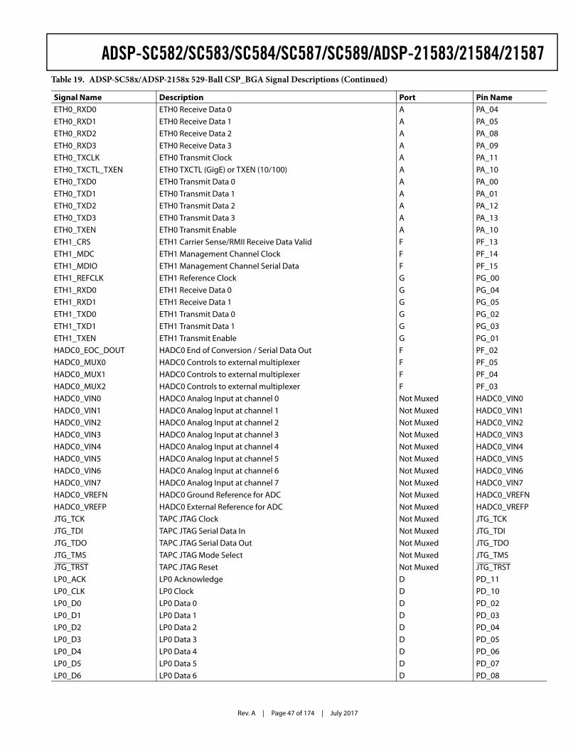
Rev. A | Page 47 of 174 | July 2017
ADSP-SC582/SC583/SC584/SC587/SC589/ADSP-21583/21584/21587
ETH0_RXD0 ETH0 Receive Data 0 A PA_04
ETH0_RXD1 ETH0 Receive Data 1 A PA_05ETH0_RXD2 ETH0 Receive Data 2 A PA_08
ETH0_RXD3 ETH0 Receive Data 3 A PA_09ETH0_TXCLK ETH0 Transmit Clock A PA_11
ETH0_TXCTL_TXEN ETH0 TXCTL (GigE) or TXEN (10/100) A PA_10ETH0_TXD0 ETH0 Transmit Data 0 A PA_00
ETH0_TXD1 ETH0 Transmit Data 1 A PA_01ETH0_TXD2 ETH0 Transmit Data 2 A PA_12
ETH0_TXD3 ETH0 Transmit Data 3 A PA_13ETH0_TXEN ETH0 Transmit Enable A PA_10
ETH1_CRS ETH1 Carrier Sense/RMII Receive Data Valid F PF_13ETH1_MDC ETH1 Management Channel Clock F PF_14
ETH1_MDIO ETH1 Management Channel Serial Data F PF_15ETH1_REFCLK ETH1 Reference Clock G PG_00
ETH1_RXD0 ETH1 Receive Data 0 G PG_04ETH1_RXD1 ETH1 Receive Data 1 G PG_05
ETH1_TXD0 ETH1 Transmit Data 0 G PG_02ETH1_TXD1 ETH1 Transmit Data 1 G PG_03
ETH1_TXEN ETH1 Transmit Enable G PG_01HADC0_EOC_DOUT HADC0 End of Conversion / Serial Data Out F PF_02
HADC0_MUX0 HADC0 Controls to external multiplexer F PF_05HADC0_MUX1 HADC0 Controls to external multiplexer F PF_04
HADC0_MUX2 HADC0 Controls to external multiplexer F PF_03HADC0_VIN0 HADC0 Analog Input at channel 0 Not Muxed HADC0_VIN0
HADC0_VIN1 HADC0 Analog Input at channel 1 Not Muxed HADC0_VIN1HADC0_VIN2 HADC0 Analog Input at channel 2 Not Muxed HADC0_VIN2
HADC0_VIN3 HADC0 Analog Input at channel 3 Not Muxed HADC0_VIN3HADC0_VIN4 HADC0 Analog Input at channel 4 Not Muxed HADC0_VIN4
HADC0_VIN5 HADC0 Analog Input at channel 5 Not Muxed HADC0_VIN5HADC0_VIN6 HADC0 Analog Input at channel 6 Not Muxed HADC0_VIN6
HADC0_VIN7 HADC0 Analog Input at channel 7 Not Muxed HADC0_VIN7HADC0_VREFN HADC0 Ground Reference for ADC Not Muxed HADC0_VREFN
HADC0_VREFP HADC0 External Reference for ADC Not Muxed HADC0_VREFPJTG_TCK TAPC JTAG Clock Not Muxed JTG_TCK
JTG_TDI TAPC JTAG Serial Data In Not Muxed JTG_TDIJTG_TDO TAPC JTAG Serial Data Out Not Muxed JTG_TDO
JTG_TMS TAPC JTAG Mode Select Not Muxed JTG_TMSJTG_TRST TAPC JTAG Reset Not Muxed JTG_TRST
LP0_ACK LP0 Acknowledge D PD_11LP0_CLK LP0 Clock D PD_10
LP0_D0 LP0 Data 0 D PD_02
LP0_D1 LP0 Data 1 D PD_03LP0_D2 LP0 Data 2 D PD_04
LP0_D3 LP0 Data 3 D PD_05LP0_D4 LP0 Data 4 D PD_06
LP0_D5 LP0 Data 5 D PD_07LP0_D6 LP0 Data 6 D PD_08
Table 19. ADSP-SC58x/ADSP-2158x 529-Ball CSP_BGA Signal Descriptions (Continued)
Signal Name Description Port Pin Name
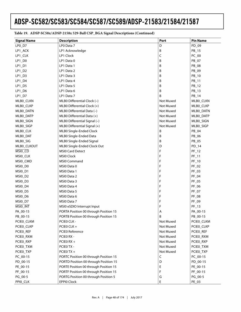
Rev. A | Page 48 of 174 | July 2017
ADSP-SC582/SC583/SC584/SC587/SC589/ADSP-21583/21584/21587
LP0_D7 LP0 Data 7 D PD_09
LP1_ACK LP1 Acknowledge B PB_15LP1_CLK LP1 Clock C PC_00
LP1_D0 LP1 Data 0 B PB_07LP1_D1 LP1 Data 1 B PB_08
LP1_D2 LP1 Data 2 B PB_09LP1_D3 LP1 Data 3 B PB_10
LP1_D4 LP1 Data 4 B PB_11LP1_D5 LP1 Data 5 B PB_12
LP1_D6 LP1 Data 6 B PB_13LP1_D7 LP1 Data 7 B PB_14
MLB0_CLKN MLB0 Differential Clock (–) Not Muxed MLB0_CLKNMLB0_CLKP MLB0 Differential Clock (+) Not Muxed MLB0_CLKP
MLB0_DATN MLB0 Differential Data (–) Not Muxed MLB0_DATNMLB0_DATP MLB0 Differential Data (+) Not Muxed MLB0_DATP
MLB0_SIGN MLB0 Differential Signal (–) Not Muxed MLB0_SIGNMLB0_SIGP MLB0 Differential Signal (+) Not Muxed MLB0_SIGP
MLB0_CLK MLB0 Single-Ended Clock B PB_04MLB0_DAT MLB0 Single-Ended Data B PB_06
MLB0_SIG MLB0 Single-Ended Signal B PB_05MLB0_CLKOUT MLB0 Single-Ended Clock Out D PD_14
MSI0_CD MSI0 Card Detect F PF_12MSI0_CLK MSI0 Clock F PF_11
MSI0_CMD MSI0 Command F PF_10MSI0_D0 MSI0 Data 0 F PF_02
MSI0_D1 MSI0 Data 1 F PF_03MSI0_D2 MSI0 Data 2 F PF_04
MSI0_D3 MSI0 Data 3 F PF_05MSI0_D4 MSI0 Data 4 F PF_06
MSI0_D5 MSI0 Data 5 F PF_07MSI0_D6 MSI0 Data 6 F PF_08
MSI0_D7 MSI0 Data 7 F PF_09MSI0_INT MSI0 eSDIO Interrupt Input F PF_13
PA_00-15 PORTA Position 00 through Position 15 A PA_00-15PB_00-15 PORTB Position 00 through Position 15 B PB_00-15
PCIE0_CLKM PCIE0 CLK - Not Muxed PCIE0_CLKMPCIE0_CLKP PCIE0 CLK + Not Muxed PCIE0_CLKP
PCIE0_REF PCIE0 Reference Not Muxed PCIE0_REFPCIE0_RXM PCIE0 RX - Not Muxed PCIE0_RXM
PCIE0_RXP PCIE0 RX + Not Muxed PCIE0_RXPPCIE0_TXM PCIE0 TX - Not Muxed PCIE0_TXM
PCIE0_TXP PCIE0 TX + Not Muxed PCIE0_TXP
PC_00-15 PORTC Position 00 through Position 15 C PC_00-15PD_00-15 PORTD Position 00 through Position 15 D PD_00-15
PE_00-15 PORTE Position 00 through Position 15 E PE_00-15PF_00-15 PORTF Position 00 through Position 15 F PF_00-15
PG_00-5 PORTG Position 00 through Position 5 G PG_00-5PPI0_CLK EPPI0 Clock E PE_03
Table 19. ADSP-SC58x/ADSP-2158x 529-Ball CSP_BGA Signal Descriptions (Continued)
Signal Name Description Port Pin Name
Rev. A | Page 49 of 174 | July 2017
ADSP-SC582/SC583/SC584/SC587/SC589/ADSP-21583/21584/21587
PPI0_D00 EPPI0 Data 0 E PE_12
PPI0_D01 EPPI0 Data 1 E PE_11PPI0_D02 EPPI0 Data 2 E PE_10
PPI0_D03 EPPI0 Data 3 E PE_09PPI0_D04 EPPI0 Data 4 E PE_08
PPI0_D05 EPPI0 Data 5 E PE_07PPI0_D06 EPPI0 Data 6 E PE_06
PPI0_D07 EPPI0 Data 7 E PE_05PPI0_D08 EPPI0 Data 8 E PE_04
PPI0_D09 EPPI0 Data 9 E PE_00PPI0_D10 EPPI0 Data 10 D PD_15
PPI0_D11 EPPI0 Data 11 D PD_14PPI0_D12 EPPI0 Data 12 B PB_04
PPI0_D13 EPPI0 Data 13 B PB_05PPI0_D14 EPPI0 Data 14 B PB_00
PPI0_D15 EPPI0 Data 15 B PB_01PPI0_D16 EPPI0 Data 16 B PB_02
PPI0_D17 EPPI0 Data 17 B PB_03PPI0_D18 EPPI0 Data 18 D PD_13
PPI0_D19 EPPI0 Data 19 D PD_12PPI0_D20 EPPI0 Data 20 E PE_13
PPI0_D21 EPPI0 Data 21 E PE_14PPI0_D22 EPPI0 Data 22 E PE_15
PPI0_D23 EPPI0 Data 23 D PD_00PPI0_FS1 EPPI0 Frame Sync 1 (HSYNC) E PE_02
PPI0_FS2 EPPI0 Frame Sync 2 (VSYNC) E PE_01PPI0_FS3 EPPI0 Frame Sync 3 (FIELD) C PC_15
PWM0_AH PWM0 Channel A High Side B PB_07PWM0_AL PWM0 Channel A Low Side B PB_08
PWM0_BH PWM0 Channel B High Side B PB_06PWM0_BL PWM0 Channel B Low Side C PC_00
PWM0_CH PWM0 Channel C High Side B PB_13PWM0_CL PWM0 Channel C Low Side B PB_14
PWM0_DH PWM0 Channel D High Side B PB_11PWM0_DL PWM0 Channel D Low Side B PB_12
PWM0_SYNC PWM0 PWMTMR Grouped E PE_09PWM0_TRIP0 PWM0 Shutdown Input 0 B PB_15
PWM1_AH PWM1 Channel A High Side D PD_03PWM1_AL PWM1 Channel A Low Side D PD_04
PWM1_BH PWM1 Channel B High Side D PD_05PWM1_BL PWM1 Channel B Low Side D PD_06
PWM1_CH PWM1 Channel C High Side D PD_07
PWM1_CL PWM1 Channel C Low Side D PD_08PWM1_DH PWM1 Channel D High Side D PD_09
PWM1_DL PWM1 Channel D Low Side D PD_10PWM1_SYNC PWM1 PWMTMR Grouped D PD_11
PWM1_TRIP0 PWM1 Shutdown Input 0 D PD_02PWM2_AH PWM2 Channel A High Side F PF_07
Table 19. ADSP-SC58x/ADSP-2158x 529-Ball CSP_BGA Signal Descriptions (Continued)
Signal Name Description Port Pin Name
Rev. A | Page 50 of 174 | July 2017
ADSP-SC582/SC583/SC584/SC587/SC589/ADSP-21583/21584/21587
PWM2_AL PWM2 Channel A Low Side F PF_06
PWM2_BH PWM2 Channel B High Side F PF_09PWM2_BL PWM2 Channel B Low Side F PF_08
PWM2_CH PWM2 Channel C High Side D PD_15PWM2_CL PWM2 Channel C Low Side E PE_00
PWM2_DH PWM2 Channel D High Side E PE_04PWM2_DL PWM2 Channel D Low Side E PE_10
PWM2_SYNC PWM2 PWMTMR Grouped E PE_05PWM2_TRIP0 PWM2 Shutdown Input 0 D PD_14
GND Ground Not Muxed GNDVDD_EXT External Voltage Domain Not Muxed VDD_EXT
VDD_INT Internal Voltage Domain Not Muxed VDD_INTRTC0_CLKIN RTC0 Crystal input / external oscillator connection Not Muxed RTC0_CLKIN
RTC0_XTAL RTC0 Crystal output Not Muxed RTC0_XTALSINC0_CLK0 SINC0 Clock 0 B PB_01
SINC0_D0 SINC0 Data 0 A PA_14SINC0_D1 SINC0 Data 1 A PA_15
SINC0_D2 SINC0 Data 2 B PB_00SINC0_D3 SINC0 Data 3 B PB_04
SMC0_A01 SMC0 Address 1 B PB_05SMC0_A02 SMC0 Address 2 B PB_06
SMC0_A03 SMC0 Address 3 B PB_03SMC0_A04 SMC0 Address 4 B PB_02
SMC0_A05 SMC0 Address 5 D PD_13SMC0_A06 SMC0 Address 6 D PD_12
SMC0_A07 SMC0 Address 7 B PB_01SMC0_A08 SMC0 Address 8 B PB_00
SMC0_A09 SMC0 Address 9 A PA_15SMC0_A10 SMC0 Address 10 A PA_14
SMC0_A11 SMC0 Address 11 A PA_09SMC0_A12 SMC0 Address 12 A PA_08
SMC0_A13 SMC0 Address 13 A PA_13SMC0_A14 SMC0 Address 14 A PA_12
SMC0_A15 SMC0 Address 15 A PA_11SMC0_A16 SMC0 Address 16 A PA_07
SMC0_A17 SMC0 Address 17 A PA_06SMC0_A18 SMC0 Address 18 A PA_05
SMC0_A19 SMC0 Address 19 A PA_04SMC0_A20 SMC0 Address 20 A PA_01
SMC0_A21 SMC0 Address 21 A PA_00SMC0_A22 SMC0 Address 22 A PA_10
SMC0_A23 SMC0 Address 23 A PA_03
SMC0_A24 SMC0 Address 24 A PA_02SMC0_A25 SMC0 Address 25 C PC_12
SMC0_ABE0 SMC0 Byte Enable 0 E PE_14SMC0_ABE1 SMC0 Byte Enable 1 E PE_15
SMC0_AMS0 SMC0 Memory Select 0 C PC_15SMC0_AMS1 SMC0 Memory Select 1 E PE_13
Table 19. ADSP-SC58x/ADSP-2158x 529-Ball CSP_BGA Signal Descriptions (Continued)
Signal Name Description Port Pin Name
Rev. A | Page 51 of 174 | July 2017
ADSP-SC582/SC583/SC584/SC587/SC589/ADSP-21583/21584/21587
SMC0_AMS2 SMC0 Memory Select 2 C PC_07
SMC0_AMS3 SMC0 Memory Select 3 C PC_08SMC0_AOE SMC0 Output Enable D PD_01
SMC0_ARDY SMC0 Asynchronous Ready B PB_04SMC0_ARE SMC0 Read Enable C PC_00
SMC0_AWE SMC0 Write Enable B PB_15SMC0_D00 SMC0 Data 0 E PE_12
SMC0_D01 SMC0 Data 1 E PE_11SMC0_D02 SMC0 Data 2 E PE_10
SMC0_D03 SMC0 Data 3 E PE_09SMC0_D04 SMC0 Data 4 E PE_00
SMC0_D05 SMC0 Data 5 D PD_15SMC0_D06 SMC0 Data 6 D PD_14
SMC0_D07 SMC0 Data 7 D PD_00SMC0_D08 SMC0 Data 8 B PB_14
SMC0_D09 SMC0 Data 9 B PB_13SMC0_D10 SMC0 Data 10 B PB_12
SMC0_D11 SMC0 Data 11 B PB_11SMC0_D12 SMC0 Data 12 B PB_10
SMC0_D13 SMC0 Data 13 B PB_09SMC0_D14 SMC0 Data 14 B PB_08
SMC0_D15 SMC0 Data 15 B PB_07SPI0_CLK SPI0 Clock C PC_09
SPI0_MISO SPI0 Master In, Slave Out C PC_10SPI0_MOSI SPI0 Master Out, Slave In C PC_11
SPI0_RDY SPI0 Ready C PC_12SPI0_SEL1 SPI0 Slave Select Output 1 C PC_07
SPI0_SEL2 SPI0 Slave Select Output 2 D PD_01SPI0_SEL3 SPI0 Slave Select Output 3 C PC_12
SPI0_SEL4 SPI0 Slave Select Output 4 C PC_00SPI0_SEL5 SPI0 Slave Select Output 5 E PE_01
SPI0_SEL6 SPI0 Slave Select Output 6 E PE_02SPI0_SEL7 SPI0 Slave Select Output 7 E PE_03
SPI0_SS SPI0 Slave Select Input D PD_01SPI1_CLK SPI1 Clock E PE_13
SPI1_MISO SPI1 Master In, Slave Out E PE_14SPI1_MOSI SPI1 Master Out, Slave In E PE_15
SPI1_RDY SPI1 Ready E PE_08SPI1_SEL1 SPI1 Slave Select Output 1 C PC_13
SPI1_SEL2 SPI1 Slave Select Output 2 E PE_07SPI1_SEL3 SPI1 Slave Select Output 3 E PE_11
SPI1_SEL4 SPI1 Slave Select Output 4 E PE_12
SPI1_SEL5 SPI1 Slave Select Output 5 E PE_08SPI1_SEL6 SPI1 Slave Select Output 6 F PF_00
SPI1_SEL7 SPI1 Slave Select Output 7 F PF_01SPI1_SS SPI1 Slave Select Input E PE_11
SPI2_CLK SPI2 Clock C PC_01SPI2_D2 SPI2 Data 2 C PC_04
Table 19. ADSP-SC58x/ADSP-2158x 529-Ball CSP_BGA Signal Descriptions (Continued)
Signal Name Description Port Pin Name
Rev. A | Page 52 of 174 | July 2017
ADSP-SC582/SC583/SC584/SC587/SC589/ADSP-21583/21584/21587
SPI2_D3 SPI2 Data 3 C PC_05
SPI2_MISO SPI2 Master In, Slave Out C PC_02SPI2_MOSI SPI2 Master Out, Slave In C PC_03
SPI2_RDY SPI2 Ready E PE_12SPI2_SEL1 SPI2 Slave Select Output 1 C PC_06
SPI2_SEL2 SPI2 Slave Select Output 2 E PE_03SPI2_SEL3 SPI2 Slave Select Output 3 E PE_04
SPI2_SEL4 SPI2 Slave Select Output 4 E PE_05SPI2_SEL5 SPI2 Slave Select Output 5 E PE_06
SPI2_SS SPI2 Slave Select Input C PC_06SYS_BMODE0 Boot Mode Control 0 Not Muxed SYS_BMODE0
SYS_BMODE1 Boot Mode Control 1 Not Muxed SYS_BMODE1SYS_BMODE2 Boot Mode Control 2 Not Muxed SYS_BMODE2
SYS_CLKIN0 Clock/Crystal Input Not Muxed SYS_CLKIN0SYS_CLKIN1 Clock/Crystal Input Not Muxed SYS_CLKIN1
SYS_CLKOUT Processor Clock Output Not Muxed SYS_CLKOUTSYS_FAULT Active-High Fault Output Not Muxed SYS_FAULT
SYS_FAULT Active-Low Fault Output Not Muxed SYS_FAULTSYS_HWRST Processor Hardware Reset Control Not Muxed SYS_HWRST
SYS_RESOUT Reset Output Not Muxed SYS_RESOUTSYS_XTAL0 Crystal Output Not Muxed SYS_XTAL0
SYS_XTAL1 Crystal Output Not Muxed SYS_XTAL1TM0_ACI0 TIMER0 Alternate Capture Input 0 C PC_14
TM0_ACI1 TIMER0 Alternate Capture Input 1 B PB_03TM0_ACI2 TIMER0 Alternate Capture Input 2 D PD_13
TM0_ACI3 TIMER0 Alternate Capture Input 3 C PC_07TM0_ACI4 TIMER0 Alternate Capture Input 4 B PB_10
TM0_ACLK1 TIMER0 Alternate Clock 1 D PD_08TM0_ACLK2 TIMER0 Alternate Clock 2 D PD_09
TM0_ACLK3 TIMER0 Alternate Clock 3 B PB_00TM0_ACLK4 TIMER0 Alternate Clock 4 B PB_01
TM0_CLK TIMER0 Clock C PC_11TM0_TMR0 TIMER0 Timer 0 E PE_09
TM0_TMR1 TIMER0 Timer 1 B PB_15TM0_TMR2 TIMER0 Timer 2 B PB_10
TM0_TMR3 TIMER0 Timer 3 B PB_07TM0_TMR4 TIMER0 Timer 4 B PB_08
TM0_TMR5 TIMER0 Timer 5 B PB_14TM0_TMR6 TIMER0 Timer 6 F PF_00
TM0_TMR7 TIMER0 Timer 7 F PF_01TRACE0_CLK TRACE0 Trace Clock (first instance) G PG_00
TRACE0_CLK TRACE0 Trace Clock (second instance) D PD_10
TRACE0_D00 TRACE0 Trace Data (first instance) F PF_13TRACE0_D00 TRACE0 Trace Data 0 (second instance) D PD_02
TRACE0_D01 TRACE0 Trace Data 1 (first instance) D PD_03TRACE0_D01 TRACE0 Trace Data (second instance) F PF_14
TRACE0_D02 TRACE0 Trace Data (first instance) F PF_15TRACE0_D02 TRACE0 Trace Data 2 (second instance) D PD_04
Table 19. ADSP-SC58x/ADSP-2158x 529-Ball CSP_BGA Signal Descriptions (Continued)
Signal Name Description Port Pin Name

Rev. A | Page 53 of 174 | July 2017
ADSP-SC582/SC583/SC584/SC587/SC589/ADSP-21583/21584/21587
TRACE0_D03 TRACE0 Trace Data (first instance) G PG_01
TRACE0_D03 TRACE0 Trace Data 3 (second instance) D PD_05TRACE0_D04 TRACE0 Trace Data (first instance) G PG_02
TRACE0_D04 TRACE0 Trace Data 4 (second instance) D PD_06TRACE0_D05 TRACE0 Trace Data 5 (first instance) D PD_07
TRACE0_D05 TRACE0 Trace Data (second instance) G PG_03TRACE0_D06 TRACE0 Trace Data (first instance) G PG_04
TRACE0_D06 TRACE0 Trace Data 6 (second instance) D PD_08TRACE0_D07 TRACE0 Trace Data (first instance) G PG_05
TRACE0_D07 TRACE0 Trace Data 7 (second instance) D PD_09TRACE0_D08 TRACE0 Trace Data 8 F PF_13
TRACE0_D09 TRACE0 Trace Data 9 F PF_14TRACE0_D10 TRACE0 Trace Data 10 F PF_15
TRACE0_D11 TRACE0 Trace Data 11 G PG_01TRACE0_D12 TRACE0 Trace Data 12 G PG_02
TRACE0_D13 TRACE0 Trace Data 13 G PG_03TRACE0_D14 TRACE0 Trace Data 14 G PG_04
TRACE0_D15 TRACE0 Trace Data 15 G PG_05TWI0_SCL TWI0 Serial Clock Not Muxed TWI0_SCL
TWI0_SDA TWI0 Serial Data Not Muxed TWI0_SDATWI1_SCL TWI1 Serial Clock Not Muxed TWI1_SCL
TWI1_SDA TWI1 Serial Data Not Muxed TWI1_SDATWI2_SCL TWI2 Serial Clock Not Muxed TWI2_SCL
TWI2_SDA TWI2 Serial Data Not Muxed TWI2_SDAUART0_CTS UART0 Clear to Send D PD_00
UART0_RTS UART0 Request to Send C PC_15UART0_RX UART0 Receive C PC_14
UART0_TX UART0 Transmit C PC_13UART1_CTS UART1 Clear to Send E PE_01
UART1_RTS UART1 Request to Send E PE_02UART1_RX UART1 Receive B PB_03
UART1_TX UART1 Transmit B PB_02UART2_CTS UART2 Clear to Send E PE_11
UART2_RTS UART2 Request to Send E PE_10UART2_RX UART2 Receive D PD_13
UART2_TX UART2 Transmit D PD_12USB0_CLKIN USB0 Clock/Crystal Input Not Muxed USB_CLKIN
USB0_DM USB0 Data – Not Muxed USB0_DMUSB0_DP USB0 Data + Not Muxed USB0_DP
USB0_ID USB0 OTG ID Not Muxed USB0_IDUSB0_VBC USB0 VBUS Control Not Muxed USB0_VBC
USB0_VBUS USB0 Bus Voltage Not Muxed USB0_VBUS
USB0_XTAL USB0 Crystal Not Muxed USB_XTALUSB1_DM USB1 Data - Not Muxed USB1_DM
USB1_DP USB1 Data + Not Muxed USB1_DPUSB1_VBUS USB1 Bus Voltage Not Muxed USB1_VBUS
VDD_DMC DMC VDD Not Muxed VDD_DMCVDD_HADC HADC/TMU VDD Not Muxed VDD_HADC
Table 19. ADSP-SC58x/ADSP-2158x 529-Ball CSP_BGA Signal Descriptions (Continued)
Signal Name Description Port Pin Name
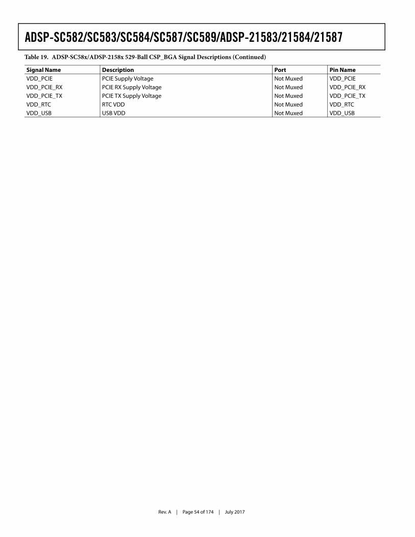
Rev. A | Page 54 of 174 | July 2017
ADSP-SC582/SC583/SC584/SC587/SC589/ADSP-21583/21584/21587
VDD_PCIE PCIE Supply Voltage Not Muxed VDD_PCIE
VDD_PCIE_RX PCIE RX Supply Voltage Not Muxed VDD_PCIE_RXVDD_PCIE_TX PCIE TX Supply Voltage Not Muxed VDD_PCIE_TX
VDD_RTC RTC VDD Not Muxed VDD_RTCVDD_USB USB VDD Not Muxed VDD_USB
Table 19. ADSP-SC58x/ADSP-2158x 529-Ball CSP_BGA Signal Descriptions (Continued)
Signal Name Description Port Pin Name
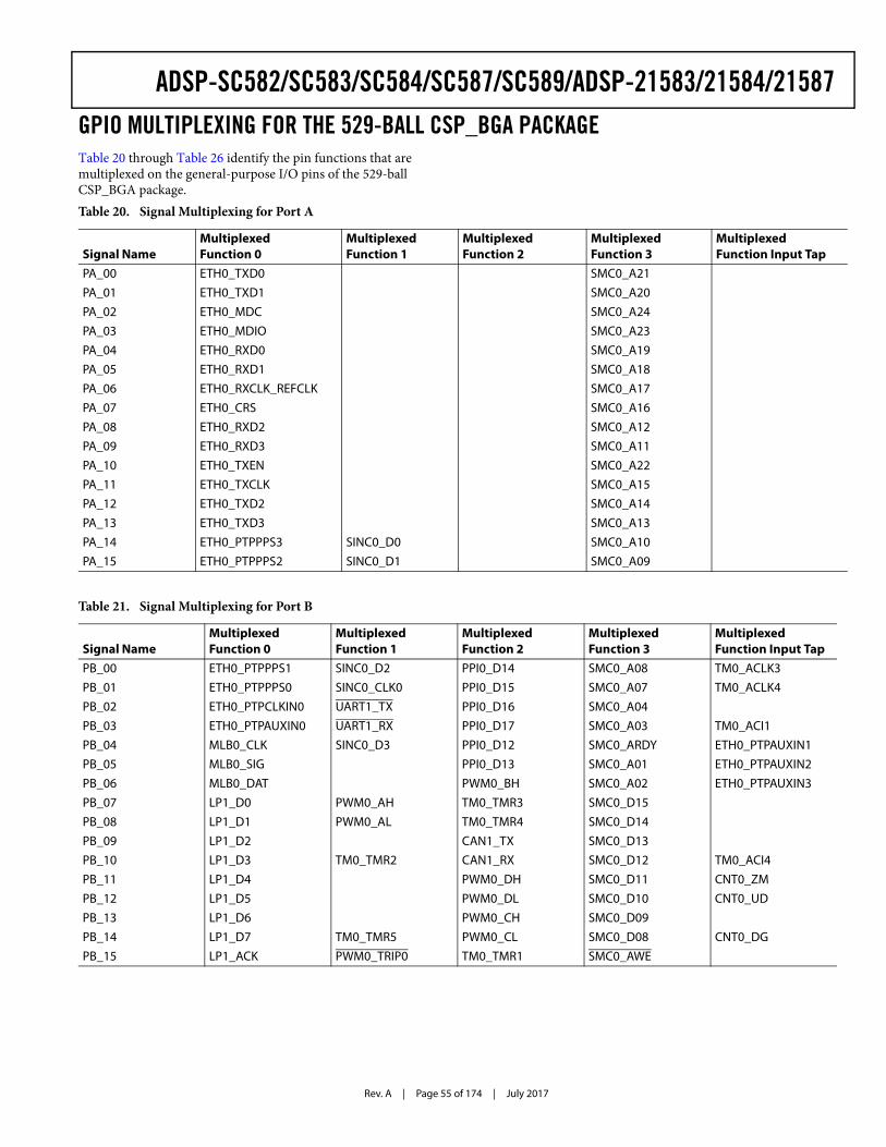
Rev. A | Page 55 of 174 | July 2017
ADSP-SC582/SC583/SC584/SC587/SC589/ADSP-21583/21584/21587GPIO MULTIPLEXING FOR THE 529-BALL CSP_BGA PACKAGETable 20 through Table 26 identify the pin functions that are multiplexed on the general-purpose I/O pins of the 529-ball CSP_BGA package.Table 20. Signal Multiplexing for Port A
Signal NameMultiplexed Function 0
Multiplexed Function 1
MultiplexedFunction 2
Multiplexed Function 3
Multiplexed Function Input Tap
PA_00 ETH0_TXD0 SMC0_A21
PA_01 ETH0_TXD1 SMC0_A20
PA_02 ETH0_MDC SMC0_A24
PA_03 ETH0_MDIO SMC0_A23
PA_04 ETH0_RXD0 SMC0_A19
PA_05 ETH0_RXD1 SMC0_A18
PA_06 ETH0_RXCLK_REFCLK SMC0_A17
PA_07 ETH0_CRS SMC0_A16
PA_08 ETH0_RXD2 SMC0_A12
PA_09 ETH0_RXD3 SMC0_A11
PA_10 ETH0_TXEN SMC0_A22
PA_11 ETH0_TXCLK SMC0_A15
PA_12 ETH0_TXD2 SMC0_A14
PA_13 ETH0_TXD3 SMC0_A13
PA_14 ETH0_PTPPPS3 SINC0_D0 SMC0_A10
PA_15 ETH0_PTPPPS2 SINC0_D1 SMC0_A09
Table 21. Signal Multiplexing for Port B
Signal NameMultiplexed Function 0
Multiplexed Function 1
Multiplexed Function 2
Multiplexed Function 3
Multiplexed Function Input Tap
PB_00 ETH0_PTPPPS1 SINC0_D2 PPI0_D14 SMC0_A08 TM0_ACLK3
PB_01 ETH0_PTPPPS0 SINC0_CLK0 PPI0_D15 SMC0_A07 TM0_ACLK4
PB_02 ETH0_PTPCLKIN0 UART1_TX PPI0_D16 SMC0_A04
PB_03 ETH0_PTPAUXIN0 UART1_RX PPI0_D17 SMC0_A03 TM0_ACI1
PB_04 MLB0_CLK SINC0_D3 PPI0_D12 SMC0_ARDY ETH0_PTPAUXIN1
PB_05 MLB0_SIG PPI0_D13 SMC0_A01 ETH0_PTPAUXIN2
PB_06 MLB0_DAT PWM0_BH SMC0_A02 ETH0_PTPAUXIN3
PB_07 LP1_D0 PWM0_AH TM0_TMR3 SMC0_D15
PB_08 LP1_D1 PWM0_AL TM0_TMR4 SMC0_D14
PB_09 LP1_D2 CAN1_TX SMC0_D13
PB_10 LP1_D3 TM0_TMR2 CAN1_RX SMC0_D12 TM0_ACI4
PB_11 LP1_D4 PWM0_DH SMC0_D11 CNT0_ZM
PB_12 LP1_D5 PWM0_DL SMC0_D10 CNT0_UD
PB_13 LP1_D6 PWM0_CH SMC0_D09
PB_14 LP1_D7 TM0_TMR5 PWM0_CL SMC0_D08 CNT0_DG
PB_15 LP1_ACK PWM0_TRIP0 TM0_TMR1 SMC0_AWE
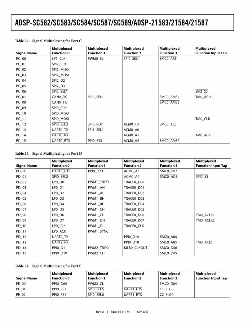
Rev. A | Page 56 of 174 | July 2017
ADSP-SC582/SC583/SC584/SC587/SC589/ADSP-21583/21584/21587
Table 22. Signal Multiplexing for Port C
Signal NameMultiplexed Function 0
Multiplexed Function 1
Multiplexed Function 2
Multiplexed Function 3
Multiplexed Function Input Tap
PC_00 LP1_CLK PWM0_BL SPI0_SEL4 SMC0_ARE
PC_01 SPI2_CLK
PC_02 SPI2_MISO
PC_03 SPI2_MOSI
PC_04 SPI2_D2
PC_05 SPI2_D3
PC_06 SPI2_SEL1 SPI2_SS
PC_07 CAN0_RX SPI0_SEL1 SMC0_AMS2 TM0_ACI3
PC_08 CAN0_TX SMC0_AMS3
PC_09 SPI0_CLK
PC_10 SPI0_MISO
PC_11 SPI0_MOSI TM0_CLK
PC_12 SPI0_SEL3 SPI0_RDY ACM0_T0 SMC0_A25
PC_13 UART0_TX SPI1_SEL1 ACM0_A0
PC_14 UART0_RX ACM0_A1 TM0_ACI0
PC_15 UART0_RTS PPI0_FS3 ACM0_A2 SMC0_AMS0
Table 23. Signal Multiplexing for Port D
Signal NameMultiplexed Function 0
Multiplexed Function 1
Multiplexed Function 2
Multiplexed Function 3
Multiplexed Function Input Tap
PD_00 UART0_CTS PPI0_D23 ACM0_A3 SMC0_D07
PD_01 SPI0_SEL2 ACM0_A4 SMC0_AOE SPI0_SS
PD_02 LP0_D0 PWM1_TRIP0 TRACE0_D00
PD_03 LP0_D1 PWM1_AH TRACE0_D01
PD_04 LP0_D2 PWM1_AL TRACE0_D02
PD_05 LP0_D3 PWM1_BH TRACE0_D03
PD_06 LP0_D4 PWM1_BL TRACE0_D04
PD_07 LP0_D5 PWM1_CH TRACE0_D05
PD_08 LP0_D6 PWM1_CL TRACE0_D06 TM0_ACLK1
PD_09 LP0_D7 PWM1_DH TRACE0_D07 TM0_ACLK2
PD_10 LP0_CLK PWM1_DL TRACE0_CLK
PD_11 LP0_ACK PWM1_SYNC
PD_12 UART2_TX PPI0_D19 SMC0_A06
PD_13 UART2_RX PPI0_D18 SMC0_A05 TM0_ACI2
PD_14 PPI0_D11 PWM2_TRIP0 MLB0_CLKOUT SMC0_D06
PD_15 PPI0_D10 PWM2_CH SMC0_D05
Table 24. Signal Multiplexing for Port E
Signal NameMultiplexed Function 0
Multiplexed Function 1
Multiplexed Function 2
Multiplexed Function 3
Multiplexed Function Input Tap
PE_00 PPI0_D09 PWM2_CL SMC0_D04
PE_01 PPI0_FS2 SPI0_SEL5 UART1_CTS C1_FLG0
PE_02 PPI0_FS1 SPI0_SEL6 UART1_RTS C2_FLG0
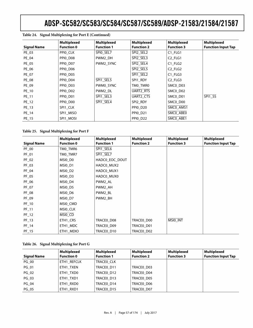
Rev. A | Page 57 of 174 | July 2017
ADSP-SC582/SC583/SC584/SC587/SC589/ADSP-21583/21584/21587
PE_03 PPI0_CLK SPI0_SEL7 SPI2_SEL2 C1_FLG1
PE_04 PPI0_D08 PWM2_DH SPI2_SEL3 C2_FLG1
PE_05 PPI0_D07 PWM2_SYNC SPI2_SEL4 C1_FLG2
PE_06 PPI0_D06 SPI2_SEL5 C2_FLG2
PE_07 PPI0_D05 SPI1_SEL2 C1_FLG3
PE_08 PPI0_D04 SPI1_SEL5 SPI1_RDY C2_FLG3
PE_09 PPI0_D03 PWM0_SYNC TM0_TMR0 SMC0_D03
PE_10 PPI0_D02 PWM2_DL UART2_RTS SMC0_D02
PE_11 PPI0_D01 SPI1_SEL3 UART2_CTS SMC0_D01 SPI1_SS
PE_12 PPI0_D00 SPI1_SEL4 SPI2_RDY SMC0_D00
PE_13 SPI1_CLK PPI0_D20 SMC0_AMS1
PE_14 SPI1_MISO PPI0_D21 SMC0_ABE0
PE_15 SPI1_MOSI PPI0_D22 SMC0_ABE1
Table 24. Signal Multiplexing for Port E (Continued)
Signal NameMultiplexed Function 0
Multiplexed Function 1
Multiplexed Function 2
Multiplexed Function 3
Multiplexed Function Input Tap
Table 25. Signal Multiplexing for Port F
Signal NameMultiplexed Function 0
Multiplexed Function 1
Multiplexed Function 2
Multiplexed Function 3
Multiplexed Function Input Tap
PF_00 TM0_TMR6 SPI1_SEL6
PF_01 TM0_TMR7 SPI1_SEL7
PF_02 MSI0_D0 HADC0_EOC_DOUT
PF_03 MSI0_D1 HADC0_MUX2
PF_04 MSI0_D2 HADC0_MUX1
PF_05 MSI0_D3 HADC0_MUX0
PF_06 MSI0_D4 PWM2_AL
PF_07 MSI0_D5 PWM2_AH
PF_08 MSI0_D6 PWM2_BL
PF_09 MSI0_D7 PWM2_BH
PF_10 MSI0_CMD
PF_11 MSI0_CLK
PF_12 MSI0_CD
PF_13 ETH1_CRS TRACE0_D08 TRACE0_D00 MSI0_INT
PF_14 ETH1_MDC TRACE0_D09 TRACE0_D01
PF_15 ETH1_MDIO TRACE0_D10 TRACE0_D02
Table 26. Signal Multiplexing for Port G
Signal NameMultiplexed Function 0
Multiplexed Function 1
Multiplexed Function 2
Multiplexed Function 3
Multiplexed Function Input Tap
PG_00 ETH1_REFCLK TRACE0_CLK
PG_01 ETH1_TXEN TRACE0_D11 TRACE0_D03
PG_02 ETH1_TXD0 TRACE0_D12 TRACE0_D04
PG_03 ETH1_TXD1 TRACE0_D13 TRACE0_D05
PG_04 ETH1_RXD0 TRACE0_D14 TRACE0_D06
PG_05 ETH1_RXD1 TRACE0_D15 TRACE0_D07
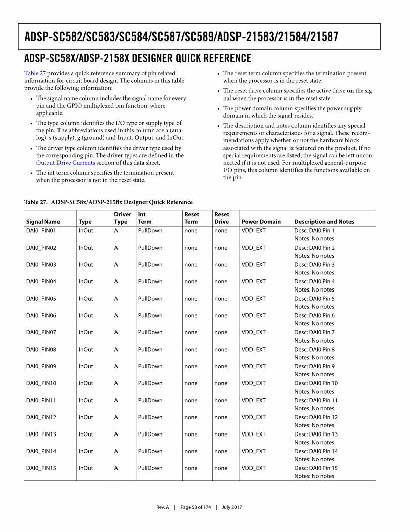
Rev. A | Page 58 of 174 | July 2017
ADSP-SC582/SC583/SC584/SC587/SC589/ADSP-21583/21584/21587
ADSP-SC58X/ADSP-2158X DESIGNER QUICK REFERENCETable 27 provides a quick reference summary of pin related information for circuit board design. The columns in this table provide the following information:
• The signal name column includes the signal name for every pin and the GPIO multiplexed pin function, where applicable.
• The type column identifies the I/O type or supply type of the pin. The abbreviations used in this column are a (ana-log), s (supply), g (ground) and Input, Output, and InOut.
• The driver type column identifies the driver type used by the corresponding pin. The driver types are defined in the Output Drive Currents section of this data sheet.
• The int term column specifies the termination present when the processor is not in the reset state.
• The reset term column specifies the termination present when the processor is in the reset state.
• The reset drive column specifies the active drive on the sig-nal when the processor is in the reset state.
• The power domain column specifies the power supply domain in which the signal resides.
• The description and notes column identifies any special requirements or characteristics for a signal. These recom-mendations apply whether or not the hardware block associated with the signal is featured on the product. If no special requirements are listed, the signal can be left uncon-nected if it is not used. For multiplexed general-purpose I/O pins, this column identifies the functions available on the pin.
Table 27. ADSP-SC58x/ADSP-2158x Designer Quick Reference
Signal Name TypeDriver Type
Int Term
Reset Term
Reset Drive Power Domain Description and Notes
DAI0_PIN01 InOut A PullDown none none VDD_EXT Desc: DAI0 Pin 1Notes: No notes
DAI0_PIN02 InOut A PullDown none none VDD_EXT Desc: DAI0 Pin 2Notes: No notes
DAI0_PIN03 InOut A PullDown none none VDD_EXT Desc: DAI0 Pin 3Notes: No notes
DAI0_PIN04 InOut A PullDown none none VDD_EXT Desc: DAI0 Pin 4Notes: No notes
DAI0_PIN05 InOut A PullDown none none VDD_EXT Desc: DAI0 Pin 5Notes: No notes
DAI0_PIN06 InOut A PullDown none none VDD_EXT Desc: DAI0 Pin 6Notes: No notes
DAI0_PIN07 InOut A PullDown none none VDD_EXT Desc: DAI0 Pin 7Notes: No notes
DAI0_PIN08 InOut A PullDown none none VDD_EXT Desc: DAI0 Pin 8Notes: No notes
DAI0_PIN09 InOut A PullDown none none VDD_EXT Desc: DAI0 Pin 9Notes: No notes
DAI0_PIN10 InOut A PullDown none none VDD_EXT Desc: DAI0 Pin 10Notes: No notes
DAI0_PIN11 InOut A PullDown none none VDD_EXT Desc: DAI0 Pin 11Notes: No notes
DAI0_PIN12 InOut A PullDown none none VDD_EXT Desc: DAI0 Pin 12Notes: No notes
DAI0_PIN13 InOut A PullDown none none VDD_EXT Desc: DAI0 Pin 13Notes: No notes
DAI0_PIN14 InOut A PullDown none none VDD_EXT Desc: DAI0 Pin 14Notes: No notes
DAI0_PIN15 InOut A PullDown none none VDD_EXT Desc: DAI0 Pin 15Notes: No notes
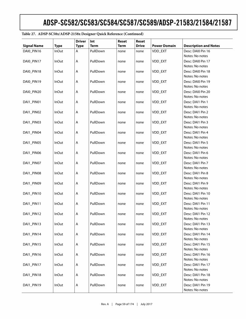
Rev. A | Page 59 of 174 | July 2017
ADSP-SC582/SC583/SC584/SC587/SC589/ADSP-21583/21584/21587
DAI0_PIN16 InOut A PullDown none none VDD_EXT Desc: DAI0 Pin 16Notes: No notes
DAI0_PIN17 InOut A PullDown none none VDD_EXT Desc: DAI0 Pin 17Notes: No notes
DAI0_PIN18 InOut A PullDown none none VDD_EXT Desc: DAI0 Pin 18Notes: No notes
DAI0_PIN19 InOut A PullDown none none VDD_EXT Desc: DAI0 Pin 19Notes: No notes
DAI0_PIN20 InOut A PullDown none none VDD_EXT Desc: DAI0 Pin 20Notes: No notes
DAI1_PIN01 InOut A PullDown none none VDD_EXT Desc: DAI1 Pin 1Notes: No notes
DAI1_PIN02 InOut A PullDown none none VDD_EXT Desc: DAI1 Pin 2Notes: No notes
DAI1_PIN03 InOut A PullDown none none VDD_EXT Desc: DAI1 Pin 3Notes: No notes
DAI1_PIN04 InOut A PullDown none none VDD_EXT Desc: DAI1 Pin 4Notes: No notes
DAI1_PIN05 InOut A PullDown none none VDD_EXT Desc: DAI1 Pin 5Notes: No notes
DAI1_PIN06 InOut A PullDown none none VDD_EXT Desc: DAI1 Pin 6Notes: No notes
DAI1_PIN07 InOut A PullDown none none VDD_EXT Desc: DAI1 Pin 7Notes: No notes
DAI1_PIN08 InOut A PullDown none none VDD_EXT Desc: DAI1 Pin 8Notes: No notes
DAI1_PIN09 InOut A PullDown none none VDD_EXT Desc: DAI1 Pin 9Notes: No notes
DAI1_PIN10 InOut A PullDown none none VDD_EXT Desc: DAI1 Pin 10Notes: No notes
DAI1_PIN11 InOut A PullDown none none VDD_EXT Desc: DAI1 Pin 11Notes: No notes
DAI1_PIN12 InOut A PullDown none none VDD_EXT Desc: DAI1 Pin 12Notes: No notes
DAI1_PIN13 InOut A PullDown none none VDD_EXT Desc: DAI1 Pin 13Notes: No notes
DAI1_PIN14 InOut A PullDown none none VDD_EXT Desc: DAI1 Pin 14Notes: No notes
DAI1_PIN15 InOut A PullDown none none VDD_EXT Desc: DAI1 Pin 15Notes: No notes
DAI1_PIN16 InOut A PullDown none none VDD_EXT Desc: DAI1 Pin 16Notes: No notes
DAI1_PIN17 InOut A PullDown none none VDD_EXT Desc: DAI1 Pin 17Notes: No notes
DAI1_PIN18 InOut A PullDown none none VDD_EXT Desc: DAI1 Pin 18Notes: No notes
DAI1_PIN19 InOut A PullDown none none VDD_EXT Desc: DAI1 Pin 19Notes: No notes
Table 27. ADSP-SC58x/ADSP-2158x Designer Quick Reference (Continued)
Signal Name TypeDriver Type
Int Term
Reset Term
Reset Drive Power Domain Description and Notes
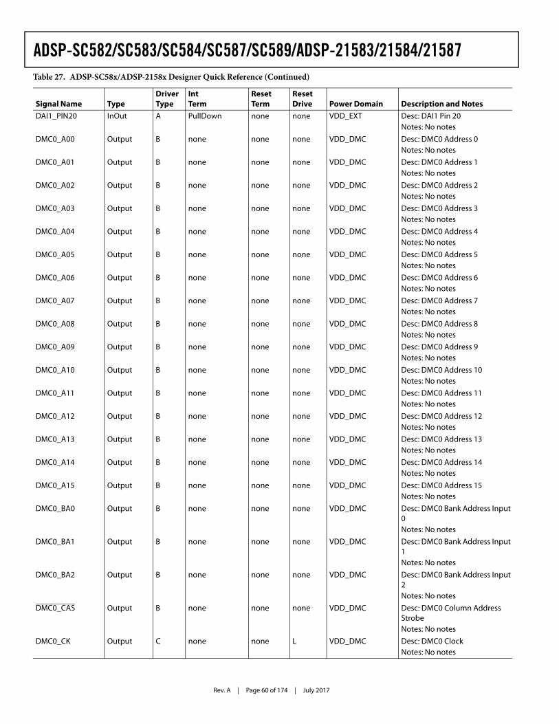
Rev. A | Page 60 of 174 | July 2017
ADSP-SC582/SC583/SC584/SC587/SC589/ADSP-21583/21584/21587
DAI1_PIN20 InOut A PullDown none none VDD_EXT Desc: DAI1 Pin 20Notes: No notes
DMC0_A00 Output B none none none VDD_DMC Desc: DMC0 Address 0Notes: No notes
DMC0_A01 Output B none none none VDD_DMC Desc: DMC0 Address 1Notes: No notes
DMC0_A02 Output B none none none VDD_DMC Desc: DMC0 Address 2Notes: No notes
DMC0_A03 Output B none none none VDD_DMC Desc: DMC0 Address 3Notes: No notes
DMC0_A04 Output B none none none VDD_DMC Desc: DMC0 Address 4Notes: No notes
DMC0_A05 Output B none none none VDD_DMC Desc: DMC0 Address 5Notes: No notes
DMC0_A06 Output B none none none VDD_DMC Desc: DMC0 Address 6Notes: No notes
DMC0_A07 Output B none none none VDD_DMC Desc: DMC0 Address 7Notes: No notes
DMC0_A08 Output B none none none VDD_DMC Desc: DMC0 Address 8Notes: No notes
DMC0_A09 Output B none none none VDD_DMC Desc: DMC0 Address 9Notes: No notes
DMC0_A10 Output B none none none VDD_DMC Desc: DMC0 Address 10Notes: No notes
DMC0_A11 Output B none none none VDD_DMC Desc: DMC0 Address 11Notes: No notes
DMC0_A12 Output B none none none VDD_DMC Desc: DMC0 Address 12Notes: No notes
DMC0_A13 Output B none none none VDD_DMC Desc: DMC0 Address 13Notes: No notes
DMC0_A14 Output B none none none VDD_DMC Desc: DMC0 Address 14Notes: No notes
DMC0_A15 Output B none none none VDD_DMC Desc: DMC0 Address 15Notes: No notes
DMC0_BA0 Output B none none none VDD_DMC Desc: DMC0 Bank Address Input 0Notes: No notes
DMC0_BA1 Output B none none none VDD_DMC Desc: DMC0 Bank Address Input 1Notes: No notes
DMC0_BA2 Output B none none none VDD_DMC Desc: DMC0 Bank Address Input 2Notes: No notes
DMC0_CAS Output B none none none VDD_DMC Desc: DMC0 Column Address StrobeNotes: No notes
DMC0_CK Output C none none L VDD_DMC Desc: DMC0 ClockNotes: No notes
Table 27. ADSP-SC58x/ADSP-2158x Designer Quick Reference (Continued)
Signal Name TypeDriver Type
Int Term
Reset Term
Reset Drive Power Domain Description and Notes
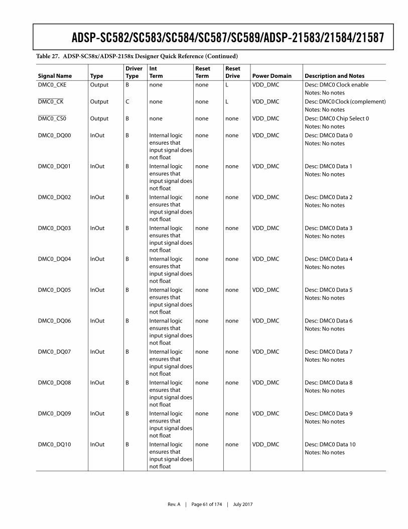
Rev. A | Page 61 of 174 | July 2017
ADSP-SC582/SC583/SC584/SC587/SC589/ADSP-21583/21584/21587
DMC0_CKE Output B none none L VDD_DMC Desc: DMC0 Clock enableNotes: No notes
DMC0_CK Output C none none L VDD_DMC Desc: DMC0 Clock (complement)Notes: No notes
DMC0_CS0 Output B none none none VDD_DMC Desc: DMC0 Chip Select 0Notes: No notes
DMC0_DQ00 InOut B Internal logic ensures that input signal does not float
none none VDD_DMC Desc: DMC0 Data 0Notes: No notes
DMC0_DQ01 InOut B Internal logic ensures that input signal does not float
none none VDD_DMC Desc: DMC0 Data 1Notes: No notes
DMC0_DQ02 InOut B Internal logic ensures that input signal does not float
none none VDD_DMC Desc: DMC0 Data 2Notes: No notes
DMC0_DQ03 InOut B Internal logic ensures that input signal does not float
none none VDD_DMC Desc: DMC0 Data 3Notes: No notes
DMC0_DQ04 InOut B Internal logic ensures that input signal does not float
none none VDD_DMC Desc: DMC0 Data 4Notes: No notes
DMC0_DQ05 InOut B Internal logic ensures that input signal does not float
none none VDD_DMC Desc: DMC0 Data 5Notes: No notes
DMC0_DQ06 InOut B Internal logic ensures that input signal does not float
none none VDD_DMC Desc: DMC0 Data 6Notes: No notes
DMC0_DQ07 InOut B Internal logic ensures that input signal does not float
none none VDD_DMC Desc: DMC0 Data 7Notes: No notes
DMC0_DQ08 InOut B Internal logic ensures that input signal does not float
none none VDD_DMC Desc: DMC0 Data 8Notes: No notes
DMC0_DQ09 InOut B Internal logic ensures that input signal does not float
none none VDD_DMC Desc: DMC0 Data 9Notes: No notes
DMC0_DQ10 InOut B Internal logic ensures that input signal does not float
none none VDD_DMC Desc: DMC0 Data 10Notes: No notes
Table 27. ADSP-SC58x/ADSP-2158x Designer Quick Reference (Continued)
Signal Name TypeDriver Type
Int Term
Reset Term
Reset Drive Power Domain Description and Notes
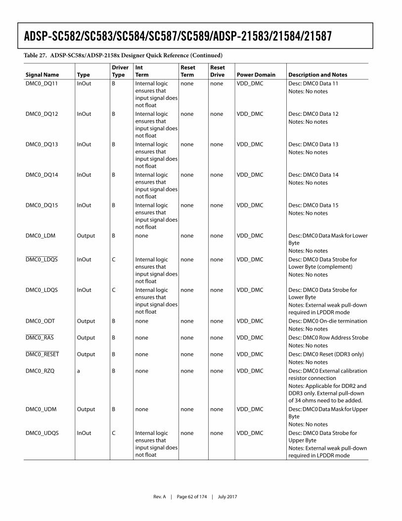
Rev. A | Page 62 of 174 | July 2017
ADSP-SC582/SC583/SC584/SC587/SC589/ADSP-21583/21584/21587
DMC0_DQ11 InOut B Internal logic ensures that input signal does not float
none none VDD_DMC Desc: DMC0 Data 11Notes: No notes
DMC0_DQ12 InOut B Internal logic ensures that input signal does not float
none none VDD_DMC Desc: DMC0 Data 12Notes: No notes
DMC0_DQ13 InOut B Internal logic ensures that input signal does not float
none none VDD_DMC Desc: DMC0 Data 13Notes: No notes
DMC0_DQ14 InOut B Internal logic ensures that input signal does not float
none none VDD_DMC Desc: DMC0 Data 14Notes: No notes
DMC0_DQ15 InOut B Internal logic ensures that input signal does not float
none none VDD_DMC Desc: DMC0 Data 15Notes: No notes
DMC0_LDM Output B none none none VDD_DMC Desc: DMC0 Data Mask for Lower ByteNotes: No notes
DMC0_LDQS InOut C Internal logic ensures that input signal does not float
none none VDD_DMC Desc: DMC0 Data Strobe for Lower Byte (complement)Notes: No notes
DMC0_LDQS InOut C Internal logic ensures that input signal does not float
none none VDD_DMC Desc: DMC0 Data Strobe for Lower ByteNotes: External weak pull-down required in LPDDR mode
DMC0_ODT Output B none none none VDD_DMC Desc: DMC0 On-die terminationNotes: No notes
DMC0_RAS Output B none none none VDD_DMC Desc: DMC0 Row Address StrobeNotes: No notes
DMC0_RESET Output B none none none VDD_DMC Desc: DMC0 Reset (DDR3 only)Notes: No notes
DMC0_RZQ a B none none none VDD_DMC Desc: DMC0 External calibration resistor connectionNotes: Applicable for DDR2 and DDR3 only. External pull-down of 34 ohms need to be added.
DMC0_UDM Output B none none none VDD_DMC Desc: DMC0 Data Mask for Upper ByteNotes: No notes
DMC0_UDQS InOut C Internal logic ensures that input signal does not float
none none VDD_DMC Desc: DMC0 Data Strobe for Upper ByteNotes: External weak pull-down required in LPDDR mode
Table 27. ADSP-SC58x/ADSP-2158x Designer Quick Reference (Continued)
Signal Name TypeDriver Type
Int Term
Reset Term
Reset Drive Power Domain Description and Notes
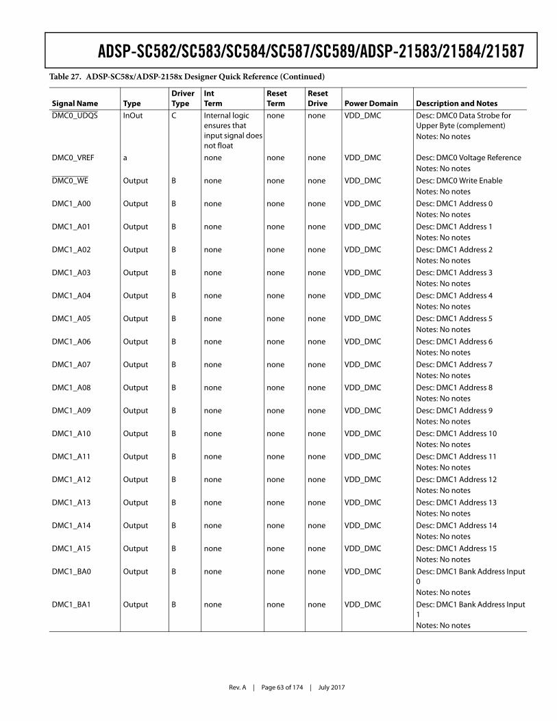
Rev. A | Page 63 of 174 | July 2017
ADSP-SC582/SC583/SC584/SC587/SC589/ADSP-21583/21584/21587
DMC0_UDQS InOut C Internal logic ensures that input signal does not float
none none VDD_DMC Desc: DMC0 Data Strobe for Upper Byte (complement)Notes: No notes
DMC0_VREF a none none none VDD_DMC Desc: DMC0 Voltage ReferenceNotes: No notes
DMC0_WE Output B none none none VDD_DMC Desc: DMC0 Write EnableNotes: No notes
DMC1_A00 Output B none none none VDD_DMC Desc: DMC1 Address 0Notes: No notes
DMC1_A01 Output B none none none VDD_DMC Desc: DMC1 Address 1Notes: No notes
DMC1_A02 Output B none none none VDD_DMC Desc: DMC1 Address 2Notes: No notes
DMC1_A03 Output B none none none VDD_DMC Desc: DMC1 Address 3Notes: No notes
DMC1_A04 Output B none none none VDD_DMC Desc: DMC1 Address 4Notes: No notes
DMC1_A05 Output B none none none VDD_DMC Desc: DMC1 Address 5Notes: No notes
DMC1_A06 Output B none none none VDD_DMC Desc: DMC1 Address 6Notes: No notes
DMC1_A07 Output B none none none VDD_DMC Desc: DMC1 Address 7Notes: No notes
DMC1_A08 Output B none none none VDD_DMC Desc: DMC1 Address 8Notes: No notes
DMC1_A09 Output B none none none VDD_DMC Desc: DMC1 Address 9Notes: No notes
DMC1_A10 Output B none none none VDD_DMC Desc: DMC1 Address 10Notes: No notes
DMC1_A11 Output B none none none VDD_DMC Desc: DMC1 Address 11Notes: No notes
DMC1_A12 Output B none none none VDD_DMC Desc: DMC1 Address 12Notes: No notes
DMC1_A13 Output B none none none VDD_DMC Desc: DMC1 Address 13Notes: No notes
DMC1_A14 Output B none none none VDD_DMC Desc: DMC1 Address 14Notes: No notes
DMC1_A15 Output B none none none VDD_DMC Desc: DMC1 Address 15Notes: No notes
DMC1_BA0 Output B none none none VDD_DMC Desc: DMC1 Bank Address Input 0Notes: No notes
DMC1_BA1 Output B none none none VDD_DMC Desc: DMC1 Bank Address Input 1Notes: No notes
Table 27. ADSP-SC58x/ADSP-2158x Designer Quick Reference (Continued)
Signal Name TypeDriver Type
Int Term
Reset Term
Reset Drive Power Domain Description and Notes
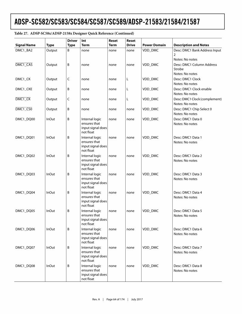
Rev. A | Page 64 of 174 | July 2017
ADSP-SC582/SC583/SC584/SC587/SC589/ADSP-21583/21584/21587
DMC1_BA2 Output B none none none VDD_DMC Desc: DMC1 Bank Address Input 2Notes: No notes
DMC1_CAS Output B none none none VDD_DMC Desc: DMC1 Column Address StrobeNotes: No notes
DMC1_CK Output C none none L VDD_DMC Desc: DMC1 ClockNotes: No notes
DMC1_CKE Output B none none L VDD_DMC Desc: DMC1 Clock enableNotes: No notes
DMC1_CK Output C none none L VDD_DMC Desc: DMC1 Clock (complement)Notes: No notes
DMC1_CS0 Output B none none none VDD_DMC Desc: DMC1 Chip Select 0Notes: No notes
DMC1_DQ00 InOut B Internal logic ensures that input signal does not float
none none VDD_DMC Desc: DMC1 Data 0Notes: No notes
DMC1_DQ01 InOut B Internal logic ensures that input signal does not float
none none VDD_DMC Desc: DMC1 Data 1Notes: No notes
DMC1_DQ02 InOut B Internal logic ensures that input signal does not float
none none VDD_DMC Desc: DMC1 Data 2Notes: No notes
DMC1_DQ03 InOut B Internal logic ensures that input signal does not float
none none VDD_DMC Desc: DMC1 Data 3Notes: No notes
DMC1_DQ04 InOut B Internal logic ensures that input signal does not float
none none VDD_DMC Desc: DMC1 Data 4Notes: No notes
DMC1_DQ05 InOut B Internal logic ensures that input signal does not float
none none VDD_DMC Desc: DMC1 Data 5Notes: No notes
DMC1_DQ06 InOut B Internal logic ensures that input signal does not float
none none VDD_DMC Desc: DMC1 Data 6Notes: No notes
DMC1_DQ07 InOut B Internal logic ensures that input signal does not float
none none VDD_DMC Desc: DMC1 Data 7Notes: No notes
DMC1_DQ08 InOut B Internal logic ensures that input signal does not float
none none VDD_DMC Desc: DMC1 Data 8Notes: No notes
Table 27. ADSP-SC58x/ADSP-2158x Designer Quick Reference (Continued)
Signal Name TypeDriver Type
Int Term
Reset Term
Reset Drive Power Domain Description and Notes
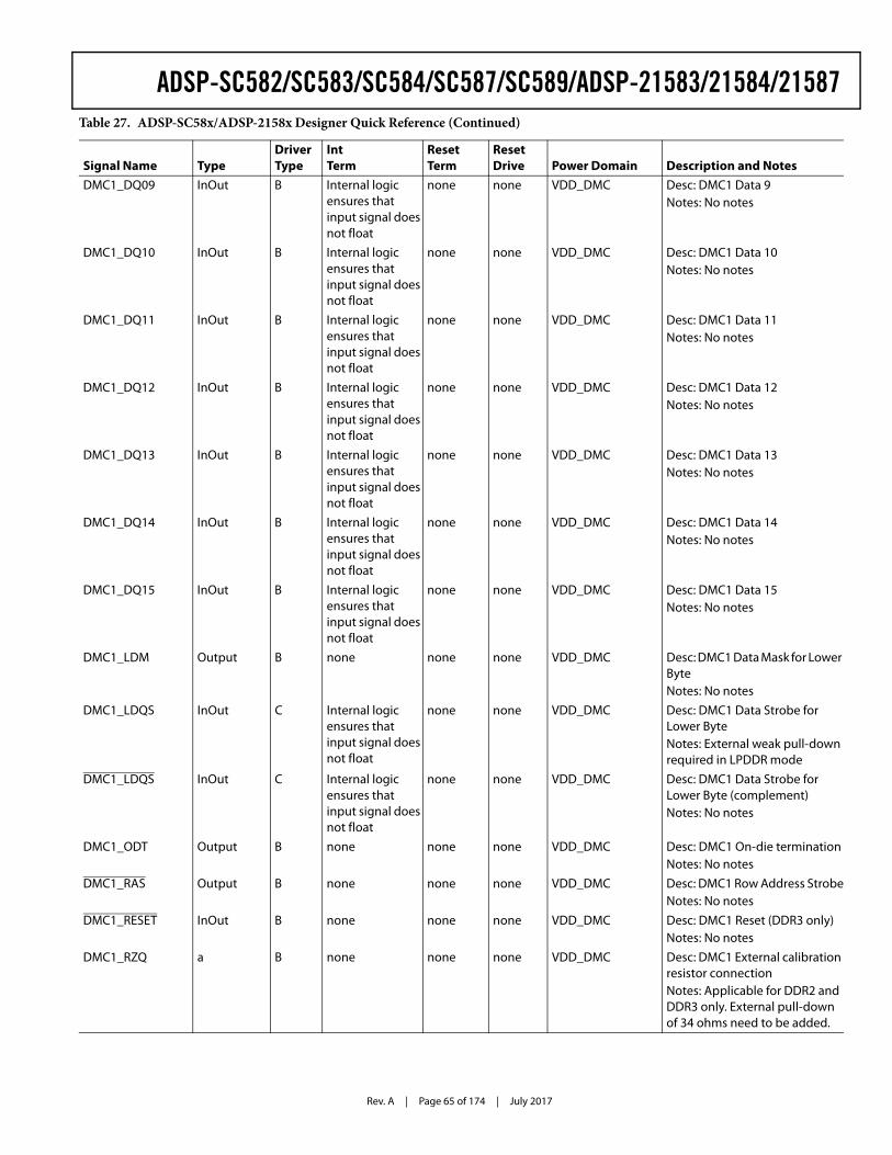
Rev. A | Page 65 of 174 | July 2017
ADSP-SC582/SC583/SC584/SC587/SC589/ADSP-21583/21584/21587
DMC1_DQ09 InOut B Internal logic ensures that input signal does not float
none none VDD_DMC Desc: DMC1 Data 9Notes: No notes
DMC1_DQ10 InOut B Internal logic ensures that input signal does not float
none none VDD_DMC Desc: DMC1 Data 10Notes: No notes
DMC1_DQ11 InOut B Internal logic ensures that input signal does not float
none none VDD_DMC Desc: DMC1 Data 11Notes: No notes
DMC1_DQ12 InOut B Internal logic ensures that input signal does not float
none none VDD_DMC Desc: DMC1 Data 12Notes: No notes
DMC1_DQ13 InOut B Internal logic ensures that input signal does not float
none none VDD_DMC Desc: DMC1 Data 13Notes: No notes
DMC1_DQ14 InOut B Internal logic ensures that input signal does not float
none none VDD_DMC Desc: DMC1 Data 14Notes: No notes
DMC1_DQ15 InOut B Internal logic ensures that input signal does not float
none none VDD_DMC Desc: DMC1 Data 15Notes: No notes
DMC1_LDM Output B none none none VDD_DMC Desc: DMC1 Data Mask for Lower ByteNotes: No notes
DMC1_LDQS InOut C Internal logic ensures that input signal does not float
none none VDD_DMC Desc: DMC1 Data Strobe for Lower ByteNotes: External weak pull-down required in LPDDR mode
DMC1_LDQS InOut C Internal logic ensures that input signal does not float
none none VDD_DMC Desc: DMC1 Data Strobe for Lower Byte (complement)Notes: No notes
DMC1_ODT Output B none none none VDD_DMC Desc: DMC1 On-die terminationNotes: No notes
DMC1_RAS Output B none none none VDD_DMC Desc: DMC1 Row Address StrobeNotes: No notes
DMC1_RESET InOut B none none none VDD_DMC Desc: DMC1 Reset (DDR3 only)Notes: No notes
DMC1_RZQ a B none none none VDD_DMC Desc: DMC1 External calibration resistor connectionNotes: Applicable for DDR2 and DDR3 only. External pull-down of 34 ohms need to be added.
Table 27. ADSP-SC58x/ADSP-2158x Designer Quick Reference (Continued)
Signal Name TypeDriver Type
Int Term
Reset Term
Reset Drive Power Domain Description and Notes
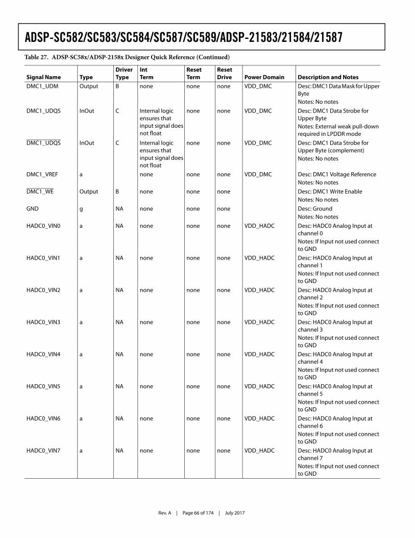
Rev. A | Page 66 of 174 | July 2017
ADSP-SC582/SC583/SC584/SC587/SC589/ADSP-21583/21584/21587
DMC1_UDM Output B none none none VDD_DMC Desc: DMC1 Data Mask for Upper ByteNotes: No notes
DMC1_UDQS InOut C Internal logic ensures that input signal does not float
none none VDD_DMC Desc: DMC1 Data Strobe for Upper ByteNotes: External weak pull-down required in LPDDR mode
DMC1_UDQS InOut C Internal logic ensures that input signal does not float
none none VDD_DMC Desc: DMC1 Data Strobe for Upper Byte (complement)Notes: No notes
DMC1_VREF a none none none VDD_DMC Desc: DMC1 Voltage ReferenceNotes: No notes
DMC1_WE Output B none none none Desc: DMC1 Write EnableNotes: No notes
GND g NA none none none Desc: GroundNotes: No notes
HADC0_VIN0 a NA none none none VDD_HADC Desc: HADC0 Analog Input at channel 0Notes: If Input not used connect to GND
HADC0_VIN1 a NA none none none VDD_HADC Desc: HADC0 Analog Input at channel 1Notes: If Input not used connect to GND
HADC0_VIN2 a NA none none none VDD_HADC Desc: HADC0 Analog Input at channel 2Notes: If Input not used connect to GND
HADC0_VIN3 a NA none none none VDD_HADC Desc: HADC0 Analog Input at channel 3Notes: If Input not used connect to GND
HADC0_VIN4 a NA none none none VDD_HADC Desc: HADC0 Analog Input at channel 4Notes: If Input not used connect to GND
HADC0_VIN5 a NA none none none VDD_HADC Desc: HADC0 Analog Input at channel 5Notes: If Input not used connect to GND
HADC0_VIN6 a NA none none none VDD_HADC Desc: HADC0 Analog Input at channel 6Notes: If Input not used connect to GND
HADC0_VIN7 a NA none none none VDD_HADC Desc: HADC0 Analog Input at channel 7Notes: If Input not used connect to GND
Table 27. ADSP-SC58x/ADSP-2158x Designer Quick Reference (Continued)
Signal Name TypeDriver Type
Int Term
Reset Term
Reset Drive Power Domain Description and Notes
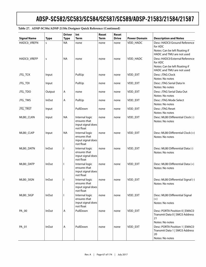
Rev. A | Page 67 of 174 | July 2017
ADSP-SC582/SC583/SC584/SC587/SC589/ADSP-21583/21584/21587
HADC0_VREFN s NA none none none VDD_HADC Desc: HADC0 Ground Reference for ADCNotes: Can be left floating if HADC and TMU are not used
HADC0_VREFP s NA none none none VDD_HADC Desc: HADC0 External Reference for ADCNotes: Can be left floating if HADC and TMU are not used
JTG_TCK Input PullUp none none VDD_EXT Desc: JTAG ClockNotes: No notes
JTG_TDI Input PullUp none none VDD_EXT Desc: JTAG Serial Data InNotes: No notes
JTG_TDO Output A none none none VDD_EXT Desc: JTAG Serial Data OutNotes: No notes
JTG_TMS InOut A PullUp none none VDD_EXT Desc: JTAG Mode SelectNotes: No notes
JTG_TRST Input PullDown none none VDD_EXT Desc: JTAG ResetNotes: No notes
MLB0_CLKN Input NA Internal logic ensures that input signal does not float
none none VDD_EXT Desc: MLB0 Differential Clock (-)Notes: No notes
MLB0_CLKP Input NA Internal logic ensures that input signal does not float
none none VDD_EXT Desc: MLB0 Differential Clock (+)Notes: No notes
MLB0_DATN InOut I Internal logic ensures that input signal does not float
none none VDD_EXT Desc: MLB0 Differential Data (-)Notes: No notes
MLB0_DATP InOut I Internal logic ensures that input signal does not float
none none VDD_EXT Desc: MLB0 Differential Data (+)Notes: No notes
MLB0_SIGN InOut I Internal logic ensures that input signal does not float
none none VDD_EXT Desc: MLB0 Differential Signal (-)Notes: No notes
MLB0_SIGP InOut I Internal logic ensures that input signal does not float
none none VDD_EXT Desc: MLB0 Differential Signal (+)Notes: No notes
PA_00 InOut A PullDown none none VDD_EXT Desc: PORTA Position 0 | EMAC0 Transmit Data 0 | SMC0 Address 21Notes: No notes
PA_01 InOut A PullDown none none VDD_EXT Desc: PORTA Position 1 | EMAC0 Transmit Data 1 | SMC0 Address 20Notes: No notes
Table 27. ADSP-SC58x/ADSP-2158x Designer Quick Reference (Continued)
Signal Name TypeDriver Type
Int Term
Reset Term
Reset Drive Power Domain Description and Notes
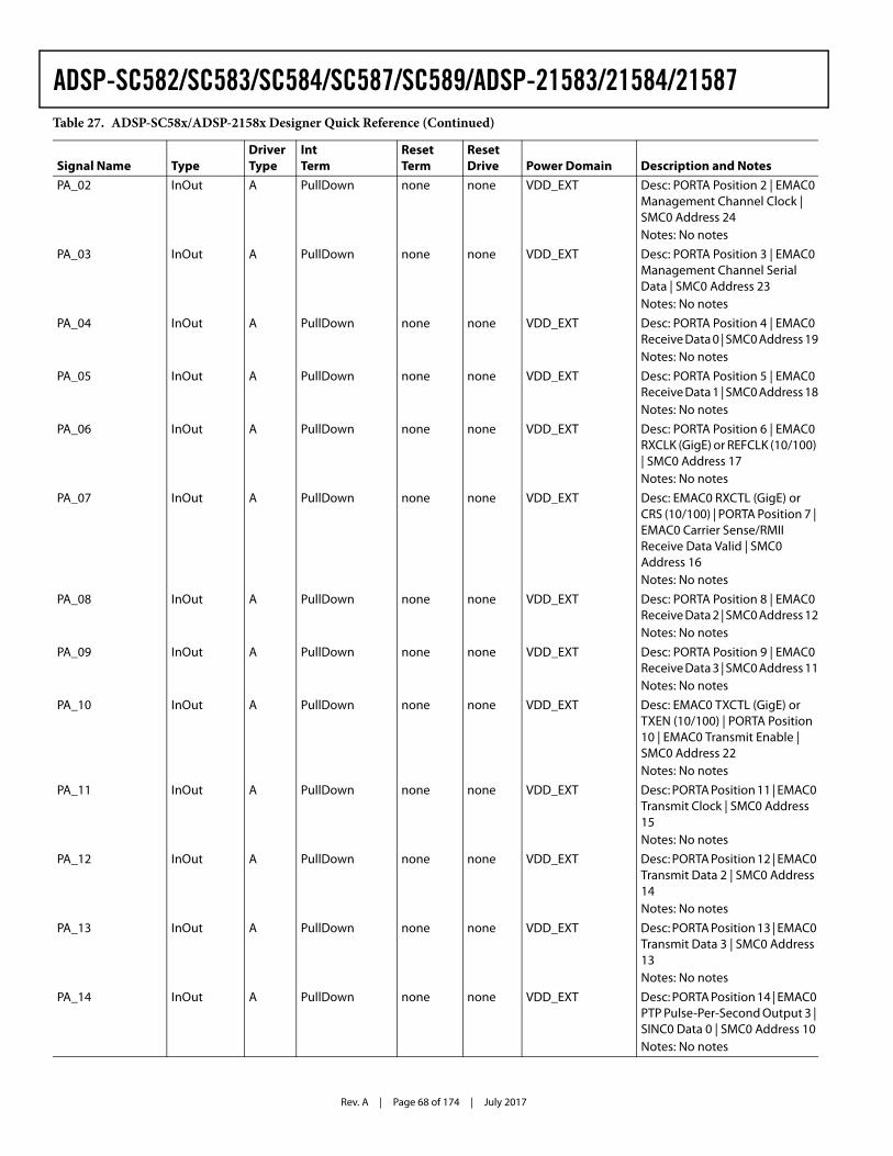
Rev. A | Page 68 of 174 | July 2017
ADSP-SC582/SC583/SC584/SC587/SC589/ADSP-21583/21584/21587
PA_02 InOut A PullDown none none VDD_EXT Desc: PORTA Position 2 | EMAC0 Management Channel Clock | SMC0 Address 24Notes: No notes
PA_03 InOut A PullDown none none VDD_EXT Desc: PORTA Position 3 | EMAC0 Management Channel Serial Data | SMC0 Address 23Notes: No notes
PA_04 InOut A PullDown none none VDD_EXT Desc: PORTA Position 4 | EMAC0 Receive Data 0 | SMC0 Address 19Notes: No notes
PA_05 InOut A PullDown none none VDD_EXT Desc: PORTA Position 5 | EMAC0 Receive Data 1 | SMC0 Address 18Notes: No notes
PA_06 InOut A PullDown none none VDD_EXT Desc: PORTA Position 6 | EMAC0 RXCLK (GigE) or REFCLK (10/100) | SMC0 Address 17Notes: No notes
PA_07 InOut A PullDown none none VDD_EXT Desc: EMAC0 RXCTL (GigE) or CRS (10/100) | PORTA Position 7 | EMAC0 Carrier Sense/RMII Receive Data Valid | SMC0 Address 16Notes: No notes
PA_08 InOut A PullDown none none VDD_EXT Desc: PORTA Position 8 | EMAC0 Receive Data 2 | SMC0 Address 12Notes: No notes
PA_09 InOut A PullDown none none VDD_EXT Desc: PORTA Position 9 | EMAC0 Receive Data 3 | SMC0 Address 11Notes: No notes
PA_10 InOut A PullDown none none VDD_EXT Desc: EMAC0 TXCTL (GigE) or TXEN (10/100) | PORTA Position 10 | EMAC0 Transmit Enable | SMC0 Address 22Notes: No notes
PA_11 InOut A PullDown none none VDD_EXT Desc: PORTA Position 11 | EMAC0 Transmit Clock | SMC0 Address 15Notes: No notes
PA_12 InOut A PullDown none none VDD_EXT Desc: PORTA Position 12 | EMAC0 Transmit Data 2 | SMC0 Address 14Notes: No notes
PA_13 InOut A PullDown none none VDD_EXT Desc: PORTA Position 13 | EMAC0 Transmit Data 3 | SMC0 Address 13Notes: No notes
PA_14 InOut A PullDown none none VDD_EXT Desc: PORTA Position 14 | EMAC0 PTP Pulse-Per-Second Output 3 | SINC0 Data 0 | SMC0 Address 10Notes: No notes
Table 27. ADSP-SC58x/ADSP-2158x Designer Quick Reference (Continued)
Signal Name TypeDriver Type
Int Term
Reset Term
Reset Drive Power Domain Description and Notes
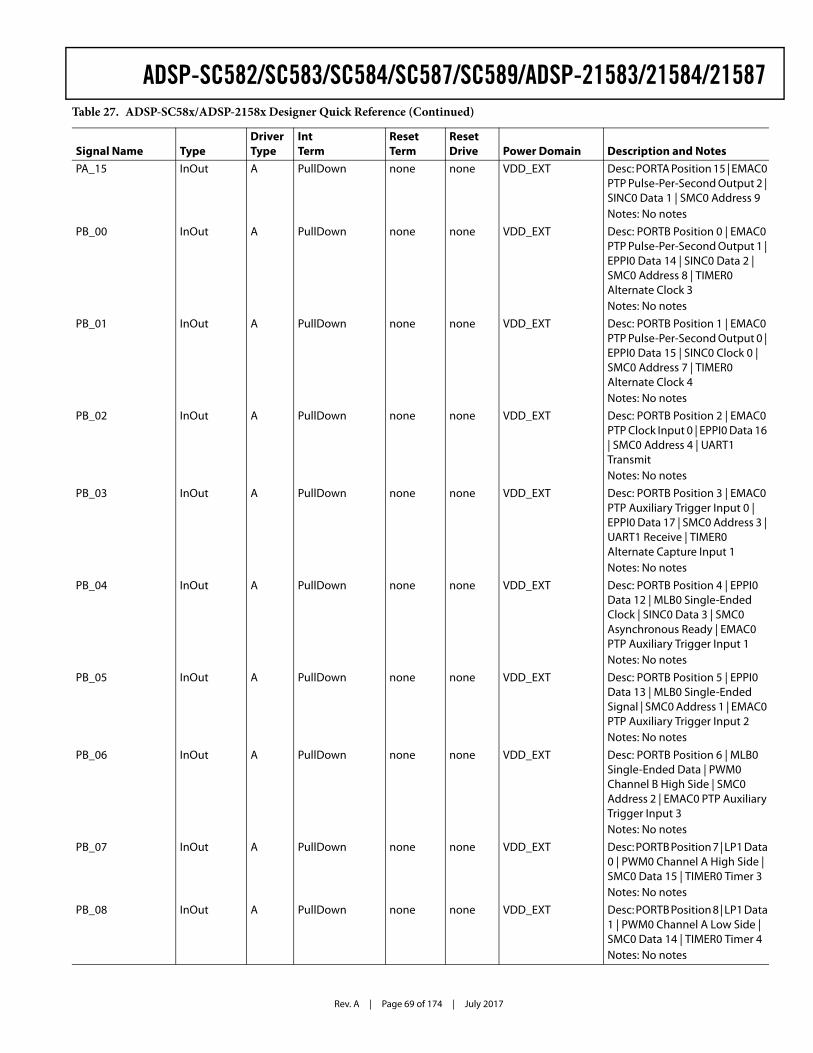
Rev. A | Page 69 of 174 | July 2017
ADSP-SC582/SC583/SC584/SC587/SC589/ADSP-21583/21584/21587
PA_15 InOut A PullDown none none VDD_EXT Desc: PORTA Position 15 | EMAC0 PTP Pulse-Per-Second Output 2 | SINC0 Data 1 | SMC0 Address 9Notes: No notes
PB_00 InOut A PullDown none none VDD_EXT Desc: PORTB Position 0 | EMAC0 PTP Pulse-Per-Second Output 1 | EPPI0 Data 14 | SINC0 Data 2 | SMC0 Address 8 | TIMER0 Alternate Clock 3Notes: No notes
PB_01 InOut A PullDown none none VDD_EXT Desc: PORTB Position 1 | EMAC0 PTP Pulse-Per-Second Output 0 | EPPI0 Data 15 | SINC0 Clock 0 | SMC0 Address 7 | TIMER0 Alternate Clock 4Notes: No notes
PB_02 InOut A PullDown none none VDD_EXT Desc: PORTB Position 2 | EMAC0 PTP Clock Input 0 | EPPI0 Data 16 | SMC0 Address 4 | UART1 TransmitNotes: No notes
PB_03 InOut A PullDown none none VDD_EXT Desc: PORTB Position 3 | EMAC0 PTP Auxiliary Trigger Input 0 | EPPI0 Data 17 | SMC0 Address 3 | UART1 Receive | TIMER0 Alternate Capture Input 1Notes: No notes
PB_04 InOut A PullDown none none VDD_EXT Desc: PORTB Position 4 | EPPI0 Data 12 | MLB0 Single-Ended Clock | SINC0 Data 3 | SMC0 Asynchronous Ready | EMAC0 PTP Auxiliary Trigger Input 1Notes: No notes
PB_05 InOut A PullDown none none VDD_EXT Desc: PORTB Position 5 | EPPI0 Data 13 | MLB0 Single-Ended Signal | SMC0 Address 1 | EMAC0 PTP Auxiliary Trigger Input 2Notes: No notes
PB_06 InOut A PullDown none none VDD_EXT Desc: PORTB Position 6 | MLB0 Single-Ended Data | PWM0 Channel B High Side | SMC0 Address 2 | EMAC0 PTP Auxiliary Trigger Input 3Notes: No notes
PB_07 InOut A PullDown none none VDD_EXT Desc: PORTB Position 7 | LP1 Data 0 | PWM0 Channel A High Side | SMC0 Data 15 | TIMER0 Timer 3Notes: No notes
PB_08 InOut A PullDown none none VDD_EXT Desc: PORTB Position 8 | LP1 Data 1 | PWM0 Channel A Low Side | SMC0 Data 14 | TIMER0 Timer 4Notes: No notes
Table 27. ADSP-SC58x/ADSP-2158x Designer Quick Reference (Continued)
Signal Name TypeDriver Type
Int Term
Reset Term
Reset Drive Power Domain Description and Notes
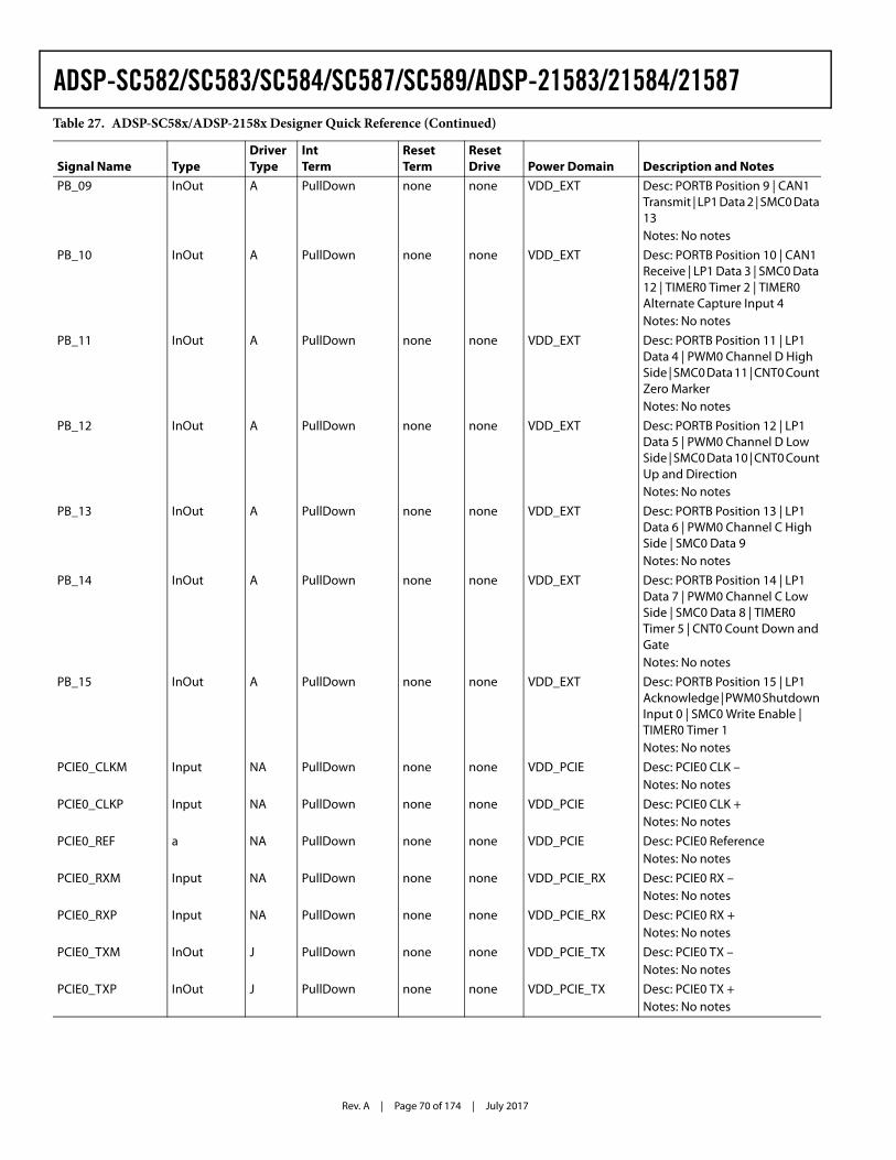
Rev. A | Page 70 of 174 | July 2017
ADSP-SC582/SC583/SC584/SC587/SC589/ADSP-21583/21584/21587
PB_09 InOut A PullDown none none VDD_EXT Desc: PORTB Position 9 | CAN1 Transmit | LP1 Data 2 | SMC0 Data 13Notes: No notes
PB_10 InOut A PullDown none none VDD_EXT Desc: PORTB Position 10 | CAN1 Receive | LP1 Data 3 | SMC0 Data 12 | TIMER0 Timer 2 | TIMER0 Alternate Capture Input 4Notes: No notes
PB_11 InOut A PullDown none none VDD_EXT Desc: PORTB Position 11 | LP1 Data 4 | PWM0 Channel D High Side | SMC0 Data 11 | CNT0 Count Zero MarkerNotes: No notes
PB_12 InOut A PullDown none none VDD_EXT Desc: PORTB Position 12 | LP1 Data 5 | PWM0 Channel D Low Side | SMC0 Data 10 | CNT0 Count Up and DirectionNotes: No notes
PB_13 InOut A PullDown none none VDD_EXT Desc: PORTB Position 13 | LP1 Data 6 | PWM0 Channel C High Side | SMC0 Data 9Notes: No notes
PB_14 InOut A PullDown none none VDD_EXT Desc: PORTB Position 14 | LP1 Data 7 | PWM0 Channel C Low Side | SMC0 Data 8 | TIMER0 Timer 5 | CNT0 Count Down and GateNotes: No notes
PB_15 InOut A PullDown none none VDD_EXT Desc: PORTB Position 15 | LP1 Acknowledge | PWM0 Shutdown Input 0 | SMC0 Write Enable | TIMER0 Timer 1Notes: No notes
PCIE0_CLKM Input NA PullDown none none VDD_PCIE Desc: PCIE0 CLK –Notes: No notes
PCIE0_CLKP Input NA PullDown none none VDD_PCIE Desc: PCIE0 CLK +Notes: No notes
PCIE0_REF a NA PullDown none none VDD_PCIE Desc: PCIE0 ReferenceNotes: No notes
PCIE0_RXM Input NA PullDown none none VDD_PCIE_RX Desc: PCIE0 RX –Notes: No notes
PCIE0_RXP Input NA PullDown none none VDD_PCIE_RX Desc: PCIE0 RX +Notes: No notes
PCIE0_TXM InOut J PullDown none none VDD_PCIE_TX Desc: PCIE0 TX –Notes: No notes
PCIE0_TXP InOut J PullDown none none VDD_PCIE_TX Desc: PCIE0 TX +Notes: No notes
Table 27. ADSP-SC58x/ADSP-2158x Designer Quick Reference (Continued)
Signal Name TypeDriver Type
Int Term
Reset Term
Reset Drive Power Domain Description and Notes
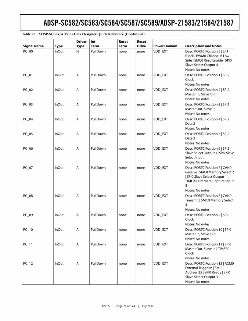
Rev. A | Page 71 of 174 | July 2017
ADSP-SC582/SC583/SC584/SC587/SC589/ADSP-21583/21584/21587
PC_00 InOut H PullDown none none VDD_EXT Desc: PORTC Position 0 | LP1 Clock | PWM0 Channel B Low Side | SMC0 Read Enable | SPI0 Slave Select Output 4Notes: No notes
PC_01 InOut A PullDown none none VDD_EXT Desc: PORTC Position 1 | SPI2 ClockNotes: No notes
PC_02 InOut A PullDown none none VDD_EXT Desc: PORTC Position 2 | SPI2 Master In, Slave OutNotes: No notes
PC_03 InOut A PullDown none none VDD_EXT Desc: PORTC Position 3 | SPI2 Master Out, Slave InNotes: No notes
PC_04 InOut A PullDown none none VDD_EXT Desc: PORTC Position 4 | SPI2 Data 2Notes: No notes
PC_05 InOut A PullDown none none VDD_EXT Desc: PORTC Position 5 | SPI2 Data 3Notes: No notes
PC_06 InOut A PullDown none none VDD_EXT Desc: PORTC Position 6 | SPI2 Slave Select Output 1 | SPI2 Slave Select InputNotes: No notes
PC_07 InOut A PullDown none none VDD_EXT Desc: PORTC Position 7 | CAN0 Receive | SMC0 Memory Select 2 | SPI0 Slave Select Output 1 | TIMER0 Alternate Capture Input 3Notes: No notes
PC_08 InOut A PullDown none none VDD_EXT Desc: PORTC Position 8 | CAN0 Transmit | SMC0 Memory Select 3Notes: No notes
PC_09 InOut A PullDown none none VDD_EXT Desc: PORTC Position 9 | SPI0 ClockNotes: No notes
PC_10 InOut A PullDown none none VDD_EXT Desc: PORTC Position 10 | SPI0 Master In, Slave OutNotes: No notes
PC_11 InOut A PullDown none none VDD_EXT Desc: PORTC Position 11 | SPI0 Master Out, Slave In | TIMER0 ClockNotes: No notes
PC_12 InOut A PullDown none none VDD_EXT Desc: PORTC Position 12 | ACM0 External Trigger n | SMC0 Address 25 | SPI0 Ready | SPI0 Slave Select Output 3Notes: No notes
Table 27. ADSP-SC58x/ADSP-2158x Designer Quick Reference (Continued)
Signal Name TypeDriver Type
Int Term
Reset Term
Reset Drive Power Domain Description and Notes
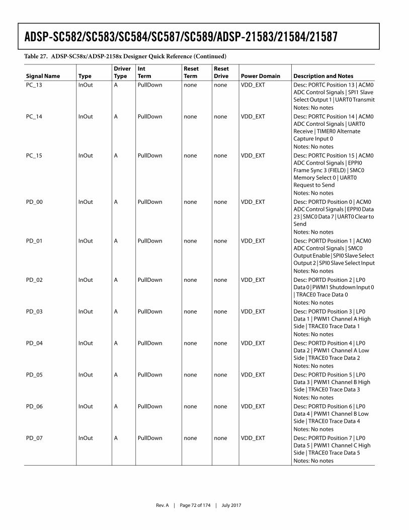
Rev. A | Page 72 of 174 | July 2017
ADSP-SC582/SC583/SC584/SC587/SC589/ADSP-21583/21584/21587
PC_13 InOut A PullDown none none VDD_EXT Desc: PORTC Position 13 | ACM0 ADC Control Signals | SPI1 Slave Select Output 1 | UART0 TransmitNotes: No notes
PC_14 InOut A PullDown none none VDD_EXT Desc: PORTC Position 14 | ACM0 ADC Control Signals | UART0 Receive | TIMER0 Alternate Capture Input 0Notes: No notes
PC_15 InOut A PullDown none none VDD_EXT Desc: PORTC Position 15 | ACM0 ADC Control Signals | EPPI0 Frame Sync 3 (FIELD) | SMC0 Memory Select 0 | UART0 Request to SendNotes: No notes
PD_00 InOut A PullDown none none VDD_EXT Desc: PORTD Position 0 | ACM0 ADC Control Signals | EPPI0 Data 23 | SMC0 Data 7 | UART0 Clear to SendNotes: No notes
PD_01 InOut A PullDown none none VDD_EXT Desc: PORTD Position 1 | ACM0 ADC Control Signals | SMC0 Output Enable | SPI0 Slave Select Output 2 | SPI0 Slave Select InputNotes: No notes
PD_02 InOut A PullDown none none VDD_EXT Desc: PORTD Position 2 | LP0 Data 0 | PWM1 Shutdown Input 0 | TRACE0 Trace Data 0Notes: No notes
PD_03 InOut A PullDown none none VDD_EXT Desc: PORTD Position 3 | LP0 Data 1 | PWM1 Channel A High Side | TRACE0 Trace Data 1Notes: No notes
PD_04 InOut A PullDown none none VDD_EXT Desc: PORTD Position 4 | LP0 Data 2 | PWM1 Channel A Low Side | TRACE0 Trace Data 2Notes: No notes
PD_05 InOut A PullDown none none VDD_EXT Desc: PORTD Position 5 | LP0 Data 3 | PWM1 Channel B High Side | TRACE0 Trace Data 3Notes: No notes
PD_06 InOut A PullDown none none VDD_EXT Desc: PORTD Position 6 | LP0 Data 4 | PWM1 Channel B Low Side | TRACE0 Trace Data 4Notes: No notes
PD_07 InOut A PullDown none none VDD_EXT Desc: PORTD Position 7 | LP0 Data 5 | PWM1 Channel C High Side | TRACE0 Trace Data 5Notes: No notes
Table 27. ADSP-SC58x/ADSP-2158x Designer Quick Reference (Continued)
Signal Name TypeDriver Type
Int Term
Reset Term
Reset Drive Power Domain Description and Notes
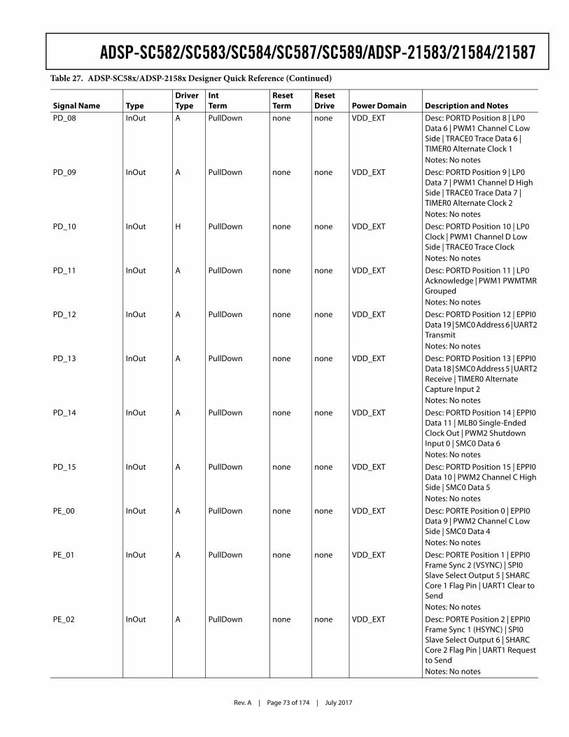
Rev. A | Page 73 of 174 | July 2017
ADSP-SC582/SC583/SC584/SC587/SC589/ADSP-21583/21584/21587
PD_08 InOut A PullDown none none VDD_EXT Desc: PORTD Position 8 | LP0 Data 6 | PWM1 Channel C Low Side | TRACE0 Trace Data 6 | TIMER0 Alternate Clock 1Notes: No notes
PD_09 InOut A PullDown none none VDD_EXT Desc: PORTD Position 9 | LP0 Data 7 | PWM1 Channel D High Side | TRACE0 Trace Data 7 | TIMER0 Alternate Clock 2Notes: No notes
PD_10 InOut H PullDown none none VDD_EXT Desc: PORTD Position 10 | LP0 Clock | PWM1 Channel D Low Side | TRACE0 Trace ClockNotes: No notes
PD_11 InOut A PullDown none none VDD_EXT Desc: PORTD Position 11 | LP0 Acknowledge | PWM1 PWMTMR GroupedNotes: No notes
PD_12 InOut A PullDown none none VDD_EXT Desc: PORTD Position 12 | EPPI0 Data 19 | SMC0 Address 6 | UART2 TransmitNotes: No notes
PD_13 InOut A PullDown none none VDD_EXT Desc: PORTD Position 13 | EPPI0 Data 18 | SMC0 Address 5 | UART2 Receive | TIMER0 Alternate Capture Input 2Notes: No notes
PD_14 InOut A PullDown none none VDD_EXT Desc: PORTD Position 14 | EPPI0 Data 11 | MLB0 Single-Ended Clock Out | PWM2 Shutdown Input 0 | SMC0 Data 6Notes: No notes
PD_15 InOut A PullDown none none VDD_EXT Desc: PORTD Position 15 | EPPI0 Data 10 | PWM2 Channel C High Side | SMC0 Data 5Notes: No notes
PE_00 InOut A PullDown none none VDD_EXT Desc: PORTE Position 0 | EPPI0 Data 9 | PWM2 Channel C Low Side | SMC0 Data 4Notes: No notes
PE_01 InOut A PullDown none none VDD_EXT Desc: PORTE Position 1 | EPPI0 Frame Sync 2 (VSYNC) | SPI0 Slave Select Output 5 | SHARC Core 1 Flag Pin | UART1 Clear to SendNotes: No notes
PE_02 InOut A PullDown none none VDD_EXT Desc: PORTE Position 2 | EPPI0 Frame Sync 1 (HSYNC) | SPI0 Slave Select Output 6 | SHARC Core 2 Flag Pin | UART1 Request to SendNotes: No notes
Table 27. ADSP-SC58x/ADSP-2158x Designer Quick Reference (Continued)
Signal Name TypeDriver Type
Int Term
Reset Term
Reset Drive Power Domain Description and Notes
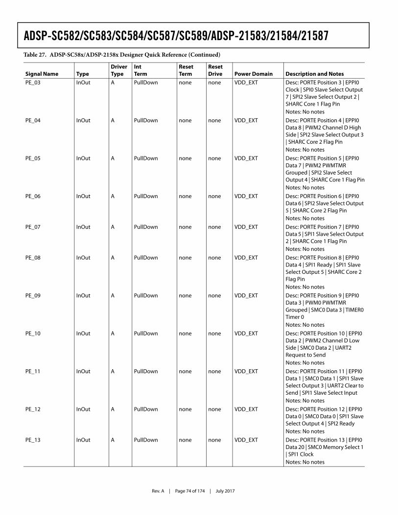
Rev. A | Page 74 of 174 | July 2017
ADSP-SC582/SC583/SC584/SC587/SC589/ADSP-21583/21584/21587
PE_03 InOut A PullDown none none VDD_EXT Desc: PORTE Position 3 | EPPI0 Clock | SPI0 Slave Select Output 7 | SPI2 Slave Select Output 2 | SHARC Core 1 Flag PinNotes: No notes
PE_04 InOut A PullDown none none VDD_EXT Desc: PORTE Position 4 | EPPI0 Data 8 | PWM2 Channel D High Side | SPI2 Slave Select Output 3 | SHARC Core 2 Flag PinNotes: No notes
PE_05 InOut A PullDown none none VDD_EXT Desc: PORTE Position 5 | EPPI0 Data 7 | PWM2 PWMTMR Grouped | SPI2 Slave Select Output 4 | SHARC Core 1 Flag PinNotes: No notes
PE_06 InOut A PullDown none none VDD_EXT Desc: PORTE Position 6 | EPPI0 Data 6 | SPI2 Slave Select Output 5 | SHARC Core 2 Flag PinNotes: No notes
PE_07 InOut A PullDown none none VDD_EXT Desc: PORTE Position 7 | EPPI0 Data 5 | SPI1 Slave Select Output 2 | SHARC Core 1 Flag PinNotes: No notes
PE_08 InOut A PullDown none none VDD_EXT Desc: PORTE Position 8 | EPPI0 Data 4 | SPI1 Ready | SPI1 Slave Select Output 5 | SHARC Core 2 Flag PinNotes: No notes
PE_09 InOut A PullDown none none VDD_EXT Desc: PORTE Position 9 | EPPI0 Data 3 | PWM0 PWMTMR Grouped | SMC0 Data 3 | TIMER0 Timer 0Notes: No notes
PE_10 InOut A PullDown none none VDD_EXT Desc: PORTE Position 10 | EPPI0 Data 2 | PWM2 Channel D Low Side | SMC0 Data 2 | UART2 Request to SendNotes: No notes
PE_11 InOut A PullDown none none VDD_EXT Desc: PORTE Position 11 | EPPI0 Data 1 | SMC0 Data 1 | SPI1 Slave Select Output 3 | UART2 Clear to Send | SPI1 Slave Select InputNotes: No notes
PE_12 InOut A PullDown none none VDD_EXT Desc: PORTE Position 12 | EPPI0 Data 0 | SMC0 Data 0 | SPI1 Slave Select Output 4 | SPI2 ReadyNotes: No notes
PE_13 InOut A PullDown none none VDD_EXT Desc: PORTE Position 13 | EPPI0 Data 20 | SMC0 Memory Select 1 | SPI1 ClockNotes: No notes
Table 27. ADSP-SC58x/ADSP-2158x Designer Quick Reference (Continued)
Signal Name TypeDriver Type
Int Term
Reset Term
Reset Drive Power Domain Description and Notes
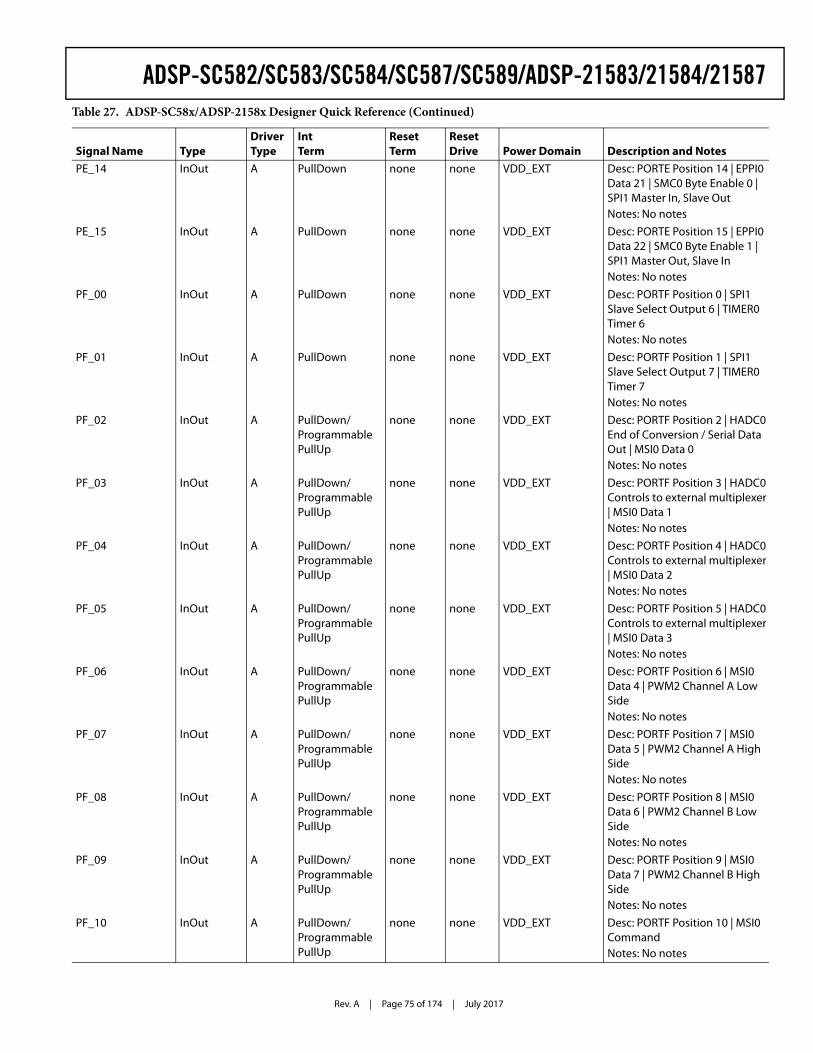
Rev. A | Page 75 of 174 | July 2017
ADSP-SC582/SC583/SC584/SC587/SC589/ADSP-21583/21584/21587
PE_14 InOut A PullDown none none VDD_EXT Desc: PORTE Position 14 | EPPI0 Data 21 | SMC0 Byte Enable 0 | SPI1 Master In, Slave OutNotes: No notes
PE_15 InOut A PullDown none none VDD_EXT Desc: PORTE Position 15 | EPPI0 Data 22 | SMC0 Byte Enable 1 | SPI1 Master Out, Slave InNotes: No notes
PF_00 InOut A PullDown none none VDD_EXT Desc: PORTF Position 0 | SPI1 Slave Select Output 6 | TIMER0 Timer 6Notes: No notes
PF_01 InOut A PullDown none none VDD_EXT Desc: PORTF Position 1 | SPI1 Slave Select Output 7 | TIMER0 Timer 7Notes: No notes
PF_02 InOut A PullDown/Programmable PullUp
none none VDD_EXT Desc: PORTF Position 2 | HADC0 End of Conversion / Serial Data Out | MSI0 Data 0Notes: No notes
PF_03 InOut A PullDown/Programmable PullUp
none none VDD_EXT Desc: PORTF Position 3 | HADC0 Controls to external multiplexer | MSI0 Data 1Notes: No notes
PF_04 InOut A PullDown/Programmable PullUp
none none VDD_EXT Desc: PORTF Position 4 | HADC0 Controls to external multiplexer | MSI0 Data 2Notes: No notes
PF_05 InOut A PullDown/Programmable PullUp
none none VDD_EXT Desc: PORTF Position 5 | HADC0 Controls to external multiplexer | MSI0 Data 3Notes: No notes
PF_06 InOut A PullDown/Programmable PullUp
none none VDD_EXT Desc: PORTF Position 6 | MSI0 Data 4 | PWM2 Channel A Low SideNotes: No notes
PF_07 InOut A PullDown/Programmable PullUp
none none VDD_EXT Desc: PORTF Position 7 | MSI0 Data 5 | PWM2 Channel A High SideNotes: No notes
PF_08 InOut A PullDown/Programmable PullUp
none none VDD_EXT Desc: PORTF Position 8 | MSI0 Data 6 | PWM2 Channel B Low SideNotes: No notes
PF_09 InOut A PullDown/Programmable PullUp
none none VDD_EXT Desc: PORTF Position 9 | MSI0 Data 7 | PWM2 Channel B High SideNotes: No notes
PF_10 InOut A PullDown/Programmable PullUp
none none VDD_EXT Desc: PORTF Position 10 | MSI0 CommandNotes: No notes
Table 27. ADSP-SC58x/ADSP-2158x Designer Quick Reference (Continued)
Signal Name TypeDriver Type
Int Term
Reset Term
Reset Drive Power Domain Description and Notes
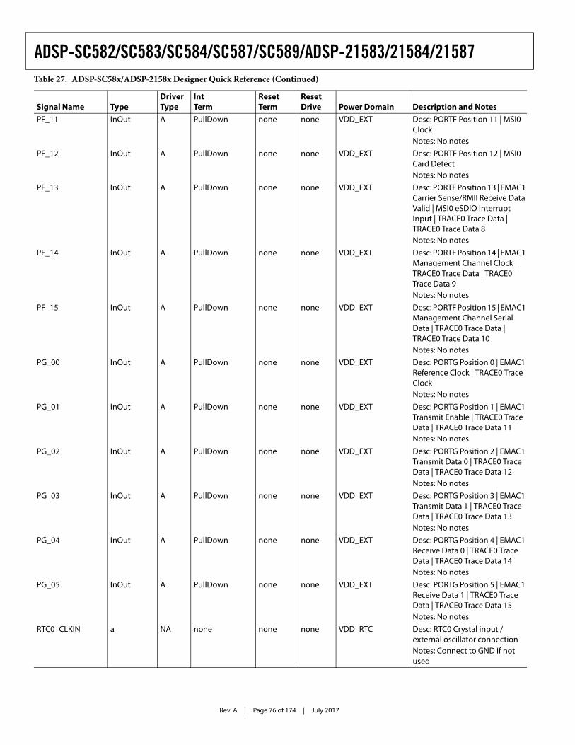
Rev. A | Page 76 of 174 | July 2017
ADSP-SC582/SC583/SC584/SC587/SC589/ADSP-21583/21584/21587
PF_11 InOut A PullDown none none VDD_EXT Desc: PORTF Position 11 | MSI0 ClockNotes: No notes
PF_12 InOut A PullDown none none VDD_EXT Desc: PORTF Position 12 | MSI0 Card DetectNotes: No notes
PF_13 InOut A PullDown none none VDD_EXT Desc: PORTF Position 13 | EMAC1 Carrier Sense/RMII Receive Data Valid | MSI0 eSDIO Interrupt Input | TRACE0 Trace Data | TRACE0 Trace Data 8Notes: No notes
PF_14 InOut A PullDown none none VDD_EXT Desc: PORTF Position 14 | EMAC1 Management Channel Clock | TRACE0 Trace Data | TRACE0 Trace Data 9Notes: No notes
PF_15 InOut A PullDown none none VDD_EXT Desc: PORTF Position 15 | EMAC1 Management Channel Serial Data | TRACE0 Trace Data | TRACE0 Trace Data 10Notes: No notes
PG_00 InOut A PullDown none none VDD_EXT Desc: PORTG Position 0 | EMAC1 Reference Clock | TRACE0 Trace ClockNotes: No notes
PG_01 InOut A PullDown none none VDD_EXT Desc: PORTG Position 1 | EMAC1 Transmit Enable | TRACE0 Trace Data | TRACE0 Trace Data 11Notes: No notes
PG_02 InOut A PullDown none none VDD_EXT Desc: PORTG Position 2 | EMAC1 Transmit Data 0 | TRACE0 Trace Data | TRACE0 Trace Data 12Notes: No notes
PG_03 InOut A PullDown none none VDD_EXT Desc: PORTG Position 3 | EMAC1 Transmit Data 1 | TRACE0 Trace Data | TRACE0 Trace Data 13Notes: No notes
PG_04 InOut A PullDown none none VDD_EXT Desc: PORTG Position 4 | EMAC1 Receive Data 0 | TRACE0 Trace Data | TRACE0 Trace Data 14Notes: No notes
PG_05 InOut A PullDown none none VDD_EXT Desc: PORTG Position 5 | EMAC1 Receive Data 1 | TRACE0 Trace Data | TRACE0 Trace Data 15Notes: No notes
RTC0_CLKIN a NA none none none VDD_RTC Desc: RTC0 Crystal input / external oscillator connectionNotes: Connect to GND if not used
Table 27. ADSP-SC58x/ADSP-2158x Designer Quick Reference (Continued)
Signal Name TypeDriver Type
Int Term
Reset Term
Reset Drive Power Domain Description and Notes
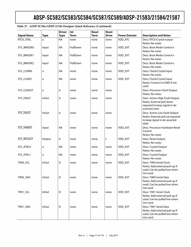
Rev. A | Page 77 of 174 | July 2017
ADSP-SC582/SC583/SC584/SC587/SC589/ADSP-21583/21584/21587
RTC0_XTAL a NA none none none VDD_RTC Desc: RTC0 Crystal outputNotes: No notes
SYS_BMODE0 Input NA PullDown none none VDD_EXT Desc: Boot Mode Control nNotes: No notes
SYS_BMODE1 Input NA PullDown none none VDD_EXT Desc: Boot Mode Control nNotes: No notes
SYS_BMODE2 Input NA PullDown none none VDD_EXT Desc: Boot Mode Control nNotes: No notes
SYS_CLKIN0 a NA none none none VDD_EXT Desc: Clock/Crystal InputNotes: No notes
SYS_CLKIN1 a NA none none none VDD_EXT Desc: Clock/Crystal InputNotes: Connect to GND if not used
SYS_CLKOUT a A none none none Desc: Processor Clock OutputNotes: No notes
SYS_FAULT InOut A none none none Desc: Active-High Fault OutputNotes: External pull-down required to keep signal in de-asserted state
SYS_FAULT InOut A none none none Desc: Active-Low Fault OutputNotes: External pull-up required to keep signal in de-asserted state
SYS_HWRST Input NA none none none VDD_EXT Desc: Processor Hardware Reset ControlNotes: No notes
SYS_RESOUT Output A none none L VDD_EXT Desc: Reset OutputNotes: No notes
SYS_XTAL0 a NA none none none VDD_EXT Desc: Crystal OutputNotes: No notes
SYS_XTAL1 a NA none none none VDD_EXT Desc: Crystal OutputNotes: No notes
TWI0_SCL InOut D none none none VDD_EXT Desc: TWI0 Serial ClockNotes: Add external pull-up if used. Can be pulled low when not used.
TWI0_SDA InOut D none none none VDD_EXT Desc: TWI0 Serial DataNotes: Add external pull-up if used. Can be pulled low when not used.
TWI1_SCL InOut D none none none VDD_EXT Desc: TWI1 Serial ClockNotes: Add external pull-up if used. Can be pulled low when not used.
TWI1_SDA InOut D none none none VDD_EXT Desc: TWI1 Serial DataNotes: Add external pull-up if used. Can be pulled low when not used.
Table 27. ADSP-SC58x/ADSP-2158x Designer Quick Reference (Continued)
Signal Name TypeDriver Type
Int Term
Reset Term
Reset Drive Power Domain Description and Notes
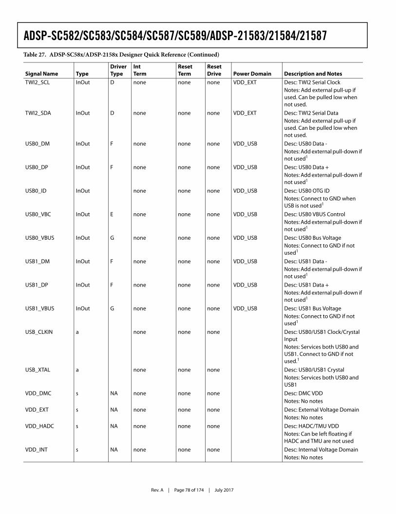
Rev. A | Page 78 of 174 | July 2017
ADSP-SC582/SC583/SC584/SC587/SC589/ADSP-21583/21584/21587
TWI2_SCL InOut D none none none VDD_EXT Desc: TWI2 Serial ClockNotes: Add external pull-up if used. Can be pulled low when not used.
TWI2_SDA InOut D none none none VDD_EXT Desc: TWI2 Serial DataNotes: Add external pull-up if used. Can be pulled low when not used.
USB0_DM InOut F none none none VDD_USB Desc: USB0 Data -Notes: Add external pull-down if not used1
USB0_DP InOut F none none none VDD_USB Desc: USB0 Data +Notes: Add external pull-down if not used1
USB0_ID InOut none none none VDD_USB Desc: USB0 OTG IDNotes: Connect to GND when USB is not used1
USB0_VBC InOut E none none none VDD_USB Desc: USB0 VBUS ControlNotes: Add external pull-down if not used1
USB0_VBUS InOut G none none none VDD_USB Desc: USB0 Bus VoltageNotes: Connect to GND if not used1
USB1_DM InOut F none none none VDD_USB Desc: USB1 Data -Notes: Add external pull-down if not used1
USB1_DP InOut F none none none VDD_USB Desc: USB1 Data +Notes: Add external pull-down if not used1
USB1_VBUS InOut G none none none VDD_USB Desc: USB1 Bus VoltageNotes: Connect to GND if not used1
USB_CLKIN a none none none Desc: USB0/USB1 Clock/Crystal InputNotes: Services both USB0 and USB1. Connect to GND if not used.1
USB_XTAL a none none none Desc: USB0/USB1 CrystalNotes: Services both USB0 and USB1
VDD_DMC s NA none none none Desc: DMC VDDNotes: No notes
VDD_EXT s NA none none none Desc: External Voltage DomainNotes: No notes
VDD_HADC s NA none none none Desc: HADC/TMU VDDNotes: Can be left floating if HADC and TMU are not used
VDD_INT s NA none none none Desc: Internal Voltage DomainNotes: No notes
Table 27. ADSP-SC58x/ADSP-2158x Designer Quick Reference (Continued)
Signal Name TypeDriver Type
Int Term
Reset Term
Reset Drive Power Domain Description and Notes
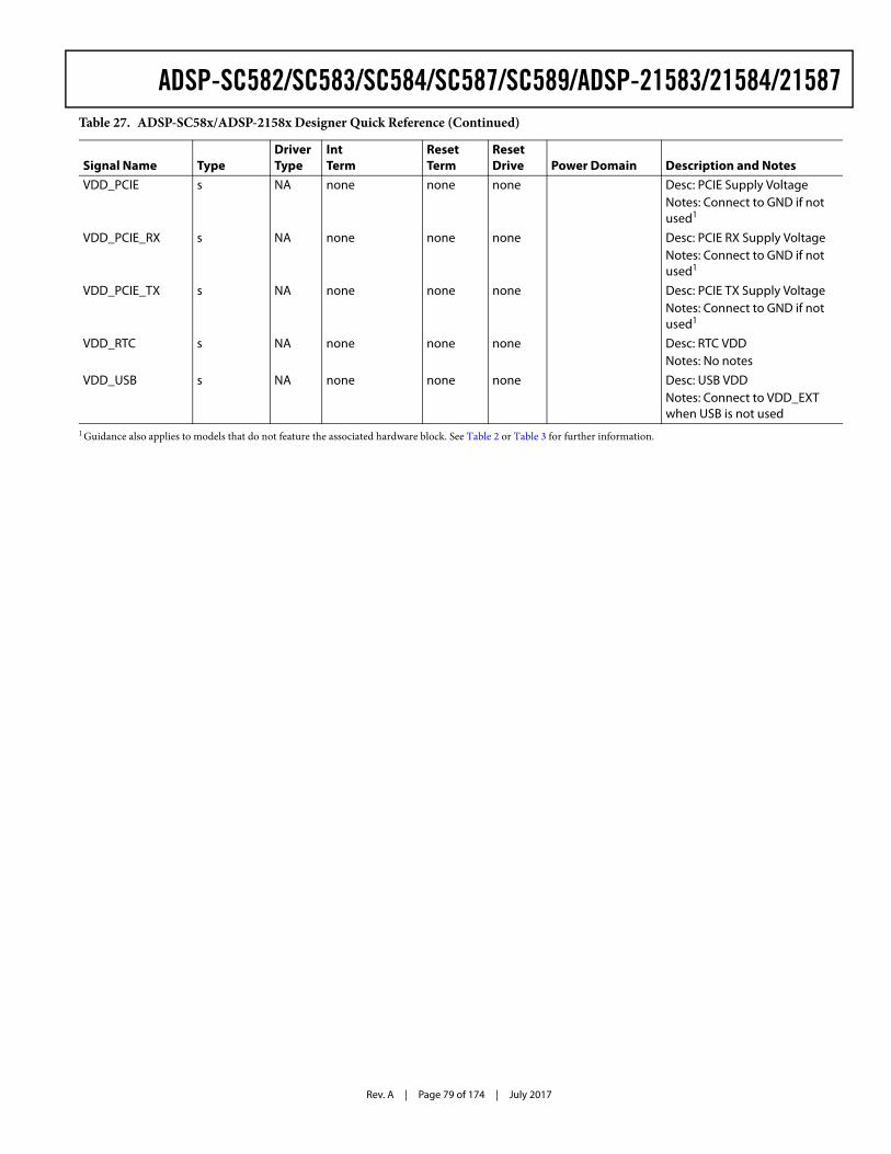
Rev. A | Page 79 of 174 | July 2017
ADSP-SC582/SC583/SC584/SC587/SC589/ADSP-21583/21584/21587
VDD_PCIE s NA none none none Desc: PCIE Supply VoltageNotes: Connect to GND if not used1
VDD_PCIE_RX s NA none none none Desc: PCIE RX Supply VoltageNotes: Connect to GND if not used1
VDD_PCIE_TX s NA none none none Desc: PCIE TX Supply VoltageNotes: Connect to GND if not used1
VDD_RTC s NA none none none Desc: RTC VDDNotes: No notes
VDD_USB s NA none none none Desc: USB VDDNotes: Connect to VDD_EXT when USB is not used
1 Guidance also applies to models that do not feature the associated hardware block. See Table 2 or Table 3 for further information.
Table 27. ADSP-SC58x/ADSP-2158x Designer Quick Reference (Continued)
Signal Name TypeDriver Type
Int Term
Reset Term
Reset Drive Power Domain Description and Notes
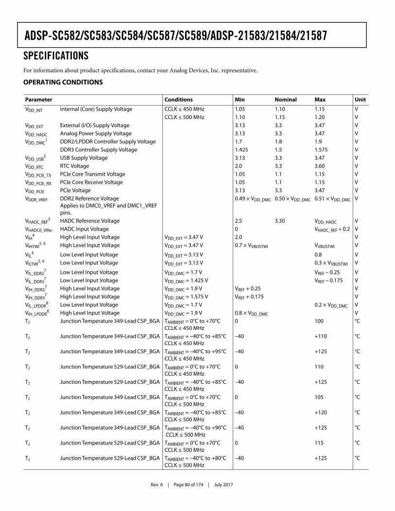
Rev. A | Page 80 of 174 | July 2017
ADSP-SC582/SC583/SC584/SC587/SC589/ADSP-21583/21584/21587
SPECIFICATIONSFor information about product specifications, contact your Analog Devices, Inc. representative.
OPERATING CONDITIONS
Parameter Conditions Min Nominal Max Unit
VDD_INT Internal (Core) Supply Voltage CCLK ≤ 450 MHz 1.05 1.10 1.15 VCCLK ≤ 500 MHz 1.10 1.15 1.20 V
VDD_EXT External (I/O) Supply Voltage 3.13 3.3 3.47 VVDD_HADC Analog Power Supply Voltage 3.13 3.3 3.47 VVDD_DMC
1 DDR2/LPDDR Controller Supply Voltage 1.7 1.8 1.9 VDDR3 Controller Supply Voltage 1.425 1.5 1.575 V
VDD_USB2 USB Supply Voltage 3.13 3.3 3.47 V
VDD_RTC RTC Voltage 2.0 3.3 3.60 VVDD_PCIE_TX PCIe Core Transmit Voltage 1.05 1.1 1.15 VVDD_PCIE_RX PCIe Core Receive Voltage 1.05 1.1 1.15 VVDD_PCIE PCIe Voltage 3.13 3.3 3.47 VVDDR_VREF DDR2 Reference Voltage
Applies to DMC0_VREF and DMC1_VREF pins.
0.49 × VDD_DMC 0.50 × VDD_DMC 0.51 × VDD_DMC V
VHADC_REF3 HADC Reference Voltage 2.5 3.30 VDD_HADC V
VHADC0_VINx HADC Input Voltage 0 VHADC_REF + 0.2 VVIH
4 High Level Input Voltage VDD_EXT = 3.47 V 2.0 VVIHTWI
5, 6 High Level Input Voltage VDD_EXT = 3.47 V 0.7 × VVBUSTWI VVBUSTWI V
VIL4 Low Level Input Voltage VDD_EXT = 3.13 V 0.8 V
VILTWI5, 6 Low Level Input Voltage VDD_EXT = 3.13 V 0.3 × VVBUSTWI V
VIL_DDR27 Low Level Input Voltage VDD_DMC = 1.7 V VREF – 0.25 V
VIL_DDR37 Low Level Input Voltage VDD_DMC = 1.425 V VREF – 0.175 V
VIH_DDR27 High Level Input Voltage VDD_DMC = 1.9 V VREF + 0.25 V
VIH_DDR37 High Level Input Voltage VDD_DMC = 1.575 V VREF + 0.175 V
VIL_LPDDR8 Low Level Input Voltage VDD_DMC = 1.7 V 0.2 × VDD_DMC V
VIH_LPDDR8 High Level Input Voltage VDD_DMC = 1.9 V 0.8 × VDD_DMC V
TJ Junction Temperature 349-Lead CSP_BGA TAMBIENT = 0°C to +70°CCCLK ≤ 450 MHz
0 100 °C
TJ Junction Temperature 349-Lead CSP_BGA TAMBIENT = –40°C to +85°CCCLK ≤ 450 MHz
–40 +110 °C
TJ Junction Temperature 349-Lead CSP_BGA TAMBIENT = –40°C to +95°CCCLK ≤ 450 MHz
–40 +125 °C
TJ Junction Temperature 529-Lead CSP_BGA TAMBIENT = 0°C to +70°CCCLK ≤ 450 MHz
0 110 °C
TJ Junction Temperature 529-Lead CSP_BGA TAMBIENT = –40°C to +85°CCCLK ≤ 450 MHz
–40 +125 °C
TJ Junction Temperature 349-Lead CSP_BGA TAMBIENT = 0°C to +70°CCCLK ≤ 500 MHz
0 105 °C
TJ Junction Temperature 349-Lead CSP_BGA TAMBIENT = –40°C to +85°CCCLK ≤ 500 MHz
–40 +120 °C
TJ Junction Temperature 349-Lead CSP_BGA TAMBIENT = –40°C to +90°C CCLK ≤ 500 MHz
–40 +125 °C
TJ Junction Temperature 529-Lead CSP_BGA TAMBIENT = 0°C to +70°CCCLK ≤ 500 MHz
0 115 °C
TJ Junction Temperature 529-Lead CSP_BGA TAMBIENT = –40°C to +80°CCCLK ≤ 500 MHz
–40 +125 °C
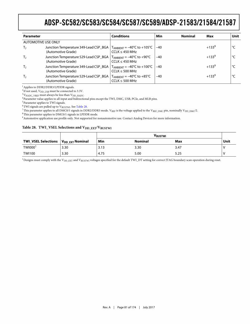
Rev. A | Page 81 of 174 | July 2017
ADSP-SC582/SC583/SC584/SC587/SC589/ADSP-21583/21584/21587
AUTOMOTIVE USE ONLYTJ Junction Temperature 349-Lead CSP_BGA
(Automotive Grade) TAMBIENT = –40°C to +105°CCCLK ≤ 450 MHz
–40 +1339 °C
TJ Junction Temperature 529-Lead CSP_BGA (Automotive Grade)
TAMBIENT = –40°C to +90°CCCLK ≤ 450 MHz
–40 +1339 °C
TJ Junction Temperature 349-Lead CSP_BGA (Automotive Grade)
TAMBIENT = –40°C to +100°CCCLK ≤ 500 MHz
–40 +1339 °C
TJ Junction Temperature 529-Lead CSP_BGA (Automotive Grade)
TAMBIENT = –40°C to +85°CCCLK ≤ 500 MHz
–40 +1339 °C
1 Applies to DDR2/DDR3/LPDDR signals.2 If not used, VDD_USB must be connected to 3.3V.3 VHADC_VREF must always be less than VDD_HADC.4 Parameter value applies to all input and bidirectional pins except the TWI, DMC, USB, PCIe, and MLB pins.5 Parameter applies to TWI signals.6 TWI signals are pulled up to VBUSTWI. See Table 28.7 This parameter applies to all DMC0/1 signals in DDR2/DDR3 mode. VREF is the voltage applied to the VREF_DMC pin, nominally VDD_DMC/2.8 This parameter applies to DMC0/1 signals in LPDDR mode.9 Automotive application use profile only. Not supported for nonautomotive use. Contact Analog Devices for more information.
Table 28. TWI_VSEL Selections and VDD_EXT/VBUSTWI
VBUSTWI
TWI_VSEL Selections VDD_EXT Nominal Min Nominal Max Unit
TWI0001 3.30 3.13 3.30 3.47 V
TWI100 3.30 4.75 5.00 5.25 V1 Designs must comply with the VDD_EXT and VBUSTWI voltages specified for the default TWI_DT setting for correct JTAG boundary scan operation during reset.
Parameter Conditions Min Nominal Max Unit
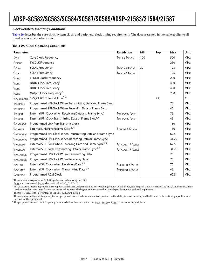
Rev. A | Page 82 of 174 | July 2017
ADSP-SC582/SC583/SC584/SC587/SC589/ADSP-21583/21584/21587Clock Related Operating Conditions
Table 29 describes the core clock, system clock, and peripheral clock timing requirements. The data presented in the table applies to all speed grades except where noted.
Table 29. Clock Operating Conditions
Parameter Restriction Min Typ Max Unit
fCCLK Core Clock Frequency fCCLK ≥ fSYSCLK 100 500 MHz
fSYSCLK SYSCLK Frequency 250 MHz
fSCLK0 SCLK0 Frequency1
1 The minimum frequency for SCLK0 applies only when using the USB.
fSYSCLK ≥ fSCLK0 30 125 MHz
fSCLK1 SCLK1 Frequency fSYSCLK ≥ fSCLK1 125 MHz
fDCLK LPDDR Clock Frequency 200 MHz
fDCLK DDR2 Clock Frequency 400 MHz
fDCLK DDR3 Clock Frequency 450 MHz
fOCLK Output Clock Frequency2
2 fOCLK must not exceed fSCLK0 when selected as SYS_CLKOUT.
250 MHz
fSYS_CLKOUTJ SYS_CLKOUT Period Jitter3, 4
3 SYS_CLKOUT jitter is dependent on the application system design including pin switching activity, board layout, and the jitter characteristics of the SYS_CLKIN source. Due to the dependency on these factors, the measured jitter may be higher or lower than this typical specification for each end application.
4 The typical value is the percentage of the SYS_CLKOUT period.
±2 %
fPCLKPROG Programmed PPI Clock When Transmitting Data and Frame Sync 75 MHz
fPCLKPROG Programmed PPI Clock When Receiving Data or Frame Sync 45 MHz
fPCLKEXT External PPI Clock When Receiving Data and Frame Sync5
5 The maximum achievable frequency for any peripheral in external clock mode is dependent on the ability to meet the setup and hold times in the ac timing specifications section for that peripheral.
fPCLKEXT ≤ fSCLK1 75 MHz
fPCLKEXT External PPI Clock Transmitting Data or Frame Sync5, 6
6 The peripheral external clock frequency must also be less than or equal to the fSCLK (fSCLK0 or fSCLK1) that clocks the peripheral.
fPCLKEXT ≤ fSCLK1 45 MHz
fLCLKTPROG Programmed Link Port Transmit Clock 150 MHz
fLCLKREXT External Link Port Receive Clock5, 6 fLCLKEXT ≤ fCLKO8 150 MHz
fSPTCLKPROG Programmed SPT Clock When Transmitting Data and Frame Sync 62.5 MHz
fSPTCLKPROG Programmed SPT Clock When Receiving Data or Frame Sync 31.25 MHz
fSPTCLKEXT External SPT Clock When Receiving Data and Frame Sync5, 6 fSPTCLKEXT ≤ fSCLK0 62.5 MHz
fSPTCLKEXT External SPT Clock Transmitting Data or Frame Sync5, 6 fSPTCLKEXT ≤ fSCLK0 31.25 MHz
fSPICLKPROG Programmed SPI Clock When Transmitting Data 75 MHz
fSPICLKPROG Programmed SPI Clock When Receiving Data 75 MHz
fSPICLKEXT External SPI Clock When Receiving Data5, 6 fSPICLKEXT ≤ fSCLK1 75 MHz
fSPICLKEXT External SPI Clock When Transmitting Data5, 6 fSPICLKEXT ≤ fSCLK1 45 MHz
fACLKPROG Programmed ACM Clock 62.5 MHz
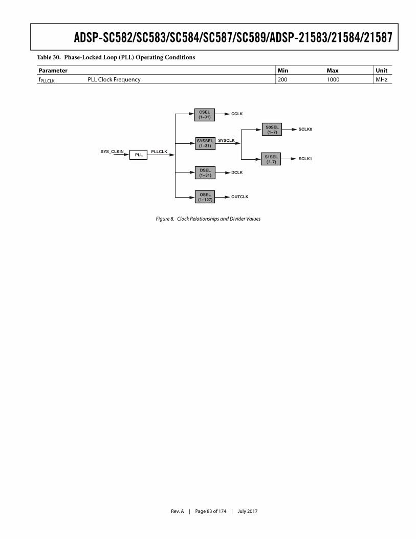
Rev. A | Page 83 of 174 | July 2017
ADSP-SC582/SC583/SC584/SC587/SC589/ADSP-21583/21584/21587Table 30. Phase-Locked Loop (PLL) Operating Conditions
Parameter Min Max UnitfPLLCLK PLL Clock Frequency 200 1000 MHz
Figure 8. Clock Relationships and Divider Values
SYS_CLKINPLL
DCLK
SYSCLK
CCLK
SCLK1
SCLK0
CSEL(1-31)
SYSSEL(1-31)
S0SEL(1-7)
S1SEL(1-7)
DSEL(1-31)
OUTCLKOSEL(1-127)
PLLCLK
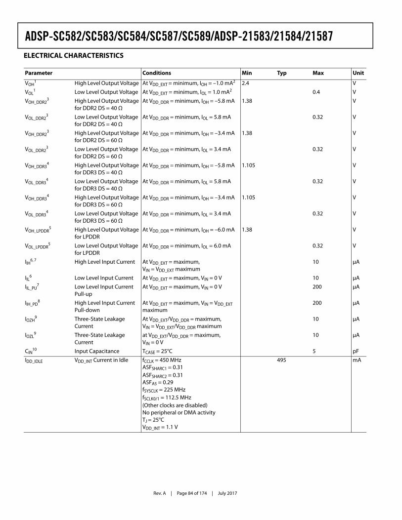
Rev. A | Page 84 of 174 | July 2017
ADSP-SC582/SC583/SC584/SC587/SC589/ADSP-21583/21584/21587ELECTRICAL CHARACTERISTICS
Parameter Conditions Min Typ Max Unit
VOH1 High Level Output Voltage At VDD_EXT = minimum, IOH = –1.0 mA2 2.4 V
VOL1 Low Level Output Voltage At VDD_EXT = minimum, IOL = 1.0 mA2 0.4 V
VOH_DDR23 High Level Output Voltage
for DDR2 DS = 40 ΩAt VDD_DDR = minimum, IOH = –5.8 mA 1.38 V
VOL_DDR23 Low Level Output Voltage
for DDR2 DS = 40 ΩAt VDD_DDR = minimum, IOL = 5.8 mA 0.32 V
VOH_DDR23 High Level Output Voltage
for DDR2 DS = 60 ΩAt VDD_DDR = minimum, IOH = –3.4 mA 1.38 V
VOL_DDR23 Low Level Output Voltage
for DDR2 DS = 60 ΩAt VDD_DDR = minimum, IOL = 3.4 mA 0.32 V
VOH_DDR34 High Level Output Voltage
for DDR3 DS = 40 ΩAt VDD_DDR = minimum, IOH = –5.8 mA 1.105 V
VOL_DDR34 Low Level Output Voltage
for DDR3 DS = 40 ΩAt VDD_DDR = minimum, IOL = 5.8 mA 0.32 V
VOH_DDR34 High Level Output Voltage
for DDR3 DS = 60 ΩAt VDD_DDR = minimum, IOH = –3.4 mA 1.105 V
VOL_DDR34 Low Level Output Voltage
for DDR3 DS = 60 ΩAt VDD_DDR = minimum, IOL = 3.4 mA 0.32 V
VOH_LPDDR5 High Level Output Voltage
for LPDDRAt VDD_DDR = minimum, IOH = –6.0 mA 1.38 V
VOL_LPDDR5 Low Level Output Voltage
for LPDDRAt VDD_DDR = minimum, IOL = 6.0 mA 0.32 V
IIH6, 7 High Level Input Current At VDD_EXT = maximum, VIN = VDD_EXT maximum
10 µA
IIL6 Low Level Input Current At VDD_EXT = maximum, VIN = 0 V 10 µA
IIL_PU7 Low Level Input Current
Pull-upAt VDD_EXT = maximum, VIN = 0 V 200 µA
IIH_PD8 High Level Input Current
Pull-downAt VDD_EXT = maximum, VIN = VDD_EXT maximum
200 µA
IOZH9 Three-State Leakage
CurrentAt VDD_EXT/VDD_DDR = maximum, VIN = VDD_EXT/VDD_DDR maximum
10 µA
IOZL9 Three-State Leakage
Currentat VDD_EXT/VDD_DDR = maximum, VIN = 0 V
10 µA
CIN10 Input Capacitance TCASE = 25°C 5 pF
IDD_IDLE VDD_INT Current in Idle fCCLK = 450 MHzASFSHARC1 = 0.31ASFSHARC2 = 0.31ASFA5 = 0.29fSYSCLK = 225 MHzfSCLK0/1 = 112.5 MHz(Other clocks are disabled)No peripheral or DMA activity TJ = 25°CVDD_INT = 1.1 V
495 mA
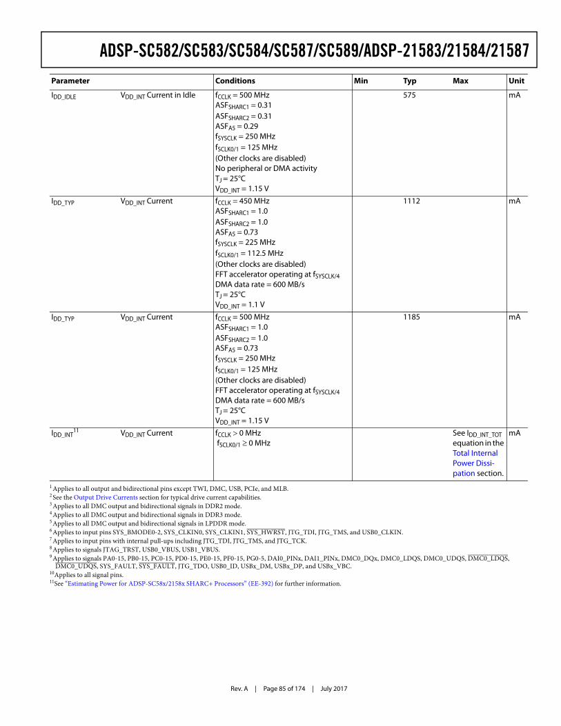
Rev. A | Page 85 of 174 | July 2017
ADSP-SC582/SC583/SC584/SC587/SC589/ADSP-21583/21584/21587
IDD_IDLE VDD_INT Current in Idle fCCLK = 500 MHzASFSHARC1 = 0.31ASFSHARC2 = 0.31ASFA5 = 0.29fSYSCLK = 250 MHzfSCLK0/1 = 125 MHz(Other clocks are disabled)No peripheral or DMA activity TJ = 25°CVDD_INT = 1.15 V
575 mA
IDD_TYP VDD_INT Current fCCLK = 450 MHzASFSHARC1 = 1.0ASFSHARC2 = 1.0ASFA5 = 0.73fSYSCLK = 225 MHzfSCLK0/1 = 112.5 MHz(Other clocks are disabled)FFT accelerator operating at fSYSCLK/4 DMA data rate = 600 MB/sTJ = 25°CVDD_INT = 1.1 V
1112 mA
IDD_TYP VDD_INT Current fCCLK = 500 MHzASFSHARC1 = 1.0ASFSHARC2 = 1.0ASFA5 = 0.73fSYSCLK = 250 MHzfSCLK0/1 = 125 MHz(Other clocks are disabled)FFT accelerator operating at fSYSCLK/4 DMA data rate = 600 MB/sTJ = 25°CVDD_INT = 1.15 V
1185 mA
IDD_INT11 VDD_INT Current fCCLK 0 MHz
fSCLK0/1 0 MHzSee IDD_INT_TOT equation in the Total Internal Power Dissi-pation section.
mA
1 Applies to all output and bidirectional pins except TWI, DMC, USB, PCIe, and MLB.2 See the Output Drive Currents section for typical drive current capabilities.3 Applies to all DMC output and bidirectional signals in DDR2 mode.4 Applies to all DMC output and bidirectional signals in DDR3 mode.5 Applies to all DMC output and bidirectional signals in LPDDR mode.6 Applies to input pins SYS_BMODE0-2, SYS_CLKIN0, SYS_CLKIN1, SYS_HWRST, JTG_TDI, JTG_TMS, and USB0_CLKIN.7 Applies to input pins with internal pull-ups including JTG_TDI, JTG_TMS, and JTG_TCK.8 Applies to signals JTAG_TRST, USB0_VBUS, USB1_VBUS.9 Applies to signals PA0-15, PB0-15, PC0-15, PD0-15, PE0-15, PF0-15, PG0-5, DAI0_PINx, DAI1_PINx, DMC0_DQx, DMC0_LDQS, DMC0_UDQS, DMC0_LDQS,
DMC0_UDQS, SYS_FAULT, SYS_FAULT, JTG_TDO, USB0_ID, USBx_DM, USBx_DP, and USBx_VBC.10Applies to all signal pins.11See “Estimating Power for ADSP-SC58x/2158x SHARC+ Processors” (EE-392) for further information.
Parameter Conditions Min Typ Max Unit
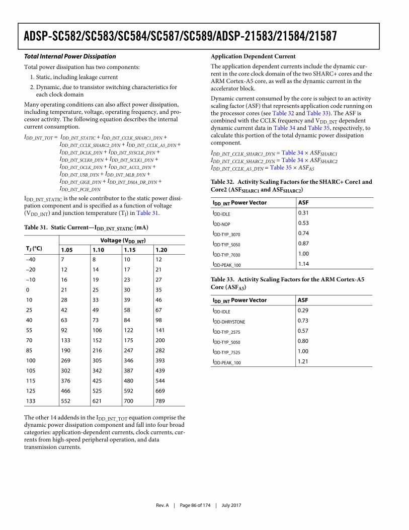
Rev. A | Page 86 of 174 | July 2017
ADSP-SC582/SC583/SC584/SC587/SC589/ADSP-21583/21584/21587Total Internal Power Dissipation
Total power dissipation has two components:1. Static, including leakage current2. Dynamic, due to transistor switching characteristics for
each clock domainMany operating conditions can also affect power dissipation, including temperature, voltage, operating frequency, and pro-cessor activity. The following equation describes the internal current consumption. IDD_INT_TOT = IDD_INT_STATIC + IDD_INT_CCLK_SHARC1_DYN +
IDD_INT_CCLK_SHARC2_DYN + IDD_INT_CCLK_A5_DYN +IDD_INT_DCLK_DYN + IDD_INT_SYSCLK_DYN +IDD_INT_SCLK0_DYN + IDD_INT_SCLK1_DYN +IDD_INT_OCLK_DYN + IDD_INT_ACCL_DYN +IDD_INT_USB_DYN + IDD_INT_MLB_DYN +IDD_INT_GIGE_DYN + IDD_INT_DMA_DR_DYN +IDD_INT_PCIE_DYN
IDD_INT_STATIC is the sole contributor to the static power dissi-pation component and is specified as a function of voltage (VDD_INT) and junction temperature (TJ) in Table 31.
The other 14 addends in the IDD_INT_TOT equation comprise the dynamic power dissipation component and fall into four broad categories: application-dependent currents, clock currents, cur-rents from high-speed peripheral operation, and data transmission currents.
Application Dependent CurrentThe application dependent currents include the dynamic cur-rent in the core clock domain of the two SHARC+ cores and the ARM Cortex-A5 core, as well as the dynamic current in the accelerator block.Dynamic current consumed by the core is subject to an activity scaling factor (ASF) that represents application code running on the processor cores (see Table 32 and Table 33). The ASF is combined with the CCLK frequency and VDD_INT dependent dynamic current data in Table 34 and Table 35, respectively, to calculate this portion of the total dynamic power dissipation component.IDD_INT_CCLK_SHARC1_DYN = Table 34 × ASFSHARC1IDD_INT_CCLK_SHARC2_DYN = Table 34 × ASFSHARC2IDD_INT_CCLK_A5_DYN = Table 35 × ASFA5
Table 31. Static Current—IDD_INT_STATIC (mA)
TJ (°C)Voltage (VDD_INT)
1.05 1.10 1.15 1.20
–40 7 8 10 12
–20 12 14 17 21
–10 16 19 23 27
0 21 25 30 35
10 28 33 39 46
25 42 49 58 67
40 63 73 84 98
55 92 106 122 141
70 133 152 175 200
85 190 216 247 282
100 269 305 346 393
105 302 342 387 439
115 376 425 480 544
125 466 525 592 669
133 552 621 700 789
Table 32. Activity Scaling Factors for the SHARC+ Core1 and Core2 (ASFSHARC1 and ASFSHARC2)
IDD_INT Power Vector ASF
IDD-IDLE 0.31
IDD-NOP 0.53
IDD-TYP_3070 0.74
IDD-TYP_5050 0.87
IDD-TYP_7030 1.00
IDD-PEAK_100 1.14
Table 33. Activity Scaling Factors for the ARM Cortex-A5 Core (ASFA5)
IDD_INT Power Vector ASF
IDD-IDLE 0.29
IDD-DHRYSTONE 0.73
IDD-TYP_2575 0.57
IDD-TYP_5050 0.80
IDD-TYP_7525 1.00
IDD-PEAK_100 1.21
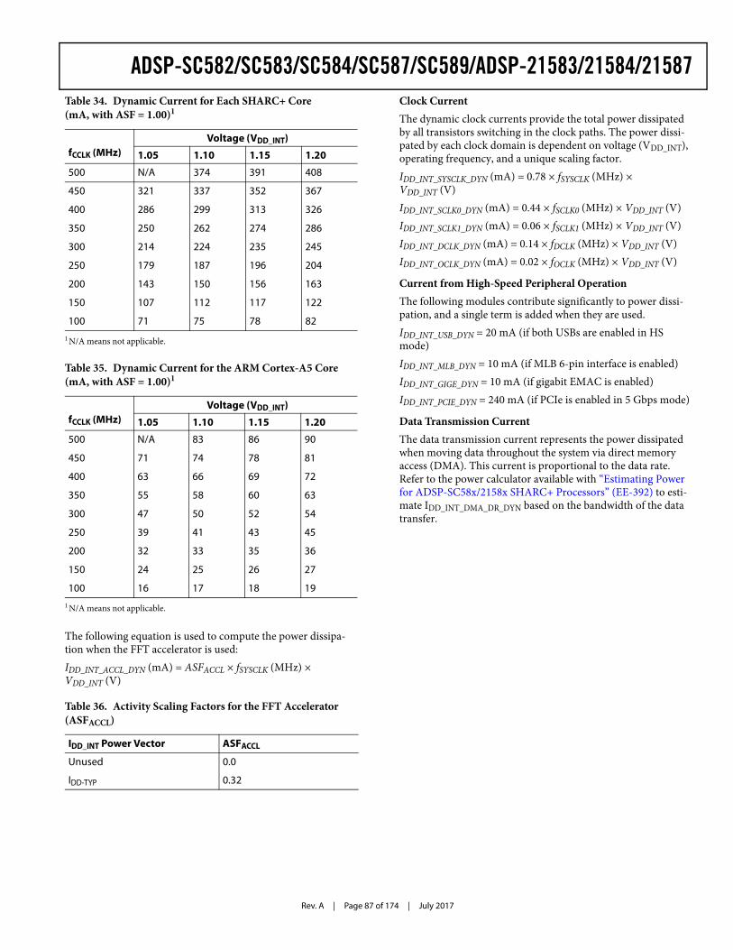
Rev. A | Page 87 of 174 | July 2017
ADSP-SC582/SC583/SC584/SC587/SC589/ADSP-21583/21584/21587
The following equation is used to compute the power dissipa-tion when the FFT accelerator is used:IDD_INT_ACCL_DYN (mA) = ASFACCL × fSYSCLK (MHz) × VDD_INT (V)
Clock CurrentThe dynamic clock currents provide the total power dissipated by all transistors switching in the clock paths. The power dissi-pated by each clock domain is dependent on voltage (VDD_INT), operating frequency, and a unique scaling factor.IDD_INT_SYSCLK_DYN (mA) = 0.78 × fSYSCLK (MHz) × VDD_INT (V)IDD_INT_SCLK0_DYN (mA) = 0.44 × fSCLK0 (MHz) × VDD_INT (V)IDD_INT_SCLK1_DYN (mA) = 0.06 × fSCLK1 (MHz) × VDD_INT (V)IDD_INT_DCLK_DYN (mA) = 0.14 × fDCLK (MHz) × VDD_INT (V)IDD_INT_OCLK_DYN (mA) = 0.02 × fOCLK (MHz) × VDD_INT (V)
Current from High-Speed Peripheral OperationThe following modules contribute significantly to power dissi-pation, and a single term is added when they are used.IDD_INT_USB_DYN = 20 mA (if both USBs are enabled in HS mode)IDD_INT_MLB_DYN = 10 mA (if MLB 6-pin interface is enabled)IDD_INT_GIGE_DYN = 10 mA (if gigabit EMAC is enabled)IDD_INT_PCIE_DYN = 240 mA (if PCIe is enabled in 5 Gbps mode)
Data Transmission CurrentThe data transmission current represents the power dissipated when moving data throughout the system via direct memory access (DMA). This current is proportional to the data rate. Refer to the power calculator available with “Estimating Power for ADSP-SC58x/2158x SHARC+ Processors” (EE-392) to esti-mate IDD_INT_DMA_DR_DYN based on the bandwidth of the data transfer.
Table 34. Dynamic Current for Each SHARC+ Core(mA, with ASF = 1.00)1
fCCLK (MHz)Voltage (VDD_INT)
1.05 1.10 1.15 1.20
500 N/A 374 391 408
450 321 337 352 367
400 286 299 313 326
350 250 262 274 286
300 214 224 235 245
250 179 187 196 204
200 143 150 156 163
150 107 112 117 122
100 71 75 78 821 N/A means not applicable.
Table 35. Dynamic Current for the ARM Cortex-A5 Core (mA, with ASF = 1.00)1
fCCLK (MHz)Voltage (VDD_INT)
1.05 1.10 1.15 1.20
500 N/A 83 86 90
450 71 74 78 81
400 63 66 69 72
350 55 58 60 63
300 47 50 52 54
250 39 41 43 45
200 32 33 35 36
150 24 25 26 27
100 16 17 18 191 N/A means not applicable.
Table 36. Activity Scaling Factors for the FFT Accelerator (ASFACCL)
IDD_INT Power Vector ASFACCL
Unused 0.0
IDD-TYP 0.32
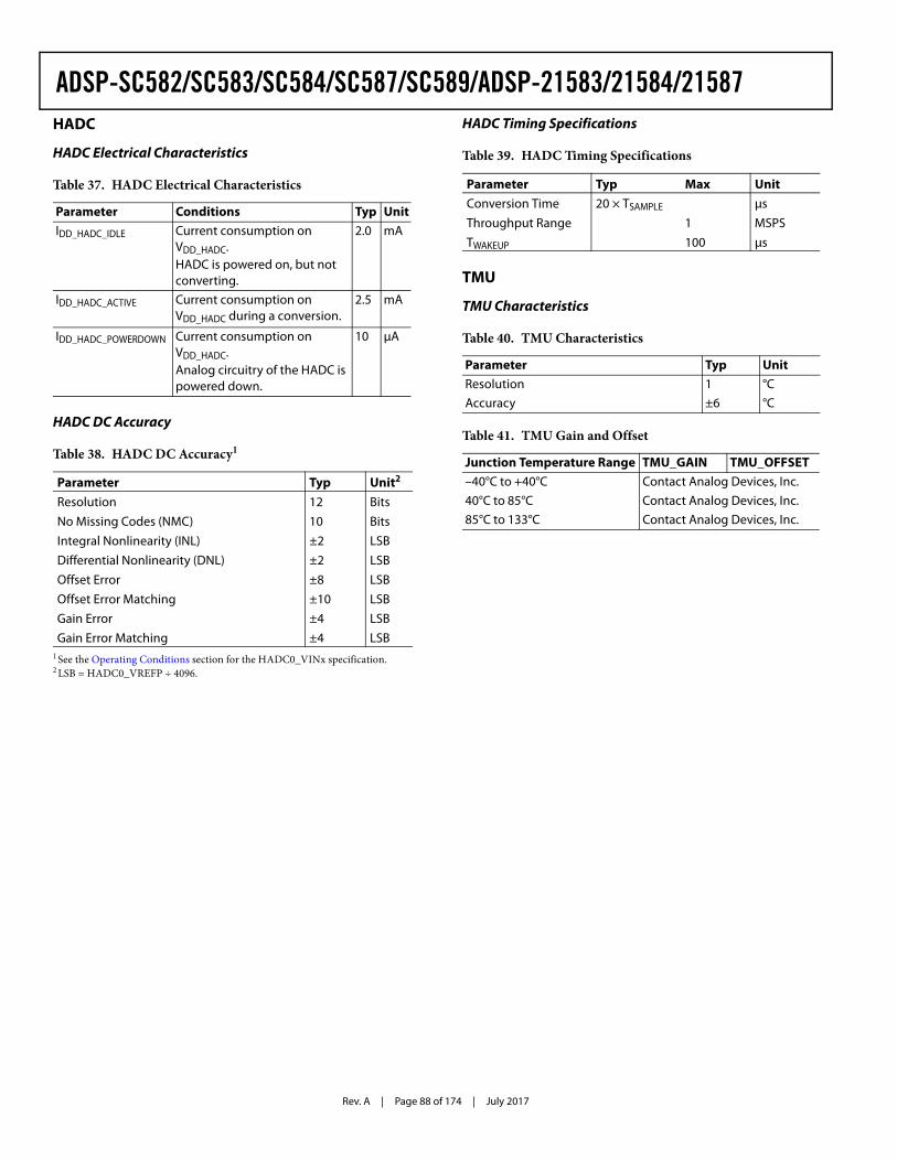
Rev. A | Page 88 of 174 | July 2017
ADSP-SC582/SC583/SC584/SC587/SC589/ADSP-21583/21584/21587HADC
HADC Electrical Characteristics
HADC DC Accuracy
HADC Timing Specifications
TMU
TMU Characteristics
Table 37. HADC Electrical Characteristics
Parameter Conditions Typ UnitIDD_HADC_IDLE Current consumption on
VDD_HADC.HADC is powered on, but not converting.
2.0 mA
IDD_HADC_ACTIVE Current consumption on VDD_HADC during a conversion.
2.5 mA
IDD_HADC_POWERDOWN Current consumption on VDD_HADC.Analog circuitry of the HADC is powered down.
10 μA
Table 38. HADC DC Accuracy1
1 See the Operating Conditions section for the HADC0_VINx specification.
Parameter Typ Unit2
2 LSB = HADC0_VREFP ÷ 4096.
Resolution 12 BitsNo Missing Codes (NMC) 10 BitsIntegral Nonlinearity (INL) ±2 LSBDifferential Nonlinearity (DNL) ±2 LSBOffset Error ±8 LSBOffset Error Matching ±10 LSBGain Error ±4 LSBGain Error Matching ±4 LSB
Table 39. HADC Timing Specifications
Parameter Typ Max UnitConversion Time 20 × TSAMPLE μsThroughput Range 1 MSPSTWAKEUP 100 μs
Table 40. TMU Characteristics
Parameter Typ UnitResolution 1 °CAccuracy ±6 °C
Table 41. TMU Gain and Offset
Junction Temperature Range TMU_GAIN TMU_OFFSET–40°C to +40°C Contact Analog Devices, Inc.40°C to 85°C Contact Analog Devices, Inc.85°C to 133°C Contact Analog Devices, Inc.
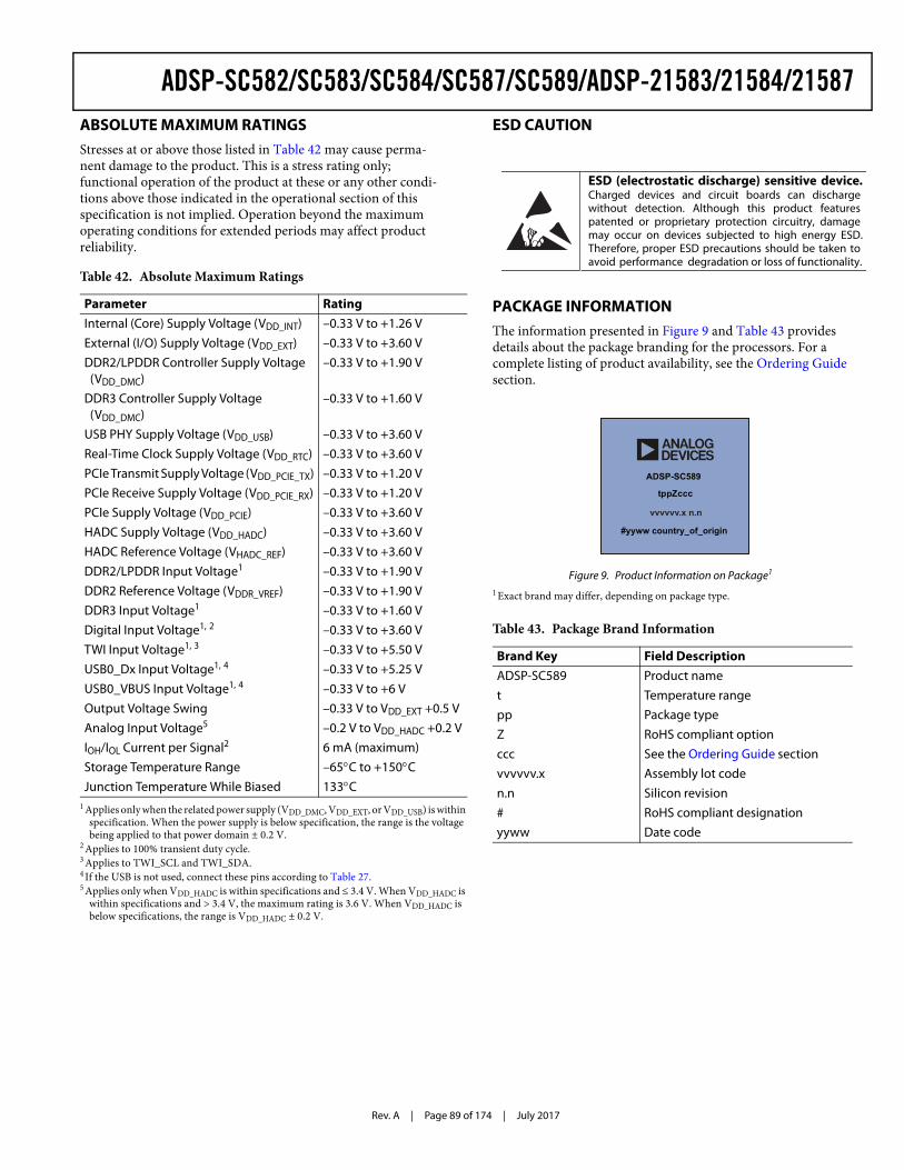
Rev. A | Page 89 of 174 | July 2017
ADSP-SC582/SC583/SC584/SC587/SC589/ADSP-21583/21584/21587ABSOLUTE MAXIMUM RATINGSStresses at or above those listed in Table 42 may cause perma-nent damage to the product. This is a stress rating only; functional operation of the product at these or any other condi-tions above those indicated in the operational section of this specification is not implied. Operation beyond the maximum operating conditions for extended periods may affect product reliability.
ESD CAUTION
PACKAGE INFORMATIONThe information presented in Figure 9 and Table 43 provides details about the package branding for the processors. For a complete listing of product availability, see the Ordering Guide section.
Table 42. Absolute Maximum Ratings
Parameter RatingInternal (Core) Supply Voltage (VDD_INT) –0.33 V to +1.26 VExternal (I/O) Supply Voltage (VDD_EXT) –0.33 V to +3.60 VDDR2/LPDDR Controller Supply Voltage
(VDD_DMC)–0.33 V to +1.90 V
DDR3 Controller Supply Voltage (VDD_DMC)
–0.33 V to +1.60 V
USB PHY Supply Voltage (VDD_USB) –0.33 V to +3.60 VReal-Time Clock Supply Voltage (VDD_RTC) –0.33 V to +3.60 VPCIe Transmit Supply Voltage (VDD_PCIE_TX) –0.33 V to +1.20 VPCIe Receive Supply Voltage (VDD_PCIE_RX) –0.33 V to +1.20 VPCIe Supply Voltage (VDD_PCIE) –0.33 V to +3.60 VHADC Supply Voltage (VDD_HADC) –0.33 V to +3.60 VHADC Reference Voltage (VHADC_REF) –0.33 V to +3.60 VDDR2/LPDDR Input Voltage1
1 Applies only when the related power supply (VDD_DMC, VDD_EXT, or VDD_USB) is within specification. When the power supply is below specification, the range is the voltage being applied to that power domain ± 0.2 V.
–0.33 V to +1.90 VDDR2 Reference Voltage (VDDR_VREF) –0.33 V to +1.90 VDDR3 Input Voltage1 –0.33 V to +1.60 VDigital Input Voltage1, 2
2 Applies to 100% transient duty cycle.
–0.33 V to +3.60 VTWI Input Voltage1, 3
3 Applies to TWI_SCL and TWI_SDA.
–0.33 V to +5.50 VUSB0_Dx Input Voltage1, 4
4 If the USB is not used, connect these pins according to Table 27.
–0.33 V to +5.25 VUSB0_VBUS Input Voltage1, 4 –0.33 V to +6 VOutput Voltage Swing –0.33 V to VDD_EXT +0.5 VAnalog Input Voltage5
5 Applies only when VDD_HADC is within specifications and ≤ 3.4 V. When VDD_HADC is within specifications and > 3.4 V, the maximum rating is 3.6 V. When VDD_HADC is below specifications, the range is VDD_HADC ± 0.2 V.
–0.2 V to VDD_HADC +0.2 VIOH/IOL Current per Signal2 6 mA (maximum)Storage Temperature Range –65C to +150CJunction Temperature While Biased 133C
Figure 9. Product Information on Package1
1 Exact brand may differ, depending on package type.
Table 43. Package Brand Information
Brand Key Field DescriptionADSP-SC589 Product namet Temperature rangepp Package typeZ RoHS compliant option ccc See the Ordering Guide sectionvvvvvv.x Assembly lot coden.n Silicon revision# RoHS compliant designationyyww Date code
ESD (electrostatic discharge) sensitive device.Charged devices and circuit boards can discharge without detection. Although this product features patented or proprietary protection circuitry, damage may occur on devices subjected to high energy ESD. Therefore, proper ESD precautions should be taken to avoid performance degradation or loss of functionality.
tppZccc
ADSP-SC589
a
#yyww country_of_origin
vvvvvv.x n.n
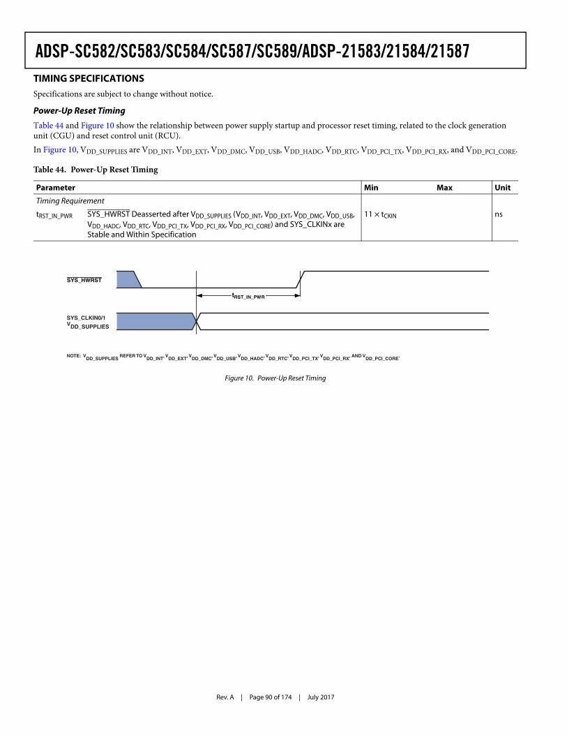
Rev. A | Page 90 of 174 | July 2017
ADSP-SC582/SC583/SC584/SC587/SC589/ADSP-21583/21584/21587TIMING SPECIFICATIONSSpecifications are subject to change without notice.
Power-Up Reset Timing
Table 44 and Figure 10 show the relationship between power supply startup and processor reset timing, related to the clock generation unit (CGU) and reset control unit (RCU). In Figure 10, VDD_SUPPLIES are VDD_INT, VDD_EXT, VDD_DMC, VDD_USB, VDD_HADC, VDD_RTC, VDD_PCI_TX, VDD_PCI_RX, and VDD_PCI_CORE.
Table 44. Power-Up Reset Timing
Parameter Min Max Unit
Timing Requirement
tRST_IN_PWR SYS_HWRST Deasserted after VDD_SUPPLIES (VDD_INT, VDD_EXT, VDD_DMC, VDD_USB, VDD_HADC, VDD_RTC, VDD_PCI_TX, VDD_PCI_RX, VDD_PCI_CORE) and SYS_CLKINx are Stable and Within Specification
11 × tCKIN ns
Figure 10. Power-Up Reset Timing
SYS_HWRST
tRST_IN_PWR
SYS_CLKIN0/1VDD_SUPPLIES
NOTE: VDD_SUPPLIES
REFER TO VDD_INT
, VDD_EXT
, VDD_DMC
, VDD_USB
, VDD_HADC
, VDD_RTC
, VDD_PCI_TX
, VDD_PCI_RX
, AND VDD_PCI_CORE
.
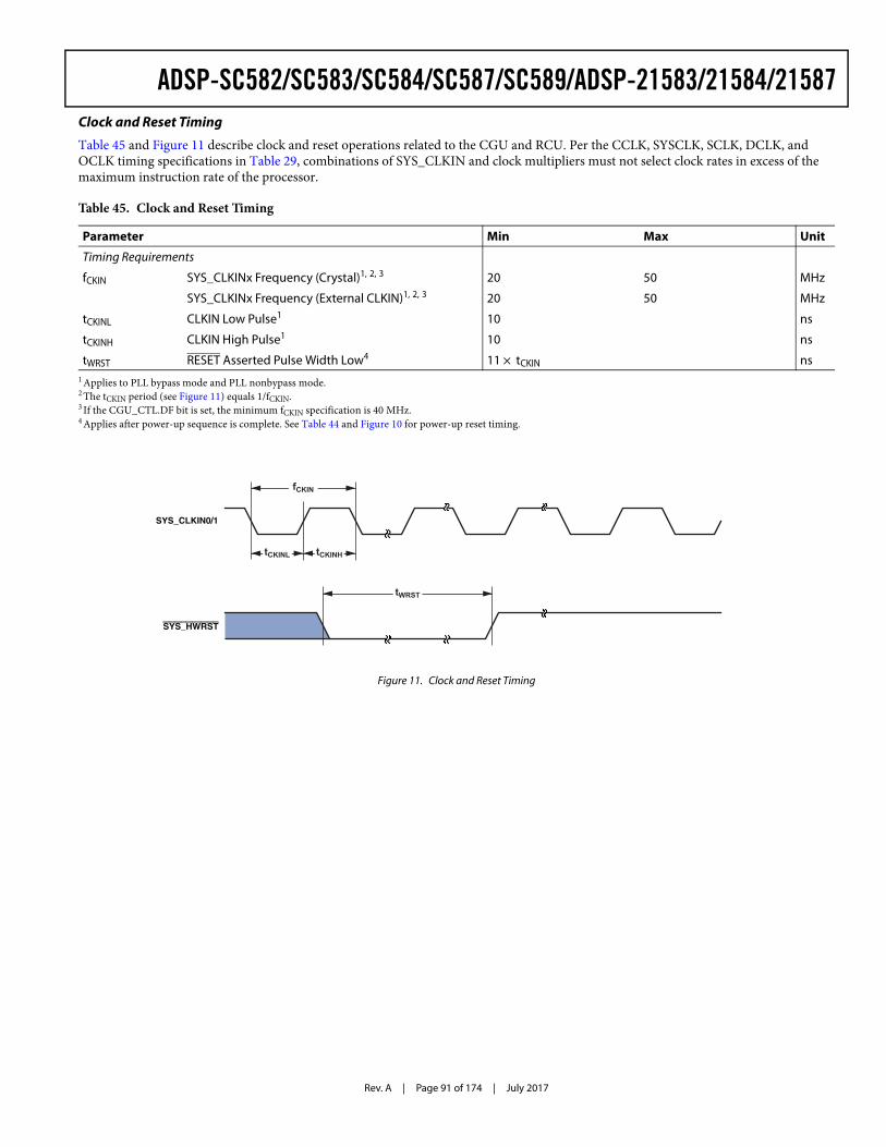
Rev. A | Page 91 of 174 | July 2017
ADSP-SC582/SC583/SC584/SC587/SC589/ADSP-21583/21584/21587Clock and Reset Timing
Table 45 and Figure 11 describe clock and reset operations related to the CGU and RCU. Per the CCLK, SYSCLK, SCLK, DCLK, and OCLK timing specifications in Table 29, combinations of SYS_CLKIN and clock multipliers must not select clock rates in excess of the maximum instruction rate of the processor.
Table 45. Clock and Reset Timing
Parameter Min Max Unit
Timing Requirements
fCKIN SYS_CLKINx Frequency (Crystal)1, 2, 3
1 Applies to PLL bypass mode and PLL nonbypass mode.2 The tCKIN period (see Figure 11) equals 1/fCKIN.3 If the CGU_CTL.DF bit is set, the minimum fCKIN specification is 40 MHz.
20 50 MHz
SYS_CLKINx Frequency (External CLKIN)1, 2, 3 20 50 MHz
tCKINL CLKIN Low Pulse1 10 ns
tCKINH CLKIN High Pulse1 10 ns
tWRST RESET Asserted Pulse Width Low4
4 Applies after power-up sequence is complete. See Table 44 and Figure 10 for power-up reset timing.
11 × tCKIN ns
Figure 11. Clock and Reset Timing
SYS_CLKIN0/1
tWRST
fCKIN
tCKINL tCKINH
SYS_HWRST
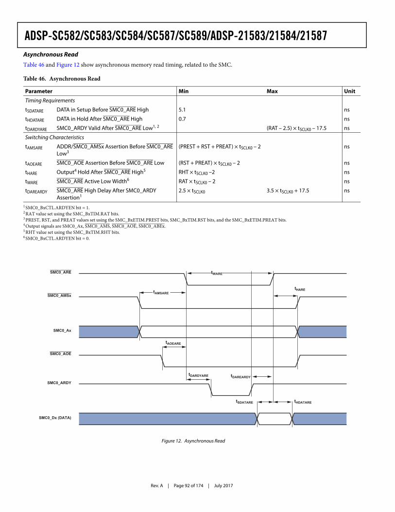
Rev. A | Page 92 of 174 | July 2017
ADSP-SC582/SC583/SC584/SC587/SC589/ADSP-21583/21584/21587Asynchronous Read
Table 46 and Figure 12 show asynchronous memory read timing, related to the SMC.
Table 46. Asynchronous Read
Parameter Min Max Unit
Timing Requirements
tSDATARE DATA in Setup Before SMC0_ARE High 5.1 ns
tHDATARE DATA in Hold After SMC0_ARE High 0.7 ns
tDARDYARE SMC0_ARDY Valid After SMC0_ARE Low1, 2
1 SMC0_BxCTL.ARDYEN bit = 1.2 RAT value set using the SMC_BxTIM.RAT bits.
(RAT – 2.5) × tSCLK0 – 17.5 ns
Switching Characteristics
tAMSARE ADDR/SMC0_AMSx Assertion Before SMC0_ARE Low3
3 PREST, RST, and PREAT values set using the SMC_BxETIM.PREST bits, SMC_BxTIM.RST bits, and the SMC_BxETIM.PREAT bits.
(PREST + RST + PREAT) × tSCLK0 – 2 ns
tAOEARE SMC0_AOE Assertion Before SMC0_ARE Low (RST + PREAT) × tSCLK0 – 2 ns
tHARE Output4 Hold After SMC0_ARE High5
4 Output signals are SMC0_Ax, SMC0_AMS, SMC0_AOE, SMC0_ABEx.5 RHT value set using the SMC_BxTIM.RHT bits.
RHT × tSCLK0 –2 ns
tWARE SMC0_ARE Active Low Width6
6 SMC0_BxCTL.ARDYEN bit = 0.
RAT × tSCLK0 – 2 ns
tDAREARDY SMC0_ARE High Delay After SMC0_ARDY Assertion1
2.5 × tSCLK0 3.5 × tSCLK0 + 17.5 ns
Figure 12. Asynchronous Read
SMC0_ARE
SMC0_AMSx
SMC0_Ax
tWARE
SMC0_AOE
SMC0_Dx (DATA)
SMC0_ARDY
tAOEARE
tAMSARE
tDARDYARE
tHARE
tHDATARE
tDAREARDY
tSDATARE
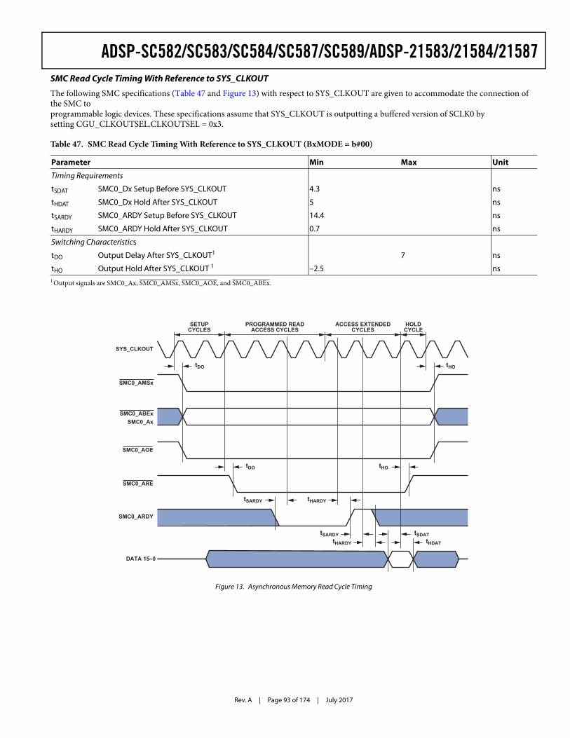
Rev. A | Page 93 of 174 | July 2017
ADSP-SC582/SC583/SC584/SC587/SC589/ADSP-21583/21584/21587SMC Read Cycle Timing With Reference to SYS_CLKOUT
The following SMC specifications (Table 47 and Figure 13) with respect to SYS_CLKOUT are given to accommodate the connection of the SMC to programmable logic devices. These specifications assume that SYS_CLKOUT is outputting a buffered version of SCLK0 by setting CGU_CLKOUTSEL.CLKOUTSEL = 0x3.
Table 47. SMC Read Cycle Timing With Reference to SYS_CLKOUT (BxMODE = b#00)
Parameter Min Max Unit
Timing Requirements
tSDAT SMC0_Dx Setup Before SYS_CLKOUT 4.3 ns
tHDAT SMC0_Dx Hold After SYS_CLKOUT 5 ns
tSARDY SMC0_ARDY Setup Before SYS_CLKOUT 14.4 ns
tHARDY SMC0_ARDY Hold After SYS_CLKOUT 0.7 ns
Switching Characteristics
tDO Output Delay After SYS_CLKOUT1
1 Output signals are SMC0_Ax, SMC0_AMSx, SMC0_AOE, and SMC0_ABEx.
7 ns
tHO Output Hold After SYS_CLKOUT 1 –2.5 ns
Figure 13. Asynchronous Memory Read Cycle Timing
tHARDY
SETUPCYCLES
PROGRAMMED READACCESS CYCLES
ACCESS EXTENDEDCYCLES
HOLDCYCLE
tDO tHO
tDO
tHARDYtSARDY
tSDATtHDAT
tSARDY
SYS_CLKOUT
SMC0_AMSx
SMC0_ABEx
SMC0_AOE
SMC0_ARE
SMC0_ARDY
DATA 15–0
tHO
SMC0_Ax
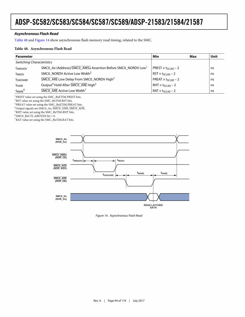
Rev. A | Page 94 of 174 | July 2017
ADSP-SC582/SC583/SC584/SC587/SC589/ADSP-21583/21584/21587Asynchronous Flash Read
Table 48 and Figure 14 show asynchronous flash memory read timing, related to the SMC.
Table 48. Asynchronous Flash Read
Parameter Min Max Unit
Switching Characteristics
tAMSADV SMC0_Ax (Address)/SMC0_AMSx Assertion Before SMC0_NORDV Low1
1 PREST value set using the SMC_BxETIM.PREST bits.
PREST × tSCLK0 – 2 ns
tWADV SMC0_NORDV Active Low Width2
2 RST value set using the SMC_BxTIM.RST bits.
RST × tSCLK0 – 2 ns
tDADVARE SMC0_ARE Low Delay From SMC0_NORDV High3
3 PREAT value set using the SMC_BxETIM.PREAT bits.
PREAT × tSCLK0 – 2 ns
tHARE Output4 Hold After SMC0_ARE High5
4 Output signals are SMC0_Ax, SMC0_AMS, SMC0_AOE.5 RHT value set using the SMC_BxTIM.RHT bits.
RHT × tSCLK0 – 2 ns
tWARE6
6 SMC0_BxCTL.ARDYEN bit = 0.
SMC0_ARE Active Low Width7
7 RAT value set using the SMC_BxTIM.RAT bits.
RAT × tSCLK0 – 2 ns
Figure 14. Asynchronous Flash Read
SMC0_Ax(NOR_Ax)
tAMSADV
tDADVARE
tWADV
tWARE tHARE
READ LATCHEDDATA
SMC0_AMSx(NOR_CE)
SMC0_ARE(NOR_OE)
SMC0_Dx(NOR_Dx)
SMC0_AOE(NOR_ADV)
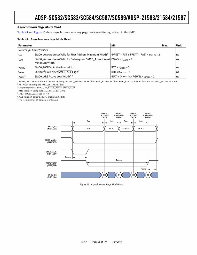
Rev. A | Page 95 of 174 | July 2017
ADSP-SC582/SC583/SC584/SC587/SC589/ADSP-21583/21584/21587Asynchronous Page Mode Read
Table 49 and Figure 15 show asynchronous memory page mode read timing, related to the SMC.
Table 49. Asynchronous Page Mode Read
Parameter Min Max Unit
Switching Characteristics
tAV SMC0_Axx (Address) Valid for First Address Minimum Width1
1 PREST, RST, PREAT and RAT values set using the SMC_BxETIM.PREST bits, SMC_BxTIM.RST bits, SMC_BxETIM.PREAT bits, and the SMC_BxTIM.RAT bits.
(PREST + RST + PREAT + RAT) × tSCLK0 – 2 ns
tAV1 SMC0_Axx (Address) Valid for Subsequent SMC0_Ax (Address) Minimum Width
PGWS × tSCLK0 – 2 ns
tWADV SMC0_NORDV Active Low Width2
2 RST value set using the SMC_BxTIM.RST bits.
RST × tSCLK0 – 2 ns
tHARE Output3 Hold After SMC0_ARE High4
3 Output signals are SMC0_Ax, SMC0_AMSx, SMC0_AOE.4 RHT value set using the SMC_BxTIM.RHT bits.
RHT × tSCLK0 – 2 ns
tWARE5
5 SMC_BxCTL.ARDYEN bit = 0.
SMC0_ARE Active Low Width6, 7
6 RAT value set using the SMC_BxTIM.RAT bits.7 Nw = Number of 16-bit data words read.
(RAT + (Nw – 1) × PGWS) × tSCLK0 – 2 ns
Figure 15. Asynchronous Page Mode Read
SMC0_AMSx(NOR_CE)
SMC0_ARE(NOR_OE)
SMC0_AOENOR_ADV
SMC0_Dx(NOR_Dx)
A0
tWADV
tHARE
D0 D1 D2 D3
A0 + 1 A0 + 2 A0 + 3
tAV tAV1 tAV1 tAV1
READ LATCHED
DATA
READ LATCHED
DATA
READ LATCHED
DATA
READ LATCHED
DATA
SMC0_Ax(NOR_Ax)
tWARE
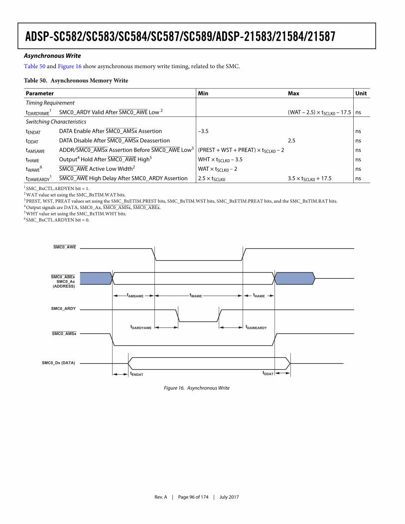
Rev. A | Page 96 of 174 | July 2017
ADSP-SC582/SC583/SC584/SC587/SC589/ADSP-21583/21584/21587Asynchronous Write
Table 50 and Figure 16 show asynchronous memory write timing, related to the SMC.
Table 50. Asynchronous Memory Write
Parameter Min Max Unit
Timing Requirement
tDARDYAWE1
1 SMC_BxCTL.ARDYEN bit = 1.
SMC0_ARDY Valid After SMC0_AWE Low 2
2 WAT value set using the SMC_BxTIM.WAT bits.
(WAT – 2.5) × tSCLK0 – 17.5 ns
Switching Characteristics
tENDAT DATA Enable After SMC0_AMSx Assertion –3.5 ns
tDDAT DATA Disable After SMC0_AMSx Deassertion 2.5 ns
tAMSAWE ADDR/SMC0_AMSx Assertion Before SMC0_AWE Low3
3 PREST, WST, PREAT values set using the SMC_BxETIM.PREST bits, SMC_BxTIM.WST bits, SMC_BxETIM.PREAT bits, and the SMC_BxTIM.RAT bits.
(PREST + WST + PREAT) × tSCLK0 – 2 ns
tHAWE Output4 Hold After SMC0_AWE High5
4 Output signals are DATA, SMC0_Ax, SMC0_AMSx, SMC0_ABEx.5 WHT value set using the SMC_BxTIM.WHT bits.
WHT × tSCLK0 – 3.5 ns
tWAWE6
6 SMC_BxCTL.ARDYEN bit = 0.
SMC0_AWE Active Low Width2 WAT × tSCLK0 – 2 ns
tDAWEARDY1 SMC0_AWE High Delay After SMC0_ARDY Assertion 2.5 × tSCLK0 3.5 × tSCLK0 + 17.5 ns
Figure 16. Asynchronous Write
SMC0_AWE
SMC0_ABExSMC0_Ax
(ADDRESS)
tDARDYAWE
tAMSAWE
tDAWEARDY
tENDAT tDDAT
tHAWEtWAWE
SMC0_AMSx
SMC0_Dx (DATA)
SMC0_ARDY
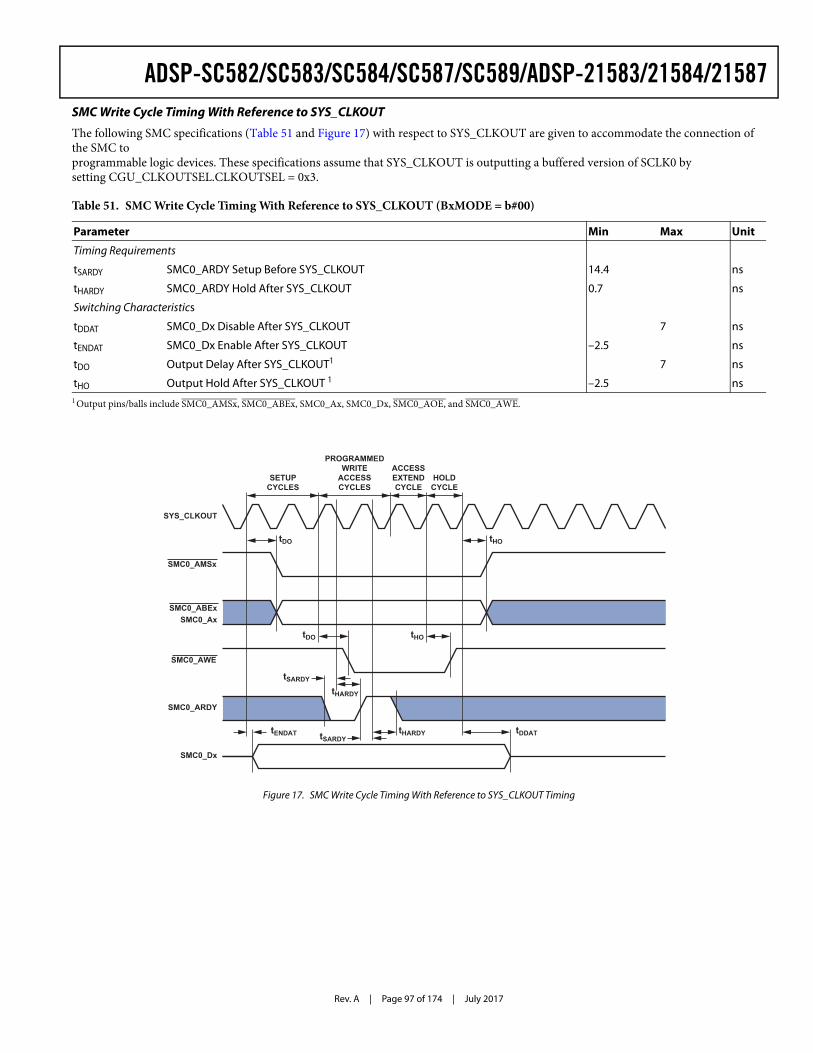
Rev. A | Page 97 of 174 | July 2017
ADSP-SC582/SC583/SC584/SC587/SC589/ADSP-21583/21584/21587SMC Write Cycle Timing With Reference to SYS_CLKOUT
The following SMC specifications (Table 51 and Figure 17) with respect to SYS_CLKOUT are given to accommodate the connection of the SMC to programmable logic devices. These specifications assume that SYS_CLKOUT is outputting a buffered version of SCLK0 by setting CGU_CLKOUTSEL.CLKOUTSEL = 0x3.
Table 51. SMC Write Cycle Timing With Reference to SYS_CLKOUT (BxMODE = b#00)
Parameter Min Max Unit
Timing Requirements
tSARDY SMC0_ARDY Setup Before SYS_CLKOUT 14.4 ns
tHARDY SMC0_ARDY Hold After SYS_CLKOUT 0.7 ns
Switching Characteristics
tDDAT SMC0_Dx Disable After SYS_CLKOUT 7 ns
tENDAT SMC0_Dx Enable After SYS_CLKOUT –2.5 ns
tDO Output Delay After SYS_CLKOUT1
1 Output pins/balls include SMC0_AMSx, SMC0_ABEx, SMC0_Ax, SMC0_Dx, SMC0_AOE, and SMC0_AWE.
7 ns
tHO Output Hold After SYS_CLKOUT 1 –2.5 ns
Figure 17. SMC Write Cycle Timing With Reference to SYS_CLKOUT Timing
SETUPCYCLES
PROGRAMMEDWRITE
ACCESSCYCLES
ACCESSEXTENDCYCLE
HOLDCYCLE
tDO tHO
SYS_CLKOUT
SMC0_ABEx
SMC0_AWE
SMC0_ARDY
SMC0_Dx
tSARDY
tSARDYtDDATtENDAT tHARDY
tHOtDO
tHARDY
SMC0_Ax
SMC0_AMSx
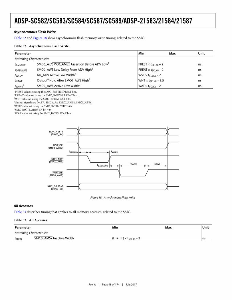
Rev. A | Page 98 of 174 | July 2017
ADSP-SC582/SC583/SC584/SC587/SC589/ADSP-21583/21584/21587Asynchronous Flash Write
Table 52 and Figure 18 show asynchronous flash memory write timing, related to the SMC.
All Accesses
Table 53 describes timing that applies to all memory accesses, related to the SMC.
Table 52. Asynchronous Flash Write
Parameter Min Max Unit
Switching Characteristics
tAMSADV SMC0_Ax/SMC0_AMSx Assertion Before ADV Low1
1 PREST value set using the SMC_BxETIM.PREST bits.
PREST × tSCLK0 – 2 ns
tDADVAWE SMC0_AWE Low Delay From ADV High2
2 PREAT value set using the SMC_BxETIM.PREAT bits.
PREAT × tSCLK0 – 2 ns
tWADV NR_ADV Active Low Width3
3 WST value set using the SMC_BxTIM.WST bits.
WST × tSCLK0 – 2 ns
tHAWE Output4 Hold After SMC0_AWE High5
4 Output signals are DATA, SMC0_Ax, SMC0_AMSx, SMC0_ABEx.5 WHT value set using the SMC_BxTIM.WHT bits.
WHT × tSCLK0 – 3.5 ns
tWAWE6
6 SMC_BxCTL.ARDYEN bit = 0.
SMC0_AWE Active Low Width7
7 WAT value set using the SMC_BxTIM.WAT bits.
WAT × tSCLK0 – 2 ns
Figure 18. Asynchronous Flash Write
Table 53. All Accesses
Parameter Min Max Unit
Switching Characteristic
tTURN SMC0_AMSx Inactive Width (IT + TT) × tSCLK0 – 2 ns
NOR_CE (SMC0_AMSx)
NOR_WE (SMC0_AWE)
NOR_A 25-1(SMC0_Ax)
NOR_ADV (SMC0_AOE)
tAMSADV
tDADVAWE
NOR_DQ 15-0(SMC0_Dx)
tWADV
tWAWE tHAWE
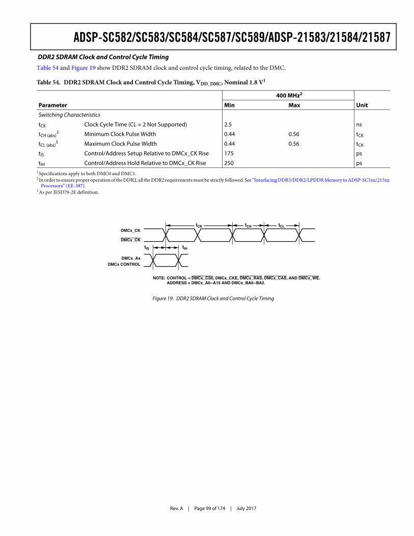
Rev. A | Page 99 of 174 | July 2017
ADSP-SC582/SC583/SC584/SC587/SC589/ADSP-21583/21584/21587 DDR2 SDRAM Clock and Control Cycle Timing
Table 54 and Figure 19 show DDR2 SDRAM clock and control cycle timing, related to the DMC.
Table 54. DDR2 SDRAM Clock and Control Cycle Timing, VDD_DMC, Nominal 1.8 V1
1 Specifications apply to both DMC0 and DMC1.
400 MHz2
2 In order to ensure proper operation of the DDR2, all the DDR2 requirements must be strictly followed. See “Interfacing DDR3/DDR2/LPDDR Memory to ADSP-SC5xx/215xx Processors” (EE-387).
Parameter Min Max Unit
Switching Characteristics
tCK Clock Cycle Time (CL = 2 Not Supported) 2.5 ns
tCH (abs)3
3 As per JESD79-2E definition.
Minimum Clock Pulse Width 0.44 0.56 tCK
tCL (abs)3 Maximum Clock Pulse Width 0.44 0.56 tCK
tIS Control/Address Setup Relative to DMCx_CK Rise 175 ps
tIH Control/Address Hold Relative to DMCx_CK Rise 250 ps
Figure 19. DDR2 SDRAM Clock and Control Cycle Timing
NOTE: CONTROL = DMCx_CS0, DMCx_CKE, DMCx_RAS, DMCx_CAS, AND DMCx_WE. ADDRESS = DMCx_A0-A15 AND DMCx_BA0-BA2.
DMCx_CK
DMCx_Ax
DMCx CONTROL
tIS tIH
tCK tCH tCL
DMCx_CK
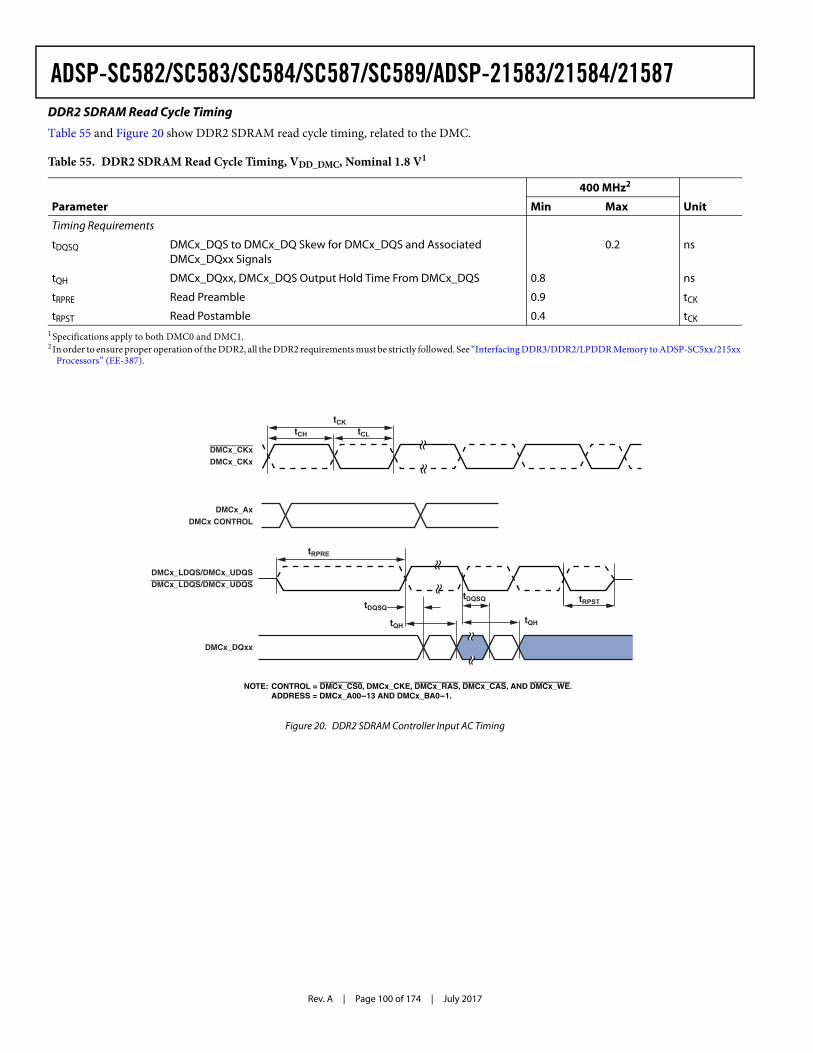
Rev. A | Page 100 of 174 | July 2017
ADSP-SC582/SC583/SC584/SC587/SC589/ADSP-21583/21584/21587DDR2 SDRAM Read Cycle Timing
Table 55 and Figure 20 show DDR2 SDRAM read cycle timing, related to the DMC.
Table 55. DDR2 SDRAM Read Cycle Timing, VDD_DMC, Nominal 1.8 V1
1 Specifications apply to both DMC0 and DMC1.
400 MHz2
2 In order to ensure proper operation of the DDR2, all the DDR2 requirements must be strictly followed. See “Interfacing DDR3/DDR2/LPDDR Memory to ADSP-SC5xx/215xx Processors” (EE-387).
Parameter Min Max Unit
Timing Requirements
tDQSQ DMCx_DQS to DMCx_DQ Skew for DMCx_DQS and Associated DMCx_DQxx Signals
0.2 ns
tQH DMCx_DQxx, DMCx_DQS Output Hold Time From DMCx_DQS 0.8 ns
tRPRE Read Preamble 0.9 tCK
tRPST Read Postamble 0.4 tCK
Figure 20. DDR2 SDRAM Controller Input AC Timing
DMCx_CKx
DMCx_LDQS/DMCx_UDQS
tRPRE
tDQSQtDQSQ
tQH
tRPST
DMCx_DQxx
DMCx_CKx
DMCx_LDQS/DMCx_UDQS
tCKtCH tCL
tQH
DMCx_Ax
DMCx CONTROL
NOTE: CONTROL = DMCx_CS0, DMCx_CKE, DMCx_RAS, DMCx_CAS, AND DMCx_WE. ADDRESS = DMCx_A00-13 AND DMCx_BA0-1.
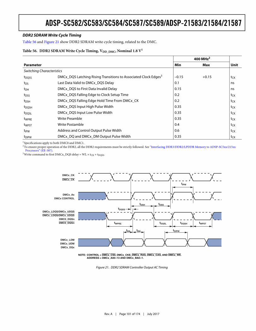
Rev. A | Page 101 of 174 | July 2017
ADSP-SC582/SC583/SC584/SC587/SC589/ADSP-21583/21584/21587DDR2 SDRAM Write Cycle Timing
Table 56 and Figure 21 show DDR2 SDRAM write cycle timing, related to the DMC.
Table 56. DDR2 SDRAM Write Cycle Timing, VDD_DMC, Nominal 1.8 V1
1 Specifications apply to both DMC0 and DMC1.
400 MHz2
2 To ensure proper operation of the DDR2, all the DDR2 requirements must be strictly followed. See “Interfacing DDR3/DDR2/LPDDR Memory to ADSP-SC5xx/215xx Processors” (EE-387).
Parameter Min Max Unit
Switching Characteristics
tDQSS DMCx_DQS Latching Rising Transitions to Associated Clock Edges3
3 Write command to first DMCx_DQS delay = WL × tCK + tDQSS.
–0.15 +0.15 tCK
tDS Last Data Valid to DMCx_DQS Delay 0.1 ns
tDH DMCx_DQS to First Data Invalid Delay 0.15 ns
tDSS DMCx_DQS Falling Edge to Clock Setup Time 0.2 tCK
tDSH DMCx_DQS Falling Edge Hold Time From DMCx_CK 0.2 tCK
tDQSH DMCx_DQS Input High Pulse Width 0.35 tCK
tDQSL DMCx_DQS Input Low Pulse Width 0.35 tCK
tWPRE Write Preamble 0.35 tCK
tWPST Write Postamble 0.4 tCK
tIPW Address and Control Output Pulse Width 0.6 tCK
tDIPW DMCx_DQ and DMCx_DM Output Pulse Width 0.35 tCK
Figure 21. DDR2 SDRAM Controller Output AC Timing
tDS tDH
tDQSS
tDSH tDSS
tWPRE tDQSL tDQSH tWPST
DMCx_CK
tIPW
tDIPW
DMCx_LDQS/DMCx_UDQS
DMCx_LDQS/DMCx_UDQS
DMCx_CK
DMCx_Ax
DMCx CONTROL
DMC0_DQSn
DMC0_DQSn
DMCx_LDM
DMCx_DQx
DMCx_UDM
NOTE: CONTROL = DMCx_CS0, DMCx_CKE, DMCx_RAS, DMCx_CAS, AND DMCx_WE. ADDRESS = DMCx_A00-13 AND DMCx_BA0-1.
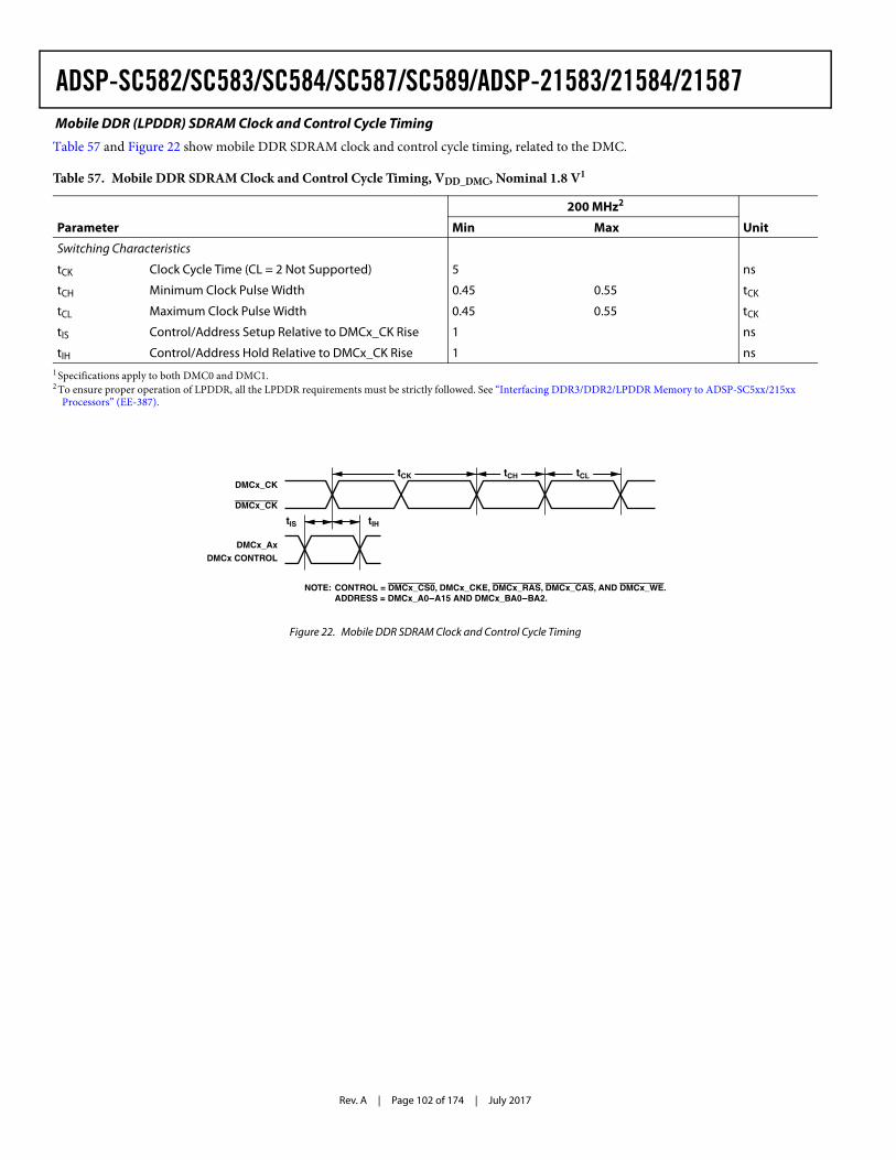
Rev. A | Page 102 of 174 | July 2017
ADSP-SC582/SC583/SC584/SC587/SC589/ADSP-21583/21584/21587 Mobile DDR (LPDDR) SDRAM Clock and Control Cycle Timing
Table 57 and Figure 22 show mobile DDR SDRAM clock and control cycle timing, related to the DMC.
Table 57. Mobile DDR SDRAM Clock and Control Cycle Timing, VDD_DMC, Nominal 1.8 V1
1 Specifications apply to both DMC0 and DMC1.
200 MHz2
2 To ensure proper operation of LPDDR, all the LPDDR requirements must be strictly followed. See “Interfacing DDR3/DDR2/LPDDR Memory to ADSP-SC5xx/215xx Processors” (EE-387).
Parameter Min Max Unit
Switching Characteristics
tCK Clock Cycle Time (CL = 2 Not Supported) 5 ns
tCH Minimum Clock Pulse Width 0.45 0.55 tCK
tCL Maximum Clock Pulse Width 0.45 0.55 tCK
tIS Control/Address Setup Relative to DMCx_CK Rise 1 ns
tIH Control/Address Hold Relative to DMCx_CK Rise 1 ns
Figure 22. Mobile DDR SDRAM Clock and Control Cycle Timing
NOTE: CONTROL = DMCx_CS0, DMCx_CKE, DMCx_RAS, DMCx_CAS, AND DMCx_WE. ADDRESS = DMCx_A0-A15 AND DMCx_BA0-BA2.
DMCx_CK
DMCx_Ax
DMCx CONTROL
tIS tIH
tCK tCH tCL
DMCx_CK
Rev. A | Page 103 of 174 | July 2017
ADSP-SC582/SC583/SC584/SC587/SC589/ADSP-21583/21584/21587Mobile DDR SDRAM Read Cycle Timing
Table 58 and Figure 23 show mobile DDR SDRAM read cycle timing, related to the DMC.
Table 58. Mobile DDR SDRAM Read Cycle Timing, VDD_DMC, Nominal 1.8 V1
1 Specifications apply to both DMC0 and DMC1.
200 MHz2
2 To ensure proper operation of LPDDR, all the LPDDR requirements must be strictly followed. See “Interfacing DDR3/DDR2/LPDDR Memory to ADSP-SC5xx/215xx Processors” (EE-387).
Parameter Min Max Unit
Timing Requirements
tQH DMCx_DQ, DMCx_DQS Output Hold Time From DMCx_DQS 1.75 ns
tDQSQ DMCx_DQS to DMCx_DQ Skew for DMCx_DQS and Associated DMCx_DQ Signals
0.4 ns
tRPRE Read Preamble 0.9 1.1 tCK
tRPST Read Postamble 0.4 0.6 tCK
Figure 23. Mobile DDR SDRAM Controller Input AC Timing
DMCx_CK
DMCx_LDQS/DMCx_HDQS
tDQSQ
DMCx_DQx(DATA)
Dn Dn+1 Dn+2 Dn+3
tRPRE tRPST
tQH
Rev. A | Page 104 of 174 | July 2017
ADSP-SC582/SC583/SC584/SC587/SC589/ADSP-21583/21584/21587Mobile DDR SDRAM Write Cycle Timing
Table 59 and Figure 24 show mobile DDR SDRAM write cycle timing, related to the DMC.
Table 59. Mobile DDR SDRAM Write Cycle Timing, VDD_DMC, Nominal 1.8 V1
1 Specifications apply to both DMC0 and DMC1.
200 MHz2
2 To ensure proper operation of LPDDR, all the LPDDR requirements must be strictly followed. See “Interfacing DDR3/DDR2/LPDDR Memory to ADSP-SC5xx/215xx Processors” (EE-387).
Parameter Min Max Unit
Switching Characteristics
tDQSS3
3 Write command to first DMCx_DQS delay = WL × tCK + tDQSS.
DMCx_DQS Latching Rising Transitions to Associated Clock Edges 0.75 1.25 tCK
tDS Last Data Valid to DMCx_DQS Delay (Slew > 1 V/ns) 0.48 ns
tDH DMCx_DQS to First Data Invalid Delay (Slew > 1 V/ns) 0.48 ns
tDSS DMCx_DQS Falling Edge to Clock Setup Time 0.2 tCK
tDSH DMCx_DQS Falling Edge Hold Time From DMCx_CK 0.2 tCK
tDQSH DMCx_DQS Input High Pulse Width 0.4 tCK
tDQSL DMCx_DQS Input Low Pulse Width 0.4 tCK
tWPRE Write Preamble 0.25 tCK
tWPST Write Postamble 0.4 tCK
tIPW Address and Control Output Pulse Width 2.3 ns
tDIPW DMCx_DQ and DMCx_DM Output Pulse Width 1.8 ns
Figure 24. Mobile DDR SDRAM Controller Output AC Timing
DMCx_CK
DMCx_LDQS/DMCx_HDQS
DMCx_DQ0-15/DMCx_LDQM/DMCx_HDQM
tDQSStDSH tDSS
tDQSL tDQSH tWPST
tWPRE
tDS tDH
tDIPW
DMCx CONTROL Write CMD
Dn Dn+1 Dn+2 Dn+3
NOTE: CONTROL = DMCx_CSx, DMCx_CKE, DMCx_RAS, DMCx_CAS, AND DMCx_WE. ADDRESS = DMCx_A00-13, AND DMCx_BA0-1.
tDIPW
tIPW
Rev. A | Page 105 of 174 | July 2017
ADSP-SC582/SC583/SC584/SC587/SC589/ADSP-21583/21584/21587DDR3 SDRAM Clock and Control Cycle Timing
Table 60 and Figure 25 show mobile DDR3 SDRAM clock and control cycle timing, related to the DMC.
Table 60. DDR3 SDRAM Clock and Control Cycle Timing, VDD_DMC, Nominal 1.5 V1
1 Specifications apply to both DMC0 and DMC1.
450 MHz2
2 To ensure proper operation of the DDR3, all the DDR3 requirements must be strictly followed. See “Interfacing DDR3/DDR2/LPDDR Memory to ADSP-SC5xx/215xx Processors” (EE-387).
Parameter Min Max Unit
Switching Characteristics
tCK Clock Cycle Time (CL = 2 Not Supported) 2.22 ns
tCH(abs)3
3 As per JESD79-3F definition.
Minimum Clock Pulse Width 0.43 0.57 tCK
tCL(abs)3 Maximum Clock Pulse Width 0.43 0.57 tCK
tIS Control/Address Setup Relative to DMCx_CK Rise 0.2 ns
tIH Control/Address Hold Relative to DMCx_CK Rise 0.275 ns
Figure 25. DDR3 SDRAM Clock and Control Cycle Timing
NOTE: CONTROL = DMCx_CS0, DMCx_CKE, DMCx_RAS, DMCx_CAS, AND DMCx_WE. ADDRESS = DMCx_A0-A15 AND DMCx_BA0-BA2.
DMCx_CK
DMCx_Ax
DMCx CONTROL
tIS tIH
tCK tCH tCL
DMCx_CK
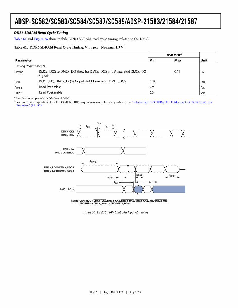
Rev. A | Page 106 of 174 | July 2017
ADSP-SC582/SC583/SC584/SC587/SC589/ADSP-21583/21584/21587DDR3 SDRAM Read Cycle Timing
Table 61 and Figure 26 show mobile DDR3 SDRAM read cycle timing, related to the DMC.
Table 61. DDR3 SDRAM Read Cycle Timing, VDD_DMC, Nominal 1.5 V1
1 Specifications apply to both DMC0 and DMC1.
450 MHz2
2 To ensure proper operation of the DDR3, all the DDR3 requirements must be strictly followed. See “Interfacing DDR3/DDR2/LPDDR Memory to ADSP-SC5xx/215xx Processors” (EE-387).
Parameter Min Max Unit
Timing Requirements
tDQSQ DMCx_DQS to DMCx_DQ Skew for DMCx_DQS and Associated DMCx_DQ Signals
0.15 ns
tQH DMCx_DQ, DMCx_DQS Output Hold Time From DMCx_DQS 0.38 tCK
tRPRE Read Preamble 0.9 tCK
tRPST Read Postamble 0.3 tCK
Figure 26. DDR3 SDRAM Controller Input AC Timing
DMCx_CKx
DMCx_LDQS/DMCx_UDQS
tRPRE
tDQSQtDQSQ
tQH
tRPST
DMCx_DQxx
DMCx_CKx
DMCx_LDQS/DMCx_UDQS
tCKtCH tCL
tQH
DMCx_Ax
DMCx CONTROL
NOTE: CONTROL = DMCx_CS0, DMCx_CKE, DMCx_RAS, DMCx_CAS, AND DMCx_WE. ADDRESS = DMCx_A00-13 AND DMCx_BA0-1.
Rev. A | Page 107 of 174 | July 2017
ADSP-SC582/SC583/SC584/SC587/SC589/ADSP-21583/21584/21587DDR3 SDRAM Write Cycle Timing
Table 62 and Figure 27 show mobile DDR3 SDRAM output ac timing, related to the DMC.
Table 62. DDR3 SDRAM Write Cycle Timing, VDD_DMC, Nominal 1.5 V1
1 Specifications apply to both DMC0 and DMC1.
450 MHz2
2 To ensure proper operation of the DDR3, all the DDR3 requirements must be strictly followed. See “Interfacing DDR3/DDR2/LPDDR Memory to ADSP-SC5xx/215xx Processors” (EE-387).
Parameter Min Max Unit
Switching Characteristics
tDQSS DMCx_DQS Latching Rising Transitions to Associated Clock Edges3
3 Write command to first DMCx_DQS delay = WL × tCK + tDQSS.
–0.25 0.25 tCK
tDS Last Data Valid to DMCx_DQS Delay (Slew > 1 V/ns) 0.125 ns
tDH DMCx_DQS to First Data Invalid Delay (Slew > 1 V/ns) 0.150 ns
tDSS DMCx_DQS Falling Edge to Clock Setup Time 0.2 tCK
tDSH DMCx_DQS Falling Edge Hold Time From DMCx_CK 0.2 tCK
tDQSH DMCx_DQS Input High Pulse Width 0.45 0.55 tCK
tDQSL DMCx_DQS Input Low Pulse Width 0.45 0.55 tCK
tWPRE Write Preamble 0.9 tCK
tWPST Write Postamble 0.3 tCK
tIPW Address and Control Output Pulse Width 0.840 ns
tDIPW DMCx_DQ and DMCx_DM Output Pulse Width 0.550 ns
Figure 27. DDR3 SDRAM Controller Output AC Timing
tDS tDH
tDQSS
tDSH tDSS
tWPRE
tDQSL tDQSH tWPST
DMCx_CK
tIPW
tDIPW
DMCx_LDQS/DMCx_UDQS
DMCx_LDQS/DMCx_UDQS
DMCx_CK
DMCx_Ax
DMCx CONTROL
DMC0_DQSn
DMC0_DQSn
DMCx_LDM
DMCx_DQx
DMCx_UDM
NOTE: CONTROL = DMCx_CS0, DMCx_CKE, DMCx_RAS, DMCx_CAS, AND DMCx_WE. ADDRESS = DMCx_A00-13, AND DMCx_BA0-1.
Rev. A | Page 108 of 174 | July 2017
ADSP-SC582/SC583/SC584/SC587/SC589/ADSP-21583/21584/21587Enhanced Parallel Peripheral Interface (EPPI) Timing
Table 63 and Table 64 and Figure 28 through Figure 36 describe enhanced parallel peripheral interface (EPPI) timing operations. In Figure 28 through Figure 36, POLC[1:0] represents the setting of the EPPI_CTL register, which sets the sampling/driving edges of the EPPI clock.When internally generated, the programmed PPI clock (fPCLKPROG) frequency in MHz is set by the following equation where VALUE is a field in the EPPI_CLKDIV register that can be set from 0 to 65535:
When externally generated, the EPPI_CLK is called fPCLKEXT:
Table 63. Enhanced Parallel Peripheral Interface (EPPI)—Internal Clock
Parameter Min Max Unit
Timing Requirements
tSFSPI External FS Setup Before EPPI_CLK 6.5 ns
tHFSPI External FS Hold After EPPI_CLK 0 ns
tSDRPI Receive Data Setup Before EPPI_CLK 6.5 ns
tHDRPI Receive Data Hold After EPPI_CLK 0 ns
tSFS3GI External FS3 Input Setup Before EPPI_CLK Fall Edge in Clock Gating Mode
14 ns
tHFS3GI External FS3 Input Hold Before EPPI_CLK Fall Edge in Clock Gating Mode
0 ns
Switching Characteristics
tPCLKW EPPI_CLK Width1
1 See Table 29 for details on the minimum period that can be programmed for tPCLKPROG.
0.5 × tPCLKPROG – 1.5 ns
tPCLK EPPI_CLK Period1 tPCLKPROG – 1.5 ns
tDFSPI Internal FS Delay After EPPI_CLK 3.5 ns
tHOFSPI Internal FS Hold After EPPI_CLK –0.5 ns
tDDTPI Transmit Data Delay After EPPI_CLK 3.5 ns
tHDTPI Transmit Data Hold After EPPI_CLK –0.5 ns
fPCLKPROGfSCLK0
VALUE 1+ ----------------------=
tPCLKPROG1
fPCLKPROG-----------------=
tPCLKEXT1
fPCLKEXT--------------=
Rev. A | Page 109 of 174 | July 2017
ADSP-SC582/SC583/SC584/SC587/SC589/ADSP-21583/21584/21587
Figure 28. EPPI Internal Clock GP Receive Mode with Internal Frame Sync Timing
Figure 29. EPPI Internal Clock GP Transmit Mode with Internal Frame Sync Timing
Figure 30. EPPI Internal Clock GP Receive Mode with External Frame Sync Timing
tHDRPItSDRPI
tHOFSPI
FRAME SYNCDRIVEN
DATASAMPLED
tDFSPItPCLK
tPCLKW
EPPI_D00-23
EPPI_FS1/2
EPPI_CLK
POLC[1:0] = 10
POLC[1:0] = 01
tHOFSPI
FRAME SYNCDRIVEN
DATADRIVEN
tDFSPI
tDDTPI tHDTPI
tPCLK
tPCLKW
DATADRIVEN
EPPI_D00-23
EPPI_FS1/2
EPPI_CLK
POLC[1:0] = 11
POLC[1:0] = 00
tPCLKtSFSPI
DATA SAMPLED /FRAME SYNC SAMPLED
DATA SAMPLED /FRAME SYNC SAMPLED
EPPI_D00-23
EPPI_FS1/2
tHFSPI
tHDRPItSDRPI
tPCLKW
EPPI_CLK
POLC[1:0] = 11
POLC[1:0] = 00
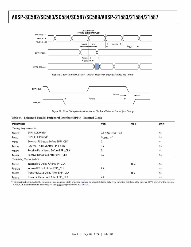
Rev. A | Page 110 of 174 | July 2017
ADSP-SC582/SC583/SC584/SC587/SC589/ADSP-21583/21584/21587
Figure 31. EPPI Internal Clock GP Transmit Mode with External Frame Sync Timing
Figure 32. Clock Gating Mode with Internal Clock and External Frame Sync Timing
Table 64. Enhanced Parallel Peripheral Interface (EPPI)—External Clock
Parameter Min Max Unit
Timing Requirements
tPCLKW EPPI_CLK Width1 0.5 × tPCLKEXT – 0.5 ns
tPCLK EPPI_CLK Period1 tPCLKEXT – 1 ns
tSFSPE External FS Setup Before EPPI_CLK 2 ns
tHFSPE External FS Hold After EPPI_CLK 3.7 ns
tSDRPE Receive Data Setup Before EPPI_CLK 2 ns
tHDRPE Receive Data Hold After EPPI_CLK 3.7 ns
Switching Characteristics
tDFSPE Internal FS Delay After EPPI_CLK 15.3 ns
tHOFSPE Internal FS Hold After EPPI_CLK 2.4 ns
tDDTPE Transmit Data Delay After EPPI_CLK 15.3 ns
tHDTPE Transmit Data Hold After EPPI_CLK 2.4 ns1 This specification indicates the minimum instantaneous width or period that can be tolerated due to duty cycle variation or jitter on the external EPPI_CLK. For the external
EPPI_CLK ideal maximum frequency see the fPCLKEXT specification in Table 29.
tHDTPI
tSFSPI
DATA DRIVEN /FRAME SYNC SAMPLED
tHFSPI
tDDTPI
tPCLK
tPCLKW
EPPI_D00-23
EPPI_FS1/2
EPPI_CLK
POLC[1:0] = 11
POLC[1:0] = 00
EPPI_CLK
tSFS3GI
EPPI_FS3
tHFS3GI
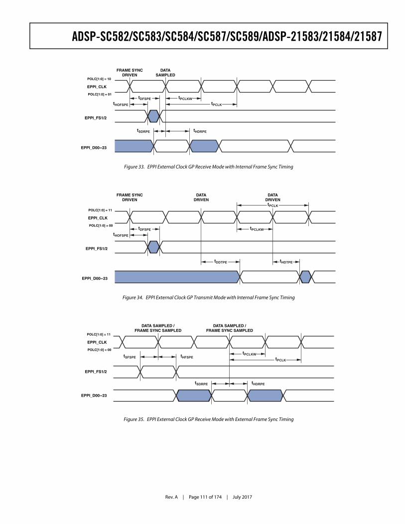
Rev. A | Page 111 of 174 | July 2017
ADSP-SC582/SC583/SC584/SC587/SC589/ADSP-21583/21584/21587
Figure 33. EPPI External Clock GP Receive Mode with Internal Frame Sync Timing
Figure 34. EPPI External Clock GP Transmit Mode with Internal Frame Sync Timing
Figure 35. EPPI External Clock GP Receive Mode with External Frame Sync Timing
tHDRPEtSDRPE
tHOFSPE
FRAME SYNCDRIVEN
DATASAMPLED
tDFSPEtPCLK
tPCLKW
EPPI_D00-23
EPPI_FS1/2
EPPI_CLK
POLC[1:0] = 10
POLC[1:0] = 01
tHOFSPE
FRAME SYNCDRIVEN
DATADRIVEN
tDFSPE
tDDTPE tHDTPE
tPCLK
tPCLKW
DATADRIVEN
EPPI_D00-23
EPPI_FS1/2
EPPI_CLK
POLC[1:0] = 11
POLC[1:0] = 00
tPCLKtSFSPE
DATA SAMPLED /FRAME SYNC SAMPLED
DATA SAMPLED /FRAME SYNC SAMPLED
EPPI_D00-23
EPPI_FS1/2
tHFSPE
tHDRPEtSDRPE
tPCLKW
EPPI_CLK
POLC[1:0] = 11
POLC[1:0] = 00
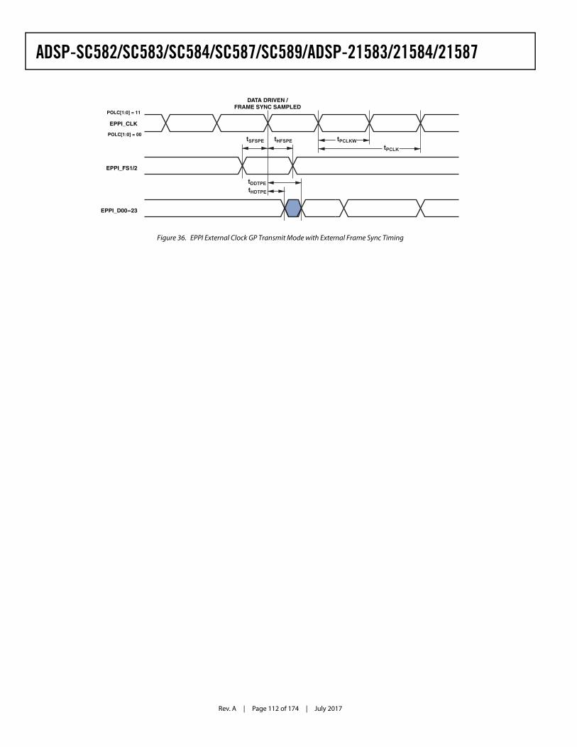
Rev. A | Page 112 of 174 | July 2017
ADSP-SC582/SC583/SC584/SC587/SC589/ADSP-21583/21584/21587
Figure 36. EPPI External Clock GP Transmit Mode with External Frame Sync Timing
tHDTPE
tSFSPE
DATA DRIVEN /FRAME SYNC SAMPLED
tHFSPE
tDDTPE
tPCLK
tPCLKW
EPPI_D00-23
EPPI_FS1/2
EPPI_CLK
POLC[1:0] = 11
POLC[1:0] = 00
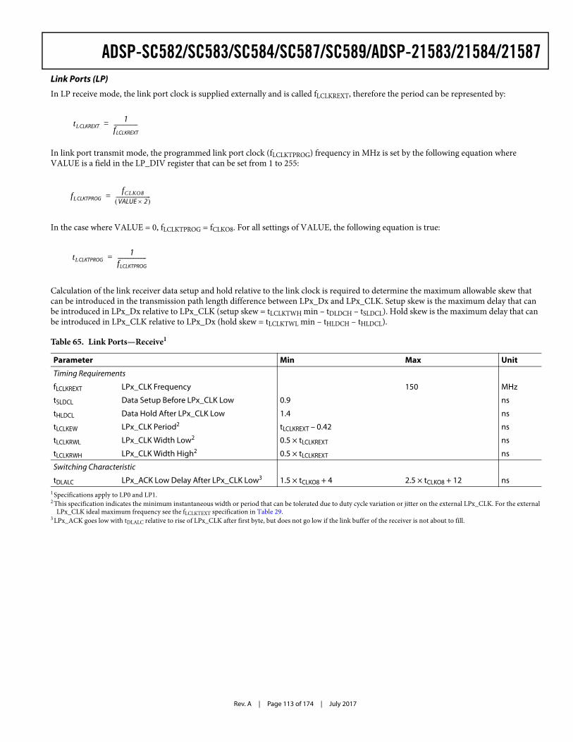
Rev. A | Page 113 of 174 | July 2017
ADSP-SC582/SC583/SC584/SC587/SC589/ADSP-21583/21584/21587Link Ports (LP)
In LP receive mode, the link port clock is supplied externally and is called fLCLKREXT, therefore the period can be represented by:
In link port transmit mode, the programmed link port clock (fLCLKTPROG) frequency in MHz is set by the following equation where VALUE is a field in the LP_DIV register that can be set from 1 to 255:
In the case where VALUE = 0, fLCLKTPROG = fCLKO8. For all settings of VALUE, the following equation is true:
Calculation of the link receiver data setup and hold relative to the link clock is required to determine the maximum allowable skew that can be introduced in the transmission path length difference between LPx_Dx and LPx_CLK. Setup skew is the maximum delay that can be introduced in LPx_Dx relative to LPx_CLK (setup skew = tLCLKTWH min – tDLDCH – tSLDCL). Hold skew is the maximum delay that can be introduced in LPx_CLK relative to LPx_Dx (hold skew = tLCLKTWL min – tHLDCH – tHLDCL).
Table 65. Link Ports—Receive1
1 Specifications apply to LP0 and LP1.
Parameter Min Max Unit
Timing Requirements
fLCLKREXT LPx_CLK Frequency 150 MHz
tSLDCL Data Setup Before LPx_CLK Low 0.9 ns
tHLDCL Data Hold After LPx_CLK Low 1.4 ns
tLCLKEW LPx_CLK Period2
2 This specification indicates the minimum instantaneous width or period that can be tolerated due to duty cycle variation or jitter on the external LPx_CLK. For the external LPx_CLK ideal maximum frequency see the fLCLKTEXT specification in Table 29.
tLCLKREXT – 0.42 ns
tLCLKRWL LPx_CLK Width Low2 0.5 × tLCLKREXT ns
tLCLKRWH LPx_CLK Width High2 0.5 × tLCLKREXT ns
Switching Characteristic
tDLALC LPx_ACK Low Delay After LPx_CLK Low3
3 LPx_ACK goes low with tDLALC relative to rise of LPx_CLK after first byte, but does not go low if the link buffer of the receiver is not about to fill.
1.5 × tCLKO8 + 4 2.5 × tCLKO8 + 12 ns
tLCLKREXT1
fLCLKREXT---------------=
fLCLKTPROGfCLKO8
VALUE 2 ----------------------=
tLCLKTPROG1
fLCLKTPROG------------------=
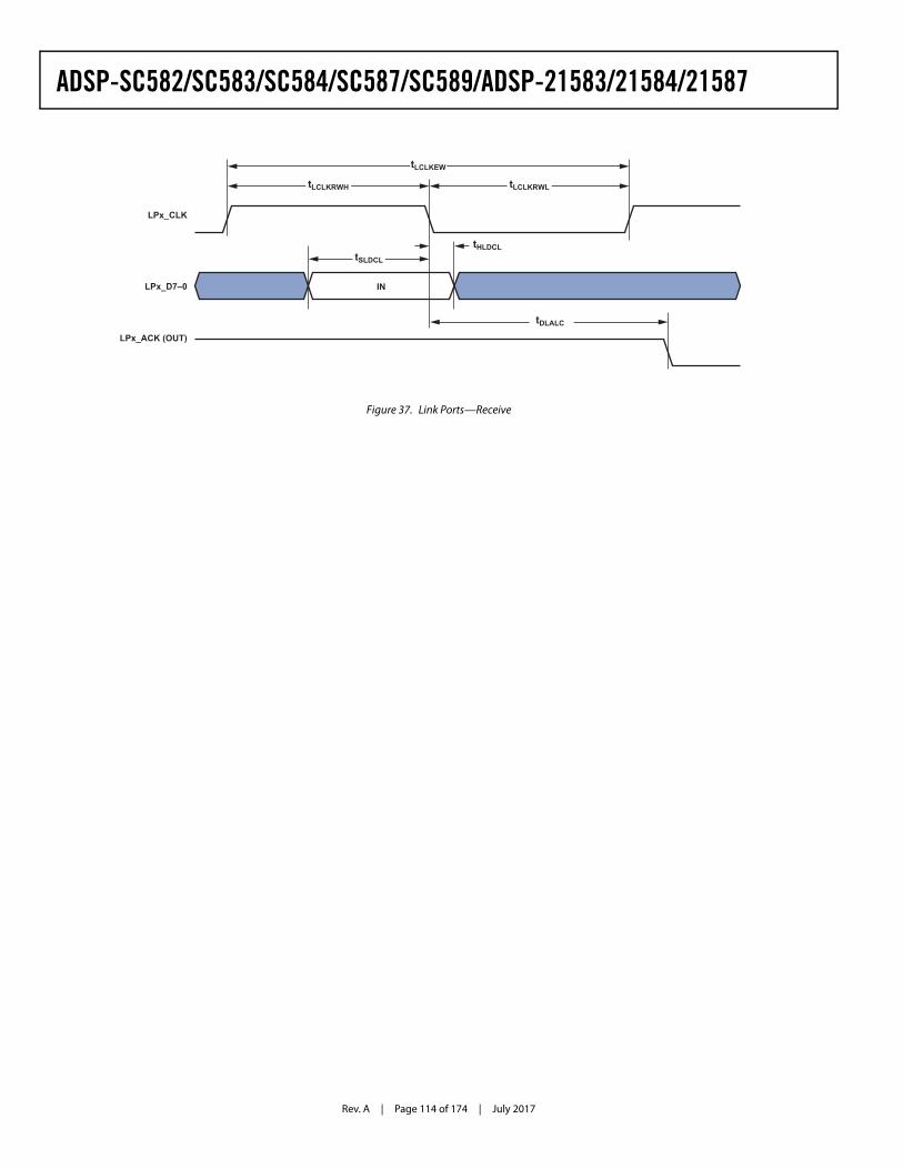
Rev. A | Page 114 of 174 | July 2017
ADSP-SC582/SC583/SC584/SC587/SC589/ADSP-21583/21584/21587
Figure 37. Link Ports—Receive
tHLDCLtSLDCL
IN
tLCLKRWH tLCLKRWL
tLCLKEW
tDLALC
LPx_CLK
LPx_D7–0
LPx_ACK (OUT)
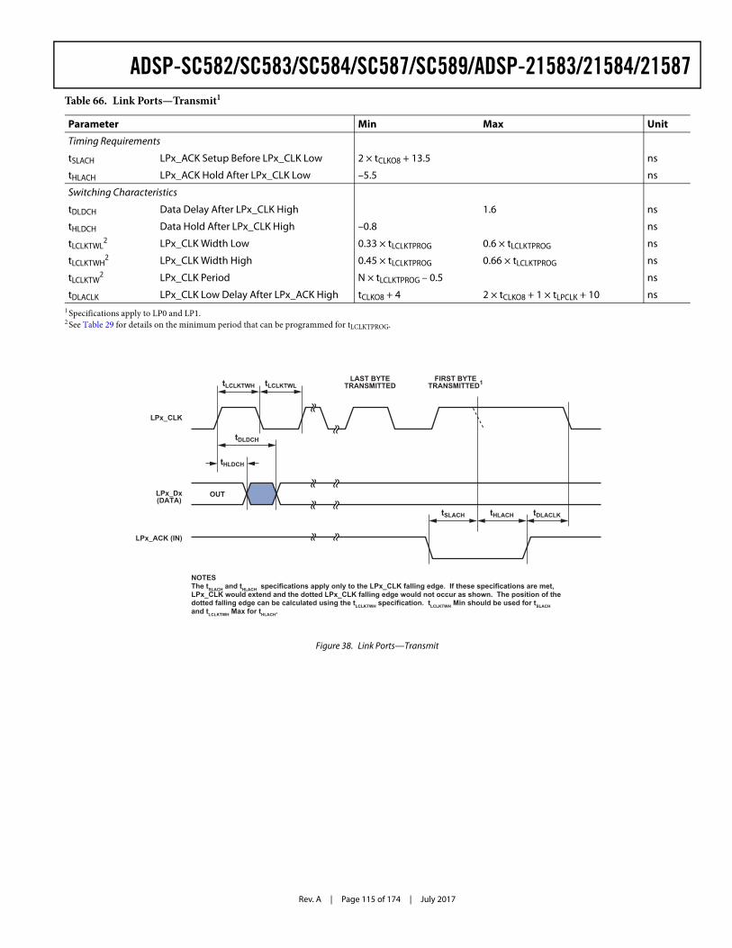
Rev. A | Page 115 of 174 | July 2017
ADSP-SC582/SC583/SC584/SC587/SC589/ADSP-21583/21584/21587Table 66. Link Ports—Transmit1
Parameter Min Max Unit
Timing Requirements
tSLACH LPx_ACK Setup Before LPx_CLK Low 2 × tCLKO8 + 13.5 ns
tHLACH LPx_ACK Hold After LPx_CLK Low –5.5 ns
Switching Characteristics
tDLDCH Data Delay After LPx_CLK High 1.6 ns
tHLDCH Data Hold After LPx_CLK High –0.8 ns
tLCLKTWL2 LPx_CLK Width Low 0.33 × tLCLKTPROG 0.6 × tLCLKTPROG ns
tLCLKTWH2 LPx_CLK Width High 0.45 × tLCLKTPROG 0.66 × tLCLKTPROG ns
tLCLKTW2 LPx_CLK Period N × tLCLKTPROG – 0.5 ns
tDLACLK LPx_CLK Low Delay After LPx_ACK High tCLKO8 + 4 2 × tCLKO8 + 1 × tLPCLK + 10 ns 1 Specifications apply to LP0 and LP1.2 See Table 29 for details on the minimum period that can be programmed for tLCLKTPROG.
Figure 38. Link Ports—Transmit
LPx_CLK
LPx_Dx(DATA)
LPx_ACK (IN)
OUT
tDLDCH
tHLDCH
tSLACH tHLACH tDLACLK
tLCLKTWH tLCLKTWLLAST BYTE
TRANSMITTEDFIRST BYTE
TRANSMITTED1
NOTESThe tSLACH and tHLACH specifications apply only to the LPx_CLK falling edge. If these specifications are met, LPx_CLK would extend and the dotted LPx_CLK falling edge would not occur as shown. The position of the dotted falling edge can be calculated using the tLCLKTWH specification. tLCLKTWH Min should be used for tSLACH and tLCLKTWH Max for tHLACH.
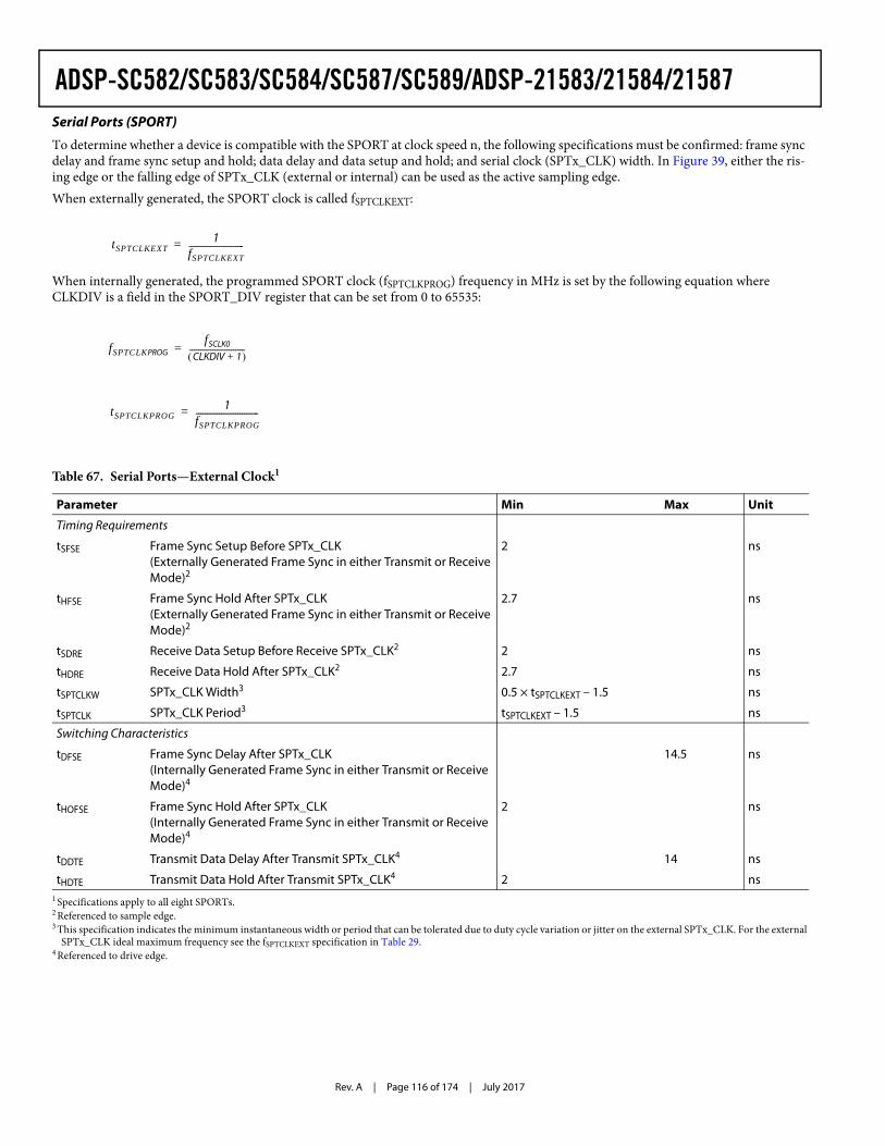
Rev. A | Page 116 of 174 | July 2017
ADSP-SC582/SC583/SC584/SC587/SC589/ADSP-21583/21584/21587Serial Ports (SPORT)
To determine whether a device is compatible with the SPORT at clock speed n, the following specifications must be confirmed: frame sync delay and frame sync setup and hold; data delay and data setup and hold; and serial clock (SPTx_CLK) width. In Figure 39, either the ris-ing edge or the falling edge of SPTx_CLK (external or internal) can be used as the active sampling edge. When externally generated, the SPORT clock is called fSPTCLKEXT:
When internally generated, the programmed SPORT clock (fSPTCLKPROG) frequency in MHz is set by the following equation where CLKDIV is a field in the SPORT_DIV register that can be set from 0 to 65535:
Table 67. Serial Ports—External Clock1
1 Specifications apply to all eight SPORTs.
Parameter Min Max Unit
Timing Requirements
tSFSE Frame Sync Setup Before SPTx_CLK (Externally Generated Frame Sync in either Transmit or Receive Mode)2
2 Referenced to sample edge.
2 ns
tHFSE Frame Sync Hold After SPTx_CLK (Externally Generated Frame Sync in either Transmit or Receive Mode)2
2.7 ns
tSDRE Receive Data Setup Before Receive SPTx_CLK2 2 ns
tHDRE Receive Data Hold After SPTx_CLK2 2.7 ns
tSPTCLKW SPTx_CLK Width3
3 This specification indicates the minimum instantaneous width or period that can be tolerated due to duty cycle variation or jitter on the external SPTx_CLK. For the external SPTx_CLK ideal maximum frequency see the fSPTCLKEXT specification in Table 29.
0.5 × tSPTCLKEXT – 1.5 ns
tSPTCLK SPTx_CLK Period3 tSPTCLKEXT – 1.5 ns
Switching Characteristics
tDFSE Frame Sync Delay After SPTx_CLK (Internally Generated Frame Sync in either Transmit or Receive Mode)4
4 Referenced to drive edge.
14.5 ns
tHOFSE Frame Sync Hold After SPTx_CLK (Internally Generated Frame Sync in either Transmit or Receive Mode)4
2 ns
tDDTE Transmit Data Delay After Transmit SPTx_CLK4 14 ns
tHDTE Transmit Data Hold After Transmit SPTx_CLK4 2 ns
tSPTCLKEXT1
fSPTCLKEXT------------------------=
fSPTCLKPROGfSCLK0
CLKDIV 1+ ------------------------=
tSPTCLKPROG1
fSPTCLKPROG---------------------------=
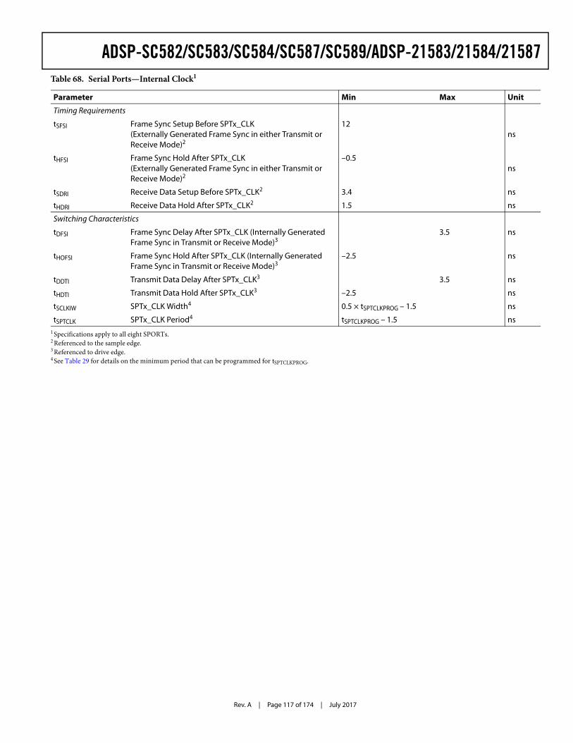
Rev. A | Page 117 of 174 | July 2017
ADSP-SC582/SC583/SC584/SC587/SC589/ADSP-21583/21584/21587Table 68. Serial Ports—Internal Clock1
Parameter Min Max Unit
Timing Requirements
tSFSI Frame Sync Setup Before SPTx_CLK(Externally Generated Frame Sync in either Transmit or Receive Mode)2
12ns
tHFSI Frame Sync Hold After SPTx_CLK(Externally Generated Frame Sync in either Transmit or Receive Mode)2
–0.5ns
tSDRI Receive Data Setup Before SPTx_CLK2 3.4 ns
tHDRI Receive Data Hold After SPTx_CLK2 1.5 ns
Switching Characteristics
tDFSI Frame Sync Delay After SPTx_CLK (Internally Generated Frame Sync in Transmit or Receive Mode)3
3.5 ns
tHOFSI Frame Sync Hold After SPTx_CLK (Internally Generated Frame Sync in Transmit or Receive Mode)3
–2.5 ns
tDDTI Transmit Data Delay After SPTx_CLK3 3.5 ns
tHDTI Transmit Data Hold After SPTx_CLK3 –2.5 ns
tSCLKIW SPTx_CLK Width4 0.5 × tSPTCLKPROG – 1.5 ns
tSPTCLK SPTx_CLK Period4 tSPTCLKPROG – 1.5 ns1 Specifications apply to all eight SPORTs.2 Referenced to the sample edge.3 Referenced to drive edge.4 See Table 29 for details on the minimum period that can be programmed for tSPTCLKPROG.
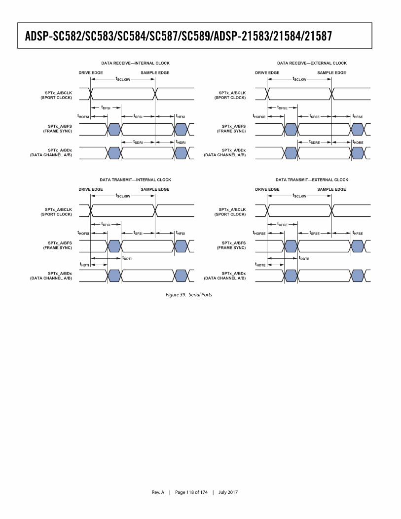
Rev. A | Page 118 of 174 | July 2017
ADSP-SC582/SC583/SC584/SC587/SC589/ADSP-21583/21584/21587
Figure 39. Serial Ports
DRIVE EDGE SAMPLE EDGE
SPTx_A/BDx(DATA CHANNEL A/B)
SPTx_A/BFS(FRAME SYNC)
SPTx_A/BCLK(SPORT CLOCK)
tHOFSI tHFSI
tHDRI
DATA RECEIVE—INTERNAL CLOCK
DRIVE EDGE SAMPLE EDGE
tHFSI
tDDTI
DATA TRANSMIT—INTERNAL CLOCK
DRIVE EDGE SAMPLE EDGE
tHOFSEtHOFSI
tHDTI
tHFSE
tHDTE
tDDTE
DATA TRANSMIT—EXTERNAL CLOCK
DRIVE EDGE SAMPLE EDGE
tHOFSE tHFSE
tHDRE
DATA RECEIVE—EXTERNAL CLOCK
tSCLKIW
tDFSI
tSFSI
tSDRI
tSCLKW
tDFSE
tSFSE
tSDRE
tDFSE
tSFSEtSFSI
tDFSI
tSCLKIW tSCLKW
SPTx_A/BDx(DATA CHANNEL A/B)
SPTx_A/BFS(FRAME SYNC)
SPTx_A/BCLK(SPORT CLOCK)
SPTx_A/BDx(DATA CHANNEL A/B)
SPTx_A/BFS(FRAME SYNC)
SPTx_A/BCLK(SPORT CLOCK)
SPTx_A/BDx(DATA CHANNEL A/B)
SPTx_A/BFS(FRAME SYNC)
SPTx_A/BCLK(SPORT CLOCK)
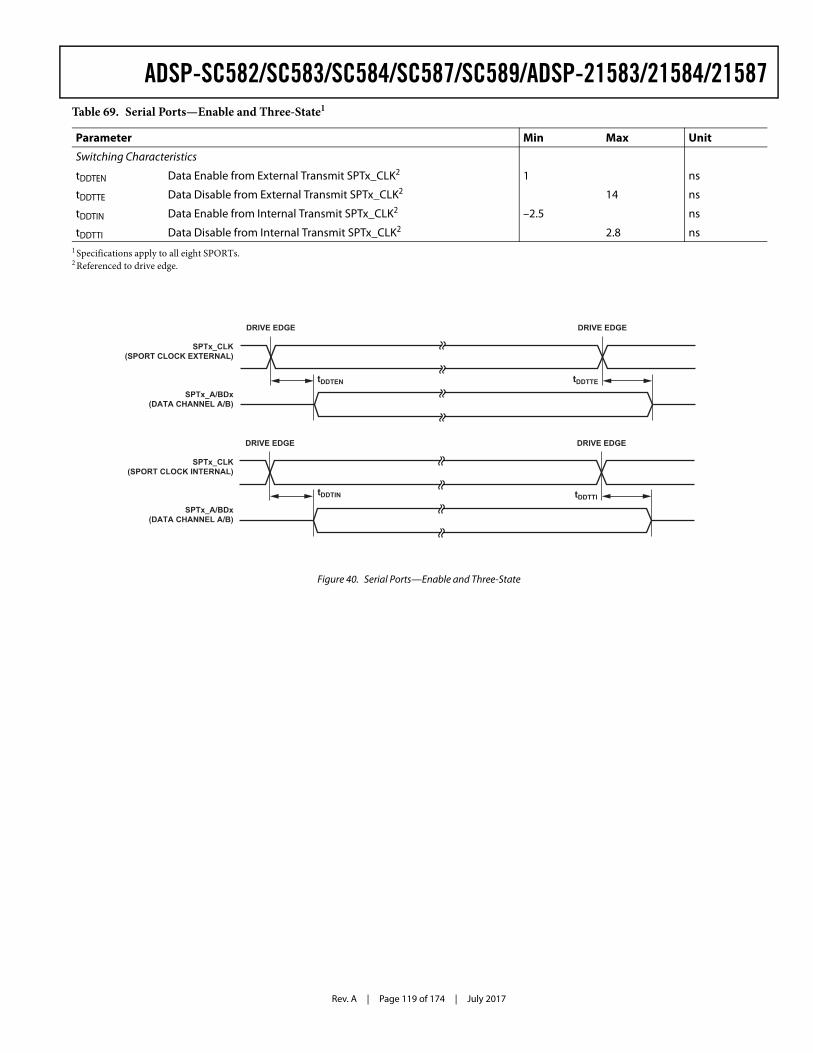
Rev. A | Page 119 of 174 | July 2017
ADSP-SC582/SC583/SC584/SC587/SC589/ADSP-21583/21584/21587Table 69. Serial Ports—Enable and Three-State1
Parameter Min Max Unit
Switching Characteristics
tDDTEN Data Enable from External Transmit SPTx_CLK2 1 ns
tDDTTE Data Disable from External Transmit SPTx_CLK2 14 ns
tDDTIN Data Enable from Internal Transmit SPTx_CLK2 –2.5 ns
tDDTTI Data Disable from Internal Transmit SPTx_CLK2 2.8 ns 1 Specifications apply to all eight SPORTs.2 Referenced to drive edge.
Figure 40. Serial Ports—Enable and Three-State
DRIVE EDGE DRIVE EDGE
tDDTIN
tDDTEN tDDTTE
SPTx_CLK(SPORT CLOCK INTERNAL)
SPTx_A/BDx(DATA CHANNEL A/B)
SPTx_CLK(SPORT CLOCK EXTERNAL)
SPTx_A/BDx(DATA CHANNEL A/B)
DRIVE EDGE DRIVE EDGE
tDDTTI
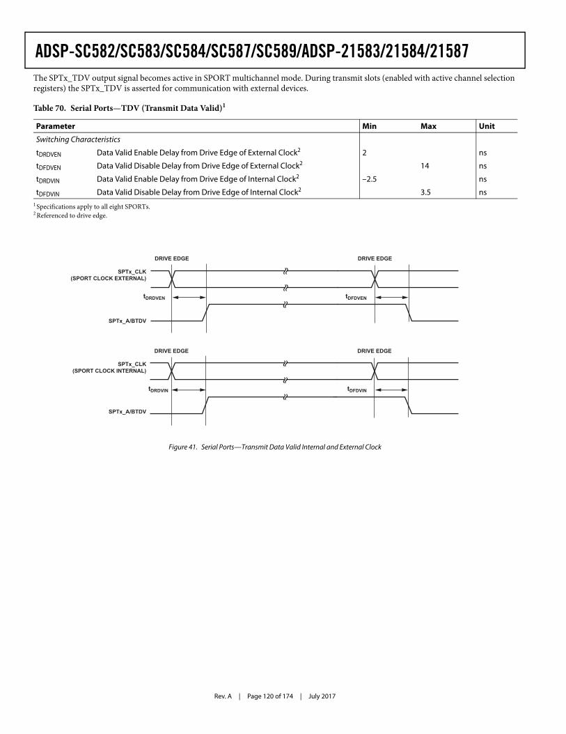
Rev. A | Page 120 of 174 | July 2017
ADSP-SC582/SC583/SC584/SC587/SC589/ADSP-21583/21584/21587The SPTx_TDV output signal becomes active in SPORT multichannel mode. During transmit slots (enabled with active channel selection registers) the SPTx_TDV is asserted for communication with external devices.
Table 70. Serial Ports—TDV (Transmit Data Valid)1
1 Specifications apply to all eight SPORTs.
Parameter Min Max Unit
Switching Characteristics
tDRDVEN Data Valid Enable Delay from Drive Edge of External Clock2
2 Referenced to drive edge.
2 ns
tDFDVEN Data Valid Disable Delay from Drive Edge of External Clock2 14 ns
tDRDVIN Data Valid Enable Delay from Drive Edge of Internal Clock2 –2.5 ns
tDFDVIN Data Valid Disable Delay from Drive Edge of Internal Clock2 3.5 ns
Figure 41. Serial Ports—Transmit Data Valid Internal and External Clock
DRIVE EDGE DRIVE EDGE
SPTx_CLK(SPORT CLOCK EXTERNAL)
tDRDVEN tDFDVEN
DRIVE EDGE DRIVE EDGE
SPTx_CLK(SPORT CLOCK INTERNAL)
tDRDVIN tDFDVIN
SPTx_A/BTDV
SPTx_A/BTDV
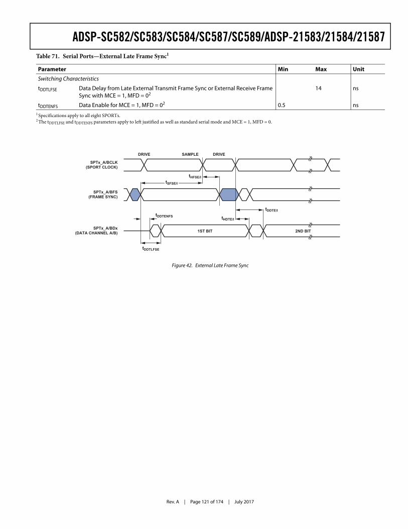
Rev. A | Page 121 of 174 | July 2017
ADSP-SC582/SC583/SC584/SC587/SC589/ADSP-21583/21584/21587Table 71. Serial Ports—External Late Frame Sync1
Parameter Min Max Unit
Switching Characteristics
tDDTLFSE Data Delay from Late External Transmit Frame Sync or External Receive Frame Sync with MCE = 1, MFD = 02
14 ns
tDDTENFS Data Enable for MCE = 1, MFD = 02 0.5 ns1 Specifications apply to all eight SPORTs.2 The tDDTLFSE and tDDTENFS parameters apply to left justified as well as standard serial mode and MCE = 1, MFD = 0.
Figure 42. External Late Frame Sync
DRIVE SAMPLE
2ND BIT1ST BIT
DRIVE
tDDTE/I
tHDTE/I
tDDTLFSE
tDDTENFS
tSFSE/I
tHFSE/I
SPTx_A/BDx(DATA CHANNEL A/B)
SPTx_A/BFS(FRAME SYNC)
SPTx_A/BCLK(SPORT CLOCK)
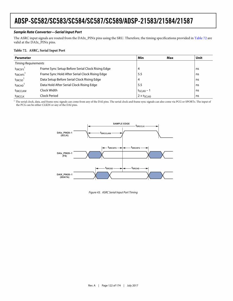
Rev. A | Page 122 of 174 | July 2017
ADSP-SC582/SC583/SC584/SC587/SC589/ADSP-21583/21584/21587Sample Rate Converter—Serial Input Port
The ASRC input signals are routed from the DAIx_PINx pins using the SRU. Therefore, the timing specifications provided in Table 72 are valid at the DAIx_PINx pins.
Table 72. ASRC, Serial Input Port
Parameter Min Max Unit
Timing Requirements
tSRCSFS1
1 The serial clock, data, and frame sync signals can come from any of the DAI pins. The serial clock and frame sync signals can also come via PCG or SPORTs. The input of the PCG can be either CLKIN or any of the DAI pins.
Frame Sync Setup Before Serial Clock Rising Edge 4 ns
tSRCHFS1 Frame Sync Hold After Serial Clock Rising Edge 5.5 ns
tSRCSD1 Data Setup Before Serial Clock Rising Edge 4 ns
tSRCHD1 Data Hold After Serial Clock Rising Edge 5.5 ns
tSRCCLKW Clock Width tSCLK0 – 1 ns
tSRCCLK Clock Period 2 × tSCLK0 ns
Figure 43. ASRC Serial Input Port Timing
DAIx_PIN20–1(SCLK)
SAMPLE EDGE
DAIx_PIN20–1(FS)
DAIX_PIN20–1(SDATA)
tSRCCLK
tSRCCLKW
tSRCSFS tSRCHFS
tSRCHDtSRCSD
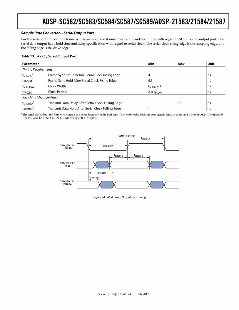
Rev. A | Page 123 of 174 | July 2017
ADSP-SC582/SC583/SC584/SC587/SC589/ADSP-21583/21584/21587Sample Rate Converter—Serial Output Port
For the serial output port, the frame sync is an input and it must meet setup and hold times with regard to SCLK on the output port. The serial data output has a hold time and delay specification with regard to serial clock. The serial clock rising edge is the sampling edge, and the falling edge is the drive edge.
Figure 44. ASRC Serial Output Port Timing
Table 73. ASRC, Serial Output Port
Parameter Min Max Unit
Timing Requirements
tSRCSFS1
1 The serial clock, data, and frame sync signals can come from any of the DAI pins. The serial clock and frame sync signals can also come via PCG or SPORTs. The input of the PCG can be either CLKIN, SCLK0, or any of the DAI pins.
Frame Sync Setup Before Serial Clock Rising Edge 4 ns
tSRCHFS1 Frame Sync Hold After Serial Clock Rising Edge 5.5 ns
tSRCCLKW Clock Width tSCLK0 – 1 ns
tSRCCLK Clock Period 2 × tSCLK0 ns
Switching Characteristics
tSRCTDD1 Transmit Data Delay After Serial Clock Falling Edge 13 ns
tSRCTDH1 Transmit Data Hold After Serial Clock Falling Edge 1 ns
DAIx_PIN20–1(SCLK)
SAMPLE EDGE
DAIx_PIN20–1(FS)
DAIx_PIN20–1(SDATA)
tSRCCLK
tSRCCLKW
tSRCSFS tSRCHFS
tSRCTDD
tSRCTDH
Rev. A | Page 124 of 174 | July 2017
ADSP-SC582/SC583/SC584/SC587/SC589/ADSP-21583/21584/21587SPI Port—Master Timing
Table 74 and Figure 45 describe SPI port master operations.When internally generated, the programmed SPI clock (fSPICLKPROG) frequency in MHz is set by the following equation where BAUD is a field in the SPIx_CLK register that can be set from 0 to 65535:
Note that • In dual-mode data transmit, the SPIx_MISO signal is also an output.• In quad-mode data transmit, the SPIx_MISO, SPIx_D2, and SPIx_D3 signals are also outputs. • In dual-mode data receive, the SPIx_MOSI signal is also an input. • In quad-mode data receive, the SPIx_MOSI, SPIx_D2, and SPIx_D3 signals are also inputs. • Quad-mode is supported by SPI2 only. • CPHA is a configuration bit in the SPI_CTL register.
Table 74. SPI Port—Master Timing1
1 All specifications apply to all three SPIs.
Parameter Min Max Unit
Timing Requirements
tSSPIDM Data Input Valid to SPIx_CLK Edge (Data Input Setup) 3.2 ns
tHSPIDM SPIx_CLK Sampling Edge to Data Input Invalid 1.2 ns
Switching Characteristics
tSDSCIM SPIx_SEL Low to First SPI_CLK Edge for CPHA = 1 tSCLK1 – 2 ns
SPIx_SEL Low to First SPI_CLK Edge for CPHA = 0 1.5 × tSCLK1 – 2 ns
tSPICHM SPIx_CLK High Period2
2 See Table 29 for details on the minimum period that can be programmed for tSPICLKPROG.
0.5 × tSPICLKPROG – 1 ns
tSPICLM SPIx_CLK Low Period2 0.5 × tSPICLKPROG – 1 ns
tSPICLK SPIx_CLK Period2 tSPICLKPROG – 1 ns
tHDSM Last SPIx_CLK Edge to SPIx_SEL High for CPHA = 1 1.5 × tSCLK1 –2 ns
Last SPIx_CLK Edge to SPIx_SEL High for CPHA = 0 tSCLK1 –2 ns
tSPITDM Sequential Transfer Delay3
3 Applies to sequential mode with STOP ≥ 1.
tSCLK1 – 1 ns
tDDSPIDM SPIx_CLK Edge to Data Out Valid (Data Out Delay) 2.6 ns
tHDSPIDM SPIx_CLK Edge to Data Out Invalid (Data Out Hold) –1.5 ns
fSPICLKPROGfSCLK1
BAUD 1+ ----------------------=
tSPICLKPROG1
fSPICLKPROG--------------------------=
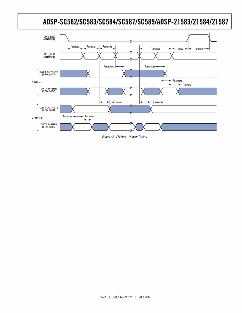
Rev. A | Page 125 of 174 | July 2017
ADSP-SC582/SC583/SC584/SC587/SC589/ADSP-21583/21584/21587
Figure 45. SPI Port—Master Timing
tSDSCIM tSPICLK tHDSM tSPITDMtSPICLM tSPICHM
tHDSPIDM
tHSPIDMtSSPIDM
SPIx_SEL(OUTPUT)
SPIx_CLK(OUTPUT)
DATA OUTPUTS (SPIx_MOSI)
CPHA = 1
CPHA = 0
tDDSPIDM
tHSPIDM
tSSPIDM
tHDSPIDM
tDDSPIDM
DATA INPUTS (SPIx_MISO)
DATA OUTPUTS (SPIx_MOSI)
DATA INPUTS (SPIx_MISO)
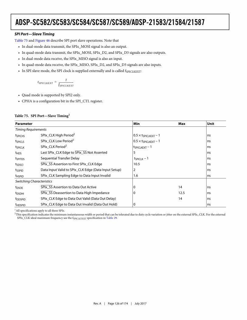
Rev. A | Page 126 of 174 | July 2017
ADSP-SC582/SC583/SC584/SC587/SC589/ADSP-21583/21584/21587SPI Port—Slave Timing
Table 75 and Figure 46 describe SPI port slave operations. Note that • In dual-mode data transmit, the SPIx_MOSI signal is also an output.• In quad-mode data transmit, the SPIx_MOSI, SPIx_D2, and SPIx_D3 signals are also outputs. • In dual-mode data receive, the SPIx_MISO signal is also an input. • In quad-mode data receive, the SPIx_MISO, SPIx_D2, and SPIx_D3 signals are also inputs. • In SPI slave mode, the SPI clock is supplied externally and is called fSPICLKEXT:
• Quad mode is supported by SPI2 only. • CPHA is a configuration bit in the SPI_CTL register.
Table 75. SPI Port—Slave Timing1
1 All specifications apply to all three SPIs.
Parameter Min Max Unit
Timing Requirements
tSPICHS SPIx_CLK High Period2
2 This specification indicates the minimum instantaneous width or period that can be tolerated due to duty cycle variation or jitter on the external SPIx_CLK. For the external SPIx_CLK ideal maximum frequency see the fSPICLKTEXT specification in Table 29.
0.5 × tSPICLKEXT – 1 ns
tSPICLS SPIx_CLK Low Period2 0.5 × tSPICLKEXT – 1 ns
tSPICLK SPIx_CLK Period2 tSPICLKEXT – 1 ns
tHDS Last SPIx_CLK Edge to SPIx_SS Not Asserted 5 ns
tSPITDS Sequential Transfer Delay tSPICLK – 1 ns
tSDSCI SPIx_SS Assertion to First SPIx_CLK Edge 10.5 ns
tSSPID Data Input Valid to SPIx_CLK Edge (Data Input Setup) 2 ns
tHSPID SPIx_CLK Sampling Edge to Data Input Invalid 1.6 ns
Switching Characteristics
tDSOE SPIx_SS Assertion to Data Out Active 0 14 ns
tDSDHI SPIx_SS Deassertion to Data High Impedance 0 12.5 ns
tDDSPID SPIx_CLK Edge to Data Out Valid (Data Out Delay) 14 ns
tHDSPID SPIx_CLK Edge to Data Out Invalid (Data Out Hold) 0 ns
tSPICLKEXT1
fSPICLKEXT-----------------------=
Rev. A | Page 127 of 174 | July 2017
ADSP-SC582/SC583/SC584/SC587/SC589/ADSP-21583/21584/21587
Figure 46. SPI Port—Slave Timing
tSPICLK tHDS tSPITDStSDSCI tSPICLS tSPICHS
tDSOE tDDSPIDtDDSPID tDSDHItHDSPID
tSSPID
tDSDHItHDSPIDtDSOE
tHSPIDtSSPID
tDDSPID
SPIx_SS(INPUT)
SPIx_CLK(INPUT)
tHSPID
DATA OUTPUTS (SPIx_MISO)
CPHA = 1
CPHA = 0
DATA INPUTS (SPIx_MOSI)
DATA OUTPUTS (SPIx_MISO)
DATA INPUTS (SPIx_MOSI)
Rev. A | Page 128 of 174 | July 2017
ADSP-SC582/SC583/SC584/SC587/SC589/ADSP-21583/21584/21587SPI Port—SPIx_RDY Slave Timing
SPIx_RDY is used to provide flow control. CPOL, CPHA, and FCCH are configuration bits in the SPIx_CTL register.
Table 76. SPI Port—SPIx_RDY Slave Timing1
1 All specifications apply to all three SPIs.
Parameter Conditions Min Max Unit
Switching Characteristic
tDSPISCKRDYS SPIx_RDY Deassertion from Last Valid Input SPIx_CLK Edge FCCH = 0 3 × tSCLK1 4 × tSCLK1 + 10 ns
FCCH = 1 4 × tSCLK1 5 × tSCLK1 + 10 ns
Figure 47. SPIx_RDY Deassertion from Valid Input SPIx_CLK Edge in Slave Mode
SPIx_CLK (CPOL = 0)
SPIx_CLK(CPOL = 1)
tDSPISCKRDYS
SPIx_RDY (O)
SPIx_CLK(CPOL = 0)
SPIx_CLK(CPOL = 1)
CPHA = 1
CPHA = 0
Rev. A | Page 129 of 174 | July 2017
ADSP-SC582/SC583/SC584/SC587/SC589/ADSP-21583/21584/21587SPI Port—Open Drain Mode (ODM) Timing
In Figure 48 and Figure 49 and Table 78 and Table 79, the outputs can be SPIx_MOSI, SPIx_MISO, SPIx_D2, and/or SPIx_D3 depending on the mode of operation. CPOL and CPHA are configuration bits in the SPI_CTL register.
Table 77. SPI Port—ODM Master Mode 1
1 All specifications apply to all three SPIs.
Parameter Min Max Unit
Switching Characteristics
tHDSPIODMM SPIx_CLK Edge to High Impedance from Data Out Valid –1 ns
tDDSPIODMM SPIx_CLK Edge to Data Out Valid from High Impedance –1 +6 ns
Figure 48. ODM Master Mode
Table 78. SPI Port—ODM Slave Mode1
1 All specifications apply to all three SPIs.
Parameter Min Max Unit
Timing Requirements
tHDSPIODMS SPIx_CLK Edge to High Impedance from Data Out Valid 0 ns
tDDSPIODMS SPIx_CLK Edge to Data Out Valid from High Impedance 11 ns
Figure 49. ODM Slave Mode
SPIx_CLK(CPOL = 0)
tHDSPIODMM
SPIx_CLK (CPOL = 1)
tDDSPIODMM tDDSPIODMM
tHDSPIODMM
OUTPUT (CPHA = 1)
OUTPUT (CPHA = 0)
tHDSPIODMS
tDDSPIODMS tDDSPIODMS
tHDSPIODMS
SPIx_CLK (CPOL = 0)
SPIx_CLK(CPOL = 1)
OUTPUT (CPHA = 1)
OUTPUT (CPHA = 0)
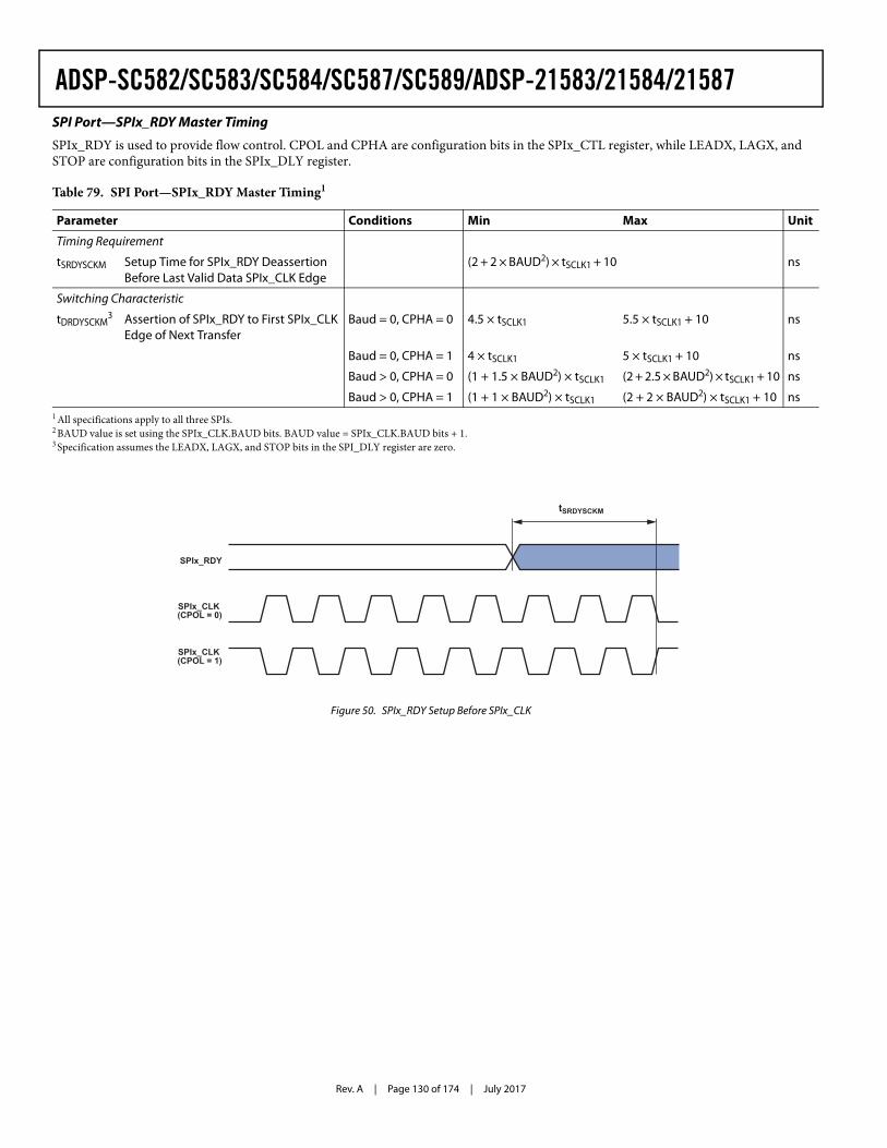
Rev. A | Page 130 of 174 | July 2017
ADSP-SC582/SC583/SC584/SC587/SC589/ADSP-21583/21584/21587SPI Port—SPIx_RDY Master Timing
SPIx_RDY is used to provide flow control. CPOL and CPHA are configuration bits in the SPIx_CTL register, while LEADX, LAGX, and STOP are configuration bits in the SPIx_DLY register.
Table 79. SPI Port—SPIx_RDY Master Timing1
1 All specifications apply to all three SPIs.
Parameter Conditions Min Max Unit
Timing Requirement
tSRDYSCKM Setup Time for SPIx_RDY Deassertion Before Last Valid Data SPIx_CLK Edge
(2 + 2 × BAUD2) × tSCLK1 + 10
2 BAUD value is set using the SPIx_CLK.BAUD bits. BAUD value = SPIx_CLK.BAUD bits + 1.
ns
Switching Characteristic
tDRDYSCKM3
3 Specification assumes the LEADX, LAGX, and STOP bits in the SPI_DLY register are zero.
Assertion of SPIx_RDY to First SPIx_CLK Edge of Next Transfer
Baud = 0, CPHA = 0 4.5 × tSCLK1 5.5 × tSCLK1 + 10 ns
Baud = 0, CPHA = 1 4 × tSCLK1 5 × tSCLK1 + 10 ns
Baud > 0, CPHA = 0 (1 + 1.5 × BAUD2) × tSCLK1 (2 + 2.5 × BAUD2) × tSCLK1 + 10 ns
Baud > 0, CPHA = 1 (1 + 1 × BAUD2) × tSCLK1 (2 + 2 × BAUD2) × tSCLK1 + 10 ns
Figure 50. SPIx_RDY Setup Before SPIx_CLK
SPIx_CLK (CPOL = 0)
SPIx_CLK (CPOL = 1)
tSRDYSCKM
SPIx_RDY
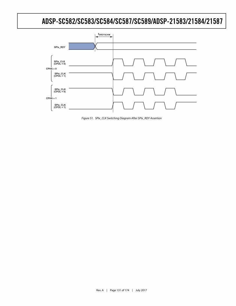
Rev. A | Page 131 of 174 | July 2017
ADSP-SC582/SC583/SC584/SC587/SC589/ADSP-21583/21584/21587
Figure 51. SPIx_CLK Switching Diagram After SPIx_RDY Assertion
tDRDYSCKM
SPIx_RDY
SPIx_CLK (CPOL = 0)
SPIx_CLK(CPOL = 1)
SPIx_CLK(CPOL = 0)
SPIx_CLK(CPOL = 1)
CPHA = 1
CPHA = 0
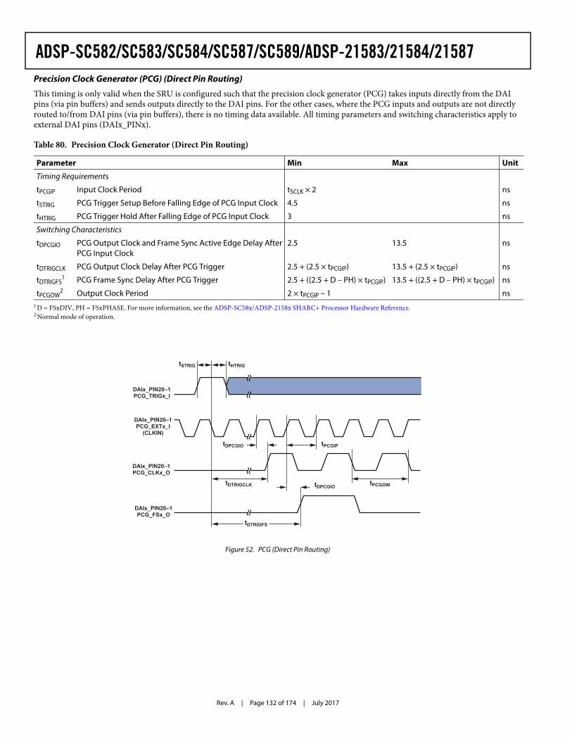
Rev. A | Page 132 of 174 | July 2017
ADSP-SC582/SC583/SC584/SC587/SC589/ADSP-21583/21584/21587Precision Clock Generator (PCG) (Direct Pin Routing)
This timing is only valid when the SRU is configured such that the precision clock generator (PCG) takes inputs directly from the DAI pins (via pin buffers) and sends outputs directly to the DAI pins. For the other cases, where the PCG inputs and outputs are not directly routed to/from DAI pins (via pin buffers), there is no timing data available. All timing parameters and switching characteristics apply to external DAI pins (DAIx_PINx).
Table 80. Precision Clock Generator (Direct Pin Routing)
Parameter Min Max Unit
Timing Requirements
tPCGIP Input Clock Period tSCLK × 2 ns
tSTRIG PCG Trigger Setup Before Falling Edge of PCG Input Clock 4.5 ns
tHTRIG PCG Trigger Hold After Falling Edge of PCG Input Clock 3 ns
Switching Characteristics
tDPCGIO PCG Output Clock and Frame Sync Active Edge Delay After PCG Input Clock
2.5 13.5 ns
tDTRIGCLK PCG Output Clock Delay After PCG Trigger 2.5 + (2.5 × tPCGIP) 13.5 + (2.5 × tPCGIP) ns
tDTRIGFS1
1 D = FSxDIV, PH = FSxPHASE. For more information, see the ADSP-SC58x/ADSP-2158x SHARC+ Processor Hardware Reference.
PCG Frame Sync Delay After PCG Trigger 2.5 + ((2.5 + D – PH) × tPCGIP) 13.5 + ((2.5 + D – PH) × tPCGIP) ns
tPCGOW2
2 Normal mode of operation.
Output Clock Period 2 × tPCGIP – 1 ns
Figure 52. PCG (Direct Pin Routing)
DAIx_PIN20–1PCG_TRIGx_I
DAIx_PIN20–1PCG_EXTx_I
(CLKIN)
DAIx_PIN20–1PCG_CLKx_O
DAIx_PIN20–1PCG_FSx_O
tDTRIGFS
tDTRIGCLK
tDPCGIO
tSTRIG tHTRIG
tPCGOWtDPCGIO
tPCGIP
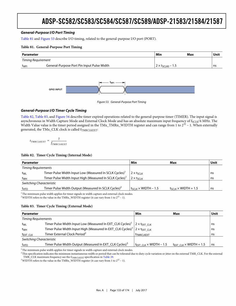
Rev. A | Page 133 of 174 | July 2017
ADSP-SC582/SC583/SC584/SC587/SC589/ADSP-21583/21584/21587General-Purpose I/O Port Timing
Table 81 and Figure 53 describe I/O timing, related to the general-purpose I/O port (PORT).
General-Purpose I/O Timer Cycle Timing
Table 82, Table 83, and Figure 54 describe timer expired operations related to the general-purpose timer (TIMER). The input signal is asynchronous in Width Capture Mode and External Clock Mode and has an absolute maximum input frequency of fSCLK/4 MHz. The Width Value value is the timer period assigned in the TMx_TMRn_WIDTH register and can range from 1 to 232 – 1. When externally generated, the TMx_CLK clock is called fTMRCLKEXT:
Table 81. General-Purpose Port Timing
Parameter Min Max Unit
Timing Requirement
tWFI General-Purpose Port Pin Input Pulse Width 2 × tSCLK0 – 1.5 ns
Figure 53. General-Purpose Port Timing
Table 82. Timer Cycle Timing (Internal Mode)
Parameter Min Max UnitTiming RequirementstWL Timer Pulse Width Input Low (Measured In SCLK Cycles)1
1 The minimum pulse width applies for timer signals in width capture and external clock modes.
2 × tSCLK ns
tWH Timer Pulse Width Input High (Measured In SCLK Cycles)1 2 × tSCLK ns
Switching CharacteristictHTO Timer Pulse Width Output (Measured In SCLK Cycles)2
2 WIDTH refers to the value in the TMRx_WIDTH register (it can vary from 1 to 232 – 1).
tSCLK × WIDTH – 1.5 tSCLK × WIDTH + 1.5 ns
Table 83. Timer Cycle Timing (External Mode)
Parameter Min Max UnitTiming RequirementstWL Timer Pulse Width Input Low (Measured In EXT_CLK Cycles)1
1 The minimum pulse width applies for timer signals in width capture and external clock modes.
2 × tEXT_CLK ns
tWH Timer Pulse Width Input High (Measured In EXT_CLK Cycles)1 2 × tEXT_CLK ns
tEXT_CLK Timer External Clock Period2
2 This specification indicates the minimum instantaneous width or period that can be tolerated due to duty cycle variation or jitter on the external TMR_CLK. For the external TMR_CLK maximum frequency see the fTMRCLKEXT specification in Table 29.
tTMRCLKEXT ns
Switching CharacteristictHTO Timer Pulse Width Output (Measured In EXT_CLK Cycles)3
3 WIDTH refers to the value in the TMRx_WIDTH register (it can vary from 1 to 232 – 1).
tEXT_CLK × WIDTH – 1.5 tEXT_CLK × WIDTH + 1.5 ns
GPIO INPUT
tWFI
tTMRCLKEXT1
fTMRCLKEXT-------------------------=
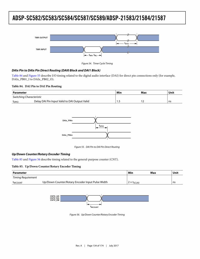
Rev. A | Page 134 of 174 | July 2017
ADSP-SC582/SC583/SC584/SC587/SC589/ADSP-21583/21584/21587
DAIx Pin to DAIx Pin Direct Routing (DAI0 Block and DAI1 Block)
Table 84 and Figure 55 describe I/O timing related to the digital audio interface (DAI) for direct pin connections only (for example, DAIx_PB01_I to DAIx_PB02_O).
Up/Down Counter/Rotary Encoder Timing
Table 85 and Figure 56 describe timing related to the general-purpose counter (CNT).
Figure 54. Timer Cycle Timing
Table 84. DAI Pin to DAI Pin Routing
Parameter Min Max UnitSwitching CharacteristictDPIO Delay DAI Pin Input Valid to DAI Output Valid 1.5 12 ns
Figure 55. DAI Pin to DAI Pin Direct Routing
Table 85. Up/Down Counter/Rotary Encoder Timing
Parameter Min Max Unit
Timing Requirement
tWCOUNT Up/Down Counter/Rotary Encoder Input Pulse Width 2 × tSCLK0 ns
Figure 56. Up/Down Counter/Rotary Encoder Timing
TMR OUTPUT
TMR INPUT
tWH, tWL
tHTO
DAIx_PINn
DAIx_PINm
tDPIO
CNT0_UDCNT0_DGCNT0_ZM
tWCOUNT
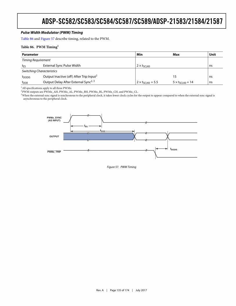
Rev. A | Page 135 of 174 | July 2017
ADSP-SC582/SC583/SC584/SC587/SC589/ADSP-21583/21584/21587Pulse Width Modulator (PWM) Timing
Table 86 and Figure 57 describe timing, related to the PWM.
Table 86. PWM Timing1
1 All specifications apply to all three PWMs.
Parameter Min Max Unit
Timing Requirement
tES External Sync Pulse Width 2 × tSCLK0 ns
Switching Characteristics
tDODIS Output Inactive (off ) After Trip Input2
2 PWM outputs are PWMx_AH, PWMx_AL, PWMx_BH, PWMx_BL, PWMx_CH, and PWMx_CL.
15 ns
tDOE Output Delay After External Sync2, 3
3 When the external sync signal is synchronous to the peripheral clock, it takes fewer clock cycles for the output to appear compared to when the external sync signal is asynchronous to the peripheral clock.
2 × tSCLK0 + 5.5 5 × tSCLK0 + 14 ns
Figure 57. PWM Timing
PWMx_TRIP
PWMx_SYNC(AS INPUT)
tES
tDOE
OUTPUT
tDODIS
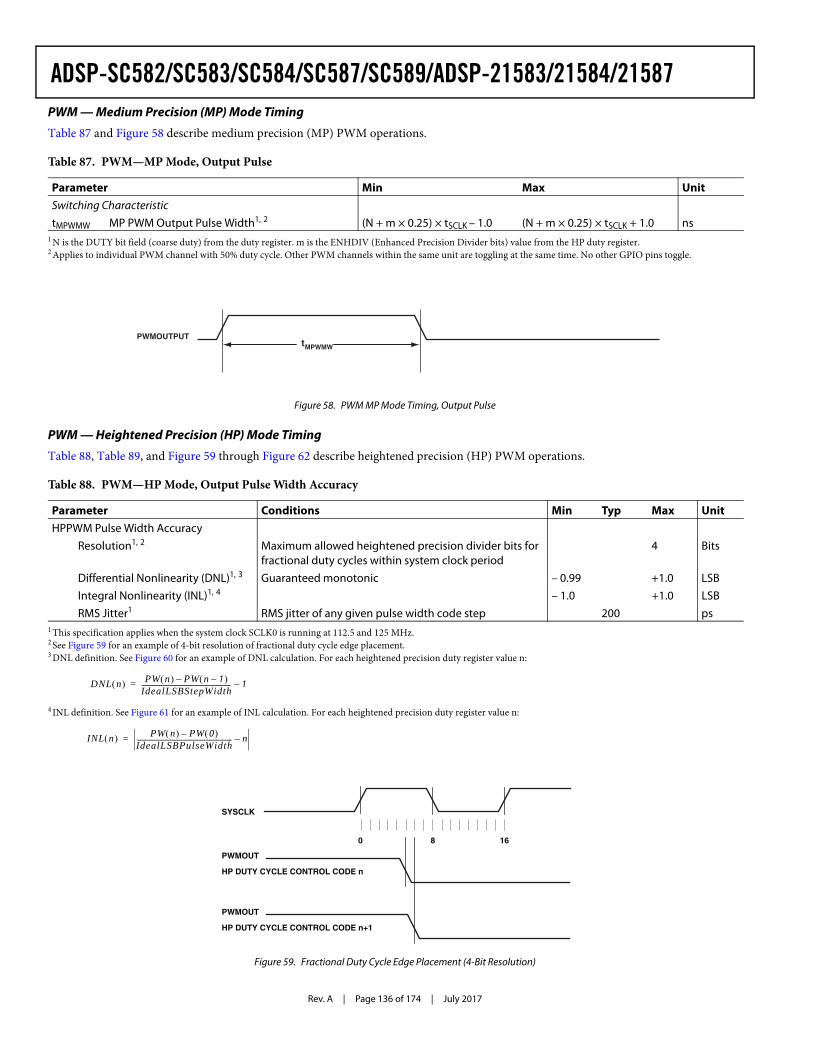
Rev. A | Page 136 of 174 | July 2017
ADSP-SC582/SC583/SC584/SC587/SC589/ADSP-21583/21584/21587PWM — Medium Precision (MP) Mode Timing
Table 87 and Figure 58 describe medium precision (MP) PWM operations.
PWM — Heightened Precision (HP) Mode Timing
Table 88, Table 89, and Figure 59 through Figure 62 describe heightened precision (HP) PWM operations.
Table 87. PWM—MP Mode, Output Pulse
Parameter Min Max UnitSwitching CharacteristictMPWMW MP PWM Output Pulse Width1, 2
1 N is the DUTY bit field (coarse duty) from the duty register. m is the ENHDIV (Enhanced Precision Divider bits) value from the HP duty register.2 Applies to individual PWM channel with 50% duty cycle. Other PWM channels within the same unit are toggling at the same time. No other GPIO pins toggle.
(N + m × 0.25) × tSCLK – 1.0 (N + m × 0.25) × tSCLK + 1.0 ns
Figure 58. PWM MP Mode Timing, Output Pulse
Table 88. PWM—HP Mode, Output Pulse Width Accuracy
Parameter Conditions Min Typ Max UnitHPPWM Pulse Width Accuracy
Resolution1, 2
1 This specification applies when the system clock SCLK0 is running at 112.5 and 125 MHz.2 See Figure 59 for an example of 4-bit resolution of fractional duty cycle edge placement.
Maximum allowed heightened precision divider bits for fractional duty cycles within system clock period
4 Bits
Differential Nonlinearity (DNL)1, 3
3 DNL definition. See Figure 60 for an example of DNL calculation. For each heightened precision duty register value n:
Guaranteed monotonic – 0.99 +1.0 LSBIntegral Nonlinearity (INL)1, 4
4 INL definition. See Figure 61 for an example of INL calculation. For each heightened precision duty register value n:
– 1.0 +1.0 LSBRMS Jitter1 RMS jitter of any given pulse width code step 200 ps
Figure 59. Fractional Duty Cycle Edge Placement (4-Bit Resolution)
PWMOUTPUTtMPWMW
DNL n PW n PW n 1– –IdealLSBStepWidth-------------------------------------------------- 1–=
INL n PW n PW 0 –IdealLSBPulseWidth------------------------------------------------------ n–=
SYSCLK
HP DUTY CYCLE CONTROL CODE n
PWMOUT
0 8 16
HP DUTY CYCLE CONTROL CODE n+1
PWMOUT
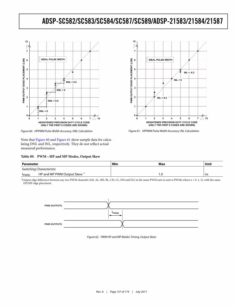
Rev. A | Page 137 of 174 | July 2017
ADSP-SC582/SC583/SC584/SC587/SC589/ADSP-21583/21584/21587
Note that Figure 60 and Figure 61 show sample data for calcu-lating DNL and INL, respectively. They do not reflect actual measured performance.
Figure 60. HPPWM Pulse Width Accuracy: DNL Calculation
0
1
2
3
4
5
6
0 1 2 3 4 5 6 7 15
PWM
OU
TPU
T ED
GE
PLA
CEM
ENT
(LSB
)
HEIGHTENED PRECISION DUTY CYCLE CODE(ONLY THE FIRST 8 CODES ARE SHOWN)
7
15
DNL = 0
DNL = 0.5
DNL = 0
DNL = 0.5
IDEAL PULSE WIDTH
…
…
Figure 61. HPPWM Pulse Width Accuracy: INL Calculation
0
1
2
3
4
5
6
0 1 2 3 4 5 6 7 15
PWM
OU
TPU
T ED
GE
PLA
CEM
ENT
(LSB
)
HEIGHTENED PRECISION DUTY CYCLE CODE(ONLY THE FIRST 8 CODES ARE SHOWN)
7
15
INL = 0.5
INL = 0
INL = -0.3
IDEAL PULSE WIDTH
…
…
Table 89. PWM—HP and MP Modes, Output Skew
Parameter Min Max UnitSwitching CharacteristictPWMS HP and MP PWM Output Skew 1 1.0 ns
1 Output edge difference between any two PWM channels (AH, AL, BH, BL, CH, CL, DH and DL) in the same PWM unit (a unit is PWMx where x = 0, 1, 2), with the same HP/MP edge placement.
Figure 62. PWM HP and MP Modes Timing, Output Skew
PWM OUTPUTS
PWM OUTPUTS
tPWMS
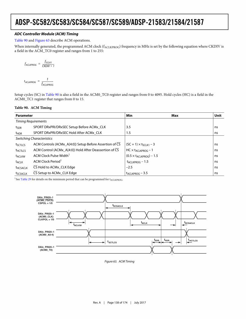
Rev. A | Page 138 of 174 | July 2017
ADSP-SC582/SC583/SC584/SC587/SC589/ADSP-21583/21584/21587ADC Controller Module (ACM) Timing
Table 90 and Figure 63 describe ACM operations. When internally generated, the programmed ACM clock (fACLKPROG) frequency in MHz is set by the following equation where CKDIV is a field in the ACM_TC0 register and ranges from 1 to 255:
Setup cycles (SC) in Table 90 is also a field in the ACM0_TC0 register and ranges from 0 to 4095. Hold cycles (HC) is a field in the ACM0_TC1 register that ranges from 0 to 15.
Table 90. ACM Timing
Parameter Min Max Unit
Timing Requirements
tSDR SPORT DRxPRI/DRxSEC Setup Before ACMx_CLK 3.5 ns
tHDR SPORT DRxPRI/DRxSEC Hold After ACMx_CLK 1.5 ns
Switching Characteristics
tSCTLCS ACM Controls (ACMx_A[4:0]) Setup Before Assertion of CS (SC + 1) × tSCLK1 – 3 ns
tHCTLCS ACM Control (ACMx_A[4:0]) Hold After Deassertion of CS HC × tACLKPROG – 1 ns
tACLKW ACM Clock Pulse Width1
1 See Table 29 for details on the minimum period that can be programmed for tACLKPROG.
(0.5 × tACLKPROG) – 1.5 ns
tACLK ACM Clock Period1 tACLKPROG – 1.5 ns
tHCSACLK CS Hold to ACMx_CLK Edge –2.5 ns
tSCSACLK CS Setup to ACMx_CLK Edge tACLKPROG – 3.5 ns
Figure 63. ACM Timing
fACLKPROGfSCLK1
CKDIV 1+------------------=
tACLKPROG1
fACLKPROG------------------=
DAIx_PIN20–1(ACM0_FS/CS)
CSPOL = 1/0tSCSACLK
DAIx_PIN20–1(ACM0_A0-4)
tACLK
tSCTLCStSDR tHDR
DAIx_PIN20–1(ACM0_CLK)
CLKPOL = 1/0tHCSACLK
tHCTLCS
tACLKW
DAIx_PIN20–1(ACM0_T0)
Rev. A | Page 139 of 174 | July 2017
ADSP-SC582/SC583/SC584/SC587/SC589/ADSP-21583/21584/21587Universal Asynchronous Receiver-Transmitter (UART) Ports—Receive and Transmit Timing
The UART ports receive and transmit operations are described in the ADSP-SC58x/ADSP-2158x SHARC+ Processor Hardware Reference.
Controller Area Network (CAN) Interface
The CAN interface timing is described in the ADSP-SC58x/ADSP-2158x SHARC+ Processor Hardware Reference.
Universal Serial Bus (USB) OTG—Receive and Transmit Timing
Table 91 describes the USB OTG receive and transmit operations.
PCI Express (PCIe)
The PCIe interface complies with the Gen1 and Gen2 x1 lane data rate specification and supports up to 3.0 PCIe base functionality.For more information about PCIe, see the following standards:
• PCI Express Base 3.0 Specification, Revision 1.0, PCI-SIG• PCI Express 2.0 Card Electromechanical Specification, Revision 2.0, PCI-SIG• PHY Interface for the PCI Express Architecture, Revision 2.0, Intel Corporation• PCI-SIG Engineering Change Request: L1 Substates, February 1, 2012, PCI-SIG• IEEE Standard 1149.1-2001, IEEE• IEEE Standard 1149.6-2003, IEEE
Table 91. USB OTG—Receive and Transmit Timing1
1 This specification is supported by USB0.
Parameter Min Max Unit
Timing Requirements
fUSBS USB_XI Frequency 24 24 MHz
fsUSB USB_XI Clock Frequency Stability –50 +50 ppm
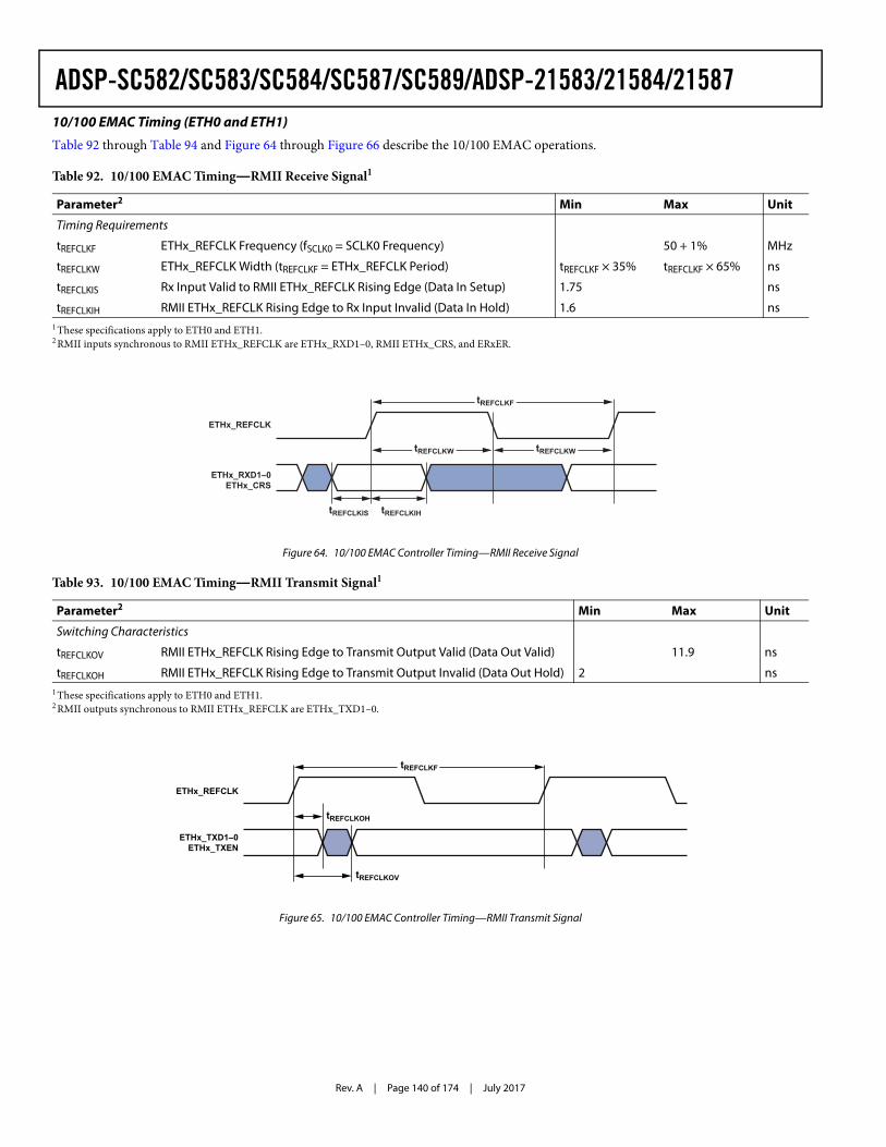
Rev. A | Page 140 of 174 | July 2017
ADSP-SC582/SC583/SC584/SC587/SC589/ADSP-21583/21584/2158710/100 EMAC Timing (ETH0 and ETH1)
Table 92 through Table 94 and Figure 64 through Figure 66 describe the 10/100 EMAC operations.
Table 92. 10/100 EMAC Timing—RMII Receive Signal1
1 These specifications apply to ETH0 and ETH1.
Parameter2
2 RMII inputs synchronous to RMII ETHx_REFCLK are ETHx_RXD1–0, RMII ETHx_CRS, and ERxER.
Min Max Unit
Timing Requirements
tREFCLKF ETHx_REFCLK Frequency (fSCLK0 = SCLK0 Frequency) 50 + 1% MHz
tREFCLKW ETHx_REFCLK Width (tREFCLKF = ETHx_REFCLK Period) tREFCLKF × 35% tREFCLKF × 65% ns
tREFCLKIS Rx Input Valid to RMII ETHx_REFCLK Rising Edge (Data In Setup) 1.75 ns
tREFCLKIH RMII ETHx_REFCLK Rising Edge to Rx Input Invalid (Data In Hold) 1.6 ns
Figure 64. 10/100 EMAC Controller Timing—RMII Receive Signal
Table 93. 10/100 EMAC Timing—RMII Transmit Signal1
1 These specifications apply to ETH0 and ETH1.
Parameter2
2 RMII outputs synchronous to RMII ETHx_REFCLK are ETHx_TXD1–0.
Min Max Unit
Switching Characteristics
tREFCLKOV RMII ETHx_REFCLK Rising Edge to Transmit Output Valid (Data Out Valid) 11.9 ns
tREFCLKOH RMII ETHx_REFCLK Rising Edge to Transmit Output Invalid (Data Out Hold) 2 ns
Figure 65. 10/100 EMAC Controller Timing—RMII Transmit Signal
tREFCLKIS tREFCLKIH
ETHx_RXD1–0ETHx_CRS
ETHx_REFCLK
tREFCLKW
tREFCLKF
tREFCLKW
tREFCLKOV
tREFCLKOH
ETHx_REFCLK
ETHx_TXD1–0ETHx_TXEN
tREFCLKF
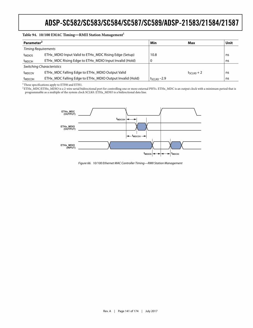
Rev. A | Page 141 of 174 | July 2017
ADSP-SC582/SC583/SC584/SC587/SC589/ADSP-21583/21584/21587Table 94. 10/100 EMAC Timing—RMII Station Management1
Parameter2 Min Max Unit
Timing Requirements
tMDIOS ETHx_MDIO Input Valid to ETHx_MDC Rising Edge (Setup) 10.8 ns
tMDCIH ETHx_MDC Rising Edge to ETHx_MDIO Input Invalid (Hold) 0 ns
Switching Characteristics
tMDCOV ETHx_MDC Falling Edge to ETHx_MDIO Output Valid tSCLK0 + 2 ns
tMDCOH ETHx_MDC Falling Edge to ETHx_MDIO Output Invalid (Hold) tSCLK0 –2.9 ns1 These specifications apply to ETH0 and ETH1.2 ETHx_MDC/ETHx_MDIO is a 2-wire serial bidirectional port for controlling one or more external PHYs. ETHx_MDC is an output clock with a minimum period that is
programmable as a multiple of the system clock SCLK0. ETHx_MDIO is a bidirectional data line.
Figure 66. 10/100 Ethernet MAC Controller Timing—RMII Station Management
ETHx_MDIO (INPUT)
ETHx_MDIO (OUTPUT)
ETHx_MDC (OUTPUT)
tMDIOS
tMDCOH
tMDCIH
tMDCOV
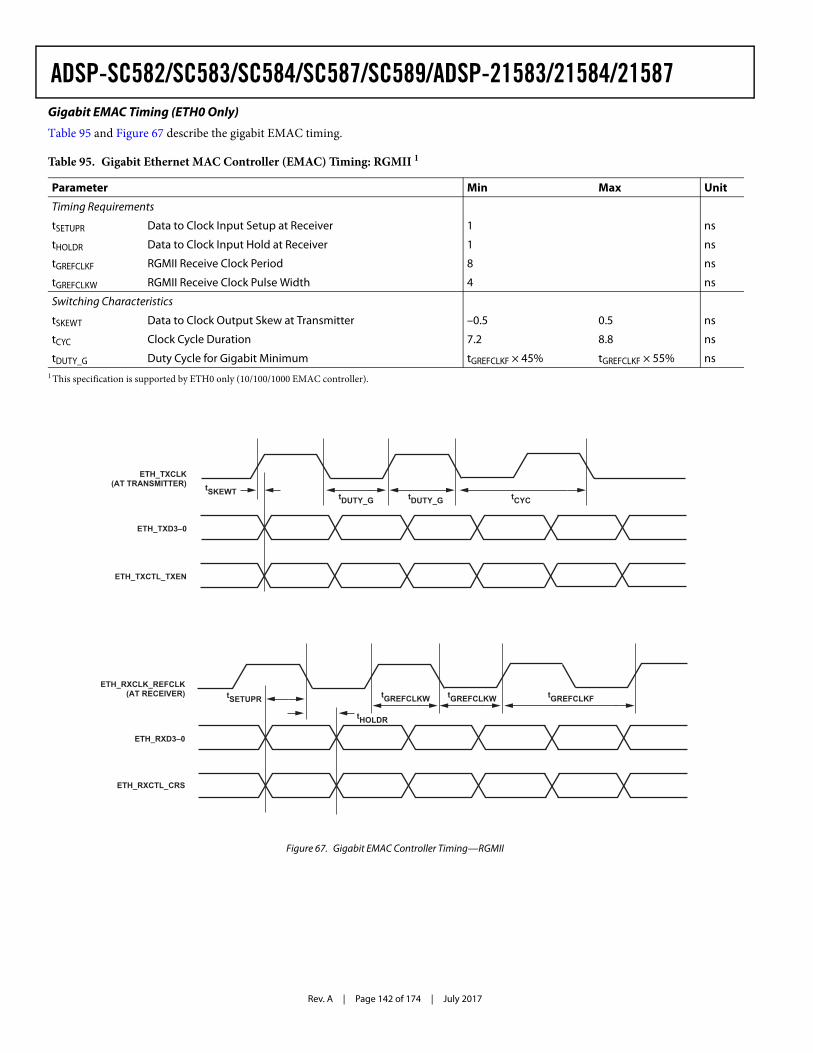
Rev. A | Page 142 of 174 | July 2017
ADSP-SC582/SC583/SC584/SC587/SC589/ADSP-21583/21584/21587Gigabit EMAC Timing (ETH0 Only)
Table 95 and Figure 67 describe the gigabit EMAC timing.
Table 95. Gigabit Ethernet MAC Controller (EMAC) Timing: RGMII 1
1 This specification is supported by ETH0 only (10/100/1000 EMAC controller).
Parameter Min Max Unit
Timing Requirements
tSETUPR Data to Clock Input Setup at Receiver 1 ns
tHOLDR Data to Clock Input Hold at Receiver 1 ns
tGREFCLKF RGMII Receive Clock Period 8 ns
tGREFCLKW RGMII Receive Clock Pulse Width 4 ns
Switching Characteristics
tSKEWT Data to Clock Output Skew at Transmitter –0.5 0.5 ns
tCYC Clock Cycle Duration 7.2 8.8 ns
tDUTY_G Duty Cycle for Gigabit Minimum tGREFCLKF × 45% tGREFCLKF × 55% ns
Figure 67. Gigabit EMAC Controller Timing—RGMII
tHOLDR
ETH_TXCLK(AT TRANSMITTER)
ETH_TXD3–0
ETH_TXCTL_TXEN
tSKEWT tDUTY_G tDUTY_G tCYC
tGREFCLKFtGREFCLKW
ETH_RXCLK_REFCLK(AT RECEIVER)
ETH_RXD3–0
ETH_RXCTL_CRS
tSETUPR tGREFCLKW
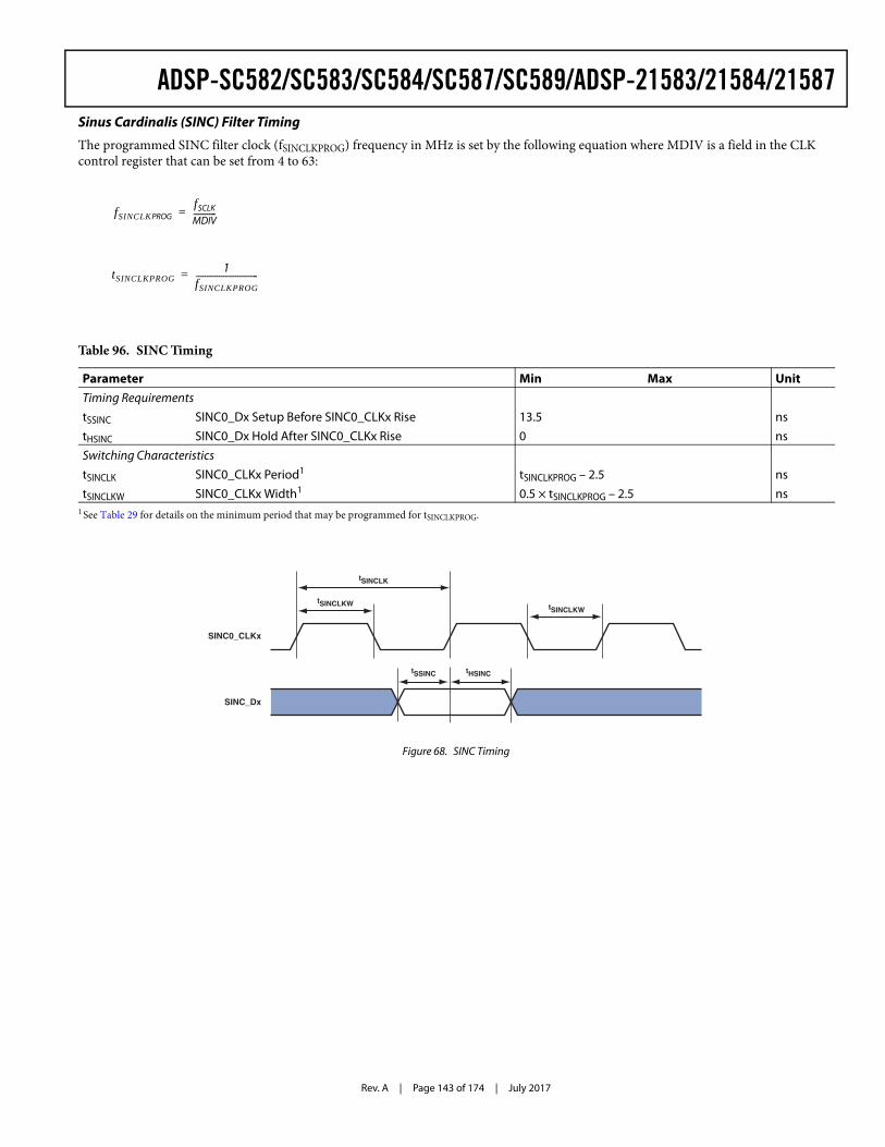
Rev. A | Page 143 of 174 | July 2017
ADSP-SC582/SC583/SC584/SC587/SC589/ADSP-21583/21584/21587Sinus Cardinalis (SINC) Filter Timing
The programmed SINC filter clock (fSINCLKPROG) frequency in MHz is set by the following equation where MDIV is a field in the CLK control register that can be set from 4 to 63:
Table 96. SINC Timing
Parameter Min Max UnitTiming RequirementstSSINC SINC0_Dx Setup Before SINC0_CLKx Rise 13.5 ns
tHSINC SINC0_Dx Hold After SINC0_CLKx Rise 0 ns
Switching CharacteristicstSINCLK SINC0_CLKx Period1
1 See Table 29 for details on the minimum period that may be programmed for tSINCLKPROG.
tSINCLKPROG – 2.5 ns
tSINCLKW SINC0_CLKx Width1 0.5 × tSINCLKPROG – 2.5 ns
Figure 68. SINC Timing
fSINCLKPROGfSCLK
MDIV----------=
tSINCLKPROG1
fSINCLKPROG---------------------------=
SINC0_CLKx
SINC_Dx
tSINCLK
tSINCLKWtSINCLKW
tSSINC tHSINC
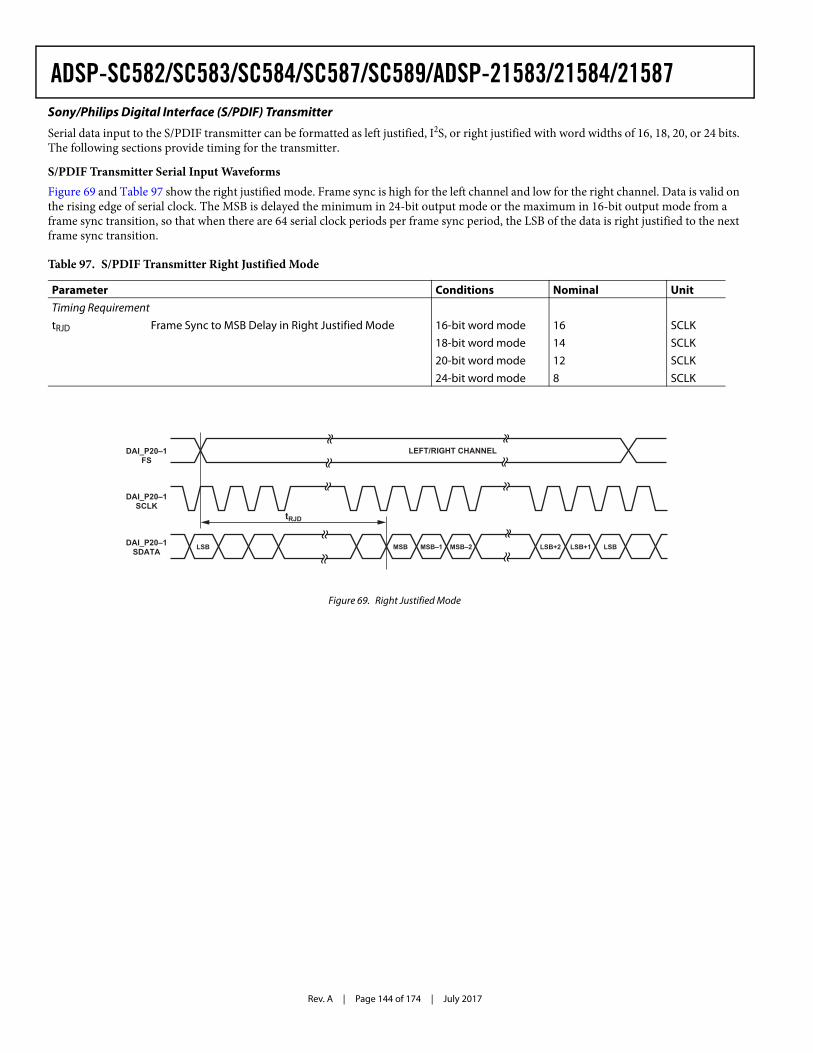
Rev. A | Page 144 of 174 | July 2017
ADSP-SC582/SC583/SC584/SC587/SC589/ADSP-21583/21584/21587Sony/Philips Digital Interface (S/PDIF) Transmitter
Serial data input to the S/PDIF transmitter can be formatted as left justified, I2S, or right justified with word widths of 16, 18, 20, or 24 bits. The following sections provide timing for the transmitter.
S/PDIF Transmitter Serial Input WaveformsFigure 69 and Table 97 show the right justified mode. Frame sync is high for the left channel and low for the right channel. Data is valid on the rising edge of serial clock. The MSB is delayed the minimum in 24-bit output mode or the maximum in 16-bit output mode from a frame sync transition, so that when there are 64 serial clock periods per frame sync period, the LSB of the data is right justified to the next frame sync transition.
Table 97. S/PDIF Transmitter Right Justified Mode
Parameter Conditions Nominal UnitTiming RequirementtRJD Frame Sync to MSB Delay in Right Justified Mode 16-bit word mode 16 SCLK
18-bit word mode 14 SCLK
20-bit word mode 12 SCLK
24-bit word mode 8 SCLK
Figure 69. Right Justified Mode
MSB
LEFT/RIGHT CHANNEL
LSB LSBMSB–1 MSB–2 LSB+2 LSB+1
DAI_P20–1FS
DAI_P20–1SCLK
DAI_P20–1SDATA
tRJD
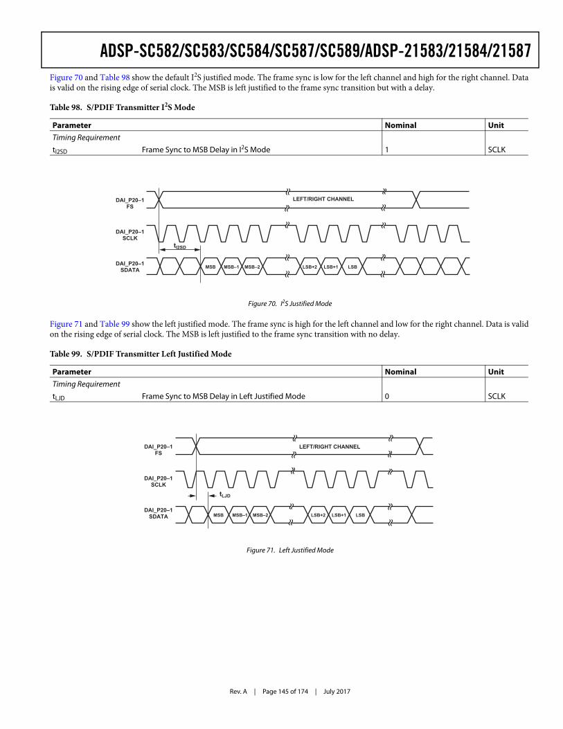
Rev. A | Page 145 of 174 | July 2017
ADSP-SC582/SC583/SC584/SC587/SC589/ADSP-21583/21584/21587Figure 70 and Table 98 show the default I2S justified mode. The frame sync is low for the left channel and high for the right channel. Data is valid on the rising edge of serial clock. The MSB is left justified to the frame sync transition but with a delay.
Figure 71 and Table 99 show the left justified mode. The frame sync is high for the left channel and low for the right channel. Data is valid on the rising edge of serial clock. The MSB is left justified to the frame sync transition with no delay.
Table 98. S/PDIF Transmitter I2S Mode
Parameter Nominal UnitTiming RequirementtI2SD Frame Sync to MSB Delay in I2S Mode 1 SCLK
Figure 70. I2S Justified Mode
Table 99. S/PDIF Transmitter Left Justified Mode
Parameter Nominal UnitTiming RequirementtLJD Frame Sync to MSB Delay in Left Justified Mode 0 SCLK
Figure 71. Left Justified Mode
MSB
LEFT/RIGHT CHANNEL
LSBMSB–1 MSB–2 LSB+2 LSB+1
DAI_P20–1FS
DAI_P20–1SCLK
DAI_P20–1SDATA
tI2SD
MSB
LEFT/RIGHT CHANNEL
LSBMSB–1 MSB–2 LSB+2 LSB+1
DAI_P20–1FS
DAI_P20–1SCLK
DAI_P20–1SDATA
tLJD
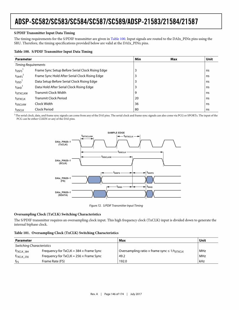
Rev. A | Page 146 of 174 | July 2017
ADSP-SC582/SC583/SC584/SC587/SC589/ADSP-21583/21584/21587S/PDIF Transmitter Input Data TimingThe timing requirements for the S/PDIF transmitter are given in Table 100. Input signals are routed to the DAIx_PINx pins using the SRU. Therefore, the timing specifications provided below are valid at the DAIx_PINx pins.
Oversampling Clock (TxCLK) Switching CharacteristicsThe S/PDIF transmitter requires an oversampling clock input. This high frequency clock (TxCLK) input is divided down to generate the internal biphase clock.
Table 100. S/PDIF Transmitter Input Data Timing
Parameter Min Max Unit
Timing Requirements
tSISFS1
1 The serial clock, data, and frame sync signals can come from any of the DAI pins. The serial clock and frame sync signals can also come via PCG or SPORTs. The input of the PCG can be either CLKIN or any of the DAI pins.
Frame Sync Setup Before Serial Clock Rising Edge 3 ns
tSIHFS1 Frame Sync Hold After Serial Clock Rising Edge 3 ns
tSISD1 Data Setup Before Serial Clock Rising Edge 3 ns
tSIHD1 Data Hold After Serial Clock Rising Edge 3 ns
tSITXCLKW Transmit Clock Width 9 ns
tSITXCLK Transmit Clock Period 20 ns
tSISCLKW Clock Width 36 ns
tSISCLK Clock Period 80 ns
Figure 72. S/PDIF Transmitter Input Timing
Table 101. Oversampling Clock (TxCLK) Switching Characteristics
Parameter Max UnitSwitching Characteristics fTXCLK_384 Frequency for TxCLK = 384 × Frame Sync Oversampling ratio × frame sync ≤ 1/tSITXCLK MHz
fTXCLK_256 Frequency for TxCLK = 256 × Frame Sync 49.2 MHz
fFS Frame Rate (FS) 192.0 kHz
SAMPLE EDGE
DAIx_PIN20–1(TxCLK)
DAIx_PIN20–1(SCLK)
DAIx_PIN20–1(FS)
DAIx_PIN20–1(SDATA)
tSITXCLKW tSITXCLK
tSISCLKW
tSISCLK
tSISFS tSIHFS
tSISD tSIHD
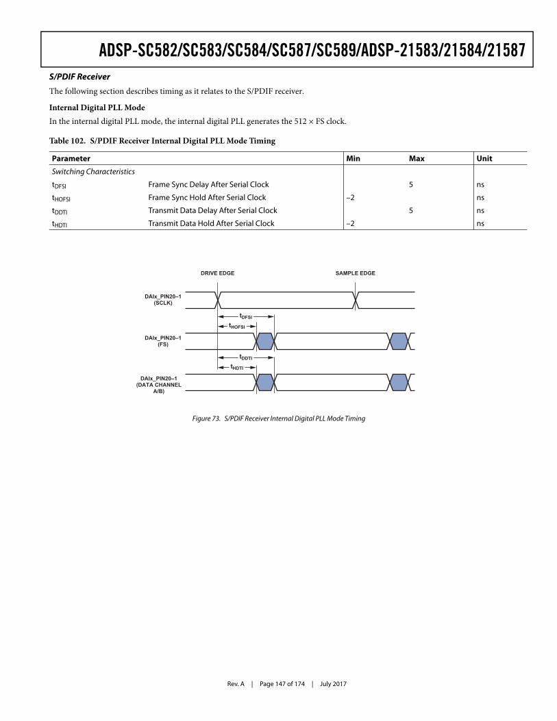
Rev. A | Page 147 of 174 | July 2017
ADSP-SC582/SC583/SC584/SC587/SC589/ADSP-21583/21584/21587S/PDIF Receiver
The following section describes timing as it relates to the S/PDIF receiver.
Internal Digital PLL ModeIn the internal digital PLL mode, the internal digital PLL generates the 512 × FS clock.
Table 102. S/PDIF Receiver Internal Digital PLL Mode Timing
Parameter Min Max Unit
Switching Characteristics
tDFSI Frame Sync Delay After Serial Clock 5 ns
tHOFSI Frame Sync Hold After Serial Clock –2 ns
tDDTI Transmit Data Delay After Serial Clock 5 ns
tHDTI Transmit Data Hold After Serial Clock –2 ns
Figure 73. S/PDIF Receiver Internal Digital PLL Mode Timing
DAIx_PIN20–1(SCLK)
SAMPLE EDGE
DAIx_PIN20–1(FS)
DAIx_PIN20–1(DATA CHANNEL
A/B)
DRIVE EDGE
tDFSI
tHOFSI
tDDTI
tHDTI
Rev. A | Page 148 of 174 | July 2017
ADSP-SC582/SC583/SC584/SC587/SC589/ADSP-21583/21584/21587MediaLB (MLB)
All the numbers shown in Table 103 are applicable for all MLB speed modes (1024 FS, 512 FS, and 256 FS) for the 3-pin protocol, unless otherwise specified. Refer to the Media Local Bus Specification version 4.2 for more details.
Table 103. 3-Pin MLB Interface Specifications
Parameter Min Typ Max UnittMLBCLK MLB Clock Period
1024 FS 512 FS 256 FS
20.34081
nsnsns
tMCKL MLBCLK Low Time 1024 FS 512 FS 256 FS
6.11430
nsnsns
tMCKH MLBCLK High Time 1024 FS 512 FS 256 FS
9.31430
nsnsns
tMCKR MLBCLK Rise Time (VIL to VIH) 1024 FS 512 FS/256 FS
13
nsns
tMCKF MLBCLK Fall Time (VIH to VIL) 1024 FS 512 FS/256 FS
13
nsns
tMPWV1
1 Pulse width variation is measured at 1.25 V by triggering on one edge of MLBCLK and measuring the spread on the other edge, measured in ns peak-to-peak.
MLBCLK Pulse Width Variation 1024 FS 512 FS/256
0.72.0
nsppnspp
tDSMCF DAT/SIG Input Setup Time 1 ns
tDHMCF DAT/SIG Input Hold Time 2 ns
tMCFDZ DAT/SIG Output Time to Three-State 0 15 ns
tMCDRV DAT/SIG Output Data Delay From MLBCLK Rising Edge 8 ns
tMDZH2
2 Board designs must ensure the high impedance bus does not leave the logic state of the final driven bit for this time period. Therefore, coupling must be minimized while meeting the maximum capacitive load listed.
Bus Hold Time 1024 FS 512 FS/256
24
nsns
CMLB DAT/SIG Pin Load 1024 FS 512 FS/256
4060
pfpf
Rev. A | Page 149 of 174 | July 2017
ADSP-SC582/SC583/SC584/SC587/SC589/ADSP-21583/21584/21587
The ac timing specifications of the 6-pin MLB interface is detailed in Table 104. Refer to the Media Local Bus Specification version 4.2 for more details.
Figure 74. MLB Timing (3-Pin Interface)
Table 104. 6-Pin MLB Interface Specifications
Parameter Conditions Min Typ Max UnittMT Differential Transition Time at the Input Pin (See Figure 75) 20% to 80% VIN+/VIN– 1 ns
80% to 20% VIN+/VIN–
fMCKE MLBCP/N External Clock Operating Frequency (See Figure 76)1
1 fMCKE (maximum) and fMCKR (maximum) include maximum cycle to cycle system jitter (tJITTER) of 600 ps for a bit error rate of 10E-9.
2048 × FS at 44.0 kHz 90.112 MHz
2048 × FS at 50.0 kHz 102.4 MHz
fMCKR Recovered Clock Operating Frequency (Internal, not Observable at Pins, Only for Timing References) (See Figure 76)
2048 × FS at 44.0 kHz 90.112 MHz
2048 × FS at 50.0 kHz 102.4 MHz
tDELAY Transmitter MLBSP/N (MLBDP/N) Output Valid From Transition of MLBCP/N (Low to High) (See Figure 77)
fMCKR = 2048 × FS 0.6 5 ns
tPHZ Disable Turnaround Time From Transition of MLBCP/N (Low to High) (See Figure 78)
fMCKR = 2048 × FS 0.6 7 ns
tPLZ Enable Turnaround Time From Transition of MLBCP/N (Low to High) (See Figure 78)
fMCKR = 2048 × FS 0.6 11.2 ns
tSU MLBSP/N (MLBDP/N) Valid to Transition of MLBCP/N (Low to High) (See Figure 77)
fMCKR = 2048 × FS 1 ns
tHD MLBSP/N (MLBDP/N) Hold From Transition of MLBCP/N (Low to High) (See Figure 77)2
2 Receivers must latch MLBSP/N (MLBDP/N) data within tHD (min) of the rising edge of MLBCP/N.
0.6 ns
tMCKH
MLB_SIG/MLB_DAT(Rx, Input)
tMCKL
tMCKR
MLB_SIG/MLB_DAT
(Tx, Output)
tMCFDZ
tDSMCF
MLB_CLK
tMLBCLK
VALID
tDHMCF
tMCKF
tMCDRV
VALID
tMDZH
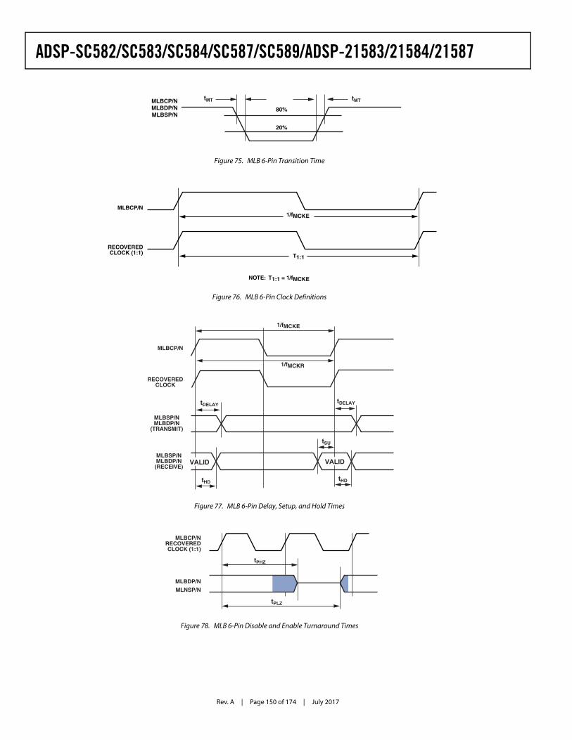
Rev. A | Page 150 of 174 | July 2017
ADSP-SC582/SC583/SC584/SC587/SC589/ADSP-21583/21584/21587
Figure 75. MLB 6-Pin Transition Time
Figure 76. MLB 6-Pin Clock Definitions
Figure 77. MLB 6-Pin Delay, Setup, and Hold Times
Figure 78. MLB 6-Pin Disable and Enable Turnaround Times
MLBCP/NMLBDP/NMLBSP/N
tMT
80%
20%
tMT
MLBCP/N
RECOVEREDCLOCK (1:1)
1/fMCKE
T1:1
T1:1 = 1/fMCKENOTE:
tHD
MLBCP/N
RECOVEREDCLOCK
MLBSP/NMLBDP/N
(TRANSMIT)
MLBSP/NMLBDP/N(RECEIVE)
tDELAY
1/fMCKE
1/fMCKR
tDELAY
VALIDVALID
tSU
tHD
tPLZ
MLBCP/NRECOVEREDCLOCK (1:1)
tPHZ
MLBDP/N
MLNSP/N
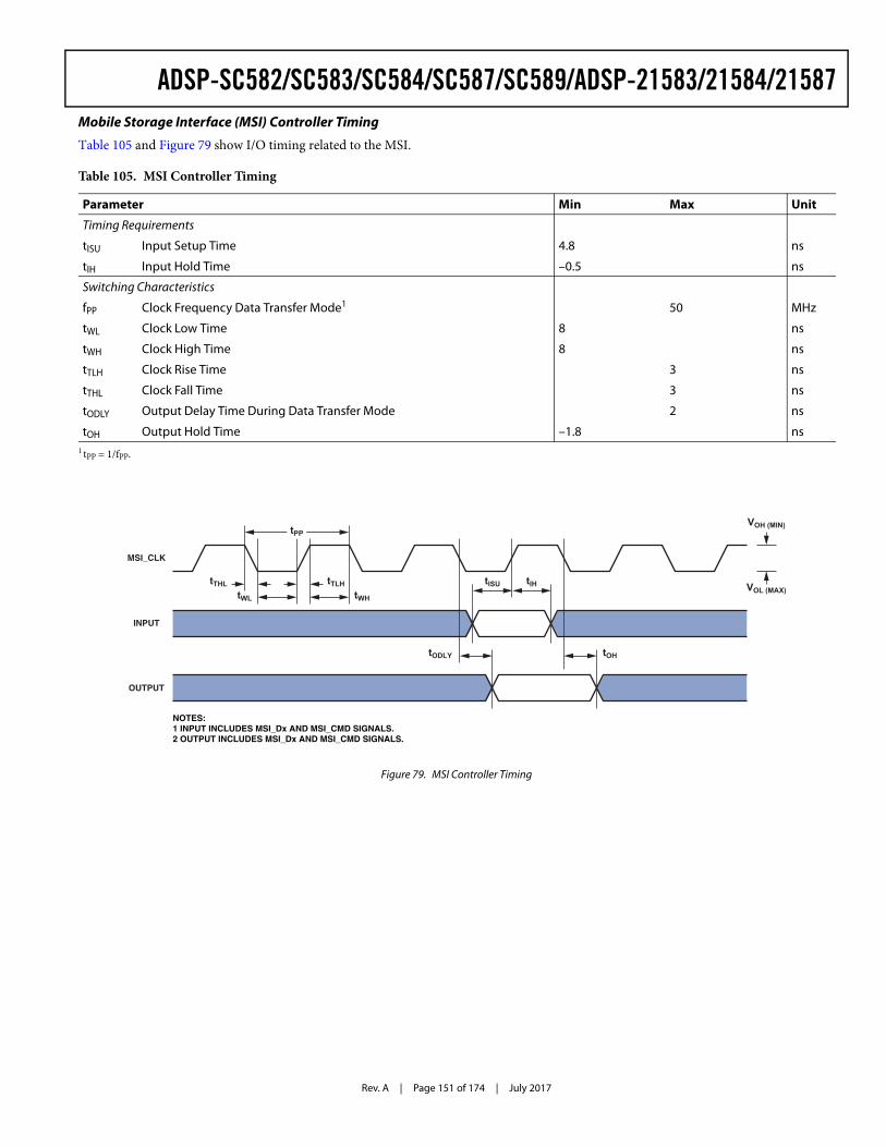
Rev. A | Page 151 of 174 | July 2017
ADSP-SC582/SC583/SC584/SC587/SC589/ADSP-21583/21584/21587Mobile Storage Interface (MSI) Controller Timing
Table 105 and Figure 79 show I/O timing related to the MSI.
Table 105. MSI Controller Timing
Parameter Min Max Unit
Timing Requirements
tISU Input Setup Time 4.8 ns
tIH Input Hold Time –0.5 ns
Switching Characteristics
fPP Clock Frequency Data Transfer Mode1
1 tPP = 1/fPP.
50 MHz
tWL Clock Low Time 8 ns
tWH Clock High Time 8 ns
tTLH Clock Rise Time 3 ns
tTHL Clock Fall Time 3 ns
tODLY Output Delay Time During Data Transfer Mode 2 ns
tOH Output Hold Time –1.8 ns
Figure 79. MSI Controller Timing
MSI_CLK
INPUT
OUTPUT
tISU
NOTES:1 INPUT INCLUDES MSI_Dx AND MSI_CMD SIGNALS.2 OUTPUT INCLUDES MSI_Dx AND MSI_CMD SIGNALS.
tTHL tTLHtWL tWH
tPP
tIH
tODLY tOH
VOH (MIN)
VOL (MAX)
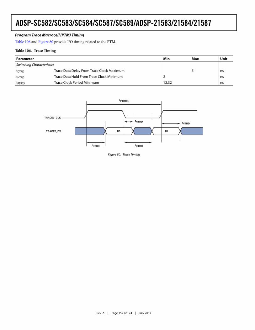
Rev. A | Page 152 of 174 | July 2017
ADSP-SC582/SC583/SC584/SC587/SC589/ADSP-21583/21584/21587Program Trace Macrocell (PTM) Timing
Table 106 and Figure 80 provide I/O timing related to the PTM.
Table 106. Trace Timing
Parameter Min Max Unit
Switching Characteristics
tDTRD Trace Data Delay From Trace Clock Maximum 5 ns
tHTRD Trace Data Hold From Trace Clock Minimum 2 ns
tPTRCK Trace Clock Period Minimum 12.32 ns
Figure 80. Trace Timing
TRACE0_CLK
TRACE0_DX
tPTRCK
tHTRDtHTRD
tDTRD
D0 D1
tDTRD
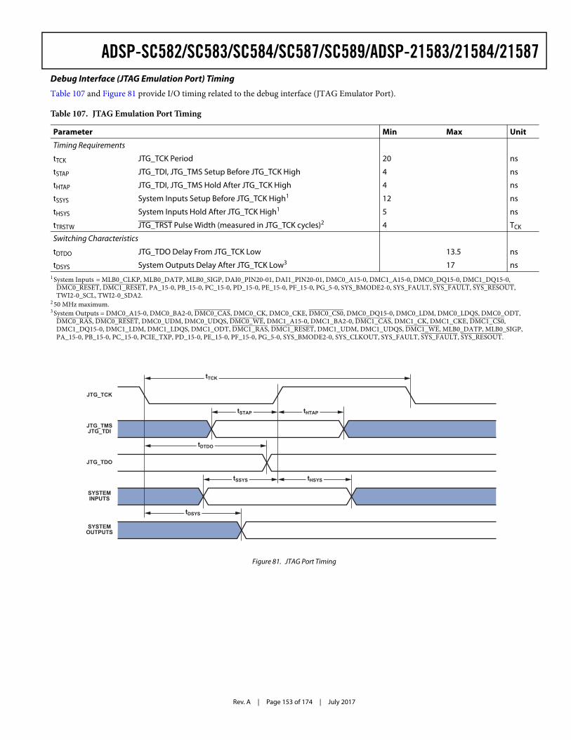
Rev. A | Page 153 of 174 | July 2017
ADSP-SC582/SC583/SC584/SC587/SC589/ADSP-21583/21584/21587Debug Interface (JTAG Emulation Port) Timing
Table 107 and Figure 81 provide I/O timing related to the debug interface (JTAG Emulator Port).
Table 107. JTAG Emulation Port Timing
Parameter Min Max Unit
Timing Requirements
tTCK JTG_TCK Period 20 ns
tSTAP JTG_TDI, JTG_TMS Setup Before JTG_TCK High 4 ns
tHTAP JTG_TDI, JTG_TMS Hold After JTG_TCK High 4 ns
tSSYS System Inputs Setup Before JTG_TCK High1
1 System Inputs = MLB0_CLKP, MLB0_DATP, MLB0_SIGP, DAI0_PIN20-01, DAI1_PIN20-01, DMC0_A15-0, DMC1_A15-0, DMC0_DQ15-0, DMC1_DQ15-0, DMC0_RESET, DMC1_RESET, PA_15-0, PB_15-0, PC_15-0, PD_15-0, PE_15-0, PF_15-0, PG_5-0, SYS_BMODE2-0, SYS_FAULT, SYS_FAULT, SYS_RESOUT, TWI2-0_SCL, TWI2-0_SDA2.
12 ns
tHSYS System Inputs Hold After JTG_TCK High1 5 ns
tTRSTW JTG_TRST Pulse Width (measured in JTG_TCK cycles)2
2 50 MHz maximum.
4 TCK
Switching Characteristics
tDTDO JTG_TDO Delay From JTG_TCK Low 13.5 ns
tDSYS System Outputs Delay After JTG_TCK Low3
3 System Outputs = DMC0_A15-0, DMC0_BA2-0, DMC0_CAS, DMC0_CK, DMC0_CKE, DMC0_CS0, DMC0_DQ15-0, DMC0_LDM, DMC0_LDQS, DMC0_ODT, DMC0_RAS, DMC0_RESET, DMC0_UDM, DMC0_UDQS, DMC0_WE, DMC1_A15-0, DMC1_BA2-0, DMC1_CAS, DMC1_CK, DMC1_CKE, DMC1_CS0, DMC1_DQ15-0, DMC1_LDM, DMC1_LDQS, DMC1_ODT, DMC1_RAS, DMC1_RESET, DMC1_UDM, DMC1_UDQS, DMC1_WE, MLB0_DATP, MLB0_SIGP, PA_15-0, PB_15-0, PC_15-0, PCIE_TXP, PD_15-0, PE_15-0, PF_15-0, PG_5-0, SYS_BMODE2-0, SYS_CLKOUT, SYS_FAULT, SYS_FAULT, SYS_RESOUT.
17 ns
Figure 81. JTAG Port Timing
JTG_TCK
JTG_TMSJTG_TDI
JTG_TDO
SYSTEMINPUTS
SYSTEMOUTPUTS
tTCK
tSTAP tHTAP
tDTDO
tSSYS tHSYS
tDSYS
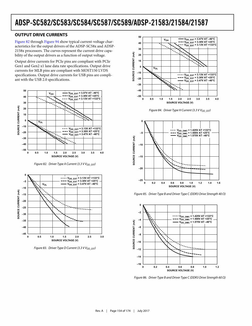
Rev. A | Page 154 of 174 | July 2017
ADSP-SC582/SC583/SC584/SC587/SC589/ADSP-21583/21584/21587OUTPUT DRIVE CURRENTSFigure 82 through Figure 94 show typical current-voltage char-acteristics for the output drivers of the ADSP-SC58x and ADSP-2158x processors. The curves represent the current drive capa-bility of the output drivers as a function of output voltage.Output drive currents for PCIe pins are compliant with PCIe Gen1 and Gen2 x1 lane data rate specifications. Output drive currents for MLB pins are compliant with MOST150 LVDS specifications. Output drive currents for USB pins are compli-ant with the USB 2.0 specifications.
Figure 82. Driver Type A Current (3.3 V VDD_EXT)
Figure 83. Driver Type D Current (3.3 V VDD_EXT)
–50
–40
–30
–20
–10
0
10
20
30
40
50
0 0.5 1.0 1.5 2.0 2.5 3.0 3.5 4.0
SOU
RC
E C
UR
REN
T (m
A)
SOURCE VOLTAGE (V)
VOH
VOL
VDD_EXT = 3.13V AT +133°C
VDD_EXT = 3.47V AT –40°CVDD_EXT = 3.30V AT +25°C
VDD_EXT = 3.13V AT +133°C
VDD_EXT = 3.47V AT –40°CVDD_EXT = 3.30V AT +25°C
0 0.5 1.0 1.5 2.0 2.5 3.0
SOU
RC
E C
UR
REN
T (m
A)
SOURCE VOLTAGE (V)
–45
–40
–35
–30
–25
–20
–15
–10
–5
0
VOL
VDD_EXT = 3.13V AT +133°C
VDD_EXT = 3.47V AT –40°CVDD_EXT = 3.30V AT +25°C
Figure 84. Driver Type H Current (3.3 V VDD_EXT)
Figure 85. Driver Type B and Driver Type C (DDR3 Drive Strength 40 Ω)
Figure 86. Driver Type B and Driver Type C (DDR3 Drive Strength 60 Ω)
–50
–40
–30
–20
–10
0
10
20
30
40
50
0 0.5 1.0 1.5 2.0 2.5 3.0 3.5 4.0
SOU
RC
E C
UR
REN
T (m
A)
SOURCE VOLTAGE (V)
VOH
VOL
VDD_EXT = 3.13V AT +133°C
VDD_EXT = 3.47V AT –40°CVDD_EXT = 3.30V AT +25°C
VDD_EXT = 3.13V AT +133°C
VDD_EXT = 3.47V AT –40°CVDD_EXT = 3.30V AT +25°C
–25
–20
–15
–10
–5
0
0 0.2 0.4 0.6 0.8 1.0 1.2 1.4 1.6
SOU
RC
E C
UR
REN
T (m
A)
SOURCE VOLTAGE (V)
VDD_DMC = 1.425V AT +133°C
VDD_DMC = 1.575V AT –40°CVDD_DMC = 1.500V AT +25°C
–16
–14
–10
–6
–12
–8
–4
–2
0
0 0.2 0.4 0.6 0.8 1.0 1.2
SOU
RC
E C
UR
REN
T (m
A)
SOURCE VOLTAGE (V)
VDD_DMC = 1.425V AT +133°C
VDD_DMC = 1.575V AT –40°CVDD_DMC = 1.500V AT +25°C
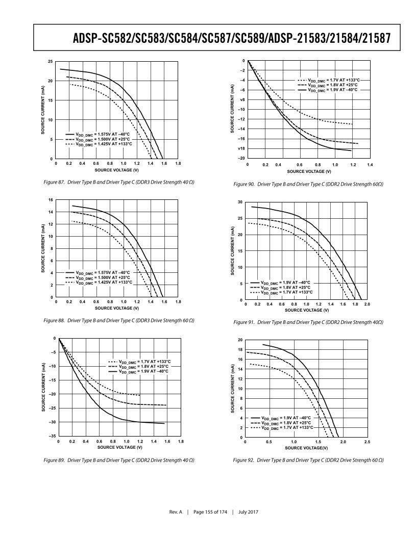
Rev. A | Page 155 of 174 | July 2017
ADSP-SC582/SC583/SC584/SC587/SC589/ADSP-21583/21584/21587
Figure 87. Driver Type B and Driver Type C (DDR3 Drive Strength 40 Ω)
Figure 88. Driver Type B and Driver Type C (DDR3 Drive Strength 60 Ω)
Figure 89. Driver Type B and Driver Type C (DDR2 Drive Strength 40 Ω)
0
5
10
15
20
25
0 0.2 0.4 0.6 0.8 1.0 1.2 1.4 1.6 1.8
SOU
RC
E C
UR
REN
T (m
A)
SOURCE VOLTAGE (V)
VDD_DMC = 1.425V AT +133°C
VDD_DMC = 1.575V AT –40°CVDD_DMC = 1.500V AT +25°C
0 0.2 0.4 0.6 0.8 1.0 1.2 1.4 1.6 1.8
SOU
RC
E C
UR
REN
T (m
A)
SOURCE VOLTAGE (V)
VDD_DMC = 1.425V AT +133°C
VDD_DMC = 1.575V AT –40°CVDD_DMC = 1.500V AT +25°C
0
2
4
6
8
10
12
14
16
–35
–30
–25
–20
–15
–10
–5
0
0 0.2 0.4 0.6 0.8 1.0 1.2 1.4 1.6 1.8
SOU
RC
E C
UR
REN
T (m
A)
SOURCE VOLTAGE (V)
VDD_DMC = 1.7V AT +133°C
VDD_DMC = 1.9V AT –40°CVDD_DMC = 1.8V AT +25°C
Figure 90. Driver Type B and Driver Type C (DDR2 Drive Strength 60Ω)
Figure 91. Driver Type B and Driver Type C (DDR2 Drive Strength 40Ω)
Figure 92. Driver Type B and Driver Type C (DDR2 Drive Strength 60 Ω)
–20
v18
–16
–14
–12
–10
v8
–6
–4
–2
0
0 0.2 0.4 0.6 0.8 1.0 1.2 1.4
SOU
RC
E C
UR
REN
T (m
A)
SOURCE VOLTAGE (V)
VDD_DMC = 1.7V AT +133°C
VDD_DMC = 1.9V AT –40°CVDD_DMC = 1.8V AT +25°C
5
0
10
15
20
25
30
SOU
RC
E C
UR
REN
T (m
A)
SOURCE VOLTAGE (V)0 0.2 0.4 0.6 0.8 1.0 1.2 1.4 1.6 1.8 2.0
VDD_DMC = 1.7V AT +133°C
VDD_DMC = 1.9V AT –40°CVDD_DMC = 1.8V AT +25°C
0
2
4
6
8
10
12
14
16
20
18
0 0.5 1.0 1.5 2.0 2.5
SOU
RC
E C
UR
REN
T (m
A)
SOURCE VOLTAGE(V)
VDD_DMC = 1.7V AT +133°C
VDD_DMC = 1.9V AT –40°CVDD_DMC = 1.8V AT +25°C
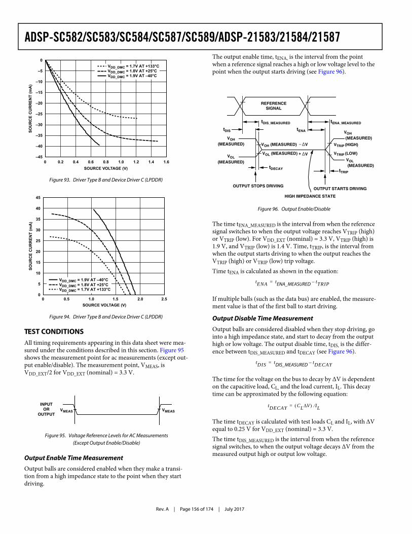
Rev. A | Page 156 of 174 | July 2017
ADSP-SC582/SC583/SC584/SC587/SC589/ADSP-21583/21584/21587
TEST CONDITIONSAll timing requirements appearing in this data sheet were mea-sured under the conditions described in this section. Figure 95 shows the measurement point for ac measurements (except out-put enable/disable). The measurement point, VMEAS, is VDD_EXT/2 for VDD_EXT (nominal) = 3.3 V.
Output Enable Time Measurement
Output balls are considered enabled when they make a transi-tion from a high impedance state to the point when they start driving.
The output enable time, tENA, is the interval from the point when a reference signal reaches a high or low voltage level to the point when the output starts driving (see Figure 96).
The time tENA_MEASURED is the interval from when the reference signal switches to when the output voltage reaches VTRIP (high) or VTRIP (low). For VDD_EXT (nominal) = 3.3 V, VTRIP (high) is 1.9 V, and VTRIP (low) is 1.4 V. Time, tTRIP, is the interval from when the output starts driving to when the output reaches the VTRIP (high) or VTRIP (low) trip voltage. Time tENA is calculated as shown in the equation:
If multiple balls (such as the data bus) are enabled, the measure-ment value is that of the first ball to start driving.
Output Disable Time Measurement
Output balls are considered disabled when they stop driving, go into a high impedance state, and start to decay from the output high or low voltage. The output disable time, tDIS, is the differ-ence between tDIS_MEASURED and tDECAY (see Figure 96).
The time for the voltage on the bus to decay by ΔV is dependent on the capacitive load, CL, and the load current, IL. This decay time can be approximated by the following equation:
The time tDECAY is calculated with test loads CL and IL, with V equal to 0.25 V for VDD_EXT (nominal) = 3.3 V.The time tDIS_MEASURED is the interval from when the reference signal switches, to when the output voltage decays ΔV from the measured output high or output low voltage.
Figure 93. Driver Type B and Device Driver C (LPDDR)
Figure 94. Driver Type B and Device Driver C (LPDDR)
Figure 95. Voltage Reference Levels for AC Measurements (Except Output Enable/Disable)
–45
–40
–35
–30
–25
–20
–15
–10
–5
0
0 0.2 0.4 0.6 0.8 1.0 1.2 1.4 1.6
SOU
RC
E C
UR
REN
T (m
A)
SOURCE VOLTAGE (V)
VDD_DMC = 1.7V AT +133°C
VDD_DMC = 1.9V AT –40°CVDD_DMC = 1.8V AT +25°C
0
5
10
15
20
25
30
35
40
45
0 0.5 1.0 1.5 2.0 2.5
SOU
RC
E C
UR
REN
T (m
A)
SOURCE VOLTAGE (V)
VDD_DMC = 1.7V AT +133°C
VDD_DMC = 1.9V AT –40°CVDD_DMC = 1.8V AT +25°C
INPUTOR
OUTPUTVMEAS VMEAS
Figure 96. Output Enable/Disable
REFERENCESIGNAL
tDIS
OUTPUT STARTS DRIVING
VOH (MEASURED) V
VOL (MEASURED) +
tDIS_MEASURED
VOH(MEASURED)
VOL(MEASURED)
VTRIP (HIGH)
VOH(MEASURED)
HIGH IMPEDANCE STATE
OUTPUT STOPS DRIVING
tENA
tDECAY
tENA_MEASURED
tTRIP
VOL(MEASURED)
VTRIP (LOW)
Δ-
VΔ
tENA tENA_MEASURED tTRIP–=
tDIS tDIS_MEASURED tDECAY–=
tDECAY CL V IL=
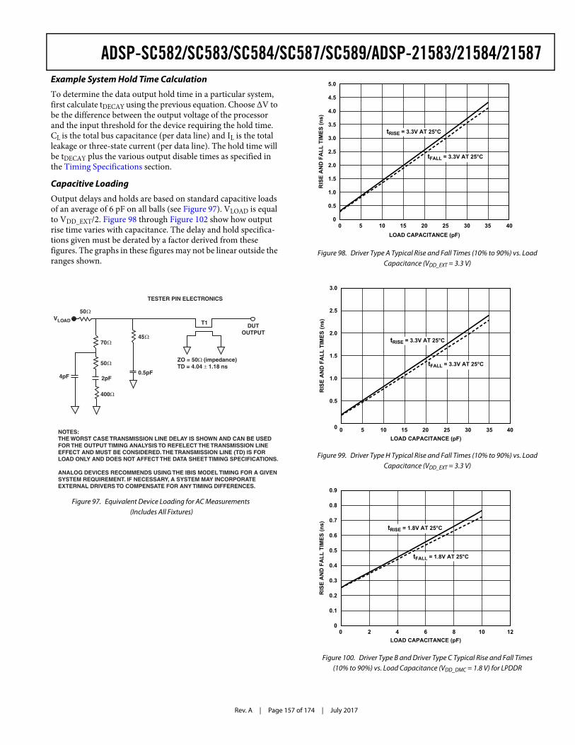
Rev. A | Page 157 of 174 | July 2017
ADSP-SC582/SC583/SC584/SC587/SC589/ADSP-21583/21584/21587Example System Hold Time Calculation
To determine the data output hold time in a particular system, first calculate tDECAY using the previous equation. Choose ΔV to be the difference between the output voltage of the processor and the input threshold for the device requiring the hold time. CL is the total bus capacitance (per data line) and IL is the total leakage or three-state current (per data line). The hold time will be tDECAY plus the various output disable times as specified in the Timing Specifications section.
Capacitive Loading
Output delays and holds are based on standard capacitive loads of an average of 6 pF on all balls (see Figure 97). VLOAD is equal to VDD_EXT/2. Figure 98 through Figure 102 show how output rise time varies with capacitance. The delay and hold specifica-tions given must be derated by a factor derived from these figures. The graphs in these figures may not be linear outside the ranges shown.
Figure 97. Equivalent Device Loading for AC Measurements (Includes All Fixtures)
REFERENCESIGNAL
tDIS
OUTPUT STARTS DRIVING
VOH (MEASURED) V
VOL (MEASURED) +
tDIS_MEASURED
VOH(MEASURED)
VOL(MEASURED)
VTRIP (HIGH)
VOH(MEASURED)
HIGH IMPEDANCE STATE
OUTPUT STOPS DRIVING
tENA
tDECAY
tENA_MEASURED
tTRIP
VOL(MEASURED)
VTRIP (LOW)
Δ-
VΔ
T1
ZO = 50Ω (impedance)TD = 4.04 ± 1.18 ns
2pF
TESTER PIN ELECTRONICS
50Ω
0.5pF
70Ω
400Ω
45Ω
4pF
NOTES:THE WORST CASE TRANSMISSION LINE DELAY IS SHOWN AND CAN BE USEDFOR THE OUTPUT TIMING ANALYSIS TO REFELECT THE TRANSMISSION LINEEFFECT AND MUST BE CONSIDERED. THE TRANSMISSION LINE (TD) IS FOR LOAD ONLY AND DOES NOT AFFECT THE DATA SHEET TIMING SPECIFICATIONS.
ANALOG DEVICES RECOMMENDS USING THE IBIS MODEL TIMING FOR A GIVEN SYSTEM REQUIREMENT. IF NECESSARY, A SYSTEM MAY INCORPORATE EXTERNAL DRIVERS TO COMPENSATE FOR ANY TIMING DIFFERENCES.
VLOADDUT
OUTPUT
50Ω
Figure 98. Driver Type A Typical Rise and Fall Times (10% to 90%) vs. Load Capacitance (VDD_EXT = 3.3 V)
Figure 99. Driver Type H Typical Rise and Fall Times (10% to 90%) vs. Load Capacitance (VDD_EXT = 3.3 V)
Figure 100. Driver Type B and Driver Type C Typical Rise and Fall Times (10% to 90%) vs. Load Capacitance (VDD_DMC = 1.8 V) for LPDDR
0
0.5
1.0
1.5
2.0
2.5
3.0
3.5
4.0
4.5
5.0
0 5 10 15 20 25 30 35 40
RIS
E A
ND
FA
LL T
IMES
(ns)
LOAD CAPACITANCE (pF)
tFALL = 3.3V AT 25°C
tRISE = 3.3V AT 25°C
0
0.5
1.0
1.5
2.0
2.5
3.0
0 5 10 15 20 25 30 35 40
RIS
E A
ND
FA
LL T
IMES
(ns)
LOAD CAPACITANCE (pF)
tFALL = 3.3V AT 25°C
tRISE = 3.3V AT 25°C
0
0.1
0.2
0.3
0.4
0.5
0.6
0.7
0.8
0.9
0 2 4 6 8 10 12
RIS
E A
ND
FA
LL T
IMES
(ns)
LOAD CAPACITANCE (pF)
tRISE = 1.8V AT 25°C
tFALL = 1.8V AT 25°C
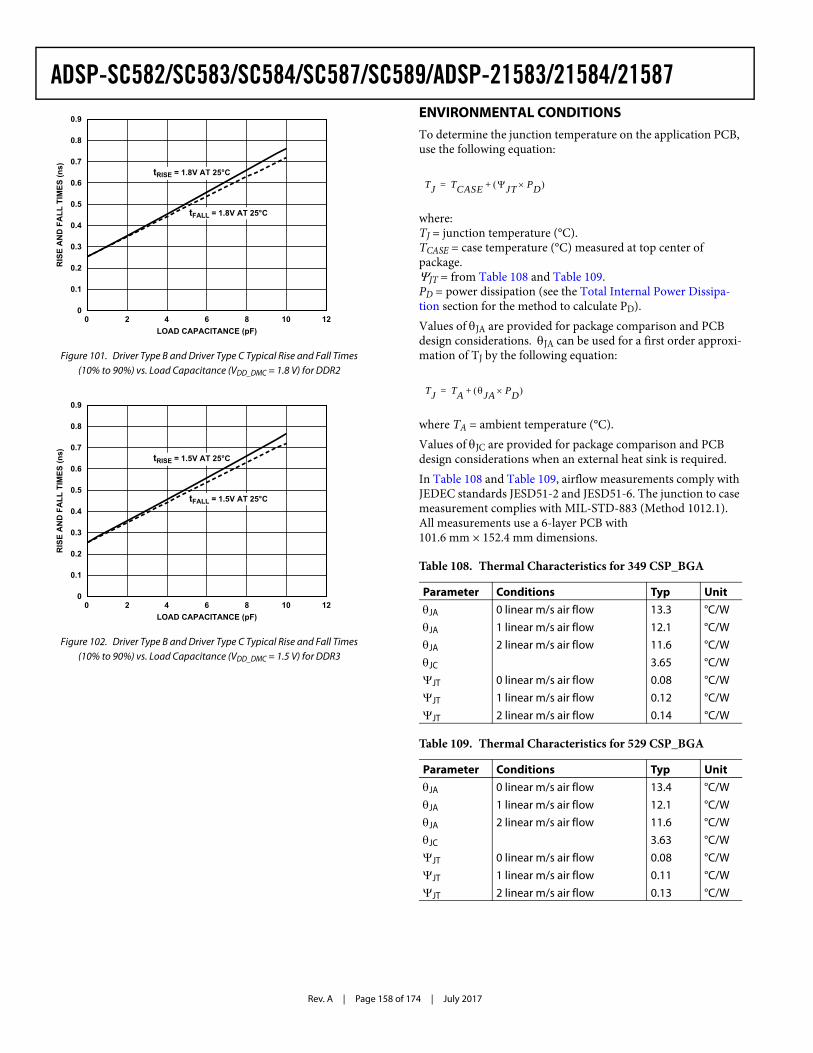
Rev. A | Page 158 of 174 | July 2017
ADSP-SC582/SC583/SC584/SC587/SC589/ADSP-21583/21584/21587ENVIRONMENTAL CONDITIONSTo determine the junction temperature on the application PCB, use the following equation:
where:TJ = junction temperature (°C).TCASE = case temperature (°C) measured at top center of package.JT = from Table 108 and Table 109.PD = power dissipation (see the Total Internal Power Dissipa-tion section for the method to calculate PD).Values of JA are provided for package comparison and PCB design considerations. JA can be used for a first order approxi-mation of TJ by the following equation:
where TA = ambient temperature (°C).Values of JC are provided for package comparison and PCB design considerations when an external heat sink is required.In Table 108 and Table 109, airflow measurements comply with JEDEC standards JESD51-2 and JESD51-6. The junction to case measurement complies with MIL-STD-883 (Method 1012.1). All measurements use a 6-layer PCB with 101.6 mm × 152.4 mm dimensions.
Figure 101. Driver Type B and Driver Type C Typical Rise and Fall Times (10% to 90%) vs. Load Capacitance (VDD_DMC = 1.8 V) for DDR2
Figure 102. Driver Type B and Driver Type C Typical Rise and Fall Times (10% to 90%) vs. Load Capacitance (VDD_DMC = 1.5 V) for DDR3
0
0.1
0.2
0.3
0.4
0.5
0.6
0.7
0.8
0.9
0 2 4 6 8 10 12
RIS
E A
ND
FA
LL T
IMES
(ns)
LOAD CAPACITANCE (pF)
tRISE = 1.8V AT 25°C
tFALL = 1.8V AT 25°C
0
0.1
0.2
0.3
0.4
0.5
0.6
0.7
0.8
0.9
0 2 4 6 8 10 12
RIS
E A
ND
FA
LL T
IMES
(ns)
LOAD CAPACITANCE (pF)
tRISE = 1.5V AT 25°C
tFALL = 1.5V AT 25°C
Table 108. Thermal Characteristics for 349 CSP_BGA
Parameter Conditions Typ UnitJA 0 linear m/s air flow 13.3 °C/WJA 1 linear m/s air flow 12.1 °C/WJA 2 linear m/s air flow 11.6 °C/WJC 3.65 °C/WJT 0 linear m/s air flow 0.08 °C/WJT 1 linear m/s air flow 0.12 °C/WJT 2 linear m/s air flow 0.14 °C/W
Table 109. Thermal Characteristics for 529 CSP_BGA
Parameter Conditions Typ UnitJA 0 linear m/s air flow 13.4 °C/WJA 1 linear m/s air flow 12.1 °C/WJA 2 linear m/s air flow 11.6 °C/WJC 3.63 °C/WJT 0 linear m/s air flow 0.08 °C/WJT 1 linear m/s air flow 0.11 °C/WJT 2 linear m/s air flow 0.13 °C/W
TJ TCASE JT PD +=
TJ TA JA PD +=
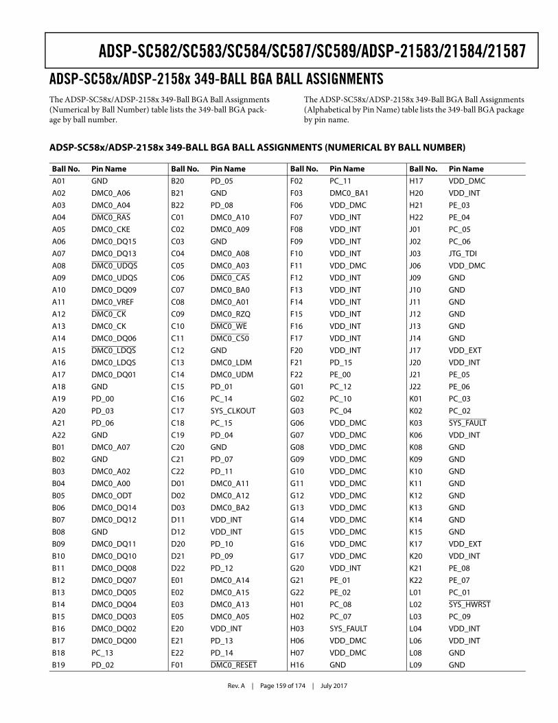
Rev. A | Page 159 of 174 | July 2017
ADSP-SC582/SC583/SC584/SC587/SC589/ADSP-21583/21584/21587ADSP-SC58x/ADSP-2158x 349-BALL BGA BALL ASSIGNMENTS The ADSP-SC58x/ADSP-2158x 349-Ball BGA Ball Assignments (Numerical by Ball Number) table lists the 349-ball BGA pack-age by ball number.
The ADSP-SC58x/ADSP-2158x 349-Ball BGA Ball Assignments (Alphabetical by Pin Name) table lists the 349-ball BGA package by pin name.
ADSP-SC58x/ADSP-2158x 349-BALL BGA BALL ASSIGNMENTS (NUMERICAL BY BALL NUMBER)
Ball No. Pin NameA01 GND
A02 DMC0_A06
A03 DMC0_A04
A04 DMC0_RAS
A05 DMC0_CKE
A06 DMC0_DQ15
A07 DMC0_DQ13
A08 DMC0_UDQS
A09 DMC0_UDQS
A10 DMC0_DQ09
A11 DMC0_VREF
A12 DMC0_CK
A13 DMC0_CK
A14 DMC0_DQ06
A15 DMC0_LDQS
A16 DMC0_LDQS
A17 DMC0_DQ01
A18 GND
A19 PD_00
A20 PD_03
A21 PD_06
A22 GND
B01 DMC0_A07
B02 GND
B03 DMC0_A02
B04 DMC0_A00
B05 DMC0_ODT
B06 DMC0_DQ14
B07 DMC0_DQ12
B08 GND
B09 DMC0_DQ11
B10 DMC0_DQ10
B11 DMC0_DQ08
B12 DMC0_DQ07
B13 DMC0_DQ05
B14 DMC0_DQ04
B15 DMC0_DQ03
B16 DMC0_DQ02
B17 DMC0_DQ00
B18 PC_13
B19 PD_02
B20 PD_05
B21 GND
B22 PD_08
C01 DMC0_A10
C02 DMC0_A09
C03 GND
C04 DMC0_A08
C05 DMC0_A03
C06 DMC0_CAS
C07 DMC0_BA0
C08 DMC0_A01
C09 DMC0_RZQ
C10 DMC0_WE
C11 DMC0_CS0
C12 GND
C13 DMC0_LDM
C14 DMC0_UDM
C15 PD_01
C16 PC_14
C17 SYS_CLKOUT
C18 PC_15
C19 PD_04
C20 GND
C21 PD_07
C22 PD_11
D01 DMC0_A11
D02 DMC0_A12
D03 DMC0_BA2
D11 VDD_INT
D12 VDD_INT
D20 PD_10
D21 PD_09
D22 PD_12
E01 DMC0_A14
E02 DMC0_A15
E03 DMC0_A13
E05 DMC0_A05
E20 VDD_INT
E21 PD_13
E22 PD_14
F01 DMC0_RESET
Ball No. Pin NameF02 PC_11
F03 DMC0_BA1
F06 VDD_DMC
F07 VDD_INT
F08 VDD_INT
F09 VDD_INT
F10 VDD_INT
F11 VDD_DMC
F12 VDD_INT
F13 VDD_INT
F14 VDD_INT
F15 VDD_INT
F16 VDD_INT
F17 VDD_INT
F20 VDD_INT
F21 PD_15
F22 PE_00
G01 PC_12
G02 PC_10
G03 PC_04
G06 VDD_DMC
G07 VDD_DMC
G08 VDD_DMC
G09 VDD_DMC
G10 VDD_DMC
G11 VDD_DMC
G12 VDD_DMC
G13 VDD_DMC
G14 VDD_DMC
G15 VDD_DMC
G16 VDD_DMC
G17 VDD_DMC
G20 VDD_INT
G21 PE_01
G22 PE_02
H01 PC_08
H02 PC_07
H03 SYS_FAULT
H06 VDD_DMC
H07 VDD_DMC
H16 GND
Ball No. Pin NameH17 VDD_DMC
H20 VDD_INT
H21 PE_03
H22 PE_04
J01 PC_05
J02 PC_06
J03 JTG_TDI
J06 VDD_DMC
J09 GND
J10 GND
J11 GND
J12 GND
J13 GND
J14 GND
J17 VDD_EXT
J20 VDD_INT
J21 PE_05
J22 PE_06
K01 PC_03
K02 PC_02
K03 SYS_FAULT
K06 VDD_INT
K08 GND
K09 GND
K10 GND
K11 GND
K12 GND
K13 GND
K14 GND
K15 GND
K17 VDD_EXT
K20 VDD_INT
K21 PE_08
K22 PE_07
L01 PC_01
L02 SYS_HWRST
L03 PC_09
L04 VDD_INT
L06 VDD_INT
L08 GND
L09 GND
Ball No. Pin Name
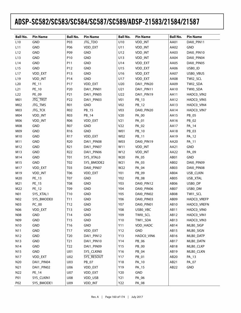
Rev. A | Page 160 of 174 | July 2017
ADSP-SC582/SC583/SC584/SC587/SC589/ADSP-21583/21584/21587
L10 GND
L11 GND
L12 GND
L13 GND
L14 GND
L15 GND
L17 VDD_EXT
L19 VDD_INT
L20 PE_11
L21 PE_10
L22 PE_09
M01 JTG_TRST
M02 JTG_TMS
M03 JTG_TCK
M04 VDD_INT
M06 VDD_INT
M08 GND
M09 GND
M10 GND
M11 GND
M12 GND
M13 GND
M14 GND
M15 GND
M17 VDD_EXT
M19 VDD_INT
M20 PE_13
M21 PE_15
M22 PE_12
N01 SYS_XTAL1
N02 SYS_BMODE0
N03 PC_00
N06 VDD_EXT
N08 GND
N09 GND
N10 GND
N11 GND
N12 GND
N13 GND
N14 GND
N15 GND
N17 VDD_EXT
N20 DAI1_PIN04
N21 DAI1_PIN02
N22 PE_14
P01 SYS_CLKIN1
P02 SYS_BMODE1
Ball No. Pin NameP03 JTG_TDO
P06 VDD_EXT
P09 GND
P10 GND
P11 GND
P12 GND
P13 GND
P14 GND
P17 VDD_EXT
P20 DAI1_PIN01
P21 DAI1_PIN05
P22 DAI1_PIN03
R01 GND
R02 PB_15
R03 PB_14
R06 VDD_EXT
R07 GND
R16 GND
R17 VDD_EXT
R20 DAI1_PIN08
R21 DAI1_PIN07
R22 DAI1_PIN06
T01 SYS_XTAL0
T02 SYS_BMODE2
T03 DAI0_PIN07
T06 VDD_EXT
T07 GND
T08 GND
T09 GND
T10 GND
T11 GND
T12 GND
T13 GND
T14 GND
T15 GND
T16 GND
T17 VDD_EXT
T20 DAI1_PIN12
T21 DAI1_PIN10
T22 DAI1_PIN09
U01 SYS_CLKIN0
U02 SYS_RESOUT
U03 PB_07
U06 VDD_EXT
U07 VDD_EXT
U08 VDD_USB
U09 VDD_INT
Ball No. Pin NameU10 VDD_INT
U11 VDD_INT
U12 VDD_INT
U13 VDD_INT
U14 VDD_EXT
U15 VDD_EXT
U16 VDD_EXT
U17 VDD_EXT
U20 DAI1_PIN20
U21 DAI1_PIN11
U22 DAI1_PIN19
V01 PB_13
V02 PB_12
V03 DAI0_PIN20
V20 PA_00
V21 PA_01
V22 PA_02
W01 PB_10
W02 PB_11
W03 DAI0_PIN19
W11 VDD_INT
W12 VDD_INT
W20 PA_05
W21 PA_03
W22 PA_04
Y01 PB_09
Y02 PB_08
Y03 DAI0_PIN12
Y04 DAI0_PIN06
Y05 DAI0_PIN02
Y06 DAI0_PIN03
Y07 DAI0_PIN01
Y08 USB0_VBC
Y09 TWI0_SCL
Y10 TWI1_SDA
Y11 VDD_HADC
Y12 GND
Y13 HADC0_VIN6
Y14 PB_06
Y15 PB_00
Y16 PB_04
Y17 PB_01
Y18 PA_10
Y19 PA_15
Y20 GND
Y21 PA_06
Y22 PA_08
Ball No. Pin NameAA01 DAI0_PIN11
AA02 GND
AA03 DAI0_PIN10
AA04 DAI0_PIN04
AA05 DAI0_PIN05
AA06 USB0_ID
AA07 USB0_VBUS
AA08 TWI2_SCL
AA09 TWI2_SDA
AA10 TWI0_SDA
AA11 HADC0_VIN2
AA12 HADC0_VIN5
AA13 HADC0_VIN4
AA14 HADC0_VIN7
AA15 PB_05
AA16 PB_02
AA17 PA_14
AA18 PB_03
AA19 PA_12
AA20 PA_11
AA21 GND
AA22 PA_09
AB01 GND
AB02 DAI0_PIN09
AB03 DAI0_PIN08
AB04 USB_CLKIN
AB05 USB_XTAL
AB06 USB0_DP
AB07 USB0_DM
AB08 TWI1_SCL
AB09 HADC0_VREFP
AB10 HADC0_VREFN
AB11 HADC0_VIN0
AB12 HADC0_VIN1
AB13 HADC0_VIN3
AB14 MLB0_SIGP
AB15 MLB0_SIGN
AB16 MLB0_DATP
AB17 MLB0_DATN
AB18 MLB0_CLKP
AB19 MLB0_CLKN
AB20 PA_13
AB21 PA_07
AB22 GND
Ball No. Pin Name
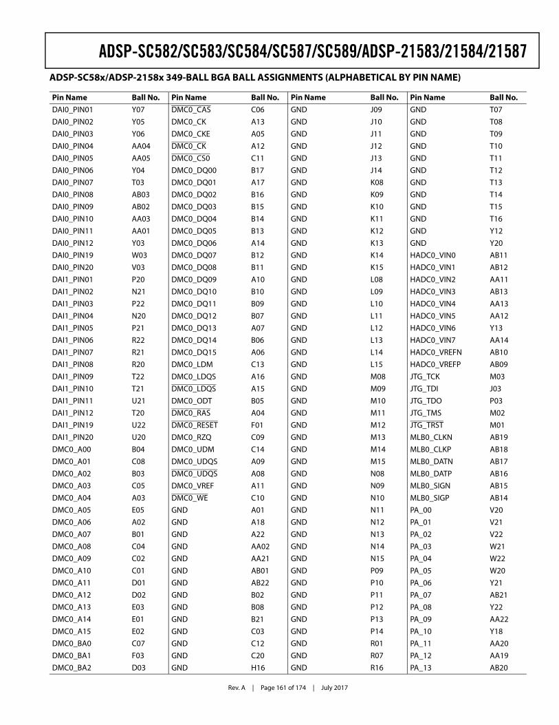
Rev. A | Page 161 of 174 | July 2017
ADSP-SC582/SC583/SC584/SC587/SC589/ADSP-21583/21584/21587ADSP-SC58x/ADSP-2158x 349-BALL BGA BALL ASSIGNMENTS (ALPHABETICAL BY PIN NAME)
Pin Name Ball No.DAI0_PIN01 Y07
DAI0_PIN02 Y05
DAI0_PIN03 Y06
DAI0_PIN04 AA04
DAI0_PIN05 AA05
DAI0_PIN06 Y04
DAI0_PIN07 T03
DAI0_PIN08 AB03
DAI0_PIN09 AB02
DAI0_PIN10 AA03
DAI0_PIN11 AA01
DAI0_PIN12 Y03
DAI0_PIN19 W03
DAI0_PIN20 V03
DAI1_PIN01 P20
DAI1_PIN02 N21
DAI1_PIN03 P22
DAI1_PIN04 N20
DAI1_PIN05 P21
DAI1_PIN06 R22
DAI1_PIN07 R21
DAI1_PIN08 R20
DAI1_PIN09 T22
DAI1_PIN10 T21
DAI1_PIN11 U21
DAI1_PIN12 T20
DAI1_PIN19 U22
DAI1_PIN20 U20
DMC0_A00 B04
DMC0_A01 C08
DMC0_A02 B03
DMC0_A03 C05
DMC0_A04 A03
DMC0_A05 E05
DMC0_A06 A02
DMC0_A07 B01
DMC0_A08 C04
DMC0_A09 C02
DMC0_A10 C01
DMC0_A11 D01
DMC0_A12 D02
DMC0_A13 E03
DMC0_A14 E01
DMC0_A15 E02
DMC0_BA0 C07
DMC0_BA1 F03
DMC0_BA2 D03
DMC0_CAS C06
DMC0_CK A13
DMC0_CKE A05
DMC0_CK A12
DMC0_CS0 C11
DMC0_DQ00 B17
DMC0_DQ01 A17
DMC0_DQ02 B16
DMC0_DQ03 B15
DMC0_DQ04 B14
DMC0_DQ05 B13
DMC0_DQ06 A14
DMC0_DQ07 B12
DMC0_DQ08 B11
DMC0_DQ09 A10
DMC0_DQ10 B10
DMC0_DQ11 B09
DMC0_DQ12 B07
DMC0_DQ13 A07
DMC0_DQ14 B06
DMC0_DQ15 A06
DMC0_LDM C13
DMC0_LDQS A16
DMC0_LDQS A15
DMC0_ODT B05
DMC0_RAS A04
DMC0_RESET F01
DMC0_RZQ C09
DMC0_UDM C14
DMC0_UDQS A09
DMC0_UDQS A08
DMC0_VREF A11
DMC0_WE C10
GND A01
GND A18
GND A22
GND AA02
GND AA21
GND AB01
GND AB22
GND B02
GND B08
GND B21
GND C03
GND C12
GND C20
GND H16
Pin Name Ball No.GND J09
GND J10
GND J11
GND J12
GND J13
GND J14
GND K08
GND K09
GND K10
GND K11
GND K12
GND K13
GND K14
GND K15
GND L08
GND L09
GND L10
GND L11
GND L12
GND L13
GND L14
GND L15
GND M08
GND M09
GND M10
GND M11
GND M12
GND M13
GND M14
GND M15
GND N08
GND N09
GND N10
GND N11
GND N12
GND N13
GND N14
GND N15
GND P09
GND P10
GND P11
GND P12
GND P13
GND P14
GND R01
GND R07
GND R16
Pin Name Ball No.GND T07
GND T08
GND T09
GND T10
GND T11
GND T12
GND T13
GND T14
GND T15
GND T16
GND Y12
GND Y20
HADC0_VIN0 AB11
HADC0_VIN1 AB12
HADC0_VIN2 AA11
HADC0_VIN3 AB13
HADC0_VIN4 AA13
HADC0_VIN5 AA12
HADC0_VIN6 Y13
HADC0_VIN7 AA14
HADC0_VREFN AB10
HADC0_VREFP AB09
JTG_TCK M03
JTG_TDI J03
JTG_TDO P03
JTG_TMS M02
JTG_TRST M01
MLB0_CLKN AB19
MLB0_CLKP AB18
MLB0_DATN AB17
MLB0_DATP AB16
MLB0_SIGN AB15
MLB0_SIGP AB14
PA_00 V20
PA_01 V21
PA_02 V22
PA_03 W21
PA_04 W22
PA_05 W20
PA_06 Y21
PA_07 AB21
PA_08 Y22
PA_09 AA22
PA_10 Y18
PA_11 AA20
PA_12 AA19
PA_13 AB20
Pin Name Ball No.
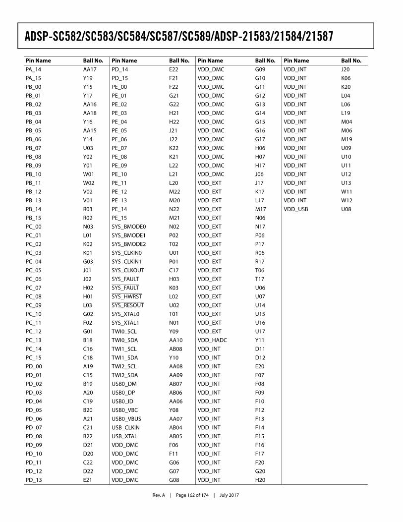
Rev. A | Page 162 of 174 | July 2017
ADSP-SC582/SC583/SC584/SC587/SC589/ADSP-21583/21584/21587
PA_14 AA17
PA_15 Y19
PB_00 Y15
PB_01 Y17
PB_02 AA16
PB_03 AA18
PB_04 Y16
PB_05 AA15
PB_06 Y14
PB_07 U03
PB_08 Y02
PB_09 Y01
PB_10 W01
PB_11 W02
PB_12 V02
PB_13 V01
PB_14 R03
PB_15 R02
PC_00 N03
PC_01 L01
PC_02 K02
PC_03 K01
PC_04 G03
PC_05 J01
PC_06 J02
PC_07 H02
PC_08 H01
PC_09 L03
PC_10 G02
PC_11 F02
PC_12 G01
PC_13 B18
PC_14 C16
PC_15 C18
PD_00 A19
PD_01 C15
PD_02 B19
PD_03 A20
PD_04 C19
PD_05 B20
PD_06 A21
PD_07 C21
PD_08 B22
PD_09 D21
PD_10 D20
PD_11 C22
PD_12 D22
PD_13 E21
Pin Name Ball No.PD_14 E22
PD_15 F21
PE_00 F22
PE_01 G21
PE_02 G22
PE_03 H21
PE_04 H22
PE_05 J21
PE_06 J22
PE_07 K22
PE_08 K21
PE_09 L22
PE_10 L21
PE_11 L20
PE_12 M22
PE_13 M20
PE_14 N22
PE_15 M21
SYS_BMODE0 N02
SYS_BMODE1 P02
SYS_BMODE2 T02
SYS_CLKIN0 U01
SYS_CLKIN1 P01
SYS_CLKOUT C17
SYS_FAULT H03
SYS_FAULT K03
SYS_HWRST L02
SYS_RESOUT U02
SYS_XTAL0 T01
SYS_XTAL1 N01
TWI0_SCL Y09
TWI0_SDA AA10
TWI1_SCL AB08
TWI1_SDA Y10
TWI2_SCL AA08
TWI2_SDA AA09
USB0_DM AB07
USB0_DP AB06
USB0_ID AA06
USB0_VBC Y08
USB0_VBUS AA07
USB_CLKIN AB04
USB_XTAL AB05
VDD_DMC F06
VDD_DMC F11
VDD_DMC G06
VDD_DMC G07
VDD_DMC G08
Pin Name Ball No.VDD_DMC G09
VDD_DMC G10
VDD_DMC G11
VDD_DMC G12
VDD_DMC G13
VDD_DMC G14
VDD_DMC G15
VDD_DMC G16
VDD_DMC G17
VDD_DMC H06
VDD_DMC H07
VDD_DMC H17
VDD_DMC J06
VDD_EXT J17
VDD_EXT K17
VDD_EXT L17
VDD_EXT M17
VDD_EXT N06
VDD_EXT N17
VDD_EXT P06
VDD_EXT P17
VDD_EXT R06
VDD_EXT R17
VDD_EXT T06
VDD_EXT T17
VDD_EXT U06
VDD_EXT U07
VDD_EXT U14
VDD_EXT U15
VDD_EXT U16
VDD_EXT U17
VDD_HADC Y11
VDD_INT D11
VDD_INT D12
VDD_INT E20
VDD_INT F07
VDD_INT F08
VDD_INT F09
VDD_INT F10
VDD_INT F12
VDD_INT F13
VDD_INT F14
VDD_INT F15
VDD_INT F16
VDD_INT F17
VDD_INT F20
VDD_INT G20
VDD_INT H20
Pin Name Ball No.VDD_INT J20
VDD_INT K06
VDD_INT K20
VDD_INT L04
VDD_INT L06
VDD_INT L19
VDD_INT M04
VDD_INT M06
VDD_INT M19
VDD_INT U09
VDD_INT U10
VDD_INT U11
VDD_INT U12
VDD_INT U13
VDD_INT W11
VDD_INT W12
VDD_USB U08
Pin Name Ball No.
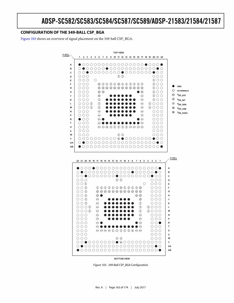
Rev. A | Page 163 of 174 | July 2017
ADSP-SC582/SC583/SC584/SC587/SC589/ADSP-21583/21584/21587CONFIGURATION OF THE 349-BALL CSP_BGAFigure 103 shows an overview of signal placement on the 349-ball CSP_BGA.
Figure 103. 349-Ball CSP_BGA Configuration
A1 BALLCORNER
15 14 13 12 11 10 9 8 7 5 4 3 2 116171819202122 6
A
B
C
D
E
FG
HJ
KL
M
N
P
RT
VW
AA
AB
U
Y
GND
VDD_INT
VDD_EXT
I/O SIGNALS
VDD_DDR
VDD_USBU
VDD_HADCH
BOTTOM VIEW
U
A1 BALLCORNER 15141312111098754321 16 17 18 19 20 21 226
TOP VIEW
A
B
C
D
E
FG
HJ
KL
M
N
P
RT
VW
AA
AB
U
Y
U
H
H
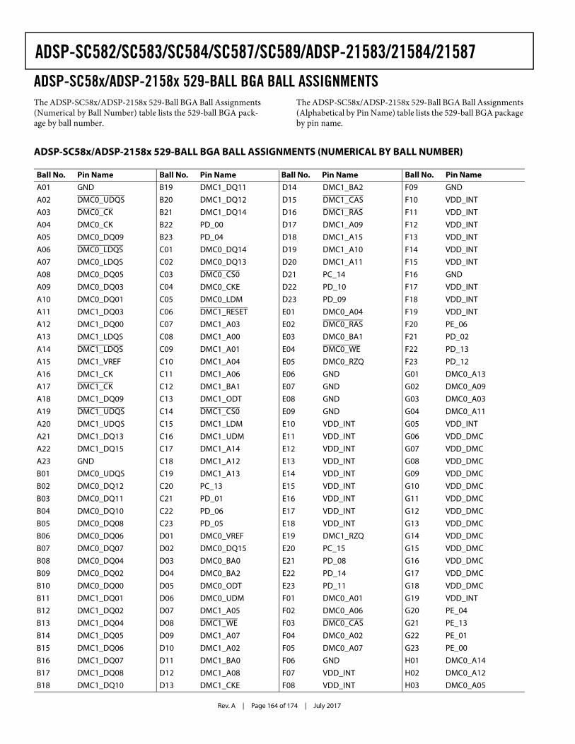
Rev. A | Page 164 of 174 | July 2017
ADSP-SC582/SC583/SC584/SC587/SC589/ADSP-21583/21584/21587
ADSP-SC58x/ADSP-2158x 529-BALL BGA BALL ASSIGNMENTSThe ADSP-SC58x/ADSP-2158x 529-Ball BGA Ball Assignments (Numerical by Ball Number) table lists the 529-ball BGA pack-age by ball number.
The ADSP-SC58x/ADSP-2158x 529-Ball BGA Ball Assignments (Alphabetical by Pin Name) table lists the 529-ball BGA package by pin name.
ADSP-SC58x/ADSP-2158x 529-BALL BGA BALL ASSIGNMENTS (NUMERICAL BY BALL NUMBER)
Ball No. Pin NameA01 GND
A02 DMC0_UDQS
A03 DMC0_CK
A04 DMC0_CK
A05 DMC0_DQ09
A06 DMC0_LDQS
A07 DMC0_LDQS
A08 DMC0_DQ05
A09 DMC0_DQ03
A10 DMC0_DQ01
A11 DMC1_DQ03
A12 DMC1_DQ00
A13 DMC1_LDQS
A14 DMC1_LDQS
A15 DMC1_VREF
A16 DMC1_CK
A17 DMC1_CK
A18 DMC1_DQ09
A19 DMC1_UDQS
A20 DMC1_UDQS
A21 DMC1_DQ13
A22 DMC1_DQ15
A23 GND
B01 DMC0_UDQS
B02 DMC0_DQ12
B03 DMC0_DQ11
B04 DMC0_DQ10
B05 DMC0_DQ08
B06 DMC0_DQ06
B07 DMC0_DQ07
B08 DMC0_DQ04
B09 DMC0_DQ02
B10 DMC0_DQ00
B11 DMC1_DQ01
B12 DMC1_DQ02
B13 DMC1_DQ04
B14 DMC1_DQ05
B15 DMC1_DQ06
B16 DMC1_DQ07
B17 DMC1_DQ08
B18 DMC1_DQ10
B19 DMC1_DQ11
B20 DMC1_DQ12
B21 DMC1_DQ14
B22 PD_00
B23 PD_04
C01 DMC0_DQ14
C02 DMC0_DQ13
C03 DMC0_CS0
C04 DMC0_CKE
C05 DMC0_LDM
C06 DMC1_RESET
C07 DMC1_A03
C08 DMC1_A00
C09 DMC1_A01
C10 DMC1_A04
C11 DMC1_A06
C12 DMC1_BA1
C13 DMC1_ODT
C14 DMC1_CS0
C15 DMC1_LDM
C16 DMC1_UDM
C17 DMC1_A14
C18 DMC1_A12
C19 DMC1_A13
C20 PC_13
C21 PD_01
C22 PD_06
C23 PD_05
D01 DMC0_VREF
D02 DMC0_DQ15
D03 DMC0_BA0
D04 DMC0_BA2
D05 DMC0_ODT
D06 DMC0_UDM
D07 DMC1_A05
D08 DMC1_WE
D09 DMC1_A07
D10 DMC1_A02
D11 DMC1_BA0
D12 DMC1_A08
D13 DMC1_CKE
Ball No. Pin NameD14 DMC1_BA2
D15 DMC1_CAS
D16 DMC1_RAS
D17 DMC1_A09
D18 DMC1_A15
D19 DMC1_A10
D20 DMC1_A11
D21 PC_14
D22 PD_10
D23 PD_09
E01 DMC0_A04
E02 DMC0_RAS
E03 DMC0_BA1
E04 DMC0_WE
E05 DMC0_RZQ
E06 GND
E07 GND
E08 GND
E09 GND
E10 VDD_INT
E11 VDD_INT
E12 VDD_INT
E13 VDD_INT
E14 VDD_INT
E15 VDD_INT
E16 VDD_INT
E17 VDD_INT
E18 VDD_INT
E19 DMC1_RZQ
E20 PC_15
E21 PD_08
E22 PD_14
E23 PD_11
F01 DMC0_A01
F02 DMC0_A06
F03 DMC0_CAS
F04 DMC0_A02
F05 DMC0_A07
F06 GND
F07 VDD_INT
F08 VDD_INT
Ball No. Pin NameF09 GND
F10 VDD_INT
F11 VDD_INT
F12 VDD_INT
F13 VDD_INT
F14 VDD_INT
F15 VDD_INT
F16 GND
F17 VDD_INT
F18 VDD_INT
F19 VDD_INT
F20 PE_06
F21 PD_02
F22 PD_13
F23 PD_12
G01 DMC0_A13
G02 DMC0_A09
G03 DMC0_A03
G04 DMC0_A11
G05 VDD_INT
G06 VDD_DMC
G07 VDD_DMC
G08 VDD_DMC
G09 VDD_DMC
G10 VDD_DMC
G11 VDD_DMC
G12 VDD_DMC
G13 VDD_DMC
G14 VDD_DMC
G15 VDD_DMC
G16 VDD_DMC
G17 VDD_DMC
G18 VDD_DMC
G19 VDD_INT
G20 PE_04
G21 PE_13
G22 PE_01
G23 PE_00
H01 DMC0_A14
H02 DMC0_A12
H03 DMC0_A05
Ball No. Pin Name
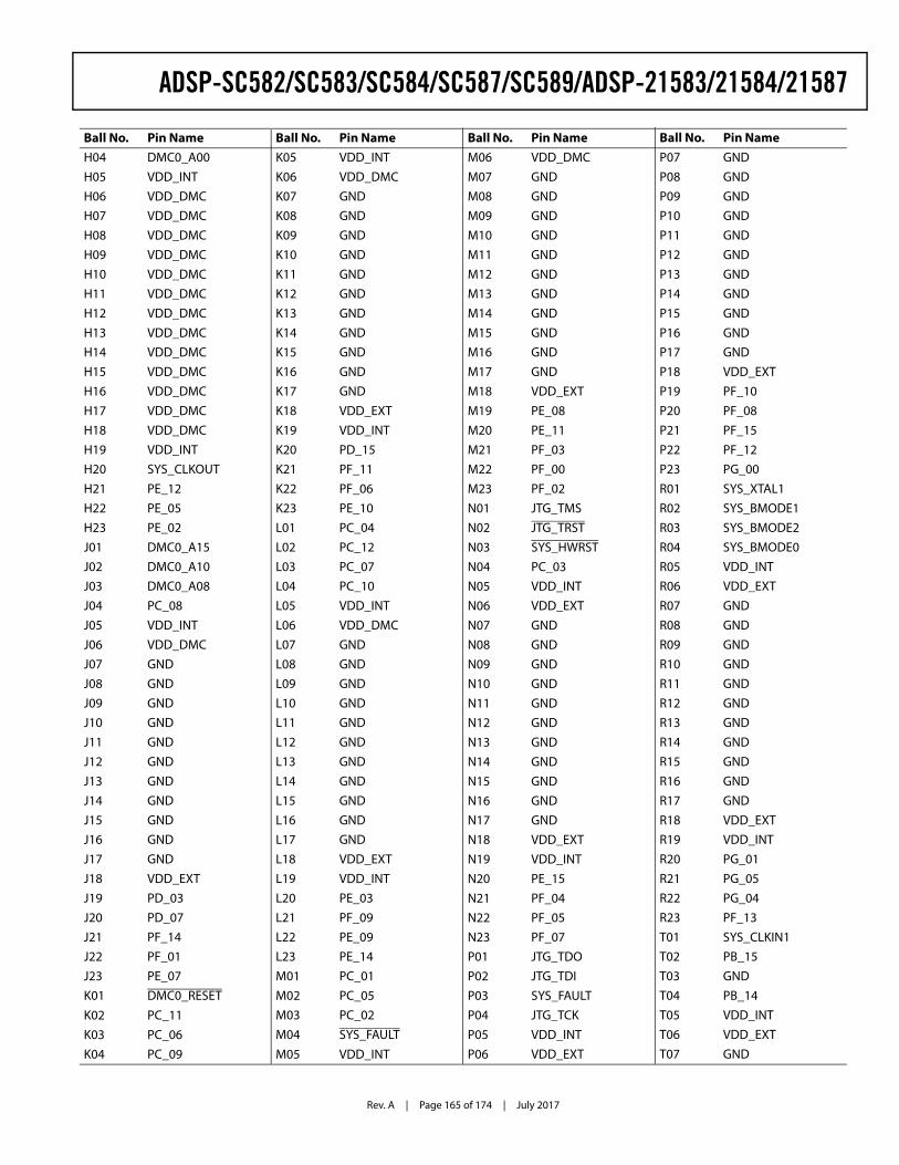
Rev. A | Page 165 of 174 | July 2017
ADSP-SC582/SC583/SC584/SC587/SC589/ADSP-21583/21584/21587
H04 DMC0_A00
H05 VDD_INT
H06 VDD_DMC
H07 VDD_DMC
H08 VDD_DMC
H09 VDD_DMC
H10 VDD_DMC
H11 VDD_DMC
H12 VDD_DMC
H13 VDD_DMC
H14 VDD_DMC
H15 VDD_DMC
H16 VDD_DMC
H17 VDD_DMC
H18 VDD_DMC
H19 VDD_INT
H20 SYS_CLKOUT
H21 PE_12
H22 PE_05
H23 PE_02
J01 DMC0_A15
J02 DMC0_A10
J03 DMC0_A08
J04 PC_08
J05 VDD_INT
J06 VDD_DMC
J07 GND
J08 GND
J09 GND
J10 GND
J11 GND
J12 GND
J13 GND
J14 GND
J15 GND
J16 GND
J17 GND
J18 VDD_EXT
J19 PD_03
J20 PD_07
J21 PF_14
J22 PF_01
J23 PE_07
K01 DMC0_RESET
K02 PC_11
K03 PC_06
K04 PC_09
Ball No. Pin NameK05 VDD_INT
K06 VDD_DMC
K07 GND
K08 GND
K09 GND
K10 GND
K11 GND
K12 GND
K13 GND
K14 GND
K15 GND
K16 GND
K17 GND
K18 VDD_EXT
K19 VDD_INT
K20 PD_15
K21 PF_11
K22 PF_06
K23 PE_10
L01 PC_04
L02 PC_12
L03 PC_07
L04 PC_10
L05 VDD_INT
L06 VDD_DMC
L07 GND
L08 GND
L09 GND
L10 GND
L11 GND
L12 GND
L13 GND
L14 GND
L15 GND
L16 GND
L17 GND
L18 VDD_EXT
L19 VDD_INT
L20 PE_03
L21 PF_09
L22 PE_09
L23 PE_14
M01 PC_01
M02 PC_05
M03 PC_02
M04 SYS_FAULT
M05 VDD_INT
Ball No. Pin NameM06 VDD_DMC
M07 GND
M08 GND
M09 GND
M10 GND
M11 GND
M12 GND
M13 GND
M14 GND
M15 GND
M16 GND
M17 GND
M18 VDD_EXT
M19 PE_08
M20 PE_11
M21 PF_03
M22 PF_00
M23 PF_02
N01 JTG_TMS
N02 JTG_TRST
N03 SYS_HWRST
N04 PC_03
N05 VDD_INT
N06 VDD_EXT
N07 GND
N08 GND
N09 GND
N10 GND
N11 GND
N12 GND
N13 GND
N14 GND
N15 GND
N16 GND
N17 GND
N18 VDD_EXT
N19 VDD_INT
N20 PE_15
N21 PF_04
N22 PF_05
N23 PF_07
P01 JTG_TDO
P02 JTG_TDI
P03 SYS_FAULT
P04 JTG_TCK
P05 VDD_INT
P06 VDD_EXT
Ball No. Pin NameP07 GND
P08 GND
P09 GND
P10 GND
P11 GND
P12 GND
P13 GND
P14 GND
P15 GND
P16 GND
P17 GND
P18 VDD_EXT
P19 PF_10
P20 PF_08
P21 PF_15
P22 PF_12
P23 PG_00
R01 SYS_XTAL1
R02 SYS_BMODE1
R03 SYS_BMODE2
R04 SYS_BMODE0
R05 VDD_INT
R06 VDD_EXT
R07 GND
R08 GND
R09 GND
R10 GND
R11 GND
R12 GND
R13 GND
R14 GND
R15 GND
R16 GND
R17 GND
R18 VDD_EXT
R19 VDD_INT
R20 PG_01
R21 PG_05
R22 PG_04
R23 PF_13
T01 SYS_CLKIN1
T02 PB_15
T03 GND
T04 PB_14
T05 VDD_INT
T06 VDD_EXT
T07 GND
Ball No. Pin Name
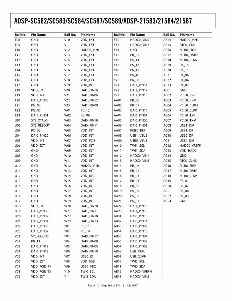
Rev. A | Page 166 of 174 | July 2017
ADSP-SC582/SC583/SC584/SC587/SC589/ADSP-21583/21584/21587
T08 GND
T09 GND
T10 GND
T11 GND
T12 GND
T13 GND
T14 GND
T15 GND
T16 GND
T17 GND
T18 VDD_EXT
T19 VDD_INT
T20 DAI1_PIN03
T21 PG_03
T22 PG_02
T23 DAI1_PIN01
U01 SYS_XTAL0
U02 SYS_RESOUT
U03 PC_00
U04 DAI0_PIN20
U05 VDD_INT
U06 VDD_EXT
U07 GND
U08 GND
U09 GND
U10 GND
U11 GND
U12 GND
U13 GND
U14 GND
U15 GND
U16 GND
U17 GND
U18 VDD_EXT
U19 DAI1_PIN08
U20 DAI1_PIN07
U21 DAI1_PIN04
U22 DAI1_PIN05
U23 DAI1_PIN02
V01 SYS_CLKIN0
V02 PB_13
V03 DAI0_PIN19
V04 DAI0_PIN12
V05 VDD_INT
V06 VDD_EXT
V07 VDD_PCIE_RX
V08 VDD_PCIE_TX
V09 VDD_EXT
Ball No. Pin NameV10 VDD_EXT
V11 VDD_EXT
V12 HADC0_VIN4
V13 VDD_EXT
V14 VDD_EXT
V15 VDD_EXT
V16 VDD_EXT
V17 VDD_EXT
V18 VDD_EXT
V19 VDD_INT
V20 DAI1_PIN16
V21 DAI1_PIN06
V22 DAI1_PIN12
V23 DAI1_PIN09
W01 PB_12
W02 PB_09
W03 DAI0_PIN18
W04 DAI0_PIN11
W05 VDD_INT
W06 VDD_INT
W07 VDD_PCIE
W08 VDD_INT
W09 VDD_INT
W10 VDD_INT
W11 VDD_INT
W12 HADC0_VIN6
W13 VDD_INT
W14 VDD_RTC
W15 VDD_INT
W16 VDD_INT
W17 VDD_INT
W18 VDD_INT
W19 VDD_INT
W20 DAI1_PIN20
W21 DAI1_PIN11
W22 DAI1_PIN10
W23 DAI1_PIN13
Y01 PB_11
Y02 PB_10
Y03 DAI0_PIN17
Y04 DAI0_PIN08
Y05 DAI0_PIN05
Y06 DAI0_PIN10
Y07 USB0_ID
Y08 VDD_USB
Y09 USB0_VBC
Y10 TWI0_SCL
Y11 TWI2_SDA
Ball No. Pin NameY12 HADC0_VIN0
Y13 HADC0_VIN7
Y14 GND
Y15 PB_05
Y16 PA_14
Y17 PA_13
Y18 PA_12
Y19 PA_10
Y20 PA_00
Y21 DAI1_PIN14
Y22 DAI1_PIN17
Y23 DAI1_PIN15
AA01 PB_08
AA02 PB_07
AA03 DAI0_PIN16
AA04 DAI0_PIN07
AA05 DAI0_PIN06
AA06 DAI0_PIN01
AA07 PCIE0_REF
AA08 USB1_VBUS
AA09 USB0_VBUS
AA10 TWI1_SCL
AA11 TWI1_SDA
AA12 HADC0_VIN1
AA13 HADC0_VIN5
AA14 PB_06
AA15 PB_02
AA16 PB_04
AA17 PB_03
AA18 PB_00
AA19 PA_09
AA20 PA_05
AA21 PA_01
AA22 DAI1_PIN19
AA23 DAI1_PIN18
AB01 DAI0_PIN15
AB02 DAI0_PIN14
AB03 DAI0_PIN09
AB04 DAI0_PIN13
AB05 DAI0_PIN04
AB06 DAI0_PIN02
AB07 DAI0_PIN03
AB08 USB_XTAL
AB09 USB_CLKIN
AB10 TWI2_SCL
AB11 TWI0_SDA
AB12 HADC0_VREFN
AB13 HADC0_VIN2
Ball No. Pin NameAB14 HADC0_VIN3
AB15 RTC0_XTAL
AB16 MLB0_SIGN
AB17 MLB0_DATN
AB18 MLB0_CLKN
AB19 PA_15
AB20 PA_11
AB21 PA_06
AB22 PA_04
AB23 PA_02
AC01 GND
AC02 PCIE0_RXP
AC03 PCIE0_RXM
AC04 PCIE0_CLKM
AC05 PCIE0_CLKP
AC06 PCIE0_TXP
AC07 PCIE0_TXM
AC08 USB1_DM
AC09 USB1_DP
AC10 USB0_DP
AC11 USB0_DM
AC12 HADC0_VREFP
AC13 VDD_HADC
AC14 GND
AC15 RTC0_CLKIN
AC16 MLB0_SIGP
AC17 MLB0_DATP
AC18 MLB0_CLKP
AC19 PB_01
AC20 PA_07
AC21 PA_08
AC22 PA_03
AC23 GND
Ball No. Pin Name
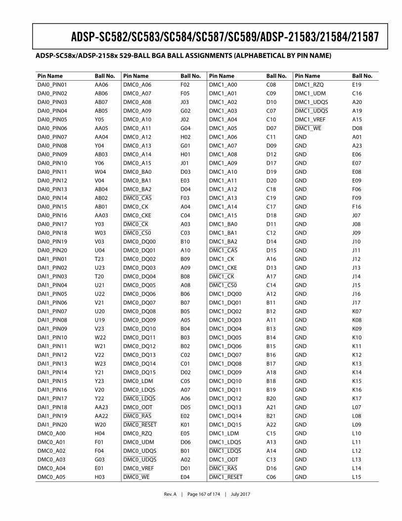
Rev. A | Page 167 of 174 | July 2017
ADSP-SC582/SC583/SC584/SC587/SC589/ADSP-21583/21584/21587ADSP-SC58x/ADSP-2158x 529-BALL BGA BALL ASSIGNMENTS (ALPHABETICAL BY PIN NAME)
Pin Name Ball No.DAI0_PIN01 AA06
DAI0_PIN02 AB06
DAI0_PIN03 AB07
DAI0_PIN04 AB05
DAI0_PIN05 Y05
DAI0_PIN06 AA05
DAI0_PIN07 AA04
DAI0_PIN08 Y04
DAI0_PIN09 AB03
DAI0_PIN10 Y06
DAI0_PIN11 W04
DAI0_PIN12 V04
DAI0_PIN13 AB04
DAI0_PIN14 AB02
DAI0_PIN15 AB01
DAI0_PIN16 AA03
DAI0_PIN17 Y03
DAI0_PIN18 W03
DAI0_PIN19 V03
DAI0_PIN20 U04
DAI1_PIN01 T23
DAI1_PIN02 U23
DAI1_PIN03 T20
DAI1_PIN04 U21
DAI1_PIN05 U22
DAI1_PIN06 V21
DAI1_PIN07 U20
DAI1_PIN08 U19
DAI1_PIN09 V23
DAI1_PIN10 W22
DAI1_PIN11 W21
DAI1_PIN12 V22
DAI1_PIN13 W23
DAI1_PIN14 Y21
DAI1_PIN15 Y23
DAI1_PIN16 V20
DAI1_PIN17 Y22
DAI1_PIN18 AA23
DAI1_PIN19 AA22
DAI1_PIN20 W20
DMC0_A00 H04
DMC0_A01 F01
DMC0_A02 F04
DMC0_A03 G03
DMC0_A04 E01
DMC0_A05 H03
DMC0_A06 F02
DMC0_A07 F05
DMC0_A08 J03
DMC0_A09 G02
DMC0_A10 J02
DMC0_A11 G04
DMC0_A12 H02
DMC0_A13 G01
DMC0_A14 H01
DMC0_A15 J01
DMC0_BA0 D03
DMC0_BA1 E03
DMC0_BA2 D04
DMC0_CAS F03
DMC0_CK A04
DMC0_CKE C04
DMC0_CK A03
DMC0_CS0 C03
DMC0_DQ00 B10
DMC0_DQ01 A10
DMC0_DQ02 B09
DMC0_DQ03 A09
DMC0_DQ04 B08
DMC0_DQ05 A08
DMC0_DQ06 B06
DMC0_DQ07 B07
DMC0_DQ08 B05
DMC0_DQ09 A05
DMC0_DQ10 B04
DMC0_DQ11 B03
DMC0_DQ12 B02
DMC0_DQ13 C02
DMC0_DQ14 C01
DMC0_DQ15 D02
DMC0_LDM C05
DMC0_LDQS A07
DMC0_LDQS A06
DMC0_ODT D05
DMC0_RAS E02
DMC0_RESET K01
DMC0_RZQ E05
DMC0_UDM D06
DMC0_UDQS B01
DMC0_UDQS A02
DMC0_VREF D01
DMC0_WE E04
Pin Name Ball No.DMC1_A00 C08
DMC1_A01 C09
DMC1_A02 D10
DMC1_A03 C07
DMC1_A04 C10
DMC1_A05 D07
DMC1_A06 C11
DMC1_A07 D09
DMC1_A08 D12
DMC1_A09 D17
DMC1_A10 D19
DMC1_A11 D20
DMC1_A12 C18
DMC1_A13 C19
DMC1_A14 C17
DMC1_A15 D18
DMC1_BA0 D11
DMC1_BA1 C12
DMC1_BA2 D14
DMC1_CAS D15
DMC1_CK A16
DMC1_CKE D13
DMC1_CK A17
DMC1_CS0 C14
DMC1_DQ00 A12
DMC1_DQ01 B11
DMC1_DQ02 B12
DMC1_DQ03 A11
DMC1_DQ04 B13
DMC1_DQ05 B14
DMC1_DQ06 B15
DMC1_DQ07 B16
DMC1_DQ08 B17
DMC1_DQ09 A18
DMC1_DQ10 B18
DMC1_DQ11 B19
DMC1_DQ12 B20
DMC1_DQ13 A21
DMC1_DQ14 B21
DMC1_DQ15 A22
DMC1_LDM C15
DMC1_LDQS A13
DMC1_LDQS A14
DMC1_ODT C13
DMC1_RAS D16
DMC1_RESET C06
Pin Name Ball No.DMC1_RZQ E19
DMC1_UDM C16
DMC1_UDQS A20
DMC1_UDQS A19
DMC1_VREF A15
DMC1_WE D08
GND A01
GND A23
GND E06
GND E07
GND E08
GND E09
GND F06
GND F09
GND F16
GND J07
GND J08
GND J09
GND J10
GND J11
GND J12
GND J13
GND J14
GND J15
GND J16
GND J17
GND K07
GND K08
GND K09
GND K10
GND K11
GND K12
GND K13
GND K14
GND K15
GND K16
GND K17
GND L07
GND L08
GND L09
GND L10
GND L11
GND L12
GND L13
GND L14
GND L15
Pin Name Ball No.
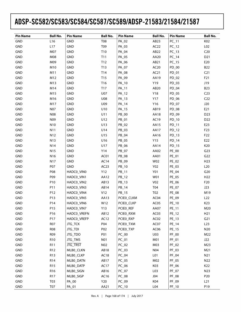
Rev. A | Page 168 of 174 | July 2017
ADSP-SC582/SC583/SC584/SC587/SC589/ADSP-21583/21584/21587
GND L16
GND L17
GND M07
GND M08
GND M09
GND M10
GND M11
GND M12
GND M13
GND M14
GND M15
GND M16
GND M17
GND N07
GND N08
GND N09
GND N10
GND N11
GND N12
GND N13
GND N14
GND N15
GND N16
GND N17
GND P07
GND P08
GND P09
GND P10
GND P11
GND P12
GND P13
GND P14
GND P15
GND P16
GND P17
GND R07
GND R08
GND R09
GND R10
GND R11
GND R12
GND R13
GND R14
GND R15
GND R16
GND R17
GND T03
GND T07
Pin Name Ball No.GND T08
GND T09
GND T10
GND T11
GND T12
GND T13
GND T14
GND T15
GND T16
GND T17
GND U07
GND U08
GND U09
GND U10
GND U11
GND U12
GND U13
GND U14
GND U15
GND U16
GND U17
GND Y14
GND AC01
GND AC14
GND AC23
HADC0_VIN0 Y12
HADC0_VIN1 AA12
HADC0_VIN2 AB13
HADC0_VIN3 AB14
HADC0_VIN4 V12
HADC0_VIN5 AA13
HADC0_VIN6 W12
HADC0_VIN7 Y13
HADC0_VREFN AB12
HADC0_VREFP AC12
JTG_TCK P04
JTG_TDI P02
JTG_TDO P01
JTG_TMS N01
JTG_TRST N02
MLB0_CLKN AB18
MLB0_CLKP AC18
MLB0_DATN AB17
MLB0_DATP AC17
MLB0_SIGN AB16
MLB0_SIGP AC16
PA_00 Y20
PA_01 AA21
Pin Name Ball No.PA_02 AB23
PA_03 AC22
PA_04 AB22
PA_05 AA20
PA_06 AB21
PA_07 AC20
PA_08 AC21
PA_09 AA19
PA_10 Y19
PA_11 AB20
PA_12 Y18
PA_13 Y17
PA_14 Y16
PA_15 AB19
PB_00 AA18
PB_01 AC19
PB_02 AA15
PB_03 AA17
PB_04 AA16
PB_05 Y15
PB_06 AA14
PB_07 AA02
PB_08 AA01
PB_09 W02
PB_10 Y02
PB_11 Y01
PB_12 W01
PB_13 V02
PB_14 T04
PB_15 T02
PCIE0_CLKM AC04
PCIE0_CLKP AC05
PCIE0_REF AA07
PCIE0_RXM AC03
PCIE0_RXP AC02
PCIE0_TXM AC07
PCIE0_TXP AC06
PC_00 U03
PC_01 M01
PC_02 M03
PC_03 N04
PC_04 L01
PC_05 M02
PC_06 K03
PC_07 L03
PC_08 J04
PC_09 K04
PC_10 L04
Pin Name Ball No.PC_11 K02
PC_12 L02
PC_13 C20
PC_14 D21
PC_15 E20
PD_00 B22
PD_01 C21
PD_02 F21
PD_03 J19
PD_04 B23
PD_05 C23
PD_06 C22
PD_07 J20
PD_08 E21
PD_09 D23
PD_10 D22
PD_11 E23
PD_12 F23
PD_13 F22
PD_14 E22
PD_15 K20
PE_00 G23
PE_01 G22
PE_02 H23
PE_03 L20
PE_04 G20
PE_05 H22
PE_06 F20
PE_07 J23
PE_08 M19
PE_09 L22
PE_10 K23
PE_11 M20
PE_12 H21
PE_13 G21
PE_14 L23
PE_15 N20
PF_00 M22
PF_01 J22
PF_02 M23
PF_03 M21
PF_04 N21
PF_05 N22
PF_06 K22
PF_07 N23
PF_08 P20
PF_09 L21
PF_10 P19
Pin Name Ball No.
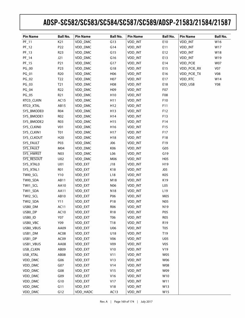
Rev. A | Page 169 of 174 | July 2017
ADSP-SC582/SC583/SC584/SC587/SC589/ADSP-21583/21584/21587
PF_11 K21
PF_12 P22
PF_13 R23
PF_14 J21
PF_15 P21
PG_00 P23
PG_01 R20
PG_02 T22
PG_03 T21
PG_04 R22
PG_05 R21
RTC0_CLKIN AC15
RTC0_XTAL AB15
SYS_BMODE0 R04
SYS_BMODE1 R02
SYS_BMODE2 R03
SYS_CLKIN0 V01
SYS_CLKIN1 T01
SYS_CLKOUT H20
SYS_FAULT P03
SYS_FAULT M04
SYS_HWRST N03
SYS_RESOUT U02
SYS_XTAL0 U01
SYS_XTAL1 R01
TWI0_SCL Y10
TWI0_SDA AB11
TWI1_SCL AA10
TWI1_SDA AA11
TWI2_SCL AB10
TWI2_SDA Y11
USB0_DM AC11
USB0_DP AC10
USB0_ID Y07
USB0_VBC Y09
USB0_VBUS AA09
USB1_DM AC08
USB1_DP AC09
USB1_VBUS AA08
USB_CLKIN AB09
USB_XTAL AB08
VDD_DMC G06
VDD_DMC G07
VDD_DMC G08
VDD_DMC G09
VDD_DMC G10
VDD_DMC G11
VDD_DMC G12
Pin Name Ball No.VDD_DMC G13
VDD_DMC G14
VDD_DMC G15
VDD_DMC G16
VDD_DMC G17
VDD_DMC G18
VDD_DMC H06
VDD_DMC H07
VDD_DMC H08
VDD_DMC H09
VDD_DMC H10
VDD_DMC H11
VDD_DMC H12
VDD_DMC H13
VDD_DMC H14
VDD_DMC H15
VDD_DMC H16
VDD_DMC H17
VDD_DMC H18
VDD_DMC J06
VDD_DMC K06
VDD_DMC L06
VDD_DMC M06
VDD_EXT J18
VDD_EXT K18
VDD_EXT L18
VDD_EXT M18
VDD_EXT N06
VDD_EXT N18
VDD_EXT P06
VDD_EXT P18
VDD_EXT R06
VDD_EXT R18
VDD_EXT T06
VDD_EXT T18
VDD_EXT U06
VDD_EXT U18
VDD_EXT V06
VDD_EXT V09
VDD_EXT V10
VDD_EXT V11
VDD_EXT V13
VDD_EXT V14
VDD_EXT V15
VDD_EXT V16
VDD_EXT V17
VDD_EXT V18
VDD_HADC AC13
Pin Name Ball No.VDD_INT E10
VDD_INT E11
VDD_INT E12
VDD_INT E13
VDD_INT E14
VDD_INT E15
VDD_INT E16
VDD_INT E17
VDD_INT E18
VDD_INT F07
VDD_INT F08
VDD_INT F10
VDD_INT F11
VDD_INT F12
VDD_INT F13
VDD_INT F14
VDD_INT F15
VDD_INT F17
VDD_INT F18
VDD_INT F19
VDD_INT G05
VDD_INT G19
VDD_INT H05
VDD_INT H19
VDD_INT J05
VDD_INT K05
VDD_INT K19
VDD_INT L05
VDD_INT L19
VDD_INT M05
VDD_INT N05
VDD_INT N19
VDD_INT P05
VDD_INT R05
VDD_INT R19
VDD_INT T05
VDD_INT T19
VDD_INT U05
VDD_INT V05
VDD_INT V19
VDD_INT W05
VDD_INT W06
VDD_INT W08
VDD_INT W09
VDD_INT W10
VDD_INT W11
VDD_INT W13
VDD_INT W15
Pin Name Ball No.VDD_INT W16
VDD_INT W17
VDD_INT W18
VDD_INT W19
VDD_PCIE W07
VDD_PCIE_RX V07
VDD_PCIE_TX V08
VDD_RTC W14
VDD_USB Y08
Pin Name Ball No.
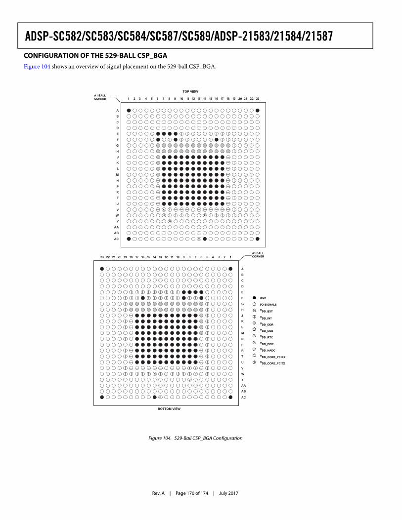
Rev. A | Page 170 of 174 | July 2017
ADSP-SC582/SC583/SC584/SC587/SC589/ADSP-21583/21584/21587CONFIGURATION OF THE 529-BALL CSP_BGA Figure 104 shows an overview of signal placement on the 529-ball CSP_BGA.
Figure 104. 529-Ball CSP_BGA Configuration
BOTTOM VIEW
GND
VDD_INT
VDD_EXT
I/O SIGNALS
VDD_DDR
VDD_RTC
P
R
VDD_PCIE
VDD_USBU
VDD_HADCH
C VDD_CORE_PCIRX
VDD_CORE_PCITXT
A
B
C
D
E
F
G
H
J
K
L
M
N
P
R
T
V
W
AA
AC
AB
U
Y
15 14 13 12 11 10 9 8 7 6 5 4 3 2 116171819202123 22
U
R P
H
CT
A1 BALLCORNER
A
B
C
D
E
F
G
H
J
K
L
M
N
P
R
T
V
W
AA
AC
AB
U
Y
151413121110987654321 16 17 18 19 20 21 2322
U
RP
H
C T
A1 BALLCORNER
TOP VIEW
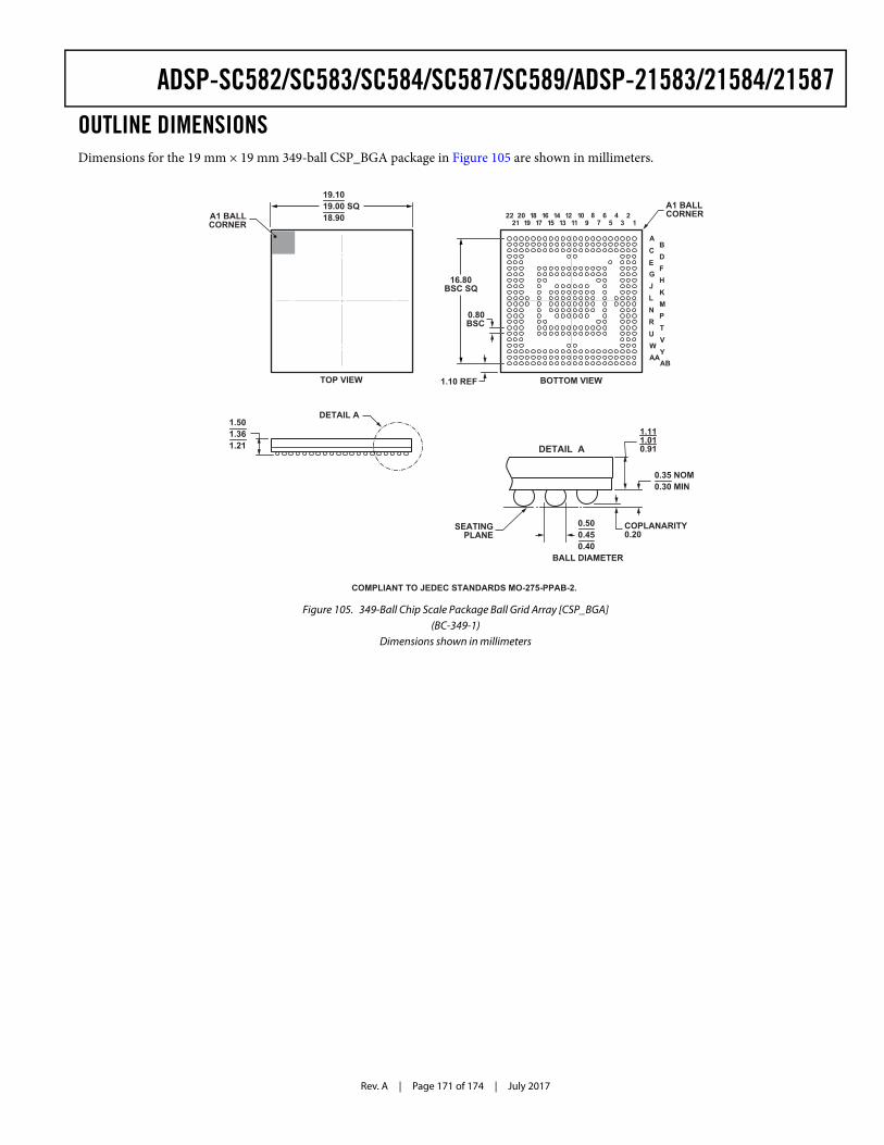
Rev. A | Page 171 of 174 | July 2017
ADSP-SC582/SC583/SC584/SC587/SC589/ADSP-21583/21584/21587
OUTLINE DIMENSIONSDimensions for the 19 mm × 19 mm 349-ball CSP_BGA package in Figure 105 are shown in millimeters.
Figure 105. 349-Ball Chip Scale Package Ball Grid Array [CSP_BGA](BC-349-1)
Dimensions shown in millimeters
COMPLIANT TO JEDEC STANDARDS MO-275-PPAB-2.
1.10 REF
AB
CD
EF
GH
JK
LM
NP
RTV
WAA
AB
U
Y
1514
1312
1110
98
76
54
32
116
1718
1920
2122
16.80BSC SQ
0.500.450.40
19.1019.00 SQ18.90
COPLANARITY0.20
BOTTOM VIEW
DETAIL A
TOP VIEW
1.501.361.21
0.35 NOM0.30 MIN
BALL DIAMETER
SEATINGPLANE
A1 BALLCORNER
A1 BALLCORNER
DETAIL A
0.80BSC
1.111.010.91
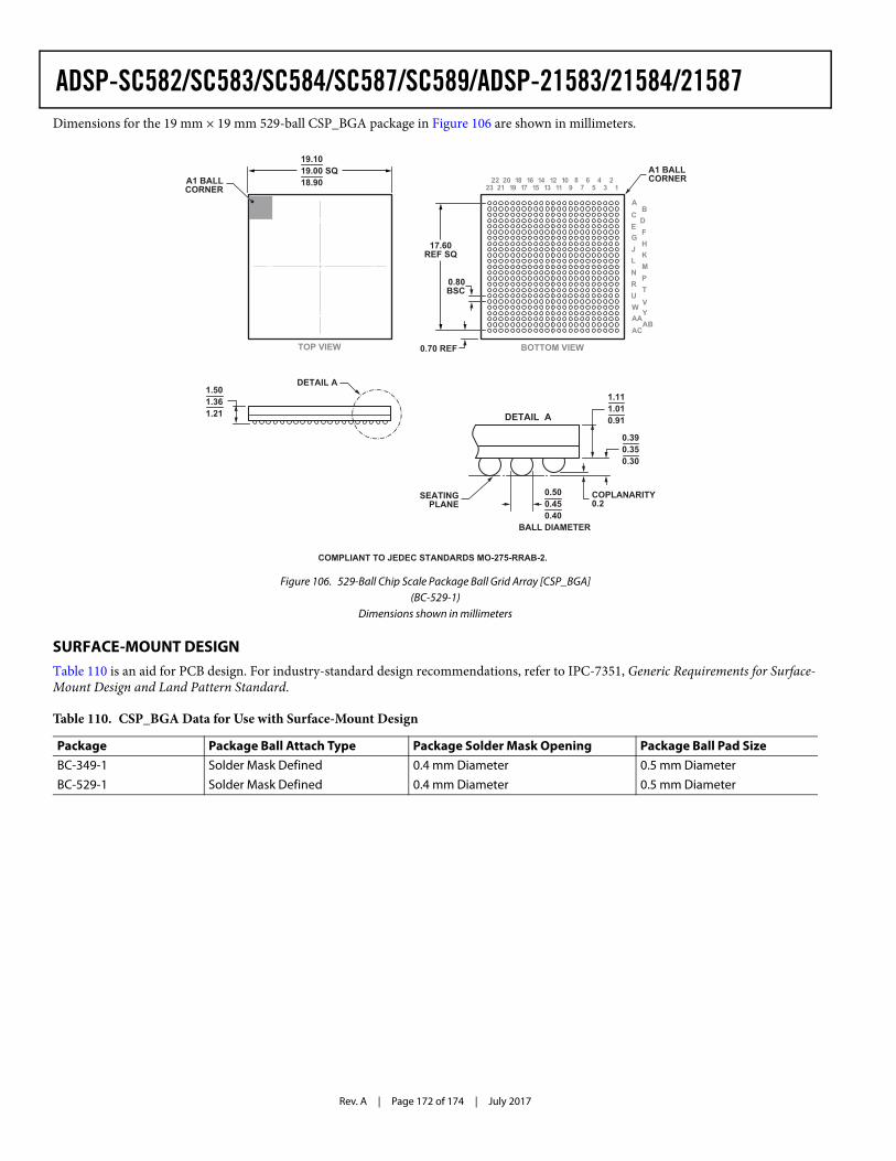
Rev. A | Page 172 of 174 | July 2017
ADSP-SC582/SC583/SC584/SC587/SC589/ADSP-21583/21584/21587Dimensions for the 19 mm × 19 mm 529-ball CSP_BGA package in Figure 106 are shown in millimeters.
SURFACE-MOUNT DESIGNTable 110 is an aid for PCB design. For industry-standard design recommendations, refer to IPC-7351, Generic Requirements for Surface-Mount Design and Land Pattern Standard.
Figure 106. 529-Ball Chip Scale Package Ball Grid Array [CSP_BGA](BC-529-1)
Dimensions shown in millimeters
Table 110. CSP_BGA Data for Use with Surface-Mount Design
Package Package Ball Attach Type Package Solder Mask Opening Package Ball Pad SizeBC-349-1 Solder Mask Defined 0.4 mm Diameter 0.5 mm Diameter
BC-529-1 Solder Mask Defined 0.4 mm Diameter 0.5 mm Diameter
COMPLIANT TO JEDEC STANDARDS MO-275-RRAB-2.
0.70 REF
AB
CD
EF
GH
JK
LM
NP
RTVW
AAAC
AB
U
Y
1514
1312
1110
98
76
54
32
116
1718
1920
212322
17.60REF SQ
0.500.450.40
19.1019.00 SQ18.90
COPLANARITY0.2
BOTTOM VIEW
DETAIL A
TOP VIEW
1.501.361.21
BALL DIAMETER
SEATINGPLANE
A1 BALLCORNER
A1 BALLCORNER
DETAIL A
0.80BSC
1.111.010.91
0.390.350.30
Rev. A | Page 173 of 174 | July 2017
ADSP-SC582/SC583/SC584/SC587/SC589/ADSP-21583/21584/21587PLANNED AUTOMOTIVE PRODUCTION PRODUCTS
Model 1, 2
1 Z = RoHS Compliant Part.2 xx denotes the current die revision.
Processor Instruction Rate (Max)
TemperatureRange3
3 Referenced temperature is ambient temperature. The ambient temperature is not a specification. Please see the Operating Conditions section for the junction temperature (TJ) specification which is the only temperature specification.
ARM Cores4
4 N/A means not applicable.
SHARC+ Cores
SHARC+ SRAM
PCIeLanes4
Package Description
PackageOption
AD21583WCBCZ4Axx 450 MHz –40°C to +105°C N/A 2 384 kB N/A 349-Ball cspBGA BC-349-1
AD21584WCBCZ4Axx 450 MHz –40°C to +105°C N/A 2 640 kB N/A 349-Ball cspBGA BC-349-1
AD21584WCBCZ5Axx 500 MHz –40°C to +100°C N/A 2 640 kB N/A 349-Ball cspBGA BC-349-1
ADSC582WCBCZ4Axx 450 MHz –40°C to +105°C 1 1 640 kB N/A 349-Ball cspBGA BC-349-1
ADSC583WCBCZ3Axx 300 MHz –40°C to +105°C 1 2 384 kB N/A 349-Ball cspBGA BC-349-1
ADSC583WCBCZ4Axx 450 MHz –40°C to +105°C 1 2 384 kB N/A 349-Ball cspBGA BC-349-1
ADSC584WCBCZ3Axx 300 MHz –40°C to +105°C 1 2 640 kB N/A 349-Ball cspBGA BC-349-1
ADSC584WCBCZ4Axx 450 MHz –40°C to +105°C 1 2 640 kB N/A 349-Ball cspBGA BC-349-1
ADSC584WCBCZ5Axx 500 MHz –40°C to +100°C 1 2 640 kB N/A 349-Ball cspBGA BC-349-1
ADSC587WCBCZ4Bxx 450 MHz –40°C to +105°C 1 2 640 kB N/A 529-Ball cspBGA BC-529-1
ADSC587WBBCZ5Bxx 500 MHz –40°C to +85°C 1 2 640 kB N/A 529-Ball cspBGA BC-529-1
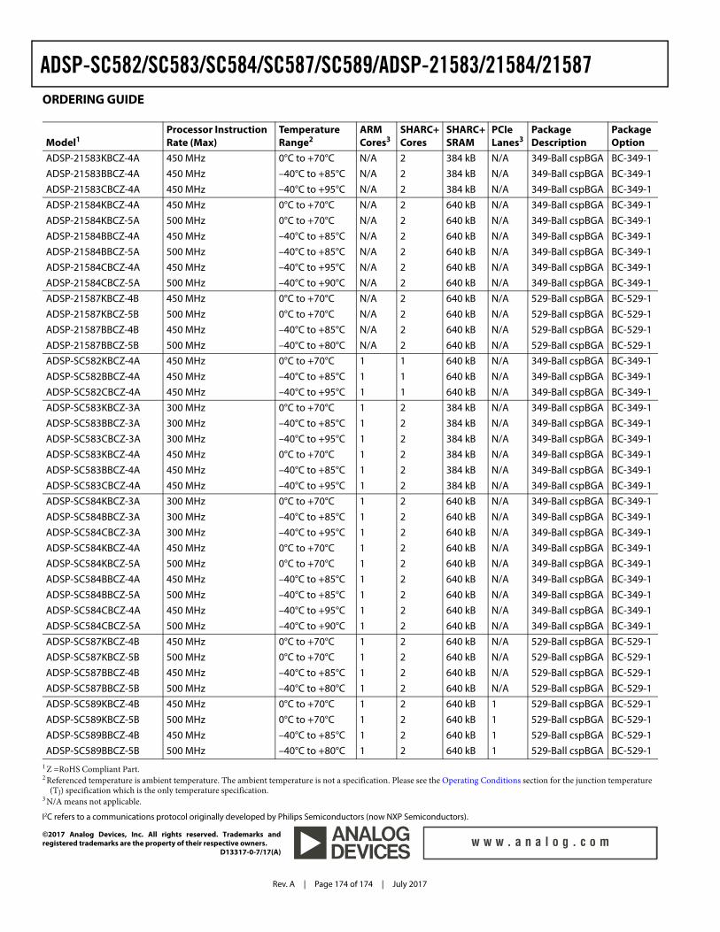
Rev. A | Page 174 of 174 | July 2017
©2017 Analog Devices, Inc. All rights reserved. Trademarks andregistered trademarks are the property of their respective owners.
D13317-0-7/17(A)
ADSP-SC582/SC583/SC584/SC587/SC589/ADSP-21583/21584/21587ORDERING GUIDE
Model1
1 Z =RoHS Compliant Part.
Processor Instruction Rate (Max)
TemperatureRange2
2 Referenced temperature is ambient temperature. The ambient temperature is not a specification. Please see the Operating Conditions section for the junction temperature (TJ) specification which is the only temperature specification.
ARM Cores3
3 N/A means not applicable.
SHARC+ Cores
SHARC+ SRAM
PCIeLanes3
Package Description
PackageOption
ADSP-21583KBCZ-4A 450 MHz 0°C to +70°C N/A 2 384 kB N/A 349-Ball cspBGA BC-349-1
ADSP-21583BBCZ-4A 450 MHz –40°C to +85°C N/A 2 384 kB N/A 349-Ball cspBGA BC-349-1
ADSP-21583CBCZ-4A 450 MHz –40°C to +95°C N/A 2 384 kB N/A 349-Ball cspBGA BC-349-1
ADSP-21584KBCZ-4A 450 MHz 0°C to +70°C N/A 2 640 kB N/A 349-Ball cspBGA BC-349-1
ADSP-21584KBCZ-5A 500 MHz 0°C to +70°C N/A 2 640 kB N/A 349-Ball cspBGA BC-349-1
ADSP-21584BBCZ-4A 450 MHz –40°C to +85°C N/A 2 640 kB N/A 349-Ball cspBGA BC-349-1
ADSP-21584BBCZ-5A 500 MHz –40°C to +85°C N/A 2 640 kB N/A 349-Ball cspBGA BC-349-1
ADSP-21584CBCZ-4A 450 MHz –40°C to +95°C N/A 2 640 kB N/A 349-Ball cspBGA BC-349-1
ADSP-21584CBCZ-5A 500 MHz –40°C to +90°C N/A 2 640 kB N/A 349-Ball cspBGA BC-349-1
ADSP-21587KBCZ-4B 450 MHz 0°C to +70°C N/A 2 640 kB N/A 529-Ball cspBGA BC-529-1
ADSP-21587KBCZ-5B 500 MHz 0°C to +70°C N/A 2 640 kB N/A 529-Ball cspBGA BC-529-1
ADSP-21587BBCZ-4B 450 MHz –40°C to +85°C N/A 2 640 kB N/A 529-Ball cspBGA BC-529-1
ADSP-21587BBCZ-5B 500 MHz –40°C to +80°C N/A 2 640 kB N/A 529-Ball cspBGA BC-529-1
ADSP-SC582KBCZ-4A 450 MHz 0°C to +70°C 1 1 640 kB N/A 349-Ball cspBGA BC-349-1
ADSP-SC582BBCZ-4A 450 MHz –40°C to +85°C 1 1 640 kB N/A 349-Ball cspBGA BC-349-1
ADSP-SC582CBCZ-4A 450 MHz –40°C to +95°C 1 1 640 kB N/A 349-Ball cspBGA BC-349-1
ADSP-SC583KBCZ-3A 300 MHz 0°C to +70°C 1 2 384 kB N/A 349-Ball cspBGA BC-349-1
ADSP-SC583BBCZ-3A 300 MHz –40°C to +85°C 1 2 384 kB N/A 349-Ball cspBGA BC-349-1
ADSP-SC583CBCZ-3A 300 MHz –40°C to +95°C 1 2 384 kB N/A 349-Ball cspBGA BC-349-1
ADSP-SC583KBCZ-4A 450 MHz 0°C to +70°C 1 2 384 kB N/A 349-Ball cspBGA BC-349-1
ADSP-SC583BBCZ-4A 450 MHz –40°C to +85°C 1 2 384 kB N/A 349-Ball cspBGA BC-349-1
ADSP-SC583CBCZ-4A 450 MHz –40°C to +95°C 1 2 384 kB N/A 349-Ball cspBGA BC-349-1
ADSP-SC584KBCZ-3A 300 MHz 0°C to +70°C 1 2 640 kB N/A 349-Ball cspBGA BC-349-1
ADSP-SC584BBCZ-3A 300 MHz –40°C to +85°C 1 2 640 kB N/A 349-Ball cspBGA BC-349-1
ADSP-SC584CBCZ-3A 300 MHz –40°C to +95°C 1 2 640 kB N/A 349-Ball cspBGA BC-349-1
ADSP-SC584KBCZ-4A 450 MHz 0°C to +70°C 1 2 640 kB N/A 349-Ball cspBGA BC-349-1
ADSP-SC584KBCZ-5A 500 MHz 0°C to +70°C 1 2 640 kB N/A 349-Ball cspBGA BC-349-1
ADSP-SC584BBCZ-4A 450 MHz –40°C to +85°C 1 2 640 kB N/A 349-Ball cspBGA BC-349-1
ADSP-SC584BBCZ-5A 500 MHz –40°C to +85°C 1 2 640 kB N/A 349-Ball cspBGA BC-349-1
ADSP-SC584CBCZ-4A 450 MHz –40°C to +95°C 1 2 640 kB N/A 349-Ball cspBGA BC-349-1
ADSP-SC584CBCZ-5A 500 MHz –40°C to +90°C 1 2 640 kB N/A 349-Ball cspBGA BC-349-1
ADSP-SC587KBCZ-4B 450 MHz 0°C to +70°C 1 2 640 kB N/A 529-Ball cspBGA BC-529-1
ADSP-SC587KBCZ-5B 500 MHz 0°C to +70°C 1 2 640 kB N/A 529-Ball cspBGA BC-529-1
ADSP-SC587BBCZ-4B 450 MHz –40°C to +85°C 1 2 640 kB N/A 529-Ball cspBGA BC-529-1
ADSP-SC587BBCZ-5B 500 MHz –40°C to +80°C 1 2 640 kB N/A 529-Ball cspBGA BC-529-1
ADSP-SC589KBCZ-4B 450 MHz 0°C to +70°C 1 2 640 kB 1 529-Ball cspBGA BC-529-1
ADSP-SC589KBCZ-5B 500 MHz 0°C to +70°C 1 2 640 kB 1 529-Ball cspBGA BC-529-1
ADSP-SC589BBCZ-4B 450 MHz –40°C to +85°C 1 2 640 kB 1 529-Ball cspBGA BC-529-1
ADSP-SC589BBCZ-5B 500 MHz –40°C to +80°C 1 2 640 kB 1 529-Ball cspBGA BC-529-1
I2C refers to a communications protocol originally developed by Philips Semiconductors (now NXP Semiconductors).
Related Documents


