SGM321/SGM358/SGM324 1MHz, 60μA, Rail-to-Rail I/O CMOS Operational Amplifiers PRODUCT DESCRIPTION The SGM321(single), SGM358(dual) and SGM324(quad) are rail-to-rail input and output voltage feedback amplifiers offering low cost. They have a wide input common-mode voltage range and output voltage swing, and take the minimum operating supply voltage down to 2.1V and the maximum recommended supply voltage is 5.5V. All are specified over the extended –40℃ to +85℃ temperature range. The SGM321/358/324 provide 1MHz bandwidth at a low current consumption of 60μA per amplifier. Very low input bias currents of 10pA enable SGM321/358/324 to be used for integrators, photodiode amplifiers, and piezoelectric sensors. Rail-to-rail inputs and outputs are useful to designers buffering ASIC in single-supply systems. Applications for the series amplifiers include safety monitoring, portable equipment, battery and power supply control, and signal conditioning and interfacing for transducers in very low power systems. The SGM321 is available in SOT23-5 and SC70-5 packages. The SGM358 comes in SO-8, MSOP-8 and DIP-8 packages. The SGM324 is offered in SO-14 and TSSOP-14 packages. APPLICATIONS ASIC Input or Output Amplifier Sensor Interface Piezo Electric Transducer Amplifier Medical Instrumentation Mobile Communication Audio Output Portable Systems Smoke Detectors Notebook PC PCMCIA Cards Battery –Powered Equipment FEATURES • Low Cost • Rail-to-Rail Input and Output 0.8mV Typical V OS • Unity Gain Stable • Gain Bandwidth Product: 1MHz • Very Low Input Bias Currents: 10pA • Operates on 2.1V to 5.5V Supplies • Input Voltage Range: -0.1V to +5.6V with V S = 5.5V • Low Supply Current: 60μA/Amplifier • Small Packaging SGM321 Available in SOT23-5 and SC70-5 SGM358 Available in SO-8, MSOP-8 and DIP-8 SGM324 Available in SO-14 and TSSOP-14 PIN CONFIGURATIONS (Top View) +VS -IN 1 2 3 4 5 -VS +IN SGM321 SOT23-5 / SC70-5 OUT 1 2 3 4 5 OUT A -IN A +IN A -VS +VS -IND +IND SGM324 TSSOP-14 / SO-14 6 7 8 9 10 11 12 13 14 -INB +INB -INC OUT B OUT C +INC OUT D OUT A OUT B +INB +VS 1 2 3 4 5 6 7 8 -INA +INA -VS -INB SGM358 SO-8 / MSOP-8 / DIP-8 DSP Interface REV. D. 2 SG Micro Limited www.sg-micro.com

Welcome message from author
This document is posted to help you gain knowledge. Please leave a comment to let me know what you think about it! Share it to your friends and learn new things together.
Transcript

SGM321/SGM358/SGM324 1MHz, 60µA, Rail-to-Rail I/O CMOS Operational Amplifiers
PRODUCT DESCRIPTION The SGM321(single), SGM358(dual) and SGM324(quad) are rail-to-rail input and output voltage feedback amplifiers offering low cost. They have a wide input common-mode voltage range and output voltage swing, and take the minimum operating supply voltage down to 2.1V and the maximum recommended supply voltage is 5.5V. All are specified over the extended –40 to +85 temperature range.
The SGM321/358/324 provide 1MHz bandwidth at a low current consumption of 60µA per amplifier. Very low input bias currents of 10pA enable SGM321/358/324 to be used for integrators, photodiode amplifiers, and piezoelectric sensors. Rail-to-rail inputs and outputs are useful to designers buffering ASIC in single-supply systems. Applications for the series amplifiers include safety monitoring, portable equipment, battery and power supply control, and signal conditioning and interfacing for transducers in very low power systems. The SGM321 is available in SOT23-5 and SC70-5 packages. The SGM358 comes in SO-8, MSOP-8 and DIP-8 packages. The SGM324 is offered in SO-14 and TSSOP-14 packages.
APPLICATIONS ASIC Input or Output Amplifier Sensor Interface Piezo Electric Transducer Amplifier Medical Instrumentation Mobile Communication Audio Output Portable Systems Smoke Detectors Notebook PC PCMCIA Cards Battery –Powered Equipment
FEATURES • Low Cost • Rail-to-Rail Input and Output
0.8mV Typical VOS • Unity Gain Stable • Gain Bandwidth Product: 1MHz • Very Low Input Bias Currents: 10pA • Operates on 2.1V to 5.5V Supplies • Input Voltage Range:
-0.1V to +5.6V with VS = 5.5V • Low Supply Current: 60µA/Amplifier • Small Packaging
SGM321 Available in SOT23-5 and SC70-5 SGM358 Available in SO-8, MSOP-8 and DIP-8 SGM324 Available in SO-14 and TSSOP-14
PIN CONFIGURATIONS (Top View)
+VS
-IN
1
2
3 4
5
-VS
+IN
SGM321
SOT23-5 / SC70-5
OUT
1
2
3
4
5
OUT A
-IN A
+IN A
-VS+VS
-IND
+IND
SGM324
TSSOP-14 / SO-14
6
7 8
9
10
11
12
13
14
-INB
+INB
-INC
OUT B OUT C
+INC
OUT D
OUT A
OUT B
+INB
+VS1
2
3
4 5
6
7
8
-INA
+INA
-VS
-INB
SGM358
SO-8 / MSOP-8 / DIP-8
DSP Interface
REV. D. 2 SG Micro Limited www.sg-micro.com
1MHz, 60µA, Rail-to-Rail I/O SGM321/SGM358/SGM324 CMOS Operational Amplifiers
2SG Micro Limited www.sg-micro.com
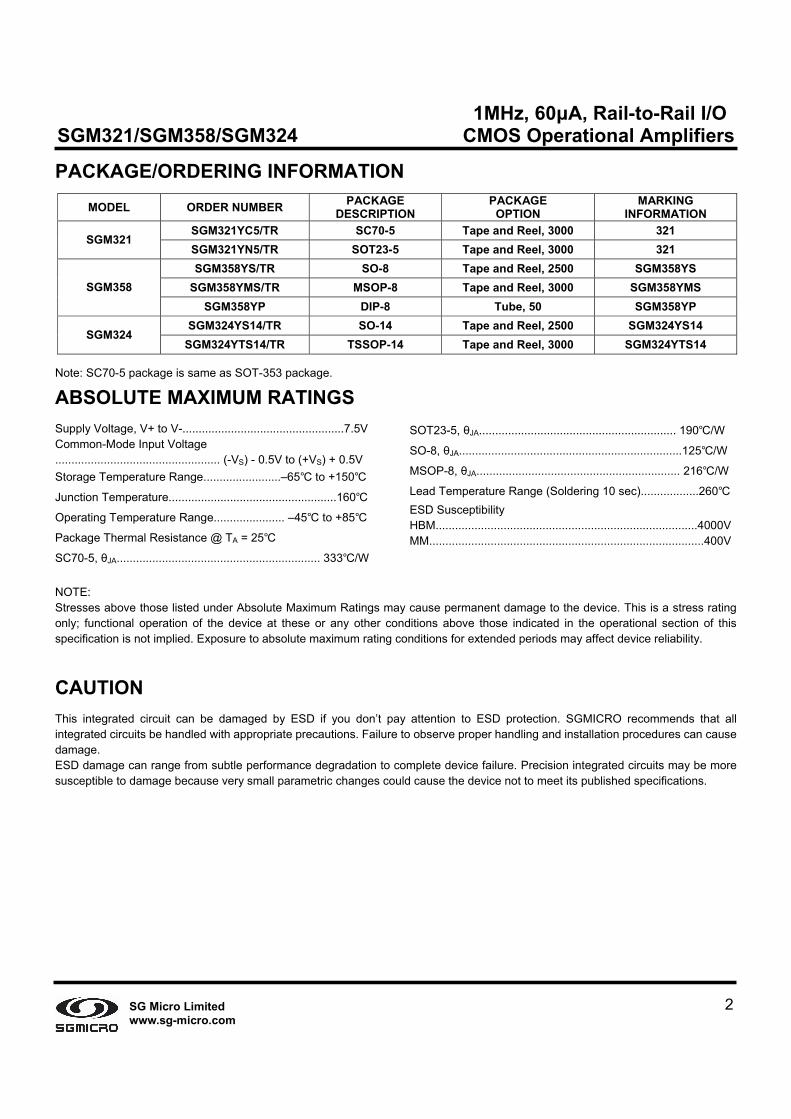
PACKAGE/ORDERING INFORMATION
MODEL ORDER NUMBER PACKAGE DESCRIPTION
PACKAGE OPTION
MARKING INFORMATION
SGM321YC5/TR SC70-5 Tape and Reel, 3000 321 SGM321
SGM321YN5/TR SOT23-5 Tape and Reel, 3000 321 SGM358YS/TR SO-8 Tape and Reel, 2500 SGM358YS
SGM358YMS/TR MSOP-8 Tape and Reel, 3000 SGM358YMS SGM358 SGM358YP DIP-8 Tube, 50 SGM358YP
SGM324YS14/TR SO-14 Tape and Reel, 2500 SGM324YS14 SGM324
SGM324YTS14/TR TSSOP-14 Tape and Reel, 3000 SGM324YTS14
Note: SC70-5 package is same as SOT-353 package. ABSOLUTE MAXIMUM RATINGS Supply Voltage, V+ to V-..................................................7.5V Common-Mode Input Voltage ................................................... (-VS) - 0.5V to (+VS) + 0.5V Storage Temperature Range........................–65 to +150
Junction Temperature....................................................160
Operating Temperature Range...................... –45 to +85
Package Thermal Resistance @ TA = 25
SC70-5, θJA............................................................... 333/W
SOT23-5, θJA............................................................. 190/W
SO-8, θJA.....................................................................125/W
MSOP-8, θJA............................................................... 216/W
Lead Temperature Range (Soldering 10 sec)..................260 ESD Susceptibility HBM.................................................................................4000V MM.....................................................................................400V
NOTE: Stresses above those listed under Absolute Maximum Ratings may cause permanent damage to the device. This is a stress rating only; functional operation of the device at these or any other conditions above those indicated in the operational section of this specification is not implied. Exposure to absolute maximum rating conditions for extended periods may affect device reliability. CAUTION This integrated circuit can be damaged by ESD if you don’t pay attention to ESD protection. SGMICRO recommends that all integrated circuits be handled with appropriate precautions. Failure to observe proper handling and installation procedures can cause damage. ESD damage can range from subtle performance degradation to complete device failure. Precision integrated circuits may be more susceptible to damage because very small parametric changes could cause the device not to meet its published specifications.

1MHz, 60µA, Rail-to-Rail I/O SGM321/SGM358/SGM324 CMOS Operational Amplifiers
3SG Micro Limited www.sg-micro.com
ELECTRICAL CHARACTERISTICS: VS = +5V (At RL = 100KΩ connected to Vs/2, and VOUT = Vs/2, unless otherwise noted.)
SGM321/358/324
TYP MIN/MAX OVER TEMPERATURE PARAMETER CONDITIONS
+25 +25 -40
to 85 UNITS MIN / MAX
INPUT CHARACTERISTICS
Input Offset Voltage (VOS)
Input Bias Current (IB)
Input Offset Current (IOS)
Common-Mode Voltage Range (VCM)
Common-Mode Rejection Ratio (CMRR)
Open-Loop Voltage Gain ( AOL)
Input Offset Voltage Drift (∆VOS/∆T)
VS = 5.5V
VS = 5.5V, VCM = - 0.1V to 4V
VS = 5.5V, VCM = - 0.1V to 5.6V
RL = 5KΩ ,Vo = 0.1V to 4.9V
RL = 100KΩ ,Vo = 0.035V to 4.965V
±0.8
10
10
-0.1 to +5.6
70
68
80
84
2.7
±5
62
56
70
80
±5.6
62
55
70
80
mV
pA
pA
V
dB
dB
dB
dB
µV/
MAX
TYP
TYP
TYP
MIN
MIN
MIN
MIN
TYP
OUTPUT CHARACTERISTICS
Output Voltage Swing from Rail
Output Current (IOUT)
RL = 100KΩ
RL = 10KΩ
0.008
0.08
23
20
18.8
V
V
mA
TYP
TYP
MIN
POWER SUPPLY
Operating Voltage Range
Power Supply Rejection Ratio (PSRR)
Quiescent Current / Amplifier (IQ)
Vs = +2.5V to + 5.5V
VCM = (-VS) + 0.5V
IOUT = 0
82
60
2.1
5.5
60
80
2.5
5.5
58
86
V
V
dB
µA
MIN
MAX
MIN
MAX
DYNAMIC PERFORMANCE
Gain-Bandwidth Product (GBP)
Slew Rate (SR)
Settling Time to 0.1% ( tS)
Overload Recovery Time
CL = 100pF
G = +1, 2V Output Step
G = +1, 2V Output Step
VIN ·Gain = VS
1
0.52
5.3
2.6
MHz
V/µs
µs
µs
TYP
TYP
TYP
TYP
NOISE PERFORMANCE
Voltage Noise Density (en)
f = 1kHz
f = 10kHz
27
20
nV/ Hz
nV/ Hz
TYP
TYP
Specifications subject to changes without notice.

1MHz, 60µA, Rail-to-Rail I/O SGM321/SGM358/SGM324 CMOS Operational Amplifiers
4SG Micro Limited www.sg-micro.com
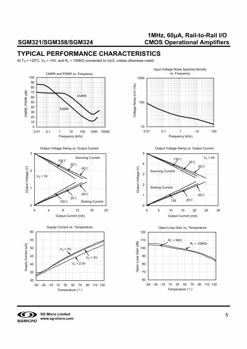
TYPICAL PERFORMANCE CHARACTERISTICS At TA = +25, VS = +5V, and RL = 100KΩ connected to Vs/2, unless otherwise noted.
Small-Signal Step Response Large-Signal Step Response
2µs/div 10µs/div
Small-Signal Overshoot vs. Load Capacitance
0
10
20
30
40
50
60
10 100 1000 10000Load Capacitance (pF)
Sm
all-S
igna
l Ove
rsho
ot (%
)
G = -5RFB = 100KΩ
Small-Signal Overshoot vs. Load Capacitance
0
10
20
30
40
50
60
10 100 1000 10000Load Capacitance (pF)
Sm
all-S
igna
l Ove
rsho
ot (%
) G = -1RFB = 100KΩ
G = +1RL = 100KΩ G = -1
RFB = 5KΩ
Maximum Output Voltage vs. Frequency
0
1
2
3
4
5
6
1 10 100 1000 10000Frequency (kHz)
Out
put V
olta
ge (V
p-p) Maximum Output Voltage
Without Slew-RateInduced Distortion
VS = 5.5V
VS = 5V
VS = 2.5V
Quiescent and Short-Circuit Current vs. Supply Voltage
25
30
35
40
45
50
2 2.5 3 3.5 4 4.5 5 5.5Supply Voltage (V)
Qui
esce
nt C
urre
nt (µ
A)
ISC
IQ
5
15
20
10
25
30S
hort-
Circ
uit C
urre
nt (m
A)
20m
V/d
iv
500m
V/di
v
G = +1 CL = 100pF RL = 100KΩ
G = +1 CL = 100pFRL = 100KΩ
1MHz, 60µA, Rail-to-Rail I/O SGM321/SGM358/SGM324 CMOS Operational Amplifiers
5SG Micro Limited www.sg-micro.com
TYPICAL PERFORMANCE CHARACTERISTICS At TA = +25, VS = +5V, and RL = 100KΩ connected to Vs/2, unless otherwise noted.
CMRR and PSRR vs. Frequency
0102030405060708090
100
0.01 0.1 1 10 100 1000 10000Frequency (kHz)
CM
RR
, PS
RR
(dB)
CMRR
PSRR
Input Voltage Noise Spectral Densityvs. Frequency
10
100
1000
0.01 0.1 1 10 100Frequency (kHz)
Vol
tage
Noi
se (n
V/ √
Hz)
Output Voltage Swing vs. Output Current
0
1
2
3
0 4 8 12 16 20
Output Current (mA)
Out
put V
olta
ge (V
)
25135
-50
25135
-50
VS = 3V
Sourcing Current
Sinking Current
Output Voltage Swing vs. Output Current
0
1
2
3
4
5
0 5 10 15 20 25 30
Output Current (mA)
Out
put V
olta
ge (V
)
25135
-50
25135
-50
VS = 5V
Sourcing Current
Sinking Current
Supply Current vs. Temperature
30
35
40
45
50
55
60
-50 -30 -10 10 30 50 70 90 110 130Temperature ()
Sup
ply
Cur
rent
(µA
)
VS = 2.5V
VS = 5V
VS = 3V
Open-Loop Gain vs. Temperature
60
70
80
90
100
110
120
-50 -30 -10 10 30 50 70 90 110 130Temperature ()
Ope
n–Lo
op G
ain
(dB
)
RL = 100KΩRL = 5KΩ
1MHz, 60µA, Rail-to-Rail I/O SGM321/SGM358/SGM324 CMOS Operational Amplifiers
6SG Micro Limited www.sg-micro.com
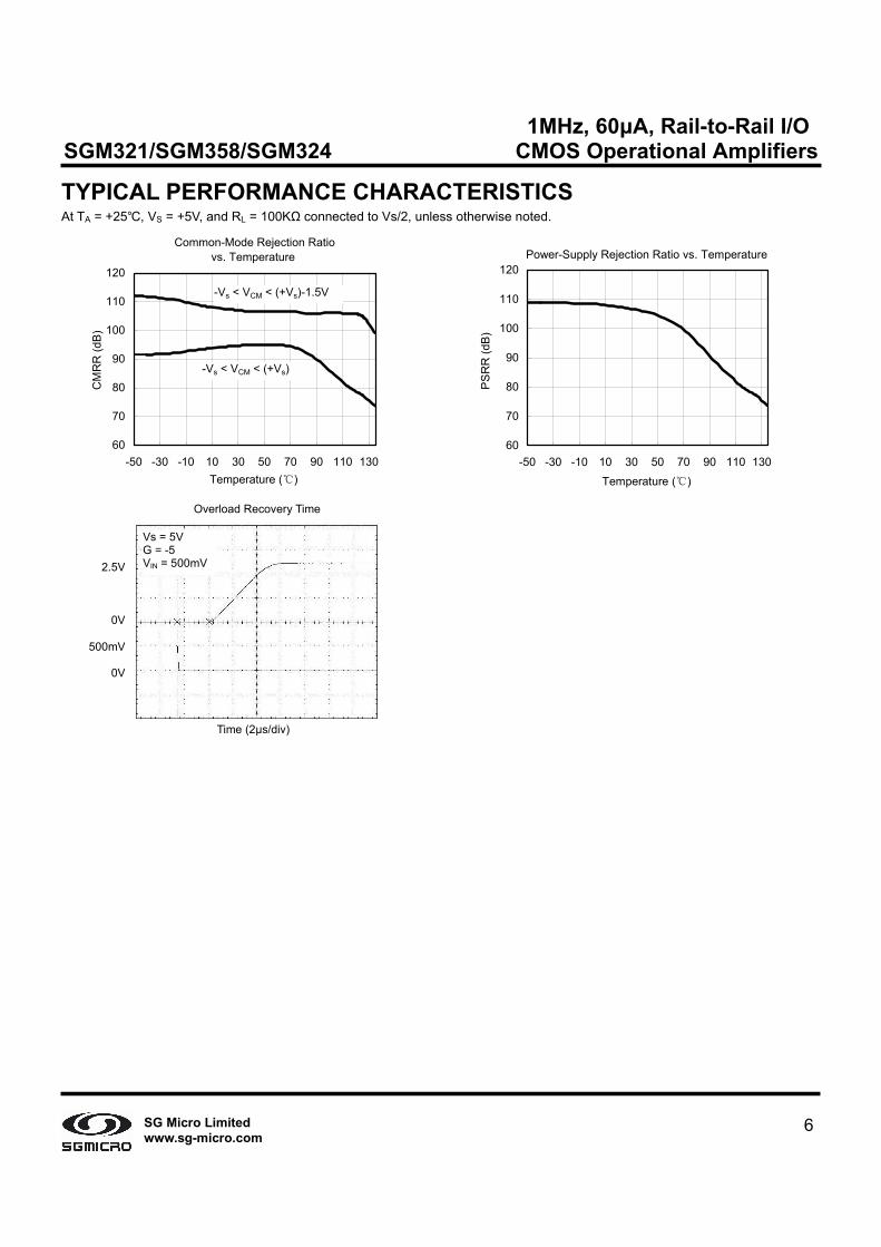
TYPICAL PERFORMANCE CHARACTERISTICS At TA = +25, VS = +5V, and RL = 100KΩ connected to Vs/2, unless otherwise noted.
Common-Mode Rejection Ratiovs. Temperature
60
70
80
90
100
110
120
-50 -30 -10 10 30 50 70 90 110 130Temperature ()
CM
RR
(dB)
-Vs < VCM < (+Vs)
-Vs < VCM < (+Vs)-1.5V
Power-Supply Rejection Ratio vs. Temperature
60
70
80
90
100
110
120
-50 -30 -10 10 30 50 70 90 110 130
Temperature ()P
SR
R (d
B)
Overload Recovery Time
Time (2µs/div)
Vs = 5V G = -5 VIN = 500mV 2.5V
0V
500mV
0V

1MHz, 60µA, Rail-to-Rail I/O SGM321/SGM358/SGM324 CMOS Operational Amplifiers
7SG Micro Limited www.sg-micro.com
APPLICATION NOTES Driving Capacitive Loads The SGM3XX can directly drive 250pF in unity-gain without oscillation. The unity-gain follower (buffer) is the most sensitive configuration to capacitive loading. Direct capacitive loading reduces the phase margin of amplifiers and this results in ringing or even oscillation. Applications that require greater capacitive drive capability should use an isolation resistor between the output and the capacitive load like the circuit in Figure 1. The isolation resistor RISO and the load capacitor CL form a zero to increase stability. The bigger the RISO resistor value, the more stable VOUT will be. Note that this method results in a loss of gain accuracy because RISO forms a voltage divider with the RLOAD.
VIN
VOUTSGM321CL
RISO
Figure 1. Indirectly Driving Heavy Capacitive Load An improvement circuit is shown in Figure 2, It provides DC accuracy as well as AC stability. RF provides the DC accuracy by connecting the inverting signal with the output, CF and RIso serve to counteract the loss of phase margin by feeding the high frequency component of the output signal back to the amplifier’s inverting input, thereby preserving phase margin in the overall feedback loop.
VIN
VOUTSGM321
CL
RISO
RL
RF
CF
Figure 2. Indirectly Driving Heavy Capacitive Load with DC Accuracy For no-buffer configuration, there are two others ways to increase the phase margin: (a) by increasing the amplifier’s gain or (b) by placing a capacitor in parallel with the feedback resistor to counteract the parasitic capacitance associated with inverting node.
Power-Supply Bypassing and Layout The SGM3XX family operates from either a single +2.5V to +5.5V supply or dual ±1.25V to ±2.75V supplies. For single-supply operation, bypass the power supply VDD with a 0.1µF ceramic capacitor which should be placed close to the VDD pin. For dual-supply operation, both the VDD and the VSS supplies should be bypassed to ground with separate 0.1µF ceramic capacitors. 2.2µF tantalum capacitor can be added for better performance.
SGM321Vn
Vp
VDD
VSS(GND)
VOUT
10µF
0.1µF
SGM321
VDD
Vn
Vp
VSS
VOUT
10µF
0.1µF
10µF
0.1µF
Figure 3. Amplifier with Bypass Capacitors
1MHz, 60µA, Rail-to-Rail I/O SGM321/SGM358/SGM324 CMOS Operational Amplifiers
8SG Micro Limited www.sg-micro.com
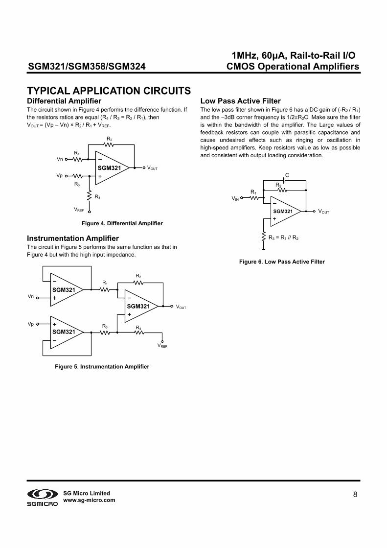
TYPICAL APPLICATION CIRCUITSDifferential Amplifier The circuit shown in Figure 4 performs the difference function. If the resistors ratios are equal (R4 / R3 = R2 / R1), then VOUT = (Vp – Vn) × R2 / R1 + VREF.
Vn
VpVOUTSGM321
VREF
R1
R2
R3
R4
Figure 4. Differential Amplifier
Instrumentation Amplifier The circuit in Figure 5 performs the same function as that in Figure 4 but with the high input impedance.
Vn
Vp
SGM321
VREF
R1
R2
R3 R4
VOUT
SGM321
SGM321
Figure 5. Instrumentation Amplifier
Low Pass Active Filter The low pass filter shown in Figure 6 has a DC gain of (-R2 / R1) and the –3dB corner frequency is 1/2πR2C. Make sure the filter is within the bandwidth of the amplifier. The Large values of feedback resistors can couple with parasitic capacitance and cause undesired effects such as ringing or oscillation in high-speed amplifiers. Keep resistors value as low as possible and consistent with output loading consideration.
VIN
VOUTSGM321
R1
R2
R3 = R1 // R2
C
Figure 6. Low Pass Active Filter

1MHz, 60µA, Rail-to-Rail I/O SGM321/SGM358/SGM324 CMOS Operational Amplifiers
9SG Micro Limited www.sg-micro.com
PACKAGE OUTLINE DIMENSIONS SC70-5 / SOT-353
E1
De1
e
b
A2 A
A1
E
LL1
0.20C
θ
Dimensions In Millimeters
Dimensions In Inches Symbol
Min Max Min Max A 0.900 1.100 0.035 0.043
A1 0.000 0.100 0.000 0.004 A2 0.900 1.000 0.035 0.039 b 0.150 0.350 0.006 0.014 c 0.080 0.150 0.003 0.006 D 2.000 2.200 0.079 0.087 E 1.150 1.350 0.045 0.053
E1 2.150 2.450 0.085 0.096 e 0.650TYP 0.026TYP
e1 1.200 1.400 0.047 0.055 L 0.525REF 0.021REF
L1 0.260 0.460 0.010 0.018 θ 0° 8° 0° 8°
1MHz, 60µA, Rail-to-Rail I/O SGM321/SGM358/SGM324 CMOS Operational Amplifiers
10SG Micro Limited www.sg-micro.com
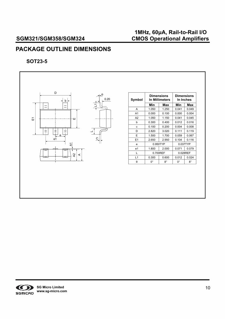
PACKAGE OUTLINE DIMENSIONS SOT23-5
D
e1
b
A2 A
A1E
L1L
C
E1
0
θ0.20
e
Dimensions In Millimeters
DimensionsIn Inches Symbol
Min Max Min MaxA 1.050 1.250 0.041 0.049
A1 0.000 0.100 0.000 0.004A2 1.050 1.150 0.041 0.045b 0.300 0.400 0.012 0.016c 0.100 0.200 0.004 0.008D 2.820 3.020 0.111 0.119E 1.500 1.700 0.059 0.067
E1 2.650 2.950 0.104 0.116e 0.950TYP 0.037TYP
e1 1.800 2.000 0.071 0.079L 0.700REF 0.028REF
L1 0.300 0.600 0.012 0.024θ 0° 8° 0° 8°
1MHz, 60µA, Rail-to-Rail I/O SGM321/SGM358/SGM324 CMOS Operational Amplifiers
11SG Micro Limited www.sg-micro.com
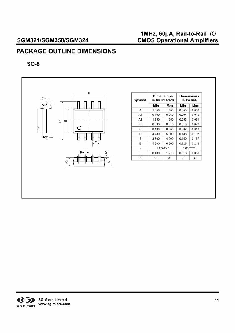
PACKAGE OUTLINE DIMENSIONS SO-8
C
L
θ
D
e
EE1
A2
B
AA1
Dimensions In Millimeters
Dimensions In Inches Symbol
Min Max Min Max A 1.350 1.750 0.053 0.069
A1 0.100 0.250 0.004 0.010 A2 1.350 1.550 0.053 0.061 B 0.330 0.510 0.013 0.020 C 0.190 0.250 0.007 0.010 D 4.780 5.000 0.188 0.197 E 3.800 4.000 0.150 0.157
E1 5.800 6.300 0.228 0.248 e 1.270TYP 0.050TYP L 0.400 1.270 0.016 0.050 θ 0° 8° 0° 8°

1MHz, 60µA, Rail-to-Rail I/O SGM321/SGM358/SGM324 CMOS Operational Amplifiers
12SG Micro Limited www.sg-micro.com
PACKAGE OUTLINE DIMENSIONS MSOP-8
CL
D
EE1
A1
e
b
A2
A
θ
Dimensions In Millimeters
Dimensions In Inches Symbol
Min Max Min MaxA 0.800 1.200 0.031 0.047
A1 0.000 0.200 0.000 0.008A2 0.760 0.970 0.030 0.038b 0.30 TYP 0.012 TYP C 0.15 TYP 0.006 TYP D 2.900 3.100 0.114 0.122e 0.65 TYP 0.026 TYP E 2.900 3.100 0.114 0.122
E1 4.700 5.100 0.185 0.201L 0.410 0.650 0.016 0.026θ 0° 6° 0° 6°
1MHz, 60µA, Rail-to-Rail I/O SGM321/SGM358/SGM324 CMOS Operational Amplifiers
13SG Micro Limited www.sg-micro.com
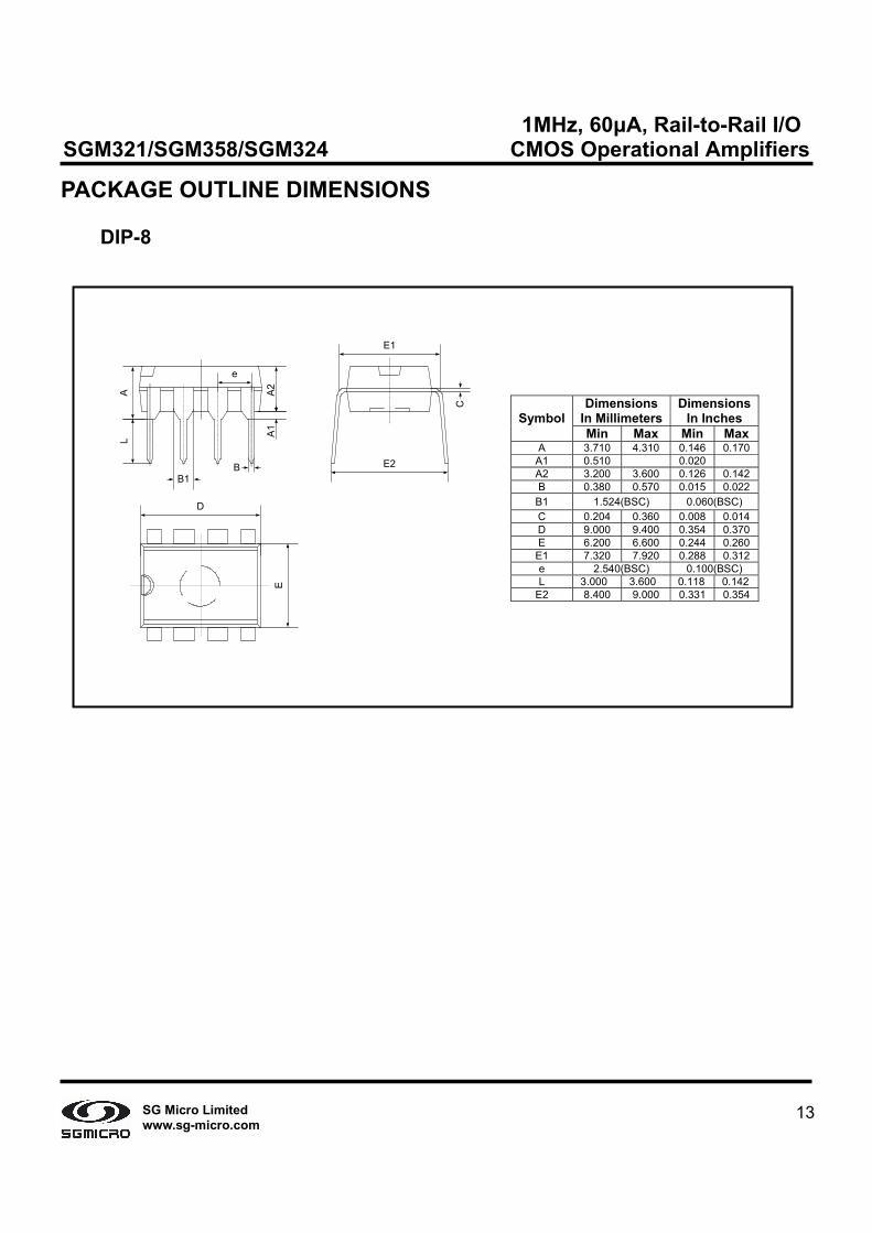
PACKAGE OUTLINE DIMENSIONS DIP-8
D
E
AL
A
2
A1
e
B1
B
E1
CE2
Dimensions In Millimeters
DimensionsIn Inches Symbol
Min Max Min MaxA 3.710 4.310 0.146 0.170
A1 0.510 0.020 A2 3.200 3.600 0.126 0.142B 0.380 0.570 0.015 0.022
B1 1.524(BSC) 0.060(BSC) C 0.204 0.360 0.008 0.014D 9.000 9.400 0.354 0.370E 6.200 6.600 0.244 0.260
E1 7.320 7.920 0.288 0.312e 2.540(BSC) 0.100(BSC) L 3.000 3.600 0.118 0.142
E2 8.400 9.000 0.331 0.354

1MHz, 60µA, Rail-to-Rail I/O SGM321/SGM358/SGM324 CMOS Operational Amplifiers
14SG Micro Limited www.sg-micro.com
PACKAGE OUTLINE DIMENSIONS SO-14
0.25
D
E1E
b
A3
A
L2
Lθ
Me
INDEX Φ0.8±0.1DEP0.2±0.1
Φ2.0±0.1 BTM E-MARKDEP0.1±0.05
A1
A2
θ3
θ4 0.10
b
b1
c c1
WITH PLATINGBASE METAL
SECTION B-B
θ2
θ1
R1 R
L1
h
B Bh
Dimensions In Millimeters Symbol
MIN NOM MAXA 1.35 1.60 1.75
A1 0.10 0.15 0.25 A2 1.25 1.45 1.65 A3 0.55 0.65 0.75 b 0.36 0.49
b1 0.35 0.40 0.45 c 0.16 0.25
c1 0.15 0.20 0.25 D 8.53 8.63 8.73 E 5.80 6.00 6.20
E1 3.80 3.90 4.00 e 1.27 BSC L 0.45 0.60 0.80
L1 1.04 REF L2 0.25 BSC R 0.07
R1 0.07 h 0.30 0.40 0.50 θ 0° 8° θ1 6° 8° 10° θ2 6° 8° 10° θ3 5° 7° 9° θ4 5° 7° 9°
1MHz, 60µA, Rail-to-Rail I/O SGM321/SGM358/SGM324 CMOS Operational Amplifiers
15SG Micro Limited www.sg-micro.com
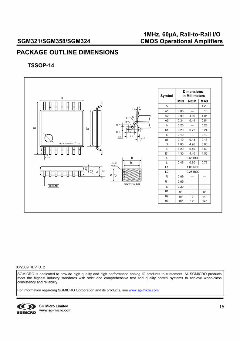
PACKAGE OUTLINE DIMENSIONS TSSOP-14
D
E1E
A3
e
INDEX Φ1.0±0.05 0.1 DEP
0.10
+0-0.1
#1 P
IN
A2 A A1
θ2
θ3
θ1
R1R
S
B
B
L2
L
L1
bb1
c c1
BASE METAL
SECTION B-B
03/2009 REV. D. 2
Dimensions In Millimeters Symbol
MIN NOM MAXA — — 1.20
A1 0.05 — 0.15A2 0.90 1.00 1.05A3 0.34 0.44 0.54b 0.20 — 0.28
b1 0.20 0.22 0.24c 0.10 — 0.19
c1 0.10 0.13 0.15D 4.86 4.96 5.06E 6.20 6.40 6.60
E1 4.30 4.40 4.50e 0.65 BSC L 0.45 0.60 0.75
L1 1.00 REF L2 0.25 BSC R 0.09 — —
R1 0.09 — —
S 0.20 — — θ1 0° — 8° θ2 10° 12° 14° θ3 10° 12° 14°
SGMICRO is dedicated to provide high quality and high performance analog IC products to customers. All SGMICRO products meet the highest industry standards with strict and comprehensive test and quality control systems to achieve world-class consistency and reliability. For information regarding SGMICRO Corporation and its products, see www.sg-micro.com
Related Documents


