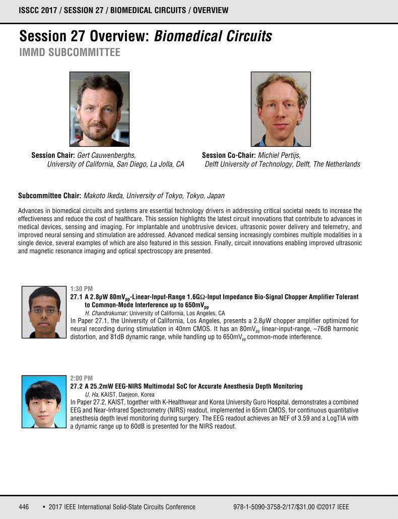
446 • 2017 IEEE International Solid-State Circuits Conference 978-1-5090-3758-2/17/$31.00 ©2017 IEEE ISSCC 2017 / SESSION 27 / BIOMEDICAL CIRCUITS / OVERVIEW Session 27 Overview: Biomedical Circuits IMMD SUBCOMMITTEE 1:30 PM 27.1 A 2.8μW 80mV pp -Linear-Input-Range 1.6GΩ-Input Impedance Bio-Signal Chopper Amplifier Tolerant to Common-Mode Interference up to 650mV pp H. Chandrakumar, University of California, Los Angeles, CA In Paper 27.1, the University of California, Los Angeles, presents a 2.8μW chopper amplifier optimized for neural recording during stimulation in 40nm CMOS. It has an 80mV pp linear-input-range, –76dB harmonic distortion, and 81dB dynamic range, while handling up to 650mV pp common-mode interference. 2:00 PM 27.2 A 25.2mW EEG-NIRS Multimodal SoC for Accurate Anesthesia Depth Monitoring U. Ha, KAIST, Daejeon, Korea In Paper 27.2, KAIST, together with K-Healthwear and Korea University Guro Hospital, demonstrates a combined EEG and Near-Infrared Spectrometry (NIRS) readout, implemented in 65nm CMOS, for continuous quantitative anesthesia depth level monitoring during surgery. The EEG readout achieves an NEF of 3.59 and a LogTIA with a dynamic range up to 60dB is presented for the NIRS readout. Subcommittee Chair: Makoto Ikeda, University of Tokyo, Tokyo, Japan Advances in biomedical circuits and systems are essential technology drivers in addressing critical societal needs to increase the effectiveness and reduce the cost of healthcare. This session highlights the latest circuit innovations that contribute to advances in medical devices, sensing and imaging. For implantable and unobtrusive devices, ultrasonic power delivery and telemetry, and improved neural sensing and stimulation are addressed. Advanced medical sensing increasingly combines multiple modalities in a single device, several examples of which are also featured in this session. Finally, circuit innovations enabling improved ultrasonic and magnetic resonance imaging and optical spectroscopy are presented. Session Chair: Gert Cauwenberghs, University of California, San Diego, La Jolla, CA Session Co-Chair: Michiel Pertijs, Delft University of Technology, Delft, The Netherlands

Welcome message from author
This document is posted to help you gain knowledge. Please leave a comment to let me know what you think about it! Share it to your friends and learn new things together.
Transcript
446 • 2017 IEEE International Solid-State Circuits Conference 978-1-5090-3758-2/17/$31.00 ©2017 IEEE
ISSCC 2017 / SESSION 27 / BIOMEDICAL CIRCUITS / OVERVIEW
Session 27 Overview: Biomedical CircuitsIMMD SUBCOMMITTEE
1:30 PM27.1 A 2.8µW 80mVpp-Linear-Input-Range 1.6GΩ-Input Impedance Bio-Signal Chopper Amplifier Tolerant
to Common-Mode Interference up to 650mVppH. Chandrakumar, University of California, Los Angeles, CA
In Paper 27.1, the University of California, Los Angeles, presents a 2.8μW chopper amplifier optimized forneural recording during stimulation in 40nm CMOS. It has an 80mVpp linear-input-range, –76dB harmonicdistortion, and 81dB dynamic range, while handling up to 650mVpp common-mode interference.
2:00 PM27.2 A 25.2mW EEG-NIRS Multimodal SoC for Accurate Anesthesia Depth Monitoring
U. Ha, KAIST, Daejeon, KoreaIn Paper 27.2, KAIST, together with K-Healthwear and Korea University Guro Hospital, demonstrates a combinedEEG and Near-Infrared Spectrometry (NIRS) readout, implemented in 65nm CMOS, for continuous quantitativeanesthesia depth level monitoring during surgery. The EEG readout achieves an NEF of 3.59 and a LogTIA witha dynamic range up to 60dB is presented for the NIRS readout.
Subcommittee Chair: Makoto Ikeda, University of Tokyo, Tokyo, Japan
Advances in biomedical circuits and systems are essential technology drivers in addressing critical societal needs to increase theeffectiveness and reduce the cost of healthcare. This session highlights the latest circuit innovations that contribute to advances inmedical devices, sensing and imaging. For implantable and unobtrusive devices, ultrasonic power delivery and telemetry, andimproved neural sensing and stimulation are addressed. Advanced medical sensing increasingly combines multiple modalities in asingle device, several examples of which are also featured in this session. Finally, circuit innovations enabling improved ultrasonicand magnetic resonance imaging and optical spectroscopy are presented.
Session Chair: Gert Cauwenberghs, University of California, San Diego, La Jolla, CA
Session Co-Chair: Michiel Pertijs, Delft University of Technology, Delft, The Netherlands

447DIGEST OF TECHNICAL PAPERS •
ISSCC 2017 / February 8, 2017 / 1:30 PM
2:30 PM27.3 All-Wireless 64-Channel 0.013mm2/ch Closed-Loop Neurostimulator with Rail-to-Rail DC Offset
RemovalH. Kassiri, York University, Toronto, Canada
In Paper 27.3, York University, together with the University of Toronto, GlaxoSmithKline, and Toronto WesternHospital, present a 64-channel wireless closed-loop neurostimulator with a compact (0.013mm2/ch) and energy-efficient (630nW/ch) channel architecture that merges both amplification and digitization in a single D2S-basedneural ADC. The design, implemented in 0.13µm CMOS, yields 1.13mVrms IR noise and an NEF of 2.86.
3:15 PM27.4 A Sub-1dB NF Dual-Channel On-Coil CMOS Receiver for Magnetic Resonance Imaging
B. Sporrer, ETH Zurich, Zurich, SwitzerlandIn Paper 27.4, ETH Zurich presents a fully integrated CMOS receiver for medical MRI that can be placed directlyon the coil eliminating any RF cabling. The RX features sub-1dB NF and 0dBm IIP3.
3:45 PM27.5 A Pixel-Pitch-Matched Ultrasound Receiver for 3D Photoacoustic Imaging with Integrated Delta-Sigma
Beamformer in 28nm UTBB FDSOIM-C. Chen, Stanford University, Stanford, CA
In Paper 27.5, Stanford University and STMicroelectronics present a 28nm ultrasound receiver for 3Dphotoacoustic imaging with the front-end and the modulator integrated within a 250×250µm2 pixel. Thebeamformer achieves 59.9dB SNR with a 7.4× area reduction over comparable prior-art solutions.
4:15 PM27.6 Single-Chip 3072ch 2D Array IC with RX Analog and All-Digital TX Beamformer for 3D Ultrasound
ImagingS. Kajiyama, Hitachi, Kokubunji, Japan
In Paper 27.6, Hitachi presents a 2D array ASIC with 3072 channel analog RX/TX beamformers for volumetricultrasound imaging. It features 138Vpp output capability on 0.09mm2/ch. The IC is fabricated in 0.18µm HV-CMOS, and the echo imaging consumes 0.7mW/ch.
4:45 PM27.7 A 30.5 mm3 Fully Packaged Implantable Device with Duplex Ultrasonic Data and Power Links Achieving
95kb/s with <10-4 BER at 8.5cm DepthT. C. Chang, Stanford University, Stanford, CA
In Paper 27.7, Stanford University demonstrates simultaneous ultrasonic wireless power and duplex datacommunication for implantable applications. It operates at a depth of 8.5cm tissue phantom at a data rate of95kb/s. The system consumes 405µW, while receiving power and delivering -9dBm to the transmitter.
5:00 PM27.8 Fully Integrated Optical Spectrometer with 500-to-830nm Range in 65nm CMOS
L. Hong, Princeton University, Princeton, NJIn Paper 27.8, Princeton University presents a fully integrated CMOS-based optical spectrometer in a 65nmbulk CMOS process that requires no external optical components. It achieves nearly 10nm resolution and 1.4nmaccuracy in peak prediction of continuous-wave excitation in the visible and near-IR range between 500 and830nm.
27
448 • 2017 IEEE International Solid-State Circuits Conference
ISSCC 2017 / SESSION 27 / BIOMEDICAL CIRCUITS / 27.1
27.1 A 2.8µW 80mVpp-Linear-Input-Range 1.6GΩ-Input Impedance Bio-Signal Chopper Amplifier Tolerant to Common-Mode Interference up to 650mVpp
Hariprasad Chandrakumar, Dejan Marković
University of California, Los Angeles, CA
Closed-loop neuromodulation with simultaneous stimulation and sensing isdesired to administer therapy in patients suffering from drug-resistantneurological ailments. However, stimulation generates large artifacts at therecording sites, which saturate traditional front-ends. The common-mode (CM)artifact can be ~500mV, and the differential-mode (DM) artifact is 50 to 100mV.This work presents a neural recording chopper amplifier that can tolerate 80mVpp
DM and 650mVpp CM artifacts in a signal band of 1Hz to 5kHz. To digitize a 2mVpp
neural signal to 8b accompanied by an 80mVpp DM artifact requires a linearity of80dB. Neural recording front-ends also need to function within a power budgetof 3 to 5μW/ch, input-referred noise of 4 to 8μVrms, DC input impedance Zin>1GΩand high-pass cutoff of 1Hz [1,2]. Prior work has addressed power and noise [2-6], but has low Zin and limited input signal range, making them incapable ofperforming true closed-loop operation.
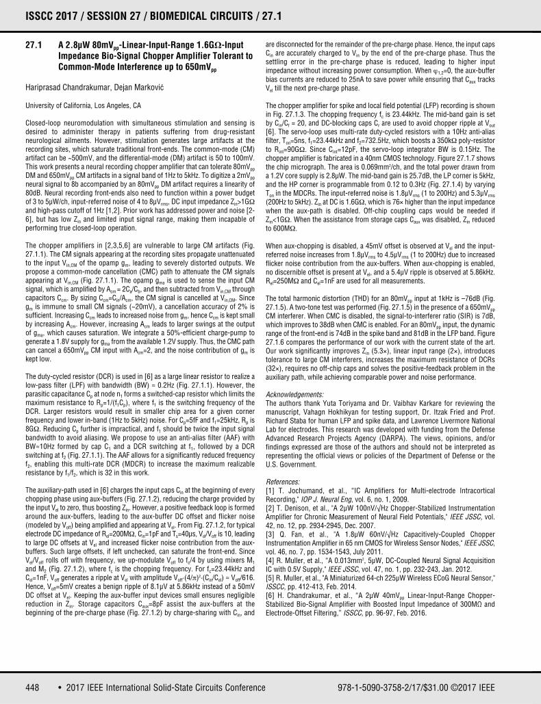
The chopper amplifiers in [2,3,5,6] are vulnerable to large CM artifacts (Fig.27.1.1). The CM signals appearing at the recording sites propagate unattenuatedto the input Vin,CM of the opamp gm, leading to severely distorted outputs. Wepropose a common-mode cancellation (CMC) path to attenuate the CM signalsappearing at Vin,CM (Fig. 27.1.1). The opamp gma is used to sense the input CMsignal, which is amplified by Acm = 2Ca/Cb, and then subtracted from Vin,CM throughcapacitors Ccm. By sizing Ccm=Cin/Acm, the CM signal is cancelled at Vin,CM. Sincegm is immune to small CM signals (~20mV), a cancellation accuracy of 2% issufficient. Increasing Ccm leads to increased noise from gm, hence Ccm is kept smallby increasing Acm. However, increasing Acm leads to larger swings at the outputof gma, which causes saturation. We integrate a 50%-efficient charge-pump togenerate a 1.8V supply for gma from the available 1.2V supply. Thus, the CMC pathcan cancel a 650mVpp CM input with Acm=2, and the noise contribution of gm iskept low.
The duty-cycled resistor (DCR) is used in [6] as a large linear resistor to realize alow-pass filter (LPF) with bandwidth (BW) ≈ 0.2Hz (Fig. 27.1.1). However, theparasitic capacitance Cp at node n1 forms a switched-cap resistor which limits themaximum resistance to Rp=1/(f1Cp), where f1 is the switching frequency of theDCR. Larger resistors would result in smaller chip area for a given cornerfrequency and lower in-band (1Hz to 5kHz) noise. For Cp=5fF and f1=25kHz, Rp is8GΩ. Reducing Cp further is impractical, and f1 should be twice the input signalbandwidth to avoid aliasing. We propose to use an anti-alias filter (AAF) withBW≈10Hz formed by cap C1 and a DCR switching at f1, followed by a DCRswitching at f2 (Fig. 27.1.1). The AAF allows for a significantly reduced frequencyf2, enabling this multi-rate DCR (MDCR) to increase the maximum realizableresistance by f1/f2, which is 32 in this work.
The auxiliary-path used in [6] charges the input caps Cin at the beginning of everychopping phase using aux-buffers (Fig. 27.1.2), reducing the charge provided bythe input Vel to zero, thus boosting Zin. However, a positive feedback loop is formedaround the aux-buffers, leading to the aux-buffer DC offset and flicker noise(modeled by Voff) being amplified and appearing at Vel. From Fig. 27.1.2, for typicalelectrode DC impedance of Rel=200MΩ, Cin=1pF and Ts=40μs, Vel/Voff is 10, leadingto large DC offsets at Vel and increased flicker noise contribution from the aux-buffers. Such large offsets, if left unchecked, can saturate the front-end. SinceVel/Voff rolls off with frequency, we up-modulate Voff to fc/4 by using mixers M1
and M2 (Fig. 27.1.2), where fc is the chopping frequency. For fc=23.44kHz andCel=1nF, Voff generates a ripple at Vel with amplitude Voff∙(4/π)2∙(Cin/Cel) ≈ Voff/616.Hence, Voff=5mV creates a benign ripple of 8.1μV at 5.86kHz instead of a 50mVDC offset at Vel. Keeping the aux-buffer input devices small ensures negligiblereduction in Zin. Storage capacitors Caux=8pF assist the aux-buffers at thebeginning of the pre-charge phase (Fig. 27.1.2) by charge-sharing with Cin, and
are disconnected for the remainder of the pre-charge phase. Hence, the input capsCin are accurately charged to Vin by the end of the pre-charge phase. Thus thesettling error in the pre-charge phase is reduced, leading to higher inputimpedance without increasing power consumption. When ϕ1,2=0, the aux-bufferbias currents are reduced to 25nA to save power while ensuring that Caux tracksVel till the next pre-charge phase.
The chopper amplifier for spike and local field potential (LFP) recording is shownin Fig. 27.1.3. The chopping frequency fc is 23.44kHz. The mid-band gain is setby Cin/Cf = 20, and DC-blocking caps Cr are used to avoid chopper ripple at Vout
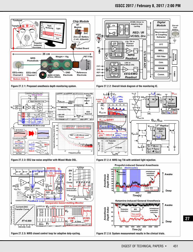
[6]. The servo-loop uses multi-rate duty-cycled resistors with a 10Hz anti-aliasfilter, Ton=5ns, f1=23.44kHz and f2=732.5Hz, which boosts a 350kΩ poly-resistorto Rint=90GΩ. Since Cint=12pF, the servo-loop integrator BW is 0.15Hz. Thechopper amplifier is fabricated in a 40nm CMOS technology. Figure 27.1.7 showsthe chip micrograph. The area is 0.069mm2/ch, and the total power drawn froma 1.2V core supply is 2.8μW. The mid-band gain is 25.7dB, the LP corner is 5kHz,and the HP corner is programmable from 0.12 to 0.3Hz (Fig. 27.1.4) by varyingTon in the MDCRs. The input-referred noise is 1.8μVrms (1 to 200Hz) and 5.3μVrms
(200Hz to 5kHz). Zin at DC is 1.6GΩ, which is 76× higher than the input impedancewhen the aux-path is disabled. Off-chip coupling caps would be needed ifZin<1GΩ. When the assistance from storage caps Caux was disabled, Zin reducedto 600MΩ.
When aux-chopping is disabled, a 45mV offset is observed at Vel and the input-referred noise increases from 1.8μVrms to 4.5μVrms (1 to 200Hz) due to increasedflicker noise contribution from the aux-buffers. When aux-chopping is enabled,no discernible offset is present at Vel, and a 5.4μV ripple is observed at 5.86kHz.Rel=250MΩ and Cel=1nF are used for all measurements.
The total harmonic distortion (THD) for an 80mVpp input at 1kHz is –76dB (Fig.27.1.5). A two-tone test was performed (Fig. 27.1.5) in the presence of a 650mVpp
CM interferer. When CMC is disabled, the signal-to-interferer ratio (SIR) is 7dB,which improves to 38dB when CMC is enabled. For an 80mVpp input, the dynamicrange of the front-end is 74dB in the spike band and 81dB in the LFP band. Figure27.1.6 compares the performance of our work with the current state of the art.Our work significantly improves Zin (5.3×), linear input range (2×), introducestolerance to large CM interferers, increases the maximum resistance of DCRs(32×), requires no off-chip caps and solves the positive-feedback problem in theauxiliary path, while achieving comparable power and noise performance.
Acknowledgements: The authors thank Yuta Toriyama and Dr. Vaibhav Karkare for reviewing themanuscript, Vahagn Hokhikyan for testing support, Dr. Itzak Fried and Prof.Richard Staba for human LFP and spike data, and Lawrence Livermore NationalLab for electrodes. This research was developed with funding from the DefenseAdvanced Research Projects Agency (DARPA). The views, opinions, and/orfindings expressed are those of the authors and should not be interpreted asrepresenting the official views or policies of the Department of Defense or theU.S. Government.
References:[1] T. Jochumand, et al., “IC Amplifiers for Multi-electrode IntracorticalRecording," IOP J. Neural Eng, vol. 6, no. 1, 2009.[2] T. Denison, et al., "A 2μW 100nV/√Hz Chopper-Stabilized InstrumentationAmplifier for Chronic Measurement of Neural Field Potentials," IEEE JSSC, vol.42, no. 12, pp. 2934-2945, Dec. 2007.[3] Q. Fan, et al., "A 1.8μW 60nV/√Hz Capacitively-Coupled ChopperInstrumentation Amplifier in 65 nm CMOS for Wireless Sensor Nodes," IEEE JSSC,vol. 46, no. 7, pp. 1534-1543, July 2011.[4] R. Muller, et al., “A 0.013mm2, 5μW, DC-Coupled Neural Signal AcquisitionIC with 0.5V Supply," IEEE JSSC, vol. 47, no. 1, pp. 232-243, Jan. 2012.[5] R. Muller, et al., "A Miniaturized 64-ch 225μW Wireless ECoG Neural Sensor,"ISSCC, pp. 412-413, Feb. 2014.[6] H. Chandrakumar, et al., “A 2μW 40mVpp Linear-Input-Range Chopper-Stabilized Bio-Signal Amplifier with Boosted Input Impedance of 300MΩ andElectrode-Offset Filtering,” ISSCC, pp. 96-97, Feb. 2016.
978-1-5090-3758-2/17/$31.00 ©2017 IEEE

449DIGEST OF TECHNICAL PAPERS •
ISSCC 2017 / February 8, 2017 / 1:30 PM
Figure 27.1.1: CM cancellation in chopper amps (left) preserves linearity.Multi-rate resistor (right) increases maximum realizable resistance by 32×.
Figure 27.1.2: Conventional auxiliary path amplifies aux-buffer offset (top).Proposed auxiliary path technique (bottom) mitigates the offset and achieveshigher Zin.
Figure 27.1.3: Complete implementation of the chopper amplifier.
Figure 27.1.5: Measured linearity (top). Measured outputs for 2-tone tests witha CM interferer (bottom). The DM and CM tones at 900Hz emulate the stimartifact, and the 1kHz tone is the signal of interest. Figure 27.1.6: Comparison with current state of the art.
Figure 27.1.4: Chip measurements: gain with programmable HP corner (top),input-referred noise (center), input impedance (bottom).
27

• 2017 IEEE International Solid-State Circuits Conference 978-1-5090-3758-2/17/$31.00 ©2017 IEEE
ISSCC 2017 PAPER CONTINUATIONS
Figure 27.1.7: Chip micrograph (top) of 8-channel IC, and single-channelamplifier (bottom).
450 • 2017 IEEE International Solid-State Circuits Conference
ISSCC 2017 / SESSION 27 / BIOMEDICAL CIRCUITS / 27.2
27.2 A 25.2mW EEG-NIRS Multimodal SoC for Accurate Anesthesia Depth Monitoring
Unsoo Ha1, Jaehyuk Lee1, Jihee Lee1, Kwantae Kim1, Minseo Kim1, Taehwan Roh2, Sangsik Choi3, Hoi-Jun Yoo1
1KAIST, Daejeon, Korea2K-Healthwear, Daejeon, Korea3Korea University Guro Hospital, Seoul, Korea
There has been recent research into continuous monitoring of the quantitativeanesthesia (ANES) depth level for safe surgery [1]. However, the current ANESdepth monitoring approach, bispectral index (BIS) [3], uses only EEG from thefrontal lobe, and it shows critical limitations in the monitoring of ANES depth suchas signal distortion due to electrocautery, EMG and dried gel, and false responseto the special types of anesthetic drugs [3]. Near-infrared spectroscopy (NIRS)is complementary to EEG [2], and can not only compensate for the distorted depthlevel, but also assess the effects of various anesthetic drugs. In spite of itsimportance, a unified ANES monitoring system using EEG/NIRS together has notbeen reported because NIRS signals have widely different dynamic ranges (10pAto 10nA), and also signal level variations from person to person and environmentare not manageable without closed-loop control (CLC).
In this paper, a multimodal head-patch system that simultaneously measures EEGand NIRS on the frontal lobe is proposed for accurate ANES depth monitoring. A60dB dynamic range logarithmic TIA (logTIA) is adopted to amplify the photodiode(PD) signal and a CLC driver is used to compensate for the human-to-humanvariations. Also, an LNA with high Zin (1GΩ) and wide electrode DC-offset (EDO)cancelation range (350mV) is integrated to obtain reliable EEG signals.
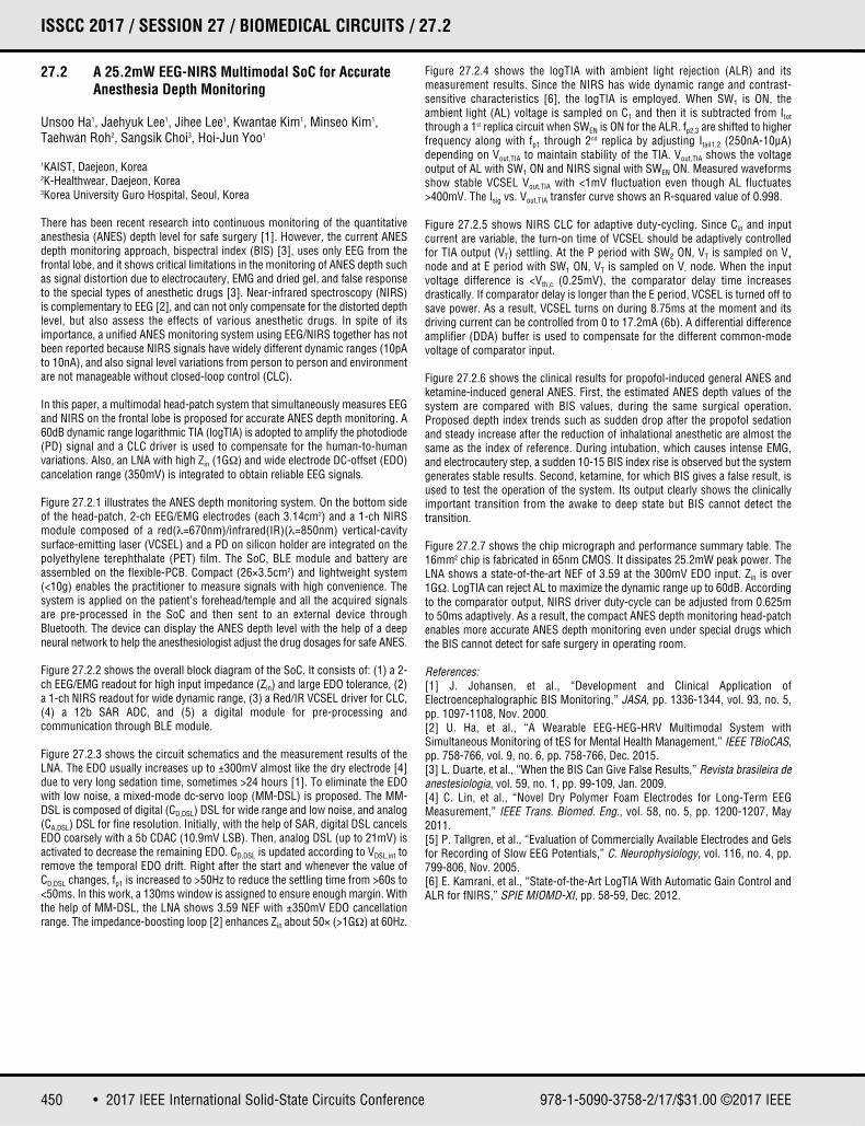
Figure 27.2.1 illustrates the ANES depth monitoring system. On the bottom sideof the head-patch, 2-ch EEG/EMG electrodes (each 3.14cm2) and a 1-ch NIRSmodule composed of a red(λ=670nm)/infrared(IR)(λ=850nm) vertical-cavitysurface-emitting laser (VCSEL) and a PD on silicon holder are integrated on thepolyethylene terephthalate (PET) film. The SoC, BLE module and battery areassembled on the flexible-PCB. Compact (26×3.5cm2) and lightweight system(<10g) enables the practitioner to measure signals with high convenience. Thesystem is applied on the patient’s forehead/temple and all the acquired signalsare pre-processed in the SoC and then sent to an external device throughBluetooth. The device can display the ANES depth level with the help of a deepneural network to help the anesthesiologist adjust the drug dosages for safe ANES.
Figure 27.2.2 shows the overall block diagram of the SoC. It consists of: (1) a 2-ch EEG/EMG readout for high input impedance (Zin) and large EDO tolerance, (2)a 1-ch NIRS readout for wide dynamic range, (3) a Red/IR VCSEL driver for CLC,(4) a 12b SAR ADC, and (5) a digital module for pre-processing andcommunication through BLE module.
Figure 27.2.3 shows the circuit schematics and the measurement results of theLNA. The EDO usually increases up to ±300mV almost like the dry electrode [4]due to very long sedation time, sometimes >24 hours [1]. To eliminate the EDOwith low noise, a mixed-mode dc-servo loop (MM-DSL) is proposed. The MM-DSL is composed of digital (CD,DSL) DSL for wide range and low noise, and analog(CA,DSL) DSL for fine resolution. Initially, with the help of SAR, digital DSL cancelsEDO coarsely with a 5b CDAC (10.9mV LSB). Then, analog DSL (up to 21mV) isactivated to decrease the remaining EDO. CD,DSL is updated according to VDSL,int toremove the temporal EDO drift. Right after the start and whenever the value ofCD,DSL changes, fp1 is increased to >50Hz to reduce the settling time from >60s to<50ms. In this work, a 130ms window is assigned to ensure enough margin. Withthe help of MM-DSL, the LNA shows 3.59 NEF with ±350mV EDO cancellationrange. The impedance-boosting loop [2] enhances Zin about 50× (>1GΩ) at 60Hz.
Figure 27.2.4 shows the logTIA with ambient light rejection (ALR) and itsmeasurement results. Since the NIRS has wide dynamic range and contrast-sensitive characteristics [6], the logTIA is employed. When SW1 is ON, theambient light (AL) voltage is sampled on C1 and then it is subtracted from Itot
through a 1st replica circuit when SWEN is ON for the ALR. fp2,3 are shifted to higherfrequency along with fp1 through 2nd replica by adjusting Itail1,2 (250nA-10μA)depending on Vout,TIA to maintain stability of the TIA. Vout,TIA shows the voltageoutput of AL with SW1 ON and NIRS signal with SWEN ON. Measured waveformsshow stable VCSEL Vout,TIA with <1mV fluctuation even though AL fluctuates>400mV. The Isig vs. Vout,TIA transfer curve shows an R-squared value of 0.998.
Figure 27.2.5 shows NIRS CLC for adaptive duty-cycling. Since Cin and inputcurrent are variable, the turn-on time of VCSEL should be adaptively controlledfor TIA output (VT) settling. At the P period with SW2 ON, VT is sampled on V+
node and at E period with SW1 ON, VT is sampled on V- node. When the inputvoltage difference is <Vth,c (0.25mV), the comparator delay time increasesdrastically. If comparator delay is longer than the E period, VCSEL is turned off tosave power. As a result, VCSEL turns on during 8.75ms at the moment and itsdriving current can be controlled from 0 to 17.2mA (6b). A differential differenceamplifier (DDA) buffer is used to compensate for the different common-modevoltage of comparator input.
Figure 27.2.6 shows the clinical results for propofol-induced general ANES andketamine-induced general ANES. First, the estimated ANES depth values of thesystem are compared with BIS values, during the same surgical operation.Proposed depth index trends such as sudden drop after the propofol sedationand steady increase after the reduction of inhalational anesthetic are almost thesame as the index of reference. During intubation, which causes intense EMG,and electrocautery step, a sudden 10-15 BIS index rise is observed but the systemgenerates stable results. Second, ketamine, for which BIS gives a false result, isused to test the operation of the system. Its output clearly shows the clinicallyimportant transition from the awake to deep state but BIS cannot detect thetransition.
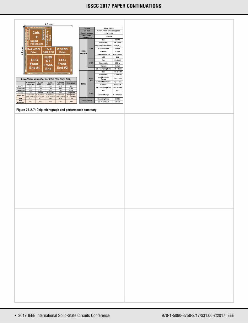
Figure 27.2.7 shows the chip micrograph and performance summary table. The16mm2 chip is fabricated in 65nm CMOS. It dissipates 25.2mW peak power. TheLNA shows a state-of-the-art NEF of 3.59 at the 300mV EDO input. Zin is over1GΩ. LogTIA can reject AL to maximize the dynamic range up to 60dB. Accordingto the comparator output, NIRS driver duty-cycle can be adjusted from 0.625mto 50ms adaptively. As a result, the compact ANES depth monitoring head-patchenables more accurate ANES depth monitoring even under special drugs whichthe BIS cannot detect for safe surgery in operating room.
References: [1] J. Johansen, et al., “Development and Clinical Application ofElectroencephalographic BIS Monitoring,” JASA, pp. 1336-1344, vol. 93, no. 5,pp. 1097-1108, Nov. 2000.[2] U. Ha, et al., “A Wearable EEG-HEG-HRV Multimodal System withSimultaneous Monitoring of tES for Mental Health Management,” IEEE TBioCAS,pp. 758-766, vol. 9, no. 6, pp. 758-766, Dec. 2015.[3] L. Duarte, et al., “When the BIS Can Give False Results,” Revista brasileira deanestesiologia, vol. 59, no. 1, pp. 99-109, Jan. 2009.[4] C. Lin, et al., “Novel Dry Polymer Foam Electrodes for Long-Term EEGMeasurement,” IEEE Trans. Biomed. Eng., vol. 58, no. 5, pp. 1200-1207, May2011.[5] P. Tallgren, et al., “Evaluation of Commercially Available Electrodes and Gelsfor Recording of Slow EEG Potentials,” C. Neurophysiology, vol. 116, no. 4, pp.799-806, Nov. 2005.[6] E. Kamrani, et al., “State-of-the-Art LogTIA With Automatic Gain Control andALR for fNIRS,” SPIE MIOMD-XI, pp. 58-59, Dec. 2012.
978-1-5090-3758-2/17/$31.00 ©2017 IEEE
451DIGEST OF TECHNICAL PAPERS •
ISSCC 2017 / February 8, 2017 / 2:00 PM
Figure 27.2.1: Proposed anesthesia depth monitoring system. Figure 27.2.2: Overall block diagram of the monitoring IC.
Figure 27.2.3: EEG low-noise amplifier with Mixed-Mode DSL.
Figure 27.2.5: NIRS closed control loop for adaptive duty-cycling. Figure 27.2.6: System measurement results in the clinical trials.
Figure 27.2.4: NIRS log TIA with ambient light rejection.
27
• 2017 IEEE International Solid-State Circuits Conference 978-1-5090-3758-2/17/$31.00 ©2017 IEEE
ISSCC 2017 PAPER CONTINUATIONS
Figure 27.2.7: Chip micrograph and performance summary.
452 • 2017 IEEE International Solid-State Circuits Conference
ISSCC 2017 / SESSION 27 / BIOMEDICAL CIRCUITS / 27.3
27.3 All-Wireless 64-Channel 0.013mm2/ch Closed-Loop Neurostimulator with Rail-to-Rail DC Offset Removal
Hossein Kassiri1, M. Reza Pazhouhandeh2, Nima Soltani2,M. Tariqus Salam3, Peter Carlen2,4, Jose Luiz Perez Velazquez2,Roman Genov2
1York University, Toronto, Canada2University of Toronto, Toronto, Canada3GSK (GlaxoSmithKline), Stevenage, United Kingdom4Toronto Western Hospital, Toronto, Canada
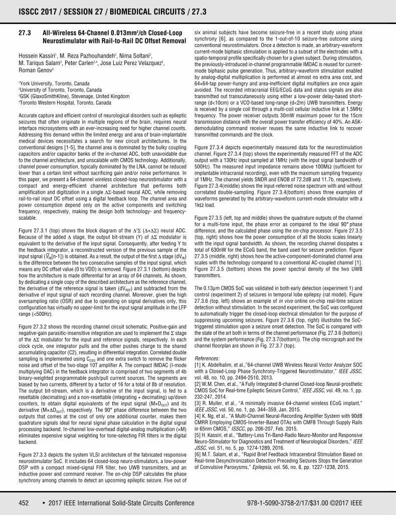
Accurate capture and efficient control of neurological disorders such as epilepticseizures that often originate in multiple regions of the brain, requires neuralinterface microsystems with an ever-increasing need for higher channel counts.Addressing this demand within the limited energy and area of brain-implantablemedical devices necessitates a search for new circuit architectures. In theconventional designs [1-5], the channel area is dominated by the bulky couplingcapacitors and/or capacitor banks of the in-channel ADC, both unavoidable dueto the channel architecture, and unscalable with CMOS technology. Additionally,channel power consumption, typically dominated by the LNA, cannot be reducedlower than a certain limit without sacrificing gain and/or noise performance. Inthis paper, we present a 64-channel wireless closed-loop neurostimulator with acompact and energy-efficient channel architecture that performs bothamplification and digitization in a single ΔΣ-based neural ADC, while removingrail-to-rail input DC offset using a digital feedback loop. The channel area andpower consumption depend only on the active components and switchingfrequency, respectively, making the design both technology- and frequency-scalable.
Figure 27.3.1 (top) shows the block diagram of the Δ2Σ (Δ+ΔΣ) neural ADC.Because of the added Δ stage, the output bit-stream (Y) of ΔΣ modulator isequivalent to the derivative of the input signal. Consequently, after feeding Y tothe feedback integrator, a reconstructed version of the previous sample of theinput signal (VIN[n-1]) is obtained. As a result, the output of the first Δ stage (dVIN)is the difference between the two consecutive samples of the input signal, whichmeans any DC offset value (0 to VDD) is removed. Figure 27.3.1 (bottom) depictshow the architecture is made differential for an array of 64 channels. As shown,by dedicating a single copy of the described architecture as the reference channel,the derivative of the reference signal is taken (dVREF) and subtracted from thederivative of input signal of each recording channel. Moreover, given the highoversampling ratio (OSR) and due to operating on signal derivatives only, thisconfiguration has virtually no upper-limit for the input signal amplitude in the LFPrange (<500Hz).
Figure 27.3.2 shows the recording channel circuit schematic. Positive-gain andnegative-gain parasitic-insensitive integration are used to implement the Σ stageof the ΔΣ modulator for the input and reference signals, respectively. In eachclock cycle, one integrator pulls and the other pushes charge to the sharedaccumulating capacitor (C2), resulting in differential integration. Correlated doublesampling is implemented using CCDS and one extra switch to remove the flickernoise and offset of the two-stage 10T amplifier A. The compact IMDAC (I-modemultiplying DAC) in the feedback integrator is comprised of two segments of 4bbinary-weighted programmable push/pull current sources. The segments arebiased by two currents, different by a factor of 16 for a total of 8b of resolution.The output bit-stream, which is a derivative of the input signal, is fed to aresettable (decimating) and a non-resettable (integrating + decimating) up/downcounters, to obtain digital equivalents of the input signal (M×DOUT) and itsderivative (M×ΔDOUT), respectively. The 90° phase difference between the twooutputs that comes at the cost of only one additional counter, makes themquadrature signals ideal for neural signal phase calculation in the digital signalprocessing backend. In-channel low-overhead digital-analog multiplication (×M)eliminates expensive signal weighting for tone-selecting FIR filters in the digitalbackend.
Figure 27.3.3 depicts the system VLSI architecture of the fabricated responsiveneurostimulator SoC. It includes 64 closed-loop neuro-stimulators, a low-powerDSP with a compact mixed-signal FIR filter, two UWB transmitters, and aninductive power and command receiver. The on-chip DSP calculates the phasesynchrony among channels to detect an upcoming epileptic seizure. Five out of
six animal subjects have become seizure-free in a recent study using phasesynchrony [6], as compared to the 1-out-of-10 seizure-free outcome usingconventional neurostimulators. Once a detection is made, an arbitrary-waveformcurrent-mode biphasic stimulation is applied to a subset of the electrodes with aspatio-temporal profile specifically chosen for a given subject. During stimulation,the previously-introduced in-channel programmable IMDAC is reused for current-mode biphasic pulse generation. Thus, arbitrary-waveform stimulation enabledby analog-digital multiplication is performed at almost no extra area cost, and64×64-tap power-hungry and area-inefficient digital multipliers are once againavoided. The recorded intracranial EEG/ECoG data and status signals are alsotransmitted out transcutaneously using either a low-power delay-based short-range (d<10cm) or a VCO-based long-range (d<2m) UWB transmitters. Energyis received by a single coil through a multi-coil cellular inductive link at 1.5MHzfrequency. The power receiver outputs 30mW maximum power for the 15cmtransmission distance with the overall power transfer efficiency of 40%. An ASK-demodulating command receiver reuses the same inductive link to recovertransmitted commands and the clock.
Figure 27.3.4 depicts experimentally measured data for the neurostimulationchannel. Figure 27.3.4 (top) shows the experimentally measured FFT of the ADCoutput with a 130Hz input sampled at 1MHz (with the input signal bandwidth of500Hz). The measured input impedance remains above 100MΩ (sufficient forimplantable intracranial recording), even with the maximum sampling frequencyof 1MHz. The channel yields SNDR and ENOB of 72.2dB and 11.7b, respectively.Figure 27.3.4(middle) shows the input-referred noise spectrum with and withoutcorrelated double-sampling. Figure 27.3.4(bottom) shows three examples ofwaveforms generated by the arbitrary-waveform current-mode stimulator with a1kΩ load.
Figure 27.3.5 (left, top and middle) shows the quadrature outputs of the channelfor a multi-tone input, the phase error as compared to the ideal 90° phasedifference, and the calculated phase using the on-chip processor. Figure 27.3.5(top, right) shows how the power consumption of all the blocks scales linearlywith the input signal bandwidth. As shown, the recording channel dissipates atotal of 630nW for the ECoG band, the band used for seizure prediction. Figure27.3.5 (middle, right) shows how the active-component-dominated channel areascales with the technology compared to a conventional AC-coupled channel [1].Figure 27.3.5 (bottom) shows the power spectral density of the two UWBtransmitters.
The 0.13μm CMOS SoC was validated in both early detection (experiment 1) andcontrol (experiment 2) of seizures in temporal lobe epilepsy (rat model). Figure27.3.6 (top, left) shows an example of in vivo online on-chip real-time seizuredetection without stimulation. In the second experiment, the SoC was configuredto automatically trigger the closed-loop electrical stimulation for the purpose ofsuppressing upcoming seizures. Figure 27.3.6 (top, right) illustrates the SoC-triggered stimulation upon a seizure onset detection. The SoC is compared withthe state of the art both in terms of the channel performance (Fig. 27.3.6 (bottom))and the system performance (Fig. 27.3.7(bottom)). The chip micrograph and thechannel floorplan are shown in Fig. 27.3.7 (top).
References:[1] K. Abdelhalim, et al.,”64-channel UWB Wireless Neural Vector Analyzer SOCwith a Closed-Loop Phase Synchrony-Triggered Neurostimulator,” IEEE JSSC,vol. 48, no. 10, pp. 2494-2510, 2013.[2] W.M. Chen, et al., “A Fully Integrated 8-channel Closed-loop Neural-prostheticCMOS SoC for Real-time Epileptic Seizure Control,” IEEE JSSC, vol. 49, no. 1, pp.232-247, 2014.[3] R. Muller, et al., “A minimally invasive 64-channel wireless ECoG implant,”IEEE JSSC, vol. 50, no. 1, pp. 344–359, Jan. 2015.[4] K. Ng, et al., “A Multi-Channel Neural-Recording Amplifier System with 90dBCMRR Employing CMOS-Inverter-Based OTAs with CMFB Through Supply Railsin 65nm CMOS,” ISSCC, pp. 206-207, Feb. 2015.[5] H. Kassiri, et al., “Battery-Less Tri-Band-Radio Neuro-Monitor and ResponsiveNeuro-Stimulator for Diagnostics and Treatment of Neurological Disorders,” IEEEJSSC, vol. 51, no. 5, pp. 1274-1289, 2016.[6] M.T. Salam, et al., “Rapid Brief Feedback Intracerebral Stimulation Based onReal-time Desynchronization Detection Preceding Seizures Stops the Generationof Convulsive Paroxysms,” Epilepsia, vol. 56, no. 8, pp. 1227-1238, 2015.
978-1-5090-3758-2/17/$31.00 ©2017 IEEE

453DIGEST OF TECHNICAL PAPERS •
ISSCC 2017 / February 8, 2017 / 2:30 PM
Figure 27.3.1: Block diagram of the ΔΣ-based neural recording channel in bothsingle-ended (top) and differential (bottom) configurations.
Figure 27.3.2: Circuit schematic of the recording channel (top); the inputintegrator during the two phases of a single clock cycle (bottom).
Figure 27.3.3: Block diagram of the fabricated neurostimulator SoC.
Figure 27.3.5: Experimentally measured performance: the on-chip phasecalculation, power scalability with bandwidth, area scalability with technology,and wireless transmitters output spectra.
Figure 27.3.6: In vivo seizure detection and closed-loop stimulation results fora rat epilepsy model (top), neurostimulator channel performance comparison(bottom).
Figure 27.3.4: Experimentally measured performance characteristics of theneurostimulator channel.
27

• 2017 IEEE International Solid-State Circuits Conference 978-1-5090-3758-2/17/$31.00 ©2017 IEEE
ISSCC 2017 PAPER CONTINUATIONS
Figure 27.3.7: Chip micrograph and channel floorplan (top), and a system-levelcomparison table (bottom).
454 • 2017 IEEE International Solid-State Circuits Conference
ISSCC 2017 / SESSION 27 / BIOMEDICAL CIRCUITS / 27.4
27.4 A Sub-1dB NF Dual-Channel On-Coil CMOS Receiver for Magnetic Resonance Imaging
Benjamin Sporrer1, Lianbo Wu1, Luca Bettini1, Christian Vogt1,Jonas Reber2, Josip Marjanovic2, Thomas Burger1, David O. Brunner2, Klaas P. Prüssmann2, Gerhard Tröster1, Qiuting Huang1
1ETH Zurich, Zurich, Switzerland2University and ETH Zurich, Zurich, Switzerland
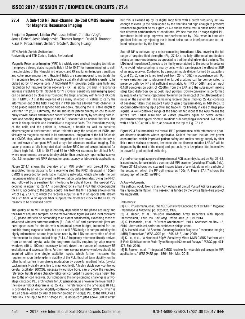
Magnetic Resonance Imaging (MRI) is a widely used medical imaging technique.It employs a strong static magnetic field (1.5 to 10.5T for human imaging) to splitthe spin states of the 1H nuclei in the body, and RF excitation to induce transitionsand coherence among them. Gradient fields are superimposed to modulate the1H resonance frequency, which enables spatially distinguishable signals to bepicked up by RF receive coils. A high-field MRI provides better sensitivity andresolution but requires better receivers (RX), as signal DR and 1H resonanceincrease (128MHz for 3T, 300MHz for 7T). Overall sensitivity and imaging speedcan be enhanced by closely surrounding the target anatomy with tens of RX coils(as in MIMO) [1], at the expense of as many shielded RF cables to carry theinformation out of the field. Progress in PCB size has allowed multi-channel RXto be placed inside the magnetic field (in-bore), reducing the RF cable length toless than 1m [2,3]. Ultimately, the RX should be placed directly on-coil to avoidbulky coaxial cables and improve patient comfort and safety by acquiring data in-bore and sending them digitally to the MRI scanner via an optical fiber link. Thelatter is cheap, flexible and insensitive to magnetic fields. The immediate vicinityof the coils and the patient is, however, a hostile as well as sensitiveelectromagnetic environment, which tolerates only the smallest of PCBs andvirtually no magnetic material in its components. Integration of the full RX chainin a CMOS chip, which is small, non-magnetic and low power, holds the key tothe next wave of compact MRI coil arrays for advanced medical imaging. Thispaper presents a fully integrated dual-receiver RFIC for coil arrays intended for(ultra-) high field (1.5 to 10.5T and 64 to 450MHz) scanners for clinical MRI,where requirements are considerably stricter than previously reported transceiverICs [4,5] on palm-held NMR devices for spectroscopy or lab-on-chip applications.
Figure 27.4.1 shows the overview of an MRI system with on-coil RX, andassociated timing diagrams for a receiving slot. The RFIC integrated in 130nmCMOS is preceded by switchable matching networks, which alternate the coilresonances (detune) to prevent the RF excitation pulse from destroying the RFIC,and followed by a serializer for interfacing to optical fibers. The on-coil PCBdepicted in upper Fig. 27.4.1 is completed by a small FPGA that choreographsthe RFIC according to the optical control line from the MRI scanner shown on theleft of Fig. 27.4.1, to which the receiver output is sent in an optical data streamon a 2nd fiber. A 3rd optical fiber supplies the reference clock to the RFIC, forreasons to be discussed below.
The quality of an MRI image is critically dependent on the phase accuracy andthe SNR of acquired samples, so the receiver noise figure (NF) and local oscillator(LO) phase jitter can be demanding to an extent considerably exceeding those ofadvanced wireless communications [6]. Sub-dB NF and picoseconds jitter arehard specs even for circuits with substantial power budget, intended for useoutside strong magnetic fields, but an on-coil RFIC design is compounded by thehighly mismatched source impedance seen by the LNA and corruption of clockreference for its phase-locked-loop (PLL). A frequency reference directly derivedfrom an on-coil crystal lacks the long-term stability required by wide receivewindows (50 to 100ms) necessary to hold down the number of necessary RFexcitations and save scan time. Furthermore, several receive-windows should beacquired within one single excitation cycle, which further increases therequirements on the long-term stability of the PLL. Its short term stability, on theother hand, suffers from strong modulation by powerful gradient fields (crystalpackaging is typically sensitive to magnetic field). A highly stable oven-controlledcrystal oscillator (OCXO), necessarily outside bore, can provide the requiredreference, but its phase characteristics get corrupted if supplied via a noisy fiberlink to the on-coil receiver. Our solution to this long-standing challenge is a two-stage cascaded PLL architecture for LO generation, as shown in the lower half ofthe receiver block diagram in Fig. 27.4.2. The reference to the (2nd-stage) RF PLLis provided by an on-coil digitally-controlled crystal oscillator (DCXO), which isin turn phase-locked by way of another on-chip (1st-stage) PLL to the OCXO via afiber link. The input to the 1st-stage PLL is noise-corrupted above 500Hz offset
but this is cleaned up by its digital loop filter with a cutoff frequency set lowenough to clean up the noise added by the fiber link but high enough to preserveresilience to gradient fields. Figure 27.4.3 shows measured LO phase noise underfive different combinations of conditions. We see that the 1st-stage digital PLLintroduced in this chip improves jitter performance by 100×, when in-bore withgradient field on, by rejecting the in-band noise due to interference and out-of-band noise added by the fiber link.
Sub-dB NF is achieved by a noise-cancelling broadband LNA, covering the fullrange of targeted field strengths (Fig. 27.4.4). Its fully differential architecturerejects common-mode noise as opposed to traditional single-ended designs. TheLNA input impedance Zin needs to be highly mismatched to the source impedanceRS to avoid noise coupling to nearby coils, which can degrade the effective SNRof an array receiver. Controlled by a programmable divider formed by capacitorsCL and Cfb, Zin can be tuned (real part from 25 to 100Ω) in accordance with RS,whose variation due to placement or target anatomy can be compensated topreserve both low NF and sufficient mismatch. An IIP3 of 0dBm and an input0.1dB compression point of -23dBm from the LNA and the subsequent mixingstage keep distortion low at peak input powers. Down-conversion is performedby means of a harmonic-reject mixer to minimize the impact of the LNA broadbandnoise on the system NF. The remaining receiver chain (mid-Fig. 27.4.2) consistsof baseband filters that support 42dB of gain programmability in 1dB steps, toaccommodate varying input power and trade NF for linearity in case of large peaksignals. A well-controlled range of the band-limited input at the ADC means thelatter’s 12b ENOB resolution at 2MS/s provides equal or better overallperformance than typical discrete solutions sub-sampling a wideband LNA outputwith a 16b ADC at 100+ MHz, as shown at the top of Fig. 27.4.2.
Figure 27.4.5 summarizes the overall RFIC performance, with reference to prior-art discrete solutions where applicable. Salient features include low powerconsumption, which improves patient safety and makes energy supply by fiberlink a more realistic prospect, low noise (in the discrete solution LNA NF will bedegraded by the rest of the chain) and, particularly, a low phase jitter insensitiveto powerful gradient field switching.
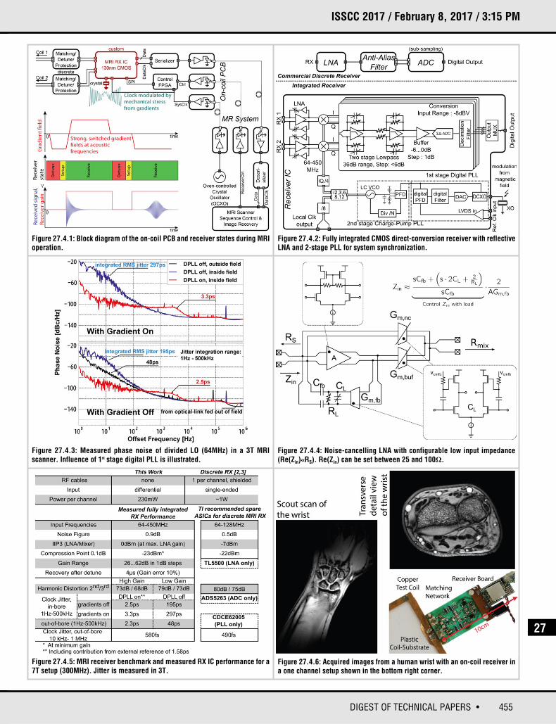
A proof-of-concept, single-coil experimental PCB assembly, based on Fig. 27.4.1,is constructed for use inside a commercial MRI scanner (providing 3T static field).Figure 27.4.6 shows two scanned images taken of a wrist, along with a photo ofthe setup, on which the RF coil measures 100cm2. Figure 27.4.7 shows themicrograph of the 22mm2 RFIC.
Acknowledgments:The authors would like to thank ACP Advanced Circuit Pursuit AG for supportingthe chip implementation. This research is funded by the Swiss Nano-Tera projectWearableMRI.
References:[1] K.P. Pruessmann, et al., “SENSE: Sensitivity Encoding for Fast MRI,” MagneticResonance in Medicine, pp. 952-962, 1999.[2] J. Reber, et al., “In-Bore Broadband Array Receivers with OpticalTransmission,” Proc. Intl. Soc. Mag. Reson. Med., p. 619, 2014.[3] C. Possanzini, et al., “dStream Architecture”, 2011. Accessed on Nov. 15,2016. <http://clinical.netforum.healthcare.philips.com>.[4] A. Hassibi, et al., “A Spectral-Scanning Nuclear Magnetic Resonance Imaging(MRI) Transceiver,” IEEE JSSC, pp. 1805-1813, June 2009.[5] K. Lei, et al., “A Handheld 50pM-Sensitivity Micro-NMR CMOS Platform withB-Field Stabilization for Multi-Type Biological/Chemical Assays,” ISSCC, pp. 474-475, Feb. 2016.[6] B. Sporrer, et al., “Integrated CMOS receiver for wearable coil arrays in MRIapplications,” IEEE DATE, pp. 1689-1694, Mar. 2015.
978-1-5090-3758-2/17/$31.00 ©2017 IEEE
455DIGEST OF TECHNICAL PAPERS •
ISSCC 2017 / February 8, 2017 / 3:15 PM
Figure 27.4.1: Block diagram of the on-coil PCB and receiver states during MRIoperation.
Figure 27.4.2: Fully integrated CMOS direct-conversion receiver with reflectiveLNA and 2-stage PLL for system synchronization.
Figure 27.4.3: Measured phase noise of divided LO (64MHz) in a 3T MRIscanner. Influence of 1st stage digital PLL is illustrated.
Figure 27.4.5: MRI receiver benchmark and measured RX IC performance for a7T setup (300MHz). Jitter is measured in 3T.
Figure 27.4.6: Acquired images from a human wrist with an on-coil receiver ina one channel setup shown in the bottom right corner.
Figure 27.4.4: Noise-cancelling LNA with configurable low input impedance(Re(Zin)«RS). Re(Zin) can be set between 25 and 100Ω.
27
• 2017 IEEE International Solid-State Circuits Conference 978-1-5090-3758-2/17/$31.00 ©2017 IEEE
ISSCC 2017 PAPER CONTINUATIONS
Figure 27.4.7: Integrated MRI receiver chip micrograph.
456 • 2017 IEEE International Solid-State Circuits Conference
ISSCC 2017 / SESSION 27 / BIOMEDICAL CIRCUITS / 27.5
27.5 A Pixel-Pitch-Matched Ultrasound Receiver for 3D Photoacoustic Imaging with Integrated Delta-Sigma Beamformer in 28nm UTBB FDSOI
Man-Chia Chen1, Aldo Peña Perez1, Sri-Rajasekhar Kothapalli1,Philippe Cathelin2, Andreia Cathelin2, Sanjiv Sam Gambhir1,Boris Murmann1
1Stanford University, Stanford, CA2STMicroelectronics, Crolles, France
A variety of emerging applications in medical ultrasound rely on 3D volumetricimaging, calling for dense 2D transducer arrays with thousands of elements. Dueto this high channel count, the traditional per-element cable interface used for 1Darrays is no longer viable. To address this issue, recent work has proven theviability of flip-chip bonding [1] or direct transducer integration [2]. This shiftsthe burden to a CMOS substrate, which must provide dense signal conditioningand processing before the massively parallel image data can be pushed off chip.A common approach for data reduction is to employ subarray beamforming (BF),which applies delay and sum operations within a group of pixels. To implementsuch functionality within the tight pixel pitch, prior works have implemented thedelays using simple S/H circuits [2] or analog filters [3], and typically suffer froma combination of issues related to limited delay, coarse delay resolution andlimited SNR.
This work leverages the integration density of modern CMOS to demonstrate apitch-matched digital subarray beamforming receiver (RX) with signalconditioning and ΔΣ modulator (ΔΣM) integrated within a pixel area of250×250μm2 (see Fig. 27.5.1). Our proof-of-concept IC supports a subarray of4×4 pixels and is flip-chip bonded to a Capacitive Micromachined UltrasoundTransducer (CMUT) chip that is similar to the one used in [1]. Since ourapplication is photoacoustic imaging (receive-only using external laser pulses),we did not integrate a transmitter interface. However, in a large-scale arrayimplementation of our concept, it is conceivable to add this functionality using asubset of the pixels for transmit [2].
Figure 27.5.2 compares our approach with prior art: analog BF [2-3] and digitalBF using a per-channel Nyquist ADC. The latter approach is popular for 1D arrays,but difficult to integrate within a pitch-constrained 2D array. In addition, theNyquist ADC must typically oversample to provide sufficient timing resolution,which further exacerbates the integration issue. The work of [4] combines analogand digital Nyquist-rate BF, but the area per element is ~5× larger than our pixelsize. To enable area-efficient digital BF, this work uses a ΔΣ approach similar to[5]. The oversampling of the ΔΣM naturally provides sufficient timing resolutionfor BF, enables low-complexity analog design with small passives, and simplifiesthe signal routing (1b outputs). In our chip, the 16 bitstreams are routed to aglobal digital block for decimation filtering (DF1) and beamforming (BF = FIFO +summation), followed by a final decimation filter (DF2) off chip. Within the on-chip block, the BF is placed after DF1, which was identified as the preferred optiondue to the lower FIFO clock speed and the commensurate reduction in power (seeFig. 27.5.3). Placing the BF before DF1 (as in [5]) would lead to a slightly lowergate count (since DF1 is shared), but the savings are insignificant due to therelatively low complexity of the employed cascaded integrator comb (CIC) filter.We expect the advantages of the DF-first option to become more pronounced forlarger arrays, where early clock rate reduction is critical. Despite the decimationby DF1, the delay resolution is still 8.33ns, which is sufficient for a 5MHz CMUTcenter frequency. The implemented FIFOs have a depth of 27, providing therequired delay range for our 4×4 subarray (1.06μs).
Figure 27.5.4 shows the analog front-end. The transimpedance amplifier (TIA)provides five gain levels using a programmable R network. The TIA output is takenagainst a replica to facilitate supply noise cancellation as the succeeding lowpassfilter (LPF) performs single-ended to differential conversion. Both the TIA and LPFare designed using 1.5V thick oxide devices (for large DR), while all other circuitsuse core devices (1V supply). The VGA uses a Padé approximation to provide finelinear-in-dB gain tuning. The 1b ΔΣM (see Fig. 27.5.5) uses a 3rd-orderarchitecture with an OSR of 48 to provide 60dB peak SNR in a 10MHz BW. Theemployed inverter-based SC integrator is similar to [6]. It uses three gain stagesto achieve the required gain with minimum L, and it is designed to slew for the
most of the clock period. The large swing at the 3rd stage input during slewingleads to small devices and a compact layout. The input bias of the 3rd stage isestablished using diode replicas and stored on Cb. In comparison to [6], thisobviates the need for special high VT devices and resistors. As illustrated in Fig.27.5.5, the designed ADC is the smallest published among designs with similarBW and SNDR.
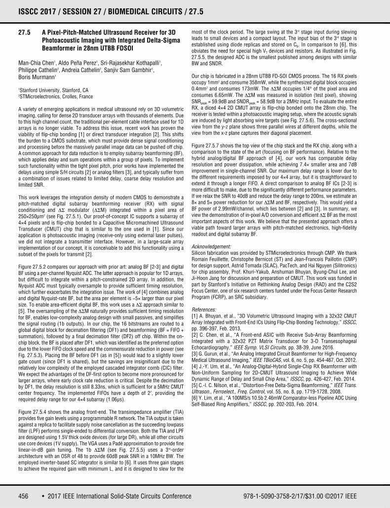
Our chip is fabricated in a 28nm UTBB FD-SOI CMOS process. The 16 RX pixelsoccupy 1mm2 and consume 358mW, while the synthesized digital block occupies0.4mm2 and consumes 173mW. The ΔΣM occupies 1/4th of the pixel area andconsumes 6.65mW. The ΔΣM was measured in isolation (test pixel), showingSNRpeak = 59.9dB and SNDRpeak = 58.9dB for a 2MHz input. To evaluate the entireRX, a diced 4×4 2D CMUT array is flip-chip bonded onto the 28nm chip. Thereceiver is tested within a photoacoustic imaging setup, where the acoustic signalsare induced by light absorbing wire targets (see Fig. 27.5.6). The cross-sectionalview from the y-z plane shows three parallel wires at different depths, while theview from the x-z plane captures their diagonal placement.
Figure 27.5.7 shows the top view of the chip stack and the RX chip, along with acomparison to the state of the art (focusing on BF performance). Relative to thehybrid analog/digital BF approach of [4], our work has comparable delayresolution and power dissipation, while achieving 7.4× smaller area and 7dBimprovement in single-channel SNR. Our maximum delay range is lower due tothe different requirements imposed by our 4×4 array, but it is straightforward toextend it through a longer FIFO. A direct comparison to analog BF ICs [2-3] ismore difficult to make, due to the significantly different performance parameters.If we relax the SNR to 40dB and reduce the delay range to 200ns, we estimate an8× and 5× power reduction for our ΔΣM and BF, respectively. This would yield aBF power of 2.99mW/channel, which lies between [2] and [3]. In summary, weview the demonstration of in-pixel A/D conversion and efficient ΔΣ BF as the mostimportant aspects of this work. We believe that the presented approach offers aviable path toward larger arrays with pitch-matched electronics, high-fidelityreadout and digital subarray BF.
Acknowledgement:Silicon fabrication was provided by STMicroelectronics through CMP. We thankRomain Feuillette, Christophe Bernicot (ST) and Jean-Francois Paillotin (CMP)for design support, Astrid Tomada (SLAC), PacTech, and Hai Nguyen (Silitronics)for chip assembly, Prof. Khuri-Yakub, Anshuman Bhuyan, Byung-Chul Lee, andJi-Hoon Jang for discussion and preparation of CMUT. This work was funded inpart by Stanford’s Initiative on Rethinking Analog Design (RAD) and the C2S2Focus Center, one of six research centers funded under the Focus Center ResearchProgram (FCRP), an SRC subsidiary.
References:[1] A. Bhuyan, et al., “3D Volumetric Ultrasound Imaging with a 32x32 CMUTArray Integrated with Front-End ICs Using Flip-Chip Bonding Technology,” ISSCC,pp. 396-397, Feb. 2013.[2] C. Chen, et al., “A Front-end ASIC with Receive Sub-Array BeamformingIntegrated with a 32x32 PZT Matrix Transducer for 3-D TransesophagealEchocardiography,” IEEE Symp. VLSI Circuits, pp. 38-39, June 2016.[3] G. Gurun, et al., “An Analog Integrated Circuit Beamformer for High-FrequencyMedical Ultrasound Imaging,” IEEE TBioCAS, vol. 6, no. 5, pp. 454-467, Oct. 2012.[4] J.-Y. Um, et al., “An Analog-Digital-Hybrid Single-Chip RX Beamformer withNon-Uniform Sampling for 2D-CMUT Ultrasound Imaging to Achieve WideDynamic Range of Delay and Small Chip Area,” ISSCC, pp. 426-427, Feb. 2014.[5] C.-I. C. Nilson, et al., “Distortion-Free Delta-Sigma Beamforming,” IEEE Trans.Ultrason., Ferroelect., Freq. Control, vol. 55, no. 8, pp. 1719-1728, 2008.[6] Y. Lim, et al., “A 100MS/s 10.5b 2.46mW Comparator-less Pipeline ADC UsingSelf-Biased Ring Amplifiers,” ISSCC, pp. 202-203, Feb. 2014.
978-1-5090-3758-2/17/$31.00 ©2017 IEEE

457DIGEST OF TECHNICAL PAPERS •
ISSCC 2017 / February 8, 2017 / 3:45 PM
Figure 27.5.1: Block diagram of the implemented RX and pixel layout. Figure 27.5.2: Comparison of beamformer architectures.
Figure 27.5.3: Comparison of two ΔΣ beamforming options.
Figure 27.5.5: Block diagram of ΔΣM (contained in each pixel) and SCintegrator half circuit. Figure 27.5.6: Photoacoustic imaging setup and results.
Figure 27.5.4: RX front-end (contained in each pixel).
27

• 2017 IEEE International Solid-State Circuits Conference 978-1-5090-3758-2/17/$31.00 ©2017 IEEE
ISSCC 2017 PAPER CONTINUATIONS
Figure 27.5.7: Photo of chip assembly and RX die, along with a comparison tothe state of the art.
458 • 2017 IEEE International Solid-State Circuits Conference
ISSCC 2017 / SESSION 27 / BIOMEDICAL CIRCUITS / 27.6
27.6 Single-Chip 3072ch 2D Array IC with RX Analog and All-Digital TX Beamformer for 3D Ultrasound Imaging
Yusaku Katsube1, Shinya Kajiyama2, Takuma Nishimoto1, Tatsuo Nakagawa2, Yasuyuki Okuma3, Yohei Nakamura2, Takahide Terada2, Yutaka Igarashi1, Taizo Yamawaki2,Toru Yazaki1, Yoshihiro Hayashi2, Kazuhiro Amino2,Takuya Kaneko2, Hiroki Tanaka2
1Hitachi, Yokohama, Japan2Hitachi, Kokubunji, Japan3Hitachi, Hatoyama, Japan
A diagnostic ultrasound (US) system transmits acoustic waves at several to tensof MHz into the human body for clinical purposes and detects the reflected wavesto observe the internal organs without having a medical operation or radiationexposure. The system is composed of a main unit and probe connected via coaxialcables. The probe is very small because medical technicians laboriously grab andmanipulate it for a long time. To avoid image obscurity depending on medicaltechnicians, high-speed and high-resolution 3D/4D imaging is necessary. For thisreason, several thousands of lead bulk piezoelectric material transducers (TD)need to be squeezed into the small probe. Since the number of cables is limitedto several hundreds, the probe needs to include beamforming functionality and a2D array IC [1-6], which includes thousands of US transceivers.
Figure 27.6.1 shows a block diagram of the diagnostic US system and theproposed 2D array IC, which includes 3,072 US transceivers. Since a TD pillar is300×300μm2, each US transceiver size needs to be the same pitch. The TD isconnected to an IC via a low-temperature co-fired ceramic (LTCC) interposer toalleviate fabrication difficulties. On the other side of the pillars, there is an acousticimpedance matching layer and a lens. The 2D array IC bilaterally interfaces fromthe 3,072-ch TD to the 128-ch coaxial cables. The 24 TD and US transceivers aregrouped to coherently execute transmitter and receiver US signal processing. Themain unit digitizes the signal to perform beamforming and image rendering.
The subarray block diagram is shown in Fig. 27.6.2. The transmitter is an all-digital architecture, and is composed of a digital beamformer, aswitched-capacitor delayer (SCD), and a tunable amplitude 3-level pulser (TA3LP).Therefore, it is free from waveform distortion and timing error caused by cablepropagation between the main unit and the probe. The pulser power consumptionis generally far less than that of linear amplifiers, but the pulser’s constantamplitude leads to limited image quality. TA3LP in this work has a built-inamplitude control function, and the TX and RX chain share the SCD to squeezeall the necessary blocks in a die. The TD TRX signal I/Os include zero-power-TRX-isolation switches (ZTRSW) to protect subsequent blocks with ordinal ratingelements. Although conventional ZTRSW uses a zener diode as a floating switchgate bias and inherently needs a lot of power, ZTRSW in this work only consumes10μW during RX mode using MOSFET active floating-gate bias topology. The nextstage is a programmable gain-and-input-impedance low-noise amplifier(PGZLNA). PGZLNA boosts the weak signal to a reasonable level for the nextstage. The programmable input impedance is used to achieve >85dB dynamicrange. The charge-domain adders (CDADDs) perform, in the charge domain,correlated-signal summation of 24 SCD outputs, and the CDADDs are placed in asubarray without signal headroom concerns. If each SCD setting is ideal, and theircorrelation is ideal, RX SNR is √24 times better. It means the noise level is √24times lower. Therefore, the next stage block, which is the low-noise cable buffer(LNCBUF), needs to be low noise and have heavy coaxial cable drivability. Finally,the main unit digitizes the signal to perform beamforming and image rendering.
Figure 27.6.3 shows the SCD circuit, which is composed of a capacitor ringmemory (CRM), an operational amplifier (OPA), and a CDADD. Since CRMoccupies most of the area, TX and RX chain share the CRM. While the RX chainuses CRM as an analog memory, the TX chain uses them as a 2b D-latch. DuringTX mode, the OPA operates as a comparator. The switches, being carefully placedand deployed, achieve the optimal metamorphosis to avoid signal distortions. TheCRM, which is composed of 32 capacitors, controls the time differences of write(charge) and read timing to make the necessary delay. The write and read signalsare non-overlapped 40MHz pulse trains and cover the 25-to-750ns delay range.During RX mode, dynamically changing the focal points leads to fast imagerendering. For this reason, duplicated write pulse or doubling the read pulse widthcan increase the delay time. Adversely doubling the write pulse width or skippingread pulse can shorten it. Figure 27.6.4 shows the TA3LP circuits, which canlaunch plus, zero, and minus level signals. The output stage takes on the sourcefollower push-pull topology (PP). PP consumes a lot of power only during thepulse transition durations and alleviates the previous inverter (INV) stage biascurrent and transistor sizes. The INV output has grounding switches to make zerolevel (RZ: return to zero circuit). PP and INV will operate within a safe operatingarea to avoid device destruction. Since TA3LP does not use feedback topology,rise and fall time adjustment is necessary. As previously noted, TA3LP has a 256level amplitude adjustment module to compete with a linear amplifier system andcover many diagnostic modes necessary for the US system. The amplitudetransition can settle to <4.4μs.
The 2D array IC is assembled and implemented in the probe and main unit with areal-time rendering engine that is optimized and caters for the probe. The systemcan capture 3D tissue images with several arbitrary 2D cutting planes within theangle of view (AoV) of this system. Arbitrary 2D cutting plane images are easilyextracted from the full-volume 3D dataset. The System AoV is more than 90°×90°,and it can look over the whole human heart during echo-cardiography. Figure27.6.5 shows the 2D and 3D image of a phantom (white ball: agar / black ball:agar and graphite mixture) as an example. Figure 27.6.6 shows the performancecomparisons. Our work is only a 2D array IC that includes the RX analog, all-digital TX beamformer, and related peripheral blocks. The silicon area occupies0.09mm2/ch and consumes 0.7mW/ch during B-mode capture. Regardless of the138Vpp US launch capability, 0.7mW/ch power consumption is also the lowest inthe table.
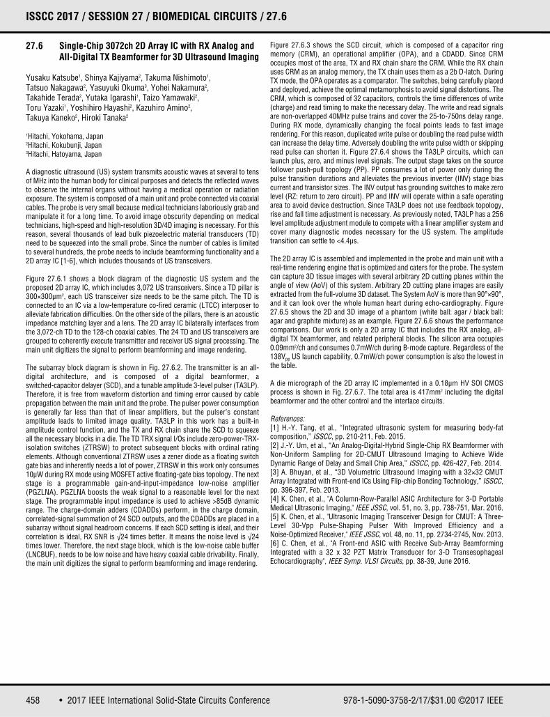
A die micrograph of the 2D array IC implemented in a 0.18μm HV SOI CMOSprocess is shown in Fig. 27.6.7. The total area is 417mm2 including the digitalbeamformer and the other control and the interface circuits.
References:[1] H.-Y. Tang, et al., “Integrated ultrasonic system for measuring body-fatcomposition,” ISSCC, pp. 210-211, Feb. 2015.[2] J.-Y. Um, et al., “An Analog-Digital-Hybrid Single-Chip RX Beamformer withNon-Uniform Sampling for 2D-CMUT Ultrasound Imaging to Achieve WideDynamic Range of Delay and Small Chip Area,” ISSCC, pp. 426-427, Feb. 2014.[3] A. Bhuyan, et al., “3D Volumetric Ultrasound Imaging with a 32×32 CMUTArray Integrated with Front-end ICs Using Flip-chip Bonding Technology,” ISSCC,pp. 396-397, Feb. 2013.[4] K. Chen, et al., "A Column-Row-Parallel ASIC Architecture for 3-D PortableMedical Ultrasonic Imaging," IEEE JSSC, vol. 51, no. 3, pp. 738-751, Mar. 2016.[5] K. Chen, et al., "Ultrasonic Imaging Transceiver Design for CMUT: A Three-Level 30-Vpp Pulse-Shaping Pulser With Improved Efficiency and aNoise-Optimized Receiver," IEEE JSSC, vol. 48, no. 11, pp. 2734-2745, Nov. 2013.[6] C. Chen, et al., "A Front-end ASIC with Receive Sub-Array BeamformingIntegrated with a 32 x 32 PZT Matrix Transducer for 3-D TransesophagealEchocardiography", IEEE Symp. VLSI Circuits, pp. 38-39, June 2016.
978-1-5090-3758-2/17/$31.00 ©2017 IEEE

459DIGEST OF TECHNICAL PAPERS •
ISSCC 2017 / February 8, 2017 / 4:15 PM
Figure 27.6.1: Block diagram of diagnostic ultrasound system with 3,072-ch 2Darray IC. Figure 27.6.2: Block diagram of 2D array IC.
Figure 27.6.3: Switched-capacitor delayer circuit (top). Timing chart of fixedfocus (bottom left) and dynamic focus (bottom right).
Figure 27.6.5: Evaluated 3D image (top right) and 2D cutting plain images fromthe full-volume 3D dataset (bottom right). Figure 27.6.6: Comparison table of ultrasound array IC.
Figure 27.6.4: Circuit diagram of tunable amplitude 3-level pulser and itscontrol block.
27
• 2017 IEEE International Solid-State Circuits Conference 978-1-5090-3758-2/17/$31.00 ©2017 IEEE
ISSCC 2017 PAPER CONTINUATIONS
Figure 27.6.7: Die photograph.
460 • 2017 IEEE International Solid-State Circuits Conference
ISSCC 2017 / SESSION 27 / BIOMEDICAL CIRCUITS / 27.7
27.7 A 30.5mm3 Fully Packaged Implantable Device with Duplex Ultrasonic Data and Power Links Achieving 95kb/s with <10-4 BER at 8.5cm Depth
Ting Chia Chang, Max L. Wang, Jayant Charthad, Marcus J. Weber,Amin Arbabian
Stanford University, Stanford, CA
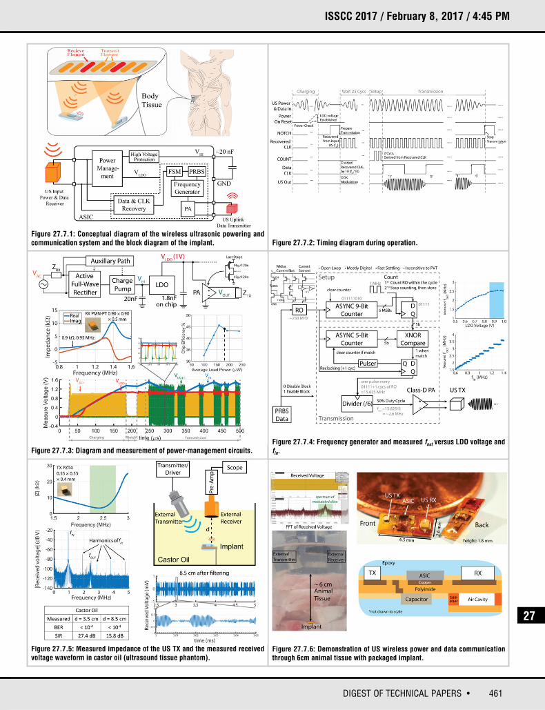
The next generation of implantable medical devices focuses on minimally invasiveminiaturized solutions that operate reliably at large depths, provide duplexcommunication for closed-loop therapies, and enable multi-access for a networkof implants to gather information or provide systemic interventions. Usingultrasound (US), power and data can be efficiently transferred through the bodyas its wavelength at MHz is comparable to a mm-sized receiver, resulting inimproved focusing, coupling, and acoustic-to-electrical conversion efficiency.Furthermore, thanks to the low propagation loss (~1dB/cm/MHz) and 7.2mW/mm2
safety limit, several mW of power is obtainable at the receiver, enabling high-power, complicated functionalities.
While initial experiments using US for power transfer to implants have beensuccessful [1,2], there is still a significant need to have reliable uplink datacommunication at depth. Other studies have worked on RF uplink [3,4] orbackscatter [2], which have limited depth and/or multi-access capability restrictingcoordinated therapies throughout the body. We demonstrate a miniaturized fullypackaged implant that receives both US power and data and also transmits USdata for uplink. Figure 27.7.1 depicts the conceptual diagram of the system aswell as the block diagram of the implant. It consists of two transducers (US powerand data receiver (RX) and data transmitter (TX)), a discrete capacitor, and aCMOS chip in TSMC 65nm GP technology, which includes power-management,data and clock-recovery circuits, frequency generators, finite state machine,pseudorandom binary sequence (PRBS), and the power amplifier (PA). Both RXand TX are made from piezoelectric materials. The operating frequency of thereceiver is chosen to be ~1MHz for low propagation loss and mm-size as theresonance of the receiver is inversely proportional to its thickness. Using clockrecovery and frequency generation circuitry, the carrier frequency of the outputdata (fout) is ~2.6× of the input frequency (fin) to avoid self and external interferencefrom the high-power downlink and its harmonics.
Figure 27.7.2 illustrates the timing diagram during operation. The implant ischarged until the LDO voltage is established. The implant then listens for the datainput (falling edge) from the external source to generate a NOTCH and preparefor uplink transmission. The Recovered CLK is obtained from fin. DATA CLKdivides Recovered CLK by 10; thus, the data rate is close to 100kb/s for fin ~1MHzwith OOK modulation, sufficient for a range of applications including pressure,temperature, or neural recording. An on-chip 210 – 1 PRBS is used for datageneration. The next input falling edge stops the transmission. If sufficient energyis retained on the storage capacitors, the process can be immediately restarted,re-enabling uplink transmission.
The power-management circuits, which are shown in Figure 27.7.3, use a two-path architecture. The main path includes an active full-wave rectifier for AC-DCconversion, a charge pump to boost the generated voltage, and a low-dropoutregulator (LDO) regulating supply at 1V; the low-power auxiliary path sets up thebiasing, similar to what [1] presents. PMN-PT with dimension of 0.9×0.9×0.5mm3
is chosen for RX; it has a measured impedance of 900Ω and resonance of0.95MHz as desired for impedance matching and low propagation loss. Chipefficiency, defined as load power over power into rectifier, along with measuredvoltage waveforms at four nodes are also plotted.
Figure 27.7.4 shows the frequency generator and the differential class-D PAdriving the TX. The frequency generator uses an open-loop architecture to ensurefast settling and robust fout. In the setup phase, the frequency of a free-runningcurrent-starved RO (fRO) is resolved with a 9b asynchronous counter controlled
by COUNT. Five MSBs are stored in the registers, effectively dividing fRO by 16.During transmission, a 5b asynchronous counter counts the RO cycles, which iscompared to the stored value; if they match, a pulse is sent to a 3b Johnsoncounter, dividing the frequency of the pulse train by six to generate fout. Anexample calculation for an fRO of 250MHz and fin of 1MHz is shown in gray text.This method is insensitive to process and temperature variation. In addition, aWidlar bias is used so that fRO is stable for small perturbations of supply. fRO isrecounted in the setup phase for each transmission; and fin and fout have a steppedrelationship because of the open-loop operation, leading to a more reliable system.Measured fout across different LDO voltages shows that it stays constant for LDOvoltages from 0.84 to 1.0V. As OOK modulation is used, the generator is disabledwhen DATA = 0 and the output of the PA is cycled and pulled to GND to saveenergy; for DATA = 1, the generator can start up and settle in <1μs and consumes32μW during runtime.
Taking into account the loss, the transmitted output power needs to be at least100μW for successful transmission at large tissue depth. Therefore, the desiredimpedance of the TX driven differentially with 1V supply should be <5kΩ aroundresonance. Using PZT4, the TX is sized 0.55×0.55×0.4mm3, giving a resonancenear 2.5MHz with impedance ~4kΩ as shown in Fig. 27.7.5. Simulated PAefficiency is 86%, delivering a peak power of 125μW to the TX. A fully wirelessend-to-end test with external power/data transmitter and data receiver in castoroil, commonly used as a tissue phantom with loss ~0.6dB/cm/MHz, is performed.The carrier frequency of the received voltage is 2.45MHz for fin of 950kHz. Thereceived voltage waveform for an 8.5cm link after filtering out the harmonics offin is also plotted; the interference signals are mostly due to multipath reflectionsand can be mitigated. Bit error rate (BER) is calculated by sending the on-chipPRBS 10 times; no errors are found for both 3.5 and 8.5cm links, achieving aBER of <10-4 for a data rate of 95kb/s. The average signal-to-interference ratio(SIR) is computed to be 27.4 and 15.8dB respectively; SIR can be furtherimproved with better alignment and larger receiver gain.
Figure 27.7.6 shows the fully packaged implants and their cross-sections alongwith the end-to-end blind test through 6cm of animal tissue with no precisealignment; the spectrum of the received modulated data is shown. This confirmsthe end-to-end demonstration of an implant system capable of power/data transferthrough >5cm of tissue. With access to an external beamformer, based on themeasured received voltages we achieve >10cm depth in the body. Figure 27.7.7shows the die photo and comparison to implantable devices using variouswireless powering and communication modalities with full system measurements.Based on the table in Fig. 27.7.7, our implant is at least 2.5× smaller and operates2× deeper (in tissue) than comparable US-powered implants and 10× smaller and10× deeper than inductively powered implants.
Acknowledgement:The authors thank Prof. Khuri-Yakub for valuable discussions. The chip fabricationwas made possible by the TSMC University Shuttle Program. We alsoacknowledge Mentor Graphics for the use of the Analog FastSPICE (AFS)Platform. This material is based upon work supported by the DARPA YFA and theNSF CAREER award ECCS-1454107.
References:[1] J. Charthad, et al., “A mm-Sized Implantable Medical Device (IMD) WithUltrasonic Power Transfer and a Hybrid Bi-Directional Data Link,” IEEE JSSC, vol.50, no. 6, pp. 1741-1753, Aug. 2015.[2] S. Ozeri and D. Shmilovitz, “Simultaneous Backward Data Transmission andPower Harvesting in an Ultrasonic Transcutaneous Energy Transfer LinkEmploying Acoustically Dependent Electric Impedance Modulation,” Ultrasonics,vol. 54, no. 7, pp. 1929-1937, Sept. 2014. [3] A. Mirbozorgi, et al., “A Single-Chip Full-Duplex High Speed Transceiver forMulti-Site Stimulating and Recording Neural Implants,” IEEE TBioCAS, vol. 10,no. 3, pp. 643-653, June 2016.[4] G. Yilmaz and C. Dehollain, "An implantable system for intracranial neuralrecording applications," IEEE BioCAS, pp. 408-411, Oct. 2014.
978-1-5090-3758-2/17/$31.00 ©2017 IEEE
461DIGEST OF TECHNICAL PAPERS •
ISSCC 2017 / February 8, 2017 / 4:45 PM
Figure 27.7.1: Conceptual diagram of the wireless ultrasonic powering andcommunication system and the block diagram of the implant. Figure 27.7.2: Timing diagram during operation.
Figure 27.7.3: Diagram and measurement of power-management circuits.
Figure 27.7.5: Measured impedance of the US TX and the measured receivedvoltage waveform in castor oil (ultrasound tissue phantom).
Figure 27.7.6: Demonstration of US wireless power and data communicationthrough 6cm animal tissue with packaged implant.
Figure 27.7.4: Frequency generator and measured fout versus LDO voltage andfin.
27

• 2017 IEEE International Solid-State Circuits Conference 978-1-5090-3758-2/17/$31.00 ©2017 IEEE
ISSCC 2017 PAPER CONTINUATIONS
Figure 27.7.7: Die photo and comparisons of implantable devices with wirelesspowering and data communication.
462 • 2017 IEEE International Solid-State Circuits Conference
ISSCC 2017 / SESSION 27 / BIOMEDICAL CIRCUITS / 27.8
27.8 Fully Integrated Optical Spectrometer with500-to-830nm Range in 65nm CMOS
Lingyu Hong, Kaushik Sengupta
Princeton University, Princeton, NJ
Next-generation IoT systems are expected to be enabled by compact, low-cost,low-power, smart sensing devices that provide a wealth of information to buildnew applications and capabilities. Among sensing modalities, optical spectrometryis one of the rapidly growing areas of interest due to its wide range of applicationsfrom environment monitoring, industrial and home applications to healthcare [1-3]. As shown in Fig. 27.8.1, current optical spectrometers are large and bulkywith non-integrated components that limit their application potential. In this paper,we present a fully integrated CMOS-based optical spectrometer in a 65nm bulkprocess that requires no external optical components. The spectrometer achievesnearly 10nm resolution and 1.4nm accuracy in peak prediction of continuous-wave (CW) excitations between 500 and 830nm.
The principle of operation of a classical optical spectrometer relies on light incidenton a grating structure getting diffracted, focused and sensed by a photodetectorarray, which enables us to correlate the measured voltages of the photodetectorsto the incident optical spectrum (Fig. 27.8.1). The architecture of the presentedCMOS optical spectrometer is shown in Fig. 27.8.1. The incident light is deliveredthrough an optical fiber into the CMOS chip through a 3μm-sized opening apertureon the 7th metal layer (M7) and is converted into a propagating mode in metal-insulator-metal (MIM) waveguides between M4-M7 [5,6]. The propagating waveis incident onto a concave grating structure (M4-M7) that is designed to dispersethe incident mode and create a wavelength-dependent focal plane 400μm awaywithin the MIM waveguides. The spatial distribution is sensed by deflecting thefocused light with a metal shield into an array of photodetectors underneath (Fig.27.8.1). The signal is then processed on-chip with low-noise circuitry and digitizedoff-chip for analysis. The entire structure measures 650×540μm2.
The layout of the dispersive optical elements, the MIM waveguide, and theconstituent circuits is shown in Fig. 27.8.2. It shows focusing of the optical wavesof different wavelengths within the chip on the focal plane. The resolution isdetermined by the numerical aperture of the grating structure and the slit aperturesize at the fiber input, and is simulated to be 5nm. Unlike free-space propagationin a classical spectrometer, mode propagation within the copper-metalwaveguides at optical frequencies can be very complex and the interaction withthe grating structure on-chip can be dependent on the mode profiles in additionto wavelength. To remove this extra dependence, the MIM waveguides aredesigned to suppress higher-order modes, allowing only the lowest fundamentalmode to interact with the grating structure. Figure 27.8.2 shows the attenuationof the higher-order modes by >20dB relative to the fundamental over the wavetravel distance across the spectrum.
Figure 27.8.3 shows the array architecture where the photodetector arrangementfollows the curvature of the focal plane. The array of 60 detectors is realized withn-well/ p-sub junctions, and the signals are integrated by capacitive TIAs toremove the dependence on the diode capacitance in this non-custom imagerprocess. To partially suppress the effect of dark currents, each signal is senseddifferentially with a reference diode and a differential TIA which suppressescommon-mode perturbations. It is also important to ensure that the detectors areaccommodated within the 4μm spot size of the optical focus points so that theresolution is not degraded by the photodiode layout (Fig. 27.8.3). Therefore, thegrating structure and the array architecture need to be co-designed for optimalperformance and resolution. As shown in Fig. 27.8.3, the signals are multiplexedand finally processed through a correlated double sampling architecture to removeoffsets and low-frequency drifts and ultimately digitized by a 16b ADC off-chipand analyzed.
Stray light scattering can cause unintended errors in spectral estimation, whichare typically eliminated by elaborate optical shielding. For a chip-scalespectrometer, such external effects can be minimized by proper packaging, whileinside the chip, the propagation of light in undesired directions can be shieldedwith metal optical walls (Fig. 27.8.2). In this work, we show spectral estimationin the unpackaged die (Fig. 27.8.7) not completely shielded from externalscattered light. The spectrometer is first characterized against CW excitations witha wide-band source and a tunable narrow-band filter (~10nm) realized with a linearvariable filter on a motorized translational stage (Fig. 27.8.4). Over the range ofmeasured wavelengths, the array response creates a responsivity matrix definedas Ropt ∈ R N×M, where N is the number of diodes and M is the number ofwavelengths of characterization. When a spectrum approximated by Sinc ∈ RM ×1
is incident on the chip, the array response is given by Vop = RoptSinc + Vn, whereVn ∈ RN ×1 is the random noise voltages of the outputs. Given Vop and measuredresponsivity Ropt, we estimate the incident spectrum Sest by the minimizing thefollowing:
The regularization parameter λ allows for robust estimation in presence of noiseby eliminating solutions with undesirable spikes due to the inverse estimationprocess [4]. The measured responsivity matrix which is a one-timecharacterization is shown in Fig. 27.8.4 by removing the average spectralresponses of the sensors. The spectral dependence of the spatial distribution ofintensity is evident from the figure. The presence of scattering of stray light createsthe non-focus profile, but the wavelength-dependent variation of the spatialdistribution still allows us to achieve spectral estimation across the range.
The chip is tested with CW excitations of light and Fig. 27.8.5 shows the spectralestimation from the measured responses showing robust estimation withregularization with only 40nW estimated to be entering the chip. When the chipis excited at a wavelength between the characterization wavelengths, thereconstruction shows two peaks near the center wavelength. The estimation ofthe peak can be progressively narrowed reaching down to 1.4nm when theestimation is averaged over five responsivity matrices with 1nm spacing. The chipis then tested with excitation of varying spectra and the estimation reasonablymatches the measured spectra without optical packaging and external shielding(Fig. 27.8.6). The normalized RMS error of reconstructed spectra given by:
was measured to be around 15 to 20%. The chip is powered by a 3V supply anddissipates 30mW of total DC power. The chip-scale spectrometer shows thefeasibility of integrating complex optical systems-on-chip for various applicationsin sensing by exploiting metal-optical structures in CMOS through a co-designapproach.
References:[1] B. Redding, et al., “Compact Spectrometer Based on a Disordered PhotonicChip,” Nature Photonics, vol. 7, pp. 746-751, Sept. 2013,[2] X. Ma, et al., "CMOS-Compatible Integrated Spectrometer Based on EchelleDiffraction Grating and MSM Photodetector Array," IEEE Photon. J., vol. 5, no. 2,Apr. 2013.[3] Z. Shi, et al., “Dispersive Element Based on Grating and Tunable Fabry–PerotFilter in Miniature Spectrometer,” Appl. Opt., vol. 53, pp. 76-81, 2014.[4] X. Wu and K. Sengupta, "A 40-to-330GHz Synthesizer-free THz Spectroscope-on-chip Exploiting Electromagnetic Scattering," ISSCC, pp. 428-429, Feb. 2016.[5] L. Hong, et al., “A Fully Integrated CMOS Fluorescence Biosensor with On-chip Nanophotonic Filter,” IEEE Symp. VLSI Circuits, pp. C206-C207, 2015.[6] X. Lu, et al., "An Integrated Optical Physically Unclonable Function UsingProcess-Sensitive Sub-Wavelength Photonic Crystals in 65nm CMOS," ISSCC,2017.
978-1-5090-3758-2/17/$31.00 ©2017 IEEE
.
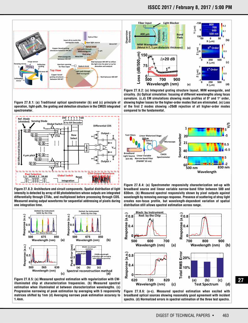
463DIGEST OF TECHNICAL PAPERS •
ISSCC 2017 / February 8, 2017 / 5:00 PM
Figure 27.8.1: (a) Traditional optical spectrometer (b) and (c) principle ofoperation, light-path, the grating and detection structure in the CMOS integratedspectrometer.
Figure 27.8.2: (a) Integrated grating structure layout, MIM waveguide, andcircuitry. (b) Optical simulation: focusing of different wavelengths along focuscurvature. (c,d) EM simulations showing mode profiles of 0th and 1st order,showing higher losses for the higher-order modes that are eliminated. (e) Lossof the first 2 modes showing >20dB rejection of all higher-order modescompared to the fundamental.
Figure 27.8.3: Architecture and circuit components. Spatial distribution of lightintensity is detected by array of 60 photodetectors whose outputs are integrateddifferentially through CTIAs, and multiplexed before processing through CDS.Measured analog output waveforms for sequential addressing of pixels duringone integration time.
Figure 27.8.5: (a) Measured spectral estimation with regularization with CW-illuminated chip at characterization frequencies. (b) Measured spectralestimation when illuminated at between characterization wavelengths. (c)Progressive narrowing of peak estimation by averaging with 5 responsivitymatrices shifted by 1nm (d) Averaging narrows peak estimation accuracy to1.4nm.
Figure 27.8.6: (a-c). Measured spectral estimation when excited withbroadband optical sources showing reasonably good agreement with incidentspectra. (d) Normalized errors in spectral estimation of the three test spectra.
Figure 27.8.4: (a) Spectrometer responsivity characterization set-up withbroadband source and linear variable narrow-band filter between 500 and830nm. (b) Measured spectral responsivity shown by pixel outputs againstwavelength by removing average response. Presence of scattering of stray lightcreates non-focus profile, but wavelength-dependent variation of spatialdistribution still allows spectral estimation across range.
27
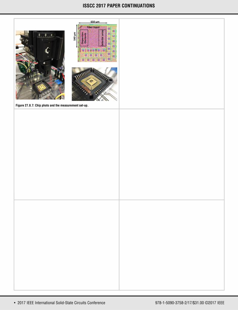
• 2017 IEEE International Solid-State Circuits Conference 978-1-5090-3758-2/17/$31.00 ©2017 IEEE
ISSCC 2017 PAPER CONTINUATIONS
Figure 27.8.7: Chip photo and the measurement set-up.
Related Documents