SERVICE MANUAL Colour Television Product Code: 111356463 Original Version Chassis Series: AC5-G2 C4ZKH FILE NO. (Russia) Give complete “SERVICE REF. NO.” for parts order or servicing. It is shown on the rating plate at the cabinet back of the unit. This T.V. receiver will not work properly in foreign countries where the television transmission system and power source dif- fer from the design specifications. Refer to the specification table. Specifications Power Source . . . . . . . . . . AC110-240V, 50Hz/60Hz. Colour System . . . . . . . . . PAL/SECAM/NTSC4.43/NTSC/PAL-60Hz Television System . . . . . . B/G, D/K, K’, I, M/M Channel Coverage . . . . . VHF: E2-E12, R1-R12, K1-K9, A2-A13, J1-J12 UHF: 21-69, A14-A69, J13-J62 CATV: S1-S41, X, Y, Z, Z+1, Z+2 Video IF . . . . . . . . . . . . . . 38.0MHz Aerial Input Impedance . . 75Ω Ext. Terminals Video inputs: Phono jack ✕ 2 (1Vp - p, 75Ω) Audio inputs: Phono jack (L/R) ✕ 2(436mVrms, more than 40KΩ) Video monitor outputs: Phono jack ✕ 1(1Vp - p, 75Ω) Audio monitor outputs: Phono jack (L/R) ✕ 1(436mVrms, less than 600Ω) Headphone jack: Mini stereo jack ✕ 1 Sound Output (RMS) . . . . 5W + 5W Speaker . . . . . . . . . . . . . 6 cm ✕ 12 cm ✕ 2 pcs. Dimensions . . . . . . . . . . . .770 (W) ✕ 590 (H) ✕ 495 (D)mm Weight . . . . . . . . . . . . . . . .approx. 39.9 Kg Specifications subject to change without notice. REFERENCE NO. SM3010001 JXMRM PICTURE -/-- -/-- P P A•B TIMER TV/AV CH SWAP SOUND CH SCAN BASS CH SURROUND MENU S.SYS C.SYS Service Ref. No. CE29ST8R-50 Model No. CE29ST8R

Welcome message from author
This document is posted to help you gain knowledge. Please leave a comment to let me know what you think about it! Share it to your friends and learn new things together.
Transcript
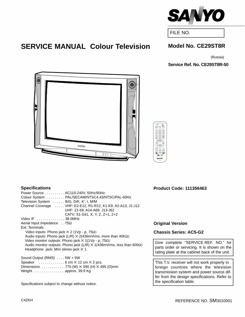
SERVICE MANUAL Colour Television
Product Code: 111356463
Original Version
Chassis Series: AC5-G2
C4ZKH
FILE NO.
(Russia)
Give complete “SERVICE REF. NO.” forparts order or servicing. It is shown on therating plate at the cabinet back of the unit.
This T.V. receiver will not work properly in foreign countries where the televisiontransmission system and power source dif-fer from the design specifications. Refer tothe specification table.
SpecificationsPower Source . . . . . . . . . . AC110-240V, 50Hz/60Hz.Colour System . . . . . . . . . PAL/SECAM/NTSC4.43/NTSC/PAL-60HzTelevision System . . . . . . B/G, D/K, K’, I, M/MChannel Coverage . . . . . VHF: E2-E12, R1-R12, K1-K9, A2-A13, J1-J12
UHF: 21-69, A14-A69, J13-J62CATV: S1-S41, X, Y, Z, Z+1, Z+2
Video IF . . . . . . . . . . . . . . 38.0MHz Aerial Input Impedance . . 75ΩExt. Terminals
Video inputs: Phono jack 2 (1Vp - p, 75Ω)Audio inputs: Phono jack (L/R) 2(436mVrms, more than 40KΩ)Video monitor outputs: Phono jack 1(1Vp - p, 75Ω)Audio monitor outputs: Phono jack (L/R) 1(436mVrms, less than 600Ω)Headphone jack: Mini stereo jack 1
Sound Output (RMS) . . . . 5W + 5WSpeaker . . . . . . . . . . . . . 6 cm 12 cm 2 pcs.Dimensions . . . . . . . . . . . .770 (W) 590 (H) 495 (D)mmWeight . . . . . . . . . . . . . . . .approx. 39.9 Kg
Specifications subject to change without notice.
REFERENCE NO. SM3010001
JXMRM
PICTURE
-/---/--
P P
A•B
TIMER
TV/AV
CH
SWAP SOUND
CH SCAN
BASS
CH
SURROUND
MENU
S.SYS C.SYS
Service Ref. No. CE29ST8R-50
Model No. CE29ST8R
SM_29-C4ZKH(Rus) 6/28/04 10:31 AM Page 1
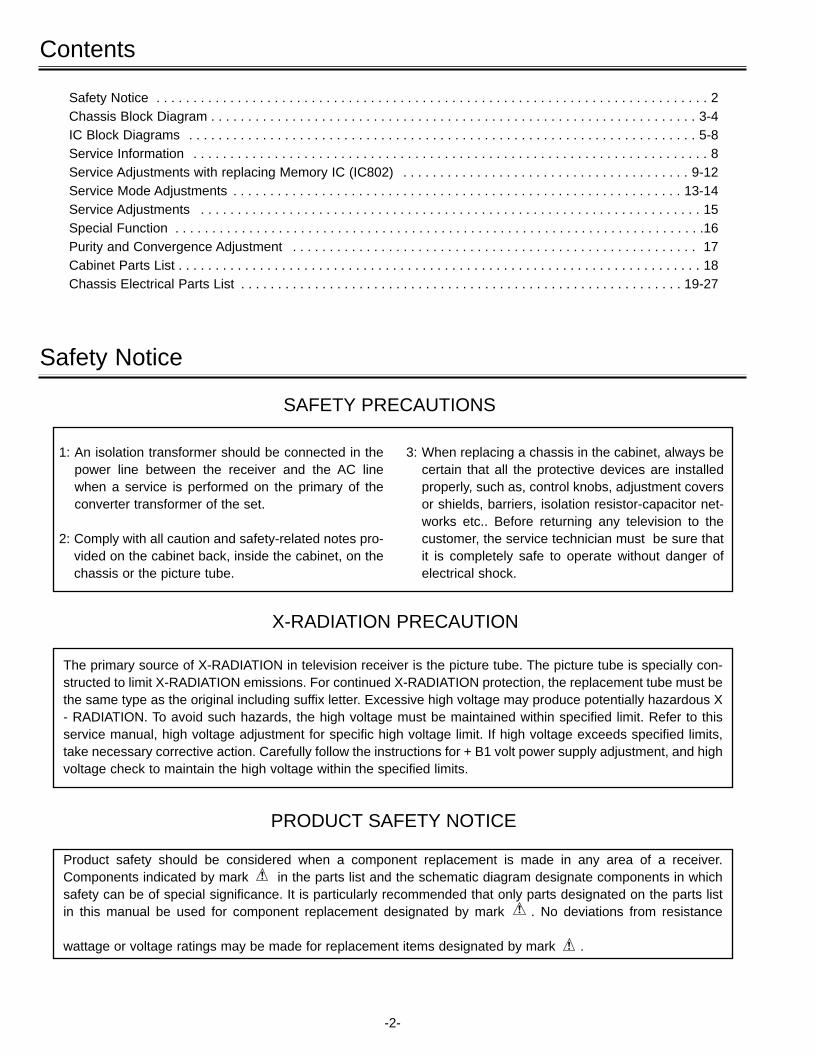
Contents
-2-
Safety Notice . . . . . . . . . . . . . . . . . . . . . . . . . . . . . . . . . . . . . . . . . . . . . . . . . . . . . . . . . . . . . . . . . . . . . . . . . . . 2Chassis Block Diagram . . . . . . . . . . . . . . . . . . . . . . . . . . . . . . . . . . . . . . . . . . . . . . . . . . . . . . . . . . . . . . . . . . 3-4IC Block Diagrams . . . . . . . . . . . . . . . . . . . . . . . . . . . . . . . . . . . . . . . . . . . . . . . . . . . . . . . . . . . . . . . . . . . . . 5-8Service Information . . . . . . . . . . . . . . . . . . . . . . . . . . . . . . . . . . . . . . . . . . . . . . . . . . . . . . . . . . . . . . . . . . . . . . 8Service Adjustments with replacing Memory IC (IC802) . . . . . . . . . . . . . . . . . . . . . . . . . . . . . . . . . . . . . . . 9-12Service Mode Adjustments . . . . . . . . . . . . . . . . . . . . . . . . . . . . . . . . . . . . . . . . . . . . . . . . . . . . . . . . . . . . . 13-14Service Adjustments . . . . . . . . . . . . . . . . . . . . . . . . . . . . . . . . . . . . . . . . . . . . . . . . . . . . . . . . . . . . . . . . . . . . 15Special Function . . . . . . . . . . . . . . . . . . . . . . . . . . . . . . . . . . . . . . . . . . . . . . . . . . . . . . . . . . . . . . . . . . . . . . . .16Purity and Convergence Adjustment . . . . . . . . . . . . . . . . . . . . . . . . . . . . . . . . . . . . . . . . . . . . . . . . . . . . . . . 17Cabinet Parts List . . . . . . . . . . . . . . . . . . . . . . . . . . . . . . . . . . . . . . . . . . . . . . . . . . . . . . . . . . . . . . . . . . . . . . . 18Chassis Electrical Parts List . . . . . . . . . . . . . . . . . . . . . . . . . . . . . . . . . . . . . . . . . . . . . . . . . . . . . . . . . . . . 19-27
Safety Notice
SAFETY PRECAUTIONS
1: An isolation transformer should be connected in thepower line between the receiver and the AC linewhen a service is performed on the primary of theconverter transformer of the set.
2: Comply with all caution and safety-related notes pro-vided on the cabinet back, inside the cabinet, on thechassis or the picture tube.
3: When replacing a chassis in the cabinet, always becertain that all the protective devices are installedproperly, such as, control knobs, adjustment coversor shields, barriers, isolation resistor-capacitor net-works etc.. Before returning any television to thecustomer, the service technician must be sure thatit is completely safe to operate without danger ofelectrical shock.
X-RADIATION PRECAUTION
The primary source of X-RADIATION in television receiver is the picture tube. The picture tube is specially con-structed to limit X-RADIATION emissions. For continued X-RADIATION protection, the replacement tube must bethe same type as the original including suffix letter. Excessive high voltage may produce potentially hazardous X- RADIATION. To avoid such hazards, the high voltage must be maintained within specified limit. Refer to thisservice manual, high voltage adjustment for specific high voltage limit. If high voltage exceeds specified limits,take necessary corrective action. Carefully follow the instructions for + B1 volt power supply adjustment, and highvoltage check to maintain the high voltage within the specified limits.
PRODUCT SAFETY NOTICE
Product safety should be considered when a component replacement is made in any area of a receiver.Components indicated by mark in the parts list and the schematic diagram designate components in whichsafety can be of special significance. It is particularly recommended that only parts designated on the parts listin this manual be used for component replacement designated by mark . No deviations from resistance
wattage or voltage ratings may be made for replacement items designated by mark .
SM_29-C4ZKH(Rus) 6/28/04 10:31 AM Page 2
IC80
1C
PU
IC80
2E
EP
RO
M
5 6
3 10 214
A19
01R
C P
RE
-AM
P.
28
D19
01A
LED
32 27
ON
-TIM
ER
PO
WE
R F
AIL
Fro
ntke
y
12
SD
A
SC
L
IC37
01S
UR
RO
UN
D
IC00
1A
UD
IO A
MP
.
MO
NIT
OR
-OU
T
AU
DIO
-OU
T (
L)
AU
DIO
-OU
T (
R)
RE
AR
AV
TE
RM
INA
L
AU
DIO
1-I
N (
L)
AU
DIO
1-I
N (
R)
VID
EO
1-I
N
FRO
NT
AV
TE
RM
INA
L
IC12
01V
IDE
O S
ELE
CTO
R
VID
EO
2-I
N
AU
DIO
2-I
N (
L)
AU
DIO
2-I
N (
R)
AV
1/A
V2
AV
OU
T4
275 26 2 29
3 28
8 6
12 2R
-OU
T
L-O
UT
SP
901
SP
902
EA
R P
HO
NE
K00
2
A10
1T
UN
ER
SC
L
SD
A
SDA
SCL45
1112
IC20
1IF
/VID
EO
/CH
RO
MA
1H DLRGB
MATRIX
5/6
46 4442 252 54
SA
W
FIL
TE
R
X16
1 R-O
UT
B-O
UT
G-O
UT
19 20 21
EX
T. V
IDE
O IN
40
SE
LEC
TE
D
VID
EO
OU
T
AU
DIO
OU
T(T
V O
UT
)
1/30
SIF
OU
T
SIF
IN
VID
EO
OU
T
INT.
VID
EO
IN
IC28
1S
EC
AM
7 9
R-Y
OU
T
B-Y
OU
T17
VID
EO
IN
35 34
VE
RT.
OU
T
HO
RIZ
. OU
T
23 27
Q43
1H
-DR
IVE
T43
1H
-DR
IVE
TR
AN
S.
IC50
1V
ER
T. /D
EF.
PC
C
CIR
CU
ITQ
461-
Q46
2
T47
1F
BT
HV
L902
DY
CR
T
CR
T U
NIT
R G B
R G B
HE
ATE
RS
CR
EE
NF
OC
US
3
RC
-IN
KE
Y-I
N
26A
V1/
AV
2
15
PO
WE
R S
UP
PLY
CIR
CU
IT
12
SD
AS
CL
1314
IC70
1TR
IPLE
VID
EO
OU
TPU
T A
MP.
R G B
1 2 3
9 8 7
RE
CT
IFIC
ATIO
NC
IRC
UIT
SW
ITC
HIN
GO
SC
ILLA
TOR
4 5 6 7 1 2 3
14 15 12 16 13 17
24 V
9 V
IC68
15V
_RC
11V
140V
FB
T
AU
DIO
IC80
1/IC
802
IC37
01/IC
1201
IC20
1/IC
281
IC50
1/H
OR
IZ. D
EF.
Q61
3
-3-
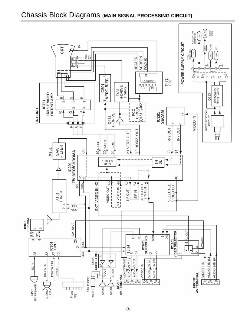
Chassis Block Diagrams (MAIN SIGNAL PROCESSING CIRCUIT)
SM_29-C4ZKH(Rus) 6/28/04 10:31 AM Page 3
-4-
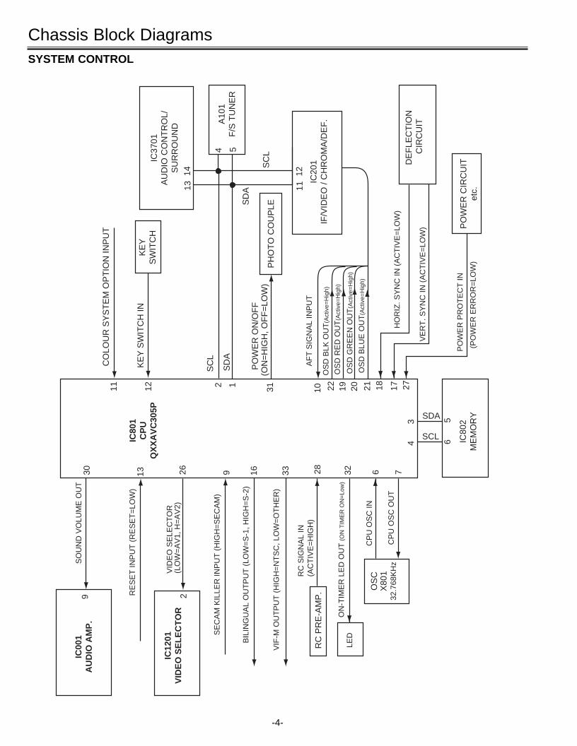
Chassis Block DiagramsSYSTEM CONTROL
11 12
CO
LOU
R S
YS
TE
M O
PT
ION
INP
UT
KE
Y S
WIT
CH
INK
EY
SW
ITC
H
SC
L2 1 31
SD
A
PO
WE
R O
N/O
FF
PH
OT
O C
OU
PLE
(O
N=
HIG
H, O
FF
=LO
W)
IC20
1IF
/VID
EO
/ C
HR
OM
A/D
EF
.
IC80
1C
PU
QX
XA
VC
305P
22 19 20 21 18 17 273
476322826 33
OS
D B
LK O
UT
(Act
ive=
Hig
h)
OS
D R
ED
OU
T(A
ctiv
e=H
igh)
OS
D G
RE
EN
OU
T(A
ctiv
e=H
igh)
OS
D B
LUE
OU
T(A
ctiv
e=H
igh)
DE
FLE
CT
ION
CIR
CU
IT
HO
RIZ
. SY
NC
IN (
AC
TIV
E=
LOW
)
VE
RT
. SY
NC
IN (
AC
TIV
E=
LOW
)
PO
WE
R P
RO
TE
CT
IN
(P
OW
ER
ER
RO
R=
LOW
)P
OW
ER
CIR
CU
ITet
c.
SCL
SDA
IC80
2M
EM
OR
Y
OS
CX
801
32.7
68K
Hz
CP
U O
SC
OU
T
CP
U O
SC
IN
LED
ON
-TIM
ER
LE
D O
UT
(ON
TIM
ER
ON
=Lo
w)
RC
SIG
NA
L IN
(AC
TIV
E=
HIG
H)
RC
PR
E-A
MP
.
930S
OU
ND
VO
LUM
E O
UT
IC
001
AU
DIO
AM
P.
VIF
-M O
UT
PU
T (
HIG
H=
NT
SC
, LO
W=
OT
HE
R)
A10
1F
/S T
UN
ER
AF
T S
IGN
AL
INP
UT
10
RE
SE
T IN
PU
T (
RE
SE
T=
LOW
)13
VID
EO
SE
LEC
TO
R(L
OW
=A
V1,
H=
AV
2)
56
SE
CA
M K
ILLE
R IN
PU
T (
HIG
H=
SE
CA
M)
IC12
01V
IDE
O S
EL
EC
TO
R2
16B
ILIN
GU
AL
OU
TP
UT
(LO
W=
S-1
, HIG
H=
S-2
)
IC37
01A
UD
IO C
ON
TR
OL/
SU
RR
OU
ND
9
1314
SC
L
SD
A 1112
54
SM_29-C4ZKH(Rus) 6/28/04 10:31 AM Page 4
-5-
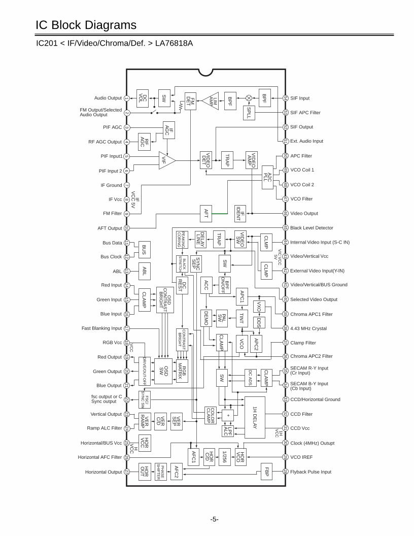
IC Block DiagramsIC201 < IF/Video/Chroma/Def. > LA76818A
1
DC
V
OL
SW F
M
DE
T
23
45
6
IF
AG
C
RF
A
GC
VIF
78
910
IF
VC
C 5V
1112
13
BU
S
PE
AK
ING
C
OR
ING
BLA
CK
S
TR
ET
CH
SY
NC
S
EP
1415
AB
L
DC
R
ES
T
CLA
MP
OS
D
CO
NT
RA
ST
B
RIG
HT
1617
1819
20
CO
NT
RA
ST
B
RIG
HT
RG
B
MAT
RIX
OS
D
SW
DR
IVE
/OU
T-OF
F
VC
C21
2223
FS
C/
SY
NC
SW
2425
2627
VE
R
RA
MP
HO
R
VC
CH
VC
C
VE
R
C/D
HO
R
OU
T
PH
AS
E
SH
IFT
ER
AF
C2
AF
C1
VE
R
SE
P
HO
R
C/D
1/256
CO
LOR
C
LAM
P
LPF
A
LC+
SW
CLA
MP
DE
MO
PAL
SW
AC
C
BP
F
ON
/OF
F
DE
LAY
LINE
SW
TR
AP
AF
TV
IDE
O
DE
T
TR
AP
LIM
AM
P
BP
F
SP
LL
BP
F
VID
EO
A
MP
IF
IDE
NT
VID
EO
S
WA
PC
1T
INT
VX
OD
DS
AP
C2
DC
AD
S.
CLA
MP
VC
O
1H D
ELAY
HO
R
VC
O
FB
P
2829
3031
321H
V
CC
3334
3536
3738
3940
4142
CLM
P
4344
45
CLM
P
V/C
VC
C
5V
4647
4849
50
A2C
P
LL
5152
5354Audio Output
FM Output/Selected Audio Output
PIF AGC
RF AGC Output
PIF Input1
PIF Input 2
IF Ground
IF Vcc
FM Filter
AFT Output
Bus Data
Bus Clock
ABL
Red Input
Green Input
Blue Input
Fast Blanking Input
RGB Vcc
Red Output
Green Output
Blue Output
fsc output or CSync output
Vertical Output
Ramp ALC Filter
Horizontal/BUS Vcc
Horizontal Output
Horizontal AFC Filter
Flyback Pulse Input
VCO IREF
Clock (4MHz) Outupt
CCD Vcc
CCD Filter
CCD/Horizontal Ground
SECAM B-Y Input (Cb Input)
SECAM R-Y Input (Cr Input)
Chroma APC2 Filter
Clamp Filter
4.43 MHz Crystal
Chroma APC1 Filter
Selected Video Output
Video/Vertical/BUS Ground
External Video Input(Y-IN)
Video/Vertical Vcc
Internal Video Input (S-C IN)
Black Level Detector
Video Output
VCO Filter
VCO Coil 2
VCO Coil 1
APC Filter
Ext. Audio Input
SIF Output
SIF APC Filter
SIF Input
SM_29-C4ZKH(Rus) 6/28/04 10:31 AM Page 5
IC Block Diagrams
-6-
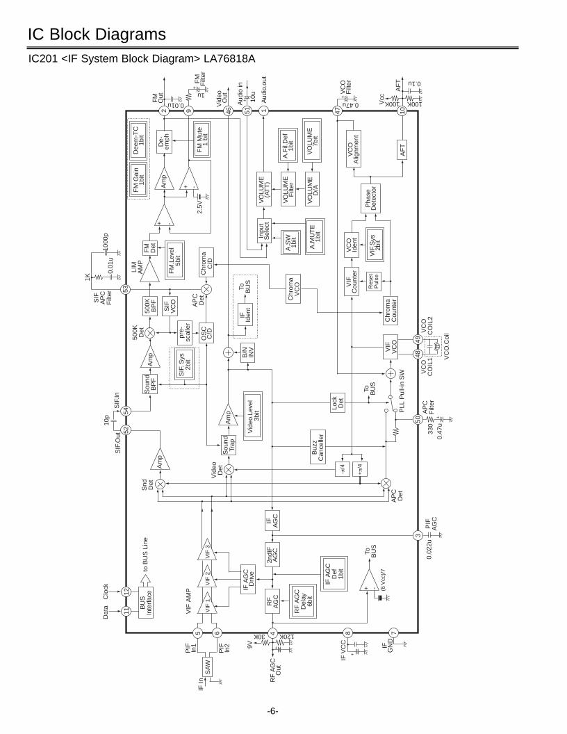
IC201 <IF System Block Diagram> LA76818A
1112
BU
S
Inte
rfac
e
SA
W
5 6 4 8 7
PIF
In
1
PIF
In
2
IF In
9V
30K
RF
AG
C
Out
120K
IF V
CC
IF
GN
D
VIF
AM
P
VIF
1V
IF 2
VIF
3
IF A
GC
D
rive
RF
A
GC
2ndI
F
AG
C
RF
AG
C
Del
ay
6bit
IF A
GC
D
ef
1bit
+ - (6 V
cc)/
7
To
BU
S
3
0.02
2uP
IF
AG
CIF
AG
C
Dat
aC
lock
AP
C
Det
+π/
4
-π/4
Snd
D
etA
mp
52S
IF.O
ut
Sou
nd
Trap
Vid
eo
Det
Buz
zC
ance
ller
50A
PC
F
ilter
330
0.47
u+
PLL
Pul
l-in
SW
To
BU
S
Lock
D
et
Vid
eo.L
evel
3b
it
Am
p54
10p
SIF
.In
Sou
nd
BP
F
VC
O.C
oil
VC
O
CO
IL1
VC
O
CO
IL2
4849
VIF
V
CO
Chr
oma
Cou
nter
B/N
IN
VIF
Id
ent
OS
C
C/D
Am
p
SIF
. Sys
2b
itpr
e-
scal
ler
SIF
V
CO
500K
B
PFS
IF
AP
C
Filt
er
1K
0.01
u10
00p
53LI
M
AM
PF
M
Det
FM
.Lev
el
5bit
Chr
oma
C/D
AP
C
Det
500K
D
et
To
BU
S
Chr
oma
VC
O VIF
C
ount
er
Res
et
Pul
se
VC
O
Iden
t
VIF
.Sys
2b
it
Pha
se
Det
ecto
r
A.M
UT
E
1bit
VO
LUM
E
D/A
VO
LUM
E
Filt
erA
.SW
1b
itInpu
tS
elec
tV
OLU
ME
(A
TT
)
-+
-+
2.5V
Am
p
FM
Gai
n1b
itD
eem
-TC
1b
it
De-
em
ph
FM
Mut
e1
bit
2 9 46 51 1
A.F
il.D
ef
1bit
VO
LUM
E
7bit
47
VC
O
Alig
nmen
t
AF
T10
AF
T
Vcc 100K 100K
0.1u
VC
O
Filt
er+
0.47uAud
io.o
ut
+Aud
io in
10u
Vid
eo
Out
FM
F
ilter
+
1u
FM
O
ut
0.01u
+
to B
US
Lin
e
+
SM_29-C4ZKH(Rus) 6/28/04 10:31 AM Page 6
-7-
IC Block Diagrams
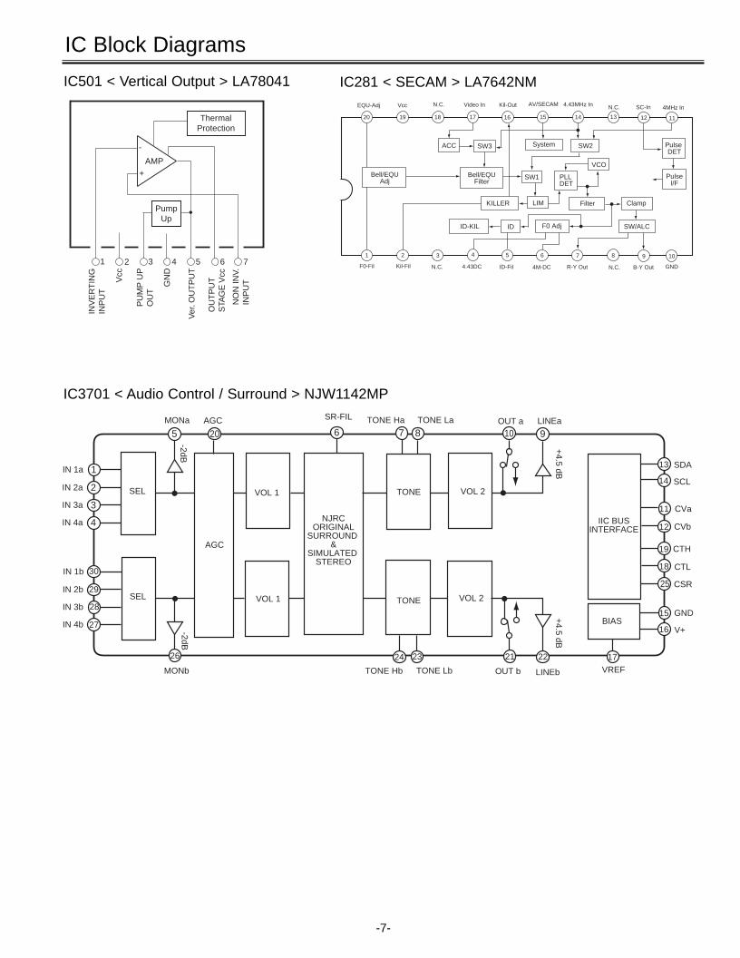
IC501 < Vertical Output > LA78041
ThermalProtection
-
+AMP
PumpUp
1
INV
ER
TIN
G
INP
UT
2
Vcc
3
PU
MP
UP
O
UT
4
GN
D
5
Ver
. OU
TP
UT
6
OU
TP
UT
S
TAG
E V
cc
7
NO
N IN
V.
INP
UT
IC3701 < Audio Control / Surround > NJW1142MP
6 8
1
720 10
25
22
NJRCORIGINAL
SURROUND &
SIMULATED STEREO
IIC BUSINTERFACE
AGC
BIAS
TONEVOL 1
TONEVOL 1
VOL 2
VOL 2
19
18
14
13
16
15
17
30
212324
12
11
IN 1a
AGC TONE Ha TONE La OUT a
CVa
CVb
CTH
CTL
CSR
SCL
SDA
V+
GND
VREFOUT b
SR-FIL
TONE Hb TONE Lb
5MONa
-2dB
SEL2IN 2a
3IN 3a
4IN 4a
IN 1b
SELIN 2b
IN 3b
IN 4b
29
28
27
MONb
-2dB
26
9
+4.5 dB
LINEa
LINEb
+4.5 dB
14 13
Pulse DET
PulseI/F
Clamp
VCO
SW2
15
Filter
PLLDET
1617
System
SW1
LIMKILLER
Bell/EQUFilter
SW3
1819
ACC
Bell/EQUAdj
20
1 2 3
ID-KIL ID
4 5
F0 Adj
6 7
SW/ALC
8
F0-Fil Kil-Fil 4.43DC ID-Fil 4M-DC R-Y Out B-Y OutN.C.
4MHz InSC-In4.43MHz InAV/SECAMKil-OutVideo InVccEQU-Adj
9 10
GND
1112
N.C.
N.C.N.C.
IC281 < SECAM > LA7642NM
SM_29-C4ZKH(Rus) 6/28/04 10:31 AM Page 7
-8-
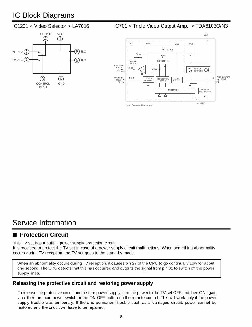
IC Block DiagramsIC1201 < Video Selector > LA7016
2
7
3 6
8
5
4 1
CONTROLINPUT
GND
N.C.
N.C.
OUTPUT VCC
INPUT 1
INPUT 2
Service Information
This TV set has a built-in power supply protection circuit.It is provided to protect the TV set in case of a power supply circuit malfunctions. When something abnormalityoccurs during TV reception, the TV set goes to the stand-by mode.
When an abnormality occurs during TV reception, it causes pin 27 of the CPU to go continually Low for aboutone second. The CPU detects that this has occurred and outputs the signal from pin 31 to switch off the powersupply lines.
Releasing the protective circuit and restoring power supply
To release the protective circuit and restore power supply, turn the power to the TV set OFF and then ON againvia either the main power switch or the ON-OFF button on the remote control. This will work only if the powersupply trouble was temporary. If there is permanent trouble such as a damaged circuit, power cannot berestored and the circuit will have to be repaired.
Protection Circuit
VDD VDD VDD
VDD
MIRROR 2
VDD
FLASH-DIODE
1xVOC
InvertingInput
(3x)
1,2,3
9,8,7
3x
VDD
6
5
4
Non-invertingInput
Vip
MIRROR 1
Vbias
MIRROR 3
LEVEL-SHIFTER 1
LEVEL-SHIFTER 2
DIFFERENTIALSTAGE
CURRENTSOURCES
GND
THERMALPROTECTION
Note: One amplifier shown.
CathodeOutput
(3x)
Vi
IC701 < Triple Video Output Amp. > TDA6103Q/N3
SM_29-C4ZKH(Rus) 6/28/04 10:31 AM Page 8
-9-
Service Adjustments with Replacing Memory IC(IC802)
Note: The CPU (IC801) and memory IC (IC802) store the service adjustments data and controls data for each circuit.When the Memory IC(IC802) is replaced, some of the service adjustments should be readjusted to obtain the best performance. The necessary service adjustments are carried out by using the RC handset. Please set up the TV set with following steps [1] to [2].
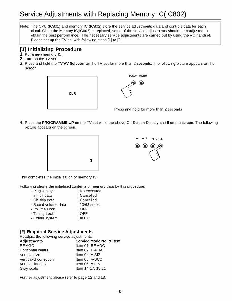
[1] Initializing Procedure1. Put a new memory IC.2. Turn on the TV set.3. Press and hold the TV/AV Selector on the TV set for more than 2 seconds. The following picture appears on the
screen.
4. Press the PROGRAMME UP on the TV set while the above On-Screen Display is still on the screen. The followingpicture appears on the screen.
This completes the initialization of memory IC.
Following shows the initialized contents of memory data by this procedure.- Plug & play : No executed- Inhibit data : Cancelled- Ch skip data : Cancelled- Sound volume data : 10/63 steps.- Volume Lock : OFF- Tuning Lock : OFF- Colour system : AUTO
1
CLR
[2] Required Service AdjustmentsReadjust the following service adjustments.Adjustments Service Mode No. & ItemRF AGC Item 01, RF AGCHorizontal centre Item 02, H-PHAVertical size Item 04, V-SIZVertical-S correction Item 05, V-SCOVertical linearity Item 06, V-LINGray scale Item 14-17, 19-21
Further adjustment please refer to page 12 and 13.
Press and hold for more than 2 seconds
+ CH
TV/AV MENU
SM_29-C4ZKH(Rus) 6/28/04 10:31 AM Page 9
Service Adjustments with Replacing Memory IC(IC802)
-10-
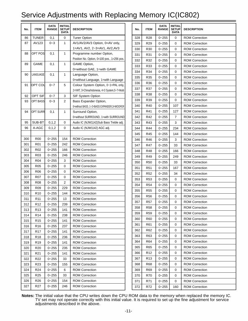
DATA INITIALNo. ITEM RANGE SETUP DESCRIPTION
DATA
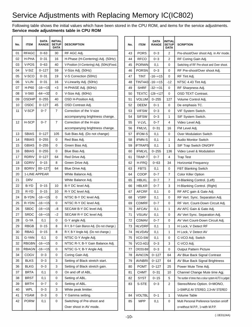
01 RFAGC 0~63 30 RF AGC Adj.
02 H-PHA 0~31 16 H-Phase (H-Centering) Adj. (50Hz)
03 V-POS 0~63 40 V-Position (V-Centering) Adj. (50Hz)Fixed.
04 V-SIZ 0~127 59 V-Size Adj. (50Hz)
05 V-SCO 0~31 19 V-S Correction (50Hz)
06 V-LIN 0~31 16 V-Linearity Adj. (50Hz)
07 H-P60 -16~+15 +3 H-PHASE Adj. (60Hz)
08 V-S60 -64~+32 0 V-Size Adj. (60Hz)
09 OSDHP 0~255 40 OSD H-Position Adj.
10 OSDC 0~127 45 OSD Contrast Adj.
11 V-SCP 0~7 7 Correction of the V-size
accompanying brightness change.
12 H-SCP 0~7 7 Correction of the H-size
accompanying brightness change.
13 SBIAS 0~127 105 Sub Bias Adj. (Do not change)
14 RBIAS 0~255 0 Red Bias Adj.
15 GBIAS 0~255 0 Green Bias Adj.
16 BBIAS 0~255 0 Blue Bias Adj.
17 RDRIV 0~127 64 Red Drive Adj.
18 GDRIV 0~15 8 Green Drive Adj.
19 BDRIV 00~127 64 Blue Drive Adj.
20 1-LINE APPEAR White Balance Adj.
21 DRV White Balance Adj.
22 B-YD 0~15 10 B-Y DC level Adj.
23 R-YD 0~15 10 R-Y DC level Adj.
24 B-YDN -16~+15 0 NTSC B-Y DC level Adj.
25 R-YDN -16~+15 0 NTSC R-Y DC level Adj.
26 SBDC -16~+15 −8 SECAM B-Y DC level Adj.
27 SRDC -16~+15 −2 SECAM R-Y DC level Adj.
28 G-YA 0,1 0 G-Y angle Adj.
29 RBGB 0~15 8 R-Y, B-Y Gain Blance Adj. (Do not change.)
30 RBAG 0~15 8 R-Y, B-Y Angle Adj. (Do not change.)
31 G-YAN 0,1 0 NTSC G-Y Angle Adj.
32 RBGBN -16~+15 0 NTSC R-Y, B-Y Gain Balance Adj.
33 RBAGN -16~+15 0 NTSC G-Y, B-Y Angle Adj.
34 COGV 0~3 0 Coring Gain Adj.
35 BLKS 0~3 3 Setting of Black stretch start.
36 BLKG 0~3 3 Setting of Black stretch gain.
37 BRTA 0,1 0 On and off of ABL.
38 BRST 0,1 0 Setting of ABL.
39 BRTH 0~7 0 Setting of ABL.
40 WPL 0~3 3 White peak limitter.
41 YGAM 0~3 0 Y Gamma setting.
42 PORW 0,1 0 Switching of Pre-shoot and
Over shoot in AV mode.
Following table shows the initial values which have been stored in the CPU ROM, and items for the service adjustments.Service mode adjustments table in CPU ROM
DATA INITIALNo. ITEM RANGE SETUP SCRIPTION
DATA
43 PORS 0~3 2 Pre-shoot/Over shoot Adj. in AV mode.
44 RFCO 0~3 2 RF Coring Gain Adj.
45 PORWN 0,1 0 Switching of RF Pre-shoot and Over shoot.
46 PORSN 0~3 0 RF Pre-shoot/Over shoot Adj.
47 TINT -16~+15 0 RF Tint Adj.
48 TINT443 -16~+15 -12 NTSC 4.43 Tint Adj.
49 SHRF -32~+31 0 RF Sharpness Adj.
50 TEXTC -128~+127 0 OSD TEXT Contrast.
51 VOLUM 0~255 127 Volume Control Adj.
52 DEEM 0~1 0 De emphasis TC.
53 VIFSW 0~3 0 VIF System Switch.
54 SIFSW 0~3 1 SIF System Switch.
55 V-LVL 0~7 4 Video Level Adj.
56 FMLVL 0~31 16 FM Level Adj.
57 IFOM-S 0,1 0 Over Modulation Switch
58 IFMN-S 0,1 1 Audio Monitor Switch
59 IFTRAPS 0,1 1 SIF Trap Switch ON/OFF
60 IFMLVL 0~255 136 Video Level & Modulation
61 TRAP-T 0~7 4 Trap Test
62 H-FRQ 0~63 34 Horizontal Frequency
63 FBTS 0,1 0 FBT Blanking Switch
64 COOP 0~7 7 Color Killer Option
65 HBLKL 0~7 7 H-Blanking Control. (Left)
66 HBLKR 0~7 3 H-Blanking Control. (Right)
67 AFCRF 0,1 0 RF AFC gain & Gate Adj.
68 VSRF 0,1 0 RF Vert. Sync. Separation Adj.
69 CDMRF 0~7 0 RF Vert. Count-Down Circuit Adj.
70 AFCAV 0,1 1 AV AFC Gain & Gate Adj.
71 VSUAV 0,1 0 AV Vert Sync. Separation Adj.
72 CDMAV 0~7 0 AV Vert Count-Down Circuit Adj.
73 HLVDRF 0,1 1 H Lock, V Detect RF
74 HLVDAV 0,1 1 H Lock, V Detect AV
75 VCO-SW 0,1 0 C-VCO Adj. Switch
76 VCO-ADJ 0~3 3 C-VCO Adj.
77 CROSS-BW 0~3 0 Output Pattern Picture
78 AVNCON 0~127 64 AV Blue Back Signal Contrast
79 AVNBRI 0~127 64 AV Blue Back Signal Brightness
80 POMT 0~127 25 Power Mute Time Adj.
81 CHMT 0~31 10 Channel Change Mute time Agj.
82 SYST 0~15 5 The number of times that a colour system AUTO is judged.
83 S-STE 0~3 2 Stereo/Mono Option. 0=MONO,
1=SIMPLE AV STEREO, 2,3=AV STEREO
84 VOLTBL 0~1 1 Volume Table
85 MPP 0,1 0 Multi Personal Preference function on/off
o=without M.P.P., 1=with M.P.P.
( /JE0124A)
SM_29-C4ZKH(Rus) 6/28/04 10:31 AM Page 10
-11-
Service Adjustments with Replacing Memory IC(IC802)
Notes: The initial value that the CPU writes down the CPU ROM data to the memory when replaced the memory IC. TV set may not operate correctly with this initial value. It is required to set up the fine adjustment for service adjustments described in the above.
DATA INITIALNo. ITEM RANGE SETUP DESCRIPTION
DATA
86 TUNER 0,1 0 Tuner Option
87 AV123 0~3 1 AV1/AV2/AV3 Option, 0=AV only,
1=AV1, AV2, 2~3=AV1, AV2,AV3
88 OPT POS 0,1 1 Programme number Option,
Position No. Option, 0=100 pos., 1=256 pos.
89 GAME 0,1 1 GAME Option,
0=without GAE, 1=with GAME
90 LANGUAGE 0,1 1 Language Option,
0=without Language, 1=with Language
91 OPT COL 0~7 5 Colour System Option, 0~1=PAL only,
2=VMT, 3=China/Indonesia, 4=3 System,5~7=Multi
92 OPT SIF 0~7 3 SIF System Option
93 OPT BASS 0~3 2 Bass Expander Option,
0=without BASS, 1~2=BASS EXPANDER,3=WOOFER
94 OPT SURR 0,1 1 Surround Option,
0=without SURROUND, 1=with SURROUND
95 SUB-BT 0,1,2 0 Audio IC (NJW1142)Sub Bass Treble adj.
96 A-AGC 0,1,2 0 Audio IC (NJW1142) AGC adj.
300 R00 0~255 154 ROM Correction
301 R01 0~255 242 ROM Correction
302 R02 0~255 166 ROM Correction
303 R03 0~255 246 ROM Correction
304 R04 0~255 3 ROM Correction
305 R05 0~255 0 ROM Correction
306 R06 0~255 0 ROM Correction
307 R07 0~255 0 ROM Correction
308 R08 0~255 2 ROM Correction
309 R09 0~255 229 ROM Correction
310 R10 0~255 144 ROM Correction
311 R11 0~255 13 ROM Correction
312 R12 0~255 239 ROM Correction
313 R13 0~255 141 ROM Correction
314 R14 0~255 238 ROM Correction
315 R15 0~255 141 ROM Correction
316 R16 0~255 237 ROM Correction
317 R17 0~255 141 ROM Correction
318 R18 0~255 236 ROM Correction
319 R19 0~255 141 ROM Correction
320 R20 0~255 235 ROM Correction
321 R21 0~255 141 ROM Correction
322 R22 0~255 33 ROM Correction
323 R23 0~255 155 ROM Correction
324 R24 0~255 6 ROM Correction
325 R25 0~255 33 ROM Correction
326 R26 0~255 154 ROM Correction
327 R27 0~255 246 ROM Correction
DATA INITIALNo. ITEM RANGE SETUP DESCRIPTION
DATA
328 R28 0~255 0 ROM Correction
329 R29 0~255 0 ROM Correction
330 R30 0~255 0 ROM Correction
331 R31 0~255 0 ROM Correction
332 R32 0~255 0 ROM Correction
333 R33 0~255 0 ROM Correction
334 R34 0~255 0 ROM Correction
335 R35 0~255 0 ROM Correction
336 R36 0~255 0 ROM Correction
337 R37 0~255 0 ROM Correction
338 R38 0~255 0 ROM Correction
339 R39 0~255 0 ROM Correction
340 R40 0~255 107 ROM Correction
341 R41 0~255 127 ROM Correction
342 R42 0~255 7 ROM Correction
343 R43 0~255 3 ROM Correction
344 R44 0~255 234 ROM Correction
345 R45 0~255 144 ROM Correction
346 R46 0~255 3 ROM Correction
347 R47 0~255 33 ROM Correction
348 R48 0~255 166 ROM Correction
349 R49 0~255 249 ROM Correction
350 R50 0~255 33 ROM Correction
351 R51 0~255 167 ROM Correction
352 R52 0~255 34 ROM Correction
353 R53 0~255 0 ROM Correction
354 R54 0~255 0 ROM Correction
355 R55 0~255 0 ROM Correction
356 R56 0~255 0 ROM Correction
357 R57 0~255 0 ROM Correction
358 R58 0~255 0 ROM Correction
359 R59 0~255 0 ROM Correction
360 R60 0~255 0 ROM Correction
361 R61 0~255 0 ROM Correction
362 R62 0~255 0 ROM Correction
363 R63 0~255 0 ROM Correction
364 R64 0~255 0 ROM Correction
365 R65 0~255 0 ROM Correction
366 R12 0~255 0 ROM Correction
367 R13 0~255 0 ROM Correction
368 R68 0~255 0 ROM Correction
369 R69 0~255 0 ROM Correction
370 R70 0~255 0 ROM Correction
371 R71 0~255 0 ROM Correction
372 R72 0~255 160 ROM Correction
SM_29-C4ZKH(Rus) 6/28/04 10:31 AM Page 11
-/--
CH
CH
-12-
Service Adjustments with Replacing Memory IC(IC802)
ADDRESSDRV
SI. 00100101S2.11111000DATA
B 6421 R 64ADDRESS
V-SCO
SI. 00100101S2.11111000DATA
905
ADDRESSRF AGC
SI. 00100101S2.11111000DATA
3001
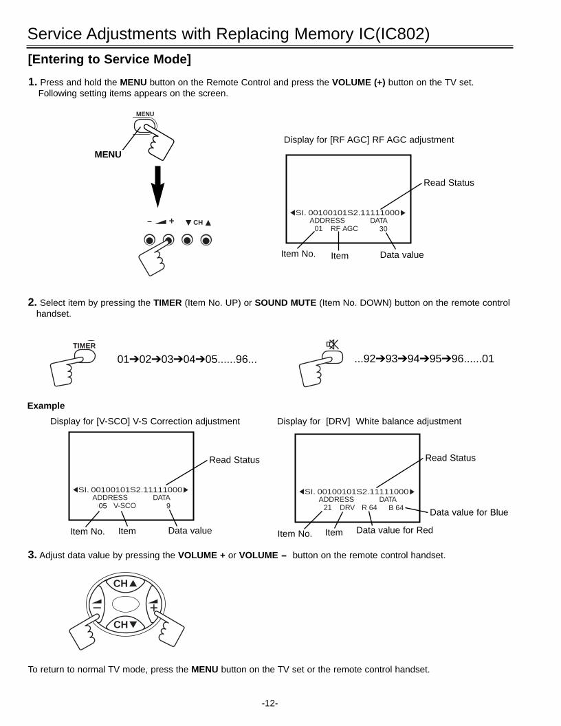
[Entering to Service Mode]
1. Press and hold the MENU button on the Remote Control and press the VOLUME (+) button on the TV set.Following setting items appears on the screen.
Display for [V-SCO] V-S Correction adjustment
Read Status
Item No. Item Data value
Display for [RF AGC] RF AGC adjustment
Read Status
Item No. Item Data value
Data value for Red
Display for [DRV] White balance adjustment
Read Status
Item No. Item
Data value for Blue
To return to normal TV mode, press the MENU button on the TV set or the remote control handset.
2. Select item by pressing the TIMER (Item No. UP) or SOUND MUTE (Item No. DOWN) button on the remote controlhandset.
3. Adjust data value by pressing the VOLUME + or VOLUME - button on the remote control handset.
Example
-/--MENU
MENU
0102030405......96... ...9293949596......01
-/--
TIMER
-/--
+ CH
05
SM_29-C4ZKH(Rus) 6/28/04 10:31 AM Page 12
-13-
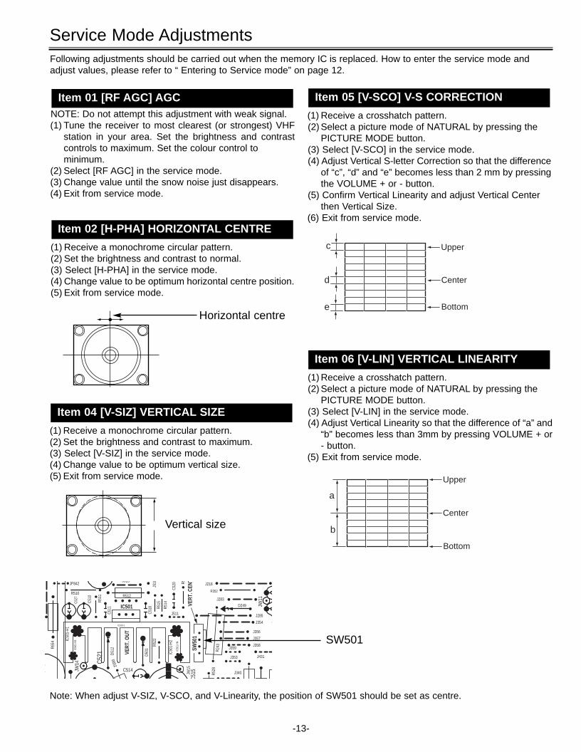
Service Mode AdjustmentsFollowing adjustments should be carried out when the memory IC is replaced. How to enter the service mode andadjust values, please refer to “ Entering to Service mode” on page 12.
NOTE: Do not attempt this adjustment with weak signal.(1) Tune the receiver to most clearest (or strongest) VHF
station in your area. Set the brightness and contrastcontrols to maximum. Set the colour control to minimum.
(2) Select [RF AGC] in the service mode.(3) Change value until the snow noise just disappears.(4) Exit from service mode.
Item 01 [RF AGC] AGC
(1) Receive a monochrome circular pattern.(2) Set the brightness and contrast to normal.(3) Select [H-PHA] in the service mode.(4) Change value to be optimum horizontal centre position. (5) Exit from service mode.
Item 02 [H-PHA] HORIZONTAL CENTRE
(1) Receive a monochrome circular pattern.(2) Set the brightness and contrast to maximum.(3) Select [V-SIZ] in the service mode.(4) Change value to be optimum vertical size.(5) Exit from service mode.
Item 04 [V-SIZ] VERTICAL SIZE
(1) Receive a crosshatch pattern.(2) Select a picture mode of NATURAL by pressing the
PICTURE MODE button.(3) Select [V-SCO] in the service mode.(4) Adjust Vertical S-letter Correction so that the difference
of “c”, “d” and “e” becomes less than 2 mm by pressingthe VOLUME + or - button.
(5) Confirm Vertical Linearity and adjust Vertical Center then Vertical Size.
(6) Exit from service mode.
Item 05 [V-SCO] V-S CORRECTION
c Upper
Center
Bottom
d
e
(1) Receive a crosshatch pattern.(2) Select a picture mode of NATURAL by pressing the
PICTURE MODE button.(3) Select [V-LIN] in the service mode.(4) Adjust Vertical Linearity so that the difference of “a” and
“b” becomes less than 3mm by pressing VOLUME + or- button.
(5) Exit from service mode.
Item 06 [V-LIN] VERTICAL LINEARITY
a
b
Upper
Center
Bottom
Horizontal centre
Vertical size
Note: When adjust V-SIZ, V-SCO, and V-Linearity, the position of SW501 should be set as centre.
IC50
1-H4
IC50
1-H3
IC50
1-H2
IC50
1-H1
D249
R652
IC501-1
IC501
R512
D512
C518
D501
C521
C511
C510
R510
R511
J515
R515
R514
R522
C515C514
SW50
1
J511
R528
R352
J340
J359J358
J357
J356
J354
J431
C520 R5
J353
C527
JW15
J518
J285
R243
J283
JW11
J218
R654
JP842
JW14
VERT
. OUT
VERT
. CEN
T
SW501
SM_29-C4ZKH(Rus) 6/28/04 10:31 AM Page 13
-14-
Service Mode Adjustments
1
T471A
T471
JP409
C437
R487
JP412
T471-H5
T471-H1
JP408
JP407
JP403A JP405
R355
JW1
J406
R477A
R492
R
C423-H2 C423-H3
C423-H1C420-H1
C420
C420-H3C420-H2
C437AR424
D438
435
JP410
JP411
R477
JP404
T471-H2
J405
C471
JW6
R483
R481R481A
T471-H7
T471-H11
T471-H6T471-H4
T471-H8
T471-H10
JP483
JP436
JP477
C437B
FC3G2 CHASSIS
T471
P435
JP403
MAIN BOARD
SCREEN VR(Under side)
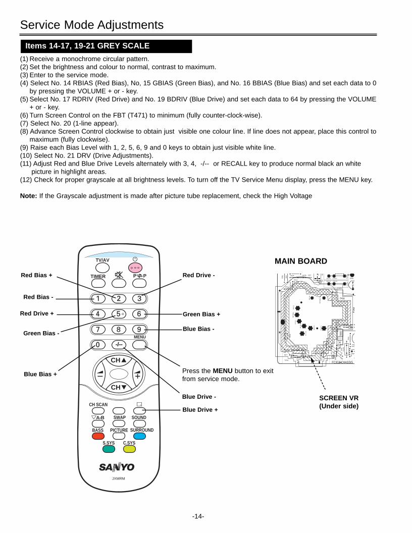
(1) Receive a monochrome circular pattern. (2) Set the brightness and colour to normal, contrast to maximum.(3) Enter to the service mode. (4) Select No. 14 RBIAS (Red Bias), No, 15 GBIAS (Green Bias), and No. 16 BBIAS (Blue Bias) and set each data to 0
by pressing the VOLUME + or - key.(5) Select No. 17 RDRIV (Red Drive) and No. 19 BDRIV (Blue Drive) and set each data to 64 by pressing the VOLUME
+ or - key.(6) Turn Screen Control on the FBT (T471) to minimum (fully counter-clock-wise).(7) Select No. 20 (1-line appear). (8) Advance Screen Control clockwise to obtain just visible one colour line. If line does not appear, place this control to
maximum (fully clockwise).(9) Raise each Bias Level with 1, 2, 5, 6, 9 and 0 keys to obtain just visible white line.(10) Select No. 21 DRV (Drive Adjustments).(11) Adjust Red and Blue Drive Levels alternately with 3, 4, -/-- or RECALL key to produce normal black an white
picture in highlight areas.(12) Check for proper grayscale at all brightness levels. To turn off the TV Service Menu display, press the MENU key.
Note: If the Grayscale adjustment is made after picture tube replacement, check the High Voltage
Items 14-17, 19-21 GREY SCALE
JXMRM
PICTURE
-/---/--
P P
A•B
TIMER
TV/AV
CH
SWAP SOUND
CH SCAN
BASS
CH
SURROUND
MENU
S.SYS C.SYS
Red Bias -
Red Bias +
Green Bias -
Green Bias +
Blue Bias -
Blue Bias + Press the MENU button to exitfrom service mode.
Red Drive -
Red Drive +
Blue Drive -
Blue Drive +
SM_29-C4ZKH(Rus) 6/28/04 10:31 AM Page 14
-15-
E
E
107
6
5
4
3
2 1
8 9
GNDHEATERLOW B
ABL
AFC
140
H OUT
210
E
E E
E
7
Q432-H6
Q432-H7
Q432-H4
Q432-H5
R449
D485
R488
D467
R423A
R423 D466
C465
T471-H8
T471-H5
T471-H2
T471-H1
T471-H10
T471
R481
Q432
C423
C423-H1
C423-H2
C423-H3
D438
C420
C420-H1
C420-H2C420-H3
C423A
C420B
C424A
C424
D439
C422C422A
JP436
L432
L431
C425
C425A
KQC486
JP476
C471
R424
R435
C426
J448
R355
J449 R474
D469 C468
VR462
R468
R464
R469
R472
R480
C462
C463
R461
C466
R466
D461
R467
C470
D465
R471
D464
Q462
C467
R473
Q461
Q461A
Q461-H2
Q461-H1
C464
R465R462
J480
J461
R485
R487
D486
Q449C449
D448
R479
R475
C469
D468
J642
C424-H1C425-H1
C424-H3C424-H2
C425-H2C425-H3
Q432-H2
C442-H2L461
L461AJ441
D651
Q432-1
Q432-H1
Q432-H3
JP501
J503
J502
J641
C540KDY
MK
T471-H9
B
E
C
TP-B
J643
C420A
C420A-H2
C420A-H1
1 4C487 D476
T471-H7T471-H6
R486
L651
Q612
R624
R623
R622
R614
613
R611
Q642
Q611 D616
C613C611
R633
R632
R621
L614
D612
D615
L612
D643
D611
C617
C615
L613
R627
D619
R631
L615
D617
VR463
R628
R629
J629
C629
J651
Q61
3-H4
Q61
3-H5
T611-H7 T61
T
J462
R463
JW8
C355
R524
J611
KDY-1
KDY-4
KDY-5
KDY-6
KDY-3
C610
FBT
CONVETRA
H-SIZE ADJ.
PCC ADJ.
H-OUT
KG
VOLU
ME
DOW
NVO
LUM
EUP
POSI
TIO
NUP
POSI
TIO
NDO
WN
F601
KG
E
E
E
E
12
43
12
E
E
T4AL250V
71
R449
R423
A
R423
D466
J1911
D1901
SW1901
SW1902
SW1903
SW1904
A1901
C1902
J1910
R424
R435
R474
D469
C468
VR46
2
R468
R464
R472
R480
C462 C4
63
R461
D461
R467
C470
D465
R471
D464
Q4
Q46
1
Q46
1A
Q46
1-H2
Q461-H1
D651
J1903
JP501
J502
TP-B
C609
C609A
SW60
1
C609
-H1
VA601
SW60
1-H1
J122
JP602JP601
PS60
1
C608
D608
C607
D607
C605
D605
C606
D606
C609A-H1
C609A-H2
C602
L601
L601
-H2
L601
A-H2
L601
A-H1
L601
-H1
L601
A-H4
L601
-H4
L601
-H3
L601
A-H3 L6
01A
R601 C601
F601B
F601A
R602
-H2
R602
-H1
R602
-H3
J601
J602
PS601-H3
PS601-H2
PS601-H1
E
KE-1
KE-2
C609
-H2
SW60
1-H2
R602C
R602B
R602
B-H1
R602
B-H2
R602
B-H3
R602A
C618A
L651
Q61
2
R644
R643
R642
R641
R624
R623
R622R619
R616
R614
R613
R611
Q64
2
Q64
1
Q62
5
Q61
1
D616
C644
C613
C611
R633
R632
R625
R621
R620L6
14
D612
C614
D615
D614
R626
R615
D610L612
D643
D611
C617
C618
C615
L613
KE
J606
D641
R627
D619
R631
L615
D617
J616
L616
J610
J603
R628
29
C629
C627
C628
R651
L654
J662
R664
Q66
2
R671
C664
D664
D671
C665
D
R669
R
VR651
D662
C663
Q65
1
C658
J653 JP
D691
J607
J651
J604
D601-H3
D601-H4
D601-H2
D601-H1
D601
KG-3
KG-2
KG-1
Q613-H4
Q613-H5
Q61
3AQ
613-
H3Q
613-
H1
Q61
3-H2
Q61
3PO
WER
SW
ITCH
ING
T611
-H7
T611
-H4
T611
-H3
T611
-H2
T611 T6
1
D654-H1D654-H2
D654
J462
J665
R602
-H4
D654A
R656
JW8
J608
J659
J609
J611
J612
KDY-
6
C610
CONV
ERTR
AN
+B A
DJ.
H-SI
ZE A
DJ.
PCC
ADJ.
Service Adjustments
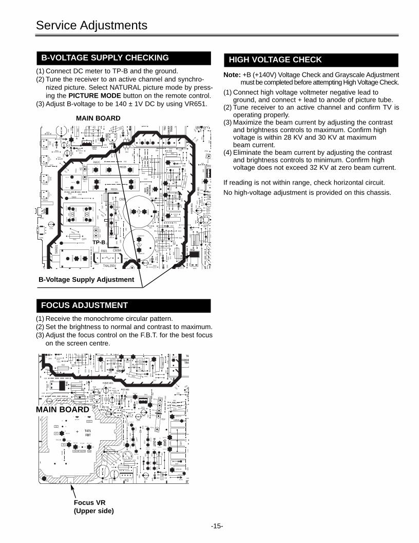
(1) Connect DC meter to TP-B and the ground. (2) Tune the receiver to an active channel and synchro-
nized picture. Select NATURAL picture mode by press-ing the PICTURE MODE button on the remote control.
(3) Adjust B-voltage to be 140 ± 1V DC by using VR651.
B-VOLTAGE SUPPLY CHECKING
(1) Receive the monochrome circular pattern.(2) Set the brightness to normal and contrast to maximum.(3) Adjust the focus control on the F.B.T. for the best focus
on the screen centre.
FOCUS ADJUSTMENT
MAIN BOARD
B-Voltage Supply Adjustment
Focus VR(Upper side)
MAIN BOARD
Note: +B (+140V) Voltage Check and Grayscale Adjustmentmust be completed before attempting High Voltage Check.
(1) Connect high voltage voltmeter negative lead to ground, and connect + lead to anode of picture tube.
(2) Tune receiver to an active channel and confirm TV is operating properly.
(3) Maximize the beam current by adjusting the contrast and brightness controls to maximum. Confirm high voltage is within 28 KV and 30 KV at maximum beam current.
(4) Eliminate the beam current by adjusting the contrast and brightness controls to minimum. Confirm high voltage does not exceed 32 KV at zero beam current.
If reading is not within range, check horizontal circuit.
No high-voltage adjustment is provided on this chassis.
HIGH VOLTAGE CHECK
TP-B
SM_29-C4ZKH(Rus) 6/28/04 10:31 AM Page 15
-/--
CH
CH
-/--
CH
CH
-16-
Special Function
TUNING LOCK
AV START
VOLUME LOCK
MUSIC MODE
OFFOFFOFFOFF
SELECT ADJUST M EXIT
1 To enter into the special function setting mode, press and hold the MENU button of the remote control, then press thePROGRAMME DOWN button on the TV set.
Once TUNING LOCK is switched on, further channel tuning(Pre-set) is not possible. The Channel Swapping function alsois not possible.
2 Select an item of the special functions by pressing the PROGRAMME UP or DOWN button on the remote controlor the TV set.
3 Set the selected special function “ ON “ by pressing the VOLUME + or - button. To cancel, set to “ OFF”.
(2) Tuning Lock setting
The following special functions can be set up on this TVset.
With this function, a maximum sound volume limit can be set atany level.
(3) Music Mode setting
When Music Mode is ON, Programme position from “247” to“255” and “0” are set Music Mode. Only sound is provided andany picture is not on the screen under Music Mode.
Set AV-START to ON and every time the TV set is switched on,AV1 position will be the initial programme position.
(4) AV Start setting
TUNING LOCKED
How to set the special function:
Note: When making the VOLUME LOCK setting, set thedesired maximum sound volume by pressing the VOLUME + or- button before entering Special Function setting mode.
AV1
MUSICTurns blackscreen
4 Press the MENU button of the remote control to return to the normal TV mode.
(1) Volume Lock setting
SOUNDBASS EXPANDER ON
IIIIIIII
-/--MENU
-/--MENU
OFFONOFFOFF
TUNING LOCK
AV START
VOLUME LOCK
MUSIC MODE
SELECT ADJUST M EXIT
OFFOFFOFFOFF
TUNING LOCK
AV START
VOLUME LOCK
MUSIC MODE
SELECT ADJUST M EXIT
+ CH
SM_29-C4ZKH(Rus) 6/28/04 10:31 AM Page 16
-17-
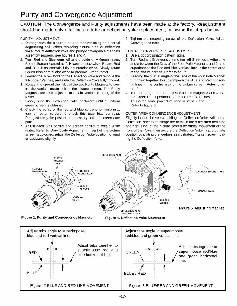
Purity and Convergence Adjustment
RED
BLUE
Adjust tabs together tosuperimpose red andblue horizontal line.
Figure- 2 BLUE AND RED LINE MOVEMENT Figure- 3 BLUE/RED AND GREEN MOVEMENT
Adjust tabs together tosuperimpose red/blueand green horizontalline.
Adjust tabs angle to superimposeblue and red vertical line.
Adjust tabs angle to superimposered/blue and green vertical line.
GREEN
BLUE / RED
CAUTION: The Convergence and Purity adjustments have been made at the factory. Readjustmentshould be made only after picture tube or deflection yoke replacement, following the steps below:
PURITY ADJUSTMENT1. Demagnetize the picture tube and receiver using an external
degaussing coil. When replacing picture tube or deflectionyoke, mount deflection yoke and purity-convergence magnetsassembly properly, see figures 1 and 4.
2. Turn Red and Blue guns off and provide only Green raster.Rotate Screen control to fully counterclockwise. Rotate Redand Blue Bias controls fully counterclockwise. Slowly rotateGreen Bias control clockwise to produce Green raster.
3. Loosen the screw holding the Deflection Yoke and remove the3 Rubber Wedges, and slide the Deflection Yoke fully forward.
4. Rotate and spread the Tabs of the two Purity Magnets to cen-tre the vertical green belt in the picture screen. The PurityMagnets are also adjusted to obtain vertical centring of theraster.
5. Slowly slide the Deflection Yoke backward until a uniformgreen screen is obtained.
6. Check the purity of the red and blue screens for uniformity,turn off other colours to check this (use bias controls).Readjust the yoke position if necessary until all screens arepure.
7. Adjust each Bias control and screen control to obtain whiteraster. Refer to Gray Scale Adjustment. If part of the picturescreen is coloured, adjust the Deflection Yoke position forwardor backward slightly.
8. Tighten the mounting screw of the Deflection Yoke. AdjustConvergence next.
CENTRE CONVERGENCE ADJUSTMENT1. Use a dot crosshatch pattern signal.2. Turn Red and Blue guns on and turn off Green gun. Adjust the
angle between the Tabs of the Four Pole Magnet 1 and 2, andsuperimpose the Red and Blue vertical lines in the centre areaof the picture screen. Refer to figure 2.
3. Keeping the mutual angle of the Tabs of the Four Pole Magnetturn them together to superimpose the Blue and Red horizon-tal lines in the centre area of the picture screen. Refer to fig-ure 2.
4. Turn Green gun on and adjust Six Pole Magnet 3 and 4 thatthe Green line superimposed on the Red/Blue lines.This is the same procedure used in steps 2 and 3.Refer to figure 3.
OUTER AREA CONVERGENCE ADJUSTMENTSlightly loosen the screw holding the Deflection Yoke. Adjust theDeflection Yoke to converge the detail in the outer area (left sideand right side) of the picture screen by orbital movement of thefront of the Yoke, then secure the Deflection Yoke in appropriateposition by putting the wedges as illustrated. Tighten screw hold-ing the Deflection Yoke.
RUBBERWEDGE
DEFLECTION YOKE
DEFLECTION YOKEMOUNTING SCREW
Figure 4. Deflection Yoke Movement
SIX-POLEMAGNET TABS FOUR-POLE
MAGNET TABS
ANGLEOF TABS
PURITYMAGNETTABS
43
21
FOCUS GAP(G3-G4)
Figure 1. Purity and Convergence Magnets
MAGNET TABS
ANGLE OF MAGNET TABS
Figure 5. Adjusting Magnet
SM_29-C4ZKH(Rus) 6/28/04 10:31 AM Page 17
-18-
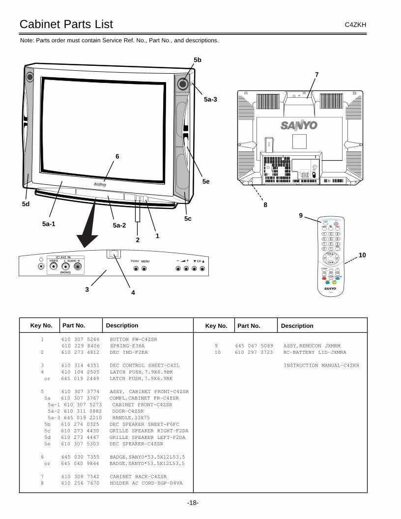
Cabinet Parts List
1 610 307 5266 BUTTON PW-C4ZSR610 229 8406 SPRING-E3HA
2 610 273 4812 DEC IND-F2EA
3 610 314 4351 DEC CONTROL SHEET-C4ZL4 610 104 2505 LATCH PUSH,7.9X6.9BKor 645 019 2449 LATCH PUSH,7.9X6.9BK
5 610 307 3774 ASSY, CABINET FRONT-C4ZSR5a 610 307 3767 COMPL,CABINET FR-C4ZSR5a-1 610 307 5273 CABINET FRONT-C4ZSR5a-2 610 311 0882 DOOR-C4ZSR5a-3 645 019 2210 HANDLE,33X75
5b 610 274 0325 DEC SPEAKER SHEET-F6FC5c 610 273 4430 GRILLE SPEAKER RIGHT-F2DA5d 610 273 4447 GRILLE SPEAKER LEFT-F2DA5e 610 307 5303 DEC SPEAKER-C4ZSR
6 645 030 7355 BADGE,SANYO*53.5X12L53.5or 645 040 9844 BADGE,SANYO*53.5X12L53.5
7 610 308 7542 CABINET BACK-C4ZSR8 610 256 7670 HOLDER AC CORD-SGP-D4VA
9 645 067 5089 ASSY,REMOCON JXMRM10 610 297 3723 RC-BATTERY LID-JXMRA
INSTRUCTION MANUAL-C4ZKH
Key No. Part No. Description Key No. Part No. Description
JXMRM
PICTURE
-/---/--
P P
A•B
TIMER
TV/AV
CH
SWAP SOUND
CH SCAN
BASS
CH
SURROUND
MENU
S.SYS C.SYS
9
10
Note: Parts order must contain Service Ref. No., Part No., and descriptions.
ANT 75Ω
VIDEO IN
AUDIO OUT
AUDIO IN
VIDEO OUT
R
R
L
L
12
4
5a-2
7
5d 8
5b
C4ZKH
AV2 IN
(MONO)
L AUDIO RVIDEO TV/AV MENU + CH
6
3
5e
5c
5a-3
5a-1
SM_29-C4ZKH(Rus) 6/28/04 10:31 AM Page 18
-19-
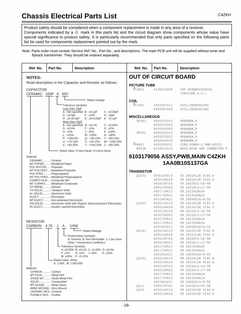
C4ZKH
OUT OF CIRCUIT BOARDPICTURE TUBE
Q901 4140124008 CRT A68QBC230X35L (INCLUDE D.Y.)
COILL901 6450481611 COIL,DEGAUSSING
6450481628 COIL,DEGAUSSING
MISCELLANEOUSSP901 6450024313 SPEAKER,8
6450253003 SPEAKER,86450543050 SPEAKER,8
SP902 6450024313 SPEAKER,86450253003 SPEAKER,86450543050 SPEAKER,8
W901 6450399251 CORD,POWER-2.0MK-A5003W903A 6102815214 ASSY,WIRE GND CONNECTOR F
6103179056 ASSY,PWB,MAIN C4ZKH1AA0B10S137GA
TRANSISTORQ1031 4050144519 TR 2SC2412K T146 R
4050144618 TR 2SC2412K T146 S4050158724 TR 2SC2812-L6-TB4050158922 TR 2SC2812-L7-TB4051739813 TR 2SC3928A1R4051739912 TR 2SC3928A1S4051843411 TR 2SD0601A-R-TX
Q1032 4050144519 TR 2SC2412K T146 R4050144618 TR 2SC2412K T146 S4050158724 TR 2SC2812-L6-TB4050158922 TR 2SC2812-L7-TB4051739813 TR 2SC3928A1R4051739912 TR 2SC3928A1S4051843411 TR 2SD0601A-R-TX
Q1041 4050144519 TR 2SC2412K T146 R4050144618 TR 2SC2412K T146 S4050158724 TR 2SC2812-L6-TB4050158922 TR 2SC2812-L7-TB4051739813 TR 2SC3928A1R4051739912 TR 2SC3928A1S4051843411 TR 2SD0601A-R-TX
Q1042 4050144519 TR 2SC2412K T146 R4050144618 TR 2SC2412K T146 S4050158724 TR 2SC2812-L6-TB4050158922 TR 2SC2812-L7-TB4051739813 TR 2SC3928A1R4051739912 TR 2SC3928A1S4051843411 TR 2SD0601A-R-TX
Q111 4050159721 TR 2SC2814-F4-TBQ122 4050144519 TR 2SC2412K T146 R
4050144618 TR 2SC2412K T146 S
!
!
!
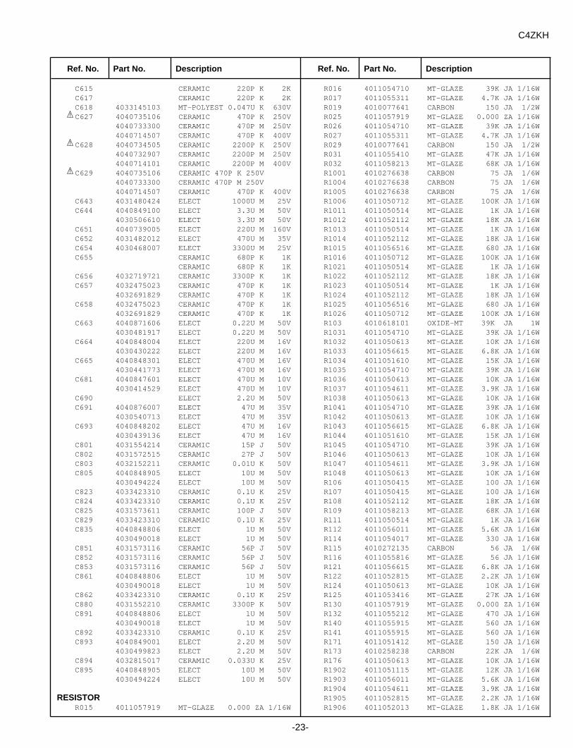
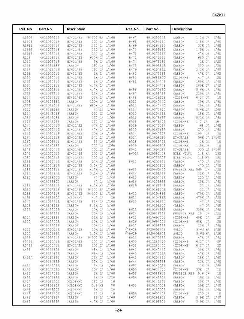
Chassis Electrical Parts List
Ref. No. Part No. Description Ref. No. Part No. Description
Product safety should be considered when a component replacement is made in any area of a receiver. Components indicated by a mark in this parts list and the circuit diagram show components whose value havespecial significance to product safety. It is particularly recommended that only parts specified on the following partslist be used for components replacement pointed out by the mark.
!
Note: Parts order must contain Service Ref. No., Part No., and descriptions. The main PCB unit will be supplied without tuner andflyback transformer. They should be ordered separately.
Read description in the Capacitor and Resistor as follows:
CAPACITORCERAMIC 100P K 50V
Rated Voltage
Tolerance Symbols:Less than 10pFA : Not specified B : ±0.1pF C : ±0.25pFD : ±0.5pF F : ±1PF G : ±2pFR : ±0.25-0pF S : ±0-0.25pF E : +0-1pFMore than 10pFA : Not specified B : ±0.1% C : ±0.25%D : ±0.5% F : ±1% G : ±2%H : ±3% J : ±5% K : ±10%L : ±15% M : ±20% N : ±30%P : +100-0% Q : +30-10% T : +50-10%U : +75-10% V : +20-10% W : +100-10%X : +40-20% Y : +150-10% Z : +80-20%
Rated value: P=pico farad, U=micro farad
Material:CERAMIC...........CeramicMT-PAPER.........Metallized PaperPOLYESTER......PolyesterMT-POLYEST.....Metallized PolyesterPOLYPRO..........PolypropyleneMT-POLYPRO....Metallized PolypropyleneCOMPO FILM.....Composite filmMT-COMPO........Metallized CompositeSTYRENE...........StyreneTA-SOLID...........Tantalum SolidAL-SOLID...........Aluminium SolidELECT................ElectrolyticNP-ELECT..........Non-polarised ElectrolyticOS-SOLID..........Aluminium Solid with Organic Semiconductive ElectrolyticDL-ELECT..........Double Layered Electrolytic
RESISTORCARBON 4.7K J A 1/4W
Rated Wattage
Performance Symbols:A: General B: Non flammable Z: Low noiseOther: Temperature coefficient
Tolerance Symbols:A: ±0.05% B: ±0.1% C: ±0.25% D: ±0.5%F: ±1% G: ±2% J: ±5% K: ±10%M: ±20% P: +5-15%
Rated value, ohms:K: 1,000, M: 1,000,000
Material:CARBON...........CarbonMT-FILM............Metal FilmOXIDE-MT.........Oxide Metal FilmSOLID................CompositionMT-GLAZE.........Metal GlazeWIRE WOUND...Wire WoundCERAMIC RES..CeramicFUSIBLE RES....Fusible
NOTES:
P List-C4ZKH 6/28/04 10:42 AM Page 19
-20-
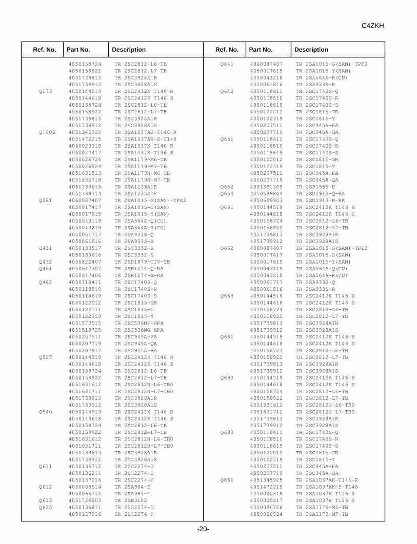
C4ZKH
4050158724 TR 2SC2812-L6-TB4050158922 TR 2SC2812-L7-TB4051739813 TR 2SC3928A1R4051739912 TR 2SC3928A1S
Q173 4050144519 TR 2SC2412K T146 R4050144618 TR 2SC2412K T146 S4050158724 TR 2SC2812-L6-TB4050158922 TR 2SC2812-L7-TB4051739813 TR 2SC3928A1R4051739912 TR 2SC3928A1S
Q1902 4051345925 TR 2SA1037AK-T146-R4051472215 TR 2SA1037AK-S-T1464050020318 TR 2SA1037K T146 R4050020417 TR 2SA1037K T146 S4050026726 TR 2SA1179-M6-TB4050026924 TR 2SA1179-M7-TB4051631513 TR 2SA1179N-M6-TB4051632718 TR 2SA1179N-M7-TB4051739615 TR 2SA1235A1E4051739714 TR 2SA1235A1F
Q261 4060087407 TR 2SA1015-G(SAN)-TPE24050017417 TR 2SA1015-O(SAN)4050017615 TR 2SA1015-Y(SAN)4050043119 TR 2SA564A-Q(CU)4050043218 TR 2SA564A-R(CU)4050061717 TR 2SA933S-Q4050061816 TR 2SA933S-R
Q431 4050180517 TR 2SC3332-R4050180616 TR 2SC3332-S
Q432 4050822407 TR 2SD1879-CTV-YBQ461 4050647307 TR 2SB1274-Q-RA
4050647406 TR 2SB1274-R-RAQ462 4050118411 TR 2SC1740S-Q
4050118510 TR 2SC1740S-R4050118619 TR 2SC1740S-S4050122012 TR 2SC1815-GR4050122111 TR 2SC1815-O4050122319 TR 2SC1815-Y4051570515 TR 2SC536NF-NPA4051518725 TR 2SC536NG-NPA4050207511 TR 2SC945A-PA4050207719 TR 2SC945A-QA4050207917 TR 2SC945A-RA
Q527 4050144519 TR 2SC2412K T146 R4050144618 TR 2SC2412K T146 S4050158724 TR 2SC2812-L6-TB4050158922 TR 2SC2812-L7-TB4051631612 TR 2SC2812N-L6-TB04051631711 TR 2SC2812N-L7-TB04051739813 TR 2SC3928A1R4051739912 TR 2SC3928A1S
Q540 4050144519 TR 2SC2412K T146 R4050144618 TR 2SC2412K T146 S4050158724 TR 2SC2812-L6-TB4050158922 TR 2SC2812-L7-TB4051631612 TR 2SC2812N-L6-TB04051631711 TR 2SC2812N-L7-TB04051739813 TR 2SC3928A1R4051739912 TR 2SC3928A1S
Q611 4050136712 TR 2SC2274-D4050136811 TR 2SC2274-E4050137016 TR 2SC2274-F
Q612 4050066514 TR 2SA984-E4050066712 TR 2SA984-F
Q613 4051726803 TR 2SK3102Q625 4050136811 TR 2SC2274-E
4050137016 TR 2SC2274-F
Q641 4060087407 TR 2SA1015-G(SAN)-TPE24050017615 TR 2SA1015-Y(SAN)4050043218 TR 2SA564A-R(CU)4050061816 TR 2SA933S-R
Q642 4050118411 TR 2SC1740S-Q4050118510 TR 2SC1740S-R4050118619 TR 2SC1740S-S4050122012 TR 2SC1815-GR4050122319 TR 2SC1815-Y4050207511 TR 2SC945A-PA4050207719 TR 2SC945A-QA
Q651 4050118411 TR 2SC1740S-Q4050118510 TR 2SC1740S-R4050118619 TR 2SC1740S-S4050122012 TR 2SC1815-GR4050122319 TR 2SC1815-Y4050207511 TR 2SC945A-PA4050207719 TR 2SC945A-QA
Q652 4051381309 TR 2SB1565-EQ654 4050599804 TR 2SD1913-Q-RA
4050599903 TR 2SD1913-R-RAQ661 4050144519 TR 2SC2412K T146 R
4050144618 TR 2SC2412K T146 S4050158724 TR 2SC2812-L6-TB4050158922 TR 2SC2812-L7-TB4051739813 TR 2SC3928A1R4051739912 TR 2SC3928A1S
Q662 4060087407 TR 2SA1015-G(SAN)-TPE24050017417 TR 2SA1015-O(SAN)4050017615 TR 2SA1015-Y(SAN)4050043119 TR 2SA564A-Q(CU)4050043218 TR 2SA564A-R(CU)4050061717 TR 2SA933S-Q4050061816 TR 2SA933S-R
Q663 4050144519 TR 2SC2412K T146 R4050144618 TR 2SC2412K T146 S4050158724 TR 2SC2812-L6-TB4050158922 TR 2SC2812-L7-TB4051739813 TR 2SC3928A1R4051739912 TR 2SC3928A1S
Q681 4050144519 TR 2SC2412K T146 R4050144618 TR 2SC2412K T146 S4050158724 TR 2SC2812-L6-TB4050158922 TR 2SC2812-L7-TB4051739813 TR 2SC3928A1R4051739912 TR 2SC3928A1S
Q690 4050144519 TR 2SC2412K T146 R4050144618 TR 2SC2412K T146 S4050158724 TR 2SC2812-L6-TB4050158922 TR 2SC2812-L7-TB4051631612 TR 2SC2812N-L6-TB04051631711 TR 2SC2812N-L7-TB04051739813 TR 2SC3928A1R4051739912 TR 2SC3928A1S
Q693 4050118411 TR 2SC1740S-Q4050118510 TR 2SC1740S-R4050118619 TR 2SC1740S-S4050122012 TR 2SC1815-GR4050122319 TR 2SC1815-Y4050207511 TR 2SC945A-PA4050207719 TR 2SC945A-QA
Q861 4051345925 TR 2SA1037AK-T146-R4051472215 TR 2SA1037AK-S-T1464050020318 TR 2SA1037K T146 R4050020417 TR 2SA1037K T146 S4050026726 TR 2SA1179-M6-TB4050026924 TR 2SA1179-M7-TB
Ref. No. Part No. Description Ref. No. Part No. Description
P List-C4ZKH 6/28/04 10:42 AM Page 20
4051739615 TR 2SA1235A1E4051739714 TR 2SA1235A1F
Q871 4050144519 TR 2SC2412K T146 R4050144618 TR 2SC2412K T146 S4050158724 TR 2SC2812-L6-TB4050158922 TR 2SC2812-L7-TB4051739813 TR 2SC3928A1R4051739912 TR 2SC3928A1S
Q881 4050144519 TR 2SC2412K T146 R4050144618 TR 2SC2412K T146 S4050158724 TR 2SC2812-L6-TB4050158922 TR 2SC2812-L7-TB4051739813 TR 2SC3928A1R4051739912 TR 2SC3928A1S
Q886 4050144519 TR 2SC2412K T146 R4050144618 TR 2SC2412K T146 S4050158724 TR 2SC2812-L6-TB4050158922 TR 2SC2812-L7-TB4051631612 TR 2SC2812N-L6-TB04051631711 TR 2SC2812N-L7-TB04051739813 TR 2SC3928A1R4051739912 TR 2SC3928A1S
INTEGRATED CIRCUITIC001 4095752202 IC AN17820BIC1201 4090187603 IC LA7016IC201 4095625011 IC LA76818J-EIC202 4092415407 IC BA178M05T
4092654806 IC L78M05CV4091721509 IC MC78M05CT4093205700 IC UPC78M05AHF
IC281 4095646115 IC LA7642NM-TLM-EIC3701 4095644319 IC NJW1142MIC501 4094535905 IC LA78041IC681 4092415407 IC BA178M05T
4092654806 IC L78M05CV4091721509 IC MC78M05CT4093205700 IC UPC78M05AHF
IC801 4104862007 IC LC863448W-XXXX-TLMIC802 4104958007 IC AT24C16A-10PI-2.7
4094594506 IC 24LC16B/P
CAPACITORC001 4040886600 ELECT 2200U M 25V
4030459867 ELECT 2200U M 25VC011 4040848806 ELECT 1U M 50V
4030490018 ELECT 1U M 50VC016 4040848806 ELECT 1U M 50V
4030490018 ELECT 1U M 50VC021 4040848806 ELECT 1U M 50V
4030490018 ELECT 1U M 50VC026 4040848806 ELECT 1U M 50V
4030490018 ELECT 1U M 50VC031 4040848905 ELECT 10U M 50V
4030494224 ELECT 10U M 50VC1001 4040848905 ELECT 10U M 50V
4030494224 ELECT 10U M 50VC1003 4040848905 ELECT 10U M 50V
4030494224 ELECT 10U M 50VC1005 4040848004 ELECT 220U M 16V
4030430222 ELECT 220U M 16VC101 4040848301 ELECT 470U M 16V
4030441773 ELECT 470U M 16VC1011 4040871606 ELECT 0.1U M 50V
4030478422 ELECT 0.1U M 50VC1013 4040871606 ELECT 0.1U M 50V
4030478422 ELECT 0.1U M 50V
C1015 4030494224 ELECT 10U M 50VC1021 4040871606 ELECT 0.1U M 50V
4030478422 ELECT 0.1U M 50VC1023 4040871606 ELECT 0.1U M 50V
4030478422 ELECT 0.1U M 50VC1025 4030494224 ELECT 10U M 50VC1031 4030494224 ELECT 10U M 50VC1032 4030494224 ELECT 10U M 50VC1041 4030494224 ELECT 10U M 50VC1042 4030494224 ELECT 10U M 50VC106 4040849308 ELECT 47U M 50V
4030513123 ELECT 47U M 50VC107 4040849308 ELECT 47U M 50V
4030513123 ELECT 47U M 50VC111 4032152211 CERAMIC 0.01U K 50VC112 4032152211 CERAMIC 0.01U K 50VC113 4032152211 CERAMIC 0.01U K 50VC120 4032844314 CERAMIC 0.022U K 50VC121 4032152211 CERAMIC 0.01U K 50VC122 4040847809 ELECT 100U M 16V
4030422425 ELECT 100U M 16VC123 4011057919 MT-GLAZE 0.000 ZA 1/16WC132 4040848707 ELECT 0.47U M 50V
4030486328 ELECT 0.47U M 50VC135 4040848707 ELECT 0.47U M 50V
4030486328 ELECT 0.47U M 50VC138 4032844314 CERAMIC 0.022U K 50VC171 4031552111 CERAMIC 1500P K 50VC172 4032152211 CERAMIC 0.01U K 50VC174 4031571914 CERAMIC 10P D 50VC178 4040871606 ELECT 0.1U M 50V
4030478422 ELECT 0.1U M 50VC1902 4040875406 ELECT 22U M 50V
4030502810 ELECT 22U M 50VC201 4040849803 NP-ELECT 1U M 50V
4030862310 NP-ELECT 1U M 50VC202 4030582634 POLYESTER 0.015U J 50V
4031793217 POLYESTER 0.015U J 50VC203 4032152211 CERAMIC 0.01U K 50VC204 4040848905 ELECT 10U M 50V
4030494224 ELECT 10U M 50VC205 4040848905 ELECT 10U M 50V
4030494224 ELECT 10U M 50VC206 4033423310 CERAMIC 0.1U K 25VC207 4033423310 CERAMIC 0.1U K 25VC209 4040848707 ELECT 0.47U M 50V
4030486328 ELECT 0.47U M 50VC210 4040875109 ELECT 470U M 25V
4030475035 ELECT 470U M 25VC212 4031554214 CERAMIC 15P J 50VC218 4011057919 MT-GLAZE 0.000 ZA 1/16WC219 4032152211 CERAMIC 0.01U K 50VC221 4033423310 CERAMIC 0.1U K 25VC222 4033423310 CERAMIC 0.1U K 25VC223 4033423310 CERAMIC 0.1U K 25VC224 4033423310 CERAMIC 0.1U K 25VC225 4040848806 ELECT 1U M 50V
4030490018 ELECT 1U M 50VC226 4040848806 ELECT 1U M 50V
4030490018 ELECT 1U M 50VC227 4040849803 NP-ELECT 1U M 50V
4030862310 NP-ELECT 1U M 50VC230 4032152211 CERAMIC 0.01U K 50VC231 4032602944 MT-COMPO 0.33U J 50VC232 4032602944 MT-COMPO 0.33U J 50VC233 4040875109 ELECT 470U M 25V
4030475035 ELECT 470U M 25V
-21-
C4ZKH
Ref. No. Part No. Description Ref. No. Part No. Description
P List-C4ZKH 6/28/04 10:42 AM Page 21
-22-
C4ZKH
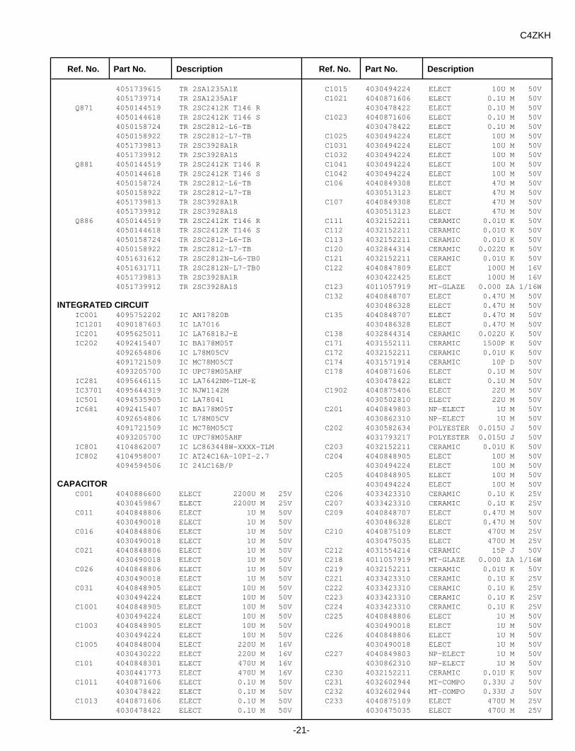
C240 4032152211 CERAMIC 0.01U K 50VC243 4032152211 CERAMIC 0.01U K 50VC244 4040849308 ELECT 47U M 50V
4030513123 ELECT 47U M 50VC245 4040849803 NP-ELECT 1U M 50V
4030862310 NP-ELECT 1U M 50VC246 4040848806 ELECT 1U M 50V
4030490018 ELECT 1U M 50VC247 4040849001 ELECT 2.2U M 50V
4030499823 ELECT 2.2U M 50VC273 4033423310 CERAMIC 0.1U K 25VC278 4033423310 CERAMIC 0.1U K 25VC280 4032152211 CERAMIC 0.01U K 50VC281 4040848806 ELECT 1U M 50V
4030490018 ELECT 1U M 50VC282 4032152211 CERAMIC 0.01U K 50VC283 4032152211 CERAMIC 0.01U K 50VC284 4040848806 ELECT 1U M 50V
4030490018 ELECT 1U M 50VC285 4040848806 ELECT 1U M 50V
4030490018 ELECT 1U M 50VC286 4040848806 ELECT 1U M 50V
4030490018 ELECT 1U M 50VC287 4040848806 ELECT 1U M 50V
4030490018 ELECT 1U M 50VC288 4031791718 POLYESTER 0.033U J 50VC289 4040848905 ELECT 10U M 50V
4030494224 ELECT 10U M 50VC291 4031818217 POLYESTER 0.1U K 50VC352 4033363517 CERAMIC 0.47U K 16VC355 4030690527 CERAMIC 1000P K 50VC358 4040848806 ELECT 1U M 50V
4030490018 ELECT 1U M 50VC3701 4040848301 ELECT 470U M 16V
4030441773 ELECT 470U M 16VC3702 4033423310 CERAMIC 0.1U K 25VC3710 4040849209 ELECT 4.7U M 50V
4030510627 ELECT 4.7U M 50VC3711 4040849209 ELECT 4.7U M 50V
4030510627 ELECT 4.7U M 50VC3712 4040849209 ELECT 4.7U M 50V
4030510627 ELECT 4.7U M 50VC3714 4031134119 CERAMIC 2200P K 50VC3715 4033423310 CERAMIC 0.1U K 25VC3717 4040848806 ELECT 1U M 50V
4030490018 ELECT 1U M 50VC3720 4040849209 ELECT 4.7U M 50V
4030510627 ELECT 4.7U M 50VC3721 4040849209 ELECT 4.7U M 50V
4030510627 ELECT 4.7U M 50VC3722 4040849209 ELECT 4.7U M 50V
4030510627 ELECT 4.7U M 50VC3724 4031134119 CERAMIC 2200P K 50VC3725 4033423310 CERAMIC 0.1U K 25VC3727 4040848806 ELECT 1U M 50V
4030490018 ELECT 1U M 50VC3730 4032844314 CERAMIC 0.022U K 50VC3731 4032789615 CERAMIC 1U Z 16VC3732 4032794312 CERAMIC 0.33U K 16VC3733 4040848806 ELECT 1U M 50V
4030490018 ELECT 1U M 50VC3734 4040848806 ELECT 1U M 50V
4030490018 ELECT 1U M 50VC3735 4040848806 ELECT 1U M 50V
4030490018 ELECT 1U M 50VC420 4040774600 MT-POLYPRO 7800P H 1.5K
4033438215 MT-POLYPRO 7800P H 1.5K
C423 4040773108 MT-POLYPRO 7500P H 1.5K4033438017 MT-POLYPRO 7500P H 1.5K
C424 4030834911 POLYPRO 0.027U J 400VC425 4030834317 POLYPRO 0.022U J 400VC426 4030666106 MT-POLYEST 0.47U J 250VC431 4030630028 POLYESTER 6800P K 50V
4030630236 POLYESTER 6800P K 50V4031790315 POLYESTER 6800P K 50V
C432 4030757121 CERAMIC 1000P K 500VC433 4030763122 CERAMIC 3900P K 500VC434 4040849308 ELECT 47U M 50V
4030513123 ELECT 47U M 50VC441 4030789914 MT-POLYPRO 0.27U J 200V
4033467126 MT-POLYPRO 0.27U J 250VC442 4030789914 MT-POLYPRO 0.27U J 200V
4033467126 MT-POLYPRO 0.27U J 250VC462 4040848806 ELECT 1U M 50V
4030490018 ELECT 1U M 50VC464 4040849001 ELECT 2.2U M 50V
4030499823 ELECT 2.2U M 50VC465 4030660104 MT-POLYEST 2.2U K 100VC466 4030572833 POLYESTER 0.1U K 50V
4030573137 POLYESTER 0.1U K 50V4031818217 POLYESTER 0.1U K 50V
C467 4030403721 ELECT 220U M 10VC468 4040875406 ELECT 22U M 50V
4030502810 ELECT 22U M 50VC469 4040848905 ELECT 10U M 50V
4030494224 ELECT 10U M 50VC470 4030698325 CERAMIC 0.01U Z 50VC471 4040565208 NP-ELECT 2.2U M 100V
4040457701 NP-ELECT 2.2U M 50VC486 4032600722 ELECT 33U M 250VC487 4032599818 ELECT 4.7U M 160VC510 4040849209 ELECT 4.7U M 50V
4030510627 ELECT 4.7U M 50VC514 4040848905 ELECT 10U M 50V
4030494224 ELECT 10U M 50VC515 4030459807 ELECT 2200U M 25VC517 4030532134 ELECT 220U M 35VC518 4032462221 MT-COMPO 0.01U J 50VC520 4030641212 POLYESTER 0.1U K 100V
4032769726 POLYESTER 0.1U K 100VC521 4030533606 ELECT 2200U M 35VC524 4032195030 MT-COMPO 0.68U J 50VC527 4040848905 ELECT 10U M 50V
4030494224 ELECT 10U M 50VC540 4030857316 NP-ELECT 10U M 25VC601 4040712107 MT-POLYEST 0.1U K 250V
4040725602 MT-POLYEST 0.1U M 250V4040607205 MT-POLYEST 0.1U M 250V4040661702 MT-POLYEST 0.1U M 275V4040936107 MT-POLYEST 0.1U M 275V
C602 4040712107 MT-POLYEST 0.1U K 250V4040725602 MT-POLYEST 0.1U M 250V4040607205 MT-POLYEST 0.1U M 250V4040661702 MT-POLYEST 0.1U M 275V4040936107 MT-POLYEST 0.1U M 275V
C608 4030766707 CERAMIC 1000P K 1KCERAMIC 1000P K 1K
4032719622 CERAMIC 1000P K 1KC609 4040445005 ELECT 220U M 400VC611 4030569734 POLYESTER 0.01U J 50V
4031789319 POLYESTER 0.01U J 50VC613 4030573137 POLYESTER 0.1U K 50V
4031818217 POLYESTER 0.1U K 50VC614 4032377941 MT-COMPO 0.22U J 50V
!
!
Ref. No. Part No. Description Ref. No. Part No. Description
P List-C4ZKH 6/28/04 10:42 AM Page 22
C615 CERAMIC 220P K 2KC617 CERAMIC 220P K 2KC618 4033145103 MT-POLYEST 0.047U K 630VC627 4040735106 CERAMIC 470P K 250V
4040733300 CERAMIC 470P M 250V4040714507 CERAMIC 470P K 400V
C628 4040734505 CERAMIC 2200P K 250V4040732907 CERAMIC 2200P M 250V4040714101 CERAMIC 2200P M 400V
C629 4040735106 CERAMIC 470P K 250V4040733300 CERAMIC 470P M 250V4040714507 CERAMIC 470P K 400V
C643 4031480424 ELECT 1000U M 25VC644 4040849100 ELECT 3.3U M 50V
4030506610 ELECT 3.3U M 50VC651 4040739005 ELECT 220U M 160VC652 4031482012 ELECT 470U M 35VC654 4030468007 ELECT 3300U M 25VC655 CERAMIC 680P K 1K
CERAMIC 680P K 1KC656 4032719721 CERAMIC 3300P K 1KC657 4032475023 CERAMIC 470P K 1K
4032691829 CERAMIC 470P K 1KC658 4032475023 CERAMIC 470P K 1K
4032691829 CERAMIC 470P K 1KC663 4040871606 ELECT 0.22U M 50V
4030481917 ELECT 0.22U M 50VC664 4040848004 ELECT 220U M 16V
4030430222 ELECT 220U M 16VC665 4040848301 ELECT 470U M 16V
4030441773 ELECT 470U M 16VC681 4040847601 ELECT 470U M 10V
4030414529 ELECT 470U M 10VC690 ELECT 2.2U M 50VC691 4040876007 ELECT 47U M 35V
4030540713 ELECT 47U M 35VC693 4040848202 ELECT 47U M 16V
4030439136 ELECT 47U M 16VC801 4031554214 CERAMIC 15P J 50VC802 4031572515 CERAMIC 27P J 50VC803 4032152211 CERAMIC 0.01U K 50VC805 4040848905 ELECT 10U M 50V
4030494224 ELECT 10U M 50VC823 4033423310 CERAMIC 0.1U K 25VC824 4033423310 CERAMIC 0.1U K 25VC825 4031573611 CERAMIC 100P J 50VC829 4033423310 CERAMIC 0.1U K 25VC835 4040848806 ELECT 1U M 50V
4030490018 ELECT 1U M 50VC851 4031573116 CERAMIC 56P J 50VC852 4031573116 CERAMIC 56P J 50VC853 4031573116 CERAMIC 56P J 50VC861 4040848806 ELECT 1U M 50V
4030490018 ELECT 1U M 50VC862 4033423310 CERAMIC 0.1U K 25VC880 4031552210 CERAMIC 3300P K 50VC891 4040848806 ELECT 1U M 50V
4030490018 ELECT 1U M 50VC892 4033423310 CERAMIC 0.1U K 25VC893 4040849001 ELECT 2.2U M 50V
4030499823 ELECT 2.2U M 50VC894 4032815017 CERAMIC 0.033U K 25VC895 4040848905 ELECT 10U M 50V
4030494224 ELECT 10U M 50V
RESISTORR015 4011057919 MT-GLAZE 0.000 ZA 1/16W
R016 4011054710 MT-GLAZE 39K JA 1/16WR017 4011055311 MT-GLAZE 4.7K JA 1/16WR019 4010077641 CARBON 150 JA 1/2WR025 4011057919 MT-GLAZE 0.000 ZA 1/16WR026 4011054710 MT-GLAZE 39K JA 1/16WR027 4011055311 MT-GLAZE 4.7K JA 1/16WR029 4010077641 CARBON 150 JA 1/2WR031 4011055410 MT-GLAZE 47K JA 1/16WR032 4011058213 MT-GLAZE 68K JA 1/16WR1001 4010276638 CARBON 75 JA 1/6WR1004 4010276638 CARBON 75 JA 1/6WR1005 4010276638 CARBON 75 JA 1/6WR1006 4011050712 MT-GLAZE 100K JA 1/16WR1011 4011050514 MT-GLAZE 1K JA 1/16WR1012 4011052112 MT-GLAZE 18K JA 1/16WR1013 4011050514 MT-GLAZE 1K JA 1/16WR1014 4011052112 MT-GLAZE 18K JA 1/16WR1015 4011056516 MT-GLAZE 680 JA 1/16WR1016 4011050712 MT-GLAZE 100K JA 1/16WR1021 4011050514 MT-GLAZE 1K JA 1/16WR1022 4011052112 MT-GLAZE 18K JA 1/16WR1023 4011050514 MT-GLAZE 1K JA 1/16WR1024 4011052112 MT-GLAZE 18K JA 1/16WR1025 4011056516 MT-GLAZE 680 JA 1/16WR1026 4011050712 MT-GLAZE 100K JA 1/16WR103 4010618101 OXIDE-MT 39K JA 1WR1031 4011054710 MT-GLAZE 39K JA 1/16WR1032 4011050613 MT-GLAZE 10K JA 1/16WR1033 4011056615 MT-GLAZE 6.8K JA 1/16WR1034 4011051610 MT-GLAZE 15K JA 1/16WR1035 4011054710 MT-GLAZE 39K JA 1/16WR1036 4011050613 MT-GLAZE 10K JA 1/16WR1037 4011054611 MT-GLAZE 3.9K JA 1/16WR1038 4011050613 MT-GLAZE 10K JA 1/16WR1041 4011054710 MT-GLAZE 39K JA 1/16WR1042 4011050613 MT-GLAZE 10K JA 1/16WR1043 4011056615 MT-GLAZE 6.8K JA 1/16WR1044 4011051610 MT-GLAZE 15K JA 1/16WR1045 4011054710 MT-GLAZE 39K JA 1/16WR1046 4011050613 MT-GLAZE 10K JA 1/16WR1047 4011054611 MT-GLAZE 3.9K JA 1/16WR1048 4011050613 MT-GLAZE 10K JA 1/16WR106 4011050415 MT-GLAZE 100 JA 1/16WR107 4011050415 MT-GLAZE 100 JA 1/16WR108 4011052112 MT-GLAZE 18K JA 1/16WR109 4011058213 MT-GLAZE 68K JA 1/16WR111 4011050514 MT-GLAZE 1K JA 1/16WR112 4011056011 MT-GLAZE 5.6K JA 1/16WR114 4011054017 MT-GLAZE 330 JA 1/16WR115 4010272135 CARBON 56 JA 1/6WR116 4011055816 MT-GLAZE 56 JA 1/16WR121 4011056615 MT-GLAZE 6.8K JA 1/16WR122 4011052815 MT-GLAZE 2.2K JA 1/16WR124 4011050613 MT-GLAZE 10K JA 1/16WR125 4011053416 MT-GLAZE 27K JA 1/16WR130 4011057919 MT-GLAZE 0.000 ZA 1/16WR132 4011055212 MT-GLAZE 470 JA 1/16WR140 4011055915 MT-GLAZE 560 JA 1/16WR141 4011055915 MT-GLAZE 560 JA 1/16WR171 4011051412 MT-GLAZE 150 JA 1/16WR173 4010258238 CARBON 22K JA 1/6WR176 4011050613 MT-GLAZE 10K JA 1/16WR1902 4011051115 MT-GLAZE 12K JA 1/16WR1903 4011056011 MT-GLAZE 5.6K JA 1/16WR1904 4011054611 MT-GLAZE 3.9K JA 1/16WR1905 4011052815 MT-GLAZE 2.2K JA 1/16WR1906 4011052013 MT-GLAZE 1.8K JA 1/16W
!
!
!
-23-
C4ZKH
Ref. No. Part No. Description Ref. No. Part No. Description
P List-C4ZKH 6/28/04 10:42 AM Page 23
-24-
C4ZKH
R1907 4011057919 MT-GLAZE 0.000 ZA 1/16WR1908 4011050415 MT-GLAZE 100 JA 1/16WR1911 4011052716 MT-GLAZE 220 JA 1/16WR1912 4011052716 MT-GLAZE 220 JA 1/16WR1913 4011052716 MT-GLAZE 220 JA 1/16WR209 4011139516 MT-GLAZE 620K JA 1/16WR210 4011053713 MT-GLAZE 3K JA 1/16WR211 4010251338 CARBON 150 JA 1/6WR212 4011051412 MT-GLAZE 150 JA 1/16WR221 4011050514 MT-GLAZE 1K JA 1/16WR222 4011050514 MT-GLAZE 1K JA 1/16WR223 4011050514 MT-GLAZE 1K JA 1/16WR224 4011055311 MT-GLAZE 4.7K JA 1/16WR225 4011055311 MT-GLAZE 4.7K JA 1/16WR226 4011052914 MT-GLAZE 22K JA 1/16WR227 4011054215 MT-GLAZE 33K JA 1/16WR228 4010252335 CARBON 150K JA 1/6WR229 4011056714 MT-GLAZE 680K JA 1/16WR230 4010269333 CARBON 47 JA 1/6WR234 4010249038 CARBON 120 JA 1/6WR235 4010249038 CARBON 120 JA 1/6WR236 4010249038 CARBON 120 JA 1/6WR244 4011055410 MT-GLAZE 47K JA 1/16WR245 4011055410 MT-GLAZE 47K JA 1/16WR263 4011050613 MT-GLAZE 10K JA 1/16WR264 4011053218 MT-GLAZE 270 JA 1/16WR265 4011053911 MT-GLAZE 33 JA 1/16WR267 4010260637 CARBON 270 JA 1/6WR271 4011050415 MT-GLAZE 100 JA 1/16WR272 4011050415 MT-GLAZE 100 JA 1/16WR280 4011050415 MT-GLAZE 100 JA 1/16WR281 4011053416 MT-GLAZE 27K JA 1/16WR282 4011054116 MT-GLAZE 3.3K JA 1/16WR283 4011055311 MT-GLAZE 4.7K JA 1/16WR284 4011054116 MT-GLAZE 3.3K JA 1/16WR285 4010199650 CARBON 47 JA 1/4W
4010199650 CARBON 47 JA 1/4WR286 4012039914 MT-GLAZE 4.7K FA 1/16WR287 4011057919 MT-GLAZE 0.000 ZA 1/16WR289 4011057919 MT-GLAZE 0.000 ZA 1/16WR291 4010681600 OXIDE-MT 4.7 JA 2WR340 4011057513 MT-GLAZE 82K JA 1/16WR351 4010278632 CARBON 8.2K JA 1/6WR352 4010127059 CARBON 10K JA 1/4W
4010127059 CARBON 10K JA 1/4WR354 4010258238 CARBON 22K JA 1/6WR355 4010127059 CARBON 10K JA 1/4W
4010127059 CARBON 10K JA 1/4WR356 4011050613 MT-GLAZE 10K JA 1/16WR357 4010251635 CARBON 1.5K JA 1/6WR358 4011057919 MT-GLAZE 0.000 ZA 1/16WR3731 4011050415 MT-GLAZE 100 JA 1/16WR3732 4011050415 MT-GLAZE 100 JA 1/16WR423 4010224154 CARBON 68K JA 1/4W
4010224154 CARBON 68K JA 1/4WR423A 4010164846 CARBON 22K JA 1/4W
4010164846 CARBON 22K JA 1/4WR424 4010247034 CARBON 1K JA 1/6WR426 4010247440 CARBON 10K JA 1/6WR432 4010247034 CARBON 1K JA 1/6WR433 4010071134 CARBON 1K JA 1/2WR434 4010596706 OXIDE-MT 180 JA 1WR435 4020836809 OXIDE-MT 5.6 KB 7WR441 4010648702 OXIDE-MT 1K JA 2WR449 4010591602 OXIDE-MT 15 JA 1WR462 4010278137 CARBON 82 JA 1/6WR463 4010269937 CARBON 4.7K JA 1/6W
R467 4010250242 CARBON 1.2M JA 1/6WR468 4010254230 CARBON 1.8K JA 1/6WR469 4010264635 CARBON 33K JA 1/6WR471 4010251635 CARBON 1.5K JA 1/6WR472 4010270339 CARBON 47K JA 1/6WR473 4010275235 CARBON 680 JA 1/6WR474 4010071134 CARBON 1K JA 1/2WR475 4010095843 CARBON 330 JA 1/2WR479 4010257835 CARBON 2.2K JA 1/6WR480 4010270339 CARBON 47K JA 1/6WR481 4010681600 OXIDE-MT 4.7 JA 2WR485 4010154748 CARBON 180K JA 1/4W
4010154748 CARBON 180K JA 1/4WR486 4010272630 CARBON 5.6K JA 1/6WR487 4010258733 CARBON 220K JA 1/6WR488 4011429508 OXIDE-MT 0.27 JA 1WR510 4010247440 CARBON 10K JA 1/6WR511 4010247440 CARBON 10K JA 1/6WR514 4010272630 CARBON 5.6K JA 1/6WR515 4010254636 CARBON 18K JA 1/6WR516 4010278632 CARBON 8.2K JA 1/6WR518 4010579105 OXIDE-MT 1.2 JA 1WR519 4010275037 CARBON 68 JA 1/6WR522 4010260637 CARBON 270 JA 1/6WR524 4010647507 OXIDE-MT 100 JA 2WR527 4011058114 MT-GLAZE 56K JA 1/16WR528 4010583706 OXIDE-MT 1K JA 1WR529 4010593903 OXIDE-MT 1.5K JA 1WR540 4011054017 MT-GLAZE 330 JA 1/16WR602A 4020582409 WIRE WOUND 1.8 KA 15W
4020733702 WIRE WOUND 1.8 KA 15WR611 4010200851 CARBON 470 JA 1/4W
4010200851 CARBON 470 JA 1/4WR613 4020960405 FUSIBLE RES 560 J- 1/2WR614 4010258238 CARBON 22K JA 1/6WR615 4010257439 CARBON 220 JA 1/6WR616 4010251932 CARBON 15K JA 1/6WR619 4010161548 CARBON 22 JA 1/4W
4010161548 CARBON 22 JA 1/4WR620 4010104812 CARBON 470K JA 1/2WR621 4010104812 CARBON 470K JA 1/2WR622 4010199650 CARBON 47 JA 1/4W
4010199650 CARBON 47 JA 1/4WR623 4010264932 CARBON 330K JA 1/6WR624 4020018502 FUSIBLE RES 10 J- 1/2WR625 4010694501 OXIDE-MT 68K JA 2WR626 4010694501 OXIDE-MT 68K JA 2WR627 4010258238 CARBON 22K JA 1/6WR628 4020008602 SOLID 5.6M KA 1/2WR629 4020008602 SOLID 5.6M KA 1/2WR631 4010270339 CARBON 47K JA 1/6WR632 4012280405 OXIDE-MT 0.27 JA 2WR633 4012280405 OXIDE-MT 0.27 JA 2WR641 4010247440 CARBON 10K JA 1/6WR642 4010270339 CARBON 47K JA 1/6WR643 4010254636 CARBON 18K JA 1/6WR644 4010258238 CARBON 22K JA 1/6WR651 4010247034 CARBON 1K JA 1/6WR652 4010614400 OXIDE-MT 33K JA 1WR653 4020589606 FUSIBLE RES 5.6 J- 1WR654 4010145251 CARBON 15K JA 1/4W
4010145251 CARBON 15K JA 1/4WR655 4010127059 CARBON 10K JA 1/4W
4010127059 CARBON 10K JA 1/4WR656 4010607402 OXIDE-MT 270 JA 1WR657 4010191951 CARBON 3.9K JA 1/4W
4010191951 CARBON 3.9K JA 1/4W
!
!
Ref. No. Part No. Description Ref. No. Part No. Description
P List-C4ZKH 6/28/04 10:42 AM Page 24
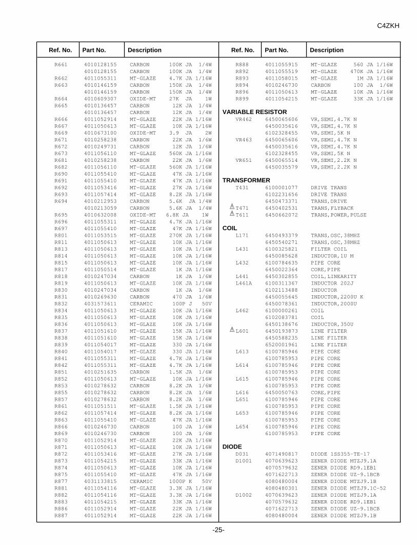
R661 4010128155 CARBON 100K JA 1/4W4010128155 CARBON 100K JA 1/4W
R662 4011055311 MT-GLAZE 4.7K JA 1/16WR663 4010146159 CARBON 150K JA 1/4W
4010146159 CARBON 150K JA 1/4WR664 4010609307 OXIDE-MT 27K JA 1WR665 4010136457 CARBON 12K JA 1/4W
4010136457 CARBON 12K JA 1/4WR666 4011052914 MT-GLAZE 22K JA 1/16WR667 4011050613 MT-GLAZE 10K JA 1/16WR669 4010673100 OXIDE-MT 3.9 JA 2WR671 4010258238 CARBON 22K JA 1/6WR672 4010249731 CARBON 12K JA 1/6WR673 4011056110 MT-GLAZE 560K JA 1/16WR681 4010258238 CARBON 22K JA 1/6WR682 4011056110 MT-GLAZE 560K JA 1/16WR690 4011055410 MT-GLAZE 47K JA 1/16WR691 4011055410 MT-GLAZE 47K JA 1/16WR692 4011053416 MT-GLAZE 27K JA 1/16WR693 4011057414 MT-GLAZE 8.2K JA 1/16WR694 4010212953 CARBON 5.6K JA 1/4W
4010213059 CARBON 5.6K JA 1/4WR695 4010632008 OXIDE-MT 6.8K JA 1WR696 4011055311 MT-GLAZE 4.7K JA 1/16WR697 4011055410 MT-GLAZE 47K JA 1/16WR801 4011053515 MT-GLAZE 270K JA 1/16WR811 4011050613 MT-GLAZE 10K JA 1/16WR813 4011050613 MT-GLAZE 10K JA 1/16WR814 4011050613 MT-GLAZE 10K JA 1/16WR815 4011050613 MT-GLAZE 10K JA 1/16WR817 4011050514 MT-GLAZE 1K JA 1/16WR818 4010247034 CARBON 1K JA 1/6WR819 4011050613 MT-GLAZE 10K JA 1/16WR830 4010247034 CARBON 1K JA 1/6WR831 4010269630 CARBON 470 JA 1/6WR832 4031573611 CERAMIC 100P J 50VR834 4011050613 MT-GLAZE 10K JA 1/16WR835 4011050613 MT-GLAZE 10K JA 1/16WR836 4011050613 MT-GLAZE 10K JA 1/16WR837 4011051610 MT-GLAZE 15K JA 1/16WR838 4011051610 MT-GLAZE 15K JA 1/16WR839 4011054017 MT-GLAZE 330 JA 1/16WR840 4011054017 MT-GLAZE 330 JA 1/16WR841 4011055311 MT-GLAZE 4.7K JA 1/16WR842 4011055311 MT-GLAZE 4.7K JA 1/16WR851 4010251635 CARBON 1.5K JA 1/6WR852 4011050613 MT-GLAZE 10K JA 1/16WR853 4010278632 CARBON 8.2K JA 1/6WR855 4010278632 CARBON 8.2K JA 1/6WR857 4010278632 CARBON 8.2K JA 1/6WR861 4011051511 MT-GLAZE 1.5K JA 1/16WR862 4011057414 MT-GLAZE 8.2K JA 1/16WR863 4011055410 MT-GLAZE 47K JA 1/16WR866 4010246730 CARBON 100 JA 1/6WR869 4010246730 CARBON 100 JA 1/6WR870 4011052914 MT-GLAZE 22K JA 1/16WR871 4011050613 MT-GLAZE 10K JA 1/16WR872 4011053416 MT-GLAZE 27K JA 1/16WR873 4011054215 MT-GLAZE 33K JA 1/16WR874 4011050613 MT-GLAZE 10K JA 1/16WR875 4011055410 MT-GLAZE 47K JA 1/16WR877 4031133815 CERAMIC 1000P K 50VR881 4011054116 MT-GLAZE 3.3K JA 1/16WR882 4011054116 MT-GLAZE 3.3K JA 1/16WR883 4011054215 MT-GLAZE 33K JA 1/16WR886 4011052914 MT-GLAZE 22K JA 1/16WR887 4011052914 MT-GLAZE 22K JA 1/16W
R888 4011055915 MT-GLAZE 560 JA 1/16WR892 4011055519 MT-GLAZE 470K JA 1/16WR893 4011058015 MT-GLAZE 1M JA 1/16WR894 4010246730 CARBON 100 JA 1/6WR896 4011050613 MT-GLAZE 10K JA 1/16WR899 4011054215 MT-GLAZE 33K JA 1/16W
VARIABLE RESISTORVR462 6450065606 VR,SEMI,4.7K N
6450035616 VR,SEMI,4.7K N6102328455 VR,SEMI,5K N
VR463 6450065606 VR,SEMI,4.7K N6450035616 VR,SEMI,4.7K N6102328455 VR,SEMI,5K N
VR651 6450065514 VR,SEMI,2.2K N6450035579 VR,SEMI,2.2K N
TRANSFORMERT431 6100001077 DRIVE TRANS
6102231656 DRIVE TRANS6450473371 TRANS,DRIVE
T471 6450402531 TRANS,FLYBACKT611 6450662072 TRANS,POWER,PULSE
COILL171 6450493379 TRANS,OSC,38MHZ
6450540271 TRANS,OSC,38MHZL431 6100325821 FILTER COIL
6450085628 INDUCTOR,1U ML432 6100784635 PIPE CORE
6450022364 CORE,PIPEL441 6450302855 COIL,LINEARITYL461A 6100311367 INDUCTOR 202J
6102113488 INDUCTOR6450055645 INDUCTOR,2200U K6450078361 INDUCTOR,2000U
L462 6100000261 COIL6102083781 COIL6450138676 INDUCTOR,350U
L601 6450193873 LINE FILTER6450588235 LINE FILTER6520001961 LINE FILTER
L613 6100785946 PIPE CORE6100785953 PIPE CORE
L614 6100785946 PIPE CORE6100785953 PIPE CORE
L615 6100785946 PIPE CORE6100785953 PIPE CORE
L616 6450050763 CORE,PIPEL651 6100785946 PIPE CORE
6100785953 PIPE COREL653 6100785946 PIPE CORE
6100785953 PIPE COREL654 6100785946 PIPE CORE
6100785953 PIPE CORE
DIODED031 4071490817 DIODE 1SS355-TE-17D1001 4070639623 ZENER DIODE MTZJ9.1A
4070579632 ZENER DIODE RD9.1EB14071622713 ZENER DIODE UZ-9.1BCB4080480004 ZENER DIODE MTZJ9.1B4080480301 ZENER DIODE MTZJ9.1C-52
D1002 4070639623 ZENER DIODE MTZJ9.1A4070579632 ZENER DIODE RD9.1EB14071622713 ZENER DIODE UZ-9.1BCB4080480004 ZENER DIODE MTZJ9.1B
!
!
!
-25-
C4ZKH
Ref. No. Part No. Description Ref. No. Part No. Description
P List-C4ZKH 6/28/04 10:42 AM Page 25
-26-
C4ZKH
4080480301 ZENER DIODE MTZJ9.1C-52D1011 4070639623 ZENER DIODE MTZJ9.1A
4070579632 ZENER DIODE RD9.1EB14071622713 ZENER DIODE UZ-9.1BCB4080480004 ZENER DIODE MTZJ9.1B4080480301 ZENER DIODE MTZJ9.1C-52
D1012 4070639623 ZENER DIODE MTZJ9.1A4070579632 ZENER DIODE RD9.1EB14071622713 ZENER DIODE UZ-9.1BCB4080480004 ZENER DIODE MTZJ9.1B4080480301 ZENER DIODE MTZJ9.1C-52
D102 4070995620 ZENER DIODE MTZJ6.8A4070574013 ZENER DIODE RD6.8EB14080478506 ZENER DIODE MTZJ6.8A
D1021 4070639623 ZENER DIODE MTZJ9.1A4070579632 ZENER DIODE RD9.1EB14071622713 ZENER DIODE UZ-9.1BCB4080480004 ZENER DIODE MTZJ9.1B4080480301 ZENER DIODE MTZJ9.1C-52
D1022 4070639623 ZENER DIODE MTZJ9.1A4070579632 ZENER DIODE RD9.1EB14071622713 ZENER DIODE UZ-9.1BCB4080480004 ZENER DIODE MTZJ9.1B4080480301 ZENER DIODE MTZJ9.1C-52
D103 4071000224 ZENER DIODE MTZJ36A4070562317 ZENER DIODE RD36EB14080476106 ZENER DIODE MTZJ36A
D122 4071661118 DIODE 1SS356-TW11D1901 4071589204 LED SPR-39MVWFD1901A 6102737929 HOLDER LED-S4KF
6103039954 HOLDER LED-C4LAD249 4070996023 ZENER DIODE MTZJ9.1B
4070579711 ZENER DIODE RD9.1EB2D280 4070639326 ZENER DIODE MTZJ7.5C
4070576324 ZENER DIODE RD7.5EB1D352 4070638626 ZENER DIODE MTZJ5.1A
4070568012 ZENER DIODE RD5.1EB24080476403 ZENER DIODE MTZJ5.1A
D357 4070054525 DIODE DS442X4080093204 DIODE 1N41484070124426 DIODE 1SS1334070134336 DIODE 1S2076A4070137129 DIODE 1S2473
D3701 4070054525 DIODE DS442X4080093204 DIODE 1N41484070124426 DIODE 1SS1334070134336 DIODE 1S2076A4070137129 DIODE 1S2473
D421 4070997228 ZENER DIODE MTZJ16A4070547027 ZENER DIODE RD16EB14080475208 ZENER DIODE MTZJ16A-52
D438 4070958001 DIODE ERD07-15LD439 4070064128 DIODE ERB44-04V1D441 4070066310 DIODE ERC05-10BV1
4070096921 DIODE RM11CD464 4010279332 CARBON 820K JA 1/6WD466 4070997822 ZENER DIODE MTZJ20A
4070551717 ZENER DIODE RD20EB14080475505 ZENER DIODE MTZJ20A
D467 4080093204 DIODE 1N41484070134336 DIODE 1S2076A4070136528 DIODE 1S2471
D468 4070054525 DIODE DS442X4080093204 DIODE 1N41484070124228 DIODE 1SS1314070124426 DIODE 1SS1334070134336 DIODE 1S2076A
4070137129 DIODE 1S2473D469 4070077415 DIODE EU1D476 4070639524 ZENER DIODE MTZJ8.2B
4070578318 ZENER DIODE RD8.2EB2D485 4070059609 DIODE ERA22-04
4070077415 DIODE EU1D486 4070054525 DIODE DS442X
4080093204 DIODE 1N41484070124228 DIODE 1SS1314070124426 DIODE 1SS1334070134336 DIODE 1S2076A4070137129 DIODE 1S2473
D501 4070057328 DIODE EM01Z4070058632 DIODE ERA15-02-V14080100506 DIODE BYD33D
D512 4070057328 DIODE EM01Z4070058632 DIODE ERA15-02-V14080100506 DIODE BYD33D
D601 4071249801 DIODE RBV-608D610 PHOTO COUPLE PC123X5YFZ
4072303908 PHOTO COUPLE PC123Y524072317707 PC TLP421F(D4-BL)
D611 4071468113 DIODE EG01CD612 4070059837 DIODE ERA81-004-V1D614 4070076616 DIODE ES1D615 4070124426 DIODE 1SS133D616 4070997921 ZENER DIODE MTZJ20B
4070551816 ZENER DIODE RD20EB24080475802 ZENER DIODE MTZJ20B-52
D617 4070124426 DIODE 1SS133D619 4070638329 ZENER DIODE MTZJ11C
4070541827 ZENER DIODE RD11EB34080473105 ZENER DIODE MTZJ11C
D643 4070124426 DIODE 1SS133D651 4070098816 DIODE RU3AMD652 DIODE RN1ZD653 4072116102 DIODE FE301-1L43
4071296706 DIODE RU4YX LF-L1D654 4071542704 DIODE YG901C2-LBD655 4080093204 DIODE 1N4148
4070124426 DIODE 1SS1334070134336 DIODE 1S2076A4070137129 DIODE 1S2473
D661 4070995521 ZENER DIODE MTZJ6.2C4070572831 ZENER DIODE RD6.2EB34080478209 ZENER DIODE MTZJ6.2C-52
D662 4070995620 ZENER DIODE MTZJ6.8A4070574013 ZENER DIODE RD6.8EB14080478506 ZENER DIODE MTZJ6.8A
D664 4070996122 ZENER DIODE MTZJ10B4070540018 ZENER DIODE RD10EB24080472207 ZENER DIODE MTZJ10B-52
D671 4080093204 DIODE 1N41484070124426 DIODE 1SS1334070134336 DIODE 1S2076A4070137129 DIODE 1S2473
D690 4071490817 DIODE 1SS355-TE-17D691 4080093204 DIODE 1N4148
4070124426 DIODE 1SS1334070134336 DIODE 1S2076A4070137129 DIODE 1S2473
D692 4070077415 DIODE EU1D693 4070054525 DIODE DS442X
4080093204 DIODE 1N41484070124426 DIODE 1SS1334070134336 DIODE 1S2076A4070137129 DIODE 1S2473
!
Ref. No. Part No. Description Ref. No. Part No. Description
P List-C4ZKH 6/28/04 10:42 AM Page 26
D861 4070557917 ZENER DIODE RD3.6ELZENER DIODE RD3.6EL
MISCELLANEOUSF601 4230288603 FUSE 250V 4A
4230248409 FUSE 250V 4AF601A 6450403576 HOLDER,FUSEF601B 6450403576 HOLDER,FUSEA101 6450572753 TUNER,U/V
6450614132 TUNER,U/VA1901 6450411519 UNIT,REMOCON RECEIVER
6450440519 UNIT,REMOCON RECEIVERK002 6450064791 JACK,PHONE D3.6K1001 6450541186 JACK,RCA-6(9-3)K1002 6520012981 JACK,RCA-3PS601 4080465407 TH PTDCA1BF4R5Q200SW1901 6100114432 SWITCH,PUSH
6450209246 SWITCH,PUSH 1P-1TX1SW1902 6100114432 SWITCH,PUSH
6450209246 SWITCH,PUSH 1P-1TX1SW1903 6100114432 SWITCH,PUSH
6450209246 SWITCH,PUSH 1P-1TX1SW1904 6100114432 SWITCH,PUSH
6450209246 SWITCH,PUSH 1P-1TX1SW1905 6100114432 SWITCH,PUSH
6450209246 SWITCH,PUSH 1P-1TX1SW1906 6100114432 SWITCH,PUSH
6450209246 SWITCH,PUSH 1P-1TX1SW501 6100112728 SWITCH,LEVER 1P-3T
6520000049 SWITCH,LEVERSW601 6450590061 SWITCH, POWER 1P-1TX1VA601 4071712008 VARISTOR ERZV14D471X161 4210094705 SAW F TSF6376UX211 6450248818 OSC,CRYSTAL 4.433619MHZ
6520010154 OSC,CRYSTAL 4.433619MHZX801 6450041938 OSC,CRYSTAL 32.768KHZ
6450041945 OSC,CRYSTAL 32.768KHZ
6103179063 ASSY,PWB,CRT C4ZKH1AA0B10S137GB
TRANSISTORQ751 4060087407 TR 2SA1015-G(SAN)-TPE2
4050017417 TR 2SA1015-O(SAN)4050017615 TR 2SA1015-Y(SAN)4050043119 TR 2SA564A-Q(CU)4050043218 TR 2SA564A-R(CU)4051513324 TR 2SA608NF-NPA4050061717 TR 2SA933S-Q4050061816 TR 2SA933S-R
INTEGRATED CIRCUITIC701 4094688403 IC TDA6103Q/N3
CAPACITORC706 4030124022 CERAMIC 15P J 50VC706A 4030140220 CERAMIC 18P J 50VC710 4030558401 ELECT 22U M 250V
4032600405 ELECT 22U M 250VC716A 4030177424 CERAMIC 22P J 50VC726 4030225927 CERAMIC 33P J 50VC731 4030772728 CERAMIC 1000P P 2K
4033128334 CERAMIC 1000P Z 2KC751 4032481618 ELECT 47U M 16VC761 4031597409 MT-POLYEST 0.1U K 250VC762 4030676719 MT-COMPO 0.22U J 50V
4032377941 MT-COMPO 0.22U J 50V
RESISTORR704 4010650804 OXIDE-MT 100K JA 2WR705 4010078440 CARBON 1.5K JA 1/2WR706 4010254230 CARBON 1.8K JA 1/6WR714 4010650804 OXIDE-MT 100K JA 2WR715L 4010078440 CARBON 1.5K JA 1/2WR716 4010254230 CARBON 1.8K JA 1/6WR718 4010078440 CARBON 1.5K JA 1/2WR724 4010650804 OXIDE-MT 100K JA 2WR725L 4010078440 CARBON 1.5K JA 1/2WR726 4010254230 CARBON 1.8K JA 1/6WR752 4010127059 CARBON 10K JA 1/4WR753 4010127059 CARBON 10K JA 1/4WR761 4010165853 CARBON 220K JA 1/4WR762 4010163859 CARBON 2.2K JA 1/4W
COILL731 4010199650 CARBON 47 JA 1/4W
DIODED731 4010249335 CARBON 1.2K JA 1/6WD732 4010249335 CARBON 1.2K JA 1/6WD733 4010249335 CARBON 1.2K JA 1/6WD751 4070054525 DIODE DS442XD751 4080093204 DIODE 1N4148
4070131236 DIODE 1S15554070134227 DIODE 1S20764070137129 DIODE 1S2473
D752 4070054525 DIODE DS442X4080093204 DIODE 1N41484070131236 DIODE 1S15554070134227 DIODE 1S20764070137129 DIODE 1S2473
D753 4070054525 DIODE DS442X4080093204 DIODE 1N41484070131236 DIODE 1S15554070134227 DIODE 1S20764070137129 DIODE 1S2473
D754 4070054525 DIODE DS442X4080093204 DIODE 1N41484070131236 DIODE 1S15554070134227 DIODE 1S20764070137129 DIODE 1S2473
MISCELLANEOUSK701M 6450262005 SOCKET,CRT 8P!
!
!
!
!
-27-
C4ZKH
Ref. No. Part No. Description Ref. No. Part No. Description
P List-C4ZKH 6/28/04 10:42 AM Page 27

SANYO Electric Co., Ltd.May./’04/
SM_29-C4ZKH(Rus) 6/28/04 10:31 AM Page 19
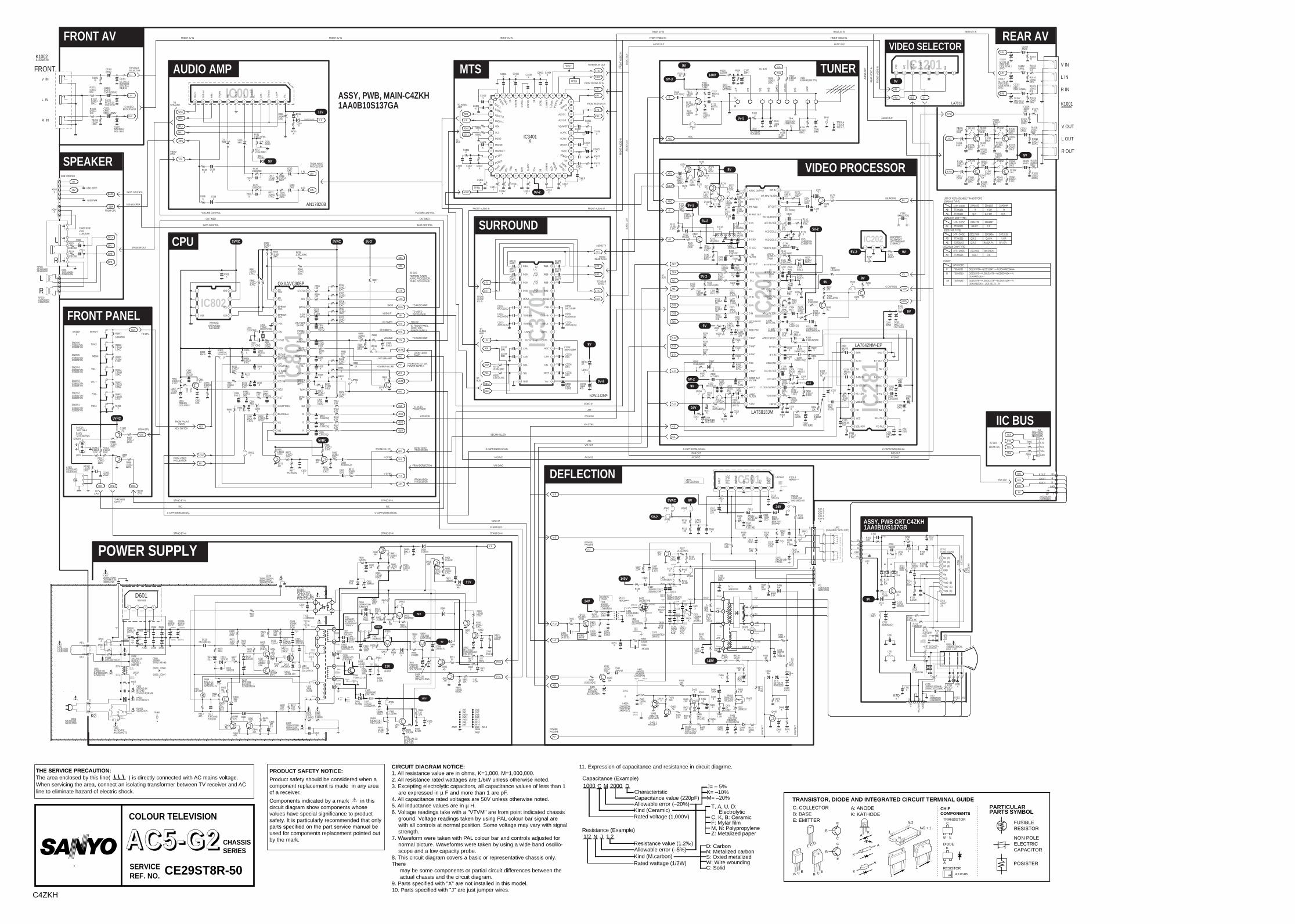
IC1201
IC501
IC37
01
IC001
IC80
1IC802
IC28
1
IC20
1
LIST OF REPLACEABLE TRANSISTORS
AC
AB
7T200182
7T200181
2SA564A2SA10152SA933S
Q,R
R
O,Y,GR
Y,GR
Q,R
R
14TH CODE
AJ 7T200221
2SA1179 2SA1037
M6,M7 R,S
14TH CODE
(2SA1037K CHIP TYPE)
(2SA933S TYPE)
AE
AD
7QT00202
7T200183
2SC945A 2SC18152SC1740S
RA,QA,PA
QA,PA
O,Y,GR
Y,GR
14TH CODE
AH 7T200220
2SC2812 2SC2412K
L6,L7 R,S
14TH CODE
(2SC1740S TYPE)
(2SC2412K CHIP TYPE)
Q,R,S
Q,R,S
(DIODE)
DD1S2076A---N,DD1S2471----N,DDXAAED0434--7DD00021
7DD00019
7DD00192
14TH CODE
P
R
AA
DD1S2076----N,DD1S2473----N,DDDS442X----NDDXAAED0434--
DD1S2076----N,DD1S2473----N,DDDS442X----NDDXAAED0434--,DD1SS133----N
B OUT
G OUT
R OUT
GND
B
G
R
5
1
SCL
SDA
STS
1ACK
50/60HZ(TUNEROPT)
IF
7.PB
9.TB
1.AG
C
3.AS
4.CL
OCK
5.DA
TA
6.M
B
11.IF
4MIN
4.43DC
R-Y OUT
SC-IN
4.43M IN
SYYSTEM
KIL-LOW
VIDEO IN
VCC
EQU-ADJ
GND
B-Y OUT
4M-DC
ID-FIL
KILL-FIL
FO-FIL
BLK DETECTION
INTER Y IN/C-IN
CLAMP FILTER
APC2-FILTER
R-Y IN
B-Y IN
G OUT
B OUT
FSC
V-OUT
RAMP ALC FILTER
R OUT
RGB VCC
CCD GND
CCD FILTER
CCD VCC
CLOCK OUTPUTH-VCC
SIF APC FILTER
4.43M CRYSTAL
APC1 FILTER
SVD
V/VERTICAL/GND
EXT VIDEO IN/Y-IN
SDA
G IN
RF AGC OUT
PIF AGC
IF VCC
IF IN
SIF OUT
B IN
IF IN
IF GND
APC FILTER
VCO COIL1
VCO FILTER
VIDEO OUTPUT(2Vpp)
VIDEO/VERTICALVCC
FM FILTER
R IN
VCO COIL2
VCO IREF
FAST BLANKING INPUT
H-AFCFILTER
AFT OUT
EXT.AUDIO IN
AUDIO OUTPUT
SCL
ABL
SIF IN
FM OUTPUT
MUTE(H=MUTE)
AV1/AV2
TV/AV
S-TERM(OPTC-SYS)
(BASS)
POWER(L=OFF)
ON-TIMER(H=ON)
STATUS
ACK
EPROMSDA
EPROMSCL
SECAMKILLER(SIF OPT)
FILT
VDD
REMOCONIN
POWERFAIL
VS
HS
BLK
B
G
R
AFTS-CURVE
KEY-IN
RES
XOUT
XIN
X-SWVIF-M
VSS
IIC5DA
IICSCL
VOL(50/50HZ)
VSS SDA
SCL
VDD
EEPROM
5.5M
4.5M
11
IF
Rout
+
Gnd
out
Rout
-
Volu
me
Rin
Gnd
in
Lin
Stan
dby
=L Lout
-
Gnd
out
Lout
+
Vcc
MONO/ST
C-CAPTION
BILINGUAL
V OUT
L OUT
R OUT
V IN
L IN
R IN
AGC
SECAM KILLER
NCNC
NC NC
IN1B
IN4B
MONB
TONE-Hb
TONE-Lb
Vcc
OUTb
SR-FIL
VREF
CTH
CTL
LINEbLINEa
GND
SCL
SDA
CVA
CVB
CSR
AGC
OUTa
TONE-La
TONE-Ha
MONA
IN4A
IN3B
IN2B
IN3A
IN2A
IN1A
(SECAM KILLER=J)
V-SYNC
H-SYNC
L IN
R IN
TVL--L
AV1L--R
AV2L--R
AV3L--R
L--R
GND
FROM CPU
POWER FAILURE
R/C PRE AMP
VOLUME
STANDBY=L
VIDEO IF
BASS
TO AUDIO AMP
TO AUDIO AMP
TO VIDEOPROCESSOR
TO VIDEOPROCESSOR
FROM VIDEOPROCESSOR
FROM DEFLECTION
FROM VIDEOPROCESSOR
FROM FRONTPANEL
FROM VIDEOPROCESSOR
FROM FRONTPANEL
FROM DEFLECTION,POWER SUPPLY
TO FRONT PANEL,AUDIO AMP,POWER SUPPLY
TO/FROM TUNER,AUDIO PROCESSOR,VIDEO PROCESSOR
POWER SUPPLY
CPU
AUDIO AMP
SURROUND
TUNER
DEFLECTION
VIDEO PROCESSOR
REAR AVFRONT AV
SPEAKER
FRONT PANEL
IIC BUS
IICBUS
IIC BUS
IIC BUS
IIC BUSOSD RGB
KEY SWITCH
BILINGUAL
C-CAPTION
RGB OUT
ON TIMER TO LED
TO AUDIOPROCESSOR
TO VIDEOSELECTOR
R IN
L IN
V IN
FRONT
6
1
HEA00****
VIDEO
ABL
HEATER
AFC
GNDLOW B
+B
H-OUT
Q461-1HA0018---
C423
SC
FO
Q432-1 HV
HORIZ.DRIVE
H-DRIVETRANS
4
1
C608
D605/.../D608
C605/.../C607
1
2
MTS
3M07794-AD1901A
POS.+
POS.-
VOL.+
VOL.-
PRESET
TV/AV
MENU
TOAUDIOAMP
FROMFRONTAV IN
AUDIO TV
FROMREAR AV IN
TO REARAV OUT
IICBUS
TO AUDIOAMP
FROM REAR AV IN
FROM FRONT AV IN
TO REAR AV OUT
TOSPEAKER
FROM AUDIOPROCESSOR
FROMCPU
TOCPU
TO POWERSUPPLY
FROM CPU
TO CPU
FRONT AV IN
SPEAKER OUT
SUB WOOFER
EARPHONE
FROMCPU
FRONT AV IN FRONT AV IN
AUDIO OUT
FRONT VIDEO IN
REAR AV IN
VIDEO SELECTOR
FRONT AUDIO IN FRONT AUDIO IN
FRO
NT A
UDIO
INFR
ONT
AUD
IO IN
REAR
VID
EO IN
FRO
NT V
IDEO
IN
REAR AV IN
FRONT VIDEO IN
REAR AV IN
AUDI
O O
UTAU
DIO
OUT
AUDI
O O
UT
AUDIO OUT
AUDIO OUT
AUDI
O O
UT
IICBUS
POWERFAILURE
POWERFAILURE
SUB WOOFER
FROM CPU
BASS CONTROL
BASS CONTROL BASS CONTROL
ON TIMER
VOLUME CONTROL
ON TIMER
VOLUME CONTROL
C-CAPTION/BILINGUAL
R/C
STAND BY=L
C-CAPTION/BILINGUAL
R/C
STAND BY=L
C-CAPTION/BILINGUAL C-CAPTION/BILINGUAL C-CAPTION/BILINGUAL
STAND BY=H STAND BY=H STAND BY=H
STAND BY=L
50/60 HZ
AV1/AV2
V/H SYNC
AV1/AV2 AV1/AV2
RGB OUTRGB OUT
SECAM KILLER
ABL
V/H OUT
V/H SYNC
AV1/AV2
0SD RGB
AFT
VIDEO IF
GND PWR
GND PREE
L
R
L
R
BASS-LLSOUT-R
LSOUT-L
SDA
SCL
DGND
MAININ
MAINOUT
PCINT1
PCINT2
PLINT
AUX1-L
NC
AUX1-R
VCAWGT
VCATC
VCAIN
VEOUT
VETCVEWGT
VESAPINSAPOUT
NOISETC
STIN
SUBOUT
NC
VCC
SAPTC
GND
NC
IREFVG
RCOMPIN
AUX2-R
AUX2-LTVO
UT-RTVO
UT-L
NCNC
SURRTC
TRE-R
BASS-R
TRE-LTOUT-L
VOLIN-L
TOUT-R
VOLIN-R
1 3
1
ASSY, PWB CRT C4ZKH
<CRT SOCKET>
5
G
R
B
GND
HEAT
ER+ B
GND
9V Vi1
Vi2
Vi3
Vip
Voc1
Voc2
Voc3
VDD
GND
(R)
(G)
(B)
(R)
(B)
(G)
1AA0B10S137GB
R1026
C1025
KP
Q291
R228
C011
R032
C021
R206
R207
C219
R357
R356
C176
R804
R805
R832
C825
R866
R869
R875
R817 R819
R354
L171
C205
C202
C201
R263
R264
R141
R140
R351
C280
A101R107
R106
R108
R109C106
C107
D103
C111
R112
R111
R114C113
R103
R105
C101
R352
D352
R130 C171
R176C172
C203
R233
R232
R231
R227
R226
C225
R281
R284R282C286
C284
C242
C282
C288
R283
C230C210 C231
C240
C133
C132
R132
C135
R229
C247
C243
C244
R220
R225
R224C226C224
X211C212
R209
C209
C206
R280
C204
C283
R286
R212
R210
C232
C233
C270
R272 C271
R245
R244
C273
C138
R115
R121
X161
R122
D122
R124
R125
Q122
C120
C121
C122
Q261
C246
R358
R221
R222
R223
R271
IC202
R230
R833
C853
C852
C851
R892
C805
R814
R815
R812
R811
R801
R842
R841
R835
C803
R838
R837
R836
R834
R813
R840
R839
R831
R893C893 R894 C894
C802
C801X801
Q861
R851
R861
C861D861
R863
R862
FBP IN
C245
R353
R818
R874
R265
JP202
JP201
Q173
R173
R291
C221
C222
C223
R179
R186C358
R845
R873
JP801
R287
C218
R267
D280C289
R285
C353
C123
R1025
C281
C862
C892
C824
C832
C829
C277
C823
X161A
TP-A
Q111
R340 D357
C278
X171
C891
C896R891R895
R1015
R1016
R1006
R1005
C001
C031
C207
C291
C178
C895
R296
L204
R876JP802
D3701
C3702
C3710
C3730
C3714
C3731
C3724
C3725
C3735
C3733
R3732
R3731
C3715
C3717
C3727
L3701
R877
C880Q871
R871
Q881
R881
R883
R882
R870
C124
D230
R211JP204
D249R243
C213
C211
C208
C804
C816
C870
R853
R855
R857
C856
C3711
C3712
C3721
C3722
C3734
C3732
K001
C835 R872
C1015
C1005
R897
R896
R899R898
R234
R235
R236
C175
D102
TP-E
R830
R116
C811
KX
Q818
D031
D011
D010
R010
JP818
JP291
R031
C287
C285
D1021
K1002
R1022
R1021 C1021
R1012
C1011R1011
JP111
T471-H7
KDY-6KDY-5
KDY-3KDY-1
Q432-H5Q432-H4
IC501-H4IC501-H3IC501-H2IC501-H1
Q432-H7Q432-H6
C420A-H2
C420A-H1
C420-H3C420-H2
JP841
JP843 JP842
R487 C487
C420B
R529
R423A
C521
C420AC423A
C423-H3
C425-H3C425-H2
C425-H1
C424-H3C424-H2
C424-H1
C442A
JP476
T471-H5
KQ
C515A
R488
D485
T471-H8
D448
R450C449
Q449
R355
D501
SW501
C511
C510
R511
R510
R514
D512C517
C520
R519
R512C518
R528
R522
C514
R515 R516
C515
R524
C524
JP501
R852
D486
R462
R449
Q461
L441-H2
C540
R434
Q540
R540
Q461A
C422A
JP442
L442-H2
L442-H1
L441-H1
C441-H3C441-H2
C441-H1
C442-H3C442-H2
C442-H1
D464
D465
L462-H2L462-H1
JP436
C420-H1C423-H1
C423-H2
Q461-H2
C425A
C424AL432
L431
L461AC462
C466
C463
R486
C486
VR462 R468 C468
D466
D469 R474
R426
D461
R466
C470
C465
L462
L461
R473
Q462
R471
R464R469
R472
R480
R461
R467
C467
R465
C464
C424C425
D439
C422
C420
C423
D438
L441R441
R442L442
C434
C432
C426
D421
R423
R479
D468
R424
C471
R481
C469
D467
R475
R485
D353T471-H10
T471-H2
T471-H1
Q432-H3
Q432-H2Q432-H1
Q461-H1
R435
T471
T431
C527
Q527
R527
R445C442
C441
R432
C431
Q431
C433
R433
Q432
R518 D441
PRO
TECT
HEA00****IC501-1
VERT.DEFLECTION O
UTPU
TST
G V
CC
INVE
RTIN
PUT
PUM
P UP
OUT
PUT
INPU
T
GND
VCC
PRO
TECT
D601-H4D601-H3D601-H2D601-H1
D601
T611-H7
KG-2
T611B-H15
T611B-H13
T611-H12T611B-H10
T611-H13
SW601-H1
SW601-H2
T611B
T611A
C693
D693
R697 R696
R695
Q693
JP631
R692
R693
R690D691
Q690 R691
D690C690
R694
C691D692
R660
JP653
JP652
R653
SW601
T611
R624
R613
Q613-H5
Q613-H4
Q653
L601A-H2
L601A-H1
L601A-H4
L601A-H3
C609A-H1
C609A-H2
C609A
R602-H3 R602C
C618A
D643
Q652
C658
C655
C657
C656
R602-H4
C602
C601T611-H17
R651
Q651
C619
D653
L601A
C628
C609
D608
D606
R602-H2
KG-3
KG-1
KE
R602-H1
C607
C606
C608D607
D605R602A
C605
C627
KE-1
KE-2
L601
VA601
R601
F601B F601A
L601-H4
L601-H2
L601-H3
L601-H1
R672
D671
R615
Q613-H1
Q613-H2
Q613-H3
D641
D655
R671
R673
C663
R665
D662
Q663
R667
R666
Q662
R681
R682
Q681
D659
R655
C681
IC681
R659
R657
R658
R652
R654
C643
C652
D652
L653
L654
L651
D610
C611R614
R616
D619
R611
Q625
R643C644
R644R642
Q642
Q641
R641
D616
D617
C614
R627D615D614
R619
C613 R621
R620
R622
L616
R623
Q612
Q611
R632 R633
L615
R631L614
D612
C615
Q613
L613
D611
R625 R626
C617
C618
L612
R669
VR651
C664
C665
D664
R656
Q654
T611-H3
R663
R664
D661
Q661R662
R661C651
D651
C629
R629R628
PS601-H2PS601-H3
PS601-H1
JP601
JP602
PS601
L-STH-ON
AUDIO
KG
C3439
C3436
IC3401
C3416
C3418
C3424
R3426
C3427C3426
C3423
R3422
R3421
C3422
C3421C3406
R3406
C3407 R3407
C3404
R3402
R3401
C3434C3433C3432C3431
C3401
R3411
C3408
C3411
C3412 C3413
C3417
R1013
R1014
C1013
D1012
D1022
C1023
R1024
R1023
D1002
C1003
R1004
JP803
K002
K1001
A1901
R886
R887
Q886R1912
C1902
R1911R1913
R888
Q1902
R1901
D1901
R1907
SW1901
SW1904
R1908
R1902
R1903
R1904
R1906
R1905
SW1902
SW1903
SW1905
SW1906
SW1907
R029C029
R019 C019
R018
R028
C018
C028
R015
C015R016R017
R027 R026C025
R025
D1011
D1001
C1001
R1001
Q1031
R1032R1031
R1033
JP1032
R1037
R1035
R1036
Q1032
Q1042
R1046
R1045
R1047
JP1042
R1043
R1041 R1042
Q1041
C1031
C1041
JP1031
JP1041
C3701
Q176
R177
Q174
R178
R180
JP174
JP176
JP171
Q172R188
Q171 JP173
R171
R174
R172
R1034R1038
R1048R1044
C639
D476
VR463JP463
C016
C026
K004
C609-H1
C609-H2
C3720
K003
R846
R104
D646
R241
KDY-4
T471-H6
JP654
C227
R289
C174
T611-H2D654-H1
D654-H2
T611-H4R602
R602B-H2R602B-H1
R602B
R602B-H3
C112
R816
C654
D654
D654A
T611B-H11
T611A
T611
T611
T611A
T611B
TP-EEJW1JW2JW10JW11JW15JW4JW5
T611B-H12T611-H14
TP101ATP101BTP101C
R645
C1032
C1042
R463
R292
JW6JW7JW8JW9
JW12JW13JW14
JW22
C3423A
C3426A
JW3
JP655 JP656
C355
JW16
D445
JW17
JW18
C352
C610
SP902
SP901
W901
L901
L902 (ASSEMBLY WITH CRT)
Q901
AT1
R721
C722
D701
D702
D703
FO
C718
IC701
R706
R705
R702
R703R701
R704
HS1
R718
L721
R722
D721 C721
C711
R711
R712C712
R715
R714
R713
K701
C751
C731
L731
K7P
Q721
R707
R708
R709
K7D2
K7MK7M-1
K7M-2
C703
C702
C701
K7D
C703A
C701A
K7Q
D731
AT1
1/16GJ100KC
EM10
J10EA050N:J10KR050N
X
150K
EM1
1/16GJ68KC
EM1
AN17820B
X
X
KK0.01GQ
1.5K
1/16GJ10KC
X
J
J
CJ100CGQ
CJ100CGQ
100
100
1/16GJ47KC
1/16GJ1KC
1/16GJ10KC
22K
L14B1830N:L14B1870N
EM10
FJ0.015(BE:D)
PM1
1/16GJ10KC
1/16GJ270C
1/16GJ560C
1/16GJ560C
8.2K
KK0.01GQ
F1BEB0(260:270)1/16GJ100C1/16GJ
100C
1/16GJ18KC
1/16GJ68KC EM47
EM47
RD36EB1:MTZJ36A
KK0.01GQ
1/16GJ5.6KC
1/16GJ1KC
1/16GJ330C
KK0.01GQ
1SJ39K
J
16EM470
DJ10K
RD5.1EB2
1/16GZ0C
KK1500GQ
1/16GJ10KC
KK0.01GQ
KK0.01GQ
X
X
X
1/16GJ33KC
1/16GJ22KC
EM1
1/16GJ27KC
1/16GJ3.3KC
1/16GJ3.3KC
EM1
EM1
X
KK0.01GQ
FJ0.033BE
1/16GJ4.7KC
KK0.01GQ25EM470
HJ0.33G
KK0.01GQ
X
EM0.47
1/16GJ470C
EM0.47
1/16GJ680KC
EM2.2
KK0.01GQ
EM47
X
1/16GJ4.7KC
1/16GJ4.7KCEM125KK
0.1GQ
V10B2930J:B4V10B0040N
CJ15CGQ
1/16GJ620KC
EM0.47
25KK0.1GQ
1/16GJ100C
EM10
KK0.01GQ
1/16GF4.7KC
1/16GJ150C
1/16GJ3KC
HJ0.33G
25EM470
X
1/16GJ100C
X
1/16GJ47KC
1/16GJ47KC
25KK0.1GQ
KK0.022GQ
LA76818JM
56
1/16GJ6.8KC
SF6376U
1/16GJ2.2KC
1SS356
1/16GJ10KC
1/16GJ27KC
AH
KK0.022GQ
KK0.01GQ
16EM100
AC
EM1
1/16GZ0C
1/16GJ1KC
1/16GJ1KC
1/16GJ1KC
1/16GJ100C
BA178M05T:MC78M05CT:UPC78M05AHF:L78M05CV
47
X
CJ56CGQ
CJ56CGQ
CJ56CGQ
1/16GJ470KC
EM10
1/16GJ10KC
1/16GJ10KC
X
1/16GJ10KC
1/16GJ270KC
1/16GJ4.7KC
1/16GJ4.7KC
1/16GJ10KC
KK0.01GQ
1/16GJ15KC
1/16GJ15KC
1/16GJ10KC
1/16GJ10KC
1/16GJ10KC
1/16GJ330C
1/16GJ330C
470
1/16GJ1MCEM2.2 100 25KK
0.033GQ
CJ27CGQ
CJ15CGQV10B0(560N:570N)
QXXAVC305P
AJ
1.5K
1/16GJ1.5KC
EM1RD3.6EL:DZXLBB017
1/16GJ47KC
1/16GJ8.2KC
24LC16B/P:QXXAVC360
H-OUT
PM1
X
1K
1/16GJ10KC
1/16GJ33C
1/16GZ0C
X
AH
22K
2SJ4.7
25KK0.1GQ
25KK0.1GQ
25KK0.1GQ
X
XEM1
X
1/16GJ33KC
J
1/16GZ0C
1/16GZ0C
270
MTZJ7.5C:RD7.5EB1
EM10
DJ47
X
1/16GZ0C
1/16GJ680C
EM1
25KK0.1GQ
25KK0.1GQ
25KK0.1GQ
X
25KK0.1GQ
J
25KK0.1GQ
X
J30B0250N:J30B1380N
2SC2814F4P
1/16GJ82KC AA
25KK0.1GQ
X
EM1
XXX
1/16GJ680C
1/16GJ100KC
1/16GJ100KC
75
25EM2200
EM10
25KK0.1GQ
FK0.1BE
EM0.1:EM0.1LBWAJ
EM10
X
J
X1/16GZ0C
AA
25KK0.1GQ
EM4.7
KK0.022GQ
KK2200GQ
16KZ1GMF
KK2200GQ
25KK0.1GQ
EM1
EM1
1/16GJ100C
1/16GJ100C
25KK0.1GQ
EM1
EM1
NJW1142MP
J
KK1000GQ
KK3300GQAH
1/16GJ10KC
AH
1/16GJ3.3KC
1/16GJ33KC
1/16GJ3.3KC
1/16GJ22KC
X
X
150J
MTZJ9.1B:RD9.1EB2
X
X
X
X
X
X
X
8.2K
8.2K
8.2K
X
EM4.7
EM4.7
EM4.7
EM4.7
EM1
16KK0.33BA
J10EA040N:J10KR040N
EM1 1/16GJ27KC
EM10
16EM220
X
1/16GJ10KC
1/16GJ33KC J
120
120
120
X
MTZJ6.8A:RD6.8EB1
X
1K
1/16GJ56C
X
J10EA050N:J10EA050N:J10KR050N
LA7642NM-EP
1
X
1SS355
X
X
X
POWER FAILURE
X
X
1/16GJ47KC
EM1
EM1
MTZJ9.1A:RD9.1EB1
B4J12B05700
1/16GJ18KC
1/16GJ1KC
EM0.1:EM0.1LBWAJ
1/16GJ18KC
EM0.1:EM0.1LBWAJ
1/16GJ1KC
X
2400010
X
2400010 2400010
2400030240003024000102400010
24000302400030
X
X
X2400030
J
X X
220K 160EM4.7CY
1SJ1.5K
DJ22K
35EM2200
XX
X
2400030X
2400030
2400030X
2400030
X
X
2400010
J10EA040N:J10KR040N
X
1SJ0
.27
EU1:ERA22-04
2400010
X
XX
X
DJ10K
EM01Z;ERA15-02;ED0448
S10B1370N:B4S10B00100
X
EM4.7
10K
10K
5.6K
EM01Z;ERA15-02;ED0448
35EM220
100FK0.1(D:BE)
68
XHJ0.01G
1SJ1K
270
EM10
18K 8.2K
25EM2200
2SJ100
HJ0.68G
X
LA78041
1/16GJ10KC
AA
82
1SJ1
5
2SB1274(QRA:RRA)
2400030
25PM10
1SJ180
AH
1/16GJ330C
X
X
J
X
X
2400010
2400030X
2400030
X2400030
2400030
820K
J
24000102400030
X
24000302400030
2400030
2400010
X
X
ZZ0008:Z21B0050N
L2G31R0MN:L7201B
L26B0170N:L26B0260N:LM0045(:D)
EM1
FK0.1(A:D:BE)
J
5.6K
250EM33CY
R3D6472NJ:R3D7472NJ:R3L1502NJ
1.8K EM22
MTZJ20A:RD20EB1:
DZXLBZA20A
EU1 1/2DJ1K
10K
X
X
KZ0.01F
100GK2.2
AA0025:AA0025A
:L26B0540N
X680
AE
1.5K
X33K
47K
47K
J
1.2M
10EM220
X
EM2.
2
400NJ0.027EAQ
400NJ0.022EAQ
ERB44-04
X
1500MH7800(AN:XK)
1500MH7500(AN:XK)
ERD07-15L
L71B0180N2SJ1K
XX
EM47
500KK1000A
250GJ0.47
MTZJ16A:RD16EB1:
DZXLBZA16A
DJ68K
2.2K
AA
1K
100PM2.2X:PM2.2X
2SJ4.7
EM10
P1/
2DJ3
30
DJ180K
X2400010
2400030
2400030
2400010
2400010
2400010
2400010
7SK5.6VC
L40B10500
AD0002:AD0002C:L18B0540N
EM10
AH
1/16GJ56KC
X200MJ0.27UCQ:250MJ0.27AP
200MJ0.27UCQ:250MJ0.27AP
1K
FK6800(A:BE:D)
2SC3332(R:S)
500KK3900A
1/2DJ1K
2SD1879YB
1SJ1.2 ERC05-10B;RM11C
2400030240003024000302400030
RBV-608
2400030
J30B0250N:J30B1380N
2400030
2400010
2400010
X
X
16EM47
AA
1/16GJ47KC
1/16GJ4.7KC
1SJ6.8K
AD
J
1/16GJ27KC
1/16GJ8.2KC
1/16GJ47KC
AA
AH 1/16GJ47KC
1SS355EM2.2CT
DJ5.6K
35EM47EU1
X
J
X
1FJ5.6
S10B6230N
L51B5900N
1/2FJ10
1/2FJ560
2400010 2400010
X
X
X X
X
2400010
2400010
400EM220XC
2400010
X
X
1SS133
2SB1565E
1000KK470(CRD:NH)
1000KK680(CRD:NH)
1000KK470(CRD:NH)
1000KK3300(CRD:NH)
2400010
250GM0.1X(BJ:D:E):275GM0.1(XB:VB)
250GM0.1X(BJ:D:E):275GM0.1(XB:VB)
2400030
1K
AD
X
FE301-1L43:RU4YXLF-L1
X
250KK2200XH:400KK2200X:250KM2200XN
400EM220XC
XX
2400010
J30B0250N:J30B1380N
J30B0250N:J30B1380N
X
2400010
X
1000KK1000(CBB:HB)
XX
15WK1.8(M:VE)
250KK470XH:250KM470XN:400KK470X
J30B0250N:J30B1380N
J30B0250N:J30B1380N
F35B0570N:B4F35B0040N:F35B1130N
ERZV14D471
X
J20B0170J J20B0170J
2400030
2400030
2400030
2400030
12K
AA
220
2400010
2400010
2400010
J
AA
22K
1/16GJ560KC
EM0.22
DJ12K
MTZJ6.8A:DZXLBZA6.8A:RD6.8EB1
AH
1/16GJ10KC
1/16GJ22KC
AC
22K
1/16GJ560KC
AH
X
DJ10K
10EM470
BA178M05T:MC78M05CT:UPC78M05AHF:L78M05CV
X
DJ3.9K
X
1SJ33K
DJ15K
25EM1000T
35EM470T
RN1Z
ZZ0122
ZZ0122
ZZ0122:ZZ0122XXA
PC123Y52:TLP421F-BL:PC123X5YFZ
FJ0.01BE:FJ0.01D
22K
15K
MTZJ11C:RD11EB3:DZXLBZA11C
DJ470
2SC2274(E:F)
18KEM3.3
22K47K
AD
AB
10K
MTZJ20B:RD20EB2:DZXLBZA20B
1SS133
HJ0.22G
22K1SS133ES1
DJ22
FK0.1(BE:D) 1/2DJ470K
1/2DJ470K
DJ47
Z21B0140B
330K
2SA984(E:F)
2SC2274(D:E:F)
2SJ0.27
2SJ0.27
ZZ0122:ZZ0122XXA 47K
ZZ0122:ZZ0122XXA
ERA81-004
2000KK220CRD
2SK3102F
ZZ0122(:XXA)
EG01C
2SJ68K
2SJ68K
2000KK220CRD
630GK0.047DCN
J
2SJ3.9
R3D6222NJ:R3D7222NJ
16EM220:16EM220LBWA
16EM470
MTZJ10B:RD10EB2:DZXLBZA10B
1SJ270
2SD1913(QRA:RRA)
2400030
DJ150K
1SJ27K
DZXLBZA6.2C:MTZJ6.2C:RD6.2EB3
AH1/16GJ4.7KC
DJ100K160EM220XJ
RU3AM
250KK470XH:400KK470X:250KM470XN
1/2CK5.6MXG
1/2CK5.6MXG
24000302400030
2400030
J
X
DHXAAEV0070
4A250VTW:4A250VHOTS
F601
X
X
X
X
X
X
X
XX
X
X
X
X
XX
X
X X
X
X
X
XXXX
X
XX
X
X X
X
1/16GJ1KC
1/16GJ18KC
EM0.1
MTZJ9.1A:RD9.1EB1:DZXLBZA9.1(B:C)
MTZJ9.1A:RD9.1EB1
EM0.1:EM0.1LBWAJ
1/16GJ18KC
1/16GJ1KC
MTZJ9.1A:RD9.1EB1:DZXLBZA9.1(B:C)
EM10
75
LA7016
VCC
AV2
AV1/
AV2
(L/H
)
AV-O
UT
GND
AV1
X
J12B06000
J12B3520N
U20B32400:U20B35900
1/16GJ22KC
1/16GJ22KC
AH
1/16GJ220C
EM22
1/16GJ220C
1/16GJ220C
1/16GJ560C
AJ
X
SPR-39MVWF
1/16GZ0C
S10B1170N:S10B2970N
S10B1170N:S10B2970N
1/16GJ100C
1/16GJ12KC
1/16GJ5.6KC
1/16GJ3.9KC
1/16GJ1.8KC
1/16GJ2.2KC
S10B1170N:S10B2970N
S10B1170N:S10B2970N
S10B1170N:S10B2970N
S10B1170N:S10B2970N
X
GREEN
RED
1/2DJ150
J
1/2DJ150
J
X
X
X
X
1/16GZ0C
X1/16GJ39KC
1/16GJ4.7KC
1/16GJ4.7KC
1/16GJ39KCX
1/16GZ0C
MTZJ9.1A:RD9.1EB1
MTZJ9.1A:RD9.1EB1:DZXLBZA9.1(B:C)
EM10
75
AH
1/16GJ10KC
1/16GJ39KC
1/16GJ6.8KC
X
1/16GJ3.9KC
1/16GJ39KC
1/16GJ10KC
AH
AH
1/16GJ10KC
1/16GJ39KC
1/16GJ3.9KC
X
1/16GJ6.8KC
1/16GJ39KC
1/16GJ10KC
AH
EM10
EM10
X
X
16EM470
X
X
X
X
X
1/16GZ0C
1/16GZ0C
1/16GZ0C
XX
X 1/16GZ0C
1/16GJ150C
X
X
1/16GJ15KC
1/16GJ10KC
1/16GJ10KC
1/16GJ15KC
X
MTZJ8.2B:RD8.2EB2
R3D6472NJ:R3D7472NJ:R3L1502NJ X
EM1
EM1
X
2400010
2400010
EM4.7
X
X
X
X
X
X
J
PM1
1/16GZ0C
CD10CGQ
X
2400030
2400030
X
X
X X
X
X
KK0.01GQ
X
25EM3300
YG901C2-LB
2HEF0021--:2HEF0065--
X
X
X
X
X
X
X
X
X
X
X
X
X
2400030X
X
X
X
X
EM10
EM10
4.7K
X
X
X
X
X
X
X
X
X
X
X
X
X KK0.1GQ
KK1000
X
X
XX
16KK0.47GQ
X
ASSY, PWB, MAIN-C4ZKH1AA0B10S137GA
A10B00400:A10B25500
A10B00400:A10B25500
W10B03901:W10B15500
L81B29500:L81B29600
A68QBC230X35L(CRT + DY)
DJ 10K
250EM22CY
R R
R
X
2000KP1000AHE:2000KZ1000CBMC
TDA6103Q/N3
1/2D
J100
K1/2D
J100
K1.8K
1.8K1.8K
1/2DJ100K
X
1/2DJ1.5K
DJ47
DJ10K
R 16EM220CD
250GK0.1P
DJ220K
DJ2.2KHJ0.22(:G)
1/2DJ1.5K
1/2DJ1.5K
1/2DJ1.5K
J11B2570N
X
X
X
X
AC
1.2K
1.2K
1.2K
X
XJ30B0250N:J30B1380N
J30B0250N:J30B1380N
X
CJ39C
X
J30B0250N:J30B1380N
X
X
X
X
12 11 10 9 8 7 6 5 4 3 2 1
54
53
52
51
50
49
48
47
46
45
44
43
42
41
40
39
38
37
36
35
34
33
32
31
30
29
2827
26
25
24
23
22
21
20
19
18
17
16
15
14
13
12
11
10
9
8
7
6
5
4
3
2
1
123
36
35
34
33
32
31
30
29
28
27
26
25
24
23
22
21
20
1918
17
16
15
14
13
12
11
10
9
8
7
6
5
4
3
2
18
7
6
54
3
2
1
30
29
28
27
26
25
24
23
22
21
20
19
18
17
1615
14
13
12
11
10
9
8
7
6
5
4
3
2
1
1
2
3
4
5
6
7
8
9
1011
12
13
14
15
16
17
18
19
20
7 6 5 4 3 2 1
95
6
4
7
10 8
2
1
4321
13
12
11
10
14
15
7
6
5
4
1
3
2
15
14
13
12
16
17
7
6
5
1
3
22
3
1
5
6
7
17
16
12
13
14
15
321
4
3 2
1
12
11
10
9
8
7
6
5
4
3
2
1
48 47 46 45 44 43 42 41 40 39 38 37
36
35
34
33
32
31
30
29
28
27
26
25
242322212019181716151413
87654321
1
2
3
4
5
6
7
8
9
275910
6
8
11
1
9V
140V
5V-2
5V-2
9V
5V-2
5V-2
9V
5V-2
9V
5VRC5VRC
11V
P.F
9V
5V-2
SDA
SCL
SDA
SCL
SDA
SCL
SCL
SDA
BIL
C-CAP
BIL
C-CAP
5V-2
9V
SCL
SDA
5VRC
9V
24V
SPR+
SPR-
SPL+
SPL-
VOL
VOL
BASS
SPL-
SPL+
SPR-
SPR+
9V-2
STS
ACK
STS
ACK
STBL
R/C
KEY
SKIL
H-S
V-S
BLK
OSB
OSG
OSR
VIF
AFT
LIN
RIN
AFT
OSR
OSG
OSB
BLK
R-O
G-O
B-O
ABL
VIF
H-O
H-S
SKIL
B-O
G-O
R-O
V-O
LIN
RIN
R-FI
V-I
L-FI
AOUT
V-RO
ATV
AGC
AGC
IF
IF
9V-3
5V-2
ONT
9V
MUTE
P.F
MUTE
9V
V-FI
L-FI
R-FI
5V-2
5VRC 9V
24V
140V
140V
H-O
H-S
24V
50/60
ABL
P.F
V-S
V-O
P.F
11V
24V
5VRC
11V
9V
140V
STBL
STBH
P.F
9V-2
V-RO
L-RO
R-RO
R-RI
L-RI
V-RI
ATV
R-RI
L-RI
SCL1
SDA1
LIN
RINR-RI
L-RI
V-FI
V-RI V-IV1/2
9V
R-FI
L-FI
R-RO
L-RO
R-RO
L-RO
50/60
V1/2
5VRC
STBL
ONT
KEY
STBHR/C
BASS
SBW
9V
AOUT
SBW
9V
11V
SDA1
SCL1
9V9V
9V-3
TP317
TP318
TP301
9V
COLOUR TELEVISION
CHASSISSERIES
SERVICE REF. NO.
AAAACCCC5555----GGGG2222
PRODUCT SAFETY NOTICE:
Product safety should be considered when acomponent replacement is made in any areaof a receiver.
Components indicated by a mark in thiscircuit diagram show components whose values have special significance to productsafety. It is particularly recommended that onlyparts specified on the part service manual beused for components replacement pointed outby the mark.
CIRCUIT DIAGRAM NOTICE:1. All resistance value are in ohms, K=1,000, M=1,000,000.2. All resistance rated wattages are 1/6W unless otherwise noted.3. Excepting electrolytic capacitors, all capacitance values of less than 1
are expressed in µ F and more than 1 are pF.4. All capacitance rated voltages are 50V unless otherwise noted.5. All inductance values are in µ H.6. Voltage readings take with a "VTVM" are from point indicated chassis
ground. Voltage readings taken by using PAL colour bar signal are with all controls at normal position. Some voltage may vary with signalstrength.
7. Waveform were taken with PAL colour bar and controls adjusted for normal picture. Waveforms were taken by using a wide band oscillo-scope and a low capacity probe.
8. This circuit diagram covers a basic or representative chassis only.There
may be some components or partial circuit differences between theactual chassis and the circuit diagram.
9. Parts specified with "X" are not installed in this model.10. Parts specified with "J" are just jumper wires.
THE SERVICE PRECAUTION:The area enclosed by this line( ) is directly connected with AC mains voltage.When servicing the area, connect an isolating transformer between TV receiver and ACline to eliminate hazard of electric shock.
11. Expression of capacitance and resistance in circuit diagrme.
C4ZKH
TRANSISTOR, DIODE AND INTEGRATED CIRCUIT TERMINAL GUIDEC: COLLECTORB: BASEE: EMITTER
A: ANODEK: KATHODE
B
B
C
C
E
E
C EB C E
B
B
C
E
AK
K
A
A
K
FUSIBLERESISTOR
PARTICULARPARTS SYMBOL
1
1
1
N/2
N/2 + 1
N
NON POLEELECTRICCAPACITOR
POSISTER
C
EB
CHIP COMPONENTS
K
A
TRANSISTOR
DIODE
123
RESISTOR
12 X 103=12K
Capacitance (Example)1000 C M 2000 D
CharacteristicCapacitance value (220pF)Allowable error (–20%)Kind (Ceramic)Rated voltage (1,000V)
J= – 5%K= –10% M= –20%
Resistance (Example)1/2 N J 1.2
Resistance value (1.2‰)Allowable error (–5%)Kind (M.carbon)Rated wattage (1/2W)
D: CarbonN: Metalized carbonS: Oxied metalizedW: Wire woundingC: Solid
T, A, U, D: ElectrolyticC, K, B: CeramicF: Mylar filmM, N: PolypropyleneZ: Metalized paper
CE29ST8R-50
Schematic Dia 29-C4ZKH 12/20/04 8:19 AM Page 1
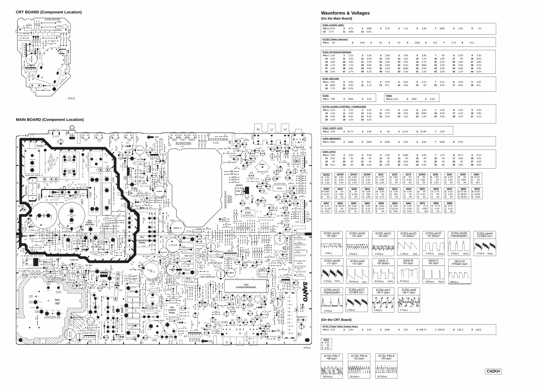
550Vp-p
Horiz.
1
12
E5
1 4
C712
R712C711
IC701
R705
K701
R714
R713
R715
K7D
C718
R718
K7P
K7M
R707
R708
R709C701
C703
C702
R701
R702
R703
D701
D703
D702
R721
C722C721
Q72
1
D721
R722
L721C731
C751
L731
R711
IC701H
1AA4B10S0230B
J701
D731
R706
R704
K7Q
CRT BOARD (Component Location) Waveforms & Voltages(On the Main Board)
Q1031B 2.5VC 6.0VE 1.9V
6.5Vp-p Horiz.
1.4Vp-p Horiz.
1.7Vp-p Horiz.
50Vp-p Horiz.47Vp-p Vert. 1000Vp-p Horiz.37.4Vp-p
IC201 (IF/VIDEO/CHROMA)Pin-1 2.3V 2 2.2V 3 2.4V 4 3.9V 5 2.9V 6 2.9V 7 0V 8 5.0V 9 2.3V
10 2.4V 11 4.3V 12 3.4V 13 3.4V 14 1.6V 15 1.7V 16 1.6V 17 0V 18 8.3V19 2.6V 20 2.6V 21 2.6V 22 2.0V 23 2.5V 24 2.7V 25 5.1V 26 2.6V 27 0.8V28 1.1V 29 1.7V 30 0.9V 31 4.5V 32 8.2V 33 GND 34 2.5V 35 2.5V 36 3.2V37 1.9V 38 2.8V 39 3.6V 40 2.5V 41 GND 42 2.6V 43 5.0V 44 2.8V 45 2.5V46 2.4V 47 3.7V 48 4.1V 49 4.1V 50 2.5V 51 2.2V 52 2.0V 53 2.1V 54 3.2V
IC501 (VERT. OUT)Pin-1 2.9V 2 22.7V 3 1.8V 4 0V 5 12.2V 6 22.9V 7 2.9V
IC801 (CPU)Pin-1 3.6V 2 3.4V 3 5.0V 4 4.0V 5 GND 6 2.6V 7 1.7V 8 5.0 V 9 0.1V
10 2.3V 11 0V 12 0V 13 0V 14 0V 15 0V 16 0V 17 4.8V 18 4.2V19 0V 20 0V 21 0V 22 0V 23 5.0V 24 0V 25 0V 26 0V 27 4.0V28 0.1V 29 0V 30 4.0V 31 4.9V 32 5.0V 33 5.0V 34 0V 35 5.0V 36 5.0V
IC802 (MEMORY)Pin-1 GND 2 GND 3 GND 4 GND 5 5.0V 6 5.0V 7 GND 8 5.0V
Q1042B 5.7VC 1.9VE 1.3V
Q462B 0.45VC 11.4VE 0V
Q461B 11.4VC 0VE 12V
4.0Vp-p2.4Vp-p4.8Vp-p 5.0Vp-p 1.2Vp-p
39.6Vp-p 37.4Vp-p 920Vp-p40.2Vp-p
IC201-pin28<Sandcastle>
IC201-pin27<H drive>
IC201-pin19<R out>
IC201-pin20<G out>
IC201-pin21<B out>
IC201-pin44<CVBS int.>
IC201-pin46<Y out>
IC501-pin5<V out>
Q432-C<H out>
Q432-B<H out>
Q1032B 1.9VC 5.6VE 1.3V
Q1902B 5VC 0.8VE 5V
2.4Vp-p
Q613-D<Power out>
488Vp-p
Q431-C<H drive>
(On the CRT Board)
Q721B 9.1VC 0VE 8.9V
Q1041B 2.5VC10.5VE 1.9V
IC701 PIN-8<G-out>
IC701 PIN-7<B-out>
IC701 PIN-9<R-out>
89.6Vp-p 83.4Vp-p 82.9Vp-p
4.6p-p
Q122B 0.6V C 0VE 0V
Q540B 0VC 0.12VE 0V
Q527B 0VC 3.9VE 0V
IC202 Pin-1 7.8V 2 GND 3 5.0V(C4LJ)
2.5Vp-p Vert.1.4Vp-p
IC201-pin23<V drive>
IC001 (AUDIO AMP.)Pin-1 12.5V 2 5.7V 3 GND 4 5.7V 5 7.1V 6 1.5V 7 GND 8 1.5V 9 1V10 5.7V 11 GND 12 5.6V.
KG
1
E
E
E
DIP
127 1020
28 5430 40 50
DIP
VOLUMEDOWN
VOLUMEUP
POSITIONUP
POSITIONDOWN
MENU TV/AV PRESET
107
6
5
4
3
2 1
8
F601
9
GNDHEATERLOW B
ABL
AFC
140
H OUT
210
5
5
KG
85
4 1
IC801
E
E
E
E
E
12
43
1 2
E
E
E
E
E
T4AL250V
169
71
112
1
E
IC3701
1
5
IC501-H4
IC501-H3
IC501-H2
IC501-H1
Q432-H6
Q432-H7
Q432-H4
Q432-H5
R449
IC1201
J1914
J657
J101
R103
D485
R488
D467
R423A
R423 D466
KX
C465
J1905
JP442
R351
R804
R805
D249
J840
J342
J838
J1320
J1321
J1322
J1911
D1901
A101
SW1901
SW1902
SW1903
SW1904
SW1905
SW1906
SW1907
T471-H8
T471-H5
T471-H2
T471-H1
T471-H10
A1901
C1902
J1902
TP101A
TP101BTP101C
C106
J1910
TP-A
D103
R104
T471
R481
Q432
C423
C423-H1
C423-H2
C423-H3
D438
C420
C420-H1
C420-H2C420-H3
C423A
C420B
C424A
C424
D439
C422C422A
JP436
L432
L431
C425
C425A
KQC486
JP476
C471
R424
R435
C426
J448
R355
C441
C441A
C442C442A
R442
L442T431
H-DRIVETRANS.
R434
C433
Q431
J449 R474
D469 C468
VR462
R468
R464
R469
R472
R480
C462
C463
R461
C466
R466
D461
R467
C470
D465
R471
D464
Q462
C467
R473
Q461
Q461A
Q461-H2
Q461-H1
C464
R465R462
J480
J461
R485
R487
D486
Q449C449
D448
R479
R475
C469
D468
R445
J642
C424-H1C425-H1
C424-H3C424-H2
C425-H2C425-H3
Q432-H2
L441-H1
L442-H2
L442-H1
C442-H2
C441-H2C441-H3
C442-H3
C442-H1
C441-H1
L441-H2
L461
L461AJ441
D441
L462-H1L462-H2
C432
R433
D651
JP631
R652
Q432-1
Q432-H1
Q432-H3
J1903
IC501-1
IC501
R512
D512
C518
R655
JP501
D501
C521
C517
C511
C510
R510
R511
J515
R515
R514
R522
C515
C514
C515A
SW501J503
J502
J513
J641 J605 R681
J511
C524R528
J512
J1912
J1904
JW4
JW5J1913
J1319
J1318
J1317
J1312
J205
D353
J284C231
C205C204
R352
D352
R354
R234
C233
C225R236
R235
C358
C232
C201 C202C210
IC201IF/VIDEO/CHROMA/DEF.
X161A
X161J121
X171J204J341
J340
J120
D421
J359J358
J357
J356
J354
J431
C540
C520
R519
J353
J203
R518
C527
AC5G2
CHASIS
KDY
MB
DT
CLK
AGC
IF1110
98
76
54
32
1
***B10S02300
MK
GND
PB
TB
T471-H9
B
E
C
E
GND
SDASCLSTSACK
C101
TP-B
R516
J643
L441
R441
J644
C420A
C420A-H2
C420A-H1
JW15
1 4
J518
C487
J645
C434
JP843
J514
J285
R243
C651
J1202
IC3401
D476
J283
J432
L462
R529
T471-H7T471-H6
R486
R432
C431
C609
C609A
SW601
C609-H1
VA601
SW601-H1
J122
JP602JP601
PS601
C608
D608
C607
D607
C605
D605C606
D606
C609A-H1
C609A-H2
C602
L601
L601-H2
L601A-H2 L601A-H1
L601-H1
L601A-H4
L601-H4L601-H3
L601A-H3
L601A
R601C601
F601B
F601A
R602-H2
R602-H1
R602-H3
J601
J602
PS601-H3
PS601-H2
PS601-H1
TP-EE
KE-1
KE-2
C609-H2
SW601-H2
R602C
R602B
R602B-H1
R602B-H2
R602B-H3
R602A
C277
R285
JW11 JW2
C285
C287
C286
C284
C288J218
IC802
C805
C893
C861
D861X801
C618A
L651
Q612
R644
R643 R642 R641
R624
R623
R622
R619
R616
R614
R613
R611
Q642
Q641
Q625
Q611 D616
C644
C613C611
R633
R632
R625
R621
R620
L614
D612
C614
D615
D614
R626
R615
D610L612
D643
D611
C617
C618
C615
L613
KE
J606
D641
R627
D619
R631
L615
D617
J616
L616
J610
J603
VR463
R426
R628
R629
J629
C629
C627
C628
C652
C656
C654J634
D653J655
R653
R651
J654C657
L654
D661J662
R665
R664Q662
R671
C664
D664
R645
D671
C665
D659
Q654
R669 Q653
R658
R659
VR651
R661
R663
D662
C663 C681
C643
IC681
L653
R657
C639
Q651
D693
J680R695
C693
Q693
C658
Q652
JP652
J681
J653
JP653
R694D692
C691
D691
C690
J693
J663
J664
J697
J607
J651
J604
J652
J672J671
J661
J691
J690
D601-H3
D601-H4
D601-H2
D601-H1
D601
KG-3KG-2KG-1
Q61
3-H4
Q61
3-H5
Q613AQ613-H3Q613-H1
Q613-H2
Q613POWER
SWITCHING
T611-H17
T611B-H15
T611-H14
T611B-H12
T611-H13
T611B-H11
T611-H12
T611-H7
T611-H4
T611-H3
T611-H2
T611
T611A
T611B
J880
K004
J1112
C3712
C3727 C3710
C3720C3711
J1111
J1108
J3727
J1107
J1106
C019
K001
C3717
C3734
C3408
D3701
J3701
C3411
L3701
K002
R2 L2 V2
C3426
C3423
J3703
J3702
C3721
C3722
D1001
C3439
J1114
J1115
C3424
C3418
C3417
C3416
C3413
D1021
C3432
C3412
C3404
C3436
J1109
JW1
R019
R029C029
C1021C1011
C1001
D1011
R1001
J012
K1002
J011
C3733
C3735
C3701C3427
J002
V2L2R2
J1103
J1104
J1105
C107
C135
L171
C132
C289
D280JW10
J1003
C247
C245
C244X211
C246
J209
J208
C227
C209
TP-E
VLR
J282
J281 D1012
J109
J106
J103
J105
R105
R1004
D1002J1001J1002
D1022
Q261L204C226 C1031
C1015
J1005
C1005
C1041
C1003
K1001C1025C1013
R1005
C1023
J1203
J026
D654
-H1
D654
-H2
D654
C3401
D655
J832
C891R894 C178
C026
C016
C028
K003
J019
J020
J027
J030
J028
J029
C018
C011
C021
J016
J017
J018J023
J022
J021
C001
D011
J031
C895
R898
R173J125
J126
J024
J119
IC202
J188J110
J189
C031
C835
JP801
R818
R831
J831
D357
R357
J843
J801
J898
R816
J899
J823
J897J850
J883
J882
J881
J833
R851
J804
J808
R866
R869
J844
J813
R211
KP J825
J826
R228
J848
J829
J847
J814J834
J835
J842
R230
J836
J812
JP204
J828
J811
J810
J809
J817
J225
J837
J818
J819
J815
JP841
R857
R853
R855
R830J805
J806
J807
J841
C122
J124
J821
J820
R115
J025
J888
D102
D230 R897
J123
C291
J462
R672
J665
J656
JP654
J014 J013
J015
C281
T611B-H13
IC001 IC001-1
J658
R267
R602-H4
D654A
R654
J211
R660
R656
1AA4B10S0230A
J839
JW3
JW6
JW7
C1032
C1042
JP842D652
J516
C655
R292R463
JW22
JW9
JW8
JW12
JW13
JW14
J827
C355
JW16
D445
R524
GND
GNDBASS
9V
11V
J851
J608
J659
R291
J127
JW17
J609
J611
J612
JW18
JP011
KDY-1
KDY-4
KDY-5
KDY-6
KDY-3
C610
FBT
CPU
(SOLDER SIDE)
CONVERTERTRANS.
+B ADJ.MEMORY
(SOLDER SIDE)
(SOLDER SIDE)
AUDIO AM
P.VERT. OUT
VERT. CENTER ADJ.
H-SIZE ADJ.
PCC ADJ.
H-OUT
MAIN BOARD (Component Location)
(C4LJ)
C4ZKH
IC1201 (Video Selector)Pin-1 9V 2 5.6V 3 0V 4 5V 5 GND 6 N.C. 7 5.7V 8 N.C.
IC681 Pin-1 12.5V 2 GND 3 5.0V
IC281 (SECAM)Pin-1 3.8V 2 4.0V 3 N.C. 4 6.0V 5 6.4V 6 5.1V 7 5.1V 8 4.0V 9 4.0V
10 GND 11 4.0V 12 1.1V 13 N.C. 14 4.0V 15 0V 16 0.2V 17 4.0V 18 N.C.19 7.7V 20 0.2V
IC3701 (AUDIO CONTROL / SURROUND)Pin-1 4.2V 2 4.2V 3 4.2V 4 4.2V 5 4.2V 6 4.2V 7 4.2V 8 4.2V 9 4.2V
10 4.2V 11 3.4V 12 3.4V 13 3.7V 14 3.5V 15 GND 16 9.0V 17 4.1V 18 3.9V19 2.6V 20 0.6V 21 4.2V 22 4.2V 23 4.2V 24 4.2V 25 0.5V 26 4.2V 27 4.1V28 4.2V 29 4.2V 30 4.2V
IC701 (Triple Video Output Amp.)Pin-1 2.0V 2 2.0V 3 2.0V 4 GND 5 2.0V 6 199.7V 7 129.5V 8 132.3 9 129.2
Q111B 5.7VC 1.9VE 1.3V
Q432B 0VC 139VE 0V
Q611B 3.0VC 30VE 3.8V
Q662B 20.0VC 0VE 21.0V
Q663B 0.6VC20.0VE 1V
Q690B -0.6VC 12.6VE 0V
Q681B 0.6VC 0.1VE 0.2V
Q613G 1.0VD 21VS 0V
Q261B 2.5VC 0VE 3.0V
Q661B 6.7VC 21.0VE 6.3V
Q431B 0.3VC 4.5VE 0V
Q612B 3.0V C 0VE 3.7V
Q642B 0.7VC 0VE 0V
Q651B 0.1VC 1.0VE 0V
Q654B 10.0VC 11.0VE 9.0V
Q652B 27.0VC 28.0VE 28.0V
Q625B 0.4VC 3VE 0V
Q641B 0VC 0.4VE 0V
Q871B 0 VC 4.8VE 0V
Q861B 4.4VC 5.0VE 5.0V
Q886B 0.7VC 0.1VE 0V
Q693B 9.0VC21.0VE 9.0V
Q881B -0.7VC 4.1VE 0V
4.3Vp-p
IC281-pin12<Sandcastle>
IC281-pin17<CVBS int.>
IC281-pin7<R-Y out>
0.8Vp-p
IC281-pin9<B-Y out>
0.7Vp-p1.7Vp-p Horiz.1.0Vp-p
Q173B 0V C 0.4VE 0V
Schematic Dia 29-C4ZKH 12/20/04 8:19 AM Page 2
Related Documents