SERVICE MANUAL Colour Television FILE NO. 1 2 3 4 5 6 7 8 9 0 TV/AV TIMER x -/-- SWAP CH SCAN MENU BASS SOUND S. SYS SURROUND PICTURE CH CH A B . P P JXPSC TV/AV MENU - + CH POWER Original Version Chassis Series: FC6-A C7GV Model No. CP29EF2 (Australia) Give complete “SERVICE REF. NO.” for parts order or servicing. It is shown on the rating plate at the cabinet back of the unit. This T.V. receiver will not work properly in foreign countries where the television transmission system and power source dif- fer from the design specifications. Refer to the specification table. Service Ref. No. CP29EF2-00 Product Code: 111379516 Specifications Power Source . . . . . . . . . . AC110-240V, 50Hz/60Hz. Colour System . . . . . . . . . PAL/NTSC4.43/NTSC/PAL-60Hz Television System . . . . . . B/G, I, D/KK’, MM Channel Coverage . . . . . VHF: E2 - E12,R1 - R12,K1 - K9,J1 - J12,A2 - A13, 0-11, 5A UHF: 21 - 69, A14 - A69, J13 - J62, 28-69 CATV: S1-S41, X, Y, Z, Z+1, Z+2 Video IF . . . . . . . . . . . . . . 38.0MHz Aerial Input Impedance . . 75Ω Power Concunption . . . . . 78 W Ext. Terminals Video inputs: Phono jack x 2 (1Vp - p, 75Ω) S-Video inputs: Din 4 pin x 1 (Separate Y/C signal input) Audio inputs: Phono jack (L/R) x 2 (436mVrms, more than 40KΩ) Video monitor outputs: Phono jack x 1 (1Vp - p, 75Ω) Audio monitor outputs: Phono jack (L/R) x 1 (436mVrms, less than 600Ω) Headphone jack: Mini stereo jack x 1 Sound Output . . . . . . . . . 7.5W + 7.5W (RMS) Speaker . . . . . . . . . . . . . 6 cm ✕ 12 cm ✕ 2 pcs Dimensions . . . . . . . . . . . . 750 (W) ✕ 581 (H) ✕ 497 (D)mm Weight . . . . . . . . . . . . . . . . approx. 47.5 Kg Specifications subject to change without notice. REFERENCE NO. SM3010091

Welcome message from author
This document is posted to help you gain knowledge. Please leave a comment to let me know what you think about it! Share it to your friends and learn new things together.
Transcript
SERVICE MANUAL Colour Television
FILE NO.
1 2 3
4 5 6
7 8 9
0
TV/AV
TIMERx
-/--
SWAP CH SCAN
MENU
BASSSOUND S. SYS
SURROUND
PICTURECH
CH
A B.
P P
JXPSC
TV/AV MENU - +CH
POWER
Original Version
Chassis Series: FC6-A
C7GV
Model No. CP29EF2
(Australia)
Give complete “SERVICE REF. NO.” forparts order or servicing. It is shown on therating plate at the cabinet back of the unit.
This T.V. receiver will not work properly in foreign countries where the televisiontransmission system and power source dif-fer from the design specifications. Refer tothe specification table.
Service Ref. No. CP29EF2-00
Product Code: 111379516SpecificationsPower Source . . . . . . . . . . AC110-240V, 50Hz/60Hz.Colour System . . . . . . . . . PAL/NTSC4.43/NTSC/PAL-60HzTelevision System . . . . . . B/G, I, D/KK’, MMChannel Coverage . . . . . VHF: E2 - E12,R1 - R12,K1 - K9,J1 - J12,A2 - A13,
0-11, 5AUHF: 21 - 69, A14 - A69, J13 - J62, 28-69CATV: S1-S41, X, Y, Z, Z+1, Z+2
Video IF . . . . . . . . . . . . . . 38.0MHz Aerial Input Impedance . . 75ΩPower Concunption . . . . . 78 WExt. Terminals
Video inputs: Phono jack x 2 (1Vp - p, 75Ω)S-Video inputs: Din 4 pin x 1 (Separate Y/C signal input)Audio inputs: Phono jack (L/R) x 2 (436mVrms, more than 40KΩ)Video monitor outputs: Phono jack x 1 (1Vp - p, 75Ω)Audio monitor outputs: Phono jack (L/R) x 1 (436mVrms, less than 600Ω)Headphone jack: Mini stereo jack x 1
Sound Output . . . . . . . . . 7.5W + 7.5W (RMS) Speaker . . . . . . . . . . . . . 6 cm 12 cm 2 pcsDimensions . . . . . . . . . . . . 750 (W) 581 (H) 497 (D)mmWeight . . . . . . . . . . . . . . . . approx. 47.5 Kg
Specifications subject to change without notice.
REFERENCE NO. SM3010091
SM_29-C7GV(FC6-A)AUS 7/29/05 1:25 PM Page 1
Contents
-2-
Safety Notice . . . . . . . . . . . . . . . . . . . . . . . . . . . . . . . . . . . . . . . . . . . . . . . . . . . . . . . . . . . . . . . . . . . . . . . . . . . 2Chassis Block Diagram . . . . . . . . . . . . . . . . . . . . . . . . . . . . . . . . . . . . . . . . . . . . . . . . . . . . . . . . . . . . . . . . . . 3-4IC Block Diagrams . . . . . . . . . . . . . . . . . . . . . . . . . . . . . . . . . . . . . . . . . . . . . . . . . . . . . . . . . . . . . . . . . . . . . 5-6Service Information . . . . . . . . . . . . . . . . . . . . . . . . . . . . . . . . . . . . . . . . . . . . . . . . . . . . . . . . . . . . . . . . . . . . . . 7Service Adjustments with replacing Memory IC (IC801) . . . . . . . . . . . . . . . . . . . . . . . . . . . . . . . . . . . . . . . 8-12Service Mode Adjustments . . . . . . . . . . . . . . . . . . . . . . . . . . . . . . . . . . . . . . . . . . . . . . . . . . . . . . . . . . . . . 13-14Service Adjustments . . . . . . . . . . . . . . . . . . . . . . . . . . . . . . . . . . . . . . . . . . . . . . . . . . . . . . . . . . . . . . . . . . . . 15Special Function . . . . . . . . . . . . . . . . . . . . . . . . . . . . . . . . . . . . . . . . . . . . . . . . . . . . . . . . . . . . . . . . . . . . . . . .16Purity and Convergence Adjustment . . . . . . . . . . . . . . . . . . . . . . . . . . . . . . . . . . . . . . . . . . . . . . . . . . . . . 17-18Cabinet Parts List . . . . . . . . . . . . . . . . . . . . . . . . . . . . . . . . . . . . . . . . . . . . . . . . . . . . . . . . . . . . . . . . . . . . . . . 19Chassis Electrical Parts List . . . . . . . . . . . . . . . . . . . . . . . . . . . . . . . . . . . . . . . . . . . . . . . . . . . . . . . . . . . . 20-28Component Locations . . . . . . . . . . . . . . . . . . . . . . . . . . . . . . . . . . . . . . . . . . . . . . . . . . . . . . . . . . . . . . . . . 29-31Voltages and Waveforms Charts . . . . . . . . . . . . . . . . . . . . . . . . . . . . . . . . . . . . . . . . . . . . . . . . . . . . . . . . . 31-32
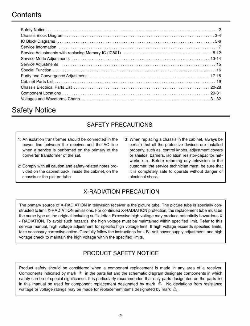
Safety Notice
SAFETY PRECAUTIONS
1: An isolation transformer should be connected in thepower line between the receiver and the AC linewhen a service is performed on the primary of theconverter transformer of the set.
2: Comply with all caution and safety-related notes pro-vided on the cabinet back, inside the cabinet, on thechassis or the picture tube.
3: When replacing a chassis in the cabinet, always becertain that all the protective devices are installedproperly, such as, control knobs, adjustment coversor shields, barriers, isolation resistor-capacitor net-works etc.. Before returning any television to thecustomer, the service technician must be sure thatit is completely safe to operate without danger ofelectrical shock.
X-RADIATION PRECAUTION
The primary source of X-RADIATION in television receiver is the picture tube. The picture tube is specially con-structed to limit X-RADIATION emissions. For continued X-RADIATION protection, the replacement tube must bethe same type as the original including suffix letter. Excessive high voltage may produce potentially hazardous X- RADIATION. To avoid such hazards, the high voltage must be maintained within specified limit. Refer to thisservice manual, high voltage adjustment for specific high voltage limit. If high voltage exceeds specified limits,take necessary corrective action. Carefully follow the instructions for + B1 volt power supply adjustment, and highvoltage check to maintain the high voltage within the specified limits.
PRODUCT SAFETY NOTICE
Product safety should be considered when a component replacement is made in any area of a receiver.Components indicated by mark in the parts list and the schematic diagram designate components in whichsafety can be of special significance. It is particularly recommended that only parts designated on the parts listin this manual be used for component replacement designated by mark . No deviations from resistancewattage or voltage ratings may be made for replacement items designated by mark .
SM_29-C7GV(FC6-A)AUS 7/27/05 7:12 PM Page 2
-3-
Chassis Block Diagrams
A10
1T
UN
ER
IIC B
us
IC10
01A
V S
ELE
CTO
R
V L R
MONITOR OUT AV1 INPUT
V
S-I
N
CR
CBY L R
DV
DIN
Y o
r V
IDE
O IN
C-I
N
IC80
2M
EM
OR
Y
IIC B
us
R/G
/B
OU
T
V-O
UT
H-O
UT
IIC Bus
H.V
.
Q43
1H
-DR
IVE
IC50
1V
ER
T. D
EF.
CR
T U
NIT
IC00
1A
UD
IO A
MP.
SP
902
SP
901
CR
T
MA
IN U
NIT
RE
AR
TE
RM
INA
L 32
5
8 641
SA
W-F
ILT
ER
5
HE
AD
PH
ON
E
JAC
K
1
TV
CO
MP.
VID
EO
OU
T
3
Y C7
4845
VID
EO
M
ON
ITO
R
OU
T
R
L
112
/13
/14
VID
EO
D
ET.
SO
UN
D
DE
T.
IC20
1IF
/VID
EO
/CH
RO
MA
Y o
r V
IDE
OO
UT
17 21
15
Q43
2H
-OU
T
DY
VE
RT.
DY
T471
FBT
FO
CU
S
SC
RE
EN
HO
RIZ
. DY
PIN
CU
SH
ION
CIR
CU
IT(Q
461,
Q46
2)
5/6
Fro
m IC
201(
CP
U)
p
in-3
1/32
31/3
2
L-O
UT
R-O
UT
SU
PE
R
WO
OF
ER
R-Y
B-Y
51 49
46T
RA
P
VID
EO
A
MP.
MO
NIT
OR
OU
T-R
MO
NIT
OR
OU
T-L
RL
DV
D R
-Y
DV
D B
-Y
VID
EO
S
W
TR
AP
DE
LAY
LIN
E
RG
B
MAT
RIX
OS
DS
W
OS
D
1HD
ELA
Y
Y-D
VD
-IN
AV1
R-I
N
AV1
VID
EO
-IN
B+:
140
V
24V
20V
9V 5VR
C
FB
T
HO
RIZ
. DE
F.V
ER
T. D
EF.
MA
IN S
OU
ND
AM
P.W
OO
FE
R A
MP.
IC20
1(1
CH
IP IC
) /IC
3451
IC20
1(C
PU
) / I
C80
2(E
EP
RO
M)
PO
WE
R S
UP
PLY
CIR
CU
IT
R BG
R BG
6X
161
IF
IF
RL
Y-IN
AV1
L-IN
Y-D
VD
IN
VID
EO
IN
46
R-Y
B-Y
FRO
NT
TER
MIN
AL
V L R
AV2 INPUT
RF
AG
C
Fro
m IC
201(
CP
U)
p
in-6
1
IC37
01A
UD
IO C
ON
TRO
L
54
AV2
VID
EO
-IN
AV2
L-IN
AV2
R-I
N
FM
D
ET.
DC
V
OL.5
6
FM
OU
T
FM
OU
T
235 34
433
19/2
0
3 1423
15/1
7
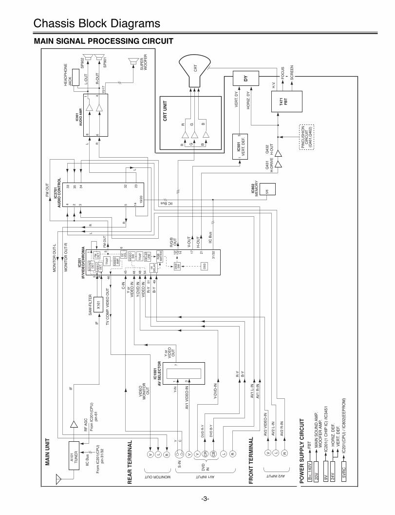
MAIN SIGNAL PROCESSING CIRCUIT
SM_29-C7GV(FC6-A)AUS 7/27/05 7:12 PM Page 3
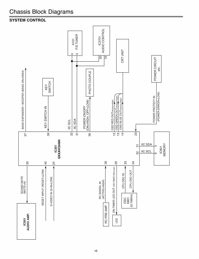
-4-
Chassis Block DiagramsSYSTEM CONTROL
BA
SS
EX
PA
ND
ER
/ W
OO
FE
R (
BA
SS
ON
=H
IGH
)37 39
KE
Y S
WIT
CH
INK
EY
SW
ITC
H
IIC S
CL
32 31 36
IIC S
DA
PO
WE
R O
N/O
FF
PH
OT
O C
OU
PLE
(O
N=
HIG
H, O
FF
=LO
W)
IC20
1Q
XX
AV
C56
8N
12 13 14 2331
3234332926
OS
D R
ED
OU
T(A
ctiv
e=H
igh)
OS
D G
RE
EN
OU
T(A
ctiv
e=H
igh)
OS
D B
LUE
OU
T(A
ctiv
e=H
igh)
CR
T U
NIT
PO
WE
R P
RO
TE
CT
IN
(P
OW
ER
ER
RO
R=
LOW
)P
OW
ER
CIR
CU
ITet
c.
IIC SCL
IIC SDA
IC80
1 M
EM
OR
Y
OS
CX
801
32.7
68K
Hz
CP
U O
SC
OU
T
CP
U O
SC
IN
LED
ON
-TIM
ER
LE
D O
UT
(ON
TIM
ER
ON
=Lo
w)
RC
SIG
NA
L IN
(AC
TIV
E=
HIG
H)
RC
PR
E-A
MP
.
30
SO
UN
D M
UT
E(M
UT
E=
H)
IC00
1A
UD
IO A
MP
.
A10
1F
/S T
UN
ER
RE
SE
T IN
PU
T (
RE
SE
T=
LOW
)40
56
54
IC37
01A
UD
IO C
ON
TR
OL
1920
S-V
IDE
O IN
(S
-IN
=LO
W)
24
QX
XA
VC
646N
SM_29-C7GV(FC6-A)AUS 7/27/05 7:12 PM Page 4
-5-
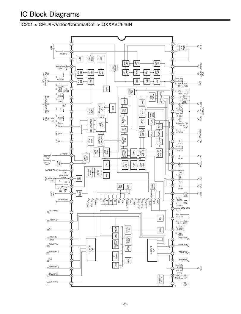
IC Block DiagramsIC201 < CPU/IF/Video/Chroma/Def. > QXXAVC646N
CLO
CK
CO
NT
RO
L
I/OP
OR
T 0
RA
MR
OM
BA
SE
TIM
ER
CP
UC
OR
E
OS
DB
US
CLO
CK
CO
NT
RO
LT
IME
R0
AD
C
RS
TP
LLV
DD
AF
T
RE
SE
T
CP
U T
ST
R
CP
U T
ST
G
CP
U T
ST
B
CV
BS
PD
C
EN
AB
LE
VS
HS
RGBFSIDA
TA
CLO
CK
C-S
YN
C
I/OP
OR
T 1
V D
ET
RE
SE
T
BU
S
HS
VS
FB
PA
FC
1
AF
C2
PH
AS
ES
HIF
TE
R
HO
RV
CC
VE
RR
AM
P
VE
RS
EP
SY
NC
SE
P
CO
LOR
CLA
MP
TIN
T
D1 S
W1H
DL
HO
RV
CO
1/256
HO
RC
/D
CLM
PD
C A
DJ
AP
C2
DD
SV
XO
VC
OFS
CS
YN
CA
PC
1
AC
CY
C S
WPA
L SW
DE
MO
BP
F
VID
EO
SW
CLM
PC
LMP
DC
RE
ST
TRA
PV
/YS
WD
LS
HA
RP
BG
SG
RG
BM
ATRIX
CO
NT
RA
ST
BR
IGH
T
VE
RC
/D
OS
DS
W
OS
D
OS
DC
ON
TR
AS
T
AB
LA
CL
DR
IVE
/OU
T-OFF
HO
RO
UT
SP
LL
AF
TVID
EOAM
P
DAH
VCO
SW
RF
AGC
TRAP
IFAG
C
VIFAM
PVID
EOD
ET
SOU
ND
DET
LIMAM
PBPF
500KD
ET
BPF
FMD
ET
FMAM
P
SWDC
VOL
18P
15P510K
0.01U
100U
+
VD
D
AN4/P04
AN5/P05
AN6/P06
AN7/P07150K
0.33U
2.2U 100
0.033U
CPU GND0.01U
100
100U
20K
FB
P
0.1U
YC
-CY
C-Y
1U
1U
750
1U
DV
D-Y
CB
0.1U
4.43M
0.1U
CR
SV
O/F
SC
0.047U
0.47U12K
1U
0.01U
100U
EX
T-VV
CC
:5VV
CD
INT-V
VC
C
OU
TV
IDE
OR
F-A
GC
IF IN
1U
680K
2.2U
560 0.47U
47K 47K
0.1U
SA
WF
IL
6463
6261
6059
5857
5655
5453
5251
5049
4847
4645
4443
4241
4039
3837
3635
3433
+
+
+
+
+
+
+
++
+
+
10P
0.022U
39K 1U
+
0.022U
1500P
10K 0.01U+
100U
0.01U
+
10U+
100U
42
+
0.01U
FM
OU
TV
OLU
ME
OU
T5V
EX
T-AU
DIO
INA
BL
RG
B9V
RO
UT
GO
UT
BO
UT
V RAMP0.47U
(M)
0.015U(M)
VE
RO
UT
(METAL FILM)4.7K+
100U
0.01U120
VD
D
0.015U+
1U 3KHO
RO
UT
1CHIP GND
INT0/P00
INT1/P01
P02
INT3/P03
IRAD
PWMI/P14
PWM2/P15
P17
PWM3/P16
SDA1/P12
SCK1/P13 3231
3029
2827
2625
2423
2221
2019
1817
1615
1413
1211
109
87
65
43
21
SM_29-C7GV(FC6-A)AUS 7/27/05 7:12 PM Page 5
IC Block Diagrams
-6-
18 17 16 15 14 13 12 11 10 9 8 7 6 5 4 3 2 1
363534333231302928272625242322212019
CONTROL
DATA
CONTROL
TONE CONT
MatrixTOTAL
Bypass
SURROUND
MUTE
ANALOGSURROUND(AViSS)
SURROUND
Bypass
TOTALMatrix
MUTE
Bypass
DC
PseudStereo
MO
NO-S
W
P-St
ereo
P-St
ereo
Bypass
DC
TONE CONT
GNDINPU
T-A(
R)
INPU
T-B(
R)
INPU
T-C(
R)
LINE
-OUT
(R)
DC C
UT(R
)
ST-1
ST-2
TREB
LE(R
)
BASS
-1(R
)
BASS
-2(R
)
OUT
(R)
EVR-
IN(R
)
EVR-
OUT
(R)
L+R
OUT
VREF
VCC
VDD
12C-
DATA
12C-
CLK
VSS
L+R
LPF
EVR-
OUT
(L)
EVR-
IN(L
)
OUT
(L)
BASS
-2(L
)
BASS
-1(L
)
TREB
LE(L
)
AviS
S HP
F
ST-2
DC C
UT(L
)
LINE
OUT
(L)
INPU
T-C(
L)
INPU
T-B(
L)
INPU
T-A(
L)
ANAL
OG
GND
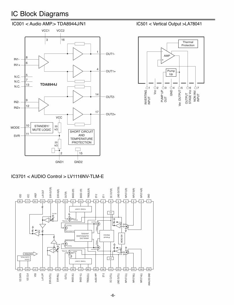
IC3701 < AUDIO Control > LV1116NV-TLM-E
IC001 < Audio AMP.> TDA8944J/N1
1
4
14
17
OUT1-
OUT1+
OUT2-
OUT2+
163
VCC1 VCC2
6
5
7
13
8
12
10
11
9
IN1-
IN1+
IN2-
IN2+
MODE
SVR
STANDBY/MUTE LOGIC
VCC
20kΩ
20kΩ
2 15
GND1 GND2
SHORT CIRCUITAND
TEMPERATUREPROTECTION
N.C.
N.C.
N.C.TDA8944J
IC501 < Vertical Output >LA78041
ThermalProtection
-
+AMP
PumpUp
1
INV
ER
TIN
G
INP
UT
2
Vcc
3
PU
MP
UP
OU
T
4
GN
D
5
Ver.
OU
TPU
T
6
OU
TPU
T S
TAG
E V
cc
7
NO
N IN
V.IN
PU
T
SM_29-C7GV(FC6-A)AUS 7/27/05 7:12 PM Page 6
-7-
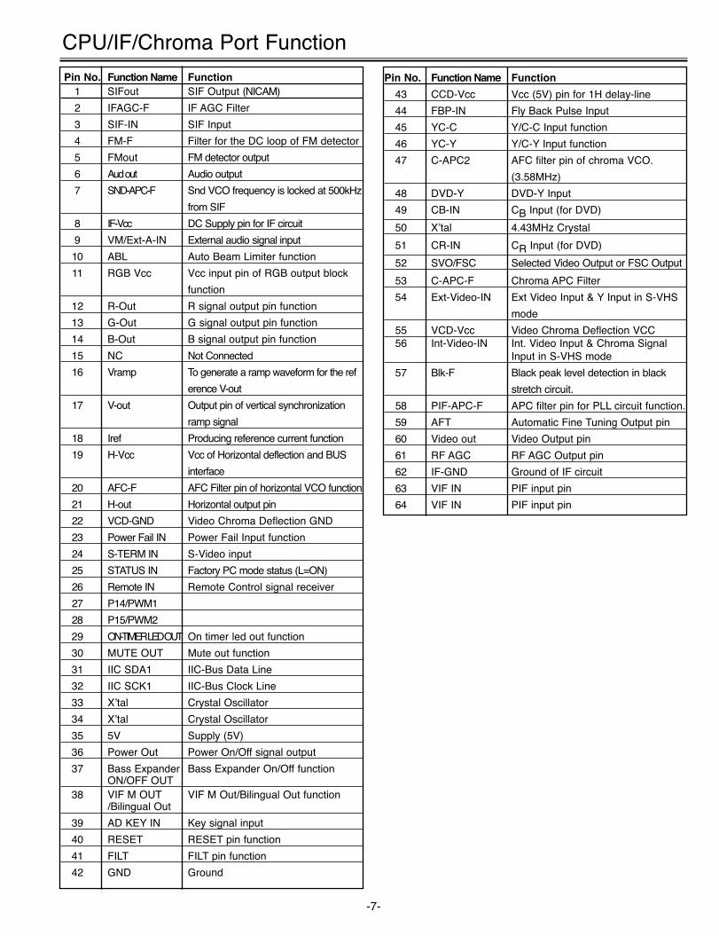
CPU/IF/Chroma Port Function
Pin No. Function Name Function1 SIFout SIF Output (NICAM)
2 IFAGC-F IF AGC Filter
3 SIF-IN SIF Input
4 FM-F Filter for the DC loop of FM detector
5 FMout FM detector output
6 Aud out Audio output
7 SND-APC-F Snd VCO frequency is locked at 500kHz
from SIF
8 IF-Vcc DC Supply pin for IF circuit
9 VM/Ext-A-IN External audio signal input
10 ABL Auto Beam Limiter function
11 RGB Vcc Vcc input pin of RGB output block
function
12 R-Out R signal output pin function
13 G-Out G signal output pin function
14 B-Out B signal output pin function
15 NC Not Connected
16 Vramp To generate a ramp waveform for the ref
erence V-out
17 V-out Output pin of vertical synchronization
ramp signal
18 Iref Producing reference current function
19 H-Vcc Vcc of Horizontal deflection and BUS
interface
20 AFC-F AFC Filter pin of horizontal VCO function
21 H-out Horizontal output pin
22 VCD-GND Video Chroma Deflection GND
23 Power Fail IN Power Fail Input function
24 S-TERM IN S-Video input
25 STATUS IN Factory PC mode status (L=ON)
26 Remote IN Remote Control signal receiver
27 P14/PWM1
28 P15/PWM2
29 ON-TIMER LED OUT On timer led out function
30 MUTE OUT Mute out function
31 IIC SDA1 IIC-Bus Data Line
32 IIC SCK1 IIC-Bus Clock Line
33 X’tal Crystal Oscillator
34 X’tal Crystal Oscillator
35 5V Supply (5V)
36 Power Out Power On/Off signal output
37 Bass Expander Bass Expander On/Off functionON/OFF OUT
38 VIF M OUT VIF M Out/Bilingual Out function/Bilingual Out
39 AD KEY IN Key signal input
40 RESET RESET pin function
41 FILT FILT pin function
42 GND Ground
Pin No. Function Name Function
43 CCD-Vcc Vcc (5V) pin for 1H delay-line
44 FBP-IN Fly Back Pulse Input
45 YC-C Y/C-C Input function
46 YC-Y Y/C-Y Input function
47 C-APC2 AFC filter pin of chroma VCO.
(3.58MHz)
48 DVD-Y DVD-Y Input
49 CB-IN CB Input (for DVD)
50 X’tal 4.43MHz Crystal
51 CR-IN CR Input (for DVD)
52 SVO/FSC Selected Video Output or FSC Output
53 C-APC-F Chroma APC Filter
54 Ext-Video-IN Ext Video Input & Y Input in S-VHS
mode
55 VCD-Vcc Video Chroma Deflection VCC56 Int-Video-IN Int. Video Input & Chroma Signal
Input in S-VHS mode
57 Blk-F Black peak level detection in black
stretch circuit.
58 PIF-APC-F APC filter pin for PLL circuit function.
59 AFT Automatic Fine Tuning Output pin
60 Video out Video Output pin
61 RF AGC RF AGC Output pin
62 IF-GND Ground of IF circuit
63 VIF IN PIF input pin
64 VIF IN PIF input pin
SM_29-C7GV(FC6-A)AUS 7/27/05 7:12 PM Page 7
-8-
Service Information
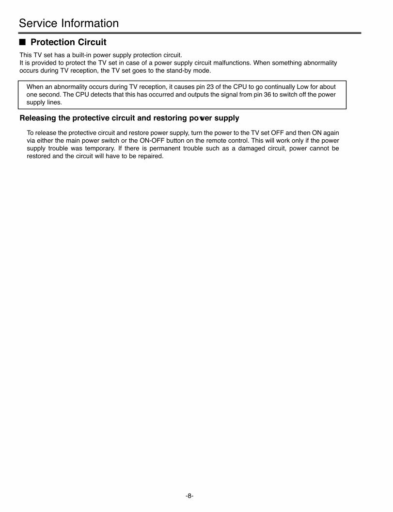
This TV set has a built-in power supply protection circuit.It is provided to protect the TV set in case of a power supply circuit malfunctions. When something abnormalityoccurs during TV reception, the TV set goes to the stand-by mode.
When an abnormality occurs during TV reception, it causes pin 23 of the CPU to go continually Low for aboutone second. The CPU detects that this has occurred and outputs the signal from pin 36 to switch off the powersupply lines.
Releasing the protective circuit and restoring power supply
To release the protective circuit and restore power supply, turn the power to the TV set OFF and then ON againvia either the main power switch or the ON-OFF button on the remote control. This will work only if the powersupply trouble was temporary. If there is permanent trouble such as a damaged circuit, power cannot berestored and the circuit will have to be repaired.
Protection Circuit
SM_29-C7GV(FC6-A)AUS 7/27/05 7:12 PM Page 8
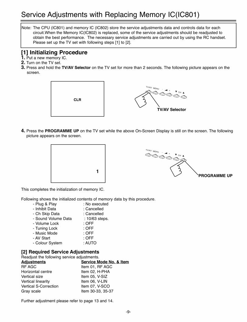
Service Adjustments with Replacing Memory IC(IC801)
Note: The CPU (IC801) and memory IC (IC802) store the service adjustments data and controls data for each circuit.When the Memory IC(IC802) is replaced, some of the service adjustments should be readjusted to obtain the best performance. The necessary service adjustments are carried out by using the RC handset. Please set up the TV set with following steps [1] to [2].
[1] Initializing Procedure1. Put a new memory IC.2. Turn on the TV set.3. Press and hold the TV/AV Selector on the TV set for more than 2 seconds. The following picture appears on the
screen.
4. Press the PROGRAMME UP on the TV set while the above On-Screen Display is still on the screen. The followingpicture appears on the screen.
This completes the initialization of memory IC.
Following shows the initialized contents of memory data by this procedure.- Plug & Play : No executed- Inhibit Data : Cancelled- Ch Skip Data : Cancelled- Sound Volume Data : 10/63 steps.- Volume Lock : OFF- Tuning Lock : OFF- Music Mode : OFF- AV Start : OFF- Colour System : AUTO
1
CLR
[2] Required Service AdjustmentsReadjust the following service adjustments.Adjustments Service Mode No. & ItemRF AGC Item 01, RF AGCHorizontal centre Item 02, H-PHAVertical size Item 05, V-SIZVertical linearity Item 06, V-LINVertical S-Correction Item 07, V-SCOGray scale Item 30-33, 35-37
Further adjustment please refer to page 13 and 14.
-9-
MENUTV/AV
- +CH
TV/AV Selector
MENUTV/AV
- +CH
PROGRAMME UP
SM_29-C7GV(FC6-A)AUS 7/27/05 7:12 PM Page 9
-10-
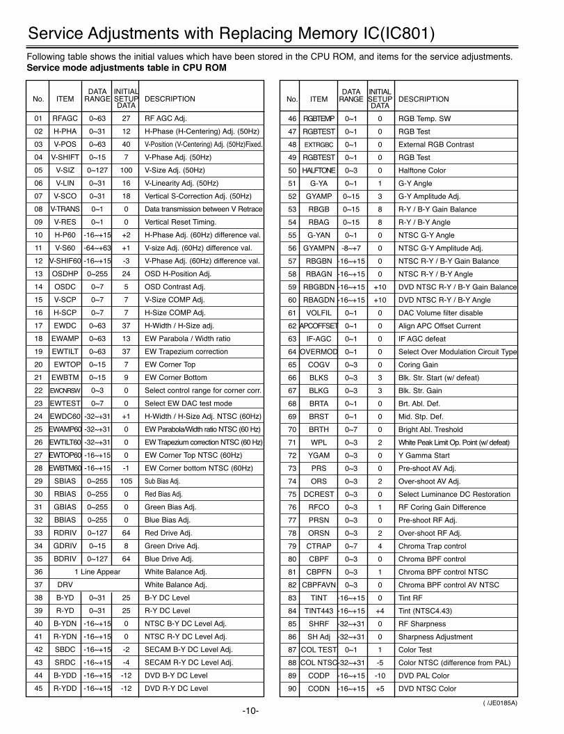
Service Adjustments with Replacing Memory IC(IC801)
DATA INITIALNo. ITEM RANGE SETUP DESCRIPTION
DATA
01 RFAGC 0~63 27 RF AGC Adj.
02 H-PHA 0~31 12 H-Phase (H-Centering) Adj. (50Hz)
03 V-POS 0~63 40 V-Position (V-Centering) Adj. (50Hz)Fixed.
04 V-SHIFT 0~15 7 V-Phase Adj. (50Hz)
05 V-SIZ 0~127 100 V-Size Adj. (50Hz)
06 V-LIN 0~31 16 V-Linearity Adj. (50Hz)
07 V-SCO 0~31 18 Vertical S-Correction Adj. (50Hz)
08 V-TRANS 0~1 0 Data transmission between V Retrace
09 V-RES 0~1 0 Vertical Reset Timing.
10 H-P60 -16~+15 +2 H-Phase Adj. (60Hz) difference val.
11 V-S60 -64~+63 +1 V-size Adj. (60Hz) difference val.
12 V-SHIF60 -16~+15 -3 V-Phase Adj. (60Hz) difference val.
13 OSDHP 0~255 24 OSD H-Position Adj.
14 OSDC 0~7 5 OSD Contrast Adj.
15 V-SCP 0~7 7 V-Size COMP Adj.
16 H-SCP 0~7 7 H-Size COMP Adj.
17 EWDC 0~63 37 H-Width / H-Size adj.
18 EWAMP 0~63 13 EW Parabola / Width ratio
19 EWTILT 0~63 37 EW Trapezium correction
20 EWTOP 0~15 7 EW Corner Top
21 EWBTM 0~15 9 EW Corner Bottom
22 EWCNRSW 0~3 0 Select control range for corner corr.
23 EWTEST 0~7 0 Select EW DAC test mode
24 EWDC60 -32~+31 +1 H-Width / H-Size Adj. NTSC (60Hz)
25 EWAMP60 -32~+31 0 EW Parabola/Width ratio NTSC (60 Hz)
26 EWTILT60 -32~+31 0 EW Trapezium correction NTSC (60 Hz)
27 EWTOP60 -16~+15 0 EW Corner Top NTSC (60Hz)
28 EWBTM60 -16~+15 -1 EW Corner bottom NTSC (60Hz)
29 SBIAS 0~255 105 Sub Bias Adj.
30 RBIAS 0~255 0 Red Bias Adj.
31 GBIAS 0~255 0 Green Bias Adj.
32 BBIAS 0~255 0 Blue Bias Adj.
33 RDRIV 0~127 64 Red Drive Adj.
34 GDRIV 0~15 8 Green Drive Adj.
35 BDRIV 0~127 64 Blue Drive Adj.
36 1 Line Appear White Balance Adj.
37 DRV White Balance Adj.
38 B-YD 0~31 25 B-Y DC Level
39 R-YD 0~31 25 R-Y DC Level
40 B-YDN -16~+15 0 NTSC B-Y DC Level Adj.
41 R-YDN -16~+15 0 NTSC R-Y DC Level Adj.
42 SBDC -16~+15 -2 SECAM B-Y DC Level Adj.
43 SRDC -16~+15 -4 SECAM R-Y DC Level Adj.
44 B-YDD -16~+15 -12 DVD B-Y DC Level
45 R-YDD -16~+15 -12 DVD R-Y DC Level
Following table shows the initial values which have been stored in the CPU ROM, and items for the service adjustments.Service mode adjustments table in CPU ROM
DATA INITIALNo. ITEM RANGE SETUP DESCRIPTION
DATA
46 RGBTEMP 0~1 0 RGB Temp. SW
47 RGBTEST 0~1 0 RGB Test
48 EXTRGBC 0~1 0 External RGB Contrast
49 RGBTEST 0~1 0 RGB Test
50 HALFTONE 0~3 0 Halftone Color
51 G-YA 0~1 1 G-Y Angle
52 GYAMP 0~15 3 G-Y Amplitude Adj.
53 RBGB 0~15 8 R-Y / B-Y Gain Balance
54 RBAG 0~15 8 R-Y / B-Y Angle
55 G-YAN 0~1 0 NTSC G-Y Angle
56 GYAMPN -8~+7 0 NTSC G-Y Amplitude Adj.
57 RBGBN -16~+15 0 NTSC R-Y / B-Y Gain Balance
58 RBAGN -16~+15 0 NTSC R-Y / B-Y Angle
59 RBGBDN -16~+15 +10 DVD NTSC R-Y / B-Y Gain Balance
60 RBAGDN -16~+15 +10 DVD NTSC R-Y / B-Y Angle
61 VOLFIL 0~1 0 DAC Volume filter disable
62 APCOFFSET 0~1 0 Align APC Offset Current
63 IF-AGC 0~1 0 IF AGC defeat
64 OVERMOD 0~1 0 Select Over Modulation Circuit Type
65 COGV 0~3 0 Coring Gain
66 BLKS 0~3 3 Blk. Str. Start (w/ defeat)
67 BLKG 0~3 3 Blk. Str. Gain
68 BRTA 0~1 0 Brt. Abl. Def.
69 BRST 0~1 0 Mid. Stp. Def.
70 BRTH 0~7 0 Bright Abl. Treshold
71 WPL 0~3 2 White Peak Limit Op. Point (w/ defeat)
72 YGAM 0~3 0 Y Gamma Start
73 PRS 0~3 0 Pre-shoot AV Adj.
74 ORS 0~3 2 Over-shoot AV Adj.
75 DCREST 0~3 0 Select Luminance DC Restoration
76 RFCO 0~3 1 RF Coring Gain Difference
77 PRSN 0~3 0 Pre-shoot RF Adj.
78 ORSN 0~3 2 Over-shoot RF Adj.
79 CTRAP 0~7 4 Chroma Trap control
80 CBPF 0~3 0 Chroma BPF control
81 CBPFN 0~3 1 Chroma BPF control NTSC
82 CBPFAVN 0~3 0 Chroma BPF control AV NTSC
83 TINT -16~+15 0 Tint RF
84 TINT443 -16~+15 +4 Tint (NTSC4.43)
85 SHRF -32~+31 0 RF Sharpness
86 SH Adj -32~+31 0 Sharpness Adjustment
87 COL TEST 0~1 1 Color Test
88 COL NTSC-32~+31 -5 Color NTSC (difference from PAL)
89 CODP -16~+15 -10 DVD PAL Color
90 CODN -16~+15 +5 DVD NTSC Color
( /JE0185A)
SM_29-C7GV(FC6-A)AUS 7/27/05 7:12 PM Page 10
-11-
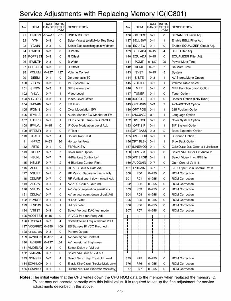
Service Adjustments with Replacing Memory IC(IC801)
Notes: The initial value that the CPU writes down the CPU ROM data to the memory when replaced the memory IC. TV set may not operate correctly with this initial value. It is required to set up the fine adjustment for service adjustments described in the above.
DATA INITIALNo. ITEM RANGE SETUP DESCRIPTION
DATA
91 TINTDN -16~+15 -15 DVD NTSC Tint
92 YTH 0~3 0 Select Y signal sensitivity for Blue Strecth
93 YGAIN 0~3 0 Select Blue stretching gain w/ defeat
94 RWIDTH 0~3 0 R Width
95 ROFFSET 0~3 0 R Offset
96 BWIDTH 0~3 0 B Width
97 BOFFSET 0~3 0 B Offset
98 VOLUM 0~127 127 Volume Control
99 DEEM 0~1 0 De-emphasis TC
100 VIFSW 0~3 0 VIF System SW
101 SIFSW 0~3 1 SIF System SW
102 V-LVL 0~7 4 Video Level
103 V-LVLOFS 0~3 1 Video Level Offset
104 FMGAIN 0~1 0 FM Gain
105 IFOM-S 0~1 0 Over Modulation SW
106 IFMN-S 0~1 1 Audio Monitor SW Monitor or FM
107 IFTRPS 0~1 1 IC Inside SIF Trap SW ON-OFF
108 IFMLVL 0~15 0 IF Over Modulation Level Adj.
109 IFTEST1 0~1 0 IF Test 1
110 TRAPT 0~7 4 Sound Trapt Test
111 H-FRQ 0~63 20 Horizontal Freq.
112 FBTS 0~1 0 FBPBLK SW
113 COOP 0~7 7 Color Killer Option
114 HBLKL 0~7 7 H-Blanking Control Left
115 HBLKR 0~7 2 H-Blanking Control Right
116 AFCRF 0~1 0 RF AFC Gain & Gate Adj.
117 VSURF 0~1 0 RF Vsync. Separation sensitivity
118 CDMRF 0~7 0 RF Vertical count down circuit Adj.
119 AFCAV 0~1 1 AV AFC Gain & Gate Adj.
120 VSUAV 0~1 0 AV Vsync separation sensitivity
121 CDMAV 0~7 0 AV vertical count down circuit Adj.
122 HLVDRF 0~1 1 H-Lock Vdet
123 HLVDAV 0~1 1 H-Lock Vdet
124 VTEST 0~3 0 Select Vertical DAC test mode
125 VCOTEST 0~15 0 IF VCO free run Freq. Adj.
126 C.VCOADJ 0~7 4 Control free run Freq. of chroma VCD
127 VCOFREQ 0~255 100 ES Sample IF VCO Freq. Adj.
128 CROSS-BW 0~3 0 Pattern Output
129 AVNCON 0~127 64 AV non-signal Contrast
130 AVNBRI 0~127 64 AV non-signal Brightness
131 VMDELAY 0~3 0 Select Delay of VM out
132 VMGAIN 0~7 0 Select VM Gain of VM out
133 SYNSEP 0~7 4 Select Sync. Sep Treshold Level
134 SCMKILON 0~1 0 Enable Killer Circuit (Service Mode only)
135 SCMKILOF 0~1 0 Disable Killer Circuit (Service Mode only)
DATA INITIALNo. ITEM RANGE SETUP DESCRIPTION
DATA
136 SCM TEST 0~1 0 SECAM DC Level Adj.
137 BELL SW 0~1 1 Enable BELL Filter Adj.
138 EQU SW 0~1 0 Enable EQUALIZER Circuit Adj.
139 BELLADJ 0~15 4 BELL Filter Adj.
140 EQU ADJ 0~15 0 EQUALIZER Filter Adj.
141 POMT 0~127 25 Power Mute Time
142 CHMT 0~31 7 Ch Mute Time
143 SYST 0~15 5 System
144 S-STE 0~3 1 AV Stereo/Mono Option
145 VOLTBL 0~1 1 Volume Table Select
146 MPP 0~1 0 MPP Function on/off Option
147 TUNER 0~1 0 Tuner Option
148 BOOSTER 0~1 0 Booster Option (LNA Tuner)
149 OPT AVIN 0~3 2 AV1/AV2/AV3 Option
150 OPT POS 0~1 1 255 Position Option
151 LANGUAGE 0~1 1 Language Option
152 OPT COL 0~1 0 Color System Option
153 OPT SIF 0~1 1 SIF System Option
154 OPT BASS 0~3 2 Bass Expander Option
155 OPT SURR 0~1 1 Surround Option
156 OPT BLBK 0~1 1 Blue Back Option
157 1LINEMOD 0~1 0 Color Output Data Option at 1 Line Mode
158 OPT VM 0~1 0 Select VM Out or Ext Audio In
159 OPT ERGB 0~1 1 Select Video In or RGB In
160 AUDGAIN 0~7 0 Gain Control LV1116
161 L/RGAIN 0~7 7 L/R Output Gain Control LV111
300 R00 0~255 0 ROM Correction
301 R01 0~255 0 ROM Correction
302 R02 0~255 0 ROM Correction
303 R03 0~255 0 ROM Correction
304 R04 0~255 0 ROM Correction
305 R05 0~255 0 ROM Correction
306 R06 0~255 0 ROM Correction
307 R07 0~255 0 ROM Correction
375 R75 0~255 0 ROM Correction
376 R76 0~255 0 ROM Correction
377 R77 0~255 0 ROM Correction
SM_29-C7GV(FC6-A)AUS 7/27/05 7:12 PM Page 11
-12-
ADDRESSDRV
SI. 00100101S2.11111000DATA
B 6421 R 64ADDRESS
V-SCO
SI. 00100101S2.11111000DATA
905
ADDRESSRF AGC
SI. 00100101S2.11111000DATA
3001
Service Adjustments with Replacing Memory IC(IC801)
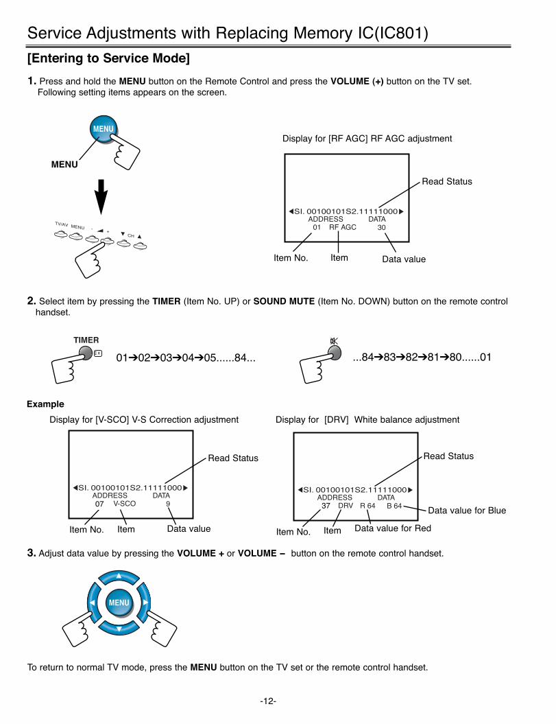
[Entering to Service Mode]
1. Press and hold the MENU button on the Remote Control and press the VOLUME (+) button on the TV set.Following setting items appears on the screen.
Display for [V-SCO] V-S Correction adjustment
Read Status
Item No. Item Data value
Display for [RF AGC] RF AGC adjustment
Read Status
Item No. Item Data value
Data value for Red
Display for [DRV] White balance adjustment
Read Status
Item No. Item
Data value for Blue
To return to normal TV mode, press the MENU button on the TV set or the remote control handset.
2. Select item by pressing the TIMER (Item No. UP) or SOUND MUTE (Item No. DOWN) button on the remote controlhandset.
3. Adjust data value by pressing the VOLUME + or VOLUME - button on the remote control handset.
Example
MENU
MENU
0102030405......84... ...8483828180......01
TIMERx
MENUTV/AV
- +CH
07
MENU
37
SM_29-C7GV(FC6-A)AUS 7/27/05 7:12 PM Page 12
-13-
Service Mode AdjustmentsFollowing adjustments should be carried out when the memory IC is replaced. How to enter the service mode andadjust values, please refer to “ Entering to Service mode” on page 12.
NOTE: Do not attempt this adjustment with weak signal.(1) Tune the receiver to most clearest (or strongest) VHF
station in your area. Set the brightness and contrastcontrols to maximum. Set the colour control to minimum.
(2) Select [RF AGC] in the service mode.(3) Change value until the snow noise just disappears.(4) Exit from service mode.
Item 01 [RF AGC] AGC
(1) Receive a monochrome circular pattern.(2) Set the brightness and contrast to normal.(3) Select [H-PHA] in the service mode.(4) Change value to be optimum horizontal centre position. (5) Exit from service mode.
Item 02 [H-PHA] HORIZONTAL CENTRE
(1) Receive a monochrome circular pattern.(2) Set the brightness and contrast to maximum.(3) Select [V-SIZ] in the service mode.(4) Change value to be optimum vertical size.(5) Exit from service mode.
Item 04 [V-SIZ] VERTICAL SIZE
Horizontal centre
Vertical size
c Upper
Center
Bottom
d
e
a
b
Upper
Center
Bottom
(1) Receive a crosshatch pattern.(2) Select a picture mode of NATURAL by pressing the
PICTURE MODE button.(3) Select [V-SCO] in the service mode.(4) Adjust Vertical S-letter Correction so that the difference
of “c”, “d” and “e” becomes less than 2 mm by pressingthe VOLUME + or - button.
(5) Confirm Vertical Linearity and adjust Vertical Center then Vertical Size.
(6) Exit from service mode.
Item 05 [V-SCO] V-S CORRECTION
(1) Receive a crosshatch pattern.(2) Select a picture mode of NATURAL by pressing the
PICTURE MODE button.(3) Select [V-LIN] in the service mode.(4) Adjust Vertical Linearity so that the difference of “a” and
“b” becomes less than 3mm by pressing VOLUME + or- button.
(5) Exit from service mode.
Item 06 [V-LIN] VERTICAL LINEARITY
(1) Receive a crosshatch pattern.(2) Select a picture mode of NATURAL by pressing the
PICTURE MODE button.(3) Select [EWAMP] in the service mode.(4) Adjust Vertical Lines to be adequately straight.(5) Select [EWTILT] in the service mode.(6) Adjust Vertical Lines to be adequately parallel each
other.(7) Select [EWTOP] in the service mode.(8) Adjust Left and Right top corner so that vertical lines
more straight.(9) Select [EWBTM] in the service mode.(10) Adjust Left and Right bottom corner so that vertical
lines more straight.
Item 18~21 [PCC] PCC Adjustment
SM_29-C7GV(FC6-A)AUS 7/27/05 7:12 PM Page 13
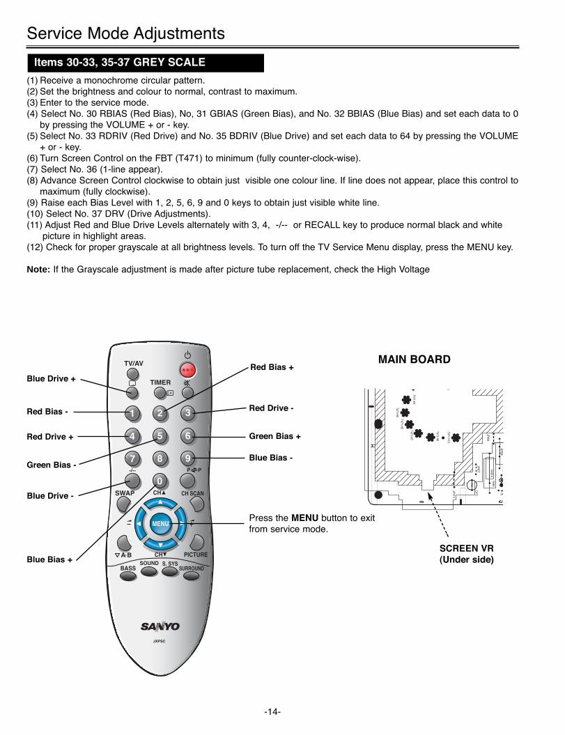
-14-
Service Mode Adjustments
JP409R488
T471-H5
1
JP408
C471
R481
T471-H7
T471-H6
T471-H4
T471-H8
T471-H10
R481A
JP407
JP414 J4
MAIN BOARD
SCREEN VR(Under side)
(1) Receive a monochrome circular pattern. (2) Set the brightness and colour to normal, contrast to maximum.(3) Enter to the service mode. (4) Select No. 30 RBIAS (Red Bias), No, 31 GBIAS (Green Bias), and No. 32 BBIAS (Blue Bias) and set each data to 0
by pressing the VOLUME + or - key.(5) Select No. 33 RDRIV (Red Drive) and No. 35 BDRIV (Blue Drive) and set each data to 64 by pressing the VOLUME
+ or - key.(6) Turn Screen Control on the FBT (T471) to minimum (fully counter-clock-wise).(7) Select No. 36 (1-line appear). (8) Advance Screen Control clockwise to obtain just visible one colour line. If line does not appear, place this control to
maximum (fully clockwise).(9) Raise each Bias Level with 1, 2, 5, 6, 9 and 0 keys to obtain just visible white line.(10) Select No. 37 DRV (Drive Adjustments).(11) Adjust Red and Blue Drive Levels alternately with 3, 4, -/-- or RECALL key to produce normal black and white
picture in highlight areas.(12) Check for proper grayscale at all brightness levels. To turn off the TV Service Menu display, press the MENU key.
Note: If the Grayscale adjustment is made after picture tube replacement, check the High Voltage
Items 30-33, 35-37 GREY SCALE
1 2 3
4 5 6
7 8 9
0
TV/AV
TIMERx
-/--
SWAP CH SCAN
MENU
BASSSOUND S. SYS
SURROUND
PICTURECH
CH
A B.
P P
JXPSC
Red Bias -
Red Bias +
Green Bias -
Green Bias +
Blue Bias -
Blue Bias +
Press the MENU button to exitfrom service mode.
Red Drive -
Red Drive +
Blue Drive -
Blue Drive +
SM_29-C7GV(FC6-A)AUS 7/27/05 7:12 PM Page 14
-15-
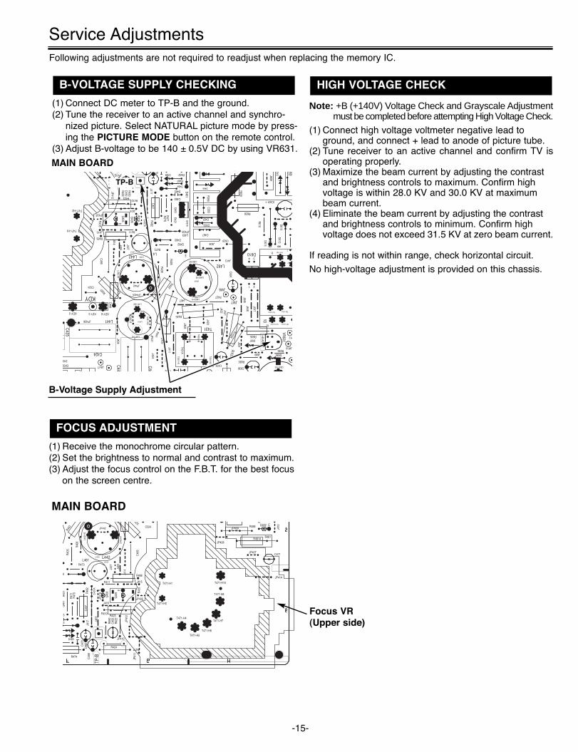
Service AdjustmentsFollowing adjustments are not required to readjust when replacing the memory IC.
Note: +B (+140V) Voltage Check and Grayscale Adjustmentmust be completed before attempting High Voltage Check.
(1) Connect high voltage voltmeter negative lead to ground, and connect + lead to anode of picture tube.
(2) Tune receiver to an active channel and confirm TV is operating properly.
(3) Maximize the beam current by adjusting the contrast and brightness controls to maximum. Confirm high voltage is within 28.0 KV and 30.0 KV at maximum beam current.
(4) Eliminate the beam current by adjusting the contrast and brightness controls to minimum. Confirm high voltage does not exceed 31.5 KV at zero beam current.
If reading is not within range, check horizontal circuit.
No high-voltage adjustment is provided on this chassis.
HIGH VOLTAGE CHECK
34
21
E
7
10
9
E E
C629
R628
R629
JP412
T471-H1
KDY-6KDY-3
D466
JP403
R422
R435
R423
JP410
T471-H2
L462
JP435
L441AL441
KDY
JP436
C450R450
C437R482
D489
D464
R487
D465
70
C355
C463
R470R471
R421
L403
J406
R473
D460R466
L462A
C465
D461
R462
C467
D441
R442
R441
R445
L461L461A
J404
L442A
R103
L442-H2
L442-H1
L462-H2
L462-H1
L462-H3
L441-H3
L441-H1
D610
J422
C691
J647
Q462
J407
C434
C432
R525
VR631
R636
R635
D686
JW7
JW8
D353
D421
R355
L441-H2
J405
JP442
J424 J425
J409
C524C44
C44
T431A
T431-H3
T431-H1
T431-H2
T431-H4
T431
C641-H2
8910
Q461
Q461A
+B ADJST.
D43
D439
JP441
T611-H10
T611-H8
T611-H11
Q432
C425
C424
J423
R427
R405J411
T611A-H10 T611A-H11
T611A-H8
J413
R410
R411
Q405
J414
R408
J415
Q406
J403
J416
J645
611-H7
A-H7
L442
JW10
W12
KDY-5
J609
605614
R610 D613D612
IC601-1
J421
J427
D615
616
R103A
JP416
J631
J646
R685
D687
C636
J680
JP442A
JP441A
J417
C437A
JW17
JW18
(1) Connect DC meter to TP-B and the ground. (2) Tune the receiver to an active channel and synchro-
nized picture. Select NATURAL picture mode by press-ing the PICTURE MODE button on the remote control.
(3) Adjust B-voltage to be 140 ± 0.5V DC by using VR631.
B-VOLTAGE SUPPLY CHECKING
(1) Receive the monochrome circular pattern.(2) Set the brightness to normal and contrast to maximum.(3) Adjust the focus control on the F.B.T. for the best focus
on the screen centre.
FOCUS ADJUSTMENT
MAIN BOARD
B-Voltage Supply Adjustment
MAIN BOARD
TP-B
E
EE
JP409R488
JP41
2
T471-H5
T471-H1
JP408
R
R422
R424
R435
R423
JP410
JP41
1
T471-H2
C471
R481
T471-H7
T471-H6
T471-H4
T471-H8
T471-H10
JP435
R477
R474
R481A
JP407
C450
R450
C437
R482
C482
D489
5
C470
3
R470
R471R4
21
R473
0 R466
C465
R442
L461L461A
L442A
L442
-H2
L442
-H1
R525
J405
JP442 C524
Q46
1
JP414
C468
Q402
J410
R405
R410
R411
Q40
5
J414
R408
J415
Q40
6
J403
TP-B
J416
L442
J427
JP41
6
J417
C437
A
Focus VR(Upper side)
SM_29-C7GV(FC6-A)AUS 7/27/05 7:12 PM Page 15
-16-
Special Function
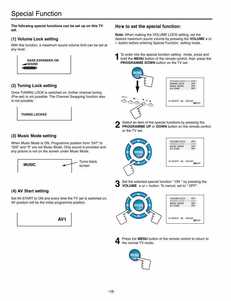
1 To enter into the special function setting mode, press and hold the MENU button of the remote control, then press thePROGRAMME DOWN button on the TV set.
Once TUNING LOCK is switched on, further channel tuning(Pre-set) is not possible. The Channel Swapping function alsois not possible.
2 Select an item of the special functions by pressing the PROGRAMME UP or DOWN button on the remote controlor the TV set.
3 Set the selected special function “ ON “ by pressing the VOLUME + or - button. To cancel, set to “ OFF”.
(2) Tuning Lock setting
The following special functions can be set up on this TVset.
With this function, a maximum sound volume limit can be set atany level.
(3) Music Mode setting
When Music Mode is ON, Programme position from “247” to“255” and “0” are set Music Mode. Only sound is provided andany picture is not on the screen under Music Mode.
Set AV-START to ON and every time the TV set is switched on,AV position will be the initial programme position.
(4) AV Start setting
TUNING LOCKED
How to set the special function:
Note: When making the VOLUME LOCK setting, set thedesired maximum sound volume by pressing the VOLUME + or- button before entering Special Function setting mode.
AV1
MUSICTurns blackscreen
4 Press the MENU button of the remote control to return to the normal TV mode.
(1) Volume Lock setting
SOUNDIIIIIIII
MENU
AV START
TUNING LOCKVOLUME LOCK
MUSIC MODE
OFFOFFOFFOFF
SELECT ADJUST M EXIT
AV START
TUNING LOCKVOLUME LOCK
MUSIC MODE
OFFONOFFOFF
SELECT ADJUST M EXIT
TUNING LOCK
AV START
VOLUME LOCK
MUSIC MODE
OFFOFFOFFOFF
SELECT ADJUST M EXIT
MENU - +CH
MENU
MENU
MENU
BASS EXPANDER ON
SM_29-C7GV(FC6-A)AUS 7/27/05 7:12 PM Page 16
-17-
Purity and Convergence Adjustment
Signals: Use a pattern generator which can output red, green, blue and white raster and crosshatch pattern signals.
Procedure: Carry out purity adjustment first, and then carryout convergence adjustment.
Preparation: The deflection yoke may have several correction magnets attached to its outer edge. If replacing the picture tube, the positions of the magnets can be changed andthey can be re-used, so remove these magnets and keep them safely so that they do not get lost.
PURITY ADJUSTMENTS1. Place the picture so that its front faces west.2. Insert the power plug into a wall outlet, and then turn on
the power for the TV and de-magnetize the TV using itsown degaussing circuit.
3. Loosen the screw which is holding the deflection yoke(with integrated purity magnets), and then move thedeflection yoke forward as far as it will go. Remove therubber wedge at this time.
4. Turn off the red and blue raster so that only the greenraster is on.
5. Adjust the angle between the tabs (wings) on puritymagnets to center the vertical green belt in the picturetube screen. (See Figures 2 and 3.)
NOTE: This adjustment can only be carried out by changing the angle, not by rotating the tabs up anddown.
6. Gently move the deflection yoke back to the positionwhere the green band fills the whole of the picture tubescreen, and then tighten the screw to secure the deflection yoke in place.
7. If there is any color distortion around the edges, correctit by attaching magnets to the outer edge of the deflection yoke. The magnets should be attached sothat the line running from the position of the distortion tothe center of the picture tube intersects the deflectionyoke. The colors on the magnets indicate the north andsouth poles of the magnets. Attach the magnets inwhichever direction causes the distortion to disappear.(See Figures 1 and 4. The south and northpole positions are shown as a guide.)
8. Switch the screen to red and blue rasters and check thatthere is no color distortion. If there is any distortion,adjust the angles of purity magnets tabs or the forward-back position of the deflection yoke, or change the attachment positions of the correction magnets.
CAUTION: The Convergence and Purity adjustments have been made at the factory. Readjustmentshould be made only after picture tube or deflection yoke replacement, following the steps below:
Deflection yokemounting scrrew
Rubber wedge
Correction magnet
Move the deflection yoke back and forth to adjust the purity
GREEN band
Color Distortion
Magnet attachment position
Deflection Yokeouter edge
Figure 1
Figure 2
Figure 3
Figure 4
N
S
12 3 4
SIX-POLEMAGNET TABS
FOUR-POLEMAGNET TABS
ANGLEOF TABS
PURITYMAGNETTABS
Change the angle to adjust the green band so that it iscentered in the screen.
SM_29-C7GV(FC6-A)AUS 7/27/05 7:12 PM Page 17
-18-
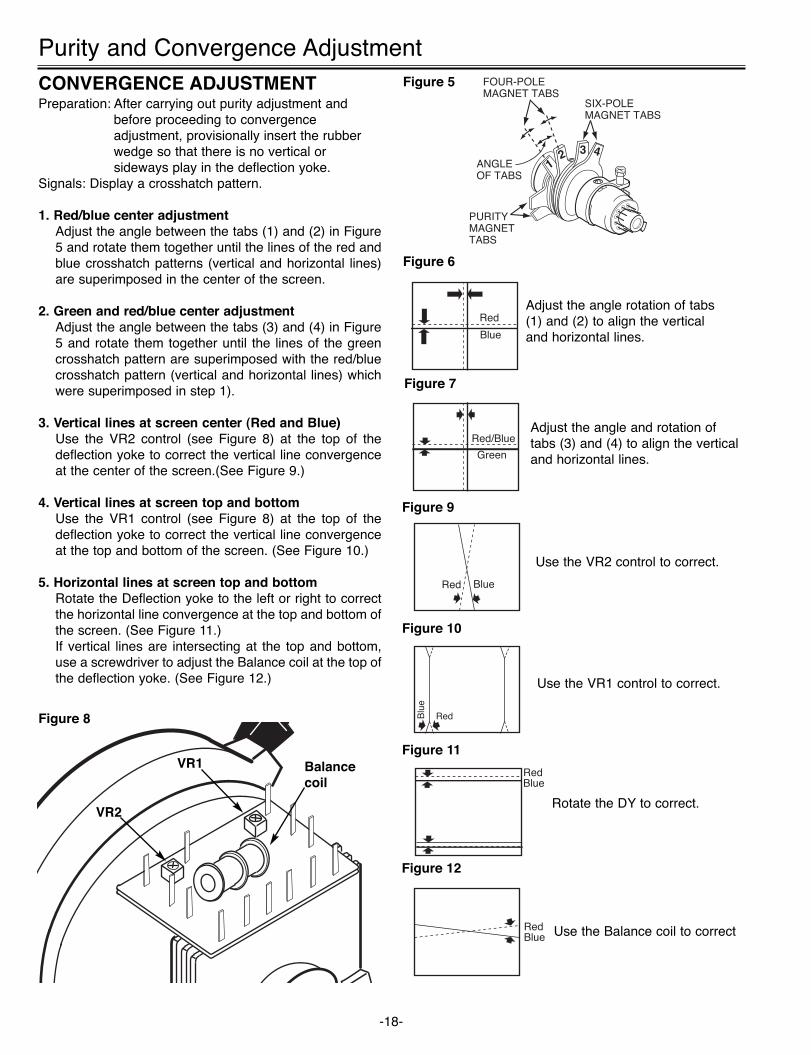
Purity and Convergence AdjustmentCONVERGENCE ADJUSTMENTPreparation: After carrying out purity adjustment and
before proceeding to convergence adjustment, provisionally insert the rubber wedge so that there is no vertical or sideways play in the deflection yoke.
Signals: Display a crosshatch pattern.
1. Red/blue center adjustmentAdjust the angle between the tabs (1) and (2) in Figure5 and rotate them together until the lines of the red andblue crosshatch patterns (vertical and horizontal lines)are superimposed in the center of the screen.
2. Green and red/blue center adjustmentAdjust the angle between the tabs (3) and (4) in Figure5 and rotate them together until the lines of the greencrosshatch pattern are superimposed with the red/bluecrosshatch pattern (vertical and horizontal lines) whichwere superimposed in step 1).
3. Vertical lines at screen center (Red and Blue)Use the VR2 control (see Figure 8) at the top of thedeflection yoke to correct the vertical line convergenceat the center of the screen.(See Figure 9.)
4. Vertical lines at screen top and bottomUse the VR1 control (see Figure 8) at the top of thedeflection yoke to correct the vertical line convergenceat the top and bottom of the screen. (See Figure 10.)
5. Horizontal lines at screen top and bottomRotate the Deflection yoke to the left or right to correctthe horizontal line convergence at the top and bottom ofthe screen. (See Figure 11.)If vertical lines are intersecting at the top and bottom,use a screwdriver to adjust the Balance coil at the top ofthe deflection yoke. (See Figure 12.)
Red
Blue
Figure 6
Red/Blue
Green
Figure 7
Red Blue
Figure 9
Figure 5
Adjust the angle rotation of tabs(1) and (2) to align the verticaland horizontal lines.
Adjust the angle and rotation oftabs (3) and (4) to align the verticaland horizontal lines.
Use the VR2 control to correct.
RedBlu
e
Figure 10
Use the VR1 control to correct.
BlueRed
Figure 11
Rotate the DY to correct.
BlueRed
Figure 12
Use the Balance coil to correct
12 3 4
SIX-POLEMAGNET TABS
FOUR-POLEMAGNET TABS
ANGLEOF TABS
PURITYMAGNETTABS
Balancecoil
VR1
VR2
Figure 8
SM_29-C7GV(FC6-A)AUS 7/27/05 7:12 PM Page 18
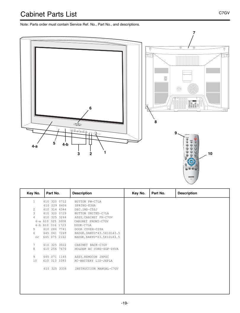
C7GVCabinet Parts ListNote: Parts order must contain Service Ref. No., Part No., and descriptions.
TV/AV MENU - +CH
POWER
1 2 3
4 5 6
7 8 9
0
TV/AV
TIMERx
-/--
SWAP CH SCAN
MENU
BASSSOUND S. SYS
SURROUND
PICTURECH
CH
A B.
P P
JXPSC
9
10
1 610 320 0712 BUTTON PW-C7LA610 229 8406 SPRING-E3HA
2 610 314 4344 DEC.IND-C5ZJ3 610 320 0729 BUTTON UNITED-C7LA4 610 325 3244 ASSY,CABINET FR-C7GV4-a 610 325 3008 CABINET FRONT-C7GV4-b 610 316 1723 DOOR-C7LA
5 610 284 7741 DOOR COVER-C2SA 6 645 041 7269 BADGE,SANYO*43.5X10L43.5or 645 075 2162 BADGE,SANYO*43.5X10L43.5
7 610 325 3022 CABINET BACK-C7GV 8 610 256 7670 HOLDER AC CORD-SGP-D4VA
9 645 071 1145 ASSY,REMOCON JXPSC10 610 313 3393 RC-BATTERY LID-JXPLA
610 325 3336 INSTRUCTION MANUAL-C7GV
Key No. Part No. Description Key No. Part No. Description
ANT. 75Ω
MONITOROUT
AV3/DVDINPUT
AV1 INPUT
AUDIO
CR
CB
VIDEO
AUDIO
R R
L L
(MONO)
Y
AUDIO
R
L
VIDEO
S-VIDEO
123
4-b5
6
8
7
4-a
-19-
SM_29-C7GV(FC6-A)AUS 7/27/05 7:12 PM Page 19
-20-
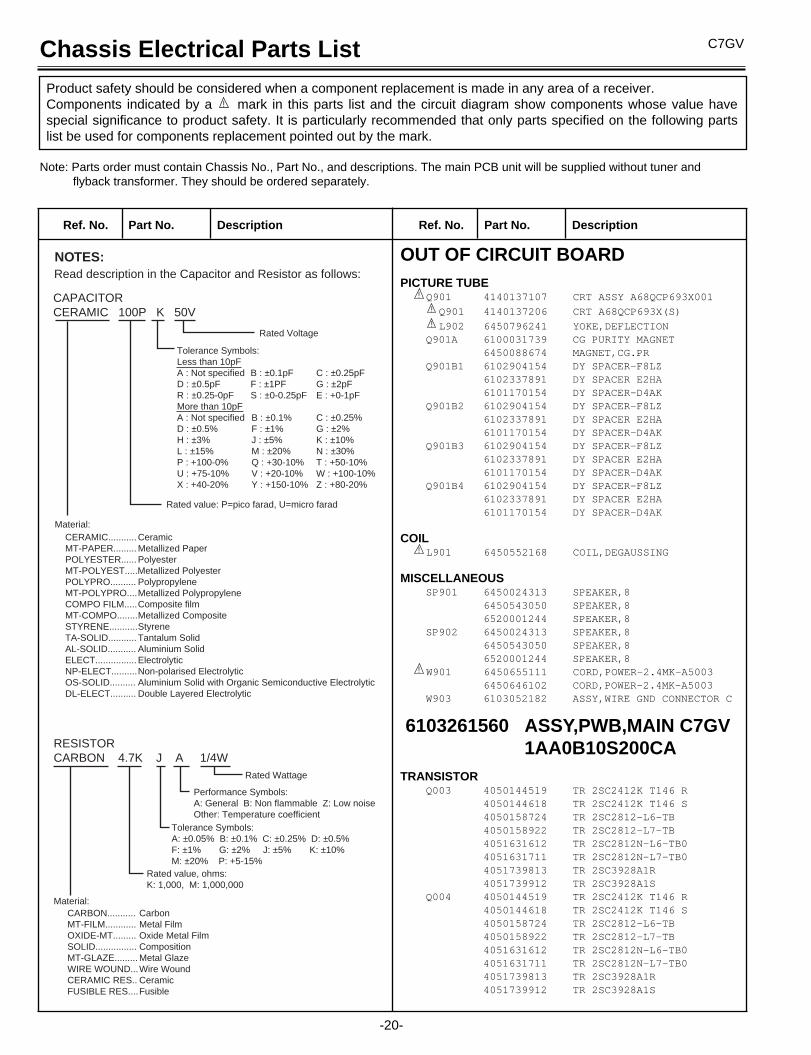
C7GV
OUT OF CIRCUIT BOARDPICTURE TUBE
Q901 4140137107 CRT ASSY A68QCP693X001
Q901 4140137206 CRT A68QCP693X(S)
L902 6450796241 YOKE,DEFLECTIONQ901A 6100031739 CG PURITY MAGNET
6450088674 MAGNET,CG.PRQ901B1 6102904154 DY SPACER-F8LZ
6102337891 DY SPACER E2HA6101170154 DY SPACER-D4AK
Q901B2 6102904154 DY SPACER-F8LZ6102337891 DY SPACER E2HA6101170154 DY SPACER-D4AK
Q901B3 6102904154 DY SPACER-F8LZ6102337891 DY SPACER E2HA6101170154 DY SPACER-D4AK
Q901B4 6102904154 DY SPACER-F8LZ6102337891 DY SPACER E2HA6101170154 DY SPACER-D4AK
COILL901 6450552168 COIL,DEGAUSSING
MISCELLANEOUSSP901 6450024313 SPEAKER,8
6450543050 SPEAKER,86520001244 SPEAKER,8
SP902 6450024313 SPEAKER,86450543050 SPEAKER,86520001244 SPEAKER,8
W901 6450655111 CORD,POWER-2.4MK-A50036450646102 CORD,POWER-2.4MK-A5003
W903 6103052182 ASSY,WIRE GND CONNECTOR C
6103261560 ASSY,PWB,MAIN C7GV1AA0B10S200CA
TRANSISTORQ003 4050144519 TR 2SC2412K T146 R
4050144618 TR 2SC2412K T146 S4050158724 TR 2SC2812-L6-TB4050158922 TR 2SC2812-L7-TB4051631612 TR 2SC2812N-L6-TB04051631711 TR 2SC2812N-L7-TB04051739813 TR 2SC3928A1R4051739912 TR 2SC3928A1S
Q004 4050144519 TR 2SC2412K T146 R4050144618 TR 2SC2412K T146 S4050158724 TR 2SC2812-L6-TB4050158922 TR 2SC2812-L7-TB4051631612 TR 2SC2812N-L6-TB04051631711 TR 2SC2812N-L7-TB04051739813 TR 2SC3928A1R4051739912 TR 2SC3928A1S
!
!
!
!
!
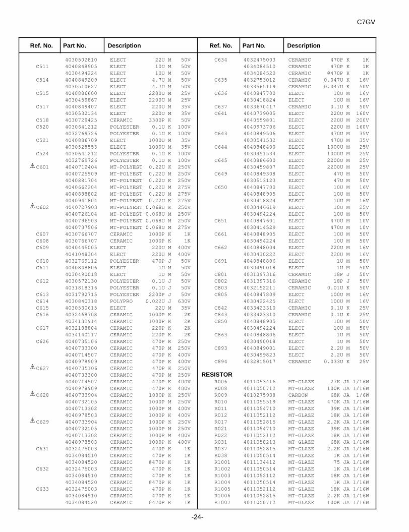
Chassis Electrical Parts List
Ref. No. Part No. Description Ref. No. Part No. Description
Product safety should be considered when a component replacement is made in any area of a receiver. Components indicated by a mark in this parts list and the circuit diagram show components whose value havespecial significance to product safety. It is particularly recommended that only parts specified on the following partslist be used for components replacement pointed out by the mark.
!
Note: Parts order must contain Chassis No., Part No., and descriptions. The main PCB unit will be supplied without tuner andflyback transformer. They should be ordered separately.
Read description in the Capacitor and Resistor as follows:
CAPACITORCERAMIC 100P K 50V
Rated Voltage
Tolerance Symbols:Less than 10pFA : Not specified B : ±0.1pF C : ±0.25pFD : ±0.5pF F : ±1PF G : ±2pFR : ±0.25-0pF S : ±0-0.25pF E : +0-1pFMore than 10pFA : Not specified B : ±0.1% C : ±0.25%D : ±0.5% F : ±1% G : ±2%H : ±3% J : ±5% K : ±10%L : ±15% M : ±20% N : ±30%P : +100-0% Q : +30-10% T : +50-10%U : +75-10% V : +20-10% W : +100-10%X : +40-20% Y : +150-10% Z : +80-20%
Rated value: P=pico farad, U=micro farad
Material:CERAMIC...........CeramicMT-PAPER.........Metallized PaperPOLYESTER......PolyesterMT-POLYEST.....Metallized PolyesterPOLYPRO..........PolypropyleneMT-POLYPRO....Metallized PolypropyleneCOMPO FILM.....Composite filmMT-COMPO........Metallized CompositeSTYRENE...........StyreneTA-SOLID...........Tantalum SolidAL-SOLID...........Aluminium SolidELECT................ElectrolyticNP-ELECT..........Non-polarised ElectrolyticOS-SOLID..........Aluminium Solid with Organic Semiconductive ElectrolyticDL-ELECT..........Double Layered Electrolytic
RESISTORCARBON 4.7K J A 1/4W
Rated Wattage
Performance Symbols:A: General B: Non flammable Z: Low noiseOther: Temperature coefficient
Tolerance Symbols:A: ±0.05% B: ±0.1% C: ±0.25% D: ±0.5%F: ±1% G: ±2% J: ±5% K: ±10%M: ±20% P: +5-15%
Rated value, ohms:K: 1,000, M: 1,000,000
Material:CARBON...........CarbonMT-FILM............Metal FilmOXIDE-MT.........Oxide Metal FilmSOLID................CompositionMT-GLAZE.........Metal GlazeWIRE WOUND...Wire WoundCERAMIC RES..CeramicFUSIBLE RES....Fusible
NOTES:
P List-C7GV 7/29/05 1:22 PM Page 20
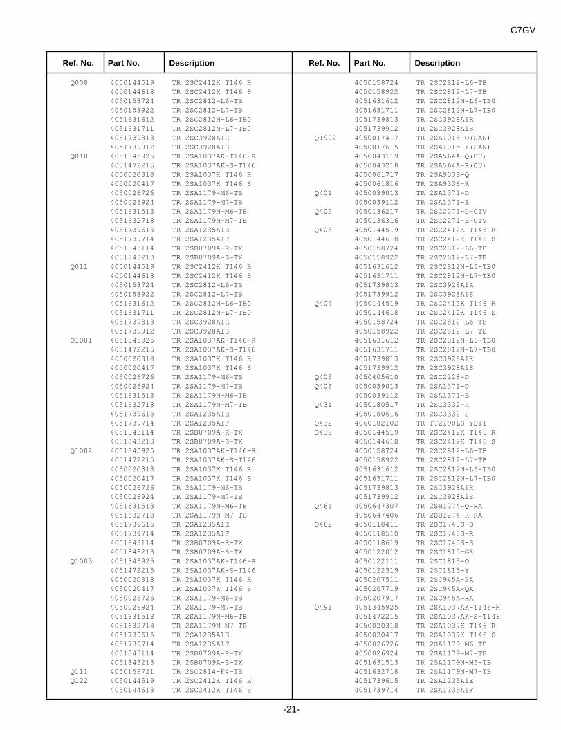
Q008 4050144519 TR 2SC2412K T146 R4050144618 TR 2SC2412K T146 S4050158724 TR 2SC2812-L6-TB4050158922 TR 2SC2812-L7-TB4051631612 TR 2SC2812N-L6-TB04051631711 TR 2SC2812N-L7-TB04051739813 TR 2SC3928A1R4051739912 TR 2SC3928A1S
Q010 4051345925 TR 2SA1037AK-T146-R4051472215 TR 2SA1037AK-S-T1464050020318 TR 2SA1037K T146 R4050020417 TR 2SA1037K T146 S4050026726 TR 2SA1179-M6-TB4050026924 TR 2SA1179-M7-TB4051631513 TR 2SA1179N-M6-TB4051632718 TR 2SA1179N-M7-TB4051739615 TR 2SA1235A1E4051739714 TR 2SA1235A1F4051843114 TR 2SB0709A-R-TX4051843213 TR 2SB0709A-S-TX
Q011 4050144519 TR 2SC2412K T146 R4050144618 TR 2SC2412K T146 S4050158724 TR 2SC2812-L6-TB4050158922 TR 2SC2812-L7-TB4051631612 TR 2SC2812N-L6-TB04051631711 TR 2SC2812N-L7-TB04051739813 TR 2SC3928A1R4051739912 TR 2SC3928A1S
Q1001 4051345925 TR 2SA1037AK-T146-R4051472215 TR 2SA1037AK-S-T1464050020318 TR 2SA1037K T146 R4050020417 TR 2SA1037K T146 S4050026726 TR 2SA1179-M6-TB4050026924 TR 2SA1179-M7-TB4051631513 TR 2SA1179N-M6-TB4051632718 TR 2SA1179N-M7-TB4051739615 TR 2SA1235A1E4051739714 TR 2SA1235A1F4051843114 TR 2SB0709A-R-TX4051843213 TR 2SB0709A-S-TX
Q1002 4051345925 TR 2SA1037AK-T146-R4051472215 TR 2SA1037AK-S-T1464050020318 TR 2SA1037K T146 R4050020417 TR 2SA1037K T146 S4050026726 TR 2SA1179-M6-TB4050026924 TR 2SA1179-M7-TB4051631513 TR 2SA1179N-M6-TB4051632718 TR 2SA1179N-M7-TB4051739615 TR 2SA1235A1E4051739714 TR 2SA1235A1F4051843114 TR 2SB0709A-R-TX4051843213 TR 2SB0709A-S-TX
Q1003 4051345925 TR 2SA1037AK-T146-R4051472215 TR 2SA1037AK-S-T1464050020318 TR 2SA1037K T146 R4050020417 TR 2SA1037K T146 S4050026726 TR 2SA1179-M6-TB4050026924 TR 2SA1179-M7-TB4051631513 TR 2SA1179N-M6-TB4051632718 TR 2SA1179N-M7-TB4051739615 TR 2SA1235A1E4051739714 TR 2SA1235A1F4051843114 TR 2SB0709A-R-TX4051843213 TR 2SB0709A-S-TX
Q111 4050159721 TR 2SC2814-F4-TBQ122 4050144519 TR 2SC2412K T146 R
4050144618 TR 2SC2412K T146 S
4050158724 TR 2SC2812-L6-TB4050158922 TR 2SC2812-L7-TB4051631612 TR 2SC2812N-L6-TB04051631711 TR 2SC2812N-L7-TB04051739813 TR 2SC3928A1R4051739912 TR 2SC3928A1S
Q1902 4050017417 TR 2SA1015-O(SAN)4050017615 TR 2SA1015-Y(SAN)4050043119 TR 2SA564A-Q(CU)4050043218 TR 2SA564A-R(CU)4050061717 TR 2SA933S-Q4050061816 TR 2SA933S-R
Q401 4050039013 TR 2SA1371-D4050039112 TR 2SA1371-E
Q402 4050136217 TR 2SC2271-D-CTV4050136316 TR 2SC2271-E-CTV
Q403 4050144519 TR 2SC2412K T146 R4050144618 TR 2SC2412K T146 S4050158724 TR 2SC2812-L6-TB4050158922 TR 2SC2812-L7-TB4051631612 TR 2SC2812N-L6-TB04051631711 TR 2SC2812N-L7-TB04051739813 TR 2SC3928A1R4051739912 TR 2SC3928A1S
Q404 4050144519 TR 2SC2412K T146 R4050144618 TR 2SC2412K T146 S4050158724 TR 2SC2812-L6-TB4050158922 TR 2SC2812-L7-TB4051631612 TR 2SC2812N-L6-TB04051631711 TR 2SC2812N-L7-TB04051739813 TR 2SC3928A1R4051739912 TR 2SC3928A1S
Q405 4050405610 TR 2SC2228-DQ406 4050039013 TR 2SA1371-D
4050039112 TR 2SA1371-EQ431 4050180517 TR 2SC3332-R
4050180616 TR 2SC3332-SQ432 4060182102 TR TT2190LS-YB11Q439 4050144519 TR 2SC2412K T146 R
4050144618 TR 2SC2412K T146 S4050158724 TR 2SC2812-L6-TB4050158922 TR 2SC2812-L7-TB4051631612 TR 2SC2812N-L6-TB04051631711 TR 2SC2812N-L7-TB04051739813 TR 2SC3928A1R4051739912 TR 2SC3928A1S
Q461 4050647307 TR 2SB1274-Q-RA4050647406 TR 2SB1274-R-RA
Q462 4050118411 TR 2SC1740S-Q4050118510 TR 2SC1740S-R4050118619 TR 2SC1740S-S4050122012 TR 2SC1815-GR4050122111 TR 2SC1815-O4050122319 TR 2SC1815-Y4050207511 TR 2SC945A-PA4050207719 TR 2SC945A-QA4050207917 TR 2SC945A-RA
Q491 4051345925 TR 2SA1037AK-T146-R4051472215 TR 2SA1037AK-S-T1464050020318 TR 2SA1037K T146 R4050020417 TR 2SA1037K T146 S4050026726 TR 2SA1179-M6-TB4050026924 TR 2SA1179-M7-TB4051631513 TR 2SA1179N-M6-TB4051632718 TR 2SA1179N-M7-TB4051739615 TR 2SA1235A1E4051739714 TR 2SA1235A1F
-21-
C7GV
Ref. No. Part No. Description Ref. No. Part No. Description
P List-C7GV 7/27/05 7:17 PM Page 21
-22-
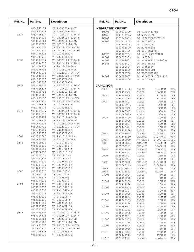
C7GV
4051843114 TR 2SB0709A-R-TX4051843213 TR 2SB0709A-S-TX
Q511 4050144519 TR 2SC2412K T146 R4050144618 TR 2SC2412K T146 S4050158724 TR 2SC2812-L6-TB4050158922 TR 2SC2812-L7-TB4051631612 TR 2SC2812N-L6-TB04051631711 TR 2SC2812N-L7-TB04051739813 TR 2SC3928A1R4051739912 TR 2SC3928A1S
Q631 4050144519 TR 2SC2412K T146 R4050144618 TR 2SC2412K T146 S4050158724 TR 2SC2812-L6-TB4050158922 TR 2SC2812-L7-TB4051631612 TR 2SC2812N-L6-TB04051631711 TR 2SC2812N-L7-TB04051739813 TR 2SC3928A1R4051739912 TR 2SC3928A1S
Q632 4050144519 TR 2SC2412K T146 R4050144618 TR 2SC2412K T146 S4050158724 TR 2SC2812-L6-TB4050158922 TR 2SC2812-L7-TB4051631612 TR 2SC2812N-L6-TB04051631711 TR 2SC2812N-L7-TB04051739813 TR 2SC3928A1R4051739912 TR 2SC3928A1S
Q641 4050144519 TR 2SC2412K T146 R4050144618 TR 2SC2412K T146 S4050158724 TR 2SC2812-L6-TB4050158922 TR 2SC2812-L7-TB4051631612 TR 2SC2812N-L6-TB04051631711 TR 2SC2812N-L7-TB04051739813 TR 2SC3928A1R4051739912 TR 2SC3928A1S
Q661 4050599903 TR 2SD1913-R-RA4050600005 TR 2SD1913-S-RA
Q681 4050118411 TR 2SC1740S-Q4050118510 TR 2SC1740S-R4050118619 TR 2SC1740S-S4050122012 TR 2SC1815-GR4050122111 TR 2SC1815-O4050122319 TR 2SC1815-Y4050207511 TR 2SC945A-PA4050207719 TR 2SC945A-QA4050207917 TR 2SC945A-RA
Q683 4050890010 TR 2SA1707-S4050890119 TR 2SA1707-T4050096917 TR 2SB985-S4050097013 TR 2SB985-T
Q684 4050118411 TR 2SC1740S-Q4050118510 TR 2SC1740S-R4050118619 TR 2SC1740S-S4050122012 TR 2SC1815-GR4050122111 TR 2SC1815-O4050122319 TR 2SC1815-Y4050207511 TR 2SC945A-PA4050207719 TR 2SC945A-QA4050207917 TR 2SC945A-RA
Q886 4050144519 TR 2SC2412K T146 R4050144618 TR 2SC2412K T146 S4050158724 TR 2SC2812-L6-TB4050158922 TR 2SC2812-L7-TB4051631612 TR 2SC2812N-L6-TB04051631711 TR 2SC2812N-L7-TB04051739813 TR 2SC3928A1R4051739912 TR 2SC3928A1S
INTEGRATED CIRCUITIC001 4096216109 IC TDA8944J/N1IC1001 4094244916 IC NJM2533MIC201 4105869609 IC LA76938DE56T5-EIC202 4092415407 IC BA178M05T
4092654806 IC L78M05CV4091721509 IC MC78M05CT4093205700 IC UPC78M05AHF
IC3701 4095922734 IC LV1116NV-TLM-EIC501 4094535905 IC LA78041IC601 4105849601 IC STR-W6756(LF2003)IC651 4092415407 IC BA178M05T
4092654806 IC L78M05CV4091721509 IC MC78M05CT4093205700 IC UPC78M05AHF
IC801 4104958007 IC AT24C16A-10PI-2.74094594506 IC 24LC16B/P
CAPACITORC001 4040848400 ELECT 1000U M 25V
4030451534 ELECT 1000U M 25VC004 4040848004 ELECT 220U M 16V
4030430222 ELECT 220U M 16VC006 4040897804 ELECT 33U M 16V
4030433926 ELECT 33U M 16V4032583322 ELECT 33U M 16V4030463517 ELECT 33U M 25V4032583619 ELECT 33U M 25V
C009 4040847700 ELECT 10U M 16V4040848905 ELECT 10U M 50V4030418824 ELECT 10U M 16V4030446619 ELECT 10U M 25V4030494224 ELECT 10U M 50V
C012 4032753012 CERAMIC 0.047U K 16V4033565119 CERAMIC 0.047U K 50V
C015 4011057919 MT-GLAZE 0.000 ZA 1/16WC017 4030708816 CERAMIC 1500P K 50V
4031552111 CERAMIC 1500P K 50VC018 4030708816 CERAMIC 1500P K 50V
4031552111 CERAMIC 1500P K 50VC020 4040897804 ELECT 33U M 16V
4030433926 ELECT 33U M 16VC022 4032753012 CERAMIC 0.047U K 16V
4033565119 CERAMIC 0.047U K 50VC025 4032121613 CERAMIC 0.22U Z 25VC026 4032121613 CERAMIC 0.22U Z 25VC1001 4040848806 ELECT 1U M 50V
4030490018 ELECT 1U M 50VC1002 4040848905 ELECT 10U M 50V
4030494224 ELECT 10U M 50VC1003 4040848905 ELECT 10U M 50V
4030494224 ELECT 10U M 50VC1004 4040848905 ELECT 10U M 50V
4030494224 ELECT 10U M 50VC1005 4040848905 ELECT 10U M 50V
4030494224 ELECT 10U M 50VC1006 4040848004 ELECT 220U M 16V
4030430222 ELECT 220U M 16VC1007 4040848905 ELECT 10U M 50V
4030494224 ELECT 10U M 50VC1008 4040848905 ELECT 10U M 50V
4030494224 ELECT 10U M 50VC1009 4040848806 ELECT 1U M 50V
4030490018 ELECT 1U M 50VC101 4040848301 ELECT 470U M 16V
4030441743 ELECT 470U M 16VC1013 4032152211 CERAMIC 0.01U K 50V
Ref. No. Part No. Description Ref. No. Part No. Description
P List-C7GV 7/27/05 7:17 PM Page 22
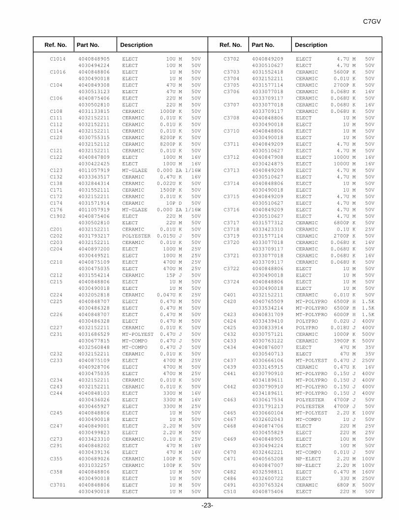
C1014 4040848905 ELECT 10U M 50V4030494224 ELECT 10U M 50V
C1016 4040848806 ELECT 1U M 50V4030490018 ELECT 1U M 50V
C104 4040849308 ELECT 47U M 50V4030513123 ELECT 47U M 50V
C106 4040875406 ELECT 22U M 50V4030502810 ELECT 22U M 50V
C108 4031133815 CERAMIC 1000P K 50VC111 4032152211 CERAMIC 0.01U K 50VC112 4032152211 CERAMIC 0.01U K 50VC114 4032152211 CERAMIC 0.01U K 50VC120 4030755315 CERAMIC 8200P K 50V
4032152112 CERAMIC 8200P K 50VC121 4032152211 CERAMIC 0.01U K 50VC122 4040847809 ELECT 100U M 16V
4030422425 ELECT 100U M 16VC123 4011057919 MT-GLAZE 0.000 ZA 1/16WC132 4033363517 CERAMIC 0.47U K 16VC138 4032844314 CERAMIC 0.022U K 50VC171 4031552111 CERAMIC 1500P K 50VC172 4032152211 CERAMIC 0.01U K 50VC174 4031571914 CERAMIC 10P D 50VC176 4011057919 MT-GLAZE 0.000 ZA 1/16WC1902 4040875406 ELECT 22U M 50V
4030502810 ELECT 22U M 50VC201 4032152211 CERAMIC 0.01U K 50VC202 4031793217 POLYESTER 0.015U J 50VC203 4032152211 CERAMIC 0.01U K 50VC204 4040897200 ELECT 100U M 25V
4030449521 ELECT 100U M 25VC210 4040875109 ELECT 470U M 25V
4030475035 ELECT 470U M 25VC212 4031554214 CERAMIC 15P J 50VC215 4040848806 ELECT 1U M 50V
4030490018 ELECT 1U M 50VC224 4032052818 CERAMIC 0.047U K 25VC225 4040848707 ELECT 0.47U M 50V
4030486328 ELECT 0.47U M 50VC226 4040848707 ELECT 0.47U M 50V
4030486328 ELECT 0.47U M 50VC227 4032152211 CERAMIC 0.01U K 50VC231 4031686529 MT-POLYEST 0.47U J 50V
4030677815 MT-COMPO 0.47U J 50V4032560848 MT-COMPO 0.47U J 50V
C232 4032152211 CERAMIC 0.01U K 50VC233 4040875109 ELECT 470U M 25V
4040928706 ELECT 470U M 50V4030475035 ELECT 470U M 25V
C234 4032152211 CERAMIC 0.01U K 50VC243 4032152211 CERAMIC 0.01U K 50VC244 4040848103 ELECT 330U M 16V
4030436026 ELECT 330U M 16V4030465927 ELECT 330U M 25V
C245 4040848806 ELECT 1U M 50V4030490018 ELECT 1U M 50V
C247 4040849001 ELECT 2.2U M 50V4030499823 ELECT 2.2U M 50V
C273 4033423310 CERAMIC 0.1U K 25VC291 4040848202 ELECT 47U M 16V
4030439136 ELECT 47U M 16VC355 4030689026 CERAMIC 100P K 50V
4031032257 CERAMIC 100P K 50VC358 4040848806 ELECT 1U M 50V
4030490018 ELECT 1U M 50VC3701 4040848806 ELECT 1U M 50V
4030490018 ELECT 1U M 50V
C3702 4040849209 ELECT 4.7U M 50V4030510627 ELECT 4.7U M 50V
C3703 4031552418 CERAMIC 5600P K 50VC3704 4032152211 CERAMIC 0.01U K 50VC3705 4031577114 CERAMIC 2700P K 50VC3706 4033077018 CERAMIC 0.068U K 16V
4033709117 CERAMIC 0.068U K 50VC3707 4033077018 CERAMIC 0.068U K 16V
4033709117 CERAMIC 0.068U K 50VC3708 4040848806 ELECT 1U M 50V
4030490018 ELECT 1U M 50VC3710 4040848806 ELECT 1U M 50V
4030490018 ELECT 1U M 50VC3711 4040849209 ELECT 4.7U M 50V
4030510627 ELECT 4.7U M 50VC3712 4040847908 ELECT 1000U M 16V
4030424875 ELECT 1000U M 16VC3713 4040849209 ELECT 4.7U M 50V
4030510627 ELECT 4.7U M 50VC3714 4040848806 ELECT 1U M 50V
4030490018 ELECT 1U M 50VC3715 4040849209 ELECT 4.7U M 50V
4030510627 ELECT 4.7U M 50VC3716 4040849209 ELECT 4.7U M 50V
4030510627 ELECT 4.7U M 50VC3717 4031577312 CERAMIC 6800P K 50VC3718 4033423310 CERAMIC 0.1U K 25VC3719 4031577114 CERAMIC 2700P K 50VC3720 4033077018 CERAMIC 0.068U K 16V
4033709117 CERAMIC 0.068U K 50VC3721 4033077018 CERAMIC 0.068U K 16V
4033709117 CERAMIC 0.068U K 50VC3722 4040848806 ELECT 1U M 50V
4030490018 ELECT 1U M 50VC3724 4040848806 ELECT 1U M 50V
4030490018 ELECT 1U M 50VC401 4032152211 CERAMIC 0.01U K 50VC420 4040765509 MT-POLYPRO 6500P H 1.5K
4033534214 MT-POLYPRO 6500P H 1.5KC423 4040831709 MT-POLYPRO 6000P H 1.5KC424 4033439410 POLYPRO 0.02U J 400VC425 4030833914 POLYPRO 0.018U J 400VC432 4030757121 CERAMIC 1000P K 500VC433 4030763122 CERAMIC 3900P K 500VC434 4040876007 ELECT 47U M 35V
4030540713 ELECT 47U M 35VC437 4030666106 MT-POLYEST 0.47U J 250VC439 4033145915 CERAMIC 0.47U K 16VC441 4030790910 MT-POLYPRO 0.15U J 400V
4034189611 MT-POLYPRO 0.15U J 400VC442 4030790910 MT-POLYPRO 0.15U J 400V
4034189611 MT-POLYPRO 0.15U J 400VC463 4030617534 POLYESTER 4700P J 50V
4031791213 POLYESTER 4700P J 50VC465 4030660104 MT-POLYEST 2.2U K 100VC467 4032602043 MT-COMPO 1U J 50VC468 4040874706 ELECT 22U M 25V
4030455829 ELECT 22U M 25VC469 4040848905 ELECT 10U M 50V
4030494224 ELECT 10U M 50VC470 4032462221 MT-COMPO 0.01U J 50VC471 4040565208 NP-ELECT 2.2U M 100V
4040847007 NP-ELECT 2.2U M 100VC482 4032598811 ELECT 0.47U M 160VC486 4032600722 ELECT 33U M 250VC491 4030765324 CERAMIC 680P K 500VC510 4040875406 ELECT 22U M 50V
-23-
C7GV
Ref. No. Part No. Description Ref. No. Part No. Description
P List-C7GV 7/27/05 7:17 PM Page 23
-24-
C7GV
4030502810 ELECT 22U M 50VC511 4040848905 ELECT 10U M 50V
4030494224 ELECT 10U M 50VC514 4040849209 ELECT 4.7U M 50V
4030510627 ELECT 4.7U M 50VC515 4040886600 ELECT 2200U M 25V
4030459867 ELECT 2200U M 25VC517 4040849407 ELECT 220U M 35V
4030532134 ELECT 220U M 35VC518 4030729425 CERAMIC 3300P K 50VC520 4030641212 POLYESTER 0.1U K 100V
4032769726 POLYESTER 0.1U K 100VC521 4040886709 ELECT 1000U M 35V
4030528553 ELECT 1000U M 35VC524 4030641212 POLYESTER 0.1U K 100V
4032769726 POLYESTER 0.1U K 100VC601 4040712404 MT-POLYEST 0.22U K 250V
4040725909 MT-POLYEST 0.22U M 250V4040881704 MT-POLYEST 0.22U K 250V4040662204 MT-POLYEST 0.22U M 275V4040888802 MT-POLYEST 0.22U M 275V4040941804 MT-POLYEST 0.22U K 275V
C602 4040727903 MT-POLYEST 0.068U K 250V4040726104 MT-POLYEST 0.068U M 250V4040796503 MT-POLYEST 0.068U M 250V4040737506 MT-POLYEST 0.068U M 275V
C607 4030766707 CERAMIC 1000P K 1KC608 4030766707 CERAMIC 1000P K 1KC609 4040445005 ELECT 220U M 400V
4041048304 ELECT 220U M 400VC610 4032769112 POLYESTER 470P J 50VC611 4040848806 ELECT 1U M 50V
4030490018 ELECT 1U M 50VC612 4030572130 POLYESTER 0.1U J 50V
4031818316 POLYESTER 0.1U J 50VC613 4031792715 POLYESTER 2200P J 50VC614 4030840318 POLYPRO 0.022U J 630VC615 4030530615 ELECT 22U M 35VC616 4032468708 CERAMIC 1000P K 2K
4034132914 CERAMIC 1000P K 2KC617 4032188804 CERAMIC 220P K 2K
4034140117 CERAMIC 220P K 2KC626 4040735106 CERAMIC 470P K 250V
4040733300 CERAMIC 470P M 250V4040714507 CERAMIC 470P K 400V4040978909 CERAMIC 470P K 400V
C627 4040735106 CERAMIC 470P K 250V4040733300 CERAMIC 470P M 250V4040714507 CERAMIC 470P K 400V4040978909 CERAMIC 470P K 400V
C628 4040733904 CERAMIC 1000P K 250V4040732105 CERAMIC 1000P M 250V4040713302 CERAMIC 1000P M 400V4040978503 CERAMIC 1000P K 400V
C629 4040733904 CERAMIC 1000P K 250V4040732105 CERAMIC 1000P M 250V4040713302 CERAMIC 1000P M 400V4040978503 CERAMIC 1000P K 400V
C631 4032475003 CERAMIC 470P K 1K4034084510 CERAMIC 470P K 1K4034084520 CERAMIC @470P K 1K
C632 4032475003 CERAMIC 470P K 1K4034084510 CERAMIC 470P K 1K4034084520 CERAMIC @470P K 1K
C633 4032475003 CERAMIC 470P K 1K4034084510 CERAMIC 470P K 1K4034084520 CERAMIC @470P K 1K
C634 4032475003 CERAMIC 470P K 1K4034084510 CERAMIC 470P K 1K4034084520 CERAMIC @470P K 1K
C635 4032753012 CERAMIC 0.047U K 16V4033565119 CERAMIC 0.047U K 50V
C636 4040847700 ELECT 10U M 16V4030418824 ELECT 10U M 16V
C637 4033670417 CERAMIC 0.1U K 50VC641 4040739005 ELECT 220U M 160V
4040559801 ELECT 220U M 200V4040973706 ELECT 220U M 160V
C643 4040849506 ELECT 470U M 35V4030541532 ELECT 470U M 35V
C644 4040848400 ELECT 1000U M 25V4030451534 ELECT 1000U M 25V
C645 4040886600 ELECT 2200U M 25V4030459807 ELECT 2200U M 25V
C649 4040849308 ELECT 47U M 50V4030513123 ELECT 47U M 50V
C650 4040847700 ELECT 10U M 16V4040848905 ELECT 10U M 50V4030418824 ELECT 10U M 16V4030446619 ELECT 10U M 25V4030494224 ELECT 10U M 50V
C651 4040847601 ELECT 470U M 10V4030414529 ELECT 470U M 10V
C661 4040848905 ELECT 10U M 50V4030494224 ELECT 10U M 50V
C662 4040848004 ELECT 220U M 16V4030430222 ELECT 220U M 16V
C691 4040848806 ELECT 1U M 50V4030490018 ELECT 1U M 50V
C801 4031397316 CERAMIC 18P J 50VC802 4031397316 CERAMIC 18P J 50VC803 4032152211 CERAMIC 0.01U K 50VC805 4040847809 ELECT 100U M 16V
4030422425 ELECT 100U M 16VC842 4033423310 CERAMIC 0.1U K 25VC843 4033423310 CERAMIC 0.1U K 25VC850 4040848905 ELECT 10U M 50V
4030494224 ELECT 10U M 50VC863 4040848806 ELECT 1U M 50V
4030490018 ELECT 1U M 50VC893 4040849001 ELECT 2.2U M 50V
4030499823 ELECT 2.2U M 50VC894 4032815017 CERAMIC 0.033U K 25V
RESISTORR006 4011053416 MT-GLAZE 27K JA 1/16WR008 4011050712 MT-GLAZE 100K JA 1/16WR009 4010275938 CARBON 68K JA 1/6WR010 4011055519 MT-GLAZE 470K JA 1/16WR011 4011054710 MT-GLAZE 39K JA 1/16WR012 4011052112 MT-GLAZE 18K JA 1/16WR017 4011052815 MT-GLAZE 2.2K JA 1/16WR021 4011054710 MT-GLAZE 39K JA 1/16WR022 4011052112 MT-GLAZE 18K JA 1/16WR031 4011058213 MT-GLAZE 68K JA 1/16WR037 4011052815 MT-GLAZE 2.2K JA 1/16WR038 4011050514 MT-GLAZE 1K JA 1/16WR1001 4011134412 MT-GLAZE 75 JA 1/16WR1002 4011050514 MT-GLAZE 1K JA 1/16WR1003 4011052112 MT-GLAZE 18K JA 1/16WR1004 4011050514 MT-GLAZE 1K JA 1/16WR1005 4011052112 MT-GLAZE 18K JA 1/16WR1006 4011052815 MT-GLAZE 2.2K JA 1/16WR1007 4011050712 MT-GLAZE 100K JA 1/16W
!
!
!
!
!
Ref. No. Part No. Description Ref. No. Part No. Description
P List-C7GV 7/27/05 7:17 PM Page 24
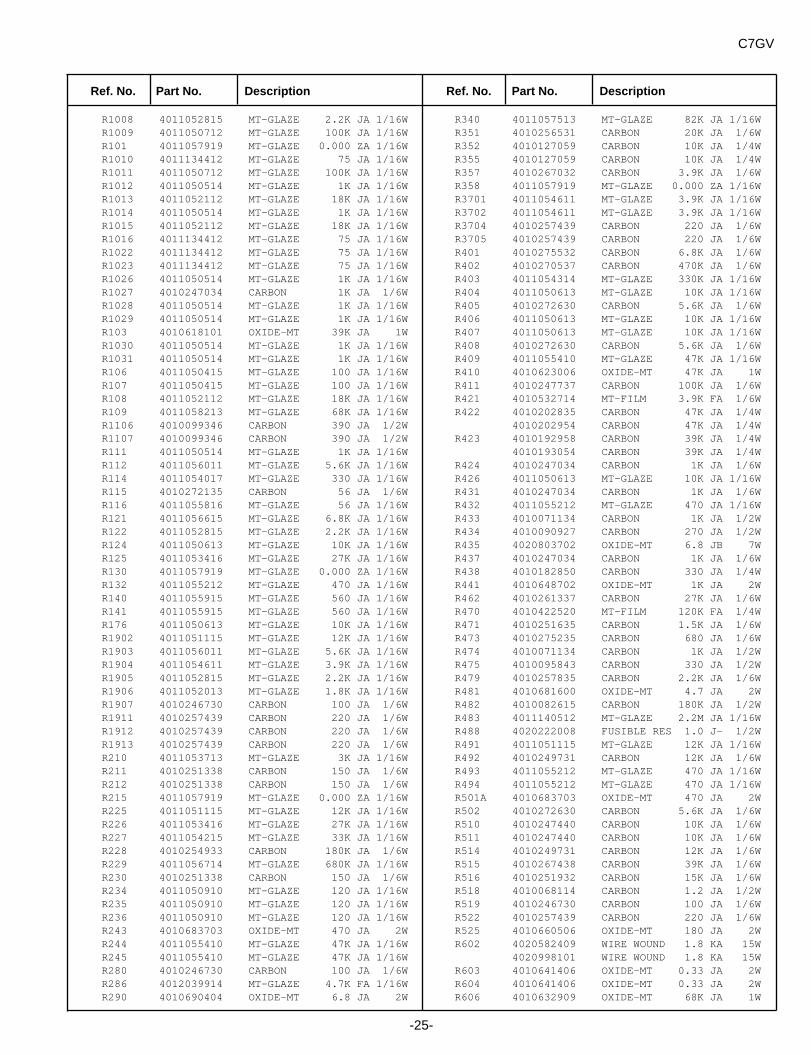
R1008 4011052815 MT-GLAZE 2.2K JA 1/16WR1009 4011050712 MT-GLAZE 100K JA 1/16WR101 4011057919 MT-GLAZE 0.000 ZA 1/16WR1010 4011134412 MT-GLAZE 75 JA 1/16WR1011 4011050712 MT-GLAZE 100K JA 1/16WR1012 4011050514 MT-GLAZE 1K JA 1/16WR1013 4011052112 MT-GLAZE 18K JA 1/16WR1014 4011050514 MT-GLAZE 1K JA 1/16WR1015 4011052112 MT-GLAZE 18K JA 1/16WR1016 4011134412 MT-GLAZE 75 JA 1/16WR1022 4011134412 MT-GLAZE 75 JA 1/16WR1023 4011134412 MT-GLAZE 75 JA 1/16WR1026 4011050514 MT-GLAZE 1K JA 1/16WR1027 4010247034 CARBON 1K JA 1/6WR1028 4011050514 MT-GLAZE 1K JA 1/16WR1029 4011050514 MT-GLAZE 1K JA 1/16WR103 4010618101 OXIDE-MT 39K JA 1WR1030 4011050514 MT-GLAZE 1K JA 1/16WR1031 4011050514 MT-GLAZE 1K JA 1/16WR106 4011050415 MT-GLAZE 100 JA 1/16WR107 4011050415 MT-GLAZE 100 JA 1/16WR108 4011052112 MT-GLAZE 18K JA 1/16WR109 4011058213 MT-GLAZE 68K JA 1/16WR1106 4010099346 CARBON 390 JA 1/2WR1107 4010099346 CARBON 390 JA 1/2WR111 4011050514 MT-GLAZE 1K JA 1/16WR112 4011056011 MT-GLAZE 5.6K JA 1/16WR114 4011054017 MT-GLAZE 330 JA 1/16WR115 4010272135 CARBON 56 JA 1/6WR116 4011055816 MT-GLAZE 56 JA 1/16WR121 4011056615 MT-GLAZE 6.8K JA 1/16WR122 4011052815 MT-GLAZE 2.2K JA 1/16WR124 4011050613 MT-GLAZE 10K JA 1/16WR125 4011053416 MT-GLAZE 27K JA 1/16WR130 4011057919 MT-GLAZE 0.000 ZA 1/16WR132 4011055212 MT-GLAZE 470 JA 1/16WR140 4011055915 MT-GLAZE 560 JA 1/16WR141 4011055915 MT-GLAZE 560 JA 1/16WR176 4011050613 MT-GLAZE 10K JA 1/16WR1902 4011051115 MT-GLAZE 12K JA 1/16WR1903 4011056011 MT-GLAZE 5.6K JA 1/16WR1904 4011054611 MT-GLAZE 3.9K JA 1/16WR1905 4011052815 MT-GLAZE 2.2K JA 1/16WR1906 4011052013 MT-GLAZE 1.8K JA 1/16WR1907 4010246730 CARBON 100 JA 1/6WR1911 4010257439 CARBON 220 JA 1/6WR1912 4010257439 CARBON 220 JA 1/6WR1913 4010257439 CARBON 220 JA 1/6WR210 4011053713 MT-GLAZE 3K JA 1/16WR211 4010251338 CARBON 150 JA 1/6WR212 4010251338 CARBON 150 JA 1/6WR215 4011057919 MT-GLAZE 0.000 ZA 1/16WR225 4011051115 MT-GLAZE 12K JA 1/16WR226 4011053416 MT-GLAZE 27K JA 1/16WR227 4011054215 MT-GLAZE 33K JA 1/16WR228 4010254933 CARBON 180K JA 1/6WR229 4011056714 MT-GLAZE 680K JA 1/16WR230 4010251338 CARBON 150 JA 1/6WR234 4011050910 MT-GLAZE 120 JA 1/16WR235 4011050910 MT-GLAZE 120 JA 1/16WR236 4011050910 MT-GLAZE 120 JA 1/16WR243 4010683703 OXIDE-MT 470 JA 2WR244 4011055410 MT-GLAZE 47K JA 1/16WR245 4011055410 MT-GLAZE 47K JA 1/16WR280 4010246730 CARBON 100 JA 1/6WR286 4012039914 MT-GLAZE 4.7K FA 1/16WR290 4010690404 OXIDE-MT 6.8 JA 2W
R340 4011057513 MT-GLAZE 82K JA 1/16WR351 4010256531 CARBON 20K JA 1/6WR352 4010127059 CARBON 10K JA 1/4WR355 4010127059 CARBON 10K JA 1/4WR357 4010267032 CARBON 3.9K JA 1/6WR358 4011057919 MT-GLAZE 0.000 ZA 1/16WR3701 4011054611 MT-GLAZE 3.9K JA 1/16WR3702 4011054611 MT-GLAZE 3.9K JA 1/16WR3704 4010257439 CARBON 220 JA 1/6WR3705 4010257439 CARBON 220 JA 1/6WR401 4010275532 CARBON 6.8K JA 1/6WR402 4010270537 CARBON 470K JA 1/6WR403 4011054314 MT-GLAZE 330K JA 1/16WR404 4011050613 MT-GLAZE 10K JA 1/16WR405 4010272630 CARBON 5.6K JA 1/6WR406 4011050613 MT-GLAZE 10K JA 1/16WR407 4011050613 MT-GLAZE 10K JA 1/16WR408 4010272630 CARBON 5.6K JA 1/6WR409 4011055410 MT-GLAZE 47K JA 1/16WR410 4010623006 OXIDE-MT 47K JA 1WR411 4010247737 CARBON 100K JA 1/6WR421 4010532714 MT-FILM 3.9K FA 1/6WR422 4010202835 CARBON 47K JA 1/4W
4010202954 CARBON 47K JA 1/4WR423 4010192958 CARBON 39K JA 1/4W
4010193054 CARBON 39K JA 1/4WR424 4010247034 CARBON 1K JA 1/6WR426 4011050613 MT-GLAZE 10K JA 1/16WR431 4010247034 CARBON 1K JA 1/6WR432 4011055212 MT-GLAZE 470 JA 1/16WR433 4010071134 CARBON 1K JA 1/2WR434 4010090927 CARBON 270 JA 1/2WR435 4020803702 OXIDE-MT 6.8 JB 7WR437 4010247034 CARBON 1K JA 1/6WR438 4010182850 CARBON 330 JA 1/4WR441 4010648702 OXIDE-MT 1K JA 2WR462 4010261337 CARBON 27K JA 1/6WR470 4010422520 MT-FILM 120K FA 1/4WR471 4010251635 CARBON 1.5K JA 1/6WR473 4010275235 CARBON 680 JA 1/6WR474 4010071134 CARBON 1K JA 1/2WR475 4010095843 CARBON 330 JA 1/2WR479 4010257835 CARBON 2.2K JA 1/6WR481 4010681600 OXIDE-MT 4.7 JA 2WR482 4010082615 CARBON 180K JA 1/2WR483 4011140512 MT-GLAZE 2.2M JA 1/16WR488 4020222008 FUSIBLE RES 1.0 J- 1/2WR491 4011051115 MT-GLAZE 12K JA 1/16WR492 4010249731 CARBON 12K JA 1/6WR493 4011055212 MT-GLAZE 470 JA 1/16WR494 4011055212 MT-GLAZE 470 JA 1/16WR501A 4010683703 OXIDE-MT 470 JA 2WR502 4010272630 CARBON 5.6K JA 1/6WR510 4010247440 CARBON 10K JA 1/6WR511 4010247440 CARBON 10K JA 1/6WR514 4010249731 CARBON 12K JA 1/6WR515 4010267438 CARBON 39K JA 1/6WR516 4010251932 CARBON 15K JA 1/6WR518 4010068114 CARBON 1.2 JA 1/2WR519 4010246730 CARBON 100 JA 1/6WR522 4010257439 CARBON 220 JA 1/6WR525 4010660506 OXIDE-MT 180 JA 2WR602 4020582409 WIRE WOUND 1.8 KA 15W
4020998101 WIRE WOUND 1.8 KA 15WR603 4010641406 OXIDE-MT 0.33 JA 2WR604 4010641406 OXIDE-MT 0.33 JA 2WR606 4010632909 OXIDE-MT 68K JA 1W
-25-
C7GV
Ref. No. Part No. Description Ref. No. Part No. Description
P List-C7GV 7/27/05 7:17 PM Page 25
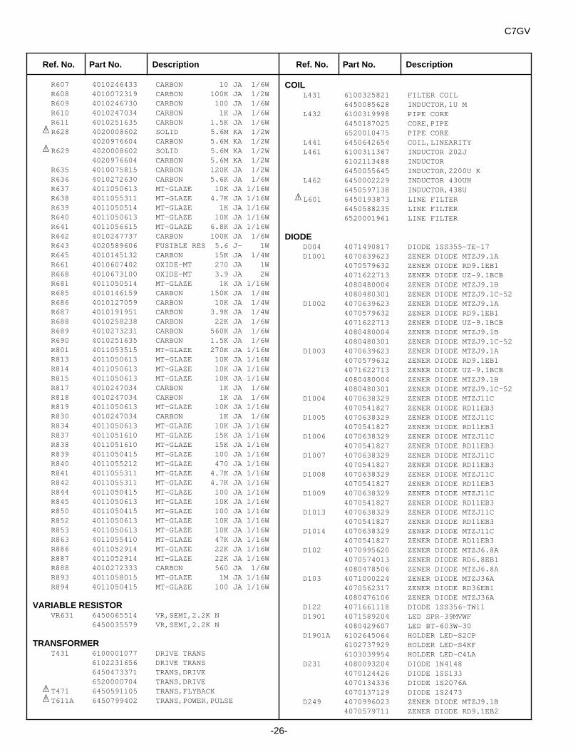
-26-
C7GV
R607 4010246433 CARBON 10 JA 1/6WR608 4010072319 CARBON 100K JA 1/2WR609 4010246730 CARBON 100 JA 1/6WR610 4010247034 CARBON 1K JA 1/6WR611 4010251635 CARBON 1.5K JA 1/6WR628 4020008602 SOLID 5.6M KA 1/2W
4020976604 CARBON 5.6M KA 1/2WR629 4020008602 SOLID 5.6M KA 1/2W
4020976604 CARBON 5.6M KA 1/2WR635 4010075815 CARBON 120K JA 1/2WR636 4010272630 CARBON 5.6K JA 1/6WR637 4011050613 MT-GLAZE 10K JA 1/16WR638 4011055311 MT-GLAZE 4.7K JA 1/16WR639 4011050514 MT-GLAZE 1K JA 1/16WR640 4011050613 MT-GLAZE 10K JA 1/16WR641 4011056615 MT-GLAZE 6.8K JA 1/16WR642 4010247737 CARBON 100K JA 1/6WR643 4020589606 FUSIBLE RES 5.6 J- 1WR645 4010145132 CARBON 15K JA 1/4WR661 4010607402 OXIDE-MT 270 JA 1WR668 4010673100 OXIDE-MT 3.9 JA 2WR681 4011050514 MT-GLAZE 1K JA 1/16WR685 4010146159 CARBON 150K JA 1/4WR686 4010127059 CARBON 10K JA 1/4WR687 4010191951 CARBON 3.9K JA 1/4WR688 4010258238 CARBON 22K JA 1/6WR689 4010273231 CARBON 560K JA 1/6WR690 4010251635 CARBON 1.5K JA 1/6WR801 4011053515 MT-GLAZE 270K JA 1/16WR813 4011050613 MT-GLAZE 10K JA 1/16WR814 4011050613 MT-GLAZE 10K JA 1/16WR815 4011050613 MT-GLAZE 10K JA 1/16WR817 4010247034 CARBON 1K JA 1/6WR818 4010247034 CARBON 1K JA 1/6WR819 4011050613 MT-GLAZE 10K JA 1/16WR830 4010247034 CARBON 1K JA 1/6WR834 4011050613 MT-GLAZE 10K JA 1/16WR837 4011051610 MT-GLAZE 15K JA 1/16WR838 4011051610 MT-GLAZE 15K JA 1/16WR839 4011050415 MT-GLAZE 100 JA 1/16WR840 4011055212 MT-GLAZE 470 JA 1/16WR841 4011055311 MT-GLAZE 4.7K JA 1/16WR842 4011055311 MT-GLAZE 4.7K JA 1/16WR844 4011050415 MT-GLAZE 100 JA 1/16WR845 4011050613 MT-GLAZE 10K JA 1/16WR850 4011050415 MT-GLAZE 100 JA 1/16WR852 4011050613 MT-GLAZE 10K JA 1/16WR853 4011050613 MT-GLAZE 10K JA 1/16WR863 4011055410 MT-GLAZE 47K JA 1/16WR886 4011052914 MT-GLAZE 22K JA 1/16WR887 4011052914 MT-GLAZE 22K JA 1/16WR888 4010272333 CARBON 560 JA 1/6WR893 4011058015 MT-GLAZE 1M JA 1/16WR894 4011050415 MT-GLAZE 100 JA 1/16W
VARIABLE RESISTORVR631 6450065514 VR,SEMI,2.2K N
6450035579 VR,SEMI,2.2K N
TRANSFORMERT431 6100001077 DRIVE TRANS
6102231656 DRIVE TRANS6450473371 TRANS,DRIVE6520000704 TRANS,DRIVE
T471 6450591105 TRANS,FLYBACKT611A 6450799402 TRANS,POWER,PULSE
COILL431 6100325821 FILTER COIL
6450085628 INDUCTOR,1U ML432 6100319998 PIPE CORE
6450187025 CORE,PIPE6520010475 PIPE CORE
L441 6450642654 COIL,LINEARITYL461 6100311367 INDUCTOR 202J
6102113488 INDUCTOR6450055645 INDUCTOR,2200U K
L462 6450002229 INDUCTOR 430UH6450597138 INDUCTOR,438U
L601 6450193873 LINE FILTER6450588235 LINE FILTER6520001961 LINE FILTER
DIODED004 4071490817 DIODE 1SS355-TE-17D1001 4070639623 ZENER DIODE MTZJ9.1A
4070579632 ZENER DIODE RD9.1EB14071622713 ZENER DIODE UZ-9.1BCB4080480004 ZENER DIODE MTZJ9.1B4080480301 ZENER DIODE MTZJ9.1C-52
D1002 4070639623 ZENER DIODE MTZJ9.1A4070579632 ZENER DIODE RD9.1EB14071622713 ZENER DIODE UZ-9.1BCB4080480004 ZENER DIODE MTZJ9.1B4080480301 ZENER DIODE MTZJ9.1C-52
D1003 4070639623 ZENER DIODE MTZJ9.1A4070579632 ZENER DIODE RD9.1EB14071622713 ZENER DIODE UZ-9.1BCB4080480004 ZENER DIODE MTZJ9.1B4080480301 ZENER DIODE MTZJ9.1C-52
D1004 4070638329 ZENER DIODE MTZJ11C4070541827 ZENER DIODE RD11EB3
D1005 4070638329 ZENER DIODE MTZJ11C4070541827 ZENER DIODE RD11EB3
D1006 4070638329 ZENER DIODE MTZJ11C4070541827 ZENER DIODE RD11EB3
D1007 4070638329 ZENER DIODE MTZJ11C4070541827 ZENER DIODE RD11EB3
D1008 4070638329 ZENER DIODE MTZJ11C4070541827 ZENER DIODE RD11EB3
D1009 4070638329 ZENER DIODE MTZJ11C4070541827 ZENER DIODE RD11EB3
D1013 4070638329 ZENER DIODE MTZJ11C4070541827 ZENER DIODE RD11EB3
D1014 4070638329 ZENER DIODE MTZJ11C4070541827 ZENER DIODE RD11EB3
D102 4070995620 ZENER DIODE MTZJ6.8A4070574013 ZENER DIODE RD6.8EB14080478506 ZENER DIODE MTZJ6.8A
D103 4071000224 ZENER DIODE MTZJ36A4070562317 ZENER DIODE RD36EB14080476106 ZENER DIODE MTZJ36A
D122 4071661118 DIODE 1SS356-TW11D1901 4071589204 LED SPR-39MVWF
4080429607 LED BT-603W-30D1901A 6102645064 HOLDER LED-S2CP
6102737929 HOLDER LED-S4KF6103039954 HOLDER LED-C4LA
D231 4080093204 DIODE 1N41484070124426 DIODE 1SS1334070134336 DIODE 1S2076A4070137129 DIODE 1S2473
D249 4070996023 ZENER DIODE MTZJ9.1B4070579711 ZENER DIODE RD9.1EB2
!
!
!
!
!
Ref. No. Part No. Description Ref. No. Part No. Description
P List-C7GV 7/27/05 7:17 PM Page 26
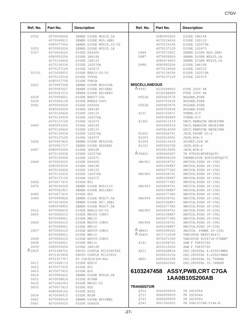
D352 4070638626 ZENER DIODE MTZJ5.1A4070569811 ZENER DIODE RD5.6EB14080477004 ZENER DIODE MTZJ5.1C-52
D353 4070995224 ZENER DIODE MTZJ5.1BD357 4070054525 DIODE DS442X
4080093204 DIODE 1N41484070124426 DIODE 1SS1334070134336 DIODE 1S2076A4070137129 DIODE 1S2473
D3701 4070058632 DIODE ERA15-02-V14070114318 DIODE TVR1B4080537708 DIODE TVR1B
D421 4070997228 ZENER DIODE MTZJ16A4070547027 ZENER DIODE RD16EB14070547215 ZENER DIODE RD16EB3
D438 4070958001 DIODE ERD07-15LD439 4070064128 DIODE ERB44-04V1D461 4070054525 DIODE DS442X
4080093204 DIODE 1N41484070124426 DIODE 1SS1334070134336 DIODE 1S2076A4070137129 DIODE 1S2473
D465 4080093204 DIODE 1N41484070124426 DIODE 1SS1334070134336 DIODE 1S2076A4070137129 DIODE 1S2473
D466 4070997822 ZENER DIODE MTZJ20A4070551717 ZENER DIODE RD20EB1
D467 4080093204 DIODE 1N41484070134336 DIODE 1S2076A4070136528 DIODE 1S2471
D468 4070054525 DIODE DS442X4080093204 DIODE 1N41484070124426 DIODE 1SS1334070134336 DIODE 1S2076A4070137129 DIODE 1S2473
D469 4070077415 DIODE EU1D476 4070638329 ZENER DIODE MTZJ11C
4070541827 ZENER DIODE RD11EB3D485 4070077415 DIODE EU1D489 4070995828 ZENER DIODE MTZJ7.5A
4070576324 ZENER DIODE RD7.5EB14080478803 ZENER DIODE MTZJ7.5A
D512 4070058632 DIODE ERA15-02-V1D605 4070066310 DIODE ERC05-10BV1
4070096921 DIODE RM11CD606 4070066310 DIODE ERC05-10BV1
4070096921 DIODE RM11CD607 4070066310 DIODE ERC05-10BV1
4070096921 DIODE RM11CD608 4070066310 DIODE ERC05-10BV1D608 4070096921 DIODE RM11CD609 4080093204 DIODE 1N4148D610 4072348701 PHOTO COUPLE PC123X5YFZ
4072303908 PHOTO COUPLE PC123Y524072317707 PC TLP421F(D4-BL)
D611 4071468113 DIODE EG01CD612 4070077415 DIODE EU1D613 4070077415 DIODE EU1D614 4070995422 ZENER DIODE MTZJ6.2BD631 4070098816 DIODE RU3AMD632 4071662303 DIODE ERC91-02D633 4070077613 DIODE EU2
4080458102 DIODE EU2ZD634 4070098915 DIODE RU3MD661 4070540018 ZENER DIODE RD10EB2D681 4070054525 DIODE DS442X
4080093204 DIODE 1N41484070124426 DIODE 1SS1334070134336 DIODE 1S2076A4070137129 DIODE 1S2473
D686 4070572831 ZENER DIODE RD6.2EB3D687 4070638626 ZENER DIODE MTZJ5.1A
4080476403 ZENER DIODE MTZJ5.1AD688 4080093204 DIODE 1N4148
4070124426 DIODE 1SS1334070134336 DIODE 1S2076A4070137129 DIODE 1S2473
MISCELLANEOUSF601 4230288603 FUSE 250V 4A
4230248409 FUSE 250V 4AF601A 6450403576 HOLDER,FUSE
6450705434 HOLDER,FUSEF601B 6450403576 HOLDER,FUSE
6450705434 HOLDER,FUSEA101 6450720871 TUNER,U/V
6450785689 TUNER.U/VA1901 6450411519 UNIT,REMOCON RECEIVER
6450440519 UNIT,REMOCON RECEIVER6450614309 UNIT,REMOCON RECEIVER
K1001 6450064791 JACK,PHONE D3.6K1003 6520015401 JACK,RCA-3K1004 6520015418 SOCKET,DIN 4PK1101 6450332708 JACK,RCA-6
6520015005 JACK,RCA-6PS601 4080465407 TH PTDCA1BF4R5Q200
4080545109 THERMISTOR ECPCD4R5Q270SW1901 6450034701 SWITCH,PUSH 1P-1TX1
6450194887 SWITCH,PUSH 1P-1TX16450277382 SWITCH,PUSH 1P-1TX1
SW1902 6450034701 SWITCH,PUSH 1P-1TX16450194887 SWITCH,PUSH 1P-1TX16450277382 SWITCH,PUSH 1P-1TX1
SW1903 6450034701 SWITCH,PUSH 1P-1TX16450194887 SWITCH,PUSH 1P-1TX16450277382 SWITCH,PUSH 1P-1TX1
SW1904 6450034701 SWITCH,PUSH 1P-1TX16450194887 SWITCH,PUSH 1P-1TX16450277382 SWITCH,PUSH 1P-1TX1
SW1905 6450034701 SWITCH,PUSH 1P-1TX16450194887 SWITCH,PUSH 1P-1TX16450277382 SWITCH,PUSH 1P-1TX1
SW1906 6450034701 SWITCH,PUSH 1P-1TX16450194887 SWITCH,PUSH 1P-1TX1
SW601 6450590061 SWITCH, POWER 1P-1TX1VA601 4071712008 VARISTOR ERZV14D471
4072471300 VARISTOR SVC471D-07ABW7X161 4210094705 SAW F TSF6376U
4210115202 SAW F TSF6376YX211 6450248818 OSC,CRYSTAL 4.433619MHZ
6520010154 OSC,CRYSTAL 4.433619MHZX801 6450041938 OSC,CRYSTAL 32.768KHZ
6450041945 OSC,CRYSTAL 32.768KHZ
6103247458 ASSY,PWB,CRT C7GA1AA0B10S200AB
TRANSISTORQ701 4060099509 TR 2SC4544Q711 4060099509 TR 2SC4544Q721 4060099509 TR 2SC4544Q741 4051345925 TR 2SA1037AK-T146-R
!
!
!
!
!
-27-
C7GV
Ref. No. Part No. Description Ref. No. Part No. Description
P List-C7GV 7/27/05 7:17 PM Page 27
-28-
C7GV
4051472215 TR 2SA1037AK-S-T1464050020318 TR 2SA1037K T146 R4050020417 TR 2SA1037K T146 S4050026726 TR 2SA1179-M6-TB4050026924 TR 2SA1179-M7-TB4051631513 TR 2SA1179N-M6-TB4051632718 TR 2SA1179N-M7-TB4051739615 TR 2SA1235A1E4051739714 TR 2SA1235A1F4051843114 TR 2SB0709A-R-TX4051843213 TR 2SB0709A-S-TX
Q751 4051345925 TR 2SA1037AK-T146-R4051472215 TR 2SA1037AK-S-T1464050020318 TR 2SA1037K T146 R4050020417 TR 2SA1037K T146 S4050026726 TR 2SA1179-M6-TB4050026924 TR 2SA1179-M7-TB4051631513 TR 2SA1179N-M6-TB4051632718 TR 2SA1179N-M7-TB4051739615 TR 2SA1235A1E4051739714 TR 2SA1235A1F4051843114 TR 2SB0709A-R-TX4051843213 TR 2SB0709A-S-TX
CAPACITORC701 4031576711 CERAMIC 560P K 50VC710 4032819302 ELECT 10U M 250V
4032455609 ELECT 10U M 250VC711 4031576711 CERAMIC 560P K 50VC721 4031576711 CERAMIC 560P K 50VC731 4032454424 CERAMIC 470P K 2K
4034140414 CERAMIC 470P K 2K4033242624 CERAMIC 470P K 3K4032644330 CERAMIC 470P K 3K
C751 4030465927 ELECT 330U M 25V
RESISTORR701 4011051917 MT-GLAZE 180 JA 1/16WR703 4010269630 CARBON 470 JA 1/6WR704 4010654604 OXIDE-MT 12K JA 2WR705 4010091528 CARBON 2.7K JA 1/2WR711 4011051917 MT-GLAZE 180 JA 1/16WR713 4010269630 CARBON 470 JA 1/6WR714 4010654604 OXIDE-MT 12K JA 2WR716 4010091528 CARBON 2.7K JA 1/2WR717 4010091528 CARBON 2.7K JA 1/2WR721 4011051917 MT-GLAZE 180 JA 1/16WR723 4010269630 CARBON 470 JA 1/6WR724 4010654604 OXIDE-MT 12K JA 2WR732 4010246433 CARBON 10 JA 1/6WR741 4011051016 MT-GLAZE 1.2K JA 1/16WR742 4011056011 MT-GLAZE 5.6K JA 1/16WR744 4011055915 MT-GLAZE 560 JA 1/16WR751 4011057919 MT-GLAZE 0.000 ZA 1/16WR752 4011057414 MT-GLAZE 8.2K JA 1/16WR753 4011050613 MT-GLAZE 10K JA 1/16W
COILL701 6450080005 INDUCTOR,330U KL702A 6520001817 CORE,PIPE
6520001749 CORE,PIPE6102371000 PIPE CORE
L711 6450080005 INDUCTOR,330U KL721 6450080005 INDUCTOR,330U K
DIODED741 4011057919 MT-GLAZE 0.000 ZA 1/16W
D742 4011057919 MT-GLAZE 0.000 ZA 1/16WD751 4071490817 DIODE 1SS355-TE-17D752 4071490817 DIODE 1SS355-TE-17D753 4071490817 DIODE 1SS355-TE-17D754 4071490817 DIODE 1SS355-TE-17
MISCELLANEOUSK701-L 6450262005 SOCKET,CRT 8P
6450317699 SOCKET,CRT 8P
!
Ref. No. Part No. Description Ref. No. Part No. Description
P List-C7GV 7/27/05 7:17 PM Page 28
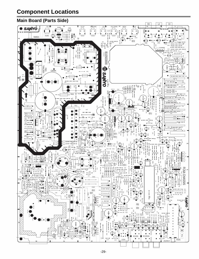
-29-
1 2
AC SW
KG
CH DOWNRC AMP
T4AL250V
V2L2R2
1
E
RED
CH UPGREEN
VOL UP VOL DOWN MENU TV/AV
4
TO W
OO
FER
TO SPEAKER
34
21
E
13
7
5
1
4
DIP
E
E
18
10
91
E
E
41
6050
4064
33
51
85
3020
1032
1
E
E
E
E 1
F601
B10S0300A
K1001(A)
SW601
VA601
KG-3
KG-2
KG-1
SW601-H1
PS601
KE
C607
D607
C606
D605
C608
D608
C609A
C609A-H2
C609A-H1
T471
C602
L601
L601-H2
L601A-H2 L601A-H1
L601-H1
L601A-H4
L601-H4L601-H3
L601A-H3
L601AR601
F601BF601A
C629
R628
R629
D632A
JP409R488
JP412
T471-H5
T471-H1
KDY-6KDY-3
KDY-1
JP408
D466
D469
C486
R490
C491D485
R475
C469
JP403
R422
R424
R435
R423
JP410
JP411
T471-H2
C471
R481
T471-H7
T471-H6
T471-H4
T471-H8
T471-H10
L462
JP435
A101
K002
K1001
K001
R1911
R1912
Q1902
R1913
R888
D1904
C1902
SW1906
SW1905SW1904SW1903SW1902SW1901
D1901
D850R1907
J1902
PS601-H1
PS601-H3
PS601-H2
TP-EE
KE-2KE-1
A1901
SW601-H2
R602R602A
L441AL441
J1908
JP1901
R1032
L603L602L602A
L602BL603B
J601
J602
JP601JP602
D606
C605
L603A
C1001
D1001C1003 C1002
D1002
D1003
R1106
R477
R474
R481A
JP407
R484
R485
R486D486
D467
R479
D476
D468
D448
C449
KDY
C423AJP436
C450R450
C437 R482C482
D489
D464
R487
D465
C470
C355
C463
R470R471
R421
L403
J406
Q432-H1
L432
J401
R473
D460R466
L462A
C465
L431
C1107
C609
C609-H1C609-H2
J1003
J1002
J1001
J1004
C1104
J1901
C1105
J011
J010
R1107
C024
C014
J013
JP008
J014
JW2
JW3
JW1
JW4
J015
J009
J008
JP009
JP007
J006
JP002
J020
J016
B10S03000
C001
C003
C007
C004
C002
C021
FC6A CHASSIS
J162C101
D103J156
J157TP-E
TP-A
C106
TP-M
C104
C1005C1004
D1006
D1004
D1005
C1010
C1008
C1009
D1009
C1012
R352
C020
R007
K1003
J1905J1904
D461R462
C467
D441
R442
R441
R445
L461L461A
J404
L442A
R103
L442-H2
L442-H1
L462-H2
L462-H1
L462-H3
L441-H3
L441-H1
C627
J603
R602-H4R602-H2
R602-H3
R602-H1
C628
R603
JP603
JP604
R604
R608
L632
J1903C645
D681
L635
D610
J422
C691
J647
J402
D633
Q462
J407
C434
C432
C433
R437
J176
R438
D634
C634
J635
C643
D631
C631
R525
PS601A
VR631 R636
R635
D686
IC651
JW7
JW8
J648
J642
C633D682
D353
D421R355
L441-H2
J405
JP442
J424
J425
J409
R433
R492
J644
JP001
J1907
C641
J252
J251
KQ
D1902
C524
C423
C420
C442
C441
D632-H1D632B
D632-H2
T431A
T431-H3
T431-H1
T431-H2
T431-H4
T431
D632-1
C641-H2
C641-H1
T611
1
8
910
Q461
Q461A
Q461-1
+B ADJST.
D438
D439
JP011
JP010
JP006
JP414
L1901
JP441
K1101
IC001
T611-H10T611-H17
T611-H18
T611-H2T611-H8
T611-H11T611-H13
T611-H15
Q432A-1
Q432A
Q432
Q432-1
C425
C424Q
432-H2
C468
J604
D1909
C850
J423
J261
C013
C023
J023
R427
J696
J654
Q401Q402
R401R402
J410
R405 J411
T611AT611-H5
T611A-H10T611A-H11
T611A-H13T611A-H15
T611A-H17T611A-H18
T611A-H2T611A-H5
T611A-H8
JP103
C603
J1106
J413
R410
R411
Q405
J414
R408
J415
Q406
J403TP-B
J029
J028
J027
JP014
J416
J645
J102
J033
C107
D632
T611-H7
T611A-H7
L442
JW9
JW10
JW11JW
12
KDY-5
R817J233
J203
L204
J236
J237
J243
J225
R280D352
C226
J109C863
C805
C893R351
C247
C245
C204
X801
IC201
C353
X211
C244
J201
R291
JW6
JW5
R290
R115
L111
X161
X161A
C122
KPJ208
C231
J211R818
R212
R211
C202
C215C210
R357
R228R230
C225
C233C358
X171
IC202
C291
IC801
R243
R501AR501
C517
C511
R516
R522
R515
R519
C520
C518
D512
IC501
IC501A
R434
C632
J609
C613R611
C612
R605D614
R610
C615
C616
D613
R607
D612
J614
R606C614
D611
R609
D609C610
C611
J611
IC601
J606
J608
IC601-1
R667R661 R668
C663
C651C662
D661
C661Q
681
R686
R642
Q683
R643
R690
Q684
R687
R688
R689
JP683
R644
R645
JP644
Q431
J235
D102
L201
R102
R105
J421
KX
J238
C1006
D1011
D1010
D1013
D1015
D1014
C1015
C1014
C1016
J1018
J1011
J807
R3704
D3701
C3712
C3711
C3710
C3708
C3724
J3710
C3716
R3705
C3702
C3725
C3701
C3713
J3702 C3715
C3722
C3714
IC3701
J3717
J3718
J212
J643
R512
C510
R511
R510
JP502
J502
R518
C514
C515
D507
J504
C650
C649
J507J508
J509
R431
J418
J510
J805
J227
J232
J1017
J219
J241
J226
D1903
JP1900
J811
J810
J809
J808
J222
J1012
D1012
J240
J207
D1008C1007
D1007
J1015
J1022
J1010
J1014
J213
J1005
R675
J215
J802
J206
J209
J239
J1019
J1013
J1016
J224
J3715
J3711
J3716
J3713 J3712
J3701
J641
J3714
J002
J216
J234
J427
J613
J650
J506
J617
J812
J419
J204
J612
J220
J223
JP501
J205
J101
J503
J505
J214
J007
J511
J610
J210
J217
J218
J1911
JP122
R514
J501
J1910
JP015
JP013
R023
J615
JW13
C601
J616
R674
J032
D615
D616
R612
J244
J242
D357
D249
R517
R103A
JP415
JP416
C617
C604
K1004
R602BR602-H5 R602-H6
Q661Q
432B-1
J038
J036
C3726C3727 D3702
D3703
J035
J039
J631
D231
C626
J646 R685
J619
C644
J040
J3719
J3720
R1027
D688
C521
D687
C636
J680
J618
J690
J691
J041
R502
JP442A
JP441A
J043
J1909
J005
J512
R830
J417
C437A
C614A
J019
C005
J017
R016
J018
J1912
J1009
JW14
JW15
JW16
JW17
JW18
C006
C009
R643A
R009
JP005
JW19
JW23
JW24
JW20
JW22
J513
JW21
K1101A
* * *
* * *
JW25
JW26
JW27
JW28
Component LocationsMain Board (Parts Side)
SM_29-C7GR PWB & WAVEFORM 7/16/05 11:33 AM Page 29
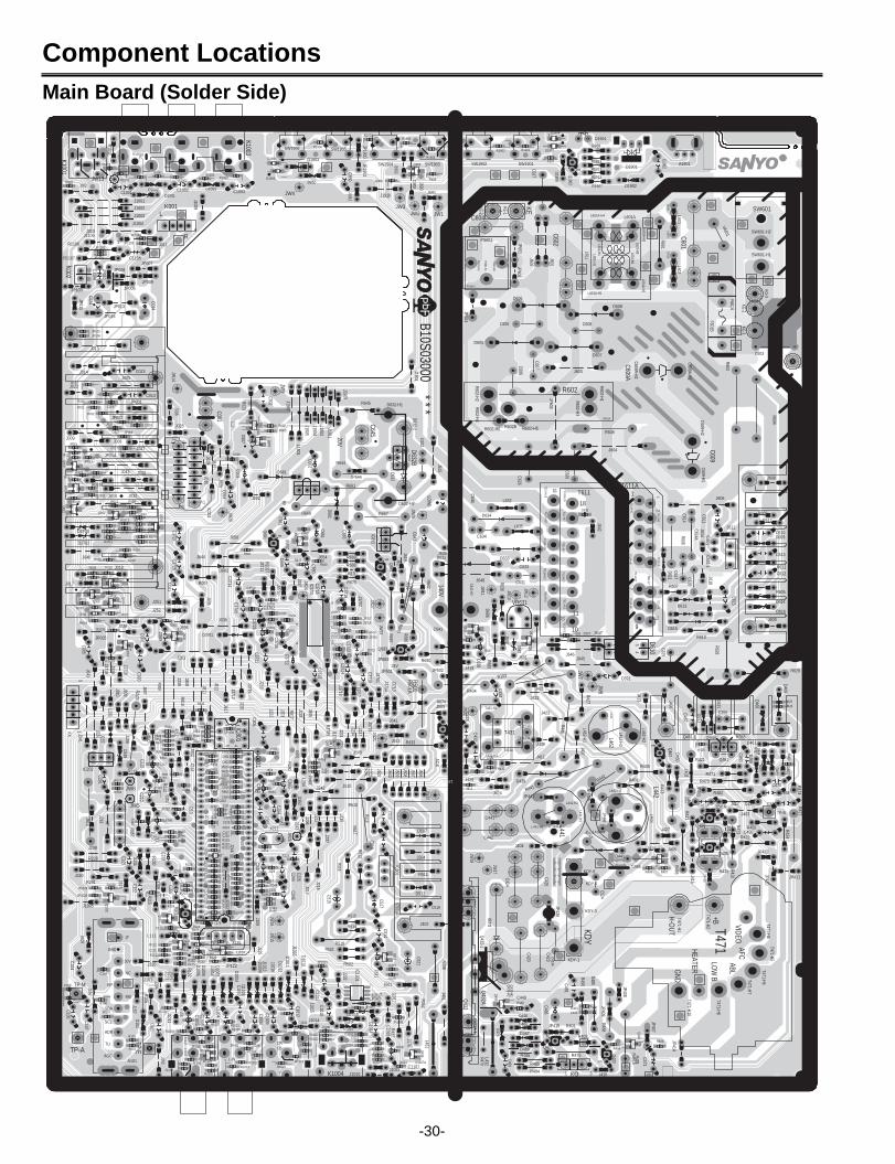
-30-
Component LocationsMain Board (Solder Side)
ABL
5VRC
140-1
VID-
OUT
24V
5V-2
5V-1
9V
X
X
X
X
X
X X
X
X
X
XX
X
X
X
X
X
XX
2 1
1
E
432
1
E
1 3
7
1
171
16
2
E
E
5
2
7
10
18
E
E
41
6050
40
6433
15
85
3020
1032
1
E
E
E
E
1
41
58
3630
20191810
1
SW601
VA601
KG-3
KG-2
KG-1
SW601-H1
PS601
KEC607
D607
C606
D605
C608
D608
C609AC609A-H2
C609A-H1
T471
C602
L601
L601-H2
L601A-H2
L601A-H1
L601-H1
L601A-H4
L601-H4
L601-H3
L601A-H3
L601A
R601
F601B
F601A
C629
R628
R629
D632A
JP409R488
JP412
T471-H5
T471-H1
KDY-6
KDY-3
KDY-1
JP408
D466
D469
C486
R490C491
D485
R475C469
JP403
R422
R424
R435
R423
JP410
JP411
T471-H2
C471
R481
T471-H7
T471-H6T471-H4
T471-H8
T471-H10
L462
H-OUT
JP435
A101
K002K1001
K001
R1911
R1912
Q1902
R1913
R888
D1904
C1902
SW1906 SW1905
SW1904 SW1903 SW1902 SW1901D1901
D850R1907
J1902
PS601-H1
PS601-H3
PS601-H2
TP-EE
KE-2
KE-1
A1901
SW601-H2
+B
VIDEOAFC
GND
LOW
B
HEATER
ABL
R602
R602A
L441A
L441
J1908
JP1901
R1032
L603L602
L602AL602B
L603B
J601
J602
JP601JP602
D606
C605
L603A
C1001D1001
C1003C1002D1002 D1003
R1106
R477R474
R481A
JP407
R484
R485
R486D486
D467
R479
D476
D468
D448
C449
KDY
C423AJP436
C450R450
C437
R482
C482
D489
D464R487D465
C470
C355
C463
R470
R471
R421
L403
J406
Q432-H1
L432
J401
R473
D460R466
L462A
C465
L431
C1107
C609C609-H1
C609-H2
J1003
J1002
J1001
J1004
C1104
J1901
L
R1
4
C1105
J011
J010
R1107
C024 C014
J013
JP008
J014
JW2JW3
JW1
JW4
J015
J009J008
JP009
JP007
J006
JP002
J020
J016
C001
C003C007
C004
C002
C021J162
C101
D103
J156
J157
ADR
TU
SCL
AGC
SDA
MB
IF
BP
NC
30V
IF
TP-ETP-A
C106
TP-M
C104
GND
C1005
C1004
D1006
D1004
D1005
C1010C1008C1009
D1009
C1012
R352
C020
R007
K1003
J1905
J1904
D461
R462
C467
D441
R442
R441
R445
L461L461A
J404
L442A
R103
L442-H2
L442-H1
L462-H2
L462-H1
L462-H3
L441-H3
L441-H1
C627
J603
R602-H4R602-H2 R602-H3
R602-H1
C628
R603
JP603
JP604
R604
R608
L632
J1903
C645
D681
L635
D610
J422
C691
J647
J402
D633
Q462
J407
C434
C432
C433
R437
J176
R438
D634
C634
J635
C643
D631
C631
R525
PS601A
VR631
R636
R635
D686
IC651
JW7
JW8
J648
J642
C633D682
D353
D421
R355
L441-H2
J405
JP442
J424
J425
J409R433
R492
J644
JP001 J1907
C641
J252
J251
KQ
D1902
C524
C423
C420
C442
C441
D632-H1
D632B
D632-H2
T431A
T431-H3
T431-H1
T431-H2
T431-H4T431
D632-1
C641-H2
C641-H1
T611 1
910
18
11
Q461
Q461AQ461-1
B10S03000D4
38
D439
JP011
JP010
JP006
JP414
L1901
JP441
K1101
IC001
T611-H10T611-H17
T611-H18
T611-H2T611-H8
T611-H11T611-H13
T611-H15
R2L2V2
Q432A-1
Q432AQ
432
Q432-1
C425
C424Q
432-H2
C468
J604
D1909
C850
J423
J261
C013
C023
J023
R427
J696
J654
Q401
Q402
R401
R402
J410
R405
J411
T611A
T611-H5
T611A-H10T611A-H11
T611A-H13T611A-H15
T611A-H17T611A-H18
T611A-H2T611A-H5
T611A-H8
JP103
C603
J1106
J413
R410
R411
Q405J414
R408
J415
Q406
J403 TP-B
J029
J028
J027JP014
J416
J645
J102
J033
C107
D632
T611-H7
T611A-H7
L442
JW9
JW10
JW11
JW12
DESIGN & DEVELOPED BY
KDY-5
C291
R817
J233
J203
L204J236
J237
J243
J225
R280
D352
C353
C226
J109C863
C805
C893
R351
C247
C245
IC801
C204
X801
IC201
X211
C244
J201
R291
JW6
JW5
R290
R115
L111
X161
X161A
C122
KP
J208
C231
J211R818
R212
R211
C202
C215C210
R357
R228
R230
C225
C233
C358X171
IC202
R243
R501AR501
C517C511
R516
R522
R515
R519
C520
C518
D512
IC501IC501A
R434
C632
J609
C613
R611C612
R605
D614
R610
C615
C616
D613
R607
D612
J614R606C614
D611
R609
D609C610
C611
J611
IC601
J606
J608
IC601-1
R667
R661
R668
C663
C651
LOW
B
C6629V
D661C661
Q681
R686
R642
Q683
R643
R690
Q684
R687
R688
R689
JP683
R644
R645
JP644
Q431
J235
D102
L201
R102
R105
J421
KX
J238
C1006
D1011
D1010
D1013
D1015
D1014 C1015
C1014
C1016
J1018
J1011
J807
R3704
D3701
C3712
C3711
C3710
C3708
C3724
J3710
C3716
R3705
C3702
C3725
C3701
C3713
J3702
C3715
C3722
C3714
J3717
J3718
J212
J643
R512
C510
R511
R510
JP502
J502
R518
C514
C515
D507
J504
C650
C649
J507
J508
J509
R431
J418
J510
J805
J227
J232
J1017
J219
J241
J226
D1903
JP1900
J811
J810
J809
J808
J222
J1012
D1012
J240
J207
D1008C1007
D1007
J1015
J1022J1010
J1014
J213
J1005
R675
J215
J802
J206
J209
J239
J1019
J1013
J1016
J224
J3715
J3711
J3716
J3713J3712
J3701
J641
J3714
J002
J216
J234
J427
J613
J650 5VRC
J506
J617
J812
J419
20V
J204
J612
J220
J223
JP501
J205
J101
J503
J505
J214
J007
J511
J610
J210
J217
J218
J1911
JP122
R514
J501
J1910
JP015
JP013
R023
J615
JW13
C601
J616
R674
J032
D615
D616
R612
J244
J242
D357
D249
R517
R103A
JP415
JP416
C617C604
K1004
R602B R602-H5R602-H6
Q661
Q432B-1
J038
J036
C3726C3727
D3702
D3703
J035
J039
J631
D231
C626
J646
R685
J619
C644
J040
J3719
J3720
R1027
D688
C521
D687
C636
J680
J618
J690
J691
J041
B10S0300A
R502
JP442A
JP441A
J043
J1909
J005
J512
R830
9V
24V
140V
J417C437A
C614A
J019
C005
J017
R016
J018
J1912J1009
JW14
JW15
JW16
JW17
JW18
C006
C009
R643
A
R009
JP005
JW19
JW23
JW24
JW20
JW22
J513
JW21
K1101A V-IN
JW25
JW26
JW27
JW28
* * *
* * *
R887
R1901R1902
R1903
R1904R1905
R886
Q886
D1905
D1906R1002
R1003
R1004
D1907
D1908
Q449
R449
R483
R489
C1107A
Q001 R003
R107
R106
C108
C105
C109
R1007
R1009
R1008R1006
R1016
Q439
R432
C431
Q631
R681
R426
R029
R027Q002
R028
R030
JP012
R038
Q010
R1906
C635
R1005
V-OUT
L-OUT
R-OUT
CBCR
Y
L-IN
R-IN
R1014
R1015
R1019
R1020
R1018
R1017
R002
Q1003
R1011R1031
R1030
Q005
R011
R012
R021
R022
R031
Q008
R006
D004 R037
Q403
R404
C401R403
J412
JP004
J1101
J1102
C1017
R409 R407
Q404
J625J626
C017
C018J026
C025
C026
JP105JP106
R893
R224
R225
J229
C123
R244
R894
C203
C227
C212
C224
R229
R132
C133
R353
R245
C273
C243
R814
R801
R140
C242
R141C124
C138
R286
R853R841
R842
J231
J230
C114Q111
C113R116
R111
R112
C111JP111
R121
D122
R125
R124
R122
R114
Q122
C112
R839
R844
R850
R852
C230
C174
R838
R837 R813
R840
R834
C843 C856
C842
JP201
R210
JP202
C213
C232
R340
R233R232
R236
R234R235
R231
C234 R227R226
C121R176 C172
C171C125 C120
R358
R173
Q173
R130
C176
C175
C894
R815C818
C229C228
R863C816
R819
C803
C802C801
D230
JP205
JP801
JP802
R802 JP804
JP803
R803
R804
R101
R109
R215
R133R131
Q491
JP1031
R1012R1013
C1011
R1022C1013
R1025
JP1004
J1025
J1023
J1024
R1023
JP1003
JP1005
J1008J1006
JP1002
JP1001
R1010
R3701
C3703
C3704
C3705C3706
C3707
C3717
C3723
R3703
C3718
R3702C3720
C3719
C3721
C3709
R1001A
R1001
Q511
C653
Q641
R640R641
C439
JP203
Q1002
JP1028
R1029R1028
R1024
R845
J804
R1021
R491R493
R494
J3708
J3707
J3705
J3706
J1906
R108
IC1001
R406
C132
C201
C022
C012
C015
JP1101
JP1102JP1103
JP1104
JP204
JP206
R3707
R3708
R3709
R3706R3711
R3712
R3710C3729
Q3701
Q1001
JP1029
R3713
R637
Q632
R638
J3703
JP161
IC3701
J042
C637R639
J1026
J1027
J1021
J1020
JP020
JP019
Q009
R1026
R008
JP017
R015
Q004
Q003
R010
Q011
Q012
R018
R017 JP016
JP018
R013
R014
R005
J021
JP003
J1007 J1028
J1029
SM_29-C7GR PWB & WAVEFORM 7/16/05 11:33 AM Page 30
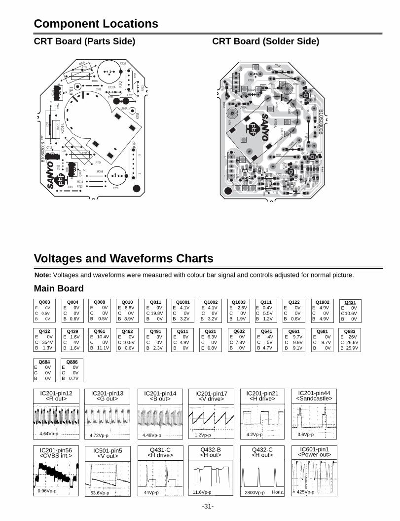
-31-
1
EE
E
B
B10S
0300
B **
*
5
13
B
C
C
B
C
R723
L702
R732
L702A
C751
K7P
J701
R703
R713
Q70
1AQ70
1R724
Q711A
Q711
Q72
1AQ
721
R705
R714
K7D1
K701
-L
L701
L721
L711
C732
C731
K7Q
R704
K7M
R717
R716
C731A
C710
J703
J702
CRT Board (Parts Side)
Component Locations
X
X
X
1
E
E
E
B-OUT
R-OUT
G-O
UT B10S0300B
5
13
B
B
B
C
C
C
***
R723
L702R732
L702A
C751
K7P
J701
R703
R713
Q701A
Q701
R724
Q711AQ711
Q721A
Q721
R705
R714
K7D1
K701-L
L701
L721
L711
C732
C731
K7Q
R704
K7M
R717
R716
C731A
C710
J703
J702
R742
R741R753
R751
Q751
D751
R752
D752
D754
D753
R701C701
R711
C711
C721
R721Q741R744
D741
D742
C754
CRT Board (Solder Side)
Voltages and Waveforms ChartsNote: Voltages and waveforms were measured with colour bar signal and controls adjusted for normal picture.
Main BoardQ003
E 0VC 0.5VB 0V
Q004E 0VC 0VB 0.6V
Q122E 0VC 0VB 0.6V
Q111E 0.4VC 5.5V B 1.2V
Q011E 0V C 19.8VB 0V
Q010E 8.8V C 0V B 8.9V
Q432E 0VC 354VB 1.3V
Q439E 1.6VC 4VB 1.6V
Q431E 0VC10.6VB 0V
Q008E 0VC 0VB 0.5V
Q1003E 2.6VC 0VB 1.9V
Q511E 0V C 4.9V B 0V
Q1001E 4.1VC 0VB 3.2V
Q1002E 4.1VC 0VB 3.2V
Q631E 6.3V C 0V E 6.8V
Q681E 0VC 9.7VB 0V
Q683E 26VC 26.6VB 25.9V
Q684E 0VC 0VB 0V
Q661E 9.7V C 9.9VB 9.1V
Q641E 4VC 5VB 4.7V
Q632E 0VC 7.8VB 0V
Q886E 0VC 0VB 0.7V
Q1902E 4.9VC 0VB 4.9V
1000Vp-p Horiz.37.4Vp-p
3.6Vp-p4.2Vp-p4.72Vp-p 4.48Vp-p
0.96Vp-p 53.6Vp-p 11.6Vp-p 2800Vp-p44Vp-p
IC201-pin44<Sandcastle>
IC201-pin21<H drive>
IC201-pin12<R out>
IC201-pin13<G out>
IC201-pin14<B out>
IC201-pin56<CVBS int.>
IC501-pin5<V out>
Q432-C<H out>
Q432-B<H out>
IC601-pin1<Power out>
425Vp-p
Q431-C<H drive>
4.64Vp-p 1.2Vp-p
IC201-pin17<V drive>
Q462E 0V C 10.5V B 0.6V
Q461E 10.4VC 0VB 11.1V
Q491E 3V C 0VB 2.3V
SM_29-C7GR PWB & WAVEFORM 7/16/05 11:33 AM Page 31
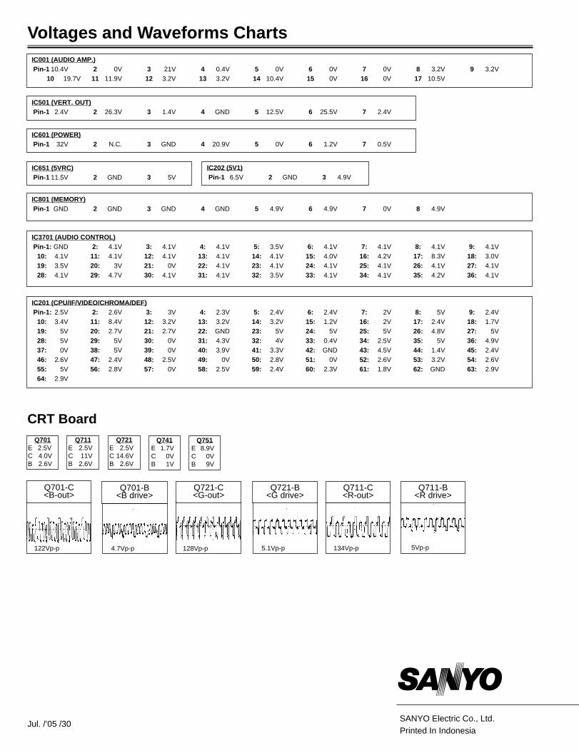
CRT BoardQ711
E 2.5VC 11VB 2.6V
Q701E 2.5VC 4.0V B 2.6V
Q741E 1.7VC 0VB 1V
Q721E 2.5VC 14.6VB 2.6V
Q701-B<B drive>
Q721-C<G-out>
Q701-C<B-out>
Q711-C<R-out>
Q711-B<R drive>
Q721-B<G drive>
122Vp-p 4.7Vp-p 128Vp-p 5.1Vp-p 5Vp-p134Vp-p
Q751E 8.9VC 0VB 9V
IC501 (VERT. OUT)Pin-1 2.4V 2 26.3V 3 1.4V 4 GND 5 12.5V 6 25.5V 7 2.4V
IC801 (MEMORY)Pin-1 GND 2 GND 3 GND 4 GND 5 4.9V 6 4.9V 7 0V 8 4.9V
IC001 (AUDIO AMP.)Pin-1 10.4V 2 0V 3 21V 4 0.4V 5 0V 6 0V 7 0V 8 3.2V 9 3.2V
10 19.7V 11 11.9V 12 3.2V 13 3.2V 14 10.4V 15 0V 16 0V 17 10.5V
IC651 (5VRC)Pin-1 11.5V 2 GND 3 5V
IC202 (5V1)Pin-1 6.5V 2 GND 3 4.9V
IC3701 (AUDIO CONTROL)Pin-1: GND 2: 4.1V 3: 4.1V 4: 4.1V 5: 3.5V 6: 4.1V 7: 4.1V 8: 4.1V 9: 4.1V
10: 4.1V 11: 4.1V 12: 4.1V 13: 4.1V 14: 4.1V 15: 4.0V 16: 4.2V 17: 8.3V 18: 3.0V19: 3.5V 20: 3V 21: 0V 22: 4.1V 23: 4.1V 24: 4.1V 25: 4.1V 26: 4.1V 27: 4.1V28: 4.1V 29: 4.7V 30: 4.1V 31: 4.1V 32: 3.5V 33: 4.1V 34: 4.1V 35: 4.2V 36: 4.1V
IC201 (CPU/IF/VIDEO/CHROMA/DEF)Pin-1: 2.5V 2: 2.6V 3: 3V 4: 2.3V 5: 2.4V 6: 2.4V 7: 2V 8: 5V 9: 2.4V
10: 3.4V 11: 8.4V 12: 3.2V 13: 3.2V 14: 3.2V 15: 1.2V 16: 2V 17: 2.4V 18: 1.7V19: 5V 20: 2.7V 21: 2.7V 22: GND 23: 5V 24: 5V 25: 5V 26: 4.8V 27: 5V28: 5V 29: 5V 30: 0V 31: 4.3V 32: 4V 33: 0.4V 34: 2.5V 35: 5V 36: 4.9V37: 0V 38: 5V 39: 0V 40: 3.9V 41: 3.3V 42: GND 43: 4.5V 44: 1.4V 45: 2.4V46: 2.6V 47: 2.4V 48: 2.5V 49: 0V 50: 2.8V 51: 0V 52: 2.6V 53: 3.2V 54: 2.6V55: 5V 56: 2.8V 57: 0V 58: 2.5V 59: 2.4V 60: 2.3V 61: 1.8V 62: GND 63: 2.9V64: 2.9V
IC601 (POWER)Pin-1 32V 2 N.C. 3 GND 4 20.9V 5 0V 6 1.2V 7 0.5V
Voltages and Waveforms Charts
SANYO Electric Co., Ltd.Jul. /’05 /30
Printed In Indonesia
SM_29-C7GR PWB & WAVEFORM 7/16/05 11:33 AM Page 32
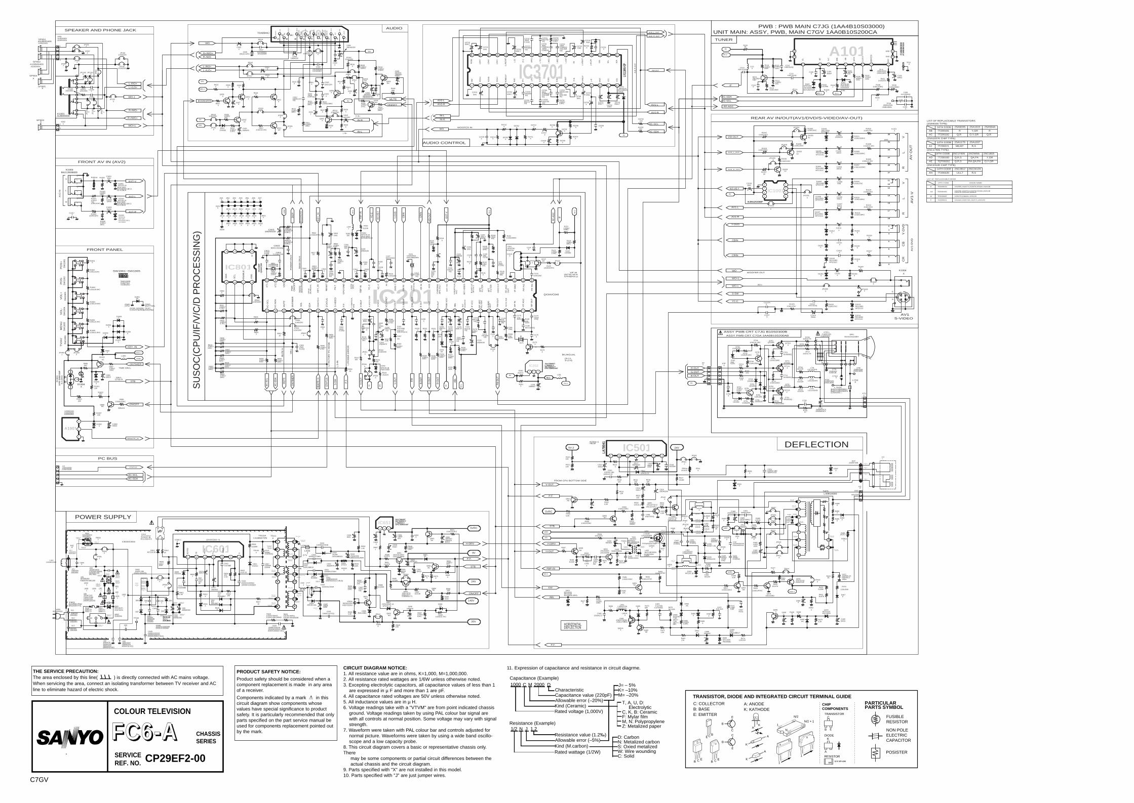
W10B04002W901
L81B31600L901
A10B00400SP901
:A10B25500
A10B00400SP902
:A10B25500
XSP904
XSP905
XSP903
BXXAVA032SEH-Q901
XL902
LIST OF REPLACEABLE TRANSISTORS
AC
AB
7T200182
7T200181
2SA564A2SA10152SA933S
Q,R
R
O,Y,GR
Y,GR
Q,R
R
14TH CODE
AJ 7T200221
2SA1179 2SA1037
M6,M7 R,S
14TH CODE
(2SA1037K CHIP TYPE)
(2SA933S TYPE)
AE
AD
7QT00202
7T200183
2SC945A 2SC18152SC1740S
RA,QA,PA
QA,PA
O,Y,GR
Y,GR
14TH CODE
AH 7T200220
2SC2812 2SC2412K
L6,L7 R,S
14TH CODE
(2SC1740S TYPE)
(2SC2412K CHIP TYPE)
Q,R,S
Q,R,S
LIST OF REPLACEABLE DIODE
7DD00019
7DD00192
7ED00025
7DD00021
R
AA
M
P
1S1555,1S2473,1S2076,DS442,1N4148
1S1555,1S2473,1S2076,DS442,1N41481SS176,1SS133,GMA01
1SS176,GMA01,1SS133
1S1553,1S2076A,1S2471,1N4148
14TH CODE DIODE NAME
ASSY PWB CRT C7JG B10S0300BASSY PWB CRT C7GA 1AA0B10S200AB
J11B2570NK701-L
:J11B3090N
125
6
7
8
11
1010 99
1/2DJ2.7KR716
1/2DJ2.7KR717
XL702
B4Z21B0090JL702A
:B4Z21B0090N:Z20103---
XC731A
J30B0250NK7D1
:J30B1380N
L2C1331KNL701
L2C1331KNL711
L2C1331KNL721
250EM10CXC710
:250EM10CY
XK7Q
1
3
10R732
XC732
2SJ12KR724
QT0392Q721
KK560GQC721
1/16GJ180C
R721
2SJ12KR714
2SJ12KR704
1/2DJ2.7KR705
QT0392Q711
KK560GQC711
1/16GJ180CR711
KK560GQC701
QT0392Q701
1/16GJ180CR701
AJQ741
1/16GJ1.2KCR741
1/16GJ5.6KCR742
1/16GZ0CD741
1/16GZ0C
D742
1/16GJ560CR744
470R713
470R723
470R703
1SS355D7521SS355
D753
1SS355D754
XK7P
1
2
3
4
5
AJQ7511/16GJ
8.2KC
R752
1SS355D751
1/16GZ0CR751 25EM330
C751
1/16GJ10KCR753X
C754
XQ701A
XQ711A
XQ721A
CK3D152KANHJN
C731 J30B0250NK7M
:J30B1380N
VD
D
SD
A
OTHERS:L)
L:S
-IN
L:P
OW
ER
ER
RO
R
BILINGUAL
MU
TE
:H
L:F
AC
TO
RY
PC
MO
DE
PO
WE
R O
N:H
BA
SS
ON
:H
SU
SO
C(C
PU
/IF/V
/C/D
PR
OC
ES
SIN
G)
(S-1:L
EN
AB
LE
S-2:H)
ON
:L
SC
L (NTSC-M:HVIF-M
SW1901~SW1905
GNDCPU
VO
L-
ON:L
ON:H
GNDBUTTON
TV
/AV
PO
S+
STB:H
(FOR SPARK TESTCOUNTERMEASURE)
VO
L+
FRONT PANEL
ME
NU
PO
S-
TMR ON:L
AV1S-VIDEO
REAR AV IN/OUT(AV1/DVD/S-VIDEO/AV-OUT)
C
WOOFER OUT
S
TUNER
R
FRONT AV IN (AV2)
L
AV
2-I
N
V
FROM CPU BOTTOM SIDE
DEFLECTIONIC501-1NEW
HORIZONTALDEFLECTION
LOW B
OP
AUD
DS
+B
27V
C603/C604
OC
P/BD
POWER SUPPLY
FB
R IN+
AUDIO
L IN+
AUDIO CONTROL
SPEAKER AND PHONE JACK
PC BUS
F6014A250VTW
:4A250VTS
WOOFER IN
PWB : PWB MAIN C7JG (1AA4B10S03000)UNIT MAIN: ASSY, PWB, MAIN C7GV 1AA0B10S200CA
SW1906
D606 & D608
C608
L
AV
OU
T
RC
RV
CB
AV
1-V
AV
1-D
VD
Y-D
VD
VL
R
GND
GND
WO-1
HEATER
AUD
_R_O
UT
200V
GND
MU
TE
1/16GJ470C
R132V10B0560N
X801
:V10B0570N
1KR818
XR232
25EM100C204
KK0.01GQC227
XJP206
EM0.47C225
1/16GJ100C
R894
1/16GJ15KC
R837
XJP201
MTZJ5.1AD352
:RD5.6EB1:DZXLBZA5.1C
1/16GJ3KC
R210
XC818
CD10CGQ
C1741
2
KK0.01GQ
C243
25KK0.047GQ
C224
AA
D357
V10B2930JX211
:B4V10B0040N
1
1/16GJ560C
R140
1KR817
1/16GJ10KC
R853
ON/O
FF
XC353
1/16GJ100C
R8441/16GJ100C
R839
25KK0.1GQ
C842
16KK0.47GQ
C132
V-O
UT
XR353
1/16GZ0CJP802
XR173
1 2
S-S
W
1/16GJ4.7KC
R842
R-O
UT
RF-
AG
C
150R212
JL201
1KR830
1
2
KK0.022GQC138
SF6376UX161
:SF6376Y
12
34
5
KK0.01GQ
C172
CJ18CGQ
C801
REMO
TE_IN
CJ18CGQC802
XR233
AV1-V
/S-Y
EM2.2C893
EM470C233
:25EM470KK0.01GQ
C232
VID
-OU
T
IIC-S
DA
CR
IN
XQ173
1
3
FJ0.015BE
C202
180KR228
1/16GJ15KC
R838
100R280
Y-D
VD
P.F
.
XC133
1/16GJ10KC
R845
2SJ470R243
XR804
XR133
150R211
1/16GJ47KC
R245
XC213
FM-O
UT
1/16GJ10KC
R814
XD230
JJP122
KK0.01GQ
C234
1/16GJ100C
R850
25KK0.1GQ
C273
XC242
KK0.01GQ
C203
JL204
1/16GJ27KC
R226
XC125
1/16GJ82KC
R340
3.9KR357
EM1C215
STA
TUS
EM1C358
1/16GJ4.7KC
R841
2SJ6.8R290
1/16GZ0CC123
1/16GZ0CJP801
1/16GJ10KC
R815
XC175
1/16GJ10KC
R819
25EM470C210
25KK0.033GQ
C894
EX
T-V
QXXAVC646IC2014
0R
ES
ET
41
FIL
T
42
CP
U G
ND
43
CC
DV
CC
44
FB
P I
N
45
YC
-C
46
YC
-Y
47
NC
48
DV
D-Y
49
CB
IN
50
4.43
MC
RY
ST
AL
51
CR
IN
52
SV
O
1S
IF O
UT
53
CH
RO
MA
AP
C F
ILT
2V
IF A
GC
54
EX
T.Y
-IN
3S
IF I
N
55
V/V
ER
TIC
AL
VC
C
4F
M F
ILT
ER
56
INT
.VID
EO
5F
M O
UT
57
BLA
CK
LV
L.D
ET
.FIL
T.
6A
UD
IOO
UT
58
AP
CF
ILT
ER
7S
IF A
PC
FIL
TE
R
59
AF
TF
ILT
ER
8IF
VC
C
9E
XT
AU
DIO
IN
10
AB
L
60
VID
EO
OU
T
11
RG
B V
CC
61
RF
-AG
CO
UT
12
R O
UT
62
IF G
ND
13
G O
UT
63
PIF
IN
2
14
B O
UT
64
PIF
IN
1
15
E/W
_O
UT
16
V-R
AM
P
17
V-O
UT
18
VC
O-I
RE
F
19
H-V
CC
20
H-A
FC
FIL
TE
R
21
H-O
UT
22
V-V
ER
TIC
AL
GN
D
23
P.F
.
24
S-V
IDE
O
25
ST
AT
US
26
RE
MO
TE
-IN
27
SD
A
28
SC
L
29
ON
TIM
ER
30
MU
TE
31
IIC
-SD
A
32
IIC
-SC
L3
3X
T1
34
XT
2
35
VD
D
36
PW
RO
N/O
FF
37
BA
SS
/W
OO
FE
R
38
VIF
-M/
BIL
ING
UA
L
39
KE
Y_
IN
EM1C863
1/16GZ0CJP804
16EM330C244
BASS
/WOO
FER
1/16GZ0C
R358
XC856
1/16GJ33KC
R227
1/16GJ6.8KC
R121
IIC-S
CL
AHQ122
1
1/16GF4.7KC
R286K
EY
_IN
1/16GJ1MC
R893
20KR351
1/16GZ0C
C176
FBP
-IN
1/16GJ2.2KC
R122
1/16GJ12KC
R225
YC
-C
1/16GJ10KC
R834 BA178M05T
IC202 :L78M05CV:MC78M05CT:UPC78M05AHF
1 2 3
XR131
1/16GJ120C
R235
H-O
UT
150R230
EM2.2C247
CB
IN
MTZJ9.1BD249
:RD9.1EB2
16EM100C805
XR224
16EM47C291
1/16GJ10KC
R176
1/16GJ470C
R840
XJP803
XR231
16EM100C122
1/16GJ47KC
R244
XC124
XR291
XC816
1/16GZ0CR215
X
R803
DJ10K
R352
KK1500GQ
C171
KK0.01GQC803
FJ0.47BEC231
:GJ0.47T:HJ0.47(G:H)
ON
TIM
ER
IF
KK0.01GQ
C121
KK8200GQ
C120
XC229
XX161A 1
23
45
1/16GJ270KC
R801X
C228
1/16GJ47KCR863
24LC
16B
/P
IC801:Q
XXA
VC36
0
1 1A0
2345 6 7 8
X171
1/16GJ560CR141
1/16GZ0C
R130
1SS356D122
1/16GJ10KC
R124
1/16GJ120C
R236
1/16GJ10KC
R852
1/16GZ0CJP202
2
G-O
UT
25KK0.1GQ
C843
1/16GJ120C
R234
1/16GJ27KCR125
CJ15CGQ
C212
AB
L
XR802
1/16GJ10KC
R813
B-O
UT
5V-1
9V5V-15V-1
5V-2
9V9V 24V
5VR
C
5V-2
5V-2
9V-2
ON/OFF
S10B2790J
SW
19
01
:S10B3670J:S10B0450J
12
220R1913
560R888
1/16GJ12KCR1902
S10B2790J
SW
19
05
:S10B3670J:S10B0450J
12
AHQ886
220R1912
S10B2790J
SW
19
04
:S10B3670J:S10B0450J
12
ACQ1902
1
REMOTE_IN
1/16GJ5.6KCR1903
100R1907
1/16GJ1.8KCR1906
ONTIMER
AAD1901
KEY_IN
R1901X1
1/16GJ22KCR886
220R1911
U20B32400
A1901
:U20B35900:U20B63800
1
2
3
S10B2790J
SW
19
02
:S10B3670J:S10B0450J
1/16GJ3.9KCR1904
1/16GJ2.2KCR1905
1/16GJ22KC
R887
EM22C1902
STB
S10B2790J
SW
19
03
:S10B3670J:S10B0450J
1
S10B2790J
SW
19
06
:S10B0450J
12
EM10C1007
1/16GJ1KCR1014
XD1012
1
XK1004
12
34
5
6
78
XJP1029
1/16GJ75CR1023
EM10C1005
EM10C1004
1/16GJ1KCR1026
1
RD11EB3D1004
:MTZJ11C
1/16GJ2.2KCR1006
XR1021
1/16GJ1KCR1031
EM1C1009
XJP1004
1/16GJ100KCR1007
AUD_L_OUT
XD1015
NJM12533MP
IC1001
1
2
3
45
6
7
8
XJP1002
YC-C
XD1011
CRIN
KK0.01GQC1013
Y-DVD
X
JP1028
S-SW
1/16GJ75CR1010
XR1018
XC1011
X
JP1001
RD11EB3D1010
:MTZJ11C1
EM10C1014
1/16GJ100KCR1011
XC1015
XC1012
XR1017
XJP1003
RD11EB3D1014
:MTZJ11C1
1/16GJ1KCR1012
RD11EB3D1006
:MTZJ11C
1/16GJ2.2KCR1008
AUD_R_OUT
AJQ1002
E
B
C
RD11EB3D1013
:MTZJ11C1
EM10C1008
1/16GJ18KCR1015
AJQ1003
XC1010
1/16GJ75CR1022
RD11EB3D1009
:MTZJ11C 1
AV1-V/S-Y
1/16GJ18KCR1013
AV1-R
1/16GJ75CR1016
1/16GJ1KCR1029
1
XR1020
AV1-L
RD11EB3D1007
:MTZJ11C 1
RD11EB3D1008
:MTZJ11C 1
VID-OUT
1/16GJ1KCR1028
1
CBIN
C100616EM220
1KR1027
AJQ1001B
C
1/16GJ100KCR1009
EM1C1016
1/16GJ1KCR1030
XR1019
RD11EB3D1005
:MTZJ11C
X
JP1031
XR1024
XR1025
9V
IF
JR102
KK0.01GQC114 KK0.01GQ
C1121/16GJ330C
R114
XC109
1/16GJ1KC
R111 1/16GZ0CR101
56R115
1/16GJ100C
R107KK0.01GQC111
J30B0250NTP-A
:J30B1380N
1/16GJ18KCR108
MTZJ36AD103
:RD36EB1:DZXLBZA36A
XC105
1SJ39KR103
1
2
1/16GJ5.6KC
R112
EM47C104
JR105
XTP-E
MTZJ6.8AD102
:RD6.8EB1:DZXLBZA
6.8A
F1B
EB
0300
A101 :F1B
EB
0320
1
AGC
3
ADD
RES
S
4
CLO
CK
5
DAT
A
6
MB
7
(MB)
8
N.C
9
BT
11
IF1
12
13 14GND
15GND
16EM470
C101
RF-AGC
KK1000GQC108
2SC2814F4P
Q111
1
X
JP111
XL111
IIC-SCL
1/16GJ100C
R106
J30B0250NTP-M
:J30B1380N
XC113
EM22C106
1/16GJ68KCR109
1/16GJ56CR116
IIC-SDA
9V-2
9V
140V-1 5V-1
1/16GJ1KC
AV2-L
XR1032
1/16GJ18KC
R1003
EM1C1001
AV2-R
1/16GJ1KCR1004
1/16GJ75C
R1001
1
2
MTZJ9.1AD1002
:RD9.1EB1:DZXLBZA9.1(B:C):UZ-9.1BCB
1
MTZJ9.1AD1001
:RD9.1EB1:DZXLBZA9.1(B:C):UZ-9.1BCB
1
EM10C1003
MTZJ9.1AD1003
:RD9.1EB1:DZXLBZA9.1(B:C):UZ-9.1BCB
EM10C1002
1/16GJ18KC
R1005
B4J12B08600K1003
7
1
2
3
4
5
6
8
9
EXT-VX
R1001A
1
2
10KR511
XKDY-1
1
X
JP502
XR525
V-OUT
12KR514
2SJ470R501A
1
2KK3300C518
220R522
25EM2200C515
1
24V
JJP501
AHQ511
P.F.
5.6KR502
LA78
041
IC501
7 123456
XKDY-6
1
EM4.7C514
100R519
XD441
ERA15-02
D512 XD507
39KR515
100FK0.1BEC524
:100FK0.1D
5V-2
C520100FK0.1BE
:100FK0.1D
1/2DJ1.2R518
XR512
XKDY-3
1
XKDY-5
1
10KR510
XR501
1
18KR516
35EM220C517
35EM1000
C521 2
XD448
X
JP412
35EM47C434
L441-H2
L71B0650N
L441
XKQ
1/2DJ1KR474
400MJ0.15CQ
C442
140V
1KR437
2400030L441-H3
400MJ0.15CQ
C441
1/16GJ2.2MC
R483
JR466
2SJ4.7R481
XC450
DZXLBZA7.5A
D489
:MTZJ7.5A:RD7.5EB1
J
JP407
ERD07-15LD438
B4Z21B0160NL432
:Z21B0330N:L3004
MTZJ16AD421
:MTZJ16A:RD16(EB1:EB3)
AHQ439
L442-H2
MTZJ5.1BD353
XC423A
ERB44-04D439
1/16GJ12KCR491
NF120KR470 1/6NF
3.9K
R421
1/2DJ180K
R482
XC431
AAD465
160EM0.47CY
C482
1/2DJ1KR433
500KK3900AC433
L7201B
L431
:L2G31R0MN
2
L26B0170NL461
:LM0045(:D)
KK100C355
1KR424
100GK2.2C465
AJQ491
FJ4700DC463
:FJ4700BE
XC437A
XR445
7SJ6.8VCR435
XD486
AEQ462
12KR492
XR486
XC449
100PM2.2XC471
:100PM2.2LBZA1
1500MH6000XK
C423
1500MH6500ANC420
:1500MH6500XK
680R473
XL403
L26A00200L462
:L26B4630N
HJ0.01GC470
1/16GJ10KC
R426
XR442
140V
400NJ0.018EAQ
C425
EM10C469
500KK680AC491
XQ449
JJP436
5V-2
JJP442A
2SJ1K
R441
EU1D469
:DDXLBB017
MTZJ20AD466
:RD20EB1
MTZJ11CD476
:RD11EB3
500KK1000AC432
JJP403
EU1
D485:DDXLBB017
XJP411
XJP441
400NJ0.02EAQ
C424
PD467
XR484
250EM33CYC486
JJP410
DJ39KR423
X
JP409
1/2DJ330
R475
1KR431
DJ47KR422
XR489
2400030
L441-H1
1/16GJ470CR493
AAD461
1/16GJ470CR494
1.5KR471
XR485
25EM22C468
1/16GJ470CR432
DJ330R438
1/2DJ270R434
J
JP408
2.2KR479
1/2FJ1R488
XR449
XR450
XJP435
J
JP414
XD460
DJ10KR355
XR490
XR487
AAD468
HJ1GC467
L442-H1
XD464
16KK0.47BA
C439
27KR462
JR477
XR427
XL442A
14
2SA1371DQ406
:2SA1371E
2SC2228DQ405
AHQ404
5.6KR408
100KR411
1SJ47KR410
1/16GJ47KCR409
1/16GJ10KCR407
140V-1
2SA1371DQ401
:2SA1371E
6.8KR401
470KR402
2SC2271D-CQ402
:2SC2271E-C
AHQ403
1/16GJ330KC
R403
1/16GJ10KCR404
KK0.01GQC401
1/16GJ10KCR406
STB
5VRC
24V
24V
EU2D633
:DDXLBB019
XC653
2400030
T611-H7
1
200EM220XDC641
:160EM220(XJ:LBUA)
FJ470BEC610
2400030
PS601-H2
1
250GM0.068XDC602
:275GM0.068XB:250GM0.068(XE:XBJ)
12
1SJ68KR606
XR674
1000KK470NHC631
250GK0.22XDC601
:275GK0.22VBB:275GM0.22XB:250GM0.22(XE:BJ)
1.5KR611
16EM220C662
DHXAAEV0070PS601
:DHXAVB017
1
23
1SJ270R661
ERC91-02LD632
35EM470C643
1/2CK5.6MXGR628
:1/2DK5.6MLBWAB
J30B0250NKG-2
:J30B1380N
AHQ631
STB
P.F.
250KK1000XHC629
:250KM1000XN:400KK1000(X:VDC)
AHQ641
400KK470X:250KM470XN:250KK470XH:400KK470(X:VDC)
C627
ERZV14D471VA601
:SVC471D07A
1
100R609
25EM2200
C645
2400010C609-H1
1
DJ3.9KR687
15KR645
2400010SW601-H2
1
20V
DJ150KR685
1/2CK5.6MXGR629
:1/2DK5.6MLBWAB
JR605
1/16GJ10KC
R640
EU1D612
:DDXLBB017
X
JP683
JR667
1/16GJ6.8KCR641
RD6.2EB3D686
XT611-H15
1
EM10C661
1000KK470NHC632
1000KK470NHC634
RU3MD634
:DDXLBB021
QXXAVC634---N
IC601NNPL/S
SPL
/SS
S/G
ND
S/G
ND
7 123456
J30B0250NKE-2
:J30B1380N
XD682
2400030T611-H2
1
XR675
JJP601
15WK1.8MR602
:15WK1.8LBZDL
1
2
2SA1707SQ683
:2SA1707T:2SB985(S:T)
10EM470
C651
S10B6230NSW601
2
1
35EM22C615
5VRC
EM1C611
XJP602
2400030L601A-H4
1
1/2DJ100K
R608
EG01CD611
D609ED0434
2400010C609-H2
1
400EM220XCC609
2400030L601A-H2
1
FJ2200BEC613
JJP644
2SJ0.33R603
2000KK1000NHC616
:2000KK1000DBH
MTZJ6.2BD614
RD10EB2
D661
2400030L601-H3
1
AEQ681
1
1/2DJ120K
R635
EM47C649
16EM10C650
:25EM10:EM10
1
AAD681
560KR689
2
1KR610
J30B0250N
KG-1
:J30B1380N5.6KR636
J20B0170JF601A
:J20B0171J
12
2400030L601-H4
1
EM1C691
RU3AMD631
R3D6222NJVR631
:R3D7222NJ
1
3
AEQ684
1
2400030PS601-H1
1
1FJ3.9R643
12
XT611-H13
1
1.5KR690
140V
2400030L601A-H1 1
:250KM1000XN:400KK1000(X:VDC)
C628250KK1000XH
BA178M05T
IC651 :MC78M05CT:L78M05CV:UPC78M05AHF
1 2 3
2SJ0.33
R604
2400030L601A-H3
12400030L601-H2 1
JL632
1
100KR642
1000KK470NHC633
FJ0.1DC612
:FJ0.1BE
1/16GJ1KC
R681
J30B0250NKE-1
:J30B1380N
25EM1000C644
:25EM1000LBWA1
2
DJ10KR686
PC123Y52:TLP421F-BL:PC123X5YFZ
D610
123 4
2400030PS601-H3
1 H-DRV
630NJ0.022EAQ
C614
9V
XIC601-1
XTP-EE
2400030L601-H1
1
B4F35B0040NL601
:F35B0570N:F35B1130N
1
2 3
4
10R607
XR644
ON/OFF
2SJ3.9R668
J30B0250N
KG-3
:J30B1380N
22KR688
H-DRV
EU1D613
:DDXLBB017
JL602
JL603
XR601 J
JP604
XJP603
1000KK1000CBB
C607
:1000KK1000HB
1000KK1000CBB:1000KK1000HB
XC606
XC605
ERC05-10B
D605
:RM11C:DDXLBB016
2
ERC05-10B
D606
:DDXLBB016
D607 D608
400EM220XCC609A
25EM1000C001
XR027
XJP001
1/16GJ39KC
R011
16EM220C004
XC002
XC013
X
JP014
XC003
1/16GJ39KC
R021
TDA8944J IC00110C1
LOU
T+
2
GN
D
33
Vcc
1
44
RO
UT-
55
WFM
UTE
66
RIN
+
77
SG
ND
88
LIN
+
99
WFI
N+
1010
Sta
ndby
1111
SV
R
1212
WFI
N+
1313
n.c.1414
WFO
UT-
1515
GN
D
1616
Vcc
2
1717
WFO
UT+
16KK0.047GQ
C022
XC014
XC024
XR028
XR030
XQ002
1/16GZ0CC015
XJP002
XC023
XR029
1/16GJ18KCR022
JC021
1/16GJ18KC
R012
20V
16KK0.047GQ
C012
220R3704
EM4.7C3713
IN-R
IN-L
EM4.7C3716
EM4.7C3702
LV11
16NV
-EPIC3701
30ST
-2
31L-
DC
32LL
INEO
UT
33LC
H-C
34LC
H-B
35LC
H-A
10R
-BC
1
36R
GN
D
11R
-BC
2
12R
-OU
T
13R
-IN
14R
-VR
OU
T
15L+
R
16VR
EF
17VC
C
18VD
D19
SDA
1G
ND
2R
CH
-A
3R
CH
-B
20SC
L
21VS
S
4R
CH
-C
22L+
R L
PF
5R
LIN
EOU
T
23L-
VRO
UT
6R
-DC
24l-I
N
7ST
-1
25L-
OU
T
8LP
FC
26L-
BC2
9R
-TC
1
27L-
BC1
28L-
TC1
29H
PFC
1/16GJ3.9KC
R3702
16KK0.068GQ
C3721
:KK0.068GQ
XR3711
AUD_L_OUT
IIC-SCL
25KK0.1GQ
C3718
EM47C3712
EM4.7C3715
KK6800GQ
C3717
1/16GJ3.9KC
R3701
XR3703
ERA15-02D3701
:DDXLBB025:TVR1B
EM4.7C3711
KK5600GQ
C3703
EM1C3722
16KK0.068GQ
C3706
:KK0.068GQ
AUD_R_OUT
EM1C3710
16KK0.068GQ
C3720
:16KK0.068GQ
XC3723
EM1C3701
EM1C3708
AV2-R
FM-OUT
EM1C3714
KK2700GQ
C3719
IIC-SDA
XC3725KK0.01
GQ
C3704
AV1-L
16KK0.068GQ
C3707
:KK0.068GQ
AV1-R
EM1C3724
AV2-L KK2700GQ
C3705
220R3705
25KZ0.22FAC026 KK1500GQ
C017
:KK1500BA 1/16GZ0CJP004
25KZ0.22FAC025
J10EA040NK001
:J10KR040N
11
2
3
44
JJP006
JJP008
XJP009
XJP007
L-/RO+
R-/WO-
J12B06000K1001
1
2
3
4
5
6
7
8
9
XJP
011
1/2DJ390R1106
1/2DJ390R1107
L+/LO+
R+/WO+
XK002
1
2
KXJ10EA050N
:J10KR050N
1 STATUS
IIC-SCL
IIC-SDA
XKP
1
2
3
4
5
R-OUT
G-OUT
B-OUT
GND9V
P.F.
H-OUT
FBP-IN
ABL
EW
MUTE
IN-R
IN-L
L+/LO+
L-/RO+
BASS/WOOFER
R-/WO-
R+/WO+
XJP1005
WO+1
1/16GZ0CJP203
XJP205
2
KK0.01GQ
C201
EW
XC1017
EM22C510
EM10C850
XD1909
XD850
XD1903
XD1907
XD1908
XJP1900
JJP1901
JL1901
5VRC
5VRC
5.6KR405
XC603
XR481A
J
JP015
J
JP013
EM1C245
XD1902
XC107
KDYJ10B0730N
XQ432A
1
2
3
XL462A
XL462-H2
1
2400010L462-H1
1
2400030
L462-H31
2400030T471-H1
1
2400030T471-H2
1
2400010
T471-H4
1
2400010T471-H5
1
2400010T471-H6
1
2400010T471-H7
12400010T471-H8
1
2400010T471-H10
1
XL461A
XT431A
1
34
5
6
AD0002T431
:AD0002C:B4L18B0020N:L18B0540N
1
2 3
4
5
2400030T431-H1
1
2400030T431-H3
1
2400030T431-H4
1
2400030T431-H2
1
XL441A
250GJ0.47
C437
XL603A
1
2
XL603B
XL602A
1
2
XL602B
XKE
1
XPS601A
1
23
JL635
XL601A
1
2 3
4
XD632A
3
1
2
XD632B
3
1
2
XC663
2400010C641-H11
2400010C641-H2
1
XR602A
1
2
X
R602B1
2
2400010R602-H1 1
2400010R602-H3
1
XR602-H5
12400010R602-H2
12400010R602-H4 1
XR602-H6
1
2400010C609A-H1
1
2400010C609A-H2
1
J
C1105
JC1104
JJP
010
XC230
XD1906
XD1905
L51B6670NT611A
1
2
3
4
5
6
7
8 9
10
11
12
13
14
15
16
17TXXGA0181753M
Q432
2
3
XQ432-H1
1 2400030Q432-H2
1
2SB1274QRAQ461
:2SB1274RRA1
2
3
XQ461A
1
2
3
XT611
1
2
3
4
5
6
7
8 9
10
11
12
13
14
15
16
17
2400030
T611-H5
1
2400030
T611-H8
1
X
T611-H10
1
XT611-H11
1
XT611-H17
1
XJW1
1X
JW2
1X
JW3
1X
JW4
1X
JW5
1X
JW6
1X
JW7
1
XJW8
1
XJW9
1
XJW10
1
XJW11
1
XJW12
1
XJW13
1
2400030T611A-H5
1
2400030T611A-H7
1
KK1500GQC018
:KK1500BA
XJP103
1/16GZ0CJP105
1/16GZ0CJP106
XC1107
XC1107A
2400030
T611A-H13
1
5VRC-1
16KK0.047GQC635
2400030T611A-H17
1
2400030T611A-H11
1
2400030T611A-H10
1
2400030T611A-H8
1
2400030T611A-H2
1
2400030T611A-H15
1
XD1904
J20B0170JF601B
:J20B0171J
12
WO-1
SP
R-3
9M
VW
FD
19
01
:DLX
LBB0
01
1
X
D632-H1 1
XR612
XD615
XD616
2400010SW601-H11
1/16GZ0CJP012
AHQ632
DZXLBZA5.1AD687
:MTZJ5.1A
16EM10C636
1/16GJ4.7KCR6381/16GJ
10KC
R637
AAD688
WO
XR3709
XR3707
XR3708
XR3710
XR3706
XC3726
XQ3701
9V
XC3729
XD3702
XD3703
XR3712
WO
AAD231
XC3709
XC3727
XR3713
XJP161
1
2000KK220NH
C617XC604
250KK470XH:250KM470XN:400KK470(X:VDC)
C626
XJP1101
XJP1102
XJP
1103
XJP
1104
XJP415
XJP416
2SJ82R517
1
2
2SC3332SQ431
:2SC3332R
WO
XR103A
1
2
XJP204
J30B0250NTP-B
:J30B1380N
9V
1/16GJ1KC
R639
KK0.1GQ
C637
JJP442
XJP441A
XC614A
2SD1913SRAQ661
:2SD1913RRA
1
XR016
XQ009
1/16GZ0CJP016
XR015
XJP017
1/16GJ100KC
R008
1/16GJ27KC
R006
AHQ004
AHQ008
1/16GJ68KC
R031
AHQ003
1/16GJ470KC
R010
68KR009
XR002
XQ001
XR003
XQ005
XR007
XR018
1/16GJ2.2KCR017
AJQ010
1/16GJ2.2KC
R037
1/16GJ1KC
R038
1SS355D004
1
1/16GZ0CJP019
XJP020
9V
20V
ON/OFF
XR023
5VRC-1
XR014
XR013
16EM33C020
XC005
20V
XC007
XJW14 1
XJW15
1
XJW16
1
XJW17
1
XJW18
1
XQ432B-1
XL442
123
XK1101
1515
22
55
11
66
33
2323
2020
2424
2121
1717
1414
1818
88
99
2626
2727
1111
1010
1212
X
JP018
WO+1
WO-1
XR643A
12
XJW19
1
XJW20
1
XJW21
1
XJW22
1
XJW23
1
XJW24
1
16EM10C009
:25EM10:EM10
16EM33C006
:16EM33CD:25EM33(:CD
XR005
XQ012
JJP005
XJP003
AHQ011
XJW25
1
XJW26
1
XJW27
1
X
JW28
1
L40B16000T471
1
2
3
4
5
6
78
9
10
C608
COLOUR TELEVISION
CHASSISSERIES
SERVICE REF. NO.
FFFFCCCC6666----AAAA
PRODUCT SAFETY NOTICE:
Product safety should be considered when acomponent replacement is made in any areaof a receiver.
Components indicated by a mark in thiscircuit diagram show components whose values have special significance to productsafety. It is particularly recommended that onlyparts specified on the part service manual beused for components replacement pointed outby the mark.
CIRCUIT DIAGRAM NOTICE:1. All resistance value are in ohms, K=1,000, M=1,000,000.2. All resistance rated wattages are 1/6W unless otherwise noted.3. Excepting electrolytic capacitors, all capacitance values of less than 1
are expressed in µ F and more than 1 are pF.4. All capacitance rated voltages are 50V unless otherwise noted.5. All inductance values are in µ H.6. Voltage readings take with a "VTVM" are from point indicated chassis
ground. Voltage readings taken by using PAL colour bar signal are with all controls at normal position. Some voltage may vary with signalstrength.
7. Waveform were taken with PAL colour bar and controls adjusted for normal picture. Waveforms were taken by using a wide band oscillo-scope and a low capacity probe.
8. This circuit diagram covers a basic or representative chassis only.There
may be some components or partial circuit differences between theactual chassis and the circuit diagram.
9. Parts specified with "X" are not installed in this model.10. Parts specified with "J" are just jumper wires.
THE SERVICE PRECAUTION:The area enclosed by this line( ) is directly connected with AC mains voltage.When servicing the area, connect an isolating transformer between TV receiver and ACline to eliminate hazard of electric shock.
11. Expression of capacitance and resistance in circuit diagrme.
C7GV
TRANSISTOR, DIODE AND INTEGRATED CIRCUIT TERMINAL GUIDEC: COLLECTORB: BASEE: EMITTER
A: ANODEK: KATHODE
B
B
C
C
E
E
C EB C E
B
B
C
E
AK
K
A
A
K
FUSIBLERESISTOR
PARTICULARPARTS SYMBOL
1
1
1
N/2
N/2 + 1
N
NON POLEELECTRICCAPACITOR
POSISTER
C
EB
CHIP COMPONENTS
K
A
TRANSISTOR
DIODE
123
RESISTOR
12 X 103=12K
Capacitance (Example)1000 C M 2000 D
CharacteristicCapacitance value (220pF)Allowable error (–20%)Kind (Ceramic)Rated voltage (1,000V)
J= – 5%K= –10% M= –20%
Resistance (Example)1/2 N J 1.2
Resistance value (1.2‰)Allowable error (–5%)Kind (M.carbon)Rated wattage (1/2W)
D: CarbonN: Metalized carbonS: Oxied metalizedW: Wire woundingC: Solid
T, A, U, D: ElectrolyticC, K, B: CeramicF: Mylar filmM, N: PolypropyleneZ: Metalized paper
CP29EF2-00
Sch Dia_29-C7GV(FC6-A)AUS 8/9/05 9:13 AM Page 1
Related Documents