TABLE OF CONTENTS Page Service Manual . Mechanical and Dismantling Instructions…………........................3-1 . Software Upgrades ....................................................................... .4-1 . Trouble Shooting Chart………………………………………………. 5-1 . Wiring Diagram………………………………………..………..….….6-1 . Electrical Diagrams and Print-layouts..….…………………....….…7-1 . Set Mechanical Exploded view & Part list.…………………..….…10-1 ©Copyright 2011 Philips Consumer Electronics B.V. Eindhoven, The Netherlands All rights reserved. No part of this publication may be reproduced, stored in aretrieval system or transmitted, in any form or by any means, electronic, mechanical, photocopying, or otherwise without the prior permission of Philips. CLASS 1 LASER PRODUCT PHILIPS GB . DFU Instruction..............................................................................2-1 . Revision List.................................................................................11-1 Home Theater Soundbar . Technical Specifications…………....………………………..............1-3 . Safety Instruction, Warning & Notes….……………………....….....1- 4 . Location of PCB Boards,Version Variation and Repair Scenario Matrix.....1-2 Published by Arya & Stephen - 1252 BU AVM Printed in The Netherlands Subject to modification 3141 785 38622 Version 1.2 Service . Pin Description & Block Diagrams of ICs..….………………..........9-1 . Votages and Waveforms for Connection Pins..….………………...8-1 HTL2160C/G/M/S/T/W/12/F7/93

Welcome message from author
This document is posted to help you gain knowledge. Please leave a comment to let me know what you think about it! Share it to your friends and learn new things together.
Transcript

TABLE OF CONTENTS
Page
Service Manual
. Mechanical and Dismantling Instructions…………........................3-1
. Software Upgrades ........................................................................4-1
. Trouble Shooting Chart………………………………………………. 5-1
. Wiring Diagram………………………………………..………..….….6-1
. Electrical Diagrams and Print-layouts..….…………………....….…7-1
. Set Mechanical Exploded view & Part list.…………………..….…10-1
©Copyright 2011 Philips Consumer Electronics B.V. Eindhoven, The Netherlands
All rights reserved. No part of this publication may be reproduced, stored in aretrieval system or
transmitted, in any form or by any means, electronic, mechanical, photocopying, or otherwise
without the prior permission of Philips.
CLASS 1
LASER PRODUCT
PHILIPSGB
. DFU Instruction..............................................................................2-1
. Revision List.................................................................................11-1
Home Theater Soundbar
. Technical Specifications…………....………………………..............1-3
. Safety Instruction, Warning & Notes….……………………....….....1-4
. Location of PCB Boards,Version Variation and Repair Scenario Matrix.....1-2
Published by Arya & Stephen - 1252 BU AVM Printed in The Netherlands Subject to modification
3141 785 38622
Version 1.2
Service
. Votages and Waveforms for Connection Pins..….………………...8-1
. Pin Description & Block Diagrams of ICs..….………………..........9-1
. Pin Description & Block Diagrams of ICs..….………………..........9-1
. Votages and Waveforms for Connection Pins..….………………...8-1
HTL2160C/G/M/S/T/W/12/F7/93
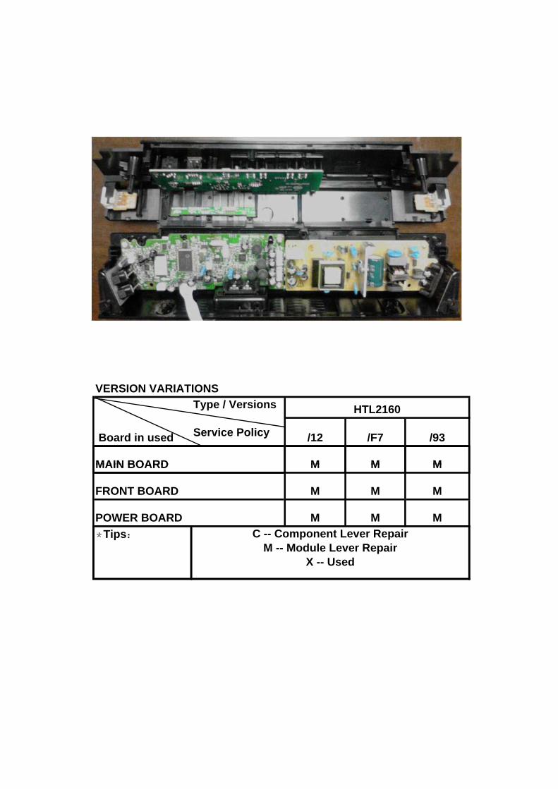
VERSION VARIATIONSType / Versions
Service Policy /12 /F7 /93
M M M
Board in used
HTL2160
MAIN BOARD M M M
M M M
M M M*Tips: C -- Component Lever Repair
M -- Module Lever Repair
MAIN BOARD
FRONT BOARD
POWER BOARD
pX -- Used
tianch
文本框
PCB BOARD LOCATION:
tianch
文本框
MAIN BOARD
tianch
文本框
POWER BOARD
tianch
文本框
OP BOARD
tianch
文本框
1-2
tianch
文本框
FK BOARD
tianch
文本框
CN BOARD
tianch
文本框
OP BOARD
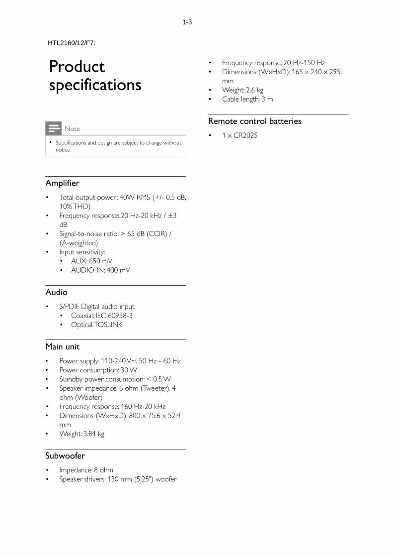
Product specifications
Note
notice.
Total output power: 40W RMS (+/- 0.5 dB, 10% THD)Frequency response: 20 Hz-20 kHz / ±3 dBSignal-to-noise ratio: > 65 dB (CCIR) / (A-weighted)Input sensitivity:
AUX: 650 mVAUDIO-IN: 400 mV
AudioS/PDIF Digital audio input:
Coaxial: IEC 60958-3Optical: TOSLINK
Main unitPower supply: 110-240 V~, 50 Hz - 60 HzPower consumption: 30 WStandby power consumption: < 0.5 W Speaker impedance: 6 ohm (Tweeter), 4 ohm (Woofer) Frequency response: 160 Hz-20 kHz Dimensions (WxHxD): 800 x 75.6 x 52.4 mmWeight: 3.84 kg
SubwooferImpedance: 8 ohmSpeaker drivers: 130 mm (5.25") woofer
Frequency response: 20 Hz-150 HzDimensions (WxHxD): 165 x 240 x 295 mmWeight: 2.6 kgCable length: 3 m
Remote control batteries1 x CR2025
1-3
HTL2160/12/F7:

Product specifications
Note
notice.
Total output power: 60W RMS (+/- 0.5 dB, 10% THD)Frequency response: 20 Hz-20 kHz / ±3 dBSignal-to-noise ratio: > 65 dB (CCIR) / (A-weighted)Input sensitivity:
AUX: 2 VAUDIO-IN: 1V
AudioS/PDIF Digital audio input:
Coaxial: IEC 60958-3Optical: TOSLINK
USBCompatibility: Full-Speed USB (2.0)Class support: USB Mass Storage Class (MSC)File system: FAT16 and FAT32
Sampling frequency:MP3: 8 kHz, 11 kHz, 12 kHz, 16 kHz, 22 kHz, 24 kHz, 32 kHz, 44.1 kHz, 48 kHzWMA: 44.1 kHz, 48 kHz
Constant bit rate:MP3: 8 kbps-320 kbpsWMA: 32 kbps-192 kbps
Version:WMA: V7, V8, V9
Bluetooth
Bluetooth version: 2.1 + EDR
Main unitPower supply: 220-240 V~, 50 Hz - 60 HzPower consumption: 30 W
Speaker impedance: 8 ohm (Tweeter), 4 ohm (Woofer) Frequency response: 160 Hz-20 kHz Dimensions (WxHxD): 800 x 75.6 x 52.4 mmWeight: 1.2 kgOperating temperature and humidity: 0°C to 40°C, 5% to 90% Humidity for all climatesStorage temperature and humidity: -40 °C to 70 °C, 5% to 95%
SubwooferImpedance: 8 ohmSpeaker drivers: 130 mm (5.25") wooferFrequency response: 45 Hz-200 HzDimensions (WxHxD): 165 x 240 x 295 mmWeight: 2.6 kgCable length: 3 m
Remote control batteries1 x CR2025
HTL2160/93:
1-4

Safety instruction
1. General safety
Safety regulations require that during a repair:
. Connect the unit to the mains via an isolation transformer.
. Replace safety components indicated by the symbol ,
only by components identical to the original ones. Any
other component substitution (other than original type)
may increase risk of fire or electrical shock hazard.
Safety regulations require that after a repair, you must
return the unit in its original condition. Pay, in particular,
attention to the following points:
. Route the wires/cables correctly, and fix them with the
mounted cable clamps.
. Check the insulation of the mains lead for external
damage.
. Check the electrical DC resistance between the mains
plug and the secondary side:
1) Unplug the mains cord, and connect a wire between
the two pins of the mains plug.
2) Set the mains switch the “on” position (keep the
mains cord unplug).
3) Measure the resistance value between the mains
plug and the front panel, controls, and chassis
bottom.
4) Repair or correct unit when the resistance
measurement is less than 1M .
5) Verify this, before you return the unit to the
customer/user (ref. UL-standard no. 1492).
6) Switch the unit “off”, and remove the wire between
the two pins of the mains plug.
2.Laser safety
This unit employs a laser. Only qualified service personnel
may remove the cover, or attempt to service this device
(due to possible eye injury).
Laser device unit
Type : Semiconductor laser GaAlAs
Wavelength : 650nm (DVD)
: 780nm (VCD/CD)
Output power : 7mW (DVD)
: 10mW (DVD /CD)
Beam divergence: 60 degree
Note: Use of controls or adjustments or performance of
procedure other than those specified herein, may result in
hazardous radiation exposure. Avoid direct exposure to
beam.
Safety instruction, Warning & Notes
1-5

Warning
1.General
. All ICs and many other semiconductors are susceptible to
electrostatic discharges (ESD). Careless handing during
repair can reduce life drastically. Make sure that, during
repair, you are at the same potential as the mass of the
set by a wristband with resistance. Keep components and
tools at this same potential. Available ESD protection
equipment:
1) Complete kit ESD3 (small tablemat, wristband,
connection box, extension cable and earth cable)
4822 310 10671.
2) Wristband tester 4822 344 13999.
. Be careful during measurements in the live voltage
section. The primary side of the power supply , including
the heat sink, carries live mains voltage when you
connect the player to the mains (even when the player is
“off”!). It is possible to touch copper tracks and/or
components in this unshielded primary area, when you
service the player. Service personnel must take
precautions to prevent touching this area or components
in this area. A “lighting stroke” and a stripe-marked
printing on the printed wiring board, indicate the primary
side of the power supply.
. Never replace modules, or components, while the unit is
“on”.
2. Laser
. The use of optical instruments with this product, will
increase eye hazard.
. Only qualified service personnel may remove the cover
or attempt to service this device, due to possible eye
injury.
. Repair handing should take place as much as possible
with a disc loaded inside the player.
. Text below is placed inside the unit, on the laser cover
shield:
Notes: Manufactured under licence from Dolby
Laboratories. The double-D symbol is trademarks of Dolby
Laboratories, Inc. All rights reserved.
CAUTION: VISIBLE AND INVISIBLE LASER
RADIATION WHEN OPEN, AVOID EXPOSURE
TO BEAM.
1-6
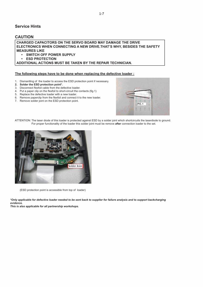
Solder Joint
1-7

Lead-Free requirement for service
INDENTIFICATION:
Regardless of special logo (not always indicated)
One must treat all sets from 1.1.2005 onwards, according next rules.
Important note: In fact also products a little older can also be treated in this way as long as you avoid mixing solder-alloys (leaded/ lead-free). So best to always use SAC305 and the higher temperatures belong to this.
Due to lead-free technology some rules have to be respected by the workshop during a repair:
Use only lead-free solder alloy Philips SAC305 with
order code 0622 149 00106. If lead-free solder-paste is
required, please contact the manufacturer of your
solder-equipment. In general use of solder-paste within
workshops should be avoided because paste is not easy
to store and to handle.
Use only adequate solder tools applicable for lead-free
solder alloy. The solder tool must be able
o To reach at least a solder-temperature of 400°C,
o To stabilize the adjusted temperature at the
solder-tip
o To exchange solder-tips for different applications.
Adjust your solder tool so that a temperature around
360°C – 380°C is reached and stabilized at the solder
joint. Heating-time of the solder-joint should not exceed
~ 4 sec. Avoid temperatures above 400°C otherwise
wear-out of tips will rise drastically and flux-fluid will be
destroyed. To avoid wear-out of tips switch off un-used
equipment, or reduce heat.
Mix of lead-free solder alloy / parts with leaded solder
alloy / parts is possible but PHILIPS recommends
strongly to avoid mixed
solder alloy types (leaded and lead-free). If one cannot
avoid, clean carefully the
solder-joint from old solder alloy and re-solder with new
solder alloy (SAC305).
Use only original spare-parts listed in the
Service-Manuals. Not listed standard-material
(commodities) has to be purchased at external
companies.
Special information for BGA-ICs:
- always use the 12nc-recognizable soldering
temperature profile of the specific BGA (for
de-soldering always use highest lead-free
temperature profile, in case of doubt)
- lead free BGA-ICs will be delivered in so-called
‘dry-packaging’ (sealed pack including a silica gel
pack) to protect the IC against moisture. After
opening, dependent of MSL-level seen on
indicator-label in the bag, the BGA-IC possibly
still has to be baked dry. This will be
communicated via AYS-website.
Do not re-use BGAs at all.
For sets produced before 1.1.2005, containing
leaded soldering-tin and components, all needed
spare-parts will be available till the end of the
service-period. For repair of such sets nothing
changes.
On our website:
www.atyourservice.ce.Philips.com
You find more information to:
BGA-de-/soldering (+ baking instructions)
Heating-profiles of BGAs and other ICs used in
Philips-sets
You will find this and more technical information
within the “magazine”, chapter “workshop news”.
For additional questions please contact your local
repair-helpdesk.
Notes
1-8
DFU InstrutionCongratulations on your purchase, and
the support that Philips offers, register your SoundBar at www.philips.com/welcome.
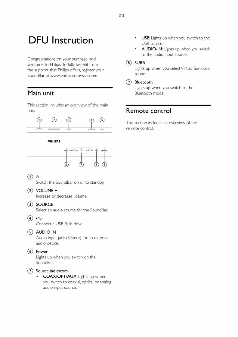
Main unitThis section includes an overview of the main unit.
aSwitch the SoundBar on or to standby.
b VOLUME +-Increase or decrease volume.
c SOURCESelect an audio source for the SoundBar.
d
e AUDIO INAudio input jack (3.5mm) for an external audio device.
f PowerLights up when you switch on the SoundBar.
g Source indicatorsCOAX/OPT/AUX: Lights up when you switch to coaxial, optical or analog audio input source.
a b c e
h igf
d
USB: Lights up when you switch to the USB source.AUDIO-IN: Lights up when you switch to the audio input source.
h SURRLights up when you select Virtual Surround sound.
i BluetoothLights up when you switch to the Bluetooth mode.
Remote controlThis section includes an overview of the remote control.
2-1
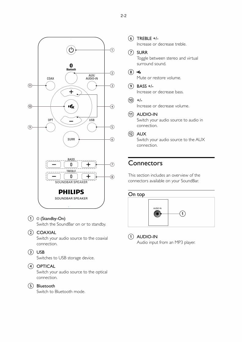
a (Standby-On) Switch the SoundBar on or to standby.
b COAXIALSwitch your audio source to the coaxial connection.
c USBSwitches to USB storage device.
d OPTICALSwitch your audio source to the optical connection.
e BluetoothSwitch to Bluetooth mode.
a
b
c
e
d
f
i
k
j
g
h
f TREBLE +/-Increase or decrease treble.
g SURRToggle between stereo and virtual surround sound.
hMute or restore volume.
i BASS +/-Increase or decrease bass.
j +/-Increase or decrease volume.
k AUDIO-INSwitch your audio source to audio in connection.
l AUXSwitch your audio source to the AUX connection.
ConnectorsThis section includes an overview of the connectors available on your SoundBar.
On top
a AUDIO-INAudio input from an MP3 player.
a
2-2
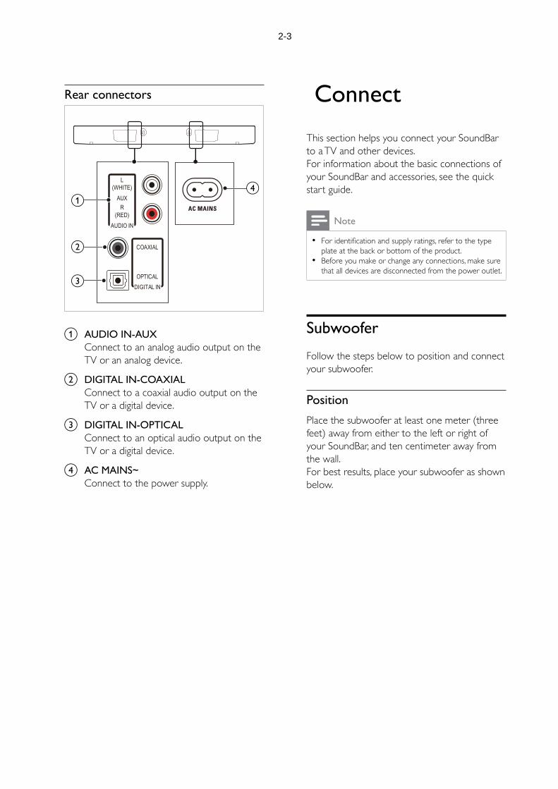
Rear connectors
a AUDIO IN-AUXConnect to an analog audio output on the TV or an analog device.
b DIGITAL IN-COAXIALConnect to a coaxial audio output on the TV or a digital device.
c DIGITAL IN-OPTICALConnect to an optical audio output on the TV or a digital device.
d AC MAINS~Connect to the power supply.
b
c
da
2-3
ConnectThis section helps you connect your SoundBar to a TV and other devices. For information about the basic connections of your SoundBar and accessories, see the quick start guide.
Note
plate at the back or bottom of the product.Before you make or change any connections, make sure that all devices are disconnected from the power outlet.
SubwooferFollow the steps below to position and connect your subwoofer.
PositionPlace the subwoofer at least one meter (three feet) away from either to the left or right of your SoundBar, and ten centimeter away from the wall.For best results, place your subwoofer as shown below.
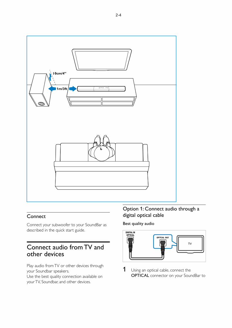
ConnectConnect your subwoofer to your SoundBar as described in the quick start guide.
Connect audio from TV and other devicesPlay audio from TV or other devices through your Soundbar speakers.Use the best quality connection available on your TV, Soundbar, and other devices.
Option 1: Connect audio through a digital optical cableBest quality audio
1 Using an optical cable, connect the OPTICAL connector on your SoundBar to
TV
2-4
the OPTICAL OUT connector on the TV or other device.
The digital optical connector might be labeled SPDIF or SPDIF OUT.
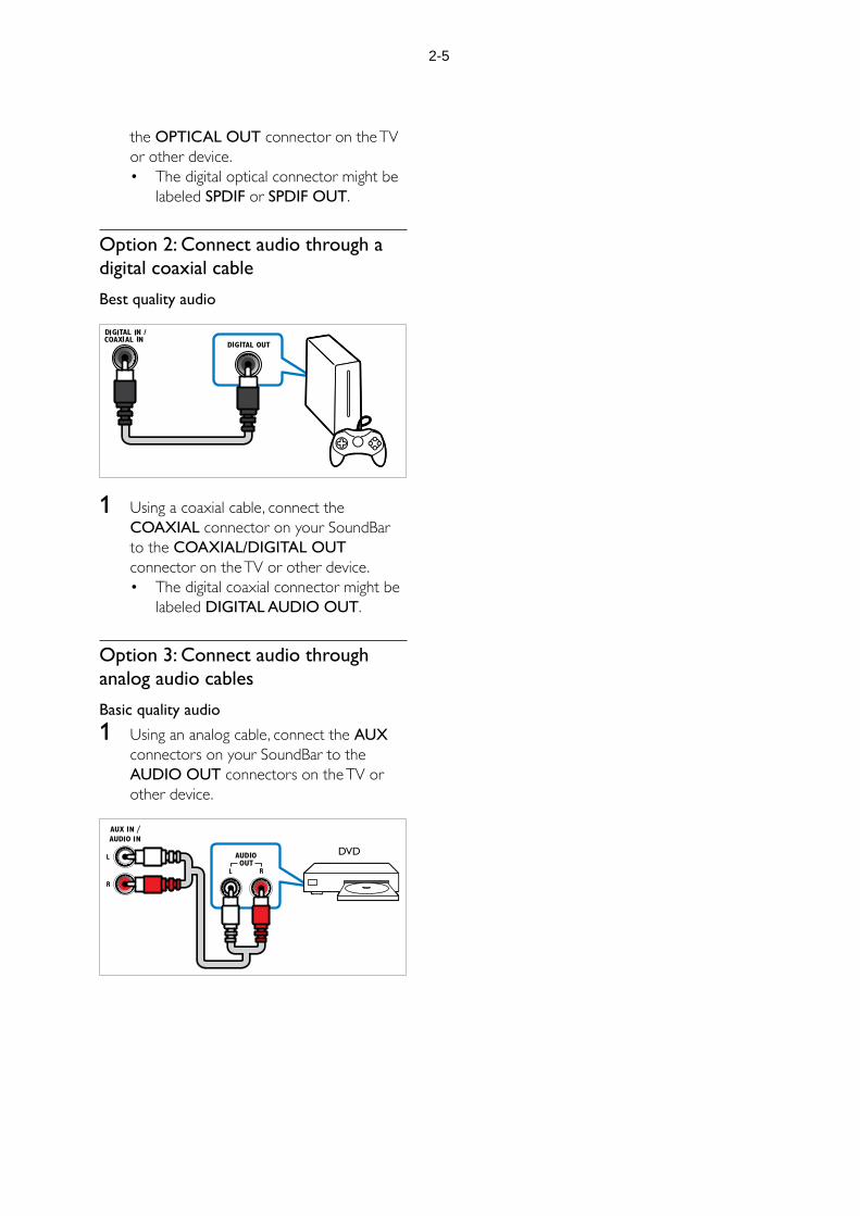
Option 2: Connect audio through a digital coaxial cableBest quality audio
1 Using a coaxial cable, connect the COAXIAL connector on your SoundBar to the COAXIAL/DIGITAL OUTconnector on the TV or other device.
The digital coaxial connector might be labeled DIGITAL AUDIO OUT.
Option 3: Connect audio through analog audio cablesBasic quality audio1 Using an analog cable, connect the AUX
connectors on your SoundBar to the AUDIO OUT connectors on the TV or other device.
DVD
2-5
Mechanical and Dismantling Instructions Dismantling Instruction
3-1
Detailed information please refer to the model set.
The following guidelines show how to dismantle the player.
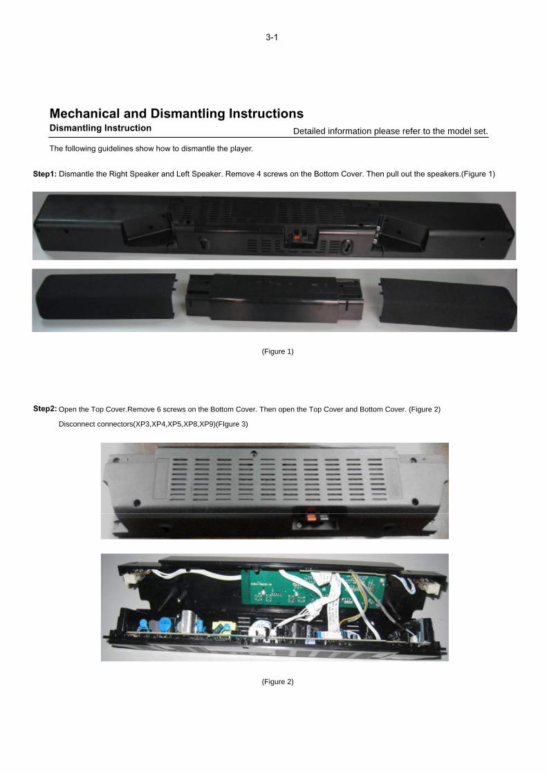
Step1: Dismantle the Right Speaker and Left Speaker. Remove 4 screws on the Bottom Cover. Then pull out the speakers.(Figure 1)
(Figure 1)
Step2: Open the Top Cover.Remove 6 screws on the Bottom Cover. Then open the Top Cover and Bottom Cover. (Figure 2)
(Figure 2)
Disconnect connectors(XP3,XP4,XP5,XP8,XP9)(FIgure 3)
ouyangry
线条
ouyangry
线条
ouyangry
线条
ouyangry
线条
ouyangry
线条
ouyangry
线条
ouyangry
线条
ouyangry
线条
ouyangry
线条
ouyangry
线条
ouyangry
线条
ouyangry
线条
Mechanical and Dismantling Instructions Dismantling Instruction Detailed information please refer to the model set.
3-2
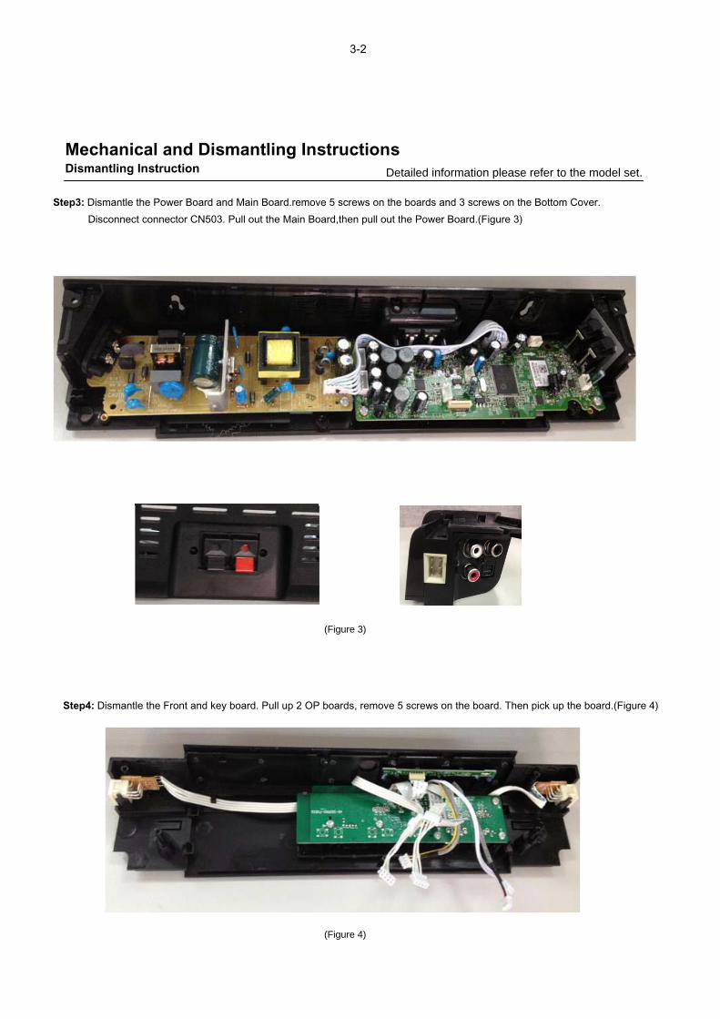
Step3: Dismantle the Power Board and Main Board.remove 5 screws on the boards and 3 screws on the Bottom Cover.
Disconnect connector CN503. Pull out the Main Board,then pull out the Power Board.(Figure 3)
(Figure 3)
(Figure 4)
Step4: Dismantle the Front and key board. Pull up 2 OP boards, remove 5 screws on the board. Then pick up the board.(Figure 4)
ouyangry
文本框
CN503
ouyangry
文本框
XP4
ouyangry
文本框
XP3
ouyangry
文本框
XS1
ouyangry
文本框
XP8
ouyangry
文本框
XP9
ouyangry
文本框
XP5
ouyangry
线条
ouyangry
线条
ouyangry
线条
ouyangry
线条
ouyangry
线条
ouyangry
线条
ouyangry
线条
ouyangry
线条
ouyangry
线条
ouyangry
线条
ouyangry
线条
ouyangry
线条
ouyangry
线条
ouyangry
线条
ouyangry
线条

Software Upgrade
Step1: Main board software Update procedure:
1. Rename upgrade file to mpeg2160_XX.bin (XX means different area code).
Copy mpeg2160_XX.bin to root directly of USB disk.
2. Plug USB in ,then Switch source to USB
It will be auto upgrade software and all LEDs will turn on while upgrading,
Strongly suggest do not operate it when upgrading.
3. The source will switch to AUX after upgrade successful.
Step 2: LED board software Update procedure:
1. Rename upgrade file to mcu_2160.bin Copy mcu_2160.bin to root directory of USB disk.
2. Plug USB in ,then switch source to USB
It will be auto upgrade software and all LEDs will turn on while upgrading,
Strongly suggest do not operate it when upgrading.
3. All LEDs will blink two times after upgrade successful. Then machine will reboot.
Warning: never copy mpeg2160_XX.bin and mcu_2160.bin to root directory of USB at the
same time.
4-1
5-1 Trouble shooting Chart
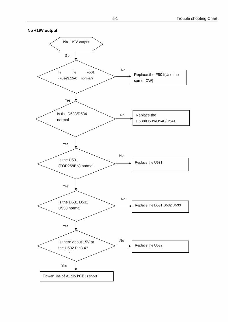
No +19V output
Is the F501
(Fuse3.15A) normal?
Go
No Is the D533/D534 normal
Yes
Yes
Yes
No
Replace the U531
Replace the D538/D539/D540/D541
Replace the F501(Use the same ICW)
No
Is the U531 (TOP258EN) normal
Is the D531 D532 U533 normal
Yes
Replace the D531 D532 U533
No
Is there about 15V at the U532 Pin3.4?
l
Replace the U532
Yes
No +19V output
Power line of Audio PCB is short
No
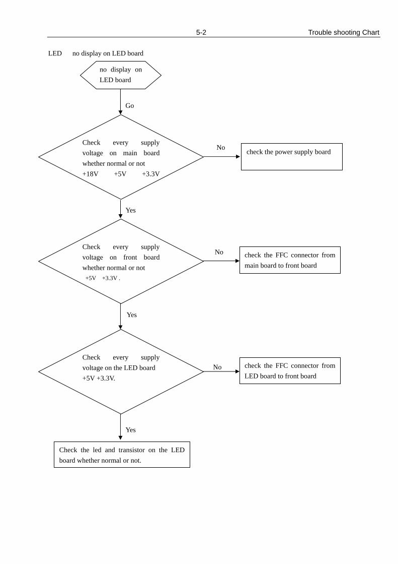
5-2 Trouble shooting Chart
LED no display on LED board Go No Yes No Yes No Yes
Check every supply voltage on main board whether normal or not +18V +5V +3.3V
check the power supply board
Check every supply voltage on front board whether normal or not +5V +3.3V .
check the FFC connector from main board to front board
Check every supply voltage on the LED board +5V +3.3V.
check the FFC connector from LED board to front board
no display on LED board
Check the led and transistor on the LED board whether normal or not.

5-3 Trouble shooting Chart
Remote control does not work
Check the battery of remote control exhausted or not
Replace the battery for remote control
Check the power supply of IR1 on main board whether
Check the 3.3V_STB weather normal or not
Remote control does not work
Replace the IR1
Yes
No
No
Yes
Go
5-4 Trouble shooting Chart
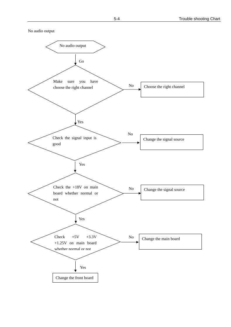
No audio output Go
No Yes No
Yes No Yes
No Yes
Make sure you have choose the right channel
Choose the right channel
Check the signal input is good
Change the signal source
Check the +18V on main board whether normal or not
Change the signal source
Check +5V +3.3V +1.25V on main board whether normal or not
Change the main board
No audio output
Change the front board
Coaxial Bluetooth
USB
Coaxial
OpticalTAS3159
SPHE8202R
SPDIF 64MSDRAM
TAS315974HC04
Aux in
MP374HC4052 AKM5358
SPHE8202R8M
FlashIIS
IISEN*1PDN
UART/reset
LEDI/O*5 L
EN
15W 2+30W(THD+N)TAS5711
M054IIC
RST/PDN
LEDIR
I/O*1
RKEYI/O*1
Subwoofer
Power AMP 20V
20VBluetooth
Mos _
ADC_5V/USB_5VEUP3482A
SWITCH
MosSWITCH
5V
1.25V3.3V
MCU3.3V AS1117
LD1117LDO_G9091330T11U
6-1 6-1
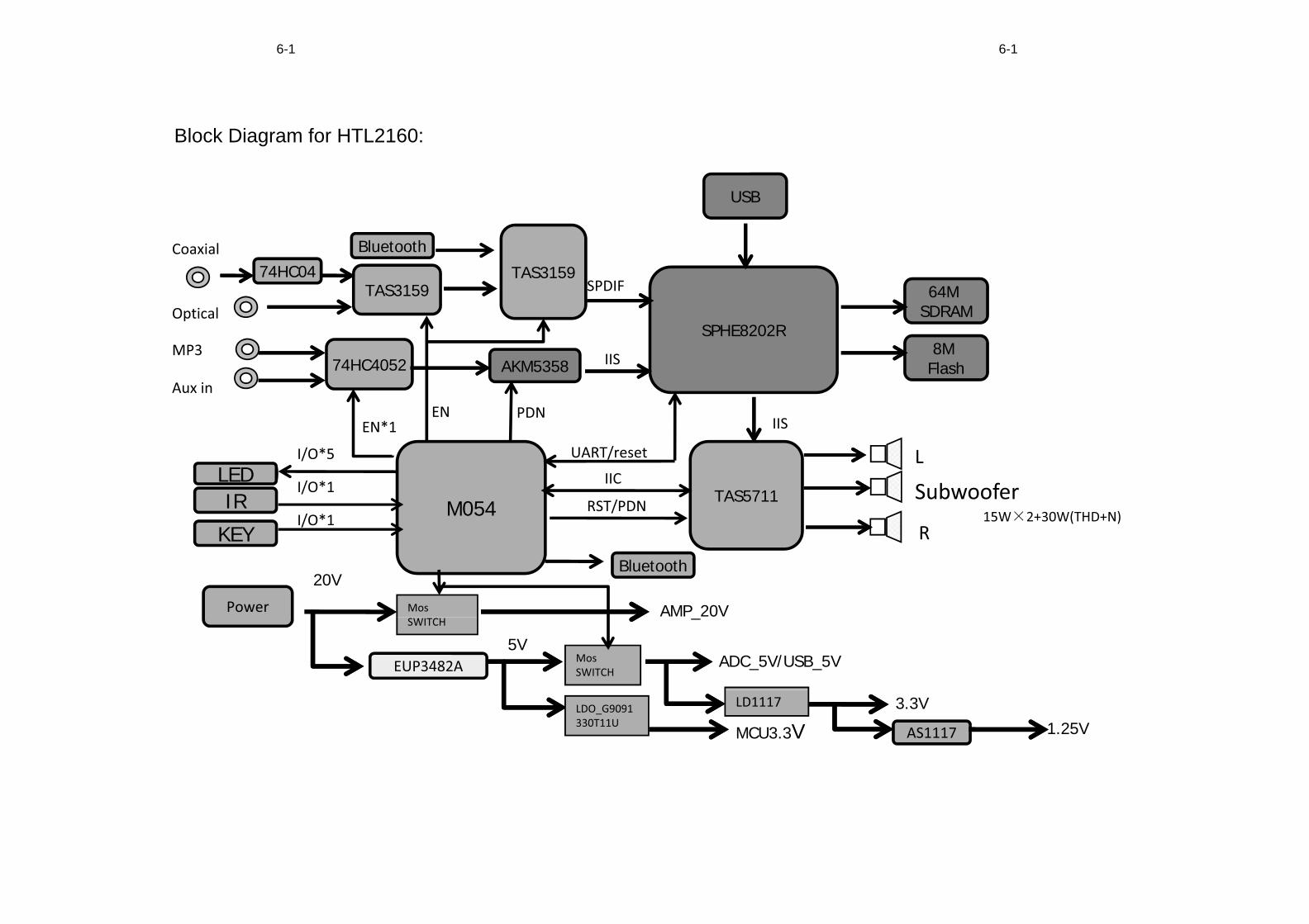
Block Diagram for HTL2160:

A
A
B
B
C
C
D
D
E
E
1 1
2 2
3 3
4 4
2-
1-
2+
1+TP4TP4TP3TP3
XP1
CON_6PIN _2*3
XP1
CON_6PIN _2*3
11
22
33
44
55
66 TP1TP1
TP2TP2
OP Board Circuit Diagram for HTL2160/12/F7/93:
7-1 7-1
A
A
B
B
C
C
D
D
E
E
1 1
2 2
3 3
4 4
OPT_LED iLINK_LEDCOAX_LED
AUX_LED POWER_LED BT_LED
BT_LEDPOWER_LED
AUX_LED
OPT_LEDiLINK_LED
COAX_LED
MCU_3V35V5
5V5
5V5 5V5
5V5MCU_3V35V5
R34
330
R34
330
C23
0.1u
F/25
V/Y
5VC
230.
1uF/
25V
/Y5V
R25
330
R25
330
C24
0.1u
F/25
V/Y
5VC
240.
1uF/
25V
/Y5V
R35
330
R35
330
C22
0.1u
F/25
V/Y
5VC
220.
1uF/
25V
/Y5V
Q1NPN_3DG3904MQ1NPN_3DG3904M
R36
330
R36
330
LED2LED_AMBERLED2LED_AMBER
XP510PIN/1.0mm/SMTXP510PIN/1.0mm/SMT
1122334455667788991010
LED3
LED_BLUE
LED3
LED_BLUE
LED1LED_AMBERLED1LED_AMBER
Q6NPN_3DG3904MQ6NPN_3DG3904M
R30
4.7K
R30
4.7K
Q3NPN_3DG3904MQ3NPN_3DG3904M
R37
4.7K
R37
4.7K
R334.7KR334.7K
R324.7KR324.7K
R38
4.7K
R38
4.7K
R29
4.7K
R29
4.7K
R27
510
R27
510
R43180/1%R43180/1%
R28
4.7K
R28
4.7K
C27
0.1u
F/25
V/Y
5VC
270.
1uF/
25V
/Y5V
R314.7KR314.7K
LED4LED_AMBERLED4LED_AMBER
R39
4.7K
R39
4.7K
Q2NPN_3DG3904MQ2NPN_3DG3904M
C26
0.1u
F/25
V/Y
5VC
260.
1uF/
25V
/Y5V
R424.7KR424.7K
C25
0.1u
F/25
V/Y
5VC
250.
1uF/
25V
/Y5V
R414.7KR414.7K
R404.7KR404.7K
Q5NPN_3DG3904MQ5NPN_3DG3904M
LED6LED_AMBERLED6LED_AMBER
Q4NPN_3DG3904MQ4NPN_3DG3904M
LED5LED_AMBERLED5LED_AMBER
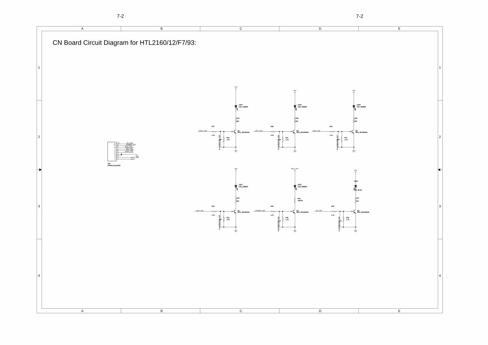
CN Board Circuit Diagram for HTL2160/12/F7/93:
7-2 7-2
A
A
B
B
C
C
D
D
E
E
1 1
2 2
3 3
4 4
TO MAIN BOARD
BT_SPDIF
BT_SPDIF1 BT_SPDIF
BT_3V3
CSBMISOBT_CLKMOSI
BT_RST
GND
BT_33
BT_33
D
D D D
BT_3V3
BT_33
D
D
D
BT_33MCU_3V3
BT_SPDIF1
BT_RST
BT_POWER
C33
10uF/10V/Y5V
C33
10uF/10V/Y5V
C310.1uF/25V/Y5V
C310.1uF/25V/Y5V
R45220KR45220K
TP4TP4
TP6TP6
TP8TP8
C28 6.8pF/50V/NP0C28 6.8pF/50V/NP0
FB3 500/500mAFB3 500/500mA
R43NC/0R43NC/0
R44NC/0R44NC/0
C29NC 0.1uF/25V/Y5V
C29NC 0.1uF/25V/Y5V
R46 1KR46 1K
XP11
3PIN/2.0mm/200mm
XP11
3PIN/2.0mm/200mm
112233
C320.1uF/25V/Y5V
C320.1uF/25V/Y5V
Q1
N_ASM3402M
Q1
N_ASM3402M
G
D S
TP13TP13TP12TP12
TP7TP7
TP5TP5
R47 33R47 33
TP11TP11
U2U2
AIO11
AIO02
RESET3
GND4
PIO95
PIO1 06
PIO117
PIO128
PIO139
PIO1410
PIO1511
GND12
VDD13
VDD_USB14
+1V815
GND16
USB_DP17
USB_DN18
UA
RT_
RTS
19
AR
T_C
TS20
UA
RT_
RX
21
UA
RT_
TX22
PC
M_I
N23
PC
M_S
YN
C24
PC
M_C
LK25
PC
M_O
UT
26
SP
I_C
SB
27
SP
I_M
ISO
28
SP
I_C
LK29
SP
I_M
OS
I30
GND48
MIC_A_N47
MIC_A_P46
MIC_B_N45
MIC_B_P44
MIC_BIAS43
GND_S42
SPK_R_P41
SPK_R_N40
SPK_L_P39
SPK_L_N38
GND37
LED036
LED135
VDD_CHG34
GND33
VDD_BAT32
VRE_IN31
GN
D60
RF
59
GN
D58
PIO
857
PIO
756
PIO
655
PIO
554
PIO
453
PIO
352
PIO
251
PIO
150
PIO
049
TP10TP10
C30
10uF/10V/Y5V
C30
10uF/10V/Y5V
TP9TP9
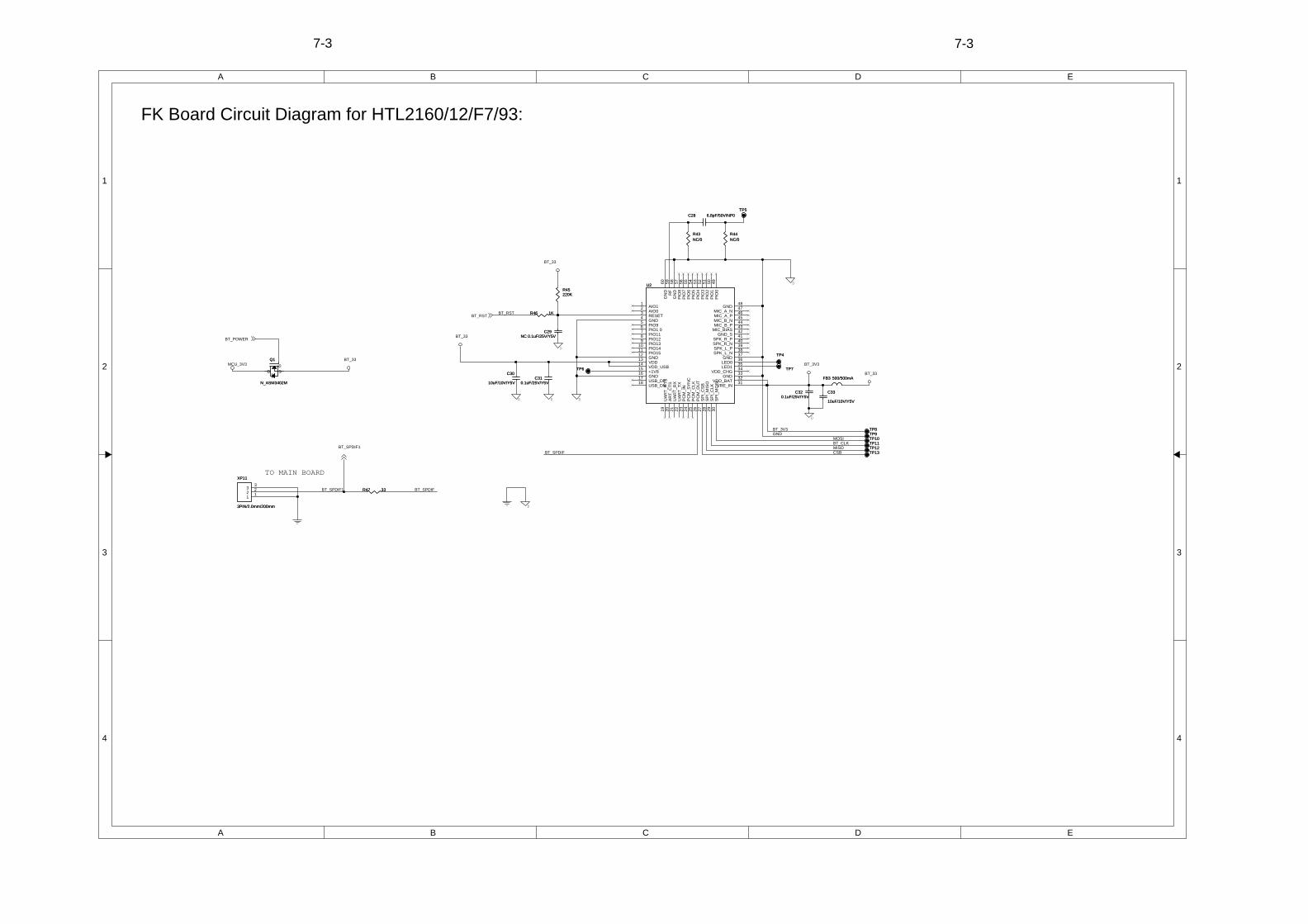
FK Board Circuit Diagram for HTL2160/12/F7/93:
7-3 7-3
A
A
B
B
C
C
D
D
E
E
1 1
2 2
3 3
4 4
MCU_RST
TO MAIN BOARD
MCU_RXBT_LED
YO
iLINK_LED
YI
AUX_LED
COAX_LED
YO YI
4052_SW
PDN
MCU_RSTICE_CLK
ADC_RST
ICE_DAT
OPT_LEDSPDIF_SW1
ICE_DAT
POWER_ON/OFF
POWER_LEDICE_CLK
MCU_RST
MCU_TXIR_IN
AMP_SCLAMP_SDA
AMP_SDA
AMP_RSTAMP_SCL
AMP_RST
MPEG_RST
USB_DPUSB_DM
SPDIF_SW2
KEY1KEY2
MP3_AR
BT_LEDAUX_LED
POWER_LED
OPT_LEDiLINK_LED
COAX_LED
USB_DMUSB_DP
MP3_AL
MP3_AL
4052_SW
AMP_RSTAMP_SCL
POWER_ON/OFF
MPEG_RST
AMP_SDA
IR_IN
ADC_RST
SPDIF_SW1PDN
+3.3V_STB
SPDIF_SW2
BT_RST
KEY1
KEY2
MCU_RST
MP3_AR
MCU_3V3
MCU_3V3
MCU_3V3
MCU_3V3
USB_5V
USB_5V
5V5MCU_3V3
MCU_3V3
MCU_3V3
MCU_3V3
MCU_3V35V5
BT_RST
BT_POWER
R69047KR69047K
R48 1KR48 1K
R20 0R20 0
R3 33R3 33
C20
100p
F/50
V/N
P0
C20
100p
F/50
V/N
P0
R694 5.1KR694 5.1K
R5 33R5 33
TP3TP3
R33 33R33 33
ES
D19
LV
E16Y
1R0
ES
D19
LV
E16Y
1R0
R51 0R51 0
C18
100p
F/50
V/N
P0
C18
100p
F/50
V/N
P0
SW2
SOURCE
SW2
SOURCE
C16
100p
F/50
V/N
P0
C16
100p
F/50
V/N
P0
FB2 500/500mAFB2 500/500mA
+ CE
3
10uF/16V
+ CE
3
10uF/16V
R16 33R16 33
XP510PIN/1.0mm/SMTXP510PIN/1.0mm/SMT
1122334455667788991010
SW3
VOLUME+
SW3
VOLUME+
R210KR210K
XP103PIN/2.0mm/200mm
XP103PIN/2.0mm/200mm
11
22
33
ES
D21
NC
/LV
E16
Y1R
0ES
D21
NC
/LV
E16
Y1R
0
TO
P
XP1
24PIN/0.5mm
TO
P
XP1
24PIN/0.5mm
242322212019181716151413121110987654321
25 2627 28
R21 0R21 0
R22
4.7K
R22
4.7K
TP16TP16
U1
M054LAN
U1
M054LAN
MOSI_01
MISO_02
SPICLK03
RST4
RXD5
AVSS6
TXD7
STADC8
MCLK9
SDA/T010
SCL11
PWM312
CK
O13
RD
14
XTA
L215
XTA
L116
VS
S17
LDO
_CA
P18
PW
M0
19
PW
M1
20
PW
M2
21
PW
M3
22
PW
M4
23
PW
M0
24
PWM525PWM626PWM727/CS28ALE29ICE_CLK30ICE_DAT31SPICLK132MISO_133MOSI_134SPISS135PWM136R
TS0
37C
TS0
38R
TS1
39C
TS1
40V
DD
41A
VD
D42
T243
T344
RX
D1
45TX
D1
46P
WM
248
SP
ISS
047
R54 0R54 0
R15 33R15 33
C15
100p
F/50
V/N
P0
C15
100p
F/50
V/N
P0
SW4
VOLUME-
SW4
VOLUME-
TP15TP15
C5
1000
pF/5
0V/X
7RC
510
00pF
/50V
/X7R
C34 100p
F/50
V/N
P0
C34 100p
F/50
V/N
P0
JACK602
MIC JACK
JACK602
MIC JACK
11
22
33
44
55
66
TP14TP14
C19
100p
F/50
V/N
P0
C19
100p
F/50
V/N
P0
ES
D22
NC
/LV
E16
Y1R
0ES
D22
NC
/LV
E16
Y1R
0
C1
100pF/50V/NP0
C1
100pF/50V/NP0
J14PIN/2mm
J14PIN/2mm
VCC1
D-2
D+3
GND4
She
ll B
6S
hell
A5
R12 1KR12 1K
C13
100p
F/50
V/N
P0
C13
100p
F/50
V/N
P0
F5PTC/1.5A/6VF5PTC/1.5A/6V
XP9
4PIN/2.0mm/100mm
XP9
4PIN/2.0mm/100mm
11223344
R13 33R13 33
C14
100p
F/50
V/N
P0
C14
100p
F/50
V/N
P0
+CE210uF/16V
+CE210uF/16V
+CE110uF/16V
+CE110uF/16V
R10 33R10 33
C11
100p
F/50
V/N
P0
C11
100p
F/50
V/N
P0
C6
0.1u
F/25
V/Y
5VC
60.
1uF/
25V
/Y5V
C7
100p
F/50
V/N
P0
C7
100p
F/50
V/N
P0
R19 1KR19 1K
R50 0R50 0
R11 33R11 33
C12
100p
F/50
V/N
P0
C12
100p
F/50
V/N
P0
R23
4.7K
R23
4.7K
R32 33R32 33
FB1 500/500mAFB1 500/500mA
R1 1MR1 1M
R52 0R52 0
R2610KR2610K
R8 33R8 33
C9
100p
F/50
V/N
P0
C9
100p
F/50
V/N
P0
C16510pF/50V/NP0C16510pF/50V/NP0
R4 33R4 33
C220pF/50V/NP0C220pF/50V/NP0
TP2TP2
C22 100pF/50V/NP0C22 100pF/50V/NP0
R6
100
R6
100
SW1
POWER ON/OFF
SW1
POWER ON/OFF
R9 33R9 33
C10
100p
F/50
V/N
P0
C10
100p
F/50
V/N
P0
ESD10PRTR5V0U2XESD10PRTR5V0U2X
123 4
D1
LL41
48D
1LL
4148
C27 100p
F/50
V/N
P0
C27 100p
F/50
V/N
P0
C4
0.1uF/25V/Y
5V
C4
0.1uF/25V/Y
5V
TP1TP1
R7 33R7 33
R2510KR2510K
FB616600/200mA
FB616600/200mA
R17 33R17 33
C26 100p
F/50
V/N
P0
C26 100p
F/50
V/N
P0
ES
D20
LV
E16Y
1R0
ES
D20
LV
E16Y
1R0
R53 0R53 0
FB615600/200mA
FB615600/200mA
R55 0R55 0
C164
0.1uF/50V/Y5V
C164
0.1uF/50V/Y5V
R49 0R49 0
Y1
12MHz/30PPM
Y1
12MHz/30PPM
R692 15KR692 15K
R24
22
R24
22
XP2
5PIN/2.0mm
XP2
5PIN/2.0mm
1122334455
C320pF/50V/NP0C320pF/50V/NP0
R27
10K
R27
10K
R34 33R34 33
R691
47K
R691
47K
R28 NC/4.7KR28 NC/4.7K
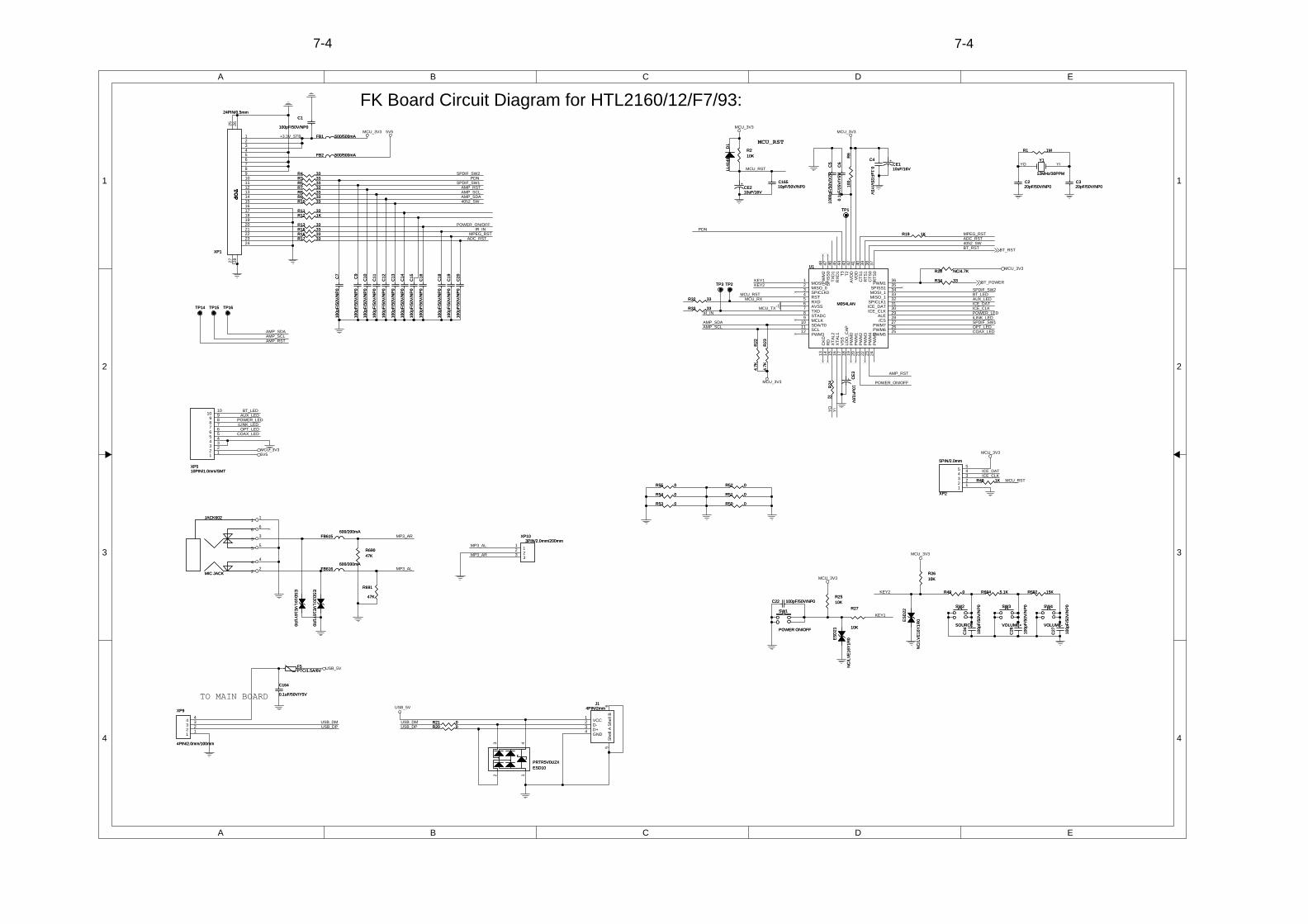
FK Board Circuit Diagram for HTL2160/12/F7/93:
7-4 7-4

A
A
B
B
C
C
D
D
E
E
1 1
2 2
3 3
4 4
PLEASE USE THE PARTS HAVING THE DESIGNATED PARTS NUMBER WITHOUT FAIL.
* CAUTION :THE PARTS MARKED WITH ARE IMPORTANT PARTS ON THE SAFETY.
Alternative
1.18V2.18V3.GND4.GND
PG
VDD
D
FB
HV+18V
HV
GND
VDD
D
FB
PG
GND
+18V
+18V1 +18V1
HV
+18V1
C534
0.1uF/50V/X7R
C534
0.1uF/50V/X7R
C537NCC537NC
ZD535BZX79C27ZD535BZX79C27
CN501
NC
CN501
NC
11
22
R570 0R570 0
R543 10KR543 10K
ZD532NC
ZD532NC
R536
2M
R536
2M
FB501
FB90@100MHz
FB501
FB90@100MHz
R502D
1M
R502D
1M
FB504FB90@100MHz
FB504FB90@100MHz
+47uF/35V
CE531+
47uF/35V
CE531
R5315.1MR5315.1M
C549
0.1uF/50V/X7R
C549
0.1uF/50V/X7R
R542
3.3K
R542
3.3KC535 1000pF/50V/X7RC535 1000pF/50V/X7R
CY506 470pF/250VACCY506 470pF/250VAC
LIF503NCLIF503NC1
34
2
CS
D V
F
CONTROL
X
U531TOP258EN
CS
D V
F
CONTROL
X
U531TOP258EN
R502A
1M
R502A
1M
R541
1.5K
R541
1.5K
R5330R5330
D533
MUR420/4A/200V
D533
MUR420/4A/200V
CY507 470pF/250VACCY507 470pF/250VAC
LIF501
LIF4-22-15
LIF501
LIF4-22-15
41
23
ZD531BZX79C8V2
ZD531BZX79C8V2
R56522R56522
U533
AS431
U533
AS4313
1
2
T502TRF327T502TRF327
D3
P-GND5
FB6
VDD1
N.C2
A88
A1012
A99
A1011
R568150KR568150K
R567150KR567150K
R56622R56622
TR501
NTC/3ohm/5A
TR501
NTC/3ohm/5A
R502B
1M
R502B
1M
R510
10
R510
10 ZD536BZX79C27ZD536BZX79C27
CY502220pF/250VACCY502220pF/250VAC
JMP502 0JMP502 0
R54468.1K/1%
R54468.1K/1%
C536
100pF/1KV
C536
100pF/1KV
CY501220pF/250VACCY501220pF/250VAC
R5572.21k/1%R5572.21k/1%
R5400R5400
R5326.8MR5326.8M
CN503
6PIN/2.5mm/120mm
CN503
6PIN/2.5mm/120mm
11
22
33
44
55
66
C5331500pF/1KV
C5331500pF/1KV
MUR420/4A/200VMUR420/4A/200V
CN5011
PWS004
CN5011
PWS004
N1
L2
C532
0.1uF/50V/X7R
C532
0.1uF/50V/X7R
D538
NC
D538
NC
1
2
3R572
150K
R572
150K
CX501
0.22uF/275VAC
CX501
0.22uF/275VAC
R5372MR5372M
R539
100
R539
100
C531222/400VC531222/400V
R569 0R569 0
D532
FR104/1A/400V
D532
FR104/1A/400V
+
68uF/450V
CE502+
68uF/450V
CE502
D531FR207/2A/1000VD531FR207/2A/1000V
+
47uF/35V
CE532+
47uF/35V
CE532
ZD533NC
ZD533NC
CN5024PIN/2.5mm/60mm
CN5024PIN/2.5mm/60mm
11
22
33
44
R5385.6R5385.6
U532LTV-817SU532LTV-817S
12
43
R546
NC
R546
NC
T501NCT501NC
D4
P-GND6
FB7
VDD1
N.C3
A1211
A98
A129
A1312
+
470uF/35VCE533
+
470uF/35VCE533
R571150KR571150K
F501T3.15AL250VF501T3.15AL250V
- +
BD1KBP306
- +
BD1KBP306
2
1
3
4
FB502
FB90@100MHz
FB502
FB90@100MHz
R502C
1M
R502C
1M
RV501
VDR/560V
RV501
VDR/560V
+
CE535470uF/25V
+
CE535470uF/25V
Power Board Circuit Diagram for HTL2160/12/93:
7-5 7-5

A
A
B
B
C
C
D
D
E
E
1 1
2 2
3 3
4 4
PLEASE USE THE PARTS HAVING THE DESIGNATED PARTS NUMBER WITHOUT FAIL.
* CAUTION :THE PARTS MARKED WITH ARE IMPORTANT PARTS ON THE SAFETY.
Alternative
1.18V2.18V3.GND4.GND
PG
VDD
D
FB
HV+18V
HV
GND
VDD
D
FB
PG
GND
+18V
+18V1 +18V1
HV
+18V1
C537NCC537NC
C534
0.1uF/50V/X7R
C534
0.1uF/50V/X7R
ZD532NCZD532NC
R543 100KR543 100K
R570 0R570 0
CN501
NC
CN501
NC
11
22
ZD535BZX79C27ZD535BZX79C27
FB504FB90@100MHzFB504FB90@100MHz
R502D
2M
R502D
2MFB501
FB90@100MHz
FB501
FB90@100MHz
R536
2M
R536
2M
C549
0.1uF/50V/X7R
C549
0.1uF/50V/X7R
R542
3.3K
R542
3.3K
R5315.1MR5315.1M
+47uF/35V
CE531+47uF/35V
CE531
LIF503NCLIF503NC1
34
2
CY506 220pF/250VACCY506 220pF/250VAC
C535 NCC535 NC
R541
1.5K
R541
1.5K
R502A
2M
R502A
2M
CS
D V
F
CONTROL
X
U531TOP257EN
CS
D V
F
CONTROL
X
U531TOP257EN
R56522R56522
ZD531BZX79C8V2ZD531
BZX79C8V2
LIF501
LIF4-22-15
LIF501
LIF4-22-15
41
23
CY507 220pF/250VACCY507 220pF/250VAC
D533
MUR420/4A/200V
D533
MUR420/4A/200V
R5330R5330
R567150KR567150K
R568150KR568150K
T502TRF327T502TRF327
D4
P-GND6
FB7
VDD1
N.C2
A88
A1012
A99
A1011
U533
AS431
U533
AS4313
1
2
R510
10
R510
10
R502B
2M
R502B
2M
TR501
NTC/3ohm/5A
TR501
NTC/3ohm/5A
R56622R56622
R5400R5400
R55733k/1%R55733k/1%
CY501470pF/250VACCY501470pF/250VAC
C536
100pF/1KV
C536
100pF/1KV
R54468.1K/1%R544
68.1K/1%
JMP502 0JMP502 0
CY502470pF/250VACCY502470pF/250VAC
ZD536BZX79C27ZD536BZX79C27
MUR420/4A/200VMUR420/4A/200V
C5331500pF/1KVC5331500pF/1KV
CN503
6PIN/2.5mm/120mm
CN503
6PIN/2.5mm/120mm
11
22
33
44
55
66
R5326.8MR5326.8M
R569 0R569 0
C531222/400VC531222/400V
R539
100
R539
100
R5372MR5372M
CX501
0.33uF/275VAC
CX501
0.33uF/275VAC
R572
150K
R572
150K
D534
D538
D534
D538
1
2
3
CN5011
PWS004
CN5011
PWS004
N1
L2
C532
0.1uF/50V/X7R
C532
0.1uF/50V/X7R
+
47uF/35V
CE532+
47uF/35V
CE532
D531FR207/2A/1000VD531FR207/2A/1000V
+
220UFuF/250V
CE502+
220UFuF/250V
CE502
D532
FR104/1A/400V
D532
FR104/1A/400V
U532LTV-817SU532LTV-817S
12
43
R5385.6R5385.6
CN502NC
CN502NC
11
22
33
44
ZD533NCZD533NC
+
470uF/35VCE533
+
470uF/35VCE533
T501NCT501NC
D4
P-GND6
FB7
VDD1
N.C3
A1211
A98
A129
A1312
R546
118K
R546
118K
FB502
FB90@100MHz
FB502
FB90@100MHz
- +
BD1KBP306
- +
BD1KBP306
2
1
3
4
F501T3.15AL250VF501T3.15AL250V
R571150KR571150K
+
CE535470uF/35V
+
CE535470uF/35V
RV501
VDR/560V
RV501
VDR/560V
R502C
2M
R502C
2M
Power Board Circuit Diagram for HTL2160/F7:
7-6 7-6
A
A
B
B
C
C
D
D
E
E
1 1
2 2
3 3
4 4
close to DC/DCclose to LDO
POWER_20V
STBY+5V
POWER_20V
POWER_20V
SYS_3V3 DV33
V12A5_5V
5V
STBY+5V
STBY+5V+3.3V_STB
USB_5V 5V
SYS_3V3VCC_AMP
VCC_AMP
POWER_ON/OFF C103300pF/50V/X7RC103300pF/50V/X7R
R140R140
R310K
R310K
+
220uF/35V
CE16 +
220uF/35V
CE16C40.01uF/50V/X7RC40.01uF/50V/X7R
C2
0.1uF/50V/Y
5V
C2
0.1uF/50V/Y
5V
FB7 500/800mAFB7 500/800mA
L1 10uH/2AL1 10uH/2A
FB6 70/1AFB6 70/1A
R117.5KR117.5K
C6
10uF
/16V
/X7R
C6
10uF
/16V
/X7R
R822KR822K
C1
0.1u
F/25
V/X
7RC
10.
1uF/
25V
/X7R
R156R156
Q2
N_ASM3402M
Q2
N_ASM3402M
G
D S
+CE3
100uF/16V
+CE3
100uF/16V
R13
120/1%
R13
120/1%
C15
2.2uF/10V/Y5V
C15
2.2uF/10V/Y5V
FB5 300/2AFB5 300/2A
C70.1uF/25V/Y5VC70.1uF/25V/Y5V
C121uF/16V/Y5V
C121uF/16V/Y5V
C61 0.1u
F/25
V/Y
5VC
61 0.1u
F/25
V/Y
5V
+
47uF/10VCE4
+
47uF/10VCE4
XS1
6PIN/2.5mm/120mm
XS1
6PIN/2.5mm/120mm
11
22
33
44
55
66
C5
2.
2uF
C5
2.
2uF
U3AS1117
U3AS1117
input3
Vout4
AD
J/G
ND
1
output2
U5
LD1117STR
U5
LD1117STR
input3
Vout4
AD
J/G
ND
1
output2
C17
0.1u
F/50
V/Y
5VC
170.
1uF/
50V
/Y5V
U1AP4435GMU1AP4435GM
S11
S32
S23
G14
D45D36D27D18
U4
LDO_G9091-330T11U
U4
LDO_G9091-330T11U
VIN1
GND2
EN3
NC4
VOUT5
R10
220/1%
R10
220/1%
+CE2220uF/16V
+CE2220uF/16V
C140.1uF/25V/Y5V
C140.1uF/25V/Y5V
R6 47KR6 47K
C11
0.1uF/25V/X7R
C11
0.1uF/25V/X7R
C18
0.1u
F/25
V/Y
5VC
180.
1uF/
25V
/Y5V
C80.1uF/25V/Y5VC80.1uF/25V/Y5V
C9
NC
/330pF/50V/N
P0
C9
NC
/330pF/50V/N
P0
C16
4.7uF/16V/Y5V
C16
4.7uF/16V/Y5V
FB23
600/1A
FB23
600/1A
C134.7uF/16V/Y5VC134.7uF/16V/Y5V
R121K/1%R121K/1%
FB2
300/2A
FB2
300/2A
R2
10K
R2
10K R4
4.3K/1%R44.3K/1%
FB1 300/2AFB1 300/2A
U2
EUP3482A
U2
EUP3482A
BS
1
IN2
SW3
FB5
CO
MP
6
GN
D4
SS8
EN7
C3330pF/50V/NP0C3330pF/50V/NP0
R910K
R910K
FB4 300/2AFB4 300/2A
Q1NPN_3DG3904M
Q1NPN_3DG3904M
+
220uF/35V
CE1 +
220uF/35V
CE1
R5NC/56R5NC/56
R7
10K
R7
10K
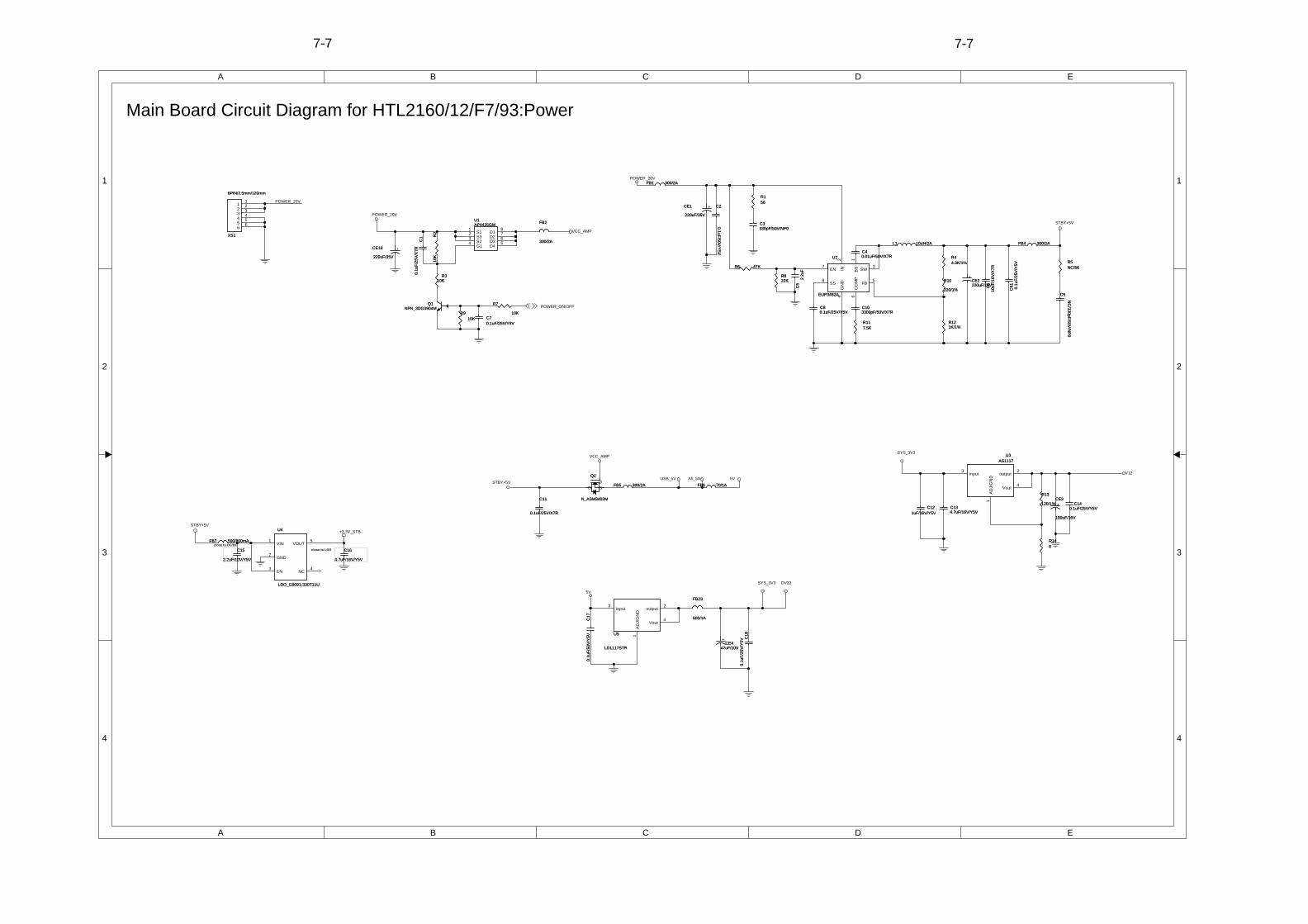
Main Board Circuit Diagram for HTL2160/12/F7/93:Power
7-7 7-7
A
A
B
B
C
C
D
D
E
E
1 1
2 2
3 3
4 4
AL_CH3
AR_CH3
AR_CH1
AL_CH1
4052_SWAD_LRCKAD_DATA
AD_BCLKAD_MCLK
ADC_INLADC_INR
MP3_AL
AR_CH1
AL_CH1
MP3_AR
AUX_R
AUX_LAUX_L AL_CH3
AR_CH3
LB
LA ADC_INR
ADC_INL
MP3_AR
MP3_AL
LB
LA9V
SYS_3V3
A5_5VSYS_3V3
A5_5V
9V
9V
VCC_AMP
9V
ALRCKAMCLKABCLKADC_RST
AUX_R
AUX_L
ADATA04052_SW
R404.7KR404.7K
R21 2KR21 2K
+
47uF/16VCE6
+
47uF/16VCE6
FB8
500/
200m
AFB
850
0/20
0mA
C26470pF/50V/X7RC26470pF/50V/X7R
R2622KR2622K
C19 2.2uF/10V/Y5VC19 2.2uF/10V/Y5V
R298.2KR298.2K
C25 2.2uF/10V/Y5VC25 2.2uF/10V/Y5V
R33
4.7K
R33
4.7K
R1910KR1910K
R35 470R35 470
R25 8.2KR25 8.2K C21 2.2uF/10V/Y5VC21 2.2uF/10V/Y5V
C24
0.1u
F/25
V/Y
5VC
240.
1uF/
25V
/Y5V
R22 1MR22 1M
R242.4KR242.4K
R34
4.7K
R34
4.7K
R2022KR2022K
R39100KR39100K
+
220u
F/16
VC
E7
+
220u
F/16
VC
E7
R38 200R38 200
R36100KR36100K
C30
0.1u
F/25
V/Y
5VC
300.
1uF/
25V
/Y5V
+
47uF/16V
CE5+
47uF/16V
CE5
U6
74HC4052
U6
74HC4052
Y01
Y22
Y3Y3
4Y1
5
EN6
VEE7
GND8
B9 A
10
X311
X012
X13
X114
X215
VCC16
C20 2.2uF/10V/Y5VC20 2.2uF/10V/Y5V
C2910uF/16V/X7R
C2910uF/16V/X7R
L2 10uH/25mAL2 10uH/25mA
ES
D8
LV
E16Y
1R0
ES
D8
LV
E16Y
1R0
C27 2.2uF/10V/Y5VC27 2.2uF/10V/Y5V
R23 1MR23 1M
R30
1K
R30
1K
C22 2.2uF/10V/Y5VC22 2.2uF/10V/Y5V
R31 4.7R31 4.7
R16 2KR16 2K
R1710KR1710K
R18 2KR18 2K
U7
ADC_AK5358A
U7
ADC_AK5358A
AINL2
CKS13
AGND5 VCOM4
PDN13DIF14
VA6
VD7
DGND8
SDTO9
MCLK11SCLK12
LRCK10
AINR1
CKS215CKS016
ES
D7
LV
E16Y
1R0
ES
D7
LV
E16Y
1R0
C230.1uF/25V/Y5V
C230.1uF/25V/Y5V
R32
4.7K
R32
4.7K
R37 470R37 470
C28470pF/50V/X7RC28470pF/50V/X7R
R278.2KR278.2K
R28 8.2KR28 8.2K
XP93PIN/2.0mmXP93PIN/2.0mm
112233
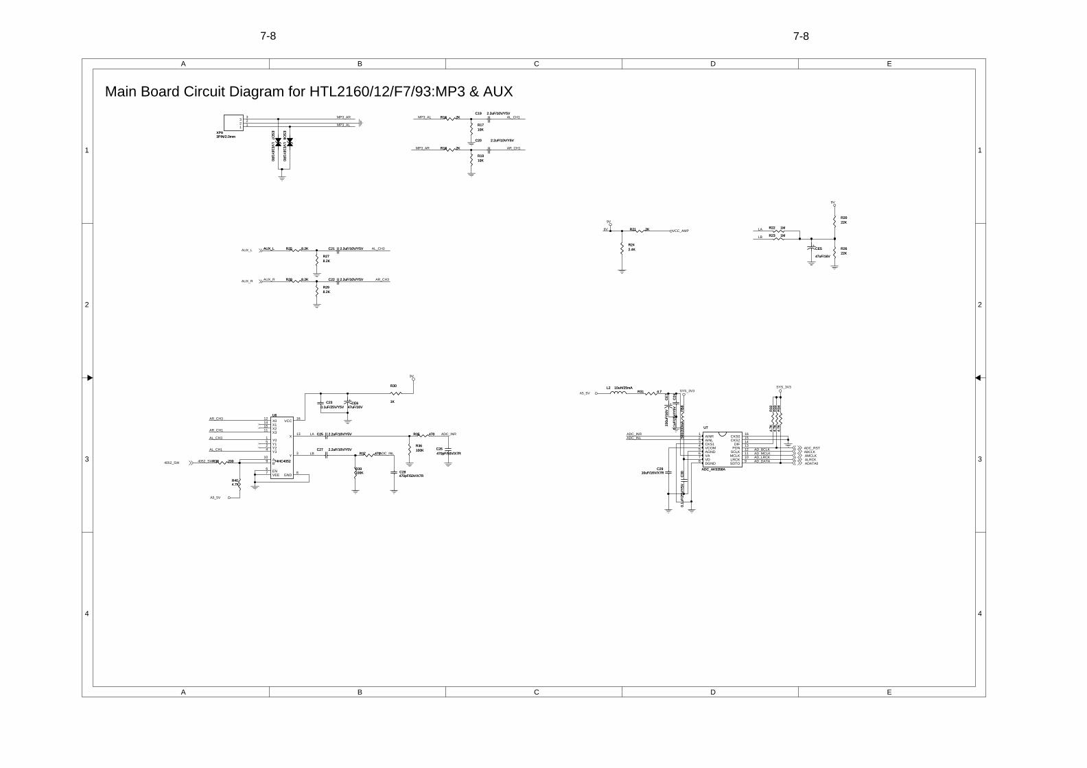
Main Board Circuit Diagram for HTL2160/12/F7/93:MP3 & AUX
7-8 7-8
A
A
B
B
C
C
D
D
E
E
1 1
2 2
3 3
4 4
FROM FRONT BOARD
5V-OPT
OPTAUXIN_RRAUXIN_LLCOAX
AUX_L5V-OPT A5_5V
SPD_VCC
OPT_IN2
COAX_IN
SPD_VCCSPD_VCC
SPDIF_SW1
OPT_IN OPT_IN2
OPT
COAX COAX_IN
OPT_INAUXIN_RR
AUXIN_LL
AUX_R
A5_5V
A5_5V
AUX_L
AUX_R
SPDIF_SW1
SPDIF_IN
SPDIF_SW2
R55 0R55 0
C35
NC
/3300pF/50V/X
7R
C35
NC
/3300pF/50V/X
7R
C32
NC
/100pF/50V/N
P0
C32
NC
/100pF/50V/N
P0
C39
100pF/50V/NP0
C39
100pF/50V/NP0
R43 0R43 0
C41
0.1uF/25V/X7R
C41
0.1uF/25V/X7R
RCA
P1
RCA
P1
COAX1L2R3OPT4GND5VCC6AGND7
R48 10R48 10
R49 100R49 100
R5375R5375
C400.1uF/25V/Y5V
C400.1uF/25V/Y5V
R42 1KR42 1K
C37 0.1uF/25V/X7RC37 0.1uF/25V/X7R
C31
1uF/10V/Y
5V
C31
1uF/10V/Y
5V
C34
NC
/3300pF/50V/X
7R
C34
NC
/3300pF/50V/X
7R
ES
D2
PE
SD
5V0S
1BA
/30K/35pF
ES
D2
PE
SD
5V0S
1BA
/30K/35pF
21
R47 10KR47 10K
C38
100pF/50V/NP0
C38
100pF/50V/NP0
R45 0R45 0
U8
74HC04PW
U8
74HC04PW
1A1
1Y2
2A3
2Y4
3A5
3Y6
4Y8
4A9
5Y10
5A11
6Y12
6A13
GND7
VCC14
U10
TS5A3159
U10
TS5A3159
NO1
GND2
NC3
COM4
V+5
IN6
ES
D1
NC
/PE
SD
5V0S
1BA
/30K/35pF
ES
D1
NC
/PE
SD
5V0S
1BA
/30K/35pF
21
C420.1uF/25V/Y5V
C420.1uF/25V/Y5V
R54 1KR54 1K
U9
TS5A3159
U9
TS5A3159
NO1
GND2
NC3
COM4
V+5
IN6
ES
D4
PE
SD
5V0S
1BA
/30K/35pF
ES
D4
PE
SD
5V0S
1BA
/30K/35pF
21
ES
D3
PE
SD
5V0S
1BA
/30K/35pF
ES
D3
PE
SD
5V0S
1BA
/30K/35pF
21
R41 10R41 10
R50 10KR50 10K R52 10R52 10
R46NC/200R46NC/200
L3 1.8uH/25mAL3 1.8uH/25mA
C36 0.1uF/25V/X7RC36 0.1uF/25V/X7R
R44 1KR44 1K
XP83PIN/2.0mmXP83PIN/2.0mm
112233
R51 1KR51 1K
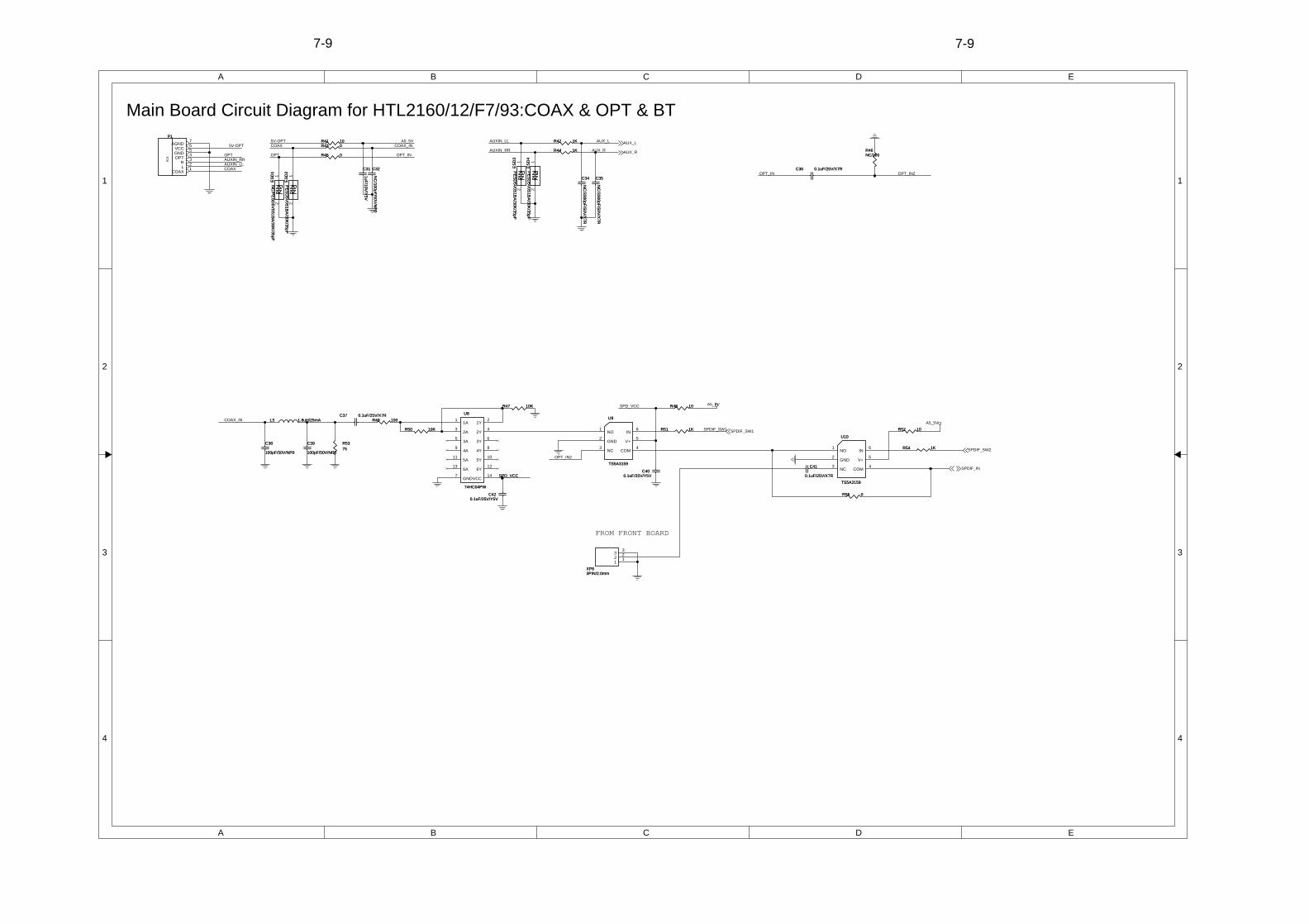
Main Board Circuit Diagram for HTL2160/12/F7/93:COAX & OPT & BT
7-9 7-9
A
A
B
B
C
C
D
D
E
E
1 1
2 2
3 3
4 4
Put these Compnonents ascloser as possible toMT1389
150mA
Debug Port
Video DAC +3.3V
RF +3.3V
Play 90mAStandby 8mA
Internal DA +3.3V
SDRAM +3.3V
Close to 8202RX-D
Close to SDRAM
Close to 8202R-D
Digital
Close to 8202RX-D
Close to 8202RX-D
Close to 8202RX-D
W=0.6mm
USB Host
I2S
_DA
TA0
SF_CS
XOXI
SPDIF_IN
I2S_MCLK
I2S_DATA_INI2S_LRCKI2S_BCLK
SF_CKSPI_D0
SPI_D1
SDCLK
M_A4
DCAS#M_CAS
M_A8
M_A3
M_A7
M_A2
DRAS#M_RAS
M_D0
M_D7
M_D5
M_D2
M_D14
M_D9M_D8
M_D13
M_D10M_D11
M_D15
M_D12
M_A10
M_D1
M_D6
RAM_CLK
M_A11
M_BA1
SDCLK
M_D3
M_BA0
M_D4
DQM1M_DQM1
M_A6M_A5
M_A1
DWE#M_WE
M_A0
DQM0M_DQM0
M_A9
US
B_D
MU
SB
_DP
MPEG_TXDMPEG_RXD
XO
XI
M_D
1
M_A2
M_A10
M_A
11
M_RAS
M_A1
M_CAS
M_A4
M_A0
M_DQM0
RA
M_C
LK
M_BA0M_BA1
M_WE
MP
EG
_RS
T
M_A3
M_D
3
M_D
6M
_D7
M_D
11
M_D
4
M_D
0
M_D
12
M_D
5
M_D
14
M_D
9
M_D
2
M_D
10
M_D
13
M_D
8
M_A
9
M_D
15
M_A
5M
_A6
SF_CS
M_A
8M
_A7
SF_CKSPI_D0
SPI_D1I2S_DATA_IN
M_D
QM
1 GP
IO25
DAC_VREF
USB_DM
USB_DP
AVCC3
RF3.3V
RF3.3V
DV33
VVCC3
DVCC3
VVCC3
AVCC3
DV
CC
3
VC
C1.
2
RF3.3V
DV
CC
3
VCC1.2DVCC3DVCC3
VV
CC
3
RF3
.3V
VCC1.2
V12
DVCC3
VCC1.2
DV33 FV33
SD33
SD33
SD33SD33
DVCC3
DV33
VVCC3
SD33
USB_5V
MP
EG
_TX
DM
PE
G_R
XD
ALRCK
I2S
_BC
LKI2
S_L
RC
K
I2S
_MC
LK
ABCLKAMCLK
I2S
_DA
TA0
SPDIF_IN
ADATA0
MP
EG
_RS
T
C53
0.1uF/50V/Y5V
C53
0.1uF/50V/Y5V
C46
0.1u
F/25
V/Y
5VC
460.
1uF/
25V
/Y5V
XP1
4PIN/2.0mm
XP1
4PIN/2.0mm
11
22
33
44
C71
0.1u
F/25
V/Y
5VC
710.
1uF/
25V
/Y5V
C574.7uF/16V/Y5VC574.7uF/16V/Y5V
Y1
27MHz/30PPM
Y1
27MHz/30PPM
C70
0.1u
F/25
V/Y
5VC
700.
1uF/
25V
/Y5V
C65
0.1u
F/25
V/Y
5VC
650.
1uF/
25V
/Y5V
R70
4.7K
/NC
R70
4.7K
/NC
C68
0.1u
F/25
V/Y
5VC
680.
1uF/
25V
/Y5V
R85 75R85 75
C790.1uF/25V/Y5VC790.1uF/25V/Y5V
C54 0.1uF/25V/Y5VC54 0.1uF/25V/Y5V
C56 0.1uF/25V/Y5VC56 0.1uF/25V/Y5V
R77 NC/0R77 NC/0
XP2
4PIN/2.0mm
XP2
4PIN/2.0mm
11
22
33
44
R58500/200mA
R58500/200mA
FB14 NC/500/200mAFB14 NC/500/200mA
R66
NC
/0R
66N
C/0
R72 51R72 51
R115 NC/0R115 NC/0
C800.1uF/50V/Y5VC800.1uF/50V/Y5V
TP1
TP1
R74 33R74 33
R69 0R69 0
C55 0.1uF/25V/Y5VC55 0.1uF/25V/Y5V
FB15 500/200mAFB15 500/200mA
R64
NC
/0R
64N
C/0
R61
4.7K
R61
4.7K
C82
0.1uF/50V/Y5V
C82
0.1uF/50V/Y5V
FB13 500/200mAFB13 500/200mA
R76
1KR
761K
C490.1uF/25V/Y5VC490.1uF/25V/Y5V
C76
NC
/10pF/50V/N
P0
C76
NC
/10pF/50V/N
P0
C51
0.1uF/25V/Y5V
C51
0.1uF/25V/Y5V
ESD10PRTR5V0U2XESD10PRTR5V0U2X
123 4
R71
4.7K
/NC
R71
4.7K
/NC
R114 NC/0R114 NC/0
R811.2KR811.2K
C67
0.1u
F/25
V/Y
5VC
670.
1uF/
25V
/Y5V
C66
0.1u
F/25
V/Y
5VC
660.
1uF/
25V
/Y5V
R821.2KR821.2K
U12
SPHE8202R-D
U12
SPHE8202R-D
DV
DLD
O10
2
AP
C_A
VS
S10
1
OP
VIN
100
OP
VIP
99
CD
E98
CD
F97
DV
DA
96
DV
DB
95
DV
DC
94
DV
DD
93
RFI
S92
AG
CC
AP
91
AD
_AV
DD
90
AD
_AV
SS
89
LDS
W/G
PIO
4088
HO
ME
/GP
IO39
87
VD
D_1
886
CLK
OU
T85
CLK
IN84
PLL
_VD
D83
PLL
_VS
S82
US
B_A
VS
S81
US
B_D
M80
US
B_D
P79
CDLDO103
DVDMDI104
CDMDI105
SRV_AVDD106
V21107
V165108
DA_AVSS109
DA_TEO110
DA_FEO111
DA_AVDD112
SPDC_OUT113
SC_OUT114
DVDVR115
DMEA116
SD_D1/GPIO4117
SD_D0/GPIO5118
SD_CLK/GPIO6119
TRAYIN/SD_SMD/GPIO7120
TRAYOUT/SD_D3/GPIO8121
SD_D2/GPIO9122
CDVR123
SPI_CE124
SPI_D0125
SPI_CLK126
SPI_D1127
ADAC_AVSS64
VREF61ADAC_AVDD62
AOUT_RS59AOUT_LS60
ADAC_AVSS58
AOUT_SUBW57
AOUT_CENTER56
AD_AVSS53AD_AVDD54AIN_R55
SPDIF_OUT51
M_A350
M_A249
M_A148
M_A047
M_A1046
M_BA1/GPIO2745
M_BA044
M_RAS43
M_CAS42
M_DQM040M_WE41
AO
UT_
L65
US
B_A
VD
D78
VD
D_1
877
TV_A
VS
S76
TV_D
AC
375
TV_D
AC
274
TV_D
AC
173
TV_A
VD
D72
TV_A
VS
S71
TV_A
VD
D70
TV_D
AC
069
V_F
SA
DJ
68
V_C
OM
P67
AO
UT_
R66
ADAC_AVDD63
TRAY+128
VFD
_CLK
/GP
IO16
1
VFD
_STB
/GP
IO17
2
VFD
_DA
TA/G
PIO
183
VD
D_1
810
RE
SE
T_B
5
M_D
QM
2/G
PIO
2211
M_D
QM
3/G
PIO
2312
M_D
013
M_D
114
M_D
215
M_D
316
M_D
417
M_D
518
M_D
619
M_D
720
M_D
1521
M_D
1422
M_D
1323
M_D
1224
M_D
1125
M_D
1026
M_D
927
M_D
828
M_D
QM
129
VS
S30
M_C
LK31
VD
D_3
332
M_A
11/G
PIO
2533
M_A
934
M_A
835
M_A
736
M_A
637
M_A
538
M_A439
VD
D_3
34
VS
S6
IR/G
PIO
197
GP
IO20
8
GP
IO21
9
GPIO2952
R65
NC
/0R
65N
C/0
R83
0R
830
R59
4.7K
R59
4.7K
C13510uF/16V/X7R
C13510uF/16V/X7R C
75N
C/10pF/50V
/NP
0C
75N
C/10pF/50V
/NP
0
R60
1KR
601K
C60
0.1uF/25V/Y5V
C60
0.1uF/25V/Y5V
C52
0.1uF/25V/Y5V
C52
0.1uF/25V/Y5V
FB12 500/200mAFB12 500/200mA
C50
0.1uF/25V/Y5V
C50
0.1uF/25V/Y5V
C69
0.1u
F/25
V/X
7RC
690.
1uF/
25V
/X7R
R56 4.7KR56 4.7K
R84 2.2R84 2.2
C471000pF/50V/X7RC47
1000pF/50V/X7R
C132NC/10pF/50V/NP0
C132NC/10pF/50V/NP0
C64
0.1u
F/25
V/Y
5VC
640.
1uF/
25V
/Y5V
C454.7uF/16V/Y5VC454.7uF/16V/Y5V
R126 NC/0R126 NC/0
C720.1uF/25V/Y5VC720.1uF/25V/Y5V
R113 NC/0R113 NC/0
TP2
TP2
C58
NC/15pF/50V/NP0
C58
NC/15pF/50V/NP0
R75 33R75 33
R62
4.7K
R62
4.7K
C4333pF/50V/NP0
C4333pF/50V/NP0
C7747pF/50V/NP0C7747pF/50V/NP0
U11
SPI_8Mb_EN25T80
U11
SPI_8Mb_EN25T80
CE#1
SO2
WP#3
VSS4
SI5SCK6HOLD#7VDD8
R73 33R73 33
C74
NC
/10pF/50V/N
P0
C74
NC
/10pF/50V/N
P0
R80
33R
8033
R86 4.7KR86 4.7K
C780.1uF/25V/Y5VC780.1uF/25V/Y5V
R63
4.7K
R63
4.7K
FB24
75/1A
FB24
75/1A C811000pF/50V/X7RC81
1000pF/50V/X7R
C59
0.1uF/25V/Y5V
C59
0.1uF/25V/Y5V
FB11 500/200mAFB11 500/200mA
R79 4.7KR79 4.7K
C63
0.1u
F/25
V/Y
5VC
630.
1uF/
25V
/Y5V
C7310pF/50V/NP0
C7310pF/50V/NP0
R78 4.7KR78 4.7K C62
1000
pF/5
0V/X
7RC
6210
00pF
/50V
/X7R
R68
NC
/0R
68N
C/0
C4433pF/50V/NP0
C4433pF/50V/NP0
+
47uF
/10V
CE
8
+
47uF
/10V
CE
8
C48 0.1uF/25V/Y5VC48 0.1uF/25V/Y5V
U13
SDRAM_64Mb_M12L64164A-7T
U13
SDRAM_64Mb_M12L64164A-7T
VCC1
DQ02
DQ14
VSSQ12
DQ25
DQ37
VCCQ9
DQ48
DQ510
VSSQ46
DQ611
DQ713
DQML15
WE16 CAS17 RAS18 CS19
A1135 A10/AP22
A023
A124
A225
A326
VCC14
VSS41
A429
A530
A631
A732
A833
A934
NC36
CKE37 CLK38
DQMH39
NC40
VCCQ43
DQ842
DQ944
VSSQ52
DQ1045
DQ1147
VCCQ49
DQ1248
DQ1350
DQ1451
DQ1553
VSS54
BA0/A1320
BA1/A1221
VCCQ3
VSSQ6
VCC27
VSS28
TP3
TP3
R67
NC
/0R
67N
C/0
R57 0R57 0
+ 10uF/10VCE9 + 10uF/10VCE9
T4ACM2012H-900-2PT4ACM2012H-900-2P
1
3 2
4
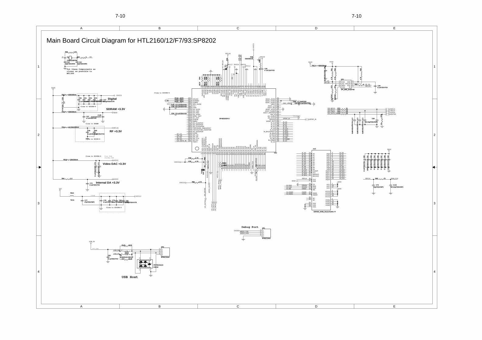
Main Board Circuit Diagram for HTL2160/12/F7/93:SP8202
7-10 7-10
A
A
B
B
C
C
D
D
E
E
1 1
2 2
3 3
4 4
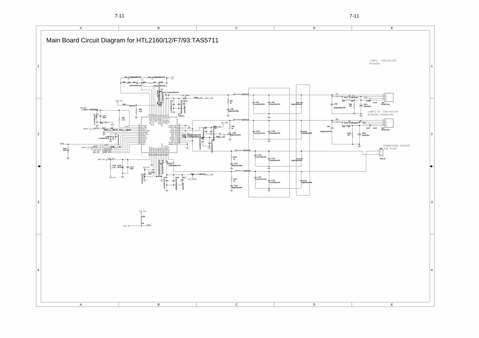
15W*2 THD+N=10%R=8ohm
SUBWOOFER OUTPUT 30W R=8R
15W*2 W THD+N=10%R=8ohm//8ohm=4R
PDN#
A_SEL
LRCK
AMP_SDAAMP_SCL
I2S_DATA0
AMP_RST
PDN#
L+L+
L-
R+R+
R-
AMCLK
ABCLK
SYS_3V3
SYS_3V3
VCC_AMP
VCC_AMP1
VCC_AMP2
VCC_AMPA
SYS_3V3
A
SYS_3V3
VCC_AMP2
VCC_AMP1VCC_AMP
VCC_AMP
SYS_3V3
AMP_SCLAMP_SDA
I2S_DATA0
ALRCK
AMP_RST
PDN
AMCLK
ABCLK
R108
10K
R108
10K
C96330pF/50V/NP0
C96330pF/50V/NP0
+
220u
F/35
V
CE11+
220u
F/35
V
CE11
R90
22.1
K/1
%R
9022
.1K
/1%
C1333.3UF
C1333.3UF
C11
80.
1uF/
25V
/X7R
C11
80.
1uF/
25V
/X7R
C11
5
1UF/
16V
/X7R
C11
5
1UF/
16V
/X7R
C10
7
4.7u
F/16
V/Y
5V
C10
7
4.7u
F/16
V/Y
5V
C117 10UF
C117 10UF
R106NC/100KR106NC/100K
C97 10UF
C97 10UF
C93100pF/50V/NP0
C93100pF/50V/NP0
R89 470R89 470
FB19 0FB19 0
C1010.47uF/25V/Y5V
C1010.47uF/25V/Y5V
C116330pF/50V/NP0
C116330pF/50V/NP0
C98
0.1u
F/25
V/X
7RC
980.
1uF/
25V
/X7R
C920.47uF/25V/Y5V
C920.47uF/25V/Y5V
C1210.47uF/25V/Y5V
C1210.47uF/25V/Y5V
C108 0.033uF/50V/X7RC108 0.033uF/50V/X7R
+
220u
F/35
V
CE17+
220u
F/35
V
CE17R10720R10720
XP34PIN/2.5mmXP34PIN/2.5mm
11
22
33
44
C109
0.1u
F/50
V/X
7R
C109
0.1u
F/50
V/X
7R
C124100pF/50V/NP0
C124100pF/50V/NP0
+220uF/35V CE15+220uF/35V CE15
XP44PIN/2.5mmXP44PIN/2.5mm
11
22
33
44
R93NC/4.7K
R93NC/4.7K
R9820R9820
C1020.22uF/50V/X7R
C1020.22uF/50V/X7R
C112100pF/50V/NP0
C112100pF/50V/NP0
U14TAS5711U14TAS5711
OU
T_A
1P
VD
D_A
2P
VD
D_A
3B
ST_
A4
GV
DD
_OU
T5
SS
TIM
ER
6O
C_A
DJ
7P
BTL
8A
VS
S9
PLL
_FLT
M10
PLL
_FLT
P11
VR
_AN
A12
AVDD13
A_SEL14
MCLK15
OSC_RES16
DVSSO17
VR_DIG18
PDN19
LRCLK20
SCLK21
SDIN22
SDA23
SCL24
RE
SE
T25
STE
ST
26
DV
DD
27
DV
SS
28
GN
D29
AG
ND
30
VR
EG
31
GV
DD
_OU
T32
BS
T_D
33
PV
DD
_D34
PV
DD
_D35
OU
T_D
36
PGND_CD37PGND_CD38OUT_C39PVDD_C40PVDD_C41BST_C42BST_B43PVDD_B44PVDD_B45OUT_B46PGND_AB47PGND_AB48
R99 10KR99 10K
C119 10UF
C119 10UF
U15
PW2-19
U15
PW2-19
11
22
C120
0.1u
F/50
V/X
7R
C120
0.1u
F/50
V/X
7R
R954.7KR954.7K
C86
0.047uF/50V/X7R
C86
0.047uF/50V/X7R
C91
0.1u
F/50
V/X
7R
C91
0.1u
F/50
V/X
7R
R97 0R97 0
C99
1000pF/50V/X7R
C99
1000pF/50V/X7RR101 200/1%R101 200/1%
L7 22uH/3.3AL7 22uH/3.3A
FB20 100/1.5AFB20 100/1.5A
R128 51R128 51R103NC/4.7KR103NC/4.7K
R9120R9120
L6 22uH/3.3AL6 22uH/3.3A
C134 3.3UFC134 3.3UF
C11
40.
1uF/
25V
/X7R
C11
40.
1uF/
25V
/X7R
R88 470R88 470
R9410KR9410K
C94
1000
pF/5
0V/X
7R
C94
1000
pF/5
0V/X
7R
L5 22uH/3.3AL5 22uH/3.3A
C103100pF/50V/NP0
C103100pF/50V/NP0
FB16 0FB16 0
C84 4700pF/50V/X7RC84 4700pF/50V/X7R
L4 22uH/3.3AL4 22uH/3.3A
C12210
00pF
/50V
/X7R
C12210
00pF
/50V
/X7R
+220uF/35V CE12+220uF/35V CE12
C1100.47uF/25V/Y5V
C1100.47uF/25V/Y5V
C83 4700pF/50V/X7RC83 4700pF/50V/X7R
C125330pF/50V/NP0
C125330pF/50V/NP0
C104 0.033uF/50V/X7RC104 0.033uF/50V/X7R
C88
NC
/220
0pF/
50V
/X7R
C88
NC
/220
0pF/
50V
/X7R
FB18 0FB18 0
R10420R10420
C89
1U
F/16
V/X
7RC
89
1UF/
16V
/X7R
FB17 500/200mAFB17 500/200mA
R1054.7KR1054.7K
C1130.033uF/50V/X7RC1130.033uF/50V/X7R
+
220uF/35V CE13
+
220uF/35V CE13
C900.22uF/50V/X7R
C900.22uF/50V/X7R
C105330pF/50V/NP0
C105330pF/50V/NP0
R92 10KR92 10K
R964.7KR964.7K
C85
0.047uF/50V/X7R
C85
0.047uF/50V/X7R
C87 0.033uF/50V/X7RC87 0.033uF/50V/X7R
C1060.1uF/50V/X7R
C1060.1uF/50V/X7R
C95
1000pF/50V/X7R
C95
1000pF/50V/X7R
R10210KR10210K
C131
1000
pF/5
0V/X
7R
C131
1000
pF/5
0V/X
7R
C100
1000
pF/5
0V/X
7R
C100
1000
pF/5
0V/X
7R
C1110.22uF/50V/X7R
C1110.22uF/50V/X7R
R127 300R127 300
C1230.22uF/50V/X7R
C1230.22uF/50V/X7R
+
220uF/35V CE10
+
220uF/35V CE10
R100 18K/1%R100 18K/1%C130
0.1u
F/50
V/X
7R
C130
0.1u
F/50
V/X
7R
Main Board Circuit Diagram for HTL2160/12/F7/93:TAS5711
7-11 7-11
A
A
B
B
C
C
D
D
E
E
1 1
2 2
3 3
4 4
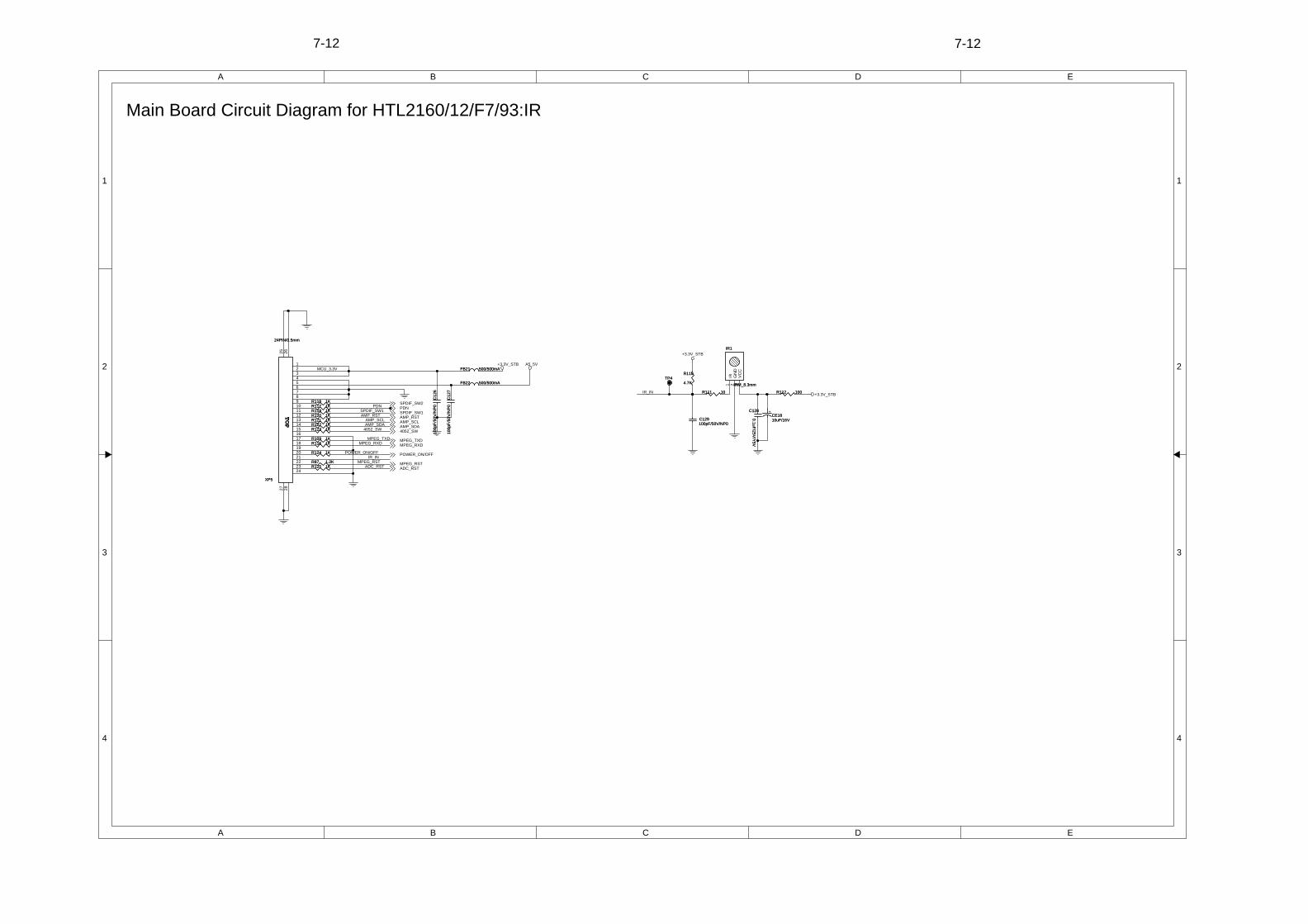
IR_IN
MCU_3.3V
PDNSPDIF_SW1AMP_RST
AMP_SCLAMP_SDA
4052_SW
IR_INMPEG_RST
POWER_ON/OFF
ADC_RST
MPEG_RXDMPEG_TXD
+3.3V_STB
+3.3V_STB
A5_5V+3.3V_STB
AMP_SCLAMP_RSTSPDIF_SW1PDN
4052_SWAMP_SDA
SPDIF_SW2
ADC_RSTMPEG_RST
POWER_ON/OFF
MPEG_RXDMPEG_TXD
FB22 500/500mAFB22 500/500mA
R119 1KR119 1K
IR1
IRM_8.3mm
IR1
IRM_8.3mm
IR1
GN
D2
VC
C3
R109 1KR109 1K
R111 10R111 10
C12
610
0pF/
50V
/NP
0C
126
100p
F/50
V/N
P0
R122 1KR122 1K
R112 100R112 100
C128
0.1uF/25V/Y
5V
C128
0.1uF/25V/Y
5V
R120 1KR120 1K
FB21 500/500mAFB21 500/500mA
R118 1KR118 1K
R121 1KR121 1K
TOP
XP5
24PIN/0.5mm
TOP
XP5
24PIN/0.5mm
242322212019181716151413121110987654321
25 2627 28
R117 1KR117 1K
R87 1.2KR87 1.2K
TP4TP4
R123 1KR123 1K
R125 1KR125 1K
+CE1810uF/16V
+CE1810uF/16V
R110
4.7K
R110
4.7K
C129100pF/50V/NP0C129100pF/50V/NP0
R116 1KR116 1KC
127
100p
F/50
V/N
P0
C12
710
0pF/
50V
/NP
0R124 1KR124 1K
Main Board Circuit Diagram for HTL2160/12/F7/93:IR
7-12 7-12

OP Board Print-layout(Bottom side):
7-13 7-13
CN Board Print-layout(Bottom side):
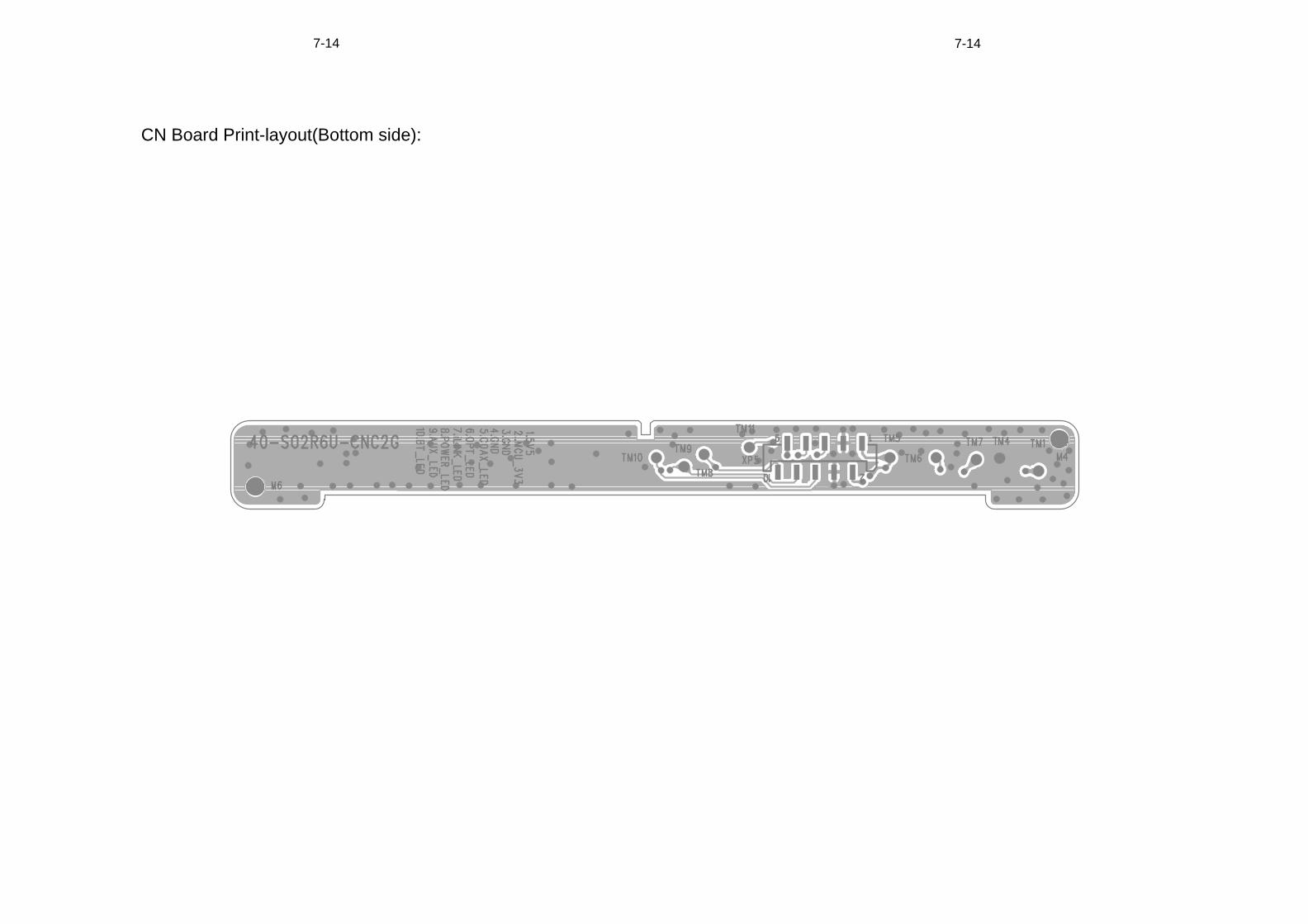
7-14 7-14
CN Board Print-layout(Top side):
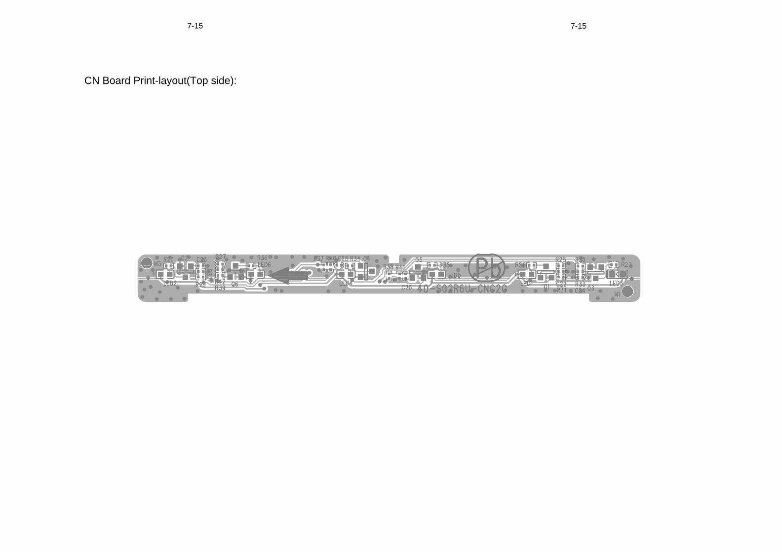
7-15 7-15

FK Board Print-layout(Bottom side):
7-16 7-16

FK Board Print-layout(Top side):
7-17 7-17
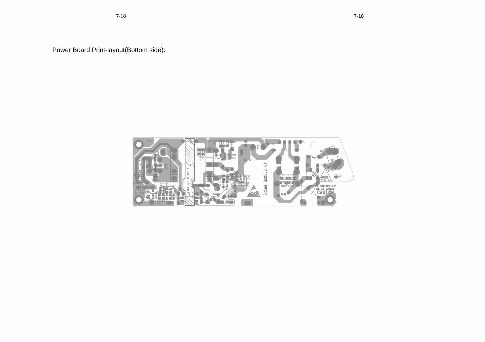
Power Board Print-layout(Bottom side):
7-18 7-18
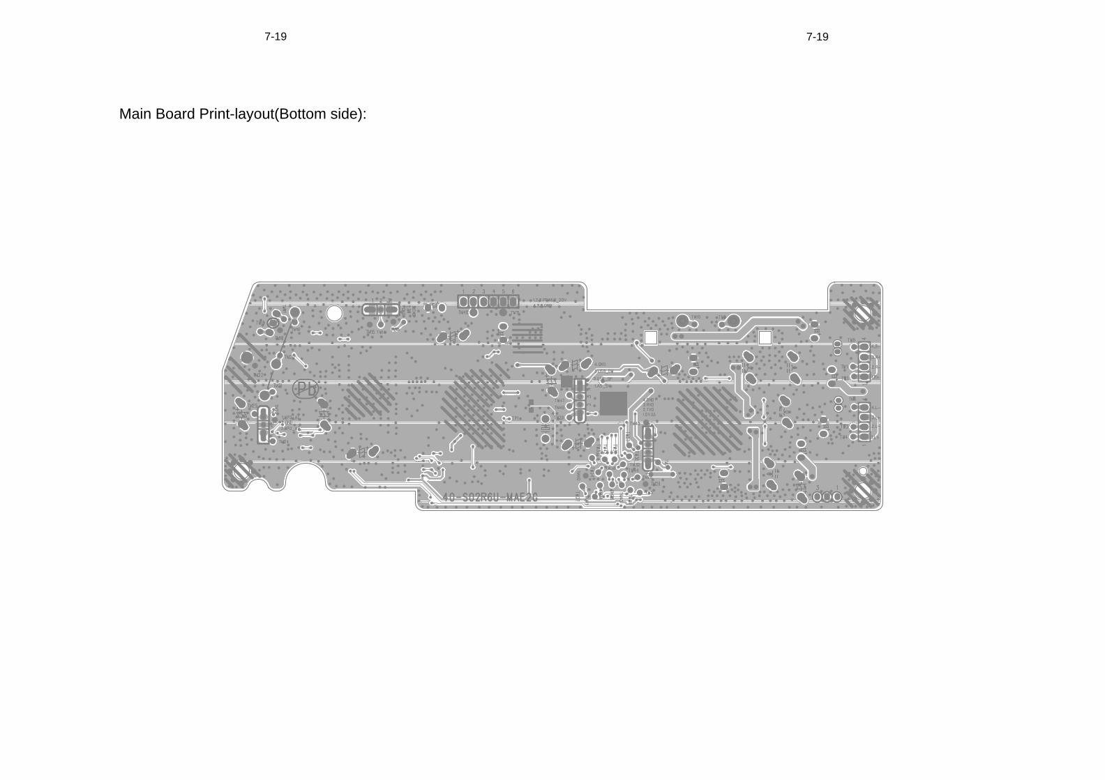
Main Board Print-layout(Bottom side):
7-19 7-19
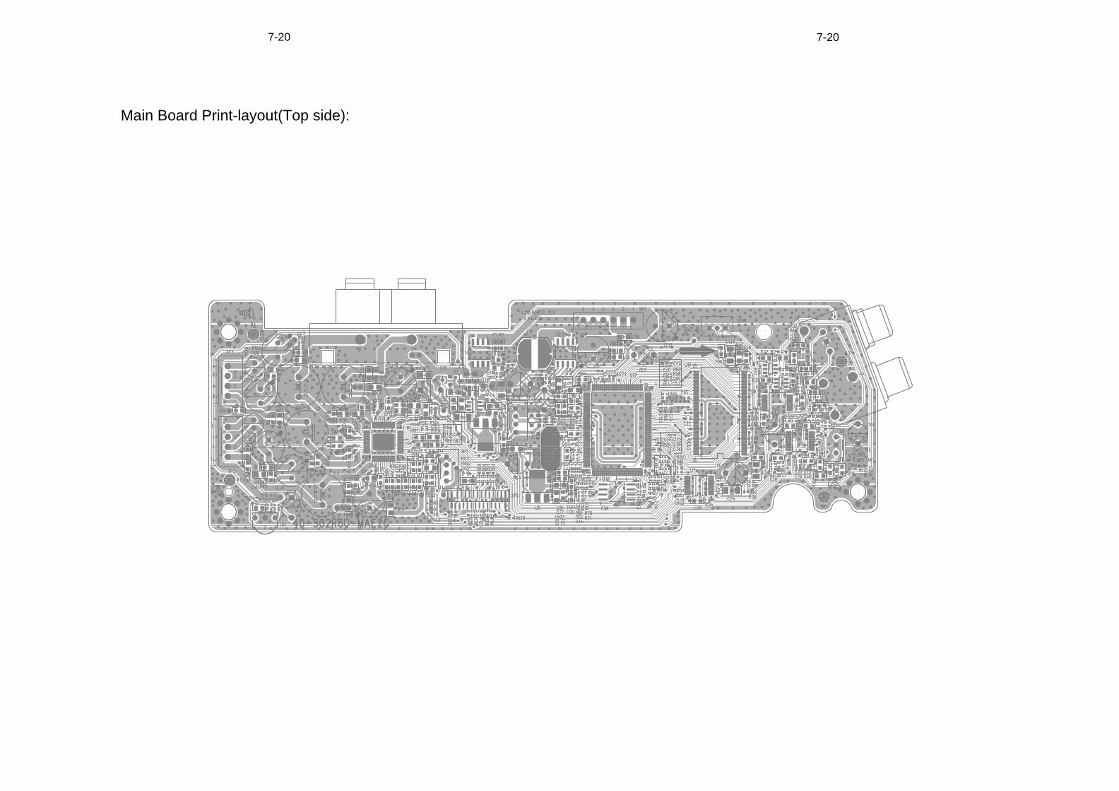
Main Board Print-layout(Top side):
7-20 7-20

Voltages for per connection pin
XS1 from power supply board connect to main boardXS1 from power supply board connect to main boardPin NO. Pin Assin Remarks
12345
19V
GND
18‐20V
6
XP5 from main board connect to front boardPin NO. Pin Assin Remarks
12 MCU 3 3v 3 2V 3 4V234 GND5 A5_5V 4.75‐5.25V678
MCU_3.3v
GND
3.2V‐3.4V
89 SPDIF_SW210 PND11 SPDIF_SW112 AMP_RST13 AMP_SCL14 AMP_SDA15 4052_SW16 GND171819 GND20 POWER_OM/OFF21 IR IN21 IR_IN22 MPEG_RST23 ADC_RST24 GND
XP2 from main board connect to front board for USBPin NO. Pin Assin RemarksPin NO. Pin Assin Remarks
1 USB_5V 4.75‐5.25V2 USB_DM3 USB_DP4 GND
8-1
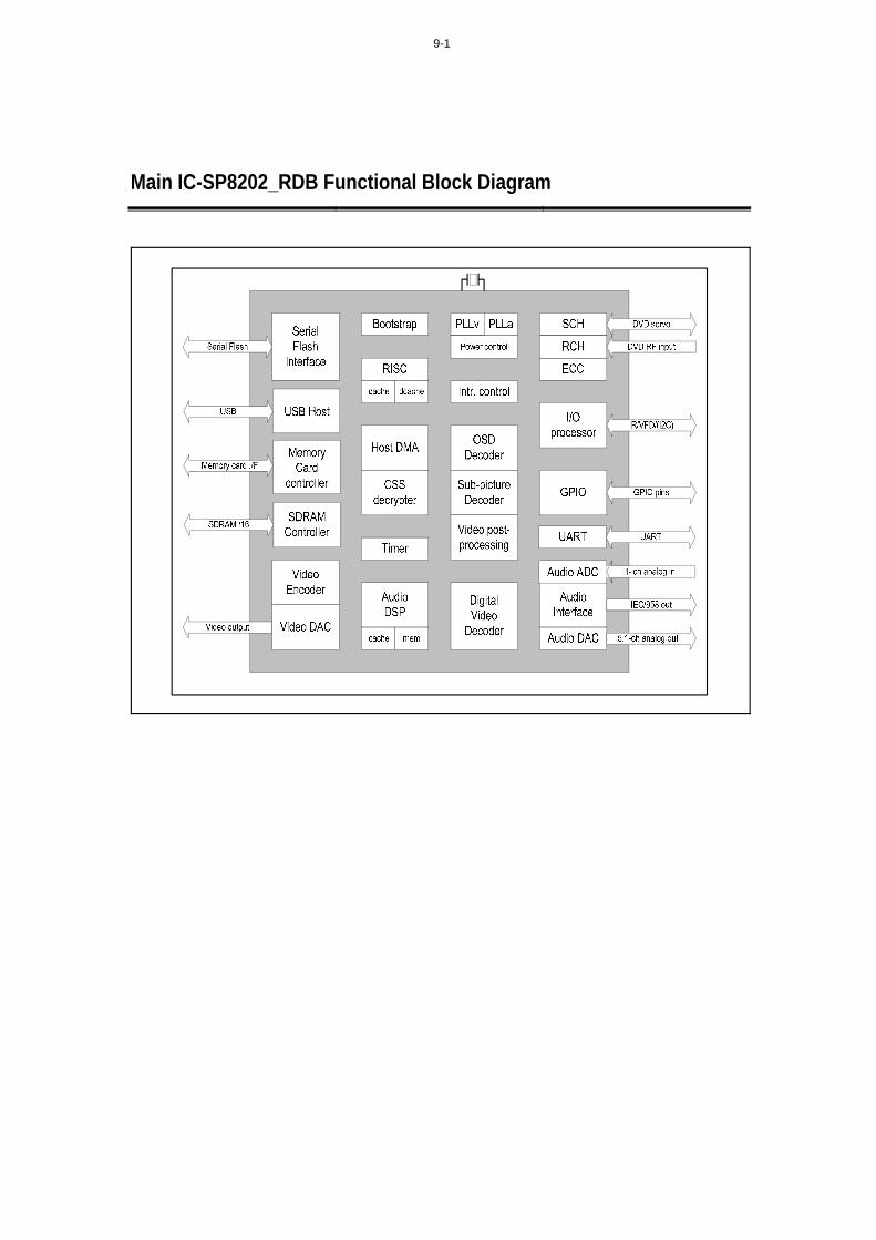
Main IC-SP8202_RDB Functional Block Diagram
9-1

Symbol Pin # I/O Description
VFD_CLK/GPIO 1 I/O 1. CLK of VFD
2. General-purpose I/O
VFD_STB/GPIO 2 I/O 1. Strobe of VFD
2. General-purpose I/O
VFD_DATA/GPIO 3 I/O 1. DATA of VFD
2. General-purpose I/O
VDD33 4 P I/O power supply
RST_B 5 I System Reset
VSS_0 6 G Ground
IR_I/GPIO 7 I/O IR input or general-purpose I/O
SCART_SEL/GPIO 8 I/O SCART select or general-purpose I/O
SCART_DIS/GPIO 9 I/O SCART display or general-purpose I/O
VDD_0 10 P 1.8V Kernel logic power supply
(For 8202R/Rx –D, 1.25V is used)
HSYNC/GPIO 11 I/O 1. General-purpose I/O
2. SD_HWORD_LDQM : SDRAM High Word LDQM
3. SD_CS0_B : SDRAM Chip Select 0
4. UA0_RXD : UART RX Port 0
5. HSYNC_PC : HSYNC signal of TV Interface
VSYNC/GPIO 12 I/O 1. General-purpose I/O
2. SD_HWORD_UDQM : SDRAM High Word UDQM
3. SD_CKE : SDRAM Clock Enable
4. UA0_TXD : UART TX Port 0
5. VSYNC_PC : VSYNC signal of TV Interface
SDRAM Interface
M_D0 13 I/O SDRAM data bus bit 0
M_D1 14 I/O SDRAM data bus bit 1
M_D2 15 I/O SDRAM data bus bit 2
M_D3 16 I/O SDRAM data bus bit 3
M_D4 17 I/O SDRAM data bus bit 4
M_D5 18 I/O SDRAM data bus bit 5
M_D6 19 I/O SDRAM data bus bit 6
M_D7 20 I/O SDRAM data bus bit 7
M_D15 21 I/O SDRAM data bus bit 15
M_D14 22 I/O SDRAM data bus bit 14
M_D13 23 I/O SDRAM data bus bit 13
M_D12 24 I/O SDRAM data bus bit 12
M_D11 25 I/O SDRAM data bus bit 11
M_D10 26 I/O SDRAM data bus bit 10
M_D9 27 I/O SDRAM data bus bit 9
M_D8 28 I/O SDRAM data bus bit 8
M_DQM1/GPIO 29 I/O 1. SDRAM data input/output mask for M DD[15:8]
2. General-purpose I/O
VSS_1 30 G Ground
Main IC-SP8202_RDB PIN Description
9-2
Symbol Pin # I/O Description
M_CLKO 31 O SDRAM CLK
VDD33 32 P I/O power supply
M_A11/GPIO 33 I/O 1. SDRAM address bus 11
2. General-purpose I/O
3. UA0_RXD : UART RX Port 1
4. HSYNC_PC : HSYNC signal of TV Interface
M_A9 34 I/O SDRAM address bus 9
M_A8 35 I/O SDRAM address bus 8
M_A7 36 I/O SDRAM address bus 7
M_A6 37 I/O SDRAM address bus 6
M_A5 38 I/O SDRAM address bus 5
M_A4 39 I/O SDRAM address bus 4
M_DQM0/GPIO 40 I/O 1. SDRAM data input/output mask for M DD[7:0]
2. General-purpose I/O
M_WE_B 41 I/O SDRAM write enable / row pre-charge
M_CAS_B 42 I/O SDRAM column address strobe
M_RAS_B 43 I/O SDRAM row address strobe / pre-charge
M_BA0 44 I/O 1. SDRAM bank select address 0
2. SDRAM bank select address 1
M_BA1/GPIO 45 I/O 1. SDRAM bank select address 1
2. SDRAM bank select address 0
3. General-purpose I/O
4. UA0_TXD : UART TX Port 1
M_A10 46 I/O SDRAM address bus 10
M_A0 47 I/O SDRAM address bus 0
M_A1 48 I/O SDRAM address bus 1
M_A2 49 I/O SDRAM address bus 2
M_A3 50 I/O SDRAM address bus 3
Audio SPDIF Output Interface
AUD_IEC_TX/GPIO 51 I/O 1. Audio SPDIF Output
2. General-purpose I/O
SCART_SIG/GPIO 52 I/O 1. SCART SIG signal
2. General-purpose I/O
Audio Codec Interface
AVSS33_AD 53 G Ground pin for Audio ADC
AVDD33_AD 54 P 3.3V power for Audio ADC
AIN_R 55 A ADC right channel analog input
AOUT_CENTER 56 A DAC Center channel analog output
AOUT_SW 57 A DAC Sub-woof channel analog output
VSS_ADAC_0 64 G Ground pin for Audio DAC #0
AOUT_RS 59 A DAC Surround Right channel analog output
AOUT_LS 60 A DAC Surround Left channel analog output
VM 61 A Reference voltage for Audio DAC
VDD_ADAC _0 62 P 3.3V power for Audio DAC #0
VDD_ADAC _1 63 P 3.3V power for Audio DAC #1
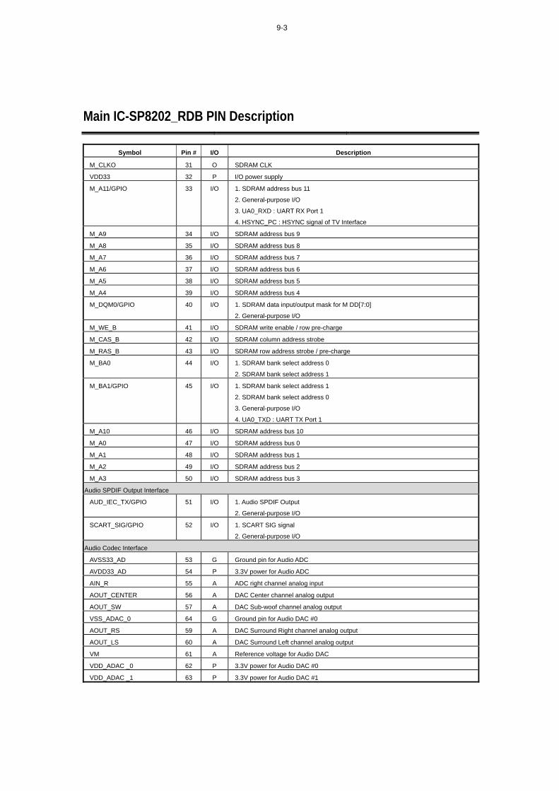
Main IC-SP8202_RDB PIN Description
9-3
Symbol Pin # I/O Description
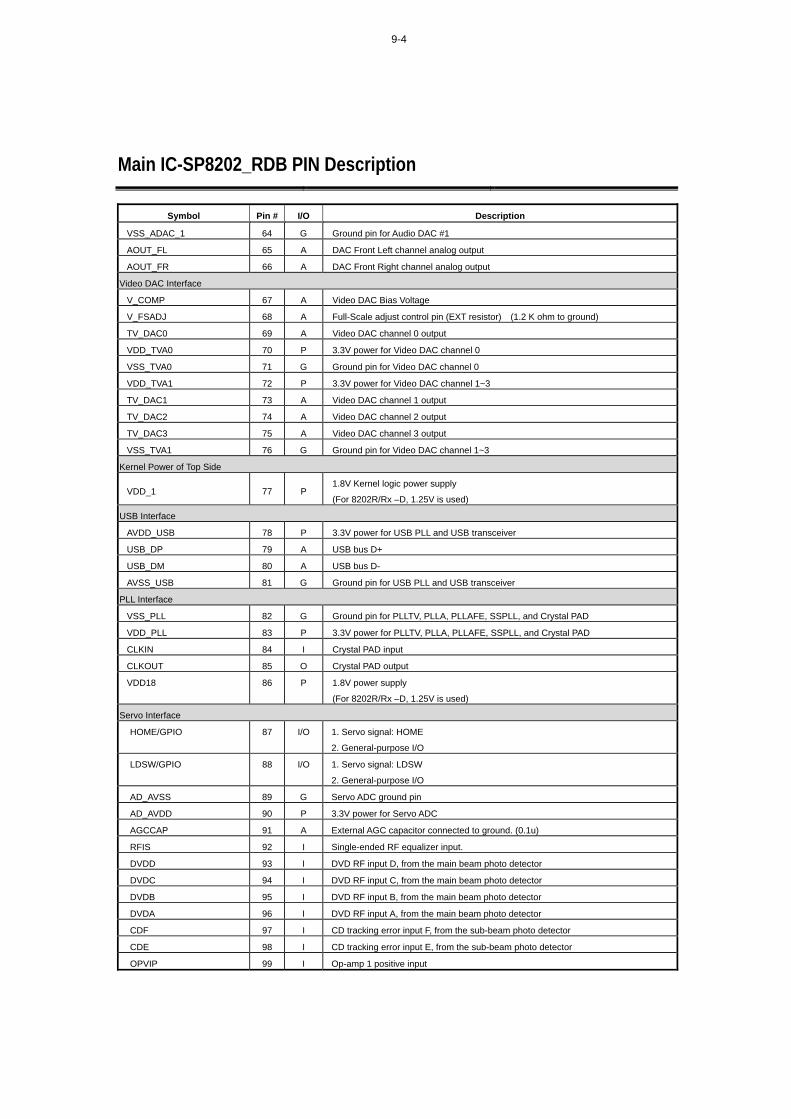
VSS_ADAC_1 64 G Ground pin for Audio DAC #1
AOUT_FL 65 A DAC Front Left channel analog output
AOUT_FR 66 A DAC Front Right channel analog output
Video DAC Interface
V_COMP 67 A Video DAC Bias Voltage
V_FSADJ 68 A Full-Scale adjust control pin (EXT resistor) (1.2 K ohm to ground)
TV_DAC0 69 A Video DAC channel 0 output
VDD_TVA0 70 P 3.3V power for Video DAC channel 0
VSS_TVA0 71 G Ground pin for Video DAC channel 0
VDD_TVA1 72 P 3.3V power for Video DAC channel 1~3
TV_DAC1 73 A Video DAC channel 1 output
TV_DAC2 74 A Video DAC channel 2 output
TV_DAC3 75 A Video DAC channel 3 output
VSS_TVA1 76 G Ground pin for Video DAC channel 1~3
Kernel Power of Top Side
VDD_1 77 P 1.8V Kernel logic power supply
(For 8202R/Rx –D, 1.25V is used)
USB Interface
AVDD_USB 78 P 3.3V power for USB PLL and USB transceiver
USB_DP 79 A USB bus D+
USB_DM 80 A USB bus D-
AVSS_USB 81 G Ground pin for USB PLL and USB transceiver
PLL Interface
VSS_PLL 82 G Ground pin for PLLTV, PLLA, PLLAFE, SSPLL, and Crystal PAD
VDD_PLL 83 P 3.3V power for PLLTV, PLLA, PLLAFE, SSPLL, and Crystal PAD
CLKIN 84 I Crystal PAD input
CLKOUT 85 O Crystal PAD output
VDD18 86 P 1.8V power supply
(For 8202R/Rx –D, 1.25V is used)
Servo Interface
HOME/GPIO 87 I/O 1. Servo signal: HOME
2. General-purpose I/O
LDSW/GPIO 88 I/O 1. Servo signal: LDSW
2. General-purpose I/O
AD_AVSS 89 G Servo ADC ground pin
AD_AVDD 90 P 3.3V power for Servo ADC
AGCCAP 91 A External AGC capacitor connected to ground. (0.1u)
RFIS 92 I Single-ended RF equalizer input.
DVDD 93 I DVD RF input D, from the main beam photo detector
DVDC 94 I DVD RF input C, from the main beam photo detector
DVDB 95 I DVD RF input B, from the main beam photo detector
DVDA 96 I DVD RF input A, from the main beam photo detector
CDF 97 I CD tracking error input F, from the sub-beam photo detector
CDE 98 I CD tracking error input E, from the sub-beam photo detector
OPVIP 99 I Op-amp 1 positive input
Main IC-SP8202_RDB PIN Description
9-4

Symbol Pin # I/O Description
OPVIN 100 I Op-amp 1 negative input
RF_APC_AVSS 101 G Ground pin for RF and APC
DVDLDO 102 O DVD APC output
CDLDO 103 O CD APC output
DVDMDI 104 I DVD APC input from monitor photo diode
CDMDI 105 I CD APC input from monitor photo diode
SRV_AVDD 106 P 3.3V power for SERVO
V21 107 A Reference DC bias voltage
V165 108 A Reference DC bias voltage
DA_AVSS 109 G Ground pin for DAC
DATEO 110 A 4-bit DAC output for motor drive TE
DAFEO 111 A 4-bit DAC output for motor drive FE
DA_AVDD 112 P 3.3V power for DAC
SPDC_OUT/GPIO 113 I/O 1. Servo SPDC OUT
2. General-purpose I/O
SC_OUT/GPIO 114 I/O 1. Servo SC_OUT
2. General-purpose I/O
TRAY_OUT/GPIO 115 I/O 1. Servo TRAY_OUT
2. General-purpose I/O
DMEA/GPIO 116 I/O 1. Servo DMEA
2. General-purpose I/O
SD_D1/CARD_SENSE/GPIO 117 I/O 1. Servo SC1_OUT
2. SD Data bit 1
3. Card Sense pin
4. General-purpose I/O
SD_D0/STEP_OUT/GPIO 118 I/O 1. Servo STEP_OUT
2. SD Data bit 0
3. General-purpose I/O
SD_CLK/GPIO 119 I/O 1. Servo FGIN
2. General-purpose I/O
3. I2C_DATA : Data pin of I2C Interface
4. SD clock pin
SD_CMD/GPIO 120 I/O 1. HW_CFG_SRC[0] : Hardware Configure bit 0
2. General-purpose I/O
3. Servo TRAY_IN
4. I2C_CLK : CLK of I2C Interface
5. SD Command pin
SD_D3/TRAY_OUT/GPIO 121 I/O 1. HW_CFG_SRC[1] : Hardware Configure bit 1
2. General-purpose I/O
3. SD Data bit 3
4. Servo TRAY_OUT
SD_D2/TRAY_IN/GPIO 122 I/O 1. HW_CFG_SRC[2] : Hardware Configure bit 2
2. General-purpose I/O
3. SD Data bit 2
4. Servo TRAY_IN
Main IC-SP8202_RDB PIN Description
9-5
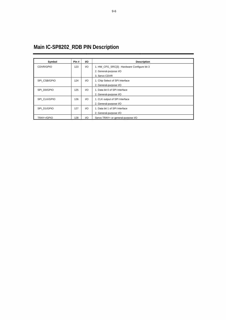
Symbol Pin # I/O Description
CDVR/GPIO 123 I/O 1. HW_CFG_SRC[3] : Hardware Configure bit 3
2. General-purpose I/O
3. Servo CDVR
SPI_CSB/GPIO 124 I/O 1. Chip Select of SPI Interface
2. General-purpose I/O
SPI_D0/GPIO 125 I/O 1. Data bit 0 of SPI Interface
2. General-purpose I/O
SPI_CLK/GPIO 126 I/O 1. CLK output of SPI Interface
2. General-purpose I/O
SPI_D1/GPIO 127 I/O 1. Data bit 1 of SPI Interface
2. General-purpose I/O
TRAY+/GPIO 128 I/O Servo TRAY+ or general-purpose I/O
Main IC-SP8202_RDB PIN Description
9-6
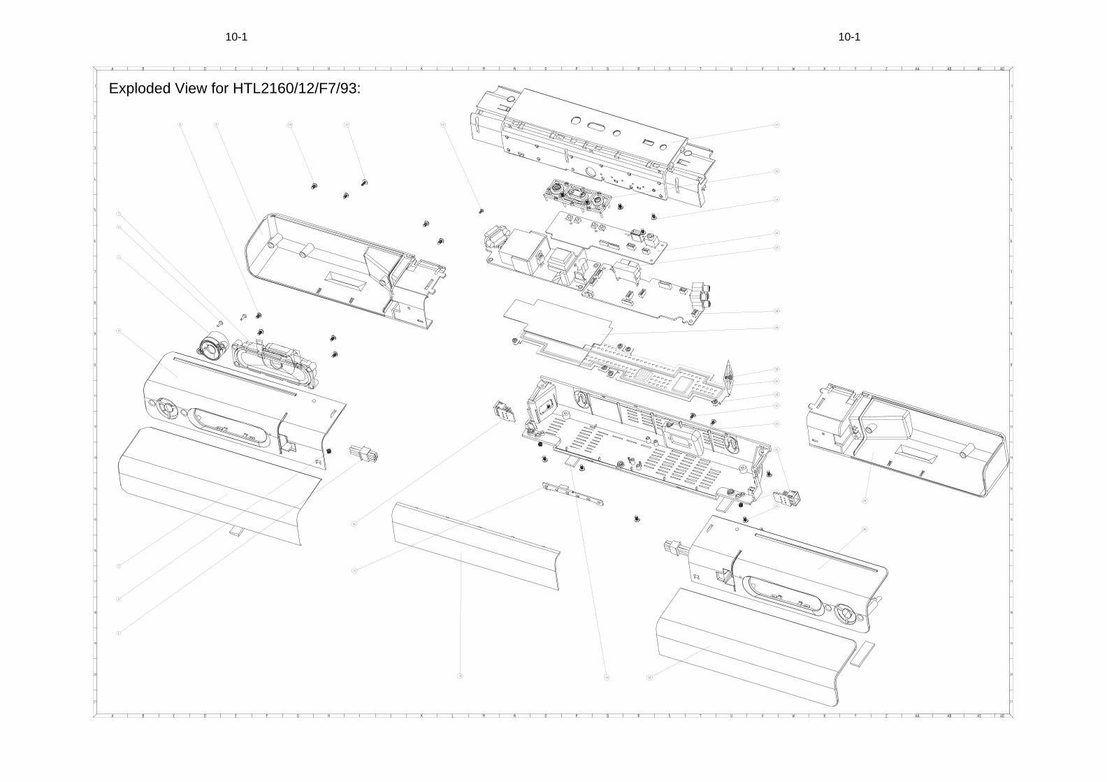
Exploded View for HTL2160/12/F7/93:
10-1 10-1
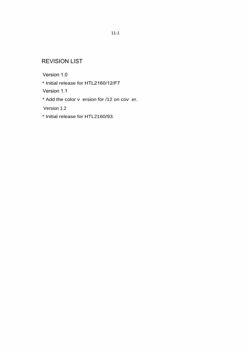
REVISION LIST
Version 1.0
* Initial release for HTL2160/12/F7
11-1
Version 1.1
* Add the color v ersion for /12 on cov er.
Version 1.2
* Initial release for HTL2160/93.
Related Documents