1 | Page

Welcome message from author
This document is posted to help you gain knowledge. Please leave a comment to let me know what you think about it! Share it to your friends and learn new things together.
Transcript
1 | P a g e
2 | P a g e
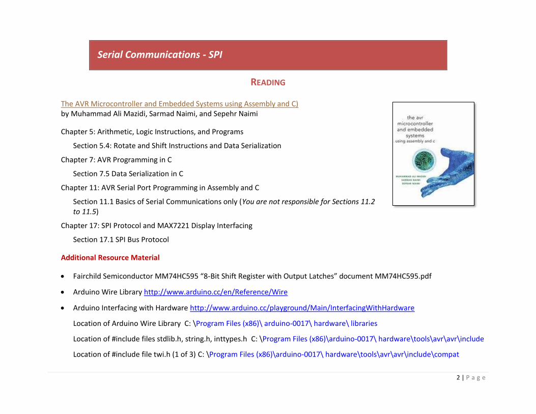
Serial Communications - SPI
READING
The AVR Microcontroller and Embedded Systems using Assembly and C) by Muhammad Ali Mazidi, Sarmad Naimi, and Sepehr Naimi
Chapter 5: Arithmetic, Logic Instructions, and Programs
Section 5.4: Rotate and Shift Instructions and Data Serialization
Chapter 7: AVR Programming in C
Section 7.5 Data Serialization in C
Chapter 11: AVR Serial Port Programming in Assembly and C
Section 11.1 Basics of Serial Communications only (You are not responsible for Sections 11.2 to 11.5)
Chapter 17: SPI Protocol and MAX7221 Display Interfacing
Section 17.1 SPI Bus Protocol
Additional Resource Material
Fairchild Semiconductor MM74HC595 “8-Bit Shift Register with Output Latches” document MM74HC595.pdf
Arduino Wire Library http://www.arduino.cc/en/Reference/Wire
Arduino Interfacing with Hardware http://www.arduino.cc/playground/Main/InterfacingWithHardware
Location of Arduino Wire Library C: \Program Files (x86)\ arduino-0017\ hardware\ libraries
Location of #include files stdlib.h, string.h, inttypes.h C: \Program Files (x86)\arduino-0017\ hardware\tools\avr\avr\include
Location of #include file twi.h (1 of 3) C: \Program Files (x86)\arduino-0017\ hardware\tools\avr\avr\include\compat
3 | P a g e
TABLE OF CONTENTS
Serial Communications .................................................................................................................................................................................................................. 4
ATmega328P Block Diagram .......................................................................................................................................................................................................... 5
ATmega SPI – Serial Peripheral Interface ....................................................................................................................................................................................... 6
What is a Flip-Flop and a Shift Register .......................................................................................................................................................................................... 7
What is a Serial Shift Register with Parallel Load............................................................................................................................................................................ 8
Setup, And Hold Times .................................................................................................................................................................................................................. 9
Ten Questions that need answers before you can design a Serial Peripheral Interface ................................................................................................................ 10
SPI Overview – Serial Communication ......................................................................................................................................................................................... 11
SPI Overview – The Registers ....................................................................................................................................................................................................... 12
Overview of the 74HC595 ............................................................................................................................................................................................................ 14
How to Configure the SPI Subsystem ........................................................................................................................................................................................... 15
How to Operate the SPI Subsystem – Polling – ............................................................................................................................................................................ 19
SPI Code Example ........................................................................................................................................................................................................................ 21
Appendix A Detail Description of the 74HC595 ..................................................................................................................................................................... 23
Tri-State Output Buffers .......................................................................................................................................................................................................... 23
74HC595 Storage Registers (D-Flip Flops) ................................................................................................................................................................................ 24
74HC595 Shift Registers (D-Flip Flops) ..................................................................................................................................................................................... 25

4 | P a g e
SERIAL COMMUNICATIONS
Taking the bits apart and putting them back together again
Lieutenant Reicher at Farpoint Station, Planet Deneb IV
5 | P a g e
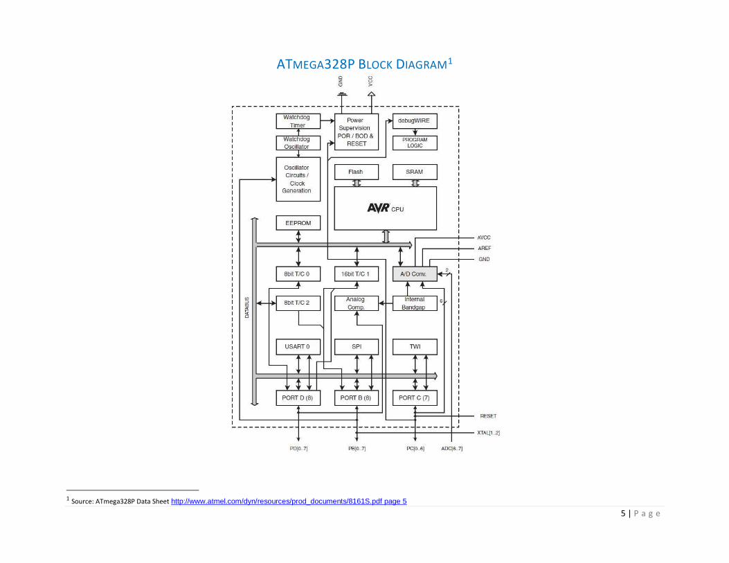
ATMEGA328P BLOCK DIAGRAM1
1 Source: ATmega328P Data Sheet http://www.atmel.com/dyn/resources/prod_documents/8161S.pdf page 5
6 | P a g e
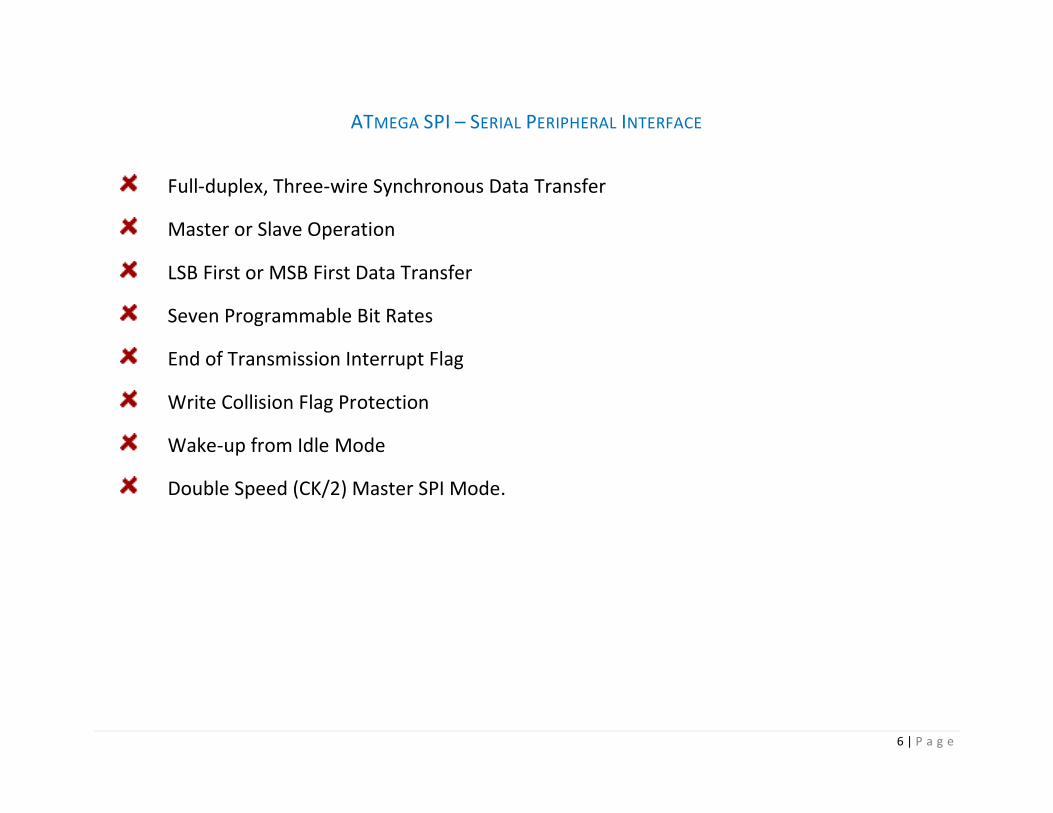
ATMEGA SPI – SERIAL PERIPHERAL INTERFACE
Full-duplex, Three-wire Synchronous Data Transfer
Master or Slave Operation
LSB First or MSB First Data Transfer
Seven Programmable Bit Rates
End of Transmission Interrupt Flag
Write Collision Flag Protection
Wake-up from Idle Mode
Double Speed (CK/2) Master SPI Mode.
7 | P a g e
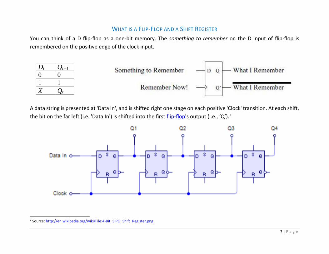
WHAT IS A FLIP-FLOP AND A SHIFT REGISTER
You can think of a D flip-flop as a one-bit memory. The something to remember on the D input of flip-flop is
remembered on the positive edge of the clock input.
Dt Qt+1
0 0
1 1
X Qt
A data string is presented at 'Data In', and is shifted right one stage on each positive 'Clock' transition. At each shift,
the bit on the far left (i.e. 'Data In') is shifted into the first flip-flop's output (i.e., ‘Q’).2
2 Source: http://en.wikipedia.org/wiki/File:4-Bit_SIPO_Shift_Register.png
8 | P a g e
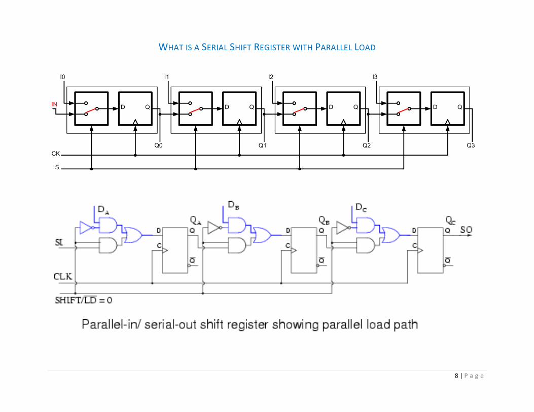
WHAT IS A SERIAL SHIFT REGISTER WITH PARALLEL LOAD
9 | P a g e
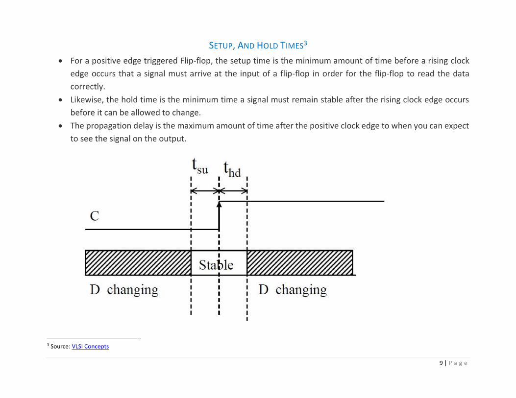
SETUP, AND HOLD TIMES3
For a positive edge triggered Flip-flop, the setup time is the minimum amount of time before a rising clock
edge occurs that a signal must arrive at the input of a flip-flop in order for the flip-flop to read the data
correctly.
Likewise, the hold time is the minimum time a signal must remain stable after the rising clock edge occurs
before it can be allowed to change.
The propagation delay is the maximum amount of time after the positive clock edge to when you can expect
to see the signal on the output.
3 Source: VLSI Concepts
10 | P a g e
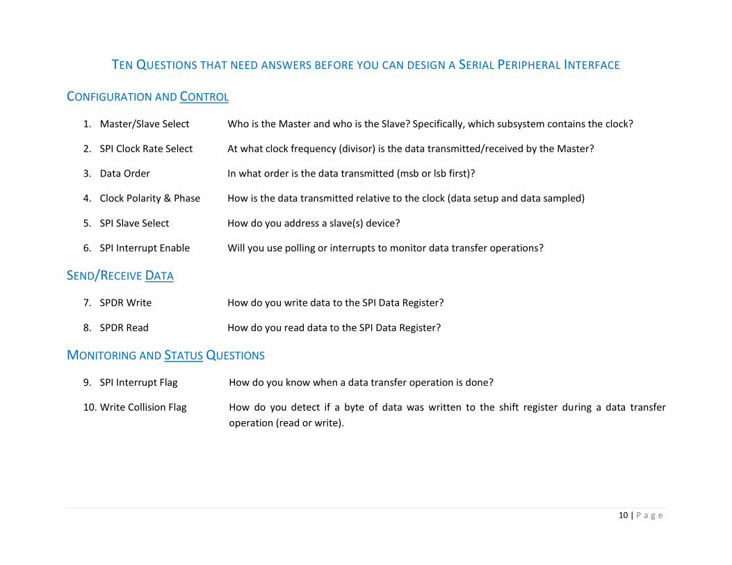
TEN QUESTIONS THAT NEED ANSWERS BEFORE YOU CAN DESIGN A SERIAL PERIPHERAL INTERFACE
CONFIGURATION AND CONTROL
1. Master/Slave Select Who is the Master and who is the Slave? Specifically, which subsystem contains the clock?
2. SPI Clock Rate Select At what clock frequency (divisor) is the data transmitted/received by the Master?
3. Data Order In what order is the data transmitted (msb or lsb first)?
4. Clock Polarity & Phase How is the data transmitted relative to the clock (data setup and data sampled)
5. SPI Slave Select How do you address a slave(s) device?
6. SPI Interrupt Enable Will you use polling or interrupts to monitor data transfer operations?
SEND/RECEIVE DATA
7. SPDR Write How do you write data to the SPI Data Register?
8. SPDR Read How do you read data to the SPI Data Register?
MONITORING AND STATUS QUESTIONS
9. SPI Interrupt Flag How do you know when a data transfer operation is done?
10. Write Collision Flag How do you detect if a byte of data was written to the shift register during a data transfer
operation (read or write).
11 | P a g e
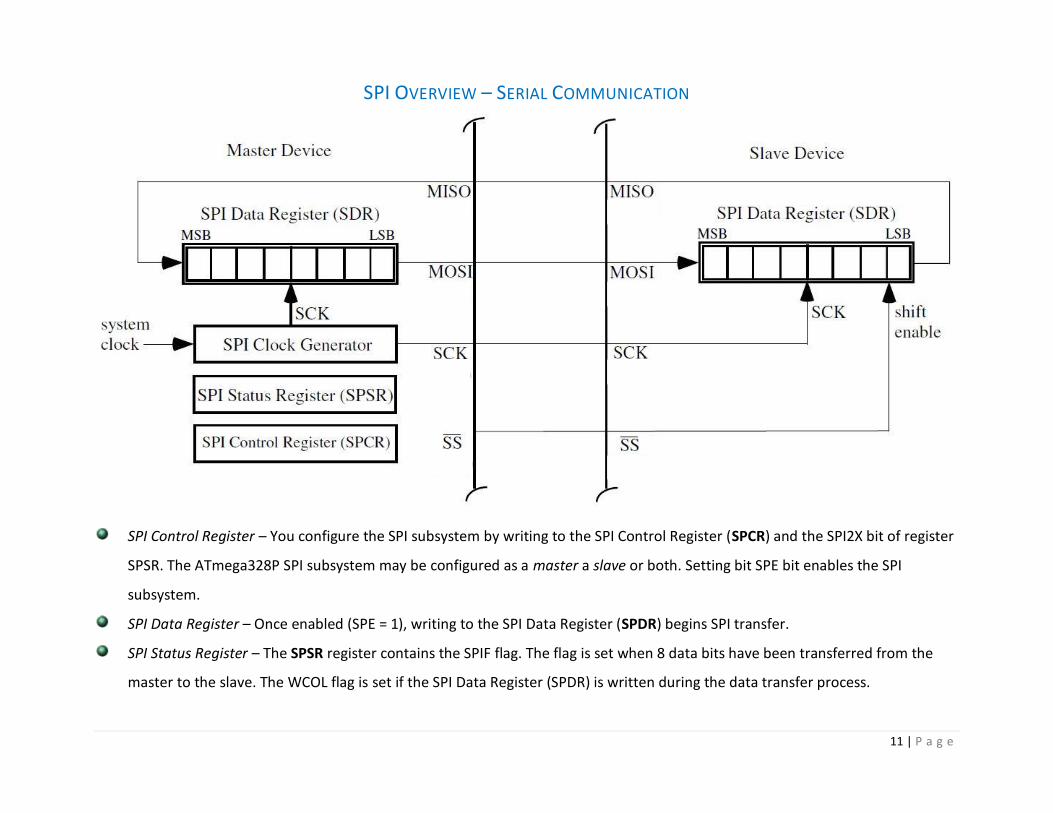
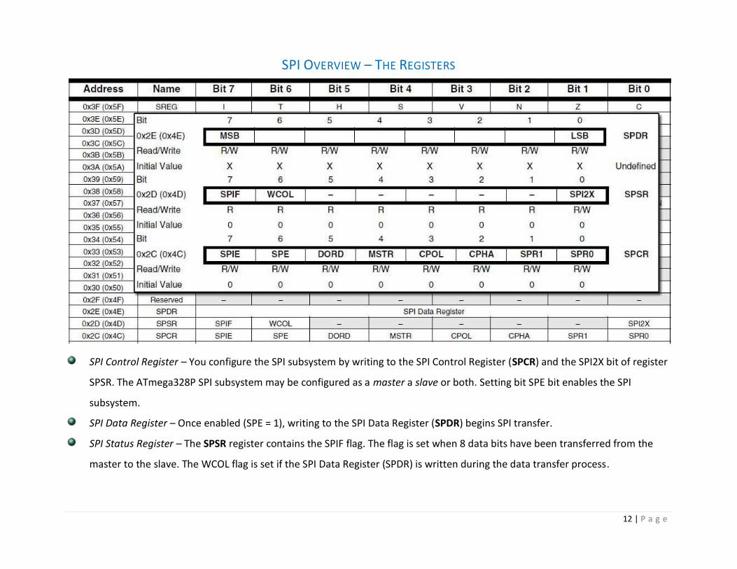
SPI OVERVIEW – SERIAL COMMUNICATION
SPI Control Register – You configure the SPI subsystem by writing to the SPI Control Register (SPCR) and the SPI2X bit of register
SPSR. The ATmega328P SPI subsystem may be configured as a master a slave or both. Setting bit SPE bit enables the SPI
subsystem.
SPI Data Register – Once enabled (SPE = 1), writing to the SPI Data Register (SPDR) begins SPI transfer.
SPI Status Register – The SPSR register contains the SPIF flag. The flag is set when 8 data bits have been transferred from the
master to the slave. The WCOL flag is set if the SPI Data Register (SPDR) is written during the data transfer process.
12 | P a g e
SPI OVERVIEW – THE REGISTERS
SPI Control Register – You configure the SPI subsystem by writing to the SPI Control Register (SPCR) and the SPI2X bit of register
SPSR. The ATmega328P SPI subsystem may be configured as a master a slave or both. Setting bit SPE bit enables the SPI
subsystem.
SPI Data Register – Once enabled (SPE = 1), writing to the SPI Data Register (SPDR) begins SPI transfer.
SPI Status Register – The SPSR register contains the SPIF flag. The flag is set when 8 data bits have been transferred from the
master to the slave. The WCOL flag is set if the SPI Data Register (SPDR) is written during the data transfer process.
13 | P a g e
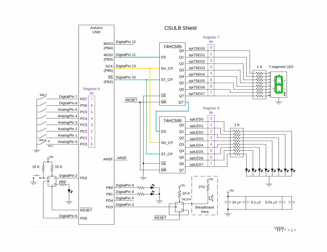
Arduino
UNO
PC0down
up
g
d
a
b
ce
f
1 K
dp
a
b
c
d
e
f
g
dp
7-segment LED
PD3
PC3
PC2
PC1
PC5
PC4
PD2
10 K
PD5
Q
QSET
CLR
D
10 K
MISO
(PB4)
MOSI
(PB3)
SCK
(PB5)
SS
(PB2)
DigitalPin 11
DigitalPin 13
DigitalPin 10
Q0
Q1
Q2
Q3
Q4
Q5
Q6
Q7
74HC595
DS
SH_CP
ST_CP
OE
MR
spi7SEG0
spi7SEG1
spi7SEG2
spi7SEG3
spi7SEG4
spi7SEG5
spi7SEG6
spi7SEG7
74HC595Q0
Q1
Q2
Q3
Q4
Q5
Q6
Q7
DS
SH_CP
ST_CP
OE
MR Q7'
DigitalPin 3
AnalogPin 0
AnalogPin 1
AnalogPin 2
AnalogPin 3
AnalogPin 4
AnalogPin 5
DigitalPin 2
DigitalPin 5
PB0
PB1
PD6
PD7
DigitalPin 8
DigitalPin 9
DigitalPin 7
DigitalPin 6
DigitalPin 12
AREF AREF
Breadboard
Area
SW.0
PD4DigitalPin 4
SW.7
RESET
RESET
Q
QSET
CLR
D
+5v
+5v
270
RESET
10 K
12/7/16
Register 6
bit
7
6
5
4
3
2
1
0
Register 8
bit
0
1
2
3
4
5
6
7
Register 7
bit
0
1
2
3
4
5
6
7
1 K
+5v
0.01 mF0.1 mF10 mF
+5v
74LS74
680Ω
spiLED0
spiLED1
spiLED2
spiLED3
spiLED4
spiLED5
spiLED6
spiLED7
CSULB Shield
14 | P a g e
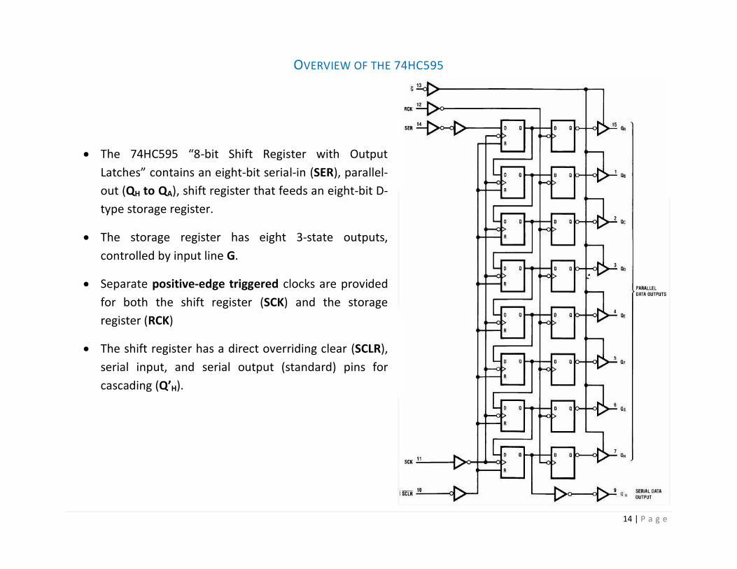
OVERVIEW OF THE 74HC595
The 74HC595 “8-bit Shift Register with Output
Latches” contains an eight-bit serial-in (SER), parallel-
out (QH to QA), shift register that feeds an eight-bit D-
type storage register.
The storage register has eight 3-state outputs,
controlled by input line G.
Separate positive-edge triggered clocks are provided
for both the shift register (SCK) and the storage
register (RCK)
The shift register has a direct overriding clear (SCLR),
serial input, and serial output (standard) pins for
cascading (Q’H).
15 | P a g e
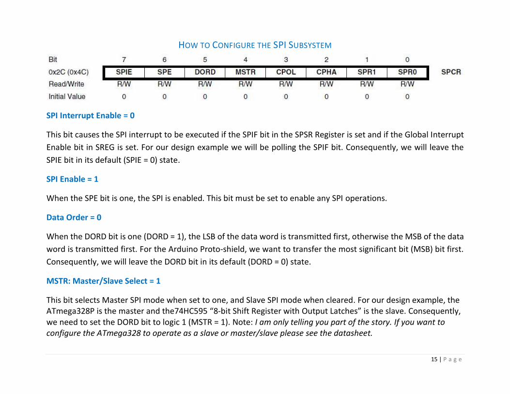
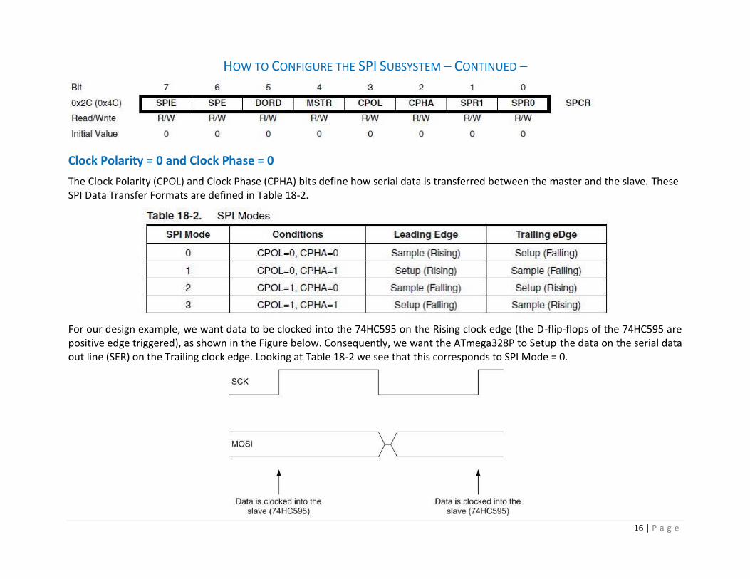
HOW TO CONFIGURE THE SPI SUBSYSTEM
SPI Interrupt Enable = 0
This bit causes the SPI interrupt to be executed if the SPIF bit in the SPSR Register is set and if the Global Interrupt
Enable bit in SREG is set. For our design example we will be polling the SPIF bit. Consequently, we will leave the
SPIE bit in its default (SPIE = 0) state.
SPI Enable = 1
When the SPE bit is one, the SPI is enabled. This bit must be set to enable any SPI operations.
Data Order = 0
When the DORD bit is one (DORD = 1), the LSB of the data word is transmitted first, otherwise the MSB of the data
word is transmitted first. For the Arduino Proto-shield, we want to transfer the most significant bit (MSB) bit first.
Consequently, we will leave the DORD bit in its default (DORD = 0) state.
MSTR: Master/Slave Select = 1
This bit selects Master SPI mode when set to one, and Slave SPI mode when cleared. For our design example, the ATmega328P is the master and the74HC595 “8-bit Shift Register with Output Latches” is the slave. Consequently, we need to set the DORD bit to logic 1 (MSTR = 1). Note: I am only telling you part of the story. If you want to configure the ATmega328 to operate as a slave or master/slave please see the datasheet.
16 | P a g e
HOW TO CONFIGURE THE SPI SUBSYSTEM – CONTINUED –
Clock Polarity = 0 and Clock Phase = 0
The Clock Polarity (CPOL) and Clock Phase (CPHA) bits define how serial data is transferred between the master and the slave. These SPI Data Transfer Formats are defined in Table 18-2.
For our design example, we want data to be clocked into the 74HC595 on the Rising clock edge (the D-flip-flops of the 74HC595 are positive edge triggered), as shown in the Figure below. Consequently, we want the ATmega328P to Setup the data on the serial data out line (SER) on the Trailing clock edge. Looking at Table 18-2 we see that this corresponds to SPI Mode = 0.

17 | P a g e
HOW TO CONFIGURE THE SPI SUBSYSTEM – CONTINUED –
SPI Clock Rate Select Bits SPI2X , SPR1, SPR0 = 0012
These three bits control the SCK rate of the Master. In our design example, the ATmega328P is the Master. These
bits have no effect on the Slave. The relationship between SCK and the Oscillator Clock frequency fosc is shown in
the following table. For our design example we will be dividing the system clock by 16.
18 | P a g e
HOW TO CONFIGURE THE SPI SUBSYSTEM – CONTINUED –
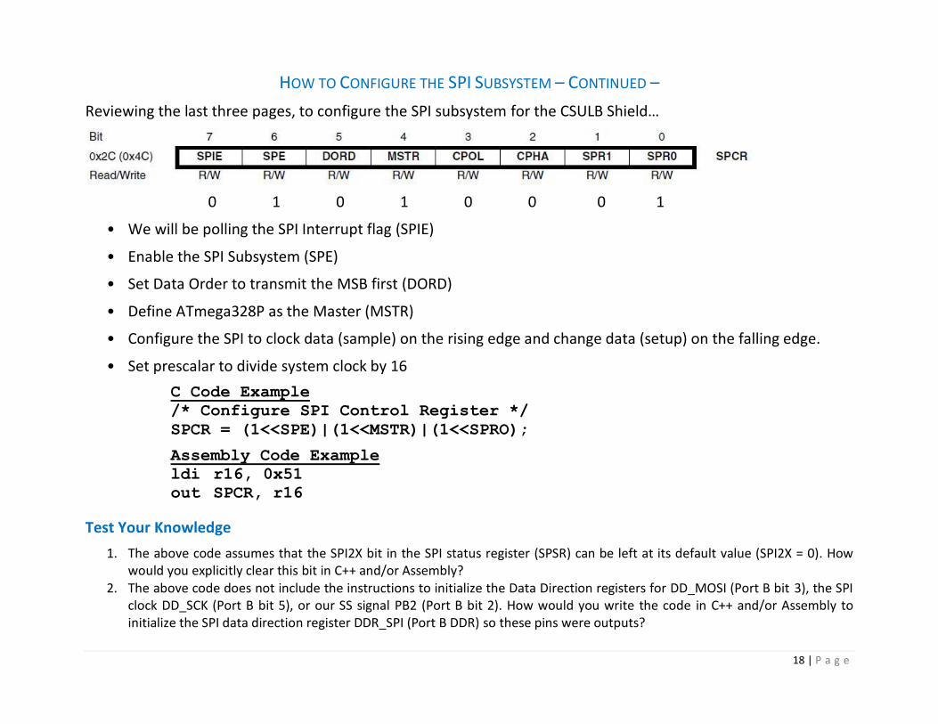
Reviewing the last three pages, to configure the SPI subsystem for the CSULB Shield…
0 1 0 1 0 0 0 1
• We will be polling the SPI Interrupt flag (SPIE)
• Enable the SPI Subsystem (SPE)
• Set Data Order to transmit the MSB first (DORD)
• Define ATmega328P as the Master (MSTR)
• Configure the SPI to clock data (sample) on the rising edge and change data (setup) on the falling edge.
• Set prescalar to divide system clock by 16
C Code Example
/* Configure SPI Control Register */
SPCR = (1<<SPE)|(1<<MSTR)|(1<<SPRO);
Assembly Code Example
ldi r16, 0x51
out SPCR, r16
Test Your Knowledge
1. The above code assumes that the SPI2X bit in the SPI status register (SPSR) can be left at its default value (SPI2X = 0). How would you explicitly clear this bit in C++ and/or Assembly?
2. The above code does not include the instructions to initialize the Data Direction registers for DD_MOSI (Port B bit 3), the SPI clock DD_SCK (Port B bit 5), or our SS signal PB2 (Port B bit 2). How would you write the code in C++ and/or Assembly to initialize the SPI data direction register DDR_SPI (Port B DDR) so these pins were outputs?
19 | P a g e
HOW TO OPERATE THE SPI SUBSYSTEM – POLLING –
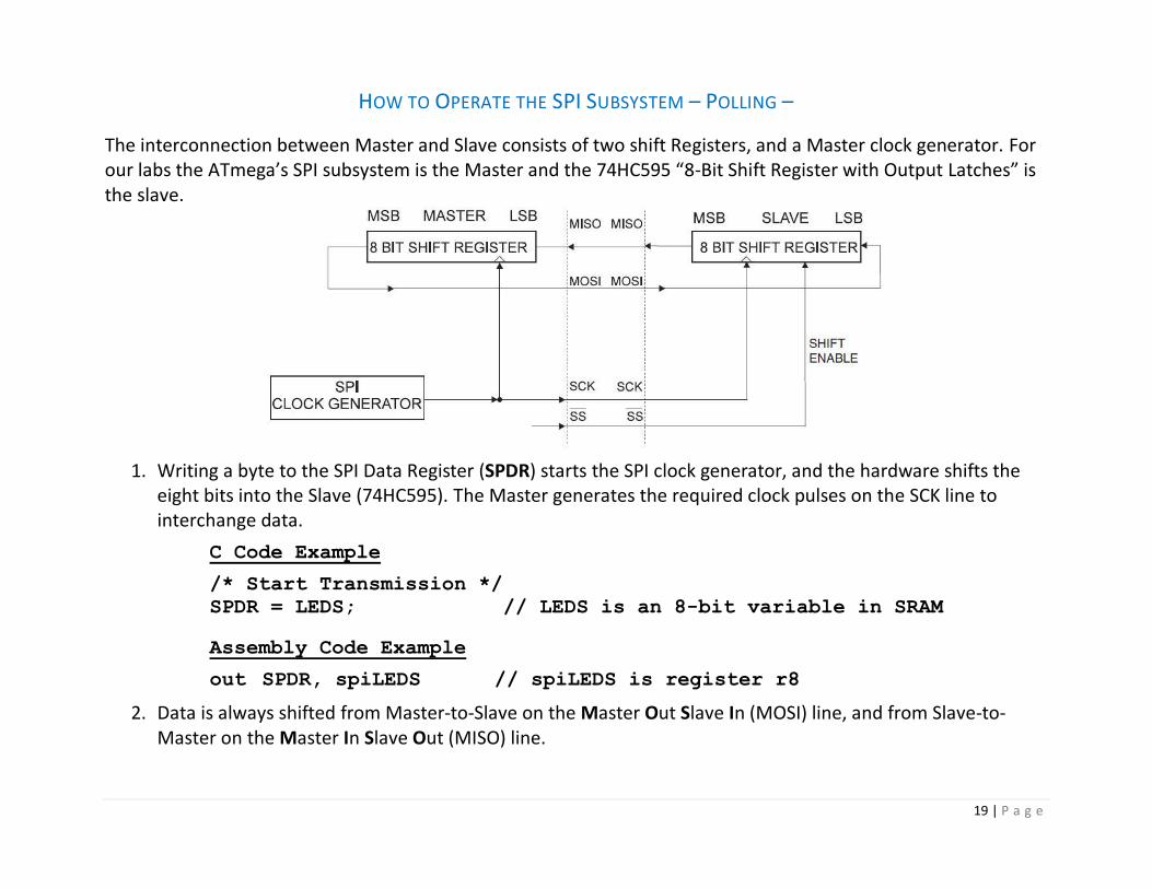
The interconnection between Master and Slave consists of two shift Registers, and a Master clock generator. For our labs the ATmega’s SPI subsystem is the Master and the 74HC595 “8-Bit Shift Register with Output Latches” is the slave.
1. Writing a byte to the SPI Data Register (SPDR) starts the SPI clock generator, and the hardware shifts the eight bits into the Slave (74HC595). The Master generates the required clock pulses on the SCK line to interchange data.
C Code Example
/* Start Transmission */
SPDR = LEDS; // LEDS is an 8-bit variable in SRAM
Assembly Code Example
out SPDR, spiLEDS // spiLEDS is register r8
2. Data is always shifted from Master-to-Slave on the Master Out Slave In (MOSI) line, and from Slave-to-Master on the Master In Slave Out (MISO) line.
20 | P a g e
How to Operate the SPI Subsystem – Polling –
3. After shifting one byte, the SPI clock generator stops, setting the end of Transmission Flag (SPIF bit in the SPSR register). If the SPI Interrupt Enable bit (SPIE) in the SPCR Register is set, an interrupt is requested. The Master may continue to shift the next byte by writing it into SPDR4. In our lab we used polling to monitor the status of the SPIF flag.
C Code Example
/* Wait for transmission complete */
while(!(SPSR & (1<<SPIF)));
Assembly Code Example
wait: in r16,SPSR
bst r16,SPIF
brtc wait
ret
4. After the last data packet is transmitted, the Master will transfer the data to the eight-bit D-type storage register of the slave by strobing the slave select (SS) line. When configured as a Master, the SPI interface has no automatic control of the SS line. This must be handled by your software. Note: We are using the SS line in a non-standard fashion. If you want to configure the ATmega328P to operate as a master, slave, or master/slave using the Atmel convention, please see the datasheet.
C Code Example
/* Pulse SS line */
PORTB &= ~(1 << (PB2));
PORTB |= (1 << (PB2));
Assembly Code Example
cbi PORTB,PB2
sbi PORTB,PB2
4 ATmega328P Datasheet Figure 18-2 SPI Master-slave Interconnection
21 | P a g e
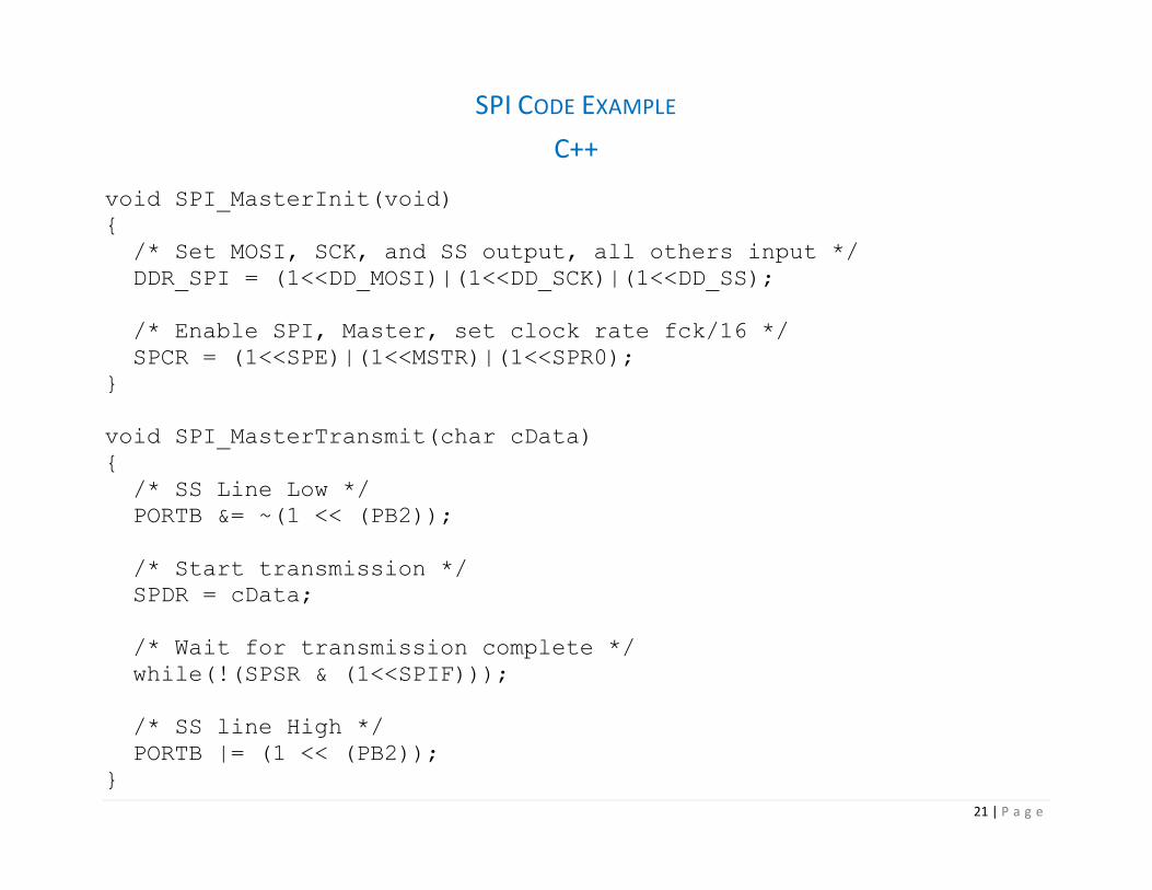
SPI CODE EXAMPLE
C++
void SPI_MasterInit(void)
{
/* Set MOSI, SCK, and SS output, all others input */
DDR_SPI = (1<<DD_MOSI)|(1<<DD_SCK)|(1<<DD_SS);
/* Enable SPI, Master, set clock rate fck/16 */
SPCR = (1<<SPE)|(1<<MSTR)|(1<<SPR0);
}
void SPI_MasterTransmit(char cData)
{
/* SS Line Low */
PORTB &= ~(1 << (PB2));
/* Start transmission */
SPDR = cData;
/* Wait for transmission complete */
while(!(SPSR & (1<<SPIF)));
/* SS line High */
PORTB |= (1 << (PB2));
}
22 | P a g e
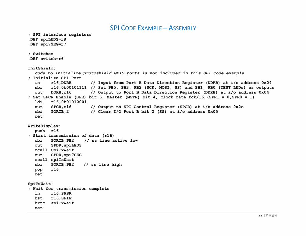
SPI CODE EXAMPLE – ASSEMBLY ; SPI interface registers
.DEF spiLEDS=r8
.DEF spi7SEG=r7
; Switches
.DEF switch=r6
InitShield:
code to initialize protoshield GPIO ports is not included in this SPI code example
; Initialize SPI Port
in r16,DDRB // Input from Port B Data Direction Register (DDRB) at i/o address 0x04
sbr r16,0b00101111 // Set PB5, PB3, PB2 (SCK, MOSI, SS) and PB1, PB0 (TEST LEDs) as outputs
out DDRB,r16 // Output to Port B Data Direction Register (DDRB) at i/o address 0x04
; Set SPCR Enable (SPE) bit 6, Master (MSTR) bit 4, clock rate fck/16 (SPR1 = 0,SPR0 = 1)
ldi r16,0b01010001
out SPCR,r16 // Output to SPI Control Register (SPCR) at i/o address 0x2c
cbi PORTB,2 // Clear I/O Port B bit 2 (SS) at i/o address 0x05
ret
WriteDisplay:
push r16
; Start transmission of data (r16)
cbi PORTB,PB2 // ss line active low
out SPDR,spiLEDS
rcall SpiTxWait
out SPDR,spi7SEG
rcall spiTxWait
sbi PORTB,PB2 // ss line high
pop r16
ret
SpiTxWait:
; Wait for transmission complete
in r16,SPSR
bst r16,SPIF
brtc spiTxWait
ret
23 | P a g e
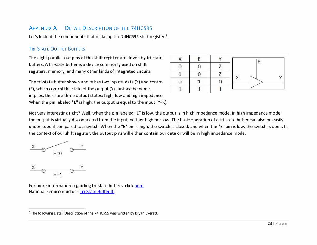
APPENDIX A DETAIL DESCRIPTION OF THE 74HC595
Let’s look at the components that make up the 74HC595 shift register.5
TRI-STATE OUTPUT BUFFERS
The eight parallel-out pins of this shift register are driven by tri-state
buffers. A tri-state buffer is a device commonly used on shift
registers, memory, and many other kinds of integrated circuits.
The tri-state buffer shown above has two inputs, data (X) and control
(E), which control the state of the output (Y). Just as the name
implies, there are three output states: high, low and high impedance.
When the pin labeled "E" is high, the output is equal to the input (Y=X).
Not very interesting right? Well, when the pin labeled "E" is low, the output is in high impedance mode. In high impedance mode,
the output is virtually disconnected from the input, neither high nor low. The basic operation of a tri-state buffer can also be easily
understood if compared to a switch. When the "E" pin is high, the switch is closed, and when the "E" pin is low, the switch is open. In
the context of our shift register, the output pins will either contain our data or will be in high impedance mode.
For more information regarding tri-state buffers, click here. National Semiconductor - Tri-State Buffer IC
5 The following Detail Description of the 74HC595 was written by Bryan Everett.
24 | P a g e
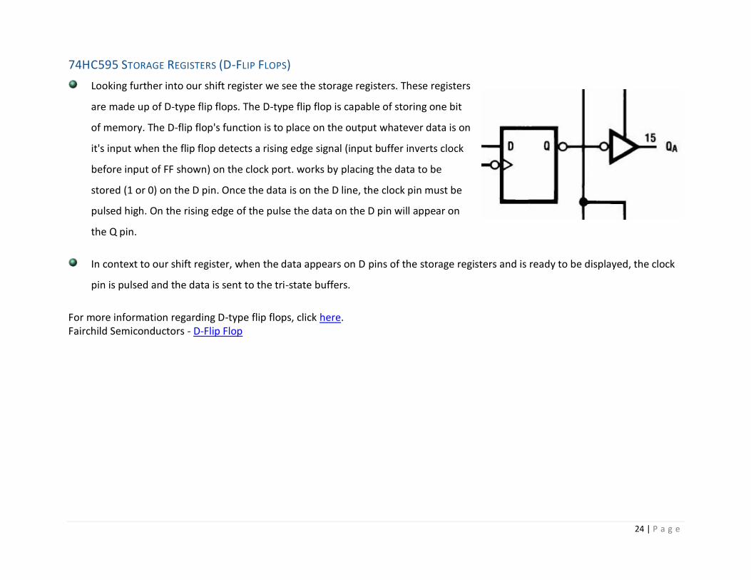
74HC595 STORAGE REGISTERS (D-FLIP FLOPS)
Looking further into our shift register we see the storage registers. These registers
are made up of D-type flip flops. The D-type flip flop is capable of storing one bit
of memory. The D-flip flop's function is to place on the output whatever data is on
it's input when the flip flop detects a rising edge signal (input buffer inverts clock
before input of FF shown) on the clock port. works by placing the data to be
stored (1 or 0) on the D pin. Once the data is on the D line, the clock pin must be
pulsed high. On the rising edge of the pulse the data on the D pin will appear on
the Q pin.
In context to our shift register, when the data appears on D pins of the storage registers and is ready to be displayed, the clock
pin is pulsed and the data is sent to the tri-state buffers.
For more information regarding D-type flip flops, click here. Fairchild Semiconductors - D-Flip Flop
25 | P a g e
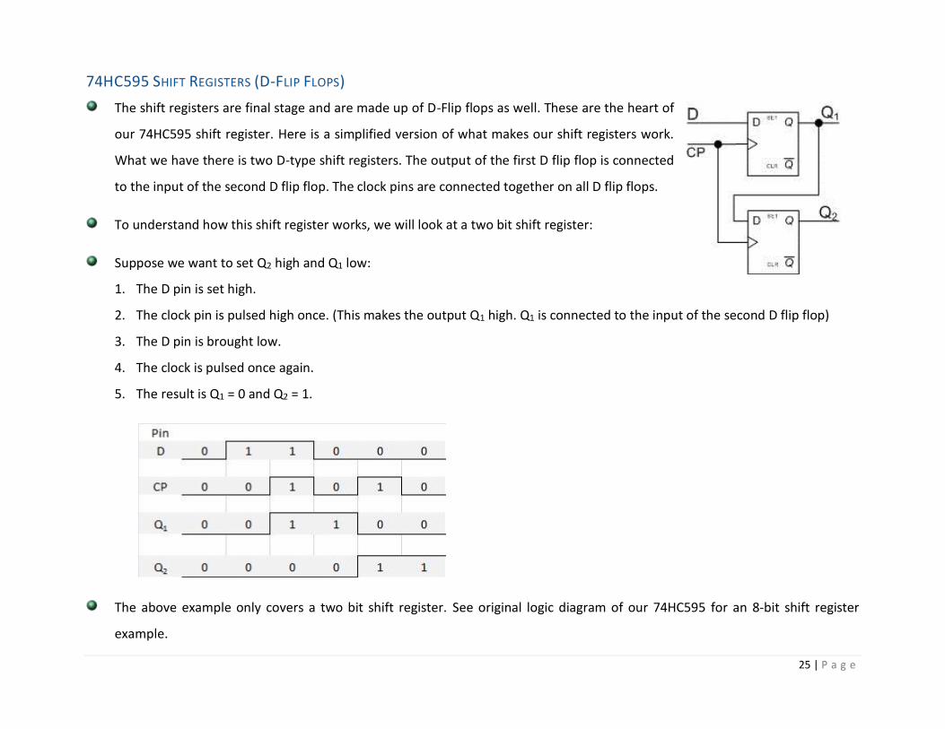
74HC595 SHIFT REGISTERS (D-FLIP FLOPS)
The shift registers are final stage and are made up of D-Flip flops as well. These are the heart of
our 74HC595 shift register. Here is a simplified version of what makes our shift registers work.
What we have there is two D-type shift registers. The output of the first D flip flop is connected
to the input of the second D flip flop. The clock pins are connected together on all D flip flops.
To understand how this shift register works, we will look at a two bit shift register:
Suppose we want to set Q2 high and Q1 low:
1. The D pin is set high.
2. The clock pin is pulsed high once. (This makes the output Q1 high. Q1 is connected to the input of the second D flip flop)
3. The D pin is brought low.
4. The clock is pulsed once again.
5. The result is Q1 = 0 and Q2 = 1.
The above example only covers a two bit shift register. See original logic diagram of our 74HC595 for an 8-bit shift register
example.
Related Documents