FLASH MEMORY TECHNOLOGY ABSTRACT A mass-storage device can provide access to data for just about any purpose. Every time an application is loaded or a file is saved on a PC, a mass-storage device is used. A computer’s hard drive is a mass-storage device, as are flash, CD, and DVD drives. Devices with dedicated functions—data loggers, robots, and other embedded systems—can use mass storage as well. Every mass-storage device contains a microcontroller, microprocessor, or other intelligent hardware that knows how to access the contents of the storage media. A USB device controller enables a mass-storage device to share its data with other computers. For example, a data logger can collect data in the field and then connect to a PC, where an application reads the data from the logger’s storage media. Or a robot can attach to a PC to receive a file containing configuration data to use in robotic tasks. Flash-memory cards provide convenient storage for many small systems. Flash memory is non-volatile, electrically erasable storage available as chips and in cards that incorporate memory chips and a controller. It is a technology that is primarily used in memory cards and USB flash drives for general storage and transfer of data between computers and other digital products. Flash-memory cards typically use the Serial Peripheral Interface (SPI), MultiMedia Card bus, SD-Card bus, or a bus derived from the ATA interface or PC-Card bus. In this paper, various architectures of the flash memory as well as their applications are treated. KEYWORDS: Tunneling, Wearing, ACRONYMS: USB- Universal Serial Bus, MMC- MultiMedia Card, SPI- Serial Peripheral Interface,

Seminar Topic 4 Msc2
Dec 13, 2015
flash
Welcome message from author
This document is posted to help you gain knowledge. Please leave a comment to let me know what you think about it! Share it to your friends and learn new things together.
Transcript

FLASH MEMORY TECHNOLOGY
ABSTRACT
A mass-storage device can provide access to data for just about any purpose. Every time an application is loaded or a file is saved on a PC, a mass-storage device is used. A computer’s hard drive is a mass-storage device, as are flash, CD, and DVD drives. Devices with dedicated functions—data loggers, robots, and other embedded systems—can use mass storage as well. Every mass-storage device contains a microcontroller, microprocessor, or other intelligent hardware that knows how to access the contents of the storage media. A USB device controller enables a mass-storage device to share its data with other computers. For example, a data logger can collect data in the field and then connect to a PC, where an application reads the data from the logger’s storage media. Or a robot can attach to a PC to receive a file containing configuration data to use in robotic tasks. Flash-memory cards provide convenient storage for many small systems. Flash memory is non-volatile, electrically erasable storage available as chips and in cards that incorporate memory chips and a controller. It is a technology that is primarily used in memory cards and USB flash drives for general storage and transfer of data between computers and other digital products. Flash-memory cards typically use the Serial Peripheral Interface (SPI), MultiMedia Card bus, SD-Card bus, or a bus derived from the ATA interface or PC-Card bus. In this paper, various architectures of the flash memory as well as their applications are treated.
KEYWORDS:
Tunneling, Wearing,
ACRONYMS:
USB- Universal Serial Bus, MMC- MultiMedia Card, SPI- Serial Peripheral Interface,
1.0 INTRODUCTION
Flash memory is a specific type of EEPROM (Electrically Erasable Programmable Read-Only Memory) that
is erased and programmed in large blocks; in early flash, the entire chip had to be erased at once. Flash
memory costs far less than byte-programmable EEPROM and therefore has become the dominant
technology wherever a significant amount of non-volatile, solid state storage is needed. Both flash memory
and EEPROM provide non-volatile, electrically erasable and reprogrammable storage. Compared to
EEPROM, flash-memory cells are physically smaller, can withstand more erase/write cycles, and are
cheaper to manufacture. Example applications include PDA’s (Personal Digital Assistants), laptop
computers, digital audio players, digital cameras and mobile phones. It has also gained popularity in the
game console market, where it is often used instead of EEPROMs or battery-powered SRAM for game
save data. Flash memory being non-volatile, implies that no power is needed to maintain the information
stored in the chip. In addition, flash memory offers fast read access times (although not as fast as volatile
DRAM memory used for main memory in PCs) and better kinetic shock resistance than hard disks. These
characteristics explain the popularity of flash memory in portable devices. Another feature of flash memory
is that when packaged in a “memory card”, it is enormously durable, being able to withstand intense
pressure, extremes of temperature and even immersion in water.
Although technically a type of EEPROM, the term “EEPROM” is generally used to refer specifically to non-
flash EEPROM which is erasable in small blocks, typically bytes. Because erase cycles are slow, the large
block sizes used in flash memory erasing give it a significant speed advantage over old-style EEPROM
when writing large amounts of data. The main disadvantage of flash memory is that unlike EEPROM, flash
memory is erasable only in blocks, not by individual byte. Even so, for most storage devices, flash memory
is the more practical choice, while EEPROM is useful for storing infrequently changed configuration
settings. Two flash-memory technologies in popular use are NOR and NAND. NOR flash is suited for
storing program code, where the CPU wants fast read access but rarely writes to the memory. NOR flash
has fast read times but slow erase and write times. NOR flash has low density, so large amounts of storage
may require multiple chips. To access NOR flash, a CPU uses the same data and address lines used to
access other parallel memory chips. Storage devices use NAND flash, which has fast erase and write
times. NAND flash also has lower power consumption and is much cheaper than NOR flash. A CPU
accesses NAND flash chips via data lines and command and address registers. NAND flash has high
density, so large amounts of memory can fit in a small package. In this regard NAND flash is similar to
other secondary storage devices such as hard disks and optical media, and is thus very suitable for use in
mass-storage devices such as memory cards. The first NAND-based removable media format was
SmartMedia, and many others have followed, including MultiMediaCard, Secure Digital, Memory Stick and
xD-Picture Card. A new generation of memory card formats, including RS-MMC, miniSD and microSD, and

Intelligent Stick, feature extremely small form factors. For example, the microSD card has an area of just
over 1.5 cm², with a thickness of less than 1 mm; microSD capacities range from 64 MB to 16 GB, as of
October 2008.The advantages of NAND flash are so attractive that some devices use NAND flash for
program memory along with a RAM cache to improve performance.
2.0 OVERVIEW OF THE FLASH MEMORY TECHNOLOGY
Flash memory stores information in an array of memory cells made from floating-gate transistors. In
traditional single-level cell (SLC) devices, each cell stores only one bit of information. Some newer flash
memory, known as multi-level cell (MLC) devices, can store more than one bit per cell by choosing
between multiple levels of electrical charge to apply to the floating gates of its cells. It has a grid of columns
and rows with a cell that has two transistors (One of the transistors is known as a floating gate and the
other one is the control gate) at each intersection.
The two transistors are separated from each other by a thin oxide layer. The floating gate's only link to the
row, or wordline, is through the control gate. As long as this link is in place, the cell has a value of 1. To
change the value to a 0 requires a process called Fowler-Nordheim tunneling.
Fig.1: A FLASH MEMORY CELL
2.1 FLASH MEMORY FLAVOURS (NAND AND NOR)
Although they use the same basic technology, the way they are addressed for reading and writing is slightly
different.

NOR Flash memory: NOR Flash memory is able to read individual flash memory cells, and as such
it behaves like a traditional ROM in this mode. For the erase and write functions, commands are
written to the first page of the mapped memory.
NAND Flash memory: NAND Flash memories have a different structure to NOR memories. They
are accessed much like block devices such as hard disks. When NAND Flash memories are to be
read, the contents must first be paged into memory-mapped RAM. This makes the presence of a
memory management unit essential.
2.2 NOR FLASH
In NOR gate flash, each cell resembles a standard MOSFET, except the transistor has two gates instead of
one. On top is the control gate (CG), as in other MOS transistors, but below this there is a floating gate
(FG) insulated all around by an oxide layer. The FG is interposed between the CG and the MOSFET
channel. Because the FG is electrically isolated by its insulating layer, any electrons placed on it are
trapped there and, under normal conditions, will not discharge for many years. When the FG holds a
charge, it screens (partially cancels) the electric field from the CG, which modifies the threshold voltage
(VT) of the cell. During read-out, a voltage is applied to the CG, and the MOSFET channel will become
conducting or remain insulating, depending on the VT of the cell, which is in turn controlled by charge on
the FG. The current flow through the MOSFET channel is sensed and forms a binary code, reproducing the
stored data. In a multi-level cell device, which stores more than one bit per cell, the amount of current flow
is sensed (rather than simply its presence or absence), in order to determine more precisely the level of
charge on the FG.

Fig.2: NOR flash memory wiring and structure on silicon
2.2.1 PROGRAMMING
A single-level NOR flash cell in its default state is logically equivalent to a binary "1" value, because current
will flow through the channel under application of an appropriate voltage to the control gate. A NOR flash
cell can be programmed, or set to a binary "0" value, by the following procedure:
an elevated on-voltage (typically >5 V) is applied to the CG
the channel is now turned on, so electrons can flow from the source to the drain (assuming an
NMOS transistor)
the source-drain current is sufficiently high to cause some high energy electrons to jump through
the insulating layer onto the FG, via a process called hot-electron injection.
Fig.3: Programming a NOR memory cell (setting it to logical 0), via hot-electron injection.
2.2.2 ERASING
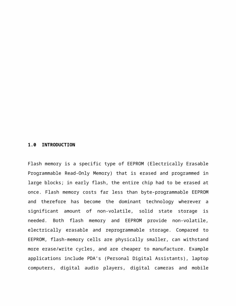
To erase a NOR flash cell (resetting it to the "1" state), a large voltage of the opposite polarity is applied
between the CG and source, pulling the electrons off the FG through quantum tunneling. Modern NOR
flash memory chips are divided into erase segments (often called blocks or sectors). The erase operation

can only be performed on a block-wise basis; all the cells in an erase segment must be erased together.
Programming of NOR cells, however, can generally be performed one byte or word at a time.
Fig.4. Erasing a NOR memory cell (setting it to logical 1), via quantum tunneling.
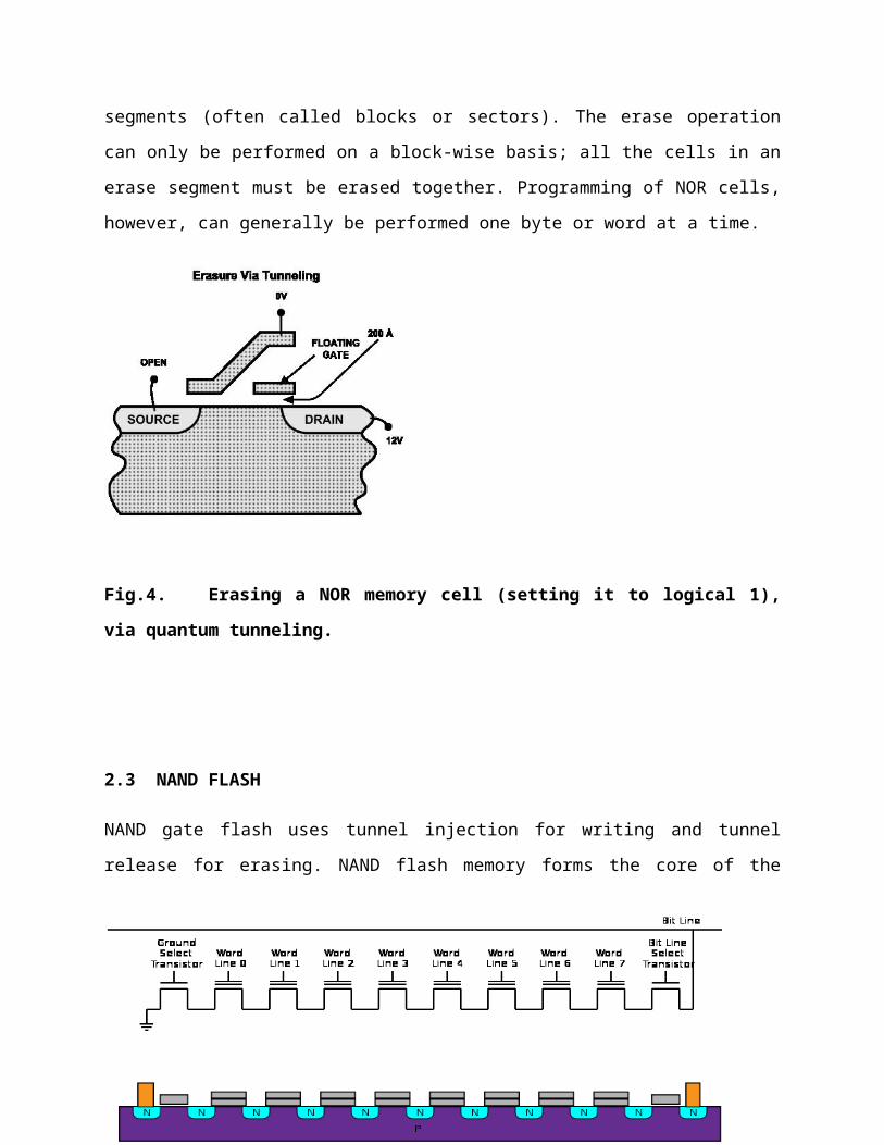
2.3 NAND FLASH
NAND gate flash uses tunnel injection for writing and tunnel release for erasing. NAND flash memory forms
the core of the removable USB storage devices known as USB flash drives and most memory card formats
available today.
Fig.5: NAND flash memory wiring and structure on silicon

3.0 LIMITATIONS
Flash memories also have their limitations. Such limitations are discussed under the following headings:
3.0.1 Block Erasure
One limitation of flash memory is that although it can be read or programmed a byte or a word at a time in a
random access fashion, it must be erased a "block" at a time. This generally sets all bits in the block to 1.
Starting with a freshly erased block, any location within that block can be programmed. However, once a bit
has been set to 0, only by erasing the entire block can it be changed back to 1. In other words, flash
memory (specifically NOR flash) offers random-access read and programming operations, but cannot offer
arbitrary random-access rewrite or erase operations. A location can, however, be rewritten as long as the
new value's 0 bits are a superset of the over-written value's. For example, a nibble value may be erased to
1111, then written as 1110. Successive writes to that nibble can change it to 1010, then 0010, and finally
0000. File systems built on NOR flash make use of this capability to represent sector metadata. Although
data structures in flash memory cannot be updated in completely general ways, this allows members to be
"removed" by marking them as invalid. This technique may need to be modified for multi-level devices,
where one memory cell holds more than one bit.
3.0.2 MEMORY WEAR
Another limitation is that flash memory has a finite number of erase-write cycles. Most commercially
available flash products are guaranteed to withstand around 100,000 write-erase-cycles, before the wear
begins to deteriorate the integrity of the storage. The guaranteed cycle count may apply only to block zero
(as is the case with TSOP NAND parts), or to all blocks (as in NOR). This effect is partially offset in some
chip firmware or file system drivers by counting the writes and dynamically remapping blocks in order to
spread write operations between sectors; this technique is called wear levelling. Another approach is to
perform write verification and remapping to spare sectors in case of write failure, a technique called bad
block management (BBM). For portable consumer devices, these wearout management techniques
typically extend the life of the flash memory beyond the life of the device itself, and some data loss may be
acceptable in these applications. For high reliability data storage, however, it is not advisable to use flash
memory that would have to go through a large number of programming cycles. This limitation is

meaningless for 'read-only' applications such as thin clients and routers, which are only programmed once
or at most a few times during their lifetime.
4.0 LOW-LEVEL ACCESS
The low-level interface to flash memory chips differs from those of other memory types such as DRAM,
ROM, and EEPROM, which support bit-alterability (both zero to one and one to zero) and random-access
via externally accessible address buses.
While NOR memory provides an external address bus for read and program operations (and thus supports
random-access); unlocking and erasing NOR memory must proceed on a block-by-block basis. With NAND
flash memory, read and programming operations must be performed page-at-a-time while unlocking and
erasing must happen in block-wise fashion.
4.1 NOR MEMORIES
Reading from NOR flash is similar to reading from random-access memory, provided the address and data
bus are mapped correctly. Because of this, most microprocessors can use NOR flash memory as execute
in place (XIP) memory, meaning that programs stored in NOR flash can be executed directly without the
need to first copy the program into RAM. NOR flash may be programmed in a random-access manner
similar to reading. Programming changes bits from a logical one to a zero. Bits that are already zero are left
unchanged. Erasure must happen a block at a time, and resets all the bits in the erased block back to one.
Typical block sizes are 64, 128, or 256 KB.
Bad block management is a relatively new feature in NOR chips. In older NOR devices not supporting bad
block management, the software or device driver controlling the memory chip must correct for blocks that
wear out, or the device will cease to work reliably.
The specific commands used to lock, unlock, program, or erase NOR memories differ for each
manufacturer. To avoid needing unique driver software for every device made a special set of CFI
commands allow the device to identify itself and its critical operating parameters.
Apart from being used as random-access ROM, NOR memories can also be used as storage devices by
taking advantage of random-access programming. Some devices offer read-while-write functionality so that
code continues to execute even while a program or erase operation is occurring in the background. For
sequential data writes, NOR flash chips typically have slow write speeds compared with NAND flash.
4.2 NAND MEMORIES
NAND flash architecture was introduced by Toshiba in 1989. These memories are accessed much like
block devices such as hard disks or memory cards. Each block consists of a number of pages. The pages
are typically 512[6] or 2,048 or 4,096 bytes in size. Associated with each page are a few bytes (typically
12–16 bytes) that should be used for storage of an error detection and correction checksum.
Typical block sizes include:
32 pages of 512 bytes each for a block size of 16 KB
64 pages of 2,048 bytes each for a block size of 128 KB
64 pages of 4,096 bytes each for a block size of 256 KB
128 pages of 4,096 bytes each for a block size of 512 KB
While reading and programming is performed on a page basis, erasure can only be performed on a block
basis. Another limitation of NAND flash is data in a block can only be written sequentially. Number of
Operations (NOPs) is the number of times the sectors can be programmed. So far this number for MLC
flash is always one whereas for SLC flash it is four.
NAND devices also require bad block management by the device driver software, or by a separate
controller chip. SD cards, for example, include controller circuitry to perform bad block management and
wear leveling. When a logical block is accessed by high-level software, it is mapped to a physical block by
the device driver or controller. A number of blocks on the flash chip may be set aside for storing mapping
tables to deal with bad blocks, or the system may simply check each block at power-up to create a bad
block map in RAM. The overall memory capacity gradually shrinks as more blocks are marked as bad.
NAND relies on ECC to compensate for bits that may spontaneously fail during normal device operation.
This ECC may correct as little as one bit error in each 2048 bits, or up to 22 bits in each 2048 bits.[7] If
ECC cannot correct the error during read, it may still detect the error. When doing erase or program
operations, the device can detect blocks that fail to program or erase and mark them bad. The data is then
written to a different, good block, and the bad block map is updated.

Most NAND devices are shipped from the factory with some bad blocks which are typically identified and
marked according to a specified bad block marking strategy. By allowing some bad blocks, the
manufacturers achieve far higher yields than would be possible if all blocks had to be verified good. This
significantly reduces NAND flash costs and only slightly decreases the storage capacity of the parts.
When executing software from NAND memories, virtual memory strategies are often used: memory
contents must first be paged or copied into memory-mapped RAM and executed there (leading to the
common combination of NAND + RAM). A memory management unit (MMU) in the system is helpful, but
this can also be accomplished with overlays. For this reason, some systems will use a combination of NOR
and NAND memories, where a smaller NOR memory is used as software ROM and a larger NAND memory
is partitioned with a file system for use as a nonvolatile data storage area.
NAND is best suited to systems requiring high capacity data storage. This type of flash architecture offers
higher densities and larger capacities at lower cost with faster erase, sequential write, and sequential read
speeds, sacrificing the random-access and execute in place advantage of the NOR architecture.
4.3 STANDARDIZATION
A group called the Open NAND Flash Interface Working Group (ONFI) has developed a standardized low-
level interface for NAND flash chips. This allows interoperability between conforming NAND devices from
different vendors. The ONFI specification version 1.0 was released on December 28, 2006. It specifies:
a standard physical interface (pinout) for NAND flash in TSOP-48, WSOP-48, LGA-52, and BGA-
63 packages
a standard command set for reading, writing, and erasing NAND flash chips
a mechanism for self-identification (comparable to the Serial Presence Detection feature of
SDRAM memory modules)
The ONFI group is supported by major NAND Flash manufacturers, including Hynix, Intel, Micron
Technology, and Numonyx, as well as by major manufacturers of devices incorporating NAND flash chips.
A group of vendors, including Intel, Dell, and Microsoft formed a Non-Volatile Memory Host Controller
Interface (NVMHCI) Working Group. The goal of the group is to provide standard software and hardware

programming interfaces for nonvolatile memory subsystems, including the "flash cache" device connected
to the PCI Express bus.
5.0 DISTINCTION BETWEEN NOR AND NAND FLASH
NOR and NAND flash differ in two important ways:
the connections of the individual memory cells are different
the interface provided for reading and writing the memory is different (NOR allows random-access
for reading, NAND allows only page access)
It is important to understand that these two are linked by the design choices made in the development of
NAND flash. An important goal of NAND flash development was to reduce the chip area required to
implement a given capacity of flash memory, and thereby to reduce cost per bit and increase maximum
chip capacity so that flash memory could compete with magnetic storage devices like hard disks.
NOR and NAND flash get their names from the structure of the interconnections between memory cells. In
NOR flash, cells are connected in parallel to the bit lines, allowing cells to be read and programmed
individually. The parallel connection of cells resembles the parallel connection of transistors in a CMOS
NOR gate. In NAND flash, cells are connected in series, resembling a NAND gate, and preventing cells
from being read and programmed individually: the cells connected in series must be read in series.
When NOR flash was developed, it was envisioned as a more economical and conveniently rewritable
ROM than contemporary EPROM, EAROM, and EEPROM memories. Thus random-access reading
circuitry was necessary. However, it was expected that NOR flash ROM would be read much more often
than written, so the write circuitry included was fairly slow and could only erase in a block-wise fashion;
random-access write circuitry would add to the complexity and cost unnecessarily.
Because of the series connection and removal of wordline contacts, a large grid of NAND flash memory
cells will occupy perhaps only 60% of the area of equivalent NOR cells (assuming the same CMOS process
resolution, e.g. 130 nm, 90 nm, 65 nm). NAND flash's designers realized that the area of a NAND chip, and
thus the cost, could be further reduced by removing the external address and data bus circuitry. Instead,
external devices could communicate with NAND flash via sequential-accessed command and data
registers, which would internally retrieve and output the necessary data. This design choice made random-

access of NAND flash memory impossible, but the goal of NAND flash was to replace hard disks, not to
replace ROMs.
5.1 WRITE ENDURANCE
The write endurance of SLC Floating Gate NOR flash is typically equal or greater than that of NAND flash,
while MLC NOR & NAND Flash have similar Endurance capabilities. Example Endurance cycle ratings
listed in datasheets for NAND and NOR Flash are provided.
SLC NAND Flash is typically rated at about 100K cycles (Samsung OneNAND KFW4G16Q2M)
MLC NAND Flash is typically rated at about 5K-10K cycles (Samsung K9G8G08U0M)
SLC Floating Gate NOR Flash has typical Endurance rating of 100K to 1,000K cycles (Numonyx
M58BW 100K; Spansion S29CD016J 1000K)
MLC Floating Gate NOR has typical Endurance rating of 100K cycles (Numonyx J3 Flash)
6.0 FLASH FILE SYSTEMS
Because of the particular characteristics of flash memory, it is best used with either a controller to perform
wear-leveling and error correction or specifically designed flash file systems, which spread writes over the
media and deal with the long erase times of NOR flash blocks. The basic concept behind flash file systems
is: When the flash store is to be updated, the file system will write a new copy of the changed data over to a
fresh block, remap the file pointers, and then erase the old block later when it has time.
In practice, flash file systems are only used for "Memory Technology Devices" ("MTD"), which are
embedded flash memories that do not have a controller. Removable flash memory cards and USB flash
drives have built-in controllers to perform wear-levelling and error correction so use of a specific flash file
system does not add any benefit. These removable flash memory devices use the FAT file system to allow
universal compatibility with computers, cameras, PDAs and other portable devices with memory card slots
or ports.
7.0 CAPACITIES

Multiple chips are often arrayed to achieve higher capacities for use in consumer electronic devices such
as multimedia players or GPS. The capacity of flash chips generally follows Moore's Law because they are
manufactured with many of the same integrated circuits techniques and equipment.
Consumer flash drives typically have sizes measured in powers of two (e.g. 512 MB, 8 GB). This includes
SSDs as hard drive replacements, even though traditional hard drives tend to use decimal units. Thus, a 64
GB SSD is actually 64 × 10243 bytes. In reality, most users will have slightly less capacity than this
available, due to the space taken by file system metadata.
In 2005, Toshiba and SanDisk developed a NAND flash chip capable of storing 1 GB of data using Multi-
level Cell (MLC) technology, capable of storing 2 bits of data per cell. In September 2005, Samsung
Electronics announced that it had developed the world’s first 2 GB chip.
In March 2006, Samsung announced flash hard drives with a capacity of 4 GB, essentially the same order
of magnitude as smaller laptop hard drives, and in September 2006, Samsung announced an 8 GB chip
produced using a 40 nanometer manufacturing process.
In January 2008 Sandisk announced availability of their 16 GB MicroSDHC and 32 GB SDHC Plus cards.
But there are still flash-chips manufactured with low capacities like 1 MB, e.g., for BIOS-ROMs.
8.0 TRANSFER RATES
Commonly advertised is the maximum read speed, NAND flash memory cards are much faster at reading
than writing. As a chip gets worn out, its erase/program operations slow down considerably, requiring more
retries and bad block remapping. Transferring multiple small files, smaller than the chip specific block size,
could lead to much lower rate. Access latency has an influence on performance but is less of an issue than
with their hard drive counterpart.
The speed is sometimes quoted in MB/s (megabytes per second), or as a multiple of that of a legacy single
speed CD-ROM, such as 60x, 100x or 150x. Here 1x is equivalent to 150 kilobytes per second. For
example, a 100x memory card gives 150 KB x 100 = 15,000 KB/s = 14.65 MB/s.
9.0 APPLICATIONS
Flash memories have various applications. Some applications are explained in details below:

9.0.1 Serial flash
Serial flash is a small, low-power flash memory that uses a serial interface, typically SPI, for sequential data
access. When incorporated into an embedded system, serial flash requires fewer wires on the PCB than
parallel flash memories, since it transmits and receives data one bit at a time. This may permit a reduction
in board space, power consumption, and total system cost.
There are several reasons why a serial device, with fewer external pins than a parallel device, can
significantly reduce overall cost:
Many ASICs are pad-limited, meaning that the size of the die is constrained by the number of wire bond
pads, rather than the complexity and number of gates used for the device logic. Eliminating bond pads thus
permits a more compact integrated circuit, on a smaller die; this increases the number of dies that may be
fabricated on a wafer, and thus reduces the cost per die.
Reducing the number of external pins also reduces assembly and packaging costs. A serial device may be
packaged in a smaller and simpler package than a parallel device.
Smaller and lower pin-count packages occupy reduced PCB area.
Lower pin-count devices simplify PCB routing.
9.0.2 Firmware storage
With the increasing speed of modern CPUs, parallel flash devices are often much slower than the memory
bus of the computer they are connected to. Conversely, modern SRAM offers access times below 10 ns,
while DDR2 SDRAM offers access times below 20 ns. Because of this, it is often desirable to shadow code
stored in flash into RAM; that is, the code is copied from flash into RAM before execution, so that the CPU
may access it at full speed. Device firmware may be stored in a serial flash device, and then copied into
SDRAM or SRAM when the device is powered-up. Using an external serial flash device rather than on-chip
flash removes the need for significant process compromise (a process that is good for high speed logic is
generally not good for flash and vice-versa). Once it is decided to read the firmware in as one big block it is
common to add compression to allow a smaller flash chip to be used. Typical applications for serial flash
include storing firmware for hard drives, Ethernet controllers, DSL modems, wireless network devices, etc.
9.0.3 Flash memory as a replacement for hard drives

An obvious extension of flash memory would be as a replacement for hard disks. Flash memory does not
have the mechanical limitations and latencies of hard drives, so the idea of a solid-state drive, or SSD, is
attractive when considering speed, noise, power consumption, and reliability.
There remain some aspects of flash-based SSDs that make the idea unattractive. Most important, the cost
per gigabyte of flash memory remains significantly higher than that of platter-based hard drives. Although
this ratio is decreasing rapidly for flash memory, it is not yet clear that flash memory will catch up to the
capacities and affordability offered by platter-based storage. Still, research and development is sufficiently
vigorous that it is not clear that it will not happen, either.
There is also some concern that the finite number of erase/write cycles of flash memory would render flash
memory unable to support an operating system. This seems to be a decreasing issue as warranties on
flash-based SSDs are approaching those of current hard drives.
As of May 24, 2006, South Korean consumer-electronics manufacturer Samsung Electronics had released
the first flash-memory based PCs, the Q1-SSD and Q30-SSD, both of which have 32 GB SSDs. Dell
Computer introduced the Latitude D430 laptop with 32 GB flash-memory storage in July 2007 -- at a price
significantly above a hard-drive equipped version.
At the Las Vegas CES 2007 Summit Taiwanese memory company A-DATA showcased SSD hard disk
drives based on Flash technology in capacities of 32 GB, 64 GB and 128 GB. Sandisk announced an OEM
32 GB 1.8" SSD drive at CES 2007. The XO-1, developed by the One Laptop Per Child (OLPC)
association, uses flash memory rather than a hard drive. As of June 2007, a South Korean company called
Mtron claims the fastest SSD with sequential read/write speeds of 100 MB/80 MB per second.
Rather than entirely replacing the hard drive, hybrid techniques such as hybrid drive and ReadyBoost
attempt to combine the advantages of both technologies, using flash as a high-speed cache for files on the
disk that are often referenced, but rarely modified, such as application and operating system executable
files. Also, Addonics has a PCI adapter for 4 CF cards, creating a RAID-able array of solid-state storage
that is much cheaper than the hardwired-chips PCI card kind.
The ASUS Eee PC uses a flash-based SSD of 2 GB to 20 GB, depending on model. The Apple Inc.
Macbook Air has the option to upgrade the standard hard drive to a 128 GB Solid State hard drive. The
Lenovo ThinkPad X300 also features a built-in 64 GB Solid State Drive.

Sharkoon has devoloped a device that uses six SDHC cards in RAID-0 as an SSD alternative; users may
use more affordable High-Speed 8GB SDHC cards to get similar or better results than can be obtained
from traditional SSDs at a lower cost.
10.0 MEMORY CARD
A memory card or flash memory card is a solid-state electronic flash memory data storage device used with
digital cameras, handheld and Mobile computers, telephones, music players, video game consoles, and
other electronics. They offer high re-record-ability, power-free storage, small form factor, and rugged
environmental specifications. There are also non-solid-state memory cards that do not use flash memory,
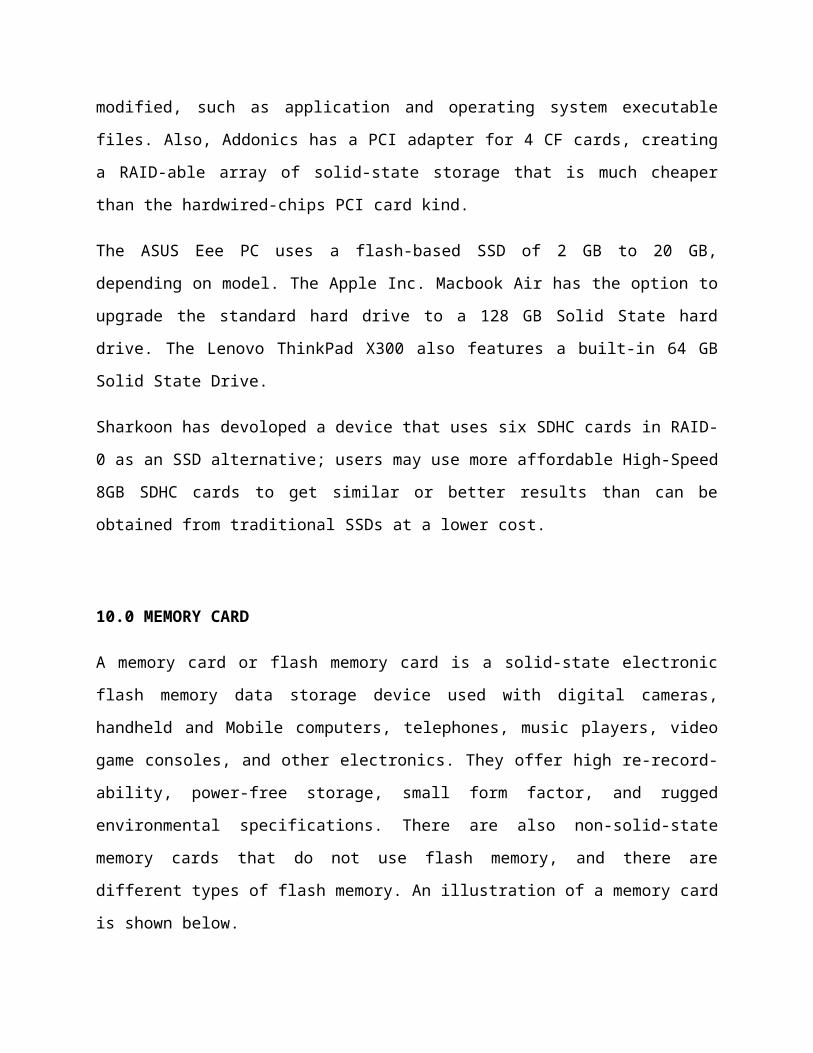
and there are different types of flash memory. An illustration of a memory card is shown below.
Fig.6: Memory Card features
There are many different types of memory cards and jobs they are used for. Some common places include
in digital cameras, game consoles, cell phones, and industrial applications. PC card (PCMCIA) were among
first commercial memory card formats (type I cards) to come out in the 1990s, but are now only mainly
used in industrial applications and for I/O jobs (using types I/II/III), as a connection standard for devices
(such as a modem). Also in 1990s, a number of memory card formats smaller than PC Card came out,
including CompactFlash, SmartMedia, and Miniature Card. In other areas, tiny embedded memory cards
(SID) were used in cell phones, game consoles started using proprietary memory card formats, and
devices like PDAs and digital music players started using removable memory cards.

Fig.7: Miniaturization is evident in memory card creation; over time, the physical sizes of the
memory cards grow smaller while their respective logical sizes grow larger. The memory cards
listed from left to right are: Compact flash (32 MB), SD (128 MB), miniSD (1.0 GB), and microSD (2.0
GB).
From the late 1990s into the early 2000s a host of new formats appeared, including SD/MMC, Memory
Stick, xD-Picture Card, and a number of variants and smaller cards. The desire for ultra-small cards for cell-
phones, PDAs, and compact digital cameras drove a trend toward smaller cards that left the previous
generation of "compact" cards looking big. In digital cameras SmartMedia and CompactFlash had been
very successful, in 2001 SM alone captured 50% of the digital camera market and CF had a strangle hold
on professional digital cameras. By 2005 however, SD/MMC had nearly taken over SmartMedia's spot,
though not to the same level and with stiff competition coming from Memory Stick variants, xD, as well as
CompactFlash. In industrial fields, even the venerable PC card (PCMCIA) memory cards still manage to
maintain a niche, while in cell-phones and PDAs, the memory card market is highly fragmented.
Nowadays, most new PCs have built-in slots for a variety of memory cards; Memory Stick, CompactFlash,
SD, etc. Some digital gadgets support more than one memory card to ensure compatibility.
10.0.1 OVERVIEW OF ALL MEMORY CARD TYPES
PCMCIA ATA Type I Flash Memory Card (PC Card ATA Type I) (max 8 GB (8 GiB) flash as of
2005)
PCMCIA Linear Flash Cards, SRAM cards, etc.
PCMCIA Type II, Type III cards
CompactFlash Card (Type I), CompactFlash High-Speed (max 32 GB as of 2008)

CompactFlash Type II, CF+(CF2.0), CF3.0
Microdrive (max 6 GB as of 2005)
MiniCard (Miniature Card) (max 64 MB (64 MiB))
SmartMedia Card (SSFDC) (max 128 MB) (3.3 V,5 V)
xD-Picture Card, xD-Picture Card Type M
Memory Stick, MagicGate Memory Stick (max 128 MB); Memory Stick Select, MagicGate Memory
Stick Select ("Select" means: 2x128 MB with A/B switch)
SecureMMC
Secure Digital (SD Card), Secure Digital High-Speed, Secure Digital Plus/Xtra/etc (SD with USB
connector)
miniSD Card
microSD Card (aka Transflash, T-Flash)
SDHC
MU-Flash (Mu-Card) (Mu-Card Alliance of OMIA)
C-Flash
SIM card (Subscriber Identity Module)
Smart card (ISO 7810 Card Standard , ISO 7816 Card Standard, etc.)
UFC (USB FlashCard) [1] (uses USB)
FISH Universal Transportable Memory Card Standard (uses USB)
Disk memory cards:
Clik! (PocketZip), (40 MB PocketZip)
Floppy disk (LS120, 2-inch, 3.5-inch, etc.)
Intelligent Stick (iStick, a USB-based flash memory card with MMS)
SxS (S-by-S) memory card, a new memory card specification developed by Sandisk and Sony.
SxS complies to the ExpressCard industry standard. [2]
Nexflash Winbond Serial Flash Moduel (SFM) cards, size range 1 mb, 2 mb and 4 mb.
10.1 COMPACT FLASH
CompactFlash (CF) is a mass storage device format used in portable electronic devices. For storage,
CompactFlash typically uses flash memory in a standardized enclosure.
The format was first specified and produced by SanDisk in 1994. The physical format is now used for a
variety of devices.
CompactFlash became a popular storage medium for digital cameras. In recent years it has been widely
replaced by smaller cards on the consumer end, but it is still a preferred format for D-SLR cameras, for its
superior capacity and reliability.
Fig.8: A 64 MB CompactFlash Type I card
Media type Mass storage device format
Encoding Various file systems
Capacity 2 MB to 100 GB
Developed by SanDisk
Dimensions 43×36×3.3mm (Type I) 43×36×5 mm (Type II)
Weight 10 grammes (typical)
Usage Digital cameras and other mass storage devices
Extended from PCMCIA / PC Card
10.2 MICRODRIVE
The Microdrive is a brand name for a miniature, 1-inch hard disk designed to fit in a CompactFlash (CF)
Type II slot. The release of similar drives by other makers has led to them often being referred to as
'microdrives'. However, 'microdrive' is not a genericized trademark and manufacturers other than IBM up to
2003 and Hitachi after do not officially refer to these drives as Microdrives. Some other companies such as
Sony have licensed the name and sell re-branded versions, others such as Seagate have their own
designs which fit in the same form factor.
Fig.9: IBM 1 GB Microdrive
These drives fit into any CompactFlash II slot; however, they may consume more power than flash memory
(currents on the order of 190 mA, peak 310 mA, at 3.3 V) and therefore may not work in some low-power
devices (e.g. handheld computers). Nevertheless, they have some benefits over flash memory in terms of
the way data is stored and manipulated. Microdrives can store 8 GB or more, but must be formatted for a
file system which supports this capacity, such as ext3 or NTFS which might not be supported by older
CompactFlash hosts. To avoid this problem, the operating system may partition a drive so that each file
system is smaller than 4 GB.
10.3 MINIATURE CARDS
Miniature Card or MiniCard is a flash or DRAM memory card standard first promoted by Intel Corp. in 1995
and backed by Advanced Micro Devices, Fujitsu and Sharp Electronics. Miniature Card Implementers
Forum (MCIF) promoted this standard for consumer electronics: PDA/Palmtops, Digital Audio Recorders,

Digital Cameras and smart phones. The Miniature Card is 37 x 45 x 3.5 mm thick and can have devices on
both sides of the substrate. 60-pin connector was a memory-only subset of PCMCIA and featured 16-bit
data and 24-bit address bus with 3.3 or 5 volt signalling. Miniature Card supports Attribute Information
Structure (AIS) in the I²C identification EEPROM. The Miniature Card format competed with SmartMedia
and CompactFlash cards, also released during the mid-1990s. Although they were all significantly smaller
than Type I PC Cards, the CompactFlash and SmartMedia cards were more successful in the consumer
electronics market.
Fig.10: Miniature Card
10.4 MULTIMEDIA CARD
The MultiMedia Card (MMC) is a flash memory memory card standard. Unveiled in 1997 by Siemens AG
and SanDisk, it is based on Toshiba's NAND-based flash memory, and is therefore much smaller than
earlier systems based on Intel NOR-based memory such as CompactFlash. MMC is about the size of a
postage stamp: 24 mm x 32 mm x 1.4 mm. MMC originally used a 1-bit serial interface, but newer versions
of the specification allow transfers of 4 or sometimes even 8 bits at a time. They have been more or less
superseded by Secure Digital cards (SD card), but still see significant use because MMCs can be used in
most devices which support SD cards.

Fig.11: A 32Mb MultiMedia Card
Typically, an MMC is used as storage media for a portable device, in a form that can easily be removed for
access by a PC. For example, a digital camera would use an MMC for storing image files. With an MMC
reader (typically a small box that connects via USB or some other serial connection, although some can be
found integrated into the computer itself), a user could copy the pictures taken with the digital camera off to
his or her computer. Modern computers, both laptops and desktops, often have SD slots, which can
additionally read MMCs if the operating system drivers support them.
MMCs are currently available in sizes up to and including 4 GB with 8 GB models announced but not yet
available. They are used in almost every context in which memory cards are used, like cellular phones,
digital audio players, digital cameras and PDAs. Since the introduction of Secure Digital card and SDIO
(Secure Digital Input/Output) slot few companies build MMC slots into their devices (an exception is some
mobile devices like the Nokia 9300 communicator, where the smaller size of the MMC is a benefit), but the
slightly thinner, pin-compatible MMCs can be used in almost any device that supports SD cards if the
software/firmware on the devices support them.
10.5 SECURE DIGITAL CARD
Secure Digital (SD) is a non-volatile memory card format developed by Matsushita, SanDisk, and Toshiba
for use in portable devices. Today it is widely used in digital cameras, handheld computers, PDAs, Media
Players, mobile phones, GPS receivers, and video game consoles. Standard SD card capacities range
from 4 MB to 4 GB, and for high capacity SDHC cards from 4 GB to 32 GB as of 2008. The SDXC
(eXtended Capacity), a new specification announced at the 2009 CES, will allow for 2 TB capacity cards.
The format has proven to be very popular. A change in the format, however, while allowing capacities
greater than 4 GB (SDHC), has created compatibility issues with older devices that cannot read the new
format. The fact that SDHC format cards have the same physical shape and form factor as the older format
has caused considerable confusion for consumers. SDHC cards require SDHC-capable device firmware
generally not found with older devices.
SD cards are based on the older MultiMediaCard (MMC) format, but have a number of differences:

The SD card is asymmetrically shaped in order not to be inserted upside down, while an MMC
would go in most of the way but not make contact if inverted.
Most SD cards are physically thicker than MMCs. SD cards generally measure 32 mm × 24 mm ×
2.1 mm, but as with MMCs can be as thin as 1.4 mm.
The card's electrical contacts are recessed beneath the surface of the card, protecting them from
contact with a user's fingers.
SD cards typically have transfer rates in the range of 10-20 MB/s, but this number is subject to
change, due to recent improvements to the MMC standard.
Devices with SD slots can use the thinner MMCs, but standard SD cards will not fit into the thinner MMC
slots. miniSD and microSD cards can be used directly in SD slots with a simple passive adapter, since the
cards differ in size and shape but not electrical interface. With an active electronic adapter, SD cards can
be used in CompactFlash or PC card slots. Some SD cards include a USB connector for compatibility with
desktop and laptop computers, and card readers allow SD cards to be accessed via connectivity ports such
as USB, FireWire, and the parallel printer port. SD cards can also be accessed via a floppy disk drive with a
FlashPath adapter.
Fig.12: An SD card, mini SD card, and micro SD card from top to bottom.

10.6 SmartMedia Card
SmartMedia is a flash memory card standard owned by Toshiba, with capacities ranging from 0.5 MB to
128 MB. SmartMedia memory cards are no longer manufactured, and there have been no new devices
designed for use with SmartMedia for many years. The SmartMedia format was launched in the summer of
1995[citation needed] to compete with the MiniCard, CompactFlash, and PC card formats[citation needed].
Although memory cards are nowadays associated with digital cameras, digital audio players, PDAs, and
similar devices, SmartMedia was pitched as a successor to the computer floppy disk. Indeed, the format
was originally named Solid State Floppy Disk Card (SSFDC). The SSFDC forum, a consortium aiming to
promote SSFDC as an industry standard, was founded in April 1996, consisting of 37 initial members.
A SmartMedia card consists of a single NAND flash chip embedded in a thin plastic card,although some
higher capacity cards contain multiple, linked chips. It was one of the smallest and thinnest of the early
memory cards, only 0.76mm thick, and managed to maintain a favorable cost ratio as compared to the
others. SmartMedia cards lack a built-in controller chip, which kept the cost down. This feature later caused
problems, since some older devices would require firmware updates to handle larger capacity cards. The
lack of built-in controller also made it impossible for the card to perform automatic wear levelling, a process
which prevents premature wearout of a sector by mapping the writes to various other sectors in the card.
SmartMedia cards can be used in a standard 3.5" floppy drive by means of a FlashPath adapter. This is
possibly the only way of obtaining flash memory functionality with very old hardware, and it remains one of
SmartMedia's most distinctive features. This method's big drawback is that it is very slow. Read/write is
limited to floppy disk speeds, meaning that copying 64 megabytes of data by this method is a very tedious
process, although usually preferable to not copying it at all.
A 32MB SmartMedia flash memory card (on keyboard for scale)
Typically, SmartMedia cards were used as storage for portable devices, in a form that could easily be
removed for access by a PC. For example, pictures taken with a digital camera would be stored as image
files on a SmartMedia card. A user could copy the images to a computer with a SmartMedia reader. A
reader was typically a small box connected via USB or some other serial connection. Modern computers,
both laptops and desktops, will occasionally have SmartMedia slots built in. While availability of dedicated
SmartMedia readers has dropped off, readers that read multiple card types (such as 4-in-1, 10-in-1)
continue to include the format.

SmartMedia was popular in digital cameras, and reached its peak in about 2001 when it garnered nearly
half of the digital camera market. It was backed especially by Fujifilm and Olympus,[citation needed] though
the format started to exhibit problems as camera resolutions increased. Cards larger than 128 MB were not
available, and the compact digital cameras were reaching a size where even SmartMedia cards were too
big to be convenient. Eventually Toshiba switched to smaller, higher-capacity Secure Digital cards, and
SmartMedia ceased to have major support after Olympus and Fujifilm both switched to xD]. It did not find
as much support in PDAs, MP3 Players, or Pagers as some other formats, especially in North America and
Europe, though there was still significant use.
SmartMedia cards larger than 128 MB were never released, although there were rumors of a 256MB card
being planned. Technical specifications for the memory size were released, and the 256 MB cards were
even advertised in some places. Some older devices cannot support cards larger than 16 or sometimes 32
MB without a firmware update, if at all. Smartmedia is a textbook case of shortsighted design priorities; its
128 megabyte capacity successfully beat that of a floppy disk, in a smaller space, but not by a sufficient
amount to overwhelm competing memory card formats. Compared to the CompactFlash card, SmartMedia
cards were small, or at least thin, but unfortunately had none of CF's capacity and flexibility.
Fig. 13: A radiograph of SmartMedia card.
SmartMedia cards came in two formats, 5 V and the more modern 3.3 V (sometimes marked 3 V), named
for their main supply voltages. The packaging was nearly identical, except for the reversed placement of
the notched corner. Many older SmartMedia devices only support 5V SmartMedia cards, whereas many
newer devices only support 3.3V cards. In order to protect 3.3V cards from being damaged in 5V-only
devices, the card reader should have some mechanical provision (such as detecting the type of notch) to
disallow insertion of an unsupported type of card. Some low-cost, 5V-only card readers do not operate this
way, and inserting a 3.3V card into such a 5V-only reader will result in permanent damage to the card.
Dual-voltage card readers are highly recommended.
SmartMedia memory cards are no longer manufactured. There have been no new devices designed for
SmartMedia for quite a long time now. Old stocks of new 128MB cards can be obtained from specialist
suppliers while their supplies last.
10.7 FLASH DRIVES (THUMB DRIVES)
USB flash drives are NAND-type flash memory data storage devices integrated with a USB (universal serial
bus) interface. They are typically small, lightweight, removable and rewritable. As of April 2007, memory
capacities for USB Flash Drives currently are sold from 32 megabytes up to 64 gigabytes [1]. Capacity is
limited only by current flash memory densities, although cost per megabyte may increase rapidly at higher
capacities due to the expensive components. (USB Memory card readers are also available, whereby
rather than being built-in, the memory is a removable Flash memory card housed in what is otherwise a
regular USB flash drive, as described below.)
USB flash drives offer potential advantages over other portable storage devices, particularly the floppy disk.
They are more compact, generally faster, hold more data, and are more reliable (due to both their lack of
moving parts, and their more durable design) than floppy disks. These types of drives use the USB mass
storage standard, supported natively by modern operating systems such as Windows, Mac OS X, Linux,
and Unix.
A flash drive consists of a small printed circuit board typically in a plastic or metal casing, making the drive
sturdy enough to be carried about in a pocket, as a key fob, or on a lanyard. Only the USB connector
protrudes from this protection, and is usually covered by a removable cap. Most flash drives use a standard
type-A USB connection allowing them to be connected directly to a port on a personal computer.
To access the data stored in a flash drive, the drive must be connected to a computer, either by plugging it
into a USB host controller built into the computer, or into a USB hub. Flash drives are active only when
plugged into a USB connection and draw all necessary power from the supply provided by that connection.
However, some flash drives, especially high-speed drives, may require more power than the limited amount
provided by a bus-powered USB hub, such as those built into some computer keyboards or monitors.
These drives will not work unless plugged directly into a host controller (i.e., the ports found on the
computer itself) or a self-powered hub.
Several companies claim to be the first to have invented the USB Flash Drive. Trek was the first company
to sell a USB Flash Drive (ThumbDrive) in early 2000. However, their patent does not describe the USB
Flash Drive; it describes a very broad family of storage devices which could include the USB Flash Drive.
Modern flash drives have USB 2.0 connectivity. However, they do not currently use the full 480 Mbit/s the
specification supports due to technical limitations inherent in NAND flash. The fastest drives currently
available use a dual channel controller, although they still fall considerably short of the transfer rate
possible from a current generation hard disk, or the maximum high speed USB throughput.
Typical overall file transfer speeds are about 3 Mbytes/s. The highest current overall file transfer speeds
are about 10-30 Mbytes/s. Older, "full speed" 12 Mbit/s devices are limited to a maximum of about 1
Mbytes/s.
One end of the device is fitted with a single male type-A USB connector. Inside the plastic casing is a small
printed circuit board. Mounted on this board is some simple power circuitry and a small number of surface-
mounted integrated circuits (ICs). Typically, one of these ICs provides an interface to the USB port, another
drives the onboard memory, and the other is the flash memory.
There are typically four parts to a flash drive:
Male type-A USB connector — provides an interface to the host computer.
USB mass storage controller — implements the USB host controller and provides a linear interface
to block-oriented serial flash devices while hiding the complexities of block-orientation, block
erasure, and wear levelling, or wear balancing. The controller contains a small RISC
microprocessor and a small amount of on-chip ROM and RAM.
NAND flash memory chip — stores data. NAND flash is typically also used in digital cameras.
Crystal oscillator — produces the device's main 12 MHz clock signal and controls the device's data
output through a phase-locked loop.
The typical device may also include:
Jumpers and test pins — for testing during the flash drive's manufacturing or loading code into the
microprocessor.

LEDs — indicate data transfers or data reads and writes.
Write-protect switches — indicate whether the device should be in "write-protection" mode.
Unpopulated space — provides space to include a second memory chip. Having this second space
allows the manufacturer to develop only one printed circuit board that can be used for more than
one storage size device, to meet the needs of the market.
USB connector cover or cap — reduces the risk of damage due to static electricity, and improves
overall device appearance. Some flash drives do not feature a cap, but instead have retractable
USB connectors. Other flash drives have a "swivel" cap that is permanently connected to the drive
itself and eliminates the chance of losing the cap.
Transport aid — In some cases, the cap or the main body contains a hole suitable for connection to
a key chain or lanyard or to otherwise aid transport and storage of the USB flash device.
This is illustrated in fig.14 below.
Fig.14 Internals of a typical flash drive (Saitek brand USB1.1 pictured)
1 USB connector
2 USB mass storage controller device
3 Test points

4 Flash memory chip
5 Crystal oscillator
6 LED
7 Write-protect switch
8 Space for second flash memory chip
10.7.1 COMMON USES
System administration
Flash drives are particularly popular among system and network administrators, who load them with
configuration information and software used for system maintenance, troubleshooting, and recovery.
Computer repair
Flash drives enjoy notable success in the PC repair field as a means to transfer recovery and antivirus
software to infected PCs, while allowing a portion of the host machine's data to be archived in case of
emergency.
Application carriers
Flash drives are used to carry applications that run on the host computer without requiring installation. U3,
backed by flash drive vendors, offers an API to flash drive-specific functions. A free and open-source
software platform known as Portable apps has also been developed to allow U3-like functionality on non-
U3 drives. airWRX is an application framework that runs from a flash drive and turns its PC host and other
nearby PCs into a multi-screen, web-like work environment. pocketSAN is a portable iSCSI framework that
runs from a flash drive and turns its PC host into a full-featured SAN appliance. The Mozilla Firefox browser
has a configuration for flash drives, as does Opera.
10.8 Flash Scalability
Due to its relatively simple structure and high demand for higher capacity, NAND Flash memory is the most
aggressively scaled technology among electronic devices. The heavy competition among the top few

manufacturers only adds to the aggression. Current projections show the technology to reach
approximately 20 nm by around 2010. While the expected shrink timeline is a factor of two every three
years per original version of Moore's law, this has recently been accelerated in the case of NAND flash to a
factor of two every two years.
As the feature size of Flash memory cells reach the minimum limit (currently estimated ~20 nm), further
Flash density increases will be driven by greater levels of MLC, possibly 3-D stacking of transistors, and
process improvements. Even with these advances, it may be impossible to economically scale Flash to
smaller and smaller dimensions. Many promising new technologies (such as FeRAM, MRAM, PMC, PCM,
and others) are under investigation and development as possible more scalable replacements for Flash.

11.0 Summary
Flash memory is a particularly important form of semiconductor memory. It is now widely used and is
possibly one of the most important forms of medium term storage. As mentioned earlier Flash memory can
be seen in a variety of forms and uses ranging from Flash memory USB sticks to Compact Flash cards
used for cameras. In addition to this many other items of electronics can be seen using Flash memory
ranging from mobile phones to MP3 players and many more. In view of its current importance, Flash
memory will be seen in widespread use for many years to come.
Related Documents