SEMINAR REPORT On PROTEIN BASED OPTICAL MEMORY Submitted by ANUJ KUMAR in partial fulfillment for the award of the degree of BACHELOR OF TECHNOLOGY in COMPUTER SCIENCE & ENGINEERING SCHOOL OF ENGINEERING COCHIN UNIVERSITY OF SCIENCE AND TECHNOLOGY, KOCHI – 682022 SEPTEMBER 2008

Welcome message from author
This document is posted to help you gain knowledge. Please leave a comment to let me know what you think about it! Share it to your friends and learn new things together.
Transcript
SEMINAR REPORT
On
PROTEIN BASED OPTICAL MEMORYSubmitted by
ANUJ KUMAR
in partial fulfillment for the award of the degree
of
BACHELOR OF TECHNOLOGY
in
COMPUTER SCIENCE & ENGINEERING
SCHOOL OF ENGINEERING
COCHIN UNIVERSITY OF SCIENCE AND TECHNOLOGY,
KOCHI – 682022
SEPTEMBER 2008

DIVISION OF COMPUTER SCIENCE & ENGINEERING
SCHOOL OF ENGINEERING
COCHIN UNIVERSITY OF SCIENCE & TECHNOLOGY,
KOCHI – 682022
Certificate
This is to certify that the seminar report entitled “PROTEIN BASED
OPTICAL MEMORY” submitted by ANUJ KUMAR, semester VII, in
partial fulfillment of the requirement of the award of B-Tech degree in
COMPUTER SCIENCE AND ENGINEERING, Cochin University of
Science and Technology, is a bonafide record of the seminar presented by him
during the academic year 2008.
.
Ms. Ancy Zachariah Seminar Guide
Mr. David Peter S Head of the Department
Place: KochiDate:
Acknowledgement
At the outset, we thank God almighty for making our endeavor a success. We also express
our gratitude to Dr. David Peter, Head of the Department, Division of Computer
Engineering for providing us with adequate facilities, ways and means by which we were
able to complete this seminar.
We express our sincere gratitude to our Seminar Guide Ms. Ancy Zachariah, Lecturer,
Division of Computer Engineering for her constant support and valuable suggestions without
which the successful completion of this seminar would not have been possible.
We express our immense pleasure and thankfulness to all the teachers and staff of the
Department of Computer Engineering, CUSAT for their cooperation and support.
Last but not the least, we thank all others, and especially our classmates and our family
members who in one way or another helped us in the successful completion of this work.
ANUJ KUMAR

Table Of Contents
CHAPTER No. TITLE PAGE NO.
Abstract vi List Of Figures v
1 Introduction 1
2 Memory Research and Development 4
2.1 Semiconductor Memory Developments 6
2.2 3 – D Optical Memories 6
3 Protein – Based Memory 8
3.1 Development 8
3.2 Process of Protein Extraction 12
3.3 BacterioRhodopsin Photocycle 13
3.4 Data operation 16
3.4.1 Data – Writing Technique 16
3.4.2 Data – Reading Technique 18
3.4.3 Data Erasing 19
3.4.4 Refreshing the Memory 19
4 Intrinsic Worth 21
5 Conclusion 22
6 References 23
iv
List of Figures
Figure No. Title Page No.
3.3.1 This is the chromophore 17
3.3.2 The photocycle for computer memory 20
3.4.1 The write process 22
3.4.2 The read process 23
3.5 Actual Implementation 25
v

Abstract
While magnetic and semi-conductor based information storage devices have been in use
since the middle 1950's, today's computers and volumes of information require
increasingly more efficient and faster methods of storing data. While the speed of
integrated circuit random access memory (RAM) has increased steadily over the past ten
to fifteen years, the limits of these systems are rapidly approaching. In response to the
rapidly changing face of computing and demand for
• physically smaller,
• greater capacity,
• bandwidth,
A number of alternative methods to integrated circuit information storage have surfaced
recently. Among the most promising of the new alternatives are
• photopolymer-based devices,
• holographic optical memory storage devices, and
• protein-based optical memory storage using rhodopsin ,
• Photosynthetic reaction centers, cytochrome c, photosystems I and II,
phycobiliproteins, and phytochrome.
This article focuses mainly on protein-based optical memory storage using the
photosensitive protein bacteriorhodopsin with the two-photon method of exciting the
molecules, but briefly describes what is involved in the other two. Bacteriorhodopsin is a
light-harvesting protein from bacteria that live in salt marshes that has shown some
promise as feasible optical data storage. The current work is to hybridize this biological
molecule with the solid state components of a typical computer.
vi
Protein Based Optical Memory
1. Introduction
Since the dawn of time, man has tried to record important events and techniques for
everyday life. At first, it was sufficient to paint on the family cave wall how one
hunted. Then came the people who invented spoken languages and the need arose to
record what one was saying without hearing it firsthand. Therefore, years later, earlier
scholars invented writing to convey what was being said. Pictures gave way to letters
which represented spoken sounds. Eventually clay tablets gave way to parchment,
which gave way to paper. Paper was, and still is, the main way people convey
information. However, in the mid twentieth century computers began to come into
general use . . .
Computers have gone through their own evolution in storage media. In the
forties, fifties, and sixties, everyone who took a computer course used punched cards
to give the computer information and store data. In 1956, researchers at IBM
developed the first disk storage system. This was called RAMAC (Random Access
Method of Accounting and Control)
Since the days of punch cards, computer manufacturers have strived to
squeeze more data into smaller spaces. That mission has produced both competing
and complementary data storage technology including electronic circuits, magnetic
media like hard disks and tape, and optical media such as compact disks.
Today, companies constantly push the limits of these technologies to improve
their speed, reliability, and throughput -- all while reducing cost. The fastest and most
expensive storage technology today is based on electronic storage in a circuit such as
a solid state "disk drive" or flash RAM. This technology is getting faster and is able to
store more information thanks to improved circuit manufacturing techniques that
shrink the sizes of the chip features. Plans are underway for putting up to a gigabyte
of data onto a single chip.
Department of Computer Engineering
1

Protein Based Optical Memory
Magnetic storage technologies used for most computer hard disks are the most
common and provide the best value for fast access to a large storage space. At the low
end, disk drives cost as little as 25 cents per megabyte and provide access time to data
in ten milliseconds. Drives can be ganged to improve reliability or throughput in a
Redundant Array of Inexpensive Disks (RAID). Magnetic tape is somewhat slower
than disk, but it is significantly cheaper per megabyte. At the high end, manufacturers
are starting to ship tapes that hold 40 gigabytes of data. These can be arrayed together
into a Redundant Array of Inexpensive Tapes (RAIT), if the throughput needs to be
increased beyond the capability of one drive.
For randomly accessible removable storage, manufacturers are beginning to
ship low-cost cartridges that combine the speed and random access of a hard drive
with the low cost of tape. These drives can store from 100 megabytes to more than
one gigabyte per cartridge.
Standard compact disks are also gaining a reputation as an incredibly cheap
way of delivering data to desktops. They are the cheapest distribution medium around
when purchased in large quantities ($1 per 650 megabyte disk). This explains why so
much software is sold on CD-ROM today. With desktop CD-ROM recorders,
individuals are able to publish their own CD-ROMs.
With existing methods fast approaching their limits, it is no wonder that a
number of new storage technologies are developing. Currently, researches are looking
at protien-based memory to compete with the speed of electronic memory, the
reliability of magnetic hard-disks, and the capacities of optical/magnetic storage. We
contend that three-dimensional optical memory devices made from bacteriorhodopsin
utilizing the two photon read and write-method is such a technology with which the
future of memory lies.
In a prototype memory system, bacteriorhodopsin stores data in a 3-D matrix.
The matrix can be build by placing the protein into a cuvette (a transparent vessel)
Department of Computer Engineering
2
Protein Based Optical Memory
filled with a polyacrylamide gel. The protein, which is in the bR state, gets fixed in by
the polymerization of the gel. A battery of Krypton lasers and a charge-injection
device (CID) array surround the cuvette and are used to write and read data.
While a molecule changes states within microseconds, the combined steps to
read or write operation take about 10 milliseconds. However like the holographic
storage, this device obtains data pages in parallel, so a 10 Mbps is possible. This
speed is similar to that of slow semiconductor memory.
Department of Computer Engineering
3
Protein Based Optical Memory
2. Memory Research and Development
Semiconductor memories were first developed in 1958 by Jack St. Clair Kilby
was revolutionary for that era but this technology is already showing its age. As the
millennium nears, research into memory technologies is expanding into new
previously unexplored areas for digital storage solutions. These new fields promise to
fulfill the data processing and computational needs of the 21st century. The primary
forms of memory which are currently being explored are optical memory and
molecular memory. One of the reasons why the need for new technologies has arisen
is that the design and construction of smaller and smaller chips is becoming
increasingly difficult. Manufacturers are working with dies in the .18 - .25 micron
range. This will decrease even more but there is a finite limit to how far you can
reduce the die sizes. The restrictions are twofold. One restriction is simply economic.
The cost of producing smaller chips is skyrocketing. More importantly though the
laws of physics will eventually halt this progression of decreasing dies. Moore's law
states that the number of transistors on a chip will double approximately even 18
months and this has held true ever since he made his prediction in the 1960s.
Semiconductor chips are manufactured using a process known as
photolithography where the desired circuit features are mapped onto the silicon via a
mask and a light source. The problem arises though that your light source must be at
least as small as the features you're trying to fashion. This becomes increasingly
difficult as the wavelengths of the spectrum are fixed and will not change. Krypton-
Fluoride ultraviolet laser light is currently being used as the light source for .25
micron mask operations and although the masks can still be smaller, the task becomes
increasingly complex. One developmental system which seeks to overcome these
limitations is optical computing.
Optical computing relies on photons rather than electrons for data transfer.
Electrons although fast have mass and are limited in velocity. Photons on the other
Department of Computer Engineering
4

Protein Based Optical Memory
hand are based on light waves are as such have no mass are travel at the speed of
light. The process of using light to store data is known as holography. Holographic
data storage reads and writes entire blocks in a single operation making it extremely
fast as a storage medium. The parallel nature of the data access means that speeds of
up to 1 Gbps can be achieved and storage densities of 10 GB per cubic centimetre are
capable. Polymer memory cubes exist which allow data to be stored and accessed in
three dimensions making it very fast for optical storage. Another advantage is that the
photons in the optical computer are not subject to electrical or magnetic interference
as are their electronic counterparts. Building a system around photonics isn't as easy
as it sounds though and many years of research and development will be needed
before a successful system can be built. Several groups are working on such a system
though. Researchers from TRW Space Technology Group, the University of
California-Berkley, the National Institute of Standards and Technology, Hewlett-
Package Research Division and Stanford University are all working together in order
to develop a digital computer system based on photonics. One of the difficulties
which arise in building such a machine is that it is much more difficult to construct
hardware which can control the photons. A second alternative to traditional storage
mediums is molecular memory. At first this approach might seem somewhat odd and
possibly insane. However some of the greatest scientific minds in history were
considered insane at the time.
Professor Robert Birge has developed a system to represent binary data using a
protein known as bacteriorhodopsin. One might question why proteins would be used
to store data. Size in general allows proteins to be a good candidate for data storage
and the bacteriorhodopsin was chosen because its sensitivity to light allows it to
change structurally and would be a good representation of a logic gate, the primary
building block of our memory cell. A series of lasers is then used to excite the protein
molecules and read or set their states. Currently speeds of 10 Mbps can be achieved
however Professor Birge is convinced that 80 Mbps can be reached. So currently
molecular memory isn't very fast in comparison to semiconductor memories but its
advantages lie is the cost of developments, storage density, and its non-volatility.
Department of Computer Engineering
5
Protein Based Optical Memory
2.1 Semiconductor Memory Developments
The demands made upon computers and computing devices are increasing
each year. Processor speeds are increasing at an extremely fast clip. However, the
RAM used in most computers is the same type of memory used several years ago. The
limits of making RAM denser are being reached. Surprisingly, these limits may be
economical rather than physical. A decrease by a factor of two in size will increase
the cost of manufacturing of semiconductor pieces by a factor of 5.
Currently, RAM is available in modules called SIMMs or DIMMS. These
modules can be bought in various capacities from a few hundred kilobytes of RAM to
about 64 megabytes. Anything more is both expensive and rare. These modules are
generally 70ns; however 60ns and 100ns modules are available. The lower the
nanosecond rating, the more the module will cost. Currently, a 64MB DIMM costs
over $400. All Dimms are 12cm by 3cm by 1cm or about 36 cubic centimeters.
Whereas a 5 cubic centimeter block of bacteriorhodopsin studded polymer could
theoretically store 512 gigabytes of information. When this comparision is made, the
advantage becomes quite clear. Also, these bacteriorhodopsin modules could also
theoretically run 1000 times faster.
In response to the demand for faster, more compact, and more affordable
memory storage devices, several viable alternatives have appeared in recent years.
Among the most promising approaches include memory storage using holography,
polymer-based memory, and our focus, protein-based memory.
2.2 3-Dimensional Optical Memories
Three-dimensional optical memory storage offers significant promise for the
development of a new generation of ultra-high density RAMs (Birge, Computer, 63).
One of the keys to this process lies in the ability of the protein to occupy different
three-dimensional shapes and form cubic matrices in a polymer gel, allowing for truly
three-dimensional memory storage. The other major component in the process lies in
the use of a two-photon laser process to read and write data. As discussed earlier,
Department of Computer Engineering
6
Protein Based Optical Memory
storage capacity in two-dimensional optical memories is limited to approximately
1/lambda2 (lambda = wavelength of light), which comes out to approximately 108 bits
per square centimeter. Three-dimensional memories, however, can store data at
approximately 1/lambda3, which yields densities of 1011 to 1013 bits per cubic
centimeter. The memory storage scheme which we will focus on, proposed by Robert
Birge in Computer (Nov. 1992), is designed to store up to 18 gigabytes within a data
storage system with dimensions of 1.6 cm * 1.6 cm * 2 cm. Bear in mind, this
memory capacity is well below the theoretical maximum limit of 512 gigabytes for
the same volume (5-cm3).
Department of Computer Engineering
7

Protein Based Optical Memory
3. Protein-Based Memory
There have been many methods and proteins researched for use in computer
applications in recent years. However, among the most promising approaches, and the
focus of this particular webpage, is 3-Dimensional Optical RAM storage using the
light sensitive protein bacteriorhodopsin.
Bacteriorhodopsin is a protein found in the purple membranes of several species of
bacteria, most notably Halobacterium halobium. This particular bacteria live in salt
marshes. Salt marshes have very high salinity and temperatures can reach 140 degrees
Fahrenheit. Unlike most proteins, bacteriorhodopsin does not break down at these
high temperatures.
Early research in the field of protein-based memories yielded some serious
problems with using proteins for practical computer applications. Among the most
serious of the problems was the instability and unreliable nature of proteins, which are
subject to thermal and photochemical degradation, making room-temperature or
higher-temperature use impossible. Largely through trial and error, and thanks in part
to nature's own natural selection process, scientists stumbled upon bacteriorhodopsin,
a light-harvesting protein that has certain properties which make it a prime candidate
for computer applications. While bacteriorhodopsin can be used in any number of
schemes to store memory, we will focus our attention on the use of bacteriorhodopsin
in 3-Dimensional Optical Memories.
3.1 Development
In the early 1970s Walther Stoeckenius and Dieter Oesterhelt at Rockefeller
University in New York discovered that a protein isolated from a salt marsh
bacterium exhibited photosensitive properties. They called this protein
Department of Computer Engineering
8

Protein Based Optical Memory
bacteriorhodopsin because it was very similar to the protein, rhodopsin that is found
in the eyes of humans and animals.
Professor Birge was studying the biochemical basis of vision at the University
of California at Riverside. He was originally working with a related protein called
Rhodopsin, found in the retina of mammals.
He was originally interested purely in understanding how the light-activated
changes occurred. In the late 1970s he became interested in bacteriorhodopsin.
Professor Birge attempted to apply the photosensitive properties of the protein to the
design of computer memories.
While Birge cautiously emphasizes that this technology is still in the
developmental stage, its success several years down the road could increase computer
memory 300-fold, succeeding the silicon chip as the optimal storage medium. The
significance of this advance has not gone unnoticed—Time Digitalnamed Birge to its
top 50 Cyber Elite list in 1997. Birge's key patent, issued last year, is for a branched
photocycle optical memory device, in which a laser-activated process triggers the
protein through a series of states, including one state that has a long lifetime and is
capable of storing data. A follow-up patent, currently pending, focuses on optimizing
a modified version of the protein for the application. "As far as I know, we are the
only researchers aggressively pursuing the three-dimensional protein-memory," says
Birge, Distinguished Professor of Chemistry in The College of Arts and Sciences,
who serves as director of the W.M. Keck Center for Molecular Electronics and
research director of the Computer Applications and Software Engineering (CASE)
Center.
Birge credits a group of creative graduate students who've worked with
him through the years in advancing the technology. "I let them loose and see what
they develop," he says. "They've been very successful at making devices and the most
important device they're working on now is the 3-D memory.”
Department of Computer Engineering
9
Protein Based Optical Memory
One of those doctoral students, Jeff Stuart G'98, is director of the
Advanced Prototyping Laboratory at the Keck Center. "Our goal is to understand the
protein and use its unique properties to create a commercially viable product," says
Stuart, a biochemist. "Dr. Birge's design represents the culmination of a lot of
research by different scientists, but he's the one who figured out how to use bR as a
memory medium in three dimensions."
In the lab Stuart points to a prototype, complete with lasers, on a tabletop.
He explains the branched photocycle, which represents changes in the protein as its
hit with lasers of varying intensity. The whole sequence—from the initial resting state
through stages where information is written and stored—happens in a flash: 10
milliseconds. "It's really quite an elegant process," Stuart says. "There are many
potential applications for this protein in the way it interacts with light. It's also great to
be involved in such a project. Many scientists never get to work on a project as
exciting as this."
Down the road, the rugged little protein may get a workout in parallel-processing
computing and even associative memory, based on bar’s holographic properties. Like
many new technologies, it spawned a start-up company based at the CASE Center that
acquired a license to some of the technology. While Birge remains focused on the
research, he isn't interested in becoming a high-tech entrepreneur. "In about two years,
we'll know whether this technology is going to fly. If it looks like it's really going to
take off, a large company may have to come in and buy the technology and pursue it,"
he says. "I have no interest in the commercialization of this technology beyond what
we can do in the lab."
Chaiken, Birge's Keck Center colleague, takes a different approach,
enjoying a mix of research and entrepreneurship. "The need for memory is insatiable,"
he says. If his vision pans out, a new high-capacity storage device he's developing
could be introduced in a couple of years to a targeted market. Sitting in his office
early one Monday morning, he flashes a blue laser beam against the wall. "There
Department of Computer Engineering
10

Protein Based Optical Memory
haven't really been any blue lasers this small until now," says Chaiken, who launched
Laser Chemical Corporation to commercialize the technology. "And they're needed to
produce new drives and other products."
The blue laser—which is also of interest to Birge's team for use in the
erasing process—is produced by Nanolambda Corporation, an upstate New York
company that is collaborating with Chaiken's Laser Chemical Corporation to make
prototype drives. The laser is a component in a Photochromic Optical Memory
System (POMS) created by Chaiken and scientist Joseph Osman of the Air Force
Research Laboratory in Rome, New York. They developed POMS out of their
patented data storage process. By switching between blue and infrared lasers on a
layer of tungsten-oxide—for which Chaiken has a separate patent—data can be
written, stored, and erased. Basically, the interaction with the lasers alters the
material's color, thus distinguishing between written and unwritten spots. Chaiken,
who also holds a patent relating to transparent metal films, says the key to the system
is its ability to store large volumes of information. "We're shooting for a capacity of at
least 2,000 gigabytes on a single slab (1 foot by 2 feet by 1/2 inch)," he says.
"Everybody is going for density these days, but what's important is capacity, in my
opinion and reading of the market. The POMS technical advantage derives from the
fact that other media, i.e., magneto-optic, phase change (DVD), and conventional
magnetic material, can't be manufactured in such large pieces."
Rather than fumbling with zip drives or dozens of disks, he wants to store
huge amounts of information in one place. "We hope to get away from the round
spinning disk paradigm and use simple rectilinear motion instead. The whole
paradigm will be different," he says. "Our first generation product will be simply
recordable, and on the second generation we'll introduce erasability."
Chaiken, of course, doesn't plan on burying the CD-ROM or floppy disk markets.
Instead, he's after a niche market, envisioning such customers as government agencies
and hospitals—any place that files away warehouses of information and can benefit
Department of Computer Engineering
11

Protein Based Optical Memory
from replacing filing cabinets with an easily searched high-capacity medium. "Just as
the transportation market supports many types of products and models, you're going
to look out on the parking lot of storage devices and see lots of different ones. There's
plenty of room in the market for them, and I wish them luck because I'll want those
other products for my own applications. But when you want a lot of capacity on a
single volume, very often you'll want to come to us instead of using magnetic tape,"
he says. "We're trying to produce prototypes of a product that could be on the market
as soon as possible to get a good grip on the particular market share we're targeting."
3.2 Process of Protein Extraction
Anyone who has ever fallen on grass knows that nature has chemicals that are
as permanent as ink. At least one of those chemicals holds promise as an "electronic
ink" that can be used in improved computer displays.
The chemical is bacteriorhodopsin, a purple protein essential to the cell wall of
Halobacterium halobium, a mysterious resident of salt-marshes and lakes. When
nutrients get scarce, this bacteriorhodopsin becomes a light-converting enzyme that
keeps the organism's life cycle going. It's a protein powerhouse that in times of famine
flips back and forth between purple and yellow colors. If controllable, this could be
valuable in computer display panels.
The process of making the protein cube has many different steps. First the
bacterial DNA is splice and mutated to make the protein more efficient for use as a
volumetric memory. Then, the bacteria must be grown in large batches and the protein
extracted. Finally, the purified protein is put into the cube and used as a volumetric
storage medium. The cube is read by two lasers as binary code. One laser is used to
activate the protein in a section of the cube. The other laser is used to write or read
binary information in the same section. The data is assigned as either a zero or a one.
The binary code is then analyzed by the computer as various pieces of information.
Department of Computer Engineering
12
Protein Based Optical Memory
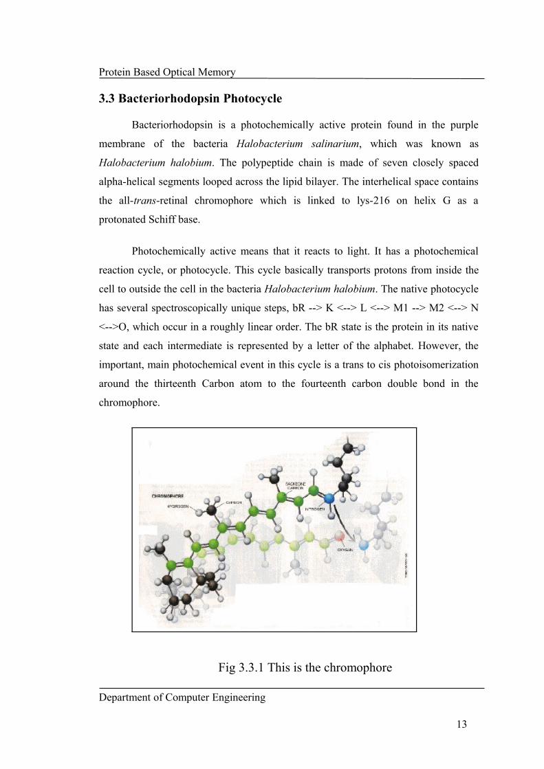
3.3 Bacteriorhodopsin Photocycle
Bacteriorhodopsin is a photochemically active protein found in the purple
membrane of the bacteria Halobacterium salinarium, which was known as
Halobacterium halobium. The polypeptide chain is made of seven closely spaced
alpha-helical segments looped across the lipid bilayer. The interhelical space contains
the all-trans-retinal chromophore which is linked to lys-216 on helix G as a
protonated Schiff base.
Photochemically active means that it reacts to light. It has a photochemical
reaction cycle, or photocycle. This cycle basically transports protons from inside the
cell to outside the cell in the bacteria Halobacterium halobium. The native photocycle
has several spectroscopically unique steps, bR --> K <--> L <--> M1 --> M2 <--> N
<-->O, which occur in a roughly linear order. The bR state is the protein in its native
state and each intermediate is represented by a letter of the alphabet. However, the
important, main photochemical event in this cycle is a trans to cis photoisomerization
around the thirteenth Carbon atom to the fourteenth carbon double bond in the
chromophore.
Fig 3.3.1 This is the chromophore
Department of Computer Engineering
13

Protein Based Optical Memory
At around the temperature of 80 K, the native protein undergoes this
photocycle and switches between a green absorbing state and a red absorbing state. At
approximately room temperature, the protein switches between a green absorbing
state and a blue absorbing state. In both the ground (green) and excited (red or blue)
states, the chromophore displays several metastable configurations. The main event
follows these steps:
1. A change in the shape of the conformational potential energy surface
resulting from electron excitation
2. A conformational change
3. A non-radiative decay to the ground state
The single critical step in the proton pumping ability of the protein is the
transfer of the Schiff base proton do D85, and piece of the protein, in the L --> M
reaction. Absorption of light leads to rapid photoisomerization in the excited state
because the barrier to conformation al change in that state is negative. In a manner of
thinking, the conformational motion of the excited state acts to gate the
conformational motion of the ground state.
In the L state, the Schiff base exhibits strong H-bonding with close water
molecules and distorts the chromophore near the Schiff base. The two necessary
coordinators for these water molecules are the anionic Asp85 and Asp212. That
coincides with the Trp182 interacting with the retinal skeleton by the 9-methyl group.
These events bring about the deprotonation of the Schiff base.
Also in the L intermediate state, the backbone has good local structural
flexibility. This is evidenced by the many different change in the peptide C to O
double bond stretching vibrational frequencies. Some of these frequency variations
correlate to the O to H single bond stretching vibrational frequencies. This indicates
that the structural changes can come from changing interaction with water molecules.
A network of H-bonding including bonds between water and peptides, exists between
two pieces of the protein, Asp85 and Asp96. This network exhibits changes most
Department of Computer Engineering
14
Protein Based Optical Memory
often in the bR to L transformation, which would be the first step in writing to a block
of bacteriorhodopsin memory.
In the K intermediate, an H-bonding change of the peptide C to O double bond
of a valine residue, called Val49, occurs. This stays on in the L intermediate, but is
gone in the M intermediate. This is affected by a mutation in the protein.
Water appears to affect the C to O double bond affects the protein at specific
regions. Some, which exhibit O to H single bond stretching frequencies, interact with
the C to O double bond of the Val49 piece.
The relative stability of some of the intermediate states determines their
usefulness in computing applications. The initial state of the native protein, often
designated bR, is quite stable. Some of the intermediates are stable at about 80K and
some are stable at room temperature, lending themselves to different types of RAM.
For computers, the two or three most stable states of the protein would be used
to record data in binary form. This is the proposed photocycle for computing needs:
An interesting intermediate in the photocycle is the O intermediate. The O
intermediate is an all-trans structure like the native protein state. The native state is a
light-adapted state. The O state is the red absorbing state.
The M state, or unprotonated Schiff base, does not accumulate in the
photocycle. This is strange since this protein transports protons. This could mean two
things. The first is that the M state cannot be observed because the kinetics is set
against its build-up. The other is that the Schiff base does not deprotonate and the
transport is based on a completely different mechanism than the wild type protein.
The two kinetic reasons for this lack of M are that the rate of decay of M is faster than
the rate of formation or that the L <--> M and M <--> N equilibrium are tilted away
from the M state.
Department of Computer Engineering
15

Protein Based Optical Memory
Fig 3.3.2 The photocycle for computer memory
3.4 Data OperationUnder this heading, we will study how to write data into memory, how to read data
from memory, how to erase data from memory and how to refresh memory.
3.4.1 Data Writing Technique
Bacteriorhodopsin, after being initially exposed to light (in our case a laser
beam), will change to between photoisomers during the main photochemical event
when it absorbs energy from a second laser beam. This process is known as sequential
one-photon architecture, or two-photon absorption. While early efforts to make use of
this property were carried out at cryogenic temperatures (liquid nitrogen
temperatures), modern research has made use of the different states of
bacteriorhodopsin to carry out these operations at room-temperature.
The process breaks down like this:
Department of Computer Engineering
16

Protein Based Optical Memory
Upon initially being struck with light (a laser beam), the bacteriorhodopsin
alters its structure from the bR native state to a form we will call the O state. After a
second pulse of light, the O state then changes to a P form, which quickly reverts to a
very stable Q state, which is stable for long periods of time (even up to several years).
The data writing technique proposed by Dr. Birge involves the use of a three-
dimensional data storage system. In this case, a cube of bacteriorhodopsin in a
polymer gel is surrounded by two arrays of laser beams placed at 90 degree angles
from each other. One array of lasers, all set to green (called "paging" beams),
activates the photocycle of the protein in any selected square plane, or page, within
the cube. After a few milliseconds, the number of intermediate O stages of
bacteriorhodopsin reaches near maximum. Now the other set, or array, of lasers - this
time of red beams - is fired.
Fig 3.4.1 The write process
The second array is programmed to strike only the region of the activated
square where the data bits are to be written, switching molecules there to the P
structure. The P intermediate then quickly relaxes to the highly stable Q state. We
then assign the initially-excited state, the O state, to a binary value of 0, and the P and
Q states are assigned a binary value of 1. This process is now analogous to the binary
Department of Computer Engineering
17

Protein Based Optical Memory
switching system which is used in existing semiconductor and magnetic memories.
However, because the laser array can activate molecules in various places throughout
the selected page or plane, multiple data locations (known as "addresses") can be
written simultaneously - or in other words, in parallel.
3.4.2 Data Reading Technique
The system for reading stored memory, either during processing or extraction
of a result, relies on the selective absorption of red light by the O intermediate state of
bacteriorhodopsin. To read multiple bits of data in parallel, we start just as we do in
the writing process. First, the green paging beam is fired at the square of protein to be
read. After two milliseconds (enough time for the maximum amount of O
intermediates to appear), the entire red laser array is turned on at a very low intensity
of red light. The molecules that are in the binary state 1 (P or Q intermediate states)
do not absorb the red light, or change their states, as they have already been excited
by the intense red light during the data writing stage.
Fig 3.4.2 The read process
Department of Computer Engineering
18

Protein Based Optical Memory
However, the molecules which started out in the binary state 0 (the O
intermediate state), do absorb the low-intensity red beams. A detector then images
(reads) the light passing through the cube of memory and records the location of the
O and P or Q structures; or in terms of binary code, the detector reads 0's and 1's. The
process is complete in approximately 10 milliseconds, a rate of 10 megabytes per
second for each page of memory.
Birge has built a prototype memory system where bacteriorhodopsin stores
data in a 3-D matrix. He builds this matrix by placing the protein into a cuvette (a
transparent vessel) filled with a polyacrylamide gel. The cuvette is oblong and 1 by 1
by 2 inches in size. The protein, which is in the bR state, gets fixed in place by the
polymerization of the gel. A battery of krypton lasers and a charge-injection device
(CID) array surround the cuvette and are used to write and read data.
Clearly, there are many advantages to protein-based memory, among the most
significant being cost, size, and memory density. However, there are still several
barriers standing in the way of mass-produced protein-based memories. Find out more
about what needs to be done before protein-based RAMs appear on the market.
3.4.3 Data Erasing
To erase data, a brief pulse from a blue laser returns molecules in the Q state
back to the rest state. The blue light doesn't necessarily have to be a laser; you can
bulk-erase the cuvette by exposing it to an incandescent light with ultraviolet output.
3.4.4 Refreshing the memory
To ensure data integrity during selective page-erase operations, Birge caches
several adjacent data pages. The read/write operations also use 2 additional parity bits
to guard against errors. A page of data can be read nondestructively about 5000 times.
Each page is monitored by a counter, and after 1024 reads, the page is refreshed via a
new write operation.
Department of Computer Engineering
19

Protein Based Optical Memory
Fig 3.5 Actual implementation
Department of Computer Engineering
20
Protein Based Optical Memory
4. Intrinsic Worth
However, the merits of molecular storage have garnered sufficient interest that
three of NASA's Space Shuttle missions explored methods to improve the
manufacture of the data cubes by using microgravity. The resulting material was more
homogeneous and provided an enhanced storage density. It remains to be seen,
however, whether microgravity manufacturing will be sufficiently cost-effective to
justify the observed factor-of-four improvement.
Can molecular storage compete with traditional semiconductor memory? The
design certainly has its merits. First, it's based on a protein that's inexpensive to
produce in quantity. In fact, genetic engineering is being used to boost the output of
the protein by the bacterium. Second, the system has the ability to operate over a
wider range of temperatures than semiconductor memory.
Third, the data is stable. If you turn off the memory system's power, the
bacteriorhodopsin molecules retain their information. This makes for an energy-
efficient computer that can be powered down yet still be ready to work with
immediately because the contents of its memory are preserved.
Data recorded on a bacteriorhodopsin storage device would be stable for
approximately five years. "We have lab samples that have held information reliably
for two years," he says. Another important feature of bacteriorhodopsin is that these
two states have widely different absorption spectra. This makes it easy to determine a
molecule's current state using a laser tuned to the proper frequency.
Finally, you can remove the small data cubes and ship gigabytes of data
around for storage or backups. Because the cubes contain no moving parts, it's safer
than using a small hard drive or cartridge for this task.
Department of Computer Engineering
21
Protein Based Optical Memory
5. Conclusion
Birge's system, which he categorizes as a level-I prototype (i.e., a proof of
concept), sits on a lab bench. He has received additional funding from the U.S. Air
Force, Syracuse University (Syracuse, NY), and the W. M. Keck Foundation to
develop a level-II prototype. Such a prototype would fit and operate within a desktop
personal computer. "We're a year or two away from doing internal testing on a level-II
prototype," says Birge. "Within three to five years, we could have a level-III beta-test
prototype ready, which would be a commercial product."
Department of Computer Engineering
22
Protein Based Optical Memory
6. References
1. Protein Based Computers Birge, Robert R., Scientific American March 1995
pp 90 – 95
2. Lewis, A., et al. 1997. Optical computation with negative light intensity with a
plastic bacteriorhodopsin film. Science 275(March 7):1462.
Department of Computer Engineering
23
Related Documents