Semiconductors, diodes, transistors (Horst Wahl, QuarkNet presentation, June 2001) ● Electrical conductivity ! Energy bands in solids ! Band structure and conductivity ● Semiconductors ! Intrinsic semiconductors ! Doped semiconductors " n-type materials " p-type materials ● Diodes and transistors ! p-n junction ! depletion region ! forward biased p-n junction ! reverse biased p-n junction ! diode ! bipolar transistor ! operation of bipolar pnp transistor ! FET

Welcome message from author
This document is posted to help you gain knowledge. Please leave a comment to let me know what you think about it! Share it to your friends and learn new things together.
Transcript
Semiconductors, diodes, transistors(Horst Wahl, QuarkNet presentation, June 2001)
Electrical conductivity! Energy bands in solids! Band structure and conductivity
Semiconductors! Intrinsic semiconductors! Doped semiconductors
" n-type materials" p-type materials
Diodes and transistors! p-n junction! depletion region! forward biased p-n junction! reverse biased p-n junction! diode! bipolar transistor! operation of bipolar pnp transistor! FET
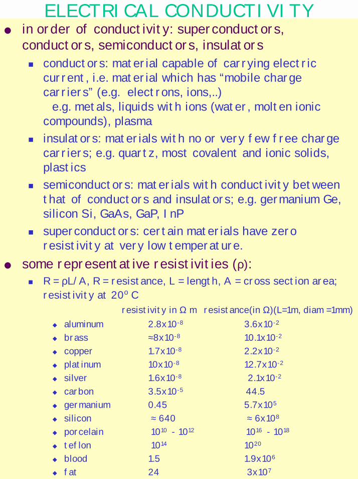
ELECTRICAL CONDUCTIVITY in order of conductivity: superconductors,
conductors, semiconductors, insulators ! conductors: material capable of carrying electric
current, i.e. material which has “mobile charge carriers” (e.g. electrons, ions,..)
e.g. metals, liquids with ions (water, molten ionic compounds), plasma
! insulators: materials with no or very few free charge carriers; e.g. quartz, most covalent and ionic solids, plastics
! semiconductors: materials with conductivity between that of conductors and insulators; e.g. germanium Ge, silicon Si, GaAs, GaP, InP
! superconductors: certain materials have zero resistivity at very low temperature.
some representative resistivities (ρ): ! R = ρL/A, R = resistance, L = length, A = cross section area;
resistivity at 20o Cresistivity in Ω m resistance(in Ω)(L=1m, diam =1mm)
" aluminum 2.8x10⁻⁸ 3.6x10⁻²
" brass ≈8x10⁻⁸ 10.1x10⁻²
" copper 1.7x10⁻⁸ 2.2x10⁻²
" platinum 10x10-8 12.7x10⁻²
" silver 1.6x10⁻⁸ 2.1x10⁻²
" carbon 3.5x10⁻⁵ 44.5" germanium 0.45 5.7x10⁵
" silicon ≈ 640 ≈ 6x10⁸
" porcelain 1010 - 1012 1016 - 1018
" teflon 1014 1020
" blood 1.5 1.9x10⁶
" fat 24 3x10⁷
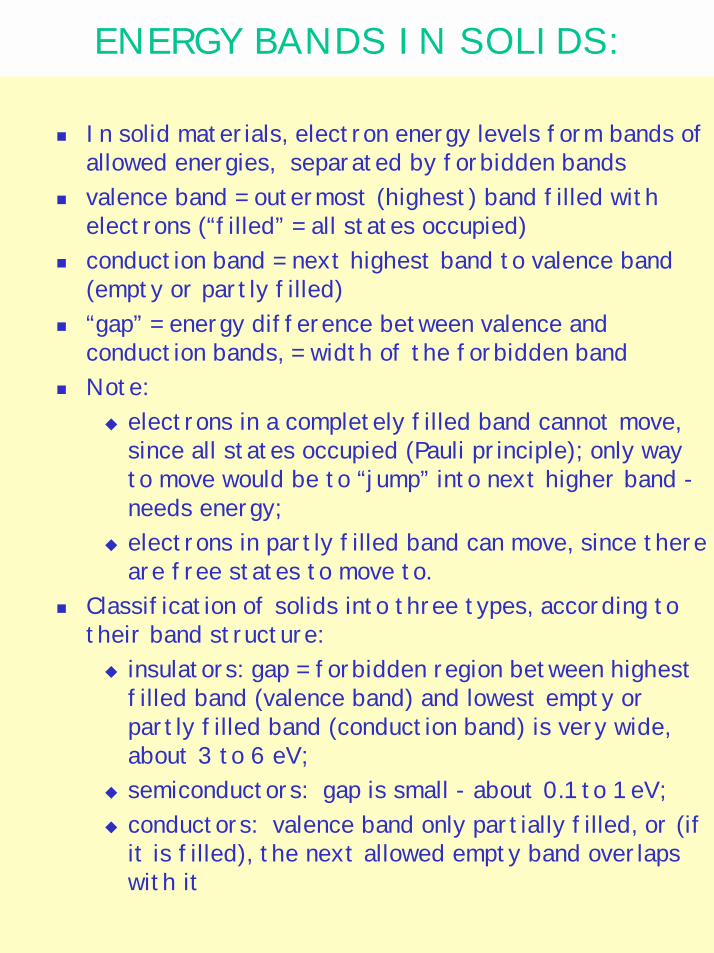
ENERGY BANDS IN SOLIDS:
! In solid materials, electron energy levels form bands of allowed energies, separated by forbidden bands
! valence band = outermost (highest) band filled with electrons (“filled” = all states occupied)
! conduction band = next highest band to valence band (empty or partly filled)
! “gap” = energy difference between valence and conduction bands, = width of the forbidden band
! Note: " electrons in a completely filled band cannot move,
since all states occupied (Pauli principle); only way to move would be to “jump” into next higher band -needs energy;
" electrons in partly filled band can move, since there are free states to move to.
! Classification of solids into three types, according to their band structure:
" insulators: gap = forbidden region between highest filled band (valence band) and lowest empty or partly filled band (conduction band) is very wide, about 3 to 6 eV;
" semiconductors: gap is small - about 0.1 to 1 eV; " conductors: valence band only partially filled, or (if
it is filled), the next allowed empty band overlaps with it
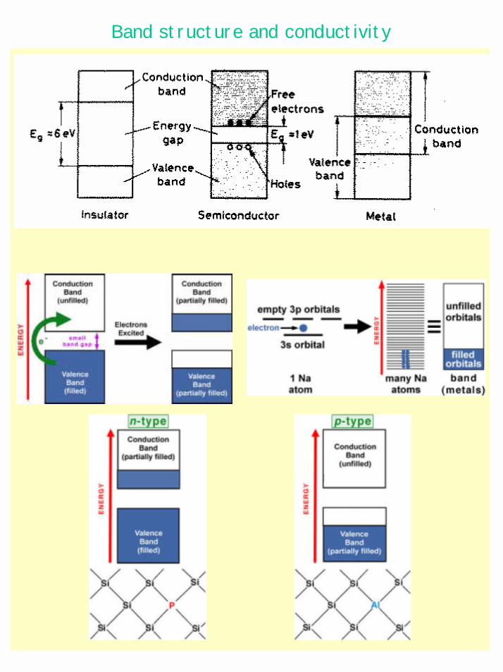
Band structure and conductivity
INTRINSIC SEMICONDUCTORS ! semiconductor = material for which gap between
valence band and conduction band is small; (gap width in Si is 1.1 eV, in Ge 0.7 eV).
! at T = 0, there are no electrons in the conduction band, and the semiconductor does not conduct (lack of free charge carriers);
! at T > 0, some fraction of electrons have sufficient thermal kinetic energy to overcome the gap and jump to the conduction band;
fraction rises with temperature; e.g. at 20o C (293 K), Si has 0.9x10¹⁰ conduction
electrons per cubic centimeter; at 50o C (323 K) there are 7.4x10¹⁰ .
! electrons moving to conduction band leave “hole” (covalent bond with missing electron) behind;
under influence of applied electric field, neighboring electrons can jump into the hole, thus creating a new hole, etc. ⇒ holes can move under the influence of an applied electric field, just like electrons;
both contribute to conduction. ! in pure Si and Ge, there are equally many holes (“p-
type charge carriers”) as there are conduction electrons (“n-type charge carriers”);
! pure semiconductors also called “intrinsic semiconductors”.
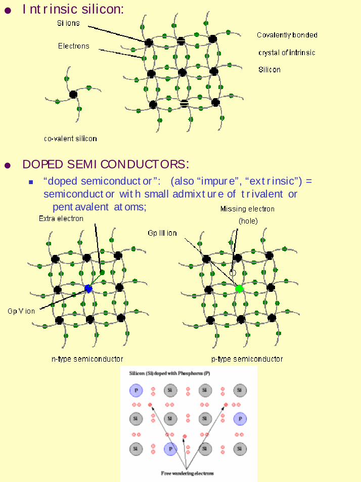
Intrinsic silicon:
DOPED SEMICONDUCTORS:! “doped semiconductor”: (also “impure”, “extrinsic”) =
semiconductor with small admixture of trivalent orpentavalent atoms;
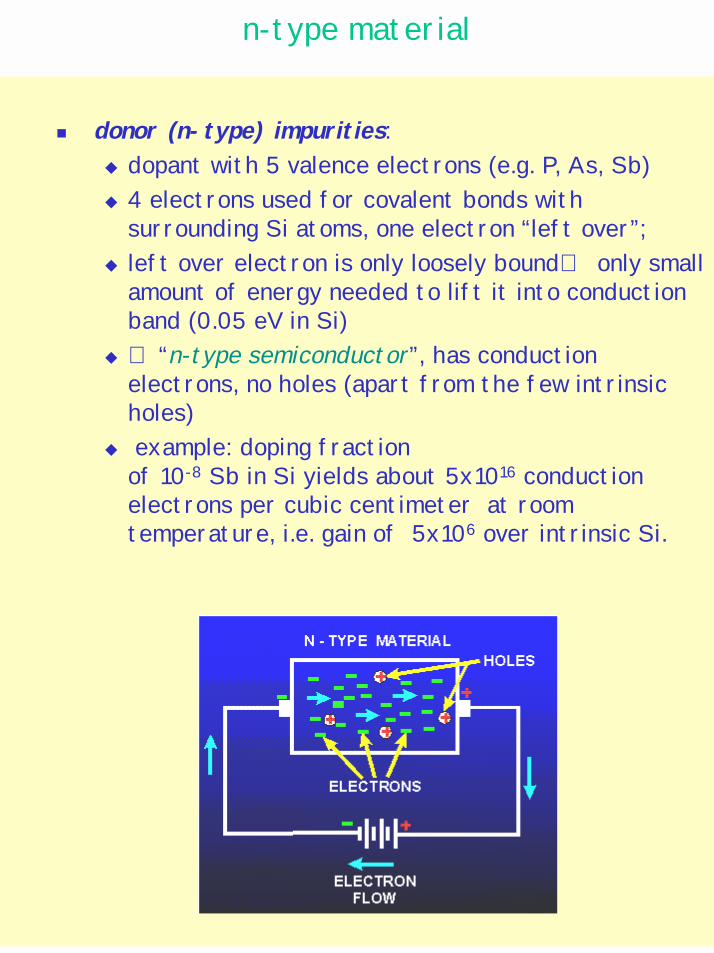
n-type material
! donor (n-type) impurities:" dopant with 5 valence electrons (e.g. P, As, Sb) " 4 electrons used for covalent bonds with
surrounding Si atoms, one electron “left over”; " left over electron is only loosely bound⇒ only small
amount of energy needed to lift it into conduction band (0.05 eV in Si)
" ⇒ “n-type semiconductor”, has conduction electrons, no holes (apart from the few intrinsic holes)
" example: doping fractionof 10-8 Sb in Si yields about 5x10¹⁶ conduction electrons per cubic centimeter at room temperature, i.e. gain of 5x10⁶ over intrinsic Si.
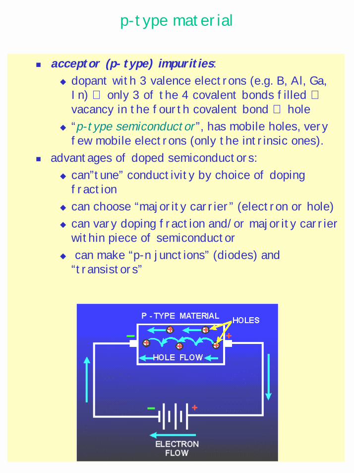
p-type material
! acceptor (p-type) impurities:" dopant with 3 valence electrons (e.g. B, Al, Ga,
In) ⇒ only 3 of the 4 covalent bonds filled ⇒vacancy in the fourth covalent bond ⇒ hole
" “p-type semiconductor”, has mobile holes, very few mobile electrons (only the intrinsic ones).
! advantages of doped semiconductors: " can”tune” conductivity by choice of doping
fraction " can choose “majority carrier” (electron or hole) " can vary doping fraction and/or majority carrier
within piece of semiconductor " can make “p-n junctions” (diodes) and
“transistors”
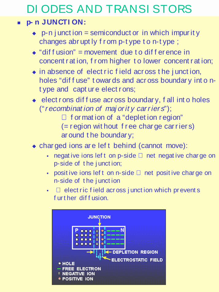
DIODES AND TRANSISTORS ! p-n JUNCTION:
" p-n junction = semiconductor in which impurity changes abruptly from p-type to n-type ;
" “diffusion” = movement due to difference in concentration, from higher to lower concentration;
" in absence of electric field across the junction, holes “diffuse” towards and across boundary into n-type and capture electrons;
" electrons diffuse across boundary, fall into holes (“recombination of majority carriers”);
⇒ formation of a “depletion region” (= region without free charge carriers) around the boundary;
" charged ions are left behind (cannot move):# negative ions left on p-side ⇒ net negative charge on
p-side of the junction; # positive ions left on n-side ⇒ net positive charge on
n-side of the junction # ⇒ electric field across junction which prevents
further diffusion.
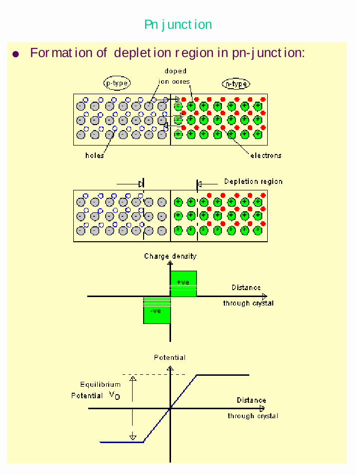
Pn junction
Formation of depletion region in pn-junction:
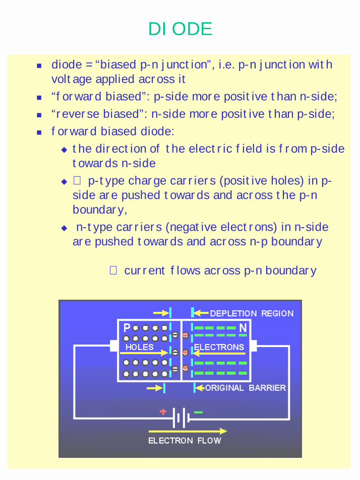
DIODE
! diode = “biased p-n junction”, i.e. p-n junction with voltage applied across it
! “forward biased”: p-side more positive than n-side; ! “reverse biased”: n-side more positive than p-side; ! forward biased diode:
" the direction of the electric field is from p-side towards n-side
" ⇒ p-type charge carriers (positive holes) in p-side are pushed towards and across the p-n boundary,
" n-type carriers (negative electrons) in n-side are pushed towards and across n-p boundary
⇒ current flows across p-n boundary
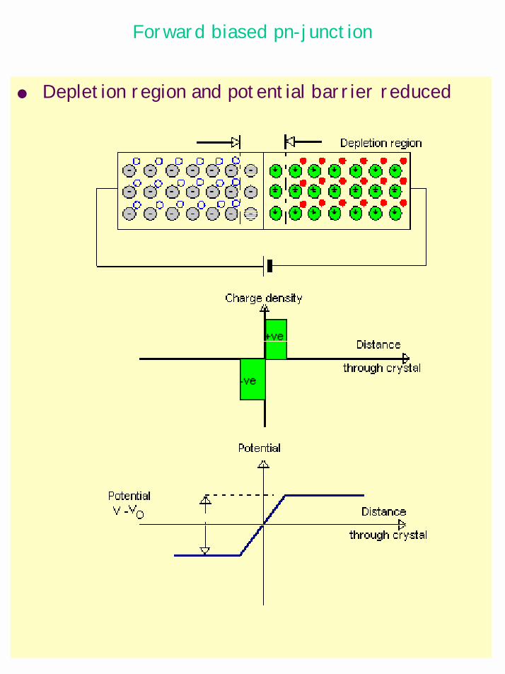
Forward biased pn-junction
Depletion region and potential barrier reduced

Reverse biased diode! reverse biased diode: applied voltage makes n-side
more positive than p-side ⇒ electric field direction is from n-side towards
p-side⇒ pushes charge carriers away from the p-n
boundary ⇒ depletion region widens, and no current flows
! diode only conducts when positive voltage applied to p-side and negative voltage to n-side
! diodes used in “rectifiers”, to convert ac voltage to dc.
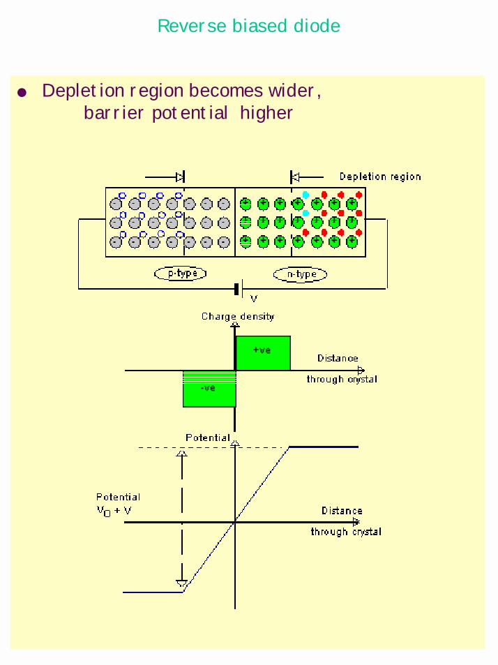
Reverse biased diode
Depletion region becomes wider, barrier potential higher
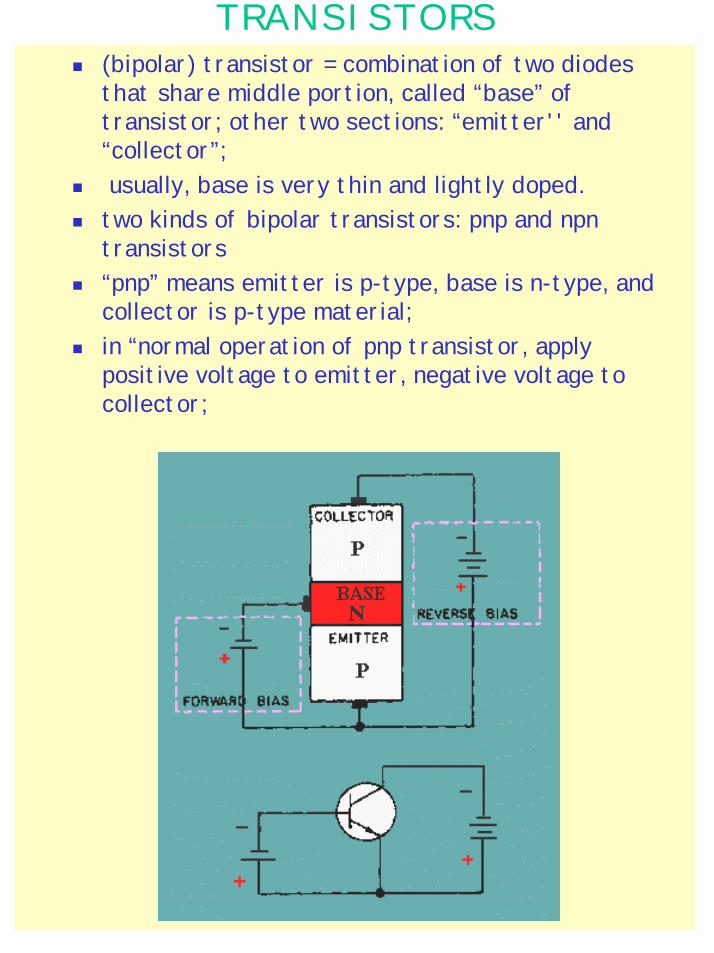
TRANSISTORS ! (bipolar) transistor = combination of two diodes
that share middle portion, called “base” of transistor; other two sections: “emitter'' and “collector”;
! usually, base is very thin and lightly doped. ! two kinds of bipolar transistors: pnp and npn
transistors ! “pnp” means emitter is p-type, base is n-type, and
collector is p-type material; ! in “normal operation of pnp transistor, apply
positive voltage to emitter, negative voltage to collector;
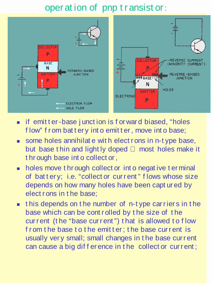
operation of pnp transistor:
! if emitter-base junction is forward biased, “holes flow” from battery into emitter, move into base;
! some holes annihilate with electrons in n-type base, but base thin and lightly doped ⇒ most holes make it through base into collector,
! holes move through collector into negative terminal of battery; i.e. “collector current” flows whose size depends on how many holes have been captured by electrons in the base;
! this depends on the number of n-type carriers in the base which can be controlled by the size of the current (the “base current”) that is allowed to flow from the base to the emitter; the base current is usually very small; small changes in the base current can cause a big difference in the collector current;
Transistor operation! transistor acts as amplifier of base current, since
small changes in base current cause big changes in collector current.
! transistor as switch: if voltage applied to base is such that emitter-base junction is reverse-biased, no current flows through transistor -- transistor is “off”
! therefore, a transistor can be used as a voltage-controlled switch; computers use transistors in this way.
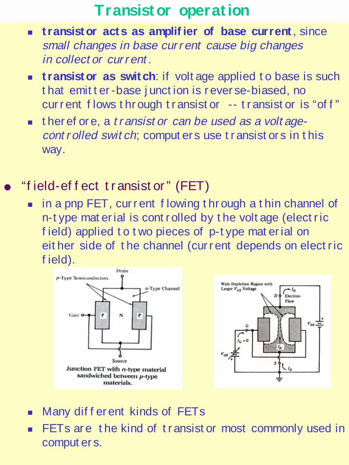
“field-effect transistor” (FET) ! in a pnp FET, current flowing through a thin channel of
n-type material is controlled by the voltage (electric field) applied to two pieces of p-type material on either side of the channel (current depends on electric field).
! Many different kinds of FETs! FETs are the kind of transistor most commonly used in
computers.
Related Documents


